US9355965B2 - Semiconductor devices and methods of making the same - Google Patents
Semiconductor devices and methods of making the sameDownload PDFInfo
- Publication number
- US9355965B2 US9355965B2US14/812,200US201514812200AUS9355965B2US 9355965 B2US9355965 B2US 9355965B2US 201514812200 AUS201514812200 AUS 201514812200AUS 9355965 B2US9355965 B2US 9355965B2
- Authority
- US
- United States
- Prior art keywords
- thickness
- laser
- buried structure
- substrate
- device layer
- Prior art date
- Legal status (The legal status is an assumption and is not a legal conclusion. Google has not performed a legal analysis and makes no representation as to the accuracy of the status listed.)
- Active
Links
Images


Classifications
- H—ELECTRICITY
- H01—ELECTRIC ELEMENTS
- H01L—SEMICONDUCTOR DEVICES NOT COVERED BY CLASS H10
- H01L23/00—Details of semiconductor or other solid state devices
- H01L23/544—Marks applied to semiconductor devices or parts, e.g. registration marks, alignment structures, wafer maps
- H—ELECTRICITY
- H01—ELECTRIC ELEMENTS
- H01L—SEMICONDUCTOR DEVICES NOT COVERED BY CLASS H10
- H01L21/00—Processes or apparatus adapted for the manufacture or treatment of semiconductor or solid state devices or of parts thereof
- H01L21/02—Manufacture or treatment of semiconductor devices or of parts thereof
- H01L21/04—Manufacture or treatment of semiconductor devices or of parts thereof the devices having potential barriers, e.g. a PN junction, depletion layer or carrier concentration layer
- H01L21/18—Manufacture or treatment of semiconductor devices or of parts thereof the devices having potential barriers, e.g. a PN junction, depletion layer or carrier concentration layer the devices having semiconductor bodies comprising elements of Group IV of the Periodic Table or AIIIBV compounds with or without impurities, e.g. doping materials
- H01L21/26—Bombardment with radiation
- H01L21/263—Bombardment with radiation with high-energy radiation
- H01L21/268—Bombardment with radiation with high-energy radiation using electromagnetic radiation, e.g. laser radiation
- H01L21/2686—Bombardment with radiation with high-energy radiation using electromagnetic radiation, e.g. laser radiation using incoherent radiation
- H—ELECTRICITY
- H01—ELECTRIC ELEMENTS
- H01L—SEMICONDUCTOR DEVICES NOT COVERED BY CLASS H10
- H01L22/00—Testing or measuring during manufacture or treatment; Reliability measurements, i.e. testing of parts without further processing to modify the parts as such; Structural arrangements therefor
- H01L22/20—Sequence of activities consisting of a plurality of measurements, corrections, marking or sorting steps
- H01L29/04—
- H01L29/0649—
- H01L29/16—
- H01L29/1608—
- H01L29/2003—
- H—ELECTRICITY
- H10—SEMICONDUCTOR DEVICES; ELECTRIC SOLID-STATE DEVICES NOT OTHERWISE PROVIDED FOR
- H10D—INORGANIC ELECTRIC SEMICONDUCTOR DEVICES
- H10D62/00—Semiconductor bodies, or regions thereof, of devices having potential barriers
- H10D62/10—Shapes, relative sizes or dispositions of the regions of the semiconductor bodies; Shapes of the semiconductor bodies
- H10D62/113—Isolations within a component, i.e. internal isolations
- H10D62/115—Dielectric isolations, e.g. air gaps
- H—ELECTRICITY
- H10—SEMICONDUCTOR DEVICES; ELECTRIC SOLID-STATE DEVICES NOT OTHERWISE PROVIDED FOR
- H10D—INORGANIC ELECTRIC SEMICONDUCTOR DEVICES
- H10D62/00—Semiconductor bodies, or regions thereof, of devices having potential barriers
- H10D62/40—Crystalline structures
- H—ELECTRICITY
- H10—SEMICONDUCTOR DEVICES; ELECTRIC SOLID-STATE DEVICES NOT OTHERWISE PROVIDED FOR
- H10D—INORGANIC ELECTRIC SEMICONDUCTOR DEVICES
- H10D62/00—Semiconductor bodies, or regions thereof, of devices having potential barriers
- H10D62/80—Semiconductor bodies, or regions thereof, of devices having potential barriers characterised by the materials
- H10D62/83—Semiconductor bodies, or regions thereof, of devices having potential barriers characterised by the materials being Group IV materials, e.g. B-doped Si or undoped Ge
- H10D62/832—Semiconductor bodies, or regions thereof, of devices having potential barriers characterised by the materials being Group IV materials, e.g. B-doped Si or undoped Ge being Group IV materials comprising two or more elements, e.g. SiGe
- H10D62/8325—Silicon carbide
- H—ELECTRICITY
- H10—SEMICONDUCTOR DEVICES; ELECTRIC SOLID-STATE DEVICES NOT OTHERWISE PROVIDED FOR
- H10D—INORGANIC ELECTRIC SEMICONDUCTOR DEVICES
- H10D62/00—Semiconductor bodies, or regions thereof, of devices having potential barriers
- H10D62/80—Semiconductor bodies, or regions thereof, of devices having potential barriers characterised by the materials
- H10D62/85—Semiconductor bodies, or regions thereof, of devices having potential barriers characterised by the materials being Group III-V materials, e.g. GaAs
- H10D62/8503—Nitride Group III-V materials, e.g. AlN or GaN
- H—ELECTRICITY
- H01—ELECTRIC ELEMENTS
- H01L—SEMICONDUCTOR DEVICES NOT COVERED BY CLASS H10
- H01L22/00—Testing or measuring during manufacture or treatment; Reliability measurements, i.e. testing of parts without further processing to modify the parts as such; Structural arrangements therefor
- H01L22/10—Measuring as part of the manufacturing process
- H01L22/12—Measuring as part of the manufacturing process for structural parameters, e.g. thickness, line width, refractive index, temperature, warp, bond strength, defects, optical inspection, electrical measurement of structural dimensions, metallurgic measurement of diffusions
- H—ELECTRICITY
- H01—ELECTRIC ELEMENTS
- H01L—SEMICONDUCTOR DEVICES NOT COVERED BY CLASS H10
- H01L2223/00—Details relating to semiconductor or other solid state devices covered by the group H01L23/00
- H01L2223/544—Marks applied to semiconductor devices or parts
- H01L2223/54406—Marks applied to semiconductor devices or parts comprising alphanumeric information
- H—ELECTRICITY
- H01—ELECTRIC ELEMENTS
- H01L—SEMICONDUCTOR DEVICES NOT COVERED BY CLASS H10
- H01L2223/00—Details relating to semiconductor or other solid state devices covered by the group H01L23/00
- H01L2223/544—Marks applied to semiconductor devices or parts
- H01L2223/54433—Marks applied to semiconductor devices or parts containing identification or tracking information
- H—ELECTRICITY
- H01—ELECTRIC ELEMENTS
- H01L—SEMICONDUCTOR DEVICES NOT COVERED BY CLASS H10
- H01L2223/00—Details relating to semiconductor or other solid state devices covered by the group H01L23/00
- H01L2223/544—Marks applied to semiconductor devices or parts
- H01L2223/54453—Marks applied to semiconductor devices or parts for use prior to dicing
- H—ELECTRICITY
- H01—ELECTRIC ELEMENTS
- H01L—SEMICONDUCTOR DEVICES NOT COVERED BY CLASS H10
- H01L2924/00—Indexing scheme for arrangements or methods for connecting or disconnecting semiconductor or solid-state bodies as covered by H01L24/00
- H—ELECTRICITY
- H01—ELECTRIC ELEMENTS
- H01L—SEMICONDUCTOR DEVICES NOT COVERED BY CLASS H10
- H01L2924/00—Indexing scheme for arrangements or methods for connecting or disconnecting semiconductor or solid-state bodies as covered by H01L24/00
- H01L2924/0001—Technical content checked by a classifier
- H01L2924/0002—Not covered by any one of groups H01L24/00, H01L24/00 and H01L2224/00
Definitions
- the present applicationrelates, in general, to electronics, and more particularly, to semiconductors, structures thereof, and methods of forming semiconductor devices.
- a substrate wafercan be made of a bulk semiconductor material such as silicon or a bulk material with a top layer, for example deposited using a homo- or hetero-epitaxial deposition process, or a wafer bonding process.
- Semiconductor substratescan be processed in highly-automated wafer fabs that use identification of each wafer. Also, engineering tests may have required additional identification of the processed wafers. Such identification can be provided with laser scribing on the wafer. A laser beam can be used to locally melt the material and thereby a visible “spot” was produced. From such spots symbols can be created. In some cases it was difficult for equipment to read the identification marked onto the wafers. If the identification markings could not be read, it was difficult or impossible to use the wafers in the automated fabs.
- FIG. 1Aillustrates one example of identification marks formed by prior laser marking methods on a silicon-on-insulator structure having a buried layer having a thickness of about 0.6 ⁇ m and a device layer having a thickness of about 1.5 ⁇ m;
- FIG. 1Billustrates one example of identification marks formed by prior laser marking methods on a silicon-on-insulator structure having a buried layer having a thickness of about 1 ⁇ m and a device layer having a thickness of about 3 ⁇ m;
- FIG. 2schematically illustrates (not to scale) one example of the reflection of light from a layered structure
- FIG. 3is a cross-sectional view (not to scale) of one example of a layered structure that can be laser marked according the methods disclosed in the present application;
- FIG. 4is a graph showing an example of the reflectivity relative to photon energy for two silicon-on-insulator layered structures
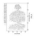
- FIG. 5is a graph showing an example of the reflectivity relative to the device layer thickness for a silicon-on-insulator structure having a buried structure with a thickness of about 0.3 ⁇ m and at a photon energy of 1 eV;
- FIG. 6is a graph showing an example of the reflectivity relative to the photon energy for two silicon-on-insulator structures.
- FIG. 7illustrates one example of identification marks formed by laser marking methods on a silicon-on-insulator structure according to some embodiments of the present application.
- current carrying electrodemeans an element of a device that carries current through the device such as a source or a drain of an MOS transistor or an emitter or a collector of a bipolar transistor or a cathode or anode of a diode
- a control electrodemeans an element of the device that controls current through the device such as a gate of an MOS transistor or a base of a bipolar transistor.
- doped regions of device structuresare illustrated as having generally straight line edges and precise angular corners. However, those skilled in the art understand that due to the diffusion and activation of dopants the edges of doped regions generally may not be straight lines and the corners may not be precise angles.
- the present applicationincludes, among other things, providing a semiconductor substrate including: a base substrate having a first semiconductor material; a buried structure; and a device layer having a second semiconductor material, where the buried structure is disposed between the base substrate and the device layer; and laser inscribing the semiconductor substrate, where the buried structure has a thickness equal to about k ⁇ laser /(2 ⁇ n), where: ⁇ laser is a wavelength of peak emission for the light applied to inscribe the semiconductor substrate; k is an integer greater than zero (1, 2, 3 . . . ); and n is an index of refraction for the buried structure.
- interference of laser light within the layered structure of a semiconductor wafercan result in significant reflection or interference of the incident light. If the light is reflected and does not penetrate the layered structure deep enough, the material may not melt or ablate in response to the laser. If the light is refracted or internally reflected the material may overheat and create a large or distorted spot.
- the problems with laser scribing or marking of layered substratesmay appear over the whole wafer surface as well as only within localized areas.
- the thicknesses of the layers and their optical propertiesare “unfavorable”, then marking of the wafer may not result in the desired identification of the wafer.
- Problems with laser scribingmay be caused by thickness variability of the layers of the semiconductor material on a semiconductor wafer. For example, the spot size in a wafer identification character or barcode may not have controlled dimensions and appearance. Also, the interaction of the laser with the semiconductor structure may result in marks that are not predictable, thus, not readable, such as by automated readers.
- FIG. 1Aillustrates one example identification marks formed by prior laser marking methods on a silicon-on-insulator structure having a buried layer having a thickness of about 0.6 ⁇ m and a device layer having a thickness of about 1.5 ⁇ m.
- the laser markingwas produced using light with a wavelength of peak emission of about 1064 nm. Without being bound to any particular theory, applicants believe this variation results from slight thickness changes in the device layer.
- FIG. 1Billustrates another example of identification marks formed by prior laser marking methods on a silicon-on-insulator structure having a buried layer having a thickness of about 3 ⁇ m and a device layer having a thickness of about 1 ⁇ m.
- the laser markingwas also produced using light with a wavelength of peak emission of about 1064 nm. Note the “standing wave” appearance in both figures across the character set as the light is passing through a layer thickness that is a multiple of the incident light wavelength.
- FIG. 1AThe dependence of the “size” of the laser scribe mark on the device layer thickness is illustrated in FIG. 1A . Variations of the device layer thickness are shown as the interference color band pattern visible. The “problematic” laser spots (the small ones) are localized in bands corresponding to certain interference fringes, which correspond to regions in the device layer having certain thicknesses.
- the present applicationalso relates to semiconductor substrates and semiconductor chips that, in some embodiments, can be obtained by the methods disclosed herein.
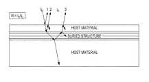
- FIG. 2is a ray diagram that schematically illustrates the reflection of light from a layered structure including a buried structure of several layers.
- An arrow identified as I 0represents near-normal incident light.
- Arrow 1represents reflected light
- arrow 2represents light reflected from the first interface, along with subsequent transmissions and reflections at interfaces with discontinuities of the dielectric constants. Additional multiple reflections and refraction may occur as illustrated by other arrows.
- the total intensity of the reflected light, I Ris a the sum of beams 1 , 2 , 3 , and more, i.e., all beams after reflections from all interfaces, including multiple reflections back and forth in each layer.
- Some embodiments disclosed hereininclude selecting a layered system and wavelength of light for laser marking the layered system so that the marking exhibits improved legibility, machine-readability, uniformity, and/or darkness. Without being bound to any particular theory, it is believed that, in some embodiments, the amount of reflected light is reduced during laser marking. In some embodiments, the dependence of the reflected intensity on the thickness of the “top” layer (e.g., device layer) is suppressed. As a consequence, the stable formation of laser marks may be improved and may not be substantially deteriorated by common variations in the thickness of the top layer.
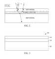
- FIG. 3is a cross-sectional view of one example of a layered structure that can be laser marked according some embodiments of the methods disclosed in the present application.
- Layered structure 300includes base substrate 310 , buried layer 320 , and device layer 330 .
- the layered structuree.g., layered structure 300
- the layered structureis a semiconductor substrate.
- the layered structureis a silicon-on-insulator (SOI) structure.
- SOIsilicon-on-insulator
- the layered structuremay be, for example, a semiconducting wafer that may be used to manufacture one or more semiconductor devices.
- buried layer 320is illustrated as coextensive with base substrate 310 and device layer 330 , the skilled artisan will appreciate that the present application is not limited to this configuration.
- the buried structuremay be embedded within base layer and device layer.
- a three-layered structureis illustrated for simplicity, however more complex structures are within the scope of the present application.
- the layered structuremay contain multiple, distinct buried structures in separate regions. In these instances, the thickness of the buried structure aligned with the region that is laser marked may be used to determine appropriate laser marking conditions or layered structure dimensions.
- the materials within the layered structureare not particularly limited and may be selected according to design choices.
- the base substratee.g., base substrate 310
- the base substratecan be, for example, silicon, GaN, SiC, sapphire, or any other suitable material.
- the buried structure(e.g., buried layer 320 ) can be an insulating material. In some embodiments, the buried structure is a homogenous material. In some embodiments, the buried structure is a non-absorbing material for the light applied to the layered structure when laser marking.
- the buried structurecan be, for example, silicon dioxide, AlN, AlGaN or any other suitable material.
- the device layer(e.g., device layer 330 ) is a semiconducting material.
- the device layercan be, for example, silicon, GaN, SiC, sapphire, or any other suitable material.
- the device layeris monocrystalline (e.g., single crystal silicon).
- the device layer and base substrateare the same material.
- the device layer and base substrateare different materials.
- the buried structureis an oxide of either the device layer or the base substrate.
- the device layercan be silicon and the buried structure can be silicon dioxide.
- the layered structurecan have a base substrate that is silicon, a buried structure that is silicon dioxide, and a device layer that is silicon.
- the dimensions of the layered structureare not particularly limited and may be selected according to design choices. In some embodiments, the dimension may be selected at least in part based on the wavelength of peak emission for a laser that is used to mark the layered structure.
- the base substratecan have a thickness of, for example, at least about 50 ⁇ m; at least about 100 ⁇ m; at least about 250 ⁇ m; or at least about 300 ⁇ m.
- the base substratecan have a thickness of, for example, less than or equal to about 1.5 mm; less than or equal to about 1 mm; less than or equal to about 750 ⁇ m; or less than or equal to about 650 ⁇ m. In some embodiments, the thickness of the base substrate can be about 50 ⁇ m to about 1.5 mm, or about 250 ⁇ m to about 750 ⁇ m.
- Non-limiting examples of thicknesses for the base substrateinclude 525 ⁇ m or 625 ⁇ m.
- the buried structurecan have a thickness of, for example, at least about 0.001 ⁇ m; at least about 0.1 ⁇ m; or at least about 0.5 ⁇ m.
- the buried structurecan have a thickness of, for example, less than or equal to about 5 ⁇ m; less than or equal to about 3 ⁇ m; less than or equal to about 1.5 ⁇ m; or less than or equal to about 1 ⁇ m.
- the buried structurehas a thickness of about 0.01 ⁇ m to about 5 ⁇ m, or about 0.1 ⁇ m to about 1.5 ⁇ m.
- the device layercan have a thickness of, for example, at least about 0.1 ⁇ m; at least about 1 ⁇ m; at least about 3 ⁇ m; at least about 10 ⁇ m; or at least about 50 ⁇ m.
- the device layercan have a thickness of, for example, less than or equal to about 500 ⁇ m; less than or equal to about 250 ⁇ m; less than or equal to about 150 ⁇ m; or less than or equal to about 100 ⁇ m.
- the device layerhas a thickness of about 0.1 ⁇ m to about 500 ⁇ m, or about 1 ⁇ m to about 150 ⁇ m.
- the layered structureis a silicon-on-insulator (SOI) wafer.
- SOIsilicon-on-insulator
- the methods of the present applicationare not limited to any particular SOI wafer structure, and the SOI wafer can be prepared using standard techniques. Examples of techniques for the SOI wafer include, but are not limited to, SIMOX, Bond and Grind-back SOI (BGSOI), Bond and Etch-back SOI (BESOI), ELTRAN, or SMART-CUT.
- SIMOX technologyutilizes oxygen implantation and subsequent annealing to separate the device layer and substrate by a layer of buried oxide.
- the other technologiesutilize bonding of two wafers (device wafer and handle wafer), where at least one wafer has the bonded surface covered by an insulating layer such as silicon oxide or silicon nitride.
- the bonded surfacesare joined by hydrogen bonds at first, but more covalent-like bonds are formed after high temperature annealing.
- the technologiesdiffer in the thinning of the device wafer in order to reach the desired device layer thickness.
- the BGSOI technologyuses grinding and polishing.
- BESOIutilizes selective etching to a predefined etch-stop layer formed in the device wafer prior to the bonding.
- ELTRANis based on porous silicon layer and wafer cut. Other methods may utilize hydrogen ion implantation into the device wafer before the bonding step.
- the manufacturing procedures for SOI waferscan result in variability of the device layer thickness.
- the variability of the device layer thicknessis believed to make it difficult to produce machine-readable laser markings on the substrate.
- the thickness variationsmay be especially pronounced in the near-perimeter area, where laser scribing is typically formed.
- the variability of the device layer thicknessmay modify the amount of the light penetrating the surface region and alter the resonance condition, and thus influences the quality of the laser marking. The larger the nominal device layer thickness the greater the interference spectrum. Local variability also has an influence.
- the thickness of the buried structuremay, in some embodiments, be proportional to the wavelength of peak emission for a laser that is used to mark the layered structure.
- the layered structurecan exhibit improved marking properties (e.g., more uniform marks).
- it is believed the interferences above the buried structure on the laser lightcan be reduced and the influence of the device layer thickness on the amount of penetrating light may also be decreased. This can reduce problems with laser marking for any thickness of the device layer.
- a layered structuremay contain a silicon dioxide buried structure having an index of refraction equal to about 1.45.
- a layered structuremay contain an AlN buried structure having index of refraction equal to about 2.13.
- some embodiments of the laser marking methodinclude forming a laser mark on a semiconductor wafer using a laser with a wavelength of peak emission as defined by Equation (1) for a given thickness d of the buried structure. That is, the wavelength of peak emission can be equal to (2 ⁇ d ⁇ n)/k.
- a wavelength of peak emissionBy selecting a wavelength of peak emission, improved marks can be formed on the structure by the laser. For example, it can reduce variations in the marks (e.g., which may result from variations in the thickness of the top layer of a semiconductor device).
- the thickness of the device layermay vary, the thickness of the buried structure may be more easily controlled. In many silion-on-insulator wafer specifications, the buried structure is specified in a manner thinner than, or thicker than, a certain value, or a thickness range is allowed. Thus, the thickness of the buried structure may be selected to facilitate laser marking that may be more easily read or detected without adversely affecting the characteristic of the devices.
- the layered structuree.g., layered structure 300 as depicted in FIG. 3
- the variability in thickness for the buried structurecan be, for example, less than or equal to about 15%; less than or equal to about 10%; less than or equal to about 5%; less than or equal to about 3%; or less than or equal to about 1%.
- the device layer of the layered structurecan have a variation in thickness of at least about 3%; at least about 5%; at least about 7%; at least about 10%; or at least about 15%.
- the wavelength of peak emission of the lasercan be tuned using standard techniques.
- the wavelengthcan be reduced using an optical frequency multiplier (e.g., a doubler)
- wavelength-selective optical elementsmay be use to a select a particular wavelength.
- the laser wavelengthmay therefore be tuned to an appropriate wavelength based on the thickness of the buried structure (e.g., using Equation (1)).
- the laser markingis performed using a tunable laser.
- the tunable lasermay permit selecting an appropriate wavelength of light to apply to the layered structure for forming the laser marking.
- the wavelength of peak emission for the light applied to the layered structure for laser markingcan be, for example, at least about 200 nm; at least about 400 nm; at least about 500 nm; at least about 600 nm; at least about 700 nm; at least about 800 nm; or at least about 1000 nm.
- the wavelength of peak emission for the light applied to the layered structure for laser markingcan be, for example, less than or equal to about 1500 nm; less than or equal to about 1300 nm; less than or equal to about 1100 nm; less than or equal to about 1000 nm; or less than or equal to about 800 nm.
- the wavelength of peak emission for the light applied to the layered structure for laser markingcan be about 200 nm to about 1500 nm. In some embodiments, the wavelength of peak emission for the light applied to the layered structure for laser marking can be in the near infrared.
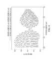
- FIG. 4is a graph showing an example of the reflectance relative to photon energy (which is inversely proportional to the wavelength) for two silicon-on-insulator layered structures.
- the dashed lineillustrates a wafer having a device layer (approximately 2.0 ⁇ m thick) and a buried structure (approximately 0.3 ⁇ m thick).
- the solid lineillustrates a wafer having a device layer (approximately 2.1 ⁇ m thick) and a buried structure (approximately 0.3 ⁇ m thick).
- a lower reflectivityproduces larger, more uniform laser markings.
- the reflectivityis an oscillating function dependent on the thickness of the top silicon layer (device layer) and the buried layer. Due to these oscillations the amount of light reflected from the layered structure may vary from desirably low values to unacceptably high values with only a small change in the device layer thickness. However at about ⁇ 1.4 eV (or about 0.89 ⁇ m in wavelength), both plots exhibit similarly low reflectance. It is within the vicinity of these nodes where laser marking can be performed to obtain markings that do not significantly vary with the thickness of the device layer. In other words, near the node at about ⁇ 1.4 eV, variations in the thickness of the device layer do not substantially affect the laser marking outcome.
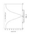
- FIG. 5is a graph showing an example of the reflectivity relative to the device layer thickness for a layered structure having a buried structure (BOX) with a thickness of about 0.3 ⁇ m and at a photon energy of 1 eV (or about 1.24 ⁇ m in wavelength).
- FIG. 5demonstrates that the reflectance can vary significantly with small changes in the device layer thickness. For example, an increase in device layer thickness from 2.10 ⁇ m to 2.15 ⁇ m (an approximately 2% increase) increases the reflectivity from about 0.05 to about 0.7.
- the interferences of the laser light in the layered structureare caused by multiple reflections from the optical interfaces present in the structure. This interference (and therefore increased reflection) is not present in bulk silicon or other bulk semiconductor wafers. Therefore, if the BOX is not present, or is not “visible” to the light with the given wavelength, the interference pattern vanishes and the reflectivity cannot rise above a critical value.
- the interferencesmay be reduced if the buried structure is generally homogenous and made from a non-absorbing material.
- the phase-shift caused by the light traveling through the buried structurecan be approximately an integer multiple of 2 ⁇ pi (the Ludolphine number).
- the laser lightis not substantially influenced by the interferences above the buried structure and the device layer thickness has little effect on the amount of penetrated light.
- FIG. 6is a graph showing an example of the reflectivity relative to the photon energy for two layered structures.
- the solid lineis a wafer having a device layer of about 2.0 ⁇ m thick and a buried oxide of about 0.428 ⁇ m thick.
- the dashed lineis a wafer having a device layer of about 2.0 ⁇ m and a buried oxide of about 0.856 ⁇ m thick. Note the multiple null regions, and the different resonant conditions for different silicon-oxide layer combinations.
- the reflectivity spectrumis calculated for a buried structure thickness with a laser photon energy of 1 eV.
- This calculationcan be made for a buried oxide structure (e.g., in silicon-on-insulator structures), but can also apply to any non-absorbing layer or system of non-absorbing layers. If the system also includes absorbing layers, the dependence on the device layer thickness can be further reduced with the proper selection of the layer thicknesses.
- Equation (2)may be satisfied by changing ⁇ laser .
- ⁇ laserFor example, for a layered structure thinner than ⁇ laser /(2 ⁇ n), a laser with shorter wavelength (higher photon energy) may be beneficial.
- FIG. 7illustrates one example of identification marks formed by laser marking methods on a silicon-on-insulator structure according to some embodiments of the present application.
- the silicon device layerwas about 3 ⁇ m thick and the silicon oxide insulating layer was about 720 nm thick.
- a Nd:YAG laser having a wavelength of peak emission of about 1064 nmwas used to laser mark the silicon-on-insulator structure.
- the laser markingsare more uniform in size and darkness regardless of the interference pattern when applied according to some embodiments of the present application.
- the laser markingcan be improved (e.g., uniform spot size) by adding an “anti-reflection” surface layer.
- the reflection from the interfacemay be high if there is a large difference in the refractive indices.
- a thin non-absorbing surface layer with an index of refraction in-between the index of refraction of the wafer and the ambientwill enable more light to penetrate into the sample.
- a thin silicon oxide surface layer on a silicon waferwill reduce the surface reflectivity.
- the non-absorbing layerhas a thickness about 0.05 ⁇ m to about 10 ⁇ m, about 0.1 ⁇ m to about 2 ⁇ m, or about 0.1 ⁇ m to about 1 ⁇ m
- the thickness of the layered structuremay be formed to facilitate laser marking a substrate and enabling detection/reading of the laser marks.
- Some embodiments disclosed hereininclude a method of laser marking that can include determining a thickness of a buried structure, selecting a wavelength of peak emission of light for laser marking the layered structure based on the thickness of the buried structure, and laser marking the layered structure using the light having the selected wavelength of peak emission.
- the wavelengthcan be determined, for example, using Equations (1) or (2) disclosed above.
- the wavelength of peak emissionis approximately equal to (2 ⁇ d ⁇ n)/k, wherein: d is a thickness of the buried structure; k is an integer greater than zero (1, 2, 3 . . . ); and n is an index of refraction for the buried structure.
- the procedure for determining the thickness of the buried structureis not particularly limited.
- the thicknesscan be determined by receiving data that corresponds to the thickness of the buried structure.
- a usermay provide the thickness of the buried structure for one or more layered structures to a controller for a laser marking device (e.g., using a keyboard).
- a controller for the laser marking devicecan electronically receive over a network manufacturing condition, a lot number, or other information that corresponds with the thickness of the buried structure.
- a machine readable identifiercan be used to determine the thickness.
- the layered structuremay have a bar code, machine-readable letters, and the like disposed on the layered structure or packaging that contains the layered structure.
- a readere.g., a bar code scanner or machine vision
- the thicknesscan be determined using known measurement techniques, such as ellipsometry or Fourier Transform Infrared Reflectance (FTIR).
- FTIRFourier Transform Infrared Reflectance
- Selecting the wavelength of peak emissioncan include, in some embodiments, tuning an output of a laser to the wavelength of peak emission for laser marking the layered structure.
- the wavelength of peak emission of the lasercan be tuned using standard techniques. For example, the wavelength can be reduced using an optical frequency multiplier (e.g., a doubler) As another example, wavelength-selective optical elements may be use to a select a particular wavelength.
- the laser markingcan be performed using a tunable laser, for example a gas-laser with different gases or blends of gases to change the emission wavelength.
- Selecting the wavelength of peak emissioncan include, in some embodiments, selecting a laser from two or more lasers (e.g., two, three, four, five, or more lasers), where each laser has a different wavelength of peak emission.
- the methods disclosed in the present applicationmay also, in some embodiments, include additional operations that occur during standard semiconductor fabrication processes.
- the methodmay include fabricating one or more integrated circuits in the semiconductor substrate having the laser marking.
- the fabricationmay include standard procedures, such as etching, ion implantation, chemical vapor deposition, photolithography, and the like.
- the methodmay include dicing the semiconductor substrate to form one or more semiconductor devices.
- Some embodiments discloses hereinrelate to a method of analyzing the structure of a layered structure.
- the methodcan include, in some embodiments, forming two or more laser markings on a layered structure, where markings are formed using at least two different wavelengths of light to obtain different laser markings; and correlating the laser markings with a characteristic of the layered structure.
- the methodcan be used, for example, for quality control during manufacturing.
- the thickness of the buried structuremay, in some embodiments, be inferred based, at least in part, on the wavelength of light that produced the most uniform laser spots.
- the laser marking variability in the device layermay be correlated with the variability in thickness for the device layer.
- the number of different wavelengths appliedcan be, for example, two, three, four, five, or more.
- multiple laser spotsare formed for each wavelength (e.g., two, three, four, five, ten, or more sports are formed for each wavelength).
- an array of spotscan formed, where each row of laser spots is formed by the same laser wavelength.
- the arraycan be, for example, 5 rows with 10 spots each.
- the pattern of the laser spotsmay then be used to infer characteristics of the layered structure. For example, the row with the most uniform markings may correlate with a thickness of the buried structure. As another example, variation in spot size along certain rows may be correlated with variations in the device layer thickness.
- the skilled artisan, guided by the teachings of the present application,will appreciate that other characteristics of the layered structure may be correlated based on the laser markings.
- the thickness of the buried structuremay be calculated using Equation (1) to be 1 ⁇ m. Any thickness within 10% of this calculated thickness (i.e., a range from 0.9 ⁇ m to 1.1 ⁇ m) may be used in this example and is within the scope of the present application. Similarly, a variability of 10% is within the scope of the present application for the wavelength of peak emission. As used herein, the terms “about” and “approximately” can include variability of less than or equal 10%, or preferably less than or equal to 5%.
- a methodcomprises: providing a semiconductor substrate including a base substrate having a first semiconductor material, a buried structure; and a device layer having a second semiconductor material, wherein the buried structure is disposed between the base substrate and the device layer; and laser marking the semiconductor substrate, wherein the buried structure has a thickness equal to about k ⁇ laser /(2 ⁇ n), wherein: ⁇ laser is a wavelength of peak emission for the laser applied to mark the semiconductor substrate; k is an integer greater than zero (1, 2, 3 . . . ); and n is an index of refraction for the buried structure.
- a methodcomprises: receiving a semiconductor substrate including a base substrate having a first semiconductor material, a buried structure, and a device layer having a second semiconductor material, wherein the buried structure is disposed between the base substrate and the device layer; determining a thickness of the buried structure; selecting a wavelength of peak emission for laser marking the semiconductor substrate such that the wavelength of peak emission is approximately equal to (2 ⁇ d ⁇ n)/k, wherein: d is a thickness of the buried structure; k is an integer greater than zero (1, 2, 3 . . . ); and n is an index of refraction for the buried structure; and laser marking the semiconductor substrate using the selected wavelength of peak emission.
- a semiconductor devicecomprises: a base substrate having a first semiconductor material; a buried structure; a device layer having a second semiconductor material, wherein the buried structure is disposed between the base substrate and the device layer; and a laser marking formed in the semiconductor substrate by applying a laser having a wavelength of peak emission that is approximately equal to (2 ⁇ d ⁇ n)/k, wherein: d is a thickness of the buried structure; k is an integer greater than zero (1, 2, 3 . . . ); and n is an index of refraction for the buried structure.
- a semiconductor device and methodis disclosed. Included, among other features, laser marking a layered structure using a wavelength of peak emission based on a thickness of the buried structure in the layered structure. Furthermore, laser-marked semiconductor devices formed according to the methods of the present application that have improved uniformity (e.g., uniform laser spot size and darkness).
Landscapes
- Engineering & Computer Science (AREA)
- Physics & Mathematics (AREA)
- Power Engineering (AREA)
- Microelectronics & Electronic Packaging (AREA)
- Computer Hardware Design (AREA)
- General Physics & Mathematics (AREA)
- Condensed Matter Physics & Semiconductors (AREA)
- Manufacturing & Machinery (AREA)
- High Energy & Nuclear Physics (AREA)
- Electromagnetism (AREA)
- Optics & Photonics (AREA)
- Health & Medical Sciences (AREA)
- Toxicology (AREA)
- Laser Beam Processing (AREA)
- Chemical & Material Sciences (AREA)
- Crystallography & Structural Chemistry (AREA)
Abstract
Description
d=k×λlaser/(2×n) (1)
- where:
- λlaseris the wavelength of the laser light,
- k is an integer greater than zero, and
- n is the refractive index of the buried structure.
d=k×0.62/(n×Elaser) (2)
- where k is an integer (1, 2, 3, . . . );
- n is the refractive index of the buried layer;
- Elaseris the energy of the light in electronvolts; and
- 0.62 is a constant calculated from Planck's constant, the velocity of light in vacuum, and conversion to energy in electron volts.
Claims (20)
Priority Applications (1)
| Application Number | Priority Date | Filing Date | Title |
|---|---|---|---|
| US14/812,200US9355965B2 (en) | 2013-03-15 | 2015-07-29 | Semiconductor devices and methods of making the same |
Applications Claiming Priority (3)
| Application Number | Priority Date | Filing Date | Title |
|---|---|---|---|
| US201361786587P | 2013-03-15 | 2013-03-15 | |
| US14/200,283US9099481B2 (en) | 2013-03-15 | 2014-03-07 | Methods of laser marking semiconductor substrates |
| US14/812,200US9355965B2 (en) | 2013-03-15 | 2015-07-29 | Semiconductor devices and methods of making the same |
Related Parent Applications (1)
| Application Number | Title | Priority Date | Filing Date |
|---|---|---|---|
| US14/200,283ContinuationUS9099481B2 (en) | 2013-03-15 | 2014-03-07 | Methods of laser marking semiconductor substrates |
Publications (2)
| Publication Number | Publication Date |
|---|---|
| US20150333016A1 US20150333016A1 (en) | 2015-11-19 |
| US9355965B2true US9355965B2 (en) | 2016-05-31 |
Family
ID=51523838
Family Applications (2)
| Application Number | Title | Priority Date | Filing Date |
|---|---|---|---|
| US14/200,283ActiveUS9099481B2 (en) | 2013-03-15 | 2014-03-07 | Methods of laser marking semiconductor substrates |
| US14/812,200ActiveUS9355965B2 (en) | 2013-03-15 | 2015-07-29 | Semiconductor devices and methods of making the same |
Family Applications Before (1)
| Application Number | Title | Priority Date | Filing Date |
|---|---|---|---|
| US14/200,283ActiveUS9099481B2 (en) | 2013-03-15 | 2014-03-07 | Methods of laser marking semiconductor substrates |
Country Status (1)
| Country | Link |
|---|---|
| US (2) | US9099481B2 (en) |
Cited By (1)
| Publication number | Priority date | Publication date | Assignee | Title |
|---|---|---|---|---|
| US11837553B2 (en) | 2020-11-24 | 2023-12-05 | Samsung Electronics Co., Ltd. | Semiconductor package |
Families Citing this family (4)
| Publication number | Priority date | Publication date | Assignee | Title |
|---|---|---|---|---|
| US8901715B1 (en)* | 2013-07-05 | 2014-12-02 | Infineon Technologies Ag | Method for manufacturing a marked single-crystalline substrate and semiconductor device with marking |
| JP2016019997A (en)* | 2014-07-15 | 2016-02-04 | ファナック株式会社 | Laser processing system for laser-processing workpiece |
| US9728508B2 (en) | 2015-09-18 | 2017-08-08 | Taiwan Semiconductor Manufacturing Company, Ltd. | Semiconductor device and method of manufacture |
| US11063000B2 (en)* | 2019-01-29 | 2021-07-13 | Infineon Technologies Ag | Semiconductor package authentication feature |
Citations (71)
| Publication number | Priority date | Publication date | Assignee | Title |
|---|---|---|---|---|
| US3742183A (en) | 1971-11-26 | 1973-06-26 | Hughes Aircraft Co | Optical element protection in laser apparatus |
| US3752589A (en) | 1971-10-26 | 1973-08-14 | M Kobayashi | Method and apparatus for positioning patterns of a photographic mask on the surface of a wafer on the basis of backside patterns of the wafer |
| US4044222A (en) | 1976-01-16 | 1977-08-23 | Western Electric Company, Inc. | Method of forming tapered apertures in thin films with an energy beam |
| US4166574A (en) | 1977-06-07 | 1979-09-04 | Tokyo Shibaura Electric Co., Ltd. | Apparatus for marking identification symbols on wafer |
| US4470875A (en) | 1983-11-09 | 1984-09-11 | At&T Bell Laboratories | Fabrication of silicon devices requiring anisotropic etching |
| US4510673A (en) | 1983-06-23 | 1985-04-16 | International Business Machines Corporation | Laser written chip identification method |
| US4534804A (en) | 1984-06-14 | 1985-08-13 | International Business Machines Corporation | Laser process for forming identically positioned alignment marks on the opposite sides of a semiconductor wafer |
| US4597166A (en) | 1982-02-10 | 1986-07-01 | Tokyo Shibaura Denki Kabushiki Kaisha | Semiconductor substrate and method for manufacturing semiconductor device using the same |
| US4732646A (en) | 1986-03-27 | 1988-03-22 | International Business Machines Corporation | Method of forming identically positioned alignment marks on opposite sides of a semiconductor wafer |
| US4877481A (en) | 1987-05-28 | 1989-10-31 | Semiconductor Energy Laboratory Co., Ltd. | Patterning method by laser scribing |
| US4961077A (en) | 1988-02-19 | 1990-10-02 | E. I. Du Pont De Nemours And Company | Method for affixing information on read-only optical discs |
| US5067437A (en) | 1988-03-28 | 1991-11-26 | Kabushiki Kaisha Toshiba | Apparatus for coating of silicon semiconductor surface |
| US5122223A (en) | 1979-05-29 | 1992-06-16 | Massachusetts Institute Of Technology | Graphoepitaxy using energy beams |
| US5175774A (en) | 1990-10-16 | 1992-12-29 | Micron Technology, Inc. | Semiconductor wafer marking for identification during processing |
| US5200798A (en) | 1990-07-23 | 1993-04-06 | Hitachi, Ltd. | Method of position detection and the method and apparatus of printing patterns by use of the position detection method |
| US5475268A (en) | 1994-06-13 | 1995-12-12 | Mitsubishi Denki Kabushiki Kaisha | Semiconductor device having an alignment mark |
| US5498902A (en) | 1993-08-25 | 1996-03-12 | Seiko Epson Corporation | Semiconductor device and its manufacturing method |
| US5503962A (en) | 1994-07-15 | 1996-04-02 | Cypress Semiconductor Corporation | Chemical-mechanical alignment mark and method of fabrication |
| US5541731A (en) | 1995-04-28 | 1996-07-30 | International Business Machines Corporation | Interferometric measurement and alignment technique for laser scanners |
| US5543365A (en) | 1994-12-02 | 1996-08-06 | Texas Instruments Incorporated | Wafer scribe technique using laser by forming polysilicon |
| US5597590A (en) | 1990-02-20 | 1997-01-28 | Nikon Corporation | Apparatus for removing a thin film layer |
| US5610104A (en) | 1996-05-21 | 1997-03-11 | Cypress Semiconductor Corporation | Method of providing a mark for identification on a silicon surface |
| US5733711A (en) | 1996-01-02 | 1998-03-31 | Micron Technology, Inc. | Process for forming both fixed and variable patterns on a single photoresist resin mask |
| US5761301A (en) | 1994-11-17 | 1998-06-02 | Matsushita Electric Industrial Co., Ltd. | Mark forming apparatus, method of forming laser mark on optical disk, reproducing apparatus, optical disk and method of producing optical disk |
| US5786267A (en) | 1993-06-22 | 1998-07-28 | Kabushiki Kaisha Toshiba | Method of making a semiconductor wafer with alignment marks |
| US5877064A (en) | 1997-07-15 | 1999-03-02 | Taiwan Semiconductor Manufacturing Co.Ltd | Method for marking a wafer |
| US5942136A (en) | 1995-03-07 | 1999-08-24 | Komatsu Ltd. | Laser marking device |
| US5956596A (en) | 1995-11-06 | 1999-09-21 | Samsung Electronics Co., Ltd. | Method of forming and cleaning a laser marking region at a round zone of a semiconductor wafer |
| US6063695A (en) | 1998-11-16 | 2000-05-16 | Taiwan Semiconductor Manufacturing Company | Simplified process for the fabrication of deep clear laser marks using a photoresist mask |
| US6112738A (en) | 1999-04-02 | 2000-09-05 | Memc Electronics Materials, Inc. | Method of slicing silicon wafers for laser marking |
| US6156676A (en) | 1997-07-31 | 2000-12-05 | Lsi Logic Corporation | Laser marking of semiconductor wafer substrate while inhibiting adherence to substrate surface of particles generated during laser marking |
| US6187060B1 (en) | 1996-06-18 | 2001-02-13 | Tokyo Electron Limited | Sheet processing method |
| US6214703B1 (en) | 1999-04-15 | 2001-04-10 | Taiwan Semiconductor Manufacturing Company | Method to increase wafer utility by implementing deep trench in scribe line |
| US6235637B1 (en) | 1999-09-15 | 2001-05-22 | Taiwan Semiconductor Manufacturing Company | Method for marking a wafer without inducing flat edge particle problem |
| US6248973B1 (en) | 1998-03-11 | 2001-06-19 | Komatsu Limited | Laser marking method for semiconductor wafer |
| US6261382B1 (en) | 1997-08-01 | 2001-07-17 | Infineon Technologies Ag | Wafer marking |
| US6261919B1 (en) | 1998-10-09 | 2001-07-17 | Kabushiki Kaisha Toshiba | Semiconductor device and method of manufacturing the same |
| US6273099B1 (en) | 1998-07-01 | 2001-08-14 | Taiwan Semiconductor Manufacturing Company | Simplified method for cleaning silicon wafers after application of laser marks |
| US6340806B1 (en) | 1999-12-28 | 2002-01-22 | General Scanning Inc. | Energy-efficient method and system for processing target material using an amplified, wavelength-shifted pulse train |
| US6377866B2 (en) | 1996-12-06 | 2002-04-23 | Shibaura Mechatronics Corporation | Device for engraving and inspecting a semiconductor wafer identification mark |
| US6387777B1 (en) | 1998-09-02 | 2002-05-14 | Kelly T. Hurley | Variable temperature LOCOS process |
| US6512198B2 (en) | 2001-05-15 | 2003-01-28 | Lexmark International, Inc | Removal of debris from laser ablated nozzle plates |
| US6596965B2 (en) | 2000-09-06 | 2003-07-22 | Samsung Electronics Co., Ltd. | Method and apparatus for marking an identification mark on a wafer |
| US6624383B1 (en) | 2000-08-30 | 2003-09-23 | Parker-Hannifin Corporation | Using laser etching to improve surface contact resistance of conductive fiber filler polymer composites |
| US6632012B2 (en) | 2001-03-30 | 2003-10-14 | Wafer Solutions, Inc. | Mixing manifold for multiple inlet chemistry fluids |
| US6672943B2 (en) | 2001-01-26 | 2004-01-06 | Wafer Solutions, Inc. | Eccentric abrasive wheel for wafer processing |
| US6680458B2 (en) | 1999-02-26 | 2004-01-20 | Micron Technology, Inc. | Laser marking techniques for bare semiconductor die |
| US6743694B2 (en) | 2002-04-30 | 2004-06-01 | Chartered Semiconductor Manufacturing Ltd. | Method of wafer marking for multi-layer metal processes |
| US6774340B1 (en) | 1998-11-25 | 2004-08-10 | Komatsu Limited | Shape of microdot mark formed by laser beam and microdot marking method |
| US6914006B2 (en) | 2001-10-30 | 2005-07-05 | Freescale Semiconductor, Inc. | Wafer scribing method and wafer scribing device |
| US6927176B2 (en) | 2000-06-26 | 2005-08-09 | Applied Materials, Inc. | Cleaning method and solution for cleaning a wafer in a single wafer process |
| US6998090B2 (en) | 2001-10-01 | 2006-02-14 | Cpar Ag | Method and device for workpiece identification marking |
| USRE39001E1 (en) | 2000-01-31 | 2006-03-07 | Electro Scientific Industries, Inc. | Laser cutting method for forming magnetic recording head sliders |
| US7067763B2 (en) | 2002-05-17 | 2006-06-27 | Gsi Group Corporation | High speed, laser-based marking method and system for producing machine readable marks on workpieces and semiconductor devices with reduced subsurface damage produced thereby |
| US7078319B2 (en) | 2000-11-17 | 2006-07-18 | Gelcore Llc | Laser separated die with tapered sidewalls for improved light extraction |
| US7148150B2 (en) | 2003-07-18 | 2006-12-12 | Hynix Semiconductor Inc. | Method of forming metal line layer in semiconductor device |
| US7157038B2 (en) | 2000-09-20 | 2007-01-02 | Electro Scientific Industries, Inc. | Ultraviolet laser ablative patterning of microstructures in semiconductors |
| US7252239B2 (en) | 2000-02-25 | 2007-08-07 | Giesecke & Devrient Gmbh | Method for producing laser-writable data carriers and data carrier produced according to this method |
| US7253428B1 (en) | 2000-04-04 | 2007-08-07 | Micron Technology, Inc. | Apparatus and method for feature edge detection in semiconductor processing |
| US7282377B2 (en) | 2000-12-01 | 2007-10-16 | Hitachi, Ltd. | Method for identifying semiconductor integrated circuit device, method for manufacturing semiconductor integrated circuit device, semiconductor integrated circuit device and semiconductor chip |
| US7323699B2 (en) | 2005-02-02 | 2008-01-29 | Rave, Llc | Apparatus and method for modifying an object |
| US7402469B1 (en) | 2007-01-12 | 2008-07-22 | Applied Micro Circuits Corporation | System and method for selectivity etching an integrated circuit |
| US7456113B2 (en) | 2000-06-26 | 2008-11-25 | Applied Materials, Inc. | Cleaning method and solution for cleaning a wafer in a single wafer process |
| US7682937B2 (en) | 2005-11-25 | 2010-03-23 | Advanced Laser Separation International B.V. | Method of treating a substrate, method of processing a substrate using a laser beam, and arrangement |
| US7705268B2 (en) | 2004-11-11 | 2010-04-27 | Gsi Group Corporation | Method and system for laser soft marking |
| US7754999B2 (en) | 2003-05-13 | 2010-07-13 | Hewlett-Packard Development Company, L.P. | Laser micromachining and methods of same |
| US7838331B2 (en) | 2005-11-16 | 2010-11-23 | Denso Corporation | Method for dicing semiconductor substrate |
| US7842543B2 (en) | 2009-02-17 | 2010-11-30 | Alpha And Omega Semiconductor Incorporated | Wafer level chip scale package and method of laser marking the same |
| US8143143B2 (en) | 2008-04-14 | 2012-03-27 | Bandgap Engineering Inc. | Process for fabricating nanowire arrays |
| USRE43400E1 (en) | 2000-09-20 | 2012-05-22 | Electro Scientific Industries, Inc. | Laser segmented cutting, multi-step cutting, or both |
| US20120204936A1 (en) | 2011-02-16 | 2012-08-16 | Auria Solar Co., Ltd. | Color building-integrated photovoltaic (bipv) panel |
- 2014
- 2014-03-07USUS14/200,283patent/US9099481B2/enactiveActive
- 2015
- 2015-07-29USUS14/812,200patent/US9355965B2/enactiveActive
Patent Citations (79)
| Publication number | Priority date | Publication date | Assignee | Title |
|---|---|---|---|---|
| US3752589A (en) | 1971-10-26 | 1973-08-14 | M Kobayashi | Method and apparatus for positioning patterns of a photographic mask on the surface of a wafer on the basis of backside patterns of the wafer |
| US3742183A (en) | 1971-11-26 | 1973-06-26 | Hughes Aircraft Co | Optical element protection in laser apparatus |
| US4044222A (en) | 1976-01-16 | 1977-08-23 | Western Electric Company, Inc. | Method of forming tapered apertures in thin films with an energy beam |
| US4166574A (en) | 1977-06-07 | 1979-09-04 | Tokyo Shibaura Electric Co., Ltd. | Apparatus for marking identification symbols on wafer |
| US5122223A (en) | 1979-05-29 | 1992-06-16 | Massachusetts Institute Of Technology | Graphoepitaxy using energy beams |
| US4597166A (en) | 1982-02-10 | 1986-07-01 | Tokyo Shibaura Denki Kabushiki Kaisha | Semiconductor substrate and method for manufacturing semiconductor device using the same |
| US4510673A (en) | 1983-06-23 | 1985-04-16 | International Business Machines Corporation | Laser written chip identification method |
| US4470875A (en) | 1983-11-09 | 1984-09-11 | At&T Bell Laboratories | Fabrication of silicon devices requiring anisotropic etching |
| US4534804A (en) | 1984-06-14 | 1985-08-13 | International Business Machines Corporation | Laser process for forming identically positioned alignment marks on the opposite sides of a semiconductor wafer |
| US4732646A (en) | 1986-03-27 | 1988-03-22 | International Business Machines Corporation | Method of forming identically positioned alignment marks on opposite sides of a semiconductor wafer |
| US4877481A (en) | 1987-05-28 | 1989-10-31 | Semiconductor Energy Laboratory Co., Ltd. | Patterning method by laser scribing |
| US4961077A (en) | 1988-02-19 | 1990-10-02 | E. I. Du Pont De Nemours And Company | Method for affixing information on read-only optical discs |
| US5067437A (en) | 1988-03-28 | 1991-11-26 | Kabushiki Kaisha Toshiba | Apparatus for coating of silicon semiconductor surface |
| US5597590A (en) | 1990-02-20 | 1997-01-28 | Nikon Corporation | Apparatus for removing a thin film layer |
| US5200798A (en) | 1990-07-23 | 1993-04-06 | Hitachi, Ltd. | Method of position detection and the method and apparatus of printing patterns by use of the position detection method |
| US5408320A (en) | 1990-07-23 | 1995-04-18 | Hitachi, Ltd. | Workpiece having alignment marks for positioning a pattern at a different pitch to be formed thereon, and method for fabricating the same |
| US5175774A (en) | 1990-10-16 | 1992-12-29 | Micron Technology, Inc. | Semiconductor wafer marking for identification during processing |
| US5786267A (en) | 1993-06-22 | 1998-07-28 | Kabushiki Kaisha Toshiba | Method of making a semiconductor wafer with alignment marks |
| US5498902A (en) | 1993-08-25 | 1996-03-12 | Seiko Epson Corporation | Semiconductor device and its manufacturing method |
| US5475268A (en) | 1994-06-13 | 1995-12-12 | Mitsubishi Denki Kabushiki Kaisha | Semiconductor device having an alignment mark |
| US5503962A (en) | 1994-07-15 | 1996-04-02 | Cypress Semiconductor Corporation | Chemical-mechanical alignment mark and method of fabrication |
| US5761301A (en) | 1994-11-17 | 1998-06-02 | Matsushita Electric Industrial Co., Ltd. | Mark forming apparatus, method of forming laser mark on optical disk, reproducing apparatus, optical disk and method of producing optical disk |
| US5543365A (en) | 1994-12-02 | 1996-08-06 | Texas Instruments Incorporated | Wafer scribe technique using laser by forming polysilicon |
| US5942136A (en) | 1995-03-07 | 1999-08-24 | Komatsu Ltd. | Laser marking device |
| US5541731A (en) | 1995-04-28 | 1996-07-30 | International Business Machines Corporation | Interferometric measurement and alignment technique for laser scanners |
| US5956596A (en) | 1995-11-06 | 1999-09-21 | Samsung Electronics Co., Ltd. | Method of forming and cleaning a laser marking region at a round zone of a semiconductor wafer |
| US5733711A (en) | 1996-01-02 | 1998-03-31 | Micron Technology, Inc. | Process for forming both fixed and variable patterns on a single photoresist resin mask |
| US5610104A (en) | 1996-05-21 | 1997-03-11 | Cypress Semiconductor Corporation | Method of providing a mark for identification on a silicon surface |
| US6187060B1 (en) | 1996-06-18 | 2001-02-13 | Tokyo Electron Limited | Sheet processing method |
| US6377866B2 (en) | 1996-12-06 | 2002-04-23 | Shibaura Mechatronics Corporation | Device for engraving and inspecting a semiconductor wafer identification mark |
| US5877064A (en) | 1997-07-15 | 1999-03-02 | Taiwan Semiconductor Manufacturing Co.Ltd | Method for marking a wafer |
| US6156676A (en) | 1997-07-31 | 2000-12-05 | Lsi Logic Corporation | Laser marking of semiconductor wafer substrate while inhibiting adherence to substrate surface of particles generated during laser marking |
| US6261382B1 (en) | 1997-08-01 | 2001-07-17 | Infineon Technologies Ag | Wafer marking |
| US6248973B1 (en) | 1998-03-11 | 2001-06-19 | Komatsu Limited | Laser marking method for semiconductor wafer |
| US6273099B1 (en) | 1998-07-01 | 2001-08-14 | Taiwan Semiconductor Manufacturing Company | Simplified method for cleaning silicon wafers after application of laser marks |
| US6387777B1 (en) | 1998-09-02 | 2002-05-14 | Kelly T. Hurley | Variable temperature LOCOS process |
| US6261919B1 (en) | 1998-10-09 | 2001-07-17 | Kabushiki Kaisha Toshiba | Semiconductor device and method of manufacturing the same |
| US6063695A (en) | 1998-11-16 | 2000-05-16 | Taiwan Semiconductor Manufacturing Company | Simplified process for the fabrication of deep clear laser marks using a photoresist mask |
| US6774340B1 (en) | 1998-11-25 | 2004-08-10 | Komatsu Limited | Shape of microdot mark formed by laser beam and microdot marking method |
| US6710284B1 (en) | 1999-02-26 | 2004-03-23 | Micron Technology, Inc. | Laser marking techniques for bare semiconductor die |
| US6680458B2 (en) | 1999-02-26 | 2004-01-20 | Micron Technology, Inc. | Laser marking techniques for bare semiconductor die |
| US6112738A (en) | 1999-04-02 | 2000-09-05 | Memc Electronics Materials, Inc. | Method of slicing silicon wafers for laser marking |
| US6214703B1 (en) | 1999-04-15 | 2001-04-10 | Taiwan Semiconductor Manufacturing Company | Method to increase wafer utility by implementing deep trench in scribe line |
| US6235637B1 (en) | 1999-09-15 | 2001-05-22 | Taiwan Semiconductor Manufacturing Company | Method for marking a wafer without inducing flat edge particle problem |
| US6340806B1 (en) | 1999-12-28 | 2002-01-22 | General Scanning Inc. | Energy-efficient method and system for processing target material using an amplified, wavelength-shifted pulse train |
| USRE39001E1 (en) | 2000-01-31 | 2006-03-07 | Electro Scientific Industries, Inc. | Laser cutting method for forming magnetic recording head sliders |
| US7252239B2 (en) | 2000-02-25 | 2007-08-07 | Giesecke & Devrient Gmbh | Method for producing laser-writable data carriers and data carrier produced according to this method |
| US7253428B1 (en) | 2000-04-04 | 2007-08-07 | Micron Technology, Inc. | Apparatus and method for feature edge detection in semiconductor processing |
| US7469883B2 (en) | 2000-06-26 | 2008-12-30 | Applied Materials, Inc. | Cleaning method and solution for cleaning a wafer in a single wafer process |
| US7456113B2 (en) | 2000-06-26 | 2008-11-25 | Applied Materials, Inc. | Cleaning method and solution for cleaning a wafer in a single wafer process |
| US7449127B2 (en) | 2000-06-26 | 2008-11-11 | Applied Materials, Inc. | Cleaning method and solution for cleaning a wafer in a single wafer process |
| US6927176B2 (en) | 2000-06-26 | 2005-08-09 | Applied Materials, Inc. | Cleaning method and solution for cleaning a wafer in a single wafer process |
| US6624383B1 (en) | 2000-08-30 | 2003-09-23 | Parker-Hannifin Corporation | Using laser etching to improve surface contact resistance of conductive fiber filler polymer composites |
| US6596965B2 (en) | 2000-09-06 | 2003-07-22 | Samsung Electronics Co., Ltd. | Method and apparatus for marking an identification mark on a wafer |
| USRE43400E1 (en) | 2000-09-20 | 2012-05-22 | Electro Scientific Industries, Inc. | Laser segmented cutting, multi-step cutting, or both |
| USRE43487E1 (en) | 2000-09-20 | 2012-06-26 | Electro Scientific Industries, Inc. | Laser segmented cutting |
| US7157038B2 (en) | 2000-09-20 | 2007-01-02 | Electro Scientific Industries, Inc. | Ultraviolet laser ablative patterning of microstructures in semiconductors |
| US7078319B2 (en) | 2000-11-17 | 2006-07-18 | Gelcore Llc | Laser separated die with tapered sidewalls for improved light extraction |
| US7282377B2 (en) | 2000-12-01 | 2007-10-16 | Hitachi, Ltd. | Method for identifying semiconductor integrated circuit device, method for manufacturing semiconductor integrated circuit device, semiconductor integrated circuit device and semiconductor chip |
| US7665049B2 (en) | 2000-12-01 | 2010-02-16 | Hitachi, Ltd. | Method for identifying semiconductor integrated circuit device, method for manufacturing semiconductor integrated circuit device, semiconductor integrated circuit device and semiconductor chip |
| US6672943B2 (en) | 2001-01-26 | 2004-01-06 | Wafer Solutions, Inc. | Eccentric abrasive wheel for wafer processing |
| US6632012B2 (en) | 2001-03-30 | 2003-10-14 | Wafer Solutions, Inc. | Mixing manifold for multiple inlet chemistry fluids |
| US6512198B2 (en) | 2001-05-15 | 2003-01-28 | Lexmark International, Inc | Removal of debris from laser ablated nozzle plates |
| US6998090B2 (en) | 2001-10-01 | 2006-02-14 | Cpar Ag | Method and device for workpiece identification marking |
| US6914006B2 (en) | 2001-10-30 | 2005-07-05 | Freescale Semiconductor, Inc. | Wafer scribing method and wafer scribing device |
| US6743694B2 (en) | 2002-04-30 | 2004-06-01 | Chartered Semiconductor Manufacturing Ltd. | Method of wafer marking for multi-layer metal processes |
| US7067763B2 (en) | 2002-05-17 | 2006-06-27 | Gsi Group Corporation | High speed, laser-based marking method and system for producing machine readable marks on workpieces and semiconductor devices with reduced subsurface damage produced thereby |
| USRE41924E1 (en) | 2002-05-17 | 2010-11-16 | Gsi Group Corporation | Method and system for machine vision-based feature detection and mark verification in a workpiece or wafer marking system |
| US7754999B2 (en) | 2003-05-13 | 2010-07-13 | Hewlett-Packard Development Company, L.P. | Laser micromachining and methods of same |
| US7148150B2 (en) | 2003-07-18 | 2006-12-12 | Hynix Semiconductor Inc. | Method of forming metal line layer in semiconductor device |
| US7705268B2 (en) | 2004-11-11 | 2010-04-27 | Gsi Group Corporation | Method and system for laser soft marking |
| US7495240B2 (en) | 2005-02-02 | 2009-02-24 | Rave Llc | Apparatus and method for modifying an object |
| US7323699B2 (en) | 2005-02-02 | 2008-01-29 | Rave, Llc | Apparatus and method for modifying an object |
| US7838331B2 (en) | 2005-11-16 | 2010-11-23 | Denso Corporation | Method for dicing semiconductor substrate |
| US7682937B2 (en) | 2005-11-25 | 2010-03-23 | Advanced Laser Separation International B.V. | Method of treating a substrate, method of processing a substrate using a laser beam, and arrangement |
| US7402469B1 (en) | 2007-01-12 | 2008-07-22 | Applied Micro Circuits Corporation | System and method for selectivity etching an integrated circuit |
| US8143143B2 (en) | 2008-04-14 | 2012-03-27 | Bandgap Engineering Inc. | Process for fabricating nanowire arrays |
| US7842543B2 (en) | 2009-02-17 | 2010-11-30 | Alpha And Omega Semiconductor Incorporated | Wafer level chip scale package and method of laser marking the same |
| US20120204936A1 (en) | 2011-02-16 | 2012-08-16 | Auria Solar Co., Ltd. | Color building-integrated photovoltaic (bipv) panel |
Cited By (2)
| Publication number | Priority date | Publication date | Assignee | Title |
|---|---|---|---|---|
| US11837553B2 (en) | 2020-11-24 | 2023-12-05 | Samsung Electronics Co., Ltd. | Semiconductor package |
| US12100668B2 (en) | 2020-11-24 | 2024-09-24 | Samsung Electronics Co., Ltd. | Semiconductor package |
Also Published As
| Publication number | Publication date |
|---|---|
| US20140264761A1 (en) | 2014-09-18 |
| US20150333016A1 (en) | 2015-11-19 |
| US9099481B2 (en) | 2015-08-04 |
Similar Documents
| Publication | Publication Date | Title |
|---|---|---|
| US9355965B2 (en) | Semiconductor devices and methods of making the same | |
| US8993461B2 (en) | Method for curing defects in a semiconductor layer | |
| JP5331381B2 (en) | Method for manufacturing semiconductor device | |
| US8053810B2 (en) | Structures having lattice-mismatched single-crystalline semiconductor layers on the same lithographic level and methods of manufacturing the same | |
| TWI476927B (en) | Semiconductor device manufacturing method | |
| US20070235842A1 (en) | Semiconductor device and cutting equipment for cutting semiconductor device | |
| JP5002703B2 (en) | Semiconductor light emitting device | |
| US9129918B2 (en) | Systems and methods for annealing semiconductor structures | |
| US20170092812A1 (en) | Semiconductor light-emitting element | |
| TWI764006B (en) | Semiconductor device and manufacturing method of semiconductor device | |
| JP7151642B2 (en) | Surface emitting laser, its manufacturing method and its inspection method | |
| US20080272418A1 (en) | Semiconductor component comprising a buried mirror | |
| TW201117277A (en) | Integrated circuit wafer and dicing method thereof | |
| TWI321885B (en) | Fabrication method of semiconductor luminescent device | |
| JP5387451B2 (en) | Design method and manufacturing method of SOI wafer | |
| US8841681B2 (en) | Wide-gap semiconductor substrate and method to fabricate wide-gap semiconductor device using the same | |
| US20080315213A1 (en) | Process for Producing an Electroluminescent P-N Junction Made of a Semiconductor Material by Molecular Bonding | |
| JP7185867B2 (en) | laser diode | |
| Potfajova et al. | Microcavity enhanced silicon light emitting pn-diode | |
| JP2018056225A (en) | Light receiving element | |
| US12288720B2 (en) | Semiconductor chip, processed wafer, and method for manufacturing semiconductor chip | |
| CN101697341B (en) | Method for mixing quantum wells | |
| US20230160104A1 (en) | Method for manufacturing semiconductor device, and semiconductor wafer | |
| CN116230568A (en) | Manufacturing method of semiconductor device | |
| JP2012124495A (en) | Semiconductor light-emitting element |
Legal Events
| Date | Code | Title | Description |
|---|---|---|---|
| AS | Assignment | Owner name:SEMICONDUCTOR COMPONENTS INDUSTRIES, LLC, ARIZONA Free format text:ASSIGNMENT OF ASSIGNORS INTEREST;ASSIGNORS:SIK, JAN;KOSTELNIK, PETR;VALEK, LUKAS;AND OTHERS;SIGNING DATES FROM 20140305 TO 20140307;REEL/FRAME:036207/0554 | |
| AS | Assignment | Owner name:DEUTSCHE BANK AG NEW YORK BRANCH, NEW YORK Free format text:SECURITY INTEREST;ASSIGNOR:SEMICONDUCTOR COMPONENTS INDUSTRIES, LLC;REEL/FRAME:038620/0087 Effective date:20160415 | |
| STCF | Information on status: patent grant | Free format text:PATENTED CASE | |
| AS | Assignment | Owner name:DEUTSCHE BANK AG NEW YORK BRANCH, AS COLLATERAL AG Free format text:CORRECTIVE ASSIGNMENT TO CORRECT THE INCORRECT PATENT NUMBER 5859768 AND TO RECITE COLLATERAL AGENT ROLE OF RECEIVING PARTY IN THE SECURITY INTEREST PREVIOUSLY RECORDED ON REEL 038620 FRAME 0087. ASSIGNOR(S) HEREBY CONFIRMS THE SECURITY INTEREST;ASSIGNOR:SEMICONDUCTOR COMPONENTS INDUSTRIES, LLC;REEL/FRAME:039853/0001 Effective date:20160415 Owner name:DEUTSCHE BANK AG NEW YORK BRANCH, AS COLLATERAL AGENT, NEW YORK Free format text:CORRECTIVE ASSIGNMENT TO CORRECT THE INCORRECT PATENT NUMBER 5859768 AND TO RECITE COLLATERAL AGENT ROLE OF RECEIVING PARTY IN THE SECURITY INTEREST PREVIOUSLY RECORDED ON REEL 038620 FRAME 0087. ASSIGNOR(S) HEREBY CONFIRMS THE SECURITY INTEREST;ASSIGNOR:SEMICONDUCTOR COMPONENTS INDUSTRIES, LLC;REEL/FRAME:039853/0001 Effective date:20160415 | |
| MAFP | Maintenance fee payment | Free format text:PAYMENT OF MAINTENANCE FEE, 4TH YEAR, LARGE ENTITY (ORIGINAL EVENT CODE: M1551); ENTITY STATUS OF PATENT OWNER: LARGE ENTITY Year of fee payment:4 | |
| AS | Assignment | Owner name:FAIRCHILD SEMICONDUCTOR CORPORATION, ARIZONA Free format text:RELEASE OF SECURITY INTEREST IN PATENTS RECORDED AT REEL 038620, FRAME 0087;ASSIGNOR:DEUTSCHE BANK AG NEW YORK BRANCH, AS COLLATERAL AGENT;REEL/FRAME:064070/0001 Effective date:20230622 Owner name:SEMICONDUCTOR COMPONENTS INDUSTRIES, LLC, ARIZONA Free format text:RELEASE OF SECURITY INTEREST IN PATENTS RECORDED AT REEL 038620, FRAME 0087;ASSIGNOR:DEUTSCHE BANK AG NEW YORK BRANCH, AS COLLATERAL AGENT;REEL/FRAME:064070/0001 Effective date:20230622 | |
| AS | Assignment | Owner name:JPMORGAN CHASE BANK, N.A., NEW YORK Free format text:SECURITY INTEREST;ASSIGNORS:SEMICONDUCTOR COMPONENTS INDUSTRIES, LLC;GTAT CORPORATION;REEL/FRAME:064271/0971 Effective date:20230706 | |
| MAFP | Maintenance fee payment | Free format text:PAYMENT OF MAINTENANCE FEE, 8TH YEAR, LARGE ENTITY (ORIGINAL EVENT CODE: M1552); ENTITY STATUS OF PATENT OWNER: LARGE ENTITY Year of fee payment:8 |