US9355854B2 - Methods of fabricating printable compound semiconductor devices on release layers - Google Patents
Methods of fabricating printable compound semiconductor devices on release layersDownload PDFInfo
- Publication number
- US9355854B2 US9355854B2US13/814,343US201113814343AUS9355854B2US 9355854 B2US9355854 B2US 9355854B2US 201113814343 AUS201113814343 AUS 201113814343AUS 9355854 B2US9355854 B2US 9355854B2
- Authority
- US
- United States
- Prior art keywords
- layer
- substrate
- release layer
- release
- etching
- Prior art date
- Legal status (The legal status is an assumption and is not a legal conclusion. Google has not performed a legal analysis and makes no representation as to the accuracy of the status listed.)
- Active, expires
Links
- 238000000034methodMethods0.000titleclaimsabstractdescription85
- 239000004065semiconductorSubstances0.000titleclaimsabstractdescription70
- 150000001875compoundsChemical class0.000titleclaimsdescription36
- 239000000758substrateSubstances0.000claimsabstractdescription113
- 238000005530etchingMethods0.000claimsabstractdescription79
- 239000000463materialSubstances0.000claimsabstractdescription50
- AUCDRFABNLOFRE-UHFFFAOYSA-Nalumane;indiumChemical compound[AlH3].[In]AUCDRFABNLOFRE-UHFFFAOYSA-N0.000claimsabstractdescription33
- 238000004519manufacturing processMethods0.000claimsabstractdescription15
- 239000010410layerSubstances0.000claimsdescription389
- LFQSCWFLJHTTHZ-UHFFFAOYSA-NEthanolChemical compoundCCOLFQSCWFLJHTTHZ-UHFFFAOYSA-N0.000claimsdescription30
- VEXZGXHMUGYJMC-UHFFFAOYSA-NHydrochloric acidChemical compoundClVEXZGXHMUGYJMC-UHFFFAOYSA-N0.000claimsdescription28
- 238000005538encapsulationMethods0.000claimsdescription20
- JBRZTFJDHDCESZ-UHFFFAOYSA-NAsGaChemical compound[As]#[Ga]JBRZTFJDHDCESZ-UHFFFAOYSA-N0.000claimsdescription19
- 229910000530Gallium indium arsenideInorganic materials0.000claimsdescription17
- KXNLCSXBJCPWGL-UHFFFAOYSA-N[Ga].[As].[In]Chemical compound[Ga].[As].[In]KXNLCSXBJCPWGL-UHFFFAOYSA-N0.000claimsdescription17
- 229910001218Gallium arsenideInorganic materials0.000claimsdescription16
- 229910002601GaNInorganic materials0.000claimsdescription14
- JMASRVWKEDWRBT-UHFFFAOYSA-NGallium nitrideChemical compound[Ga]#NJMASRVWKEDWRBT-UHFFFAOYSA-N0.000claimsdescription14
- 229910052738indiumInorganic materials0.000claimsdescription14
- APFVFJFRJDLVQX-UHFFFAOYSA-Nindium atomChemical compound[In]APFVFJFRJDLVQX-UHFFFAOYSA-N0.000claimsdescription14
- FTWRSWRBSVXQPI-UHFFFAOYSA-Nalumanylidynearsane;gallanylidynearsaneChemical compound[As]#[Al].[As]#[Ga]FTWRSWRBSVXQPI-UHFFFAOYSA-N0.000claimsdescription10
- 238000004873anchoringMethods0.000claimsdescription10
- 229920002120photoresistant polymerPolymers0.000claimsdescription10
- 239000000203mixtureSubstances0.000claimsdescription9
- WATWJIUSRGPENY-UHFFFAOYSA-Nantimony atomChemical compound[Sb]WATWJIUSRGPENY-UHFFFAOYSA-N0.000claimsdescription7
- 239000000126substanceSubstances0.000claimsdescription7
- 239000013545self-assembled monolayerSubstances0.000claimsdescription6
- 230000006835compressionEffects0.000claimsdescription4
- 238000007906compressionMethods0.000claimsdescription4
- 239000002094self assembled monolayerSubstances0.000claimsdescription4
- 239000006117anti-reflective coatingSubstances0.000claimsdescription3
- 239000011149active materialSubstances0.000claimsdescription2
- 239000000243solutionSubstances0.000description14
- KRHYYFGTRYWZRS-UHFFFAOYSA-NFluoraneChemical compoundFKRHYYFGTRYWZRS-UHFFFAOYSA-N0.000description13
- 238000000576coating methodMethods0.000description9
- 239000011248coating agentSubstances0.000description8
- 238000012546transferMethods0.000description7
- 238000010023transfer printingMethods0.000description7
- 229910052782aluminiumInorganic materials0.000description5
- XAGFODPZIPBFFR-UHFFFAOYSA-NaluminiumChemical compound[Al]XAGFODPZIPBFFR-UHFFFAOYSA-N0.000description5
- GPXJNWSHGFTCBW-UHFFFAOYSA-NIndium phosphideChemical compound[In]#PGPXJNWSHGFTCBW-UHFFFAOYSA-N0.000description4
- 239000000853adhesiveSubstances0.000description3
- 230000001070adhesive effectEffects0.000description3
- QPJSUIGXIBEQAC-UHFFFAOYSA-Nn-(2,4-dichloro-5-propan-2-yloxyphenyl)acetamideChemical compoundCC(C)OC1=CC(NC(C)=O)=C(Cl)C=C1ClQPJSUIGXIBEQAC-UHFFFAOYSA-N0.000description3
- 239000004094surface-active agentSubstances0.000description3
- MHAJPDPJQMAIIY-UHFFFAOYSA-NHydrogen peroxideChemical compoundOOMHAJPDPJQMAIIY-UHFFFAOYSA-N0.000description2
- VYPSYNLAJGMNEJ-UHFFFAOYSA-NSilicium dioxideChemical compoundO=[Si]=OVYPSYNLAJGMNEJ-UHFFFAOYSA-N0.000description2
- 238000002441X-ray diffractionMethods0.000description2
- 238000003825pressingMethods0.000description2
- 238000007639printingMethods0.000description2
- 238000012545processingMethods0.000description2
- -1structureSubstances0.000description2
- 239000002253acidSubstances0.000description1
- MDPILPRLPQYEEN-UHFFFAOYSA-Naluminium arsenideChemical compound[As]#[Al]MDPILPRLPQYEEN-UHFFFAOYSA-N0.000description1
- 238000013459approachMethods0.000description1
- 239000007864aqueous solutionSubstances0.000description1
- 230000015572biosynthetic processEffects0.000description1
- 238000003486chemical etchingMethods0.000description1
- 239000003795chemical substances by applicationSubstances0.000description1
- 239000002131composite materialSubstances0.000description1
- 239000003989dielectric materialSubstances0.000description1
- 239000008393encapsulating agentSubstances0.000description1
- 230000014509gene expressionEffects0.000description1
- IXCSERBJSXMMFS-UHFFFAOYSA-Nhcl hclChemical compoundCl.ClIXCSERBJSXMMFS-UHFFFAOYSA-N0.000description1
- ORTRWBYBJVGVQC-UHFFFAOYSA-Nhexadecane-1-thiolChemical compoundCCCCCCCCCCCCCCCCSORTRWBYBJVGVQC-UHFFFAOYSA-N0.000description1
- BHEPBYXIRTUNPN-UHFFFAOYSA-Nhydridophosphorus(.) (triplet)Chemical compound[PH]BHEPBYXIRTUNPN-UHFFFAOYSA-N0.000description1
- 230000001404mediated effectEffects0.000description1
- 238000012986modificationMethods0.000description1
- 230000004048modificationEffects0.000description1
- 150000004767nitridesChemical class0.000description1
- 238000012552reviewMethods0.000description1
- 238000005389semiconductor device fabricationMethods0.000description1
- 239000000377silicon dioxideSubstances0.000description1
- 235000012239silicon dioxideNutrition0.000description1
- 239000007787solidSubstances0.000description1
- 238000001039wet etchingMethods0.000description1
Images


Classifications
- H—ELECTRICITY
- H01—ELECTRIC ELEMENTS
- H01L—SEMICONDUCTOR DEVICES NOT COVERED BY CLASS H10
- H01L21/00—Processes or apparatus adapted for the manufacture or treatment of semiconductor or solid state devices or of parts thereof
- H01L21/02—Manufacture or treatment of semiconductor devices or of parts thereof
- H01L21/04—Manufacture or treatment of semiconductor devices or of parts thereof the devices having potential barriers, e.g. a PN junction, depletion layer or carrier concentration layer
- H01L21/18—Manufacture or treatment of semiconductor devices or of parts thereof the devices having potential barriers, e.g. a PN junction, depletion layer or carrier concentration layer the devices having semiconductor bodies comprising elements of Group IV of the Periodic Table or AIIIBV compounds with or without impurities, e.g. doping materials
- H01L21/30—Treatment of semiconductor bodies using processes or apparatus not provided for in groups H01L21/20 - H01L21/26
- H01L21/302—Treatment of semiconductor bodies using processes or apparatus not provided for in groups H01L21/20 - H01L21/26 to change their surface-physical characteristics or shape, e.g. etching, polishing, cutting
- H01L21/306—Chemical or electrical treatment, e.g. electrolytic etching
- H01L21/30604—Chemical etching
- H01L21/30612—Etching of AIIIBV compounds
- H—ELECTRICITY
- H01—ELECTRIC ELEMENTS
- H01L—SEMICONDUCTOR DEVICES NOT COVERED BY CLASS H10
- H01L23/00—Details of semiconductor or other solid state devices
- H01L23/28—Encapsulations, e.g. encapsulating layers, coatings, e.g. for protection
- H01L31/02168—
- H01L31/048—
- H01L31/184—
- H01L31/1844—
- H01L31/1892—
- H—ELECTRICITY
- H10—SEMICONDUCTOR DEVICES; ELECTRIC SOLID-STATE DEVICES NOT OTHERWISE PROVIDED FOR
- H10F—INORGANIC SEMICONDUCTOR DEVICES SENSITIVE TO INFRARED RADIATION, LIGHT, ELECTROMAGNETIC RADIATION OF SHORTER WAVELENGTH OR CORPUSCULAR RADIATION
- H10F19/00—Integrated devices, or assemblies of multiple devices, comprising at least one photovoltaic cell covered by group H10F10/00, e.g. photovoltaic modules
- H10F19/80—Encapsulations or containers for integrated devices, or assemblies of multiple devices, having photovoltaic cells
- H—ELECTRICITY
- H10—SEMICONDUCTOR DEVICES; ELECTRIC SOLID-STATE DEVICES NOT OTHERWISE PROVIDED FOR
- H10F—INORGANIC SEMICONDUCTOR DEVICES SENSITIVE TO INFRARED RADIATION, LIGHT, ELECTROMAGNETIC RADIATION OF SHORTER WAVELENGTH OR CORPUSCULAR RADIATION
- H10F71/00—Manufacture or treatment of devices covered by this subclass
- H10F71/127—The active layers comprising only Group III-V materials, e.g. GaAs or InP
- H10F71/1272—The active layers comprising only Group III-V materials, e.g. GaAs or InP comprising at least three elements, e.g. GaAlAs or InGaAsP
- H—ELECTRICITY
- H10—SEMICONDUCTOR DEVICES; ELECTRIC SOLID-STATE DEVICES NOT OTHERWISE PROVIDED FOR
- H10F—INORGANIC SEMICONDUCTOR DEVICES SENSITIVE TO INFRARED RADIATION, LIGHT, ELECTROMAGNETIC RADIATION OF SHORTER WAVELENGTH OR CORPUSCULAR RADIATION
- H10F71/00—Manufacture or treatment of devices covered by this subclass
- H10F71/139—Manufacture or treatment of devices covered by this subclass using temporary substrates
- H—ELECTRICITY
- H10—SEMICONDUCTOR DEVICES; ELECTRIC SOLID-STATE DEVICES NOT OTHERWISE PROVIDED FOR
- H10F—INORGANIC SEMICONDUCTOR DEVICES SENSITIVE TO INFRARED RADIATION, LIGHT, ELECTROMAGNETIC RADIATION OF SHORTER WAVELENGTH OR CORPUSCULAR RADIATION
- H10F77/00—Constructional details of devices covered by this subclass
- H10F77/30—Coatings
- H10F77/306—Coatings for devices having potential barriers
- H10F77/311—Coatings for devices having potential barriers for photovoltaic cells
- H10F77/315—Coatings for devices having potential barriers for photovoltaic cells the coatings being antireflective or having enhancing optical properties
- H—ELECTRICITY
- H01—ELECTRIC ELEMENTS
- H01L—SEMICONDUCTOR DEVICES NOT COVERED BY CLASS H10
- H01L21/00—Processes or apparatus adapted for the manufacture or treatment of semiconductor or solid state devices or of parts thereof
- H01L21/02—Manufacture or treatment of semiconductor devices or of parts thereof
- H01L21/02104—Forming layers
- H01L21/02365—Forming inorganic semiconducting materials on a substrate
- H01L21/02367—Substrates
- H01L21/0237—Materials
- H01L21/02387—Group 13/15 materials
- H01L21/02395—Arsenides
- H—ELECTRICITY
- H01—ELECTRIC ELEMENTS
- H01L—SEMICONDUCTOR DEVICES NOT COVERED BY CLASS H10
- H01L21/00—Processes or apparatus adapted for the manufacture or treatment of semiconductor or solid state devices or of parts thereof
- H01L21/02—Manufacture or treatment of semiconductor devices or of parts thereof
- H01L21/02104—Forming layers
- H01L21/02365—Forming inorganic semiconducting materials on a substrate
- H01L21/02436—Intermediate layers between substrates and deposited layers
- H01L21/02439—Materials
- H01L21/02455—Group 13/15 materials
- H01L21/02461—Phosphides
- H—ELECTRICITY
- H01—ELECTRIC ELEMENTS
- H01L—SEMICONDUCTOR DEVICES NOT COVERED BY CLASS H10
- H01L21/00—Processes or apparatus adapted for the manufacture or treatment of semiconductor or solid state devices or of parts thereof
- H01L21/02—Manufacture or treatment of semiconductor devices or of parts thereof
- H01L21/02104—Forming layers
- H01L21/02365—Forming inorganic semiconducting materials on a substrate
- H01L21/02518—Deposited layers
- H01L21/02521—Materials
- H01L21/02538—Group 13/15 materials
- H01L21/02546—Arsenides
- H—ELECTRICITY
- H01—ELECTRIC ELEMENTS
- H01L—SEMICONDUCTOR DEVICES NOT COVERED BY CLASS H10
- H01L21/00—Processes or apparatus adapted for the manufacture or treatment of semiconductor or solid state devices or of parts thereof
- H01L21/02—Manufacture or treatment of semiconductor devices or of parts thereof
- H01L21/02104—Forming layers
- H01L21/02365—Forming inorganic semiconducting materials on a substrate
- H01L21/02518—Deposited layers
- H01L21/02521—Materials
- H01L21/02538—Group 13/15 materials
- H01L21/02549—Antimonides
- H—ELECTRICITY
- H01—ELECTRIC ELEMENTS
- H01L—SEMICONDUCTOR DEVICES NOT COVERED BY CLASS H10
- H01L21/00—Processes or apparatus adapted for the manufacture or treatment of semiconductor or solid state devices or of parts thereof
- H01L21/02—Manufacture or treatment of semiconductor devices or of parts thereof
- H01L21/02104—Forming layers
- H01L21/02365—Forming inorganic semiconducting materials on a substrate
- H01L21/02656—Special treatments
- H01L21/02664—Aftertreatments
- H—ELECTRICITY
- H01—ELECTRIC ELEMENTS
- H01L—SEMICONDUCTOR DEVICES NOT COVERED BY CLASS H10
- H01L21/00—Processes or apparatus adapted for the manufacture or treatment of semiconductor or solid state devices or of parts thereof
- H01L21/70—Manufacture or treatment of devices consisting of a plurality of solid state components formed in or on a common substrate or of parts thereof; Manufacture of integrated circuit devices or of parts thereof
- H01L21/77—Manufacture or treatment of devices consisting of a plurality of solid state components or integrated circuits formed in, or on, a common substrate
- H01L21/78—Manufacture or treatment of devices consisting of a plurality of solid state components or integrated circuits formed in, or on, a common substrate with subsequent division of the substrate into plural individual devices
- H01L21/7806—Manufacture or treatment of devices consisting of a plurality of solid state components or integrated circuits formed in, or on, a common substrate with subsequent division of the substrate into plural individual devices involving the separation of the active layers from a substrate
- H01L21/7813—Manufacture or treatment of devices consisting of a plurality of solid state components or integrated circuits formed in, or on, a common substrate with subsequent division of the substrate into plural individual devices involving the separation of the active layers from a substrate leaving a reusable substrate, e.g. epitaxial lift off
- H—ELECTRICITY
- H01—ELECTRIC ELEMENTS
- H01L—SEMICONDUCTOR DEVICES NOT COVERED BY CLASS H10
- H01L23/00—Details of semiconductor or other solid state devices
- H01L23/02—Containers; Seals
- H01L23/04—Containers; Seals characterised by the shape of the container or parts, e.g. caps, walls
- H01L23/053—Containers; Seals characterised by the shape of the container or parts, e.g. caps, walls the container being a hollow construction and having an insulating or insulated base as a mounting for the semiconductor body
- H—ELECTRICITY
- H01—ELECTRIC ELEMENTS
- H01L—SEMICONDUCTOR DEVICES NOT COVERED BY CLASS H10
- H01L2924/00—Indexing scheme for arrangements or methods for connecting or disconnecting semiconductor or solid-state bodies as covered by H01L24/00
- H01L2924/0001—Technical content checked by a classifier
- H01L2924/0002—Not covered by any one of groups H01L24/00, H01L24/00 and H01L2224/00
- Y—GENERAL TAGGING OF NEW TECHNOLOGICAL DEVELOPMENTS; GENERAL TAGGING OF CROSS-SECTIONAL TECHNOLOGIES SPANNING OVER SEVERAL SECTIONS OF THE IPC; TECHNICAL SUBJECTS COVERED BY FORMER USPC CROSS-REFERENCE ART COLLECTIONS [XRACs] AND DIGESTS
- Y02—TECHNOLOGIES OR APPLICATIONS FOR MITIGATION OR ADAPTATION AGAINST CLIMATE CHANGE
- Y02E—REDUCTION OF GREENHOUSE GAS [GHG] EMISSIONS, RELATED TO ENERGY GENERATION, TRANSMISSION OR DISTRIBUTION
- Y02E10/00—Energy generation through renewable energy sources
- Y02E10/50—Photovoltaic [PV] energy
- Y02E10/544—Solar cells from Group III-V materials
Definitions
- the present inventionrelates to compound semiconductor device fabrication, and more particularly, to the fabrication of compound semiconductor devices and structures that may be released from a growth substrate.
- etchingis used in microfabrication processes to chemically remove layers from the surface of a wafer without etching or damaging underlying or overlying layers.
- a release layermay be used to separate one or more layers from a wafer or other substrate.
- United States Patent Application Publication No. 2009/0321881 and U.S. Pat. No. 4,846,931describe the release of compound semiconductor devices and structures from a gallium arsenide (GaAs) substrate using aluminum gallium arsenide (AlGaAs) layers that have high aluminum content or pure aluminum arsenide (AlAs) as a release layer and hydrofluoric acid-based wet etches for the release agent.
- Such systemsare typically successful because of the good etching selectivity of hydrofluoric acid with respect to high aluminum content arsenides over low aluminum content arsenides.
- Some shortcomings of such systemsinclude that the release layer may have poor stability in air, and that it may be difficult to protect the top and sides of the transferrable devices and structures from hydrofluoric acid during the release process without thick (>20 micron) polymeric coatings or other masks.
- such systemsmay be nearly or totally incompatible with micro-transfer printing of compound semiconductor devices (as described for example in U.S. Pat. No.
- U.S. Pat. No. 5,641,381describes the release of indium phosphide (InP) devices from an indium phosphide (InP) substrate using indium gallium arsenide (InGaAs) as a release layer.
- Some shortcomings of this approachmay include that the etch rate of indium gallium arsenide (InGaAs) is relatively slow, and that the selectivity of certain wet chemical etches to indium gallium arsenide (InGaAs) over indium phosphide (InP) may be insufficient for very high aspect ratio release processes, in which the lateral expanse of the releasable device is roughly fifty or more times the thickness of the layer of the device above the release layer.
- United States Patent Application Publication No. 2008/0054296describes the use of oxide release layers for nitride-based compound semiconductor light emitters that may be etched selectively using hydrochloric acid or other chemicals. This system may be used successfully when the device is not susceptible to attack by the release chemical.
- Some embodiments of the present inventionare directed to a material that enables the release of printable compound semiconductor devices that are sensitive to other release processes.
- Some embodiments of the present inventionare directed to a process that enables the release of printable compound semiconductor devices that are sensitive to other release processes.
- a method of fabricating transferable semiconductor devicesincludes providing a release layer including indium aluminum phosphide on a substrate, and providing a support layer on the release layer.
- the support layer and the substrateinclude respective materials such that the release layer has an etching selectivity relative to the support layer and the substrate.
- At least one device layeris provided on the support layer.
- the release layeris selectively etched without substantially etching the support layer and the substrate.
- the substrate and/or the support layermay be an arsenide-based material, and the release layer may contact and couple the support layer to the substrate.
- providing the release layer, the support layer, and the at least one device layersmay include epitaxially growing the release layer comprising indium aluminum phosphide on the substrate comprising the arsenide-based material, epitaxially growing the support layer comprising the arsenide-based material on the release layer, and epitaxially growing the at least one device layer on the support layer.
- the support layermay be under compressive strain relative to the device layer, the release layer, and/or the substrate.
- a lattice mismatch between the release layer and the substratemay be less than about 500 parts-per-million (ppm).
- the substrate and/or the support layermay be a Group III arsenide material and/or a Group III-V arsenide material.
- the arsenide-based materialmay be indium gallium arsenide, gallium arsenide, indium gallium nitride arsenide, and/or indium gallium nitride arsenide antimonide.
- the indium aluminum phosphide release layermay be selectively laterally etched using an etching solution comprising hydrochloric acid.
- the etching solutionmay further include ethanol.
- the etching solutionmay further include a compound configured to form a self-assembled monolayer on the substrate and/or the support layer.
- the release layermay have a thickness of about 0.02 micrometers ( ⁇ m) to about 1 ⁇ m.
- the selective etchingmay be sufficient to etch the release layer at a rate of more than about 0.1 millimeters (mm) per hour.
- the at least one device layermay laterally extend on the support layer by a distance that is at least about 100 times greater than a thickness of the at least one device layer.
- semiconductor devicesmay be partially or fully formed on the at least one device layer and a portion of the release layer may be exposed by microfabrication techniques prior to selectively etching the release layer.
- an encapsulation layermay be formed on the at least one device layer prior to selectively etching the release layer.
- the encapsulation layermay be a photoresist material, and the photoresist material may be baked prior to selectively etching the release layer.
- anchoring and/or tethering structuresmay be formed within the encapsulation layer. In other embodiments, the anchoring and/or tethering structures may be formed within the support layer. The anchoring and/or tethering structures may be configured to maintain spatial orientation of the semiconductor devices during the selective etching.
- the at least one device layermay be an active layer of a photovoltaic cell.
- an indium aluminum phosphide window layermay be provided on the active layer, and a dielectric anti-reflective coating may be provided on the window layer.
- the at least one device layermay be indium aluminum phosphide and/or aluminum gallium arsenide.
- the support layermay be a Group III arsenide-based lateral conduction layer having a sheet resistance of less than about 50 ohms per square.
- the at least one device layermay be an active layer of a transferable photovoltaic cell, light emitting diode, radio frequency device, or wireless device.
- a transferable semiconductor deviceincludes a support layer and at least one semiconductor device layer on the support layer.
- a surface of the support layer opposite the at least one device layerincludes a portion of an indium aluminum phosphide-based release layer thereon.
- a compound semiconductor device structureincludes a substrate, a release layer comprising indium aluminum phosphide on the substrate, a support layer on the release layer, and at least one transferable semiconductor device layer on the support layer.
- the substrate and the support layerinclude respective materials such that the release layer has an etching selectivity relative thereto.
- a compound semiconductor material epitaxial stack for the formation of a printable deviceincludes a gallium arsenide substrate, an indium aluminum phosphide release layer on the substrate, an arsenide-based layer adjacent to the indium aluminum phosphide release layer, and device layers on the arsenide-based layer.
- the release layermay have a thickness between about 20 nanometers and about 1 micron.
- the arsenide-based layer adjacent to the release layermay be indium gallium arsenide, gallium arsenide, indium gallium nitride arsenide, and/or indium gallium nitride arsenide antimonide.
- the arsenide-based layer adjacent to the release layermay be grown in compression relative to some part of the device, the release layer, and/or the substrate.
- the device layersmay form the active materials for photovoltaic cells, light-emitting diodes, lasers, radio-frequency or wireless devices.
- the device layersmay include indium aluminum phosphide and/or aluminum gallium arsenide.
- a process of releasing printable devices from a gallium arsenide substrateincludes selectively laterally etching a release layer of indium aluminum phosphide in a mixture of hydrochloric acid and ethanol.
- the mixturemay further include a compound that forms self-assembled monolayers on compound semiconductors.
- a method of preparing a releasable printable deviceincludes epitaxially growing on a gallium arsenide substrate an indium aluminum phosphide release layer, an arsenide-based layer adjacent to the release layer, and device layers, thereby forming an epi-stack; partially or fully forming functional devices on the epi-stack and exposing some portion of the release layer by microfabrication techniques; and selectively laterally etching the release layer in a mixture of hydrochloric acid and ethanol, thereby releasing the devices.
- the microfabrication techniquesmay further include the application and baking of photoresist to protect the partially or fully formed devices from chemical attack by the mixture of hydrochloric acid and ethanol.
- the microfabrication techniquesmay further include forming anchoring and tethering structures to maintain spatial orientation of the printable devices through the release process.
- FIGS. 1A-1Care cross-sectional views illustrating structures and methods for fabricating printable compound semiconductor devices according to some embodiments of the present invention.
- FIGS. 2A-2Care a cross-sectional views illustrating structures and methods for fabricating printable compound semiconductor devices according to further embodiments of the present invention that include an encapsulation layer.
- FIG. 3is a flowchart illustrating methods for fabricating printable compound semiconductor devices according to some embodiments of the present invention.
- first, second, etc.may be used herein to describe various elements, these elements should not be limited by these terms. These terms are only used to distinguish one element from another. For example, a first element could be termed a second element, and, similarly, a second element could be termed a first element, without departing from the scope of the present invention.
- relative termssuch as “under” or “lower” or “bottom,” and “over” or “upper” or “top,” may be used herein to describe one element's relationship to another element as illustrated in the Figures. It will be understood that relative terms are intended to encompass different orientations of the device in addition to the orientation depicted in the Figures. For example, if the device in one of the figures is turned over, elements described as being on the “lower” side of other elements would then be oriented on “upper” sides of the other elements. The exemplary term “lower”, can therefore, encompasses both an orientation of “lower” and “upper,” depending of the particular orientation of the figure.
- Embodiments of the inventionare described herein with reference to cross-section illustrations that are schematic illustrations of idealized embodiments (and intermediate structures) of the invention. As such, variations from the shapes of the illustrations as a result, for example, of manufacturing techniques and/or tolerances, are to be expected. Thus, embodiments of the invention should not be construed as limited to the particular shapes of regions illustrated herein but are to include deviations in shapes that result, for example, from manufacturing. In other words, the regions illustrated in the figures are schematic in nature and their shapes are not intended to illustrate the actual shape of a region of a device and are not intended to limit the scope of the invention.
- semiconductor componentsemiconductor component
- semiconductor elementsemiconductor element
- semiconductor structuresemiconductor material, structure, layer, device, and/or component of a device.
- Semiconductor elementsinclude high quality single crystalline and polycrystalline semiconductors, semiconductor materials fabricated via high temperature processing, doped semiconductor materials, organic and inorganic semiconductors and composite semiconductor materials and structures having one or more additional semiconductor components and/or non-semiconductor components, such as dielectric layers or materials and/or conducting layers or materials.
- Semiconductor elementsinclude semiconductor devices and device components including, but not limited to, transistors, photovoltaics including solar cells, diodes, light emitting diodes, lasers, p-n junctions, photodiodes, integrated circuits, and sensors.
- semiconductor elementsrefer to a part or portion that forms an end functional semiconductor.
- Printrefers to a process of transferring a feature, such as a semiconductor component or element, from a first surface to a second surface.
- the first surfaceis a donor surface and the second surface a receiving surface, and the transfer is mediated by an intermediate surface, such as an elastomeric stamp, which is capable of releasing the elements to a receiving surface on a target substrate, thereby transferring the semiconductor element.
- the printingis dry transfer printing of printable semiconductors, wherein the adhesive force between a solid object and the stamp surface is rate-sensitive. Transfer printing methods are further described, for example, in U.S. patent application Ser. No. 11/145,574 filed Jun. 2, 2005, the disclosure of which is incorporated by reference herein.
- Some embodiments of the present inventionprovide a release layer that is compatible with methods for releasing printable or transferrable compound semiconductor devices.
- the release layerhas a high etching selectivity relative to that of the semiconductor device layers and/or the support layer (such as an arsenide-based support layer) on which the semiconductor device layers are provided, and can be grown on a same substrate as the device layer(s) and/or support layer in some embodiments.
- the release layerincludes indium aluminum phosphide (InAlP), and can be disposed between layers of arsenide-based Group III-V materials such as indium gallium arsenide, gallium arsenide, indium gallium nitride arsenide, indium gallium nitride arsenide antimonide or variants thereof.
- InAlPoffers significant practical benefits in the fabrication of transferrable semiconductor devices in that it may be grown epitaxially on gallium arsenide substrates.
- Embodiments of the present inventionalso provide a wet chemical release process for selectively laterally etching a release layer including InAlP without substantially etching the arsenide-based materials adjacent to the InAlP layer, by using an etchant or etching solution that includes a mixture of hydrochloric acid (HCl) and ethanol.
- a hydrochloric acid-based etching solutionto etch the release layer may offer several advantages over conventional hydrofluoric acid (HF)-based wet etching. For example, while HF may provide good etching selectivity with respect to high aluminum content arsenide-based release layers, it may be difficult to protect the active layers of the device from the HF-based etchant. HCl, in contrast, offer good etching selectivity to InAlP, and the active device layers may be more easily encapsulated against an HCl-based etchant.
- Embodiments of the inventionmay simultaneously provide several advantages.
- release layers in accordance with embodiments of the present inventionmay be satisfactorily stable in air, and may be lattice-matched to common compound semiconductor substrates.
- the release layersalso provide a relatively high etch rate, for instance, to release devices at a rate greater than 0.1 millimeters per hour.
- the release layers described hereinprovide very good selectivity in the etch rate of the release layer relative to an adjacent arsenide device layer, sufficient to release devices with lateral expanse many hundreds or thousands of times greater than the thickness of the device layer adjacent to the release layer.
- Release processes according to embodiments of the present inventionare compatible with readily-available encapsulation (e.g., using photoresist) of the device layers, and thus, are compatible with printable compound semiconductor devices that include materials that would otherwise be easily attacked by the release chemistry (e.g., InAlP, AlGaAs).
- the use of ethanol or other surfactants in the release processcan reduce the size of bubbles evolved during the chemical etching process of the InAlP. Without ethanol or another suitable surfactant, the release process may produce large bubbles and can damage the printable and/or releasable devices.
- embodiments of the present inventioncan facilitate the fabrication of compound semiconductor devices (such as photovoltaic cells, light-emitting diodes, lasers, and radio-frequency or wireless devices) that can be transferred to or printed on a receiving/destination substrate different from a growth substrate or other donor/source substrate by micro-transfer printing using stamps or other conformable transfer elements.
- compound semiconductor devicessuch as photovoltaic cells, light-emitting diodes, lasers, and radio-frequency or wireless devices
- FIGS. 1A-1Cillustrate compound semiconductor device structures and methods of fabrication according to some embodiments of the present invention.
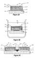
- a printable compound semiconductor device structure 100includes a wafer or substrate 101 , a release layer 105 on the substrate 101 , a support layer 110 on the release layer 105 , and one or more printable or transferrable device layers 115 on the support layer 110 .
- the release layer 105contacts and couples the support layer 110 to the substrate 101 .
- the release layer 105is an indium aluminum phosphide (InAlP) layer, and the substrate 101 and the support layer 110 are formed of arsenide-based materials.
- the InAlP release layer 105may have a thickness between about 0.02 microns (or micrometers ( ⁇ m)) and about 1 micron.
- the layers 105 , 110 , and/or 115may be epitaxially grown on the substrate 101 .
- the indium-phosphide release layer 105may be epitaxially grown on the arsenide-based source substrate 101 .
- the InAlP release layer 105may be epitaxially grown on and closely lattice-matched to (e.g., at a lattice mismatch of less than about 500 parts-per million (ppm) as measured by X-ray diffractometry) the GaAs substrate 101 .
- the arsenide based support layer 110may be epitaxially grown on the release layer 105
- the device layer(s) 115may be epitaxially grown on the support layer 110 .
- at least a portion of the support layer 110exhibits compressive strain relative to the device layer(s) 115 , the release layer 105 , and/or the substrate 101 .
- at least a portion of the arsenide-based support layer 110 adjacent to the release layer 105is grown in slight compression relative to some part of the release layer 105 , the substrate 101 , and/or the device layer(s) 115 .
- Semiconductor devicessuch as transistors, photovoltaic cells, light emitting diodes, and/or radio frequency or other wireless devices, may be partially or fully formed in or on the device layer(s) 115 by microfabrication techniques prior to separating the device layer(s) 115 from the growth substrate 101 .
- anchoring and/or tethering structuresmay be formed in the support layer 110 and/or other layers, and may be configured to maintain spatial orientation of the semiconductor devices during subsequent operations for separating the device layer(s) 115 from the substrate 101 .
- the fabrication of such anchoring and/or tethering structuresare described, for example, in PCT Application Nos. PCT/US2011/029365 and PCT/US2011/029357 filed Mar.
- An encapsulation structure(not shown) may be further provided on the device layer(s) 115 to protect the partially or fully formed devices from chemical attack during subsequent processing.
- the release layer 105can be selectively etched without substantially etching the support layer 110 , the device layer(s) 115 , and/or the substrate 101 .
- the substrate 101 and the support layer 110respectively include a material having etching selectivity with respect to that of the release layer 105 .
- FIG. 1Billustrates a process of releasing printable devices formed in or on the device layer(s) 115 from an arsenide-based substrate 101 by selectively laterally etching the InAlP release layer 105 in a solution 120 including hydrochloric acid to separate the arsenide-based support layer 110 and the device layer(s) 115 thereon from the substrate 101 .
- the substrate 101 and/or the support layer 110may include a Group III arsenide material (such as gallium arsenide (GaAs) and indium gallium arsenide (InGaAs)) and/or a Group III-V arsenide material (such as indium gallium nitride arsenide (InGaNAs) and indium gallium nitride arsenide antimonide (InGaNAsSb)).
- a Group III arsenide materialsuch as gallium arsenide (GaAs) and indium gallium arsenide (InGaAs)
- a Group III-V arsenide materialsuch as indium gallium nitride arsenide (InGaNAs) and indium gallium nitride arsenide antimonide (InGaNAsSb)
- the device layer(s) 115may be formed of indium aluminum phosphide (InAlP), aluminum gallium arsenide (AlGaAs), and/or other materials that would be otherwise etched along with the release layer 105 .
- InAlPindium aluminum phosphide
- AlGaAsaluminum gallium arsenide
- the etching solution 120may also include ethanol in some embodiments.
- the release process and/or the etching solution 120 described hereincan further include a compound that is configured to form a self-assembled monolayer on compound semiconductor surfaces (e.g., 1-hexadecanethiol), to lubricate the surfaces of the structure 100 that become exposed during the release process and/or to change the surface tension of the etching solution 120 .
- a compound that is configured to form a self-assembled monolayer on compound semiconductor surfacese.g., 1-hexadecanethiol
- the release process illustrated in FIG. 1Bis sufficient to separate the support layer 110 from the substrate 101 at a relatively high etch rate of more than about 0.1 millimeters (mm) per hour.
- the InAlP release layer 105 described hereinalso provides very good selectivity in the relative to the arsenide-based layers 101 and 110 , which allows for release of device layer(s) 115 that laterally extend up to at least 100 times greater than a thickness of the device layer(s) 115 .
- embodiments of the present inventionallow for selectively laterally etching an indium aluminum phosphide release layer 105 using an etching solution 120 including hydrochloric acid to separate the arsenide-based support layer 110 including the device layer(s) 115 thereon from the arsenide-based substrate 101 .
- FIG. 1Cillustrates two transferable devices or chiplets 100 ′ and 100 ′′ after etching of the release layer 105 according to embodiments as described herein. As shown in FIG. 1C , the transferable devices 100 ′ and 100 ′′ are attached to a portion 140 of the support layer 110 by breakable micro-bridges or tethers 145 , and the portion 140 of the support layer 110 remains attached to the substrate 101 by a portion of the release layer 105 that remains after the selective etching process shown in FIG. 1B .
- the surface of the support layer 110 opposite the device layer(s) 115may include at least some remaining portion or residue or trace amounts of the InAlP release layer 105 thereon (not shown).
- the released devices 100 ′ and 100 ′′may be washed with an aqueous solution of hydrogen peroxide, some phosphorous-containing residues (e.g., products of the release layer etching reaction) may still persist on the surface of the support layer 110 .
- the devices 100 ′ and 100 ′′can then be transferred to a different target substrate by pressing or contacting an elastomeric stamp (or other intermediary transfer element) against the devices 100 ′ and 100 ′′, where the stamp has an adhesive strength sufficient to sufficient to break the tethers 145 and transfer the devices 100 ′ and 100 ′′ to a desired destination substrate.
- an elastomeric stampor other intermediary transfer element
- FIGS. 2A-2Cillustrate compound semiconductor device structures and methods of fabrication according to further embodiments of the present invention.
- a printable compound semiconductor device structure 200includes a wafer or substrate 201 , a release layer 205 on the substrate 201 , a support layer 210 on the release layer 205 , and one or more printable or transferrable device layers 215 on the support layer 210 .
- the release layer 205is an InAlP-based layer
- the support layer 210is a Group III arsenide-based lateral conduction layer adjacent to the release layer 205 that provides a relatively low sheet resistance (e.g., less than about 50 ohms per square).
- the support layer 210may be formed of GaAs, InGaAs, InGaNAsSb, or InGaNAs in some embodiments.
- the substrate 201may include a Group III arsenide material (such as gallium arsenide (GaAs) and indium gallium arsenide (InGaAs)) and/or a Group III-V arsenide material (such as indium gallium nitride arsenide (InGaNAs) and indium gallium nitride arsenide antimonide (InGaNAsSb)).
- a Group III arsenide materialsuch as gallium arsenide (GaAs) and indium gallium arsenide (InGaAs)
- a Group III-V arsenide materialsuch as indium gallium nitride arsenide (InGaNAs) and indium gallium nitride arsenide antimonide (InGaNAsSb)
- the substrate 201may be a source or growth substrate, and the layers 205 , 210 , and/or 215 may be epitaxially grown on the substrate 201 in some embodiments.
- the structure 200may further include a layer of GaAs, InGaAs, InGaNAsSb, and/or InGaNAs adjacent to the release layer 205 that is grown in slight compression (e.g., having a lattice mismatch of about 100 ppm to about 1000 ppm as measured by X-ray diffractometry) relative to some part of the device layer(s) 215 , the release layer 205 , and/or the substrate 201 .
- slight compressione.g., having a lattice mismatch of about 100 ppm to about 1000 ppm as measured by X-ray diffractometry
- the printable device layers(s) 215provide active layers for one or more photovoltaic or solar cells.
- a partially transparent window layer 225is provided on an upper surface of the device layers(s) 215 , and a dielectric anti-reflection coating 230 is provided on the window layer 225 .
- the dielectric anti-reflection coating 230may further cover sidewalls of the device layers(s) 215 and the support layer 210 .
- the dielectric anti-reflection coating 230may be a single- or multi-layer coating. In the embodiments of FIGS.
- the dielectric anti-reflection coating 230is further covered by an encapsulation layer 235 that surrounds the solar cells in or on the device layer(s) 215 .
- the dielectric anti-reflection coating 230may be covered with photoresist, and the photoresist may be subsequently baked to provide the encapsulation layer 235 that protects the device layers(s) 215 during a subsequent release process, as shown in FIG. 2B .
- the release layer 205is selectively etched without substantially etching the support layer 210 , the device layer(s) 215 , and/or the substrate 201 .
- the release layer 205is formed of a material (InAlP) that provides etching selectivity to the arsenide-based substrate 201
- the release layer 205can be selectively laterally etched in a solution 220 including hydrochloric acid to separate the support layer 210 and the device layer(s) 215 thereon from the substrate 201 .
- the encapsulation layer 235provides further protection for the device layer(s) 215 , the window layer 225 , and the dielectric anti-reflection coating 230 from attack by the solution 220 used to selectively etch the release layer 205 .
- the window layer 225may be formed of InAlP and/or other materials that would otherwise be etched by the etching solution 220 in some embodiments.
- the device layer(s)may be formed of indium aluminum phosphide and/or aluminum gallium arsenide.
- the etching solution 220may also include ethanol and/or a compound that is configured to form a self-assembled monolayer on compound semiconductor surfaces in some embodiments.
- the active layer(s) 215 of the solar cellmay be separated from the arsenide-based substrate 201 without damage to the solar cell, window layer, and/or anti-reflective coating thereon.
- FIG. 2Cillustrates two transferable solar cell devices or chiplets 200 ′ and 200 ′′ after etching of the release layer 205 according to embodiments as described herein.
- the transferable devices 200 ′ and 200 ′′are attached to breakable tethers 245 that are attached to anchors 240 that are also attached to the substrate 201 throughout and after the selective etching process shown in FIG. 2B .
- the tethers 245 and anchors 240are formed within the encapsulation layer 235 .
- the surface of the support layer 210 opposite the device layer(s) 215may also include at least some remaining portion or residue of the InAlP release layer 205 thereon (not shown).
- the devices 200 ′ and 200 ′′can then be transferred to a different target substrate by pressing or contacting an elastomeric stamp or other intermediary transfer element against the devices 200 ′ and 200 ′′ with a force sufficient to break the tethers 245 , where the stamp has an adhesive strength sufficient to transfer the devices 200 ′ and 200 ′′ to a desired destination substrate.
- FIG. 3is a flowchart illustrating methods of fabricating printable compound semiconductor device structures and releasing such structures from a growth substrate or other donor substrate in accordance with embodiments of the present invention.
- an arsenide-based substrateis provided at block 305 .
- a release layer including indium aluminum phosphide (InAlP), an arsenide-based support layer, and at least one semiconductor device layerare sequentially provided on the arsenide-based substrate at blocks 310 , 315 , and 320 , respectively.
- the release layer, the support layer, and/or the device layer(s)may be epitaxially grown on the arsenide-based substrate in some embodiments to define an epi-stack structure.
- One or more semiconductor devicessuch as transistors, photovoltaic cells, and/or light-emitting diodes, may be formed in/on the device layer(s) using microfabrication techniques at block 322 . Also, one or more portions of the release layer may also be exposed using microfabrication techniques at block 322 .
- the material of the release layerprovides an etching selectivity to the material(s) of the arsenide-based substrate and/or support layer.
- the release layeris selectively etched without substantially etching the substrate and/or support layer.
- an etchant including hydrochloric (HCl) acidmay be used to selectively laterally etch the InAlP release layer without substantially etching the arsenide-based layers.
- the etchantmay further include ethanol or another suitable surfactant to reduce the size of bubbles that may be produced during the etching of the InAlP release layer, thereby reducing the likelihood of damage to the device structure.
- an encapsulant layermay be provided on the device layer(s) and/or other portions of the device structure to protect layers that may be otherwise vulnerable to the etchant.
- the etchant including HCl and ethanolmay selectively etch the release layer at a relatively high rate (for example, at more than about 0.1 millimeters (mm) per hour) to thereby separate the support layer from the substrate.
- the device layer(s)may then be transferred to a different substrate, for example, using micro-transfer printing techniques.
Landscapes
- Engineering & Computer Science (AREA)
- Physics & Mathematics (AREA)
- Condensed Matter Physics & Semiconductors (AREA)
- General Physics & Mathematics (AREA)
- Computer Hardware Design (AREA)
- Microelectronics & Electronic Packaging (AREA)
- Power Engineering (AREA)
- Manufacturing & Machinery (AREA)
- Chemical & Material Sciences (AREA)
- Chemical Kinetics & Catalysis (AREA)
- General Chemical & Material Sciences (AREA)
- Weting (AREA)
- Photovoltaic Devices (AREA)
- Recrystallisation Techniques (AREA)
- Led Devices (AREA)
- Life Sciences & Earth Sciences (AREA)
- Sustainable Development (AREA)
Abstract
Description
Claims (31)
Priority Applications (1)
| Application Number | Priority Date | Filing Date | Title |
|---|---|---|---|
| US13/814,343US9355854B2 (en) | 2010-08-06 | 2011-08-04 | Methods of fabricating printable compound semiconductor devices on release layers |
Applications Claiming Priority (3)
| Application Number | Priority Date | Filing Date | Title |
|---|---|---|---|
| US37146710P | 2010-08-06 | 2010-08-06 | |
| US13/814,343US9355854B2 (en) | 2010-08-06 | 2011-08-04 | Methods of fabricating printable compound semiconductor devices on release layers |
| PCT/US2011/046575WO2012018997A2 (en) | 2010-08-06 | 2011-08-04 | Materials and processes for releasing printable compound semiconductor devices |
Publications (2)
| Publication Number | Publication Date |
|---|---|
| US20130196474A1 US20130196474A1 (en) | 2013-08-01 |
| US9355854B2true US9355854B2 (en) | 2016-05-31 |
Family
ID=44509676
Family Applications (1)
| Application Number | Title | Priority Date | Filing Date |
|---|---|---|---|
| US13/814,343Active2032-05-21US9355854B2 (en) | 2010-08-06 | 2011-08-04 | Methods of fabricating printable compound semiconductor devices on release layers |
Country Status (5)
| Country | Link |
|---|---|
| US (1) | US9355854B2 (en) |
| JP (1) | JP6076903B2 (en) |
| KR (1) | KR101916968B1 (en) |
| CN (1) | CN103155114B (en) |
| WO (1) | WO2012018997A2 (en) |
Cited By (46)
| Publication number | Priority date | Publication date | Assignee | Title |
|---|---|---|---|---|
| US10181507B2 (en) | 2014-09-25 | 2019-01-15 | X-Celeprint Limited | Display tile structure and tiled display |
| US10217730B2 (en) | 2016-02-25 | 2019-02-26 | X-Celeprint Limited | Efficiently micro-transfer printing micro-scale devices onto large-format substrates |
| US10224231B2 (en) | 2016-11-15 | 2019-03-05 | X-Celeprint Limited | Micro-transfer-printable flip-chip structures and methods |
| US10297585B1 (en) | 2017-12-21 | 2019-05-21 | X-Celeprint Limited | Multi-resolution compound micro-devices |
| US10347535B2 (en) | 2014-06-18 | 2019-07-09 | X-Celeprint Limited | Systems and methods for controlling release of transferable semiconductor structures |
| US10388205B2 (en) | 2015-08-25 | 2019-08-20 | X-Celeprint Limited | Bit-plane pulse width modulated digital display system |
| US10395966B2 (en) | 2016-11-15 | 2019-08-27 | X-Celeprint Limited | Micro-transfer-printable flip-chip structures and methods |
| US10418331B2 (en) | 2010-11-23 | 2019-09-17 | X-Celeprint Limited | Interconnection structures and methods for transfer-printed integrated circuit elements with improved interconnection alignment tolerance |
| US10468397B2 (en) | 2017-05-05 | 2019-11-05 | X-Celeprint Limited | Matrix addressed tiles and arrays |
| US10505079B2 (en) | 2018-05-09 | 2019-12-10 | X-Celeprint Limited | Flexible devices and methods using laser lift-off |
| US10522575B2 (en) | 2009-03-26 | 2019-12-31 | X-Celeprint Limited | Methods of making printable device wafers with sacrificial layers |
| US10573544B1 (en) | 2018-10-17 | 2020-02-25 | X-Celeprint Limited | Micro-transfer printing with selective component removal |
| US10600671B2 (en) | 2016-11-15 | 2020-03-24 | X-Celeprint Limited | Micro-transfer-printable flip-chip structures and methods |
| US10622700B2 (en) | 2016-05-18 | 2020-04-14 | X-Celeprint Limited | Antenna with micro-transfer-printed circuit element |
| US10714374B1 (en) | 2019-05-09 | 2020-07-14 | X Display Company Technology Limited | High-precision printed structures |
| US10748793B1 (en) | 2019-02-13 | 2020-08-18 | X Display Company Technology Limited | Printing component arrays with different orientations |
| US10790173B2 (en) | 2018-12-03 | 2020-09-29 | X Display Company Technology Limited | Printed components on substrate posts |
| US10796938B2 (en) | 2018-10-17 | 2020-10-06 | X Display Company Technology Limited | Micro-transfer printing with selective component removal |
| US10804880B2 (en) | 2018-12-03 | 2020-10-13 | X-Celeprint Limited | Device structures with acoustic wave transducers and connection posts |
| US10832935B2 (en) | 2017-08-14 | 2020-11-10 | X Display Company Technology Limited | Multi-level micro-device tethers |
| US10832934B2 (en) | 2018-06-14 | 2020-11-10 | X Display Company Technology Limited | Multi-layer tethers for micro-transfer printing |
| US10836200B2 (en) | 2017-11-13 | 2020-11-17 | X Display Company Technology Limited | Rigid micro-modules with ILED and light conductor |
| US10944027B2 (en) | 2019-06-14 | 2021-03-09 | X Display Company Technology Limited | Pixel modules with controllers and light emitters |
| US11024608B2 (en) | 2017-03-28 | 2021-06-01 | X Display Company Technology Limited | Structures and methods for electrical connection of micro-devices and substrates |
| US11037912B1 (en) | 2020-01-31 | 2021-06-15 | X Display Company Technology Limited | LED color displays with multiple LEDs connected in series and parallel in different sub-pixels of a pixel |
| US11088121B2 (en) | 2019-02-13 | 2021-08-10 | X Display Company Technology Limited | Printed LED arrays with large-scale uniformity |
| US11094870B2 (en) | 2019-03-12 | 2021-08-17 | X Display Company Technology Limited | Surface-mountable pixel packages and pixel engines |
| US11101417B2 (en) | 2019-08-06 | 2021-08-24 | X Display Company Technology Limited | Structures and methods for electrically connecting printed components |
| US11127889B2 (en) | 2019-10-30 | 2021-09-21 | X Display Company Technology Limited | Displays with unpatterned layers of light-absorbing material |
| US11164934B2 (en) | 2019-03-12 | 2021-11-02 | X Display Company Technology Limited | Tiled displays with black-matrix support screens |
| US11251139B2 (en) | 2019-01-22 | 2022-02-15 | X-Celeprint Limited | Secure integrated-circuit systems |
| US11274035B2 (en) | 2019-04-24 | 2022-03-15 | X-Celeprint Limited | Overhanging device structures and related methods of manufacture |
| US11282786B2 (en) | 2018-12-12 | 2022-03-22 | X Display Company Technology Limited | Laser-formed interconnects for redundant devices |
| US11315909B2 (en) | 2019-12-20 | 2022-04-26 | X Display Company Technology Limited | Displays with embedded light emitters |
| US11322460B2 (en) | 2019-01-22 | 2022-05-03 | X-Celeprint Limited | Secure integrated-circuit systems |
| US11482979B2 (en) | 2018-12-03 | 2022-10-25 | X Display Company Technology Limited | Printing components over substrate post edges |
| US11483937B2 (en) | 2018-12-28 | 2022-10-25 | X Display Company Technology Limited | Methods of making printed structures |
| US11488943B2 (en) | 2019-06-14 | 2022-11-01 | X Display Company Technology Limited | Modules with integrated circuits and devices |
| US11528808B2 (en) | 2018-12-03 | 2022-12-13 | X Display Company Technology Limited | Printing components to substrate posts |
| US11538849B2 (en) | 2020-05-28 | 2022-12-27 | X Display Company Technology Limited | Multi-LED structures with reduced circuitry |
| US11626856B2 (en) | 2019-10-30 | 2023-04-11 | X-Celeprint Limited | Non-linear tethers for suspended devices |
| US11637540B2 (en) | 2019-10-30 | 2023-04-25 | X-Celeprint Limited | Non-linear tethers for suspended devices |
| US11884537B2 (en) | 2018-12-03 | 2024-01-30 | X-Celeprint Limited | Enclosed cavity structures |
| US11952266B2 (en) | 2020-10-08 | 2024-04-09 | X-Celeprint Limited | Micro-device structures with etch holes |
| US12006205B2 (en) | 2020-10-08 | 2024-06-11 | X-Celeprint Limited | Micro-device structures with etch holes |
| US12074583B2 (en) | 2021-05-11 | 2024-08-27 | X Display Company Technology Limited | Printing components to adhesive substrate posts |
Families Citing this family (71)
| Publication number | Priority date | Publication date | Assignee | Title |
|---|---|---|---|---|
| US9161448B2 (en) | 2010-03-29 | 2015-10-13 | Semprius, Inc. | Laser assisted transfer welding process |
| WO2012027458A1 (en) | 2010-08-26 | 2012-03-01 | Semprius, Inc. | Structures and methods for testing printable integrated circuits |
| US8889485B2 (en) | 2011-06-08 | 2014-11-18 | Semprius, Inc. | Methods for surface attachment of flipped active componenets |
| US9412727B2 (en) | 2011-09-20 | 2016-08-09 | Semprius, Inc. | Printing transferable components using microstructured elastomeric surfaces with pressure modulated reversible adhesion |
| KR20150038217A (en)* | 2012-07-24 | 2015-04-08 | 스미또모 가가꾸 가부시키가이샤 | Semiconductor substrate, method for manufacturing semiconductor substrate, and method for manufacturing composite substrate |
| US8946052B2 (en)* | 2012-09-26 | 2015-02-03 | Sandia Corporation | Processes for multi-layer devices utilizing layer transfer |
| US9058990B1 (en)* | 2013-12-19 | 2015-06-16 | International Business Machines Corporation | Controlled spalling of group III nitrides containing an embedded spall releasing plane |
| WO2015193436A1 (en) | 2014-06-18 | 2015-12-23 | X-Celeprint Limited | Systems and methods for preparing gan and related materials for micro assembly |
| US9865600B2 (en) | 2014-06-18 | 2018-01-09 | X-Celeprint Limited | Printed capacitors |
| US9929053B2 (en) | 2014-06-18 | 2018-03-27 | X-Celeprint Limited | Systems and methods for controlling release of transferable semiconductor structures |
| US10050351B2 (en) | 2014-06-18 | 2018-08-14 | X-Celeprint Limited | Multilayer printed capacitors |
| US9444015B2 (en) | 2014-06-18 | 2016-09-13 | X-Celeprint Limited | Micro assembled LED displays and lighting elements |
| US9358775B2 (en) | 2014-07-20 | 2016-06-07 | X-Celeprint Limited | Apparatus and methods for micro-transfer-printing |
| WO2016030422A1 (en) | 2014-08-26 | 2016-03-03 | X-Celeprint Limited | Micro assembled hybrid displays and lighting elements |
| US9991163B2 (en) | 2014-09-25 | 2018-06-05 | X-Celeprint Limited | Small-aperture-ratio display with electrical component |
| US9818725B2 (en) | 2015-06-01 | 2017-11-14 | X-Celeprint Limited | Inorganic-light-emitter display with integrated black matrix |
| US9799261B2 (en) | 2014-09-25 | 2017-10-24 | X-Celeprint Limited | Self-compensating circuit for faulty display pixels |
| US9468050B1 (en) | 2014-09-25 | 2016-10-11 | X-Celeprint Limited | Self-compensating circuit for faulty display pixels |
| US9537069B1 (en) | 2014-09-25 | 2017-01-03 | X-Celeprint Limited | Inorganic light-emitting diode with encapsulating reflector |
| US11067643B2 (en) | 2014-11-03 | 2021-07-20 | Melexis Technologies Nv | Magnetic field sensor and method for making same |
| GB2535683A (en) | 2014-11-03 | 2016-08-31 | Melexis Technologies Nv | Magnetic field sensor and method for making same |
| US9640715B2 (en) | 2015-05-15 | 2017-05-02 | X-Celeprint Limited | Printable inorganic semiconductor structures |
| US9871345B2 (en) | 2015-06-09 | 2018-01-16 | X-Celeprint Limited | Crystalline color-conversion device |
| US10102794B2 (en) | 2015-06-09 | 2018-10-16 | X-Celeprint Limited | Distributed charge-pump power-supply system |
| US10133426B2 (en) | 2015-06-18 | 2018-11-20 | X-Celeprint Limited | Display with micro-LED front light |
| US11061276B2 (en) | 2015-06-18 | 2021-07-13 | X Display Company Technology Limited | Laser array display |
| US9704821B2 (en) | 2015-08-11 | 2017-07-11 | X-Celeprint Limited | Stamp with structured posts |
| US10255834B2 (en) | 2015-07-23 | 2019-04-09 | X-Celeprint Limited | Parallel redundant chiplet system for controlling display pixels |
| US10468363B2 (en) | 2015-08-10 | 2019-11-05 | X-Celeprint Limited | Chiplets with connection posts |
| US10380930B2 (en) | 2015-08-24 | 2019-08-13 | X-Celeprint Limited | Heterogeneous light emitter display system |
| US10230048B2 (en) | 2015-09-29 | 2019-03-12 | X-Celeprint Limited | OLEDs for micro transfer printing |
| US10066819B2 (en) | 2015-12-09 | 2018-09-04 | X-Celeprint Limited | Micro-light-emitting diode backlight system |
| US9930277B2 (en) | 2015-12-23 | 2018-03-27 | X-Celeprint Limited | Serial row-select matrix-addressed system |
| US10091446B2 (en) | 2015-12-23 | 2018-10-02 | X-Celeprint Limited | Active-matrix displays with common pixel control |
| US9786646B2 (en) | 2015-12-23 | 2017-10-10 | X-Celeprint Limited | Matrix addressed device repair |
| US9928771B2 (en) | 2015-12-24 | 2018-03-27 | X-Celeprint Limited | Distributed pulse width modulation control |
| US10200013B2 (en) | 2016-02-18 | 2019-02-05 | X-Celeprint Limited | Micro-transfer-printed acoustic wave filter device |
| US10361677B2 (en) | 2016-02-18 | 2019-07-23 | X-Celeprint Limited | Transverse bulk acoustic wave filter |
| US10109753B2 (en) | 2016-02-19 | 2018-10-23 | X-Celeprint Limited | Compound micro-transfer-printed optical filter device |
| US10150326B2 (en) | 2016-02-29 | 2018-12-11 | X-Celeprint Limited | Hybrid document with variable state |
| US10193025B2 (en) | 2016-02-29 | 2019-01-29 | X-Celeprint Limited | Inorganic LED pixel structure |
| US10150325B2 (en) | 2016-02-29 | 2018-12-11 | X-Celeprint Limited | Hybrid banknote with electronic indicia |
| US10153257B2 (en) | 2016-03-03 | 2018-12-11 | X-Celeprint Limited | Micro-printed display |
| US10153256B2 (en) | 2016-03-03 | 2018-12-11 | X-Celeprint Limited | Micro-transfer printable electronic component |
| US10103069B2 (en) | 2016-04-01 | 2018-10-16 | X-Celeprint Limited | Pressure-activated electrical interconnection by micro-transfer printing |
| US10008483B2 (en) | 2016-04-05 | 2018-06-26 | X-Celeprint Limited | Micro-transfer printed LED and color filter structure |
| US10199546B2 (en) | 2016-04-05 | 2019-02-05 | X-Celeprint Limited | Color-filter device |
| US10198890B2 (en) | 2016-04-19 | 2019-02-05 | X-Celeprint Limited | Hybrid banknote with electronic indicia using near-field-communications |
| US9997102B2 (en) | 2016-04-19 | 2018-06-12 | X-Celeprint Limited | Wirelessly powered display and system |
| US10360846B2 (en) | 2016-05-10 | 2019-07-23 | X-Celeprint Limited | Distributed pulse-width modulation system with multi-bit digital storage and output device |
| US9997501B2 (en) | 2016-06-01 | 2018-06-12 | X-Celeprint Limited | Micro-transfer-printed light-emitting diode device |
| US10453826B2 (en) | 2016-06-03 | 2019-10-22 | X-Celeprint Limited | Voltage-balanced serial iLED pixel and display |
| US11137641B2 (en) | 2016-06-10 | 2021-10-05 | X Display Company Technology Limited | LED structure with polarized light emission |
| US10222698B2 (en) | 2016-07-28 | 2019-03-05 | X-Celeprint Limited | Chiplets with wicking posts |
| US11064609B2 (en) | 2016-08-04 | 2021-07-13 | X Display Company Technology Limited | Printable 3D electronic structure |
| US9980341B2 (en) | 2016-09-22 | 2018-05-22 | X-Celeprint Limited | Multi-LED components |
| US10157880B2 (en) | 2016-10-03 | 2018-12-18 | X-Celeprint Limited | Micro-transfer printing with volatile adhesive layer |
| US10782002B2 (en) | 2016-10-28 | 2020-09-22 | X Display Company Technology Limited | LED optical components |
| US10347168B2 (en) | 2016-11-10 | 2019-07-09 | X-Celeprint Limited | Spatially dithered high-resolution |
| US10297502B2 (en) | 2016-12-19 | 2019-05-21 | X-Celeprint Limited | Isolation structure for micro-transfer-printable devices |
| US10438859B2 (en) | 2016-12-19 | 2019-10-08 | X-Celeprint Limited | Transfer printed device repair |
| US10832609B2 (en) | 2017-01-10 | 2020-11-10 | X Display Company Technology Limited | Digital-drive pulse-width-modulated output system |
| US10332868B2 (en) | 2017-01-26 | 2019-06-25 | X-Celeprint Limited | Stacked pixel structures |
| US10468391B2 (en) | 2017-02-08 | 2019-11-05 | X-Celeprint Limited | Inorganic light-emitting-diode displays with multi-ILED pixels |
| US10396137B2 (en) | 2017-03-10 | 2019-08-27 | X-Celeprint Limited | Testing transfer-print micro-devices on wafer |
| US10943946B2 (en) | 2017-07-21 | 2021-03-09 | X Display Company Technology Limited | iLED displays with substrate holes |
| FR3082998B1 (en)* | 2018-06-25 | 2021-01-08 | Commissariat Energie Atomique | DEVICE AND METHODS FOR TRANSFERRING CHIPS FROM A SOURCE SUBSTRATE TO A DESTINATION SUBSTRATE |
| US10714001B2 (en) | 2018-07-11 | 2020-07-14 | X Display Company Technology Limited | Micro-light-emitting-diode displays |
| DE102019108701A1 (en)* | 2019-04-03 | 2020-10-08 | OSRAM Opto Semiconductors Gesellschaft mit beschränkter Haftung | Process for the production of a plurality of components, component and component composite from components |
| KR102687815B1 (en) | 2019-06-20 | 2024-07-24 | 엘지전자 주식회사 | Display device and self assembly method for semiconductor light emitting device |
| WO2022013246A1 (en)* | 2020-07-13 | 2022-01-20 | Rockley Photonics Limited | Method of preparing a device coupon for micro-transfer printing, device wafer including said device coupon, and optoelectronic device manufactured from said device wafer |
Citations (10)
| Publication number | Priority date | Publication date | Assignee | Title |
|---|---|---|---|---|
| US20030062580A1 (en)* | 2000-06-30 | 2003-04-03 | Rie Sato | Spin-valve transistor |
| JP2005108943A (en) | 2003-09-29 | 2005-04-21 | Oki Data Corp | Semiconductor wafer and method of manufacturing semiconductor device using the same |
| JP2005259912A (en) | 2004-03-10 | 2005-09-22 | Shin Etsu Handotai Co Ltd | Manufacturing method of light emitting element |
| JP2006108441A (en) | 2004-10-06 | 2006-04-20 | Mitsubishi Chemicals Corp | Etching method of compound semiconductor |
| US20060145177A1 (en) | 2003-02-28 | 2006-07-06 | Kazunori Hagimoto | Light emitting device and process for fabricating the same |
| WO2008036837A2 (en) | 2006-09-20 | 2008-03-27 | The Board Of Trustees Of The University Of Illinois | Release strategies for making transferable semiconductor structures, devices and device components |
| US7399693B2 (en)* | 2004-06-23 | 2008-07-15 | Canon Kabushiki Kaisha | Semiconductor film manufacturing method and substrate manufacturing method |
| JP2009105450A (en) | 2009-02-09 | 2009-05-14 | Oki Data Corp | Laminate |
| WO2009104561A1 (en) | 2008-02-21 | 2009-08-27 | シャープ株式会社 | Solar cell and method for manufacturing solar cell |
| US20150137187A1 (en)* | 2012-07-24 | 2015-05-21 | Sumitomo Chemical Company, Limited | Semiconductor wafer, manufacturing method of semiconductor wafer and method for maunfacturing composite wafer |
Family Cites Families (9)
| Publication number | Priority date | Publication date | Assignee | Title |
|---|---|---|---|---|
| US4846931A (en) | 1988-03-29 | 1989-07-11 | Bell Communications Research, Inc. | Method for lifting-off epitaxial films |
| US5641381A (en) | 1995-03-27 | 1997-06-24 | The United States Of America As Represented By The Administrator Of The National Aeronautics And Space Administration | Preferentially etched epitaxial liftoff of InP material |
| CN103646848B (en) | 2004-06-04 | 2018-06-05 | 伊利诺伊大学评议会 | The method of assembling printable semiconductor elements and manufacture electronic device |
| KR100867518B1 (en) | 2006-09-06 | 2008-11-07 | 삼성전기주식회사 | Manufacturing method of nitride semiconductor light emitting device |
| SG182989A1 (en)* | 2007-07-03 | 2012-08-30 | Microlink Devices Inc | Methods for fabricating thin film iii-v compound solar cell |
| WO2009155122A2 (en) | 2008-05-30 | 2009-12-23 | Alta Devices, Inc. | Epitaxial lift off stacks and methods |
| US20100028844A1 (en) | 2008-07-29 | 2010-02-04 | Wiseman Daneya L | Method for transforming an under-achieving student into a superior student |
| US20110029365A1 (en) | 2009-07-28 | 2011-02-03 | Beezag Inc. | Targeting Multimedia Content Based On Authenticity Of Marketing Data |
| US8392101B2 (en) | 2009-07-29 | 2013-03-05 | The Invention Science Fund I Llc | Promotional correlation with selective vehicle modes |
- 2011
- 2011-08-04WOPCT/US2011/046575patent/WO2012018997A2/enactiveApplication Filing
- 2011-08-04JPJP2013523333Apatent/JP6076903B2/enactiveActive
- 2011-08-04KRKR1020127034088Apatent/KR101916968B1/enactiveActive
- 2011-08-04CNCN201180038489.6Apatent/CN103155114B/enactiveActive
- 2011-08-04USUS13/814,343patent/US9355854B2/enactiveActive
Patent Citations (11)
| Publication number | Priority date | Publication date | Assignee | Title |
|---|---|---|---|---|
| US20030062580A1 (en)* | 2000-06-30 | 2003-04-03 | Rie Sato | Spin-valve transistor |
| US20060145177A1 (en) | 2003-02-28 | 2006-07-06 | Kazunori Hagimoto | Light emitting device and process for fabricating the same |
| JP2005108943A (en) | 2003-09-29 | 2005-04-21 | Oki Data Corp | Semiconductor wafer and method of manufacturing semiconductor device using the same |
| JP2005259912A (en) | 2004-03-10 | 2005-09-22 | Shin Etsu Handotai Co Ltd | Manufacturing method of light emitting element |
| US7399693B2 (en)* | 2004-06-23 | 2008-07-15 | Canon Kabushiki Kaisha | Semiconductor film manufacturing method and substrate manufacturing method |
| JP2006108441A (en) | 2004-10-06 | 2006-04-20 | Mitsubishi Chemicals Corp | Etching method of compound semiconductor |
| WO2008036837A2 (en) | 2006-09-20 | 2008-03-27 | The Board Of Trustees Of The University Of Illinois | Release strategies for making transferable semiconductor structures, devices and device components |
| WO2009104561A1 (en) | 2008-02-21 | 2009-08-27 | シャープ株式会社 | Solar cell and method for manufacturing solar cell |
| US20100326518A1 (en) | 2008-02-21 | 2010-12-30 | Hiroyuki Juso | Solar cell and method of manufacturing solar cell |
| JP2009105450A (en) | 2009-02-09 | 2009-05-14 | Oki Data Corp | Laminate |
| US20150137187A1 (en)* | 2012-07-24 | 2015-05-21 | Sumitomo Chemical Company, Limited | Semiconductor wafer, manufacturing method of semiconductor wafer and method for maunfacturing composite wafer |
Non-Patent Citations (4)
| Title |
|---|
| International Preliminary Report on Patentability Corresponding to International Application No. PCT/US2011/046575; Date of Mailing: Feb. 21, 2013; 9 Pages. |
| International Search Report and Written Opinion, PCT/US2011/046575 mailed Apr. 26, 2012. |
| Lothian JR et al., "Wet and Dry Etching Characteristics of A10.5In0.5P", Journal of Vacuum Science & Technology B, Microelectronics Processing and Phenomena USA, vol. 10, No. 3, May 1992, p. 1061-1065. |
| Yazawa et al., GaInP Single-Junction and GaInP/GaAs Two-Junction Thin-Film Solar Cell Structures by Epitaxial Lift-Off, Solar Energy Materials and Solar Cells, Elsevier Science Publishers, Amsterdam, vol. 50, No. 1-4, Jan. 1, 1998, p. 229-235. |
Cited By (75)
| Publication number | Priority date | Publication date | Assignee | Title |
|---|---|---|---|---|
| US10522575B2 (en) | 2009-03-26 | 2019-12-31 | X-Celeprint Limited | Methods of making printable device wafers with sacrificial layers |
| US10943931B2 (en) | 2009-03-26 | 2021-03-09 | X Display Company Technology Limited | Wafers with etchable sacrificial patterns, anchors, tethers, and printable devices |
| US11469259B2 (en) | 2009-03-26 | 2022-10-11 | X Display Company Technology Limited | Printable device wafers with sacrificial layers |
| US10418331B2 (en) | 2010-11-23 | 2019-09-17 | X-Celeprint Limited | Interconnection structures and methods for transfer-printed integrated circuit elements with improved interconnection alignment tolerance |
| US10347535B2 (en) | 2014-06-18 | 2019-07-09 | X-Celeprint Limited | Systems and methods for controlling release of transferable semiconductor structures |
| US10181507B2 (en) | 2014-09-25 | 2019-01-15 | X-Celeprint Limited | Display tile structure and tiled display |
| US10388205B2 (en) | 2015-08-25 | 2019-08-20 | X-Celeprint Limited | Bit-plane pulse width modulated digital display system |
| US10217730B2 (en) | 2016-02-25 | 2019-02-26 | X-Celeprint Limited | Efficiently micro-transfer printing micro-scale devices onto large-format substrates |
| US10468398B2 (en) | 2016-02-25 | 2019-11-05 | X-Celeprint Limited | Efficiently micro-transfer printing micro-scale devices onto large-format substrates |
| USRE50432E1 (en) | 2016-05-18 | 2025-05-13 | X-Celeprint Limited | Antenna with micro-transfer-printed circuit element |
| US10622700B2 (en) | 2016-05-18 | 2020-04-14 | X-Celeprint Limited | Antenna with micro-transfer-printed circuit element |
| US10431487B2 (en) | 2016-11-15 | 2019-10-01 | X-Celeprint Limited | Micro-transfer-printable flip-chip structures and methods |
| US10395966B2 (en) | 2016-11-15 | 2019-08-27 | X-Celeprint Limited | Micro-transfer-printable flip-chip structures and methods |
| US10224231B2 (en) | 2016-11-15 | 2019-03-05 | X-Celeprint Limited | Micro-transfer-printable flip-chip structures and methods |
| US10600671B2 (en) | 2016-11-15 | 2020-03-24 | X-Celeprint Limited | Micro-transfer-printable flip-chip structures and methods |
| US10964583B2 (en) | 2016-11-15 | 2021-03-30 | X Display Company Technology Limited | Micro-transfer-printable flip-chip structures and methods |
| US11024608B2 (en) | 2017-03-28 | 2021-06-01 | X Display Company Technology Limited | Structures and methods for electrical connection of micro-devices and substrates |
| US10468397B2 (en) | 2017-05-05 | 2019-11-05 | X-Celeprint Limited | Matrix addressed tiles and arrays |
| US12249532B2 (en) | 2017-08-14 | 2025-03-11 | X Display Company Technology Limited | Multi-level micro-device tethers |
| US10832935B2 (en) | 2017-08-14 | 2020-11-10 | X Display Company Technology Limited | Multi-level micro-device tethers |
| US11670533B2 (en) | 2017-08-14 | 2023-06-06 | X Display Company Technology Limited | Multi-level micro-device tethers |
| US12240262B2 (en) | 2017-11-13 | 2025-03-04 | X Display Company Technology Limited | Rigid micro-modules with iLED and light conductor |
| US11890890B2 (en) | 2017-11-13 | 2024-02-06 | X Display Company Technology Limited | Rigid micro-modules with iLED and light conductor |
| US10836200B2 (en) | 2017-11-13 | 2020-11-17 | X Display Company Technology Limited | Rigid micro-modules with ILED and light conductor |
| US10297585B1 (en) | 2017-12-21 | 2019-05-21 | X-Celeprint Limited | Multi-resolution compound micro-devices |
| US10505079B2 (en) | 2018-05-09 | 2019-12-10 | X-Celeprint Limited | Flexible devices and methods using laser lift-off |
| US10832934B2 (en) | 2018-06-14 | 2020-11-10 | X Display Company Technology Limited | Multi-layer tethers for micro-transfer printing |
| US11367648B2 (en) | 2018-06-14 | 2022-06-21 | X Display Company Technology Limited | Multi-layer tethers for micro-transfer printing |
| US10796938B2 (en) | 2018-10-17 | 2020-10-06 | X Display Company Technology Limited | Micro-transfer printing with selective component removal |
| US11309197B2 (en) | 2018-10-17 | 2022-04-19 | X Display Company Technology Limited | Micro-transfer printing with selective component removal |
| US10573544B1 (en) | 2018-10-17 | 2020-02-25 | X-Celeprint Limited | Micro-transfer printing with selective component removal |
| US11854855B2 (en) | 2018-10-17 | 2023-12-26 | X Display Company Technology Limited | Micro-transfer printing with selective component removal |
| US10804880B2 (en) | 2018-12-03 | 2020-10-13 | X-Celeprint Limited | Device structures with acoustic wave transducers and connection posts |
| US11884537B2 (en) | 2018-12-03 | 2024-01-30 | X-Celeprint Limited | Enclosed cavity structures |
| US11528808B2 (en) | 2018-12-03 | 2022-12-13 | X Display Company Technology Limited | Printing components to substrate posts |
| US11950375B2 (en) | 2018-12-03 | 2024-04-02 | X Display Company Technology Limited | Printing components to substrate posts |
| US11482979B2 (en) | 2018-12-03 | 2022-10-25 | X Display Company Technology Limited | Printing components over substrate post edges |
| US10790173B2 (en) | 2018-12-03 | 2020-09-29 | X Display Company Technology Limited | Printed components on substrate posts |
| US11804431B2 (en) | 2018-12-12 | 2023-10-31 | Display Company Technology Limited | Laser-formed interconnects for redundant devices |
| US11282786B2 (en) | 2018-12-12 | 2022-03-22 | X Display Company Technology Limited | Laser-formed interconnects for redundant devices |
| US11540398B2 (en) | 2018-12-28 | 2022-12-27 | X Display Company Technology Limited | Methods of making printed structures |
| US11483937B2 (en) | 2018-12-28 | 2022-10-25 | X Display Company Technology Limited | Methods of making printed structures |
| US11251139B2 (en) | 2019-01-22 | 2022-02-15 | X-Celeprint Limited | Secure integrated-circuit systems |
| US11670602B2 (en) | 2019-01-22 | 2023-06-06 | X-Celeprint Limited | Secure integrated-circuit systems |
| US11322460B2 (en) | 2019-01-22 | 2022-05-03 | X-Celeprint Limited | Secure integrated-circuit systems |
| US10748793B1 (en) | 2019-02-13 | 2020-08-18 | X Display Company Technology Limited | Printing component arrays with different orientations |
| US11088121B2 (en) | 2019-02-13 | 2021-08-10 | X Display Company Technology Limited | Printed LED arrays with large-scale uniformity |
| US11569425B2 (en) | 2019-03-12 | 2023-01-31 | X Display Company Technology Limited | Surface-mountable pixel packages and pixel engines |
| US11164934B2 (en) | 2019-03-12 | 2021-11-02 | X Display Company Technology Limited | Tiled displays with black-matrix support screens |
| US11489037B2 (en) | 2019-03-12 | 2022-11-01 | X Display Company Technology Limited | Tiled displays with black-matrix support screens |
| US11742471B2 (en) | 2019-03-12 | 2023-08-29 | X Display Company Technology Limited | Surface-mountable pixel packages and pixel engines |
| US11094870B2 (en) | 2019-03-12 | 2021-08-17 | X Display Company Technology Limited | Surface-mountable pixel packages and pixel engines |
| US11274035B2 (en) | 2019-04-24 | 2022-03-15 | X-Celeprint Limited | Overhanging device structures and related methods of manufacture |
| US12043541B2 (en) | 2019-04-24 | 2024-07-23 | X-Celeprint Limited | Overhanging device structures and related methods of manufacture |
| US10937679B2 (en) | 2019-05-09 | 2021-03-02 | X Display Company Technology Limited | High-precision printed structures |
| US10714374B1 (en) | 2019-05-09 | 2020-07-14 | X Display Company Technology Limited | High-precision printed structures |
| US10944027B2 (en) | 2019-06-14 | 2021-03-09 | X Display Company Technology Limited | Pixel modules with controllers and light emitters |
| US11488943B2 (en) | 2019-06-14 | 2022-11-01 | X Display Company Technology Limited | Modules with integrated circuits and devices |
| US11881475B2 (en) | 2019-06-14 | 2024-01-23 | X Display Company Technology Limited | Modules with integrated circuits and devices |
| US11101417B2 (en) | 2019-08-06 | 2021-08-24 | X Display Company Technology Limited | Structures and methods for electrically connecting printed components |
| US11527691B2 (en) | 2019-08-06 | 2022-12-13 | X Display Company Technology Limited | Structures and methods for electrically connecting printed components |
| US11626856B2 (en) | 2019-10-30 | 2023-04-11 | X-Celeprint Limited | Non-linear tethers for suspended devices |
| US11863154B2 (en) | 2019-10-30 | 2024-01-02 | X-Celeprint Limited | Non-linear tethers for suspended devices |
| US11127889B2 (en) | 2019-10-30 | 2021-09-21 | X Display Company Technology Limited | Displays with unpatterned layers of light-absorbing material |
| US11637540B2 (en) | 2019-10-30 | 2023-04-25 | X-Celeprint Limited | Non-linear tethers for suspended devices |
| US11799061B2 (en) | 2019-10-30 | 2023-10-24 | X Display Company Technology Limited | Displays with unpatterned layers of light-absorbing material |
| US11315909B2 (en) | 2019-12-20 | 2022-04-26 | X Display Company Technology Limited | Displays with embedded light emitters |
| US11817434B2 (en) | 2019-12-20 | 2023-11-14 | X Display Company Technology Limited | Displays with embedded light emitters |
| US11705439B2 (en) | 2020-01-31 | 2023-07-18 | X Display Company Technology Limited | LED color displays with multi-LED sub-pixels |
| US11037912B1 (en) | 2020-01-31 | 2021-06-15 | X Display Company Technology Limited | LED color displays with multiple LEDs connected in series and parallel in different sub-pixels of a pixel |
| US11538849B2 (en) | 2020-05-28 | 2022-12-27 | X Display Company Technology Limited | Multi-LED structures with reduced circuitry |
| US12006205B2 (en) | 2020-10-08 | 2024-06-11 | X-Celeprint Limited | Micro-device structures with etch holes |
| US11952266B2 (en) | 2020-10-08 | 2024-04-09 | X-Celeprint Limited | Micro-device structures with etch holes |
| US12398031B2 (en) | 2020-10-08 | 2025-08-26 | X-Celeprint Limited | Micro-device structures with etch holes |
| US12074583B2 (en) | 2021-05-11 | 2024-08-27 | X Display Company Technology Limited | Printing components to adhesive substrate posts |
Also Published As
| Publication number | Publication date |
|---|---|
| CN103155114A (en) | 2013-06-12 |
| KR101916968B1 (en) | 2018-11-08 |
| US20130196474A1 (en) | 2013-08-01 |
| WO2012018997A3 (en) | 2012-08-09 |
| JP6076903B2 (en) | 2017-02-08 |
| WO2012018997A2 (en) | 2012-02-09 |
| JP2013539211A (en) | 2013-10-17 |
| KR20130093528A (en) | 2013-08-22 |
| CN103155114B (en) | 2016-10-12 |
Similar Documents
| Publication | Publication Date | Title |
|---|---|---|
| US9355854B2 (en) | Methods of fabricating printable compound semiconductor devices on release layers | |
| US10312405B2 (en) | Systems and methods for preparing GaN and related materials for micro assembly | |
| EP2064734B1 (en) | Method of printing transferable functional structures | |
| US10770289B2 (en) | Systems and methods for graphene based layer transfer | |
| KR100390670B1 (en) | Process for bonding crystalline substrates with different crystal lattices | |
| EP2171758B1 (en) | Method of manufacturing light-emitting device | |
| TW201603297A (en) | Non-destructive wafer recycling of epitaxial lift-off film devices using superlattice epitaxial layers | |
| TW201225171A (en) | Method of manufacturing a semiconductor device | |
| US10014216B2 (en) | Method for manufacturing semiconductor device using high speed epitaxial lift-off and template for III-V direct growth and semiconductor device manufactured using the same | |
| US20160104819A1 (en) | Method for producing an optoelectronic semiconductor chip | |
| KR20170128777A (en) | Strain relief through pre-patterned mesas Epitaxial lift-off | |
| JP4638000B2 (en) | Manufacturing method of semiconductor substrate | |
| WO2005038889A1 (en) | The method for allngan epitaxial growth on silicon substrate | |
| JP2011049565A (en) | Method of manufacturing semiconductor substrate |
Legal Events
| Date | Code | Title | Description |
|---|---|---|---|
| AS | Assignment | Owner name:SEMPRIUS, INC., NORTH CAROLINA Free format text:ASSIGNMENT OF ASSIGNORS INTEREST;ASSIGNORS:MEITL, MATTHEW;BOWER, CHRISTOPHER;MENARD, ETIENNE;AND OTHERS;SIGNING DATES FROM 20130410 TO 20130412;REEL/FRAME:030216/0254 | |
| STCF | Information on status: patent grant | Free format text:PATENTED CASE | |
| AS | Assignment | Owner name:SEMPRIUS (ASSIGNMENT FOR THE BENEFIT OF CREDITORS), LLC, CALIFORNIA Free format text:ASSIGNMENT OF ASSIGNORS INTEREST;ASSIGNOR:SEMPRIUS, INC.;REEL/FRAME:042231/0140 Effective date:20170131 Owner name:SEMPRIUS (ASSIGNMENT FOR THE BENEFIT OF CREDITORS) Free format text:ASSIGNMENT OF ASSIGNORS INTEREST;ASSIGNOR:SEMPRIUS, INC.;REEL/FRAME:042231/0140 Effective date:20170131 | |
| AS | Assignment | Owner name:X-CELEPRINT LIMITED, IRELAND Free format text:ASSIGNMENT OF ASSIGNORS INTEREST;ASSIGNOR:SEMPRIUS (ASSIGNMENT FOR THE BENEFIT OF CREDITORS), LLC;REEL/FRAME:042244/0531 Effective date:20170330 | |
| MAFP | Maintenance fee payment | Free format text:PAYMENT OF MAINTENANCE FEE, 4TH YEAR, LARGE ENTITY (ORIGINAL EVENT CODE: M1551); ENTITY STATUS OF PATENT OWNER: LARGE ENTITY Year of fee payment:4 | |
| AS | Assignment | Owner name:X DISPLAY COMPANY TECHNOLOGY LIMITED, IRELAND Free format text:CHANGE OF NAME;ASSIGNOR:X-CELEPRINT LIMITED;REEL/FRAME:052631/0800 Effective date:20191223 | |
| AS | Assignment | Owner name:X DISPLAY COMPANY TECHNOLOGY LIMITED, IRELAND Free format text:CHANGE OF NAME;ASSIGNOR:X-CELEPRINT LIMITED;REEL/FRAME:057501/0765 Effective date:20191223 | |
| MAFP | Maintenance fee payment | Free format text:PAYMENT OF MAINTENANCE FEE, 8TH YEAR, LARGE ENTITY (ORIGINAL EVENT CODE: M1552); ENTITY STATUS OF PATENT OWNER: LARGE ENTITY Year of fee payment:8 |