US9354654B2 - High voltage ring pump with inverter stages and voltage boosting stages - Google Patents
High voltage ring pump with inverter stages and voltage boosting stagesDownload PDFInfo
- Publication number
- US9354654B2 US9354654B2US14/230,945US201414230945AUS9354654B2US 9354654 B2US9354654 B2US 9354654B2US 201414230945 AUS201414230945 AUS 201414230945AUS 9354654 B2US9354654 B2US 9354654B2
- Authority
- US
- United States
- Prior art keywords
- voltage
- charge pump
- pump
- inverter
- block
- Prior art date
- Legal status (The legal status is an assumption and is not a legal conclusion. Google has not performed a legal analysis and makes no representation as to the accuracy of the status listed.)
- Expired - Fee Related
Links
- 239000003990capacitorSubstances0.000claimsdescription123
- 230000000295complement effectEffects0.000claimsdescription14
- 238000000034methodMethods0.000claimsdescription11
- 230000008878couplingEffects0.000claimsdescription10
- 238000010168coupling processMethods0.000claimsdescription10
- 238000005859coupling reactionMethods0.000claimsdescription10
- 230000003071parasitic effectEffects0.000description16
- OGWKCGZFUXNPDA-XQKSVPLYSA-NvincristineChemical compoundC([N@]1C[C@@H](C[C@]2(C(=O)OC)C=3C(=CC4=C([C@]56[C@H]([C@@]([C@H](OC(C)=O)[C@]7(CC)C=CCN([C@H]67)CC5)(O)C(=O)OC)N4C=O)C=3)OC)C[C@@](C1)(O)CC)CC1=C2NC2=CC=CC=C12OGWKCGZFUXNPDA-XQKSVPLYSA-N0.000description16
- 230000000903blocking effectEffects0.000description14
- 230000010355oscillationEffects0.000description14
- 238000012360testing methodMethods0.000description9
- 238000012546transferMethods0.000description8
- 230000000694effectsEffects0.000description6
- 238000002955isolationMethods0.000description6
- 230000007704transitionEffects0.000description6
- 230000003139buffering effectEffects0.000description5
- 238000010586diagramMethods0.000description5
- NJPPVKZQTLUDBO-UHFFFAOYSA-NnovaluronChemical compoundC1=C(Cl)C(OC(F)(F)C(OC(F)(F)F)F)=CC=C1NC(=O)NC(=O)C1=C(F)C=CC=C1FNJPPVKZQTLUDBO-UHFFFAOYSA-N0.000description5
- 230000008569processEffects0.000description4
- 230000009471actionEffects0.000description3
- 238000001914filtrationMethods0.000description3
- 230000007423decreaseEffects0.000description2
- 238000009499grossingMethods0.000description2
- 230000001939inductive effectEffects0.000description2
- 238000005259measurementMethods0.000description2
- 238000012986modificationMethods0.000description2
- 230000004048modificationEffects0.000description2
- 230000002265preventionEffects0.000description2
- 239000004065semiconductorSubstances0.000description2
- 230000001360synchronised effectEffects0.000description2
- 238000009825accumulationMethods0.000description1
- 238000013459approachMethods0.000description1
- 230000015556catabolic processEffects0.000description1
- 230000003247decreasing effectEffects0.000description1
- 238000004146energy storageMethods0.000description1
- 230000009467reductionEffects0.000description1
- 230000007480spreadingEffects0.000description1
- 230000000087stabilizing effectEffects0.000description1
Images


Classifications
- G—PHYSICS
- G05—CONTROLLING; REGULATING
- G05F—SYSTEMS FOR REGULATING ELECTRIC OR MAGNETIC VARIABLES
- G05F3/00—Non-retroactive systems for regulating electric variables by using an uncontrolled element, or an uncontrolled combination of elements, such element or such combination having self-regulating properties
- G05F3/02—Regulating voltage or current
- G05F3/04—Regulating voltage or current wherein the variable is AC
- H—ELECTRICITY
- H02—GENERATION; CONVERSION OR DISTRIBUTION OF ELECTRIC POWER
- H02M—APPARATUS FOR CONVERSION BETWEEN AC AND AC, BETWEEN AC AND DC, OR BETWEEN DC AND DC, AND FOR USE WITH MAINS OR SIMILAR POWER SUPPLY SYSTEMS; CONVERSION OF DC OR AC INPUT POWER INTO SURGE OUTPUT POWER; CONTROL OR REGULATION THEREOF
- H02M3/00—Conversion of DC power input into DC power output
- H02M3/02—Conversion of DC power input into DC power output without intermediate conversion into AC
- H02M3/04—Conversion of DC power input into DC power output without intermediate conversion into AC by static converters
- H02M3/06—Conversion of DC power input into DC power output without intermediate conversion into AC by static converters using resistors or capacitors, e.g. potential divider
- H02M3/07—Conversion of DC power input into DC power output without intermediate conversion into AC by static converters using resistors or capacitors, e.g. potential divider using capacitors charged and discharged alternately by semiconductor devices with control electrode, e.g. charge pumps
- H—ELECTRICITY
- H02—GENERATION; CONVERSION OR DISTRIBUTION OF ELECTRIC POWER
- H02M—APPARATUS FOR CONVERSION BETWEEN AC AND AC, BETWEEN AC AND DC, OR BETWEEN DC AND DC, AND FOR USE WITH MAINS OR SIMILAR POWER SUPPLY SYSTEMS; CONVERSION OF DC OR AC INPUT POWER INTO SURGE OUTPUT POWER; CONTROL OR REGULATION THEREOF
- H02M1/00—Details of apparatus for conversion
- H02M1/0067—Converter structures employing plural converter units, other than for parallel operation of the units on a single load
- H02M1/0077—Plural converter units whose outputs are connected in series
- H02M2001/0077—
Definitions
- a charge pumpis one such auxiliary circuit that functions as a DC to DC converter.
- the charge pumptakes in an input voltage and generates an output voltage that is either higher in magnitude or lower in magnitude than the input voltage, depending on the application required.
- Charge pumpsgenerally utilize an energy storage element to generate the output voltage.
- a charge pump elementcomprising: an initial inverter, wherein an input voltage to the initial inverter is inverted to obtain a complementary output voltage; at least one pump block, wherein an output voltage of a particular pump block in the at least one pump block is larger in magnitude than an input voltage to the particular pump block in the at least one pump block; and a driving circuit connected with the initial inverter on one end and the at least one pump block on another end, wherein the driving circuit generates a first voltage and a second voltage based on the input voltage to the initial inverter, and wherein each of the first and second voltages are adapted to be applied to the at least one pump block.
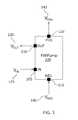
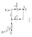
- FIG. 1shows an exemplary diagram of an individual full-wave pump element and illustrates input terminals and output terminals of the individual full-wave pump element.
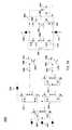
- the inverter stage of the third FWPump ( 210 )inverts voltage state of the voltage V IS3 ( 232 ).
- the second FWPump ( 205 ) in FIG. 2sits on a pedestal voltage given by the first voltage V 1 ( 256 ) and generates the second voltage boosting stage voltage V 2 ( 262 ).
- the third FWPump ( 210 ) in FIG. 2sits on a pedestal voltage given by the second voltage V 2 ( 262 ) and generates the ring pump output voltage V ring3 ( 270 ).
- V DD+2 V
- V SS⁇ 1 V
- V 00 V
- V 26 V
- V ring39 V.
- each of the voltages V 1 ( 256 ), V 2 ( 262 ), and V ring3 ( 270 )will generally be lower than those values given above.
- the voltage boosting stage of each FWPumpincreases voltage in a negative direction.
- the NEG terminal ( 252 , 258 , 264 ) and the POS terminal ( 254 , 260 , 266 ) of each FWPump ( 200 , 205 , 210 )are flipped for each FWPump ( 200 , 205 , 210 ).
- the relative values of the voltages in this caseare given by V 0 >V 1 >V 2 >V ring3 .
- the FWPump ( 100 )comprises an inverter stage. Operation of the inverter stage is as follows and is made with reference to FIG. 3A .
- the IN terminal ( 105 ) of the FWPump ( 100 )takes as its input the output of a previous FWPump's OUT terminal (not shown in FIG. 3A ).
- the input voltage V IN ( 125 )is sent into a first inverter ( 305 ), which inverts the input voltage V IN ( 125 ) and sends the resulting output voltage V OUT ( 130 ) to a next FWPump (not shown in FIG. 3A ) via the OUT terminal ( 110 ).
- the voltage state of the output voltage V OUT ( 130 )is opposite the voltage state of the input voltage V IN ( 125 ). Consequently, the first inverter ( 305 ) implements the inverter stage of the individual FWPump ( 100 ).
- the invertersare adapted to have a high voltage state of +2 V and a low voltage state of ⁇ 1 V.
- values used for the supply voltages V DD and V SScan differ from example values given in the present disclosure.
- the positive supply voltage V DDcould be, for instance, 3.3 V or 2.5 V
- the negative supply voltage V SScould be tied to ground.
- Node Pb ( 345 )is connected to the gate of the first PMOS ( 350 ) and the gate of the first NMOS ( 355 ); node Pb ( 345 ) is also connected to the drain of the second PMOS ( 360 ) and the drain of the second NMOS ( 365 ).
- the source of the first PMOS ( 350 ) and the source of the second PMOS ( 360 )are connected; both the source of the first PMOS ( 350 ) and the source of the second PMOS ( 360 ) are tied to the POS terminal ( 120 ).
- transition of the voltages (from V DD to V SS and vice versa) through the inverter ringspreads charge transfer events over time from the capacitors ( 330 , 335 ) to the reservoir capacitor ( 370 ).
- the charge transfer eventsare due to six charge pulses, where one pulse comes from each of the first and second capacitors ( 330 , 335 in FIGS. 3A and 3B ) of each of the three FWPumps ( 200 , 205 , 210 ).
- a single charge pumpthat can supply one single charge pulse that is equal in magnitude to the sum of the six charge pulses.
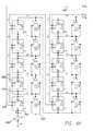
- FIGS. 4A-4Cshow another embodiment of a ring pump. Specifically, connecting components between FIGS. 4A-4B and between FIGS. 4B-4C provide the ring pump.
- the ring pumpcomprises twenty-nine individual FWPumps. The components and operation of the individual FWPump were previously described in detail with reference to FIGS. 1, 2, 3A, and 3B .
- a decrease in the ring pump output voltage V ring ( 430 in FIG. 4C )will result from charge drawn by the load circuit ( 460 in FIG. 4C ).
- charge stored by a reservoir capacitor (not shown) of the last FWPump ( 420 in FIG. 4C )decreases.
- Charge from reservoir capacitors (not shown) of preceding FWPumpsflows toward the reservoir capacitor of the last FWPump ( 420 in FIG. 4C ) to charge up the reservoir capacitor of the last FWPump ( 420 in FIG. 4C ).
- the inverter stage of each FWpumpis either in a high voltage state of +2.5 V or in a low voltage state of 0 V.
- the first FWPump ( 400 in FIG. 4A ) and the last FWPump ( 420 in FIG. 4C )are in opposite voltage states.
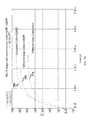
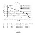
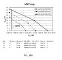
- a middle curve ( 705 in FIG. 7A )shows that with a 10 M ⁇ resistor as part of the load circuit ( 460 in FIG. 4C ) and first and second capacitors ( 330 , 335 in FIGS.
- FIG. 8Cshows the voltage at the P node ( 340 in FIG. 3B ) and Pb node ( 345 in FIG. 3B ) of the last FWPump ( 420 ) shown in FIG. 4C that includes the parasitic effects.
- Operation of a cycle of an inverter ring in the ring pumpbegins at the inverter ( 1130 ) and circles back to the inverter ( 1130 ) via the last FWPump element ( 1105 ) on a right side of the test chip.
- Each graphhas a vertical line ( 1200 ) corresponding to a selected operating current for the 50 V ring pump.
- Type of MOS transistor and value for the positive oscillator supply V DDcan be selected based on required output voltage and/or required output current for a desired application.
Landscapes
- Engineering & Computer Science (AREA)
- Physics & Mathematics (AREA)
- Electromagnetism (AREA)
- General Physics & Mathematics (AREA)
- Radar, Positioning & Navigation (AREA)
- Automation & Control Theory (AREA)
- Power Engineering (AREA)
- Dc-Dc Converters (AREA)
Abstract
Description
Claims (11)
Priority Applications (1)
| Application Number | Priority Date | Filing Date | Title |
|---|---|---|---|
| US14/230,945US9354654B2 (en) | 2011-05-11 | 2014-03-31 | High voltage ring pump with inverter stages and voltage boosting stages |
Applications Claiming Priority (2)
| Application Number | Priority Date | Filing Date | Title |
|---|---|---|---|
| US13/105,743US8686787B2 (en) | 2011-05-11 | 2011-05-11 | High voltage ring pump with inverter stages and voltage boosting stages |
| US14/230,945US9354654B2 (en) | 2011-05-11 | 2014-03-31 | High voltage ring pump with inverter stages and voltage boosting stages |
Related Parent Applications (1)
| Application Number | Title | Priority Date | Filing Date |
|---|---|---|---|
| US13/105,743DivisionUS8686787B2 (en) | 2011-01-18 | 2011-05-11 | High voltage ring pump with inverter stages and voltage boosting stages |
Publications (2)
| Publication Number | Publication Date |
|---|---|
| US20140361827A1 US20140361827A1 (en) | 2014-12-11 |
| US9354654B2true US9354654B2 (en) | 2016-05-31 |
Family
ID=47141491
Family Applications (2)
| Application Number | Title | Priority Date | Filing Date |
|---|---|---|---|
| US13/105,743Expired - Fee RelatedUS8686787B2 (en) | 2011-01-18 | 2011-05-11 | High voltage ring pump with inverter stages and voltage boosting stages |
| US14/230,945Expired - Fee RelatedUS9354654B2 (en) | 2011-05-11 | 2014-03-31 | High voltage ring pump with inverter stages and voltage boosting stages |
Family Applications Before (1)
| Application Number | Title | Priority Date | Filing Date |
|---|---|---|---|
| US13/105,743Expired - Fee RelatedUS8686787B2 (en) | 2011-01-18 | 2011-05-11 | High voltage ring pump with inverter stages and voltage boosting stages |
Country Status (1)
| Country | Link |
|---|---|
| US (2) | US8686787B2 (en) |
Cited By (4)
| Publication number | Priority date | Publication date | Assignee | Title |
|---|---|---|---|---|
| US9413362B2 (en) | 2011-01-18 | 2016-08-09 | Peregrine Semiconductor Corporation | Differential charge pump |
| US9429969B2 (en) | 2008-07-18 | 2016-08-30 | Peregrine Semiconductor Corporation | Low-noise high efficiency bias generation circuits and method |
| US9660590B2 (en) | 2008-07-18 | 2017-05-23 | Peregrine Semiconductor Corporation | Low-noise high efficiency bias generation circuits and method |
| US10148255B2 (en) | 2003-09-08 | 2018-12-04 | Psemi Corporation | Low noise charge pump method and apparatus |
Families Citing this family (5)
| Publication number | Priority date | Publication date | Assignee | Title |
|---|---|---|---|---|
| US9030248B2 (en) | 2008-07-18 | 2015-05-12 | Peregrine Semiconductor Corporation | Level shifter with output spike reduction |
| EP2421132A2 (en) | 2008-07-18 | 2012-02-22 | Peregrine Semiconductor Corporation | Charge pump with a plurality of transfer control switches |
| US8686787B2 (en) | 2011-05-11 | 2014-04-01 | Peregrine Semiconductor Corporation | High voltage ring pump with inverter stages and voltage boosting stages |
| US10319854B1 (en) | 2017-12-05 | 2019-06-11 | Psemi Corporation | High voltage switching device |
| CN113992003B (en)* | 2021-09-24 | 2025-03-25 | 南京矽力微电子技术有限公司 | Power conversion modules and power converters |
Citations (239)
| Publication number | Priority date | Publication date | Assignee | Title |
|---|---|---|---|---|
| US3470443A (en) | 1967-12-07 | 1969-09-30 | Nasa | Positive dc to negative dc converter |
| US3646361A (en) | 1970-10-16 | 1972-02-29 | Hughes Aircraft Co | High-speed sample and hold signal level comparator |
| US3731112A (en) | 1971-12-15 | 1973-05-01 | A Smith | Regulated power supply with diode capacitor matrix |
| US3878450A (en) | 1970-04-29 | 1975-04-15 | Greatbatch W Ltd | Controlled voltage multiplier providing pulse output |
| US3942047A (en) | 1974-06-03 | 1976-03-02 | Motorola, Inc. | MOS DC Voltage booster circuit |
| US3943428A (en) | 1973-11-23 | 1976-03-09 | General Electric Company | DC to DC Voltage converter |
| US3955353A (en) | 1974-07-10 | 1976-05-11 | Optel Corporation | Direct current power converters employing digital techniques used in electronic timekeeping apparatus |
| US3975671A (en) | 1975-02-24 | 1976-08-17 | Intel Corporation | Capacitive voltage converter employing CMOS switches |
| US3995228A (en) | 1975-09-26 | 1976-11-30 | Threshold Corporation | Active bias circuit for operating push-pull amplifiers in class A mode |
| US4047091A (en) | 1976-07-21 | 1977-09-06 | National Semiconductor Corporation | Capacitive voltage multiplier |
| US4061929A (en) | 1975-09-22 | 1977-12-06 | Kabushiki Kaisha Daini Seikosha | Circuit for obtaining DC voltage higher than power source voltage |
| US4068295A (en) | 1975-08-14 | 1978-01-10 | Ebauches S.A. | Voltage multiplier for an electronic time apparatus |
| US4106086A (en) | 1976-12-29 | 1978-08-08 | Rca Corporation | Voltage multiplier circuit |
| US4158182A (en) | 1978-07-31 | 1979-06-12 | Harris Corporation | Low noise oscillator circuit |
| US4186436A (en) | 1977-01-27 | 1980-01-29 | Canon Kabushiki Kaisha | Booster circuit |
| US4321661A (en) | 1980-12-23 | 1982-03-23 | Gte Laboratories Incorporated | Apparatus for charging a capacitor |
| US4344050A (en) | 1980-09-22 | 1982-08-10 | American Microsystems, Inc. | Dual channel digitally switched capacitor filter |
| US4374357A (en) | 1981-07-27 | 1983-02-15 | Motorola, Inc. | Switched capacitor precision current source |
| US4388537A (en) | 1979-12-27 | 1983-06-14 | Tokyo Shibaura Denki Kabushiki Kaisha | Substrate bias generation circuit |
| US4390798A (en) | 1979-11-22 | 1983-06-28 | Fujitsu Limited | Bias-voltage generator |
| US4460952A (en) | 1982-05-13 | 1984-07-17 | Texas Instruments Incorporated | Electronic rectifier/multiplier/level shifter |
| US4485433A (en) | 1982-12-22 | 1984-11-27 | Ncr Corporation | Integrated circuit dual polarity high voltage multiplier for extended operating temperature range |
| USRE31749E (en) | 1975-09-03 | 1984-11-27 | Hitachi, Ltd. | Class B FET amplifier circuit |
| US4575644A (en) | 1983-12-02 | 1986-03-11 | Burroughs Corporation | Circuit for prevention of the metastable state in flip-flops |
| US4621315A (en) | 1985-09-03 | 1986-11-04 | Motorola, Inc. | Recirculating MOS charge pump |
| US4633106A (en) | 1983-05-27 | 1986-12-30 | Itt Industries, Inc. | MOS bootstrap push-pull stage |
| US4638184A (en) | 1983-09-22 | 1987-01-20 | Oki Electric Industry Co., Ltd. | CMOS bias voltage generating circuit |
| US4679134A (en) | 1985-10-01 | 1987-07-07 | Maxim Integrated Products, Inc. | Integrated dual charge pump power supply and RS-232 transmitter/receiver |
| US4703196A (en) | 1984-08-13 | 1987-10-27 | Fujitsu Limited | High voltage precharging circuit |
| US4736169A (en) | 1986-09-29 | 1988-04-05 | Hughes Aircraft Company | Voltage controlled oscillator with frequency sensitivity control |
| US4739191A (en) | 1981-04-27 | 1988-04-19 | Signetics Corporation | Depletion-mode FET for the regulation of the on-chip generated substrate bias voltage |
| US4752699A (en) | 1986-12-19 | 1988-06-21 | International Business Machines Corp. | On chip multiple voltage generation using a charge pump and plural feedback sense circuits |
| US4769784A (en) | 1986-08-19 | 1988-09-06 | Advanced Micro Devices, Inc. | Capacitor-plate bias generator for CMOS DRAM memories |
| US4777577A (en) | 1985-10-01 | 1988-10-11 | Maxim Integrated Products, Inc. | Integrated dual charge pump power supply and RS-232 transmitter/receiver |
| US4839787A (en) | 1987-05-20 | 1989-06-13 | Matsushita Electric Industrial Co., Ltd. | Integrated high voltage generating system |
| US4847519A (en) | 1987-10-14 | 1989-07-11 | Vtc Incorporated | Integrated, high speed, zero hold current and delay compensated charge pump |
| JPH01254014A (en) | 1988-04-04 | 1989-10-11 | Toshiba Corp | power amplifier |
| US4891609A (en) | 1987-12-22 | 1990-01-02 | U.S. Philips Corporation | Ring oscillator |
| US4897774A (en) | 1985-10-01 | 1990-01-30 | Maxim Integrated Products | Integrated dual charge pump power supply and RS-232 transmitter/receiver |
| US4918336A (en) | 1987-05-19 | 1990-04-17 | Gazelle Microcircuits, Inc. | Capacitor coupled push pull logic circuit |
| EP0385641A2 (en) | 1989-02-28 | 1990-09-05 | AT&T Corp. | A high efficiency UHF linear power amplifier |
| US5023465A (en) | 1990-03-26 | 1991-06-11 | Micron Technology, Inc. | High efficiency charge pump circuit |
| US5029282A (en) | 1989-02-16 | 1991-07-02 | Kabushiki Kaisha Toshiba | Voltage regulator circuit |
| US5032799A (en) | 1989-10-04 | 1991-07-16 | Westinghouse Electric Corp. | Multistage cascode radio frequency amplifier |
| US5036229A (en) | 1989-07-18 | 1991-07-30 | Gazelle Microcircuits, Inc. | Low ripple bias voltage generator |
| US5038325A (en) | 1990-03-26 | 1991-08-06 | Micron Technology Inc. | High efficiency charge pump circuit |
| JPH03198248A (en) | 1989-12-25 | 1991-08-29 | Mitsubishi Electric Corp | Magnetic recording and reproducing device |
| JPH0360451B2 (en) | 1985-12-28 | 1991-09-13 | Hisato Abe | |
| US5061907A (en) | 1991-01-17 | 1991-10-29 | National Semiconductor Corporation | High frequency CMOS VCO with gain constant and duty cycle compensation |
| US5068626A (en) | 1989-06-27 | 1991-11-26 | Sony Corporation | Charge pump circuit |
| US5075572A (en) | 1990-05-18 | 1991-12-24 | Texas Instruments Incorporated | Detector and integrated circuit device including charge pump circuits for high load conditions |
| US5081371A (en) | 1990-11-07 | 1992-01-14 | U.S. Philips Corp. | Integrated charge pump circuit with back bias voltage reduction |
| US5093586A (en)* | 1989-08-28 | 1992-03-03 | Mitsubishi Denki Kabushiki Kaisha | Voltage step-up circuit for non-volatile semiconductor memory |
| US5111375A (en) | 1990-12-20 | 1992-05-05 | Texas Instruments Incorporated | Charge pump |
| US5124571A (en) | 1991-03-29 | 1992-06-23 | International Business Machines Corporation | Data processing system having four phase clocks generated separately on each processor chip |
| US5126590A (en) | 1991-06-17 | 1992-06-30 | Micron Technology, Inc. | High efficiency charge pump |
| US5138190A (en) | 1988-09-13 | 1992-08-11 | Kabushiki Kaisha Toshiba | Charge pump circuit |
| US5146178A (en) | 1990-11-16 | 1992-09-08 | Nippon Telegraph And Telephone Company | Impedance-matched, class F high-frequency amplifier |
| JPH04334105A (en) | 1991-05-08 | 1992-11-20 | Sharp Corp | Current source circuit |
| US5180928A (en) | 1991-09-30 | 1993-01-19 | Samsung Electronics Co., Ltd. | Constant voltage generation of semiconductor device |
| US5182529A (en) | 1992-03-06 | 1993-01-26 | Micron Technology, Inc. | Zero crossing-current ring oscillator for substrate charge pump |
| US5193198A (en) | 1990-05-07 | 1993-03-09 | Seiko Epson Corporation | Method and apparatus for reduced power integrated circuit operation |
| US5196996A (en) | 1990-08-17 | 1993-03-23 | Hyundai Electronics Industries Co., Ltd. | High voltage generating circuit for semiconductor devices having a charge pump for eliminating diode threshold voltage losses |
| JPH05111241A (en) | 1991-10-18 | 1993-04-30 | Fujitsu Ltd | Dc/dc converter |
| US5208557A (en) | 1992-02-18 | 1993-05-04 | Texas Instruments Incorporated | Multiple frequency ring oscillator |
| US5212456A (en) | 1991-09-03 | 1993-05-18 | Allegro Microsystems, Inc. | Wide-dynamic-range amplifier with a charge-pump load and energizing circuit |
| US5216588A (en) | 1992-02-14 | 1993-06-01 | Catalyst Semiconductor, Inc. | Charge pump with high output current |
| US5289137A (en) | 1991-12-31 | 1994-02-22 | Texas Instruments Incorporated | Single supply operational amplifier and charge pump device |
| US5306954A (en) | 1992-06-04 | 1994-04-26 | Sipex Corporation | Charge pump with symmetrical +V and -V outputs |
| JPH06152334A (en) | 1992-11-06 | 1994-05-31 | Mitsubishi Electric Corp | Ring oscillator and constant voltage generating circuit |
| US5392186A (en) | 1992-10-19 | 1995-02-21 | Intel Corporation | Providing various electrical protections to a CMOS integrated circuit |
| US5392205A (en) | 1991-11-07 | 1995-02-21 | Motorola, Inc. | Regulated charge pump and method therefor |
| US5394372A (en) | 1992-05-19 | 1995-02-28 | Kabushiki Kaisha Toshiba | Semiconductor memory device having charge-pump system with improved oscillation means |
| US5408140A (en) | 1992-10-29 | 1995-04-18 | Mitsubishi Denki Kabushiki Kaisha | Substrate potential generating circuit generating substrate potential of lower level and semiconductor device including the same |
| US5418499A (en) | 1993-08-31 | 1995-05-23 | Mitsubishi Denki Kabushiki Kaisha | Ring oscillator having selectable number of inverter stages |
| US5422586A (en) | 1993-09-10 | 1995-06-06 | Intel Corporation | Apparatus for a two phase bootstrap charge pump |
| WO1995023460A1 (en) | 1994-02-28 | 1995-08-31 | Qualcomm Incorporated | Method and apparatus for correction and limitation of transmitter power on the reverse link of a mobile radio telephone system |
| US5455794A (en) | 1993-09-10 | 1995-10-03 | Intel Corporation | Method and apparatus for controlling the output current provided by a charge pump circuit |
| US5465061A (en) | 1993-03-03 | 1995-11-07 | U.S. Philips Corporation | Low-consumption low-noise charge-pump circuit |
| US5483434A (en) | 1992-01-14 | 1996-01-09 | Seesink; Petrus H. | High voltage generator having output current control |
| US5483195A (en) | 1994-10-20 | 1996-01-09 | Northern Telecom Limited | Second generation low noise microwave voltage controlled oscillator |
| US5493249A (en) | 1993-12-06 | 1996-02-20 | Micron Technology, Inc. | System powered with inter-coupled charge pumps |
| US5519360A (en) | 1995-07-24 | 1996-05-21 | Micron Technology, Inc. | Ring oscillator enable circuit with immediate shutdown |
| JPH08148949A (en) | 1994-11-18 | 1996-06-07 | Fujitsu Ltd | High frequency amplifier |
| US5528245A (en) | 1995-02-10 | 1996-06-18 | Applied Concepts, Inc. | Police traffic radar using double balanced mixer for even order harmonic suppression |
| US5535160A (en) | 1993-07-05 | 1996-07-09 | Mitsubishi Denki Kabushiki Kaisha | Semiconductor integrated circuit |
| US5546031A (en) | 1992-01-14 | 1996-08-13 | Sierra Semiconductor B.V. | Feed-back circuit for CMOS high voltage generator to program (E) eprom-memory cells |
| US5553021A (en) | 1993-12-17 | 1996-09-03 | Hitachi, Ltd. | Semiconductor integrated circuit device including a voltage generator for providing desired interval internal voltages |
| US5589793A (en) | 1992-10-01 | 1996-12-31 | Sgs-Thomson Microelectronics S.A. | Voltage booster circuit of the charge-pump type with bootstrapped oscillator |
| US5600281A (en) | 1993-06-28 | 1997-02-04 | Mitsubishi Denki Kabushiki Kaisha | Oscillator circuit generating a clock signal having a temperature dependent cycle and a semiconductor memory device including the same |
| JPH09161472A (en) | 1995-12-13 | 1997-06-20 | Hitachi Ltd | Memory control method |
| US5670907A (en) | 1995-03-14 | 1997-09-23 | Lattice Semiconductor Corporation | VBB reference for pumped substrates |
| US5672992A (en) | 1995-04-11 | 1997-09-30 | International Rectifier Corporation | Charge pump circuit for high side switch |
| US5677650A (en) | 1995-12-19 | 1997-10-14 | Pmc-Sierra, Inc. | Ring oscillator having a substantially sinusoidal signal |
| US5677649A (en) | 1994-08-17 | 1997-10-14 | Micron Technology, Inc. | Frequency-variable oscillator controlled high efficiency charge pump |
| US5689213A (en) | 1995-08-23 | 1997-11-18 | Micron Technology, Inc. | Post-fabrication programmable integrated circuit ring oscillator |
| US5694308A (en) | 1995-07-03 | 1997-12-02 | Motorola, Inc. | Method and apparatus for regulated low voltage charge pump |
| US5698877A (en) | 1995-10-31 | 1997-12-16 | Gonzalez; Fernando | Charge-pumping to increase electron collection efficiency |
| US5734291A (en) | 1996-03-11 | 1998-03-31 | Telcom Semiconductor, Inc. | Power saving technique for battery powered devices |
| US5757170A (en) | 1993-05-25 | 1998-05-26 | Micron Technology, Inc. | Method and apparatus for reducing current supplied to an integrated circuit useable in a computer system |
| US5786617A (en) | 1994-04-01 | 1998-07-28 | National Semiconductor Corporation | High voltage charge pump using low voltage type transistors |
| US5793246A (en) | 1995-11-08 | 1998-08-11 | Altera Corporation | High voltage pump scheme incorporating an overlapping clock |
| US5808505A (en) | 1993-05-25 | 1998-09-15 | Nec Corporation | Substrate biasing circuit having controllable ring oscillator |
| US5818766A (en) | 1997-03-05 | 1998-10-06 | Integrated Silicon Solution Inc. | Drain voltage pump circuit for nonvolatile memory device |
| US5818289A (en) | 1996-07-18 | 1998-10-06 | Micron Technology, Inc. | Clocking scheme and charge transfer switch for increasing the efficiency of a charge pump or other circuit |
| WO1998058382A1 (en) | 1997-06-16 | 1998-12-23 | Hitachi, Ltd. | Semiconductor integrated circuit device |
| US5864328A (en) | 1995-09-01 | 1999-01-26 | Sharp Kabushiki Kaisha | Driving method for a liquid crystal display apparatus |
| US5874849A (en) | 1996-07-19 | 1999-02-23 | Texas Instruments Incorporated | Low voltage, high current pump for flash memory |
| US5889428A (en) | 1995-06-06 | 1999-03-30 | Ramtron International Corporation | Low loss, regulated charge pump with integrated ferroelectric capacitors |
| US5892400A (en) | 1995-12-15 | 1999-04-06 | Anadigics, Inc. | Amplifier using a single polarity power supply and including depletion mode FET and negative voltage generator |
| EP0938094A1 (en) | 1998-02-19 | 1999-08-25 | Sanyo Electric Co., Ltd. | Write circuit for a semiconductor memory device |
| JPH11252900A (en) | 1998-02-25 | 1999-09-17 | Sharp Corp | Power supply circuit, display device including power supply circuit, and electronic apparatus including display device |
| US5969988A (en) | 1993-08-17 | 1999-10-19 | Kabushiki Kaisha Toshiba | Voltage multiplier circuit and nonvolatile semiconductor memory device having voltage multiplier |
| US5986649A (en) | 1995-01-11 | 1999-11-16 | Seiko Epson Corporation | Power circuit, liquid crystal display device, and electronic equipment |
| US6020781A (en) | 1996-12-27 | 2000-02-01 | Fujitsu Limited | Step-up circuit using two frequencies |
| US6064275A (en) | 1996-04-22 | 2000-05-16 | Mitsubishi Denki Kabushiki Kaisha | Internal voltage generation circuit having ring oscillator whose frequency changes inversely with power supply voltage |
| JP2000166220A (en) | 1998-09-22 | 2000-06-16 | Sharp Corp | Power supply circuit Display device and electronic device using the same |
| US6081165A (en) | 1997-07-25 | 2000-06-27 | Texas Instruments Incorporated | Ring oscillator |
| US6087968A (en) | 1997-04-16 | 2000-07-11 | U.S. Philips Corporation | Analog to digital converter comprising an asynchronous sigma delta modulator and decimating digital filter |
| US6094103A (en) | 1997-09-18 | 2000-07-25 | Electronics And Telecommunications Research Institute | Multiple feedback loop ring oscillator and delay cell |
| US6107885A (en) | 1999-01-25 | 2000-08-22 | General Instrument Corporation | Wideband linear GaAsFET ternate cascode amplifier |
| US6122185A (en) | 1997-07-22 | 2000-09-19 | Seiko Instruments R&D Center Inc. | Electronic apparatus |
| US6130572A (en) | 1997-01-23 | 2000-10-10 | Stmicroelectronics S.R.L. | NMOS negative charge pump |
| US6169444B1 (en) | 1999-07-15 | 2001-01-02 | Maxim Integrated Products, Inc. | Pulse frequency operation of regulated charge pumps |
| US6188590B1 (en) | 1996-12-18 | 2001-02-13 | Macronix International Co., Ltd. | Regulator system for charge pump circuits |
| JP2001051758A (en) | 1999-08-04 | 2001-02-23 | Hitachi Ltd | Data receiving circuit for polarized RTZ signal |
| US6195307B1 (en) | 1997-02-26 | 2001-02-27 | Kabushiki Kaisha Toshiba | Booster circuit and semiconductor memory device having the same |
| USRE37124E1 (en) | 1993-04-30 | 2001-04-03 | Stmicroelectronics Limited | Ring oscillator using current mirror inverter stages |
| JP2001119927A (en) | 1999-10-20 | 2001-04-27 | Toshiba Corp | Charge pump booster circuit and stabilized voltage generator |
| US6226206B1 (en) | 1998-03-12 | 2001-05-01 | Nec Corporation | Semiconductor memory device including boost circuit |
| US6249446B1 (en) | 2000-08-23 | 2001-06-19 | Intersil Americas Inc. | Cascadable, high efficiency charge pump circuit and related methods |
| US6297687B1 (en) | 1998-08-11 | 2001-10-02 | Oki Electric Industry Co., Ltd. | Drive control circuit of charged pump circuit |
| US6337594B1 (en) | 1998-06-17 | 2002-01-08 | Hynix Semiconductor, Inc. | Charge pump circuit |
| US6339349B1 (en) | 2000-02-02 | 2002-01-15 | National Semiconductor Corporation | Method and circuit for comparator-less generation of ramped voltage having controlled maximum amplitude |
| US6356062B1 (en) | 2000-09-27 | 2002-03-12 | Intel Corporation | Degenerative load temperature correction for charge pumps |
| JP2002119053A (en) | 2000-10-10 | 2002-04-19 | Onkyo Corp | Switching regulator |
| US6400211B1 (en) | 2000-09-19 | 2002-06-04 | Rohm Co., Ltd. | DC/DC converter |
| US6411531B1 (en) | 2000-11-21 | 2002-06-25 | Linear Technology Corporation | Charge pump DC/DC converters with reduced input noise |
| US6414863B1 (en) | 2001-08-30 | 2002-07-02 | Texas Instruments Incorporated | Frequency control circuit for unregulated inductorless DC/DC converters |
| US6424585B1 (en) | 1994-08-04 | 2002-07-23 | Mitsubishi Denki Kabushiki Kaisha | Semiconductor memory device with a voltage down converter stably generating an internal down-converted voltage |
| US6429632B1 (en) | 2000-02-11 | 2002-08-06 | Micron Technology, Inc. | Efficient CMOS DC-DC converters based on switched capacitor power supplies with inductive current limiters |
| US6429732B1 (en) | 1997-12-10 | 2002-08-06 | Intel Corporation | Oscillator for simultaneously generating multiple clock signals of different frequencies |
| US6429723B1 (en) | 1999-11-18 | 2002-08-06 | Texas Instruments Incorporated | Integrated circuit with charge pump and method |
| US6429730B2 (en) | 1999-04-29 | 2002-08-06 | International Business Machines Corporation | Bias circuit for series connected decoupling capacitors |
| US20020140412A1 (en) | 2001-01-26 | 2002-10-03 | True Circuits, Inc. | Programmable current mirror |
| US20020153940A1 (en) | 2001-04-18 | 2002-10-24 | Scott Wurcer | Amplifier system with on-demand power supply boost |
| US6486729B2 (en) | 2000-05-24 | 2002-11-26 | Kabushiki Kaisha Toshiba | Potential detector and semiconductor integrated circuit |
| US6486728B2 (en) | 2001-03-16 | 2002-11-26 | Matrix Semiconductor, Inc. | Multi-stage charge pump |
| US6496074B1 (en) | 2000-09-28 | 2002-12-17 | Koninklijke Philips Electronics N.V. | Cascode bootstrapped analog power amplifier circuit |
| US20030002452A1 (en) | 2001-06-26 | 2003-01-02 | Sahota Gurkanwal Singh | System and method for power control calibration and a wireless communication device |
| US6518829B2 (en) | 2000-12-04 | 2003-02-11 | United Memories, Inc. | Driver timing and circuit technique for a low noise charge pump circuit |
| US20030034849A1 (en) | 2001-08-16 | 2003-02-20 | Sanduleanu Mihai Adrian Tiberiu | Ring oscillator stage |
| US6535071B2 (en) | 2001-05-17 | 2003-03-18 | Micron Technology, Inc. | CMOS voltage controlled phase shift oscillator |
| US6559689B1 (en) | 2000-10-02 | 2003-05-06 | Allegro Microsystems, Inc. | Circuit providing a control voltage to a switch and including a capacitor |
| US6617933B2 (en) | 2000-09-29 | 2003-09-09 | Mitsubishi Denki Kabushiki Kaisha | VCO circuit with wide output frequency range and PLL circuit with the VCO circuit |
| US6661682B2 (en) | 2001-02-16 | 2003-12-09 | Imec (Interuniversitair Microelectronica Centrum) | High voltage generating charge pump circuit |
| US6714065B2 (en) | 2001-10-26 | 2004-03-30 | Renesas Technology Corp. | Semiconductor device including power supply circuit conducting charge pumping operation |
| US6717458B1 (en) | 2001-12-03 | 2004-04-06 | National Semiconductor Corporation | Method and apparatus for a DC-DC charge pump voltage converter-regulator circuit |
| US20040080364A1 (en) | 2000-08-10 | 2004-04-29 | Sander Wendell B. | High-efficiency modulating RF amplifier |
| US6737926B2 (en) | 2001-08-30 | 2004-05-18 | Micron Technology, Inc. | Method and apparatus for providing clock signals at different locations with minimal clock skew |
| US6744224B2 (en) | 2002-02-06 | 2004-06-01 | Seiko Instruments Inc. | Rush current limiting circuit for a PFM control charge pump |
| US6784737B2 (en) | 2001-12-17 | 2004-08-31 | Intel Corporation | Voltage multiplier circuit |
| US6788130B2 (en) | 2002-09-25 | 2004-09-07 | Texas Instruments Incorporated | Efficient charge pump capable of high voltage operation |
| US6788578B1 (en) | 2003-01-27 | 2004-09-07 | Turbo Ic, Inc. | Charge pump for conductive lines in programmable memory array |
| US6794927B2 (en) | 2002-09-06 | 2004-09-21 | Atmel Corporation | Modular charge pump architecture |
| US6801076B1 (en) | 2000-04-28 | 2004-10-05 | Micron Technology, Inc. | High output high efficiency low voltage charge pump |
| US6803807B2 (en) | 2002-02-12 | 2004-10-12 | Sharp Kabushiki Kaisha | Negative voltage output charge pump circuit |
| US6806761B1 (en) | 2003-05-01 | 2004-10-19 | National Semiconductor Corporation | Integrated charge pump circuit with low power voltage regulation |
| US6809603B1 (en) | 2003-04-29 | 2004-10-26 | Ememory Technology Inc. | Ring oscillator having a stable output signal without influence of MOS devices |
| US6812775B2 (en) | 2002-10-07 | 2004-11-02 | Hynix Semiconductor Inc. | Boosting voltage control circuit |
| US6816001B2 (en) | 2001-11-09 | 2004-11-09 | Stmicroelectronics S.R.L. | Low power charge pump circuit |
| US6816000B2 (en) | 2000-08-18 | 2004-11-09 | Texas Instruments Incorporated | Booster circuit |
| US6819187B1 (en) | 2002-07-12 | 2004-11-16 | Marvell International Ltd. | Limit swing charge pump and method thereof |
| US6825730B1 (en) | 2003-03-31 | 2004-11-30 | Applied Micro Circuits Corporation | High-performance low-noise charge-pump for voltage controlled oscillator applications |
| US6825699B2 (en) | 2003-01-31 | 2004-11-30 | Hewlett-Packard Development Company, L.P. | Charge pump circuit, passive buffer that employs the charge pump circuit, and pass gate that employs the charge pump circuit |
| US6828614B2 (en) | 2002-04-26 | 2004-12-07 | Micron Technology, Inc. | Semiconductor constructions, and methods of forming semiconductor constructions |
| US6831847B2 (en) | 2000-11-20 | 2004-12-14 | Artesyn Technologies, Inc. | Synchronous rectifier drive circuit and power supply including same |
| US6831499B2 (en) | 2002-09-20 | 2004-12-14 | Atmel Corporation | Negative charge pump with bulk biasing |
| US6833745B2 (en) | 2002-04-30 | 2004-12-21 | Infineon Technologies Ag | Signal generator for charge pump in an integrated circuit |
| US6833752B2 (en) | 2000-04-28 | 2004-12-21 | Micron Technology, Inc. | High output high efficiency low voltage charge pump |
| US6836176B2 (en) | 2002-01-02 | 2004-12-28 | Intel Corporation | Charge pump ripple reduction |
| US6836173B1 (en) | 2003-09-24 | 2004-12-28 | System General Corp. | High-side transistor driver for power converters |
| US6844762B2 (en) | 2002-10-30 | 2005-01-18 | Freescale Semiconductor, Inc. | Capacitive charge pump |
| US6847251B2 (en) | 2001-01-11 | 2005-01-25 | Media Tek, Inc. | Differential charge pump circuit |
| US6853566B2 (en) | 2002-04-18 | 2005-02-08 | Ricoh Company, Ltd. | Charge pump circuit and power supply circuit |
| US6856177B1 (en) | 2003-07-22 | 2005-02-15 | International Rectifier Corporation | High side power switch with charge pump and bootstrap capacitor |
| US6855655B2 (en) | 2002-07-15 | 2005-02-15 | Univation Technologies, Llc | Supported polymerization catalyst |
| JP2005057860A (en) | 2003-08-01 | 2005-03-03 | Seiko Epson Corp | Booster circuit |
| US20050052220A1 (en) | 2003-09-08 | 2005-03-10 | Burgener Mark L. | Low noise charge pump method and apparatus |
| US6879502B2 (en) | 2002-06-13 | 2005-04-12 | Seiko Instruments Inc. | Power source inverter circuit |
| US6897708B2 (en)* | 2001-11-29 | 2005-05-24 | Nec Electronics Corporation | Semiconductor booster circuit requiring no transistor elements having a breakdown voltage of substantially twice the power supply voltage |
| US6906575B2 (en) | 1999-05-17 | 2005-06-14 | Renesas Technology Corp. | Semiconductor integrated circuit device |
| US6967523B2 (en) | 2000-11-21 | 2005-11-22 | Mosaid Technologies Incorporated | Cascaded charge pump power supply with different gate oxide thickness transistors |
| US7023260B2 (en) | 2003-06-30 | 2006-04-04 | Matrix Semiconductor, Inc. | Charge pump circuit incorporating corresponding parallel charge pump stages and method therefor |
| US7129796B2 (en) | 2003-11-25 | 2006-10-31 | Sanyo Electric Co., Ltd. | Oscillator circuit with supporting transistor for voltage sweep |
| US20060284670A1 (en) | 2005-06-21 | 2006-12-21 | Salem Eid | Neutralization Techniques for differential low noise amplifiers |
| JP2006352326A (en) | 2005-06-14 | 2006-12-28 | Toyota Motor Corp | Differential amplifier circuit |
| US7180794B2 (en) | 2001-11-30 | 2007-02-20 | Sharp Kabushiki Kaisha | Oscillating circuit, booster circuit, nonvolatile memory device, and semiconductor device |
| US20070069801A1 (en) | 2005-05-20 | 2007-03-29 | Stmicroelectronics S.R.L. | Charge-pump type, voltage-boosting device with reduced ripple, in particular for non-volatile flash memories |
| US20070146064A1 (en) | 2005-12-28 | 2007-06-28 | Takashi Morie | Transconductor, integrator, and filter circuit |
| US7256642B2 (en)* | 2004-03-19 | 2007-08-14 | Semiconductor Energy Laboratory Co., Ltd. | Booster circuit, semiconductor device, and electronic apparatus |
| US20080007980A1 (en) | 2005-07-05 | 2008-01-10 | Nec Electronics Corporation | Power supply apparatus including charge-pump type step-up circuit having different discharging time constants |
| US20080030237A1 (en) | 2006-08-04 | 2008-02-07 | Stmicroelectronics S.R.L. | Signal-processing circuit, in particular operating as a rectifier and peak detector, with active elements and differential inputs |
| US20080044041A1 (en) | 2006-08-21 | 2008-02-21 | John Christopher Tucker | Energy-efficient consumer device audio power output stage |
| US20080116979A1 (en) | 2006-06-30 | 2008-05-22 | Lesso John P | Amplifier circuit and methods of operation thereof |
| US7382176B2 (en)* | 2003-01-17 | 2008-06-03 | Tpo Hong Kong Holding Limited | Charge pump circuit |
| US7430133B1 (en) | 2005-05-31 | 2008-09-30 | National Semiconductor Corporation | Apparatus and method for switch connected as a diode in a charge pump |
| US20080272845A1 (en) | 2007-05-02 | 2008-11-06 | Micron Technology, Inc. | Operational transconductance amplifier (ota) |
| US20080272833A1 (en) | 2007-05-04 | 2008-11-06 | Ivanov Vadim V | Charge Pump |
| US20080298605A1 (en) | 2007-05-31 | 2008-12-04 | Richtek Technology Corporation | Half-Voltage Headphone Driver Circuit |
| US7486128B2 (en) | 2005-07-21 | 2009-02-03 | Novatek Microelectronics Corp. | Charge pump control circuit and control method thereof |
| US20090066407A1 (en) | 2007-09-12 | 2009-03-12 | Rochester Institute Of Technology | Charge pump systems and methods thereof |
| WO2009063661A1 (en) | 2007-11-13 | 2009-05-22 | Sharp Kabushiki Kaisha | Power supply circuit and display device including same |
| US20090140795A1 (en)* | 2007-11-30 | 2009-06-04 | Choy Jon S | High-dynamic range low ripple voltage multiplier |
| US7551036B2 (en) | 2004-11-23 | 2009-06-23 | Universitat Stuttgart | Power amplifier for amplifying high-frequency (H.F.) signals |
| US7560977B2 (en) | 2006-07-28 | 2009-07-14 | Oki Semiconductor Co., Ltd. | Step-up booster circuit |
| US7649403B2 (en)* | 2005-04-30 | 2010-01-19 | Hynix Semiconductor, Inc. | Internal voltage generating circuit |
| WO2010008586A2 (en) | 2008-07-18 | 2010-01-21 | Peregrine Semiconductor Corporation | Low-noise high efficiency bias generation circuits and method |
| US7667529B2 (en) | 2007-11-07 | 2010-02-23 | Orlando Consuelo | Charge pump warm-up current reduction |
| US20100052771A1 (en) | 2008-08-29 | 2010-03-04 | Hendrik Hartono | Circuit for driving multiple charge pumps |
| US7724070B2 (en)* | 2005-01-24 | 2010-05-25 | Nec Electronics Corporation | Charge-pump circuit and boosting method for charge-pump circuit |
| US7944277B1 (en) | 2008-01-04 | 2011-05-17 | Marvell International Ltd. | Circuit and methods of adaptive charge-pump regulation |
| US7956675B2 (en) | 2008-09-08 | 2011-06-07 | Rohm Co., Ltd. | Control circuit and control method for charge pump circuit |
| US7969235B2 (en) | 2008-06-09 | 2011-06-28 | Sandisk Corporation | Self-adaptive multi-stage charge pump |
| US8040175B2 (en)* | 2007-10-24 | 2011-10-18 | Cypress Semiconductor Corporation | Supply regulated charge pump system |
| US8067977B2 (en)* | 2008-04-18 | 2011-11-29 | Samsung Electronics Co., Ltd. | Voltage generating circuit and semiconductor device having the same |
| US8072258B2 (en) | 2009-09-15 | 2011-12-06 | Panasonic Corporation | Booster circuit |
| US20120038344A1 (en) | 2010-08-06 | 2012-02-16 | Tae Youn Kim | Low-Noise High Efficiency Bias Generation Circuits and Method |
| DE102005039138B4 (en) | 2005-08-18 | 2012-07-12 | Infineon Technologies Ag | By means of a resistor programmable and a reference current source having circuit |
| US20120242379A1 (en) | 2011-03-25 | 2012-09-27 | Skyworks Solutions, Inc. | Variable frequency circuit controller |
| US20120286854A1 (en) | 2011-05-11 | 2012-11-15 | Swonger James W | High Voltage Ring Pump |
| GB2451524B (en) | 2007-08-03 | 2012-11-21 | Wolfson Microelectronics Plc | Amplifier circuit |
| US8339185B2 (en)* | 2010-12-20 | 2012-12-25 | Sandisk 3D Llc | Charge pump system that dynamically selects number of active stages |
| US8497670B1 (en) | 2012-07-09 | 2013-07-30 | Io Semiconductor, Inc. | Charge pump regulator circuit for powering a variable load |
| US20130229841A1 (en) | 2011-05-05 | 2013-09-05 | Arctic Sand Technologies, Inc. | Dc-dc converter with modular stages |
| US20130320955A1 (en) | 2012-05-31 | 2013-12-05 | Volodymyr Kratyuk | Temperature compensated oscillator with improved noise performance |
| US8674749B2 (en) | 2005-03-14 | 2014-03-18 | Silicon Storage Technology, Inc. | Fast start charge pump for voltage regulators |
| US20150002195A1 (en) | 2011-01-18 | 2015-01-01 | Peregrine Semiconductor Corporation | Variable Frequency Charge Pump |
| US9030248B2 (en) | 2008-07-18 | 2015-05-12 | Peregrine Semiconductor Corporation | Level shifter with output spike reduction |
- 2011
- 2011-05-11USUS13/105,743patent/US8686787B2/ennot_activeExpired - Fee Related
- 2014
- 2014-03-31USUS14/230,945patent/US9354654B2/ennot_activeExpired - Fee Related
Patent Citations (264)
| Publication number | Priority date | Publication date | Assignee | Title |
|---|---|---|---|---|
| US3470443A (en) | 1967-12-07 | 1969-09-30 | Nasa | Positive dc to negative dc converter |
| US3878450A (en) | 1970-04-29 | 1975-04-15 | Greatbatch W Ltd | Controlled voltage multiplier providing pulse output |
| US3646361A (en) | 1970-10-16 | 1972-02-29 | Hughes Aircraft Co | High-speed sample and hold signal level comparator |
| US3731112A (en) | 1971-12-15 | 1973-05-01 | A Smith | Regulated power supply with diode capacitor matrix |
| US3943428A (en) | 1973-11-23 | 1976-03-09 | General Electric Company | DC to DC Voltage converter |
| US3942047A (en) | 1974-06-03 | 1976-03-02 | Motorola, Inc. | MOS DC Voltage booster circuit |
| US3955353A (en) | 1974-07-10 | 1976-05-11 | Optel Corporation | Direct current power converters employing digital techniques used in electronic timekeeping apparatus |
| US3975671A (en) | 1975-02-24 | 1976-08-17 | Intel Corporation | Capacitive voltage converter employing CMOS switches |
| US4068295A (en) | 1975-08-14 | 1978-01-10 | Ebauches S.A. | Voltage multiplier for an electronic time apparatus |
| USRE31749E (en) | 1975-09-03 | 1984-11-27 | Hitachi, Ltd. | Class B FET amplifier circuit |
| US4061929A (en) | 1975-09-22 | 1977-12-06 | Kabushiki Kaisha Daini Seikosha | Circuit for obtaining DC voltage higher than power source voltage |
| US3995228A (en) | 1975-09-26 | 1976-11-30 | Threshold Corporation | Active bias circuit for operating push-pull amplifiers in class A mode |
| US4047091A (en) | 1976-07-21 | 1977-09-06 | National Semiconductor Corporation | Capacitive voltage multiplier |
| US4106086A (en) | 1976-12-29 | 1978-08-08 | Rca Corporation | Voltage multiplier circuit |
| US4186436A (en) | 1977-01-27 | 1980-01-29 | Canon Kabushiki Kaisha | Booster circuit |
| US4158182A (en) | 1978-07-31 | 1979-06-12 | Harris Corporation | Low noise oscillator circuit |
| US4390798A (en) | 1979-11-22 | 1983-06-28 | Fujitsu Limited | Bias-voltage generator |
| US4388537A (en) | 1979-12-27 | 1983-06-14 | Tokyo Shibaura Denki Kabushiki Kaisha | Substrate bias generation circuit |
| US4344050A (en) | 1980-09-22 | 1982-08-10 | American Microsystems, Inc. | Dual channel digitally switched capacitor filter |
| US4321661A (en) | 1980-12-23 | 1982-03-23 | Gte Laboratories Incorporated | Apparatus for charging a capacitor |
| US4739191A (en) | 1981-04-27 | 1988-04-19 | Signetics Corporation | Depletion-mode FET for the regulation of the on-chip generated substrate bias voltage |
| US4374357A (en) | 1981-07-27 | 1983-02-15 | Motorola, Inc. | Switched capacitor precision current source |
| US4460952A (en) | 1982-05-13 | 1984-07-17 | Texas Instruments Incorporated | Electronic rectifier/multiplier/level shifter |
| US4485433A (en) | 1982-12-22 | 1984-11-27 | Ncr Corporation | Integrated circuit dual polarity high voltage multiplier for extended operating temperature range |
| US4633106A (en) | 1983-05-27 | 1986-12-30 | Itt Industries, Inc. | MOS bootstrap push-pull stage |
| US4638184A (en) | 1983-09-22 | 1987-01-20 | Oki Electric Industry Co., Ltd. | CMOS bias voltage generating circuit |
| US4575644A (en) | 1983-12-02 | 1986-03-11 | Burroughs Corporation | Circuit for prevention of the metastable state in flip-flops |
| US4703196A (en) | 1984-08-13 | 1987-10-27 | Fujitsu Limited | High voltage precharging circuit |
| US4621315A (en) | 1985-09-03 | 1986-11-04 | Motorola, Inc. | Recirculating MOS charge pump |
| US4679134A (en) | 1985-10-01 | 1987-07-07 | Maxim Integrated Products, Inc. | Integrated dual charge pump power supply and RS-232 transmitter/receiver |
| US4897774A (en) | 1985-10-01 | 1990-01-30 | Maxim Integrated Products | Integrated dual charge pump power supply and RS-232 transmitter/receiver |
| US4777577A (en) | 1985-10-01 | 1988-10-11 | Maxim Integrated Products, Inc. | Integrated dual charge pump power supply and RS-232 transmitter/receiver |
| JPH0360451B2 (en) | 1985-12-28 | 1991-09-13 | Hisato Abe | |
| US4769784A (en) | 1986-08-19 | 1988-09-06 | Advanced Micro Devices, Inc. | Capacitor-plate bias generator for CMOS DRAM memories |
| US4736169A (en) | 1986-09-29 | 1988-04-05 | Hughes Aircraft Company | Voltage controlled oscillator with frequency sensitivity control |
| US4752699A (en) | 1986-12-19 | 1988-06-21 | International Business Machines Corp. | On chip multiple voltage generation using a charge pump and plural feedback sense circuits |
| US4918336A (en) | 1987-05-19 | 1990-04-17 | Gazelle Microcircuits, Inc. | Capacitor coupled push pull logic circuit |
| US4839787A (en) | 1987-05-20 | 1989-06-13 | Matsushita Electric Industrial Co., Ltd. | Integrated high voltage generating system |
| US4847519A (en) | 1987-10-14 | 1989-07-11 | Vtc Incorporated | Integrated, high speed, zero hold current and delay compensated charge pump |
| US4891609A (en) | 1987-12-22 | 1990-01-02 | U.S. Philips Corporation | Ring oscillator |
| JPH01254014A (en) | 1988-04-04 | 1989-10-11 | Toshiba Corp | power amplifier |
| US5138190A (en) | 1988-09-13 | 1992-08-11 | Kabushiki Kaisha Toshiba | Charge pump circuit |
| US5029282A (en) | 1989-02-16 | 1991-07-02 | Kabushiki Kaisha Toshiba | Voltage regulator circuit |
| EP0385641A2 (en) | 1989-02-28 | 1990-09-05 | AT&T Corp. | A high efficiency UHF linear power amplifier |
| US5068626A (en) | 1989-06-27 | 1991-11-26 | Sony Corporation | Charge pump circuit |
| US5036229A (en) | 1989-07-18 | 1991-07-30 | Gazelle Microcircuits, Inc. | Low ripple bias voltage generator |
| US5093586A (en)* | 1989-08-28 | 1992-03-03 | Mitsubishi Denki Kabushiki Kaisha | Voltage step-up circuit for non-volatile semiconductor memory |
| US5032799A (en) | 1989-10-04 | 1991-07-16 | Westinghouse Electric Corp. | Multistage cascode radio frequency amplifier |
| JPH03198248A (en) | 1989-12-25 | 1991-08-29 | Mitsubishi Electric Corp | Magnetic recording and reproducing device |
| US5023465A (en) | 1990-03-26 | 1991-06-11 | Micron Technology, Inc. | High efficiency charge pump circuit |
| US5038325A (en) | 1990-03-26 | 1991-08-06 | Micron Technology Inc. | High efficiency charge pump circuit |
| US5193198A (en) | 1990-05-07 | 1993-03-09 | Seiko Epson Corporation | Method and apparatus for reduced power integrated circuit operation |
| US5075572A (en) | 1990-05-18 | 1991-12-24 | Texas Instruments Incorporated | Detector and integrated circuit device including charge pump circuits for high load conditions |
| US5196996A (en) | 1990-08-17 | 1993-03-23 | Hyundai Electronics Industries Co., Ltd. | High voltage generating circuit for semiconductor devices having a charge pump for eliminating diode threshold voltage losses |
| US5081371A (en) | 1990-11-07 | 1992-01-14 | U.S. Philips Corp. | Integrated charge pump circuit with back bias voltage reduction |
| US5146178A (en) | 1990-11-16 | 1992-09-08 | Nippon Telegraph And Telephone Company | Impedance-matched, class F high-frequency amplifier |
| US5111375A (en) | 1990-12-20 | 1992-05-05 | Texas Instruments Incorporated | Charge pump |
| US5061907A (en) | 1991-01-17 | 1991-10-29 | National Semiconductor Corporation | High frequency CMOS VCO with gain constant and duty cycle compensation |
| US5124571A (en) | 1991-03-29 | 1992-06-23 | International Business Machines Corporation | Data processing system having four phase clocks generated separately on each processor chip |
| JPH04334105A (en) | 1991-05-08 | 1992-11-20 | Sharp Corp | Current source circuit |
| US5126590A (en) | 1991-06-17 | 1992-06-30 | Micron Technology, Inc. | High efficiency charge pump |
| US5212456A (en) | 1991-09-03 | 1993-05-18 | Allegro Microsystems, Inc. | Wide-dynamic-range amplifier with a charge-pump load and energizing circuit |
| US5180928A (en) | 1991-09-30 | 1993-01-19 | Samsung Electronics Co., Ltd. | Constant voltage generation of semiconductor device |
| JPH05111241A (en) | 1991-10-18 | 1993-04-30 | Fujitsu Ltd | Dc/dc converter |
| US5392205A (en) | 1991-11-07 | 1995-02-21 | Motorola, Inc. | Regulated charge pump and method therefor |
| US5289137A (en) | 1991-12-31 | 1994-02-22 | Texas Instruments Incorporated | Single supply operational amplifier and charge pump device |
| US5483434A (en) | 1992-01-14 | 1996-01-09 | Seesink; Petrus H. | High voltage generator having output current control |
| US5546031A (en) | 1992-01-14 | 1996-08-13 | Sierra Semiconductor B.V. | Feed-back circuit for CMOS high voltage generator to program (E) eprom-memory cells |
| US5216588A (en) | 1992-02-14 | 1993-06-01 | Catalyst Semiconductor, Inc. | Charge pump with high output current |
| US5208557A (en) | 1992-02-18 | 1993-05-04 | Texas Instruments Incorporated | Multiple frequency ring oscillator |
| US5182529A (en) | 1992-03-06 | 1993-01-26 | Micron Technology, Inc. | Zero crossing-current ring oscillator for substrate charge pump |
| US5394372A (en) | 1992-05-19 | 1995-02-28 | Kabushiki Kaisha Toshiba | Semiconductor memory device having charge-pump system with improved oscillation means |
| US5306954A (en) | 1992-06-04 | 1994-04-26 | Sipex Corporation | Charge pump with symmetrical +V and -V outputs |
| US5589793A (en) | 1992-10-01 | 1996-12-31 | Sgs-Thomson Microelectronics S.A. | Voltage booster circuit of the charge-pump type with bootstrapped oscillator |
| US5392186A (en) | 1992-10-19 | 1995-02-21 | Intel Corporation | Providing various electrical protections to a CMOS integrated circuit |
| US5408140A (en) | 1992-10-29 | 1995-04-18 | Mitsubishi Denki Kabushiki Kaisha | Substrate potential generating circuit generating substrate potential of lower level and semiconductor device including the same |
| US5446418A (en) | 1992-11-06 | 1995-08-29 | Mitsubishi Denki Kabushiki Kaisha | Ring oscillator and constant voltage generation circuit |
| JPH06152334A (en) | 1992-11-06 | 1994-05-31 | Mitsubishi Electric Corp | Ring oscillator and constant voltage generating circuit |
| US5465061A (en) | 1993-03-03 | 1995-11-07 | U.S. Philips Corporation | Low-consumption low-noise charge-pump circuit |
| USRE37124E1 (en) | 1993-04-30 | 2001-04-03 | Stmicroelectronics Limited | Ring oscillator using current mirror inverter stages |
| US5757170A (en) | 1993-05-25 | 1998-05-26 | Micron Technology, Inc. | Method and apparatus for reducing current supplied to an integrated circuit useable in a computer system |
| US5808505A (en) | 1993-05-25 | 1998-09-15 | Nec Corporation | Substrate biasing circuit having controllable ring oscillator |
| US5600281A (en) | 1993-06-28 | 1997-02-04 | Mitsubishi Denki Kabushiki Kaisha | Oscillator circuit generating a clock signal having a temperature dependent cycle and a semiconductor memory device including the same |
| US5535160A (en) | 1993-07-05 | 1996-07-09 | Mitsubishi Denki Kabushiki Kaisha | Semiconductor integrated circuit |
| US5969988A (en) | 1993-08-17 | 1999-10-19 | Kabushiki Kaisha Toshiba | Voltage multiplier circuit and nonvolatile semiconductor memory device having voltage multiplier |
| US5418499A (en) | 1993-08-31 | 1995-05-23 | Mitsubishi Denki Kabushiki Kaisha | Ring oscillator having selectable number of inverter stages |
| US5422586A (en) | 1993-09-10 | 1995-06-06 | Intel Corporation | Apparatus for a two phase bootstrap charge pump |
| US5455794A (en) | 1993-09-10 | 1995-10-03 | Intel Corporation | Method and apparatus for controlling the output current provided by a charge pump circuit |
| US5493249A (en) | 1993-12-06 | 1996-02-20 | Micron Technology, Inc. | System powered with inter-coupled charge pumps |
| US5553021A (en) | 1993-12-17 | 1996-09-03 | Hitachi, Ltd. | Semiconductor integrated circuit device including a voltage generator for providing desired interval internal voltages |
| WO1995023460A1 (en) | 1994-02-28 | 1995-08-31 | Qualcomm Incorporated | Method and apparatus for correction and limitation of transmitter power on the reverse link of a mobile radio telephone system |
| US5786617A (en) | 1994-04-01 | 1998-07-28 | National Semiconductor Corporation | High voltage charge pump using low voltage type transistors |
| US6424585B1 (en) | 1994-08-04 | 2002-07-23 | Mitsubishi Denki Kabushiki Kaisha | Semiconductor memory device with a voltage down converter stably generating an internal down-converted voltage |
| US5677649A (en) | 1994-08-17 | 1997-10-14 | Micron Technology, Inc. | Frequency-variable oscillator controlled high efficiency charge pump |
| US5483195A (en) | 1994-10-20 | 1996-01-09 | Northern Telecom Limited | Second generation low noise microwave voltage controlled oscillator |
| JPH08148949A (en) | 1994-11-18 | 1996-06-07 | Fujitsu Ltd | High frequency amplifier |
| US5986649A (en) | 1995-01-11 | 1999-11-16 | Seiko Epson Corporation | Power circuit, liquid crystal display device, and electronic equipment |
| US5528245A (en) | 1995-02-10 | 1996-06-18 | Applied Concepts, Inc. | Police traffic radar using double balanced mixer for even order harmonic suppression |
| US5670907A (en) | 1995-03-14 | 1997-09-23 | Lattice Semiconductor Corporation | VBB reference for pumped substrates |
| US5672992A (en) | 1995-04-11 | 1997-09-30 | International Rectifier Corporation | Charge pump circuit for high side switch |
| US5889428A (en) | 1995-06-06 | 1999-03-30 | Ramtron International Corporation | Low loss, regulated charge pump with integrated ferroelectric capacitors |
| US5694308A (en) | 1995-07-03 | 1997-12-02 | Motorola, Inc. | Method and apparatus for regulated low voltage charge pump |
| US5519360A (en) | 1995-07-24 | 1996-05-21 | Micron Technology, Inc. | Ring oscillator enable circuit with immediate shutdown |
| US5689213A (en) | 1995-08-23 | 1997-11-18 | Micron Technology, Inc. | Post-fabrication programmable integrated circuit ring oscillator |
| US5864328A (en) | 1995-09-01 | 1999-01-26 | Sharp Kabushiki Kaisha | Driving method for a liquid crystal display apparatus |
| US5698877A (en) | 1995-10-31 | 1997-12-16 | Gonzalez; Fernando | Charge-pumping to increase electron collection efficiency |
| US5793246A (en) | 1995-11-08 | 1998-08-11 | Altera Corporation | High voltage pump scheme incorporating an overlapping clock |
| JPH09161472A (en) | 1995-12-13 | 1997-06-20 | Hitachi Ltd | Memory control method |
| US5892400A (en) | 1995-12-15 | 1999-04-06 | Anadigics, Inc. | Amplifier using a single polarity power supply and including depletion mode FET and negative voltage generator |
| US5677650A (en) | 1995-12-19 | 1997-10-14 | Pmc-Sierra, Inc. | Ring oscillator having a substantially sinusoidal signal |
| US5734291A (en) | 1996-03-11 | 1998-03-31 | Telcom Semiconductor, Inc. | Power saving technique for battery powered devices |
| US6064275A (en) | 1996-04-22 | 2000-05-16 | Mitsubishi Denki Kabushiki Kaisha | Internal voltage generation circuit having ring oscillator whose frequency changes inversely with power supply voltage |
| US5818289A (en) | 1996-07-18 | 1998-10-06 | Micron Technology, Inc. | Clocking scheme and charge transfer switch for increasing the efficiency of a charge pump or other circuit |
| US5874849A (en) | 1996-07-19 | 1999-02-23 | Texas Instruments Incorporated | Low voltage, high current pump for flash memory |
| US6188590B1 (en) | 1996-12-18 | 2001-02-13 | Macronix International Co., Ltd. | Regulator system for charge pump circuits |
| US6020781A (en) | 1996-12-27 | 2000-02-01 | Fujitsu Limited | Step-up circuit using two frequencies |
| US6130572A (en) | 1997-01-23 | 2000-10-10 | Stmicroelectronics S.R.L. | NMOS negative charge pump |
| US6195307B1 (en) | 1997-02-26 | 2001-02-27 | Kabushiki Kaisha Toshiba | Booster circuit and semiconductor memory device having the same |
| US5818766A (en) | 1997-03-05 | 1998-10-06 | Integrated Silicon Solution Inc. | Drain voltage pump circuit for nonvolatile memory device |
| US6087968A (en) | 1997-04-16 | 2000-07-11 | U.S. Philips Corporation | Analog to digital converter comprising an asynchronous sigma delta modulator and decimating digital filter |
| WO1998058382A1 (en) | 1997-06-16 | 1998-12-23 | Hitachi, Ltd. | Semiconductor integrated circuit device |
| US6122185A (en) | 1997-07-22 | 2000-09-19 | Seiko Instruments R&D Center Inc. | Electronic apparatus |
| US6081165A (en) | 1997-07-25 | 2000-06-27 | Texas Instruments Incorporated | Ring oscillator |
| US6094103A (en) | 1997-09-18 | 2000-07-25 | Electronics And Telecommunications Research Institute | Multiple feedback loop ring oscillator and delay cell |
| US6429732B1 (en) | 1997-12-10 | 2002-08-06 | Intel Corporation | Oscillator for simultaneously generating multiple clock signals of different frequencies |
| EP0938094A1 (en) | 1998-02-19 | 1999-08-25 | Sanyo Electric Co., Ltd. | Write circuit for a semiconductor memory device |
| JPH11252900A (en) | 1998-02-25 | 1999-09-17 | Sharp Corp | Power supply circuit, display device including power supply circuit, and electronic apparatus including display device |
| US6226206B1 (en) | 1998-03-12 | 2001-05-01 | Nec Corporation | Semiconductor memory device including boost circuit |
| US6337594B1 (en) | 1998-06-17 | 2002-01-08 | Hynix Semiconductor, Inc. | Charge pump circuit |
| US6297687B1 (en) | 1998-08-11 | 2001-10-02 | Oki Electric Industry Co., Ltd. | Drive control circuit of charged pump circuit |
| JP2000166220A (en) | 1998-09-22 | 2000-06-16 | Sharp Corp | Power supply circuit Display device and electronic device using the same |
| US6107885A (en) | 1999-01-25 | 2000-08-22 | General Instrument Corporation | Wideband linear GaAsFET ternate cascode amplifier |
| US6429730B2 (en) | 1999-04-29 | 2002-08-06 | International Business Machines Corporation | Bias circuit for series connected decoupling capacitors |
| US6906575B2 (en) | 1999-05-17 | 2005-06-14 | Renesas Technology Corp. | Semiconductor integrated circuit device |
| US6169444B1 (en) | 1999-07-15 | 2001-01-02 | Maxim Integrated Products, Inc. | Pulse frequency operation of regulated charge pumps |
| JP2001051758A (en) | 1999-08-04 | 2001-02-23 | Hitachi Ltd | Data receiving circuit for polarized RTZ signal |
| JP2001119927A (en) | 1999-10-20 | 2001-04-27 | Toshiba Corp | Charge pump booster circuit and stabilized voltage generator |
| US6429723B1 (en) | 1999-11-18 | 2002-08-06 | Texas Instruments Incorporated | Integrated circuit with charge pump and method |
| US6339349B1 (en) | 2000-02-02 | 2002-01-15 | National Semiconductor Corporation | Method and circuit for comparator-less generation of ramped voltage having controlled maximum amplitude |
| US6429632B1 (en) | 2000-02-11 | 2002-08-06 | Micron Technology, Inc. | Efficient CMOS DC-DC converters based on switched capacitor power supplies with inductive current limiters |
| US6833752B2 (en) | 2000-04-28 | 2004-12-21 | Micron Technology, Inc. | High output high efficiency low voltage charge pump |
| US6801076B1 (en) | 2000-04-28 | 2004-10-05 | Micron Technology, Inc. | High output high efficiency low voltage charge pump |
| US6486729B2 (en) | 2000-05-24 | 2002-11-26 | Kabushiki Kaisha Toshiba | Potential detector and semiconductor integrated circuit |
| US20040080364A1 (en) | 2000-08-10 | 2004-04-29 | Sander Wendell B. | High-efficiency modulating RF amplifier |
| US6816016B2 (en) | 2000-08-10 | 2004-11-09 | Tropian, Inc. | High-efficiency modulating RF amplifier |
| US6816000B2 (en) | 2000-08-18 | 2004-11-09 | Texas Instruments Incorporated | Booster circuit |
| US6249446B1 (en) | 2000-08-23 | 2001-06-19 | Intersil Americas Inc. | Cascadable, high efficiency charge pump circuit and related methods |
| US6400211B1 (en) | 2000-09-19 | 2002-06-04 | Rohm Co., Ltd. | DC/DC converter |
| US6356062B1 (en) | 2000-09-27 | 2002-03-12 | Intel Corporation | Degenerative load temperature correction for charge pumps |
| US6496074B1 (en) | 2000-09-28 | 2002-12-17 | Koninklijke Philips Electronics N.V. | Cascode bootstrapped analog power amplifier circuit |
| US6617933B2 (en) | 2000-09-29 | 2003-09-09 | Mitsubishi Denki Kabushiki Kaisha | VCO circuit with wide output frequency range and PLL circuit with the VCO circuit |
| US6559689B1 (en) | 2000-10-02 | 2003-05-06 | Allegro Microsystems, Inc. | Circuit providing a control voltage to a switch and including a capacitor |
| JP2002119053A (en) | 2000-10-10 | 2002-04-19 | Onkyo Corp | Switching regulator |
| US6831847B2 (en) | 2000-11-20 | 2004-12-14 | Artesyn Technologies, Inc. | Synchronous rectifier drive circuit and power supply including same |
| US6967523B2 (en) | 2000-11-21 | 2005-11-22 | Mosaid Technologies Incorporated | Cascaded charge pump power supply with different gate oxide thickness transistors |
| US6411531B1 (en) | 2000-11-21 | 2002-06-25 | Linear Technology Corporation | Charge pump DC/DC converters with reduced input noise |
| US6518829B2 (en) | 2000-12-04 | 2003-02-11 | United Memories, Inc. | Driver timing and circuit technique for a low noise charge pump circuit |
| US6847251B2 (en) | 2001-01-11 | 2005-01-25 | Media Tek, Inc. | Differential charge pump circuit |
| US20020140412A1 (en) | 2001-01-26 | 2002-10-03 | True Circuits, Inc. | Programmable current mirror |
| US6661682B2 (en) | 2001-02-16 | 2003-12-09 | Imec (Interuniversitair Microelectronica Centrum) | High voltage generating charge pump circuit |
| US6486728B2 (en) | 2001-03-16 | 2002-11-26 | Matrix Semiconductor, Inc. | Multi-stage charge pump |
| US20020153940A1 (en) | 2001-04-18 | 2002-10-24 | Scott Wurcer | Amplifier system with on-demand power supply boost |
| US6535071B2 (en) | 2001-05-17 | 2003-03-18 | Micron Technology, Inc. | CMOS voltage controlled phase shift oscillator |
| US6819938B2 (en) | 2001-06-26 | 2004-11-16 | Qualcomm Incorporated | System and method for power control calibration and a wireless communication device |
| US20030002452A1 (en) | 2001-06-26 | 2003-01-02 | Sahota Gurkanwal Singh | System and method for power control calibration and a wireless communication device |
| US20030034849A1 (en) | 2001-08-16 | 2003-02-20 | Sanduleanu Mihai Adrian Tiberiu | Ring oscillator stage |
| US6414863B1 (en) | 2001-08-30 | 2002-07-02 | Texas Instruments Incorporated | Frequency control circuit for unregulated inductorless DC/DC converters |
| US6737926B2 (en) | 2001-08-30 | 2004-05-18 | Micron Technology, Inc. | Method and apparatus for providing clock signals at different locations with minimal clock skew |
| US6714065B2 (en) | 2001-10-26 | 2004-03-30 | Renesas Technology Corp. | Semiconductor device including power supply circuit conducting charge pumping operation |
| US6816001B2 (en) | 2001-11-09 | 2004-11-09 | Stmicroelectronics S.R.L. | Low power charge pump circuit |
| US6897708B2 (en)* | 2001-11-29 | 2005-05-24 | Nec Electronics Corporation | Semiconductor booster circuit requiring no transistor elements having a breakdown voltage of substantially twice the power supply voltage |
| US7180794B2 (en) | 2001-11-30 | 2007-02-20 | Sharp Kabushiki Kaisha | Oscillating circuit, booster circuit, nonvolatile memory device, and semiconductor device |
| US6717458B1 (en) | 2001-12-03 | 2004-04-06 | National Semiconductor Corporation | Method and apparatus for a DC-DC charge pump voltage converter-regulator circuit |
| US6784737B2 (en) | 2001-12-17 | 2004-08-31 | Intel Corporation | Voltage multiplier circuit |
| US6836176B2 (en) | 2002-01-02 | 2004-12-28 | Intel Corporation | Charge pump ripple reduction |
| US6744224B2 (en) | 2002-02-06 | 2004-06-01 | Seiko Instruments Inc. | Rush current limiting circuit for a PFM control charge pump |
| US6803807B2 (en) | 2002-02-12 | 2004-10-12 | Sharp Kabushiki Kaisha | Negative voltage output charge pump circuit |
| US6853566B2 (en) | 2002-04-18 | 2005-02-08 | Ricoh Company, Ltd. | Charge pump circuit and power supply circuit |
| US6828614B2 (en) | 2002-04-26 | 2004-12-07 | Micron Technology, Inc. | Semiconductor constructions, and methods of forming semiconductor constructions |
| US6833745B2 (en) | 2002-04-30 | 2004-12-21 | Infineon Technologies Ag | Signal generator for charge pump in an integrated circuit |
| US6879502B2 (en) | 2002-06-13 | 2005-04-12 | Seiko Instruments Inc. | Power source inverter circuit |
| US6819187B1 (en) | 2002-07-12 | 2004-11-16 | Marvell International Ltd. | Limit swing charge pump and method thereof |
| US6855655B2 (en) | 2002-07-15 | 2005-02-15 | Univation Technologies, Llc | Supported polymerization catalyst |
| US6794927B2 (en) | 2002-09-06 | 2004-09-21 | Atmel Corporation | Modular charge pump architecture |
| US6831499B2 (en) | 2002-09-20 | 2004-12-14 | Atmel Corporation | Negative charge pump with bulk biasing |
| US6788130B2 (en) | 2002-09-25 | 2004-09-07 | Texas Instruments Incorporated | Efficient charge pump capable of high voltage operation |
| US6812775B2 (en) | 2002-10-07 | 2004-11-02 | Hynix Semiconductor Inc. | Boosting voltage control circuit |
| US6844762B2 (en) | 2002-10-30 | 2005-01-18 | Freescale Semiconductor, Inc. | Capacitive charge pump |
| US7382176B2 (en)* | 2003-01-17 | 2008-06-03 | Tpo Hong Kong Holding Limited | Charge pump circuit |
| US6788578B1 (en) | 2003-01-27 | 2004-09-07 | Turbo Ic, Inc. | Charge pump for conductive lines in programmable memory array |
| US6825699B2 (en) | 2003-01-31 | 2004-11-30 | Hewlett-Packard Development Company, L.P. | Charge pump circuit, passive buffer that employs the charge pump circuit, and pass gate that employs the charge pump circuit |
| US6825730B1 (en) | 2003-03-31 | 2004-11-30 | Applied Micro Circuits Corporation | High-performance low-noise charge-pump for voltage controlled oscillator applications |
| US6809603B1 (en) | 2003-04-29 | 2004-10-26 | Ememory Technology Inc. | Ring oscillator having a stable output signal without influence of MOS devices |
| US6806761B1 (en) | 2003-05-01 | 2004-10-19 | National Semiconductor Corporation | Integrated charge pump circuit with low power voltage regulation |
| US7023260B2 (en) | 2003-06-30 | 2006-04-04 | Matrix Semiconductor, Inc. | Charge pump circuit incorporating corresponding parallel charge pump stages and method therefor |
| US6856177B1 (en) | 2003-07-22 | 2005-02-15 | International Rectifier Corporation | High side power switch with charge pump and bootstrap capacitor |
| JP2005057860A (en) | 2003-08-01 | 2005-03-03 | Seiko Epson Corp | Booster circuit |
| US7719343B2 (en) | 2003-09-08 | 2010-05-18 | Peregrine Semiconductor Corporation | Low noise charge pump method and apparatus |
| US20140055194A1 (en) | 2003-09-08 | 2014-02-27 | Peregrine Semiconductor Corporation | Low Noise Charge Pump Method and Apparatus |
| US8378736B2 (en) | 2003-09-08 | 2013-02-19 | Peregrine Semiconductor Corporation | Low noise charge pump method and apparatus |
| JP4524286B2 (en) | 2003-09-08 | 2010-08-11 | ペレグリン セミコンダクター コーポレーション | Charge pump device and output power generation method |
| WO2005043267A2 (en) | 2003-09-08 | 2005-05-12 | Peregrine Semiconductor Corporation | Low noise charge pump method and apparatus |
| US9190902B2 (en) | 2003-09-08 | 2015-11-17 | Peregrine Semiconductor Corporation | Low noise charge pump method and apparatus |
| US20050052220A1 (en) | 2003-09-08 | 2005-03-10 | Burgener Mark L. | Low noise charge pump method and apparatus |
| EP2830203A1 (en) | 2003-09-08 | 2015-01-28 | Peregrine Semiconductor Corporation | Low noise charge pump method and apparatus |
| EP1664966B1 (en) | 2003-09-08 | 2014-07-30 | Peregrine Semiconductor Corporation | Low noise charge pump method and apparatus |
| JP5156774B2 (en) | 2003-09-08 | 2013-03-06 | ペレグリン セミコンダクター コーポレーション | Charge pump device and output power generation method |
| US6836173B1 (en) | 2003-09-24 | 2004-12-28 | System General Corp. | High-side transistor driver for power converters |
| US7129796B2 (en) | 2003-11-25 | 2006-10-31 | Sanyo Electric Co., Ltd. | Oscillator circuit with supporting transistor for voltage sweep |
| US7256642B2 (en)* | 2004-03-19 | 2007-08-14 | Semiconductor Energy Laboratory Co., Ltd. | Booster circuit, semiconductor device, and electronic apparatus |
| US7551036B2 (en) | 2004-11-23 | 2009-06-23 | Universitat Stuttgart | Power amplifier for amplifying high-frequency (H.F.) signals |
| US7724070B2 (en)* | 2005-01-24 | 2010-05-25 | Nec Electronics Corporation | Charge-pump circuit and boosting method for charge-pump circuit |
| US8674749B2 (en) | 2005-03-14 | 2014-03-18 | Silicon Storage Technology, Inc. | Fast start charge pump for voltage regulators |
| US7649403B2 (en)* | 2005-04-30 | 2010-01-19 | Hynix Semiconductor, Inc. | Internal voltage generating circuit |
| US20070069801A1 (en) | 2005-05-20 | 2007-03-29 | Stmicroelectronics S.R.L. | Charge-pump type, voltage-boosting device with reduced ripple, in particular for non-volatile flash memories |
| US7430133B1 (en) | 2005-05-31 | 2008-09-30 | National Semiconductor Corporation | Apparatus and method for switch connected as a diode in a charge pump |
| JP2006352326A (en) | 2005-06-14 | 2006-12-28 | Toyota Motor Corp | Differential amplifier circuit |
| US20060284670A1 (en) | 2005-06-21 | 2006-12-21 | Salem Eid | Neutralization Techniques for differential low noise amplifiers |
| US20080007980A1 (en) | 2005-07-05 | 2008-01-10 | Nec Electronics Corporation | Power supply apparatus including charge-pump type step-up circuit having different discharging time constants |
| US7486128B2 (en) | 2005-07-21 | 2009-02-03 | Novatek Microelectronics Corp. | Charge pump control circuit and control method thereof |
| DE102005039138B4 (en) | 2005-08-18 | 2012-07-12 | Infineon Technologies Ag | By means of a resistor programmable and a reference current source having circuit |
| US20070146064A1 (en) | 2005-12-28 | 2007-06-28 | Takashi Morie | Transconductor, integrator, and filter circuit |
| US20080116979A1 (en) | 2006-06-30 | 2008-05-22 | Lesso John P | Amplifier circuit and methods of operation thereof |
| US7560977B2 (en) | 2006-07-28 | 2009-07-14 | Oki Semiconductor Co., Ltd. | Step-up booster circuit |
| US20080030237A1 (en) | 2006-08-04 | 2008-02-07 | Stmicroelectronics S.R.L. | Signal-processing circuit, in particular operating as a rectifier and peak detector, with active elements and differential inputs |
| US20080044041A1 (en) | 2006-08-21 | 2008-02-21 | John Christopher Tucker | Energy-efficient consumer device audio power output stage |
| US20080272845A1 (en) | 2007-05-02 | 2008-11-06 | Micron Technology, Inc. | Operational transconductance amplifier (ota) |
| US20080272833A1 (en) | 2007-05-04 | 2008-11-06 | Ivanov Vadim V | Charge Pump |
| US20080298605A1 (en) | 2007-05-31 | 2008-12-04 | Richtek Technology Corporation | Half-Voltage Headphone Driver Circuit |
| GB2451524B (en) | 2007-08-03 | 2012-11-21 | Wolfson Microelectronics Plc | Amplifier circuit |
| US20090066407A1 (en) | 2007-09-12 | 2009-03-12 | Rochester Institute Of Technology | Charge pump systems and methods thereof |
| US8040175B2 (en)* | 2007-10-24 | 2011-10-18 | Cypress Semiconductor Corporation | Supply regulated charge pump system |
| US7667529B2 (en) | 2007-11-07 | 2010-02-23 | Orlando Consuelo | Charge pump warm-up current reduction |
| US20100245327A1 (en) | 2007-11-13 | 2010-09-30 | Sharp Kabushiki Kaisha | Power supply circuit and display device including the same |
| WO2009063661A1 (en) | 2007-11-13 | 2009-05-22 | Sharp Kabushiki Kaisha | Power supply circuit and display device including same |
| US20090140795A1 (en)* | 2007-11-30 | 2009-06-04 | Choy Jon S | High-dynamic range low ripple voltage multiplier |
| US7944277B1 (en) | 2008-01-04 | 2011-05-17 | Marvell International Ltd. | Circuit and methods of adaptive charge-pump regulation |
| US8067977B2 (en)* | 2008-04-18 | 2011-11-29 | Samsung Electronics Co., Ltd. | Voltage generating circuit and semiconductor device having the same |
| US7969235B2 (en) | 2008-06-09 | 2011-06-28 | Sandisk Corporation | Self-adaptive multi-stage charge pump |
| US20150084610A1 (en) | 2008-07-18 | 2015-03-26 | Peregrine Semiconductor Corporation | Low-Noise High Efficiency Bias Generation Circuits and Method |
| EP2385616A2 (en) | 2008-07-18 | 2011-11-09 | Peregrine Semiconductor Corporation | Low-noise high efficiency bias generation circuits and method |
| WO2010008586A2 (en) | 2008-07-18 | 2010-01-21 | Peregrine Semiconductor Corporation | Low-noise high efficiency bias generation circuits and method |
| EP2346169A2 (en) | 2008-07-18 | 2011-07-20 | Peregrine Semiconductor Corporation | Low-noise high efficiency bias generation circuits and method |
| US20110156819A1 (en) | 2008-07-18 | 2011-06-30 | Tae Youn Kim | Low-Noise High Efficiency Bias Generation Circuits and Method |
| EP2421132A2 (en) | 2008-07-18 | 2012-02-22 | Peregrine Semiconductor Corporation | Charge pump with a plurality of transfer control switches |
| EP2330735A2 (en) | 2008-07-18 | 2011-06-08 | Peregrine Semiconductor Corporation | Operational transconductance amplifier |
| US9030248B2 (en) | 2008-07-18 | 2015-05-12 | Peregrine Semiconductor Corporation | Level shifter with output spike reduction |
| US8994452B2 (en) | 2008-07-18 | 2015-03-31 | Peregrine Semiconductor Corporation | Low-noise high efficiency bias generation circuits and method |
| US20100052771A1 (en) | 2008-08-29 | 2010-03-04 | Hendrik Hartono | Circuit for driving multiple charge pumps |
| US7956675B2 (en) | 2008-09-08 | 2011-06-07 | Rohm Co., Ltd. | Control circuit and control method for charge pump circuit |
| US8072258B2 (en) | 2009-09-15 | 2011-12-06 | Panasonic Corporation | Booster circuit |
| JP5675529B2 (en) | 2010-08-06 | 2015-02-25 | ペレグリン セミコンダクター コーポレーション | Low noise high efficiency bias generation circuit and method |
| US20120038344A1 (en) | 2010-08-06 | 2012-02-16 | Tae Youn Kim | Low-Noise High Efficiency Bias Generation Circuits and Method |
| US8816659B2 (en) | 2010-08-06 | 2014-08-26 | Peregrine Semiconductor Corporation | Low-noise high efficiency bias generation circuits and method |
| US8339185B2 (en)* | 2010-12-20 | 2012-12-25 | Sandisk 3D Llc | Charge pump system that dynamically selects number of active stages |
| US20150002195A1 (en) | 2011-01-18 | 2015-01-01 | Peregrine Semiconductor Corporation | Variable Frequency Charge Pump |
| US20150002214A1 (en) | 2011-01-18 | 2015-01-01 | Peregrine Semiconductor Corporation | Differential Charge Pump |
| US9264053B2 (en) | 2011-01-18 | 2016-02-16 | Peregrine Semiconductor Corporation | Variable frequency charge pump |
| US20120242379A1 (en) | 2011-03-25 | 2012-09-27 | Skyworks Solutions, Inc. | Variable frequency circuit controller |
| US20130229841A1 (en) | 2011-05-05 | 2013-09-05 | Arctic Sand Technologies, Inc. | Dc-dc converter with modular stages |
| US8686787B2 (en) | 2011-05-11 | 2014-04-01 | Peregrine Semiconductor Corporation | High voltage ring pump with inverter stages and voltage boosting stages |
| US20120286854A1 (en) | 2011-05-11 | 2012-11-15 | Swonger James W | High Voltage Ring Pump |
| US20130320955A1 (en) | 2012-05-31 | 2013-12-05 | Volodymyr Kratyuk | Temperature compensated oscillator with improved noise performance |
| US8497670B1 (en) | 2012-07-09 | 2013-07-30 | Io Semiconductor, Inc. | Charge pump regulator circuit for powering a variable load |
Non-Patent Citations (144)
| Title |
|---|
| Adams, W.J., et al., "OTA Extended Adjustment Range and Linearization Via Programmable Current Mirrors", Circuits and Systems, 1991, Proceedings of the 34th Midwest Symposium on Monterey, CA, USA 14-17, May 1991. |
| Bogdan, Pankiewicz, et al., "A Field Programmable Analog Array for CMOS Continuous-Time OTA-C Filter Applications", IEEE Journal of Solid-State Circuits, IEEE Service Center, Piscataway, NJ, USA, vol. 37, No. 2, Feb. 1, 2002. |
| Burgener, et al., Amendment and Terminal Disclaimer filed in the USPTO dated Jun. 19, 2012 for related U.S. Appl. No. 12/799,583, 4 pgs. |
| Burgener, et al., Amendment filed in the USPTO dated Apr. 1, 2005 for related U.S. Appl. No. 10/658,154, 27 pgs. |
| Burgener, et al., Amendment filed in the USPTO dated Dec. 2, 2009 for related U.S. Appl. No. 10/658,154, 21 pgs. |
| Burgener, et al., Amendment filed in the USPTO dated Feb. 17, 2012 for related U.S. Appl. No. 12/799,583, 27 pgs. |
| Burgener, et al., Amendment filed in the USPTO dated Oct. 11, 2005 for related U.S. Appl. No. 10/658,154, 32 pgs. |
| Burgener, et al., Amendment filed in the USPTO dated Sep. 17, 2007 for related U.S. Appl. No. 10/658,154, 35 pgs. |
| Burgener, et al., Applicants' Statement of the Substance of Telephonic Interview with Examiner Conducted Oct. 8, 2009-Summary of Proposed Claim Amendments which Examiner Agreed would Render Claims Allowable filed in the USPTO dated Nov. 9, 2009 for related U.S. Appl. No. 10/658,154, 20 pgs. |
| Burgener, et al., Notice of Appeal filed in the USPTO dated Nov. 10, 2005 for related U.S. Appl. No. 10/658,154, 1 pg. |
| Burgener, et al., Notice of Appeal, Pre-Appeal Brief Request for Review and Pre-Appeal Brief Request for Review filed in the USPTO dated May 12, 2008 for related U.S. Appl. No. 10/658,154, 9 pgs. |
| Burgener, et al., Response After Final Office Action filed in the USPTO dated Dec. 18, 2014 for U.S. Appl. No. 13/769,780, 21 pgs. |
| Burgener, et al., Response filed in the USPTO dated Jun. 3, 2014 for U.S. Appl. No. 13/769,780, 17 pgs. |
| Burgener, et al., Response filed in USPTO dated Jun. 6, 2011 for related U.S. Appl. No. 12/799,583, 10 pgs. |
| Burgener, Mark, et al., Amended Appeal Brief filed in USPTO for related U.S. Appl. No. 10/658,154, dated Jan. 5, 2007, 170 pages. |
| Burgener, Mark, et al., Amended Appeal Brief filed in USPTO for related U.S. Appl. No. 10/658,154, dated Jun.1, 2009, 175 pages. |
| Burgener, Mark, et al., Amendment filed in USPTO for related U.S. Appl. No. 10/658,154, dated Dec. 2, 2009, 19 pages. |
| Burgener, Mark, et al., Issue Fee Transmittal filed in USPTO for related U.S. Appl. No. 10/658,154, dated Mar. 23, 2010, 1 page. |
| Burgener, Mark, et al., Pet. to Expedite Previous Petition filed in USPTO for related U.S. Appl. No. 10/658,154, dated Jan. 8, 2007, 6 pgs. |
| Burgener, Mark, et al., Petition for Revival of Appln. and Facts Statement filed in the USPTO for related U.S. Appl. No. 10/658,154, dated Jan. 4, 2007, 5 pgs. |
| Burke, Julie, International Search Report dated Jul. 28, 2005 for related appln. No. PCT/US2004/029166, 11 pgs. |
| Ebner von Eschenbach, Jennifer, Communication and Supplementary Search Report dated Nov. 27, 2009 for related appln. No. 05763216.8, 10 pages. |
| Englekirk, Robert Mark, Amendment After Final Office Action filed in the USPTO dated Feb. 9, 2016 for U.S. Appl. No. 13/932,996, 17 pgs. |
| Englekirk, Robert Mark, Response After Final Office Action filed in the USPTO dated Jun. 2, 2015 for U.S. Appl. No. 13/933,006, 17 pgs. |
| Englekirk, Robert Mark, Response After Final Office Action filed in the USPTO dated Mar. 23, 2015 for U.S. Appl. No. 13/933,006, 16 pgs. |
| Englekirk, Robert Mark, Response filed in the USPTO dated Aug. 25, 2014 for U.S. Appl. No. 13/932,996, 14 pgs. |
| Englekirk, Robert Mark, Response filed in the USPTO dated Nov. 13, 2014 for U.S. Appl. No. 13/933,006, 12 pgs. |
| Englekirk, Robert Mark, Response filed in the USPTO dated Oct. 27, 2015 for U.S. Appl. No. 13/932,996, 12 pgs. |
| Englekirk, Robert Mark, Response to Final Pre-RCE Office Action filed in the USPTO dated Mar. 20, 2015 for U.S. Appl. No. 13/932,996, 14 pgs. |
| Englund, Terry Lee, Advisory Action dated Jan. 6, 2015 for U.S. Appl. No. 13/769,780, 12 pgs. |
| Englund, Terry Lee, Advisory Action dated Nov. 2, 2005 related U.S. Appl. No. 10/658,154, 2 pgs. |
| Englund, Terry Lee, Final Office Action dated Jan. 20, 2015 for U.S. Appl. No. 13/932,996, 65 pgs. |
| Englund, Terry Lee, Final Office Action dated Sep. 18, 2014 for U.S. Appl. No. 13/769,780, 25 pgs. |
| Englund, Terry Lee, Notice of Allowance received from the USPTO dated Jul. 5, 2012 for related U.S. Appl. No. 12/799,583, 8 pgs. |
| Englund, Terry Lee, Office Action dated Apr. 20, 2012 for related appln. No. 12/799,583, 20 pgs. |
| Englund, Terry Lee, Office Action dated Apr. 5, 2011 for related U.S. Appl. No. 12/799,583, 5 pgs. |
| Englund, Terry Lee, Office Action dated Aug. 10, 2005 for related U.S. Appl. No. 10/658,154, 38 pgs. |
| Englund, Terry Lee, Office Action dated Dec. 1, 2004 for related U.S. Appl. No. 10/658,154, 25 pgs. |
| Englund, Terry Lee, Office Action dated Dec. 6, 2013 for related U.S. Appl. No. 13/769,780, 18 pgs. |
| Englund, Terry Lee, Office Action dated May 23, 2014 for U.S. Appl. No. 13/932,996, 13 pgs. |
| Englund, Terry, Interview Summary dated Oct. 9, 2009 for related U.S. Appl. No. 10/658,154, 3 pgs. |
| Englund, Terry, Not. of Non-Compliant Appeal Brief for related U.S. Appl. No. 10/658,154, dated Apr. 1, 2009, 2 pages. |
| Englund, Terry, Not. of Non-Compliant Appeal Brief for related U.S. Appl. No. 10/658,154, dated Nov. 2, 2006, 2 pages. |
| Englund, Terry, Notice of Allowance dated Jan. 11, 2010 or related U.S. Appl. No. 10/658,154, 22 pgs. |
| Englund, Terry, Notice of Allowance dated Oct. 12, 2012 for related U.S. Appl. No. 12/799,583, 26 pgs. |
| Englund, Terry, Office Action dated Aug. 18, 2011 for related U.S. Appl. No. 12/799,583, 47 pgs. |
| Englund, Terry, Office Action dated Dec. 12, 2007 for related U.S. Appl. No. 10/658,154, 52 pgs. |
| Englund, Terry, Office Action dated May 17, 2007 for related U.S. Appl. No. 10/658,154, 52 pgs. |
| European Patent Office, Communication dated Oct. 1, 2014 for appln. No. 14178741.6, 1 pg. |
| European Patent Office, Communication pursuant to Rule 69 EPC dated Nov. 25. 2013 for related appln. No. 11154275.9, 2 pgs. |
| European Patent Office, Communication Pursuant to Rules 161(2) and 162 EPC dated May 19, 2011 for related appln. No. 09798318.3, 2 pgs. |
| European Patent Office, Communication pursuant to Rules 70(2) and 70a(2) EPC dated Feb. 14, 2014 for appln. No. 09798318.3, 1 pg. |
| European Patent Office, Communication under Rule 71(3) EPC dated Feb. 14, 2014 for appln. No. 04816848.8, 44 pgs. |
| European Patent Office, Invitation pursuant to Rule 63(1) EPC dated Aug. 19, 2011 for related appln. No. 11154275.9, 3 pgs. |
| Fedi, Giulio, Extended Search Report dated Mar. 5. 2012 for related appln. No. 11154277.5, 8 pgs. |
| Gentili, Luigi, Communication under Rule 71(3) EPC dated Nov. 14, 2013 for related appln. No. 04816848.8, 43 pgs. |
| Hiltunen, Thomas J., Final Office Action dated Apr. 2, 2015 for U.S. Appl. No. 13/933,006, 20 pgs. |
| Hiltunen, Thomas J., Final Office Action dated Jan. 23, 2015 for U.S. Appl. No. 13/933,006, 68 pgs. |
| Hiltunen, Thomas J., Notice of Allowance dated Jun. 12, 2015 for U.S. Appl. No. 13/933,006, 17 pgs. |
| Hiltunen, Thomas J., Notice of Allowance dated Oct. 8, 2015 for U.S. Appl. No. 13/933,006, 9 pgs. |
| Hiltunen, Thomas J., Office Action dated May 22, 2014 for U.S. Appl. No. 13/933,006, 10 pgs. |
| Hiltunen, Thomas T., Office Action received from the USPTO dated Apr. 14, 2016 for U.S. Appl. No. 14/911,577, 13 pgs. |
| Imbernon, L., Decision to grant a European patent pursuant to Article 97(1) EPC dated Jul. 3, 2014 for appln. No. 04816848.8, 2 pgs. |
| Imbernon, Lisa, Communication from the EPO dated Apr. 6, 2009 for related appln. No. 048168488, 3 pgs. |
| Imbernon, Lisa, Communication Pursuant to Article 94(3) EPC dated May 18, 2011 for related appln. No. 04816848.8, 5 pgs. |
| Imbernon, Lisa, Communication Pursuant to Article 94(3) EPC for related appln. No. 04 816 848.8-1242, dated May 18, 2011, 5 pgs. |
| Imbernon, Lisa, Extended Search Report dated Jan. 8, 2015 for appln. No. 14178741.6, 6 pgs. |
| Jader, et al., "A Linearly Tunable Low-Voltage CMOS Transconductor with Improved Common-Mode Stability and Its Application to gm-C Filters", IEEE Transactions on Circuits and Systems II: Analog and Digitalsignal Processing/ISSN 1057-7130, Institute of Electrical and Electronics Engineers Inc., vol. 48, No. 7, Jul. 1, 2001. |
| Japanese Patent Office, Office Action dated Feb. 4, 2014 for related appln. No. 2012-243547, 2 pgs. (not in English). |
| Kai, Tetsuo, Translation of an Office Action dated Mar. 23, 2011 for related Japanese appln. No. 2010-232563, 4 pgs. |
| Kim, et al., Amendment filed in USPTO dated Jul. 12, 2013 for related U.S. Appl. No. 13/016,875, 8 pgs. |
| Kim, et al., Amendment-Response to Restriction Requirement filed in the USPTO dated Apr. 15, 2013 for related U.S. Appl. No. 13/054,781, 5 pgs. |
| Kim, et al., Comments on Examiner's Statement of Reasons for Allowance filed in the USPTO dated Feb. 13, 2015, 3 pgs. |
| Kim, et al., Response filed in the USPTO dated Oct. 11, 2013 for related U.S. Appl. No. 13/054,781, 13 pgs. |
| Kim, et al., Response to Restriction Requirement filed in the USPTO dated Feb. 29, 2016 for U.S. Appl. No. 14/638,954, 8 pgs. |
| Kurzbauer, Werner, Communication under Rule 71(3) EPC dated May 23, 2012 for related appln. No. 11175503.9-2215, 60 pgs. |
| Kurzbauer, Werner, Extended European Search Report dated Dec. 6, 2011 for related appln. No. 11175503.9, 4 pgs. |
| Lascari, Lance, "Accurate Phase Noise Prediction in PLL Synthesizers", Applied Microwave & Wireless, pp. 90-96, published May 2000. |
| Le, Dinh Thanh, Notice of Allowance dated Jan. 2, 2015 for U.S. Appl. No. 12/460,442, 23 pgs. |
| Le, Dinh Thanh, Notice of Allowance dated Jul. 8, 2014 for U.S. Appl. No. 12/460,442, 15 pgs. |
| Le, Dinh Thanh, Notice of Allowance dated Mar. 12, 2014 for U.S. Appl. No. 12/460,442, 12 pgs. |
| Le, Dinh Thanh, Notice of Allowance dated Nov. 7, 2013 for related U.S. Appl. No. 12/460,422, 16 pgs. |
| Linear Technology, "LTC1550L/LTC1551L: Low Noise Charge Pump Inverters in MS8 Shrink Cell Phone Designs", published Dec. 1998, 2 pgs. |
| Matsumoto, Yasunori, English translation of Office Action dated Feb. 10, 2015 for appln. No. 2012-243547. 2 pgs. |
| Maxim Integrated Products, "Charge Pumps Shine in Portable Designs", published Mar. 15, 2001, 16 pgs. |
| McLaughlin, Kenya, Decision Granting for related U.S. Appl. No. 10/658,154, dated Mar. 28, 2007, 1 page. |
| McLaughlin, Kenya, Decision of Petition under 37 CFR 1.137(f) for related U.S. Appl. No. 10/658,154, dated Jan. 31, 2007, 1 page. |
| Mehari, Yemane, Notice of Allowance dated Apr. 14, 2014 for U.S. Appl. No. 13/016,875, 12 pgs. |
| Mehari, Yemane, Notice of Allowance dated Aug. 20, 2013 for related U.S. Appl. No. 13/016,875, 17 pgs. |
| Mehari, Yemane, Notice of Allowance dated Jan. 2, 2014 for related U.S. Appl. No. 13/016,875, 15 pgs. |
| Mehari, Yemane, Notice of Allowance received from the USPTO dated Feb. 17, 2016 for U.S. Appl. No. 14/462,193, 37 pgs. |
| Mehari, Yemane, Notice of Allowance received from the USPTO dated Mar. 29, 2016 for U.S. Appl. No. 14/462,193, 17 pgs. |
| Mehari, Yemane, Office Action dated Mar. 15, 2013 for related U.S. Appl. No. 13/016,875, 83 pgs. |
| Meulemans, Bart, Communication dated Oct. 22, 2013 for related appln. No. 11154275.9, 6 pgs. |
| Meulemans, Bart, Supplementary Search Report received from the EPO dated Jan. 22, 2014 for related appln. No. EP09798318, 6 pgs. |
| Moon, et al., "Design of a Low-Distortion 22-kHz Fifth-Order Bessel Filter", IEEE Journal of Solid-State Circuits, vol. 28, No. 12, Dec. 1993, pp. 1254-1263. |
| Nguyen, Hieu P., Notice of Allowance dated Jul. 8, 2014 for appln. No. 13/054,781, 61 pgs. |
| Nguyen, Hieu P., Notice of Allowance dated Mar. 13, 2014 for U.S. Appl. No. 13/054,781, 19 pgs. |
| Nguyen, Hieu P., Office Action dated Dec. 30, 2015 for U.S. Appl. No. 14/638,954, 6 pgs. |
| Nguyen, Hieu P., Office Action dated Jun. 11, 2013 for related U.S. Appl. No. 13/054,781, 45 pgs. |
| Nguyen, Hieu P., Office Action dated Nov. 14, 2012 for related U.S. Appl. No. 13/054,781, 5 pgs. |
| Nguyen, Hieu, Notice of Allowance dated Nov. 13, 2014 for U.S. Appl. No. 13/054,781, 13 pgs. |
| Nork, Sam, "New Charge Pumps Offer Low Input and Output Noise", Linear Technology Corporation, Design Notes, Design Note 243, published Nov. 2000, 2 pgs. |
| Ohyama. Hirohito, Translation of Office Action of Japan Patent Office dated Aug. 7, 2012 for related appln. No. 2010-040443, 1 pg. |
| Peregrine Semiconductor Corporation, Article 19 Amendment Under Section 205(b) and Rule 46.5(b) PCT dated May 13, 2011 for related appln. No. PCT/US2009/004149, 17 pgs. |
| Peregrine Semiconductor Corporation, English translation of Response filed in the JPO dated Jun. 3, 2014 for appln. No. 2011-171908, 3 pgs. |
| Peregrine Semiconductor Corporation, English translation of Response filed in the JPO on May 12, 2015 for appln. No. 2012-243547, 4 pgs. |
| Peregrine Semiconductor Corporation, Response filed in the EPO dated Aug. 19, 2014 for appln. No. 09798318.3, 20 pgs. |
| Peregrine Semiconductor Corporation, Response filed in the EPO dated Jan. 8, 2014 for appln. No. 04816848.8, 13 pgs. |
| Peregrine Semiconductor Corporation, Response filed in the EPO dated Jul. 14, 2015 for appln. No. 14178741.6, 9 pgs. |
| Peregrine Semiconductor Corporation, Response filed in the EPO dated Mar. 5. 2012 for related appln. No. 11175503.9, 19 pgs. |
| Peregrine Semiconductor Corporation, Response filed in the EPO dated Mar. 9, 2010 for related appln. No. 04816848.8, 26 pgs. |
| Peregrine Semiconductor Corporation, Response filed in the EPO dated May 25, 2006 for related appln. No. 04816848.8-2006, 29 pgs. |
| Peregrine Semiconductor Corporation, Response filed in the EPO dated May 9, 2014 for appln. No. 11154275.9, 4pgs. |
| Peregrine Semiconductor Corporation, Response filed in the EPO dated Nov. 28, 2011 for related appln. No. 04816848.8, 18 pgs. |
| Peregrine Semiconductor Corporation, Response filed in the EPO dated Oct. 10, 2011 for related appln. No. 09798318.3, 3 pgs. |
| Peregrine Semiconductor Corporation, Response filed in the EPO dated Oct. 11, 2011 for related appln. No. 11154275.9, 11 pgs. |
| Peregrine Semiconductor Corporation, Response filed in the EPO dated Oct. 2, 2012 for related appln. No. 11154277.5, 14 pgs. |
| Peregrine Semiconductor Corporation, Response filed in the JPO dated Mar. 19, 2014 for appln. No. 2012-243547, 5 pgs. |
| Sakurada, Masaki, Office Action and English translation dated Mar. 4, 2014 for appln. No. 2011-171908, 10 pgs. |
| Sasaki, Satoshi, English translation of Office Action dated Jul. 23, 2013 for related appln. No. 2011-171908, 2 pgs. |
| Sircus, Brian, International Preliminary Report on Patentability dated Aug. 10, 2011 for related appln. No. PCT/US2009/004149, 17 pgs. |
| Sircus, Brian, Notification of Transmittal of International Preliminary Report on Patentability dated Aug. 10, 2011 for related application No. PCT/US2009/04149, 17 pgs. |
| Sircus, Brian, Notification of Transmittal of International Preliminary Report on Patentability dated Aug. 10, 2011 for related appln. No. PCT/US2009/04149, 17 pgs. |
| Skibinski, Thomas S., Final Office Action dated Jul. 27, 2015 for U.S. Appl. No. 13/932,996, 43 pgs. |
| Skibinski, Thomas S., Final Office Action dated Nov. 9, 2015 for U.S. Appl. No. 13/932,996, 31 pgs. |
| Skibinsky, Thomas, Advisory Action received from the USPTO dated Feb. 23, 2016 for U.S. Appl. No. 13/932,996, 8 pgs. |
| Skibinsky, Thomas, Notice of Allowance received from the USPTO dated Mar. 11, 2016 for U.S. Appl. No. 13/932,996, 13 ps. |
| Suzuki, Shigeyuki, English Translation of Office Action received from the Jpo dated 212116 for appln. No. 2014-260387, 3 pgs. |
| Swonger, Preliminary Amendment and Replacement Figures filed in the USPTO dated Jul. 22, 2011, 18 pgs. |
| Swonger, Response filed in the USPTO dated Jan. 28, 2013 for U.S. Appl. No. 13/105,743, 7 pgs. |
| Swonger, Response filed in the USPTO dated Jun. 12, 2013 for U.S. Appl. No. 13/105,743, 21 pgs. |
| Texas Instruments, "TPS60204, TPS60205, Regulated 3.3-V, 100-mA Low-Ripple Charge Pump Low Power DC/DC Converters", published Feb. 2001, Revised Sep. 2001, pp. 1-18. |
| Tokuda, Kenji, Office Action and English translation dated Jul. 13, 2013 for related appln. No. 2011-518737, 10 pgs. |
| Tran, Pablo N., Notice of Allowance dated Oct. 6, 2011 for related U.S. Appl. No. 11/501,125, 11 pgs. |
| Tran, Pablo N., Office Action dated Oct. 29, 2009 for related U.S. Appl. No. 11/501,125, 19 pages. |
| Wells, Kenneth B., Notice of Allowance dated Jul. 24, 2013 for U.S. Appl. No. 13/105,743, 10 pgs. |
| Wells, Kenneth B., Notice of Allowance dated Nov. 7, 2013 for U.S. Appl. No. 13/105,743, 11 pgs. |
| Wells, Kenneth B., Notice of Allowance dated Sep. 4, 2015 for U.S. Appl. No. 13/769,780, 9 pgs. |
| Wells, Kenneth B., Office Action dated Dec. 26, 2012 for U.S. Appl. No. 13/105,743, 6 pgs. |
| Wells, Kenneth B., Office Action dated Feb. 13, 2013 for U.S. Appl. No. 13/105,743, 55 pgs. |
| Wells, Kenneth, Notice of Allowance dated May 4, 2015 for U.S. Appl. No. 13/769,780, 28 pgs. |
| Yasuike, Kazuki, English translation of an Office Action received from the Japanese Patent Office dated Aug. 15, 2009 for related appln. No. 2006-525525, 3 pgs. |
| Young, Lee, International Search Report dated Mar. 14, 2011 for related appln. No. PCT/ US2009/004149, 25 pgs. |
Cited By (9)
| Publication number | Priority date | Publication date | Assignee | Title |
|---|---|---|---|---|
| US10148255B2 (en) | 2003-09-08 | 2018-12-04 | Psemi Corporation | Low noise charge pump method and apparatus |
| US10965276B2 (en) | 2003-09-08 | 2021-03-30 | Psemi Corporation | Low noise charge pump method and apparatus |
| US9429969B2 (en) | 2008-07-18 | 2016-08-30 | Peregrine Semiconductor Corporation | Low-noise high efficiency bias generation circuits and method |
| US9660590B2 (en) | 2008-07-18 | 2017-05-23 | Peregrine Semiconductor Corporation | Low-noise high efficiency bias generation circuits and method |
| US9778669B2 (en) | 2008-07-18 | 2017-10-03 | Peregrine Semiconductor Corporation | Low-noise high efficiency bias generation circuits and method |
| US11188106B2 (en) | 2010-08-06 | 2021-11-30 | Psemi Corporation | Low-noise high efficiency bias generation circuits and method |
| US11662755B2 (en) | 2010-08-06 | 2023-05-30 | Psemi Corporation | Low-noise high efficiency bias generation circuits and method |
| US12242293B2 (en) | 2010-08-06 | 2025-03-04 | Psemi Corporation | Low-noise high efficiency bias generation circuits and method |
| US9413362B2 (en) | 2011-01-18 | 2016-08-09 | Peregrine Semiconductor Corporation | Differential charge pump |
Also Published As
| Publication number | Publication date |
|---|---|
| US20120286854A1 (en) | 2012-11-15 |
| US8686787B2 (en) | 2014-04-01 |
| US20140361827A1 (en) | 2014-12-11 |
Similar Documents
| Publication | Publication Date | Title |
|---|---|---|
| US9354654B2 (en) | High voltage ring pump with inverter stages and voltage boosting stages | |
| US10608617B2 (en) | Low noise charge pump method and apparatus | |
| CA2894324C (en) | Rf-dc power converter | |
| US7602233B2 (en) | Voltage multiplier with improved efficiency | |
| Fuketa et al. | Fully integrated, 100-mV minimum input voltage converter with gate-boosted charge pump kick-started by LC oscillator for energy harvesting | |
| Schaef et al. | 20.2 A variable-conversion-ratio 3-phase resonant switched capacitor converter with 85% efficiency at 0.91 W/mm 2 using 1.1 nH PCB-trace inductors | |
| US9966944B2 (en) | Gate driver circuit for a half bridge or full bridge output driver stage and corresponding method for driving a half bridge or full bridge output driver stage | |
| US8026755B2 (en) | Signal output apparatus, charge pump, voltage doubler and method for outputting current | |
| US9768683B2 (en) | Differential charge pump | |
| US6909319B2 (en) | Low power charge pump method and apparatus | |
| US8456225B1 (en) | Negative charge pump | |
| JP2002084739A (en) | Charge pump circuit | |
| Shirazi et al. | Self-start-up fully integrated DC-DC step-up converter using body biasing technique for energy harvesting applications | |
| Lee et al. | A 20 MHz on-chip all-NMOS 3-level DC–DC converter with interception coupling dead-time control and 3-switch bootstrap gate driver | |
| US7157891B1 (en) | DC-DC voltage converter with reduced output voltage ripple | |
| US12040705B2 (en) | Self clocked low power doubling charge pump | |
| US9431901B2 (en) | Charge pump stage and a charge pump | |
| Abdulslam et al. | 5-Level buck converter with reduced inductor size suitable for on-chip integration | |
| Bîzîitu et al. | On-chip 500μA dual-chain Dickson charge pump optimized for NMOS LDO supply | |
| Hannon et al. | Design and optimisation of a high current, high frequency monolithic buck converter | |
| Shin et al. | A high current driving charge pump with current regulation method | |
| US9973007B2 (en) | Energy mixer | |
| Yasir et al. | A modified boost converter for energy harvesting applications | |
| Htet et al. | Energy-efficient start-up dickson charge pump for batteryless biomedical implant devices | |
| Abdulslam et al. | Five-level hybrid dc-dc converter with enhanced light-load efficiency |
Legal Events
| Date | Code | Title | Description |
|---|---|---|---|
| ZAAA | Notice of allowance and fees due | Free format text:ORIGINAL CODE: NOA | |
| ZAAB | Notice of allowance mailed | Free format text:ORIGINAL CODE: MN/=. | |
| ZAAA | Notice of allowance and fees due | Free format text:ORIGINAL CODE: NOA | |
| ZAAA | Notice of allowance and fees due | Free format text:ORIGINAL CODE: NOA | |
| STCF | Information on status: patent grant | Free format text:PATENTED CASE | |
| AS | Assignment | Owner name:PEREGRINE SEMICONDUCTOR CORPORATION, CALIFORNIA Free format text:ASSIGNMENT OF ASSIGNORS INTEREST;ASSIGNOR:SWONGER, JAMES W.;REEL/FRAME:038845/0161 Effective date:20160525 | |
| AS | Assignment | Owner name:PSEMI CORPORATION, CALIFORNIA Free format text:CHANGE OF NAME;ASSIGNOR:PEREGRINE SEMICONDUCTOR CORPORATION;REEL/FRAME:045749/0391 Effective date:20171227 | |
| MAFP | Maintenance fee payment | Free format text:PAYMENT OF MAINTENANCE FEE, 4TH YEAR, LARGE ENTITY (ORIGINAL EVENT CODE: M1551); ENTITY STATUS OF PATENT OWNER: LARGE ENTITY Year of fee payment:4 | |
| FEPP | Fee payment procedure | Free format text:MAINTENANCE FEE REMINDER MAILED (ORIGINAL EVENT CODE: REM.); ENTITY STATUS OF PATENT OWNER: LARGE ENTITY | |
| STCH | Information on status: patent discontinuation | Free format text:PATENT EXPIRED DUE TO NONPAYMENT OF MAINTENANCE FEES UNDER 37 CFR 1.362 | |
| FP | Lapsed due to failure to pay maintenance fee | Effective date:20240531 |