US9351348B2 - Laminate support film for fabrication of light emitting devices and method of fabrication - Google Patents
Laminate support film for fabrication of light emitting devices and method of fabricationDownload PDFInfo
- Publication number
- US9351348B2 US9351348B2US13/879,639US201113879639AUS9351348B2US 9351348 B2US9351348 B2US 9351348B2US 201113879639 AUS201113879639 AUS 201113879639AUS 9351348 B2US9351348 B2US 9351348B2
- Authority
- US
- United States
- Prior art keywords
- optical elements
- film
- elements
- support film
- light emitting
- Prior art date
- Legal status (The legal status is an assumption and is not a legal conclusion. Google has not performed a legal analysis and makes no representation as to the accuracy of the status listed.)
- Active
Links
Images


Classifications
- H—ELECTRICITY
- H10—SEMICONDUCTOR DEVICES; ELECTRIC SOLID-STATE DEVICES NOT OTHERWISE PROVIDED FOR
- H10H—INORGANIC LIGHT-EMITTING SEMICONDUCTOR DEVICES HAVING POTENTIAL BARRIERS
- H10H20/00—Individual inorganic light-emitting semiconductor devices having potential barriers, e.g. light-emitting diodes [LED]
- H10H20/80—Constructional details
- H10H20/84—Coatings, e.g. passivation layers or antireflective coatings
- H—ELECTRICITY
- H05—ELECTRIC TECHNIQUES NOT OTHERWISE PROVIDED FOR
- H05B—ELECTRIC HEATING; ELECTRIC LIGHT SOURCES NOT OTHERWISE PROVIDED FOR; CIRCUIT ARRANGEMENTS FOR ELECTRIC LIGHT SOURCES, IN GENERAL
- H05B33/00—Electroluminescent light sources
- H05B33/02—Details
- F—MECHANICAL ENGINEERING; LIGHTING; HEATING; WEAPONS; BLASTING
- F21—LIGHTING
- F21V—FUNCTIONAL FEATURES OR DETAILS OF LIGHTING DEVICES OR SYSTEMS THEREOF; STRUCTURAL COMBINATIONS OF LIGHTING DEVICES WITH OTHER ARTICLES, NOT OTHERWISE PROVIDED FOR
- F21V9/00—Elements for modifying spectral properties, polarisation or intensity of the light emitted, e.g. filters
- H—ELECTRICITY
- H01—ELECTRIC ELEMENTS
- H01L—SEMICONDUCTOR DEVICES NOT COVERED BY CLASS H10
- H01L25/00—Assemblies consisting of a plurality of semiconductor or other solid state devices
- H01L25/03—Assemblies consisting of a plurality of semiconductor or other solid state devices all the devices being of a type provided for in a single subclass of subclasses H10B, H10D, H10F, H10H, H10K or H10N, e.g. assemblies of rectifier diodes
- H01L25/04—Assemblies consisting of a plurality of semiconductor or other solid state devices all the devices being of a type provided for in a single subclass of subclasses H10B, H10D, H10F, H10H, H10K or H10N, e.g. assemblies of rectifier diodes the devices not having separate containers
- H01L25/075—Assemblies consisting of a plurality of semiconductor or other solid state devices all the devices being of a type provided for in a single subclass of subclasses H10B, H10D, H10F, H10H, H10K or H10N, e.g. assemblies of rectifier diodes the devices not having separate containers the devices being of a type provided for in group H10H20/00
- H01L25/0753—Assemblies consisting of a plurality of semiconductor or other solid state devices all the devices being of a type provided for in a single subclass of subclasses H10B, H10D, H10F, H10H, H10K or H10N, e.g. assemblies of rectifier diodes the devices not having separate containers the devices being of a type provided for in group H10H20/00 the devices being arranged next to each other
- H—ELECTRICITY
- H05—ELECTRIC TECHNIQUES NOT OTHERWISE PROVIDED FOR
- H05B—ELECTRIC HEATING; ELECTRIC LIGHT SOURCES NOT OTHERWISE PROVIDED FOR; CIRCUIT ARRANGEMENTS FOR ELECTRIC LIGHT SOURCES, IN GENERAL
- H05B33/00—Electroluminescent light sources
- H05B33/10—Apparatus or processes specially adapted to the manufacture of electroluminescent light sources
- H—ELECTRICITY
- H10—SEMICONDUCTOR DEVICES; ELECTRIC SOLID-STATE DEVICES NOT OTHERWISE PROVIDED FOR
- H10H—INORGANIC LIGHT-EMITTING SEMICONDUCTOR DEVICES HAVING POTENTIAL BARRIERS
- H10H20/00—Individual inorganic light-emitting semiconductor devices having potential barriers, e.g. light-emitting diodes [LED]
- H10H20/80—Constructional details
- H10H20/85—Packages
- H—ELECTRICITY
- H01—ELECTRIC ELEMENTS
- H01L—SEMICONDUCTOR DEVICES NOT COVERED BY CLASS H10
- H01L2224/00—Indexing scheme for arrangements for connecting or disconnecting semiconductor or solid-state bodies and methods related thereto as covered by H01L24/00
- H01L2224/01—Means for bonding being attached to, or being formed on, the surface to be connected, e.g. chip-to-package, die-attach, "first-level" interconnects; Manufacturing methods related thereto
- H01L2224/18—High density interconnect [HDI] connectors; Manufacturing methods related thereto
- H01L2224/23—Structure, shape, material or disposition of the high density interconnect connectors after the connecting process
- H01L2224/24—Structure, shape, material or disposition of the high density interconnect connectors after the connecting process of an individual high density interconnect connector
- H01L2933/0041—
- H01L2933/0058—
- H01L33/50—
- H01L33/58—
- H01L33/62—
- H—ELECTRICITY
- H10—SEMICONDUCTOR DEVICES; ELECTRIC SOLID-STATE DEVICES NOT OTHERWISE PROVIDED FOR
- H10H—INORGANIC LIGHT-EMITTING SEMICONDUCTOR DEVICES HAVING POTENTIAL BARRIERS
- H10H20/00—Individual inorganic light-emitting semiconductor devices having potential barriers, e.g. light-emitting diodes [LED]
- H10H20/01—Manufacture or treatment
- H10H20/036—Manufacture or treatment of packages
- H10H20/0361—Manufacture or treatment of packages of wavelength conversion means
- H—ELECTRICITY
- H10—SEMICONDUCTOR DEVICES; ELECTRIC SOLID-STATE DEVICES NOT OTHERWISE PROVIDED FOR
- H10H—INORGANIC LIGHT-EMITTING SEMICONDUCTOR DEVICES HAVING POTENTIAL BARRIERS
- H10H20/00—Individual inorganic light-emitting semiconductor devices having potential barriers, e.g. light-emitting diodes [LED]
- H10H20/01—Manufacture or treatment
- H10H20/036—Manufacture or treatment of packages
- H10H20/0363—Manufacture or treatment of packages of optical field-shaping means
- H—ELECTRICITY
- H10—SEMICONDUCTOR DEVICES; ELECTRIC SOLID-STATE DEVICES NOT OTHERWISE PROVIDED FOR
- H10H—INORGANIC LIGHT-EMITTING SEMICONDUCTOR DEVICES HAVING POTENTIAL BARRIERS
- H10H20/00—Individual inorganic light-emitting semiconductor devices having potential barriers, e.g. light-emitting diodes [LED]
- H10H20/80—Constructional details
- H10H20/85—Packages
- H10H20/851—Wavelength conversion means
- H—ELECTRICITY
- H10—SEMICONDUCTOR DEVICES; ELECTRIC SOLID-STATE DEVICES NOT OTHERWISE PROVIDED FOR
- H10H—INORGANIC LIGHT-EMITTING SEMICONDUCTOR DEVICES HAVING POTENTIAL BARRIERS
- H10H20/00—Individual inorganic light-emitting semiconductor devices having potential barriers, e.g. light-emitting diodes [LED]
- H10H20/80—Constructional details
- H10H20/85—Packages
- H10H20/855—Optical field-shaping means, e.g. lenses
- H—ELECTRICITY
- H10—SEMICONDUCTOR DEVICES; ELECTRIC SOLID-STATE DEVICES NOT OTHERWISE PROVIDED FOR
- H10H—INORGANIC LIGHT-EMITTING SEMICONDUCTOR DEVICES HAVING POTENTIAL BARRIERS
- H10H20/00—Individual inorganic light-emitting semiconductor devices having potential barriers, e.g. light-emitting diodes [LED]
- H10H20/80—Constructional details
- H10H20/85—Packages
- H10H20/857—Interconnections, e.g. lead-frames, bond wires or solder balls
- Y—GENERAL TAGGING OF NEW TECHNOLOGICAL DEVELOPMENTS; GENERAL TAGGING OF CROSS-SECTIONAL TECHNOLOGIES SPANNING OVER SEVERAL SECTIONS OF THE IPC; TECHNICAL SUBJECTS COVERED BY FORMER USPC CROSS-REFERENCE ART COLLECTIONS [XRACs] AND DIGESTS
- Y10—TECHNICAL SUBJECTS COVERED BY FORMER USPC
- Y10T—TECHNICAL SUBJECTS COVERED BY FORMER US CLASSIFICATION
- Y10T428/00—Stock material or miscellaneous articles
- Y10T428/24—Structurally defined web or sheet [e.g., overall dimension, etc.]
- Y10T428/24802—Discontinuous or differential coating, impregnation or bond [e.g., artwork, printing, retouched photograph, etc.]
- Y10T428/24851—Intermediate layer is discontinuous or differential
- Y10T428/2486—Intermediate layer is discontinuous or differential with outer strippable or release layer
- Y—GENERAL TAGGING OF NEW TECHNOLOGICAL DEVELOPMENTS; GENERAL TAGGING OF CROSS-SECTIONAL TECHNOLOGIES SPANNING OVER SEVERAL SECTIONS OF THE IPC; TECHNICAL SUBJECTS COVERED BY FORMER USPC CROSS-REFERENCE ART COLLECTIONS [XRACs] AND DIGESTS
- Y10—TECHNICAL SUBJECTS COVERED BY FORMER USPC
- Y10T—TECHNICAL SUBJECTS COVERED BY FORMER US CLASSIFICATION
- Y10T428/00—Stock material or miscellaneous articles
- Y10T428/24—Structurally defined web or sheet [e.g., overall dimension, etc.]
- Y10T428/24802—Discontinuous or differential coating, impregnation or bond [e.g., artwork, printing, retouched photograph, etc.]
- Y10T428/24926—Discontinuous or differential coating, impregnation or bond [e.g., artwork, printing, retouched photograph, etc.] including ceramic, glass, porcelain or quartz layer
Definitions
- This inventionrelates to the field of light emitting devices, and in particular to a patterned lamination sheet and corresponding structures and devices formed by such a sheet.
- the wavelength converting elementof e.g., phosphor and glass, is produced in a sheet that is separated into individual wavelength converting elements that are bonded to light emitting devices.
- the wavelength converting elementsmay be grouped and stored according to their wavelength converting properties.
- the wavelength converting elementsmay be selectively matched with a semiconductor light emitting device, to produce a desired mixture of primary and secondary light.
- Optical elementsare attached to a flexible support film at select locations, the select locations corresponding to locations of light emitting elements on a separate substrate.
- the filmis placed on the substrate containing the light emitting elements such that the optical elements are in contact with their corresponding light emitting elements.
- the optical elementsare laminated to the light emitting elements, and the support film may be removed.
- the optical elementsmay include wavelength conversion elements, lens elements, combinations of elements, and so on. Other elements, such as metal conductors may also be positioned on the laminate film.
- FIGS. 1A-1Eillustrates an example formation of a laminate arrangement of optical elements and light emitting devices.
- FIG. 1Fillustrates a laminate film including a lens element, phosphor elements, electrically conductive layers, and thermally conductive layers.
- FIGS. 2A-2Cillustrate example patterned optical elements.
- FIGS. 3A-3Billustrate an example multilayer optical element.
- FIG. 4illustrates an example flow diagram for forming a laminate arrangement of optical elements and light emitting devices.
- wavelength conversion elementse.g. phosphor
- a sheet of phosphor materialis placed over a substrate that contains multiple light emitting elements, then processed to attach the phosphor material to the light emitting elements. Using this technique, the entire substrate is covered by the phosphor material.
- the sheet of phosphor materialis cut into individual elements, and the individual elements are attached to the light emitting portion of the light emitting elements, thereby conserving the amount of phosphor being used.
- a pick-and-place processmay be used to place each of the phosphor elements upon each light emitting element.
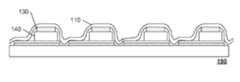
- FIGS. 1A-1Eillustrate formation of an example laminate structure 190 .
- FIG. 1Aillustrates a cross section view of a laminate film 100 ;
- FIG. 1Billustrates a surface view of the laminate film 100 ;
- FIG. 1Cillustrates an example tile 150 of light emitting devices before they are sliced/diced or otherwise singularized into individual light emitting devices 160 .
- a ‘tile’is merely a plurality of devices on a substrate; the tile may be a semiconductor wafer upon which the devices are formed, a frame with receptacles within which the devices are placed, or any other substrate upon which the devices are located.
- the laminate film 100 of this exampleincludes a plurality of optical elements 130 that are positioned at select locations on a flexible support film 110 , producing variations in elevation, or profile, normal to the surface of the support film. The locations are selected such that, when the laminate film 100 is inverted and placed upon the tile 150 of light emitting devices 160 , the optical elements 130 will be located upon a particular feature 140 of the light emitting devices 160 .
- the optical elements 130include a wavelength converting material, such as phosphor, they may be situated on the support film 110 at locations corresponding to the light emitting elements of the light emitting devices 160 on the tile 150 .
- a heat and vacuum lamination processmay be used to attach the optical elements 130 to their corresponding feature 140 , to form a laminate structure as illustrated in FIG. 1E . That is, the laminate film 100 may be drawn down upon the tile 150 using a vacuum, and heated so that the optical element 130 bonds with the corresponding feature 140 of the light emitting device 160 . Thereafter, the support film 110 may be removed, and any subsequent processing of the light emitting devices 160 with optical elements 130 may be performed.
- the support film 110may be an ethylene tetra fluoro ethylene (ETFE) film that has relatively low adhesion to the optical element 130 .
- the optical element 130may be a glass or epoxy element with a higher adhesion to the feature 140 of the light emitting device 160 .
- WO 2012/023119 “LAMINATION PROCESS FOR LEDS”, published 23 Feb. 2012 for Grigoriy Basin and Kazutoshi Iwata,discloses a method for laminating a layer of, for example, phosphor powder in a silicone binder, over an array of LED dies on a submount wafer, and is incorporated by reference herein. The layer is mounted over the LED dies, and the structure is heated in a vacuum.
- Downward pressureis placed on the support film so that the layer adheres to the tops of the LED dies.
- the structureis then exposed to ambient air, and the support film is removed.
- the structureis heated to a higher temperature in a vacuum to remove the remaining air between the layer and the wafer.
- the optical elements 130may be formed or placed on the support film 110 using any of a variety of techniques.
- An embossing process or screen printingmay be used to stamp or print the optical elements 130 upon the support film; a photo-lithograph process may be used to form the optical elements 130 upon the support film; a pick-and-place process may be used to place the optical elements 130 upon the support film; or a combination of these and other techniques known in the art may be used.
- An embossing or other ‘casting’ techniquemay be used to create a desired pattern in the optical elements 130 . Depending upon the processes and materials used, the pattern could be formed directly upon the optical elements 130 , or the support film 111 could contain a pattern that is subsequently adopted by the optical elements 130 .
- a removable cover filmmay be placed over the optical elements 130 , opposite the support film 110 , to avoid contamination or damage to the optical elements 130 .
- the terms ‘support film’ and ‘cover film’may be interpreted to be equivalent.
- the elements 130are sandwiched between the original film upon which the elements 130 are formed and another film that covers the elements 130 , it may be immaterial which film is removed to expose the elements 130 , the remaining film thereafter being the support film.
- the laminate film 100is not limited to a single type of optical element 130 .
- the optical element 130may comprise multiple elements and structures. For example, as illustrated in FIG. 1F , a lens element 131 may be formed on the laminate film 110 , followed by phosphor elements 132 on the lenses 131 , followed by reflectors 134 formed around the phosphor elements.
- circuit traces 135may be formed as one or more electrically conductive lamination layers in the laminate film 100 .
- one or more thermal conductive lamination layers 133may be formed in the laminate film 100 to facilitate the transfer or dissipation of heat produced within the device, or the other layers, such as a phosphor wavelength conversion layer.
- the thermal conductive layer 133may be selected to have optical properties similar to adjacent layers, or thermal conductive material 139 may be embedded within an ‘existing’ layer, such that the layer performs its primary function as well as the function of thermal transfer. For example, if a silicone/phosphor polymer is used for wavelength conversion, silica may be added to the polymer to provide better thermal transfer; because silica has a refraction index similar to silicone, the addition of silica is not likely to reduce the optical quality of the device.
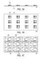
- FIGS. 2A-2Cillustrate surface views of example optical elements 130 A- 130 C.
- the example optical element 130 Ais patterned 210 to perhaps form a particular optical pattern or characteristic, such a collimation, polarization, dispersion, and so on.
- This patterning 210may be created by forming the surface of the optical element 130 A with the pattern, using, for example, a patterned laminate film 100 to transform the pattern to the optical material 230 during the lamination process.
- the pattern 210could be formed by applying a second material, such as metal, to the support film in the desired pattern, then covering this material with the optical material 230 .
- Other techniques for creating a patterned surfaceare well known in the art.
- FIGS. 2B and 2Cdifferent types of material form the optical elements 130 B and 130 C, as illustrated by the different shadings.
- the two different materials 250 , 255such as two different phosphors are arranged in an alternating pattern.
- Such a combinationmay be used, for example, when a broader spectrum of output light is desired, by converting the originally emitted light into light of two other wavelengths.
- This conceptmay be extended to include any number of combinations, a combination of four phosphors 260 , 262 , 264 , 266 being illustrated in FIG. 2C .
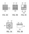
- FIGS. 3A-3Billustrate a surface and cross-cut view of an optical element 350 that includes a phosphor 330 and a reflector 320 .
- the reflector 320may be a metal or dielectric layer that is applied atop the phosphor 330 .
- the reflector 320includes an opening 325 that permits light from the light emitting element in the light emitting device 340 to enter the phosphor layer 330 .
- the reflector 320may extend beyond the phosphor layer 330 .
- FIG. 4illustrates an example flow diagram for formation of a laminate structure with optical elements and light emitting devices.
- a support filmis provided.
- the support filmmay be an ethylene tetra fluoro ethylene (ETFE) film with low adhesion.
- EFEethylene tetra fluoro ethylene
- discrete optical elementsare placed or formed at select locations, at 420 . These locations are selected to correspond to locations of features of light emitting devices on a separate substrate, such as the location of the light emitting element in each light emitting device.
- these optical elementsmay be embossed or printed on the support film, or formed using photo-lithographic techniques.
- the optical elementsmay include phosphors in an epoxy or glass slurry that is subsequently cured, or partially cured upon the support film to form a laminate film.
- Other elements, which may be additional parts of the discrete optical elements,may also be added to the laminate film, at 430 .
- a protective cover filmmay be added to the laminate film, opposite the support film.
- This cover filmmay also be an ETFE film with low adhesion.
- the tile of light emitting devicesis provided, and at 455 , the protective cover, if any, may be removed. If a protective cover film had been added, and depending on the particular structure of the optical element, either the original film or this cover film may subsequently be considered the support film; the support film being the film remaining after the other film is removed.
- the laminate filmis placed upon the tile such that the optical elements are in contact with the corresponding feature of the light emitting devices, at 460 .
- the laminate filmis then laminated to the light emitting devices, at 470 .
- Laminationmay be performed using a vacuum and heating process, as detailed above, or, any alternative lamination technique may be used.
- the resultant laminate structuremay be stored for subsequent processing, the support film forming a protective cover for this structure.
- the support filmmay be removed and any remaining processes may be performed, at 490 , such as testing, encapsulation, singularizing, and so on.
Landscapes
- Engineering & Computer Science (AREA)
- Physics & Mathematics (AREA)
- Microelectronics & Electronic Packaging (AREA)
- Power Engineering (AREA)
- Spectroscopy & Molecular Physics (AREA)
- General Engineering & Computer Science (AREA)
- Manufacturing & Machinery (AREA)
- Condensed Matter Physics & Semiconductors (AREA)
- General Physics & Mathematics (AREA)
- Computer Hardware Design (AREA)
- Led Device Packages (AREA)
- Optical Filters (AREA)
- Led Devices (AREA)
Abstract
Description
Claims (20)
Priority Applications (1)
| Application Number | Priority Date | Filing Date | Title |
|---|---|---|---|
| US13/879,639US9351348B2 (en) | 2010-10-27 | 2011-10-20 | Laminate support film for fabrication of light emitting devices and method of fabrication |
Applications Claiming Priority (3)
| Application Number | Priority Date | Filing Date | Title |
|---|---|---|---|
| US40718010P | 2010-10-27 | 2010-10-27 | |
| PCT/IB2011/054684WO2012056378A1 (en) | 2010-10-27 | 2011-10-20 | Laminate support film for fabrication of light emitting devices and method its fabrication |
| US13/879,639US9351348B2 (en) | 2010-10-27 | 2011-10-20 | Laminate support film for fabrication of light emitting devices and method of fabrication |
Publications (2)
| Publication Number | Publication Date |
|---|---|
| US20130221835A1 US20130221835A1 (en) | 2013-08-29 |
| US9351348B2true US9351348B2 (en) | 2016-05-24 |
Family
ID=44993634
Family Applications (1)
| Application Number | Title | Priority Date | Filing Date |
|---|---|---|---|
| US13/879,639ActiveUS9351348B2 (en) | 2010-10-27 | 2011-10-20 | Laminate support film for fabrication of light emitting devices and method of fabrication |
Country Status (7)
| Country | Link |
|---|---|
| US (1) | US9351348B2 (en) |
| EP (1) | EP2633554A1 (en) |
| JP (3) | JP2013541220A (en) |
| KR (1) | KR101909299B1 (en) |
| CN (1) | CN103180945B (en) |
| TW (1) | TWI560400B (en) |
| WO (1) | WO2012056378A1 (en) |
Cited By (1)
| Publication number | Priority date | Publication date | Assignee | Title |
|---|---|---|---|---|
| US20190371770A1 (en)* | 2012-10-05 | 2019-12-05 | Bridgelux, Inc. | Methods of making light-emitting assemblies comprising an array of light-emitting diodes having an optimized lens configuration |
Families Citing this family (9)
| Publication number | Priority date | Publication date | Assignee | Title |
|---|---|---|---|---|
| JP2014075527A (en)* | 2012-10-05 | 2014-04-24 | Nippon Telegr & Teleph Corp <Ntt> | Semiconductor element structure and method for preparing the same |
| DE102012109806A1 (en)* | 2012-10-15 | 2014-04-17 | Osram Opto Semiconductors Gmbh | Radiation-emitting component |
| JP6713720B2 (en)* | 2013-08-30 | 2020-06-24 | エルジー イノテック カンパニー リミテッド | Light emitting device package and vehicle lighting device including the same |
| US20160131328A1 (en)* | 2014-11-07 | 2016-05-12 | Lighthouse Technologies Limited | Indoor smd led equipped for outdoor usage |
| CN106449951B (en)* | 2016-11-16 | 2019-01-04 | 厦门市三安光电科技有限公司 | A kind of production method of light-emitting diode encapsulation structure |
| US11304291B2 (en)* | 2017-06-29 | 2022-04-12 | Kyocera Corporation | Circuit board and light emitting device including circuit board |
| US11022791B2 (en)* | 2018-05-18 | 2021-06-01 | Facebook Technologies, Llc | Assemblies of anisotropic optical elements and methods of making |
| US11923483B2 (en) | 2018-05-18 | 2024-03-05 | Ddp Specialty Electronic Materials Us, Llc | Method for producing LED by one step film lamination |
| US11527684B2 (en) | 2020-12-04 | 2022-12-13 | Lumileds Llc | Patterned downconverter and adhesive film for micro-LED, mini-LED downconverter mass transfer |
Citations (24)
| Publication number | Priority date | Publication date | Assignee | Title |
|---|---|---|---|---|
| US4007396A (en) | 1974-11-06 | 1977-02-08 | The Marconi Company Limited | Light emissive diode displays |
| JP2005183777A (en) | 2003-12-22 | 2005-07-07 | Nichia Chem Ind Ltd | Semiconductor device and manufacturing method thereof |
| US20060102914A1 (en)* | 2004-11-15 | 2006-05-18 | Lumileds Lighting U.S., Llc | Wide emitting lens for LED useful for backlighting |
| JP2006165326A (en) | 2004-12-08 | 2006-06-22 | Stanley Electric Co Ltd | Light emitting diode and manufacturing method thereof |
| JP2007019096A (en) | 2005-07-05 | 2007-01-25 | Toyoda Gosei Co Ltd | Light emitting device and manufacturing method thereof |
| US20070096131A1 (en) | 2005-10-28 | 2007-05-03 | Lumileds Lighting U.S. Llc | Laminating encapsulant film containing phosphor over LEDS |
| US20070267646A1 (en) | 2004-06-03 | 2007-11-22 | Philips Lumileds Lighting Company, Llc | Light Emitting Device Including a Photonic Crystal and a Luminescent Ceramic |
| WO2007146860A1 (en) | 2006-06-12 | 2007-12-21 | 3M Innovative Properties Company | Led device with re-emitting semiconductor construction and optical element |
| US20090001869A1 (en) | 2005-05-12 | 2009-01-01 | Matsushita Electric Industrial Co., Ltd. | Led with Phosphor Layer Having Different Thickness or Different Phosphor Concentration |
| US20090020779A1 (en)* | 2007-06-27 | 2009-01-22 | Namics Corporation | Method of preparing a sealed light-emitting diode chip |
| US20090053528A1 (en)* | 2006-04-25 | 2009-02-26 | Asahi Glass Company, Limited | Release film for semiconductor resin molds |
| US20090154166A1 (en) | 2007-12-13 | 2009-06-18 | Philips Lumileds Lighting Company, Llc | Light Emitting Diode for Mounting to a Heat Sink |
| US20090173960A1 (en) | 2004-06-09 | 2009-07-09 | Koninklijke Philips Electronics N.V. | Semiconductor light emitting device with pre-fabricated wavelength converting element |
| EP2120271A1 (en) | 2007-03-01 | 2009-11-18 | NEC Lighting, Ltd. | Led device and illuminating apparatus |
| US20100051984A1 (en) | 2008-09-02 | 2010-03-04 | Scott West | Phosphor-Converted LED |
| US20100109025A1 (en)* | 2008-11-05 | 2010-05-06 | Koninklijke Philips Electronics N.V. | Over the mold phosphor lens for an led |
| TW201019395A (en) | 2008-11-13 | 2010-05-16 | Samsung Electro Mech | Method of fabricating thin film device |
| US20100295077A1 (en)* | 2009-05-19 | 2010-11-25 | Intematix Corporation | Manufacture of light emitting devices with phosphor wavelength conversion |
| US20110018011A1 (en)* | 2007-12-03 | 2011-01-27 | Beeson Karl W | Solid-state light source |
| US20110058372A1 (en)* | 2010-08-27 | 2011-03-10 | Quarkstar, Llc | Solid State Bidirectional Light Sheet for General Illumination |
| WO2012023119A1 (en) | 2010-08-20 | 2012-02-23 | Koninklijke Philips Electronics N.V. | Lamination process for leds |
| US8141384B2 (en)* | 2006-05-03 | 2012-03-27 | 3M Innovative Properties Company | Methods of making LED extractor arrays |
| US8669573B2 (en)* | 2007-02-12 | 2014-03-11 | Cree, Inc. | Packaged semiconductor light emitting devices having multiple optical elements |
| US8759123B2 (en)* | 2009-03-26 | 2014-06-24 | Toyoda Gosei Co., Ltd. | Method of manufacturing LED lamp |
Family Cites Families (6)
| Publication number | Priority date | Publication date | Assignee | Title |
|---|---|---|---|---|
| JP2007150233A (en)* | 2005-11-02 | 2007-06-14 | Trion:Kk | Color-temperature controllable light-emitting device |
| DE102006024165A1 (en)* | 2006-05-23 | 2007-11-29 | Patent-Treuhand-Gesellschaft für elektrische Glühlampen mbH | Optoelectronic semiconductor chip with a wavelength conversion substance and optoelectronic semiconductor component with such a semiconductor chip and method for producing the optoelectronic semiconductor chip |
| US7652301B2 (en)* | 2007-08-16 | 2010-01-26 | Philips Lumileds Lighting Company, Llc | Optical element coupled to low profile side emitting LED |
| KR101383357B1 (en)* | 2007-08-27 | 2014-04-10 | 엘지이노텍 주식회사 | Light emitting device package and method of making the same |
| CN100483762C (en)* | 2008-02-25 | 2009-04-29 | 鹤山丽得电子实业有限公司 | LED device making method |
| JP2009229507A (en)* | 2008-03-19 | 2009-10-08 | Hitachi Chem Co Ltd | Sealing film |
- 2011
- 2011-10-20USUS13/879,639patent/US9351348B2/enactiveActive
- 2011-10-20CNCN201180052305.1Apatent/CN103180945B/enactiveActive
- 2011-10-20KRKR1020137013389Apatent/KR101909299B1/enactiveActive
- 2011-10-20EPEP11784784.8Apatent/EP2633554A1/ennot_activeWithdrawn
- 2011-10-20WOPCT/IB2011/054684patent/WO2012056378A1/enactiveApplication Filing
- 2011-10-20JPJP2013535553Apatent/JP2013541220A/enactivePending
- 2011-10-27TWTW100139214Apatent/TWI560400B/ennot_activeIP Right Cessation
- 2018
- 2018-05-30JPJP2018102950Apatent/JP6595044B2/enactiveActive
- 2019
- 2019-09-25JPJP2019173665Apatent/JP6883632B2/enactiveActive
Patent Citations (25)
| Publication number | Priority date | Publication date | Assignee | Title |
|---|---|---|---|---|
| US4007396A (en) | 1974-11-06 | 1977-02-08 | The Marconi Company Limited | Light emissive diode displays |
| JP2005183777A (en) | 2003-12-22 | 2005-07-07 | Nichia Chem Ind Ltd | Semiconductor device and manufacturing method thereof |
| US20070267646A1 (en) | 2004-06-03 | 2007-11-22 | Philips Lumileds Lighting Company, Llc | Light Emitting Device Including a Photonic Crystal and a Luminescent Ceramic |
| US20090173960A1 (en) | 2004-06-09 | 2009-07-09 | Koninklijke Philips Electronics N.V. | Semiconductor light emitting device with pre-fabricated wavelength converting element |
| US20060102914A1 (en)* | 2004-11-15 | 2006-05-18 | Lumileds Lighting U.S., Llc | Wide emitting lens for LED useful for backlighting |
| JP2006165326A (en) | 2004-12-08 | 2006-06-22 | Stanley Electric Co Ltd | Light emitting diode and manufacturing method thereof |
| US20090001869A1 (en) | 2005-05-12 | 2009-01-01 | Matsushita Electric Industrial Co., Ltd. | Led with Phosphor Layer Having Different Thickness or Different Phosphor Concentration |
| JP2007019096A (en) | 2005-07-05 | 2007-01-25 | Toyoda Gosei Co Ltd | Light emitting device and manufacturing method thereof |
| US20070096131A1 (en) | 2005-10-28 | 2007-05-03 | Lumileds Lighting U.S. Llc | Laminating encapsulant film containing phosphor over LEDS |
| US20090053528A1 (en)* | 2006-04-25 | 2009-02-26 | Asahi Glass Company, Limited | Release film for semiconductor resin molds |
| US8141384B2 (en)* | 2006-05-03 | 2012-03-27 | 3M Innovative Properties Company | Methods of making LED extractor arrays |
| WO2007146860A1 (en) | 2006-06-12 | 2007-12-21 | 3M Innovative Properties Company | Led device with re-emitting semiconductor construction and optical element |
| US8669573B2 (en)* | 2007-02-12 | 2014-03-11 | Cree, Inc. | Packaged semiconductor light emitting devices having multiple optical elements |
| EP2120271A1 (en) | 2007-03-01 | 2009-11-18 | NEC Lighting, Ltd. | Led device and illuminating apparatus |
| US20090020779A1 (en)* | 2007-06-27 | 2009-01-22 | Namics Corporation | Method of preparing a sealed light-emitting diode chip |
| US20110018011A1 (en)* | 2007-12-03 | 2011-01-27 | Beeson Karl W | Solid-state light source |
| US20090154166A1 (en) | 2007-12-13 | 2009-06-18 | Philips Lumileds Lighting Company, Llc | Light Emitting Diode for Mounting to a Heat Sink |
| WO2010027672A2 (en) | 2008-09-02 | 2010-03-11 | Bridgelux, Inc. | Phosphor-converted led |
| US20100051984A1 (en) | 2008-09-02 | 2010-03-04 | Scott West | Phosphor-Converted LED |
| US20100109025A1 (en)* | 2008-11-05 | 2010-05-06 | Koninklijke Philips Electronics N.V. | Over the mold phosphor lens for an led |
| TW201019395A (en) | 2008-11-13 | 2010-05-16 | Samsung Electro Mech | Method of fabricating thin film device |
| US8759123B2 (en)* | 2009-03-26 | 2014-06-24 | Toyoda Gosei Co., Ltd. | Method of manufacturing LED lamp |
| US20100295077A1 (en)* | 2009-05-19 | 2010-11-25 | Intematix Corporation | Manufacture of light emitting devices with phosphor wavelength conversion |
| WO2012023119A1 (en) | 2010-08-20 | 2012-02-23 | Koninklijke Philips Electronics N.V. | Lamination process for leds |
| US20110058372A1 (en)* | 2010-08-27 | 2011-03-10 | Quarkstar, Llc | Solid State Bidirectional Light Sheet for General Illumination |
Non-Patent Citations (3)
| Title |
|---|
| International Search Report mailed Feb. 12, 2012 from International Application No. PCT/IB2011/054684, 13 pgs. |
| Office Action dated Dec. 10, 2015 from ROC (Taiwan) Application No. 100139214. |
| Office Action issued Aug. 4, 2015 from Japanese Application No. 2013-535553. |
Cited By (3)
| Publication number | Priority date | Publication date | Assignee | Title |
|---|---|---|---|---|
| US20190371770A1 (en)* | 2012-10-05 | 2019-12-05 | Bridgelux, Inc. | Methods of making light-emitting assemblies comprising an array of light-emitting diodes having an optimized lens configuration |
| US11302676B2 (en)* | 2012-10-05 | 2022-04-12 | Bridgelux, Inc. | Methods of making light-emitting assemblies comprising an array of light-emitting diodes having an optimized lens configuration |
| US12015016B2 (en) | 2012-10-05 | 2024-06-18 | Bridgelux, Inc. | Methods of making light-emitting assemblies comprising an array of light-emitting diodes having an optimized lens configuration |
Also Published As
| Publication number | Publication date |
|---|---|
| JP2013541220A (en) | 2013-11-07 |
| JP2019220720A (en) | 2019-12-26 |
| EP2633554A1 (en) | 2013-09-04 |
| KR20130140039A (en) | 2013-12-23 |
| JP2018160678A (en) | 2018-10-11 |
| CN103180945A (en) | 2013-06-26 |
| WO2012056378A1 (en) | 2012-05-03 |
| JP6883632B2 (en) | 2021-06-09 |
| US20130221835A1 (en) | 2013-08-29 |
| TW201231873A (en) | 2012-08-01 |
| JP6595044B2 (en) | 2019-10-23 |
| TWI560400B (en) | 2016-12-01 |
| CN103180945B (en) | 2016-12-07 |
| KR101909299B1 (en) | 2018-10-17 |
Similar Documents
| Publication | Publication Date | Title |
|---|---|---|
| US9351348B2 (en) | Laminate support film for fabrication of light emitting devices and method of fabrication | |
| US7781794B2 (en) | Resin sheet for encapsulating optical semiconductor element and optical semiconductor device | |
| KR102323289B1 (en) | Glueless light emitting device with phosphor converter | |
| JP6599295B2 (en) | LIGHT EMITTING ELEMENT HAVING BELT ANGLE REFLECTOR AND MANUFACTURING METHOD | |
| US10347798B2 (en) | Photoluminescence material coating of LED chips | |
| CN101978515B (en) | Optoelectronic semiconductor component and method for producing an optoelectronic semiconductor component | |
| CN105409014B (en) | Method for producing converter element and optoelectronic component, converter element and optoelectronic component | |
| EP2197048B1 (en) | Light-emitting device | |
| KR101641384B1 (en) | Sheet for photosemiconductor encapsulation | |
| JP2013038215A (en) | Wavelength conversion member | |
| TWI850567B (en) | Method of packaging light emitting display device and light emitting display device packaging structure | |
| JP6608359B2 (en) | PCLED with optical element without substrate carrier | |
| WO2012017304A2 (en) | White led device and manufacturing method thereof | |
| JP2019201089A (en) | Oblique angle chip reflector of chip scale packaging light emission device and manufacturing method of the same | |
| CN104205365B (en) | Singulation of light-emitting devices before and after phosphor application | |
| US20110065218A1 (en) | Pre-thermal greased led array | |
| JP2018523256A (en) | Conversion part manufacturing method and optoelectronic lighting device | |
| TW201739071A (en) | Method for manufacturing photovoltaic module and photovoltaic module | |
| TWI894926B (en) | Hybrid encapsulation film and method of manufacturing light emitting device using the same | |
| CN106104801A (en) | Lighting device and the method manufacturing lighting device | |
| CN116314159A (en) | Lighting panel, manufacturing method thereof and desk lamp | |
| TW201429008A (en) | Light-emitting module, light source assembly, and methods for manufacturing |
Legal Events
| Date | Code | Title | Description |
|---|---|---|---|
| AS | Assignment | Owner name:KONINKLIJKE PHILIPS ELECTRONICS N.V., NETHERLANDS Free format text:ASSIGNMENT OF ASSIGNORS INTEREST;ASSIGNORS:BASIN, GRIGORIY;MARTIN, PAUL SCOTT;SIGNING DATES FROM 20130213 TO 20130408;REEL/FRAME:030220/0494 | |
| AS | Assignment | Owner name:KONINKLIJKE PHILIPS N.V., NETHERLANDS Free format text:CHANGE OF NAME;ASSIGNOR:KONINKLIJKE PHILIPS ELECTRONICS N.V.;REEL/FRAME:036115/0982 Effective date:20130515 | |
| STCF | Information on status: patent grant | Free format text:PATENTED CASE | |
| AS | Assignment | Owner name:DEUTSCHE BANK AG NEW YORK BRANCH, AS COLLATERAL AGENT, NEW YORK Free format text:SECURITY INTEREST;ASSIGNOR:LUMILEDS LLC;REEL/FRAME:043108/0001 Effective date:20170630 Owner name:DEUTSCHE BANK AG NEW YORK BRANCH, AS COLLATERAL AG Free format text:SECURITY INTEREST;ASSIGNOR:LUMILEDS LLC;REEL/FRAME:043108/0001 Effective date:20170630 | |
| AS | Assignment | Owner name:LUMILEDS LLC, CALIFORNIA Free format text:ASSIGNMENT OF ASSIGNORS INTEREST;ASSIGNOR:KONINKLIJKE PHILIPS N.V.;REEL/FRAME:044809/0940 Effective date:20170428 | |
| MAFP | Maintenance fee payment | Free format text:PAYMENT OF MAINTENANCE FEE, 4TH YEAR, LARGE ENTITY (ORIGINAL EVENT CODE: M1551); ENTITY STATUS OF PATENT OWNER: LARGE ENTITY Year of fee payment:4 | |
| AS | Assignment | Owner name:SOUND POINT AGENCY LLC, NEW YORK Free format text:SECURITY INTEREST;ASSIGNORS:LUMILEDS LLC;LUMILEDS HOLDING B.V.;REEL/FRAME:062299/0338 Effective date:20221230 | |
| MAFP | Maintenance fee payment | Free format text:PAYMENT OF MAINTENANCE FEE, 8TH YEAR, LARGE ENTITY (ORIGINAL EVENT CODE: M1552); ENTITY STATUS OF PATENT OWNER: LARGE ENTITY Year of fee payment:8 | |
| AS | Assignment | Owner name:LUMILEDS HOLDING B.V., NETHERLANDS Free format text:RELEASE BY SECURED PARTY;ASSIGNOR:SOUND POINT AGENCY LLC;REEL/FRAME:070046/0001 Effective date:20240731 Owner name:LUMILEDS LLC, CALIFORNIA Free format text:RELEASE BY SECURED PARTY;ASSIGNOR:SOUND POINT AGENCY LLC;REEL/FRAME:070046/0001 Effective date:20240731 | |
| AS | Assignment | Owner name:LUMILEDS SINGAPORE PTE. LTD., SINGAPORE Free format text:ASSIGNMENT OF ASSIGNORS INTEREST;ASSIGNOR:LUMILEDS LLC;REEL/FRAME:071888/0086 Effective date:20250708 |