US9344192B1 - Driver chip for minimizing transmission impairments and for boosting signal transmission rates - Google Patents
Driver chip for minimizing transmission impairments and for boosting signal transmission ratesDownload PDFInfo
- Publication number
- US9344192B1 US9344192B1US14/548,836US201414548836AUS9344192B1US 9344192 B1US9344192 B1US 9344192B1US 201414548836 AUS201414548836 AUS 201414548836AUS 9344192 B1US9344192 B1US 9344192B1
- Authority
- US
- United States
- Prior art keywords
- signal
- tapped delay
- driver chip
- optical
- taps
- Prior art date
- Legal status (The legal status is an assumption and is not a legal conclusion. Google has not performed a legal analysis and makes no representation as to the accuracy of the status listed.)
- Active, expires
Links
- 230000006735deficitEffects0.000titleclaimsabstractdescription38
- 230000008054signal transmissionEffects0.000titleclaimsabstractdescription12
- 230000005540biological transmissionEffects0.000titleclaimsdescription37
- 230000003287optical effectEffects0.000claimsabstractdescription49
- 239000013307optical fiberSubstances0.000claimsabstractdescription15
- 238000010586diagramMethods0.000claimsdescription16
- 238000000034methodMethods0.000claimsdescription13
- 238000007493shaping processMethods0.000claimsdescription9
- 238000001228spectrumMethods0.000claimsdescription5
- 238000012544monitoring processMethods0.000claims3
- 238000005070samplingMethods0.000claims2
- 230000000694effectsEffects0.000abstractdescription8
- 239000006185dispersionSubstances0.000abstractdescription3
- 230000003466anti-cipated effectEffects0.000abstract1
- 239000000835fiberSubstances0.000description9
- 238000013461designMethods0.000description2
- 230000006872improvementEffects0.000description2
- 230000008569processEffects0.000description2
- 238000012545processingMethods0.000description2
- 230000004044responseEffects0.000description2
- 238000012360testing methodMethods0.000description2
- DNTFEAHNXKUSKQ-RFZPGFLSSA-N(1r,2r)-2-aminocyclopentane-1-sulfonic acidChemical compoundN[C@@H]1CCC[C@H]1S(O)(=O)=ODNTFEAHNXKUSKQ-RFZPGFLSSA-N0.000description1
- 238000006243chemical reactionMethods0.000description1
- 238000010276constructionMethods0.000description1
- 238000012937correctionMethods0.000description1
- 230000003111delayed effectEffects0.000description1
- 238000005516engineering processMethods0.000description1
- 230000008520organizationEffects0.000description1
- 230000003071parasitic effectEffects0.000description1
- 238000000926separation methodMethods0.000description1
- 230000007781signaling eventEffects0.000description1
- 239000000758substrateSubstances0.000description1
- 238000010200validation analysisMethods0.000description1
Images


Classifications
- H—ELECTRICITY
- H04—ELECTRIC COMMUNICATION TECHNIQUE
- H04B—TRANSMISSION
- H04B10/00—Transmission systems employing electromagnetic waves other than radio-waves, e.g. infrared, visible or ultraviolet light, or employing corpuscular radiation, e.g. quantum communication
- H04B10/25—Arrangements specific to fibre transmission
- H04B10/2589—Bidirectional transmission
- H04B10/25891—Transmission components
- H04B10/2504—
- H—ELECTRICITY
- H04—ELECTRIC COMMUNICATION TECHNIQUE
- H04B—TRANSMISSION
- H04B10/00—Transmission systems employing electromagnetic waves other than radio-waves, e.g. infrared, visible or ultraviolet light, or employing corpuscular radiation, e.g. quantum communication
- H04B10/25—Arrangements specific to fibre transmission
- H04B10/2507—Arrangements specific to fibre transmission for the reduction or elimination of distortion or dispersion
- H—ELECTRICITY
- H04—ELECTRIC COMMUNICATION TECHNIQUE
- H04B—TRANSMISSION
- H04B10/00—Transmission systems employing electromagnetic waves other than radio-waves, e.g. infrared, visible or ultraviolet light, or employing corpuscular radiation, e.g. quantum communication
- H04B10/25—Arrangements specific to fibre transmission
- H04B10/2575—Radio-over-fibre, e.g. radio frequency signal modulated onto an optical carrier
- H—ELECTRICITY
- H04—ELECTRIC COMMUNICATION TECHNIQUE
- H04B—TRANSMISSION
- H04B10/00—Transmission systems employing electromagnetic waves other than radio-waves, e.g. infrared, visible or ultraviolet light, or employing corpuscular radiation, e.g. quantum communication
- H04B10/50—Transmitters
- H04B10/58—Compensation for non-linear transmitter output
- H—ELECTRICITY
- H04—ELECTRIC COMMUNICATION TECHNIQUE
- H04B—TRANSMISSION
- H04B2210/00—Indexing scheme relating to optical transmission systems
- H04B2210/25—Distortion or dispersion compensation
- H04B2210/254—Distortion or dispersion compensation before the transmission line, i.e. pre-compensation
Definitions
- the present inventionpertains generally to systems and methods for transporting an optical signal over a fiber optic. More particularly, the present invention pertains to systems and methods for shaping an electrical signal, to compensate for impairments, distortions and mismatch values that are introduced into the electrical signal during its conversion into an optical signal and its subsequent transmission over an optical fiber.
- the present inventionis particularly, but not exclusively, useful for systems and methods that employ tapped delay equalizers having weighted taps to compensate for impedance mismatch impairments, electrical pre-distortions and transmission line losses during an optical signal transmission.
- Tapped delay equalizersare well known in pertinent signal processing technologies as being an effective means for shaping electrical signals. They are widely used in a variety of electric/optical environments, and they are employed for a plethora of different purposes.
- the electrical/optical environment of interestinvolves the transmission of optical signals over a fiber optic.
- a purpose hereis to provide an effective driver chip for use in a system that includes Electrical/Optical (E/O) and Optical/Electrical (O/E) converters, which will optimize the quality of signal transmissions.
- E/OElectrical/Optical
- O/EOptical/Electrical
- ISIInterSymbol Interference
- driver chipE/O converter, fiber optic, and O/E converter
- electrical and photonic signal distortionscaused by impairments such as amplitude and group delay distortions, photon-carrier lifetime effects, and fiber dispersion
- other additional impairmentsfrom signal characteristics that can be attributed to slow rise/fall time and laser relaxation peak effect and E/O device parasitics.
- the present inventionrecognizes that all of the various impairments noted above can be collectively compensated for by the employment and proper configuration of an analog tapped delay equalizer.
- the present inventionalso recognizes that an “eye diagram,” of a type well known in the pertinent art, can be used to monitor the design, the signal-to-noise ratio (SNR), and the testing or reconfiguration of an analog tapped delay equalizer.
- SNRsignal-to-noise ratio
- an optimal operation for the driver chipis indicated when the “eye” of the eye diagram is open to its greatest extent.
- an object of the present inventionto provide a system and method for simultaneously minimizing operational and architectural impairments during the transmission of an optical signal over an optical fiber.
- Another object of the present inventionis to establish tap weights for the tapped delay equalizer of a driver chip that can be controlled to minimize impairments and distortions to an output signal that are caused by transmission line losses and impedance mismatches, as well as other electrical and photonic impairments.
- Another object of the present inventionis to optimize bandwidth and ISI performance.
- Yet another object of the present inventionis to provide a driver chip for use in optimizing the transmission of an optical signal over an optical fiber that is easy to use, is simple to implement, and is comparatively cost effective.
- a driver chipfor transmitting optical signals over an optical fiber.
- the driver chipis designed and configured to minimize impairments to signal transmissions, and to thereby optimize the quality of these transmissions.
- the driver chipincludes, in combination: an analog tapped delay equalizer, an amplifier with gain and bias control, and control circuitry for maintaining an operation of the driver chip. It is an important aspect of the present invention that minimizing impairments and optimizing signal quality is accomplished simultaneously by providing a proper operating configuration of the tap weights for the tapped delay equalizer.
- the input signal for the driver chipwill be a digital signal.
- a digitally modulated signalhas a characteristic symbol rate, R s .
- this symbol rate, R sis equal to the number of symbol changes (i.e. waveform changes or signaling events) that are made per second.
- FFEFeed Forward Equalizer
- a tapped delay equalizerneeds to be programmed (configured) for compliance with the symbol rate, R s , of the digitally modulated input signal.
- additional considerationsinclude the time delay, d n , between adjacent taps, and the number of taps per symbol, N.
- time delay, d nwill be less than the symbol time duration, T.
- the number of taps, n, that are used with the tapped delay equalizer (FFE)will need to be three or more (n ⁇ 3).
- the tapped delay equalizeris positioned on the driver chip to receive an input digital signal.
- the equalizer receiving this input digital signalwill have an n-number of taps, and a time delay, d n , between adjacent taps can be established as desired for the particular chip.
- d n⁇ T.
- d nis constant.
- d nis preferably the same between all adjacent taps (i.e.
- the tapped delay equalizeris employed to modify the input digital signal, and to thereby create a compensated signal.
- the amplifier of the driver chipis connected with the tap delay equalizer for receiving the compensated signal. Further, in this combination, the amplifier provides gain for the signal, and it includes a biasing element to bias the compensated signal. Thus, bulky external bias circuitry is eliminated. Further, this on-chip control is provided to control average power and to stabilize laser operation.
- the general, overall purpose hereis to create an electrical output signal for the driver chip which has a proper operating point.
- control circuitryis provided on, or off, the driver chip to interconnect with the other components.
- the connection between the amplifier and the control circuitry, either on or off the chip,is used to control a gain and a bias for the amplifier.
- its connection with the tapped delay equalizeris provided to control tap weights for individual taps of the tapped delay filter.
- the driver chipwill normally be electronically connected to an Electrical/Optical (E/O) converter which will convert the electrical output signal into an optical signal, ⁇ .
- E/OElectrical/Optical
- a low-pass filtercan be inserted between the driver chip and the E/O converter to achieve the required spectrum shaping using fewer filter taps during a transmission of the optical signal, ⁇ , over an optical fiber.
- these componentsi.e. the E/O converter, the low-pass filter, and the fiber optic
- these componentsi.e. the E/O converter, the low-pass filter, and the fiber optic
- the taps of the tapped delay equalizerare weighted. Specifically, this is done to minimize impairments to the output signal that may be caused by distortions, line losses and mismatch values that are introduced during creation of the optical signal, ⁇ . As intended for the present invention, however, the taps can also be weighted to achieve other purposes.
- an eye diagramcan be used to verify its optimal operation.
- FIG. 1is a schematic presentation of a driver chip in accordance with the present invention
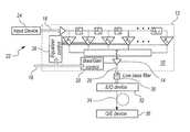
- FIG. 2is a detailed presentation of operational components of the driver chip in combination with system components required for transmission of an optical signal
- FIG. 3is a schematic presentation of a typical electrical environment for the driver chip of the present invention, illustrating an impairment requiring mismatch compensation from the driver chip;
- FIG. 4is an exemplary graph of tap locations and respective tap weights presented on a time line for a 9 tap Gaussian equalizer employing 2-tap/symbol;
- FIG. 5Ais a representative eye diagram of an exemplary optical transmission system without equalization
- FIG. 5Bis a representative eye diagram of the same optical transmission system considered for FIG. 5A which results when the system is equalized by a 3 tap Gaussian equalizer employing 1-tap/symbol;
- FIG. 5Cis a representative eye diagram of the same optical transmission system considered for FIGS. 5A and 5B which results when the system is equalized by a 9 tap Gaussian equalizer employing 2-taps/symbol.
- a driver chip in accordance with the present inventionis shown and is generally designated 10 .
- the essential components of the driver chip 10include: a tapped delay equalizer 12 (e.g. Feed Forward Equalizer [FFE]); an amplifier 14 with an Electrical/Optical (E/O) bias; and a control circuitry 16 .
- FIG. 1indicates that an input signal 18 is fed directly to the tapped delay equalizer 12 , and that a compensated signal 20 is created as an output of the driver chip 10 .
- both the tapped delay equalizer 12 and the amplifier 14are controlled by the circuitry 16 .
- control circuitry 16 shown in FIG. 1is an integral component of the driver chip 10 , it will be appreciated by the skilled artisan that the control circuitry 16 can properly operate while separated from the substrate of driver chip 10 .
- FIG. 2A system which establishes architecture for incorporating the driver chip 10 is shown in FIG. 2 , where the system is generally designated 22 .
- an input device 24is provided to generate the input signal 18 .
- FIG. 2shows that the tapped delay equalizer 12 has an n-number of taps, an, with a time delay, d n , between adjacent taps (e.g. a n and a n+1 ).
- d na time delay between adjacent taps
- R ssymbol rate
- FIG. 2shows that the control circuitry 16 includes an equalizer control 26 that is connected directly to each of the taps, a n , and a bias/gain control 28 that is connected directly to the amplifier 14 .
- FIG. 2further indicates that in the system 22 , the driver chip 10 can be connected to a low pass filter 30 to achieve the required spectrum shaping using fewer filter taps.
- an E/O device (converter) 32is shown for converting the compensated signal 20 into an optical signal, ⁇ .
- a fiber optic (transmission medium) 34is shown for use in transporting the optical signal, ⁇ , to an Optical/Electrical (O/E) device 36 (see FIG. 3 ) where it is reconverted to an electrical signal for further processing.
- O/EOptical/Electrical
- FIG. 3is provided to illustrate an exemplary impedance mismatch 40 which requires compensation by the driver chip 10 of the present invention.
- the impedance mismatch 40is shown to be the result of reflections that will occur between the driver chip 10 and the E/O device 32 of the system 22 .
- the letter L shown in FIG. 3indicates that a time delay can occur or develop between the E/O driver chip 10 and the E/O device 32 . When this happens, the resultant separation will cause a round trip delay of 2L for any reflections between the driver chip 10 and the E/O device 32 . As is well known, these reflections will create an impairment.
- the present inventionrecognizes that such an impairment can be compensated for using the tapped delay equalizer 12 of the driver chip 10 when the 2L delay is less than about one half of the total tapped delay of the tapped delay equalizer (FFE) 12 .
- the present inventionenvisions being able to provide a substantial correction for impedance mismatch (ISI) impairments when 2L ⁇ d n /2.
- an overarching purpose for the driver chip 10is to minimize all forms of impairments in the system 22 , and to optimize the signal quality provided by the system 22 .
- thisis achieved by establishing a proper weighting configuration for the taps, a n , in the tapped delay equalizer 12 , and by maintaining a proper operating point for the E/O device 32 .
- a detailed description of pertinent transmission characteristics for a tapped delay equalizer (FFE) 12 of the present inventionis presented as a schema 42 in FIG. 4 .
- the time duration, T, for each symbolis established based on characteristics of the input signal 18 and its symbol rate, R s .
- Nthe time duration
- d nT/2 (i.e. d n ⁇ T).
- the same organization for tap locationpertains for the remaining symbols T 2 et seq.
- a shaping of the input signal 18is accomplished for the purpose of minimizing the effect of impairments on the output compensated signal 20 .
- thisis done to minimize the effect of impairments caused by all sources required for the optical transmission of the input signal 18 .
- these impairmentscan include: 1) transmission line losses, along with impedance mismatch distortions that are introduced at interfaces between system components (e.g. driver chip, E/O converter, fiber optic, and O/E converter); 2) electrical and photonic signal distortions caused by impairments such as amplitude and group delay distortions, photon-carrier lifetime effects, and fiber dispersion; and 3) other additional impairments from signal characteristics that can be attributed to slow rise/fall time, and laser relaxation peak effect.
- compensation for these impairmentsis done by appropriately weighting the samples a n taken from the various taps of the tapped delay equalizer (FFE) 12 .
- FFEtapped delay equalizer
- programming of the tapped delay equalizer 12is done by first creating a test model of the intended signal transmission system.
- thiswill include the driver chip 10 together with selected associated components, such as the E/O device 32 , the low pass filter 30 (optional), the transmission medium 34 (e.g. fiber optic), and the O/E device 36 .
- the collective response of components in a signal transmission systemis monitored, and respective gains are set for the taps a n of the tapped delay equalizer 12 to minimize impairments caused by these components.
- the collective responseis monitored using an eye diagram 44 of a type well known in the pertinent art.
- the eye diagram 44is preferably taken at the output of the O/E device 36 . This positioning, however, is only exemplary. Moreover, it is to be appreciated that, regardless where the eye diagram 44 is placed, the compensation to be provided by the driver chip 10 will extend to all components throughout the particular signal transmission system.
- FIGS. 5A-Can operational validation of the driver chip 10 for the present invention is evidenced by sequentially presenting the results from a same optical transmission system.
- the results from using three different configurations for the tapped delay equalizer 12 of the driver chip 10are shown.
- the eye diagram 44 shown in FIG. 5Aresulted when there was no equalization for the optical transmission system.
Landscapes
- Physics & Mathematics (AREA)
- Electromagnetism (AREA)
- Engineering & Computer Science (AREA)
- Computer Networks & Wireless Communication (AREA)
- Signal Processing (AREA)
- Nonlinear Science (AREA)
- Optical Communication System (AREA)
Abstract
Description
Claims (20)
Priority Applications (1)
| Application Number | Priority Date | Filing Date | Title |
|---|---|---|---|
| US14/548,836US9344192B1 (en) | 2014-11-20 | 2014-11-20 | Driver chip for minimizing transmission impairments and for boosting signal transmission rates |
Applications Claiming Priority (1)
| Application Number | Priority Date | Filing Date | Title |
|---|---|---|---|
| US14/548,836US9344192B1 (en) | 2014-11-20 | 2014-11-20 | Driver chip for minimizing transmission impairments and for boosting signal transmission rates |
Publications (2)
| Publication Number | Publication Date |
|---|---|
| US9344192B1true US9344192B1 (en) | 2016-05-17 |
| US20160149642A1 US20160149642A1 (en) | 2016-05-26 |
Family
ID=55920227
Family Applications (1)
| Application Number | Title | Priority Date | Filing Date |
|---|---|---|---|
| US14/548,836Active2034-12-02US9344192B1 (en) | 2014-11-20 | 2014-11-20 | Driver chip for minimizing transmission impairments and for boosting signal transmission rates |
Country Status (1)
| Country | Link |
|---|---|
| US (1) | US9344192B1 (en) |
Families Citing this family (2)
| Publication number | Priority date | Publication date | Assignee | Title |
|---|---|---|---|---|
| US9762417B1 (en)* | 2016-09-28 | 2017-09-12 | Integra Research And Development, Llc | Adaptive equalization for vestigial sideband (VSB) transmissions |
| US11580373B2 (en)* | 2017-01-20 | 2023-02-14 | International Business Machines Corporation | System, method and article of manufacture for synchronization-free transmittal of neuron values in a hardware artificial neural networks |
Citations (49)
| Publication number | Priority date | Publication date | Assignee | Title |
|---|---|---|---|---|
| US3488586A (en) | 1965-06-02 | 1970-01-06 | Gen Electric | Frequency modulated light coupled data link |
| US3794841A (en) | 1972-07-25 | 1974-02-26 | L Cosentino | Light coupling data transfer system |
| US4812641A (en) | 1987-02-03 | 1989-03-14 | General Electric Company | High power optical fiber failure detection system |
| US5379141A (en) | 1989-12-04 | 1995-01-03 | Scientific-Atlanta, Inc. | Method and apparatus for transmitting broadband amplitude modulated radio frequency signals over optical links |
| US5526161A (en) | 1993-06-22 | 1996-06-11 | Canon Kabushiki Kaisha | Communication control method and apparatus |
| US5541951A (en) | 1994-11-14 | 1996-07-30 | Intelligent Surgical Lasers, Inc. | Device and method for high-power end pumping |
| US5596436A (en) | 1995-07-14 | 1997-01-21 | The Regents Of The University Of California | Subcarrier multiplexing with dispersion reduction and direct detection |
| US5680104A (en) | 1996-05-31 | 1997-10-21 | Volution | Fiber optic security system |
| US5777768A (en) | 1995-09-01 | 1998-07-07 | Astroterra Corporation | Multiple transmitter laser link |
| US5871449A (en) | 1996-12-27 | 1999-02-16 | Brown; David Lloyd | Device and method for locating inflamed plaque in an artery |
| US6091074A (en) | 1998-05-11 | 2000-07-18 | Astroterra Corporation | System for directing a laser beam toward an active area |
| US6118131A (en) | 1998-05-11 | 2000-09-12 | Astro Terra Corporation | Directional optics for a system for directing a laser beam toward an active area |
| WO2000069098A1 (en) | 1999-05-12 | 2000-11-16 | Quintech, Inc. | Improved c/n performance of bandwidth limited broadband two-way transmission of rf signals |
| US6263077B1 (en)* | 1997-10-03 | 2001-07-17 | Conexant Systems, Inc. | Digital subscriber line modem utilizing echo cancellation to reduce near-end cross-talk noise |
| EP1128197A2 (en) | 2000-02-22 | 2001-08-29 | Marconi Communications Limited | Wavelength selective optical filter |
| US20020012495A1 (en) | 2000-06-29 | 2002-01-31 | Hiroyuki Sasai | Optical transmission system for radio access and high frequency optical transmitter |
| US20020041728A1 (en) | 1999-08-13 | 2002-04-11 | Fujitsu Limited | Optical transmission system and terminal device applicable to the system |
| US20020076132A1 (en) | 2000-12-15 | 2002-06-20 | Peral Eva M. | Optical filter for simultaneous single sideband modulation and wavelength stabilization |
| US6493485B1 (en) | 1999-08-03 | 2002-12-10 | Astro Terra Corporation | Systems and methods for aligning a laser beam with an optical fiber |
| US6538789B2 (en) | 2001-04-03 | 2003-03-25 | Lightwave Solutions, Inc. | Optical linearizer for fiber communications |
| US20030133716A1 (en) | 2002-01-11 | 2003-07-17 | Alcatel | Optical filter and transmission system incorporating an optical filter |
| US6686800B2 (en) | 2001-02-13 | 2004-02-03 | Quantum Applied Science And Research, Inc. | Low noise, electric field sensor |
| US20040109696A1 (en) | 2002-11-18 | 2004-06-10 | Matsuo Toshihisa | Optical transmission controller |
| US6760371B1 (en)* | 2000-03-22 | 2004-07-06 | The Boeing Company | Method and apparatus implementation of a zero forcing equalizer |
| US6928248B2 (en) | 2001-05-30 | 2005-08-09 | Optical Access, Inc. | Optical communications system with back-up link |
| US6944403B2 (en) | 2000-06-09 | 2005-09-13 | Shlomo Margalit | MEMS based over-the-air optical data transmission system |
| US20060165413A1 (en) | 1999-05-24 | 2006-07-27 | Broadband Royalty Corporation | DWDM CATV return system with up-converters to prevent fiber crosstalk |
| US7088921B1 (en) | 1999-06-11 | 2006-08-08 | Lucent Technologies Inc. | System for operating an Ethernet data network over a passive optical network access system |
| US7146103B2 (en) | 1999-12-29 | 2006-12-05 | Forster Energy Llc | Optical communications using multiplexed single sideband transmission and heterodyne detection |
| WO2006135139A1 (en) | 2005-06-13 | 2006-12-21 | Electronics And Telecommunications Research Institute | Optical node unit having multiplexing function in hybrid fiber coaxial cable and method for the same |
| US20070032256A1 (en) | 2005-08-03 | 2007-02-08 | Broadcom Corporation | Systems and methods to transmit information among a plurality of physical upstream channels |
| US20070150927A1 (en) | 2001-06-27 | 2007-06-28 | Cisco Technology, Inc. | Packet fiber node |
| US20070160165A1 (en)* | 2006-01-10 | 2007-07-12 | Morgan Dennis R | Composite channel equalization of a wideband wireless communication system |
| US20070206693A1 (en) | 1995-02-06 | 2007-09-06 | Adc Telecommunications, Inc. | Adaptive modulation in multipoint-to-point communication using orthogonal frequency division multiplexing |
| US7428385B2 (en) | 2004-01-12 | 2008-09-23 | Samsung Electronics Co., Ltd. | Ethernet PON using time division multiplexing to converge broadcasting/video with data |
| US7525460B1 (en)* | 2006-07-13 | 2009-04-28 | Marvell International Ltd. | Timing loop based on analog to digital converter output and method of use |
| US20090274462A1 (en) | 2008-05-01 | 2009-11-05 | Nec Laboratories America, Inc. | Centralized lightwave wdm-pon employing intensity modulated dowstream and upstream |
| US20100098147A1 (en)* | 2008-10-20 | 2010-04-22 | Avago Technologies Fiber Ip (Singapore) Pte. Ltd | Equalizer and method for performing equalization |
| US20100196013A1 (en) | 2009-02-03 | 2010-08-05 | Franklin James D | System and method for a photonic system |
| US20100272447A1 (en) | 2009-04-22 | 2010-10-28 | Broadcom Corporation | Signal detection for optical transmitters in networks with optical combining |
| US7825836B1 (en)* | 2006-07-13 | 2010-11-02 | Marvell International, Ltd | Limit equalizer output based timing loop |
| US20100329680A1 (en) | 2007-10-29 | 2010-12-30 | Marco Presi | Optical networks |
| US20110142449A1 (en)* | 2009-12-10 | 2011-06-16 | Alcatel-Lucent Usa Inc. | Method And Apparatus For Polarization-Division-Multiplexed Optical Coherent Receivers |
| US20120027421A1 (en) | 2008-02-20 | 2012-02-02 | Harmonic Inc. | Four Wave Mixing Suppression |
| US20120230692A1 (en) | 2011-03-10 | 2012-09-13 | Chen-Kuo Sun | Sub-Octave RF Stacking for Optical Transport and De-Stacking for Distribution |
| US8463124B2 (en) | 2010-12-28 | 2013-06-11 | Titan Photonics, Inc. | Passive optical network with sub-octave transmission |
| US8463137B2 (en) | 2010-09-27 | 2013-06-11 | Titan Photonics, Inc. | System and method for transmissions via RF over glass |
| US8804808B1 (en)* | 2014-01-14 | 2014-08-12 | The Aerospace Corporation | Dynamic equalization systems and methods for use with a receiver for a multipath channel |
| US20150311974A1 (en)* | 2014-04-25 | 2015-10-29 | Arris Enterprises, Inc. | Microreflection delay estimation in a catv network |
- 2014
- 2014-11-20USUS14/548,836patent/US9344192B1/enactiveActive
Patent Citations (52)
| Publication number | Priority date | Publication date | Assignee | Title |
|---|---|---|---|---|
| US3488586A (en) | 1965-06-02 | 1970-01-06 | Gen Electric | Frequency modulated light coupled data link |
| US3794841A (en) | 1972-07-25 | 1974-02-26 | L Cosentino | Light coupling data transfer system |
| US4812641A (en) | 1987-02-03 | 1989-03-14 | General Electric Company | High power optical fiber failure detection system |
| US5379141A (en) | 1989-12-04 | 1995-01-03 | Scientific-Atlanta, Inc. | Method and apparatus for transmitting broadband amplitude modulated radio frequency signals over optical links |
| US5526161A (en) | 1993-06-22 | 1996-06-11 | Canon Kabushiki Kaisha | Communication control method and apparatus |
| US5541951A (en) | 1994-11-14 | 1996-07-30 | Intelligent Surgical Lasers, Inc. | Device and method for high-power end pumping |
| US20070206693A1 (en) | 1995-02-06 | 2007-09-06 | Adc Telecommunications, Inc. | Adaptive modulation in multipoint-to-point communication using orthogonal frequency division multiplexing |
| US5596436A (en) | 1995-07-14 | 1997-01-21 | The Regents Of The University Of California | Subcarrier multiplexing with dispersion reduction and direct detection |
| US5777768A (en) | 1995-09-01 | 1998-07-07 | Astroterra Corporation | Multiple transmitter laser link |
| US5680104A (en) | 1996-05-31 | 1997-10-21 | Volution | Fiber optic security system |
| US5871449A (en) | 1996-12-27 | 1999-02-16 | Brown; David Lloyd | Device and method for locating inflamed plaque in an artery |
| US6263077B1 (en)* | 1997-10-03 | 2001-07-17 | Conexant Systems, Inc. | Digital subscriber line modem utilizing echo cancellation to reduce near-end cross-talk noise |
| US6091074A (en) | 1998-05-11 | 2000-07-18 | Astroterra Corporation | System for directing a laser beam toward an active area |
| US6118131A (en) | 1998-05-11 | 2000-09-12 | Astro Terra Corporation | Directional optics for a system for directing a laser beam toward an active area |
| WO2000069098A1 (en) | 1999-05-12 | 2000-11-16 | Quintech, Inc. | Improved c/n performance of bandwidth limited broadband two-way transmission of rf signals |
| US6353490B1 (en) | 1999-05-12 | 2002-03-05 | Quintech, Inc. | C/N performance of broadband two-way transmission of RF signals over transmission mediums with limited bandwidth |
| US20060165413A1 (en) | 1999-05-24 | 2006-07-27 | Broadband Royalty Corporation | DWDM CATV return system with up-converters to prevent fiber crosstalk |
| US7088921B1 (en) | 1999-06-11 | 2006-08-08 | Lucent Technologies Inc. | System for operating an Ethernet data network over a passive optical network access system |
| US6493485B1 (en) | 1999-08-03 | 2002-12-10 | Astro Terra Corporation | Systems and methods for aligning a laser beam with an optical fiber |
| US20020041728A1 (en) | 1999-08-13 | 2002-04-11 | Fujitsu Limited | Optical transmission system and terminal device applicable to the system |
| US7146103B2 (en) | 1999-12-29 | 2006-12-05 | Forster Energy Llc | Optical communications using multiplexed single sideband transmission and heterodyne detection |
| EP1128197A2 (en) | 2000-02-22 | 2001-08-29 | Marconi Communications Limited | Wavelength selective optical filter |
| US6760371B1 (en)* | 2000-03-22 | 2004-07-06 | The Boeing Company | Method and apparatus implementation of a zero forcing equalizer |
| US6944403B2 (en) | 2000-06-09 | 2005-09-13 | Shlomo Margalit | MEMS based over-the-air optical data transmission system |
| US20020012495A1 (en) | 2000-06-29 | 2002-01-31 | Hiroyuki Sasai | Optical transmission system for radio access and high frequency optical transmitter |
| US20020076132A1 (en) | 2000-12-15 | 2002-06-20 | Peral Eva M. | Optical filter for simultaneous single sideband modulation and wavelength stabilization |
| US6686800B2 (en) | 2001-02-13 | 2004-02-03 | Quantum Applied Science And Research, Inc. | Low noise, electric field sensor |
| US6538789B2 (en) | 2001-04-03 | 2003-03-25 | Lightwave Solutions, Inc. | Optical linearizer for fiber communications |
| US6928248B2 (en) | 2001-05-30 | 2005-08-09 | Optical Access, Inc. | Optical communications system with back-up link |
| US20070150927A1 (en) | 2001-06-27 | 2007-06-28 | Cisco Technology, Inc. | Packet fiber node |
| US20030133716A1 (en) | 2002-01-11 | 2003-07-17 | Alcatel | Optical filter and transmission system incorporating an optical filter |
| US20040109696A1 (en) | 2002-11-18 | 2004-06-10 | Matsuo Toshihisa | Optical transmission controller |
| US7428385B2 (en) | 2004-01-12 | 2008-09-23 | Samsung Electronics Co., Ltd. | Ethernet PON using time division multiplexing to converge broadcasting/video with data |
| WO2006135139A1 (en) | 2005-06-13 | 2006-12-21 | Electronics And Telecommunications Research Institute | Optical node unit having multiplexing function in hybrid fiber coaxial cable and method for the same |
| US20070032256A1 (en) | 2005-08-03 | 2007-02-08 | Broadcom Corporation | Systems and methods to transmit information among a plurality of physical upstream channels |
| US20070160165A1 (en)* | 2006-01-10 | 2007-07-12 | Morgan Dennis R | Composite channel equalization of a wideband wireless communication system |
| US7825836B1 (en)* | 2006-07-13 | 2010-11-02 | Marvell International, Ltd | Limit equalizer output based timing loop |
| US7525460B1 (en)* | 2006-07-13 | 2009-04-28 | Marvell International Ltd. | Timing loop based on analog to digital converter output and method of use |
| US20100329680A1 (en) | 2007-10-29 | 2010-12-30 | Marco Presi | Optical networks |
| US20120027421A1 (en) | 2008-02-20 | 2012-02-02 | Harmonic Inc. | Four Wave Mixing Suppression |
| US20090274462A1 (en) | 2008-05-01 | 2009-11-05 | Nec Laboratories America, Inc. | Centralized lightwave wdm-pon employing intensity modulated dowstream and upstream |
| US20100098147A1 (en)* | 2008-10-20 | 2010-04-22 | Avago Technologies Fiber Ip (Singapore) Pte. Ltd | Equalizer and method for performing equalization |
| US20100196013A1 (en) | 2009-02-03 | 2010-08-05 | Franklin James D | System and method for a photonic system |
| US20100272447A1 (en) | 2009-04-22 | 2010-10-28 | Broadcom Corporation | Signal detection for optical transmitters in networks with optical combining |
| US20110142449A1 (en)* | 2009-12-10 | 2011-06-16 | Alcatel-Lucent Usa Inc. | Method And Apparatus For Polarization-Division-Multiplexed Optical Coherent Receivers |
| US8463137B2 (en) | 2010-09-27 | 2013-06-11 | Titan Photonics, Inc. | System and method for transmissions via RF over glass |
| US8463124B2 (en) | 2010-12-28 | 2013-06-11 | Titan Photonics, Inc. | Passive optical network with sub-octave transmission |
| US20120230692A1 (en) | 2011-03-10 | 2012-09-13 | Chen-Kuo Sun | Sub-Octave RF Stacking for Optical Transport and De-Stacking for Distribution |
| WO2012122254A2 (en) | 2011-03-10 | 2012-09-13 | Titan Photonics | Sub-octave rf stacking for optical transport and de-stacking for distribution |
| US8483566B2 (en) | 2011-03-10 | 2013-07-09 | Titan Photonics, Inc. | Sub-octave RF stacking for optical transport and de-stacking for distribution |
| US8804808B1 (en)* | 2014-01-14 | 2014-08-12 | The Aerospace Corporation | Dynamic equalization systems and methods for use with a receiver for a multipath channel |
| US20150311974A1 (en)* | 2014-04-25 | 2015-10-29 | Arris Enterprises, Inc. | Microreflection delay estimation in a catv network |
Also Published As
| Publication number | Publication date |
|---|---|
| US20160149642A1 (en) | 2016-05-26 |
Similar Documents
| Publication | Publication Date | Title |
|---|---|---|
| US10547387B2 (en) | Transition based feedforward equalization method and apparatus implemented with lookup table circuits | |
| US9705708B1 (en) | Integrated circuit with continuously adaptive equalization circuitry | |
| US9900189B2 (en) | Methods and circuits for asymmetric distribution of channel equalization between devices | |
| US8873615B2 (en) | Method and controller for equalizing a received serial data stream | |
| US8054876B2 (en) | Active delay line | |
| EP1862779B1 (en) | System and method for the non-linear adjustment of compensation applied to a signal | |
| US20080260016A1 (en) | Fully Adaptive Equalization for High Loss Communications Channels | |
| EP1392013B1 (en) | Hybrid adaptive equalizer for optical communication systems | |
| US8817867B1 (en) | Adaptive continuous time linear equalizer | |
| EP1863246A2 (en) | System and method for independently adjusting multiple offset compensations applied to a signal | |
| EP1863244A2 (en) | System and method for independently adjusting multiple offset compensations applied to a signal | |
| EP1862778A2 (en) | System and method for the adjustment of offset compensation applied to a signal | |
| EP1862776A2 (en) | System and method for decoupling multiple control loops | |
| US20140255037A1 (en) | Optical transmission for binary and duobinary modulation formats | |
| US20210044086A1 (en) | Non-linear filter for dml | |
| US10523471B2 (en) | Look ahead based method and apparatus for equalizing pulse amplitude modulation electronic signals | |
| JPWO2012029613A1 (en) | DIGITAL FILTER DEVICE, DIGITAL FILTERING METHOD, AND DIGITAL FILTER DEVICE CONTROL PROGRAM | |
| US20150063828A1 (en) | Generalized Transmit Pre-Coding for Optical and Backplane Channels | |
| KR102241380B1 (en) | Optical communication method and device | |
| US8081677B2 (en) | Receiver-based adaptive equalizer with pre-cursor compensation | |
| US9344192B1 (en) | Driver chip for minimizing transmission impairments and for boosting signal transmission rates | |
| US9231713B2 (en) | Method for designing an analog Nyquist filter | |
| US20150312061A1 (en) | Decision-feedback analyzer and methods for operating the same | |
| US8270461B2 (en) | Signal processing device and signal processing method utilized in communication system | |
| US20050111559A1 (en) | Selection of pre-computed equalizer based on channel characteristic |
Legal Events
| Date | Code | Title | Description |
|---|---|---|---|
| AS | Assignment | Owner name:TITAN PHOTONICS, INC., CALIFORNIA Free format text:ASSIGNMENT OF ASSIGNORS INTEREST;ASSIGNORS:SUN, CHEN-KUO;HUNTLEY, PAUL N.;GHIASI, ALI;AND OTHERS;SIGNING DATES FROM 20141201 TO 20150112;REEL/FRAME:034978/0177 | |
| AS | Assignment | Owner name:CHEN, CHARLIE, CALIFORNIA Free format text:ASSIGNMENT OF ASSIGNORS INTEREST;ASSIGNOR:TITAN PHOTONICS, INC.;REEL/FRAME:035397/0126 Effective date:20150410 | |
| AS | Assignment | Owner name:TIOPTICS, INC., CALIFORNIA Free format text:ASSIGNMENT OF ASSIGNORS INTEREST;ASSIGNOR:CHEN, CHARLIE;REEL/FRAME:037790/0035 Effective date:20160208 | |
| AS | Assignment | Owner name:INTEGRA RESEARCH AND DEVELOPMENT, LLC, CALIFORNIA Free format text:ASSIGNMENT OF ASSIGNORS INTEREST;ASSIGNOR:TIOPTICS, INC.;REEL/FRAME:037792/0447 Effective date:20160222 | |
| AS | Assignment | Owner name:INTEGRA RESEARCH AND DEVELOPMENT, LLC, CALIFORNIA Free format text:ASSIGNMENT OF ASSIGNORS INTEREST;ASSIGNOR:TIOPTICS, INC.;REEL/FRAME:037935/0420 Effective date:20160208 | |
| AS | Assignment | Owner name:INTEGRA RESEARCH AND DEVELOPMENT, LLC, NEW YORK Free format text:CORRECTIVE ASSIGNMENT TO CORRECT THE ASSIGNEE'S ADDRESS PREVIOUSLY RECORDED ON REEL 037935 FRAME 0420. ASSIGNOR(S) HEREBY CONFIRMS THE ASSIGNMENT;ASSIGNOR:TIOPTICS, INC.;REEL/FRAME:038131/0112 Effective date:20160208 | |
| STCF | Information on status: patent grant | Free format text:PATENTED CASE | |
| AS | Assignment | Owner name:TIOPTICS, INC., CALIFORNIA Free format text:ASSIGNMENT OF ASSIGNORS INTEREST;ASSIGNOR:INTEGRA RESEARCH AND DEVELOPMENT, LLC;REEL/FRAME:043813/0661 Effective date:20171003 | |
| MAFP | Maintenance fee payment | Free format text:PAYMENT OF MAINTENANCE FEE, 4TH YR, SMALL ENTITY (ORIGINAL EVENT CODE: M2551); ENTITY STATUS OF PATENT OWNER: SMALL ENTITY Year of fee payment:4 | |
| MAFP | Maintenance fee payment | Free format text:PAYMENT OF MAINTENANCE FEE, 8TH YR, SMALL ENTITY (ORIGINAL EVENT CODE: M2552); ENTITY STATUS OF PATENT OWNER: SMALL ENTITY Year of fee payment:8 |