US9343871B1 - Facet on a gallium and nitrogen containing laser diode - Google Patents
Facet on a gallium and nitrogen containing laser diodeDownload PDFInfo
- Publication number
- US9343871B1 US9343871B1US13/850,187US201313850187AUS9343871B1US 9343871 B1US9343871 B1US 9343871B1US 201313850187 AUS201313850187 AUS 201313850187AUS 9343871 B1US9343871 B1US 9343871B1
- Authority
- US
- United States
- Prior art keywords
- layer
- etched facet
- facet
- gallium
- plane
- Prior art date
- Legal status (The legal status is an assumption and is not a legal conclusion. Google has not performed a legal analysis and makes no representation as to the accuracy of the status listed.)
- Active
Links
- 229910052733galliumInorganic materials0.000titleclaimsdescription94
- GYHNNYVSQQEPJS-UHFFFAOYSA-NGalliumChemical compound[Ga]GYHNNYVSQQEPJS-UHFFFAOYSA-N0.000titleclaimsdescription93
- QJGQUHMNIGDVPM-UHFFFAOYSA-Nnitrogen groupChemical group[N]QJGQUHMNIGDVPM-UHFFFAOYSA-N0.000titleclaimsdescription93
- 238000000034methodMethods0.000claimsabstractdescription130
- 230000003287optical effectEffects0.000claimsabstractdescription106
- 238000002310reflectometryMethods0.000claimsabstractdescription26
- 239000011247coating layerSubstances0.000claimsabstractdescription8
- 239000010410layerSubstances0.000claimsdescription257
- 238000005253claddingMethods0.000claimsdescription144
- VYPSYNLAJGMNEJ-UHFFFAOYSA-NSilicium dioxideChemical compoundO=[Si]=OVYPSYNLAJGMNEJ-UHFFFAOYSA-N0.000claimsdescription72
- 238000000576coating methodMethods0.000claimsdescription69
- 239000011248coating agentSubstances0.000claimsdescription60
- 238000005530etchingMethods0.000claimsdescription43
- 230000008569processEffects0.000claimsdescription42
- 239000000377silicon dioxideSubstances0.000claimsdescription36
- 238000001020plasma etchingMethods0.000claimsdescription18
- 238000002161passivationMethods0.000claimsdescription15
- PNEYBMLMFCGWSK-UHFFFAOYSA-Naluminium oxideInorganic materials[O-2].[O-2].[O-2].[Al+3].[Al+3]PNEYBMLMFCGWSK-UHFFFAOYSA-N0.000claimsdescription14
- 238000009616inductively coupled plasmaMethods0.000claimsdescription14
- PBCFLUZVCVVTBY-UHFFFAOYSA-Ntantalum pentoxideInorganic materialsO=[Ta](=O)O[Ta](=O)=OPBCFLUZVCVVTBY-UHFFFAOYSA-N0.000claimsdescription14
- 229910052593corundumInorganic materials0.000claimsdescription13
- 229910001845yogo sapphireInorganic materials0.000claimsdescription13
- 238000010884ion-beam techniqueMethods0.000claimsdescription11
- BPUBBGLMJRNUCC-UHFFFAOYSA-Noxygen(2-);tantalum(5+)Chemical compound[O-2].[O-2].[O-2].[O-2].[O-2].[Ta+5].[Ta+5]BPUBBGLMJRNUCC-UHFFFAOYSA-N0.000claimsdescription11
- 238000004544sputter depositionMethods0.000claimsdescription10
- 239000000126substanceSubstances0.000claimsdescription9
- 238000002207thermal evaporationMethods0.000claimsdescription9
- 238000000313electron-beam-induced depositionMethods0.000claimsdescription8
- 238000000623plasma-assisted chemical vapour depositionMethods0.000claimsdescription5
- 238000004519manufacturing processMethods0.000claimsdescription4
- 229910052681coesiteInorganic materials0.000claims13
- 229910052906cristobaliteInorganic materials0.000claims13
- 229910052682stishoviteInorganic materials0.000claims13
- 229910052905tridymiteInorganic materials0.000claims13
- 230000004048modificationEffects0.000abstractdescription23
- 238000012986modificationMethods0.000abstractdescription23
- 238000005516engineering processMethods0.000abstractdescription17
- 230000015572biosynthetic processEffects0.000abstractdescription4
- 239000000463materialSubstances0.000description129
- 229910052782aluminiumInorganic materials0.000description80
- XAGFODPZIPBFFR-UHFFFAOYSA-NaluminiumChemical compound[Al]XAGFODPZIPBFFR-UHFFFAOYSA-N0.000description80
- JMASRVWKEDWRBT-UHFFFAOYSA-NGallium nitrideChemical compound[Ga]#NJMASRVWKEDWRBT-UHFFFAOYSA-N0.000description77
- 229910002601GaNInorganic materials0.000description76
- 230000004888barrier functionEffects0.000description62
- 239000000758substrateSubstances0.000description61
- 230000000903blocking effectEffects0.000description30
- 241000894007speciesSpecies0.000description26
- 229910052751metalInorganic materials0.000description25
- 239000002184metalSubstances0.000description25
- 229910002704AlGaNInorganic materials0.000description21
- 239000013078crystalSubstances0.000description21
- 238000000151depositionMethods0.000description18
- 239000010931goldSubstances0.000description17
- PXHVJJICTQNCMI-UHFFFAOYSA-NnickelSubstances[Ni]PXHVJJICTQNCMI-UHFFFAOYSA-N0.000description16
- 238000013461designMethods0.000description15
- 239000002019doping agentSubstances0.000description13
- 239000011777magnesiumSubstances0.000description13
- 235000012239silicon dioxideNutrition0.000description13
- 230000008901benefitEffects0.000description12
- GWEVSGVZZGPLCZ-UHFFFAOYSA-NTitan oxideChemical compoundO=[Ti]=OGWEVSGVZZGPLCZ-UHFFFAOYSA-N0.000description10
- MCMNRKCIXSYSNV-UHFFFAOYSA-NZirconium dioxideChemical compoundO=[Zr]=OMCMNRKCIXSYSNV-UHFFFAOYSA-N0.000description10
- 230000008021depositionEffects0.000description10
- 239000012535impuritySubstances0.000description10
- BASFCYQUMIYNBI-UHFFFAOYSA-NplatinumChemical compound[Pt]BASFCYQUMIYNBI-UHFFFAOYSA-N0.000description10
- 230000010287polarizationEffects0.000description9
- 239000002243precursorSubstances0.000description9
- QGZKDVFQNNGYKY-UHFFFAOYSA-NAmmoniaChemical compoundNQGZKDVFQNNGYKY-UHFFFAOYSA-N0.000description8
- KDLHZDBZIXYQEI-UHFFFAOYSA-NPalladiumChemical compound[Pd]KDLHZDBZIXYQEI-UHFFFAOYSA-N0.000description8
- FPIPGXGPPPQFEQ-OVSJKPMPSA-Nall-trans-retinolChemical compoundOC\C=C(/C)\C=C\C=C(/C)\C=C\C1=C(C)CCCC1(C)CFPIPGXGPPPQFEQ-OVSJKPMPSA-N0.000description8
- 230000007547defectEffects0.000description8
- 239000003989dielectric materialSubstances0.000description8
- 238000001312dry etchingMethods0.000description8
- 229910052737goldInorganic materials0.000description8
- 239000000203mixtureSubstances0.000description8
- 229910052760oxygenInorganic materials0.000description8
- PCHJSUWPFVWCPO-UHFFFAOYSA-NgoldChemical compound[Au]PCHJSUWPFVWCPO-UHFFFAOYSA-N0.000description7
- 229910052738indiumInorganic materials0.000description7
- APFVFJFRJDLVQX-UHFFFAOYSA-Nindium atomChemical compound[In]APFVFJFRJDLVQX-UHFFFAOYSA-N0.000description7
- 229920002120photoresistant polymerPolymers0.000description7
- IJGRMHOSHXDMSA-UHFFFAOYSA-NAtomic nitrogenChemical compoundN#NIJGRMHOSHXDMSA-UHFFFAOYSA-N0.000description6
- 239000006117anti-reflective coatingSubstances0.000description6
- QVGXLLKOCUKJST-UHFFFAOYSA-Natomic oxygenChemical compound[O]QVGXLLKOCUKJST-UHFFFAOYSA-N0.000description6
- 239000012159carrier gasSubstances0.000description6
- 239000000460chlorineSubstances0.000description6
- 230000001627detrimental effectEffects0.000description6
- 229910052759nickelInorganic materials0.000description6
- 239000001301oxygenSubstances0.000description6
- 230000002829reductive effectEffects0.000description6
- 239000007787solidSubstances0.000description6
- RGGPNXQUMRMPRA-UHFFFAOYSA-NtriethylgalliumChemical compoundCC[Ga](CC)CCRGGPNXQUMRMPRA-UHFFFAOYSA-N0.000description6
- XCZXGTMEAKBVPV-UHFFFAOYSA-NtrimethylgalliumChemical compoundC[Ga](C)CXCZXGTMEAKBVPV-UHFFFAOYSA-N0.000description6
- -1Argon ionChemical class0.000description5
- 229910052581Si3N4Inorganic materials0.000description5
- XKRFYHLGVUSROY-UHFFFAOYSA-NargonSubstances[Ar]XKRFYHLGVUSROY-UHFFFAOYSA-N0.000description5
- CJNBYAVZURUTKZ-UHFFFAOYSA-Nhafnium(IV) oxideInorganic materialsO=[Hf]=OCJNBYAVZURUTKZ-UHFFFAOYSA-N0.000description5
- 230000000873masking effectEffects0.000description5
- 230000006798recombinationEffects0.000description5
- 238000005215recombinationMethods0.000description5
- 239000004065semiconductorSubstances0.000description5
- 241000588731HafniaSpecies0.000description4
- 238000010521absorption reactionMethods0.000description4
- 239000011717all-trans-retinolSubstances0.000description4
- 235000019169all-trans-retinolNutrition0.000description4
- 229910021529ammoniaInorganic materials0.000description4
- 238000013459approachMethods0.000description4
- 238000005229chemical vapour depositionMethods0.000description4
- 229910052801chlorineInorganic materials0.000description4
- 125000001309chloro groupChemical groupCl*0.000description4
- 229910052804chromiumInorganic materials0.000description4
- 239000011651chromiumSubstances0.000description4
- 238000000295emission spectrumMethods0.000description4
- 239000007789gasSubstances0.000description4
- 238000001451molecular beam epitaxyMethods0.000description4
- 229910052763palladiumInorganic materials0.000description4
- 229910052697platinumInorganic materials0.000description4
- HQVNEWCFYHHQES-UHFFFAOYSA-Nsilicon nitrideChemical compoundN12[Si]34N5[Si]62N3[Si]51N64HQVNEWCFYHHQES-UHFFFAOYSA-N0.000description4
- 238000001039wet etchingMethods0.000description4
- 229910052786argonInorganic materials0.000description3
- 230000015556catabolic processEffects0.000description3
- 230000008859changeEffects0.000description3
- 238000006243chemical reactionMethods0.000description3
- 238000007796conventional methodMethods0.000description3
- 238000006731degradation reactionMethods0.000description3
- 230000005611electricityEffects0.000description3
- 239000001257hydrogenSubstances0.000description3
- 229910052739hydrogenInorganic materials0.000description3
- 125000004435hydrogen atomChemical group[H]*0.000description3
- 238000007737ion beam depositionMethods0.000description3
- 238000007733ion platingMethods0.000description3
- 238000000869ion-assisted depositionMethods0.000description3
- 150000004767nitridesChemical class0.000description3
- 229910052757nitrogenInorganic materials0.000description3
- 230000002269spontaneous effectEffects0.000description3
- 239000007858starting materialSubstances0.000description3
- 229910052984zinc sulfideInorganic materials0.000description3
- 229910017109AlONInorganic materials0.000description2
- FOXXZZGDIAQPQI-XKNYDFJKSA-NAsp-Pro-Ser-SerChemical compoundOC(=O)C[C@H](N)C(=O)N1CCC[C@H]1C(=O)N[C@@H](CO)C(=O)N[C@@H](CO)C(O)=OFOXXZZGDIAQPQI-XKNYDFJKSA-N0.000description2
- KZBUYRJDOAKODT-UHFFFAOYSA-NChlorineChemical compoundClClKZBUYRJDOAKODT-UHFFFAOYSA-N0.000description2
- VYZAMTAEIAYCRO-UHFFFAOYSA-NChromiumChemical compound[Cr]VYZAMTAEIAYCRO-UHFFFAOYSA-N0.000description2
- BQCADISMDOOEFD-UHFFFAOYSA-NSilverChemical compound[Ag]BQCADISMDOOEFD-UHFFFAOYSA-N0.000description2
- 229910020776SixNyInorganic materials0.000description2
- 229910045601alloyInorganic materials0.000description2
- 239000000956alloySubstances0.000description2
- 238000010586diagramMethods0.000description2
- PZPGRFITIJYNEJ-UHFFFAOYSA-NdisilaneChemical compound[SiH3][SiH3]PZPGRFITIJYNEJ-UHFFFAOYSA-N0.000description2
- 238000005566electron beam evaporationMethods0.000description2
- 238000009713electroplatingMethods0.000description2
- 238000004146energy storageMethods0.000description2
- 238000001704evaporationMethods0.000description2
- 230000008020evaporationEffects0.000description2
- 230000002349favourable effectEffects0.000description2
- 230000006870functionEffects0.000description2
- 239000001307heliumSubstances0.000description2
- 229910052734heliumInorganic materials0.000description2
- SWQJXJOGLNCZEY-UHFFFAOYSA-Nhelium atomChemical compound[He]SWQJXJOGLNCZEY-UHFFFAOYSA-N0.000description2
- 230000000977initiatory effectEffects0.000description2
- 230000002427irreversible effectEffects0.000description2
- 230000000670limiting effectEffects0.000description2
- 238000001459lithographyMethods0.000description2
- 238000004020luminiscence typeMethods0.000description2
- 230000007246mechanismEffects0.000description2
- 150000002739metalsChemical class0.000description2
- 238000004806packaging method and processMethods0.000description2
- 238000000059patterningMethods0.000description2
- 238000000206photolithographyMethods0.000description2
- 238000001552radio frequency sputter depositionMethods0.000description2
- 229910052703rhodiumInorganic materials0.000description2
- 239000010948rhodiumSubstances0.000description2
- MHOVAHRLVXNVSD-UHFFFAOYSA-Nrhodium atomChemical compound[Rh]MHOVAHRLVXNVSD-UHFFFAOYSA-N0.000description2
- 238000001878scanning electron micrographMethods0.000description2
- 229910052710siliconInorganic materials0.000description2
- 229910052709silverInorganic materials0.000description2
- 239000004332silverSubstances0.000description2
- 238000001228spectrumMethods0.000description2
- 238000000992sputter etchingMethods0.000description2
- JLTRXTDYQLMHGR-UHFFFAOYSA-NtrimethylaluminiumChemical compoundC[Al](C)CJLTRXTDYQLMHGR-UHFFFAOYSA-N0.000description2
- IBEFSUTVZWZJEL-UHFFFAOYSA-NtrimethylindiumChemical compoundC[In](C)CIBEFSUTVZWZJEL-UHFFFAOYSA-N0.000description2
- FYYHWMGAXLPEAU-UHFFFAOYSA-NMagnesiumChemical compound[Mg]FYYHWMGAXLPEAU-UHFFFAOYSA-N0.000description1
- 230000009471actionEffects0.000description1
- 238000003486chemical etchingMethods0.000description1
- 238000003776cleavage reactionMethods0.000description1
- 238000004891communicationMethods0.000description1
- 238000010276constructionMethods0.000description1
- 238000011109contaminationMethods0.000description1
- 230000008878couplingEffects0.000description1
- 238000010168coupling processMethods0.000description1
- 238000005859coupling reactionMethods0.000description1
- 238000005520cutting processMethods0.000description1
- 230000000694effectsEffects0.000description1
- 230000005684electric fieldEffects0.000description1
- 238000001194electroluminescence spectrumMethods0.000description1
- 238000010894electron beam technologyMethods0.000description1
- 238000001017electron-beam sputter depositionMethods0.000description1
- 239000000835fiberSubstances0.000description1
- MSNOMDLPLDYDME-UHFFFAOYSA-Ngold nickelChemical compound[Ni].[Au]MSNOMDLPLDYDME-UHFFFAOYSA-N0.000description1
- 230000036541healthEffects0.000description1
- 238000001534heteroepitaxyMethods0.000description1
- 230000003993interactionEffects0.000description1
- 239000011229interlayerSubstances0.000description1
- 150000002500ionsChemical class0.000description1
- 229910052749magnesiumInorganic materials0.000description1
- 238000012423maintenanceMethods0.000description1
- 230000007935neutral effectEffects0.000description1
- HFLAMWCKUFHSAZ-UHFFFAOYSA-Nniobium dioxideInorganic materialsO=[Nb]=OHFLAMWCKUFHSAZ-UHFFFAOYSA-N0.000description1
- 229910052756noble gasInorganic materials0.000description1
- TWNQGVIAIRXVLR-UHFFFAOYSA-Noxo(oxoalumanyloxy)alumaneChemical compoundO=[Al]O[Al]=OTWNQGVIAIRXVLR-UHFFFAOYSA-N0.000description1
- 238000000103photoluminescence spectrumMethods0.000description1
- 229910021420polycrystalline siliconInorganic materials0.000description1
- 229920005591polysiliconPolymers0.000description1
- 238000005086pumpingMethods0.000description1
- 238000011160researchMethods0.000description1
- 230000007017scissionEffects0.000description1
- 230000035945sensitivityEffects0.000description1
- 238000009494specialized coatingMethods0.000description1
- 230000003595spectral effectEffects0.000description1
- 230000003068static effectEffects0.000description1
- 238000001356surgical procedureMethods0.000description1
- 239000011009synthetic rubySubstances0.000description1
- 230000008685targetingEffects0.000description1
- 230000005641tunnelingEffects0.000description1
- 238000001429visible spectrumMethods0.000description1
Images


Classifications
- H—ELECTRICITY
- H01—ELECTRIC ELEMENTS
- H01S—DEVICES USING THE PROCESS OF LIGHT AMPLIFICATION BY STIMULATED EMISSION OF RADIATION [LASER] TO AMPLIFY OR GENERATE LIGHT; DEVICES USING STIMULATED EMISSION OF ELECTROMAGNETIC RADIATION IN WAVE RANGES OTHER THAN OPTICAL
- H01S5/00—Semiconductor lasers
- H01S5/02—Structural details or components not essential to laser action
- H01S5/028—Coatings ; Treatment of the laser facets, e.g. etching, passivation layers or reflecting layers
- H01S5/0287—Facet reflectivity
- H—ELECTRICITY
- H01—ELECTRIC ELEMENTS
- H01S—DEVICES USING THE PROCESS OF LIGHT AMPLIFICATION BY STIMULATED EMISSION OF RADIATION [LASER] TO AMPLIFY OR GENERATE LIGHT; DEVICES USING STIMULATED EMISSION OF ELECTROMAGNETIC RADIATION IN WAVE RANGES OTHER THAN OPTICAL
- H01S5/00—Semiconductor lasers
- H01S5/02—Structural details or components not essential to laser action
- H01S5/0201—Separation of the wafer into individual elements, e.g. by dicing, cleaving, etching or directly during growth
- H01S5/0203—Etching
- H—ELECTRICITY
- H01—ELECTRIC ELEMENTS
- H01S—DEVICES USING THE PROCESS OF LIGHT AMPLIFICATION BY STIMULATED EMISSION OF RADIATION [LASER] TO AMPLIFY OR GENERATE LIGHT; DEVICES USING STIMULATED EMISSION OF ELECTROMAGNETIC RADIATION IN WAVE RANGES OTHER THAN OPTICAL
- H01S5/00—Semiconductor lasers
- H01S5/30—Structure or shape of the active region; Materials used for the active region
- H01S5/32—Structure or shape of the active region; Materials used for the active region comprising PN junctions, e.g. hetero- or double- heterostructures
- H01S5/3202—Structure or shape of the active region; Materials used for the active region comprising PN junctions, e.g. hetero- or double- heterostructures grown on specifically orientated substrates, or using orientation dependent growth
- H01S5/320275—Structure or shape of the active region; Materials used for the active region comprising PN junctions, e.g. hetero- or double- heterostructures grown on specifically orientated substrates, or using orientation dependent growth semi-polar orientation
- H—ELECTRICITY
- H01—ELECTRIC ELEMENTS
- H01S—DEVICES USING THE PROCESS OF LIGHT AMPLIFICATION BY STIMULATED EMISSION OF RADIATION [LASER] TO AMPLIFY OR GENERATE LIGHT; DEVICES USING STIMULATED EMISSION OF ELECTROMAGNETIC RADIATION IN WAVE RANGES OTHER THAN OPTICAL
- H01S5/00—Semiconductor lasers
- H01S5/30—Structure or shape of the active region; Materials used for the active region
- H01S5/34—Structure or shape of the active region; Materials used for the active region comprising quantum well or superlattice structures, e.g. single quantum well [SQW] lasers, multiple quantum well [MQW] lasers or graded index separate confinement heterostructure [GRINSCH] lasers
- H01S5/343—Structure or shape of the active region; Materials used for the active region comprising quantum well or superlattice structures, e.g. single quantum well [SQW] lasers, multiple quantum well [MQW] lasers or graded index separate confinement heterostructure [GRINSCH] lasers in AIIIBV compounds, e.g. AlGaAs-laser, InP-based laser
- H01S5/34333—Structure or shape of the active region; Materials used for the active region comprising quantum well or superlattice structures, e.g. single quantum well [SQW] lasers, multiple quantum well [MQW] lasers or graded index separate confinement heterostructure [GRINSCH] lasers in AIIIBV compounds, e.g. AlGaAs-laser, InP-based laser with a well layer based on Ga(In)N or Ga(In)P, e.g. blue laser
- H—ELECTRICITY
- H01—ELECTRIC ELEMENTS
- H01S—DEVICES USING THE PROCESS OF LIGHT AMPLIFICATION BY STIMULATED EMISSION OF RADIATION [LASER] TO AMPLIFY OR GENERATE LIGHT; DEVICES USING STIMULATED EMISSION OF ELECTROMAGNETIC RADIATION IN WAVE RANGES OTHER THAN OPTICAL
- H01S5/00—Semiconductor lasers
- H01S5/02—Structural details or components not essential to laser action
- H01S5/028—Coatings ; Treatment of the laser facets, e.g. etching, passivation layers or reflecting layers
- H01S5/0282—Passivation layers or treatments
- H—ELECTRICITY
- H01—ELECTRIC ELEMENTS
- H01S—DEVICES USING THE PROCESS OF LIGHT AMPLIFICATION BY STIMULATED EMISSION OF RADIATION [LASER] TO AMPLIFY OR GENERATE LIGHT; DEVICES USING STIMULATED EMISSION OF ELECTROMAGNETIC RADIATION IN WAVE RANGES OTHER THAN OPTICAL
- H01S5/00—Semiconductor lasers
- H01S5/02—Structural details or components not essential to laser action
- H01S5/028—Coatings ; Treatment of the laser facets, e.g. etching, passivation layers or reflecting layers
- H01S5/0285—Coatings with a controllable reflectivity
- H—ELECTRICITY
- H01—ELECTRIC ELEMENTS
- H01S—DEVICES USING THE PROCESS OF LIGHT AMPLIFICATION BY STIMULATED EMISSION OF RADIATION [LASER] TO AMPLIFY OR GENERATE LIGHT; DEVICES USING STIMULATED EMISSION OF ELECTROMAGNETIC RADIATION IN WAVE RANGES OTHER THAN OPTICAL
- H01S5/00—Semiconductor lasers
- H01S5/20—Structure or shape of the semiconductor body to guide the optical wave ; Confining structures perpendicular to the optical axis, e.g. index or gain guiding, stripe geometry, broad area lasers, gain tailoring, transverse or lateral reflectors, special cladding structures, MQW barrier reflection layers
- H01S5/2004—Confining in the direction perpendicular to the layer structure
- H01S5/2009—Confining in the direction perpendicular to the layer structure by using electron barrier layers
- H—ELECTRICITY
- H01—ELECTRIC ELEMENTS
- H01S—DEVICES USING THE PROCESS OF LIGHT AMPLIFICATION BY STIMULATED EMISSION OF RADIATION [LASER] TO AMPLIFY OR GENERATE LIGHT; DEVICES USING STIMULATED EMISSION OF ELECTROMAGNETIC RADIATION IN WAVE RANGES OTHER THAN OPTICAL
- H01S5/00—Semiconductor lasers
- H01S5/20—Structure or shape of the semiconductor body to guide the optical wave ; Confining structures perpendicular to the optical axis, e.g. index or gain guiding, stripe geometry, broad area lasers, gain tailoring, transverse or lateral reflectors, special cladding structures, MQW barrier reflection layers
- H01S5/22—Structure or shape of the semiconductor body to guide the optical wave ; Confining structures perpendicular to the optical axis, e.g. index or gain guiding, stripe geometry, broad area lasers, gain tailoring, transverse or lateral reflectors, special cladding structures, MQW barrier reflection layers having a ridge or stripe structure
- H01S5/2201—Structure or shape of the semiconductor body to guide the optical wave ; Confining structures perpendicular to the optical axis, e.g. index or gain guiding, stripe geometry, broad area lasers, gain tailoring, transverse or lateral reflectors, special cladding structures, MQW barrier reflection layers having a ridge or stripe structure in a specific crystallographic orientation
- H—ELECTRICITY
- H01—ELECTRIC ELEMENTS
- H01S—DEVICES USING THE PROCESS OF LIGHT AMPLIFICATION BY STIMULATED EMISSION OF RADIATION [LASER] TO AMPLIFY OR GENERATE LIGHT; DEVICES USING STIMULATED EMISSION OF ELECTROMAGNETIC RADIATION IN WAVE RANGES OTHER THAN OPTICAL
- H01S5/00—Semiconductor lasers
- H01S5/30—Structure or shape of the active region; Materials used for the active region
- H01S5/32—Structure or shape of the active region; Materials used for the active region comprising PN junctions, e.g. hetero- or double- heterostructures
- H01S5/3202—Structure or shape of the active region; Materials used for the active region comprising PN junctions, e.g. hetero- or double- heterostructures grown on specifically orientated substrates, or using orientation dependent growth
- H01S5/32025—Structure or shape of the active region; Materials used for the active region comprising PN junctions, e.g. hetero- or double- heterostructures grown on specifically orientated substrates, or using orientation dependent growth non-polar orientation
Definitions
- the present disclosurerelates generally to optical techniques. More specifically, the present disclosure provides methods and devices using semi-polar oriented gallium and nitrogen containing substrates for optical applications.
- the Ar-ion laserutilized a noble gas as the active medium and produce laser light output in the UV, blue, and green wavelengths including 351 nm, 454.6 nm, 457.9 nm, 465.8 nm, 476.5 nm, 488.0 nm, 496.5 nm, 501.7 nm, 514.5 nm, and 528.7 nm.
- the Ar-ion laserhad the benefit of producing highly directional and focusable light with a narrow spectral output, but the wall plug efficiency was ⁇ 0.1%, and the size, weight, and cost of the lasers were undesirable as well.
- lamp pumped solid state laserswere developed in the infrared, and the output wavelength was converted to the visible using specialty crystals with nonlinear optical properties.
- a green lamp pumped solid state laserhad 3 stages: electricity powers lamp, lamp excites gain crystal which lases at 1064 nm, 1064 nm goes into frequency conversion crystal which converts to visible 532 nm.
- the resulting green and blue laserswere called “lamped pumped solid state lasers with second harmonic generation” (LPSS with SHG) had wall plug efficiency of about 1%, and were more efficient than Ar-ion gas lasers, but were still too inefficient, large, expensive, fragile for broad deployment outside of specialty scientific and medical applications. Additionally, the gain crystal used in the solid state lasers typically had energy storage properties which made the lasers difficult to modulate at high speeds which limited its broader deployment.
- DPSS with SHGhigh power diode (or semiconductor) lasers were utilized.
- These “diode pumped solid state lasers with SHG”had 3 stages: electricity powers 808 nm diode laser, 808 nm excites gain crystal which lases at 1064 nm, 1064 nm goes into frequency conversion crystal which converts to visible 532 nm.
- the DPSS laser technologyextended the life and improved the wall plug efficiency of the LPSS lasers to 5% to 10%, and further commercialization ensue into more high end specialty industrial, medical, and scientific applications.
- the change to diode pumpingincreased the system cost and required precise temperature controls, leaving the laser with substantial size, power consumption while not addressing the energy storage properties which made the lasers difficult to modulate at high speeds.
- the present disclosuregenerally relates to optical techniques. More specifically, the present disclosure provides methods and devices using semi-polar oriented gallium and nitrogen containing substrates for optical applications.
- the present method and deviceprovides the following:
- the present method and deviceincludes a gallium and nitrogen containing substrate configured on a surface orientation of (30-3-1), which is offcut from m-plane by about ⁇ 10 degrees toward (0001), which is desirable for a blue laser diode device operating in the 420 nm to 480 nm range.
- a gallium and nitrogen containing substrateconfigured on a surface orientation of (30-3-1), which is offcut from m-plane by about ⁇ 10 degrees toward (0001), which is desirable for a blue laser diode device operating in the 420 nm to 480 nm range.
- the EL and PL spectraare much narrower in the blue region compared to a broad m-plane configured device or a device on an orientation which is offcut from m-plane by less than about ⁇ 8 degrees toward (0001). This indicates that the material is more homogenous and thus will provide a higher material gain than m-plane or even planes miscut by ⁇ 5, ⁇ 7, or ⁇ 8 degrees off of m-plane toward (0001) such as (60-6-1) or (40-4-1).
- m-planeoffers desirable characteristics because it allows the growth of thick p-cladding regions above the active region required in blue laser diodes at relatively high temperatures (e.g., 100 to 200 Degrees Celsius higher than the active region) without substantial degradation to the active region. Additionally, m-plane also enables growth of thick active regions in the blue emission region, which are desirable for high modal gain laser diodes. However, as explained above, the PL and EL emission spectra are broad in the blue regime indicating that material is not homogenous and will not provide maximum gain.
- the orientations around (30-3-1)offers an unexpected benefit of enabling bright emission in the blue regime using thick active regions designs and hot p-clad techniques while maintaining a narrow emission spectrum.
- the (30-31) planeoffers narrow emission
- the (30-3-1) planeoffers brighter emission and higher gain. These characteristics are favorable for laser diodes.
- This (30-3-1) planeis also highly polarized and very bright. It is desirable to grow the p-clad hot to achieve high crystal quality, low resistance cladding layers.
- the present method and deviceincludes (30-3-1) with offcut orientations ranging from plus 1-2 degrees to negative 2-3 degrees toward m-plane.
- the terms “substantially parallel to the c-projection”should be interpreted by ordinary meaning of one of ordinary skill in the art. As an example, this term indicates that the stripe should be aligned in the c-direction, like within +/ ⁇ 3 to 5 degrees, although there can be variations. In other examples, the stripe can be aligned away (but not opposite) from the projection of the c-direction by 5, 10, 15, 20, or 25 degrees toward the a-direction. In this example, the strips would be “more” aligned to the projection of the c-direction than to the a-direction. Additionally, the plane (30-3-1) refers also to any crystallographically equivalent planes with a minus c-orientation; i.e. (30-3-1), ( ⁇ 303-1), (03-3-1), (0-33-1), (3-30-1) and ( ⁇ 330-1).
- the present inventionenables a cost-effective optical device for laser applications.
- the present optical devicecan be manufactured in a relatively simple and cost effective manner.
- the present apparatus and methodcan be manufactured using conventional materials and/or methods according to one of ordinary skill in the art.
- the present method and devicesincludes etched facets, thick QW layers, thin barrier layers, AlGaN cladding free for p-clad, n-clad, or both clads, operable in the 395-420 nm range, 420-440 nm range, 440-475 nm range, 475-505 nm range, and 505-535 nm range, but preferably in the 440-475 nm range.
- the thick active regionse.g., summation of all light emitting layers within the device structures, including QW and double hetero-structures
- the thick active regionscan achieve higher model confinement leading to higher model gain, and an ability to grow laser diode structures that may be free from AlGaN cladding regions or aluminum containing cladding regions, which limits c-plane devices.
- one or more of these benefitsmay be achieved.
- the present method and deviceincludes a gallium and nitrogen containing substrate configured on a surface orientation of (20-21), which is offcut from m-plane by about 14.9 degrees toward (0001), which is desirable for a green laser diode device operating in the 500 nm to 540 nm range.
- (20-21) configurationcan be found throughout the present specification and more particularly below.
- Certain embodiments of the present disclosureprovide a gallium and nitrogen containing laser device configured on either a non-polar or a semipolar surface orientation.
- the deviceincludes a gallium and nitrogen containing substrate member and a cavity region formed overlying a cladding region and configured in alignment in substantially a c-direction or a projection of the c-direction of the substrate member.
- the devicehas a first optical coating formed overlying a first facet and a second optical coating formed overlying a second facet.
- the first coating overlying the first facetis configured to increase reflectivity and the second coating layer overlying the second facet is configured to reduce reflectivity.
- the devicehas an optical power density characterizing the laser device and the laser device is substantially free from catastrophic optical mirror damage (COMD) related failure.
- COMPcatastrophic optical mirror damage
- FIG. 1shows an example of c-direction or projection of a c-direction oriented laser diode stripe on a nonpolar oriented substrate or semipolar oriented substrate in an example.
- FIG. 2shows a cross-sectional view of a waveguide design of a nonpolar or a semipolar laser diode that contains cladding regions that are substantially free from aluminum containing species in an example.
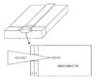
- FIG. 3Ashows a schematic diagram of a typical configuration of a laser facet with optical coating in an example.
- FIG. 3Bshows a graph of the reflectivity (%) of a laser diode front facet versus the wavelength (nm) for an optical coating configurations with and without the passivation layer shown in FIG. 3A in an example.
- FIG. 4Ashows a graph of laser output power (mA) versus input current (mA) for a laser diode that undergoes a COMD failure at >700 mW output power in an example.
- FIG. 4Bshows an image of the irreversible damage at the front facet of the laser that occurs with COMD. It can be seen that COMD results in a sudden drop in power. COMD is typically a thermal runaway process, consistent with the apparent burn mark/hole on the laser facet.
- FIG. 5shows an example from the literature (Tamikawa et al., Appl. Phys. Lett., 2009, 95, 031106) demonstrating how the COMD threshold power can be improved by ECR coating with AlON in conventional GaN laser diodes.
- FIG. 6shows experimental COMD level data for commercially available c-plane (-Plane) laser diodes having AlGaN claddings and ECR facet coatings, and for nonpolar/semipolar (NP/SP) laser diodes with cladding layers substantially free from Al-containing claddings and using conventional e-beam facet coating (E-Beam Coated) techniques in an example.
- -Planec-plane
- NP/SPnonpolar/semipolar
- FIGS. 7A and 7Bshow examples of facet imperfections resulting from a cleaving process on nonpolar/semipolar laser diode facets in an example.
- FIGS. 8A and 8Bshow an SEM image and an optical image, respectively, of facet failures related to imperfections from the cleaving process where the arrows depict the failure points and the imperfections in an example.
- FIG. 9shows an example taken from the literature (Behfar et al., http://www.binoptics.com/CSMAX05_Paper.pdf) of etched facet technology that can yield smooth, vertical, and defect free etched facets to enable very high COMD levels in an example.
- FIG. 10shows example data demonstrating how etched facets technology can improve the COMD yield compared to etched facet technology on nonpolar or semipolar laser diodes with front facet coatings in an example.
- the present disclosurerelates generally to optical techniques. More specifically, the present disclosure provides methods and devices using semi-polar oriented gallium and nitrogen containing substrates for optical applications.
- Lasersare useful and important. They are used in many applications and recently visible lasers have reached performance thresholds that make them useful in the field of video displays and video projectors. While there are several technologies that can produce visible lasers, solid-state diode lasers (LDs) emitting at the desired wavelength have the best chance of minimizing system size while maximizing wall-plug efficiency (WPE). While diode lasers emitting with high WPE in the red region of the visible spectrum have been available for years it is only recently that blue and green LDs have become good enough to consider for many high power and space and efficiency conscious applications.
- LDssolid-state diode lasers
- WPEwall-plug efficiency
- Blue LDs currently available commerciallyare based on the semiconductor GaN grown with device layers oriented parallel to the (0001) plane of the GaN crystal. Recently, blue LDs based on other crystallographic orientations of GaN have been demonstrated.
- the so-called “non-polar” orientations [(10-10) or “m-plane” and (11-20) or “a-plane”offer an advantage over c-plane based devices in that the heterostructures that provide for electron and hole confinement do not result in piezoelectric or spontaneous electric fields due to differences in polarization between various AlInGaN alloys used in the devices.
- Non-polar orientationsIn c-plane devices the internal fields result in band-tilting that spatially separates electron and hole bound states and reduces the thickness of InGaN quantum wells that can be used. Smaller quantum wells result in less modal overlap, increased spontaneous emission lifetimes, which respectively reduce the gain and increase the threshold current densities of the devices. Growing in non-polar orientations results in better electron and hole overlap even for wide wells, resulting in higher gain and threshold current densities. Non-polar orientations also have the advantage that photon emission in the plane of the device is not isotropic, such that laser stripes can be oriented parallel to the direction of preferred emission to help decrease threshold currents even further.
- m-Plane oriented InGaN/(AlIn)GaN devicesexhibit a broadening of luminescence spectra in the range of wavelengths spanning from approximately 415 nm to 470 nm. This is not optimal for providing gain in laser diode active regions since when all other factors are equivalent using a gain medium with a narrower spontaneous emission spectrum will result in higher gain and consequently higher WPE. Growth on semi-polar planes that are derived from the m-plane results in devices with narrower full width at half maximum (FWHM) of luminescence spectra.
- FWHMfull width at half maximum
- GaN-based high power laser diodes fabricated on the conventional c-plane orientationtypically require special facet coatings to modify the reflectivity of the front mirror/facet where the optical intensity is highest. Such facet coatings are required to reduce the reflectivity of the mirrored surface and thereby increase the slope efficiency and output power of the laser diode. Specialized coating techniques and methods can be used to raise the optical power threshold before the onset of catastrophic optical mirror damage (COMD) that occurs at the front facet where the dielectric coating layers are applied.
- COMPcatastrophic optical mirror damage
- the origin of the of the COMD failureis typically located at the semiconductor facet—dielectric coating interface and results from absorption induced by mechanisms such as surface states, trace contamination at the interface, surface damage, and/or from other facet imperfections such as roughness or shear lines in a cleaved facet.
- the facetis very susceptible to COMD failure and expensive and/or highly specialized techniques must be used to increase the COMD threshold.
- commercial c-plane high power blue laser diodes operating with output powers of above 1 Wtypically require electron cyclotron resonance (ECR) facet coating.
- ECRelectron cyclotron resonance
- optical output power density threshold values for COMDare provided that equal those of commercially available AlGaN clad c-plane devices that utilize ECR coatings.
- certain embodiments provided by the present disclosurecombine nonpolar/semipolar GaN technology with AlGaN cladding free waveguide designs and conventional dielectric deposition techniques to provide low cost, high-throughput methods for forming robust facets useful in high power GaN laser diodes.
- embodiments provided by the present disclosurecombine a passivation layer such as SiO 2 to increase the optical power density COMD threshold.
- the difficulty in achieving a high quality cleaved facetis great. This is due to the availability of the nonpolar a-face and m-face facets for c-plane surface oriented devices.
- the resulting candidate cleaved facet crystal orientations that are orthogonal to the surface planeare the polar c-plane or higher Miller index semipolar planes, which are not natural cleavage planes. Therefore, the challenge of achieving high-quality cleaved facets in such nonpolar or semipolar laser diodes is great and they are likely to suffer from a high number of imperfections such as scaling or shear stress mark that result from the scribing and breaking process. As discussed above, such imperfections can serve as failure sites for COMD at high optical densities. To increase the optical power density threshold for COMD failure it is necessary to have a facet formation technique that minimizes or eliminates such imperfections.
- CAIBEchemical assisted ion beam etching
- ICPinductively coupled plasma
- RIEreactive ion etching
- a masking layeris deposited and patterned on the surface of the wafer.
- the etch mask layercould be comprised of dielectrics such as silicon dioxide (SiO2), silicon nitride (SixNy), a combination thereof or other dielectric materials.
- the mask layercould be comprised of metal layers such as Ni or Cr, but could be comprised of metal combination stacks or stacks comprising metal and dielectrics.
- photoresist maskscan be used either alone or in combination with dielectrics and/or metals.
- the etch mask layeris patterned using conventional photolithography and etch steps.
- the alignment lithographycould be performed with a contact aligner or stepper aligner.
- Such lithographically defined mirrorsprovide a high level of control to the design engineer.
- the patternsin then transferred to the etch mask using a wet etch or dry etch technique.
- the facet patternis then etched into the wafer using a dry etching technique selected from CAIBE, ICP, RIE and/or other techniques.
- the etched facet surfacesmust be highly vertical of between about 87 and 93 degrees or between about 89 and 91 degrees from the surface plane of the wafer.
- the etched facet surface regionmust be very smooth with root mean square roughness values of less than 50 nm, 20 nm, 5 nm, or 1 nm.
- the etchedmust be substantially free from damage, which could act as nonradiative recombination centers and hence reduce the COMD threshold.
- CAIBEis provides very smooth and low damage sidewalls due to the chemical nature of the etch, while it can provide highly vertical etches due to the ability to tilt the wafer stage to compensate for any inherent angle in etch.
- CAIBEchemically assisted ion beam etching
- etched facet techniquescan yield high quality facets that are free from COMD-causing imperfections.
- the end yieldwill be improved compared to the yield obtained using the cleaving process which can lead to imperfections.
- high power laser diodes with high power density COMD threshold values and high yieldcan be achieved using conventional facet coating deposition techniques.
- etching mirrorsinclude inductively coupled plasma (ICP) etching, reactive ion etching (RIE) etching, and focused ion beam (FIB) etching.
- ICPinductively coupled plasma
- RIEreactive ion etching
- FIBfocused ion beam
- gallium and nitrogen containing laser deviceconfigured on either a nonpolar or a semipolar surface orientation, the device comprising: a gallium and nitrogen containing substrate member; a cladding region overlying the substrate member; a cavity region formed overlying the substrate member and configured in alignment in substantially a c-direction or a projection of the c-direction, the cavity region being characterized by a first end and a second end; the first end forming a first facet or mirror; the second end forming a second facet or mirror; a first optical coating formed overlying the first facet, wherein the first coating overlying the first facet is configured to increase a reflectivity; a second optical coating formed overlying the second facet, wherein the second coating layer overlying the second facet is configured to reduce a reflectivity; and an optical power density characterizing the laser device, the laser device being substantially free from COMD related failure.
- the nonpolar or semipolar surface orientationcomprises an m-plane, a (30-31) plane, a (20-21) plane, a (30-32) plane, a (30-3-1) plane, a (20-2-1) plane, a (30-3-2) plane, or an offcut of within +/ ⁇ 5 degrees of any of these planes toward an a-direction or a c-direction; the cladding region being substantially free from Al-containing material, the cladding region being characterized by an AlN mol fraction in the cladding region of less than about 2%.
- the first optical coatingis provided by a method selected from electron-beam deposition, thermal evaporation, PECVD, sputtering, and a combination of any of the foregoing.
- the first facet and the second facetare formed using a scribing and breaking process.
- the first facet and the second facetare formed using an etching process selected from reactive ion etching, inductively coupled plasma etching, and chemical assisted ion beam etching.
- the second optical coatingcomprises Al 2 O 3 .
- the second opticalcomprises at least of Al 2 O 3 and SiO 2 .
- the second optical coatingcomprises Al 2 O 3 and SiO 2
- the SiO 2is configured as a passivation layer and is configured between the second facet and the Al 2 O 3 .
- the devicecomprises an output cavity width of greater than about 3 ⁇ m and less than about 20 ⁇ m, and is operable at over 1 W.
- the devicecomprises an output cavity width of greater than about 3 ⁇ m and less than about 25 ⁇ m, and is operable at over 2 W.
- the devicecomprises an output cavity width of greater than about 3 ⁇ m and less than about 35 ⁇ m, and is operable at over 3 W.
- the devicecomprises an output cavity width of greater than about 3 ⁇ m and less than about 35 ⁇ m and is operable at over 4.5 W
- the devicecomprises an output cavity width of greater than about 3 ⁇ m and less than about 50 ⁇ m, and is operable at over 3 W.
- the deviceis operable at a wavelength from 430 nm to 480 nm.
- the deviceis operable at a wavelength from 480 nm to 535 nm.
- the deviceis operable at a wavelength from 390 nm to 430 nm.
- FIG. 1shows an example of c-direction or projection of a c-direction oriented laser diode stripe on a nonpolar or semipolar oriented substrate.
- the optical deviceincludes a gallium nitride substrate member having a semipolar crystalline surface region characterized by an orientation of about 9 degrees to about 12.5 degrees toward (000-1) from the m-plane.
- the gallium nitride substrate memberis a bulk GaN substrate characterized by having a semipolar crystalline surface region, but can be others.
- the bulk GaN substratehas a surface dislocation density below 10 5 cm ⁇ 2 or 10 5 to 10 7 cm ⁇ 2 . It should be noted that homoepitaxial growth on bulk GaN is generally better than hetero-epitaxy growth.
- the nitride crystal or wafermay comprise Al x In y Ga 1-x-y N, where 0 ⁇ x, y, x+y ⁇ 1.
- the nitride crystalcomprises GaN.
- the GaN substratehas threading dislocations, at a concentration between about 10 5 cm ⁇ 2 and about 10 8 cm ⁇ 2 , in a direction that is substantially orthogonal or oblique with respect to the surface.
- the surface dislocation densityis below about 10 5 cm ⁇ 2 or others such as those ranging from about 10 5 -10 8 cm ⁇ 2 .
- the surface dislocation densityis below about 10 5 cm ⁇ 2 or others such as those ranging from about 10 5 -10 8 cm ⁇ 2 .
- the devicehas a laser stripe region formed overlying a portion of the semipolar crystalline orientation surface region.
- the laser stripe regionis characterized by a cavity orientation is substantially parallel to the projection of the c-direction.
- the laser stripe regionhas a first end and a second end.
- the devicehas a first facet provided on the first end of the laser stripe region and a second facet provided on the second end of the laser stripe region.
- the first facetis substantially parallel with the second facet.
- Mirror surfacesare formed on each of the surfaces.
- the first facetcomprises a first mirror surface.
- the first mirror surfaceis provided by an etching process.
- the etching processcan use any suitable techniques, such as a chemical etching process using a CAIBE etching processor combinations.
- the first mirror surfacecomprises a reflective coating.
- deposition of the reflective coatingoccurs using, for example, e-beam evaporation, thermal evaporation, RF sputtering, DC sputtering, ECR sputtering, ion beam deposition, Ion Assisted Deposition, reactive ion plating, any combinations, and the like.
- the present methodmay provide surface passivation to the exposed surface prior to coating.
- the reflective coatingis selected from silicon dioxide, hafnia, and titania, tantalum pentoxide, zirconia, including combinations, and the like.
- the reflective coatingis highly reflective and includes a coating of silicon dioxide and tantalum pentoxide, which has been deposited using electron beam deposition.
- the first mirror surfacecan also comprise an anti-reflective coating.
- the facetscan be etched or a combination of them.
- the second facetcomprises a second mirror surface.
- the second mirror surfaceis provided by an etching techniques using etching technologies such as reactive ion etching (RIE), inductively coupled plasma etching (ICP), or chemical assisted ion beam etching (CAIBE), or other method.
- RIEreactive ion etching
- ICPinductively coupled plasma etching
- CAIBEchemical assisted ion beam etching
- RIEreactive ion etching
- ICPinductively coupled plasma etching
- CAIBEchemical assisted ion beam etching
- RIEchemical assisted ion beam etching
- the mask layercould be comprised of metal layers such as Ni or Cr, but could be comprised of metal combination stacks or stacks comprising metal and dielectrics.
- photoresist maskscan be used either alone or in combination with dielectrics and/or metals.
- the etch mask layeris patterned using conventional photolithography and etch steps.
- the alignment lithographycould be performed with a contact aligner or stepper aligner.
- Such lithographically defined mirrorsprovide a high level of control to the design engineer.
- the patternsin then transferred to the etch mask using a wet etch or dry etch technique.
- the facet patternis then etched into the wafer using a dry etching technique selected from CAIBE, ICP, RIE and/or other techniques.
- the etched facet surfacesmust be highly vertical of between about 87 and 93 degrees or between about 89 and 91 degrees from the surface plane of the wafer.
- the etched facet surface regionmust be very smooth with root mean square roughness values of less than 50 nm, 20 nm, 5 nm, or 1 nm.
- the etchedshould be substantially free from damage, which could act as non-radiative recombination centers and hence reduce the COMD threshold.
- CAIBEis provides very smooth and low damage sidewalls due to the chemical nature of the etch, while it can provide highly vertical etches due to the ability to tilt the wafer stage to compensate for any angle in etch in an example.
- the second mirror surfacecomprises a reflective coating, such as silicon dioxide, hafnia, titania, tantalum pentoxide, zirconia, combinations, and the like.
- the second mirror surfacecomprises an anti-reflective coating, such alumina or aluminum oxide.
- the coatingcan be formed using electron beam deposition, thermal evaporation, RF sputtering, DC sputtering, ECR sputtering, ion beam deposition, ion assisted deposition, reactive ion plating, any combinations, and the like.
- the present methodmay provide surface passivation to the exposed surface prior to coating.
- the laser stripehas a length and width.
- the lengthranges from about 200 microns to about 3000 microns.
- the stripealso has a width ranging from about 0.5 microns to about 50 microns, but can be other dimensions.
- the stripecan also be about 6 to 25 microns wide for a high power multi-lateral-mode device or 1 to 2 microns for a single lateral mode laser device.
- the widthis substantially constant in dimension, although there may be slight variations.
- the width and lengthare often formed using a masking and etching process, which are commonly used in the art. Further details of the present device can be found throughout the present specification and more particularly below.
- the deviceis also characterized by a spontaneously emitted light that is polarized in substantially perpendicular to the projection of the c-direction (in the a-direction. That is, the device performs as a laser or the like.
- the spontaneously emitted lightis characterized by a polarization ratio of greater than 0.2 to about 1 perpendicular to the c-direction.
- the spontaneously emitted lightcharacterized by a wavelength ranging from about 400 nanometers to yield a violet emission, a blue emission, a green emission, and others.
- the lightcan be emissions ranging from violet 395 to 420 nanometers; blue 430 to 470 nm; green 500 to 540 nm; and others, which may slightly vary depending upon the application.
- the spontaneously emitted lightis highly polarized and is characterized by a polarization ratio of greater than 0.4.
- the emitted lightis characterized by a polarization ratio that is desirable.
- there can be other variations, modifications, and alternatives. Further details of the laser devicecan be found throughout the present specification and more particularly below.
- FIG. 2shows a cross-sectional view of a waveguide design of a nonpolar or a semipolar laser diode that contains cladding regions that are substantially free from aluminum.
- the laser diode designscan enable high COMD levels without the need for highly-specialized and costly mirror coating techniques such as electron cyclotron resonance (ECR).
- ECRelectron cyclotron resonance
- the laser deviceincludes gallium nitride substrate, which has an underlying n-type metal back contact region.
- the metal back contact regionis made of a suitable material such as those noted below and others. Further details of the contact region can be found throughout the present specification and more particularly below.
- FIG. 1shows a cross-sectional view of a waveguide design of a nonpolar or a semipolar laser diode that contains cladding regions that are substantially free from aluminum.
- the laser deviceincludes gallium nitride substrate, which has an underlying n-type metal back contact region.
- the metal back contact regionis made of a suitable material such as those
- substrate 203shows substrate 203 , which has an underlying n-type metal back contact region 201 , n-type gallium nitride layer 205 overlying substrate 205 , n-side separate confinement heterostructure (SCH) 206 , active region 207 , p-side guiding layer or separate confinement heterostructure 208 , p-type electron blocking layer 209 , p++ type gallium nitride contact region 213 , metal contact layer 215 , and p-type gallium containing nitride layer configured as a laser stripe 211 .
- SCHseparate confinement heterostructure
- the devicealso has an overlying n-type gallium nitride layer, an active region, and an overlying p-type gallium nitride layer structured as a laser stripe region. Additionally, the device also includes an n-side separate confinement hetereostructure (SCH), p-side guiding layer or SCH, p-AlGaN EBL, among other features. In a specific embodiment, the device also has a p++ type gallium nitride material to form a contact region. In a specific embodiment, the p++ type contact region has a suitable thickness and may range from about 10 nm 50 nm, or other thicknesses.
- the doping levelcan be higher than the p-type cladding region and/or bulk region.
- the p++ type regionhas doping concentration ranging from about 10E19 to 10E21 Mg/centimeter 3 , and others.
- the p++ type regionpreferably causes tunneling between the semiconductor region and overlying metal contact region.
- each of these regionsis formed using at least an epitaxial deposition technique of metal organic chemical vapor deposition (MOCVD), molecular beam epitaxy (MBE), or other epitaxial growth techniques suitable for GaN growth.
- the epitaxial layeris a high quality epitaxial layer overlying the n-type gallium nitride layer.
- the high quality layeris doped, for example, with Si or O to form n-type material, with a dopant concentration between about 10 16 cm ⁇ 3 and 10 20 cm ⁇ 3 .
- an n-type Al u In v Ga 1-u-v N layerwhere 0 ⁇ u, v, u+v ⁇ 1, is deposited on the substrate.
- the carrier concentrationmay lie in the range between about 10 16 cm ⁇ 3 and 10 20 cm ⁇ 3 .
- the depositionmay be performed using metalorganic chemical vapor deposition (MOCVD) or molecular beam epitaxy (MBE).
- MOCVDmetalorganic chemical vapor deposition
- MBEmolecular beam epitaxy
- the bulk GaN substrateis placed on a susceptor in an MOCVD reactor.
- the susceptoris heated to a temperature between about 900 to about 1200 degrees Celsius in the presence of a nitrogen-containing gas.
- the carriercan be hydrogen or nitrogen or others.
- the susceptoris heated to approximately 1100 degrees Celsius under flowing ammonia.
- a flow of a gallium-containing metalorganic precursor, such as trimethylgallium (TMG) or triethylgallium (TEG)is initiated, in a carrier gas, at a total rate between approximately 1 and 50 standard cubic centimeters per minute (sccm).
- the carrier gasmay comprise hydrogen, helium, nitrogen, or argon.
- the ratio of the flow rate of the group V precursor (e.g., ammonia) to that of the group III precursor (trimethylgallium, triethylgallium, trimethylindium, trimethylaluminum) during growthis between about 2000 and about 12000.
- a flow of disilane in a carrier gas, with a total flow rate of between about 0.1 and 10 sccmis initiated.
- the laser stripe regionis made of the p-type gallium nitride layer 211 .
- the laser stripeis provided by an etching process selected from dry etching or wet etching.
- the etching processis dry, but can be others.
- the dry etching processis an inductively coupled plasma process using chlorine bearing species or a reactive ion etching process using similar chemistries or combination of ICP and RIE, among other techniques.
- the chlorine bearing speciesare commonly derived from chlorine gas or the like.
- the devicealso has an overlying dielectric region, which exposes 213 contact region, which is preferably a p++ gallium nitride region.
- the dielectric regionis an oxide such as silicon dioxide or silicon nitride, but can be others, such as those described in more detail throughout the present specification and more particularly below.
- the contact regionis coupled to an overlying metal layer 215 .
- the overlying metal layeris a multilayered structure containing gold and platinum (Ni/Au), but can be others such as gold and palladium (Pd/Au) or gold and nickel (Ni/Au).
- the metal layercomprises Ni/Au formed using suitable techniques.
- the Ni/Auis formed via electron-beam deposition, sputtering, or any like techniques.
- the thicknessincludes nickel material ranging in thickness from about 50 to about 100 nm and gold material ranging in thickness from about 100 Angstroms to about 1-3 microns, and others.
- the dielectric regioncan be made using a suitable technique.
- the techniquemay include reactively sputter of SiO 2 using an undoped polysilicon target (99.999% purity) with O 2 and Ar.
- the techniqueuses RF magnetron sputter cathodes configured for static deposition; sputter target; throw distance; pressure: 1-5 mT or about 2.5 mT, power: 300 to 400 W; flows: 2-3.-9 sccm O 2 , 20-50 sccm, Ar, deposition thickness: 1000-2500 A, and may include other variations.
- depositionmay occur using non-absorbing, nonconductive films, e.g., Al 2 O 3 , Ta 2 O 5 , SiO 2 , Ta 2 O 5 , ZrO 2 , TiO 2 , HfO 2 , NbO 2 .
- the dielectric regionmay be thinner, thicker, or the like.
- the dielectric regioncan also include multilayer coatings, e.g., 1000 A of SiO 2 capped with 500 A of Al 2 O 3 .
- Deposition techniquescan include, among others, ebeam evaporation, thermal evaporation, RF Sputter, DC Sputter, ECR Sputter, Ion Beam Deposition, Ion Assisted Deposition, reactive ion plating, combinations, and the like. Of course, there can be other variations, modifications, and alternatives.
- the laser devicehas active region 207 .
- the active regioncan include one to twenty quantum well regions according to one or more embodiments.
- an active layeris deposited.
- the active layermay comprise a single quantum well or a multiple quantum well, with 1-20 quantum wells.
- the active layermay include about 3-7 quantum wells or more preferably 4-6 quantum wells or others.
- the quantum wellsmay comprise InGaN wells and GaN barrier layers.
- the well layers and barrier layerscomprise Al w In x Ga 1-w-x N and Al y In z Ga 1-y-z N, respectively, where 0 ⁇ w, x, y, z, w+x, y+z ⁇ 1, where w ⁇ u, y and/or x>v, z so that the bandgap of the well layer(s) is less than that of the barrier layer(s) and the n-type layer.
- the well layers and barrier layersmay each have a thickness between about 1 nm and about 30 nm. In a preferred embodiment, each of the thicknesses is preferably 3-8 nm.
- each well regionmay have a thickness of about 5 nm to 7 nm and each barrier region may have a thickness of about 2 nm to about 5 nm, among others.
- the active layercomprises a double heterostructure, with an InGaN or Al w In x Ga 1-w-x N layer about 10 nm to 100 nm thick surrounded by GaN or Al y In z Ga 1-y-z N layers, where w ⁇ u, y and/or x>v, z.
- the composition and structure of the active layerare chosen to provide light emission at a preselected wavelength.
- the active layermay be left undoped (or unintentionally doped) or may be doped n-type or p-type.
- the active regioncan also include an electron blocking region, and a separate confinement heterostructure.
- the separate confinement heterostructurecan include AlInGaN or preferably InGaN, but can be other materials.
- the SCHis generally comprised of material with an intermediate index between the cladding layers and the active layers to improve confinement of the optical mode within the active region of the laser device according to a specific embodiment.
- the SCH layershave a desirable thickness, impurity, and configuration above and below the active region to confine the optical mode.
- the upper and lower SCHcan be configured differently or the same.
- the electron blocking regioncan be on either side or both sides of the SCH positioned above the active region according to a specific embodiment.
- the SCHcan range from about 100 nm to about 1500 nm, and preferably about 40 to 100 nm for the lower SCH region. In the upper SCH region, the thickness ranges from about 20 to 50 nm in a specific embodiment. As noted, the SCH is preferably InGaN having about 2% to about 5% indium or 5% to about 10% by atomic percent according to a specific embodiment. Of course, there can be other variations, modifications, and alternatives.
- an electron blocking layeris preferably deposited.
- the electron blocking layercomprises a gallium and nitrogen containing material including magnesium 10E16 cm ⁇ 3 to about 10E22 cm ⁇ 3 .
- the electron-blocking layermay comprise Al s In t Ga 1-s-t N, where 0 ⁇ s, t, s+t ⁇ 1, with a higher bandgap than the active layer, and may be doped p-type.
- the electron blocking layercomprises AlGaN with an Al composition ranging from 5 to 20%. In another embodiment, the electron blocking layer may not contain Al.
- the electron blocking layercomprises an AlGaN/GaN super-lattice structure, comprising alternating layers of AlGaN and GaN, each with a thickness between about 0.2 nm and about 5 nm.
- AlGaN/GaN super-lattice structurecomprising alternating layers of AlGaN and GaN, each with a thickness between about 0.2 nm and about 5 nm.
- the p-type gallium nitride structurewhich can be a p-type doped Al q In r Ga 1-q-r N, where 0 ⁇ q, r, q+r ⁇ 1, layer is deposited above the active layer.
- the p-type layermay be doped with Mg, to a level between about 10 16 cm ⁇ 3 and 10 22 cm ⁇ 3 , and may have a thickness between about 5 nm and about 1000 nm.
- the outermost 1 nm to 50 nm of the p-type layermay be doped more heavily than the rest of the layer, so as to enable an improved electrical contact.
- the laser stripeis provided by an etching process selected from dry etching or wet etching.
- the etching processis dry, but can be others.
- the devicealso has an overlying dielectric region, which exposes 213 contact region.
- the dielectric regionis an oxide such as silicon dioxide, but can be others.
- oxidesuch as silicon dioxide
- the metal contactis made of suitable material.
- the reflective electrical contactmay comprise at least one of silver, gold, aluminum, nickel, platinum, rhodium, palladium, chromium, or the like.
- the electrical contactmay be deposited by thermal evaporation, electron beam evaporation, electroplating, sputtering, or another suitable technique.
- the electrical contactserves as a p-type electrode for the optical device.
- the electrical contactserves as an n-type electrode for the optical device.
- a ridge waveguideis fabricated using a certain deposition, masking, and etching processes.
- the maskis comprised of photoresist (PR) or dielectric or any combination of both and/or different types of them.
- PRphotoresist
- the ridge maskis 1 to 2.5 microns wide for single lateral mode applications or 2.5 ⁇ m to 30 ⁇ m wide for multimode applications.
- the ridge waveguideis etched by ion-coupled plasma (ICP), reactive ion etching (RIE), chemical assisted ion beam (CAIBE) etched, or other method.
- ICPion-coupled plasma
- RIEreactive ion etching
- CAIBEchemical assisted ion beam
- a dielectric passivation layeris then blanket deposited by any number of commonly used methods in the art, such as sputter, e-beam, PECVD, or other methods.
- This passivation layercan include SiO 2 , Si 3 N 4 , Ta 2 O 5 , or others. The thickness of this layer is 80 nm to 400 nm thick.
- An ultrasonic processis used to remove the etch mask which is covered with the dielectric. This exposes the p-GaN contact layer.
- P-contact metalis deposited by e-beam, sputter, or other deposition technique using a PR mask to define the 2D geometry.
- the contact layercan be Ni/Au but others can be Pt/Au or Pd/Au. Further details of the present method and resulting structure can be found throughout the present specification and more particularly below. Further details of the facets can be found throughout the present specification and more particularly below.
- the present inventionprovides a laser structure without an aluminum bearing cladding region.
- the laser devicecomprises a multi-quantum well active region having thin barrier layers.
- the active regioncomprises three or more quantum well structures. Between each of the quantum well structures comprises a thin barrier layer, e.g., 7 nm and less, 6 nm and less, 5 nm and less, 4 nm and less, 3 nm and less, 2 nm and less.
- the combination of thin barrier layers configured in the multi-quantum well structuresenables a low voltage (e.g., 6 volts and less) laser diode free from use of aluminum bearing cladding regions.
- the present inventionprovides an optical device.
- the optical devicehas a gallium and nitrogen containing substrate including a (30-3-1) or offcut crystalline surface region orientation, which may be off-cut.
- the devicepreferably has an n-type cladding material overlying the n-type gallium and nitrogen containing material according to a specific embodiment.
- the n-type cladding materialis substantially free from an aluminum bearing material according to a specific embodiment.
- the devicealso has an active region comprising at least three quantum wells. Each of the quantum wells has a thickness of 3.0 nm and greater or 5.5 nm and greater, and one or more barrier layers.
- Each of the barrier layershas a thickness ranging from about 2 nm to about 5 nm or about 5 nm to about 9 nm and is configured between a pair of quantum wells according to a specific embodiment. At least one or each of the barrier layers has a thickness ranging from about 2 nm to about nm and is configured between a pair of quantum wells or adjacent to a quantum well according to a specific embodiment. At least one or each of the barrier layers has a thickness ranging from about 4 nm to about 6.5 nm and is configured between a pair of quantum wells or adjacent to a quantum well according to a specific embodiment.
- the devicehas a p-type cladding material overlying the active region.
- the p-type cladding materialis substantially free from an aluminum bearing material according to a specific embodiment.
- the active regionis configured operably for a forward voltage of less than about 6V or less than about 5V for the device for an output power of 60 mW or 100 mW and greater.
- the present inventionprovides an optical device.
- the devicehas a gallium and nitrogen containing substrate including a (30-3-1) or offcut crystalline surface region orientation.
- the devicealso has an n-type cladding material overlying the n-type gallium and nitrogen containing material.
- the n-type cladding materialis substantially free from an aluminum bearing material.
- the devicefurther has an active region comprising at least three quantum wells.
- Each of the quantum wellshas a thickness of 3.5 nm and greater or 5 nm and greater and one or more barrier layers according to a specific embodiment.
- Each of the barrier layershas a thickness ranging from about 2 nm to about 4 nm or about 4 nm to about 8 nm according to a specific embodiment.
- Each of the barrier layersis configured between a pair of quantum wells according to one or more embodiments. At least one or each of the barrier layers has a thickness ranging from about 2 nm to about 5 nm and is configured between a pair of quantum wells or adjacent to a quantum well according to a specific embodiment. At least one or each of the barrier layers has a thickness ranging from about 4 nm to about 8 nm and is configured between a pair of quantum wells or adjacent to a quantum well according to a specific embodiment.
- the devicealso has a p-type cladding material overlying the active region. The p-type cladding material is substantially free from an aluminum bearing material according to a preferred embodiment. The device optionally has a p-type material overlying the p-type cladding material.
- the inventionprovides yet an alternative optical device, which has a gallium and nitrogen containing substrate including a (30-3-1) or offcut crystalline surface region orientation.
- An n-type cladding materialis overlying the n-type gallium and nitrogen containing material.
- the n-type cladding materialis substantially free from an aluminum bearing material.
- the devicehas an active region comprising at least three quantum wells, each of which has a thickness of 4 nm and greater.
- the devicehas one or more barrier layers, each of which has an n-type impurity characteristic and a thickness ranging from about 2 nm to about 4 nm or about 4 nm to about 8 nm in one or more alternative embodiments.
- each of the barrier layersis configured between a pair of quantum wells according to a specific embodiment.
- the devicealso has a p-type cladding material overlying the active region according to a specific embodiment.
- the p-type cladding materialis substantially free from an aluminum bearing material according to a specific embodiment.
- the devicealso has a p-type material overlying the p-type cladding material.
- the inventionprovides a method of fabricating an optical device, which has a gallium and nitrogen containing substrate including a (30-3-1) or offcut crystalline surface region orientation.
- An n-type cladding materialis overlying the n-type gallium and nitrogen containing material.
- the n-type cladding materialis substantially free from an aluminum bearing material.
- the methodincludes forming an active region comprising at least three quantum wells, each of which has a thickness of 3.5 nm and greater.
- the devicehas one or more barrier layers, each of which has an n-type impurity characteristic and a thickness ranging from about 2 nm to about 4 nm or about 4 nm to about 8 nm in one or more alternative embodiments.
- each of the barrier layersis configured between a pair of quantum wells according to a specific embodiment.
- the methodalso includes forming a p-type cladding material overlying the active region according to a specific embodiment.
- the p-type cladding materialis substantially free from an aluminum bearing material according to a specific embodiment.
- the methodalso includes forming a p-type material overlying the p-type cladding material.
- the present inventionprovides an optical device, such as a laser diode.
- the devicehas a gallium and nitrogen containing substrate including a (30-3-1) or offcut crystalline surface region orientation, which may be off-cut according to one or more embodiments.
- the devicehas an n-type cladding material overlying the n-type gallium and nitrogen containing material.
- the n-type cladding materialis substantially free from an aluminum bearing material.
- the devicealso has an active region comprising at least three quantum wells.
- each of the quantum wellshas a thickness of 3.5 nm and greater and one or more barrier layers according to a specific embodiment.
- Each of the barrier layershas a p-type characteristic and a thickness ranging from about 2 nm to about 3.5 nm in a specific embodiment.
- Each of the barrier layershas a p-type characteristic and a thickness ranging from about 3.5 nm to about 7 nm in an alternative specific embodiment.
- each of the barrier layersis configured between a pair of quantum wells.
- the devicealso has a p-type cladding material overlying the active region.
- the p-type cladding materialis substantially free from an aluminum bearing material. And overlying p-type material is included.
- the active regionis configured for a forward voltage of less than about 6V or less than about 7V for the device for an output power of 60 mW and greater.
- the present method and structureinclude five (5) or more thick QWs of greater than 4 or 5 nm in thickness and thin barriers that are 2-4 nm in thickness.
- the present inventionincludes a laser diode substantially free from an aluminum containing cladding region.
- the present laser diodeincludes three or more quantum wells to provide enough confinement of the optical mode for sufficient gain to reach lasing.
- the forward voltage of the diodecan increase, as a tradeoff
- the present inventionprovides a laser device and method that is free from aluminum-containing cladding regions with low voltage on (30-3-1) or offcut substrates.
- the present inventionprovides a laser device and method that is free from aluminum-containing cladding regions with low voltage on (30-3-1) or offcut substrates.
- the present inventionprovides an optical device that is substantially free from aluminum bearing cladding materials.
- the devicehas a gallium and nitrogen containing substrate member having a (30-3-1) or offcut crystalline surface region.
- the devicehas an n-type gallium and nitrogen containing cladding material.
- the n-type gallium and nitrogen containing cladding materialis substantially free from an aluminum species, which leads to imperfections, defects, and other limitations.
- the devicealso has an active region including multiple quantum well structures overlying the n-type gallium and nitrogen containing cladding material.
- the devicealso has thin barrier layers configured with the multiple well structures.
- the devicehas a p-type gallium and nitrogen containing cladding material overlying the active region.
- the p-type gallium and nitrogen containing cladding materialis substantially free from an aluminum species.
- the devicepreferably includes a laser stripe region configured from at least the active region and characterized by a cavity orientation substantially parallel to a projection in a c-direction.
- the laser stripe regionhas a first end and a second end.
- the devicealso has a first etched or etched facet provided on the first end of the laser stripe region and a second etched or etched facet provided on the second end of the laser stripe region.
- the facetsmay be etched, etched, or a combination of cleaved and etched.
- the present deviceincludes a gallium and nitrogen containing electron blocking region that is substantially free from aluminum species.
- the devicedoes not include any electron blocking layer or yet in other embodiments, there is no aluminum in the cladding layers and/or electron blocking layer, although other embodiments include aluminum containing blocking layers.
- the optical device and methodare free from any aluminum material, which leads to defects, imperfections, and the like. Further details of these limitations can be found throughout the present specification and more particularly below.
- the present method and structureis substantially free from InAlGaN or aluminum bearing species in the cladding layers as conventional techniques, such as those in Yoshizumi et al., “Continuous-Wave operation of 520 nm Green InGaN-Based Laser Diodes on Semi-Polar ⁇ 20-21 ⁇ GaN Substrates,” Applied Physics Express 2 (2009) 092101. That is, the present laser structure and method are substantially free from any aluminum species in the cladding region.
- Aluminumis generally detrimental. Aluminum often leads to introduction of oxygen in the reactor, which can act as non radiative recombination centers to reduce the radiative efficiency and introduce other limitations.
- oxygencan compensate p-type dopants in the p-cladding to cause additional resistivity in the optical device.
- the present inventionprovides a green laser diode configured using a semipolar gallium and nitrogen containing bulk substrate member, as described in more detail below, which has etched facets.
- the inventionprovides a laser structure without an aluminum bearing cladding region.
- the laser devicecomprises a multi-quantum well active region having thin barrier layers, with the active region comprising three or more quantum well structures. Between each of the quantum well structures is a thin barrier layer, e.g., 8 nm and less, 7 nm and less, 6 nm and less, 5 nm and less, 4 nm and less, 3 nm and less, 2 nm and less, 1.5 nm and less.
- the combination of thin barrier layers configured in the multi-quantum well structuresenables a low voltage (e.g., 7 volts and less, 6 volts and less) laser diode free from use of aluminum bearing cladding regions.
- the optical devicehas a gallium and nitrogen containing substrate including a ⁇ 20-21 ⁇ crystalline surface region orientation, which may be off-cut.
- the devicepreferably has an n-type cladding material overlying the n-type gallium and nitrogen containing material according to a specific embodiment.
- the n-type cladding materialis substantially free from an aluminum bearing material.
- the devicealso has an active region comprising at least three quantum wells. Each of the quantum wells has a thickness of 2.5 nm and greater or 3.5 nm and greater and one or more barrier layers.
- Each of the barrier layershas a thickness ranging from about 2 nm to about 4 nm or about 3 nm to about 6.5 nm and is configured between a pair of quantum wells according to a specific embodiment. At least one or each of the barrier layers has a thickness ranging from about 2 nm to about 4 nm and is configured between a pair of quantum wells or adjacent to a quantum well according to a specific embodiment. At least one or each of the barrier layers has a thickness ranging from about 3 nm to about 6.5 nm and is configured between a pair of quantum wells or adjacent to a quantum well according to a specific embodiment.
- the devicehas a p-type cladding material overlying the active region.
- the p-type cladding materialis substantially free from an aluminum bearing material according to a specific embodiment.
- the active regionis configured operably for a forward voltage of less than about 7V or less than about 6V for the device for an output power of 60 mW and greater.
- the present inventionprovides an optical device.
- the devicehas a gallium and nitrogen containing substrate including a ⁇ 20-21 ⁇ crystalline surface region orientation.
- the devicealso has an n-type cladding material overlying the n-type gallium and nitrogen containing material.
- the n-type cladding materialis substantially free from an aluminum bearing material.
- the devicefurther has an active region comprising at least two quantum wells.
- Each of the quantum wellshas a thickness of 2.5 nm and greater or 3.5 nm and greater and one or more barrier layers according to a specific embodiment.
- Each of the barrier layershas a thickness ranging from about 2 nm to about 5 nm or about 3 nm to about 8 nm according to a specific embodiment.
- Each of the barrier layersis configured between a pair of quantum wells according to one or more embodiments. At least one or each of the barrier layers has a thickness ranging from about 2 nm to about 5 nm and is configured between a pair of quantum wells or adjacent to a quantum well according to a specific embodiment. At least one or each of the barrier layers has a thickness ranging from about 3 nm to about 8 nm and is configured between a pair of quantum wells or adjacent to a quantum well according to a specific embodiment.
- the devicealso has a p-type cladding material overlying the active region. The p-type cladding material is substantially free from an aluminum bearing material according to a preferred embodiment. The device optionally has a p-type material overlying the p-type cladding material.
- the inventionprovides yet an alternative optical device, which has a gallium and nitrogen containing substrate including a ⁇ 20-21 ⁇ crystalline surface region orientation.
- An n-type cladding materialis overlying the n-type gallium and nitrogen containing material.
- the n-type cladding materialis substantially free from an aluminum bearing material.
- the devicehas an active region comprising at least two quantum wells, each of which has a thickness of 2.5 nm and greater.
- the devicehas one or more barrier layers, each of which has an n-type impurity characteristic and a thickness ranging from about 2 nm to about 5 nm or about 3 nm to about 8 nm in one or more alternative embodiments.
- each of the barrier layersis configured between a pair of quantum wells according to a specific embodiment.
- the devicealso has a p-type cladding material overlying the active region according to a specific embodiment.
- the p-type cladding materialis substantially free from an aluminum bearing material according to a specific embodiment.
- the devicealso has a p-type material overlying the p-type cladding material.
- the inventionprovides a method of fabricating an optical device, which has a gallium and nitrogen containing substrate including a ⁇ 20-21 ⁇ crystalline surface region orientation.
- An n-type cladding materialis overlying the n-type gallium and nitrogen containing material.
- the n-type cladding materialis substantially free from an aluminum bearing material.
- the methodincludes forming an active region comprising at least two quantum wells, each of which has a thickness of 2.5 nm and greater.
- the devicehas one or more barrier layers, each of which has an n-type impurity characteristic and a thickness ranging from about 2 nm to about 5 nm or about 3 nm to about 8 nm in one or more alternative embodiments.
- each of the barrier layersis configured between a pair of quantum wells according to a specific embodiment.
- the methodalso includes forming a p-type cladding material overlying the active region according to a specific embodiment.
- the p-type cladding materialis substantially free from an aluminum bearing material according to a specific embodiment.
- the methodalso includes forming a p-type material overlying the p-type cladding material.
- the present inventionprovides an optical device, such as a laser diode.
- the devicehas a gallium and nitrogen containing substrate including a ⁇ 20-21 ⁇ crystalline surface region orientation, which may be off-cut according to one or more embodiments.
- the devicehas an n-type cladding material overlying the n-type gallium and nitrogen containing material.
- the n-type cladding materialis substantially free from an aluminum bearing material.
- the devicealso has an active region comprising at least two quantum wells.
- each of the quantum wellshas a thickness of 2.5 nm and greater and one or more barrier layers according to a specific embodiment.
- Each of the barrier layershas a p-type characteristic and a thickness ranging from about 2 nm to about 3.5 nm in a specific embodiment.
- Each of the barrier layershas a p-type characteristic and a thickness ranging from about 3.5 nm to about 7 nm in an alternative specific embodiment.
- each of the barrier layersis configured between a pair of quantum wells.
- the devicealso has a p-type cladding material overlying the active region.
- the p-type cladding materialis substantially free from an aluminum bearing material. And overlying p-type material is included.
- the active regionis configured for a forward voltage of less than about 6 v or less than about 7V for the device for an output power of 60 mW and greater.
- the present inventionincludes a laser diode substantially free from an aluminum containing cladding region.
- the present laser diodeincludes three or more quantum wells to provide enough confinement of the optical mode for sufficient gain to reach lasing.
- the forward voltage of the diodecan increase, as a tradeoff
- the present inventionprovides a laser device and method that is free from aluminum-containing cladding regions with low voltage on ⁇ 20-21) substrates.
- the present inventionprovides an optical device that is substantially free from aluminum bearing cladding materials.
- the devicehas a gallium and nitrogen containing substrate member having a ⁇ 20-21 ⁇ crystalline surface region.
- the devicehas an n-type gallium and nitrogen containing cladding material.
- the n-type gallium and nitrogen containing cladding materialis substantially free from an aluminum species, which leads to imperfections, defects, and other limitations.
- the devicealso has an active region including multiple quantum well structures overlying the n-type gallium and nitrogen containing cladding material.
- the devicealso has thin barrier layers configured with the multiple well structures.
- the devicehas a p-type gallium and nitrogen containing cladding material overlying the active region.
- the p-type gallium and nitrogen containing cladding materialis substantially free from an aluminum species.
- the devicepreferably includes a laser stripe region configured from at least the active region and characterized by a cavity orientation substantially parallel to a projection in a c-direction.
- the laser stripe regionhas a first end and a second end.
- the devicealso has a first etched facet provided on the first end of the laser stripe region and a second etched facet provided on the second end of the laser stripe region.
- the present deviceincludes a gallium and nitrogen containing electron blocking region that is substantially free from aluminum species.
- the devicedoes not include any electron blocking layer or yet in other embodiments, there is no aluminum in the cladding layers and/or electron blocking layer, although other embodiments include aluminum containing blocking layers.
- the optical device and methodare free from any aluminum material, which leads to defects, imperfections, and the like.
- the present method and structureis substantially free from InAlGaN or aluminum bearing species in the cladding layers as conventional techniques, such as those in Yoshizumi et al., “Continuous-Wave operation of 520 nm Green InGaN-Based Laser Diodes on Semi-Polar ⁇ 20-21 ⁇ GaN Substrates,” Applied Physics Express 2 (2009) 092101. That is, the present laser structure and method are substantially free from any aluminum species in the cladding region.
- Aluminumis generally detrimental. Aluminum often leads to introduction of oxygen in the reactor, which can act as non radiative recombination centers to reduce the radiative efficiency and introduce other limitations.
- oxygencan compensate p-type dopants in the p-cladding to cause additional resistivity in the optical device.
- the devicehas a laser stripe region formed overlying a portion of the off-cut crystalline orientation surface region.
- the laser stripe regionis characterized by a cavity orientation substantially in a projection of a c-direction, which is substantially normal to an a-direction.
- the laser stripe regionhas a first end and a second end, each of which is etched.
- the deviceis formed on a projection of a c-direction on a ⁇ 20-21 ⁇ gallium and nitrogen containing substrate having a pair of etched mirror structures, which face each other.
- the devicehas a first etched facet provided on the first end of the laser stripe region and a second etched facet provided on the second end of the laser stripe region.
- the first etchedis substantially parallel with the second etched facet.
- Mirror surfacesare formed on each of the etched surfaces.
- the first etched facetcomprises a first mirror surface.
- the first mirror surfacecomprises a reflective coating.
- the reflective coatingis selected from silicon dioxide, hafnia, and titania, tantalum pentoxide, zirconia, including combinations, and the like.
- the first mirror surfacecan also comprise an anti-reflective coating.
- the second etched facetcomprises a second mirror surface.
- the second mirror surfacecomprises a reflective coating, such as silicon dioxide, hafnia, and titania, tantalum pentoxide, zirconia, combinations, and the like.
- the second mirror surfacecomprises an anti-reflective coating.
- the laser stripehas a length and width.
- the lengthranges from about 50 microns to about 3000 microns or preferably from about 400 microns to about 650 microns or about 650 microns to about 1200 um microns.
- the stripalso has a width ranging from about 0.5 microns to about 50 microns or preferably between 1 microns to about 1.5 microns, about 1.5 microns to about 2.0 microns, or about 2.0 microns to about 4 microns, but can be other dimensions.
- the widthis substantially constant in dimension, although there may be slight variations.
- the width and lengthare often formed using a masking and etching process, which are commonly used in the art.
- the present inventionprovides an alternative device structure capable of emitting 501 nm and greater light in a ridge laser embodiment having etched facets.
- the deviceis provided with one or more of the following epitaxially grown elements, but is not limiting.
- an n-GaN cladding layerwith a thickness from 100 nm to 3000 nm with Si doping level of 5E17 to 3E18 cm- 3 ;
- an n-side SCH layercomprised of InGaN with molar fraction of indium of between 3% and 10% and thickness from 20 to 150 nm;
- multiple quantum well active region layerscomprised of at least two 2.0-5.5 nm InGaN quantum wells separated by thin 2.5 nm and greater, and optionally up to about 8 nm, GaN barriers;
- a p-side SCH layercomprised of InGaN with molar a fraction of indium of between 1% and 10% and a thickness from 15 nm to 100 nm;
- an electron blocking layercomprised of AlGaN with molar fraction of aluminum of between 5% and 20% and thickness from 5 nm to 20 nm and doped with Mg;
- a p-GaN cladding layerwith a thickness from 400 nm to 1000 nm with Mg doping level of 2E17 cm-3 to 2E19 cm ⁇ 3 ; and a p++-GaN contact layer with a thickness from 20 nm to 40 nm with Mg doping level of 1E19 cm-3 to 1E21 cm ⁇ 3 .
- a laser deviceis fabricated on a ⁇ 20-21 ⁇ substrate according to an embodiment of the present invention.
- the laser deviceincludes gallium nitride substrate, which has an underlying n-type metal back contact region.
- the metal back contact regionis made of a suitable material such as those noted below and others. Further details of the contact region can be found throughout the present specification, and more particularly below.
- the devicealso has an overlying n-type gallium nitride layer, an active region, and an overlying p-type gallium nitride layer structured as a laser stripe region.
- each of these regionsis formed using at least an epitaxial deposition technique of metal organic chemical vapor deposition (MOCVD), molecular beam epitaxy (MBE), or other epitaxial growth techniques suitable for GaN growth.
- MOCVDmetal organic chemical vapor deposition
- MBEmolecular beam epitaxy
- the epitaxial layeris a high quality epitaxial layer overlying the n-type gallium nitride layer.
- the high quality layeris doped, for example, with Si or O to form n-type material, with a dopant concentration between about 10 16 cm ⁇ 3 and 10 20 cm ⁇ 3 .
- an n-type Al u In v Ga 1-u-v N layerwhere 0 ⁇ u, v, u+v ⁇ 1, is deposited on the substrate.
- the carrier concentrationmay lie in the range between about 10 16 cm ⁇ 3 and 10 20 cm ⁇ 3 .
- the depositionmay be performed using metalorganic chemical vapor deposition (MOCVD) or molecular beam epitaxy (MBE).
- the bulk GaN substrateis placed on a susceptor in an MOCVD reactor.
- the susceptoris heated to a temperature between about 1000 and about 1200 degrees Celsius in the presence of a nitrogen-containing gas.
- the susceptoris heated to approximately 900 to 1100 degrees Celsius under flowing ammonia.
- a flow of a gallium-containing metalorganic precursor, such as trimethylgallium (TMG) or triethylgallium (TEG)is initiated, in a carrier gas, at a total rate between approximately 1 and 50 standard cubic centimeters per minute (sccm).
- the carrier gasmay comprise hydrogen, helium, nitrogen, or argon.
- the ratio of the flow rate of the group V precursor (ammonia) to that of the group III precursor (trimethylgallium, triethylgallium, trimethylindium, trimethylaluminum) during growthis between about 2000 and about 12000.
- the laser stripe regionis made of the p-type gallium nitride layer.
- the laser stripeis provided by an etching process selected from dry etching or wet etching.
- the etching processis dry, but can be others.
- the dry etching processis an inductively coupled process using chlorine bearing species or a reactive ion etching process using similar chemistries. Again as an example, the chlorine bearing species are commonly derived from chlorine gas or the like.
- the devicealso has an overlying dielectric region, which exposes contact region.
- the dielectric regionis an oxide such as silicon dioxide or silicon nitride, but can be others.
- the contact regionis coupled to an overlying metal layer.
- the overlying metal layeris a multilayered structure containing gold and platinum (Pt/Au), nickel gold (Ni/Au), but can be others.
- the laser devicehas active region.
- the active regioncan include one to twenty quantum well regions according to one or more embodiments.
- an active layeris deposited.
- the active layermay be comprised of multiple quantum wells, with 2-10 quantum wells.
- the quantum wellsmay be comprised of InGaN with GaN barrier layers separating them.
- the well layers and barrier layerscomprise Al w In x Ga 1-w-x N and Al y In z Ga 1-y-z N, respectively, where 0 ⁇ w, x, y, z, w+x, y+z ⁇ 1, where w ⁇ u, y and/or x>v, z so that the bandgap of the well layer(s) is less than that of the barrier layer(s) and the n-type layer.
- the well layers and barrier layersmay each have a thickness between about 1 nm and about 20 nm.
- the composition and structure of the active layerare chosen to provide light emission at a preselected wavelength.
- the active layermay be left undoped (or unintentionally doped) or may be doped n-type or p-type.
- the active regioncan also include an electron blocking region, and a separate confinement heterostructure.
- an electron blocking layeris preferably deposited.
- the electron-blocking layermay comprise Al s In t Ga 1-s-t N, where 0 ⁇ s, t, s+t ⁇ 1, with a higher bandgap than the active layer, and may be doped p-type.
- the electron blocking layercomprises AlGaN.
- the electron blocking layercomprises an AlGaN/GaN super-lattice structure, comprising alternating layers of AlGaN and GaN, each with a thickness between about 0.2 nm and about 5 nm.
- the action region structuredoes not include an AlGaN EBL layer. That is, the laser device is free from any electron blocking layer, which is optional in such embodiment.
- the p-type gallium nitride structureis deposited above the electron blocking layer and active layer(s).
- the p-type layermay be doped with Mg, to a level between about 10 16 cm ⁇ 3 and 10 22 cm ⁇ 3 , and may have a thickness between about 5 nm and about 1000 nm.
- the outermost 1-50 nm of the p-type layermay be doped more heavily than the rest of the layer, so as to enable an improved electrical contact.
- the laser stripeis provided by an etching process selected from dry etching or wet etching. In a preferred embodiment, the etching process is dry, but can be others.
- the devicealso has an overlying dielectric region, which exposes a contact region. In a specific embodiment, the dielectric region is an oxide such as silicon dioxide.
- the metal contactis made of suitable material.
- the reflective electrical contactmay comprise at least one of silver, gold, aluminum, nickel, platinum, rhodium, palladium, chromium, or the like.
- the electrical contactmay be deposited by thermal evaporation, electron beam evaporation, electroplating, sputtering, or another suitable technique.
- the electrical contactserves as a p-type electrode for the optical device.
- the electrical contactserves as an n-type electrode for the optical device.
- a laser deviceincludes a starting material such as a bulk nonpolar or semipolar GaN substrate, but can be others.
- the deviceis configured to achieve emission wavelength ranges of 390 nm to 420 nm, 420 nm to 440 nm, 440 nm to 470 nm, 470 nm to 490 nm, 490 nm to 510 nm, and 510 nm to 530 nm, but can be others.
- the growth structureis configured using between 3 and 5 or 5 and 7 quantum wells positioned between n-type GaN and p-type GaN cladding layers.
- the n-type GaN cladding layerranges in thickness from 500 nm to 2000 nm and has an n-type dopant such as Si with a doping level of between 1E18 cm-3 and 3E18 cm ⁇ 3 .
- the p-type GaN cladding layerranges in thickness from 500 nm to 1000 nm and has a p-type dopant such as Mg with a doping level of between 1E17 cm ⁇ 3 and 7E19 cm ⁇ 3 .
- the Mg doping levelis graded such that the concentration would be lower in the region closer to the quantum wells.
- the quantum wellshave a thickness of between 2.5 nm and 4 nm, 4 nm and 5.5 nm or 5.5 nm and 8 nm, but can be others. In a specific embodiment, the quantum wells would be separated by barrier layers with thicknesses between 2 nm and 3.5 nm or 3.5 nm and 6 nm or 6 nm and 8 nm.
- the quantum wells and the barriers togethercomprise a multiple quantum well (MQW) region.
- MQWmultiple quantum well
- the devicehas barrier layers formed from GaN, InGaN, AlGaN, or InAlGaN.
- the indium contentsrange from 0% to 5% (mole percent), but can be others. Also, it should be noted that % of indium or aluminum is in a molar fraction, not weight percent.
- An InGaN separate confinement hetereostructure layercould be positioned between the n-type GaN cladding and the MQW region according to one or more embodiments.
- such separate confinement layeris commonly called the n-side SCH.
- the n-side SCH layerranges in thickness from 10 nm to 60 nm or 60 nm to 150 nm and ranges in indium composition from 1% to 12% (mole percent), but can be others.
- the n-side SCH layermay be doped with an n-type dopant such as Si.
- an InGaN separate confinement heterostructure layeris positioned between the p-type GaN cladding and the MQW region, which is called the p-side SCH.
- the p-side SCH layerranges in thickness from 10 nm to 40 nm or 40 nm to 150 nm and ranges in indium composition from 0% to 10% (mole percent), but can be others.
- the p-side SCH layermay be doped with a p-type dopant such as Mg.
- the structurewould contain both an n-side SCH and a p-side SCH.
- the p-side SCHwould be replaced with p-side GaN guiding layer.
- the n-side and/or p-side SCH regionswould contain multiple layers.
- the structurewould contain a GaN guiding layer on the p-side positioned between the p-type GaN cladding layer and the MQW region.
- This GaN guiding layercould range in thickness from 10 nm to 60 nm and may or may not be doped with a p-type species such as Mg.
- an AlGaN electron blocking layerwith an aluminum content of between 5% and 20% (mole percent), is positioned between the MQW and the p-type GaN cladding layer either between the MQW and the p-side SCH, within the p-side SCH, or between the p-side SCH and the p-type GaN cladding.
- the AlGaN electron blocking layerranges in thickness from 5 nm to 20 nm and is doped with a p-type dopant such as Mg from 1E17 cm ⁇ 3 and 1E21 cm ⁇ 3 according to a specific embodiment.
- the electron blocking layeris free from any aluminum species and/or may be eliminated all together.
- the devicewould be substantially free from an electron blocking layer.
- a p-contact layerpositioned on top of and is formed overlying the p-type cladding layer.
- the p-contact layerwould be comprised of GaN doped with a p-dopant such as Mg at a level ranging from 1E20 cm-3 to 1E22 cm-3.
- a laser devicehas a gallium and nitrogen containing substrate member (e.g., bulk gallium nitride) having a ⁇ 20-21 ⁇ crystalline surface region or other surface configuration.
- the devicehas an n-type gallium and nitrogen containing cladding material.
- the n-type gallium and nitrogen containing cladding materialis substantially free from an aluminum species, which leads to imperfections, impurities, and other limitations.
- the cladding materialhas no aluminum species and is made of a gallium and nitrogen containing material.
- the devicealso has an active region including multiple quantum well structures overlying the n-type gallium and nitrogen containing cladding material.
- the active regionscan include those noted, as well as others. That is, the device can include InGaN/InGaN and/or InGaN/GaN active regions, among others.
- the opticalcan include seven MQW, six MQW, five MQW, four MQW, three MQW, more MQW, or fewer, and the like. Of course, there can be other variations, modification, and alternatives.
- the devicehas a p-type gallium and nitrogen containing cladding material overlying the active region.
- the p-type gallium and nitrogen containing cladding materialis substantially free from an aluminum species, which leads to imperfections, defects, and other limitations.
- the cladding materialhas no aluminum species and is made of a gallium and nitrogen containing material.
- the devicepreferably includes a laser stripe region configured from at least the active region and characterized by a cavity orientation substantially parallel to a projection in a c-direction. Other configurations may also exist depending upon the specific embodiment.
- the laser stripe regionhas a first end and a second end or other configurations.
- the devicealso has a first etched facet provided on the first end of the laser stripe region and a second etched facet provided on the second end of the laser stripe region.
- the present deviceincludes a gallium and nitrogen containing electron blocking region that is substantially free from aluminum species. In yet other embodiments, the device does not include any electron blocking layer or yet in other embodiments, there is no aluminum in the cladding layers and/or electron blocking layer.
- the present method and structureis substantially free from InAlGaN or aluminum bearing species in the cladding layers as conventional techniques, such as those in Yoshizumi et al., “Continuous-Wave operation of 520 nm Green InGaN-Based Laser Diodes on Semi-Polar ⁇ 20-21 ⁇ GaN Substrates,” Applied Physics Express 2 (2009) 092101. That is, the present laser structure and method are substantially free from any aluminum species in the cladding region.
- Aluminumis generally detrimental. Aluminum often leads to introduction of oxygen in the reactor, which can act as non radiative recombination centers to reduce the radiative efficiency and introduce other limitations.
- FIG. 3Ashows a schematic diagram of a typical configuration of a laser facet with optical coating configured in two dielectric layers where layer 1 functions as the passivation layer to increase the COMD level and layer 2 functions as the reflectivity modification layer.
- FIG. 3Bshows a graphs of the reflectivity (%) of a laser diode front facet versus the wavelength (nm) for optical coating configurations with and without the passivation layer shown in FIG. 3A , and for designs targeting ⁇ 5% and ⁇ 10% reflectivity in the blue region.
- the curvesshow that a thin SiO 2 passivation layer offsets the reflectivity at a given wavelength.
- FIG. 4Ashows a graph of laser output power (mA) versus input current (mA) for a laser diode that undergoes a COMD failure at >700 mW output power. Upon the onset of COMD the output power abruptly drops.
- FIG. 4Bshows an image of the irreversible damage at the front facet of the laser that occurs with COMD. It can be seen that COMD results in a sudden drop in power. COMD is typically a thermal runaway process, consistent with the apparent burn mark/hole on the laser facet.
- FIG. 5shows an example from the literature demonstrating how the COMD threshold power can be improved by ECR coating in conventional GaN laser diodes.
- FIG. 6shows experimental COMD level data for commercially available c-plane laser diodes having AlGaN claddings and ECR facet coatings, and for nonpolar/semipolar laser diodes with cladding layers substantially free from Al-containing claddings and using conventional e-beam facet coating techniques.
- the e-beam coated nonpolar/semipolar devicescan achieve the same power level before COMD as the c-plane or nonpolar/semipolar devices using the more specialized ECR coating technique.
- the COMD levelis substantially reduced.
- FIGS. 7A and 7Bshows examples of facet imperfections resulting from a cleaving process on nonpolar/semipolar laser diode facets. Such imperfections can act as initiation sites for catastrophic failure and lead to low COMD levels and hence device failures.
- FIG. 7Ashows a top view image of an imperfect facet and
- FIG. 7Bshows an end view image of an imperfect facet.
- FIGS. 8A and 8Bshow an SEM image and an optical image, respectively, of facet failures related to imperfections from the cleaving process where the arrows depict the failure points and the imperfections.
- FIG. 9shows an example taken from literature of etched facet technology which can yield smooth, vertical, and defect free etched facets to enable very high COMD levels.
- FIG. 10shows example data demonstrating how etched facets technology could improve the COMD yield compared to etched facet technology on nonpolar or semipolar laser diodes with front facet coatings. Because the quality of a cleaved varies, the COMD power threshold is scattered due to the varied occurrences of imperfections. With the etched facet process, the COMD threshold power levels are tightly distributed due to the lack of cleave associated imperfections, and meet the COMD power requirements for certain applications as indicated by the dashed line of 400 mW/ ⁇ m.
- a gallium and nitrogen containing laser deviceconfigured on either a nonpolar or a semipolar surface orientation.
- the devicehas a gallium and nitrogen containing substrate member and a cladding region overlying the substrate member.
- the devicehas a cavity region formed overlying the cladding region and configured in alignment in substantially a c-direction or a projection of the c-direction.
- a cavity regionis characterized by a first end and a second end.
- the devicehas a first optical coating formed overlying the first facet, wherein the first coating overlying the first facet is configured to increase a reflectivity and a second optical coating formed overlying the second facet, wherein the second coating layer overlying the second facet is configured to reduce a reflectivity.
- the devicehas an optical power density characterizing the laser device, the laser device being substantially free from COMD related failure.
- the nonpolar or semipolar surface orientationcomprises an m-plane, a (30-31) plane, a (20-21) plane, a (30-32) plane, a (30-3-1) plane, a (20-2-1) plane, a (30-3-2) plane, or an offcut of within +/ ⁇ 5 degrees of any of these planes toward an a-direction or a c-direction; the cladding region being substantially free from Al-containing material, the cladding region being characterized by an AlN mol fraction in the cladding region of less than about 2%.
- the first optical coatingis provided by a method selected from electron-beam deposition, thermal evaporation, PECVD, sputtering, and a combination of any of the foregoing.
- the present inventionalso includes related methods reciting the same or similar elements.
- the devicecomprises an output cavity width of greater than about 3 ⁇ m and less than about 25 ⁇ m, and is operable at over 1 W or wherein the device comprises an output cavity width of greater than about 3 ⁇ m and less than about 25 ⁇ m and is operable at over 2 W or wherein the device comprises an output cavity width of greater than about 3 ⁇ m and less than about 35 ⁇ m, and is operable at over 3 W or wherein the device comprises an output cavity width of greater than about 3 ⁇ m and less than about 35 ⁇ m, and is operable at over 4.5 W or wherein the device comprises an output cavity width of greater than about 3 ⁇ m and less than about 50 ⁇ m and is operable at over 3 W.
- the deviceis substantially free from COMD for power levels greater than 100 mW per micron of output cavity width, 200 mW per micron of output cavity width, or 400 mW per micron of output cavity width.
- GaN substrateis associated with Group III-nitride based materials including GaN, InGaN, AlGaN, or other Group III containing alloys or compositions that are used as starting materials.
- the present devicecan be enclosed in a suitable package.
- a suitable packagecan include those such as in TO-38 and TO-56 headers.
- Other suitable package designs and methodscan also exist, such as TO-9 or flat packs where fiber optic coupling is required and even non-standard packaging.
- the present devicecan be implemented in a co-packaging configuration such as those described in U.S. application Ser. No. 12/789,303 filed on May 27, 2010, which is incorporated by reference in its entirety.
- the present laser devicecan be configured in a variety of applications. Such applications include laser displays, metrology, communications, health care and surgery, information technology, and others.
- the present laser devicecan be provided in a laser display such as those described in U.S. Ser. No. 12/789,303 filed on May 27, 2010, which claims priority to U.S. Provisional Application Nos. 61/182,105 filed on May 29, 2009, and 61/182,106 filed May 29, 2009, each of which is incorporated by reference in its entirety.
- the packaged devicecan include any combination of elements described above, as well as outside of the present specification.
- the term “substrate”can mean the bulk substrate or can include overlying growth structures such as a gallium and nitrogen containing epitaxial region, or functional regions such as n-type GaN, combinations, and the like. Additionally, the examples illustrates two waveguide structures in normal configurations, there can be variations, e.g., other angles and polarizations.
- the present method and structureincludes a stripe oriented perpendicular to the c-axis, an in-plane polarized mode is not an Eigen-mode of the waveguide.
- the polarizationrotates to elliptic (if the crystal angle is not exactly 45 degrees, in that special case the polarization would rotate but be linear, like in a half-wave plate).
- the polarizationwill of course not rotate toward the propagation direction, which has no interaction with the Al band.
- the length of the a-axis stripedetermines which polarization comes out at the next mirror.
Landscapes
- Physics & Mathematics (AREA)
- Condensed Matter Physics & Semiconductors (AREA)
- General Physics & Mathematics (AREA)
- Electromagnetism (AREA)
- Optics & Photonics (AREA)
- Semiconductor Lasers (AREA)
Abstract
Description
- 1. Wurtzite group III-Nitride laser diode composed of layers of various compositions of InGaAlN.
- 2. Optical device consists of (AlIn)GaN p-type layers and n-type layers cladding a light emitting region comprised of light emitting layers and cladding layers of various compositions of AlInGaN.
- 3. Device grown either homoepitaxially on a free-standing (AlIn)GaN crystal, hetero-epitaxially on a non (AlIn)GaN substrates with a wurtzite crystal structure (e.g. ZnO), or hetero-epitaxially on a non-wurtzite substrate.
- 4. Epitaxial surface of device during growth of active region is oriented relative to the InAlGaN crystal such that the epitaxial surface coincides with a nonpolar m-plane or a (40-41), (40-4-1), (30-31), (30-3-1), (20-21), (20-2-1), (30-32), or (30-3-2) crystal plane where Small deviations (“offcut”) are acceptable between the above planes and the epitaxial surface.
- a. Acceptable component of offcut toward [0001] is ≦±3.5°;
- b. Offcut can be less than or equal to ≦±10° toward [11-20].
- 5. LDs operating in the 410-500 nm or in the 500-540 nm range; preferably embodied as lasing between 430 nm and 470 nm or between 505 nm and 535 nm.
Claims (16)
Priority Applications (6)
| Application Number | Priority Date | Filing Date | Title |
|---|---|---|---|
| US13/850,187US9343871B1 (en) | 2012-04-05 | 2013-03-25 | Facet on a gallium and nitrogen containing laser diode |
| US15/153,554US9800016B1 (en) | 2012-04-05 | 2016-05-12 | Facet on a gallium and nitrogen containing laser diode |
| US15/789,413US11121522B1 (en) | 2012-04-05 | 2017-10-20 | Facet on a gallium and nitrogen containing laser diode |
| US15/937,740US10559939B1 (en) | 2012-04-05 | 2018-03-27 | Facet on a gallium and nitrogen containing laser diode |
| US16/786,551US11139634B1 (en) | 2012-04-05 | 2020-02-10 | Facet on a gallium and nitrogen containing laser diode |
| US17/476,776US11742631B1 (en) | 2012-04-05 | 2021-09-16 | Facet on a gallium and nitrogen containing laser diode |
Applications Claiming Priority (2)
| Application Number | Priority Date | Filing Date | Title |
|---|---|---|---|
| US201261620648P | 2012-04-05 | 2012-04-05 | |
| US13/850,187US9343871B1 (en) | 2012-04-05 | 2013-03-25 | Facet on a gallium and nitrogen containing laser diode |
Related Child Applications (1)
| Application Number | Title | Priority Date | Filing Date |
|---|---|---|---|
| US15/153,554Continuation-In-PartUS9800016B1 (en) | 2012-04-05 | 2016-05-12 | Facet on a gallium and nitrogen containing laser diode |
Publications (1)
| Publication Number | Publication Date |
|---|---|
| US9343871B1true US9343871B1 (en) | 2016-05-17 |
Family
ID=55920212
Family Applications (1)
| Application Number | Title | Priority Date | Filing Date |
|---|---|---|---|
| US13/850,187ActiveUS9343871B1 (en) | 2012-04-05 | 2013-03-25 | Facet on a gallium and nitrogen containing laser diode |
Country Status (1)
| Country | Link |
|---|---|
| US (1) | US9343871B1 (en) |
Cited By (8)
| Publication number | Priority date | Publication date | Assignee | Title |
|---|---|---|---|---|
| US9800016B1 (en) | 2012-04-05 | 2017-10-24 | Soraa Laser Diode, Inc. | Facet on a gallium and nitrogen containing laser diode |
| CN110176398A (en)* | 2019-06-13 | 2019-08-27 | 苏州长瑞光电有限公司 | Method for etching plasma and vertical cavity surface emitting laser preparation method |
| US10559939B1 (en) | 2012-04-05 | 2020-02-11 | Soraa Laser Diode, Inc. | Facet on a gallium and nitrogen containing laser diode |
| US20210222326A1 (en)* | 2018-05-14 | 2021-07-22 | Qd Solar Inc. | Passivation of nanocrystals tailored to different facets, and its application to optoelectronic devices |
| US20210234068A1 (en)* | 2018-05-11 | 2021-07-29 | Osram Opto Semiconductors Gmbh | Optoelectronic Semiconductor Device and Method of Manufacturing an Optoelectronic Semiconductor Device |
| US11862939B1 (en) | 2014-11-06 | 2024-01-02 | Kyocera Sld Laser, Inc. | Ultraviolet laser diode device |
| US20240055822A1 (en)* | 2022-08-09 | 2024-02-15 | Meta Platforms Technologies, Llc | Reducing spectral variance of a laser source |
| US12191626B1 (en) | 2020-07-31 | 2025-01-07 | Kyocera Sld Laser, Inc. | Vertically emitting laser devices and chip-scale-package laser devices and laser-based, white light emitting devices |
Citations (200)
| Publication number | Priority date | Publication date | Assignee | Title |
|---|---|---|---|---|
| US4318058A (en) | 1979-04-24 | 1982-03-02 | Nippon Electric Co., Ltd. | Semiconductor diode laser array |
| US4341592A (en) | 1975-08-04 | 1982-07-27 | Texas Instruments Incorporated | Method for removing photoresist layer from substrate by ozone treatment |
| US4860687A (en) | 1986-03-21 | 1989-08-29 | U.S. Philips Corporation | Device comprising a flat susceptor rotating parallel to a reference surface about a shift perpendicular to this surface |
| US4911102A (en) | 1987-01-31 | 1990-03-27 | Toyoda Gosei Co., Ltd. | Process of vapor growth of gallium nitride and its apparatus |
| JPH03287770A (en) | 1990-04-05 | 1991-12-18 | Hitachi Electron Eng Co Ltd | Single wafer processing atmospheric cvd device |
| US5331654A (en) | 1993-03-05 | 1994-07-19 | Photonics Research Incorporated | Polarized surface-emitting laser |
| US5334277A (en) | 1990-10-25 | 1994-08-02 | Nichia Kagaky Kogyo K.K. | Method of vapor-growing semiconductor crystal and apparatus for vapor-growing the same |
| US5527417A (en) | 1992-07-06 | 1996-06-18 | Kabushiki Kaisha Toshiba | Photo-assisted CVD apparatus |
| US5546418A (en)* | 1993-07-28 | 1996-08-13 | Matsushita Electric Industrial Co., Ltd. | Semiconductor laser having a flat groove for selected crystal planes |
| US5607899A (en) | 1994-02-25 | 1997-03-04 | Sumitomo Electric Industries, Ltd. | Method of forming single-crystalline thin film |
| US5632812A (en) | 1993-03-10 | 1997-05-27 | Canon Kabushiki Kaisha | Diamond electronic device and process for producing the same |
| US5647945A (en) | 1993-08-25 | 1997-07-15 | Tokyo Electron Limited | Vacuum processing apparatus |
| US5821555A (en) | 1995-03-27 | 1998-10-13 | Kabushiki Kaisha Toshiba | Semicoductor device having a hetero interface with a lowered barrier |
| US5888907A (en) | 1996-04-26 | 1999-03-30 | Tokyo Electron Limited | Plasma processing method |
| US5951923A (en) | 1996-05-23 | 1999-09-14 | Ebara Corporation | Vaporizer apparatus and film deposition apparatus therewith |
| US6069394A (en) | 1997-04-09 | 2000-05-30 | Matsushita Electronics Corporation | Semiconductor substrate, semiconductor device and method of manufacturing the same |
| US6072197A (en) | 1996-02-23 | 2000-06-06 | Fujitsu Limited | Semiconductor light emitting device with an active layer made of semiconductor having uniaxial anisotropy |
| US6153010A (en) | 1997-04-11 | 2000-11-28 | Nichia Chemical Industries Ltd. | Method of growing nitride semiconductors, nitride semiconductor substrate and nitride semiconductor device |
| US6195381B1 (en) | 1998-04-27 | 2001-02-27 | Wisconsin Alumni Research Foundation | Narrow spectral width high-power distributed feedback semiconductor lasers |
| US20010048114A1 (en) | 1997-06-03 | 2001-12-06 | Etsuo Morita | Semiconductor substrate and semiconductor device |
| US20020027933A1 (en) | 2000-07-18 | 2002-03-07 | Rohm Co., Ltd. | Semiconductor light emitting device and semiconductor laser |
| US6379985B1 (en) | 2001-08-01 | 2002-04-30 | Xerox Corporation | Methods for cleaving facets in III-V nitrides grown on c-face sapphire substrates |
| US20020085603A1 (en) | 1997-03-07 | 2002-07-04 | Toshiyuki Okumura | Gallium nitride semiconductor light emitting device having multi-quantum-well structure active layer, and semiconductor laser light source device |
| US20020105986A1 (en) | 2000-12-20 | 2002-08-08 | Yukio Yamasaki | Semiconductor laser device and method of manufacturing the same |
| US6451157B1 (en) | 1999-09-23 | 2002-09-17 | Lam Research Corporation | Gas distribution apparatus for semiconductor processing |
| US20030000453A1 (en) | 2001-06-27 | 2003-01-02 | Yasuyuki Unno | Optical element and manufacturing method thereof |
| US20030001238A1 (en) | 2001-06-06 | 2003-01-02 | Matsushita Electric Industrial Co., Ltd. | GaN-based compound semiconductor EPI-wafer and semiconductor element using the same |
| US20030012243A1 (en) | 1998-01-26 | 2003-01-16 | Toshiyuki Okumura | Gallium nitride type semiconductor laser device |
| US20030020087A1 (en) | 2001-04-24 | 2003-01-30 | Osamu Goto | Nitride semiconductor, semiconductor device, and method of manufacturing the same |
| US20030123506A1 (en)* | 2001-12-25 | 2003-07-03 | Fuji Photo Film Co., Ltd. | Semiconductor laser element having end-facet protection layer which includes unoxidized or unnitrided first sublayer formed on end facet and second sublayer produced by oxidizing or nitriding the surface of the first sublayer |
| US20030129810A1 (en) | 2000-05-30 | 2003-07-10 | Barth Kurt L. | Apparatus and processes for the mass production of photovoltaic modules |
| US20030140846A1 (en) | 2002-01-17 | 2003-07-31 | Goshi Biwa | Selective growth method, and semiconductor light emitting device and fabrication method thereof |
| US20030178617A1 (en) | 2002-03-20 | 2003-09-25 | International Business Machines Corporation | Self-aligned nanotube field effect transistor and method of fabricating same |
| US6639925B2 (en) | 1996-10-30 | 2003-10-28 | Hitachi, Inc. | Optical information processing equipment and semiconductor light emitting device suitable therefor |
| US20030200931A1 (en) | 2000-04-17 | 2003-10-30 | Goodwin Dennis L. | Rotating semiconductor processing apparatus |
| US20030216011A1 (en) | 1992-11-20 | 2003-11-20 | Nichia Chemical Industries Ltd. | Light-emitting gallium nitride-based compound semiconductor device |
| US20040025787A1 (en) | 2002-04-19 | 2004-02-12 | Selbrede Steven C. | System for depositing a film onto a substrate using a low pressure gas precursor |
| US20040060518A1 (en) | 2001-09-29 | 2004-04-01 | Cree Lighting Company | Apparatus for inverted multi-wafer MOCVD fabrication |
| US6734461B1 (en) | 1999-09-07 | 2004-05-11 | Sixon Inc. | SiC wafer, SiC semiconductor device, and production method of SiC wafer |
| US20040099213A1 (en) | 2000-07-24 | 2004-05-27 | Adomaitis Raymond A | Spatially programmable microelectronics process equipment using segmented gas injection showerhead with exhaust gas recirculation |
| US6755932B2 (en) | 2000-02-21 | 2004-06-29 | Hitachi, Ltd. | Plasma processing system and apparatus and a sample processing method |
| US20040146264A1 (en) | 2000-06-16 | 2004-07-29 | Auner Gregory W. | Wide bandgap semiconductor waveguide structures |
| US20040151222A1 (en) | 2003-02-05 | 2004-08-05 | Fujitsu Limited | Distributed feedback semiconductor laser |
| CN1538534A (en) | 2003-04-15 | 2004-10-20 | 郑荣彬 | White light illuminating device |
| US6809781B2 (en) | 2002-09-24 | 2004-10-26 | General Electric Company | Phosphor blends and backlight sources for liquid crystal displays |
| US6814811B2 (en) | 1998-10-29 | 2004-11-09 | Shin-Etsu Handotai Co., Ltd. | Semiconductor wafer and vapor phase growth apparatus |
| US20040233950A1 (en) | 2001-06-15 | 2004-11-25 | Yoshihiko Furukawa | Semicondutor laser device and its manufacturing method |
| US20040247275A1 (en) | 2003-03-12 | 2004-12-09 | Daryoosh Vakhshoori | Extended optical bandwidth semiconductor source |
| WO2004084275A3 (en) | 2003-03-18 | 2004-12-09 | Crystal Photonics Inc | Method for making group iii nitride devices and devices produced thereby |
| US6833564B2 (en) | 2001-11-02 | 2004-12-21 | Lumileds Lighting U.S., Llc | Indium gallium nitride separate confinement heterostructure light emitting devices |
| US6858882B2 (en) | 2000-09-08 | 2005-02-22 | Sharp Kabushiki Kaisha | Nitride semiconductor light-emitting device and optical device including the same |
| US20050040384A1 (en) | 2003-08-20 | 2005-02-24 | Kabushiki Kaisha Toshiba | Semiconductor light-emitting element and method of manufacturing the same |
| US20050072986A1 (en) | 2001-09-03 | 2005-04-07 | Nec Corporation | Group-III nitride semiconductor device |
| US6920166B2 (en) | 2002-03-19 | 2005-07-19 | Nippon Telegraph & Telephone Corporation | Thin film deposition method of nitride semiconductor and nitride semiconductor light emitting device |
| US20050168564A1 (en) | 2004-01-30 | 2005-08-04 | Yoshinobu Kawaguchi | Method and device for driving LED element, illumination apparatus, and display apparatus |
| US20050214992A1 (en) | 2002-12-16 | 2005-09-29 | The Regents Of The University Of California | Fabrication of nonpolar indium gallium nitride thin films, heterostructures and devices by metalorganic chemical vapor deposition |
| US20050218413A1 (en) | 2001-12-27 | 2005-10-06 | Fuji Photo Film Co., Ltd. | Image exposure device and laser exposure device applied thereto |
| US20050224826A1 (en) | 2004-03-19 | 2005-10-13 | Lumileds Lighting, U.S., Llc | Optical system for light emitting diodes |
| US20050230701A1 (en) | 2004-04-16 | 2005-10-20 | Wen-Chieh Huang | High brightness gallium nitride-based light emitting diode with transparent conducting oxide spreading layer |
| US20050229855A1 (en) | 1998-09-10 | 2005-10-20 | Ivo Raaijmakers | Apparatus for thermal treatment of substrates |
| CN1702836A (en) | 2004-05-07 | 2005-11-30 | 三星康宁株式会社 | Non-polar single crystalline A-plane nitride semiconductor wafer and preparation thereof |
| US20050286591A1 (en) | 2004-06-25 | 2005-12-29 | Samsung Electro-Mechanics Co., Ltd. | Method of producing multi-wavelength semiconductor laser device |
| US20060033009A1 (en) | 2004-08-16 | 2006-02-16 | Shuichi Kobayashi | Displaying optical system and image projection apparatus |
| US7009199B2 (en) | 2002-10-22 | 2006-03-07 | Cree, Inc. | Electronic devices having a header and antiparallel connected light emitting diodes for producing light from AC current |
| US20060060131A1 (en) | 2003-12-29 | 2006-03-23 | Translucent, Inc. | Method of forming a rare-earth dielectric layer |
| US7019325B2 (en) | 2004-06-16 | 2006-03-28 | Exalos Ag | Broadband light emitting device |
| US20060077795A1 (en) | 2004-09-01 | 2006-04-13 | Fujinon Corporation | Objective optical system for optical recording media and optical pickup device using it |
| US20060078022A1 (en) | 1999-03-04 | 2006-04-13 | Tokuya Kozaki | Nitride semiconductor laser device |
| US20060086319A1 (en) | 2003-06-10 | 2006-04-27 | Tokyo Electron Limited | Processing gas supply mechanism, film forming apparatus and method, and computer storage medium storing program for controlling same |
| US7053413B2 (en) | 2000-10-23 | 2006-05-30 | General Electric Company | Homoepitaxial gallium-nitride-based light emitting device and method for producing |
| CN1781195A (en) | 2003-03-18 | 2006-05-31 | 克利斯托光子学公司 | Method for making group III nitride devices and devices produced thereby |
| US20060144334A1 (en) | 2002-05-06 | 2006-07-06 | Applied Materials, Inc. | Method and apparatus for deposition of low dielectric constant materials |
| US20060193359A1 (en) | 2005-02-25 | 2006-08-31 | Mitsubishi Denki Kabushiki Kaisha | Semiconductor light-emitting device |
| US20060213429A1 (en) | 2001-10-09 | 2006-09-28 | Sumitomo Electric Industries, Ltd. | Single crystal GaN substrate, method of growing single crystal GaN and method of producing single crystal GaN substrate |
| US20060216416A1 (en) | 2003-04-16 | 2006-09-28 | Sumakeris Joseph J | Methods for controlling formation of deposits in a deposition system and deposition methods including the same |
| US7128849B2 (en) | 2003-10-31 | 2006-10-31 | General Electric Company | Phosphors containing boron and metals of Group IIIA and IIIB |
| US20060256482A1 (en) | 2005-05-10 | 2006-11-16 | Hitachi Global Storage Technologies Netherlands, B.V. | Method to fabricate side shields for a magnetic sensor |
| US20060288928A1 (en) | 2005-06-10 | 2006-12-28 | Chang-Beom Eom | Perovskite-based thin film structures on miscut semiconductor substrates |
| US20070081857A1 (en) | 2005-10-07 | 2007-04-12 | Yoon Jung H | Four parts manhole enabling an easy install and height adjustment |
| US20070093073A1 (en) | 2005-06-01 | 2007-04-26 | Farrell Robert M Jr | Technique for the growth and fabrication of semipolar (Ga,A1,In,B)N thin films, heterostructures, and devices |
| US20070101932A1 (en) | 2001-12-24 | 2007-05-10 | Crystal Is, Inc. | Method and apparatus for producing large, single-crystals of aluminum nitride |
| US20070110112A1 (en) | 2005-11-16 | 2007-05-17 | Katsumi Sugiura | Group III nitride semiconductor light emitting device |
| US20070153866A1 (en) | 2004-07-30 | 2007-07-05 | Shchegrov Andrei V | Manufacturable vertical extended cavity surface emitting laser arrays |
| JP2007173467A (en) | 2005-12-21 | 2007-07-05 | Toyota Motor Corp | Semiconductor thin film manufacturing equipment |
| US20070163490A1 (en) | 2005-12-22 | 2007-07-19 | Freiberger Compound Materials Gmbh | Process for selective masking of iii-n layers and for the preparation of free-standing iii-n layers or of devices, and products obtained thereby |
| CN101009347A (en) | 2006-01-27 | 2007-08-01 | 中国科学院物理研究所 | Non polarity A side nitride film growing on the silicon(102) substrate and its making method and use |
| US20070184637A1 (en) | 2004-06-03 | 2007-08-09 | The Regents Of The University Of California | Growth of planar reduced dislocation density m-plane gallium nitride by hydride vapor phase epitaxy |
| US20070217462A1 (en) | 2006-03-14 | 2007-09-20 | Sharp Kabushiki Kaisha | Nitride semiconductor laser device and method of producing the same |
| US20070242716A1 (en) | 2004-03-19 | 2007-10-18 | Arizona Board Of Regents, A Body Corporation Acting On Behalf Of Arizona State University | High Power Vcsels With Transverse Mode Control |
| US20070259464A1 (en) | 2006-05-05 | 2007-11-08 | Applied Materials, Inc. | Dislocation-specific dielectric mask deposition and lateral epitaxial overgrowth to reduce dislocation density of nitride films |
| CN101079463A (en) | 2006-05-23 | 2007-11-28 | Lg.菲利浦Lcd株式会社 | Light-emitting diode chip for backlight unit, manufacturing method thereof, and liquid crystal display device including the same |
| US7303630B2 (en) | 2003-11-05 | 2007-12-04 | Sumitomo Electric Industries, Ltd. | Method of growing GaN crystal, method of producing single crystal GaN substrate, and single crystal GaN substrate |
| US20070280320A1 (en) | 2006-05-15 | 2007-12-06 | Feezell Daniel F | Electrically-pumped (Ga,In,Al)N vertical-cavity surface-emitting laser |
| US7312156B2 (en) | 1996-07-08 | 2007-12-25 | Asm International N.V. | Method and apparatus for supporting a semiconductor wafer during processing |
| CN101099245A (en) | 2005-01-10 | 2008-01-02 | 克利公司 | Light emitting device |
| US20080029152A1 (en) | 2006-08-04 | 2008-02-07 | Erel Milshtein | Laser scribing apparatus, systems, and methods |
| WO2008041521A1 (en) | 2006-09-29 | 2008-04-10 | Rohm Co., Ltd. | Light-emitting device |
| US7358543B2 (en) | 2005-05-27 | 2008-04-15 | Avago Technologies Ecbu Ip (Singapore) Pte. Ltd. | Light emitting device having a layer of photonic crystals and a region of diffusing material and method for fabricating the device |
| US7358542B2 (en) | 2005-02-02 | 2008-04-15 | Lumination Llc | Red emitting phosphor materials for use in LED and LCD applications |
| US20080095492A1 (en) | 2006-10-18 | 2008-04-24 | Samsung Electronics Co., Ltd. | Semiconductor optoelectronic device and method of fabricating the same |
| US20080092812A1 (en) | 2004-06-10 | 2008-04-24 | Mcdiarmid James | Methods and Apparatuses for Depositing Uniform Layers |
| CN101171692A (en) | 2005-05-02 | 2008-04-30 | 韩国化学研究院 | Using phosphorescence to make white light-emitting diodes |
| US20080121916A1 (en) | 2006-11-24 | 2008-05-29 | Agency For Science, Technology And Research | Method of forming a metal contact and passivation of a semiconductor feature |
| US20080124817A1 (en) | 2006-08-23 | 2008-05-29 | Applied Materials, Inc. | Stress measurement and stress balance in films |
| US7390359B2 (en) | 2004-10-06 | 2008-06-24 | Sumitomo Electric Industries, Ltd. | Nitride semiconductor wafer |
| US20080164578A1 (en) | 2006-12-28 | 2008-07-10 | Saint-Gobain Ceramics & Plastics, Inc. | Sapphire substrates and methods of making same |
| US20080173735A1 (en) | 2007-01-12 | 2008-07-24 | Veeco Instruments Inc. | Gas treatment systems |
| US20080191223A1 (en) | 2007-02-12 | 2008-08-14 | The Regents Of The University Of California | CLEAVED FACET (Ga,Al,In)N EDGE-EMITTING LASER DIODES GROWN ON SEMIPOLAR BULK GALLIUM NITRIDE SUBSTRATES |
| US20080198881A1 (en) | 2007-02-12 | 2008-08-21 | The Regents Of The University Of California | OPTIMIZATION OF LASER BAR ORIENTATION FOR NONPOLAR AND SEMIPOLAR (Ga,Al,In,B)N DIODE LASERS |
| US20080217745A1 (en) | 2006-12-19 | 2008-09-11 | Sumitomo Electric Industries, Ltd. | Nitride Semiconductor Wafer |
| US20080232416A1 (en) | 2007-03-23 | 2008-09-25 | Rohm Co., Ltd. | Light emitting device |
| US20080251020A1 (en) | 2005-11-19 | 2008-10-16 | Walter Franken | Cvd-Reactor with Slidingly Mounted Susceptor Holder |
| US20080283851A1 (en) | 2007-05-17 | 2008-11-20 | Sumitomo Electric Industries, Ltd. | GaN Substrate, and Epitaxial Substrate and Semiconductor Light-Emitting Device Employing the Substrate |
| US20080285609A1 (en) | 2007-05-16 | 2008-11-20 | Rohm Co., Ltd. | Semiconductor laser diode |
| US20080291961A1 (en) | 2005-12-16 | 2008-11-27 | Takeshi Kamikawa | Nitride semiconductor light emitting device and method of fabricating nitride semiconductor laser device |
| US20080298409A1 (en) | 2007-05-31 | 2008-12-04 | Sharp Kabushiki Kaisha | Nitride semiconductor laser chip and fabrication method thereof |
| US20080308815A1 (en) | 2007-06-14 | 2008-12-18 | Sumitomo Electric Industries, Ltd. | GaN Substrate, Substrate with an Epitaxial Layer, Semiconductor Device, and GaN Substrate Manufacturing Method |
| US20080315179A1 (en) | 2007-06-22 | 2008-12-25 | Tae Yun Kim | Semiconductor light emitting device |
| US7470555B2 (en) | 2000-06-08 | 2008-12-30 | Nichia Corporation | Semiconductor laser device, and method of manufacturing the same |
| US20090021723A1 (en) | 2007-07-19 | 2009-01-22 | Zygo Corporation | Generating model signals for interferometry |
| US7483466B2 (en) | 2005-04-28 | 2009-01-27 | Canon Kabushiki Kaisha | Vertical cavity surface emitting laser device |
| US7483468B2 (en) | 2006-01-27 | 2009-01-27 | Kabushiki Kaisha Toshiba | Multiple wavelengths semiconductor laser device |
| US7489441B2 (en) | 2004-05-17 | 2009-02-10 | Carl Zeiss Smt Ag | Monocrystalline optical component with curved surface and multilayer coating |
| US7491984B2 (en) | 2000-03-31 | 2009-02-17 | Toyoda Gosei Co., Ltd. | Method for fabricating group III nitride compound semiconductors and group III nitride compound semiconductor devices |
| US20090058532A1 (en) | 2007-08-31 | 2009-03-05 | Fujitsu Limited | Nitride semiconductor device, doherty amplifier and drain voltage controlled amplifier |
| US20090061857A1 (en) | 2007-08-28 | 2009-03-05 | Cingular Wireless Ii, Llc | Determining capability to provide dynamic local time updates in a prepaid terminating call |
| US20090066241A1 (en) | 2006-09-12 | 2009-03-12 | Konica Minolta Holdings ,Inc. | Organic electroluminescence element, and illuminating device and display device therewith |
| US20090081857A1 (en) | 2007-09-14 | 2009-03-26 | Kyma Technologies, Inc. | Non-polar and semi-polar GaN substrates, devices, and methods for making them |
| US20090078944A1 (en) | 2007-09-07 | 2009-03-26 | Rohm Co., Ltd. | Light emitting device and method of manufacturing the same |
| US20090080857A1 (en) | 2007-09-21 | 2009-03-26 | Echostar Technologies Corporation | Systems and methods for selectively recording at least part of a program based on an occurrence of a video or audio characteristic in the program |
| US20090141765A1 (en) | 2007-11-12 | 2009-06-04 | Rohm Co., Ltd. | Nitride semiconductor laser device |
| US20090153752A1 (en) | 2007-12-14 | 2009-06-18 | Silverstein Barry D | Projector using independent multiple wavelength light sources |
| US20090159869A1 (en) | 2005-03-11 | 2009-06-25 | Ponce Fernando A | Solid State Light Emitting Device |
| US7555025B2 (en) | 2007-03-07 | 2009-06-30 | Mitsubishi Electric Corporation | Semiconductor laser device |
| US20090250686A1 (en) | 2008-04-04 | 2009-10-08 | The Regents Of The University Of California | METHOD FOR FABRICATION OF SEMIPOLAR (Al, In, Ga, B)N BASED LIGHT EMITTING DIODES |
| US20090267100A1 (en) | 2008-04-25 | 2009-10-29 | Sanyo Electric Co., Ltd. | Nitride-based semiconductor device and method of manufacturing the same |
| US20090273005A1 (en) | 2006-07-24 | 2009-11-05 | Hung-Yi Lin | Opto-electronic package structure having silicon-substrate and method of forming the same |
| US20090310640A1 (en) | 2008-04-04 | 2009-12-17 | The Regents Of The University Of California | MOCVD GROWTH TECHNIQUE FOR PLANAR SEMIPOLAR (Al, In, Ga, B)N BASED LIGHT EMITTING DIODES |
| US20090309127A1 (en) | 2008-06-13 | 2009-12-17 | Soraa, Inc. | Selective area epitaxy growth method and structure |
| US20090309110A1 (en) | 2008-06-16 | 2009-12-17 | Soraa, Inc. | Selective area epitaxy growth method and structure for multi-colored devices |
| US20090316116A1 (en) | 2008-05-19 | 2009-12-24 | University Of Washington Uw Techtransfer - Invention Licensing | Scanning laser projection display for small handheld devices |
| US20090321778A1 (en) | 2008-06-30 | 2009-12-31 | Advanced Optoelectronic Technology, Inc. | Flip-chip light emitting diode and method for fabricating the same |
| US20100001300A1 (en) | 2008-06-25 | 2010-01-07 | Soraa, Inc. | COPACKING CONFIGURATIONS FOR NONPOLAR GaN AND/OR SEMIPOLAR GaN LEDs |
| US20100006546A1 (en) | 2008-07-08 | 2010-01-14 | Acme Services Company, Llp | Laser Engraving of Ceramic Articles |
| US7691658B2 (en) | 2006-01-20 | 2010-04-06 | The Regents Of The University Of California | Method for improved growth of semipolar (Al,In,Ga,B)N |
| US7709284B2 (en) | 2006-08-16 | 2010-05-04 | The Regents Of The University Of California | Method for deposition of magnesium doped (Al, In, Ga, B)N layers |
| US7733571B1 (en) | 2007-07-24 | 2010-06-08 | Rockwell Collins, Inc. | Phosphor screen and displays systems |
| US20100140745A1 (en) | 2006-12-15 | 2010-06-10 | Khan M Asif | Pulsed selective area lateral epitaxy for growth of iii-nitride materials over non-polar and semi-polar substrates |
| US20100140630A1 (en) | 2009-05-01 | 2010-06-10 | Bridgelux, Inc. | Method And Apparatus For Manufacturing LED Devices Using Laser Scribing |
| US7749326B2 (en) | 2008-05-22 | 2010-07-06 | Samsung Led Co., Ltd. | Chemical vapor deposition apparatus |
| US20100195687A1 (en) | 2009-02-02 | 2010-08-05 | Rohm Co., Ltd. | Semiconductor laser device |
| US20100220262A1 (en) | 2008-08-05 | 2010-09-02 | The Regents Of The University Of California | Linearly polarized backlight source in conjunction with polarized phosphor emission screens for use in liquid crystal displays |
| US7796663B2 (en)* | 2001-05-31 | 2010-09-14 | Nichia Corporation | Semiconductor laser device |
| US7806078B2 (en) | 2002-08-09 | 2010-10-05 | Mitsubishi Heavy Industries, Ltd. | Plasma treatment apparatus |
| WO2010120819A1 (en) | 2009-04-13 | 2010-10-21 | Kaai, Inc. | Optical device structure using gan substrates for laser applications |
| US20100276663A1 (en) | 2008-08-04 | 2010-11-04 | Sumitomo Electric Industries, Ltd. | Gan semiconductor optical element, method for manufacturing gan semiconductor optical element, epitaxial wafer and method for growing gan semiconductor film |
| US20100295054A1 (en) | 2007-06-08 | 2010-11-25 | Rohm Co., Ltd. | Semiconductor light-emitting element and method for fabricating the same |
| US20100309943A1 (en) | 2009-06-05 | 2010-12-09 | The Regents Of The University Of California | LONG WAVELENGTH NONPOLAR AND SEMIPOLAR (Al,Ga,In)N BASED LASER DIODES |
| US7858408B2 (en) | 2004-11-15 | 2010-12-28 | Koninklijke Philips Electronics N.V. | LED with phosphor tile and overmolded phosphor in lens |
| US7862761B2 (en) | 2006-05-31 | 2011-01-04 | Canon Kabushiki Kaisha | Pattern forming method and pattern forming apparatus |
| US20110056429A1 (en) | 2009-08-21 | 2011-03-10 | Soraa, Inc. | Rapid Growth Method and Structures for Gallium and Nitrogen Containing Ultra-Thin Epitaxial Structures for Devices |
| US20110057167A1 (en) | 2008-09-11 | 2011-03-10 | Sumitomo Electric Industries, Ltd. | Nitride based semiconductor optical device, epitaxial wafer for nitride based semiconductor optical device, and method of fabricating semiconductor light-emitting device |
| US20110064102A1 (en)* | 2009-09-17 | 2011-03-17 | Kaai, Inc. | Growth Structures and Method for Forming Laser Diodes on or Off Cut Gallium and Nitrogen Containing Substrates |
| US20110073888A1 (en) | 2009-09-30 | 2011-03-31 | Sumitomo Electric Industries, Ltd. | Group iii nitride semiconductor optical device, epitaxial substrate, and method of making group iii nitride semiconductor light-emitting device |
| US20110075694A1 (en) | 2009-09-30 | 2011-03-31 | Sumitomo Electric Industries, Ltd. | III-Nitride semiconductor laser device, and method of fabricating the III-Nitride semiconductor laser device |
| US7923741B1 (en) | 2009-01-05 | 2011-04-12 | Lednovation, Inc. | Semiconductor lighting device with reflective remote wavelength conversion |
| US20110103418A1 (en) | 2009-11-03 | 2011-05-05 | The Regents Of The University Of California | Superluminescent diodes by crystallographic etching |
| US7939354B2 (en) | 2008-03-07 | 2011-05-10 | Sumitomo Electric Industries, Ltd. | Method of fabricating nitride semiconductor laser |
| US20110129669A1 (en) | 2008-03-03 | 2011-06-02 | Mitsubishi Chemical Corporation | Nitride semiconductor crystal and its production method |
| US20110150020A1 (en) | 2008-09-04 | 2011-06-23 | 3M Innovative Properties Company | Ii-vi mqw vscel on a heat sink optically pumped by a gan ld |
| US7968864B2 (en) | 2008-02-22 | 2011-06-28 | Sumitomo Electric Industries, Ltd. | Group-III nitride light-emitting device |
| US20110164637A1 (en) | 2009-06-17 | 2011-07-07 | Sumitomo Electric Industries, Ltd. | Group-iii nitride semiconductor laser device, and method for fabricating group-iii nitride semiconductor laser device |
| US20110180781A1 (en) | 2008-06-05 | 2011-07-28 | Soraa, Inc | Highly Polarized White Light Source By Combining Blue LED on Semipolar or Nonpolar GaN with Yellow LED on Semipolar or Nonpolar GaN |
| US20110182056A1 (en) | 2010-06-23 | 2011-07-28 | Soraa, Inc. | Quantum Dot Wavelength Conversion for Optical Devices Using Nonpolar or Semipolar Gallium Containing Materials |
| US20110188530A1 (en) | 2007-12-21 | 2011-08-04 | Osram Opto Semiconductors Gmbh | Laser Light Source and Method for Producing a Laser Light Source |
| US20110216795A1 (en) | 2007-02-12 | 2011-09-08 | The Regents Of The University Of California | Semi-polar iii-nitride optoelectronic devices on m-plane substrates with miscuts less than +/-15 degrees in the c-direction |
| US20110247556A1 (en) | 2010-03-31 | 2011-10-13 | Soraa, Inc. | Tapered Horizontal Growth Chamber |
| US8044412B2 (en) | 2006-01-20 | 2011-10-25 | Taiwan Semiconductor Manufacturing Company, Ltd | Package for a light emitting element |
| US20110281422A1 (en) | 2007-04-20 | 2011-11-17 | Lattice Power (Jiangxi) Corporation | Method for obtaining high-quality boundary for semiconductor devices fabricated on a partitioned substrate |
| US20110286484A1 (en) | 2010-05-24 | 2011-11-24 | Sorra, Inc. | System and Method of Multi-Wavelength Laser Apparatus |
| US20110317734A1 (en)* | 2005-06-01 | 2011-12-29 | Behfar Alex A | Spatial filters |
| US8126024B1 (en) | 2009-04-17 | 2012-02-28 | Soraa, Inc. | Optical device structure using GaN substrates and growth structures for laser applications of emissions of 500 nm and greater |
| US8143148B1 (en) | 2008-07-14 | 2012-03-27 | Soraa, Inc. | Self-aligned multi-dielectric-layer lift off process for laser diode stripes |
| US20120104359A1 (en) | 2010-11-09 | 2012-05-03 | Soraa, Inc. | Method of Fabricating Optical Devices Using Laser Treatment of Contact Regions of Gallium and Nitrogen Containing Material |
| US8242522B1 (en) | 2009-05-12 | 2012-08-14 | Soraa, Inc. | Optical device structure using non-polar GaN substrates and growth structures for laser applications in 481 nm |
| US8247887B1 (en) | 2009-05-29 | 2012-08-21 | Soraa, Inc. | Method and surface morphology of non-polar gallium nitride containing substrates |
| US8254425B1 (en) | 2009-04-17 | 2012-08-28 | Soraa, Inc. | Optical device structure using GaN substrates and growth structures for laser applications |
| US8259769B1 (en) | 2008-07-14 | 2012-09-04 | Soraa, Inc. | Integrated total internal reflectors for high-gain laser diodes with high quality cleaved facets on nonpolar/semipolar GaN substrates |
| US8284810B1 (en) | 2008-08-04 | 2012-10-09 | Soraa, Inc. | Solid state laser device using a selected crystal orientation in non-polar or semi-polar GaN containing materials and methods |
| US8294179B1 (en) | 2009-04-17 | 2012-10-23 | Soraa, Inc. | Optical device structure using GaN substrates and growth structures for laser applications |
| US8314429B1 (en) | 2009-09-14 | 2012-11-20 | Soraa, Inc. | Multi color active regions for white light emitting diode |
| US20120314398A1 (en) | 2011-04-04 | 2012-12-13 | Soraa, Inc. | Laser package having multiple emitters with color wheel |
| US8350273B2 (en) | 2009-08-31 | 2013-01-08 | Infineon Technologies Ag | Semiconductor structure and a method of forming the same |
| US20130016750A1 (en) | 2009-05-29 | 2013-01-17 | Soraa, Inc. | Surface Morphology of Non-Polar Gallium Nitride Containing Substrates |
| US20130022064A1 (en) | 2011-01-24 | 2013-01-24 | Soraa, Inc. | Laser Package Having Multiple Emitters Configured on a Substrate Member |
| US20130044782A1 (en) | 2009-04-13 | 2013-02-21 | Soraa, Inc. | Optical Device Structure Using GaN Substrates and Growth Structures for Laser Applications |
| US8416825B1 (en) | 2009-04-17 | 2013-04-09 | Soraa, Inc. | Optical device structure using GaN substrates and growth structure for laser applications |
| US8422525B1 (en) | 2009-03-28 | 2013-04-16 | Soraa, Inc. | Optical device structure using miscut GaN substrates for laser applications |
| US8427590B2 (en) | 2009-05-29 | 2013-04-23 | Soraa, Inc. | Laser based display method and system |
| US8451876B1 (en) | 2010-05-17 | 2013-05-28 | Soraa, Inc. | Method and system for providing bidirectional light sources with broad spectrum |
- 2013
- 2013-03-25USUS13/850,187patent/US9343871B1/enactiveActive
Patent Citations (216)
| Publication number | Priority date | Publication date | Assignee | Title |
|---|---|---|---|---|
| US4341592A (en) | 1975-08-04 | 1982-07-27 | Texas Instruments Incorporated | Method for removing photoresist layer from substrate by ozone treatment |
| US4318058A (en) | 1979-04-24 | 1982-03-02 | Nippon Electric Co., Ltd. | Semiconductor diode laser array |
| US4860687A (en) | 1986-03-21 | 1989-08-29 | U.S. Philips Corporation | Device comprising a flat susceptor rotating parallel to a reference surface about a shift perpendicular to this surface |
| US4911102A (en) | 1987-01-31 | 1990-03-27 | Toyoda Gosei Co., Ltd. | Process of vapor growth of gallium nitride and its apparatus |
| JPH03287770A (en) | 1990-04-05 | 1991-12-18 | Hitachi Electron Eng Co Ltd | Single wafer processing atmospheric cvd device |
| US5334277A (en) | 1990-10-25 | 1994-08-02 | Nichia Kagaky Kogyo K.K. | Method of vapor-growing semiconductor crystal and apparatus for vapor-growing the same |
| US5527417A (en) | 1992-07-06 | 1996-06-18 | Kabushiki Kaisha Toshiba | Photo-assisted CVD apparatus |
| US20030216011A1 (en) | 1992-11-20 | 2003-11-20 | Nichia Chemical Industries Ltd. | Light-emitting gallium nitride-based compound semiconductor device |
| US5331654A (en) | 1993-03-05 | 1994-07-19 | Photonics Research Incorporated | Polarized surface-emitting laser |
| US5632812A (en) | 1993-03-10 | 1997-05-27 | Canon Kabushiki Kaisha | Diamond electronic device and process for producing the same |
| US5546418A (en)* | 1993-07-28 | 1996-08-13 | Matsushita Electric Industrial Co., Ltd. | Semiconductor laser having a flat groove for selected crystal planes |
| US5647945A (en) | 1993-08-25 | 1997-07-15 | Tokyo Electron Limited | Vacuum processing apparatus |
| US5607899A (en) | 1994-02-25 | 1997-03-04 | Sumitomo Electric Industries, Ltd. | Method of forming single-crystalline thin film |
| US5821555A (en) | 1995-03-27 | 1998-10-13 | Kabushiki Kaisha Toshiba | Semicoductor device having a hetero interface with a lowered barrier |
| US6072197A (en) | 1996-02-23 | 2000-06-06 | Fujitsu Limited | Semiconductor light emitting device with an active layer made of semiconductor having uniaxial anisotropy |
| US5888907A (en) | 1996-04-26 | 1999-03-30 | Tokyo Electron Limited | Plasma processing method |
| US5951923A (en) | 1996-05-23 | 1999-09-14 | Ebara Corporation | Vaporizer apparatus and film deposition apparatus therewith |
| US7312156B2 (en) | 1996-07-08 | 2007-12-25 | Asm International N.V. | Method and apparatus for supporting a semiconductor wafer during processing |
| US6639925B2 (en) | 1996-10-30 | 2003-10-28 | Hitachi, Inc. | Optical information processing equipment and semiconductor light emitting device suitable therefor |
| US20020085603A1 (en) | 1997-03-07 | 2002-07-04 | Toshiyuki Okumura | Gallium nitride semiconductor light emitting device having multi-quantum-well structure active layer, and semiconductor laser light source device |
| US6069394A (en) | 1997-04-09 | 2000-05-30 | Matsushita Electronics Corporation | Semiconductor substrate, semiconductor device and method of manufacturing the same |
| US6153010A (en) | 1997-04-11 | 2000-11-28 | Nichia Chemical Industries Ltd. | Method of growing nitride semiconductors, nitride semiconductor substrate and nitride semiconductor device |
| US20010048114A1 (en) | 1997-06-03 | 2001-12-06 | Etsuo Morita | Semiconductor substrate and semiconductor device |
| US20030012243A1 (en) | 1998-01-26 | 2003-01-16 | Toshiyuki Okumura | Gallium nitride type semiconductor laser device |
| US6195381B1 (en) | 1998-04-27 | 2001-02-27 | Wisconsin Alumni Research Foundation | Narrow spectral width high-power distributed feedback semiconductor lasers |
| US20050229855A1 (en) | 1998-09-10 | 2005-10-20 | Ivo Raaijmakers | Apparatus for thermal treatment of substrates |
| US6814811B2 (en) | 1998-10-29 | 2004-11-09 | Shin-Etsu Handotai Co., Ltd. | Semiconductor wafer and vapor phase growth apparatus |
| US20060078022A1 (en) | 1999-03-04 | 2006-04-13 | Tokuya Kozaki | Nitride semiconductor laser device |
| US6734461B1 (en) | 1999-09-07 | 2004-05-11 | Sixon Inc. | SiC wafer, SiC semiconductor device, and production method of SiC wafer |
| US6451157B1 (en) | 1999-09-23 | 2002-09-17 | Lam Research Corporation | Gas distribution apparatus for semiconductor processing |
| US6755932B2 (en) | 2000-02-21 | 2004-06-29 | Hitachi, Ltd. | Plasma processing system and apparatus and a sample processing method |
| US7491984B2 (en) | 2000-03-31 | 2009-02-17 | Toyoda Gosei Co., Ltd. | Method for fabricating group III nitride compound semiconductors and group III nitride compound semiconductor devices |
| US20030200931A1 (en) | 2000-04-17 | 2003-10-30 | Goodwin Dennis L. | Rotating semiconductor processing apparatus |
| US20030129810A1 (en) | 2000-05-30 | 2003-07-10 | Barth Kurt L. | Apparatus and processes for the mass production of photovoltaic modules |
| US7470555B2 (en) | 2000-06-08 | 2008-12-30 | Nichia Corporation | Semiconductor laser device, and method of manufacturing the same |
| US20040146264A1 (en) | 2000-06-16 | 2004-07-29 | Auner Gregory W. | Wide bandgap semiconductor waveguide structures |
| US6680959B2 (en) | 2000-07-18 | 2004-01-20 | Rohm Co., Ltd. | Semiconductor light emitting device and semiconductor laser |
| US20020027933A1 (en) | 2000-07-18 | 2002-03-07 | Rohm Co., Ltd. | Semiconductor light emitting device and semiconductor laser |
| US20040099213A1 (en) | 2000-07-24 | 2004-05-27 | Adomaitis Raymond A | Spatially programmable microelectronics process equipment using segmented gas injection showerhead with exhaust gas recirculation |
| US6858882B2 (en) | 2000-09-08 | 2005-02-22 | Sharp Kabushiki Kaisha | Nitride semiconductor light-emitting device and optical device including the same |
| US7053413B2 (en) | 2000-10-23 | 2006-05-30 | General Electric Company | Homoepitaxial gallium-nitride-based light emitting device and method for producing |
| US20020105986A1 (en) | 2000-12-20 | 2002-08-08 | Yukio Yamasaki | Semiconductor laser device and method of manufacturing the same |
| US20030020087A1 (en) | 2001-04-24 | 2003-01-30 | Osamu Goto | Nitride semiconductor, semiconductor device, and method of manufacturing the same |
| US7796663B2 (en)* | 2001-05-31 | 2010-09-14 | Nichia Corporation | Semiconductor laser device |
| US20030001238A1 (en) | 2001-06-06 | 2003-01-02 | Matsushita Electric Industrial Co., Ltd. | GaN-based compound semiconductor EPI-wafer and semiconductor element using the same |
| US20040233950A1 (en) | 2001-06-15 | 2004-11-25 | Yoshihiko Furukawa | Semicondutor laser device and its manufacturing method |
| US20030000453A1 (en) | 2001-06-27 | 2003-01-02 | Yasuyuki Unno | Optical element and manufacturing method thereof |
| US6379985B1 (en) | 2001-08-01 | 2002-04-30 | Xerox Corporation | Methods for cleaving facets in III-V nitrides grown on c-face sapphire substrates |
| US20050072986A1 (en) | 2001-09-03 | 2005-04-07 | Nec Corporation | Group-III nitride semiconductor device |
| US20040060518A1 (en) | 2001-09-29 | 2004-04-01 | Cree Lighting Company | Apparatus for inverted multi-wafer MOCVD fabrication |
| US20060213429A1 (en) | 2001-10-09 | 2006-09-28 | Sumitomo Electric Industries, Ltd. | Single crystal GaN substrate, method of growing single crystal GaN and method of producing single crystal GaN substrate |
| US6833564B2 (en) | 2001-11-02 | 2004-12-21 | Lumileds Lighting U.S., Llc | Indium gallium nitride separate confinement heterostructure light emitting devices |
| US20070101932A1 (en) | 2001-12-24 | 2007-05-10 | Crystal Is, Inc. | Method and apparatus for producing large, single-crystals of aluminum nitride |
| US20030123506A1 (en)* | 2001-12-25 | 2003-07-03 | Fuji Photo Film Co., Ltd. | Semiconductor laser element having end-facet protection layer which includes unoxidized or unnitrided first sublayer formed on end facet and second sublayer produced by oxidizing or nitriding the surface of the first sublayer |
| US20050218413A1 (en) | 2001-12-27 | 2005-10-06 | Fuji Photo Film Co., Ltd. | Image exposure device and laser exposure device applied thereto |
| US6858081B2 (en) | 2002-01-17 | 2005-02-22 | Sony Corporation | Selective growth method, and semiconductor light emitting device and fabrication method thereof |
| US20030140846A1 (en) | 2002-01-17 | 2003-07-31 | Goshi Biwa | Selective growth method, and semiconductor light emitting device and fabrication method thereof |
| US6920166B2 (en) | 2002-03-19 | 2005-07-19 | Nippon Telegraph & Telephone Corporation | Thin film deposition method of nitride semiconductor and nitride semiconductor light emitting device |
| US20030178617A1 (en) | 2002-03-20 | 2003-09-25 | International Business Machines Corporation | Self-aligned nanotube field effect transistor and method of fabricating same |
| US20040025787A1 (en) | 2002-04-19 | 2004-02-12 | Selbrede Steven C. | System for depositing a film onto a substrate using a low pressure gas precursor |
| US20060144334A1 (en) | 2002-05-06 | 2006-07-06 | Applied Materials, Inc. | Method and apparatus for deposition of low dielectric constant materials |
| US7806078B2 (en) | 2002-08-09 | 2010-10-05 | Mitsubishi Heavy Industries, Ltd. | Plasma treatment apparatus |
| US6809781B2 (en) | 2002-09-24 | 2004-10-26 | General Electric Company | Phosphor blends and backlight sources for liquid crystal displays |
| US7009199B2 (en) | 2002-10-22 | 2006-03-07 | Cree, Inc. | Electronic devices having a header and antiparallel connected light emitting diodes for producing light from AC current |
| US20050214992A1 (en) | 2002-12-16 | 2005-09-29 | The Regents Of The University Of California | Fabrication of nonpolar indium gallium nitride thin films, heterostructures and devices by metalorganic chemical vapor deposition |
| US20040151222A1 (en) | 2003-02-05 | 2004-08-05 | Fujitsu Limited | Distributed feedback semiconductor laser |
| US20040247275A1 (en) | 2003-03-12 | 2004-12-09 | Daryoosh Vakhshoori | Extended optical bandwidth semiconductor source |
| WO2004084275A3 (en) | 2003-03-18 | 2004-12-09 | Crystal Photonics Inc | Method for making group iii nitride devices and devices produced thereby |
| CN1781195A (en) | 2003-03-18 | 2006-05-31 | 克利斯托光子学公司 | Method for making group III nitride devices and devices produced thereby |
| CN1538534A (en) | 2003-04-15 | 2004-10-20 | 郑荣彬 | White light illuminating device |
| US20060216416A1 (en) | 2003-04-16 | 2006-09-28 | Sumakeris Joseph J | Methods for controlling formation of deposits in a deposition system and deposition methods including the same |
| US20060086319A1 (en) | 2003-06-10 | 2006-04-27 | Tokyo Electron Limited | Processing gas supply mechanism, film forming apparatus and method, and computer storage medium storing program for controlling same |
| US20050040384A1 (en) | 2003-08-20 | 2005-02-24 | Kabushiki Kaisha Toshiba | Semiconductor light-emitting element and method of manufacturing the same |
| US7128849B2 (en) | 2003-10-31 | 2006-10-31 | General Electric Company | Phosphors containing boron and metals of Group IIIA and IIIB |
| US7303630B2 (en) | 2003-11-05 | 2007-12-04 | Sumitomo Electric Industries, Ltd. | Method of growing GaN crystal, method of producing single crystal GaN substrate, and single crystal GaN substrate |
| US20060060131A1 (en) | 2003-12-29 | 2006-03-23 | Translucent, Inc. | Method of forming a rare-earth dielectric layer |
| US20050168564A1 (en) | 2004-01-30 | 2005-08-04 | Yoshinobu Kawaguchi | Method and device for driving LED element, illumination apparatus, and display apparatus |
| US20050224826A1 (en) | 2004-03-19 | 2005-10-13 | Lumileds Lighting, U.S., Llc | Optical system for light emitting diodes |
| US20070242716A1 (en) | 2004-03-19 | 2007-10-18 | Arizona Board Of Regents, A Body Corporation Acting On Behalf Of Arizona State University | High Power Vcsels With Transverse Mode Control |
| US20050230701A1 (en) | 2004-04-16 | 2005-10-20 | Wen-Chieh Huang | High brightness gallium nitride-based light emitting diode with transparent conducting oxide spreading layer |
| CN1702836A (en) | 2004-05-07 | 2005-11-30 | 三星康宁株式会社 | Non-polar single crystalline A-plane nitride semiconductor wafer and preparation thereof |
| US7489441B2 (en) | 2004-05-17 | 2009-02-10 | Carl Zeiss Smt Ag | Monocrystalline optical component with curved surface and multilayer coating |
| US20070184637A1 (en) | 2004-06-03 | 2007-08-09 | The Regents Of The University Of California | Growth of planar reduced dislocation density m-plane gallium nitride by hydride vapor phase epitaxy |
| US20080092812A1 (en) | 2004-06-10 | 2008-04-24 | Mcdiarmid James | Methods and Apparatuses for Depositing Uniform Layers |
| US7019325B2 (en) | 2004-06-16 | 2006-03-28 | Exalos Ag | Broadband light emitting device |
| US20050286591A1 (en) | 2004-06-25 | 2005-12-29 | Samsung Electro-Mechanics Co., Ltd. | Method of producing multi-wavelength semiconductor laser device |
| US20070153866A1 (en) | 2004-07-30 | 2007-07-05 | Shchegrov Andrei V | Manufacturable vertical extended cavity surface emitting laser arrays |
| US20060033009A1 (en) | 2004-08-16 | 2006-02-16 | Shuichi Kobayashi | Displaying optical system and image projection apparatus |
| US20060077795A1 (en) | 2004-09-01 | 2006-04-13 | Fujinon Corporation | Objective optical system for optical recording media and optical pickup device using it |
| US7390359B2 (en) | 2004-10-06 | 2008-06-24 | Sumitomo Electric Industries, Ltd. | Nitride semiconductor wafer |
| US7858408B2 (en) | 2004-11-15 | 2010-12-28 | Koninklijke Philips Electronics N.V. | LED with phosphor tile and overmolded phosphor in lens |
| CN101099245A (en) | 2005-01-10 | 2008-01-02 | 克利公司 | Light emitting device |
| US7358542B2 (en) | 2005-02-02 | 2008-04-15 | Lumination Llc | Red emitting phosphor materials for use in LED and LCD applications |
| US20060193359A1 (en) | 2005-02-25 | 2006-08-31 | Mitsubishi Denki Kabushiki Kaisha | Semiconductor light-emitting device |
| US20090159869A1 (en) | 2005-03-11 | 2009-06-25 | Ponce Fernando A | Solid State Light Emitting Device |
| US7483466B2 (en) | 2005-04-28 | 2009-01-27 | Canon Kabushiki Kaisha | Vertical cavity surface emitting laser device |
| CN101171692A (en) | 2005-05-02 | 2008-04-30 | 韩国化学研究院 | Using phosphorescence to make white light-emitting diodes |
| US20060256482A1 (en) | 2005-05-10 | 2006-11-16 | Hitachi Global Storage Technologies Netherlands, B.V. | Method to fabricate side shields for a magnetic sensor |
| US7358543B2 (en) | 2005-05-27 | 2008-04-15 | Avago Technologies Ecbu Ip (Singapore) Pte. Ltd. | Light emitting device having a layer of photonic crystals and a region of diffusing material and method for fabricating the device |
| US20070093073A1 (en) | 2005-06-01 | 2007-04-26 | Farrell Robert M Jr | Technique for the growth and fabrication of semipolar (Ga,A1,In,B)N thin films, heterostructures, and devices |
| US20110317734A1 (en)* | 2005-06-01 | 2011-12-29 | Behfar Alex A | Spatial filters |
| US20060288928A1 (en) | 2005-06-10 | 2006-12-28 | Chang-Beom Eom | Perovskite-based thin film structures on miscut semiconductor substrates |
| US20070081857A1 (en) | 2005-10-07 | 2007-04-12 | Yoon Jung H | Four parts manhole enabling an easy install and height adjustment |
| US20070110112A1 (en) | 2005-11-16 | 2007-05-17 | Katsumi Sugiura | Group III nitride semiconductor light emitting device |
| US20080251020A1 (en) | 2005-11-19 | 2008-10-16 | Walter Franken | Cvd-Reactor with Slidingly Mounted Susceptor Holder |
| US20080291961A1 (en) | 2005-12-16 | 2008-11-27 | Takeshi Kamikawa | Nitride semiconductor light emitting device and method of fabricating nitride semiconductor laser device |
| US20090229519A1 (en) | 2005-12-21 | 2009-09-17 | Hiroaki Saitoh | Apparatus for manufacturing semiconductor thin film |
| JP2007173467A (en) | 2005-12-21 | 2007-07-05 | Toyota Motor Corp | Semiconductor thin film manufacturing equipment |
| US7727332B2 (en) | 2005-12-22 | 2010-06-01 | Freiberger Compound Materials Gmbh | Process for selective masking of III-N layers and for the preparation of free-standing III-N layers or of devices, and products obtained thereby |
| US20070163490A1 (en) | 2005-12-22 | 2007-07-19 | Freiberger Compound Materials Gmbh | Process for selective masking of iii-n layers and for the preparation of free-standing iii-n layers or of devices, and products obtained thereby |
| US8044412B2 (en) | 2006-01-20 | 2011-10-25 | Taiwan Semiconductor Manufacturing Company, Ltd | Package for a light emitting element |
| US7691658B2 (en) | 2006-01-20 | 2010-04-06 | The Regents Of The University Of California | Method for improved growth of semipolar (Al,In,Ga,B)N |
| CN101009347A (en) | 2006-01-27 | 2007-08-01 | 中国科学院物理研究所 | Non polarity A side nitride film growing on the silicon(102) substrate and its making method and use |
| US7483468B2 (en) | 2006-01-27 | 2009-01-27 | Kabushiki Kaisha Toshiba | Multiple wavelengths semiconductor laser device |
| US20070217462A1 (en) | 2006-03-14 | 2007-09-20 | Sharp Kabushiki Kaisha | Nitride semiconductor laser device and method of producing the same |
| US20070259464A1 (en) | 2006-05-05 | 2007-11-08 | Applied Materials, Inc. | Dislocation-specific dielectric mask deposition and lateral epitaxial overgrowth to reduce dislocation density of nitride films |
| US20070280320A1 (en) | 2006-05-15 | 2007-12-06 | Feezell Daniel F | Electrically-pumped (Ga,In,Al)N vertical-cavity surface-emitting laser |
| US20070272933A1 (en) | 2006-05-23 | 2007-11-29 | Lg.Philips Lcd Co., Ltd. | Light-emitting diode chip for backlight unit, manufacturing method thereof, and liquid crystal display device including the same |
| CN101079463A (en) | 2006-05-23 | 2007-11-28 | Lg.菲利浦Lcd株式会社 | Light-emitting diode chip for backlight unit, manufacturing method thereof, and liquid crystal display device including the same |
| US7862761B2 (en) | 2006-05-31 | 2011-01-04 | Canon Kabushiki Kaisha | Pattern forming method and pattern forming apparatus |
| US20090273005A1 (en) | 2006-07-24 | 2009-11-05 | Hung-Yi Lin | Opto-electronic package structure having silicon-substrate and method of forming the same |
| US20080029152A1 (en) | 2006-08-04 | 2008-02-07 | Erel Milshtein | Laser scribing apparatus, systems, and methods |
| US7709284B2 (en) | 2006-08-16 | 2010-05-04 | The Regents Of The University Of California | Method for deposition of magnesium doped (Al, In, Ga, B)N layers |
| US20080124817A1 (en) | 2006-08-23 | 2008-05-29 | Applied Materials, Inc. | Stress measurement and stress balance in films |
| US20090066241A1 (en) | 2006-09-12 | 2009-03-12 | Konica Minolta Holdings ,Inc. | Organic electroluminescence element, and illuminating device and display device therewith |
| WO2008041521A1 (en) | 2006-09-29 | 2008-04-10 | Rohm Co., Ltd. | Light-emitting device |
| US20100096615A1 (en) | 2006-09-29 | 2010-04-22 | Rohm Co., Ltd. | Light-emitting device |
| US20080095492A1 (en) | 2006-10-18 | 2008-04-24 | Samsung Electronics Co., Ltd. | Semiconductor optoelectronic device and method of fabricating the same |
| US20080121916A1 (en) | 2006-11-24 | 2008-05-29 | Agency For Science, Technology And Research | Method of forming a metal contact and passivation of a semiconductor feature |
| US7598104B2 (en) | 2006-11-24 | 2009-10-06 | Agency For Science, Technology And Research | Method of forming a metal contact and passivation of a semiconductor feature |
| US20100140745A1 (en) | 2006-12-15 | 2010-06-10 | Khan M Asif | Pulsed selective area lateral epitaxy for growth of iii-nitride materials over non-polar and semi-polar substrates |
| US20080217745A1 (en) | 2006-12-19 | 2008-09-11 | Sumitomo Electric Industries, Ltd. | Nitride Semiconductor Wafer |
| US20080164578A1 (en) | 2006-12-28 | 2008-07-10 | Saint-Gobain Ceramics & Plastics, Inc. | Sapphire substrates and methods of making same |
| US20080173735A1 (en) | 2007-01-12 | 2008-07-24 | Veeco Instruments Inc. | Gas treatment systems |
| US20110216795A1 (en) | 2007-02-12 | 2011-09-08 | The Regents Of The University Of California | Semi-polar iii-nitride optoelectronic devices on m-plane substrates with miscuts less than +/-15 degrees in the c-direction |
| US20080198881A1 (en) | 2007-02-12 | 2008-08-21 | The Regents Of The University Of California | OPTIMIZATION OF LASER BAR ORIENTATION FOR NONPOLAR AND SEMIPOLAR (Ga,Al,In,B)N DIODE LASERS |
| US20080191223A1 (en) | 2007-02-12 | 2008-08-14 | The Regents Of The University Of California | CLEAVED FACET (Ga,Al,In)N EDGE-EMITTING LASER DIODES GROWN ON SEMIPOLAR BULK GALLIUM NITRIDE SUBSTRATES |
| US7555025B2 (en) | 2007-03-07 | 2009-06-30 | Mitsubishi Electric Corporation | Semiconductor laser device |
| US20080232416A1 (en) | 2007-03-23 | 2008-09-25 | Rohm Co., Ltd. | Light emitting device |
| US20110281422A1 (en) | 2007-04-20 | 2011-11-17 | Lattice Power (Jiangxi) Corporation | Method for obtaining high-quality boundary for semiconductor devices fabricated on a partitioned substrate |
| US20080285609A1 (en) | 2007-05-16 | 2008-11-20 | Rohm Co., Ltd. | Semiconductor laser diode |
| US20080283851A1 (en) | 2007-05-17 | 2008-11-20 | Sumitomo Electric Industries, Ltd. | GaN Substrate, and Epitaxial Substrate and Semiconductor Light-Emitting Device Employing the Substrate |
| US20080298409A1 (en) | 2007-05-31 | 2008-12-04 | Sharp Kabushiki Kaisha | Nitride semiconductor laser chip and fabrication method thereof |
| US20100295054A1 (en) | 2007-06-08 | 2010-11-25 | Rohm Co., Ltd. | Semiconductor light-emitting element and method for fabricating the same |
| US20080308815A1 (en) | 2007-06-14 | 2008-12-18 | Sumitomo Electric Industries, Ltd. | GaN Substrate, Substrate with an Epitaxial Layer, Semiconductor Device, and GaN Substrate Manufacturing Method |
| US20080315179A1 (en) | 2007-06-22 | 2008-12-25 | Tae Yun Kim | Semiconductor light emitting device |
| US20090021723A1 (en) | 2007-07-19 | 2009-01-22 | Zygo Corporation | Generating model signals for interferometry |
| US7733571B1 (en) | 2007-07-24 | 2010-06-08 | Rockwell Collins, Inc. | Phosphor screen and displays systems |
| US20090061857A1 (en) | 2007-08-28 | 2009-03-05 | Cingular Wireless Ii, Llc | Determining capability to provide dynamic local time updates in a prepaid terminating call |
| US20090058532A1 (en) | 2007-08-31 | 2009-03-05 | Fujitsu Limited | Nitride semiconductor device, doherty amplifier and drain voltage controlled amplifier |
| US20090078944A1 (en) | 2007-09-07 | 2009-03-26 | Rohm Co., Ltd. | Light emitting device and method of manufacturing the same |
| US20090081857A1 (en) | 2007-09-14 | 2009-03-26 | Kyma Technologies, Inc. | Non-polar and semi-polar GaN substrates, devices, and methods for making them |
| US20090080857A1 (en) | 2007-09-21 | 2009-03-26 | Echostar Technologies Corporation | Systems and methods for selectively recording at least part of a program based on an occurrence of a video or audio characteristic in the program |
| US20090141765A1 (en) | 2007-11-12 | 2009-06-04 | Rohm Co., Ltd. | Nitride semiconductor laser device |
| US20090153752A1 (en) | 2007-12-14 | 2009-06-18 | Silverstein Barry D | Projector using independent multiple wavelength light sources |
| US20110188530A1 (en) | 2007-12-21 | 2011-08-04 | Osram Opto Semiconductors Gmbh | Laser Light Source and Method for Producing a Laser Light Source |
| US7968864B2 (en) | 2008-02-22 | 2011-06-28 | Sumitomo Electric Industries, Ltd. | Group-III nitride light-emitting device |
| US20110129669A1 (en) | 2008-03-03 | 2011-06-02 | Mitsubishi Chemical Corporation | Nitride semiconductor crystal and its production method |
| US7939354B2 (en) | 2008-03-07 | 2011-05-10 | Sumitomo Electric Industries, Ltd. | Method of fabricating nitride semiconductor laser |
| US20090310640A1 (en) | 2008-04-04 | 2009-12-17 | The Regents Of The University Of California | MOCVD GROWTH TECHNIQUE FOR PLANAR SEMIPOLAR (Al, In, Ga, B)N BASED LIGHT EMITTING DIODES |
| US20090250686A1 (en) | 2008-04-04 | 2009-10-08 | The Regents Of The University Of California | METHOD FOR FABRICATION OF SEMIPOLAR (Al, In, Ga, B)N BASED LIGHT EMITTING DIODES |
| US20090267100A1 (en) | 2008-04-25 | 2009-10-29 | Sanyo Electric Co., Ltd. | Nitride-based semiconductor device and method of manufacturing the same |
| US20090316116A1 (en) | 2008-05-19 | 2009-12-24 | University Of Washington Uw Techtransfer - Invention Licensing | Scanning laser projection display for small handheld devices |
| US7749326B2 (en) | 2008-05-22 | 2010-07-06 | Samsung Led Co., Ltd. | Chemical vapor deposition apparatus |
| US20110180781A1 (en) | 2008-06-05 | 2011-07-28 | Soraa, Inc | Highly Polarized White Light Source By Combining Blue LED on Semipolar or Nonpolar GaN with Yellow LED on Semipolar or Nonpolar GaN |
| US20090309127A1 (en) | 2008-06-13 | 2009-12-17 | Soraa, Inc. | Selective area epitaxy growth method and structure |
| US20090309110A1 (en) | 2008-06-16 | 2009-12-17 | Soraa, Inc. | Selective area epitaxy growth method and structure for multi-colored devices |
| US20100001300A1 (en) | 2008-06-25 | 2010-01-07 | Soraa, Inc. | COPACKING CONFIGURATIONS FOR NONPOLAR GaN AND/OR SEMIPOLAR GaN LEDs |
| US20100006873A1 (en) | 2008-06-25 | 2010-01-14 | Soraa, Inc. | HIGHLY POLARIZED WHITE LIGHT SOURCE BY COMBINING BLUE LED ON SEMIPOLAR OR NONPOLAR GaN WITH YELLOW LED ON SEMIPOLAR OR NONPOLAR GaN |
| US20090321778A1 (en) | 2008-06-30 | 2009-12-31 | Advanced Optoelectronic Technology, Inc. | Flip-chip light emitting diode and method for fabricating the same |
| US20100006546A1 (en) | 2008-07-08 | 2010-01-14 | Acme Services Company, Llp | Laser Engraving of Ceramic Articles |
| US8143148B1 (en) | 2008-07-14 | 2012-03-27 | Soraa, Inc. | Self-aligned multi-dielectric-layer lift off process for laser diode stripes |
| US20120178198A1 (en) | 2008-07-14 | 2012-07-12 | Soraa, Inc. | Self-Aligned Multi-Dielectric-Layer Lift Off Process for Laser Diode Stripes |
| US8259769B1 (en) | 2008-07-14 | 2012-09-04 | Soraa, Inc. | Integrated total internal reflectors for high-gain laser diodes with high quality cleaved facets on nonpolar/semipolar GaN substrates |
| US8284810B1 (en) | 2008-08-04 | 2012-10-09 | Soraa, Inc. | Solid state laser device using a selected crystal orientation in non-polar or semi-polar GaN containing materials and methods |
| US20130064261A1 (en) | 2008-08-04 | 2013-03-14 | Soraa, Inc. | Solid State Laser Device Using a Selected Crystal Orientation in Non-Polar or Semi-Polar GaN Containing Materials and Methods |
| US20100276663A1 (en) | 2008-08-04 | 2010-11-04 | Sumitomo Electric Industries, Ltd. | Gan semiconductor optical element, method for manufacturing gan semiconductor optical element, epitaxial wafer and method for growing gan semiconductor film |
| US20100220262A1 (en) | 2008-08-05 | 2010-09-02 | The Regents Of The University Of California | Linearly polarized backlight source in conjunction with polarized phosphor emission screens for use in liquid crystal displays |
| US20110150020A1 (en) | 2008-09-04 | 2011-06-23 | 3M Innovative Properties Company | Ii-vi mqw vscel on a heat sink optically pumped by a gan ld |
| US20110057167A1 (en) | 2008-09-11 | 2011-03-10 | Sumitomo Electric Industries, Ltd. | Nitride based semiconductor optical device, epitaxial wafer for nitride based semiconductor optical device, and method of fabricating semiconductor light-emitting device |
| US7923741B1 (en) | 2009-01-05 | 2011-04-12 | Lednovation, Inc. | Semiconductor lighting device with reflective remote wavelength conversion |
| US20100195687A1 (en) | 2009-02-02 | 2010-08-05 | Rohm Co., Ltd. | Semiconductor laser device |
| US8422525B1 (en) | 2009-03-28 | 2013-04-16 | Soraa, Inc. | Optical device structure using miscut GaN substrates for laser applications |
| US20130044782A1 (en) | 2009-04-13 | 2013-02-21 | Soraa, Inc. | Optical Device Structure Using GaN Substrates and Growth Structures for Laser Applications |
| US20100316075A1 (en) | 2009-04-13 | 2010-12-16 | Kaai, Inc. | Optical Device Structure Using GaN Substrates for Laser Applications |
| WO2010120819A1 (en) | 2009-04-13 | 2010-10-21 | Kaai, Inc. | Optical device structure using gan substrates for laser applications |
| US8254425B1 (en) | 2009-04-17 | 2012-08-28 | Soraa, Inc. | Optical device structure using GaN substrates and growth structures for laser applications |
| US8294179B1 (en) | 2009-04-17 | 2012-10-23 | Soraa, Inc. | Optical device structure using GaN substrates and growth structures for laser applications |
| US8126024B1 (en) | 2009-04-17 | 2012-02-28 | Soraa, Inc. | Optical device structure using GaN substrates and growth structures for laser applications of emissions of 500 nm and greater |
| US8416825B1 (en) | 2009-04-17 | 2013-04-09 | Soraa, Inc. | Optical device structure using GaN substrates and growth structure for laser applications |
| US20110031508A1 (en) | 2009-05-01 | 2011-02-10 | Bridgelux, Inc. | Method and Apparatus for Manufacturing LED Devices using Laser Scribing |
| US20100140630A1 (en) | 2009-05-01 | 2010-06-10 | Bridgelux, Inc. | Method And Apparatus For Manufacturing LED Devices Using Laser Scribing |
| US8242522B1 (en) | 2009-05-12 | 2012-08-14 | Soraa, Inc. | Optical device structure using non-polar GaN substrates and growth structures for laser applications in 481 nm |
| US20130016750A1 (en) | 2009-05-29 | 2013-01-17 | Soraa, Inc. | Surface Morphology of Non-Polar Gallium Nitride Containing Substrates |
| US8247887B1 (en) | 2009-05-29 | 2012-08-21 | Soraa, Inc. | Method and surface morphology of non-polar gallium nitride containing substrates |
| US8427590B2 (en) | 2009-05-29 | 2013-04-23 | Soraa, Inc. | Laser based display method and system |
| US20100309943A1 (en) | 2009-06-05 | 2010-12-09 | The Regents Of The University Of California | LONG WAVELENGTH NONPOLAR AND SEMIPOLAR (Al,Ga,In)N BASED LASER DIODES |
| US20110164637A1 (en) | 2009-06-17 | 2011-07-07 | Sumitomo Electric Industries, Ltd. | Group-iii nitride semiconductor laser device, and method for fabricating group-iii nitride semiconductor laser device |
| US20110056429A1 (en) | 2009-08-21 | 2011-03-10 | Soraa, Inc. | Rapid Growth Method and Structures for Gallium and Nitrogen Containing Ultra-Thin Epitaxial Structures for Devices |
| US8350273B2 (en) | 2009-08-31 | 2013-01-08 | Infineon Technologies Ag | Semiconductor structure and a method of forming the same |
| US8314429B1 (en) | 2009-09-14 | 2012-11-20 | Soraa, Inc. | Multi color active regions for white light emitting diode |
| US8351478B2 (en) | 2009-09-17 | 2013-01-08 | Soraa, Inc. | Growth structures and method for forming laser diodes on {30-31} or off cut gallium and nitrogen containing substrates |
| US20110064100A1 (en) | 2009-09-17 | 2011-03-17 | Kaai, Inc. | Growth Structures and Method for Forming Laser Diodes on or Off Cut Gallium and Nitrogen Containing Substrates |
| US20110064101A1 (en) | 2009-09-17 | 2011-03-17 | Kaai, Inc. | Low Voltage Laser Diodes on Gallium and Nitrogen Containing Substrates |
| US20110064102A1 (en)* | 2009-09-17 | 2011-03-17 | Kaai, Inc. | Growth Structures and Method for Forming Laser Diodes on or Off Cut Gallium and Nitrogen Containing Substrates |
| US8355418B2 (en) | 2009-09-17 | 2013-01-15 | Soraa, Inc. | Growth structures and method for forming laser diodes on {20-21} or off cut gallium and nitrogen containing substrates |
| US20110073888A1 (en) | 2009-09-30 | 2011-03-31 | Sumitomo Electric Industries, Ltd. | Group iii nitride semiconductor optical device, epitaxial substrate, and method of making group iii nitride semiconductor light-emitting device |
| US20110075694A1 (en) | 2009-09-30 | 2011-03-31 | Sumitomo Electric Industries, Ltd. | III-Nitride semiconductor laser device, and method of fabricating the III-Nitride semiconductor laser device |
| US20110103418A1 (en) | 2009-11-03 | 2011-05-05 | The Regents Of The University Of California | Superluminescent diodes by crystallographic etching |
| US20110247556A1 (en) | 2010-03-31 | 2011-10-13 | Soraa, Inc. | Tapered Horizontal Growth Chamber |
| US8451876B1 (en) | 2010-05-17 | 2013-05-28 | Soraa, Inc. | Method and system for providing bidirectional light sources with broad spectrum |
| US20110286484A1 (en) | 2010-05-24 | 2011-11-24 | Sorra, Inc. | System and Method of Multi-Wavelength Laser Apparatus |
| US20110182056A1 (en) | 2010-06-23 | 2011-07-28 | Soraa, Inc. | Quantum Dot Wavelength Conversion for Optical Devices Using Nonpolar or Semipolar Gallium Containing Materials |
| US20120104359A1 (en) | 2010-11-09 | 2012-05-03 | Soraa, Inc. | Method of Fabricating Optical Devices Using Laser Treatment of Contact Regions of Gallium and Nitrogen Containing Material |
| US20130022064A1 (en) | 2011-01-24 | 2013-01-24 | Soraa, Inc. | Laser Package Having Multiple Emitters Configured on a Substrate Member |
| US20120314398A1 (en) | 2011-04-04 | 2012-12-13 | Soraa, Inc. | Laser package having multiple emitters with color wheel |
Non-Patent Citations (91)
| Title |
|---|
| Abare, 'Cleaved and Etched Facet Nitride Laser Diodes', IEEE Journal of Selected Topics in Quantum Electronics, vol. 4, No. 3, 1998, pp. 505-509. |
| Adesida et al., 'Characteristics of chemically assisted ion beam etching of gallium nitride', Applied Physics Letters, vol. 65, No. 7, 1994, pp. 889-891. |
| Behfar et al., 'Progress in Etched Facet Technology for GaN and Blue Lasers', Proc. of SPIE., vol. 6473, 64731F, 2007, pp. 1-8. |
| Communication from the Chinese Patent Office re 200980134723.8 dated Jun. 27, 2013, 19 pages. |
| Feezell et al. 'Development of nonpolar and semipolar InGaN/GaN visible light-emitting diodes', MRS Bulletin, vol. 34, May 2009, pp. 318-323. |
| Founta et al., 'Anisotropic Morphology of Nonpolar a-Plane GaN Quantum Dots and Quantum Wells', Journal of Applied Physics, vol. 102, vol. 7, 2007, pp. 074304-1-074304-6. |
| Franssila, 'Tools for CVD and Epitaxy', Introduction to Microfabrication, 2004, pp. 329-336. |
| International Preliminary Report & Written Opinion of PCT Application No. PCT/US2011/037792, dated Dec. 6, 2012, 8 pages total. |
| International Preliminary Report & Written Opinion of PCT Application No. PCT/US2011/060030 dated Mar. 21, 2012, 11 pgs. total. |
| International Search Report of PCT Application No. PCT/US2010/030939, dated Jun. 16, 2010, 9 pages total. |
| Khan, 'Cleaved Cavity Optically Pumped InGaN-GaN Laser Grown on Spinel Substrates', Applied Physics Letters, vol. 69, No. 16, 1996, pp. 2417-2420. |
| Lin et al., 'Influence of Separate Confinement Heterostructure Layer on Carrier Distribution in InGaAsP Laser Diodes With Nonidentical Multiple Quantum Wells', Japanese Journal of Applied Physics, vol. 43, No. 10, 2004, pp. 7032-7035. |
| Okamoto et al., 'Continuous-Wave Operation of m-Plane InGaN Multiple Quantum Well Laser Diodes', Japanese Journal of Applied Physics, vol. 46, No. 9, 2007, pp. L187-L189. |
| Okamoto et al., 'High-Efficiency Continuous-Wave Operation of Blue-Green Laser Diodes Based on Nonpolar mPlane Gallium Nitride', The Japan Society of Applied Physics, Applied Physics, Express 1, 2008, pp. 072201-1-072201-3. |
| Park, 'Crystal Orientation Effects on Electronic Properties of Wurtzite InGaN/GaN Quantum Wells', Journal of Applied Physics, vol. 91, No. 12, 2002, pp. 9903-9908. |
| Romanov et al., 'Strain-Induced Polarization in Wurtzite III-Nitride Semipolar Layers', Journal of Applied Plysics, vol. 100, 2006, pp. 023522-1 through 023522-10. |
| Schoedl, 'Facet Degradation of GaN Heterostructure Laser Diodes', Journal of Applied Physics, vol. 97, issue 12, 2006, pp. 123102-1-123102-8. |
| Tyagi et al., 'Semipolar (1011) InGaN/GaN Laser Diodes on Bulk GaN Substrates', Japanese Journal of Applied Physics, vol. 46, No. 19, 2007, pp. L444-L445. |
| USPTO Notice of Allowance for U.S. Appl. No. 12/497,289 dated May 22, 2012. |
| USPTO Notice of Allowance for U.S. Appl. No. 12/502,058 dated Apr. 16, 2012. |
| USPTO Notice of Allowance for U.S. Appl. No. 12/502,058 dated Jul. 19, 2012. |
| USPTO Notice of Allowance for U.S. Appl. No. 12/534,838 dated Jun. 8, 2012. |
| USPTO Notice of Allowance for U.S. Appl. No. 12/749,466 dated Jan. 2, 2013. |
| USPTO Notice of Allowance for U.S. Appl. No. 12/762,269 dated Apr. 23, 2012. |
| USPTO Notice of Allowance for U.S. Appl. No. 12/762,271 dated Aug. 8, 2012. |
| USPTO Notice of Allowance for U.S. Appl. No. 12/762,278 dated Nov. 7, 2011. |
| USPTO Notice of Allowance for U.S. Appl. No. 12/778,718 dated Apr. 3, 2012. |
| USPTO Notice of Allowance for U.S. Appl. No. 12/778,718 dated Jun. 13, 2012. |
| USPTO Notice of Allowance for U.S. Appl. No. 12/787,343 dated Jun. 10, 2013. |
| USPTO Notice of Allowance for U.S. Appl. No. 12/789,303 dated Dec. 21, 2012. |
| USPTO Notice of Allowance for U.S. Appl. No. 12/868,441 dated Sep. 18, 2013, 13 pages. |
| USPTO Notice of Allowance for U.S. Appl. No. 12/880,803 dated Jul. 18, 2012. |
| USPTO Notice of Allowance for U.S. Appl. No. 12/883,093 dated Nov. 21, 2012. |
| USPTO Notice of Allowance for U.S. Appl. No. 12/884,993 dated Nov. 26, 2012. |
| USPTO Notice of Allowance for U.S. Appl. No. 13/108,645 dated Jan. 28, 2013. |
| USPTO Notice of Allowance for U.S. Appl. No. 13/354,639 dated Dec. 14, 2012. |
| USPTO Notice of Allowance for U.S. Appl. No. 13/606,894 dated May 24, 2013. |
| USPTO Office Action for U.S. Appl. No. 12/481,543 dated Jun. 27, 2011. |
| USPTO Office Action for U.S. Appl. No. 12/482,440 dated Aug. 12, 2011. |
| USPTO Office Action for U.S. Appl. No. 12/482,440 dated Feb. 23, 2011. |
| USPTO Office Action for U.S. Appl. No. 12/484,924 dated Apr. 14, 2011. |
| USPTO Office Action for U.S. Appl. No. 12/484,924 dated Oct. 31, 2011. |
| USPTO Office Action for U.S. Appl. No. 12/491,169 dated May 11, 2011. |
| USPTO Office Action for U.S. Appl. No. 12/491,169 dated Oct. 22, 2010. |
| USPTO Office Action for U.S. Appl. No. 12/497,289 dated Feb. 2, 2012. |
| USPTO Office Action for U.S. Appl. No. 12/502,058 dated Aug. 19, 2011. |
| USPTO Office Action for U.S. Appl. No. 12/502,058 dated Dec. 8, 2010. |
| USPTO Office Action for U.S. Appl. No. 12/534,838 dated Jan. 13, 2012. |
| USPTO Office Action for U.S. Appl. No. 12/534,838 dated Mar. 20, 2012. |
| USPTO Office Action for U.S. Appl. No. 12/534,838 dated May 3, 2011. |
| USPTO Office Action for U.S. Appl. No. 12/573,820 dated Mar. 2, 2011. |
| USPTO Office Action for U.S. Appl. No. 12/573,820 dated Oct. 11, 2011. |
| USPTO Office Action for U.S. Appl. No. 12/749,466 dated Feb. 3, 2012. |
| USPTO Office Action for U.S. Appl. No. 12/749,466 dated Jul. 3, 2012. |
| USPTO Office Action for U.S. Appl. No. 12/749,466 dated Jun. 29, 2011. |
| USPTO Office Action for U.S. Appl. No. 12/759,273 dated Jun. 26, 2012. |
| USPTO Office Action for U.S. Appl. No. 12/759,273 dated Nov. 21, 2011. |
| USPTO Office Action for U.S. Appl. No. 12/762,269 dated Oct. 12, 2011. |
| USPTO Office Action for U.S. Appl. No. 12/762,271 dated Dec. 23, 2011. |
| USPTO Office Action for U.S. Appl. No. 12/762,271 dated Jun. 6, 2012. |
| USPTO Office Action for U.S. Appl. No. 12/778,718 dated Nov. 25, 2011. |
| USPTO Office Action for U.S. Appl. No. 12/787,343 dated Dec. 17, 2012. |
| USPTO Office Action for U.S. Appl. No. 12/789,303 dated Sep. 24, 2012. |
| USPTO Office Action for U.S. Appl. No. 12/859,153 dated Sep. 25, 2012. |
| USPTO Office Action for U.S. Appl. No. 12/859.153 dated Feb. 26, 2013. |
| USPTO Office Action for U.S. Appl. No. 12/868,441 dated Apr. 30, 2012. |
| USPTO Office Action for U.S. Appl. No. 12/868,441 dated Dec. 18, 2012. |
| USPTO Office Action for U.S. Appl. No. 12/880,803 dated Feb. 22, 2012. |
| USPTO Office Action for U.S. Appl. No. 12/883,093 dated Aug. 3, 2012. |
| USPTO Office Action for U.S. Appl. No. 12/883,093 dated Mar. 13, 2012. |
| USPTO Office Action for U.S. Appl. No. 12/884,993 dated Aug. 2, 2012. |
| USPTO Office Action for U.S. Appl. No. 12/884,993 dated Mar. 16, 2012. |
| USPTO Office Action for U.S. Appl. No. 12/942,817 dated Feb. 20, 2013. |
| USPTO Office Action for U.S. Appl. No. 12/995,946 dated Jan. 29, 2013. |
| USPTO Office Action for U.S. Appl. No. 12/995,946 dated Mar. 28, 2012. |
| USPTO Office Action for U.S. Appl. No. 13/014,622 dated Apr. 30, 2012. |
| USPTO Office Action for U.S. Appl. No. 13/014,622 dated Nov. 28, 2011. |
| USPTO Office Action for U.S. Appl. No. 13/046,565 dated Apr. 13, 2012. |
| USPTO Office Action for U.S. Appl. No. 13/046,565 dated Feb. 2, 2012. |
| USPTO Office Action for U.S. Appl. No. 13/046,565 dated Jul. 19, 2012. |
| USPTO Office Action for U.S. Appl. No. 13/046,565 dated Nov. 7, 2011. |
| USPTO Office Action for U.S. Appl. No. 13/114,806 dated Apr. 12, 2013. |
| USPTO Office Action for U.S. Appl. No. 13/114,806 dated Aug. 26, 2013, 22 pages. |
| USPTO Office Action for U.S. Appl. No. 13/291,922 dated Feb. 20, 2013. |
| USPTO Office Action for U.S. Appl. No. 13/291,922 dated Jun. 18, 2013. |
| USPTO Office Action for U.S. Appl. No. 13/354,639 dated Nov. 7, 2012. |
| USPTO Office Action for U.S. Appl. No. 13/425,354 dated Feb. 14, 2013. |
| USPTO Office Action for U.S. Appl. No. 13/548,312 dated Mar. 12, 2013. |
| USPTO Office Action for U.S. Appl. No. 13/548,635 dated Jun. 14, 2013. |
| USPTO Office Action for U.S. Appl. No. 13/606,894 dated Feb. 5, 2013. |
| Zhong et al., 'Demonstration of High Power Blue-Green Light Emitting Diode on Semipolar (1122) Bulk GaN Substrate', Electronics Letters, vol. 43, No. 15, 2007, pp. 825-826. |
Cited By (14)
| Publication number | Priority date | Publication date | Assignee | Title |
|---|---|---|---|---|
| US11742631B1 (en) | 2012-04-05 | 2023-08-29 | Kyocera Sld Laser, Inc. | Facet on a gallium and nitrogen containing laser diode |
| US10559939B1 (en) | 2012-04-05 | 2020-02-11 | Soraa Laser Diode, Inc. | Facet on a gallium and nitrogen containing laser diode |
| US9800016B1 (en) | 2012-04-05 | 2017-10-24 | Soraa Laser Diode, Inc. | Facet on a gallium and nitrogen containing laser diode |
| US11121522B1 (en) | 2012-04-05 | 2021-09-14 | Kyocera Sld Laser, Inc. | Facet on a gallium and nitrogen containing laser diode |
| US11139634B1 (en) | 2012-04-05 | 2021-10-05 | Kyocera Sld Laser, Inc. | Facet on a gallium and nitrogen containing laser diode |
| US11862939B1 (en) | 2014-11-06 | 2024-01-02 | Kyocera Sld Laser, Inc. | Ultraviolet laser diode device |
| US12243959B2 (en)* | 2018-05-11 | 2025-03-04 | Osram Opto Semiconductors Gmbh | Optoelectronic semiconductor device and method of manufacturing an optoelectronic semiconductor device |
| US20210234068A1 (en)* | 2018-05-11 | 2021-07-29 | Osram Opto Semiconductors Gmbh | Optoelectronic Semiconductor Device and Method of Manufacturing an Optoelectronic Semiconductor Device |
| US11846041B2 (en)* | 2018-05-14 | 2023-12-19 | Qd Solar Inc. | Passivation of nanocrystals tailored to different facets, and its application to optoelectronic devices |
| US20210222326A1 (en)* | 2018-05-14 | 2021-07-22 | Qd Solar Inc. | Passivation of nanocrystals tailored to different facets, and its application to optoelectronic devices |
| CN110176398B (en)* | 2019-06-13 | 2021-06-22 | 苏州长瑞光电有限公司 | Plasma etching method and preparation method of vertical cavity surface emitting laser |
| CN110176398A (en)* | 2019-06-13 | 2019-08-27 | 苏州长瑞光电有限公司 | Method for etching plasma and vertical cavity surface emitting laser preparation method |
| US12191626B1 (en) | 2020-07-31 | 2025-01-07 | Kyocera Sld Laser, Inc. | Vertically emitting laser devices and chip-scale-package laser devices and laser-based, white light emitting devices |
| US20240055822A1 (en)* | 2022-08-09 | 2024-02-15 | Meta Platforms Technologies, Llc | Reducing spectral variance of a laser source |
Similar Documents
| Publication | Publication Date | Title |
|---|---|---|
| US11862937B1 (en) | Optical device structure using GaN substrates and growth structures for laser applications | |
| US10566766B1 (en) | Magnesium based gettering regions for gallium and nitrogen containing laser diode devices | |
| US9343871B1 (en) | Facet on a gallium and nitrogen containing laser diode | |
| US11742631B1 (en) | Facet on a gallium and nitrogen containing laser diode | |
| JP5608753B2 (en) | Low voltage laser diode on {20-21} gallium and nitrogen containing substrate | |
| US11177634B1 (en) | Gallium and nitrogen containing laser device configured on a patterned substrate | |
| US11121522B1 (en) | Facet on a gallium and nitrogen containing laser diode | |
| US11715931B1 (en) | Strained and strain control regions in optical devices | |
| US9166373B1 (en) | Laser devices having a gallium and nitrogen containing semipolar surface orientation | |
| US9093820B1 (en) | Method and structure for laser devices using optical blocking regions | |
| US10439365B1 (en) | Epitaxial growth of cladding regions for a gallium and nitrogen containing laser diode | |
| US9020003B1 (en) | Group III-nitride laser diode grown on a semi-polar orientation of gallium and nitrogen containing substrates |
Legal Events
| Date | Code | Title | Description |
|---|---|---|---|
| AS | Assignment | Owner name:SORAA, INC., CALIFORNIA Free format text:ASSIGNMENT OF ASSIGNORS INTEREST;ASSIGNOR:RARING, JAMES W.;REEL/FRAME:030886/0753 Effective date:20121029 | |
| AS | Assignment | Owner name:SORAA LASER DIODE, INC., CALIFORNIA Free format text:ASSIGNMENT OF ASSIGNORS INTEREST;ASSIGNOR:SORAA, INC.;REEL/FRAME:032743/0321 Effective date:20140416 | |
| AS | Assignment | Owner name:SORAA LASER DIODE, INC., CALIFORNIA Free format text:ASSIGNMENT OF ASSIGNORS INTEREST;ASSIGNOR:HUANG, HUA;REEL/FRAME:038086/0398 Effective date:20160322 | |
| STCF | Information on status: patent grant | Free format text:PATENTED CASE | |
| MAFP | Maintenance fee payment | Free format text:PAYMENT OF MAINTENANCE FEE, 4TH YR, SMALL ENTITY (ORIGINAL EVENT CODE: M2551); ENTITY STATUS OF PATENT OWNER: SMALL ENTITY Year of fee payment:4 | |
| AS | Assignment | Owner name:KYOCERA SLD LASER, INC., CALIFORNIA Free format text:CHANGE OF NAME;ASSIGNOR:SORAA LASER DIODE, INC.;REEL/FRAME:056001/0313 Effective date:20210108 | |
| FEPP | Fee payment procedure | Free format text:ENTITY STATUS SET TO UNDISCOUNTED (ORIGINAL EVENT CODE: BIG.); ENTITY STATUS OF PATENT OWNER: LARGE ENTITY | |
| MAFP | Maintenance fee payment | Free format text:PAYMENT OF MAINTENANCE FEE, 8TH YEAR, LARGE ENTITY (ORIGINAL EVENT CODE: M1552); ENTITY STATUS OF PATENT OWNER: LARGE ENTITY Year of fee payment:8 |