US9343490B2 - Nanowire structured color filter arrays and fabrication method of the same - Google Patents
Nanowire structured color filter arrays and fabrication method of the sameDownload PDFInfo
- Publication number
- US9343490B2 US9343490B2US13/963,847US201313963847AUS9343490B2US 9343490 B2US9343490 B2US 9343490B2US 201313963847 AUS201313963847 AUS 201313963847AUS 9343490 B2US9343490 B2US 9343490B2
- Authority
- US
- United States
- Prior art keywords
- nanowires
- array
- substrate
- pixel array
- nanowire
- Prior art date
- Legal status (The legal status is an assumption and is not a legal conclusion. Google has not performed a legal analysis and makes no representation as to the accuracy of the status listed.)
- Expired - Fee Related
Links
- 239000002070nanowireSubstances0.000titleclaimsabstractdescription180
- 238000000034methodMethods0.000titleclaimsabstractdescription64
- 238000004519manufacturing processMethods0.000titleclaimsabstractdescription6
- 238000003491arrayMethods0.000titledescription6
- 239000000758substrateSubstances0.000claimsabstractdescription55
- 229920000642polymerPolymers0.000claimsabstractdescription46
- 230000003287optical effectEffects0.000claimsabstractdescription16
- 239000002861polymer materialSubstances0.000claimsabstractdescription3
- 239000000463materialSubstances0.000claimsdescription30
- 239000004065semiconductorSubstances0.000claimsdescription14
- 229910052710siliconInorganic materials0.000claimsdescription11
- XUIMIQQOPSSXEZ-UHFFFAOYSA-NSiliconChemical compound[Si]XUIMIQQOPSSXEZ-UHFFFAOYSA-N0.000claimsdescription10
- 239000010703siliconSubstances0.000claimsdescription10
- 238000001312dry etchingMethods0.000claimsdescription6
- 238000005530etchingMethods0.000claimsdescription6
- 238000001459lithographyMethods0.000claimsdescription6
- 238000005507sprayingMethods0.000claimsdescription6
- JBRZTFJDHDCESZ-UHFFFAOYSA-NAsGaChemical compound[As]#[Ga]JBRZTFJDHDCESZ-UHFFFAOYSA-N0.000claimsdescription5
- SKJCKYVIQGBWTN-UHFFFAOYSA-N(4-hydroxyphenyl) methanesulfonateChemical compoundCS(=O)(=O)OC1=CC=C(O)C=C1SKJCKYVIQGBWTN-UHFFFAOYSA-N0.000claimsdescription4
- PFNQVRZLDWYSCW-UHFFFAOYSA-N(fluoren-9-ylideneamino) n-naphthalen-1-ylcarbamateChemical compoundC12=CC=CC=C2C2=CC=CC=C2C1=NOC(=O)NC1=CC=CC2=CC=CC=C12PFNQVRZLDWYSCW-UHFFFAOYSA-N0.000claimsdescription4
- IHGSAQHSAGRWNI-UHFFFAOYSA-N1-(4-bromophenyl)-2,2,2-trifluoroethanoneChemical compoundFC(F)(F)C(=O)C1=CC=C(Br)C=C1IHGSAQHSAGRWNI-UHFFFAOYSA-N0.000claimsdescription4
- WUPHOULIZUERAE-UHFFFAOYSA-N3-(oxolan-2-yl)propanoic acidChemical compoundOC(=O)CCC1CCCO1WUPHOULIZUERAE-UHFFFAOYSA-N0.000claimsdescription4
- MARUHZGHZWCEQU-UHFFFAOYSA-N5-phenyl-2h-tetrazoleChemical compoundC1=CC=CC=C1C1=NNN=N1MARUHZGHZWCEQU-UHFFFAOYSA-N0.000claimsdescription4
- 239000005083Zinc sulfideSubstances0.000claimsdescription4
- DBKNIEBLJMAJHX-UHFFFAOYSA-N[As]#BChemical compound[As]#BDBKNIEBLJMAJHX-UHFFFAOYSA-N0.000claimsdescription4
- 229910052980cadmium sulfideInorganic materials0.000claimsdescription4
- 239000004205dimethyl polysiloxaneSubstances0.000claimsdescription4
- 235000013870dimethyl polysiloxaneNutrition0.000claimsdescription4
- 229920000435poly(dimethylsiloxane)Polymers0.000claimsdescription4
- 239000000126substanceSubstances0.000claimsdescription4
- 229910052984zinc sulfideInorganic materials0.000claimsdescription4
- 238000005229chemical vapour depositionMethods0.000claimsdescription3
- 230000000295complement effectEffects0.000claimsdescription3
- 229910052732germaniumInorganic materials0.000claimsdescription3
- 230000008018meltingEffects0.000claimsdescription3
- 238000002844meltingMethods0.000claimsdescription3
- 229910005542GaSbInorganic materials0.000claimsdescription2
- JMASRVWKEDWRBT-UHFFFAOYSA-NGallium nitrideChemical compound[Ga]#NJMASRVWKEDWRBT-UHFFFAOYSA-N0.000claimsdescription2
- GPXJNWSHGFTCBW-UHFFFAOYSA-NIndium phosphideChemical compound[In]#PGPXJNWSHGFTCBW-UHFFFAOYSA-N0.000claimsdescription2
- XLOMVQKBTHCTTD-UHFFFAOYSA-NZinc monoxideChemical compound[Zn]=OXLOMVQKBTHCTTD-UHFFFAOYSA-N0.000claimsdescription2
- LVQULNGDVIKLPK-UHFFFAOYSA-Naluminium antimonideChemical compound[Sb]#[Al]LVQULNGDVIKLPK-UHFFFAOYSA-N0.000claimsdescription2
- MDPILPRLPQYEEN-UHFFFAOYSA-Naluminium arsenideChemical compound[As]#[Al]MDPILPRLPQYEEN-UHFFFAOYSA-N0.000claimsdescription2
- 238000000231atomic layer depositionMethods0.000claimsdescription2
- NWAIGJYBQQYSPW-UHFFFAOYSA-NazanylidyneindiganeChemical compound[In]#NNWAIGJYBQQYSPW-UHFFFAOYSA-N0.000claimsdescription2
- FFBGYFUYJVKRNV-UHFFFAOYSA-NboranylidynephosphaneChemical compoundP#BFFBGYFUYJVKRNV-UHFFFAOYSA-N0.000claimsdescription2
- AQCDIIAORKRFCD-UHFFFAOYSA-Ncadmium selenideChemical compound[Cd]=[Se]AQCDIIAORKRFCD-UHFFFAOYSA-N0.000claimsdescription2
- 238000000151depositionMethods0.000claimsdescription2
- VTGARNNDLOTBET-UHFFFAOYSA-Ngallium antimonideChemical compound[Sb]#[Ga]VTGARNNDLOTBET-UHFFFAOYSA-N0.000claimsdescription2
- HZXMRANICFIONG-UHFFFAOYSA-Ngallium phosphideChemical compound[Ga]#PHZXMRANICFIONG-UHFFFAOYSA-N0.000claimsdescription2
- GNPVGFCGXDBREM-UHFFFAOYSA-Ngermanium atomChemical compound[Ge]GNPVGFCGXDBREM-UHFFFAOYSA-N0.000claimsdescription2
- RPQDHPTXJYYUPQ-UHFFFAOYSA-Nindium arsenideChemical compound[In]#[As]RPQDHPTXJYYUPQ-UHFFFAOYSA-N0.000claimsdescription2
- 238000005498polishingMethods0.000claimsdescription2
- 230000005855radiationEffects0.000claimsdescription2
- 238000001039wet etchingMethods0.000claimsdescription2
- DRDVZXDWVBGGMH-UHFFFAOYSA-Nzinc;sulfideChemical compound[S-2].[Zn+2]DRDVZXDWVBGGMH-UHFFFAOYSA-N0.000claimsdescription2
- 230000008569processEffects0.000description37
- 229910052751metalInorganic materials0.000description26
- 239000002184metalSubstances0.000description26
- 229920002120photoresistant polymerPolymers0.000description13
- 238000001228spectrumMethods0.000description10
- 239000010409thin filmSubstances0.000description8
- 238000001020plasma etchingMethods0.000description6
- 239000002904solventSubstances0.000description5
- 239000007789gasSubstances0.000description4
- 210000002381plasmaAnatomy0.000description4
- WGTYBPLFGIVFAS-UHFFFAOYSA-Mtetramethylammonium hydroxideChemical compound[OH-].C[N+](C)(C)CWGTYBPLFGIVFAS-UHFFFAOYSA-M0.000description4
- 229910001218Gallium arsenideInorganic materials0.000description3
- QVGXLLKOCUKJST-UHFFFAOYSA-Natomic oxygenChemical compound[O]QVGXLLKOCUKJST-UHFFFAOYSA-N0.000description3
- 238000010586diagramMethods0.000description3
- 239000010408filmSubstances0.000description3
- -1for exampleSubstances0.000description3
- 239000007800oxidant agentSubstances0.000description3
- 239000001301oxygenSubstances0.000description3
- 229910052760oxygenInorganic materials0.000description3
- 238000004528spin coatingMethods0.000description3
- 238000004544sputter depositionMethods0.000description3
- ZAMOUSCENKQFHK-UHFFFAOYSA-NChlorine atomChemical compound[Cl]ZAMOUSCENKQFHK-UHFFFAOYSA-N0.000description2
- KRHYYFGTRYWZRS-UHFFFAOYSA-NFluoraneChemical compoundFKRHYYFGTRYWZRS-UHFFFAOYSA-N0.000description2
- 239000004642PolyimideSubstances0.000description2
- VYPSYNLAJGMNEJ-UHFFFAOYSA-NSilicium dioxideChemical compoundO=[Si]=OVYPSYNLAJGMNEJ-UHFFFAOYSA-N0.000description2
- 239000002253acidSubstances0.000description2
- 238000003486chemical etchingMethods0.000description2
- 239000000460chlorineSubstances0.000description2
- 229910052801chlorineInorganic materials0.000description2
- 239000003086colorantSubstances0.000description2
- 230000008878couplingEffects0.000description2
- 238000010168coupling processMethods0.000description2
- 238000005859coupling reactionMethods0.000description2
- 230000005670electromagnetic radiationEffects0.000description2
- 239000000203mixtureSubstances0.000description2
- 238000002161passivationMethods0.000description2
- 229920000139polyethylene terephthalatePolymers0.000description2
- 239000005020polyethylene terephthalateSubstances0.000description2
- 229920001721polyimidePolymers0.000description2
- 238000000992sputter etchingMethods0.000description2
- 238000003631wet chemical etchingMethods0.000description2
- MHAJPDPJQMAIIY-UHFFFAOYSA-NHydrogen peroxideChemical compoundOOMHAJPDPJQMAIIY-UHFFFAOYSA-N0.000description1
- 239000004341OctafluorocyclobutaneSubstances0.000description1
- KWYUFKZDYYNOTN-UHFFFAOYSA-MPotassium hydroxideChemical compound[OH-].[K+]KWYUFKZDYYNOTN-UHFFFAOYSA-M0.000description1
- 229910018503SF6Inorganic materials0.000description1
- 229910052581Si3N4Inorganic materials0.000description1
- 238000010521absorption reactionMethods0.000description1
- 239000003054catalystSubstances0.000description1
- 230000008859changeEffects0.000description1
- 238000006243chemical reactionMethods0.000description1
- 239000003153chemical reaction reagentSubstances0.000description1
- 230000002596correlated effectEffects0.000description1
- 230000000875corresponding effectEffects0.000description1
- 239000013078crystalSubstances0.000description1
- 230000001419dependent effectEffects0.000description1
- 230000008021depositionEffects0.000description1
- 238000004090dissolutionMethods0.000description1
- 238000009826distributionMethods0.000description1
- 238000005566electron beam evaporationMethods0.000description1
- 238000000609electron-beam lithographyMethods0.000description1
- 238000001523electrospinningMethods0.000description1
- 238000005516engineering processMethods0.000description1
- 239000003822epoxy resinSubstances0.000description1
- 238000001914filtrationMethods0.000description1
- 230000009477glass transitionEffects0.000description1
- 238000010438heat treatmentMethods0.000description1
- 150000002500ionsChemical class0.000description1
- 230000001788irregularEffects0.000description1
- 238000003801millingMethods0.000description1
- 150000004767nitridesChemical class0.000description1
- BCCOBQSFUDVTJQ-UHFFFAOYSA-NoctafluorocyclobutaneChemical compoundFC1(F)C(F)(F)C(F)(F)C1(F)FBCCOBQSFUDVTJQ-UHFFFAOYSA-N0.000description1
- 235000019407octafluorocyclobutaneNutrition0.000description1
- 238000013386optimize processMethods0.000description1
- 238000000059patterningMethods0.000description1
- 238000000206photolithographyMethods0.000description1
- 230000000704physical effectEffects0.000description1
- 229920000647polyepoxidePolymers0.000description1
- 238000004549pulsed laser depositionMethods0.000description1
- 239000000377silicon dioxideSubstances0.000description1
- 235000012239silicon dioxideNutrition0.000description1
- HQVNEWCFYHHQES-UHFFFAOYSA-Nsilicon nitrideChemical compoundN12[Si]34N5[Si]62N3[Si]51N64HQVNEWCFYHHQES-UHFFFAOYSA-N0.000description1
- 239000007787solidSubstances0.000description1
- SFZCNBIFKDRMGX-UHFFFAOYSA-Nsulfur hexafluorideChemical compoundFS(F)(F)(F)(F)FSFZCNBIFKDRMGX-UHFFFAOYSA-N0.000description1
- 229960000909sulfur hexafluorideDrugs0.000description1
- TXEYQDLBPFQVAA-UHFFFAOYSA-NtetrafluoromethaneChemical compoundFC(F)(F)FTXEYQDLBPFQVAA-UHFFFAOYSA-N0.000description1
- 238000002207thermal evaporationMethods0.000description1
- FAQYAMRNWDIXMY-UHFFFAOYSA-NtrichloroboraneChemical compoundClB(Cl)ClFAQYAMRNWDIXMY-UHFFFAOYSA-N0.000description1
- 238000002604ultrasonographyMethods0.000description1
- 238000003466weldingMethods0.000description1
Images


Classifications
- H01L27/14625—
- H—ELECTRICITY
- H10—SEMICONDUCTOR DEVICES; ELECTRIC SOLID-STATE DEVICES NOT OTHERWISE PROVIDED FOR
- H10F—INORGANIC SEMICONDUCTOR DEVICES SENSITIVE TO INFRARED RADIATION, LIGHT, ELECTROMAGNETIC RADIATION OF SHORTER WAVELENGTH OR CORPUSCULAR RADIATION
- H10F39/00—Integrated devices, or assemblies of multiple devices, comprising at least one element covered by group H10F30/00, e.g. radiation detectors comprising photodiode arrays
- H10F39/80—Constructional details of image sensors
- H10F39/805—Coatings
- H10F39/8053—Colour filters
- H01L27/14621—
- H01L27/14627—
- H01L27/1464—
- H01L27/14685—
- H—ELECTRICITY
- H10—SEMICONDUCTOR DEVICES; ELECTRIC SOLID-STATE DEVICES NOT OTHERWISE PROVIDED FOR
- H10D—INORGANIC ELECTRIC SEMICONDUCTOR DEVICES
- H10D62/00—Semiconductor bodies, or regions thereof, of devices having potential barriers
- H10D62/10—Shapes, relative sizes or dispositions of the regions of the semiconductor bodies; Shapes of the semiconductor bodies
- H10D62/117—Shapes of semiconductor bodies
- H10D62/118—Nanostructure semiconductor bodies
- H10D62/119—Nanowire, nanosheet or nanotube semiconductor bodies
- H10D62/122—Nanowire, nanosheet or nanotube semiconductor bodies oriented at angles to substrates, e.g. perpendicular to substrates
- H—ELECTRICITY
- H10—SEMICONDUCTOR DEVICES; ELECTRIC SOLID-STATE DEVICES NOT OTHERWISE PROVIDED FOR
- H10F—INORGANIC SEMICONDUCTOR DEVICES SENSITIVE TO INFRARED RADIATION, LIGHT, ELECTROMAGNETIC RADIATION OF SHORTER WAVELENGTH OR CORPUSCULAR RADIATION
- H10F39/00—Integrated devices, or assemblies of multiple devices, comprising at least one element covered by group H10F30/00, e.g. radiation detectors comprising photodiode arrays
- H10F39/011—Manufacture or treatment of image sensors covered by group H10F39/12
- H10F39/024—Manufacture or treatment of image sensors covered by group H10F39/12 of coatings or optical elements
- H—ELECTRICITY
- H10—SEMICONDUCTOR DEVICES; ELECTRIC SOLID-STATE DEVICES NOT OTHERWISE PROVIDED FOR
- H10F—INORGANIC SEMICONDUCTOR DEVICES SENSITIVE TO INFRARED RADIATION, LIGHT, ELECTROMAGNETIC RADIATION OF SHORTER WAVELENGTH OR CORPUSCULAR RADIATION
- H10F39/00—Integrated devices, or assemblies of multiple devices, comprising at least one element covered by group H10F30/00, e.g. radiation detectors comprising photodiode arrays
- H10F39/10—Integrated devices
- H10F39/12—Image sensors
- H10F39/15—Charge-coupled device [CCD] image sensors
- H10F39/157—CCD or CID infrared image sensors
- H—ELECTRICITY
- H10—SEMICONDUCTOR DEVICES; ELECTRIC SOLID-STATE DEVICES NOT OTHERWISE PROVIDED FOR
- H10F—INORGANIC SEMICONDUCTOR DEVICES SENSITIVE TO INFRARED RADIATION, LIGHT, ELECTROMAGNETIC RADIATION OF SHORTER WAVELENGTH OR CORPUSCULAR RADIATION
- H10F39/00—Integrated devices, or assemblies of multiple devices, comprising at least one element covered by group H10F30/00, e.g. radiation detectors comprising photodiode arrays
- H10F39/10—Integrated devices
- H10F39/12—Image sensors
- H10F39/18—Complementary metal-oxide-semiconductor [CMOS] image sensors; Photodiode array image sensors
- H10F39/184—Infrared image sensors
- H—ELECTRICITY
- H10—SEMICONDUCTOR DEVICES; ELECTRIC SOLID-STATE DEVICES NOT OTHERWISE PROVIDED FOR
- H10F—INORGANIC SEMICONDUCTOR DEVICES SENSITIVE TO INFRARED RADIATION, LIGHT, ELECTROMAGNETIC RADIATION OF SHORTER WAVELENGTH OR CORPUSCULAR RADIATION
- H10F39/00—Integrated devices, or assemblies of multiple devices, comprising at least one element covered by group H10F30/00, e.g. radiation detectors comprising photodiode arrays
- H10F39/10—Integrated devices
- H10F39/12—Image sensors
- H10F39/199—Back-illuminated image sensors
- H—ELECTRICITY
- H10—SEMICONDUCTOR DEVICES; ELECTRIC SOLID-STATE DEVICES NOT OTHERWISE PROVIDED FOR
- H10F—INORGANIC SEMICONDUCTOR DEVICES SENSITIVE TO INFRARED RADIATION, LIGHT, ELECTROMAGNETIC RADIATION OF SHORTER WAVELENGTH OR CORPUSCULAR RADIATION
- H10F39/00—Integrated devices, or assemblies of multiple devices, comprising at least one element covered by group H10F30/00, e.g. radiation detectors comprising photodiode arrays
- H10F39/80—Constructional details of image sensors
- H10F39/806—Optical elements or arrangements associated with the image sensors
- H10F39/8063—Microlenses
- B—PERFORMING OPERATIONS; TRANSPORTING
- B82—NANOTECHNOLOGY
- B82Y—SPECIFIC USES OR APPLICATIONS OF NANOSTRUCTURES; MEASUREMENT OR ANALYSIS OF NANOSTRUCTURES; MANUFACTURE OR TREATMENT OF NANOSTRUCTURES
- B82Y20/00—Nanooptics, e.g. quantum optics or photonic crystals
Definitions
- An image sensormay be fabricated to have a large number of identical sensor elements (pixels), generally more than 1 million, in a (Cartesian) square grid.
- the pixelsmay be photodiodes, or other photosensitive elements, that are adapted to convert electromagnetic radiation into electrical signals.
- Recent advances in semiconductor technologieshave enabled the fabrication of nanoscale semiconductor components such as nanowires.
- Nanowireshave been introduced into solid state image devices to confine and transmit electromagnetic radiation impinging thereupon to the photosensitive elements. These nanowires can be fabricated from bulk silicon which appears gray in color, although researchers have patterned the surface of silicon so it “looks” black and does not reflect any visible light.
- nanowiresconfigured to selectively absorb (or to lower the reflectance of) light at a predetermined wavelength have not been fabricated.
- a color filter arraymay include a substrate having a plurality of pixels thereon, one or more nanowires associated with each of the plurality of pixels and an optical coupler associated with each of the one or more nanowires.
- the one or more nanowiresextend substantially perpendicularly from the substrate.
- each of the one or more nanowiresis configured to absorb a fundamental frequency of light, the fundamental frequency being correlated with the diameter of the nanowire.
- the nanowiresmay also absorb harmonic frequencies of light in some embodiments.
- a method of making a color filter arraymay include providing a pixel array having a plurality of pixels, wherein a hard polymer substantially covers an image plane of the pixel array, making an array of nanowires, wherein each of the nanowires extends substantially perpendicularly from a substrate, disposing a transparent polymer material to substantially encapsulate the nanowires, removing the nanowires from the substrate, disposing the array of nanowires on the pixel array, and removing the transparent polymer encapsulating the nanowires.
- the array of nanowiresis aligned on the pixel array such that each of the plurality of pixels is aligned with one or more nanowires.
- the pixel arraymay include an image sensor having a charge coupled device (CCD) array, or a complementary metal (CMOS) sensor array.
- CCDcharge coupled device
- CMOScomplementary metal
- FIG. 1depicts an illustrative example of a color filter array according to an embodiment.
- FIG. 2depicts a process of making a color filter array according to an embodiment.
- FIG. 3schematically depicts the process of making an array of nanowires extending substantially perpendicularly from a substrate according to an embodiment.
- FIG. 3Aschematically depicts an alternative embodiment of the process of making an array of nanowires extending substantially perpendicularly from a substrate.
- FIG. 4depicts a process of disposing the array of nanowires on the pixel array according to an embodiment.
- a color filter arraymay include one or more nanowires associated with each of a plurality of pixels of a pixel array such that each of the one or more nanowires extends substantially perpendicularly from the surface of the pixel array.
- Each of the nanowiresmay be associated with an optical coupler configured to direct light into the nanowires.
- the nanowiresmay be made from group IV semiconductor (e.g. silicon) or a III-V semiconductor (e.g. gallium arsenide).
- lightcan couple into guided mode in individual nanowires depending on their diameter. Longer wavelengths can couple into larger diameter nanowires. Such coupling of a particular wavelength of light into an individual nanowire can result in near perfect absorption (as high as 98%) of that wavelength of light. As such, if such a nanowire is exposed to white light, emerging light will have the coupled wavelength subtracted from the white light.
- an array of nanowires having different diameterscan act as a filter to subtract various wavelengths of light depending on the different diameters of nanowires.
- a color filtercan be designed for filtering out particular colors or color shades.
- a material of the nanowire, length of the nanowire, material surrounding the nanowire, and so forthmay determine the particular relationship between diameter of the nanowire and the absorbed wavelength.
- a nanowire of silicon having a diameter of about 90 nm to about 110 nmcan subtract red light, while a nanowire of gallium arsenide having the same diameter may subtract a different wavelength.
- the wavelength subtracted by the nanowiremay change.
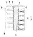
- FIG. 1depicts an illustrative example of a color filter array according to an embodiment.
- Color filter array 100includes substrate 115 having passivation layer 114 , a plurality of pixels 130 thereon, one or more nanowires 110 associated with each of the plurality of pixels 130 and optical coupler 118 associated with each of the one or more nanowires.
- Nanowires 110extend substantially perpendicularly to substrate 115 .
- substrate 115may further include image sensor 135 .
- substrate 115 and nanowires 110may be fused at intermediate layer 112 .
- passivation layer 114may be an oxide of the substrate material or a doped semiconductor layer.
- FIG. 1is illustrative and not to scale. As such, dimensions and aspect ratios of various aspects of color filter array 100 shown in FIG. 1 are not meant to be limiting.
- each of the one or more nanowires 110may absorb a fundamental frequency of light depending on the diameter of nanowire 110 .
- the fundamental frequency of the absorbed lightmay be primarily dependent on the diameter of nanowire 110 , other factors such as the material of the nanowire, the material surrounding the nanowire, length of the nanowire, and so on may determine the relationship between the diameter and the fundamental frequency.
- the fundamental frequency of light absorbed by a nanowiremay depend linearly an the diameter of the nanowire.
- a harmonic frequency of lightmay be absorbed by a nanowire of a certain diameter.
- a particular nanowireabsorbs light having a frequency of 375 THz (wavelength of 800 nm)
- the same nanowiremay absorb light having a second harmonic frequency of 750 THz (wavelength of 400 nm).
- higher harmonicsmay be similarly absorbed where applicable.
- the incident lighthas frequencies ranging from far infrared (FIR) region of the electromagnetic spectrum to deep ultraviolet (DUV) region of the electromagnetic spectrum, it may be possible to find third or even fourth harmonics within the incident light.
- FIRfar infrared
- DUVdeep ultraviolet
- the incident lighthas frequencies ranging from FIR region of the electromagnetic spectrum to X-ray region of the electromagnetic spectrum
- further higher harmonicsmay be absorbed by nanowires with diameters large enough to absorb light in FIR region of the electromagnetic spectrum.
- nanowires 110may have a diameter of about 10 nm to about 200 ⁇ m. Certain embodiments may have nanowires 110 having a diameter of about 10 nm to about 50 nm, about 50 nm to about 75 nm, about 75 nm to about 100 nm, about 75 nm to about 120 nm, about 120 nm to about 1000 nm, about 1 ⁇ m to about 10 ⁇ m, about 10 ⁇ m to about 100 ⁇ m, about 100 ⁇ m to about 200 ⁇ m, or any value or range between any two of these values.
- nanowires 110 having a diameter of less than about 50 nmcan absorb light in the ultraviolet (UV) region of the electromagnetic spectrum; nanowires having diameters of about 50 nm to about 75 nm can absorb light in the blue region of the electromagnetic spectrum; nanowires having diameters of about 75 nm to about 100 nm absorb light in the green region of the electromagnetic spectrum; nanowires having diameters of about 90 nm to about 120 nm can absorb light in the red region of the electromagnetic spectrum; and nanowires having diameters of larger than about 115 nm can absorb light in the infrared (IR) region of the electromagnetic spectrum.
- UVultraviolet
- nanowires having diameters of about 50 nm to about 75 nmcan absorb light in the blue region of the electromagnetic spectrum
- nanowires having diameters of about 75 nm to about 100 nmabsorb light in the green region of the electromagnetic spectrum
- nanowires having diameters of about 90 nm to about 120 nmcan absorb light in the red region of the electromagnetic spectrum
- Nanowiresmay be made from various materials. Some materials may be preferable than others based on their optical properties. For example, certain group IV semiconductors or III-V semiconductors may be preferred in some embodiments depending on their band-gap and refractive index. Examples, of materials that may be used for making the nanowires include, but are not limited to, silicon (Si), germanium (Ge), boron phosphide (BP), boron arsenide (BAs), aluminum phosphide (AlP), aluminum arsenide (AlAs), aluminum antimonide (AlSb), gallium nitride (GaN), gallium phosphide (GaP), gallium arsenide (GaAs), gallium antimonide (GaSb), indium nitride (InN), indium phosphide (InP), indium arsenide (InAs), zinc oxide (ZnO), zinc sulfide (ZnS), zinc selenide (ZnSe
- nanowires 110 in color filter array 100may have any convex cross-sectional shape.
- the nanowiresmay be circular in cross-section in some embodiments.
- the nanowiresmay have, for example, elliptical, square, rectangular, pentagonal, hexagonal, octagonal, or any other regular or irregular polygonal shape. It is to be understood that while the illustration in FIG. 1 shows a uniform cross-section along the length of nanowires 110 , it is contemplated within the scope and spirit of the present disclosure to have nanowires with non-uniform cross-section along the length of the nanowire.
- the cross-section area of the nanowiresmay increase along the length from the free-standing end of the nanowire to the substrate such that the portion of the nanowire which is in contact with the substrate has the largest cross-section area.
- the free-standing end of the nanowiremay have the largest cross-section area.
- the nanowiresmay also be referred to as height of the nanowire.
- the ratio of length (or height) to diameter (or, in case of a nanowire with a polygonal cross-section, the largest side)is referred to as aspect ratio of the nanowire.
- the nanowiresmay have an aspect ratio of about 2 to about 20.
- the nanowiresmay have aspect ratios as high as 1000, practically achievable aspect ratios of nanowires 110 may be limited by fabrication techniques.
- Nanowires 110 of color filter array 100may have lengths of about 0.1 ⁇ m to about 20 ⁇ m.
- image sensor 135may be a charge coupled device (CCD) or a complementary metal-oxide-semiconductor (CMOS) sensor array.
- CCDcharge coupled device
- CMOScomplementary metal-oxide-semiconductor
- Each of the image sensors 135 that form the sensor arraymay be associated with one or more of the plurality of pixels 130 .
- each of the pixels 130may be associated with one or more nanowires.
- light received by each nanowiremay be transmitted to a single image sensor 135 .
- more than one nanowiremay transmit light to one image sensor 135 .
- a group of nanowires having different diametersmay be associated with each of the pixels 130 such that a particular mix of colors is subtracted from the light received at pixel 130 , thereby transmitting light of a particular color to image sensor 135 which can then sense the intensity of the received light.
- Image sensor 135 arrayis typically arranged as a rectangular (or Cartesian) grid.
- nanowires 110may be arranged to form an array corresponding to image sensor 135 array.
- the nanowire arraymay be identical in pitch and shape to the image sensor array.
- each grid-point of the array of nanowiresmay have multiple nanowires, forming a sub-array which is repeated with a pitch and shape identical to that of the image sensor array.
- Color filter 100may additionally include optical couplers 118 such as, for example, microlenses, disposed at the light receiving end of nanowires 110 .
- optical couplerstypically, serve to improve coupling of light by guiding more light into the nanowires, thereby increasing the efficiency of color filter 100 .
- each of optical couplers 118may correspond to a single nanowire 110 , while in other embodiments, each of the optical couplers may be associated with more than one nanowire.
- FIG. 2depicts a process of making a color filter array according to an embodiment. It is to be understood that those skilled in the art will be able to optimize process parameters for various steps of the process with reasonable experimentation. Such process parameters will depend on factors such as, for example, particular materials used, geometry of desired features conditions in the processing environment and so forth, it is also to be understood that changing the order of steps may yield same or similar results depending on the particular process and materials being used. As such, the process and the order in which various steps are described herein are not to be considered limiting. Those skilled in the art will be able to suitably modify the process within the scope and spirit of this disclosure. In various embodiments, one or more of the illustrated steps may be omitted. One skilled in the art will be able to decide which steps can be omitted based on factors such as, for example, particular materials used, material quality, available reagents, available equipment, and so forth, while still obtaining the desired result.
- Process 200 of making a color filter arraymay include making 210 an array of nanowires extending substantially perpendicularly from a substrate, disposing 220 a transparent polymer to substantially encapsulate the nanowires, removing 230 the nanowires from the substrate, providing 240 a pixel array having a plurality of pixels, disposing 250 the array of nanowires on the pixel array and removing 260 the transparent polymer encapsulating the nanowires.
- FIG. 3schematically depicts the process of making 210 an array of nanowires extending substantially perpendicularly from a substrate according to an embodiment.
- a semiconductor substrateis cleaned.
- an array patternis obtained in a thin layer of metal.
- the semiconductor substrateis etched to a pre-determined depth.
- the metal layeris removed using a suitable process to leave behind the nanowires extending substantially perpendicularly from the semiconductor substrate.
- the array pattern of process 212may be obtained using various lithography techniques.
- a thin film of a photoresistmay be deposited on the substrate by, for example, spin-coating or spray-coating.
- An array patternis drawn into the photoresist using a lithography step such that specific portions of the photoresist may be removed by a solvent while other portions are left behind.
- the array patternmay be drawn by, for example, photolithography or electron beam lithography.
- a metal thin filmis deposited using, for example, chemical vapor deposition, sputtering, pulsed laser deposition, thermal evaporation, electron beam evaporation, and/or the like.
- the photoresistis then lifted-off, for example, by dissolving in a suitable solvent, to leave behind an array pattern in the metal thin film.
- a metal thin filmis deposited on the substrate, a photoresist is deposited on top of the metal thin film, the array pattern is drawn into the photoresist using a lithography step such that specific portions of the photoresist may be removed by a solvent while other portions are left behind, the metal is removed by a suitable process and the photoresist is removed to leave behind the array pattern in the metal thin film.
- the substratemay be etched 213 using dry or wet chemical etching techniques.
- Wet chemical etchingmay include treating the substrate with a suitable chemical etchant that can dissolve the substrate material.
- a chemical that can etch along a particular crystal plane of the substrate materialmay be preferred in such embodiments.
- potassium hydroxide (KOH) or tetramethyl ammonium hydroxide (TMAH)may be used for etching silicon.
- KOHpotassium hydroxide
- TMAHtetramethyl ammonium hydroxide
- Dry etchingmay include, for example, physical sputtering such as ion milling or plasma milling, plasma etching, or reactive ion etching (RIE). Reactive ion etching using specific gases or plasmas for removing the semiconductor. For example, gases such as sulfur hexafluoride, tetrafluoro methane, or octafluorocyclobutane may be used for etching silicon. Likewise, chlorine, or mixture of chlorine and boron trichloride may be used for etching gallium arsenide. Skilled artisans will be able to choose suitable gases and suitable metal masks for particular substrate materials.
- gasessuch as sulfur hexafluoride, tetrafluoro methane, or octafluorocyclobutane may be used for etching silicon.
- chlorine, or mixture of chlorine and boron trichloridemay be used for etching gallium arsenide. Skilled artisans will be able
- an array pattern with openings in the metal layer such that substrate is exposed through the openingsis obtained using techniques similar to those described with respect process 212 above, with the difference being in the lithography step.
- the photoresistis removed to leave behind the array pattern of followed by deposition of a metal and subsequently lifting off the photoresist resulting in a pattern of openings in the metal film.
- a metal thin filmmay be deposited first, followed by patterning the photoresist with an array pattern of openings within the photoresist.
- the metalmay, then, be etched with a suitable etchant such that the array pattern of openings is transferred through the metal to expose the substrate. Removal of the photoresist layer, then, results in a metal film with a pattern of openings where the substrate is exposed.
- metal-assisted chemical etchingmay be used at process 213 A to etch the substrate beneath the metal film.
- the etchantincludes a suitable acid, for example, hydrofluoric acid when the substrate is Si or Ge, and an oxidizing agent such as hydrogen peroxide (H 2 O 2 ), with the metal acting as a catalyst for reducing the oxidizing agent.
- the oxidizing agentwhile being reduced, oxidizes the substrate to orm an oxide which is dissolved by the acid.
- the metal layercaves-in without peeling off the substrate and thereby, continuously supplying the etchant to the substrate.
- the metalmay be removed, at process 214 , by dissolving in a suitable etchant.
- the metalmay be removed using a dry etching process by exposing the metal to, for example, oxygen plasma, a beam of high energy electrons, a beam of high energy ions, ionized gas, and/or the like.
- a transparent polymeris disposed on the substrate so as to substantially encapsulate the nanowires.
- the transparent polymermay be, for example, polydimethyl siloxane (PDMS), polymethyl methacralate (PMMA), polyethylene terephthalate (PET), or the like.
- the transparent polymermay be disposed by, for example, pouring or spraying the polymer on to the substrate.
- the substratemay be cured or annealed for a specified amount of time at a particular temperature following spraying or pouring of the polymer.
- the polymerin various embodiments, may have a thickness that is larger than the height of the nanowires.
- the polymermay have a thickness of about 15.5 ⁇ m, 16 ⁇ m, 20 ⁇ m, 25 ⁇ m, 50 ⁇ m, 100 ⁇ m, or any thickness between any two of these values.
- the substrateis etched away to remove the nanowires from the substrate.
- Etching the substratemay include physical sputtering (such as ion milling), dry etching, wet etching, chemical mechanical polishing or any combination thereof.
- the nanowire arraymay be mechanically detached from the substrate by scrapping or undercutting the nanowire array, for example, using a razor blade.
- the pixel arraymay include a layer of hard polymer that substantially covers an image plane of the pixel array.
- a hard polymerinclude, but are not limited to, polyimide, epoxy resin, and the like, or any combination thereof.
- the hard polymermay be disposed using, for example, spray coating, spin coating, electro-spinning, pouring, and the like, or any combination thereof.
- the pixel arraymay include a Cartesian grid of pixels.
- each of the plurality of pixelsmay be associated with a light sensing device such as a CCD sensor or a CMOS sensor. In other embodiments, more than one pixels may be associated with one light sensing device.
- FIG. 4depicts a process of disposing 250 the array of nanowires on the pixel array according to an embodiment.
- at process 252at least a portion of the transparent polymer encapsulating the nanowires is removed (using, for example, oxygen plasma etch, dry etch, or controlled dissolution in a suitable solvent) such that at least a portion of nanowires is not encapsulated by the transparent polymer.
- a hard polymersuch as, for example, polyimide is disposed such that the unencapsulated portion of the nanowires is substantially encapsulated by the hard polymer.
- the hard polymer encapsulating a portion of the nanowiresmay be the same as the hard polymer covering the pixel array.
- the nanowire arrayis disposed on the pixel array such that hard polymers of the two arrays are in contact.
- the hard polymermay be disposed using, for example, spray-coating, spin-coating or pouring the hard polymer on the nanowire array.
- the nanowire arrayis aligned on the pixel array such that the hard polymer encapsulating the nanowires is in contact with the hard polymer disposed on the pixel array.
- the shape and pitch of the nanowire arraywill be identical to the shape and pitch of pixel array.
- an appropriate number of nanowiresform a group arranged in an array with the shape and pitch of the pixel array.
- the two arraysmay be fused together by melting the hard polymer.
- the hard polymermay be melted, in some embodiments, by heating the assembly of the pixel array and the nanowire array to an appropriate temperature (depending on the melting point or glass transition temperature of the hard polymer or polymers) for a relatively short period of time.
- the arraysmay be fused together by, for example, ultrasound welding. It will be understood that the particular process, and parameters (such as frequency, intensity, time, temperature and so on) used therefor, for fusing together the nanowire array and the pixel array will depend on the particular materials used in making the color filter array.
- the transparent polymer encapsulating the nanowiresis removed.
- the transparent polymermay be removed by reactive ion etching, oxygen plasma etching, or dissolving in a suitable solvent.
- Other suitable techniques for removing the transparent polymerare contemplated in the scope of this disclosure.
- process 200 of making the color filter arraymay optionally include disposing (not shown) a material having a lower refractive index than a material of the nanowires.
- the lower refractive indexmay be disposed such that the space between the nanowires may be substantially filled with the lower refractive index material.
- the lower refractive index materialmay be disposed using, for example, chemical vapor deposition, atomic layer deposition, or other suitable techniques compatible with the various materials used.
- process 200may further optionally include disposing (not shown) a plurality of optical couplers such that each of the plurality of optical couplers is associated with at least one nanowire of the nanowire array.
- the optical couplersmay include structures such as, for example, microlenses. As discussed elsewhere herein, the optical couplers may increase the light capture efficiency of the color filter array by guiding radiation into each of the nanowires.
Landscapes
- Solid State Image Pick-Up Elements (AREA)
- Engineering & Computer Science (AREA)
- Chemical & Material Sciences (AREA)
- Nanotechnology (AREA)
- Physics & Mathematics (AREA)
- Optical Filters (AREA)
- Crystallography & Structural Chemistry (AREA)
- Condensed Matter Physics & Semiconductors (AREA)
- Materials Engineering (AREA)
- General Physics & Mathematics (AREA)
- Manufacturing & Machinery (AREA)
- Computer Hardware Design (AREA)
- Microelectronics & Electronic Packaging (AREA)
- Power Engineering (AREA)
- Life Sciences & Earth Sciences (AREA)
- Biophysics (AREA)
- Optics & Photonics (AREA)
Abstract
Description
Claims (14)
Priority Applications (19)
| Application Number | Priority Date | Filing Date | Title |
|---|---|---|---|
| US12/945,492US9515218B2 (en) | 2008-09-04 | 2010-11-12 | Vertical pillar structured photovoltaic devices with mirrors and optical claddings |
| US13/963,847US9343490B2 (en) | 2013-08-09 | 2013-08-09 | Nanowire structured color filter arrays and fabrication method of the same |
| JP2016533492AJP2016528552A (en) | 2013-08-09 | 2014-08-11 | Color filter array having nanowire structure and manufacturing method thereof |
| KR1020167005780AKR20160041978A (en) | 2013-08-09 | 2014-08-11 | Nanowire structured color filter arrays and fabrication method of the same |
| TW103127484ATW201505959A (en) | 2013-08-09 | 2014-08-11 | Color filter array of nanowire structure and method of manufacturing the color filter array |
| PCT/US2014/050544WO2015021467A1 (en) | 2013-08-09 | 2014-08-11 | Nanowire structured color filter arrays and fabrication method of the same |
| CN201480055533.8ACN105814689A (en) | 2013-08-09 | 2014-08-11 | Nanowire structured color filter array and manufacturing method thereof |
| US14/503,598US9410843B2 (en) | 2008-09-04 | 2014-10-01 | Nanowire arrays comprising fluorescent nanowires and substrate |
| US14/516,402US20160111460A1 (en) | 2008-09-04 | 2014-10-16 | Back-lit photodetector |
| US14/516,162US20160111562A1 (en) | 2008-09-04 | 2014-10-16 | Multispectral and polarization-selective detector |
| US14/632,739US9601529B2 (en) | 2008-09-04 | 2015-02-26 | Light absorption and filtering properties of vertically oriented semiconductor nano wires |
| US14/704,143US20150303333A1 (en) | 2008-09-04 | 2015-05-05 | Passivated upstanding nanostructures and methods of making the same |
| US14/705,380US9337220B2 (en) | 2008-09-04 | 2015-05-06 | Solar blind ultra violet (UV) detector and fabrication methods of the same |
| US15/057,153US20160178840A1 (en) | 2008-09-04 | 2016-03-01 | Optical waveguides in image sensors |
| US15/082,514US20160211394A1 (en) | 2008-11-13 | 2016-03-28 | Nano wire array based solar energy harvesting device |
| US15/090,155US20160216523A1 (en) | 2008-09-04 | 2016-04-04 | Vertical waveguides with various functionality on integrated circuits |
| US15/093,928US20160225811A1 (en) | 2008-09-04 | 2016-04-08 | Nanowire structured color filter arrays and fabrication method of the same |
| US15/149,252US20160254301A1 (en) | 2008-09-04 | 2016-05-09 | Solar blind ultra violet (uv) detector and fabrication methods of the same |
| US15/225,264US20160344964A1 (en) | 2008-09-04 | 2016-08-01 | Methods for fabricating and using nanowires |
Applications Claiming Priority (1)
| Application Number | Priority Date | Filing Date | Title |
|---|---|---|---|
| US13/963,847US9343490B2 (en) | 2013-08-09 | 2013-08-09 | Nanowire structured color filter arrays and fabrication method of the same |
Related Child Applications (1)
| Application Number | Title | Priority Date | Filing Date |
|---|---|---|---|
| US15/093,928ContinuationUS20160225811A1 (en) | 2008-09-04 | 2016-04-08 | Nanowire structured color filter arrays and fabrication method of the same |
Publications (2)
| Publication Number | Publication Date |
|---|---|
| US20150041937A1 US20150041937A1 (en) | 2015-02-12 |
| US9343490B2true US9343490B2 (en) | 2016-05-17 |
Family
ID=52447934
Family Applications (2)
| Application Number | Title | Priority Date | Filing Date |
|---|---|---|---|
| US13/963,847Expired - Fee RelatedUS9343490B2 (en) | 2008-09-04 | 2013-08-09 | Nanowire structured color filter arrays and fabrication method of the same |
| US15/093,928AbandonedUS20160225811A1 (en) | 2008-09-04 | 2016-04-08 | Nanowire structured color filter arrays and fabrication method of the same |
Family Applications After (1)
| Application Number | Title | Priority Date | Filing Date |
|---|---|---|---|
| US15/093,928AbandonedUS20160225811A1 (en) | 2008-09-04 | 2016-04-08 | Nanowire structured color filter arrays and fabrication method of the same |
Country Status (6)
| Country | Link |
|---|---|
| US (2) | US9343490B2 (en) |
| JP (1) | JP2016528552A (en) |
| KR (1) | KR20160041978A (en) |
| CN (1) | CN105814689A (en) |
| TW (1) | TW201505959A (en) |
| WO (1) | WO2015021467A1 (en) |
Cited By (2)
| Publication number | Priority date | Publication date | Assignee | Title |
|---|---|---|---|---|
| US20160284649A1 (en)* | 2015-03-26 | 2016-09-29 | Globalwafers Co., Ltd. | Nanostructured chip and method of producing the same |
| US10636825B2 (en) | 2017-07-12 | 2020-04-28 | Applied Materials, Inc. | Shaped color filter |
Families Citing this family (19)
| Publication number | Priority date | Publication date | Assignee | Title |
|---|---|---|---|---|
| JP5524839B2 (en) | 2007-08-21 | 2014-06-18 | ザ、リージェンツ、オブ、ザ、ユニバーシティ、オブ、カリフォルニア | Thermoelectric device with nanostructures and method of operating the device |
| US9240328B2 (en) | 2010-11-19 | 2016-01-19 | Alphabet Energy, Inc. | Arrays of long nanostructures in semiconductor materials and methods thereof |
| US8736011B2 (en) | 2010-12-03 | 2014-05-27 | Alphabet Energy, Inc. | Low thermal conductivity matrices with embedded nanostructures and methods thereof |
| US9051175B2 (en) | 2012-03-07 | 2015-06-09 | Alphabet Energy, Inc. | Bulk nano-ribbon and/or nano-porous structures for thermoelectric devices and methods for making the same |
| US9257627B2 (en) | 2012-07-23 | 2016-02-09 | Alphabet Energy, Inc. | Method and structure for thermoelectric unicouple assembly |
| EP3033788A1 (en)* | 2013-08-14 | 2016-06-22 | Board of Regents, The University of Texas System | Methods of fabricating silicon nanowires and devices containing silicon nanowires |
| US20150137296A1 (en)* | 2013-11-20 | 2015-05-21 | Taiwan Semiconductor Manufacturing Co., Ltd. | Color Filter Array and Micro-Lens Structure for Imaging System |
| WO2015157501A1 (en)* | 2014-04-10 | 2015-10-15 | Alphabet Energy, Inc. | Ultra-long silicon nanostructures, and methods of forming and transferring the same |
| US10535701B2 (en)* | 2016-01-12 | 2020-01-14 | Omnivision Technologies, Inc. | Plasmonic-nanostructure sensor pixel |
| US10507466B2 (en)* | 2016-04-27 | 2019-12-17 | International Business Machines Corporation | Metal assisted chemical etching for fabricating high aspect ratio and straight silicon nanopillar arrays for sorting applications |
| KR101994892B1 (en)* | 2017-12-27 | 2019-07-01 | 전남대학교산학협력단 | Tactile sensor and method for manufacturing thereof |
| CN108511469B (en)* | 2017-12-29 | 2021-08-27 | 郑纪元 | Integrated imaging sensor and preparation method thereof |
| CN108831898A (en)* | 2018-05-08 | 2018-11-16 | 苏州解光语半导体科技有限公司 | A solid-state multispectral sensor |
| KR102806130B1 (en)* | 2019-05-31 | 2025-05-09 | 삼성전자주식회사 | Combination structure and optical filter and image sensor and camera moduel and electronic device |
| WO2021240998A1 (en)* | 2020-05-26 | 2021-12-02 | ソニーセミコンダクタソリューションズ株式会社 | Solid-state imaging element |
| CN114530465A (en)* | 2020-11-23 | 2022-05-24 | 联华电子股份有限公司 | Image sensor device and method of making the same |
| US12265200B2 (en)* | 2021-07-01 | 2025-04-01 | Samsung Electronics Co., Ltd. | Normal-to-plane surface plasmon mode for angle-and-polarization independent optomechanical sensing |
| FR3130782A1 (en)* | 2021-12-17 | 2023-06-23 | Centre National De La Recherche Scientifique | METHOD FOR THE DENSE FILLING OF MICROMETRIC OR SUBMICROMETRIC INTERWIRE SPACES WITH AN ORGANO-SILICATE HYBRID MATRIX AND COMPOSITE DEVICE THUS OBTAINED |
| CN114879390B (en)* | 2022-06-06 | 2023-09-12 | 南京信息工程大学 | A kind of nanowire structure color display screen and its production method |
Citations (482)
| Publication number | Priority date | Publication date | Assignee | Title |
|---|---|---|---|---|
| US1918848A (en) | 1929-04-26 | 1933-07-18 | Norwich Res Inc | Polarizing refracting bodies |
| US3903427A (en) | 1973-12-28 | 1975-09-02 | Hughes Aircraft Co | Solar cell connections |
| US4017332A (en) | 1975-02-27 | 1977-04-12 | Varian Associates | Solar cells employing stacked opposite conductivity layers |
| US4292512A (en) | 1978-06-19 | 1981-09-29 | Bell Telephone Laboratories, Incorporated | Optical monitoring photodiode system |
| US4316048A (en) | 1980-06-20 | 1982-02-16 | International Business Machines Corporation | Energy conversion |
| US4357415A (en) | 1980-03-06 | 1982-11-02 | Eastman Kodak Company | Method of making a solid-state color imaging device having a color filter array using a photocrosslinkable barrier |
| US4387265A (en) | 1981-07-17 | 1983-06-07 | University Of Delaware | Tandem junction amorphous semiconductor photovoltaic cell |
| US4394571A (en) | 1981-05-18 | 1983-07-19 | Honeywell Inc. | Optically enhanced Schottky barrier IR detector |
| US4400221A (en) | 1981-07-08 | 1983-08-23 | The United States Of America As Represented By The Secretary Of The Air Force | Fabrication of gallium arsenide-germanium heteroface junction device |
| US4443890A (en) | 1980-12-02 | 1984-04-17 | Thomson-Csf | Optical-connection direct-light modulation information transmission system with a passband extended towards the low frequencies and continuous waves |
| US4513168A (en) | 1984-04-19 | 1985-04-23 | Varian Associates, Inc. | Three-terminal solar cell circuit |
| US4531055A (en) | 1983-01-05 | 1985-07-23 | The United States Of America As Represented By The Secretary Of The Air Force | Self-guarding Schottky barrier infrared detector array |
| WO1986003347A1 (en) | 1984-11-20 | 1986-06-05 | Hughes Aircraft Company | Solid state laser employing diamond having color centers as a laser active material |
| US4620237A (en) | 1984-10-22 | 1986-10-28 | Xerox Corporation | Fast scan jitter measuring system for raster scanners |
| US4678772A (en) | 1983-02-28 | 1987-07-07 | Yissum Research Development Company Of The Hebrew University Of Jerusalem | Compositions containing glycyrrhizin |
| US4827335A (en) | 1986-08-29 | 1989-05-02 | Kabushiki Kaisha Toshiba | Color image reading apparatus with two color separation filters each having two filter elements |
| US4846556A (en) | 1987-05-14 | 1989-07-11 | Toppan Printing Co., Ltd. | Color filter and method of manufacturing the same |
| US4857973A (en) | 1987-05-14 | 1989-08-15 | The United States Of America As Represented By The Secretary Of The Air Force | Silicon waveguide with monolithically integrated Schottky barrier photodetector |
| US4876586A (en) | 1987-12-21 | 1989-10-24 | Sangamo-Weston, Incorporated | Grooved Schottky barrier photodiode for infrared sensing |
| US4880613A (en) | 1987-01-12 | 1989-11-14 | Sumitomo Electric Industries, Ltd. | Light emitting element comprising diamond and method for producing the same |
| US4896941A (en) | 1985-04-27 | 1990-01-30 | Doryokuro Kakunenryo Kaihatsu Jigyodan | Image-transmitting fiber |
| US4950625A (en) | 1988-06-13 | 1990-08-21 | Sumitomo Electric Industries, Ltd. | Diamond laser crystal and method manufacturing the same |
| US4972244A (en) | 1988-06-16 | 1990-11-20 | Commissariat A L'energie Atomique | Photodiode and photodiode array on a II-VI material and processes for the production thereof |
| US4971928A (en) | 1990-01-16 | 1990-11-20 | General Motors Corporation | Method of making a light emitting semiconductor having a rear reflecting surface |
| US4990988A (en) | 1989-06-09 | 1991-02-05 | The United States Of America As Represented By The Administrator Of The National Aeronautics And Space Administration | Laterally stacked Schottky diodes for infrared sensor applications |
| US5071490A (en) | 1988-03-18 | 1991-12-10 | Sharp Kabushiki Kaisha | Tandem stacked amorphous solar cell device |
| US5081049A (en) | 1988-07-18 | 1992-01-14 | Unisearch Limited | Sculpted solar cell surfaces |
| US5096520A (en) | 1990-08-01 | 1992-03-17 | Faris Sades M | Method for producing high efficiency polarizing filters |
| US5124543A (en) | 1989-08-09 | 1992-06-23 | Ricoh Company, Ltd. | Light emitting element, image sensor and light receiving element with linearly varying waveguide index |
| US5217911A (en) | 1990-06-29 | 1993-06-08 | Mitsubishi Denki Kabushiki Kaisha | Method of producing a semiconductor structure including a Schottky junction |
| US5247349A (en) | 1982-11-16 | 1993-09-21 | Stauffer Chemical Company | Passivation and insulation of III-V devices with pnictides, particularly amorphous pnictides having a layer-like structure |
| US5272518A (en) | 1990-12-17 | 1993-12-21 | Hewlett-Packard Company | Colorimeter and calibration system |
| US5311047A (en) | 1988-11-16 | 1994-05-10 | National Science Council | Amorphous SI/SIC heterojunction color-sensitive phototransistor |
| US5347147A (en) | 1990-11-28 | 1994-09-13 | Jones Barbara L | Light emitting diamond device |
| US5362972A (en) | 1990-04-20 | 1994-11-08 | Hitachi, Ltd. | Semiconductor device using whiskers |
| US5374841A (en) | 1991-12-18 | 1994-12-20 | Texas Instruments Incorporated | HgCdTe S-I-S two color infrared detector |
| US5391896A (en) | 1992-09-02 | 1995-02-21 | Midwest Research Institute | Monolithic multi-color light emission/detection device |
| US5401968A (en) | 1989-12-29 | 1995-03-28 | Honeywell Inc. | Binary optical microlens detector array |
| US5449626A (en) | 1991-12-27 | 1995-09-12 | Hezel; Rudolf | Method for manufacture of a solar cell |
| US5468652A (en) | 1993-07-14 | 1995-11-21 | Sandia Corporation | Method of making a back contacted solar cell |
| US5602661A (en) | 1993-02-17 | 1997-02-11 | Hoffmann-La Roche Inc. | Optical component |
| US5612780A (en) | 1996-06-05 | 1997-03-18 | Harris Corporation | Device for detecting light emission from optical fiber |
| US5671914A (en) | 1995-11-06 | 1997-09-30 | Spire Corporation | Multi-band spectroscopic photodetector array |
| US5696863A (en) | 1982-08-06 | 1997-12-09 | Kleinerman; Marcos Y. | Distributed fiber optic temperature sensors and systems |
| US5723945A (en) | 1996-04-09 | 1998-03-03 | Electro Plasma, Inc. | Flat-panel display |
| US5747796A (en) | 1995-07-13 | 1998-05-05 | Sharp Kabushiki Kaisha | Waveguide type compact optical scanner and manufacturing method thereof |
| US5767507A (en) | 1996-07-15 | 1998-06-16 | Trustees Of Boston University | Polarization sensitive photodetectors and detector arrays |
| US5798535A (en) | 1996-12-20 | 1998-08-25 | Motorola, Inc. | Monolithic integration of complementary transistors and an LED array |
| US5844290A (en) | 1996-06-27 | 1998-12-01 | Nec Corporation | Solid state image pick-up device and method for manufacturing the same |
| US5853446A (en) | 1996-04-16 | 1998-12-29 | Corning Incorporated | Method for forming glass rib structures |
| US5857053A (en) | 1997-06-17 | 1999-01-05 | Lucent Technologies Inc. | Optical fiber filter |
| US5877492A (en) | 1995-09-14 | 1999-03-02 | Nec Corporation | Contact type image sensor comprising a plurality of microlenses |
| US5880495A (en) | 1998-01-08 | 1999-03-09 | Omnivision Technologies, Inc. | Active pixel with a pinned photodiode |
| US5885881A (en) | 1996-04-24 | 1999-03-23 | Northern Telecom Limited | Planar wave guide cladding |
| US5900623A (en) | 1997-08-11 | 1999-05-04 | Chrontel, Inc. | Active pixel sensor using CMOS technology with reverse biased photodiodes |
| US5943463A (en) | 1996-06-17 | 1999-08-24 | Sharp Kabushiki Kaisha | Color image sensor and a production method of an optical waveguide array for use therein |
| US5968528A (en) | 1997-05-23 | 1999-10-19 | The Procter & Gamble Company | Skin care compositions |
| US6013871A (en) | 1997-07-02 | 2000-01-11 | Curtin; Lawrence F. | Method of preparing a photovoltaic device |
| WO2000002379A1 (en) | 1998-07-01 | 2000-01-13 | Cmos Sensor, Inc. | Silicon butting contact image sensor chip with line transfer and pixel readout (ltpr) structure |
| US6033582A (en) | 1996-01-22 | 2000-03-07 | Etex Corporation | Surface modification of medical implants |
| US6037243A (en) | 1997-11-06 | 2000-03-14 | Electronics And Telecommunications Research Institute | Method for manufacturing silicon nanometer structure using silicon nitride film |
| US6046466A (en) | 1997-09-12 | 2000-04-04 | Nikon Corporation | Solid-state imaging device |
| US6074892A (en) | 1996-05-07 | 2000-06-13 | Ciena Corporation | Semiconductor hetero-interface photodetector |
| US6100551A (en) | 1995-04-13 | 2000-08-08 | Eastman Kodak Company | Active pixel sensor integrated with a pinned photodiode |
| GB2348399A (en) | 1999-03-31 | 2000-10-04 | Univ Glasgow | Reactive ion etching with control of etch gas flow rate, pressure and rf power |
| JP2000324396A (en) | 1999-05-06 | 2000-11-24 | Olympus Optical Co Ltd | Solid image pickup element and method for driving the same |
| US6270548B1 (en) | 1997-04-17 | 2001-08-07 | James Wilbert Campbell | Sintering process for diamond and diamond growth |
| US6301420B1 (en) | 1998-05-01 | 2001-10-09 | The Secretary Of State For Defence In Her Britannic Majesty's Government Of The United Kingdom Of Great Britain And Northern Ireland | Multicore optical fibre |
| US6326649B1 (en) | 1999-01-13 | 2001-12-04 | Agere Systems, Inc. | Pin photodiode having a wide bandwidth |
| US20020003201A1 (en) | 1998-02-02 | 2002-01-10 | Gang Yu | Image sensors made from organic semiconductors |
| US20020020846A1 (en) | 2000-04-20 | 2002-02-21 | Bo Pi | Backside illuminated photodiode array |
| US20020021879A1 (en) | 2000-07-10 | 2002-02-21 | Lee Kevin K. | Graded index waveguide |
| US6388243B1 (en) | 1999-03-01 | 2002-05-14 | Photobit Corporation | Active pixel sensor with fully-depleted buried photoreceptor |
| US6388648B1 (en) | 1996-11-05 | 2002-05-14 | Clarity Visual Systems, Inc. | Color gamut and luminance matching techniques for image display systems |
| JP2002151715A (en) | 2000-11-08 | 2002-05-24 | Sharp Corp | Thin film solar cell |
| US20020071468A1 (en) | 1999-09-27 | 2002-06-13 | Sandstrom Richard L. | Injection seeded F2 laser with pre-injection filter |
| US6407439B1 (en) | 1999-08-19 | 2002-06-18 | Epitaxial Technologies, Llc | Programmable multi-wavelength detector array |
| US20020104821A1 (en) | 1996-10-04 | 2002-08-08 | Michael Bazylenko | Reactive ion etching of silica structures |
| US20020109082A1 (en) | 2001-02-13 | 2002-08-15 | Yoshikazu Nakayama And Daiken Chemical Co., Ltd. | Light receiving and emitting probe and light receiving and emitting probe apparatus |
| US20020117675A1 (en) | 2001-02-09 | 2002-08-29 | Angelo Mascarenhas | Isoelectronic co-doping |
| WO2002069623A1 (en) | 2001-02-28 | 2002-09-06 | Sony Corporation | Image input device |
| US20020130311A1 (en) | 2000-08-22 | 2002-09-19 | Lieber Charles M. | Doped elongated semiconductors, growing such semiconductors, devices including such semiconductors and fabricating such devices |
| US6459034B2 (en) | 2000-06-01 | 2002-10-01 | Sharp Kabushiki Kaisha | Multi-junction solar cell |
| US6463204B1 (en) | 1998-12-18 | 2002-10-08 | Fujitsu Network Communications, Inc. | Modular lightpipe system |
| US20020172820A1 (en) | 2001-03-30 | 2002-11-21 | The Regents Of The University Of California | Methods of fabricating nanostructures and nanowires and devices fabricated therefrom |
| US20030003300A1 (en) | 2001-07-02 | 2003-01-02 | Korgel Brian A. | Light-emitting nanoparticles and method of making same |
| US20030006363A1 (en) | 2001-04-27 | 2003-01-09 | Campbell Scott Patrick | Optimization of alignment between elements in an image sensor |
| US6542231B1 (en) | 2000-08-22 | 2003-04-01 | Thermo Finnegan Llc | Fiber-coupled liquid sample analyzer with liquid flow cell |
| US20030077907A1 (en) | 1999-08-06 | 2003-04-24 | Kao David Y. | Method for forming an etch mask during the manufacture of a semiconductor device |
| US6563995B2 (en) | 2001-04-02 | 2003-05-13 | Lightwave Electronics | Optical wavelength filtering apparatus with depressed-index claddings |
| US20030089899A1 (en) | 2000-08-22 | 2003-05-15 | Lieber Charles M. | Nanoscale wires and related devices |
| US6566723B1 (en) | 2002-01-10 | 2003-05-20 | Agilent Technologies, Inc. | Digital color image sensor with elevated two-color photo-detector and related circuitry |
| US20030132480A1 (en) | 2002-01-16 | 2003-07-17 | Duc Chau | Self-aligned trench mosfets and methods for making the same |
| US20030160176A1 (en) | 2000-06-26 | 2003-08-28 | Ratnakar Vispute | Mgzno based uv detectors |
| US20030189202A1 (en) | 2002-04-05 | 2003-10-09 | Jun Li | Nanowire devices and methods of fabrication |
| US20030227090A1 (en) | 2002-05-31 | 2003-12-11 | Ichiro Okabe | Dual damascene semiconductor devices |
| WO2003107439A1 (en) | 2002-06-12 | 2003-12-24 | Rwe Schott Solar, Inc. | Photovoltaic module with light reflecting backskin |
| US6680216B2 (en) | 2000-03-09 | 2004-01-20 | General Electric Company | Method of making imager structure |
| US20040011975A1 (en) | 2002-07-17 | 2004-01-22 | Nicoli David F. | Sensors and methods for high-sensitivity optical particle counting and sizing |
| US20040021062A1 (en) | 2001-11-16 | 2004-02-05 | Zaidi Saleem H. | Enhanced optical absorption and radiation tolerance in thin-film solar cells and photodetectors |
| US20040026684A1 (en) | 2002-04-02 | 2004-02-12 | Nanosys, Inc. | Nanowire heterostructures for encoding information |
| US6709929B2 (en) | 2001-06-25 | 2004-03-23 | North Carolina State University | Methods of forming nano-scale electronic and optoelectronic devices using non-photolithographically defined nano-channel templates |
| US20040058058A1 (en) | 2000-04-12 | 2004-03-25 | Shchegolikhin Alexander Nikitovich | Raman-active taggants and thier recognition |
| US20040065362A1 (en) | 2001-01-31 | 2004-04-08 | Takenori Watabe | Solar cell and method for producing the same |
| US6720594B2 (en) | 2002-01-07 | 2004-04-13 | Xerox Corporation | Image sensor array with reduced pixel crosstalk |
| US20040075464A1 (en) | 2002-07-08 | 2004-04-22 | Btg International Limited | Nanostructures and methods for manufacturing the same |
| US20040095658A1 (en) | 2002-09-05 | 2004-05-20 | Nanosys, Inc. | Nanocomposites |
| US20040109666A1 (en) | 2002-12-10 | 2004-06-10 | John Kim | Optoelectronic devices employing fibers for light collection and emission |
| US20040114847A1 (en) | 2002-08-19 | 2004-06-17 | Jan-Malte Fischer | Method of efficient carrier generation in silicon waveguide systems for switching/modulating purposes using parallel pump and signal waveguides |
| US20040118377A1 (en) | 2002-12-19 | 2004-06-24 | Bloms Jason K. | Fuel allocation at idle or light engine load |
| US20040118337A1 (en) | 2002-09-30 | 2004-06-24 | Canon Kabushiki Kaisha | Method for growing silicon film, method for manufacturing solar cell, semiconductor substrate, and solar cell |
| US20040122328A1 (en) | 2000-06-19 | 2004-06-24 | University Of Washington | Integrated optical scanning image acquisition and display |
| US20040124366A1 (en) | 2002-10-02 | 2004-07-01 | Haishan Zeng | Apparatus and methods relating to high speed spectroscopy and excitation-emission matrices |
| US6771314B1 (en) | 1998-03-31 | 2004-08-03 | Intel Corporation | Orange-green-blue (OGB) color system for digital image sensor applications |
| US20040156610A1 (en) | 1997-05-16 | 2004-08-12 | Btg International Limited | Optical devices and methods of fabrication thereof |
| US20040155247A1 (en) | 2000-12-21 | 2004-08-12 | Stephan Benthien | Image sensor device comprising central locking |
| US20040160522A1 (en) | 1994-01-28 | 2004-08-19 | California Institute Of Technology | Active pixel sensor with intra-pixel charge transfer |
| US20040180461A1 (en) | 2003-03-12 | 2004-09-16 | Taiwan Semiconductor Manufacturing Company | Light guide for image sensor |
| US6805139B1 (en) | 1999-10-20 | 2004-10-19 | Mattson Technology, Inc. | Systems and methods for photoresist strip and residue treatment in integrated circuit manufacturing |
| US20040213307A1 (en) | 2002-07-19 | 2004-10-28 | President And Fellows Of Harvard College | Nanoscale coherent optical components |
| US6812473B1 (en) | 1999-06-30 | 2004-11-02 | Hoya Corporation | Electron beam drawing mask blank, electron beam drawing mask, and method of manufacturing the same |
| US20040217086A1 (en) | 2002-09-11 | 2004-11-04 | Matsushita Electric Industrial Co., Ltd. | Pattern formation method |
| US20040223681A1 (en) | 2003-04-23 | 2004-11-11 | Block Bruce A. | On-chip optical signal routing |
| US20040241965A1 (en) | 2003-05-28 | 2004-12-02 | Charles Merritt | High aspect ratio microelectrode arrays |
| US20040252957A1 (en) | 2003-06-16 | 2004-12-16 | The Regents Of The University Of California | Apparatus for optical measurements on low-index non-solid materials based on arrow waveguides |
| US20040261840A1 (en) | 2003-06-30 | 2004-12-30 | Advent Solar, Inc. | Emitter wrap-through back contact solar cells on thin silicon wafers |
| US20050009224A1 (en) | 2003-06-20 | 2005-01-13 | The Regents Of The University Of California | Nanowire array and nanowire solar cells and methods for forming the same |
| US20050035381A1 (en) | 2003-08-13 | 2005-02-17 | Holm Paige M. | Vertically integrated photosensor for CMOS imagers |
| TWI228782B (en) | 2004-01-19 | 2005-03-01 | Toppoly Optoelectronics Corp | Method of fabricating display panel |
| US20050082676A1 (en) | 2003-10-17 | 2005-04-21 | International Business Machines Corporation | Silicon chip carrier with through-vias using laser assisted chemical vapor deposition of conductor |
| US20050087601A1 (en) | 2003-10-24 | 2005-04-28 | Gerst Carl W.Iii | Light pipe illumination system and method |
| US20050095699A1 (en) | 2002-10-30 | 2005-05-05 | Akihiro Miyauchi | Functioning substrate with a group of columnar micro pillars and its manufacturing method |
| US20050109388A1 (en) | 2003-11-05 | 2005-05-26 | Canon Kabushiki Kaisha | Photovoltaic device and manufacturing method thereof |
| US20050116271A1 (en) | 2003-12-02 | 2005-06-02 | Yoshiaki Kato | Solid-state imaging device and manufacturing method thereof |
| US20050133476A1 (en) | 2003-12-17 | 2005-06-23 | Islam M. S. | Methods of bridging lateral nanowires and device using same |
| WO2005064337A1 (en) | 2003-12-22 | 2005-07-14 | Koninklijke Philips Electronics N.V. | Optical nanowire biosensor based on energy transfer |
| US20050164514A1 (en) | 2004-01-28 | 2005-07-28 | Shahid Rauf | Method for etching a quartz layer in a photoresistless semiconductor mask |
| US6927145B1 (en) | 2004-02-02 | 2005-08-09 | Advanced Micro Devices, Inc. | Bitline hard mask spacer flow for memory cell scaling |
| US20050190453A1 (en) | 2004-03-01 | 2005-09-01 | Hideki Dobashi | Image sensor |
| US20050201704A1 (en) | 2004-02-12 | 2005-09-15 | Panorama Flat Ltd. | Apparatus, method, and computer program product for transverse waveguided display system |
| JP2005252210A (en) | 2004-02-03 | 2005-09-15 | Sharp Corp | Solar cell |
| US20050218468A1 (en) | 2004-03-18 | 2005-10-06 | Owen Mark D | Micro-reflectors on a substrate for high-density LED array |
| US20050224707A1 (en) | 2002-06-25 | 2005-10-13 | Commissariat A A'energie Atomique | Imager |
| US6960526B1 (en) | 2003-10-10 | 2005-11-01 | The United States Of America As Represented By The Secretary Of The Army | Method of fabricating sub-100 nanometer field emitter tips comprising group III-nitride semiconductors |
| TW200535914A (en) | 2003-12-22 | 2005-11-01 | Koninkl Philips Electronics Nv | Fabricating a set of semiconducting nanowires, and electric device comprising a set of nanowires |
| TW200536048A (en) | 2004-04-16 | 2005-11-01 | Ind Tech Res Inst | Metal nanoline process and its application on aligned growth of carbon nanotube or silicon nanowrie |
| US20050242409A1 (en) | 2004-04-28 | 2005-11-03 | Advanced Chip Engineering Technology Inc. | Imagine sensor with a protection layer |
| US6967120B2 (en) | 2002-07-19 | 2005-11-22 | Dongbu Anam Semiconductor | Pinned photodiode for a CMOS image sensor and fabricating method thereof |
| JP2005328135A (en) | 2004-05-12 | 2005-11-24 | Sony Corp | Ad conversion method and semiconductor apparatus for detecting physical quantity distribution |
| US6969899B2 (en) | 2003-12-08 | 2005-11-29 | Taiwan Semiconductor Manufacturing Co., Ltd. | Image sensor with light guides |
| US20050284517A1 (en) | 2004-06-29 | 2005-12-29 | Sanyo Electric Co., Ltd. | Photovoltaic cell, photovoltaic cell module, method of fabricating photovoltaic cell and method of repairing photovoltaic cell |
| US6987258B2 (en) | 2001-12-19 | 2006-01-17 | Intel Corporation | Integrated circuit-based compound eye image sensor using a light pipe bundle |
| US20060011362A1 (en) | 2002-01-14 | 2006-01-19 | China Petroleum & Chemical Corporation | Power transmission unit of an impactor, a hydraulic jet impactor and the application thereof |
| US20060027071A1 (en) | 2004-08-06 | 2006-02-09 | Barnett Ronald J | Tensegrity musical structures |
| US20060038990A1 (en) | 2004-08-20 | 2006-02-23 | Habib Youssef M | Nanowire optical sensor system and methods for making and using same |
| US7052927B1 (en) | 2004-01-27 | 2006-05-30 | Raytheon Company | Pin detector apparatus and method of fabrication |
| US20060113622A1 (en) | 2004-11-30 | 2006-06-01 | International Business Machines Corporation | A damascene copper wiring image sensor |
| US20060115230A1 (en) | 2002-12-13 | 2006-06-01 | Tetsuya Komoguchi | Solid-state imaging device and production method therefor |
| US20060121371A1 (en) | 2004-12-03 | 2006-06-08 | Innolux Display Corp. | Color filter having nanoparticles for liquid crystal display |
| US7064372B2 (en) | 2002-09-30 | 2006-06-20 | Nanosys, Inc. | Large-area nanoenabled macroelectronic substrates and uses therefor |
| US20060146323A1 (en) | 2005-01-06 | 2006-07-06 | Alexandre Bratkovski | Nanowires for surface-enhanced raman scattering molecular sensors |
| US20060162766A1 (en) | 2003-06-26 | 2006-07-27 | Advent Solar, Inc. | Back-contacted solar cells with integral conductive vias and method of making |
| US20060180197A1 (en) | 2005-02-15 | 2006-08-17 | Gui John Y | Layer-to-layer interconnects for photoelectric devices and methods of fabricating the same |
| EP0809303B1 (en) | 1996-05-22 | 2006-09-06 | Eastman Kodak Company | A color active pixel sensor with electronic shuttering, anti-blooming and low cross-talk |
| US7105428B2 (en) | 2004-04-30 | 2006-09-12 | Nanosys, Inc. | Systems and methods for nanowire growth and harvesting |
| US7106938B2 (en) | 2004-03-16 | 2006-09-12 | Regents Of The University Of Minnesota | Self assembled three-dimensional photonic crystal |
| US20060208320A1 (en) | 2005-03-15 | 2006-09-21 | Kabushiki Kaisha Toshiba | MIS-type semiconductor device |
| US20060257071A1 (en) | 2005-05-11 | 2006-11-16 | Fitel Usa Corp. | Optical fiber filter for suppression of amplified spontaneous emission |
| US20060260674A1 (en) | 2004-04-06 | 2006-11-23 | Tran Bao Q | Nano ic |
| US20060273262A1 (en) | 2000-12-20 | 2006-12-07 | Michel Sayag | Light stimulating and collecting methods and apparatus for storage-phosphor image plates |
| US20060273389A1 (en) | 2005-05-23 | 2006-12-07 | International Business Machines Corporation | Vertical FET with nanowire channels and a silicided bottom contact |
| US20060284118A1 (en) | 2005-06-15 | 2006-12-21 | Board Of Trustees Of Michigan State University | Process and apparatus for modifying a surface in a work region |
| US7153720B2 (en) | 2002-12-09 | 2006-12-26 | Quantum Semiconductor Llc | CMOS image sensor |
| WO2007000879A1 (en) | 2005-06-29 | 2007-01-04 | National University Corporation NARA Institute of Science and Technology | Solid-state imaging element and signal reading method thereof |
| US7163659B2 (en) | 2002-12-03 | 2007-01-16 | Hewlett-Packard Development Company, L.P. | Free-standing nanowire sensor and method for detecting an analyte in a fluid |
| US20070012980A1 (en) | 2002-09-30 | 2007-01-18 | Nanosys, Inc. | Large-area nanoenabled macroelectronic substrates and uses therefor |
| US20070012985A1 (en) | 2004-03-23 | 2007-01-18 | Nanosys, Inc. | Nanowire capacitor and methods of making same |
| US20070023799A1 (en) | 2005-08-01 | 2007-02-01 | Micro Technology, Inc. | Structure and method for building a light tunnel for use with imaging devices |
| US20070025504A1 (en) | 2003-06-20 | 2007-02-01 | Tumer Tumay O | System for molecular imaging |
| US20070029545A1 (en) | 2003-02-24 | 2007-02-08 | Ignis Innovation Inc | Pixel having an organic light emitting diode and method of fabricating the pixel |
| US20070052050A1 (en) | 2005-09-07 | 2007-03-08 | Bart Dierickx | Backside thinned image sensor with integrated lens stack |
| US7192533B2 (en) | 2002-03-28 | 2007-03-20 | Koninklijke Philips Electronics N.V. | Method of manufacturing nanowires and electronic device |
| US20070076481A1 (en) | 2005-10-03 | 2007-04-05 | Rockwell Scientific Licensing, Llc | Multimode focal plane array with electrically isolated commons for independent sub-array biasing |
| US20070082255A1 (en) | 2005-10-06 | 2007-04-12 | Gongquan Sun | Fuel cells and fuel cell catalysts incorporating a nanoring support |
| US7208783B2 (en) | 2004-11-09 | 2007-04-24 | Micron Technology, Inc. | Optical enhancement of integrated circuit photodetectors |
| US20070099292A1 (en) | 2001-04-10 | 2007-05-03 | Bioprocessors Corp. | Reactor systems having a light-interacting component |
| US20070104441A1 (en) | 2005-11-08 | 2007-05-10 | Massachusetts Institute Of Technology | Laterally-integrated waveguide photodetector apparatus and related coupling methods |
| US20070107773A1 (en) | 2005-11-17 | 2007-05-17 | Palo Alto Research Center Incorporated | Bifacial cell with extruded gridline metallization |
| US20070108371A1 (en) | 2005-11-16 | 2007-05-17 | Eastman Kodak Company | PMOS pixel structure with low cross talk for active pixel image sensors |
| US20070120254A1 (en) | 2003-12-23 | 2007-05-31 | Koninklijke Philips Electronics N.C. | Semiconductor device comprising a pn-heterojunction |
| JP2007134562A (en) | 2005-11-11 | 2007-05-31 | Sharp Corp | Solid-state imaging device and manufacturing method thereof |
| US20070126037A1 (en) | 2005-12-06 | 2007-06-07 | Sotomitsu Ikeda | Electric device having nanowires, manufacturing method thereof, and electric device assembly |
| US20070140638A1 (en) | 2004-05-13 | 2007-06-21 | The Regents Of The University Of California | Nanowires and nanoribbons as subwavelength optical waveguides and their use as components in photonic circuits and devices |
| US20070138459A1 (en) | 2005-10-13 | 2007-06-21 | Wong Stanislaus S | Ternary oxide nanostructures and methods of making same |
| US20070137697A1 (en) | 2005-08-24 | 2007-06-21 | The Trustees Of Boston College | Apparatus and methods for solar energy conversion using nanoscale cometal structures |
| US20070138376A1 (en) | 2005-08-24 | 2007-06-21 | The Trustees Of Boston College | Nanoscale optical microscope |
| JP2007152548A (en) | 2005-12-01 | 2007-06-21 | Samsung Electronics Co Ltd | Method for producing nanowire using porous template and nanowire structure |
| US20070138380A1 (en) | 2005-12-16 | 2007-06-21 | Adkisson James W | Funneled light pipe for pixel sensors |
| US20070139740A1 (en) | 2005-12-20 | 2007-06-21 | Fujitsu Limited | Image processing circuit and image processing method |
| US7235475B2 (en) | 2004-12-23 | 2007-06-26 | Hewlett-Packard Development Company, L.P. | Semiconductor nanowire fluid sensor and method for fabricating the same |
| US20070145512A1 (en) | 2004-09-27 | 2007-06-28 | Rhodes Howard E | Photogate stack with nitride insulating cap over conductive layer |
| US20070148599A1 (en) | 2005-09-13 | 2007-06-28 | Randall True | Multiple step printing methods for microbarcodes |
| US20070152248A1 (en) | 2006-01-05 | 2007-07-05 | Korea Advanced Institute Of Science & Technology | Complementary metal oxide semiconductor image sensor and method for fabricating the same |
| US20070155025A1 (en) | 2006-01-04 | 2007-07-05 | Anping Zhang | Nanowire structures and devices for use in large-area electronics and methods of making the same |
| US7241434B2 (en) | 2000-08-11 | 2007-07-10 | Bellataire International, Llc | High pressure and high temperature production of diamonds |
| JP2007184566A (en) | 2005-12-06 | 2007-07-19 | Canon Inc | Semiconductor device using semiconductor nanowire, display device and imaging device using the same |
| US20070172623A1 (en) | 2003-12-18 | 2007-07-26 | Tesa Ag | Optical data store with several storage layers |
| US20070170418A1 (en) | 2005-12-02 | 2007-07-26 | Bowers Michael J | Broad-emission nanocrystals and methods of making and using same |
| JP2007520877A (en) | 2003-12-23 | 2007-07-26 | コーニンクレッカ フィリップス エレクトロニクス エヌ ヴィ | Semiconductor device with heterojunction |
| US7253017B1 (en) | 2002-06-22 | 2007-08-07 | Nanosolar, Inc. | Molding technique for fabrication of optoelectronic devices |
| JP2007201091A (en) | 2006-01-25 | 2007-08-09 | Fujifilm Corp | Manufacturing method of solid-state imaging device |
| US20070187787A1 (en) | 2006-02-16 | 2007-08-16 | Ackerson Kristin M | Pixel sensor structure including light pipe and method for fabrication thereof |
| US7262400B2 (en) | 2005-12-02 | 2007-08-28 | Taiwan Semiconductor Manufacturing Co., Ltd. | Image sensor device having an active layer overlying a substrate and an isolating region in the active layer |
| US20070200054A1 (en) | 2006-02-24 | 2007-08-30 | Tower Semiconductor Ltd. | Via wave guide with curved light concentrator for image sensing devices |
| US7265328B2 (en) | 2005-08-22 | 2007-09-04 | Micron Technology, Inc. | Method and apparatus providing an optical guide for an imager pixel having a ring of air-filled spaced slots around a photosensor |
| US20070205483A1 (en) | 2006-01-27 | 2007-09-06 | Williams R S | Mixed-scale electronic interface |
| US20070217754A1 (en) | 2005-10-07 | 2007-09-20 | Takashi Sasaki | Optical fiber, optical transmission line, optical module and optical transmission system |
| US20070228421A1 (en) | 2005-12-06 | 2007-10-04 | Shunsuke Shioya | Semiconductor device using semiconductor nanowire and display apparatus and image pick-up apparatus using the same |
| US20070238265A1 (en) | 2005-04-05 | 2007-10-11 | Keiichi Kurashina | Plating apparatus and plating method |
| US20070238285A1 (en) | 2006-03-31 | 2007-10-11 | Applied Materials, Inc. | Method for making an improved thin film solar cell interconnect using etch and deposition process |
| US20070241260A1 (en) | 2004-09-30 | 2007-10-18 | Osram Opto Semiconductors Gmbh | Radiation detector with an epitaxially grown semiconductor body |
| US7285812B2 (en) | 2004-09-02 | 2007-10-23 | Micron Technology, Inc. | Vertical transistors |
| US20070248958A1 (en) | 2004-09-15 | 2007-10-25 | Microchip Biotechnologies, Inc. | Microfluidic devices |
| US20070246689A1 (en) | 2006-04-11 | 2007-10-25 | Jiaxin Ge | Transparent thin polythiophene films having improved conduction through use of nanomaterials |
| CN100350429C (en) | 2003-02-28 | 2007-11-21 | 索尼株式会社 | Image processing device, method, and program |
| US20070272828A1 (en) | 2006-05-24 | 2007-11-29 | Micron Technology, Inc. | Method and apparatus providing dark current reduction in an active pixel sensor |
| JP2007317961A (en) | 2006-05-26 | 2007-12-06 | Sharp Corp | Integrated circuit device, method for manufacturing the same, and display device |
| US20070278500A1 (en) | 2006-04-25 | 2007-12-06 | Gigno Technology Co., Ltd. | Package module of light emitting diode |
| US7307327B2 (en) | 2005-08-04 | 2007-12-11 | Micron Technology, Inc. | Reduced crosstalk CMOS image sensors |
| US7306963B2 (en) | 2004-11-30 | 2007-12-11 | Spire Corporation | Precision synthesis of quantum dot nanostructures for fluorescent and optoelectronic devices |
| US20070285378A1 (en) | 2006-06-09 | 2007-12-13 | Philips Lumileds Lighting Company, Llc | LED Backlight for LCD with Color Uniformity Recalibration Over Lifetime |
| US20070290193A1 (en) | 2006-01-18 | 2007-12-20 | The Board Of Trustees Of The University Of Illinois | Field effect transistor devices and methods |
| US20070290265A1 (en) | 2001-10-12 | 2007-12-20 | Augusto Carlos J | Method of Fabricating Heterojunction Photodiodes with CMOS |
| US7311889B2 (en) | 2002-06-19 | 2007-12-25 | Fujitsu Limited | Carbon nanotubes, process for their production, and catalyst for production of carbon nanotubes |
| US20080001498A1 (en) | 2005-07-18 | 2008-01-03 | Fritz Muller | Driving apparatus for a linear motion of elongated bodies |
| US20080006319A1 (en) | 2006-06-05 | 2008-01-10 | Martin Bettge | Photovoltaic and photosensing devices based on arrays of aligned nanostructures |
| US7326915B2 (en) | 2005-04-01 | 2008-02-05 | Em4, Inc. | Wavelength stabilization for broadband light sources |
| US20080029701A1 (en) | 2006-07-25 | 2008-02-07 | Matsushita Electric Industrial Co. Ltd. | Night-vision imaging apparatus, control method of the same, and headlight module |
| US7330404B2 (en) | 2003-10-10 | 2008-02-12 | Seagate Technology Llc | Near-field optical transducers for thermal assisted magnetic and optical data storage |
| US20080036038A1 (en) | 2006-03-10 | 2008-02-14 | Hersee Stephen D | PULSED GROWTH OF CATALYST-FREE GROWITH OF GaN NANOWIRES AND APPLICATION IN GROUP III NITRIDE SEMICONDUCTOR BULK MATERIAL |
| TW200810100A (en) | 2006-08-11 | 2008-02-16 | United Microelectronics Corp | Image sensor and the method for manufacturing the same |
| US20080044984A1 (en) | 2006-08-16 | 2008-02-21 | Taiwan Semiconductor Manufacturing Co., Ltd. | Methods of avoiding wafer breakage during manufacture of backside illuminated image sensors |
| US7335962B2 (en) | 2004-07-08 | 2008-02-26 | Micron Technology, Inc. | Photonic crystal-based lens elements for use in an image sensor |
| US7336860B2 (en) | 2003-04-07 | 2008-02-26 | Eksigent Technologies, Llc | Microfluidic detection device having reduced dispersion and method for making same |
| US20080047604A1 (en) | 2006-08-25 | 2008-02-28 | General Electric Company | Nanowires in thin-film silicon solar cells |
| US20080047601A1 (en) | 2006-08-22 | 2008-02-28 | Somnath Nag | High Efficiency Solar Cells and Manufacturing Methods |
| US7339110B1 (en) | 2003-04-10 | 2008-03-04 | Sunpower Corporation | Solar cell and method of manufacture |
| US20080055451A1 (en) | 2006-08-29 | 2008-03-06 | Sony Corporation | Solid-state imaging device and imaging apparatus |
| TW200814308A (en) | 2006-04-17 | 2008-03-16 | Cdm Optics Inc | Arrayed imaging systems and associated methods |
| US20080073742A1 (en) | 2006-09-26 | 2008-03-27 | Adkisson James W | Stacked image package |
| US20080079022A1 (en) | 2006-09-29 | 2008-04-03 | Kazushige Yamamoto | Optical device having photoelectric conversion layer |
| US20080079076A1 (en) | 2006-09-29 | 2008-04-03 | Dong Sun Sheen | Semiconductor device having reduced standby leakage current and increased driving current and method for manufacturing the same |
| US20080083963A1 (en) | 2006-10-04 | 2008-04-10 | International Business Machines Corporation | P-i-n semiconductor diodes and methods of forming the same |
| US20080090401A1 (en) | 2006-10-17 | 2008-04-17 | Alexandre Bratkovski | Independently addressable interdigitated nanowires |
| US20080096308A1 (en) | 2006-10-13 | 2008-04-24 | Charles Santori | Methods for coupling diamond structures to photonic devices |
| US20080108170A1 (en) | 2004-12-23 | 2008-05-08 | International Business Machines Corporation | Cmos imager with cu wiring and method of eliminating high reflectivity interfaces therefrom |
| US20080116537A1 (en) | 2006-11-17 | 2008-05-22 | Adkisson James W | Cmos imager array with recessed dielectric |
| US7381966B2 (en) | 2006-04-13 | 2008-06-03 | Integrated Micro Sensors, Inc. | Single-chip monolithic dual-band visible- or solar-blind photodetector |
| US20080128760A1 (en) | 2006-12-04 | 2008-06-05 | Electronics And Telecommunications Research Institute | Schottky barrier nanowire field effect transistor and method for fabricating the same |
| WO2008069565A1 (en) | 2006-12-05 | 2008-06-12 | Lg Chem, Ltd. | Method for high resolution ink-jet print using pre-patterned substrate and conductive substrate manufactured using the same |
| US20080137188A1 (en) | 2006-12-07 | 2008-06-12 | Atsushi Sato | Wire grid polarizer and method of manufacturing the same |
| US7388147B2 (en) | 2003-04-10 | 2008-06-17 | Sunpower Corporation | Metal contact structure for solar cell and method of manufacture |
| US20080143906A1 (en) | 2006-10-12 | 2008-06-19 | Cambrios Technologies Corporation | Nanowire-based transparent conductors and applications thereof |
| US20080149914A1 (en) | 2006-12-22 | 2008-06-26 | Qunano Ab | Nanoelectronic structure and method of producing such |
| US20080149944A1 (en) | 2006-12-22 | 2008-06-26 | Qunano Ab | Led with upstanding nanowire structure and method of producing such |
| WO2008079076A1 (en) | 2006-12-22 | 2008-07-03 | Qunano Ab | Led with upstanding nanowire structure and method of producing such |
| US20080157253A1 (en) | 2006-04-13 | 2008-07-03 | Integrated Micro Sensors Inc. | Single-Chip Monolithic Dual-Band Visible- or Solar-Blind Photodetector |
| US20080166883A1 (en) | 2006-01-04 | 2008-07-10 | Taiwan Semiconductor Manufacturing Co., Ltd. | Hemi-spherical structure and method for fabricating the same |
| US20080169017A1 (en) | 2007-01-11 | 2008-07-17 | General Electric Company | Multilayered Film-Nanowire Composite, Bifacial, and Tandem Solar Cells |
| US20080169019A1 (en) | 2007-01-11 | 2008-07-17 | General Electric Company | Nanowall Solar Cells and Optoelectronic Devices |
| US20080173615A1 (en) | 2006-12-04 | 2008-07-24 | Jin Wuk Kim | Etch resist solution, method of fabricating thin film pattern using the same and method of fabricating an LCD device using the same |
| US20080178924A1 (en) | 2007-01-30 | 2008-07-31 | Solasta, Inc. | Photovoltaic cell and method of making thereof |
| US20080188029A1 (en) | 2003-07-02 | 2008-08-07 | Rhodes Howard E | Pinned photodiode structure and method of formation |
| US20080191298A1 (en) | 2007-02-09 | 2008-08-14 | Intersil Americas Inc. | Ambient light detectors using conventional cmos image sensor process |
| US20080191278A1 (en) | 2004-03-26 | 2008-08-14 | Semiconductor Energy Laboratory Co., Ltd. | Semiconductor device, method for manufacturing the same, liquid crystal television, and EL television |
| US7416911B2 (en) | 2003-06-24 | 2008-08-26 | California Institute Of Technology | Electrochemical method for attaching molecular and biomolecular structures to semiconductor microstructures and nanostructures |
| US20080211945A1 (en) | 2007-01-10 | 2008-09-04 | Jong-Wook Hong | Image sensor with extended dynamic range |
| US20080218740A1 (en) | 2006-04-28 | 2008-09-11 | Williams R Stanley | Nanowire-based photonic devices |
| US20080225140A1 (en) | 2007-03-16 | 2008-09-18 | Stmicroelectronics (Research & Development) Limited | Image sensors |
| US20080233280A1 (en) | 2007-03-22 | 2008-09-25 | Graciela Beatriz Blanchet | Method to form a pattern of functional material on a substrate by treating a surface of a stamp |
| US20080237568A1 (en) | 2007-04-02 | 2008-10-02 | Nobuhiko Kobayashi | Methods of making nano-scale structures having controlled size, nanowire structures and methods of making the nanowire structures |
| US20080246020A1 (en) | 2006-06-20 | 2008-10-09 | Takahiro Kawashima | Nanowire, method for fabricating the same, and device having nanowires |
| US20080246123A1 (en) | 2007-04-09 | 2008-10-09 | Kamins Theodore I | Methods for controlling catalyst nanoparticle positioning and apparatus for growing a nanowire |
| US20080248304A1 (en) | 2003-07-08 | 2008-10-09 | Brian Korgel | Growth of single crystal nanowires |
| US20080251780A1 (en) | 2007-04-11 | 2008-10-16 | General Electric Company | Light-emitting device and article |
| US20080260225A1 (en) | 2004-10-06 | 2008-10-23 | Harold Szu | Infrared Multi-Spectral Camera and Process of Using Infrared Multi-Spectral Camera |
| US20080258747A1 (en) | 2007-04-19 | 2008-10-23 | Oc Oerlikon Balzers Ag | Test equipment for automated quality control of thin film solar modules |
| US20080264478A1 (en) | 2007-02-26 | 2008-10-30 | Lg Electronics Inc. | Thin-film solar cell and method of manufacturing the same |
| US20080266572A1 (en) | 2007-04-24 | 2008-10-30 | Kamins Theodore I | Optical device and method of making the same |
| US20080266556A1 (en) | 2007-04-25 | 2008-10-30 | Kamins Theodore I | Nanowire configured to couple electromagnetic radiation to selected guided wave, devices using same, and methods of fabricating same |
| WO2008131313A2 (en) | 2007-04-18 | 2008-10-30 | Invisage Technologies, Inc. | Materials systems and methods for optoelectronic devices |
| US20080277646A1 (en) | 2005-03-28 | 2008-11-13 | Samsung Electronics Co., Ltd. | Vertical Type Nanotube Semiconductor Device |
| TW200845402A (en) | 2006-10-26 | 2008-11-16 | Omnivision Tech Inc | Image sensor having curved micro-mirrors over the sensing photodiode and method for fabricating |
| US20080283728A1 (en) | 2007-05-15 | 2008-11-20 | Sony Corporation | Solid-state image pickup device and a method of manufacturing the same, and image pickup apparatus |
| US20080283883A1 (en) | 2007-05-16 | 2008-11-20 | Cheon Man Shim | Image Sensor and Method for Manufacturing the Same |
| WO2008143727A2 (en) | 2007-02-27 | 2008-11-27 | The Regents Of The University Of California | Nanowire photodetector and image sensor with internal gain |
| US20080297281A1 (en) | 2007-06-01 | 2008-12-04 | Georgia Tech Research Corporation | Piezo-on-diamond resonators and resonator systems |
| US7462774B2 (en) | 2003-05-21 | 2008-12-09 | Nanosolar, Inc. | Photovoltaic devices fabricated from insulating nanostructured template |
| US20080311712A1 (en) | 2005-08-18 | 2008-12-18 | Anwar Abul F | Insulated gate silicon nanowire transistor and method of manufacture |
| US20080311693A1 (en) | 2005-06-03 | 2008-12-18 | Graeme Douglas Maxwell | Method of Aligning Optical Components With Waveguides |
| US7471428B2 (en) | 2004-03-12 | 2008-12-30 | Seiko Epson Corporation | Contact image sensor module and image reading device equipped with the same |
| US20090001498A1 (en) | 2007-06-26 | 2009-01-01 | Shih-Yuan Wang | Nanowire photodiodes and methods of making nanowire photodiodes |
| US20090020687A1 (en) | 2007-07-18 | 2009-01-22 | Mesa Imaging Ag | Reference Pixel Array with Varying Sensitivities for TOF Sensor |
| US20090020150A1 (en) | 2007-07-19 | 2009-01-22 | Atwater Harry A | Structures of ordered arrays of semiconductors |
| US20090032687A1 (en) | 2007-08-01 | 2009-02-05 | Silverbrook Research Pty Ltd | Two dimensional contact image sensor with frontlighting |
| US7491269B2 (en) | 2001-12-04 | 2009-02-17 | Thales | Method for catalytic growth of nanotubes or nanofibers comprising a NiSi alloy diffusion barrier |
| US20090046749A1 (en) | 2004-08-04 | 2009-02-19 | Kiminori Mizuuchi | Coherent light source |
| US20090046362A1 (en) | 2007-04-10 | 2009-02-19 | Lingjie Jay Guo | Roll to roll nanoimprint lithography |
| US20090050204A1 (en) | 2007-08-03 | 2009-02-26 | Illuminex Corporation. | Photovoltaic device using nanostructured material |
| US20090052029A1 (en) | 2006-10-12 | 2009-02-26 | Cambrios Technologies Corporation | Functional films formed by highly oriented deposition of nanowires |
| US20090057650A1 (en) | 2000-08-22 | 2009-03-05 | President And Fellows Of Harvard College | Nanoscale wires and related devices |
| WO2008135905A3 (en) | 2007-05-07 | 2009-03-12 | Nxp Bv | A photosensitive device and a method of manufacturing a photosensitive device |
| US20090072145A1 (en) | 2007-09-13 | 2009-03-19 | Honeywell International Inc. | Nanowire multispectral imaging array |
| US7507293B2 (en) | 2002-10-28 | 2009-03-24 | Hewlett-Packard Development Company, L.P. | Photonic crystals with nanowire-based fabrication |
| TW200915551A (en) | 2007-05-10 | 2009-04-01 | Koninkl Philips Electronics Nv | Spectrum detector and manufacturing method therefore |
| US20090104160A1 (en) | 2007-02-01 | 2009-04-23 | Moraga Biotechnology Corporation | Mobilization of Stem Cells After Trauma and Methods Therefor |
| US20090120498A1 (en) | 2007-11-09 | 2009-05-14 | Semiconductor Energy Laboratory Co., Ltd. | Photoelectric conversion device and method for manufacturing the same |
| US20090121136A1 (en) | 2007-11-12 | 2009-05-14 | Commissariat A L'energie Atomique | Electromagnetic radiation detector with nanowire thermometer and method for producing same |
| FR2923651A1 (en) | 2007-11-13 | 2009-05-15 | Commissariat Energie Atomique | PN junction forming method for nanowire of e.g. LED, involves polarizing conductor element such that regions are created in nanowire, where regions comprise conductivity carriers provided with PN junction between them |
| US20090127442A1 (en) | 2007-11-20 | 2009-05-21 | Hong-Wei Lee | Anti-resonant reflecting optical waveguide for imager light pipe |
| US20090146198A1 (en) | 2007-12-11 | 2009-06-11 | Samsung Electronics Co., Ltd | Photodiodes, image sensing devices and image sensors |
| US20090151782A1 (en) | 2007-12-18 | 2009-06-18 | Lg Electronics Inc. | Hetero-junction silicon solar cell and fabrication method thereof |
| US20090153961A1 (en) | 2005-07-22 | 2009-06-18 | Zeon Corporation | Grid Polarizer and Method for Manufacturing the Same |
| US20090165844A1 (en) | 2007-12-31 | 2009-07-02 | Banpil Photonics Inc. | Hybrid photovoltaic device |
| US20090173976A1 (en) | 2002-09-19 | 2009-07-09 | Augusto Carlos J R P | Light-Sensing Device for Multi-Spectral Imaging |
| US20090179289A1 (en) | 2004-11-29 | 2009-07-16 | Samsung Electronics Co., Ltd. | Image sensor microlens structures and methods of forming the same |
| US20090179225A1 (en) | 2008-01-14 | 2009-07-16 | International Business Machines Corporation | Photo detector device |
| US20090189144A1 (en) | 2008-01-29 | 2009-07-30 | Nathaniel Quitoriano | Device For Absorbing Or Emitting Light And Methods Of Making The Same |
| US20090188552A1 (en) | 2008-01-30 | 2009-07-30 | Shih-Yuan Wang | Nanowire-Based Photovoltaic Cells And Methods For Fabricating The Same |
| US20090189145A1 (en) | 2008-01-30 | 2009-07-30 | Shih-Yuan Wang | Photodetectors, Photovoltaic Devices And Methods Of Making The Same |
| US20090194160A1 (en) | 2008-02-03 | 2009-08-06 | Alan Hap Chin | Thin-film photovoltaic devices and related manufacturing methods |
| US20090201400A1 (en) | 2008-02-08 | 2009-08-13 | Omnivision Technologies, Inc. | Backside illuminated image sensor with global shutter and storage capacitor |
| US20090199597A1 (en) | 2008-02-07 | 2009-08-13 | Danley Jeffrey D | Systems and methods for collapsing air lines in nanostructured optical fibers |
| WO2009099841A2 (en) | 2008-02-01 | 2009-08-13 | Qualcomm Incorporated | Method and apparatus for facilitating concatenated codes for beacon channels |
| US20090206405A1 (en) | 2008-02-15 | 2009-08-20 | Doyle Brian S | Fin field effect transistor structures having two dielectric thicknesses |
| US7582857B2 (en) | 2006-04-18 | 2009-09-01 | The Trustees Of The University Of Pennsylvania | Sensor and polarimetric filters for real-time extraction of polarimetric information at the focal plane |
| US20090224245A1 (en) | 2006-09-29 | 2009-09-10 | Semiconductor Energy Laboratory Co., Ltd. | Display device |
| US20090223558A1 (en) | 2008-03-07 | 2009-09-10 | Tsinghua University | Solar cell |
| US20090224349A1 (en) | 2006-11-15 | 2009-09-10 | International Business Machines Corporation | Image sensor including spatially different active and dark pixel interconnect patterns |
| US20090230039A1 (en) | 2008-03-14 | 2009-09-17 | Albonia Innovative Technologies Ltd. | Electrostatic Desalination And Water Purification |
| US20090233445A1 (en) | 2008-03-12 | 2009-09-17 | City University Of Hong Kong | Method of making diamond nanopillars |
| WO2009116018A2 (en) | 2008-03-21 | 2009-09-24 | Oerlikon Trading Ag, Trübbach | Photovoltaic cell and methods for producing a photovoltaic cell |
| TW200941716A (en) | 2007-03-12 | 2009-10-01 | Nantero Inc | Electromagnetic and thermal sensors using carbon nanotubes and methods of making same |
| US20090244514A1 (en) | 2008-03-26 | 2009-10-01 | Samsung Electronics Co., Ltd. | Distance measuring sensors including vertical photogate and three-dimensional color image sensors including distance measuring sensors |
| US20090243016A1 (en) | 2008-03-27 | 2009-10-01 | Texas Instruments Incorporated | Semiconductor device |
| US20090242018A1 (en) | 2006-04-12 | 2009-10-01 | Seh-Won Ahn | Thin-film solar cell and fabrication method thereof |
| US7598482B1 (en) | 2005-07-29 | 2009-10-06 | Imec | Wavelength-sensitive detector with elongate nanostructures |
| US20090260687A1 (en) | 2008-04-03 | 2009-10-22 | Samsung Electronics Co., Ltd. | Solar cell |
| US20090261438A1 (en) | 2008-04-17 | 2009-10-22 | Choi Kyoung Jin | Visible-range semiconductor nanowire-based photosensor and method for manufacturing the same |
| US20090266418A1 (en) | 2008-02-18 | 2009-10-29 | Board Of Regents, The University Of Texas System | Photovoltaic devices based on nanostructured polymer films molded from porous template |
| US20090272423A1 (en) | 2003-06-26 | 2009-11-05 | Kyocera Corporation | Multi-Junction Type Solar Cell Device |
| US20090278998A1 (en) | 2007-09-27 | 2009-11-12 | Ostendo Technologies, Inc. | Quantum Photonic Imagers and Methods of Fabrication Thereof |
| US7622367B1 (en) | 2004-06-04 | 2009-11-24 | The Board Of Trustees Of The University Of Illinois | Methods and devices for fabricating and assembling printable semiconductor elements |
| US20090289320A1 (en) | 2008-05-21 | 2009-11-26 | International Business Machines Corporation | Fast p-i-n photodetector with high responsitivity |
| US7646943B1 (en) | 2008-09-04 | 2010-01-12 | Zena Technologies, Inc. | Optical waveguides in image sensors |
| US7646138B2 (en) | 2006-11-21 | 2010-01-12 | Interuniversitair Microelektronica Centrum (Imec) | Diamond enhanced thickness shear mode resonator |
| US20100006817A1 (en) | 2008-07-09 | 2010-01-14 | Qunano Ab | Optoelectronic semiconductor device |
| US7649665B2 (en) | 2005-08-24 | 2010-01-19 | The Trustees Of Boston College | Apparatus and methods for optical switching using nanoscale optics |
| US7647695B2 (en) | 2003-12-30 | 2010-01-19 | Lockheed Martin Corporation | Method of matching harnesses of conductors with apertures in connectors |
| US20100019355A1 (en) | 2008-07-25 | 2010-01-28 | Theodore I Kamins | Multi-Level Nanowire Structure And Method Of Making The Same |
| US20100019252A1 (en) | 2008-07-24 | 2010-01-28 | Alexandre Bratkovski | Nanowire-Based Light-Emitting Diodes and Light-Detection Devices With Nanocrystalline Outer Surface |
| US20100019296A1 (en) | 2008-07-24 | 2010-01-28 | Cha Dae-Kil | Image sensor having nanodot |
| US7655860B2 (en) | 2005-04-01 | 2010-02-02 | North Carolina State University | Nano-structured photovoltaic solar cell and related methods |
| US20100025710A1 (en) | 2008-08-01 | 2010-02-04 | Oki Semiconductor Co., Ltd. | Semiconductor device and fabrication method thereof |
| WO2010019887A1 (en) | 2008-08-14 | 2010-02-18 | Brookhaven Science Associates | Structured pillar electrodes |
| US20100078055A1 (en) | 2005-08-22 | 2010-04-01 | Ruxandra Vidu | Nanostructure and photovoltaic cell implementing same |
| WO2009137241A9 (en) | 2008-04-14 | 2010-04-08 | Bandgap Engineering, Inc. | Process for fabricating nanowire arrays |
| WO2010039631A1 (en) | 2008-09-30 | 2010-04-08 | The Regents Of The University Of California | Photonic crystal solar cell |
| US20100090341A1 (en) | 2008-10-14 | 2010-04-15 | Molecular Imprints, Inc. | Nano-patterned active layers formed by nano-imprint lithography |
| US7704806B2 (en) | 2005-04-07 | 2010-04-27 | Lg Display Co., Ltd. | Thin film transistor having silicon nanowire and method of fabricating the same |
| US20100104494A1 (en) | 2008-10-24 | 2010-04-29 | Meng Yu-Fei | Enhanced Optical Properties of Chemical Vapor Deposited Single Crystal Diamond by Low-Pressure/High-Temperature Annealing |
| US20100101633A1 (en) | 2008-10-23 | 2010-04-29 | Min Park | Photovoltaic device and method for manufacturing the same |
| US20100110433A1 (en) | 2008-10-24 | 2010-05-06 | Thales | Polarimetric imaging device optimized for polarization contrast |
| US7713779B2 (en) | 2004-07-21 | 2010-05-11 | Commissariat A L'energie Atomique | Photoactive nanocomposite and method for the production thereof |
| US20100116976A1 (en) | 2008-11-13 | 2010-05-13 | Zena Technologies, Inc. | Vertical waveguides with various functionality on integrated circuits |
| US20100126573A1 (en) | 2008-11-26 | 2010-05-27 | Microlink Devices, Inc. | Solar cell with a backside via to contact the emitter layer |
| US20100136721A1 (en) | 2005-08-14 | 2010-06-03 | Samsung Electronics Co., Ltd. | Nitride-based white light emitting device and manufacturing method thereof |
| US20100132779A1 (en) | 2007-05-30 | 2010-06-03 | Jusung Engineering Co., Ltd. | Solar cell and method of fabricating the same |
| US20100133986A1 (en) | 2008-12-03 | 2010-06-03 | Yoon-Jin Kim | Light emission device and display device using same as light source |
| US7732839B2 (en) | 2005-10-26 | 2010-06-08 | Panasonic Corporation | Semiconductor device and method for fabricating the same |
| US7732769B2 (en) | 2005-11-08 | 2010-06-08 | General Atomics | Apparatus and methods for use in flash detection |
| US7736954B2 (en) | 2005-08-26 | 2010-06-15 | Sematech, Inc. | Methods for nanoscale feature imprint molding |
| US20100148221A1 (en) | 2008-11-13 | 2010-06-17 | Zena Technologies, Inc. | Vertical photogate (vpg) pixel structure with nanowires |
| US7740824B2 (en) | 2002-11-21 | 2010-06-22 | Herman Philip Godfried | Optical quality diamond material |
| US20100163941A1 (en) | 2008-12-30 | 2010-07-01 | Seung-Man Jung | Image sensor and method for manufacturing the same |
| US20100163714A1 (en) | 2008-09-04 | 2010-07-01 | Zena Technologies, Inc. | Optical waveguides in image sensors |
| US20100178018A1 (en) | 2007-09-06 | 2010-07-15 | Augusto Carlos J R P | Photonic Via Waveguide for Pixel Arrays |
| US20100186809A1 (en) | 2007-06-19 | 2010-07-29 | Lars Samuelson | Nanowire- based solar cell structure |
| US20100200065A1 (en) | 2009-02-12 | 2010-08-12 | Kyu Hyun Choi | Photovoltaic Cell and Fabrication Method Thereof |
| US20100207103A1 (en) | 2007-06-20 | 2010-08-19 | New Jersey Institute Of Technology | Method of Forming Nanotube Vertical Field Effect Transistor |
| US20100218816A1 (en) | 2009-11-19 | 2010-09-02 | International Business Machines Corporation | Grid-line-free contact for a photovoltaic cell |
| US7790495B2 (en) | 2007-10-26 | 2010-09-07 | International Business Machines Corporation | Optoelectronic device with germanium photodetector |
| US20100230653A1 (en) | 2009-03-16 | 2010-09-16 | Industrial Technology Research Institute | Phase-change memory element and method for fabricating the same |
| US20100229939A1 (en) | 2009-03-13 | 2010-09-16 | Shen Kuo-Hung | Thin-film solar cell |
| US20100237454A1 (en) | 2006-09-07 | 2010-09-23 | Sony Corporation | Light-receiving device and method for manufacturing light-receiving device |
| US20100244169A1 (en) | 2009-03-31 | 2010-09-30 | Sony Corporation | Solid-state imaging device, fabrication method thereof, imaging apparatus, and fabrication method of anti-reflection structure |
| US20100244108A1 (en) | 2009-03-31 | 2010-09-30 | Glenn Eric Kohnke | Cmos image sensor on a semiconductor-on-insulator substrate and process for making same |
| US20100249877A1 (en) | 2007-11-21 | 2010-09-30 | The Trustees Of Boston College | Apparatus and Methods for Visual Perception Using an Array of Nanoscale Waveguides |
| US20100258184A1 (en) | 2009-04-09 | 2010-10-14 | E. I. Du Pont De Nemours And Company | Glass compositions used in conductors for photovoltaic cells |
| US20100277607A1 (en) | 2007-09-28 | 2010-11-04 | Regents Of The University Of Minnesota | Image sensor with high dynamic range imaging and integrated motion detection |
| US20100276572A1 (en) | 2005-06-02 | 2010-11-04 | Sony Corporation | Semiconductor image sensor module and method of manufacturing the same |
| US20100282314A1 (en) | 2009-05-06 | 2010-11-11 | Thinsilicion Corporation | Photovoltaic cells and methods to enhance light trapping in semiconductor layer stacks |
| US20100302440A1 (en) | 2009-05-26 | 2010-12-02 | Zena Technologies, Inc. | Determination of optimal diameters for nanowires |
| US20100304061A1 (en) | 2009-05-26 | 2010-12-02 | Zena Technologies, Inc. | Fabrication of high aspect ratio features in a glass layer by etching |
| US20100308214A1 (en) | 2009-06-04 | 2010-12-09 | Zena Technologies, Inc. | Array of nanowires in a single cavity with anti-reflective coating on substrate |
| TW201044610A (en) | 2009-04-30 | 2010-12-16 | Hewlett Packard Development Co | Photonic device and method of making same |
| US20100313952A1 (en) | 2009-06-10 | 2010-12-16 | Thinsilicion Corporation | Photovoltaic modules and methods of manufacturing photovoltaic modules having multiple semiconductor layer stacks |
| US20100320444A1 (en) | 2009-06-22 | 2010-12-23 | Banpil Photonics, Inc. | Integrated Image Sensor System on Common Substrate |
| US20100319763A1 (en) | 2009-06-18 | 2010-12-23 | Park Hyunjung | Solar cell and method for manufacturing the same |
| US20110018424A1 (en) | 2008-07-25 | 2011-01-27 | Hiroshi Takada | Transparent electrode and production method of same |
| US20110036396A1 (en) | 2008-04-30 | 2011-02-17 | The Regents Of The University Of California | Method and apparatus for fabricating optoelectromechanical devices by structural transfer using re-usable substrate |
| US20110037133A1 (en) | 2009-08-17 | 2011-02-17 | Tzung-I Su | Semiconductor Photodetector Structure and the Fabrication Method Thereof |
| US20110050042A1 (en) | 2009-08-25 | 2011-03-03 | Samsung Electronics Co., Ltd. | Apparatus for generating electrical energy and method for manufacturing the same |
| US20110049572A1 (en) | 2009-08-28 | 2011-03-03 | Samsung Electro-Mechanics Co., Ltd. | Semiconductor device and method for manufacturing of the same |
| US20110057234A1 (en) | 2009-09-08 | 2011-03-10 | Samsung Electro-Mechanics Co., Ltd. | Semiconductor device and method for manufacturing of the same |
| US20110057286A1 (en) | 2009-09-08 | 2011-03-10 | Samsung Electro-Mechanics Co., Ltd. | Semiconductor device and method for manufacturing of the same |
| US20110057231A1 (en) | 2009-09-08 | 2011-03-10 | Samsung Electro-Mechanics Co., Ltd. | Semiconductor device and method for manufacturing of the same |
| US20110080508A1 (en) | 2006-03-24 | 2011-04-07 | Panasonic Corporation | Solid-state image pickup device |
| US20110084212A1 (en) | 2009-09-22 | 2011-04-14 | Irvine Sensors Corporation | Multi-layer photon counting electronic module |
| US7948555B2 (en) | 2007-11-12 | 2011-05-24 | Samsung Electronics Co., Ltd. | Camera module and electronic apparatus having the same |
| US20110127490A1 (en) | 2009-11-30 | 2011-06-02 | The Royal Institution For The Advancement Of Learning / Mcgill University | Method of Growing Uniform Semiconductor Nanowires without Foreign Metal Catalyst and Devices Thereof |
| US20110133160A1 (en) | 2009-12-08 | 2011-06-09 | Zena Technologies, Inc. | Nanowire structured photodiode with a surrounding epitaxially grown p or n layer |
| US20110133060A1 (en) | 2009-12-08 | 2011-06-09 | Zena Technologies, Inc. | Active pixel sensor with nanowire structured photodetectors |
| US20110139176A1 (en) | 2009-12-11 | 2011-06-16 | David Cheung | Low damage photoresist strip method for low-k dielectrics |
| US20110147870A1 (en) | 2008-02-15 | 2011-06-23 | Kah Wee Ang | Photodetector with valence-mending adsorbate region and a method of fabrication thereof |
| US20110146771A1 (en) | 2009-05-27 | 2011-06-23 | The Regents Of The University Of California | Nanoneedle plasmonic photodetectors and solar cells |
| WO2011074457A1 (en) | 2009-12-15 | 2011-06-23 | ソニー株式会社 | Photoelectric conversion element and method for manufacturing photoelectric conversion element |
| US20110180894A1 (en) | 2008-09-04 | 2011-07-28 | Qunano Ab | Nanostructured photodiode |
| US20110195577A1 (en) | 2010-02-05 | 2011-08-11 | Tokyo Electron Limited | Semiconductor device manufacturing method and plasma etching apparatus |
| US20110220191A1 (en) | 2008-09-09 | 2011-09-15 | Vanguard Solar, Inc. | Solar cells and photodetectors with semiconducting nanostructures |
| US20110226937A1 (en) | 2008-09-04 | 2011-09-22 | Zena Technologies, Inc. | Vertical pillar structured photovoltaic devices with mirrors and optical claddings |
| US8035184B1 (en) | 2008-09-25 | 2011-10-11 | Banpil Photonics, Inc. | Broadband imaging device |
| US20110249219A1 (en) | 2010-04-13 | 2011-10-13 | Allan Evans | Integrated display and photovoltaic element |
| US20110249322A1 (en) | 2007-04-25 | 2011-10-13 | Shih-Yuan Wang | Nanowire-based opto-electronic device |
| US20110253982A1 (en) | 2008-10-28 | 2011-10-20 | The Regents Of The University Of California | Vertical group iii-v nanowires on si, heterostructures, flexible arrays and fabrication |
| US20110272014A1 (en) | 2008-12-19 | 2011-11-10 | Mathai Sagi V | Photovoltaic Structure And Method Of Fabication Employing Nanowire In Stub |
| TW201140859A (en) | 2010-05-07 | 2011-11-16 | Huang-Chung Cheng | Coaxial nanowire solar cell structure |
| US8063450B2 (en) | 2006-09-19 | 2011-11-22 | Qunano Ab | Assembly of nanoscaled field effect transistors |
| US20110297214A1 (en) | 2010-06-08 | 2011-12-08 | Sundiode Inc. | Multi-junction solar cell having sidewall bi-layer electrical interconnect |
| US20110309237A1 (en) | 2010-06-22 | 2011-12-22 | President And Fellows Of Harvard College | Light absorption and filtering properties of vertically oriented semiconductor nano wires |
| US20110309331A1 (en)* | 2010-06-22 | 2011-12-22 | Zena Technologies, Inc. | Solar blind ultra violet (uv) detector and fabrication methods of the same |
| US8084728B2 (en) | 2005-07-06 | 2011-12-27 | Capella Microsystems, Corp. | Optical sensing device |
| US20110316106A1 (en) | 2010-06-29 | 2011-12-29 | Himax Imaging, Inc. | Light pipe etch control for cmos fabrication |
| US20110315988A1 (en) | 2009-10-05 | 2011-12-29 | Zena Technologies, Inc. | Passivated upstanding nanostructures and methods of making the same |
| US8093675B2 (en) | 2007-08-31 | 2012-01-10 | Sharp Kabushiki Kaisha | Photoelectric conversion element, photoelectric conversion element assembly and photoelectric conversion module |
| US20120006390A1 (en) | 2009-12-08 | 2012-01-12 | Yijie Huo | Nano-wire solar cell or detector |
| US20120009714A1 (en) | 2004-07-08 | 2012-01-12 | Chandra Mouli | Deuterated structures for image sensors and methods for forming the same |
| US20120014837A1 (en) | 2010-02-19 | 2012-01-19 | Pacific Biosciences Of California, Inc. | Illumination of integrated analytical systems |
| US20120029328A1 (en) | 2009-04-13 | 2012-02-02 | Terumo Kabushiki Kaisha | Fluorescence sensor, needle-type fluorescence sensor, and method for measuring analyte |
| US20120031454A1 (en) | 2010-08-09 | 2012-02-09 | International Business Machines Corporation | Efficient nanoscale solar cell and fabrication method |
| US8118170B2 (en) | 2006-01-06 | 2012-02-21 | Fujitsu Limited | Particulate size classification apparatus and method |
| US20120060905A1 (en) | 2010-09-10 | 2012-03-15 | International Business Machines Corporation | Nanowires formed by employing solder nanodots |
| US8143658B2 (en) | 2007-03-27 | 2012-03-27 | Qunano Ab | Charge storage nanostructure |
| US20120075513A1 (en) | 2009-06-11 | 2012-03-29 | Chipman Russell A | Microgrid imaging polarimeters with frequency domain reconstruction |
| US8154127B1 (en) | 2007-07-30 | 2012-04-10 | Hewlett-Packard Development Company, L.P. | Optical device and method of making the same |
| US8193524B2 (en) | 2008-09-24 | 2012-06-05 | International Business Machines Corporation | Nanoelectronic device |
| US20120153124A1 (en)* | 2010-12-21 | 2012-06-21 | Zena Technologies, Inc. | Vertically structured passive pixel arrays and methods for fabricating the same |
| US8208776B2 (en) | 2007-01-10 | 2012-06-26 | Nec Corporation | Optical control device |
| US8212138B2 (en) | 2003-05-16 | 2012-07-03 | The United States Of America As Represented By The Administrator Of National Aeronautics And Space Administration | Reverse bias protected solar array with integrated bypass battery |
| US8222705B2 (en) | 2009-05-29 | 2012-07-17 | Sony Corporation | Solid-state image pickup device, method of manufacturing the same and electronic apparatus |
| US20120192939A1 (en) | 2010-03-23 | 2012-08-02 | The California Institute Of Technology | Heterojunction wire array solar cells |
| US20120196383A1 (en) | 2009-06-01 | 2012-08-02 | Arthur Nitkowski | Integrated optofluidic system using microspheres |
| US20120196401A1 (en) | 2009-06-08 | 2012-08-02 | International Business Machines Corporation | Nano/Microwire Solar Cell Fabricated by Nano/Microsphere Lithography |
| US8242353B2 (en) | 2009-03-16 | 2012-08-14 | International Business Machines Corporation | Nanowire multijunction solar cell |
| US20120280345A1 (en) | 2011-05-05 | 2012-11-08 | Agency For Science, Technology And Research | Photodetector and a method of forming the same |
| US20120298843A1 (en) | 2009-12-08 | 2012-11-29 | Zena Technologies, Inc. | Nanowire photo-detector grown on a back-side illuminated imager sensor |
| US20120313078A1 (en) | 2010-02-25 | 2012-12-13 | Takashi Fukui | Semiconductor device and method for manufacturing semiconductor device |
| US20120318336A1 (en) | 2011-06-17 | 2012-12-20 | International Business Machines Corporation | Contact for silicon heterojunction solar cells |
| US20120322164A1 (en) | 2009-10-16 | 2012-12-20 | Cornell University | Nanowire array structures for sensing, solar cell and other applications |
| US20130000704A1 (en) | 2011-06-30 | 2013-01-03 | International Business Machines Corporation | Three-dimensional conductive electrode for solar cell |
| US20130037100A1 (en) | 2010-04-09 | 2013-02-14 | Charlotte PLATZER BJÖRKMAN | Thin Film Photovoltaic Solar Cells |
| US8384007B2 (en) | 2009-10-07 | 2013-02-26 | Zena Technologies, Inc. | Nano wire based passive pixel image sensor |
| US20130112256A1 (en) | 2011-11-03 | 2013-05-09 | Young-June Yu | Vertical pillar structured photovoltaic devices with wavelength-selective mirrors |
| US20130125965A1 (en) | 2011-11-23 | 2013-05-23 | Quswami, Inc. | Nanopillar tunneling photovoltaic cell |
| US20130174904A1 (en) | 2010-09-30 | 2013-07-11 | Mitsubishi Materials Corporation | Composition for antireflective film for solar cell, antireflective film for solar cell, method for manufacturing antireflective film for solar cell, and solar cell |
| US20130220406A1 (en) | 2012-02-27 | 2013-08-29 | Sharp Kabushiki Kaisha | Vertical junction solar cell structure and method |
| US20140045209A1 (en) | 2010-05-21 | 2014-02-13 | The Trustees Of Princeton University | Structures for Enhancement of Local Electric Field, Light Absorption, Light Radiation, Material Detection and Methods for Making and Using of the Same |
| US20140096816A1 (en) | 2010-12-22 | 2014-04-10 | Harry A. Atwater | Heterojunction microwire array semiconductor devices |
| US20140117401A1 (en) | 2012-10-26 | 2014-05-01 | Glo Ab | Nanowire LED Structure and Method for Manufacturing the Same |
| US8748799B2 (en) | 2010-12-14 | 2014-06-10 | Zena Technologies, Inc. | Full color single pixel including doublet or quadruplet si nanowires for image sensors |
| US8791470B2 (en) | 2009-10-05 | 2014-07-29 | Zena Technologies, Inc. | Nano structured LEDs |
| US8866065B2 (en) | 2010-12-13 | 2014-10-21 | Zena Technologies, Inc. | Nanowire arrays comprising fluorescent nanowires |
- 2013
- 2013-08-09USUS13/963,847patent/US9343490B2/ennot_activeExpired - Fee Related
- 2014
- 2014-08-11TWTW103127484Apatent/TW201505959A/enunknown
- 2014-08-11CNCN201480055533.8Apatent/CN105814689A/enactivePending
- 2014-08-11WOPCT/US2014/050544patent/WO2015021467A1/enactiveApplication Filing
- 2014-08-11KRKR1020167005780Apatent/KR20160041978A/ennot_activeWithdrawn
- 2014-08-11JPJP2016533492Apatent/JP2016528552A/enactivePending
- 2016
- 2016-04-08USUS15/093,928patent/US20160225811A1/ennot_activeAbandoned
Patent Citations (554)
| Publication number | Priority date | Publication date | Assignee | Title |
|---|---|---|---|---|
| US1918848A (en) | 1929-04-26 | 1933-07-18 | Norwich Res Inc | Polarizing refracting bodies |
| US3903427A (en) | 1973-12-28 | 1975-09-02 | Hughes Aircraft Co | Solar cell connections |
| US4017332A (en) | 1975-02-27 | 1977-04-12 | Varian Associates | Solar cells employing stacked opposite conductivity layers |
| US4292512A (en) | 1978-06-19 | 1981-09-29 | Bell Telephone Laboratories, Incorporated | Optical monitoring photodiode system |
| US4357415A (en) | 1980-03-06 | 1982-11-02 | Eastman Kodak Company | Method of making a solid-state color imaging device having a color filter array using a photocrosslinkable barrier |
| US4316048A (en) | 1980-06-20 | 1982-02-16 | International Business Machines Corporation | Energy conversion |
| US4443890A (en) | 1980-12-02 | 1984-04-17 | Thomson-Csf | Optical-connection direct-light modulation information transmission system with a passband extended towards the low frequencies and continuous waves |
| US4394571A (en) | 1981-05-18 | 1983-07-19 | Honeywell Inc. | Optically enhanced Schottky barrier IR detector |
| US4400221A (en) | 1981-07-08 | 1983-08-23 | The United States Of America As Represented By The Secretary Of The Air Force | Fabrication of gallium arsenide-germanium heteroface junction device |
| US4387265A (en) | 1981-07-17 | 1983-06-07 | University Of Delaware | Tandem junction amorphous semiconductor photovoltaic cell |
| US5696863A (en) | 1982-08-06 | 1997-12-09 | Kleinerman; Marcos Y. | Distributed fiber optic temperature sensors and systems |
| US5247349A (en) | 1982-11-16 | 1993-09-21 | Stauffer Chemical Company | Passivation and insulation of III-V devices with pnictides, particularly amorphous pnictides having a layer-like structure |
| US4531055A (en) | 1983-01-05 | 1985-07-23 | The United States Of America As Represented By The Secretary Of The Air Force | Self-guarding Schottky barrier infrared detector array |
| US4678772A (en) | 1983-02-28 | 1987-07-07 | Yissum Research Development Company Of The Hebrew University Of Jerusalem | Compositions containing glycyrrhizin |
| US4513168A (en) | 1984-04-19 | 1985-04-23 | Varian Associates, Inc. | Three-terminal solar cell circuit |
| US4620237A (en) | 1984-10-22 | 1986-10-28 | Xerox Corporation | Fast scan jitter measuring system for raster scanners |
| WO1986003347A1 (en) | 1984-11-20 | 1986-06-05 | Hughes Aircraft Company | Solid state laser employing diamond having color centers as a laser active material |
| US4896941A (en) | 1985-04-27 | 1990-01-30 | Doryokuro Kakunenryo Kaihatsu Jigyodan | Image-transmitting fiber |
| US4827335A (en) | 1986-08-29 | 1989-05-02 | Kabushiki Kaisha Toshiba | Color image reading apparatus with two color separation filters each having two filter elements |
| US4880613A (en) | 1987-01-12 | 1989-11-14 | Sumitomo Electric Industries, Ltd. | Light emitting element comprising diamond and method for producing the same |
| US4857973A (en) | 1987-05-14 | 1989-08-15 | The United States Of America As Represented By The Secretary Of The Air Force | Silicon waveguide with monolithically integrated Schottky barrier photodetector |
| US4846556A (en) | 1987-05-14 | 1989-07-11 | Toppan Printing Co., Ltd. | Color filter and method of manufacturing the same |
| US4876586A (en) | 1987-12-21 | 1989-10-24 | Sangamo-Weston, Incorporated | Grooved Schottky barrier photodiode for infrared sensing |
| US5071490A (en) | 1988-03-18 | 1991-12-10 | Sharp Kabushiki Kaisha | Tandem stacked amorphous solar cell device |
| US4950625A (en) | 1988-06-13 | 1990-08-21 | Sumitomo Electric Industries, Ltd. | Diamond laser crystal and method manufacturing the same |
| US4972244A (en) | 1988-06-16 | 1990-11-20 | Commissariat A L'energie Atomique | Photodiode and photodiode array on a II-VI material and processes for the production thereof |
| US5081049A (en) | 1988-07-18 | 1992-01-14 | Unisearch Limited | Sculpted solar cell surfaces |
| US5311047A (en) | 1988-11-16 | 1994-05-10 | National Science Council | Amorphous SI/SIC heterojunction color-sensitive phototransistor |
| US4990988A (en) | 1989-06-09 | 1991-02-05 | The United States Of America As Represented By The Administrator Of The National Aeronautics And Space Administration | Laterally stacked Schottky diodes for infrared sensor applications |
| US5124543A (en) | 1989-08-09 | 1992-06-23 | Ricoh Company, Ltd. | Light emitting element, image sensor and light receiving element with linearly varying waveguide index |
| US5401968A (en) | 1989-12-29 | 1995-03-28 | Honeywell Inc. | Binary optical microlens detector array |
| US4971928A (en) | 1990-01-16 | 1990-11-20 | General Motors Corporation | Method of making a light emitting semiconductor having a rear reflecting surface |
| US5362972A (en) | 1990-04-20 | 1994-11-08 | Hitachi, Ltd. | Semiconductor device using whiskers |
| US5217911A (en) | 1990-06-29 | 1993-06-08 | Mitsubishi Denki Kabushiki Kaisha | Method of producing a semiconductor structure including a Schottky junction |
| US5096520A (en) | 1990-08-01 | 1992-03-17 | Faris Sades M | Method for producing high efficiency polarizing filters |
| US5347147A (en) | 1990-11-28 | 1994-09-13 | Jones Barbara L | Light emitting diamond device |
| US5272518A (en) | 1990-12-17 | 1993-12-21 | Hewlett-Packard Company | Colorimeter and calibration system |
| US5374841A (en) | 1991-12-18 | 1994-12-20 | Texas Instruments Incorporated | HgCdTe S-I-S two color infrared detector |
| US5449626A (en) | 1991-12-27 | 1995-09-12 | Hezel; Rudolf | Method for manufacture of a solar cell |
| US5391896A (en) | 1992-09-02 | 1995-02-21 | Midwest Research Institute | Monolithic multi-color light emission/detection device |
| US5602661A (en) | 1993-02-17 | 1997-02-11 | Hoffmann-La Roche Inc. | Optical component |
| US5468652A (en) | 1993-07-14 | 1995-11-21 | Sandia Corporation | Method of making a back contacted solar cell |
| US20040160522A1 (en) | 1994-01-28 | 2004-08-19 | California Institute Of Technology | Active pixel sensor with intra-pixel charge transfer |
| US6100551A (en) | 1995-04-13 | 2000-08-08 | Eastman Kodak Company | Active pixel sensor integrated with a pinned photodiode |
| US5747796A (en) | 1995-07-13 | 1998-05-05 | Sharp Kabushiki Kaisha | Waveguide type compact optical scanner and manufacturing method thereof |
| US5877492A (en) | 1995-09-14 | 1999-03-02 | Nec Corporation | Contact type image sensor comprising a plurality of microlenses |
| US5671914A (en) | 1995-11-06 | 1997-09-30 | Spire Corporation | Multi-band spectroscopic photodetector array |
| US6033582A (en) | 1996-01-22 | 2000-03-07 | Etex Corporation | Surface modification of medical implants |
| US5723945A (en) | 1996-04-09 | 1998-03-03 | Electro Plasma, Inc. | Flat-panel display |
| US5853446A (en) | 1996-04-16 | 1998-12-29 | Corning Incorporated | Method for forming glass rib structures |
| US5885881A (en) | 1996-04-24 | 1999-03-23 | Northern Telecom Limited | Planar wave guide cladding |
| US6074892A (en) | 1996-05-07 | 2000-06-13 | Ciena Corporation | Semiconductor hetero-interface photodetector |
| EP0809303B1 (en) | 1996-05-22 | 2006-09-06 | Eastman Kodak Company | A color active pixel sensor with electronic shuttering, anti-blooming and low cross-talk |
| US5612780A (en) | 1996-06-05 | 1997-03-18 | Harris Corporation | Device for detecting light emission from optical fiber |
| US5943463A (en) | 1996-06-17 | 1999-08-24 | Sharp Kabushiki Kaisha | Color image sensor and a production method of an optical waveguide array for use therein |
| US5844290A (en) | 1996-06-27 | 1998-12-01 | Nec Corporation | Solid state image pick-up device and method for manufacturing the same |
| US5767507A (en) | 1996-07-15 | 1998-06-16 | Trustees Of Boston University | Polarization sensitive photodetectors and detector arrays |
| US20020104821A1 (en) | 1996-10-04 | 2002-08-08 | Michael Bazylenko | Reactive ion etching of silica structures |
| US6388648B1 (en) | 1996-11-05 | 2002-05-14 | Clarity Visual Systems, Inc. | Color gamut and luminance matching techniques for image display systems |
| US5798535A (en) | 1996-12-20 | 1998-08-25 | Motorola, Inc. | Monolithic integration of complementary transistors and an LED array |
| US6270548B1 (en) | 1997-04-17 | 2001-08-07 | James Wilbert Campbell | Sintering process for diamond and diamond growth |
| US20040156610A1 (en) | 1997-05-16 | 2004-08-12 | Btg International Limited | Optical devices and methods of fabrication thereof |
| US5968528A (en) | 1997-05-23 | 1999-10-19 | The Procter & Gamble Company | Skin care compositions |
| US5857053A (en) | 1997-06-17 | 1999-01-05 | Lucent Technologies Inc. | Optical fiber filter |
| US6013871A (en) | 1997-07-02 | 2000-01-11 | Curtin; Lawrence F. | Method of preparing a photovoltaic device |
| US5900623A (en) | 1997-08-11 | 1999-05-04 | Chrontel, Inc. | Active pixel sensor using CMOS technology with reverse biased photodiodes |
| US6046466A (en) | 1997-09-12 | 2000-04-04 | Nikon Corporation | Solid-state imaging device |
| US6037243A (en) | 1997-11-06 | 2000-03-14 | Electronics And Telecommunications Research Institute | Method for manufacturing silicon nanometer structure using silicon nitride film |
| US5880495A (en) | 1998-01-08 | 1999-03-09 | Omnivision Technologies, Inc. | Active pixel with a pinned photodiode |
| US20020003201A1 (en) | 1998-02-02 | 2002-01-10 | Gang Yu | Image sensors made from organic semiconductors |
| US6771314B1 (en) | 1998-03-31 | 2004-08-03 | Intel Corporation | Orange-green-blue (OGB) color system for digital image sensor applications |
| US6301420B1 (en) | 1998-05-01 | 2001-10-09 | The Secretary Of State For Defence In Her Britannic Majesty's Government Of The United Kingdom Of Great Britain And Northern Ireland | Multicore optical fibre |
| WO2000002379A1 (en) | 1998-07-01 | 2000-01-13 | Cmos Sensor, Inc. | Silicon butting contact image sensor chip with line transfer and pixel readout (ltpr) structure |
| US6463204B1 (en) | 1998-12-18 | 2002-10-08 | Fujitsu Network Communications, Inc. | Modular lightpipe system |
| US6326649B1 (en) | 1999-01-13 | 2001-12-04 | Agere Systems, Inc. | Pin photodiode having a wide bandwidth |
| US6388243B1 (en) | 1999-03-01 | 2002-05-14 | Photobit Corporation | Active pixel sensor with fully-depleted buried photoreceptor |
| GB2348399A (en) | 1999-03-31 | 2000-10-04 | Univ Glasgow | Reactive ion etching with control of etch gas flow rate, pressure and rf power |
| JP2000324396A (en) | 1999-05-06 | 2000-11-24 | Olympus Optical Co Ltd | Solid image pickup element and method for driving the same |
| US6812473B1 (en) | 1999-06-30 | 2004-11-02 | Hoya Corporation | Electron beam drawing mask blank, electron beam drawing mask, and method of manufacturing the same |
| US20030077907A1 (en) | 1999-08-06 | 2003-04-24 | Kao David Y. | Method for forming an etch mask during the manufacture of a semiconductor device |
| US6407439B1 (en) | 1999-08-19 | 2002-06-18 | Epitaxial Technologies, Llc | Programmable multi-wavelength detector array |
| US20020071468A1 (en) | 1999-09-27 | 2002-06-13 | Sandstrom Richard L. | Injection seeded F2 laser with pre-injection filter |
| US6805139B1 (en) | 1999-10-20 | 2004-10-19 | Mattson Technology, Inc. | Systems and methods for photoresist strip and residue treatment in integrated circuit manufacturing |
| US6680216B2 (en) | 2000-03-09 | 2004-01-20 | General Electric Company | Method of making imager structure |
| US20040058058A1 (en) | 2000-04-12 | 2004-03-25 | Shchegolikhin Alexander Nikitovich | Raman-active taggants and thier recognition |
| US20020020846A1 (en) | 2000-04-20 | 2002-02-21 | Bo Pi | Backside illuminated photodiode array |
| US6459034B2 (en) | 2000-06-01 | 2002-10-01 | Sharp Kabushiki Kaisha | Multi-junction solar cell |
| US20040122328A1 (en) | 2000-06-19 | 2004-06-24 | University Of Washington | Integrated optical scanning image acquisition and display |
| US20030160176A1 (en) | 2000-06-26 | 2003-08-28 | Ratnakar Vispute | Mgzno based uv detectors |
| US20020021879A1 (en) | 2000-07-10 | 2002-02-21 | Lee Kevin K. | Graded index waveguide |
| US7241434B2 (en) | 2000-08-11 | 2007-07-10 | Bellataire International, Llc | High pressure and high temperature production of diamonds |
| US20090057650A1 (en) | 2000-08-22 | 2009-03-05 | President And Fellows Of Harvard College | Nanoscale wires and related devices |
| US6542231B1 (en) | 2000-08-22 | 2003-04-01 | Thermo Finnegan Llc | Fiber-coupled liquid sample analyzer with liquid flow cell |
| US20030089899A1 (en) | 2000-08-22 | 2003-05-15 | Lieber Charles M. | Nanoscale wires and related devices |
| US20020130311A1 (en) | 2000-08-22 | 2002-09-19 | Lieber Charles M. | Doped elongated semiconductors, growing such semiconductors, devices including such semiconductors and fabricating such devices |
| JP2002151715A (en) | 2000-11-08 | 2002-05-24 | Sharp Corp | Thin film solar cell |
| US20060273262A1 (en) | 2000-12-20 | 2006-12-07 | Michel Sayag | Light stimulating and collecting methods and apparatus for storage-phosphor image plates |
| US20040155247A1 (en) | 2000-12-21 | 2004-08-12 | Stephan Benthien | Image sensor device comprising central locking |
| US20040065362A1 (en) | 2001-01-31 | 2004-04-08 | Takenori Watabe | Solar cell and method for producing the same |
| US20020117675A1 (en) | 2001-02-09 | 2002-08-29 | Angelo Mascarenhas | Isoelectronic co-doping |
| US20020109082A1 (en) | 2001-02-13 | 2002-08-15 | Yoshikazu Nakayama And Daiken Chemical Co., Ltd. | Light receiving and emitting probe and light receiving and emitting probe apparatus |
| WO2002069623A1 (en) | 2001-02-28 | 2002-09-06 | Sony Corporation | Image input device |
| US20030103744A1 (en) | 2001-02-28 | 2003-06-05 | Yoshimi Koyama | Image input device |
| CN1306619C (en) | 2001-03-30 | 2007-03-21 | 加利福尼亚大学董事会 | Nanowires and devices fabricated therefrom |
| US20080092938A1 (en) | 2001-03-30 | 2008-04-24 | Arun Majumdar | Methods of fabricating nanostructures and nanowires and devices fabricated therefrom |
| US20070164270A1 (en) | 2001-03-30 | 2007-07-19 | Arun Majumdar | Methods of fabricating nanostructures and nanowires and devices fabricated therefrom |
| US6996147B2 (en) | 2001-03-30 | 2006-02-07 | The Regents Of The University Of California | Methods of fabricating nanostructures and nanowires and devices fabricated therefrom |
| US20020172820A1 (en) | 2001-03-30 | 2002-11-21 | The Regents Of The University Of California | Methods of fabricating nanostructures and nanowires and devices fabricated therefrom |
| US20050161662A1 (en) | 2001-03-30 | 2005-07-28 | Arun Majumdar | Methods of fabricating nanostructures and nanowires and devices fabricated therefrom |
| US6563995B2 (en) | 2001-04-02 | 2003-05-13 | Lightwave Electronics | Optical wavelength filtering apparatus with depressed-index claddings |
| US20070099292A1 (en) | 2001-04-10 | 2007-05-03 | Bioprocessors Corp. | Reactor systems having a light-interacting component |
| US20030006363A1 (en) | 2001-04-27 | 2003-01-09 | Campbell Scott Patrick | Optimization of alignment between elements in an image sensor |
| US6709929B2 (en) | 2001-06-25 | 2004-03-23 | North Carolina State University | Methods of forming nano-scale electronic and optoelectronic devices using non-photolithographically defined nano-channel templates |
| US20030003300A1 (en) | 2001-07-02 | 2003-01-02 | Korgel Brian A. | Light-emitting nanoparticles and method of making same |
| US20070290265A1 (en) | 2001-10-12 | 2007-12-20 | Augusto Carlos J | Method of Fabricating Heterojunction Photodiodes with CMOS |
| US7109517B2 (en) | 2001-11-16 | 2006-09-19 | Zaidi Saleem H | Method of making an enhanced optical absorption and radiation tolerance in thin-film solar cells and photodetectors |
| US20040021062A1 (en) | 2001-11-16 | 2004-02-05 | Zaidi Saleem H. | Enhanced optical absorption and radiation tolerance in thin-film solar cells and photodetectors |
| US7491269B2 (en) | 2001-12-04 | 2009-02-17 | Thales | Method for catalytic growth of nanotubes or nanofibers comprising a NiSi alloy diffusion barrier |
| US6987258B2 (en) | 2001-12-19 | 2006-01-17 | Intel Corporation | Integrated circuit-based compound eye image sensor using a light pipe bundle |
| US6720594B2 (en) | 2002-01-07 | 2004-04-13 | Xerox Corporation | Image sensor array with reduced pixel crosstalk |
| US6566723B1 (en) | 2002-01-10 | 2003-05-20 | Agilent Technologies, Inc. | Digital color image sensor with elevated two-color photo-detector and related circuitry |
| US20060011362A1 (en) | 2002-01-14 | 2006-01-19 | China Petroleum & Chemical Corporation | Power transmission unit of an impactor, a hydraulic jet impactor and the application thereof |
| US20030132480A1 (en) | 2002-01-16 | 2003-07-17 | Duc Chau | Self-aligned trench mosfets and methods for making the same |
| US7192533B2 (en) | 2002-03-28 | 2007-03-20 | Koninklijke Philips Electronics N.V. | Method of manufacturing nanowires and electronic device |
| US20040026684A1 (en) | 2002-04-02 | 2004-02-12 | Nanosys, Inc. | Nanowire heterostructures for encoding information |
| US20030189202A1 (en) | 2002-04-05 | 2003-10-09 | Jun Li | Nanowire devices and methods of fabrication |
| US20030227090A1 (en) | 2002-05-31 | 2003-12-11 | Ichiro Okabe | Dual damascene semiconductor devices |
| WO2003107439A1 (en) | 2002-06-12 | 2003-12-24 | Rwe Schott Solar, Inc. | Photovoltaic module with light reflecting backskin |
| US7311889B2 (en) | 2002-06-19 | 2007-12-25 | Fujitsu Limited | Carbon nanotubes, process for their production, and catalyst for production of carbon nanotubes |
| US7253017B1 (en) | 2002-06-22 | 2007-08-07 | Nanosolar, Inc. | Molding technique for fabrication of optoelectronic devices |
| US20050224707A1 (en) | 2002-06-25 | 2005-10-13 | Commissariat A A'energie Atomique | Imager |
| TWI318418B (en) | 2002-07-08 | 2009-12-11 | Qunano Ab | Photoelectric device, and solar cell and photodetector using the same |
| US20040075464A1 (en) | 2002-07-08 | 2004-04-22 | Btg International Limited | Nanostructures and methods for manufacturing the same |
| US20040011975A1 (en) | 2002-07-17 | 2004-01-22 | Nicoli David F. | Sensors and methods for high-sensitivity optical particle counting and sizing |
| US6967120B2 (en) | 2002-07-19 | 2005-11-22 | Dongbu Anam Semiconductor | Pinned photodiode for a CMOS image sensor and fabricating method thereof |
| US20040213307A1 (en) | 2002-07-19 | 2004-10-28 | President And Fellows Of Harvard College | Nanoscale coherent optical components |
| US7254151B2 (en) | 2002-07-19 | 2007-08-07 | President & Fellows Of Harvard College | Nanoscale coherent optical components |
| US20040114847A1 (en) | 2002-08-19 | 2004-06-17 | Jan-Malte Fischer | Method of efficient carrier generation in silicon waveguide systems for switching/modulating purposes using parallel pump and signal waveguides |
| US6904187B2 (en) | 2002-08-19 | 2005-06-07 | Massachusetts Institute Of Technology | Method of efficient carrier generation in silicon waveguide systems for switching/modulating purposes using parallel pump and signal waveguides |
| US20040095658A1 (en) | 2002-09-05 | 2004-05-20 | Nanosys, Inc. | Nanocomposites |
| US20040217086A1 (en) | 2002-09-11 | 2004-11-04 | Matsushita Electric Industrial Co., Ltd. | Pattern formation method |
| US20090173976A1 (en) | 2002-09-19 | 2009-07-09 | Augusto Carlos J R P | Light-Sensing Device for Multi-Spectral Imaging |
| US7064372B2 (en) | 2002-09-30 | 2006-06-20 | Nanosys, Inc. | Large-area nanoenabled macroelectronic substrates and uses therefor |
| US20040118337A1 (en) | 2002-09-30 | 2004-06-24 | Canon Kabushiki Kaisha | Method for growing silicon film, method for manufacturing solar cell, semiconductor substrate, and solar cell |
| US20070012980A1 (en) | 2002-09-30 | 2007-01-18 | Nanosys, Inc. | Large-area nanoenabled macroelectronic substrates and uses therefor |
| US20040124366A1 (en) | 2002-10-02 | 2004-07-01 | Haishan Zeng | Apparatus and methods relating to high speed spectroscopy and excitation-emission matrices |
| US7507293B2 (en) | 2002-10-28 | 2009-03-24 | Hewlett-Packard Development Company, L.P. | Photonic crystals with nanowire-based fabrication |
| US20110135814A1 (en) | 2002-10-30 | 2011-06-09 | Akihiro Miyauchi | Functioning substrate with a group of columnar micro pillars and its manufacturing method |
| US20050095699A1 (en) | 2002-10-30 | 2005-05-05 | Akihiro Miyauchi | Functioning substrate with a group of columnar micro pillars and its manufacturing method |
| US7740824B2 (en) | 2002-11-21 | 2010-06-22 | Herman Philip Godfried | Optical quality diamond material |
| US7163659B2 (en) | 2002-12-03 | 2007-01-16 | Hewlett-Packard Development Company, L.P. | Free-standing nanowire sensor and method for detecting an analyte in a fluid |
| US7153720B2 (en) | 2002-12-09 | 2006-12-26 | Quantum Semiconductor Llc | CMOS image sensor |
| US20040109666A1 (en) | 2002-12-10 | 2004-06-10 | John Kim | Optoelectronic devices employing fibers for light collection and emission |
| US20060115230A1 (en) | 2002-12-13 | 2006-06-01 | Tetsuya Komoguchi | Solid-state imaging device and production method therefor |
| US20040118377A1 (en) | 2002-12-19 | 2004-06-24 | Bloms Jason K. | Fuel allocation at idle or light engine load |
| US20070029545A1 (en) | 2003-02-24 | 2007-02-08 | Ignis Innovation Inc | Pixel having an organic light emitting diode and method of fabricating the pixel |
| CN100350429C (en) | 2003-02-28 | 2007-11-21 | 索尼株式会社 | Image processing device, method, and program |
| US20040180461A1 (en) | 2003-03-12 | 2004-09-16 | Taiwan Semiconductor Manufacturing Company | Light guide for image sensor |
| US7336860B2 (en) | 2003-04-07 | 2008-02-26 | Eksigent Technologies, Llc | Microfluidic detection device having reduced dispersion and method for making same |
| US7339110B1 (en) | 2003-04-10 | 2008-03-04 | Sunpower Corporation | Solar cell and method of manufacture |
| US7388147B2 (en) | 2003-04-10 | 2008-06-17 | Sunpower Corporation | Metal contact structure for solar cell and method of manufacture |
| US20040223681A1 (en) | 2003-04-23 | 2004-11-11 | Block Bruce A. | On-chip optical signal routing |
| US8212138B2 (en) | 2003-05-16 | 2012-07-03 | The United States Of America As Represented By The Administrator Of National Aeronautics And Space Administration | Reverse bias protected solar array with integrated bypass battery |
| US7462774B2 (en) | 2003-05-21 | 2008-12-09 | Nanosolar, Inc. | Photovoltaic devices fabricated from insulating nanostructured template |
| US20040241965A1 (en) | 2003-05-28 | 2004-12-02 | Charles Merritt | High aspect ratio microelectrode arrays |
| US20040252957A1 (en) | 2003-06-16 | 2004-12-16 | The Regents Of The University Of California | Apparatus for optical measurements on low-index non-solid materials based on arrow waveguides |
| US20050009224A1 (en) | 2003-06-20 | 2005-01-13 | The Regents Of The University Of California | Nanowire array and nanowire solar cells and methods for forming the same |
| US20070025504A1 (en) | 2003-06-20 | 2007-02-01 | Tumer Tumay O | System for molecular imaging |
| US7416911B2 (en) | 2003-06-24 | 2008-08-26 | California Institute Of Technology | Electrochemical method for attaching molecular and biomolecular structures to semiconductor microstructures and nanostructures |
| US20060162766A1 (en) | 2003-06-26 | 2006-07-27 | Advent Solar, Inc. | Back-contacted solar cells with integral conductive vias and method of making |
| US20090272423A1 (en) | 2003-06-26 | 2009-11-05 | Kyocera Corporation | Multi-Junction Type Solar Cell Device |
| US20040261840A1 (en) | 2003-06-30 | 2004-12-30 | Advent Solar, Inc. | Emitter wrap-through back contact solar cells on thin silicon wafers |
| US20080188029A1 (en) | 2003-07-02 | 2008-08-07 | Rhodes Howard E | Pinned photodiode structure and method of formation |
| US20080248304A1 (en) | 2003-07-08 | 2008-10-09 | Brian Korgel | Growth of single crystal nanowires |
| US20050035381A1 (en) | 2003-08-13 | 2005-02-17 | Holm Paige M. | Vertically integrated photosensor for CMOS imagers |
| US6960526B1 (en) | 2003-10-10 | 2005-11-01 | The United States Of America As Represented By The Secretary Of The Army | Method of fabricating sub-100 nanometer field emitter tips comprising group III-nitride semiconductors |
| US7330404B2 (en) | 2003-10-10 | 2008-02-12 | Seagate Technology Llc | Near-field optical transducers for thermal assisted magnetic and optical data storage |
| US20050082676A1 (en) | 2003-10-17 | 2005-04-21 | International Business Machines Corporation | Silicon chip carrier with through-vias using laser assisted chemical vapor deposition of conductor |
| US20050087601A1 (en) | 2003-10-24 | 2005-04-28 | Gerst Carl W.Iii | Light pipe illumination system and method |
| US20080271783A1 (en) | 2003-11-05 | 2008-11-06 | Canon Kabushiki Kaisha | Photovoltaic device and manufacturing method thereof |
| US20050109388A1 (en) | 2003-11-05 | 2005-05-26 | Canon Kabushiki Kaisha | Photovoltaic device and manufacturing method thereof |
| US20050116271A1 (en) | 2003-12-02 | 2005-06-02 | Yoshiaki Kato | Solid-state imaging device and manufacturing method thereof |
| CN1624925A (en) | 2003-12-02 | 2005-06-08 | 松下电器产业株式会社 | Solid-state imaging device and manufacturing method thereof |
| US6969899B2 (en) | 2003-12-08 | 2005-11-29 | Taiwan Semiconductor Manufacturing Co., Ltd. | Image sensor with light guides |
| US20050133476A1 (en) | 2003-12-17 | 2005-06-23 | Islam M. S. | Methods of bridging lateral nanowires and device using same |
| US20070172623A1 (en) | 2003-12-18 | 2007-07-26 | Tesa Ag | Optical data store with several storage layers |
| WO2005064337A1 (en) | 2003-12-22 | 2005-07-14 | Koninklijke Philips Electronics N.V. | Optical nanowire biosensor based on energy transfer |
| US20080224115A1 (en) | 2003-12-22 | 2008-09-18 | Erik Petrus Antonius Maria Bakkers | Fabricating a Set of Semiconducting Nanowires, and Electric Device Comprising a Set of Nanowires |
| TW200535914A (en) | 2003-12-22 | 2005-11-01 | Koninkl Philips Electronics Nv | Fabricating a set of semiconducting nanowires, and electric device comprising a set of nanowires |
| US20070196239A1 (en) | 2003-12-22 | 2007-08-23 | Koninklijke Philips Electronics N.V. | Optical nanowire biosensor based on energy transfer |
| US20070120254A1 (en) | 2003-12-23 | 2007-05-31 | Koninklijke Philips Electronics N.C. | Semiconductor device comprising a pn-heterojunction |
| JP2007520877A (en) | 2003-12-23 | 2007-07-26 | コーニンクレッカ フィリップス エレクトロニクス エヌ ヴィ | Semiconductor device with heterojunction |
| US7647695B2 (en) | 2003-12-30 | 2010-01-19 | Lockheed Martin Corporation | Method of matching harnesses of conductors with apertures in connectors |
| TWI228782B (en) | 2004-01-19 | 2005-03-01 | Toppoly Optoelectronics Corp | Method of fabricating display panel |
| US7052927B1 (en) | 2004-01-27 | 2006-05-30 | Raytheon Company | Pin detector apparatus and method of fabrication |
| US20050164514A1 (en) | 2004-01-28 | 2005-07-28 | Shahid Rauf | Method for etching a quartz layer in a photoresistless semiconductor mask |
| US6927145B1 (en) | 2004-02-02 | 2005-08-09 | Advanced Micro Devices, Inc. | Bitline hard mask spacer flow for memory cell scaling |
| JP2005252210A (en) | 2004-02-03 | 2005-09-15 | Sharp Corp | Solar cell |
| US20050201704A1 (en) | 2004-02-12 | 2005-09-15 | Panorama Flat Ltd. | Apparatus, method, and computer program product for transverse waveguided display system |
| US20050190453A1 (en) | 2004-03-01 | 2005-09-01 | Hideki Dobashi | Image sensor |
| US7471428B2 (en) | 2004-03-12 | 2008-12-30 | Seiko Epson Corporation | Contact image sensor module and image reading device equipped with the same |
| US7106938B2 (en) | 2004-03-16 | 2006-09-12 | Regents Of The University Of Minnesota | Self assembled three-dimensional photonic crystal |
| US20050218468A1 (en) | 2004-03-18 | 2005-10-06 | Owen Mark D | Micro-reflectors on a substrate for high-density LED array |
| US20070012985A1 (en) | 2004-03-23 | 2007-01-18 | Nanosys, Inc. | Nanowire capacitor and methods of making same |
| US20080191278A1 (en) | 2004-03-26 | 2008-08-14 | Semiconductor Energy Laboratory Co., Ltd. | Semiconductor device, method for manufacturing the same, liquid crystal television, and EL television |
| US20060260674A1 (en) | 2004-04-06 | 2006-11-23 | Tran Bao Q | Nano ic |
| TW200536048A (en) | 2004-04-16 | 2005-11-01 | Ind Tech Res Inst | Metal nanoline process and its application on aligned growth of carbon nanotube or silicon nanowrie |
| US20050242409A1 (en) | 2004-04-28 | 2005-11-03 | Advanced Chip Engineering Technology Inc. | Imagine sensor with a protection layer |
| US7105428B2 (en) | 2004-04-30 | 2006-09-12 | Nanosys, Inc. | Systems and methods for nanowire growth and harvesting |
| JP2005328135A (en) | 2004-05-12 | 2005-11-24 | Sony Corp | Ad conversion method and semiconductor apparatus for detecting physical quantity distribution |
| US20070140638A1 (en) | 2004-05-13 | 2007-06-21 | The Regents Of The University Of California | Nanowires and nanoribbons as subwavelength optical waveguides and their use as components in photonic circuits and devices |
| US7622367B1 (en) | 2004-06-04 | 2009-11-24 | The Board Of Trustees Of The University Of Illinois | Methods and devices for fabricating and assembling printable semiconductor elements |
| US20050284517A1 (en) | 2004-06-29 | 2005-12-29 | Sanyo Electric Co., Ltd. | Photovoltaic cell, photovoltaic cell module, method of fabricating photovoltaic cell and method of repairing photovoltaic cell |
| US7335962B2 (en) | 2004-07-08 | 2008-02-26 | Micron Technology, Inc. | Photonic crystal-based lens elements for use in an image sensor |
| US20120009714A1 (en) | 2004-07-08 | 2012-01-12 | Chandra Mouli | Deuterated structures for image sensors and methods for forming the same |
| US7713779B2 (en) | 2004-07-21 | 2010-05-11 | Commissariat A L'energie Atomique | Photoactive nanocomposite and method for the production thereof |
| US20090046749A1 (en) | 2004-08-04 | 2009-02-19 | Kiminori Mizuuchi | Coherent light source |
| US20060027071A1 (en) | 2004-08-06 | 2006-02-09 | Barnett Ronald J | Tensegrity musical structures |
| US20060038990A1 (en) | 2004-08-20 | 2006-02-23 | Habib Youssef M | Nanowire optical sensor system and methods for making and using same |
| US7521322B2 (en) | 2004-09-02 | 2009-04-21 | Micron Technology, Inc. | Vertical transistors |
| US7285812B2 (en) | 2004-09-02 | 2007-10-23 | Micron Technology, Inc. | Vertical transistors |
| US20070248958A1 (en) | 2004-09-15 | 2007-10-25 | Microchip Biotechnologies, Inc. | Microfluidic devices |
| US20070145512A1 (en) | 2004-09-27 | 2007-06-28 | Rhodes Howard E | Photogate stack with nitride insulating cap over conductive layer |
| US20070241260A1 (en) | 2004-09-30 | 2007-10-18 | Osram Opto Semiconductors Gmbh | Radiation detector with an epitaxially grown semiconductor body |
| US20080260225A1 (en) | 2004-10-06 | 2008-10-23 | Harold Szu | Infrared Multi-Spectral Camera and Process of Using Infrared Multi-Spectral Camera |
| US7208783B2 (en) | 2004-11-09 | 2007-04-24 | Micron Technology, Inc. | Optical enhancement of integrated circuit photodetectors |
| US20090179289A1 (en) | 2004-11-29 | 2009-07-16 | Samsung Electronics Co., Ltd. | Image sensor microlens structures and methods of forming the same |
| US20060113622A1 (en) | 2004-11-30 | 2006-06-01 | International Business Machines Corporation | A damascene copper wiring image sensor |
| US20070114622A1 (en) | 2004-11-30 | 2007-05-24 | International Business Machines Corporation | Damascene copper wiring optical image sensor |
| US7306963B2 (en) | 2004-11-30 | 2007-12-11 | Spire Corporation | Precision synthesis of quantum dot nanostructures for fluorescent and optoelectronic devices |
| US20060121371A1 (en) | 2004-12-03 | 2006-06-08 | Innolux Display Corp. | Color filter having nanoparticles for liquid crystal display |
| US20080108170A1 (en) | 2004-12-23 | 2008-05-08 | International Business Machines Corporation | Cmos imager with cu wiring and method of eliminating high reflectivity interfaces therefrom |
| US7235475B2 (en) | 2004-12-23 | 2007-06-26 | Hewlett-Packard Development Company, L.P. | Semiconductor nanowire fluid sensor and method for fabricating the same |
| US20060146323A1 (en) | 2005-01-06 | 2006-07-06 | Alexandre Bratkovski | Nanowires for surface-enhanced raman scattering molecular sensors |
| US20060180197A1 (en) | 2005-02-15 | 2006-08-17 | Gui John Y | Layer-to-layer interconnects for photoelectric devices and methods of fabricating the same |
| US20060208320A1 (en) | 2005-03-15 | 2006-09-21 | Kabushiki Kaisha Toshiba | MIS-type semiconductor device |
| US20080277646A1 (en) | 2005-03-28 | 2008-11-13 | Samsung Electronics Co., Ltd. | Vertical Type Nanotube Semiconductor Device |
| US7655860B2 (en) | 2005-04-01 | 2010-02-02 | North Carolina State University | Nano-structured photovoltaic solar cell and related methods |
| US7326915B2 (en) | 2005-04-01 | 2008-02-05 | Em4, Inc. | Wavelength stabilization for broadband light sources |
| US20070238265A1 (en) | 2005-04-05 | 2007-10-11 | Keiichi Kurashina | Plating apparatus and plating method |
| US7704806B2 (en) | 2005-04-07 | 2010-04-27 | Lg Display Co., Ltd. | Thin film transistor having silicon nanowire and method of fabricating the same |
| US7272287B2 (en) | 2005-05-11 | 2007-09-18 | Fitel Usa Corp | Optical fiber filter for suppression of amplified spontaneous emission |
| US20060257071A1 (en) | 2005-05-11 | 2006-11-16 | Fitel Usa Corp. | Optical fiber filter for suppression of amplified spontaneous emission |
| US7446025B2 (en) | 2005-05-23 | 2008-11-04 | International Business Machines Corporation | Method of forming vertical FET with nanowire channels and a silicided bottom contact |
| US20060273389A1 (en) | 2005-05-23 | 2006-12-07 | International Business Machines Corporation | Vertical FET with nanowire channels and a silicided bottom contact |
| US7230286B2 (en) | 2005-05-23 | 2007-06-12 | International Business Machines Corporation | Vertical FET with nanowire channels and a silicided bottom contact |
| US20100276572A1 (en) | 2005-06-02 | 2010-11-04 | Sony Corporation | Semiconductor image sensor module and method of manufacturing the same |
| US20080311693A1 (en) | 2005-06-03 | 2008-12-18 | Graeme Douglas Maxwell | Method of Aligning Optical Components With Waveguides |
| US20060284118A1 (en) | 2005-06-15 | 2006-12-21 | Board Of Trustees Of Michigan State University | Process and apparatus for modifying a surface in a work region |
| WO2007000879A1 (en) | 2005-06-29 | 2007-01-04 | National University Corporation NARA Institute of Science and Technology | Solid-state imaging element and signal reading method thereof |
| US8084728B2 (en) | 2005-07-06 | 2011-12-27 | Capella Microsystems, Corp. | Optical sensing device |
| US20080001498A1 (en) | 2005-07-18 | 2008-01-03 | Fritz Muller | Driving apparatus for a linear motion of elongated bodies |
| US20090153961A1 (en) | 2005-07-22 | 2009-06-18 | Zeon Corporation | Grid Polarizer and Method for Manufacturing the Same |
| US20090266974A1 (en) | 2005-07-29 | 2009-10-29 | Anne Verhulst | Wavelength-sensitive detector with elongate nanostructures |
| US7598482B1 (en) | 2005-07-29 | 2009-10-06 | Imec | Wavelength-sensitive detector with elongate nanostructures |
| US20070023799A1 (en) | 2005-08-01 | 2007-02-01 | Micro Technology, Inc. | Structure and method for building a light tunnel for use with imaging devices |
| US7307327B2 (en) | 2005-08-04 | 2007-12-11 | Micron Technology, Inc. | Reduced crosstalk CMOS image sensors |
| US20100136721A1 (en) | 2005-08-14 | 2010-06-03 | Samsung Electronics Co., Ltd. | Nitride-based white light emitting device and manufacturing method thereof |
| US20080311712A1 (en) | 2005-08-18 | 2008-12-18 | Anwar Abul F | Insulated gate silicon nanowire transistor and method of manufacture |
| US20100078055A1 (en) | 2005-08-22 | 2010-04-01 | Ruxandra Vidu | Nanostructure and photovoltaic cell implementing same |
| US7265328B2 (en) | 2005-08-22 | 2007-09-04 | Micron Technology, Inc. | Method and apparatus providing an optical guide for an imager pixel having a ring of air-filled spaced slots around a photosensor |
| US20070137697A1 (en) | 2005-08-24 | 2007-06-21 | The Trustees Of Boston College | Apparatus and methods for solar energy conversion using nanoscale cometal structures |
| US20070138376A1 (en) | 2005-08-24 | 2007-06-21 | The Trustees Of Boston College | Nanoscale optical microscope |
| US7649665B2 (en) | 2005-08-24 | 2010-01-19 | The Trustees Of Boston College | Apparatus and methods for optical switching using nanoscale optics |
| JP2009506546A (en) | 2005-08-24 | 2009-02-12 | ザ トラスティーズ オブ ボストン カレッジ | Apparatus and method for solar energy conversion using nanoscale co-metallic structures |
| US7736954B2 (en) | 2005-08-26 | 2010-06-15 | Sematech, Inc. | Methods for nanoscale feature imprint molding |
| US20070052050A1 (en) | 2005-09-07 | 2007-03-08 | Bart Dierickx | Backside thinned image sensor with integrated lens stack |
| US20070148599A1 (en) | 2005-09-13 | 2007-06-28 | Randall True | Multiple step printing methods for microbarcodes |
| US20070076481A1 (en) | 2005-10-03 | 2007-04-05 | Rockwell Scientific Licensing, Llc | Multimode focal plane array with electrically isolated commons for independent sub-array biasing |
| US20070082255A1 (en) | 2005-10-06 | 2007-04-12 | Gongquan Sun | Fuel cells and fuel cell catalysts incorporating a nanoring support |
| US20070217754A1 (en) | 2005-10-07 | 2007-09-20 | Takashi Sasaki | Optical fiber, optical transmission line, optical module and optical transmission system |
| US20070138459A1 (en) | 2005-10-13 | 2007-06-21 | Wong Stanislaus S | Ternary oxide nanostructures and methods of making same |
| US7732839B2 (en) | 2005-10-26 | 2010-06-08 | Panasonic Corporation | Semiconductor device and method for fabricating the same |
| US20070104441A1 (en) | 2005-11-08 | 2007-05-10 | Massachusetts Institute Of Technology | Laterally-integrated waveguide photodetector apparatus and related coupling methods |
| US7732769B2 (en) | 2005-11-08 | 2010-06-08 | General Atomics | Apparatus and methods for use in flash detection |
| JP2007134562A (en) | 2005-11-11 | 2007-05-31 | Sharp Corp | Solid-state imaging device and manufacturing method thereof |
| US20070108371A1 (en) | 2005-11-16 | 2007-05-17 | Eastman Kodak Company | PMOS pixel structure with low cross talk for active pixel image sensors |
| US20070107773A1 (en) | 2005-11-17 | 2007-05-17 | Palo Alto Research Center Incorporated | Bifacial cell with extruded gridline metallization |
| JP2007152548A (en) | 2005-12-01 | 2007-06-21 | Samsung Electronics Co Ltd | Method for producing nanowire using porous template and nanowire structure |
| US20070170418A1 (en) | 2005-12-02 | 2007-07-26 | Bowers Michael J | Broad-emission nanocrystals and methods of making and using same |
| US7262400B2 (en) | 2005-12-02 | 2007-08-28 | Taiwan Semiconductor Manufacturing Co., Ltd. | Image sensor device having an active layer overlying a substrate and an isolating region in the active layer |
| US20070228421A1 (en) | 2005-12-06 | 2007-10-04 | Shunsuke Shioya | Semiconductor device using semiconductor nanowire and display apparatus and image pick-up apparatus using the same |
| US20070126037A1 (en) | 2005-12-06 | 2007-06-07 | Sotomitsu Ikeda | Electric device having nanowires, manufacturing method thereof, and electric device assembly |
| JP2007184566A (en) | 2005-12-06 | 2007-07-19 | Canon Inc | Semiconductor device using semiconductor nanowire, display device and imaging device using the same |
| US7524694B2 (en) | 2005-12-16 | 2009-04-28 | International Business Machines Corporation | Funneled light pipe for pixel sensors |
| US20070138380A1 (en) | 2005-12-16 | 2007-06-21 | Adkisson James W | Funneled light pipe for pixel sensors |
| US20070139740A1 (en) | 2005-12-20 | 2007-06-21 | Fujitsu Limited | Image processing circuit and image processing method |
| US20080166883A1 (en) | 2006-01-04 | 2008-07-10 | Taiwan Semiconductor Manufacturing Co., Ltd. | Hemi-spherical structure and method for fabricating the same |
| US20070155025A1 (en) | 2006-01-04 | 2007-07-05 | Anping Zhang | Nanowire structures and devices for use in large-area electronics and methods of making the same |
| US20070152248A1 (en) | 2006-01-05 | 2007-07-05 | Korea Advanced Institute Of Science & Technology | Complementary metal oxide semiconductor image sensor and method for fabricating the same |
| US8118170B2 (en) | 2006-01-06 | 2012-02-21 | Fujitsu Limited | Particulate size classification apparatus and method |
| US20070290193A1 (en) | 2006-01-18 | 2007-12-20 | The Board Of Trustees Of The University Of Illinois | Field effect transistor devices and methods |
| JP2007201091A (en) | 2006-01-25 | 2007-08-09 | Fujifilm Corp | Manufacturing method of solid-state imaging device |
| US20070205483A1 (en) | 2006-01-27 | 2007-09-06 | Williams R S | Mixed-scale electronic interface |
| US20070187787A1 (en) | 2006-02-16 | 2007-08-16 | Ackerson Kristin M | Pixel sensor structure including light pipe and method for fabrication thereof |
| US20070200054A1 (en) | 2006-02-24 | 2007-08-30 | Tower Semiconductor Ltd. | Via wave guide with curved light concentrator for image sensing devices |
| US7358583B2 (en) | 2006-02-24 | 2008-04-15 | Tower Semiconductor Ltd. | Via wave guide with curved light concentrator for image sensing devices |
| US20080145965A1 (en) | 2006-02-24 | 2008-06-19 | Tower Semiconductor Ltd. | Via Wave Guide With Curved Light Concentrator For Image Sensing Devices |
| US20080036038A1 (en) | 2006-03-10 | 2008-02-14 | Hersee Stephen D | PULSED GROWTH OF CATALYST-FREE GROWITH OF GaN NANOWIRES AND APPLICATION IN GROUP III NITRIDE SEMICONDUCTOR BULK MATERIAL |
| US20110080508A1 (en) | 2006-03-24 | 2011-04-07 | Panasonic Corporation | Solid-state image pickup device |
| US20070238285A1 (en) | 2006-03-31 | 2007-10-11 | Applied Materials, Inc. | Method for making an improved thin film solar cell interconnect using etch and deposition process |
| US20070246689A1 (en) | 2006-04-11 | 2007-10-25 | Jiaxin Ge | Transparent thin polythiophene films having improved conduction through use of nanomaterials |
| US20090242018A1 (en) | 2006-04-12 | 2009-10-01 | Seh-Won Ahn | Thin-film solar cell and fabrication method thereof |
| US7381966B2 (en) | 2006-04-13 | 2008-06-03 | Integrated Micro Sensors, Inc. | Single-chip monolithic dual-band visible- or solar-blind photodetector |
| US20080157253A1 (en) | 2006-04-13 | 2008-07-03 | Integrated Micro Sensors Inc. | Single-Chip Monolithic Dual-Band Visible- or Solar-Blind Photodetector |
| TW200814308A (en) | 2006-04-17 | 2008-03-16 | Cdm Optics Inc | Arrayed imaging systems and associated methods |
| US7582857B2 (en) | 2006-04-18 | 2009-09-01 | The Trustees Of The University Of Pennsylvania | Sensor and polarimetric filters for real-time extraction of polarimetric information at the focal plane |
| US20070278500A1 (en) | 2006-04-25 | 2007-12-06 | Gigno Technology Co., Ltd. | Package module of light emitting diode |
| US20080218740A1 (en) | 2006-04-28 | 2008-09-11 | Williams R Stanley | Nanowire-based photonic devices |
| US20070272828A1 (en) | 2006-05-24 | 2007-11-29 | Micron Technology, Inc. | Method and apparatus providing dark current reduction in an active pixel sensor |
| JP2007317961A (en) | 2006-05-26 | 2007-12-06 | Sharp Corp | Integrated circuit device, method for manufacturing the same, and display device |
| US20080006319A1 (en) | 2006-06-05 | 2008-01-10 | Martin Bettge | Photovoltaic and photosensing devices based on arrays of aligned nanostructures |
| US20070285378A1 (en) | 2006-06-09 | 2007-12-13 | Philips Lumileds Lighting Company, Llc | LED Backlight for LCD with Color Uniformity Recalibration Over Lifetime |
| US20080246020A1 (en) | 2006-06-20 | 2008-10-09 | Takahiro Kawashima | Nanowire, method for fabricating the same, and device having nanowires |
| US20080029701A1 (en) | 2006-07-25 | 2008-02-07 | Matsushita Electric Industrial Co. Ltd. | Night-vision imaging apparatus, control method of the same, and headlight module |
| TW200810100A (en) | 2006-08-11 | 2008-02-16 | United Microelectronics Corp | Image sensor and the method for manufacturing the same |
| US20080044984A1 (en) | 2006-08-16 | 2008-02-21 | Taiwan Semiconductor Manufacturing Co., Ltd. | Methods of avoiding wafer breakage during manufacture of backside illuminated image sensors |
| US20080047601A1 (en) | 2006-08-22 | 2008-02-28 | Somnath Nag | High Efficiency Solar Cells and Manufacturing Methods |
| US20080047604A1 (en) | 2006-08-25 | 2008-02-28 | General Electric Company | Nanowires in thin-film silicon solar cells |
| US20080055451A1 (en) | 2006-08-29 | 2008-03-06 | Sony Corporation | Solid-state imaging device and imaging apparatus |
| US20100237454A1 (en) | 2006-09-07 | 2010-09-23 | Sony Corporation | Light-receiving device and method for manufacturing light-receiving device |
| US8063450B2 (en) | 2006-09-19 | 2011-11-22 | Qunano Ab | Assembly of nanoscaled field effect transistors |
| US20080073742A1 (en) | 2006-09-26 | 2008-03-27 | Adkisson James W | Stacked image package |
| US20080088014A1 (en) | 2006-09-26 | 2008-04-17 | Adkisson James W | Stacked imager package |
| US20080079076A1 (en) | 2006-09-29 | 2008-04-03 | Dong Sun Sheen | Semiconductor device having reduced standby leakage current and increased driving current and method for manufacturing the same |
| US20090224245A1 (en) | 2006-09-29 | 2009-09-10 | Semiconductor Energy Laboratory Co., Ltd. | Display device |
| US20080079022A1 (en) | 2006-09-29 | 2008-04-03 | Kazushige Yamamoto | Optical device having photoelectric conversion layer |
| CN100568516C (en) | 2006-10-04 | 2009-12-09 | 国际商业机器公司 | P-I-N semiconductor diode and method of forming same |
| US20080083963A1 (en) | 2006-10-04 | 2008-04-10 | International Business Machines Corporation | P-i-n semiconductor diodes and methods of forming the same |
| US20090052029A1 (en) | 2006-10-12 | 2009-02-26 | Cambrios Technologies Corporation | Functional films formed by highly oriented deposition of nanowires |
| US20080143906A1 (en) | 2006-10-12 | 2008-06-19 | Cambrios Technologies Corporation | Nanowire-based transparent conductors and applications thereof |
| US20080096308A1 (en) | 2006-10-13 | 2008-04-24 | Charles Santori | Methods for coupling diamond structures to photonic devices |
| US20080090401A1 (en) | 2006-10-17 | 2008-04-17 | Alexandre Bratkovski | Independently addressable interdigitated nanowires |
| TW200845402A (en) | 2006-10-26 | 2008-11-16 | Omnivision Tech Inc | Image sensor having curved micro-mirrors over the sensing photodiode and method for fabricating |
| US20090224349A1 (en) | 2006-11-15 | 2009-09-10 | International Business Machines Corporation | Image sensor including spatially different active and dark pixel interconnect patterns |
| US20080116537A1 (en) | 2006-11-17 | 2008-05-22 | Adkisson James W | Cmos imager array with recessed dielectric |
| US7646138B2 (en) | 2006-11-21 | 2010-01-12 | Interuniversitair Microelektronica Centrum (Imec) | Diamond enhanced thickness shear mode resonator |
| US20080128760A1 (en) | 2006-12-04 | 2008-06-05 | Electronics And Telecommunications Research Institute | Schottky barrier nanowire field effect transistor and method for fabricating the same |
| US20080173615A1 (en) | 2006-12-04 | 2008-07-24 | Jin Wuk Kim | Etch resist solution, method of fabricating thin film pattern using the same and method of fabricating an LCD device using the same |
| WO2008069565A1 (en) | 2006-12-05 | 2008-06-12 | Lg Chem, Ltd. | Method for high resolution ink-jet print using pre-patterned substrate and conductive substrate manufactured using the same |
| US20080137188A1 (en) | 2006-12-07 | 2008-06-12 | Atsushi Sato | Wire grid polarizer and method of manufacturing the same |
| US7692860B2 (en) | 2006-12-07 | 2010-04-06 | Cheil Industries, Inc. | Wire grid polarizer and method of manufacturing the same |
| US20080149944A1 (en) | 2006-12-22 | 2008-06-26 | Qunano Ab | Led with upstanding nanowire structure and method of producing such |
| US8455857B2 (en) | 2006-12-22 | 2013-06-04 | Qunano Ab | Nanoelectronic structure and method of producing such |
| US20080149914A1 (en) | 2006-12-22 | 2008-06-26 | Qunano Ab | Nanoelectronic structure and method of producing such |
| US8049203B2 (en) | 2006-12-22 | 2011-11-01 | Qunano Ab | Nanoelectronic structure and method of producing such |
| WO2008079076A1 (en) | 2006-12-22 | 2008-07-03 | Qunano Ab | Led with upstanding nanowire structure and method of producing such |
| US8067299B2 (en) | 2006-12-22 | 2011-11-29 | Qunano Ab | Nanoelectronic structure and method of producing such |
| US20080211945A1 (en) | 2007-01-10 | 2008-09-04 | Jong-Wook Hong | Image sensor with extended dynamic range |
| US8208776B2 (en) | 2007-01-10 | 2012-06-26 | Nec Corporation | Optical control device |
| US20080169017A1 (en) | 2007-01-11 | 2008-07-17 | General Electric Company | Multilayered Film-Nanowire Composite, Bifacial, and Tandem Solar Cells |
| US20080169019A1 (en) | 2007-01-11 | 2008-07-17 | General Electric Company | Nanowall Solar Cells and Optoelectronic Devices |
| US20080178924A1 (en) | 2007-01-30 | 2008-07-31 | Solasta, Inc. | Photovoltaic cell and method of making thereof |
| US20090104160A1 (en) | 2007-02-01 | 2009-04-23 | Moraga Biotechnology Corporation | Mobilization of Stem Cells After Trauma and Methods Therefor |
| US20080191298A1 (en) | 2007-02-09 | 2008-08-14 | Intersil Americas Inc. | Ambient light detectors using conventional cmos image sensor process |
| US20080264478A1 (en) | 2007-02-26 | 2008-10-30 | Lg Electronics Inc. | Thin-film solar cell and method of manufacturing the same |
| WO2008143727A2 (en) | 2007-02-27 | 2008-11-27 | The Regents Of The University Of California | Nanowire photodetector and image sensor with internal gain |
| US20100295019A1 (en) | 2007-02-27 | 2010-11-25 | The Regents Of The University Of California | Nanowire photodetector and image sensor with internal gain |
| TW200941716A (en) | 2007-03-12 | 2009-10-01 | Nantero Inc | Electromagnetic and thermal sensors using carbon nanotubes and methods of making same |
| US20080225140A1 (en) | 2007-03-16 | 2008-09-18 | Stmicroelectronics (Research & Development) Limited | Image sensors |
| US20080233280A1 (en) | 2007-03-22 | 2008-09-25 | Graciela Beatriz Blanchet | Method to form a pattern of functional material on a substrate by treating a surface of a stamp |
| US8143658B2 (en) | 2007-03-27 | 2012-03-27 | Qunano Ab | Charge storage nanostructure |
| US20080237568A1 (en) | 2007-04-02 | 2008-10-02 | Nobuhiko Kobayashi | Methods of making nano-scale structures having controlled size, nanowire structures and methods of making the nanowire structures |
| US20080246123A1 (en) | 2007-04-09 | 2008-10-09 | Kamins Theodore I | Methods for controlling catalyst nanoparticle positioning and apparatus for growing a nanowire |
| US20090046362A1 (en) | 2007-04-10 | 2009-02-19 | Lingjie Jay Guo | Roll to roll nanoimprint lithography |
| US20080251780A1 (en) | 2007-04-11 | 2008-10-16 | General Electric Company | Light-emitting device and article |
| US20090152664A1 (en) | 2007-04-18 | 2009-06-18 | Ethan Jacob Dukenfield Klem | Materials, Systems and Methods for Optoelectronic Devices |
| WO2008131313A2 (en) | 2007-04-18 | 2008-10-30 | Invisage Technologies, Inc. | Materials systems and methods for optoelectronic devices |
| US20100187404A1 (en) | 2007-04-18 | 2010-07-29 | Ethan Jacob Dukenfield Klem | Materials, systems and methods for optoelectronic devices |
| US20080258747A1 (en) | 2007-04-19 | 2008-10-23 | Oc Oerlikon Balzers Ag | Test equipment for automated quality control of thin film solar modules |
| US20080266572A1 (en) | 2007-04-24 | 2008-10-30 | Kamins Theodore I | Optical device and method of making the same |
| US7719688B2 (en) | 2007-04-24 | 2010-05-18 | Hewlett-Packard Development Company, L.P. | Optical device and method of making the same |
| US7719678B2 (en) | 2007-04-25 | 2010-05-18 | Hewlett-Packard Development Company, L.P. | Nanowire configured to couple electromagnetic radiation to selected guided wave, devices using same, and methods of fabricating same |
| US20080266556A1 (en) | 2007-04-25 | 2008-10-30 | Kamins Theodore I | Nanowire configured to couple electromagnetic radiation to selected guided wave, devices using same, and methods of fabricating same |
| US20110249322A1 (en) | 2007-04-25 | 2011-10-13 | Shih-Yuan Wang | Nanowire-based opto-electronic device |
| US20100127153A1 (en) | 2007-05-07 | 2010-05-27 | Nxp B.V. | Photosensitive device and a method of manufacturing a photosensitive device |
| WO2008135905A3 (en) | 2007-05-07 | 2009-03-12 | Nxp Bv | A photosensitive device and a method of manufacturing a photosensitive device |
| CN101675522B (en) | 2007-05-07 | 2012-08-29 | Nxp股份有限公司 | A photosensitive device and a method of manufacturing a photosensitive device |
| US8330090B2 (en) | 2007-05-07 | 2012-12-11 | Nxp, B.V. | Photosensitive device and method of manufacturing a photosensitive device using nanowire diodes |
| TW200915551A (en) | 2007-05-10 | 2009-04-01 | Koninkl Philips Electronics Nv | Spectrum detector and manufacturing method therefore |
| US20080283728A1 (en) | 2007-05-15 | 2008-11-20 | Sony Corporation | Solid-state image pickup device and a method of manufacturing the same, and image pickup apparatus |
| JP2008288585A (en) | 2007-05-16 | 2008-11-27 | Dongbu Hitek Co Ltd | Image sensor and manufacturing method thereof |
| TW200847412A (en) | 2007-05-16 | 2008-12-01 | Dongbu Hitek Co Ltd | Image sensor and method for manufacturing the same |
| US20080283883A1 (en) | 2007-05-16 | 2008-11-20 | Cheon Man Shim | Image Sensor and Method for Manufacturing the Same |
| US20100132779A1 (en) | 2007-05-30 | 2010-06-03 | Jusung Engineering Co., Ltd. | Solar cell and method of fabricating the same |
| CN101681941B (en) | 2007-05-30 | 2011-07-20 | 周星工程股份有限公司 | Solar cell and manufacturing method thereof |
| US20080297281A1 (en) | 2007-06-01 | 2008-12-04 | Georgia Tech Research Corporation | Piezo-on-diamond resonators and resonator systems |
| US20100186809A1 (en) | 2007-06-19 | 2010-07-29 | Lars Samuelson | Nanowire- based solar cell structure |
| US20100207103A1 (en) | 2007-06-20 | 2010-08-19 | New Jersey Institute Of Technology | Method of Forming Nanotube Vertical Field Effect Transistor |
| US20090001498A1 (en) | 2007-06-26 | 2009-01-01 | Shih-Yuan Wang | Nanowire photodiodes and methods of making nanowire photodiodes |
| US7663202B2 (en) | 2007-06-26 | 2010-02-16 | Hewlett-Packard Development Company, L.P. | Nanowire photodiodes and methods of making nanowire photodiodes |
| US20090020687A1 (en) | 2007-07-18 | 2009-01-22 | Mesa Imaging Ag | Reference Pixel Array with Varying Sensitivities for TOF Sensor |
| US20090020150A1 (en) | 2007-07-19 | 2009-01-22 | Atwater Harry A | Structures of ordered arrays of semiconductors |
| US8154127B1 (en) | 2007-07-30 | 2012-04-10 | Hewlett-Packard Development Company, L.P. | Optical device and method of making the same |
| US20090032687A1 (en) | 2007-08-01 | 2009-02-05 | Silverbrook Research Pty Ltd | Two dimensional contact image sensor with frontlighting |
| US20090050204A1 (en) | 2007-08-03 | 2009-02-26 | Illuminex Corporation. | Photovoltaic device using nanostructured material |
| US8093675B2 (en) | 2007-08-31 | 2012-01-10 | Sharp Kabushiki Kaisha | Photoelectric conversion element, photoelectric conversion element assembly and photoelectric conversion module |
| US20100178018A1 (en) | 2007-09-06 | 2010-07-15 | Augusto Carlos J R P | Photonic Via Waveguide for Pixel Arrays |
| US20090072145A1 (en) | 2007-09-13 | 2009-03-19 | Honeywell International Inc. | Nanowire multispectral imaging array |
| US20090278998A1 (en) | 2007-09-27 | 2009-11-12 | Ostendo Technologies, Inc. | Quantum Photonic Imagers and Methods of Fabrication Thereof |
| US20100277607A1 (en) | 2007-09-28 | 2010-11-04 | Regents Of The University Of Minnesota | Image sensor with high dynamic range imaging and integrated motion detection |
| US7790495B2 (en) | 2007-10-26 | 2010-09-07 | International Business Machines Corporation | Optoelectronic device with germanium photodetector |
| US20090120498A1 (en) | 2007-11-09 | 2009-05-14 | Semiconductor Energy Laboratory Co., Ltd. | Photoelectric conversion device and method for manufacturing the same |
| US7948555B2 (en) | 2007-11-12 | 2011-05-24 | Samsung Electronics Co., Ltd. | Camera module and electronic apparatus having the same |
| US20090121136A1 (en) | 2007-11-12 | 2009-05-14 | Commissariat A L'energie Atomique | Electromagnetic radiation detector with nanowire thermometer and method for producing same |
| US8067736B2 (en) | 2007-11-12 | 2011-11-29 | Commissariat A L'energie Atomique | Electromagnetic radiation detector with nanowire thermometer and method for producing same |
| FR2923651A1 (en) | 2007-11-13 | 2009-05-15 | Commissariat Energie Atomique | PN junction forming method for nanowire of e.g. LED, involves polarizing conductor element such that regions are created in nanowire, where regions comprise conductivity carriers provided with PN junction between them |
| US20090127442A1 (en) | 2007-11-20 | 2009-05-21 | Hong-Wei Lee | Anti-resonant reflecting optical waveguide for imager light pipe |
| US20100249877A1 (en) | 2007-11-21 | 2010-09-30 | The Trustees Of Boston College | Apparatus and Methods for Visual Perception Using an Array of Nanoscale Waveguides |
| CN101459185A (en) | 2007-12-11 | 2009-06-17 | 三星电子株式会社 | Photodiodes, image sensing devices and image sensors |
| US20090146198A1 (en) | 2007-12-11 | 2009-06-11 | Samsung Electronics Co., Ltd | Photodiodes, image sensing devices and image sensors |
| US20090151782A1 (en) | 2007-12-18 | 2009-06-18 | Lg Electronics Inc. | Hetero-junction silicon solar cell and fabrication method thereof |
| US20090165844A1 (en) | 2007-12-31 | 2009-07-02 | Banpil Photonics Inc. | Hybrid photovoltaic device |
| US20090179225A1 (en) | 2008-01-14 | 2009-07-16 | International Business Machines Corporation | Photo detector device |
| US20090189144A1 (en) | 2008-01-29 | 2009-07-30 | Nathaniel Quitoriano | Device For Absorbing Or Emitting Light And Methods Of Making The Same |
| US8030729B2 (en) | 2008-01-29 | 2011-10-04 | Hewlett-Packard Development Company, L.P. | Device for absorbing or emitting light and methods of making the same |
| US20090188552A1 (en) | 2008-01-30 | 2009-07-30 | Shih-Yuan Wang | Nanowire-Based Photovoltaic Cells And Methods For Fabricating The Same |
| US20090189145A1 (en) | 2008-01-30 | 2009-07-30 | Shih-Yuan Wang | Photodetectors, Photovoltaic Devices And Methods Of Making The Same |
| WO2009099841A2 (en) | 2008-02-01 | 2009-08-13 | Qualcomm Incorporated | Method and apparatus for facilitating concatenated codes for beacon channels |
| US20090194160A1 (en) | 2008-02-03 | 2009-08-06 | Alan Hap Chin | Thin-film photovoltaic devices and related manufacturing methods |
| US20090199597A1 (en) | 2008-02-07 | 2009-08-13 | Danley Jeffrey D | Systems and methods for collapsing air lines in nanostructured optical fibers |
| US20090201400A1 (en) | 2008-02-08 | 2009-08-13 | Omnivision Technologies, Inc. | Backside illuminated image sensor with global shutter and storage capacitor |
| US20090206405A1 (en) | 2008-02-15 | 2009-08-20 | Doyle Brian S | Fin field effect transistor structures having two dielectric thicknesses |
| US20110147870A1 (en) | 2008-02-15 | 2011-06-23 | Kah Wee Ang | Photodetector with valence-mending adsorbate region and a method of fabrication thereof |
| US20090266418A1 (en) | 2008-02-18 | 2009-10-29 | Board Of Regents, The University Of Texas System | Photovoltaic devices based on nanostructured polymer films molded from porous template |
| US20090223558A1 (en) | 2008-03-07 | 2009-09-10 | Tsinghua University | Solar cell |
| US20090233445A1 (en) | 2008-03-12 | 2009-09-17 | City University Of Hong Kong | Method of making diamond nanopillars |
| US20090230039A1 (en) | 2008-03-14 | 2009-09-17 | Albonia Innovative Technologies Ltd. | Electrostatic Desalination And Water Purification |
| WO2009116018A2 (en) | 2008-03-21 | 2009-09-24 | Oerlikon Trading Ag, Trübbach | Photovoltaic cell and methods for producing a photovoltaic cell |
| JP2009236914A (en) | 2008-03-26 | 2009-10-15 | Samsung Electronics Co Ltd | Distance measurement sensor and 3d color image sensor provided with the same |
| US20090244514A1 (en) | 2008-03-26 | 2009-10-01 | Samsung Electronics Co., Ltd. | Distance measuring sensors including vertical photogate and three-dimensional color image sensors including distance measuring sensors |
| US7626685B2 (en) | 2008-03-26 | 2009-12-01 | Samsung Electronics Co., Ltd. | Distance measuring sensors including vertical photogate and three-dimensional color image sensors including distance measuring sensors |
| US20090243016A1 (en) | 2008-03-27 | 2009-10-01 | Texas Instruments Incorporated | Semiconductor device |
| US20090260687A1 (en) | 2008-04-03 | 2009-10-22 | Samsung Electronics Co., Ltd. | Solar cell |
| WO2009137241A9 (en) | 2008-04-14 | 2010-04-08 | Bandgap Engineering, Inc. | Process for fabricating nanowire arrays |
| US20090261438A1 (en) | 2008-04-17 | 2009-10-22 | Choi Kyoung Jin | Visible-range semiconductor nanowire-based photosensor and method for manufacturing the same |
| US20110036396A1 (en) | 2008-04-30 | 2011-02-17 | The Regents Of The University Of California | Method and apparatus for fabricating optoelectromechanical devices by structural transfer using re-usable substrate |
| US7902540B2 (en) | 2008-05-21 | 2011-03-08 | International Business Machines Corporation | Fast P-I-N photodetector with high responsitivity |
| US20090289320A1 (en) | 2008-05-21 | 2009-11-26 | International Business Machines Corporation | Fast p-i-n photodetector with high responsitivity |
| US20090305454A1 (en) | 2008-05-21 | 2009-12-10 | International Business Machines Corporation | Fast p-i-n photodetector with high responsitivity |
| US20100006817A1 (en) | 2008-07-09 | 2010-01-14 | Qunano Ab | Optoelectronic semiconductor device |
| US20100019296A1 (en) | 2008-07-24 | 2010-01-28 | Cha Dae-Kil | Image sensor having nanodot |
| US20100019252A1 (en) | 2008-07-24 | 2010-01-28 | Alexandre Bratkovski | Nanowire-Based Light-Emitting Diodes and Light-Detection Devices With Nanocrystalline Outer Surface |
| US20100019355A1 (en) | 2008-07-25 | 2010-01-28 | Theodore I Kamins | Multi-Level Nanowire Structure And Method Of Making The Same |
| US20110018424A1 (en) | 2008-07-25 | 2011-01-27 | Hiroshi Takada | Transparent electrode and production method of same |
| US20100025710A1 (en) | 2008-08-01 | 2010-02-04 | Oki Semiconductor Co., Ltd. | Semiconductor device and fabrication method thereof |
| US20110248315A1 (en) | 2008-08-14 | 2011-10-13 | Brookhaven Science Associates | Structured pillar electrodes |
| WO2010019887A1 (en) | 2008-08-14 | 2010-02-18 | Brookhaven Science Associates | Structured pillar electrodes |
| US20110180894A1 (en) | 2008-09-04 | 2011-07-28 | Qunano Ab | Nanostructured photodiode |
| US7646943B1 (en) | 2008-09-04 | 2010-01-12 | Zena Technologies, Inc. | Optical waveguides in image sensors |
| US20130020620A1 (en) | 2008-09-04 | 2013-01-24 | Zena Technologies, Inc. | Optical waveguides in image sensors |
| US20100163714A1 (en) | 2008-09-04 | 2010-07-01 | Zena Technologies, Inc. | Optical waveguides in image sensors |
| TW201027730A (en) | 2008-09-04 | 2010-07-16 | Zena Technologies Inc | Optical waveguides in image sensors |
| US20110226937A1 (en) | 2008-09-04 | 2011-09-22 | Zena Technologies, Inc. | Vertical pillar structured photovoltaic devices with mirrors and optical claddings |
| US20110220191A1 (en) | 2008-09-09 | 2011-09-15 | Vanguard Solar, Inc. | Solar cells and photodetectors with semiconducting nanostructures |
| US8193524B2 (en) | 2008-09-24 | 2012-06-05 | International Business Machines Corporation | Nanoelectronic device |
| US8035184B1 (en) | 2008-09-25 | 2011-10-11 | Banpil Photonics, Inc. | Broadband imaging device |
| WO2010039631A1 (en) | 2008-09-30 | 2010-04-08 | The Regents Of The University Of California | Photonic crystal solar cell |
| US20100090341A1 (en) | 2008-10-14 | 2010-04-15 | Molecular Imprints, Inc. | Nano-patterned active layers formed by nano-imprint lithography |
| US20100101633A1 (en) | 2008-10-23 | 2010-04-29 | Min Park | Photovoltaic device and method for manufacturing the same |
| US20100110433A1 (en) | 2008-10-24 | 2010-05-06 | Thales | Polarimetric imaging device optimized for polarization contrast |
| US20100104494A1 (en) | 2008-10-24 | 2010-04-29 | Meng Yu-Fei | Enhanced Optical Properties of Chemical Vapor Deposited Single Crystal Diamond by Low-Pressure/High-Temperature Annealing |
| US20110253982A1 (en) | 2008-10-28 | 2011-10-20 | The Regents Of The University Of California | Vertical group iii-v nanowires on si, heterostructures, flexible arrays and fabrication |
| US8471190B2 (en) | 2008-11-13 | 2013-06-25 | Zena Technologies, Inc. | Vertical waveguides with various functionality on integrated circuits |
| US20100116976A1 (en) | 2008-11-13 | 2010-05-13 | Zena Technologies, Inc. | Vertical waveguides with various functionality on integrated circuits |
| TW201034172A (en) | 2008-11-13 | 2010-09-16 | Zena Technologies Inc | Vertical waveguides with various functionality on integrated circuits |
| US20100148221A1 (en) | 2008-11-13 | 2010-06-17 | Zena Technologies, Inc. | Vertical photogate (vpg) pixel structure with nanowires |
| US8274039B2 (en) | 2008-11-13 | 2012-09-25 | Zena Technologies, Inc. | Vertical waveguides with various functionality on integrated circuits |
| US20100126573A1 (en) | 2008-11-26 | 2010-05-27 | Microlink Devices, Inc. | Solar cell with a backside via to contact the emitter layer |
| US20100133986A1 (en) | 2008-12-03 | 2010-06-03 | Yoon-Jin Kim | Light emission device and display device using same as light source |
| US20110272014A1 (en) | 2008-12-19 | 2011-11-10 | Mathai Sagi V | Photovoltaic Structure And Method Of Fabication Employing Nanowire In Stub |
| US20100163941A1 (en) | 2008-12-30 | 2010-07-01 | Seung-Man Jung | Image sensor and method for manufacturing the same |
| US20100200065A1 (en) | 2009-02-12 | 2010-08-12 | Kyu Hyun Choi | Photovoltaic Cell and Fabrication Method Thereof |
| US20100229939A1 (en) | 2009-03-13 | 2010-09-16 | Shen Kuo-Hung | Thin-film solar cell |
| US7888155B2 (en) | 2009-03-16 | 2011-02-15 | Industrial Technology Research Institute | Phase-change memory element and method for fabricating the same |
| US20100230653A1 (en) | 2009-03-16 | 2010-09-16 | Industrial Technology Research Institute | Phase-change memory element and method for fabricating the same |
| US8242353B2 (en) | 2009-03-16 | 2012-08-14 | International Business Machines Corporation | Nanowire multijunction solar cell |
| US20100244108A1 (en) | 2009-03-31 | 2010-09-30 | Glenn Eric Kohnke | Cmos image sensor on a semiconductor-on-insulator substrate and process for making same |
| US20100244169A1 (en) | 2009-03-31 | 2010-09-30 | Sony Corporation | Solid-state imaging device, fabrication method thereof, imaging apparatus, and fabrication method of anti-reflection structure |
| US20100258184A1 (en) | 2009-04-09 | 2010-10-14 | E. I. Du Pont De Nemours And Company | Glass compositions used in conductors for photovoltaic cells |
| US20120029328A1 (en) | 2009-04-13 | 2012-02-02 | Terumo Kabushiki Kaisha | Fluorescence sensor, needle-type fluorescence sensor, and method for measuring analyte |
| TW201044610A (en) | 2009-04-30 | 2010-12-16 | Hewlett Packard Development Co | Photonic device and method of making same |
| US20100282314A1 (en) | 2009-05-06 | 2010-11-11 | Thinsilicion Corporation | Photovoltaic cells and methods to enhance light trapping in semiconductor layer stacks |
| US8269985B2 (en) | 2009-05-26 | 2012-09-18 | Zena Technologies, Inc. | Determination of optimal diameters for nanowires |
| US8810808B2 (en) | 2009-05-26 | 2014-08-19 | Zena Technologies, Inc. | Determination of optimal diameters for nanowires |
| US8514411B2 (en) | 2009-05-26 | 2013-08-20 | Zena Technologies, Inc. | Determination of optimal diameters for nanowires |
| US20100304061A1 (en) | 2009-05-26 | 2010-12-02 | Zena Technologies, Inc. | Fabrication of high aspect ratio features in a glass layer by etching |
| US20100302440A1 (en) | 2009-05-26 | 2010-12-02 | Zena Technologies, Inc. | Determination of optimal diameters for nanowires |
| US20110146771A1 (en) | 2009-05-27 | 2011-06-23 | The Regents Of The University Of California | Nanoneedle plasmonic photodetectors and solar cells |
| US20120258563A1 (en) | 2009-05-29 | 2012-10-11 | Sony Corporation | Solid-state image pickup device, method of manufacturing the same and electronic apparatus |
| US8222705B2 (en) | 2009-05-29 | 2012-07-17 | Sony Corporation | Solid-state image pickup device, method of manufacturing the same and electronic apparatus |
| US20120196383A1 (en) | 2009-06-01 | 2012-08-02 | Arthur Nitkowski | Integrated optofluidic system using microspheres |
| US20100308214A1 (en) | 2009-06-04 | 2010-12-09 | Zena Technologies, Inc. | Array of nanowires in a single cavity with anti-reflective coating on substrate |
| US8546742B2 (en) | 2009-06-04 | 2013-10-01 | Zena Technologies, Inc. | Array of nanowires in a single cavity with anti-reflective coating on substrate |
| US20120196401A1 (en) | 2009-06-08 | 2012-08-02 | International Business Machines Corporation | Nano/Microwire Solar Cell Fabricated by Nano/Microsphere Lithography |
| US20100313952A1 (en) | 2009-06-10 | 2010-12-16 | Thinsilicion Corporation | Photovoltaic modules and methods of manufacturing photovoltaic modules having multiple semiconductor layer stacks |
| US20120075513A1 (en) | 2009-06-11 | 2012-03-29 | Chipman Russell A | Microgrid imaging polarimeters with frequency domain reconstruction |
| US20100319763A1 (en) | 2009-06-18 | 2010-12-23 | Park Hyunjung | Solar cell and method for manufacturing the same |
| US20100320444A1 (en) | 2009-06-22 | 2010-12-23 | Banpil Photonics, Inc. | Integrated Image Sensor System on Common Substrate |
| US20110037133A1 (en) | 2009-08-17 | 2011-02-17 | Tzung-I Su | Semiconductor Photodetector Structure and the Fabrication Method Thereof |
| US20110050042A1 (en) | 2009-08-25 | 2011-03-03 | Samsung Electronics Co., Ltd. | Apparatus for generating electrical energy and method for manufacturing the same |
| US20110049572A1 (en) | 2009-08-28 | 2011-03-03 | Samsung Electro-Mechanics Co., Ltd. | Semiconductor device and method for manufacturing of the same |
| US20110057286A1 (en) | 2009-09-08 | 2011-03-10 | Samsung Electro-Mechanics Co., Ltd. | Semiconductor device and method for manufacturing of the same |
| US20110057234A1 (en) | 2009-09-08 | 2011-03-10 | Samsung Electro-Mechanics Co., Ltd. | Semiconductor device and method for manufacturing of the same |
| US20110057231A1 (en) | 2009-09-08 | 2011-03-10 | Samsung Electro-Mechanics Co., Ltd. | Semiconductor device and method for manufacturing of the same |
| US20110084212A1 (en) | 2009-09-22 | 2011-04-14 | Irvine Sensors Corporation | Multi-layer photon counting electronic module |
| US8791470B2 (en) | 2009-10-05 | 2014-07-29 | Zena Technologies, Inc. | Nano structured LEDs |
| US20110315988A1 (en) | 2009-10-05 | 2011-12-29 | Zena Technologies, Inc. | Passivated upstanding nanostructures and methods of making the same |
| US8384007B2 (en) | 2009-10-07 | 2013-02-26 | Zena Technologies, Inc. | Nano wire based passive pixel image sensor |
| US20120322164A1 (en) | 2009-10-16 | 2012-12-20 | Cornell University | Nanowire array structures for sensing, solar cell and other applications |
| US20100218816A1 (en) | 2009-11-19 | 2010-09-02 | International Business Machines Corporation | Grid-line-free contact for a photovoltaic cell |
| US20110127490A1 (en) | 2009-11-30 | 2011-06-02 | The Royal Institution For The Advancement Of Learning / Mcgill University | Method of Growing Uniform Semiconductor Nanowires without Foreign Metal Catalyst and Devices Thereof |
| US8299472B2 (en) | 2009-12-08 | 2012-10-30 | Young-June Yu | Active pixel sensor with nanowire structured photodetectors |
| US20120006390A1 (en) | 2009-12-08 | 2012-01-12 | Yijie Huo | Nano-wire solar cell or detector |
| US8766272B2 (en) | 2009-12-08 | 2014-07-01 | Zena Technologies, Inc. | Active pixel sensor with nanowire structured photodetectors |
| US20110133160A1 (en) | 2009-12-08 | 2011-06-09 | Zena Technologies, Inc. | Nanowire structured photodiode with a surrounding epitaxially grown p or n layer |
| JP2013513254A (en) | 2009-12-08 | 2013-04-18 | ゼーナ テクノロジーズ,インク. | Active pixel sensor with photodetector of nanowire structure |
| JP2013513253A (en) | 2009-12-08 | 2013-04-18 | ゼーナ テクノロジーズ,インク. | Vertical photogate (VPG) pixel structure with nanowires |
| US20120298843A1 (en) | 2009-12-08 | 2012-11-29 | Zena Technologies, Inc. | Nanowire photo-detector grown on a back-side illuminated imager sensor |
| US20130341749A1 (en) | 2009-12-08 | 2013-12-26 | Zena Technologies, Inc. | Nanowire structured photodiode with a surrounding epitaxially grown p or n layer |
| US20110133060A1 (en) | 2009-12-08 | 2011-06-09 | Zena Technologies, Inc. | Active pixel sensor with nanowire structured photodetectors |
| US20110139176A1 (en) | 2009-12-11 | 2011-06-16 | David Cheung | Low damage photoresist strip method for low-k dielectrics |
| US20120240999A1 (en) | 2009-12-15 | 2012-09-27 | Sony Corporation | Photoelectric conversion device and method of manufacturing photoelectric conversion device |
| WO2011074457A1 (en) | 2009-12-15 | 2011-06-23 | ソニー株式会社 | Photoelectric conversion element and method for manufacturing photoelectric conversion element |
| US20110195577A1 (en) | 2010-02-05 | 2011-08-11 | Tokyo Electron Limited | Semiconductor device manufacturing method and plasma etching apparatus |
| US20120014837A1 (en) | 2010-02-19 | 2012-01-19 | Pacific Biosciences Of California, Inc. | Illumination of integrated analytical systems |
| US20120313078A1 (en) | 2010-02-25 | 2012-12-13 | Takashi Fukui | Semiconductor device and method for manufacturing semiconductor device |
| US20120192939A1 (en) | 2010-03-23 | 2012-08-02 | The California Institute Of Technology | Heterojunction wire array solar cells |
| US20130037100A1 (en) | 2010-04-09 | 2013-02-14 | Charlotte PLATZER BJÖRKMAN | Thin Film Photovoltaic Solar Cells |
| US20110249219A1 (en) | 2010-04-13 | 2011-10-13 | Allan Evans | Integrated display and photovoltaic element |
| TW201140859A (en) | 2010-05-07 | 2011-11-16 | Huang-Chung Cheng | Coaxial nanowire solar cell structure |
| US20140045209A1 (en) | 2010-05-21 | 2014-02-13 | The Trustees Of Princeton University | Structures for Enhancement of Local Electric Field, Light Absorption, Light Radiation, Material Detection and Methods for Making and Using of the Same |
| US20110297214A1 (en) | 2010-06-08 | 2011-12-08 | Sundiode Inc. | Multi-junction solar cell having sidewall bi-layer electrical interconnect |
| US20110309237A1 (en) | 2010-06-22 | 2011-12-22 | President And Fellows Of Harvard College | Light absorption and filtering properties of vertically oriented semiconductor nano wires |
| US20110309240A1 (en)* | 2010-06-22 | 2011-12-22 | Zena Technologies, Inc. | Polarized light detecting device and fabrication methods of the same |
| US9000353B2 (en) | 2010-06-22 | 2015-04-07 | President And Fellows Of Harvard College | Light absorption and filtering properties of vertically oriented semiconductor nano wires |
| US20110309331A1 (en)* | 2010-06-22 | 2011-12-22 | Zena Technologies, Inc. | Solar blind ultra violet (uv) detector and fabrication methods of the same |
| US8835831B2 (en) | 2010-06-22 | 2014-09-16 | Zena Technologies, Inc. | Polarized light detecting device and fabrication methods of the same |
| US20110316106A1 (en) | 2010-06-29 | 2011-12-29 | Himax Imaging, Inc. | Light pipe etch control for cmos fabrication |
| US20120031454A1 (en) | 2010-08-09 | 2012-02-09 | International Business Machines Corporation | Efficient nanoscale solar cell and fabrication method |
| US20120060905A1 (en) | 2010-09-10 | 2012-03-15 | International Business Machines Corporation | Nanowires formed by employing solder nanodots |
| US20130174904A1 (en) | 2010-09-30 | 2013-07-11 | Mitsubishi Materials Corporation | Composition for antireflective film for solar cell, antireflective film for solar cell, method for manufacturing antireflective film for solar cell, and solar cell |
| CN103201858A (en) | 2010-11-12 | 2013-07-10 | 立那工业股份有限公司 | Vertical pillar structured photovoltaic devices with mirrors and optical claddings |
| US8866065B2 (en) | 2010-12-13 | 2014-10-21 | Zena Technologies, Inc. | Nanowire arrays comprising fluorescent nanowires |
| US8748799B2 (en) | 2010-12-14 | 2014-06-10 | Zena Technologies, Inc. | Full color single pixel including doublet or quadruplet si nanowires for image sensors |
| US20120153124A1 (en)* | 2010-12-21 | 2012-06-21 | Zena Technologies, Inc. | Vertically structured passive pixel arrays and methods for fabricating the same |
| US20140096816A1 (en) | 2010-12-22 | 2014-04-10 | Harry A. Atwater | Heterojunction microwire array semiconductor devices |
| US20120280345A1 (en) | 2011-05-05 | 2012-11-08 | Agency For Science, Technology And Research | Photodetector and a method of forming the same |
| US20120318336A1 (en) | 2011-06-17 | 2012-12-20 | International Business Machines Corporation | Contact for silicon heterojunction solar cells |
| US20130000704A1 (en) | 2011-06-30 | 2013-01-03 | International Business Machines Corporation | Three-dimensional conductive electrode for solar cell |
| US20130112256A1 (en) | 2011-11-03 | 2013-05-09 | Young-June Yu | Vertical pillar structured photovoltaic devices with wavelength-selective mirrors |
| US20130125965A1 (en) | 2011-11-23 | 2013-05-23 | Quswami, Inc. | Nanopillar tunneling photovoltaic cell |
| US20130220406A1 (en) | 2012-02-27 | 2013-08-29 | Sharp Kabushiki Kaisha | Vertical junction solar cell structure and method |
| US20140117401A1 (en) | 2012-10-26 | 2014-05-01 | Glo Ab | Nanowire LED Structure and Method for Manufacturing the Same |
Non-Patent Citations (209)
| Title |
|---|
| A. Gu et al., "Design and growth of III-V nanowire solar cell arrays on low cost substrates," Conf. Record, 35rd IEEE Photovoltaic Specialists Conference, Honolulu, Jun. 2010, pp. 20-25. |
| Adler, Nanowire Lawns Make for Sheets of Image Sensors, NewScientist.com, Jul. 28, 2008. |
| Babinec et al., High-Flux, Low-Power Diamond Nanowire Single-Photon Source Arrays: An Enabling Material for Optical and Quantum Computing and Cryptography, obtained on Jul. 22, 2010 at URL: http://otd.harvard.edu/technologies/tech.php?case=3702. |
| Baillie et al., 'Zero-space microlenses for CMOS image sensors: optical modeling and lithographic process development', Publication Date May 2004, http://adsabs.harvard.edu/abs/2004SPIE.5377.953B, pp. 1-2. |
| Baomin, et al., Nanotechology 23 (2012) 194003, 7 pages. |
| Barclay et al., Chip-Based Microcavities Coupled to NV Centers in Single Crystal Diamond, Applied Physics Letters, Nov. 12, 2009, vol. 95, Issue 19. |
| Bernstein et al. "Modern Physics", Chapter 14, Section 6, pp. 420-421, 2000 by Prentice-Hall Inc. |
| Berstein et al., "Modern Physics", Chapter 14, Section 6, pp. 420-421, 2000, Prentice-Hall, Inc. |
| Brouri et al., Photon Antibunching in the Flurescence of Individual Colored Centers in Diamond, Optics Letters, Sep. 1, 2000, vol. 25, Issue 17. |
| Canadian Office Action of Canadian Application No. 3,676,376, dated Oct. 11, 2013. |
| Catrysse, et al., An Integrated Color Pixel in 0.18 mum CMOS Technology, Proceedings IEDM 2001, pp. 559-562. |
| Catrysse, et al., An Integrated Color Pixel in 0.18 μm CMOS Technology, Proceedings IEDM 2001, pp. 559-562. |
| Choi et al., Optimization of sidewall roughness in silica waveguides to reduce propagation losses, May 2001, Lasers and Electro-Optics, 2001. CLEO '01. Technical Digest. Summaries of papers presented at the Conference on, pp. 175-176. |
| Chung, Sung-Wook et al. Silicon Nanowire Devices. Applied Physics Letters, vol. 76, No. 15 (Apr. 10, 2000), pp. 2068-2070. |
| CMOS image sensor pixel microlens array optimization using FDTD Solutions, http://www.lumerical-com/ fdtd-microlens/cmos-image-sensor-pixel-microlens.php, pp. 1-2, Jun. 25, 2008. |
| CMOS image sensor pixel optical efficiency and optical crosstalk optimization using FDTD Solutions' www.lumerical.com/fdtd-microlens/cmos-image-sensor-pixel-microlens.php, Mar. 19, 2009. |
| Corrected Notice of Allowability issued on Oct. 14, 2014 in U.S. Appl. No. 12/966,535. |
| Decision issued on Jan. 30, 2016 in Taiwanese Application 099142971. |
| Deptuch et al., Vertically Integrated Circuits at Fermilab, IEEE Transactions on Nuclear Science, Aug. 2010, vol. 54, Issue 4, pp. 2178-2186. |
| Dmitruk, et al.; 'Modeling and Measurement of Optical Response of 1D Array of Metallic Nanowires for Sensing and Detection Application': 26th International Conference on Microelectronics (MIEL 2008), Nis, Serbia, May 11-14, 2008. |
| Ekroll, On the Nature of Simultaneous Color Contrast, Dissertation, University of Kiel, 2005. |
| Fan et al., Large-Scale, Heterogeneous Integration of Nanowire Arrays for Image Sensor Circuitry, Proceedings of the National Academy of Sciences (PNAS) of the United States of America, Aug. 12, 2008, vol. 105, No. 32. |
| Fang et al., Fabrication of Slantingly-Aligned Silicon Nanowire Arrays for Solar Cell Applications, Nanotechnology, 2008, vol. 19, No. 25. |
| Furumiya, et al. 'High-sensitivity and no-crosstalk pixel technology for embedded CMOS image sensor'; IEEE Electron Device Letters, vol. 48, No. 10, Oct. 2001. |
| Gadelrab et al., The Source-Gated Amorphous Silicon Photo-Transistor, IEEE Transactions on Electron Devices, Oct. 1997, vol. 44, No. 10, pp. 1789-1794. |
| Gambino et al., 'CMOS Imager with Copper Wiring and Lightpipe,' Electron Devices Meeting, 2006. IEDM'06, International Publication Date: Dec. 11-13, 2006, pp. 1-4. |
| Garnett et al., Light Trapping in Silicon Nanowire Solar Cells, Nanoletters, Jan. 28, 2010, vol. 10, No. 3, pp. 1082-1087. |
| Ge et al., Orientation-Controlled Growth of Single-Crystal Silicon-Nanowire Arrays, Advanced Materials, Jan. 18, 2005, vol. 17, No. 1, pp. 56-61. |
| Geyer et al., Model for the Mass Transport during Metal-Assisted Chemical Etching with Contiguous Metal Films as Catalysts, J. Phys. Chem. C 2012, 116, 13446-13451. |
| Guillaumée, et al., Polarization Sensitive Silicon Photodiodes Using Nanostructured Metallic Grids, Applied Physics Letters 94, 2009. |
| Hanrath et al., Nucleation and Growth of Germanium Nanowires Seeded by Organic Monolayer-Coated Gold Nanocrystals, J. Am. Chem. Soc., Feb. 20, 2002, vol. 124, No. 7, pp. 1424-1429. |
| Hanrath et al., Supercritical Fluid-Liquid-Solid (SFLS) Synthesis of Si and Ge Nanowires Seeded by Colloidal Metal Nanocrystals, Advanced Materials, Mar. 4, 2003, vol. 15, No. 5, pp. 437-440. |
| Hochbaum et al., Controlled Growth of Si Nanowire Arrays for Device Integration, Nano Letters, Mar. 2005, vol. 5, No. 3, pp. 457-460. |
| Holmes et al., Control of Thickness and Orientation of Solution-Grown Silicon Nanowires, Science, Feb. 25, 2000, vol. 287, No. 5457, pp. 1471-1473. |
| Hopkins, Addressing sidewall roughness using dry etching silicon and Si02, Jul. 1, 2004, ElectroIQ, vol. 47, Issue 7. |
| Hsu, et al. 'Light Guide for Pixel Crosstalk Improvement in Deep Submicron CMOS Image Sensor'; IEEE Electron Device Letters, vol. 25, No. 1, Jan. 2004. |
| International Preliminary Report and Written Opinion re PCT/US2010/059468, mailed Jun. 21, 2012. |
| International Preliminary Report and Written Opinion re PCT/US2010/059491, mailed Jun. 21, 2012. |
| International Preliminary Report and Written Opinion re PCT/US2010/059496, mailed Jun. 21, 2012. |
| International Preliminary Report and Written Opinion re PCT/US2010/059504, mailed Jun. 21, 2012. |
| International Preliminary Report on Patentability for PCT International Application No. PCT/US2010/035722, mailed Nov. 3, 2011. |
| International Preliminary Report on Patentability for PCT International Patent Application No. PCT/U62009/055963, mailed Mar. 17, 2011. |
| International Preliminary Report on Patentability issued Feb. 9, 2016 in International Application PCT/US2014/050544. |
| International Preliminary Report on Patentability issued on Mar. 22, 2016 in International Application PCT/US2014/056558. |
| International Preliminary Search Report on Patentability of PCT/US201-057325, mailed May 2, 2013. |
| International Search Report and Written Opinion for International Application No. PCT/US2014/050544 mailed Jan. 9, 2015. |
| International Search Report and Written Opinion for International Application No. PCT/US2014/056558 mailed Dec. 12, 2014. |
| International Search Report and Written Opinion for PCT International Application No. PCT/US2010/035722, mailed Jul. 20, 2010. |
| International Search Report and Written Opinion for PCT International Application No. PCT/US2010/035726, mailed Jul. 21, 2010. |
| International Search Report and Written Opinion for PCT International Application No. PCT/US2010/057227, mailed Jan. 26, 2011. |
| International Search Report and Written Opinion for PCT International Patent Application No. PCT/US2009/055963, mailed Oct. 15, 2009. |
| International Search Report and Written Opinion for PCT International Patent Application No. PCT/US2009/063592, mailed Jan. 13, 2010. |
| International Search Report and Written Opinion for PCT International Patent Application No. PCT/US2010/035727, mailed Sep. 27, 2010. |
| International Search Report and Written Opinion for PCT International Patent Application No. PCT/US2010/051435, mailed Dec. 3, 2010. |
| International Search Report and Written Opinion for PCT International Patent Application No. PCT/US2010/051446, mailed Jan. 3, 2011. |
| International Search Report and Written Opinion for PCT International Patent Application No. PCT/US2010/059468, mailed Feb. 11, 2011. |
| International Search Report and Written Opinion for PCT International Patent Application No. PCT/US2010/059491, mailed Feb. 9, 2011. |
| International Search Report and Written Opinion for PCT International Patent Application No. PCT/US2010/059501, mailed Feb. 15, 2011. |
| International Search Report and Written Opinion for PCT International Patent Application No. PCT/US2010/059504, mailed Apr. 7, 2011. |
| International Search Report and Written Opinion for PCT International Patent Application No. PCT/US2011/060348, mailed Mar. 9, 2012. |
| International Search Report and Written Opinion for PCT International Patent Application No. PCT/US2011/064635, mailed Apr. 13, 2012. |
| International Search Report and Written Opinion for PCT International Patent Application No. PCT/US2011/066097, mailed Mar. 12, 2012. |
| International Search Report and Written Opinion for PCT International Patent Application No. PCT/US2011/067712, mailed May 3, 2012. |
| International Search Report and Written Opinion mailed Feb. 9, 2016 in International Application PCT/US2015/55710. |
| International Search Report and Written Opinion mailed Jan. 8, 2016 in International Application No. PCT/US2015/055728. |
| International Search Report and Written Opinion mailed Nov. 27, 2015 in International Application No. PCT/US2015/038999. |
| International Search Report and Written Opinion mailed Nov. 27, 2015 in International Application PCT/US2015/038999. |
| International Search Report and Written Opinion re PCT/US2011/57325, mailed Jun. 22, 2012. |
| Jeong et al., J. Vac. Sci. Technol. A 30(6), Nov./Dec. 2012. |
| Jeong, et al., Nano Lett. 2012, 12, 2971-2976. |
| Jin-Kon Kim; 'New Functional Nanomaterials Based on Block Copolymers' http://www.ziu.edu.cn/adver/subjectizyhd/jz0707061313.html, Jul. 11, 2007. |
| Juan et al., High Aspect Ratio Polymide Etching Using an Oxygen Plasma Generated by Electron Cyclotron Resonance Source, Journal of Vacuum Science and Technology, Jan./Feb. 1994, vol. 12, No. 1., pp. 422-426. |
| Junger, et. al., Polarization- and wavelength-sensitive sub-wavelength structures fabricated in the metal layers of deep submicron CMOS processes, Proc. of SPIE, vol. 7712, 2010. |
| Kalkofen et al., Atomic Layer Deposition of Boron Oxide as Dopant Source for Shallow Doping of Silicon, Meeting Abstract 943, 217th ECS Meeting, MA2010-01, Apr. 25-30, 2010, Vancouver Canada, El-Advanced Gate Stack, Source / Drain, and Channel Engineering for Si-Based CMOS 6: New Materials, Processes, and Equipment. |
| Kane, Why Nanowires Make Great Photodetectors, EurekAlert.com article, Apr. 25, 2007. |
| Kempa, Thomas J. et al. Single and Tandem Axial p-i-n. Nanowire Photovoltaic Devices. Nano Letters. 2008, vol. 8, No. 10, 3456-3460. |
| Kim et al., Electronic Structure of Vertically Aligned Mn-Doped CoFe2O4 Nanowires and Their Application as Humidity Sensors and Photodetectors, Journal of Physical Chemistry C, Apr. 7, 2009. |
| Kim, Y.S. et al., "ITO/AU/ITO multilayer thin films for transparent conducting electrode applications", Applied Surface Science, vol. 254 (2007), pp. 1524-1527. |
| Kim; 'New Functional Nanomaterials Based on Block Copolymers' http://www.ziu.edu.cn/adver/subjectizyhd/jz0707061313.html, Jul. 7, 2011. |
| Kosonocky, et al., 160×244 Element PtSi Schottky-Barrier IR-CCD Image Sensor, IEEE Transactions on Electron Devices, vol. Ed-32, No. 8, Aug. 1985. |
| Law, et al., 'Semiconductor Nanowires and Nanotubes'; Annu. Rev. Mater. Res. 2004, 34:83-122. |
| Lee et al., Vertical Pillar-Superlattice Array and Graphene Hybrid Light Emitting Diodes, Nano Letters, 2010, vol. 10, pp. 2783-2788. |
| Lin et al., Fabrication of Nanowire Anisotropic Conductive Film for Ultra-fine Pitch Flip Chip Interconnection, Electronic Components and Technology Conference, Jun. 20, 2005, 55th Proceedings, pp. 66-70. |
| Lin et al., Reducing Dark Current in a High-Speed Si-Based Interdigitated Trench-Electrode MSM Photodetector, IEEE Transactions on Electron Devices, May 2003, vol. 50, No. 5, pp. 1306-1313. |
| Loncar et al., Diamond Nanotechnology, SPIE Newsroom, May 18, 2010, obtained at url: http://spie.org/x40194.xml?ArticleID=x40194. |
| Loose et al., CMOS Detector Technology, Scientific Detector Workshop, Sicily, 2005, Experimental Astronomy, vol. 19, Issue 1-3, pp. 111-134. |
| Lu et al., Growth of Single Crystal Silicon Nanowires in Supercritical Solution from Tethered Gold Particles on a Silicon Substrate, NanoLetters, Jan. 2003, vol. 3, No. 1, pp. 93-99. |
| Lugstein et al., Ga/Au Alloy Catalyst for Single Crystal Silicon-Nanowire Epitaxy, Applied Physics Letters, Jan. 8, 2007, vol. 90, No. 2, pp. 023109-1-023109-3. |
| Madou, Properties and Growth of Silicon, Including Crystalline Silicon, Fundamentals of Microfabrication, 2nd Ed., CRC Press, 2002, pp. 125-204. |
| Makarova et al., Fabrication of High Density, High-Aspect-Ratio Polyimide Nanofilters, Journal of Vacuum Science and Technology, Nov./Dec. 2009, vol. 27, No. 6., pp. 2585-2587. |
| Mei-Ling Kuo et al. "Realization of a near-perfect antireflection coating for silicon solar energy utilization" (Nov. 1, 2008, vol. 33, No. 21, Optics Letters). |
| Morales et al., A Laser Ablation Method for the Synthesis of Crystalline Semiconductor Nanowires, Science, Jan. 9, 1998, vol. 279, pp. 208-211. |
| Mukhopadhyay, When PDMS Isn't the Best, American Chemical Society, May 1, 2007. |
| Nguyen et al., Deep Reactive Ion etching of Polyimide for Microfluidic Applications, Journal of the Korean Physical Society, Sep. 2007, vol. 51, No. 3, pp. 984-988. |
| Notice of Allowance issued Jan. 30, 2015 in U.S. Appl. No. 14/487,375. |
| Notice of Allowance issued on Dec. 1, 2014 in U.S. Appl. No. 12/910,664. |
| Office Action dated Oct. 6, 2015 in Taiwanese Application No. 100141376. |
| Office Action dated Sep. 11, 2015 in Taiwanese Application No. 103143553. |
| Office Action for U.S. Appl. No. 12,945,492 mailed Jan. 16, 2015. |
| Office Action for U.S. Appl. No. 12/633,313 mailed Apr. 9, 2015. |
| Office Action for U.S. Appl. No. 12/633,313 mailed Oct. 21, 2015. |
| Office Action for U.S. Appl. No. 12/945,429 mailed Sep. 4, 2015. |
| Office Action for U.S. Appl. No. 12/945,492 mailed Sep. 9, 2015. |
| Office Action for U.S. Appl. No. 12/966,514 mailed Mar. 10, 2015. |
| Office Action for U.S. Appl. No. 12/966,514 mailed Nov. 2, 2015. |
| Office Action for U.S. Appl. No. 12/982,269 mailed May 22, 2015. |
| Office Action for U.S. Appl. No. 12/982,269, mailed Jan. 15, 2015. |
| Office Action for U.S. Appl. No. 13/288,131 mailed Apr. 17, 2015. |
| Office Action for U.S. Appl. No. 13/288,131 mailed Oct. 22, 2015. |
| Office Action for U.S. Appl. No. 13/543,307 mailed Apr. 17, 2015. |
| Office Action for U.S. Appl. No. 13/693,207 mailed May 7, 2015. |
| Office Action for U.S. Appl. No. 14/068,864 mailed Jun. 15, 2015. |
| Office Action for U.S. Appl. No. 14/274,448 mailed Aug. 26, 2015. |
| Office Action for U.S. Appl. No. 14/281,108 mailed Apr. 6, 2015. |
| Office Action for U.S. Appl. No. 14/293,164 mailed Aug. 14, 2015. |
| Office Action for U.S. Appl. No. 14/450,812 mailed Apr. 1, 2015. |
| Office Action for U.S. Appl. No. 14/450,812 mailed Jul. 23, 2015. |
| Office Action for U.S. Appl. No. 14/450,812 mailed Oct. 28, 2015. |
| Office Action for U.S. Appl. No. 14/459,398 mailed Sep. 16, 2015. |
| Office Action issued Apr. 3, 2015 in Chinese Application No. 201180051048.X. |
| Office Action issued Aug. 12, 2015 in Chinese Application No. 201180054442.9. |
| Office Action issued Dec. 25, 2015 in Chinese Application No. 201410264248.9. |
| Office Action issued Dec. 28, 2015 in Taiwanese Application No. 102149110. |
| Office Action issued Dec. 30, 2015 in Taiwanese Application No. 104123757. |
| Office Action issued Feb. 1, 2016 in Taiwanese Application 102124069. |
| Office Action issued Feb. 23, 2015 in U.S. Appl. No. 13/925,429. |
| Office Action issued Feb. 25, 2016 in Chinese Application No. 201180051048. |
| Office Action issued Feb. 4, 2016 in U.S. Appl. No. 14/274,448. |
| Office Action issued Feb. 6, 2016 in Chinese Application No. 201180054442.9. |
| Office Action issued Jan. 14, 2016 in U.S. Appl. No. 14/459,398. |
| Office Action issued Jan. 15, 2016 in Chinese Application No. 201180066970.6. |
| Office Action issued Jan. 15, 2016 in U.S. Appl. No. 14/632,739. |
| Office Action issued Jan. 4, 2016 in U.S. Appl. No. 14/293,164. |
| Office Action issued Jan. 4, 2016 in U.S. Appl. No. 14/311,954. |
| Office Action issued Jan. 5, 2016 in U.S. Appl. No. 14/291,888. |
| Office Action issued Jan. 7, 2016 in U.S. Appl. No. 14/322,503. |
| Office Action issued Jul. 9, 2015 in Taiwanese Application No. 102124069. |
| Office Action issued Jun. 23, 2015 in Chinese Application No. 201310284409.6. |
| Office Action issued Mar. 19, 2015 in Chinese Application No. 201180065814.8. |
| Office Action issued Mar. 7, 2016 in U.S. Appl. No. 14/450,812. |
| Office Action issued May 15, 2015 in U.S. Appl. No. 14/274,448. |
| Office Action issued May 22, 2015 in Taiwanese Application No. 099142971. |
| Office Action issued Nov. 17, 2015 in Taiwanese Application 103102171. |
| Office Action issued Nov. 20, 2015 in Taiwanese Application 104108370. |
| Office Action issued Nov. 9, 2015 in U.S. Appl. No. 14/503,598. |
| Office Action issued on Jan. 16, 2015 in Chinese Application No. 201180054442.9. |
| Office Action issued on Jan. 28, 2014 in Taiwanese Application No. 100146327. |
| Office Action issued on Jun. 19, 2014 in Taiwanese Application No. 099133891. |
| Office Action issued on Mar. 17, 2014 in Korean Application No. 10-2013-7018243. |
| Office Action issued on Mar. 18, 2015 in Chinese Application No. 201180066970.6. |
| Office Action issued on Mar. 4, 2015 in U.S. Appl. No. 13/556,041. |
| Office Action issued on May 5, 2015 in Chinese Application No. 201410264248.9. |
| Office Action issued on Nov. 11, 2014 in Taiwanese Application No. 098129911. |
| Office Action issued on Nov. 25, 2015 in Japanese Application No. 2015-005091. |
| Office Action issued on Nov. 27, 2015 in Taiwanese Application No. 100138526. |
| Office Action issued on Oct. 29, 2014 in Korean Application No. 10-2013-7020107. |
| Office Action mailed Mar. 29, 2016 in Japanese Application No. 2014-138265. |
| Office Action mailed May 26, 2015 in Japanese Application No. 2014 138265. |
| Office Action mailed Sep. 30, 2015 in Japanese Application No. 2014-094365. |
| Ozgur Yavuzcetin, et al.; 'Index-tuned Anti-reflective Coating using a Nanostructured Metamaterial'; http://www.umass.edu/research/rld/bioportal/vuewtech.php?tid=40, Feb. 28, 2007. |
| Pain et al., A Back-Illuminated Megapixel CMOS Image Sensor, IEEE Workshop on Charge-Coupled Devices and Advanced Image Sensors, Karuizawa, Japan, Jun. 9-11, 2005, Jet Propulsion Laboratory, National Aeronautics and Space Administration, Pasadena California. |
| Parraga et al., Color and Luminance Information in Natural Scenes, Journal of Optical Society of America A, Optics, Image, Science and Vision, Jun. 1998, vol. 15, No. 6. |
| Reynard Corporation; 'Anti-Reflection Coatings (AR)', http://www.reynardcorp.com/coating-anti-reflection.php, dowwnloaded Jun. 4, 2009. |
| Rosfjord et al., Nanowire Single-Photon Detector with an Integrated Optical Cavity and Anti-Reflection Coating, Optics Express: The International Electronic Journal of Optics, Jan. 23, 2006, vol. 14, No. 2, pp. 527-534. |
| Rugani, First All-Nanowire Sensor, Technology Review, Aug. 13, 2008, Published by MIT. |
| Rutter, Diamond-Based Nanowire Devices Advance Quantum Science, SEAS Communications, Feb. 14, 2010, obtained at. |
| Sangmoo Jeon, et al., Nano Lett. 2012, 12, 2971-2976. |
| Sangmoo Jeong et al., J. Vac. Sci. Technol. A 30(6), Nov./Dec. 2012. |
| Sarkar et. al., Integrated polarization-analyzing CMOS image sensor for detecting incoming light ray direction, Sensors Application Symposium (SAS), Mar. 29, 2012, p. 194-199, 1010 IEEE. |
| Schmidt et al., Realization of a Silicon Nanowire Vertical Surround-Gate Field-Effect Transistor, Small, Jan. 2006, vol. 2, No. 1, pp. 85-88. |
| Seo, et. al., "Multicolored vertical silicon nanowires," Nano Letters, vol. 11 issue 4, pp. 1851-1856, 2010. |
| Shimizu et al., Homoepitaxial Growth of Vertical Si Nanowires on Si(100) Substrate using Anodic Aluminum Oxide Template, (abstract only), Materials Research Society, Fall 2007. |
| Shockley, et al., Detailed Balance Limit of Efficiency of p-n Junction Solar Cells, J. of Appl. Physics, vol. 32, No. 3, Mar. 1961, 10 pages. |
| Song et al., Vertically Standing Ge Nanowires on GaAs(110) Substrates, Nanotechnology 19, Feb. 21, 2008. |
| Taiwanese Office Action of Taiwan Patent Application No. 099116881, issued Jul. 18, 2013 (8 pages). |
| Thelander et al., Nanowire-Based One-Dimensional Electronics, Materials Today, Oct. 2006, vol. 9, No. 10, pp. 28-35. |
| Trentler, Timothy J. et al. Solution-Liquid-Solid Growth of Cyrstalline III-V Semiconductors: An Analogy to Vapor Liquid-Solid Growth. vol. 270(5243), Dec. 15, 1995, pp. 1791-1794. |
| Tseng, et al. 'Crosstalk improvement technology applicable to 0.14 mum CMOS image sensor'; IEEE International Electron Devices Meeting, Dec. 13-15, 2004; IEDM Technical Digest, pp. 997-1000. |
| Tseng, et al. 'Crosstalk improvement technology applicable to 0.14 μm CMOS image sensor'; IEEE International Electron Devices Meeting, Dec. 13-15, 2004; IEDM Technical Digest, pp. 997-1000. |
| U.S. Final Office Action for U.S. Appl. No. 12/966,514, mailed Mar. 19, 2013, 50 pages. |
| U.S. Final Office Action for U.S. Appl. No. 13/494,661, mailed Mar. 7, 2013, 10 pages. |
| U.S. Office Action for U.S. Appl. No. 12/573,582, dated Jun. 28, 2012. |
| U.S. Office Action for U.S. Appl. No. 12/633,313 mailed Aug. 1, 2014. |
| U.S. Office Action for U.S. Appl. No. 12/633,313, dated Aug. 1, 2013, 20 pages. |
| U.S. Office Action for U.S. Appl. No. 12/910,664, mailed Feb. 26, 2014. |
| U.S. Office Action for U.S. Appl. No. 12/945,492 mailed May 13, 2014. |
| U.S. Office Action for U.S. Appl. No. 12/966,514 mailed Sep. 23, 2014. |
| U.S. Office Action for U.S. Appl. No. 12/966,514, dated Aug. 15, 2013, 17 pages. |
| U.S. Office Action for U.S. Appl. No. 12/966,514, mailed Feb. 25, 2014. |
| U.S. Office Action for U.S. Appl. No. 12/966,535, mailed Jun. 14, 2013, 22 pages. |
| U.S. Office Action for U.S. Appl. No. 12/966,573, dated Aug. 6, 2013, 13 pages. |
| U.S. Office Action for U.S. Appl. No. 12/982,269 mailed Jun. 11, 2014. |
| U.S. Office Action for U.S. Appl. No. 13/048,635, mailed Jun. 6, 2013, 24 pages. |
| U.S. Office Action for U.S. Appl. No. 13/106,851 mailed May 29, 2014. |
| U.S. Office Action for U.S. Appl. No. 13/494,661, notification date Nov. 7, 2012. |
| U.S. Office Action for U.S. Appl. No. 13/543,307 mailed Dec. 24, 2014. |
| U.S. Office Action for U.S. Appl. No. 13/556,041 mailed Jun. 12, 2014. |
| U.S. Office Action for U.S. Appl. No. 13/693,207 mailed Oct. 9, 2014. |
| U.S. Office Action for U.S. Appl. No. 13/925,429 mailed Nov. 4, 2014. |
| U.S. Office Action for U.S. Appl. No. 14/021,672 mailed May 9, 2014. |
| U.S. Office Action for U.S. Appl. No. 14/274,448 mailed Dec. 5, 2014. |
| University of California San Diego, Class ECE 183 Lab 1, 2013. |
| Verheijen, Marcel A. et al. Growth Kinetics of Heterostructured GaP-GaAs Nanowires. J. Am. Chem. Soc. 2006, 128, 1353-1359. |
| Wagner, R.S. and Ellis, W.C. Vapor-Liquid-Solid Mechanism of Single Crystal Growth. Applied Physics Letters. vol. 4, No. 5 (Mar. 1, 1964), pp. 89-90. |
| Wang, Introduction to Nanotechnology-Where Opportunities arise & Great Future Being Built from Small Things, Fall 2008. |
| Wang, Introduction to Nanotechnology-Where Opportunities arise Great Future Being Built from Small Things, Fall 2008. |
| Wong et al., Lateral Nanoconcentrator Nanowire Multijunction Photovoltaic Cells, GCEP Progress report, Apr. 20, 2009, pp. 1-18. |
| Ye et al., Fabrication Techniques of High Aspect Ratio Vertical Lightpipes Using a Dielectric Photo Mask, SPIE, Proceedings, Feb. 2010, vol. 7591. |
| Zhang et al., Ultrahigh Responsivity Visible and Infrared Detection Using Silicon Nanowire Phototransistors, Nanoletters, May 14, 2010, vol. 10, No. 6, pp. 2117-2120. |
Cited By (3)
| Publication number | Priority date | Publication date | Assignee | Title |
|---|---|---|---|---|
| US20160284649A1 (en)* | 2015-03-26 | 2016-09-29 | Globalwafers Co., Ltd. | Nanostructured chip and method of producing the same |
| US10103108B2 (en)* | 2015-03-26 | 2018-10-16 | Globalwafers Co., Ltd. | Nanostructured chip and method of producing the same |
| US10636825B2 (en) | 2017-07-12 | 2020-04-28 | Applied Materials, Inc. | Shaped color filter |
Also Published As
| Publication number | Publication date |
|---|---|
| US20160225811A1 (en) | 2016-08-04 |
| TW201505959A (en) | 2015-02-16 |
| JP2016528552A (en) | 2016-09-15 |
| WO2015021467A1 (en) | 2015-02-12 |
| KR20160041978A (en) | 2016-04-18 |
| CN105814689A (en) | 2016-07-27 |
| US20150041937A1 (en) | 2015-02-12 |
Similar Documents
| Publication | Publication Date | Title |
|---|---|---|
| US9343490B2 (en) | Nanowire structured color filter arrays and fabrication method of the same | |
| KR101264535B1 (en) | Photovoltaic cell texturization | |
| JP7381486B2 (en) | Controlling reflection and diffraction with graded semiconductor metamaterials | |
| US9461198B2 (en) | Backside transparent substrate roughening for UV light emitting diode | |
| KR20100109405A (en) | Solid-state imaging device, fabrication nethod thereof, imaging apparatus, and fabrication nethod of anti-reflection structure | |
| WO2010086748A1 (en) | Method of producing a photonic device and corresponding photonic device | |
| US9941445B2 (en) | Method for randomly texturing a semiconductor substrate | |
| US20160190194A1 (en) | Photodetector focal plane array systems and methods | |
| TWI697949B (en) | Semiconductor devices and methods for forming the same | |
| US10481420B2 (en) | Optical detector and filter employing resonant nano-/microparticles | |
| US12044821B2 (en) | Apertures for flat optical devices | |
| US12159956B2 (en) | Optoelectronic semiconductor chip and method for producing an optoelectronic semiconductor chip | |
| KR100997927B1 (en) | Solar cell manufacturing method and solar cell manufactured thereby | |
| JP2001177142A5 (en) | ||
| US20140367816A1 (en) | Photodetector device having light-collecting optical microstructure | |
| CN113972295A (en) | Optical detector and preparation method thereof | |
| US11152422B2 (en) | Semiconductor devices and methods for forming the same | |
| Visser et al. | GaInP nanowire arrays for color conversion applications | |
| CN112530980B (en) | Semiconductor device and method of forming the same | |
| Tseng et al. | GeSn waveguide photodetectors fabricated by rapid-melt-growth method | |
| US20080095491A1 (en) | Integrated Optical Wave Guide for Light Generated by a Bipolar Transistor | |
| Hou | A review of site-controlled compound semiconductor quantum dots for single photon emitters | |
| Li et al. | Metasurface Manufacturing on 300-mm Wafer Platforms | |
| US20220043215A1 (en) | Recessed portion in a substrate and method of forming the same | |
| Bochicchio | Light management in InP nanowire solar cells |
Legal Events
| Date | Code | Title | Description |
|---|---|---|---|
| AS | Assignment | Owner name:ZENA TECHNOLOGIES, INC., MASSACHUSETTS Free format text:ASSIGNMENT OF ASSIGNORS INTEREST;ASSIGNORS:YU, YOUNG-JUNE;WOBER, MUNIB;REEL/FRAME:032200/0284 Effective date:20131003 | |
| FEPP | Fee payment procedure | Free format text:PAYOR NUMBER ASSIGNED (ORIGINAL EVENT CODE: ASPN); ENTITY STATUS OF PATENT OWNER: LARGE ENTITY | |
| STCF | Information on status: patent grant | Free format text:PATENTED CASE | |
| AS | Assignment | Owner name:WU, XIANHONG, CALIFORNIA Free format text:SECURITY INTEREST;ASSIGNOR:ZENA TECHNOLOGIES, INC.;REEL/FRAME:041901/0038 Effective date:20151015 | |
| AS | Assignment | Owner name:HABBAL, FAWWAZ, MASSACHUSETTS Free format text:SECURITY INTEREST;ASSIGNOR:ZENA TECHNOLOGIES, INC.;REEL/FRAME:041941/0895 Effective date:20161230 | |
| AS | Assignment | Owner name:PILLSBURY WINTHROP SHAW PITTMAN LLP, VIRGINIA Free format text:SECURITY INTEREST;ASSIGNOR:ZENA TECHNOLOGIES, INC.;REEL/FRAME:042107/0543 Effective date:20170320 | |
| FEPP | Fee payment procedure | Free format text:MAINTENANCE FEE REMINDER MAILED (ORIGINAL EVENT CODE: REM.); ENTITY STATUS OF PATENT OWNER: LARGE ENTITY | |
| LAPS | Lapse for failure to pay maintenance fees | Free format text:PATENT EXPIRED FOR FAILURE TO PAY MAINTENANCE FEES (ORIGINAL EVENT CODE: EXP.); ENTITY STATUS OF PATENT OWNER: LARGE ENTITY | |
| STCH | Information on status: patent discontinuation | Free format text:PATENT EXPIRED DUE TO NONPAYMENT OF MAINTENANCE FEES UNDER 37 CFR 1.362 | |
| FP | Lapsed due to failure to pay maintenance fee | Effective date:20200517 |