US9343441B2 - Light emitter devices having improved light output and related methods - Google Patents
Light emitter devices having improved light output and related methodsDownload PDFInfo
- Publication number
- US9343441B2 US9343441B2US13/444,399US201213444399AUS9343441B2US 9343441 B2US9343441 B2US 9343441B2US 201213444399 AUS201213444399 AUS 201213444399AUS 9343441 B2US9343441 B2US 9343441B2
- Authority
- US
- United States
- Prior art keywords
- approximately
- layer
- discrete
- discrete layer
- filled
- Prior art date
- Legal status (The legal status is an assumption and is not a legal conclusion. Google has not performed a legal analysis and makes no representation as to the accuracy of the status listed.)
- Active, expires
Links
Images


Classifications
- H—ELECTRICITY
- H01—ELECTRIC ELEMENTS
- H01L—SEMICONDUCTOR DEVICES NOT COVERED BY CLASS H10
- H01L25/00—Assemblies consisting of a plurality of semiconductor or other solid state devices
- H01L25/03—Assemblies consisting of a plurality of semiconductor or other solid state devices all the devices being of a type provided for in a single subclass of subclasses H10B, H10D, H10F, H10H, H10K or H10N, e.g. assemblies of rectifier diodes
- H01L25/04—Assemblies consisting of a plurality of semiconductor or other solid state devices all the devices being of a type provided for in a single subclass of subclasses H10B, H10D, H10F, H10H, H10K or H10N, e.g. assemblies of rectifier diodes the devices not having separate containers
- H01L25/075—Assemblies consisting of a plurality of semiconductor or other solid state devices all the devices being of a type provided for in a single subclass of subclasses H10B, H10D, H10F, H10H, H10K or H10N, e.g. assemblies of rectifier diodes the devices not having separate containers the devices being of a type provided for in group H10H20/00
- H01L25/0753—Assemblies consisting of a plurality of semiconductor or other solid state devices all the devices being of a type provided for in a single subclass of subclasses H10B, H10D, H10F, H10H, H10K or H10N, e.g. assemblies of rectifier diodes the devices not having separate containers the devices being of a type provided for in group H10H20/00 the devices being arranged next to each other
- H—ELECTRICITY
- H01—ELECTRIC ELEMENTS
- H01L—SEMICONDUCTOR DEVICES NOT COVERED BY CLASS H10
- H01L2224/00—Indexing scheme for arrangements for connecting or disconnecting semiconductor or solid-state bodies and methods related thereto as covered by H01L24/00
- H01L2224/01—Means for bonding being attached to, or being formed on, the surface to be connected, e.g. chip-to-package, die-attach, "first-level" interconnects; Manufacturing methods related thereto
- H01L2224/42—Wire connectors; Manufacturing methods related thereto
- H01L2224/47—Structure, shape, material or disposition of the wire connectors after the connecting process
- H01L2224/48—Structure, shape, material or disposition of the wire connectors after the connecting process of an individual wire connector
- H01L2224/4805—Shape
- H01L2224/4809—Loop shape
- H01L2224/48091—Arched
- H—ELECTRICITY
- H01—ELECTRIC ELEMENTS
- H01L—SEMICONDUCTOR DEVICES NOT COVERED BY CLASS H10
- H01L2224/00—Indexing scheme for arrangements for connecting or disconnecting semiconductor or solid-state bodies and methods related thereto as covered by H01L24/00
- H01L2224/01—Means for bonding being attached to, or being formed on, the surface to be connected, e.g. chip-to-package, die-attach, "first-level" interconnects; Manufacturing methods related thereto
- H01L2224/42—Wire connectors; Manufacturing methods related thereto
- H01L2224/47—Structure, shape, material or disposition of the wire connectors after the connecting process
- H01L2224/48—Structure, shape, material or disposition of the wire connectors after the connecting process of an individual wire connector
- H01L2224/481—Disposition
- H01L2224/48151—Connecting between a semiconductor or solid-state body and an item not being a semiconductor or solid-state body, e.g. chip-to-substrate, chip-to-passive
- H01L2224/48221—Connecting between a semiconductor or solid-state body and an item not being a semiconductor or solid-state body, e.g. chip-to-substrate, chip-to-passive the body and the item being stacked
- H01L2224/48245—Connecting between a semiconductor or solid-state body and an item not being a semiconductor or solid-state body, e.g. chip-to-substrate, chip-to-passive the body and the item being stacked the item being metallic
- H01L2224/48247—Connecting between a semiconductor or solid-state body and an item not being a semiconductor or solid-state body, e.g. chip-to-substrate, chip-to-passive the body and the item being stacked the item being metallic connecting the wire to a bond pad of the item
- H—ELECTRICITY
- H01—ELECTRIC ELEMENTS
- H01L—SEMICONDUCTOR DEVICES NOT COVERED BY CLASS H10
- H01L2224/00—Indexing scheme for arrangements for connecting or disconnecting semiconductor or solid-state bodies and methods related thereto as covered by H01L24/00
- H01L2224/01—Means for bonding being attached to, or being formed on, the surface to be connected, e.g. chip-to-package, die-attach, "first-level" interconnects; Manufacturing methods related thereto
- H01L2224/42—Wire connectors; Manufacturing methods related thereto
- H01L2224/47—Structure, shape, material or disposition of the wire connectors after the connecting process
- H01L2224/49—Structure, shape, material or disposition of the wire connectors after the connecting process of a plurality of wire connectors
- H01L2224/491—Disposition
- H01L2224/4911—Disposition the connectors being bonded to at least one common bonding area, e.g. daisy chain
- H01L2224/49113—Disposition the connectors being bonded to at least one common bonding area, e.g. daisy chain the connectors connecting different bonding areas on the semiconductor or solid-state body to a common bonding area outside the body, e.g. converging wires
- H—ELECTRICITY
- H01—ELECTRIC ELEMENTS
- H01L—SEMICONDUCTOR DEVICES NOT COVERED BY CLASS H10
- H01L2924/00—Indexing scheme for arrangements or methods for connecting or disconnecting semiconductor or solid-state bodies as covered by H01L24/00
- H01L2924/0001—Technical content checked by a classifier
- H01L2924/00014—Technical content checked by a classifier the subject-matter covered by the group, the symbol of which is combined with the symbol of this group, being disclosed without further technical details
- H01L33/486—
- H01L33/54—
- H01L33/56—
- H—ELECTRICITY
- H10—SEMICONDUCTOR DEVICES; ELECTRIC SOLID-STATE DEVICES NOT OTHERWISE PROVIDED FOR
- H10H—INORGANIC LIGHT-EMITTING SEMICONDUCTOR DEVICES HAVING POTENTIAL BARRIERS
- H10H20/00—Individual inorganic light-emitting semiconductor devices having potential barriers, e.g. light-emitting diodes [LED]
- H10H20/80—Constructional details
- H10H20/85—Packages
- H10H20/8506—Containers
- H—ELECTRICITY
- H10—SEMICONDUCTOR DEVICES; ELECTRIC SOLID-STATE DEVICES NOT OTHERWISE PROVIDED FOR
- H10H—INORGANIC LIGHT-EMITTING SEMICONDUCTOR DEVICES HAVING POTENTIAL BARRIERS
- H10H20/00—Individual inorganic light-emitting semiconductor devices having potential barriers, e.g. light-emitting diodes [LED]
- H10H20/80—Constructional details
- H10H20/85—Packages
- H10H20/852—Encapsulations
- H10H20/853—Encapsulations characterised by their shape
- H—ELECTRICITY
- H10—SEMICONDUCTOR DEVICES; ELECTRIC SOLID-STATE DEVICES NOT OTHERWISE PROVIDED FOR
- H10H—INORGANIC LIGHT-EMITTING SEMICONDUCTOR DEVICES HAVING POTENTIAL BARRIERS
- H10H20/00—Individual inorganic light-emitting semiconductor devices having potential barriers, e.g. light-emitting diodes [LED]
- H10H20/80—Constructional details
- H10H20/85—Packages
- H10H20/852—Encapsulations
- H10H20/854—Encapsulations characterised by their material, e.g. epoxy or silicone resins
Definitions
- the subject matter hereinrelates generally to light emitter devices and related methods. More particularly, the subject matter herein relates to light emitter devices having improved light output and related methods.
- LEDsLight emitting diodes
- LEDscan be utilized in light emitter devices or packages for providing white light (e.g., perceived as being white or near-white) and are developing as replacements for incandescent, fluorescent, and metal halide high-intensity discharge (HID) light products.
- Conventional light emitter devices or packagesemploy conventional wisdom which aims at minimizing distances between the LED chips and air interface for increasing light extraction efficiency.
- Conventional light emitter devicesalso typically employ a single layer of encapsulant which may or may not contain one or more phosphors disposed therein.
- Light emitter devices and methods described hereincan advantageously increase distances between the LED chips and air interface in part by changing the depth of packages and/or by dispensing one or more clear layers of encapsulant within the device in addition to a layer of encapsulant having phosphor disposed therein.
- described methodscan be used and applied to create brighter surface mount device (SMD) type of light emitter devices of any style, shape, and/or dimension.
- SMDsurface mount device
- novel light emitter deviceshaving improved light output are provided. It is, therefore, an object of the present disclosure herein to provide devices and methods which exhibit improved light output provided in part by provision of an additional clear layer of material deposited within a cavity of the device alone and/or in combination with increasing a depth of the cavity of the device for maximizing a distance between an LED chip and air interface. Such improvements in depth and the addition of one or more clear layers can be adapted to maximize light extraction efficiency.
- FIG. 1is a top perspective view of a first embodiment of a light emitter device according to the disclosure herein;
- FIG. 2is a cross-sectional view of the first embodiment of the light emitter device according to the disclosure herein;
- FIG. 3is a top perspective view of a second embodiment of a light emitter device according to the disclosure herein;
- FIG. 4is a cross-sectional view of the second embodiment of the light emitter device according to the disclosure herein;
- FIGS. 5 through 7are cross-sectional views of light emitter devices according to the disclosure herein.
- FIG. 8is a graphical illustration of improved light output for light emitter devices according to the disclosure herein.
- references to a structure being formed “on” or “above” another structure or portioncontemplates that additional structure, portion, or both may intervene. References to a structure or a portion being formed “on” another structure or portion without an intervening structure or portion are described herein as being formed “directly on” the structure or portion.
- relative terms such as “on”, “above”, “upper”, “top”, “lower”, or “bottom”are used herein to describe one structure's or portion's relationship to another structure or portion as illustrated in the figures. It will be understood that relative terms such as “on”, “above”, “upper”, “top”, “lower” or “bottom” are intended to encompass different orientations of the device in addition to the orientation depicted in the figures. For example, if the device in the figures is turned over, structure or portion described as “above” other structures or portions would now be oriented “below” the other structures or portions. Likewise, if devices in the figures are rotated along an axis, structure or portion described as “above”, other structures or portions would now be oriented “next to” or “left of the other structures or portions. Like numbers refer to like elements throughout.
- Light emitter devicescan comprise group III-V nitride (e.g., gallium nitride (GaN)) based light emitting chips such as light emitting diode (LED) chips or lasers that can be fabricated on a growth substrate, for example, a silicon carbide (SiC) substrate, such as those devices manufactured and sold by Cree, Inc. of Durham, N.C.
- a growth substratefor example, a silicon carbide (SiC) substrate, such as those devices manufactured and sold by Cree, Inc. of Durham, N.C.
- Other growth substratesare also contemplated herein, for example and not limited to sapphire, silicon (Si) and GaN.
- SiC substrates/layerscan be 4H polytype silicon carbide substrates/layers.
- SiC candidate polytypessuch as 3C, 6H, and 15R polytypes, however, can be used.
- Appropriate SiC substratesare available from Cree, Inc., of Durham, N.C., the assignee of the present subject matter, and the methods for producing such substrates are set forth in the scientific literature as well as in a number of commonly assigned U.S. patents, including but not limited to U.S. Pat. No. Re. 34,861; U.S. Pat. No. 4,946,547; and U.S. Pat. No. 5,200,022, the disclosures of which are incorporated by reference herein in their entireties. Any other suitable growth substrates are contemplated herein.
- Group III nitriderefers to those semiconducting compounds formed between nitrogen and one or more elements in Group III of the periodic table, usually aluminum (Al), gallium (Ga), and indium (In).
- the termalso refers to binary, ternary, and quaternary compounds such as GaN, AlGaN and AlInGaN.
- the Group III elementscan combine with nitrogen to form binary (e.g., GaN), ternary (e.g., AlGaN), and quaternary (e.g., AlInGaN) compounds. These compounds may have empirical formulas in which one mole of nitrogen is combined with a total of one mole of the Group III elements. Accordingly, formulas such as AlxGa1-xN where 1>x>0 are often used to describe these compounds. Techniques for epitaxial growth of Group III nitrides have become reasonably well developed and reported in the appropriate scientific literature.
- light emitting chipse.g., LEDs or LED chips
- the crystalline epitaxial growth substrate on which the epitaxial layers comprising an LED chip are growncan be removed, and the freestanding epitaxial layers can be mounted on a substitute carrier substrate or substrate which can have different thermal, electrical, structural and/or optical characteristics than the original substrate.
- the subject matter described hereinis not limited to structures having crystalline epitaxial growth substrates and can be used in connection with structures in which the epitaxial layers have been removed from their original growth substrates and bonded to substitute carrier substrates.
- Group III nitride based chips or LEDscan be fabricated on growth substrates (e.g., Si, SiC, or sapphire substrates) to provide horizontal devices (with at least two electrical contacts on a same side of the LED chip) or vertical devices (with electrical contacts on opposing sides of the LED chip).
- the growth substratecan be maintained on the LED chip after fabrication or removed (e.g., by etching, grinding, polishing, etc.). The growth substrate can be removed, for example, to reduce a thickness of the resulting LED chip and/or to reduce a forward voltage through a vertical LED chip.
- a horizontal device(with or without the growth substrate), for example, can be flip chip bonded (e.g., using solder) to a carrier substrate or printed circuit board (PCB), or wire bonded.
- a vertical device(with or without the growth substrate) can have a first terminal solder bonded to a carrier substrate, mounting pad, or PCB and a second terminal wire bonded to the carrier substrate, electrical element, or PCB. Examples of vertical and horizontal LED chip structures are discussed by way of example in U.S. Publication No. 2008/0258130 to Bergmann et al. and in U.S. Publication No. 2006/0186418 to Edmond et al., the disclosures of which are hereby incorporated by reference herein in their entireties.
- One or more LED chipscan be at least partially coated with one or more phosphors.
- the phosphorscan absorb a portion of light emitted from the LED chip and emit a different wavelength of light such that the light emitter device or package emits a combination of light from each of the LED chip and the phosphor.
- the light emitter device or packageemits what is perceived as white light resulting from a combination of light emission from the LED chip and the phosphor.
- One or more LED chipscan be coated and fabricated using many different methods, with one suitable method being described in U.S. patent application Ser. Nos.
- LED chipscan also be coated using other methods such electrophoretic deposition (EPD), with a suitable EPD method described in U.S. patent application Ser. No. 11/473,089 entitled “Close Loop Electrophoretic Deposition of Semiconductor Devices”, which is also incorporated herein by reference in its entirety. It is understood that light emitter devices, systems, and methods according to the present subject matter can also have multiple LED chips of different colors.
- EPDelectrophoretic deposition
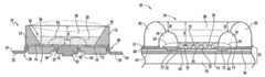
- FIGS. 1 and 2illustrate top and cross-sectional views of one example of a light emitter package or device, generally designated 10 .
- light emitter device 10can comprise a surface mount device (SMD) type of emitter device comprising a body 12 which can be molded or otherwise formed about components such as electrical leads.
- SMD type light emitter devicescan be suitable for general LED illumination applications, such as indoor and outdoor lighting, automotive lighting, and preferably suitable for high power and/or high brightness lighting applications.
- the subject matter disclosed hereincan be suitably adapted for application within a wide range of SMD type light emitter device designs, not limited to dimensional and/or material variations.
- devices and methods disclosed hereincan exhibit improved light output provided in part by provision of an additional clear layer of material deposited within a cavity of the SMD type device alone and/or in combination with increasing a depth of the cavity of the device for maximizing a distance between an LED chip and air interface.
- Such improvements in depth and the addition of one or more clear layerscan increase and maximize light extraction efficiency.
- Such improvementsare currently not employed in the art and actually conflict with conventional wisdom employed in conventional light emitter devices which focused on minimizing (e.g., decreasing) the distance between an LED chip and air interface and providing a single layer of encapsulant with or without phosphors or phosphoric material(s). Accordingly, light emitter devices and methods disclosed herein provide unexpected results such as improved light output when employed in device design and manufacture.
- body 12can be disposed about electrical leads or lead components comprising a thermal element 14 and one or more electrical elements, for example, first and second electrical elements 16 and 18 , respectively. That is, thermal element 14 and electrical elements 16 and 18 can be collectively referred to as a “leads” which can be singulated from a sheet of leadframes (not shown). A corner notch, generally designated N can be used for indicating electrical polarity of first and second electrical elements 16 and 18 .
- Thermal element 14 and first and second electrical elements 16 and 18can comprise a material that is electrically and/or thermally conductive such as a metal or metal alloy.
- thermal element 14can be electrically and/or thermally isolated from one and/or both of first and second electrical elements 16 and 18 by one or more isolating portions 20 of the body. Thermal element 14 can also be physically separated from electrical elements 16 and 18 by isolating portions 20 of the body.
- One or more LED chips 22can be mounted over thermal element 14 using any suitable die attach technique(s) and/or material(s), for example only and not limited to die attach adhesive (e.g., silicone, epoxy, or conductive silver (Ag) epoxy) or a metal-to-metal die attach technique such as flux or no-flux eutectic, non-eutectic, or thermal compression die attach.
- die attach adhesivee.g., silicone, epoxy, or conductive silver (Ag) epoxy
- metal-to-metal die attach techniquesuch as flux or no-flux eutectic, non-eutectic, or thermal compression die attach.
- LED chips 22can electrically communicate with one and/or both first and second electrical elements 16 and 18 by one or more electrical connectors such as electrically conductive wire bonds 24 .
- LED chips 22comprise a horizontal device having two electrical contacts (e.g., anode and cathode) on the same side (e.g., upper surface) are shown as electrically connected to two electrical elements (e.g., 16 and 18 ) via wire bonds 24 .
- LED chips 22 having one electrical contact on the upper surface that is electrically connected with a single electrical element 16 or 18is also contemplated.
- LED chips 22can comprise a horizontal device having both electrical contacts on the bottom surface, where one contact could be directly attached to first electrical element 16 and the second contact could be directly attached to second electrical element 18 .
- Any type, style, structure, build, size, and/or shape of LED chip 22can be used in devices described herein.
- LED chip 22can comprise a horizontally structured chip (e.g., having at least two electrical contacts on a same side of the LED) or a vertically structured chip (e.g., with electrical contacts on opposing sides of the LED) with or without a growth substrate.
- LED chip 22can comprise one or more substantially straight cut and/or beveled (i.e., angled) cut sides or surfaces.
- LED chip 22can comprise a direct attach build (e.g., bonded to a carrier substrate) or a build incorporating a grown substrate such as sapphire, SiC, or GaN.
- LED chips 22can be substantially square or rectangular in shape. LED chips 22 having any build, structure, type, style, shape, and/or dimension are contemplated herein.
- Wire bonds 24 or other electrical attachment connectors and related methodscan be adapted to communicate, transmit, or convey an electrical current or signal from electrical elements 16 and 18 to one or more LED chips 22 thereby causing illumination of the one or more LED chips 22 .
- Thermal element 14 and/or first and second electrical elements 16 and 18can be coated, plated, deposited, or otherwise layered with a reflective material ( FIG. 2 ), such as, for example and without limitation, Ag or a Ag-containing alloy for reflecting light from the one or more LED chips 22 .
- a reflective materialFIG. 2
- LED chips 22 as described hereincan embody a solid state emitter used alone and/or in combination with one or more phosphors or lumiphors to emit light of various colors, color points, or wavelength ranges.
- LED chips 22can comprise chips selected from the following targeted wavelength bins: (1) primarily blue wavelengths (preferably approximately 430 nm to 480 nm; optionally 430-475 nm, 440-475 nm, 450-475 nm, or any suitable sub-range of 430-480 nm); (2) primarily cyan wavelengths (preferably approximately 481 nm to 499 nm); (3) primarily green wavelengths (preferably approximately 500 nm to 570 nm, optionally 505-515 nm, 515-527 nm, or 527-535 nm, or 535-570 nm, or any suitable sub-range of 500-570 nm a or any suitable sub-range of 500-570 nm); (4) primarily yellow wavelengths (preferably approximately 571 to 590
- body 12can comprise any suitable material molded or otherwise disposed about thermal element 14 and/or first and second elements 16 and 18 , respectively.
- body 12can comprise a ceramic material such as a low temperature co-fired ceramic (LTCC) material, a high temperature co-fired ceramic (HTCC) material, alumina, aluminum nitride (AlN), aluminum oxide (Al 2 O 3 ), glass, and/or an Al panel material.
- body 12can comprise a molded plastic material such as polyamide (PA), polyphthalamide (PPA), liquid crystal polymer (LCP), or silicone.
- ESD protection devices 25can optionally be disposed within device 10 and can be electrically connected to electrical elements 16 and 18 and reverse biased with respect to LED chips 22 . Where used, ESD device 25 can protect against damage from ESD within device 10 .
- the arrangement of LED chips 22 and ESD protection device 25allows excessive voltage and/or current passing through light emitter device 10 from an ESD event to pass through protection device 25 instead of LED chips 22 thereby protecting LED chips 22 from damage.
- different elementscan be used as ESD protection devices 25 such as various vertical silicon (Si) Zener diodes, different LEDs arranged reverse biased to LED chips 22 , surface mount varistors and lateral Si diodes.
- ESD device 25can comprise a vertically structured device having one electrical contact on the bottom and another electrical contact on the top; however, horizontally structured devices are also contemplated.
- Body 12 of device 10can comprise a cavity, generally designated 26 , for example, a reflector cavity optionally coated with a reflective material for reflecting light from the one or more LED chips 22 .
- device 10can comprise a light emission area comprising a space or cavity 26 in which one or more LED chips 22 can be disposed.
- a filling materialcan be at least partially disposed within the cavity 26 or space and over the one or more LED chips 22 .
- filling materialcan be dispensed to a level that is substantially flush with an upper surface of emitter device, or to any level below and/or above an upper surface of emitter device.
- Filling materialcan comprise a first discrete layer of filling material, such as an encapsulant layer 28 comprising one or more phosphors, lumiphors, and/or phosphoric or lumiphoric materials as denoted by the shaded or speckled appearance.
- the one or more phosphorscan be adapted to emit light of a desired wavelength when activated by light emitted from the one or more LED chips 22 .
- device 10can emit light having a desired wavelength or color point that can be a combination of light emitted from phosphors disposed in encapsulant layer 28 and from the light emitted from one or more LED chips 22 .
- At least some LED chips 22can be coated with or otherwise disposed to impinge light onto one or more phosphors disposed within encapsulant layer 28 .
- Encapsulant layer 28can be adapted to absorb at least some of the LED chip emissions and responsively emit light of a different wavelength.
- LED chip emissionscan be fully absorbed or only partially absorbed such that emissions from the resulting device include a combination of light from the LED chip 22 and light from one or more phosphors.
- at least one of the LED chips 22can comprise an LED that emits light in the blue wavelength spectrum, with a phosphor absorbing some of the blue light and re-emitting yellow light.
- the resulting LED chip 22 and phosphor combinationmay emit a combination of blue and yellow light appearing white or non-white.
- any commercially available yellow phosphorcan be used for white emitting LED chips 22 in devices described herein.
- at least one of the LED chips 22can comprise an LED that emits light in the blue wavelength spectrum and arranged to interact with other phosphors that absorb blue light and emit green light.
- Any commercially available green phosphorcan be used in devices described herein.
- LED chips 22 emitting red lightcan also be provided and used alone and/or in combination with other LED chips 22 for producing warm white light and can comprise LED structures and materials that permit emission of red light directly from the active region of the LED chip 22 (e.g., a phosphide-based active region).
- red emitting LED chips 22can comprise LEDs covered by a phosphor that absorbs the LED light and emits a red light which can combine with other emissions for achieving warm white light. Any combination of LED chip(s) 22 and phosphor(s) wavelength emissions can be used to achieve the desired aggregated spectral output. It is understood that light emitter packages 10 and 50 ( FIGS. 3-7 ) as described herein can include multiple LED chips 22 of the same and/or different colors, of which one or more may emit white light or near-white light.
- filling material disposed in light emitter device 10can further comprise a second discrete layer of filling material at least partially disposed above and/or below the phosphor containing encapsulant layer 28 .
- the second layer of filling materialcan comprise an optically clear layer 30 of material adapted to improve light output by increasing light extraction efficiency.
- addition of clear layer 30 within device 10improves the luminous flux by approximately 3% or more (e.g., see FIG. 8 ).
- addition of clear layer 30 within device 10improves the luminous flux by approximately 3% or more (e.g., see FIG. 8 ).
- a single clear layer 30can be disposed above a single encapsulant layer 28 as shown; however, more than one clear layer 30 and/or more than one encapsulant layer 28 are contemplated herein.
- Clear layer 30can comprise any suitable material that is optically clear and capable of molding and/or dispensing within the light emission area or cavity 26 .
- Clear layer 30can comprise a layer that does not contain phosphoric or lumiphoric materials.
- clear layer 30can comprise a layer of any suitable epoxy, silicone, or glass material.
- clear layer 30comprises a material having a refractive index (RI) between that of the air and the chip.
- RIrefractive index
- clear layer 30can comprise a low RI silicone material having a RI of approximately 1.4 or less.
- the RI of the silicone materialcan comprise any sub-range between approximately 1.0 and 1.4 such as 1.1 to 1.2; 1.2 to 1.3; and 1.3 to 1.4.
- clear layer 30can comprise a high RI silicone material having a RI of approximately 1.5 or more.
- the RI of clear layer 30 comprising a high RI silicone materialcan be any sub-range between approximately 1.5 and 2.0, for example such as: 1.5 to 1.6; 1.6 to 1.7; 1.7 to 1.8; 1.8 to 1.9; and 1.9 to 2.0. Silicone materials having a medium RI of approximately 1.4 to 1.5 are also contemplated herein.
- clear layer 30 and encapsulant layer 28can comprise the same material (e.g., both can comprise a high RI silicone, a low RI silicone, or a medium RI silicone), however, one difference being the addition of phosphor(s) to encapsulant layer 28 .
- clear layer 30 and encapsulant layer 28can comprise different materials, for example, clear layer 30 can comprise a high RI silicone and encapsulant layer 28 can comprise a low RI silicone or vice versa.
- Encapsulant layer 28 and clear layer 30can comprise any suitable material capable of being dispensed and/or molded.
- encapsulant layer 28can be directly disposed over a portion of the LED chips 22
- clear layercan be directly disposed over a portion of the LED chips 22 (e.g., see FIG. 6 ).
- Encapsulant layer 28 , clear layer 30 , and/or multiple discrete clear layers 30can be separately and sequentially dispensed directly over each other within cavity 26 of device 10 .
- clear layer 30alone can contribute to improved light output of light emitter device 10 by reducing the amount of reabsorbed internal reflections, thereby increasing the overall luminous output of the device.
- clear layer 30can be used in combination with an increase in the depth of cavity 26 to improve light output of light emitter device 10 .
- the depth of cavity 26can be increased to accommodate the additional clear layer 30 such that a distance d can be increased or maximized to increase light output.
- Distance dcan comprise a distance between the LED chip 22 and air interface. Distance d can be, but does not have to be, approximately the same for each of the plurality of LED chips 22 as the distances may vary due to process variability.
- distance dcan comprise an average distance (calculated by averaging distance d for each LED chip 22 ) between the plurality of LED chips 22 and the air interface.
- distance dcan be increased by increasing the design depth of cavity 26 , for example, by increasing a wall length of cavity 26 by approximately 0.2 mm to 1.5 mm.
- distance dcan be increased by downsetting the one or more LED chips 22 , for example, by attaching LED chips 22 to a surface on a plane disposed below a cavity floor 36 , such as over a downset thermal element 14 .
- addition of clear layer 30 within device 10can increase the distance d by approximately 0.2 mm (e.g., from 0.6 to 0.8 mm) thereby increasing brightness by approximately 1 to 3.5% (e.g., by approximately 1.5 to 4 lumens at 300 mA).
- distance dcan be increased to accommodate more than one clear layer 30 provided in device 10 (e.g., see FIGS. 5 to 7 ).
- Each additional clear layer 30can increase distance d between LED chip 22 and air interface by approximately 0.2 to 0.5 mm.
- distance dcan comprise approximately 0.5 to 2 mm.
- clear layer 30 , or multiple clear layers 30can comprise a substantially flat, non-domed layer that is not primarily useful in curving about chips to focus light. That is, clear layer 30 may not be useful for focusing light as conventional domed lenses, but can still improve light output by increasing light extraction efficiency, such as by reducing the amount or reabsorbed internal reflections and/or increasing distance d.
- thermal element 14 and first and second electrical elements 16 and 18can comprise an inner portion 32 and an outer portion 34 .
- inner portion 32 and outer portion 34can comprise electrically and/or thermally conductive materials.
- Outer portion 34may be applied such that it entirely surrounds inner portion 32 as shown, or in other aspects outer portion 34 can optionally plate, coat, or comprise a layer over a single surface or two or more surfaces of portion 32 .
- outer portion 34can for example comprise a highly reflective Ag substrate, substrate containing Ag, or layer of material such as Ag for maximizing light output from device 10 and for assisting in heat dissipation by conducting heat away from the one or more LED chips 22 .
- Outer portion 34can also comprise a substrate of Ag-containing alloy instead of pure Ag, and such alloy can contain other metals such as titanium (Ti) or nickel (Ni).
- Inner portion 32can for example comprise a metal or metal alloy such as copper (Cu) substrate or Cu-alloy substrate.
- an optional layer of material(not shown) can be disposed between inner portion 32 and outer portion 34 , such as a layer of Ni for providing a barrier between the Ag and Cu, thereby preventing defects caused by migratory Cu atoms, such as a defect commonly known as “red plague”.
- outer portion 34can be directly attached to and/or directly coat inner portion 32 .
- Outer portion 34can advantageously reflect light emitted from the one or more LED chips 22 thereby improving optical performance of device 10 .
- Thermal element 14 and electrical elements 16 and 18can be disposed along a floor 36 of cavity 26 such that respective upper surfaces of thermal and electrical elements can be disposed along the same plane and/or different planes.
- upper surfaces of thermal element 14 and electrical elements 16 and 18are disposed along the same plane which is also the plane of floor 36 .
- thermal element 14can be downset such that an upper surface of thermal element 14 can be disposed below floor 36 such that it is below the plane of respective upper surfaces of each electrical element 16 and 18 . That is, thermal element 14 can be downset such that it is disposed on a lower plane than electrical elements 16 and 18 such that thermal element 14 appears sunken in respect to electrical elements 16 and 18 .
- First and second electrical elements 16 and 18can extend internally through body 12 and externally from one or more lateral sides of body 12 and form one or more external tab portions, generally designated 38 and 40 .
- Tab portions 38 and 40can bend to form one or more lower mounting surfaces such that device 10 can be mounted to an underlying substrate.
- Tab portions 38 and 40can outwardly bend away from each other or inwardly bend towards each other thereby adapting either a J-bend or gull-wing orientation as known in the art.
- any configuration of external tabs 38 and 40is contemplated.
- clear layer 30(and/or encapsulant layer 28 depending upon which layer is on top) can be partially disposed below and/or above an upper surface 42 of device 10 .
- filling materialcan comprise clear layer 30 disposed above encapsulant layer 28 where clear layer is filled to a level that is substantially flush with upper surface 42 of device as shown.
- filling materialcan comprise encapsulant layer 28 disposed above clear layer 30 where encapsulant layer is filled to a level that is substantially flush with upper surface 42 of device.
- the top layer(e.g., either clear or encapsulant layer 30 or 28 ) can be filled such that it forms a concave or convex surface with respect to upper surface 42 of device 10 as indicated by the dotted lines.
- One or more clear layers 30can be at least partially disposed below upper surface 42 of device.
- one or more clear layers 30can be entirely disposed below upper surface 42 of device.
- encapsulant layer 28 and clear layer 30can be adapted for dispensing within cavity 26 . Such layers 28 and 30 can be dispensed such that they are substantially flat and adjacent each other. That is, encapsulant layer 28 can be disposed adjacent one or more other phosphor containing layers and/or adjacent one or more clear layers.
- encapsulant layer 28can be disposed between multiple substantially flat and non-domed clear layers 30 .
- a single clear layer 30can also be disposed adjacent and/or between one or more additional, substantially flat clear layers 30 .
- encapsulant layer 28can comprise a selective amount of one or more phosphors adapted to emit light or combinations of light providing device 10 having a desired color point or color temperature.
- a volume of cavity 26can be at least approximately 25% filled with encapsulant layer 28 and at least approximately 25% filled with clear layer 30 .
- at least approximately 25% of a total cavity volumecan be filled with encapsulant layer 28 and at least approximately 75% of the total cavity volume can be filled with clear layer 30 such that approximately 100% of the total cavity volume is filled (i.e., dispensed) to a level that is approximately flush with upper surface 42 of device 10 .
- the volume of cavity 26can be approximately 50% filled with encapsulant layer 28 and approximately 50% filled with clear layer 30 , such that approximately 100% of the cavity is filled approximately flush with upper surface 42 of device 10 .
- the volume of cavity 26can be approximately 75% filled with encapsulant layer 28 and approximately 25% filled with clear layer 30 , such that approximately 100% of the total cavity volume is filled approximately flush with upper surface 42 of device 10 .
- the volume of cavity 26can be filled to any desired percentage (e.g., over-filled above upper surface 42 beyond 100% or under-filled below upper surface 42 and below 100%) and any combination or variation of volumetric percentages between encapsulant layer 28 and clear layer 30 within cavity 26 is contemplated herein.
- encapsulant layer 28 and clear layer 30can comprise approximately the same thickness, in other aspects, one of encapsulant layer 28 or clear layer 30 can be thicker than the other layer.
- encapsulant layer 28 and clear layer 30can each comprise approximately 0.4 mm, and each subsequent layer (where used, see e.g., FIGS. 5-7 ) can comprise approximately 0.2 to 0.3 mm in thickness.
- a device having just encapsulant layer 28can comprise a distance d of approximately 0.4 mm while a device as described herein having three clear layers (e.g., FIG. 7 ) can comprise a distance d of approximately 0.5 to 2 mm including any sub range thereof such as 0.5 to 1 mm; 1 to 1.2 mm; 1.2 to 01.4 mm; 1.4 to 1.5 mm; 1.5 to 2 mm, and in some instances, greater than 2 mm.
- encapsulant layer 28can completely cover wirebonds 24 , while in other aspects, wire bonds 24 can be completely covered by clear layer 30 . In yet further aspects, wire bonds 24 are completely covered by a combination of encapsulant layer 28 and clear layer 30 .
- a first layere.g., either encapsulant layer 28 or clear layer 30
- the second layere.g., the remaining encapsulant layer 28 or clear layer 30
- encapsulant layer 28 and clear layer 30can be sequentially dispensed within cavity 26 such that they are directly adjacent each other and can be cured at the same time. That is, multiple dispense and multiple curing steps (i.e., separately dispensing and curing of encapsulant layer 28 and clear layer 30 ) are contemplated herein, or multiple dispense and one curing step (i.e., separately dispensing and simultaneous curing of encapsulant layer 28 and clear layer 30 ) are contemplated herein.
- the various devices shown and described hereincan comprise an additional, discrete clear layer 30 that is physically separate from a phosphor containing encapsulant layer 28 for improving light output by increasing efficiency of light extraction. Devices can also advantageously provide an improved and increased distance d between the LED chip 22 and air interface for improving light output, as maximizing this distance can further increase light extraction efficiency.
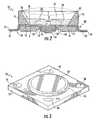
- FIGS. 3 and 4illustrate top perspective and cross-sectional views of another embodiment of a light emitter package or device, generally designated 50 .
- Light emitter device 50can also incorporate an optically clear layer 30 ( FIG. 4 ) that is physically separate or discrete from a phosphor containing encapsulant layer 28 .
- Clear layer 30can increase light extraction efficiency in part by reducing the amount or reabsorbed internal reflections, thereby improving light output of device 50 .
- Light emitter device 50can comprise an SMD type device, similar to device 10 .
- Light emitter device 50can comprise a submount 52 over which an emission area, generally designated 54 , can be disposed.
- a light emission area 54can comprise a cavity or space in which one or more LED chips 22 can be disposed under a first layer of filling material, such as an encapsulant layer 28 (see FIG. 4 ).
- LED chips 22can comprise a plurality of chips adapted to emit the same color or targeted wavelength of lights, or at least one of the plurality of LED chips 22 can be adapted to emit light that is a different color (e.g., from a different targeted wavelength bin) than a second LED of the plurality of LED chips 22 .
- a single LED chip 22is contemplated for use in emitter devices described herein.
- LED chips 22can be configured to emit light having wavelengths in the visible spectrum portion of the electromagnetic spectrum in any of the previously described colors and/or wavelength ranges.
- encapsulant layer 28can comprise phosphors adapted to emit light in any color, for example, yellow, green, and/or red when activated by emissions from the one or more LED chips 22 . Any combination of LED chip 22 and phosphor colors or targeted wavelength ranges are contemplated herein for producing white light, cool white light, and/or warm white light.
- emission area 54can be substantially centrally disposed with respect to submount 52 of light emitter device 50 .
- emission area 54can be disposed at any location over light emitter device 50 , for example, in a corner or adjacent an edge. Any location is contemplated, and more than one emission area 54 is also contemplated.
- a single, circular emission area 54is shown; however, the number, size, shape, and/or location of emission area 54 can change subject to the discretion of light emitter device consumers, manufacturers, and/or designers.
- Emission area 54can comprise any suitable shape such as a substantially circular, square, oval, rectangular, diamond, irregular, regular, or asymmetrical shape.
- Light emitter device 50can further comprise a retention material 56 at least partially disposed about emission area 54 where retention material 56 can be referred to as a dam.
- Retention material 56can comprise any material such as a silicone, ceramic, thermoplastic, and/or thermosetting polymer material.
- retention material 56is adapted for dispensing about emission area 54 , which can be advantageous as it is easy to apply and easy to obtain any desired size and/or shape.
- Submount 52can comprise any suitable mounting substrate, for example, a printed circuit board (PCB), a metal core printed circuit board (MCPCB), an external circuit, a dielectric laminate panel, a ceramic panel, an Al panel, AlN, Al 2 O 3 , or any other suitable substrate over which lighting devices such as LED chips may mount and/or attach.
- LED chips 22 disposed in emission area 54can electrically and/or thermally communicate with electrical elements disposed with submount 52 , for example, electrically conductive traces (e.g., 64 , 66 of FIG. 4 ).
- Emission area 54can comprise a single and/or a plurality of LED chips 22 disposed within and/or below encapsulant layer 28 such as illustrated in FIG. 4 .
- emission area 54 of light emitter device 50can further comprise a second layer of filling material at least partially disposed above and/or below the phosphor containing encapsulant layer 28 .
- the second layer of filling materialcan comprise an optically clear layer 30 ( FIG. 4 ) of material adapted to improve light output by increasing light extraction efficiency.
- LED chips 22can comprise any suitable size and/or shape of chip and can be vertically structured (e.g., electrical contacts on opposing sides) and/or horizontally structured (e.g., contacts on the same side or surface).
- LED chips 22can be any style of chip for example, straight cut and/or bevel cut chips, a sapphire, SiC, or GaN growth substrate or no substrate.
- One or more LED chips 22can form a multi-chip array of LED chips 22 electrically connected to each other and/or electrically conductive traces in combinations of series and parallel configurations.
- LED chips 22can be arranged in one or more strings of LEDs, where each string can comprise more than one LED electrically connected in series. Strings of LED chips 22 can be electrically connected in parallel to other strings of LED chips 22 . Strings of LED chips 22 can be arranged in one or more pattern (not shown). LED chips 22 can be electrically connected to other LEDs in series, parallel, and/or combinations of series and parallel arrangements depending upon the application.
- light emitter device 50can further comprise at least one opening or hole, generally designated 58 , that can be disposed through or at least partially through submount 52 for facilitating attachment of light emitter device 50 to an external substrate, circuit, or surface.
- at least one holecan be disposed through or at least partially through submount 52 for facilitating attachment of light emitter device 50 to an external substrate, circuit, or surface.
- one or more screwscan be inserted through the at least one hole 58 for securing device 50 to another member, structure, or substrate.
- Light emitter device 50can also comprise one or more electrical attachment surfaces 60 .
- attachment surfaces 60comprise electrical contacts such as solder contacts or connectors.
- Attachment surfaces 60can be any suitable configuration, size, shape and/or location and can comprise positive and negative electrode terminals, denoted by the “+” and/or “ ⁇ ” signs on respective sides of device 50 , through which an electrical current or signal can pass when connected to an external power source.
- attachment surfaces 60can comprise devices configured to clamp, crimp, or otherwise attach to external wires (not shown). Electrical current or signal can pass into light emitter device 50 from the external wires electrically connected to device 50 at the attachment surfaces 60 . Electrical current can flow into the emission area 54 to facilitate light output from the LED chips 22 disposed therein ( FIG. 4 ). Attachment surfaces 60 can electrically communicate with LED chips 22 of emission area 54 via conductive traces 64 and 66 ( FIG. 4 ).
- attachment surfaces 60can comprise a same layer of material as first and second conductive traces 64 and 66 ( FIG. 4 ) and therefore can electrically communicate to LED chips 22 attached to traces 64 and 66 via electrical connectors such as wire bonds 24 .
- Electrical connectorscan comprise wire bonds 24 or other suitable members for electrically connecting LED chips 22 to first and second conductive traces 64 and 66 ( FIG. 4 ).
- LED chips 22FIG. 4
- LED chips 22can comprise horizontally structured devices having both electrical contacts (e.g., anode and cathode) on the same top surface of respective LED chip 22 such that the contacts (e.g., bond pads) can electrically connect with traces (e.g., 64 and 66 , FIG.
- LED chips 22can comprise horizontal devices having both electrical contacts (e.g., anode and cathode) on a bottom surface such that wire bonds 24 are unnecessary. In further aspects, LED chips 22 can comprise vertical devices having electrical contacts on opposing sides such that one wire bond 24 is needed. Any type or structure of LED chip 22 is contemplated herein.
- a first layer of filling materialcan comprise a phosphor containing encapsulant layer 28 that can be disposed between inner walls of retention material 56 .
- Encapsulant layer 28can comprise a predetermined, or selective, amount of one or more phosphors and/or lumiphors in an amount suitable for any desired light emission, for example, suitable for white light conversion or any given color temperature or color point.
- Encapsulant layer 28can comprise a silicone encapsulant material, such as a low RI, high RI, or medium RI silicone material having the one or more phosphors disposed therein.
- Encapsulant layer 28can interact with light emitted from the plurality of LED chips 22 such that a perceived white light, or any suitable and/or desirable wavelength of light, can be observed. Any suitable combination of encapsulant and/or phosphors can be used, and combinations of differently colored phosphors and/or LED chips 22 can be used for producing any desired color points(s) of light.
- Retention material 56can be adapted for dispensing, positioning, damming, or placing, about at least a portion of emission area 54 .
- light emitter device 50can further comprise a second layer of filling material at least partially disposed above and/or below the phosphor containing encapsulant layer 28 .
- the second layer of filling materialcan comprise a discrete layer of the previously described optically clear layer 30 of material adapted to improve light output by increasing light extraction efficiency.
- the addition of clear layer 30 within device 50can improve the luminous flux by approximately 3% and in some cases by more than 5% (e.g., see FIG. 8 ).
- a single clear layer 30can be disposed above a single encapsulant layer 28 as shown, however, more than one clear layer 30 (e.g. FIGS. 5-7 ) and/or more than one encapsulant layer 28 are contemplated herein.
- Clear layer 30can comprise any suitable material that is optically clear and capable of molding and/or dispensing within cavity 26 .
- Clear layer 30can comprise a layer that does not contain phosphoric or lumiphoric materials and can, but does not have to, comprise the same material as encapsulant layer 28 without the phosphoric or lumiphoric materials.
- clear layer 30can comprise a layer of any suitable epoxy, silicone, or glass material.
- clear layer 30comprises a material having a refractive index (RI) between that of the air and the chip.
- RIrefractive index
- clear layer 30can comprise a low RI silicone material having a RI of approximately 1.4 or less.
- the RI of the silicone materialcan comprise any sub-range between approximately 1.0 and 1.4 such as 1.1 to 1.2; 1.2 to 1.3; and 1.3 to 1.4.
- clear layer 30can comprise a high RI silicone material having a RI of approximately 1.5 or more. That is, the RI of clear layer 30 comprising a high RI silicone material can comprise any sub-range between approximately 1.5 and 2.0, for example such as: 1.5 to 1.6; 1.6 to 1.7; 1.7 to 1.8; 1.8 to 1.9; and 1.9 to 2.0. Silicone materials having a medium RI of approximately 1.4 to 1.5 are also contemplated herein.
- clear layer 30alone can contribute to improved light output of light emitter device 10 by reducing the amount of reabsorbed internal reflections, thereby increasing the overall luminous output of the device.
- clear layer 30can be used in combination with an increase in the depth of emission area 54 to improve light output of light emitter device 50 .
- the depth of emission area 54can be increased to accommodate the additional clear layer 30 such that a distance d can be increased or maximized to increase light output.
- Distance dcan be a distance between the LED chip 22 and air interface.
- distance dcan be increased by increasing the height of retention material 56 .
- distance dcan be increased by incorporating a secondary dam structure (e.g., 82 , FIG.
- distance dcan be increased to accommodate more than one clear layer 30 provided in device 50 (e.g., see FIGS. 5 to 7 ). Each additional clear layer 30 can increase distance d between LED chip 22 and air interface for example by approximately 0.2 to 0.5 mm. In one aspect, distance d can comprise a total distance between approximately 0.5 and 2 mm.
- encapsulant layer 28 and clear layer 30can be selectively filled to any suitable level within the space disposed between one or more inner walls of retention material 56 .
- Different percentages and/or volumes of encapsulant layer 28 and clear layer 30can be deposited within emission area 54 of emitter device 50 .
- the volume of emission area 54can be at least approximately 25% filled with encapsulant layer 28 and at least approximately 25% filled with clear layer 30 .
- At least approximately 25% of a cavity volumecan be filled with encapsulant layer 28 and at least approximately 75% of the cavity volume can be filled with clear layer 30 such that approximately 100% of the emission area 54 can be filled (i.e., dispensed) to a level that is approximately flush with upper surface of device 50 (e.g., approximately flush with an upper surface of retention material 56 ).
- the volume of emission area 54can be approximately 50% filled with encapsulant layer 28 and approximately 50% filled with clear layer 30 , such that approximately 100% of the emission area 54 is filled approximately flush with the upper surface of retention material 56 .
- the volume of emission area 54can be approximately 75% filled with encapsulant layer 28 and approximately 25% filled with clear layer 30 , such that approximately 100% of the emission area 54 is filled approximately flush with upper surface of retention material 56 .
- Any volume of emission area 54can be filled to any percentage level (e.g., over-filled above upper surface of retention material 56 beyond 100% or under-filled below upper surface of retention material 56 and below 100%) and any combination or variation of volumetric percentages of encapsulant layer 28 and clear layer 30 is contemplated herein.
- filling materialcan be over-filled and/or under-filled resulting in concave and/or convex surfaces between walls of retention material 56 .
- encapsulant layer 28can comprise a thickness within the cavity of between approximately 0 and 2 mm alone and/or in combination with clear layer 30 which can also comprise a thickness within the cavity of between approximately 0 and 2 mm.
- encapsulant layer 28can completely cover wirebonds 24 , while in other aspects wire bonds 24 can be completely covered by clear layer 30 .
- wire bonds 24can be covered by a combination of encapsulant layer 28 and clear layer 30 .
- a first layere.g., either encapsulant layer 28 or clear layer 30
- the second layere.g., the remaining encapsulant layer 28 or clear layer 30
- encapsulant layer 28 and clear layer 30can be sequentially dispensed in emission area 54 and cured at the same time.
- multiple dispense and multiple curing stepsi.e., separately dispensing and curing of encapsulant layer 28 and clear layer 30
- multiple dispense and one curing stepi.e., separately dispensing and simultaneous curing of encapsulant layer 28 and clear layer 30
- the various devicescan comprise an additional, clear layer 30 that is physically separate from a phosphor containing encapsulant layer 28 for improving light output by increasing efficiency of light extraction.
- the devicescan also advantageously provide an improved and increased distance d between the LED chip 22 and air interface for improving light output, as maximizing this distance can further increase light extraction efficiency.
- FIG. 4further illustrates retention material 56 dispensed or otherwise placed over submount 52 after wire bonding the one or more LED chips 22 such that retention material 56 is disposed over and at least partially covers at least a portion of the wire bonds 24 .
- wire bonds 24 of the outermost edge LEDs in a given set or string of LED chips 22can be disposed within retention material 14 .
- only four LED chips 22are illustrated and are shown as electrically connected in series via wire bonds 24 , however, many strings of LED chips 22 of any number can be used, for example, less than four or more than four LED chips 22 can be electrically connected in series, parallel, and/or combinations of series and parallel arrangements.
- Strings of LED chips 22can comprise diodes of the same and/or different colors, or wavelength bins, and different colors of phosphors can be used in the encapsulant layer 28 disposed over LED chips 22 that are the same or different colors in order to achieve emitted light of a desired color temperature or color point.
- LED chips 22can attach to a conductive pad 70 or intervening layers (e.g., layer 68 described below) disposed between LED chip 22 and conductive pad 70 using any die attach technique or materials as known in art and mentioned above, for example adhesive attach, metal or silicone epoxy attach, solder attach, flux-attach, or direct metal-to-metal die attach techniques and materials as known in the art.
- LED chips 22can be arranged, disposed, or mounted over an electrically and/or thermally conductive pad 70 .
- Conductive pad 70can be electrically and/or thermally conductive and can comprise any suitable electrically and/or thermally conducting material.
- conductive pad 70can comprise a layer of Cu or a Cu substrate.
- LED chips 22can be electrically connected to first and second conductive traces 64 and 66 via optional wire bonds 24 .
- One of first and second conductive traces 64 and 66can comprise an anode and the other a cathode.
- Conductive traces 64 and 66can also comprise a layer of electrically conductive Cu or Cu substrate.
- conductive pad 70 and traces 64 and 66can comprise the same Cu substrate from which traces 64 and 66 have been singulated or separated from pad 70 via etching or other removal method.
- an electrically insulating solder mask 72can be applied such that it is at least partially disposed between conductive pad 70 and respective conductive traces 64 and 66 .
- Solder mask 72can comprise a white material for reflecting light from light emitter device 50 .
- One or more layers of materialcan be disposed between LED chips 22 and conductive pad 70 .
- one or more layers of materialcan be disposed over conductive traces 64 and 66 .
- first intervening layer or substrate of material 68can be disposed between LED chips 22 and conductive pad 70 and disposed over traces 64 and 66 .
- First layer of material 68can comprise a layer of reflective Ag or Ag-alloy material for maximizing brightness of light emitted from light emitter device 50 . That is, first layer of material 68 can comprise a Ag or Ag-containing substrate adapted to increase brightness of device 50 .
- One or more additional layers of materialcan be disposed between first layer 68 and conductive pad 70 and/or first layer 68 and traces 64 and 66 , for example, a layer of Ni, can be disposed therebetween for providing a barrier between the Cu of pad and traces 70 , 64 , and 66 and the Ag of layer 68 .
- FIG. 4further illustrates a cross-section of submount 52 over which LED chips 22 can be mounted or otherwise arranged.
- Submount 52can comprise, for example, conductive pad 70 , first and second conductive traces 64 and 66 , and solder mask 72 at least partially disposed between conductive pad 70 and each of conductive traces 64 and/or 66 .
- Conductive traces 64 , 66 and conductive pad 70can be coated with a first layer 68 , for example a Ag or Ag-containing layer.
- Submount 52can further comprise a dielectric layer 74 , and a core layer 76 .
- solder mask 72can directly adhere to portions of dielectric layer 74 .
- submount 52can comprise a MCPCB, for example, those available and manufactured by The Bergquist Company of Chanhassan, Minn. Any suitable submount 52 can be used, however.
- Core layer 76can comprise a conductive metal layer, for example copper or aluminum.
- Dielectric layer 74can comprise an electrically insulating but thermally conductive material to assist with heat dissipation through submount 52 .
- FIGS. 5 to 7are cross-sections of light emitter device 50 which illustrate various locations, configurations, or arrangements of encapsulant layer 28 and clear layer 30 within emission area 54 .
- the arrangements of encapsulant layer 28 and clear layer 30 shown and described in FIGS. 5 to 7are equally applicable to device 10 ( FIGS. 1 and 2 ) as well as any other emitter devices or embodiments, such as SMD type devices, however, for illustration purposes only device 50 has been illustrated in such numerous embodiments.
- devices described hereincan incorporate one or more discrete optically clear layers of silicone, epoxy, or glass material for improving light output from such devices.
- device 50can comprise a filling material disposed within emission area 54 , where the filling material can comprise a phosphor containing encapsulant layer 28 and a first layer of optically clear material such as previously described clear layer 30 .
- Filling materialcan also comprise a second layer of optically clear filling material or second clear layer 80 such that filling material comprises three or more physically discrete or separate layers disposed within the walls of retention material 56 .
- Second clear layer 80can, but does not have to, comprise the same material as first layer 30 . That is, second clear layer 80 can comprise a layer of any suitable epoxy, silicone, or glass material.
- second clear layer 80can comprise a low RI silicone material having a RI of approximately 1.4 or less, a medium RI material having a RI of approximately 1.4 to 1.5, or a high RI silicone material having a RI of approximately 1.5 or more.
- Encapsulant layer 28can also comprise the same materials as first and second clear layers 30 and 80 , respectively, but can also include one or more phosphors as denoted by the shaded or speckled appearance.
- each of the layerscan comprise different materials, for example, a first layer can comprise a low RI encapsulant, a second layer can comprise a high RI silicone, and a third layer can comprise a medium RI silicone or an epoxy or glass material.
- tow of the layerscan comprise the same material and one of the layers can comprise a different material. Any arrangement of layers and/or materials is contemplated herein.
- Emission area 54can be filled to a level that is substantially flush with an upper surface of retention material 56 or over-filled or under-filled such that layers form a concave or convex surface.
- the height of retention material 56can be increased such that distance d between the LED chip 22 and air interface can be increased to accommodate more than one optically clear layer of material within emission area 54 .
- retention material 56can be increased between approximately 0.2 and 0.5 mm to accommodate each additional clear layer. That is, retention material 56 can be increased approximately 0.6 to 1.0 mm where two or more clear layers are provided in device 50 and retention material 56 can be increased approximately 0.9 to 1.5 mm where three or more clear layers are provided.
- any percentage of encapsulant layer 28 , clear layer 30 , and second layer 80can be deposited within a volume of emission area 54 .
- the volume of emission area 54can be approximately 33% filled with each layer.
- the volume of emission area 54can be approximately 20% filled with encapsulant layer 28 and approximately 40% filled with each of clear layer 30 and second clear layer 80 such that approximately 100% of the emission area is filled.
- the volume of emission area 54can be approximately 50% filled with encapsulant layer 28 and approximately 25% filled with each of clear layer 30 and second clear layer 80 such that approximately 100% of the emission area 54 is filled.
- the volume of emission area 54can be approximately 40% filled with encapsulant layer 28 and approximately 30% filled with each of clear layer 30 and second clear layer 80 such that approximately 100% of the emission area is filled.
- the clear layersdo not have to be equal in thickness and/or of the same volumetric percentage, for example, the volume of emission area 54 can be approximately 25% filled with encapsulant layer 28 , approximately 25% filled with clear layer 30 , and approximately 50% filled with second clear layer 80 .
- Layers 28 , 30 , and 80can occupy any percentage and/or volume of emission area 54 and can be deposited in any order within emission area.
- Layers 28 , 30 , and 80can be optionally cured during the same curing step, or each layer can be separately and optionally cured at different curing steps.
- FIG. 6illustrates an embodiment where phosphor containing encapsulant layer 28 is disposed between more than one optically clear layer of filling material.
- a first optically clear layer 30can be dispensed within emission area 54 first.
- clear layer 30can be dispensed such that it covers wire bonds 24 .
- Phosphor containing encapsulant layer 28can be arranged and subsequently dispensed such that it covers clear layer 30 .
- Second clear layer 80can be arranged and subsequently dispensed over encapsulant layer 28 such that encapsulant layer 28 is disposed between more than one clear layer. Any percentage of encapsulant layer 28 , clear layer 30 , and second layer 80 can be deposited within emission area 54 , such as percentages previously noted. Distance d can be increased to accommodate more than one clear layer of filling material, for example, by increasing the height of retention material 56 .
- FIG. 7illustrates an embodiment where a secondary dam member or material 82 can be used to increase the distance between the LED chip 22 and air interface.
- secondary dam 82can be dispensed or otherwise deposited or positioned along outer edges of retention material 56 such that the distance d between an LED chip 22 and air interface increases by a distance d 2 , which is the difference in height between secondary dam 82 and retention material 56 .
- distance d 2can comprise an increase in height of between approximately 0.2 and 0.5 mm for each additional clear layer to be used in device 50 .
- secondary dam 82can be adapted to increase distance d by a distance d 2 of approximately 0.6 to 1.0 mm where two or more clear layers are provided in device 50 and by a distance d 2 of approximately 0.9 to 1.5 mm where three or more clear layers are provided. That is, secondary dam 82 can be approximately 0.2 to 1.5 mm taller than retention material 56 .
- Encapsulant layer 28can be dispensed within retention are 54 first and optionally cured prior to deposition of one or more subsequent optically clear layers of material, or can be optionally cured at the same time as other discrete and subsequently applied layers in one curing step. At least one additional layer of optically clear filling material or clear layer 30 can be disposed above encapsulant layer 28 . As the broken lines indicate, more than one discrete layer of optically clear material can be applied to emission area 54 , for example, two or more clear layers can be applied.
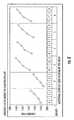
- FIG. 8is a graphical illustration of improved light output for devices disclosed herein which can incorporate one or more discrete clear layers of optical material in addition to a layer of phosphor containing encapsulant material.
- devices incorporating the one or more clear layers of materialcan comprise a larger distance d ( FIGS. 2 and 4-7 ) between an LED chip 22 and an air interface.
- six different variability charts representing six different groups of devices testedillustrate the improvement in light output when moving from zero clear layers (e.g., conventional packages identified as “0” in each of the six groups/charts) to three clear layers (e.g., identified as “3” in each of the six groups/charts).
- each additional clear layercan add between approximately 0.2 and 0.5 mm to the overall, total distance d between the LED chips 22 and air interface.
- the first two groupsinclude data obtained from using a low RI silicone in an initial layer (e.g., encapsulant layer 28 , FIGS. 2 and 4-7 ) and a low RI for subsequent dispenses of each of the one or more additional clear layers of material (e.g., clear layer 30 and/or 80 FIGS. 2 and 4-7 ).
- Groups numbered 3 through 6 and respective chartsinclude data obtained from using a high RI silicone in the initial layer (e.g., encapsulant layer 28 , FIGS. 2 and 4-7 ) and a low RI for subsequent dispenses of each of the one or more additional clear layers of material (e.g., clear layer 30 and/or 80 FIGS. 2 and 4-7 ).
- luminous flux, or brightnessincreases linearly as the number of clear layers used in the device increases, which also can correspond to an increased distance d ( FIGS. 2 and 4-7 ) between the LED chip 22 and air interface.
- light output of devices described hereincan increase by more than 3% when one or more clear layers are separately dispensed and/or discretely applied within the device.
- light outputcan increase by at least approximately 3.6% as illustrated by the groups 1 and 2, where three discrete clear layers improved the luminous flux from approximately 1100 lumens (lm) to approximately 1140 lm.
- each additional clear layerincreased light output by approximately 0.85 to 1.25%.
- Charts for groups 3 through 6indicate that packages using a high RI silicone in the initial encapsulant layer (e.g., layer 28 FIGS. 2, 4-7 ) can emit more light than packages using low RI silicone in the initial layer.
- Charts for groups 3 through 6illustrate light increases per package that are greater than approximately 4%, for example, greater than approximately 4.5% and greater than approximately 5% as light output increases from approximately 1120 lm to approximately 1180 lm.
- each additional clear layerincreased light output by approximately 0.75 to 1.75%.
- packages comprising one or more layers of optically clear materialcan for example comprise a light output of approximately 1150 to 1190 lm.
- packages comprising one layer of optically clear materialcan for example comprise a light output of between approximately 1150 and 1160 lm.
- packages comprising two layers of optically clear materialcan for example comprise a light output of between approximately 1160 and 1170 lm.
- Packages comprising three layers of optically clear materialcan for example comprise a light output of between approximately 1170 to 1190 lm.
- luminous fluxcan increase linearly, for example by approximately 1% or more, with an increasing distance between LED chips and an air interface (e.g., by increasing the number of clear layers), with gains in excess of 5% being demonstrated.
- the luminous flux values obtained for each variability chartcan be measured at 270 mA.
Landscapes
- Engineering & Computer Science (AREA)
- Power Engineering (AREA)
- Microelectronics & Electronic Packaging (AREA)
- Physics & Mathematics (AREA)
- Condensed Matter Physics & Semiconductors (AREA)
- General Physics & Mathematics (AREA)
- Computer Hardware Design (AREA)
- Led Device Packages (AREA)
Abstract
Description
Claims (42)
Priority Applications (1)
| Application Number | Priority Date | Filing Date | Title |
|---|---|---|---|
| US13/444,399US9343441B2 (en) | 2012-02-13 | 2012-04-11 | Light emitter devices having improved light output and related methods |
Applications Claiming Priority (3)
| Application Number | Priority Date | Filing Date | Title |
|---|---|---|---|
| US13/372,063US8957580B2 (en) | 2012-02-13 | 2012-02-13 | Lighting device including multiple wavelength conversion material layers |
| US13/372,076US8946747B2 (en) | 2012-02-13 | 2012-02-13 | Lighting device including multiple encapsulant material layers |
| US13/444,399US9343441B2 (en) | 2012-02-13 | 2012-04-11 | Light emitter devices having improved light output and related methods |
Related Parent Applications (1)
| Application Number | Title | Priority Date | Filing Date |
|---|---|---|---|
| US13/372,063Continuation-In-PartUS8957580B2 (en) | 2012-02-13 | 2012-02-13 | Lighting device including multiple wavelength conversion material layers |
Publications (2)
| Publication Number | Publication Date |
|---|---|
| US20130207130A1 US20130207130A1 (en) | 2013-08-15 |
| US9343441B2true US9343441B2 (en) | 2016-05-17 |
Family
ID=48944888
Family Applications (1)
| Application Number | Title | Priority Date | Filing Date |
|---|---|---|---|
| US13/444,399Active2034-01-18US9343441B2 (en) | 2012-02-13 | 2012-04-11 | Light emitter devices having improved light output and related methods |
Country Status (1)
| Country | Link |
|---|---|
| US (1) | US9343441B2 (en) |
Cited By (8)
| Publication number | Priority date | Publication date | Assignee | Title |
|---|---|---|---|---|
| US9496466B2 (en) | 2011-12-06 | 2016-11-15 | Cree, Inc. | Light emitter devices and methods, utilizing light emitting diodes (LEDs), for improved light extraction |
| US10008637B2 (en) | 2011-12-06 | 2018-06-26 | Cree, Inc. | Light emitter devices and methods with reduced dimensions and improved light output |
| US10211380B2 (en) | 2011-07-21 | 2019-02-19 | Cree, Inc. | Light emitting devices and components having improved chemical resistance and related methods |
| US10295157B2 (en)* | 2017-01-24 | 2019-05-21 | Lg Electronics Inc. | Mobile terminal |
| US10461225B2 (en)* | 2015-03-09 | 2019-10-29 | Toyoda Gosei Co., Ltd. | Method of manufacturing light-emitting device including sealing materials with phosphor particles |
| US10490712B2 (en) | 2011-07-21 | 2019-11-26 | Cree, Inc. | Light emitter device packages, components, and methods for improved chemical resistance and related methods |
| US10686107B2 (en) | 2011-07-21 | 2020-06-16 | Cree, Inc. | Light emitter devices and components with improved chemical resistance and related methods |
| US10824054B2 (en) | 2017-01-24 | 2020-11-03 | Lg Electronics Inc. | Mobile terminal |
Families Citing this family (31)
| Publication number | Priority date | Publication date | Assignee | Title |
|---|---|---|---|---|
| US8835952B2 (en)* | 2005-08-04 | 2014-09-16 | Cree, Inc. | Submounts for semiconductor light emitting devices and methods of forming packaged light emitting devices including dispensed encapsulants |
| US8564000B2 (en) | 2010-11-22 | 2013-10-22 | Cree, Inc. | Light emitting devices for light emitting diodes (LEDs) |
| US8575639B2 (en) | 2011-02-16 | 2013-11-05 | Cree, Inc. | Light emitting devices for light emitting diodes (LEDs) |
| US8624271B2 (en) | 2010-11-22 | 2014-01-07 | Cree, Inc. | Light emitting devices |
| US9300062B2 (en) | 2010-11-22 | 2016-03-29 | Cree, Inc. | Attachment devices and methods for light emitting devices |
| US9000470B2 (en) | 2010-11-22 | 2015-04-07 | Cree, Inc. | Light emitter devices |
| USD702653S1 (en) | 2011-10-26 | 2014-04-15 | Cree, Inc. | Light emitting device component |
| US8455908B2 (en) | 2011-02-16 | 2013-06-04 | Cree, Inc. | Light emitting devices |
| KR20140097284A (en) | 2011-11-07 | 2014-08-06 | 크리,인코포레이티드 | High voltage array light emitting diode(led) devices, fixtures and methods |
| US9240530B2 (en) | 2012-02-13 | 2016-01-19 | Cree, Inc. | Light emitter devices having improved chemical and physical resistance and related methods |
| US9735198B2 (en) | 2012-03-30 | 2017-08-15 | Cree, Inc. | Substrate based light emitter devices, components, and related methods |
| US10134961B2 (en) | 2012-03-30 | 2018-11-20 | Cree, Inc. | Submount based surface mount device (SMD) light emitter components and methods |
| JP6102273B2 (en)* | 2013-01-18 | 2017-03-29 | 日亜化学工業株式会社 | Light emitting device and manufacturing method thereof |
| USD740453S1 (en) | 2013-06-27 | 2015-10-06 | Cree, Inc. | Light emitter unit |
| USD739565S1 (en) | 2013-06-27 | 2015-09-22 | Cree, Inc. | Light emitter unit |
| JP6429621B2 (en)* | 2014-02-18 | 2018-11-28 | エイブリック株式会社 | Optical sensor device and method for manufacturing optical sensor device |
| US9680067B2 (en)* | 2014-03-18 | 2017-06-13 | GE Lighting Solutions, LLC | Heavily phosphor loaded LED packages having higher stability |
| WO2016194405A1 (en)* | 2015-05-29 | 2016-12-08 | シチズン電子株式会社 | Light emitting device and manufacturing method thereof |
| CN107615497B (en)* | 2015-05-29 | 2019-05-21 | 西铁城电子株式会社 | Light-emitting device and method of manufacturing the same |
| CN109642718B (en)* | 2016-01-28 | 2020-10-16 | 生态照明公司 | Illumination with Multi-Zone Fusion Cups |
| WO2017131693A1 (en) | 2016-01-28 | 2017-08-03 | Ecosense Lighting Inc | Compositions for led light conversions |
| US11047534B2 (en) | 2016-01-28 | 2021-06-29 | EcoSense Lighting, Inc. | Multizone mixing cup illumination system |
| US10512133B2 (en) | 2016-01-28 | 2019-12-17 | Ecosense Lighting Inc. | Methods of providing tunable warm white light |
| WO2017131697A1 (en) | 2016-01-28 | 2017-08-03 | Ecosense Lighting Inc | Systems for providing tunable white light with high color rendering |
| CN109315037B (en) | 2016-01-28 | 2022-07-01 | 生态照明公司 | System for providing tunable white light with high color rendering |
| US10197226B2 (en) | 2016-01-28 | 2019-02-05 | Ecosense Lighting Inc | Illuminating with a multizone mixing cup |
| JP6809098B2 (en)* | 2016-09-30 | 2021-01-06 | 日亜化学工業株式会社 | Manufacturing method of light emitting device |
| USD823492S1 (en) | 2016-10-04 | 2018-07-17 | Cree, Inc. | Light emitting device |
| US11793217B1 (en)* | 2016-10-04 | 2023-10-24 | Lonza Greenwood Llc | Method of manufacture and pasteurization of products containing undenatured collagen |
| CN109867257A (en)* | 2017-12-04 | 2019-06-11 | 讯芯电子科技(中山)有限公司 | Chip package and manufacturing method thereof |
| JP6665872B2 (en) | 2018-01-15 | 2020-03-13 | 日亜化学工業株式会社 | Light emitting device and method of manufacturing light emitting device |
Citations (176)
| Publication number | Priority date | Publication date | Assignee | Title |
|---|---|---|---|---|
| US3288728A (en) | 1966-02-18 | 1966-11-29 | Union Carbide Corp | Para-xylylene copolymers |
| US3875456A (en)* | 1972-04-04 | 1975-04-01 | Hitachi Ltd | Multi-color semiconductor lamp |
| JPS5867077A (en) | 1981-10-19 | 1983-04-21 | Toshiba Corp | Manufacture of lead frame for semiconductor device |
| USH445H (en) | 1985-11-29 | 1988-03-01 | American Telephone and Telegraph Company, AT&T Technologies, Incorporated | Method of forming light emitting device with direct contact lens |
| US4918497A (en) | 1988-12-14 | 1990-04-17 | Cree Research, Inc. | Blue light emitting diode formed in silicon carbide |
| US4946547A (en) | 1989-10-13 | 1990-08-07 | Cree Research, Inc. | Method of preparing silicon carbide surfaces for crystal growth |
| US4966862A (en) | 1989-08-28 | 1990-10-30 | Cree Research, Inc. | Method of production of light emitting diodes |
| US5027168A (en) | 1988-12-14 | 1991-06-25 | Cree Research, Inc. | Blue light emitting diode formed in silicon carbide |
| US5200022A (en) | 1990-10-03 | 1993-04-06 | Cree Research, Inc. | Method of improving mechanically prepared substrate surfaces of alpha silicon carbide for deposition of beta silicon carbide thereon and resulting product |
| US5210051A (en) | 1990-03-27 | 1993-05-11 | Cree Research, Inc. | High efficiency light emitting diodes from bipolar gallium nitride |
| US5338944A (en) | 1993-09-22 | 1994-08-16 | Cree Research, Inc. | Blue light-emitting diode with degenerate junction structure |
| US5359345A (en) | 1992-08-05 | 1994-10-25 | Cree Research, Inc. | Shuttered and cycled light emitting diode display and method of producing the same |
| USRE34861E (en) | 1987-10-26 | 1995-02-14 | North Carolina State University | Sublimation of silicon carbide to produce large, device quality single crystals of silicon carbide |
| US5393993A (en) | 1993-12-13 | 1995-02-28 | Cree Research, Inc. | Buffer structure between silicon carbide and gallium nitride and resulting semiconductor devices |
| US5416342A (en) | 1993-06-23 | 1995-05-16 | Cree Research, Inc. | Blue light-emitting diode with high external quantum efficiency |
| US5523589A (en) | 1994-09-20 | 1996-06-04 | Cree Research, Inc. | Vertical geometry light emitting diode with group III nitride active layer and extended lifetime |
| US5604135A (en) | 1994-08-12 | 1997-02-18 | Cree Research, Inc. | Method of forming green light emitting diode in silicon carbide |
| US5631190A (en) | 1994-10-07 | 1997-05-20 | Cree Research, Inc. | Method for producing high efficiency light-emitting diodes and resulting diode structures |
| US5739554A (en) | 1995-05-08 | 1998-04-14 | Cree Research, Inc. | Double heterojunction light emitting diode with gallium nitride active layer |
| US5959316A (en) | 1998-09-01 | 1999-09-28 | Hewlett-Packard Company | Multiple encapsulation of phosphor-LED devices |
| US6121637A (en) | 1997-10-03 | 2000-09-19 | Rohm Co., Ltd. | Semiconductor light emitting device with increased luminous power |
| US6187606B1 (en) | 1997-10-07 | 2001-02-13 | Cree, Inc. | Group III nitride photonic devices on silicon carbide substrates with conductive buffer interlayer structure |
| US6252254B1 (en) | 1998-02-06 | 2001-06-26 | General Electric Company | Light emitting device with phosphor composition |
| JP2001291406A (en) | 2000-04-07 | 2001-10-19 | Yamada Shomei Kk | Lighting |
| US20020004577A1 (en) | 1996-07-10 | 2002-01-10 | International Business Machines Corporation | Siloxane and siloxane derivatives as encapsulants for organic light emitting devices |
| US6350041B1 (en) | 1999-12-03 | 2002-02-26 | Cree Lighting Company | High output radial dispersing lamp using a solid state light source |
| US20030067761A1 (en) | 2001-10-09 | 2003-04-10 | Citizen Electronics Co., Ltd. | Edge light for a lighting panel |
| US6576930B2 (en) | 1996-06-26 | 2003-06-10 | Osram Opto Semiconductors Gmbh | Light-radiating semiconductor component with a luminescence conversion element |
| US6600175B1 (en) | 1996-03-26 | 2003-07-29 | Advanced Technology Materials, Inc. | Solid state white light emitter and display using same |
| JP2003243704A (en) | 2002-02-07 | 2003-08-29 | Lumileds Lighting Us Llc | Light emitting semiconductor device and method |
| US6717353B1 (en) | 2002-10-14 | 2004-04-06 | Lumileds Lighting U.S., Llc | Phosphor converted light emitting device |
| US20040069993A1 (en) | 2001-06-11 | 2004-04-15 | Citizen Electronics Co., Ltd. | Light emitting device and manufacturing method thereof |
| US20040079957A1 (en) | 2002-09-04 | 2004-04-29 | Andrews Peter Scott | Power surface mount light emitting die package |
| WO2004077580A2 (en) | 2003-02-26 | 2004-09-10 | Cree, Inc. | White light source using emitting diode and phosphor and method of fabrication |
| US6791119B2 (en) | 2001-02-01 | 2004-09-14 | Cree, Inc. | Light emitting diodes including modifications for light extraction |
| US6853010B2 (en) | 2002-09-19 | 2005-02-08 | Cree, Inc. | Phosphor-coated light emitting diodes including tapered sidewalls, and fabrication methods therefor |
| US6860621B2 (en) | 2000-07-10 | 2005-03-01 | Osram Opto Semiconductors Gmbh | LED module and methods for producing and using the module |
| US20050045898A1 (en) | 2003-09-03 | 2005-03-03 | Charles Leu | Light-emitting diode and backlight system using the same |
| EP1536487A1 (en) | 2002-05-28 | 2005-06-01 | Matsushita Electric Works, Ltd. | Light emitting element, light emitting device and surface emission illuminating device using it |
| US20050159581A1 (en) | 2003-10-22 | 2005-07-21 | Dirk Vanderzande | Method of preparing derivatives of polyarylene vinylene and method of preparing an electronic device including same |
| US6936857B2 (en) | 2003-02-18 | 2005-08-30 | Gelcore, Llc | White light LED device |
| JP2005244226A (en) | 2004-02-23 | 2005-09-08 | Lumileds Lighting Us Llc | Wavelength conversion type semiconductor light emitting device |
| US20050224830A1 (en) | 2004-04-09 | 2005-10-13 | Blonder Greg E | Illumination devices comprising white light emitting diodes and diode arrays and method and apparatus for making them |
| US6958497B2 (en) | 2001-05-30 | 2005-10-25 | Cree, Inc. | Group III nitride based light emitting diode structures with a quantum well and superlattice, group III nitride based quantum well structures and group III nitride based superlattice structures |
| JP2006054209A (en) | 2003-09-30 | 2006-02-23 | Toyoda Gosei Co Ltd | Light emitting device |
| US7005679B2 (en)* | 2003-05-01 | 2006-02-28 | Cree, Inc. | Multiple component solid state white light |
| US20060091415A1 (en) | 2004-10-29 | 2006-05-04 | Ledengin, Inc. (Cayman) | LED package with structure and materials for high heat dissipation |
| US20060124953A1 (en) | 2004-12-14 | 2006-06-15 | Negley Gerald H | Semiconductor light emitting device mounting substrates and packages including cavities and cover plates, and methods of packaging same |
| US20060145172A1 (en) | 2004-12-30 | 2006-07-06 | Jung-Chieh Su | Light emitting diode with a quasi-omnidirectional reflector |
| US20060163589A1 (en) | 2005-01-21 | 2006-07-27 | Zhaoyang Fan | Heterogeneous integrated high voltage DC/AC light emitter |
| US7087936B2 (en) | 2003-04-30 | 2006-08-08 | Cree, Inc. | Methods of forming light-emitting devices having an antireflective layer that has a graded index of refraction |
| US20060181866A1 (en) | 2005-02-16 | 2006-08-17 | Samsung Electronics Co., Ltd. | Multi-chip light emitting diode unit, and backlight unit and liquid crystal display device employing the same |
| US7095056B2 (en) | 2003-12-10 | 2006-08-22 | Sensor Electronic Technology, Inc. | White light emitting device and method |
| US20060186418A1 (en) | 2004-05-18 | 2006-08-24 | Edmond John A | External extraction light emitting diode based upon crystallographic faceted surfaces |
| JP2006245443A (en) | 2005-03-07 | 2006-09-14 | Citizen Electronics Co Ltd | Light emitting device and lighting device |
| US20060221272A1 (en) | 2005-04-04 | 2006-10-05 | Negley Gerald H | Light emitting diode backlighting systems and methods that use more colors than display picture elements |
| US20060226759A1 (en)* | 2005-03-06 | 2006-10-12 | Sharp Kabushiki Kaisha | Light emitting device and fabricating method thereof |
| US20070012940A1 (en)* | 2005-07-14 | 2007-01-18 | Samsung Electro-Mechanics Co., Ltd. | Wavelength-convertible light emitting diode package |
| US7183577B2 (en) | 1999-09-27 | 2007-02-27 | Philips Lumileds Lighting Company, Llc | Thin film phosphor-converted light emitting diode device |
| KR100705552B1 (en) | 2006-06-30 | 2007-04-09 | 서울반도체 주식회사 | Light emitting diode |
| US20070090383A1 (en) | 2000-12-28 | 2007-04-26 | Toyoda Gosei Co., Ltd. | Light emitting device |
| US7211835B2 (en) | 2003-07-09 | 2007-05-01 | Nichia Corporation | Light emitting device, method of manufacturing the same and lighting equipment |
| US7213940B1 (en) | 2005-12-21 | 2007-05-08 | Led Lighting Fixtures, Inc. | Lighting device and lighting method |
| US20070139923A1 (en) | 2005-12-21 | 2007-06-21 | Led Lighting Fixtures, Inc. | Lighting device |
| US20070158668A1 (en) | 2005-08-25 | 2007-07-12 | Cree, Inc. | Close loop electrophoretic deposition of semiconductor devices |
| US7246930B2 (en) | 2003-09-17 | 2007-07-24 | Stanley Electric Co., Ltd. | Light source and vehicle lamp |
| US20070170447A1 (en) | 2006-01-20 | 2007-07-26 | Led Lighting Fixtures, Inc. | Shifting spectral content in solid state light emitters by spatially separating lumiphor films |
| KR20070084959A (en) | 2006-02-22 | 2007-08-27 | 삼성전기주식회사 | LED Package |
| US20070223219A1 (en) | 2005-01-10 | 2007-09-27 | Cree, Inc. | Multi-chip light emitting device lamps for providing high-cri warm white light and light fixtures including the same |
| US20070228387A1 (en) | 2006-04-04 | 2007-10-04 | Gerald Negley | Uniform emission LED package |
| KR20070100124A (en) | 2006-04-05 | 2007-10-10 | 샤프 가부시키가이샤 | Semiconductor light emitting device |
| JP2007266343A (en) | 2006-03-29 | 2007-10-11 | Toyoda Gosei Co Ltd | Light emitting device |
| US20070253209A1 (en) | 2006-04-27 | 2007-11-01 | Cree, Inc. | Submounts for semiconductor light emitting device packages and semiconductor light emitting device packages including the same |
| US20070268694A1 (en) | 2006-04-18 | 2007-11-22 | Lamina Ceramics, Inc. | Optical devices for controlled color mixing |
| US7304326B2 (en)* | 2004-02-06 | 2007-12-04 | Toyoda Gosei Co., Ltd. | Light emitting device and sealing material |
| US20080012036A1 (en) | 2006-07-13 | 2008-01-17 | Loh Ban P | Leadframe-based packages for solid state light emitting devices and methods of forming leadframe-based packages for solid state light emitting devices |
| US7344902B2 (en) | 2004-11-15 | 2008-03-18 | Philips Lumileds Lighting Company, Llc | Overmolded lens over LED die |
| US20080081065A1 (en) | 2002-03-22 | 2008-04-03 | Govermment of the United States of America, represente by the Secretary, Department of Health | Materials and methods for inhibiting wip1 |
| US20080080165A1 (en) | 2006-10-02 | 2008-04-03 | Samsung Electro-Mechanics Co. Ltd. | Surface light source device using light emitting diodes |
| TW200821371A (en) | 2006-08-22 | 2008-05-16 | Mitsubishi Chem Corp | Semiconductor device member, liquid for forming semiconductor device member, method for manufacturing semiconductor device member, and liquid for forming semiconductor device member using the method, phosphor composition, semiconductor light emitting |
| US20080121921A1 (en) | 2006-07-13 | 2008-05-29 | Cree, Inc. | Leadframe-based packages for solid state light emitting devices and methods of forming leadframe-based packages for solid state light emitting devices |
| US20080173884A1 (en) | 2007-01-22 | 2008-07-24 | Cree, Inc. | Wafer level phosphor coating method and devices fabricated utilizing method |
| US20080179611A1 (en) | 2007-01-22 | 2008-07-31 | Cree, Inc. | Wafer level phosphor coating method and devices fabricated utilizing method |
| US20080198112A1 (en) | 2007-02-15 | 2008-08-21 | Cree, Inc. | Partially filterless liquid crystal display devices and methods of operating the same |
| US20080237616A1 (en) | 2007-03-27 | 2008-10-02 | Kabushiki Kaisha Toshiba | Semiconductor light emitting device and method for manufacturing the same |
| US20080239724A1 (en) | 2004-03-24 | 2008-10-02 | Toshiba Lighting & Technology Corporation | Illuminating Device |
| US20080258130A1 (en) | 2007-04-23 | 2008-10-23 | Bergmann Michael J | Beveled LED Chip with Transparent Substrate |
| US7456499B2 (en) | 2004-06-04 | 2008-11-25 | Cree, Inc. | Power light emitting die package with reflecting lens and the method of making the same |
| US20080303052A1 (en) | 2004-09-10 | 2008-12-11 | Seoul Semiconductor Co., Ltd. | Light emitting diode package having multiple molding resins |
| US20080308825A1 (en) | 2007-06-14 | 2008-12-18 | Cree, Inc. | Encapsulant with scatterer to tailor spatial emission pattern and color uniformity in light emitting diodes |
| US7476909B2 (en) | 2004-12-20 | 2009-01-13 | Sumitomo Electric Industries, Ltd. | Light emitting device |
| TW200903859A (en) | 2007-03-12 | 2009-01-16 | Nichia Corp | High power light emitting device and package for using the same |
| US20090039375A1 (en) | 2007-08-07 | 2009-02-12 | Cree, Inc. | Semiconductor light emitting devices with separated wavelength conversion materials and methods of forming the same |
| US20090050907A1 (en) | 2005-01-10 | 2009-02-26 | Cree, Inc. | Solid state lighting component |
| US20090050908A1 (en) | 2005-01-10 | 2009-02-26 | Cree, Inc. | Solid state lighting component |
| US20090050924A1 (en) | 2007-06-11 | 2009-02-26 | Cree, Inc. | Droop-free high output light emitting devices and methods of fabricating and operating same |
| US20090065792A1 (en) | 2007-09-07 | 2009-03-12 | 3M Innovative Properties Company | Method of making an led device having a dome lens |
| US20090080185A1 (en) | 2007-09-25 | 2009-03-26 | Cree, Inc. | LED multi-chip lighting units and related methods |
| US20090108281A1 (en) | 2007-10-31 | 2009-04-30 | Cree, Inc. | Light emitting diode package and method for fabricating same |
| US7534635B1 (en) | 2008-03-24 | 2009-05-19 | General Electric Company | Getter precursors for hermetically sealed packaging |
| US20090179213A1 (en) | 2008-01-15 | 2009-07-16 | Cree, Inc. | Phosphor coating systems and methods for light emitting structures and packaged light emitting diodes including phosphor coating |
| US7564180B2 (en) | 2005-01-10 | 2009-07-21 | Cree, Inc. | Light emission device and method utilizing multiple emitters and multiple phosphors |
| US20090184616A1 (en) | 2007-10-10 | 2009-07-23 | Cree Led Lighting Solutions, Inc. | Lighting device and method of making |
| JP2009170825A (en) | 2008-01-19 | 2009-07-30 | Nichia Corp | Light emitting device and manufacturing method thereof |
| US20090194782A1 (en) | 2008-02-06 | 2009-08-06 | Sharp Kabushiki Kaisha | Semiconductor light emitting device |
| US20090212316A1 (en) | 2005-08-30 | 2009-08-27 | Osram Opto Semiconductors Gmbh | Surface-mounted optoelectronic semiconductor component and method for the production thereof |
| WO2009107052A1 (en) | 2008-02-27 | 2009-09-03 | Koninklijke Philips Electronics N.V. | Illumination device with led and one or more transmissive windows |
| US20090231833A1 (en) | 2005-02-18 | 2009-09-17 | Tomohide Miki | Light emitting device provided with lens for controlling light distribution characteristic |
| US20090236759A1 (en) | 2008-03-24 | 2009-09-24 | Tsutomu Kashiwagi | Curable silicone rubber composition and semiconductor device |
| US20090236621A1 (en) | 2008-03-19 | 2009-09-24 | Cree, Inc. | Low index spacer layer in LED devices |
| JP2009224536A (en) | 2008-03-17 | 2009-10-01 | Citizen Holdings Co Ltd | Led device and method of manufacturing the same |
| US7598669B2 (en) | 2002-03-29 | 2009-10-06 | Samsung Mobile Display Co., Ltd. | Light-emitting diode, its manufacturing method, and display device using the same |
| US20090250714A1 (en)* | 2008-04-03 | 2009-10-08 | Samsung Electro-Mechanics Co., Ltd. | White light emitting diode and lighting apparatus using the same |
| US20090283779A1 (en) | 2007-06-14 | 2009-11-19 | Cree, Inc. | Light source with near field mixing |
| US20090295265A1 (en)* | 2004-12-24 | 2009-12-03 | Kyocera Corporation | Light Emitting Device and Illumination Apparatus |
| US20090315057A1 (en) | 2008-06-24 | 2009-12-24 | Sharp Kabushiki Kaisha | Light-emitting apparatus, surface light source, and method for manufacturing package for light-emitting apparatus |
| US7638811B2 (en) | 2007-03-13 | 2009-12-29 | Cree, Inc. | Graded dielectric layer |
| JP2010007013A (en) | 2008-06-30 | 2010-01-14 | Jsr Corp | Coating material for metal surface, light emitter, and method for protecting metal surface |
| US20100025709A1 (en) | 2008-07-29 | 2010-02-04 | Toyoda Gosei Co., Ltd. | Light emitting device |
| JP2010092956A (en) | 2008-10-06 | 2010-04-22 | Mitsubishi Electric Corp | Led light source and luminary using it |
| US20100102344A1 (en) | 2007-03-01 | 2010-04-29 | Yoshinori Ueji | Led device and illuminating apparatus |
| US20100103660A1 (en) | 2008-10-24 | 2010-04-29 | Cree Led Lighting Solutions, Inc. | Array layout for color mixing |
| US7709853B2 (en) | 2007-02-12 | 2010-05-04 | Cree, Inc. | Packaged semiconductor light emitting devices having multiple optical elements |
| JP2010103404A (en) | 2008-10-27 | 2010-05-06 | Sanyo Electric Co Ltd | Lighting device |
| US20100133556A1 (en) | 2009-06-18 | 2010-06-03 | Bridgelux, Inc. | Led array package covered with a highly thermal conductive plate |
| US20100155763A1 (en) | 2008-01-15 | 2010-06-24 | Cree, Inc. | Systems and methods for application of optical materials to optical elements |
| KR20100079970A (en) | 2008-12-31 | 2010-07-08 | 서울반도체 주식회사 | Light source package |
| KR20100086955A (en) | 2009-01-23 | 2010-08-02 | 신에쓰 가가꾸 고교 가부시끼가이샤 | Primer composition and optical semiconductor device using the same |
| US20100200874A1 (en) | 2007-09-03 | 2010-08-12 | National Institute For Materials Science | Phosphor, method for producing the same and light-emitting device using the same |
| US20100203657A1 (en) | 2009-02-09 | 2010-08-12 | Samsung Electronics Co., Ltd. | Method of fabricating light emitting device |
| US20100213502A1 (en) | 2009-02-24 | 2010-08-26 | Tsutomu Kashiwagi | Optical semiconductor device encapsulated with silicone resin |
| US20100226130A1 (en) | 2009-03-04 | 2010-09-09 | Unilumin Group Co., Ltd. | Led light module for street lamp and method of manufacturing same |
| JP2010206015A (en) | 2009-03-04 | 2010-09-16 | Toyoda Gosei Co Ltd | Method of manufacturing light emitting device |
| US20100237375A1 (en) | 2007-12-07 | 2010-09-23 | Panasonic Electric Works Co., Ltd. | Light Emitting Device |
| WO2010113852A1 (en) | 2009-03-31 | 2010-10-07 | 東芝ライテック株式会社 | Light-emitting device and illumination device |
| US20100252851A1 (en) | 2007-10-31 | 2010-10-07 | Cree, Inc. | Led package with increased feature sizes |
| US20100258830A1 (en) | 2007-11-19 | 2010-10-14 | Yoshiyuki Ide | Semiconductor light-emitting device and manufacturing method of the same |
| US7825575B2 (en) | 2005-09-13 | 2010-11-02 | Sumita Optical Glass, Inc. | Solid-state element device and light-emitting apparatus using same |
| US20100283381A1 (en) | 2005-09-06 | 2010-11-11 | Sharp Kabushiki Kaisha | Phosphor and light emitting device |
| US7833073B2 (en) | 2004-11-29 | 2010-11-16 | Nichia Corporation | Method of manufacturing a light emitting device |
| US20100289395A1 (en) | 2009-05-13 | 2010-11-18 | Light Prescriptions Innovators, Llc | Dimmable led lamp |
| US7842526B2 (en) | 2004-09-09 | 2010-11-30 | Toyoda Gosei Co., Ltd. | Light emitting device and method of producing same |
| US20110001148A1 (en) | 2009-07-06 | 2011-01-06 | Zhuo Sun | Thin flat solid state light source module |
| US7868343B2 (en) | 2004-04-06 | 2011-01-11 | Cree, Inc. | Light-emitting devices having multiple encapsulation layers with at least one of the encapsulation layers including nanoparticles and methods of forming the same |
| US20110031513A1 (en) | 2009-08-04 | 2011-02-10 | Advanced Optoelectronic Technology, Inc. | Waterproof smd led module and method of manufacturing the same |
| US20110046319A1 (en) | 2009-08-21 | 2011-02-24 | Shin-Etsu Chemical Co., Ltd. | Organopolysilmethylene and a cured product thereof |
| US7952115B2 (en) | 2006-05-31 | 2011-05-31 | Cree, Inc. | Packaged light emitting devices including multiple index lenses and methods of fabricating the same |
| JP2011127011A (en) | 2009-12-18 | 2011-06-30 | Sekisui Chem Co Ltd | Sealant for optical semiconductor device and optical semiconductor device produced by using the same |
| JP2011134508A (en) | 2009-12-22 | 2011-07-07 | Panasonic Electric Works Co Ltd | Lighting fixture |
| US20110204398A1 (en) | 2010-02-19 | 2011-08-25 | Asahi Glass Company, Limited | Substrate for mounting light-emitting element and light-emitting device |
| US8011818B2 (en) | 2006-11-13 | 2011-09-06 | Cree, Inc. | Lighting device including plural optical structures having at least two different refraction indices, and lighting methods |
| WO2011109097A1 (en) | 2010-03-03 | 2011-09-09 | Cree, Inc. | Enhanced color rendering index emitter through phosphor separation |
| EP2365549A1 (en) | 2010-03-12 | 2011-09-14 | Asahi Glass Company, Limited | Light-emitting device |
| US20110220929A1 (en) | 2010-03-09 | 2011-09-15 | Cree, Inc. | Warm white leds having high color rendering index values and related luminophoric mediums |
| US20110220920A1 (en) | 2010-03-09 | 2011-09-15 | Brian Thomas Collins | Methods of forming warm white light emitting devices having high color rendering index values and related light emitting devices |
| US20110242806A1 (en) | 2010-03-31 | 2011-10-06 | Renaissance Lighting, Inc. | Solid state lighting with selective matching of index of refraction |
| KR20110111243A (en) | 2010-04-02 | 2011-10-10 | 아사히 가라스 가부시키가이샤 | Light emitting element mounting substrate and light emitting device using the substrate |
| US20110248289A1 (en) | 2010-04-09 | 2011-10-13 | Everlight Electronics Co., Ltd. | Light emitting diode package, lighting device and light emitting diode package substrate |
| US20110253429A1 (en) | 2008-08-18 | 2011-10-20 | Semblant Global Limited | Apparatus with a Multi-Layer Coating and Method of Forming the Same |
| US8052307B2 (en) | 2009-11-19 | 2011-11-08 | Lg Innotek Co., Ltd. | Lens and light emitting apparatus having the same |
| US20110272721A1 (en) | 2010-05-07 | 2011-11-10 | Philips Lumileds Lighting Company, Llc | Led package with a rounded square lens |
| US20120126257A1 (en) | 2010-11-22 | 2012-05-24 | Jesse Colin Reiherzer | Light emitting devices and methods |
| US20120161621A1 (en) | 2010-12-28 | 2012-06-28 | Nichia Corporation | Light emitting device |
| US20120193660A1 (en) | 2011-01-31 | 2012-08-02 | Cree, Inc. | Horizontal light emitting diodes including phosphor particles |
| US20120193649A1 (en) | 2011-01-31 | 2012-08-02 | Matthew Donofrio | Light emitting diode (led) arrays including direct die attach and related assemblies |
| US20130020590A1 (en) | 2011-07-21 | 2013-01-24 | Shaow Lin | Light emitting devices and components having excellent chemical resistance and related methods |
| WO2013013154A2 (en) | 2011-07-21 | 2013-01-24 | Cree, Inc. | Light emitter device packages, components, and methods for improved chemical resistance and related methods |
| US20130141920A1 (en) | 2011-12-06 | 2013-06-06 | Cree, Inc. | Light emitter devices and methods with reduced dimensions and improved light output |
| WO2013082445A1 (en) | 2011-12-01 | 2013-06-06 | Cree, Inc. | Light emitter devices and components with improved chemical resistance and related methods |
| US20130141905A1 (en) | 2011-12-06 | 2013-06-06 | Cree, Inc. | Light emitter devices and methods for improved light extraction |
| US20130161650A1 (en) | 2009-10-02 | 2013-06-27 | Taiwan Semiconductor Manufacturing Co., Ltd. | Device with self aligned stressor and method of making same |
| US20130168719A1 (en) | 2010-03-02 | 2013-07-04 | Micron Technology, Inc. | Method for forming a light conversion material |
| US20130207142A1 (en) | 2012-02-13 | 2013-08-15 | Jesse Colin Reiherzer | Light emitter devices having improved chemical and physical resistance and related methods |
| US20130208442A1 (en) | 2012-02-13 | 2013-08-15 | Cree, Inc. | Lighting device including multiple wavelength conversion material layers |
| US20130207141A1 (en) | 2012-02-13 | 2013-08-15 | Cree, Inc. | Lighting device including multiple encapsulant material layers |
| US8858022B2 (en) | 2011-05-05 | 2014-10-14 | Ledengin, Inc. | Spot TIR lens system for small high-power emitter |
- 2012
- 2012-04-11USUS13/444,399patent/US9343441B2/enactiveActive
Patent Citations (201)
| Publication number | Priority date | Publication date | Assignee | Title |
|---|---|---|---|---|
| US3288728A (en) | 1966-02-18 | 1966-11-29 | Union Carbide Corp | Para-xylylene copolymers |
| US3875456A (en)* | 1972-04-04 | 1975-04-01 | Hitachi Ltd | Multi-color semiconductor lamp |
| JPS5867077A (en) | 1981-10-19 | 1983-04-21 | Toshiba Corp | Manufacture of lead frame for semiconductor device |
| USH445H (en) | 1985-11-29 | 1988-03-01 | American Telephone and Telegraph Company, AT&T Technologies, Incorporated | Method of forming light emitting device with direct contact lens |
| USRE34861E (en) | 1987-10-26 | 1995-02-14 | North Carolina State University | Sublimation of silicon carbide to produce large, device quality single crystals of silicon carbide |
| US5027168A (en) | 1988-12-14 | 1991-06-25 | Cree Research, Inc. | Blue light emitting diode formed in silicon carbide |
| US4918497A (en) | 1988-12-14 | 1990-04-17 | Cree Research, Inc. | Blue light emitting diode formed in silicon carbide |
| US4966862A (en) | 1989-08-28 | 1990-10-30 | Cree Research, Inc. | Method of production of light emitting diodes |
| US4946547A (en) | 1989-10-13 | 1990-08-07 | Cree Research, Inc. | Method of preparing silicon carbide surfaces for crystal growth |
| US5210051A (en) | 1990-03-27 | 1993-05-11 | Cree Research, Inc. | High efficiency light emitting diodes from bipolar gallium nitride |
| US5200022A (en) | 1990-10-03 | 1993-04-06 | Cree Research, Inc. | Method of improving mechanically prepared substrate surfaces of alpha silicon carbide for deposition of beta silicon carbide thereon and resulting product |
| US5359345A (en) | 1992-08-05 | 1994-10-25 | Cree Research, Inc. | Shuttered and cycled light emitting diode display and method of producing the same |
| US5416342A (en) | 1993-06-23 | 1995-05-16 | Cree Research, Inc. | Blue light-emitting diode with high external quantum efficiency |
| US5338944A (en) | 1993-09-22 | 1994-08-16 | Cree Research, Inc. | Blue light-emitting diode with degenerate junction structure |
| US5393993A (en) | 1993-12-13 | 1995-02-28 | Cree Research, Inc. | Buffer structure between silicon carbide and gallium nitride and resulting semiconductor devices |
| US5604135A (en) | 1994-08-12 | 1997-02-18 | Cree Research, Inc. | Method of forming green light emitting diode in silicon carbide |
| US5523589A (en) | 1994-09-20 | 1996-06-04 | Cree Research, Inc. | Vertical geometry light emitting diode with group III nitride active layer and extended lifetime |
| US5631190A (en) | 1994-10-07 | 1997-05-20 | Cree Research, Inc. | Method for producing high efficiency light-emitting diodes and resulting diode structures |
| US5912477A (en) | 1994-10-07 | 1999-06-15 | Cree Research, Inc. | High efficiency light emitting diodes |
| US5739554A (en) | 1995-05-08 | 1998-04-14 | Cree Research, Inc. | Double heterojunction light emitting diode with gallium nitride active layer |
| US6120600A (en) | 1995-05-08 | 2000-09-19 | Cree, Inc. | Double heterojunction light emitting diode with gallium nitride active layer |
| US6600175B1 (en) | 1996-03-26 | 2003-07-29 | Advanced Technology Materials, Inc. | Solid state white light emitter and display using same |
| US6576930B2 (en) | 1996-06-26 | 2003-06-10 | Osram Opto Semiconductors Gmbh | Light-radiating semiconductor component with a luminescence conversion element |
| US20020004577A1 (en) | 1996-07-10 | 2002-01-10 | International Business Machines Corporation | Siloxane and siloxane derivatives as encapsulants for organic light emitting devices |
| US6121637A (en) | 1997-10-03 | 2000-09-19 | Rohm Co., Ltd. | Semiconductor light emitting device with increased luminous power |
| US6201262B1 (en) | 1997-10-07 | 2001-03-13 | Cree, Inc. | Group III nitride photonic devices on silicon carbide substrates with conductive buffer interlay structure |
| US6187606B1 (en) | 1997-10-07 | 2001-02-13 | Cree, Inc. | Group III nitride photonic devices on silicon carbide substrates with conductive buffer interlayer structure |
| US6252254B1 (en) | 1998-02-06 | 2001-06-26 | General Electric Company | Light emitting device with phosphor composition |
| US5959316A (en) | 1998-09-01 | 1999-09-28 | Hewlett-Packard Company | Multiple encapsulation of phosphor-LED devices |
| US7183577B2 (en) | 1999-09-27 | 2007-02-27 | Philips Lumileds Lighting Company, Llc | Thin film phosphor-converted light emitting diode device |
| US6350041B1 (en) | 1999-12-03 | 2002-02-26 | Cree Lighting Company | High output radial dispersing lamp using a solid state light source |
| JP2001291406A (en) | 2000-04-07 | 2001-10-19 | Yamada Shomei Kk | Lighting |
| US6860621B2 (en) | 2000-07-10 | 2005-03-01 | Osram Opto Semiconductors Gmbh | LED module and methods for producing and using the module |
| US20070090383A1 (en) | 2000-12-28 | 2007-04-26 | Toyoda Gosei Co., Ltd. | Light emitting device |
| US6791119B2 (en) | 2001-02-01 | 2004-09-14 | Cree, Inc. | Light emitting diodes including modifications for light extraction |
| US6958497B2 (en) | 2001-05-30 | 2005-10-25 | Cree, Inc. | Group III nitride based light emitting diode structures with a quantum well and superlattice, group III nitride based quantum well structures and group III nitride based superlattice structures |
| US20040069993A1 (en) | 2001-06-11 | 2004-04-15 | Citizen Electronics Co., Ltd. | Light emitting device and manufacturing method thereof |
| US20030067761A1 (en) | 2001-10-09 | 2003-04-10 | Citizen Electronics Co., Ltd. | Edge light for a lighting panel |
| JP2003243704A (en) | 2002-02-07 | 2003-08-29 | Lumileds Lighting Us Llc | Light emitting semiconductor device and method |
| US20080081065A1 (en) | 2002-03-22 | 2008-04-03 | Govermment of the United States of America, represente by the Secretary, Department of Health | Materials and methods for inhibiting wip1 |
| US7598669B2 (en) | 2002-03-29 | 2009-10-06 | Samsung Mobile Display Co., Ltd. | Light-emitting diode, its manufacturing method, and display device using the same |
| EP1536487A1 (en) | 2002-05-28 | 2005-06-01 | Matsushita Electric Works, Ltd. | Light emitting element, light emitting device and surface emission illuminating device using it |
| US20040079957A1 (en) | 2002-09-04 | 2004-04-29 | Andrews Peter Scott | Power surface mount light emitting die package |
| US7244965B2 (en) | 2002-09-04 | 2007-07-17 | Cree Inc, | Power surface mount light emitting die package |
| US6853010B2 (en) | 2002-09-19 | 2005-02-08 | Cree, Inc. | Phosphor-coated light emitting diodes including tapered sidewalls, and fabrication methods therefor |
| US6717353B1 (en) | 2002-10-14 | 2004-04-06 | Lumileds Lighting U.S., Llc | Phosphor converted light emitting device |
| US6936857B2 (en) | 2003-02-18 | 2005-08-30 | Gelcore, Llc | White light LED device |
| WO2004077580A2 (en) | 2003-02-26 | 2004-09-10 | Cree, Inc. | White light source using emitting diode and phosphor and method of fabrication |
| US20050093430A1 (en) | 2003-02-26 | 2005-05-05 | Cree, Inc. | Composite white light source and method for fabricating |
| US7087936B2 (en) | 2003-04-30 | 2006-08-08 | Cree, Inc. | Methods of forming light-emitting devices having an antireflective layer that has a graded index of refraction |
| US7005679B2 (en)* | 2003-05-01 | 2006-02-28 | Cree, Inc. | Multiple component solid state white light |
| US7211835B2 (en) | 2003-07-09 | 2007-05-01 | Nichia Corporation | Light emitting device, method of manufacturing the same and lighting equipment |
| US20050045898A1 (en) | 2003-09-03 | 2005-03-03 | Charles Leu | Light-emitting diode and backlight system using the same |
| US7246930B2 (en) | 2003-09-17 | 2007-07-24 | Stanley Electric Co., Ltd. | Light source and vehicle lamp |
| JP2006054209A (en) | 2003-09-30 | 2006-02-23 | Toyoda Gosei Co Ltd | Light emitting device |
| US20050159581A1 (en) | 2003-10-22 | 2005-07-21 | Dirk Vanderzande | Method of preparing derivatives of polyarylene vinylene and method of preparing an electronic device including same |
| US7095056B2 (en) | 2003-12-10 | 2006-08-22 | Sensor Electronic Technology, Inc. | White light emitting device and method |
| US7304326B2 (en)* | 2004-02-06 | 2007-12-04 | Toyoda Gosei Co., Ltd. | Light emitting device and sealing material |
| US7250715B2 (en)* | 2004-02-23 | 2007-07-31 | Philips Lumileds Lighting Company, Llc | Wavelength converted semiconductor light emitting devices |
| JP2005244226A (en) | 2004-02-23 | 2005-09-08 | Lumileds Lighting Us Llc | Wavelength conversion type semiconductor light emitting device |
| US20080239724A1 (en) | 2004-03-24 | 2008-10-02 | Toshiba Lighting & Technology Corporation | Illuminating Device |
| US7868343B2 (en) | 2004-04-06 | 2011-01-11 | Cree, Inc. | Light-emitting devices having multiple encapsulation layers with at least one of the encapsulation layers including nanoparticles and methods of forming the same |
| US20050224830A1 (en) | 2004-04-09 | 2005-10-13 | Blonder Greg E | Illumination devices comprising white light emitting diodes and diode arrays and method and apparatus for making them |
| US20060186418A1 (en) | 2004-05-18 | 2006-08-24 | Edmond John A | External extraction light emitting diode based upon crystallographic faceted surfaces |
| US7791061B2 (en) | 2004-05-18 | 2010-09-07 | Cree, Inc. | External extraction light emitting diode based upon crystallographic faceted surfaces |
| US7456499B2 (en) | 2004-06-04 | 2008-11-25 | Cree, Inc. | Power light emitting die package with reflecting lens and the method of making the same |
| US7842526B2 (en) | 2004-09-09 | 2010-11-30 | Toyoda Gosei Co., Ltd. | Light emitting device and method of producing same |
| US20080303052A1 (en) | 2004-09-10 | 2008-12-11 | Seoul Semiconductor Co., Ltd. | Light emitting diode package having multiple molding resins |
| US20060091415A1 (en) | 2004-10-29 | 2006-05-04 | Ledengin, Inc. (Cayman) | LED package with structure and materials for high heat dissipation |
| US7344902B2 (en) | 2004-11-15 | 2008-03-18 | Philips Lumileds Lighting Company, Llc | Overmolded lens over LED die |
| US7833073B2 (en) | 2004-11-29 | 2010-11-16 | Nichia Corporation | Method of manufacturing a light emitting device |
| US20060124953A1 (en) | 2004-12-14 | 2006-06-15 | Negley Gerald H | Semiconductor light emitting device mounting substrates and packages including cavities and cover plates, and methods of packaging same |
| US7476909B2 (en) | 2004-12-20 | 2009-01-13 | Sumitomo Electric Industries, Ltd. | Light emitting device |
| US20090295265A1 (en)* | 2004-12-24 | 2009-12-03 | Kyocera Corporation | Light Emitting Device and Illumination Apparatus |
| US20060145172A1 (en) | 2004-12-30 | 2006-07-06 | Jung-Chieh Su | Light emitting diode with a quasi-omnidirectional reflector |
| US20090050908A1 (en) | 2005-01-10 | 2009-02-26 | Cree, Inc. | Solid state lighting component |
| US20090050907A1 (en) | 2005-01-10 | 2009-02-26 | Cree, Inc. | Solid state lighting component |
| US7821023B2 (en) | 2005-01-10 | 2010-10-26 | Cree, Inc. | Solid state lighting component |
| US7564180B2 (en) | 2005-01-10 | 2009-07-21 | Cree, Inc. | Light emission device and method utilizing multiple emitters and multiple phosphors |
| US20070223219A1 (en) | 2005-01-10 | 2007-09-27 | Cree, Inc. | Multi-chip light emitting device lamps for providing high-cri warm white light and light fixtures including the same |
| US20060163589A1 (en) | 2005-01-21 | 2006-07-27 | Zhaoyang Fan | Heterogeneous integrated high voltage DC/AC light emitter |
| US20060181866A1 (en) | 2005-02-16 | 2006-08-17 | Samsung Electronics Co., Ltd. | Multi-chip light emitting diode unit, and backlight unit and liquid crystal display device employing the same |
| US20090231833A1 (en) | 2005-02-18 | 2009-09-17 | Tomohide Miki | Light emitting device provided with lens for controlling light distribution characteristic |
| US20060226759A1 (en)* | 2005-03-06 | 2006-10-12 | Sharp Kabushiki Kaisha | Light emitting device and fabricating method thereof |
| JP2006245443A (en) | 2005-03-07 | 2006-09-14 | Citizen Electronics Co Ltd | Light emitting device and lighting device |
| US20060221272A1 (en) | 2005-04-04 | 2006-10-05 | Negley Gerald H | Light emitting diode backlighting systems and methods that use more colors than display picture elements |
| US20070012940A1 (en)* | 2005-07-14 | 2007-01-18 | Samsung Electro-Mechanics Co., Ltd. | Wavelength-convertible light emitting diode package |
| US20070158668A1 (en) | 2005-08-25 | 2007-07-12 | Cree, Inc. | Close loop electrophoretic deposition of semiconductor devices |
| US20090212316A1 (en) | 2005-08-30 | 2009-08-27 | Osram Opto Semiconductors Gmbh | Surface-mounted optoelectronic semiconductor component and method for the production thereof |
| US20100283381A1 (en) | 2005-09-06 | 2010-11-11 | Sharp Kabushiki Kaisha | Phosphor and light emitting device |
| US7825575B2 (en) | 2005-09-13 | 2010-11-02 | Sumita Optical Glass, Inc. | Solid-state element device and light-emitting apparatus using same |
| US7213940B1 (en) | 2005-12-21 | 2007-05-08 | Led Lighting Fixtures, Inc. | Lighting device and lighting method |
| US20070139923A1 (en) | 2005-12-21 | 2007-06-21 | Led Lighting Fixtures, Inc. | Lighting device |
| US20070170447A1 (en) | 2006-01-20 | 2007-07-26 | Led Lighting Fixtures, Inc. | Shifting spectral content in solid state light emitters by spatially separating lumiphor films |
| KR20070084959A (en) | 2006-02-22 | 2007-08-27 | 삼성전기주식회사 | LED Package |
| JP2007266343A (en) | 2006-03-29 | 2007-10-11 | Toyoda Gosei Co Ltd | Light emitting device |
| JP2009532900A (en) | 2006-04-04 | 2009-09-10 | クリー インコーポレイテッド | Uniform radiation LED package |
| US20070228387A1 (en) | 2006-04-04 | 2007-10-04 | Gerald Negley | Uniform emission LED package |
| KR20070100124A (en) | 2006-04-05 | 2007-10-10 | 샤프 가부시키가이샤 | Semiconductor light emitting device |
| US20070268694A1 (en) | 2006-04-18 | 2007-11-22 | Lamina Ceramics, Inc. | Optical devices for controlled color mixing |
| US20070253209A1 (en) | 2006-04-27 | 2007-11-01 | Cree, Inc. | Submounts for semiconductor light emitting device packages and semiconductor light emitting device packages including the same |
| US7655957B2 (en) | 2006-04-27 | 2010-02-02 | Cree, Inc. | Submounts for semiconductor light emitting device packages and semiconductor light emitting device packages including the same |
| US7952115B2 (en) | 2006-05-31 | 2011-05-31 | Cree, Inc. | Packaged light emitting devices including multiple index lenses and methods of fabricating the same |
| KR100705552B1 (en) | 2006-06-30 | 2007-04-09 | 서울반도체 주식회사 | Light emitting diode |
| US20080121921A1 (en) | 2006-07-13 | 2008-05-29 | Cree, Inc. | Leadframe-based packages for solid state light emitting devices and methods of forming leadframe-based packages for solid state light emitting devices |
| US20080012036A1 (en) | 2006-07-13 | 2008-01-17 | Loh Ban P | Leadframe-based packages for solid state light emitting devices and methods of forming leadframe-based packages for solid state light emitting devices |
| US20090309116A1 (en) | 2006-08-22 | 2009-12-17 | Mitsubishi Chemical Corporation | Semiconductor device member, production method of semiconductor-device-member formation liquid and semiconductor device member, and semiconductor-device-member formation liquid, phosphor composition, semiconductor light-emitting device, lighting system and image display system using the same |
| TW200821371A (en) | 2006-08-22 | 2008-05-16 | Mitsubishi Chem Corp | Semiconductor device member, liquid for forming semiconductor device member, method for manufacturing semiconductor device member, and liquid for forming semiconductor device member using the method, phosphor composition, semiconductor light emitting |
| US20080080165A1 (en) | 2006-10-02 | 2008-04-03 | Samsung Electro-Mechanics Co. Ltd. | Surface light source device using light emitting diodes |
| US8011818B2 (en) | 2006-11-13 | 2011-09-06 | Cree, Inc. | Lighting device including plural optical structures having at least two different refraction indices, and lighting methods |
| US20080173884A1 (en) | 2007-01-22 | 2008-07-24 | Cree, Inc. | Wafer level phosphor coating method and devices fabricated utilizing method |
| US20080179611A1 (en) | 2007-01-22 | 2008-07-31 | Cree, Inc. | Wafer level phosphor coating method and devices fabricated utilizing method |
| US7709853B2 (en) | 2007-02-12 | 2010-05-04 | Cree, Inc. | Packaged semiconductor light emitting devices having multiple optical elements |
| US20080198112A1 (en) | 2007-02-15 | 2008-08-21 | Cree, Inc. | Partially filterless liquid crystal display devices and methods of operating the same |
| US20100102344A1 (en) | 2007-03-01 | 2010-04-29 | Yoshinori Ueji | Led device and illuminating apparatus |
| TW200903859A (en) | 2007-03-12 | 2009-01-16 | Nichia Corp | High power light emitting device and package for using the same |
| US20090261374A1 (en) | 2007-03-12 | 2009-10-22 | Nichia Corporation | High output power light emitting device and packaged used therefor |
| US7638811B2 (en) | 2007-03-13 | 2009-12-29 | Cree, Inc. | Graded dielectric layer |
| US20080237616A1 (en) | 2007-03-27 | 2008-10-02 | Kabushiki Kaisha Toshiba | Semiconductor light emitting device and method for manufacturing the same |
| US20080258130A1 (en) | 2007-04-23 | 2008-10-23 | Bergmann Michael J | Beveled LED Chip with Transparent Substrate |
| US20090050924A1 (en) | 2007-06-11 | 2009-02-26 | Cree, Inc. | Droop-free high output light emitting devices and methods of fabricating and operating same |
| US20080308825A1 (en) | 2007-06-14 | 2008-12-18 | Cree, Inc. | Encapsulant with scatterer to tailor spatial emission pattern and color uniformity in light emitting diodes |
| US20090283779A1 (en) | 2007-06-14 | 2009-11-19 | Cree, Inc. | Light source with near field mixing |
| US20090039375A1 (en) | 2007-08-07 | 2009-02-12 | Cree, Inc. | Semiconductor light emitting devices with separated wavelength conversion materials and methods of forming the same |
| US20100200874A1 (en) | 2007-09-03 | 2010-08-12 | National Institute For Materials Science | Phosphor, method for producing the same and light-emitting device using the same |
| US20090065792A1 (en) | 2007-09-07 | 2009-03-12 | 3M Innovative Properties Company | Method of making an led device having a dome lens |
| US20090080185A1 (en) | 2007-09-25 | 2009-03-26 | Cree, Inc. | LED multi-chip lighting units and related methods |
| US20090184616A1 (en) | 2007-10-10 | 2009-07-23 | Cree Led Lighting Solutions, Inc. | Lighting device and method of making |
| US20090108281A1 (en) | 2007-10-31 | 2009-04-30 | Cree, Inc. | Light emitting diode package and method for fabricating same |
| US20100252851A1 (en) | 2007-10-31 | 2010-10-07 | Cree, Inc. | Led package with increased feature sizes |
| EP2056363A2 (en) | 2007-10-31 | 2009-05-06 | Cree, Inc. | Light emitting diode package and method for fabricating same |
| JP2009111395A (en) | 2007-10-31 | 2009-05-21 | Cree Inc | Light emitting diode package and manufacturing method thereof |
| US20100258830A1 (en) | 2007-11-19 | 2010-10-14 | Yoshiyuki Ide | Semiconductor light-emitting device and manufacturing method of the same |
| US20100237375A1 (en) | 2007-12-07 | 2010-09-23 | Panasonic Electric Works Co., Ltd. | Light Emitting Device |
| US20090179213A1 (en) | 2008-01-15 | 2009-07-16 | Cree, Inc. | Phosphor coating systems and methods for light emitting structures and packaged light emitting diodes including phosphor coating |
| US8058088B2 (en) | 2008-01-15 | 2011-11-15 | Cree, Inc. | Phosphor coating systems and methods for light emitting structures and packaged light emitting diodes including phosphor coating |
| US20100155763A1 (en) | 2008-01-15 | 2010-06-24 | Cree, Inc. | Systems and methods for application of optical materials to optical elements |
| JP2009170825A (en) | 2008-01-19 | 2009-07-30 | Nichia Corp | Light emitting device and manufacturing method thereof |
| US20090194782A1 (en) | 2008-02-06 | 2009-08-06 | Sharp Kabushiki Kaisha | Semiconductor light emitting device |
| WO2009107052A1 (en) | 2008-02-27 | 2009-09-03 | Koninklijke Philips Electronics N.V. | Illumination device with led and one or more transmissive windows |
| JP2009224536A (en) | 2008-03-17 | 2009-10-01 | Citizen Holdings Co Ltd | Led device and method of manufacturing the same |
| US20090236621A1 (en) | 2008-03-19 | 2009-09-24 | Cree, Inc. | Low index spacer layer in LED devices |
| US20090236759A1 (en) | 2008-03-24 | 2009-09-24 | Tsutomu Kashiwagi | Curable silicone rubber composition and semiconductor device |
| US7534635B1 (en) | 2008-03-24 | 2009-05-19 | General Electric Company | Getter precursors for hermetically sealed packaging |
| US20090250714A1 (en)* | 2008-04-03 | 2009-10-08 | Samsung Electro-Mechanics Co., Ltd. | White light emitting diode and lighting apparatus using the same |
| US20090315057A1 (en) | 2008-06-24 | 2009-12-24 | Sharp Kabushiki Kaisha | Light-emitting apparatus, surface light source, and method for manufacturing package for light-emitting apparatus |
| JP2010007013A (en) | 2008-06-30 | 2010-01-14 | Jsr Corp | Coating material for metal surface, light emitter, and method for protecting metal surface |
| US20100025709A1 (en) | 2008-07-29 | 2010-02-04 | Toyoda Gosei Co., Ltd. | Light emitting device |
| US20110253429A1 (en) | 2008-08-18 | 2011-10-20 | Semblant Global Limited | Apparatus with a Multi-Layer Coating and Method of Forming the Same |
| JP2010092956A (en) | 2008-10-06 | 2010-04-22 | Mitsubishi Electric Corp | Led light source and luminary using it |
| US20100103660A1 (en) | 2008-10-24 | 2010-04-29 | Cree Led Lighting Solutions, Inc. | Array layout for color mixing |
| JP2010103404A (en) | 2008-10-27 | 2010-05-06 | Sanyo Electric Co Ltd | Lighting device |
| KR20100079970A (en) | 2008-12-31 | 2010-07-08 | 서울반도체 주식회사 | Light source package |
| KR20100086955A (en) | 2009-01-23 | 2010-08-02 | 신에쓰 가가꾸 고교 가부시끼가이샤 | Primer composition and optical semiconductor device using the same |
| US20100203657A1 (en) | 2009-02-09 | 2010-08-12 | Samsung Electronics Co., Ltd. | Method of fabricating light emitting device |
| JP2010226093A (en) | 2009-02-24 | 2010-10-07 | Shin-Etsu Chemical Co Ltd | Optical semiconductor device sealed with silicone resin |
| US20100213502A1 (en) | 2009-02-24 | 2010-08-26 | Tsutomu Kashiwagi | Optical semiconductor device encapsulated with silicone resin |
| JP2010206015A (en) | 2009-03-04 | 2010-09-16 | Toyoda Gosei Co Ltd | Method of manufacturing light emitting device |
| US20100226130A1 (en) | 2009-03-04 | 2010-09-09 | Unilumin Group Co., Ltd. | Led light module for street lamp and method of manufacturing same |
| WO2010113852A1 (en) | 2009-03-31 | 2010-10-07 | 東芝ライテック株式会社 | Light-emitting device and illumination device |
| US20100289395A1 (en) | 2009-05-13 | 2010-11-18 | Light Prescriptions Innovators, Llc | Dimmable led lamp |
| US20100133556A1 (en) | 2009-06-18 | 2010-06-03 | Bridgelux, Inc. | Led array package covered with a highly thermal conductive plate |
| US20110001148A1 (en) | 2009-07-06 | 2011-01-06 | Zhuo Sun | Thin flat solid state light source module |
| US20110031513A1 (en) | 2009-08-04 | 2011-02-10 | Advanced Optoelectronic Technology, Inc. | Waterproof smd led module and method of manufacturing the same |
| TW201109370A (en) | 2009-08-21 | 2011-03-16 | Shinetsu Chemical Co | Organopolysilmethylene and a cured product thereof |
| US20110046319A1 (en) | 2009-08-21 | 2011-02-24 | Shin-Etsu Chemical Co., Ltd. | Organopolysilmethylene and a cured product thereof |
| US20130161650A1 (en) | 2009-10-02 | 2013-06-27 | Taiwan Semiconductor Manufacturing Co., Ltd. | Device with self aligned stressor and method of making same |
| US8052307B2 (en) | 2009-11-19 | 2011-11-08 | Lg Innotek Co., Ltd. | Lens and light emitting apparatus having the same |
| JP2011127011A (en) | 2009-12-18 | 2011-06-30 | Sekisui Chem Co Ltd | Sealant for optical semiconductor device and optical semiconductor device produced by using the same |
| JP2011134508A (en) | 2009-12-22 | 2011-07-07 | Panasonic Electric Works Co Ltd | Lighting fixture |
| US20110204398A1 (en) | 2010-02-19 | 2011-08-25 | Asahi Glass Company, Limited | Substrate for mounting light-emitting element and light-emitting device |
| US20130168719A1 (en) | 2010-03-02 | 2013-07-04 | Micron Technology, Inc. | Method for forming a light conversion material |
| WO2011109097A1 (en) | 2010-03-03 | 2011-09-09 | Cree, Inc. | Enhanced color rendering index emitter through phosphor separation |
| US20110220920A1 (en) | 2010-03-09 | 2011-09-15 | Brian Thomas Collins | Methods of forming warm white light emitting devices having high color rendering index values and related light emitting devices |
| US20110220929A1 (en) | 2010-03-09 | 2011-09-15 | Cree, Inc. | Warm white leds having high color rendering index values and related luminophoric mediums |
| US20110220939A1 (en) | 2010-03-12 | 2011-09-15 | Asahi Glass Company, Limited | Light-emitting device |
| EP2365549A1 (en) | 2010-03-12 | 2011-09-14 | Asahi Glass Company, Limited | Light-emitting device |
| US20110242806A1 (en) | 2010-03-31 | 2011-10-06 | Renaissance Lighting, Inc. | Solid state lighting with selective matching of index of refraction |
| KR20110111243A (en) | 2010-04-02 | 2011-10-10 | 아사히 가라스 가부시키가이샤 | Light emitting element mounting substrate and light emitting device using the substrate |
| US20110248289A1 (en) | 2010-04-09 | 2011-10-13 | Everlight Electronics Co., Ltd. | Light emitting diode package, lighting device and light emitting diode package substrate |
| US20110272721A1 (en) | 2010-05-07 | 2011-11-10 | Philips Lumileds Lighting Company, Llc | Led package with a rounded square lens |
| US20120126257A1 (en) | 2010-11-22 | 2012-05-24 | Jesse Colin Reiherzer | Light emitting devices and methods |
| US20120161621A1 (en) | 2010-12-28 | 2012-06-28 | Nichia Corporation | Light emitting device |
| US20120193649A1 (en) | 2011-01-31 | 2012-08-02 | Matthew Donofrio | Light emitting diode (led) arrays including direct die attach and related assemblies |
| US20120193660A1 (en) | 2011-01-31 | 2012-08-02 | Cree, Inc. | Horizontal light emitting diodes including phosphor particles |
| US8858022B2 (en) | 2011-05-05 | 2014-10-14 | Ledengin, Inc. | Spot TIR lens system for small high-power emitter |
| US20130020590A1 (en) | 2011-07-21 | 2013-01-24 | Shaow Lin | Light emitting devices and components having excellent chemical resistance and related methods |
| WO2013013154A2 (en) | 2011-07-21 | 2013-01-24 | Cree, Inc. | Light emitter device packages, components, and methods for improved chemical resistance and related methods |
| US20130214298A1 (en) | 2011-07-21 | 2013-08-22 | Cree Inc. | Light emitter device packages, components, and methods for improved chemical resistance and related methods |
| WO2013082445A1 (en) | 2011-12-01 | 2013-06-06 | Cree, Inc. | Light emitter devices and components with improved chemical resistance and related methods |
| WO2013101385A1 (en) | 2011-12-01 | 2013-07-04 | Cree, Inc. | Light emitting devices and components having excellent chemical resistance and related methods |
| EP2786429A1 (en) | 2011-12-01 | 2014-10-08 | Cree, Inc. | Light emitter devices and components with improved chemical resistance and related methods |
| EP2791982A1 (en) | 2011-12-01 | 2014-10-22 | Cree, Inc. | Light emitting devices and components having excellent chemical resistance and related methods |
| WO2013085816A1 (en) | 2011-12-06 | 2013-06-13 | Cree, Inc. | Light emitter devices and methods with reduced dimensions and improved light output |
| WO2013085793A1 (en) | 2011-12-06 | 2013-06-13 | Cree, Inc. | Light emitter devices and methods for improved light extraction |
| US20130141905A1 (en) | 2011-12-06 | 2013-06-06 | Cree, Inc. | Light emitter devices and methods for improved light extraction |
| US20130141920A1 (en) | 2011-12-06 | 2013-06-06 | Cree, Inc. | Light emitter devices and methods with reduced dimensions and improved light output |
| EP2791984A4 (en) | 2011-12-06 | 2015-07-22 | Cree Inc | LIGHT EMITTING DEVICES AND METHODS FOR ENHANCED EXTRACTION OF LIGHT |
| US20130207142A1 (en) | 2012-02-13 | 2013-08-15 | Jesse Colin Reiherzer | Light emitter devices having improved chemical and physical resistance and related methods |
| US20130208442A1 (en) | 2012-02-13 | 2013-08-15 | Cree, Inc. | Lighting device including multiple wavelength conversion material layers |
| US20130207141A1 (en) | 2012-02-13 | 2013-08-15 | Cree, Inc. | Lighting device including multiple encapsulant material layers |
Non-Patent Citations (56)
| Title |
|---|
| "Press Release Nichia Corporation" posted to http://www.nichia.com/en/about-nichia/2010/2010-110201.html on Nov. 2, 2010, captured by Wayback Machine on Dec. 1, 2011, accessed on Nov. 7, 2014. |
| "SCS Electronic Coatings," Specialty Coating Systems, 2010, pp. 1-4, Indianapolis, IN, USA. |
| "SCS Parylene Coatings for LEDS," Specialty Coating Systems, 2009, pp. 1-2, Indianapolis, IN, USA. |
| Advisory Action for U.S. Appl. No. 13/554,769 dated Jan. 5, 2015. |
| Extended European Search Report for Application No. EP 12853831 dated Jun. 22, 2015. |
| Extended European Search Report for Application No. EP 12863904 dated Jun. 22, 2015. |
| Final Office Action for U.S. Appl. No. 13/312,508 dated Aug. 20, 2014. |
| Final Office Action for U.S. Appl. No. 13/312,508 dated Jul. 22, 2015. |
| Final Office Action for U.S. Appl. No. 13/312,518 dated Nov. 24, 2014. |
| Final Office Action for U.S. Appl. No. 13/444,394 dated Jan. 23, 2015. |
| Final Office Action for U.S. Appl. No. 13/554,769 dated Oct. 16, 2014. |
| International Search Report and Written Opinion for Application No. PCT/US2012/047608 dated Jan. 31, 2013. |
| International Search Report and Written Opinion for Application No. PCT/US2012/067055 dated Mar. 28, 2013. |
| International Search Report and Written Opinion for Application No. PCT/US2012/067058 dated Mar. 29, 2013. |
| International Search Report and Written Opinion for Application No. PCT/US2012/067323 dated Mar. 15, 2013. |
| International Search Report and Written Opinion for Application No. PCT/US2012/067326 dated Mar. 15, 2013. |
| Japanese Office Action for Application No. 2014/521828 dated Jan. 6, 2015. |
| Japanese Office Action for Application No. 2014-545949 dated May 19, 2015. |
| Korean Office Action for Application No. 10 2014 7018692 dated Jun. 9, 2015. |
| Korean Office Action for Application No. 10 2014 7018718 dated Jun. 10, 2015. |
| Korean Office Action for Application No. 10-2014-7004030 dated Feb. 9, 2015. |
| Ming Ma, et al., Effects of the refractive index of the encapsulant on the light-extraction efficiency of light-emitting diodes, Optics Express, Sep. 12, 2011, pp. A1135-A1140, vol. 19, No. S5. |
| Narukawa et al. "White light emitting diodes with super-high luminous efficacy", Journal of Physics D, 43 (2010) 354002. |
| Non-Final Office Action for Application No. 13/312,508 dated Dec. 17, 2013. |
| Non-Final Office Action for U.S. Appl. No. 13/309,177 dated Apr. 23, 2015. |
| Non-Final Office Action for U.S. Appl. No. 13/309,177 dated Feb. 13, 2014. |
| Non-Final Office Action for U.S. Appl. No. 13/309,177 dated Sep. 11, 2014. |
| Non-Final Office Action for U.S. Appl. No. 13/312,508 dated Feb. 18, 2015. |
| Non-Final Office Action for U.S. Appl. No. 13/312,518 dated Feb. 28, 2014. |
| Non-Final Office Action for U.S. Appl. No. 13/312,518 dated Jul. 17, 2014. |
| Non-Final Office Action for U.S. Appl. No. 13/312,518 dated Mar. 13, 2015. |
| Non-Final Office Action for U.S. Appl. No. 13/372,063 dated Jul. 28, 2014. |
| Non-Final Office Action for U.S. Appl. No. 13/372,076 dated Aug. 8, 2013. |
| Non-Final Office Action for U.S. Appl. No. 13/372,076 dated Mar. 18, 2014. |
| Non-Final Office Action for U.S. Appl. No. 13/444,394 dated Jul. 22, 2014. |
| Non-Final Office Action for U.S. Appl. No. 13/554,769 dated Apr. 27, 2015. |
| Non-Final Office Action for U.S. Appl. No. 13/554,769 dated Mar. 18, 2014. |
| Non-Final Office Action for U.S. Appl. No. 13/691,102 dated Apr. 24, 2015. |
| Notice of Allowance for U.S. Appl. No. 13/444,394 dated Jun. 29, 2015. |
| Notice of Allowance for U.S. Appl. No. 13/444,394 dated Jun. 5, 2015. |
| Restriction Requirement for U.S. Appl. No. 13/309,177 dated Sep. 16, 2013. |
| Restriction Requirement for U.S. Appl. No. 13/372,063 dated Apr. 10, 2014. |
| Restriction Requirement for U.S. Appl. No. 13/372,076 dated Jan. 31, 2013. |
| Restriction Requirement for U.S. Appl. No. 13/554,769 dated Oct. 9, 2013. |
| Restriction Requirement for U.S. Appl. No. 13/691,102 dated Apr. 11, 2014. |
| Restriction Requirement for U.S. Appl. No. 13/691,102 dated Oct. 3, 2014. |
| Supplementary European Search Report for Application No. EP 12855245 dated Jun. 12, 2015. |
| Taiwanese Office Action for Application No. 101126247 dated Dec. 19, 2014. |
| U.S. Appl. No. 12/757,891, filed Apr. 9, 2010. |
| U.S. Appl. No. 13/309,117, filed Dec. 1, 2011. |
| U.S. Appl. No. 13/312,508, filed Dec. 6, 2011. |
| U.S. Appl. No. 13/312,518, filed Dec. 6, 2011. |
| U.S. Appl. No. 13/372,063, filed Feb. 13, 2012. |
| U.S. Appl. No. 13/372,076, filed Feb. 13, 2012. |
| U.S. Appl. No. 13/444,394, filed Apr. 11, 2012. |
| U.S. Appl. No. 13/554,769, filed Jul. 20, 2012. |
Cited By (9)
| Publication number | Priority date | Publication date | Assignee | Title |
|---|---|---|---|---|
| US10211380B2 (en) | 2011-07-21 | 2019-02-19 | Cree, Inc. | Light emitting devices and components having improved chemical resistance and related methods |
| US10490712B2 (en) | 2011-07-21 | 2019-11-26 | Cree, Inc. | Light emitter device packages, components, and methods for improved chemical resistance and related methods |
| US10686107B2 (en) | 2011-07-21 | 2020-06-16 | Cree, Inc. | Light emitter devices and components with improved chemical resistance and related methods |
| US11563156B2 (en) | 2011-07-21 | 2023-01-24 | Creeled, Inc. | Light emitting devices and components having improved chemical resistance and related methods |
| US9496466B2 (en) | 2011-12-06 | 2016-11-15 | Cree, Inc. | Light emitter devices and methods, utilizing light emitting diodes (LEDs), for improved light extraction |
| US10008637B2 (en) | 2011-12-06 | 2018-06-26 | Cree, Inc. | Light emitter devices and methods with reduced dimensions and improved light output |
| US10461225B2 (en)* | 2015-03-09 | 2019-10-29 | Toyoda Gosei Co., Ltd. | Method of manufacturing light-emitting device including sealing materials with phosphor particles |
| US10295157B2 (en)* | 2017-01-24 | 2019-05-21 | Lg Electronics Inc. | Mobile terminal |
| US10824054B2 (en) | 2017-01-24 | 2020-11-03 | Lg Electronics Inc. | Mobile terminal |
Also Published As
| Publication number | Publication date |
|---|---|
| US20130207130A1 (en) | 2013-08-15 |
Similar Documents
| Publication | Publication Date | Title |
|---|---|---|
| US9343441B2 (en) | Light emitter devices having improved light output and related methods | |
| US9240530B2 (en) | Light emitter devices having improved chemical and physical resistance and related methods | |
| US11563156B2 (en) | Light emitting devices and components having improved chemical resistance and related methods | |
| US10439112B2 (en) | Light emitter packages, systems, and methods having improved performance | |
| US9349929B2 (en) | Light emitter packages, systems, and methods | |
| US8575639B2 (en) | Light emitting devices for light emitting diodes (LEDs) | |
| US9496466B2 (en) | Light emitter devices and methods, utilizing light emitting diodes (LEDs), for improved light extraction | |
| US10008637B2 (en) | Light emitter devices and methods with reduced dimensions and improved light output | |
| US9496473B2 (en) | Semiconductor light emitting device | |
| US10222032B2 (en) | Light emitter components and methods having improved electrical contacts | |
| US9203004B2 (en) | Light emitting devices for light emitting diodes (LEDs) | |
| US9172012B2 (en) | Multi-chip light emitter packages and related methods | |
| US9082921B2 (en) | Multi-die LED package | |
| US9590155B2 (en) | Light emitting devices and substrates with improved plating | |
| US20130270592A1 (en) | Submount based surface mount device (smd) light emitter components and methods | |
| US10043960B2 (en) | Light emitting diode (LED) packages and related methods | |
| EP2803715B1 (en) | Phosphor and light emitting device package including the same |
Legal Events
| Date | Code | Title | Description |
|---|---|---|---|
| AS | Assignment | Owner name:CREE, INC., NORTH CAROLINA Free format text:ASSIGNMENT OF ASSIGNORS INTEREST;ASSIGNOR:REIHERZER, JESSE C.;REEL/FRAME:028756/0901 Effective date:20120717 | |
| STCF | Information on status: patent grant | Free format text:PATENTED CASE | |
| MAFP | Maintenance fee payment | Free format text:PAYMENT OF MAINTENANCE FEE, 4TH YEAR, LARGE ENTITY (ORIGINAL EVENT CODE: M1551); ENTITY STATUS OF PATENT OWNER: LARGE ENTITY Year of fee payment:4 | |
| AS | Assignment | Owner name:CREELED, INC., CALIFORNIA Free format text:ASSIGNMENT OF ASSIGNORS INTEREST;ASSIGNOR:CREE, INC.;REEL/FRAME:055780/0121 Effective date:20210301 | |
| AS | Assignment | Owner name:CITIZENS BANK, N.A., MASSACHUSETTS Free format text:SECURITY INTEREST;ASSIGNORS:SMART MODULAR TECHNOLOGIES, INC.;SMART HIGH RELIABILITY SOLUTIONS, LLC;SMART EMBEDDED COMPUTING, INC.;AND OTHERS;REEL/FRAME:058983/0001 Effective date:20220207 | |
| MAFP | Maintenance fee payment | Free format text:PAYMENT OF MAINTENANCE FEE, 8TH YEAR, LARGE ENTITY (ORIGINAL EVENT CODE: M1552); ENTITY STATUS OF PATENT OWNER: LARGE ENTITY Year of fee payment:8 | |
| AS | Assignment | Owner name:SMART MODULAR TECHNOLOGIES, INC., CALIFORNIA Free format text:RELEASE OF PATENT SECURITY INTEREST RECORDED AT R/F 058983/0001;ASSIGNOR:CITIZENS BANK, N.A.;REEL/FRAME:071725/0207 Effective date:20250624 Owner name:SMART EMBEDDED COMPUTING, INC., ARIZONA Free format text:RELEASE OF PATENT SECURITY INTEREST RECORDED AT R/F 058983/0001;ASSIGNOR:CITIZENS BANK, N.A.;REEL/FRAME:071725/0207 Effective date:20250624 Owner name:SMART HIGH RELIABILITY SOLUTIONS LLC, CALIFORNIA Free format text:RELEASE OF PATENT SECURITY INTEREST RECORDED AT R/F 058983/0001;ASSIGNOR:CITIZENS BANK, N.A.;REEL/FRAME:071725/0207 Effective date:20250624 Owner name:CREELED, INC., CALIFORNIA Free format text:RELEASE OF PATENT SECURITY INTEREST RECORDED AT R/F 058983/0001;ASSIGNOR:CITIZENS BANK, N.A.;REEL/FRAME:071725/0207 Effective date:20250624 | |
| AS | Assignment | Owner name:JPMORGAN CHASE BANK, N.A., ILLINOIS Free format text:PATENT SECURITY AGREEMENT;ASSIGNORS:CREELED, INC.;PENGUIN SOLUTIONS CORPORATION (DE);SMART EMBEDDED COMPUTING, INC.;AND OTHERS;REEL/FRAME:071755/0001 Effective date:20250624 |