US9343436B2 - Stacked package and method of manufacturing the same - Google Patents
Stacked package and method of manufacturing the sameDownload PDFInfo
- Publication number
- US9343436B2 US9343436B2US14/511,051US201414511051AUS9343436B2US 9343436 B2US9343436 B2US 9343436B2US 201414511051 AUS201414511051 AUS 201414511051AUS 9343436 B2US9343436 B2US 9343436B2
- Authority
- US
- United States
- Prior art keywords
- housing
- cooling fluid
- stacked package
- hydrophilic coating
- structures
- Prior art date
- Legal status (The legal status is an assumption and is not a legal conclusion. Google has not performed a legal analysis and makes no representation as to the accuracy of the status listed.)
- Expired - Fee Related, expires
Links
Images


Classifications
- H—ELECTRICITY
- H01—ELECTRIC ELEMENTS
- H01L—SEMICONDUCTOR DEVICES NOT COVERED BY CLASS H10
- H01L25/00—Assemblies consisting of a plurality of semiconductor or other solid state devices
- H01L25/03—Assemblies consisting of a plurality of semiconductor or other solid state devices all the devices being of a type provided for in a single subclass of subclasses H10B, H10D, H10F, H10H, H10K or H10N, e.g. assemblies of rectifier diodes
- H01L25/04—Assemblies consisting of a plurality of semiconductor or other solid state devices all the devices being of a type provided for in a single subclass of subclasses H10B, H10D, H10F, H10H, H10K or H10N, e.g. assemblies of rectifier diodes the devices not having separate containers
- H01L25/065—Assemblies consisting of a plurality of semiconductor or other solid state devices all the devices being of a type provided for in a single subclass of subclasses H10B, H10D, H10F, H10H, H10K or H10N, e.g. assemblies of rectifier diodes the devices not having separate containers the devices being of a type provided for in group H10D89/00
- H01L25/0657—Stacked arrangements of devices
- F—MECHANICAL ENGINEERING; LIGHTING; HEATING; WEAPONS; BLASTING
- F28—HEAT EXCHANGE IN GENERAL
- F28D—HEAT-EXCHANGE APPARATUS, NOT PROVIDED FOR IN ANOTHER SUBCLASS, IN WHICH THE HEAT-EXCHANGE MEDIA DO NOT COME INTO DIRECT CONTACT
- F28D15/00—Heat-exchange apparatus with the intermediate heat-transfer medium in closed tubes passing into or through the conduit walls ; Heat-exchange apparatus employing intermediate heat-transfer medium or bodies
- F28D15/02—Heat-exchange apparatus with the intermediate heat-transfer medium in closed tubes passing into or through the conduit walls ; Heat-exchange apparatus employing intermediate heat-transfer medium or bodies in which the medium condenses and evaporates, e.g. heat pipes
- H—ELECTRICITY
- H01—ELECTRIC ELEMENTS
- H01L—SEMICONDUCTOR DEVICES NOT COVERED BY CLASS H10
- H01L23/00—Details of semiconductor or other solid state devices
- H01L23/02—Containers; Seals
- H01L23/04—Containers; Seals characterised by the shape of the container or parts, e.g. caps, walls
- H01L23/053—Containers; Seals characterised by the shape of the container or parts, e.g. caps, walls the container being a hollow construction and having an insulating or insulated base as a mounting for the semiconductor body
- H—ELECTRICITY
- H01—ELECTRIC ELEMENTS
- H01L—SEMICONDUCTOR DEVICES NOT COVERED BY CLASS H10
- H01L23/00—Details of semiconductor or other solid state devices
- H01L23/28—Encapsulations, e.g. encapsulating layers, coatings, e.g. for protection
- H01L23/31—Encapsulations, e.g. encapsulating layers, coatings, e.g. for protection characterised by the arrangement or shape
- H01L23/3157—Partial encapsulation or coating
- H01L23/3185—Partial encapsulation or coating the coating covering also the sidewalls of the semiconductor body
- H—ELECTRICITY
- H01—ELECTRIC ELEMENTS
- H01L—SEMICONDUCTOR DEVICES NOT COVERED BY CLASS H10
- H01L23/00—Details of semiconductor or other solid state devices
- H01L23/34—Arrangements for cooling, heating, ventilating or temperature compensation ; Temperature sensing arrangements
- H—ELECTRICITY
- H01—ELECTRIC ELEMENTS
- H01L—SEMICONDUCTOR DEVICES NOT COVERED BY CLASS H10
- H01L23/00—Details of semiconductor or other solid state devices
- H01L23/34—Arrangements for cooling, heating, ventilating or temperature compensation ; Temperature sensing arrangements
- H01L23/46—Arrangements for cooling, heating, ventilating or temperature compensation ; Temperature sensing arrangements involving the transfer of heat by flowing fluids
- H01L23/473—Arrangements for cooling, heating, ventilating or temperature compensation ; Temperature sensing arrangements involving the transfer of heat by flowing fluids by flowing liquids
- H—ELECTRICITY
- H01—ELECTRIC ELEMENTS
- H01L—SEMICONDUCTOR DEVICES NOT COVERED BY CLASS H10
- H01L24/00—Arrangements for connecting or disconnecting semiconductor or solid-state bodies; Methods or apparatus related thereto
- H01L24/01—Means for bonding being attached to, or being formed on, the surface to be connected, e.g. chip-to-package, die-attach, "first-level" interconnects; Manufacturing methods related thereto
- H01L24/10—Bump connectors ; Manufacturing methods related thereto
- H01L24/15—Structure, shape, material or disposition of the bump connectors after the connecting process
- H01L24/17—Structure, shape, material or disposition of the bump connectors after the connecting process of a plurality of bump connectors
- H—ELECTRICITY
- H01—ELECTRIC ELEMENTS
- H01L—SEMICONDUCTOR DEVICES NOT COVERED BY CLASS H10
- H01L24/00—Arrangements for connecting or disconnecting semiconductor or solid-state bodies; Methods or apparatus related thereto
- H01L24/80—Methods for connecting semiconductor or other solid state bodies using means for bonding being attached to, or being formed on, the surface to be connected
- H01L24/81—Methods for connecting semiconductor or other solid state bodies using means for bonding being attached to, or being formed on, the surface to be connected using a bump connector
- H—ELECTRICITY
- H01—ELECTRIC ELEMENTS
- H01L—SEMICONDUCTOR DEVICES NOT COVERED BY CLASS H10
- H01L25/00—Assemblies consisting of a plurality of semiconductor or other solid state devices
- H01L25/50—Multistep manufacturing processes of assemblies consisting of devices, the devices being individual devices of subclass H10D or integrated devices of class H10
- H—ELECTRICITY
- H01—ELECTRIC ELEMENTS
- H01L—SEMICONDUCTOR DEVICES NOT COVERED BY CLASS H10
- H01L2224/00—Indexing scheme for arrangements for connecting or disconnecting semiconductor or solid-state bodies and methods related thereto as covered by H01L24/00
- H01L2224/01—Means for bonding being attached to, or being formed on, the surface to be connected, e.g. chip-to-package, die-attach, "first-level" interconnects; Manufacturing methods related thereto
- H01L2224/10—Bump connectors; Manufacturing methods related thereto
- H01L2224/12—Structure, shape, material or disposition of the bump connectors prior to the connecting process
- H01L2224/13—Structure, shape, material or disposition of the bump connectors prior to the connecting process of an individual bump connector
- H01L2224/13001—Core members of the bump connector
- H01L2224/13099—Material
- H01L2224/131—Material with a principal constituent of the material being a metal or a metalloid, e.g. boron [B], silicon [Si], germanium [Ge], arsenic [As], antimony [Sb], tellurium [Te] and polonium [Po], and alloys thereof
- H—ELECTRICITY
- H01—ELECTRIC ELEMENTS
- H01L—SEMICONDUCTOR DEVICES NOT COVERED BY CLASS H10
- H01L2224/00—Indexing scheme for arrangements for connecting or disconnecting semiconductor or solid-state bodies and methods related thereto as covered by H01L24/00
- H01L2224/01—Means for bonding being attached to, or being formed on, the surface to be connected, e.g. chip-to-package, die-attach, "first-level" interconnects; Manufacturing methods related thereto
- H01L2224/10—Bump connectors; Manufacturing methods related thereto
- H01L2224/15—Structure, shape, material or disposition of the bump connectors after the connecting process
- H01L2224/16—Structure, shape, material or disposition of the bump connectors after the connecting process of an individual bump connector
- H01L2224/161—Disposition
- H01L2224/16135—Disposition the bump connector connecting between different semiconductor or solid-state bodies, i.e. chip-to-chip
- H01L2224/16145—Disposition the bump connector connecting between different semiconductor or solid-state bodies, i.e. chip-to-chip the bodies being stacked
- H—ELECTRICITY
- H01—ELECTRIC ELEMENTS
- H01L—SEMICONDUCTOR DEVICES NOT COVERED BY CLASS H10
- H01L2224/00—Indexing scheme for arrangements for connecting or disconnecting semiconductor or solid-state bodies and methods related thereto as covered by H01L24/00
- H01L2224/01—Means for bonding being attached to, or being formed on, the surface to be connected, e.g. chip-to-package, die-attach, "first-level" interconnects; Manufacturing methods related thereto
- H01L2224/10—Bump connectors; Manufacturing methods related thereto
- H01L2224/15—Structure, shape, material or disposition of the bump connectors after the connecting process
- H01L2224/16—Structure, shape, material or disposition of the bump connectors after the connecting process of an individual bump connector
- H01L2224/161—Disposition
- H01L2224/16151—Disposition the bump connector connecting between a semiconductor or solid-state body and an item not being a semiconductor or solid-state body, e.g. chip-to-substrate, chip-to-passive
- H01L2224/16221—Disposition the bump connector connecting between a semiconductor or solid-state body and an item not being a semiconductor or solid-state body, e.g. chip-to-substrate, chip-to-passive the body and the item being stacked
- H01L2224/16225—Disposition the bump connector connecting between a semiconductor or solid-state body and an item not being a semiconductor or solid-state body, e.g. chip-to-substrate, chip-to-passive the body and the item being stacked the item being non-metallic, e.g. insulating substrate with or without metallisation
- H01L2224/16227—Disposition the bump connector connecting between a semiconductor or solid-state body and an item not being a semiconductor or solid-state body, e.g. chip-to-substrate, chip-to-passive the body and the item being stacked the item being non-metallic, e.g. insulating substrate with or without metallisation the bump connector connecting to a bond pad of the item
- H—ELECTRICITY
- H01—ELECTRIC ELEMENTS
- H01L—SEMICONDUCTOR DEVICES NOT COVERED BY CLASS H10
- H01L2224/00—Indexing scheme for arrangements for connecting or disconnecting semiconductor or solid-state bodies and methods related thereto as covered by H01L24/00
- H01L2224/01—Means for bonding being attached to, or being formed on, the surface to be connected, e.g. chip-to-package, die-attach, "first-level" interconnects; Manufacturing methods related thereto
- H01L2224/10—Bump connectors; Manufacturing methods related thereto
- H01L2224/15—Structure, shape, material or disposition of the bump connectors after the connecting process
- H01L2224/17—Structure, shape, material or disposition of the bump connectors after the connecting process of a plurality of bump connectors
- H01L2224/171—Disposition
- H01L2224/1718—Disposition being disposed on at least two different sides of the body, e.g. dual array
- H01L2224/17181—On opposite sides of the body
- H—ELECTRICITY
- H01—ELECTRIC ELEMENTS
- H01L—SEMICONDUCTOR DEVICES NOT COVERED BY CLASS H10
- H01L2224/00—Indexing scheme for arrangements for connecting or disconnecting semiconductor or solid-state bodies and methods related thereto as covered by H01L24/00
- H01L2224/01—Means for bonding being attached to, or being formed on, the surface to be connected, e.g. chip-to-package, die-attach, "first-level" interconnects; Manufacturing methods related thereto
- H01L2224/10—Bump connectors; Manufacturing methods related thereto
- H01L2224/15—Structure, shape, material or disposition of the bump connectors after the connecting process
- H01L2224/17—Structure, shape, material or disposition of the bump connectors after the connecting process of a plurality of bump connectors
- H01L2224/171—Disposition
- H01L2224/1718—Disposition being disposed on at least two different sides of the body, e.g. dual array
- H01L2224/17183—On contiguous sides of the body
- H—ELECTRICITY
- H01—ELECTRIC ELEMENTS
- H01L—SEMICONDUCTOR DEVICES NOT COVERED BY CLASS H10
- H01L2224/00—Indexing scheme for arrangements for connecting or disconnecting semiconductor or solid-state bodies and methods related thereto as covered by H01L24/00
- H01L2224/01—Means for bonding being attached to, or being formed on, the surface to be connected, e.g. chip-to-package, die-attach, "first-level" interconnects; Manufacturing methods related thereto
- H01L2224/10—Bump connectors; Manufacturing methods related thereto
- H01L2224/15—Structure, shape, material or disposition of the bump connectors after the connecting process
- H01L2224/17—Structure, shape, material or disposition of the bump connectors after the connecting process of a plurality of bump connectors
- H01L2224/175—Material
- H—ELECTRICITY
- H01—ELECTRIC ELEMENTS
- H01L—SEMICONDUCTOR DEVICES NOT COVERED BY CLASS H10
- H01L2224/00—Indexing scheme for arrangements for connecting or disconnecting semiconductor or solid-state bodies and methods related thereto as covered by H01L24/00
- H01L2224/01—Means for bonding being attached to, or being formed on, the surface to be connected, e.g. chip-to-package, die-attach, "first-level" interconnects; Manufacturing methods related thereto
- H01L2224/10—Bump connectors; Manufacturing methods related thereto
- H01L2224/15—Structure, shape, material or disposition of the bump connectors after the connecting process
- H01L2224/17—Structure, shape, material or disposition of the bump connectors after the connecting process of a plurality of bump connectors
- H01L2224/1751—Function
- H01L2224/17515—Bump connectors having different functions
- H—ELECTRICITY
- H01—ELECTRIC ELEMENTS
- H01L—SEMICONDUCTOR DEVICES NOT COVERED BY CLASS H10
- H01L2225/00—Details relating to assemblies covered by the group H01L25/00 but not provided for in its subgroups
- H01L2225/03—All the devices being of a type provided for in the same main group of the same subclass of class H10, e.g. assemblies of rectifier diodes
- H01L2225/04—All the devices being of a type provided for in the same main group of the same subclass of class H10, e.g. assemblies of rectifier diodes the devices not having separate containers
- H01L2225/065—All the devices being of a type provided for in the same main group of the same subclass of class H10
- H01L2225/06503—Stacked arrangements of devices
- H01L2225/06513—Bump or bump-like direct electrical connections between devices, e.g. flip-chip connection, solder bumps
- H—ELECTRICITY
- H01—ELECTRIC ELEMENTS
- H01L—SEMICONDUCTOR DEVICES NOT COVERED BY CLASS H10
- H01L2225/00—Details relating to assemblies covered by the group H01L25/00 but not provided for in its subgroups
- H01L2225/03—All the devices being of a type provided for in the same main group of the same subclass of class H10, e.g. assemblies of rectifier diodes
- H01L2225/04—All the devices being of a type provided for in the same main group of the same subclass of class H10, e.g. assemblies of rectifier diodes the devices not having separate containers
- H01L2225/065—All the devices being of a type provided for in the same main group of the same subclass of class H10
- H01L2225/06503—Stacked arrangements of devices
- H01L2225/06517—Bump or bump-like direct electrical connections from device to substrate
- H—ELECTRICITY
- H01—ELECTRIC ELEMENTS
- H01L—SEMICONDUCTOR DEVICES NOT COVERED BY CLASS H10
- H01L2225/00—Details relating to assemblies covered by the group H01L25/00 but not provided for in its subgroups
- H01L2225/03—All the devices being of a type provided for in the same main group of the same subclass of class H10, e.g. assemblies of rectifier diodes
- H01L2225/04—All the devices being of a type provided for in the same main group of the same subclass of class H10, e.g. assemblies of rectifier diodes the devices not having separate containers
- H01L2225/065—All the devices being of a type provided for in the same main group of the same subclass of class H10
- H01L2225/06503—Stacked arrangements of devices
- H01L2225/06589—Thermal management, e.g. cooling
- H—ELECTRICITY
- H01—ELECTRIC ELEMENTS
- H01L—SEMICONDUCTOR DEVICES NOT COVERED BY CLASS H10
- H01L24/00—Arrangements for connecting or disconnecting semiconductor or solid-state bodies; Methods or apparatus related thereto
- H01L24/01—Means for bonding being attached to, or being formed on, the surface to be connected, e.g. chip-to-package, die-attach, "first-level" interconnects; Manufacturing methods related thereto
- H01L24/10—Bump connectors ; Manufacturing methods related thereto
- H01L24/15—Structure, shape, material or disposition of the bump connectors after the connecting process
- H01L24/16—Structure, shape, material or disposition of the bump connectors after the connecting process of an individual bump connector
- H—ELECTRICITY
- H01—ELECTRIC ELEMENTS
- H01L—SEMICONDUCTOR DEVICES NOT COVERED BY CLASS H10
- H01L25/00—Assemblies consisting of a plurality of semiconductor or other solid state devices
- H01L25/16—Assemblies consisting of a plurality of semiconductor or other solid state devices the devices being of types provided for in two or more different subclasses of H10B, H10D, H10F, H10H, H10K or H10N, e.g. forming hybrid circuits
- H—ELECTRICITY
- H01—ELECTRIC ELEMENTS
- H01L—SEMICONDUCTOR DEVICES NOT COVERED BY CLASS H10
- H01L2924/00—Indexing scheme for arrangements or methods for connecting or disconnecting semiconductor or solid-state bodies as covered by H01L24/00
- H—ELECTRICITY
- H01—ELECTRIC ELEMENTS
- H01L—SEMICONDUCTOR DEVICES NOT COVERED BY CLASS H10
- H01L2924/00—Indexing scheme for arrangements or methods for connecting or disconnecting semiconductor or solid-state bodies as covered by H01L24/00
- H01L2924/01—Chemical elements
- H01L2924/01029—Copper [Cu]
- H—ELECTRICITY
- H01—ELECTRIC ELEMENTS
- H01L—SEMICONDUCTOR DEVICES NOT COVERED BY CLASS H10
- H01L2924/00—Indexing scheme for arrangements or methods for connecting or disconnecting semiconductor or solid-state bodies as covered by H01L24/00
- H01L2924/013—Alloys
- H01L2924/014—Solder alloys
- H—ELECTRICITY
- H01—ELECTRIC ELEMENTS
- H01L—SEMICONDUCTOR DEVICES NOT COVERED BY CLASS H10
- H01L2924/00—Indexing scheme for arrangements or methods for connecting or disconnecting semiconductor or solid-state bodies as covered by H01L24/00
- H01L2924/06—Polymers
- H01L2924/0715—Polysiloxane
- H—ELECTRICITY
- H01—ELECTRIC ELEMENTS
- H01L—SEMICONDUCTOR DEVICES NOT COVERED BY CLASS H10
- H01L2924/00—Indexing scheme for arrangements or methods for connecting or disconnecting semiconductor or solid-state bodies as covered by H01L24/00
- H01L2924/10—Details of semiconductor or other solid state devices to be connected
- H01L2924/11—Device type
- H01L2924/14—Integrated circuits
- H01L2924/143—Digital devices
- H01L2924/1433—Application-specific integrated circuit [ASIC]
- H—ELECTRICITY
- H01—ELECTRIC ELEMENTS
- H01L—SEMICONDUCTOR DEVICES NOT COVERED BY CLASS H10
- H01L2924/00—Indexing scheme for arrangements or methods for connecting or disconnecting semiconductor or solid-state bodies as covered by H01L24/00
- H01L2924/10—Details of semiconductor or other solid state devices to be connected
- H01L2924/11—Device type
- H01L2924/14—Integrated circuits
- H01L2924/143—Digital devices
- H01L2924/1434—Memory
- H—ELECTRICITY
- H01—ELECTRIC ELEMENTS
- H01L—SEMICONDUCTOR DEVICES NOT COVERED BY CLASS H10
- H01L2924/00—Indexing scheme for arrangements or methods for connecting or disconnecting semiconductor or solid-state bodies as covered by H01L24/00
- H01L2924/10—Details of semiconductor or other solid state devices to be connected
- H01L2924/146—Mixed devices
- H01L2924/1461—MEMS
- H—ELECTRICITY
- H01—ELECTRIC ELEMENTS
- H01L—SEMICONDUCTOR DEVICES NOT COVERED BY CLASS H10
- H01L2924/00—Indexing scheme for arrangements or methods for connecting or disconnecting semiconductor or solid-state bodies as covered by H01L24/00
- H01L2924/15—Details of package parts other than the semiconductor or other solid state devices to be connected
- H01L2924/151—Die mounting substrate
- H01L2924/156—Material
- H01L2924/15786—Material with a principal constituent of the material being a non metallic, non metalloid inorganic material
- H01L2924/15788—Glasses, e.g. amorphous oxides, nitrides or fluorides
Definitions
- the disclosurerelates generally to stacked die packages and, more particularly, to cooling mechanisms for stacked die packages.
- 3D IC packageshave provided a possible solution to traditional two-dimensional (2D) ICs in overcoming the interconnect scaling barrier and for improving performance.
- 2D ICsthree-dimensional integrated circuit
- stacked die packagesmultiple dies are stacked together using vertical through silicon vias (TSVs) where longer wire connections and inter-die input/output (I/O) pads are eliminated.
- TSVsvertical through silicon vias
- I/Ointer-die input/output
- 3D IC technologyfaces critical thermal management challenges.
- the thermal path for dissipating heat generated by the diesis limited.
- Stacked die packagesare typically encapsulated in a material that does not dissipate heat well and, if the heat dissipation problem is not addressed, the dies may overheat during operation leading to possible problems with transistor performance and reliability.
- cooling systemsthat use thermal via and liquid micro channels have been proposed. However, such systems are complex and expensive to implement.
- FIG. 1Ais a cross-sectional view of a stacked package according to some embodiments.
- FIG. 1Bis a cross-sectional view of a stacked package according to some embodiments.
- FIG. 2is a cross-sectional view of a multi-chip system package according to some embodiments.
- FIG. 3is a cross-sectional view of a stacked package according to some embodiments.
- FIG. 4is a cross-section view of a stacked package according to some embodiments.
- FIG. 5is a flowchart of a method of making a hydrophilic coating on a surface of a structure according to some embodiments.
- FIGS. 6A-6Dare cross-sectional views of a hydrophilic coating at various stages of production according to some embodiments.
- FIG. 7is a flowchart of a method of a making a hydrophilic coating on a housing according to some embodiments.
- FIG. 8is a flowchart of a method of making a hydrophobic coating on a housing according to some embodiments.
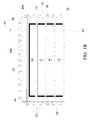
- FIG. 1Ais a cross-sectional view of a stacked package 10 according to some embodiments.
- Stacked package 10includes a substrate 20 , a first structure A, a second structure B, a third structure C, a fourth structure D, a housing 40 and a cooling fluid 60 contained in a cavity of housing 40 .
- a hydrophilic coating 35is on exposed surfaces of structures A, B, C and D.
- a hydrophilic coating 45is on an inner surface of housing 40 .
- Structures A, B, C, and Dare bonded together by bumps 30 .
- a hydrophilic coating 30 ′is on an exposed surface of bumps 30 located at a periphery of structures A, B, C and D.
- FIG. 1Ashows the stacked package 10 as having four structures A, B, C, and D stacked upon one another, one skilled in the art will understand that the stacked package 10 has two or more structures stacked one upon the other in some embodiments while in other embodiments the stacked package 10 may have more than four structures.
- cooling fluid 60To address heat dissipation in stacked package 10 , structures A, B, C, and D are immersed in cooling fluid 60 .
- a volume of cooling fluid 60is contained in housing 40 with the housing 40 hermetically sealing structures A, B, C, and D from ambient air or some other environment. Cooling fluid 60 both cools and insulates structures A, B, C, and D. Cooling fluid 60 helps cool structures A, B, C, and D by absorbing heat generated by operating devices within structures A, B, C, and D and drawing the heat away from the structures to the walls of housing 40 where the heat is then dissipated to a surrounding environment.
- Substrate 20may comprise a silicon substrate although other semiconductor substrates, such as silicon-germanium substrate, III-V compound substrate, glass substrate, or silicon on insulator (SOI) substrate may be utilized in various embodiments.
- semiconductor substratessuch as silicon-germanium substrate, III-V compound substrate, glass substrate, or silicon on insulator (SOI) substrate may be utilized in various embodiments.
- SOIsilicon on insulator
- structures A, B, C, and Dindependently include one of a processor die, memory die (e.g., SRAM, DRAM), power device die, an ASIC (application specific integrated circuit) die, or other functional device dies.
- structures A, B, C, and Dindependently include an interposer, a passive die, or another suitable connecting structure.
- structures A, B, C, and Dindependently include a plurality of through silicon vias (TSVs) (not shown) for inter-die communication, silicon or other semiconductor materials and may include one or more conductive layers (not shown).
- TSVsthrough silicon vias
- multiple metallization layersare formed within structures A, B, C, and D, and structures A, B, C, and D independently include a plurality of other layers, such as inter-metal dielectric (IMD) layers (not shown).
- structures A, B, C, and Dindependently include other active components or circuits, such as transistors, capacitors, and other devices.
- an underfillis located between substrate 20 and a structure A, B, C or D closest to the substrate to help increase mechanical strength of stacked package 10 .
- Exposed surfaces of structures A, B, C, and Dinclude hydrophilic coating 35 to help increase direct contact between cooling fluid 60 and the structures. As an amount of direct contact between the cooling fluid 60 and structures A, B, C and D increases, efficiency of heat transfer from the structures to the cooling fluid 60 increases. Hydrophilic coating 35 has a high thermal conductivity to facilitate efficient heat transfer from structures A, B, C, and D to cooling fluid 60 . The increase in heat transfer efficiency helps to maintain a constant temperature within structures A, B, C and D within an acceptable operating range.
- hydrophilic coating 35includes a metallic layer. In some embodiments, the metallic layer includes a plurality of pillars.
- At least one of the plurality of pillarshas an increased surface roughness in comparison with a plated then etched pillar.
- the increased surface roughness on a pillar structurehelps to increase surface area of hydrophilic coating 35 in order to facilitate more efficient heat transfer.
- hydrophilic coating 35extends along a surface of structures A, B, C, and D closest to an adjacent structure from an outer edge of the structure to an outer most bump 30 . Hydrophilic coating 35 extends across substantially an entirety of a surface of structure D farthest from substrate 20 .
- Bumps 30provide electrical connections between structures A, B, C, and D.
- bumps 30are solder balls, conductive pillars, or other suitable connecting elements.
- hydrophilic coating 30 ′is on exposed bumps 30 along a periphery of structures A, B, C and D. Hydrophilic coating 30 ′ has a high thermal conductivity to facilitate efficient heat transfer from bumps 30 to cooling fluid 60 .
- hydrophilic coating 30 ′includes a metallic layer. In some embodiments, the metallic layer includes a plurality of pillars. In some embodiments, hydrophilic coating 30 ′ is a same coating as hydrophilic coating 35 . In some embodiments, hydrophilic coating 30 ′ is different from hydrophilic coating 35 .
- Housing 40defines a cooling fluid compartment and contains cooling fluid 60 therein.
- Housing 40has a generally rectangular shape but other shapes are also contemplated, such as a shape or design capable of placing the cooling fluid 60 and structures A, B, C, and D in efficient heat exchange with one another.
- housing 40is constructed of a thermally conductive material, such as steel, aluminum, copper, silver, metal, silicon, or silicon carbide. Other materials, such as gold, though perhaps less cost effective than those already mentioned, are also thermally conductive to an adequate degree and are used in certain embodiments.
- an outside surface of housing 40includes a plurality of radiators or fins 50 for heat dissipation.
- fins 50are disposed on any or all of the outside surface(s) of housing 40 . Fins 50 provide additional surface area for establishing heat transfer between housing 40 and the surrounding environment.
- fins 50are elongated for efficient thermal energy transfer to the surrounding environment and are constructed of a thermally conductive material such as steel, aluminum, copper, silver, metal silicon, or silicon carbide.
- a thermally conductive materialsuch as steel, aluminum, copper, silver, metal silicon, or silicon carbide.
- fins 50are made from any material having a relatively high thermal conductivity.
- fins 50have a different shape, such as square, oval, circular, or a variety of other shapes capable of assisting with heat dissipation from stacked package 10 .
- fins 50are affixed to an outer surface of housing 40 by soldering, brazing, bonding, or by some other manner.
- fins 50are formed integrally with housing 40 .
- fins 50include an inner space capable of receiving a coolant.
- the coolantincludes water, oil, antifreeze or another suitable coolant.
- the coolantis circulated through fins 50 by a circulation system (not shown).
- Inner surfaces of housing 40include hydrophilic coating 45 to help increase direct contact between cooling fluid 60 and the housing. As an amount of direct contact between the cooling fluid 60 and housing 40 increases, efficiency of heat transfer from the cooling fluid to the surrounding environment through the housing increases. Hydrophilic coating 45 has a high thermal conductivity to facilitate efficient heat transfer from cooling fluid 60 to housing 40 . The increase in heat transfer efficiency helps to maintain a constant temperature in cooling fluid 60 to permit the cooling fluid to absorb more heat from structures A, B, C, and D.
- hydrophilic coating 45includes a metallic layer.
- the metallic layerincludes a plurality of pillars. In some embodiments, at least one pillar of the plurality of pillars has an increased surface roughness in comparison with a plated then etched pillar.
- hydrophilic coating 45is a same coating as at least one of hydrophilic coating 35 or hydrophilic coating 30 ′. In some embodiments, hydrophilic coating 45 is different from at least one of hydrophilic coating 35 or hydrophilic coating 30 ′.
- cooling fluid 60includes a fluid or liquid.
- cooling fluid 60includes a fluid, such as oil, dielectric oil, water, a mixture of water and an anti-freezing agent, potassium formate, perfluorinate coolant, or the like.
- the cooling fluid 60includes a non-electrically conductive liquid perfluorinate coolant, such as those made by 3MTM including 3M's HFE-7100 coolant and similar coolants.
- cooling fluid 60includes a two-phase liquid, such as any two-phase liquid commercially available from various manufacturers.
- cooling fluid 60may be any fluid capable of absorbing and releasing energy and may be in a fluid form, such as water, gas, oil, or a mixture thereof.
- cooling fluid 60is introduced into housing 40 prior to placing housing around structures A, B, C, and D.
- substrate 20is held by a vacuum chuck, a carrier wafer or another suitable support structure.
- Housing 40is filled with a predetermined volume of cooling fluid 60 and is then placed around structures A, B, C, and D and bonded to substrate 20 to seal the cooling fluid within the housing.
- cooling fluid 60is introduced into housing 40 in a vacuum chamber or another suitable production tool.
- a volume of cooling fluid 60such as oil for example, heated by structures A, B, C, and D within housing 40 rises upwardly towards the top of housing 40 .
- cooling fluid 60such as oil for example
- heated oilcools, a density of the oil increases with a resultant downward flow aided by gravity.
- the downward flowis limited by the bottom of housing 40 consequently establishing a lateral flow to again bring the cooling fluid into engagement with the dies to begin the cycle anew.
- a level of cooling fluid 60 within housing 40is maintained at a prescribed level to receive heat from structures A, B, C and D.
- the prescribed levelis a minimum level of cooling fluid 60 during operation, e.g., a level of cooling fluid 60 receiving a maximum amount of heat during operation of devices within structures A, B, C and D.
- the prescribed levelis above the surface of structure D farthest from substrate 20 .
- the prescribed levelis a predetermined distance above the surface of structure D farthest from substrate 20 .
- the stacked package 10includes a pressure release apparatus 65 .
- the pressure release apparatus 65 in FIG. 1Ais depicted as a box.
- the pressure release apparatus 65releases pressure within housing 40 caused by changes in volume of cooling fluid 60 .
- the temperature in the stacked package 10increases, there is a corresponding increase in the volume of cooling fluid 60 which increases the pressure within housing 40 .
- the pressure within housing 40is not offset, this pressure may rupture the housing 40 of the stacked package 10 .
- the pressure release apparatus 65releases the pressure within housing 40 to prevent such a rupture.
- pressure release apparatus 65is a valve.
- pressure release apparatus 65is configured to continuously release cooling fluid 60 or vaporized cooling fluid while the pressure within housing 40 is above a threshold value and stop releasing the cooling fluid or the vaporized cooling fluid when the pressure within the housing is at or below the threshold value.
- stacked package 10includes a deionizer 75 or an apparatus to deionize ions in the cooling fluid 60 .
- ionsare introduced into cooling fluid 60 by interaction between the cooling fluid and components of the stacked package 10 , such as structures A, B, C, D, or bumps 30 . If the cooling fluid 60 is not de-ionized, conductivity of cooling fluid 60 increases which causes shorts in one or more structures A, B, C, or D, in some instances.
- a deionizeris constructed and for convenience the details of such will not be described herein.
- FIG. 1Bis a cross-sectional view of a stacked package 10 ′ according to some embodiments.
- Stacked package 10 ′is similar to stacked package 10 ( FIG. 1A ). Same elements have a same reference number.
- cooling fluid 60 in stacked package 10 ′does not substantially fill housing 40 .
- a top surface 60 a of cooling fluid 60is spaced from a top inner surface of housing 40 .
- a space between top surface 60 a and the top inner surface of housing 40includes vaporized cooling fluid 60 .
- Housing 40 of stacked package 10 ′also includes a hydrophobic coating 45 ′ on the top inner surface of housing 40 .
- a coating 45 a on a portion of inner side surfaces of housing 40is either hydrophilic or hydrophobic.
- Hydrophobic coating 45 ′helps to maintain a level of cooling fluid 60 within housing 40 . Hydrophobic coating 45 ′ reduces an amount of cooling fluid 60 which remains on the top surface of housing following condensation. During operation, cooling fluid 60 is heated by structures A, B, C, and D. A portion of cooling fluid 60 evaporates due to the increased temperature of the cooling fluid. When the vaporized cooling fluid contacts the top inner surface of housing 40 , heat is transferred to the surrounding environment through the housing. The vaporized cooling fluid then condenses back into a liquid state. Hydrophobic coating 45 ′ helps to increase a contact angle between the condensate and the top inner surface of housing 40 . The increased contact angle causes the condensate to form a droplet and fall back into cooling fluid 60 .
- hydrophobic coating 45 ′includes an organic material. In some embodiments, hydrophobic coating 45 ′ includes trichloro(1H,1H,2H,2H-perfluorooctyl)silane, 1H,1H,2H,2H-perfluorodecyltrimethosxysilane, 1H,1H,2H,2H-perfluorodecyldimethylchlorosilane, or another suitable hydrophobic material.
- Coating 45 ais located on a top portion of the inner sidewall of housing 40 above a top surface 60 a of cooling fluid 60 at an operating temperature of stacked package 10 ′.
- coating 45 ais entirely a hydrophilic coating, such as hydrophilic coating 45 .
- coating 45 ais entirely a hydrophobic coating, such as hydrophobic coating 45 ′.
- a first portion of coating 45 ais hydrophilic and a second portion of coating 45 a is hydrophobic. The second portion of coating 45 a is located closer to the top inner surface of housing 40 than the first portion of coating 45 a .
- a ratio of a length of the first portion to a length of the second portion along inner sidewalls of housing 40is based on a location of top surface 60 a .
- an interface of the first portion of coating 45 a and the second portion of coating 45 ais co-planar with the location of top surface 60 a at an operating temperature of stacked package 10 ′.
- the location of top surface 60 adepends on a material of cooling fluid 60 and the operating temperature of stacked package 10 ′. As a vapor pressure of cooling fluid 60 increases, the top surface 60 a is located closer to the top inner surface of housing 40 .
- the top surface 60 ais located farther from the top inner surface of housing 40 due to greater vaporization of cooling fluid 60 .
- the vaporization of cooling fluid 60converts a portion of a volume of the cooling fluid from a liquid state to a gaseous state which increases a distance between top surface 60 a and the top inner surface of housing 40 .
- the first portion of coating 45 awill help to increase heat transfer efficiency in a similar manner as hydrophilic coating 45 .
- the first portion of the coating 45 awill act to maintain a volume of cooling fluid 60 away from contact with structures A, B, C, and D.
- the volume of cooling fluid 60 kept away from structures A, B, C, and Dreduces an amount of the cooling fluid available to absorb heat from the structures.
- the second portion of coating 45 awill help to return condensed cooling fluid 60 to the cooling fluid surrounding structures A, B, C, and D. In some embodiments where the second portion of coating 45 a extends below top surface 60 a , the second portion of coating 45 a prevents efficient heat transfer from cooling fluid 60 to housing 40 .
- the reduced efficiency of heat transfer from cooling fluid 60 to housing 40results in an increase in the temperature of the cooling fluid.
- a driving force for heat transfer from structures A, B, C, and D to the cooling fluidis reduced.
- the reduced driving force for heat transfermeans a temperature of structures A, B, C, and D increases, which in turn increases a risk of damage to the structures.
- stacked package 10includes temperature sensors 55 A and 55 B ( FIG. 3 ). Temperature sensors 55 A and 55 B are positioned at one or more places on an exterior wall portion of housing 40 . Positioning temperature sensors 55 A and 55 B on an exterior wall of housing 40 makes removing and replacing the temperature sensors less time consuming and less expensive.
- FIG. 2is a cross-sectional view of a multi-chip system package 15 according to some embodiments.
- the multi-chip system package 15includes many different chips, such as stacked chips, and components, such as 3D IC packages, MEMs packaging, system on chips (SOCs), THERMAL SOPs, OPTO SOPs, embedded components, antennas and filters, and the like.
- a volume of cooling fluid 60is contained in housing 40 . Cooling fluid 60 both cools and insulates the components of multi-chip system package 15 .
- the cooling fluid 60helps cool the components by absorbing heat generated by the components and drawing the absorbed heat to the walls of housing 40 where the absorbed heat is then dissipated to the surrounding environment.
- an outside surface of housing 40includes a plurality of radiators or fins 50 for additional heat dissipation.
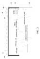
- FIG. 3depicts the stacked package 10 of FIG. 1A having a pump 80 and a conduit 85 .
- FIG. 3does not depict a pressure release apparatus 65 for ease of illustration.
- the assembly of FIG. 3includes pressure release apparatus 65 similar to the assembly of FIG. 1A .
- hydrophilic coating 35 , hydrophilic coating 30 ′, hydrophilic coating 45 , and hydrophobic coating 45 ′are not included in FIG. 3 for ease of review.
- hydrophilic coating 35 , hydrophilic coating 30 ′, hydrophilic coating 45 , or hydrophobic coating 45 ′are included in the assembly of FIG. 3 .
- conduit 85is connected to an inlet or opening in housing 40 and the other end of the conduit 85 is connected to an outlet or opening in housing 40 .
- FIG. 3indicates that the inlet is closer to substrate 20 than the outlet.
- the outletis closer to substrate 20 than the inlet.
- the outlet and the inletare spaced an equal distance from substrate 20 .
- conduit 85is a pipe, tube or another suitable passageway for allowing cooling fluid 60 to circulate from the outlet to the inlet.
- Pump 80is coupled to conduit 85 for pumping the cooling fluid 60 from the outlet to the inlet of housing 40 .
- Pump 80is an apparatus for circulating the cooling fluid by means of a piston, plunger, or a set of rotating vanes, or another suitable circulating apparatus.
- pump 80forces cooling fluid 60 from a bottom region of housing 40 , where the cooling fluid is generally cooler, to an upper region of housing 40 where the cooling fluid is generally warmer as compared to the cooling fluid at the bottom region.
- the circulation of cooling fluid 60 from the lower region to the upper region of housing 40cools structures A, B, C, and D.
- cooling fluid 60passes along sidewalls of structures A, B, C, and D. Cooling fluid 60 also passes between adjacent structures A, B, C, and D. Cooling fluid 60 contacts bumps 30 which provide a heat transfer interface in addition to the surfaces of structures A, B, C, and D. In some embodiments, cooling fluid 60 does not pass between structure A and substrate 20 due to the presence of an underfill layer.
- Cooling fluid 60 contained within housing 40 in these embodiments and othersis able to be circulated by one or more methods, such as by gravity, an active pumping action, such as with the mechanical pump described above, a passive pumping action, such as with a wicking action, a thermal siphoning action, or the like.
- stacked package 10includes one or more barriers 96 disposed within the housing 40 of the stacked die package 10 .
- Barriers 96help direct the fluid flow F of cooling fluid 60 , particularly to areas between two stacked structures, in the region of the bumps 30 . Without barriers 96 , a substantial amount of cooling fluid 60 will flow over the top of the topmost structure D or around the sides of the dies A, B, C and D, in some instances, as fluid flow will generally take the path of least resistance.
- a configuration or shape of barriers 96is not limited so long as such configuration or shape directs the fluid flow F substantially to regions between the structures (e.g., to the region of the bumps 30 ) and substantially blocks at least a portion of fluid flow over the top of the topmost structure D or around the sides of the stacked structures A, B, C and D.
- a heat sink 70is thermally coupled to conduit 85 .
- Heat sink 70draws heat from cooling fluid 60 to the surrounding environment thereby causing cooling of cooling fluid 60 .
- heat sink 70includes fins or other heat dissipating elements.
- temperature sensor 55 Ais fitted at or near the inlet in housing 40
- temperature sensor 55 Bis positioned at or near the outlet in housing 40 .
- Temperature sensors 55 A and 55 Bare located at a location below a top surface of cooling fluid 60 .
- temperature sensors 55 A and 55 Bare resistive temperature sensors that indicate a change in temperature by a change in electrical resistance. The measured temperature is dependent on the level of the cooling fluid 60 , the ambient temperature, and a given stacked package design.
- the stack package 10includes a specific purpose computer (not shown) having suitable computer control algorithms to receive the outputs and provide information indicative of an operation property of stacked package 10 from the measured temperatures.
- calculating the level of the cooling fluid 60 in the housing 40includes the specific purpose computer comparing a value associated with the measured outputs from temperature sensor 55 A or 55 B with predetermined values expected for a normal operation condition. If a difference between the predetermined outputs and measured outputs from temperature sensor 55 A or 55 B is above a threshold value, the specific purpose computer is arranged to generate an alarm condition, in some embodiments. In some embodiments, the specific purpose computer is arranged to generate a warning signal when the cooling fluid 60 level drops below a prescribed minimum level.
- the specific purpose computeris configured to generate a control signal for controlling pump 80 to adjust a flow rate of cooling fluid 60 .
- a flow rate of cooling fluid 60increases, an amount of heat the cooling fluid absorbs from structures A, B, C and D increases. The increased amount of heat absorbed by cooling fluid 60 is dissipated into the surrounding environment by heat sink 70 .
- FIG. 4is a cross-section view of a stacked package 10 ′ according to some embodiments.
- Stacked package 10 ′ in FIG. 4is similar to stacked package 10 ′ in FIG. 1B . Same elements have a same reference number.
- stacked package 10 ′ in FIG. 4includes a single port 90 .
- Port 90is configured to provide both an inlet and an outlet for cooling fluid 60 .
- a flow of cooling fluid 60 into or out of housing 40is controlled by valves 95 a , 95 b and 95 c .
- a reservoir 100 connected to port 90is configured to help relieve pressure within housing 40 and to store additional cooling fluid 60 .
- FIG. 4includes just one port 90 for both inlet and outlet of cooling fluid 60 .
- Valve 95 ais configured to selectively connect an interior of housing 40 with reservoir 100 .
- Reservoir 100helps to relieve pressure within housing 40 while avoiding releasing a volume of cooling fluid 60 through pressure release apparatus 65 .
- the cooling fluidabsorbs heat from structures A, B, C, and D, the cooling fluid expands and a portion of the cooling fluid evaporates.
- valve 95 ais open the volume of cooling fluid 60 is able to expand into reservoir 100 instead of just increasing the pressure within housing 40 .
- cooling fluid 60cools, the cooling fluid within reservoir 100 is able to return to housing 40 through valve 95 a without having to supply a new volume of cooling fluid.
- reservoir 100helps to reduce the risk of damage to housing 40 or structures A, B, C, and D resulting from increased pressure during operation. Reservoir 100 also helps to conserve cooling fluid 60 by relieving pressure within housing 40 without venting the cooling fluid into the surrounding environment through pressure release apparatus 65 .
- Valve 95 bis able to connect housing 40 , through valve 95 a , to a cooling fluid supply (not shown).
- a pumpsuch as pump 80 , is usable to supply a volume of cooling fluid 60 to housing 40 through valve 95 b and valve 95 a.
- Valve 95 cis able to connect housing, through valve 95 a and reservoir 100 , without a cooling fluid discharge (not shown).
- a pumpsuch as pump 80 , is usable to remove a volume of cooling fluid 60 from housing 40 through valve 95 a , reservoir 100 and valve 95 c .
- the cooling fluid dischargeis connected to the cooling fluid supply.
- valves 95 a , 95 b and 95 care controlled to regulate a level of cooling fluid 60 within housing 60 .
- a controller 150is connected to valves 95 a , 95 b and 95 c in order to control the valves.
- controller 150includes an algorithm for controlling valves 95 a , 95 b and 95 c based on a temperature of cooling fluid 60 , a volume of the cooling fluid, or a pressure within housing 40 .
- controller 150controls valve 95 a in order to connect housing to reservoir 100 .
- controller 150controls valves 95 b and 95 c in order to circulate cooling fluid 60 to help decrease the temperature of the cooling fluid.
- controllercontrols valve 95 a and valve 95 b in order to increase the volume of the cooling fluid within housing 40 .
- controller 150controls valve 95 a and valve 95 c in order to reduce the volume of the cooling fluid within housing 40 .
- a pressure threshold controller 150controls valve 95 a and valve 95 c in order to discharge a portion of cooling fluid 60 to reduce the pressure within the housing.
- controller 150includes a process configured to execute instructions for controlling valves 95 a , 95 b and 95 c .
- controller 150includes a non-transitory computer readable memory for storing instructions and parameters for controlling valves 95 a , 95 b and 95 c .
- controller 150includes an input/output (I/O) interface for sending and receiving information to or from an operator or other devices such as temperature sensors, pressure sensors, a keyboard, a mouse, or other suitable devices.
- controller 150includes a network interface for wirelessly connecting to at least one of valves 95 a , 95 b or 95 c or other devices such as temperature sensors, pressure sensors, or other suitable devices.
- FIG. 5is a flowchart of a method 500 of making a hydrophilic coating on a surface of a structure according to some embodiments.
- method 500describes forming hydrophilic coating 35 on at least one of structure A, B, C, or D.
- a seed layeris formed on the structure.
- the seed layeris a single material.
- the seed layeris a multi-layer seed layer.
- the seed layeris formed using chemical vapor deposition (CVD), physical vapor deposition (PVD), sputtering, atomic layer deposition (ALD), plating, or another suitable formation process.
- the seed layerincludes copper, titanium, or another suitable material.
- FIG. 6Ais a cross-sectional view of a hydrophilic coating following operation 502 according to some embodiments.
- FIG. 6Aincludes a seed layer 610 formed on a structure, such as structure A, B, C, or D. Seed layer 610 includes a first titanium layer 612 a closest to the structure. In some embodiments, first titanium layer 612 a is in direct contact with the structure. In some embodiments, an intermediate layer is between first titanium layer 612 a and the structure to increase adhesive between the first titanium layer and the structure. A copper layer 614 is over first titanium layer 612 a . A second titanium layer 612 b is over copper layer 614 .
- a photoresistis formed over the seed layer and the photoresist is patterned in operation 504 .
- the photoresistis formed by spin-on coating, PVD or another suitable formation process.
- the photoresistis patterned using an etching process.
- the etching processincludes a lithography step.
- the patterned photoresistis subjected to an oxygen plasma treatment in order to increase wettability of the patterned photoresist for subsequent processing, such as plating of a copper layer.
- FIG. 6Bis a cross-sectional view of the hydrophilic coating following operation 504 according to some embodiments.
- a photoresist 620is formed over seed layer 610 . Photoresist 620 is then patterned to form a plurality of openings within the photoresist.
- a top portion of the seed layeris removed in operation 506 .
- operation 506is omitted.
- the top portion of the seed layeris removed by etching the seed layer through the patterned photoresist.
- the etching processincludes a hydrofluoric acid solution or another suitable etchant.
- the etching processincludes multiple etching steps. For example, in some embodiments which include a multi-layer seed layer as in FIG. 6A , a portion of second titanium layer 612 b is removed using a hydrofluoric acid solution then an oxide layer is removed from copper layer 614 using a hydrochloric acid solution.
- a copper layeris formed over the seed layer in the openings of the patterned photoresist.
- the copper layeris formed by plating, PVD, sputtering or another suitable formation process.
- the plating processis accompanied by a sonication process.
- FIG. 6Cis a cross-sectional view of the hydrophilic coating following operation 508 according to some embodiments.
- a copper layer 630is plated over seed layer 610 within openings of photoresist 620 .
- the photoresistis removed in operation 510 .
- the photoresistis removed using a stripping solution, an ashing process, or another suitable photoresist removal process.
- the copper layer formed in operation 508is substantially undamaged during the removal of the photoresist.
- a surface treatmentis performed on the copper layer.
- the surface treatmentis performed on a top surface of the copper layer and portions of the copper layer exposed by removing the photoresist.
- the surface treatmentincreases a surface roughness of the copper layer.
- the increased surface roughnessincreases a surface area of the copper layer contacting a cooling fluid, e.g., cooling fluid 60 ( FIG. 1A ), which in turn increases efficiency of heat transfer from the copper layer to the cooling fluid.
- the surface treatmentincludes immersing the copper layer in an alkali solution.
- the alkali solutionincludes NaClO 2 , NaOH, Na 3 PO 4 , or H 2 O.
- the surface treatmentforms needle-shaped nanostructures on surfaces of the copper layer.
- the surface treatment of operation 512also increases surface roughness of bumps, e.g., bumps 30 ( FIG. 1A ), attached to the structure.
- bumpse.g., bumps 30 ( FIG. 1A )
- peripheral bumps 30bonding structures A, B, C, and D together that are exposed to the surface treatment process.
- the surface roughness of the peripheral bumpsis increased in comparison with a surface roughness of the bumps which are not exposed to the surface treatment.
- more bumps than just peripheral bumps bonded to the structureare subjected to the surface treatment process.
- substantially all bumps bonded to the structureare subjected to the surface treatment process.
- FIG. 6Dis a cross-sectional view of the hydrophilic coating following operation 512 according to some embodiments.
- photoresist 620is removed.
- Copper layer 630 ′includes an enhanced surface roughness in comparison with the surface roughness of copper layer 630 in FIG. 6C .
- the enhanced surface roughness of copper layer 630 ′increases a surface area for heat transfer in comparison with copper layer 630 .
- method 500includes additional operations such as bonding structures, e.g., structures A, B, C, and D ( FIG. 1A ), together, forming an underfill between a substrate and the structure, or other suitable operations.
- additional operationssuch as bonding structures, e.g., structures A, B, C, and D ( FIG. 1A ), together, forming an underfill between a substrate and the structure, or other suitable operations.
- FIG. 7is a flowchart of a method 700 of a making a hydrophilic coating on a housing according to some embodiments.
- Method 700begins with operation 702 in which a copper layer is formed on an inner surface of a housing.
- the copper layeris formed by sintering a copper powder on the inner surface of the housing, e.g., housing 40 ( FIG. 1A ).
- the copper layeris formed by plating, ALD, PVD, or another suitable formation process.
- a surface treatmentis performed on the copper layer.
- the surface treatmentincreases a surface roughness of the copper layer.
- the increased surface roughnessincreases a surface area of the copper layer contacting a cooling fluid, e.g., cooling fluid 60 ( FIG. 1A ), which in turn increases efficiency of heat transfer from the cooling fluid to the housing.
- the surface treatmentincludes immersing the copper layer in an alkali solution.
- the alkali solutionincludes NaClO 2 , NaOH, Na 3 PO 4 , or H 2 O.
- the surface treatmentforms needle-shaped nanostructures on surfaces of the copper layer.
- the surface treatment of operation 704is a same surface treatment as the surface treatment of operation 512 .
- the surface treatment of operation 704is different from the surface treatment of operation 512 .
- additional operationsare included in method 700 , such as forming a seed layer, forming a patterned photoresist or another suitable operation.
- FIG. 8is a flowchart of a method 800 of a making a hydrophobic coating on a housing according to some embodiments.
- Method 800begins with operation 802 in which a copper layer is formed on an inner surface of a housing.
- the copper layeris formed by sintering a copper powder on the inner surface of the housing, e.g., housing 40 ( FIG. 1A ).
- the copper layeris formed by plating, ALD, PVD, or another suitable formation process.
- operation 802is performed simultaneously with operation 702 .
- operation 802is performed sequentially with operation 702 .
- a surface treatmentis performed on the copper layer.
- the surface treatmentincreases a surface roughness of the copper layer.
- the surface treatmentincludes immersing the copper layer in an alkali solution.
- the alkali solutionincludes NaClO 2 , NaOH, Na 3 PO 4 , or H 2 O.
- the surface treatmentforms needle-shaped nanostructures on surfaces of the copper layer.
- the surface treatment of operation 804is a same surface treatment as at least one of the surface treatment of operation 512 or operation 704 .
- the surface treatment of operation 704is different from at least one of the surface treatment of operation 512 or operation 704 .
- operation 804is performed simultaneously with operation 704 .
- operation 804is performed sequentially with operation 704 .
- a hydrophobic coatingis formed on the treated copper layer.
- the hydrophobic coatingis formed by ALD, CVD, an epitaxial process or another suitable formation process.
- the hydrophobic coatingincludes trichloro(1H,1H,2H,2H-perfluorooctyl)silane.
- the hydrophobic coatingincludes a different hydrophobic material.
- additional operationsare included in method 800 , such as forming a seed layer, forming a patterned photoresist or another suitable operation.
- the stacked packageincludes a substrate, and a first structure bonded to the substrate.
- the first structurehas a plurality of bumps, and a first hydrophilic coating is on sidewalls of the first structure.
- the stacked packagefurther includes a second structure bonded to the plurality of bumps.
- the first hydrophilic coatingis on sidewalls of the second structure.
- the first structureis between the second structure and the substrate.
- the stacked packagefurther includes a housing, wherein the housing defines a volume enclosing the first structure and the second structure.
- a second hydrophilic coatingis on sidewalls of an inner surface of the housing.
- the stacked packagefurther includes a cooling fluid within the volume enclosing the first structure and the second structure. A top surface of the cooling fluid is above a top surface of the second structure.
- the stacked packageincludes a substrate, and a plurality of structures bonded to the substrate. Adjacent structures of the plurality of structures are bonded together by a plurality of bumps.
- the stacked packagefurther includes a first hydrophilic coating on sidewalls of at least one structure of the plurality of structures.
- the stacked packagefurther includes a housing, wherein the housing defines a volume enclosing the plurality of structures.
- the stacked packagefurther includes a second hydrophilic coating on sidewalls of an inner surface of the housing.
- the stacked packagefurther includes a hydrophobic coating on a top surface of the inner surface of the housing.
- the stacked packagefurther includes a cooling fluid within the volume enclosing the plurality of structures. A top surface of the cooling fluid is above a top surface of a structure of the plurality of structures farthest from the substrate.
- Still another aspect of this descriptionrelates to a method of making a stacked package.
- the methodincludes bonding a first structure to a substrate, and bonding a second structure to the first structure using a plurality of bumps.
- the methodfurther includes forming a first hydrophilic coating on a sidewall surface of the first structure and on a sidewall surface of the second structure.
- the methodfurther includes forming a second hydrophilic coating on sidewalls of an inner surface of a housing.
- the methodfurther includes enclosing the first structure and the second structure using the housing to define a volume surrounding the first structure and the second structure.
- the methodfurther includes filling at least a portion of the volume with a cooling fluid.
Landscapes
- Engineering & Computer Science (AREA)
- Microelectronics & Electronic Packaging (AREA)
- Power Engineering (AREA)
- Computer Hardware Design (AREA)
- Physics & Mathematics (AREA)
- General Physics & Mathematics (AREA)
- Condensed Matter Physics & Semiconductors (AREA)
- Manufacturing & Machinery (AREA)
- Life Sciences & Earth Sciences (AREA)
- Sustainable Development (AREA)
- Thermal Sciences (AREA)
- Mechanical Engineering (AREA)
- General Engineering & Computer Science (AREA)
- Cooling Or The Like Of Semiconductors Or Solid State Devices (AREA)
Abstract
Description
Claims (20)
Priority Applications (1)
| Application Number | Priority Date | Filing Date | Title |
|---|---|---|---|
| US14/511,051US9343436B2 (en) | 2010-09-09 | 2014-10-09 | Stacked package and method of manufacturing the same |
Applications Claiming Priority (4)
| Application Number | Priority Date | Filing Date | Title |
|---|---|---|---|
| US12/878,319US20120063090A1 (en) | 2010-09-09 | 2010-09-09 | Cooling mechanism for stacked die package and method of manufacturing the same |
| US41828110P | 2010-11-30 | 2010-11-30 | |
| US13/033,840US20120061059A1 (en) | 2010-09-09 | 2011-02-24 | Cooling mechanism for stacked die package and method of manufacturing the same |
| US14/511,051US9343436B2 (en) | 2010-09-09 | 2014-10-09 | Stacked package and method of manufacturing the same |
Related Parent Applications (1)
| Application Number | Title | Priority Date | Filing Date |
|---|---|---|---|
| US13/033,840Continuation-In-PartUS20120061059A1 (en) | 2010-09-09 | 2011-02-24 | Cooling mechanism for stacked die package and method of manufacturing the same |
Publications (2)
| Publication Number | Publication Date |
|---|---|
| US20150021755A1 US20150021755A1 (en) | 2015-01-22 |
| US9343436B2true US9343436B2 (en) | 2016-05-17 |
Family
ID=52342925
Family Applications (1)
| Application Number | Title | Priority Date | Filing Date |
|---|---|---|---|
| US14/511,051Expired - Fee RelatedUS9343436B2 (en) | 2010-09-09 | 2014-10-09 | Stacked package and method of manufacturing the same |
Country Status (1)
| Country | Link |
|---|---|
| US (1) | US9343436B2 (en) |
Cited By (2)
| Publication number | Priority date | Publication date | Assignee | Title |
|---|---|---|---|---|
| US10159165B2 (en) | 2017-02-02 | 2018-12-18 | Qualcomm Incorporated | Evaporative cooling solution for handheld electronic devices |
| US10431648B2 (en) | 2014-05-02 | 2019-10-01 | Invensas Corporation | Making electrical components in handle wafers of integrated circuit packages |
Families Citing this family (14)
| Publication number | Priority date | Publication date | Assignee | Title |
|---|---|---|---|---|
| US11081423B2 (en)* | 2012-08-28 | 2021-08-03 | The Boeing Company | Power distribution by a working fluid contained in a conduit |
| US20150262902A1 (en) | 2014-03-12 | 2015-09-17 | Invensas Corporation | Integrated circuits protected by substrates with cavities, and methods of manufacture |
| US9355997B2 (en) | 2014-03-12 | 2016-05-31 | Invensas Corporation | Integrated circuit assemblies with reinforcement frames, and methods of manufacture |
| US9263366B2 (en)* | 2014-05-30 | 2016-02-16 | International Business Machines Corporation | Liquid cooling of semiconductor chips utilizing small scale structures |
| US9741649B2 (en) | 2014-06-04 | 2017-08-22 | Invensas Corporation | Integrated interposer solutions for 2D and 3D IC packaging |
| US9252127B1 (en) | 2014-07-10 | 2016-02-02 | Invensas Corporation | Microelectronic assemblies with integrated circuits and interposers with cavities, and methods of manufacture |
| US9478504B1 (en) | 2015-06-19 | 2016-10-25 | Invensas Corporation | Microelectronic assemblies with cavities, and methods of fabrication |
| US10121726B2 (en)* | 2015-08-28 | 2018-11-06 | Intel IP Corporation | Cooler for semiconductor devices |
| GB2542844B (en)* | 2015-10-01 | 2021-06-16 | Iceotope Group Ltd | An immersion cooling system |
| US10558249B2 (en)* | 2016-09-27 | 2020-02-11 | International Business Machines Corporation | Sensor-based non-uniform cooling |
| US10424528B2 (en)* | 2018-02-07 | 2019-09-24 | Toyota Motor Engineering & Manufacturing North America, Inc. | Layered cooling structure including insulative layer and multiple metallization layers |
| CN109920768B (en)* | 2019-03-28 | 2020-12-18 | 河北工业大学 | A high-power IGBT module water cooling system considering operating conditions |
| CN111273752B (en)* | 2020-01-17 | 2021-07-13 | 河南工业职业技术学院 | A computer chip cooling device |
| CN114551385B (en)* | 2022-04-28 | 2022-09-13 | 之江实验室 | Three-dimensional stacked packaging structure containing micro-channel heat dissipation structure and packaging method thereof |
Citations (117)
| Publication number | Priority date | Publication date | Assignee | Title |
|---|---|---|---|---|
| US4811082A (en) | 1986-11-12 | 1989-03-07 | International Business Machines Corporation | High performance integrated circuit packaging structure |
| US4990462A (en) | 1989-04-12 | 1991-02-05 | Advanced Micro Devices, Inc. | Method for coplanar integration of semiconductor ic devices |
| US5075253A (en) | 1989-04-12 | 1991-12-24 | Advanced Micro Devices, Inc. | Method of coplanar integration of semiconductor IC devices |
| US5144811A (en) | 1991-01-10 | 1992-09-08 | Hughes Aircraft Company | Condensation control system for water-cooled electronics |
| US5189911A (en) | 1992-01-10 | 1993-03-02 | Sarasota Measurements & Controls, Inc. | Liquid level and temperature sensing device |
| US5270572A (en) | 1991-06-26 | 1993-12-14 | Hitachi, Ltd. | Liquid impingement cooling module for semiconductor devices |
| US5380681A (en) | 1994-03-21 | 1995-01-10 | United Microelectronics Corporation | Three-dimensional multichip package and methods of fabricating |
| US5528456A (en) | 1993-11-15 | 1996-06-18 | Nec Corporation | Package with improved heat transfer structure for semiconductor device |
| US5737186A (en) | 1995-04-20 | 1998-04-07 | Daimler-Benz Ag | Arrangement of plural micro-cooling devices with electronic components |
| US5785754A (en)* | 1994-11-30 | 1998-07-28 | Sumitomo Electric Industries, Ltd. | Substrate, semiconductor device, element-mounted device and preparation of substrate |
| US5933323A (en) | 1997-11-05 | 1999-08-03 | Intel Corporation | Electronic component lid that provides improved thermal dissipation |
| US6002177A (en) | 1995-12-27 | 1999-12-14 | International Business Machines Corporation | High density integrated circuit packaging with chip stacking and via interconnections |
| US6172874B1 (en) | 1998-04-06 | 2001-01-09 | Silicon Graphics, Inc. | System for stacking of integrated circuit packages |
| US6229216B1 (en) | 1999-01-11 | 2001-05-08 | Intel Corporation | Silicon interposer and multi-chip-module (MCM) with through substrate vias |
| US6271059B1 (en) | 1999-01-04 | 2001-08-07 | International Business Machines Corporation | Chip interconnection structure using stub terminals |
| US20010011773A1 (en)* | 1997-09-29 | 2001-08-09 | Ross Downey Havens | Electronic package utilizing protective coating |
| US6279815B1 (en) | 1998-06-17 | 2001-08-28 | International Business Machines Corporation | Stacked chip process carrier |
| US6349760B1 (en) | 1999-10-22 | 2002-02-26 | Intel Corporation | Method and apparatus for improving the thermal performance of heat sinks |
| US6355501B1 (en) | 2000-09-21 | 2002-03-12 | International Business Machines Corporation | Three-dimensional chip stacking assembly |
| US6366462B1 (en) | 2000-07-18 | 2002-04-02 | International Business Machines Corporation | Electronic module with integral refrigerant evaporator assembly and control system therefore |
| US6434016B2 (en) | 1999-06-18 | 2002-08-13 | Intel Corporation | Apparatus for interconnecting multiple devices on a circuit board |
| US6448661B1 (en) | 2001-02-09 | 2002-09-10 | Samsung Electornics Co., Ltd. | Three-dimensional multi-chip package having chip selection pads and manufacturing method thereof |
| US6461895B1 (en) | 1999-01-05 | 2002-10-08 | Intel Corporation | Process for making active interposer for high performance packaging applications |
| US6550263B2 (en) | 2001-02-22 | 2003-04-22 | Hp Development Company L.L.P. | Spray cooling system for a device |
| US6570248B1 (en) | 1998-08-31 | 2003-05-27 | Micron Technology, Inc. | Structure and method for a high-performance electronic packaging assembly |
| US20030104170A1 (en)* | 2001-02-07 | 2003-06-05 | 3M Innovative Properties Company | Microstructured surface film assembly for liquid acquisition and transport |
| US20030123225A1 (en) | 2001-12-27 | 2003-07-03 | Miller Charles A. | Electronic package with direct cooling of active electronic components |
| US6600222B1 (en) | 2002-07-17 | 2003-07-29 | Intel Corporation | Stacked microelectronic packages |
| US6607938B2 (en) | 2001-07-19 | 2003-08-19 | Samsung Electronics Co., Ltd. | Wafer level stack chip package and method for manufacturing same |
| US6611057B2 (en) | 2000-11-09 | 2003-08-26 | Nec Corporation | Semiconductor device attaining both high speed processing and sufficient cooling capacity |
| US20030159456A1 (en) | 2002-02-22 | 2003-08-28 | Advanced Thermal Sciences Corp. | Systems and methods for temperature control |
| US6661085B2 (en) | 2002-02-06 | 2003-12-09 | Intel Corporation | Barrier structure against corrosion and contamination in three-dimensional (3-D) wafer-to-wafer vertical stack |
| US6717812B1 (en) | 2002-11-21 | 2004-04-06 | Institute Of Microelectronics | Apparatus and method for fluid-based cooling of heat-generating devices |
| US6762076B2 (en) | 2002-02-20 | 2004-07-13 | Intel Corporation | Process of vertically stacking multiple wafers supporting different active integrated circuit (IC) devices |
| US6790748B2 (en) | 2002-12-19 | 2004-09-14 | Intel Corporation | Thinning techniques for wafer-to-wafer vertical stacks |
| US6790702B2 (en)* | 2001-08-17 | 2004-09-14 | Micron Technology, Inc. | Three-dimensional multichip module |
| US20040190255A1 (en) | 2002-09-11 | 2004-09-30 | Kioan Cheon | Soft cooling jacket for electronic device |
| US20040264124A1 (en) | 2003-06-30 | 2004-12-30 | Patel Chandrakant D | Cooling system for computer systems |
| US20050067694A1 (en) | 2003-09-30 | 2005-03-31 | Pon Florence R. | Spacerless die stacking |
| US6887769B2 (en) | 2002-02-06 | 2005-05-03 | Intel Corporation | Dielectric recess for wafer-to-wafer and die-to-die metal bonding and method of fabricating the same |
| US6908565B2 (en) | 2002-12-24 | 2005-06-21 | Intel Corporation | Etch thinning techniques for wafer-to-wafer vertical stacks |
| US6908785B2 (en) | 2001-12-06 | 2005-06-21 | Samsung Electronics Co., Ltd. | Multi-chip package (MCP) with a conductive bar and method for manufacturing the same |
| US6924551B2 (en) | 2003-05-28 | 2005-08-02 | Intel Corporation | Through silicon via, folded flex microelectronic package |
| US6943067B2 (en) | 2002-01-08 | 2005-09-13 | Advanced Micro Devices, Inc. | Three-dimensional integrated semiconductor devices |
| US6946384B2 (en) | 2003-06-06 | 2005-09-20 | Intel Corporation | Stacked device underfill and a method of fabrication |
| US6975016B2 (en) | 2002-02-06 | 2005-12-13 | Intel Corporation | Wafer bonding using a flexible bladder press and thinned wafers for three-dimensional (3D) wafer-to-wafer vertical stack integration, and application thereof |
| US20060023424A1 (en) | 2004-07-30 | 2006-02-02 | Espec Corp. | Cooling apparatus |
| US7015572B2 (en) | 2003-06-12 | 2006-03-21 | Kabushiki Kaisha Toshiba | Three-dimensionally mounted semiconductor module and three-dimensionally mounted semiconductor system |
| US7019971B2 (en) | 2003-09-30 | 2006-03-28 | Intel Corporation | Thermal management systems for micro-components |
| US7032392B2 (en) | 2001-12-19 | 2006-04-25 | Intel Corporation | Method and apparatus for cooling an integrated circuit package using a cooling fluid |
| US7057270B2 (en) | 2001-04-19 | 2006-06-06 | Simpletech, Inc. | Systems and methods for stacking chip components |
| US20060126309A1 (en) | 2004-12-15 | 2006-06-15 | Bolle Cristian A | Thermal management for shielded circuit packs |
| US7087538B2 (en) | 2004-08-16 | 2006-08-08 | Intel Corporation | Method to fill the gap between coupled wafers |
| US7151009B2 (en) | 2004-06-18 | 2006-12-19 | Samsung Electronics Co., Ltd. | Method for manufacturing wafer level chip stack package |
| US7159414B2 (en) | 2002-09-27 | 2007-01-09 | Isothermal Systems Research Inc. | Hotspot coldplate spray cooling system |
| US7180742B1 (en) | 2004-05-24 | 2007-02-20 | Nvidia Corporation | Apparatus and method for cooling semiconductor devices |
| US7180165B2 (en) | 2003-09-05 | 2007-02-20 | Sanmina, Sci Corporation | Stackable electronic assembly |
| US7201214B2 (en)* | 2003-01-31 | 2007-04-10 | Cooligy, Inc. | Remedies to prevent cracking in a liquid system |
| US7215033B2 (en) | 2003-11-19 | 2007-05-08 | Samsung Electronics Co., Ltd. | Wafer level stack structure for system-in-package and method thereof |
| US7276799B2 (en) | 2003-08-26 | 2007-10-02 | Samsung Electronics Co., Ltd. | Chip stack package and manufacturing method thereof |
| US7279795B2 (en) | 2005-12-29 | 2007-10-09 | Intel Corporation | Stacked die semiconductor package |
| US20070241449A1 (en) | 2004-12-15 | 2007-10-18 | International Business Machines Corporation | Apparatus for Effecting Reliable Heat Transfer of Bare Die Microelectroinc Device and Method Thereof |
| US7289326B2 (en) | 2006-02-02 | 2007-10-30 | Sun Microsystems, Inc. | Direct contact cooling liquid embedded package for a central processor unit |
| US7307005B2 (en) | 2004-06-30 | 2007-12-11 | Intel Corporation | Wafer bonding with highly compliant plate having filler material enclosed hollow core |
| US7317256B2 (en) | 2005-06-01 | 2008-01-08 | Intel Corporation | Electronic packaging including die with through silicon via |
| US20080013291A1 (en) | 2006-07-17 | 2008-01-17 | Toralf Bork | Thermal flow sensor having streamlined packaging |
| US7320928B2 (en) | 2003-06-20 | 2008-01-22 | Intel Corporation | Method of forming a stacked device filler |
| US7345350B2 (en) | 2003-09-23 | 2008-03-18 | Micron Technology, Inc. | Process and integration scheme for fabricating conductive components, through-vias and semiconductor components including conductive through-wafer vias |
| US7362580B2 (en) | 2004-06-18 | 2008-04-22 | Intel Corporation | Electronic assembly having an indium wetting layer on a thermally conductive body |
| US20080128896A1 (en) | 2006-12-05 | 2008-06-05 | Keiji Toh | Semiconductor apparatus and manufacturing method thereof |
| US20080141875A1 (en) | 2006-12-13 | 2008-06-19 | Jurgen Fahrenback | Cooled energy storage device and press including such a device |
| US7402442B2 (en) | 2005-12-21 | 2008-07-22 | International Business Machines Corporation | Physically highly secure multi-chip assembly |
| US7402515B2 (en) | 2005-06-28 | 2008-07-22 | Intel Corporation | Method of forming through-silicon vias with stress buffer collars and resulting devices |
| WO2008093294A1 (en)* | 2007-02-01 | 2008-08-07 | Delphi Technologies, Inc. | A casing for an electrical component |
| US7410884B2 (en) | 2005-11-21 | 2008-08-12 | Intel Corporation | 3D integrated circuits using thick metal for backside connections and offset bumps |
| US20080225493A1 (en) | 2005-11-29 | 2008-09-18 | Hans-Joachim Barth | Three-Dimensional Multichip Module |
| US7432592B2 (en) | 2005-10-13 | 2008-10-07 | Intel Corporation | Integrated micro-channels for 3D through silicon architectures |
| US20090000332A1 (en)* | 2007-06-15 | 2009-01-01 | Yoshihiro Kondo | Electronic Equipment Cooling System |
| US7482207B2 (en)* | 2002-12-14 | 2009-01-27 | Plastic Logic Limited | Electronic devices |
| US7494845B2 (en) | 2004-06-22 | 2009-02-24 | Samsung Electronics Co., Ltd. | Method of forming a thin wafer stack for a wafer level package |
| US20090052137A1 (en) | 2007-08-22 | 2009-02-26 | Chien Ouyang | Micro thrust cooling |
| US20090052134A1 (en) | 2007-08-22 | 2009-02-26 | Casteel Jordan B | Liquid-cooled grounded heatsink for diode rectifier system |
| US7528494B2 (en) | 2005-11-03 | 2009-05-05 | International Business Machines Corporation | Accessible chip stack and process of manufacturing thereof |
| US7557597B2 (en) | 2005-06-03 | 2009-07-07 | International Business Machines Corporation | Stacked chip security |
| US7561425B2 (en) | 2006-06-07 | 2009-07-14 | The Boeing Company | Encapsulated multi-phase electronics heat-sink |
| US7576435B2 (en) | 2007-04-27 | 2009-08-18 | Taiwan Semiconductor Manufacturing Company, Ltd. | Low-cost and ultra-fine integrated circuit packaging technique |
| US20090231811A1 (en) | 2008-03-11 | 2009-09-17 | Hitachi. Ltd. | Electric Power Conversion Apparatus |
| US20090268404A1 (en) | 2008-04-23 | 2009-10-29 | International Business Machines Corporation | Energy efficient apparatus and method for cooling an electronics rack |
| US7611923B2 (en) | 2005-05-05 | 2009-11-03 | International Business Machines Corporation | Method and apparatus for forming stacked die and substrate structures for increased packing density |
| US20090279220A1 (en) | 2008-05-06 | 2009-11-12 | Hauenstein Henning M | Semiconductor device package with internal device protection |
| US20090294954A1 (en) | 2008-05-28 | 2009-12-03 | Georgia Tech Research Corporation | 3-D ICs WITH MICROFLUIDIC INTERCONNECTS AND METHODS OF CONSTRUCTING SAME |
| US20100019377A1 (en) | 2008-07-22 | 2010-01-28 | International Business Machines Corporation | Segmentation of a die stack for 3d packaging thermal management |
| US7692926B2 (en)* | 2005-09-16 | 2010-04-06 | Progressive Cooling Solutions, Inc. | Integrated thermal systems |
| US20100117209A1 (en) | 2007-02-28 | 2010-05-13 | Bezama Raschid J | Multiple chips on a semiconductor chip with cooling means |
| US20100127390A1 (en) | 2008-11-21 | 2010-05-27 | Hans-Joachim Barth | Cooling Structures and Methods |
| US20100134947A1 (en) | 2007-01-25 | 2010-06-03 | Ion A-Z, Llc | Fluid cooled electrical capacitor and methods of making and using |
| US20100187682A1 (en) | 2006-09-21 | 2010-07-29 | Damaruganath Pinjala | Electronic package and method of assembling the same |
| US20100187683A1 (en) | 2008-05-28 | 2010-07-29 | Georgia Tech Research Corporation | 3-D ICs EQUIPPED WITH DOUBLE SIDED POWER, COOLANT, AND DATA FEATURES |
| US7781263B2 (en)* | 2008-06-06 | 2010-08-24 | Coolsilicon Llc | Systems, devices, and methods for semiconductor device temperature management |
| US20100246117A1 (en) | 2008-02-28 | 2010-09-30 | International Business Machines Coporation | Variable flow computer cooling system for a data center and method of operation |
| US7834450B2 (en) | 2007-08-20 | 2010-11-16 | Samsung Electronics Co., Ltd. | Semiconductor package having memory devices stacked on logic device |
| US7849914B2 (en) | 2006-05-02 | 2010-12-14 | Clockspeed, Inc. | Cooling apparatus for microelectronic devices |
| US20110092064A1 (en) | 2009-10-20 | 2011-04-21 | Taiwan Semiconductor Manufacturing Company, Ltd. | Preventing UBM Oxidation in Bump Formation Processes |
| US20110101527A1 (en) | 2009-11-05 | 2011-05-05 | Taiwan Semiconductor Manufacturing Company, Ltd. | Mechanisms for forming copper pillar bumps |
| US7990711B1 (en)* | 2010-02-24 | 2011-08-02 | International Business Machines Corporation | Double-face heat removal of vertically integrated chip-stacks utilizing combined symmetric silicon carrier fluid cavity and micro-channel cold plate |
| DE202011101830U1 (en)* | 2011-06-14 | 2011-08-18 | Asia Vital Components Co., Ltd. | Cooling unit and its cooling module |
| US20110292595A1 (en) | 2010-05-27 | 2011-12-01 | International Business Machines Corporation | Liquid Cooling System for Stackable Modules in Energy-Efficient Computing Systems |
| US20110292601A1 (en) | 2010-05-26 | 2011-12-01 | International Business Machines Corporation | Dehumidifying and re-humidifying apparatus and method for an electronics rack |
| US8236379B2 (en)* | 2007-04-02 | 2012-08-07 | Applied Microstructures, Inc. | Articles with super-hydrophobic and-or super-hydrophilic surfaces and method of formation |
| US20120227936A1 (en)* | 2011-03-11 | 2012-09-13 | Asia Vital Components Co., Ltd. | Heat-dissipating unit having a hydrophilic compound film and method for depositing a hydrophilic compound film |
| US8349517B2 (en)* | 2009-04-23 | 2013-01-08 | GM Global Technology Operations LLC | Method of coating a surface of a fuel cell plate |
| US8349652B2 (en)* | 2009-03-23 | 2013-01-08 | Tokyo Electron Limited | Method and apparatus for manufacturing three-dimensional integrated circuit |
| US8363402B2 (en)* | 2007-09-17 | 2013-01-29 | International Business Machines Corporation | Integrated circuit stack |
| US8399974B1 (en)* | 2008-07-10 | 2013-03-19 | Henkel Corporation | Methods of dicing stacked shingled strip constructions to form stacked die packages |
| US8782889B2 (en)* | 2009-12-18 | 2014-07-22 | Asia Vital Components Co., Ltd. | Method for manufacturing a heat-dissipation unit including a heat-dissipation microstucture |
| US8824162B2 (en)* | 2010-08-30 | 2014-09-02 | Apple Inc. | Electronic devices with moisture guiding structures |
| US9072197B2 (en)* | 2011-03-10 | 2015-06-30 | Toyota Jidosha Kabushiki Kaisha | Cooling apparatus |
- 2014
- 2014-10-09USUS14/511,051patent/US9343436B2/ennot_activeExpired - Fee Related
Patent Citations (133)
| Publication number | Priority date | Publication date | Assignee | Title |
|---|---|---|---|---|
| US4811082A (en) | 1986-11-12 | 1989-03-07 | International Business Machines Corporation | High performance integrated circuit packaging structure |
| US4990462A (en) | 1989-04-12 | 1991-02-05 | Advanced Micro Devices, Inc. | Method for coplanar integration of semiconductor ic devices |
| US5075253A (en) | 1989-04-12 | 1991-12-24 | Advanced Micro Devices, Inc. | Method of coplanar integration of semiconductor IC devices |
| US5144811A (en) | 1991-01-10 | 1992-09-08 | Hughes Aircraft Company | Condensation control system for water-cooled electronics |
| US5270572A (en) | 1991-06-26 | 1993-12-14 | Hitachi, Ltd. | Liquid impingement cooling module for semiconductor devices |
| US5189911A (en) | 1992-01-10 | 1993-03-02 | Sarasota Measurements & Controls, Inc. | Liquid level and temperature sensing device |
| US5528456A (en) | 1993-11-15 | 1996-06-18 | Nec Corporation | Package with improved heat transfer structure for semiconductor device |
| US5380681A (en) | 1994-03-21 | 1995-01-10 | United Microelectronics Corporation | Three-dimensional multichip package and methods of fabricating |
| US5481133A (en) | 1994-03-21 | 1996-01-02 | United Microelectronics Corporation | Three-dimensional multichip package |
| US5785754A (en)* | 1994-11-30 | 1998-07-28 | Sumitomo Electric Industries, Ltd. | Substrate, semiconductor device, element-mounted device and preparation of substrate |
| US5737186A (en) | 1995-04-20 | 1998-04-07 | Daimler-Benz Ag | Arrangement of plural micro-cooling devices with electronic components |
| US6002177A (en) | 1995-12-27 | 1999-12-14 | International Business Machines Corporation | High density integrated circuit packaging with chip stacking and via interconnections |
| US6187678B1 (en) | 1995-12-27 | 2001-02-13 | International Business Machines Corporation | High density integrated circuit packaging with chip stacking and via interconnections |
| US6236115B1 (en) | 1995-12-27 | 2001-05-22 | International Business Machines Corporation | High density integrated circuit packaging with chip stacking and via interconnections |
| US20010011773A1 (en)* | 1997-09-29 | 2001-08-09 | Ross Downey Havens | Electronic package utilizing protective coating |
| US5933323A (en) | 1997-11-05 | 1999-08-03 | Intel Corporation | Electronic component lid that provides improved thermal dissipation |
| US6172874B1 (en) | 1998-04-06 | 2001-01-09 | Silicon Graphics, Inc. | System for stacking of integrated circuit packages |
| US6279815B1 (en) | 1998-06-17 | 2001-08-28 | International Business Machines Corporation | Stacked chip process carrier |
| US6570248B1 (en) | 1998-08-31 | 2003-05-27 | Micron Technology, Inc. | Structure and method for a high-performance electronic packaging assembly |
| US6271059B1 (en) | 1999-01-04 | 2001-08-07 | International Business Machines Corporation | Chip interconnection structure using stub terminals |
| US6461895B1 (en) | 1999-01-05 | 2002-10-08 | Intel Corporation | Process for making active interposer for high performance packaging applications |
| US6229216B1 (en) | 1999-01-11 | 2001-05-08 | Intel Corporation | Silicon interposer and multi-chip-module (MCM) with through substrate vias |
| US6562653B1 (en) | 1999-01-11 | 2003-05-13 | Intel Corporation | Silicon interposer and multi-chip-module (MCM) with through substrate vias |
| US6434016B2 (en) | 1999-06-18 | 2002-08-13 | Intel Corporation | Apparatus for interconnecting multiple devices on a circuit board |
| US6349760B1 (en) | 1999-10-22 | 2002-02-26 | Intel Corporation | Method and apparatus for improving the thermal performance of heat sinks |
| US6366462B1 (en) | 2000-07-18 | 2002-04-02 | International Business Machines Corporation | Electronic module with integral refrigerant evaporator assembly and control system therefore |
| US6355501B1 (en) | 2000-09-21 | 2002-03-12 | International Business Machines Corporation | Three-dimensional chip stacking assembly |
| US6611057B2 (en) | 2000-11-09 | 2003-08-26 | Nec Corporation | Semiconductor device attaining both high speed processing and sufficient cooling capacity |
| US20030104170A1 (en)* | 2001-02-07 | 2003-06-05 | 3M Innovative Properties Company | Microstructured surface film assembly for liquid acquisition and transport |
| US6448661B1 (en) | 2001-02-09 | 2002-09-10 | Samsung Electornics Co., Ltd. | Three-dimensional multi-chip package having chip selection pads and manufacturing method thereof |
| US6550263B2 (en) | 2001-02-22 | 2003-04-22 | Hp Development Company L.L.P. | Spray cooling system for a device |
| US7057270B2 (en) | 2001-04-19 | 2006-06-06 | Simpletech, Inc. | Systems and methods for stacking chip components |
| US6607938B2 (en) | 2001-07-19 | 2003-08-19 | Samsung Electronics Co., Ltd. | Wafer level stack chip package and method for manufacturing same |
| US6790702B2 (en)* | 2001-08-17 | 2004-09-14 | Micron Technology, Inc. | Three-dimensional multichip module |
| US6908785B2 (en) | 2001-12-06 | 2005-06-21 | Samsung Electronics Co., Ltd. | Multi-chip package (MCP) with a conductive bar and method for manufacturing the same |
| US7531890B2 (en) | 2001-12-06 | 2009-05-12 | Samsung Electronics Co., Ltd. | Multi-chip package (MCP) with a conductive bar and method for manufacturing the same |
| US7032392B2 (en) | 2001-12-19 | 2006-04-25 | Intel Corporation | Method and apparatus for cooling an integrated circuit package using a cooling fluid |
| US20060274501A1 (en) | 2001-12-27 | 2006-12-07 | Formfactor, Inc. | Electronic package with direct cooling of active electronic components |
| US20030123225A1 (en) | 2001-12-27 | 2003-07-03 | Miller Charles A. | Electronic package with direct cooling of active electronic components |
| US6943067B2 (en) | 2002-01-08 | 2005-09-13 | Advanced Micro Devices, Inc. | Three-dimensional integrated semiconductor devices |
| US6661085B2 (en) | 2002-02-06 | 2003-12-09 | Intel Corporation | Barrier structure against corrosion and contamination in three-dimensional (3-D) wafer-to-wafer vertical stack |
| US6975016B2 (en) | 2002-02-06 | 2005-12-13 | Intel Corporation | Wafer bonding using a flexible bladder press and thinned wafers for three-dimensional (3D) wafer-to-wafer vertical stack integration, and application thereof |
| US6887769B2 (en) | 2002-02-06 | 2005-05-03 | Intel Corporation | Dielectric recess for wafer-to-wafer and die-to-die metal bonding and method of fabricating the same |
| US7056807B2 (en) | 2002-02-06 | 2006-06-06 | Intel Corporation | Barrier structure against corrosion and contamination in three-dimensional (3-D) wafer-to-wafer vertical stack |
| US7037804B2 (en) | 2002-02-06 | 2006-05-02 | Intel Corporation | Wafer bonding using a flexible bladder press for three dimensional (3D) vertical stack integration |
| US7157787B2 (en) | 2002-02-20 | 2007-01-02 | Intel Corporation | Process of vertically stacking multiple wafers supporting different active integrated circuit (IC) devices |
| US6762076B2 (en) | 2002-02-20 | 2004-07-13 | Intel Corporation | Process of vertically stacking multiple wafers supporting different active integrated circuit (IC) devices |
| US20030159456A1 (en) | 2002-02-22 | 2003-08-28 | Advanced Thermal Sciences Corp. | Systems and methods for temperature control |
| US6600222B1 (en) | 2002-07-17 | 2003-07-29 | Intel Corporation | Stacked microelectronic packages |
| US20040190255A1 (en) | 2002-09-11 | 2004-09-30 | Kioan Cheon | Soft cooling jacket for electronic device |
| US7159414B2 (en) | 2002-09-27 | 2007-01-09 | Isothermal Systems Research Inc. | Hotspot coldplate spray cooling system |
| US6717812B1 (en) | 2002-11-21 | 2004-04-06 | Institute Of Microelectronics | Apparatus and method for fluid-based cooling of heat-generating devices |
| US7482207B2 (en)* | 2002-12-14 | 2009-01-27 | Plastic Logic Limited | Electronic devices |
| US7935565B2 (en)* | 2002-12-14 | 2011-05-03 | Plastic Logic Limited | Electronic devices |
| US6790748B2 (en) | 2002-12-19 | 2004-09-14 | Intel Corporation | Thinning techniques for wafer-to-wafer vertical stacks |
| US6908565B2 (en) | 2002-12-24 | 2005-06-21 | Intel Corporation | Etch thinning techniques for wafer-to-wafer vertical stacks |
| US7201214B2 (en)* | 2003-01-31 | 2007-04-10 | Cooligy, Inc. | Remedies to prevent cracking in a liquid system |
| US7344363B2 (en) | 2003-01-31 | 2008-03-18 | Cooligy Inc. | Remedies to prevent cracking in a liquid system |
| US6924551B2 (en) | 2003-05-28 | 2005-08-02 | Intel Corporation | Through silicon via, folded flex microelectronic package |
| US6946384B2 (en) | 2003-06-06 | 2005-09-20 | Intel Corporation | Stacked device underfill and a method of fabrication |
| US7015572B2 (en) | 2003-06-12 | 2006-03-21 | Kabushiki Kaisha Toshiba | Three-dimensionally mounted semiconductor module and three-dimensionally mounted semiconductor system |
| US7320928B2 (en) | 2003-06-20 | 2008-01-22 | Intel Corporation | Method of forming a stacked device filler |
| US20040264124A1 (en) | 2003-06-30 | 2004-12-30 | Patel Chandrakant D | Cooling system for computer systems |
| US7276799B2 (en) | 2003-08-26 | 2007-10-02 | Samsung Electronics Co., Ltd. | Chip stack package and manufacturing method thereof |
| US7180165B2 (en) | 2003-09-05 | 2007-02-20 | Sanmina, Sci Corporation | Stackable electronic assembly |
| US7345350B2 (en) | 2003-09-23 | 2008-03-18 | Micron Technology, Inc. | Process and integration scheme for fabricating conductive components, through-vias and semiconductor components including conductive through-wafer vias |
| US20050067694A1 (en) | 2003-09-30 | 2005-03-31 | Pon Florence R. | Spacerless die stacking |
| US7019971B2 (en) | 2003-09-30 | 2006-03-28 | Intel Corporation | Thermal management systems for micro-components |
| US7215033B2 (en) | 2003-11-19 | 2007-05-08 | Samsung Electronics Co., Ltd. | Wafer level stack structure for system-in-package and method thereof |
| US7274568B1 (en) | 2004-05-24 | 2007-09-25 | Nvidia Corporation | Apparatus and method for cooling semiconductor devices |
| US7180742B1 (en) | 2004-05-24 | 2007-02-20 | Nvidia Corporation | Apparatus and method for cooling semiconductor devices |
| US7151009B2 (en) | 2004-06-18 | 2006-12-19 | Samsung Electronics Co., Ltd. | Method for manufacturing wafer level chip stack package |
| US7362580B2 (en) | 2004-06-18 | 2008-04-22 | Intel Corporation | Electronic assembly having an indium wetting layer on a thermally conductive body |
| US7494845B2 (en) | 2004-06-22 | 2009-02-24 | Samsung Electronics Co., Ltd. | Method of forming a thin wafer stack for a wafer level package |
| US7307005B2 (en) | 2004-06-30 | 2007-12-11 | Intel Corporation | Wafer bonding with highly compliant plate having filler material enclosed hollow core |
| US20060023424A1 (en) | 2004-07-30 | 2006-02-02 | Espec Corp. | Cooling apparatus |
| US7087538B2 (en) | 2004-08-16 | 2006-08-08 | Intel Corporation | Method to fill the gap between coupled wafers |
| US20070241449A1 (en) | 2004-12-15 | 2007-10-18 | International Business Machines Corporation | Apparatus for Effecting Reliable Heat Transfer of Bare Die Microelectroinc Device and Method Thereof |
| US20060126309A1 (en) | 2004-12-15 | 2006-06-15 | Bolle Cristian A | Thermal management for shielded circuit packs |
| US7611923B2 (en) | 2005-05-05 | 2009-11-03 | International Business Machines Corporation | Method and apparatus for forming stacked die and substrate structures for increased packing density |
| US7317256B2 (en) | 2005-06-01 | 2008-01-08 | Intel Corporation | Electronic packaging including die with through silicon via |
| US7557597B2 (en) | 2005-06-03 | 2009-07-07 | International Business Machines Corporation | Stacked chip security |
| US7402515B2 (en) | 2005-06-28 | 2008-07-22 | Intel Corporation | Method of forming through-silicon vias with stress buffer collars and resulting devices |
| US7692926B2 (en)* | 2005-09-16 | 2010-04-06 | Progressive Cooling Solutions, Inc. | Integrated thermal systems |
| US7432592B2 (en) | 2005-10-13 | 2008-10-07 | Intel Corporation | Integrated micro-channels for 3D through silicon architectures |
| US7528494B2 (en) | 2005-11-03 | 2009-05-05 | International Business Machines Corporation | Accessible chip stack and process of manufacturing thereof |
| US7410884B2 (en) | 2005-11-21 | 2008-08-12 | Intel Corporation | 3D integrated circuits using thick metal for backside connections and offset bumps |
| US20080225493A1 (en) | 2005-11-29 | 2008-09-18 | Hans-Joachim Barth | Three-Dimensional Multichip Module |
| US7402442B2 (en) | 2005-12-21 | 2008-07-22 | International Business Machines Corporation | Physically highly secure multi-chip assembly |
| US7279795B2 (en) | 2005-12-29 | 2007-10-09 | Intel Corporation | Stacked die semiconductor package |
| US7289326B2 (en) | 2006-02-02 | 2007-10-30 | Sun Microsystems, Inc. | Direct contact cooling liquid embedded package for a central processor unit |
| US7849914B2 (en) | 2006-05-02 | 2010-12-14 | Clockspeed, Inc. | Cooling apparatus for microelectronic devices |
| US7561425B2 (en) | 2006-06-07 | 2009-07-14 | The Boeing Company | Encapsulated multi-phase electronics heat-sink |
| US20080013291A1 (en) | 2006-07-17 | 2008-01-17 | Toralf Bork | Thermal flow sensor having streamlined packaging |
| US20100187682A1 (en) | 2006-09-21 | 2010-07-29 | Damaruganath Pinjala | Electronic package and method of assembling the same |
| US20080128896A1 (en) | 2006-12-05 | 2008-06-05 | Keiji Toh | Semiconductor apparatus and manufacturing method thereof |
| US20080141875A1 (en) | 2006-12-13 | 2008-06-19 | Jurgen Fahrenback | Cooled energy storage device and press including such a device |
| US20100134947A1 (en) | 2007-01-25 | 2010-06-03 | Ion A-Z, Llc | Fluid cooled electrical capacitor and methods of making and using |
| WO2008093294A1 (en)* | 2007-02-01 | 2008-08-07 | Delphi Technologies, Inc. | A casing for an electrical component |
| US20100117209A1 (en) | 2007-02-28 | 2010-05-13 | Bezama Raschid J | Multiple chips on a semiconductor chip with cooling means |
| US8236379B2 (en)* | 2007-04-02 | 2012-08-07 | Applied Microstructures, Inc. | Articles with super-hydrophobic and-or super-hydrophilic surfaces and method of formation |
| US7576435B2 (en) | 2007-04-27 | 2009-08-18 | Taiwan Semiconductor Manufacturing Company, Ltd. | Low-cost and ultra-fine integrated circuit packaging technique |
| US20090000332A1 (en)* | 2007-06-15 | 2009-01-01 | Yoshihiro Kondo | Electronic Equipment Cooling System |
| US7913507B2 (en)* | 2007-06-15 | 2011-03-29 | Hitachi, Ltd. | Electronic equipment cooling system |
| US7834450B2 (en) | 2007-08-20 | 2010-11-16 | Samsung Electronics Co., Ltd. | Semiconductor package having memory devices stacked on logic device |
| US20090052134A1 (en) | 2007-08-22 | 2009-02-26 | Casteel Jordan B | Liquid-cooled grounded heatsink for diode rectifier system |
| US20090052137A1 (en) | 2007-08-22 | 2009-02-26 | Chien Ouyang | Micro thrust cooling |
| US8363402B2 (en)* | 2007-09-17 | 2013-01-29 | International Business Machines Corporation | Integrated circuit stack |
| US20100246117A1 (en) | 2008-02-28 | 2010-09-30 | International Business Machines Coporation | Variable flow computer cooling system for a data center and method of operation |
| US20090231811A1 (en) | 2008-03-11 | 2009-09-17 | Hitachi. Ltd. | Electric Power Conversion Apparatus |
| US20090268404A1 (en) | 2008-04-23 | 2009-10-29 | International Business Machines Corporation | Energy efficient apparatus and method for cooling an electronics rack |
| US20090279220A1 (en) | 2008-05-06 | 2009-11-12 | Hauenstein Henning M | Semiconductor device package with internal device protection |
| US20090294954A1 (en) | 2008-05-28 | 2009-12-03 | Georgia Tech Research Corporation | 3-D ICs WITH MICROFLUIDIC INTERCONNECTS AND METHODS OF CONSTRUCTING SAME |
| US20100187683A1 (en) | 2008-05-28 | 2010-07-29 | Georgia Tech Research Corporation | 3-D ICs EQUIPPED WITH DOUBLE SIDED POWER, COOLANT, AND DATA FEATURES |
| US7781263B2 (en)* | 2008-06-06 | 2010-08-24 | Coolsilicon Llc | Systems, devices, and methods for semiconductor device temperature management |
| US8399974B1 (en)* | 2008-07-10 | 2013-03-19 | Henkel Corporation | Methods of dicing stacked shingled strip constructions to form stacked die packages |
| US20100019377A1 (en) | 2008-07-22 | 2010-01-28 | International Business Machines Corporation | Segmentation of a die stack for 3d packaging thermal management |
| US20100127390A1 (en) | 2008-11-21 | 2010-05-27 | Hans-Joachim Barth | Cooling Structures and Methods |
| US8349652B2 (en)* | 2009-03-23 | 2013-01-08 | Tokyo Electron Limited | Method and apparatus for manufacturing three-dimensional integrated circuit |
| US8349517B2 (en)* | 2009-04-23 | 2013-01-08 | GM Global Technology Operations LLC | Method of coating a surface of a fuel cell plate |
| US20110092064A1 (en) | 2009-10-20 | 2011-04-21 | Taiwan Semiconductor Manufacturing Company, Ltd. | Preventing UBM Oxidation in Bump Formation Processes |
| US20110101527A1 (en) | 2009-11-05 | 2011-05-05 | Taiwan Semiconductor Manufacturing Company, Ltd. | Mechanisms for forming copper pillar bumps |
| US8782889B2 (en)* | 2009-12-18 | 2014-07-22 | Asia Vital Components Co., Ltd. | Method for manufacturing a heat-dissipation unit including a heat-dissipation microstucture |
| US20110205708A1 (en) | 2010-02-24 | 2011-08-25 | International Business Machines Corporation | Double-face heat removal of vertically integrated chip-stacks utilizing combined symmetric silicon carrier fluid cavity and micro-channel cold plate |
| US7990711B1 (en)* | 2010-02-24 | 2011-08-02 | International Business Machines Corporation | Double-face heat removal of vertically integrated chip-stacks utilizing combined symmetric silicon carrier fluid cavity and micro-channel cold plate |
| US20110292601A1 (en) | 2010-05-26 | 2011-12-01 | International Business Machines Corporation | Dehumidifying and re-humidifying apparatus and method for an electronics rack |
| US20120188719A1 (en) | 2010-05-27 | 2012-07-26 | International Business Machines Corporation | Liquid Cooling System for Stackable Modules in Energy-Efficient Computing Systems |
| US20110292595A1 (en) | 2010-05-27 | 2011-12-01 | International Business Machines Corporation | Liquid Cooling System for Stackable Modules in Energy-Efficient Computing Systems |
| US8824162B2 (en)* | 2010-08-30 | 2014-09-02 | Apple Inc. | Electronic devices with moisture guiding structures |
| US9072197B2 (en)* | 2011-03-10 | 2015-06-30 | Toyota Jidosha Kabushiki Kaisha | Cooling apparatus |
| US20120227936A1 (en)* | 2011-03-11 | 2012-09-13 | Asia Vital Components Co., Ltd. | Heat-dissipating unit having a hydrophilic compound film and method for depositing a hydrophilic compound film |
| US8997840B2 (en)* | 2011-03-11 | 2015-04-07 | Asia Vital Components Co., Ltd. | Heat-dissipating unit having a hydrophilic compound film and method for depositing a hydrophilic compound film |
| DE202011101830U1 (en)* | 2011-06-14 | 2011-08-18 | Asia Vital Components Co., Ltd. | Cooling unit and its cooling module |
Cited By (2)
| Publication number | Priority date | Publication date | Assignee | Title |
|---|---|---|---|---|
| US10431648B2 (en) | 2014-05-02 | 2019-10-01 | Invensas Corporation | Making electrical components in handle wafers of integrated circuit packages |
| US10159165B2 (en) | 2017-02-02 | 2018-12-18 | Qualcomm Incorporated | Evaporative cooling solution for handheld electronic devices |
Also Published As
| Publication number | Publication date |
|---|---|
| US20150021755A1 (en) | 2015-01-22 |
Similar Documents
| Publication | Publication Date | Title |
|---|---|---|
| US9343436B2 (en) | Stacked package and method of manufacturing the same | |
| TWI861605B (en) | Fluid cooling for die stacks | |
| US20120063090A1 (en) | Cooling mechanism for stacked die package and method of manufacturing the same | |
| US8592254B2 (en) | Microelectronic devices with improved heat dissipation and methods for cooling microelectronic devices | |
| US20120061059A1 (en) | Cooling mechanism for stacked die package and method of manufacturing the same | |
| CN109314093B (en) | Semiconductor device assembly with through-mold cooling channel | |
| US10153178B2 (en) | Semiconductor die assemblies with heat sink and associated systems and methods | |
| US9721868B2 (en) | Three dimensional integrated circuit (3DIC) having a thermally enhanced heat spreader embedded in a substrate | |
| JP5975449B2 (en) | Chip-level heat dissipation using silicon | |
| US9386685B2 (en) | Interposer and semiconductor module using the same | |
| WO2024137661A1 (en) | Integrated systems for cooling high powered devices and methods of manufacturing the same | |
| CN107591396B (en) | Thermally Enhanced Package to Reduce Thermal Interaction Between Dies | |
| US20090288808A1 (en) | Quick temperature-equlizing heat-dissipating device | |
| US10566270B2 (en) | Enhanced thermal transfer in a semiconductor structure | |
| CN107240578B (en) | Silicon carbide fluid channel radiator structure of three dimensional integrated circuits and preparation method thereof | |
| TWM617587U (en) | Chip package assembly | |
| CN105938821B (en) | Thermally enhanced heat sink | |
| KR101046384B1 (en) | Semiconductor package | |
| CN113725175B (en) | Integrated circuit chip, manufacturing method and semiconductor device | |
| KR101078746B1 (en) | Semiconductor package | |
| US20250201651A1 (en) | Semiconductor package with double-sided thermal solution and method for forming the same | |
| US20240170364A1 (en) | Semiconductor package structure | |
| KR102401866B1 (en) | Method of manufacturing a semiconductor device and a semiconductor device assembly | |
| CN119993936A (en) | Semiconductor devices | |
| KR20240127264A (en) | Package lid with a vapor chamber base having an angled portion and methods for forming the same |
Legal Events
| Date | Code | Title | Description |
|---|---|---|---|
| AS | Assignment | Owner name:TAIWAN SEMICONDUCTOR MANUFACTURING COMPANY, LTD., Free format text:ASSIGNMENT OF ASSIGNORS INTEREST;ASSIGNORS:HSIAO, YI-LI;LIN, LI-YEN;TUNG, CHIH-HANG;REEL/FRAME:033995/0832 Effective date:20141013 | |
| AS | Assignment | Owner name:SALESFORCE.COM, INC., CALIFORNIA Free format text:ASSIGNMENT OF ASSIGNORS INTEREST;ASSIGNORS:MATHUR, ASHRAYA RAJ;XIA, JINGSHU;VAUGHAN, TOM;AND OTHERS;SIGNING DATES FROM 20141007 TO 20141008;REEL/FRAME:034802/0934 | |
| ZAAA | Notice of allowance and fees due | Free format text:ORIGINAL CODE: NOA | |
| ZAAB | Notice of allowance mailed | Free format text:ORIGINAL CODE: MN/=. | |
| STCF | Information on status: patent grant | Free format text:PATENTED CASE | |
| MAFP | Maintenance fee payment | Free format text:PAYMENT OF MAINTENANCE FEE, 4TH YEAR, LARGE ENTITY (ORIGINAL EVENT CODE: M1551); ENTITY STATUS OF PATENT OWNER: LARGE ENTITY Year of fee payment:4 | |
| FEPP | Fee payment procedure | Free format text:MAINTENANCE FEE REMINDER MAILED (ORIGINAL EVENT CODE: REM.); ENTITY STATUS OF PATENT OWNER: LARGE ENTITY | |
| LAPS | Lapse for failure to pay maintenance fees | Free format text:PATENT EXPIRED FOR FAILURE TO PAY MAINTENANCE FEES (ORIGINAL EVENT CODE: EXP.); ENTITY STATUS OF PATENT OWNER: LARGE ENTITY | |
| STCH | Information on status: patent discontinuation | Free format text:PATENT EXPIRED DUE TO NONPAYMENT OF MAINTENANCE FEES UNDER 37 CFR 1.362 | |
| FP | Lapsed due to failure to pay maintenance fee | Effective date:20240517 |