US9343314B2 - Split gate nanocrystal memory integration - Google Patents
Split gate nanocrystal memory integrationDownload PDFInfo
- Publication number
- US9343314B2 US9343314B2US14/291,359US201414291359AUS9343314B2US 9343314 B2US9343314 B2US 9343314B2US 201414291359 AUS201414291359 AUS 201414291359AUS 9343314 B2US9343314 B2US 9343314B2
- Authority
- US
- United States
- Prior art keywords
- layer
- gate
- conductive layer
- dummy
- logic
- Prior art date
- Legal status (The legal status is an assumption and is not a legal conclusion. Google has not performed a legal analysis and makes no representation as to the accuracy of the status listed.)
- Active
Links
Images


Classifications
- H—ELECTRICITY
- H01—ELECTRIC ELEMENTS
- H01L—SEMICONDUCTOR DEVICES NOT COVERED BY CLASS H10
- H01L21/00—Processes or apparatus adapted for the manufacture or treatment of semiconductor or solid state devices or of parts thereof
- H01L21/02—Manufacture or treatment of semiconductor devices or of parts thereof
- H01L21/04—Manufacture or treatment of semiconductor devices or of parts thereof the devices having potential barriers, e.g. a PN junction, depletion layer or carrier concentration layer
- H01L21/18—Manufacture or treatment of semiconductor devices or of parts thereof the devices having potential barriers, e.g. a PN junction, depletion layer or carrier concentration layer the devices having semiconductor bodies comprising elements of Group IV of the Periodic Table or AIIIBV compounds with or without impurities, e.g. doping materials
- H01L21/28—Manufacture of electrodes on semiconductor bodies using processes or apparatus not provided for in groups H01L21/20 - H01L21/268
- H01L21/28008—Making conductor-insulator-semiconductor electrodes
- H01L21/28273—
- H01L27/11534—
- H01L29/7883—
- H—ELECTRICITY
- H10—SEMICONDUCTOR DEVICES; ELECTRIC SOLID-STATE DEVICES NOT OTHERWISE PROVIDED FOR
- H10B—ELECTRONIC MEMORY DEVICES
- H10B41/00—Electrically erasable-and-programmable ROM [EEPROM] devices comprising floating gates
- H10B41/40—Electrically erasable-and-programmable ROM [EEPROM] devices comprising floating gates characterised by the peripheral circuit region
- H10B41/42—Simultaneous manufacture of periphery and memory cells
- H10B41/43—Simultaneous manufacture of periphery and memory cells comprising only one type of peripheral transistor
- H—ELECTRICITY
- H10—SEMICONDUCTOR DEVICES; ELECTRIC SOLID-STATE DEVICES NOT OTHERWISE PROVIDED FOR
- H10D—INORGANIC ELECTRIC SEMICONDUCTOR DEVICES
- H10D30/00—Field-effect transistors [FET]
- H10D30/60—Insulated-gate field-effect transistors [IGFET]
- H10D30/68—Floating-gate IGFETs
- H10D30/681—Floating-gate IGFETs having only two programming levels
- H10D30/683—Floating-gate IGFETs having only two programming levels programmed by tunnelling of carriers, e.g. Fowler-Nordheim tunnelling
- H—ELECTRICITY
- H10—SEMICONDUCTOR DEVICES; ELECTRIC SOLID-STATE DEVICES NOT OTHERWISE PROVIDED FOR
- H10D—INORGANIC ELECTRIC SEMICONDUCTOR DEVICES
- H10D64/00—Electrodes of devices having potential barriers
- H10D64/01—Manufacture or treatment
- H10D64/017—Manufacture or treatment using dummy gates in processes wherein at least parts of the final gates are self-aligned to the dummy gates, i.e. replacement gate processes
- H—ELECTRICITY
- H10—SEMICONDUCTOR DEVICES; ELECTRIC SOLID-STATE DEVICES NOT OTHERWISE PROVIDED FOR
- H10D—INORGANIC ELECTRIC SEMICONDUCTOR DEVICES
- H10D64/00—Electrodes of devices having potential barriers
- H10D64/01—Manufacture or treatment
- H10D64/031—Manufacture or treatment of data-storage electrodes
- H10D64/035—Manufacture or treatment of data-storage electrodes comprising conductor-insulator-conductor-insulator-semiconductor structures
- H—ELECTRICITY
- H01—ELECTRIC ELEMENTS
- H01L—SEMICONDUCTOR DEVICES NOT COVERED BY CLASS H10
- H01L21/00—Processes or apparatus adapted for the manufacture or treatment of semiconductor or solid state devices or of parts thereof
- H01L21/02—Manufacture or treatment of semiconductor devices or of parts thereof
- H01L21/04—Manufacture or treatment of semiconductor devices or of parts thereof the devices having potential barriers, e.g. a PN junction, depletion layer or carrier concentration layer
- H01L21/18—Manufacture or treatment of semiconductor devices or of parts thereof the devices having potential barriers, e.g. a PN junction, depletion layer or carrier concentration layer the devices having semiconductor bodies comprising elements of Group IV of the Periodic Table or AIIIBV compounds with or without impurities, e.g. doping materials
- H01L21/28—Manufacture of electrodes on semiconductor bodies using processes or apparatus not provided for in groups H01L21/20 - H01L21/268
- H01L21/28008—Making conductor-insulator-semiconductor electrodes
- H01L21/28017—Making conductor-insulator-semiconductor electrodes the insulator being formed after the semiconductor body, the semiconductor being silicon
- H01L21/28026—Making conductor-insulator-semiconductor electrodes the insulator being formed after the semiconductor body, the semiconductor being silicon characterised by the conductor
- H01L21/28088—Making conductor-insulator-semiconductor electrodes the insulator being formed after the semiconductor body, the semiconductor being silicon characterised by the conductor the final conductor layer next to the insulator being a composite, e.g. TiN
- H01L21/28282—
- H01L27/11573—
- H01L29/792—
- H—ELECTRICITY
- H10—SEMICONDUCTOR DEVICES; ELECTRIC SOLID-STATE DEVICES NOT OTHERWISE PROVIDED FOR
- H10B—ELECTRONIC MEMORY DEVICES
- H10B43/00—EEPROM devices comprising charge-trapping gate insulators
- H10B43/40—EEPROM devices comprising charge-trapping gate insulators characterised by the peripheral circuit region
- H—ELECTRICITY
- H10—SEMICONDUCTOR DEVICES; ELECTRIC SOLID-STATE DEVICES NOT OTHERWISE PROVIDED FOR
- H10D—INORGANIC ELECTRIC SEMICONDUCTOR DEVICES
- H10D30/00—Field-effect transistors [FET]
- H10D30/60—Insulated-gate field-effect transistors [IGFET]
- H10D30/69—IGFETs having charge trapping gate insulators, e.g. MNOS transistors
- H—ELECTRICITY
- H10—SEMICONDUCTOR DEVICES; ELECTRIC SOLID-STATE DEVICES NOT OTHERWISE PROVIDED FOR
- H10D—INORGANIC ELECTRIC SEMICONDUCTOR DEVICES
- H10D64/00—Electrodes of devices having potential barriers
- H10D64/01—Manufacture or treatment
- H10D64/031—Manufacture or treatment of data-storage electrodes
- H10D64/037—Manufacture or treatment of data-storage electrodes comprising charge-trapping insulators
- H—ELECTRICITY
- H10—SEMICONDUCTOR DEVICES; ELECTRIC SOLID-STATE DEVICES NOT OTHERWISE PROVIDED FOR
- H10D—INORGANIC ELECTRIC SEMICONDUCTOR DEVICES
- H10D64/00—Electrodes of devices having potential barriers
- H10D64/60—Electrodes characterised by their materials
- H10D64/66—Electrodes having a conductor capacitively coupled to a semiconductor by an insulator, e.g. MIS electrodes
- H10D64/667—Electrodes having a conductor capacitively coupled to a semiconductor by an insulator, e.g. MIS electrodes the conductor comprising a layer of alloy material, compound material or organic material contacting the insulator, e.g. TiN workfunction layers
- H—ELECTRICITY
- H10—SEMICONDUCTOR DEVICES; ELECTRIC SOLID-STATE DEVICES NOT OTHERWISE PROVIDED FOR
- H10D—INORGANIC ELECTRIC SEMICONDUCTOR DEVICES
- H10D64/00—Electrodes of devices having potential barriers
- H10D64/60—Electrodes characterised by their materials
- H10D64/66—Electrodes having a conductor capacitively coupled to a semiconductor by an insulator, e.g. MIS electrodes
- H10D64/68—Electrodes having a conductor capacitively coupled to a semiconductor by an insulator, e.g. MIS electrodes characterised by the insulator, e.g. by the gate insulator
- H10D64/691—Electrodes having a conductor capacitively coupled to a semiconductor by an insulator, e.g. MIS electrodes characterised by the insulator, e.g. by the gate insulator comprising metallic compounds, e.g. metal oxides or metal silicates
Definitions
- This disclosurerelates generally to integrated circuit devices and methods for manufacturing same, and more specifically, to the fabrication of CMOS metal gate devices and non-volatile memory devices integrated on a single substrate or chip.
- Non-volatile memory devicessuch as EEPROM and flash memory
- EEPROM and flash memoryare used in computers and other electronic devices to store data and/or programming instructions that can be electrically erased and reprogrammed and that must be saved when power is removed.
- Embedded non-volatile memory (NVM)has become increasingly important in applications ranging from data and code storage to circuit trimming and customization. By embedding a non-volatile memory in a CMOS device, a single chip device can be manufactured and configured for a variety of applications.
- FIG. 1-9illustrate an example semiconductor device during successive phases of a fabrication process that implements the present disclosure, according to some embodiments.
- a compact split gate nanocrystal thin film storage (TFS) non-volatile memory (NVM) bitcell integrated with metal gate transistors, such as high-k dielectric metal gate (HKMG) transistors, and associated fabrication processare disclosed in which the NVM bitcells are formed with a non-metal (e.g., polysilicon or non-HKMG material) control gate that is formed along with a metal select gate (e.g., HKMG) using a CMOS metal gate-last fabrication sequence to enable the co-existence of embedded flash and metal transistors on the same wafer.
- non-metal control gate structuresare first formed on the substrate, and then dummy select gate structures and dummy logic gate structures are formed on the substrate.
- a top surface of the non-metal control gate structureis coplanar with or lower relative to the top surfaces of the dummy select gate structures, as well as lower relative to the top surfaces of the dummy logic gate structures.
- the dummy select gate structuresare replaced with metal (e.g., HKMG) select gates, and the dummy logic gate structures are replaced with metal (e.g., HKMG) logic gates.
- non-volatile memorysuch as flash EEPROM
- CMOS technologyis increasingly replacing silicon dioxide gate dielectrics and polysilicon gate conductors with high dielectric constant (high-k) dielectrics in combination with metal gate electrodes formed with one or more metal layers to form metal gate stacks, such as high-k metal gate (HKMG) stacks.
- high-k metal gate (HKMG) stacksmetal gate stacks formed with one or more metal layers to form metal gate stacks.
- HKMGhigh-k metal gate
- FIG. 1is a partial cross-sectional view of a first example semiconductor device or structure 10 formed on a semiconductor substrate 16 , which includes a logic region 12 and a non-volatile memory (NVM) region 14 .
- Logic region 12includes an area in which logic devices (e.g., CMOS, PMOS, NMOS transistors) are generally formed.
- NVM region 14includes an area in which non-volatile memory devices (e.g., NVM bitcells) are generally formed.
- the depicted device structuresmay be formed with different semiconductor materials having P-type conductivity and N-type conductivity.
- the dopant concentrationsvary from lowest dopant concentrations (P ⁇ ), higher dopant concentration (P), even higher dopant concentration (P+), and the highest dopant concentration (P++).
- the dopant concentrations for the N-type materialsvary from lowest dopant concentrations (N), higher dopant concentration (N+), and the highest dopant concentration for (N++).
- the semiconductor substrate described hereincan be any semiconductor material or combinations of materials, such as gallium arsenide, silicon germanium, silicon-on-insulator (SOI), silicon, monocrystalline silicon, the like, and combinations of the above.
- one or more split gate thin film storage non-volatile memory bitcellsmay be formed in NVM region 14 with one or more polysilicon control gates and one or more metal select gates using any desired processing steps.
- a non-limiting example of processing steps that may be usedis provided herein.
- a charge storage layer 18is formed over substrate 16 (e.g., deposited over the entirety of the substrate).
- Charge storage layer 18includes discrete storage elements, such as silicon nanocrystals.
- the discrete storage elementsare made of other types of materials, such as, for example, polysilicon nanocrystals, silicon germanium nanocrystals, nanoclusters of a metal (e.g.
- the charge storage layer 105is formed as a nanocrystal stack, thereby forming a polysilicon-nitrided-silicon dioxide (poly-SiON) stack.
- the charge storage layer 105may include an insulating layer formed over the substrate 16 , such as by depositing a high-k dielectric layer or other appropriate insulating layer to a predetermined thickness (e.g., approximately 40-150 Angstroms), though other thicknesses may be used.
- a layer of conductive nanocrystalsmay be formed, where the nanocrystals having predetermined diameters (e.g., approximately 3-10 nanometers) and spacing (e.g., about 5 nanometers apart).
- a suitable high-k dielectric with a low pressure chemical vapor deposition (LPCVD)is formed over and around the nanocrystals, such as by depositing a suitable high-k dielectric with a low pressure chemical vapor deposition (LPCVD) to a predetermined thickness (e.g., approximately 100-200 Angstroms), though other materials or thicknesses may be used.
- LPCVDlow pressure chemical vapor deposition
- a first poly layer 20(also referred to as a first conductive layer) is formed over charge storage layer 18 (e.g., deposited over the entirety of the substrate), such as by blanket-deposition of a conformal layer of polysilicon using chemical vapor deposition (CVD), plasma-enhanced chemical vapor deposition (PECVD), physical vapor deposition (PVD), atomic layer deposition (ALD), or any combination(s) thereof to a thickness of approximately 500-2000 Angstroms, although a thinner or thicker layer may also be used.
- CVDchemical vapor deposition
- PECVDplasma-enhanced chemical vapor deposition
- PVDphysical vapor deposition
- ALDatomic layer deposition
- Poly layer 20may be deposited as a doped poly layer, or may be subsequently doped with appropriate impurities to make poly layer 20 conductive.
- a capping layer 22is formed over poly layer 20 (e.g., deposited over the entirety of the substrate).
- Capping layer 22may be an anti-reflective coating (ARC) material, such as silicon nitride.
- FIG. 2illustrates processing of semiconductor structure 10 subsequent to FIG. 1 .
- Charge storage layer 18 , poly layer 20 , and capping layer 22are patterned and etched to form one or more control gate stacks 24 in NVM region 14 .
- Each control gate stack 24includes a remaining portion of charge storage layer 18 , a remaining portion of poly layer 20 (also referred to as a polysilicon control gate), and a remaining portion of capping layer 22 .
- any desired gate patterning and etch sequencemay be used to form the one or more control gate stacks 24 , including but not limited to photoresist or a hard mask formation, TEOS etch (using the photoresist as a mask), ARC etch (using the remnant TEOS as a mask), pre-etch cleaning, oxide break through, main poly plasma etch, soft landing etch, poly clean overetch, and post-etch cleaning.
- a patterned etch maskis formed over the intended control gate region(s) in NVM region 14 by patterning a photoresist layer or other hard mask layer. The exposed regions not covered by the patterned etch mask are then selectively etched with a dry etch, such as a reactive ion etch process, and removed. Any remaining etch mask or photoresist layers are then stripped or removed.
- FIG. 3illustrates processing of semiconductor structure 10 subsequent to FIG. 2 .
- a first set of sidewall spacers 26are formed around control gate stack 24 in NVM region 24 .
- one or more dielectric layerse.g., silicon dioxide or nitride
- the substrateincluding over the one or more control gate stacks 24 (e.g., deposited over the entirety of the substrate) and are anisotropically etched to form sidewall spacers 26 .
- FIG. 4illustrates processing of semiconductor structure 10 subsequent to FIG. 3 .
- a gate dielectric layer 28is formed over substrate 16 . Though the gate dielectric layer 28 is shown having a same thickness in logic region 12 and NVM region 14 for purposes of simplicity, gate dielectric layer 28 may have different thicknesses or constituent materials. Gate dielectric layer 28 includes one or more layers of gate dielectric materials. In some embodiments, gate dielectric layer 28 is formed by thermally growing an oxide layer on substrate 16 (also referred to as a thermal oxide layer) or depositing an oxide layer with a low pressure chemical vapor deposition (LPCVD) high temperature oxide (HTO) over substrate 16 , including over control gate stack 24 (not shown).
- LPCVDlow pressure chemical vapor deposition
- gate dielectric layer 28includes a high-k dielectric layer, which is formed alone or in combination with a deposited barrier metal layer, including over control gate stack 24 (not shown). High-k dielectric and barrier layers are further discussed below in connection with FIG. 9 .
- a second poly layer 30(also referred to as a second conductive layer) is formed over gate dielectric layer 28 and over control gate stack 24 (e.g., deposited over the entirety of the substrate), such as by blanket-deposition of a conformal layer of polysilicon using CVD, PECVD, PVD, ALD, or any combination(s) thereof to a thickness of approximately 500-2000 Angstroms, although a thinner or thicker layer may also be used.
- Poly layer 30serves as a dummy gate material that will be replaced with metal, as further described below.
- Poly layer 30may be deposited as a doped poly layer, or may be subsequently doped with appropriate impurities to make poly layer 30 conductive.
- the second poly layer 30 formed over the control gate stackhas a greater height (or thickness) relative to the height of the control gate stack in the NVM region.
- FIG. 5illustrates processing of semiconductor structure 10 subsequent to FIG. 4 .
- Poly layer 30 and gate dielectric layer 28are patterned and etched to form one or more logic gate structures 64 in logic region 12 and one or more select gate structures 66 in NVM region 14 .
- Logic gate structure 64includes a first remaining portion of poly layer 30 (or dummy gate material) and a select gate structure 66 includes a second remaining portion of poly layer 30 (or dummy gate material).
- the second remaining portion of poly layer 30is selectively formed adjacent to control gate stack 24 to cover at least a first side of the control gate stack 24 and an adjacent region of the substrate 16 (e.g., over an adjacent control channel region in the substrate 16 ).
- the select gate structure 66 and control gate stack 24together form a split gate structure 68 .
- the gate dielectric layer 28is removed from the control gate stack's outer sidewall spacer 26 (which is the sidewall spacer that is not between the control gate stack 24 and the select gate structure 66 ).
- any desired gate patterning and etch sequencemay be used to form the one or more logic gate structures 64 and one or more select gate structures 66 , including but not limited to photoresist or a hard mask formation, TEOS etch (using the photoresist as a mask), ARC etch (using the remnant TEOS as a mask), pre-etch cleaning, oxide break through, main poly plasma etch, soft landing etch, poly clean overetch, and post-etch cleaning.
- a patterned etch maskis formed over the intended logic and select gate region(s) by patterning a photoresist layer or other hard mask layer. The exposed regions not covered by the patterned etch mask are then selectively etched with a dry etch, such as a reactive ion etch process, and removed. Any remaining etch mask or photoresist layers are then stripped or removed.
- FIG. 6illustrates processing of semiconductor structure 10 subsequent to FIG. 5 .
- a second set of sidewall spacers 32are formed around the logic gate structure 64 in logic region 12
- a third set of sidewall spacers 34 , 36 , 38 , and 40are formed around the split gate structure 68 in NVM region 14 .
- one or more dielectric layerse.g., silicon dioxide or nitride
- One or more source/drain implant regions 42 , 44 , 46 , and 48are also formed in substrate 16 , such as by implanting impurities around the split gate structure 68 in NVM region 14 , the logic gate structure 64 in logic region 12 , any sidewall spacers, and any implant masks (not shown) formed over substrate 16 .
- Source/drain regions 42 and 44are formed adjacent to the sides of the logic gate structure 64 in logic region 12 .
- Source/drain region 46is formed adjacent to sidewall 26 of the control gate stack 24 and source/drain region 48 is formed adjacent to a side of the select gate structure 66 in NVM region 14 .
- the one or more source/drain implant regionsmay be formed using any desired source/drain implant process for implanting ions having a predetermined conductivity type.
- the logic gate structures and split gate structures in combination with one or more patterned implant masksmay be used to form halo or extension regions (not shown) by implanting appropriate polarity dopants, such as n-type halo/extension regions for n-type flash cell devices or p-type halo/extension regions for p-type flash cell devices around the logic and control/select gate stacks and into the substrate 16 .
- appropriate polarity dopantssuch as n-type halo/extension regions for n-type flash cell devices or p-type halo/extension regions for p-type flash cell devices around the logic and control/select gate stacks and into the substrate 16 .
- silicided regionsmay be formed on one or more of the source/drain regions 42 , 44 , 46 , and 48 , if not also on a top surface of the logic gate structure 64 , select gate structure 68 , and control gate stack 24 , such as by forming self-aligned silicide regions by depositing and thermally annealing conductive or metal layer (e.g., cobalt or nickel) to react with the exposed semiconductor layers to form the silicide regions.
- conductive or metal layere.g., cobalt or nickel
- FIG. 7illustrates processing of semiconductor structure 10 subsequent to FIG. 6 .
- An interlayer dielectric (ILD) layer 50e.g., silicon oxide
- substrate 16e.g., deposited over the entirety of the substrate
- ILD layer 50may be deposited using CVD, PECVD, PVD, or ALD to a predetermined thickness (e.g., approximately 500-5000 Angstroms) that is at least as thick as the height of the select gate structure 66 .
- the ILD layer 50can be formed alone or in combination with other dielectric layers, such as one or more gettering dielectric layers (e.g., a BPTEOS layer), sub-atmospheric tetra-ethyl ortho-silicate (SATEOS) layer(s), low-pressure TEOS (LPTEOS) CVD layer(s), plasma-enhanced TEOS (PETEOS) layer(s), and/or SiO x N y , atmospheric pressure TEOS (APTEOS) layer(s), HDP BPTEOS or HDP plasma enhanced PTEOS layer(s).
- the ILD layer 50may be densified with one or more anneal process steps, though it will be appreciated that an anneal process may also be applied subsequently in the fabrication process.
- FIG. 8illustrates processing of semiconductor structure 10 subsequent to FIG. 7 .
- ILD layer 50is planarized using any desired planarization process, such as a timed chemical mechanical polishing (CMP) step, to form a substantially planar surface on ILD layer 50 .
- Planarizationforms a dummy logic gate 52 (which is the remaining portion of logic gate structure 64 that includes the first remaining portion of poly layer 30 , or dummy gate material) and a dummy select gate 54 (which is the remaining portion of the select gate structure 66 that includes the second remaining portion of poly layer 30 , or dummy gate material).
- CMPchemical mechanical polishing
- Planarizationalso exposes a top surface of the first remaining portion of poly layer 30 of dummy logic gate 52 in logic region 12 (also referred to as a top surface of dummy logic gate) and a top surface of the second remaining portion of poly layer 30 of dummy select gate 54 in NVM region 14 (also referred to as a top surface of dummy select gate).
- at least a portion of capping layer 22continues to remain over poly layer 20 , which protects control gate stack 24 and provides isolation between control gate stack 24 and the resulting select gate.
- the top surface of poly layer 20 of control gate stack 24is lower relative to the top surface of the dummy select gate, and may also be lower relative to the top surface of the dummy logic gate, after planarization.
- capping layer 22is used as a planarization stop to ensure that planarization does not reach poly layer 20 .
- planarizationreaches capping layer 22 before stopping, which may remove a small portion of capping layer 22 .
- planarizationexposes a top surface of the control gate stack 24 (e.g., the top surface of remaining capping layer 22 ) that is coplanar with the top surface of the dummy select gate, and may also be coplanar with the top surface of the dummy logic gate.
- planarizationdoes not reach capping layer 22 , such as when planarization is timed to stop before reaching capping layer 22 .
- the portion of capping layer 22remains in its entirety over poly layer 20 , with a portion of ILD layer 50 also remaining over capping layer 22 .
- a portion of sidewall 36 and poly layer 30may also remain over capping layer 22 , where poly layer 30 of the dummy select gate extends over a portion of control gate stack 24 .
- planarizationdoes not expose a top surface of the control gate stack 24 (e.g., the top surface of capping layer 22 ), but instead exposes a top surface of the remaining portion of ILD layer 50 that is located above the top surface of the control gate stack.
- the top surface of the control gate stackis lower relative to the top surface of the dummy select gate, and may also be lower relative to the top surface of the dummy logic gate, after planarization. Since capping layer 22 is in its entirety, capping layer 22 (and the remaining portion of ILD layer 50 ) provides improved isolation between the control gate and the resulting select gate, as compared with a (smaller) remaining portion of capping layer 22 .
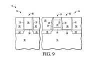
- FIG. 9illustrates processing of semiconductor structure 10 subsequent to FIG. 8 .
- a replacement gate method(also referred to as a metal gate-last process) is used to replace dummy logic gate 52 with metal logic gate 60 and to replace dummy select gate 54 with metal select gate 62 .
- a replacement methodat least a portion of dummy logic gate 52 is removed by applying one or more etch processes.
- a first poly etch processis applied to remove the exposed poly layer 30 (or dummy gate material) from the dummy logic gate 52 and from the dummy select gate 54 , where the poly layer 30 is etched selective to the material(s) used to form the ILD layer 50 (e.g., silicon oxide), the capping layer 22 (e.g., silicon nitride), and the sidewall spacers (e.g., silicon dioxide or nitride).
- the material(s) used to form the ILD layer 50e.g., silicon oxide
- the capping layer 22e.g., silicon nitride
- the sidewall spacerse.g., silicon dioxide or nitride
- Removal of the exposed portions of poly layer 30may use any desired poly etch process, including a dry etching process such as reactive-ion etching, ion beam etching, plasma etching, or laser etching, a wet etching process using a chemical etchant, or any combination thereof.
- a dry etching processsuch as reactive-ion etching, ion beam etching, plasma etching, or laser etching, a wet etching process using a chemical etchant, or any combination thereof.
- gate dielectric layer 28may include a thermal oxide layer that is etched selective to the material(s) used to form the ILD layer 50 , the capping layer 22 , and the sidewall spacers.
- Removal of the exposed portions of gate dielectric layer 28may use any desired dielectric etch process, including a dry etching process such as reactive-ion etching, ion beam etching, plasma etching, or laser etching, a wet etching process using a chemical etchant, or any combination thereof.
- a wet etching processis applied briefly to remove the gate dielectric layer 28 , where the timing and chemistry of the wet etch is controlled to minimize any etching of the planarized ILD layer 50 and sidewall spacers.
- a high-k dielectric layer(not shown) is then formed to a predetermined gate dielectric thickness in each opening over the substrate 16 .
- the high-k dielectric layermay be formed alone or in combination with a barrier layer, which is a layer of barrier metal that is deposited over the high-k dielectric layer in each opening to a predetermined thickness (e.g., approximately 50-200 Angstroms, although thinner or thicker layers may be used).
- the high-k dielectric layermay be formed by depositing a high-k gate dielectric material with a relatively high dielectric constant value over the substrate 16 in each opening using CVD, PECVD, PVD, ALD, or any combination(s) of the above.
- the high-k dielectric layermay be formed by a low temperature CVD or ALD process to a predetermined final thickness in the range of 1-100 Angstroms (e.g., 15-25 Angstroms), though other thicknesses may be used.
- a suitable high-k gate dielectric material for the high-k dielectric layeris an insulator material having a dielectric constant value k of 7.0 or greater, including a hafnium-based dielectric such hafnium silicate (e.g., Hf x Si 1-x O y ) or hafnium oxy-nitride (e.g., Hf x Si 1-x O y N z ), though other silicates of zirconium, aluminum, lanthanum, strontium, tantalum, titanium and combinations thereof may also be used, including but not limited to HfSiO X , ZrSiO X , LaSiO X , YSiO X , ScSiO X , CeS
- multi-metallic oxidesmay also provide high-k dielectric properties.
- a suitable temperature for the deposition processis in the range of approximately 200 degrees Celsius to approximately 400 degrees Celsius. Any portion of the high-k dielectric layer and barrier layer (if present) that is formed outside of each opening is removed.
- one or more appropriate gate dielectric layersare formed over the exposed portions of gate dielectric layer 28 in each opening.
- the gate dielectric layer 28may include a thermal oxide layer, where a high-k dielectric layer is formed over gate dielectric layer 28 in each opening.
- the high-k dielectric layermay be formed alone or in combination with a barrier layer, which is formed over the high-k dielectric layer in each opening. Any portion of the high-k dielectric layer and barrier layer (if present) that is formed outside of each opening is removed.
- gate dielectric layer 28already include one or more appropriate gate dielectric layers in each opening.
- gate dielectric layer 28may include a high-k dielectric layer, alone or in combination with a barrier layer formed over the high-k dielectric layer.
- a metal gate stack(also referred to as a conductive gate) is then formed over the one or more appropriate gate dielectric layers in each opening, where a high-k metal gate (HKMG) stack is formed in the event the one or more appropriate gate dielectric layers include a high-k dielectric layer.
- metal gate stack 56is formed in the opening of the logic gate (replacing the first remaining portion of the poly layer 30 ) and results in a metal logic gate 60 .
- Metal gate stack 58is formed in the opening of the select gate (replacing the second remaining portion of the poly layer 30 ) and results in a metal select gate 62 .
- Metal gate stack 56 and metal gate stack 58each include one or more metal layers.
- the metal gate stack used in the logic gate 60is identical to the metal gate stack used in the select gate 62 (e.g., stacks 56 and 58 include the same metal layers). In other embodiments, the metal gate stack used in the logic gate 60 is different from the metal gate stack used in the select gate 62 (e.g., stacks 56 and 58 include different metal layers).
- the portion of capping layer 22 that remains over poly layer 20provides isolation between control gate stack 24 and the metal gate stack 58 . Isolation may be improved by leaving capping layer 22 in its entirety over the control gate stack (e.g., by stopping planarization in FIG. 8 before reaching capping layer 22 , which may also leave a remaining portion of ILD layer 50 over the control gate stack). It is also noted that in some embodiments where a portion of ILD layer 50 and a portion of poly layer 30 remain over control gate stack 24 , the resulting metal gate stack 58 may extend over a portion of the control gate stack 24 (due to poly layer 30 being replaced with metal).
- Each metal gate stackis formed using any desired technique, such as by conformally depositing one or more metal layers on the bottom of the openings, depending on the type of transistor (e.g., NMOS or PMOS) being formed, or other desired deposition or sputtering process, such as CVD, PECVD, PVD, ALD, molecular beam deposition (MBD), or any combination(s) thereof.
- a suitable material for use as a metal layeris a conductive material, such as a metal or transition metal material including, as an example, aluminum, tungsten, titanium or TiN, using metal organic chemical vapor deposition (MOCVD), CVD, PECVD, PVD, ALD, MBD, or any combination(s) thereof to a predetermined thickness in the range of 200-1000 Angstroms (e.g., 500-600 Angstroms), though other materials and thicknesses may be used.
- MOCVDmetal organic chemical vapor deposition
- the one or more metal layersmay include an element selected from the group consisting of Ti, Ta, La, Ir, Mo, Ru, W, Os, Nb, Ti, V, Ni, W, and Re to form a metal or metal-based layer that may contain carbon and/or nitrogen (such as TiN, TaC, HfC, TaSi, ZrC, Hf, etc.) or even a conductive metal oxide (such as IrO2), which may be deposited to a predetermined thickness of 20-150 Angstroms, although other metallic layer materials with different thicknesses may be used.
- the one or more metal layersmay be used to adjust the work function of the finally formed transistor, depending on its polarity type.
- an upper portion of the metal gate stacksmay be removed in order to planarize the metal gate stacks with the planarized portions of ILD layer 50 by applying a chemical mechanical polish to clear any metal over the top of the planarized portion of ILD layer 50 , though this polish step can occur later in the fabrication sequence.
- the top surface of poly layer 20 of control gate stack 24is lower relative to the top surface of the resulting metal select gate 62 , and may also be lower relative to the top surface of the resulting metal logic gate 60 .
- the top surface of the control gate stack 24e.g., the top surface of capping layer 22
- the top surface of the control gate stack 24(e.g., the top surface of capping layer 22 ) is lower relative to the top surface of metal select gate 62 , and may also be lower relative to the top surface of metal logic gate 60 (e.g., the top surface of capping layer 22 is covered by a remaining portion of ILD layer 50 , which has a top surface that is coplanar with the top surface of metal select gate 62 , and may also be coplanar with the top surface of metal logic gate 60 ).
- additional processing stepsmay be used to complete the fabrication of the split-gate non-volatile memory cells and other transistors in the NVM and logic regions.
- additional backend processing stepsmay be performed, such as forming contact openings, contact plugs and multiple levels of interconnect(s) that are used to connect the device components in a desired manner to achieve the desired functionality.
- the specific sequence of steps used to complete the fabrication of the device componentsmay vary, depending on the process and/or design requirements.
- One embodiment of the present disclosureprovides for a method of making a semiconductor structure using a semiconductor substrate, where the semiconductor structure includes a split gate NVM cell in an NVM region of the substrate.
- the methodincludes forming a charge storage layer on the substrate, depositing a first conductive layer over the charge storage layer, depositing a capping layer over the first conductive layer, and patterning the capping layer, the first conductive layer, and the charge storage layer to form a control gate stack.
- the methodalso includes depositing a second conductive layer over the substrate including over the control gate stack; and patterning the second conductive layer to leave a first portion of the second conductive layer over a portion of the control gate stack and adjacent to a first side of the control gate stack.
- the methodalso includes planarizing the first portion of the second conductive layer and the control gate stack to leave a dummy select gate from the first portion of the second conductive layer, where the planarizing exposes a top surface of the dummy select gate, and a top surface of a remaining portion of the first conductive layer of the control gate stack is lower relative to the top surface of the dummy select gate; and replacing the dummy select gate with a select gate including metal.
- the methodfurther includes forming an insulating sidewall spacer on sides of the control gate stack prior to the depositing the second conductive layer.
- the methodfurther includes forming a first dielectric layer on the substrate after the patterning the capping layer, the first conductive layer, and the charge storage layer and prior to the depositing the second conductive layer.
- the first dielectric layerincludes one of a group consisting of thermal oxide and a high-k dielectric.
- the patterning the second conductive layerfurther includes etching the first dielectric layer to leave a portion of the first dielectric layer under the first portion of the second conductive layer.
- the methodfurther includes replacing the portion of the first dielectric layer with a high-k dielectric prior to replacing the dummy select gate.
- the semiconductor structurefurther includes a logic transistor in a logic region
- the methodfurther includes removing the capping layer, the first conductive layer, and the charge storage layer from the logic region prior to depositing the second conductive layer.
- the patterning the second conductive layeris further characterized by leaving a dummy logic gate in the logic region.
- the methodfurther includes replacing the dummy logic gate with a logic gate including metal.
- the methodfurther includes forming a first dielectric layer on the substrate in the NVM region and the logic region after the patterning the capping layer, the first conductive layer, and the charge storage layer and prior to the depositing the second conductive layer, wherein the first dielectric layer includes one of a group consisting of oxide and a high-k dielectric.
- the methodfurther includes forming a first dielectric layer on the substrate in the NVM region and the logic region after the patterning the capping layer, the first conductive layer, and the charge storage layer and prior to the depositing the second conductive layer, wherein the patterning the second conductive layer further includes etching the first dielectric layer to leave a portion of the first dielectric layer under the dummy logic gate.
- the methodfurther includes replacing the first dielectric layer with a high-k dielectric prior to replacing the dummy logic gate.
- the split gate NVM cellincludes a control gate stack that includes a charge storage layer over the substrate, a polysilicon control gate over the charge storage layer, and a capping layer of dielectric material over the polysilicon control gate, where the capping layer has a top surface of the control gate stack; and a select gate stack laterally adjacent to the control gate stack having a gate dielectric over the substrate and a conductive select gate over the gate dielectric, where the polysilicon control gate has a top surface that is lower relative to a top surface of the conductive select gate.
- the semiconductor structurefurther includes a first source/drain in the substrate adjacent to a first side of the control gate stack and a second source/drain in the substrate adjacent to a first side of the select gate stack, wherein the first side of the control gate stack is on an opposite side of the split gate NVM cell from the first side of the select gate stack.
- the conductive select gateincludes metal and the gate dielectric includes a high-k dielectric material.
- the select gatefurther includes a polysilicon layer having a top surface of the conductive select gate.
- the semiconductor structurefurther includes a logic region, which includes a logic transistor in the logic region, where the logic transistor has a gate including metal with a top surface coplanar with the top surface of conductive select gate.
- the gate of the logic transistorhas a top layer of polysilicon over a metal layer, where the top layer of polysilicon has a top surface as the top surface of the gate of the logic transistor.
- Another embodiment of the present disclosureprovides for a method of making a semiconductor structure using a substrate, wherein the semiconductor structure includes a split gate non-volatile memory (NVM) structure in an NVM region.
- the methodincludes forming a charge storage layer on the substrate; depositing a first polysilicon layer over the charge storage layer; depositing a capping layer over the first polysilicon layer; and patterning the capping layer, the first conductive layer, and the charge storage layer to leave a control gate stack that includes remaining portions of the capping layer, the first conductive layer, and the charge storage layer.
- NVMnon-volatile memory
- the methodfurther includes depositing a second polysilicon layer over the substrate including over the control gate stack; and patterning the second polysilicon layer to leave a first portion of the second polysilicon layer over a portion of the control gate stack and adjacent to a first side of the control gate stack.
- the methodfurther includes planarizing the first portion of the second polysilicon layer and the control gate stack to leave a dummy select gate from the first portion of the second polysilicon layer, where a top surface of the control gate stack includes a top surface of the remaining portion of the capping layer and where a top surface of the remaining portion of the first conductive layer is lower relative to a top surface of the dummy select gate; and replacing the dummy select gate with a select gate that includes metal by using an etchant to remove the dummy select gate, where the etchant is highly selective to polysilicon and does not substantially remove the capping layer.
- the semiconductor structurefurther includes a logic transistor in a logic region
- the methodfurther includes removing the capping layer, the first conductive layer, and the charge storage layer from the logic region prior to depositing the second conductive layer; where: the depositing the second polysilicon layer deposits the second polysilicon layer over the logic region; the patterning the second polysilicon layer leaves a dummy logic gate including polysilicon over the substrate in the logic region; the planarizing the first portion of second polysilicon layer leaves the dummy gate with a top surface coplanar with a top surface of the dummy select gate and a top surface of the control gate stack; and the replacing the dummy select gate occurs simultaneously with replacing the dummy logic gate with a gate including metal.
- gate dielectric layer 28that is a thermal oxide layer can be deposited over the control gate stack 24 without needing to be removed from the control gate stack's outer sidewall spacer.
- other types of split-gate NVM bitcell devicesmay be formed with different sequencing and/or materials. Accordingly, the specification and figures are to be regarded in an illustrative rather than a restrictive sense, and all such modifications are intended to be included within the scope of the present invention. Any benefits, advantages, or solutions to problems that are described herein with regard to specific embodiments are not intended to be construed as a critical, required, or essential feature or element of any or all the claims.
Landscapes
- Engineering & Computer Science (AREA)
- Manufacturing & Machinery (AREA)
- Physics & Mathematics (AREA)
- Condensed Matter Physics & Semiconductors (AREA)
- General Physics & Mathematics (AREA)
- Computer Hardware Design (AREA)
- Microelectronics & Electronic Packaging (AREA)
- Power Engineering (AREA)
- Non-Volatile Memory (AREA)
- Semiconductor Memories (AREA)
Abstract
Description
Claims (13)
Priority Applications (1)
| Application Number | Priority Date | Filing Date | Title |
|---|---|---|---|
| US14/291,359US9343314B2 (en) | 2014-05-30 | 2014-05-30 | Split gate nanocrystal memory integration |
Applications Claiming Priority (1)
| Application Number | Priority Date | Filing Date | Title |
|---|---|---|---|
| US14/291,359US9343314B2 (en) | 2014-05-30 | 2014-05-30 | Split gate nanocrystal memory integration |
Publications (2)
| Publication Number | Publication Date |
|---|---|
| US20150348786A1 US20150348786A1 (en) | 2015-12-03 |
| US9343314B2true US9343314B2 (en) | 2016-05-17 |
Family
ID=54702619
Family Applications (1)
| Application Number | Title | Priority Date | Filing Date |
|---|---|---|---|
| US14/291,359ActiveUS9343314B2 (en) | 2014-05-30 | 2014-05-30 | Split gate nanocrystal memory integration |
Country Status (1)
| Country | Link |
|---|---|
| US (1) | US9343314B2 (en) |
Cited By (2)
| Publication number | Priority date | Publication date | Assignee | Title |
|---|---|---|---|---|
| US20170365690A1 (en)* | 2016-06-20 | 2017-12-21 | Semiconductor Manufacturing International (Shanghai) Corporation | Transistor device and fabrication method |
| US20190027484A1 (en)* | 2017-07-19 | 2019-01-24 | Cypress Semiconductor Corporation | Embedded non-volatile memory device and fabrication method of the same |
Families Citing this family (9)
| Publication number | Priority date | Publication date | Assignee | Title |
|---|---|---|---|---|
| US9397176B2 (en)* | 2014-07-30 | 2016-07-19 | Freescale Semiconductor, Inc. | Method of forming split gate memory with improved reliability |
| US9793279B2 (en)* | 2015-07-10 | 2017-10-17 | Silicon Storage Technology, Inc. | Split gate non-volatile memory cell having a floating gate, word line, erase gate, and method of manufacturing |
| JP6620046B2 (en)* | 2016-03-15 | 2019-12-11 | ルネサスエレクトロニクス株式会社 | Semiconductor device manufacturing method and semiconductor device |
| US10290722B2 (en)* | 2016-10-31 | 2019-05-14 | Taiwan Semiconductor Manufacturing Co., Ltd. | Memory device and method of fabricating thereof |
| JP6778607B2 (en)* | 2016-12-22 | 2020-11-04 | ルネサスエレクトロニクス株式会社 | Manufacturing method of semiconductor devices |
| US10510765B2 (en)* | 2017-07-18 | 2019-12-17 | Taiwan Semiconductor Manufacturing Co., Ltd. | Memory device and method for fabricating the same |
| DE102019122590A1 (en) | 2018-08-28 | 2020-03-05 | Taiwan Semiconductor Manufacturing Co., Ltd. | METHOD FOR IMPROVING CONTROL GATE UNIFORMITY DURING THE MANUFACTURING OF PROCESSORS WITH EMBEDDED FLASH MEMORY |
| US11069693B2 (en)* | 2018-08-28 | 2021-07-20 | Taiwan Semiconductor Manufacturing Co., Ltd. | Method for improving control gate uniformity during manufacture of processors with embedded flash memory |
| CN110620115B (en)* | 2019-05-23 | 2022-03-18 | 上海华力集成电路制造有限公司 | Manufacturing method of 1.5T SONOS flash memory |
Citations (128)
| Publication number | Priority date | Publication date | Assignee | Title |
|---|---|---|---|---|
| US5614746A (en) | 1994-11-28 | 1997-03-25 | United Microelectronics Corporation | Structure and process of manufacture of split gate flash memory cell |
| US6087225A (en) | 1998-02-05 | 2000-07-11 | International Business Machines Corporation | Method for dual gate oxide dual workfunction CMOS |
| US6130168A (en) | 1999-07-08 | 2000-10-10 | Taiwan Semiconductor Manufacturing Company | Using ONO as hard mask to reduce STI oxide loss on low voltage device in flash or EPROM process |
| US6194301B1 (en) | 1999-07-12 | 2001-02-27 | International Business Machines Corporation | Method of fabricating an integrated circuit of logic and memory using damascene gate structure |
| US6235574B1 (en) | 1999-03-22 | 2001-05-22 | Infineon North America Corp. | High performance DRAM and method of manufacture |
| US20010049166A1 (en) | 2000-03-29 | 2001-12-06 | Stmicroelectronics S.R.L. | Method of manufacturing an electrically programmable, non-volatile memory and high-performance logic circuitry in the same semiconductor chip |
| US6333223B1 (en) | 1998-12-25 | 2001-12-25 | Matsushita Electric Industrial Co., Ltd. | Semiconductor device and method of manufacturing the same |
| US20020061616A1 (en) | 2000-11-22 | 2002-05-23 | Kim Jae Hyung | Method for fabricating semiconductor device |
| US20030022434A1 (en) | 1998-12-25 | 2003-01-30 | Yasuhiro Taniguchi | Semiconductor integrated circuit device and a method of manufacturing the same |
| US6531734B1 (en) | 2002-05-24 | 2003-03-11 | Silicon Based Technology Corp. | Self-aligned split-gate flash memory cell having an integrated source-side erase structure and its contactless flash memory arrays |
| US6635526B1 (en) | 2002-06-07 | 2003-10-21 | Infineon Technologies Ag | Structure and method for dual work function logic devices in vertical DRAM process |
| US6707079B2 (en) | 2001-02-22 | 2004-03-16 | Halo Lsi, Inc. | Twin MONOS cell fabrication method and array organization |
| US20040075133A1 (en) | 2000-09-29 | 2004-04-22 | Fujitsu Limited | Semiconductor device and its manufacturing method |
| US6777761B2 (en) | 2002-08-06 | 2004-08-17 | International Business Machines Corporation | Semiconductor chip using both polysilicon and metal gate devices |
| US6785165B2 (en) | 2002-01-25 | 2004-08-31 | Renesas Technology Corporation | Semiconductor device |
| US20040188753A1 (en) | 2003-03-31 | 2004-09-30 | Yoshiyuki Kawashima | Semiconductor device and a method of manufacturing the same |
| US20040262670A1 (en) | 2003-06-30 | 2004-12-30 | Kabushiki Kaisha Toshiba | Semiconductor device including nonvolatile memory and method for fabricating the same |
| US6861698B2 (en) | 2002-01-24 | 2005-03-01 | Silicon Storage Technology, Inc. | Array of floating gate memory cells having strap regions and a peripheral logic device region |
| US20050145949A1 (en) | 2003-10-27 | 2005-07-07 | Kayvan Sadra | Application of different isolation schemes for logic and embedded memory |
| US6939767B2 (en) | 2003-11-19 | 2005-09-06 | Freescale Semiconductor, Inc. | Multi-bit non-volatile integrated circuit memory and method therefor |
| US20050247962A1 (en) | 2004-05-06 | 2005-11-10 | Arup Bhattacharyya | Silicon on insulator read-write non-volatile memory comprising lateral thyristor and trapping layer |
| US20060038240A1 (en) | 2004-08-17 | 2006-02-23 | Fujitsu Limited | Semiconductor device and manufacturing method of the same |
| US20060046449A1 (en) | 2004-08-27 | 2006-03-02 | Taiwan Semiconductor Manufacturing Co., Ltd. | Metal gate structure for mos devices |
| US20060099798A1 (en) | 2004-11-08 | 2006-05-11 | Fujitsu Limited | Semiconductor device and manufacturing method of the same |
| US20060134864A1 (en) | 2004-12-22 | 2006-06-22 | Masaaki Higashitani | Multi-thickness dielectric for semiconductor memory |
| US20060211206A1 (en) | 2005-03-18 | 2006-09-21 | Freescale Semiconductor, Inc. | Electronic devices including non-volatile memory and processes for forming the same |
| US20060221688A1 (en) | 1999-02-01 | 2006-10-05 | Shoji Shukuri | Semiconductor integrated circuit and nonvolatile memory element |
| US7154779B2 (en) | 2004-01-21 | 2006-12-26 | Sandisk Corporation | Non-volatile memory cell using high-k material inter-gate programming |
| US20070037343A1 (en) | 2005-08-10 | 2007-02-15 | Texas Instruments Inc. | Process for manufacturing dual work function metal gates in a microelectronics device |
| US7183159B2 (en) | 2005-01-14 | 2007-02-27 | Freescale Semiconductor, Inc. | Method of forming an integrated circuit having nanocluster devices and non-nanocluster devices |
| US7190022B2 (en) | 2003-06-27 | 2007-03-13 | Infineon Technologies Ag | One transistor flash memory cell |
| US20070077705A1 (en) | 2005-09-30 | 2007-04-05 | Prinz Erwin J | Split gate memory cell and method therefor |
| US7202524B2 (en) | 2004-12-08 | 2007-04-10 | Samsung Electronics Co., Ltd. | Nonvolatile memory device and method of manufacturing the same |
| US7208793B2 (en) | 2004-11-23 | 2007-04-24 | Micron Technology, Inc. | Scalable integrated logic and non-volatile memory |
| US20070115725A1 (en) | 2004-12-22 | 2007-05-24 | Tuan Pham | Low-Voltage, Multiple Thin-Gate Oxide and Low-Resistance Gate Electrode |
| US7223650B2 (en) | 2005-10-12 | 2007-05-29 | Intel Corporation | Self-aligned gate isolation |
| US7256125B2 (en) | 2003-08-25 | 2007-08-14 | Renesas Technology Corp. | Method of manufacturing a semiconductor device |
| US7271050B2 (en) | 2002-08-27 | 2007-09-18 | Micron Technology, Inc. | Silicon nanocrystal capacitor and process for forming same |
| US20070215917A1 (en) | 2006-03-20 | 2007-09-20 | Renesas Technology Corp. | Semiconductor integrated circuit device and a method of manufacturing the same |
| US20070224772A1 (en) | 2006-03-21 | 2007-09-27 | Freescale Semiconductor, Inc. | Method for forming a stressor structure |
| US20070249129A1 (en) | 2006-04-21 | 2007-10-25 | Freescale Semiconductor, Inc. | STI stressor integration for minimal phosphoric exposure and divot-free topography |
| US20070264776A1 (en) | 2003-11-19 | 2007-11-15 | Zhong Dong | Precision creation of inter-gates insulator |
| US20080029805A1 (en) | 2006-08-03 | 2008-02-07 | Yasuhiro Shimamoto | Semiconductor device and manufacturing method of the same |
| US20080050875A1 (en) | 2006-08-25 | 2008-02-28 | Jung-Ho Moon | Methods of fabricating embedded flash memory devices |
| US20080067599A1 (en) | 2005-05-23 | 2008-03-20 | Fujitsu Limited | Semiconductor device and method of manufacturing the same |
| US7365389B1 (en) | 2004-12-10 | 2008-04-29 | Spansion Llc | Memory cell having enhanced high-K dielectric |
| US20080105945A1 (en) | 2004-11-12 | 2008-05-08 | Freescale Semiconductor, Inc. | Method of forming a nanocluster charge storage device |
| US20080121983A1 (en) | 2006-09-22 | 2008-05-29 | Seong Geum-Jung | Gate and method of forming the same, and memory device and method of manufacturing the same |
| US20080128785A1 (en) | 2006-11-30 | 2008-06-05 | Jin-Ha Park | Flash memory device and method of manufacturing the same |
| US20080145985A1 (en) | 2006-12-15 | 2008-06-19 | Semiconductor Manufacturing International (Shanghai) Corporation | Embedded semiconductor memory devices and methods for fabricating the same |
| US7391075B2 (en) | 2004-10-08 | 2008-06-24 | Samsung Electronics Co., Ltd. | Non-volatile semiconductor memory device with alternative metal gate material |
| US7402493B2 (en) | 2004-04-12 | 2008-07-22 | Samsung Electronics Co., Ltd. | Method for forming non-volatile memory devices |
| US20080185635A1 (en) | 2007-02-01 | 2008-08-07 | Renesas Technology Corp. | Semiconductor storage device and manufacturing method thereof |
| US20080237690A1 (en) | 2007-03-26 | 2008-10-02 | Fujitsu Limited | Semiconductor device and method of manufacturing the same |
| US20080237700A1 (en) | 2007-03-28 | 2008-10-02 | Samsung Electronics Co., Ltd. | Nonvolatile memory device having cell and peripheral regions and method of making the same |
| US7439134B1 (en) | 2007-04-20 | 2008-10-21 | Freescale Semiconductor, Inc. | Method for process integration of non-volatile memory cell transistors with transistors of another type |
| US20080283900A1 (en) | 2005-12-14 | 2008-11-20 | Fujitsu Limited | Semiconductor device and method for manufacturing the same |
| US20080290385A1 (en) | 2007-05-24 | 2008-11-27 | Seiko Epson Corporation | Method for manufacturing ferroelectric capacitor, and ferroelectric capacitor |
| US20080308876A1 (en) | 2007-06-12 | 2008-12-18 | Hye-Lan Lee | Semiconductor device and method of manufacturing the same |
| US20090050955A1 (en) | 2007-08-24 | 2009-02-26 | Kenichi Akita | Nonvolatile semiconductor device and method of manufacturing the same |
| US20090065845A1 (en) | 2007-09-11 | 2009-03-12 | Samsung Electronics Co., Ltd. | Embedded semiconductor device and method of manufacturing an embedded semiconductor device |
| US20090072274A1 (en) | 2007-09-14 | 2009-03-19 | Qimonda Ag | Integrated circuit including a first gate stack and a second gate stack and a method of manufacturing |
| US20090078986A1 (en) | 2007-09-20 | 2009-03-26 | Lars Bach | Manufacturing method for an integrated circuit including different types of gate stacks, corresponding intermediate integrated circuit structure and corresponding integrated circuit |
| US7521314B2 (en) | 2007-04-20 | 2009-04-21 | Freescale Semiconductor, Inc. | Method for selective removal of a layer |
| US20090101961A1 (en) | 2007-10-22 | 2009-04-23 | Yue-Song He | Memory devices with split gate and blocking layer |
| US7524719B2 (en) | 2006-08-31 | 2009-04-28 | Freescale Semiconductor, Inc. | Method of making self-aligned split gate memory cell |
| US20090111229A1 (en) | 2007-10-31 | 2009-04-30 | Steimle Robert F | Method of forming a split gate non-volatile memory cell |
| WO2009058486A1 (en) | 2007-10-29 | 2009-05-07 | Freescale Semiconductor Inc. | Method for integrating nvm circuitry with logic circuitry |
| US7544980B2 (en) | 2006-01-27 | 2009-06-09 | Freescale Semiconductor, Inc. | Split gate memory cell in a FinFET |
| US7544490B2 (en) | 2002-02-08 | 2009-06-09 | Genencor International, Inc. | Secretion, transcription and sporulation genes in Bacillus clausii |
| US7560767B2 (en) | 2005-10-14 | 2009-07-14 | Kabushiki Kaisha Toshiba | Nonvolatile semiconductor memory device |
| US20090179283A1 (en) | 2007-12-12 | 2009-07-16 | International Business Machines Corporation | Metal gate stack and semiconductor gate stack for cmos devices |
| US20090225602A1 (en) | 2005-05-26 | 2009-09-10 | Micron Technology, Inc. | Multi-state memory cell |
| US20090256211A1 (en) | 2008-04-10 | 2009-10-15 | International Business Machines Corporation | Metal gate compatible flash memory gate stack |
| US20090263749A1 (en)* | 2008-04-17 | 2009-10-22 | Samsung Electronics Co., Ltd. | Method of forming fine patterns of semiconductor device |
| US20090269893A1 (en) | 2001-07-05 | 2009-10-29 | Fujitsu Limited | Semiconductor integrated circuit device and method of producing the same |
| US20090273013A1 (en) | 2008-04-30 | 2009-11-05 | Winstead Brian A | Method of forming a split gate memory device and apparatus |
| US20090278187A1 (en) | 2008-05-09 | 2009-11-12 | Toba Takayuki | Semiconductor device and manufacturing method of semiconductor device |
| US20100096719A1 (en)* | 2008-10-22 | 2010-04-22 | Samsung Electronics Co., Ltd. | Methods of forming fine patterns in integrated circuit devices |
| US7799650B2 (en) | 2007-08-08 | 2010-09-21 | Freescale Semiconductor, Inc. | Method for making a transistor with a stressor |
| US7816727B2 (en) | 2007-08-27 | 2010-10-19 | Macronix International Co., Ltd. | High-κ capped blocking dielectric bandgap engineered SONOS and MONOS |
| US7821055B2 (en) | 2009-03-31 | 2010-10-26 | Freescale Semiconductor, Inc. | Stressed semiconductor device and method for making |
| US20110031548A1 (en) | 2008-04-15 | 2011-02-10 | Freescale Semiconductor, Inc. | Split gate non-volatile memory cell with improved endurance and method therefor |
| US7906396B1 (en) | 2009-09-02 | 2011-03-15 | Winbond Electronics Corp. | Flash memory and method of fabricating the same |
| US7932146B2 (en) | 2008-03-20 | 2011-04-26 | United Microelectronics Corp. | Metal gate transistor and polysilicon resistor and method for fabricating the same |
| US20110095348A1 (en) | 2009-10-28 | 2011-04-28 | Renesas Electronics Corporation | Semiconductor device and method of manufacturing the same |
| US7989871B2 (en) | 2006-03-15 | 2011-08-02 | Kabushiki Kaisha Toshiba | Nonvolatile semiconductor memory device having insulating films that include multiple layers formed by insulating materials having d-orbital metal element and insulating materials without d-orbital metal element |
| US7999304B2 (en) | 2007-02-07 | 2011-08-16 | Kabushiki Kaisha Toshiba | Semiconductor device |
| US8003482B2 (en)* | 2009-11-19 | 2011-08-23 | Micron Technology, Inc. | Methods of processing semiconductor substrates in forming scribe line alignment marks |
| US20110204450A1 (en) | 2010-02-25 | 2011-08-25 | Renesas Electronics Corporation | Semiconductor device and manufacturing method thereof |
| US8017991B2 (en) | 2006-07-28 | 2011-09-13 | Samsung Electronics Co., Ltd. | Non-volatile memory device and methods of operating and fabricating the same |
| US8043951B2 (en) | 2007-08-01 | 2011-10-25 | Freescale Semiconductor, Inc. | Method of manufacturing a semiconductor device and semiconductor device obtainable therewith |
| US20110260258A1 (en) | 2009-12-31 | 2011-10-27 | Institute of Microelectronics, Chinese Academy of Sciences | Field effect transistor device with improved carrier mobility and method of manufacturing the same |
| US8063434B1 (en) | 2007-05-25 | 2011-11-22 | Cypress Semiconductor Corporation | Memory transistor with multiple charge storing layers and a high work function gate electrode |
| US8093128B2 (en) | 2007-05-25 | 2012-01-10 | Cypress Semiconductor Corporation | Integration of non-volatile charge trap memory devices and logic CMOS devices |
| US20120034751A1 (en) | 2010-08-06 | 2012-02-09 | Fujitsu Semiconductor Limited | Method of manufacturing semiconductor device |
| US8138037B2 (en) | 2009-03-17 | 2012-03-20 | International Business Machines Corporation | Method and structure for gate height scaling with high-k/metal gate technology |
| US8168493B2 (en) | 2010-03-05 | 2012-05-01 | Samsung Electronics Co., Ltd. | Semiconductor memory device and method of manufacturing the same |
| US20120104483A1 (en) | 2010-10-29 | 2012-05-03 | Shroff Mehul D | Non-volatile memory and logic circuit process integration |
| US8173505B2 (en) | 2008-10-20 | 2012-05-08 | Freescale Semiconductor, Inc. | Method of making a split gate memory cell |
| US20120132978A1 (en) | 2010-11-25 | 2012-05-31 | Renesas Electronics Corporation | Semiconductor device and manufacturing method of semiconductor device |
| US20120142153A1 (en) | 2005-03-08 | 2012-06-07 | Magnachip Semiconductor Ltd. | Non-volatile memory device and method for fabricating the same |
| US20120248523A1 (en) | 2011-03-31 | 2012-10-04 | Shroff Mehul D | Non-volatile memory and logic circuit process integration |
| US20120252171A1 (en) | 2011-03-31 | 2012-10-04 | Shroff Mehul D | Non-volatile memory and logic circuit process integration |
| US8298885B2 (en) | 2009-05-15 | 2012-10-30 | Globalfoundries Inc. | Semiconductor device comprising metal gates and a silicon containing resistor formed on an isolation structure |
| US8334198B2 (en) | 2011-04-12 | 2012-12-18 | Taiwan Semiconductor Manufacturing Company, Ltd. | Method of fabricating a plurality of gate structures |
| US20130026553A1 (en) | 2011-07-26 | 2013-01-31 | Synopsys, Inc. | NVM Bitcell with a Replacement Control Gate and Additional Floating Gate |
| US8372699B2 (en) | 2010-02-22 | 2013-02-12 | Freescale Semiconductor, Inc. | Method for forming a split-gate memory cell |
| US20130037886A1 (en) | 2011-08-10 | 2013-02-14 | Teng-Chun Tsai | Semiconductor device and method of making the same |
| US20130065366A1 (en) | 2011-09-08 | 2013-03-14 | Stmicroelectronics | Soi integrated circuit comprising adjacent cells of different types |
| US20130084684A1 (en) | 2011-10-03 | 2013-04-04 | Renesas Electronics Corporation | Manufacturing method of semiconductor device |
| US20130137227A1 (en) | 2011-11-30 | 2013-05-30 | Mehul D. Shroff | Logic and non-volatile memory (nvm) integration |
| US20130171785A1 (en) | 2012-01-04 | 2013-07-04 | Mehul D. Shroff | Non-volatile memory (nvm) and logic integration |
| US20130171786A1 (en) | 2012-01-04 | 2013-07-04 | Freescale Semiconductor, Inc. | Non-volatile memory (nvm) and logic integration |
| US20130178027A1 (en) | 2012-01-04 | 2013-07-11 | Freescale Semiconductor, Inc. | Non-volatile memory (nvm) and logic integration |
| US8524557B1 (en)* | 2012-02-22 | 2013-09-03 | Freescale Semiconductor, Inc. | Integration technique using thermal oxide select gate dielectric for select gate and replacement gate for logic |
| US20130264633A1 (en) | 2012-04-09 | 2013-10-10 | Mark D. Hall | Logic transistor and non-volatile memory cell integration |
| US20130267074A1 (en) | 2012-04-09 | 2013-10-10 | Freescale Semiconductor Inc. | Integration technique using thermal oxide select gate dielectric for select gate and apartial replacement gate for logic |
| US20130267072A1 (en) | 2012-04-06 | 2013-10-10 | Freescale Semiconductor, Inc. | Non-volatile memory (nvm) and logic integration |
| US20130323922A1 (en) | 2011-09-29 | 2013-12-05 | Freescale Semiconductor, Inc. | Split gate memory device with gap spacer |
| US20140035027A1 (en) | 2009-11-25 | 2014-02-06 | Renesas Electronics Corporation | Semiconductor device and a manufacturing method thereof |
| US20140050029A1 (en) | 2012-08-20 | 2014-02-20 | Sung-taeg Kang | Split-gate memory cells having select-gate sidewall metal silicide regions and related manufacturing methods |
| US20140120713A1 (en) | 2012-10-26 | 2014-05-01 | Mehul D. Shroff | Method of making a logic transistor and a non-volatile memory (nvm) cell |
| US20140227843A1 (en) | 2013-02-12 | 2014-08-14 | Renesas Electronics Corporation | Method of manufacturing a semiconductor device |
| US8871598B1 (en) | 2013-07-31 | 2014-10-28 | Freescale Semiconductor, Inc. | Non-volatile memory (NVM) and high-k and metal gate integration using gate-first methodology |
| US8937011B2 (en)* | 2012-12-18 | 2015-01-20 | Sandisk 3D Llc | Method of forming crack free gap fill |
| US8969206B1 (en)* | 2013-09-04 | 2015-03-03 | Sandisk Technologies Inc. | Triple patterning NAND flash memory with stepped mandrel |
| US9112056B1 (en)* | 2014-03-28 | 2015-08-18 | Freescale Semiconductor, Inc. | Method for forming a split-gate device |
- 2014
- 2014-05-30USUS14/291,359patent/US9343314B2/enactiveActive
Patent Citations (143)
| Publication number | Priority date | Publication date | Assignee | Title |
|---|---|---|---|---|
| US5614746A (en) | 1994-11-28 | 1997-03-25 | United Microelectronics Corporation | Structure and process of manufacture of split gate flash memory cell |
| US6087225A (en) | 1998-02-05 | 2000-07-11 | International Business Machines Corporation | Method for dual gate oxide dual workfunction CMOS |
| US6333223B1 (en) | 1998-12-25 | 2001-12-25 | Matsushita Electric Industrial Co., Ltd. | Semiconductor device and method of manufacturing the same |
| US6509225B2 (en) | 1998-12-25 | 2003-01-21 | Matsushita Electric Industrial Co., Ltd. | Semiconductor device and method of manufacturing the same |
| US20030022434A1 (en) | 1998-12-25 | 2003-01-30 | Yasuhiro Taniguchi | Semiconductor integrated circuit device and a method of manufacturing the same |
| US20060221688A1 (en) | 1999-02-01 | 2006-10-05 | Shoji Shukuri | Semiconductor integrated circuit and nonvolatile memory element |
| US6235574B1 (en) | 1999-03-22 | 2001-05-22 | Infineon North America Corp. | High performance DRAM and method of manufacture |
| US6130168A (en) | 1999-07-08 | 2000-10-10 | Taiwan Semiconductor Manufacturing Company | Using ONO as hard mask to reduce STI oxide loss on low voltage device in flash or EPROM process |
| US6194301B1 (en) | 1999-07-12 | 2001-02-27 | International Business Machines Corporation | Method of fabricating an integrated circuit of logic and memory using damascene gate structure |
| US6388294B1 (en) | 1999-07-12 | 2002-05-14 | International Business Machines Corporation | Integrated circuit using damascene gate structure |
| US20010049166A1 (en) | 2000-03-29 | 2001-12-06 | Stmicroelectronics S.R.L. | Method of manufacturing an electrically programmable, non-volatile memory and high-performance logic circuitry in the same semiconductor chip |
| US20040075133A1 (en) | 2000-09-29 | 2004-04-22 | Fujitsu Limited | Semiconductor device and its manufacturing method |
| US7476582B2 (en) | 2000-09-29 | 2009-01-13 | Fujitsu Limited | Semiconductor device and its manufacturing method |
| US20020061616A1 (en) | 2000-11-22 | 2002-05-23 | Kim Jae Hyung | Method for fabricating semiconductor device |
| US6707079B2 (en) | 2001-02-22 | 2004-03-16 | Halo Lsi, Inc. | Twin MONOS cell fabrication method and array organization |
| US20090269893A1 (en) | 2001-07-05 | 2009-10-29 | Fujitsu Limited | Semiconductor integrated circuit device and method of producing the same |
| US6861698B2 (en) | 2002-01-24 | 2005-03-01 | Silicon Storage Technology, Inc. | Array of floating gate memory cells having strap regions and a peripheral logic device region |
| US6785165B2 (en) | 2002-01-25 | 2004-08-31 | Renesas Technology Corporation | Semiconductor device |
| US7544490B2 (en) | 2002-02-08 | 2009-06-09 | Genencor International, Inc. | Secretion, transcription and sporulation genes in Bacillus clausii |
| US6531734B1 (en) | 2002-05-24 | 2003-03-11 | Silicon Based Technology Corp. | Self-aligned split-gate flash memory cell having an integrated source-side erase structure and its contactless flash memory arrays |
| US6635526B1 (en) | 2002-06-07 | 2003-10-21 | Infineon Technologies Ag | Structure and method for dual work function logic devices in vertical DRAM process |
| US6777761B2 (en) | 2002-08-06 | 2004-08-17 | International Business Machines Corporation | Semiconductor chip using both polysilicon and metal gate devices |
| US7271050B2 (en) | 2002-08-27 | 2007-09-18 | Micron Technology, Inc. | Silicon nanocrystal capacitor and process for forming same |
| US20040188753A1 (en) | 2003-03-31 | 2004-09-30 | Yoshiyuki Kawashima | Semiconductor device and a method of manufacturing the same |
| US7190022B2 (en) | 2003-06-27 | 2007-03-13 | Infineon Technologies Ag | One transistor flash memory cell |
| US20040262670A1 (en) | 2003-06-30 | 2004-12-30 | Kabushiki Kaisha Toshiba | Semiconductor device including nonvolatile memory and method for fabricating the same |
| US7256125B2 (en) | 2003-08-25 | 2007-08-14 | Renesas Technology Corp. | Method of manufacturing a semiconductor device |
| US20050145949A1 (en) | 2003-10-27 | 2005-07-07 | Kayvan Sadra | Application of different isolation schemes for logic and embedded memory |
| US20070264776A1 (en) | 2003-11-19 | 2007-11-15 | Zhong Dong | Precision creation of inter-gates insulator |
| US6939767B2 (en) | 2003-11-19 | 2005-09-06 | Freescale Semiconductor, Inc. | Multi-bit non-volatile integrated circuit memory and method therefor |
| US7405968B2 (en) | 2004-01-21 | 2008-07-29 | Sandisk Corporation | Non-volatile memory cell using high-K material and inter-gate programming |
| US7154779B2 (en) | 2004-01-21 | 2006-12-26 | Sandisk Corporation | Non-volatile memory cell using high-k material inter-gate programming |
| US7402493B2 (en) | 2004-04-12 | 2008-07-22 | Samsung Electronics Co., Ltd. | Method for forming non-volatile memory devices |
| US20050247962A1 (en) | 2004-05-06 | 2005-11-10 | Arup Bhattacharyya | Silicon on insulator read-write non-volatile memory comprising lateral thyristor and trapping layer |
| US20060038240A1 (en) | 2004-08-17 | 2006-02-23 | Fujitsu Limited | Semiconductor device and manufacturing method of the same |
| US20060046449A1 (en) | 2004-08-27 | 2006-03-02 | Taiwan Semiconductor Manufacturing Co., Ltd. | Metal gate structure for mos devices |
| US7391075B2 (en) | 2004-10-08 | 2008-06-24 | Samsung Electronics Co., Ltd. | Non-volatile semiconductor memory device with alternative metal gate material |
| US20060099798A1 (en) | 2004-11-08 | 2006-05-11 | Fujitsu Limited | Semiconductor device and manufacturing method of the same |
| US20080105945A1 (en) | 2004-11-12 | 2008-05-08 | Freescale Semiconductor, Inc. | Method of forming a nanocluster charge storage device |
| US7208793B2 (en) | 2004-11-23 | 2007-04-24 | Micron Technology, Inc. | Scalable integrated logic and non-volatile memory |
| US7544990B2 (en) | 2004-11-23 | 2009-06-09 | Micron Technology, Inc. | Scalable integrated logic and non-volatile memory |
| US7202524B2 (en) | 2004-12-08 | 2007-04-10 | Samsung Electronics Co., Ltd. | Nonvolatile memory device and method of manufacturing the same |
| US7365389B1 (en) | 2004-12-10 | 2008-04-29 | Spansion Llc | Memory cell having enhanced high-K dielectric |
| US20070115725A1 (en) | 2004-12-22 | 2007-05-24 | Tuan Pham | Low-Voltage, Multiple Thin-Gate Oxide and Low-Resistance Gate Electrode |
| US20060134864A1 (en) | 2004-12-22 | 2006-06-22 | Masaaki Higashitani | Multi-thickness dielectric for semiconductor memory |
| US7183159B2 (en) | 2005-01-14 | 2007-02-27 | Freescale Semiconductor, Inc. | Method of forming an integrated circuit having nanocluster devices and non-nanocluster devices |
| US20120142153A1 (en) | 2005-03-08 | 2012-06-07 | Magnachip Semiconductor Ltd. | Non-volatile memory device and method for fabricating the same |
| US20060211206A1 (en) | 2005-03-18 | 2006-09-21 | Freescale Semiconductor, Inc. | Electronic devices including non-volatile memory and processes for forming the same |
| US20080067599A1 (en) | 2005-05-23 | 2008-03-20 | Fujitsu Limited | Semiconductor device and method of manufacturing the same |
| US20090225602A1 (en) | 2005-05-26 | 2009-09-10 | Micron Technology, Inc. | Multi-state memory cell |
| US20070037343A1 (en) | 2005-08-10 | 2007-02-15 | Texas Instruments Inc. | Process for manufacturing dual work function metal gates in a microelectronics device |
| US20070077705A1 (en) | 2005-09-30 | 2007-04-05 | Prinz Erwin J | Split gate memory cell and method therefor |
| US7223650B2 (en) | 2005-10-12 | 2007-05-29 | Intel Corporation | Self-aligned gate isolation |
| US7560767B2 (en) | 2005-10-14 | 2009-07-14 | Kabushiki Kaisha Toshiba | Nonvolatile semiconductor memory device |
| US20080283900A1 (en) | 2005-12-14 | 2008-11-20 | Fujitsu Limited | Semiconductor device and method for manufacturing the same |
| US7544980B2 (en) | 2006-01-27 | 2009-06-09 | Freescale Semiconductor, Inc. | Split gate memory cell in a FinFET |
| US7989871B2 (en) | 2006-03-15 | 2011-08-02 | Kabushiki Kaisha Toshiba | Nonvolatile semiconductor memory device having insulating films that include multiple layers formed by insulating materials having d-orbital metal element and insulating materials without d-orbital metal element |
| US20070215917A1 (en) | 2006-03-20 | 2007-09-20 | Renesas Technology Corp. | Semiconductor integrated circuit device and a method of manufacturing the same |
| US20070224772A1 (en) | 2006-03-21 | 2007-09-27 | Freescale Semiconductor, Inc. | Method for forming a stressor structure |
| US20070249129A1 (en) | 2006-04-21 | 2007-10-25 | Freescale Semiconductor, Inc. | STI stressor integration for minimal phosphoric exposure and divot-free topography |
| US8017991B2 (en) | 2006-07-28 | 2011-09-13 | Samsung Electronics Co., Ltd. | Non-volatile memory device and methods of operating and fabricating the same |
| US20080029805A1 (en) | 2006-08-03 | 2008-02-07 | Yasuhiro Shimamoto | Semiconductor device and manufacturing method of the same |
| US20080050875A1 (en) | 2006-08-25 | 2008-02-28 | Jung-Ho Moon | Methods of fabricating embedded flash memory devices |
| US7524719B2 (en) | 2006-08-31 | 2009-04-28 | Freescale Semiconductor, Inc. | Method of making self-aligned split gate memory cell |
| US20080121983A1 (en) | 2006-09-22 | 2008-05-29 | Seong Geum-Jung | Gate and method of forming the same, and memory device and method of manufacturing the same |
| US20080128785A1 (en) | 2006-11-30 | 2008-06-05 | Jin-Ha Park | Flash memory device and method of manufacturing the same |
| US20080145985A1 (en) | 2006-12-15 | 2008-06-19 | Semiconductor Manufacturing International (Shanghai) Corporation | Embedded semiconductor memory devices and methods for fabricating the same |
| US20080185635A1 (en) | 2007-02-01 | 2008-08-07 | Renesas Technology Corp. | Semiconductor storage device and manufacturing method thereof |
| US7999304B2 (en) | 2007-02-07 | 2011-08-16 | Kabushiki Kaisha Toshiba | Semiconductor device |
| US20080237690A1 (en) | 2007-03-26 | 2008-10-02 | Fujitsu Limited | Semiconductor device and method of manufacturing the same |
| US20080237700A1 (en) | 2007-03-28 | 2008-10-02 | Samsung Electronics Co., Ltd. | Nonvolatile memory device having cell and peripheral regions and method of making the same |
| US7439134B1 (en) | 2007-04-20 | 2008-10-21 | Freescale Semiconductor, Inc. | Method for process integration of non-volatile memory cell transistors with transistors of another type |
| US7521314B2 (en) | 2007-04-20 | 2009-04-21 | Freescale Semiconductor, Inc. | Method for selective removal of a layer |
| US20080290385A1 (en) | 2007-05-24 | 2008-11-27 | Seiko Epson Corporation | Method for manufacturing ferroelectric capacitor, and ferroelectric capacitor |
| US8093128B2 (en) | 2007-05-25 | 2012-01-10 | Cypress Semiconductor Corporation | Integration of non-volatile charge trap memory devices and logic CMOS devices |
| US8679927B2 (en) | 2007-05-25 | 2014-03-25 | Cypress Semiconductor Corporation | Integration of non-volatile charge trap memory devices and logic CMOS devices |
| US8063434B1 (en) | 2007-05-25 | 2011-11-22 | Cypress Semiconductor Corporation | Memory transistor with multiple charge storing layers and a high work function gate electrode |
| US20080308876A1 (en) | 2007-06-12 | 2008-12-18 | Hye-Lan Lee | Semiconductor device and method of manufacturing the same |
| US8043951B2 (en) | 2007-08-01 | 2011-10-25 | Freescale Semiconductor, Inc. | Method of manufacturing a semiconductor device and semiconductor device obtainable therewith |
| US7799650B2 (en) | 2007-08-08 | 2010-09-21 | Freescale Semiconductor, Inc. | Method for making a transistor with a stressor |
| US20090050955A1 (en) | 2007-08-24 | 2009-02-26 | Kenichi Akita | Nonvolatile semiconductor device and method of manufacturing the same |
| US7816727B2 (en) | 2007-08-27 | 2010-10-19 | Macronix International Co., Ltd. | High-κ capped blocking dielectric bandgap engineered SONOS and MONOS |
| US20090065845A1 (en) | 2007-09-11 | 2009-03-12 | Samsung Electronics Co., Ltd. | Embedded semiconductor device and method of manufacturing an embedded semiconductor device |
| US20090072274A1 (en) | 2007-09-14 | 2009-03-19 | Qimonda Ag | Integrated circuit including a first gate stack and a second gate stack and a method of manufacturing |
| US20090078986A1 (en) | 2007-09-20 | 2009-03-26 | Lars Bach | Manufacturing method for an integrated circuit including different types of gate stacks, corresponding intermediate integrated circuit structure and corresponding integrated circuit |
| US20090101961A1 (en) | 2007-10-22 | 2009-04-23 | Yue-Song He | Memory devices with split gate and blocking layer |
| WO2009058486A1 (en) | 2007-10-29 | 2009-05-07 | Freescale Semiconductor Inc. | Method for integrating nvm circuitry with logic circuitry |
| US7745344B2 (en) | 2007-10-29 | 2010-06-29 | Freescale Semiconductor, Inc. | Method for integrating NVM circuitry with logic circuitry |
| US20090111229A1 (en) | 2007-10-31 | 2009-04-30 | Steimle Robert F | Method of forming a split gate non-volatile memory cell |
| US20090179283A1 (en) | 2007-12-12 | 2009-07-16 | International Business Machines Corporation | Metal gate stack and semiconductor gate stack for cmos devices |
| US7932146B2 (en) | 2008-03-20 | 2011-04-26 | United Microelectronics Corp. | Metal gate transistor and polysilicon resistor and method for fabricating the same |
| US20090256211A1 (en) | 2008-04-10 | 2009-10-15 | International Business Machines Corporation | Metal gate compatible flash memory gate stack |
| US20110031548A1 (en) | 2008-04-15 | 2011-02-10 | Freescale Semiconductor, Inc. | Split gate non-volatile memory cell with improved endurance and method therefor |
| US20090263749A1 (en)* | 2008-04-17 | 2009-10-22 | Samsung Electronics Co., Ltd. | Method of forming fine patterns of semiconductor device |
| US7795091B2 (en) | 2008-04-30 | 2010-09-14 | Winstead Brian A | Method of forming a split gate memory device and apparatus |
| US20090273013A1 (en) | 2008-04-30 | 2009-11-05 | Winstead Brian A | Method of forming a split gate memory device and apparatus |
| US20090278187A1 (en) | 2008-05-09 | 2009-11-12 | Toba Takayuki | Semiconductor device and manufacturing method of semiconductor device |
| US8173505B2 (en) | 2008-10-20 | 2012-05-08 | Freescale Semiconductor, Inc. | Method of making a split gate memory cell |
| US20100096719A1 (en)* | 2008-10-22 | 2010-04-22 | Samsung Electronics Co., Ltd. | Methods of forming fine patterns in integrated circuit devices |
| US8216947B2 (en)* | 2008-10-22 | 2012-07-10 | Samsung Electronics Co., Ltd. | Methods of forming fine patterns in integrated circuit devices |
| US8138037B2 (en) | 2009-03-17 | 2012-03-20 | International Business Machines Corporation | Method and structure for gate height scaling with high-k/metal gate technology |
| US7821055B2 (en) | 2009-03-31 | 2010-10-26 | Freescale Semiconductor, Inc. | Stressed semiconductor device and method for making |
| US8298885B2 (en) | 2009-05-15 | 2012-10-30 | Globalfoundries Inc. | Semiconductor device comprising metal gates and a silicon containing resistor formed on an isolation structure |
| US7906396B1 (en) | 2009-09-02 | 2011-03-15 | Winbond Electronics Corp. | Flash memory and method of fabricating the same |
| US20110095348A1 (en) | 2009-10-28 | 2011-04-28 | Renesas Electronics Corporation | Semiconductor device and method of manufacturing the same |
| US8003482B2 (en)* | 2009-11-19 | 2011-08-23 | Micron Technology, Inc. | Methods of processing semiconductor substrates in forming scribe line alignment marks |
| US20140035027A1 (en) | 2009-11-25 | 2014-02-06 | Renesas Electronics Corporation | Semiconductor device and a manufacturing method thereof |
| US20110260258A1 (en) | 2009-12-31 | 2011-10-27 | Institute of Microelectronics, Chinese Academy of Sciences | Field effect transistor device with improved carrier mobility and method of manufacturing the same |
| US8372699B2 (en) | 2010-02-22 | 2013-02-12 | Freescale Semiconductor, Inc. | Method for forming a split-gate memory cell |
| US20110204450A1 (en) | 2010-02-25 | 2011-08-25 | Renesas Electronics Corporation | Semiconductor device and manufacturing method thereof |
| US8168493B2 (en) | 2010-03-05 | 2012-05-01 | Samsung Electronics Co., Ltd. | Semiconductor memory device and method of manufacturing the same |
| US20120034751A1 (en) | 2010-08-06 | 2012-02-09 | Fujitsu Semiconductor Limited | Method of manufacturing semiconductor device |
| US20120104483A1 (en) | 2010-10-29 | 2012-05-03 | Shroff Mehul D | Non-volatile memory and logic circuit process integration |
| US20130178054A1 (en) | 2010-10-29 | 2013-07-11 | Freescale Semiconductor, Inc. | Methods of making logic transistors and non-volatile memory cells |
| US8399310B2 (en) | 2010-10-29 | 2013-03-19 | Freescale Semiconductor, Inc. | Non-volatile memory and logic circuit process integration |
| US20120132978A1 (en) | 2010-11-25 | 2012-05-31 | Renesas Electronics Corporation | Semiconductor device and manufacturing method of semiconductor device |
| US20120248523A1 (en) | 2011-03-31 | 2012-10-04 | Shroff Mehul D | Non-volatile memory and logic circuit process integration |
| US20120252171A1 (en) | 2011-03-31 | 2012-10-04 | Shroff Mehul D | Non-volatile memory and logic circuit process integration |
| US8389365B2 (en) | 2011-03-31 | 2013-03-05 | Freescale Semiconductor, Inc. | Non-volatile memory and logic circuit process integration |
| US8334198B2 (en) | 2011-04-12 | 2012-12-18 | Taiwan Semiconductor Manufacturing Company, Ltd. | Method of fabricating a plurality of gate structures |
| US20130026553A1 (en) | 2011-07-26 | 2013-01-31 | Synopsys, Inc. | NVM Bitcell with a Replacement Control Gate and Additional Floating Gate |
| US20130037886A1 (en) | 2011-08-10 | 2013-02-14 | Teng-Chun Tsai | Semiconductor device and method of making the same |
| US20130065366A1 (en) | 2011-09-08 | 2013-03-14 | Stmicroelectronics | Soi integrated circuit comprising adjacent cells of different types |
| US20130323922A1 (en) | 2011-09-29 | 2013-12-05 | Freescale Semiconductor, Inc. | Split gate memory device with gap spacer |
| US20130084684A1 (en) | 2011-10-03 | 2013-04-04 | Renesas Electronics Corporation | Manufacturing method of semiconductor device |
| US20130137227A1 (en) | 2011-11-30 | 2013-05-30 | Mehul D. Shroff | Logic and non-volatile memory (nvm) integration |
| US8536006B2 (en) | 2011-11-30 | 2013-09-17 | Freescale Semiconductor, Inc. | Logic and non-volatile memory (NVM) integration |
| US20130171785A1 (en) | 2012-01-04 | 2013-07-04 | Mehul D. Shroff | Non-volatile memory (nvm) and logic integration |
| US20130171786A1 (en) | 2012-01-04 | 2013-07-04 | Freescale Semiconductor, Inc. | Non-volatile memory (nvm) and logic integration |
| US20130178027A1 (en) | 2012-01-04 | 2013-07-11 | Freescale Semiconductor, Inc. | Non-volatile memory (nvm) and logic integration |
| US8524557B1 (en)* | 2012-02-22 | 2013-09-03 | Freescale Semiconductor, Inc. | Integration technique using thermal oxide select gate dielectric for select gate and replacement gate for logic |
| US8536007B2 (en)* | 2012-02-22 | 2013-09-17 | Freescale Semiconductor, Inc. | Non-volatile memory cell and logic transistor integration |
| US20130267072A1 (en) | 2012-04-06 | 2013-10-10 | Freescale Semiconductor, Inc. | Non-volatile memory (nvm) and logic integration |
| US20130264634A1 (en) | 2012-04-09 | 2013-10-10 | Freescalese Miconductor, Inc. | Logic transistor and non-volatile memory cell integration |
| US20130267074A1 (en) | 2012-04-09 | 2013-10-10 | Freescale Semiconductor Inc. | Integration technique using thermal oxide select gate dielectric for select gate and apartial replacement gate for logic |
| US20130264633A1 (en) | 2012-04-09 | 2013-10-10 | Mark D. Hall | Logic transistor and non-volatile memory cell integration |
| US20140050029A1 (en) | 2012-08-20 | 2014-02-20 | Sung-taeg Kang | Split-gate memory cells having select-gate sidewall metal silicide regions and related manufacturing methods |
| US20140120713A1 (en) | 2012-10-26 | 2014-05-01 | Mehul D. Shroff | Method of making a logic transistor and a non-volatile memory (nvm) cell |
| US8937011B2 (en)* | 2012-12-18 | 2015-01-20 | Sandisk 3D Llc | Method of forming crack free gap fill |
| US20140227843A1 (en) | 2013-02-12 | 2014-08-14 | Renesas Electronics Corporation | Method of manufacturing a semiconductor device |
| US8871598B1 (en) | 2013-07-31 | 2014-10-28 | Freescale Semiconductor, Inc. | Non-volatile memory (NVM) and high-k and metal gate integration using gate-first methodology |
| US8969206B1 (en)* | 2013-09-04 | 2015-03-03 | Sandisk Technologies Inc. | Triple patterning NAND flash memory with stepped mandrel |
| US9112056B1 (en)* | 2014-03-28 | 2015-08-18 | Freescale Semiconductor, Inc. | Method for forming a split-gate device |
Non-Patent Citations (90)
| Title |
|---|
| Chen, J.H., et al., "Nonvolatile Flash Memory Device Using Ge Nanocrystals Embedded in HfA10 High-k Tunneling and Control Oxides: Device Fabrication and Electrical Performance", IEEE Transactions on Electron Devices, vol. 51, No. 11, Nov. 2004, pp. 1840-1848. |
| First Action Interview Office Action mailed May 22, 105 for U.S. Appl. No. 13/972,372, 12 pages. |
| Kang, T.K., et al., "Improved characteristics for Pd nanocrystal memory with stacked HfAlO-SiO2 tunnel layer", Sciencedirect.com, Solid-State Electronics, vol. 61, Issue 1, Jul. 2011, pp. 100-105, http://wwww.sciencedirect.com/science/article/pii/S0038110111000803. |
| Krishnan, S., et al.., "A Manufacturable Dual Channel (Si and SiGe) High-K Metal Gate CMOS Technology with Multiple Oxides for High Performance and Low Power Applications", IEEE, Feb. 2011 IEEE International Electron Devices Meeting (IEDM), 28.1.1-28.1.4, pp. 634-637. |
| Lee, J.J., et al., "Theoretical and Experimental Investigation of Si Nanocrystal Memory Device with HfO2 High-K Tunneling Dielectric", IEEE Transactions on Electron Devices, vol. 50, No. 10, Oct. 2003, pp. 2067-2072. |
| Liu, Z., et al., "Metal Nanocrystal Memories-Part I: Device Design and Fabrication", IEEE Transactions on Electron Devices, vol. 49, No. 9, Sep. 2002, pp. 1606-1613. |
| Mao, P., et al., "Nonvolatile Memory Characteristics with Embedded high Density Ruthenium Nanocrystals", http://iopscience.iop.org/0256-307X/26/5/056104, Chinese Physics Letters, vol. 26, No. 5, 2009. |
| Mao, P., et al., "Nonvolatile memory devices with high density ruthenium nanocrystals", Applied Physics Letters, vol. 93, Issue 24, Electronic Transport and Semiconductors, 2006. |
| Notice of Allowance mailed Apr. 27, 2015 for U.S. Appl. No. 13/971,987, 12 pages. |
| Notice of Allowance mailed Aug. 4, 2015 for U.S. Appl. No. 13/972,372, 8 pages. |
| Notice of Allowance mailed Jan. 22, 2015 for U.S. Appl. No. 13/790,004, 11 pages. |
| Notice of Allowance mailed Mar. 30, 2015 for U.S. Appl. No. 13/790,004, 5 pages. |
| Notice of Allowance mailed Mar. 6, 2014 for U.S. Appl. No. 13/491,771, 3 pages. |
| Notice of Allowance mailed May 13, 2014 for U.S. Appl. No. 13/962,338, 11 pages. |
| Notice of Allowance mailed Nov. 4, 2015 for U.S. Appl. No. 13/973,433, 10 pages. |
| Notice of Allowance mailed Sep. 29, 2015 for U.S. Appl. No. 13/972,372, 9 pages. |
| Office Action mailed Dec. 4, 2014 for U.S. Appl. No. 13/972,372, 5 pages. |
| Office Action mailed Dec. 5, 2014 for U.S. Appl. No. 13/962,338, 7 pages. |
| Office Action mailed Dec. 5, 2014 for U.S. Appl. No. 13/971,987, 5 pages. |
| Office Action mailed Feb. 12, 2015 for U.S. Appl. No. 13/971,987, 7 pages. |
| Pei, Y., et al., "MOSFET nonvolatile Memory with High-Density Cobalt-Nanodots Floating Gate and HfO2 High-k Blocking Dielectric", IEEE Transactions of Nanotechnology, vol. 10, No. 3, May 2011, pp. 528-531. |
| Restriction Requirement mailed Jul. 27, 2015 for U.S. Appl. No. 13/973,433, 7 pages. |
| U.S. Appl. No. 12/915,726, Office Action-Allowance, Dec. 10, 2012. |
| U.S. Appl. No. 12/915,726, Office Action-Restriction, Jul. 31, 2012. |
| U.S. Appl. No. 13/077,491, Office Action-Allowance, Jun. 18, 2013. |
| U.S. Appl. No. 13/077,491, Office Action-Rejection, Aug. 15, 2012. |
| U.S. Appl. No. 13/077,491, Office Action-Rejection, Feb. 6, 2013. |
| U.S. Appl. No. 13/077,501, Office Action-Allowance, Nov. 26, 2012. |
| U.S. Appl. No. 13/307,719, Office Action-Allowance, May 29, 2013. |
| U.S. Appl. No. 13/313,179, Office Action-Rejection, Aug. 15, 2013. |
| U.S. Appl. No. 13/343,331, Office Action-Allowance, Jun. 24, 2013. |
| U.S. Appl. No. 13/343,331, Office Action-Allowance, Nov. 8, 2013. |
| U.S. Appl. No. 13/343,331, Office Action-Rejection, Mar. 13, 2013. |
| U.S. Appl. No. 13/402,426, Office Action-Allowance-May 3, 2013. |
| U.S. Appl. No. 13/441,426, Office Action-Allowance, Feb. 21, 2014. |
| U.S. Appl. No. 13/441,426, Office Action-Allowance, Sep. 9, 2013. |
| U.S. Appl. No. 13/441,426, Shroff, M. D., et al., Office Action-Allowance, mailed Jun. 9, 2014. |
| U.S. Appl. No. 13/441,426, Shroff, Office Action-Allowance, mailed Sep. 26, 2014. |
| U.S. Appl. No. 13/442,142, Office Action-Allowance, Aug. 2, 2013. |
| U.S. Appl. No. 13/442,142, Office Action-Allowance, Dec. 31, 2013. |
| U.S. Appl. No. 13/442,142, Office Action-Allowance, Feb. 28, 2014. |
| U.S. Appl. No. 13/442,142, Office Action-Ex Parte Quayle, Apr. 4, 2013. |
| U.S. Appl. No. 13/491,760, Office Action-Allowance, Jul. 1, 2013. |
| U.S. Appl. No. 13/491,760, Shroff, M.D., et al., "Integrating Formation of a Replacement Gate Transistor and a Non-Volatile Memory Cell Using an Interlayer Dielectric", filed Jun. 8, 2012. |
| U.S. Appl. No. 13/491,771, Hall, M., et al., "Integrating Formation of a Replacement Gate Transistor and a Non-Volatile Memory Cell Using a High-K Dielectric", filed Jun. 8, 2012. |
| U.S. Appl. No. 13/491,771, Office Action mailed Mar. 6, 2014. |
| U.S. Appl. No. 13/491,771, Office Action-Allowance, Jan. 16, 2014. |
| U.S. Appl. No. 13/491,771, Office Action-Rejection, Sep. 9, 2013. |
| U.S. Appl. No. 13/661,157, Office Action-Restriction, mailed Oct. 2, 2014. |
| U.S. Appl. No. 13/661,157, Shroff, M.D., et al., "Method of Making a Logic Transistor and a Non-Volatile Memory (NVM) Cell", file Oct. 26, 2012. |
| U.S. Appl. No. 13/780,574, Office Action-Allowance, Sep. 6, 2013. |
| U.S. Appl. No. 13/780,591, Hall, M.D., et al., "Non-Volatile Memory (NVM) and Logic Integration", filed Feb. 28, 2013. |
| U.S. Appl. No. 13/780,591, Office Action-Allowance, Nov. 22, 2013. |
| U.S. Appl. No. 13/781,727, Office Action-Allowance, Jan. 31, 2014. |
| U.S. Appl. No. 13/781,727, Office Action-Allowance, May 12, 2014. |
| U.S. Appl. No. 13/781,727, Office Action-Rejection, Aug. 22, 2013. |
| U.S. Appl. No. 13/781,727, Office Action-Restriction, Jun. 21, 2013. |
| U.S. Appl. No. 13/781,727, Shroff, Office Action-Allowance, mailed Aug. 15, 2014. |
| U.S. Appl. No. 13/789,971, Office Action-Allowance-May 15, 2013. |
| U.S. Appl. No. 13/790,014, Hall, M., et al., "Integrating Formation of a Logic Transistor and a None-Volatile Memory Cell Using a Partial Replacement Gate Technique", filed Mar. 8, 2013. |
| U.S. Appl. No. 13/790,014, Office Action-Allowance, Dec. 24, 2013. |
| U.S. Appl. No. 13/790,014, Office Action-Allowance, Mar. 3, 2014. |
| U.S. Appl. No. 13/790,225, Hall, M., et al., "Integrating Formation of a Replacement Gate Transistor and a non-Volatile Memory Cell Having Thin Film Storage", filed Mar. 8, 2013. |
| U.S. Appl. No. 13/790,225, Office Action-Allowance, Dec. 24, 2013. |
| U.S. Appl. No. 13/790,225, Office Action-Allowance, Mar. 12, 2014. |
| U.S. Appl. No. 13/907,491, Office Action-Allowance, Mar. 11, 2014. |
| U.S. Appl. No. 13/907,491, Office Action-Rejection, Sep. 3, 2013. |
| U.S. Appl. No. 13/928,666, Hong, C. M., et al., "Non-Volatile Memory (NVM) and High Voltage Transistor Integration", filed Jun. 27, 2013. |
| U.S. Appl. No. 13/928,666, Hong, Office Action-Rejection, mailed Jul. 23, 2014. |
| U.S. Appl. No. 13/955,665, Office Action-Allowance, mailed Aug. 20, 2014. |
| U.S. Appl. No. 13/955,665, Perera, A.H., "Non-Volatile Memory (NVM) and High K and Metal Gate Integration Using Gate First Methodology", filed Jul. 31, 2013. |
| U.S. Appl. No. 13/962,338, Perera, A.H., "Nonvolatile Memory Bitcell With Inlaid High K Metal Select Gate", filed Aug. 8, 2013. |
| U.S. Appl. No. 13/969,180, Perera, A.H., et al., "Non-Volatile Memory (NVM) Cell, High Voltage Transistor, and High-K and Metal Gate Transistor Integration", filed Aug. 16, 2013. |
| U.S. Appl. No. 13/969,180, Perera, Office Action-Allowance, mailed Aug. 5, 2014. |
| U.S. Appl. No. 13/971,987, Perera, A.H., et al., "Integrated Split Gate Non-Volatile Memory Cell and Logic Structure", filed Aug. 21, 2013. |
| U.S. Appl. No. 13/972,372, Perera, A.H., et al., "Integrated Split Gate Non-Volatile Memory Cell and Logic Device", filed Aug. 21, 2013. |
| U.S. Appl. No. 13/973,433, Perera, A.H., et al., "Method to Form a Polysilicon Nanocrystal Thin Film Storage Bitcell Within a High K Metal Gate Platform Technology Using a Gate Last Process to Form Transistor Gates", filed Aug. 22, 2013. |
| U.S. Appl. No. 13/973,549, Hong, C.M., et al., "Split-Gate non-Volatile Memory (NVM) Cell and Device Structure Integration", filed Aug. 22, 2013. |
| U.S. Appl. No. 13/973,549, Hong, Office Action-Restriction, mailed Aug. 26, 2014. |
| U.S. Appl. No. 14/023,440, Baker, F.K., Jr., et al., "Non-Volatile Memory (NVM) Cell and High-K and Metal Gate Transistor Integration", filed Sep. 10, 2013. |
| U.S. Appl. No. 14/041,591, Perera, A.H., "Non-Volatile Memory (NVM) and High K and Metal Gate Integration Using Gate Last Methodology", filed Sep. 30, 2013. |
| U.S. Appl. No. 14/041,647, Perera, A.H., et al., "Non-Volatile Memory (NVM) and High-K and Metal Gate Integration Using Gate-First", filed Sep. 30, 2013. |
| U.S. Appl. No. 14/041,662, Perera, A.H., et al., "Non-Volatile Memory (NVM) and High-K and Metal Gate Integration Using Gate-Last Methodology", filed Sep. 30, 2013. |
| U.S. Appl. No. 14/041,662, Perera, Office Action-Allowance, mailed Oct. 17, 2014. |
| U.S. Appl. No. 14/041,662, Perera, Office Action-Restriction, mailed Aug. 1, 2014. |
| U.S. Appl. No. 14/195,299, Shroff, M., et al., "Method of Making a Logic Transistor and a Non-Volatile Memory (NVM) Cell", filed Mar. 3, 2014. |
| U.S. Appl. No. 14/228,672, Hall, M.D., et al., "Method of Forming a Split-Gate Device", filed Mar. 28, 2014. |
| U.S. Appl. No. 14/228,678, Hall, M.D., et al., "Method of Forming a Split-Gate Device", filed Mar. 28, 2014. |
| U.S. Appl. No. 14/228,682, Shroff, M., et al., "Method of Forming a Split-Gate Device", filed Mar. 28, 2014. |
| Wang, X.P., et al., Dual Metal Gates with Band-Edge Work Functions on Novel HfLaO High-K Gate Dielectric, IEEE, Symposium on VLSI Technology Digest of Technical Papers, 2006. |
Cited By (4)
| Publication number | Priority date | Publication date | Assignee | Title |
|---|---|---|---|---|
| US20170365690A1 (en)* | 2016-06-20 | 2017-12-21 | Semiconductor Manufacturing International (Shanghai) Corporation | Transistor device and fabrication method |
| US10056465B2 (en)* | 2016-06-20 | 2018-08-21 | Semiconductor Manufacturing International (Shanghai) Corporation | Transistor device and fabrication method |
| US20190027484A1 (en)* | 2017-07-19 | 2019-01-24 | Cypress Semiconductor Corporation | Embedded non-volatile memory device and fabrication method of the same |
| US10872898B2 (en)* | 2017-07-19 | 2020-12-22 | Cypress Semiconductor Corporation | Embedded non-volatile memory device and fabrication method of the same |
Also Published As
| Publication number | Publication date |
|---|---|
| US20150348786A1 (en) | 2015-12-03 |
Similar Documents
| Publication | Publication Date | Title |
|---|---|---|
| US9343314B2 (en) | Split gate nanocrystal memory integration | |
| US9082837B2 (en) | Nonvolatile memory bitcell with inlaid high k metal select gate | |
| US9111867B2 (en) | Split gate nanocrystal memory integration | |
| US9275864B2 (en) | Method to form a polysilicon nanocrystal thin film storage bitcell within a high k metal gate platform technology using a gate last process to form transistor gates | |
| US9368499B2 (en) | Method of forming different voltage devices with high-k metal gate | |
| US9276008B2 (en) | Embedded NVM in a HKMG process | |
| US9799751B1 (en) | Methods of forming a gate structure on a vertical transistor device | |
| EP2725607B1 (en) | Method of making a logic transistor and a non-volatile memory (nvm) cell | |
| US9576801B2 (en) | High dielectric constant/metal gate (HK/MG) compatible floating gate (FG)/ferroelectric dipole non-volatile memory | |
| US8975672B2 (en) | Metal oxide semiconductor transistor and manufacturing method thereof | |
| US7880217B2 (en) | Programmable non-volatile memory (PNVM) device | |
| US8969940B1 (en) | Method of gate strapping in split-gate memory cell with inlaid gate | |
| US9349822B2 (en) | Semiconductor device and method for fabricating the same | |
| CN107112355B (en) | Split-gate non-volatile flash memory cell with metal gate and method of making the same | |
| US11094827B2 (en) | Semiconductor devices with uniform gate height and method of forming same | |
| CN106684041A (en) | Semiconductor element and manufacturing method thereof | |
| EP3371812B1 (en) | Integration of metal floating gate in non-volatile memory | |
| US9859290B1 (en) | Memory device and method for fabricating the same | |
| CN110473784B (en) | Semiconductor element and manufacturing method thereof | |
| US8962490B1 (en) | Method for fabricating semiconductor device | |
| US9418864B2 (en) | Method of forming a non volatile memory device using wet etching | |
| CN103117296A (en) | Metal-oxide-semiconductor transistor and method of forming the same | |
| CN102738083A (en) | Method for manufacturing semiconductor element with metal gate | |
| CN118299406A (en) | Semiconductor element and manufacturing method thereof |
Legal Events
| Date | Code | Title | Description |
|---|---|---|---|
| AS | Assignment | Owner name:FREESCALE SEMICONDUCTOR, INC., TEXAS Free format text:ASSIGNMENT OF ASSIGNORS INTEREST;ASSIGNORS:LOIKO, KONSTANTIN V.;WINSTEAD, BRIAN A.;SIGNING DATES FROM 20140520 TO 20140521;REEL/FRAME:032999/0884 | |
| AS | Assignment | Owner name:CITIBANK, N.A., AS NOTES COLLATERAL AGENT, NEW YORK Free format text:SUPPLEMENT TO IP SECURITY AGREEMENT;ASSIGNOR:FREESCALE SEMICONDUCTOR, INC.;REEL/FRAME:033462/0267 Effective date:20140729 Owner name:CITIBANK, N.A., AS NOTES COLLATERAL AGENT, NEW YORK Free format text:SUPPLEMENT TO IP SECURITY AGREEMENT;ASSIGNOR:FREESCALE SEMICONDUCTOR, INC.;REEL/FRAME:033462/0293 Effective date:20140729 Owner name:CITIBANK, N.A., AS NOTES COLLATERAL AGENT, NEW YORK Free format text:SUPPLEMENT TO IP SECURITY AGREEMENT;ASSIGNOR:FREESCALE SEMICONDUCTOR, INC.;REEL/FRAME:033460/0337 Effective date:20140729 Owner name:CITIBANK, N.A., AS NOTES COLLATERAL AGENT, NEW YOR Free format text:SUPPLEMENT TO IP SECURITY AGREEMENT;ASSIGNOR:FREESCALE SEMICONDUCTOR, INC.;REEL/FRAME:033462/0293 Effective date:20140729 Owner name:CITIBANK, N.A., AS NOTES COLLATERAL AGENT, NEW YOR Free format text:SUPPLEMENT TO IP SECURITY AGREEMENT;ASSIGNOR:FREESCALE SEMICONDUCTOR, INC.;REEL/FRAME:033460/0337 Effective date:20140729 Owner name:CITIBANK, N.A., AS NOTES COLLATERAL AGENT, NEW YOR Free format text:SUPPLEMENT TO IP SECURITY AGREEMENT;ASSIGNOR:FREESCALE SEMICONDUCTOR, INC.;REEL/FRAME:033462/0267 Effective date:20140729 | |
| AS | Assignment | Owner name:FREESCALE SEMICONDUCTOR, INC., TEXAS Free format text:PATENT RELEASE;ASSIGNOR:CITIBANK, N.A., AS COLLATERAL AGENT;REEL/FRAME:037357/0903 Effective date:20151207 | |
| AS | Assignment | Owner name:MORGAN STANLEY SENIOR FUNDING, INC., MARYLAND Free format text:ASSIGNMENT AND ASSUMPTION OF SECURITY INTEREST IN PATENTS;ASSIGNOR:CITIBANK, N.A.;REEL/FRAME:037444/0082 Effective date:20151207 Owner name:MORGAN STANLEY SENIOR FUNDING, INC., MARYLAND Free format text:ASSIGNMENT AND ASSUMPTION OF SECURITY INTEREST IN PATENTS;ASSIGNOR:CITIBANK, N.A.;REEL/FRAME:037444/0109 Effective date:20151207 | |
| STCF | Information on status: patent grant | Free format text:PATENTED CASE | |
| AS | Assignment | Owner name:MORGAN STANLEY SENIOR FUNDING, INC., MARYLAND Free format text:SUPPLEMENT TO THE SECURITY AGREEMENT;ASSIGNOR:FREESCALE SEMICONDUCTOR, INC.;REEL/FRAME:039138/0001 Effective date:20160525 | |
| AS | Assignment | Owner name:MORGAN STANLEY SENIOR FUNDING, INC., MARYLAND Free format text:CORRECTIVE ASSIGNMENT TO CORRECT THE REMOVE APPLICATION14/258,829 AND REPLACE IT WITH 14/258,629 PREVIOUSLY RECORDED ON REEL 037444 FRAME 0109. ASSIGNOR(S) HEREBY CONFIRMS THE ASSIGNMENT AND ASSUMPTION OF SECURITY INTEREST IN PATENTS;ASSIGNOR:CITIBANK, N.A.;REEL/FRAME:039639/0208 Effective date:20151207 Owner name:MORGAN STANLEY SENIOR FUNDING, INC., MARYLAND Free format text:CORRECTIVE ASSIGNMENT TO CORRECT THE REMOVE APPLICATION 14/258,829 AND REPLACE ITWITH 14/258,629 PREVIOUSLY RECORDED ON REEL 037444 FRAME 0082. ASSIGNOR(S) HEREBY CONFIRMS THE ASSIGNMENT AND ASSUMPTION OFSECURITY INTEREST IN PATENTS;ASSIGNOR:CITIBANK, N.A.;REEL/FRAME:039639/0332 Effective date:20151207 Owner name:MORGAN STANLEY SENIOR FUNDING, INC., MARYLAND Free format text:CORRECTIVE ASSIGNMENT OF INCORRECT APPLICATION 14/258,829 PREVIOUSLY RECORDED ON REEL 037444 FRAME 0109. ASSIGNOR(S) HEREBY CONFIRMS THE ASSIGNMENT AND ASSUMPTION OF SECURITY INTEREST IN PATENTS;ASSIGNOR:CITIBANK, N.A.;REEL/FRAME:039639/0208 Effective date:20151207 | |
| AS | Assignment | Owner name:NXP, B.V., F/K/A FREESCALE SEMICONDUCTOR, INC., NETHERLANDS Free format text:RELEASE BY SECURED PARTY;ASSIGNOR:MORGAN STANLEY SENIOR FUNDING, INC.;REEL/FRAME:040925/0001 Effective date:20160912 Owner name:NXP, B.V., F/K/A FREESCALE SEMICONDUCTOR, INC., NE Free format text:RELEASE BY SECURED PARTY;ASSIGNOR:MORGAN STANLEY SENIOR FUNDING, INC.;REEL/FRAME:040925/0001 Effective date:20160912 | |
| AS | Assignment | Owner name:NXP B.V., NETHERLANDS Free format text:RELEASE BY SECURED PARTY;ASSIGNOR:MORGAN STANLEY SENIOR FUNDING, INC.;REEL/FRAME:040928/0001 Effective date:20160622 | |
| AS | Assignment | Owner name:NXP USA, INC., TEXAS Free format text:MERGER;ASSIGNOR:FREESCALE SEMICONDUCTOR, INC.;REEL/FRAME:041144/0363 Effective date:20161107 | |
| AS | Assignment | Owner name:NXP B.V., NETHERLANDS Free format text:RELEASE BY SECURED PARTY;ASSIGNOR:MORGAN STANLEY SENIOR FUNDING, INC.;REEL/FRAME:050744/0097 Effective date:20190903 | |
| MAFP | Maintenance fee payment | Free format text:PAYMENT OF MAINTENANCE FEE, 4TH YEAR, LARGE ENTITY (ORIGINAL EVENT CODE: M1551); ENTITY STATUS OF PATENT OWNER: LARGE ENTITY Year of fee payment:4 | |
| AS | Assignment | Owner name:NXP B.V., NETHERLANDS Free format text:CORRECTIVE ASSIGNMENT TO CORRECT THE REMOVEAPPLICATION 11759915 AND REPLACE IT WITH APPLICATION11759935 PREVIOUSLY RECORDED ON REEL 040928 FRAME 0001. ASSIGNOR(S) HEREBY CONFIRMS THE RELEASE OF SECURITYINTEREST;ASSIGNOR:MORGAN STANLEY SENIOR FUNDING, INC.;REEL/FRAME:052915/0001 Effective date:20160622 | |
| AS | Assignment | Owner name:NXP, B.V. F/K/A FREESCALE SEMICONDUCTOR, INC., NETHERLANDS Free format text:CORRECTIVE ASSIGNMENT TO CORRECT THE REMOVEAPPLICATION 11759915 AND REPLACE IT WITH APPLICATION11759935 PREVIOUSLY RECORDED ON REEL 040925 FRAME 0001. ASSIGNOR(S) HEREBY CONFIRMS THE RELEASE OF SECURITYINTEREST;ASSIGNOR:MORGAN STANLEY SENIOR FUNDING, INC.;REEL/FRAME:052917/0001 Effective date:20160912 | |
| MAFP | Maintenance fee payment | Free format text:PAYMENT OF MAINTENANCE FEE, 8TH YEAR, LARGE ENTITY (ORIGINAL EVENT CODE: M1552); ENTITY STATUS OF PATENT OWNER: LARGE ENTITY Year of fee payment:8 |