US9343297B1 - Method for forming multi-element thin film constituted by at least five elements by PEALD - Google Patents
Method for forming multi-element thin film constituted by at least five elements by PEALDDownload PDFInfo
- Publication number
- US9343297B1 US9343297B1US14/693,138US201514693138AUS9343297B1US 9343297 B1US9343297 B1US 9343297B1US 201514693138 AUS201514693138 AUS 201514693138AUS 9343297 B1US9343297 B1US 9343297B1
- Authority
- US
- United States
- Prior art keywords
- precursor
- cycle
- deposition
- reaction zone
- surface treatment
- Prior art date
- Legal status (The legal status is an assumption and is not a legal conclusion. Google has not performed a legal analysis and makes no representation as to the accuracy of the status listed.)
- Active
Links
- 238000000034methodMethods0.000titleclaimsabstractdescription82
- 239000010409thin filmSubstances0.000title1
- 239000002243precursorSubstances0.000claimsabstractdescription104
- IJGRMHOSHXDMSA-UHFFFAOYSA-NAtomic nitrogenChemical compoundN#NIJGRMHOSHXDMSA-UHFFFAOYSA-N0.000claimsabstractdescription45
- 229910052799carbonInorganic materials0.000claimsabstractdescription31
- 229910052760oxygenInorganic materials0.000claimsabstractdescription30
- QVGXLLKOCUKJST-UHFFFAOYSA-Natomic oxygenChemical compound[O]QVGXLLKOCUKJST-UHFFFAOYSA-N0.000claimsabstractdescription29
- 239000001301oxygenSubstances0.000claimsabstractdescription29
- OKTJSMMVPCPJKN-UHFFFAOYSA-NCarbonChemical compound[C]OKTJSMMVPCPJKN-UHFFFAOYSA-N0.000claimsabstractdescription27
- 229910052757nitrogenInorganic materials0.000claimsabstractdescription25
- 239000000758substrateSubstances0.000claimsabstractdescription22
- 238000000231atomic layer depositionMethods0.000claimsabstractdescription17
- 230000015572biosynthetic processEffects0.000claimsabstractdescription5
- 238000006243chemical reactionMethods0.000claimsdescription111
- 239000007789gasSubstances0.000claimsdescription108
- 238000000151depositionMethods0.000claimsdescription102
- 230000008021depositionEffects0.000claimsdescription95
- 238000004381surface treatmentMethods0.000claimsdescription88
- 239000000376reactantSubstances0.000claimsdescription78
- 229910052752metalloidInorganic materials0.000claimsdescription17
- 229910052756noble gasInorganic materials0.000claimsdescription10
- 229910052710siliconInorganic materials0.000claimsdescription9
- 239000010703siliconSubstances0.000claimsdescription5
- 229910052755nonmetalInorganic materials0.000claimsdescription4
- 238000010926purgeMethods0.000description43
- 239000010410layerSubstances0.000description41
- 239000000203mixtureSubstances0.000description33
- 239000012159carrier gasSubstances0.000description18
- 238000010790dilutionMethods0.000description18
- 239000012895dilutionSubstances0.000description18
- QGZKDVFQNNGYKY-UHFFFAOYSA-NAmmoniaChemical compoundNQGZKDVFQNNGYKY-UHFFFAOYSA-N0.000description15
- 238000001678elastic recoil detection analysisMethods0.000description9
- 229910000069nitrogen hydrideInorganic materials0.000description8
- 238000005001rutherford backscattering spectroscopyMethods0.000description8
- 238000001179sorption measurementMethods0.000description8
- 238000004458analytical methodMethods0.000description7
- 229910052796boronInorganic materials0.000description7
- 239000002019doping agentSubstances0.000description7
- 229910052739hydrogenInorganic materials0.000description7
- 239000000126substanceSubstances0.000description7
- 239000011159matrix materialSubstances0.000description6
- RYGMFSIKBFXOCR-UHFFFAOYSA-NCopperChemical compound[Cu]RYGMFSIKBFXOCR-UHFFFAOYSA-N0.000description4
- XUIMIQQOPSSXEZ-UHFFFAOYSA-NSiliconChemical compound[Si]XUIMIQQOPSSXEZ-UHFFFAOYSA-N0.000description4
- 238000010000carbonizingMethods0.000description4
- 229910052802copperInorganic materials0.000description4
- 239000010949copperSubstances0.000description4
- ZOXJGFHDIHLPTG-UHFFFAOYSA-NBoronChemical compound[B]ZOXJGFHDIHLPTG-UHFFFAOYSA-N0.000description3
- 239000000654additiveSubstances0.000description3
- 230000000996additive effectEffects0.000description3
- 229910052785arsenicInorganic materials0.000description3
- 238000005229chemical vapour depositionMethods0.000description3
- 230000000052comparative effectEffects0.000description3
- -1etc.)Inorganic materials0.000description3
- VLKZOEOYAKHREP-UHFFFAOYSA-Nn-HexaneChemical compoundCCCCCCVLKZOEOYAKHREP-UHFFFAOYSA-N0.000description3
- 230000001590oxidative effectEffects0.000description3
- 238000001004secondary ion mass spectrometryMethods0.000description3
- 239000004215Carbon black (E152)Substances0.000description2
- UFHFLCQGNIYNRP-UHFFFAOYSA-NHydrogenChemical compound[H][H]UFHFLCQGNIYNRP-UHFFFAOYSA-N0.000description2
- CBENFWSGALASAD-UHFFFAOYSA-NOzoneChemical compound[O-][O+]=OCBENFWSGALASAD-UHFFFAOYSA-N0.000description2
- 239000010953base metalSubstances0.000description2
- 239000006227byproductSubstances0.000description2
- HPNMFZURTQLUMO-UHFFFAOYSA-NdiethylamineChemical compoundCCNCCHPNMFZURTQLUMO-UHFFFAOYSA-N0.000description2
- AIHCVGFMFDEUMO-UHFFFAOYSA-NdiiodosilaneChemical compoundI[SiH2]IAIHCVGFMFDEUMO-UHFFFAOYSA-N0.000description2
- 150000004820halidesChemical class0.000description2
- 229930195733hydrocarbonNatural products0.000description2
- 150000002430hydrocarbonsChemical class0.000description2
- 239000001257hydrogenSubstances0.000description2
- 239000012535impuritySubstances0.000description2
- 238000011065in-situ storageMethods0.000description2
- 239000000463materialSubstances0.000description2
- 229910052751metalInorganic materials0.000description2
- 239000002184metalSubstances0.000description2
- 150000002738metalloidsChemical class0.000description2
- 238000012986modificationMethods0.000description2
- 230000004048modificationEffects0.000description2
- 238000005121nitridingMethods0.000description2
- 239000002356single layerSubstances0.000description2
- 239000000243solutionSubstances0.000description2
- LALRXNPLTWZJIJ-UHFFFAOYSA-NtriethylboraneChemical compoundCCB(CC)CCLALRXNPLTWZJIJ-UHFFFAOYSA-N0.000description2
- HTDIUWINAKAPER-UHFFFAOYSA-NtrimethylarsineChemical compoundC[As](C)CHTDIUWINAKAPER-UHFFFAOYSA-N0.000description2
- 229910003697SiBNInorganic materials0.000description1
- 229910052782aluminiumInorganic materials0.000description1
- 229910052786argonInorganic materials0.000description1
- RQNWIZPPADIBDY-UHFFFAOYSA-Narsenic atomChemical compound[As]RQNWIZPPADIBDY-UHFFFAOYSA-N0.000description1
- 230000000903blocking effectEffects0.000description1
- BVKZGUZCCUSVTD-UHFFFAOYSA-Ncarbonic acidChemical compoundOC(O)=OBVKZGUZCCUSVTD-UHFFFAOYSA-N0.000description1
- 238000003763carbonizationMethods0.000description1
- 229910052801chlorineInorganic materials0.000description1
- 238000004140cleaningMethods0.000description1
- 230000003247decreasing effectEffects0.000description1
- 238000011161developmentMethods0.000description1
- JZALIDSFNICAQX-UHFFFAOYSA-Ndichloro-methyl-trimethylsilylsilaneChemical compoundC[Si](C)(C)[Si](C)(Cl)ClJZALIDSFNICAQX-UHFFFAOYSA-N0.000description1
- 239000003989dielectric materialSubstances0.000description1
- 238000009792diffusion processMethods0.000description1
- 229910001873dinitrogenInorganic materials0.000description1
- 238000009826distributionMethods0.000description1
- 238000005530etchingMethods0.000description1
- 238000011156evaluationMethods0.000description1
- 238000010438heat treatmentMethods0.000description1
- 229910052734heliumInorganic materials0.000description1
- OAKJQQAXSVQMHS-UHFFFAOYSA-NhydrazineSubstancesNNOAKJQQAXSVQMHS-UHFFFAOYSA-N0.000description1
- 150000002431hydrogenChemical class0.000description1
- 239000011261inert gasSubstances0.000description1
- 238000009413insulationMethods0.000description1
- 239000007788liquidSubstances0.000description1
- 150000002835noble gasesChemical class0.000description1
- 230000003647oxidationEffects0.000description1
- 238000007254oxidation reactionMethods0.000description1
- 230000001681protective effectEffects0.000description1
- 239000012495reaction gasSubstances0.000description1
- 229920006395saturated elastomerPolymers0.000description1
- 238000007789sealingMethods0.000description1
- 238000000926separation methodMethods0.000description1
- 239000007787solidSubstances0.000description1
- 238000006557surface reactionMethods0.000description1
- 238000012546transferMethods0.000description1
- PVGYYKBIUKOMTG-UHFFFAOYSA-Ntrichloro-[chloro(dimethyl)silyl]silaneChemical compoundC[Si](C)(Cl)[Si](Cl)(Cl)ClPVGYYKBIUKOMTG-UHFFFAOYSA-N0.000description1
- BUZKVHDUZDJKHI-UHFFFAOYSA-Ntriethyl arsoriteChemical compoundCCO[As](OCC)OCCBUZKVHDUZDJKHI-UHFFFAOYSA-N0.000description1
- WXRGABKACDFXMG-UHFFFAOYSA-NtrimethylboraneChemical compoundCB(C)CWXRGABKACDFXMG-UHFFFAOYSA-N0.000description1
Images


Classifications
- H—ELECTRICITY
- H01—ELECTRIC ELEMENTS
- H01L—SEMICONDUCTOR DEVICES NOT COVERED BY CLASS H10
- H01L21/00—Processes or apparatus adapted for the manufacture or treatment of semiconductor or solid state devices or of parts thereof
- H01L21/02—Manufacture or treatment of semiconductor devices or of parts thereof
- H01L21/02104—Forming layers
- H01L21/02107—Forming insulating materials on a substrate
- H01L21/02225—Forming insulating materials on a substrate characterised by the process for the formation of the insulating layer
- H01L21/0226—Forming insulating materials on a substrate characterised by the process for the formation of the insulating layer formation by a deposition process
- H01L21/02263—Forming insulating materials on a substrate characterised by the process for the formation of the insulating layer formation by a deposition process deposition from the gas or vapour phase
- H01L21/02271—Forming insulating materials on a substrate characterised by the process for the formation of the insulating layer formation by a deposition process deposition from the gas or vapour phase deposition by decomposition or reaction of gaseous or vapour phase compounds, i.e. chemical vapour deposition
- H01L21/0228—Forming insulating materials on a substrate characterised by the process for the formation of the insulating layer formation by a deposition process deposition from the gas or vapour phase deposition by decomposition or reaction of gaseous or vapour phase compounds, i.e. chemical vapour deposition deposition by cyclic CVD, e.g. ALD, ALE, pulsed CVD
- C—CHEMISTRY; METALLURGY
- C23—COATING METALLIC MATERIAL; COATING MATERIAL WITH METALLIC MATERIAL; CHEMICAL SURFACE TREATMENT; DIFFUSION TREATMENT OF METALLIC MATERIAL; COATING BY VACUUM EVAPORATION, BY SPUTTERING, BY ION IMPLANTATION OR BY CHEMICAL VAPOUR DEPOSITION, IN GENERAL; INHIBITING CORROSION OF METALLIC MATERIAL OR INCRUSTATION IN GENERAL
- C23C—COATING METALLIC MATERIAL; COATING MATERIAL WITH METALLIC MATERIAL; SURFACE TREATMENT OF METALLIC MATERIAL BY DIFFUSION INTO THE SURFACE, BY CHEMICAL CONVERSION OR SUBSTITUTION; COATING BY VACUUM EVAPORATION, BY SPUTTERING, BY ION IMPLANTATION OR BY CHEMICAL VAPOUR DEPOSITION, IN GENERAL
- C23C16/00—Chemical coating by decomposition of gaseous compounds, without leaving reaction products of surface material in the coating, i.e. chemical vapour deposition [CVD] processes
- C23C16/44—Chemical coating by decomposition of gaseous compounds, without leaving reaction products of surface material in the coating, i.e. chemical vapour deposition [CVD] processes characterised by the method of coating
- C23C16/455—Chemical coating by decomposition of gaseous compounds, without leaving reaction products of surface material in the coating, i.e. chemical vapour deposition [CVD] processes characterised by the method of coating characterised by the method used for introducing gases into reaction chamber or for modifying gas flows in reaction chamber
- C23C16/45523—Pulsed gas flow or change of composition over time
- C23C16/45525—Atomic layer deposition [ALD]
- C23C16/45527—Atomic layer deposition [ALD] characterized by the ALD cycle, e.g. different flows or temperatures during half-reactions, unusual pulsing sequence, use of precursor mixtures or auxiliary reactants or activations
- C23C16/45531—Atomic layer deposition [ALD] characterized by the ALD cycle, e.g. different flows or temperatures during half-reactions, unusual pulsing sequence, use of precursor mixtures or auxiliary reactants or activations specially adapted for making ternary or higher compositions
- C—CHEMISTRY; METALLURGY
- C23—COATING METALLIC MATERIAL; COATING MATERIAL WITH METALLIC MATERIAL; CHEMICAL SURFACE TREATMENT; DIFFUSION TREATMENT OF METALLIC MATERIAL; COATING BY VACUUM EVAPORATION, BY SPUTTERING, BY ION IMPLANTATION OR BY CHEMICAL VAPOUR DEPOSITION, IN GENERAL; INHIBITING CORROSION OF METALLIC MATERIAL OR INCRUSTATION IN GENERAL
- C23C—COATING METALLIC MATERIAL; COATING MATERIAL WITH METALLIC MATERIAL; SURFACE TREATMENT OF METALLIC MATERIAL BY DIFFUSION INTO THE SURFACE, BY CHEMICAL CONVERSION OR SUBSTITUTION; COATING BY VACUUM EVAPORATION, BY SPUTTERING, BY ION IMPLANTATION OR BY CHEMICAL VAPOUR DEPOSITION, IN GENERAL
- C23C16/00—Chemical coating by decomposition of gaseous compounds, without leaving reaction products of surface material in the coating, i.e. chemical vapour deposition [CVD] processes
- C23C16/44—Chemical coating by decomposition of gaseous compounds, without leaving reaction products of surface material in the coating, i.e. chemical vapour deposition [CVD] processes characterised by the method of coating
- C23C16/455—Chemical coating by decomposition of gaseous compounds, without leaving reaction products of surface material in the coating, i.e. chemical vapour deposition [CVD] processes characterised by the method of coating characterised by the method used for introducing gases into reaction chamber or for modifying gas flows in reaction chamber
- C23C16/45523—Pulsed gas flow or change of composition over time
- C23C16/45525—Atomic layer deposition [ALD]
- C23C16/45527—Atomic layer deposition [ALD] characterized by the ALD cycle, e.g. different flows or temperatures during half-reactions, unusual pulsing sequence, use of precursor mixtures or auxiliary reactants or activations
- C23C16/45536—Use of plasma, radiation or electromagnetic fields
- C23C16/4554—Plasma being used non-continuously in between ALD reactions
- H—ELECTRICITY
- H01—ELECTRIC ELEMENTS
- H01L—SEMICONDUCTOR DEVICES NOT COVERED BY CLASS H10
- H01L21/00—Processes or apparatus adapted for the manufacture or treatment of semiconductor or solid state devices or of parts thereof
- H01L21/02—Manufacture or treatment of semiconductor devices or of parts thereof
- H01L21/02104—Forming layers
- H01L21/02107—Forming insulating materials on a substrate
- H01L21/02109—Forming insulating materials on a substrate characterised by the type of layer, e.g. type of material, porous/non-porous, pre-cursors, mixtures or laminates
- H01L21/02112—Forming insulating materials on a substrate characterised by the type of layer, e.g. type of material, porous/non-porous, pre-cursors, mixtures or laminates characterised by the material of the layer
- H01L21/02123—Forming insulating materials on a substrate characterised by the type of layer, e.g. type of material, porous/non-porous, pre-cursors, mixtures or laminates characterised by the material of the layer the material containing silicon
- H01L21/02126—Forming insulating materials on a substrate characterised by the type of layer, e.g. type of material, porous/non-porous, pre-cursors, mixtures or laminates characterised by the material of the layer the material containing silicon the material containing Si, O, and at least one of H, N, C, F, or other non-metal elements, e.g. SiOC, SiOC:H or SiONC
- H01L21/02129—Forming insulating materials on a substrate characterised by the type of layer, e.g. type of material, porous/non-porous, pre-cursors, mixtures or laminates characterised by the material of the layer the material containing silicon the material containing Si, O, and at least one of H, N, C, F, or other non-metal elements, e.g. SiOC, SiOC:H or SiONC the material being boron or phosphorus doped silicon oxides, e.g. BPSG, BSG or PSG
- H—ELECTRICITY
- H01—ELECTRIC ELEMENTS
- H01L—SEMICONDUCTOR DEVICES NOT COVERED BY CLASS H10
- H01L21/00—Processes or apparatus adapted for the manufacture or treatment of semiconductor or solid state devices or of parts thereof
- H01L21/02—Manufacture or treatment of semiconductor devices or of parts thereof
- H01L21/02104—Forming layers
- H01L21/02107—Forming insulating materials on a substrate
- H01L21/02109—Forming insulating materials on a substrate characterised by the type of layer, e.g. type of material, porous/non-porous, pre-cursors, mixtures or laminates
- H01L21/02112—Forming insulating materials on a substrate characterised by the type of layer, e.g. type of material, porous/non-porous, pre-cursors, mixtures or laminates characterised by the material of the layer
- H01L21/02123—Forming insulating materials on a substrate characterised by the type of layer, e.g. type of material, porous/non-porous, pre-cursors, mixtures or laminates characterised by the material of the layer the material containing silicon
- H01L21/02142—Forming insulating materials on a substrate characterised by the type of layer, e.g. type of material, porous/non-porous, pre-cursors, mixtures or laminates characterised by the material of the layer the material containing silicon the material containing silicon and at least one metal element, e.g. metal silicate based insulators or metal silicon oxynitrides
- H—ELECTRICITY
- H01—ELECTRIC ELEMENTS
- H01L—SEMICONDUCTOR DEVICES NOT COVERED BY CLASS H10
- H01L21/00—Processes or apparatus adapted for the manufacture or treatment of semiconductor or solid state devices or of parts thereof
- H01L21/02—Manufacture or treatment of semiconductor devices or of parts thereof
- H01L21/02104—Forming layers
- H01L21/02107—Forming insulating materials on a substrate
- H01L21/02225—Forming insulating materials on a substrate characterised by the process for the formation of the insulating layer
- H01L21/0226—Forming insulating materials on a substrate characterised by the process for the formation of the insulating layer formation by a deposition process
- H01L21/02263—Forming insulating materials on a substrate characterised by the process for the formation of the insulating layer formation by a deposition process deposition from the gas or vapour phase
- H01L21/02271—Forming insulating materials on a substrate characterised by the process for the formation of the insulating layer formation by a deposition process deposition from the gas or vapour phase deposition by decomposition or reaction of gaseous or vapour phase compounds, i.e. chemical vapour deposition
- H01L21/02274—Forming insulating materials on a substrate characterised by the process for the formation of the insulating layer formation by a deposition process deposition from the gas or vapour phase deposition by decomposition or reaction of gaseous or vapour phase compounds, i.e. chemical vapour deposition in the presence of a plasma [PECVD]
- H—ELECTRICITY
- H01—ELECTRIC ELEMENTS
- H01L—SEMICONDUCTOR DEVICES NOT COVERED BY CLASS H10
- H01L21/00—Processes or apparatus adapted for the manufacture or treatment of semiconductor or solid state devices or of parts thereof
- H01L21/02—Manufacture or treatment of semiconductor devices or of parts thereof
- H01L21/02104—Forming layers
- H01L21/02107—Forming insulating materials on a substrate
- H01L21/02296—Forming insulating materials on a substrate characterised by the treatment performed before or after the formation of the layer
- H01L21/02318—Forming insulating materials on a substrate characterised by the treatment performed before or after the formation of the layer post-treatment
- H01L21/02321—Forming insulating materials on a substrate characterised by the treatment performed before or after the formation of the layer post-treatment introduction of substances into an already existing insulating layer
- H01L21/02323—Forming insulating materials on a substrate characterised by the treatment performed before or after the formation of the layer post-treatment introduction of substances into an already existing insulating layer introduction of oxygen
- H—ELECTRICITY
- H01—ELECTRIC ELEMENTS
- H01L—SEMICONDUCTOR DEVICES NOT COVERED BY CLASS H10
- H01L21/00—Processes or apparatus adapted for the manufacture or treatment of semiconductor or solid state devices or of parts thereof
- H01L21/02—Manufacture or treatment of semiconductor devices or of parts thereof
- H01L21/02104—Forming layers
- H01L21/02107—Forming insulating materials on a substrate
- H01L21/02296—Forming insulating materials on a substrate characterised by the treatment performed before or after the formation of the layer
- H01L21/02318—Forming insulating materials on a substrate characterised by the treatment performed before or after the formation of the layer post-treatment
- H01L21/02321—Forming insulating materials on a substrate characterised by the treatment performed before or after the formation of the layer post-treatment introduction of substances into an already existing insulating layer
- H01L21/02329—Forming insulating materials on a substrate characterised by the treatment performed before or after the formation of the layer post-treatment introduction of substances into an already existing insulating layer introduction of nitrogen
- H—ELECTRICITY
- H01—ELECTRIC ELEMENTS
- H01L—SEMICONDUCTOR DEVICES NOT COVERED BY CLASS H10
- H01L21/00—Processes or apparatus adapted for the manufacture or treatment of semiconductor or solid state devices or of parts thereof
- H01L21/02—Manufacture or treatment of semiconductor devices or of parts thereof
- H01L21/02104—Forming layers
- H01L21/02107—Forming insulating materials on a substrate
- H01L21/02296—Forming insulating materials on a substrate characterised by the treatment performed before or after the formation of the layer
- H01L21/02318—Forming insulating materials on a substrate characterised by the treatment performed before or after the formation of the layer post-treatment
- H01L21/02337—Forming insulating materials on a substrate characterised by the treatment performed before or after the formation of the layer post-treatment treatment by exposure to a gas or vapour
- H01L21/0234—Forming insulating materials on a substrate characterised by the treatment performed before or after the formation of the layer post-treatment treatment by exposure to a gas or vapour treatment by exposure to a plasma
Definitions
- the present inventionrelates generally to a method forming a single-phase multi-element film constituted by at least four elements on a substrate by plasma-enhanced atomic layer deposition (PEALD).
- PEALDplasma-enhanced atomic layer deposition
- Copper wiringhas been used for logic devices, and dielectric films have been applied for copper wiring, which films are deposited by chemical vapor deposition (CVD) or spin-on dielectric (SOD).
- CVDchemical vapor deposition
- SODspin-on dielectric
- a Cu-cap film used as a diffusion blocking film for copperis constituted by a dielectric material such as SiN.
- k valuedielectric coefficient
- a dielectric filmis required to have a good step coverage or conformality as well as a good resistance to chemicals, in addition to a low dielectric constant. It is difficult to deposit a dielectric film having the above properties by CVD.
- a dielectric filmis deposited by atomic layer deposition (ALD) which is suitable for depositing a film having a good step coverage, particularly by plasma-enhanced ALD (PEALD), rather than thermal ALD, in consideration of potential damage caused to films due to heat.
- ALDatomic layer deposition
- PEALDplasma-enhanced ALD
- thermal ALDthermal ALD
- a single-phase multi-element film constituted by at least four elementsis formed on a substrate by plasma-enhanced atomic layer deposition (PEALD), wherein the composition of a deposited film by PEALD is adjusted or manipulated by a post-deposition cycle which is conducted after a deposition cycle, in order to render the deposited film low in dielectric constant, high in step coverage, and/or high in wet etch resistance.
- PEALDplasma-enhanced atomic layer deposition
- the deposited filmis suitably used as a protective film disposed around copper wiring, or as an insulation film for a gate in integrated circuits, where wiring delay is a problem. Since the deposited film has a low dielectric constant (typically less than 5), it can suppress wiring delay.
- single-phaserefers generally to a phase formed by a single ALD process constituted by one or more ALD process cycles each consisting essentially of deposition and one or more post-deposition cycles.
- multi-elementrefers generally to elements including at least one metalloid element or metal element and more than one other element, or to elements including more than two nonmetal elements.
- post-deposition cyclerefers generally to a non-deposition cycle conducted after a last deposition cycle in each ALD process cycle.
- the deposition cycleuses two or more precursors.
- the post-deposition cyclecomprises oxidizing, nitriding, and/or carbonizing the deposited layer, wherein the post-deposition cycle is conducted once or is repeated multiple times after the deposition cycle is conducted once or is repeated multiple times.
- the single-phase multi-element filmcontains silicon or base metal constituting a main structure of its matrix and has a dielectric constant of 5.0 or less and good step coverage.
- the single-phase multi-element filmis constituted by SiBCNH, SiBOCNH, SiCNH, SiOCNH, SiOCH, SiPNH, or SiPOCNH.
- the process temperatureis in a range of 0° C. to 600° C.
- each columndoes not necessarily represent the actual time length, and a raised level of the line in each row represents an ON-state whereas a bottom level of the line in each row represents an OFF-state.
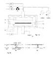
- FIG. 1Ais a schematic representation of a PEALD (plasma-enhanced atomic layer deposition) apparatus for depositing a dielectric film usable in an embodiment of the present invention.
- PEALDplasma-enhanced atomic layer deposition
- FIG. 1Billustrates a schematic representation of switching flow of an inactive gas and flow of a precursor gas usable in an embodiment of the present invention.
- FIG. 2illustrates a PEALD process sequence according to a comparative example.
- FIG. 3illustrates a PEALD process sequence according to an embodiment of the present invention.
- FIG. 4illustrates a PEALD process sequence according to another embodiment of the present invention.
- FIG. 5illustrates a PEALD process sequence according to still another embodiment of the present invention.
- FIG. 6illustrates a PEALD process sequence according to yet another embodiment of the present invention.
- gasmay include vaporized solid and/or liquid and may be constituted by a single gas or a mixture of gases.
- a process gas introduced to a reaction chamber through a showerheadmay be comprised of, consist essentially of, or consist of a precursor gas and an additive gas.
- the precursor gas and the additive gasare typically introduced as a mixed gas or separately to a reaction space.
- the precursor gascan be introduced with a carrier gas such as a noble gas.
- the additive gasmay be comprised of, consist essentially of, or consist of a reactant gas and a dilution gas such as a noble gas.
- the reactant gas and the dilution gasmay be introduced as a mixed gas or separately to the reaction space.
- a precursormay be comprised of two or more precursors, and a reactant gas may be comprised of two or more reactant gases.
- the precursoris a gas chemisorbed on a substrate and typically containing a metalloid or metal element which constitutes a main structure of a matrix of a dielectric film
- the reactant gas for depositionis a gas reacting with the precursor chemisorbed on a substrate when the gas is excited to fix an atomic layer or monolayer on the substrate.
- “Chemisorption”refers to chemical saturation adsorption.
- a gas other than the process gasi.e., a gas introduced without passing through the showerhead, may be used for, e.g., sealing the reaction space, which includes a seal gas such as a noble gas.
- filmrefers to a layer continuously extending in a direction perpendicular to a thickness direction substantially without pinholes to cover an entire target or concerned surface, or simply a layer covering a target or concerned surface.
- layerrefers to a structure having a certain thickness formed on a surface or a synonym of film or a non-film structure.
- a film or layermay be constituted by a discrete single film or layer having certain characteristics or multiple films or layers, and a boundary between adjacent films or layers may or may not be clear and may be established based on physical, chemical, and/or any other characteristics, formation processes or sequence, and/or functions or purposes of the adjacent films or layers.
- the article “a” or “an”refers to a species or a genus including multiple species unless specified otherwise.
- the terms “constituted by” and “having”refer independently to “typically or broadly comprising”, “comprising”, “consisting essentially of”, or “consisting of” in some embodiments. Also, in this disclosure, any defined meanings do not necessarily exclude ordinary and customary meanings in some embodiments.
- any two numbers of a variablecan constitute a workable range of the variable as the workable range can be determined based on routine work, and any ranges indicated may include or exclude the endpoints. Additionally, any values of variables indicated (regardless of whether they are indicated with “about” or not) may refer to precise values or approximate values and include equivalents, and may refer to average, median, representative, majority, etc. in some embodiments.
- Some embodimentsprovide a method for forming a single-phase multi-element film constituted by at least four elements on a substrate by plasma-enhanced atomic layer deposition (PEALD) conducting one or more process cycles, each process cycle comprising: (i) forming an integrated multi-element layer constituted by at least three elements on a substrate by PEALD using at least one precursor; and (ii) treating a surface of the integrated multi-element layer with a reactive oxygen, nitrogen, and/or carbon in the absence of a precursor for film formation so as to incorporate at least one new additional element selected from oxygen, nitrogen, and carbon into the integrated multi-element layer.
- the single-phase multi-element filmmay be constituted by four, five, six, or seven elements.
- the multiple elementsconsist of at least one metalloid or base metal element for forming a main structure of a matrix of the film (e.g., Si, B, As, Al, etc.), and nonmetal elements (e.g., H, C, N, O, P, etc.), wherein the multiple elements may be SiBNH, SiBONH, SiBCNH, SiBOCNH, SiCNH, SiONH, SiOCNH, SiOCH, SiPNH, SiPOCNH, BCONH, AsCONH, BCNH, or AsCNH.
- the multiple elementsconsist of nonmetal elements, wherein the multiple elements may be PCONH or PCNH.
- elementconstitutes a part of a matrix of a film and may not include impurities, elements which are not expressed members of a chemical formula of the film, and elements included in the film in a negligible amounts or less than detectable amount.
- the filmcan include such impurities, negligible elements, and undetectable elements without being expressly so indicated.
- the detectable amountvaries depending on the composition analysis method. For example, an element such as carbon in a film may not be detected by Rutherford backscattering Spectrometry (RBS) and Hydrogen Forward Scattering (HFS) if the content of carbon is 5 atomic % or less.
- a film which is considered to be a film of SiBNH according to RBS/HFS analysismay be a film of SiBCNH according to SIMS analysis.
- the chemical formula of a filmis determined based on a composition analysis by RBS/HFS.
- the multiple elementsinclude two or more metalloid elements
- the multi-element layeris deposited using two or more precursors containing different metalloid elements.
- two or more metalloid elementsconstitute the multiple elements
- one precursorcontains multiple metalloid elements in its molecule such as a precursor containing Si, B, C, N, and H, the concentrations of the metalloid elements (Si and B) cannot be controlled independently, and it may cause adsorption interference, e.g., lowering deposition rate.
- the reactant gas for depositioncontains hydrogen, nitrogen, carbon, and/or oxygen, and introduces such an element to the multi-element film.
- the reactant gas for depositionis a mixture of hydrogen gas and nitrogen gas, or NH 3 , which introduces N and H to the multi-element film.
- Carbon and oxygencan be introduced into the multi-element film from the precursor and reactant for deposition in step (i), and/or reactant for surface treatment in step (ii).
- step (i)is conducted in each process cycle to the extent that a thickness of the integrated multi-element layer does not exceed 15 nm.
- the thickness of the integrated multi-element layer in each process cycleis a thickness of one atomic layer (e.g., 0.2 nm) or more (e.g., 1.0 nm or more), but about 3 nm or less, about 5 nm or less, about 10 nm or less, about 15 nm or less, or in a range between any two foregoing numbers (typically 10 nm or less, preferably 5 nm or less, e.g., 2 to 5 nm).
- step (ii)is conducted in each process cycle to the extent that the at least one new additional element is diffused throughout the integrated multi-element layer.
- step (i) in each process cycleis constituted by a deposition cycle of PEALD
- step (ii) in each process cycleis constituted by a surface treatment cycle, wherein a cycle ratio of the number of the deposition cycles to the number of the surface treatment cycles in each process cycle is 1/10 to 100/1.
- the cycle ratiois 1/1 to 60/1 (e.g., 2/1, 5/1, 10/1, 20/1, 30/1, 40/1, 50/1, or values between any two foregoing numbers, e.g., 10/1 to 30/1).
- the surface treatment cycleis repeated fewer times than is the deposition cycle.
- the surface treatment cycleis repeated more than once, where purging is conducted after each cycle, so that reaction by-products can be removed from the surface of the substrate, increasing efficiency of the surface reaction. Further, by conducting the surface treatment cycle multiple times, it becomes easier to adjust the compositions of the multi-element layer, and distributions of the additional element or dopant in a thickness direction. In some embodiments, the surface treatment cycle is repeated more often than is the deposition cycle. In some embodiments, the cycle ratio is 1/2 to 1/5.
- the number of process cyclesis one to 1,000, or at least two, or 10 to 100, depending on the target thickness of a multi-element film.
- step (ii)an additional element or dopant is introduced or doped into the multi-element layer obtained in step (i), which penetrates the multi-element layer from the surface toward the inside in a thickness direction and diffuses in the multi-element layer.
- a reactive oxygen, nitrogen, and/or carbonare/is used in the absence of a precursor for film formation, to incorporate at least a new additional element, and in some embodiments, the reactive oxygen, nitrogen, and/or carbon are/is an oxygen plasma, nitrogen plasma, and/or carbon plasma, which may be generated by applying RF power to oxygen or ozone for oxidation, to a mixture of nitrogen and hydrogen gases for nitridization, and/or to hydrocarbon gas such as CH 4 for carbonization.
- a thickness of the integrated multi-element layer obtained in step (i)is not increased by step (ii).
- the single-phase multi-element filmhas a dielectric constant of about 5.0 or less (e.g., 4.5 or less, 4.0 or less).
- the step coverage of the filmmay be at least 90% (e.g., 93% to 100%).
- the wet etch rate of the filmcan be adjusted to a desired level by changing the treatment conditions and the sequence in step (ii). For example, by doping the film with more nitrogen, the wet etch rate of the film is increased.
- the deposition cyclecomprises: (ia) supplying a precursor in a pulse to a reaction zone where the substrate is placed; (ib) supplying a reactant gas for deposition and a noble gas continuously to the reaction zone; and (ic) applying RF power to the reaction zone in a pulse after step (ia), and the surface treatment cycle comprises: (iia) continuously supplying the noble gas to the reaction zone; and (iib) supplying a reactant gas for treatment in a pulse to the reaction zone wherein the reactive oxygen, nitrogen, and/or carbon are/is derived from the reactant gas for treatment, wherein neither the precursor nor the reactant gas for deposition is supplied throughout the surface treatment cycle.
- the reactive oxygen, nitrogen, and/or carbonare/is an oxygen plasma, nitrogen plasma, and/or carbon plasma
- the surface treatment cyclefurther comprises: (iic) applying RF power to the reaction zone in a pulse during step (iib).
- the precursoris constituted by first and second precursors, and step (ia) comprises supplying the first precursor in a pulse and then supplying the second precursor in a pulse.
- the precursoris constituted by first and second precursors
- the deposition cyclefurther comprises, after conducting steps (ia) to (ic) using the first precursor, conducting steps (ia) to (ic) using the second precursor.
- the precursoris constituted by first and second precursors
- the deposition cyclefurther comprises, after conducting steps (ia) to (ic) using the first precursor, conducting steps (ia) and (ib) using the second precursor without step (ic).
- the reactant gas for treatmentis constituted by first and second reactant gases
- the surface treatment cyclefurther comprises, after conducting steps (iia) and (iib) using the first reactant gas, conducting steps (iia) and (iib) using the second reactant gas.
- the reactant gas for treatmentis constituted by first and second reactant gases
- the surface treatment cyclefurther comprises, after conducting steps (iia) to (iic) using the first reactant gas, conducting steps (iia) to (iic) using the second reactant gas.
- the word “continuously”refers to at least one of the following: without breaking a vacuum, without being exposed to air, without opening a chamber, as an in-situ process, without interruption as a step in sequence, without changing process conditions, and without causing chemical changes on a substrate surface between steps, depending on the embodiment.
- an auxiliary stepsuch as a delay between steps or other step immaterial or insubstantial in the context does not count as a step, and thus, the word “continuously” does not exclude an intervening auxiliary step.
- FIG. 2illustrates a PEALD process sequence according to a comparative example, wherein the width of each column does not necessarily represent the actual time length, and a raised level of the line in each row represents an ON-state whereas a bottom level of the line in each row represents an OFF-state.
- the deposition cycleis repeated, which is constituted by (e.g., consists of) steps of feeding precursor 1 to a reaction zone, purging the reaction zone, feeding precursor 2 , purging the reaction zone, applying RF power to the reaction zone, and purging the reaction zone in this order, wherein a carrier gas, dilution gas, and reactant gas for deposition are supplied constantly to the reaction zone throughout the deposition cycle. Since no surface treatment cycle is conducted, a low dielectric constant of the thus-obtained film is not expected.
- FIG. 3illustrates a PEALD process sequence according to an embodiment of the present invention.
- the process cycleis constituted by (e.g., consists of) the deposition cycle and the surface treatment cycle.
- the deposition cycleconsists of steps of feeding precursor 1 to a reaction zone, purging the reaction zone, feeding precursor 2 , purging the reaction zone, applying RF power to the reaction zone, and purging the reaction zone in this order, wherein a carrier gas, dilution gas, and reactant gas for deposition are supplied continuously to the reaction zone throughout the deposition cycle.
- steps of feeding precursor 2 , purging the reaction zone, applying RF power to the reaction zone, and purging the reaction zonecan be repeated k times (k is an integer of 1 to 5, typically 1 to 3), depending on the target compositions and quality of the multi-element film, although repeating is not required.
- the deposition cyclealso can be repeated m times (m is an integer of 1 to 60, typically 1 to 30, e.g., 5 to 20), depending on the target compositions and quality of the multi-element film, although repeating is not required.
- the surface treatment cycleis conducted continuously after the deposition cycle, which surface treatment cycle is constituted by (e.g., consists of) steps of feeding a reactant for surface treatment (“STR” in the figure) to the reaction zone, applying RF power to the reaction zone, and purging the reaction zone in this order, wherein the carrier gas and dilution gas are supplied continuously to the reaction zone, but the reactant for deposition is not supplied throughout the surface treatment cycle.
- the surface treatment cyclecan be repeated n times (n is an integer of 1 to 10, typically 1 to 3), depending on the target compositions and quality of the multi-element film, although repeating is not required.
- the process cycleneed not be repeated, but is typically repeated multiple times (e.g., 1 to 200 times, typically 1 to 20 times), depending on the target thickness of the multi-element film, the value of m, etc.
- FIG. 4illustrates a PEALD process sequence according to another embodiment of the present invention.
- the process cycleis constituted by (e.g., consists of) the deposition cycle and the surface treatment cycle.
- the deposition cycleis constituted by (e.g., consists of) steps of feeding precursor 1 to a reaction zone, purging the reaction zone, applying RF power to the reaction zone, purging the reaction zone, feeding precursor 2 to the reaction zone, purging the reaction zone, applying RF power to the reaction zone, and purging the reaction zone in this order, wherein a carrier gas, dilution gas, and reactant gas for deposition are supplied continuously to the reaction zone throughout the deposition cycle.
- steps of feeding precursor 2 , purging the reaction zone, applying RF power to the reaction zone, and purging the reaction zonecan be repeated k times (k is an integer of 1 to 5, typically 1 to 3), depending on the target compositions and quality of the multi-element film, although repeating is not required.
- the deposition cyclealso can be repeated m times (m is an integer of 1 to 40, typically 1 to 20, e.g., 4 to 15), depending on the target compositions and quality of the multi-element film, although repeating is not required.
- the surface treatment cycleis conducted continuously after the deposition cycle, which surface treatment cycle is constituted by (e.g., consists of) steps of feeding a reactant for surface treatment (“STR” in the figure) to the reaction zone, applying RF power to the reaction zone, and purging the reaction zone in this order, wherein the carrier gas and dilution gas are supplied continuously to the reaction zone, but the reactant for deposition is not supplied throughout the surface treatment cycle.
- the surface treatment cyclecan be repeated n times (n is an integer of 1 to 10, typically 1 to 3), depending on the target compositions and quality of the multi-element film, although repeating is not required.
- the process cycleneed not be repeated, but is typically repeated multiple times (e.g., 1 to 200 times, typically 1 to 20 times), depending on the target thickness of the multi-element film, the value of m, etc.
- FIG. 5illustrates a PEALD process sequence according to still another embodiment of the present invention.
- the process cycleis constituted by (e.g., consists of) the deposition cycle and the surface treatment cycle.
- the deposition cycleis constituted by (e.g., consists of) steps of feeding precursor 1 to a reaction zone, purging the reaction zone, feeding precursor 2 to the reaction zone, purging the reaction zone, applying RF power to the reaction zone, and purging the reaction zone in this order, wherein a carrier gas, dilution gas, and reactant gas for deposition are supplied continuously to the reaction zone throughout the deposition cycle.
- steps of feeding precursor 2 , purging the reaction zone, applying RF power to the reaction zone, and purging the reaction zonecan be repeated k times (k is an integer of 1 to 5, typically 1 to 3), depending on the target compositions and quality of the multi-element film, although repeating is not required.
- the deposition cyclealso can be repeated m times (m is an integer of 1 to 60, typically 1 to 30, e.g., 5 to 20), depending on the target compositions and quality of the multi-element film, although repeating is not required.
- the surface treatment cycleis conducted continuously after the deposition cycle, which surface treatment cycle is constituted by (e.g., consists of) steps of feeding reactant 1 for surface treatment (“STR” in the figure) to the reaction zone, applying RF power to the reaction zone, purging the reaction zone, feeding reactant 2 for surface treatment, applying RF power to the reaction zone, and purging the reaction zone in this order, wherein the carrier gas and dilution gas are supplied continuously to the reaction zone, but the reactant for deposition is not supplied throughout the surface treatment cycle.
- STRreactant 1 for surface treatment
- steps of feeding reactant 1 for surface treatment to the reaction zone, applying RF power to the reaction zone, and purging the reaction zonecan be repeated p times (p is an integer of 1 to 20, typically 1 to 10), depending on the target compositions and quality of the multi-element film, although repeating is not required.
- steps of feeding reactant 2 for surface treatment to the reaction zone, applying RF power to the reaction zone, and purging the reaction zonealso can be repeated q times (q is an integer of 1 to 20, typically 1 to 10), depending on the target compositions and quality of the multi-element film, although repeating is not required.
- the surface treatment cyclecan be repeated n times (n is an integer of 1 to 20, typically 1 to 10), depending on the target compositions and quality of the multi-element film, although repeating is not required.
- the process cycleneed not be repeated, but is typically repeated multiple times (e.g., 1 to 200 times, typically 1 to 20 times), depending on the target thickness of the multi-element film, the value of m, etc.
- FIG. 6illustrates a PEALD process sequence according to yet another embodiment of the present invention.
- the process cycleis constituted by (e.g., consists of) the deposition cycle and the surface treatment cycle.
- the deposition cycleis constituted by (e.g., consists of) steps of feeding precursor 1 to a reaction zone, purging the reaction zone, applying RF power to the reaction zone, purging the reaction zone, feeding precursor 2 to the reaction zone, purging the reaction zone, applying RF power to the reaction zone, and purging the reaction zone in this order, wherein a carrier gas, dilution gas, and reactant gas for deposition are supplied continuously to the reaction zone throughout the deposition cycle.
- steps of feeding precursor 2 , purging the reaction zone, applying RF power to the reaction zone, and purging the reaction zonecan be repeated k times (k is an integer of 1 to 5, typically 1 to 3), depending on the target compositions and quality of the multi-element film, although repeating is not required.
- the deposition cyclealso can be repeated m times (m is an integer of 1 to 60, typically 1 to 30, e.g., 5 to 20), depending on the target compositions and quality of the multi-element film, although repeating is not required.
- the surface treatment cycleis conducted continuously after the deposition cycle, which surface treatment cycle is constituted by (e.g., consists of) steps of feeding reactant 1 for surface treatment (“STR” in the figure) to the reaction zone, applying RF power to the reaction zone, purging the reaction zone, feeding reactant 2 for surface treatment, applying RF power to the reaction zone, and purging the reaction zone in this order, wherein the carrier gas and dilution gas are supplied continuously to the reaction zone, but the reactant for deposition is not supplied throughout the surface treatment cycle.
- STRreactant 1 for surface treatment
- steps of feeding reactant 1 for surface treatment to the reaction zone, applying RF power to the reaction zone, and purging the reaction zonecan be repeated p times (p is an integer of 1 to 20, typically 1 to 10), depending on the target compositions and quality of the multi-element film, although repeating is not required.
- steps of feeding reactant 2 for surface treatment to the reaction zone, applying RF power to the reaction zone, and purging the reaction zonealso can be repeated q times (q is an integer of 1 to 10, typically 1 to 3), depending on the target compositions and quality of the multi-element film, although repeating is not required.
- the surface treatment cyclecan be repeated n times (n is an integer of 1 to 10, typically 1 to 3, more typically 1), depending on the target compositions and quality of the multi-element film, although repeating is not required.
- the process cycleneed not be repeated, but is typically repeated multiple times (e.g., 1 to 200 times, typically 1 to 20 times), depending on the target thickness of the multi-element film, the value of m, etc.
- reactant 1 and/or reactant 2 for surface treatmentcan be excited using a remote plasma unit, or can be excited thermally.
- precursor 1e.g., silicon-containing material
- precursor 2e.g., boron-containing material
- the order of feeding precursor 1 and precursor 2can be reversed.
- steps involving precursor 2are optionally repeated k times in the figures, the steps involving precursor 1 also can be repeated multiple times (e.g., k times independently of the steps involving precursor 2 ).
- reactant 1 and/or reactant 2 for surface treatmentneed not be supplied continuously, but can be supplied only while RF power is applied to the reaction zone.
- a time period exclusively designated for purgingcan be omitted.
- FIGS. 2-6the precursor is supplied in a pulse using a carrier gas which is continuously supplied.
- a gas supply system illustrated in FIG. 1Billustrates a schematic representation of such a switching flow system.
- valves V 1 (X) and V 2 (R)are closed, and valves V 1 (R) and V 2 (X) are open, so that a precursor gas flows to a vent via valve V 1 (R), and an inactive gas flows to a reactor via valve V 2 (X).
- FIG. 1Billustrates a schematic representation of such a switching flow system.
- valves V 1 (X) and V 2 (R)are closed, and valves V 1 (R) and V 2 (X) are open, so that a precursor gas flows to a vent via valve V 1 (R), and an inactive gas flows to a reactor via valve V 2 (X).
- FIG. 1Billustrates a schematic representation of such a switching flow system.
- valves V 1 (R) and V 2 (X) and opening valves V 1 (X) and V 2 (R)by simultaneously closing valves V 1 (R) and V 2 (X) and opening valves V 1 (X) and V 2 (R), the precursor gas is instantly directed to flow to the reactor, and the inactive gas is instantly directed to flow to the vent, without substantial changes in the flow rate while maintaining continuous flows.
- the ventcan be set downstream of an exhaust, for example.
- a first precursorincludes, but is not limited to, one or more of the following: a silicon-containing halide precursor such as dichlorotetramethyldisilane, tetrachlorodimethyldisilane, and diiodosilane, providing Si, Cl, C, H, and a second precursor includes, but is not limited to, boron-containing gas such as triethylboron and trimethylboron, and arsenic-containing gas such as arsenic triethoxide and trimethylarsine, providing B, As, C, H.
- a silicon-containing halide precursorsuch as dichlorotetramethyldisilane, tetrachlorodimethyldisilane, and diiodosilane, providing Si, Cl, C, H
- a second precursorincludes, but is not limited to, boron-containing gas such as triethylboron and trimethylboron, and arsenic-containing gas such as arsenic trie
- a reactant for surface treatmentincludes, but is not limited to, one or more of the following: nitridizing gas such as NH 3 , a mixture of H 2 and N 2 , and hydrazine compound, oxidizing gas such as oxygen, ozone, and carbonic-acid, and carbonizing gas such as CH 4 and hexane.
- a reactant for depositionwhich can also provide elements can be selected from the above group for a reactant for surface treatment.
- a carrier gas and a dilution gasmay be selected from one or more of the following: noble gases such as He and Ar, and other inert gases such as N 2 .
- the deposition cyclemay be performed by PEALD, one cycle of which is conducted under conditions shown in Table 1 below.
- Precursor 2purge 0.3 to 5 sec (preferably 0.3 to 1 sec)
- Reactante.g., nitridizing gas Flow rate of reactant 50 to 1000 sccm (preferably (continuous) 100 to 500 sccm)
- Carrier gase.g., noble gas Dilution gas e.g., noble gas Flow rate of carrier 1000 to 4000 sccm gas (continuous) (preferably 1500 to 2000 sccm) Flow rate of dilution 50 to 2000 sccm (preferably gas (continuous) 500 to 1000 sccm)
- RF power13.56 MHz
- 50 to 1000 Wpreferably 50 to 300 W
- a 300-mm wafer RF power pulse0.3 to 20 sec (preferably 0.5 to 5 sec)
- Purge 0.1 to 1 secpreferably 0.1 to 0.5 sec
- Growth rate per cycle 0.06 to 0.15 nm/cyclepreferably 0.07 to 0.1 nm/cycle
- the precursormay be provided with the aid of a carrier gas. Since ALD is a self-limiting adsorption reaction process, the number of deposited precursor molecules is determined by the number of reactive surface sites and is independent of the precursor exposure after saturation, and a supply of the precursor is such that the reactive surface sites are saturated thereby per cycle.
- a plasma for depositionmay be generated in situ, for example, in an ammonia gas that flows continuously throughout the deposition cycle. In other embodiments the plasma may be generated remotely and provided to the reaction chamber.
- each pulse or phase of each deposition cycleis preferably self-limiting.
- An excess of reactantsis supplied in each phase to saturate the susceptible structure surfaces.
- Surface saturationensures reactant occupation of all available reactive sites (subject, for example, to physical size or “steric hindrance” restraints) and thus ensures excellent step coverage.
- the pulse time of one or more of the reactantscan be reduced such that complete saturation is not achieved and less than a monolayer is adsorbed on the substrate surface.
- the ALD cycle disclosed in US 2009/0209081 A1 and US 2013/0084714 A1, each disclosure of which is incorporated by reference in its entiretycan be employed for forming a multi-element layer by a deposition cycle.
- the multi-element layeris treated with a surface treating gas (reactant) in the surface treatment cycle under conditions shown in Table 2 below.
- FIG. 1Ais a schematic view of a PEALD apparatus, desirably in conjunction with controls programmed to conduct the sequences described below, usable in some embodiments of the present invention.
- HRF power13.56 MHz or 27 MHz
- LRF power5 MHz or less, 400 kHz-500 kHz
- a temperature regulatoris provided in a lower stage 2 (the lower electrode), and a temperature of a substrate 1 placed thereon is kept constant at a given temperature.
- the upper electrode 4serves as a shower plate as well, and reaction gas and rare gas are introduced into the reaction chamber 3 through a gas flow controller 23 , a pulse flow control valve 31 , and the shower plate.
- an exhaust pipe 6is provided, through which gas in the interior 11 of the reaction chamber 3 is exhausted.
- the reaction chamberis provided with a seal gas flow controller 24 to introduce seal gas into the interior 11 of the reaction chamber 3 (a separation plate for separating a reaction zone and a transfer zone in the interior of the reaction chamber is omitted from this figure).
- the deposition of multi-element film and surface treatmentare performed in the same apparatus such as that described above, so that all the steps can continuously be conducted without exposing the substrate to air or other oxygen-containing atmosphere.
- a remote plasma unitcan be used for exciting a gas.
- the system of switching flow of an inactive gas and flow of a precursor gas illustrated in FIG. 1Bcan be used.
- the apparatusincludes one or more controller(s) (not shown) programmed or otherwise configured to cause the deposition and reactor cleaning processes described elsewhere herein to be conducted.
- the controller(s)are communicated with the various power sources, heating systems, pumps, robotics and gas flow controllers or valves of the reactor, as will be appreciated by the skilled artisan.
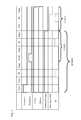
- a multi-element dielectric filmwas formed on a Si substrate (0300 mm) having trenches with an aspect ratio of 3 (a width of 35 nm) by PEALD, one cycle of which was conducted under the common conditions shown in Table 3 (deposition cycle) and Table 4 (surface treatment cycle) below using the PEALD apparatus illustrated in FIG. 1A (including a modification illustrated in FIG. 1B ) with the specific conditions and sequence indicated in Table 5 wherein “DCTDMS” represents dichlorotetradimehylsilane, “BT” represents boron triethyl, and “DIS” represents diiodosilane.
- Example numbers with “*”indicate comparative examples.
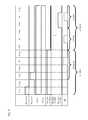
- “Cycle ratio of deposition to surface treatment”represents a cycle ratio of the number of deposition cycles repeated to the number of surface treatment cycles repeated. The RF power applied during the deposition cycle and the surface treatment cycle was the same. Each obtained film was evaluated. Table 6 shows the results of evaluation.
- Example 3-12the surface treatment cycle was conducted in order to incorporate oxygen into a layer of SiBNH obtained by the deposition cycle, so as to produce a layer of SiBONH.
- the multi-element film obtained in Example 3had the compositions shown in Table 7 below, as a result of composition analysis by Rutherford backscattering Spectrometry (RBS) and Hydrogen Forward Scattering (HFS). Note that although the compositions of the films are expressed as SiBNH or SiBONH in Table 6 above, it was confirmed that the films also contained carbon in an amount of approximately 5 atomic % (or less) based on Secondary Ion Mass Spectrometry (SIMS).
- RBSRutherford backscattering Spectrometry
- HFSHydrogen Forward Scattering
- multi-element filmscomprising two metalloid elements can be formed.
- multi-element filmscomprising three metalloid elements can be formed.
- a skilled artisan in the artcan readily provide conditions and/or structures for forming such multi-element films, in view of the present disclosure, as a matter of routine experimentation.
- Example 3-10oxygen is expected to have been incorporated and diffused uniformly throughout the film as being evident from the composition analysis of the film obtained in Example 11.
- the results of composition analysis by Rutherford backscattering Spectrometry (RBS) and Hydrogen Forward Scattering (HFS) of the film of Example 11are shown in Table 8 below. That is, the film was fully doped with oxygen from the surface to a depth of 10 nm, but was not doped with oxygen at a depth of deeper than 10 nm.
- the thickness of the layer obtained by each deposition cycle in Examples 3-10can be calculated as follows (the numbers are approximate): 1.7 nm (Example 3), 1.1 nm (Example 4), 1.9 nm (Example 5), 1.5 nm (Example 6), 1.6 nm (Example 7), 1.9 nm (Example 8), 2.0 nm (Example 9), and 1.7 nm (Example 10).
- the multi-element films obtained in Examples 3-10were constituted by compositions substantially uniformly distributed throughout the films.
- the cycle ratio of the number of deposition cycles repeated to the number of surface treatment cycles repeatedwas 20:1.
- the cycle ratiowas 15:1.
- the duration of a surface treatment cyclethe dielectric constant of the film can also be adjusted. For example, in Example 5, the duration was 40% of that in Example 3, and as a result, the dielectric constant was increased to 4.3 in Example 5 as compared with 4.0 in Example 3.
- Example 6the duration was 200% of that in Example 3, and as a result, the dielectric constant was decreased to 3.5 in Example 6 as compared with 4.0 in Example 3.
- the filmwhen a film has a low dielectric constant, the film tends to have a high wet etch rate (less resistant to chemicals), i.e., dielectric constant and wet etch rate are in a trade-off relationship.
- dielectric constant and wet etch rateare in a trade-off relationship.
- doping the film with carbonit is possible to significantly lower wet etch rate while avoiding significantly increasing dielectric constant.
- Example 6the dielectric constant of the film was 3.5 and the wet etch rate relative to thermal oxide film was 5, but in Example 7 where the film was doped with carbon by using diethylamine gas upon exposure to oxygen plasma in each surface treatment cycle, the wet etch rate relative to thermal oxide film was drastically improved to 0.3 (about 16 times less than that in Example 6) while suppressing an increase of dielectric constant to about 17% or a dielectric constant of 4.1.
- surface treatment cyclesthe type of dopant used in the cycle, the number of the cycles repeated, the process conditions for the cycle, and/or the duration of the cycle
- Example 11nitrogen plasma was used in the surface treatment cycle in Example 11 (no new element was added by the surface treatment cycle), and a hydrocarbon plasma was used in the surface treatment cycle in Example 12 (a new element which was carbon was added by the surface treatment cycle).
- Example 11nitrogen plasma was used in the surface treatment cycle in Example 11 (no new element was added by the surface treatment cycle), and a hydrocarbon plasma was used in the surface treatment cycle in Example 12 (a new element which was carbon was added by the surface treatment cycle).
- Example 11nitrogen plasma was used in the surface treatment cycle in Example 11 (nitriding)
- Example 12carbonizing
- the RIwas increased to 2.2, and the wet etch rate relative to thermal oxide film was 0.1 while the dielectric constant was 4.8 which was less than 5.0, indicating that the concentration of carbon incorporated into the film was significantly increased.
Landscapes
- Engineering & Computer Science (AREA)
- Chemical & Material Sciences (AREA)
- Physics & Mathematics (AREA)
- Manufacturing & Machinery (AREA)
- Power Engineering (AREA)
- Microelectronics & Electronic Packaging (AREA)
- Computer Hardware Design (AREA)
- Condensed Matter Physics & Semiconductors (AREA)
- General Physics & Mathematics (AREA)
- Chemical Kinetics & Catalysis (AREA)
- General Chemical & Material Sciences (AREA)
- Mechanical Engineering (AREA)
- Organic Chemistry (AREA)
- Metallurgy (AREA)
- Materials Engineering (AREA)
- Plasma & Fusion (AREA)
- Electromagnetism (AREA)
- Chemical Vapour Deposition (AREA)
- Formation Of Insulating Films (AREA)
- Inorganic Chemistry (AREA)
- Crystallography & Structural Chemistry (AREA)
Abstract
Description
1. Field of the Invention
The present invention relates generally to a method forming a single-phase multi-element film constituted by at least four elements on a substrate by plasma-enhanced atomic layer deposition (PEALD).
2. Related Art
Copper wiring has been used for logic devices, and dielectric films have been applied for copper wiring, which films are deposited by chemical vapor deposition (CVD) or spin-on dielectric (SOD). For example, a Cu-cap film used as a diffusion blocking film for copper is constituted by a dielectric material such as SiN. As miniaturization of devices progresses, a dielectric film having a dielectric coefficient (k value) as low as 5 or less is required. However, for a layer structure formed by damascene methods, such a dielectric film need not have a good step coverage or conformality. However, depending on the type of layer structure formed by, e.g., deposition and etching, a dielectric film is required to have a good step coverage or conformality as well as a good resistance to chemicals, in addition to a low dielectric constant. It is difficult to deposit a dielectric film having the above properties by CVD.
From the above viewpoints, a dielectric film is deposited by atomic layer deposition (ALD) which is suitable for depositing a film having a good step coverage, particularly by plasma-enhanced ALD (PEALD), rather than thermal ALD, in consideration of potential damage caused to films due to heat. Further, since a two-element film such as SiN may not have sufficient etch selectivity and good dielectric constant, a multi-element dielectric film consisting of more than two elements is under development. However, it is not easy to deposit a high-quality multi-element dielectric film by ALD, since ALD using multiple elements involves problems such as interference with adsorption of one gas by adsorption of another gas.
Any discussion of problems and solutions in relation to the related art has been included in this disclosure solely for the purposes of providing a context for the present invention, and should not be taken as an admission that any or all of the discussion was known at the time the invention was made.
In some embodiments, a single-phase multi-element film constituted by at least four elements is formed on a substrate by plasma-enhanced atomic layer deposition (PEALD), wherein the composition of a deposited film by PEALD is adjusted or manipulated by a post-deposition cycle which is conducted after a deposition cycle, in order to render the deposited film low in dielectric constant, high in step coverage, and/or high in wet etch resistance. The deposited film is suitably used as a protective film disposed around copper wiring, or as an insulation film for a gate in integrated circuits, where wiring delay is a problem. Since the deposited film has a low dielectric constant (typically less than 5), it can suppress wiring delay. By changing a process sequence, various types of multi-element films can be formed. In this disclosure, the term “single-phase” refers generally to a phase formed by a single ALD process constituted by one or more ALD process cycles each consisting essentially of deposition and one or more post-deposition cycles. The term “multi-element” refers generally to elements including at least one metalloid element or metal element and more than one other element, or to elements including more than two nonmetal elements. The “post-deposition cycle” refers generally to a non-deposition cycle conducted after a last deposition cycle in each ALD process cycle.
In some embodiments, the deposition cycle uses two or more precursors. In some embodiments, the post-deposition cycle comprises oxidizing, nitriding, and/or carbonizing the deposited layer, wherein the post-deposition cycle is conducted once or is repeated multiple times after the deposition cycle is conducted once or is repeated multiple times. In some embodiments, the single-phase multi-element film contains silicon or base metal constituting a main structure of its matrix and has a dielectric constant of 5.0 or less and good step coverage. In some embodiments, the single-phase multi-element film is constituted by SiBCNH, SiBOCNH, SiCNH, SiOCNH, SiOCH, SiPNH, or SiPOCNH. In some embodiments, the process temperature is in a range of 0° C. to 600° C.
For purposes of summarizing aspects of the invention and the advantages achieved over the related art, certain objects and advantages of the invention are described in this disclosure. Of course, it is to be understood that not necessarily all such objects or advantages may be achieved in accordance with any particular embodiment of the invention. Thus, for example, those skilled in the art will recognize that the invention may be embodied or carried out in a manner that achieves or optimizes one advantage or group of advantages as taught herein without necessarily achieving other objects or advantages as may be taught or suggested herein.
Further aspects, features and advantages of this invention will become apparent from the detailed description which follows.
These and other features of this invention will now be described with reference to the drawings of preferred embodiments which are intended to illustrate and not to limit the invention. The drawings are greatly simplified for illustrative purposes and are not necessarily to scale. InFIGS. 2-6 , the width of each column does not necessarily represent the actual time length, and a raised level of the line in each row represents an ON-state whereas a bottom level of the line in each row represents an OFF-state.
In this disclosure, “gas” may include vaporized solid and/or liquid and may be constituted by a single gas or a mixture of gases. In this disclosure, a process gas introduced to a reaction chamber through a showerhead may be comprised of, consist essentially of, or consist of a precursor gas and an additive gas. The precursor gas and the additive gas are typically introduced as a mixed gas or separately to a reaction space. The precursor gas can be introduced with a carrier gas such as a noble gas. The additive gas may be comprised of, consist essentially of, or consist of a reactant gas and a dilution gas such as a noble gas. The reactant gas and the dilution gas may be introduced as a mixed gas or separately to the reaction space. A precursor may be comprised of two or more precursors, and a reactant gas may be comprised of two or more reactant gases. The precursor is a gas chemisorbed on a substrate and typically containing a metalloid or metal element which constitutes a main structure of a matrix of a dielectric film, and the reactant gas for deposition is a gas reacting with the precursor chemisorbed on a substrate when the gas is excited to fix an atomic layer or monolayer on the substrate. “Chemisorption” refers to chemical saturation adsorption. A gas other than the process gas, i.e., a gas introduced without passing through the showerhead, may be used for, e.g., sealing the reaction space, which includes a seal gas such as a noble gas. In some embodiments, “film” refers to a layer continuously extending in a direction perpendicular to a thickness direction substantially without pinholes to cover an entire target or concerned surface, or simply a layer covering a target or concerned surface. In some embodiments, “layer” refers to a structure having a certain thickness formed on a surface or a synonym of film or a non-film structure. A film or layer may be constituted by a discrete single film or layer having certain characteristics or multiple films or layers, and a boundary between adjacent films or layers may or may not be clear and may be established based on physical, chemical, and/or any other characteristics, formation processes or sequence, and/or functions or purposes of the adjacent films or layers.
Further, in this disclosure, the article “a” or “an” refers to a species or a genus including multiple species unless specified otherwise. The terms “constituted by” and “having” refer independently to “typically or broadly comprising”, “comprising”, “consisting essentially of”, or “consisting of” in some embodiments. Also, in this disclosure, any defined meanings do not necessarily exclude ordinary and customary meanings in some embodiments.
Additionally, in this disclosure, any two numbers of a variable can constitute a workable range of the variable as the workable range can be determined based on routine work, and any ranges indicated may include or exclude the endpoints. Additionally, any values of variables indicated (regardless of whether they are indicated with “about” or not) may refer to precise values or approximate values and include equivalents, and may refer to average, median, representative, majority, etc. in some embodiments.
In the present disclosure where conditions and/or structures are not specified, the skilled artisan in the art can readily provide such conditions and/or structures, in view of the present disclosure, as a matter of routine experimentation. In all of the disclosed embodiments, any element used in an embodiment can be replaced with any elements equivalent thereto, including those explicitly, necessarily, or inherently disclosed herein, for the intended purposes. Further, the present invention can equally be applied to apparatuses and methods.
The embodiments will be explained with respect to preferred embodiments. However, the present invention is not limited to the preferred embodiments.
Some embodiments provide a method for forming a single-phase multi-element film constituted by at least four elements on a substrate by plasma-enhanced atomic layer deposition (PEALD) conducting one or more process cycles, each process cycle comprising: (i) forming an integrated multi-element layer constituted by at least three elements on a substrate by PEALD using at least one precursor; and (ii) treating a surface of the integrated multi-element layer with a reactive oxygen, nitrogen, and/or carbon in the absence of a precursor for film formation so as to incorporate at least one new additional element selected from oxygen, nitrogen, and carbon into the integrated multi-element layer. The single-phase multi-element film may be constituted by four, five, six, or seven elements. In some embodiments, the multiple elements consist of at least one metalloid or base metal element for forming a main structure of a matrix of the film (e.g., Si, B, As, Al, etc.), and nonmetal elements (e.g., H, C, N, O, P, etc.), wherein the multiple elements may be SiBNH, SiBONH, SiBCNH, SiBOCNH, SiCNH, SiONH, SiOCNH, SiOCH, SiPNH, SiPOCNH, BCONH, AsCONH, BCNH, or AsCNH. In some embodiments, the multiple elements consist of nonmetal elements, wherein the multiple elements may be PCONH or PCNH. In this disclosure, “element” constitutes a part of a matrix of a film and may not include impurities, elements which are not expressed members of a chemical formula of the film, and elements included in the film in a negligible amounts or less than detectable amount. Thus, the film can include such impurities, negligible elements, and undetectable elements without being expressly so indicated. The detectable amount varies depending on the composition analysis method. For example, an element such as carbon in a film may not be detected by Rutherford backscattering Spectrometry (RBS) and Hydrogen Forward Scattering (HFS) if the content of carbon is 5 atomic % or less. However, Secondary Ion Mass Spectrometry (SIMS) may be able to detect such a low content of carbon. For example, a film which is considered to be a film of SiBNH according to RBS/HFS analysis may be a film of SiBCNH according to SIMS analysis. In this disclosure, unless otherwise specified, the chemical formula of a film is determined based on a composition analysis by RBS/HFS.
In some embodiments, the multiple elements include two or more metalloid elements, and in step (i), the multi-element layer is deposited using two or more precursors containing different metalloid elements. When two or more metalloid elements constitute the multiple elements, it is preferable to use two or more precursors each containing a different metalloid element, because by doing so, control over concentration of each metalloid element can easily and independently be accomplished, and a problem of adsorption interference can be avoided. If one precursor contains multiple metalloid elements in its molecule such as a precursor containing Si, B, C, N, and H, the concentrations of the metalloid elements (Si and B) cannot be controlled independently, and it may cause adsorption interference, e.g., lowering deposition rate.
In some embodiments, in step (i), the reactant gas for deposition contains hydrogen, nitrogen, carbon, and/or oxygen, and introduces such an element to the multi-element film. In some embodiments, in step (i), the reactant gas for deposition is a mixture of hydrogen gas and nitrogen gas, or NH3, which introduces N and H to the multi-element film. Carbon and oxygen can be introduced into the multi-element film from the precursor and reactant for deposition in step (i), and/or reactant for surface treatment in step (ii).
In some embodiments, step (i) is conducted in each process cycle to the extent that a thickness of the integrated multi-element layer does not exceed 15 nm. In some embodiments, the thickness of the integrated multi-element layer in each process cycle is a thickness of one atomic layer (e.g., 0.2 nm) or more (e.g., 1.0 nm or more), but about 3 nm or less, about 5 nm or less, about 10 nm or less, about 15 nm or less, or in a range between any two foregoing numbers (typically 10 nm or less, preferably 5 nm or less, e.g., 2 to 5 nm). If the thickness of the integrated multi-element layer in each process cycle exceeds 10 nm or 15 nm, an additional element (or dopant) which is introduced into the multi-element film by step (ii) may not penetrate throughout the integrated multi-element layer formed in step (i) in a thickness direction, regardless of the duration of step (ii). In order to disperse the additional element or dopant uniformly throughout the multi-element layer, preferably, the thickness does not exceed 10 nm. Thus, in some embodiments, step (ii) is conducted in each process cycle to the extent that the at least one new additional element is diffused throughout the integrated multi-element layer.
In some embodiments, step (i) in each process cycle is constituted by a deposition cycle of PEALD, and step (ii) in each process cycle is constituted by a surface treatment cycle, wherein a cycle ratio of the number of the deposition cycles to the number of the surface treatment cycles in each process cycle is 1/10 to 100/1. In some embodiments, the cycle ratio is 1/1 to 60/1 (e.g., 2/1, 5/1, 10/1, 20/1, 30/1, 40/1, 50/1, or values between any two foregoing numbers, e.g., 10/1 to 30/1). In some embodiments, the surface treatment cycle is repeated fewer times than is the deposition cycle. In some embodiments, the surface treatment cycle is repeated more than once, where purging is conducted after each cycle, so that reaction by-products can be removed from the surface of the substrate, increasing efficiency of the surface reaction. Further, by conducting the surface treatment cycle multiple times, it becomes easier to adjust the compositions of the multi-element layer, and distributions of the additional element or dopant in a thickness direction. In some embodiments, the surface treatment cycle is repeated more often than is the deposition cycle. In some embodiments, the cycle ratio is 1/2 to 1/5.
In some embodiments, the number of process cycles is one to 1,000, or at least two, or 10 to 100, depending on the target thickness of a multi-element film.
In some embodiments, in step (ii), an additional element or dopant is introduced or doped into the multi-element layer obtained in step (i), which penetrates the multi-element layer from the surface toward the inside in a thickness direction and diffuses in the multi-element layer. In step (ii), a reactive oxygen, nitrogen, and/or carbon are/is used in the absence of a precursor for film formation, to incorporate at least a new additional element, and in some embodiments, the reactive oxygen, nitrogen, and/or carbon are/is an oxygen plasma, nitrogen plasma, and/or carbon plasma, which may be generated by applying RF power to oxygen or ozone for oxidation, to a mixture of nitrogen and hydrogen gases for nitridization, and/or to hydrocarbon gas such as CH4for carbonization.
In the surface treatment cycle, mainly replacement reaction takes place, and thus, basically, the thickness of the multi-element layer is unchanged. However, since reaction by-products are removed or dissociated from the multi-element layer, typically the thickness of the multi-element layer is reduced by about 1% to about 40% (5%, 10%, 20%, 30%, or values between any two foregoing numbers). However, if oxygen excessively replaces nitrogen, the multi-element layer may expand. In some embodiments, a thickness of the integrated multi-element layer obtained in step (i) is not increased by step (ii).
In some embodiments, the single-phase multi-element film has a dielectric constant of about 5.0 or less (e.g., 4.5 or less, 4.0 or less). Further, the step coverage of the film (percentage of thickness at a sidewall as compared with thickness on a top surface) may be at least 90% (e.g., 93% to 100%). Also, the wet etch rate of the film can be adjusted to a desired level by changing the treatment conditions and the sequence in step (ii). For example, by doping the film with more nitrogen, the wet etch rate of the film is increased.
In some embodiments, the deposition cycle comprises: (ia) supplying a precursor in a pulse to a reaction zone where the substrate is placed; (ib) supplying a reactant gas for deposition and a noble gas continuously to the reaction zone; and (ic) applying RF power to the reaction zone in a pulse after step (ia), and the surface treatment cycle comprises: (iia) continuously supplying the noble gas to the reaction zone; and (iib) supplying a reactant gas for treatment in a pulse to the reaction zone wherein the reactive oxygen, nitrogen, and/or carbon are/is derived from the reactant gas for treatment, wherein neither the precursor nor the reactant gas for deposition is supplied throughout the surface treatment cycle.
In some embodiments, in step (iib), the reactive oxygen, nitrogen, and/or carbon are/is an oxygen plasma, nitrogen plasma, and/or carbon plasma, and the surface treatment cycle further comprises: (iic) applying RF power to the reaction zone in a pulse during step (iib).
In some embodiments, the precursor is constituted by first and second precursors, and step (ia) comprises supplying the first precursor in a pulse and then supplying the second precursor in a pulse.
In some embodiments, the precursor is constituted by first and second precursors, and the deposition cycle further comprises, after conducting steps (ia) to (ic) using the first precursor, conducting steps (ia) to (ic) using the second precursor.
In some embodiments, the precursor is constituted by first and second precursors, and the deposition cycle further comprises, after conducting steps (ia) to (ic) using the first precursor, conducting steps (ia) and (ib) using the second precursor without step (ic).
In some embodiments, the reactant gas for treatment is constituted by first and second reactant gases, and the surface treatment cycle further comprises, after conducting steps (iia) and (iib) using the first reactant gas, conducting steps (iia) and (iib) using the second reactant gas.
In some embodiments, the reactant gas for treatment is constituted by first and second reactant gases, and the surface treatment cycle further comprises, after conducting steps (iia) to (iic) using the first reactant gas, conducting steps (iia) to (iic) using the second reactant gas.
The process sequences according to embodiments are explained below. A skilled artisan will be able to modify these sequences according to the target multi-element film based on this disclosure and routine experimentation. In this disclosure, the word “continuously” refers to at least one of the following: without breaking a vacuum, without being exposed to air, without opening a chamber, as an in-situ process, without interruption as a step in sequence, without changing process conditions, and without causing chemical changes on a substrate surface between steps, depending on the embodiment. In some embodiments, an auxiliary step such as a delay between steps or other step immaterial or insubstantial in the context does not count as a step, and thus, the word “continuously” does not exclude an intervening auxiliary step.
In the sequence illustrated inFIG. 3 , in the deposition cycle, application of RF power is conducted once afterprecursor 2 is fed, and in the surface treatment cycle, only one reactant for surface treatment is used, and thus, the multi-element layer is constituted by a single phase, and doped with one element from the reactant for surface treatment. In the sequence illustrated inFIG. 4 , in the deposition cycle, application of RF power is conducted both afterprecursor 1 is fed and afterprecursor 2 is fed, and in the surface treatment cycle, only one reactant for surface treatment is used, and thus, the multi-element layer is constituted by a laminate, and doped with one element from the reactant for surface treatment. In the sequence illustrated inFIG. 5 , in the deposition cycle, application of RF power is conducted once afterprecursor 2 is fed, and in the surface treatment cycle, two reactants for surface treatment are used, and thus, the multi-element layer is constituted by a single phase, and doped with two elements from the reactants for surface treatment. In the sequence illustrated inFIG. 6 , in the deposition cycle, application of RF power is conducted once afterprecursor 1 is fed and once afterprecursor 2 is fed, and in the surface treatment cycle, two reactants for surface treatment are used, and thus, the multi-element layer is constituted by a laminate, and doped with two elements from the reactants for surface treatment. In the sequences illustrated inFIGS. 3-6 ,reactant 1 and/orreactant 2 for surface treatment can be excited using a remote plasma unit, or can be excited thermally. In the sequences illustrated inFIGS. 3-6 , typically, precursor1 (e.g., silicon-containing material) forms a base matrix of a film, and precursor2 (e.g., boron-containing material) introduces a dopant into the base matrix of the film, and if a higher content of dopant is desired, the step of feedingprecursor 2 is repeated. However, in some embodiments, the order of feedingprecursor 1 andprecursor 2 can be reversed. Further, although thesteps involving precursor 2 are optionally repeated k times in the figures, thesteps involving precursor 1 also can be repeated multiple times (e.g., k times independently of the steps involving precursor2). In the sequences,reactant 1 and/orreactant 2 for surface treatment need not be supplied continuously, but can be supplied only while RF power is applied to the reaction zone. In some embodiments, a time period exclusively designated for purging can be omitted.
In the sequences illustrated inFIGS. 2-6 , the precursor is supplied in a pulse using a carrier gas which is continuously supplied. This can be accomplished by, for example, a gas supply system illustrated inFIG. 1B .FIG. 1B illustrates a schematic representation of such a switching flow system. In (a) inFIG. 1B , valves V1 (X) and V2 (R) are closed, and valves V1 (R) and V2 (X) are open, so that a precursor gas flows to a vent via valve V1 (R), and an inactive gas flows to a reactor via valve V2 (X). In (b) inFIG. 1B , by simultaneously closing valves V1 (R) and V2 (X) and opening valves V1 (X) and V2 (R), the precursor gas is instantly directed to flow to the reactor, and the inactive gas is instantly directed to flow to the vent, without substantial changes in the flow rate while maintaining continuous flows. The vent can be set downstream of an exhaust, for example.
In some embodiments, two or more precursors are used, wherein a first precursor provides two or three elements, and a second precursor provides one or two elements, whereas a reactant for surface treatment provides one or two elements. For example, a first precursor includes, but is not limited to, one or more of the following: a silicon-containing halide precursor such as dichlorotetramethyldisilane, tetrachlorodimethyldisilane, and diiodosilane, providing Si, Cl, C, H, and a second precursor includes, but is not limited to, boron-containing gas such as triethylboron and trimethylboron, and arsenic-containing gas such as arsenic triethoxide and trimethylarsine, providing B, As, C, H. The order of feedingprecursor 1 andprecursor 2 is not limited, and either one can be first. Additionally, in some embodiments, a reactant for surface treatment includes, but is not limited to, one or more of the following: nitridizing gas such as NH3, a mixture of H2and N2, and hydrazine compound, oxidizing gas such as oxygen, ozone, and carbonic-acid, and carbonizing gas such as CH4and hexane. A reactant for deposition which can also provide elements can be selected from the above group for a reactant for surface treatment. In some embodiments, a carrier gas and a dilution gas may be selected from one or more of the following: noble gases such as He and Ar, and other inert gases such as N2.
In some embodiments, the deposition cycle may be performed by PEALD, one cycle of which is conducted under conditions shown in Table 1 below.
| TABLE 1 |
| (the numbers are approximate) |
| Conditions for Deposition Cycle |
| Substrate temperature | 0 to 600° C. (preferably 200 to 450° C.) | ||
| Pressure | 133 to 1000 Pa (preferably 267 to 533 Pa) | ||
| Precursor 1 | e.g., silicon-containing halide precursor | ||
| Precursor 1 pulse | 0.1. to 3 sec (preferably 0.1 to 1 sec) | ||
| Precursor 1 purge | 0.3 to 5 sec (preferably 0.3 to 1 sec) | ||
| Precursor 2 | e.g., boron-containing gas | ||
| Precursor 2 pulse | 0.1. to 3 sec (preferably 0.1 to 1 sec) | ||
| Precursor 2 purge | 0.3 to 5 sec (preferably 0.3 to 1 sec) | ||
| Reactant | e.g., nitridizing gas | ||
| Flow rate of reactant | 50 to 1000 sccm (preferably | ||
| (continuous) | 100 to 500 sccm) | ||
| Carrier gas | e.g., noble gas | ||
| Dilution gas | e.g., noble gas | ||
| Flow rate of carrier | 1000 to 4000 sccm | ||
| gas (continuous) | (preferably 1500 to 2000 sccm) | ||
| Flow rate of dilution | 50 to 2000 sccm (preferably | ||
| gas (continuous) | 500 to 1000 sccm) | ||
| RF power (13.56 MHz) | 50 to 1000 W (preferably 50 to 300 W) | ||
| for a 300-mm wafer | |||
| RF power pulse | 0.3 to 20 sec (preferably 0.5 to 5 sec) | ||
| Purge | 0.1 to 1 sec (preferably 0.1 to 0.5 sec) | ||
| Growth rate per cycle | 0.06 to 0.15 nm/cycle (preferably | ||
| 0.07 to 0.1 nm/cycle) | |||
The precursor may be provided with the aid of a carrier gas. Since ALD is a self-limiting adsorption reaction process, the number of deposited precursor molecules is determined by the number of reactive surface sites and is independent of the precursor exposure after saturation, and a supply of the precursor is such that the reactive surface sites are saturated thereby per cycle. A plasma for deposition may be generated in situ, for example, in an ammonia gas that flows continuously throughout the deposition cycle. In other embodiments the plasma may be generated remotely and provided to the reaction chamber.
As mentioned above, each pulse or phase of each deposition cycle is preferably self-limiting. An excess of reactants is supplied in each phase to saturate the susceptible structure surfaces. Surface saturation ensures reactant occupation of all available reactive sites (subject, for example, to physical size or “steric hindrance” restraints) and thus ensures excellent step coverage. In some embodiments the pulse time of one or more of the reactants can be reduced such that complete saturation is not achieved and less than a monolayer is adsorbed on the substrate surface.
In some embodiments, the ALD cycle disclosed in US 2009/0209081 A1 and US 2013/0084714 A1, each disclosure of which is incorporated by reference in its entirety can be employed for forming a multi-element layer by a deposition cycle.
In some embodiments, the multi-element layer is treated with a surface treating gas (reactant) in the surface treatment cycle under conditions shown in Table 2 below.
| TABLE 2 |
| (the numbers are approximate) |
| Conditions for Surface Treatment Cycle |
| Susceptor temperature | Same as in deposition cycle | ||
| Pressure | Same as in deposition cycle | ||
| Reactant gas | e.g., nitridizing gas, oxidizing gas, | ||
| carbonizing gas | |||
| Flow rate of reactant gas | 10 to 1000 sccm (preferably | ||
| 10 to 300 sccm) | |||
| Carrier gas (continuous) | Same as in deposition cycle | ||
| Dilution gas (continuous) | Same as in deposition cycle | ||
| RF power (13.56 MHz) | 50 to 500 W (preferably | ||
| for a 300- | 50 to 200 W) | ||
| RF power pulse | 0.5 to 10 sec (preferably 0.1 to 3 sec) | ||
| Purge | 0.1 to 10-sec (preferably 0.1 to 5 sec) | ||
The process cycle can be performed using any suitable apparatus including an apparatus illustrated inFIG. 1A , for example.FIG. 1A is a schematic view of a PEALD apparatus, desirably in conjunction with controls programmed to conduct the sequences described below, usable in some embodiments of the present invention. In this figure, by providing a pair of electrically conductive flat-plate electrodes 4,2 in parallel and facing each other in the interior11 of a reaction chamber3, applying HRF power (13.56 MHz or 27 MHz)5 and LRF power (5 MHz or less, 400 kHz-500 kHz)50 to one side, and electrically grounding12 to the other side, a plasma is excited between the electrodes. A temperature regulator is provided in a lower stage2 (the lower electrode), and a temperature of asubstrate 1 placed thereon is kept constant at a given temperature. The upper electrode4 serves as a shower plate as well, and reaction gas and rare gas are introduced into the reaction chamber3 through agas flow controller 23, a pulseflow control valve 31, and the shower plate. Additionally, in the reaction chamber3, an exhaust pipe6 is provided, through which gas in the interior11 of the reaction chamber3 is exhausted. Additionally, the reaction chamber is provided with a sealgas flow controller 24 to introduce seal gas into the interior11 of the reaction chamber3 (a separation plate for separating a reaction zone and a transfer zone in the interior of the reaction chamber is omitted from this figure). In some embodiments, the deposition of multi-element film and surface treatment are performed in the same apparatus such as that described above, so that all the steps can continuously be conducted without exposing the substrate to air or other oxygen-containing atmosphere. In some embodiments, a remote plasma unit can be used for exciting a gas.
In some embodiments, in the apparatus depicted inFIG. 1A , in place of the pulseflow control valve 31, the system of switching flow of an inactive gas and flow of a precursor gas illustrated inFIG. 1B (described earlier), can be used.
A skilled artisan will appreciate that the apparatus includes one or more controller(s) (not shown) programmed or otherwise configured to cause the deposition and reactor cleaning processes described elsewhere herein to be conducted. The controller(s) are communicated with the various power sources, heating systems, pumps, robotics and gas flow controllers or valves of the reactor, as will be appreciated by the skilled artisan.
The present invention is further explained with reference to working examples below. However, the examples are not intended to limit the present invention. In the examples where conditions and/or structures are not specified, the skilled artisan in the art can readily provide such conditions and/or structures, in view of the present disclosure, as a matter of routine experimentation. Also, the numbers applied in the specific examples can be modified by a range of at least ±50% in some embodiments, and the numbers are approximate.
A multi-element dielectric film was formed on a Si substrate (0300 mm) having trenches with an aspect ratio of 3 (a width of 35 nm) by PEALD, one cycle of which was conducted under the common conditions shown in Table 3 (deposition cycle) and Table 4 (surface treatment cycle) below using the PEALD apparatus illustrated inFIG. 1A (including a modification illustrated inFIG. 1B ) with the specific conditions and sequence indicated in Table 5 wherein “DCTDMS” represents dichlorotetradimehylsilane, “BT” represents boron triethyl, and “DIS” represents diiodosilane.
| TABLE 3 |
| (the numbers are approximate) |
| Common Conditions for Deposition Cycle |
| Substrate temperature | 400° C. | ||
| Pressure | 400 Pa | ||
| Carrier gas | Ar | ||
| Dilution gas | Ar | ||
| Flow rate of carrier gas (continuous) | 2000 sccm | ||
| Flow rate of dilution gas (continuous) | 500 sccm | ||
| 1 sec | |||
| Purge | 0.5 sec | ||
| TABLE 4 |
| (the numbers are approximate) |
| Common Conditions for Surface Treatment Cycle |
| Substrate temperature | Same as in deposition cycle | ||
| Pressure | Same as in deposition cycle | ||
| Carrier gas (continuous) | Same as in deposition cycle | ||
| Dilution gas (continuous) | Same as in deposition cycle | ||
| Purge | 5 sec | ||
| TABLE 5 |
| (the numbers are approximate) |
| Cycle ratio of | ||||||
| Reactant for | deposition to | |||||
| surface | surface | |||||
| Reactant for | treatment | treatment | ||||
| deposition | RF | (flow rate; | (number of | |||
| Precursor | (flow rate) | [W] | duration) | process cycle) | Sequence | |
| *1 | 1st: DCTDMS | NH3 (2 slm) | 200 | — | — | FIG. 2 |
| 2nd: BT | ||||||
| *2 | 1st: DCTDMS | H2/N2 | 100 | — | — | FIG. 2 |
| 2nd: BT | (0.25/1 slm) | |||||
| 3 | 1st: DCTDMS | NH3 (2 slm) | 200 | O2 (20 sccm; | 20:1 | FIG. 3 |
| 2nd: BT | 0.5 s) | (10) | k = 1/m = 20/n = 1 | |||
| 4 | 1st: DCTDMS | NH3 (2 slm) | 200 | O2 (20 sccm; | 15:1 | FIG. 4 |
| 2nd: BT | 0.5 s) | (13) | k = 1/m = 15/n = 1 | |||
| 5 | 1st: DCTDMS | NH3 (2 slm) | 200 | O2 (20 sccm; | 20:1 | FIG. 3 |
| 2nd: BT | 0.2 s) | (10) | k = 1/m = 20/n = 1 | |||
| 6 | 1st: DCTDMS | NH3 (2 slm) | 200 | O2 (20 sccm; | 20:1 | FIG. 3 |
| 2nd: BT | 1 s) | (10) | k = 1/m = 20/n = 1 | |||
| 7 | 1st: DCTDMS | NH3 (2 slm) | 200 | 1st: O2 (20 | 20:1 | FIG. 5 |
| 2nd: BT | sccm; 0.3 s) | (10) | k = 1/m = 20/n = 1/ | |||
| 2nd: | p = 1/q = 1 | |||||
| Diethylamine | ||||||
| (5 sccm; 0.5 s) | ||||||
| 8 | 1st: DIS | H2/N2 | 100 | O2 (20 sccm; | 20:1 | FIG. 3 |
| 2nd: BT | (0.25/1 slm) | 0.5 s) | (10) | k = 1/m = 20/n = 1 | ||
| 9 | 1st: DIS | H2/N2 | 100 | O2 (20 sccm; | 20:1 | FIG. 3 |
| 2nd: BT | (0.25/1 slm) | 0.2 s) | (10) | k = 1/m = 20/n = 1 | ||
| 10 | 1st: DCTDMS | H2/N2 | ||||
| 2nd: BT | (0.25/1 slm) | 100 | O2 (20 sccm; | 20:1 | FIG. 3 | |
| ↓ | 0.5 s) | (10) | k = 1/m = 20/n = 1 | |||
| N2 (1 slm) | ||||||
| *11 | 1st: DIS | H2/N2 | 100 | O2 (20 sccm; | 200:1 | FIG. 3 |
| 2nd: BT | (0.25/1 slm) | 10 min) | (1) | k = 1/m = 200/n = 1 | ||
| *12 | 1st: DIS | H2/N2 | 100 | O2 (20 sccm; | 200:1 | FIG. 3 |
| 2nd: BT | (0.25/1 slm) | 20 mm) | (1) | k = 1/m = 200/n = 1 | ||
| *13 | 1st: DIS | H2/N2 | 100 | N2 (1000 | 20:1 | FIG. 3 |
| 2nd: BT | (0.25/1 slm) | sccm; 0.2 s) | (10) | k = 1/m = 20/n = 1 | ||
| 14 | 1st: DIS | H2/N2 | 100 | CH4 (500 | 20:1 | FIG. 3 |
| 2nd: BT | (0.25/1 slm) | sccm; 0.2 s) | (10) | k = 1/m = 20/n = 1 | ||
In Table 5, the Example numbers with “*” indicate comparative examples. “Cycle ratio of deposition to surface treatment” represents a cycle ratio of the number of deposition cycles repeated to the number of surface treatment cycles repeated. The RF power applied during the deposition cycle and the surface treatment cycle was the same. Each obtained film was evaluated. Table 6 shows the results of evaluation.
| TABLE 6 |
| (the numbers are approximate) |
| GPC | RI | K- | Leakage Current | 100:1 DHF | Step Coverage | ||
| (nm/cycle) | @633 nm | Value | (A/cm2) | WERR@TOX | @AR3 (%) | Film | |
| *1 | 0.1 | 1.80 | 5.3 | 3E-9 | 0.5 | 92 | SiBNH |
| *2 | 0.11 | 1.78 | 5.0 | 6E-9 | 0.3 | 90 | SiBNH |
| 3 | 0.085 | 1.62 | 4.0 | 8E-9 | 2 | 93 | SiBONH |
| 4 | 0.075 | 1.55 | 3.7 | 1E-8 | 1.8 | 94 | SiBONH |
| 5 | 0.095 | 1.7 | 4.3 | 4E-9 | 0.9 | 93 | SiBONH |
| 6 | 0.075 | 1.49 | 3.5 | 2E-8 | 5 | 95 | SiBONH |
| 7 | 0.08 | 1.85 | 4.1 | 6E-9 | 0.3 | 95 | SiBOCNH |
| 8 | 0.095 | 1.65 | 4.0 | 8E-9 | 2 | 94 | SiBONH |
| 9 | 0.099 | 1.71 | 4.3 | 5E-9 | 0.9 | 97 | SiBONH |
| 10 | 0.085 | 1.74 | 4.1 | 5E-9 | 0.5 | 94 | SiBONH |
| *11 | 0.092 | 1.71 | 4.4 | 3E-8 | 0.8 | 97 | |
| * | |||||||
| 12 | 0.097 | 1.61 | 3.8 | 1E-9 | 1.2 | 95 | SiBONH |
| *13 | 0.05 | 1.99 | 5.5 | 1E-8 | 0.2 | 93 | SiBNH |
| 14 | 0.06 | 2.21 | 4.8 | 9E-9 | 0.1 | 90 | SiBCNH |
In Table 6, “GPC” represents growth rate per cycle, “RI@633 nm” represents refractive index at a wavelength of 633 nm, “K-Value” represents dielectric constant, “100:1 DHF WERR@TOX” represents wet etch rate using a diluted HF solution at a 1% concentration relative to that of thermal oxide film, “Step Coverage@AR3” represents a step coverage at a trench having an aspect ratio of 3, and “Film” represents compositions of the film.
In Examples 3-12, the surface treatment cycle was conducted in order to incorporate oxygen into a layer of SiBNH obtained by the deposition cycle, so as to produce a layer of SiBONH. For example, it was confirmed that the multi-element film obtained in Example 3 had the compositions shown in Table 7 below, as a result of composition analysis by Rutherford backscattering Spectrometry (RBS) and Hydrogen Forward Scattering (HFS). Note that although the compositions of the films are expressed as SiBNH or SiBONH in Table 6 above, it was confirmed that the films also contained carbon in an amount of approximately 5 atomic % (or less) based on Secondary Ion Mass Spectrometry (SIMS).
In a manner similar to that in Examples 2-12, other multi-element films comprising two metalloid elements can be formed. Also, if three precursors are used, each providing a different metalloid element, multi-element films comprising three metalloid elements can be formed. A skilled artisan in the art can readily provide conditions and/or structures for forming such multi-element films, in view of the present disclosure, as a matter of routine experimentation.
| TABLE 7 |
| (the numbers are approximate) |
| Example | Si (at %) | N (at %) | H (at %) | O (at %) | B (at %) | ||
| 3 | 15 | 35 | 10 | 20 | 20 | ||
Further, in Examples 3-10, oxygen is expected to have been incorporated and diffused uniformly throughout the film as being evident from the composition analysis of the film obtained in Example 11. The results of composition analysis by Rutherford backscattering Spectrometry (RBS) and Hydrogen Forward Scattering (HFS) of the film of Example 11 are shown in Table 8 below. That is, the film was fully doped with oxygen from the surface to a depth of 10 nm, but was not doped with oxygen at a depth of deeper than 10 nm. The thickness of the layer obtained by each deposition cycle in Examples 3-10 can be calculated as follows (the numbers are approximate): 1.7 nm (Example 3), 1.1 nm (Example 4), 1.9 nm (Example 5), 1.5 nm (Example 6), 1.6 nm (Example 7), 1.9 nm (Example 8), 2.0 nm (Example 9), and 1.7 nm (Example 10). Thus, it is expected that the multi-element films obtained in Examples 3-10 were constituted by compositions substantially uniformly distributed throughout the films.
| TABLE 8 |
| (the numbers are approximate) |
| RBS-HFS Composition (at %) |
| Example 11 | Si | N | H | O | B |
| SiBN + O2 Plasma | Surface | 16.0 | 36.0 | 10.0 | 28.0 | 10.0 |
| 10 nm | 15.0 | 55.0 | 10.0 | 0.0 | 20.0 | |
In Examples 3 and 5-10, the cycle ratio of the number of deposition cycles repeated to the number of surface treatment cycles repeated was 20:1. In Example 4, the cycle ratio was 15:1. By reducing the cycle ratio (i.e., by conducting a surface treatment cycle at fewer intervals or more frequently relative to a deposition cycle), the dielectric constant of the film can be reduced as being evident from Example 4 (k=3.7) as compared with Example 3 (k=4.0). Further, by adjusting the duration of a surface treatment cycle, the dielectric constant of the film can also be adjusted. For example, in Example 5, the duration was 40% of that in Example 3, and as a result, the dielectric constant was increased to 4.3 in Example 5 as compared with 4.0 in Example 3. On the other hand, in Example 6, the duration was 200% of that in Example 3, and as a result, the dielectric constant was decreased to 3.5 in Example 6 as compared with 4.0 in Example 3.
In general, when a film has a low dielectric constant, the film tends to have a high wet etch rate (less resistant to chemicals), i.e., dielectric constant and wet etch rate are in a trade-off relationship. However, by doping the film with carbon, it is possible to significantly lower wet etch rate while avoiding significantly increasing dielectric constant. For example, in Example 6, the dielectric constant of the film was 3.5 and the wet etch rate relative to thermal oxide film was 5, but in Example 7 where the film was doped with carbon by using diethylamine gas upon exposure to oxygen plasma in each surface treatment cycle, the wet etch rate relative to thermal oxide film was drastically improved to 0.3 (about 16 times less than that in Example 6) while suppressing an increase of dielectric constant to about 17% or a dielectric constant of 4.1. Thus, by controlling surface treatment cycles (the type of dopant used in the cycle, the number of the cycles repeated, the process conditions for the cycle, and/or the duration of the cycle), the compositions and properties of a multi-element film can be adjusted.
Further, all of the films had a step coverage of 90% or higher, indicating that adsorption hindrance or adsorption interference of precursors did not occur.
Additionally, in place of the oxygen plasma in Examples 3-10, a nitrogen plasma was used in the surface treatment cycle in Example 11 (no new element was added by the surface treatment cycle), and a hydrocarbon plasma was used in the surface treatment cycle in Example 12 (a new element which was carbon was added by the surface treatment cycle). As a result, in Example 11 (nitriding), the RI was increased approximately twofold as compared with that in Example 2, but the dielectric constant was increased to 5.5 which exceeded 5.0. In Example 12 (carbonizing), the RI was increased to 2.2, and the wet etch rate relative to thermal oxide film was 0.1 while the dielectric constant was 4.8 which was less than 5.0, indicating that the concentration of carbon incorporated into the film was significantly increased.
It will be understood by those of skill in the art that numerous and various modifications can be made without departing from the spirit of the present invention. Therefore, it should be clearly understood that the forms of the present invention are illustrative only and are not intended to limit the scope of the present invention.
Claims (20)
1. A method for forming a single-phase multi-element film constituted by at least four elements on a substrate by plasma-enhanced atomic layer deposition (PEALD) conducting one or more process cycles, each process cycle comprising:
(i) forming an integrated multi-element layer constituted by at least three elements on a substrate by PEALD using at least one precursor; and
(ii) treating a surface of the integrated multi-element layer with a reactive oxygen, nitrogen, and/or carbon in the absence of a precursor for film formation so as to incorporate at least one new additional element selected from oxygen, nitrogen, and carbon into the integrated multi-element layer.
2. The method according toclaim 1 , wherein step (i) is conducted in each process cycle to the extent that a thickness of the integrated multi-element layer does not exceed 15 nm.
3. The method according toclaim 1 , wherein step (ii) is conducted in each process cycle to the extent that the at least one new additional element is diffused throughout the integrated multi-element layer.
4. The method according toclaim 1 , wherein step (i) in each process cycle is constituted by a deposition cycle of PEALD, and step (ii) in each process cycle is constituted by a surface treatment cycle, wherein a cycle ratio of the number of the deposition cycles to the number of the surface treatment cycles in each process cycle is 1/10 to 60/1.
5. The method according toclaim 1 , wherein the multi-element film is constituted by five elements.
6. The method according toclaim 1 , wherein the reactive oxygen, nitrogen, and/or carbon are/is an oxygen plasma, nitrogen plasma, and/or carbon plasma.
7. The method according toclaim 1 , wherein the at least four elements are selected from the group consisting of metalloid elements and nonmetal elements.
8. The method according toclaim 7 , wherein the metalloid element is silicon.
9. The method according toclaim 7 , wherein the at least four elements include two or more metalloid elements, and in step (i), the multi-element layer is deposited using two or more precursors each containing a different metalloid element.
10. The method according toclaim 8 , wherein the single-phase multi-element film is a film of SiBCNH, SiBOCNH, SiCNH, SiOCNH, SiOCH, SiPNH, SiPOCNH, BCONH, PCONH, AsCONH, BCNH, PCNH, or AsCNH.
11. The method according toclaim 1 , wherein the single-phase multi-element film has a dielectric constant of about 5.0 or less.
12. The method according toclaim 1 , wherein a thickness of the integrated multi-element layer obtained in step (i) is not increased by step (ii).
13. The method according toclaim 1 , wherein steps (i) and (ii) are conducted at a temperature of about 0° C. to about 600° C.
14. The method according toclaim 4 , wherein:
the deposition cycle comprises: (ia) supplying a precursor in a pulse to a reaction zone where the substrate is placed; (ib) supplying a reactant gas for deposition and a noble gas continuously to the reaction zone; and (ic) applying RF power to the reaction zone in a pulse after step (ia), and
the surface treatment cycle comprises: (iia) continuously supplying the noble gas to the reaction zone; and (iib) supplying a reactant gas for treatment in a pulse to the reaction zone wherein the reactive oxygen, nitrogen, and/or carbon are/is derived from the reactant gas for treatment, wherein neither the precursor nor the reactant gas for deposition is supplied throughout the surface treatment cycle.
15. The method according toclaim 14 , wherein in step (iib), the reactive oxygen, nitrogen, and/or carbon are/is an oxygen plasma, nitrogen plasma, and/or carbon plasma, and the surface treatment cycle further comprises: (iic) applying RF power to the reaction zone in a pulse during step (iib).
16. The method according toclaim 14 , wherein the precursor is constituted by first and second precursors, and step (ia) comprises supplying the first precursor in a pulse and then supplying the second precursor in a pulse.
17. The method according toclaim 14 , wherein the precursor is constituted by first and second precursors, and the deposition cycle further comprises, after conducting steps (ia) to (ic) using the first precursor, conducting steps (ia) to (ic) using the second precursor.
18. The method according toclaim 14 , wherein the precursor is constituted by first and second precursors, and the deposition cycle further comprises, after conducting steps (ia) to (ic) using the first precursor, conducting steps (ia) and (ib) using the second precursor without step (ic).
19. The method according toclaim 14 , wherein the reactant gas for treatment is constituted by first and second reactant gases, and the surface treatment cycle further comprises, after conducting steps (iia) and (iib) using the first reactant gas, conducting steps (iia) and (iib) using the second reactant gas.
20. The method according toclaim 15 , wherein the reactant gas for treatment is constituted by first and second reactant gases, and the surface treatment cycle further comprises, after conducting steps (iia) to (iic) using the first reactant gas, conducting steps (iia) to (iic) using the second reactant gas.
Priority Applications (3)
| Application Number | Priority Date | Filing Date | Title |
|---|---|---|---|
| US14/693,138US9343297B1 (en) | 2015-04-22 | 2015-04-22 | Method for forming multi-element thin film constituted by at least five elements by PEALD |
| TW105104453ATWI675931B (en) | 2015-04-22 | 2016-02-16 | Method for forming multi-element thin film constituted by at least five elements by peald |
| KR1020160048944AKR102629302B1 (en) | 2015-04-22 | 2016-04-21 | Method for forming multi-element thin film constituted by at least five elements by PEALD |
Applications Claiming Priority (1)
| Application Number | Priority Date | Filing Date | Title |
|---|---|---|---|
| US14/693,138US9343297B1 (en) | 2015-04-22 | 2015-04-22 | Method for forming multi-element thin film constituted by at least five elements by PEALD |
Publications (1)
| Publication Number | Publication Date |
|---|---|
| US9343297B1true US9343297B1 (en) | 2016-05-17 |
Family
ID=55920187
Family Applications (1)
| Application Number | Title | Priority Date | Filing Date |
|---|---|---|---|
| US14/693,138ActiveUS9343297B1 (en) | 2015-04-22 | 2015-04-22 | Method for forming multi-element thin film constituted by at least five elements by PEALD |
Country Status (3)
| Country | Link |
|---|---|
| US (1) | US9343297B1 (en) |
| KR (1) | KR102629302B1 (en) |
| TW (1) | TWI675931B (en) |
Cited By (357)
| Publication number | Priority date | Publication date | Assignee | Title |
|---|---|---|---|---|
| US10083836B2 (en) | 2015-07-24 | 2018-09-25 | Asm Ip Holding B.V. | Formation of boron-doped titanium metal films with high work function |
| US10134757B2 (en) | 2016-11-07 | 2018-11-20 | Asm Ip Holding B.V. | Method of processing a substrate and a device manufactured by using the method |
| US10229833B2 (en) | 2016-11-01 | 2019-03-12 | Asm Ip Holding B.V. | Methods for forming a transition metal nitride film on a substrate by atomic layer deposition and related semiconductor device structures |
| US10249577B2 (en) | 2016-05-17 | 2019-04-02 | Asm Ip Holding B.V. | Method of forming metal interconnection and method of fabricating semiconductor apparatus using the method |
| US10249524B2 (en) | 2017-08-09 | 2019-04-02 | Asm Ip Holding B.V. | Cassette holder assembly for a substrate cassette and holding member for use in such assembly |
| US10262859B2 (en) | 2016-03-24 | 2019-04-16 | Asm Ip Holding B.V. | Process for forming a film on a substrate using multi-port injection assemblies |
| US10269558B2 (en) | 2016-12-22 | 2019-04-23 | Asm Ip Holding B.V. | Method of forming a structure on a substrate |
| US10276355B2 (en) | 2015-03-12 | 2019-04-30 | Asm Ip Holding B.V. | Multi-zone reactor, system including the reactor, and method of using the same |
| US10283353B2 (en) | 2017-03-29 | 2019-05-07 | Asm Ip Holding B.V. | Method of reforming insulating film deposited on substrate with recess pattern |
| US10290508B1 (en) | 2017-12-05 | 2019-05-14 | Asm Ip Holding B.V. | Method for forming vertical spacers for spacer-defined patterning |
| US10312055B2 (en) | 2017-07-26 | 2019-06-04 | Asm Ip Holding B.V. | Method of depositing film by PEALD using negative bias |
| US10312129B2 (en) | 2015-09-29 | 2019-06-04 | Asm Ip Holding B.V. | Variable adjustment for precise matching of multiple chamber cavity housings |
| US10319588B2 (en) | 2017-10-10 | 2019-06-11 | Asm Ip Holding B.V. | Method for depositing a metal chalcogenide on a substrate by cyclical deposition |
| US10322384B2 (en) | 2015-11-09 | 2019-06-18 | Asm Ip Holding B.V. | Counter flow mixer for process chamber |
| US10340135B2 (en) | 2016-11-28 | 2019-07-02 | Asm Ip Holding B.V. | Method of topologically restricted plasma-enhanced cyclic deposition of silicon or metal nitride |
| US10340125B2 (en) | 2013-03-08 | 2019-07-02 | Asm Ip Holding B.V. | Pulsed remote plasma method and system |
| US10343920B2 (en) | 2016-03-18 | 2019-07-09 | Asm Ip Holding B.V. | Aligned carbon nanotubes |
| US10361201B2 (en) | 2013-09-27 | 2019-07-23 | Asm Ip Holding B.V. | Semiconductor structure and device formed using selective epitaxial process |
| US10364496B2 (en) | 2011-06-27 | 2019-07-30 | Asm Ip Holding B.V. | Dual section module having shared and unshared mass flow controllers |
| US10367080B2 (en) | 2016-05-02 | 2019-07-30 | Asm Ip Holding B.V. | Method of forming a germanium oxynitride film |
| US10366864B2 (en) | 2013-03-08 | 2019-07-30 | Asm Ip Holding B.V. | Method and system for in-situ formation of intermediate reactive species |
| US10378106B2 (en) | 2008-11-14 | 2019-08-13 | Asm Ip Holding B.V. | Method of forming insulation film by modified PEALD |
| US10381219B1 (en) | 2018-10-25 | 2019-08-13 | Asm Ip Holding B.V. | Methods for forming a silicon nitride film |
| US10381226B2 (en) | 2016-07-27 | 2019-08-13 | Asm Ip Holding B.V. | Method of processing substrate |
| US10388513B1 (en) | 2018-07-03 | 2019-08-20 | Asm Ip Holding B.V. | Method for depositing silicon-free carbon-containing film as gap-fill layer by pulse plasma-assisted deposition |
| US10388509B2 (en) | 2016-06-28 | 2019-08-20 | Asm Ip Holding B.V. | Formation of epitaxial layers via dislocation filtering |
| US10395919B2 (en) | 2016-07-28 | 2019-08-27 | Asm Ip Holding B.V. | Method and apparatus for filling a gap |
| US10403504B2 (en) | 2017-10-05 | 2019-09-03 | Asm Ip Holding B.V. | Method for selectively depositing a metallic film on a substrate |
| US10410943B2 (en) | 2016-10-13 | 2019-09-10 | Asm Ip Holding B.V. | Method for passivating a surface of a semiconductor and related systems |
| US10438965B2 (en) | 2014-12-22 | 2019-10-08 | Asm Ip Holding B.V. | Semiconductor device and manufacturing method thereof |
| US10435790B2 (en) | 2016-11-01 | 2019-10-08 | Asm Ip Holding B.V. | Method of subatmospheric plasma-enhanced ALD using capacitively coupled electrodes with narrow gap |
| US10446393B2 (en) | 2017-05-08 | 2019-10-15 | Asm Ip Holding B.V. | Methods for forming silicon-containing epitaxial layers and related semiconductor device structures |
| US10458018B2 (en) | 2015-06-26 | 2019-10-29 | Asm Ip Holding B.V. | Structures including metal carbide material, devices including the structures, and methods of forming same |
| US10468251B2 (en) | 2016-02-19 | 2019-11-05 | Asm Ip Holding B.V. | Method for forming spacers using silicon nitride film for spacer-defined multiple patterning |
| US10468261B2 (en) | 2017-02-15 | 2019-11-05 | Asm Ip Holding B.V. | Methods for forming a metallic film on a substrate by cyclical deposition and related semiconductor device structures |
| US10480072B2 (en) | 2009-04-06 | 2019-11-19 | Asm Ip Holding B.V. | Semiconductor processing reactor and components thereof |
| US10483099B1 (en) | 2018-07-26 | 2019-11-19 | Asm Ip Holding B.V. | Method for forming thermally stable organosilicon polymer film |
| US10504742B2 (en) | 2017-05-31 | 2019-12-10 | Asm Ip Holding B.V. | Method of atomic layer etching using hydrogen plasma |
| US10501866B2 (en) | 2016-03-09 | 2019-12-10 | Asm Ip Holding B.V. | Gas distribution apparatus for improved film uniformity in an epitaxial system |
| US10510536B2 (en) | 2018-03-29 | 2019-12-17 | Asm Ip Holding B.V. | Method of depositing a co-doped polysilicon film on a surface of a substrate within a reaction chamber |
| US10529542B2 (en) | 2015-03-11 | 2020-01-07 | Asm Ip Holdings B.V. | Cross-flow reactor and method |
| US10529563B2 (en) | 2017-03-29 | 2020-01-07 | Asm Ip Holdings B.V. | Method for forming doped metal oxide films on a substrate by cyclical deposition and related semiconductor device structures |
| US10529554B2 (en) | 2016-02-19 | 2020-01-07 | Asm Ip Holding B.V. | Method for forming silicon nitride film selectively on sidewalls or flat surfaces of trenches |
| US10535516B2 (en) | 2018-02-01 | 2020-01-14 | Asm Ip Holdings B.V. | Method for depositing a semiconductor structure on a surface of a substrate and related semiconductor structures |
| US10541173B2 (en) | 2016-07-08 | 2020-01-21 | Asm Ip Holding B.V. | Selective deposition method to form air gaps |
| US10541333B2 (en) | 2017-07-19 | 2020-01-21 | Asm Ip Holding B.V. | Method for depositing a group IV semiconductor and related semiconductor device structures |
| US10559458B1 (en) | 2018-11-26 | 2020-02-11 | Asm Ip Holding B.V. | Method of forming oxynitride film |
| US10561975B2 (en) | 2014-10-07 | 2020-02-18 | Asm Ip Holdings B.V. | Variable conductance gas distribution apparatus and method |
| US10566223B2 (en) | 2012-08-28 | 2020-02-18 | Asm Ip Holdings B.V. | Systems and methods for dynamic semiconductor process scheduling |
| US10590535B2 (en) | 2017-07-26 | 2020-03-17 | Asm Ip Holdings B.V. | Chemical treatment, deposition and/or infiltration apparatus and method for using the same |
| US10600673B2 (en) | 2015-07-07 | 2020-03-24 | Asm Ip Holding B.V. | Magnetic susceptor to baseplate seal |
| US10604847B2 (en) | 2014-03-18 | 2020-03-31 | Asm Ip Holding B.V. | Gas distribution system, reactor including the system, and methods of using the same |
| US10607895B2 (en) | 2017-09-18 | 2020-03-31 | Asm Ip Holdings B.V. | Method for forming a semiconductor device structure comprising a gate fill metal |
| US10605530B2 (en) | 2017-07-26 | 2020-03-31 | Asm Ip Holding B.V. | Assembly of a liner and a flange for a vertical furnace as well as the liner and the vertical furnace |
| US10612137B2 (en) | 2016-07-08 | 2020-04-07 | Asm Ip Holdings B.V. | Organic reactants for atomic layer deposition |
| USD880437S1 (en) | 2018-02-01 | 2020-04-07 | Asm Ip Holding B.V. | Gas supply plate for semiconductor manufacturing apparatus |
| US10612136B2 (en) | 2018-06-29 | 2020-04-07 | ASM IP Holding, B.V. | Temperature-controlled flange and reactor system including same |
| US10643826B2 (en) | 2016-10-26 | 2020-05-05 | Asm Ip Holdings B.V. | Methods for thermally calibrating reaction chambers |
| US10643904B2 (en) | 2016-11-01 | 2020-05-05 | Asm Ip Holdings B.V. | Methods for forming a semiconductor device and related semiconductor device structures |
| US10655221B2 (en)* | 2017-02-09 | 2020-05-19 | Asm Ip Holding B.V. | Method for depositing oxide film by thermal ALD and PEALD |
| US10658181B2 (en) | 2018-02-20 | 2020-05-19 | Asm Ip Holding B.V. | Method of spacer-defined direct patterning in semiconductor fabrication |
| US10658205B2 (en) | 2017-09-28 | 2020-05-19 | Asm Ip Holdings B.V. | Chemical dispensing apparatus and methods for dispensing a chemical to a reaction chamber |
| US10665452B2 (en) | 2016-05-02 | 2020-05-26 | Asm Ip Holdings B.V. | Source/drain performance through conformal solid state doping |
| US10685834B2 (en) | 2017-07-05 | 2020-06-16 | Asm Ip Holdings B.V. | Methods for forming a silicon germanium tin layer and related semiconductor device structures |
| US10683571B2 (en) | 2014-02-25 | 2020-06-16 | Asm Ip Holding B.V. | Gas supply manifold and method of supplying gases to chamber using same |
| US10692741B2 (en) | 2017-08-08 | 2020-06-23 | Asm Ip Holdings B.V. | Radiation shield |
| US10707106B2 (en) | 2011-06-06 | 2020-07-07 | Asm Ip Holding B.V. | High-throughput semiconductor-processing apparatus equipped with multiple dual-chamber modules |
| US10714315B2 (en) | 2012-10-12 | 2020-07-14 | Asm Ip Holdings B.V. | Semiconductor reaction chamber showerhead |
| US10714350B2 (en) | 2016-11-01 | 2020-07-14 | ASM IP Holdings, B.V. | Methods for forming a transition metal niobium nitride film on a substrate by atomic layer deposition and related semiconductor device structures |
| US10714385B2 (en) | 2016-07-19 | 2020-07-14 | Asm Ip Holding B.V. | Selective deposition of tungsten |
| US10714335B2 (en) | 2017-04-25 | 2020-07-14 | Asm Ip Holding B.V. | Method of depositing thin film and method of manufacturing semiconductor device |
| US10734497B2 (en) | 2017-07-18 | 2020-08-04 | Asm Ip Holding B.V. | Methods for forming a semiconductor device structure and related semiconductor device structures |
| US10731249B2 (en) | 2018-02-15 | 2020-08-04 | Asm Ip Holding B.V. | Method of forming a transition metal containing film on a substrate by a cyclical deposition process, a method for supplying a transition metal halide compound to a reaction chamber, and related vapor deposition apparatus |
| US10734244B2 (en) | 2017-11-16 | 2020-08-04 | Asm Ip Holding B.V. | Method of processing a substrate and a device manufactured by the same |
| US10741385B2 (en) | 2016-07-28 | 2020-08-11 | Asm Ip Holding B.V. | Method and apparatus for filling a gap |
| US10755922B2 (en) | 2018-07-03 | 2020-08-25 | Asm Ip Holding B.V. | Method for depositing silicon-free carbon-containing film as gap-fill layer by pulse plasma-assisted deposition |
| US10770336B2 (en) | 2017-08-08 | 2020-09-08 | Asm Ip Holding B.V. | Substrate lift mechanism and reactor including same |
| US10767789B2 (en) | 2018-07-16 | 2020-09-08 | Asm Ip Holding B.V. | Diaphragm valves, valve components, and methods for forming valve components |
| US10770286B2 (en) | 2017-05-08 | 2020-09-08 | Asm Ip Holdings B.V. | Methods for selectively forming a silicon nitride film on a substrate and related semiconductor device structures |
| US10787741B2 (en) | 2014-08-21 | 2020-09-29 | Asm Ip Holding B.V. | Method and system for in situ formation of gas-phase compounds |
| US10797133B2 (en) | 2018-06-21 | 2020-10-06 | Asm Ip Holding B.V. | Method for depositing a phosphorus doped silicon arsenide film and related semiconductor device structures |
| US10804098B2 (en) | 2009-08-14 | 2020-10-13 | Asm Ip Holding B.V. | Systems and methods for thin-film deposition of metal oxides using excited nitrogen-oxygen species |
| US10811256B2 (en) | 2018-10-16 | 2020-10-20 | Asm Ip Holding B.V. | Method for etching a carbon-containing feature |
| USD900036S1 (en) | 2017-08-24 | 2020-10-27 | Asm Ip Holding B.V. | Heater electrical connector and adapter |
| US10818758B2 (en) | 2018-11-16 | 2020-10-27 | Asm Ip Holding B.V. | Methods for forming a metal silicate film on a substrate in a reaction chamber and related semiconductor device structures |
| US10829852B2 (en) | 2018-08-16 | 2020-11-10 | Asm Ip Holding B.V. | Gas distribution device for a wafer processing apparatus |
| US10832903B2 (en) | 2011-10-28 | 2020-11-10 | Asm Ip Holding B.V. | Process feed management for semiconductor substrate processing |
| US10847371B2 (en) | 2018-03-27 | 2020-11-24 | Asm Ip Holding B.V. | Method of forming an electrode on a substrate and a semiconductor device structure including an electrode |
| US10844484B2 (en) | 2017-09-22 | 2020-11-24 | Asm Ip Holding B.V. | Apparatus for dispensing a vapor phase reactant to a reaction chamber and related methods |
| US10847365B2 (en) | 2018-10-11 | 2020-11-24 | Asm Ip Holding B.V. | Method of forming conformal silicon carbide film by cyclic CVD |
| US10847366B2 (en) | 2018-11-16 | 2020-11-24 | Asm Ip Holding B.V. | Methods for depositing a transition metal chalcogenide film on a substrate by a cyclical deposition process |
| USD903477S1 (en) | 2018-01-24 | 2020-12-01 | Asm Ip Holdings B.V. | Metal clamp |
| US10851456B2 (en) | 2016-04-21 | 2020-12-01 | Asm Ip Holding B.V. | Deposition of metal borides |
| US10854498B2 (en) | 2011-07-15 | 2020-12-01 | Asm Ip Holding B.V. | Wafer-supporting device and method for producing same |
| US10858737B2 (en) | 2014-07-28 | 2020-12-08 | Asm Ip Holding B.V. | Showerhead assembly and components thereof |
| US10865475B2 (en) | 2016-04-21 | 2020-12-15 | Asm Ip Holding B.V. | Deposition of metal borides and silicides |
| US10867788B2 (en) | 2016-12-28 | 2020-12-15 | Asm Ip Holding B.V. | Method of forming a structure on a substrate |
| US10867786B2 (en) | 2018-03-30 | 2020-12-15 | Asm Ip Holding B.V. | Substrate processing method |
| US10872771B2 (en) | 2018-01-16 | 2020-12-22 | Asm Ip Holding B. V. | Method for depositing a material film on a substrate within a reaction chamber by a cyclical deposition process and related device structures |
| US10886123B2 (en) | 2017-06-02 | 2021-01-05 | Asm Ip Holding B.V. | Methods for forming low temperature semiconductor layers and related semiconductor device structures |
| US10883175B2 (en) | 2018-08-09 | 2021-01-05 | Asm Ip Holding B.V. | Vertical furnace for processing substrates and a liner for use therein |
| US10892156B2 (en) | 2017-05-08 | 2021-01-12 | Asm Ip Holding B.V. | Methods for forming a silicon nitride film on a substrate and related semiconductor device structures |
| US10896820B2 (en) | 2018-02-14 | 2021-01-19 | Asm Ip Holding B.V. | Method for depositing a ruthenium-containing film on a substrate by a cyclical deposition process |
| US10910262B2 (en) | 2017-11-16 | 2021-02-02 | Asm Ip Holding B.V. | Method of selectively depositing a capping layer structure on a semiconductor device structure |
| US10914004B2 (en) | 2018-06-29 | 2021-02-09 | Asm Ip Holding B.V. | Thin-film deposition method and manufacturing method of semiconductor device |
| US10923344B2 (en) | 2017-10-30 | 2021-02-16 | Asm Ip Holding B.V. | Methods for forming a semiconductor structure and related semiconductor structures |
| US10928731B2 (en) | 2017-09-21 | 2021-02-23 | Asm Ip Holding B.V. | Method of sequential infiltration synthesis treatment of infiltrateable material and structures and devices formed using same |
| US10934619B2 (en) | 2016-11-15 | 2021-03-02 | Asm Ip Holding B.V. | Gas supply unit and substrate processing apparatus including the gas supply unit |
| US10941490B2 (en) | 2014-10-07 | 2021-03-09 | Asm Ip Holding B.V. | Multiple temperature range susceptor, assembly, reactor and system including the susceptor, and methods of using the same |
| US10975470B2 (en) | 2018-02-23 | 2021-04-13 | Asm Ip Holding B.V. | Apparatus for detecting or monitoring for a chemical precursor in a high temperature environment |
| US11001925B2 (en) | 2016-12-19 | 2021-05-11 | Asm Ip Holding B.V. | Substrate processing apparatus |
| US11018002B2 (en) | 2017-07-19 | 2021-05-25 | Asm Ip Holding B.V. | Method for selectively depositing a Group IV semiconductor and related semiconductor device structures |
| US11018047B2 (en) | 2018-01-25 | 2021-05-25 | Asm Ip Holding B.V. | Hybrid lift pin |
| US11015245B2 (en) | 2014-03-19 | 2021-05-25 | Asm Ip Holding B.V. | Gas-phase reactor and system having exhaust plenum and components thereof |
| US11022879B2 (en) | 2017-11-24 | 2021-06-01 | Asm Ip Holding B.V. | Method of forming an enhanced unexposed photoresist layer |
| US11024523B2 (en) | 2018-09-11 | 2021-06-01 | Asm Ip Holding B.V. | Substrate processing apparatus and method |
| US11031242B2 (en) | 2018-11-07 | 2021-06-08 | Asm Ip Holding B.V. | Methods for depositing a boron doped silicon germanium film |
| USD922229S1 (en) | 2019-06-05 | 2021-06-15 | Asm Ip Holding B.V. | Device for controlling a temperature of a gas supply unit |
| US11049751B2 (en) | 2018-09-14 | 2021-06-29 | Asm Ip Holding B.V. | Cassette supply system to store and handle cassettes and processing apparatus equipped therewith |
| US11056344B2 (en) | 2017-08-30 | 2021-07-06 | Asm Ip Holding B.V. | Layer forming method |
| US11056567B2 (en) | 2018-05-11 | 2021-07-06 | Asm Ip Holding B.V. | Method of forming a doped metal carbide film on a substrate and related semiconductor device structures |
| US11053591B2 (en) | 2018-08-06 | 2021-07-06 | Asm Ip Holding B.V. | Multi-port gas injection system and reactor system including same |
| US11069510B2 (en) | 2017-08-30 | 2021-07-20 | Asm Ip Holding B.V. | Substrate processing apparatus |
| US11081345B2 (en) | 2018-02-06 | 2021-08-03 | Asm Ip Holding B.V. | Method of post-deposition treatment for silicon oxide film |
| US11088002B2 (en) | 2018-03-29 | 2021-08-10 | Asm Ip Holding B.V. | Substrate rack and a substrate processing system and method |
| US11087997B2 (en) | 2018-10-31 | 2021-08-10 | Asm Ip Holding B.V. | Substrate processing apparatus for processing substrates |
| US11114294B2 (en) | 2019-03-08 | 2021-09-07 | Asm Ip Holding B.V. | Structure including SiOC layer and method of forming same |
| US11114283B2 (en) | 2018-03-16 | 2021-09-07 | Asm Ip Holding B.V. | Reactor, system including the reactor, and methods of manufacturing and using same |
| USD930782S1 (en) | 2019-08-22 | 2021-09-14 | Asm Ip Holding B.V. | Gas distributor |
| US11127617B2 (en) | 2017-11-27 | 2021-09-21 | Asm Ip Holding B.V. | Storage device for storing wafer cassettes for use with a batch furnace |
| US11127589B2 (en) | 2019-02-01 | 2021-09-21 | Asm Ip Holding B.V. | Method of topology-selective film formation of silicon oxide |
| USD931978S1 (en) | 2019-06-27 | 2021-09-28 | Asm Ip Holding B.V. | Showerhead vacuum transport |
| US11139191B2 (en) | 2017-08-09 | 2021-10-05 | Asm Ip Holding B.V. | Storage apparatus for storing cassettes for substrates and processing apparatus equipped therewith |
| US11139308B2 (en) | 2015-12-29 | 2021-10-05 | Asm Ip Holding B.V. | Atomic layer deposition of III-V compounds to form V-NAND devices |
| US11158513B2 (en) | 2018-12-13 | 2021-10-26 | Asm Ip Holding B.V. | Methods for forming a rhenium-containing film on a substrate by a cyclical deposition process and related semiconductor device structures |
| USD935572S1 (en) | 2019-05-24 | 2021-11-09 | Asm Ip Holding B.V. | Gas channel plate |
| US11171025B2 (en) | 2019-01-22 | 2021-11-09 | Asm Ip Holding B.V. | Substrate processing device |
| US11174550B2 (en) | 2015-08-03 | 2021-11-16 | Asm Ip Holding B.V. | Selective deposition on metal or metallic surfaces relative to dielectric surfaces |
| US11205585B2 (en) | 2016-07-28 | 2021-12-21 | Asm Ip Holding B.V. | Substrate processing apparatus and method of operating the same |
| US11217444B2 (en) | 2018-11-30 | 2022-01-04 | Asm Ip Holding B.V. | Method for forming an ultraviolet radiation responsive metal oxide-containing film |
| US20220002869A1 (en)* | 2020-07-01 | 2022-01-06 | Applied Materials, Inc. | Vapor phase photoresists deposition |
| US11222772B2 (en) | 2016-12-14 | 2022-01-11 | Asm Ip Holding B.V. | Substrate processing apparatus |
| USD940837S1 (en) | 2019-08-22 | 2022-01-11 | Asm Ip Holding B.V. | Electrode |
| US11227789B2 (en) | 2019-02-20 | 2022-01-18 | Asm Ip Holding B.V. | Method and apparatus for filling a recess formed within a substrate surface |
| US11227782B2 (en) | 2019-07-31 | 2022-01-18 | Asm Ip Holding B.V. | Vertical batch furnace assembly |
| US11230766B2 (en) | 2018-03-29 | 2022-01-25 | Asm Ip Holding B.V. | Substrate processing apparatus and method |
| US11232963B2 (en) | 2018-10-03 | 2022-01-25 | Asm Ip Holding B.V. | Substrate processing apparatus and method |
| US11233133B2 (en) | 2015-10-21 | 2022-01-25 | Asm Ip Holding B.V. | NbMC layers |
| US11251068B2 (en) | 2018-10-19 | 2022-02-15 | Asm Ip Holding B.V. | Substrate processing apparatus and substrate processing method |
| US11251040B2 (en) | 2019-02-20 | 2022-02-15 | Asm Ip Holding B.V. | Cyclical deposition method including treatment step and apparatus for same |
| USD944946S1 (en) | 2019-06-14 | 2022-03-01 | Asm Ip Holding B.V. | Shower plate |
| US11270899B2 (en) | 2018-06-04 | 2022-03-08 | Asm Ip Holding B.V. | Wafer handling chamber with moisture reduction |
| US11274369B2 (en) | 2018-09-11 | 2022-03-15 | Asm Ip Holding B.V. | Thin film deposition method |
| US11282698B2 (en) | 2019-07-19 | 2022-03-22 | Asm Ip Holding B.V. | Method of forming topology-controlled amorphous carbon polymer film |
| US11289326B2 (en) | 2019-05-07 | 2022-03-29 | Asm Ip Holding B.V. | Method for reforming amorphous carbon polymer film |
| US11286558B2 (en) | 2019-08-23 | 2022-03-29 | Asm Ip Holding B.V. | Methods for depositing a molybdenum nitride film on a surface of a substrate by a cyclical deposition process and related semiconductor device structures including a molybdenum nitride film |
| US11286562B2 (en) | 2018-06-08 | 2022-03-29 | Asm Ip Holding B.V. | Gas-phase chemical reactor and method of using same |
| USD947913S1 (en) | 2019-05-17 | 2022-04-05 | Asm Ip Holding B.V. | Susceptor shaft |
| US11295980B2 (en) | 2017-08-30 | 2022-04-05 | Asm Ip Holding B.V. | Methods for depositing a molybdenum metal film over a dielectric surface of a substrate by a cyclical deposition process and related semiconductor device structures |
| USD948463S1 (en) | 2018-10-24 | 2022-04-12 | Asm Ip Holding B.V. | Susceptor for semiconductor substrate supporting apparatus |
| US11306395B2 (en) | 2017-06-28 | 2022-04-19 | Asm Ip Holding B.V. | Methods for depositing a transition metal nitride film on a substrate by atomic layer deposition and related deposition apparatus |
| USD949319S1 (en) | 2019-08-22 | 2022-04-19 | Asm Ip Holding B.V. | Exhaust duct |
| US11315794B2 (en) | 2019-10-21 | 2022-04-26 | Asm Ip Holding B.V. | Apparatus and methods for selectively etching films |
| US11342216B2 (en) | 2019-02-20 | 2022-05-24 | Asm Ip Holding B.V. | Cyclical deposition method and apparatus for filling a recess formed within a substrate surface |
| US11339476B2 (en) | 2019-10-08 | 2022-05-24 | Asm Ip Holding B.V. | Substrate processing device having connection plates, substrate processing method |
| US11345999B2 (en) | 2019-06-06 | 2022-05-31 | Asm Ip Holding B.V. | Method of using a gas-phase reactor system including analyzing exhausted gas |
| US11355338B2 (en) | 2019-05-10 | 2022-06-07 | Asm Ip Holding B.V. | Method of depositing material onto a surface and structure formed according to the method |
| US11361990B2 (en) | 2018-05-28 | 2022-06-14 | Asm Ip Holding B.V. | Substrate processing method and device manufactured by using the same |
| US11374112B2 (en) | 2017-07-19 | 2022-06-28 | Asm Ip Holding B.V. | Method for depositing a group IV semiconductor and related semiconductor device structures |
| US11378337B2 (en) | 2019-03-28 | 2022-07-05 | Asm Ip Holding B.V. | Door opener and substrate processing apparatus provided therewith |
| US11390946B2 (en) | 2019-01-17 | 2022-07-19 | Asm Ip Holding B.V. | Methods of forming a transition metal containing film on a substrate by a cyclical deposition process |
| US11390945B2 (en) | 2019-07-03 | 2022-07-19 | Asm Ip Holding B.V. | Temperature control assembly for substrate processing apparatus and method of using same |
| US11393690B2 (en) | 2018-01-19 | 2022-07-19 | Asm Ip Holding B.V. | Deposition method |
| US11401605B2 (en) | 2019-11-26 | 2022-08-02 | Asm Ip Holding B.V. | Substrate processing apparatus |
| US11414760B2 (en) | 2018-10-08 | 2022-08-16 | Asm Ip Holding B.V. | Substrate support unit, thin film deposition apparatus including the same, and substrate processing apparatus including the same |
| US11424119B2 (en) | 2019-03-08 | 2022-08-23 | Asm Ip Holding B.V. | Method for selective deposition of silicon nitride layer and structure including selectively-deposited silicon nitride layer |
| US11430640B2 (en) | 2019-07-30 | 2022-08-30 | Asm Ip Holding B.V. | Substrate processing apparatus |
| US11430674B2 (en) | 2018-08-22 | 2022-08-30 | Asm Ip Holding B.V. | Sensor array, apparatus for dispensing a vapor phase reactant to a reaction chamber and related methods |
| US11437241B2 (en) | 2020-04-08 | 2022-09-06 | Asm Ip Holding B.V. | Apparatus and methods for selectively etching silicon oxide films |
| US11443926B2 (en) | 2019-07-30 | 2022-09-13 | Asm Ip Holding B.V. | Substrate processing apparatus |
| US11447861B2 (en) | 2016-12-15 | 2022-09-20 | Asm Ip Holding B.V. | Sequential infiltration synthesis apparatus and a method of forming a patterned structure |
| US11447864B2 (en) | 2019-04-19 | 2022-09-20 | Asm Ip Holding B.V. | Layer forming method and apparatus |
| USD965044S1 (en) | 2019-08-19 | 2022-09-27 | Asm Ip Holding B.V. | Susceptor shaft |
| US11453943B2 (en)* | 2016-05-25 | 2022-09-27 | Asm Ip Holding B.V. | Method for forming carbon-containing silicon/metal oxide or nitride film by ALD using silicon precursor and hydrocarbon precursor |
| USD965524S1 (en) | 2019-08-19 | 2022-10-04 | Asm Ip Holding B.V. | Susceptor support |
| US11469098B2 (en) | 2018-05-08 | 2022-10-11 | Asm Ip Holding B.V. | Methods for depositing an oxide film on a substrate by a cyclical deposition process and related device structures |
| US11476109B2 (en) | 2019-06-11 | 2022-10-18 | Asm Ip Holding B.V. | Method of forming an electronic structure using reforming gas, system for performing the method, and structure formed using the method |
| US11473195B2 (en) | 2018-03-01 | 2022-10-18 | Asm Ip Holding B.V. | Semiconductor processing apparatus and a method for processing a substrate |
| US11482418B2 (en) | 2018-02-20 | 2022-10-25 | Asm Ip Holding B.V. | Substrate processing method and apparatus |
| US11482412B2 (en) | 2018-01-19 | 2022-10-25 | Asm Ip Holding B.V. | Method for depositing a gap-fill layer by plasma-assisted deposition |
| US11482533B2 (en) | 2019-02-20 | 2022-10-25 | Asm Ip Holding B.V. | Apparatus and methods for plug fill deposition in 3-D NAND applications |
| US11488819B2 (en) | 2018-12-04 | 2022-11-01 | Asm Ip Holding B.V. | Method of cleaning substrate processing apparatus |
| US11488854B2 (en) | 2020-03-11 | 2022-11-01 | Asm Ip Holding B.V. | Substrate handling device with adjustable joints |
| US11492703B2 (en) | 2018-06-27 | 2022-11-08 | Asm Ip Holding B.V. | Cyclic deposition methods for forming metal-containing material and films and structures including the metal-containing material |
| US11495459B2 (en) | 2019-09-04 | 2022-11-08 | Asm Ip Holding B.V. | Methods for selective deposition using a sacrificial capping layer |
| US11499222B2 (en) | 2018-06-27 | 2022-11-15 | Asm Ip Holding B.V. | Cyclic deposition methods for forming metal-containing material and films and structures including the metal-containing material |
| US11501968B2 (en) | 2019-11-15 | 2022-11-15 | Asm Ip Holding B.V. | Method for providing a semiconductor device with silicon filled gaps |
| US11501965B2 (en) | 2017-05-05 | 2022-11-15 | Asm Ip Holding B.V. | Plasma enhanced deposition processes for controlled formation of metal oxide thin films |
| US11499226B2 (en) | 2018-11-02 | 2022-11-15 | Asm Ip Holding B.V. | Substrate supporting unit and a substrate processing device including the same |
| US11515187B2 (en) | 2020-05-01 | 2022-11-29 | Asm Ip Holding B.V. | Fast FOUP swapping with a FOUP handler |
| US11515188B2 (en) | 2019-05-16 | 2022-11-29 | Asm Ip Holding B.V. | Wafer boat handling device, vertical batch furnace and method |
| US11521851B2 (en) | 2020-02-03 | 2022-12-06 | Asm Ip Holding B.V. | Method of forming structures including a vanadium or indium layer |
| US11527403B2 (en) | 2019-12-19 | 2022-12-13 | Asm Ip Holding B.V. | Methods for filling a gap feature on a substrate surface and related semiconductor structures |
| US11527400B2 (en) | 2019-08-23 | 2022-12-13 | Asm Ip Holding B.V. | Method for depositing silicon oxide film having improved quality by peald using bis(diethylamino)silane |
| US11530483B2 (en) | 2018-06-21 | 2022-12-20 | Asm Ip Holding B.V. | Substrate processing system |
| US11530876B2 (en) | 2020-04-24 | 2022-12-20 | Asm Ip Holding B.V. | Vertical batch furnace assembly comprising a cooling gas supply |
| US11532757B2 (en) | 2016-10-27 | 2022-12-20 | Asm Ip Holding B.V. | Deposition of charge trapping layers |
| US11551925B2 (en) | 2019-04-01 | 2023-01-10 | Asm Ip Holding B.V. | Method for manufacturing a semiconductor device |
| US11551912B2 (en) | 2020-01-20 | 2023-01-10 | Asm Ip Holding B.V. | Method of forming thin film and method of modifying surface of thin film |
| USD975665S1 (en) | 2019-05-17 | 2023-01-17 | Asm Ip Holding B.V. | Susceptor shaft |
| US11557474B2 (en) | 2019-07-29 | 2023-01-17 | Asm Ip Holding B.V. | Methods for selective deposition utilizing n-type dopants and/or alternative dopants to achieve high dopant incorporation |
| US11562901B2 (en) | 2019-09-25 | 2023-01-24 | Asm Ip Holding B.V. | Substrate processing method |
| US11572620B2 (en) | 2018-11-06 | 2023-02-07 | Asm Ip Holding B.V. | Methods for selectively depositing an amorphous silicon film on a substrate |
| US11581186B2 (en) | 2016-12-15 | 2023-02-14 | Asm Ip Holding B.V. | Sequential infiltration synthesis apparatus |
| US11587815B2 (en) | 2019-07-31 | 2023-02-21 | Asm Ip Holding B.V. | Vertical batch furnace assembly |
| US11587814B2 (en) | 2019-07-31 | 2023-02-21 | Asm Ip Holding B.V. | Vertical batch furnace assembly |
| USD979506S1 (en) | 2019-08-22 | 2023-02-28 | Asm Ip Holding B.V. | Insulator |
| US11594600B2 (en) | 2019-11-05 | 2023-02-28 | Asm Ip Holding B.V. | Structures with doped semiconductor layers and methods and systems for forming same |
| US11594450B2 (en) | 2019-08-22 | 2023-02-28 | Asm Ip Holding B.V. | Method for forming a structure with a hole |
| US11605528B2 (en) | 2019-07-09 | 2023-03-14 | Asm Ip Holding B.V. | Plasma device using coaxial waveguide, and substrate treatment method |
| USD980814S1 (en) | 2021-05-11 | 2023-03-14 | Asm Ip Holding B.V. | Gas distributor for substrate processing apparatus |
| USD980813S1 (en) | 2021-05-11 | 2023-03-14 | Asm Ip Holding B.V. | Gas flow control plate for substrate processing apparatus |
| US11610774B2 (en) | 2019-10-02 | 2023-03-21 | Asm Ip Holding B.V. | Methods for forming a topographically selective silicon oxide film by a cyclical plasma-enhanced deposition process |
| US11610775B2 (en) | 2016-07-28 | 2023-03-21 | Asm Ip Holding B.V. | Method and apparatus for filling a gap |
| US11615970B2 (en) | 2019-07-17 | 2023-03-28 | Asm Ip Holding B.V. | Radical assist ignition plasma system and method |
| USD981973S1 (en) | 2021-05-11 | 2023-03-28 | Asm Ip Holding B.V. | Reactor wall for substrate processing apparatus |
| EP4156231A1 (en)* | 2021-09-28 | 2023-03-29 | Kokusai Electric Corp. | Method of processing substrate, substrate processing apparatus, method of manufacturing semiconductor device, and program |
| US11626316B2 (en) | 2019-11-20 | 2023-04-11 | Asm Ip Holding B.V. | Method of depositing carbon-containing material on a surface of a substrate, structure formed using the method, and system for forming the structure |
| US11626308B2 (en) | 2020-05-13 | 2023-04-11 | Asm Ip Holding B.V. | Laser alignment fixture for a reactor system |
| US11629406B2 (en) | 2018-03-09 | 2023-04-18 | Asm Ip Holding B.V. | Semiconductor processing apparatus comprising one or more pyrometers for measuring a temperature of a substrate during transfer of the substrate |
| US11629407B2 (en) | 2019-02-22 | 2023-04-18 | Asm Ip Holding B.V. | Substrate processing apparatus and method for processing substrates |
| US11637011B2 (en) | 2019-10-16 | 2023-04-25 | Asm Ip Holding B.V. | Method of topology-selective film formation of silicon oxide |
| US11637014B2 (en) | 2019-10-17 | 2023-04-25 | Asm Ip Holding B.V. | Methods for selective deposition of doped semiconductor material |
| US11639811B2 (en) | 2017-11-27 | 2023-05-02 | Asm Ip Holding B.V. | Apparatus including a clean mini environment |
| US11639548B2 (en) | 2019-08-21 | 2023-05-02 | Asm Ip Holding B.V. | Film-forming material mixed-gas forming device and film forming device |
| US11643724B2 (en) | 2019-07-18 | 2023-05-09 | Asm Ip Holding B.V. | Method of forming structures using a neutral beam |
| US11646204B2 (en) | 2020-06-24 | 2023-05-09 | Asm Ip Holding B.V. | Method for forming a layer provided with silicon |
| US11646205B2 (en) | 2019-10-29 | 2023-05-09 | Asm Ip Holding B.V. | Methods of selectively forming n-type doped material on a surface, systems for selectively forming n-type doped material, and structures formed using same |
| US11644758B2 (en) | 2020-07-17 | 2023-05-09 | Asm Ip Holding B.V. | Structures and methods for use in photolithography |
| US11646184B2 (en) | 2019-11-29 | 2023-05-09 | Asm Ip Holding B.V. | Substrate processing apparatus |
| US11658035B2 (en) | 2020-06-30 | 2023-05-23 | Asm Ip Holding B.V. | Substrate processing method |
| US11658029B2 (en) | 2018-12-14 | 2023-05-23 | Asm Ip Holding B.V. | Method of forming a device structure using selective deposition of gallium nitride and system for same |
| US11664267B2 (en) | 2019-07-10 | 2023-05-30 | Asm Ip Holding B.V. | Substrate support assembly and substrate processing device including the same |
| US11664199B2 (en) | 2018-10-19 | 2023-05-30 | Asm Ip Holding B.V. | Substrate processing apparatus and substrate processing method |
| US11664245B2 (en) | 2019-07-16 | 2023-05-30 | Asm Ip Holding B.V. | Substrate processing device |
| US11674220B2 (en) | 2020-07-20 | 2023-06-13 | Asm Ip Holding B.V. | Method for depositing molybdenum layers using an underlayer |
| US11680839B2 (en) | 2019-08-05 | 2023-06-20 | Asm Ip Holding B.V. | Liquid level sensor for a chemical source vessel |
| US11685991B2 (en) | 2018-02-14 | 2023-06-27 | Asm Ip Holding B.V. | Method for depositing a ruthenium-containing film on a substrate by a cyclical deposition process |
| USD990534S1 (en) | 2020-09-11 | 2023-06-27 | Asm Ip Holding B.V. | Weighted lift pin |
| US11688603B2 (en) | 2019-07-17 | 2023-06-27 | Asm Ip Holding B.V. | Methods of forming silicon germanium structures |
| USD990441S1 (en) | 2021-09-07 | 2023-06-27 | Asm Ip Holding B.V. | Gas flow control plate |
| US11705333B2 (en) | 2020-05-21 | 2023-07-18 | Asm Ip Holding B.V. | Structures including multiple carbon layers and methods of forming and using same |
| US11718913B2 (en) | 2018-06-04 | 2023-08-08 | Asm Ip Holding B.V. | Gas distribution system and reactor system including same |
| US11725277B2 (en) | 2011-07-20 | 2023-08-15 | Asm Ip Holding B.V. | Pressure transmitter for a semiconductor processing environment |
| US11725280B2 (en) | 2020-08-26 | 2023-08-15 | Asm Ip Holding B.V. | Method for forming metal silicon oxide and metal silicon oxynitride layers |
| US11735422B2 (en) | 2019-10-10 | 2023-08-22 | Asm Ip Holding B.V. | Method of forming a photoresist underlayer and structure including same |
| US11742198B2 (en) | 2019-03-08 | 2023-08-29 | Asm Ip Holding B.V. | Structure including SiOCN layer and method of forming same |
| US11767589B2 (en) | 2020-05-29 | 2023-09-26 | Asm Ip Holding B.V. | Substrate processing device |
| US11769682B2 (en) | 2017-08-09 | 2023-09-26 | Asm Ip Holding B.V. | Storage apparatus for storing cassettes for substrates and processing apparatus equipped therewith |
| US11776846B2 (en) | 2020-02-07 | 2023-10-03 | Asm Ip Holding B.V. | Methods for depositing gap filling fluids and related systems and devices |
| US11781221B2 (en) | 2019-05-07 | 2023-10-10 | Asm Ip Holding B.V. | Chemical source vessel with dip tube |
| US11781243B2 (en) | 2020-02-17 | 2023-10-10 | Asm Ip Holding B.V. | Method for depositing low temperature phosphorous-doped silicon |
| US11804364B2 (en) | 2020-05-19 | 2023-10-31 | Asm Ip Holding B.V. | Substrate processing apparatus |
| US11814747B2 (en) | 2019-04-24 | 2023-11-14 | Asm Ip Holding B.V. | Gas-phase reactor system-with a reaction chamber, a solid precursor source vessel, a gas distribution system, and a flange assembly |
| US11821078B2 (en) | 2020-04-15 | 2023-11-21 | Asm Ip Holding B.V. | Method for forming precoat film and method for forming silicon-containing film |
| US11823866B2 (en) | 2020-04-02 | 2023-11-21 | Asm Ip Holding B.V. | Thin film forming method |
| US11823876B2 (en) | 2019-09-05 | 2023-11-21 | Asm Ip Holding B.V. | Substrate processing apparatus |
| US11830730B2 (en) | 2017-08-29 | 2023-11-28 | Asm Ip Holding B.V. | Layer forming method and apparatus |
| US11830738B2 (en) | 2020-04-03 | 2023-11-28 | Asm Ip Holding B.V. | Method for forming barrier layer and method for manufacturing semiconductor device |
| US11828707B2 (en) | 2020-02-04 | 2023-11-28 | Asm Ip Holding B.V. | Method and apparatus for transmittance measurements of large articles |
| US11827981B2 (en) | 2020-10-14 | 2023-11-28 | Asm Ip Holding B.V. | Method of depositing material on stepped structure |
| US11840761B2 (en) | 2019-12-04 | 2023-12-12 | Asm Ip Holding B.V. | Substrate processing apparatus |
| US11876356B2 (en) | 2020-03-11 | 2024-01-16 | Asm Ip Holding B.V. | Lockout tagout assembly and system and method of using same |
| US11873557B2 (en) | 2020-10-22 | 2024-01-16 | Asm Ip Holding B.V. | Method of depositing vanadium metal |
| US11887857B2 (en) | 2020-04-24 | 2024-01-30 | Asm Ip Holding B.V. | Methods and systems for depositing a layer comprising vanadium, nitrogen, and a further element |
| US11885023B2 (en) | 2018-10-01 | 2024-01-30 | Asm Ip Holding B.V. | Substrate retaining apparatus, system including the apparatus, and method of using same |
| US11885020B2 (en) | 2020-12-22 | 2024-01-30 | Asm Ip Holding B.V. | Transition metal deposition method |
| USD1012873S1 (en) | 2020-09-24 | 2024-01-30 | Asm Ip Holding B.V. | Electrode for semiconductor processing apparatus |
| US11885013B2 (en) | 2019-12-17 | 2024-01-30 | Asm Ip Holding B.V. | Method of forming vanadium nitride layer and structure including the vanadium nitride layer |
| US11891696B2 (en) | 2020-11-30 | 2024-02-06 | Asm Ip Holding B.V. | Injector configured for arrangement within a reaction chamber of a substrate processing apparatus |
| US11901179B2 (en) | 2020-10-28 | 2024-02-13 | Asm Ip Holding B.V. | Method and device for depositing silicon onto substrates |
| US11898243B2 (en) | 2020-04-24 | 2024-02-13 | Asm Ip Holding B.V. | Method of forming vanadium nitride-containing layer |
| US11915929B2 (en) | 2019-11-26 | 2024-02-27 | Asm Ip Holding B.V. | Methods for selectively forming a target film on a substrate comprising a first dielectric surface and a second metallic surface |
| US11923181B2 (en) | 2019-11-29 | 2024-03-05 | Asm Ip Holding B.V. | Substrate processing apparatus for minimizing the effect of a filling gas during substrate processing |
| US11929251B2 (en) | 2019-12-02 | 2024-03-12 | Asm Ip Holding B.V. | Substrate processing apparatus having electrostatic chuck and substrate processing method |
| US11946137B2 (en) | 2020-12-16 | 2024-04-02 | Asm Ip Holding B.V. | Runout and wobble measurement fixtures |
| US11961741B2 (en) | 2020-03-12 | 2024-04-16 | Asm Ip Holding B.V. | Method for fabricating layer structure having target topological profile |
| US11959168B2 (en) | 2020-04-29 | 2024-04-16 | Asm Ip Holding B.V. | Solid source precursor vessel |
| US11967488B2 (en) | 2013-02-01 | 2024-04-23 | Asm Ip Holding B.V. | Method for treatment of deposition reactor |
| USD1023959S1 (en) | 2021-05-11 | 2024-04-23 | Asm Ip Holding B.V. | Electrode for substrate processing apparatus |
| US11976359B2 (en) | 2020-01-06 | 2024-05-07 | Asm Ip Holding B.V. | Gas supply assembly, components thereof, and reactor system including same |
| US11986868B2 (en) | 2020-02-28 | 2024-05-21 | Asm Ip Holding B.V. | System dedicated for parts cleaning |
| US11987881B2 (en) | 2020-05-22 | 2024-05-21 | Asm Ip Holding B.V. | Apparatus for depositing thin films using hydrogen peroxide |
| US11996309B2 (en) | 2019-05-16 | 2024-05-28 | Asm Ip Holding B.V. | Wafer boat handling device, vertical batch furnace and method |
| US11996289B2 (en) | 2020-04-16 | 2024-05-28 | Asm Ip Holding B.V. | Methods of forming structures including silicon germanium and silicon layers, devices formed using the methods, and systems for performing the methods |
| US11993843B2 (en) | 2017-08-31 | 2024-05-28 | Asm Ip Holding B.V. | Substrate processing apparatus |
| US11996292B2 (en) | 2019-10-25 | 2024-05-28 | Asm Ip Holding B.V. | Methods for filling a gap feature on a substrate surface and related semiconductor structures |
| US11993847B2 (en) | 2020-01-08 | 2024-05-28 | Asm Ip Holding B.V. | Injector |
| US12009241B2 (en) | 2019-10-14 | 2024-06-11 | Asm Ip Holding B.V. | Vertical batch furnace assembly with detector to detect cassette |
| US12006572B2 (en) | 2019-10-08 | 2024-06-11 | Asm Ip Holding B.V. | Reactor system including a gas distribution assembly for use with activated species and method of using same |
| US12009224B2 (en) | 2020-09-29 | 2024-06-11 | Asm Ip Holding B.V. | Apparatus and method for etching metal nitrides |
| US12020934B2 (en) | 2020-07-08 | 2024-06-25 | Asm Ip Holding B.V. | Substrate processing method |
| US12027365B2 (en) | 2020-11-24 | 2024-07-02 | Asm Ip Holding B.V. | Methods for filling a gap and related systems and devices |
| US12025484B2 (en) | 2018-05-08 | 2024-07-02 | Asm Ip Holding B.V. | Thin film forming method |
| US12033885B2 (en) | 2020-01-06 | 2024-07-09 | Asm Ip Holding B.V. | Channeled lift pin |
| US12040199B2 (en) | 2018-11-28 | 2024-07-16 | Asm Ip Holding B.V. | Substrate processing apparatus for processing substrates |
| US12040200B2 (en) | 2017-06-20 | 2024-07-16 | Asm Ip Holding B.V. | Semiconductor processing apparatus and methods for calibrating a semiconductor processing apparatus |
| US12040177B2 (en) | 2020-08-18 | 2024-07-16 | Asm Ip Holding B.V. | Methods for forming a laminate film by cyclical plasma-enhanced deposition processes |
| US12043899B2 (en) | 2017-01-10 | 2024-07-23 | Asm Ip Holding B.V. | Reactor system and method to reduce residue buildup during a film deposition process |
| US12051567B2 (en) | 2020-10-07 | 2024-07-30 | Asm Ip Holding B.V. | Gas supply unit and substrate processing apparatus including gas supply unit |
| US12051602B2 (en) | 2020-05-04 | 2024-07-30 | Asm Ip Holding B.V. | Substrate processing system for processing substrates with an electronics module located behind a door in a front wall of the substrate processing system |
| US12057314B2 (en) | 2020-05-15 | 2024-08-06 | Asm Ip Holding B.V. | Methods for silicon germanium uniformity control using multiple precursors |
| US12074022B2 (en) | 2020-08-27 | 2024-08-27 | Asm Ip Holding B.V. | Method and system for forming patterned structures using multiple patterning process |
| US12080548B2 (en) | 2016-05-05 | 2024-09-03 | Asm Ip Holding B.V. | Selective deposition using hydrophobic precursors |
| US12087586B2 (en) | 2020-04-15 | 2024-09-10 | Asm Ip Holding B.V. | Method of forming chromium nitride layer and structure including the chromium nitride layer |
| US12106944B2 (en) | 2020-06-02 | 2024-10-01 | Asm Ip Holding B.V. | Rotating substrate support |
| US12107005B2 (en) | 2020-10-06 | 2024-10-01 | Asm Ip Holding B.V. | Deposition method and an apparatus for depositing a silicon-containing material |
| US12112940B2 (en) | 2019-07-19 | 2024-10-08 | Asm Ip Holding B.V. | Method of forming topology-controlled amorphous carbon polymer film |
| US12125700B2 (en) | 2020-01-16 | 2024-10-22 | Asm Ip Holding B.V. | Method of forming high aspect ratio features |
| US12131885B2 (en) | 2020-12-22 | 2024-10-29 | Asm Ip Holding B.V. | Plasma treatment device having matching box |
| US12129545B2 (en) | 2020-12-22 | 2024-10-29 | Asm Ip Holding B.V. | Precursor capsule, a vessel and a method |
| US12148609B2 (en) | 2020-09-16 | 2024-11-19 | Asm Ip Holding B.V. | Silicon oxide deposition method |
| US12154824B2 (en) | 2020-08-14 | 2024-11-26 | Asm Ip Holding B.V. | Substrate processing method |
| US12159788B2 (en) | 2020-12-14 | 2024-12-03 | Asm Ip Holding B.V. | Method of forming structures for threshold voltage control |
| US12169361B2 (en) | 2019-07-30 | 2024-12-17 | Asm Ip Holding B.V. | Substrate processing apparatus and method |
| US12173404B2 (en) | 2020-03-17 | 2024-12-24 | Asm Ip Holding B.V. | Method of depositing epitaxial material, structure formed using the method, and system for performing the method |
| US12195852B2 (en) | 2020-11-23 | 2025-01-14 | Asm Ip Holding B.V. | Substrate processing apparatus with an injector |
| US12209308B2 (en) | 2020-11-12 | 2025-01-28 | Asm Ip Holding B.V. | Reactor and related methods |
| US12211742B2 (en) | 2020-09-10 | 2025-01-28 | Asm Ip Holding B.V. | Methods for depositing gap filling fluid |
| US12218269B2 (en) | 2020-02-13 | 2025-02-04 | Asm Ip Holding B.V. | Substrate processing apparatus including light receiving device and calibration method of light receiving device |
| US12217946B2 (en) | 2020-10-15 | 2025-02-04 | Asm Ip Holding B.V. | Method of manufacturing semiconductor device, and substrate treatment apparatus using ether-CAT |
| USD1060598S1 (en) | 2021-12-03 | 2025-02-04 | Asm Ip Holding B.V. | Split showerhead cover |
| US12218000B2 (en) | 2020-09-25 | 2025-02-04 | Asm Ip Holding B.V. | Semiconductor processing method |
| US12217954B2 (en) | 2020-08-25 | 2025-02-04 | Asm Ip Holding B.V. | Method of cleaning a surface |
| US12221357B2 (en) | 2020-04-24 | 2025-02-11 | Asm Ip Holding B.V. | Methods and apparatus for stabilizing vanadium compounds |
| US12230531B2 (en) | 2018-04-09 | 2025-02-18 | Asm Ip Holding B.V. | Substrate supporting apparatus, substrate processing apparatus including the same, and substrate processing method |
| US12241158B2 (en) | 2020-07-20 | 2025-03-04 | Asm Ip Holding B.V. | Method for forming structures including transition metal layers |
| US12243757B2 (en) | 2020-05-21 | 2025-03-04 | Asm Ip Holding B.V. | Flange and apparatus for processing substrates |
| US12243747B2 (en) | 2020-04-24 | 2025-03-04 | Asm Ip Holding B.V. | Methods of forming structures including vanadium boride and vanadium phosphide layers |
| US12243742B2 (en) | 2020-04-21 | 2025-03-04 | Asm Ip Holding B.V. | Method for processing a substrate |
| US12247286B2 (en) | 2019-08-09 | 2025-03-11 | Asm Ip Holding B.V. | Heater assembly including cooling apparatus and method of using same |
| US12252785B2 (en) | 2019-06-10 | 2025-03-18 | Asm Ip Holding B.V. | Method for cleaning quartz epitaxial chambers |
| US12255053B2 (en) | 2020-12-10 | 2025-03-18 | Asm Ip Holding B.V. | Methods and systems for depositing a layer |
| US12266524B2 (en) | 2020-06-16 | 2025-04-01 | Asm Ip Holding B.V. | Method for depositing boron containing silicon germanium layers |
| US12272527B2 (en) | 2018-05-09 | 2025-04-08 | Asm Ip Holding B.V. | Apparatus for use with hydrogen radicals and method of using same |
| US12276023B2 (en) | 2017-08-04 | 2025-04-15 | Asm Ip Holding B.V. | Showerhead assembly for distributing a gas within a reaction chamber |
| US12278129B2 (en) | 2020-03-04 | 2025-04-15 | Asm Ip Holding B.V. | Alignment fixture for a reactor system |
| US12288710B2 (en) | 2020-12-18 | 2025-04-29 | Asm Ip Holding B.V. | Wafer processing apparatus with a rotatable table |
| US12322591B2 (en) | 2020-07-27 | 2025-06-03 | Asm Ip Holding B.V. | Thin film deposition process |
| US12322593B2 (en) | 2018-10-02 | 2025-06-03 | Asm Ip Holding B.V. | Selective passivation and selective deposition |
| US12378665B2 (en) | 2018-10-26 | 2025-08-05 | Asm Ip Holding B.V. | High temperature coatings for a preclean and etch apparatus and related methods |
| US12406846B2 (en) | 2020-05-26 | 2025-09-02 | Asm Ip Holding B.V. | Method for depositing boron and gallium containing silicon germanium layers |
| US12410515B2 (en) | 2020-01-29 | 2025-09-09 | Asm Ip Holding B.V. | Contaminant trap system for a reactor system |
| US12431354B2 (en) | 2020-07-01 | 2025-09-30 | Asm Ip Holding B.V. | Silicon nitride and silicon oxide deposition methods using fluorine inhibitor |
| US12428726B2 (en) | 2019-10-08 | 2025-09-30 | Asm Ip Holding B.V. | Gas injection system and reactor system including same |
| US12431334B2 (en) | 2020-02-13 | 2025-09-30 | Asm Ip Holding B.V. | Gas distribution assembly |
| US12444599B2 (en) | 2021-12-08 | 2025-10-14 | Asm Ip Holding B.V. | Method for forming an ultraviolet radiation responsive metal oxide-containing film |
Families Citing this family (2)
| Publication number | Priority date | Publication date | Assignee | Title |
|---|---|---|---|---|
| KR102684628B1 (en)* | 2017-05-16 | 2024-07-15 | 에이에스엠 아이피 홀딩 비.브이. | Selective PEALD of oxides on dielectrics |
| KR102652485B1 (en)* | 2018-10-29 | 2024-03-28 | 주성엔지니어링(주) | Method for processing substrate |
Citations (4)
| Publication number | Priority date | Publication date | Assignee | Title |
|---|---|---|---|---|
| US20090209081A1 (en) | 2007-12-21 | 2009-08-20 | Asm International N.V. | Silicon Dioxide Thin Films by ALD |
| US20120032311A1 (en)* | 2010-08-09 | 2012-02-09 | International Business Machines Corporation | Multi component dielectric layer |
| US20130084714A1 (en) | 2011-09-30 | 2013-04-04 | Asm Japan K.K. | Method for Forming Single-Phase Multi-Element Film by PEALD |
| US20150021599A1 (en)* | 2012-03-09 | 2015-01-22 | Air Products And Chemicals, Inc. | Barrier materials for display devices |
- 2015
- 2015-04-22USUS14/693,138patent/US9343297B1/enactiveActive
- 2016
- 2016-02-16TWTW105104453Apatent/TWI675931B/enactive
- 2016-04-21KRKR1020160048944Apatent/KR102629302B1/enactiveActive
Patent Citations (4)
| Publication number | Priority date | Publication date | Assignee | Title |
|---|---|---|---|---|
| US20090209081A1 (en) | 2007-12-21 | 2009-08-20 | Asm International N.V. | Silicon Dioxide Thin Films by ALD |
| US20120032311A1 (en)* | 2010-08-09 | 2012-02-09 | International Business Machines Corporation | Multi component dielectric layer |
| US20130084714A1 (en) | 2011-09-30 | 2013-04-04 | Asm Japan K.K. | Method for Forming Single-Phase Multi-Element Film by PEALD |
| US20150021599A1 (en)* | 2012-03-09 | 2015-01-22 | Air Products And Chemicals, Inc. | Barrier materials for display devices |
Cited By (458)
| Publication number | Priority date | Publication date | Assignee | Title |
|---|---|---|---|---|
| US10378106B2 (en) | 2008-11-14 | 2019-08-13 | Asm Ip Holding B.V. | Method of forming insulation film by modified PEALD |
| US10844486B2 (en) | 2009-04-06 | 2020-11-24 | Asm Ip Holding B.V. | Semiconductor processing reactor and components thereof |
| US10480072B2 (en) | 2009-04-06 | 2019-11-19 | Asm Ip Holding B.V. | Semiconductor processing reactor and components thereof |
| US10804098B2 (en) | 2009-08-14 | 2020-10-13 | Asm Ip Holding B.V. | Systems and methods for thin-film deposition of metal oxides using excited nitrogen-oxygen species |
| US10707106B2 (en) | 2011-06-06 | 2020-07-07 | Asm Ip Holding B.V. | High-throughput semiconductor-processing apparatus equipped with multiple dual-chamber modules |
| US10364496B2 (en) | 2011-06-27 | 2019-07-30 | Asm Ip Holding B.V. | Dual section module having shared and unshared mass flow controllers |
| US10854498B2 (en) | 2011-07-15 | 2020-12-01 | Asm Ip Holding B.V. | Wafer-supporting device and method for producing same |
| US11725277B2 (en) | 2011-07-20 | 2023-08-15 | Asm Ip Holding B.V. | Pressure transmitter for a semiconductor processing environment |
| US10832903B2 (en) | 2011-10-28 | 2020-11-10 | Asm Ip Holding B.V. | Process feed management for semiconductor substrate processing |
| US10566223B2 (en) | 2012-08-28 | 2020-02-18 | Asm Ip Holdings B.V. | Systems and methods for dynamic semiconductor process scheduling |
| US10714315B2 (en) | 2012-10-12 | 2020-07-14 | Asm Ip Holdings B.V. | Semiconductor reaction chamber showerhead |
| US11501956B2 (en) | 2012-10-12 | 2022-11-15 | Asm Ip Holding B.V. | Semiconductor reaction chamber showerhead |
| US11967488B2 (en) | 2013-02-01 | 2024-04-23 | Asm Ip Holding B.V. | Method for treatment of deposition reactor |
| US10340125B2 (en) | 2013-03-08 | 2019-07-02 | Asm Ip Holding B.V. | Pulsed remote plasma method and system |
| US10366864B2 (en) | 2013-03-08 | 2019-07-30 | Asm Ip Holding B.V. | Method and system for in-situ formation of intermediate reactive species |
| US10361201B2 (en) | 2013-09-27 | 2019-07-23 | Asm Ip Holding B.V. | Semiconductor structure and device formed using selective epitaxial process |
| US10683571B2 (en) | 2014-02-25 | 2020-06-16 | Asm Ip Holding B.V. | Gas supply manifold and method of supplying gases to chamber using same |
| US10604847B2 (en) | 2014-03-18 | 2020-03-31 | Asm Ip Holding B.V. | Gas distribution system, reactor including the system, and methods of using the same |
| US11015245B2 (en) | 2014-03-19 | 2021-05-25 | Asm Ip Holding B.V. | Gas-phase reactor and system having exhaust plenum and components thereof |
| US10858737B2 (en) | 2014-07-28 | 2020-12-08 | Asm Ip Holding B.V. | Showerhead assembly and components thereof |
| US10787741B2 (en) | 2014-08-21 | 2020-09-29 | Asm Ip Holding B.V. | Method and system for in situ formation of gas-phase compounds |
| US10941490B2 (en) | 2014-10-07 | 2021-03-09 | Asm Ip Holding B.V. | Multiple temperature range susceptor, assembly, reactor and system including the susceptor, and methods of using the same |
| US10561975B2 (en) | 2014-10-07 | 2020-02-18 | Asm Ip Holdings B.V. | Variable conductance gas distribution apparatus and method |
| US11795545B2 (en) | 2014-10-07 | 2023-10-24 | Asm Ip Holding B.V. | Multiple temperature range susceptor, assembly, reactor and system including the susceptor, and methods of using the same |
| US10438965B2 (en) | 2014-12-22 | 2019-10-08 | Asm Ip Holding B.V. | Semiconductor device and manufacturing method thereof |
| US10529542B2 (en) | 2015-03-11 | 2020-01-07 | Asm Ip Holdings B.V. | Cross-flow reactor and method |
| US11742189B2 (en) | 2015-03-12 | 2023-08-29 | Asm Ip Holding B.V. | Multi-zone reactor, system including the reactor, and method of using the same |
| US10276355B2 (en) | 2015-03-12 | 2019-04-30 | Asm Ip Holding B.V. | Multi-zone reactor, system including the reactor, and method of using the same |
| US10458018B2 (en) | 2015-06-26 | 2019-10-29 | Asm Ip Holding B.V. | Structures including metal carbide material, devices including the structures, and methods of forming same |
| US11242598B2 (en) | 2015-06-26 | 2022-02-08 | Asm Ip Holding B.V. | Structures including metal carbide material, devices including the structures, and methods of forming same |
| US10600673B2 (en) | 2015-07-07 | 2020-03-24 | Asm Ip Holding B.V. | Magnetic susceptor to baseplate seal |
| US10083836B2 (en) | 2015-07-24 | 2018-09-25 | Asm Ip Holding B.V. | Formation of boron-doped titanium metal films with high work function |
| US11174550B2 (en) | 2015-08-03 | 2021-11-16 | Asm Ip Holding B.V. | Selective deposition on metal or metallic surfaces relative to dielectric surfaces |
| US10312129B2 (en) | 2015-09-29 | 2019-06-04 | Asm Ip Holding B.V. | Variable adjustment for precise matching of multiple chamber cavity housings |
| US11233133B2 (en) | 2015-10-21 | 2022-01-25 | Asm Ip Holding B.V. | NbMC layers |
| US10322384B2 (en) | 2015-11-09 | 2019-06-18 | Asm Ip Holding B.V. | Counter flow mixer for process chamber |
| US11139308B2 (en) | 2015-12-29 | 2021-10-05 | Asm Ip Holding B.V. | Atomic layer deposition of III-V compounds to form V-NAND devices |
| US11956977B2 (en) | 2015-12-29 | 2024-04-09 | Asm Ip Holding B.V. | Atomic layer deposition of III-V compounds to form V-NAND devices |
| US10529554B2 (en) | 2016-02-19 | 2020-01-07 | Asm Ip Holding B.V. | Method for forming silicon nitride film selectively on sidewalls or flat surfaces of trenches |
| US10720322B2 (en) | 2016-02-19 | 2020-07-21 | Asm Ip Holding B.V. | Method for forming silicon nitride film selectively on top surface |
| US11676812B2 (en) | 2016-02-19 | 2023-06-13 | Asm Ip Holding B.V. | Method for forming silicon nitride film selectively on top/bottom portions |
| US10468251B2 (en) | 2016-02-19 | 2019-11-05 | Asm Ip Holding B.V. | Method for forming spacers using silicon nitride film for spacer-defined multiple patterning |
| US10501866B2 (en) | 2016-03-09 | 2019-12-10 | Asm Ip Holding B.V. | Gas distribution apparatus for improved film uniformity in an epitaxial system |
| US10343920B2 (en) | 2016-03-18 | 2019-07-09 | Asm Ip Holding B.V. | Aligned carbon nanotubes |
| US12240760B2 (en) | 2016-03-18 | 2025-03-04 | Asm Ip Holding B.V. | Aligned carbon nanotubes |
| US10262859B2 (en) | 2016-03-24 | 2019-04-16 | Asm Ip Holding B.V. | Process for forming a film on a substrate using multi-port injection assemblies |
| US10865475B2 (en) | 2016-04-21 | 2020-12-15 | Asm Ip Holding B.V. | Deposition of metal borides and silicides |
| US10851456B2 (en) | 2016-04-21 | 2020-12-01 | Asm Ip Holding B.V. | Deposition of metal borides |
| US10665452B2 (en) | 2016-05-02 | 2020-05-26 | Asm Ip Holdings B.V. | Source/drain performance through conformal solid state doping |
| US10367080B2 (en) | 2016-05-02 | 2019-07-30 | Asm Ip Holding B.V. | Method of forming a germanium oxynitride film |
| US11101370B2 (en) | 2016-05-02 | 2021-08-24 | Asm Ip Holding B.V. | Method of forming a germanium oxynitride film |
| US12080548B2 (en) | 2016-05-05 | 2024-09-03 | Asm Ip Holding B.V. | Selective deposition using hydrophobic precursors |
| US10249577B2 (en) | 2016-05-17 | 2019-04-02 | Asm Ip Holding B.V. | Method of forming metal interconnection and method of fabricating semiconductor apparatus using the method |
| US11453943B2 (en)* | 2016-05-25 | 2022-09-27 | Asm Ip Holding B.V. | Method for forming carbon-containing silicon/metal oxide or nitride film by ALD using silicon precursor and hydrocarbon precursor |
| US10388509B2 (en) | 2016-06-28 | 2019-08-20 | Asm Ip Holding B.V. | Formation of epitaxial layers via dislocation filtering |
| US11094582B2 (en) | 2016-07-08 | 2021-08-17 | Asm Ip Holding B.V. | Selective deposition method to form air gaps |
| US10612137B2 (en) | 2016-07-08 | 2020-04-07 | Asm Ip Holdings B.V. | Organic reactants for atomic layer deposition |
| US11749562B2 (en) | 2016-07-08 | 2023-09-05 | Asm Ip Holding B.V. | Selective deposition method to form air gaps |
| US11649546B2 (en) | 2016-07-08 | 2023-05-16 | Asm Ip Holding B.V. | Organic reactants for atomic layer deposition |
| US10541173B2 (en) | 2016-07-08 | 2020-01-21 | Asm Ip Holding B.V. | Selective deposition method to form air gaps |
| US10714385B2 (en) | 2016-07-19 | 2020-07-14 | Asm Ip Holding B.V. | Selective deposition of tungsten |
| US10381226B2 (en) | 2016-07-27 | 2019-08-13 | Asm Ip Holding B.V. | Method of processing substrate |
| US10395919B2 (en) | 2016-07-28 | 2019-08-27 | Asm Ip Holding B.V. | Method and apparatus for filling a gap |
| US11610775B2 (en) | 2016-07-28 | 2023-03-21 | Asm Ip Holding B.V. | Method and apparatus for filling a gap |
| US11107676B2 (en) | 2016-07-28 | 2021-08-31 | Asm Ip Holding B.V. | Method and apparatus for filling a gap |
| US10741385B2 (en) | 2016-07-28 | 2020-08-11 | Asm Ip Holding B.V. | Method and apparatus for filling a gap |
| US11205585B2 (en) | 2016-07-28 | 2021-12-21 | Asm Ip Holding B.V. | Substrate processing apparatus and method of operating the same |
| US11694892B2 (en) | 2016-07-28 | 2023-07-04 | Asm Ip Holding B.V. | Method and apparatus for filling a gap |
| US10410943B2 (en) | 2016-10-13 | 2019-09-10 | Asm Ip Holding B.V. | Method for passivating a surface of a semiconductor and related systems |
| US10943771B2 (en) | 2016-10-26 | 2021-03-09 | Asm Ip Holding B.V. | Methods for thermally calibrating reaction chambers |
| US10643826B2 (en) | 2016-10-26 | 2020-05-05 | Asm Ip Holdings B.V. | Methods for thermally calibrating reaction chambers |
| US11532757B2 (en) | 2016-10-27 | 2022-12-20 | Asm Ip Holding B.V. | Deposition of charge trapping layers |
| US11810788B2 (en) | 2016-11-01 | 2023-11-07 | Asm Ip Holding B.V. | Methods for forming a transition metal niobium nitride film on a substrate by atomic layer deposition and related semiconductor device structures |
| US10714350B2 (en) | 2016-11-01 | 2020-07-14 | ASM IP Holdings, B.V. | Methods for forming a transition metal niobium nitride film on a substrate by atomic layer deposition and related semiconductor device structures |
| US10229833B2 (en) | 2016-11-01 | 2019-03-12 | Asm Ip Holding B.V. | Methods for forming a transition metal nitride film on a substrate by atomic layer deposition and related semiconductor device structures |
| US10720331B2 (en) | 2016-11-01 | 2020-07-21 | ASM IP Holdings, B.V. | Methods for forming a transition metal nitride film on a substrate by atomic layer deposition and related semiconductor device structures |
| US10435790B2 (en) | 2016-11-01 | 2019-10-08 | Asm Ip Holding B.V. | Method of subatmospheric plasma-enhanced ALD using capacitively coupled electrodes with narrow gap |
| US10643904B2 (en) | 2016-11-01 | 2020-05-05 | Asm Ip Holdings B.V. | Methods for forming a semiconductor device and related semiconductor device structures |
| US10644025B2 (en) | 2016-11-07 | 2020-05-05 | Asm Ip Holding B.V. | Method of processing a substrate and a device manufactured by using the method |
| US10134757B2 (en) | 2016-11-07 | 2018-11-20 | Asm Ip Holding B.V. | Method of processing a substrate and a device manufactured by using the method |
| US10622375B2 (en) | 2016-11-07 | 2020-04-14 | Asm Ip Holding B.V. | Method of processing a substrate and a device manufactured by using the method |
| US11396702B2 (en) | 2016-11-15 | 2022-07-26 | Asm Ip Holding B.V. | Gas supply unit and substrate processing apparatus including the gas supply unit |
| US10934619B2 (en) | 2016-11-15 | 2021-03-02 | Asm Ip Holding B.V. | Gas supply unit and substrate processing apparatus including the gas supply unit |
| US10340135B2 (en) | 2016-11-28 | 2019-07-02 | Asm Ip Holding B.V. | Method of topologically restricted plasma-enhanced cyclic deposition of silicon or metal nitride |
| US11222772B2 (en) | 2016-12-14 | 2022-01-11 | Asm Ip Holding B.V. | Substrate processing apparatus |
| US12000042B2 (en) | 2016-12-15 | 2024-06-04 | Asm Ip Holding B.V. | Sequential infiltration synthesis apparatus and a method of forming a patterned structure |
| US11581186B2 (en) | 2016-12-15 | 2023-02-14 | Asm Ip Holding B.V. | Sequential infiltration synthesis apparatus |
| US11851755B2 (en) | 2016-12-15 | 2023-12-26 | Asm Ip Holding B.V. | Sequential infiltration synthesis apparatus and a method of forming a patterned structure |
| US11447861B2 (en) | 2016-12-15 | 2022-09-20 | Asm Ip Holding B.V. | Sequential infiltration synthesis apparatus and a method of forming a patterned structure |
| US11970766B2 (en) | 2016-12-15 | 2024-04-30 | Asm Ip Holding B.V. | Sequential infiltration synthesis apparatus |
| US11001925B2 (en) | 2016-12-19 | 2021-05-11 | Asm Ip Holding B.V. | Substrate processing apparatus |
| US10784102B2 (en) | 2016-12-22 | 2020-09-22 | Asm Ip Holding B.V. | Method of forming a structure on a substrate |
| US10269558B2 (en) | 2016-12-22 | 2019-04-23 | Asm Ip Holding B.V. | Method of forming a structure on a substrate |
| US11251035B2 (en) | 2016-12-22 | 2022-02-15 | Asm Ip Holding B.V. | Method of forming a structure on a substrate |
| US10867788B2 (en) | 2016-12-28 | 2020-12-15 | Asm Ip Holding B.V. | Method of forming a structure on a substrate |
| US12043899B2 (en) | 2017-01-10 | 2024-07-23 | Asm Ip Holding B.V. | Reactor system and method to reduce residue buildup during a film deposition process |
| US10655221B2 (en)* | 2017-02-09 | 2020-05-19 | Asm Ip Holding B.V. | Method for depositing oxide film by thermal ALD and PEALD |
| US10468262B2 (en) | 2017-02-15 | 2019-11-05 | Asm Ip Holding B.V. | Methods for forming a metallic film on a substrate by a cyclical deposition and related semiconductor device structures |
| US11410851B2 (en) | 2017-02-15 | 2022-08-09 | Asm Ip Holding B.V. | Methods for forming a metallic film on a substrate by cyclical deposition and related semiconductor device structures |
| US12106965B2 (en) | 2017-02-15 | 2024-10-01 | Asm Ip Holding B.V. | Methods for forming a metallic film on a substrate by cyclical deposition and related semiconductor device structures |
| US10468261B2 (en) | 2017-02-15 | 2019-11-05 | Asm Ip Holding B.V. | Methods for forming a metallic film on a substrate by cyclical deposition and related semiconductor device structures |
| US10283353B2 (en) | 2017-03-29 | 2019-05-07 | Asm Ip Holding B.V. | Method of reforming insulating film deposited on substrate with recess pattern |
| US10529563B2 (en) | 2017-03-29 | 2020-01-07 | Asm Ip Holdings B.V. | Method for forming doped metal oxide films on a substrate by cyclical deposition and related semiconductor device structures |
| US11658030B2 (en) | 2017-03-29 | 2023-05-23 | Asm Ip Holding B.V. | Method for forming doped metal oxide films on a substrate by cyclical deposition and related semiconductor device structures |
| US10950432B2 (en) | 2017-04-25 | 2021-03-16 | Asm Ip Holding B.V. | Method of depositing thin film and method of manufacturing semiconductor device |
| US10714335B2 (en) | 2017-04-25 | 2020-07-14 | Asm Ip Holding B.V. | Method of depositing thin film and method of manufacturing semiconductor device |
| US11501965B2 (en) | 2017-05-05 | 2022-11-15 | Asm Ip Holding B.V. | Plasma enhanced deposition processes for controlled formation of metal oxide thin films |
| US10446393B2 (en) | 2017-05-08 | 2019-10-15 | Asm Ip Holding B.V. | Methods for forming silicon-containing epitaxial layers and related semiconductor device structures |
| US11848200B2 (en) | 2017-05-08 | 2023-12-19 | Asm Ip Holding B.V. | Methods for selectively forming a silicon nitride film on a substrate and related semiconductor device structures |
| US10892156B2 (en) | 2017-05-08 | 2021-01-12 | Asm Ip Holding B.V. | Methods for forming a silicon nitride film on a substrate and related semiconductor device structures |
| US10770286B2 (en) | 2017-05-08 | 2020-09-08 | Asm Ip Holdings B.V. | Methods for selectively forming a silicon nitride film on a substrate and related semiconductor device structures |
| US10504742B2 (en) | 2017-05-31 | 2019-12-10 | Asm Ip Holding B.V. | Method of atomic layer etching using hydrogen plasma |
| US10886123B2 (en) | 2017-06-02 | 2021-01-05 | Asm Ip Holding B.V. | Methods for forming low temperature semiconductor layers and related semiconductor device structures |
| US12040200B2 (en) | 2017-06-20 | 2024-07-16 | Asm Ip Holding B.V. | Semiconductor processing apparatus and methods for calibrating a semiconductor processing apparatus |
| US11306395B2 (en) | 2017-06-28 | 2022-04-19 | Asm Ip Holding B.V. | Methods for depositing a transition metal nitride film on a substrate by atomic layer deposition and related deposition apparatus |
| US11976361B2 (en) | 2017-06-28 | 2024-05-07 | Asm Ip Holding B.V. | Methods for depositing a transition metal nitride film on a substrate by atomic layer deposition and related deposition apparatus |
| US10685834B2 (en) | 2017-07-05 | 2020-06-16 | Asm Ip Holdings B.V. | Methods for forming a silicon germanium tin layer and related semiconductor device structures |
| US10734497B2 (en) | 2017-07-18 | 2020-08-04 | Asm Ip Holding B.V. | Methods for forming a semiconductor device structure and related semiconductor device structures |
| US11164955B2 (en) | 2017-07-18 | 2021-11-02 | Asm Ip Holding B.V. | Methods for forming a semiconductor device structure and related semiconductor device structures |
| US11695054B2 (en) | 2017-07-18 | 2023-07-04 | Asm Ip Holding B.V. | Methods for forming a semiconductor device structure and related semiconductor device structures |
| US12363960B2 (en) | 2017-07-19 | 2025-07-15 | Asm Ip Holding B.V. | Method for depositing a Group IV semiconductor and related semiconductor device structures |
| US11374112B2 (en) | 2017-07-19 | 2022-06-28 | Asm Ip Holding B.V. | Method for depositing a group IV semiconductor and related semiconductor device structures |
| US11004977B2 (en) | 2017-07-19 | 2021-05-11 | Asm Ip Holding B.V. | Method for depositing a group IV semiconductor and related semiconductor device structures |
| US10541333B2 (en) | 2017-07-19 | 2020-01-21 | Asm Ip Holding B.V. | Method for depositing a group IV semiconductor and related semiconductor device structures |
| US11018002B2 (en) | 2017-07-19 | 2021-05-25 | Asm Ip Holding B.V. | Method for selectively depositing a Group IV semiconductor and related semiconductor device structures |
| US10312055B2 (en) | 2017-07-26 | 2019-06-04 | Asm Ip Holding B.V. | Method of depositing film by PEALD using negative bias |
| US10590535B2 (en) | 2017-07-26 | 2020-03-17 | Asm Ip Holdings B.V. | Chemical treatment, deposition and/or infiltration apparatus and method for using the same |
| US11802338B2 (en) | 2017-07-26 | 2023-10-31 | Asm Ip Holding B.V. | Chemical treatment, deposition and/or infiltration apparatus and method for using the same |
| US10605530B2 (en) | 2017-07-26 | 2020-03-31 | Asm Ip Holding B.V. | Assembly of a liner and a flange for a vertical furnace as well as the liner and the vertical furnace |
| US12276023B2 (en) | 2017-08-04 | 2025-04-15 | Asm Ip Holding B.V. | Showerhead assembly for distributing a gas within a reaction chamber |
| US11587821B2 (en) | 2017-08-08 | 2023-02-21 | Asm Ip Holding B.V. | Substrate lift mechanism and reactor including same |
| US10692741B2 (en) | 2017-08-08 | 2020-06-23 | Asm Ip Holdings B.V. | Radiation shield |
| US10770336B2 (en) | 2017-08-08 | 2020-09-08 | Asm Ip Holding B.V. | Substrate lift mechanism and reactor including same |
| US11417545B2 (en) | 2017-08-08 | 2022-08-16 | Asm Ip Holding B.V. | Radiation shield |
| US10672636B2 (en) | 2017-08-09 | 2020-06-02 | Asm Ip Holding B.V. | Cassette holder assembly for a substrate cassette and holding member for use in such assembly |
| US10249524B2 (en) | 2017-08-09 | 2019-04-02 | Asm Ip Holding B.V. | Cassette holder assembly for a substrate cassette and holding member for use in such assembly |
| US11769682B2 (en) | 2017-08-09 | 2023-09-26 | Asm Ip Holding B.V. | Storage apparatus for storing cassettes for substrates and processing apparatus equipped therewith |
| US11139191B2 (en) | 2017-08-09 | 2021-10-05 | Asm Ip Holding B.V. | Storage apparatus for storing cassettes for substrates and processing apparatus equipped therewith |
| USD900036S1 (en) | 2017-08-24 | 2020-10-27 | Asm Ip Holding B.V. | Heater electrical connector and adapter |
| US11830730B2 (en) | 2017-08-29 | 2023-11-28 | Asm Ip Holding B.V. | Layer forming method and apparatus |
| US11581220B2 (en) | 2017-08-30 | 2023-02-14 | Asm Ip Holding B.V. | Methods for depositing a molybdenum metal film over a dielectric surface of a substrate by a cyclical deposition process and related semiconductor device structures |
| US11069510B2 (en) | 2017-08-30 | 2021-07-20 | Asm Ip Holding B.V. | Substrate processing apparatus |
| US11295980B2 (en) | 2017-08-30 | 2022-04-05 | Asm Ip Holding B.V. | Methods for depositing a molybdenum metal film over a dielectric surface of a substrate by a cyclical deposition process and related semiconductor device structures |
| US11056344B2 (en) | 2017-08-30 | 2021-07-06 | Asm Ip Holding B.V. | Layer forming method |
| US11993843B2 (en) | 2017-08-31 | 2024-05-28 | Asm Ip Holding B.V. | Substrate processing apparatus |
| US10607895B2 (en) | 2017-09-18 | 2020-03-31 | Asm Ip Holdings B.V. | Method for forming a semiconductor device structure comprising a gate fill metal |
| US10928731B2 (en) | 2017-09-21 | 2021-02-23 | Asm Ip Holding B.V. | Method of sequential infiltration synthesis treatment of infiltrateable material and structures and devices formed using same |
| US10844484B2 (en) | 2017-09-22 | 2020-11-24 | Asm Ip Holding B.V. | Apparatus for dispensing a vapor phase reactant to a reaction chamber and related methods |
| US10658205B2 (en) | 2017-09-28 | 2020-05-19 | Asm Ip Holdings B.V. | Chemical dispensing apparatus and methods for dispensing a chemical to a reaction chamber |
| US11387120B2 (en) | 2017-09-28 | 2022-07-12 | Asm Ip Holding B.V. | Chemical dispensing apparatus and methods for dispensing a chemical to a reaction chamber |
| US11094546B2 (en) | 2017-10-05 | 2021-08-17 | Asm Ip Holding B.V. | Method for selectively depositing a metallic film on a substrate |
| US12033861B2 (en) | 2017-10-05 | 2024-07-09 | Asm Ip Holding B.V. | Method for selectively depositing a metallic film on a substrate |
| US10403504B2 (en) | 2017-10-05 | 2019-09-03 | Asm Ip Holding B.V. | Method for selectively depositing a metallic film on a substrate |
| US10734223B2 (en) | 2017-10-10 | 2020-08-04 | Asm Ip Holding B.V. | Method for depositing a metal chalcogenide on a substrate by cyclical deposition |
| US10319588B2 (en) | 2017-10-10 | 2019-06-11 | Asm Ip Holding B.V. | Method for depositing a metal chalcogenide on a substrate by cyclical deposition |
| US12040184B2 (en) | 2017-10-30 | 2024-07-16 | Asm Ip Holding B.V. | Methods for forming a semiconductor structure and related semiconductor structures |
| US10923344B2 (en) | 2017-10-30 | 2021-02-16 | Asm Ip Holding B.V. | Methods for forming a semiconductor structure and related semiconductor structures |
| US10910262B2 (en) | 2017-11-16 | 2021-02-02 | Asm Ip Holding B.V. | Method of selectively depositing a capping layer structure on a semiconductor device structure |
| US10734244B2 (en) | 2017-11-16 | 2020-08-04 | Asm Ip Holding B.V. | Method of processing a substrate and a device manufactured by the same |
| US11022879B2 (en) | 2017-11-24 | 2021-06-01 | Asm Ip Holding B.V. | Method of forming an enhanced unexposed photoresist layer |
| US11682572B2 (en) | 2017-11-27 | 2023-06-20 | Asm Ip Holdings B.V. | Storage device for storing wafer cassettes for use with a batch furnace |
| US11639811B2 (en) | 2017-11-27 | 2023-05-02 | Asm Ip Holding B.V. | Apparatus including a clean mini environment |
| US11127617B2 (en) | 2017-11-27 | 2021-09-21 | Asm Ip Holding B.V. | Storage device for storing wafer cassettes for use with a batch furnace |
| US10290508B1 (en) | 2017-12-05 | 2019-05-14 | Asm Ip Holding B.V. | Method for forming vertical spacers for spacer-defined patterning |
| US10872771B2 (en) | 2018-01-16 | 2020-12-22 | Asm Ip Holding B. V. | Method for depositing a material film on a substrate within a reaction chamber by a cyclical deposition process and related device structures |
| US11501973B2 (en) | 2018-01-16 | 2022-11-15 | Asm Ip Holding B.V. | Method for depositing a material film on a substrate within a reaction chamber by a cyclical deposition process and related device structures |
| US11972944B2 (en) | 2018-01-19 | 2024-04-30 | Asm Ip Holding B.V. | Method for depositing a gap-fill layer by plasma-assisted deposition |
| US11482412B2 (en) | 2018-01-19 | 2022-10-25 | Asm Ip Holding B.V. | Method for depositing a gap-fill layer by plasma-assisted deposition |
| US12119228B2 (en) | 2018-01-19 | 2024-10-15 | Asm Ip Holding B.V. | Deposition method |
| US11393690B2 (en) | 2018-01-19 | 2022-07-19 | Asm Ip Holding B.V. | Deposition method |
| USD903477S1 (en) | 2018-01-24 | 2020-12-01 | Asm Ip Holdings B.V. | Metal clamp |
| US11018047B2 (en) | 2018-01-25 | 2021-05-25 | Asm Ip Holding B.V. | Hybrid lift pin |
| US10535516B2 (en) | 2018-02-01 | 2020-01-14 | Asm Ip Holdings B.V. | Method for depositing a semiconductor structure on a surface of a substrate and related semiconductor structures |
| USD913980S1 (en) | 2018-02-01 | 2021-03-23 | Asm Ip Holding B.V. | Gas supply plate for semiconductor manufacturing apparatus |
| USD880437S1 (en) | 2018-02-01 | 2020-04-07 | Asm Ip Holding B.V. | Gas supply plate for semiconductor manufacturing apparatus |
| US11081345B2 (en) | 2018-02-06 | 2021-08-03 | Asm Ip Holding B.V. | Method of post-deposition treatment for silicon oxide film |
| US11735414B2 (en) | 2018-02-06 | 2023-08-22 | Asm Ip Holding B.V. | Method of post-deposition treatment for silicon oxide film |
| US10896820B2 (en) | 2018-02-14 | 2021-01-19 | Asm Ip Holding B.V. | Method for depositing a ruthenium-containing film on a substrate by a cyclical deposition process |
| US11387106B2 (en) | 2018-02-14 | 2022-07-12 | Asm Ip Holding B.V. | Method for depositing a ruthenium-containing film on a substrate by a cyclical deposition process |
| US11685991B2 (en) | 2018-02-14 | 2023-06-27 | Asm Ip Holding B.V. | Method for depositing a ruthenium-containing film on a substrate by a cyclical deposition process |
| US10731249B2 (en) | 2018-02-15 | 2020-08-04 | Asm Ip Holding B.V. | Method of forming a transition metal containing film on a substrate by a cyclical deposition process, a method for supplying a transition metal halide compound to a reaction chamber, and related vapor deposition apparatus |
| US12173402B2 (en) | 2018-02-15 | 2024-12-24 | Asm Ip Holding B.V. | Method of forming a transition metal containing film on a substrate by a cyclical deposition process, a method for supplying a transition metal halide compound to a reaction chamber, and related vapor deposition apparatus |
| US10658181B2 (en) | 2018-02-20 | 2020-05-19 | Asm Ip Holding B.V. | Method of spacer-defined direct patterning in semiconductor fabrication |
| US11482418B2 (en) | 2018-02-20 | 2022-10-25 | Asm Ip Holding B.V. | Substrate processing method and apparatus |
| US11939673B2 (en) | 2018-02-23 | 2024-03-26 | Asm Ip Holding B.V. | Apparatus for detecting or monitoring for a chemical precursor in a high temperature environment |
| US10975470B2 (en) | 2018-02-23 | 2021-04-13 | Asm Ip Holding B.V. | Apparatus for detecting or monitoring for a chemical precursor in a high temperature environment |
| US11473195B2 (en) | 2018-03-01 | 2022-10-18 | Asm Ip Holding B.V. | Semiconductor processing apparatus and a method for processing a substrate |
| US11629406B2 (en) | 2018-03-09 | 2023-04-18 | Asm Ip Holding B.V. | Semiconductor processing apparatus comprising one or more pyrometers for measuring a temperature of a substrate during transfer of the substrate |
| US11114283B2 (en) | 2018-03-16 | 2021-09-07 | Asm Ip Holding B.V. | Reactor, system including the reactor, and methods of manufacturing and using same |
| US10847371B2 (en) | 2018-03-27 | 2020-11-24 | Asm Ip Holding B.V. | Method of forming an electrode on a substrate and a semiconductor device structure including an electrode |
| US12020938B2 (en) | 2018-03-27 | 2024-06-25 | Asm Ip Holding B.V. | Method of forming an electrode on a substrate and a semiconductor device structure including an electrode |
| US11398382B2 (en) | 2018-03-27 | 2022-07-26 | Asm Ip Holding B.V. | Method of forming an electrode on a substrate and a semiconductor device structure including an electrode |
| US11230766B2 (en) | 2018-03-29 | 2022-01-25 | Asm Ip Holding B.V. | Substrate processing apparatus and method |
| US11088002B2 (en) | 2018-03-29 | 2021-08-10 | Asm Ip Holding B.V. | Substrate rack and a substrate processing system and method |
| US10510536B2 (en) | 2018-03-29 | 2019-12-17 | Asm Ip Holding B.V. | Method of depositing a co-doped polysilicon film on a surface of a substrate within a reaction chamber |
| US10867786B2 (en) | 2018-03-30 | 2020-12-15 | Asm Ip Holding B.V. | Substrate processing method |
| US12230531B2 (en) | 2018-04-09 | 2025-02-18 | Asm Ip Holding B.V. | Substrate supporting apparatus, substrate processing apparatus including the same, and substrate processing method |
| US11469098B2 (en) | 2018-05-08 | 2022-10-11 | Asm Ip Holding B.V. | Methods for depositing an oxide film on a substrate by a cyclical deposition process and related device structures |
| US12025484B2 (en) | 2018-05-08 | 2024-07-02 | Asm Ip Holding B.V. | Thin film forming method |
| US12272527B2 (en) | 2018-05-09 | 2025-04-08 | Asm Ip Holding B.V. | Apparatus for use with hydrogen radicals and method of using same |
| US11056567B2 (en) | 2018-05-11 | 2021-07-06 | Asm Ip Holding B.V. | Method of forming a doped metal carbide film on a substrate and related semiconductor device structures |
| US11908733B2 (en) | 2018-05-28 | 2024-02-20 | Asm Ip Holding B.V. | Substrate processing method and device manufactured by using the same |
| US11361990B2 (en) | 2018-05-28 | 2022-06-14 | Asm Ip Holding B.V. | Substrate processing method and device manufactured by using the same |
| US11837483B2 (en) | 2018-06-04 | 2023-12-05 | Asm Ip Holding B.V. | Wafer handling chamber with moisture reduction |
| US11718913B2 (en) | 2018-06-04 | 2023-08-08 | Asm Ip Holding B.V. | Gas distribution system and reactor system including same |
| US11270899B2 (en) | 2018-06-04 | 2022-03-08 | Asm Ip Holding B.V. | Wafer handling chamber with moisture reduction |
| US11286562B2 (en) | 2018-06-08 | 2022-03-29 | Asm Ip Holding B.V. | Gas-phase chemical reactor and method of using same |
| US10797133B2 (en) | 2018-06-21 | 2020-10-06 | Asm Ip Holding B.V. | Method for depositing a phosphorus doped silicon arsenide film and related semiconductor device structures |
| US11296189B2 (en) | 2018-06-21 | 2022-04-05 | Asm Ip Holding B.V. | Method for depositing a phosphorus doped silicon arsenide film and related semiconductor device structures |
| US11530483B2 (en) | 2018-06-21 | 2022-12-20 | Asm Ip Holding B.V. | Substrate processing system |
| US11499222B2 (en) | 2018-06-27 | 2022-11-15 | Asm Ip Holding B.V. | Cyclic deposition methods for forming metal-containing material and films and structures including the metal-containing material |
| US11814715B2 (en) | 2018-06-27 | 2023-11-14 | Asm Ip Holding B.V. | Cyclic deposition methods for forming metal-containing material and films and structures including the metal-containing material |
| US11492703B2 (en) | 2018-06-27 | 2022-11-08 | Asm Ip Holding B.V. | Cyclic deposition methods for forming metal-containing material and films and structures including the metal-containing material |
| US11952658B2 (en) | 2018-06-27 | 2024-04-09 | Asm Ip Holding B.V. | Cyclic deposition methods for forming metal-containing material and films and structures including the metal-containing material |
| US10914004B2 (en) | 2018-06-29 | 2021-02-09 | Asm Ip Holding B.V. | Thin-film deposition method and manufacturing method of semiconductor device |
| US11168395B2 (en) | 2018-06-29 | 2021-11-09 | Asm Ip Holding B.V. | Temperature-controlled flange and reactor system including same |
| US10612136B2 (en) | 2018-06-29 | 2020-04-07 | ASM IP Holding, B.V. | Temperature-controlled flange and reactor system including same |
| US11923190B2 (en) | 2018-07-03 | 2024-03-05 | Asm Ip Holding B.V. | Method for depositing silicon-free carbon-containing film as gap-fill layer by pulse plasma-assisted deposition |
| US10388513B1 (en) | 2018-07-03 | 2019-08-20 | Asm Ip Holding B.V. | Method for depositing silicon-free carbon-containing film as gap-fill layer by pulse plasma-assisted deposition |
| US10755922B2 (en) | 2018-07-03 | 2020-08-25 | Asm Ip Holding B.V. | Method for depositing silicon-free carbon-containing film as gap-fill layer by pulse plasma-assisted deposition |
| US11646197B2 (en) | 2018-07-03 | 2023-05-09 | Asm Ip Holding B.V. | Method for depositing silicon-free carbon-containing film as gap-fill layer by pulse plasma-assisted deposition |
| US10755923B2 (en) | 2018-07-03 | 2020-08-25 | Asm Ip Holding B.V. | Method for depositing silicon-free carbon-containing film as gap-fill layer by pulse plasma-assisted deposition |
| US10767789B2 (en) | 2018-07-16 | 2020-09-08 | Asm Ip Holding B.V. | Diaphragm valves, valve components, and methods for forming valve components |
| US10483099B1 (en) | 2018-07-26 | 2019-11-19 | Asm Ip Holding B.V. | Method for forming thermally stable organosilicon polymer film |
| US11053591B2 (en) | 2018-08-06 | 2021-07-06 | Asm Ip Holding B.V. | Multi-port gas injection system and reactor system including same |
| US10883175B2 (en) | 2018-08-09 | 2021-01-05 | Asm Ip Holding B.V. | Vertical furnace for processing substrates and a liner for use therein |
| US10829852B2 (en) | 2018-08-16 | 2020-11-10 | Asm Ip Holding B.V. | Gas distribution device for a wafer processing apparatus |
| US11430674B2 (en) | 2018-08-22 | 2022-08-30 | Asm Ip Holding B.V. | Sensor array, apparatus for dispensing a vapor phase reactant to a reaction chamber and related methods |
| US11024523B2 (en) | 2018-09-11 | 2021-06-01 | Asm Ip Holding B.V. | Substrate processing apparatus and method |
| US11274369B2 (en) | 2018-09-11 | 2022-03-15 | Asm Ip Holding B.V. | Thin film deposition method |
| US11804388B2 (en) | 2018-09-11 | 2023-10-31 | Asm Ip Holding B.V. | Substrate processing apparatus and method |
| US11049751B2 (en) | 2018-09-14 | 2021-06-29 | Asm Ip Holding B.V. | Cassette supply system to store and handle cassettes and processing apparatus equipped therewith |
| US11885023B2 (en) | 2018-10-01 | 2024-01-30 | Asm Ip Holding B.V. | Substrate retaining apparatus, system including the apparatus, and method of using same |
| US12322593B2 (en) | 2018-10-02 | 2025-06-03 | Asm Ip Holding B.V. | Selective passivation and selective deposition |
| US11232963B2 (en) | 2018-10-03 | 2022-01-25 | Asm Ip Holding B.V. | Substrate processing apparatus and method |
| US11414760B2 (en) | 2018-10-08 | 2022-08-16 | Asm Ip Holding B.V. | Substrate support unit, thin film deposition apparatus including the same, and substrate processing apparatus including the same |
| US10847365B2 (en) | 2018-10-11 | 2020-11-24 | Asm Ip Holding B.V. | Method of forming conformal silicon carbide film by cyclic CVD |
| US10811256B2 (en) | 2018-10-16 | 2020-10-20 | Asm Ip Holding B.V. | Method for etching a carbon-containing feature |
| US11664199B2 (en) | 2018-10-19 | 2023-05-30 | Asm Ip Holding B.V. | Substrate processing apparatus and substrate processing method |
| US11251068B2 (en) | 2018-10-19 | 2022-02-15 | Asm Ip Holding B.V. | Substrate processing apparatus and substrate processing method |
| USD948463S1 (en) | 2018-10-24 | 2022-04-12 | Asm Ip Holding B.V. | Susceptor for semiconductor substrate supporting apparatus |
| US10381219B1 (en) | 2018-10-25 | 2019-08-13 | Asm Ip Holding B.V. | Methods for forming a silicon nitride film |
| US12378665B2 (en) | 2018-10-26 | 2025-08-05 | Asm Ip Holding B.V. | High temperature coatings for a preclean and etch apparatus and related methods |
| US11735445B2 (en) | 2018-10-31 | 2023-08-22 | Asm Ip Holding B.V. | Substrate processing apparatus for processing substrates |
| US11087997B2 (en) | 2018-10-31 | 2021-08-10 | Asm Ip Holding B.V. | Substrate processing apparatus for processing substrates |
| US11866823B2 (en) | 2018-11-02 | 2024-01-09 | Asm Ip Holding B.V. | Substrate supporting unit and a substrate processing device including the same |
| US11499226B2 (en) | 2018-11-02 | 2022-11-15 | Asm Ip Holding B.V. | Substrate supporting unit and a substrate processing device including the same |
| US11572620B2 (en) | 2018-11-06 | 2023-02-07 | Asm Ip Holding B.V. | Methods for selectively depositing an amorphous silicon film on a substrate |
| US11031242B2 (en) | 2018-11-07 | 2021-06-08 | Asm Ip Holding B.V. | Methods for depositing a boron doped silicon germanium film |
| US10847366B2 (en) | 2018-11-16 | 2020-11-24 | Asm Ip Holding B.V. | Methods for depositing a transition metal chalcogenide film on a substrate by a cyclical deposition process |
| US11798999B2 (en) | 2018-11-16 | 2023-10-24 | Asm Ip Holding B.V. | Methods for forming a metal silicate film on a substrate in a reaction chamber and related semiconductor device structures |
| US10818758B2 (en) | 2018-11-16 | 2020-10-27 | Asm Ip Holding B.V. | Methods for forming a metal silicate film on a substrate in a reaction chamber and related semiconductor device structures |
| US11244825B2 (en) | 2018-11-16 | 2022-02-08 | Asm Ip Holding B.V. | Methods for depositing a transition metal chalcogenide film on a substrate by a cyclical deposition process |
| US11411088B2 (en) | 2018-11-16 | 2022-08-09 | Asm Ip Holding B.V. | Methods for forming a metal silicate film on a substrate in a reaction chamber and related semiconductor device structures |
| US10559458B1 (en) | 2018-11-26 | 2020-02-11 | Asm Ip Holding B.V. | Method of forming oxynitride film |
| US12040199B2 (en) | 2018-11-28 | 2024-07-16 | Asm Ip Holding B.V. | Substrate processing apparatus for processing substrates |
| US11217444B2 (en) | 2018-11-30 | 2022-01-04 | Asm Ip Holding B.V. | Method for forming an ultraviolet radiation responsive metal oxide-containing film |
| US11488819B2 (en) | 2018-12-04 | 2022-11-01 | Asm Ip Holding B.V. | Method of cleaning substrate processing apparatus |
| US11769670B2 (en) | 2018-12-13 | 2023-09-26 | Asm Ip Holding B.V. | Methods for forming a rhenium-containing film on a substrate by a cyclical deposition process and related semiconductor device structures |
| US11158513B2 (en) | 2018-12-13 | 2021-10-26 | Asm Ip Holding B.V. | Methods for forming a rhenium-containing film on a substrate by a cyclical deposition process and related semiconductor device structures |
| US11658029B2 (en) | 2018-12-14 | 2023-05-23 | Asm Ip Holding B.V. | Method of forming a device structure using selective deposition of gallium nitride and system for same |
| US11959171B2 (en) | 2019-01-17 | 2024-04-16 | Asm Ip Holding B.V. | Methods of forming a transition metal containing film on a substrate by a cyclical deposition process |
| US11390946B2 (en) | 2019-01-17 | 2022-07-19 | Asm Ip Holding B.V. | Methods of forming a transition metal containing film on a substrate by a cyclical deposition process |
| US11171025B2 (en) | 2019-01-22 | 2021-11-09 | Asm Ip Holding B.V. | Substrate processing device |
| US11127589B2 (en) | 2019-02-01 | 2021-09-21 | Asm Ip Holding B.V. | Method of topology-selective film formation of silicon oxide |
| US11227789B2 (en) | 2019-02-20 | 2022-01-18 | Asm Ip Holding B.V. | Method and apparatus for filling a recess formed within a substrate surface |
| US11251040B2 (en) | 2019-02-20 | 2022-02-15 | Asm Ip Holding B.V. | Cyclical deposition method including treatment step and apparatus for same |
| US11342216B2 (en) | 2019-02-20 | 2022-05-24 | Asm Ip Holding B.V. | Cyclical deposition method and apparatus for filling a recess formed within a substrate surface |
| US11798834B2 (en) | 2019-02-20 | 2023-10-24 | Asm Ip Holding B.V. | Cyclical deposition method and apparatus for filling a recess formed within a substrate surface |
| US12176243B2 (en) | 2019-02-20 | 2024-12-24 | Asm Ip Holding B.V. | Method and apparatus for filling a recess formed within a substrate surface |
| US11615980B2 (en) | 2019-02-20 | 2023-03-28 | Asm Ip Holding B.V. | Method and apparatus for filling a recess formed within a substrate surface |
| US11482533B2 (en) | 2019-02-20 | 2022-10-25 | Asm Ip Holding B.V. | Apparatus and methods for plug fill deposition in 3-D NAND applications |
| US12410522B2 (en) | 2019-02-22 | 2025-09-09 | Asm Ip Holding B.V. | Substrate processing apparatus and method for processing substrates |
| US11629407B2 (en) | 2019-02-22 | 2023-04-18 | Asm Ip Holding B.V. | Substrate processing apparatus and method for processing substrates |
| US11114294B2 (en) | 2019-03-08 | 2021-09-07 | Asm Ip Holding B.V. | Structure including SiOC layer and method of forming same |
| US11901175B2 (en) | 2019-03-08 | 2024-02-13 | Asm Ip Holding B.V. | Method for selective deposition of silicon nitride layer and structure including selectively-deposited silicon nitride layer |
| US11742198B2 (en) | 2019-03-08 | 2023-08-29 | Asm Ip Holding B.V. | Structure including SiOCN layer and method of forming same |
| US11424119B2 (en) | 2019-03-08 | 2022-08-23 | Asm Ip Holding B.V. | Method for selective deposition of silicon nitride layer and structure including selectively-deposited silicon nitride layer |
| US11378337B2 (en) | 2019-03-28 | 2022-07-05 | Asm Ip Holding B.V. | Door opener and substrate processing apparatus provided therewith |
| US11551925B2 (en) | 2019-04-01 | 2023-01-10 | Asm Ip Holding B.V. | Method for manufacturing a semiconductor device |
| US11447864B2 (en) | 2019-04-19 | 2022-09-20 | Asm Ip Holding B.V. | Layer forming method and apparatus |
| US11814747B2 (en) | 2019-04-24 | 2023-11-14 | Asm Ip Holding B.V. | Gas-phase reactor system-with a reaction chamber, a solid precursor source vessel, a gas distribution system, and a flange assembly |
| US11781221B2 (en) | 2019-05-07 | 2023-10-10 | Asm Ip Holding B.V. | Chemical source vessel with dip tube |
| US11289326B2 (en) | 2019-05-07 | 2022-03-29 | Asm Ip Holding B.V. | Method for reforming amorphous carbon polymer film |
| US11355338B2 (en) | 2019-05-10 | 2022-06-07 | Asm Ip Holding B.V. | Method of depositing material onto a surface and structure formed according to the method |
| US11515188B2 (en) | 2019-05-16 | 2022-11-29 | Asm Ip Holding B.V. | Wafer boat handling device, vertical batch furnace and method |
| US11996309B2 (en) | 2019-05-16 | 2024-05-28 | Asm Ip Holding B.V. | Wafer boat handling device, vertical batch furnace and method |
| USD947913S1 (en) | 2019-05-17 | 2022-04-05 | Asm Ip Holding B.V. | Susceptor shaft |
| USD975665S1 (en) | 2019-05-17 | 2023-01-17 | Asm Ip Holding B.V. | Susceptor shaft |
| USD935572S1 (en) | 2019-05-24 | 2021-11-09 | Asm Ip Holding B.V. | Gas channel plate |
| USD922229S1 (en) | 2019-06-05 | 2021-06-15 | Asm Ip Holding B.V. | Device for controlling a temperature of a gas supply unit |
| US12195855B2 (en) | 2019-06-06 | 2025-01-14 | Asm Ip Holding B.V. | Gas-phase reactor system including a gas detector |
| US11345999B2 (en) | 2019-06-06 | 2022-05-31 | Asm Ip Holding B.V. | Method of using a gas-phase reactor system including analyzing exhausted gas |
| US11453946B2 (en) | 2019-06-06 | 2022-09-27 | Asm Ip Holding B.V. | Gas-phase reactor system including a gas detector |
| US12252785B2 (en) | 2019-06-10 | 2025-03-18 | Asm Ip Holding B.V. | Method for cleaning quartz epitaxial chambers |
| US11908684B2 (en) | 2019-06-11 | 2024-02-20 | Asm Ip Holding B.V. | Method of forming an electronic structure using reforming gas, system for performing the method, and structure formed using the method |
| US11476109B2 (en) | 2019-06-11 | 2022-10-18 | Asm Ip Holding B.V. | Method of forming an electronic structure using reforming gas, system for performing the method, and structure formed using the method |
| USD944946S1 (en) | 2019-06-14 | 2022-03-01 | Asm Ip Holding B.V. | Shower plate |
| USD931978S1 (en) | 2019-06-27 | 2021-09-28 | Asm Ip Holding B.V. | Showerhead vacuum transport |
| US11746414B2 (en) | 2019-07-03 | 2023-09-05 | Asm Ip Holding B.V. | Temperature control assembly for substrate processing apparatus and method of using same |
| US11390945B2 (en) | 2019-07-03 | 2022-07-19 | Asm Ip Holding B.V. | Temperature control assembly for substrate processing apparatus and method of using same |
| US11605528B2 (en) | 2019-07-09 | 2023-03-14 | Asm Ip Holding B.V. | Plasma device using coaxial waveguide, and substrate treatment method |
| US11664267B2 (en) | 2019-07-10 | 2023-05-30 | Asm Ip Holding B.V. | Substrate support assembly and substrate processing device including the same |
| US12107000B2 (en) | 2019-07-10 | 2024-10-01 | Asm Ip Holding B.V. | Substrate support assembly and substrate processing device including the same |
| US11996304B2 (en) | 2019-07-16 | 2024-05-28 | Asm Ip Holding B.V. | Substrate processing device |
| US11664245B2 (en) | 2019-07-16 | 2023-05-30 | Asm Ip Holding B.V. | Substrate processing device |
| US11615970B2 (en) | 2019-07-17 | 2023-03-28 | Asm Ip Holding B.V. | Radical assist ignition plasma system and method |
| US11688603B2 (en) | 2019-07-17 | 2023-06-27 | Asm Ip Holding B.V. | Methods of forming silicon germanium structures |
| US11643724B2 (en) | 2019-07-18 | 2023-05-09 | Asm Ip Holding B.V. | Method of forming structures using a neutral beam |
| US12129548B2 (en) | 2019-07-18 | 2024-10-29 | Asm Ip Holding B.V. | Method of forming structures using a neutral beam |
| US12112940B2 (en) | 2019-07-19 | 2024-10-08 | Asm Ip Holding B.V. | Method of forming topology-controlled amorphous carbon polymer film |
| US11282698B2 (en) | 2019-07-19 | 2022-03-22 | Asm Ip Holding B.V. | Method of forming topology-controlled amorphous carbon polymer film |
| US11557474B2 (en) | 2019-07-29 | 2023-01-17 | Asm Ip Holding B.V. | Methods for selective deposition utilizing n-type dopants and/or alternative dopants to achieve high dopant incorporation |
| US11430640B2 (en) | 2019-07-30 | 2022-08-30 | Asm Ip Holding B.V. | Substrate processing apparatus |
| US12169361B2 (en) | 2019-07-30 | 2024-12-17 | Asm Ip Holding B.V. | Substrate processing apparatus and method |
| US11443926B2 (en) | 2019-07-30 | 2022-09-13 | Asm Ip Holding B.V. | Substrate processing apparatus |
| US11227782B2 (en) | 2019-07-31 | 2022-01-18 | Asm Ip Holding B.V. | Vertical batch furnace assembly |
| US11876008B2 (en) | 2019-07-31 | 2024-01-16 | Asm Ip Holding B.V. | Vertical batch furnace assembly |
| US11587815B2 (en) | 2019-07-31 | 2023-02-21 | Asm Ip Holding B.V. | Vertical batch furnace assembly |
| US11587814B2 (en) | 2019-07-31 | 2023-02-21 | Asm Ip Holding B.V. | Vertical batch furnace assembly |
| US11680839B2 (en) | 2019-08-05 | 2023-06-20 | Asm Ip Holding B.V. | Liquid level sensor for a chemical source vessel |
| US12247286B2 (en) | 2019-08-09 | 2025-03-11 | Asm Ip Holding B.V. | Heater assembly including cooling apparatus and method of using same |
| USD965524S1 (en) | 2019-08-19 | 2022-10-04 | Asm Ip Holding B.V. | Susceptor support |
| USD965044S1 (en) | 2019-08-19 | 2022-09-27 | Asm Ip Holding B.V. | Susceptor shaft |
| US11639548B2 (en) | 2019-08-21 | 2023-05-02 | Asm Ip Holding B.V. | Film-forming material mixed-gas forming device and film forming device |
| USD930782S1 (en) | 2019-08-22 | 2021-09-14 | Asm Ip Holding B.V. | Gas distributor |
| USD949319S1 (en) | 2019-08-22 | 2022-04-19 | Asm Ip Holding B.V. | Exhaust duct |
| USD940837S1 (en) | 2019-08-22 | 2022-01-11 | Asm Ip Holding B.V. | Electrode |
| USD979506S1 (en) | 2019-08-22 | 2023-02-28 | Asm Ip Holding B.V. | Insulator |
| US12040229B2 (en) | 2019-08-22 | 2024-07-16 | Asm Ip Holding B.V. | Method for forming a structure with a hole |
| US11594450B2 (en) | 2019-08-22 | 2023-02-28 | Asm Ip Holding B.V. | Method for forming a structure with a hole |
| US11827978B2 (en) | 2019-08-23 | 2023-11-28 | Asm Ip Holding B.V. | Methods for depositing a molybdenum nitride film on a surface of a substrate by a cyclical deposition process and related semiconductor device structures including a molybdenum nitride film |
| US11527400B2 (en) | 2019-08-23 | 2022-12-13 | Asm Ip Holding B.V. | Method for depositing silicon oxide film having improved quality by peald using bis(diethylamino)silane |
| US11286558B2 (en) | 2019-08-23 | 2022-03-29 | Asm Ip Holding B.V. | Methods for depositing a molybdenum nitride film on a surface of a substrate by a cyclical deposition process and related semiconductor device structures including a molybdenum nitride film |
| US12033849B2 (en) | 2019-08-23 | 2024-07-09 | Asm Ip Holding B.V. | Method for depositing silicon oxide film having improved quality by PEALD using bis(diethylamino)silane |
| US11898242B2 (en) | 2019-08-23 | 2024-02-13 | Asm Ip Holding B.V. | Methods for forming a polycrystalline molybdenum film over a surface of a substrate and related structures including a polycrystalline molybdenum film |
| US11495459B2 (en) | 2019-09-04 | 2022-11-08 | Asm Ip Holding B.V. | Methods for selective deposition using a sacrificial capping layer |
| US11823876B2 (en) | 2019-09-05 | 2023-11-21 | Asm Ip Holding B.V. | Substrate processing apparatus |
| US11562901B2 (en) | 2019-09-25 | 2023-01-24 | Asm Ip Holding B.V. | Substrate processing method |
| US12230497B2 (en) | 2019-10-02 | 2025-02-18 | Asm Ip Holding B.V. | Methods for forming a topographically selective silicon oxide film by a cyclical plasma-enhanced deposition process |
| US11610774B2 (en) | 2019-10-02 | 2023-03-21 | Asm Ip Holding B.V. | Methods for forming a topographically selective silicon oxide film by a cyclical plasma-enhanced deposition process |
| US12006572B2 (en) | 2019-10-08 | 2024-06-11 | Asm Ip Holding B.V. | Reactor system including a gas distribution assembly for use with activated species and method of using same |
| US12428726B2 (en) | 2019-10-08 | 2025-09-30 | Asm Ip Holding B.V. | Gas injection system and reactor system including same |
| US11339476B2 (en) | 2019-10-08 | 2022-05-24 | Asm Ip Holding B.V. | Substrate processing device having connection plates, substrate processing method |
| US11735422B2 (en) | 2019-10-10 | 2023-08-22 | Asm Ip Holding B.V. | Method of forming a photoresist underlayer and structure including same |
| US12009241B2 (en) | 2019-10-14 | 2024-06-11 | Asm Ip Holding B.V. | Vertical batch furnace assembly with detector to detect cassette |
| US11637011B2 (en) | 2019-10-16 | 2023-04-25 | Asm Ip Holding B.V. | Method of topology-selective film formation of silicon oxide |
| US11637014B2 (en) | 2019-10-17 | 2023-04-25 | Asm Ip Holding B.V. | Methods for selective deposition of doped semiconductor material |
| US11315794B2 (en) | 2019-10-21 | 2022-04-26 | Asm Ip Holding B.V. | Apparatus and methods for selectively etching films |
| US11996292B2 (en) | 2019-10-25 | 2024-05-28 | Asm Ip Holding B.V. | Methods for filling a gap feature on a substrate surface and related semiconductor structures |
| US11646205B2 (en) | 2019-10-29 | 2023-05-09 | Asm Ip Holding B.V. | Methods of selectively forming n-type doped material on a surface, systems for selectively forming n-type doped material, and structures formed using same |
| US12266695B2 (en) | 2019-11-05 | 2025-04-01 | Asm Ip Holding B.V. | Structures with doped semiconductor layers and methods and systems for forming same |
| US11594600B2 (en) | 2019-11-05 | 2023-02-28 | Asm Ip Holding B.V. | Structures with doped semiconductor layers and methods and systems for forming same |
| US11501968B2 (en) | 2019-11-15 | 2022-11-15 | Asm Ip Holding B.V. | Method for providing a semiconductor device with silicon filled gaps |
| US11626316B2 (en) | 2019-11-20 | 2023-04-11 | Asm Ip Holding B.V. | Method of depositing carbon-containing material on a surface of a substrate, structure formed using the method, and system for forming the structure |
| US11915929B2 (en) | 2019-11-26 | 2024-02-27 | Asm Ip Holding B.V. | Methods for selectively forming a target film on a substrate comprising a first dielectric surface and a second metallic surface |
| US11401605B2 (en) | 2019-11-26 | 2022-08-02 | Asm Ip Holding B.V. | Substrate processing apparatus |
| US11923181B2 (en) | 2019-11-29 | 2024-03-05 | Asm Ip Holding B.V. | Substrate processing apparatus for minimizing the effect of a filling gas during substrate processing |
| US11646184B2 (en) | 2019-11-29 | 2023-05-09 | Asm Ip Holding B.V. | Substrate processing apparatus |
| US11929251B2 (en) | 2019-12-02 | 2024-03-12 | Asm Ip Holding B.V. | Substrate processing apparatus having electrostatic chuck and substrate processing method |
| US11840761B2 (en) | 2019-12-04 | 2023-12-12 | Asm Ip Holding B.V. | Substrate processing apparatus |
| US11885013B2 (en) | 2019-12-17 | 2024-01-30 | Asm Ip Holding B.V. | Method of forming vanadium nitride layer and structure including the vanadium nitride layer |
| US11527403B2 (en) | 2019-12-19 | 2022-12-13 | Asm Ip Holding B.V. | Methods for filling a gap feature on a substrate surface and related semiconductor structures |
| US12119220B2 (en) | 2019-12-19 | 2024-10-15 | Asm Ip Holding B.V. | Methods for filling a gap feature on a substrate surface and related semiconductor structures |
| US11976359B2 (en) | 2020-01-06 | 2024-05-07 | Asm Ip Holding B.V. | Gas supply assembly, components thereof, and reactor system including same |
| US12033885B2 (en) | 2020-01-06 | 2024-07-09 | Asm Ip Holding B.V. | Channeled lift pin |
| US11993847B2 (en) | 2020-01-08 | 2024-05-28 | Asm Ip Holding B.V. | Injector |
| US12125700B2 (en) | 2020-01-16 | 2024-10-22 | Asm Ip Holding B.V. | Method of forming high aspect ratio features |
| US11551912B2 (en) | 2020-01-20 | 2023-01-10 | Asm Ip Holding B.V. | Method of forming thin film and method of modifying surface of thin film |
| US12410515B2 (en) | 2020-01-29 | 2025-09-09 | Asm Ip Holding B.V. | Contaminant trap system for a reactor system |
| US11521851B2 (en) | 2020-02-03 | 2022-12-06 | Asm Ip Holding B.V. | Method of forming structures including a vanadium or indium layer |
| US11828707B2 (en) | 2020-02-04 | 2023-11-28 | Asm Ip Holding B.V. | Method and apparatus for transmittance measurements of large articles |
| US11776846B2 (en) | 2020-02-07 | 2023-10-03 | Asm Ip Holding B.V. | Methods for depositing gap filling fluids and related systems and devices |
| US12431334B2 (en) | 2020-02-13 | 2025-09-30 | Asm Ip Holding B.V. | Gas distribution assembly |
| US12218269B2 (en) | 2020-02-13 | 2025-02-04 | Asm Ip Holding B.V. | Substrate processing apparatus including light receiving device and calibration method of light receiving device |
| US11781243B2 (en) | 2020-02-17 | 2023-10-10 | Asm Ip Holding B.V. | Method for depositing low temperature phosphorous-doped silicon |
| US11986868B2 (en) | 2020-02-28 | 2024-05-21 | Asm Ip Holding B.V. | System dedicated for parts cleaning |
| US12278129B2 (en) | 2020-03-04 | 2025-04-15 | Asm Ip Holding B.V. | Alignment fixture for a reactor system |
| US11488854B2 (en) | 2020-03-11 | 2022-11-01 | Asm Ip Holding B.V. | Substrate handling device with adjustable joints |
| US11837494B2 (en) | 2020-03-11 | 2023-12-05 | Asm Ip Holding B.V. | Substrate handling device with adjustable joints |
| US11876356B2 (en) | 2020-03-11 | 2024-01-16 | Asm Ip Holding B.V. | Lockout tagout assembly and system and method of using same |
| US11961741B2 (en) | 2020-03-12 | 2024-04-16 | Asm Ip Holding B.V. | Method for fabricating layer structure having target topological profile |
| US12173404B2 (en) | 2020-03-17 | 2024-12-24 | Asm Ip Holding B.V. | Method of depositing epitaxial material, structure formed using the method, and system for performing the method |
| US11823866B2 (en) | 2020-04-02 | 2023-11-21 | Asm Ip Holding B.V. | Thin film forming method |
| US11830738B2 (en) | 2020-04-03 | 2023-11-28 | Asm Ip Holding B.V. | Method for forming barrier layer and method for manufacturing semiconductor device |
| US11437241B2 (en) | 2020-04-08 | 2022-09-06 | Asm Ip Holding B.V. | Apparatus and methods for selectively etching silicon oxide films |
| US12087586B2 (en) | 2020-04-15 | 2024-09-10 | Asm Ip Holding B.V. | Method of forming chromium nitride layer and structure including the chromium nitride layer |
| US11821078B2 (en) | 2020-04-15 | 2023-11-21 | Asm Ip Holding B.V. | Method for forming precoat film and method for forming silicon-containing film |
| US11996289B2 (en) | 2020-04-16 | 2024-05-28 | Asm Ip Holding B.V. | Methods of forming structures including silicon germanium and silicon layers, devices formed using the methods, and systems for performing the methods |
| US12243742B2 (en) | 2020-04-21 | 2025-03-04 | Asm Ip Holding B.V. | Method for processing a substrate |
| US12243747B2 (en) | 2020-04-24 | 2025-03-04 | Asm Ip Holding B.V. | Methods of forming structures including vanadium boride and vanadium phosphide layers |
| US12221357B2 (en) | 2020-04-24 | 2025-02-11 | Asm Ip Holding B.V. | Methods and apparatus for stabilizing vanadium compounds |
| US11530876B2 (en) | 2020-04-24 | 2022-12-20 | Asm Ip Holding B.V. | Vertical batch furnace assembly comprising a cooling gas supply |
| US12130084B2 (en) | 2020-04-24 | 2024-10-29 | Asm Ip Holding B.V. | Vertical batch furnace assembly comprising a cooling gas supply |
| US11887857B2 (en) | 2020-04-24 | 2024-01-30 | Asm Ip Holding B.V. | Methods and systems for depositing a layer comprising vanadium, nitrogen, and a further element |
| US11898243B2 (en) | 2020-04-24 | 2024-02-13 | Asm Ip Holding B.V. | Method of forming vanadium nitride-containing layer |
| US11959168B2 (en) | 2020-04-29 | 2024-04-16 | Asm Ip Holding B.V. | Solid source precursor vessel |
| US11515187B2 (en) | 2020-05-01 | 2022-11-29 | Asm Ip Holding B.V. | Fast FOUP swapping with a FOUP handler |
| US11798830B2 (en) | 2020-05-01 | 2023-10-24 | Asm Ip Holding B.V. | Fast FOUP swapping with a FOUP handler |
| US12051602B2 (en) | 2020-05-04 | 2024-07-30 | Asm Ip Holding B.V. | Substrate processing system for processing substrates with an electronics module located behind a door in a front wall of the substrate processing system |
| US11626308B2 (en) | 2020-05-13 | 2023-04-11 | Asm Ip Holding B.V. | Laser alignment fixture for a reactor system |
| US12057314B2 (en) | 2020-05-15 | 2024-08-06 | Asm Ip Holding B.V. | Methods for silicon germanium uniformity control using multiple precursors |
| US11804364B2 (en) | 2020-05-19 | 2023-10-31 | Asm Ip Holding B.V. | Substrate processing apparatus |
| US11705333B2 (en) | 2020-05-21 | 2023-07-18 | Asm Ip Holding B.V. | Structures including multiple carbon layers and methods of forming and using same |
| US12243757B2 (en) | 2020-05-21 | 2025-03-04 | Asm Ip Holding B.V. | Flange and apparatus for processing substrates |
| US11987881B2 (en) | 2020-05-22 | 2024-05-21 | Asm Ip Holding B.V. | Apparatus for depositing thin films using hydrogen peroxide |
| US12406846B2 (en) | 2020-05-26 | 2025-09-02 | Asm Ip Holding B.V. | Method for depositing boron and gallium containing silicon germanium layers |
| US11767589B2 (en) | 2020-05-29 | 2023-09-26 | Asm Ip Holding B.V. | Substrate processing device |
| US12106944B2 (en) | 2020-06-02 | 2024-10-01 | Asm Ip Holding B.V. | Rotating substrate support |
| US12266524B2 (en) | 2020-06-16 | 2025-04-01 | Asm Ip Holding B.V. | Method for depositing boron containing silicon germanium layers |
| US11646204B2 (en) | 2020-06-24 | 2023-05-09 | Asm Ip Holding B.V. | Method for forming a layer provided with silicon |
| US11658035B2 (en) | 2020-06-30 | 2023-05-23 | Asm Ip Holding B.V. | Substrate processing method |
| US20220002869A1 (en)* | 2020-07-01 | 2022-01-06 | Applied Materials, Inc. | Vapor phase photoresists deposition |
| US12431354B2 (en) | 2020-07-01 | 2025-09-30 | Asm Ip Holding B.V. | Silicon nitride and silicon oxide deposition methods using fluorine inhibitor |
| US12084764B2 (en)* | 2020-07-01 | 2024-09-10 | Applied Materials, Inc. | Vapor phase photoresists deposition |
| US12020934B2 (en) | 2020-07-08 | 2024-06-25 | Asm Ip Holding B.V. | Substrate processing method |
| US11644758B2 (en) | 2020-07-17 | 2023-05-09 | Asm Ip Holding B.V. | Structures and methods for use in photolithography |
| US12055863B2 (en) | 2020-07-17 | 2024-08-06 | Asm Ip Holding B.V. | Structures and methods for use in photolithography |
| US12241158B2 (en) | 2020-07-20 | 2025-03-04 | Asm Ip Holding B.V. | Method for forming structures including transition metal layers |
| US11674220B2 (en) | 2020-07-20 | 2023-06-13 | Asm Ip Holding B.V. | Method for depositing molybdenum layers using an underlayer |
| US12322591B2 (en) | 2020-07-27 | 2025-06-03 | Asm Ip Holding B.V. | Thin film deposition process |
| US12154824B2 (en) | 2020-08-14 | 2024-11-26 | Asm Ip Holding B.V. | Substrate processing method |
| US12040177B2 (en) | 2020-08-18 | 2024-07-16 | Asm Ip Holding B.V. | Methods for forming a laminate film by cyclical plasma-enhanced deposition processes |
| US12217954B2 (en) | 2020-08-25 | 2025-02-04 | Asm Ip Holding B.V. | Method of cleaning a surface |
| US11725280B2 (en) | 2020-08-26 | 2023-08-15 | Asm Ip Holding B.V. | Method for forming metal silicon oxide and metal silicon oxynitride layers |
| US12074022B2 (en) | 2020-08-27 | 2024-08-27 | Asm Ip Holding B.V. | Method and system for forming patterned structures using multiple patterning process |
| US12211742B2 (en) | 2020-09-10 | 2025-01-28 | Asm Ip Holding B.V. | Methods for depositing gap filling fluid |
| USD990534S1 (en) | 2020-09-11 | 2023-06-27 | Asm Ip Holding B.V. | Weighted lift pin |
| US12148609B2 (en) | 2020-09-16 | 2024-11-19 | Asm Ip Holding B.V. | Silicon oxide deposition method |
| USD1012873S1 (en) | 2020-09-24 | 2024-01-30 | Asm Ip Holding B.V. | Electrode for semiconductor processing apparatus |
| US12218000B2 (en) | 2020-09-25 | 2025-02-04 | Asm Ip Holding B.V. | Semiconductor processing method |
| US12009224B2 (en) | 2020-09-29 | 2024-06-11 | Asm Ip Holding B.V. | Apparatus and method for etching metal nitrides |
| US12107005B2 (en) | 2020-10-06 | 2024-10-01 | Asm Ip Holding B.V. | Deposition method and an apparatus for depositing a silicon-containing material |
| US12051567B2 (en) | 2020-10-07 | 2024-07-30 | Asm Ip Holding B.V. | Gas supply unit and substrate processing apparatus including gas supply unit |
| US11827981B2 (en) | 2020-10-14 | 2023-11-28 | Asm Ip Holding B.V. | Method of depositing material on stepped structure |
| US12217946B2 (en) | 2020-10-15 | 2025-02-04 | Asm Ip Holding B.V. | Method of manufacturing semiconductor device, and substrate treatment apparatus using ether-CAT |
| US11873557B2 (en) | 2020-10-22 | 2024-01-16 | Asm Ip Holding B.V. | Method of depositing vanadium metal |
| US11901179B2 (en) | 2020-10-28 | 2024-02-13 | Asm Ip Holding B.V. | Method and device for depositing silicon onto substrates |
| US12209308B2 (en) | 2020-11-12 | 2025-01-28 | Asm Ip Holding B.V. | Reactor and related methods |
| US12195852B2 (en) | 2020-11-23 | 2025-01-14 | Asm Ip Holding B.V. | Substrate processing apparatus with an injector |
| US12027365B2 (en) | 2020-11-24 | 2024-07-02 | Asm Ip Holding B.V. | Methods for filling a gap and related systems and devices |
| US11891696B2 (en) | 2020-11-30 | 2024-02-06 | Asm Ip Holding B.V. | Injector configured for arrangement within a reaction chamber of a substrate processing apparatus |
| US12255053B2 (en) | 2020-12-10 | 2025-03-18 | Asm Ip Holding B.V. | Methods and systems for depositing a layer |
| US12159788B2 (en) | 2020-12-14 | 2024-12-03 | Asm Ip Holding B.V. | Method of forming structures for threshold voltage control |
| US11946137B2 (en) | 2020-12-16 | 2024-04-02 | Asm Ip Holding B.V. | Runout and wobble measurement fixtures |
| US12288710B2 (en) | 2020-12-18 | 2025-04-29 | Asm Ip Holding B.V. | Wafer processing apparatus with a rotatable table |
| US12129545B2 (en) | 2020-12-22 | 2024-10-29 | Asm Ip Holding B.V. | Precursor capsule, a vessel and a method |
| US12131885B2 (en) | 2020-12-22 | 2024-10-29 | Asm Ip Holding B.V. | Plasma treatment device having matching box |
| US11885020B2 (en) | 2020-12-22 | 2024-01-30 | Asm Ip Holding B.V. | Transition metal deposition method |
| US12442082B2 (en) | 2021-05-04 | 2025-10-14 | Asm Ip Holding B.V. | Reactor system comprising a tuning circuit |
| USD980813S1 (en) | 2021-05-11 | 2023-03-14 | Asm Ip Holding B.V. | Gas flow control plate for substrate processing apparatus |
| USD981973S1 (en) | 2021-05-11 | 2023-03-28 | Asm Ip Holding B.V. | Reactor wall for substrate processing apparatus |
| USD980814S1 (en) | 2021-05-11 | 2023-03-14 | Asm Ip Holding B.V. | Gas distributor for substrate processing apparatus |
| USD1023959S1 (en) | 2021-05-11 | 2024-04-23 | Asm Ip Holding B.V. | Electrode for substrate processing apparatus |
| USD990441S1 (en) | 2021-09-07 | 2023-06-27 | Asm Ip Holding B.V. | Gas flow control plate |
| EP4156231A1 (en)* | 2021-09-28 | 2023-03-29 | Kokusai Electric Corp. | Method of processing substrate, substrate processing apparatus, method of manufacturing semiconductor device, and program |
| USD1060598S1 (en) | 2021-12-03 | 2025-02-04 | Asm Ip Holding B.V. | Split showerhead cover |
| US12444599B2 (en) | 2021-12-08 | 2025-10-14 | Asm Ip Holding B.V. | Method for forming an ultraviolet radiation responsive metal oxide-containing film |
Also Published As
| Publication number | Publication date |
|---|---|
| TWI675931B (en) | 2019-11-01 |
| KR102629302B1 (en) | 2024-01-24 |
| KR20160125914A (en) | 2016-11-01 |
| TW201638376A (en) | 2016-11-01 |
Similar Documents
| Publication | Publication Date | Title |
|---|---|---|
| US9343297B1 (en) | Method for forming multi-element thin film constituted by at least five elements by PEALD | |
| TWI782003B (en) | Method of plasma-assisted cyclic deposition using ramp-down flow of reactant gas | |
| US12033849B2 (en) | Method for depositing silicon oxide film having improved quality by PEALD using bis(diethylamino)silane | |
| US11127589B2 (en) | Method of topology-selective film formation of silicon oxide | |
| US11637011B2 (en) | Method of topology-selective film formation of silicon oxide | |
| US9455138B1 (en) | Method for forming dielectric film in trenches by PEALD using H-containing gas | |
| US9607837B1 (en) | Method for forming silicon oxide cap layer for solid state diffusion process | |
| US9478415B2 (en) | Method for forming film having low resistance and shallow junction depth | |
| US20170051405A1 (en) | Method for forming sin or sicn film in trenches by peald | |
| US10043661B2 (en) | Method for protecting layer by forming hydrocarbon-based extremely thin film | |
| US8329599B2 (en) | Method of depositing dielectric film by ALD using precursor containing silicon, hydrocarbon, and halogen | |
| US9899291B2 (en) | Method for protecting layer by forming hydrocarbon-based extremely thin film | |
| US10179947B2 (en) | Method for forming conformal nitrided, oxidized, or carbonized dielectric film by atomic layer deposition | |
| US20170062209A1 (en) | Method for forming aluminum nitride-based film by peald | |
| US9909214B2 (en) | Method for depositing dielectric film in trenches by PEALD | |
| US9284642B2 (en) | Method for forming oxide film by plasma-assisted processing | |
| US8569184B2 (en) | Method for forming single-phase multi-element film by PEALD | |
| US8784951B2 (en) | Method for forming insulation film using non-halide precursor having four or more silicons | |
| KR20170017779A (en) | Selective deposition of aluminum and nitrogen containing material | |
| CN107794515B (en) | Method for protecting a layer by forming an ultra-thin hydrocarbon-based film |
Legal Events
| Date | Code | Title | Description |
|---|---|---|---|
| AS | Assignment | Owner name:ASM IP HOLDING B.V., NETHERLANDS Free format text:ASSIGNMENT OF ASSIGNORS INTEREST;ASSIGNORS:FUKAZAWA, ATSUKI;FUKUDA, HEDEAKI;REEL/FRAME:035470/0206 Effective date:20150422 | |
| STCF | Information on status: patent grant | Free format text:PATENTED CASE | |
| MAFP | Maintenance fee payment | Free format text:PAYMENT OF MAINTENANCE FEE, 4TH YEAR, LARGE ENTITY (ORIGINAL EVENT CODE: M1551); ENTITY STATUS OF PATENT OWNER: LARGE ENTITY Year of fee payment:4 | |
| MAFP | Maintenance fee payment | Free format text:PAYMENT OF MAINTENANCE FEE, 8TH YEAR, LARGE ENTITY (ORIGINAL EVENT CODE: M1552); ENTITY STATUS OF PATENT OWNER: LARGE ENTITY Year of fee payment:8 |