US9337307B2 - Method for fabricating transistor with thinned channel - Google Patents
Method for fabricating transistor with thinned channelDownload PDFInfo
- Publication number
- US9337307B2 US9337307B2US12/949,696US94969610AUS9337307B2US 9337307 B2US9337307 B2US 9337307B2US 94969610 AUS94969610 AUS 94969610AUS 9337307 B2US9337307 B2US 9337307B2
- Authority
- US
- United States
- Prior art keywords
- semiconductor body
- dimensional semiconductor
- disposed
- outermost width
- transistor
- Prior art date
- Legal status (The legal status is an assumption and is not a legal conclusion. Google has not performed a legal analysis and makes no representation as to the accuracy of the status listed.)
- Expired - Lifetime
Links
Images


Classifications
- H—ELECTRICITY
- H10—SEMICONDUCTOR DEVICES; ELECTRIC SOLID-STATE DEVICES NOT OTHERWISE PROVIDED FOR
- H10D—INORGANIC ELECTRIC SEMICONDUCTOR DEVICES
- H10D30/00—Field-effect transistors [FET]
- H10D30/60—Insulated-gate field-effect transistors [IGFET]
- H10D30/791—Arrangements for exerting mechanical stress on the crystal lattice of the channel regions
- H10D30/797—Arrangements for exerting mechanical stress on the crystal lattice of the channel regions being in source or drain regions, e.g. SiGe source or drain
- H01L29/66621—
- H01L29/42376—
- H01L29/66545—
- H01L29/66628—
- H01L29/7834—
- H—ELECTRICITY
- H04—ELECTRIC COMMUNICATION TECHNIQUE
- H04B—TRANSMISSION
- H04B1/00—Details of transmission systems, not covered by a single one of groups H04B3/00 - H04B13/00; Details of transmission systems not characterised by the medium used for transmission
- H04B1/38—Transceivers, i.e. devices in which transmitter and receiver form a structural unit and in which at least one part is used for functions of transmitting and receiving
- H04B1/3827—Portable transceivers
- H—ELECTRICITY
- H10—SEMICONDUCTOR DEVICES; ELECTRIC SOLID-STATE DEVICES NOT OTHERWISE PROVIDED FOR
- H10D—INORGANIC ELECTRIC SEMICONDUCTOR DEVICES
- H10D30/00—Field-effect transistors [FET]
- H10D30/01—Manufacture or treatment
- H10D30/021—Manufacture or treatment of FETs having insulated gates [IGFET]
- H10D30/027—Manufacture or treatment of FETs having insulated gates [IGFET] of lateral single-gate IGFETs
- H10D30/0275—Manufacture or treatment of FETs having insulated gates [IGFET] of lateral single-gate IGFETs forming single crystalline semiconductor source or drain regions resulting in recessed gates, e.g. forming raised source or drain regions
- H—ELECTRICITY
- H10—SEMICONDUCTOR DEVICES; ELECTRIC SOLID-STATE DEVICES NOT OTHERWISE PROVIDED FOR
- H10D—INORGANIC ELECTRIC SEMICONDUCTOR DEVICES
- H10D30/00—Field-effect transistors [FET]
- H10D30/60—Insulated-gate field-effect transistors [IGFET]
- H10D30/601—Insulated-gate field-effect transistors [IGFET] having lightly-doped drain or source extensions, e.g. LDD IGFETs or DDD IGFETs
- H10D30/608—Insulated-gate field-effect transistors [IGFET] having lightly-doped drain or source extensions, e.g. LDD IGFETs or DDD IGFETs having non-planar bodies, e.g. having recessed gate electrodes
- H—ELECTRICITY
- H10—SEMICONDUCTOR DEVICES; ELECTRIC SOLID-STATE DEVICES NOT OTHERWISE PROVIDED FOR
- H10D—INORGANIC ELECTRIC SEMICONDUCTOR DEVICES
- H10D30/00—Field-effect transistors [FET]
- H10D30/60—Insulated-gate field-effect transistors [IGFET]
- H10D30/637—Lateral IGFETs having no inversion channels, e.g. buried channel lateral IGFETs, normally-on lateral IGFETs or depletion-mode lateral IGFETs
- H—ELECTRICITY
- H10—SEMICONDUCTOR DEVICES; ELECTRIC SOLID-STATE DEVICES NOT OTHERWISE PROVIDED FOR
- H10D—INORGANIC ELECTRIC SEMICONDUCTOR DEVICES
- H10D62/00—Semiconductor bodies, or regions thereof, of devices having potential barriers
- H10D62/10—Shapes, relative sizes or dispositions of the regions of the semiconductor bodies; Shapes of the semiconductor bodies
- H10D62/113—Isolations within a component, i.e. internal isolations
- H10D62/115—Dielectric isolations, e.g. air gaps
- H—ELECTRICITY
- H10—SEMICONDUCTOR DEVICES; ELECTRIC SOLID-STATE DEVICES NOT OTHERWISE PROVIDED FOR
- H10D—INORGANIC ELECTRIC SEMICONDUCTOR DEVICES
- H10D62/00—Semiconductor bodies, or regions thereof, of devices having potential barriers
- H10D62/10—Shapes, relative sizes or dispositions of the regions of the semiconductor bodies; Shapes of the semiconductor bodies
- H10D62/13—Semiconductor regions connected to electrodes carrying current to be rectified, amplified or switched, e.g. source or drain regions
- H10D62/149—Source or drain regions of field-effect devices
- H10D62/151—Source or drain regions of field-effect devices of IGFETs
- H—ELECTRICITY
- H10—SEMICONDUCTOR DEVICES; ELECTRIC SOLID-STATE DEVICES NOT OTHERWISE PROVIDED FOR
- H10D—INORGANIC ELECTRIC SEMICONDUCTOR DEVICES
- H10D62/00—Semiconductor bodies, or regions thereof, of devices having potential barriers
- H10D62/10—Shapes, relative sizes or dispositions of the regions of the semiconductor bodies; Shapes of the semiconductor bodies
- H10D62/17—Semiconductor regions connected to electrodes not carrying current to be rectified, amplified or switched, e.g. channel regions
- H10D62/213—Channel regions of field-effect devices
- H10D62/221—Channel regions of field-effect devices of FETs
- H10D62/235—Channel regions of field-effect devices of FETs of IGFETs
- H—ELECTRICITY
- H10—SEMICONDUCTOR DEVICES; ELECTRIC SOLID-STATE DEVICES NOT OTHERWISE PROVIDED FOR
- H10D—INORGANIC ELECTRIC SEMICONDUCTOR DEVICES
- H10D62/00—Semiconductor bodies, or regions thereof, of devices having potential barriers
- H10D62/80—Semiconductor bodies, or regions thereof, of devices having potential barriers characterised by the materials
- H10D62/82—Heterojunctions
- H10D62/822—Heterojunctions comprising only Group IV materials heterojunctions, e.g. Si/Ge heterojunctions
- H—ELECTRICITY
- H10—SEMICONDUCTOR DEVICES; ELECTRIC SOLID-STATE DEVICES NOT OTHERWISE PROVIDED FOR
- H10D—INORGANIC ELECTRIC SEMICONDUCTOR DEVICES
- H10D62/00—Semiconductor bodies, or regions thereof, of devices having potential barriers
- H10D62/80—Semiconductor bodies, or regions thereof, of devices having potential barriers characterised by the materials
- H10D62/83—Semiconductor bodies, or regions thereof, of devices having potential barriers characterised by the materials being Group IV materials, e.g. B-doped Si or undoped Ge
- H10D62/832—Semiconductor bodies, or regions thereof, of devices having potential barriers characterised by the materials being Group IV materials, e.g. B-doped Si or undoped Ge being Group IV materials comprising two or more elements, e.g. SiGe
- H—ELECTRICITY
- H10—SEMICONDUCTOR DEVICES; ELECTRIC SOLID-STATE DEVICES NOT OTHERWISE PROVIDED FOR
- H10D—INORGANIC ELECTRIC SEMICONDUCTOR DEVICES
- H10D64/00—Electrodes of devices having potential barriers
- H10D64/01—Manufacture or treatment
- H10D64/017—Manufacture or treatment using dummy gates in processes wherein at least parts of the final gates are self-aligned to the dummy gates, i.e. replacement gate processes
- H—ELECTRICITY
- H10—SEMICONDUCTOR DEVICES; ELECTRIC SOLID-STATE DEVICES NOT OTHERWISE PROVIDED FOR
- H10D—INORGANIC ELECTRIC SEMICONDUCTOR DEVICES
- H10D64/00—Electrodes of devices having potential barriers
- H10D64/01—Manufacture or treatment
- H10D64/025—Manufacture or treatment forming recessed gates, e.g. by using local oxidation
- H10D64/027—Manufacture or treatment forming recessed gates, e.g. by using local oxidation by etching at gate locations
- H—ELECTRICITY
- H10—SEMICONDUCTOR DEVICES; ELECTRIC SOLID-STATE DEVICES NOT OTHERWISE PROVIDED FOR
- H10D—INORGANIC ELECTRIC SEMICONDUCTOR DEVICES
- H10D64/00—Electrodes of devices having potential barriers
- H10D64/20—Electrodes characterised by their shapes, relative sizes or dispositions
- H10D64/27—Electrodes not carrying the current to be rectified, amplified, oscillated or switched, e.g. gates
- H10D64/311—Gate electrodes for field-effect devices
- H10D64/411—Gate electrodes for field-effect devices for FETs
- H10D64/511—Gate electrodes for field-effect devices for FETs for IGFETs
- H10D64/512—Disposition of the gate electrodes, e.g. buried gates
- H10D64/513—Disposition of the gate electrodes, e.g. buried gates within recesses in the substrate, e.g. trench gates, groove gates or buried gates
- H—ELECTRICITY
- H10—SEMICONDUCTOR DEVICES; ELECTRIC SOLID-STATE DEVICES NOT OTHERWISE PROVIDED FOR
- H10D—INORGANIC ELECTRIC SEMICONDUCTOR DEVICES
- H10D64/00—Electrodes of devices having potential barriers
- H10D64/20—Electrodes characterised by their shapes, relative sizes or dispositions
- H10D64/27—Electrodes not carrying the current to be rectified, amplified, oscillated or switched, e.g. gates
- H10D64/311—Gate electrodes for field-effect devices
- H10D64/411—Gate electrodes for field-effect devices for FETs
- H10D64/511—Gate electrodes for field-effect devices for FETs for IGFETs
- H10D64/517—Gate electrodes for field-effect devices for FETs for IGFETs characterised by the conducting layers
- H10D64/518—Gate electrodes for field-effect devices for FETs for IGFETs characterised by the conducting layers characterised by their lengths or sectional shapes
- H—ELECTRICITY
- H10—SEMICONDUCTOR DEVICES; ELECTRIC SOLID-STATE DEVICES NOT OTHERWISE PROVIDED FOR
- H10D—INORGANIC ELECTRIC SEMICONDUCTOR DEVICES
- H10D64/00—Electrodes of devices having potential barriers
- H10D64/60—Electrodes characterised by their materials
- H10D64/66—Electrodes having a conductor capacitively coupled to a semiconductor by an insulator, e.g. MIS electrodes
- H10D64/667—Electrodes having a conductor capacitively coupled to a semiconductor by an insulator, e.g. MIS electrodes the conductor comprising a layer of alloy material, compound material or organic material contacting the insulator, e.g. TiN workfunction layers
- H01L29/66636—
- H01L29/66818—
- H01L29/785—
- H—ELECTRICITY
- H10—SEMICONDUCTOR DEVICES; ELECTRIC SOLID-STATE DEVICES NOT OTHERWISE PROVIDED FOR
- H10D—INORGANIC ELECTRIC SEMICONDUCTOR DEVICES
- H10D30/00—Field-effect transistors [FET]
- H10D30/01—Manufacture or treatment
- H10D30/021—Manufacture or treatment of FETs having insulated gates [IGFET]
- H10D30/024—Manufacture or treatment of FETs having insulated gates [IGFET] of fin field-effect transistors [FinFET]
- H10D30/0245—Manufacture or treatment of FETs having insulated gates [IGFET] of fin field-effect transistors [FinFET] by further thinning the channel after patterning the channel, e.g. using sacrificial oxidation on fins
- H—ELECTRICITY
- H10—SEMICONDUCTOR DEVICES; ELECTRIC SOLID-STATE DEVICES NOT OTHERWISE PROVIDED FOR
- H10D—INORGANIC ELECTRIC SEMICONDUCTOR DEVICES
- H10D30/00—Field-effect transistors [FET]
- H10D30/60—Insulated-gate field-effect transistors [IGFET]
- H10D30/62—Fin field-effect transistors [FinFET]
- H—ELECTRICITY
- H10—SEMICONDUCTOR DEVICES; ELECTRIC SOLID-STATE DEVICES NOT OTHERWISE PROVIDED FOR
- H10D—INORGANIC ELECTRIC SEMICONDUCTOR DEVICES
- H10D62/00—Semiconductor bodies, or regions thereof, of devices having potential barriers
- H10D62/01—Manufacture or treatment
- H10D62/021—Forming source or drain recesses by etching e.g. recessing by etching and then refilling
- Y—GENERAL TAGGING OF NEW TECHNOLOGICAL DEVELOPMENTS; GENERAL TAGGING OF CROSS-SECTIONAL TECHNOLOGIES SPANNING OVER SEVERAL SECTIONS OF THE IPC; TECHNICAL SUBJECTS COVERED BY FORMER USPC CROSS-REFERENCE ART COLLECTIONS [XRACs] AND DIGESTS
- Y10—TECHNICAL SUBJECTS COVERED BY FORMER USPC
- Y10S—TECHNICAL SUBJECTS COVERED BY FORMER USPC CROSS-REFERENCE ART COLLECTIONS [XRACs] AND DIGESTS
- Y10S438/00—Semiconductor device manufacturing: process
- Y10S438/926—Dummy metallization
Definitions
- the inventionrelates to the field of semiconductor processing for transistors having thin channel regions.
- CMOScomplementary metal-oxide-semiconductor
- Examples of a transistor having a reduced body which includes the channel region along with a tri-gate structureare shown in US 2004/0036127.
- Other small channel transistorsare delta-doped transistors formed in lightly doped or undoped epitaxial layers grown on a heavily doped substrate. See, for instance, “Metal Gate Transistor with Epitaxial Source and Drain Regions,” application Ser. No. 10/955,669, filed Sep. 29, 2004, assigned to the assignee of the present application.
- FIG. 1Ais a plane view of a prior art transistor taken with a scanning electron microscope.
- FIG. 1Bis a cross-sectional, elevation view of a depletion mode transistor fabricated on a heavily doped substrate. This figure was taken from the patent application cited in the Prior Art and Related Art section of this application.
- FIG. 2is a cross-sectional, elevation view of a silicon-on-insulator (SOT) substrate.
- SOTsilicon-on-insulator
- FIG. 3is a perspective view of the structure of FIG. 2 , after the formation of a silicon body, sometimes referred to as a fin.
- FIG. 4illustrates the structure of FIG. 3 , after a dummy gate is fabricated and during a first ion implantation process.
- FIG. 5illustrates the structure of FIG. 4 , after spacers are fabricated and during a second ion implantation step.
- FIG. 6illustrates the structure of FIG. 5 , after forming a dielectric layer.
- FIG. 7illustrates the structure of FIG. 6 , after removal of the dummy gate.
- FIG. 8is a cross-sectional, elevation view of the structure of FIG. 7 taken through section line 8 - 8 of FIG. 7 .
- FIG. 9illustrates the structure of FIG. 8 , after an etching step which thins the channel region.
- FIG. 10illustrates the structure of FIG. 9 , after forming a high-k gate insulating layer and a metal gate layer.
- FIG. 11illustrates the structure of FIG. 10 after planarization.
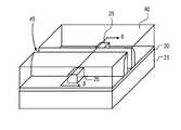
- FIG. 12which illustrates alternate processing, is a cross-sectional, elevation view, at a point in the processing similar to FIG. 8 .
- a hard maskused to define the silicon body, remains atop the channel region.
- FIG. 13illustrates the structure of FIG. 12 , as viewed through the section lines 13 - 13 of FIG. 12 .
- FIG. 14illustrates the structure of FIG. 13 , after etching which reduced the width of the body in the channel region.
- FIG. 15is a cross-sectional, elevation view of a SOI substrate.
- FIG. 16illustrates the structure of FIG. 15 , after etching of the silicon layer.
- FIG. 17illustrates the structure of FIG. 16 , with epitaxially grown source and drain regions.
- FIG. 18illustrates the structure of FIG. 17 , after a dielectric layer is formed around the structure and a gate region is exposed.
- FIG. 19illustrates the structure of FIG. 18 , after additional etching.
- FIG. 20illustrates the structure of FIG. 19 , after etching, which thins the channel region.
- FIG. 21illustrates the structure of FIG. 20 , after forming an insulating, high-k layer, and a metal gate layer.
- FIG. 22illustrates the structure of FIG. 21 , after planarization.
- FIG. 23is a block diagram, incorporating the above-illustrated thinned channel transistors in a system.
- CMOS field-effect transistorsA process for fabricating CMOS field-effect transistors and the resultant transistors are described.
- numerous specific detailsare set forth, such as specific dimensions and chemical regimes, in order to provide a thorough understanding of the present invention. It will be apparent to one skilled in the art that the present invention may be practiced without these specific details. In other instances, well-known processing steps, such as cleaning steps, are not described in detail, in order to not unnecessarily obscure the present invention.
- FIG. 1AA problem associated with small body devices is illustrated in FIG. 1A .
- a tri-gate structure 10is shown traversing a silicon body at the channel region 14 of a transistor.
- the semiconductor body or finhas been thinned at the gate edges 11 .
- This thinningis the result of processing used for defining the body, forming spacers, and cleaning of oxides. This processing can so reduce the body such that it may no longer have sufficient silicon seed to support the growth of an epitaxial layer. Often, as much as 20-50% of the body at the edge of the gate can be lost during such processing. In addition to yield loss, this results in higher source/drain resistance and the consequential reduction in transistor performance.
- FIG. 1BA similar problem is shown in FIG. 1B , where the n type or intrinsic channel region 15 is formed between the relatively thin regions 16 of the source and drain extension regions of a depletion mode planar transistor.
- the problem of thinning at the gate edgesis not limited to tri-gate structures, or for that matter, SOI substrates, but can also occur in a bulk silicon layer or a delta-doped transistor, as shown in FIG. 1B .
- an epitaxial layeris grown on a heavily doped substrate 14 .
- An etchantdiscriminates between the epitaxially grown layer and the substrate 14 , allowing the channel region 15 to be defined.
- the source and drain regions 17are grown following the etching of the region 15 .
- the structureis described in the application referenced in the Prior Art and Related Art section of this application.
- transistorsare fabricated on an oxide layer 20 which is disposed on a silicon substrate 21 shown in FIG. 2 .
- the transistor bodiesare fabricated from a monocrystalline, silicon layer 24 disposed on the oxide layer 20 .
- This SOI substrateis well-known in the semiconductor industry.
- the SOI substrateis fabricated by bonding the oxide layer 20 and silicon layer 24 onto the substrate 21 , and then planarizing the layer 24 so that it is relatively thin.
- Other techniquesare known for forming an SOI substrate including, for instance, the implantation of oxygen into the silicon substrate to form a buried oxide layer.
- Other semiconductor materials, other than silicon,may also be used such as gallium arsenide.
- the layer 24may be selectively ion implanted with a p type dopant in regions where n channel transistors are to be fabricated, and with a n type dopant in those regions where p channel devices are to be fabricated. This is used to provide the relatively light doping typically found in the channel regions of MOS devices fabricated in a CMOS integrated circuit.
- n channel transistorthe fabrication of a single n channel transistor is described. As will be appreciated in the typical integrated circuit, both n and p channel devices are fabricated. Also, in the processing for the first embodiment, a protective oxide (not shown) is disposed on the silicon layer 24 followed by the deposition of a silicon nitride layer. The nitride layer acts as a hard mask to define silicon bodies such as the silicon body 25 of FIG. 3 .
- the silicon body, in the channel region of a field-effect transistorshould ideally have a height of 20 nm and a width of 20 nm.
- the thickness of the silicon layer from which the body is etchedwould also have a thickness of 20 nm.
- the layer 24may initially be thicker than 20 nm, and will subsequently be thinned in the channel region. This thinning only occurs in the channel region, leaving the source and drain regions thicker, thereby reducing the external resistance. This will become more apparent in the description below.
- a polysilicon layeris formed over the structure of FIG. 3 and etched to define a dummy gate 30 which extends over the body 25 as seen in FIG. 4 .
- a dummy gate oxidewhich subsequently acts as an etch stop is not shown.
- the region of the body 25 below the dummy gate 30is the channel region for this replacement gate process.
- phosphorous or arsenicmay be implanted into the body 25 in alignment with the dummy gate, as illustrated by the ion implantation 26 . This ion implantation defines the tip or extension source and drain regions frequently used in CMOS transistors.
- a layer of silicon nitrideis conformally deposited over the structure of FIG. 4 , and is used to fabricate the spacers 38 shown in FIG. 5 .
- Ordinary, well-known, anisotropic etchingmay be used to fabricate the spacers.
- a carbon-doped nitride, doped with 5-13% carbon concentrationis used for the spacers.
- an oxide layer present on the body 25is removed prior to the formation of the nitride layer. This cleaning process is one of the processes that typically reduces the thickness of the body at the edges of the gate.
- the main part of the source and drain regionsare formed through ion implantation 35 shown in FIG. 5 .
- arsenic or phosphorousis used with an implant dose of up to 1 ⁇ 10 19 ⁇ 1 ⁇ 10 20 atoms/cm 3 .
- a dielectric layer 40is now conformally deposited over the structure of FIG. 5 , as shown in FIG. 6 .
- Thismay comprise a silicon dioxide layer which will become an interlayer dielectric (ILD) in an integrated circuit.
- ILDinterlayer dielectric
- a low-k dielectric or a sacrificial dielectric layermay be used.
- the layer 40typically has the mechanical strength to withstand a planarization process such as chemical mechanical polishing (CMP).
- a wet etchis used to remove the dummy polysilicon gate 30 , leaving the opening 45 , as shown in FIG. 7 .
- the dummy gate oxide(not shown) is also removed.)
- the cross-sectional view of FIG. 8 taken through section line 8 - 8 of FIG. 7better shows the opening 45 .
- the spacers 38are recessed at 47 into the body 25 .
- an oxide layeris removed from the body 25 . This results in the loss of some of the body material and, in part, accounts for the thinning occurring in the prior art structure shown at 11 of FIG. 1A . The removal of this oxide is important in some processes, as will be discussed later.
- any oxide over the body 25 within the opening 45is removed in an ordinary cleaning step.
- the structure of FIG. 8is placed in a selective silicon bath such as NH 4 OH which reduces the size of the body within the opening 45 .
- This etchingreduces both the height of the body as seen at 50 of FIG. 9 , as well as the width of the body.
- the target height and thickness of the body 25 in the channel regionis 20 ⁇ 20 nm.
- a thicker and wider body 25may be initially formed since it is thinned in this etching step.
- this etching stepdoes not thin the body 25 outside of the channel region.
- the body 25is initially thicker and wider, the source and drain regions remain thicker or wider after the channel region has been thinned.
- the severe thinning shown at 11 of FIG. 1Ais avoided.
- a gate dielectric 60is formed on exposed surfaces which includes the sides and top of the body 25 lying within the opening 45 .
- the layer 60also deposits on the interior sidewalls of the spacers 38 and on the upper surface of the dielectric layer 40 .
- the gate dielectricin one embodiment, has a high dielectric constant (k), such as a metal oxide dielectric, for instance, HfO 2 or ZrO 2 or other high k dielectrics, such as PZT or BST.
- the gate dielectricmay be formed by any well-known technique such as atomic layer deposition (ALD) or chemical vapor deposition (CVD). Alternately, the gate dielectric may be a grown dielectric.
- the gate dielectric 60may be a silicon dioxide film grown with a wet or dry oxidation process to a thickness between 5-50 ⁇ .
- a gate electrode (metal) layer 61is formed over the gate dielectric layer 60 .
- the gate electrode layer 61may be formed by blanket deposition of a suitable gate electrode material.
- a gate electrode materialcomprises a metal film such as tungsten, tantalum, titanium and/or nitrides and alloys thereof.
- n channel transistorsa work function in the range of 3.9 to 4.6 eV may be used.
- p channel transistorsa work function of 4.6 to 5.2 eV may be used. Accordingly, for substrates with both n channel and p channel transistors, two separate metal deposition processes may need to be used.
- the metal layer 61is planarized using, for example CMP, and the planarization continues until at least the upper surface of the dielectric layer 40 is exposed, as shown in FIG. 11 .
- FIGS. 12-14Alternate processing is next described in conjunction with FIGS. 12-14 .
- the numbering used in FIG. 12includes a “0” after the numbers used in FIGS. 2-11 for corresponding layers and members.
- the spacers 38 of FIG. 11are shown as spacers 380 in FIG. 12 .
- a substrate 210 , insulator 200 and body 250are seen along with the source and drain regions.
- the processing leading up to FIG. 12is the same as the processing as in the prior embodiment, with one exception.
- This differenceis that the hard mask defining the bodies or fins, such as body 250 , is not immediately removed after defining the bodies. Rather, the polysilicon dummy gate structure is formed over the hard mask. Then, where the body is not protected by the polysilicon dummy gate, the hard mask is removed. Consequently, the hard mask 260 remains over the channel region, and after the spacers are formed and dummy gate removed, the hard mask 260 is exposed in opening 450 of FIG. 12 .
- FIG. 12The structure of FIG. 12 is again illustrated in FIG. 13 from the view taken through the lines 13 - 13 of FIG. 12 .
- the silicon body 250 and mask 260are shown with the spacer 380 in the background.
- the dimension 280 of FIG. 13is the width of the body 250 in the channel region.
- wet etchingis now used to etch the silicon body 250 with, for example, NH 4 OH. This thins the width of the silicon body without changing its height, as shown in FIG. 14 . Note, in FIG. 14 the remaining body 250 is narrower than its original dimension 280 , while its height has not changed. For some semiconductor processes, better control may be obtained when only the width of the silicon body is etched. Thus, only the width of the body in the channel region is reduced to a predetermined target dimension, without reducing the height or width of the source and drain regions as this occurs.
- the hard mask 260is removed, then the high k dielectric and metal gates are formed, as was the case in the previous embodiment.
- the silicon dioxide layerwhich typically is present on the silicon body, is removed before the deposition of the spacer material. This was discussed in conjunction with the recess 47 of FIG. 8 . This is done because an undesirable reaction may occur between the oxide layer and the high k dielectric, if a high temperature anneal is used to activate the doping in the source and drain regions after the replacement gate is formed. At least the sides of the oxide layer, if not removed, may contact the high k dielectric and cause this problem. This is not a problem, however, if the annealing of the source and drain regions occurs before the high k dielectric is formed.
- the thinning of the channel region described abovecan also be used on a planar, bulk transistor or a transistor formed in a delta-doped substrate.
- FIGS. 15-21 belowdescribe the formation of a depletion mode transistor with raised source and drain regions, where controlled thinning of the channel region occurs.
- FIG. 15illustrates an SOI substrate having a base 100 , oxide layer 102 and a monocrystalline silicon layer 103 .
- the layer 103or at least the region where the depletion mode transistor is fabricated, is lightly doped with an n type dopant or is intrinsic silicon, or other semiconductor material.
- a gate structureis fabricated on a dummy gate oxide layer 110 . This structure comprises a polysilicon dummy gate 104 and spacers 105 .
- the semiconductor layer 103is etched isotropically in alignment with the gate structure. This etching undercuts the gate structure as illustrated at undercut 114 . The remaining silicon from layer 103 , is the channel region 119 , seen in FIG. 16 .
- Raised source and drain regionsare then epitaxially grown to establish a shallow, highly doped source/drain tip (extension) that laterally extends the distance under the gate edge to the channel region 119 .
- Separate processingis used for the p-channel and n-channel transistors with each of the source and drain regions being grown in different processing, both with in-situ doping. This results in the source and drain regions being highly doped, in one case with a p-type dopant, and in the other case with an n-type dopant.
- the source and drain regionsare raised as illustrated. They may be formed by selectively depositing epitaxial boron (B) doped silicon or SiGe with germanium concentrations up to 30%, as an example. Under the processing conditions of 100 sccm of dichlorosilane (DCS), 20 slm H 2 , 750-800° C., 20 Torr, 150-200 sccm HCl, a diborane (B 2 H 6 ) flow of 150-200 sccm and a GeH 4 flow of 150-200 sccm, a highly doped SiGe film with a deposition rate of 20 nm/min, B concentration of 1E20 cm ⁇ 3 and a germanium concentration of 20% is achieved.
- DCSdichlorosilane
- B 2 H 6diborane
- a low resistivity of 0.7-0.9 mOhm-cm resulting from the high B concentration in the filmprovides the benefit of high conductivity in the tip source/drain regions and thereby reduced R external .
- SiGe in the source/drain regionsexerts compressive strain on the channel, which in turn results in enhanced mobility and improved transistor performance.
- the source/drain regionsare formed, for instance, using in-situ phosphorous doped silicon deposited selectively under processing conditions of 100 sccm of DCS, 25-50 sccm HCl, 200-300 sccm of 1% PH 3 with a carrier H 2 gas flow of 20 slm at 750° C. and 20 Torr.
- a phosphorous concentration of 2E20 cm ⁇ 3 with a resistivity of 0.4-0.6 mOhm-cmis achieved in the deposited film.
- the resultant structureis shown in FIG. 17 .
- Ion implantation of boronmay be used to more heavily dope the source and drain region beyond the edges of the gate structure shown in FIG. 17 .
- a dielectric layer 130is now formed over the structure of FIG. 17 .
- This layercorresponds to the dielectric layers 40 and 400 in the prior embodiments.
- this layermay be an ILD layer or a sacrificial layer.
- An etchantis used to etch away the dummy gate, providing an opening 140 seen in FIG. 18 . This exposes the underlying oxide layer 110 .
- the oxide layer 110is removed with an ordinary etchant as shown in FIG. 19 , thereby exposing the channel region 119 .
- the channel regioncan be etched to reduce its cross section as shown in FIG. 20 .
- a tetramethylammonium hydroxide (TMAH) or ammonium hydroxide solution with an appropriate pH valueis used to selectively etch the exposed n type or intrinsic silicon channel region 119 without affecting the p+ source and drain regions.
- This etchantis highly selective, and thus leaves in place the tips 150 of the source and drain regions 120 while the thinning of the channel region 119 occurs.
- the boron-doped siliconhas a sufficiently different lattice energy than the phosphorous- or arsenic-doped silicon, thereby allowing this selective etching to occur. In one process, this etching is done at a megasonic energy level of between 600 and 1100 kHz.
- the tips 150 shown in FIG. 20thus remain even though the channel region falls below the raised source and drain regions.
- a high k dielectric gate layer 122may next be conformally deposited using, for instance, ALD. Following this, metal gate layer 124 is formed. The appropriate work function for the layer 124 is used as discussed above for the layer 61 .
- FIG. 21is planarized with, for instance, CMP to provide the structure of FIG. 22 .
- the final recessed channel 119thus has raised, source/drain extension regions. This allows the current from the channel inversion layer to spread upward into these extension regions as shown by the lines 125 . In contrast in examining FIG. 1B at 16 , the current can only spread outward and downward, thereby resulting in higher series resistance.
- FIG. 23illustrates such a system 600 in accordance with one embodiment.
- system 600includes computing device 602 for processing data.
- Computing device 602may include a motherboard 604 .
- Motherboard 604may include in particular a processor 606 , and a networking interface 608 coupled to a bus 610 .
- processor 606may comprise the transistors of FIG. 11 or 22 , as examples, of the above-described transistor.
- system 600may include other components, including but are not limited to, volatile and non-volatile memory, a graphics processor, a digital signal processor, a crypto processor, a chipset, mass storage (such as hard disk, compact disk (CD), digital versatile disk (DVD) and so forth), and so forth.
- system 600may be a personal digital assistant (PDA), a mobile phone, a tablet computing device, a laptop computing device, a desktop computing device, a set-top box, an entertainment control unit, a digital camera, a digital video recorder, a CD player, a DVD player, or other digital device of the like.
- PDApersonal digital assistant
Landscapes
- Engineering & Computer Science (AREA)
- Computer Networks & Wireless Communication (AREA)
- Signal Processing (AREA)
- Chemical & Material Sciences (AREA)
- Insulated Gate Type Field-Effect Transistor (AREA)
- Crystallography & Structural Chemistry (AREA)
- Composite Materials (AREA)
- Materials Engineering (AREA)
- Thin Film Transistor (AREA)
- Metal-Oxide And Bipolar Metal-Oxide Semiconductor Integrated Circuits (AREA)
Abstract
Description
This application is a divisional of U.S. patent application Ser. No. 11/154,138, filed Jun. 15, 2005, the entire contents of which are hereby incorporated by reference herein.
1) Field of the Invention
The invention relates to the field of semiconductor processing for transistors having thin channel regions.
2) Description of Related Art
The trend in the fabrication of complementary metal-oxide-semiconductor (CMOS) transistors is to have small channel regions. Examples of a transistor having a reduced body which includes the channel region along with a tri-gate structure are shown in US 2004/0036127. Other small channel transistors are delta-doped transistors formed in lightly doped or undoped epitaxial layers grown on a heavily doped substrate. See, for instance, “Metal Gate Transistor with Epitaxial Source and Drain Regions,” application Ser. No. 10/955,669, filed Sep. 29, 2004, assigned to the assignee of the present application.
One problem with some of these devices is the generally high external resistance that comes about from the thinning of the source and drain regions, sometimes at the edges of the gates. Other devices have similar problems that result in higher external resistance, such as limited available cross-sectional area for source and drain regions. These problems are discussed in conjunction withFIGS. 1A and 1B .
A process for fabricating CMOS field-effect transistors and the resultant transistors are described. In the following description, numerous specific details are set forth, such as specific dimensions and chemical regimes, in order to provide a thorough understanding of the present invention. It will be apparent to one skilled in the art that the present invention may be practiced without these specific details. In other instances, well-known processing steps, such as cleaning steps, are not described in detail, in order to not unnecessarily obscure the present invention.
A problem associated with small body devices is illustrated inFIG. 1A . A tri-gatestructure 10 is shown traversing a silicon body at thechannel region 14 of a transistor. The semiconductor body or fin has been thinned at thegate edges 11. This thinning is the result of processing used for defining the body, forming spacers, and cleaning of oxides. This processing can so reduce the body such that it may no longer have sufficient silicon seed to support the growth of an epitaxial layer. Often, as much as 20-50% of the body at the edge of the gate can be lost during such processing. In addition to yield loss, this results in higher source/drain resistance and the consequential reduction in transistor performance.
A similar problem is shown inFIG. 1B , where the n type orintrinsic channel region 15 is formed between the relativelythin regions 16 of the source and drain extension regions of a depletion mode planar transistor. Thus, the problem of thinning at the gate edges is not limited to tri-gate structures, or for that matter, SOI substrates, but can also occur in a bulk silicon layer or a delta-doped transistor, as shown inFIG. 1B . In the structure ofFIG. 1B , an epitaxial layer is grown on a heavily dopedsubstrate 14. An etchant discriminates between the epitaxially grown layer and thesubstrate 14, allowing thechannel region 15 to be defined. The source and drainregions 17 are grown following the etching of theregion 15. The structure is described in the application referenced in the Prior Art and Related Art section of this application.
In a first embodiment, transistors are fabricated on anoxide layer 20 which is disposed on asilicon substrate 21 shown inFIG. 2 . The transistor bodies are fabricated from a monocrystalline,silicon layer 24 disposed on theoxide layer 20. This SOI substrate is well-known in the semiconductor industry. By way of example, the SOI substrate is fabricated by bonding theoxide layer 20 andsilicon layer 24 onto thesubstrate 21, and then planarizing thelayer 24 so that it is relatively thin. Other techniques are known for forming an SOI substrate including, for instance, the implantation of oxygen into the silicon substrate to form a buried oxide layer. Other semiconductor materials, other than silicon, may also be used such as gallium arsenide.
Thelayer 24 may be selectively ion implanted with a p type dopant in regions where n channel transistors are to be fabricated, and with a n type dopant in those regions where p channel devices are to be fabricated. This is used to provide the relatively light doping typically found in the channel regions of MOS devices fabricated in a CMOS integrated circuit.
In the description below, for the first embodiment, the fabrication of a single n channel transistor is described. As will be appreciated in the typical integrated circuit, both n and p channel devices are fabricated. Also, in the processing for the first embodiment, a protective oxide (not shown) is disposed on thesilicon layer 24 followed by the deposition of a silicon nitride layer. The nitride layer acts as a hard mask to define silicon bodies such as thesilicon body 25 ofFIG. 3 .
Assume for a particular process that the silicon body, in the channel region of a field-effect transistor, should ideally have a height of 20 nm and a width of 20 nm. Using the prior art processing associated with the transistor ofFIG. 1 , the thickness of the silicon layer from which the body is etched would also have a thickness of 20 nm. As will be seen for the embodiment ofFIGS. 2-11 , thelayer 24 may initially be thicker than 20 nm, and will subsequently be thinned in the channel region. This thinning only occurs in the channel region, leaving the source and drain regions thicker, thereby reducing the external resistance. This will become more apparent in the description below.
A polysilicon layer is formed over the structure ofFIG. 3 and etched to define adummy gate 30 which extends over thebody 25 as seen inFIG. 4 . (A dummy gate oxide which subsequently acts as an etch stop is not shown.) The region of thebody 25 below thedummy gate 30, as will be seen, is the channel region for this replacement gate process. Once thedummy gate 30 has been defined, phosphorous or arsenic may be implanted into thebody 25 in alignment with the dummy gate, as illustrated by theion implantation 26. This ion implantation defines the tip or extension source and drain regions frequently used in CMOS transistors.
Next, a layer of silicon nitride is conformally deposited over the structure ofFIG. 4 , and is used to fabricate thespacers 38 shown inFIG. 5 . Ordinary, well-known, anisotropic etching may be used to fabricate the spacers. In one embodiment, a carbon-doped nitride, doped with 5-13% carbon concentration is used for the spacers. As will be discussed later, prior to the formation of the nitride layer, an oxide layer present on thebody 25 is removed. This cleaning process is one of the processes that typically reduces the thickness of the body at the edges of the gate. After the spacer formation, the main part of the source and drain regions are formed throughion implantation 35 shown inFIG. 5 . For the n channel device, arsenic or phosphorous is used with an implant dose of up to 1×10¹⁹−1×10²⁰atoms/cm3.
Adielectric layer 40 is now conformally deposited over the structure ofFIG. 5 , as shown inFIG. 6 . This may comprise a silicon dioxide layer which will become an interlayer dielectric (ILD) in an integrated circuit. A low-k dielectric or a sacrificial dielectric layer may be used. In any event, thelayer 40 typically has the mechanical strength to withstand a planarization process such as chemical mechanical polishing (CMP).
After the deposition and planarization of thedielectric layer 40, a wet etch is used to remove thedummy polysilicon gate 30, leaving theopening 45, as shown inFIG. 7 . (The dummy gate oxide (not shown) is also removed.) The cross-sectional view ofFIG. 8 taken through section line8-8 ofFIG. 7 , better shows theopening 45. Also better shown inFIG. 8 , is that thespacers 38 are recessed at47 into thebody 25. As mentioned earlier, after the source and drain tip implant and before the spacer material is deposited, an oxide layer is removed from thebody 25. This results in the loss of some of the body material and, in part, accounts for the thinning occurring in the prior art structure shown at11 ofFIG. 1A . The removal of this oxide is important in some processes, as will be discussed later.
Following the removal of the dummy gate, any oxide over thebody 25 within theopening 45 is removed in an ordinary cleaning step. Then, the structure ofFIG. 8 is placed in a selective silicon bath such as NH4OH which reduces the size of the body within theopening 45. This etching reduces both the height of the body as seen at50 ofFIG. 9 , as well as the width of the body. This allows the channel region of thebody 25 to be thinned to a target height and thickness. Again, assume that the target height and thickness of thebody 25 in the channel region is 20×20 nm. A thicker andwider body 25 may be initially formed since it is thinned in this etching step. Importantly, this etching step does not thin thebody 25 outside of the channel region. Consequently, if thebody 25 is initially thicker and wider, the source and drain regions remain thicker or wider after the channel region has been thinned. Thus, by starting with a thicker and wider body, there is more silicon left after the cleaning process, and the severe thinning shown at11 ofFIG. 1A is avoided.
Next, agate dielectric 60 is formed on exposed surfaces which includes the sides and top of thebody 25 lying within theopening 45. Thelayer 60 also deposits on the interior sidewalls of thespacers 38 and on the upper surface of thedielectric layer 40. The gate dielectric, in one embodiment, has a high dielectric constant (k), such as a metal oxide dielectric, for instance, HfO2or ZrO2or other high k dielectrics, such as PZT or BST. The gate dielectric may be formed by any well-known technique such as atomic layer deposition (ALD) or chemical vapor deposition (CVD). Alternately, the gate dielectric may be a grown dielectric. For instance, thegate dielectric 60, may be a silicon dioxide film grown with a wet or dry oxidation process to a thickness between 5-50 Å.
Following this, also as seen inFIG. 10 , a gate electrode (metal)layer 61 is formed over thegate dielectric layer 60. Thegate electrode layer 61 may be formed by blanket deposition of a suitable gate electrode material. In one embodiment, a gate electrode material comprises a metal film such as tungsten, tantalum, titanium and/or nitrides and alloys thereof. For the n channel transistors, a work function in the range of 3.9 to 4.6 eV may be used. For the p channel transistors, a work function of 4.6 to 5.2 eV may be used. Accordingly, for substrates with both n channel and p channel transistors, two separate metal deposition processes may need to be used.
Themetal layer 61 is planarized using, for example CMP, and the planarization continues until at least the upper surface of thedielectric layer 40 is exposed, as shown inFIG. 11 .
Standard processing is now used to complete the transistor ofFIG. 11 .
Alternate processing is next described in conjunction withFIGS. 12-14 . The numbering used inFIG. 12 includes a “0” after the numbers used inFIGS. 2-11 for corresponding layers and members. For instance, thespacers 38 ofFIG. 11 are shown asspacers 380 inFIG. 12 . InFIG. 12 , asubstrate 210,insulator 200 andbody 250 are seen along with the source and drain regions.
The processing leading up toFIG. 12 is the same as the processing as in the prior embodiment, with one exception. This difference is that the hard mask defining the bodies or fins, such asbody 250, is not immediately removed after defining the bodies. Rather, the polysilicon dummy gate structure is formed over the hard mask. Then, where the body is not protected by the polysilicon dummy gate, the hard mask is removed. Consequently, thehard mask 260 remains over the channel region, and after the spacers are formed and dummy gate removed, thehard mask 260 is exposed in opening450 ofFIG. 12 .
The structure ofFIG. 12 is again illustrated inFIG. 13 from the view taken through the lines13-13 ofFIG. 12 . In this view, thesilicon body 250 andmask 260 are shown with thespacer 380 in the background. Thedimension 280 ofFIG. 13 is the width of thebody 250 in the channel region.
Wet etching is now used to etch thesilicon body 250 with, for example, NH4OH. This thins the width of the silicon body without changing its height, as shown inFIG. 14 . Note, inFIG. 14 the remainingbody 250 is narrower than itsoriginal dimension 280, while its height has not changed. For some semiconductor processes, better control may be obtained when only the width of the silicon body is etched. Thus, only the width of the body in the channel region is reduced to a predetermined target dimension, without reducing the height or width of the source and drain regions as this occurs.
After this etching step, thehard mask 260 is removed, then the high k dielectric and metal gates are formed, as was the case in the previous embodiment.
As mentioned earlier, the silicon dioxide layer, which typically is present on the silicon body, is removed before the deposition of the spacer material. This was discussed in conjunction with therecess 47 ofFIG. 8 . This is done because an undesirable reaction may occur between the oxide layer and the high k dielectric, if a high temperature anneal is used to activate the doping in the source and drain regions after the replacement gate is formed. At least the sides of the oxide layer, if not removed, may contact the high k dielectric and cause this problem. This is not a problem, however, if the annealing of the source and drain regions occurs before the high k dielectric is formed.
The thinning of the channel region described above can also be used on a planar, bulk transistor or a transistor formed in a delta-doped substrate.FIGS. 15-21 below describe the formation of a depletion mode transistor with raised source and drain regions, where controlled thinning of the channel region occurs.
Following this, as shown inFIG. 16 , thesemiconductor layer 103 is etched isotropically in alignment with the gate structure. This etching undercuts the gate structure as illustrated at undercut114. The remaining silicon fromlayer 103, is thechannel region 119, seen inFIG. 16 .
Raised source and drain regions are then epitaxially grown to establish a shallow, highly doped source/drain tip (extension) that laterally extends the distance under the gate edge to thechannel region 119. Separate processing is used for the p-channel and n-channel transistors with each of the source and drain regions being grown in different processing, both with in-situ doping. This results in the source and drain regions being highly doped, in one case with a p-type dopant, and in the other case with an n-type dopant.
In forming a PMOS transistor, the source and drain regions are raised as illustrated. They may be formed by selectively depositing epitaxial boron (B) doped silicon or SiGe with germanium concentrations up to 30%, as an example. Under the processing conditions of 100 sccm of dichlorosilane (DCS), 20 slm H2, 750-800° C., 20 Torr, 150-200 sccm HCl, a diborane (B2H6) flow of 150-200 sccm and a GeH4flow of 150-200 sccm, a highly doped SiGe film with a deposition rate of 20 nm/min, B concentration of 1E20 cm−3and a germanium concentration of 20% is achieved. A low resistivity of 0.7-0.9 mOhm-cm resulting from the high B concentration in the film provides the benefit of high conductivity in the tip source/drain regions and thereby reduced Rexternal. SiGe in the source/drain regions exerts compressive strain on the channel, which in turn results in enhanced mobility and improved transistor performance.
For an NMOS transistor, the source/drain regions are formed, for instance, using in-situ phosphorous doped silicon deposited selectively under processing conditions of 100 sccm of DCS, 25-50 sccm HCl, 200-300 sccm of 1% PH3with a carrier H2gas flow of 20 slm at 750° C. and 20 Torr. A phosphorous concentration of 2E20 cm−3with a resistivity of 0.4-0.6 mOhm-cm is achieved in the deposited film.
The resultant structure is shown inFIG. 17 . Ion implantation of boron may be used to more heavily dope the source and drain region beyond the edges of the gate structure shown inFIG. 17 .
Adielectric layer 130 is now formed over the structure ofFIG. 17 . This corresponds to thedielectric layers opening 140 seen inFIG. 18 . This exposes theunderlying oxide layer 110. Theoxide layer 110 is removed with an ordinary etchant as shown inFIG. 19 , thereby exposing thechannel region 119.
Now, the channel region can be etched to reduce its cross section as shown inFIG. 20 . A tetramethylammonium hydroxide (TMAH) or ammonium hydroxide solution with an appropriate pH value is used to selectively etch the exposed n type or intrinsicsilicon channel region 119 without affecting the p+ source and drain regions. This etchant is highly selective, and thus leaves in place thetips 150 of the source and drainregions 120 while the thinning of thechannel region 119 occurs. The boron-doped silicon has a sufficiently different lattice energy than the phosphorous- or arsenic-doped silicon, thereby allowing this selective etching to occur. In one process, this etching is done at a megasonic energy level of between 600 and 1100 kHz. Thetips 150 shown inFIG. 20 , thus remain even though the channel region falls below the raised source and drain regions.
A high kdielectric gate layer 122 may next be conformally deposited using, for instance, ALD. Following this,metal gate layer 124 is formed. The appropriate work function for thelayer 124 is used as discussed above for thelayer 61.
The structure ofFIG. 21 is planarized with, for instance, CMP to provide the structure ofFIG. 22 . In the finished device, the final recessedchannel 119 thus has raised, source/drain extension regions. This allows the current from the channel inversion layer to spread upward into these extension regions as shown by thelines 125. In contrast in examiningFIG. 1B at16, the current can only spread outward and downward, thereby resulting in higher series resistance.
The transistor fabricated as described above may be incorporated into an integrated circuit, central processing unit, which in turn is part of a computing device or system.FIG. 23 illustrates such asystem 600 in accordance with one embodiment. As illustrated, for the embodiment,system 600 includescomputing device 602 for processing data.Computing device 602 may include amotherboard 604.Motherboard 604 may include in particular aprocessor 606, and anetworking interface 608 coupled to a bus610. More specifically,processor 606 may comprise the transistors ofFIG. 11 or 22 , as examples, of the above-described transistor.
Depending on the applications,system 600 may include other components, including but are not limited to, volatile and non-volatile memory, a graphics processor, a digital signal processor, a crypto processor, a chipset, mass storage (such as hard disk, compact disk (CD), digital versatile disk (DVD) and so forth), and so forth.
In various embodiments,system 600 may be a personal digital assistant (PDA), a mobile phone, a tablet computing device, a laptop computing device, a desktop computing device, a set-top box, an entertainment control unit, a digital camera, a digital video recorder, a CD player, a DVD player, or other digital device of the like.
Thus, improved processing has been described that allows a channel region to be controllably thinned, and that permits the source/drain regions to have less resistance.
Claims (14)
1. A non-planar transistor, comprising:
a three-dimensional semiconductor body disposed above a substrate, the three-dimensional semiconductor body having a top surface and a pair of sidewall surfaces and having a first outermost width, a second outermost width, a length, and an uppermost height;
a source region disposed only in a first end of the three-dimensional semiconductor body having only the first outermost width and the uppermost height, the source region having the first outermost width and the uppermost height;
a drain region disposed only in a second end of the three-dimensional semiconductor body having only the first outermost width and the uppermost height, the drain region having the first outermost width and the uppermost height, the second end opposite the first end;
a channel region disposed only in a portion of the three-dimensional semiconductor body having only the second outermost width, the uppermost height and a length, the portion disposed between the source region and the drain region, and the second outermost width narrower than the first outermost width, wherein the length of the three-dimensional semiconductor body runs from the source region through the channel region to the drain region, wherein the uppermost height of the three-dimensional semiconductor body is taken from the substrate to a top surface of the three-dimensional semiconductor body, and wherein the first and second outermost width are orthogonal to the length and the uppermost height; and
a gate stack disposed directly on a portion of the top surface of the three-dimensional semiconductor body and the gate stack further disposed directly on a portion of the sidewall surfaces of the three-dimensional semiconductor body and at least partially surrounding the channel region, the gate stack having a distance between sidewalls of the gate stack equal to and in direct alignment with the length of the portion of the three-dimensional semiconductor body having only the second outermost width, wherein the gate stack comprises a gate dielectric layer and a gate electrode, and wherein the gate dielectric layer comprises a high-k insulation layer, and the gate electrode comprises a metal layer disposed directly on the high-k insulation layer.
2. The transistor ofclaim 1 , wherein the channel region is directly adjacent to both the source region and the drain region.
3. The transistor ofclaim 1 , further comprising:
a first tip region disposed only in the first end of the three-dimensional semiconductor body having only the first outermost width and the uppermost height; and
a second tip region disposed only in the second end of the three-dimensional semiconductor body having only the first outermost width and the uppermost height, wherein the channel region is directly adjacent to both the first and second tip regions.
4. The transistor ofclaim 1 , wherein the gate dielectric layer is disposed below the gate electrode and also forms the sidewalls of the gate stack.
5. The transistor ofclaim 1 , wherein the gate dielectric layer is disposed only below the gate electrode.
6. The transistor ofclaim 1 , wherein the metal layer has a work function between 3.9 eV and 5.2 eV.
7. The transistor ofclaim 1 , wherein the three-dimensional semiconductor body is disposed directly on a silicon-on-insulator substrate.
8. The transistor ofclaim 1 , wherein the three-dimensional semiconductor body is disposed directly on a delta-doped substrate.
9. A non-planar transistor, comprising:
a three-dimensional semiconductor body disposed above a substrate, the three-dimensional semiconductor body having a top surface and a pair of sidewall surfaces and having a first outermost width, a second outermost width, a length, and an uppermost height, wherein the three-dimensional semiconductor body is disposed directly on a delta-doped substrate;
a source region disposed only in a first end of the three-dimensional semiconductor body having only the first outermost width and the uppermost height, the source region having the first outermost width and the uppermost height;
a drain region disposed only in a second end of the three-dimensional semiconductor body having only the first outermost width and the uppermost height, the drain region having the first outermost width and the uppermost height, the second end opposite the first end;
a channel region disposed only in a portion of the three-dimensional semiconductor body having only the second outermost width, the uppermost height and a length, the portion disposed between the source region and the drain region, and the second outermost width narrower than the first outermost width, wherein the length of the three-dimensional semiconductor body runs from the source region through the channel region to the drain region, wherein the uppermost height of the three-dimensional semiconductor body is taken from the substrate to a top surface of the three-dimensional semiconductor body, and wherein the first and second outermost width are orthogonal to the length and the uppermost height; and
a gate stack disposed directly on a portion of the top surface of the three-dimensional semiconductor body and the gate stack further disposed directly on a portion of the sidewall surfaces of the three-dimensional semiconductor body and at least partially surrounding the channel region, the gate stack having a distance between sidewalls of the gate stack equal to and in direct alignment with the length of the portion of the three-dimensional semiconductor body having only the second outermost width, wherein the gate stack comprises a gate dielectric layer and a gate electrode.
10. The transistor ofclaim 9 , wherein the channel region is directly adjacent to both the source region and the drain region.
11. The transistor ofclaim 9 , further comprising:
a first tip region disposed only in the first end of the three-dimensional semiconductor body having only the first outermost width and the uppermost height; and
a second tip region disposed only in the second end of the three-dimensional semiconductor body having only the first outermost width and the uppermost height, wherein the channel region is directly adjacent to both the first and second tip regions.
12. The transistor ofclaim 9 , wherein the gate dielectric layer is disposed below the gate electrode and also forms the sidewalls of the gate stack.
13. The transistor ofclaim 9 , wherein the gate dielectric layer is disposed only below the gate electrode.
14. The transistor ofclaim 9 , wherein the three-dimensional semiconductor body is disposed directly on a silicon-on-insulator substrate.
Priority Applications (5)
| Application Number | Priority Date | Filing Date | Title |
|---|---|---|---|
| US12/949,696US9337307B2 (en) | 2005-06-15 | 2010-11-18 | Method for fabricating transistor with thinned channel |
| US15/069,726US9806195B2 (en) | 2005-06-15 | 2016-03-14 | Method for fabricating transistor with thinned channel |
| US15/730,542US10367093B2 (en) | 2005-06-15 | 2017-10-11 | Method for fabricating transistor with thinned channel |
| US16/526,898US10937907B2 (en) | 2005-06-15 | 2019-07-30 | Method for fabricating transistor with thinned channel |
| US17/148,330US11978799B2 (en) | 2005-06-15 | 2021-01-13 | Method for fabricating transistor with thinned channel |
Applications Claiming Priority (2)
| Application Number | Priority Date | Filing Date | Title |
|---|---|---|---|
| US11/154,138US7858481B2 (en) | 2005-06-15 | 2005-06-15 | Method for fabricating transistor with thinned channel |
| US12/949,696US9337307B2 (en) | 2005-06-15 | 2010-11-18 | Method for fabricating transistor with thinned channel |
Related Parent Applications (2)
| Application Number | Title | Priority Date | Filing Date |
|---|---|---|---|
| US11/154,138DivisionUS7858481B2 (en) | 2005-06-15 | 2005-06-15 | Method for fabricating transistor with thinned channel |
| US11/154,138ContinuationUS7858481B2 (en) | 2005-06-15 | 2005-06-15 | Method for fabricating transistor with thinned channel |
Related Child Applications (2)
| Application Number | Title | Priority Date | Filing Date |
|---|---|---|---|
| US15/069,726ContinuationUS9806195B2 (en) | 2005-06-15 | 2016-03-14 | Method for fabricating transistor with thinned channel |
| US15/069,726DivisionUS9806195B2 (en) | 2005-06-15 | 2016-03-14 | Method for fabricating transistor with thinned channel |
Publications (2)
| Publication Number | Publication Date |
|---|---|
| US20110062520A1 US20110062520A1 (en) | 2011-03-17 |
| US9337307B2true US9337307B2 (en) | 2016-05-10 |
Family
ID=37573926
Family Applications (6)
| Application Number | Title | Priority Date | Filing Date |
|---|---|---|---|
| US11/154,138Active2028-10-03US7858481B2 (en) | 2005-06-15 | 2005-06-15 | Method for fabricating transistor with thinned channel |
| US12/949,696Expired - LifetimeUS9337307B2 (en) | 2005-06-15 | 2010-11-18 | Method for fabricating transistor with thinned channel |
| US15/069,726Expired - LifetimeUS9806195B2 (en) | 2005-06-15 | 2016-03-14 | Method for fabricating transistor with thinned channel |
| US15/730,542Expired - LifetimeUS10367093B2 (en) | 2005-06-15 | 2017-10-11 | Method for fabricating transistor with thinned channel |
| US16/526,898Expired - LifetimeUS10937907B2 (en) | 2005-06-15 | 2019-07-30 | Method for fabricating transistor with thinned channel |
| US17/148,330Active2026-01-01US11978799B2 (en) | 2005-06-15 | 2021-01-13 | Method for fabricating transistor with thinned channel |
Family Applications Before (1)
| Application Number | Title | Priority Date | Filing Date |
|---|---|---|---|
| US11/154,138Active2028-10-03US7858481B2 (en) | 2005-06-15 | 2005-06-15 | Method for fabricating transistor with thinned channel |
Family Applications After (4)
| Application Number | Title | Priority Date | Filing Date |
|---|---|---|---|
| US15/069,726Expired - LifetimeUS9806195B2 (en) | 2005-06-15 | 2016-03-14 | Method for fabricating transistor with thinned channel |
| US15/730,542Expired - LifetimeUS10367093B2 (en) | 2005-06-15 | 2017-10-11 | Method for fabricating transistor with thinned channel |
| US16/526,898Expired - LifetimeUS10937907B2 (en) | 2005-06-15 | 2019-07-30 | Method for fabricating transistor with thinned channel |
| US17/148,330Active2026-01-01US11978799B2 (en) | 2005-06-15 | 2021-01-13 | Method for fabricating transistor with thinned channel |
Country Status (1)
| Country | Link |
|---|---|
| US (6) | US7858481B2 (en) |
Cited By (3)
| Publication number | Priority date | Publication date | Assignee | Title |
|---|---|---|---|---|
| US20170054001A1 (en)* | 2014-05-12 | 2017-02-23 | Institute of Microelectronics, Chinese Academy of Sciences | Method for manufacturing a finfet device |
| US9917195B2 (en)* | 2015-07-29 | 2018-03-13 | International Business Machines Corporation | High doped III-V source/drain junctions for field effect transistors |
| US11978799B2 (en) | 2005-06-15 | 2024-05-07 | Tahoe Research, Ltd. | Method for fabricating transistor with thinned channel |
Families Citing this family (43)
| Publication number | Priority date | Publication date | Assignee | Title |
|---|---|---|---|---|
| US7473947B2 (en)* | 2002-07-12 | 2009-01-06 | Intel Corporation | Process for ultra-thin body SOI devices that incorporate EPI silicon tips and article made thereby |
| US7504328B2 (en)* | 2004-05-11 | 2009-03-17 | National University Of Singapore | Schottky barrier source/drain n-mosfet using ytterbium silicide |
| US7332439B2 (en)* | 2004-09-29 | 2008-02-19 | Intel Corporation | Metal gate transistors with epitaxial source and drain regions |
| US20090004868A1 (en)* | 2007-06-29 | 2009-01-01 | Doyle Brian S | Amorphous silicon oxidation patterning |
| US20090001438A1 (en)* | 2007-06-29 | 2009-01-01 | Doyle Brian S | Isolation of MIM FIN DRAM capacitor |
| US8076735B2 (en)* | 2009-10-02 | 2011-12-13 | United Microelectronics Corp. | Semiconductor device with trench of various widths |
| US8313999B2 (en)* | 2009-12-23 | 2012-11-20 | Intel Corporation | Multi-gate semiconductor device with self-aligned epitaxial source and drain |
| US8936976B2 (en)* | 2009-12-23 | 2015-01-20 | Intel Corporation | Conductivity improvements for III-V semiconductor devices |
| US8436404B2 (en) | 2009-12-30 | 2013-05-07 | Intel Corporation | Self-aligned contacts |
| US8609495B2 (en) | 2010-04-08 | 2013-12-17 | Taiwan Semiconductor Manufacturing Company, Ltd. | Hybrid gate process for fabricating finfet device |
| DE102010029527B4 (en)* | 2010-05-31 | 2012-04-05 | Globalfoundries Dresden Module One Limited Liability Company & Co. Kg | A method of fabricating a multi-gate self-aligned transistor on a bulk substrate |
| US9698054B2 (en)* | 2010-10-19 | 2017-07-04 | Taiwan Semiconductor Manufacturing Company, Ltd. | Strained structure of a p-type field effect transistor |
| CN102214596B (en)* | 2011-05-26 | 2012-08-29 | 北京大学 | Manufacturing method of fence silicon nanowire transistor with air as side wall |
| WO2012163429A1 (en) | 2011-06-03 | 2012-12-06 | Acconeer Ab | Process for manufacturing a semiconductor device and an intermediate product for the manufacture of a semiconductor device |
| CN102891178A (en)* | 2011-07-19 | 2013-01-23 | 中芯国际集成电路制造(北京)有限公司 | Semiconductor device and manufacturing method thereof |
| WO2013095550A1 (en) | 2011-12-22 | 2013-06-27 | Intel Corporation | Semiconductor device having a necked semiconductor body and method of forming semiconductor bodies of varying width |
| US8828813B2 (en)* | 2012-04-13 | 2014-09-09 | Taiwan Semiconductor Manufacturing Co., Ltd. | Replacement channels |
| FR2995135B1 (en)* | 2012-09-05 | 2015-12-04 | Commissariat Energie Atomique | METHOD FOR PRODUCING FET TRANSISTORS |
| US9111801B2 (en)* | 2013-04-04 | 2015-08-18 | Stmicroelectronics, Inc. | Integrated circuit devices and fabrication techniques |
| US9105707B2 (en)* | 2013-07-24 | 2015-08-11 | International Business Machines Corporation | ZRAM heterochannel memory |
| US9048123B2 (en) | 2013-09-19 | 2015-06-02 | International Business Machines Corporation | Interdigitated finFETs |
| US20150137237A1 (en)* | 2013-11-21 | 2015-05-21 | Globalfoundries Inc. | Undoped epitaxial layer for junction isolation in a fin field effect transistor (finfet) device |
| CN104701149A (en)* | 2013-12-04 | 2015-06-10 | 中芯国际集成电路制造(上海)有限公司 | Semiconductor device and forming method thereof |
| US9711645B2 (en) | 2013-12-26 | 2017-07-18 | International Business Machines Corporation | Method and structure for multigate FinFET device epi-extension junction control by hydrogen treatment |
| US9136356B2 (en)* | 2014-02-10 | 2015-09-15 | Taiwan Semiconductor Manufacturing Co., Ltd. | Non-planar field effect transistor having a semiconductor fin and method for manufacturing |
| US9543410B2 (en)* | 2014-02-14 | 2017-01-10 | Taiwan Semiconductor Manufacturing Company Limited | Semiconductor device and formation thereof |
| US9379185B2 (en)* | 2014-04-24 | 2016-06-28 | International Business Machines Corporation | Method of forming channel region dopant control in fin field effect transistor |
| US9331146B2 (en) | 2014-06-11 | 2016-05-03 | International Business Machines Corporation | Silicon nanowire formation in replacement metal gate process |
| US9299939B1 (en)* | 2014-12-09 | 2016-03-29 | International Business Machines Corporation | Formation of CMOS device using carbon nanotubes |
| US9929242B2 (en) | 2015-01-12 | 2018-03-27 | Taiwan Semiconductor Manufacturing Co., Ltd. | Semiconductor device and manufacturing method thereof |
| US9502567B2 (en)* | 2015-02-13 | 2016-11-22 | Taiwan Semiconductor Manufacturing Co., Ltd. | Semiconductor fin structure with extending gate structure |
| US20160247888A1 (en)* | 2015-02-19 | 2016-08-25 | International Business Machines Corporation | Non-uniform gate dielectric for u-shape mosfet |
| US9362400B1 (en)* | 2015-03-06 | 2016-06-07 | International Business Machines Corporation | Semiconductor device including dielectrically isolated finFETs and buried stressor |
| US9972711B2 (en) | 2015-06-03 | 2018-05-15 | International Business Machines Corporation | Reduced resistance short-channel InGaAs planar MOSFET |
| US9799654B2 (en)* | 2015-06-18 | 2017-10-24 | International Business Machines Corporation | FET trench dipole formation |
| US9978748B2 (en)* | 2015-12-09 | 2018-05-22 | International Business Machines Corporation | Method of cutting fins to create diffusion breaks for finFETs |
| US9799649B2 (en)* | 2015-12-17 | 2017-10-24 | Taiwan Semiconductor Manufacturing Company Limited | Semiconductor device and manufacturing method thereof |
| KR102385567B1 (en) | 2017-08-29 | 2022-04-12 | 삼성전자주식회사 | Semiconductor devices and method of manufacturing semiconductor devices |
| US11424335B2 (en)* | 2017-09-26 | 2022-08-23 | Intel Corporation | Group III-V semiconductor devices having dual workfunction gate electrodes |
| CN108470769A (en)* | 2018-03-14 | 2018-08-31 | 上海华力集成电路制造有限公司 | Fin transistor and its manufacturing method |
| CN109065610B (en)* | 2018-08-21 | 2021-07-27 | 电子科技大学 | A shielded gate device |
| US11488978B2 (en)* | 2018-09-27 | 2022-11-01 | Intel Corporation | Ferroelectric gate oxide based tunnel feFET memory |
| US11610820B2 (en)* | 2019-07-24 | 2023-03-21 | Infineon Technologies LLC | Embedded SONOS and high voltage select gate with a high-K metal gate and manufacturing methods of the same |
Citations (470)
| Publication number | Priority date | Publication date | Assignee | Title |
|---|---|---|---|---|
| US4231149A (en) | 1978-10-10 | 1980-11-04 | Texas Instruments Incorporated | Narrow band-gap semiconductor CCD imaging device and method of fabrication |
| JPS5673454U (en) | 1979-11-09 | 1981-06-16 | ||
| JPS59145538U (en) | 1983-03-22 | 1984-09-28 | 日本電気株式会社 | High-frequency heating high-pressure zone "Ku" molten material synthesis furnace |
| US4487652A (en) | 1984-03-30 | 1984-12-11 | Motorola, Inc. | Slope etch of polyimide |
| GB2156149A (en) | 1984-03-14 | 1985-10-02 | Philips Electronic Associated | Dielectrically-isolated integrated circuit manufacture |
| US4711701A (en) | 1986-09-16 | 1987-12-08 | Texas Instruments Incorporated | Self-aligned transistor method |
| US4818715A (en) | 1987-07-09 | 1989-04-04 | Industrial Technology Research Institute | Method of fabricating a LDDFET with self-aligned silicide |
| US4905063A (en) | 1988-06-21 | 1990-02-27 | American Telephone And Telegraph Company, At&T Bell Laboratories | Floating gate memories |
| US4906589A (en) | 1989-02-06 | 1990-03-06 | Industrial Technology Research Institute | Inverse-T LDDFET with self-aligned silicide |
| US4907048A (en) | 1987-11-23 | 1990-03-06 | Xerox Corporation | Double implanted LDD transistor self-aligned with gate |
| US4994873A (en) | 1988-10-17 | 1991-02-19 | Motorola, Inc. | Local interconnect for stacked polysilicon device |
| US4996574A (en) | 1988-07-01 | 1991-02-26 | Fujitsu Limited | MIS transistor structure for increasing conductance between source and drain regions |
| US5023203A (en) | 1988-07-28 | 1991-06-11 | Korea Electronics & Telecommunications Research Institute Et Al. | Method of patterning fine line width semiconductor topology using a spacer |
| US5120666A (en) | 1989-05-16 | 1992-06-09 | Fujitsu Limited | Manufacturing method for semiconductor device |
| US5124777A (en) | 1990-07-02 | 1992-06-23 | Samsung Electronics Co., Ltd. | Dielectric medium for capacitor of semiconductor device |
| US5179037A (en) | 1991-12-24 | 1993-01-12 | Texas Instruments Incorporated | Integration of lateral and vertical quantum well transistors in the same epitaxial stack |
| US5216271A (en) | 1990-09-28 | 1993-06-01 | Kabushiki Kaisha Toshiba | BiCMOS device with low bandgap CMOS contact regions and low bandgap bipolar base region |
| US5266518A (en) | 1989-09-14 | 1993-11-30 | U.S. Philips Corporation | Method of manufacturing a semiconductor body comprising a mesa |
| US5278102A (en) | 1990-08-18 | 1994-01-11 | Fujitsu Limited | SOI device and a fabrication process thereof |
| JPH065856Y2 (en) | 1988-03-29 | 1994-02-16 | 株式会社名機製作所 | Mold clamping device |
| US5308999A (en) | 1992-02-27 | 1994-05-03 | Fujitsu Limited | MOS FET having a thin film SOI structure |
| JPH06177089A (en) | 1992-12-04 | 1994-06-24 | Fujitsu Ltd | Method for manufacturing semiconductor device |
| US5328810A (en) | 1990-05-07 | 1994-07-12 | Micron Technology, Inc. | Method for reducing, by a factor or 2-N, the minimum masking pitch of a photolithographic process |
| JPH06224440A (en) | 1993-01-21 | 1994-08-12 | Nippon Steel Corp | MOS field effect transistor and nonvolatile semiconductor memory device |
| US5338959A (en) | 1992-03-30 | 1994-08-16 | Samsung Electronics Co., Ltd. | Thin film transistor with three dimensional multichannel structure |
| US5346839A (en) | 1991-06-10 | 1994-09-13 | Texas Instruments Incorporated | Sidewall doping technique for SOI transistors |
| US5346836A (en) | 1991-06-06 | 1994-09-13 | Micron Technology, Inc. | Process for forming low resistance contacts between silicide areas and upper level polysilicon interconnects |
| US5357119A (en) | 1993-02-19 | 1994-10-18 | Board Of Regents Of The University Of California | Field effect devices having short period superlattice structures using Si and Ge |
| EP0623963A1 (en) | 1993-05-06 | 1994-11-09 | Siemens Aktiengesellschaft | MOSFET on SOI substrate |
| US5371024A (en)* | 1988-09-30 | 1994-12-06 | Kabushiki Kaisha Toshiba | Semiconductor device and process for manufacturing the same |
| US5391506A (en) | 1992-01-31 | 1995-02-21 | Kawasaki Steel Corporation | Manufacturing method for semiconductor devices with source/drain formed in substrate projection. |
| US5428237A (en) | 1991-04-26 | 1995-06-27 | Canon Kabushiki Kaisha | Semiconductor device having an insulated gate transistor |
| US5466621A (en) | 1988-11-21 | 1995-11-14 | Hitachi, Ltd. | Method of manufacturing a semiconductor device having silicon islands |
| US5475869A (en) | 1993-05-28 | 1995-12-12 | Nec Corporation | Radio base station capable of distinguishing between interference due to collisions of outgoing call signals and an external interference noise |
| US5479033A (en) | 1994-05-27 | 1995-12-26 | Sandia Corporation | Complementary junction heterostructure field-effect transistor |
| US5482877A (en) | 1993-02-17 | 1996-01-09 | Samsung Electronics Co., Ltd. | Method for making a semiconductor device having a silicon-on-insulator structure |
| US5514885A (en) | 1986-10-09 | 1996-05-07 | Myrick; James J. | SOI methods and apparatus |
| US5521859A (en) | 1991-03-20 | 1996-05-28 | Fujitsu Limited | Semiconductor memory device having thin film transistor and method of producing the same |
| US5543351A (en) | 1992-03-19 | 1996-08-06 | Matsushita Electric Industrial Co., Ltd. | Method of producing electrically insulated silicon structure |
| US5545586A (en) | 1990-11-27 | 1996-08-13 | Nec Corporation | Method of making a transistor having easily controllable impurity profile |
| US5554870A (en) | 1994-02-04 | 1996-09-10 | Motorola, Inc. | Integrated circuit having both vertical and horizontal devices and process for making the same |
| US5563077A (en) | 1992-04-24 | 1996-10-08 | Hyundai Electronics Industries Co., Ltd. | Method of fabricating a thin film transistor having vertical channel |
| US5576227A (en) | 1994-11-02 | 1996-11-19 | United Microelectronics Corp. | Process for fabricating a recessed gate MOS device |
| US5578513A (en) | 1993-09-17 | 1996-11-26 | Mitsubishi Denki Kabushiki Kaisha | Method of making a semiconductor device having a gate all around type of thin film transistor |
| US5595941A (en) | 1994-06-01 | 1997-01-21 | Mitsubishi Denki Kabushiki Kaisha | Method of forming fine patterns |
| US5595919A (en) | 1996-02-20 | 1997-01-21 | Chartered Semiconductor Manufacturing Pte Ltd. | Method of making self-aligned halo process for reducing junction capacitance |
| US5652454A (en) | 1993-07-05 | 1997-07-29 | Iwamatsu; Toshiaki | Semiconductor device on an SOI substrate |
| US5658806A (en) | 1995-10-26 | 1997-08-19 | National Science Council | Method for fabricating thin-film transistor with bottom-gate or dual-gate configuration |
| US5665203A (en) | 1995-04-28 | 1997-09-09 | International Business Machines Corporation | Silicon etching method |
| US5682048A (en) | 1995-05-19 | 1997-10-28 | Nissan Motor Co., Ltd. | Groove-type semiconductor device |
| US5693542A (en) | 1994-12-26 | 1997-12-02 | Hyundai Electronics Industries Co., Ltd. | Method for forming a transistor with a trench |
| US5698869A (en) | 1994-09-13 | 1997-12-16 | Kabushiki Kaisha Toshiba | Insulated-gate transistor having narrow-bandgap-source |
| US5701016A (en) | 1994-11-24 | 1997-12-23 | Kabushiki Kaisha Toshiba | Semiconductor device and method for its manufacture |
| US5716879A (en) | 1994-12-15 | 1998-02-10 | Goldstar Electron Company, Ltd. | Method of making a thin film transistor |
| US5739544A (en) | 1993-05-26 | 1998-04-14 | Matsushita Electric Industrial Co., Ltd. | Quantization functional device utilizing a resonance tunneling effect and method for producing the same |
| US5747356A (en)* | 1995-12-06 | 1998-05-05 | Korea Information & Communication Co., Ltd. | Method for manufacturing ISRC MOSFET |
| US5760442A (en) | 1994-09-29 | 1998-06-02 | Kabushiki Kaisha Toshiba | Semiconductor device of a silicon on insulator metal-insulator type with a concave feature |
| US5770513A (en) | 1993-02-25 | 1998-06-23 | Mitsubishi Denki Kabushiki Kaisha | Method for producing semiconductor device with heat dissipation structure |
| US5773331A (en) | 1996-12-17 | 1998-06-30 | International Business Machines Corporation | Method for making single and double gate field effect transistors with sidewall source-drain contacts |
| US5776821A (en) | 1997-08-22 | 1998-07-07 | Vlsi Technology, Inc. | Method for forming a reduced width gate electrode |
| US5793088A (en) | 1996-06-18 | 1998-08-11 | Integrated Device Technology, Inc. | Structure for controlling threshold voltage of MOSFET |
| US5804848A (en) | 1995-01-20 | 1998-09-08 | Sony Corporation | Field effect transistor having multiple gate electrodes surrounding the channel region |
| US5811324A (en) | 1995-12-26 | 1998-09-22 | Lg Semicon Co., Ltd. | Method for manufacturing thin film transistor |
| US5814544A (en) | 1994-07-14 | 1998-09-29 | Vlsi Technology, Inc. | Forming a MOS transistor with a recessed channel |
| US5814895A (en) | 1995-12-22 | 1998-09-29 | Sony Corporation | Static random access memory having transistor elements formed on side walls of a trench in a semiconductor substrate |
| US5821629A (en) | 1994-10-04 | 1998-10-13 | United Microelectronics Corporation | Buried structure SRAM cell and methods for fabrication |
| US5827769A (en) | 1996-11-20 | 1998-10-27 | Intel Corporation | Method for fabricating a transistor with increased hot carrier resistance by nitridizing and annealing the sidewall oxide of the gate electrode |
| US5844278A (en) | 1994-09-14 | 1998-12-01 | Kabushiki Kaisha Toshiba | Semiconductor device having a projecting element region |
| US5856225A (en) | 1997-11-24 | 1999-01-05 | Chartered Semiconductor Manufacturing Ltd | Creation of a self-aligned, ion implanted channel region, after source and drain formation |
| US5859456A (en) | 1994-11-02 | 1999-01-12 | Texas Instruments Incorporated | Multiple transistor integrated circuit with thick copper interconnect |
| US5880015A (en) | 1991-04-30 | 1999-03-09 | Sgs-Thomson Microelectronics, Inc. | Method of producing stepped wall interconnects and gates |
| US5889304A (en) | 1996-06-28 | 1999-03-30 | Kabushiki Kaisha Toshiba | Nonvolatile semiconductor memory device |
| US5888309A (en) | 1997-12-29 | 1999-03-30 | Taiwan Semiconductor Manufacturing Company, Ltd. | Lateral etch inhibited multiple for forming a via through a microelectronics layer susceptible to etching within a fluorine containing plasma followed by an oxygen containing plasma |
| US5905285A (en) | 1996-09-12 | 1999-05-18 | Advanced Micro Devices, Inc. | Ultra short trench transistors and process for making same |
| US5908313A (en) | 1996-12-31 | 1999-06-01 | Intel Corporation | Method of forming a transistor |
| US5952701A (en) | 1997-08-18 | 1999-09-14 | National Semiconductor Corporation | Design and fabrication of semiconductor structure having complementary channel-junction insulated-gate field-effect transistors whose gate electrodes have work functions close to mid-gap semiconductor value |
| US5965914A (en) | 1997-06-18 | 1999-10-12 | Mitsubishi Denki Kabushiki Kaisha | Thin film transistor having a branched gate and channel |
| US5976767A (en) | 1997-10-09 | 1999-11-02 | Micron Technology, Inc. | Ammonium hydroxide etch of photoresist masked silicon |
| US5985726A (en) | 1998-11-06 | 1999-11-16 | Advanced Micro Devices, Inc. | Damascene process for forming ultra-shallow source/drain extensions and pocket in ULSI MOSFET |
| US5994747A (en)* | 1998-02-13 | 1999-11-30 | Texas Instruments-Acer Incorporated | MOSFETs with recessed self-aligned silicide gradual S/D junction |
| US6010921A (en)* | 1997-05-23 | 2000-01-04 | Sharp Kabushiki Kaisha | Method of fabricating a field-effect transistor utilizing an SOI substrate |
| US6013926A (en) | 1996-11-20 | 2000-01-11 | Mitsubishi Denki Kabushiki Kaisha | Semiconductor device with refractory metal element |
| US6018176A (en) | 1995-05-26 | 2000-01-25 | Samsung Electronics Co., Ltd. | Vertical transistor and memory cell |
| JP2000037842A (en) | 1998-07-27 | 2000-02-08 | Dainippon Printing Co Ltd | Electromagnetic wave absorbing cosmetic material |
| US6031249A (en) | 1996-07-11 | 2000-02-29 | Semiconductor Energy Laboratory Co., Ltd. | CMOS semiconductor device having boron doped channel |
| US6054355A (en) | 1997-06-30 | 2000-04-25 | Kabushiki Kaisha Toshiba | Method of manufacturing a semiconductor device which includes forming a dummy gate |
| US6063677A (en) | 1996-10-28 | 2000-05-16 | Texas Instruments Incorporated | Method of forming a MOSFET using a disposable gate and raised source and drain |
| US6063675A (en) | 1996-10-28 | 2000-05-16 | Texas Instruments Incorporated | Method of forming a MOSFET using a disposable gate with a sidewall dielectric |
| US6066869A (en) | 1997-10-06 | 2000-05-23 | Micron Technology, Inc. | Circuit and method for a folded bit line memory cell with vertical transistor and trench capacitor |
| US6087208A (en) | 1998-03-31 | 2000-07-11 | Advanced Micro Devices, Inc. | Method for increasing gate capacitance by using both high and low dielectric gate material |
| US6093621A (en) | 1999-04-05 | 2000-07-25 | Vanguard International Semiconductor Corp. | Method of forming shallow trench isolation |
| US6093947A (en) | 1998-08-19 | 2000-07-25 | International Business Machines Corporation | Recessed-gate MOSFET with out-diffused source/drain extension |
| US6114206A (en) | 1998-11-06 | 2000-09-05 | Advanced Micro Devices, Inc. | Multiple threshold voltage transistor implemented by a damascene process |
| US6114201A (en) | 1998-06-01 | 2000-09-05 | Texas Instruments-Acer Incorporated | Method of manufacturing a multiple fin-shaped capacitor for high density DRAMs |
| US6117741A (en) | 1998-01-09 | 2000-09-12 | Texas Instruments Incorporated | Method of forming a transistor having an improved sidewall gate structure |
| US6120846A (en) | 1997-12-23 | 2000-09-19 | Advanced Technology Materials, Inc. | Method for the selective deposition of bismuth based ferroelectric thin films by chemical vapor deposition |
| US6124177A (en) | 1999-08-13 | 2000-09-26 | Taiwan Semiconductor Manufacturing Company | Method for making deep sub-micron mosfet structures having improved electrical characteristics |
| US6144072A (en) | 1994-11-02 | 2000-11-07 | Mitsubishi Denki Kabushiki Kaisha | Semiconductor device formed on insulating layer and method of manufacturing the same |
| US6150222A (en) | 1999-01-07 | 2000-11-21 | Advanced Micro Devices, Inc. | Method of making a high performance transistor with elevated spacer formation and self-aligned channel regions |
| US6153485A (en) | 1998-11-09 | 2000-11-28 | Chartered Semiconductor Manufacturing Ltd. | Salicide formation on narrow poly lines by pulling back of spacer |
| US6163053A (en)* | 1996-11-06 | 2000-12-19 | Ricoh Company, Ltd. | Semiconductor device having opposite-polarity region under channel |
| US6165880A (en) | 1998-06-15 | 2000-12-26 | Taiwan Semiconductor Manufacturing Company | Double spacer technology for making self-aligned contacts (SAC) on semiconductor integrated circuits |
| US6174820B1 (en) | 1999-02-16 | 2001-01-16 | Sandia Corporation | Use of silicon oxynitride as a sacrificial material for microelectromechanical devices |
| US6190975B1 (en) | 1996-09-17 | 2001-02-20 | Matsushita Electric Industrial Co., Ltd. | Method of forming HCMOS devices with a silicon-germanium-carbon compound semiconductor layer |
| US6200865B1 (en) | 1998-12-04 | 2001-03-13 | Advanced Micro Devices, Inc. | Use of sacrificial dielectric structure to form semiconductor device with a self-aligned threshold adjust and overlying low-resistance gate |
| US6218309B1 (en) | 1999-06-30 | 2001-04-17 | Lam Research Corporation | Method of achieving top rounding and uniform etch depths while etching shallow trench isolation features |
| US6251729B1 (en) | 1998-12-18 | 2001-06-26 | U.S. Philips Corporation | Method of manufacturing a nonvolatile memory |
| US6252284B1 (en) | 1999-12-09 | 2001-06-26 | International Business Machines Corporation | Planarized silicon fin device |
| US6251763B1 (en) | 1997-06-30 | 2001-06-26 | Kabushiki Kaisha Toshiba | Semiconductor device and method for manufacturing same |
| JP2001189453A (en) | 1999-10-06 | 2001-07-10 | Lsi Logic Corp | Fully depleted, fully inverted, vertical channel, short and dual gate CMOS field effect transistors |
| US6259135B1 (en) | 1999-09-24 | 2001-07-10 | International Business Machines Corporation | MOS transistors structure for reducing the size of pitch limited circuits |
| US6261921B1 (en) | 1999-07-31 | 2001-07-17 | Taiwan Semiconductor Manufacturing Co., Ltd. | Method of forming shallow trench isolation structure |
| US6262456B1 (en) | 1998-11-06 | 2001-07-17 | Advanced Micro Devices, Inc. | Integrated circuit having transistors with different threshold voltages |
| US6274503B1 (en) | 1998-12-18 | 2001-08-14 | United Microelectronics Corp. | Etching method for doped polysilicon layer |
| US20010019886A1 (en) | 1998-05-12 | 2001-09-06 | International Business Machines Corporation | Borderless contact to diffusion with respect to gate conductor and methods for fabricating |
| US6287924B1 (en) | 1998-09-21 | 2001-09-11 | Texas Instruments Incorporated | Integrated circuit and method |
| US6294416B1 (en) | 1998-01-23 | 2001-09-25 | Texas Instruments-Acer Incorporated | Method of fabricating CMOS transistors with self-aligned planarization twin-well by using fewer mask counts |
| US20010026985A1 (en)* | 2000-03-29 | 2001-10-04 | Kim Moon Jung | Fabrication method of submicron gate using anisotropic etching |
| US20010028067A1 (en)* | 2000-03-31 | 2001-10-11 | Fujitsu Limited | Semiconductor device, method for fabricating the semiconductor device and semiconductor integrated circuit |
| US6307235B1 (en) | 1998-03-30 | 2001-10-23 | Micron Technology, Inc. | Another technique for gated lateral bipolar transistors |
| US6310367B1 (en) | 1999-02-22 | 2001-10-30 | Kabushiki Kaisha Toshiba | MOS transistor having a tensile-strained SI layer and a compressive-strained SI-GE layer |
| US6317444B1 (en) | 1998-06-12 | 2001-11-13 | Agere System Optoelectronics Guardian Corp. | Optical device including carbon-doped contact layers |
| US6319807B1 (en) | 2000-02-07 | 2001-11-20 | United Microelectronics Corp. | Method for forming a semiconductor device by using reverse-offset spacer process |
| JP2001338987A (en) | 2000-05-26 | 2001-12-07 | Nec Microsystems Ltd | Forming method of shallow trench isolation region of mos transistor |
| US6335251B2 (en) | 1998-05-29 | 2002-01-01 | Kabushiki Kaisha Toshiba | Semiconductor apparatus having elevated source and drain structure and manufacturing method therefor |
| US20020011612A1 (en) | 2000-07-31 | 2002-01-31 | Kabushiki Kaisha Toshiba | Semiconductor device and method for manufacturing the same |
| US6346450B1 (en) | 1996-12-16 | 2002-02-12 | Commissariat A L'energie Atomique | Process for manufacturing MIS transistor with self-aligned metal grid |
| US6359311B1 (en) | 2001-01-17 | 2002-03-19 | Taiwan Semiconductor Manufacturing Co., Ltd. | Quasi-surrounding gate and a method of fabricating a silicon-on-insulator semiconductor device with the same |
| US6358800B1 (en)* | 2000-09-18 | 2002-03-19 | Vanguard International Semiconductor Corporation | Method of forming a MOSFET with a recessed-gate having a channel length beyond photolithography limit |
| US6362111B1 (en) | 1998-12-09 | 2002-03-26 | Texas Instruments Incorporated | Tunable gate linewidth reduction process |
| US20020036290A1 (en)* | 2000-09-28 | 2002-03-28 | Kabushiki Kaisha Toshiba | Semiconductor device having MIS field effect transistors or three-dimensional structure |
| US20020037619A1 (en)* | 2000-09-22 | 2002-03-28 | Kohei Sugihara | Semiconductor device and method of producing the same |
| US6368923B1 (en) | 2000-04-20 | 2002-04-09 | United Microelectronics Corp. | Method of fabricating a dual metal gate having two different gate dielectric layers |
| US6376317B1 (en) | 1998-03-30 | 2002-04-23 | Micron Technology, Inc. | Methods for dual-gated transistors |
| US20020048918A1 (en)* | 2000-10-19 | 2002-04-25 | Grider Douglas T. | Multi-layered polysilicon process |
| US6383882B1 (en) | 2000-08-21 | 2002-05-07 | Samsung Electronics Co., Ltd. | Method for fabricating MOS transistor using selective silicide process |
| US6387820B1 (en) | 2000-09-19 | 2002-05-14 | Advanced Micro Devices, Inc. | BC13/AR chemistry for metal overetching on a high density plasma etcher |
| US20020058374A1 (en) | 2000-11-16 | 2002-05-16 | Tae-Kyun Kim | Method of forming dual-metal gates in semiconductor device |
| US6391782B1 (en) | 2000-06-20 | 2002-05-21 | Advanced Micro Devices, Inc. | Process for forming multiple active lines and gate-all-around MOSFET |
| US6396108B1 (en) | 2000-11-13 | 2002-05-28 | Advanced Micro Devices, Inc. | Self-aligned double gate silicon-on-insulator (SOI) device |
| WO2002043151A1 (en) | 2000-11-22 | 2002-05-30 | Hitachi, Ltd | Semiconductor device and method for fabricating the same |
| US6403981B1 (en) | 2000-08-07 | 2002-06-11 | Advanced Micro Devices, Inc. | Double gate transistor having a silicon/germanium channel region |
| US6403434B1 (en) | 2001-02-09 | 2002-06-11 | Advanced Micro Devices, Inc. | Process for manufacturing MOS transistors having elevated source and drain regions and a high-k gate dielectric |
| US6407442B2 (en) | 1994-10-28 | 2002-06-18 | Canon Kabushiki Kaisha | Semiconductor device, and operating device, signal converter, and signal processing system using the same semiconductor device |
| US20020074614A1 (en) | 2000-12-15 | 2002-06-20 | Mitsubishi Denki Kabushiki Kaisha | Semiconductor device and manufacturing method therefor |
| US20020081794A1 (en) | 2000-12-26 | 2002-06-27 | Nec Corporation | Enhanced deposition control in fabricating devices in a semiconductor wafer |
| US6413877B1 (en) | 2000-12-22 | 2002-07-02 | Lam Research Corporation | Method of preventing damage to organo-silicate-glass materials during resist stripping |
| US6413802B1 (en) | 2000-10-23 | 2002-07-02 | The Regents Of The University Of California | Finfet transistor structures having a double gate channel extending vertically from a substrate and methods of manufacture |
| US6424015B1 (en) | 1999-06-29 | 2002-07-23 | Hitachi, Ltd. | Semiconductor integrated circuit device |
| US20020096724A1 (en) | 1998-06-30 | 2002-07-25 | Chunlin Liang | Complementary metal gate electrode technology |
| US6437550B2 (en) | 1999-12-28 | 2002-08-20 | Ricoh Company, Ltd. | Voltage generating circuit and reference voltage source circuit employing field effect transistors |
| US6452229B1 (en)* | 2002-02-21 | 2002-09-17 | Advanced Micro Devices, Inc. | Ultra-thin fully depleted SOI device with T-shaped gate and method of fabrication |
| US6459123B1 (en) | 1999-04-30 | 2002-10-01 | Infineon Technologies Richmond, Lp | Double gated transistor |
| US6458662B1 (en) | 2001-04-04 | 2002-10-01 | Advanced Micro Devices, Inc. | Method of fabricating a semiconductor device having an asymmetrical dual-gate silicon-germanium (SiGe) channel MOSFET and a device thereby formed |
| US6457890B1 (en) | 1996-02-26 | 2002-10-01 | Gregor Kohlruss | Device for cleaning flat objects |
| US20020142529A1 (en) | 2001-03-29 | 2002-10-03 | Satoshi Matsuda | Semiconductor device comprising buried channel region and method for manufacturing the same |
| JP2002298051A (en) | 2001-03-30 | 2002-10-11 | Mizuho Bank Ltd | Point exchange service system |
| US6465290B1 (en) | 2000-03-27 | 2002-10-15 | Kabushiki Kaisha Toshiba | Method of manufacturing a semiconductor device using a polymer film pattern |
| US20020149031A1 (en) | 2001-04-12 | 2002-10-17 | Samsung Electronics Co., Ltd. | Semiconductor device having gate all around type transistor and method of forming the same |
| US6472258B1 (en) | 2000-11-13 | 2002-10-29 | International Business Machines Corporation | Double gate trench transistor |
| US20020160553A1 (en) | 2001-02-14 | 2002-10-31 | Hideo Yamanaka | Method and apparatus for forming a thin semiconductor film, method and apparatus for producing a semiconductor device, and electro-opitcal apparatus |
| US6475869B1 (en) | 2001-02-26 | 2002-11-05 | Advanced Micro Devices, Inc. | Method of forming a double gate transistor having an epitaxial silicon/germanium channel region |
| US6475890B1 (en) | 2001-02-12 | 2002-11-05 | Advanced Micro Devices, Inc. | Fabrication of a field effect transistor with an upside down T-shaped semiconductor pillar in SOI technology |
| US6479866B1 (en) | 2000-11-14 | 2002-11-12 | Advanced Micro Devices, Inc. | SOI device with self-aligned selective damage implant, and method |
| US20020167007A1 (en) | 1998-12-29 | 2002-11-14 | Semiconductor Energy Laboratory Co., Ltd. | Semiconductor device and method of fabricating the same |
| US20020166838A1 (en) | 2001-05-10 | 2002-11-14 | Institute Of Microelectronics | Sloped trench etching process |
| US6483156B1 (en) | 2000-03-16 | 2002-11-19 | International Business Machines Corporation | Double planar gated SOI MOSFET structure |
| US6483146B2 (en) | 1999-12-13 | 2002-11-19 | Samsung Electronics Co., Ltd. | Nonvolatile semiconductor memory device and manufacturing method thereof |
| US6483151B2 (en) | 2000-01-21 | 2002-11-19 | Nec Corporation | Semiconductor device and method of manufacturing the same |
| US20020177263A1 (en) | 2001-05-24 | 2002-11-28 | International Business Machines Corporation | Damascene double-gate MOSFET with vertical channel regions |
| WO2002095814A1 (en) | 2001-05-21 | 2002-11-28 | Motorola, Inc., A Corporation Of The State Of Delaware | Semiconductor device and method therefor________________________ |
| US20020177282A1 (en) | 2001-05-23 | 2002-11-28 | Samsung Electronics Co., Ltd. | Method of forming semiconductor device having a GAA type transistor |
| US6495403B1 (en) | 1999-10-05 | 2002-12-17 | Stmicroelectronics S.A. | Gate-all-around semiconductor device and process for fabricating the same |
| US6500767B2 (en) | 2001-03-20 | 2002-12-31 | Macronix International Co., Ltd. | Method of etching semiconductor metallic layer |
| US6501141B1 (en) | 2001-08-13 | 2002-12-31 | Taiwan Semiconductor Manufacturing Company, Ltd | Self-aligned contact with improved isolation and method for forming |
| TW516232B (en) | 1999-07-22 | 2003-01-01 | Ibm | Structure and process integration for producing transistors having independently adjustable parameters |
| US20030001205A1 (en)* | 2001-06-28 | 2003-01-02 | Hynix Semiconductor Inc. | Transistor of semiconductor device and method of manufacturing the same |
| WO2003003442A1 (en) | 2001-06-28 | 2003-01-09 | Infineon Technologies Ag | Field effect transistor and method for production thereof |
| US6506692B2 (en) | 2001-05-30 | 2003-01-14 | Intel Corporation | Method of making a semiconductor device using a silicon carbide hard mask |
| US20030036290A1 (en) | 2001-08-17 | 2003-02-20 | United Microelectronics Corp. | Method for improving the coating capability of low-k dielectric layer |
| US6526996B1 (en) | 2000-06-12 | 2003-03-04 | Promos Technologies, Inc. | Dry clean method instead of traditional wet clean after metal etch |
| US20030042542A1 (en) | 1996-04-26 | 2003-03-06 | Shigeto Maegawa | Semiconductor device having a thin film transistor and manufacturing method thereof |
| US6534807B2 (en) | 2001-08-13 | 2003-03-18 | International Business Machines Corporation | Local interconnect junction on insulator (JOI) structure |
| US6537885B1 (en) | 2002-05-09 | 2003-03-25 | Infineon Technologies Ag | Transistor and method of manufacturing a transistor having a shallow junction formation using a two step EPI layer |
| US6537901B2 (en) | 2000-12-29 | 2003-03-25 | Hynix Semiconductor Inc. | Method of manufacturing a transistor in a semiconductor device |
| US20030057486A1 (en) | 2001-09-27 | 2003-03-27 | International Business Machines Corporation | Fin field effect transistor with self-aligned gate |
| US20030057477A1 (en) | 1999-06-18 | 2003-03-27 | Hergenrother John Michael | CMOS integrated circuit having vertical transistors and a process for fabricating same |
| US6541829B2 (en) | 1999-12-03 | 2003-04-01 | Kabushiki Kaisha Toshiba | Semiconductor device and method of manufacturing the same |
| US20030067017A1 (en) | 2001-10-05 | 2003-04-10 | Meikei Ieong | Variable threshold voltage double gated transistors and method of fabrication |
| US6551886B1 (en)* | 2001-04-27 | 2003-04-22 | Advanced Micro Devices, Inc. | Ultra-thin body SOI MOSFET and gate-last fabrication method |
| US6555879B1 (en) | 2002-01-11 | 2003-04-29 | Advanced Micro Devices, Inc. | SOI device with metal source/drain and method of fabrication |
| US20030080384A1 (en)* | 2001-10-25 | 2003-05-01 | Matsushita Electric Industrial Co.., Ltd. | Semiconductor substrate, semiconductor device and method for fabricating the same |
| US20030085194A1 (en) | 2001-11-07 | 2003-05-08 | Hopkins Dean A. | Method for fabricating close spaced mirror arrays |
| US6562665B1 (en)* | 2000-10-16 | 2003-05-13 | Advanced Micro Devices, Inc. | Fabrication of a field effect transistor with a recess in a semiconductor pillar in SOI technology |
| US6562687B1 (en)* | 1999-01-15 | 2003-05-13 | Commissariat A L'energie Atomique | MIS transistor and method for making same on a semiconductor substrate |
| US20030098488A1 (en) | 2001-11-27 | 2003-05-29 | O'keeffe James | Band-structure modulation of nano-structures in an electric field |
| US20030098479A1 (en) | 1999-12-30 | 2003-05-29 | Anand Murthy | Novel MOS transistor structure and method of fabrication |
| US20030102518A1 (en) | 2001-12-04 | 2003-06-05 | International Business Machines Corporation | Finfet SRAM cell using low mobility plane for cell stability and method for forming |
| US20030102497A1 (en) | 2001-12-04 | 2003-06-05 | International Business Machines Corporation | Multiple-plane finFET CMOS |
| US20030111686A1 (en) | 2001-12-13 | 2003-06-19 | Nowak Edward J. | Method for forming asymmetric dual gate transistor |
| US6583469B1 (en) | 2002-01-28 | 2003-06-24 | International Business Machines Corporation | Self-aligned dog-bone structure for FinFET applications and methods to fabricate the same |
| US20030122186A1 (en) | 2001-03-13 | 2003-07-03 | Nat'l. Inst. Of Advanced Indust'l Sci. And Tech. | Double-gate field-effect transistor, integrated circuit using the transistor and method of manufacturing the same |
| US20030143791A1 (en) | 2002-01-29 | 2003-07-31 | Samsung Electronics Co., Ltd. | Methods for fabricating MOS transistors with notched gate electrodes |
| US6605498B1 (en) | 2002-03-29 | 2003-08-12 | Intel Corporation | Semiconductor transistor having a backfilled channel material |
| US20030151077A1 (en) | 2002-02-13 | 2003-08-14 | Leo Mathew | Method of forming a vertical double gate semiconductor device and structure thereof |
| JP2003229575A (en) | 2002-02-04 | 2003-08-15 | Hitachi Ltd | Integrated semiconductor device and manufacturing method thereof |
| DE10203998A1 (en) | 2002-02-01 | 2003-08-21 | Infineon Technologies Ag | Production of a toothed structure in crystal structure in/on substrate used in production of floating gate transistor comprises forming trenches using a mask on the substrate and etching process and the unmasked region of substrate |
| TW548799B (en) | 2001-09-21 | 2003-08-21 | Mitsubishi Electric Corp | Method of manufacturing semiconductor device with offset sidewall structure |
| US6611029B1 (en) | 2002-11-08 | 2003-08-26 | Advanced Micro Devices, Inc. | Double gate semiconductor device having separate gates |
| US20030162358A1 (en)* | 2002-02-26 | 2003-08-28 | International Business Machines Corporation | Method of forming a fully-depleted soi (silicon-on-insulator) mosfet having a thinned channel region |
| US20030174534A1 (en) | 2002-03-12 | 2003-09-18 | Clark Lawrence T. | Low standby power using shadow storage |
| US20030190766A1 (en) | 2002-04-08 | 2003-10-09 | Micron Technology, Inc. | Process for making a silicon-on-insulator ledge and structures achieved thereby |
| JP2003298051A (en) | 2002-01-30 | 2003-10-17 | Soko Lee | Double gate FET device and method of manufacturing the same |
| US6635909B2 (en) | 2002-03-19 | 2003-10-21 | International Business Machines Corporation | Strained fin FETs structure and method |
| US20030203636A1 (en) | 2002-04-29 | 2003-10-30 | Anthony Thomas C. | Method of fabricating high density sub-lithographic features on a substrate |
| US6642114B2 (en) | 1997-01-29 | 2003-11-04 | Fujitsu Limited | Semiconductor device and method for fabricating the same |
| US6642090B1 (en)* | 2002-06-03 | 2003-11-04 | International Business Machines Corporation | Fin FET devices from bulk semiconductor and method for forming |
| TW561530B (en) | 2001-01-03 | 2003-11-11 | Macronix Int Co Ltd | Process for fabricating CMOS transistor of IC devices employing double spacers for preventing short-channel effect |
| US6645861B2 (en) | 2001-04-18 | 2003-11-11 | International Business Machines Corporation | Self-aligned silicide process for silicon sidewall source and drain contacts |
| US6645797B1 (en) | 2002-12-06 | 2003-11-11 | Advanced Micro Devices, Inc. | Method for forming fins in a FinFET device using sacrificial carbon layer |
| US20030227036A1 (en) | 2002-02-22 | 2003-12-11 | Naoharu Sugiyama | Semiconductor device |
| US6664160B2 (en) | 2000-06-28 | 2003-12-16 | Hyundai Electronics Industries Co., Ltd. | Gate structure with high K dielectric |
| US20040007724A1 (en)* | 2002-07-12 | 2004-01-15 | Anand Murthy | Process for ultra-thin body SOI devices that incorporate EPI silicon tips and article made thereby |
| US6680240B1 (en) | 2002-06-25 | 2004-01-20 | Advanced Micro Devices, Inc. | Silicon-on-insulator device with strained device film and method for making the same with partial replacement of isolation oxide |
| US20040016968A1 (en) | 2002-04-08 | 2004-01-29 | Stmicroelectronics S.A. | Surround-gate semiconductor device encapsulated in an insulating medium |
| US6686231B1 (en) | 2002-12-06 | 2004-02-03 | Advanced Micro Devices, Inc. | Damascene gate process with sacrificial oxide in semiconductor devices |
| US20040029393A1 (en) | 2002-08-12 | 2004-02-12 | Applied Materials, Inc. | Method for removal of residue from a magneto-resistive random access memory (MRAM) film stack using a sacrificial mask layer |
| US20040029345A1 (en) | 2000-06-09 | 2004-02-12 | Simon Deleonibus | Damascene architecture electronics storage and method for making same |
| US20040026736A1 (en)* | 2002-08-12 | 2004-02-12 | Grupp Daniel E. | Insulated gate field effect transistor having passivated schottky barriers to the channel |
| TW200402872A (en) | 2002-03-05 | 2004-02-16 | Sharp Kk | Semiconductor memory device |
| US20040031979A1 (en) | 2002-06-07 | 2004-02-19 | Amberwave Systems Corporation | Strained-semiconductor-on-insulator device structures |
| US20040033639A1 (en) | 2001-05-07 | 2004-02-19 | Applied Materials, Inc. | Integrated method for release and passivation of MEMS structures |
| US6696366B1 (en) | 1998-08-17 | 2004-02-24 | Lam Research Corporation | Technique for etching a low capacitance dielectric layer |
| US20040038533A1 (en) | 1999-04-09 | 2004-02-26 | Chunlin Liang | Isolated junction structure and method of manufacture |
| US20040036126A1 (en) | 2002-08-23 | 2004-02-26 | Chau Robert S. | Tri-gate devices and methods of fabrication |
| US20040038436A1 (en) | 2002-08-09 | 2004-02-26 | Hitachi, Ltd. | Method of manufacturing a semiconductor integrated circuit device |
| US20040036118A1 (en) | 2002-08-26 | 2004-02-26 | International Business Machines Corporation | Concurrent Fin-FET and thick-body device fabrication |
| US6706571B1 (en) | 2002-10-22 | 2004-03-16 | Advanced Micro Devices, Inc. | Method for forming multiple structures in a semiconductor device |
| US6709982B1 (en) | 2002-11-26 | 2004-03-23 | Advanced Micro Devices, Inc. | Double spacer FinFET formation |
| US20040063286A1 (en)* | 2002-10-01 | 2004-04-01 | Kim Sung-Min | Field effect transistors having multiple stacked channels |
| US20040061178A1 (en) | 2002-09-30 | 2004-04-01 | Advanced Micro Devices Inc. | Finfet having improved carrier mobility and method of its formation |
| TW200405408A (en) | 2002-08-30 | 2004-04-01 | Fujitsu Ltd | Semiconductor memory device and method of manufacturing the same |
| US6716690B1 (en) | 2003-03-12 | 2004-04-06 | Advanced Micro Devices, Inc. | Uniformly doped source/drain junction in a double-gate MOSFET |
| US6716684B1 (en) | 2000-11-13 | 2004-04-06 | Advanced Micro Devices, Inc. | Method of making a self-aligned triple gate silicon-on-insulator device |
| US6716686B1 (en) | 2003-07-08 | 2004-04-06 | Advanced Micro Devices, Inc. | Method for forming channels in a finfet device |
| US20040070020A1 (en) | 1999-12-17 | 2004-04-15 | Ichiro Fujiwara | Nonvolatile semiconductor memory device and method for operating the same |
| US20040075149A1 (en) | 2000-12-04 | 2004-04-22 | Amberwave Systems Corporation | CMOS inverter and integrated circuits utilizing strained silicon surface channel MOSFETs |
| US20040075141A1 (en) | 2002-10-17 | 2004-04-22 | Renesas Technology Corp. | Semiconductor device and method of manufacturing same |
| US20040082125A1 (en) | 2002-10-29 | 2004-04-29 | Taiwan Semiconductor Manufacturing Company | Novel dual gate dielectric scheme: SiON for high performance devices and high k for low power devices |
| US6730964B2 (en) | 1997-07-22 | 2004-05-04 | Hitachi, Ltd. | Semiconductor device and method of producing the same |
| US20040092062A1 (en) | 2002-11-08 | 2004-05-13 | Ahmed Shibly S. | Planarizing gate material to improve gate critical dimension in semiconductor devices |
| US20040099966A1 (en) | 2002-11-27 | 2004-05-27 | Chau Robert S. | Novel field effect transistor and method of fabrication |
| US20040099903A1 (en) | 2002-11-26 | 2004-05-27 | Taiwan Semiconductor Manufacturing Co., Ltd. | Strained-channel multiple-gate transistor |
| US6744103B2 (en) | 1999-12-16 | 2004-06-01 | Spinnaker Semiconductor, Inc. | Short-channel schottky-barrier MOSFET device and manufacturing method |
| US20040108523A1 (en) | 2002-12-06 | 2004-06-10 | Hao-Yu Chen | Multiple-gate transistor structure and method for fabricating |
| US20040108558A1 (en)* | 2002-12-06 | 2004-06-10 | Kwak Byung Il | Transistor of semiconductor device, and method for manufacturing the same |
| US20040110331A1 (en) | 2002-12-06 | 2004-06-10 | Yee-Chia Yeo | CMOS inverters configured using multiple-gate transistors |
| US20040113181A1 (en) | 2002-12-13 | 2004-06-17 | Wicker Guy C. | Lateral phase change memory and method therefor |
| US20040119100A1 (en) | 2002-12-19 | 2004-06-24 | International Business Machines Corporation | Dense dual-plane devices |
| US6756657B1 (en) | 1993-06-25 | 2004-06-29 | Semiconductor Energy Laboratory Co., Ltd. | Method of preparing a semiconductor having controlled crystal orientation |
| US20040124492A1 (en) | 2002-09-12 | 2004-07-01 | Kouji Matsuo | Semiconductor device and method of manufacturing the same |
| US20040132236A1 (en) | 2003-01-08 | 2004-07-08 | International Business Machines Corporation | Mos transistor |
| US6762469B2 (en) | 2002-04-19 | 2004-07-13 | International Business Machines Corporation | High performance CMOS device structure with mid-gap metal gate |
| WO2004059726A1 (en) | 2002-12-20 | 2004-07-15 | International Business Machines Corporation | Integrated antifuse structure for finfet and cmos devices |
| US6765303B1 (en) | 2003-05-06 | 2004-07-20 | Advanced Micro Devices, Inc. | FinFET-based SRAM cell |
| US6764884B1 (en)* | 2003-04-03 | 2004-07-20 | Advanced Micro Devices, Inc. | Method for forming a gate in a FinFET device and thinning a fin in a channel region of the FinFET device |
| US20040145000A1 (en) | 2003-01-23 | 2004-07-29 | An Judy Xilin | Tri-gate and gate around MOSFET devices and methods for making same |
| US20040145019A1 (en) | 2003-01-23 | 2004-07-29 | Srikanteswara Dakshina-Murthy | Strained channel finfet |
| US6770516B2 (en) | 2002-09-05 | 2004-08-03 | Taiwan Semiconductor Manufacturing Company | Method of forming an N channel and P channel FINFET device on the same semiconductor substrate |
| US20040166642A1 (en) | 2003-02-20 | 2004-08-26 | Hao-Yu Chen | Semiconductor nano-rod devices |
| US6784071B2 (en) | 2003-01-31 | 2004-08-31 | Taiwan Semiconductor Manufacturing Company, Ltd. | Bonded SOI wafer with <100> device layer and <110> substrate for performance improvement |
| TW200417034A (en) | 2003-02-27 | 2004-09-01 | Taiwan Semiconductor Mfg | Contacts to semiconductor fin device and method for manufacturing the same |
| US20040169221A1 (en) | 2003-02-28 | 2004-09-02 | Samsung Electronics Co., Ltd. | MOS transistor with elevated source and drain structures and method of fabrication thereof |
| US6787424B1 (en)* | 2001-02-09 | 2004-09-07 | Advanced Micro Devices, Inc. | Fully depleted SOI transistor with elevated source and drain |
| US6787406B1 (en) | 2003-08-12 | 2004-09-07 | Advanced Micro Devices, Inc. | Systems and methods for forming dense n-channel and p-channel fins using shadow implanting |
| US6787402B1 (en) | 2001-04-27 | 2004-09-07 | Advanced Micro Devices, Inc. | Double-gate vertical MOSFET transistor and fabrication method |
| US6787845B2 (en) | 2000-03-22 | 2004-09-07 | Commissariat A L'energie Atomique | Metal source and drain mos transistor |
| US6787854B1 (en) | 2003-03-12 | 2004-09-07 | Advanced Micro Devices, Inc. | Method for forming a fin in a finFET device |
| US6790733B1 (en) | 2003-03-28 | 2004-09-14 | International Business Machines Corporation | Preserving TEOS hard mask using COR for raised source-drain including removable/disposable spacer |
| US20040180491A1 (en) | 2003-03-13 | 2004-09-16 | Nobutoshi Arai | Memory function body, particle forming method therefor and, memory device, semiconductor device, and electronic equipment having the memory function body |
| US6794313B1 (en) | 2002-09-20 | 2004-09-21 | Taiwan Semiconductor Manufacturing Company, Ltd. | Oxidation process to improve polysilicon sidewall roughness |
| US6798000B2 (en) | 2000-07-04 | 2004-09-28 | Infineon Technologies Ag | Field effect transistor |
| US20040191980A1 (en) | 2003-03-27 | 2004-09-30 | Rafael Rios | Multi-corner FET for better immunity from short channel effects |
| US6800885B1 (en) | 2003-03-12 | 2004-10-05 | Advance Micro Devices, Inc. | Asymmetrical double gate or all-around gate MOSFET devices and methods for making same |
| US20040197975A1 (en)* | 2003-01-23 | 2004-10-07 | Zoran Krivokapic | Narrow fin finfet |
| US20040195624A1 (en)* | 2003-04-04 | 2004-10-07 | National Taiwan University | Strained silicon fin field effect transistor |
| US20040198003A1 (en) | 2003-03-26 | 2004-10-07 | Taiwan Semiconductor Manufacturing Co., Ltd. | Multiple-gate transistors with improved gate control |
| US20040203254A1 (en) | 2003-04-11 | 2004-10-14 | Sharp Laboratories Of America, Inc. | Modulated temperature method of atomic layer deposition (ALD) of high dielectric constant films |
| US20040219722A1 (en)* | 2003-05-01 | 2004-11-04 | Pham Daniel T. | Method for forming a double-gated semiconductor device |
| US20040219780A1 (en) | 2003-04-30 | 2004-11-04 | Elpida Memory, Inc | Manufacturing method of semiconductor device |
| US20040217420A1 (en) | 2003-04-30 | 2004-11-04 | Yee-Chia Yeo | Semiconductor-on-insulator chip incorporating strained-channel partially-depleted, fully-depleted, and multiple-gate transistors |
| US20040222473A1 (en) | 2003-04-15 | 2004-11-11 | Tomomitsu Risaki | Semiconductor device |
| US20040227187A1 (en) | 2003-02-13 | 2004-11-18 | Zhiyuan Cheng | Integrated semiconductor device and method to make same |
| US6821834B2 (en) | 2002-12-04 | 2004-11-23 | Yoshiyuki Ando | Ion implantation methods and transistor cell layout for fin type transistors |
| US20040238915A1 (en) | 2001-07-03 | 2004-12-02 | Zhihao Chen | Semiconductor device isolation structure and method of forming |
| US20040238887A1 (en) | 2001-07-05 | 2004-12-02 | Fumiyuki Nihey | Field-effect transistor constituting channel by carbon nano tubes |
| US6831310B1 (en) | 2003-11-10 | 2004-12-14 | Freescale Semiconductor, Inc. | Integrated circuit having multiple memory types and method of formation |
| US6830998B1 (en) | 2003-06-17 | 2004-12-14 | Advanced Micro Devices, Inc. | Gate dielectric quality for replacement metal gate transistors |
| US6833588B2 (en) | 2002-10-22 | 2004-12-21 | Advanced Micro Devices, Inc. | Semiconductor device having a U-shaped gate structure |
| US20040256647A1 (en) | 2003-06-23 | 2004-12-23 | Sharp Laboratories Of America Inc. | Strained silicon finFET device |
| US6835618B1 (en) | 2003-08-05 | 2004-12-28 | Advanced Micro Devices, Inc. | Epitaxially grown fin for FinFET |
| US20040262699A1 (en) | 2003-06-30 | 2004-12-30 | Rafael Rios | N-gate transistor |
| US20040262683A1 (en) | 2003-06-27 | 2004-12-30 | Bohr Mark T. | PMOS transistor strain optimization with raised junction regions |
| US20040266076A1 (en) | 2003-06-26 | 2004-12-30 | International Business Machines Corporation | HYBRID PLANAR AND FinFET CMOS DEVICES |
| US20050003612A1 (en) | 2003-07-03 | 2005-01-06 | Hackler Douglas R. | Sram cell |
| US20050017377A1 (en) | 2003-07-21 | 2005-01-27 | International Business Machines Corporation | FET channel having a strained lattice structure along multiple surfaces |
| US20050019993A1 (en) | 2003-07-24 | 2005-01-27 | Deok-Hyung Lee | Methods for fabricating fin field effect transistors using a protective layer to reduce etching damage |
| US20050020020A1 (en) | 2002-07-16 | 2005-01-27 | Nadine Collaert | Integrated semiconductor fin device and a method for manufacturing such device |
| US6849556B2 (en) | 2002-09-27 | 2005-02-01 | Oki Electric Industry Co., Ltd. | Etching method, gate etching method, and method of manufacturing semiconductor devices |
| US20050023535A1 (en)* | 2001-10-24 | 2005-02-03 | Saptharishi Sriram | Methods of fabricating delta doped silicon carbide metal-semiconductor field effect transistors having a gate disposed in a double recess structure |
| US20050023633A1 (en) | 2003-08-01 | 2005-02-03 | Yee-Chia Yeo | Semiconductor-on-insulator SRAM configured using partially-depleted and fully-depleted transistors |
| US20050035415A1 (en) | 2003-08-13 | 2005-02-17 | Yee-Chia Yeo | Multiple-gate transistors formed on bulk substrates |
| US20050040444A1 (en) | 2003-08-22 | 2005-02-24 | International Business Machines Corporation | Strained-channel fin field effect transistor (FET) with a uniform channel thickness and separate gates |
| US6864540B1 (en) | 2004-05-21 | 2005-03-08 | International Business Machines Corp. | High performance FET with elevated source/drain region |
| US6867460B1 (en) | 2003-11-05 | 2005-03-15 | International Business Machines Corporation | FinFET SRAM cell with chevron FinFET logic |
| US20050059214A1 (en) | 2003-09-16 | 2005-03-17 | International Business Machines Corporation | Method and structure of vertical strained silicon devices |
| US6869898B2 (en) | 2000-07-31 | 2005-03-22 | Heraeus Quarzglas Gmbh & Co. Kg | Quartz glass jig for processing apparatus using plasma |
| US6869868B2 (en) | 2002-12-13 | 2005-03-22 | Taiwan Semiconductor Manufacturing Company, Ltd. | Method of fabricating a MOSFET device with metal containing gate structures |
| US20050073060A1 (en) | 2003-10-02 | 2005-04-07 | Suman Datta | Method and apparatus for improving stability of a 6T CMOS SRAM cell |
| WO2005036651A1 (en) | 2003-10-09 | 2005-04-21 | Nec Corporation | Semiconductor device and production method therefor |
| US6885055B2 (en) | 2003-02-04 | 2005-04-26 | Lee Jong-Ho | Double-gate FinFET device and fabricating method thereof |
| US6885072B1 (en)* | 2003-11-18 | 2005-04-26 | Applied Intellectual Properties Co., Ltd. | Nonvolatile memory with undercut trapping structure |
| US6884154B2 (en) | 2000-02-23 | 2005-04-26 | Shin-Etsu Handotai Co., Ltd. | Method for apparatus for polishing outer peripheral chamfered part of wafer |
| US6888181B1 (en)* | 2004-03-18 | 2005-05-03 | United Microelectronics Corp. | Triple gate device having strained-silicon channel |
| US20050093075A1 (en) | 2003-10-31 | 2005-05-05 | Bentum Ralf V. | Advanced technique for forming a transistor having raised drain and source regions |
| US20050093028A1 (en) | 2003-10-29 | 2005-05-05 | Chambers James J. | Multiple-gate MOSFET device with lithography independent silicon body thickness and methods for fabricating the same |
| US20050093154A1 (en) | 2003-07-25 | 2005-05-05 | Interuniversitair Microelektronica Centrum (Imec Vzw) | Multiple gate semiconductor device and method for forming same |
| US6891234B1 (en) | 2004-01-07 | 2005-05-10 | Acorn Technologies, Inc. | Transistor with workfunction-induced charge layer |
| US20050110082A1 (en) | 2003-11-25 | 2005-05-26 | Taiwan Semiconductor Manufacturing Co., Ltd. | Semiconductor device having high drive current and method of manufacture therefor |
| US20050116289A1 (en) | 2003-12-02 | 2005-06-02 | International Business Machines Corporation | Ultra-thin Si channel MOSFET using a self-aligned oxygen implant and damascene technique |
| US20050118790A1 (en) | 2003-12-01 | 2005-06-02 | Taiwan Semiconductor Manufacturing Company, Ltd. | Method for dicing semiconductor wafers |
| US6902962B2 (en) | 2003-04-04 | 2005-06-07 | Taiwan Semiconductor Manufacturing Company, Ltd. | Silicon-on-insulator chip with multiple crystal orientations |
| US20050127362A1 (en) | 2003-12-10 | 2005-06-16 | Ying Zhang | Sectional field effect devices and method of fabrication |
| US20050127632A1 (en) | 2003-09-04 | 2005-06-16 | Greg Gehret | Vehicle having a suspension assembly with multiple torsion members which cooperatively provide suspension |
| US6909151B2 (en)* | 2003-06-27 | 2005-06-21 | Intel Corporation | Nonplanar device with stress incorporation layer and method of fabrication |
| US6909147B2 (en) | 2003-05-05 | 2005-06-21 | International Business Machines Corporation | Multi-height FinFETS |
| US20050136584A1 (en) | 2003-12-23 | 2005-06-23 | Boyan Boyanov | Strained transistor integration for CMOS |
| US20050133829A1 (en) | 2003-12-22 | 2005-06-23 | Mitsubishi Denki Kabushiki Kaisha | High-frequency semiconductor device |
| US20050139860A1 (en) | 2003-10-22 | 2005-06-30 | Snyder John P. | Dynamic schottky barrier MOSFET device and method of manufacture |
| US20050145944A1 (en) | 2003-12-24 | 2005-07-07 | Anand Murthy | Transistor gate electrode having conductor material layer |
| US20050145941A1 (en) | 2004-01-07 | 2005-07-07 | International Business Machines Corporation | High performance strained silicon FinFETs device and method for forming same |
| US20050148137A1 (en) | 2003-12-30 | 2005-07-07 | Brask Justin K. | Nonplanar transistors with metal gate electrodes |
| US20050148131A1 (en) | 2003-12-30 | 2005-07-07 | Brask Justin K. | Method of varying etch selectivities of a film |
| US20050145894A1 (en) | 2003-12-30 | 2005-07-07 | Chau Robert S. | Replacement gate flow facilitating high yield and incorporation of etch stop layers and/or stressed films |
| US20050153494A1 (en) | 2004-01-09 | 2005-07-14 | International Business Machines Corporation | Method of forming fet silicide gate structures incorporating inner spacers |
| US6919238B2 (en) | 2002-07-29 | 2005-07-19 | Intel Corporation | Silicon on insulator (SOI) transistor and methods of fabrication |
| US20050156202A1 (en)* | 2004-01-17 | 2005-07-21 | Hwa-Sung Rhee | At least penta-sided-channel type of FinFET transistor |
| US6921702B2 (en) | 2002-07-30 | 2005-07-26 | Micron Technology Inc. | Atomic layer deposited nanolaminates of HfO2/ZrO2 films as gate dielectrics |
| US6921691B1 (en) | 2004-03-18 | 2005-07-26 | Infineon Technologies Ag | Transistor with dopant-bearing metal in source and drain |
| US20050162928A1 (en) | 2003-12-23 | 2005-07-28 | Maarten Rosmeulen | Non-volatile multibit memory cell and method of manufacturing thereof |
| US20050161739A1 (en) | 2004-01-28 | 2005-07-28 | International Business Machines Corporation | Method and structure to create multiple device widths in finfet technology in both bulk and soi |
| US6924190B2 (en) | 2000-11-27 | 2005-08-02 | Micron Technology, Inc. | Use of gate electrode workfunction to improve DRAM refresh |
| US20050170593A1 (en) | 2004-02-02 | 2005-08-04 | Hee-Soo Kang | Method for forming a FinFET by a damascene process |
| US20050170104A1 (en)* | 2004-01-29 | 2005-08-04 | Applied Materials, Inc. | Stress-tuned, single-layer silicon nitride film |
| US20050167766A1 (en) | 2004-01-21 | 2005-08-04 | Atsushi Yagishita | Semiconductor device and manufacturing method thereof |
| EP1566844A2 (en) | 2004-02-20 | 2005-08-24 | Samsung Electronics Co., Ltd. | Multi-gate transistor and method for manufacturing the same |
| US20050184316A1 (en) | 2003-07-23 | 2005-08-25 | Kim Young-Pil | Fin field effect transistors having multi-layer fin patterns and methods of forming the same |
| US20050191795A1 (en) | 2004-03-01 | 2005-09-01 | Dureseti Chidambarrao | Method of manufacture of FinFET devices with T-shaped fins and devices manufactured thereby |
| US20050199919A1 (en) | 2004-03-02 | 2005-09-15 | National Institute Of Advanced Industrial Science And Technology | Semiconductor integrated circuit and method for manufacturing the same |
| US20050215014A1 (en) | 2004-03-23 | 2005-09-29 | Young-Joon Ahn | Complementary metal oxide semiconductor (CMOS) transistors having three-dimensional channel regions and methods of forming same |
| US20050215022A1 (en) | 2004-03-26 | 2005-09-29 | Texas Instruments Incorporated | Tri-gate low power device and method for manufacturing the same |
| US20050224800A1 (en) | 2004-03-31 | 2005-10-13 | Nick Lindert | Bulk non-planar transistor having strained enhanced mobility and methods of fabrication |
| US20050224797A1 (en) | 2004-04-01 | 2005-10-13 | Taiwan Semiconductor Manufacturing Company, Ltd. | CMOS fabricated on different crystallographic orientation substrates |
| US20050227498A1 (en) | 2004-03-31 | 2005-10-13 | International Business Machines Corporation | Method for fabricating strained silicon-on-insulator structures and strained silicon-on insulator structures formed thereby |
| US6955961B1 (en) | 2004-05-27 | 2005-10-18 | Macronix International Co., Ltd. | Method for defining a minimum pitch in an integrated circuit beyond photolithographic resolution |
| US20050230763A1 (en) | 2004-04-15 | 2005-10-20 | Taiwan Semiconductor Manufacturing Co., Ltd. | Method of manufacturing a microelectronic device with electrode perturbing sill |
| US20050233525A1 (en)* | 2004-04-16 | 2005-10-20 | Yee-Chia Yeo | Gate electrode for a semiconductor fin device |
| US20050233156A1 (en) | 2003-04-21 | 2005-10-20 | Aviza Technology, Inc. | System and method for forming multi-component dielectric films |
| US20050239252A1 (en) | 2004-04-27 | 2005-10-27 | Young-Joon Ahn | Methods of forming integrated circuit devices having field effect transistors of different types in different device regions |
| US20050255642A1 (en) | 2004-05-11 | 2005-11-17 | Chi-Wen Liu | Method of fabricating inlaid structure |
| US20050266645A1 (en) | 2004-05-25 | 2005-12-01 | Jin-Jun Park | Phosphorous doping methods of manufacturing field effect transistors having multiple stacked channels |
| US20050263821A1 (en)* | 2004-05-25 | 2005-12-01 | Cho Young K | Multiple-gate MOS transistor and a method of manufacturing the same |
| US20050266622A1 (en)* | 2004-05-25 | 2005-12-01 | Applied Materials, Inc., A Delaware Corporation | Method for forming a low thermal budget spacer |
| US20050272192A1 (en) | 2004-06-04 | 2005-12-08 | Chang-Woo Oh | Methods of forming fin field effect transistors using oxidation barrier layers and related devices |
| US6975014B1 (en) | 2001-01-09 | 2005-12-13 | Advanced Micro Devices, Inc. | Method for making an ultra thin FDSOI device with improved short-channel performance |
| US20050277294A1 (en) | 2004-06-10 | 2005-12-15 | Schaeffer James K | Method for treating a semiconductor surface to form a metal-containing layer |
| US20050280121A1 (en) | 2004-06-21 | 2005-12-22 | International Business Machines Corporation | Hybrid substrate technology for high-mobility planar and multiple-gate MOSFETs |
| US20050285149A1 (en)* | 2004-06-28 | 2005-12-29 | Chang Peter L | Methods for forming semiconductor wires and resulting devices |
| US20060001095A1 (en)* | 2004-06-30 | 2006-01-05 | International Business Machines Corporation | Ultra thin body fully-depleted soi mosfets |
| US20060014338A1 (en) | 2004-06-30 | 2006-01-19 | International Business Machines Corporation | Method and structure for strained finfet devices |
| US6998318B2 (en) | 2002-07-26 | 2006-02-14 | Dongbuanam Semiconductor Inc. | Method for forming short-channel transistors |
| US6998301B1 (en) | 2003-09-03 | 2006-02-14 | Advanced Micro Devices, Inc. | Method for forming a tri-gate MOSFET |
| US20060040054A1 (en) | 2004-08-18 | 2006-02-23 | Pearlstein Ronald M | Passivating ALD reactor chamber internal surfaces to prevent residue buildup |
| US20060043500A1 (en) | 2004-08-24 | 2006-03-02 | Jian Chen | Transistor structure with stress modification and capacitive reduction feature in a channel direction and method thereof |
| US20060046521A1 (en) | 2004-09-01 | 2006-03-02 | Vaartstra Brian A | Deposition methods using heteroleptic precursors |
| US7013447B2 (en) | 2003-07-22 | 2006-03-14 | Freescale Semiconductor, Inc. | Method for converting a planar transistor design to a vertical double gate transistor design |
| US20060057792A1 (en)* | 2004-09-10 | 2006-03-16 | Varughese Mathew | Semiconductor device having conductive spacers in sidewall regions and method for forming |
| US20060063469A1 (en) | 2002-01-17 | 2006-03-23 | Homayoun Talieh | Advanced chemical mechanical polishing system with smart endpoint detection |
| US7018551B2 (en) | 2003-12-09 | 2006-03-28 | International Business Machines Corporation | Pull-back method of forming fins in FinFets |
| US20060068590A1 (en) | 2004-09-29 | 2006-03-30 | Nick Lindert | Metal gate transistors with epitaxial source and drain regions |
| US20060071299A1 (en)* | 2004-09-29 | 2006-04-06 | Doyle Brian S | Independently accessed double-gate and tri-gate transistors in same process flow |
| US7029958B2 (en)* | 2003-11-04 | 2006-04-18 | Advanced Micro Devices, Inc. | Self aligned damascene gate |
| US7033869B1 (en)* | 2004-01-13 | 2006-04-25 | Advanced Micro Devices | Strained silicon semiconductor on insulator MOSFET |
| US20060086977A1 (en)* | 2004-10-25 | 2006-04-27 | Uday Shah | Nonplanar device with thinned lower body portion and method of fabrication |
| US20060091432A1 (en) | 2004-11-02 | 2006-05-04 | International Business Machines Corporation | Damascene gate field effect transistor with an internal spacer structure |
| US7041601B1 (en)* | 2003-09-03 | 2006-05-09 | Advanced Micro Devices, Inc. | Method of manufacturing metal gate MOSFET with strained channel |
| US7045407B2 (en) | 2003-12-30 | 2006-05-16 | Intel Corporation | Amorphous etch stop for the anisotropic etching of substrates |
| US7045441B2 (en) | 2003-03-13 | 2006-05-16 | Industrial Technology Research Institute | Method for forming a single-crystal silicon layer on a transparent substrate |
| US20060113605A1 (en)* | 2004-12-01 | 2006-06-01 | Amberwave Systems Corporation | Hybrid fin field-effect transistor structures and related methods |
| US7056794B2 (en) | 2004-01-09 | 2006-06-06 | International Business Machines Corporation | FET gate structure with metal gate electrode and silicide contact |
| US7067361B2 (en)* | 2000-05-10 | 2006-06-27 | Cree, Inc. | Methods of fabricating silicon carbide metal-semiconductor field effect transistors |
| US7071064B2 (en) | 2004-09-23 | 2006-07-04 | Intel Corporation | U-gate transistors and methods of fabrication |
| US7074656B2 (en) | 2003-04-29 | 2006-07-11 | Taiwan Semiconductor Manufacturing Company, Ltd. | Doping of semiconductor fin devices |
| US20060154478A1 (en) | 2005-01-12 | 2006-07-13 | Taiwan Semiconductor Manufacturing Co., Ltd. | Contact hole structures and contact structures and fabrication methods thereof |
| US20060160312A1 (en)* | 2005-01-20 | 2006-07-20 | Nirmal Chaudhary | Gate electrode for finfet device |
| US7084018B1 (en) | 2004-05-05 | 2006-08-01 | Advanced Micro Devices, Inc. | Sacrificial oxide for minimizing box undercut in damascene FinFET |
| US20060172480A1 (en) | 2005-02-03 | 2006-08-03 | Taiwan Semiconductor Manufacturing Company, Ltd. | Single metal gate CMOS device design |
| US20060170066A1 (en) | 2005-01-31 | 2006-08-03 | Freescale Semiconductor Inc. | Hybrid-fet and its application as sram |
| US20060172497A1 (en)* | 2003-06-27 | 2006-08-03 | Hareland Scott A | Nonplanar semiconductor device with partially or fully wrapped around gate electrode and methods of fabrication |
| US20060172479A1 (en) | 2005-01-28 | 2006-08-03 | International Business Machines Corporation | Method of forming buried isolation regions in semiconductor substrates and semiconductor devices with buried isolation regions |
| US20060180859A1 (en) | 2005-02-16 | 2006-08-17 | Marko Radosavljevic | Metal gate carbon nanotube transistor |
| US7105934B2 (en) | 2004-08-30 | 2006-09-12 | International Business Machines Corporation | FinFET with low gate capacitance and low extrinsic resistance |
| US7105891B2 (en) | 2002-07-15 | 2006-09-12 | Texas Instruments Incorporated | Gate structure and method |
| US20060204898A1 (en) | 2005-02-24 | 2006-09-14 | Martin Gutsche | Process for producing sublithographic structures |
| US20060202270A1 (en) | 2003-10-31 | 2006-09-14 | Samsung Electronics Co., Ltd. | Fin field effect transistors having capping insulation layers |
| US20060202266A1 (en)* | 2005-03-14 | 2006-09-14 | Marko Radosavljevic | Field effect transistor with metal source/drain regions |
| US20060205164A1 (en) | 2005-03-10 | 2006-09-14 | Chih-Hsin Ko | Method of forming a shallow trench isolation structure |
| US20060220131A1 (en) | 2005-03-28 | 2006-10-05 | Atsuhiro Kinoshita | Fin-type channel transistor and method of manufacturing the same |
| US7119402B2 (en) | 2003-09-05 | 2006-10-10 | Kabushiki Kaisha Toshiba | Field effect transistor and manufacturing method thereof |
| US20060227595A1 (en) | 2005-04-07 | 2006-10-12 | International Business Machines Corporation | Back-gate controlled read SRAM cell |
| US20060240622A1 (en)* | 2005-04-21 | 2006-10-26 | Samsung Electronics Co., Ltd. | Multi-channel semiconductor device and method of manufacturing the same |
| US20060263699A1 (en) | 2005-05-23 | 2006-11-23 | Mirzafer Abatchev | Methods for forming arrays of a small, closely spaced features |
| US7141856B2 (en) | 2003-08-14 | 2006-11-28 | Samsung Electronics Co., Ltd. | Multi-structured Si-fin |
| US20060281325A1 (en) | 2005-06-13 | 2006-12-14 | Pei-Yu Chou | Method of defining polysilicon patterns |
| US20070001219A1 (en) | 2005-06-30 | 2007-01-04 | Marko Radosavljevic | Block contact architectures for nanoscale channel transistors |
| US7163898B2 (en) | 2002-07-31 | 2007-01-16 | Stmicroelectronics S.R.L. | Method for manufacturing semiconductor integrated circuit structures |
| US20070023795A1 (en) | 2005-07-15 | 2007-02-01 | Kabushiki Kaisha Toshiba | Semiconductor device and method of fabricating the same |
| US20070029624A1 (en) | 2005-08-03 | 2007-02-08 | International Business Machines Corporation | Fin-type field effect transistor |
| US20070045735A1 (en) | 2005-08-31 | 2007-03-01 | Orlowski Marius K | FinFET structure with contacts |
| US20070045748A1 (en) | 2005-08-25 | 2007-03-01 | International Business Machines Corporation | Semiconductor structures integrating damascene-body FinFET's and planar devices on a common substrate and methods for forming such semiconductor structures |
| US20070048930A1 (en) | 2005-09-01 | 2007-03-01 | Figura Thomas A | Peripheral gate stacks and recessed array gates |
| US20070052041A1 (en) | 2003-05-30 | 2007-03-08 | Haruyuki Sorada | Semiconductor device and method of fabricating the same |
| US20070054457A1 (en)* | 2005-09-08 | 2007-03-08 | Samsung Electronics Co., Ltd. | Method of fabricating MOS transistor having epitaxial region |
| US7193279B2 (en)* | 2005-01-18 | 2007-03-20 | Intel Corporation | Non-planar MOS structure with a strained channel region |
| US20070069293A1 (en) | 2005-09-28 | 2007-03-29 | Kavalieros Jack T | Process for integrating planar and non-planar CMOS transistors on a bulk substrate and article made thereby |
| US20070093010A1 (en) | 2005-10-25 | 2007-04-26 | Leo Mathew | Method of making an inverted-T channel transistor |
| US7211864B2 (en)* | 2003-09-15 | 2007-05-01 | Seliskar John J | Fully-depleted castellated gate MOSFET device and method of manufacture thereof |
| US7214993B2 (en)* | 2003-11-24 | 2007-05-08 | Samsung Electonics Co., Ltd. | Non-planar transistor having germanium channel region and method of manufacturing the same |
| US20070108514A1 (en)* | 2003-04-28 | 2007-05-17 | Akira Inoue | Semiconductor device and method of fabricating the same |
| US20070148937A1 (en) | 2002-03-29 | 2007-06-28 | Kabushiki Kaisha Toshiba | Semiconductor device and manufacturing method of semiconductor device |
| US7247547B2 (en) | 2005-01-05 | 2007-07-24 | International Business Machines Corporation | Method of fabricating a field effect transistor having improved junctions |
| US7250645B1 (en) | 2004-01-22 | 2007-07-31 | Advanced Micro Devices, Inc. | Reversed T-shaped FinFET |
| US20070187682A1 (en) | 2003-08-28 | 2007-08-16 | Nec Corporation | Semiconductor device having fin-type effect transistor |
| US20070228473A1 (en)* | 2003-12-02 | 2007-10-04 | International Business Machines Corporation | ULTRA-THIN Si MOSFET DEVICE STRUCTURE AND METHOD OF MANUFACTURE |
| US20070241414A1 (en) | 2004-06-10 | 2007-10-18 | Mitsuru Narihiro | Semiconductor Device and Manufacturing Process Therefor |
| US20070259501A1 (en) | 2006-05-05 | 2007-11-08 | Texas Instruments Incorporated | Integrating high performance and low power multi-gate devices |
| US20070262389A1 (en) | 2004-01-16 | 2007-11-15 | Robert Chau | Tri-gate transistors and methods to fabricate same |
| US20070272925A1 (en)* | 2004-02-17 | 2007-11-29 | Choi Jung-A | Semiconductor Device Having Multi-Gate Structure and Method of Manufacturing the Same |
| US7309626B2 (en)* | 2005-11-15 | 2007-12-18 | International Business Machines Corporation | Quasi self-aligned source/drain FinFET process |
| US20080017890A1 (en) | 2006-06-30 | 2008-01-24 | Sandisk 3D Llc | Highly dense monolithic three dimensional memory array and method for forming |
| US20080017934A1 (en) | 2006-05-18 | 2008-01-24 | Samsung Electronic Co., Ltd. | Wire-type semiconductor devices and methods of fabricating the same |
| US7348284B2 (en) | 2004-08-10 | 2008-03-25 | Intel Corporation | Non-planar pMOS structure with a strained channel region and an integrated strained CMOS flow |
| US7354817B2 (en) | 2002-08-19 | 2008-04-08 | Fujitsu Limited | Semiconductor device, manufacturing method thereof, and CMOS integrated circuit device |
| US20080102586A1 (en)* | 2004-05-25 | 2008-05-01 | Samsung Electronics Co., Ltd. | Phosphorous doping methods of manufacturing field effect transistors having multiple stacked channels |
| US20080111163A1 (en) | 2006-11-14 | 2008-05-15 | Infineon Technologies Ag | Field effect transistor with a fin structure |
| US20080116515A1 (en) | 2006-11-17 | 2008-05-22 | Infineon Technologies Agam Campeon | Mugfet with increased thermal mass |
| US20080128796A1 (en) | 2006-11-30 | 2008-06-05 | International Business Machines Corporation | Triple gate and double gate finfets with different vertical dimension fins |
| US20080128797A1 (en) | 2006-11-30 | 2008-06-05 | International Business Machines Corporation | Structure and method for multiple height finfet devices |
| US7396730B2 (en) | 2004-02-11 | 2008-07-08 | Samsung Electronics Co., Ltd. | Integrated circuit devices including an L-shaped depletion barrier layer adjacent opposite sides of a gate pattern and methods of forming the same |
| US20080212392A1 (en) | 2007-03-02 | 2008-09-04 | Infineon Technologies | Multiple port mugfet sram |
| US20080237655A1 (en) | 2007-03-29 | 2008-10-02 | Kabushiki Kaisha Toshiba | Semiconductor apparatus and method for manufacturing same |
| US7452778B2 (en) | 2004-06-10 | 2008-11-18 | Taiwan Semiconductor Manufacturing Company, Ltd. | Semiconductor nano-wire devices and methods of fabrication |
| US7456471B2 (en) | 2006-09-15 | 2008-11-25 | International Business Machines Corporation | Field effect transistor with raised source/drain fin straps |
| EP1202335B1 (en) | 2000-10-18 | 2009-03-18 | International Business Machines Corporation | Method of fabricating semiconductor side wall fin |
| US20090099181A1 (en) | 2006-11-16 | 2009-04-16 | Allergan, Inc. | Sulfoximines as kinase inhibitors |
| US7585734B2 (en) | 2004-06-29 | 2009-09-08 | Samsung Electronics Co., Ltd. | Method of fabricating multi-gate transistor and multi-gate transistor fabricated thereby |
| US7701018B2 (en) | 2004-03-19 | 2010-04-20 | Nec Corporation | Semiconductor device and method for manufacturing same |
| US7704833B2 (en)* | 2004-08-25 | 2010-04-27 | Intel Corporation | Method of forming abrupt source drain metal gate transistors |
| US8193582B2 (en)* | 2008-07-09 | 2012-06-05 | Renesas Electronics Corporation | Semiconductor device and method of manufacturing the same |
| US8278164B2 (en)* | 2010-02-04 | 2012-10-02 | International Business Machines Corporation | Semiconductor structures and methods of manufacturing the same |
Family Cites Families (43)
| Publication number | Priority date | Publication date | Assignee | Title |
|---|---|---|---|---|
| JPS5673454A (en) | 1979-11-21 | 1981-06-18 | Sumitomo Metal Mining Co Ltd | Manufacture of stepped semiconductor substrate |
| JPS59145538A (en) | 1983-10-21 | 1984-08-21 | Hitachi Ltd | Semiconductor integrated circuit device |
| JPS6151387U (en) | 1984-09-08 | 1986-04-07 | ||
| JP2553702B2 (en) | 1989-05-18 | 1996-11-13 | 日産自動車株式会社 | Semiconductor device and manufacturing method thereof |
| JPH065856A (en) | 1992-06-19 | 1994-01-14 | Kawasaki Steel Corp | Semiconductor device |
| JPH06151387A (en) | 1992-11-10 | 1994-05-31 | Nippon Telegr & Teleph Corp <Ntt> | Precision processing method of silicon |
| US6366682B1 (en)* | 1994-11-28 | 2002-04-02 | Indivos Corporation | Tokenless electronic transaction system |
| US5953602A (en)* | 1995-05-26 | 1999-09-14 | Lg Semicon Co., Ltd. | EEPROM cell and related method of making thereof |
| JP2845186B2 (en) | 1995-12-05 | 1999-01-13 | 日本電気株式会社 | Semiconductor device and manufacturing method thereof |
| TW324101B (en)* | 1995-12-21 | 1998-01-01 | Hitachi Ltd | Semiconductor integrated circuit and its working method |
| EP0802483B1 (en)* | 1996-04-18 | 2002-01-30 | STMicroelectronics S.r.l. | Semiconductor memory device with row redundancy |
| US6130602A (en)* | 1996-05-13 | 2000-10-10 | Micron Technology, Inc. | Radio frequency data communications device |
| US6849557B1 (en)* | 1997-04-30 | 2005-02-01 | Micron Technology, Inc. | Undoped silicon dioxide as etch stop for selective etch of doped silicon dioxide |
| US5852540A (en)* | 1997-09-24 | 1998-12-22 | Intel Corporation | Circuit for protecting the input/output stage of a low voltage integrated circuit device from a failure of the internal voltage supply or a difference in the power-up sequencing of supply voltage levels |
| FR2779849B1 (en)* | 1998-06-15 | 2000-07-28 | Schlumberger Ind Sa | SECURE INTEGRATED CIRCUIT DEVICE USING COMPLEMENTARY BUS LINES |
| US6130454A (en)* | 1998-07-07 | 2000-10-10 | Advanced Micro Devices, Inc. | Gate conductor formed within a trench bounded by slanted sidewalls |
| US6956263B1 (en)* | 1999-12-28 | 2005-10-18 | Intel Corporation | Field effect transistor structure with self-aligned raised source/drain extensions |
| US6352111B1 (en)* | 2000-01-11 | 2002-03-05 | Weatherford/Lamb, Inc. | Filter for subterranean wells |
| US6297117B1 (en)* | 2001-02-12 | 2001-10-02 | Advanced Micro Devices, Inc. | Formation of confined halo regions in field effect transistor |
| JP3589997B2 (en) | 2001-03-30 | 2004-11-17 | 株式会社東芝 | Infrared sensor and method of manufacturing the same |
| US20030008038A1 (en)* | 2001-07-05 | 2003-01-09 | The J.M. Smucker Company, An Ohio Corporation | Frozen crustless sliced sandwich and method and apparatus for making same |
| DE10137217A1 (en)* | 2001-07-30 | 2003-02-27 | Infineon Technologies Ag | Bridge field effect transistor and method for producing a bridge field effect transistor |
| JP2003077283A (en)* | 2001-08-31 | 2003-03-14 | Hitachi Ltd | Semiconductor integrated circuit, semiconductor nonvolatile memory, memory card, and microcomputer |
| FR2838237B1 (en)* | 2002-04-03 | 2005-02-25 | St Microelectronics Sa | METHOD FOR MANUFACTURING AN INSULATED GRID FIELD FIELD EFFECT TRANSISTOR WITH A CONSTANT CHANNEL AND INTEGRATED CIRCUIT COMPRISING SUCH A TRANSISTOR |
| JP2004296491A (en)* | 2003-03-25 | 2004-10-21 | Sanyo Electric Co Ltd | Semiconductor device |
| US7173305B2 (en)* | 2003-04-08 | 2007-02-06 | Taiwan Semiconductor Manufacturing Company, Ltd. | Self-aligned contact for silicon-on-insulator devices |
| US7160740B2 (en) | 2003-07-07 | 2007-01-09 | Advanced Micro Devices, Inc. | Methods of controlling properties and characteristics of a gate insulation layer based upon electrical test data, and system for performing same |
| US6869963B2 (en) | 2003-07-11 | 2005-03-22 | Sandoz Ag | Stable pharmaceutical compositions containing an ACE inhibitor |
| US6914303B2 (en)* | 2003-08-28 | 2005-07-05 | International Business Machines Corporation | Ultra thin channel MOSFET |
| US6876042B1 (en)* | 2003-09-03 | 2005-04-05 | Advanced Micro Devices, Inc. | Additional gate control for a double-gate MOSFET |
| US6927104B2 (en)* | 2003-09-15 | 2005-08-09 | Chartered Semiconductor Manufacturing Ltd. | Method of forming double-gated silicon-on-insulator (SOI) transistors with corner rounding |
| US7112463B2 (en) | 2003-11-13 | 2006-09-26 | Honeywell International Inc. | Method for making devices using ink jet printing |
| JP3962009B2 (en)* | 2003-12-05 | 2007-08-22 | 株式会社東芝 | Manufacturing method of semiconductor device |
| KR100552058B1 (en)* | 2004-01-06 | 2006-02-20 | 삼성전자주식회사 | Semiconductor device having field effect transistor and manufacturing method thereof |
| US6881635B1 (en)* | 2004-03-23 | 2005-04-19 | International Business Machines Corporation | Strained silicon NMOS devices with embedded source/drain |
| US7018876B2 (en)* | 2004-06-18 | 2006-03-28 | Freescale Semiconductor, Inc. | Transistor with vertical dielectric structure |
| US7042009B2 (en) | 2004-06-30 | 2006-05-09 | Intel Corporation | High mobility tri-gate devices and methods of fabrication |
| US7361958B2 (en)* | 2004-09-30 | 2008-04-22 | Intel Corporation | Nonplanar transistors with metal gate electrodes |
| US7365958B2 (en) | 2004-10-27 | 2008-04-29 | Kyocera Corporation | Dielectric ceramics, multilayer ceramic capacitor and method for manufacturing the same |
| US7820538B2 (en)* | 2005-04-21 | 2010-10-26 | Freescale Semiconductor, Inc. | Method of fabricating a MOS device with non-SiO2 gate dielectric |
| US7446354B2 (en)* | 2005-04-25 | 2008-11-04 | Semiconductor Components Industries, L.L.C. | Power semiconductor device having improved performance and method |
| US7858481B2 (en) | 2005-06-15 | 2010-12-28 | Intel Corporation | Method for fabricating transistor with thinned channel |
| JP6151387B2 (en) | 2016-01-21 | 2017-06-21 | 東芝テック株式会社 | Product sales data registration processing apparatus and product sales data registration processing program |
- 2005
- 2005-06-15USUS11/154,138patent/US7858481B2/enactiveActive
- 2010
- 2010-11-18USUS12/949,696patent/US9337307B2/ennot_activeExpired - Lifetime
- 2016
- 2016-03-14USUS15/069,726patent/US9806195B2/ennot_activeExpired - Lifetime
- 2017
- 2017-10-11USUS15/730,542patent/US10367093B2/ennot_activeExpired - Lifetime
- 2019
- 2019-07-30USUS16/526,898patent/US10937907B2/ennot_activeExpired - Lifetime
- 2021
- 2021-01-13USUS17/148,330patent/US11978799B2/enactiveActive
Patent Citations (589)
| Publication number | Priority date | Publication date | Assignee | Title |
|---|---|---|---|---|
| US4231149A (en) | 1978-10-10 | 1980-11-04 | Texas Instruments Incorporated | Narrow band-gap semiconductor CCD imaging device and method of fabrication |
| JPS5673454U (en) | 1979-11-09 | 1981-06-16 | ||
| JPS59145538U (en) | 1983-03-22 | 1984-09-28 | 日本電気株式会社 | High-frequency heating high-pressure zone "Ku" molten material synthesis furnace |
| GB2156149A (en) | 1984-03-14 | 1985-10-02 | Philips Electronic Associated | Dielectrically-isolated integrated circuit manufacture |
| US4487652A (en) | 1984-03-30 | 1984-12-11 | Motorola, Inc. | Slope etch of polyimide |
| US4711701A (en) | 1986-09-16 | 1987-12-08 | Texas Instruments Incorporated | Self-aligned transistor method |
| US5514885A (en) | 1986-10-09 | 1996-05-07 | Myrick; James J. | SOI methods and apparatus |
| US4818715A (en) | 1987-07-09 | 1989-04-04 | Industrial Technology Research Institute | Method of fabricating a LDDFET with self-aligned silicide |
| US4907048A (en) | 1987-11-23 | 1990-03-06 | Xerox Corporation | Double implanted LDD transistor self-aligned with gate |
| JPH065856Y2 (en) | 1988-03-29 | 1994-02-16 | 株式会社名機製作所 | Mold clamping device |
| US4905063A (en) | 1988-06-21 | 1990-02-27 | American Telephone And Telegraph Company, At&T Bell Laboratories | Floating gate memories |
| US4996574A (en) | 1988-07-01 | 1991-02-26 | Fujitsu Limited | MIS transistor structure for increasing conductance between source and drain regions |
| US5023203A (en) | 1988-07-28 | 1991-06-11 | Korea Electronics & Telecommunications Research Institute Et Al. | Method of patterning fine line width semiconductor topology using a spacer |
| US5371024A (en)* | 1988-09-30 | 1994-12-06 | Kabushiki Kaisha Toshiba | Semiconductor device and process for manufacturing the same |
| US4994873A (en) | 1988-10-17 | 1991-02-19 | Motorola, Inc. | Local interconnect for stacked polysilicon device |
| US5466621A (en) | 1988-11-21 | 1995-11-14 | Hitachi, Ltd. | Method of manufacturing a semiconductor device having silicon islands |
| US4906589A (en) | 1989-02-06 | 1990-03-06 | Industrial Technology Research Institute | Inverse-T LDDFET with self-aligned silicide |
| US5120666A (en) | 1989-05-16 | 1992-06-09 | Fujitsu Limited | Manufacturing method for semiconductor device |
| US5266518A (en) | 1989-09-14 | 1993-11-30 | U.S. Philips Corporation | Method of manufacturing a semiconductor body comprising a mesa |
| US5328810A (en) | 1990-05-07 | 1994-07-12 | Micron Technology, Inc. | Method for reducing, by a factor or 2-N, the minimum masking pitch of a photolithographic process |
| US5124777A (en) | 1990-07-02 | 1992-06-23 | Samsung Electronics Co., Ltd. | Dielectric medium for capacitor of semiconductor device |
| US5278102A (en) | 1990-08-18 | 1994-01-11 | Fujitsu Limited | SOI device and a fabrication process thereof |
| US5216271A (en) | 1990-09-28 | 1993-06-01 | Kabushiki Kaisha Toshiba | BiCMOS device with low bandgap CMOS contact regions and low bandgap bipolar base region |
| US5545586A (en) | 1990-11-27 | 1996-08-13 | Nec Corporation | Method of making a transistor having easily controllable impurity profile |
| US5521859A (en) | 1991-03-20 | 1996-05-28 | Fujitsu Limited | Semiconductor memory device having thin film transistor and method of producing the same |
| EP0510667B1 (en) | 1991-04-26 | 1996-09-11 | Canon Kabushiki Kaisha | Semiconductor device having an improved insulated gate transistor |
| US5428237A (en) | 1991-04-26 | 1995-06-27 | Canon Kabushiki Kaisha | Semiconductor device having an insulated gate transistor |
| US5880015A (en) | 1991-04-30 | 1999-03-09 | Sgs-Thomson Microelectronics, Inc. | Method of producing stepped wall interconnects and gates |
| US5346836A (en) | 1991-06-06 | 1994-09-13 | Micron Technology, Inc. | Process for forming low resistance contacts between silicide areas and upper level polysilicon interconnects |
| US5346839A (en) | 1991-06-10 | 1994-09-13 | Texas Instruments Incorporated | Sidewall doping technique for SOI transistors |
| US5179037A (en) | 1991-12-24 | 1993-01-12 | Texas Instruments Incorporated | Integration of lateral and vertical quantum well transistors in the same epitaxial stack |
| US5391506A (en) | 1992-01-31 | 1995-02-21 | Kawasaki Steel Corporation | Manufacturing method for semiconductor devices with source/drain formed in substrate projection. |
| US5308999A (en) | 1992-02-27 | 1994-05-03 | Fujitsu Limited | MOS FET having a thin film SOI structure |
| US5543351A (en) | 1992-03-19 | 1996-08-06 | Matsushita Electric Industrial Co., Ltd. | Method of producing electrically insulated silicon structure |
| US5338959A (en) | 1992-03-30 | 1994-08-16 | Samsung Electronics Co., Ltd. | Thin film transistor with three dimensional multichannel structure |
| US5563077A (en) | 1992-04-24 | 1996-10-08 | Hyundai Electronics Industries Co., Ltd. | Method of fabricating a thin film transistor having vertical channel |
| JPH06177089A (en) | 1992-12-04 | 1994-06-24 | Fujitsu Ltd | Method for manufacturing semiconductor device |
| JPH06224440A (en) | 1993-01-21 | 1994-08-12 | Nippon Steel Corp | MOS field effect transistor and nonvolatile semiconductor memory device |
| US5482877A (en) | 1993-02-17 | 1996-01-09 | Samsung Electronics Co., Ltd. | Method for making a semiconductor device having a silicon-on-insulator structure |
| US5357119A (en) | 1993-02-19 | 1994-10-18 | Board Of Regents Of The University Of California | Field effect devices having short period superlattice structures using Si and Ge |
| US5770513A (en) | 1993-02-25 | 1998-06-23 | Mitsubishi Denki Kabushiki Kaisha | Method for producing semiconductor device with heat dissipation structure |
| EP0623963A1 (en) | 1993-05-06 | 1994-11-09 | Siemens Aktiengesellschaft | MOSFET on SOI substrate |
| US5739544A (en) | 1993-05-26 | 1998-04-14 | Matsushita Electric Industrial Co., Ltd. | Quantization functional device utilizing a resonance tunneling effect and method for producing the same |
| US5475869A (en) | 1993-05-28 | 1995-12-12 | Nec Corporation | Radio base station capable of distinguishing between interference due to collisions of outgoing call signals and an external interference noise |
| US6756657B1 (en) | 1993-06-25 | 2004-06-29 | Semiconductor Energy Laboratory Co., Ltd. | Method of preparing a semiconductor having controlled crystal orientation |
| US5652454A (en) | 1993-07-05 | 1997-07-29 | Iwamatsu; Toshiaki | Semiconductor device on an SOI substrate |
| US5578513A (en) | 1993-09-17 | 1996-11-26 | Mitsubishi Denki Kabushiki Kaisha | Method of making a semiconductor device having a gate all around type of thin film transistor |
| US5554870A (en) | 1994-02-04 | 1996-09-10 | Motorola, Inc. | Integrated circuit having both vertical and horizontal devices and process for making the same |
| US5479033A (en) | 1994-05-27 | 1995-12-26 | Sandia Corporation | Complementary junction heterostructure field-effect transistor |
| US5595941A (en) | 1994-06-01 | 1997-01-21 | Mitsubishi Denki Kabushiki Kaisha | Method of forming fine patterns |
| US5814544A (en) | 1994-07-14 | 1998-09-29 | Vlsi Technology, Inc. | Forming a MOS transistor with a recessed channel |
| US5698869A (en) | 1994-09-13 | 1997-12-16 | Kabushiki Kaisha Toshiba | Insulated-gate transistor having narrow-bandgap-source |
| US5844278A (en) | 1994-09-14 | 1998-12-01 | Kabushiki Kaisha Toshiba | Semiconductor device having a projecting element region |
| US5760442A (en) | 1994-09-29 | 1998-06-02 | Kabushiki Kaisha Toshiba | Semiconductor device of a silicon on insulator metal-insulator type with a concave feature |
| US6051452A (en) | 1994-09-29 | 2000-04-18 | Kabushiki Kaisha Toshiba | Method for manufacturing a semiconductor device with ion implantation |
| US5821629A (en) | 1994-10-04 | 1998-10-13 | United Microelectronics Corporation | Buried structure SRAM cell and methods for fabrication |
| US6407442B2 (en) | 1994-10-28 | 2002-06-18 | Canon Kabushiki Kaisha | Semiconductor device, and operating device, signal converter, and signal processing system using the same semiconductor device |
| US6144072A (en) | 1994-11-02 | 2000-11-07 | Mitsubishi Denki Kabushiki Kaisha | Semiconductor device formed on insulating layer and method of manufacturing the same |
| US5859456A (en) | 1994-11-02 | 1999-01-12 | Texas Instruments Incorporated | Multiple transistor integrated circuit with thick copper interconnect |
| US5576227A (en) | 1994-11-02 | 1996-11-19 | United Microelectronics Corp. | Process for fabricating a recessed gate MOS device |
| US5701016A (en) | 1994-11-24 | 1997-12-23 | Kabushiki Kaisha Toshiba | Semiconductor device and method for its manufacture |
| US5716879A (en) | 1994-12-15 | 1998-02-10 | Goldstar Electron Company, Ltd. | Method of making a thin film transistor |
| US5693542A (en) | 1994-12-26 | 1997-12-02 | Hyundai Electronics Industries Co., Ltd. | Method for forming a transistor with a trench |
| US5804848A (en) | 1995-01-20 | 1998-09-08 | Sony Corporation | Field effect transistor having multiple gate electrodes surrounding the channel region |
| US5899710A (en) | 1995-01-20 | 1999-05-04 | Sony Corporation | Method for forming field effect transistor having multiple gate electrodes surrounding the channel region |
| US5665203A (en) | 1995-04-28 | 1997-09-09 | International Business Machines Corporation | Silicon etching method |
| US5682048A (en) | 1995-05-19 | 1997-10-28 | Nissan Motor Co., Ltd. | Groove-type semiconductor device |
| US6018176A (en) | 1995-05-26 | 2000-01-25 | Samsung Electronics Co., Ltd. | Vertical transistor and memory cell |
| US5658806A (en) | 1995-10-26 | 1997-08-19 | National Science Council | Method for fabricating thin-film transistor with bottom-gate or dual-gate configuration |
| US5747356A (en)* | 1995-12-06 | 1998-05-05 | Korea Information & Communication Co., Ltd. | Method for manufacturing ISRC MOSFET |
| US5814895A (en) | 1995-12-22 | 1998-09-29 | Sony Corporation | Static random access memory having transistor elements formed on side walls of a trench in a semiconductor substrate |
| US5811324A (en) | 1995-12-26 | 1998-09-22 | Lg Semicon Co., Ltd. | Method for manufacturing thin film transistor |
| US5595919A (en) | 1996-02-20 | 1997-01-21 | Chartered Semiconductor Manufacturing Pte Ltd. | Method of making self-aligned halo process for reducing junction capacitance |
| US6457890B1 (en) | 1996-02-26 | 2002-10-01 | Gregor Kohlruss | Device for cleaning flat objects |
| US6693324B2 (en) | 1996-04-26 | 2004-02-17 | Mitsubishi Denki Kabushiki Kaisha | Semiconductor device having a thin film transistor and manufacturing method thereof |
| US20030042542A1 (en) | 1996-04-26 | 2003-03-06 | Shigeto Maegawa | Semiconductor device having a thin film transistor and manufacturing method thereof |
| US5793088A (en) | 1996-06-18 | 1998-08-11 | Integrated Device Technology, Inc. | Structure for controlling threshold voltage of MOSFET |
| US5889304A (en) | 1996-06-28 | 1999-03-30 | Kabushiki Kaisha Toshiba | Nonvolatile semiconductor memory device |
| US6031249A (en) | 1996-07-11 | 2000-02-29 | Semiconductor Energy Laboratory Co., Ltd. | CMOS semiconductor device having boron doped channel |
| US5905285A (en) | 1996-09-12 | 1999-05-18 | Advanced Micro Devices, Inc. | Ultra short trench transistors and process for making same |
| US6190975B1 (en) | 1996-09-17 | 2001-02-20 | Matsushita Electric Industrial Co., Ltd. | Method of forming HCMOS devices with a silicon-germanium-carbon compound semiconductor layer |
| US6399970B2 (en) | 1996-09-17 | 2002-06-04 | Matsushita Electric Industrial Co., Ltd. | FET having a Si/SiGeC heterojunction channel |
| US6063675A (en) | 1996-10-28 | 2000-05-16 | Texas Instruments Incorporated | Method of forming a MOSFET using a disposable gate with a sidewall dielectric |
| US6063677A (en) | 1996-10-28 | 2000-05-16 | Texas Instruments Incorporated | Method of forming a MOSFET using a disposable gate and raised source and drain |
| US6163053A (en)* | 1996-11-06 | 2000-12-19 | Ricoh Company, Ltd. | Semiconductor device having opposite-polarity region under channel |
| US5827769A (en) | 1996-11-20 | 1998-10-27 | Intel Corporation | Method for fabricating a transistor with increased hot carrier resistance by nitridizing and annealing the sidewall oxide of the gate electrode |
| US6013926A (en) | 1996-11-20 | 2000-01-11 | Mitsubishi Denki Kabushiki Kaisha | Semiconductor device with refractory metal element |
| US6346450B1 (en) | 1996-12-16 | 2002-02-12 | Commissariat A L'energie Atomique | Process for manufacturing MIS transistor with self-aligned metal grid |
| US5773331A (en) | 1996-12-17 | 1998-06-30 | International Business Machines Corporation | Method for making single and double gate field effect transistors with sidewall source-drain contacts |
| US5908313A (en) | 1996-12-31 | 1999-06-01 | Intel Corporation | Method of forming a transistor |
| US6642114B2 (en) | 1997-01-29 | 2003-11-04 | Fujitsu Limited | Semiconductor device and method for fabricating the same |
| US6010921A (en)* | 1997-05-23 | 2000-01-04 | Sharp Kabushiki Kaisha | Method of fabricating a field-effect transistor utilizing an SOI substrate |
| US5965914A (en) | 1997-06-18 | 1999-10-12 | Mitsubishi Denki Kabushiki Kaisha | Thin film transistor having a branched gate and channel |
| US6251763B1 (en) | 1997-06-30 | 2001-06-26 | Kabushiki Kaisha Toshiba | Semiconductor device and method for manufacturing same |
| US6054355A (en) | 1997-06-30 | 2000-04-25 | Kabushiki Kaisha Toshiba | Method of manufacturing a semiconductor device which includes forming a dummy gate |
| US6730964B2 (en) | 1997-07-22 | 2004-05-04 | Hitachi, Ltd. | Semiconductor device and method of producing the same |
| US5952701A (en) | 1997-08-18 | 1999-09-14 | National Semiconductor Corporation | Design and fabrication of semiconductor structure having complementary channel-junction insulated-gate field-effect transistors whose gate electrodes have work functions close to mid-gap semiconductor value |
| US5776821A (en) | 1997-08-22 | 1998-07-07 | Vlsi Technology, Inc. | Method for forming a reduced width gate electrode |
| US6066869A (en) | 1997-10-06 | 2000-05-23 | Micron Technology, Inc. | Circuit and method for a folded bit line memory cell with vertical transistor and trench capacitor |
| US5976767A (en) | 1997-10-09 | 1999-11-02 | Micron Technology, Inc. | Ammonium hydroxide etch of photoresist masked silicon |
| US5856225A (en) | 1997-11-24 | 1999-01-05 | Chartered Semiconductor Manufacturing Ltd | Creation of a self-aligned, ion implanted channel region, after source and drain formation |
| US6120846A (en) | 1997-12-23 | 2000-09-19 | Advanced Technology Materials, Inc. | Method for the selective deposition of bismuth based ferroelectric thin films by chemical vapor deposition |
| US5888309A (en) | 1997-12-29 | 1999-03-30 | Taiwan Semiconductor Manufacturing Company, Ltd. | Lateral etch inhibited multiple for forming a via through a microelectronics layer susceptible to etching within a fluorine containing plasma followed by an oxygen containing plasma |
| US6117741A (en) | 1998-01-09 | 2000-09-12 | Texas Instruments Incorporated | Method of forming a transistor having an improved sidewall gate structure |
| US6294416B1 (en) | 1998-01-23 | 2001-09-25 | Texas Instruments-Acer Incorporated | Method of fabricating CMOS transistors with self-aligned planarization twin-well by using fewer mask counts |
| US5994747A (en)* | 1998-02-13 | 1999-11-30 | Texas Instruments-Acer Incorporated | MOSFETs with recessed self-aligned silicide gradual S/D junction |
| US6307235B1 (en) | 1998-03-30 | 2001-10-23 | Micron Technology, Inc. | Another technique for gated lateral bipolar transistors |
| US6376317B1 (en) | 1998-03-30 | 2002-04-23 | Micron Technology, Inc. | Methods for dual-gated transistors |
| US6087208A (en) | 1998-03-31 | 2000-07-11 | Advanced Micro Devices, Inc. | Method for increasing gate capacitance by using both high and low dielectric gate material |
| US6498096B2 (en) | 1998-05-12 | 2002-12-24 | International Business Machines Corporation | Borderless contact to diffusion with respect to gate conductor and methods for fabricating |
| US20010019886A1 (en) | 1998-05-12 | 2001-09-06 | International Business Machines Corporation | Borderless contact to diffusion with respect to gate conductor and methods for fabricating |
| US6335251B2 (en) | 1998-05-29 | 2002-01-01 | Kabushiki Kaisha Toshiba | Semiconductor apparatus having elevated source and drain structure and manufacturing method therefor |
| US6114201A (en) | 1998-06-01 | 2000-09-05 | Texas Instruments-Acer Incorporated | Method of manufacturing a multiple fin-shaped capacitor for high density DRAMs |
| US20010040907A1 (en) | 1998-06-12 | 2001-11-15 | Utpal Kumar Chakrabarti | Optical device including carbon-doped contact layers |
| US6317444B1 (en) | 1998-06-12 | 2001-11-13 | Agere System Optoelectronics Guardian Corp. | Optical device including carbon-doped contact layers |
| US6165880A (en) | 1998-06-15 | 2000-12-26 | Taiwan Semiconductor Manufacturing Company | Double spacer technology for making self-aligned contacts (SAC) on semiconductor integrated circuits |
| US20020096724A1 (en) | 1998-06-30 | 2002-07-25 | Chunlin Liang | Complementary metal gate electrode technology |
| JP2000037842A (en) | 1998-07-27 | 2000-02-08 | Dainippon Printing Co Ltd | Electromagnetic wave absorbing cosmetic material |
| US6696366B1 (en) | 1998-08-17 | 2004-02-24 | Lam Research Corporation | Technique for etching a low capacitance dielectric layer |
| US6093947A (en) | 1998-08-19 | 2000-07-25 | International Business Machines Corporation | Recessed-gate MOSFET with out-diffused source/drain extension |
| US6287924B1 (en) | 1998-09-21 | 2001-09-11 | Texas Instruments Incorporated | Integrated circuit and method |
| US6114206A (en) | 1998-11-06 | 2000-09-05 | Advanced Micro Devices, Inc. | Multiple threshold voltage transistor implemented by a damascene process |
| US5985726A (en) | 1998-11-06 | 1999-11-16 | Advanced Micro Devices, Inc. | Damascene process for forming ultra-shallow source/drain extensions and pocket in ULSI MOSFET |
| US6262456B1 (en) | 1998-11-06 | 2001-07-17 | Advanced Micro Devices, Inc. | Integrated circuit having transistors with different threshold voltages |
| US6153485A (en) | 1998-11-09 | 2000-11-28 | Chartered Semiconductor Manufacturing Ltd. | Salicide formation on narrow poly lines by pulling back of spacer |
| US6200865B1 (en) | 1998-12-04 | 2001-03-13 | Advanced Micro Devices, Inc. | Use of sacrificial dielectric structure to form semiconductor device with a self-aligned threshold adjust and overlying low-resistance gate |
| US6362111B1 (en) | 1998-12-09 | 2002-03-26 | Texas Instruments Incorporated | Tunable gate linewidth reduction process |
| US6251729B1 (en) | 1998-12-18 | 2001-06-26 | U.S. Philips Corporation | Method of manufacturing a nonvolatile memory |
| US6274503B1 (en) | 1998-12-18 | 2001-08-14 | United Microelectronics Corp. | Etching method for doped polysilicon layer |
| US20020167007A1 (en) | 1998-12-29 | 2002-11-14 | Semiconductor Energy Laboratory Co., Ltd. | Semiconductor device and method of fabricating the same |
| US6645826B2 (en) | 1998-12-29 | 2003-11-11 | Semiconductor Energy Laboratory Co., Ltd. | Semiconductor device and method of fabricating the same |
| US6150222A (en) | 1999-01-07 | 2000-11-21 | Advanced Micro Devices, Inc. | Method of making a high performance transistor with elevated spacer formation and self-aligned channel regions |
| US6562687B1 (en)* | 1999-01-15 | 2003-05-13 | Commissariat A L'energie Atomique | MIS transistor and method for making same on a semiconductor substrate |
| US6174820B1 (en) | 1999-02-16 | 2001-01-16 | Sandia Corporation | Use of silicon oxynitride as a sacrificial material for microelectromechanical devices |
| US6310367B1 (en) | 1999-02-22 | 2001-10-30 | Kabushiki Kaisha Toshiba | MOS transistor having a tensile-strained SI layer and a compressive-strained SI-GE layer |
| US6093621A (en) | 1999-04-05 | 2000-07-25 | Vanguard International Semiconductor Corp. | Method of forming shallow trench isolation |
| US20040038533A1 (en) | 1999-04-09 | 2004-02-26 | Chunlin Liang | Isolated junction structure and method of manufacture |
| US6459123B1 (en) | 1999-04-30 | 2002-10-01 | Infineon Technologies Richmond, Lp | Double gated transistor |
| US20030057477A1 (en) | 1999-06-18 | 2003-03-27 | Hergenrother John Michael | CMOS integrated circuit having vertical transistors and a process for fabricating same |
| US6424015B1 (en) | 1999-06-29 | 2002-07-23 | Hitachi, Ltd. | Semiconductor integrated circuit device |
| US6218309B1 (en) | 1999-06-30 | 2001-04-17 | Lam Research Corporation | Method of achieving top rounding and uniform etch depths while etching shallow trench isolation features |
| TW516232B (en) | 1999-07-22 | 2003-01-01 | Ibm | Structure and process integration for producing transistors having independently adjustable parameters |
| US6261921B1 (en) | 1999-07-31 | 2001-07-17 | Taiwan Semiconductor Manufacturing Co., Ltd. | Method of forming shallow trench isolation structure |
| US6124177A (en) | 1999-08-13 | 2000-09-26 | Taiwan Semiconductor Manufacturing Company | Method for making deep sub-micron mosfet structures having improved electrical characteristics |
| US6259135B1 (en) | 1999-09-24 | 2001-07-10 | International Business Machines Corporation | MOS transistors structure for reducing the size of pitch limited circuits |
| US6495403B1 (en) | 1999-10-05 | 2002-12-17 | Stmicroelectronics S.A. | Gate-all-around semiconductor device and process for fabricating the same |
| JP2001189453A (en) | 1999-10-06 | 2001-07-10 | Lsi Logic Corp | Fully depleted, fully inverted, vertical channel, short and dual gate CMOS field effect transistors |
| EP1091413A3 (en) | 1999-10-06 | 2005-01-12 | Lsi Logic Corporation | Fully-depleted, fully-inverted, short-length and vertical channel, dual-gate, cmos fet |
| US6541829B2 (en) | 1999-12-03 | 2003-04-01 | Kabushiki Kaisha Toshiba | Semiconductor device and method of manufacturing the same |
| US6252284B1 (en) | 1999-12-09 | 2001-06-26 | International Business Machines Corporation | Planarized silicon fin device |
| US6483146B2 (en) | 1999-12-13 | 2002-11-19 | Samsung Electronics Co., Ltd. | Nonvolatile semiconductor memory device and manufacturing method thereof |
| US6744103B2 (en) | 1999-12-16 | 2004-06-01 | Spinnaker Semiconductor, Inc. | Short-channel schottky-barrier MOSFET device and manufacturing method |
| US20040070020A1 (en) | 1999-12-17 | 2004-04-15 | Ichiro Fujiwara | Nonvolatile semiconductor memory device and method for operating the same |
| US6437550B2 (en) | 1999-12-28 | 2002-08-20 | Ricoh Company, Ltd. | Voltage generating circuit and reference voltage source circuit employing field effect transistors |
| US20030098479A1 (en) | 1999-12-30 | 2003-05-29 | Anand Murthy | Novel MOS transistor structure and method of fabrication |
| US6483151B2 (en) | 2000-01-21 | 2002-11-19 | Nec Corporation | Semiconductor device and method of manufacturing the same |
| US6319807B1 (en) | 2000-02-07 | 2001-11-20 | United Microelectronics Corp. | Method for forming a semiconductor device by using reverse-offset spacer process |
| US6884154B2 (en) | 2000-02-23 | 2005-04-26 | Shin-Etsu Handotai Co., Ltd. | Method for apparatus for polishing outer peripheral chamfered part of wafer |
| US6483156B1 (en) | 2000-03-16 | 2002-11-19 | International Business Machines Corporation | Double planar gated SOI MOSFET structure |
| US6787845B2 (en) | 2000-03-22 | 2004-09-07 | Commissariat A L'energie Atomique | Metal source and drain mos transistor |
| US6465290B1 (en) | 2000-03-27 | 2002-10-15 | Kabushiki Kaisha Toshiba | Method of manufacturing a semiconductor device using a polymer film pattern |
| US20010026985A1 (en)* | 2000-03-29 | 2001-10-04 | Kim Moon Jung | Fabrication method of submicron gate using anisotropic etching |
| US20010028067A1 (en)* | 2000-03-31 | 2001-10-11 | Fujitsu Limited | Semiconductor device, method for fabricating the semiconductor device and semiconductor integrated circuit |
| US6368923B1 (en) | 2000-04-20 | 2002-04-09 | United Microelectronics Corp. | Method of fabricating a dual metal gate having two different gate dielectric layers |
| US7067361B2 (en)* | 2000-05-10 | 2006-06-27 | Cree, Inc. | Methods of fabricating silicon carbide metal-semiconductor field effect transistors |
| JP2001338987A (en) | 2000-05-26 | 2001-12-07 | Nec Microsystems Ltd | Forming method of shallow trench isolation region of mos transistor |
| US20040029345A1 (en) | 2000-06-09 | 2004-02-12 | Simon Deleonibus | Damascene architecture electronics storage and method for making same |
| US6526996B1 (en) | 2000-06-12 | 2003-03-04 | Promos Technologies, Inc. | Dry clean method instead of traditional wet clean after metal etch |
| US6391782B1 (en) | 2000-06-20 | 2002-05-21 | Advanced Micro Devices, Inc. | Process for forming multiple active lines and gate-all-around MOSFET |
| US6664160B2 (en) | 2000-06-28 | 2003-12-16 | Hyundai Electronics Industries Co., Ltd. | Gate structure with high K dielectric |
| US6798000B2 (en) | 2000-07-04 | 2004-09-28 | Infineon Technologies Ag | Field effect transistor |
| US20020011612A1 (en) | 2000-07-31 | 2002-01-31 | Kabushiki Kaisha Toshiba | Semiconductor device and method for manufacturing the same |
| US6869898B2 (en) | 2000-07-31 | 2005-03-22 | Heraeus Quarzglas Gmbh & Co. Kg | Quartz glass jig for processing apparatus using plasma |
| US6403981B1 (en) | 2000-08-07 | 2002-06-11 | Advanced Micro Devices, Inc. | Double gate transistor having a silicon/germanium channel region |
| US6383882B1 (en) | 2000-08-21 | 2002-05-07 | Samsung Electronics Co., Ltd. | Method for fabricating MOS transistor using selective silicide process |
| US6358800B1 (en)* | 2000-09-18 | 2002-03-19 | Vanguard International Semiconductor Corporation | Method of forming a MOSFET with a recessed-gate having a channel length beyond photolithography limit |
| US6387820B1 (en) | 2000-09-19 | 2002-05-14 | Advanced Micro Devices, Inc. | BC13/AR chemistry for metal overetching on a high density plasma etcher |
| US6566734B2 (en) | 2000-09-22 | 2003-05-20 | Mitsubishi Denki Kabushiki Kaisha | Semiconductor device |
| US20020037619A1 (en)* | 2000-09-22 | 2002-03-28 | Kohei Sugihara | Semiconductor device and method of producing the same |
| US6525403B2 (en) | 2000-09-28 | 2003-02-25 | Kabushiki Kaisha Toshiba | Semiconductor device having MIS field effect transistors or three-dimensional structure |
| US20020036290A1 (en)* | 2000-09-28 | 2002-03-28 | Kabushiki Kaisha Toshiba | Semiconductor device having MIS field effect transistors or three-dimensional structure |
| US6562665B1 (en)* | 2000-10-16 | 2003-05-13 | Advanced Micro Devices, Inc. | Fabrication of a field effect transistor with a recess in a semiconductor pillar in SOI technology |
| EP1202335B1 (en) | 2000-10-18 | 2009-03-18 | International Business Machines Corporation | Method of fabricating semiconductor side wall fin |
| US20020048918A1 (en)* | 2000-10-19 | 2002-04-25 | Grider Douglas T. | Multi-layered polysilicon process |
| US6413802B1 (en) | 2000-10-23 | 2002-07-02 | The Regents Of The University Of California | Finfet transistor structures having a double gate channel extending vertically from a substrate and methods of manufacture |
| US6716684B1 (en) | 2000-11-13 | 2004-04-06 | Advanced Micro Devices, Inc. | Method of making a self-aligned triple gate silicon-on-insulator device |
| US6396108B1 (en) | 2000-11-13 | 2002-05-28 | Advanced Micro Devices, Inc. | Self-aligned double gate silicon-on-insulator (SOI) device |
| US6472258B1 (en) | 2000-11-13 | 2002-10-29 | International Business Machines Corporation | Double gate trench transistor |
| US6479866B1 (en) | 2000-11-14 | 2002-11-12 | Advanced Micro Devices, Inc. | SOI device with self-aligned selective damage implant, and method |
| US20020058374A1 (en) | 2000-11-16 | 2002-05-16 | Tae-Kyun Kim | Method of forming dual-metal gates in semiconductor device |
| WO2002043151A1 (en) | 2000-11-22 | 2002-05-30 | Hitachi, Ltd | Semiconductor device and method for fabricating the same |
| US6924190B2 (en) | 2000-11-27 | 2005-08-02 | Micron Technology, Inc. | Use of gate electrode workfunction to improve DRAM refresh |
| US20040075149A1 (en) | 2000-12-04 | 2004-04-22 | Amberwave Systems Corporation | CMOS inverter and integrated circuits utilizing strained silicon surface channel MOSFETs |
| US20020074614A1 (en) | 2000-12-15 | 2002-06-20 | Mitsubishi Denki Kabushiki Kaisha | Semiconductor device and manufacturing method therefor |
| US6413877B1 (en) | 2000-12-22 | 2002-07-02 | Lam Research Corporation | Method of preventing damage to organo-silicate-glass materials during resist stripping |
| US6656853B2 (en) | 2000-12-26 | 2003-12-02 | Nec Electronics Corporation | Enhanced deposition control in fabricating devices in a semiconductor wafer |
| US20020081794A1 (en) | 2000-12-26 | 2002-06-27 | Nec Corporation | Enhanced deposition control in fabricating devices in a semiconductor wafer |
| US6537901B2 (en) | 2000-12-29 | 2003-03-25 | Hynix Semiconductor Inc. | Method of manufacturing a transistor in a semiconductor device |
| TW561530B (en) | 2001-01-03 | 2003-11-11 | Macronix Int Co Ltd | Process for fabricating CMOS transistor of IC devices employing double spacers for preventing short-channel effect |
| US6975014B1 (en) | 2001-01-09 | 2005-12-13 | Advanced Micro Devices, Inc. | Method for making an ultra thin FDSOI device with improved short-channel performance |
| US6359311B1 (en) | 2001-01-17 | 2002-03-19 | Taiwan Semiconductor Manufacturing Co., Ltd. | Quasi-surrounding gate and a method of fabricating a silicon-on-insulator semiconductor device with the same |
| US6787424B1 (en)* | 2001-02-09 | 2004-09-07 | Advanced Micro Devices, Inc. | Fully depleted SOI transistor with elevated source and drain |
| US6403434B1 (en) | 2001-02-09 | 2002-06-11 | Advanced Micro Devices, Inc. | Process for manufacturing MOS transistors having elevated source and drain regions and a high-k gate dielectric |
| US6475890B1 (en) | 2001-02-12 | 2002-11-05 | Advanced Micro Devices, Inc. | Fabrication of a field effect transistor with an upside down T-shaped semiconductor pillar in SOI technology |
| US20020160553A1 (en) | 2001-02-14 | 2002-10-31 | Hideo Yamanaka | Method and apparatus for forming a thin semiconductor film, method and apparatus for producing a semiconductor device, and electro-opitcal apparatus |
| US6475869B1 (en) | 2001-02-26 | 2002-11-05 | Advanced Micro Devices, Inc. | Method of forming a double gate transistor having an epitaxial silicon/germanium channel region |
| US7061055B2 (en) | 2001-03-13 | 2006-06-13 | National Institute Of Advanced Industrial Science And Technology | Double-gate field-effect transistor, integrated circuit using the transistor and method of manufacturing the same |
| US6630388B2 (en)* | 2001-03-13 | 2003-10-07 | National Institute Of Advanced Industrial Science And Technology | Double-gate field-effect transistor, integrated circuit using the transistor and method of manufacturing the same |
| US20030122186A1 (en) | 2001-03-13 | 2003-07-03 | Nat'l. Inst. Of Advanced Indust'l Sci. And Tech. | Double-gate field-effect transistor, integrated circuit using the transistor and method of manufacturing the same |
| US6500767B2 (en) | 2001-03-20 | 2002-12-31 | Macronix International Co., Ltd. | Method of etching semiconductor metallic layer |
| US20020142529A1 (en) | 2001-03-29 | 2002-10-03 | Satoshi Matsuda | Semiconductor device comprising buried channel region and method for manufacturing the same |
| JP2002298051A (en) | 2001-03-30 | 2002-10-11 | Mizuho Bank Ltd | Point exchange service system |
| US6458662B1 (en) | 2001-04-04 | 2002-10-01 | Advanced Micro Devices, Inc. | Method of fabricating a semiconductor device having an asymmetrical dual-gate silicon-germanium (SiGe) channel MOSFET and a device thereby formed |
| US20020149031A1 (en) | 2001-04-12 | 2002-10-17 | Samsung Electronics Co., Ltd. | Semiconductor device having gate all around type transistor and method of forming the same |
| US6645861B2 (en) | 2001-04-18 | 2003-11-11 | International Business Machines Corporation | Self-aligned silicide process for silicon sidewall source and drain contacts |
| US6787402B1 (en) | 2001-04-27 | 2004-09-07 | Advanced Micro Devices, Inc. | Double-gate vertical MOSFET transistor and fabrication method |
| US6551886B1 (en)* | 2001-04-27 | 2003-04-22 | Advanced Micro Devices, Inc. | Ultra-thin body SOI MOSFET and gate-last fabrication method |
| US20040033639A1 (en) | 2001-05-07 | 2004-02-19 | Applied Materials, Inc. | Integrated method for release and passivation of MEMS structures |
| US6902947B2 (en) | 2001-05-07 | 2005-06-07 | Applied Materials, Inc. | Integrated method for release and passivation of MEMS structures |
| US20020166838A1 (en) | 2001-05-10 | 2002-11-14 | Institute Of Microelectronics | Sloped trench etching process |
| WO2002095814A1 (en) | 2001-05-21 | 2002-11-28 | Motorola, Inc., A Corporation Of The State Of Delaware | Semiconductor device and method therefor________________________ |
| US20020177282A1 (en) | 2001-05-23 | 2002-11-28 | Samsung Electronics Co., Ltd. | Method of forming semiconductor device having a GAA type transistor |
| US6537862B2 (en) | 2001-05-23 | 2003-03-25 | Samsung Electronics Co., Ltd. | Method of forming semiconductor device having a GAA type transistor |
| US20020177263A1 (en) | 2001-05-24 | 2002-11-28 | International Business Machines Corporation | Damascene double-gate MOSFET with vertical channel regions |
| US20040092067A1 (en) | 2001-05-24 | 2004-05-13 | International Business Machines Corporation | Damascene double-gate MOSFET with vertical channel regions |
| US6835614B2 (en) | 2001-05-24 | 2004-12-28 | International Business Machines Corporation | Damascene double-gate MOSFET with vertical channel regions |
| US6506692B2 (en) | 2001-05-30 | 2003-01-14 | Intel Corporation | Method of making a semiconductor device using a silicon carbide hard mask |
| US20030001205A1 (en)* | 2001-06-28 | 2003-01-02 | Hynix Semiconductor Inc. | Transistor of semiconductor device and method of manufacturing the same |
| WO2003003442A1 (en) | 2001-06-28 | 2003-01-09 | Infineon Technologies Ag | Field effect transistor and method for production thereof |
| US20040238915A1 (en) | 2001-07-03 | 2004-12-02 | Zhihao Chen | Semiconductor device isolation structure and method of forming |
| US20040238887A1 (en) | 2001-07-05 | 2004-12-02 | Fumiyuki Nihey | Field-effect transistor constituting channel by carbon nano tubes |
| US6501141B1 (en) | 2001-08-13 | 2002-12-31 | Taiwan Semiconductor Manufacturing Company, Ltd | Self-aligned contact with improved isolation and method for forming |
| US6534807B2 (en) | 2001-08-13 | 2003-03-18 | International Business Machines Corporation | Local interconnect junction on insulator (JOI) structure |
| US20030036290A1 (en) | 2001-08-17 | 2003-02-20 | United Microelectronics Corp. | Method for improving the coating capability of low-k dielectric layer |
| TW548799B (en) | 2001-09-21 | 2003-08-21 | Mitsubishi Electric Corp | Method of manufacturing semiconductor device with offset sidewall structure |
| US20030057486A1 (en) | 2001-09-27 | 2003-03-27 | International Business Machines Corporation | Fin field effect transistor with self-aligned gate |
| US6689650B2 (en) | 2001-09-27 | 2004-02-10 | International Business Machines Corporation | Fin field effect transistor with self-aligned gate |
| US20030067017A1 (en) | 2001-10-05 | 2003-04-10 | Meikei Ieong | Variable threshold voltage double gated transistors and method of fabrication |
| US20050023535A1 (en)* | 2001-10-24 | 2005-02-03 | Saptharishi Sriram | Methods of fabricating delta doped silicon carbide metal-semiconductor field effect transistors having a gate disposed in a double recess structure |
| US20030080384A1 (en)* | 2001-10-25 | 2003-05-01 | Matsushita Electric Industrial Co.., Ltd. | Semiconductor substrate, semiconductor device and method for fabricating the same |
| US20030085194A1 (en) | 2001-11-07 | 2003-05-08 | Hopkins Dean A. | Method for fabricating close spaced mirror arrays |
| US20030098488A1 (en) | 2001-11-27 | 2003-05-29 | O'keeffe James | Band-structure modulation of nano-structures in an electric field |
| US6815277B2 (en) | 2001-12-04 | 2004-11-09 | International Business Machines Corporation | Method for fabricating multiple-plane FinFET CMOS |
| US20030102518A1 (en) | 2001-12-04 | 2003-06-05 | International Business Machines Corporation | Finfet SRAM cell using low mobility plane for cell stability and method for forming |
| US6657259B2 (en) | 2001-12-04 | 2003-12-02 | International Business Machines Corporation | Multiple-plane FinFET CMOS |
| US20030102497A1 (en) | 2001-12-04 | 2003-06-05 | International Business Machines Corporation | Multiple-plane finFET CMOS |
| US6967351B2 (en) | 2001-12-04 | 2005-11-22 | International Business Machines Corporation | Finfet SRAM cell using low mobility plane for cell stability and method for forming |
| US20030111686A1 (en) | 2001-12-13 | 2003-06-19 | Nowak Edward J. | Method for forming asymmetric dual gate transistor |
| US6610576B2 (en) | 2001-12-13 | 2003-08-26 | International Business Machines Corporation | Method for forming asymmetric dual gate transistor |
| US6555879B1 (en) | 2002-01-11 | 2003-04-29 | Advanced Micro Devices, Inc. | SOI device with metal source/drain and method of fabrication |
| US20060063469A1 (en) | 2002-01-17 | 2006-03-23 | Homayoun Talieh | Advanced chemical mechanical polishing system with smart endpoint detection |
| US6583469B1 (en) | 2002-01-28 | 2003-06-24 | International Business Machines Corporation | Self-aligned dog-bone structure for FinFET applications and methods to fabricate the same |
| US6812075B2 (en) | 2002-01-28 | 2004-11-02 | International Business Machines Corporation | Self-aligned dog-bone structure for FinFET applications and methods to fabricate the same |
| US20030143791A1 (en) | 2002-01-29 | 2003-07-31 | Samsung Electronics Co., Ltd. | Methods for fabricating MOS transistors with notched gate electrodes |
| US6812111B2 (en) | 2002-01-29 | 2004-11-02 | Samsung Electronics Co., Ltd. | Methods for fabricating MOS transistors with notched gate electrodes |
| JP2003298051A (en) | 2002-01-30 | 2003-10-17 | Soko Lee | Double gate FET device and method of manufacturing the same |
| DE10203998A1 (en) | 2002-02-01 | 2003-08-21 | Infineon Technologies Ag | Production of a toothed structure in crystal structure in/on substrate used in production of floating gate transistor comprises forming trenches using a mask on the substrate and etching process and the unmasked region of substrate |
| JP2003229575A (en) | 2002-02-04 | 2003-08-15 | Hitachi Ltd | Integrated semiconductor device and manufacturing method thereof |
| US20030151077A1 (en) | 2002-02-13 | 2003-08-14 | Leo Mathew | Method of forming a vertical double gate semiconductor device and structure thereof |
| US6509234B1 (en)* | 2002-02-21 | 2003-01-21 | Advanced Micro Devices, Inc. | Method of fabricating an ultra-thin fully depleted SOI device with T-shaped gate |
| US6452229B1 (en)* | 2002-02-21 | 2002-09-17 | Advanced Micro Devices, Inc. | Ultra-thin fully depleted SOI device with T-shaped gate and method of fabrication |
| US20030227036A1 (en) | 2002-02-22 | 2003-12-11 | Naoharu Sugiyama | Semiconductor device |
| US6774390B2 (en) | 2002-02-22 | 2004-08-10 | Kabushiki Kaisha Toshiba | Semiconductor device |
| US20030162358A1 (en)* | 2002-02-26 | 2003-08-28 | International Business Machines Corporation | Method of forming a fully-depleted soi (silicon-on-insulator) mosfet having a thinned channel region |
| US6841831B2 (en)* | 2002-02-26 | 2005-01-11 | International Business Machines Corporation | Fully-depleted SOI MOSFETs with low source and drain resistance and minimal overlap capacitance using a recessed channel damascene gate process |
| US6660598B2 (en)* | 2002-02-26 | 2003-12-09 | International Business Machines Corporation | Method of forming a fully-depleted SOI ( silicon-on-insulator) MOSFET having a thinned channel region |
| TW200402872A (en) | 2002-03-05 | 2004-02-16 | Sharp Kk | Semiconductor memory device |
| US20030174534A1 (en) | 2002-03-12 | 2003-09-18 | Clark Lawrence T. | Low standby power using shadow storage |
| US6849884B2 (en) | 2002-03-19 | 2005-02-01 | International Business Machines Corporation | Strained Fin FETs structure and method |
| US20030201458A1 (en) | 2002-03-19 | 2003-10-30 | Clark William F. | Strained fin fets structure and method |
| US6635909B2 (en) | 2002-03-19 | 2003-10-21 | International Business Machines Corporation | Strained fin FETs structure and method |
| US6605498B1 (en) | 2002-03-29 | 2003-08-12 | Intel Corporation | Semiconductor transistor having a backfilled channel material |
| US20070148937A1 (en) | 2002-03-29 | 2007-06-28 | Kabushiki Kaisha Toshiba | Semiconductor device and manufacturing method of semiconductor device |
| US6969878B2 (en) | 2002-04-08 | 2005-11-29 | Stmicroelectronics S.A. | Surround-gate semiconductor device encapsulated in an insulating medium |
| US20040016968A1 (en) | 2002-04-08 | 2004-01-29 | Stmicroelectronics S.A. | Surround-gate semiconductor device encapsulated in an insulating medium |
| US6784076B2 (en) | 2002-04-08 | 2004-08-31 | Micron Technology, Inc. | Process for making a silicon-on-insulator ledge by implanting ions from silicon source |
| US20030190766A1 (en) | 2002-04-08 | 2003-10-09 | Micron Technology, Inc. | Process for making a silicon-on-insulator ledge and structures achieved thereby |
| US6762469B2 (en) | 2002-04-19 | 2004-07-13 | International Business Machines Corporation | High performance CMOS device structure with mid-gap metal gate |
| US20030203636A1 (en) | 2002-04-29 | 2003-10-30 | Anthony Thomas C. | Method of fabricating high density sub-lithographic features on a substrate |
| US6713396B2 (en) | 2002-04-29 | 2004-03-30 | Hewlett-Packard Development Company, L.P. | Method of fabricating high density sub-lithographic features on a substrate |
| US6537885B1 (en) | 2002-05-09 | 2003-03-25 | Infineon Technologies Ag | Transistor and method of manufacturing a transistor having a shallow junction formation using a two step EPI layer |
| US6642090B1 (en)* | 2002-06-03 | 2003-11-04 | International Business Machines Corporation | Fin FET devices from bulk semiconductor and method for forming |
| US7074623B2 (en) | 2002-06-07 | 2006-07-11 | Amberwave Systems Corporation | Methods of forming strained-semiconductor-on-insulator finFET device structures |
| US20040031979A1 (en) | 2002-06-07 | 2004-02-19 | Amberwave Systems Corporation | Strained-semiconductor-on-insulator device structures |
| US6680240B1 (en) | 2002-06-25 | 2004-01-20 | Advanced Micro Devices, Inc. | Silicon-on-insulator device with strained device film and method for making the same with partial replacement of isolation oxide |
| US20040007724A1 (en)* | 2002-07-12 | 2004-01-15 | Anand Murthy | Process for ultra-thin body SOI devices that incorporate EPI silicon tips and article made thereby |
| US20050272187A1 (en)* | 2002-07-12 | 2005-12-08 | Anand Murthy | Process for ultra-thin body SOI devices that incorporate EPI silicon tips and article made thereby |
| US7105891B2 (en) | 2002-07-15 | 2006-09-12 | Texas Instruments Incorporated | Gate structure and method |
| US20050020020A1 (en) | 2002-07-16 | 2005-01-27 | Nadine Collaert | Integrated semiconductor fin device and a method for manufacturing such device |
| US6998318B2 (en) | 2002-07-26 | 2006-02-14 | Dongbuanam Semiconductor Inc. | Method for forming short-channel transistors |
| US6919238B2 (en) | 2002-07-29 | 2005-07-19 | Intel Corporation | Silicon on insulator (SOI) transistor and methods of fabrication |
| US6921702B2 (en) | 2002-07-30 | 2005-07-26 | Micron Technology Inc. | Atomic layer deposited nanolaminates of HfO2/ZrO2 films as gate dielectrics |
| US7163898B2 (en) | 2002-07-31 | 2007-01-16 | Stmicroelectronics S.R.L. | Method for manufacturing semiconductor integrated circuit structures |
| US20040038436A1 (en) | 2002-08-09 | 2004-02-26 | Hitachi, Ltd. | Method of manufacturing a semiconductor integrated circuit device |
| US20070026591A1 (en)* | 2002-08-12 | 2007-02-01 | Grupp Daniel E | Insulated gate field effect transistor having passivated schottky barriers to the channel |
| US7112478B2 (en) | 2002-08-12 | 2006-09-26 | Acorn Technologies, Inc. | Insulated gate field effect transistor having passivated Schottky barriers to the channel |
| US20040026736A1 (en)* | 2002-08-12 | 2004-02-12 | Grupp Daniel E. | Insulated gate field effect transistor having passivated schottky barriers to the channel |
| US20040029393A1 (en) | 2002-08-12 | 2004-02-12 | Applied Materials, Inc. | Method for removal of residue from a magneto-resistive random access memory (MRAM) film stack using a sacrificial mask layer |
| US20040142524A1 (en)* | 2002-08-12 | 2004-07-22 | Grupp Daniel E. | Insulated gate field effect transistor having passivated Schottky barriers to the channel |
| US7354817B2 (en) | 2002-08-19 | 2008-04-08 | Fujitsu Limited | Semiconductor device, manufacturing method thereof, and CMOS integrated circuit device |
| US20040036126A1 (en) | 2002-08-23 | 2004-02-26 | Chau Robert S. | Tri-gate devices and methods of fabrication |
| TW200414538A (en) | 2002-08-23 | 2004-08-01 | Intel Corp | Tri-gate devices and methods of fabrication |
| US20040036127A1 (en)* | 2002-08-23 | 2004-02-26 | Chau Robert S. | Tri-gate devices and methods of fabrication |
| US20040094807A1 (en)* | 2002-08-23 | 2004-05-20 | Chau Robert S. | Tri-gate devices and methods of fabrication |
| US7358121B2 (en) | 2002-08-23 | 2008-04-15 | Intel Corporation | Tri-gate devices and methods of fabrication |
| US6858478B2 (en) | 2002-08-23 | 2005-02-22 | Intel Corporation | Tri-gate devices and methods of fabrication |
| US20040036118A1 (en) | 2002-08-26 | 2004-02-26 | International Business Machines Corporation | Concurrent Fin-FET and thick-body device fabrication |
| US7163851B2 (en) | 2002-08-26 | 2007-01-16 | International Business Machines Corporation | Concurrent Fin-FET and thick-body device fabrication |
| TW200405408A (en) | 2002-08-30 | 2004-04-01 | Fujitsu Ltd | Semiconductor memory device and method of manufacturing the same |
| US6770516B2 (en) | 2002-09-05 | 2004-08-03 | Taiwan Semiconductor Manufacturing Company | Method of forming an N channel and P channel FINFET device on the same semiconductor substrate |
| US6977415B2 (en) | 2002-09-12 | 2005-12-20 | Kabushiki Kaisha Toshiba | Semiconductor device including a gate insulating film on a recess and source and drain extension regions |
| US20060038241A1 (en)* | 2002-09-12 | 2006-02-23 | Kabushiki Kaisha Toshiba | Semiconductor device and method of manufacturing the same |
| US20040124492A1 (en) | 2002-09-12 | 2004-07-01 | Kouji Matsuo | Semiconductor device and method of manufacturing the same |
| US6794313B1 (en) | 2002-09-20 | 2004-09-21 | Taiwan Semiconductor Manufacturing Company, Ltd. | Oxidation process to improve polysilicon sidewall roughness |
| US6849556B2 (en) | 2002-09-27 | 2005-02-01 | Oki Electric Industry Co., Ltd. | Etching method, gate etching method, and method of manufacturing semiconductor devices |
| US20040061178A1 (en) | 2002-09-30 | 2004-04-01 | Advanced Micro Devices Inc. | Finfet having improved carrier mobility and method of its formation |
| US6800910B2 (en) | 2002-09-30 | 2004-10-05 | Advanced Micro Devices, Inc. | FinFET device incorporating strained silicon in the channel region |
| US20040063286A1 (en)* | 2002-10-01 | 2004-04-01 | Kim Sung-Min | Field effect transistors having multiple stacked channels |
| US7615429B2 (en) | 2002-10-01 | 2009-11-10 | Samsung Electronics Co., Ltd. | Methods of fabricating field effect transistors having multiple stacked channels |
| US20040209463A1 (en) | 2002-10-01 | 2004-10-21 | Kim Sung-Min | Methods of fabricating field effect transistors having multiple stacked channels |
| US20050189583A1 (en) | 2002-10-01 | 2005-09-01 | Samsung Electronics Co., Ltd. | Field effect transistors having multiple stacked channels |
| US6870226B2 (en) | 2002-10-17 | 2005-03-22 | Renesas Technology Corp. | Semiconductor device and method of manufacturing same |
| US20040075141A1 (en) | 2002-10-17 | 2004-04-22 | Renesas Technology Corp. | Semiconductor device and method of manufacturing same |
| US6833588B2 (en) | 2002-10-22 | 2004-12-21 | Advanced Micro Devices, Inc. | Semiconductor device having a U-shaped gate structure |
| US6706571B1 (en) | 2002-10-22 | 2004-03-16 | Advanced Micro Devices, Inc. | Method for forming multiple structures in a semiconductor device |
| US6890811B2 (en) | 2002-10-29 | 2005-05-10 | Taiwan Semiconductor Manufacturing Company, Ltd. | Dual gate dielectric scheme: SiON for high performance devices and high k for low power devices |
| US20040082125A1 (en) | 2002-10-29 | 2004-04-29 | Taiwan Semiconductor Manufacturing Company | Novel dual gate dielectric scheme: SiON for high performance devices and high k for low power devices |
| US20040092062A1 (en) | 2002-11-08 | 2004-05-13 | Ahmed Shibly S. | Planarizing gate material to improve gate critical dimension in semiconductor devices |
| US6611029B1 (en) | 2002-11-08 | 2003-08-26 | Advanced Micro Devices, Inc. | Double gate semiconductor device having separate gates |
| US6787439B2 (en) | 2002-11-08 | 2004-09-07 | Advanced Micro Devices, Inc. | Method using planarizing gate material to improve gate critical dimension in semiconductor devices |
| US20040126975A1 (en) | 2002-11-08 | 2004-07-01 | Ahmed Shibly S. | Double gate semiconductor device having separate gates |
| US20040099903A1 (en) | 2002-11-26 | 2004-05-27 | Taiwan Semiconductor Manufacturing Co., Ltd. | Strained-channel multiple-gate transistor |
| US6855990B2 (en) | 2002-11-26 | 2005-02-15 | Taiwan Semiconductor Manufacturing Co., Ltd | Strained-channel multiple-gate transistor |
| US6709982B1 (en) | 2002-11-26 | 2004-03-23 | Advanced Micro Devices, Inc. | Double spacer FinFET formation |
| US20040099966A1 (en) | 2002-11-27 | 2004-05-27 | Chau Robert S. | Novel field effect transistor and method of fabrication |
| US6825506B2 (en) | 2002-11-27 | 2004-11-30 | Intel Corporation | Field effect transistor and method of fabrication |
| US20050133866A1 (en) | 2002-11-27 | 2005-06-23 | Chau Robert S. | Novel field effect transistor and method of fabrication |
| US6821834B2 (en) | 2002-12-04 | 2004-11-23 | Yoshiyuki Ando | Ion implantation methods and transistor cell layout for fin type transistors |
| US20040110097A1 (en) | 2002-12-06 | 2004-06-10 | Ahmed Shibly S. | Double gate semiconductor device having a metal gate |
| US6852559B2 (en) | 2002-12-06 | 2005-02-08 | Hynix Semiconductor Inc. | Transistor of semiconductor device, and method for manufacturing the same |
| US20040110331A1 (en) | 2002-12-06 | 2004-06-10 | Yee-Chia Yeo | CMOS inverters configured using multiple-gate transistors |
| US20100200923A1 (en) | 2002-12-06 | 2010-08-12 | Taiwan Semiconductor Manufacturing Co., Ltd. | Multiple-gate transistor structure and method for fabricating |
| US20040108558A1 (en)* | 2002-12-06 | 2004-06-10 | Kwak Byung Il | Transistor of semiconductor device, and method for manufacturing the same |
| US7214991B2 (en) | 2002-12-06 | 2007-05-08 | Taiwan Semiconductor Manufacturing Co., Ltd. | CMOS inverters configured using multiple-gate transistors |
| US6645797B1 (en) | 2002-12-06 | 2003-11-11 | Advanced Micro Devices, Inc. | Method for forming fins in a FinFET device using sacrificial carbon layer |
| US20050104055A1 (en)* | 2002-12-06 | 2005-05-19 | Hynix Semiconductor Inc. | Transistor of semiconductor device, and method for manufacturing the same |
| US6686231B1 (en) | 2002-12-06 | 2004-02-03 | Advanced Micro Devices, Inc. | Damascene gate process with sacrificial oxide in semiconductor devices |
| US20040108523A1 (en) | 2002-12-06 | 2004-06-10 | Hao-Yu Chen | Multiple-gate transistor structure and method for fabricating |
| US20040113181A1 (en) | 2002-12-13 | 2004-06-17 | Wicker Guy C. | Lateral phase change memory and method therefor |
| US6869868B2 (en) | 2002-12-13 | 2005-03-22 | Taiwan Semiconductor Manufacturing Company, Ltd. | Method of fabricating a MOSFET device with metal containing gate structures |
| US6794718B2 (en) | 2002-12-19 | 2004-09-21 | International Business Machines Corporation | High mobility crystalline planes in double-gate CMOS technology |
| US20040119100A1 (en) | 2002-12-19 | 2004-06-24 | International Business Machines Corporation | Dense dual-plane devices |
| WO2004059726A1 (en) | 2002-12-20 | 2004-07-15 | International Business Machines Corporation | Integrated antifuse structure for finfet and cmos devices |
| US20040132236A1 (en) | 2003-01-08 | 2004-07-08 | International Business Machines Corporation | Mos transistor |
| US6780694B2 (en) | 2003-01-08 | 2004-08-24 | International Business Machines Corporation | MOS transistor |
| US20040145000A1 (en) | 2003-01-23 | 2004-07-29 | An Judy Xilin | Tri-gate and gate around MOSFET devices and methods for making same |
| US20040145019A1 (en) | 2003-01-23 | 2004-07-29 | Srikanteswara Dakshina-Murthy | Strained channel finfet |
| US6803631B2 (en) | 2003-01-23 | 2004-10-12 | Advanced Micro Devices, Inc. | Strained channel finfet |
| US6897527B2 (en) | 2003-01-23 | 2005-05-24 | Advanced Micro Devices, Inc. | Strained channel FinFET |
| US6921963B2 (en) | 2003-01-23 | 2005-07-26 | Advanced Micro Devices, Inc | Narrow fin FinFET |
| US20040197975A1 (en)* | 2003-01-23 | 2004-10-07 | Zoran Krivokapic | Narrow fin finfet |
| US6784071B2 (en) | 2003-01-31 | 2004-08-31 | Taiwan Semiconductor Manufacturing Company, Ltd. | Bonded SOI wafer with <100> device layer and <110> substrate for performance improvement |
| US6885055B2 (en) | 2003-02-04 | 2005-04-26 | Lee Jong-Ho | Double-gate FinFET device and fabricating method thereof |
| US20050202604A1 (en) | 2003-02-13 | 2005-09-15 | Zhiyuan Cheng | Integrated semiconductor device and method to make same |
| US20040227187A1 (en) | 2003-02-13 | 2004-11-18 | Zhiyuan Cheng | Integrated semiconductor device and method to make same |
| US7304336B2 (en) | 2003-02-13 | 2007-12-04 | Massachusetts Institute Of Technology | FinFET structure and method to make the same |
| US6855606B2 (en) | 2003-02-20 | 2005-02-15 | Taiwan Semiconductor Manufacturing Company, Ltd. | Semiconductor nano-rod devices |
| US20040166642A1 (en) | 2003-02-20 | 2004-08-26 | Hao-Yu Chen | Semiconductor nano-rod devices |
| US20040169269A1 (en) | 2003-02-27 | 2004-09-02 | Yee-Chia Yeo | Contacts to semiconductor fin devices |
| US7105894B2 (en) | 2003-02-27 | 2006-09-12 | Taiwan Semiconductor Manufacturing Co., Ltd. | Contacts to semiconductor fin devices |
| TW200417034A (en) | 2003-02-27 | 2004-09-01 | Taiwan Semiconductor Mfg | Contacts to semiconductor fin device and method for manufacturing the same |
| US20060244066A1 (en) | 2003-02-27 | 2006-11-02 | Taiwan Semiconductor Manufacturing Co., Ltd. | Contacts to semiconductor fin devices |
| US20040169221A1 (en) | 2003-02-28 | 2004-09-02 | Samsung Electronics Co., Ltd. | MOS transistor with elevated source and drain structures and method of fabrication thereof |
| US6800885B1 (en) | 2003-03-12 | 2004-10-05 | Advance Micro Devices, Inc. | Asymmetrical double gate or all-around gate MOSFET devices and methods for making same |
| US6716690B1 (en) | 2003-03-12 | 2004-04-06 | Advanced Micro Devices, Inc. | Uniformly doped source/drain junction in a double-gate MOSFET |
| US6787854B1 (en) | 2003-03-12 | 2004-09-07 | Advanced Micro Devices, Inc. | Method for forming a fin in a finFET device |
| US7045441B2 (en) | 2003-03-13 | 2006-05-16 | Industrial Technology Research Institute | Method for forming a single-crystal silicon layer on a transparent substrate |
| US7187043B2 (en) | 2003-03-13 | 2007-03-06 | Sharp Kabushiki Kaisha | Memory function body, particle forming method therefor and, memory device, semiconductor device, and electronic equipment having the memory function body |
| US20040180491A1 (en) | 2003-03-13 | 2004-09-16 | Nobutoshi Arai | Memory function body, particle forming method therefor and, memory device, semiconductor device, and electronic equipment having the memory function body |
| US6844238B2 (en) | 2003-03-26 | 2005-01-18 | Taiwan Semiconductor Manufacturing Co., Ltd | Multiple-gate transistors with improved gate control |
| US20040198003A1 (en) | 2003-03-26 | 2004-10-07 | Taiwan Semiconductor Manufacturing Co., Ltd. | Multiple-gate transistors with improved gate control |
| US20040191980A1 (en) | 2003-03-27 | 2004-09-30 | Rafael Rios | Multi-corner FET for better immunity from short channel effects |
| US6790733B1 (en) | 2003-03-28 | 2004-09-14 | International Business Machines Corporation | Preserving TEOS hard mask using COR for raised source-drain including removable/disposable spacer |
| US6764884B1 (en)* | 2003-04-03 | 2004-07-20 | Advanced Micro Devices, Inc. | Method for forming a gate in a FinFET device and thinning a fin in a channel region of the FinFET device |
| US20040195624A1 (en)* | 2003-04-04 | 2004-10-07 | National Taiwan University | Strained silicon fin field effect transistor |
| US6902962B2 (en) | 2003-04-04 | 2005-06-07 | Taiwan Semiconductor Manufacturing Company, Ltd. | Silicon-on-insulator chip with multiple crystal orientations |
| US20040203254A1 (en) | 2003-04-11 | 2004-10-14 | Sharp Laboratories Of America, Inc. | Modulated temperature method of atomic layer deposition (ALD) of high dielectric constant films |
| US20040222473A1 (en) | 2003-04-15 | 2004-11-11 | Tomomitsu Risaki | Semiconductor device |
| US20050233156A1 (en) | 2003-04-21 | 2005-10-20 | Aviza Technology, Inc. | System and method for forming multi-component dielectric films |
| US20070108514A1 (en)* | 2003-04-28 | 2007-05-17 | Akira Inoue | Semiconductor device and method of fabricating the same |
| US7074656B2 (en) | 2003-04-29 | 2006-07-11 | Taiwan Semiconductor Manufacturing Company, Ltd. | Doping of semiconductor fin devices |
| US20040217420A1 (en) | 2003-04-30 | 2004-11-04 | Yee-Chia Yeo | Semiconductor-on-insulator chip incorporating strained-channel partially-depleted, fully-depleted, and multiple-gate transistors |
| US6867433B2 (en) | 2003-04-30 | 2005-03-15 | Taiwan Semiconductor Manufacturing Company, Ltd. | Semiconductor-on-insulator chip incorporating strained-channel partially-depleted, fully-depleted, and multiple-gate transistors |
| US7268024B2 (en) | 2003-04-30 | 2007-09-11 | Taiwan Semiconductor Manufacturing Company, Ltd. | Semiconductor-on-insulator chip incorporating strained-channel partially-depleted, fully-depleted, and multiple-gate transistors |
| US20040219780A1 (en) | 2003-04-30 | 2004-11-04 | Elpida Memory, Inc | Manufacturing method of semiconductor device |
| US7122463B2 (en) | 2003-04-30 | 2006-10-17 | Elpida Memory, Inc. | Manufacturing method of semiconductor device |
| US20050093067A1 (en) | 2003-04-30 | 2005-05-05 | Yee-Chia Yeo | Semiconductor-on-insulator chip incorporating strained-channel partially-depleted, fully-depleted, and multiple-gate transistors |
| US20040219722A1 (en)* | 2003-05-01 | 2004-11-04 | Pham Daniel T. | Method for forming a double-gated semiconductor device |
| US6838322B2 (en) | 2003-05-01 | 2005-01-04 | Freescale Semiconductor, Inc. | Method for forming a double-gated semiconductor device |
| US6909147B2 (en) | 2003-05-05 | 2005-06-21 | International Business Machines Corporation | Multi-height FinFETS |
| US6765303B1 (en) | 2003-05-06 | 2004-07-20 | Advanced Micro Devices, Inc. | FinFET-based SRAM cell |
| US20070052041A1 (en) | 2003-05-30 | 2007-03-08 | Haruyuki Sorada | Semiconductor device and method of fabricating the same |
| US6830998B1 (en) | 2003-06-17 | 2004-12-14 | Advanced Micro Devices, Inc. | Gate dielectric quality for replacement metal gate transistors |
| US7045401B2 (en) | 2003-06-23 | 2006-05-16 | Sharp Laboratories Of America, Inc. | Strained silicon finFET device |
| US20040256647A1 (en) | 2003-06-23 | 2004-12-23 | Sharp Laboratories Of America Inc. | Strained silicon finFET device |
| US7115945B2 (en) | 2003-06-23 | 2006-10-03 | Sharp Laboratories Of America, Inc. | Strained silicon fin structure |
| US20040266076A1 (en) | 2003-06-26 | 2004-12-30 | International Business Machines Corporation | HYBRID PLANAR AND FinFET CMOS DEVICES |
| US20040262683A1 (en) | 2003-06-27 | 2004-12-30 | Bohr Mark T. | PMOS transistor strain optimization with raised junction regions |
| US20090061572A1 (en) | 2003-06-27 | 2009-03-05 | Intel Corporation | Nonplanar semiconductor device with partially or fully wrapped around gate electrode and methods of fabrication |
| US7456476B2 (en) | 2003-06-27 | 2008-11-25 | Intel Corporation | Nonplanar semiconductor device with partially or fully wrapped around gate electrode and methods of fabrication |
| US6909151B2 (en)* | 2003-06-27 | 2005-06-21 | Intel Corporation | Nonplanar device with stress incorporation layer and method of fabrication |
| US20060172497A1 (en)* | 2003-06-27 | 2006-08-03 | Hareland Scott A | Nonplanar semiconductor device with partially or fully wrapped around gate electrode and methods of fabrication |
| US6974738B2 (en) | 2003-06-27 | 2005-12-13 | Intel Corporation | Nonplanar device with stress incorporation layer and method of fabrication |
| US7241653B2 (en) | 2003-06-27 | 2007-07-10 | Intel Corporation | Nonplanar device with stress incorporation layer and method of fabrication |
| US20040262699A1 (en) | 2003-06-30 | 2004-12-30 | Rafael Rios | N-gate transistor |
| US6960517B2 (en) | 2003-06-30 | 2005-11-01 | Intel Corporation | N-gate transistor |
| US20050003612A1 (en) | 2003-07-03 | 2005-01-06 | Hackler Douglas R. | Sram cell |
| US6716686B1 (en) | 2003-07-08 | 2004-04-06 | Advanced Micro Devices, Inc. | Method for forming channels in a finfet device |
| US6921982B2 (en) | 2003-07-21 | 2005-07-26 | International Business Machines Corporation | FET channel having a strained lattice structure along multiple surfaces |
| US20050017377A1 (en) | 2003-07-21 | 2005-01-27 | International Business Machines Corporation | FET channel having a strained lattice structure along multiple surfaces |
| US7013447B2 (en) | 2003-07-22 | 2006-03-14 | Freescale Semiconductor, Inc. | Method for converting a planar transistor design to a vertical double gate transistor design |
| US7323710B2 (en) | 2003-07-23 | 2008-01-29 | Samsung Electronics Co., Ltd. | Fin field effect transistors having multi-layer fin patterns |
| US20050184316A1 (en) | 2003-07-23 | 2005-08-25 | Kim Young-Pil | Fin field effect transistors having multi-layer fin patterns and methods of forming the same |
| US20050019993A1 (en) | 2003-07-24 | 2005-01-27 | Deok-Hyung Lee | Methods for fabricating fin field effect transistors using a protective layer to reduce etching damage |
| US7074662B2 (en) | 2003-07-24 | 2006-07-11 | Samsung Electronics Co., Ltd. | Methods for fabricating fin field effect transistors using a protective layer to reduce etching damage |
| US20050093154A1 (en) | 2003-07-25 | 2005-05-05 | Interuniversitair Microelektronica Centrum (Imec Vzw) | Multiple gate semiconductor device and method for forming same |
| US20050023633A1 (en) | 2003-08-01 | 2005-02-03 | Yee-Chia Yeo | Semiconductor-on-insulator SRAM configured using partially-depleted and fully-depleted transistors |
| US6835618B1 (en) | 2003-08-05 | 2004-12-28 | Advanced Micro Devices, Inc. | Epitaxially grown fin for FinFET |
| US6787406B1 (en) | 2003-08-12 | 2004-09-07 | Advanced Micro Devices, Inc. | Systems and methods for forming dense n-channel and p-channel fins using shadow implanting |
| US7172943B2 (en) | 2003-08-13 | 2007-02-06 | Taiwan Semiconductor Manufacturing Company, Ltd. | Multiple-gate transistors formed on bulk substrates |
| US20050035415A1 (en) | 2003-08-13 | 2005-02-17 | Yee-Chia Yeo | Multiple-gate transistors formed on bulk substrates |
| US7141856B2 (en) | 2003-08-14 | 2006-11-28 | Samsung Electronics Co., Ltd. | Multi-structured Si-fin |
| US20050040444A1 (en) | 2003-08-22 | 2005-02-24 | International Business Machines Corporation | Strained-channel fin field effect transistor (FET) with a uniform channel thickness and separate gates |
| US20070187682A1 (en) | 2003-08-28 | 2007-08-16 | Nec Corporation | Semiconductor device having fin-type effect transistor |
| US7041601B1 (en)* | 2003-09-03 | 2006-05-09 | Advanced Micro Devices, Inc. | Method of manufacturing metal gate MOSFET with strained channel |
| US6998301B1 (en) | 2003-09-03 | 2006-02-14 | Advanced Micro Devices, Inc. | Method for forming a tri-gate MOSFET |
| US20050127632A1 (en) | 2003-09-04 | 2005-06-16 | Greg Gehret | Vehicle having a suspension assembly with multiple torsion members which cooperatively provide suspension |
| US7119402B2 (en) | 2003-09-05 | 2006-10-10 | Kabushiki Kaisha Toshiba | Field effect transistor and manufacturing method thereof |
| US7211864B2 (en)* | 2003-09-15 | 2007-05-01 | Seliskar John J | Fully-depleted castellated gate MOSFET device and method of manufacture thereof |
| US20050059214A1 (en) | 2003-09-16 | 2005-03-17 | International Business Machines Corporation | Method and structure of vertical strained silicon devices |
| US6970373B2 (en)* | 2003-10-02 | 2005-11-29 | Intel Corporation | Method and apparatus for improving stability of a 6T CMOS SRAM cell |
| US20050073060A1 (en) | 2003-10-02 | 2005-04-07 | Suman Datta | Method and apparatus for improving stability of a 6T CMOS SRAM cell |
| US7612416B2 (en) | 2003-10-09 | 2009-11-03 | Nec Corporation | Semiconductor device having a conductive portion below an interlayer insulating film and method for producing the same |
| WO2005036651A1 (en) | 2003-10-09 | 2005-04-21 | Nec Corporation | Semiconductor device and production method therefor |
| US20050139860A1 (en) | 2003-10-22 | 2005-06-30 | Snyder John P. | Dynamic schottky barrier MOSFET device and method of manufacture |
| US20050093028A1 (en) | 2003-10-29 | 2005-05-05 | Chambers James J. | Multiple-gate MOSFET device with lithography independent silicon body thickness and methods for fabricating the same |
| US7138320B2 (en) | 2003-10-31 | 2006-11-21 | Advanced Micro Devices, Inc. | Advanced technique for forming a transistor having raised drain and source regions |
| US20060202270A1 (en) | 2003-10-31 | 2006-09-14 | Samsung Electronics Co., Ltd. | Fin field effect transistors having capping insulation layers |
| US20050093075A1 (en) | 2003-10-31 | 2005-05-05 | Bentum Ralf V. | Advanced technique for forming a transistor having raised drain and source regions |
| US7029958B2 (en)* | 2003-11-04 | 2006-04-18 | Advanced Micro Devices, Inc. | Self aligned damascene gate |
| US6867460B1 (en) | 2003-11-05 | 2005-03-15 | International Business Machines Corporation | FinFET SRAM cell with chevron FinFET logic |
| US6831310B1 (en) | 2003-11-10 | 2004-12-14 | Freescale Semiconductor, Inc. | Integrated circuit having multiple memory types and method of formation |
| US6885072B1 (en)* | 2003-11-18 | 2005-04-26 | Applied Intellectual Properties Co., Ltd. | Nonvolatile memory with undercut trapping structure |
| US20050156227A1 (en) | 2003-11-18 | 2005-07-21 | Applied Intellectual Properties Co., Ltd. | Nonvolatile memory with undercut trapping structure |
| US7214993B2 (en)* | 2003-11-24 | 2007-05-08 | Samsung Electonics Co., Ltd. | Non-planar transistor having germanium channel region and method of manufacturing the same |
| US20050110082A1 (en) | 2003-11-25 | 2005-05-26 | Taiwan Semiconductor Manufacturing Co., Ltd. | Semiconductor device having high drive current and method of manufacture therefor |
| US7183137B2 (en) | 2003-12-01 | 2007-02-27 | Taiwan Semiconductor Manufacturing Company | Method for dicing semiconductor wafers |
| US20050118790A1 (en) | 2003-12-01 | 2005-06-02 | Taiwan Semiconductor Manufacturing Company, Ltd. | Method for dicing semiconductor wafers |
| US20070228473A1 (en)* | 2003-12-02 | 2007-10-04 | International Business Machines Corporation | ULTRA-THIN Si MOSFET DEVICE STRUCTURE AND METHOD OF MANUFACTURE |
| US20060211184A1 (en) | 2003-12-02 | 2006-09-21 | Boyd Diane C | Ultra-thin Si channel MOSFET using a self-aligned oxygen implant and damascene technique |
| US20050116289A1 (en) | 2003-12-02 | 2005-06-02 | International Business Machines Corporation | Ultra-thin Si channel MOSFET using a self-aligned oxygen implant and damascene technique |
| US7018551B2 (en) | 2003-12-09 | 2006-03-28 | International Business Machines Corporation | Pull-back method of forming fins in FinFets |
| US20050127362A1 (en) | 2003-12-10 | 2005-06-16 | Ying Zhang | Sectional field effect devices and method of fabrication |
| US20050133829A1 (en) | 2003-12-22 | 2005-06-23 | Mitsubishi Denki Kabushiki Kaisha | High-frequency semiconductor device |
| US20050136584A1 (en) | 2003-12-23 | 2005-06-23 | Boyan Boyanov | Strained transistor integration for CMOS |
| US20050162928A1 (en) | 2003-12-23 | 2005-07-28 | Maarten Rosmeulen | Non-volatile multibit memory cell and method of manufacturing thereof |
| US20050145944A1 (en) | 2003-12-24 | 2005-07-07 | Anand Murthy | Transistor gate electrode having conductor material layer |
| US7045407B2 (en) | 2003-12-30 | 2006-05-16 | Intel Corporation | Amorphous etch stop for the anisotropic etching of substrates |
| US7105390B2 (en) | 2003-12-30 | 2006-09-12 | Intel Corporation | Nonplanar transistors with metal gate electrodes |
| US20050148137A1 (en) | 2003-12-30 | 2005-07-07 | Brask Justin K. | Nonplanar transistors with metal gate electrodes |
| US20050156171A1 (en)* | 2003-12-30 | 2005-07-21 | Brask Justin K. | Nonplanar transistors with metal gate electrodes |
| US20050148131A1 (en) | 2003-12-30 | 2005-07-07 | Brask Justin K. | Method of varying etch selectivities of a film |
| US7329913B2 (en) | 2003-12-30 | 2008-02-12 | Intel Corporation | Nonplanar transistors with metal gate electrodes |
| US20050145894A1 (en) | 2003-12-30 | 2005-07-07 | Chau Robert S. | Replacement gate flow facilitating high yield and incorporation of etch stop layers and/or stressed films |
| US7247578B2 (en) | 2003-12-30 | 2007-07-24 | Intel Corporation | Method of varying etch selectivities of a film |
| US6891234B1 (en) | 2004-01-07 | 2005-05-10 | Acorn Technologies, Inc. | Transistor with workfunction-induced charge layer |
| US20050145941A1 (en) | 2004-01-07 | 2005-07-07 | International Business Machines Corporation | High performance strained silicon FinFETs device and method for forming same |
| US7056794B2 (en) | 2004-01-09 | 2006-06-06 | International Business Machines Corporation | FET gate structure with metal gate electrode and silicide contact |
| US20050153494A1 (en) | 2004-01-09 | 2005-07-14 | International Business Machines Corporation | Method of forming fet silicide gate structures incorporating inner spacers |
| US7033869B1 (en)* | 2004-01-13 | 2006-04-25 | Advanced Micro Devices | Strained silicon semiconductor on insulator MOSFET |
| US20070262389A1 (en) | 2004-01-16 | 2007-11-15 | Robert Chau | Tri-gate transistors and methods to fabricate same |
| US20050156202A1 (en)* | 2004-01-17 | 2005-07-21 | Hwa-Sung Rhee | At least penta-sided-channel type of FinFET transistor |
| US20050167766A1 (en) | 2004-01-21 | 2005-08-04 | Atsushi Yagishita | Semiconductor device and manufacturing method thereof |
| US7250645B1 (en) | 2004-01-22 | 2007-07-31 | Advanced Micro Devices, Inc. | Reversed T-shaped FinFET |
| US20050161739A1 (en) | 2004-01-28 | 2005-07-28 | International Business Machines Corporation | Method and structure to create multiple device widths in finfet technology in both bulk and soi |
| US20050170104A1 (en)* | 2004-01-29 | 2005-08-04 | Applied Materials, Inc. | Stress-tuned, single-layer silicon nitride film |
| US20050170593A1 (en) | 2004-02-02 | 2005-08-04 | Hee-Soo Kang | Method for forming a FinFET by a damascene process |
| US7396730B2 (en) | 2004-02-11 | 2008-07-08 | Samsung Electronics Co., Ltd. | Integrated circuit devices including an L-shaped depletion barrier layer adjacent opposite sides of a gate pattern and methods of forming the same |
| US20070272925A1 (en)* | 2004-02-17 | 2007-11-29 | Choi Jung-A | Semiconductor Device Having Multi-Gate Structure and Method of Manufacturing the Same |
| EP1566844A2 (en) | 2004-02-20 | 2005-08-24 | Samsung Electronics Co., Ltd. | Multi-gate transistor and method for manufacturing the same |
| US7060539B2 (en) | 2004-03-01 | 2006-06-13 | International Business Machines Corporation | Method of manufacture of FinFET devices with T-shaped fins and devices manufactured thereby |
| US20050191795A1 (en) | 2004-03-01 | 2005-09-01 | Dureseti Chidambarrao | Method of manufacture of FinFET devices with T-shaped fins and devices manufactured thereby |
| US20050199919A1 (en) | 2004-03-02 | 2005-09-15 | National Institute Of Advanced Industrial Science And Technology | Semiconductor integrated circuit and method for manufacturing the same |
| US6921691B1 (en) | 2004-03-18 | 2005-07-26 | Infineon Technologies Ag | Transistor with dopant-bearing metal in source and drain |
| US6888181B1 (en)* | 2004-03-18 | 2005-05-03 | United Microelectronics Corp. | Triple gate device having strained-silicon channel |
| US7701018B2 (en) | 2004-03-19 | 2010-04-20 | Nec Corporation | Semiconductor device and method for manufacturing same |
| US20050215014A1 (en) | 2004-03-23 | 2005-09-29 | Young-Joon Ahn | Complementary metal oxide semiconductor (CMOS) transistors having three-dimensional channel regions and methods of forming same |
| US20050215022A1 (en) | 2004-03-26 | 2005-09-29 | Texas Instruments Incorporated | Tri-gate low power device and method for manufacturing the same |
| US7141480B2 (en) | 2004-03-26 | 2006-11-28 | Texas Instruments Incorporated | Tri-gate low power device and method for manufacturing the same |
| US20050227498A1 (en) | 2004-03-31 | 2005-10-13 | International Business Machines Corporation | Method for fabricating strained silicon-on-insulator structures and strained silicon-on insulator structures formed thereby |
| US20050224800A1 (en) | 2004-03-31 | 2005-10-13 | Nick Lindert | Bulk non-planar transistor having strained enhanced mobility and methods of fabrication |
| US7154118B2 (en) | 2004-03-31 | 2006-12-26 | Intel Corporation | Bulk non-planar transistor having strained enhanced mobility and methods of fabrication |
| US20050224797A1 (en) | 2004-04-01 | 2005-10-13 | Taiwan Semiconductor Manufacturing Company, Ltd. | CMOS fabricated on different crystallographic orientation substrates |
| US20050230763A1 (en) | 2004-04-15 | 2005-10-20 | Taiwan Semiconductor Manufacturing Co., Ltd. | Method of manufacturing a microelectronic device with electrode perturbing sill |
| US20050233525A1 (en)* | 2004-04-16 | 2005-10-20 | Yee-Chia Yeo | Gate electrode for a semiconductor fin device |
| US20050239252A1 (en) | 2004-04-27 | 2005-10-27 | Young-Joon Ahn | Methods of forming integrated circuit devices having field effect transistors of different types in different device regions |
| US7084018B1 (en) | 2004-05-05 | 2006-08-01 | Advanced Micro Devices, Inc. | Sacrificial oxide for minimizing box undercut in damascene FinFET |
| US20050255642A1 (en) | 2004-05-11 | 2005-11-17 | Chi-Wen Liu | Method of fabricating inlaid structure |
| US6864540B1 (en) | 2004-05-21 | 2005-03-08 | International Business Machines Corp. | High performance FET with elevated source/drain region |
| US20050266622A1 (en)* | 2004-05-25 | 2005-12-01 | Applied Materials, Inc., A Delaware Corporation | Method for forming a low thermal budget spacer |
| US20050266645A1 (en) | 2004-05-25 | 2005-12-01 | Jin-Jun Park | Phosphorous doping methods of manufacturing field effect transistors having multiple stacked channels |
| US20050263821A1 (en)* | 2004-05-25 | 2005-12-01 | Cho Young K | Multiple-gate MOS transistor and a method of manufacturing the same |
| US20080102586A1 (en)* | 2004-05-25 | 2008-05-01 | Samsung Electronics Co., Ltd. | Phosphorous doping methods of manufacturing field effect transistors having multiple stacked channels |
| US6955961B1 (en) | 2004-05-27 | 2005-10-18 | Macronix International Co., Ltd. | Method for defining a minimum pitch in an integrated circuit beyond photolithographic resolution |
| US7297600B2 (en) | 2004-06-04 | 2007-11-20 | Samsung Electronics Co., Ltd. | Methods of forming fin field effect transistors using oxidation barrier layers |
| US20050272192A1 (en) | 2004-06-04 | 2005-12-08 | Chang-Woo Oh | Methods of forming fin field effect transistors using oxidation barrier layers and related devices |
| US7132360B2 (en) | 2004-06-10 | 2006-11-07 | Freescale Semiconductor, Inc. | Method for treating a semiconductor surface to form a metal-containing layer |
| US20070241414A1 (en) | 2004-06-10 | 2007-10-18 | Mitsuru Narihiro | Semiconductor Device and Manufacturing Process Therefor |
| US20050277294A1 (en) | 2004-06-10 | 2005-12-15 | Schaeffer James K | Method for treating a semiconductor surface to form a metal-containing layer |
| US7452778B2 (en) | 2004-06-10 | 2008-11-18 | Taiwan Semiconductor Manufacturing Company, Ltd. | Semiconductor nano-wire devices and methods of fabrication |
| US20050280121A1 (en) | 2004-06-21 | 2005-12-22 | International Business Machines Corporation | Hybrid substrate technology for high-mobility planar and multiple-gate MOSFETs |
| US7291886B2 (en) | 2004-06-21 | 2007-11-06 | International Business Machines Corporation | Hybrid substrate technology for high-mobility planar and multiple-gate MOSFETs |
| US20050285149A1 (en)* | 2004-06-28 | 2005-12-29 | Chang Peter L | Methods for forming semiconductor wires and resulting devices |
| US7585734B2 (en) | 2004-06-29 | 2009-09-08 | Samsung Electronics Co., Ltd. | Method of fabricating multi-gate transistor and multi-gate transistor fabricated thereby |
| US20060001095A1 (en)* | 2004-06-30 | 2006-01-05 | International Business Machines Corporation | Ultra thin body fully-depleted soi mosfets |
| US20060014338A1 (en) | 2004-06-30 | 2006-01-19 | International Business Machines Corporation | Method and structure for strained finfet devices |
| US7348284B2 (en) | 2004-08-10 | 2008-03-25 | Intel Corporation | Non-planar pMOS structure with a strained channel region and an integrated strained CMOS flow |
| US20060040054A1 (en) | 2004-08-18 | 2006-02-23 | Pearlstein Ronald M | Passivating ALD reactor chamber internal surfaces to prevent residue buildup |
| US20060043500A1 (en) | 2004-08-24 | 2006-03-02 | Jian Chen | Transistor structure with stress modification and capacitive reduction feature in a channel direction and method thereof |
| US7704833B2 (en)* | 2004-08-25 | 2010-04-27 | Intel Corporation | Method of forming abrupt source drain metal gate transistors |
| US7105934B2 (en) | 2004-08-30 | 2006-09-12 | International Business Machines Corporation | FinFET with low gate capacitance and low extrinsic resistance |
| US20060046521A1 (en) | 2004-09-01 | 2006-03-02 | Vaartstra Brian A | Deposition methods using heteroleptic precursors |
| US7250367B2 (en) | 2004-09-01 | 2007-07-31 | Micron Technology, Inc. | Deposition methods using heteroleptic precursors |
| US20060057792A1 (en)* | 2004-09-10 | 2006-03-16 | Varughese Mathew | Semiconductor device having conductive spacers in sidewall regions and method for forming |
| US7071064B2 (en) | 2004-09-23 | 2006-07-04 | Intel Corporation | U-gate transistors and methods of fabrication |
| US20060068591A1 (en)* | 2004-09-29 | 2006-03-30 | Marko Radosavljevic | Fabrication of channel wraparound gate structure for field-effect transistor |
| US20060068590A1 (en) | 2004-09-29 | 2006-03-30 | Nick Lindert | Metal gate transistors with epitaxial source and drain regions |
| US20060071299A1 (en)* | 2004-09-29 | 2006-04-06 | Doyle Brian S | Independently accessed double-gate and tri-gate transistors in same process flow |
| US20060086977A1 (en)* | 2004-10-25 | 2006-04-27 | Uday Shah | Nonplanar device with thinned lower body portion and method of fabrication |
| US8502351B2 (en)* | 2004-10-25 | 2013-08-06 | Intel Corporation | Nonplanar device with thinned lower body portion and method of fabrication |
| US20060091432A1 (en) | 2004-11-02 | 2006-05-04 | International Business Machines Corporation | Damascene gate field effect transistor with an internal spacer structure |
| US20060113605A1 (en)* | 2004-12-01 | 2006-06-01 | Amberwave Systems Corporation | Hybrid fin field-effect transistor structures and related methods |
| US7247547B2 (en) | 2005-01-05 | 2007-07-24 | International Business Machines Corporation | Method of fabricating a field effect transistor having improved junctions |
| US20060154478A1 (en) | 2005-01-12 | 2006-07-13 | Taiwan Semiconductor Manufacturing Co., Ltd. | Contact hole structures and contact structures and fabrication methods thereof |
| US7193279B2 (en)* | 2005-01-18 | 2007-03-20 | Intel Corporation | Non-planar MOS structure with a strained channel region |
| US20060160312A1 (en)* | 2005-01-20 | 2006-07-20 | Nirmal Chaudhary | Gate electrode for finfet device |
| US20060172479A1 (en) | 2005-01-28 | 2006-08-03 | International Business Machines Corporation | Method of forming buried isolation regions in semiconductor substrates and semiconductor devices with buried isolation regions |
| US20060170066A1 (en) | 2005-01-31 | 2006-08-03 | Freescale Semiconductor Inc. | Hybrid-fet and its application as sram |
| US20060172480A1 (en) | 2005-02-03 | 2006-08-03 | Taiwan Semiconductor Manufacturing Company, Ltd. | Single metal gate CMOS device design |
| US20060180859A1 (en) | 2005-02-16 | 2006-08-17 | Marko Radosavljevic | Metal gate carbon nanotube transistor |
| US20060204898A1 (en) | 2005-02-24 | 2006-09-14 | Martin Gutsche | Process for producing sublithographic structures |
| US7238564B2 (en) | 2005-03-10 | 2007-07-03 | Taiwan Semiconductor Manufacturing Company | Method of forming a shallow trench isolation structure |
| US20060205164A1 (en) | 2005-03-10 | 2006-09-14 | Chih-Hsin Ko | Method of forming a shallow trench isolation structure |
| US20060202266A1 (en)* | 2005-03-14 | 2006-09-14 | Marko Radosavljevic | Field effect transistor with metal source/drain regions |
| US20060220131A1 (en) | 2005-03-28 | 2006-10-05 | Atsuhiro Kinoshita | Fin-type channel transistor and method of manufacturing the same |
| US20060227595A1 (en) | 2005-04-07 | 2006-10-12 | International Business Machines Corporation | Back-gate controlled read SRAM cell |
| US20060240622A1 (en)* | 2005-04-21 | 2006-10-26 | Samsung Electronics Co., Ltd. | Multi-channel semiconductor device and method of manufacturing the same |
| US20060263699A1 (en) | 2005-05-23 | 2006-11-23 | Mirzafer Abatchev | Methods for forming arrays of a small, closely spaced features |
| US20060281325A1 (en) | 2005-06-13 | 2006-12-14 | Pei-Yu Chou | Method of defining polysilicon patterns |
| US20080258207A1 (en) | 2005-06-30 | 2008-10-23 | Marko Radosavljevic | Block Contact Architectures for Nanoscale Channel Transistors |
| US20070001219A1 (en) | 2005-06-30 | 2007-01-04 | Marko Radosavljevic | Block contact architectures for nanoscale channel transistors |
| US20070023795A1 (en) | 2005-07-15 | 2007-02-01 | Kabushiki Kaisha Toshiba | Semiconductor device and method of fabricating the same |
| US7348642B2 (en) | 2005-08-03 | 2008-03-25 | International Business Machines Corporation | Fin-type field effect transistor |
| US20070029624A1 (en) | 2005-08-03 | 2007-02-08 | International Business Machines Corporation | Fin-type field effect transistor |
| US20070045748A1 (en) | 2005-08-25 | 2007-03-01 | International Business Machines Corporation | Semiconductor structures integrating damascene-body FinFET's and planar devices on a common substrate and methods for forming such semiconductor structures |
| US20070045735A1 (en) | 2005-08-31 | 2007-03-01 | Orlowski Marius K | FinFET structure with contacts |
| US7339241B2 (en) | 2005-08-31 | 2008-03-04 | Freescale Semiconductor, Inc. | FinFET structure with contacts |
| US20070048930A1 (en) | 2005-09-01 | 2007-03-01 | Figura Thomas A | Peripheral gate stacks and recessed array gates |
| US20070054457A1 (en)* | 2005-09-08 | 2007-03-08 | Samsung Electronics Co., Ltd. | Method of fabricating MOS transistor having epitaxial region |
| WO2007038575A3 (en) | 2005-09-28 | 2007-07-19 | Intel Corp | Process for integrating planar and non-planar cmos transistors on a bulk substrate and article made thereby |
| US20070069293A1 (en) | 2005-09-28 | 2007-03-29 | Kavalieros Jack T | Process for integrating planar and non-planar CMOS transistors on a bulk substrate and article made thereby |
| US20090090976A1 (en) | 2005-09-28 | 2009-04-09 | Intel Corporation | Process for integrating planar and non-planar cmos transistors on a bulk substrate and article made thereby |
| US7479421B2 (en) | 2005-09-28 | 2009-01-20 | Intel Corporation | Process for integrating planar and non-planar CMOS transistors on a bulk substrate and article made thereby |
| US20070093010A1 (en) | 2005-10-25 | 2007-04-26 | Leo Mathew | Method of making an inverted-T channel transistor |
| US7309626B2 (en)* | 2005-11-15 | 2007-12-18 | International Business Machines Corporation | Quasi self-aligned source/drain FinFET process |
| US20070259501A1 (en) | 2006-05-05 | 2007-11-08 | Texas Instruments Incorporated | Integrating high performance and low power multi-gate devices |
| US20080017934A1 (en) | 2006-05-18 | 2008-01-24 | Samsung Electronic Co., Ltd. | Wire-type semiconductor devices and methods of fabricating the same |
| US20080017890A1 (en) | 2006-06-30 | 2008-01-24 | Sandisk 3D Llc | Highly dense monolithic three dimensional memory array and method for forming |
| US7456471B2 (en) | 2006-09-15 | 2008-11-25 | International Business Machines Corporation | Field effect transistor with raised source/drain fin straps |
| US20080111163A1 (en) | 2006-11-14 | 2008-05-15 | Infineon Technologies Ag | Field effect transistor with a fin structure |
| US20090099181A1 (en) | 2006-11-16 | 2009-04-16 | Allergan, Inc. | Sulfoximines as kinase inhibitors |
| US20080116515A1 (en) | 2006-11-17 | 2008-05-22 | Infineon Technologies Agam Campeon | Mugfet with increased thermal mass |
| US7655989B2 (en) | 2006-11-30 | 2010-02-02 | International Business Machines Corporation | Triple gate and double gate finFETs with different vertical dimension fins |
| US20080128797A1 (en) | 2006-11-30 | 2008-06-05 | International Business Machines Corporation | Structure and method for multiple height finfet devices |
| US20080128796A1 (en) | 2006-11-30 | 2008-06-05 | International Business Machines Corporation | Triple gate and double gate finfets with different vertical dimension fins |
| US20080212392A1 (en) | 2007-03-02 | 2008-09-04 | Infineon Technologies | Multiple port mugfet sram |
| US20080237655A1 (en) | 2007-03-29 | 2008-10-02 | Kabushiki Kaisha Toshiba | Semiconductor apparatus and method for manufacturing same |
| US8193582B2 (en)* | 2008-07-09 | 2012-06-05 | Renesas Electronics Corporation | Semiconductor device and method of manufacturing the same |
| US8278164B2 (en)* | 2010-02-04 | 2012-10-02 | International Business Machines Corporation | Semiconductor structures and methods of manufacturing the same |
Non-Patent Citations (6)
| Title |
|---|
| Final Office Action from U.S. Appl. No. 11/154,138 mailed Dec. 18, 2009, 12 pgs. |
| Final Office Action from U.S. Appl. No. 11/154,138 mailed Dec. 8, 2009, 12 pgs. |
| Final Office Action from U.S. Appl. No. 11/154,138 mailed Feb. 18, 2009, 13 pgs. |
| Non-Final Office Action from U.S. Appl. No. 11/154,138 mailed Aug. 14. 2008, 14 pgs. |
| Non-Final Office Action from U.S. Appl. No. 11/154,138 mailed Jun. 23, 2009, 14 pgs. |
| Non-Final Office Action from U.S. Appl. No. 11/154,138 mailed Mar. 18. 2008, 16 pgs. |
Cited By (4)
| Publication number | Priority date | Publication date | Assignee | Title |
|---|---|---|---|---|
| US11978799B2 (en) | 2005-06-15 | 2024-05-07 | Tahoe Research, Ltd. | Method for fabricating transistor with thinned channel |
| US20170054001A1 (en)* | 2014-05-12 | 2017-02-23 | Institute of Microelectronics, Chinese Academy of Sciences | Method for manufacturing a finfet device |
| US9590076B1 (en)* | 2014-05-12 | 2017-03-07 | Institute of Microelectronics, Chinese Academy of Sciences | Method for manufacturing a FinFET device |
| US9917195B2 (en)* | 2015-07-29 | 2018-03-13 | International Business Machines Corporation | High doped III-V source/drain junctions for field effect transistors |
Also Published As
| Publication number | Publication date |
|---|---|
| US20180047846A1 (en) | 2018-02-15 |
| US20190371940A1 (en) | 2019-12-05 |
| US20210135007A1 (en) | 2021-05-06 |
| US9806195B2 (en) | 2017-10-31 |
| US20110062520A1 (en) | 2011-03-17 |
| US7858481B2 (en) | 2010-12-28 |
| US11978799B2 (en) | 2024-05-07 |
| US10367093B2 (en) | 2019-07-30 |
| US20060286755A1 (en) | 2006-12-21 |
| US10937907B2 (en) | 2021-03-02 |
| US20160197185A1 (en) | 2016-07-07 |
Similar Documents
| Publication | Publication Date | Title |
|---|---|---|
| US11978799B2 (en) | Method for fabricating transistor with thinned channel | |
| US11024709B2 (en) | Vertical fin field effect transistor with air gap spacers | |
| US10510889B2 (en) | P-type strained channel in a fin field effect transistor (FinFET) device | |
| US7332439B2 (en) | Metal gate transistors with epitaxial source and drain regions | |
| US9659823B2 (en) | Highly scaled tunnel FET with tight pitch and method to fabricate same | |
| CN104218086B (en) | Multi-height finfets with coplanar topography background | |
| US7618853B2 (en) | Field effect transistors with dielectric source drain halo regions and reduced miller capacitance | |
| EP1205980A1 (en) | A method for forming a field effect transistor in a semiconductor substrate | |
| US9337313B2 (en) | Spacerless fin device with reduced parasitic resistance and capacitance and method to fabricate same | |
| US11295988B2 (en) | Semiconductor FET device with bottom isolation and high-κ first | |
| CN101346811A (en) | Method and structure for reducing external resistance of three-dimensional transistors by using epitaxial layers | |
| US20170154889A1 (en) | Integrated circuit having mim capacitor with refractory metal silicided strap and method to fabricate same | |
| US20110201166A1 (en) | Methods of manufacturing semiconductor devices | |
| US20250056871A1 (en) | Methods of forming bottom dielectric isolation layers |
Legal Events
| Date | Code | Title | Description |
|---|---|---|---|
| STCF | Information on status: patent grant | Free format text:PATENTED CASE | |
| MAFP | Maintenance fee payment | Free format text:PAYMENT OF MAINTENANCE FEE, 4TH YEAR, LARGE ENTITY (ORIGINAL EVENT CODE: M1551); ENTITY STATUS OF PATENT OWNER: LARGE ENTITY Year of fee payment:4 | |
| AS | Assignment | Owner name:TAHOE RESEARCH, LTD., IRELAND Free format text:ASSIGNMENT OF ASSIGNORS INTEREST;ASSIGNOR:INTEL CORPORATION;REEL/FRAME:061175/0176 Effective date:20220718 | |
| MAFP | Maintenance fee payment | Free format text:PAYMENT OF MAINTENANCE FEE, 8TH YEAR, LARGE ENTITY (ORIGINAL EVENT CODE: M1552); ENTITY STATUS OF PATENT OWNER: LARGE ENTITY Year of fee payment:8 |