US9337278B1 - Gallium nitride on high thermal conductivity material device and method - Google Patents
Gallium nitride on high thermal conductivity material device and methodDownload PDFInfo
- Publication number
- US9337278B1 US9337278B1US14/631,677US201514631677AUS9337278B1US 9337278 B1US9337278 B1US 9337278B1US 201514631677 AUS201514631677 AUS 201514631677AUS 9337278 B1US9337278 B1US 9337278B1
- Authority
- US
- United States
- Prior art keywords
- layer
- face
- thermoconductive
- gan
- forming
- Prior art date
- Legal status (The legal status is an assumption and is not a legal conclusion. Google has not performed a legal analysis and makes no representation as to the accuracy of the status listed.)
- Active
Links
- JMASRVWKEDWRBT-UHFFFAOYSA-NGallium nitrideChemical compound[Ga]#NJMASRVWKEDWRBT-UHFFFAOYSA-N0.000titleclaimsabstractdescription128
- 229910002601GaNInorganic materials0.000titleclaimsabstractdescription118
- 238000000034methodMethods0.000titleclaimsabstractdescription33
- 239000000463materialSubstances0.000titleclaimsdescription15
- 230000004888barrier functionEffects0.000claimsabstractdescription66
- 239000004065semiconductorSubstances0.000claimsabstractdescription28
- 239000000758substrateSubstances0.000claimsdescription35
- 230000004913activationEffects0.000claimsdescription24
- 230000006911nucleationEffects0.000claimsdescription20
- 238000010899nucleationMethods0.000claimsdescription20
- 229910003460diamondInorganic materials0.000claimsdescription9
- 239000010432diamondSubstances0.000claimsdescription9
- OKTJSMMVPCPJKN-UHFFFAOYSA-NCarbonChemical compound[C]OKTJSMMVPCPJKN-UHFFFAOYSA-N0.000claimsdescription6
- PIGFYZPCRLYGLF-UHFFFAOYSA-NAluminum nitrideChemical compound[Al]#NPIGFYZPCRLYGLF-UHFFFAOYSA-N0.000claimsdescription3
- 229910052582BNInorganic materials0.000claimsdescription3
- PZNSFCLAULLKQX-UHFFFAOYSA-NBoron nitrideChemical compoundN#BPZNSFCLAULLKQX-UHFFFAOYSA-N0.000claimsdescription3
- DBKNIEBLJMAJHX-UHFFFAOYSA-N[As]#BChemical compound[As]#BDBKNIEBLJMAJHX-UHFFFAOYSA-N0.000claimsdescription3
- 230000008878couplingEffects0.000claimsdescription3
- 238000010168coupling processMethods0.000claimsdescription3
- 238000005859coupling reactionMethods0.000claimsdescription3
- 229910021389grapheneInorganic materials0.000claimsdescription3
- 229910002804graphiteInorganic materials0.000claimsdescription3
- 239000010439graphiteSubstances0.000claimsdescription3
- 238000004519manufacturing processMethods0.000claimsdescription3
- 238000005530etchingMethods0.000claimsdescription2
- PMHQVHHXPFUNSP-UHFFFAOYSA-Mcopper(1+);methylsulfanylmethane;bromideChemical compoundBr[Cu].CSCPMHQVHHXPFUNSP-UHFFFAOYSA-M0.000description17
- 238000004891communicationMethods0.000description12
- 230000008569processEffects0.000description11
- 239000000203mixtureSubstances0.000description6
- 230000003321amplificationEffects0.000description5
- 238000003199nucleic acid amplification methodMethods0.000description5
- HBMJWWWQQXIZIP-UHFFFAOYSA-Nsilicon carbideChemical compound[Si+]#[C-]HBMJWWWQQXIZIP-UHFFFAOYSA-N0.000description5
- 238000010586diagramMethods0.000description4
- 238000005229chemical vapour depositionMethods0.000description3
- 230000010287polarizationEffects0.000description3
- 229910010271silicon carbideInorganic materials0.000description3
- 229910052581Si3N4Inorganic materials0.000description2
- 239000000956alloySubstances0.000description2
- 229910045601alloyInorganic materials0.000description2
- 230000005540biological transmissionEffects0.000description2
- 229910052738indiumInorganic materials0.000description2
- APFVFJFRJDLVQX-UHFFFAOYSA-Nindium atomChemical compound[In]APFVFJFRJDLVQX-UHFFFAOYSA-N0.000description2
- 238000001451molecular beam epitaxyMethods0.000description2
- 229910052594sapphireInorganic materials0.000description2
- 239000010980sapphireSubstances0.000description2
- 229910052710siliconInorganic materials0.000description2
- 239000010703siliconSubstances0.000description2
- HQVNEWCFYHHQES-UHFFFAOYSA-Nsilicon nitrideChemical compoundN12[Si]34N5[Si]62N3[Si]51N64HQVNEWCFYHHQES-UHFFFAOYSA-N0.000description2
- XUIMIQQOPSSXEZ-UHFFFAOYSA-NSiliconChemical compound[Si]XUIMIQQOPSSXEZ-UHFFFAOYSA-N0.000description1
- 230000006978adaptationEffects0.000description1
- 239000000853adhesiveSubstances0.000description1
- 230000001070adhesive effectEffects0.000description1
- AUCDRFABNLOFRE-UHFFFAOYSA-Nalumane;indiumChemical compound[AlH3].[In]AUCDRFABNLOFRE-UHFFFAOYSA-N0.000description1
- RNQKDQAVIXDKAG-UHFFFAOYSA-Naluminum galliumChemical compound[Al].[Ga]RNQKDQAVIXDKAG-UHFFFAOYSA-N0.000description1
- 230000015556catabolic processEffects0.000description1
- 238000010276constructionMethods0.000description1
- 238000011109contaminationMethods0.000description1
- 230000001419dependent effectEffects0.000description1
- 238000000151depositionMethods0.000description1
- 230000008021depositionEffects0.000description1
- 230000000694effectsEffects0.000description1
- 238000011065in-situ storageMethods0.000description1
- 229910052751metalInorganic materials0.000description1
- 239000002184metalSubstances0.000description1
- 230000005404monopoleEffects0.000description1
- 230000003647oxidationEffects0.000description1
- 238000007254oxidation reactionMethods0.000description1
- 238000004886process controlMethods0.000description1
- 230000009467reductionEffects0.000description1
- 230000000717retained effectEffects0.000description1
- 230000008054signal transmissionEffects0.000description1
- 230000011664signalingEffects0.000description1
- 230000002269spontaneous effectEffects0.000description1
- 239000007858starting materialSubstances0.000description1
- 230000007704transitionEffects0.000description1
- 230000005533two-dimensional electron gasEffects0.000description1
Images


Classifications
- H01L29/2003—
- H—ELECTRICITY
- H10—SEMICONDUCTOR DEVICES; ELECTRIC SOLID-STATE DEVICES NOT OTHERWISE PROVIDED FOR
- H10D—INORGANIC ELECTRIC SEMICONDUCTOR DEVICES
- H10D62/00—Semiconductor bodies, or regions thereof, of devices having potential barriers
- H10D62/80—Semiconductor bodies, or regions thereof, of devices having potential barriers characterised by the materials
- H10D62/85—Semiconductor bodies, or regions thereof, of devices having potential barriers characterised by the materials being Group III-V materials, e.g. GaAs
- H10D62/8503—Nitride Group III-V materials, e.g. AlN or GaN
- H—ELECTRICITY
- H01—ELECTRIC ELEMENTS
- H01L—SEMICONDUCTOR DEVICES NOT COVERED BY CLASS H10
- H01L21/00—Processes or apparatus adapted for the manufacture or treatment of semiconductor or solid state devices or of parts thereof
- H01L21/02—Manufacture or treatment of semiconductor devices or of parts thereof
- H01L21/02104—Forming layers
- H01L21/02365—Forming inorganic semiconducting materials on a substrate
- H01L21/02518—Deposited layers
- H01L21/02521—Materials
- H01L21/02538—Group 13/15 materials
- H01L21/0254—Nitrides
- H—ELECTRICITY
- H01—ELECTRIC ELEMENTS
- H01L—SEMICONDUCTOR DEVICES NOT COVERED BY CLASS H10
- H01L21/00—Processes or apparatus adapted for the manufacture or treatment of semiconductor or solid state devices or of parts thereof
- H01L21/02—Manufacture or treatment of semiconductor devices or of parts thereof
- H01L21/04—Manufacture or treatment of semiconductor devices or of parts thereof the devices having potential barriers, e.g. a PN junction, depletion layer or carrier concentration layer
- H01L21/48—Manufacture or treatment of parts, e.g. containers, prior to assembly of the devices, using processes not provided for in a single one of the groups H01L21/18 - H01L21/326 or H10D48/04 - H10D48/07
- H01L21/4803—Insulating or insulated parts, e.g. mountings, containers, diamond heatsinks
- H—ELECTRICITY
- H01—ELECTRIC ELEMENTS
- H01L—SEMICONDUCTOR DEVICES NOT COVERED BY CLASS H10
- H01L23/00—Details of semiconductor or other solid state devices
- H01L23/34—Arrangements for cooling, heating, ventilating or temperature compensation ; Temperature sensing arrangements
- H01L23/36—Selection of materials, or shaping, to facilitate cooling or heating, e.g. heatsinks
- H01L23/367—Cooling facilitated by shape of device
- H—ELECTRICITY
- H01—ELECTRIC ELEMENTS
- H01L—SEMICONDUCTOR DEVICES NOT COVERED BY CLASS H10
- H01L23/00—Details of semiconductor or other solid state devices
- H01L23/34—Arrangements for cooling, heating, ventilating or temperature compensation ; Temperature sensing arrangements
- H01L23/36—Selection of materials, or shaping, to facilitate cooling or heating, e.g. heatsinks
- H01L23/373—Cooling facilitated by selection of materials for the device or materials for thermal expansion adaptation, e.g. carbon
- H01L23/3732—Diamonds
- H—ELECTRICITY
- H01—ELECTRIC ELEMENTS
- H01L—SEMICONDUCTOR DEVICES NOT COVERED BY CLASS H10
- H01L24/00—Arrangements for connecting or disconnecting semiconductor or solid-state bodies; Methods or apparatus related thereto
- H01L24/01—Means for bonding being attached to, or being formed on, the surface to be connected, e.g. chip-to-package, die-attach, "first-level" interconnects; Manufacturing methods related thereto
- H01L24/26—Layer connectors, e.g. plate connectors, solder or adhesive layers; Manufacturing methods related thereto
- H01L24/31—Structure, shape, material or disposition of the layer connectors after the connecting process
- H01L24/32—Structure, shape, material or disposition of the layer connectors after the connecting process of an individual layer connector
- H—ELECTRICITY
- H01—ELECTRIC ELEMENTS
- H01L—SEMICONDUCTOR DEVICES NOT COVERED BY CLASS H10
- H01L24/00—Arrangements for connecting or disconnecting semiconductor or solid-state bodies; Methods or apparatus related thereto
- H01L24/80—Methods for connecting semiconductor or other solid state bodies using means for bonding being attached to, or being formed on, the surface to be connected
- H01L24/83—Methods for connecting semiconductor or other solid state bodies using means for bonding being attached to, or being formed on, the surface to be connected using a layer connector
- H01L29/205—
- H01L29/66462—
- H01L29/7787—
- H—ELECTRICITY
- H10—SEMICONDUCTOR DEVICES; ELECTRIC SOLID-STATE DEVICES NOT OTHERWISE PROVIDED FOR
- H10D—INORGANIC ELECTRIC SEMICONDUCTOR DEVICES
- H10D30/00—Field-effect transistors [FET]
- H10D30/01—Manufacture or treatment
- H10D30/015—Manufacture or treatment of FETs having heterojunction interface channels or heterojunction gate electrodes, e.g. HEMT
- H—ELECTRICITY
- H10—SEMICONDUCTOR DEVICES; ELECTRIC SOLID-STATE DEVICES NOT OTHERWISE PROVIDED FOR
- H10D—INORGANIC ELECTRIC SEMICONDUCTOR DEVICES
- H10D30/00—Field-effect transistors [FET]
- H10D30/40—FETs having zero-dimensional [0D], one-dimensional [1D] or two-dimensional [2D] charge carrier gas channels
- H10D30/47—FETs having zero-dimensional [0D], one-dimensional [1D] or two-dimensional [2D] charge carrier gas channels having 2D charge carrier gas channels, e.g. nanoribbon FETs or high electron mobility transistors [HEMT]
- H10D30/471—High electron mobility transistors [HEMT] or high hole mobility transistors [HHMT]
- H10D30/473—High electron mobility transistors [HEMT] or high hole mobility transistors [HHMT] having confinement of carriers by multiple heterojunctions, e.g. quantum well HEMT
- H10D30/4732—High electron mobility transistors [HEMT] or high hole mobility transistors [HHMT] having confinement of carriers by multiple heterojunctions, e.g. quantum well HEMT using Group III-V semiconductor material
- H—ELECTRICITY
- H01—ELECTRIC ELEMENTS
- H01L—SEMICONDUCTOR DEVICES NOT COVERED BY CLASS H10
- H01L2224/00—Indexing scheme for arrangements for connecting or disconnecting semiconductor or solid-state bodies and methods related thereto as covered by H01L24/00
- H01L2224/01—Means for bonding being attached to, or being formed on, the surface to be connected, e.g. chip-to-package, die-attach, "first-level" interconnects; Manufacturing methods related thereto
- H01L2224/26—Layer connectors, e.g. plate connectors, solder or adhesive layers; Manufacturing methods related thereto
- H01L2224/31—Structure, shape, material or disposition of the layer connectors after the connecting process
- H01L2224/32—Structure, shape, material or disposition of the layer connectors after the connecting process of an individual layer connector
- H01L2224/321—Disposition
- H01L2224/32151—Disposition the layer connector connecting between a semiconductor or solid-state body and an item not being a semiconductor or solid-state body, e.g. chip-to-substrate, chip-to-passive
- H01L2224/32221—Disposition the layer connector connecting between a semiconductor or solid-state body and an item not being a semiconductor or solid-state body, e.g. chip-to-substrate, chip-to-passive the body and the item being stacked
- H01L2224/32225—Disposition the layer connector connecting between a semiconductor or solid-state body and an item not being a semiconductor or solid-state body, e.g. chip-to-substrate, chip-to-passive the body and the item being stacked the item being non-metallic, e.g. insulating substrate with or without metallisation
- H—ELECTRICITY
- H01—ELECTRIC ELEMENTS
- H01L—SEMICONDUCTOR DEVICES NOT COVERED BY CLASS H10
- H01L2224/00—Indexing scheme for arrangements for connecting or disconnecting semiconductor or solid-state bodies and methods related thereto as covered by H01L24/00
- H01L2224/80—Methods for connecting semiconductor or other solid state bodies using means for bonding being attached to, or being formed on, the surface to be connected
- H01L2224/83—Methods for connecting semiconductor or other solid state bodies using means for bonding being attached to, or being formed on, the surface to be connected using a layer connector
- H01L2224/8319—Arrangement of the layer connectors prior to mounting
- H01L2224/83192—Arrangement of the layer connectors prior to mounting wherein the layer connectors are disposed only on another item or body to be connected to the semiconductor or solid-state body
- H—ELECTRICITY
- H10—SEMICONDUCTOR DEVICES; ELECTRIC SOLID-STATE DEVICES NOT OTHERWISE PROVIDED FOR
- H10D—INORGANIC ELECTRIC SEMICONDUCTOR DEVICES
- H10D64/00—Electrodes of devices having potential barriers
- H10D64/111—Field plates
- H—ELECTRICITY
- H10—SEMICONDUCTOR DEVICES; ELECTRIC SOLID-STATE DEVICES NOT OTHERWISE PROVIDED FOR
- H10D—INORGANIC ELECTRIC SEMICONDUCTOR DEVICES
- H10D64/00—Electrodes of devices having potential barriers
- H10D64/20—Electrodes characterised by their shapes, relative sizes or dispositions
- H10D64/27—Electrodes not carrying the current to be rectified, amplified, oscillated or switched, e.g. gates
- H10D64/311—Gate electrodes for field-effect devices
- H10D64/411—Gate electrodes for field-effect devices for FETs
Definitions
- Embodiments of the present disclosurerelate generally to gallium nitride (GaN) semiconductor devices and methods, and more particularly to GaN on high thermal conductivity material high electron mobility transistors (HEMTs).
- GaNgallium nitride
- HEMTshigh electron mobility transistors
- the standard approach toward making GaN devices such as HEMTs, on a high thermal conductivity substratehas multiple limitations.
- the standard approachtypically starts with a Ga-polar GaN device structure grown on Si-face SiC or a Si (111) substrate that is then flip-chip surface mounted to a carrier wafer.
- the SiC or Si substrate and part of a GaN buffer layeris then mechanically or chemically removed and replaced by a high thermal conductivity substrate such as diamond.
- the standard approachtypically uses surface bonding to a carrier wafer that generates surface contamination that increases the possibility of high gate leakage current and large current collapse.
- the standard approachtypically removes a substrate and a GaN buffer to expose the highly chemically active N-face of GaN to processing, which can lead to increased buffer leakage and reduced breakdown voltage. This may, in turn, limit the operation voltage of the device and its radio-frequency (RF) performance.
- the standard approachmay also use a considerably thick GaN buffer layer that is retained due to process control limitations, which increases the distance between a junction of the device and the high thermal conductivity substrate which compromises the thermal dissipation performance of the device.
- the substrateis also typically attached to the active wafer by using an interfacial adhesive material with a significantly low thermal conductivity, which increases the thermal resistance of the device significantly.
- FIG. 1illustrates a cross-sectional view of a semiconductor device in accordance with various embodiments.
- FIG. 2illustrates a cross-sectional view of a multilayer wafer formed in accordance with various embodiments.
- FIG. 3illustrates a cross-sectional view of a multilayer wafer formed in accordance with various embodiments.
- FIG. 4is a flow diagram of a method for fabricating a semiconductor device in accordance with various embodiments.
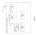
- FIG. 5illustrates a block diagram of a system incorporating a semiconductor device, such as, for example, the semiconductor device illustrated in FIG. 1 in accordance with various embodiments.
- Embodiments of the present disclosuredescribe gallium nitride (GaN) semiconductor devices and methods, and more particularly GaN on high thermal conductivity material high electron mobility transistors (HEMTs).
- GaNgallium nitride
- HEMTshigh electron mobility transistors
- Coupledmay mean one or more of the following. “Coupled” may mean that two or more elements are in direct physical or electrical contact. However, “coupled” may also mean that two or more elements indirectly contact each other, but yet still cooperate or interact with each other, and may mean that one or more other elements are coupled or connected between the elements that are said to be coupled with each other.
- “formed on,” along with its derivatives,may be used herein. “Formed on” in the context of a layer being “formed on” another layer may mean that a layer is formed above, but not necessarily in direct physical or electrical contact with, another layer (e.g., there may be one or more other layers interposing the layers). In some embodiments, however, “formed on” may mean that a layer is in direct physical contact with at least a portion of a top surface of another layer. Usage of terms like “top” and “bottom” are to assist in understanding, and they are not to be construed to be limiting on the disclosure.
- active surfacemay refer to the surface of a die having the active regions/areas, as is known to those having skill in the art.
- the active surface of a diemay include any one or more of various circuitry components, such as transistors, memory cells, passive components, and the like.
- phrases “A or B” and “A and/or B”mean (A), (B), or (A and B).
- the semiconductor device 100may include a Ga-face wafer stack including a carrier mounting layer 102 , a thermoconductive layer 104 , a dielectric layer 106 , a back barrier layer 108 that may be a Ga-face aluminum nitride (AlN)/GaN layer or an aluminum gallium nitride (AlGaN) alloyed layer with Al composition from 1 to 100% in various embodiments, a Ga-face GaN channel layer 110 , a barrier layer 112 , and a Ga-face GaN cap layer 114 .
- AlNGa-face aluminum nitride
- AlGaNaluminum gallium nitride
- the barrier layer 112may be a Ga-face AlGaN layer, an indium aluminum nitride (InAlN) layer, or a related alloy layer.
- the back barrier layer 108may include at least one AlN layer and at least one GaN layer, or an AlGaN alloyed layer with Al composition from 1 to 100%.
- the back barrier layer 108may include a plurality of AlN layers and a plurality of GaN layers arranged in an alternating fashion.
- An activation layer 116may be formed on the Ga-face GaN cap layer 114 in various embodiments and include a material such as silicon nitride (SiN).
- Ga-face layers of the Ga-face wafer stackmay have a Ga-face that faces away from the carrier mounting layer 102 toward the activation layer 116 .
- the activation layer 116may include a gate 118 , a source 120 , and a drain 122 in various embodiments.
- the activation layer 116may also include a field plate 124 .
- a two dimensional electron gas (2DEG) region 126may be formed at an interface of the Ga-face GaN channel layer 110 and the barrier layer 112 from polarization and piezoelectric strain effects between these layers.
- the thermoconductive layer 104may be within a distance 128 of 5 to 1000 nanometers (nm) from the 2DEG region 126 in various embodiments.
- the thermoconductive layer 104has a thermal conductivity, k value, of at least 500 watts per meter kelvin (W/(m ⁇ K)).
- the thermoconductive layer 104may be a layer formed of diamond, boron nitride, graphene, graphite, or cubic boron arsenide in various embodiments.
- the carrier mounting layer 102may have a similar thermal conductivity and composition as the thermoconductive layer 104 in various embodiments.
- the device 100includes an activation layer that is used in a high-electron-mobility transisitor (HEMT).
- HEMThigh-electron-mobility transisitor
- differing types of activation layers for other device typesmay be used.
- an activation layermay not be present, with the device 100 being a multilayer wafer semiconductor component for use in later fabrication processes.
- FIG. 2illustrates a cross-sectional view of an N-face wafer stack 200 in accordance with various embodiments.
- the N-face wafer stack 200may include a substrate 202 , an N-face nucleation layer 204 , an N-face GaN buffer layer 206 , a release layer 208 , an N-face GaN layer 210 , a barrier layer 212 , an N-face GaN channel layer 214 , a back barrier layer 216 , that may be an N-face AlN/GaN layer in various embodiments, a dielectric layer 218 , a thermoconductive layer 220 , and a carrier mounting layer 222 .
- the barrier layer 212may be an N-face barrier layer such as an N-face AlGaN layer, an N-face InAlN layer, or a related alloy layer.
- the back barrier layer 216may include at least one N-face AlN layer and at least one N-face GaN layer.
- the back barrier layer 216may include a plurality of N-face AlN layers and a plurality of N-face GaN layers arranged in an alternating fashion, or an N-face AlGaN alloyed layer with Al composition from 1 to 100%.
- N-face layers of the N-face wafer stack 200may have an N-face that faces away from the substrate 202 .
- one or more of the layerssuch as the release layer 208 , the N-face GaN layer 210 , the back barrier layer 216 , the dielectric layer 218 , or the carrier mounting layer 222 , may not be present.
- the substrate 202may be a C-face silicon carbide (SiC) substrate, but other materials such as N-face GaN, N-face AlN, silicon, or sapphire may also be used.
- the release layer 208may be an indium gallium nitride (InGaN) layer having a thickness of approximately 10 nm to 100 nm and a composition of approximately 1% to 100% indium (In) in various embodiments.
- the dielectric layer 218may range in thickness from approximately 0 nm to 50 nm in various embodiments and may be formed of a material such as AlN. Other materials may be used for the release layer 208 or the dielectric layer 218 in other embodiments.
- FIG. 3illustrates a cross-sectional view of a Ga-face wafer stack 300 in accordance with various embodiments.
- the Ga-face wafer stack 300may be a flipped N-face wafer stack 200 as described with respect to FIG. 2 , in various embodiments.
- the Ga-face wafer stack 300includes a release layer 302 partially etched to remove the release layer 302 , a substrate 310 , and a buffer stack 304 that may include a Ga-face GaN buffer layer 306 and a Ga-face nucleation layer 308 .
- Ga-face layers of the Ga-face wafer stack 300may have a Ga-face that faces toward the substrate 310 .
- the Ga-face GaN wafer stack 312may include a carrier mounting layer 314 , thermoconductive layer 316 , dielectric layer 318 , back barrier layer 320 , that may be a Ga-face AlN/GaN layer in various embodiments, Ga-face GaN channel layer 322 , barrier layer 324 , and Ga-face GaN cap layer 326 .
- the back barrier layer 320may include at least one AlN layer and at least one GaN layer.
- the back barrier layer 320may include a plurality of AlN layers and a plurality of GaN layers arranged in an alternating fashion.
- the back barrier layer 320may include an N-face AlGaN alloyed layer with Al composition from 1 to 100%.
- the barrier layer 324may be a Ga-face barrier layer, such as a Ga-face AlGaN layer.
- the barrier layer 324may be other than a Ga-face barrier layer.
- one or more of the layers, such as the back barrier layer 320may not be present.
- Ga-face layers of the Ga-face GaN wafer stack 312may have a Ga-face that faces away from the carrier mounting layer 314 .
- the Ga-face GaN wafer stack 312corresponds to the portion of the device 100 below the activation layer 116 as shown in FIG. 1 , with layers 102 , 104 , 106 , 108 , 110 , 112 , and 114 corresponding to layers 314 , 316 , 318 , 320 , 322 , 324 , and 326 , respectively.
- layers 310 , 308 , 306 , 302 , 326 , 324 , 322 , 320 , 318 , 316 , and 314 of the wafer stack 300may correspond to layers 202 , 204 , 206 , 208 , 210 , 212 , 214 , 216 , 218 , 220 , and 222 , respectively, of the wafer stack 200 . Accordingly, their characteristics and whether a given layer may not be present in some embodiments will not be further described as these matters have been discussed with respect to FIG. 2 .
- FIG. 4illustrates a flow diagram of a method 400 for fabricating a semiconductor device such as the device 100 in accordance with various embodiments.
- various layersmay be formed or grown, such as by using molecular beam epitaxy (MBE) or metal organic chemical vapor deposition (MOCVD), for example.
- MBEmolecular beam epitaxy
- MOCVDmetal organic chemical vapor deposition
- some layersmay be coupled with other layers using other methods, such as a bonding process for example.
- an inverted N-face GaN epitaxial structuremay be used as a starting material with a high thermal conductivity material such as diamond deposited or bonded to a front side of the epitaxial structure, in an N-face GaN approach to fabricating the device.
- thisallows the high thermal conductivity material to be made very close to a junction of the device, leading to a reduction in thermal resistance in comparison to devices produced by previous methods, and may increase power handling capability.
- the N-face GaN approachalso may protect the N-face GaN from harsh processing operations in comparison to previous methods, resulting lower buffer leakage.
- a substratesuch as substrate 202 or 310 may be provided.
- the substratemay be C-face SiC, N-face GaN, N-face AlN, silicon, sapphire, or another substrate.
- an N-face nucleation layersuch as the N-face nucleation layer 204
- an N-face buffer layersuch as the N-face GaN buffer layer 206
- a release layersuch as the release layer 208 or 302 , may be formed on the N-face buffer layer.
- the release layermay include InGaN or InGaN-based multiple quantum wells.
- an N-face GaN cap layersuch as the N-face GaN layer 210
- a barrier layersuch as the barrier layer 212 that may be an N-face barrier layer such as an N-face AlGaN layer in various embodiments, may be formed on the GaN cap layer.
- the barrier layermay be formed on or coupled with a different layer, such as with the release layer if the GaN cap layer is not included or with the N-face buffer layer if both the GaN cap layer and the release layer are not included, for example.
- an N-face GaN channel layersuch as the N-face GaN channel layer 214
- an N-face GaN channel layermay be formed on the barrier layer such that a Ga-face of the N-face GaN channel layer is coupled with the barrier layer.
- operations performed at the blocks 404 - 414may include growth of an epitaxial layer stack using a growth technique such as MBE or MOCVD, for example.
- a back barrier layersuch as the back barrier layer 216 that may be an AlGaN layer or an AlN/GaN layer, such as an N-face AlN/GaN layer, may be formed on the N-face GaN channel layer.
- the N-face AlN/GaN layermay be deposited in-situ to protect the N-face GaN material from exposure to air.
- the back barrier layermay be formed by forming at least one AlN layer and at least one GaN layer, with some embodiments forming the back barrier layer by forming a plurality of AlN layers and a plurality of GaN layers in an alternating fashion.
- a dielectric layersuch as the dielectric layer 218
- a high thermal conductivity layersuch as the thermoconductive layer 220
- the high thermal conductivity layermay be formed by deposition, or alternatively may be placed on the epitaxial stack by bonding, in various embodiments.
- the high thermal conductivity layermay be grown by chemical vapor deposition (CVD) and may have a thickness between approximately 1 micrometers ( ⁇ m) and 100 ⁇ m.
- the high thermal conductivity layermay be formed on or coupled with the back barrier layer if the dielectric layer is not included or the N-face GaN channel layer if both the dielectric layer and the back barrier layer are not included.
- a high thermal conductivity carrier mounting layersuch as the carrier mounting layer 222 , may be coupled with the high thermal conductivity layer.
- the high thermal conductivity layermay have a thickness such as approximately 100 ⁇ m (or greater) such that the carrier mounting layer is not used.
- the wafer structure formed by the preceding operationsmay be flipped.
- the high thermal conductivity carrier mounting layeris now the substrate, with the overlying GaN/AlGaN material having Ga-face polarity facing upward.
- the original substratemay now be on the top of the structure.
- the release layermay be etched to remove the substrate and buffer layer stack and expose a Ga-face of the GaN cap layer.
- a photo-assisted electrochemical wet etchmay be applied to etch the release layer to remove the substrate and buffer layer stack.
- a thin GaN layer formed at the block 410may be present on the top of the structure that may prevent the AlGaN layer from oxidation, followed by the AlGaN layer formed at operation 412 and the GaN channel layer formed at the block 414 .
- a 2DEGmay be formed at the interface between the AlGaN layer and the GaN channel layer due to spontaneous polarization and piezoelectric polarization.
- the high thermal conductivity layer and high thermal conductivity carrier mounting layermay be below, and may be separated from the layers above by only a thin dielectric transition layer formed at the block 418 in various embodiments.
- an activation layersuch as the activation layer 116 , may be formed on the Ga-face of the GaN cap layer.
- one or more of the layers of the process 400may not be formed in various embodiments, such as the release layer, the N-face GaN layer, the back barrier layer, the dielectric layer, or the carrier mounting layer, for example. Accordingly, one or more of the operations of the process 400 may not be performed, such as forming an N-face GaN cap layer at the block 410 , forming the back barrier layer at operation 416 , forming the dielectric layer at the block 418 , or coupling a high thermal conductivity carrier mounting layer to the thermoconductive layer at the block 422 , for example.
- subsequent layers described as being formed on or coupled with a particular layer with respect to the process 400may be formed on or coupled with a different layer when the layer to which they are described as being formed on or coupled with was not formed.
- layers formed during the process 400may be coupled directly with the layer they are formed on or bonded with.
- the device 100may be incorporated into any of a variety of apparatuses and systems.
- the device 100may be used as a discrete transistor, included in a switch or amplifier, or be included as part of a monolithic microwave integrated circuit (MMIC), for example.
- MMICmonolithic microwave integrated circuit
- a block diagram of an exemplary wireless communication device 500 incorporating device 100is illustrated in FIG. 5 .
- the wireless communication device 500may include amplification circuitry 504 , antenna structure 512 , a duplexer 516 , a transceiver 520 , a processor 524 , and a memory 528 coupled with each other at least as shown.
- the wireless communication device 500may include the device 100 incorporated into one or more of the components such as, but not limited to, amplification circuitry 504 , or transceiver 520 . While the wireless communication device 500 is shown with transmitting and receiving capabilities, other embodiments may include wireless communication devices without receiving or transmitting capabilities.
- the wireless communication device 500may be, but is not limited to, a mobile phone, a paging device, a personal digital assistant, a text-messaging device, a portable computer, a desktop computer, a telecommunications base station, a subscriber station, an access point, a radar, a satellite communication device, or any other device capable of wirelessly transmitting radio-frequency (RF) signals.
- a mobile phonea paging device, a personal digital assistant, a text-messaging device, a portable computer, a desktop computer, a telecommunications base station, a subscriber station, an access point, a radar, a satellite communication device, or any other device capable of wirelessly transmitting radio-frequency (RF) signals.
- RFradio-frequency
- the processor 524may execute a basic operating system program, stored in the memory 528 , in order to control the overall operation of the wireless communication device 500 .
- the processor 524may control the reception of signals and the transmission of signals by transceiver 520 .
- the processor 524may be capable of executing other processes and programs resident in the memory 528 and may move data into or out of memory 528 , as desired by an executing process.
- the transceiver 520may receive outgoing data (e.g., voice data, web data, e-mail, signaling data, etc.) from the processor 524 , may generate an RFin signal to represent the outgoing data, and provide the RFin signal to the amplification circuitry 504 .
- outgoing datae.g., voice data, web data, e-mail, signaling data, etc.
- the transceiver 520may receive outgoing data (e.g., voice data, web data, e-mail, signaling data, etc.) from the processor 524 , may generate an RFin signal to represent the outgoing data, and provide the RFin signal to the amplification circuitry 504 .
- the amplification circuitry 504may amplify the RFin signal in accordance with a selected amplification mode.
- the amplified RFamp signalmay be forwarded to the duplexer 516 and then to the antenna structure 512 for an over-the-air (OTA) transmission.
- OTAover-the-air
- the transceiver 520may receive an incoming OTA signal from the antenna structure 512 through the duplexer 516 .
- the transceiver 520may process and send the incoming signal to the processor 524 for further processing.
- the antenna structure 512may include one or more directional and/or omnidirectional antennas, including, e.g., a dipole antenna, a monopole antenna, a patch antenna, a loop antenna, a microstrip antenna or any other type of antenna suitable for OTA transmission/reception of RF signals.
- the wireless communication device 500is given by way of example and that, for simplicity and clarity, only so much of the construction and operation of the wireless communication device 500 as is necessary for an understanding of the embodiments is shown and described.
- Various embodimentscontemplate any suitable component or combination of components performing any suitable tasks in association with wireless communication device 500 , according to particular needs.
- the wireless communication device 500should not be construed to limit the types of devices in which embodiments may be implemented.
- Some non-limiting examplesinclude:
- Example 1may include a semiconductor component comprising: a barrier layer; a gallium nitride (GaN) channel layer having a Ga-face coupled with the barrier layer; and a thermoconductive layer within 1000 nanometers of the Ga-face of the GaN channel layer, wherein the thermoconductive layer has a thermal conductivity value of at least 500 W/(m ⁇ K) and is closer to an N-face of the GaN channel layer than to the Ga-face of the GaN channel layer.
- GaNgallium nitride
- Example 2may include the subject matter of Example 1, further comprising: a dielectric layer between the GaN channel layer and the thermoconductive layer.
- Example 3may include the subject matter of any one of Examples 1-2, further comprising: a thermoconductive carrier mounting layer coupled with the thermoconductive layer, wherein the thermoconductive carrier mounting layer has a thermal conductivity value of at least 500 W/(m ⁇ K).
- Example 4may include the subject matter of any one of Examples 1-3, further comprising: a GaN cap layer, wherein the GaN cap layer is coupled with the barrier layer.
- Example 5may include the subject matter of any one of Examples 1-4, further comprising: a back barrier layer between the GaN channel layer and the thermoconductive layer.
- Example 6may include the subject matter of Example 5, further comprising a dielectric layer between the back barrier layer and the thermoconductive layer.
- Example 7may include the subject matter of any one of Examples 4-6, further comprising an activation layer coupled with a Ga-face of the GaN cap layer, the activation layer including a gate, a source, and a drain.
- Example 8may include the subject matter of any one of Examples 1-7, further comprising a thermoconductive carrier mounting layer coupled with the thermoconductive layer, wherein the thermoconductive carrier mounting layer has a thermal conductivity value of at least 500 W/(m ⁇ K).
- Example 9may include the subject matter of Example 8, wherein the thermoconductive layer and the thermoconductive carrier mounting layer are formed of a diamond based material.
- Example 10may include the subject matter of any one of Examples 1-9, wherein the thermoconductive layer is within 500 nanometers of the Ga-face of the GaN channel layer.
- Example 11may include a method of fabricating a semiconductor component comprising: forming an N-face barrier layer; forming an N-face gallium nitride (GaN) channel layer on the N-face barrier layer; and forming a thermoconductive layer within 1000 nanometers of the N-face GaN channel layer, wherein the thermoconductive layer has a thermal conductivity of at least 500 W/(m ⁇ K).
- a method of fabricating a semiconductor componentcomprising: forming an N-face barrier layer; forming an N-face gallium nitride (GaN) channel layer on the N-face barrier layer; and forming a thermoconductive layer within 1000 nanometers of the N-face GaN channel layer, wherein the thermoconductive layer has a thermal conductivity of at least 500 W/(m ⁇ K).
- GaNN-face gallium nitride
- Example 12may include the subject matter of Example 11, further comprising before forming the N-face barrier layer, forming an N-face GaN cap layer, wherein the N-face barrier layer is formed on the N-face GaN cap layer.
- Example 13may include the subject matter of Example 12, further comprising: providing a substrate; forming an N-face nucleation layer on the substrate before forming the N-face GaN cap layer; forming an N-face buffer layer on the N-face nucleation layer, wherein the N-face GaN cap layer is formed above the N-face buffer layer; and removing the substrate, N-face nucleation layer, and N-face buffer layer to expose a Ga-face of the N-face GaN cap layer.
- Example 14may include the subject matter of Example 13, further comprising forming a release layer on the N-face buffer layer, wherein forming the N-face GaN cap layer above the N-face nucleation layer includes forming the N-face GaN cap layer on the release layer, and wherein removing the substrate, N-face nucleation layer, and N-face buffer layer includes etching the release layer.
- Example 15may include the subject matter of any one of Examples 11-14, further comprising forming a back barrier layer on the N-face GaN channel layer.
- Example 16may include the subject matter of Example 15, further comprising forming a dielectric layer on the back barrier layer, wherein forming the thermoconductive layer includes forming the thermoconductive layer on the dielectric layer.
- Example 17may include the subject matter of any one of Examples 11-16, further comprising coupling a thermoconductive carrier mounting layer to the thermoconductive layer, wherein the thermoconductive carrier mounting layer has a thermal conductivity of at least 500 W/(m ⁇ K).
- Example 18may include the subject matter of any one of Examples 13-17, further comprising forming an activation layer on the Ga-face of the N-face GaN cap layer, the activation layer including a gate, a source, and a drain.
- Example 19may include the subject matter of any one of Examples 11-15, further comprising forming a dielectric layer above the N-face GaN channel layer, wherein forming the thermoconductive layer includes forming the thermoconductive layer on the dielectric layer.
- Example 20may include the subject matter of any one of Examples 11-15, further comprising forming a dielectric layer on the N-face GaN channel layer, wherein forming the thermoconductive layer includes forming the thermoconductive layer on the dielectric layer.
- Example 21may include the subject matter of any one of Examples 11-17, further comprising forming an activation layer on a Ga-face of the N-face GaN cap layer, the activation layer including a gate, a source, and a drain.
- Example 22may include the subject matter of any one of Examples 11-21, wherein the thermoconductive layer is formed of diamond, boron nitride, graphene, graphite, or cubic boron arsenide.
- Example 23may include the subject matter of any one of Examples 13-19, wherein the thermoconductive layer is formed of diamond, the N-face nucleation layer is formed of aluminum nitride (AlN), and the N-face buffer layer is formed of GaN.
- the thermoconductive layeris formed of diamond
- the N-face nucleation layeris formed of aluminum nitride (AlN)
- the N-face buffer layeris formed of GaN.
- Example 24may include semiconductor component prepared by a process comprising: forming an N-face barrier layer; forming an N-face gallium nitride (GaN) channel layer on the N-face barrier layer; and forming a thermoconductive layer within 1000 nanometers of the N-face GaN channel layer, wherein the thermoconductive layer has a thermal conductivity of at least 500 W/(m ⁇ K).
- GaNN-face gallium nitride
- Example 25may include the subject matter of Example 24 wherein the process further comprises: providing a substrate; forming an N-face nucleation layer on the substrate; forming an N-face buffer layer on the N-face nucleation layer; forming an N-face GaN cap layer above the N-face buffer layer, wherein the N-face barrier layer is formed on the N-face GaN cap layer; removing the substrate, N-face nucleation layer, and N-face buffer layer to expose a Ga-face of the N-face GaN cap layer; and forming an activation layer on the Ga-face of the N-face GaN cap layer, the activation layer including a gate, a source, and a drain.
Landscapes
- Engineering & Computer Science (AREA)
- Computer Hardware Design (AREA)
- Microelectronics & Electronic Packaging (AREA)
- Power Engineering (AREA)
- Physics & Mathematics (AREA)
- Condensed Matter Physics & Semiconductors (AREA)
- General Physics & Mathematics (AREA)
- Manufacturing & Machinery (AREA)
- Chemical & Material Sciences (AREA)
- Materials Engineering (AREA)
- Junction Field-Effect Transistors (AREA)
Abstract
Description
Claims (23)
Priority Applications (1)
| Application Number | Priority Date | Filing Date | Title |
|---|---|---|---|
| US14/631,677US9337278B1 (en) | 2015-02-25 | 2015-02-25 | Gallium nitride on high thermal conductivity material device and method |
Applications Claiming Priority (1)
| Application Number | Priority Date | Filing Date | Title |
|---|---|---|---|
| US14/631,677US9337278B1 (en) | 2015-02-25 | 2015-02-25 | Gallium nitride on high thermal conductivity material device and method |
Publications (1)
| Publication Number | Publication Date |
|---|---|
| US9337278B1true US9337278B1 (en) | 2016-05-10 |
Family
ID=55860099
Family Applications (1)
| Application Number | Title | Priority Date | Filing Date |
|---|---|---|---|
| US14/631,677ActiveUS9337278B1 (en) | 2015-02-25 | 2015-02-25 | Gallium nitride on high thermal conductivity material device and method |
Country Status (1)
| Country | Link |
|---|---|
| US (1) | US9337278B1 (en) |
Cited By (90)
| Publication number | Priority date | Publication date | Assignee | Title |
|---|---|---|---|---|
| US9587918B1 (en) | 2015-09-24 | 2017-03-07 | True Velocity, Inc. | Ammunition having a projectile made by metal injection molding |
| US20170133239A1 (en)* | 2015-11-11 | 2017-05-11 | Qorvo Us, Inc. | Semiconductor device with high thermal conductivity substrate and process for making the same |
| US9933241B2 (en) | 2010-11-10 | 2018-04-03 | True Velocity, Inc. | Method of making a primer insert for use in polymer ammunition |
| US10041770B2 (en) | 2010-11-10 | 2018-08-07 | True Velocity, Inc. | Metal injection molded ammunition cartridge |
| US10041777B1 (en) | 2016-03-09 | 2018-08-07 | True Velocity, Inc. | Three-piece primer insert having an internal diffuser for polymer ammunition |
| US10048052B2 (en) | 2010-11-10 | 2018-08-14 | True Velocity, Inc. | Method of making a polymeric subsonic ammunition cartridge |
| USD828483S1 (en) | 2011-11-09 | 2018-09-11 | True Velocity Ip Holdings, Llc | Cartridge base insert |
| US10081057B2 (en) | 2010-11-10 | 2018-09-25 | True Velocity, Inc. | Method of making a projectile by metal injection molding |
| US10190857B2 (en) | 2010-11-10 | 2019-01-29 | True Velocity Ip Holdings, Llc | Method of making polymeric subsonic ammunition |
| US10365074B2 (en) | 2017-11-09 | 2019-07-30 | True Velocity Ip Holdings, Llc | Multi-piece polymer ammunition cartridge |
| US10408592B2 (en) | 2010-11-10 | 2019-09-10 | True Velocity Ip Holdings, Llc | One piece polymer ammunition cartridge having a primer insert and methods of making the same |
| WO2019176138A1 (en)* | 2018-03-13 | 2019-09-19 | Mitsubishi Electric Corporation | High electron mobility transistor |
| USD861118S1 (en) | 2011-11-09 | 2019-09-24 | True Velocity Ip Holdings, Llc | Primer insert |
| US10429156B2 (en) | 2010-11-10 | 2019-10-01 | True Velocity Ip Holdings, Llc | Subsonic polymeric ammunition cartridge |
| US10480915B2 (en) | 2010-11-10 | 2019-11-19 | True Velocity Ip Holdings, Llc | Method of making a polymeric subsonic ammunition cartridge |
| US20200052076A1 (en)* | 2018-10-31 | 2020-02-13 | Suzhou Han Hua Semiconductor Co.,Ltd | Method for Forming III-Nitride Semiconductor Device and the III-Nitride Semiconductor Device |
| US10591260B2 (en) | 2010-11-10 | 2020-03-17 | True Velocity Ip Holdings, Llc | Polymer ammunition having a projectile made by metal injection molding |
| USD881327S1 (en) | 2018-04-20 | 2020-04-14 | True Velocity Ip Holdings, Llc | Ammunition cartridge |
| USD881326S1 (en) | 2018-04-20 | 2020-04-14 | True Velocity Ip Holdings, Llc | Ammunition cartridge |
| USD881323S1 (en) | 2018-04-20 | 2020-04-14 | True Velocity Ip Holdings, Llc | Ammunition cartridge |
| USD881324S1 (en) | 2018-04-20 | 2020-04-14 | True Velocity Ip Holdings, Llc | Ammunition cartridge |
| USD881328S1 (en) | 2018-04-20 | 2020-04-14 | True Velocity Ip Holdings, Llc | Ammunition cartridge |
| USD881325S1 (en) | 2018-04-20 | 2020-04-14 | True Velocity Ip Holdings, Llc | Ammunition cartridge |
| USD882019S1 (en) | 2018-04-20 | 2020-04-21 | True Velocity Ip Holdings, Llc | Ammunition cartridge |
| USD882024S1 (en) | 2018-04-20 | 2020-04-21 | True Velocity Ip Holdings, Llc | Ammunition cartridge |
| USD882021S1 (en) | 2018-04-20 | 2020-04-21 | True Velocity Ip Holdings, Llc | Ammunition cartridge |
| USD882026S1 (en) | 2018-04-20 | 2020-04-21 | True Velocity Ip Holdings, Llc | Ammunition cartridge |
| USD882023S1 (en) | 2018-04-20 | 2020-04-21 | True Velocity Ip Holdings, Llc | Ammunition cartridge |
| USD882030S1 (en) | 2018-04-20 | 2020-04-21 | True Velocity Ip Holdings, Llc | Ammunition cartridge |
| USD882020S1 (en) | 2018-04-20 | 2020-04-21 | True Velocity Ip Holdings, Llc | Ammunition cartridge |
| USD882033S1 (en) | 2018-04-20 | 2020-04-21 | True Velocity Ip Holdings, Llc | Ammunition cartridge |
| USD882027S1 (en) | 2018-04-20 | 2020-04-21 | True Velocity Ip Holdings, Llc | Ammunition cartridge |
| USD882028S1 (en) | 2018-04-20 | 2020-04-21 | True Velocity Ip Holdings, Llc | Ammunition cartridge |
| USD882025S1 (en) | 2018-04-20 | 2020-04-21 | True Velocity Ip Holdings, Llc | Ammunition cartridge |
| USD882031S1 (en) | 2018-04-20 | 2020-04-21 | True Velocity Ip Holdings, Llc | Ammunition cartridge |
| USD882022S1 (en) | 2018-04-20 | 2020-04-21 | True Velocity Ip Holdings, Llc | Ammunition cartridge |
| USD882029S1 (en) | 2018-04-20 | 2020-04-21 | True Velocity Ip Holdings, Llc | Ammunition cartridge |
| USD882032S1 (en) | 2018-04-20 | 2020-04-21 | True Velocity Ip Holdings, Llc | Ammunition cartridge |
| USD882724S1 (en) | 2018-04-20 | 2020-04-28 | True Velocity Ip Holdings, Llc | Ammunition cartridge |
| USD882723S1 (en) | 2018-04-20 | 2020-04-28 | True Velocity Ip Holdings, Llc | Ammunition cartridge |
| USD882721S1 (en) | 2018-04-20 | 2020-04-28 | True Velocity Ip Holdings, Llc | Ammunition cartridge |
| USD882722S1 (en) | 2018-04-20 | 2020-04-28 | True Velocity Ip Holdings, Llc | Ammunition cartridge |
| USD882720S1 (en) | 2018-04-20 | 2020-04-28 | True Velocity Ip Holdings, Llc | Ammunition cartridge |
| USD884115S1 (en) | 2018-04-20 | 2020-05-12 | True Velocity Ip Holdings, Llc | Ammunition cartridge |
| USD886231S1 (en) | 2017-12-19 | 2020-06-02 | True Velocity Ip Holdings, Llc | Ammunition cartridge |
| CN111223927A (en)* | 2020-04-22 | 2020-06-02 | 浙江集迈科微电子有限公司 | GaN-diamond-Si semiconductor structure, device and preparation method |
| CN111223929A (en)* | 2020-04-23 | 2020-06-02 | 浙江集迈科微电子有限公司 | GaN semiconductor structure with diamond micro-channel, device and preparation method |
| USD886937S1 (en) | 2017-12-19 | 2020-06-09 | True Velocity Ip Holdings, Llc | Ammunition cartridge |
| US20200194552A1 (en)* | 2018-12-17 | 2020-06-18 | Sansaptak DASGUPTA | Cap layer on a polarization layer to preserve channel sheet resistance |
| US10704880B1 (en) | 2019-02-14 | 2020-07-07 | True Velocity Ip Holdings, Llc | Polymer ammunition and cartridge having a convex primer insert |
| US10704879B1 (en) | 2019-02-14 | 2020-07-07 | True Velocity Ip Holdings, Llc | Polymer ammunition and cartridge having a convex primer insert |
| US10704877B2 (en) | 2010-11-10 | 2020-07-07 | True Velocity Ip Holdings, Llc | One piece polymer ammunition cartridge having a primer insert and methods of making the same |
| US10704876B2 (en) | 2010-11-10 | 2020-07-07 | True Velocity Ip Holdings, Llc | One piece polymer ammunition cartridge having a primer insert and methods of making the same |
| US10704872B1 (en) | 2019-02-14 | 2020-07-07 | True Velocity Ip Holdings, Llc | Polymer ammunition and cartridge having a convex primer insert |
| USD891567S1 (en) | 2019-03-12 | 2020-07-28 | True Velocity Ip Holdings, Llc | Ammunition cartridge nose having an angled shoulder |
| USD891568S1 (en) | 2019-03-12 | 2020-07-28 | True Velocity Ip Holdings, Llc | Ammunition cartridge nose having an angled shoulder |
| USD891570S1 (en) | 2019-03-12 | 2020-07-28 | True Velocity Ip Holdings, Llc | Ammunition cartridge nose |
| USD891569S1 (en) | 2019-03-12 | 2020-07-28 | True Velocity Ip Holdings, Llc | Ammunition cartridge nose having an angled shoulder |
| USD892258S1 (en) | 2019-03-12 | 2020-08-04 | True Velocity Ip Holdings, Llc | Ammunition cartridge nose having an angled shoulder |
| US10731957B1 (en) | 2019-02-14 | 2020-08-04 | True Velocity Ip Holdings, Llc | Polymer ammunition and cartridge having a convex primer insert |
| USD893666S1 (en) | 2019-03-11 | 2020-08-18 | True Velocity Ip Holdings, Llc | Ammunition cartridge nose having an angled shoulder |
| USD893668S1 (en) | 2019-03-11 | 2020-08-18 | True Velocity Ip Holdings, Llc | Ammunition cartridge nose having an angled shoulder |
| USD893667S1 (en) | 2019-03-11 | 2020-08-18 | True Velocity Ip Holdings, Llc | Ammunition cartridge nose having an angled shoulder |
| USD893665S1 (en) | 2019-03-11 | 2020-08-18 | True Velocity Ip Holdings, Llc | Ammunition cartridge nose having an angled shoulder |
| CN111564501A (en)* | 2020-07-15 | 2020-08-21 | 浙江集迈科微电子有限公司 | GaN device heat dissipation structure and preparation method thereof |
| USD894320S1 (en) | 2019-03-21 | 2020-08-25 | True Velocity Ip Holdings, Llc | Ammunition Cartridge |
| US10760882B1 (en) | 2017-08-08 | 2020-09-01 | True Velocity Ip Holdings, Llc | Metal injection molded ammunition cartridge |
| USD903038S1 (en) | 2018-04-20 | 2020-11-24 | True Velocity Ip Holdings, Llc | Ammunition cartridge |
| USD903039S1 (en) | 2018-04-20 | 2020-11-24 | True Velocity Ip Holdings, Llc | Ammunition cartridge |
| US10914558B2 (en) | 2010-11-10 | 2021-02-09 | True Velocity Ip Holdings, Llc | Subsonic polymeric ammunition with diffuser |
| US10921106B2 (en) | 2019-02-14 | 2021-02-16 | True Velocity Ip Holdings, Llc | Polymer ammunition and cartridge having a convex primer insert |
| US20210050437A1 (en)* | 2019-03-26 | 2021-02-18 | Enkris Semiconductor, Inc. | Semiconductor Structure and Manufacturing Method for the Semiconductor Structure |
| USD913403S1 (en) | 2018-04-20 | 2021-03-16 | True Velocity Ip Holdings, Llc | Ammunition cartridge |
| US11047663B1 (en) | 2010-11-10 | 2021-06-29 | True Velocity Ip Holdings, Llc | Method of coding polymer ammunition cartridges |
| US11047664B2 (en) | 2010-11-10 | 2021-06-29 | True Velocity Ip Holdings, Llc | Lightweight polymer ammunition cartridge casings |
| US11118875B1 (en) | 2010-11-10 | 2021-09-14 | True Velocity Ip Holdings, Llc | Color coded polymer ammunition cartridge |
| US11209252B2 (en) | 2010-11-10 | 2021-12-28 | True Velocity Ip Holdings, Llc | Subsonic polymeric ammunition with diffuser |
| US11215430B2 (en) | 2010-11-10 | 2022-01-04 | True Velocity Ip Holdings, Llc | One piece polymer ammunition cartridge having a primer insert and methods of making the same |
| US11231257B2 (en) | 2010-11-10 | 2022-01-25 | True Velocity Ip Holdings, Llc | Method of making a metal injection molded ammunition cartridge |
| US11248885B2 (en) | 2010-11-10 | 2022-02-15 | True Velocity Ip Holdings, Llc | Subsonic polymeric ammunition cartridge |
| US11293732B2 (en) | 2010-11-10 | 2022-04-05 | True Velocity Ip Holdings, Llc | Method of making polymeric subsonic ammunition |
| US11300393B2 (en) | 2010-11-10 | 2022-04-12 | True Velocity Ip Holdings, Llc | Polymer ammunition having a MIM primer insert |
| US11313654B2 (en) | 2010-11-10 | 2022-04-26 | True Velocity Ip Holdings, Llc | Polymer ammunition having a projectile made by metal injection molding |
| US11340053B2 (en) | 2019-03-19 | 2022-05-24 | True Velocity Ip Holdings, Llc | Methods and devices metering and compacting explosive powders |
| US11424354B2 (en)* | 2017-09-29 | 2022-08-23 | Intel Corporation | Group III-nitride silicon controlled rectifier |
| US11435171B2 (en) | 2018-02-14 | 2022-09-06 | True Velocity Ip Holdings, Llc | Device and method of determining the force required to remove a projectile from an ammunition cartridge |
| US11444172B2 (en)* | 2017-12-01 | 2022-09-13 | Mitsubishi Electric Corporation | Method for producing semiconductor device and semiconductor device |
| US11543218B2 (en) | 2019-07-16 | 2023-01-03 | True Velocity Ip Holdings, Llc | Polymer ammunition having an alignment aid, cartridge and method of making the same |
| US11614314B2 (en) | 2018-07-06 | 2023-03-28 | True Velocity Ip Holdings, Llc | Three-piece primer insert for polymer ammunition |
| US11733015B2 (en) | 2018-07-06 | 2023-08-22 | True Velocity Ip Holdings, Llc | Multi-piece primer insert for polymer ammunition |
Citations (1)
| Publication number | Priority date | Publication date | Assignee | Title |
|---|---|---|---|---|
| US20140253241A1 (en)* | 2013-03-08 | 2014-09-11 | Samsung Electronics Co., Ltd. | High electron mobility transistor device |
- 2015
- 2015-02-25USUS14/631,677patent/US9337278B1/enactiveActive
Patent Citations (1)
| Publication number | Priority date | Publication date | Assignee | Title |
|---|---|---|---|---|
| US20140253241A1 (en)* | 2013-03-08 | 2014-09-11 | Samsung Electronics Co., Ltd. | High electron mobility transistor device |
Non-Patent Citations (1)
| Title |
|---|
| Gao, Y., et al., "Etched Aperture GaN Cavet Through Photoelectrochemical Wet Etching," International Journal of High Speed Electronics and Systems, vol. 14, No. 1, 2004, pp. 245-264. |
Cited By (200)
| Publication number | Priority date | Publication date | Assignee | Title |
|---|---|---|---|---|
| US11118876B2 (en) | 2010-11-10 | 2021-09-14 | True Velocity Ip Holdings, Llc | Multi-piece polymer ammunition cartridge |
| US10731956B2 (en) | 2010-11-10 | 2020-08-04 | True Velocity Ip Holdings, Llc | Multi-piece polymer ammunition cartridge nose |
| US9933241B2 (en) | 2010-11-10 | 2018-04-03 | True Velocity, Inc. | Method of making a primer insert for use in polymer ammunition |
| US10907944B2 (en) | 2010-11-10 | 2021-02-02 | True Velocity Ip Holdings, Llc | Method of making a polymer ammunition cartridge |
| US10041770B2 (en) | 2010-11-10 | 2018-08-07 | True Velocity, Inc. | Metal injection molded ammunition cartridge |
| US10859352B2 (en) | 2010-11-10 | 2020-12-08 | True Velocity Ip Holdings, Llc | Polymer ammunition having a primer insert with a primer pocket groove |
| US10048052B2 (en) | 2010-11-10 | 2018-08-14 | True Velocity, Inc. | Method of making a polymeric subsonic ammunition cartridge |
| US10914558B2 (en) | 2010-11-10 | 2021-02-09 | True Velocity Ip Holdings, Llc | Subsonic polymeric ammunition with diffuser |
| US10845169B2 (en) | 2010-11-10 | 2020-11-24 | True Velocity Ip Holdings, Llc | Polymer cartridge having a primer insert with a primer pocket groove |
| US10962338B2 (en) | 2010-11-10 | 2021-03-30 | True Velocity Ip Holdings, Llc | Polymer cartridge having a primer insert with a primer pocket groove |
| US10081057B2 (en) | 2010-11-10 | 2018-09-25 | True Velocity, Inc. | Method of making a projectile by metal injection molding |
| US10996029B2 (en) | 2010-11-10 | 2021-05-04 | True Velocity Ip Holdings, Llc | Polymer ammunition and cartridge primer insert |
| US10753713B2 (en) | 2010-11-10 | 2020-08-25 | True Velocity Ip Holdings, Llc | Method of stamping a primer insert for use in polymer ammunition |
| US10996030B2 (en) | 2010-11-10 | 2021-05-04 | True Velocity Ip Holdings, Llc | Polymer ammunition and cartridge primer insert |
| US10145662B2 (en) | 2010-11-10 | 2018-12-04 | True Velocity Ip Holdings, Llc | Method of making polymer ammunition having a metal injection molded primer insert |
| US10190857B2 (en) | 2010-11-10 | 2019-01-29 | True Velocity Ip Holdings, Llc | Method of making polymeric subsonic ammunition |
| US10234249B2 (en) | 2010-11-10 | 2019-03-19 | True Velocity Ip Holdings, Llc | Polymer ammunition having a primer insert with a primer pocket groove |
| US10234253B2 (en) | 2010-11-10 | 2019-03-19 | True Velocity, Inc. | Method of making a polymer ammunition cartridge having a metal injection molded primer insert |
| US10240905B2 (en) | 2010-11-10 | 2019-03-26 | True Velocity Ip Holdings, Llc | Polymer ammunition having a primer insert with a primer pocket groove |
| US10254096B2 (en) | 2010-11-10 | 2019-04-09 | True Velocity Ip Holdings, Llc | Polymer ammunition having a MIM primer insert |
| US10274293B2 (en) | 2010-11-10 | 2019-04-30 | True Velocity Ip Holdings, Llc | Polymer cartridge having a primer insert with a primer pocket groove |
| US11047654B1 (en) | 2010-11-10 | 2021-06-29 | True Velocity Ip Holdings, Llc | Subsonic polymeric ammunition with diffuser |
| US11047662B2 (en) | 2010-11-10 | 2021-06-29 | True Velocity Ip Holdings, Llc | Method of making a polymer ammunition cartridge having a wicking texturing |
| US11047663B1 (en) | 2010-11-10 | 2021-06-29 | True Velocity Ip Holdings, Llc | Method of coding polymer ammunition cartridges |
| US10345088B2 (en) | 2010-11-10 | 2019-07-09 | True Velocity Ip Holdings, Llc | Method of making a primer insert for use in polymer ammunition |
| US10352670B2 (en) | 2010-11-10 | 2019-07-16 | True Velocity Ip Holdings, Llc | Lightweight polymer ammunition cartridge casings |
| US10352664B2 (en) | 2010-11-10 | 2019-07-16 | True Velocity Ip Holdings, Llc | Method of making a primer insert for use in polymer ammunition |
| US11953303B2 (en) | 2010-11-10 | 2024-04-09 | True Velocity Ip Holdings, Llc | Subsonic polymeric ammunition cartridge |
| US10408592B2 (en) | 2010-11-10 | 2019-09-10 | True Velocity Ip Holdings, Llc | One piece polymer ammunition cartridge having a primer insert and methods of making the same |
| US10408582B2 (en) | 2010-11-10 | 2019-09-10 | True Velocity Ip Holdings, Llc | Polymer cartridge having a primer insert with a primer pocket groove |
| US11047664B2 (en) | 2010-11-10 | 2021-06-29 | True Velocity Ip Holdings, Llc | Lightweight polymer ammunition cartridge casings |
| US11828580B2 (en) | 2010-11-10 | 2023-11-28 | True Velocity Ip Holdings, Llc | Diffuser for polymer ammunition cartridges |
| US11079209B2 (en) | 2010-11-10 | 2021-08-03 | True Velocity Ip Holdings, Llc | Method of making polymer ammunition having a wicking texturing |
| US10429156B2 (en) | 2010-11-10 | 2019-10-01 | True Velocity Ip Holdings, Llc | Subsonic polymeric ammunition cartridge |
| US10458762B2 (en) | 2010-11-10 | 2019-10-29 | True Velocity Ip Holdings, Llc | Polymer ammunition having a primer insert with a primer pocket groove |
| US10466021B2 (en) | 2010-11-10 | 2019-11-05 | True Velocity Ip Holdings, Llc | Polymer cartridge having a primer insert with a primer pocket groove |
| US10466020B2 (en) | 2010-11-10 | 2019-11-05 | True Velocity Ip Holdings, Llc | Primer insert having a primer pocket groove |
| US10480911B2 (en) | 2010-11-10 | 2019-11-19 | True Velocity Ip Holdings, Llc | Primer insert having a primer pocket groove |
| US10480915B2 (en) | 2010-11-10 | 2019-11-19 | True Velocity Ip Holdings, Llc | Method of making a polymeric subsonic ammunition cartridge |
| US10480912B2 (en) | 2010-11-10 | 2019-11-19 | True Velocity Ip Holdings, Llc | Primer insert having a primer pocket groove |
| US10488165B2 (en) | 2010-11-10 | 2019-11-26 | True Velocity Ip Holdings, Llc | Primer insert having a primer pocket groove |
| US11821722B2 (en) | 2010-11-10 | 2023-11-21 | True Velocity Ip Holdings, Llc | Diffuser for polymer ammunition cartridges |
| US11733010B2 (en) | 2010-11-10 | 2023-08-22 | True Velocity Ip Holdings, Llc | Method of making a metal injection molded ammunition cartridge |
| US10571229B2 (en) | 2010-11-10 | 2020-02-25 | True Velocity Ip Holdings, Llc | Polymer ammunition and cartridge primer insert |
| US10571228B2 (en) | 2010-11-10 | 2020-02-25 | True Velocity Ip Holdings, Llc | Polymer ammunition and cartridge primer insert |
| US10571230B2 (en) | 2010-11-10 | 2020-02-25 | True Velocity Ip Holdings, Llc | Polymer ammunition and cartridge primer insert |
| US10571231B2 (en) | 2010-11-10 | 2020-02-25 | True Velocity Ip Holdings, Llc | Polymer ammunition and cartridge primer insert |
| US10578409B2 (en) | 2010-11-10 | 2020-03-03 | True Velocity Ip Holdings, Llc | Polymer ammunition and cartridge primer insert |
| US10591260B2 (en) | 2010-11-10 | 2020-03-17 | True Velocity Ip Holdings, Llc | Polymer ammunition having a projectile made by metal injection molding |
| US11085739B2 (en) | 2010-11-10 | 2021-08-10 | True Velocity Ip Holdings, Llc | Stamped primer insert for use in polymer ammunition |
| US10612896B2 (en) | 2010-11-10 | 2020-04-07 | True Velocity Ip Holdings, Llc | Method of making a metal injection molded ammunition cartridge |
| US11719519B2 (en) | 2010-11-10 | 2023-08-08 | True Velocity Ip Holdings, Llc | Subsonic polymeric ammunition with diffuser |
| US11614310B2 (en) | 2010-11-10 | 2023-03-28 | True Velocity Ip Holdings, Llc | Metal injection molded ammunition cartridge |
| US11592270B2 (en) | 2010-11-10 | 2023-02-28 | True Velocity Ip Holdings, Llc | Multi-piece polymer ammunition cartridge nose |
| US11486680B2 (en) | 2010-11-10 | 2022-11-01 | True Velocity Ip Holdings, Llc | Method of making a primer insert for use in polymer ammunition |
| US11454479B2 (en) | 2010-11-10 | 2022-09-27 | True Velocity Ip Holdings, Llc | Subsonic polymeric ammunition |
| US11085740B2 (en) | 2010-11-10 | 2021-08-10 | True Velocity Ip Holdings, Llc | Subsonic polymeric ammunition with diffuser |
| US11243060B2 (en) | 2010-11-10 | 2022-02-08 | True Velocity Ip Holdings, Llc | Primer insert having a primer pocket groove |
| US11085742B2 (en) | 2010-11-10 | 2021-08-10 | True Velocity Ip Holdings, Llc | Subsonic polymeric ammunition with diffuser |
| US11441881B2 (en) | 2010-11-10 | 2022-09-13 | True Velocity Ip Holdings, Llc | Polymer cartridge having a primer insert with a primer pocket groove |
| US11085741B2 (en) | 2010-11-10 | 2021-08-10 | True Velocity Ip Holdings, Llc | Subsonic polymeric ammunition with diffuser |
| US11408714B2 (en) | 2010-11-10 | 2022-08-09 | True Velocity Ip Holdings, Llc | Polymer ammunition having an overmolded primer insert |
| US11340050B2 (en) | 2010-11-10 | 2022-05-24 | True Velocity Ip Holdings, Llc | Subsonic polymeric ammunition cartridge |
| US11340048B2 (en) | 2010-11-10 | 2022-05-24 | True Velocity Ip Holdings, Llc | Method of making a primer insert for use in polymer ammunition |
| US11340049B2 (en) | 2010-11-10 | 2022-05-24 | True Velocity Ip Holdings, Llc | Method of making a metal primer insert by injection molding |
| US11333469B2 (en) | 2010-11-10 | 2022-05-17 | True Velocity Ip Holdings, Llc | Polymer ammunition and cartridge primer insert |
| US11333470B2 (en) | 2010-11-10 | 2022-05-17 | True Velocity Ip Holdings, Llc | Polymer ammunition and cartridge primer insert |
| US11313654B2 (en) | 2010-11-10 | 2022-04-26 | True Velocity Ip Holdings, Llc | Polymer ammunition having a projectile made by metal injection molding |
| US11300393B2 (en) | 2010-11-10 | 2022-04-12 | True Velocity Ip Holdings, Llc | Polymer ammunition having a MIM primer insert |
| US11293732B2 (en) | 2010-11-10 | 2022-04-05 | True Velocity Ip Holdings, Llc | Method of making polymeric subsonic ammunition |
| US11293727B2 (en) | 2010-11-10 | 2022-04-05 | True Velocity Ip Holdings, Llc | Primer insert having a primer pocket groove |
| US11280596B2 (en) | 2010-11-10 | 2022-03-22 | True Velocity Ip Holdings, Llc | Polymer cartridge having a primer insert with a primer pocket groove |
| US11255647B2 (en) | 2010-11-10 | 2022-02-22 | True Velocity Ip Holdings, Llc | Subsonic polymeric ammunition cartridge |
| US11255649B2 (en) | 2010-11-10 | 2022-02-22 | True Velocity Ip Holdings, Llc | Primer insert having a primer pocket groove |
| US11248885B2 (en) | 2010-11-10 | 2022-02-15 | True Velocity Ip Holdings, Llc | Subsonic polymeric ammunition cartridge |
| US11243059B2 (en) | 2010-11-10 | 2022-02-08 | True Velocity Ip Holdings, Llc | Primer insert having a primer pocket groove |
| US11092413B2 (en) | 2010-11-10 | 2021-08-17 | True Velocity Ip Holdings, Llc | Metal injection molded primer insert for polymer ammunition |
| US11231258B2 (en) | 2010-11-10 | 2022-01-25 | True Velocity Ip Holdings, Llc | Polymer ammunition and cartridge primer insert |
| US11231257B2 (en) | 2010-11-10 | 2022-01-25 | True Velocity Ip Holdings, Llc | Method of making a metal injection molded ammunition cartridge |
| US11226179B2 (en) | 2010-11-10 | 2022-01-18 | True Velocity Ip Holdings, Llc | Polymer ammunition and cartridge primer insert |
| US11215430B2 (en) | 2010-11-10 | 2022-01-04 | True Velocity Ip Holdings, Llc | One piece polymer ammunition cartridge having a primer insert and methods of making the same |
| US11209252B2 (en) | 2010-11-10 | 2021-12-28 | True Velocity Ip Holdings, Llc | Subsonic polymeric ammunition with diffuser |
| US11118875B1 (en) | 2010-11-10 | 2021-09-14 | True Velocity Ip Holdings, Llc | Color coded polymer ammunition cartridge |
| US11118882B2 (en) | 2010-11-10 | 2021-09-14 | True Velocity Ip Holdings, Llc | Method of making a polymeric subsonic ammunition cartridge |
| US10900760B2 (en) | 2010-11-10 | 2021-01-26 | True Velocity Ip Holdings, Llc | Method of making a polymer ammunition cartridge |
| US11112224B2 (en) | 2010-11-10 | 2021-09-07 | True Velocity Ip Holdings, Llc | Multi-piece polymer ammunition cartridge |
| US11112225B2 (en) | 2010-11-10 | 2021-09-07 | True Velocity Ip Holdings, Llc | Multi-piece polymer ammunition cartridge |
| US10704878B2 (en) | 2010-11-10 | 2020-07-07 | True Velocity Ip Holdings, Llc | One piece polymer ammunition cartridge having a primer insert and method of making the same |
| US10704876B2 (en) | 2010-11-10 | 2020-07-07 | True Velocity Ip Holdings, Llc | One piece polymer ammunition cartridge having a primer insert and methods of making the same |
| US10704877B2 (en) | 2010-11-10 | 2020-07-07 | True Velocity Ip Holdings, Llc | One piece polymer ammunition cartridge having a primer insert and methods of making the same |
| USD828483S1 (en) | 2011-11-09 | 2018-09-11 | True Velocity Ip Holdings, Llc | Cartridge base insert |
| USD849181S1 (en) | 2011-11-09 | 2019-05-21 | True Velocity Ip Holdings, Llc | Cartridge primer insert |
| USD861118S1 (en) | 2011-11-09 | 2019-09-24 | True Velocity Ip Holdings, Llc | Primer insert |
| US9587918B1 (en) | 2015-09-24 | 2017-03-07 | True Velocity, Inc. | Ammunition having a projectile made by metal injection molding |
| US20170133239A1 (en)* | 2015-11-11 | 2017-05-11 | Qorvo Us, Inc. | Semiconductor device with high thermal conductivity substrate and process for making the same |
| US10037899B2 (en)* | 2015-11-11 | 2018-07-31 | Qorvo Us, Inc. | Semiconductor device with high thermal conductivity substrate and process for making the same |
| US10090172B2 (en) | 2015-11-11 | 2018-10-02 | Qorvo Us, Inc. | Semiconductor device with high thermal conductivity substrate and process for making the same |
| US11448490B2 (en) | 2016-03-09 | 2022-09-20 | True Velocity Ip Holdings, Llc | Two-piece primer insert for polymer ammunition |
| US10101136B2 (en) | 2016-03-09 | 2018-10-16 | True Velocity Ip Holdings, Llc | Polymer ammunition cartridge having a three-piece primer insert |
| US11098993B2 (en) | 2016-03-09 | 2021-08-24 | True Velocity Ip Holdings, Llc | Method of making polymer ammunition cartridge having a two-piece primer insert |
| US10041777B1 (en) | 2016-03-09 | 2018-08-07 | True Velocity, Inc. | Three-piece primer insert having an internal diffuser for polymer ammunition |
| US11098992B2 (en) | 2016-03-09 | 2021-08-24 | True Velocity Ip Holdings, Llc | Method of making polymer ammunition cartridge having a two-piece primer insert |
| US10948275B2 (en) | 2016-03-09 | 2021-03-16 | True Velocity Ip Holdings, Llc | Polymer ammunition cartridge having a three-piece primer insert |
| US10048050B1 (en) | 2016-03-09 | 2018-08-14 | True Velocity, Inc. | Polymer ammunition cartridge having a three-piece primer insert |
| US11448489B2 (en) | 2016-03-09 | 2022-09-20 | True Velocity Ip Holdings, Llc | Two-piece primer insert for polymer ammunition |
| US10101140B2 (en) | 2016-03-09 | 2018-10-16 | True Velocity Ip Holdings, Llc | Polymer ammunition having a three-piece primer insert |
| US10415943B2 (en) | 2016-03-09 | 2019-09-17 | True Velocity Ip Holdings, Llc | Polymer ammunition cartridge having a three-piece primer insert |
| US10302403B2 (en) | 2016-03-09 | 2019-05-28 | True Velocity Ip Holdings, Llc | Method of making polymer ammunition cartridge having a two-piece primer insert |
| US11098991B2 (en) | 2016-03-09 | 2021-08-24 | True Velocity Ip Holdings, Llc | Method of making polymer ammunition cartridge having a two-piece primer insert |
| US11098990B2 (en) | 2016-03-09 | 2021-08-24 | True Velocity Ip Holdings, Llc | Method of making polymer ammunition cartridge having a two-piece primer insert |
| US10054413B1 (en) | 2016-03-09 | 2018-08-21 | True Velocity, Inc. | Polymer ammunition having a three-piece primer insert |
| US10302404B2 (en) | 2016-03-09 | 2019-05-28 | True Vilocity IP Holdings, LLC | Method of making polymer ammunition cartridge having a two-piece primer insert |
| US10760882B1 (en) | 2017-08-08 | 2020-09-01 | True Velocity Ip Holdings, Llc | Metal injection molded ammunition cartridge |
| US11448488B2 (en) | 2017-08-08 | 2022-09-20 | True Velocity Ip Holdings, Llc | Metal injection molded ammunition cartridge |
| US11424354B2 (en)* | 2017-09-29 | 2022-08-23 | Intel Corporation | Group III-nitride silicon controlled rectifier |
| US10612897B2 (en) | 2017-11-09 | 2020-04-07 | True Velocity Ip Holdings, Llc | Multi-piece polymer ammunition cartridge nose |
| US11209251B2 (en) | 2017-11-09 | 2021-12-28 | True Velocity Ip Holdings, Llc | Multi-piece polymer ammunition cartridge |
| US10852108B2 (en) | 2017-11-09 | 2020-12-01 | True Velocity Ip Holdings, Llc | Multi-piece polymer ammunition cartridge |
| US10365074B2 (en) | 2017-11-09 | 2019-07-30 | True Velocity Ip Holdings, Llc | Multi-piece polymer ammunition cartridge |
| US10921100B2 (en) | 2017-11-09 | 2021-02-16 | True Velocity Ip Holdings, Llc | Multi-piece polymer ammunition cartridge |
| US10921101B2 (en) | 2017-11-09 | 2021-02-16 | True Velocity Ip Holdings, Llc | Multi-piece polymer ammunition cartridge |
| US10704871B2 (en) | 2017-11-09 | 2020-07-07 | True Velocity Ip Holdings, Llc | Multi-piece polymer ammunition cartridge |
| US10533830B2 (en) | 2017-11-09 | 2020-01-14 | True Velocity Ip Holdings, Llc | Multi-piece polymer ammunition cartridge nose |
| US10948273B2 (en) | 2017-11-09 | 2021-03-16 | True Velocity Ip Holdings, Llc | Multi-piece polymer ammunition, cartridge and components |
| US11768059B2 (en) | 2017-11-09 | 2023-09-26 | True Velocity Ip Holdings, Llc | Multi-piece polymer ammunition, cartridge and components |
| US11506471B2 (en) | 2017-11-09 | 2022-11-22 | True Velocity Ip Holdings, Llc | Multi-piece polymer ammunition cartridge nose |
| US10876822B2 (en) | 2017-11-09 | 2020-12-29 | True Velocity Ip Holdings, Llc | Multi-piece polymer ammunition cartridge |
| US10704870B2 (en) | 2017-11-09 | 2020-07-07 | True Velocity Ip Holdings, Llc | Multi-piece polymer ammunition cartridge |
| US11079205B2 (en) | 2017-11-09 | 2021-08-03 | True Velocity Ip Holdings, Llc | Multi-piece polymer ammunition cartridge nose |
| US11118877B2 (en) | 2017-11-09 | 2021-09-14 | True Velocity Ip Holdings, Llc | Multi-piece polymer ammunition cartridge nose |
| US11047655B2 (en) | 2017-11-09 | 2021-06-29 | True Velocity Ip Holdings, Llc | Multi-piece polymer ammunition cartridge |
| US10704869B2 (en) | 2017-11-09 | 2020-07-07 | True Velocity Ip Holdings, Llc | Multi-piece polymer ammunition cartridge nose |
| US10677573B2 (en) | 2017-11-09 | 2020-06-09 | True Velocity Ip Holdings, Llc | Multi-piece polymer ammunition cartridge |
| US11444172B2 (en)* | 2017-12-01 | 2022-09-13 | Mitsubishi Electric Corporation | Method for producing semiconductor device and semiconductor device |
| USD886937S1 (en) | 2017-12-19 | 2020-06-09 | True Velocity Ip Holdings, Llc | Ammunition cartridge |
| USD886231S1 (en) | 2017-12-19 | 2020-06-02 | True Velocity Ip Holdings, Llc | Ammunition cartridge |
| US11435171B2 (en) | 2018-02-14 | 2022-09-06 | True Velocity Ip Holdings, Llc | Device and method of determining the force required to remove a projectile from an ammunition cartridge |
| WO2019176138A1 (en)* | 2018-03-13 | 2019-09-19 | Mitsubishi Electric Corporation | High electron mobility transistor |
| USD882021S1 (en) | 2018-04-20 | 2020-04-21 | True Velocity Ip Holdings, Llc | Ammunition cartridge |
| USD881324S1 (en) | 2018-04-20 | 2020-04-14 | True Velocity Ip Holdings, Llc | Ammunition cartridge |
| USD903039S1 (en) | 2018-04-20 | 2020-11-24 | True Velocity Ip Holdings, Llc | Ammunition cartridge |
| USD913403S1 (en) | 2018-04-20 | 2021-03-16 | True Velocity Ip Holdings, Llc | Ammunition cartridge |
| USD881327S1 (en) | 2018-04-20 | 2020-04-14 | True Velocity Ip Holdings, Llc | Ammunition cartridge |
| USD881326S1 (en) | 2018-04-20 | 2020-04-14 | True Velocity Ip Holdings, Llc | Ammunition cartridge |
| USD881323S1 (en) | 2018-04-20 | 2020-04-14 | True Velocity Ip Holdings, Llc | Ammunition cartridge |
| USD903038S1 (en) | 2018-04-20 | 2020-11-24 | True Velocity Ip Holdings, Llc | Ammunition cartridge |
| USD881328S1 (en) | 2018-04-20 | 2020-04-14 | True Velocity Ip Holdings, Llc | Ammunition cartridge |
| USD881325S1 (en) | 2018-04-20 | 2020-04-14 | True Velocity Ip Holdings, Llc | Ammunition cartridge |
| USD882019S1 (en) | 2018-04-20 | 2020-04-21 | True Velocity Ip Holdings, Llc | Ammunition cartridge |
| USD882024S1 (en) | 2018-04-20 | 2020-04-21 | True Velocity Ip Holdings, Llc | Ammunition cartridge |
| USD882026S1 (en) | 2018-04-20 | 2020-04-21 | True Velocity Ip Holdings, Llc | Ammunition cartridge |
| USD882023S1 (en) | 2018-04-20 | 2020-04-21 | True Velocity Ip Holdings, Llc | Ammunition cartridge |
| USD882030S1 (en) | 2018-04-20 | 2020-04-21 | True Velocity Ip Holdings, Llc | Ammunition cartridge |
| USD882020S1 (en) | 2018-04-20 | 2020-04-21 | True Velocity Ip Holdings, Llc | Ammunition cartridge |
| USD882033S1 (en) | 2018-04-20 | 2020-04-21 | True Velocity Ip Holdings, Llc | Ammunition cartridge |
| USD882027S1 (en) | 2018-04-20 | 2020-04-21 | True Velocity Ip Holdings, Llc | Ammunition cartridge |
| USD882028S1 (en) | 2018-04-20 | 2020-04-21 | True Velocity Ip Holdings, Llc | Ammunition cartridge |
| USD884115S1 (en) | 2018-04-20 | 2020-05-12 | True Velocity Ip Holdings, Llc | Ammunition cartridge |
| USD882720S1 (en) | 2018-04-20 | 2020-04-28 | True Velocity Ip Holdings, Llc | Ammunition cartridge |
| USD882722S1 (en) | 2018-04-20 | 2020-04-28 | True Velocity Ip Holdings, Llc | Ammunition cartridge |
| USD882721S1 (en) | 2018-04-20 | 2020-04-28 | True Velocity Ip Holdings, Llc | Ammunition cartridge |
| USD882025S1 (en) | 2018-04-20 | 2020-04-21 | True Velocity Ip Holdings, Llc | Ammunition cartridge |
| USD882723S1 (en) | 2018-04-20 | 2020-04-28 | True Velocity Ip Holdings, Llc | Ammunition cartridge |
| USD882724S1 (en) | 2018-04-20 | 2020-04-28 | True Velocity Ip Holdings, Llc | Ammunition cartridge |
| USD882032S1 (en) | 2018-04-20 | 2020-04-21 | True Velocity Ip Holdings, Llc | Ammunition cartridge |
| USD882029S1 (en) | 2018-04-20 | 2020-04-21 | True Velocity Ip Holdings, Llc | Ammunition cartridge |
| USD882022S1 (en) | 2018-04-20 | 2020-04-21 | True Velocity Ip Holdings, Llc | Ammunition cartridge |
| USD882031S1 (en) | 2018-04-20 | 2020-04-21 | True Velocity Ip Holdings, Llc | Ammunition cartridge |
| US11733015B2 (en) | 2018-07-06 | 2023-08-22 | True Velocity Ip Holdings, Llc | Multi-piece primer insert for polymer ammunition |
| US11614314B2 (en) | 2018-07-06 | 2023-03-28 | True Velocity Ip Holdings, Llc | Three-piece primer insert for polymer ammunition |
| US20200052076A1 (en)* | 2018-10-31 | 2020-02-13 | Suzhou Han Hua Semiconductor Co.,Ltd | Method for Forming III-Nitride Semiconductor Device and the III-Nitride Semiconductor Device |
| US11049943B2 (en)* | 2018-10-31 | 2021-06-29 | Suzhou Han Hua Semiconductor Co., Ltd. | Method for forming III-nitride semiconductor device and the III-nitride semiconductor device |
| US11610971B2 (en)* | 2018-12-17 | 2023-03-21 | Intel Corporation | Cap layer on a polarization layer to preserve channel sheet resistance |
| US20200194552A1 (en)* | 2018-12-17 | 2020-06-18 | Sansaptak DASGUPTA | Cap layer on a polarization layer to preserve channel sheet resistance |
| US10731957B1 (en) | 2019-02-14 | 2020-08-04 | True Velocity Ip Holdings, Llc | Polymer ammunition and cartridge having a convex primer insert |
| US11209256B2 (en) | 2019-02-14 | 2021-12-28 | True Velocity Ip Holdings, Llc | Polymer ammunition and cartridge having a convex primer insert |
| US10704872B1 (en) | 2019-02-14 | 2020-07-07 | True Velocity Ip Holdings, Llc | Polymer ammunition and cartridge having a convex primer insert |
| US10704879B1 (en) | 2019-02-14 | 2020-07-07 | True Velocity Ip Holdings, Llc | Polymer ammunition and cartridge having a convex primer insert |
| US11248886B2 (en) | 2019-02-14 | 2022-02-15 | True Velocity Ip Holdings, Llc | Polymer ammunition and cartridge having a convex primer insert |
| US10921106B2 (en) | 2019-02-14 | 2021-02-16 | True Velocity Ip Holdings, Llc | Polymer ammunition and cartridge having a convex primer insert |
| US10704880B1 (en) | 2019-02-14 | 2020-07-07 | True Velocity Ip Holdings, Llc | Polymer ammunition and cartridge having a convex primer insert |
| USD893668S1 (en) | 2019-03-11 | 2020-08-18 | True Velocity Ip Holdings, Llc | Ammunition cartridge nose having an angled shoulder |
| USD893667S1 (en) | 2019-03-11 | 2020-08-18 | True Velocity Ip Holdings, Llc | Ammunition cartridge nose having an angled shoulder |
| USD893666S1 (en) | 2019-03-11 | 2020-08-18 | True Velocity Ip Holdings, Llc | Ammunition cartridge nose having an angled shoulder |
| USD893665S1 (en) | 2019-03-11 | 2020-08-18 | True Velocity Ip Holdings, Llc | Ammunition cartridge nose having an angled shoulder |
| USD891569S1 (en) | 2019-03-12 | 2020-07-28 | True Velocity Ip Holdings, Llc | Ammunition cartridge nose having an angled shoulder |
| USD891570S1 (en) | 2019-03-12 | 2020-07-28 | True Velocity Ip Holdings, Llc | Ammunition cartridge nose |
| USD891568S1 (en) | 2019-03-12 | 2020-07-28 | True Velocity Ip Holdings, Llc | Ammunition cartridge nose having an angled shoulder |
| USD892258S1 (en) | 2019-03-12 | 2020-08-04 | True Velocity Ip Holdings, Llc | Ammunition cartridge nose having an angled shoulder |
| USD891567S1 (en) | 2019-03-12 | 2020-07-28 | True Velocity Ip Holdings, Llc | Ammunition cartridge nose having an angled shoulder |
| US11512936B2 (en) | 2019-03-19 | 2022-11-29 | True Velocity Ip Holdings, Llc | Methods and devices metering and compacting explosive powders |
| US11340053B2 (en) | 2019-03-19 | 2022-05-24 | True Velocity Ip Holdings, Llc | Methods and devices metering and compacting explosive powders |
| USD894320S1 (en) | 2019-03-21 | 2020-08-25 | True Velocity Ip Holdings, Llc | Ammunition Cartridge |
| US11876129B2 (en)* | 2019-03-26 | 2024-01-16 | Enkris Semiconductor, Inc. | Semiconductor structure and manufacturing method for the semiconductor structure |
| US20210050437A1 (en)* | 2019-03-26 | 2021-02-18 | Enkris Semiconductor, Inc. | Semiconductor Structure and Manufacturing Method for the Semiconductor Structure |
| US11543218B2 (en) | 2019-07-16 | 2023-01-03 | True Velocity Ip Holdings, Llc | Polymer ammunition having an alignment aid, cartridge and method of making the same |
| CN111223927A (en)* | 2020-04-22 | 2020-06-02 | 浙江集迈科微电子有限公司 | GaN-diamond-Si semiconductor structure, device and preparation method |
| CN111223929A (en)* | 2020-04-23 | 2020-06-02 | 浙江集迈科微电子有限公司 | GaN semiconductor structure with diamond micro-channel, device and preparation method |
| CN111223929B (en)* | 2020-04-23 | 2020-11-03 | 浙江集迈科微电子有限公司 | GaN semiconductor structure with diamond micro-channel, device and preparation method |
| CN111564501A (en)* | 2020-07-15 | 2020-08-21 | 浙江集迈科微电子有限公司 | GaN device heat dissipation structure and preparation method thereof |
Similar Documents
| Publication | Publication Date | Title |
|---|---|---|
| US9337278B1 (en) | Gallium nitride on high thermal conductivity material device and method | |
| JP6554530B2 (en) | Group III nitride transistor using regrowth structure | |
| US9559034B2 (en) | Package for high-power semiconductor devices | |
| US9112010B2 (en) | Nitride-based semiconductor device | |
| US10115802B2 (en) | Manufacturing method for compound semiconductor device | |
| US20140253241A1 (en) | High electron mobility transistor device | |
| JP5658753B2 (en) | Enhancement-type gallium nitride high electron mobility transistor | |
| JP2013247363A (en) | Group iii-nitride transistor with charge-inducing layer | |
| JP2013118360A (en) | High electron mobility transistor structure and method | |
| JP6510815B2 (en) | Doped gallium nitride high electron mobility transistor | |
| JP2013251544A (en) | In-situ barrier oxidation techniques and configurations | |
| JP6279294B2 (en) | III-nitride transistors with gate dielectrics containing fluoride or chloride compounds | |
| US20210043744A1 (en) | Semiconductor device, method of manufacturing semiconductor device, and electronic apparatus | |
| US8350295B1 (en) | Device structure including high-thermal-conductivity substrate | |
| US20130119404A1 (en) | Device structure including high-thermal-conductivity substrate | |
| KR20190027700A (en) | Field effect transistor | |
| US20220181236A1 (en) | Semiconductor device, semiconductor device manufacturing method, and electronic apparatus | |
| JP6180082B2 (en) | Regrown Schottky structure for GaN HEMT equipment | |
| Ueda et al. | GaN transistors for power switching and millimeter-wave applications | |
| US20100072484A1 (en) | Heteroepitaxial gallium nitride-based device formed on an off-cut substrate | |
| CN116888739A (en) | Semiconductor devices, semiconductor modules and electronic machines | |
| JP2014220338A (en) | Semiconductor device | |
| Ng et al. | 14 GaN HEMTs Technology and Applications |
Legal Events
| Date | Code | Title | Description |
|---|---|---|---|
| AS | Assignment | Owner name:TRIQUINT SEMICONDUCTOR, INC., OREGON Free format text:ASSIGNMENT OF ASSIGNORS INTEREST;ASSIGNORS:GU, XING;XIE, JINQIAO;BEAM, EDWARD A., III;AND OTHERS;REEL/FRAME:035042/0781 Effective date:20150226 | |
| STCF | Information on status: patent grant | Free format text:PATENTED CASE | |
| AS | Assignment | Owner name:QORVO US, INC., NORTH CAROLINA Free format text:MERGER;ASSIGNOR:TRIQUINT SEMICONDUCTOR, INC.;REEL/FRAME:039050/0193 Effective date:20160330 | |
| FEPP | Fee payment procedure | Free format text:MAINTENANCE FEE REMINDER MAILED (ORIGINAL EVENT CODE: REM.); ENTITY STATUS OF PATENT OWNER: LARGE ENTITY | |
| FEPP | Fee payment procedure | Free format text:SURCHARGE FOR LATE PAYMENT, LARGE ENTITY (ORIGINAL EVENT CODE: M1554); ENTITY STATUS OF PATENT OWNER: LARGE ENTITY | |
| MAFP | Maintenance fee payment | Free format text:PAYMENT OF MAINTENANCE FEE, 4TH YEAR, LARGE ENTITY (ORIGINAL EVENT CODE: M1551); ENTITY STATUS OF PATENT OWNER: LARGE ENTITY Year of fee payment:4 | |
| MAFP | Maintenance fee payment | Free format text:PAYMENT OF MAINTENANCE FEE, 8TH YEAR, LARGE ENTITY (ORIGINAL EVENT CODE: M1552); ENTITY STATUS OF PATENT OWNER: LARGE ENTITY Year of fee payment:8 |