US9335568B1 - Electro-optic grating modulator - Google Patents
Electro-optic grating modulatorDownload PDFInfo
- Publication number
- US9335568B1 US9335568B1US13/151,510US201113151510AUS9335568B1US 9335568 B1US9335568 B1US 9335568B1US 201113151510 AUS201113151510 AUS 201113151510AUS 9335568 B1US9335568 B1US 9335568B1
- Authority
- US
- United States
- Prior art keywords
- optical
- waveguide
- grating
- optical grating
- group velocity
- Prior art date
- Legal status (The legal status is an assumption and is not a legal conclusion. Google has not performed a legal analysis and makes no representation as to the accuracy of the status listed.)
- Expired - Fee Related, expires
Links
- 230000003287optical effectEffects0.000claimsabstractdescription311
- 230000005540biological transmissionEffects0.000claimsabstractdescription49
- 230000001902propagating effectEffects0.000claimsdescription71
- 238000000411transmission spectrumMethods0.000claimsdescription27
- 238000002834transmittanceMethods0.000claimsdescription20
- 230000005684electric fieldEffects0.000claimsdescription17
- 239000000758substrateSubstances0.000claimsdescription10
- 239000000382optic materialSubstances0.000claimsdescription8
- 238000000034methodMethods0.000claimsdescription7
- 230000007704transitionEffects0.000claimsdescription7
- 230000000644propagated effectEffects0.000claimsdescription6
- 230000004044responseEffects0.000claimsdescription6
- 238000005253claddingMethods0.000claimsdescription4
- 239000000463materialSubstances0.000abstractdescription30
- 238000002840optical waveguide gratingMethods0.000abstractdescription16
- 230000008859changeEffects0.000description14
- GQYHUHYESMUTHG-UHFFFAOYSA-Nlithium niobateChemical compound[Li+].[O-][Nb](=O)=OGQYHUHYESMUTHG-UHFFFAOYSA-N0.000description12
- 230000000737periodic effectEffects0.000description8
- 238000001228spectrumMethods0.000description7
- XUIMIQQOPSSXEZ-UHFFFAOYSA-NSiliconChemical compound[Si]XUIMIQQOPSSXEZ-UHFFFAOYSA-N0.000description6
- 229910052710siliconInorganic materials0.000description6
- 239000010703siliconSubstances0.000description6
- 229910003327LiNbO3Inorganic materials0.000description5
- 239000003989dielectric materialSubstances0.000description5
- 229910052751metalInorganic materials0.000description5
- 239000002184metalSubstances0.000description5
- 239000010936titaniumSubstances0.000description5
- 239000002131composite materialSubstances0.000description4
- 230000003595spectral effectEffects0.000description4
- JBRZTFJDHDCESZ-UHFFFAOYSA-NAsGaChemical compound[As]#[Ga]JBRZTFJDHDCESZ-UHFFFAOYSA-N0.000description3
- 229910001218Gallium arsenideInorganic materials0.000description3
- GPXJNWSHGFTCBW-UHFFFAOYSA-NIndium phosphideChemical compound[In]#PGPXJNWSHGFTCBW-UHFFFAOYSA-N0.000description3
- 230000007423decreaseEffects0.000description3
- 239000006185dispersionSubstances0.000description3
- 230000000694effectsEffects0.000description3
- 238000000255optical extinction spectrumMethods0.000description3
- 230000010363phase shiftEffects0.000description3
- 230000009467reductionEffects0.000description3
- 230000007480spreadingEffects0.000description3
- RTAQQCXQSZGOHL-UHFFFAOYSA-NTitaniumChemical compound[Ti]RTAQQCXQSZGOHL-UHFFFAOYSA-N0.000description2
- 238000010521absorption reactionMethods0.000description2
- 230000015556catabolic processEffects0.000description2
- 239000004020conductorSubstances0.000description2
- 230000001419dependent effectEffects0.000description2
- 238000012986modificationMethods0.000description2
- 230000004048modificationEffects0.000description2
- 239000013307optical fiberSubstances0.000description2
- 230000005693optoelectronicsEffects0.000description2
- 229920000642polymerPolymers0.000description2
- 229910052719titaniumInorganic materials0.000description2
- BJQHLKABXJIVAM-UHFFFAOYSA-Nbis(2-ethylhexyl) phthalateChemical compoundCCCCC(CC)COC(=O)C1=CC=CC=C1C(=O)OCC(CC)CCCCBJQHLKABXJIVAM-UHFFFAOYSA-N0.000description1
- 238000004364calculation methodMethods0.000description1
- 230000001934delayEffects0.000description1
- 238000010586diagramMethods0.000description1
- 238000009713electroplatingMethods0.000description1
- 238000005530etchingMethods0.000description1
- PCHJSUWPFVWCPO-UHFFFAOYSA-NgoldChemical compound[Au]PCHJSUWPFVWCPO-UHFFFAOYSA-N0.000description1
- 239000010931goldSubstances0.000description1
- 229910052737goldInorganic materials0.000description1
- 230000006872improvementEffects0.000description1
- 230000003993interactionEffects0.000description1
- 238000005259measurementMethods0.000description1
- 238000013041optical simulationMethods0.000description1
- 239000000523sampleSubstances0.000description1
- 239000004065semiconductorSubstances0.000description1
- 125000006850spacer groupChemical group0.000description1
- 230000001360synchronised effectEffects0.000description1
- 230000002123temporal effectEffects0.000description1
- 230000000699topical effectEffects0.000description1
Images


Classifications
- G—PHYSICS
- G02—OPTICS
- G02F—OPTICAL DEVICES OR ARRANGEMENTS FOR THE CONTROL OF LIGHT BY MODIFICATION OF THE OPTICAL PROPERTIES OF THE MEDIA OF THE ELEMENTS INVOLVED THEREIN; NON-LINEAR OPTICS; FREQUENCY-CHANGING OF LIGHT; OPTICAL LOGIC ELEMENTS; OPTICAL ANALOGUE/DIGITAL CONVERTERS
- G02F1/00—Devices or arrangements for the control of the intensity, colour, phase, polarisation or direction of light arriving from an independent light source, e.g. switching, gating or modulating; Non-linear optics
- G02F1/01—Devices or arrangements for the control of the intensity, colour, phase, polarisation or direction of light arriving from an independent light source, e.g. switching, gating or modulating; Non-linear optics for the control of the intensity, phase, polarisation or colour
- G02F1/03—Devices or arrangements for the control of the intensity, colour, phase, polarisation or direction of light arriving from an independent light source, e.g. switching, gating or modulating; Non-linear optics for the control of the intensity, phase, polarisation or colour based on ceramics or electro-optical crystals, e.g. exhibiting Pockels effect or Kerr effect
- G02F1/035—Devices or arrangements for the control of the intensity, colour, phase, polarisation or direction of light arriving from an independent light source, e.g. switching, gating or modulating; Non-linear optics for the control of the intensity, phase, polarisation or colour based on ceramics or electro-optical crystals, e.g. exhibiting Pockels effect or Kerr effect in an optical waveguide structure
- G02F1/0356—Devices or arrangements for the control of the intensity, colour, phase, polarisation or direction of light arriving from an independent light source, e.g. switching, gating or modulating; Non-linear optics for the control of the intensity, phase, polarisation or colour based on ceramics or electro-optical crystals, e.g. exhibiting Pockels effect or Kerr effect in an optical waveguide structure controlled by a high-frequency electromagnetic wave component in an electric waveguide structure
- G—PHYSICS
- G02—OPTICS
- G02F—OPTICAL DEVICES OR ARRANGEMENTS FOR THE CONTROL OF LIGHT BY MODIFICATION OF THE OPTICAL PROPERTIES OF THE MEDIA OF THE ELEMENTS INVOLVED THEREIN; NON-LINEAR OPTICS; FREQUENCY-CHANGING OF LIGHT; OPTICAL LOGIC ELEMENTS; OPTICAL ANALOGUE/DIGITAL CONVERTERS
- G02F1/00—Devices or arrangements for the control of the intensity, colour, phase, polarisation or direction of light arriving from an independent light source, e.g. switching, gating or modulating; Non-linear optics
- G02F1/01—Devices or arrangements for the control of the intensity, colour, phase, polarisation or direction of light arriving from an independent light source, e.g. switching, gating or modulating; Non-linear optics for the control of the intensity, phase, polarisation or colour
- G02F1/011—Devices or arrangements for the control of the intensity, colour, phase, polarisation or direction of light arriving from an independent light source, e.g. switching, gating or modulating; Non-linear optics for the control of the intensity, phase, polarisation or colour in optical waveguides, not otherwise provided for in this subclass
- G—PHYSICS
- G02—OPTICS
- G02F—OPTICAL DEVICES OR ARRANGEMENTS FOR THE CONTROL OF LIGHT BY MODIFICATION OF THE OPTICAL PROPERTIES OF THE MEDIA OF THE ELEMENTS INVOLVED THEREIN; NON-LINEAR OPTICS; FREQUENCY-CHANGING OF LIGHT; OPTICAL LOGIC ELEMENTS; OPTICAL ANALOGUE/DIGITAL CONVERTERS
- G02F1/00—Devices or arrangements for the control of the intensity, colour, phase, polarisation or direction of light arriving from an independent light source, e.g. switching, gating or modulating; Non-linear optics
- G02F1/01—Devices or arrangements for the control of the intensity, colour, phase, polarisation or direction of light arriving from an independent light source, e.g. switching, gating or modulating; Non-linear optics for the control of the intensity, phase, polarisation or colour
- G02F1/061—Devices or arrangements for the control of the intensity, colour, phase, polarisation or direction of light arriving from an independent light source, e.g. switching, gating or modulating; Non-linear optics for the control of the intensity, phase, polarisation or colour based on electro-optical organic material
- G02F1/065—Devices or arrangements for the control of the intensity, colour, phase, polarisation or direction of light arriving from an independent light source, e.g. switching, gating or modulating; Non-linear optics for the control of the intensity, phase, polarisation or colour based on electro-optical organic material in an optical waveguide structure
- G—PHYSICS
- G02—OPTICS
- G02F—OPTICAL DEVICES OR ARRANGEMENTS FOR THE CONTROL OF LIGHT BY MODIFICATION OF THE OPTICAL PROPERTIES OF THE MEDIA OF THE ELEMENTS INVOLVED THEREIN; NON-LINEAR OPTICS; FREQUENCY-CHANGING OF LIGHT; OPTICAL LOGIC ELEMENTS; OPTICAL ANALOGUE/DIGITAL CONVERTERS
- G02F2201/00—Constructional arrangements not provided for in groups G02F1/00 - G02F7/00
- G02F2201/12—Constructional arrangements not provided for in groups G02F1/00 - G02F7/00 electrode
- G02F2201/127—Constructional arrangements not provided for in groups G02F1/00 - G02F7/00 electrode travelling wave
- G—PHYSICS
- G02—OPTICS
- G02F—OPTICAL DEVICES OR ARRANGEMENTS FOR THE CONTROL OF LIGHT BY MODIFICATION OF THE OPTICAL PROPERTIES OF THE MEDIA OF THE ELEMENTS INVOLVED THEREIN; NON-LINEAR OPTICS; FREQUENCY-CHANGING OF LIGHT; OPTICAL LOGIC ELEMENTS; OPTICAL ANALOGUE/DIGITAL CONVERTERS
- G02F2201/00—Constructional arrangements not provided for in groups G02F1/00 - G02F7/00
- G02F2201/30—Constructional arrangements not provided for in groups G02F1/00 - G02F7/00 grating
- G02F2201/307—Reflective grating, i.e. Bragg grating
Definitions
- This disclosurerelates to an optoelectronic modulator for use in RF photonic links and more particularly of an electro-optic grating modulator with velocity matched traveling-wave electrodes.
- Optical or photonic linksthat comprise a laser, an optoelectronic modulator and a photodetector are known in the realm of RF photonics.
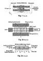
- a prior art grating intensity modulatoris described in an article by R. Kim et al. (Electronics Letters, vol. 41, no. 18, 1 Sep. 2005) and is illustrated in FIG. 1 .
- This modulatorhas a bulk electrode in which the RF signal is applied to the electrode as a whole rather than being propagated along the electrode, from one end of the electrode to the other.
- This prior optical grating waveguide intensity modulatorhas the RF modulating signal applied to the entire length of the grating by means of a lumped element electrode. Thus, the capacitance of that electrode limits the frequency response of the modulator.
- the electrodeis part of an RF waveguide, to avoid limiting the frequency response by capacitance effects, and the RF and optical field propagate in perpendicular directions.
- the maximum modulation frequencycan be limited by the group delay of the light propagating through the grating.
- the group delay through the gratingshould be substantially less than one-half cycle of the highest frequency RF modulating signal.
- the modulation efficiency of these prior modulatorswhich describes the amount of intensity modulation that is obtained for a given modulation of the voltage applied at the electrodes, increases as the length of the grating is increased and as the size of the effective periodic refractive-index steps is increased.
- these increases in the grating length and index stepalso increase the group delay of the light.
- an improvement in the modulation efficiencywould be achieved only at the expense of a corresponding reduction of the maximum modulation frequency and the modulation bandwidth.
- a common prior art wideband intensity modulatoris a Mach Zehnder interferometric modulator.
- This prior modulator(such as illustrated in FIG. 2 a ) contains an optical splitter (or a 3 dB coupler) that divides the input light into two optical-waveguide arms. The light in those two arms is then combined by an optical combiner (or another 3 dB coupler) to provide the output of the modulator.
- the intensity of the output lightdepends on the relative phases of the light coupled from the two waveguide arms, and the interference between that light.
- a goal of these prior Mach Zehnder modulatorsis to match the velocity of the traveling RF field with the velocity of the traveling optical field (the light being modulated).
- Some prior Mach Zehnder modulatorsalso contain cascaded sets of multiple optical-waveguide gratings in the two arms of the interferometer. The desired function of the gratings in these prior modulators is to change the group velocity of the light propagating through them.
- the applied RF fieldchanges the optical refractive index of the waveguide and grating material to produce a net change in the phase of the light propagated through the chain of grating reflectors and waveguide segments without substantially changing the intensity of that light.
- That chain of grating reflectors and waveguide segmentsis incorporated in the two arms of a Mach Zehnder interferometer and receive different modulation of their refractive index, resulting in a phase modulation of the light propagating through those arms.
- Any direct intensity modulation of the light directly by the gratings of these prior art modulatorsis undesirable and would interfere with the desired operation of the Mach Zehnder modulators.
- Optical Mach-Zehnder modulatorsthat contain multiple gratings in their interferometer arms wherein the overall transmittance of the modulator is modulated by the electric field carried by a traveling-wave RF electrode are described in articles by Shaw et al. (Electronics Letters, vol. 35, no. 18, 2 Sep. 1999, pp. 1557-1558), by Taylor (Journal of Lightwave Technology, vol. 17, no. 10, October 1999, pp. 1875-1883) and by Khurgin et al. (Optics Letters, vol. 25, 2000, pp. 70-72).
- FIG. 2 bshows an illustration of a portion of these prior modulators.
- the multiple gratingsare separated by optical-waveguide sections.
- the function of the multiple gratingsis to serve as optical reflectors, with each pair of such grating reflectors and the optical waveguide segment between them acting as an optical etalon.
- multiple pairs of grating segments that have differing grating periodsare cascaded end to end.
- the cascade of etalons or cascade of pairs of dissimilar gratingsslows down the group velocity of the light propagating through that cascade.
- the gratingis used solely as a means to increase the group delay (or decrease the group velocity) of light propagating through the grating.
- the prior art modulatorsthat have multiple grating reflectors in a cascade of Fabry Perot resonators operate at a wavelength for which the grating transmittance is minimal (transmittance notch) and the grating reflectance is high.
- the cascade of resonatorsproduces the “slowing” of the velocity of the light.
- the prior cascade of multiple pairs of grating segments that have different grating periodslikewise produces a “slowing” of the velocity of the light. For modulators formed from lithium niobate material, this “slowing” of the light makes it easier to match the velocity of the co-propagating RF field traveling in the RF electrodes with the velocity of the light in the two arms of the interferometer.
- the desired effect of the RF fieldis to produce only a phase modulation of the light exiting the grating and not to produce any intensity modulation of the light transmitted through a given optical-waveguide grating or cascade of grating segments.
- An optical-waveguide grating modulatorwhich is compatible with high-frequency electrical modulation signals (with frequencies typically greater than several GHz and bandwidths also typically greater than several GHz).
- the modulatorcomprises an optical grating formed in an optical waveguide constructed from electro-optic (EO) material and an electrode that is an RF waveguide or RF transmission line that conducts a traveling-wave electromagnetic (EM) field and that contains a portion of the optical-grating waveguide with a continuous grating.
- the RF input modulation signalis coupled into an RF EM field that propagates through the RF waveguide or transmission line in a direction that is parallel to the direction the light propagates in the optical-grating waveguide and that EM field overlaps the optical-grating waveguide.
- the light to be modulatedis coupled into one end of the optical-grating waveguide.
- the lighttravels along the optical-grating waveguide preferably at the same velocity as the RF EM field travels along the RF waveguide or transmission line.
- the modulated lightis coupled out from the opposite end of the optical-grating waveguide.
- Exemplary embodiments described hereininclude optical-grating waveguides with grooves etched into EO material to form the grating and optical-grating waveguides with grooves etched into a high-index material deposited above the EO material to form the grating. These embodiments also include transverse electromagnetic (TEM) RF waveguides, coplanar waveguide (CPW) RF transmission lines and coplanar strip (CPS) RF transmission lines that conduct the traveling RF field.
- Another embodimentcomprises multiple optical-waveguide gratings that are coupled to the same velocity-matched RF waveguide or transmission line. The modulated light from those multiple optical-waveguide gratings are combined and illuminate a photodete
- the modulator described in the present disclosurecan achieve high modulation efficiency at much higher signal frequency than the prior grating-waveguide intensity modulator because it has traveling-wave electrodes instead of the capacitance-limited, lumped-element electrodes.
- the disclosed modulatorachieves efficient modulation at even higher signal frequency by co-propagating the RF and optical fields and by matching the velocities of those fields.
- the present inventionmakes use of a single, continuous grating to directly produce the intensity modulation of the light, without needing an additional interferometric waveguide configuration to convert from optical phase modulation to optical intensity modulation.
- prior grating modulatorshave operated either at low modulation frequencies, using bulk electrodes rather than traveling-wave electrodes with co-propagating RF and optical fields, or they are based on an end-to-end cascade of grating segments in the arms of a Mach Zehnder interferometer.
- Some embodiments of the present inventionmake use of multiple gratings that are placed side by side like the gratings in the two arms of a Mach Zehnder interferometer.
- the multiple gratings of the present inventioncannot be interferometrically combined by means of an optical interferometer since they have different optical-carrier frequencies (optical wavelengths) and thus they do not optically interfere with each other.
- the present modulatoroperates with the optical carrier being at a wavelength on one of the two edges of the grating transmittance spectrum, rather than deep within the transmittance notch.
- the gratingitself can be used to achieve intensity modulation of the light.
- this inventionachieves stronger modulation depth (larger change in the intensity of light for the same modulation-controlling electric-field strength) while also being capable of high-frequency modulation with moderately large signal bandwidth.
- a phase-to-intensity modulatorsuch as a Mach-Zehnder interferometer that has a traveling-wave electrode
- this inventionachieves the same modulation depth with a physically shorter device.
- an electro-absorption modulatorthat has a traveling-wave electrode
- this inventioncan make use of a dielectric electro-optic material instead of a semiconductor material.
- the modulator of this inventioncan have a much higher electrical breakdown field strength compared to an electro-absorption modulator. This high breakdown field strength makes this modulator more robust when the modulator is exposed to high-energy EM fields whose intensity may be much higher than the intensity of the RF signal.
- the present inventionprovides an optical modulator structure comprising: an RF waveguide having a first longitudinal axis; and at least one optical grating waveguide having a second longitudinal axis located within the RF waveguide, the first longitudinal axis being parallel with and substantially coincident with the second longitudinal axis such that, in use, an RF field propagating in the RF waveguide and an optical field propagating in the optical grating waveguide propagate in substantially parallel directions, the at least one optical grating waveguide having a grating adapted to provide a notch in a transmission spectrum for the optical field propagating in the optical grating waveguide and having an operating wavelength of the optical field propagating in the optical grating waveguide wherein the operating wavelength is selected to occur at a transition from a substantially maximum transmission to greater than minimum transmission in said optical grating waveguide, the optical field propagating, in use, in the optical grating waveguide having an optical group velocity at the operating wavelength; wherein the RF field propagating, in use, in the RF waveguide
- the present inventionprovides an optical modulator structure comprising a substrate; and at least one optical grating waveguide having a first longitudinal axis disposed within the substrate and an RF waveguide having a second longitudinal axis disposed on the substrate, the first longitudinal axis being parallel with and substantially coincident with the second longitudinal axis such that, in use, an electric field propagating in the RF waveguide and an optical field propagating in the at least one optical grating waveguide propagate in substantially parallel directions, wherein the at least one optical grating waveguide includes a grating adapted to provide a notch for the optical field propagating, in use, in the optical grating waveguide and the at least one optical grating waveguide having an operating wavelength wherein the operating wavelength is selected to occur at a transition from substantially maximum transmission to greater than minimum transmission, the optical field propagating, in use, in the at least one optical grating waveguide having an optical group velocity at the operating wavelength; wherein the RF field propagating, in use, in the RF waveguide has
- an RF photonic transmittercomprising: an RF waveguide with a first end and a first longitudinal axis and at least one optical grating waveguide with a second end and a second longitudinal axis, wherein the first end is coincident with the second end and the first longitudinal axis is parallel with and substantially coincident with the second longitudinal axis such that an RF field propagating in the RF waveguide overlaps the optical grating waveguide, the optical grating waveguide having a grating adapted to provide a notch in a transmission spectrum of an optical field propagating in the at least one optical grating waveguide and wherein the optical field has an operating wavelength, the operating wavelength being selected to occur at a transition from substantially maximum transmission to greater than minimum transmission; an associated laser, for each of the at least one optical grating waveguide, emitting laser light at the operating wavelength of the at least one optical grating waveguide with which it is associated, the laser light of the associated laser entering its associated optical grating waveguide at the
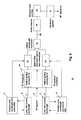
- FIG. 1is an illustration of a single-grating optical intensity modulator with non-traveling wave electrode known in the prior art.
- FIG. 2 ais an illustration of a prior art Mach Zehnder interferometric modulator.
- FIG. 2 bis an illustration of a multiple-grating optical modulator with co-directional traveling-wave electrode known in the prior art.
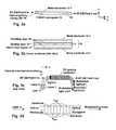
- FIG. 3 ais a perspective view which illustrates a TEM RF waveguide containing multiple strips of optical grating waveguides.
- FIG. 3 bis an exploded cross sectional side view of the embodiment of FIG. 3 a.
- FIG. 3 cpresent a top view of the embodiment of FIGS. 3 a and 3 b showing different lasers supplying the light transmitted through the different optical grating waveguides.
- FIG. 3 ddepicts an optical waveguide grating as comprising a set of interfaces between two alternating portions of a composite waveguide that have different optical refractive indices (n eff1 and n eff2 ).
- FIG. 3 eillustrates an RF signal co-propagating with and velocity matched to the light propagating in the optical grating waveguide.
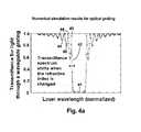
- FIG. 4 aillustrates the transmittance spectrum of an ideal optical waveguide grating showing a notch in the spectrum for which the grating transmission is low and the corresponding grating reflection is high.
- FIG. 4 bis an illustration of E-field dependent shift of the grating spectrum with the left edge of the grating notch shown.
- the shift in the grating spectrumresults in a change in the transmission for light of a given wavelength.
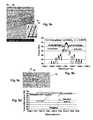
- FIG. 5 ais a view of an optical grating waveguide of lithium niobate with an etched grating.
- FIG. 5 bis an exemplary spectral response of such a grating as is depicted by FIG. 5 a.
- FIG. 5 cdepicts an optical grating waveguide formed from etching a grating into a silicon layer deposited above a lithium niobate waveguide.
- FIG. 5 ddepicts a graph of the measured optical transmission spectrum of the grating of FIG. 5 c.
- FIG. 6shows a RF photonic link with a velocity-matched modulator comprising multiple optical grating waveguides.
- FIGS. 7 a and 7 bshows an example of optical-grating waveguide modulator with CPW transmission line electrode, with FIG. 7 b being a SEM showing only a portion of the optical-grating waveguide modulator as marked on FIG. 7 a.
- FIG. 8 graphs (a) and (b)depict the measured gain of link with traveling-wave grating modulator and measured optical transmission spectrum of the modulator grating.
- FIG. 9depicts the spectral components of the light input to the grating modulator, the light transmitted through or reflected from the grating modulator, and the light output from the optical filter of the link shown in FIG. 6 .
- FIG. 10depicts the calculated transmittance for an optical grating, the phase shift of the transmitted light and the group velocity of the light transmitted through the optical grating.
- FIGS. 11 a and 11 bdepict the temporal spreading of a short optical pulse propagated through the grating.
- the present inventionrelates to an optical-waveguide grating modulator that modulates the light passing through it.
- the modulatormodulates the intensity of the light that is partially transmitted through and partially reflected by one or more gratings.
- the modulation of that lightis controlled by a traveling RF electromagnetic (EM) field that propagates parallel to the directions of the transmitted and reflected light and co-propagates with the transmitted light.
- EMtraveling RF electromagnetic
- the optical waveguide gratingis fabricated in an electro-optic material whose optical refractive index depends on the electric-field component of the traveling RF field.
- the time-varying RF fieldthe input RF signal
- the transmission/reflection spectrum of the gratingis shifted accordingly, along the frequency (or wavelength) axis. This changes the net transmission or reflection of the various frequency components of the light.
- the disclosed modulatorcomprises one or more optical waveguide-gratings that are part of an RF waveguiding structure, such as a transverse electromagnetic (TEM) RF waveguide 10 , as is illustrated in FIGS. 3 a , 3 b and 3 c .
- the TEM RF waveguide 10comprises a slab 24 of dielectric material that is sandwiched on two sides by electrically conductive metal electrodes 12 - 1 and 12 - 2 .
- An EM field 8 propagating through that RF waveguidehas electric field lines that are directed from one of the two electrodes 12 - 1 to the other of the two electrodes 12 - 2 .
- Three optical-grating waveguides 14arranged parallel to one another, are depicted in the embodiment of FIG. 3 a.
- a desirable feature of the TEM RF waveguide 10is that the electric field magnitude and direction is quite uniform over most of the slab of dielectric material. It is sufficient that at least a portion of that dielectric material comprises EO material and that portion substantially overlaps the optical field of the light propagating in the optical waveguides 14 whose optical refractive index can be modulated by the applied electric field.
- optical-grating waveguide(s) 14The longitudinal axis of optical-grating waveguide(s) 14 is(are) arranged parallel to the longitudinal axis of the RF waveguide 10 .
- lightpropagates through the optical-grating waveguide(s) 14 in a direction (the z-direction in FIG. 3 a ) that is parallel to the direction of propagation of the RF EM field 8 .
- a cross-section of the propagating RF EM field 8completely overlaps the optical-grating waveguide 14 .
- more than one optical-grating waveguide 14generally can be formed in the same RF waveguide 10 as shown in FIG. 3 a .
- the entire piece of dielectric materialcomprises EO material, only a portion thereof needs to be EO material as described below with respect to FIG. 3 b .
- An EO materialsuch as lithium niobate, gallium arsenide, indium phosphide or an electro-optic polymer may be utilized.
- the EM fieldpropagates through a TEM RF waveguide 10 having a pair of metal electrodes 12 - 1 and 12 - 2 that sandwich one or more optical waveguide gratings 14 .
- the width of the TEM waveguidewhich must be sufficiently wide (in the y-direction of FIG. 3 a ) for the RF waveguide 10 to support the desired frequency of the EM field 8 , also is sufficient to accommodate multiple optical-waveguide gratings 14 that are disposed side to side.
- different ones of these multiple optical grating waveguides 14are designed to provide optimal modulation for light of different optical-carrier frequencies (or wavelengths). The modulated light at these different optical-carrier frequencies can be combined and illuminate the same photodetector to produced a larger photocurrent, which is the output RF signal.
- Each optical grating waveguide 14contains a region 18 that has higher optical refractive index than the remaining material 20 of the slab 24 .
- the higher optical refractive index material region 18which comprises the effective core of the optical waveguide, also is preferably formed by an EO material such as lithium niobate, gallium arsenide, indium phosphide or an electro-optic polymer.
- the gratingitself can be formed directly in the higher optical refractive index material region 18 or it can be formed in another material 16 that is optically coupled to the higher optical refractive index material region 18 , as is illustrated by FIG. 3 b .
- the combination of the grating region and the higher optical refractive index material 18should have a higher net refractive index than the rest of the dielectric slab 24 , so the rest of the dielectric slab 24 serves as cladding 20 of the optical waveguide(s) 14 , with the higher optical refractive index material region 18 being the core of that waveguide(s) 14 .
- the optical mode of the guided lightis located in the vicinity of the high-index material and substantially overlaps the grating (see FIGS. 3 a and 3 b ).
- a grating formed in an optical waveguidehas a periodic spatial variation in its optical refractive index due to the periodic nature of the grating.
- the grating regioncan be thought of as comprising a periodic structure of two composite materials that have different optical refractive index as shown in FIG. 3 d .
- One composite materialhas a relatively higher effective refractive index for the waveguided light (e.g., n eff2 ) and the other composite material has a relatively lower effective refractive index for the waveguided light (e.g., n eff1 ).
- a grating waveguideacts as a distributed Bragg reflector that can reflect certain wavelengths of the light propagating through the grating waveguide, transmit other wavelengths of the light and partially reflect yet other wavelengths of the light.
- An exemplary transmission spectrum of an ideal gratingis shown in FIG. 4 a .
- transmissionis low and the light is reflected by the grating instead.
- an optical waveguide-grating modulatorat least the grating and typically also the rest of the optical waveguide 14 is constructed in an EO material as mentioned above. The refractive index of the EO material changes when that material is exposed to an electric field.
- the change in refractive indexshifts the grating transmittance spectrum, as illustrated in FIGS. 4 a and 4 b , toward longer or shorter wavelengths. For a given wavelength of light that coincides with an edge 42 of the transmission notch 41 , this shifting of the transmittance spectrum results in modulation of the transmitted light, as is illustrated in FIG. 4 b , as well as of the reflected light.
- FIG. 5 ashows an illustration, made with the assistance of a scanning electron microscope, of such a surface grating that has been etched into a titanium-diffused lithium niobate (Ti:LiNbO 3 ) waveguide.
- Ti:LiNbO 3titanium-diffused lithium niobate
- the cross sectional regions comprising the periodically etched grooves 51have the lower effective refractive index (e.g., n eff1 ) and the unetched regions 52 between the grooves have the higher effective refractive index (e.g., n eff2 ).
- An exemplary transmission spectrum of the gratingis shown in FIG. 5 b.
- optical grating waveguidecomprises a titanium diffused waveguide formed in lithium niobate covered by a layer of high-index material, such as silicon.
- a periodic pattern of groovesis etched into the silicon layer to form the grating.
- FIG. 5 cshows the silicon grating at the left and the uncovered titanium diffused waveguide at the right of the illustration.
- the regions comprising the periodic grooves 53 etched through the silicon layer plus the Ti:LiNbO 3 waveguide beneath those grooveshave the lower effective refractive index (e.g., n eff1 ) while the regions with the unetched silicon layer 54 plus the underlying Ti:LiNbO 3 waveguide have the higher effective refractive index (e.g., n eff2 ).
- An exemplary transmission spectrum of such a grating waveguideis shown in FIG. 5 d.
- the light to be modulatedtypically is produced by at least one laser (see, for example, Laser 1 , Laser 2 or Laser 3 in FIG. 3 c ) and preferably each laser generates a single wavelength at an optical-carrier frequency.
- FIG. 3 cillustrates that the input light from the lasers (Laser 1 , Laser 2 and Laser 3 ) is supplied to the same end of the RF waveguide 10 as the input RF EM field 8 .
- the RF EM field 8travels in the same direction as the light that is transmitted through the waveguide 14 .
- the TEM RF waveguide 10should be sufficiently wide in the y-direction (see FIG. 3 a ) that the RF waveguide 10 can support EM fields 8 of the desired frequency.
- this widthis at least one half of the wavelength of that EM field divided by the RF refractive index of the slab material 20 (square root of its RF dielectric constant).
- the dielectric constantis approximately thirty, so the width of the TEM waveguide for X-band frequency is several millimeters.
- Such a wide slabcan accommodate multiple optical grating waveguides 14 that can be located side by side and that extend from one end of the slab to the other end along the z-direction, as illustrated in FIGS. 3 a and 3 c . Note that for light of 1550 nm wavelength, a typical size of the guided optical mode is 10 micrometers or smaller.
- optical waveguides 14can be separated by a distance of only 10-20 micrometers and not have any optical interaction with each other.
- the length of the slab (and of the grating) or the waveguidecan be many millimeters or even many centimeters long.
- the thickness of the slab, in the x-directioncan range from values of several tens of micrometers to several hundred micrometers.
- the grating of an electro-optic grating modulatorcan be considered as comprising a set of interfaces between adjacent portions of waveguide that have different optical refractive indices (n eff1 and n eff2 ) for the guided mode. See FIG. 3 d .
- the amount of reflection or transmission occurring at an interfaceis dependent on the index difference (e.g., n eff2 ⁇ n eff1 ). It also depends on the relative phase of the light that reaches the interface from one direction, to be transmitted through it, and the light that reaches the interface from the other direction, to be reflected from it. Modulation of the electric field applied across the grating waveguide modulates slightly the index difference. However, it can change greatly the relative phases of the light incident upon that interface.
- a time-varying electric fieldmodulates the transmission/reflection that occurs at each interface.
- a given front of the propagating optical fieldwill continually see the same portion of the time-varying RF signal as that optical field propagates through the grating modulator, as illustrated in FIG. 3 e .
- the modulationgradually builds up and is enhanced as those optical and RF fields propagate together.
- the time-varying change in the electric fieldis synchronized such that a particular portion of the RF waveform remains in step with a given portion of the light as that light propagates through the grating.
- This variation in the electric fieldmodulates the transmission/reflection that occurs at the interfaces in the vicinity of that electric field.
- the local change in the electric fieldincreases (or decreases) the net transmission of light through an interface.
- the accompanying local change in electric fieldcontinues to increase (or decrease) the transmission of that light through those additional interfaces.
- the depth of modulation of the transmittance of the lightgradually become greater as that light propagates through the grating, from one end of the RF waveguide to the other end.
- Some embodimentscomprise multiple optical grating waveguides that are in the same RF waveguide. Those grating waveguides preferably are designed to operate at different optical-carrier frequencies. In general, the light for different ones of those multiple grating waveguides 14 is supplied by different lasers—which is why there are three different lasers shown in FIG. 3 c . Since the modulated light output from the multiple grating waveguides are at different optical frequencies, they can be combined onto the same photodetector without incurring any optical interference for optical carrier frequencies that are spaced farther apart than the line width of the laser light and further apart than the maximum bandwidth of the RF modulation signal.
- FIG. 6shows a block diagram of an RF photonic link 50 that contains multiple optical grating waveguides 14 .
- the RF photonic link 50 shown in FIG. 6also can include optional optical filters 24 that selectively attenuate the optical-carrier frequency (to further enhance the modulation depth) and an optional optical wavelength multiplexer 26 that combines the light of the differing frequencies into a common optical waveguide path (or optical fiber) 28 .
- the lasers 6are preferably tunable and controlled by controller 4 which also controls the filters 24 so that they continue to block the specific carrier wavelength ⁇ 1 or ⁇ 2 output by each of the lasers 6 .
- the output of the multiplexer 26 on optical waveguide path or optical fiber 28is photodetected at a photodetector 29 , whose output is preferably applied to an electrical load and filter 30 before being amplified by an amplifier 31 .
- the optical carrier frequencyis preferably variable so the laser 6 is depicted as having a tunable wavelength.
- the group velocity of the optical-carrier light propagating through the grating waveguide 14varies with the optical carrier frequency.
- This optical carrier frequency of the laser lightcan be adjusted to fine tune the group velocities in the multiple gratings so that they all approximately match the velocity of the RF wave 8 .
- the multiple gratingscan be different from each other and can have their grating period or the optical guided-mode index of their optical waveguide designed such that each grating waveguide has the same group velocity although the optical carrier frequency of the light propagating in them is different for different ones of those multiple grating waveguides 14 .
- FIGS. 7 a and 7 billustrate an example of an EO grating modulator for which the traveling RF field is carried in a single coplanar waveguide (CPW) transmission line.
- This CPW transmission linecomprises a center-conductor electrode 32 and a pair of ground electrodes 34 .
- the optical grating waveguide 14is located underneath the center-conductor electrode 32 .
- the optical grating waveguide 14abuts non-grating optical waveguide 36 (such as the titanium-infused lithium niobate waveguide 55 shown on the right half of FIG. 5 c ). A portion of the optical waveguide 36 can be seen extending beyond the CPW transmission line shown in FIG. 7 a .
- This exemplary modulatoris formed in Z-cut lithium niobate, but other modulators could be formed in other electro-optic materials such as InP or GaAs.
- the CPW lineterminates, at each end, in a set of ground-signal-ground pads 38 that are matched to the spacing of RF probes used to apply an RF signal to the electrode.
- the RF signalpropagates along the CPW transmission line to an impedance load (not shown) connected to the set of pads located at the other end of that line.
- the CPW electrodescan be formed by electroplating a thick layer of gold above the top layer of dielectric material deposited onto the optical-waveguide substrate.
- FIG. 8 graph (b)shows the gain of a RF-photonic link containing the modulator of FIGS. 7 a and 7 b , as measured at several different wavelengths.
- the RF photonic linkcomprises a laser, the modulator of FIGS. 7 a and 7 b and a photodetector.
- This linkhas a gain over a large frequency bandwidth when the RF wave and the optical wave co-propagate as shown in FIG. 8 graph (b).
- the modulation frequencycan be much higher than the inverse of twice the group delay of the light transmitted through the 5-cm long grating waveguide.
- the RF link gainis obtained for a fairly large range of laser wavelengths between 1559.35 nm and 1559.40 nm.
- FIG. 8 graph (a)The optical transmission spectrum of the modulator at these wavelengths is shown in FIG. 8 graph (a).
- those multiple gratingscan have the same grating design (i.e., the same effective refractive index step and the same pitch of the periodic variation in index) and can still be operated at different laser wavelengths.
- the multiple gratings in a modulatorcould have different grating designs (with slightly different periods of their refractive index perturbation) to optimize the RF link gain obtained for each laser wavelength separately.
- the light propagating in the gratingcan be considered as having a group velocity. That group velocity depends on the effective refractive index step at the many interfaces of the grating, the wavelength of the light, the length of the waveguide portion between grating interfaces, and the nominal refractive index of that waveguide portion.
- the overall group delay of the transmitted light output from the gratingbecomes larger and larger as the grating is made longer and longer.
- the group velocitywhich is equal to the overall grating length divided by the group delay, can remain approximately the same when the wavelength of the light is adjusted to obtain the same amount of total transmission through the grating.
- one can change the group velocity of the lightby changing the laser wavelength, changing the index difference of the grating or changing the period of the grating.
- the group velocity of light at a given optical-carrier frequencycan be determined from a calculation or measurement of the phase spectrum of the light transmitted through the grating.
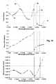
- FIG. 10shows an example of the transmittance spectrum of an ideal grating, the phase shift of the transmitted light and the group velocity of that transmitted light.
- the group delaycan be calculated from the phase shift spectrum and the group velocity can be calculated from the group delay and the grating length.
- the group velocity at the optical carrier frequency (or optical wavelength)which is chosen to coincide with some point along the steep slope 42 of the transmittance notch 41 of the grating, can be several times slower than the group velocity at optical frequencies or wavelengths far away from that notch 41 .
- the gratingis an effective means to slow the velocity of the light to match more closely the velocity of the propagating RF field.
- the RF group velocitybe matched (i.e., be identical) to the optical group velocity. For example, for a given length of grating, if the difference between propagation time delays of the RF field 8 and the grating-transmitted light become greater than one half of the period of the RF waveform, the modulation attained in one portion along the longitudinal axis of the grating will cancel the modulation obtained in another portion along the longitudinal axis of the grating.
- This walk-off or departure from phase alignment between the propagating RF field and the grating transmitted lightconstrains the maximum tolerable mismatch between their group velocities and the maximum frequency of the RF signal 8 needed to limit the reduction in the amount of modulation of the output light to some desired value (the amount of reduction may, in fact, be zero, and is preferably less than 3 db). It is notable that, at specific frequencies of the RF signal 8 , the cancellation arising from this walk-off in phase alignment can be nearly complete and the transmitted light output can have no net modulation.
- the RF waveguide or transmission lineis preferably designed such that the velocity of the EM field propagating through the portion of the RF waveguide or transmission line containing that portion of the grating is the same as the group velocity of the light propagating in that portion of the grating.
- Thismay be accomplished by various known means such as by adjusting the thickness of the dielectric spacer (the cladding layer 20 ) between the EO material in the optical grating waveguide 14 and the metal electrodes 12 - 1 and 12 - 1 of FIG. 3 b .
- Thisalso may be accomplished by adjusting the heights of the electrodes 34 , and by adjusting the gap between elements 32 and 34 of FIGS. 7 a and 7 b .
- the gratingcan be made longer to permit a weaker RF signal to achieve the same degree of modulation of the light.
- the gratingcan be designed to reduce the group velocity of light at a band of wavelengths near the operating wavelength to be approximately the same as the velocity of the RF EM field. This can be done using optical simulation (such as those illustrated by FIG. 10 ) to develop design curves that relate the optical group velocity for a given wavelength of light and the various parameters defining the grating, such as its index difference, period and length.
- Light whose intensity modulation has been controlled by an RF signalcan be described as comprising an optical-carrier frequency component 61 and modulation-sideband components 62 , 63 that are at frequencies somewhat higher (shorter wavelength) or lower (longer wavelength) than the optical carrier frequency as illustrated in FIG. 9 .
- the frequency spacing between the optical carrier 61 and the modulation sideband 62 , 63is equal to the frequency of the RF signal.
- each modulation sideband 62 , 63contains primarily a narrow bandwidth of light that is propagated through the optical grating waveguide, as limited by the dispersion of that grating.
- a short (e.g. 50 psec. wide) optical pulsecomprising many and wide-ranging optical frequencies (e.g., >40 GHz) is propagated through that grating
- the width of the pulsewould spread because of the dispersion of the grating.
- This optical-pulse spreadingis illustrated in FIGS. 11 a and 11 b .
- the wavelength 61 of the light input to the grating modulatorcoincides with a point on the edge 42 of a main transmittance notch 41 in the grating's characteristic transmittance spectrum as illustrated in FIG. 10 and FIG. 8 graph (a).
- Some modulation sidebands of the lightcoincide with the transmittance notch 41 .
- other modulation sidebands of the lightpreferably coincide with wavelengths for which the grating transmittance is constant.
- the modulation sidebands 63(illustrated in light grey in FIG. 9 ) having a wavelength that coincides with a portion of the main transmission notch 41 . That optical energy is reflected by the grating and exits the waveguide grating from the same input port though which the laser light is supplied to the grating rather than being transmitted through the grating.
- the modulation sideband 62(illustrated in black in FIG. 9 ) whose wavelength preferably coincides with a satellite peak 43 in the transmittance spectrum. Light once transferred into that sideband is not further modulated by the shifts in the transmittance as the light in that sideband propagates through the grating to the transmitted output. Since only the light in the optical carrier wavelength 61 is modulated, only the group velocity of that wavelength component is of major concern for the velocity matching.
- the wavelength of the modulation side band 62could coincide with a satellite valley 44 in the transmittance spectrum.
- FIG. 10shows that for wavelengths near these satellite or local transmittance peaks 43 or transmittance valleys 44 , the group velocity is approximately constant. If the modulation sideband 62 coincides with a local transmittance peak 43 or with a transmittance valley 44 , the group velocity of those frequency components in that sideband 62 can be approximately the same. In that case, there would be minimal broadening of a pulsed RF modulation signal. However, if the modulation sideband 62 coincides with some portion of the spectrum where the transmittance varies with wavelength (or frequency), there will be some dispersion of the various frequency components of the modulated signal.
- the components of the light at the optical-carrier 61 and at the modulation sidebands (e.g., 62 )can have different values for their group velocity.
- the modulated lightilluminates a photodetector.
- the photodetectorcan be thought of as multiplying the optical-frequency carrier with the optical-frequency modulation sideband to generate an electrical RF output signal.
- the components of the light at the optical-carrier and at the optical modulation sidebandhave different group velocities, the light at the optical-carrier will still be phase-tracked with (although not having an identical phase as) light at the modulation sideband if the inverse linewidth of the laser is shorter than the group delay through the grating modulator.
- the group velocity for that optical frequency carrier 61also can remain approximately constant as the grating is modulated.
- FIG. 8 graphs (a) and (b)also show that the wavelength of the light being modulated is preferably close to the region of the spectral notch having high transmission rather than having low transmission (or high reflection).
- the prior Fabry-Perot cascade modulators with traveling-wave electrodehave the wavelength of the laser light coincide with the bottom of the spectral notch.
- the goalis to delay the propagating light as much as possible with a minimal change in the transmitted intensity of that light and minimal change of the transmission with the wavelength of the light.
Landscapes
- Physics & Mathematics (AREA)
- Nonlinear Science (AREA)
- General Physics & Mathematics (AREA)
- Optics & Photonics (AREA)
- Electromagnetism (AREA)
- Chemical & Material Sciences (AREA)
- Engineering & Computer Science (AREA)
- Ceramic Engineering (AREA)
- Crystallography & Structural Chemistry (AREA)
- Optical Modulation, Optical Deflection, Nonlinear Optics, Optical Demodulation, Optical Logic Elements (AREA)
Abstract
Description
Claims (35)
Priority Applications (1)
| Application Number | Priority Date | Filing Date | Title |
|---|---|---|---|
| US13/151,510US9335568B1 (en) | 2011-06-02 | 2011-06-02 | Electro-optic grating modulator |
Applications Claiming Priority (1)
| Application Number | Priority Date | Filing Date | Title |
|---|---|---|---|
| US13/151,510US9335568B1 (en) | 2011-06-02 | 2011-06-02 | Electro-optic grating modulator |
Publications (1)
| Publication Number | Publication Date |
|---|---|
| US9335568B1true US9335568B1 (en) | 2016-05-10 |
Family
ID=55859941
Family Applications (1)
| Application Number | Title | Priority Date | Filing Date |
|---|---|---|---|
| US13/151,510Expired - Fee RelatedUS9335568B1 (en) | 2011-06-02 | 2011-06-02 | Electro-optic grating modulator |
Country Status (1)
| Country | Link |
|---|---|
| US (1) | US9335568B1 (en) |
Cited By (16)
| Publication number | Priority date | Publication date | Assignee | Title |
|---|---|---|---|---|
| US20160025926A1 (en)* | 2014-07-28 | 2016-01-28 | The University Of Connecticut | Optoelectronic Integrated Circuitry for Transmitting and/or Receiving Wavelength-Division Multiplexed Optical Signals |
| US9882654B1 (en)* | 2016-03-17 | 2018-01-30 | Hrl Laboratories, Llc | Jammer-suppressed photonic-enabled RF link |
| JP2018163216A (en)* | 2017-03-24 | 2018-10-18 | 住友大阪セメント株式会社 | Optical modulator |
| US10228511B2 (en) | 2016-09-28 | 2019-03-12 | LGS Innovations LLC | Integrated low-voltage CMOS-compatible electro-optic modulator |
| US10250330B1 (en)* | 2018-02-23 | 2019-04-02 | Space Systems/Loral LLC | Flexible signal distribution assisted by tunable optical carrier modulating a desired signal |
| CN109600904A (en)* | 2019-01-08 | 2019-04-09 | 惠州学院 | Semiconductor laser accelerator and its laser acceleration unit |
| CN112038888A (en)* | 2020-08-05 | 2020-12-04 | 南京大学 | A semiconductor laser with integrated waveguide grating modulator |
| CN113093410A (en)* | 2019-12-23 | 2021-07-09 | 海思光电子有限公司 | Optical modulator and sending module |
| CN113311599A (en)* | 2021-05-19 | 2021-08-27 | 清华大学 | High-speed integrated optical modulator, modulation method and modulation system |
| JP2022542009A (en)* | 2020-07-01 | 2022-09-29 | ジャージァン・ユニバーシティ | Photonic neural network on silicon substrate based on tunable filter and its modulation method |
| US20220390777A1 (en)* | 2019-11-27 | 2022-12-08 | HyperLight Corporation | Electro-optic devices having engineered electrodes |
| US20230251511A1 (en)* | 2019-11-27 | 2023-08-10 | HyperLight Corporation | Electro-optic devices having closely spaced engineered electrodes |
| CN116609978A (en)* | 2023-03-21 | 2023-08-18 | 浙江大学 | A compact Mach-Zehnder modulator chip |
| US12169347B2 (en)* | 2019-09-12 | 2024-12-17 | Nippon Telegraph And Telephone Corporation | Semiconductor Mach-Zehnder optical modulator and IQ modulator |
| US12282214B2 (en) | 2019-11-27 | 2025-04-22 | HyperLight Corporation | Thin film lithium niobate optical device having an engineered substrate for heterogeneous integration |
| US12416824B1 (en)* | 2022-02-03 | 2025-09-16 | National Technology & Engineering Solutions Of Sandia, Llc. | Ultraviolet and visible light integrated acousto-optic modulators |
Citations (69)
| Publication number | Priority date | Publication date | Assignee | Title |
|---|---|---|---|---|
| US3417400A (en) | 1966-04-25 | 1968-12-17 | Administrator Of The Nat Acron | Triaxial antenna |
| US3735293A (en) | 1970-05-12 | 1973-05-22 | Kabel Metallwerke Ghh | High frequency cable |
| US3781725A (en) | 1972-05-04 | 1973-12-25 | Sumitomo Electric Industries | Leaky coaxial cable |
| US3909757A (en) | 1973-03-13 | 1975-09-30 | Sumitomo Electric Industries | Leaky coaxial cable |
| US4129841A (en) | 1976-08-13 | 1978-12-12 | Kabel-Und Metallwerke Gutehoffnungshutte A.G. | Radiating cable having spaced radiating sleeves |
| US4152648A (en) | 1975-10-07 | 1979-05-01 | Institut National Des Industries Extractives | Radiocommunication system for confined spaces |
| US4339733A (en) | 1980-09-05 | 1982-07-13 | Times Fiber Communications, Inc. | Radiating cable |
| US4376941A (en) | 1970-01-29 | 1983-03-15 | The United States Of America As Represented By The Secretary Of The Navy | Antenna cable |
| US4541120A (en) | 1982-08-19 | 1985-09-10 | International Standard Electric Corporation | Transmitter-receiver module |
| US4987394A (en) | 1987-12-01 | 1991-01-22 | Senstar Corporation | Leaky cables |
| US5015052A (en) | 1989-07-20 | 1991-05-14 | Battelle Memorial Institute | Optical modulation at millimeter-wave frequencies |
| FR2661256A1 (en) | 1990-04-20 | 1991-10-25 | Thomson Csf | Integrated electrooptic modulator component |
| US5076655A (en) | 1990-07-19 | 1991-12-31 | Hughes Aircraft Company | Antenna-fed electro-optic modulator |
| US5076622A (en) | 1990-07-25 | 1991-12-31 | Lectron Products, Inc. | Fuel filler latch assembly |
| US5247270A (en) | 1987-12-01 | 1993-09-21 | Senstar Corporation | Dual leaky cables |
| US5291565A (en) | 1992-06-30 | 1994-03-01 | Hughes Aircraft Company | Broad band, low power electro-optic modulator apparatus and method with segmented electrodes |
| US5309531A (en) | 1992-11-12 | 1994-05-03 | California Institute Of Technology | Broad-band substrate-wave-coupled electro-optic modulator |
| US5517199A (en) | 1995-05-11 | 1996-05-14 | Aerodata Corporation | Emergency locator device |
| US5519408A (en) | 1991-01-22 | 1996-05-21 | Us Air Force | Tapered notch antenna using coplanar waveguide |
| US5703706A (en) | 1994-09-16 | 1997-12-30 | Varian Associates, Inc. | Spectral modification through phase modulation with spatial extent |
| US5751867A (en) | 1996-01-26 | 1998-05-12 | Hughes Aircraft Company | Polarization-insensitive, electro-optic modulator |
| US5936589A (en) | 1994-11-29 | 1999-08-10 | Murata Manufacturing Co., Ltd. | Dielectric rod antenna |
| US5936203A (en) | 1997-10-15 | 1999-08-10 | Andrew Corporation | Radiating coaxial cable with outer conductor formed by multiple conducting strips |
| US5940196A (en) | 1997-05-16 | 1999-08-17 | Harmonic Lightwaves, Inc. | Optical communications system with wavelength division multiplexing |
| US5963567A (en) | 1997-02-13 | 1999-10-05 | Lucent Technologies, Inc. | Multi-wavelength laser source |
| US6246500B1 (en) | 1998-09-18 | 2001-06-12 | Massachusetts Institute Of Technology | Linearization of a broadband analog optical link using two wavelengths |
| US6268781B1 (en) | 1997-09-10 | 2001-07-31 | Hughes Electronics Corporation | Planar waveguide-to-stripline adapter |
| US20010021294A1 (en) | 1997-12-15 | 2001-09-13 | University Of Southern California, Non-Profit Organization | Tuning of optical dispersion by using a tunable fiber bragg grating |
| US6418248B1 (en) | 1999-12-07 | 2002-07-09 | Hrl Laboratories, Llc | Traveling-wave photodetector |
| US20020097945A1 (en) | 2000-09-27 | 2002-07-25 | The Regents Of The University Of California | Method for optical modulation at periodic optical structure band edges |
| US20020105378A1 (en) | 1999-05-25 | 2002-08-08 | Olli Tapio | Linearisation and modulation device |
| US6509809B1 (en) | 1999-05-27 | 2003-01-21 | Hrl Laboratories, Llc | Method and apparatus for coupling strip transmission line to waveguide transmission line |
| US6522793B1 (en) | 2001-11-21 | 2003-02-18 | Andrei Szilagyi | Low voltage electro-optic modulator with integrated driver |
| US6525692B2 (en) | 1998-09-25 | 2003-02-25 | Korea Electronics Technology Institute | Dual-band antenna for mobile telecommunication units |
| US20030048232A1 (en) | 2001-09-11 | 2003-03-13 | Hrl Laboratories, Llc | Waveguide for a traveling wave antenna |
| US6640020B2 (en) | 2000-04-07 | 2003-10-28 | Hrl Laboratories, Llc | Method and apparatus for electro-optic delay generation of optical signals |
| US20030214450A1 (en) | 2002-05-14 | 2003-11-20 | Hrl Laboratories, Llc | Wideband antenna array |
| US20030235368A1 (en) | 2002-06-03 | 2003-12-25 | Adtek Photomask Inc.; And | Pi -Shifted filters based on electro-optically induced waveguide gratings |
| US6703596B1 (en) | 2001-11-13 | 2004-03-09 | Lockheed Martin Corporation | Apparatus and system for imaging radio frequency electromagnetic signals |
| US20040067006A1 (en) | 2001-10-09 | 2004-04-08 | Welch David F. | Transmitter photonic integrated circuit ( TxPIC) chips |
| US6724523B2 (en) | 2001-11-15 | 2004-04-20 | Hrl Laboratories, Llc | Remotely locatable RF power amplification system |
| US20040179825A1 (en) | 2003-03-11 | 2004-09-16 | Im Jin Seok | Digital video record/playback apparatus and playback method thereof |
| US20050094917A1 (en) | 2003-11-03 | 2005-05-05 | Wenshen Wang | Slow wave optical waveguide for velocity matched semiconductor modulators |
| US6996345B1 (en) | 2002-05-10 | 2006-02-07 | The United States Of America As Represented By The Secretary Of The Air Force | Linearization of intensity modulators using quadratic electro-optic effect |
| US7133576B2 (en) | 2003-07-25 | 2006-11-07 | Agility Communications, Inc. | Traveling-wave optoelectronic wavelength converter |
| US20060270368A1 (en) | 2003-02-26 | 2006-11-30 | Caimi Frank M | Integrated Front End Antenna |
| US20070189778A1 (en) | 2006-02-14 | 2007-08-16 | Burns William K | Bi-directional signal interface using photonic coupler |
| US7260280B2 (en) | 2004-03-26 | 2007-08-21 | Sumitomo Osaka Cement Co., Ltd. | Optical device |
| US20080069491A1 (en) | 2004-07-27 | 2008-03-20 | Jds Uniphase Corporaton | Electro-Optic Device |
| US7369722B2 (en) | 2005-03-17 | 2008-05-06 | Oewaves, Inc. | Coupled and non-coupled opto-electronic oscillators with enhanced performance |
| US7471258B2 (en) | 2006-04-26 | 2008-12-30 | Hrl Laboratories, Llc | Coaxial cable having high radiation efficiency |
| US20090016729A1 (en) | 2006-11-13 | 2009-01-15 | Optimer Photonics, Inc. | Frequency selective mmw source |
| US7486247B2 (en) | 2006-02-13 | 2009-02-03 | Optimer Photonics, Inc. | Millimeter and sub-millimeter wave detection |
| US20090051614A1 (en) | 2007-08-20 | 2009-02-26 | Hang Wong | Folded dipole antenna |
| US7555219B2 (en) | 2003-07-14 | 2009-06-30 | Photonic Systems, Inc. | Bi-directional signal interface |
| US7558488B2 (en) | 2002-11-06 | 2009-07-07 | Finisar Corporation | Reach extension by using external Bragg grating for spectral filtering |
| US20090185810A1 (en) | 2007-02-27 | 2009-07-23 | Celight, Inc. | Single chip two-polarization quadrature synthesizer, analyser and optical communications system using the same |
| US7657132B1 (en)* | 2008-06-18 | 2010-02-02 | Hrl Laboratories, Llc | Optoelectronic modulator and electric-field sensor with multiple optical-waveguide gratings |
| US7660491B2 (en) | 2006-08-24 | 2010-02-09 | Eospace, Inc. | High-dynamic-range analog fiber-optic link using phase modulation and tunable optical filter |
| US7738794B2 (en) | 2005-11-15 | 2010-06-15 | Fujitsu Limited | Optical transmitter |
| US7809216B2 (en) | 2007-03-16 | 2010-10-05 | Photonic Systems, Inc. | Bi-directional signal interface and apparatus using same |
| US7835600B1 (en) | 2008-07-18 | 2010-11-16 | Hrl Laboratories, Llc | Microwave receiver front-end assembly and array |
| US8059045B1 (en) | 2008-08-18 | 2011-11-15 | Hrl Laboratories, Llc | Antenna having an impedance matching section for integration into apparel |
| US8059969B1 (en) | 2008-06-18 | 2011-11-15 | Hrl Laboratories, Llc | Enhanced linearity RF photonic link |
| US8078014B1 (en) | 2008-09-22 | 2011-12-13 | Hrl Laboratories, Llc | High-speed electro-optical modulator |
| US8180183B1 (en) | 2008-07-18 | 2012-05-15 | Hrl Laboratories, Llc | Parallel modulator photonic link |
| US8263928B1 (en) | 2008-06-06 | 2012-09-11 | Hrl Laboratories, Llc | High speed photonic analog to digital quantizer |
| US8498539B1 (en) | 2009-04-21 | 2013-07-30 | Oewaves, Inc. | Dielectric photonic receivers and concentrators for radio frequency and microwave applications |
| US8750709B1 (en) | 2008-07-18 | 2014-06-10 | Hrl Laboratories, Llc | RF receiver front-end assembly |
- 2011
- 2011-06-02USUS13/151,510patent/US9335568B1/ennot_activeExpired - Fee Related
Patent Citations (70)
| Publication number | Priority date | Publication date | Assignee | Title |
|---|---|---|---|---|
| US3417400A (en) | 1966-04-25 | 1968-12-17 | Administrator Of The Nat Acron | Triaxial antenna |
| US4376941A (en) | 1970-01-29 | 1983-03-15 | The United States Of America As Represented By The Secretary Of The Navy | Antenna cable |
| US3735293A (en) | 1970-05-12 | 1973-05-22 | Kabel Metallwerke Ghh | High frequency cable |
| US3781725A (en) | 1972-05-04 | 1973-12-25 | Sumitomo Electric Industries | Leaky coaxial cable |
| US3909757A (en) | 1973-03-13 | 1975-09-30 | Sumitomo Electric Industries | Leaky coaxial cable |
| US4152648A (en) | 1975-10-07 | 1979-05-01 | Institut National Des Industries Extractives | Radiocommunication system for confined spaces |
| US4129841A (en) | 1976-08-13 | 1978-12-12 | Kabel-Und Metallwerke Gutehoffnungshutte A.G. | Radiating cable having spaced radiating sleeves |
| US4339733A (en) | 1980-09-05 | 1982-07-13 | Times Fiber Communications, Inc. | Radiating cable |
| US4541120A (en) | 1982-08-19 | 1985-09-10 | International Standard Electric Corporation | Transmitter-receiver module |
| US4987394A (en) | 1987-12-01 | 1991-01-22 | Senstar Corporation | Leaky cables |
| US5247270A (en) | 1987-12-01 | 1993-09-21 | Senstar Corporation | Dual leaky cables |
| US5015052A (en) | 1989-07-20 | 1991-05-14 | Battelle Memorial Institute | Optical modulation at millimeter-wave frequencies |
| FR2661256A1 (en) | 1990-04-20 | 1991-10-25 | Thomson Csf | Integrated electrooptic modulator component |
| US5076655A (en) | 1990-07-19 | 1991-12-31 | Hughes Aircraft Company | Antenna-fed electro-optic modulator |
| US5076622A (en) | 1990-07-25 | 1991-12-31 | Lectron Products, Inc. | Fuel filler latch assembly |
| US5519408A (en) | 1991-01-22 | 1996-05-21 | Us Air Force | Tapered notch antenna using coplanar waveguide |
| US5291565A (en) | 1992-06-30 | 1994-03-01 | Hughes Aircraft Company | Broad band, low power electro-optic modulator apparatus and method with segmented electrodes |
| US5309531A (en) | 1992-11-12 | 1994-05-03 | California Institute Of Technology | Broad-band substrate-wave-coupled electro-optic modulator |
| US5703706A (en) | 1994-09-16 | 1997-12-30 | Varian Associates, Inc. | Spectral modification through phase modulation with spatial extent |
| US5936589A (en) | 1994-11-29 | 1999-08-10 | Murata Manufacturing Co., Ltd. | Dielectric rod antenna |
| US5517199A (en) | 1995-05-11 | 1996-05-14 | Aerodata Corporation | Emergency locator device |
| US5751867A (en) | 1996-01-26 | 1998-05-12 | Hughes Aircraft Company | Polarization-insensitive, electro-optic modulator |
| US5963567A (en) | 1997-02-13 | 1999-10-05 | Lucent Technologies, Inc. | Multi-wavelength laser source |
| US5940196A (en) | 1997-05-16 | 1999-08-17 | Harmonic Lightwaves, Inc. | Optical communications system with wavelength division multiplexing |
| US6268781B1 (en) | 1997-09-10 | 2001-07-31 | Hughes Electronics Corporation | Planar waveguide-to-stripline adapter |
| US5936203A (en) | 1997-10-15 | 1999-08-10 | Andrew Corporation | Radiating coaxial cable with outer conductor formed by multiple conducting strips |
| US20010021294A1 (en) | 1997-12-15 | 2001-09-13 | University Of Southern California, Non-Profit Organization | Tuning of optical dispersion by using a tunable fiber bragg grating |
| US6246500B1 (en) | 1998-09-18 | 2001-06-12 | Massachusetts Institute Of Technology | Linearization of a broadband analog optical link using two wavelengths |
| US6525692B2 (en) | 1998-09-25 | 2003-02-25 | Korea Electronics Technology Institute | Dual-band antenna for mobile telecommunication units |
| US20020105378A1 (en) | 1999-05-25 | 2002-08-08 | Olli Tapio | Linearisation and modulation device |
| US6509809B1 (en) | 1999-05-27 | 2003-01-21 | Hrl Laboratories, Llc | Method and apparatus for coupling strip transmission line to waveguide transmission line |
| US6418248B1 (en) | 1999-12-07 | 2002-07-09 | Hrl Laboratories, Llc | Traveling-wave photodetector |
| US6640020B2 (en) | 2000-04-07 | 2003-10-28 | Hrl Laboratories, Llc | Method and apparatus for electro-optic delay generation of optical signals |
| US20020097945A1 (en) | 2000-09-27 | 2002-07-25 | The Regents Of The University Of California | Method for optical modulation at periodic optical structure band edges |
| US20030048232A1 (en) | 2001-09-11 | 2003-03-13 | Hrl Laboratories, Llc | Waveguide for a traveling wave antenna |
| US20040067006A1 (en) | 2001-10-09 | 2004-04-08 | Welch David F. | Transmitter photonic integrated circuit ( TxPIC) chips |
| US6703596B1 (en) | 2001-11-13 | 2004-03-09 | Lockheed Martin Corporation | Apparatus and system for imaging radio frequency electromagnetic signals |
| US6724523B2 (en) | 2001-11-15 | 2004-04-20 | Hrl Laboratories, Llc | Remotely locatable RF power amplification system |
| US6522793B1 (en) | 2001-11-21 | 2003-02-18 | Andrei Szilagyi | Low voltage electro-optic modulator with integrated driver |
| US6996345B1 (en) | 2002-05-10 | 2006-02-07 | The United States Of America As Represented By The Secretary Of The Air Force | Linearization of intensity modulators using quadratic electro-optic effect |
| US20030214450A1 (en) | 2002-05-14 | 2003-11-20 | Hrl Laboratories, Llc | Wideband antenna array |
| US20030235368A1 (en) | 2002-06-03 | 2003-12-25 | Adtek Photomask Inc.; And | Pi -Shifted filters based on electro-optically induced waveguide gratings |
| US7558488B2 (en) | 2002-11-06 | 2009-07-07 | Finisar Corporation | Reach extension by using external Bragg grating for spectral filtering |
| US20060270368A1 (en) | 2003-02-26 | 2006-11-30 | Caimi Frank M | Integrated Front End Antenna |
| US20040179825A1 (en) | 2003-03-11 | 2004-09-16 | Im Jin Seok | Digital video record/playback apparatus and playback method thereof |
| US7826751B2 (en) | 2003-07-14 | 2010-11-02 | Photonic Systems, Inc. | Bi-directional signal interface |
| US7555219B2 (en) | 2003-07-14 | 2009-06-30 | Photonic Systems, Inc. | Bi-directional signal interface |
| US7133576B2 (en) | 2003-07-25 | 2006-11-07 | Agility Communications, Inc. | Traveling-wave optoelectronic wavelength converter |
| US20050094917A1 (en) | 2003-11-03 | 2005-05-05 | Wenshen Wang | Slow wave optical waveguide for velocity matched semiconductor modulators |
| US7260280B2 (en) | 2004-03-26 | 2007-08-21 | Sumitomo Osaka Cement Co., Ltd. | Optical device |
| US20080069491A1 (en) | 2004-07-27 | 2008-03-20 | Jds Uniphase Corporaton | Electro-Optic Device |
| US7369722B2 (en) | 2005-03-17 | 2008-05-06 | Oewaves, Inc. | Coupled and non-coupled opto-electronic oscillators with enhanced performance |
| US7738794B2 (en) | 2005-11-15 | 2010-06-15 | Fujitsu Limited | Optical transmitter |
| US7486247B2 (en) | 2006-02-13 | 2009-02-03 | Optimer Photonics, Inc. | Millimeter and sub-millimeter wave detection |
| US20070189778A1 (en) | 2006-02-14 | 2007-08-16 | Burns William K | Bi-directional signal interface using photonic coupler |
| US7471258B2 (en) | 2006-04-26 | 2008-12-30 | Hrl Laboratories, Llc | Coaxial cable having high radiation efficiency |
| US7660491B2 (en) | 2006-08-24 | 2010-02-09 | Eospace, Inc. | High-dynamic-range analog fiber-optic link using phase modulation and tunable optical filter |
| US20090016729A1 (en) | 2006-11-13 | 2009-01-15 | Optimer Photonics, Inc. | Frequency selective mmw source |
| US20090185810A1 (en) | 2007-02-27 | 2009-07-23 | Celight, Inc. | Single chip two-polarization quadrature synthesizer, analyser and optical communications system using the same |
| US7809216B2 (en) | 2007-03-16 | 2010-10-05 | Photonic Systems, Inc. | Bi-directional signal interface and apparatus using same |
| US20090051614A1 (en) | 2007-08-20 | 2009-02-26 | Hang Wong | Folded dipole antenna |
| US8263928B1 (en) | 2008-06-06 | 2012-09-11 | Hrl Laboratories, Llc | High speed photonic analog to digital quantizer |
| US7657132B1 (en)* | 2008-06-18 | 2010-02-02 | Hrl Laboratories, Llc | Optoelectronic modulator and electric-field sensor with multiple optical-waveguide gratings |
| US8059969B1 (en) | 2008-06-18 | 2011-11-15 | Hrl Laboratories, Llc | Enhanced linearity RF photonic link |
| US7835600B1 (en) | 2008-07-18 | 2010-11-16 | Hrl Laboratories, Llc | Microwave receiver front-end assembly and array |
| US8180183B1 (en) | 2008-07-18 | 2012-05-15 | Hrl Laboratories, Llc | Parallel modulator photonic link |
| US8750709B1 (en) | 2008-07-18 | 2014-06-10 | Hrl Laboratories, Llc | RF receiver front-end assembly |
| US8059045B1 (en) | 2008-08-18 | 2011-11-15 | Hrl Laboratories, Llc | Antenna having an impedance matching section for integration into apparel |
| US8078014B1 (en) | 2008-09-22 | 2011-12-13 | Hrl Laboratories, Llc | High-speed electro-optical modulator |
| US8498539B1 (en) | 2009-04-21 | 2013-07-30 | Oewaves, Inc. | Dielectric photonic receivers and concentrators for radio frequency and microwave applications |
Non-Patent Citations (93)
| Title |
|---|
| Ackerman, Edward I. et al., "Optimization of Photonic Transmit/Receive Module Performance", Microwave Photonics, International Topical Meeting, Oct. 2009, p. 1-4. |
| Adams, R.C., et al., "Testing and integration of the COMWIN antenna system," COMWIN Antenna System Fiscal Year 200 Report, SPAWAR, Technical Report 1836, (Sep. 2000), pp. 637-641. |
| Ayazi, A.; Hsu, R.C.J; Houshmand, B.; Steier, W.H.; and Jalali, B. entitled "All-dielctric photonic-assisted wireless receiver," Optics Express, vol. 16, No. 3, Feb. 4, 2008, pp. 1742-1747. |
| Betts, G.E., et al., "High-Sensitivity Bandpass RF Modulator in LiNb03," SPIE Integrated Optical Circuit Engineering VI, vol. 993, pp. 110-116 (1988). |
| Bridges and Schaffner, "Distortion in Linearized Electrooptic Modulators," IEEE Transactions on Microwave Theory and Techniques, vol. 43, No. 9, pp. 2184-2197 (Sep. 1995). |
| Bridges, William B., Finbar Sheehy, Finbar T., Schaffner, James H., "Wave-Coupled LiNbO3 Electrooptic Modualtor for Microwave and Milliemter-Wave Moduation," IEEE Photonics Tech. Letters, vol. 3, No. 2, Feb. 1991, pp. 133-135. |
| Cho, et al., "Electrooptic-distributed Bragg-reflection modulators for integrated optics," IEEEE Journal of Quantum Electronics, vol. QE-13, No. 4, pp. 206-208 (Apr. 1977). |
| Cohn, S.B., et al.,"Optimum Design of Stepped Transmission-line Transformers," IRE Trans. Microwave Theory Tech., vol. 3, No. 3, pp. 16-20 (Apr. 1955). |
| Collins, Robert E., Foundations for Microwave Engineering, McGraw-Hill, New York, 1966, at pp. 237-254. |
| Cutolo, et al., "An electrically controlled Bragg reflector integrated in a rib silicon on insulator waveguide," Applied Physics Letters, vol. 71, No. 2, pp. 199-201 (Jul. 14, 1997). |
| Dagli, Nadir, "High-Speed Photonic Devices," Series in Optics and Optoelectronics, 2007, pp. 31-41, Taylor & Francis Group, LLC, Boca Raton, FL. |
| Elliott, Robert S., Electromagnetics, IEEE Press. New York, 1993, equation 5.85, p. 285-291. |
| Emerson and Cumming Microwave Products, Eccostock HiK500F data sheet, www.eccosorb.com, rev. May 11, 2007. |
| Farwell, et al., "Increased linear dynamic range by low biasing the Mach-Zehnder modulator," IEEE Photonics Technology Letters, vol. 5, No. 7, pp. 779-782 (Jul. 1993). |
| From U.S. Appl. No. 12/141,825 (now U.S. Pat. No. 7,657,132), Office Action mailed on Apr. 3, 2009. |
| From U.S. Appl. No. 12/141,825 (now U.S. Pat. No. 7,657,132), Office Action mailed on Sep. 18, 2009. |
| From U.S. Appl. No. 12/141,834 (now U.S. Pat. No. 8,059,969), Office Action mailed on Apr. 14, 2011. |
| From U.S. Appl. No. 12/141,834 (now U.S. Pat. No. 8,059,969), Office Action mailed on Jul. 11, 2011. |
| From U.S. Appl. No. 12/141,834 (now U.S. Pat. No. 8,059,969), Office Action mailed on Mar. 31, 2011. |
| From U.S. Appl. No. 12/176,071 (now U.S. Pat. No. 7,835,600), Office Action mailed on Apr. 7, 2010. |
| From U.S. Appl. No. 12/176,071 (now U.S. Pat. No. 7,835,600), Office Action mailed on Jul. 15, 2010. |
| From U.S. Appl. No. 12/176,089 (now U.S. Pat. No. 8,180,183), Office Action mailed on Jan. 20, 2012. |
| From U.S. Appl. No. 12/176,089 (now U.S. Pat. No. 8,180,183), Office Action mailed on Jul. 20, 2011. |
| From U.S. Appl. No. 12/176,089 (now U.S. Pat. No. 8,180,183), Office Action mailed on Jul. 26, 2010. |
| From U.S. Appl. No. 12/176,089 (now U.S. Pat. No. 8,180,183), Office Action mailed on May 12, 2010. |
| From U.S. Appl. No. 12/176,089 (now U.S. Pat. No. 8,180,183), Office Action mailed on Nov. 9, 2009. |
| From U.S. Appl. No. 12/176,089 (now U.S. Pat. No. 8,180,183), Office Action mailed on Oct. 5, 2010. |
| From U.S. Appl. No. 12/176,114 (now published as U.S. Pat. No. 8,750,709), Notice of Allowance mailed on Dec. 5, 2013. |
| From U.S. Appl. No. 12/176,114 (now published as U.S. Pat. No. 8,750,709), Notice of Allowance mailed on Nov. 22, 2013. |
| From U.S. Appl. No. 12/176,114 (now published as U.S. Pat. No. 8,750,709), Office Action mailed on May 3, 2011. |
| From U.S. Appl. No. 12/176,114 (now published as U.S. Pat. No. 8,750,709), Office Action mailed on May 3, 2013. |
| From U.S. Appl. No. 12/176,114 (now published as U.S. Pat. No. 8,750,709), Office Action mailed on Oct. 18, 2011. |
| From U.S. Appl. No. 12/176,114 (now published as U.S. Pat. No. 8,750,709), Office Action mailed on Sep. 18, 2013. |
| From U.S. Appl. No. 12/234,980 (now U.S. Pat. No. 8,078,014), Office Action mailed on Aug. 25, 2011. |
| From U.S. Appl. No. 12/234,980 (now U.S. Pat. No. 8,078,014), Office Action mailed on Feb. 24, 2011. |
| From U.S. Appl. No. 12/234,980 (now U.S. Pat. No. 8,078,014), Office Action mailed on Sep. 3, 2010. |
| From U.S. Appl. No. 12/959,287 (unpublished, non publication request filed), Notice of Allowance mailed on Dec. 23, 2014. |
| From U.S. Appl. No. 12/959,287 (unpublished, non publication request filed), Notice of Allowance mailed on Nov. 20, 2014. |
| From U.S. Appl. No. 12/959,287 (unpublished, non publication request filed), Office Action mailed on Aug. 12, 2014. |
| From U.S. Appl. No. 12/959,287 (unpublished, non publication request filed), Office Action mailed on Mar. 31, 2014. |
| From U.S. Appl. No. 12/959,287 (unpublished, non publication request filed), Office Action mailed on Sep. 23, 2014. |
| From U.S. Appl. No. 13/651,399 (unpublished), Office Action mailed on Jan. 29, 2014. |
| From U.S. Appl. No. 13/651,399 (unpublished), Office Action mailed on Jun. 26, 2014. |
| From U.S. Appl. No. 13/651,399 (unpublished), Office Action mailed on Nov. 7, 2014. |
| Fusco, V. "Tunable high isolation directional coupler based circulator," 2009 IET Seminar on Adaptable and Tunable Antenna Technology for Handsets and Mobile Computing Products (21 pages). |
| Ghatak, A.K., et al., "Optical Electronics," pp. 441-448, Cambridge University Press, 1989. |
| Gheorma, Iona L., et al., "RF Photonic Techniques for Same Frequency Simultaneous Duplex Antenna Operation", IEEE Photonics Technology Letters, Jul. 2007, p. 1014-1016, vol. 19, No. 13. |
| Harrington, Roger F., Time-Harmonic Electromagnetic Fields, McGraw-Hill, New York, 1961, pp. 381-395. |
| Hsu, R.C., et al., "All-dielectric photonic-assisted radio front-end technology," Nature Photonics, vol., pp. 535-538 (Sep. 2007). |
| Hukriede, J., et al., "Fabrication and application of holographic Bragg gratings in lithium niobate channel waveguides," J. Phys. D: Appl. Phys. 36 (2003) R1-R16. |
| Irace, A. et al. All-silicon optoelectronic modulator with 1 GHz switching capability. Electronics Letters, 39:2:232-233, Jan. 2003. |
| Johnson, et al., "Linearization of an interferometric modulator at microwave frequencies by polarization mixing," IEEE Photonics Technology Letters, vol. 2, No. 11, pp. 810-811 (Nov. 1990). |
| Jung, I.M. et al. Efficient optical intensity modulator based on the electrically tunable LiNbO3 reflection grating for analog fiber-optic links. Journal of the Optical Society of Korea, 11:1:1-5, Mar. 2007. |
| Khurgin et al., "Ultrabroad-bandwidth electro-optic modulator based on a cascaded Bragg grating", Optics Letters, Optical Society of America, Washington, DC, vol. 25, No. 1, Jan. 1, 2000, pp. 70-72. |
| Khurgin, et al., "Ultrabroad-bandwidth elecro-optic modulator based on a cascaded Bragg grating," Optical Letters, vol. 25, No. 1, pp. 70-72 (Jan. 2000). |
| Kim, et al., "Distributed Bragg Feedback Intensity Modulator in Ti:LiNbO3," Electronics Letters, vol. 41, No. 18, Sep. 1, 2005 (2 pages). |
| Kim, R. et al., "Distributed Bragg feedback intensity modulator in Ti:LiNbO3", Electronic Letters, vol. 41, No. 18, Sep. 1, 2005. |
| Kim, S. Geary, K., Chang, D., Fetterman, Zhang, H., Zhang, C., Wang, C., and Steier, W., "TM-pass Electro-optic APC-CPW Polymeric Modulators with Poling-Induced Waveguides and Self-Aligned Electrodes," Optical Fiber Communications Conference 2003, OFC 2003, Mar. 23-28, 2008, pp. 319-320. |
| Kim, Wan-Kyu, et al., "A Passive Circulator with High Isolation using a Directional Coupler for RFID", School of ECE, University of Seoul, Seoul, 130-743, Korea, p. 1177-1180. |
| Kumar, G., et al., "Broadband Microstrip Antennas," Table 2, p. 43, Artech House (2003). |
| Lee, R.T., et al., "A design study for the basic TEM horn antenna," IEEE Antennas and Propagation Magazine, vol. 46, No. 1, pp. 86-92 (Feb. 2004). |
| Liang, Jia Y. and Wilson, Mike G. F., "An Integrated Optical Fabry-Perot Modulator in LiNbO3," Microwave and Optical Techology Letters, vol. 6, No. 15, 1993, pp. 867-869. |
| LINX Technologies RXM-900-HP-II RF Module specification- Web. Dec. 30, 2008. |
| LINX Technologies RXM-900-HP-II RF Module specification-<www.linxtechnologies.com> Web. Dec. 30, 2008. |
| MAXIM, Receiver Sensitivity Equation for Spread Spectrum Systems, MAXIM application note 1140, Jun. 28, 2002 www.maxim-ic.com/an1140 (5 pages). |
| Mitomi, Osamu et al., "Design of Ultra-Broad-Band LiNbO3 Optical Modulators with Ridge Structure", IEEE Transactions on Microwave Theory and Techniques, Sep. 1995, p. 2203-2207, vol. 43, No. 9. |
| Morito, K., et al., "A Broad-Band MQW Semiconductor Optical Amplifier with High Saturation Output power and Low Noise Figure," IEEE Photon. Technol. Letters, vol. 17, No. 5, pp. 974-976 (May 2005). |
| NAVSYNC CW20 GPS receiver specification-www.naysync.com, 2007. |
| Pierno, L. et al. A lithium niobate electro-optic tunable Bragg filter fabricated by electron beam lithography. Journal of Optics A: Pure and Applied Optics, 10:064017, May 2008 (6 pages). |
| Rahman. B.M.A. and Haxha, S., "Optimization of Microwave Properties for Ultra-Speed Etched and Unetched Lithium Niobate Electrooptic Modulators," J. Lightwave Tehnology, vol. 20, No. 10, Oct. 2002, pp. 1856-1863. |
| Rigden, John S., Macmillan Encyclopedia of Physics, Simon & Schuster, 1996, p. 353. |
| Ruze. J., "Wide-Angle Metal Plate Optics," Proceedings of the I.R.E., vol. 38, No. 1, pp. 53-59 (Jan. 1950). |
| Secchi, Al. et al. Design of electro-optic Bragg amplitude modulator. Proceedings of COMSOL Users Conference 2006, retrieved from cds.comsol.com/access/dl/papers/1629/Secchi.pdf. (7 pages). |
| Shaw et al., "Optical slow-wave resonant modulation in electro-optic GaAs/AlGaAs modulators", Electronics Letters, vol. 35, No. 18, Sep. 2, 1999, pp. 1557-1558. |
| Shaw, et al., Electronics Letters, vol. 35, No. 18, pp. 1557-1558 ( Sep. 2, 1999). |
| Shi, W., et al., "Demonstration of Dual-Depletion-Region Electroabsorption modulator at 155 mum Wavelength for High Speed and Low Driving Voltage Performance," IEEE Photonics Technology Letters, vol. 17, No. 10, pp. 2068-2070 (Oct. 2005). |
| Shi, W., et al., "Demonstration of Dual-Depletion-Region Electroabsorption modulator at 155 μm Wavelength for High Speed and Low Driving Voltage Performance," IEEE Photonics Technology Letters, vol. 17, No. 10, pp. 2068-2070 (Oct. 2005). |
| Sun, et al., "High spurious free dynamic range fibre link using a semiconductor electroabsorption modulator," Electronic Letters, vol. 31, No. 11, pp. 902-903 (May 1995). |
| Suzuki, T., et al., "Design of a tunnel relay system with a leaky coaxial cable in an 800-MHz band land mobile telephone system," IEEE Transactions on Vehicular Technology, vol. 29, No. 3, pp. 305-316 (Aug. 1980). |
| Taylor, "Enhanced electrooptic modulation efficiency utilizing slow-wave optical propagation," Journal of Lightwave Technology, vol. 17, No. 10, pp. 1875-1883 (Oct. 1999). |
| Taylor, Henry F., "Enhanced electrooptic modulation efficiency utilizing slow-wave optical propagation", Journal of Lightwave Technology, vol. 17, No. 10, Oct. 1999, pp. 1875-1883. |
| Thomas, R.W., et al., "Radiax(TM), a new radiating coaxial cable," Vehicular Technology Conference, 22nd IEEE, vol. 22, (Dec. 7-8, 1971) (16 pages). |
| Thomas, R.W., et al., "Radiax™, a new radiating coaxial cable," Vehicular Technology Conference, 22nd IEEE, vol. 22, (Dec. 7-8, 1971) (16 pages). |
| U.S. Appl. No. 12/252,189, filed Oct. 15, 2008, Hsu. |
| U.S. Appl. No. 12/252,189, filed Oct. 15, 2018, Hsu. |
| U.S. Appl. No. 12/959,287, filed Dec. 2, 2010, Schaffner. |
| U.S. Appl. No. 13/651,399, filed Oct. 13, 2012, Yap. |
| Wait, J.R., "Electromagnetic Theory of the Loosely Braided Coaxial Cable: Part 1," IEEE Transactions on Microwave Theory and Techniques, vol. MIT-24, No. 9 (Sep. 1976), pp. 547-553. |
| Walker, Robert G., "High-Speed III-V Semiconductor Intensity Modulators," IEEE J. Quantum Electronics, vol. 27, No. 3, Mar. 1991, pp. 654-667. |
| Welstand, et al., "Enhanced linear dynamic range property of Franz-Keldysh effect waveguide modulator," IEEE Photonics Technology Letters, vol. 7, No. 7, pp. 751-753 (Jul. 1995). |
| Wood, L., "Opening Statement before the United States Senate committee on the Judiciary, Subcommittee on Terrorism," Mar. 8, 2005 (5 pages). |
| Xu, W. et al. Electrically tunable thermally-poled Bragg gratings. Bragg Gratings, Photosensitivity, and Poling in Glass Waveguides, vol. 33 of OSA Trends in Optics and Photonics Series, paper DA3, Sep. 1999, pp. 363-367. |
| Yap, D. et al., "Compact electro-optic modulator for direct integration into an X-band antenna array front-end", Digest 2010 IEEE International Topical Meeting on Microwave Photonics, pp. 35-38. |
Cited By (23)
| Publication number | Priority date | Publication date | Assignee | Title |
|---|---|---|---|---|
| US9698457B2 (en)* | 2014-07-28 | 2017-07-04 | The University Of Connecticut | Optoelectronic integrated circuitry for transmitting and/or receiving wavelength-division multiplexed optical signals |
| US9904015B2 (en) | 2014-07-28 | 2018-02-27 | The University Of Connecticut | Optoelectronic integrated circuitry for transmitting and/or receiving wavelength-division multiplexed optical signals |
| US20160025926A1 (en)* | 2014-07-28 | 2016-01-28 | The University Of Connecticut | Optoelectronic Integrated Circuitry for Transmitting and/or Receiving Wavelength-Division Multiplexed Optical Signals |
| US11438075B1 (en) | 2016-03-17 | 2022-09-06 | Hrl Laboratories, Llc | Jammer-suppressed photonic-enabled RF link |
| US9882654B1 (en)* | 2016-03-17 | 2018-01-30 | Hrl Laboratories, Llc | Jammer-suppressed photonic-enabled RF link |
| US10404381B1 (en) | 2016-03-17 | 2019-09-03 | Hrl Laboratories, Llc | Jammer-suppressed photonic-enabled RF link |
| US10228511B2 (en) | 2016-09-28 | 2019-03-12 | LGS Innovations LLC | Integrated low-voltage CMOS-compatible electro-optic modulator |
| JP2018163216A (en)* | 2017-03-24 | 2018-10-18 | 住友大阪セメント株式会社 | Optical modulator |
| US10250330B1 (en)* | 2018-02-23 | 2019-04-02 | Space Systems/Loral LLC | Flexible signal distribution assisted by tunable optical carrier modulating a desired signal |
| CN109600904A (en)* | 2019-01-08 | 2019-04-09 | 惠州学院 | Semiconductor laser accelerator and its laser acceleration unit |
| CN109600904B (en)* | 2019-01-08 | 2020-03-06 | 惠州学院 | Semiconductor laser accelerator and laser accelerating unit thereof |
| US12169347B2 (en)* | 2019-09-12 | 2024-12-17 | Nippon Telegraph And Telephone Corporation | Semiconductor Mach-Zehnder optical modulator and IQ modulator |
| US20220390777A1 (en)* | 2019-11-27 | 2022-12-08 | HyperLight Corporation | Electro-optic devices having engineered electrodes |
| US20230251511A1 (en)* | 2019-11-27 | 2023-08-10 | HyperLight Corporation | Electro-optic devices having closely spaced engineered electrodes |
| EP4066027A4 (en)* | 2019-11-27 | 2023-12-06 | Hyperlight Corporation | ELECTRO-OPTICAL DEVICES WITH DESIGNED ELECTRODES |
| US12282214B2 (en) | 2019-11-27 | 2025-04-22 | HyperLight Corporation | Thin film lithium niobate optical device having an engineered substrate for heterogeneous integration |
| CN113093410A (en)* | 2019-12-23 | 2021-07-09 | 海思光电子有限公司 | Optical modulator and sending module |
| CN113093410B (en)* | 2019-12-23 | 2024-03-15 | 海思光电子有限公司 | Optical modulator and sending module |
| JP2022542009A (en)* | 2020-07-01 | 2022-09-29 | ジャージァン・ユニバーシティ | Photonic neural network on silicon substrate based on tunable filter and its modulation method |
| CN112038888A (en)* | 2020-08-05 | 2020-12-04 | 南京大学 | A semiconductor laser with integrated waveguide grating modulator |
| CN113311599A (en)* | 2021-05-19 | 2021-08-27 | 清华大学 | High-speed integrated optical modulator, modulation method and modulation system |
| US12416824B1 (en)* | 2022-02-03 | 2025-09-16 | National Technology & Engineering Solutions Of Sandia, Llc. | Ultraviolet and visible light integrated acousto-optic modulators |
| CN116609978A (en)* | 2023-03-21 | 2023-08-18 | 浙江大学 | A compact Mach-Zehnder modulator chip |
Similar Documents
| Publication | Publication Date | Title |
|---|---|---|
| US9335568B1 (en) | Electro-optic grating modulator | |
| US9250452B1 (en) | Tunable photonic RF circulator for simultaneous transmit and receive | |
| Pan et al. | Ultra-compact lithium niobate microcavity electro-optic modulator beyond 110 GHz | |
| US7123800B2 (en) | Integrated loop resonator with adjustable couplings and methods of using the same | |
| Morichetti et al. | The first decade of coupled resonator optical waveguides: bringing slow light to applications | |
| US8149492B2 (en) | Optical modulator | |
| US8180183B1 (en) | Parallel modulator photonic link | |
| US7657132B1 (en) | Optoelectronic modulator and electric-field sensor with multiple optical-waveguide gratings | |
| US7916981B2 (en) | Optical modulator | |
| US7394950B2 (en) | Optical modulator | |
| WO2010100946A1 (en) | Semiconductor optical modulator, semiconductor optical integrated device, and method for manufacturing the same | |
| US20070211984A1 (en) | Optical coupler | |
| JPH0921986A (en) | Semiconductor phase modulator and optical signal modulation method | |
| JP2001516065A (en) | Narrowband optical modulator with low power requirements | |
| US9366937B2 (en) | Optical pulse-generator | |
| Lawetz et al. | Modulation characteristics of semiconductor Mach-Zehnder optical modulators | |
| Gong et al. | Tunable microwave photonic filter based on LNOI polarization beam splitter and waveguide grating | |
| US7519241B2 (en) | Optical device | |
| Betts | LiNbO3 external modulators and their use in high performance analog links | |
| US6771844B2 (en) | Method for optical modulation at periodic optical structure band edges | |
| US20050117829A1 (en) | Peripheral coupled traveling wave electro-absorption modulator | |
| CN118033928A (en) | Integrated ultrashort pulse generator based on thin film lithium niobate | |
| US8078014B1 (en) | High-speed electro-optical modulator | |
| Zhou et al. | Low-drive-power asymmetric Mach-Zehnder modulator with band-limited operation | |
| US20050196092A1 (en) | Optical modulator and communications system |
Legal Events
| Date | Code | Title | Description |
|---|---|---|---|
| AS | Assignment | Owner name:HRL LABORATORIES,LLC, CALIFORNIA Free format text:ASSIGNMENT OF ASSIGNORS INTEREST;ASSIGNORS:YAP, DANIEL;EFIMOV, OLEG M.;SCHAFFNER, JAMES H.;REEL/FRAME:026376/0938 Effective date:20110524 | |
| FEPP | Fee payment procedure | Free format text:PAYOR NUMBER ASSIGNED (ORIGINAL EVENT CODE: ASPN); ENTITY STATUS OF PATENT OWNER: LARGE ENTITY | |
| ZAAA | Notice of allowance and fees due | Free format text:ORIGINAL CODE: NOA | |
| ZAAB | Notice of allowance mailed | Free format text:ORIGINAL CODE: MN/=. | |
| STCF | Information on status: patent grant | Free format text:PATENTED CASE | |
| MAFP | Maintenance fee payment | Free format text:PAYMENT OF MAINTENANCE FEE, 4TH YEAR, LARGE ENTITY (ORIGINAL EVENT CODE: M1551); ENTITY STATUS OF PATENT OWNER: LARGE ENTITY Year of fee payment:4 | |
| FEPP | Fee payment procedure | Free format text:MAINTENANCE FEE REMINDER MAILED (ORIGINAL EVENT CODE: REM.); ENTITY STATUS OF PATENT OWNER: LARGE ENTITY | |
| LAPS | Lapse for failure to pay maintenance fees | Free format text:PATENT EXPIRED FOR FAILURE TO PAY MAINTENANCE FEES (ORIGINAL EVENT CODE: EXP.); ENTITY STATUS OF PATENT OWNER: LARGE ENTITY | |
| STCH | Information on status: patent discontinuation | Free format text:PATENT EXPIRED DUE TO NONPAYMENT OF MAINTENANCE FEES UNDER 37 CFR 1.362 | |
| FP | Lapsed due to failure to pay maintenance fee | Effective date:20240510 |