US9330934B2 - Methods of forming patterns on substrates - Google Patents
Methods of forming patterns on substratesDownload PDFInfo
- Publication number
- US9330934B2 US9330934B2US12/467,687US46768709AUS9330934B2US 9330934 B2US9330934 B2US 9330934B2US 46768709 AUS46768709 AUS 46768709AUS 9330934 B2US9330934 B2US 9330934B2
- Authority
- US
- United States
- Prior art keywords
- carbon
- features
- spaced
- etching
- forming
- Prior art date
- Legal status (The legal status is an assumption and is not a legal conclusion. Google has not performed a legal analysis and makes no representation as to the accuracy of the status listed.)
- Active
Links
- 238000000034methodMethods0.000titleclaimsabstractdescription66
- 239000000758substrateSubstances0.000titleclaimsabstractdescription54
- 239000000463materialSubstances0.000claimsabstractdescription220
- 239000003575carbonaceous materialSubstances0.000claimsabstractdescription99
- 238000005530etchingMethods0.000claimsabstractdescription93
- 125000006850spacer groupChemical group0.000claimsabstractdescription60
- OKTJSMMVPCPJKN-UHFFFAOYSA-NCarbonChemical compound[C]OKTJSMMVPCPJKN-UHFFFAOYSA-N0.000claimsdescription51
- 229910052799carbonInorganic materials0.000claimsdescription51
- 230000000873masking effectEffects0.000claimsdescription24
- 229910003481amorphous carbonInorganic materials0.000claimsdescription14
- 229920002120photoresistant polymerPolymers0.000claimsdescription14
- 238000003860storageMethods0.000claimsdescription12
- 239000000203mixtureSubstances0.000claimsdescription11
- 238000010276constructionMethods0.000claimsdescription10
- 230000002093peripheral effectEffects0.000claimsdescription10
- 239000003989dielectric materialSubstances0.000claimsdescription9
- 238000000059patterningMethods0.000claimsdescription6
- 229910052710siliconInorganic materials0.000claimsdescription5
- 239000010703siliconSubstances0.000claimsdescription5
- 238000000151depositionMethods0.000claimsdescription4
- 229920000642polymerPolymers0.000claimsdescription4
- 239000006117anti-reflective coatingSubstances0.000claimsdescription3
- 238000004519manufacturing processMethods0.000claimsdescription3
- 230000003667anti-reflective effectEffects0.000claims16
- 238000009966trimmingMethods0.000claims10
- VYPSYNLAJGMNEJ-UHFFFAOYSA-NSilicium dioxideChemical compoundO=[Si]=OVYPSYNLAJGMNEJ-UHFFFAOYSA-N0.000description8
- 239000004065semiconductorSubstances0.000description8
- 230000009467reductionEffects0.000description6
- 238000000206photolithographyMethods0.000description5
- XUIMIQQOPSSXEZ-UHFFFAOYSA-NSiliconChemical compound[Si]XUIMIQQOPSSXEZ-UHFFFAOYSA-N0.000description4
- 239000000377silicon dioxideSubstances0.000description4
- 229910020781SixOyInorganic materials0.000description3
- 230000015572biosynthetic processEffects0.000description3
- 230000008569processEffects0.000description3
- 229960001866silicon dioxideDrugs0.000description3
- 235000012239silicon dioxideNutrition0.000description3
- 229910052581Si3N4Inorganic materials0.000description2
- 238000000429assemblyMethods0.000description2
- 230000000712assemblyEffects0.000description2
- 238000010586diagramMethods0.000description2
- 150000002500ionsChemical class0.000description2
- 229910052751metalInorganic materials0.000description2
- 239000002184metalSubstances0.000description2
- 150000002739metalsChemical class0.000description2
- 230000005855radiationEffects0.000description2
- 239000002904solventSubstances0.000description2
- ILCYGSITMBHYNK-UHFFFAOYSA-N[Si]=O.[Hf]Chemical compound[Si]=O.[Hf]ILCYGSITMBHYNK-UHFFFAOYSA-N0.000description1
- 229910045601alloyInorganic materials0.000description1
- 239000000956alloySubstances0.000description1
- MIQVEZFSDIJTMW-UHFFFAOYSA-Naluminum hafnium(4+) oxygen(2-)Chemical compound[O-2].[Al+3].[Hf+4]MIQVEZFSDIJTMW-UHFFFAOYSA-N0.000description1
- 229910001423beryllium ionInorganic materials0.000description1
- 230000008859changeEffects0.000description1
- 239000011248coating agentSubstances0.000description1
- 238000000576coating methodMethods0.000description1
- 229910052681coesiteInorganic materials0.000description1
- 238000004891communicationMethods0.000description1
- 239000004020conductorSubstances0.000description1
- 229910052906cristobaliteInorganic materials0.000description1
- 230000008021depositionEffects0.000description1
- 230000000694effectsEffects0.000description1
- 230000005669field effectEffects0.000description1
- NBVXSUQYWXRMNV-UHFFFAOYSA-NfluoromethaneChemical compoundFCNBVXSUQYWXRMNV-UHFFFAOYSA-N0.000description1
- 239000012634fragmentSubstances0.000description1
- 230000006870functionEffects0.000description1
- 229910000449hafnium oxideInorganic materials0.000description1
- WIHZLLGSGQNAGK-UHFFFAOYSA-Nhafnium(4+);oxygen(2-)Chemical compound[O-2].[O-2].[Hf+4]WIHZLLGSGQNAGK-UHFFFAOYSA-N0.000description1
- 150000002736metal compoundsChemical class0.000description1
- 229910021421monocrystalline siliconInorganic materials0.000description1
- TWNQGVIAIRXVLR-UHFFFAOYSA-Noxo(oxoalumanyloxy)alumaneChemical compoundO=[Al]O[Al]=OTWNQGVIAIRXVLR-UHFFFAOYSA-N0.000description1
- RVTZCBVAJQQJTK-UHFFFAOYSA-Noxygen(2-);zirconium(4+)Chemical compound[O-2].[O-2].[Zr+4]RVTZCBVAJQQJTK-UHFFFAOYSA-N0.000description1
- 238000001020plasma etchingMethods0.000description1
- 230000001681protective effectEffects0.000description1
- 230000007261regionalizationEffects0.000description1
- 230000004044responseEffects0.000description1
- HQVNEWCFYHHQES-UHFFFAOYSA-Nsilicon nitrideChemical compoundN12[Si]34N5[Si]62N3[Si]51N64HQVNEWCFYHHQES-UHFFFAOYSA-N0.000description1
- 238000005549size reductionMethods0.000description1
- 229910052682stishoviteInorganic materials0.000description1
- 229910052905tridymiteInorganic materials0.000description1
- 229910001928zirconium oxideInorganic materials0.000description1
Images


Classifications
- H—ELECTRICITY
- H01—ELECTRIC ELEMENTS
- H01L—SEMICONDUCTOR DEVICES NOT COVERED BY CLASS H10
- H01L21/00—Processes or apparatus adapted for the manufacture or treatment of semiconductor or solid state devices or of parts thereof
- H01L21/02—Manufacture or treatment of semiconductor devices or of parts thereof
- H01L21/04—Manufacture or treatment of semiconductor devices or of parts thereof the devices having potential barriers, e.g. a PN junction, depletion layer or carrier concentration layer
- H01L21/18—Manufacture or treatment of semiconductor devices or of parts thereof the devices having potential barriers, e.g. a PN junction, depletion layer or carrier concentration layer the devices having semiconductor bodies comprising elements of Group IV of the Periodic Table or AIIIBV compounds with or without impurities, e.g. doping materials
- H01L21/30—Treatment of semiconductor bodies using processes or apparatus not provided for in groups H01L21/20 - H01L21/26
- H01L21/31—Treatment of semiconductor bodies using processes or apparatus not provided for in groups H01L21/20 - H01L21/26 to form insulating layers thereon, e.g. for masking or by using photolithographic techniques; After treatment of these layers; Selection of materials for these layers
- H01L21/3105—After-treatment
- H01L21/311—Etching the insulating layers by chemical or physical means
- H01L21/31127—Etching organic layers
- H01L21/31133—Etching organic layers by chemical means
- H01L21/31138—Etching organic layers by chemical means by dry-etching
- H—ELECTRICITY
- H01—ELECTRIC ELEMENTS
- H01L—SEMICONDUCTOR DEVICES NOT COVERED BY CLASS H10
- H01L21/00—Processes or apparatus adapted for the manufacture or treatment of semiconductor or solid state devices or of parts thereof
- H01L21/02—Manufacture or treatment of semiconductor devices or of parts thereof
- H01L21/027—Making masks on semiconductor bodies for further photolithographic processing not provided for in group H01L21/18 or H01L21/34
- H01L21/033—Making masks on semiconductor bodies for further photolithographic processing not provided for in group H01L21/18 or H01L21/34 comprising inorganic layers
- H01L21/0334—Making masks on semiconductor bodies for further photolithographic processing not provided for in group H01L21/18 or H01L21/34 comprising inorganic layers characterised by their size, orientation, disposition, behaviour, shape, in horizontal or vertical plane
- H01L21/0337—Making masks on semiconductor bodies for further photolithographic processing not provided for in group H01L21/18 or H01L21/34 comprising inorganic layers characterised by their size, orientation, disposition, behaviour, shape, in horizontal or vertical plane characterised by the process involved to create the mask, e.g. lift-off masks, sidewalls, or to modify the mask, e.g. pre-treatment, post-treatment
- H—ELECTRICITY
- H01—ELECTRIC ELEMENTS
- H01L—SEMICONDUCTOR DEVICES NOT COVERED BY CLASS H10
- H01L21/00—Processes or apparatus adapted for the manufacture or treatment of semiconductor or solid state devices or of parts thereof
- H01L21/02—Manufacture or treatment of semiconductor devices or of parts thereof
- H01L21/027—Making masks on semiconductor bodies for further photolithographic processing not provided for in group H01L21/18 or H01L21/34
- H01L21/033—Making masks on semiconductor bodies for further photolithographic processing not provided for in group H01L21/18 or H01L21/34 comprising inorganic layers
- H01L21/0334—Making masks on semiconductor bodies for further photolithographic processing not provided for in group H01L21/18 or H01L21/34 comprising inorganic layers characterised by their size, orientation, disposition, behaviour, shape, in horizontal or vertical plane
- H01L21/0338—Process specially adapted to improve the resolution of the mask
- H—ELECTRICITY
- H01—ELECTRIC ELEMENTS
- H01L—SEMICONDUCTOR DEVICES NOT COVERED BY CLASS H10
- H01L21/00—Processes or apparatus adapted for the manufacture or treatment of semiconductor or solid state devices or of parts thereof
- H01L21/02—Manufacture or treatment of semiconductor devices or of parts thereof
- H01L21/04—Manufacture or treatment of semiconductor devices or of parts thereof the devices having potential barriers, e.g. a PN junction, depletion layer or carrier concentration layer
- H01L21/18—Manufacture or treatment of semiconductor devices or of parts thereof the devices having potential barriers, e.g. a PN junction, depletion layer or carrier concentration layer the devices having semiconductor bodies comprising elements of Group IV of the Periodic Table or AIIIBV compounds with or without impurities, e.g. doping materials
- H01L21/30—Treatment of semiconductor bodies using processes or apparatus not provided for in groups H01L21/20 - H01L21/26
- H01L21/31—Treatment of semiconductor bodies using processes or apparatus not provided for in groups H01L21/20 - H01L21/26 to form insulating layers thereon, e.g. for masking or by using photolithographic techniques; After treatment of these layers; Selection of materials for these layers
- H01L21/3105—After-treatment
- H01L21/311—Etching the insulating layers by chemical or physical means
- H01L21/31105—Etching inorganic layers
- H01L21/31111—Etching inorganic layers by chemical means
- H01L21/31116—Etching inorganic layers by chemical means by dry-etching
- H01L21/31122—Etching inorganic layers by chemical means by dry-etching of layers not containing Si, e.g. PZT, Al2O3
- H—ELECTRICITY
- H01—ELECTRIC ELEMENTS
- H01L—SEMICONDUCTOR DEVICES NOT COVERED BY CLASS H10
- H01L21/00—Processes or apparatus adapted for the manufacture or treatment of semiconductor or solid state devices or of parts thereof
- H01L21/02—Manufacture or treatment of semiconductor devices or of parts thereof
- H01L21/04—Manufacture or treatment of semiconductor devices or of parts thereof the devices having potential barriers, e.g. a PN junction, depletion layer or carrier concentration layer
- H01L21/18—Manufacture or treatment of semiconductor devices or of parts thereof the devices having potential barriers, e.g. a PN junction, depletion layer or carrier concentration layer the devices having semiconductor bodies comprising elements of Group IV of the Periodic Table or AIIIBV compounds with or without impurities, e.g. doping materials
- H01L21/30—Treatment of semiconductor bodies using processes or apparatus not provided for in groups H01L21/20 - H01L21/26
- H01L21/31—Treatment of semiconductor bodies using processes or apparatus not provided for in groups H01L21/20 - H01L21/26 to form insulating layers thereon, e.g. for masking or by using photolithographic techniques; After treatment of these layers; Selection of materials for these layers
- H01L21/3105—After-treatment
- H01L21/311—Etching the insulating layers by chemical or physical means
- H01L21/31144—Etching the insulating layers by chemical or physical means using masks
- H—ELECTRICITY
- H01—ELECTRIC ELEMENTS
- H01L—SEMICONDUCTOR DEVICES NOT COVERED BY CLASS H10
- H01L21/00—Processes or apparatus adapted for the manufacture or treatment of semiconductor or solid state devices or of parts thereof
- H01L21/02—Manufacture or treatment of semiconductor devices or of parts thereof
- H01L21/04—Manufacture or treatment of semiconductor devices or of parts thereof the devices having potential barriers, e.g. a PN junction, depletion layer or carrier concentration layer
- H01L21/18—Manufacture or treatment of semiconductor devices or of parts thereof the devices having potential barriers, e.g. a PN junction, depletion layer or carrier concentration layer the devices having semiconductor bodies comprising elements of Group IV of the Periodic Table or AIIIBV compounds with or without impurities, e.g. doping materials
- H01L21/30—Treatment of semiconductor bodies using processes or apparatus not provided for in groups H01L21/20 - H01L21/26
- H01L21/31—Treatment of semiconductor bodies using processes or apparatus not provided for in groups H01L21/20 - H01L21/26 to form insulating layers thereon, e.g. for masking or by using photolithographic techniques; After treatment of these layers; Selection of materials for these layers
- H01L21/3205—Deposition of non-insulating-, e.g. conductive- or resistive-, layers on insulating layers; After-treatment of these layers
- H01L21/321—After treatment
- H01L21/3213—Physical or chemical etching of the layers, e.g. to produce a patterned layer from a pre-deposited extensive layer
- H01L21/32139—Physical or chemical etching of the layers, e.g. to produce a patterned layer from a pre-deposited extensive layer using masks
- H01L27/11526—
- H01L27/11534—
- H—ELECTRICITY
- H10—SEMICONDUCTOR DEVICES; ELECTRIC SOLID-STATE DEVICES NOT OTHERWISE PROVIDED FOR
- H10B—ELECTRONIC MEMORY DEVICES
- H10B41/00—Electrically erasable-and-programmable ROM [EEPROM] devices comprising floating gates
- H10B41/40—Electrically erasable-and-programmable ROM [EEPROM] devices comprising floating gates characterised by the peripheral circuit region
- H10B41/42—Simultaneous manufacture of periphery and memory cells
- H10B41/43—Simultaneous manufacture of periphery and memory cells comprising only one type of peripheral transistor
Definitions
- Embodiments disclosed hereinpertain to methods of forming patterns on substrates.
- Integrated circuitsare typically formed on a semiconductor substrate such as a silicon wafer or other semiconducting material.
- a semiconductor substratesuch as a silicon wafer or other semiconducting material.
- layers of various materialswhich are either semiconducting, conducting or insulating are utilized to form the integrated circuits.
- the various materialsare doped, ion implanted, deposited, etched, grown, etc. using various processes.
- a continuing goal in semiconductor processingis to continue to strive to reduce the size of individual electronic components thereby enabling smaller and denser integrated circuitry.
- photolithographySuch includes deposition of a patternable masking layer commonly known as photoresist.
- a patternable masking layercommonly known as photoresist.
- Such materialscan be processed to modify their solubility in certain solvents, and are thereby readily usable to form patterns on a substrate.
- portions of a photoresist layercan be exposed to actinic energy through openings in a radiation-patterning tool, such as a mask or reticle, to change the solvent solubility of the exposed regions versus the unexposed regions compared to the solubility in the as-deposited state. Thereafter, the exposed or unexposed regions can be removed, depending on the type of photoresist, thereby leaving a masking pattern of the photoresist on the substrate.
- Adjacent areas of the underlying substrate next to the masked portionscan be processed, for example by etching or ion implanting, to effect the desired processing of the substrate adjacent the masking material.
- multiple different layers of photoresist and/or a combination of photoresists with non-radiation sensitive masking materialsare utilized.
- Pitchcan be used to describe the sizes of the features in conjunction with spaces immediately adjacent thereto. Pitch may be defined as the distance between an identical point in two neighboring features of a repeating pattern in a straight line cross section, thereby including the maximum width of the feature and the space to the next immediately adjacent feature.
- photolithography techniquestend to have a minimum pitch below which a particular photolithographic technique cannot reliably form features. Thus, minimum pitch of a photolithographic technique is an obstacle to continued feature size reduction using photolithography.
- Pitch multiplicationsuch as pitch doubling
- pitch doublingis one proposed method for extending the capabilities of photolithographic techniques beyond their minimum pitch.
- Suchtypically forms features narrower than minimum photolithography resolution by depositing spacer-forming layers to have a lateral thickness which is less than that of the minimum capable photolithographic feature size.
- the spacer-forming layersare commonly anisotropically etched to form sub-lithographic features, and then the features which were formed at the minimum photolithographic feature size are etched from the substrate.
- pitch “doubling”More generally, “pitch multiplication” encompasses increase in pitch of two or more times and also of fractional values other than integers.
- pitch multiplicationof pitch by a certain factor actually involves reducing the pitch by that factor.
- Transistor gatesare one general type of integrated circuit device component that may be used in many different types of integrated circuitry, for example in memory circuitry such as flash.
- a flash memoryis a type of EEPROM (electrically-erasable programmable read-only memory) that may be erased and reprogrammed in blocks.
- BIOSelectrically-erasable programmable read-only memory
- BIOSstored on a flash memory chip. Such BIOS is sometimes called flash BIOS. Flash memory is also popular in wireless electronic devices as it enables manufacturers to support new communication protocols as they become standardized, and provides the ability to remotely upgrade the devices for enhanced features.
- a typical flash memorycomprises a memory array that includes a large number of memory cells arranged in row and column fashion.
- the cellsare usually grouped into blocks.
- Each of the cells within a blockmay be electrically programmed by charging a floating gate.
- the chargemay be removed from the floating gate by a block erase operation.
- Datais stored in a cell as charge in the floating gate.
- NANDis a basic architecture of flash memory.
- a NAND cell unitcomprises at least one select gate coupled in series to a serial combination of memory cells (with the serial combination being commonly referred to as a NAND string).
- Flash memoryincorporates charge storage structures into transistor gates, and incorporates control gate structures over the charge storage structures.
- the charge storage structuresmay be immediately over gate dielectric.
- the charge storage structurescomprise material capable of storing/trapping charge and which is collectively referred to herein as floating gate material. The amount of charge stored in the charge storage structures determines a programming state.
- standard field effect transistorsFETs
- FETsdo not utilize charge storage structures as part of the transistors, but instead have a conductive gate directly over gate dielectric material.
- FIG. 1is a diagrammatic sectional view of a substrate in process in accordance with an embodiment of the invention.
- FIG. 2is a view of the FIG. 1 substrate at a processing step subsequent to that shown by FIG. 1 .
- FIG. 3is a view of the FIG. 2 substrate at a processing step subsequent to that shown by FIG. 2 .
- FIG. 4is a view of the FIG. 3 substrate at a processing step subsequent to that shown by FIG. 3 .
- FIG. 5is a view of the FIG. 4 substrate at a processing step subsequent to that shown by FIG. 4 .
- FIG. 6is a view of the FIG. 5 substrate at a processing step subsequent to that shown by FIG. 5 .
- FIG. 7is a view of the FIG. 6 substrate at a processing step subsequent to that shown by FIG. 6 .
- FIG. 8is a view of the FIG. 7 substrate at a processing step subsequent to that shown by FIG. 7 .
- FIG. 9is a view of the FIG. 8 substrate at a processing step subsequent to that shown by FIG. 8 .
- FIG. 10is a view of the FIG. 9 substrate at a processing step subsequent to that shown by FIG. 9 .
- FIG. 11is a view of the FIG. 10 substrate at a processing step subsequent to that shown by FIG. 10 .
- FIG. 12is a simplified block diagram of a memory system in accordance with an embodiment.
- FIG. 13is a schematic of a NAND memory array in accordance with an embodiment.
- FIG. 14is a diagrammatic sectional view of a substrate in process in accordance with an embodiment of the invention.
- Example embodiments of methods of forming a pattern on a substrateare initially described with reference to FIGS. 1-11 with respect to a substrate 10 .
- a substrate 10Such may comprise a semiconductor substrate or other substrate, and in some embodiments be used in the fabrication of integrated circuitry.
- semiconductor substrateor “semiconductive substrate” is defined to mean any construction comprising semiconductive material, including, but not limited to, bulk semiconductive materials such as a semiconductive wafer (either alone or in assemblies comprising other materials thereon), and semiconductive material layers (either alone or in assemblies comprising other materials).
- substraterefers to any supporting structure, including, but not limited to, the semiconductive substrates described above.
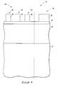
- Substrate 10comprises a base substrate or material 12 , a carbon-comprising material 14 over base material 12 , a hardmask material 16 over carbon-comprising material 14 , and a masking material 20 over hardmask material 16 .
- Base material 12may be homogenous or non-homogenous, and may comprise different composition layers. Such may comprise any one or combination of semiconductive material, insulative material, and conductive material.
- Carbon-comprising material 14may be homogenous or non-homogenous. Examples include amorphous carbon, transparent carbon, and carbon-containing polymers. Example carbon-containing polymers include spin-on-carbons (SOCs). Carbon-comprising material 14 may consist essentially of any one or more of these example materials. An example thickness range for carbon-comprising material 14 is from about 700 Angstroms to about 2,000 Angstroms.
- Hardmask material 16may be homogenous or non-homogenous, and may comprise multiple different composition layers.
- hardmask material 16comprises an antireflective coating, for example a coating comprising Si x O y N z . Regardless, in one embodiment, hardmask material 16 is inorganic.
- Hardmask materialmay also comprise a bottom antireflective coating (BARC), for example between a Si x O y N z -comprising material and masking material 20 .
- BARCbottom antireflective coating
- An example thickness range for hardmask material 16is from 200 Angstroms to 400 Angstroms. Hardmask material 16 is not required in all embodiments.
- Masking material 20may be homogenous or non-homogenous, and may comprise multiple different composition layers.
- One example materialis photoresist.
- FIG. 1depicts masking material 20 as having been patterned to form spaced primary features 18 over hardmask material 16 . Such are depicted as being equal in size and shape relative one another and equally spaced relative to each immediately adjacent feature 18 , although alternate configurations are of course contemplated.
- substrate 10may be considered as comprising an array circuitry area 22 and a peripheral circuitry area 24 , wherein features 18 are at least provided within array circuitry area 22 . The same or other features might additionally be provided in peripheral circuitry area 24 .
- Periphery circuitry area 24is shown as being largely masked by material 20 in the FIG. 1 configuration.
- Primary features 18may or may not be fabricated above, at, or below the minimum photolithographic feature size with which the substrate will ultimately be processed where photolithographic processing is used. Further, primary features 18 may be treated or coated after initial formation.
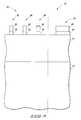
- primary features 18 of FIG. 1have been processed to laterally trim their respective widths, thereby forming spaced first features 26 within array circuitry area 22 .
- Masking material 20 in periphery area 24is also shown as being laterally trimmed. Such may be conducted by an isotropic etch which removes material approximately equally from the sides and top of spaced primary features 18 of FIG. 1 , as is shown. Alternately, chemistries and conditions may be used which tend to etch greater material from the lateral sides of spaced primary features 18 than from the respective tops. Alternately, chemistries and conditions may be used which tend to etch greater material from the tops of spaced mask features 18 than from the lateral sides.
- the construction depicted by FIG. 2may be derived by plasma etching the substrate of FIG. 1 within an inductively coupled reactor.
- Example etching parameters which will achieve essentially isotropic etching where material of spaced mask features 18 is photoresist and/or other organic-comprising materialare pressure from about 2 mTorr to about 50 mTorr, substrate temperature from about 0° C. to about 100° C., source power from about 150 watts to about 500 watts, and bias voltage at less than or equal to about 25 volts.
- An example etching gasis a combination of Cl 2 from about 20 sccm to about 100 sccm and O 2 from about 10 sccm to about 50 sccm.
- spaced primary features 18comprises a photoresist
- material of spaced primary features 18comprises a photoresist
- example parameter ranges in an inductively coupled reactorinclude pressure from about 2 mTorr to about 20 mTorr, source power from about 150 watts to about 500 watts, bias voltage at less than or equal to about 25 volts, substrate temperature of from about 0° C. to about 110° C., Cl 2 and/or HBr flow from about 20 sccm to about 100 sccm, O 2 flow from about 5 sccm to about 20 sccm, and CF 4 flow from about 80 sccm to about 120 sccm.
- the example parameters for achieving greater etch rate in the vertical direction as opposed to the lateral directionincludes pressure from about 2 mTorr to about 20 mTorr, temperature from about 0° C. to about 100° C., source power from about 150 watts to about 300 watts, bias voltage at greater than or equal to about 200 volts, Cl 2 and/or HBr flow from about 200 sccm to about 100 sccm, and O 2 flow from about 10 sccm to about 20 sccm.
- FIGS. 1 and 2depict but one example of forming spaced first features 26 which will be used as an etch mask in example embodiments described below. Any other existing or yet-to-be developed techniques might be used to form spaced first features, and whether or not such are sub-lithographic. Regardless, the spaced first features may or may not be in direct physical touching contact with carbon-comprising material 14 .
- FIG. 2shows one embodiment wherein spaced first features 26 are spaced from carbon-comprising material 14 by hardmasking material 16 . Regardless, in one embodiment, the spaced first features and the carbon-comprising material are of different compositions.
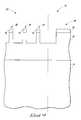
- first etchinghas been conducted through hardmask material 16 using spaced first features 26 as a mask.
- such etchinghas been conducted selectively (rate 2:1 or greater) relative to carbon-comprising material 14 , although such is not required.
- the act of etching through hardmask material 16may also etch into carbon-comprising material 14 .
- FIG. 3depicts some etching having been conducted of masking material 20 , and wherein at least some of the thickness of masking material 20 remains after completion of the etching through masking material 16 .
- hardmask material 16comprises Si x O y N z
- example etching chemistriesinclude any of HBr, CF 4 , or other fluorocarbon chemistries. If all of material 20 were removed in the FIG. 3 etch (not shown), material 16 may be considered as spaced first features.
- etchinghas been conducted only partially into carbon-comprising material 14 .
- Such partial etchingmay be into less than one half, one half, or more than one half of thickness of carbon-comprising material 14 .
- Suchmay be determined or controlled by time of etch.
- FIG. 4depicts an example wherein the partial etching has been into less than one half of thickness of carbon-comprising material 14 .
- carbon-comprising material 14has a thickness of from about 700 Angstroms to about 2,000 Angstroms
- such partial etching into carbon-comprising material 14is into from about 300 Angstroms to about 1,500 Angstroms of material 14 .
- an example anisotropic etching chemistrycomprises a combination of O 2 and SO 2 .
- Example parameters for such etchinginclude a pressure from about 1 mTorr to about 30 mTorr, source power from about 200 Watts to about 1,500 Watts, bias voltage from about 50 volts to about 500 volts, substrate temperature at from about 10° C. to about 70° C., and combined SO 2 and O 2 flow from about 20 sccm to about 500 sccm.
- An alternate example chemistryincludes a combination of O 2 , N 2 , and HBr.
- Example parameters for such etchinginclude a pressure from about 1 mTorr to about 30 mTorr, source power from about 200 Watts to about 1,500 Watts, bias voltage from about 50 volts to about 500 volts, substrate temperature at from about 10° C. to about 70° C., O 2 flow from about 10 sccm to about 300 sccm, N 2 flow from about 10 sccm to about 500 sccm, and HBr flow from about 10 sccm to about 300 sccm.
- FIG. 4depicts an embodiment wherein the partial etching has formed spaced second features 30 within carbon-comprising material 14 which comprise partially etched carbon-comprising material 14 and hardmask material 16 .
- spaced first features 26 of FIG. 2may or may not remain at the conclusion of the example FIG. 3 etching.
- spaced second features 30may or may not comprise material of spaced first features 26 .
- the spaced first featuresmay or may not be completely removed from the substrate at some point. In one embodiment where such are completely removed from the substrate, such act of removing might be completed during the act of etching only partially into carbon-comprising material 14 .
- all remnant of spaced first features 26 from FIG. 2have been etched completely away from the substrate at or prior to completion of the partial etching into carbon-comprising material 14 .
- a spacer-forming layer 32has been deposited over/as part of substrate 10 .
- Suchmay be homogenous or non-homogenous, and may comprise a material different in composition from that of carbon-comprising material 14 .
- Example materialsinclude silicon, silicon-dioxide, and/or silicon nitride. Thickness of spacer-forming layer 32 may be largely determinative of feature width dimensions as will be apparent from the continuing discussion.
- spacer-forming layer 32has been anisotropically etched to form spacers 34 along sidewalls of spaced second features 30 .
- anisotropically etched spacers 34are formed in direct physical touching contact with carbon of carbon-comprising material 14 .
- formation of anisotropically etched spacers 34leaves alternating outwardly exposed regions 35 of carbon-comprising material 14 and hardmask material 16 between immediately adjacent of anisotropically etched spacers 34 .
- a method of forming a pattern on a materialadditionally includes lithographically patterning the peripheral circuitry area after the partial etching into the carbon-comprising material, and in one embodiment after forming the anisotropically etched spacers.
- a suitable masking material 36has been deposited and lithographically patterned within peripheral circuitry area 24 .
- Example masking material 36may be homogenous or non-homogenous, and may comprise multiple different composition layers. Regardless, FIG. 7 depicts masking material 36 having been patterned to form an example feature opening 38 within peripheral circuitry area 24 . Other and/or additional features (not shown) would likely also be formed in peripheral circuitry area 24 .
- second etchinghas been conducted of hardmask material 16 (not shown) from between anisotropically etched spacers 34 . Such has also been conducted relative to example feature opening 38 in peripheral circuitry area 24 . Suitable etching chemistries and conditions may be selected by the artisan for the depicted removal of the hardmasking material 16 as exemplified by FIG. 8 . Such is shown as having been conducted substantially selectively relative to carbon-comprising material 14 and masking material 36 , although such is not required.
- FIG. 9depicts one example embodiment wherein etching of carbon-comprising material 14 has been conducted substantially selectively relative to material 32 of anisotropically etched spacers and selectively relative to hard masking material 16 in peripheral circuitry area 24 .
- Example etching chemistry and conditions to produce the FIG. 9 constructionare the same as that described above in conducting the FIG. 4 etch.
- FIG. 9depicts formation of spaced third features 45 which comprise anisotropically etched spacers 34 and carbon-comprising material 14 .
- FIG. 9also depicts one example pattern formed on a substrate.
- Pattern formationmay continue relative to substrate 10 .
- base material 12may be processed through a mask pattern comprising spaced third features 45 .
- base material 12may be ion implanted or otherwise doped through mask openings defined between spaced third features 45 .
- processingmight comprise etching into base material 12 , as shown by way of example only in FIG. 10 .
- One or more different etching chemistriesmight be utilized depending upon the composition or compositions of material of base material 12 being etched.
- FIG. 10depicts partial etching into base material 12
- FIG. 11depicts subsequent removal of materials 14 , 30 and 16 (not shown) from outwardly of base material 12 .
- FIG. 11depicts but one example of another pattern formed on a substrate by one or more aspects of the above embodiments.
- base material 12may be used to form a pattern of charge storage transistor gate constructions for use in NAND circuitry.
- Example NAND circuitryis described with reference to FIGS. 12 and 13 .
- FIG. 12is a simplified block diagram of an example memory system 100 .
- Suchincludes an integrated circuit NAND flash memory device 102 that includes an array of floating-gate memory cells 104 , an address decoder 106 , row access circuitry 108 , column access circuitry 110 , control circuitry 112 , input/output (I/O) circuitry 114 , and an address buffer 116 .
- Memory system 100includes an external microprocessor 120 electrically connected to memory device 102 for memory accessing as part of an electronic system.
- Memory device 102receives control signals from processor 120 over a control link 122 .
- the memory cellsare used to store data that is accessed via a data (DQ) link 124 .
- Address signalsare received via an address link 126 , and are decoded at address decoder 106 to access the memory array 104 .
- Address buffer circuit 116latches the address signals.
- the memory cellsmay be accessed in response to the control signals and the address signals.
- FIG. 13is a schematic of a NAND memory array 200 . Such may be a portion of memory array 104 of FIG. 18 .
- Memory array 200includes access lines (i.e., wordlines) 202 1 to 202 N , and intersecting local data lines (i.e., bitlines) 204 1 to 204 M .
- the number of wordlines 202 and the number of bitlines 204may be each some power of two, for example 64 wordlines and 64 bitlines.
- the local bitlines 204may be coupled to global bitlines (not shown) in a many-to-one relationship.
- Memory array 200includes NAND strings 206 1 to 206 M .
- Each NAND stringincludes floating gate transistors 208 1 to 208 N .
- the floating gate transistorsare located at intersections of wordlines 202 and a local bitlines 204 .
- the floating gate transistors 208represent non-volatile memory cells for storage of data, or in other words are comprised by flash transistor gates.
- the floating gate transistors 208 of each NAND string 206are connected in series source to drain between a source select gate 210 and a drain select gate 212 .
- Each source select gate 210is located at an intersection of a local bitline 204 and a source select line 214
- each drain select gate 212is located at an intersection of a local bitline 204 and a drain select line 215 .
- a source of each source select gate 210is connected to a common source line 216 .
- the drain of each source select gate 210is connected to the source of the first floating-gate transistor 208 of the corresponding NAND string 206 .
- the drain of source select gate 210 1is connected to the source of floating-gate transistor 208 1 of the corresponding NAND string 206 1 .
- each drain select gate 212is connected to a local bitline 204 for the corresponding NAND string at a drain contact 228 .
- the drain of drain select gate 212 1is connected to the local bitline 204 1 for the corresponding NAND string 206 1 at drain contact 228 1 .
- the source of each drain select gate 212is connected to the drain of the last floating-gate transistor 208 of the corresponding NAND string 206 .
- the source of drain select gate 212 1is connected to the drain of floating gate transistor 208 N of the corresponding NAND string 206 1 .
- Floating gate transistors 208include a source 230 and a drain 232 , a floating gate 234 , and a control gate 236 .
- Floating gate transistors 208have their control gates 236 coupled to a wordline 202 .
- a column of the floating gate transistors 208are those NAND strings 206 coupled to a given local bitline 204 .
- a row of the floating gate transistors 208are those transistors commonly coupled to a given wordline 202 .
- Floating gate transistors 208may be considered as comprising charge storage transistor gate constructions in NAND memory circuitry.
- base material 12may be fabricated to comprise an appropriate stack for forming such constructions.
- FIG. 14depicts one example stack of materials with respect to a substrate fragment 10 a from which an example charge storage transistor gate construction may be fabricated in accordance with any of the above techniques. Like numerals from the above-described embodiments have been utilized where appropriate, with some construction differences being indicated with the suffix “a” or with different numerals.
- base material 12 ais depicted as comprising a stack of different materials.
- material 50may be semiconductor material, such as lightly background-doped monocrystalline silicon of a first or second conductivity type.
- a dielectric material 52 which will function as a tunnel dielectrichas been deposited over semiconductor material 50 . Any existing or yet-to-be developed material is contemplated, with silicon dioxide being an example.
- Tunnel dielectric 52may be homogenous or non-homogenous, for example comprising multiple different composition dielectric layers.
- Floating gate material 54has been deposited over tunnel dielectric material 52 . Such may be homogenous or non-homogenous, with suitably doped silicon being one example.
- Gate dielectric material 66has been deposited over floating gate material 54 . Such may be homogenous or non-homogenous, with a depicted example showing such being comprised of three layers 56 , 58 , and 60 .
- Example materialsinclude one or more of silicon dioxide, hafnium oxide, aluminum oxide, zirconium oxide, hafnium aluminum oxide, hafnium silicon oxide, etc.
- conductive control gate material 62has been deposited over gate dielectric material 66 .
- Suchalso may be homogenous or non-homogenous, and may include multiple different conductive compositions and layers. Examples include conductively doped semiconductive material (i.e., silicon), elemental metals, alloys of elemental metals, and conductive metal compounds.
- a protective sacrificial material 64i.e., SiO 2 and/or Si 3 N 4 ) has been deposited over conductive control gate material 62 .
- the example FIG. 14 stack of a base material 12 amay be etched to form a pattern of charge storage transistor gate constructions using a mask pattern comprising spaced third features as by way of example only described above in connection with FIG. 10 .
- pitch reductionmay or may not be conducted to result in pitch reduction.
- Some existing pitch reduction techniquesprovide a low temperature-deposited spacer directly against photoresist which might be avoided in practice of embodiments of the invention.
- carbon-comprising material 14does not comprise photoresist.
Landscapes
- Engineering & Computer Science (AREA)
- Manufacturing & Machinery (AREA)
- Microelectronics & Electronic Packaging (AREA)
- General Physics & Mathematics (AREA)
- Condensed Matter Physics & Semiconductors (AREA)
- Computer Hardware Design (AREA)
- Physics & Mathematics (AREA)
- Power Engineering (AREA)
- Chemical & Material Sciences (AREA)
- Inorganic Chemistry (AREA)
- Chemical Kinetics & Catalysis (AREA)
- General Chemical & Material Sciences (AREA)
- Drying Of Semiconductors (AREA)
- Semiconductor Memories (AREA)
- Non-Volatile Memory (AREA)
Abstract
Description
Claims (47)
Priority Applications (1)
| Application Number | Priority Date | Filing Date | Title |
|---|---|---|---|
| US12/467,687US9330934B2 (en) | 2009-05-18 | 2009-05-18 | Methods of forming patterns on substrates |
Applications Claiming Priority (1)
| Application Number | Priority Date | Filing Date | Title |
|---|---|---|---|
| US12/467,687US9330934B2 (en) | 2009-05-18 | 2009-05-18 | Methods of forming patterns on substrates |
Publications (2)
| Publication Number | Publication Date |
|---|---|
| US20100291771A1 US20100291771A1 (en) | 2010-11-18 |
| US9330934B2true US9330934B2 (en) | 2016-05-03 |
Family
ID=43068855
Family Applications (1)
| Application Number | Title | Priority Date | Filing Date |
|---|---|---|---|
| US12/467,687ActiveUS9330934B2 (en) | 2009-05-18 | 2009-05-18 | Methods of forming patterns on substrates |
Country Status (1)
| Country | Link |
|---|---|
| US (1) | US9330934B2 (en) |
Cited By (4)
| Publication number | Priority date | Publication date | Assignee | Title |
|---|---|---|---|---|
| US20190019676A1 (en)* | 2017-07-15 | 2019-01-17 | Micromaterials Llc | Mask Scheme For Cut Pattern Flow With Enlarged EPE Window |
| US10224213B2 (en)* | 2016-04-28 | 2019-03-05 | Samsung Electronics Co., Ltd. | Method for forming patterns of a semiconductor device |
| US10522366B2 (en) | 2018-01-10 | 2019-12-31 | Samsung Electronics Co., Ltd. | Method of fabricating semiconductor device |
| US10911810B2 (en)* | 2016-06-20 | 2021-02-02 | Scripps Networks Interactive, Inc. | Non-linear C3 content scheduling and encoding methods |
Families Citing this family (11)
| Publication number | Priority date | Publication date | Assignee | Title |
|---|---|---|---|---|
| JP5563860B2 (en)* | 2010-03-26 | 2014-07-30 | 東京エレクトロン株式会社 | Substrate processing method |
| FR2968122B1 (en) | 2010-11-30 | 2012-12-07 | Commissariat Energie Atomique | IMPROVED PATTERN REALIZATION METHOD FROM LATERAL SPACER TRANSFER |
| FR2963477A1 (en)* | 2010-11-30 | 2012-02-03 | Commissariat Energie Atomique | Material pattern e.g. boron nitride material pattern, forming method for integrated circuit, involves etching covering layer via etching mask to form projecting pattern, and etching material layer via covering layer to form material pattern |
| US20120244693A1 (en)* | 2011-03-22 | 2012-09-27 | Tokyo Electron Limited | Method for patterning a full metal gate structure |
| FR2990794B1 (en) | 2012-05-16 | 2016-11-18 | Commissariat Energie Atomique | METHOD FOR PRODUCING A SUBSTRATE WITH VARIED ACTIVE ZONES AND PLANAR AND THREE DIMENSIONAL TRANSISTORS |
| US8946002B2 (en)* | 2012-07-24 | 2015-02-03 | Semiconductor Components Industries, Llc | Method of forming a semiconductor device having a patterned gate dielectric and structure therefor |
| US8716133B2 (en)* | 2012-08-23 | 2014-05-06 | International Business Machines Corporation | Three photomask sidewall image transfer method |
| KR20220025939A (en)* | 2013-12-23 | 2022-03-03 | 인텔 코포레이션 | Advanced etching techniques for straight, tall and uniform fins across multiple fin pitch structures |
| KR102471380B1 (en)* | 2016-09-19 | 2022-11-25 | 도쿄엘렉트론가부시키가이샤 | How to remove an in situ hard mask |
| WO2020209939A1 (en) | 2019-04-08 | 2020-10-15 | Applied Materials, Inc. | Methods for modifying photoresist profiles and tuning critical dimensions |
| CN113363142B (en)* | 2020-03-05 | 2023-06-09 | 中芯国际集成电路制造(上海)有限公司 | Method for forming semiconductor device |
Citations (243)
| Publication number | Priority date | Publication date | Assignee | Title |
|---|---|---|---|---|
| JPS5646531Y2 (en) | 1976-11-30 | 1981-10-30 | ||
| JPS58157135U (en) | 1982-04-17 | 1983-10-20 | 柳田 信義 | Shiatsu board |
| JPS59211231A (en) | 1983-05-16 | 1984-11-30 | Matsushita Electric Ind Co Ltd | Pattern formation method |
| EP0171111A3 (en) | 1984-07-13 | 1987-07-22 | BELL TELEPHONE MANUFACTURING COMPANY Naamloze Vennootschap | Process to superpose two positive photoresist layers |
| JPS6435916U (en) | 1987-08-28 | 1989-03-03 | ||
| US4910168A (en) | 1988-05-06 | 1990-03-20 | Mos Electronics Corporation | Method to reduce silicon area for via formation |
| US5008207A (en) | 1989-09-11 | 1991-04-16 | International Business Machines Corporation | Method of fabricating a narrow base transistor |
| US5013680A (en) | 1990-07-18 | 1991-05-07 | Micron Technology, Inc. | Process for fabricating a DRAM array having feature widths that transcend the resolution limit of available photolithography |
| US5047117A (en) | 1990-09-26 | 1991-09-10 | Micron Technology, Inc. | Method of forming a narrow self-aligned, annular opening in a masking layer |
| US5254218A (en) | 1992-04-22 | 1993-10-19 | Micron Technology, Inc. | Masking layer having narrow isolated spacings and the method for forming said masking layer and the method for forming narrow isolated trenches defined by said masking layer |
| US5328810A (en) | 1990-05-07 | 1994-07-12 | Micron Technology, Inc. | Method for reducing, by a factor or 2-N, the minimum masking pitch of a photolithographic process |
| JPH0677180B2 (en) | 1985-07-02 | 1994-09-28 | スタンレー電気株式会社 | 3D image display device |
| US5372916A (en) | 1991-09-12 | 1994-12-13 | Hitachi, Ltd. | X-ray exposure method with an X-ray mask comprising phase shifter sidewalls |
| US5382315A (en) | 1991-02-11 | 1995-01-17 | Microelectronics And Computer Technology Corporation | Method of forming etch mask using particle beam deposition |
| US5420067A (en) | 1990-09-28 | 1995-05-30 | The United States Of America As Represented By The Secretary Of The Navy | Method of fabricatring sub-half-micron trenches and holes |
| US5429988A (en) | 1994-06-13 | 1995-07-04 | United Microelectronics Corporation | Process for producing high density conductive lines |
| US5573837A (en) | 1992-04-22 | 1996-11-12 | Micron Technology, Inc. | Masking layer having narrow isolated spacings and the method for forming said masking layer and the method for forming narrow isolated trenches defined by said masking layer |
| US5593813A (en) | 1994-07-14 | 1997-01-14 | Hyundai Electronics Industries Co. Ltd. | Method for forming submicroscopic patterns |
| US5616510A (en) | 1992-11-02 | 1997-04-01 | Wong; Chun C. D. | Method for making multimedia storage system with highly compact memory cells |
| US5905279A (en) | 1996-04-09 | 1999-05-18 | Kabushiki Kaisha Toshiba | Low resistant trench fill for a semiconductor device |
| US5916821A (en) | 1995-07-17 | 1999-06-29 | Siemens Aktiengesellschaft | Method for producing sublithographic etching masks |
| US6063688A (en) | 1997-09-29 | 2000-05-16 | Intel Corporation | Fabrication of deep submicron structures and quantum wire transistors using hard-mask transistor width definition |
| US6087263A (en) | 1998-01-29 | 2000-07-11 | Micron Technology, Inc. | Methods of forming integrated circuitry and integrated circuitry structures |
| US6140217A (en) | 1998-07-16 | 2000-10-31 | International Business Machines Corporation | Technique for extending the limits of photolithography |
| US6174818B1 (en)* | 1999-11-19 | 2001-01-16 | Taiwan Semiconductor Manufacturing Company | Method of patterning narrow gate electrode |
| US6207490B1 (en) | 1997-12-11 | 2001-03-27 | Samsung Electronics Co., Ltd. | Semiconductor device and method for fabricating the same |
| US6235574B1 (en) | 1999-03-22 | 2001-05-22 | Infineon North America Corp. | High performance DRAM and method of manufacture |
| US6249335B1 (en) | 1992-01-17 | 2001-06-19 | Nikon Corporation | Photo-mask and method of exposing and projection-exposing apparatus |
| US6303272B1 (en) | 1998-11-13 | 2001-10-16 | International Business Machines Corporation | Process for self-alignment of sub-critical contacts to wiring |
| US20020037617A1 (en) | 2000-06-29 | 2002-03-28 | Kim Jun Dong | Method for forming gate electrodes in a semicoductor device using formed fine patterns |
| JP3270227B2 (en) | 1993-05-26 | 2002-04-02 | 富士写真フイルム株式会社 | Electric hoist |
| US6383952B1 (en) | 2001-02-28 | 2002-05-07 | Advanced Micro Devices, Inc. | RELACS process to double the frequency or pitch of small feature formation |
| US20020094688A1 (en) | 2001-01-16 | 2002-07-18 | Semiconductor Leading Edge Technologies, Inc. | Method of forming fine patterns |
| US6429123B1 (en) | 2000-10-04 | 2002-08-06 | Vanguard International Semiconductor Corporation | Method of manufacturing buried metal lines having ultra fine features |
| US20020130343A1 (en) | 1999-08-27 | 2002-09-19 | Nec Corporation | Semiconductor device which increases the capacity without deepening the contact hole |
| US6483136B1 (en) | 1997-06-20 | 2002-11-19 | Hitachi, Ltd. | Semiconductor integrated circuit and method of fabricating the same |
| EP1273974A2 (en) | 2001-07-05 | 2003-01-08 | Tokyo Ohka Kogyo Co., Ltd. | Method for reducing a pattern dimension in a photoresist layer |
| US20030006410A1 (en) | 2000-03-01 | 2003-01-09 | Brian Doyle | Quantum wire gate device and method of making same |
| US6545904B2 (en) | 2001-03-16 | 2003-04-08 | Micron Technology, Inc. | 6f2 dram array, a dram array formed on a semiconductive substrate, a method of forming memory cells in a 6f2 dram array and a method of isolating a single row of memory cells in a 6f2 dram array |
| US6548385B1 (en) | 2002-06-12 | 2003-04-15 | Jiun-Ren Lai | Method for reducing pitch between conductive features, and structure formed using the method |
| US6548401B1 (en) | 2002-01-23 | 2003-04-15 | Micron Technology, Inc. | Semiconductor processing methods, and semiconductor constructions |
| US20030091936A1 (en) | 2001-08-31 | 2003-05-15 | Jorg Rottstegge | Process for sidewall amplification of resist structures and for the production of structures having reduced structure size |
| US6566280B1 (en) | 2002-08-26 | 2003-05-20 | Intel Corporation | Forming polymer features on a substrate |
| US6580136B2 (en) | 2001-01-30 | 2003-06-17 | International Business Machines Corporation | Method for delineation of eDRAM support device notched gate |
| KR20030049198A (en) | 2001-12-14 | 2003-06-25 | 주식회사 하이닉스반도체 | Forming method of photoresist pattern improving etching resistance by relacs material |
| KR20030056601A (en) | 2001-12-28 | 2003-07-04 | 주식회사 하이닉스반도체 | Method of forming a source line in flash memory device |
| US6599844B2 (en) | 2000-06-22 | 2003-07-29 | Hyundai Electronics Industries, Co., Ltd. | Method and forming fine patterns of semiconductor devices using passivation layers |
| US6605541B1 (en) | 1998-05-07 | 2003-08-12 | Advanced Micro Devices, Inc. | Pitch reduction using a set of offset masks |
| JP2003234279A (en) | 2002-02-08 | 2003-08-22 | Sony Corp | Forming method of resist pattern, manufacturing method of semiconductor device and forming device for resist pattern |
| US6627524B2 (en) | 2001-06-06 | 2003-09-30 | Micron Technology, Inc. | Methods of forming transistor gates; and methods of forming programmable read-only memory constructions |
| US6630379B2 (en) | 2000-06-23 | 2003-10-07 | International Business Machines Corporation | Method of manufacturing 6F2 trench capacitor DRAM cell having vertical MOSFET and 3F bitline pitch |
| US6638441B2 (en) | 2002-01-07 | 2003-10-28 | Macronix International Co., Ltd. | Method for pitch reduction |
| KR20030089063A (en) | 2002-05-16 | 2003-11-21 | 주식회사 하이닉스반도체 | Forming method of photoresist pattern |
| US6667502B1 (en) | 1999-08-31 | 2003-12-23 | Micron Technology, Inc. | Structurally-stabilized capacitors and method of making of same |
| KR20040016678A (en) | 2002-08-19 | 2004-02-25 | 삼성전자주식회사 | Semiconductor device and method for manufacturing the same |
| US6703323B2 (en) | 2001-12-14 | 2004-03-09 | Hynix Semiconductor Inc | Method of inhibiting pattern collapse using a relacs material |
| US6710390B2 (en) | 1997-07-03 | 2004-03-23 | Micron Technology, Inc. | Capacitors and DRAM arrays |
| JP2004134574A (en) | 2002-10-10 | 2004-04-30 | Renesas Technology Corp | Manufacturing method of semiconductor device |
| US6735132B2 (en) | 2001-07-23 | 2004-05-11 | Micron Technology, Inc. | 6F2 DRAM array with apparatus for stress testing an isolation gate and method |
| US6734107B2 (en) | 2002-06-12 | 2004-05-11 | Macronix International Co., Ltd. | Pitch reduction in semiconductor fabrication |
| US6753220B2 (en) | 1996-11-01 | 2004-06-22 | Micron Technology, Inc. | Semiconductor processing methods of forming devices on a substrate, forming device arrays on a substrate, forming conductive lines on a substrate, and forming capacitor arrays on a substrate, and integrated circuitry |
| US6756619B2 (en) | 2002-08-26 | 2004-06-29 | Micron Technology, Inc. | Semiconductor constructions |
| KR20040057582A (en) | 2002-12-26 | 2004-07-02 | 주식회사 하이닉스반도체 | Method of forming a micro pattern having a dual damascene |
| US6774051B2 (en) | 2002-06-12 | 2004-08-10 | Macronix International Co., Ltd. | Method for reducing pitch |
| JP2004247399A (en) | 2003-02-12 | 2004-09-02 | Renesas Technology Corp | Method for manufacturing semiconductor device |
| US20040198065A1 (en) | 2003-04-04 | 2004-10-07 | Sung-Kwon Lee | Method for fabricating semiconductor device with fine patterns |
| US6826069B2 (en) | 2001-03-14 | 2004-11-30 | Atmos Corporation | Interleaved wordline architecture |
| US20040253535A1 (en) | 2002-11-20 | 2004-12-16 | Shipley Company, L.L.C. | Multilayer photoresist systems |
| US6864184B1 (en) | 2004-02-05 | 2005-03-08 | Advanced Micro Devices, Inc. | Method for reducing critical dimension attainable via the use of an organic conforming layer |
| US6872512B2 (en) | 2002-03-27 | 2005-03-29 | Nec Lcd Technologies, Ltd. | Method of forming resist pattern |
| US6905975B2 (en) | 2003-07-03 | 2005-06-14 | Micron Technology, Inc. | Methods of forming patterned compositions |
| US20050130068A1 (en) | 2003-11-21 | 2005-06-16 | Takehiro Kondoh | Pattern forming method and method for manufacturing a semiconductor device |
| US20050142497A1 (en) | 2003-12-26 | 2005-06-30 | Samsung Electronics Co., Ltd. | Method of forming a pattern in a semiconductor device and method of forming a gate using the same |
| US6916594B2 (en) | 2002-12-30 | 2005-07-12 | Hynix Semiconductor Inc. | Overcoating composition for photoresist and method for forming photoresist pattern using the same |
| US20050164478A1 (en) | 2004-01-26 | 2005-07-28 | Taiwan Semiconductor Manufacturing Co. | Novel method of trimming technology |
| US20050173740A1 (en) | 2004-02-07 | 2005-08-11 | You-Seung Jin | Multi-gate transistor formed with active patterns of uniform critical dimension |
| US20050214683A1 (en) | 2004-02-24 | 2005-09-29 | Tokyo Electron Limited | Method and apparatus for reforming film and controlling slimming amount thereof |
| US6951822B2 (en) | 2001-09-28 | 2005-10-04 | Infineon Technologies North America Corp. | Method for forming inside nitride spacer for deep trench device DRAM cell |
| US20050255696A1 (en) | 2003-05-09 | 2005-11-17 | Fujitsu Limited | Method of processing resist, semiconductor device, and method of producing the same |
| US20050272220A1 (en) | 2004-06-07 | 2005-12-08 | Carlo Waldfried | Ultraviolet curing process for spin-on dielectric materials used in pre-metal and/or shallow trench isolation applications |
| US6977404B2 (en) | 2002-12-27 | 2005-12-20 | Kabushiki Kaisha Toshiba | Trench DRAM with double-gated transistor and method of manufacturing the same |
| US20060011947A1 (en) | 2004-05-26 | 2006-01-19 | Werner Juengling | Semiconductor structures and memory device constructions |
| US20060024621A1 (en) | 2004-07-17 | 2006-02-02 | Infineon Technologies Ag | Method of producing a structure on the surface of a substrate |
| US20060046484A1 (en) | 2004-09-02 | 2006-03-02 | Abatchev Mirzafer K | Method for integrated circuit fabrication using pitch multiplication |
| US20060046200A1 (en) | 2004-09-01 | 2006-03-02 | Abatchev Mirzafer K | Mask material conversion |
| US20060046422A1 (en) | 2004-08-31 | 2006-03-02 | Micron Technology, Inc. | Methods for increasing photo alignment margins |
| US20060063384A1 (en) | 2004-09-23 | 2006-03-23 | Jung-Hwan Hah | Mask patterns for semiconductor device fabrication and related methods and structures |
| US7023069B2 (en) | 2003-12-19 | 2006-04-04 | Third Dimension (3D) Semiconductor, Inc. | Method for forming thick dielectric regions using etched trenches |
| CN1761063A (en) | 2004-10-14 | 2006-04-19 | 茂德科技股份有限公司 | Structure of Dynamic Random Access Memory |
| US20060088788A1 (en) | 2004-10-26 | 2006-04-27 | Takanori Kudo | Composition for coating over a photoresist pattern |
| US7037840B2 (en) | 2004-01-26 | 2006-05-02 | Micron Technology, Inc. | Methods of forming planarized surfaces over semiconductor substrates |
| US7049652B2 (en)* | 2003-12-10 | 2006-05-23 | Sandisk Corporation | Pillar cell flash memory technology |
| US20060115978A1 (en) | 2004-11-30 | 2006-06-01 | Michael Specht | Charge-trapping memory cell and method for production |
| US20060118785A1 (en) | 2003-09-12 | 2006-06-08 | International Business Machines Corporation | Techniques for patterning features in semiconductor devices |
| US7064376B2 (en) | 1996-05-24 | 2006-06-20 | Jeng-Jye Shau | High performance embedded semiconductor memory devices with multiple dimension first-level bit-lines |
| US7067385B2 (en) | 2003-09-04 | 2006-06-27 | Micron Technology, Inc. | Support for vertically oriented capacitors during the formation of a semiconductor device |
| US7074533B2 (en) | 2003-05-05 | 2006-07-11 | Xerox Corporation | Photoconductive members |
| US20060154182A1 (en) | 2005-01-12 | 2006-07-13 | International Business Machines Corporation | Method for post lithographic critical dimension shrinking using post overcoat planarization |
| JP2006245625A (en) | 1997-06-20 | 2006-09-14 | Hitachi Ltd | Semiconductor integrated circuit device and manufacturing method thereof |
| WO2006104654A1 (en) | 2005-03-25 | 2006-10-05 | Micron Technology, Inc. | Methods of forming recessed access devices |
| US7125781B2 (en) | 2003-09-04 | 2006-10-24 | Micron Technology, Inc. | Methods of forming capacitor devices |
| US20060240361A1 (en) | 2005-04-21 | 2006-10-26 | Ji-Young Lee | Method of forming small pitch pattern using double spacers |
| US20060263699A1 (en) | 2005-05-23 | 2006-11-23 | Mirzafer Abatchev | Methods for forming arrays of a small, closely spaced features |
| US20060273456A1 (en) | 2005-06-02 | 2006-12-07 | Micron Technology, Inc., A Corporation | Multiple spacer steps for pitch multiplication |
| US20060278911A1 (en) | 2005-06-14 | 2006-12-14 | Eppich Anton P | Relaxed-pitch method of aligning active area to digit line |
| US20060281266A1 (en) | 2005-06-09 | 2006-12-14 | Wells David H | Method and apparatus for adjusting feature size and position |
| US20060288795A1 (en) | 2005-06-27 | 2006-12-28 | Vishay Measurements Group, Inc. | Strain gage with off axis creep compensation feature |
| US20070003878A1 (en) | 2005-03-23 | 2007-01-04 | Asml Netherlands B.V. | Reduced pitch multiple exposure process |
| US20070010058A1 (en) | 2005-07-08 | 2007-01-11 | Micron Technology, Inc. | Method and apparatus for a self-aligned recessed access device (RAD) transistor gate |
| US7166533B2 (en) | 2005-04-08 | 2007-01-23 | Infineon Technologies, Ag | Phase change memory cell defined by a pattern shrink material process |
| JP2007017993A (en) | 2006-08-22 | 2007-01-25 | Fujitsu Ltd | Resist pattern and method for manufacturing the same, and semiconductor device and method for manufacturing the same |
| US20070020565A1 (en) | 2005-07-25 | 2007-01-25 | Samsung Electronics Co., Ltd. | Methods of fabricating a semiconductor device |
| US20070026684A1 (en) | 2005-08-01 | 2007-02-01 | Stefano Parascandola | Method of producing pitch fractionizations in semiconductor technology |
| US20070023805A1 (en) | 2005-07-26 | 2007-02-01 | Wells David H | Reverse construction memory cell |
| US20070037066A1 (en) | 2005-08-09 | 2007-02-15 | Li-Tung Hsiao | Method for correcting and configuring optical mask pattern |
| US20070049030A1 (en) | 2005-09-01 | 2007-03-01 | Sandhu Gurtej S | Pitch multiplication spacers and methods of forming the same |
| US20070045712A1 (en) | 2005-09-01 | 2007-03-01 | Haller Gordon A | Memory cell layout and process flow |
| US20070049011A1 (en) | 2005-09-01 | 2007-03-01 | Micron Technology, Inc., A Corporation | Method of forming isolated features using pitch multiplication |
| US20070049040A1 (en)* | 2005-03-15 | 2007-03-01 | Micron Technology, Inc., A Corporation | Multiple deposition for integration of spacers in pitch multiplication process |
| US20070048930A1 (en) | 2005-09-01 | 2007-03-01 | Figura Thomas A | Peripheral gate stacks and recessed array gates |
| US20070048674A1 (en) | 2005-09-01 | 2007-03-01 | Wells David H | Methods for forming arrays of small, closely spaced features |
| US20070049035A1 (en) | 2005-08-31 | 2007-03-01 | Tran Luan C | Method of forming pitch multipled contacts |
| US20070049003A1 (en) | 2005-09-01 | 2007-03-01 | John Smythe | Semiconductor constructions and methods of forming layers |
| US7199005B2 (en) | 2005-08-02 | 2007-04-03 | Micron Technology, Inc. | Methods of forming pluralities of capacitors |
| US20070077524A1 (en) | 2005-09-30 | 2007-04-05 | Samsung Electronics Co., Ltd. | Method for forming patterns of semiconductor device |
| US20070077743A1 (en) | 2005-09-30 | 2007-04-05 | Rao Rajesh A | Multiple fin formation |
| US7202174B1 (en) | 2006-02-02 | 2007-04-10 | Hynix Semiconductor Inc. | Method of forming micro pattern in semiconductor device |
| US7202127B2 (en) | 2004-08-27 | 2007-04-10 | Micron Technology, Inc. | Methods of forming a plurality of capacitors |
| US20070085152A1 (en) | 2005-10-14 | 2007-04-19 | Promos Technologies Pte.Ltd. Singapore | Reduced area dynamic random access memory (DRAM) cell and method for fabricating the same |
| US20070099431A1 (en) | 2005-11-01 | 2007-05-03 | Micron Technology, Inc. | Process for increasing feature density during the manufacture of a semiconductor device |
| US20070096182A1 (en) | 2004-09-10 | 2007-05-03 | Infineon Technologies Ag | Transistor, meomory cell array and method of manufacturing a transistor |
| US20070105357A1 (en) | 2005-09-01 | 2007-05-10 | Micron Technology, Inc. | Silicided recessed silicon |
| US20070123015A1 (en) | 2005-11-30 | 2007-05-31 | International Business Machines Corporation | Passive components in the back end of integrated circuits |
| US7230292B2 (en) | 2003-08-05 | 2007-06-12 | Micron Technology, Inc. | Stud electrode and process for making same |
| US20070145464A1 (en) | 2002-08-29 | 2007-06-28 | Voshell Thomas W | Random access memory device utilizing a vertically oriented select transistor |
| US20070161251A1 (en) | 2005-03-15 | 2007-07-12 | Micron Technology, Inc. | Pitch reduced patterns relative to photolithography features |
| KR20070076793A (en) | 2006-01-20 | 2007-07-25 | 주식회사 하이닉스반도체 | Method of forming fine pattern of semiconductor device |
| US20070181929A1 (en) | 2005-06-27 | 2007-08-09 | Micron Technology, Inc. | Semiconductor Constructions, Memory Cells, DRAM Arrays, Electronic Systems; Methods of Forming Semiconductor Constructions; and Methods of Forming DRAM Arrays |
| US20070190463A1 (en) | 2004-09-02 | 2007-08-16 | Micron Technology, Inc. | Method to align mask patterns |
| US20070197014A1 (en) | 2006-02-17 | 2007-08-23 | Samsung Electronics Co., Ltd. | Method of fabricating semiconductor device |
| CN101026087A (en) | 2006-02-24 | 2007-08-29 | 海力士半导体有限公司 | Method for forming fine pattern of semiconductor device |
| US20070202697A1 (en) | 2006-02-24 | 2007-08-30 | Hynix Semiconductor Inc. | Method for forming fine pattern of semiconductor device |
| US20070205443A1 (en) | 2006-03-02 | 2007-09-06 | Werner Juengling | Vertical gated access transistor |
| US20070205438A1 (en) | 2006-03-02 | 2007-09-06 | Werner Juengling | Masking process for simultaneously patterning separate regions |
| US7271108B2 (en) | 2005-06-28 | 2007-09-18 | Lam Research Corporation | Multiple mask process with etch mask stack |
| US20070224537A1 (en) | 2006-03-24 | 2007-09-27 | Fujitsu Limited | Resist composition, method for forming resist pattern, and semiconductor device and method for manufacturing the same |
| US20070238299A1 (en)* | 2006-04-07 | 2007-10-11 | Micron Technology, Inc. | Simplified pitch doubling process flow |
| US20070238053A1 (en) | 2006-04-11 | 2007-10-11 | Koji Hashimoto | Manufacturing method of semiconductor device |
| US20070248916A1 (en) | 2006-04-21 | 2007-10-25 | Tdk Corporation | Resist pattern forming method, thin-film pattern forming method, and microdevice manufacturing method |
| US20070261016A1 (en) | 2006-04-24 | 2007-11-08 | Sandhu Gurtej S | Masking techniques and templates for dense semiconductor fabrication |
| US20070264828A1 (en) | 2006-05-09 | 2007-11-15 | Hynix Semiconductor Inc. | Method for forming fine pattern of semiconductor device |
| US20070264830A1 (en) | 2006-05-10 | 2007-11-15 | Lam Research Corporation | Pitch reduction |
| US20070281488A1 (en) | 2006-06-02 | 2007-12-06 | Wells David H | Methods of fabricating intermediate semiconductor structures by selectively etching pockets of implanted silicon |
| US20070281493A1 (en) | 2006-06-02 | 2007-12-06 | Janos Fucsko | Methods of shaping vertical single crystal silicon walls and resulting structures |
| US20070281219A1 (en)* | 2006-06-01 | 2007-12-06 | Sandhu Gurtej S | Masking techniques and contact imprint reticles for dense semiconductor fabrication |
| US20070278183A1 (en) | 2006-06-02 | 2007-12-06 | Whonchee Lee | Wet etch suitable for creating square cuts in si and resulting structures |
| KR20070122049A (en) | 2006-06-23 | 2007-12-28 | 주식회사 하이닉스반도체 | Micro pattern formation method using double exposure process |
| US20080002475A1 (en) | 2006-06-29 | 2008-01-03 | Samsung Electronics Co., Ltd | Non-volatile memory devices having a vertical channel and methods of manufacturing such devices |
| US20080008969A1 (en) | 2006-07-10 | 2008-01-10 | Micron Technology, Inc. | Pitch reduction technology using alternating spacer depositions during the formation of a semiconductor device and systems including same |
| US7320911B2 (en) | 2004-12-06 | 2008-01-22 | Micron Technology, Inc. | Methods of forming pluralities of capacitors |
| US20080026327A1 (en) | 2006-07-14 | 2008-01-31 | Hynix Semiconductor Inc. | Method for forming fine pattern with a double exposure technology |
| US20080032508A1 (en) | 2006-08-07 | 2008-02-07 | Taiwan Semiconductor Manufacturing Company, Ltd. | Method and Material For Forming A Double Exposure Lithography Pattern |
| US20080032243A1 (en) | 2005-05-30 | 2008-02-07 | Hynix Semiconductor Inc. | Photoresist Coating Composition and Method for Forming Fine Contact of Semiconductor Device |
| US20080044770A1 (en) | 2006-08-17 | 2008-02-21 | Fujitsu Limited | Process for forming resist pattern, semiconductor device and manufacturing method for the same |
| US20080057692A1 (en) | 2006-08-30 | 2008-03-06 | Wells David H | Single spacer process for multiplying pitch by a factor greater than two and related intermediate IC structures |
| US20080063986A1 (en) | 2006-09-12 | 2008-03-13 | Hynix Semiconductor Inc. | Method of forming fine pattern of semiconductor device |
| US20080064213A1 (en) | 2006-09-12 | 2008-03-13 | Hynix Semiconductor Inc. | Method for forming a fine pattern of a semiconductor device |
| US20080070165A1 (en)* | 2006-09-14 | 2008-03-20 | Mark Fischer | Efficient pitch multiplication process |
| US20080076070A1 (en) | 2006-09-08 | 2008-03-27 | Samsung Electronics Co., Ltd. | Methods of Forming Fine Patterns In Integrated Circuits Using Atomic Layer Deposition |
| US20080085612A1 (en) | 2006-10-05 | 2008-04-10 | Micron Technology, Inc. | Method to deposit conformal low temperature SiO2 |
| US20080090416A1 (en) | 2006-10-11 | 2008-04-17 | Micro Technology, Inc. | Methods of etching polysilicon and methods of forming pluralities of capacitors |
| KR20080039006A (en) | 2006-10-31 | 2008-05-07 | 주식회사 하이닉스반도체 | How to form a mask pattern |
| KR20080038963A (en) | 2006-10-31 | 2008-05-07 | 주식회사 하이닉스반도체 | Method for manufacturing a semiconductor device having a contact |
| US20080113511A1 (en) | 2006-11-10 | 2008-05-15 | Sang-Joon Park | Method of forming fine patterns using double patterning process |
| US20080113483A1 (en) | 2006-11-15 | 2008-05-15 | Micron Technology, Inc. | Methods of etching a pattern layer to form staggered heights therein and intermediate semiconductor device structures |
| US20080122125A1 (en) | 2006-11-29 | 2008-05-29 | Micron Technology, Inc. | Methods to reduce the critical dimension of semiconductor devices and partially fabricated semiconductor devices having reduced critical dimensions |
| US7387939B2 (en) | 2004-07-19 | 2008-06-17 | Micron Technology, Inc. | Methods of forming semiconductor structures and capacitor devices |
| US7390749B2 (en) | 2005-11-30 | 2008-06-24 | Lam Research Corporation | Self-aligned pitch reduction |
| US7390750B1 (en) | 2004-03-23 | 2008-06-24 | Cypress Semiconductor Corp. | Method of patterning elements within a semiconductor topography |
| US20080171446A1 (en) | 2007-01-12 | 2008-07-17 | Advanced Micro Devices, Inc. | Method of forming semiconductor device |
| US20080171438A1 (en) | 2007-01-11 | 2008-07-17 | Micron Technology, Inc. | Methods of uniformly removing silicon oxide, a method of removing a sacrifical oxide, and an intermediate semiconductor device structure |
| US20080176406A1 (en) | 2007-01-22 | 2008-07-24 | Shuji Ikeda | Methods for Fabricating Semiconductor Structures |
| US20080193658A1 (en) | 2007-02-08 | 2008-08-14 | Micron Technology, Inc. | Methods using block copolymer self-assembly for sub-lithographic patterning |
| US20080199806A1 (en) | 2007-02-16 | 2008-08-21 | Shin-Etsu Chemical Co., Ltd. | Patterning process and resist composition |
| US20080199814A1 (en) | 2006-12-06 | 2008-08-21 | Fujifilm Electronic Materials, U.S.A., Inc. | Device manufacturing process utilizing a double patterning process |
| US20080206950A1 (en) | 2007-02-26 | 2008-08-28 | Micron Technology, Inc. | Methods of forming a plurality of capacitors |
| US20080210900A1 (en) | 2005-05-13 | 2008-09-04 | William Wojtczak | Selective Wet Etchings Of Oxides |
| US20080220600A1 (en) | 2007-03-05 | 2008-09-11 | Micron Technology, Inc. | Semiconductor constructions, methods of forming multiple lines, and methods of forming high density structures and low density structures with a single photomask |
| US7439152B2 (en) | 2004-08-27 | 2008-10-21 | Micron Technology, Inc. | Methods of forming a plurality of capacitors |
| US20080261349A1 (en) | 2005-09-01 | 2008-10-23 | Micron Technology, Inc. | Protective coating for planarization |
| US7442976B2 (en) | 2004-09-01 | 2008-10-28 | Micron Technology, Inc. | DRAM cells with vertical transistors |
| US20080292991A1 (en) | 2007-05-24 | 2008-11-27 | Advanced Micro Devices, Inc. | High fidelity multiple resist patterning |
| US20080296732A1 (en) | 2007-05-31 | 2008-12-04 | Micron Technology, Inc. | Methods of isolating array features during pitch doubling processes and semiconductor device structures having isolated array features |
| US20080305636A1 (en) | 2007-06-07 | 2008-12-11 | Samsung Electronics Co., Ltd. | Method of forming fine pattern employing self-aligned double patterning |
| US20090011374A1 (en) | 2005-08-24 | 2009-01-08 | Ching-Yu Chang | Method and material for forming high etch resistant double exposure patterns |
| US20090074958A1 (en) | 2007-09-13 | 2009-03-19 | Dequan Xiao | Polymeric nanocompositions comprising self-assembled organic quantum dots |
| US7517753B2 (en) | 2005-05-18 | 2009-04-14 | Micron Technology, Inc. | Methods of forming pluralities of capacitors |
| US7521378B2 (en) | 2004-07-01 | 2009-04-21 | Micron Technology, Inc. | Low temperature process for polysilazane oxidation/densification |
| US7521371B2 (en) | 2006-08-21 | 2009-04-21 | Micron Technology, Inc. | Methods of forming semiconductor constructions having lines |
| US7524607B2 (en) | 2003-11-17 | 2009-04-28 | Taiwan Semiconductor Manufacturing Co., Ltd. | Water soluble negative tone photoresist |
| US20090108415A1 (en) | 2007-10-31 | 2009-04-30 | Markus Lenski | Increasing etch selectivity during the patterning of a contact structure of a semiconductor device |
| US20090117739A1 (en)* | 2007-11-02 | 2009-05-07 | Hynix Semiconductor Inc. | Method for forming pattern in semiconductor device |
| US20090130612A1 (en) | 2007-11-21 | 2009-05-21 | Macronix International Co., Ltd. | Patterning process |
| US20090130601A1 (en) | 2007-11-16 | 2009-05-21 | Young-Doo Jeon | Method for fabricating semiconductor device |
| US20090130852A1 (en) | 2006-04-25 | 2009-05-21 | Micron Technology, Inc. | Process for improving critical dimension uniformity of integrated circuit arrays |
| US7537866B2 (en) | 2006-05-24 | 2009-05-26 | Synopsys, Inc. | Patterning a single integrated circuit layer using multiple masks and multiple masking layers |
| US7544563B2 (en) | 2005-05-18 | 2009-06-09 | Micron Technology, Inc. | Methods of forming a plurality of capacitors |
| US7553760B2 (en) | 2006-10-19 | 2009-06-30 | International Business Machines Corporation | Sub-lithographic nano interconnect structures, and method for forming same |
| US7557013B2 (en) | 2006-04-10 | 2009-07-07 | Micron Technology, Inc. | Methods of forming a plurality of capacitors |
| US7557015B2 (en) | 2005-03-18 | 2009-07-07 | Micron Technology, Inc. | Methods of forming pluralities of capacitors |
| US20090214823A1 (en) | 2008-02-22 | 2009-08-27 | International Business Machines Corporation | Methods for aligning polymer films and related structures |
| US20090291397A1 (en) | 2008-05-22 | 2009-11-26 | Devilliers Anton | Methods Of Forming Structures Supported By Semiconductor Substrates |
| US20090298274A1 (en) | 2008-05-29 | 2009-12-03 | Seiji Kajiwara | Method of fabricating semiconductor device |
| US20100009512A1 (en) | 2008-07-09 | 2010-01-14 | Fred Fishburn | Methods of forming a plurality of capacitors |
| US20100021573A1 (en) | 2008-07-22 | 2010-01-28 | Michael J Gonzalez | Compositions and methods for the prevention of cardiovascular disease |
| US20100028809A1 (en) | 2006-11-14 | 2010-02-04 | Nxp, B.V. | Double patterning for lithography to increase feature spatial density |
| US20100068656A1 (en) | 2008-09-15 | 2010-03-18 | Taiwan Semiconductor Manufacturing Co., Ltd. | High etch resistant material for double patterning |
| US7682924B2 (en) | 2007-08-13 | 2010-03-23 | Micron Technology, Inc. | Methods of forming a plurality of capacitors |
| US7687387B2 (en) | 2007-08-23 | 2010-03-30 | Kabushiki Kaisha Toshiba | Semiconductor device and method of manufacturing the same |
| US20100081265A1 (en) | 2008-09-30 | 2010-04-01 | Hiromitsu Mashita | Method for manufacturing semiconductor device |
| US7696076B2 (en) | 2007-05-11 | 2010-04-13 | Hynix Semiconductor Inc. | Method of fabricating flash memory device |
| US20100093175A1 (en) | 2008-10-09 | 2010-04-15 | Ardavan Niroomand | Methods Of Forming Patterns Utilizing Lithography And Spacers |
| US7713818B2 (en) | 2008-04-11 | 2010-05-11 | Sandisk 3D, Llc | Double patterning method |
| US20100124826A1 (en) | 2008-11-17 | 2010-05-20 | Dan Millward | Methods Of Utilizing Block Copolymer To Form Patterns |
| US20100129980A1 (en) | 2008-11-26 | 2010-05-27 | Sandhu Gurtej S | Methods Of Forming Diodes |
| US20100130015A1 (en) | 2007-06-08 | 2010-05-27 | Tokyo Electron Limited | Patterning method |
| US20100130016A1 (en) | 2008-11-24 | 2010-05-27 | Micron Technology, Inc. | Methods of forming a masking pattern for integrated circuits |
| US20100144153A1 (en) | 2008-12-04 | 2010-06-10 | Scott Sills | Methods of Fabricating Substrates |
| US20100144151A1 (en) | 2008-12-04 | 2010-06-10 | Scott Sills | Methods of Fabricating Substrates |
| US20100144150A1 (en) | 2008-12-04 | 2010-06-10 | Micron Technology, Inc. | Methods of Fabricating Substrates |
| US7851135B2 (en) | 2007-11-30 | 2010-12-14 | Hynix Semiconductor Inc. | Method of forming an etching mask pattern from developed negative and positive photoresist layers |
| US20110018055A1 (en) | 2009-07-21 | 2011-01-27 | Kabushiki Kaisha Toshiba | Power semiconductor device and method for manufacturing same |
| US7923371B2 (en) | 2008-04-02 | 2011-04-12 | Kabushiki Kaisha Toshiba | Method of manufacturing semiconductor device having contact plugs |
| US20110127677A1 (en) | 2008-02-15 | 2011-06-02 | Renesas Electronics Corporation | Method of manufacturing semiconductor device, and semiconductor device |
| US20110147984A1 (en) | 2009-12-18 | 2011-06-23 | Joy Cheng | Methods of directed self-assembly, and layered structures formed therefrom |
| CN101145515B (en) | 2006-09-12 | 2011-06-29 | 海力士半导体有限公司 | Method for forming a fine pattern of a semiconductor device |
| US8083953B2 (en) | 2007-03-06 | 2011-12-27 | Micron Technology, Inc. | Registered structure formation via the application of directed thermal energy to diblock copolymer films |
| US8083958B2 (en) | 2007-12-05 | 2011-12-27 | International Business Machines Corporation | Patterning method using a combination of photolithography and copolymer self-assemblying lithography techniques |
| US20130078574A1 (en) | 2010-06-04 | 2013-03-28 | Asml Netherlands B.V. | Self-assemblable polymer and method for use in lithography |
| US8440576B2 (en) | 2008-04-25 | 2013-05-14 | Macronix International Co., Ltd. | Method for pitch reduction in integrated circuit fabrication |
| US8575032B2 (en) | 2011-05-05 | 2013-11-05 | Micron Technology, Inc. | Methods of forming a pattern on a substrate |
| US8629048B1 (en) | 2012-07-06 | 2014-01-14 | Micron Technology, Inc. | Methods of forming a pattern on a substrate |
| US8629527B2 (en) | 2008-05-05 | 2014-01-14 | Micron Technology, Inc. | Semiconductor structures |
Family Cites Families (2)
| Publication number | Priority date | Publication date | Assignee | Title |
|---|---|---|---|---|
| US6725132B2 (en)* | 2002-06-20 | 2004-04-20 | Minebea Co., Ltd. | Intelligent cooling fan |
| US7510400B2 (en)* | 2007-03-14 | 2009-03-31 | Visteon Global Technologies, Inc. | LED interconnect spring clip assembly |
- 2009
- 2009-05-18USUS12/467,687patent/US9330934B2/enactiveActive
Patent Citations (300)
| Publication number | Priority date | Publication date | Assignee | Title |
|---|---|---|---|---|
| JPS5646531Y2 (en) | 1976-11-30 | 1981-10-30 | ||
| JPS58157135U (en) | 1982-04-17 | 1983-10-20 | 柳田 信義 | Shiatsu board |
| JPS59211231A (en) | 1983-05-16 | 1984-11-30 | Matsushita Electric Ind Co Ltd | Pattern formation method |
| EP0171111A3 (en) | 1984-07-13 | 1987-07-22 | BELL TELEPHONE MANUFACTURING COMPANY Naamloze Vennootschap | Process to superpose two positive photoresist layers |
| JPH0677180B2 (en) | 1985-07-02 | 1994-09-28 | スタンレー電気株式会社 | 3D image display device |
| JPS6435916U (en) | 1987-08-28 | 1989-03-03 | ||
| US4910168A (en) | 1988-05-06 | 1990-03-20 | Mos Electronics Corporation | Method to reduce silicon area for via formation |
| US5008207A (en) | 1989-09-11 | 1991-04-16 | International Business Machines Corporation | Method of fabricating a narrow base transistor |
| US5328810A (en) | 1990-05-07 | 1994-07-12 | Micron Technology, Inc. | Method for reducing, by a factor or 2-N, the minimum masking pitch of a photolithographic process |
| US5013680A (en) | 1990-07-18 | 1991-05-07 | Micron Technology, Inc. | Process for fabricating a DRAM array having feature widths that transcend the resolution limit of available photolithography |
| US5047117A (en) | 1990-09-26 | 1991-09-10 | Micron Technology, Inc. | Method of forming a narrow self-aligned, annular opening in a masking layer |
| US5420067A (en) | 1990-09-28 | 1995-05-30 | The United States Of America As Represented By The Secretary Of The Navy | Method of fabricatring sub-half-micron trenches and holes |
| US5382315A (en) | 1991-02-11 | 1995-01-17 | Microelectronics And Computer Technology Corporation | Method of forming etch mask using particle beam deposition |
| US5372916A (en) | 1991-09-12 | 1994-12-13 | Hitachi, Ltd. | X-ray exposure method with an X-ray mask comprising phase shifter sidewalls |
| US6249335B1 (en) | 1992-01-17 | 2001-06-19 | Nikon Corporation | Photo-mask and method of exposing and projection-exposing apparatus |
| US5573837A (en) | 1992-04-22 | 1996-11-12 | Micron Technology, Inc. | Masking layer having narrow isolated spacings and the method for forming said masking layer and the method for forming narrow isolated trenches defined by said masking layer |
| US5254218A (en) | 1992-04-22 | 1993-10-19 | Micron Technology, Inc. | Masking layer having narrow isolated spacings and the method for forming said masking layer and the method for forming narrow isolated trenches defined by said masking layer |
| US5616510A (en) | 1992-11-02 | 1997-04-01 | Wong; Chun C. D. | Method for making multimedia storage system with highly compact memory cells |
| JP3270227B2 (en) | 1993-05-26 | 2002-04-02 | 富士写真フイルム株式会社 | Electric hoist |
| US5429988A (en) | 1994-06-13 | 1995-07-04 | United Microelectronics Corporation | Process for producing high density conductive lines |
| US5593813A (en) | 1994-07-14 | 1997-01-14 | Hyundai Electronics Industries Co. Ltd. | Method for forming submicroscopic patterns |
| US5916821A (en) | 1995-07-17 | 1999-06-29 | Siemens Aktiengesellschaft | Method for producing sublithographic etching masks |
| US5905279A (en) | 1996-04-09 | 1999-05-18 | Kabushiki Kaisha Toshiba | Low resistant trench fill for a semiconductor device |
| US7064376B2 (en) | 1996-05-24 | 2006-06-20 | Jeng-Jye Shau | High performance embedded semiconductor memory devices with multiple dimension first-level bit-lines |
| US6753220B2 (en) | 1996-11-01 | 2004-06-22 | Micron Technology, Inc. | Semiconductor processing methods of forming devices on a substrate, forming device arrays on a substrate, forming conductive lines on a substrate, and forming capacitor arrays on a substrate, and integrated circuitry |
| US7042038B2 (en) | 1997-06-20 | 2006-05-09 | Hitachi, Ltd. | Semiconductor integrated circuit device and manufacturing method thereof |
| US6483136B1 (en) | 1997-06-20 | 2002-11-19 | Hitachi, Ltd. | Semiconductor integrated circuit and method of fabricating the same |
| US20040043546A1 (en) | 1997-06-20 | 2004-03-04 | Makoto Yoshida | Semiconductor integrated circuit device and manufacturing method thereof |
| US6649956B2 (en) | 1997-06-20 | 2003-11-18 | Hitachi, Ltd. | Semiconductor integrated circuit device and manufacturing method thereof |
| US20030001214A1 (en) | 1997-06-20 | 2003-01-02 | Makoto Yoshida | Semiconductor integrated circuit device and manufacturing method thereof |
| JP2006245625A (en) | 1997-06-20 | 2006-09-14 | Hitachi Ltd | Semiconductor integrated circuit device and manufacturing method thereof |
| US6710390B2 (en) | 1997-07-03 | 2004-03-23 | Micron Technology, Inc. | Capacitors and DRAM arrays |
| US20020043690A1 (en) | 1997-09-29 | 2002-04-18 | Doyle Brian S. | Fabrication of deep submicron structures and quantum wire transistors using hard-mask transistor width definition |
| US6063688A (en) | 1997-09-29 | 2000-05-16 | Intel Corporation | Fabrication of deep submicron structures and quantum wire transistors using hard-mask transistor width definition |
| US6207490B1 (en) | 1997-12-11 | 2001-03-27 | Samsung Electronics Co., Ltd. | Semiconductor device and method for fabricating the same |
| US6087263A (en) | 1998-01-29 | 2000-07-11 | Micron Technology, Inc. | Methods of forming integrated circuitry and integrated circuitry structures |
| US6352932B1 (en)* | 1998-01-29 | 2002-03-05 | Micron Technology, Inc. | Methods of forming integrated circuitry and integrated circuitry structures |
| US6605541B1 (en) | 1998-05-07 | 2003-08-12 | Advanced Micro Devices, Inc. | Pitch reduction using a set of offset masks |
| US6140217A (en) | 1998-07-16 | 2000-10-31 | International Business Machines Corporation | Technique for extending the limits of photolithography |
| US6303272B1 (en) | 1998-11-13 | 2001-10-16 | International Business Machines Corporation | Process for self-alignment of sub-critical contacts to wiring |
| US6235574B1 (en) | 1999-03-22 | 2001-05-22 | Infineon North America Corp. | High performance DRAM and method of manufacture |
| US20020130343A1 (en) | 1999-08-27 | 2002-09-19 | Nec Corporation | Semiconductor device which increases the capacity without deepening the contact hole |
| US6667502B1 (en) | 1999-08-31 | 2003-12-23 | Micron Technology, Inc. | Structurally-stabilized capacitors and method of making of same |
| US6174818B1 (en)* | 1999-11-19 | 2001-01-16 | Taiwan Semiconductor Manufacturing Company | Method of patterning narrow gate electrode |
| US20050215040A1 (en) | 2000-03-01 | 2005-09-29 | Brian Doyle | Quantum wire gate device and method of making same |
| US20030006410A1 (en) | 2000-03-01 | 2003-01-09 | Brian Doyle | Quantum wire gate device and method of making same |
| US6599844B2 (en) | 2000-06-22 | 2003-07-29 | Hyundai Electronics Industries, Co., Ltd. | Method and forming fine patterns of semiconductor devices using passivation layers |
| US6630379B2 (en) | 2000-06-23 | 2003-10-07 | International Business Machines Corporation | Method of manufacturing 6F2 trench capacitor DRAM cell having vertical MOSFET and 3F bitline pitch |
| US20020037617A1 (en) | 2000-06-29 | 2002-03-28 | Kim Jun Dong | Method for forming gate electrodes in a semicoductor device using formed fine patterns |
| US6429123B1 (en) | 2000-10-04 | 2002-08-06 | Vanguard International Semiconductor Corporation | Method of manufacturing buried metal lines having ultra fine features |
| JP2002217170A (en) | 2001-01-16 | 2002-08-02 | Semiconductor Leading Edge Technologies Inc | Method of forming fine pattern, method of fabricating semiconductor device and semiconductor device |
| US20020094688A1 (en) | 2001-01-16 | 2002-07-18 | Semiconductor Leading Edge Technologies, Inc. | Method of forming fine patterns |
| US6580136B2 (en) | 2001-01-30 | 2003-06-17 | International Business Machines Corporation | Method for delineation of eDRAM support device notched gate |
| US6383952B1 (en) | 2001-02-28 | 2002-05-07 | Advanced Micro Devices, Inc. | RELACS process to double the frequency or pitch of small feature formation |
| US6826069B2 (en) | 2001-03-14 | 2004-11-30 | Atmos Corporation | Interleaved wordline architecture |
| US6545904B2 (en) | 2001-03-16 | 2003-04-08 | Micron Technology, Inc. | 6f2 dram array, a dram array formed on a semiconductive substrate, a method of forming memory cells in a 6f2 dram array and a method of isolating a single row of memory cells in a 6f2 dram array |
| US6627524B2 (en) | 2001-06-06 | 2003-09-30 | Micron Technology, Inc. | Methods of forming transistor gates; and methods of forming programmable read-only memory constructions |
| US6811817B2 (en) | 2001-07-05 | 2004-11-02 | Tokyo Ohka Kogyo Co., Ltd. | Method for reducing pattern dimension in photoresist layer |
| US20060099347A1 (en) | 2001-07-05 | 2006-05-11 | Yoshiki Sugeta | Method for reducing pattern dimension in photoresist layer |
| US20030096903A1 (en) | 2001-07-05 | 2003-05-22 | Yoshiki Sugeta | Method for reducing pattern dimension in photoresist layer |
| US20050058950A1 (en) | 2001-07-05 | 2005-03-17 | Yoshiki Sugeta | Method for reducing pattern dimension in photoresist layer |
| EP1273974A2 (en) | 2001-07-05 | 2003-01-08 | Tokyo Ohka Kogyo Co., Ltd. | Method for reducing a pattern dimension in a photoresist layer |
| US20030008968A1 (en) | 2001-07-05 | 2003-01-09 | Yoshiki Sugeta | Method for reducing pattern dimension in photoresist layer |
| US6735132B2 (en) | 2001-07-23 | 2004-05-11 | Micron Technology, Inc. | 6F2 DRAM array with apparatus for stress testing an isolation gate and method |
| US6893972B2 (en) | 2001-08-31 | 2005-05-17 | Infineon Technologies Ag | Process for sidewall amplification of resist structures and for the production of structures having reduced structure size |
| US20030091936A1 (en) | 2001-08-31 | 2003-05-15 | Jorg Rottstegge | Process for sidewall amplification of resist structures and for the production of structures having reduced structure size |
| US6951822B2 (en) | 2001-09-28 | 2005-10-04 | Infineon Technologies North America Corp. | Method for forming inside nitride spacer for deep trench device DRAM cell |
| US6703323B2 (en) | 2001-12-14 | 2004-03-09 | Hynix Semiconductor Inc | Method of inhibiting pattern collapse using a relacs material |
| KR20030049198A (en) | 2001-12-14 | 2003-06-25 | 주식회사 하이닉스반도체 | Forming method of photoresist pattern improving etching resistance by relacs material |
| KR20030056601A (en) | 2001-12-28 | 2003-07-04 | 주식회사 하이닉스반도체 | Method of forming a source line in flash memory device |
| US6638441B2 (en) | 2002-01-07 | 2003-10-28 | Macronix International Co., Ltd. | Method for pitch reduction |
| US6548401B1 (en) | 2002-01-23 | 2003-04-15 | Micron Technology, Inc. | Semiconductor processing methods, and semiconductor constructions |
| JP2003234279A (en) | 2002-02-08 | 2003-08-22 | Sony Corp | Forming method of resist pattern, manufacturing method of semiconductor device and forming device for resist pattern |
| US6872512B2 (en) | 2002-03-27 | 2005-03-29 | Nec Lcd Technologies, Ltd. | Method of forming resist pattern |
| KR20030089063A (en) | 2002-05-16 | 2003-11-21 | 주식회사 하이닉스반도체 | Forming method of photoresist pattern |
| US6548385B1 (en) | 2002-06-12 | 2003-04-15 | Jiun-Ren Lai | Method for reducing pitch between conductive features, and structure formed using the method |
| US6774051B2 (en) | 2002-06-12 | 2004-08-10 | Macronix International Co., Ltd. | Method for reducing pitch |
| US6734107B2 (en) | 2002-06-12 | 2004-05-11 | Macronix International Co., Ltd. | Pitch reduction in semiconductor fabrication |
| KR20040016678A (en) | 2002-08-19 | 2004-02-25 | 삼성전자주식회사 | Semiconductor device and method for manufacturing the same |
| US6566280B1 (en) | 2002-08-26 | 2003-05-20 | Intel Corporation | Forming polymer features on a substrate |
| US6756619B2 (en) | 2002-08-26 | 2004-06-29 | Micron Technology, Inc. | Semiconductor constructions |
| US20070145464A1 (en) | 2002-08-29 | 2007-06-28 | Voshell Thomas W | Random access memory device utilizing a vertically oriented select transistor |
| JP2004134574A (en) | 2002-10-10 | 2004-04-30 | Renesas Technology Corp | Manufacturing method of semiconductor device |
| US20040253535A1 (en) | 2002-11-20 | 2004-12-16 | Shipley Company, L.L.C. | Multilayer photoresist systems |
| CN1550889B (en) | 2002-11-20 | 2011-08-03 | 希普雷公司 | Multilayer Photoresist System |
| US7582412B2 (en) | 2002-11-20 | 2009-09-01 | Rohm And Haas Electronic Materials Llc | Multilayer photoresist systems |
| KR20040057582A (en) | 2002-12-26 | 2004-07-02 | 주식회사 하이닉스반도체 | Method of forming a micro pattern having a dual damascene |
| US6977404B2 (en) | 2002-12-27 | 2005-12-20 | Kabushiki Kaisha Toshiba | Trench DRAM with double-gated transistor and method of manufacturing the same |
| US6916594B2 (en) | 2002-12-30 | 2005-07-12 | Hynix Semiconductor Inc. | Overcoating composition for photoresist and method for forming photoresist pattern using the same |
| JP2004247399A (en) | 2003-02-12 | 2004-09-02 | Renesas Technology Corp | Method for manufacturing semiconductor device |
| US20040198065A1 (en) | 2003-04-04 | 2004-10-07 | Sung-Kwon Lee | Method for fabricating semiconductor device with fine patterns |
| US7074533B2 (en) | 2003-05-05 | 2006-07-11 | Xerox Corporation | Photoconductive members |
| US20050255696A1 (en) | 2003-05-09 | 2005-11-17 | Fujitsu Limited | Method of processing resist, semiconductor device, and method of producing the same |
| US6905975B2 (en) | 2003-07-03 | 2005-06-14 | Micron Technology, Inc. | Methods of forming patterned compositions |
| US7230292B2 (en) | 2003-08-05 | 2007-06-12 | Micron Technology, Inc. | Stud electrode and process for making same |
| US7067385B2 (en) | 2003-09-04 | 2006-06-27 | Micron Technology, Inc. | Support for vertically oriented capacitors during the formation of a semiconductor device |
| US7125781B2 (en) | 2003-09-04 | 2006-10-24 | Micron Technology, Inc. | Methods of forming capacitor devices |
| US20060118785A1 (en) | 2003-09-12 | 2006-06-08 | International Business Machines Corporation | Techniques for patterning features in semiconductor devices |
| US7524607B2 (en) | 2003-11-17 | 2009-04-28 | Taiwan Semiconductor Manufacturing Co., Ltd. | Water soluble negative tone photoresist |
| US20050130068A1 (en) | 2003-11-21 | 2005-06-16 | Takehiro Kondoh | Pattern forming method and method for manufacturing a semiconductor device |
| US7049652B2 (en)* | 2003-12-10 | 2006-05-23 | Sandisk Corporation | Pillar cell flash memory technology |
| US7023069B2 (en) | 2003-12-19 | 2006-04-04 | Third Dimension (3D) Semiconductor, Inc. | Method for forming thick dielectric regions using etched trenches |
| US7339252B2 (en) | 2003-12-19 | 2008-03-04 | Third Dimension (3D) Semiconductor, Inc. | Semiconductor having thick dielectric regions |
| US20050142497A1 (en) | 2003-12-26 | 2005-06-30 | Samsung Electronics Co., Ltd. | Method of forming a pattern in a semiconductor device and method of forming a gate using the same |
| US7037840B2 (en) | 2004-01-26 | 2006-05-02 | Micron Technology, Inc. | Methods of forming planarized surfaces over semiconductor substrates |
| US20050164478A1 (en) | 2004-01-26 | 2005-07-28 | Taiwan Semiconductor Manufacturing Co. | Novel method of trimming technology |
| US6864184B1 (en) | 2004-02-05 | 2005-03-08 | Advanced Micro Devices, Inc. | Method for reducing critical dimension attainable via the use of an organic conforming layer |
| US20050173740A1 (en) | 2004-02-07 | 2005-08-11 | You-Seung Jin | Multi-gate transistor formed with active patterns of uniform critical dimension |
| US20100040980A1 (en) | 2004-02-24 | 2010-02-18 | Tokyo Electon Limited | Method and apparatus for reforming film and controlling slimming amount thereof |
| US20050214683A1 (en) | 2004-02-24 | 2005-09-29 | Tokyo Electron Limited | Method and apparatus for reforming film and controlling slimming amount thereof |
| US7390750B1 (en) | 2004-03-23 | 2008-06-24 | Cypress Semiconductor Corp. | Method of patterning elements within a semiconductor topography |
| US7098105B2 (en) | 2004-05-26 | 2006-08-29 | Micron Technology, Inc. | Methods for forming semiconductor structures |
| US20060011947A1 (en) | 2004-05-26 | 2006-01-19 | Werner Juengling | Semiconductor structures and memory device constructions |
| US20050272220A1 (en) | 2004-06-07 | 2005-12-08 | Carlo Waldfried | Ultraviolet curing process for spin-on dielectric materials used in pre-metal and/or shallow trench isolation applications |
| US7521378B2 (en) | 2004-07-01 | 2009-04-21 | Micron Technology, Inc. | Low temperature process for polysilazane oxidation/densification |
| US20060024621A1 (en) | 2004-07-17 | 2006-02-02 | Infineon Technologies Ag | Method of producing a structure on the surface of a substrate |
| US7387939B2 (en) | 2004-07-19 | 2008-06-17 | Micron Technology, Inc. | Methods of forming semiconductor structures and capacitor devices |
| US7202127B2 (en) | 2004-08-27 | 2007-04-10 | Micron Technology, Inc. | Methods of forming a plurality of capacitors |
| US7439152B2 (en) | 2004-08-27 | 2008-10-21 | Micron Technology, Inc. | Methods of forming a plurality of capacitors |
| US20060046422A1 (en) | 2004-08-31 | 2006-03-02 | Micron Technology, Inc. | Methods for increasing photo alignment margins |
| US7151040B2 (en) | 2004-08-31 | 2006-12-19 | Micron Technology, Inc. | Methods for increasing photo alignment margins |
| US20060046200A1 (en) | 2004-09-01 | 2006-03-02 | Abatchev Mirzafer K | Mask material conversion |
| US7442976B2 (en) | 2004-09-01 | 2008-10-28 | Micron Technology, Inc. | DRAM cells with vertical transistors |
| US7115525B2 (en) | 2004-09-02 | 2006-10-03 | Micron Technology, Inc. | Method for integrated circuit fabrication using pitch multiplication |
| US20060262511A1 (en) | 2004-09-02 | 2006-11-23 | Abatchev Mirzafer K | Method for integrated circuit fabrication using pitch multiplication |
| US20070190463A1 (en) | 2004-09-02 | 2007-08-16 | Micron Technology, Inc. | Method to align mask patterns |
| US20060046484A1 (en) | 2004-09-02 | 2006-03-02 | Abatchev Mirzafer K | Method for integrated circuit fabrication using pitch multiplication |
| US20070148984A1 (en)* | 2004-09-02 | 2007-06-28 | Micron Technology, Inc. | Method for integrated circuit fabrication using pitch multiplication |
| US20070096182A1 (en) | 2004-09-10 | 2007-05-03 | Infineon Technologies Ag | Transistor, meomory cell array and method of manufacturing a transistor |
| US7361609B2 (en) | 2004-09-23 | 2008-04-22 | Samsung Electronics Co., Ltd. | Mask patterns for semiconductor device fabrication and related methods |
| CN1752844B (en) | 2004-09-23 | 2010-08-25 | 三星电子株式会社 | Mask patterns for semiconductor device fabrication and related methods and structures |
| US20060063384A1 (en) | 2004-09-23 | 2006-03-23 | Jung-Hwan Hah | Mask patterns for semiconductor device fabrication and related methods and structures |
| US20080176152A1 (en) | 2004-09-23 | 2008-07-24 | Samsung Electronics Co., Ltd. | Mask Patterns for Semiconductor Device Fabrication and Related Methods and Structures |
| US7855038B2 (en) | 2004-09-23 | 2010-12-21 | Samsung Electronics Co., Ltd. | Mask patterns for semiconductor device fabrication and related methods and structures |
| CN1761063A (en) | 2004-10-14 | 2006-04-19 | 茂德科技股份有限公司 | Structure of Dynamic Random Access Memory |
| US20060088788A1 (en) | 2004-10-26 | 2006-04-27 | Takanori Kudo | Composition for coating over a photoresist pattern |
| US20060115978A1 (en) | 2004-11-30 | 2006-06-01 | Michael Specht | Charge-trapping memory cell and method for production |
| US7320911B2 (en) | 2004-12-06 | 2008-01-22 | Micron Technology, Inc. | Methods of forming pluralities of capacitors |
| US20060154182A1 (en) | 2005-01-12 | 2006-07-13 | International Business Machines Corporation | Method for post lithographic critical dimension shrinking using post overcoat planarization |
| US20070049040A1 (en)* | 2005-03-15 | 2007-03-01 | Micron Technology, Inc., A Corporation | Multiple deposition for integration of spacers in pitch multiplication process |
| US20070161251A1 (en) | 2005-03-15 | 2007-07-12 | Micron Technology, Inc. | Pitch reduced patterns relative to photolithography features |
| US7253118B2 (en) | 2005-03-15 | 2007-08-07 | Micron Technology, Inc. | Pitch reduced patterns relative to photolithography features |
| US7557015B2 (en) | 2005-03-18 | 2009-07-07 | Micron Technology, Inc. | Methods of forming pluralities of capacitors |
| US20070003878A1 (en) | 2005-03-23 | 2007-01-04 | Asml Netherlands B.V. | Reduced pitch multiple exposure process |
| US7384849B2 (en) | 2005-03-25 | 2008-06-10 | Micron Technology, Inc. | Methods of forming recessed access devices associated with semiconductor constructions |
| US8067286B2 (en) | 2005-03-25 | 2011-11-29 | Micron Technology, Inc. | Methods of forming recessed access devices associated with semiconductor constructions |
| WO2006104654A1 (en) | 2005-03-25 | 2006-10-05 | Micron Technology, Inc. | Methods of forming recessed access devices |
| US7897460B2 (en) | 2005-03-25 | 2011-03-01 | Micron Technology, Inc. | Methods of forming recessed access devices associated with semiconductor constructions |
| US7166533B2 (en) | 2005-04-08 | 2007-01-23 | Infineon Technologies, Ag | Phase change memory cell defined by a pattern shrink material process |
| US7842601B2 (en) | 2005-04-21 | 2010-11-30 | Samsung Electronics Co., Ltd. | Method of forming small pitch pattern using double spacers |
| US20060240361A1 (en) | 2005-04-21 | 2006-10-26 | Ji-Young Lee | Method of forming small pitch pattern using double spacers |
| US20080210900A1 (en) | 2005-05-13 | 2008-09-04 | William Wojtczak | Selective Wet Etchings Of Oxides |
| US7517753B2 (en) | 2005-05-18 | 2009-04-14 | Micron Technology, Inc. | Methods of forming pluralities of capacitors |
| US7544563B2 (en) | 2005-05-18 | 2009-06-09 | Micron Technology, Inc. | Methods of forming a plurality of capacitors |
| US20060263699A1 (en) | 2005-05-23 | 2006-11-23 | Mirzafer Abatchev | Methods for forming arrays of a small, closely spaced features |
| US20080032243A1 (en) | 2005-05-30 | 2008-02-07 | Hynix Semiconductor Inc. | Photoresist Coating Composition and Method for Forming Fine Contact of Semiconductor Device |
| US20060273456A1 (en) | 2005-06-02 | 2006-12-07 | Micron Technology, Inc., A Corporation | Multiple spacer steps for pitch multiplication |
| US7396781B2 (en) | 2005-06-09 | 2008-07-08 | Micron Technology, Inc. | Method and apparatus for adjusting feature size and position |
| US20060281266A1 (en) | 2005-06-09 | 2006-12-14 | Wells David H | Method and apparatus for adjusting feature size and position |
| US20080254627A1 (en) | 2005-06-09 | 2008-10-16 | Micron Technology, Inc. | Method for adjusting feature size and position |
| US20060278911A1 (en) | 2005-06-14 | 2006-12-14 | Eppich Anton P | Relaxed-pitch method of aligning active area to digit line |
| US20060288795A1 (en) | 2005-06-27 | 2006-12-28 | Vishay Measurements Group, Inc. | Strain gage with off axis creep compensation feature |
| US20070181929A1 (en) | 2005-06-27 | 2007-08-09 | Micron Technology, Inc. | Semiconductor Constructions, Memory Cells, DRAM Arrays, Electronic Systems; Methods of Forming Semiconductor Constructions; and Methods of Forming DRAM Arrays |
| US7271108B2 (en) | 2005-06-28 | 2007-09-18 | Lam Research Corporation | Multiple mask process with etch mask stack |
| US20070010058A1 (en) | 2005-07-08 | 2007-01-11 | Micron Technology, Inc. | Method and apparatus for a self-aligned recessed access device (RAD) transistor gate |
| US20070020565A1 (en) | 2005-07-25 | 2007-01-25 | Samsung Electronics Co., Ltd. | Methods of fabricating a semiconductor device |
| US20070023805A1 (en) | 2005-07-26 | 2007-02-01 | Wells David H | Reverse construction memory cell |
| US20070026684A1 (en) | 2005-08-01 | 2007-02-01 | Stefano Parascandola | Method of producing pitch fractionizations in semiconductor technology |
| US7199005B2 (en) | 2005-08-02 | 2007-04-03 | Micron Technology, Inc. | Methods of forming pluralities of capacitors |
| US20070037066A1 (en) | 2005-08-09 | 2007-02-15 | Li-Tung Hsiao | Method for correcting and configuring optical mask pattern |
| US20090011374A1 (en) | 2005-08-24 | 2009-01-08 | Ching-Yu Chang | Method and material for forming high etch resistant double exposure patterns |
| WO2007027558A3 (en) | 2005-08-31 | 2007-05-18 | Micron Technology Inc | Method of forming pitch multipled contacts |
| US20070049035A1 (en) | 2005-08-31 | 2007-03-01 | Tran Luan C | Method of forming pitch multipled contacts |
| US20070105357A1 (en) | 2005-09-01 | 2007-05-10 | Micron Technology, Inc. | Silicided recessed silicon |
| US20080261349A1 (en) | 2005-09-01 | 2008-10-23 | Micron Technology, Inc. | Protective coating for planarization |
| US20070048674A1 (en) | 2005-09-01 | 2007-03-01 | Wells David H | Methods for forming arrays of small, closely spaced features |
| US20070048930A1 (en) | 2005-09-01 | 2007-03-01 | Figura Thomas A | Peripheral gate stacks and recessed array gates |
| US20070049011A1 (en) | 2005-09-01 | 2007-03-01 | Micron Technology, Inc., A Corporation | Method of forming isolated features using pitch multiplication |
| US20070045712A1 (en) | 2005-09-01 | 2007-03-01 | Haller Gordon A | Memory cell layout and process flow |
| US20070049003A1 (en) | 2005-09-01 | 2007-03-01 | John Smythe | Semiconductor constructions and methods of forming layers |
| US20070049030A1 (en) | 2005-09-01 | 2007-03-01 | Sandhu Gurtej S | Pitch multiplication spacers and methods of forming the same |
| US20070077524A1 (en) | 2005-09-30 | 2007-04-05 | Samsung Electronics Co., Ltd. | Method for forming patterns of semiconductor device |
| US7265059B2 (en) | 2005-09-30 | 2007-09-04 | Freescale Semiconductor, Inc. | Multiple fin formation |
| US20070077743A1 (en) | 2005-09-30 | 2007-04-05 | Rao Rajesh A | Multiple fin formation |
| US20070085152A1 (en) | 2005-10-14 | 2007-04-19 | Promos Technologies Pte.Ltd. Singapore | Reduced area dynamic random access memory (DRAM) cell and method for fabricating the same |
| US20100203740A1 (en) | 2005-11-01 | 2010-08-12 | Mingtao Li | Process for Increasing Feature Density During the Manufacture of a Semiconductor Device |
| US20070099431A1 (en) | 2005-11-01 | 2007-05-03 | Micron Technology, Inc. | Process for increasing feature density during the manufacture of a semiconductor device |
| US7390749B2 (en) | 2005-11-30 | 2008-06-24 | Lam Research Corporation | Self-aligned pitch reduction |
| US20070123015A1 (en) | 2005-11-30 | 2007-05-31 | International Business Machines Corporation | Passive components in the back end of integrated circuits |
| KR20070076793A (en) | 2006-01-20 | 2007-07-25 | 주식회사 하이닉스반도체 | Method of forming fine pattern of semiconductor device |
| KR100784062B1 (en) | 2006-01-20 | 2007-12-10 | 주식회사 하이닉스반도체 | Method of forming fine pattern of semiconductor device |
| US7202174B1 (en) | 2006-02-02 | 2007-04-10 | Hynix Semiconductor Inc. | Method of forming micro pattern in semiconductor device |
| US20070197014A1 (en) | 2006-02-17 | 2007-08-23 | Samsung Electronics Co., Ltd. | Method of fabricating semiconductor device |
| US7754591B2 (en) | 2006-02-24 | 2010-07-13 | Hynix Semiconductor Inc. | Method for forming fine pattern of semiconductor device |
| CN101026087A (en) | 2006-02-24 | 2007-08-29 | 海力士半导体有限公司 | Method for forming fine pattern of semiconductor device |
| US20070202671A1 (en) | 2006-02-24 | 2007-08-30 | Hynix Semiconductor Inc. | Method for forming fine pattern of semiconductor device |
| US20070202697A1 (en) | 2006-02-24 | 2007-08-30 | Hynix Semiconductor Inc. | Method for forming fine pattern of semiconductor device |
| US20070205443A1 (en) | 2006-03-02 | 2007-09-06 | Werner Juengling | Vertical gated access transistor |
| US20070205438A1 (en) | 2006-03-02 | 2007-09-06 | Werner Juengling | Masking process for simultaneously patterning separate regions |
| US20070224537A1 (en) | 2006-03-24 | 2007-09-27 | Fujitsu Limited | Resist composition, method for forming resist pattern, and semiconductor device and method for manufacturing the same |
| US20070238299A1 (en)* | 2006-04-07 | 2007-10-11 | Micron Technology, Inc. | Simplified pitch doubling process flow |
| US7557013B2 (en) | 2006-04-10 | 2009-07-07 | Micron Technology, Inc. | Methods of forming a plurality of capacitors |
| US20070238053A1 (en) | 2006-04-11 | 2007-10-11 | Koji Hashimoto | Manufacturing method of semiconductor device |
| US7846646B2 (en) | 2006-04-21 | 2010-12-07 | Tdk Corporation | Resist pattern forming method, thin-film pattern forming method, and microdevice manufacturing method |
| US20070248916A1 (en) | 2006-04-21 | 2007-10-25 | Tdk Corporation | Resist pattern forming method, thin-film pattern forming method, and microdevice manufacturing method |
| US20070261016A1 (en) | 2006-04-24 | 2007-11-08 | Sandhu Gurtej S | Masking techniques and templates for dense semiconductor fabrication |
| US20090130852A1 (en) | 2006-04-25 | 2009-05-21 | Micron Technology, Inc. | Process for improving critical dimension uniformity of integrated circuit arrays |
| US7314810B2 (en) | 2006-05-09 | 2008-01-01 | Hynix Semiconductor Inc. | Method for forming fine pattern of semiconductor device |
| US20070264828A1 (en) | 2006-05-09 | 2007-11-15 | Hynix Semiconductor Inc. | Method for forming fine pattern of semiconductor device |
| US20070264830A1 (en) | 2006-05-10 | 2007-11-15 | Lam Research Corporation | Pitch reduction |
| US7537866B2 (en) | 2006-05-24 | 2009-05-26 | Synopsys, Inc. | Patterning a single integrated circuit layer using multiple masks and multiple masking layers |
| US20070281219A1 (en)* | 2006-06-01 | 2007-12-06 | Sandhu Gurtej S | Masking techniques and contact imprint reticles for dense semiconductor fabrication |
| US20070281493A1 (en) | 2006-06-02 | 2007-12-06 | Janos Fucsko | Methods of shaping vertical single crystal silicon walls and resulting structures |
| US20070281488A1 (en) | 2006-06-02 | 2007-12-06 | Wells David H | Methods of fabricating intermediate semiconductor structures by selectively etching pockets of implanted silicon |
| US20070278183A1 (en) | 2006-06-02 | 2007-12-06 | Whonchee Lee | Wet etch suitable for creating square cuts in si and resulting structures |
| KR20070122049A (en) | 2006-06-23 | 2007-12-28 | 주식회사 하이닉스반도체 | Micro pattern formation method using double exposure process |
| US20080002475A1 (en) | 2006-06-29 | 2008-01-03 | Samsung Electronics Co., Ltd | Non-volatile memory devices having a vertical channel and methods of manufacturing such devices |
| US20080008969A1 (en) | 2006-07-10 | 2008-01-10 | Micron Technology, Inc. | Pitch reduction technology using alternating spacer depositions during the formation of a semiconductor device and systems including same |
| WO2008008338A2 (en) | 2006-07-10 | 2008-01-17 | Micron Technology Inc. | Pitch reduction technology using alternating spacer depositions during the formation of a semiconductor device and systems including same |
| TW200818405A (en) | 2006-07-10 | 2008-04-16 | Micron Technology Inc | Pitch reduction technology using alternating spacer depositions during the formation of a semiconductor device and systems including same |
| US20080026327A1 (en) | 2006-07-14 | 2008-01-31 | Hynix Semiconductor Inc. | Method for forming fine pattern with a double exposure technology |
| US20080032508A1 (en) | 2006-08-07 | 2008-02-07 | Taiwan Semiconductor Manufacturing Company, Ltd. | Method and Material For Forming A Double Exposure Lithography Pattern |
| US20080044770A1 (en) | 2006-08-17 | 2008-02-21 | Fujitsu Limited | Process for forming resist pattern, semiconductor device and manufacturing method for the same |
| US7521371B2 (en) | 2006-08-21 | 2009-04-21 | Micron Technology, Inc. | Methods of forming semiconductor constructions having lines |
| JP2007017993A (en) | 2006-08-22 | 2007-01-25 | Fujitsu Ltd | Resist pattern and method for manufacturing the same, and semiconductor device and method for manufacturing the same |
| US20080057692A1 (en) | 2006-08-30 | 2008-03-06 | Wells David H | Single spacer process for multiplying pitch by a factor greater than two and related intermediate IC structures |
| US20080076070A1 (en) | 2006-09-08 | 2008-03-27 | Samsung Electronics Co., Ltd. | Methods of Forming Fine Patterns In Integrated Circuits Using Atomic Layer Deposition |
| US7959818B2 (en) | 2006-09-12 | 2011-06-14 | Hynix Semiconductor Inc. | Method for forming a fine pattern of a semiconductor device |
| US20080063986A1 (en) | 2006-09-12 | 2008-03-13 | Hynix Semiconductor Inc. | Method of forming fine pattern of semiconductor device |
| US20080064213A1 (en) | 2006-09-12 | 2008-03-13 | Hynix Semiconductor Inc. | Method for forming a fine pattern of a semiconductor device |
| US7790357B2 (en) | 2006-09-12 | 2010-09-07 | Hynix Semiconductor Inc. | Method of forming fine pattern of semiconductor device |
| JP2008072101A (en) | 2006-09-12 | 2008-03-27 | Hynix Semiconductor Inc | Method for forming fine pattern of semiconductor device |
| CN101145515B (en) | 2006-09-12 | 2011-06-29 | 海力士半导体有限公司 | Method for forming a fine pattern of a semiconductor device |
| US20080070165A1 (en)* | 2006-09-14 | 2008-03-20 | Mark Fischer | Efficient pitch multiplication process |
| US20080085612A1 (en) | 2006-10-05 | 2008-04-10 | Micron Technology, Inc. | Method to deposit conformal low temperature SiO2 |
| US20080090416A1 (en) | 2006-10-11 | 2008-04-17 | Micro Technology, Inc. | Methods of etching polysilicon and methods of forming pluralities of capacitors |
| US7553760B2 (en) | 2006-10-19 | 2009-06-30 | International Business Machines Corporation | Sub-lithographic nano interconnect structures, and method for forming same |
| KR20080039006A (en) | 2006-10-31 | 2008-05-07 | 주식회사 하이닉스반도체 | How to form a mask pattern |
| KR20080038963A (en) | 2006-10-31 | 2008-05-07 | 주식회사 하이닉스반도체 | Method for manufacturing a semiconductor device having a contact |
| US20080113511A1 (en) | 2006-11-10 | 2008-05-15 | Sang-Joon Park | Method of forming fine patterns using double patterning process |
| US20100028809A1 (en) | 2006-11-14 | 2010-02-04 | Nxp, B.V. | Double patterning for lithography to increase feature spatial density |
| US8148052B2 (en) | 2006-11-14 | 2012-04-03 | Nxp B.V. | Double patterning for lithography to increase feature spatial density |
| US20080113483A1 (en) | 2006-11-15 | 2008-05-15 | Micron Technology, Inc. | Methods of etching a pattern layer to form staggered heights therein and intermediate semiconductor device structures |
| TW200834660A (en) | 2006-11-29 | 2008-08-16 | Micron Technology Inc | Methods to reduce the critical dimension of semiconductor devices and partially fabricated semiconductor devices having reduced critical dimensions |
| US20080122125A1 (en) | 2006-11-29 | 2008-05-29 | Micron Technology, Inc. | Methods to reduce the critical dimension of semiconductor devices and partially fabricated semiconductor devices having reduced critical dimensions |
| US7807575B2 (en) | 2006-11-29 | 2010-10-05 | Micron Technology, Inc. | Methods to reduce the critical dimension of semiconductor devices |
| US8338304B2 (en) | 2006-11-29 | 2012-12-25 | Micron Technology, Inc. | Methods to reduce the critical dimension of semiconductor devices and related semiconductor devices |
| US20130009283A1 (en) | 2006-11-29 | 2013-01-10 | Micron Technology, Inc. | Methods to reduce the critical dimension of semiconductor devices and related semiconductor devices |
| US20080199814A1 (en) | 2006-12-06 | 2008-08-21 | Fujifilm Electronic Materials, U.S.A., Inc. | Device manufacturing process utilizing a double patterning process |
| US20080171438A1 (en) | 2007-01-11 | 2008-07-17 | Micron Technology, Inc. | Methods of uniformly removing silicon oxide, a method of removing a sacrifical oxide, and an intermediate semiconductor device structure |
| US20080171446A1 (en) | 2007-01-12 | 2008-07-17 | Advanced Micro Devices, Inc. | Method of forming semiconductor device |
| US20080176406A1 (en) | 2007-01-22 | 2008-07-24 | Shuji Ikeda | Methods for Fabricating Semiconductor Structures |
| US20080193658A1 (en) | 2007-02-08 | 2008-08-14 | Micron Technology, Inc. | Methods using block copolymer self-assembly for sub-lithographic patterning |
| US20080199806A1 (en) | 2007-02-16 | 2008-08-21 | Shin-Etsu Chemical Co., Ltd. | Patterning process and resist composition |
| US20080206950A1 (en) | 2007-02-26 | 2008-08-28 | Micron Technology, Inc. | Methods of forming a plurality of capacitors |
| US7790360B2 (en) | 2007-03-05 | 2010-09-07 | Micron Technology, Inc. | Methods of forming multiple lines |
| US20080220600A1 (en) | 2007-03-05 | 2008-09-11 | Micron Technology, Inc. | Semiconductor constructions, methods of forming multiple lines, and methods of forming high density structures and low density structures with a single photomask |
| US8083953B2 (en) | 2007-03-06 | 2011-12-27 | Micron Technology, Inc. | Registered structure formation via the application of directed thermal energy to diblock copolymer films |
| US7696076B2 (en) | 2007-05-11 | 2010-04-13 | Hynix Semiconductor Inc. | Method of fabricating flash memory device |
| US20080292991A1 (en) | 2007-05-24 | 2008-11-27 | Advanced Micro Devices, Inc. | High fidelity multiple resist patterning |
| US20080296732A1 (en) | 2007-05-31 | 2008-12-04 | Micron Technology, Inc. | Methods of isolating array features during pitch doubling processes and semiconductor device structures having isolated array features |
| US20080305636A1 (en) | 2007-06-07 | 2008-12-11 | Samsung Electronics Co., Ltd. | Method of forming fine pattern employing self-aligned double patterning |
| US20100130015A1 (en) | 2007-06-08 | 2010-05-27 | Tokyo Electron Limited | Patterning method |
| US7682924B2 (en) | 2007-08-13 | 2010-03-23 | Micron Technology, Inc. | Methods of forming a plurality of capacitors |
| US7687387B2 (en) | 2007-08-23 | 2010-03-30 | Kabushiki Kaisha Toshiba | Semiconductor device and method of manufacturing the same |
| US20090074958A1 (en) | 2007-09-13 | 2009-03-19 | Dequan Xiao | Polymeric nanocompositions comprising self-assembled organic quantum dots |
| US20090108415A1 (en) | 2007-10-31 | 2009-04-30 | Markus Lenski | Increasing etch selectivity during the patterning of a contact structure of a semiconductor device |
| US20090117739A1 (en)* | 2007-11-02 | 2009-05-07 | Hynix Semiconductor Inc. | Method for forming pattern in semiconductor device |
| US20090130601A1 (en) | 2007-11-16 | 2009-05-21 | Young-Doo Jeon | Method for fabricating semiconductor device |
| US20090130612A1 (en) | 2007-11-21 | 2009-05-21 | Macronix International Co., Ltd. | Patterning process |
| US7851135B2 (en) | 2007-11-30 | 2010-12-14 | Hynix Semiconductor Inc. | Method of forming an etching mask pattern from developed negative and positive photoresist layers |
| US8083958B2 (en) | 2007-12-05 | 2011-12-27 | International Business Machines Corporation | Patterning method using a combination of photolithography and copolymer self-assemblying lithography techniques |
| US20110127677A1 (en) | 2008-02-15 | 2011-06-02 | Renesas Electronics Corporation | Method of manufacturing semiconductor device, and semiconductor device |
| US20090212016A1 (en) | 2008-02-22 | 2009-08-27 | International Business Machines Corporation | Aligning polymer films |
| US20090214823A1 (en) | 2008-02-22 | 2009-08-27 | International Business Machines Corporation | Methods for aligning polymer films and related structures |
| US7923371B2 (en) | 2008-04-02 | 2011-04-12 | Kabushiki Kaisha Toshiba | Method of manufacturing semiconductor device having contact plugs |
| US7713818B2 (en) | 2008-04-11 | 2010-05-11 | Sandisk 3D, Llc | Double patterning method |
| US8440576B2 (en) | 2008-04-25 | 2013-05-14 | Macronix International Co., Ltd. | Method for pitch reduction in integrated circuit fabrication |
| US8629527B2 (en) | 2008-05-05 | 2014-01-14 | Micron Technology, Inc. | Semiconductor structures |
| US20090291397A1 (en) | 2008-05-22 | 2009-11-26 | Devilliers Anton | Methods Of Forming Structures Supported By Semiconductor Substrates |
| US20090298274A1 (en) | 2008-05-29 | 2009-12-03 | Seiji Kajiwara | Method of fabricating semiconductor device |
| US20100009512A1 (en) | 2008-07-09 | 2010-01-14 | Fred Fishburn | Methods of forming a plurality of capacitors |
| US20100021573A1 (en) | 2008-07-22 | 2010-01-28 | Michael J Gonzalez | Compositions and methods for the prevention of cardiovascular disease |
| US20100068656A1 (en) | 2008-09-15 | 2010-03-18 | Taiwan Semiconductor Manufacturing Co., Ltd. | High etch resistant material for double patterning |
| US20100081265A1 (en) | 2008-09-30 | 2010-04-01 | Hiromitsu Mashita | Method for manufacturing semiconductor device |
| US20100093175A1 (en) | 2008-10-09 | 2010-04-15 | Ardavan Niroomand | Methods Of Forming Patterns Utilizing Lithography And Spacers |
| US20100124826A1 (en) | 2008-11-17 | 2010-05-20 | Dan Millward | Methods Of Utilizing Block Copolymer To Form Patterns |
| US20100130016A1 (en) | 2008-11-24 | 2010-05-27 | Micron Technology, Inc. | Methods of forming a masking pattern for integrated circuits |
| US20100129980A1 (en) | 2008-11-26 | 2010-05-27 | Sandhu Gurtej S | Methods Of Forming Diodes |
| US8247302B2 (en) | 2008-12-04 | 2012-08-21 | Micron Technology, Inc. | Methods of fabricating substrates |
| US20100144153A1 (en) | 2008-12-04 | 2010-06-10 | Scott Sills | Methods of Fabricating Substrates |
| US8273634B2 (en) | 2008-12-04 | 2012-09-25 | Micron Technology, Inc. | Methods of fabricating substrates |
| US20100144151A1 (en) | 2008-12-04 | 2010-06-10 | Scott Sills | Methods of Fabricating Substrates |
| US20100144150A1 (en) | 2008-12-04 | 2010-06-10 | Micron Technology, Inc. | Methods of Fabricating Substrates |
| US8796155B2 (en) | 2008-12-04 | 2014-08-05 | Micron Technology, Inc. | Methods of fabricating substrates |
| US20110018055A1 (en) | 2009-07-21 | 2011-01-27 | Kabushiki Kaisha Toshiba | Power semiconductor device and method for manufacturing same |
| US20110147984A1 (en) | 2009-12-18 | 2011-06-23 | Joy Cheng | Methods of directed self-assembly, and layered structures formed therefrom |
| US20130078574A1 (en) | 2010-06-04 | 2013-03-28 | Asml Netherlands B.V. | Self-assemblable polymer and method for use in lithography |
| US8575032B2 (en) | 2011-05-05 | 2013-11-05 | Micron Technology, Inc. | Methods of forming a pattern on a substrate |
| US8629048B1 (en) | 2012-07-06 | 2014-01-14 | Micron Technology, Inc. | Methods of forming a pattern on a substrate |
Non-Patent Citations (42)
| Title |
|---|
| 0.1mum Level Contact Hole Pattern Formation with KrF Lithography by Resolution Enhancement Lithography Assistedby Chemical Shrink (RELACS); Toyoshima et al.; IEEE; 1998; pp. 12.5.1-12.5.4. |
| 0.1μm Level Contact Hole Pattern Formation with KrF Lithography by Resolution Enhancement Lithography Assistedby Chemical Shrink (RELACS); Toyoshima et al.; IEEE; 1998; pp. 12.5.1-12.5.4. |
| A Flexible Gate Array Architecture for High-speed and High-Density Applications; Mar. 1996 Gallia et al.; 430-436. |
| Advanced cell Structures for Dynamic RAMs; Jan. 1989; Lu; pp. 27-36. |
| CN 200980148546.9 SR, Nov. 23, 2012, Micron Technology, Inc. |
| CN 200980148548.8 SR, Feb. 18, 2013, Micron Technology, Inc. |
| CN 201080013110.1 Search Rep., May 9, 2013, Micron Technology, Inc. |
| CN200980148590.X Search Report, Feb. 22, 2013, Micron Technology, Inc. |
| Current Status of Nanonex Nanoimprint Solutions; 2004; Tan et al.; 9 pp. |
| Double-Patterning Technique Using Plasma Treatment of Photoresist; Sep. 20, 2007; Lee et al.; 5 pp. |
| Enhanced Resolution for Future Fabrication; Jan. 2003; Fritze et al.; 5 pp. |
| EP 09743197 Supp. Partial SR, Jun. 18, 2013, Micron Technology, Inc. |
| EP 098308 20 Supp. Search Rep. Aug. 13, 2013, Micron Technology, Inc. |
| EP 09830818.2 Supplemental SR, Jul. 30, 2013, Micron Technology, Inc. |
| EP 09830819 Sup. Search Report, Mar. 21, 2013, Micron Technology, Inc. |
| EP 10756541 Supp. Search. Rep., May 27, 2013, Micron Technology, Inc. |
| Immersion Lithography Ready for 45nm Manufacturing and Beyond; 2007; Owa et al.; pp. 238-244. |
| Innovative Solutions to Enhance the Legacy Equipments Towards "One Generation ahead" in Flip chip BGA 0.8mm Ball Pitch Technology; Sep. 2005; EE et al.; 4 pp. |
| Lithography and Other Patterning Techniques for Future Electronics; Feb. 2008; Pease et al.; pp. 248-270. |
| Newly developed RELACS process and materials for 65 nm node device and beyond; Feb. 2006; Terai et al.; pp. 20-21. |
| PCT/US2007/015729; Search Report mailed Jan. 2, 2008; 3 pp. |
| PCT/US2007/015729; Written Opinion mailed Jan. 2, 2008; 7 pp. |
| PCT/US2009/039793; Search Report mailed Oct. 30, 2009; 4 pp. |
| PCT/US2009/039793; Written Opinion mailed Oct. 30, 2009; 5 pp. |
| PCT/US2009/041500; Search Report mailed Dec. 7, 2009; 3 pp. |
| PCT/US2009/041500; Written Opinion mailed Dec. 7, 2009; 3 pp. |
| Plasma Resist Image Stabilization Technique (PRIST); 1980; Ma; 2 pp. |
| Polysilazane SODs Spinful 400 Series for STI/PMD Application; Clariant; At least as early as Oct. 19, 2009; 1 pp. |
| SG 201300853-7 Search Report, Jun. 10, 2013, Micron Technology, Inc. |
| SG 201300853-7 Written Opinion, Jun. 11, 2013, Micron Technology, Inc. |
| Softbake and Post-exposure Bake Optimization for Process Window Improvement and Optical Proximity Effect Tuning; 2006; Liau et al.; 7 pp. |
| Sub-40nm Half-Pitch Double Patterning with Resist Freezing Process; 2008; Hori et al.; 8 pp. |
| TW 098113229 Search Report, Sep. 26, 2012, Micron Technology, Inc. |
| TW 098139941 SR, Dec. 18, 2012, Micron Technology, Inc. |
| TW 098139942 SR Translation, Dec. 27, 2013, Micron Technology, Inc. |
| TW 098139943 SR, Dec. 21, 2012, Micron Technology, Inc. |
| TW 099140232 SR Translation, Jul. 29, 2013, Micron Technology, Inc. |
| U.S. Appl. No. 11/714,378, filed Mar. 5, 2007; Preliminary Amendment; 13 pps. |
| U.S. Appl. No. 12/328,435, filed Dec. 4, 2008, Sills et al. |
| U.S. Appl. No. 12/328,448, filed Dec. 4, 2008, Sills et al. |
| U.S. Appl. No. 12/328,464, filed Dec. 4, 2008, Sills et al. |
| U.S. Appl. No. 13/101,485, filed May 5, 2011, Light et al. |
Cited By (5)
| Publication number | Priority date | Publication date | Assignee | Title |
|---|---|---|---|---|
| US10224213B2 (en)* | 2016-04-28 | 2019-03-05 | Samsung Electronics Co., Ltd. | Method for forming patterns of a semiconductor device |
| US10911810B2 (en)* | 2016-06-20 | 2021-02-02 | Scripps Networks Interactive, Inc. | Non-linear C3 content scheduling and encoding methods |
| US20190019676A1 (en)* | 2017-07-15 | 2019-01-17 | Micromaterials Llc | Mask Scheme For Cut Pattern Flow With Enlarged EPE Window |
| US10510540B2 (en)* | 2017-07-15 | 2019-12-17 | Micromaterials Llc | Mask scheme for cut pattern flow with enlarged EPE window |
| US10522366B2 (en) | 2018-01-10 | 2019-12-31 | Samsung Electronics Co., Ltd. | Method of fabricating semiconductor device |
Also Published As
| Publication number | Publication date |
|---|---|
| US20100291771A1 (en) | 2010-11-18 |
Similar Documents
| Publication | Publication Date | Title |
|---|---|---|
| US9330934B2 (en) | Methods of forming patterns on substrates | |
| TWI442516B (en) | Methods of patterning materials, and methods of forming memory cells | |
| KR101170289B1 (en) | Semiconductor constructions, methods of forming multiple lines, and methods of forming high density structures and low density structures with a single photomask | |
| US8030217B2 (en) | Simplified pitch doubling process flow | |
| US7604926B2 (en) | Method of manufacturing a semiconductor device | |
| JP5719911B2 (en) | Method and related structure for isolating a portion of a pitch-multiplied material loop | |
| US9059115B2 (en) | Methods of forming memory cells; and methods of forming vertical structures | |
| US7476588B2 (en) | Methods of forming NAND cell units with string gates of various widths | |
| US8455341B2 (en) | Methods of forming features of integrated circuitry | |
| US7696094B2 (en) | Method for improved planarization in semiconductor devices | |
| KR100788371B1 (en) | Flash memory device manufacturing method | |
| KR20090048544A (en) | Simplified pitch doubling process flow | |
| US8696922B2 (en) | Methods of plasma etching platinum-comprising materials, methods of processing semiconductor substrates in the fabrication of integrated circuitry, and methods of forming a plurality of memory cells | |
| JP5229588B6 (en) | Simplified pitch doubling process | |
| KR100664789B1 (en) | How to Form a Floating Gate in Flash Memory | |
| KR20070071120A (en) | Patterning method of thin film using plasma reaction byproduct |
Legal Events
| Date | Code | Title | Description |
|---|---|---|---|
| AS | Assignment | Owner name:MICRON TECHNOLOGY, INC., IDAHO Free format text:ASSIGNMENT OF ASSIGNORS INTEREST;ASSIGNORS:ZHOU, BAOSUO;SCHRINSKY, ALEX J.;REEL/FRAME:022709/0168 Effective date:20090512 | |
| FEPP | Fee payment procedure | Free format text:PAYOR NUMBER ASSIGNED (ORIGINAL EVENT CODE: ASPN); ENTITY STATUS OF PATENT OWNER: LARGE ENTITY | |
| STCF | Information on status: patent grant | Free format text:PATENTED CASE | |
| AS | Assignment | Owner name:U.S. BANK NATIONAL ASSOCIATION, AS COLLATERAL AGENT, CALIFORNIA Free format text:SECURITY INTEREST;ASSIGNOR:MICRON TECHNOLOGY, INC.;REEL/FRAME:038669/0001 Effective date:20160426 Owner name:U.S. BANK NATIONAL ASSOCIATION, AS COLLATERAL AGEN Free format text:SECURITY INTEREST;ASSIGNOR:MICRON TECHNOLOGY, INC.;REEL/FRAME:038669/0001 Effective date:20160426 | |
| AS | Assignment | Owner name:MORGAN STANLEY SENIOR FUNDING, INC., AS COLLATERAL AGENT, MARYLAND Free format text:PATENT SECURITY AGREEMENT;ASSIGNOR:MICRON TECHNOLOGY, INC.;REEL/FRAME:038954/0001 Effective date:20160426 Owner name:MORGAN STANLEY SENIOR FUNDING, INC., AS COLLATERAL Free format text:PATENT SECURITY AGREEMENT;ASSIGNOR:MICRON TECHNOLOGY, INC.;REEL/FRAME:038954/0001 Effective date:20160426 | |
| AS | Assignment | Owner name:U.S. BANK NATIONAL ASSOCIATION, AS COLLATERAL AGENT, CALIFORNIA Free format text:CORRECTIVE ASSIGNMENT TO CORRECT THE REPLACE ERRONEOUSLY FILED PATENT #7358718 WITH THE CORRECT PATENT #7358178 PREVIOUSLY RECORDED ON REEL 038669 FRAME 0001. ASSIGNOR(S) HEREBY CONFIRMS THE SECURITY INTEREST;ASSIGNOR:MICRON TECHNOLOGY, INC.;REEL/FRAME:043079/0001 Effective date:20160426 Owner name:U.S. BANK NATIONAL ASSOCIATION, AS COLLATERAL AGEN Free format text:CORRECTIVE ASSIGNMENT TO CORRECT THE REPLACE ERRONEOUSLY FILED PATENT #7358718 WITH THE CORRECT PATENT #7358178 PREVIOUSLY RECORDED ON REEL 038669 FRAME 0001. ASSIGNOR(S) HEREBY CONFIRMS THE SECURITY INTEREST;ASSIGNOR:MICRON TECHNOLOGY, INC.;REEL/FRAME:043079/0001 Effective date:20160426 | |
| AS | Assignment | Owner name:JPMORGAN CHASE BANK, N.A., AS COLLATERAL AGENT, ILLINOIS Free format text:SECURITY INTEREST;ASSIGNORS:MICRON TECHNOLOGY, INC.;MICRON SEMICONDUCTOR PRODUCTS, INC.;REEL/FRAME:047540/0001 Effective date:20180703 Owner name:JPMORGAN CHASE BANK, N.A., AS COLLATERAL AGENT, IL Free format text:SECURITY INTEREST;ASSIGNORS:MICRON TECHNOLOGY, INC.;MICRON SEMICONDUCTOR PRODUCTS, INC.;REEL/FRAME:047540/0001 Effective date:20180703 | |
| AS | Assignment | Owner name:MICRON TECHNOLOGY, INC., IDAHO Free format text:RELEASE BY SECURED PARTY;ASSIGNOR:U.S. BANK NATIONAL ASSOCIATION, AS COLLATERAL AGENT;REEL/FRAME:047243/0001 Effective date:20180629 | |
| AS | Assignment | Owner name:MICRON TECHNOLOGY, INC., IDAHO Free format text:RELEASE BY SECURED PARTY;ASSIGNOR:MORGAN STANLEY SENIOR FUNDING, INC., AS COLLATERAL AGENT;REEL/FRAME:050937/0001 Effective date:20190731 | |
| MAFP | Maintenance fee payment | Free format text:PAYMENT OF MAINTENANCE FEE, 4TH YEAR, LARGE ENTITY (ORIGINAL EVENT CODE: M1551); ENTITY STATUS OF PATENT OWNER: LARGE ENTITY Year of fee payment:4 | |
| AS | Assignment | Owner name:MICRON TECHNOLOGY, INC., IDAHO Free format text:RELEASE BY SECURED PARTY;ASSIGNOR:JPMORGAN CHASE BANK, N.A., AS COLLATERAL AGENT;REEL/FRAME:051028/0001 Effective date:20190731 Owner name:MICRON SEMICONDUCTOR PRODUCTS, INC., IDAHO Free format text:RELEASE BY SECURED PARTY;ASSIGNOR:JPMORGAN CHASE BANK, N.A., AS COLLATERAL AGENT;REEL/FRAME:051028/0001 Effective date:20190731 | |
| MAFP | Maintenance fee payment | Free format text:PAYMENT OF MAINTENANCE FEE, 8TH YEAR, LARGE ENTITY (ORIGINAL EVENT CODE: M1552); ENTITY STATUS OF PATENT OWNER: LARGE ENTITY Year of fee payment:8 |