US9324849B2 - Structures and techniques for using semiconductor body to construct SCR, DIAC, or TRIAC - Google Patents
Structures and techniques for using semiconductor body to construct SCR, DIAC, or TRIACDownload PDFInfo
- Publication number
- US9324849B2 US9324849B2US13/678,544US201213678544AUS9324849B2US 9324849 B2US9324849 B2US 9324849B2US 201213678544 AUS201213678544 AUS 201213678544AUS 9324849 B2US9324849 B2US 9324849B2
- Authority
- US
- United States
- Prior art keywords
- implant
- regions
- semiconductor body
- recited
- scr
- Prior art date
- Legal status (The legal status is an assumption and is not a legal conclusion. Google has not performed a legal analysis and makes no representation as to the accuracy of the status listed.)
- Expired - Fee Related, expires
Links
Images


Classifications
- H01L29/747—
- H—ELECTRICITY
- H10—SEMICONDUCTOR DEVICES; ELECTRIC SOLID-STATE DEVICES NOT OTHERWISE PROVIDED FOR
- H10D—INORGANIC ELECTRIC SEMICONDUCTOR DEVICES
- H10D18/00—Thyristors
- H10D18/80—Bidirectional devices, e.g. triacs
- H01L29/16—
- H01L29/6609—
- H01L29/66386—
- H01L29/7391—
- H01L29/7432—
- H01L29/861—
- H01L29/8611—
- H—ELECTRICITY
- H10—SEMICONDUCTOR DEVICES; ELECTRIC SOLID-STATE DEVICES NOT OTHERWISE PROVIDED FOR
- H10D—INORGANIC ELECTRIC SEMICONDUCTOR DEVICES
- H10D12/00—Bipolar devices controlled by the field effect, e.g. insulated-gate bipolar transistors [IGBT]
- H10D12/211—Gated diodes
- H—ELECTRICITY
- H10—SEMICONDUCTOR DEVICES; ELECTRIC SOLID-STATE DEVICES NOT OTHERWISE PROVIDED FOR
- H10D—INORGANIC ELECTRIC SEMICONDUCTOR DEVICES
- H10D18/00—Thyristors
- H10D18/01—Manufacture or treatment
- H10D18/021—Manufacture or treatment of bidirectional devices, e.g. triacs
- H—ELECTRICITY
- H10—SEMICONDUCTOR DEVICES; ELECTRIC SOLID-STATE DEVICES NOT OTHERWISE PROVIDED FOR
- H10D—INORGANIC ELECTRIC SEMICONDUCTOR DEVICES
- H10D18/00—Thyristors
- H10D18/241—Asymmetrical thyristors
- H—ELECTRICITY
- H10—SEMICONDUCTOR DEVICES; ELECTRIC SOLID-STATE DEVICES NOT OTHERWISE PROVIDED FOR
- H10D—INORGANIC ELECTRIC SEMICONDUCTOR DEVICES
- H10D62/00—Semiconductor bodies, or regions thereof, of devices having potential barriers
- H10D62/80—Semiconductor bodies, or regions thereof, of devices having potential barriers characterised by the materials
- H10D62/83—Semiconductor bodies, or regions thereof, of devices having potential barriers characterised by the materials being Group IV materials, e.g. B-doped Si or undoped Ge
- H—ELECTRICITY
- H10—SEMICONDUCTOR DEVICES; ELECTRIC SOLID-STATE DEVICES NOT OTHERWISE PROVIDED FOR
- H10D—INORGANIC ELECTRIC SEMICONDUCTOR DEVICES
- H10D8/00—Diodes
- H—ELECTRICITY
- H10—SEMICONDUCTOR DEVICES; ELECTRIC SOLID-STATE DEVICES NOT OTHERWISE PROVIDED FOR
- H10D—INORGANIC ELECTRIC SEMICONDUCTOR DEVICES
- H10D8/00—Diodes
- H10D8/01—Manufacture or treatment
- H—ELECTRICITY
- H10—SEMICONDUCTOR DEVICES; ELECTRIC SOLID-STATE DEVICES NOT OTHERWISE PROVIDED FOR
- H10D—INORGANIC ELECTRIC SEMICONDUCTOR DEVICES
- H10D8/00—Diodes
- H10D8/411—PN diodes having planar bodies
- H01L27/0262—
- H01L29/0692—
- H—ELECTRICITY
- H10—SEMICONDUCTOR DEVICES; ELECTRIC SOLID-STATE DEVICES NOT OTHERWISE PROVIDED FOR
- H10D—INORGANIC ELECTRIC SEMICONDUCTOR DEVICES
- H10D62/00—Semiconductor bodies, or regions thereof, of devices having potential barriers
- H10D62/10—Shapes, relative sizes or dispositions of the regions of the semiconductor bodies; Shapes of the semiconductor bodies
- H10D62/124—Shapes, relative sizes or dispositions of the regions of semiconductor bodies or of junctions between the regions
- H10D62/126—Top-view geometrical layouts of the regions or the junctions
- H—ELECTRICITY
- H10—SEMICONDUCTOR DEVICES; ELECTRIC SOLID-STATE DEVICES NOT OTHERWISE PROVIDED FOR
- H10D—INORGANIC ELECTRIC SEMICONDUCTOR DEVICES
- H10D89/00—Aspects of integrated devices not covered by groups H10D84/00 - H10D88/00
- H10D89/60—Integrated devices comprising arrangements for electrical or thermal protection, e.g. protection circuits against electrostatic discharge [ESD]
- H10D89/601—Integrated devices comprising arrangements for electrical or thermal protection, e.g. protection circuits against electrostatic discharge [ESD] for devices having insulated gate electrodes, e.g. for IGFETs or IGBTs
- H10D89/711—Integrated devices comprising arrangements for electrical or thermal protection, e.g. protection circuits against electrostatic discharge [ESD] for devices having insulated gate electrodes, e.g. for IGFETs or IGBTs using bipolar transistors as protective elements
- H10D89/713—Integrated devices comprising arrangements for electrical or thermal protection, e.g. protection circuits against electrostatic discharge [ESD] for devices having insulated gate electrodes, e.g. for IGFETs or IGBTs using bipolar transistors as protective elements including a PNP transistor and a NPN transistor, wherein each of said transistors has its base region coupled to the collector region of the other transistor, e.g. silicon controlled rectifier [SCR] devices
Definitions
- the present inventionrelates to Electro-Static Discharge (ESD) protection, i.e. using mechanism, device, circuit, apparatus, or any means to protection an integrated circuit from ESD damages.
- ESDElectro-Static Discharge
- Human bodiesmay carry a lot of electrostatic charges.
- a very high voltage⁇ 5 KV
- a high current⁇ 2 A
- the high voltage generatedmay breakdown MOS gate oxides, and the high power generated by high current may damage the metallurgical junctions.
- the high voltagemust be clamped, the high current must be limited, and the high heat generated from the high power consumption must be quickly dissipated to protect against temperature damage.
- ESD protectionbecomes more important in today's semiconductor industry for several reasons. Firstly, as gate oxide of the MOS devices becomes thinner, it becomes more vulnerable to ESD damages due to aggressive scaling. Secondly, the threshold voltage of MOS devices in the core logic is lower from 0.7V to about 0.4V, and the breakdown voltage is lower from 5-7V to about 3-4V that can easily escape from the junction diodes' protection. Thirdly, high speed and high frequency circuits in an integrated circuit require very small input capacitance and yet good ESD protection. However, good ESD protection often requires large silicon area and high input capacitance. Therefore, the ESD protection issues deserve revisiting in today's nanometer devices.
- FIG. 1shows a prior art ESD protection device 10 that has an I/O pad 13 protected by two junction diodes 12 and 11 .
- the P terminal of the diode 12is coupled to VSS and the N terminal is coupled to the I/O pad 13 .
- the P terminal of the diode 11is coupled to the I/O pad 13 and the N terminal is coupled to the VDD.
- the junction diodes 12 and 11have a turn-on voltage of about 0.7V and a breakdown voltage of about 5V, for example. When a high positive voltage is applied to the I/O pad 13 , the I/O pad 13 can be clamped to VDD+0.7 if the diode 11 is turned on and can be clamped to 5V, if the diode 12 is broken down.
- the I/O pad 13when a high negative voltage is applied to the I/O pad 13 , the I/O pad can be clamped to ⁇ 0.7V if the diode 12 is turned on and can be clamped to VDD-5V if the diode 11 is broken down.
- the high voltage of ⁇ 3 KVcan be clamped to a very low voltage.
- the high heat generated by the high current during diode turn-on or breakdowncan be quickly dissipated by guard rings surrounding the P terminal or N terminal of the diodes.
- the area of the diodestends to be very large for better ESD immunity, but the large area is relatively costly.
- FIG. 2shows a conventional ESD protection device 20 for CMOS technologies that has an I/O pad 23 protected by two MOS devices connected as diodes 22 and 21 .
- the P terminal of the diode 22is coupled to VSS and the N terminal is coupled to the I/O pad 23 .
- the P terminal of the diode 21is coupled to the I/O pad 23 and the N terminal is coupled to the VDD.
- the MOS diodes 22 and 21have a turn-on voltage of about 0.6-0.7V and a breakdown voltage of about 4-5V depending on the MOS technologies.
- the I/O pad 23When a high positive voltage is applied to the I/O pad 23 , the I/O pad 23 can be clamped to VDD+0.7, if the diode 21 is turned on and can be clamped to 5V if the diode 22 is broken down. Similarly, when a high negative voltage is applied to the I/O pad 23 , the I/O pad can be clamped to ⁇ 0.7V if the diode 22 is turned on and can be clamped to VDD-5V if the diode 21 is broken down. Thus, the high voltage of ⁇ 3 KV can be clamped to a very low voltage.
- the junction diodes in source/drain of the MOS devices 21 and 22can also serve for protection.
- the ESD protectioncan be based on source/drain of the MOS 21 and 22 while the gates of the MOS 21 and 22 are configured as output drivers.
- a diodecan be fabricated from polysilicon.
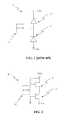
- FIG. 3( a )shows a cross section of a polysilicon diode.
- a polysiliconis implanted by N+ at one end and P+ at the other end with a spacing Lc in between that has intrinsic doping level.
- the intrinsic doping levelonly means not intentionally doped with any dopants but can be slightly N type or P type due to out diffusion or contamination.
- a silicide block layeris applied to block silicide formation on the surface of the polysilicon to thus prevent a short circuit.
- the two ends of P+ and N+ in polysiliconare further brought out as P and N terminals of a diode through contacts, vias, or metals.
- FIG. 3( b )shows current verses voltage characteristics of a polysilicon diode, such as shown in FIG. 3( a ) .
- the current verses voltage curvesshow useful diode behavior such as a threshold voltage of about 0.6V and a leakage current of less than 1 nA.
- the spacing LcBy varying the spacing Lc, the breakdown voltage and leakage current of the polysilicon diode can be adjusted accordingly.
- Polysilicon diodescan be used for ESD protection, refer to Ming-Dou Ker et al, “High-Current Characterization of Polysilicon Diode for Electrostatic Discharge Protection in Sub-Quarter-Micron Complementary Metal Oxide Semiconductor Technology,” Jpn. J. Appl. Phys. Vol. 42, 2003, pp. 3377-3378.
- Polysilicon structures for ESD protection in the prior artsare about a one-piece rectangular structure, which has rooms for improvements. Thus, there is still a need to use an optimized polysilicon diode structure to achieve higher ESD voltage, lower input capacitance, smaller area, and lower heat generated in today's giga-Hertz circuits.
- Embodiments of ESD protection using ring structures of diodesare disclosed.
- the diodes constructed from polysilicon or active region body on insulated substratecan be fabricated from standard bulk or SOI CMOS logic processes to achieve high ESD immunity, low input capacitance, small I/O size and low cost.
- the ESD protectioncan be constructed from diodes in ring structures that can be comparable to the I/O pad size and/or can be hidden underneath the pad partially or wholly.
- the diodescan be constructed from at least one polysilicon structure, insulated active region in SOI process, or junction diode in standard CMOS process.
- One ring-shape diodehas the P terminal coupled to the pad and the N terminal coupled to VDD.
- the other ring-shape diodehas the P terminal coupled to the VSS and the N terminal coupled to the pad.
- Therecan be a plurality of ring-shape structures and can be placed in concentric manner to maximize the ESD performance in small size.
- the contour of the diodescan be in circle, polygon or other shapes.
- the P or N terminal of the ring-shape diodesis coupled to VDD, VSS, or pad through Active Areas (AAs) so that the heat generated can be quickly dissipated.
- the same diode structurecan be used to create CMOS gates, sources, drains, or interconnects in standard CMOS logic processes.
- the input capacitance using ring-shape diodescan be smaller than that in the conventional junction diodes or MOS connected as diodes for the same ESD performance.
- the turn-on voltage of polysilicon diodesis about 0.6V, smaller than 0.7V of junction diodes.
- the breakdown voltage of the polysilicon or active-region diodescan be easily changed by adjusting the spacing of the P+ and N+ implants or the doping concentration in the space between P+ and N+ implants. Thus, high performance and low cost ESD protection can be realized.
- the inventioncan be implemented in numerous ways, including as a method, system, device, or apparatus (including graphical user interface and computer readable medium). Several embodiments of the invention are discussed below.
- one embodimentcan, for example, include at least: at least three regions in a portion of the semiconductor body, the first and the third regions being implanted with a first type of dopant, the second region being implanted with a second type of dopant, and the regions being adjacent are separated by spaces; and a silicide block layer (SBL) covering the spaces and overlapping into both implant regions to construct P/N junctions between the first/second and second/third regions.
- the first and third implant regionscan be conductive when a sufficiently high voltage is applied between the first and third implant regions.
- one embodimentcan, for example, include at least one integrated circuit including at least one switch device on a semiconductor body.
- the switch deviceincludes at least: at least three implant regions provided on a portion of the semiconductor body, the first and third implant regions being with a first type of implant, the second implant region being with a second type of implant, and the implant regions being adjacent are separated by at least one space; and at least one silicide block layer (SBL) covering the at least one space and overlapping into the adjacent implant regions to construct P/N junctions in first/second and second/third implant regions.
- SBLsilicide block layer
- one embodimentcan, for example, include at least: forming at least three regions in the semiconductor body, the first and the third regions being with a first type of implant and the second region being with a second type of implant, where adjacent ones of the implant regions are separated with a space; and forming a silicide block layer covering the space and overlapping into both of the adjacent implant regions to construct P/N junctions between first/second and second/third regions.
- one embodimentcan, for example, include a plurality of ESD protection rings.
- At least one of the ESD protection ringscan include at least one diode with P terminal coupled to the pad and the N terminal coupled to the VDD and at least another diode with P terminal coupled to the VSS and the N terminal coupled to the pad.
- the diodecan be on a polysilicon or active-region body on an insulated substrate.
- the diodecan also be a junction diode on a silicon substrate.
- the diodecan have the P+ and N+ implant regions in the inner or outer part of a concentric ring.
- the P+ and N+ regionscan be separated with a space, and a silicide block layer (SBL) can cover the space and overlap into both implant regions to construct P and N terminals of a diode.
- the P+ and N+ regionscan be isolated by LOCOS (LOCal Oxidation), STI (Shallow Trench Isolation), dummy gate, or SBL in a junction diode on silicon substrate.
- LOCOSLOCal Oxidation
- STIShallow Trench Isolation
- dummy gateor SBL in a junction diode on silicon substrate.
- the P and N terminals of the diodes coupled to VDD, VSS, or padcan be through contacts or vias to metals and/or through active areas to a thermally conductive substrate.
- one embodiment of the inventioncan, for example, include at least one Print Circuit Board (PCB), and at least one integrated circuit operatively connected to the PCB.
- the integrated circuitcan include at least an I/O pad and at least one ESD protection structures.
- At least one of the ESD protection structurescan include a ring-shape diode structure that has at least one diode with the P terminal coupled to the I/O pad and the N terminal coupled to the VDD and/or another diode with the P terminal coupled to the VSS and the N terminal coupled to the I/O pad.
- the diodecan be on a polysilicon or active-region body on an insulated substrate.
- the diodecan also be a junction diode on a silicon substrate.
- the P+ and N+ implant regions of the diodecan be separated with a space (or isolation), such as LOCOS, STI, or dummy gate, and a silicide block layer can cover the space and overlap into both implant regions to construct P and N terminals of a diode, respectively.
- the P or N terminal of the diodescan be coupled to VDD, VSS, or I/O pads through contacts or vias to metals, and/or through active areas to a thermally conductive substrate.
- one embodimentcan, for example, include at least providing an ring-shape diode structure, where at least one of the ring-shape diode structures can include at least (i) a ring-shape diode with the P terminal coupled to an I/O pad and the N terminal coupled to a first supply voltage; and/or (ii) a ring-shape diode with the P terminal coupled to a second supply voltage and the N terminal coupled to the I/O pad.
- the diodecan be a polysilicon or active-region body on an insulated substrate, or P/N junction on a silicon substrate.
- the P or N terminals of the diodescan be coupled to the first/second supply voltages or I/O pads through contacts or vias, to metal, and/or through active areas to a thermally conductive substrate.
- the embodiment of the inventioncan also include a plurality of concentric diode rings with the contour being circle, polygon, or other shapes.
- FIG. 1shows a prior art of ESD protection using diodes.
- FIG. 2shows a conventional ESD protection using MOS connected as diodes.
- FIG. 3( a )shows a cross section of a polysilicon diode.
- FIG. 3( b )shows current verses voltage characteristics of a polysilicon diode, such as shown in FIG. 3( a ) .
- FIG. 4shows a block diagram of an ESD protection structure using ring-shape diodes and an I/O pad according one embodiment.
- FIG. 4( a )shows a cross section of a polysilicon diode, corresponding to the diodes in FIG. 4 , according to one embodiment.
- FIG. 4( b )shows a cross section of an active-region diode on an insulated substrate corresponding to the diodes in FIG. 4 , according to another embodiment.
- FIG. 4( c )shows a cross section of an active-region diode consisting of an N+ active region on a P substrate, corresponding to the diodes in FIG. 4 , according to yet another embodiment.
- FIG. 4( d )shows a cross section of an active-region diode consisting of P+ active region on an N well, corresponding to the diodes in FIG. 4 , according to yet another embodiment.
- FIG. 4( e )shows a cross section of an active-region diode consisting of an N+ active region on a P substrate with dummy gate isolation, corresponding to the diodes in FIG. 4 , according to yet another embodiment.
- FIG. 4( f )shows a cross section of an active-region diode consisting of P+ active region on an N well with dummy gate isolation, corresponding to the diodes in FIG. 4 , according to yet another embodiment.
- FIG. 5shows a top view of a ring-shape polysilicon diode according to one embodiment.
- FIG. 6( a )shows a top view of a ring-shape ESD protection structure according to one embodiment.
- FIG. 6( b )shows a top view of a ring-shape ESD protection structure according to another embodiment.
- FIG. 6( c )shows a top view of a ring-shape ESD protection structure according to yet another embodiment.
- FIG. 7shows a top view of a multiple ring-shape ESD protection structure according to one embodiment.
- FIG. 8shows an equivalent circuit of an ESD protection structure according to one embodiment.
- FIG. 9( a )shows a Silicon-Controlled Rectifier (SCR) device on a semiconductor body according to one embodiment.
- FIG. 9( b )shows an equivalent model of a SCR device according to one embodiment.
- FIG. 9( c )shows a current versus voltage characteristic of an SCR device according to one embodiment.
- FIG. 9( d )shows a ring-shape SCR device constructed on a semiconductor body according to one embodiment.
- FIG. 10( a )shows a top view of a DIAC device constructed on a semiconductor body according to one embodiment.
- FIG. 10( b )shows a current versus voltage characteristic of a DIAC device according to one embodiment.
- FIG. 10( c )shows a ring-shape DIAC device constructed on a semiconductor body according to one embodiment.
- FIG. 11( a )shows an equivalent model of a TRIAC that can be readily embodied on a semiconductor body according to one embodiment.
- FIG. 11( b )shows a current versus voltage characteristic of a TRIAC device according to one embodiment.
- Embodiments disclosed hereinuse an ESD structure with ring-shape diodes.
- the diodescan comprise P+ and N+ implants on a polysilicon or active region body on an insulated substrate with the P+ and N+ implants separated by a gap.
- the gapcan be covered by a silicide block layer (SBL) and overlapping into both P+ and N+ areas.
- SBLsilicide block layer
- the diodecan also be N+ active region on a P type substrate or P+ active region on an N well.
- the isolation between the P+ and N+ active regionscan, for example, be LOCOS (LOCal Oxidation), STI (Shallow Trench Isolation), dummy gate, or SBL in standard CMOS processes.
- the ESD protection devicecan also be included within an electronic system.
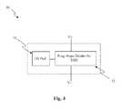
- FIG. 4shows a block diagram of an ESD protection device 30 using at least one ring-shape diodes according to one embodiment.
- the ESD protection device 30includes an I/O pad 31 and at least one ring-shape diode 32 .
- the I/O pad 31can be coupled to an anode of the diode 32 with the cathode coupled to a high voltage V+, and/or coupled to a cathode of the diode 32 with the anode coupled to a low voltage V ⁇ .
- the couplings between anode(s) or cathode(s) of the diode(s) to external nodescan be through contacts, vias, or metals.
- the anode(s) and cathode(s) of the diode(s)can be coupled to a thermally conductive substrate through active areas, contacts, vias, or metals.
- a high ESD voltage on the I/O padcan be clamped to diodes' turning or breakdown voltages.
- the internal devices of an integrated circuit coupled to an I/O padcan be protected from high ESD voltage damage.
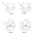
- FIG. 4( a )shows a cross section of a polysilicon diode 40 , corresponding to the diodes in FIG. 4 , according to one embodiment.
- the polysilicon diode structure 40has a polysilicon body 41 on an insulated substrate 45 that has a P+ implant 42 in one end and an N+ implant 43 in the other end.
- the N+ 43 and P+ 42are separated with a space Lc that can be used to adjust the breakdown voltage of the polysilicon diode.
- a silicide block layer (SBL) 44covers the space Lc and overlaps into both P+ and N+ regions 42 and 43 to prevent a short due to silicide grown on the surface of the polysilicon 41 .
- SBLsilicide block layer
- a portion of the N+ 43 and P+ 42 implant areascan be further coupled by contacts, vias, or metals (not shown in FIG. 4( a ) ) to external nodes as the cathode or anode of the polysilicon diode 40 , respectively.
- the dopant concentration in the space Lc between P+ and N+ regionscan be in the intrinsic level, namely, the dopants are not intentionally introduced but can be slightly P type or N type due to out diffusion or contamination. In another embodiment, the dopants in the space can be implanted slightly N or P type to control the resistance of the polysilicon diode 40 .
- FIG. 4( b )shows a cross section of an active-region diode 40 ′ on an insulated substrate 45 ′, corresponding to the diodes in FIG. 4 , according to one embodiment.
- the insulated substrate 45 ′is, for example, a SOI substrate.
- the active-region diode 40 ′has an active-region body 41 ′ on the insulated substrate 45 ′ that has a P+ implant 42 ′ in one end and an N+ implant 43 ′ in the other end.
- the N+ 43 ′ and P+ 42 ′are separated with a space Lc that can be used to adjust the breakdown voltage of the active-region diode 40 ′.
- a silicide block layer (SBL) 44 ′covers the space Lc and overlaps into both P+ and N+ regions 42 ′ and 43 ′ to prevent a short due to silicide grown on the surface of the active region 41 ′.
- a portion of the N+ 43 ′ and P+ 42 ′ implant areascan be further coupled by contacts, vias, or metals (not shown in FIG. 4( b ) ) to external nodes as the cathode or anode of the active-region diode 40 ′, respectively.
- the dopant concentration in the space Lc between P+ and N+ regionscan be in the intrinsic level, namely, the dopants are not intentionally introduced but can be slightly P type or N type due to out diffusion or contamination. In another embodiment, the dopants in the space can be implanted slightly N or P type to control the resistance of the active-region diode 40 ′.
- FIG. 4( c )shows a cross section of an active-region diode 46 on a P type silicon substrate 49 , corresponding to the diodes in FIG. 4 , according to another embodiment.
- the active region diode 46has an anode and a cathode that consist of a P+ active region 47 and an N+ active region 48 on a P type substrate 49 .
- the anode and cathodecan be further coupled through contact(s), via(s), or metal(s) (not shown in FIG. 4( c ) ) as the P and N terminals, respectively, of a diode.
- the isolation between the P+ 47 and N+ 48can be LOCS or STI in other embodiment.
- FIG. 4( d )shows a cross section of an active-region diode 46 ′ with a P+ active region 47 ′ and an N+ active region 48 ′ on an N well 49 ′, corresponding to the diodes in FIG. 4 , according to another embodiment.
- the active region diode 46 ′has an anode and a cathode that consist of a P+ active region 47 ′ and an N+ active region 48 ′ on an N well 49 ′.
- the anode and cathodecan be further coupled through contact(s), via(s), or metal(s) (not shown in FIG. 4( d ) ) as the P and N terminals, respectively, of a diode.
- the isolation between the P+ 47 ′ and N+ 48 ′can be LOCS or STI in other embodiment.
- FIG. 4( e )shows a cross section of an active-region diode 36 on a P type silicon substrate 39 , corresponding to the diodes in FIG. 4 , according to another embodiment.
- the active region diode 36has an anode and a cathode that consist of a P+ active region 37 and an N+ active region 38 on a P type substrate 39 .
- the anode and cathodecan be further coupled through contact(s), via(s), or metal(s) (not shown in FIG. 4( e ) ) as the P and N terminals, respectively, of a diode.
- the isolation between the anode and cathodecan be a dummy gate 35 with part N+ and part P+ implants to create N+ and P+ active regions 38 and 37 , respectively.
- the dummy gate 35can be coupled to a fixed bias voltage during normal operations.
- the dummy gate 35can be replaced by a silicide block layer for isolation.
- FIG. 4( f )shows a cross section of an active-region diode 36 ′ with a P+ active region 37 ′ and an N+ active region 38 ′ on an N well 39 ′, corresponding to the diodes in FIG. 4 , according to another embodiment.
- the active region diode 36 ′has an anode and a cathode that consist of a P+ active region 37 ′ and an N+ active region 38 ′ on an N well 39 ′.
- the anode and cathodecan be further coupled through contact(s), via(s), or metal(s) (not shown in FIG. 4( f ) ) as the P and N terminals, respectively, of a diode.
- the isolation between the anode and cathodecan be a dummy gate 35 ′ with part N+ and part P+ implants to create N+ and P+ active regions 38 ′ and 37 ′, respectively.
- the dummy gate 35 ′can be coupled to a fixed bias voltage during normal operations.
- the dummy gate 35can be replaced by a silicide block layer for isolation.
- FIG. 5shows a top view of a ring-shape polysilicon diode 40 according to one embodiment.
- the polysilicon diode structure 40is similar to the cross section of a polysilicon diode shown in FIG. 3( a ) except that the structure is a ring-shape.
- the circular structureallows uniform electrical field distribution, when a high voltage is applied, to prevent any sharp corners generating high electrical field and causing premature breakdown. The larger the radius of the circle, the lower the electrical field and the lower the current density generated by ESD voltage.
- the ring 42is an N+ implant mask to allow heavy N type dopants being implanted into the polysilicon 40 .
- the ring 43is a P+ implant mask to allow heavy P type dopants to be implanted into the polysilicon 40 .
- a portion of the N+ and P+ implant areasare further coupled by contacts, vias, or metals (not shown in FIG. 5 ) to external nodes, such as to the cathode or anode of the polysilicon diode 40 , respectively.
- the P+ and N+ areasare preferably separated with a space Lc to adjust the breakdown voltage.
- the ring 44is a silicide block layer (SBL) to prevent silicide from growing on the top of the polysilicon and shorting the P+ and N+ regions.
- the SBL 44covers the gap between N+ and P+ and preferably overlaps into the P+ and N+ areas.
- the dopant concentration in the gap between P+ and N+can be in the intrinsic level, namely, the dopants are not intentionally introduced but can be slightly P type or N type due to out diffusion or contamination. Alternatively, in another embodiment, the dopants in the gap can be implanted slightly N or P to control the resistance.
- the contour of the polysilicon diode 40can be a circle, polygon, or other shape in yet another embodiment.
- the polysilicon diode 40 in FIG. 5can be applied to an active-region diode built on SOI substrate, or a junction diode built on silicon substrate in other embodiments.
- FIG. 6( a )shows a ring-shape ESD protection structure 50 according to one embodiment.
- the ESD protection structure 50has a ring diode 52 , as shown in FIG. 5 , with an N+ 55 in an outer portion, a P+ 56 in an inner portion, and an intrinsic in a middle portion.
- the ESD protection structure 50also has a ring diode 53 , as shown in FIG. 5 , with an N+ 57 in an outer portion, a P+ 58 in an inner portion, and an intrinsic in a middle portion.
- the N+ 55 of the diode ring 52is coupled to VDD and the P+ 58 of the diode ring 53 is coupled to VSS.
- the P+ 56 of the diode 52 and the N+ 57 of the diode 53are coupled to an I/O pad.
- the couplings through contacts, vias, or metalsare not shown.
- the SBL layers in diodes 52 and 53are also not shown.
- FIG. 6( b )shows a ring-shape ESD protection structure 60 according to one embodiment.
- the ESD protection structure 60has a ring diode 62 , as shown in FIG. 5 , with an N+ 65 in an outer portion, a P+ 66 in an inner portion, and an intrinsic in a middle portion.
- the ESD protection structure 60also has a ring diode 63 , as shown in FIG. 5 , with an N+ 67 in an outer portion, a P+ 68 in an inner portion, and an intrinsic in a middle portion.
- the two ring diodes 62 and 63are separated by an active area 64 .
- the N+ 65 of the ring diode 62can be coupled to VDD and the P+ 68 of the ring diode 63 can be coupled to VSS.
- the P+ 66 of the diode 62 , the N+ 67 of the diode 63 , and the active area 64can be coupled to an I/O pad.
- the couplings through contacts, vias, or metalsare not shown.
- the SBL layers in the ring diodes 62 and 63are also not shown.
- the active area 64creates a short thermal path to substrate for the I/O pad.
- FIG. 6( c )shows a ring-shape ESD protection structure 70 according to one embodiment.
- the ESD protection structure 70has a ring diode 72 , as shown in FIG. 5 , with an N+ in an outer region, a P+ in an inner region, and an intrinsic in a middle region.
- the ESD protection structure 70also has a ring diode 73 , as shown in FIG. 5 , with an N+ in an outer region, a P+ in an inner region, and an intrinsic in a middle region.
- the two ring diodes 72 and 73are separated by an active area 74 and surrounded by an active area 76 in the outer ring and an active area 75 in the inner ring.
- the N+ of the ring diode 72can be coupled to VDD and the P+ of the ring diode 73 can be coupled to VSS.
- the P+ of the ring diode 72 , the N+ of the ring diode 73 , and the active area 74can be coupled to an I/O pad.
- the couplings through contacts, vias, or metalsare not shown.
- the SBL layers for ring diodes 72 and 73are also not shown.
- the active areas 74 , 75 , and 76create a short thermal path to substrate.
- FIG. 7shows a multiple ring-shape ESD protection structure 80 according to one embodiment.
- the ESD protection structure 80has a ring-shape ESD structure 81 , as shown in FIG. 6( a ), 6( b ) , or 6 ( c ), with an outer portion coupled to VDD and an inner coupled to VSS.
- the ESD protection structure 80also has a ring-shape ESD structure 82 , as shown in FIG. 6( a ), 6( b ) , or 6 ( c ), with an outer portion coupled to VSS and an inner portion coupled to VDD.
- the ESD protection structure 80also has a ring-shape ESD structure 83 , as shown in FIG.
- the three ring-shape ESD structures 81 , 82 , and 83are separated by an active area 84 and 85 , and surrounded by an active area 87 in the outer portion and active area 86 in the inner portion.
- the active region 87is coupled to VDD and the active region 86 is coupled to VSS.
- the active areas 84 and 85are coupled to VSS and VDD, respectively.
- the I/O pad portions of the ring-shape ESD structures 81 , 82 , and 83are coupled together to an I/O pad (not shown in FIG. 7 ). For simplicity, the couplings through contacts, vias, or metals are not shown.
- the N+, P+, and SBL layers of the ring-shape ESD structures 81 , 82 , and 83are not shown either.
- FIG. 8shows an equivalent circuit 90 of a multiple ring-shape ESD structure as shown in FIG. 7 according to one embodiment.
- the equivalent circuit 90has an I/O pad 99 coupled to a junction diode 91 - 2 , polysilicon/active-region/junction diodes 91 - 0 and 91 - 1 ; coupled to a junction diode 92 - 2 , polysilicon/active-region/junction diodes 92 - 0 and 92 - 1 ; coupled to a junction diode 93 - 2 , polysilicon/active region/junction diodes 93 - 0 and 93 - 1 , of ring-shape structures such as 81 , 82 , and 83 in the FIG.
- the width of the smaller inner ringscan be increased slightly so that each ESD rings have the same ESD protection thresholds.
- the ring-shape ESD structurecan be comparable to the size of the I/O pad and/or be hidden under the I/O pad partially or wholly.
- Semiconductor body on an insulated substratecan be used to construct switch devices such as Silicon Controlled Rectifier (SCR), DIAC, or TRIAC.
- the semiconductor bodycan be a polysilicon or active region body on an insulated substrate.
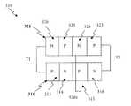
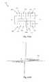
- FIG. 9( a )shows a top view of a SCR 210 constructed on a semiconductor body 211 according to one embodiment.
- the semiconductor body 211has implant regions 213 , 214 , 215 , and 216 by P+, N+, P+, and N+ implants, respectively.
- the N+ implant regions 214 and 216 and P+ implant regions 213 and 215are separated with a space.
- Silicide block layers 217 , 218 , and 219cover the spaces and overlap into both implant regions to construct P/N junctions in the interface.
- the regions with P+ implant 213 , N+ implant 216 , and P+ implant 215are coupled, respectively, as the anode, cathode, and gate of a SCR, through contacts, vias, or metals (not shown in FIG. 9( a ) ).
- FIG. 9( b )shows an equivalent model of a SCR device 110 that has 4 layers of P+ and N+ regions, 113 , 114 , 115 , and 116 , alternatively, according to one embodiment.
- the external P+ and N+ regions 113 and 116are brought out as the anode and cathode of an SCR.
- the internal P+ region 115is brought out as the gate of an SCR.
- FIG. 9( c )shows a current versus voltage characteristic of an SCR according to one embodiment.
- the SCRWhen a small voltage applied to an SCR, the SCR is not conductive. However, when the voltage is increased beyond Vh, the SCR suddenly becomes conductive and shows a low on-resistance state. Further, increasing the voltage makes the current higher and follows the on-resistance characteristics of the device.
- the Vh voltagecan be controlled by a voltage applied to the gate as shown in the different curves in FIG. 9( c ) .
- FIG. 9( d )shows a top view of a ring-shape of SCR 220 constructed on a semiconductor body 221 according to one embodiment.
- the semiconductor body 221has ring-shape implant regions 223 , 224 , 225 , and 226 by P+, N+, P+, and N+ implants, respectively.
- the ring-shape N+ implant regions 224 and 226 and ring-shape P+ implant regions 223 and 225are separated by a space.
- Silicide block layers(not shown in FIG. 9( d ) ) cover the spaces and overlap into both implant regions to construct P/N junctions in the interface.
- the regions with P+ implant 223 , N+ implant 226 , and P+ implant 225are coupled respectively as the anode, cathode, and gate of a SCR, respectively, through contacts, vias, or metals (not shown in FIG. 9( d ) ).
- FIG. 10( a )shows a top view of a DIAC 230 constructed on a semiconductor body 231 according to one embodiment.
- the semiconductor body 231has implant regions 233 , 234 , and 235 , covered by P+, N+, and P+ implants, respectively.
- the N+ implant regions 234 and the P+ implant regions 233 and 235are separated with a space.
- Silicide block layers 237 and 238cover the spaces and overlap into both implant regions to construct P/N junctions in the interface.
- the regions with P+ implant 233 and P+ implant 235are coupled respectively as the anode, cathode, T 1 and T 2 of a DIAC, through contacts, vias, or metals (not shown in FIG. 10( a ) ).
- FIG. 10( b )shows a current versus voltage characteristic of the DIAC device 230 shown in FIG. 9( d ) , according to one embodiment.
- DIACis a switch device similar to SCR, except that DIAC is a two-terminal device and does not have a gate terminal. When a voltage applied to the DIAC exceeds a critical voltage Vh, the DIAC becomes conductive. The DIAC shows the same characteristics with respect to a voltage applied in opposite polarity.
- FIG. 10( c )shows a top view of a ring-shape of DIAC 240 constructed on a semiconductor body 241 according to one embodiment.
- the semiconductor body 241has ring-shape implant regions 243 , 244 , and 245 by P+, N+, and P+ implants, respectively.
- the ring-shape N+ implant regions 244 and ring-shape P+ implant regions 243 and 245are separated by spaces.
- Silicide block layers(not shown in FIG. 10( c ) ) cover the spaces and overlap into both implant regions to construct P/N junctions in the interface.
- the regions with P+ implant 243 and 245are coupled respectively as the T 1 and T 2 of a DIAC, respectively, through contacts, vias, or metals (not shown in FIG. 10( c ) ).
- FIG. 11( a )shows an equivalent model of a TRIAC 310 that has two coupled SCR structures 311 and 321 according to one embodiment.
- the SCR 311has a P-N-P-N structure of 313 , 313 , 315 , and 316 , respectively.
- the SCR 321also has a P-N-P-N structure of 323 , 324 , 325 , and 326 , respectively.
- the anode 313 of SCR 311is coupled to the cathode of SCR 321 as a terminal T 1 of the TRIAC 310 .
- the cathode 316 of SCR 311is coupled to the anode of SCR 323 as a terminal T 2 of the TRIAC 310 .
- the internal P+ 315 of SCR 311 and the internal N+ 324 of SCR 321are coupled as a gate of the TRIAC 310 .
- the TRIAC structure in FIG. 11( a )can be readily embodied on a semiconductor body using SCR structures shown in FIG. 9( a ) and FIG. 9( d ) .
- FIG. 11( b )shows a current versus voltage characteristic of a TRIAC as shown in FIG. 310 according to one embodiment.
- the TRIAC characteristicis similar to the SCR except that the characteristic curves are symmetrical with respect to both voltage polarities.
- Semiconductor bodycan be used to construct switch devices such as SCR, DIAC, or TRIAC based on P/N junctions built on the polysilicon or active region body on insulated substrate.
- the P/N junctionscan be constructed from a gap between P+ and N+ implant regions and covered by a silicide block layer and overlapping into both implant regions.
- the dopant concentration in the gapcan be not intentionally doped or slightly doped with N or P type to control the on-resistance.
- the DIAC, SCR, or TRIACcan be in any shape such as a circle, ring, rectangle, or polygon.
- the P+ and N+ implant regions in the above discussionsare interchangeable.
- At least one of the P+ or N+ implant regionscan be coupled to active areas and further coupled to a thermally conductive substrate.
- the above discussions of various switch devices such as SCR, DIAC, or TRIAC based on a semiconductor body, or ESD structures based on ring-shape diodesare for illustration purposes.
- the semiconductor bodycan be on a conductive substrate through a dielectric, such as SiO2 on silicon substrate, or can be on a non-conductive substrate, such as mylar, plastic, glass, or paper, etc with a thin layer of semiconductor material coated on top.
- the substratecan be a film or a bulk.
- the ring-shape diodes for ESD structurescan be a polysilicon, active region body on an insulated substrate, or junction diodes on a silicon substrate.
- the P+ and N+ implant regionscan be separated with a gap.
- An SBLcan cover the gap and overlap into the N+ and P+ regions.
- the width of the gapcan be adjusted to change polysilicon or active region diodes' breakdown voltage.
- the doping concentration in the gap regioncan be changed to adjust the turn-on resistance.
- the N+ and P+ active regionscan be separated by LOCOS, STI, dummy gate, or SBL isolation.
- the N+ or P+ implant in the inner or outer ringis interchangeable.
- An active areas (AAs)can be introduced in any places to couple the diodes or switch devices to a thermally conductive substrate.
- the numbers of the supply voltagescan be more than two, e.g., VDD and VSS.
- the inventioncan be implemented in a part or all of an integrated circuit in a Printed Circuit Board (PCB), or in a system.
- the ESD structurescan comprise one or plural of ring-shape diode structures.
- Each ring-shape diode structurecan comprise at least one ring-shape diodes with one terminal coupled to the I/O pad and the other terminal coupled to a supply voltage.
Landscapes
- Semiconductor Integrated Circuits (AREA)
- Metal-Oxide And Bipolar Metal-Oxide Semiconductor Integrated Circuits (AREA)
Abstract
Description
Claims (25)
Priority Applications (1)
| Application Number | Priority Date | Filing Date | Title |
|---|---|---|---|
| US13/678,544US9324849B2 (en) | 2011-11-15 | 2012-11-15 | Structures and techniques for using semiconductor body to construct SCR, DIAC, or TRIAC |
Applications Claiming Priority (2)
| Application Number | Priority Date | Filing Date | Title |
|---|---|---|---|
| US201161560159P | 2011-11-15 | 2011-11-15 | |
| US13/678,544US9324849B2 (en) | 2011-11-15 | 2012-11-15 | Structures and techniques for using semiconductor body to construct SCR, DIAC, or TRIAC |
Publications (2)
| Publication Number | Publication Date |
|---|---|
| US20140131764A1 US20140131764A1 (en) | 2014-05-15 |
| US9324849B2true US9324849B2 (en) | 2016-04-26 |
Family
ID=50680885
Family Applications (1)
| Application Number | Title | Priority Date | Filing Date |
|---|---|---|---|
| US13/678,544Expired - Fee RelatedUS9324849B2 (en) | 2011-11-15 | 2012-11-15 | Structures and techniques for using semiconductor body to construct SCR, DIAC, or TRIAC |
Country Status (1)
| Country | Link |
|---|---|
| US (1) | US9324849B2 (en) |
Cited By (20)
| Publication number | Priority date | Publication date | Assignee | Title |
|---|---|---|---|---|
| US9460807B2 (en) | 2010-08-20 | 2016-10-04 | Shine C. Chung | One-time programmable memory devices using FinFET technology |
| US9478306B2 (en) | 2010-08-20 | 2016-10-25 | Attopsemi Technology Co., Ltd. | Circuit and system of using junction diode as program selector for one-time programmable devices with heat sink |
| US9496033B2 (en) | 2010-08-20 | 2016-11-15 | Attopsemi Technology Co., Ltd | Method and system of programmable resistive devices with read capability using a low supply voltage |
| US9548109B2 (en) | 2011-02-14 | 2017-01-17 | Attopsemi Technology Co., Ltd | Circuit and system of using FinFET for building programmable resistive devices |
| US9711237B2 (en) | 2010-08-20 | 2017-07-18 | Attopsemi Technology Co., Ltd. | Method and structure for reliable electrical fuse programming |
| US9818478B2 (en) | 2012-12-07 | 2017-11-14 | Attopsemi Technology Co., Ltd | Programmable resistive device and memory using diode as selector |
| US9824768B2 (en) | 2015-03-22 | 2017-11-21 | Attopsemi Technology Co., Ltd | Integrated OTP memory for providing MTP memory |
| US10192615B2 (en) | 2011-02-14 | 2019-01-29 | Attopsemi Technology Co., Ltd | One-time programmable devices having a semiconductor fin structure with a divided active region |
| US10229746B2 (en) | 2010-08-20 | 2019-03-12 | Attopsemi Technology Co., Ltd | OTP memory with high data security |
| US10249379B2 (en) | 2010-08-20 | 2019-04-02 | Attopsemi Technology Co., Ltd | One-time programmable devices having program selector for electrical fuses with extended area |
| US10535413B2 (en) | 2017-04-14 | 2020-01-14 | Attopsemi Technology Co., Ltd | Low power read operation for programmable resistive memories |
| US10586832B2 (en) | 2011-02-14 | 2020-03-10 | Attopsemi Technology Co., Ltd | One-time programmable devices using gate-all-around structures |
| US10726914B2 (en) | 2017-04-14 | 2020-07-28 | Attopsemi Technology Co. Ltd | Programmable resistive memories with low power read operation and novel sensing scheme |
| US10770160B2 (en) | 2017-11-30 | 2020-09-08 | Attopsemi Technology Co., Ltd | Programmable resistive memory formed by bit slices from a standard cell library |
| US10916317B2 (en) | 2010-08-20 | 2021-02-09 | Attopsemi Technology Co., Ltd | Programmable resistance memory on thin film transistor technology |
| US10923204B2 (en) | 2010-08-20 | 2021-02-16 | Attopsemi Technology Co., Ltd | Fully testible OTP memory |
| US20210090937A1 (en)* | 2015-03-30 | 2021-03-25 | Taiwan Semiconductor Manufacturing Company, Ltd. | System for designing thermal sensor arrangement |
| US11062786B2 (en) | 2017-04-14 | 2021-07-13 | Attopsemi Technology Co., Ltd | One-time programmable memories with low power read operation and novel sensing scheme |
| US11615859B2 (en) | 2017-04-14 | 2023-03-28 | Attopsemi Technology Co., Ltd | One-time programmable memories with ultra-low power read operation and novel sensing scheme |
| US12336302B1 (en) | 2024-05-03 | 2025-06-17 | Globalfoundries U.S. Inc. | Vertical device triggered silicon control rectifier |
Families Citing this family (29)
| Publication number | Priority date | Publication date | Assignee | Title |
|---|---|---|---|---|
| US9224496B2 (en) | 2010-08-11 | 2015-12-29 | Shine C. Chung | Circuit and system of aggregated area anti-fuse in CMOS processes |
| US9019742B2 (en) | 2010-08-20 | 2015-04-28 | Shine C. Chung | Multiple-state one-time programmable (OTP) memory to function as multi-time programmable (MTP) memory |
| US8488359B2 (en) | 2010-08-20 | 2013-07-16 | Shine C. Chung | Circuit and system of using junction diode as program selector for one-time programmable devices |
| US9042153B2 (en) | 2010-08-20 | 2015-05-26 | Shine C. Chung | Programmable resistive memory unit with multiple cells to improve yield and reliability |
| US9025357B2 (en) | 2010-08-20 | 2015-05-05 | Shine C. Chung | Programmable resistive memory unit with data and reference cells |
| US9236141B2 (en) | 2010-08-20 | 2016-01-12 | Shine C. Chung | Circuit and system of using junction diode of MOS as program selector for programmable resistive devices |
| US8830720B2 (en) | 2010-08-20 | 2014-09-09 | Shine C. Chung | Circuit and system of using junction diode as program selector and MOS as read selector for one-time programmable devices |
| US9251893B2 (en) | 2010-08-20 | 2016-02-02 | Shine C. Chung | Multiple-bit programmable resistive memory using diode as program selector |
| US8488364B2 (en) | 2010-08-20 | 2013-07-16 | Shine C. Chung | Circuit and system of using a polysilicon diode as program selector for resistive devices in CMOS logic processes |
| US9431127B2 (en) | 2010-08-20 | 2016-08-30 | Shine C. Chung | Circuit and system of using junction diode as program selector for metal fuses for one-time programmable devices |
| US9019791B2 (en) | 2010-11-03 | 2015-04-28 | Shine C. Chung | Low-pin-count non-volatile memory interface for 3D IC |
| US9076513B2 (en) | 2010-11-03 | 2015-07-07 | Shine C. Chung | Low-pin-count non-volatile memory interface with soft programming capability |
| US8988965B2 (en) | 2010-11-03 | 2015-03-24 | Shine C. Chung | Low-pin-count non-volatile memory interface |
| US8913449B2 (en) | 2012-03-11 | 2014-12-16 | Shine C. Chung | System and method of in-system repairs or configurations for memories |
| US9496265B2 (en) | 2010-12-08 | 2016-11-15 | Attopsemi Technology Co., Ltd | Circuit and system of a high density anti-fuse |
| US8912576B2 (en) | 2011-11-15 | 2014-12-16 | Shine C. Chung | Structures and techniques for using semiconductor body to construct bipolar junction transistors |
| US9136261B2 (en) | 2011-11-15 | 2015-09-15 | Shine C. Chung | Structures and techniques for using mesh-structure diodes for electro-static discharge (ESD) protection |
| US9324849B2 (en) | 2011-11-15 | 2016-04-26 | Shine C. Chung | Structures and techniques for using semiconductor body to construct SCR, DIAC, or TRIAC |
| US8917533B2 (en) | 2012-02-06 | 2014-12-23 | Shine C. Chung | Circuit and system for testing a one-time programmable (OTP) memory |
| US8861249B2 (en) | 2012-02-06 | 2014-10-14 | Shine C. Chung | Circuit and system of a low density one-time programmable memory |
| US9007804B2 (en) | 2012-02-06 | 2015-04-14 | Shine C. Chung | Circuit and system of protective mechanisms for programmable resistive memories |
| FR2991811A1 (en)* | 2012-06-11 | 2013-12-13 | St Microelectronics Crolles 2 | ADJUSTABLE AVALANCHE DIODE IN INTEGRATED CIRCUIT |
| US9076526B2 (en) | 2012-09-10 | 2015-07-07 | Shine C. Chung | OTP memories functioning as an MTP memory |
| US9183897B2 (en) | 2012-09-30 | 2015-11-10 | Shine C. Chung | Circuits and methods of a self-timed high speed SRAM |
| US9324447B2 (en) | 2012-11-20 | 2016-04-26 | Shine C. Chung | Circuit and system for concurrently programming multiple bits of OTP memory devices |
| US9412473B2 (en) | 2014-06-16 | 2016-08-09 | Shine C. Chung | System and method of a novel redundancy scheme for OTP |
| US9318479B2 (en)* | 2014-08-21 | 2016-04-19 | Apple Inc. | Electrostatic discharge (ESD) silicon controlled rectifier (SCR) with lateral gated section |
| US9711224B2 (en) | 2015-03-13 | 2017-07-18 | Micron Technology, Inc. | Devices including memory arrays, row decoder circuitries and column decoder circuitries |
| JP2018170455A (en)* | 2017-03-30 | 2018-11-01 | エイブリック株式会社 | Semiconductor device |
Citations (179)
| Publication number | Priority date | Publication date | Assignee | Title |
|---|---|---|---|---|
| US3198670A (en) | 1961-03-09 | 1965-08-03 | Bunker Ramo | Multi-tunnel diode |
| US3715242A (en) | 1969-12-17 | 1973-02-06 | Philips Corp | Methods of manufacturing semiconductor devices |
| US4148046A (en) | 1978-01-16 | 1979-04-03 | Honeywell Inc. | Semiconductor apparatus |
| US4192059A (en) | 1978-06-06 | 1980-03-11 | Rockwell International Corporation | Process for and structure of high density VLSI circuits, having inherently self-aligned gates and contacts for FET devices and conducting lines |
| US4642674A (en) | 1983-06-13 | 1987-02-10 | U.S. Philips Corporation | Field effect semiconductor device having improved voltage breakdown characteristics |
| JPH03264814A (en) | 1990-03-15 | 1991-11-26 | Pioneer Electron Corp | Nagivation apparatus for vehicle |
| US5192989A (en) | 1989-11-28 | 1993-03-09 | Nissan Motor Co., Ltd. | Lateral dmos fet device with reduced on resistance |
| US5389552A (en) | 1993-01-29 | 1995-02-14 | National Semiconductor Corporation | Transistors having bases with different shape top surfaces |
| US5447876A (en) | 1993-11-19 | 1995-09-05 | Micrel, Inc. | Method of making a diamond shaped gate mesh for cellular MOS transistor array |
| US5635742A (en) | 1994-02-02 | 1997-06-03 | Nissan Motor Co., Ltd. | Lateral double-diffused mosfet |
| US5637901A (en) | 1993-12-14 | 1997-06-10 | Analog Devices, Inc. | Integrated circuit with diode-connected transistor for reducing ESD damage |
| US5723890A (en) | 1994-01-07 | 1998-03-03 | Fuji Electric Co., Ltd. | MOS type semiconductor device |
| US5757046A (en) | 1994-01-07 | 1998-05-26 | Fuji Electric Company Ltd. | MOS type semiconductor device |
| US5761148A (en) | 1996-12-16 | 1998-06-02 | Cypress Semiconductor Corp. | Sub-word line driver circuit for memory blocks of a semiconductor memory device |
| US5962903A (en) | 1995-06-08 | 1999-10-05 | Taiwan Semiconductor Manufacturing Company, Ltd. | Planarized plug-diode mask ROM structure |
| US6002156A (en) | 1997-09-16 | 1999-12-14 | Winbond Electronics Corp. | Distributed MOSFET structure with enclosed gate for improved transistor size/layout area ratio and uniform ESD triggering |
| US6008092A (en) | 1996-02-12 | 1999-12-28 | International Rectifier Corporation | Short channel IGBT with improved forward voltage drop and improved switching power loss |
| US6034882A (en) | 1998-11-16 | 2000-03-07 | Matrix Semiconductor, Inc. | Vertically stacked field programmable nonvolatile memory and method of fabrication |
| US6054344A (en) | 1998-10-30 | 2000-04-25 | Taiwan Semiconductor Manufacturing Company | OTP (open trigger path) latchup scheme using buried-diode for sub-quarter micron transistors |
| US6140687A (en) | 1996-11-28 | 2000-10-31 | Matsushita Electric Industrial Co., Ltd. | High frequency ring gate MOSFET |
| US6243864B1 (en) | 1997-07-17 | 2001-06-05 | Matsushita Electric Industrial Co., Ltd. | Compiler for optimizing memory instruction sequences by marking instructions not having multiple memory address paths |
| US6249472B1 (en) | 1997-12-25 | 2001-06-19 | Texas Instruments Incorporated | Semiconductor memory device with antifuse |
| US6346727B1 (en) | 1998-01-07 | 2002-02-12 | Nec Corporation | Semiconductor device having optimized two-dimensional array of double diffused MOS field effect transistors |
| US6400540B1 (en) | 1999-03-12 | 2002-06-04 | Sil.Able Inc. | Clamp circuit to prevent ESD damage to an integrated circuit |
| US6405160B1 (en) | 1998-08-03 | 2002-06-11 | Motorola, Inc. | Memory compiler interface and methodology |
| US6461934B2 (en) | 1998-11-13 | 2002-10-08 | Mitsubishi Denki Kabushiki Kaisha | Method of manufacturing semiconductor device having trench type element isolation regions |
| US20020168821A1 (en) | 1999-04-22 | 2002-11-14 | Advanced Analogic Technologies, Inc. | Fabrication process for a super-self-aligned trench-gated DMOS with reduced on-resistance |
| US6483734B1 (en) | 2001-11-26 | 2002-11-19 | Hewlett Packard Company | Memory device having memory cells capable of four states |
| US20020196659A1 (en) | 2001-06-05 | 2002-12-26 | Hurst Terril N. | Non-Volatile memory |
| US20030104860A1 (en) | 2001-11-30 | 2003-06-05 | Anchor Gaming | Method, apparatus and system for perpetual bonus game |
| US20030135709A1 (en) | 2001-02-23 | 2003-07-17 | Niles Ronald Steven | Dynamic allocation of computer memory |
| US6611043B2 (en) | 2000-03-15 | 2003-08-26 | Nec Corporation | Bipolar transistor and semiconductor device having the same |
| US20030169625A1 (en) | 2002-03-05 | 2003-09-11 | Glen Hush | Programmable conductor random access memory and method for sensing same |
| EP1367596A1 (en) | 2002-05-31 | 2003-12-03 | Hewlett-Packard Company | Cross-point diode ROM |
| CN1469473A (en) | 2002-07-15 | 2004-01-21 | �����ɷ� | Integrated circuit device and method of manufacturing integrated circuit device |
| US20040057271A1 (en) | 2002-09-25 | 2004-03-25 | Ward Parkinson | Method of operating programmable resistant element |
| US6731535B1 (en) | 2002-12-10 | 2004-05-04 | Renesas Technology Corp. | Nonvolatile semiconductor memory device |
| US20040113183A1 (en) | 2002-12-13 | 2004-06-17 | Ilya Karpov | Isolating phase change memory devices |
| US20040130924A1 (en) | 2000-05-31 | 2004-07-08 | Ma Stanley Jeh-Chun | Multiple match detection circuit and method |
| US6770953B2 (en) | 2000-01-31 | 2004-08-03 | Infineon Technologies Ag | Bipolar transistor |
| US6803804B2 (en) | 2002-05-24 | 2004-10-12 | Raminda U. Madurawe | Programmable latch array using antifuses |
| US6813705B2 (en) | 2000-02-09 | 2004-11-02 | Hewlett-Packard Development Company, L.P. | Memory disambiguation scheme for partially redundant load removal |
| US20050060500A1 (en) | 2003-09-11 | 2005-03-17 | Taiwan Semiconductor Manufacturing Company, Ltd. | General purpose memory compiler system and associated methods |
| US20050062110A1 (en) | 2003-09-18 | 2005-03-24 | Franz Dietz | Semiconductor over-voltage protection structure for integrated circuit and for diode |
| US20050110081A1 (en) | 2003-11-25 | 2005-05-26 | Texas Instruments Incorporated | Drain extended MOS transistor with improved breakdown robustness |
| US20050124116A1 (en) | 2003-12-08 | 2005-06-09 | Tzu-Hsuan Hsu | 3D polysilicon ROM and method of fabrication thereof |
| US20050146962A1 (en) | 2002-02-15 | 2005-07-07 | John Schreck | Physically alternating sense amplifier activation |
| US6944083B2 (en) | 2003-11-17 | 2005-09-13 | Sony Corporation | Method for detecting and preventing tampering with one-time programmable digital devices |
| CN1691204A (en) | 2004-01-05 | 2005-11-02 | 国际商业机器公司 | Memory cell using gated diode and method of use thereof |
| US20050242386A1 (en) | 2004-04-29 | 2005-11-03 | Kern-Huat Ang | Memory cell and method of fabricating the same |
| US6967879B2 (en) | 2002-11-20 | 2005-11-22 | Matsushita Electric Industrial Co., Ltd. | Memory trouble relief circuit |
| US7009182B2 (en) | 2001-05-14 | 2006-03-07 | Department Of Atomic Energy, Government Of India | Low cost digital pocket dosemeter |
| US20060072357A1 (en) | 2004-10-01 | 2006-04-06 | Wicker Guy C | Method of operating a programmable resistance memory array |
| US20060092689A1 (en) | 2004-11-04 | 2006-05-04 | Daniel Braun | Reference current source for current sense amplifier and programmable resistor configured with magnetic tunnel junction cells |
| US20060104111A1 (en) | 2004-11-17 | 2006-05-18 | Spansion Llc | Diode array architecture for addressing nanoscale resistive memory arrays |
| US20060120148A1 (en) | 2004-10-26 | 2006-06-08 | Samsung Electronics Co., Ltd. | Semiconductor memory device with stacked memory cell and method of manufacturing the stacked memory cell |
| US20060129782A1 (en) | 2004-12-15 | 2006-06-15 | Sorav Bansal | Apparatus, system, and method for dynamically allocating main memory among a plurality of applications |
| US20060215440A1 (en) | 2005-03-24 | 2006-09-28 | Beak-Hyung Cho | Nonvolatile memory devices having enhanced bit line and/or word line driving capability |
| US20060244099A1 (en) | 2004-05-06 | 2006-11-02 | Wlodek Kurjanowicz | Split-channel antifuse array architecture |
| US20070004160A1 (en) | 2004-01-07 | 2007-01-04 | Voldman Steven H | Tunable semiconductor diodes |
| US20070057323A1 (en) | 2005-09-12 | 2007-03-15 | International Business Machines Corporation | Silicon-on-insulator (soi) read only memory (rom) array and method of making a soi rom |
| US20070081377A1 (en) | 2005-09-26 | 2007-04-12 | Macronix International Co., Ltd. | Method and circuit for reading fuse cells in a nonvolatile memory during power-up |
| US7212432B2 (en) | 2004-09-30 | 2007-05-01 | Infineon Technologies Ag | Resistive memory cell random access memory device and method of fabrication |
| US7211843B2 (en) | 2002-04-04 | 2007-05-01 | Broadcom Corporation | System and method for programming a memory cell |
| US20070133341A1 (en) | 2002-07-05 | 2007-06-14 | Aplus Flash Technology, Inc. | Combination nonvolatile memory using unified technology with byte, page and block write and simultaneous read and write operations |
| US20070138549A1 (en) | 2005-12-19 | 2007-06-21 | Schyi-Yi Wu | Gate layouts for transistors |
| US7263027B2 (en) | 2004-10-14 | 2007-08-28 | Broadcom Corporation | Integrated circuit chip having non-volatile on-chip memories for providing programmable functions and features |
| US20070223266A1 (en) | 2006-03-24 | 2007-09-27 | Macronix International Co., Ltd. | One-time-programmable (OTP) memory device and method for testing the same |
| US7294542B2 (en) | 2000-05-15 | 2007-11-13 | Nec Electronics Corporation | Method of fabricating a semiconductor device having CMOS transistors and a bipolar transistor |
| CN101083227A (en) | 2006-05-30 | 2007-12-05 | 旺宏电子股份有限公司 | Magnetic random access memory using single crystal self-aligned diode |
| US20080028134A1 (en) | 1992-03-17 | 2008-01-31 | Kiyoshi Matsubara | Data line disturbance free memory block divided flash memory and microcomputer having flash memory therein |
| US20080025068A1 (en) | 2006-07-31 | 2008-01-31 | Scheuerlein Roy E | Reverse bias trim operations in non-volatile memory |
| US20080044959A1 (en) | 2005-08-31 | 2008-02-21 | International Business Machines Corporation | Body-contacted semiconductor structures and methods of fabricating such body-contacted semiconductor structures |
| US20080067601A1 (en) | 2006-09-20 | 2008-03-20 | Himax Technologies Limited | Esd protection apparatus and circuit thereof |
| US20080105878A1 (en) | 2006-11-07 | 2008-05-08 | Elpida Memory, Inc. | Semiconductor storage device and method of manufacturing the same |
| CN101188140A (en) | 2006-11-21 | 2008-05-28 | 奇梦达北美公司 | Resistive memory including bipolar transistor access device |
| US7391064B1 (en) | 2004-12-01 | 2008-06-24 | Spansion Llc | Memory device with a selection element and a control line in a substantially similar layer |
| US20080151612A1 (en) | 2005-06-03 | 2008-06-26 | Stmicroelectronics S.R.L. | Method for multilevel programming of phase change memory cells using a percolation algorithm |
| US20080175060A1 (en) | 2007-01-24 | 2008-07-24 | Kilopass Technology, Inc. | Non-volatile semiconductor memory based on enhanced gate oxide breakdown |
| US7411844B2 (en) | 2005-11-30 | 2008-08-12 | Infineon Technologies Flash Gmbh & Co. Kg | Semiconductor memory device having a redundancy information memory directly connected to a redundancy control circuit |
| US20080220560A1 (en) | 1997-10-01 | 2008-09-11 | Patrick Klersy | Programmable resistance memory element and method for making same |
| US20080225567A1 (en) | 2007-03-15 | 2008-09-18 | International Business Machines Corporation | Method and structure for increasing effective transistor width in memory arrays with dual bitlines |
| CN101271881A (en) | 2007-03-20 | 2008-09-24 | 联华电子股份有限公司 | Anti-fuse and memory cell without causing non-linear current after fusing |
| US7439608B2 (en) | 2006-09-22 | 2008-10-21 | Intel Corporation | Symmetric bipolar junction transistor design for deep sub-micron fabrication processes |
| TWI309081B (en) | 2005-09-28 | 2009-04-21 | Sandisk 3D Llc | Method for using a memory cell comprising switchable semiconductor memory element with trimmable resistance |
| US20090168493A1 (en) | 2004-10-26 | 2009-07-02 | Samsung Electronics Co., Ltd | Semiconductor memory device with stacked memory cell and method of manufacturing the stacked memory cell |
| US20090172315A1 (en) | 2007-12-27 | 2009-07-02 | Ravishankar Iyer | Priority aware selective cache allocation |
| CN101483062A (en) | 2008-01-11 | 2009-07-15 | 株式会社东芝 | Resistance change type memory |
| US20090194839A1 (en) | 2005-11-15 | 2009-08-06 | Bertin Claude L | Nonvolatile nanotube diodes and nonvolatile nanotube blocks and systems using same and methods of making same |
| US7573762B2 (en) | 2007-06-06 | 2009-08-11 | Freescale Semiconductor, Inc. | One time programmable element system in an integrated circuit |
| US20090213660A1 (en) | 2008-02-25 | 2009-08-27 | Tower Semiconductor Ltd. | Three-Terminal Single Poly NMOS Non-Volatile Memory Cell |
| US20090219756A1 (en) | 2008-02-28 | 2009-09-03 | Peter Schroegmeier | Apparatus and Method for Determining a Memory State of a Resistive N-Level Memory Cell and Memory Device |
| US7589367B2 (en) | 2005-04-08 | 2009-09-15 | Samsung Electronics Co., Ltd. | Layout structure in semiconductor memory device comprising global work lines, local work lines, global bit lines and local bit lines |
| US20090309089A1 (en) | 2008-06-13 | 2009-12-17 | Kang-Jay Hsia | Non-Volatile Memory Arrays Comprising Rail Stacks with a Shared Diode Component Portion for Diodes of Electrically Isolated Pillars |
| US20100027326A1 (en) | 2008-07-30 | 2010-02-04 | Ho Jung Kim | Memory device, memory system having the same, and programming method of a memory cell |
| US7660181B2 (en) | 2002-12-19 | 2010-02-09 | Sandisk 3D Llc | Method of making non-volatile memory cell with embedded antifuse |
| US20100085798A1 (en) | 2008-10-08 | 2010-04-08 | The Regents Of The University Of Michigan | Silicon-based nanoscale resistive device with adjustable resistance |
| US20100091546A1 (en) | 2008-10-15 | 2010-04-15 | Seagate Technology Llc | High density reconfigurable spin torque non-volatile memory |
| US7701038B2 (en) | 2005-10-31 | 2010-04-20 | Taiwan Semiconductor Manufacturing Company, Ltd. | High-gain vertex lateral bipolar junction transistor |
| CN101728412A (en) | 2008-11-03 | 2010-06-09 | 财团法人工业技术研究院 | Resistive memory cell and resistive memory array |
| US20100142254A1 (en) | 2008-12-05 | 2010-06-10 | Byung-Gil Choi | Nonvolatile Memory Device Using Variable Resistive Element |
| US20100171086A1 (en) | 2009-01-07 | 2010-07-08 | Macronix International Co., Ltd. | Integrated circuit memory with single crystal silicon on silicide driver and manufacturing method |
| US7764532B2 (en) | 2004-05-06 | 2010-07-27 | Sidense Corp. | High speed OTP sensing scheme |
| US20100232203A1 (en) | 2009-03-16 | 2010-09-16 | Taiwan Semiconductor Manufacturing Company, Ltd. | Electrical anti-fuse and related applications |
| US20100238701A1 (en) | 2009-03-23 | 2010-09-23 | Kabushiki Kaisha Toshiba | Semiconductor memory device |
| US20100246237A1 (en) | 2007-10-03 | 2010-09-30 | Bertrand Borot | Anti-fuse element |
| US7808815B2 (en) | 2006-10-02 | 2010-10-05 | Samsung Electronics Co., Ltd. | Variable resistance memory device and method of manufacturing the same |
| US20100277967A1 (en) | 2009-04-29 | 2010-11-04 | Macronix International Co., Ltd. | Graded metal oxide resistance based semiconductor memory device |
| US7830697B2 (en) | 2007-06-25 | 2010-11-09 | Sandisk 3D Llc | High forward current diodes for reverse write 3D cell |
| US20100301304A1 (en) | 2009-05-26 | 2010-12-02 | Macronix International Co., Ltd. | Buried silicide structure and method for making |
| US20110022648A1 (en) | 2008-05-23 | 2011-01-27 | Harris Edward B | Secure Random Number Generator |
| US7889204B2 (en) | 1998-08-24 | 2011-02-15 | Microunity Systems Engineering, Inc. | Processor architecture for executing wide transform slice instructions |
| US20110062557A1 (en) | 2009-09-17 | 2011-03-17 | Abhijit Bandyopadhyay | 3d polysilicon diode with low contact resistance and method for forming same |
| US7910999B2 (en) | 2002-07-29 | 2011-03-22 | Taiwan Semiconductor Manufacturing Company | Method for four direction low capacitance ESD protection |
| US20110128772A1 (en) | 2009-12-02 | 2011-06-02 | Samsung Electronics Co., Ltd. | Nonvolatile memory cells and nonvolatile memory devices including the same |
| US20110145777A1 (en) | 2009-12-15 | 2011-06-16 | Sundar Iyer | Intelligent memory system compiler |
| US20110175199A1 (en)* | 2010-01-18 | 2011-07-21 | Freescale Semiconductor, Inc. | Zener diode with reduced substrate current |
| US8008723B2 (en) | 2008-03-27 | 2011-08-30 | Renesas Electronics Corporation | Semiconductor device including a plurality of diffusion layers and diffusion resistance layer |
| US20110222330A1 (en) | 2010-03-11 | 2011-09-15 | Samsung Electronics Co., Ltd. | Nonvolatile memory device comprising one-time-programmable lock bit register |
| US20110260289A1 (en) | 2008-03-17 | 2011-10-27 | Seisei Oyamada | Semiconductor device and bypass capacitor module |
| US8050129B2 (en) | 2009-06-25 | 2011-11-01 | Mediatek Inc. | E-fuse apparatus for controlling reference voltage required for programming/reading e-fuse macro in an integrated circuit via switch device in the same integrated circuit |
| US20110297912A1 (en) | 2010-06-08 | 2011-12-08 | George Samachisa | Non-Volatile Memory Having 3d Array of Read/Write Elements with Vertical Bit Lines and Laterally Aligned Active Elements and Methods Thereof |
| US20110312166A1 (en) | 2003-05-20 | 2011-12-22 | Yedinak Joseph A | Methods of Manufacturing Power Semiconductor Devices with Shield and Gate Contacts |
| US20110310655A1 (en) | 2010-06-18 | 2011-12-22 | Franz Kreupl | Composition Of Memory Cell With Resistance-Switching Layers |
| US20120032303A1 (en) | 2010-08-05 | 2012-02-09 | Elkareh Badih | Bipolar Junction Transistor Based on CMOS Technology |
| US8115280B2 (en) | 2005-10-31 | 2012-02-14 | Taiwan Semiconductor Manufacturing Company, Ltd. | Four-terminal gate-controlled LVBJTs |
| US20120039107A1 (en) | 2010-08-11 | 2012-02-16 | Chung Shine C | Circuit and System of Aggregated Area Anti-Fuse in CMOS Processes |
| US8119048B2 (en) | 2006-09-22 | 2012-02-21 | Nissha Printing Co., Ltd. | Housing case, method for manufacturing housing case, and glass insert molding die used in same |
| US20120044744A1 (en) | 2010-08-20 | 2012-02-23 | Chung Shine C | Programmably reversible resistive device cells using polysilicon diodes |
| US20120044747A1 (en) | 2010-08-20 | 2012-02-23 | Chung Shine C | Reversible resistive memory using diodes formed in cmos processes as program selectors |
| US20120047322A1 (en) | 2010-08-20 | 2012-02-23 | Chung Shine C | Method and System of Using One-Time Programmable Memory as Multi-Time Programmable in Code Memory of Processors |
| US20120074460A1 (en) | 2010-09-21 | 2012-03-29 | Kabushiki Kaisha Toshiba | Semiconductor device and method for manufacturing the same |
| US20120106231A1 (en) | 2010-11-03 | 2012-05-03 | Chung Shine C | Low-pin-count non-volatile memory interface |
| US8174063B2 (en) | 2009-07-30 | 2012-05-08 | Ememory Technology Inc. | Non-volatile semiconductor memory device with intrinsic charge trapping layer |
| US8174922B2 (en) | 2009-04-28 | 2012-05-08 | Renesas Electronics Corporation | Anti-fuse memory cell and semiconductor memory device |
| US20120147657A1 (en) | 2009-06-19 | 2012-06-14 | Sekar Deepak C | Programming reversible resistance switching elements |
| US20120147653A1 (en) | 2010-12-08 | 2012-06-14 | Chung Shine C | Circuit and system of a high density anti-fuse |
| US8217490B2 (en) | 2005-05-09 | 2012-07-10 | Nantero Inc. | Nonvolatile nanotube diodes and nonvolatile nanotube blocks and systems using same and methods of making same |
| US8233316B2 (en) | 2006-05-18 | 2012-07-31 | Micron Technology, Inc. | Memory architecture and cell design employing two access transistors |
| US20120209888A1 (en) | 2011-02-15 | 2012-08-16 | Chung Shine C | Circuit and Method of a Memory Compiler Based on Subtraction Approach |
| US20120224406A1 (en) | 2010-08-20 | 2012-09-06 | Chung Shine C | Circuit and System of Using Junction Diode as Program Selector for One-Time Programmable Devices |
| US20120256292A1 (en) | 2011-04-08 | 2012-10-11 | Taiwan Semiconductor Manufacturing Company, Ltd. | Diodes with Embedded Dummy Gate Electrodes |
| US20120314472A1 (en) | 2010-08-20 | 2012-12-13 | Chung Shine C | Multiple-Bit Programmable Resistive Memory Using Diode as Program Selector |
| US20120314473A1 (en) | 2010-08-20 | 2012-12-13 | Chung Shine C | Multiple-State One-Time Programmable (OTP) Memory to Function as Multi-Time Programmable (MTP) Memory |
| US20120320656A1 (en) | 2010-08-20 | 2012-12-20 | Chung Shine C | Programmable Resistive Memory Unit with Data and Reference Cells |
| US20120320657A1 (en) | 2010-08-20 | 2012-12-20 | Chung Shine C | Programmable Resistive Memory Unit with Multiple Cells to Improve Yield and Reliability |
| US8339079B2 (en) | 2007-09-12 | 2012-12-25 | Aisin Seiki Kabushiki Kaisha | Power semiconductor chip, power semiconductor module, inverter apparatus, and inverter-integrated motor |
| US8369166B2 (en) | 2009-07-27 | 2013-02-05 | Sidense Corp. | Redundancy system for non-volatile memory |
| US8373254B2 (en) | 2008-07-29 | 2013-02-12 | Taiwan Semiconductor Manufacturing Company, Ltd. | Structure for reducing integrated circuit corner peeling |
| US8380768B2 (en) | 2009-01-30 | 2013-02-19 | Freescale Semiconductor, Inc. | Random number generator |
| US8415764B2 (en) | 2009-06-02 | 2013-04-09 | Taiwan Semiconductor Manufacturing Company, Ltd. | High-voltage BJT formed using CMOS HV processes |
| US20130148409A1 (en) | 2011-02-14 | 2013-06-13 | Shine C. Chung | Circuit and system of using finfet for building programmable resistive devices |
| US20130161780A1 (en) | 2011-12-22 | 2013-06-27 | Epowersoft, Inc. | Method of fabricating a gan p-i-n diode using implantation |
| US20130189829A1 (en) | 2009-11-17 | 2013-07-25 | Cree, Inc. | Devices with crack stops |
| US20130201745A1 (en) | 2012-02-06 | 2013-08-08 | Shine C. Chung | Circuit and System of a Low Density One-Time Programmable Memory |
| US20130200488A1 (en) | 2011-11-15 | 2013-08-08 | Shine C. Chung | Structures and techniques for using mesh-structure diodes for electro-static discharge (esd) protection |
| US20130201748A1 (en) | 2012-02-06 | 2013-08-08 | Shine C. Chung | Circuit and System of Protective Mechanisms for Programmable Resistive Memories |
| US20130201746A1 (en) | 2012-02-06 | 2013-08-08 | Shine C. Chung | Circuit and system for testing a one-time programmable (otp) memory |
| US20130208526A1 (en) | 2010-08-20 | 2013-08-15 | Shine C. Chung | Circuit and system of using junction diode as program selector and mos as read selector for one-time programmable devices |
| US20130215663A1 (en) | 2010-08-20 | 2013-08-22 | Shine C. Chung | Circuit and System of Using Junction Diode as Porgram Selector for One-Time Programmable Devices with Heat Sink |
| US8526254B2 (en) | 2008-04-03 | 2013-09-03 | Sidense Corp. | Test cells for an unprogrammed OTP memory array |
| US20130235644A1 (en) | 2012-03-11 | 2013-09-12 | Shine C. Chung | System and method of in-system repairs or configurations for memories |
| US8643085B2 (en) | 2004-09-24 | 2014-02-04 | Infineon Technologies Ag | High-voltage-resistant semiconductor component having vertically conductive semiconductor body areas and a trench structure |
| US8648349B2 (en) | 2009-08-18 | 2014-02-11 | Sumitomo Electric Industries, Ltd. | Semiconductor device |
| US20140071726A1 (en) | 2012-09-10 | 2014-03-13 | Shine C. Chung | OTP Memories Functioning as an MTP Memory |
| US20140092674A1 (en) | 2012-09-30 | 2014-04-03 | Shine C. Chung | Circuits and Methods of a Self-Timed High Speed SRAM |
| US8699259B2 (en) | 2011-03-02 | 2014-04-15 | Sandisk 3D Llc | Non-volatile storage system using opposite polarity programming signals for MIM memory cell |
| US20140124871A1 (en) | 2009-02-20 | 2014-05-08 | Mediatek Inc. | Lateral bipolar junction transistor |
| US20140124895A1 (en) | 2012-11-06 | 2014-05-08 | Texas Instruments Incorporated | Radiation induced diode structure |
| US20140131764A1 (en) | 2011-11-15 | 2014-05-15 | Shine C. Chung | Structures and techniques for using semiconductor body to construct scr, diac, or triac |
| US20140131710A1 (en) | 2012-11-15 | 2014-05-15 | Shine C. Chung | Structures and techniques for electro-static discharge (esd) protection using ring structured diodes |
| US20140131711A1 (en) | 2011-11-15 | 2014-05-15 | Shine C. Chung | Structures and techniques for using semiconductor body to construct bipolar junction transistors |
| US20140133056A1 (en) | 2012-11-15 | 2014-05-15 | Shine C. Chung | Structures and techniques for using mesh-structure diodes for electro-static discharge (esd) protection |
| US20140160830A1 (en) | 2012-12-07 | 2014-06-12 | Shine C. Chung | Programmable Resistive Device and Memory Using Diode as Selector |
| US20140211567A1 (en) | 2010-11-03 | 2014-07-31 | Shine C. Chung | Low-Pin-Count Non-Volatile Memory Embedded in a Integrated Circuit without any Additional Pins for Access |
| US20140269135A1 (en) | 2012-11-20 | 2014-09-18 | Shine C. Chung | Circuit and system for concurrently programming multiple bits of otp memory devices |
| US20150003142A1 (en) | 2010-08-20 | 2015-01-01 | Shine C. Chung | Method and structure for reliable electrical fuse programming |
| US20150009743A1 (en) | 2010-11-03 | 2015-01-08 | Shine C. Chung | Low-Pin-Count Non-Volatile Memory Interface for 3D IC |
| US20150029777A1 (en) | 2010-08-20 | 2015-01-29 | Shine C. Chung | Circuit and System of Using Junction Diode of MOS as Program Selector for Programmable Resistive Devices |
- 2012
- 2012-11-15USUS13/678,544patent/US9324849B2/ennot_activeExpired - Fee Related
Patent Citations (230)
| Publication number | Priority date | Publication date | Assignee | Title |
|---|---|---|---|---|
| US3198670A (en) | 1961-03-09 | 1965-08-03 | Bunker Ramo | Multi-tunnel diode |
| US3715242A (en) | 1969-12-17 | 1973-02-06 | Philips Corp | Methods of manufacturing semiconductor devices |
| US4148046A (en) | 1978-01-16 | 1979-04-03 | Honeywell Inc. | Semiconductor apparatus |
| US4192059A (en) | 1978-06-06 | 1980-03-11 | Rockwell International Corporation | Process for and structure of high density VLSI circuits, having inherently self-aligned gates and contacts for FET devices and conducting lines |
| US4642674A (en) | 1983-06-13 | 1987-02-10 | U.S. Philips Corporation | Field effect semiconductor device having improved voltage breakdown characteristics |
| US5192989A (en) | 1989-11-28 | 1993-03-09 | Nissan Motor Co., Ltd. | Lateral dmos fet device with reduced on resistance |
| JPH03264814A (en) | 1990-03-15 | 1991-11-26 | Pioneer Electron Corp | Nagivation apparatus for vehicle |
| US20080028134A1 (en) | 1992-03-17 | 2008-01-31 | Kiyoshi Matsubara | Data line disturbance free memory block divided flash memory and microcomputer having flash memory therein |
| US5389552A (en) | 1993-01-29 | 1995-02-14 | National Semiconductor Corporation | Transistors having bases with different shape top surfaces |
| US5447876A (en) | 1993-11-19 | 1995-09-05 | Micrel, Inc. | Method of making a diamond shaped gate mesh for cellular MOS transistor array |
| US5637901A (en) | 1993-12-14 | 1997-06-10 | Analog Devices, Inc. | Integrated circuit with diode-connected transistor for reducing ESD damage |
| US5723890A (en) | 1994-01-07 | 1998-03-03 | Fuji Electric Co., Ltd. | MOS type semiconductor device |
| US5757046A (en) | 1994-01-07 | 1998-05-26 | Fuji Electric Company Ltd. | MOS type semiconductor device |
| US5635742A (en) | 1994-02-02 | 1997-06-03 | Nissan Motor Co., Ltd. | Lateral double-diffused mosfet |
| US5962903A (en) | 1995-06-08 | 1999-10-05 | Taiwan Semiconductor Manufacturing Company, Ltd. | Planarized plug-diode mask ROM structure |
| US6008092A (en) | 1996-02-12 | 1999-12-28 | International Rectifier Corporation | Short channel IGBT with improved forward voltage drop and improved switching power loss |
| US6140687A (en) | 1996-11-28 | 2000-10-31 | Matsushita Electric Industrial Co., Ltd. | High frequency ring gate MOSFET |
| US5761148A (en) | 1996-12-16 | 1998-06-02 | Cypress Semiconductor Corp. | Sub-word line driver circuit for memory blocks of a semiconductor memory device |
| US6243864B1 (en) | 1997-07-17 | 2001-06-05 | Matsushita Electric Industrial Co., Ltd. | Compiler for optimizing memory instruction sequences by marking instructions not having multiple memory address paths |
| US6002156A (en) | 1997-09-16 | 1999-12-14 | Winbond Electronics Corp. | Distributed MOSFET structure with enclosed gate for improved transistor size/layout area ratio and uniform ESD triggering |
| US6388292B1 (en) | 1997-09-16 | 2002-05-14 | Winbond Electronics Corporation | Distributed MOSFET structure with enclosed gate for improved transistor size/layout area ratio and uniform ESD triggering |
| US20080220560A1 (en) | 1997-10-01 | 2008-09-11 | Patrick Klersy | Programmable resistance memory element and method for making same |
| US7833823B2 (en) | 1997-10-01 | 2010-11-16 | Ovonyx, Inc. | Programmable resistance memory element and method for making same |
| US6249472B1 (en) | 1997-12-25 | 2001-06-19 | Texas Instruments Incorporated | Semiconductor memory device with antifuse |
| US6346727B1 (en) | 1998-01-07 | 2002-02-12 | Nec Corporation | Semiconductor device having optimized two-dimensional array of double diffused MOS field effect transistors |
| US6405160B1 (en) | 1998-08-03 | 2002-06-11 | Motorola, Inc. | Memory compiler interface and methodology |
| US7889204B2 (en) | 1998-08-24 | 2011-02-15 | Microunity Systems Engineering, Inc. | Processor architecture for executing wide transform slice instructions |
| US6054344A (en) | 1998-10-30 | 2000-04-25 | Taiwan Semiconductor Manufacturing Company | OTP (open trigger path) latchup scheme using buried-diode for sub-quarter micron transistors |
| US6461934B2 (en) | 1998-11-13 | 2002-10-08 | Mitsubishi Denki Kabushiki Kaisha | Method of manufacturing semiconductor device having trench type element isolation regions |
| US6034882A (en) | 1998-11-16 | 2000-03-07 | Matrix Semiconductor, Inc. | Vertically stacked field programmable nonvolatile memory and method of fabrication |
| US6400540B1 (en) | 1999-03-12 | 2002-06-04 | Sil.Able Inc. | Clamp circuit to prevent ESD damage to an integrated circuit |
| US20020168821A1 (en) | 1999-04-22 | 2002-11-14 | Advanced Analogic Technologies, Inc. | Fabrication process for a super-self-aligned trench-gated DMOS with reduced on-resistance |
| US6770953B2 (en) | 2000-01-31 | 2004-08-03 | Infineon Technologies Ag | Bipolar transistor |
| US6813705B2 (en) | 2000-02-09 | 2004-11-02 | Hewlett-Packard Development Company, L.P. | Memory disambiguation scheme for partially redundant load removal |
| US6611043B2 (en) | 2000-03-15 | 2003-08-26 | Nec Corporation | Bipolar transistor and semiconductor device having the same |
| US7294542B2 (en) | 2000-05-15 | 2007-11-13 | Nec Electronics Corporation | Method of fabricating a semiconductor device having CMOS transistors and a bipolar transistor |
| US20040130924A1 (en) | 2000-05-31 | 2004-07-08 | Ma Stanley Jeh-Chun | Multiple match detection circuit and method |
| US20030135709A1 (en) | 2001-02-23 | 2003-07-17 | Niles Ronald Steven | Dynamic allocation of computer memory |
| US7009182B2 (en) | 2001-05-14 | 2006-03-07 | Department Of Atomic Energy, Government Of India | Low cost digital pocket dosemeter |
| US20020196659A1 (en) | 2001-06-05 | 2002-12-26 | Hurst Terril N. | Non-Volatile memory |
| US6483734B1 (en) | 2001-11-26 | 2002-11-19 | Hewlett Packard Company | Memory device having memory cells capable of four states |
| US20030104860A1 (en) | 2001-11-30 | 2003-06-05 | Anchor Gaming | Method, apparatus and system for perpetual bonus game |
| US20050146962A1 (en) | 2002-02-15 | 2005-07-07 | John Schreck | Physically alternating sense amplifier activation |
| US20030169625A1 (en) | 2002-03-05 | 2003-09-11 | Glen Hush | Programmable conductor random access memory and method for sensing same |
| US7211843B2 (en) | 2002-04-04 | 2007-05-01 | Broadcom Corporation | System and method for programming a memory cell |
| US6803804B2 (en) | 2002-05-24 | 2004-10-12 | Raminda U. Madurawe | Programmable latch array using antifuses |
| EP1367596A1 (en) | 2002-05-31 | 2003-12-03 | Hewlett-Packard Company | Cross-point diode ROM |
| US20070133341A1 (en) | 2002-07-05 | 2007-06-14 | Aplus Flash Technology, Inc. | Combination nonvolatile memory using unified technology with byte, page and block write and simultaneous read and write operations |
| CN1469473A (en) | 2002-07-15 | 2004-01-21 | �����ɷ� | Integrated circuit device and method of manufacturing integrated circuit device |
| US7910999B2 (en) | 2002-07-29 | 2011-03-22 | Taiwan Semiconductor Manufacturing Company | Method for four direction low capacitance ESD protection |
| US20040057271A1 (en) | 2002-09-25 | 2004-03-25 | Ward Parkinson | Method of operating programmable resistant element |
| US6967879B2 (en) | 2002-11-20 | 2005-11-22 | Matsushita Electric Industrial Co., Ltd. | Memory trouble relief circuit |
| US6731535B1 (en) | 2002-12-10 | 2004-05-04 | Renesas Technology Corp. | Nonvolatile semiconductor memory device |
| US20040113183A1 (en) | 2002-12-13 | 2004-06-17 | Ilya Karpov | Isolating phase change memory devices |
| US7660181B2 (en) | 2002-12-19 | 2010-02-09 | Sandisk 3D Llc | Method of making non-volatile memory cell with embedded antifuse |
| US20110312166A1 (en) | 2003-05-20 | 2011-12-22 | Yedinak Joseph A | Methods of Manufacturing Power Semiconductor Devices with Shield and Gate Contacts |
| US7461371B2 (en) | 2003-09-11 | 2008-12-02 | Taiwan Semiconductor Manufacturing Company, Ltd. | General purpose memory compiler system and associated methods |
| US20050060500A1 (en) | 2003-09-11 | 2005-03-17 | Taiwan Semiconductor Manufacturing Company, Ltd. | General purpose memory compiler system and associated methods |
| US20050062110A1 (en) | 2003-09-18 | 2005-03-24 | Franz Dietz | Semiconductor over-voltage protection structure for integrated circuit and for diode |
| US6944083B2 (en) | 2003-11-17 | 2005-09-13 | Sony Corporation | Method for detecting and preventing tampering with one-time programmable digital devices |
| US20050110081A1 (en) | 2003-11-25 | 2005-05-26 | Texas Instruments Incorporated | Drain extended MOS transistor with improved breakdown robustness |
| US20050124116A1 (en) | 2003-12-08 | 2005-06-09 | Tzu-Hsuan Hsu | 3D polysilicon ROM and method of fabrication thereof |
| CN1691204A (en) | 2004-01-05 | 2005-11-02 | 国际商业机器公司 | Memory cell using gated diode and method of use thereof |
| US20070004160A1 (en) | 2004-01-07 | 2007-01-04 | Voldman Steven H | Tunable semiconductor diodes |
| US20050242386A1 (en) | 2004-04-29 | 2005-11-03 | Kern-Huat Ang | Memory cell and method of fabricating the same |
| US20060244099A1 (en) | 2004-05-06 | 2006-11-02 | Wlodek Kurjanowicz | Split-channel antifuse array architecture |
| US7764532B2 (en) | 2004-05-06 | 2010-07-27 | Sidense Corp. | High speed OTP sensing scheme |
| US8643085B2 (en) | 2004-09-24 | 2014-02-04 | Infineon Technologies Ag | High-voltage-resistant semiconductor component having vertically conductive semiconductor body areas and a trench structure |
| US7212432B2 (en) | 2004-09-30 | 2007-05-01 | Infineon Technologies Ag | Resistive memory cell random access memory device and method of fabrication |
| US20060072357A1 (en) | 2004-10-01 | 2006-04-06 | Wicker Guy C | Method of operating a programmable resistance memory array |
| US7263027B2 (en) | 2004-10-14 | 2007-08-28 | Broadcom Corporation | Integrated circuit chip having non-volatile on-chip memories for providing programmable functions and features |
| US8179711B2 (en) | 2004-10-26 | 2012-05-15 | Samsung Electronics Co., Ltd. | Semiconductor memory device with stacked memory cell and method of manufacturing the stacked memory cell |
| US20060120148A1 (en) | 2004-10-26 | 2006-06-08 | Samsung Electronics Co., Ltd. | Semiconductor memory device with stacked memory cell and method of manufacturing the stacked memory cell |
| US20090168493A1 (en) | 2004-10-26 | 2009-07-02 | Samsung Electronics Co., Ltd | Semiconductor memory device with stacked memory cell and method of manufacturing the stacked memory cell |
| US20060092689A1 (en) | 2004-11-04 | 2006-05-04 | Daniel Braun | Reference current source for current sense amplifier and programmable resistor configured with magnetic tunnel junction cells |
| US20060104111A1 (en) | 2004-11-17 | 2006-05-18 | Spansion Llc | Diode array architecture for addressing nanoscale resistive memory arrays |
| CN101057330A (en) | 2004-11-17 | 2007-10-17 | 斯班逊有限公司 | Diode array architecture for addressing nanoscale resistive memory arrays |
| US7696017B1 (en) | 2004-12-01 | 2010-04-13 | Spansion Llc | Memory device with a selection element and a control line in a substantially similar layer |
| US7391064B1 (en) | 2004-12-01 | 2008-06-24 | Spansion Llc | Memory device with a selection element and a control line in a substantially similar layer |
| US20060129782A1 (en) | 2004-12-15 | 2006-06-15 | Sorav Bansal | Apparatus, system, and method for dynamically allocating main memory among a plurality of applications |
| US20090055617A1 (en) | 2004-12-15 | 2009-02-26 | International Business Machines Corporation | Apparatus, System, and Method for Dynamically Allocating Main Memory Among A Plurality of Applications |
| US20060215440A1 (en) | 2005-03-24 | 2006-09-28 | Beak-Hyung Cho | Nonvolatile memory devices having enhanced bit line and/or word line driving capability |
| US7589367B2 (en) | 2005-04-08 | 2009-09-15 | Samsung Electronics Co., Ltd. | Layout structure in semiconductor memory device comprising global work lines, local work lines, global bit lines and local bit lines |
| US8217490B2 (en) | 2005-05-09 | 2012-07-10 | Nantero Inc. | Nonvolatile nanotube diodes and nonvolatile nanotube blocks and systems using same and methods of making same |
| US20080151612A1 (en) | 2005-06-03 | 2008-06-26 | Stmicroelectronics S.R.L. | Method for multilevel programming of phase change memory cells using a percolation algorithm |
| US20080044959A1 (en) | 2005-08-31 | 2008-02-21 | International Business Machines Corporation | Body-contacted semiconductor structures and methods of fabricating such body-contacted semiconductor structures |
| US20070057323A1 (en) | 2005-09-12 | 2007-03-15 | International Business Machines Corporation | Silicon-on-insulator (soi) read only memory (rom) array and method of making a soi rom |
| US20070081377A1 (en) | 2005-09-26 | 2007-04-12 | Macronix International Co., Ltd. | Method and circuit for reading fuse cells in a nonvolatile memory during power-up |
| TWI309081B (en) | 2005-09-28 | 2009-04-21 | Sandisk 3D Llc | Method for using a memory cell comprising switchable semiconductor memory element with trimmable resistance |
| US8115280B2 (en) | 2005-10-31 | 2012-02-14 | Taiwan Semiconductor Manufacturing Company, Ltd. | Four-terminal gate-controlled LVBJTs |
| US7701038B2 (en) | 2005-10-31 | 2010-04-20 | Taiwan Semiconductor Manufacturing Company, Ltd. | High-gain vertex lateral bipolar junction transistor |
| US20090194839A1 (en) | 2005-11-15 | 2009-08-06 | Bertin Claude L | Nonvolatile nanotube diodes and nonvolatile nanotube blocks and systems using same and methods of making same |
| US8183665B2 (en) | 2005-11-15 | 2012-05-22 | Nantero Inc. | Nonvolatile nanotube diodes and nonvolatile nanotube blocks and systems using same and methods of making same |
| US7411844B2 (en) | 2005-11-30 | 2008-08-12 | Infineon Technologies Flash Gmbh & Co. Kg | Semiconductor memory device having a redundancy information memory directly connected to a redundancy control circuit |
| US20070138549A1 (en) | 2005-12-19 | 2007-06-21 | Schyi-Yi Wu | Gate layouts for transistors |
| US20070223266A1 (en) | 2006-03-24 | 2007-09-27 | Macronix International Co., Ltd. | One-time-programmable (OTP) memory device and method for testing the same |
| US8233316B2 (en) | 2006-05-18 | 2012-07-31 | Micron Technology, Inc. | Memory architecture and cell design employing two access transistors |
| US20070279978A1 (en) | 2006-05-30 | 2007-12-06 | Macronix International Co., Ltd. | Magnetic random access memory using single crystal self-aligned diode |
| CN101083227A (en) | 2006-05-30 | 2007-12-05 | 旺宏电子股份有限公司 | Magnetic random access memory using single crystal self-aligned diode |
| US20080025068A1 (en) | 2006-07-31 | 2008-01-31 | Scheuerlein Roy E | Reverse bias trim operations in non-volatile memory |
| US20080067601A1 (en) | 2006-09-20 | 2008-03-20 | Himax Technologies Limited | Esd protection apparatus and circuit thereof |
| US7439608B2 (en) | 2006-09-22 | 2008-10-21 | Intel Corporation | Symmetric bipolar junction transistor design for deep sub-micron fabrication processes |
| US8119048B2 (en) | 2006-09-22 | 2012-02-21 | Nissha Printing Co., Ltd. | Housing case, method for manufacturing housing case, and glass insert molding die used in same |
| US7808815B2 (en) | 2006-10-02 | 2010-10-05 | Samsung Electronics Co., Ltd. | Variable resistance memory device and method of manufacturing the same |
| US20080105878A1 (en) | 2006-11-07 | 2008-05-08 | Elpida Memory, Inc. | Semiconductor storage device and method of manufacturing the same |
| CN101188140A (en) | 2006-11-21 | 2008-05-28 | 奇梦达北美公司 | Resistive memory including bipolar transistor access device |
| US20080175060A1 (en) | 2007-01-24 | 2008-07-24 | Kilopass Technology, Inc. | Non-volatile semiconductor memory based on enhanced gate oxide breakdown |
| US20080280401A1 (en) | 2007-03-15 | 2008-11-13 | International Business Machines Corporation | Increasing effective transistor witdth in memory arrays with dual bitlines |
| US20080225567A1 (en) | 2007-03-15 | 2008-09-18 | International Business Machines Corporation | Method and structure for increasing effective transistor width in memory arrays with dual bitlines |
| CN101271881A (en) | 2007-03-20 | 2008-09-24 | 联华电子股份有限公司 | Anti-fuse and memory cell without causing non-linear current after fusing |
| US7573762B2 (en) | 2007-06-06 | 2009-08-11 | Freescale Semiconductor, Inc. | One time programmable element system in an integrated circuit |
| US7830697B2 (en) | 2007-06-25 | 2010-11-09 | Sandisk 3D Llc | High forward current diodes for reverse write 3D cell |
| US8339079B2 (en) | 2007-09-12 | 2012-12-25 | Aisin Seiki Kabushiki Kaisha | Power semiconductor chip, power semiconductor module, inverter apparatus, and inverter-integrated motor |
| US20100246237A1 (en) | 2007-10-03 | 2010-09-30 | Bertrand Borot | Anti-fuse element |
| US7802057B2 (en) | 2007-12-27 | 2010-09-21 | Intel Corporation | Priority aware selective cache allocation |
| US20090172315A1 (en) | 2007-12-27 | 2009-07-02 | Ravishankar Iyer | Priority aware selective cache allocation |
| CN101483062A (en) | 2008-01-11 | 2009-07-15 | 株式会社东芝 | Resistance change type memory |
| US20090180310A1 (en) | 2008-01-11 | 2009-07-16 | Naoharu Shimomura | Resistance change type memory |
| US20090213660A1 (en) | 2008-02-25 | 2009-08-27 | Tower Semiconductor Ltd. | Three-Terminal Single Poly NMOS Non-Volatile Memory Cell |
| US20090219756A1 (en) | 2008-02-28 | 2009-09-03 | Peter Schroegmeier | Apparatus and Method for Determining a Memory State of a Resistive N-Level Memory Cell and Memory Device |
| US20110260289A1 (en) | 2008-03-17 | 2011-10-27 | Seisei Oyamada | Semiconductor device and bypass capacitor module |
| US8008723B2 (en) | 2008-03-27 | 2011-08-30 | Renesas Electronics Corporation | Semiconductor device including a plurality of diffusion layers and diffusion resistance layer |
| US8526254B2 (en) | 2008-04-03 | 2013-09-03 | Sidense Corp. | Test cells for an unprogrammed OTP memory array |
| US20110022648A1 (en) | 2008-05-23 | 2011-01-27 | Harris Edward B | Secure Random Number Generator |
| US20090309089A1 (en) | 2008-06-13 | 2009-12-17 | Kang-Jay Hsia | Non-Volatile Memory Arrays Comprising Rail Stacks with a Shared Diode Component Portion for Diodes of Electrically Isolated Pillars |
| US8373254B2 (en) | 2008-07-29 | 2013-02-12 | Taiwan Semiconductor Manufacturing Company, Ltd. | Structure for reducing integrated circuit corner peeling |
| US20100027326A1 (en) | 2008-07-30 | 2010-02-04 | Ho Jung Kim | Memory device, memory system having the same, and programming method of a memory cell |
| US20100085798A1 (en) | 2008-10-08 | 2010-04-08 | The Regents Of The University Of Michigan | Silicon-based nanoscale resistive device with adjustable resistance |
| US20100091546A1 (en) | 2008-10-15 | 2010-04-15 | Seagate Technology Llc | High density reconfigurable spin torque non-volatile memory |
| CN101728412A (en) | 2008-11-03 | 2010-06-09 | 财团法人工业技术研究院 | Resistive memory cell and resistive memory array |
| US20100142254A1 (en) | 2008-12-05 | 2010-06-10 | Byung-Gil Choi | Nonvolatile Memory Device Using Variable Resistive Element |
| US20100171086A1 (en) | 2009-01-07 | 2010-07-08 | Macronix International Co., Ltd. | Integrated circuit memory with single crystal silicon on silicide driver and manufacturing method |
| US8089137B2 (en) | 2009-01-07 | 2012-01-03 | Macronix International Co., Ltd. | Integrated circuit memory with single crystal silicon on silicide driver and manufacturing method |
| US8380768B2 (en) | 2009-01-30 | 2013-02-19 | Freescale Semiconductor, Inc. | Random number generator |
| US20140124871A1 (en) | 2009-02-20 | 2014-05-08 | Mediatek Inc. | Lateral bipolar junction transistor |
| US20100232203A1 (en) | 2009-03-16 | 2010-09-16 | Taiwan Semiconductor Manufacturing Company, Ltd. | Electrical anti-fuse and related applications |
| US20100238701A1 (en) | 2009-03-23 | 2010-09-23 | Kabushiki Kaisha Toshiba | Semiconductor memory device |
| US8174922B2 (en) | 2009-04-28 | 2012-05-08 | Renesas Electronics Corporation | Anti-fuse memory cell and semiconductor memory device |
| US20100277967A1 (en) | 2009-04-29 | 2010-11-04 | Macronix International Co., Ltd. | Graded metal oxide resistance based semiconductor memory device |
| US20100301304A1 (en) | 2009-05-26 | 2010-12-02 | Macronix International Co., Ltd. | Buried silicide structure and method for making |
| US8168538B2 (en) | 2009-05-26 | 2012-05-01 | Macronix International Co., Ltd. | Buried silicide structure and method for making |
| US8415764B2 (en) | 2009-06-02 | 2013-04-09 | Taiwan Semiconductor Manufacturing Company, Ltd. | High-voltage BJT formed using CMOS HV processes |
| US20120147657A1 (en) | 2009-06-19 | 2012-06-14 | Sekar Deepak C | Programming reversible resistance switching elements |
| US8050129B2 (en) | 2009-06-25 | 2011-11-01 | Mediatek Inc. | E-fuse apparatus for controlling reference voltage required for programming/reading e-fuse macro in an integrated circuit via switch device in the same integrated circuit |
| US8369166B2 (en) | 2009-07-27 | 2013-02-05 | Sidense Corp. | Redundancy system for non-volatile memory |
| US8174063B2 (en) | 2009-07-30 | 2012-05-08 | Ememory Technology Inc. | Non-volatile semiconductor memory device with intrinsic charge trapping layer |
| US8648349B2 (en) | 2009-08-18 | 2014-02-11 | Sumitomo Electric Industries, Ltd. | Semiconductor device |
| US20110062557A1 (en) | 2009-09-17 | 2011-03-17 | Abhijit Bandyopadhyay | 3d polysilicon diode with low contact resistance and method for forming same |
| US20130189829A1 (en) | 2009-11-17 | 2013-07-25 | Cree, Inc. | Devices with crack stops |
| US20110128772A1 (en) | 2009-12-02 | 2011-06-02 | Samsung Electronics Co., Ltd. | Nonvolatile memory cells and nonvolatile memory devices including the same |
| US20110145777A1 (en) | 2009-12-15 | 2011-06-16 | Sundar Iyer | Intelligent memory system compiler |
| US20110175199A1 (en)* | 2010-01-18 | 2011-07-21 | Freescale Semiconductor, Inc. | Zener diode with reduced substrate current |
| US20110222330A1 (en) | 2010-03-11 | 2011-09-15 | Samsung Electronics Co., Ltd. | Nonvolatile memory device comprising one-time-programmable lock bit register |
| US20110297912A1 (en) | 2010-06-08 | 2011-12-08 | George Samachisa | Non-Volatile Memory Having 3d Array of Read/Write Elements with Vertical Bit Lines and Laterally Aligned Active Elements and Methods Thereof |
| US20110310655A1 (en) | 2010-06-18 | 2011-12-22 | Franz Kreupl | Composition Of Memory Cell With Resistance-Switching Layers |
| US20120032303A1 (en) | 2010-08-05 | 2012-02-09 | Elkareh Badih | Bipolar Junction Transistor Based on CMOS Technology |
| US20120039107A1 (en) | 2010-08-11 | 2012-02-16 | Chung Shine C | Circuit and System of Aggregated Area Anti-Fuse in CMOS Processes |
| US20120320656A1 (en) | 2010-08-20 | 2012-12-20 | Chung Shine C | Programmable Resistive Memory Unit with Data and Reference Cells |
| US8570800B2 (en) | 2010-08-20 | 2013-10-29 | Shine C. Chung | Memory using a plurality of diodes as program selectors with at least one being a polysilicon diode |
| US9025357B2 (en) | 2010-08-20 | 2015-05-05 | Shine C. Chung | Programmable resistive memory unit with data and reference cells |
| US20120044738A1 (en) | 2010-08-20 | 2012-02-23 | Chung Shine C | One-time programmable memories using polysilicon diodes as program selectors |
| US20120047322A1 (en) | 2010-08-20 | 2012-02-23 | Chung Shine C | Method and System of Using One-Time Programmable Memory as Multi-Time Programmable in Code Memory of Processors |
| US20120044736A1 (en) | 2010-08-20 | 2012-02-23 | Chung Shine C | Memory devices using a plurality of diodes as program selectors for memory cells |
| US9019742B2 (en) | 2010-08-20 | 2015-04-28 | Shine C. Chung | Multiple-state one-time programmable (OTP) memory to function as multi-time programmable (MTP) memory |
| US20120044746A1 (en) | 2010-08-20 | 2012-02-23 | Chung Shine C | Circuit and system of using a junction diode as program selector for resistive devices |
| US20120044740A1 (en) | 2010-08-20 | 2012-02-23 | Chung Shine C | One-time programmable memories using junction diodes as program selectors |
| US20150029777A1 (en) | 2010-08-20 | 2015-01-29 | Shine C. Chung | Circuit and System of Using Junction Diode of MOS as Program Selector for Programmable Resistive Devices |
| US20120224406A1 (en) | 2010-08-20 | 2012-09-06 | Chung Shine C | Circuit and System of Using Junction Diode as Program Selector for One-Time Programmable Devices |
| US20150021543A1 (en) | 2010-08-20 | 2015-01-22 | Shine C. Chung | Programmably Reversible Resistive Device Cells Using CMOS Logic Processes |
| US20120314472A1 (en) | 2010-08-20 | 2012-12-13 | Chung Shine C | Multiple-Bit Programmable Resistive Memory Using Diode as Program Selector |
| US20120314473A1 (en) | 2010-08-20 | 2012-12-13 | Chung Shine C | Multiple-State One-Time Programmable (OTP) Memory to Function as Multi-Time Programmable (MTP) Memory |
| US20120044757A1 (en) | 2010-08-20 | 2012-02-23 | Chung Shine C | Memory using a plurality of diodes as program selectors with at least one being a polysilicon diode |
| US20120320657A1 (en) | 2010-08-20 | 2012-12-20 | Chung Shine C | Programmable Resistive Memory Unit with Multiple Cells to Improve Yield and Reliability |
| US20120044743A1 (en) | 2010-08-20 | 2012-02-23 | Chung Shine C | Circuit and system of using a polysilicon diode as program selector for resistive devices in cmos logic processes |
| US20120044753A1 (en) | 2010-08-20 | 2012-02-23 | Chung Shine C | Programmably reversible resistive device cells using cmos logic processes |
| US20120044756A1 (en) | 2010-08-20 | 2012-02-23 | Chung Shine C | Memory devices using a plurality of diodes as program selectors with at least one being a polysilicon diode |
| US20120044745A1 (en) | 2010-08-20 | 2012-02-23 | Chung Shine C | Reversible resistive memory using polysilicon diodes as program selectors |
| US20120044748A1 (en) | 2010-08-20 | 2012-02-23 | Chung Shine C | Sensing Circuit For Programmable Resistive Device Using Diode as Program Selector |
| US20150003142A1 (en) | 2010-08-20 | 2015-01-01 | Shine C. Chung | Method and structure for reliable electrical fuse programming |
| US8854859B2 (en) | 2010-08-20 | 2014-10-07 | Shine C. Chung | Programmably reversible resistive device cells using CMOS logic processes |
| US8482972B2 (en) | 2010-08-20 | 2013-07-09 | Shine C. Chung | Memory devices using a plurality of diodes as program selectors with at least one being a polysilicon diode |
| US8488364B2 (en) | 2010-08-20 | 2013-07-16 | Shine C. Chung | Circuit and system of using a polysilicon diode as program selector for resistive devices in CMOS logic processes |
| US8488359B2 (en) | 2010-08-20 | 2013-07-16 | Shine C. Chung | Circuit and system of using junction diode as program selector for one-time programmable devices |
| US20120044739A1 (en) | 2010-08-20 | 2012-02-23 | Chung Shine C | Circuit and system of using junction diode as program selector for one-time programmable devices |
| US8830720B2 (en) | 2010-08-20 | 2014-09-09 | Shine C. Chung | Circuit and system of using junction diode as program selector and MOS as read selector for one-time programmable devices |
| US8817563B2 (en) | 2010-08-20 | 2014-08-26 | Shine C. Chung | Sensing circuit for programmable resistive device using diode as program selector |
| US8760904B2 (en) | 2010-08-20 | 2014-06-24 | Shine C. Chung | One-Time Programmable memories using junction diodes as program selectors |
| US20140126266A1 (en) | 2010-08-20 | 2014-05-08 | Shine C. Chung | One-time programmable memories using polysilicon diodes as program selectors |
| US20130201749A1 (en) | 2010-08-20 | 2013-08-08 | Shine C. Chung | Circuit and System for Using Junction Diode as Program Selector for One-Time Programmable Devices |
| US20130208526A1 (en) | 2010-08-20 | 2013-08-15 | Shine C. Chung | Circuit and system of using junction diode as program selector and mos as read selector for one-time programmable devices |
| US8514606B2 (en) | 2010-08-20 | 2013-08-20 | Shine C. Chung | Circuit and system of using junction diode as program selector for one-time programmable devices |
| US20130215663A1 (en) | 2010-08-20 | 2013-08-22 | Shine C. Chung | Circuit and System of Using Junction Diode as Porgram Selector for One-Time Programmable Devices with Heat Sink |
| US20120044747A1 (en) | 2010-08-20 | 2012-02-23 | Chung Shine C | Reversible resistive memory using diodes formed in cmos processes as program selectors |
| US20120044744A1 (en) | 2010-08-20 | 2012-02-23 | Chung Shine C | Programmably reversible resistive device cells using polysilicon diodes |
| US8559208B2 (en) | 2010-08-20 | 2013-10-15 | Shine C. Chung | Programmably reversible resistive device cells using polysilicon diodes |
| US8649203B2 (en) | 2010-08-20 | 2014-02-11 | Shine C. Chung | Reversible resistive memory using polysilicon diodes as program selectors |
| US20130308366A1 (en) | 2010-08-20 | 2013-11-21 | Shine C. Chung | Circuit and System of Using Junction Diode as Program Selector for One-Time Programmable Devices |
| US8644049B2 (en) | 2010-08-20 | 2014-02-04 | Shine C. Chung | Circuit and system of using polysilicon diode as program selector for one-time programmable devices |
| US20120044758A1 (en) | 2010-08-20 | 2012-02-23 | Chung Shine C | Circuit and system of using at least one junction diode as program selector for memories |
| US20120044737A1 (en) | 2010-08-20 | 2012-02-23 | Chung Shine C | Circuit and system of using polysilicon diode as program selector for one-time programmable devices |
| US20120074460A1 (en) | 2010-09-21 | 2012-03-29 | Kabushiki Kaisha Toshiba | Semiconductor device and method for manufacturing the same |
| US20140340954A1 (en) | 2010-11-03 | 2014-11-20 | Shine C. Chung | Low-Pin-Count Non-Volatile Memory Interface with Soft Programming Capability |
| US9019791B2 (en) | 2010-11-03 | 2015-04-28 | Shine C. Chung | Low-pin-count non-volatile memory interface for 3D IC |
| US8988965B2 (en) | 2010-11-03 | 2015-03-24 | Shine C. Chung | Low-pin-count non-volatile memory interface |
| US20150078060A1 (en) | 2010-11-03 | 2015-03-19 | Shine C. Chung | Low-Pin-Count Non-Volatile Memory Interface |
| US20120106231A1 (en) | 2010-11-03 | 2012-05-03 | Chung Shine C | Low-pin-count non-volatile memory interface |
| US20140211567A1 (en) | 2010-11-03 | 2014-07-31 | Shine C. Chung | Low-Pin-Count Non-Volatile Memory Embedded in a Integrated Circuit without any Additional Pins for Access |
| US20150009743A1 (en) | 2010-11-03 | 2015-01-08 | Shine C. Chung | Low-Pin-Count Non-Volatile Memory Interface for 3D IC |
| US20120147653A1 (en) | 2010-12-08 | 2012-06-14 | Chung Shine C | Circuit and system of a high density anti-fuse |
| US20130148409A1 (en) | 2011-02-14 | 2013-06-13 | Shine C. Chung | Circuit and system of using finfet for building programmable resistive devices |
| US20150014785A1 (en) | 2011-02-14 | 2015-01-15 | Shine C. Chung | Circuit and System of Using Finfet for building Programmable Resistive Devices |
| US20120209888A1 (en) | 2011-02-15 | 2012-08-16 | Chung Shine C | Circuit and Method of a Memory Compiler Based on Subtraction Approach |
| US8699259B2 (en) | 2011-03-02 | 2014-04-15 | Sandisk 3D Llc | Non-volatile storage system using opposite polarity programming signals for MIM memory cell |
| US20120256292A1 (en) | 2011-04-08 | 2012-10-11 | Taiwan Semiconductor Manufacturing Company, Ltd. | Diodes with Embedded Dummy Gate Electrodes |
| US20140131764A1 (en) | 2011-11-15 | 2014-05-15 | Shine C. Chung | Structures and techniques for using semiconductor body to construct scr, diac, or triac |
| US20130200488A1 (en) | 2011-11-15 | 2013-08-08 | Shine C. Chung | Structures and techniques for using mesh-structure diodes for electro-static discharge (esd) protection |
| US20140131711A1 (en) | 2011-11-15 | 2014-05-15 | Shine C. Chung | Structures and techniques for using semiconductor body to construct bipolar junction transistors |
| US20130161780A1 (en) | 2011-12-22 | 2013-06-27 | Epowersoft, Inc. | Method of fabricating a gan p-i-n diode using implantation |
| US20130201746A1 (en) | 2012-02-06 | 2013-08-08 | Shine C. Chung | Circuit and system for testing a one-time programmable (otp) memory |
| US8861249B2 (en) | 2012-02-06 | 2014-10-14 | Shine C. Chung | Circuit and system of a low density one-time programmable memory |
| US20130201748A1 (en) | 2012-02-06 | 2013-08-08 | Shine C. Chung | Circuit and System of Protective Mechanisms for Programmable Resistive Memories |
| US20130201745A1 (en) | 2012-02-06 | 2013-08-08 | Shine C. Chung | Circuit and System of a Low Density One-Time Programmable Memory |
| US20130235644A1 (en) | 2012-03-11 | 2013-09-12 | Shine C. Chung | System and method of in-system repairs or configurations for memories |
| US20140071726A1 (en) | 2012-09-10 | 2014-03-13 | Shine C. Chung | OTP Memories Functioning as an MTP Memory |
| US20140092674A1 (en) | 2012-09-30 | 2014-04-03 | Shine C. Chung | Circuits and Methods of a Self-Timed High Speed SRAM |
| US20140124895A1 (en) | 2012-11-06 | 2014-05-08 | Texas Instruments Incorporated | Radiation induced diode structure |
| US20140131710A1 (en) | 2012-11-15 | 2014-05-15 | Shine C. Chung | Structures and techniques for electro-static discharge (esd) protection using ring structured diodes |
| US20140133056A1 (en) | 2012-11-15 | 2014-05-15 | Shine C. Chung | Structures and techniques for using mesh-structure diodes for electro-static discharge (esd) protection |
| US20140269135A1 (en) | 2012-11-20 | 2014-09-18 | Shine C. Chung | Circuit and system for concurrently programming multiple bits of otp memory devices |
| US20140160830A1 (en) | 2012-12-07 | 2014-06-12 | Shine C. Chung | Programmable Resistive Device and Memory Using Diode as Selector |
Non-Patent Citations (310)
| Title |
|---|
| "Embedded Systems/Mixed C and Assembly Programming", Wikibooks, Aug. 6, 2009, pp. 1-7. |
| Ahn, S.J. et al, "Highly Reliable 50nm Contact Cell Technology for 256Mb PRAM," IEEE VLSI Tech Symp., Jun. 2005, pp. 98-99. |
| Alavi, Mohsen, et al., "A PROM Element Based on Salicide Allgomeration of Poly Fuses in a CMOS Logic Process," IEEE IEDM, 97, pp. 855-858. |
| Andre, T. W. et al., "A 4-Mb 0.18um 1T1MTJ Toggle MRAM With Balanced Three Input Sensing Scheme and Locally Mirrored Unidirectional Write Drivers," IEEE J. of Solid-State Circuits, vol. 40, No. 1, Jan. 2005, pp. 301-309. |
| Ang, Boon et al., "NiSi Polysilicon Fuse Reliability in 65nm Logic CMOS Technology," IEEE Trans. on Dev. Mat. Rel. vol. 7, No. 2, Jun. 2007, pp. 298-303. |
| Aziz, A. et al., "Lateral Polysilicon n+p Diodes: Effect of the Grain boundaries and of the p-Implemented Doping Level on the I-V and C-V Characteristics," Springer Proceedings in Physics, vol. 54, 1991, pp. 318-322. |
| Aziz, A. et al., "Lateral Polysilicon PN Diodes: Current-Voltage Characteristics Simulation Between 200K and 400K a Numerical Approach," IEEE Trans. on Elec. Dev., vol. 41, No. 2, Feb. 1994, pp. 204-211. |
| Banerjee, Kaustav et al., "High Current Effects in Silicide Films for Sub-0.25um VLSI Technologies," IEEE 36th IRPS, 1998, pp. 284-292. |
| Bedeschi, F. et al., "4-Mb MOSFET-Selected uTrench Phase-Change Memory Experimental Chip," IEEE J. of Solid-State Circuits, vol. 40, No. 7, Jul. 2005, pp. 1557-1565. |
| Bedeschi, F. et al., "A Bipolar-Selected Phase Change Memory Featuring Multi-Level Cell Storage," IEEE J. Sol. Stat. Cir., vol. 44, No. 1, Jan. 2009, pp. 217-227. |
| Bedeschi, F. et al., "A Fully Symmetrical Sense Amplifier for Non-volatile Memories," IEEE. Int. Symp. on Circuits and Systems, (ISCAS), vol. 2, 2004, pp. 625-628. |
| Bedeschi, F. et al., "An 8Mb Demonstrator for High-Density 1.8V Phase-Change Memories," VLIS Cir. Symp, Jun. 2004, pp. 442-445. |
| Bedeschi, F. et al., "SET and RESET Pulse Characterization in BJT-Selected Phase-Change Memory," IEEE Int. Symp. on Circuits and Systems (ISCAS), 2005, pp. 1270-1273. |
| Braganca, P. M. et al., "A Three-Terminal Approach to Developing Spin-Torque Written Magnetic Random Access Memory Cells," IEEE Trans. on Nano. vol. 8, No. 2, Mar. 2009, pp. 190-195. |
| Cagli, C. et al., "Evidence for threshold switching in the set process of NiO-based RRAM and physical modeling for set, reset, retention and disturb prediction," IEEE IEDM, 2008, pp. 1-4. |
| Chan, W. T. et al., "CMOS Compatible Zero-Mask One-Time Programmable (OTP) Memory Design," Proc. Int. Conf. Solid State Integr. Cir. Tech., Beijing, China, Oct. 20-23, 2008. pp. 861-864. |
| Chan, Wan Tim, et al., "CMOS Compatible Zero-Mask One Time Programmable Memory Design", Master Thesis, Hong-Kong University of Science and Technologies, 2008. |
| Chang, Meng-Fan et al., "Circuit Design Challenges in Embedded Memory and Resistive RAM (RRAM) for Mobile SoC and 3D-IC", Design Automation Conference (ASP-DAC), 16th Asia and South Pacific, 2011, pp. 197-203. |
| Cheng, Yu-Hsing et al., "Failure Analysis and Optimization of Metal Fuses for Post Package Trimming," IEEE 45th IRPS, 2007, pp. 616-617. |
| Chiu, Pi-Feng et al., "A Low Store Energy, Low VDDmin, Nonvolatile 8T2R SRAM with 3D Stacked RRAM Devices for Low Power Mobile Applications," IEEE VLSI Cir./Tech Symp., Jun. 2010, pp. 229-230. |
| Cho, Woo Yeong et al., "A 0.18um 3.0V 64Mb Non-Volatile Phase-Transition Random-Access Memory (PRAM)," ISSCC, Feb. 2004, Sec. 2-1. |
| Choi, Sang-Jun et al., "Improvement of CBRAM Resistance Window by Scaling Down Electrode Size in Pure-GeTe Film," IEEE Elec. Dev., vol. 30, No. 2, Feb. 2009, pp. 120-122. |
| Choi, Youngdon et al., "A 20nm 1.8V 8Gb PRAM with 40MB/s Program Bandwidth," IEEE ISSCC, 2012, pp. 46-47. |
| Chua, "Many Times Programmable z8 Microcontroller", e-Gizmo.cim, Nov. 21, 2006, pp. 1-5. |
| Chung, S. et al., "A 1.25um2 Cell 32Kb Electrical Fuse Memory in 32nm CMOS with 700mV Vddmin and Parallel/Serial Interface," VLSI Cir. Symp., Jun. 2009, pp. 30-31. |
| Chung, S. et al., "A 512x8 Electrical Fuse Memory with 15um2 Cells Using 8-sq Asymmetrical Fuse and Core Devices in 90nm CMOS," VLSI Cir. Symp., Jun. 2007, pp. 74-75. |
| CMOS Z8 OTP Microcontrollers Product Specification, Zilog Inc., May 2008, Revision 1, pp. 1-84. |
| Corrected Notice of Allowability for U.S. Appl. No. 13/288,843, mailed Aug. 19, 2014. |
| Crowley, Matthew et al., "512Mb PROM with 8 Layers of Antifuse/Diode Cells," IEEE ISSCC 2003, Sec. 16.4. |
| De Sandre, Guido et al., "A 4Mb LV MOS-Selected Embedded Phase Change Memory in 90nm Standard CMOS Technology," IEEE J. Sol. Stat. Cir, vol. 46. No. 1, Jan. 2011, pp. 52-63. |
| De Sandre, Guido et al., "A 90nm 4Mb Embedded Phase-Change Memory with 1.2V 12ns Read Access Time and 1MB/s Write Throughput," ISSCC 2010, Sec. 14.7. |
| Desikan, Rajagopalan et al., "On-Chip MRAM as a High-Bandwidth Low-Latency Replacement for DRAM Physical Memories," Tech Report TR-02-47, Dept. of Computer Science, University of Texas, Austin, Sep. 27, 2002, 18 pages. |
| Dietrich, Stefan et al., "A Nonvolatile 2-Mbit CBRAM Memory Core Featuring Advanced Read and Program Control," IEEE J. of Solid-Stat Cir., vol. 42, No. 4, Apr. 2007, pp. 839-845. |
| Dion, Michael J., "Reservoir Modeling for Electromigration Improvement of Metal Systems with Refractory Barriers," IEEE 39th IRPS, 2001, pp. 327-333. |
| Doorn, T. S. et al., "Ultra-fast Programming of Silicided Polysilicon Fuses Based on New Insights in the Programming Physics," IEEE IEDM, 2005, pp. 667-670. |
| Doorn, T. S., "Detailed Qualitative Model for the Programming Physics of Silicided Polysilicon Fuses," IEEE Trans. on Elec. Dev. vol. 54, No. 12, Dec. 2007, pp. 3285-3291. |
| Durlam, M. et al., "A 1-Mbit MRAM Based on 1T1MTJ Bit Cell Integrated With Copper Interconnects," IEEE J. of Solid-State Circuits, vol. 38, No. 5, May 2003, pp. 769-773. |
| Engel, B. et al., "The Science and Technology of Magnetoresistive Tunnel Memory," IEEE Tran. on Nanotechnology, vol. 1, No. 1, Mar. 2002, pp. 32-38. |
| Engel, B.N. et al., "A 4Mb Toggle MRAM Based on a Novel bit and Switching Method," IEEE Trans. on Mag. vol. 41, No. 1, Jan. 2005, pp. 132-136. |
| Ex Parte Quayle for U.S. Appl. No. 13/590,047, mailed Aug. 29, 2014. |
| Ex Parte Quayle for U.S. Appl. No. 13/590,050, mailed Sep. 3, 2014. |
| Ex parte Quayle for U.S. Appl. No. 13/761,057, mailed Aug. 8, 2014. |
| Fellner, Johannes, et al., "Lifetime Study for a Poly Fuse in a 0.35um Polycide CMOS Process," IEEE 43rd IRPS, 2005, pp. 446-449. |
| Final Office Action for U.S. Appl. No. 13/214,183, mailed Apr. 17, 2014. |
| Final Office Action for U.S. Appl. No. 13/314,444, mailed May 14, 2014. |
| Final Office Action for U.S. Appl. No. 13/678,539, mailed Apr. 1, 2015. |
| Forum, Intel Multi-byte Nops, asmcommunity.net, Nov. 21, 2006, pp. 1-5. |
| Gao, B. et al., "Oxide-Based RRAM Switching Mechanism: A New Ion-Transport-Recombination Model," IEDM, Dec. 2008, pp. 563-566. |
| Gao, B. et al., "Oxide-Based RRAM: Uniformity Improvement Using a New Material-Oriented Methodology," IEEE VLSI Tech. Symp., Jun. 2009, pp. 30-31. |
| Gill, M. et al., "Ovonic Unified Memory-A High Performance Nonvolatile Memory Technology for Stand-Alone Memory and Embedded Applications," IEEE, ISSCC Dig. of Tech. Paper, Feb. 2002, pp. 202-203. |
| Gogl, D. et al., "A 16-Mb MRAM Featuring Bootstrapped Write Drivers," IEEE J. of Solid-State Circuits, vol. 40, No. 4, Apr. 2005, pp. 902-908. |
| Gopalan, C. et al., Demonstration of Conductive Bridging Random Access Memory (CBRAM) in Logic CMOS Process, IEEE Int. Memory Workshop, 2010, pp. 1-4. |
| Ha, Daewon and Kim, Kinam, "Recent Advances in High Density Phase Change Memory (PRAM)," IEEE VLSI Tech. Symp. Jun. 2007. |
| Hassan, "Argument for anti-fuse non-volatile memory in 28nm high-k metal gate", Feb. 15, 2011, wwwl.eeetimes.com publication. |
| Herner et al., "Vertical p-i-n Polysilicon Diode with Antifuse for stackable Field-Programmable ROM", IEEE Electron Device Letters, vol. 25, No. 5, pp. 271-273, May 2004. |
| Hosoi, Y. et al., "High Speed Unipolar Switching Resistance RAM (RRAM) Technology," IEEE IEDM, Dec. 2006, pp. 1-4. |
| Hosomi, M. et al., "A Novel Nonvolatile Memory with Spin Torque Transfer Magnetization Switching: Spin-RAM," IEEE IEDM Dig. of Tech. Paper, Dec. 2005, pp. 459-463. |
| Huang, Chia-En et al., "A New CMOS Logic Anti-Fuse Cell with Programmable Contact," IEEE IEDM Tech. Dig. 2007, pp. 48-51. |
| Im, Jay et al., "Characterization of Silicided Polysilicon Fuse Implemented in 65nm CMOS Technology," 7th Annual Non-Volatile Memory Technology Symp, (NVMTS) 2006, pp. 55-57. |
| International Search Report and Written Opinion for International Patent Application No. PCT/US/2014/056676, mailed Dec. 19, 2014. |
| Jagasivamani et al., "Development of a Low-Power SRAM Compiler", IEEE Press, 2001, pp. 498-501. |
| Jin, Li-Yan et al., "Low-Area 1-Kb Multi-Bit OTP IP Design," IEEE 8th Int. Conf. on ASIC (ASICON), 2009. pp. 629-632. |
| Johnson, Mark et al., "512Mb PROM with a Three-Dimensional Array of Diode/Antifuse Memory Cells," IEEE J. of Sol. Stat. Cir., vol. 38, No. 11, Nov. 2003, pp. 1920-1928. |
| Kalnitsy, Alexander et al., "CoSi2 Integrated Fuses on Poly Silicon for Low Voltage 0.18um CMOS Applications," IEEE IEDM 1999, pp. 765-768. |
| Kang, Han-Byul et al., "Electromigration of NiSi Poly Gated Electrical Fuse and Its Resistance Behaviors Induced by High Temperature," IEEE IRPS, 2010, pp. 265-270. |
| Kang, Sangbeom et al., "A 0.1um 1.8V 256Mb Phase-Change Random Access Memory (PRAM) with 66Mhz Synchronous Burst-Read," IEEE J. of Sol. Stat. Cir. vol. 42. No. 1, Jan. 2007, pp. 210-218. |
| Kawahara, T. et al., "2Mb Spin-Transfer Torque RAM (SPRAM) with Bit-by-Bit Bidirectional Current Write and Parallelizing-Direction Current Read," IEEE ISSCC Dig. of Tech. Paper, Feb. 2007, pp. 480-481. |
| Ker et al., "MOS-bounded diodes for on-chip ESD protection in a 0.15-μ m shallow-trench-isolation salicided CMOS Process" International Symposium on VLSI Technology, Systems and Applications, 2003, 5 pgs. |
| Ker, Ming-Dou et al., "High-Current Characterization of Polysilicon Diode for Electrostatic Discharge Protection in Sub-Quarter-Micron Complementary Metal Oxide Semiconductor Technology," Jpn. J. Appl. Phys. vol. 42 (2003) pp. 3377-3378. |
| Ker, Ming-Dou et al., "Ultra-High-Voltage Charge Pump Circuit in Low-Voltage Bulk CMOS Processes With Polysilicon Diodes," IEEE Trans. on Cir. and Sys.-II: Exp. Brief., vol. 54, No. 1, Jan. 2007, pp. 47-51. |
| Kim, Deok-Kee et al., "An Investigation of Electrical Current Induced Phase Transitions in the NiPtSi/Polysilicon System," J. App. Phy. 103, 073708 (2008). |
| Kim, I. S. et al., "High Performance PRAM Cell Scalable to sub-20nm Technology with below 4F2 Cell Size, Extendable to DRAM Applications," IEEE VLSI Tech Symp., Jun. 2010, pp. 203-204. |
| Kim, Jinbong et al., "3-Transistor Antifuse OTP ROM Array Using Standard CMOS Process," IEEE VLSI Cir. Symposium, Jun. 2003, pp. 239-242. |
| Kim, O. et al., "CMOS trimming circuit based on polysilicon fusing," Elec. Lett. vol. 34, No. 4, pp. 355-356, Feb. 1998. |
| Klee, V. et al., "A 0.13um Logic-Based Embedded DRAM Technology with Electrical Fuses, Cu Interconnect in SiLK, sub-7ns Random Access Time and its Extension to the 0.10um Generation," IEEE IEDM, 2001, pp. 407-410. |
| Kothandaramam, C. et al., "Electrically programmable fuse (eFUSE) using electromigration in silicides," IEEE Elec. Dev. Lett., vol. 23, No. 9, pp. 523-525, Sep. 2002. |
| Kulkarni, S. et al., "A 4Kb Metal-Fuse OTP-ROM Macro Featuring a 2V Programmable 1.37um2 1T1R Bit Cell in 32nm High-K Metal-Gate CMOS," IEEE J. of Sol. Stat. Cir, vol. 45, No. 4, Apr. 2010, pp. 863-868. |
| Kulkarni, S. et al., "High-Density 3-D Metal-Fuse PROM Featuring 1.37um2 1T1R Bit Cell in 32nm High-K Metal-Gate CMOS Technology," VLSI Cir. Symp., Jun. 2009 pp. 28-29. |
| Kund, Michael et al., "Conductive Bridging RAM (CBRAM): An Emerging Non-Volatile Memory Technology Scalable to Sub 20nm," IEEE IEDM 2005, pp. 754-757. |
| Lai, Han-Chao et al., "A 0.26um2 U-Shaped Nitride-Based Programming Cell on Pure 90nm CMOS Technology," IEEE Elec. Dev. Lett. vol. 28, No. 9, Sep. 2007, pp. 837-839. |
| Lai, S., "Current Status of the Phase Change Memory and Its Future," IEEE IEDM Dig. of Tech. Paper, Dec. 2003, pp. 255-258. |
| Lee, H. Y. et al., "Low Power and High Speed Bipolar Switching with a Thin Reactive Ti Buffer Layer in Robust HfO2 Based RRAM," IEEE IEDM, 2008, pp. 1-4. |
| Lee, K.J., et al., "A 90nm 1.8V 512Mb Diode-Switch PRAM with 266MB/s Read Throughout," IEEE ISSCC, Dig. of Tech. Paper, Feb. 2007, 3 pgs. |
| Lee, Kwang-Jin et al., "A 90nm 1.8V 512Mb Diode-Switch PRAM with 266MB/s Read Throughput," IEEE J. of Sol. Stat. Cir., vol. 43, No. 1, Jan. 2008, pp. 150-162. |
| Lee, M.-J. et al., "Stack Friendly all-Oxide 3D RRAM Using GaInZnO Peripheral TFT Realized Over Glass Substrates," IEDM, Dec. 2008. pp. 1-4. |
| Lee, Man Chiu et al., "OTP Memory for Low Cost Passive RFID Tags," IEEE Conf. on Electron Devices and Solid-State Circuits (EDSSC), 2007, pp. 633-636. |
| Liaw, Corvin et al., "The Conductive Bridging Random Access Memory (CBRAM): A Non-volatile Multi-Level Memory Technology," 37th European Solid-State Device Research Conference (ESSDERC), 2007, pp. 226-229. |
| Lim, Kyunam et al., "Bit Line Coupling Scheme and Electrical Fuse Circuit for Reliable Operation of High Density DRAM," IEEE VLSI Cir. Symp. Jun. 2001, pp. 33-34. |
| Liu et al., "A Flexible Embedded SRAM Compiler", IEEE Press, 2002, 3 pgs. |
| Maffitt, T. et al., "Design Considerations for MRAM," IBM J. Res. & Dev., vol. 50, No. 1, Jan. 2006, pp. 25-39. |
| Meng, X.Z. et al., "Reliability Concept for Electrical Fuses," IEE Proc.-Sci Meas. Technol., vol. 144, No. 2, Mar. 1997, pp. 87-92. |
| Min, Byung-Jun et al., "An Embedded Non-volatile FRAM with Electrical Fuse Repair Scheme and One Time Programming Scheme for High Performance Smart Cards," IEEE CICC, Nov. 2005, pp. 255-258. |
| Mojumder, N. N. et al., "Three-Terminal Dual-Pillar STT-MRAM for High Performance Robust Memory Applications," IEEE Trans. Elec. Dev. vol. 58. No. 5, May 2011, pp. 1508-1516. |
| Morimoto, T. et al., "A NiSi Salicide Technology for Advanced Logic Devices," IEEE IEDM, Dec. 1991, pp. 653-656. |
| Neale, Ron, "PCM Progress Report No. 6 Afterthoughts," http://www.eetimes.com/General/PrintView/4236240, Feb. 13, 2012, 5 pages. |
| Nebashi, R. et al., "A 90nm 12ns 32Mb 2T1MTJ MRAM," IEEE ISSCC Dig. of Tech. Paper, Sess. 27.4, Feb. 2009, 3 pages. |
| Ng, K.P. et al., "Diode-Base Gate Oxide Anti-Fuse One-Time Programmable Memory Array in Standard CMOS Process," IEEE Int. Conf. of Elect. Dev. & Solid-Stat Cir. (EDSSC), Dec. 2009, pp. 457-460. |
| Notice of Allowance for U.S. Appl. No. 13,833,067, mailed Jun. 5, 2015. |
| Notice of Allowance for U.S. Appl. No. 13,842,824, mailed Apr. 14, 2015. |
| Notice of Allowance for U.S. Appl. No. 13/026,650, mailed May 30, 2013. |
| Notice of Allowance for U.S. Appl. No. 13/026,656, mailed Apr. 22, 2013. |
| Notice of Allowance for U.S. Appl. No. 13/026,656, mailed Oct. 4, 2013. |
| Notice of Allowance for U.S. Appl. No. 13/026,664 mailed Sep. 18, 2012. |
| Notice of Allowance for U.S. Appl. No. 13/026,664, mailed Apr. 22, 2013. |
| Notice of Allowance for U.S. Appl. No. 13/026,664, mailed Jul. 22, 2013. |
| Notice of Allowance for U.S. Appl. No. 13/026,678 mailed Sep. 19, 2012. |
| Notice of Allowance for U.S. Appl. No. 13/026,678, mailed May 28, 2013. |
| Notice of Allowance for U.S. Appl. No. 13/026,692, mailed Jul. 23, 2013. |
| Notice of Allowance for U.S. Appl. No. 13/026,692, mailed Mar. 15, 2013. |
| Notice of Allowance for U.S. Appl. No. 13/026,704, mailed Apr. 30, 2013. |
| Notice of Allowance for U.S. Appl. No. 13/026,704, mailed Aug. 2, 2013. |
| Notice of Allowance for U.S. Appl. No. 13/026,717, mailed Feb. 12, 2013. |
| Notice of Allowance for U.S. Appl. No. 13/026,717, mailed May 15, 2013. |
| Notice of Allowance for U.S. Appl. No. 13/026,717, mailed Oct. 1, 2013. |
| Notice of Allowance for U.S. Appl. No. 13/026,725, mailed Dec. 10, 2013. |
| Notice of Allowance for U.S. Appl. No. 13/026,725, mailed Mar. 31, 2014. |
| Notice of Allowance for U.S. Appl. No. 13/026,752, mailed Jul. 1, 2013. |
| Notice of Allowance for U.S. Appl. No. 13/026,771, mailed Jan. 15, 2014. |
| Notice of Allowance for U.S. Appl. No. 13/026,771, mailed Mar. 18, 2014. |
| Notice of Allowance for U.S. Appl. No. 13/026,783, mailed Aug. 5, 2013. |
| Notice of Allowance for U.S. Appl. No. 13/026,783, mailed Mar. 4, 2013. |
| Notice of Allowance for U.S. Appl. No. 13/026,835, Mailed Apr. 18, 2013. |
| Notice of Allowance for U.S. Appl. No. 13/026,835, mailed Mar. 14, 2014. |
| Notice of Allowance for U.S. Appl. No. 13/026,835, mailed Mar. 20, 2013. |
| Notice of Allowance for U.S. Appl. No. 13/026,835, mailed Nov. 22, 2013. |
| Notice of Allowance for U.S. Appl. No. 13/026,840, mailed Jun. 13, 2013. |
| Notice of Allowance for U.S. Appl. No. 13/026,840, mailed Jun. 24, 2014. |
| Notice of Allowance for U.S. Appl. No. 13/026,840, mailed Mar. 10, 2014. |
| Notice of Allowance for U.S. Appl. No. 13/026,840, mailed Mar. 6, 2014. |
| Notice of Allowance for U.S. Appl. No. 13/026,852, mailed Mar. 20, 2014. |
| Notice of Allowance for U.S. Appl. No. 13/026,852, mailed May 10, 2013. |
| Notice of Allowance for U.S. Appl. No. 13/026,852, mailed Nov. 15, 2013. |
| Notice of Allowance for U.S. Appl. No. 13/026,852, mailed Sep. 18, 2013. |
| Notice of Allowance for U.S. Appl. No. 13/072,783, mailed May 13, 2015. |
| Notice of Allowance for U.S. Appl. No. 13/214,198, mailed Jun. 23, 2014. |
| Notice of Allowance for U.S. Appl. No. 13/288,843, mailed Jul. 8, 2014. |
| Notice of Allowance for U.S. Appl. No. 13/288,843, mailed Sep. 18, 2014. |
| Notice of Allowance for U.S. Appl. No. 13/314,444, mailed Sep. 24, 2014. |
| Notice of Allowance for U.S. Appl. No. 13/397,673, mailed Jul. 30, 2013. |
| Notice of Allowance for U.S. Appl. No. 13/471,704 mailed Oct. 18, 2012. |
| Notice of Allowance for U.S. Appl. No. 13/471,704, mailed May 22, 2013. |
| Notice of Allowance for U.S. Appl. No. 13/571,797, mailed Oct. 14, 2014. |
| Notice of Allowance for U.S. Appl. No. 13/590,044, mailed Apr. 29, 2014. |
| Notice of Allowance for U.S. Appl. No. 13/590,044, mailed Jul. 23, 2014. |
| Notice of Allowance for U.S. Appl. No. 13/590,044, mailed Jun. 23, 2014. |
| Notice of Allowance for U.S. Appl. No. 13/590,047, mailed Nov. 24, 2014. |
| Notice of Allowance for U.S. Appl. No. 13/590,049, mailed Nov. 25, 2014. |
| Notice of Allowance for U.S. Appl. No. 13/590,050, mailed Dec. 18, 2014. |
| Notice of Allowance for U.S. Appl. No. 13/590,444, mailed May 12, 2015. |
| Notice of Allowance for U.S. Appl. No. 13/761,045, mailed Feb. 18, 2015. |
| Notice of Allowance for U.S. Appl. No. 13/761,048, mailed Jun. 10, 2014. |
| Notice of Allowance for U.S. Appl. No. 13/761,057, mailed Sep. 26, 2014. |
| Notice of Allowance for U.S. Appl. No. 13/761,097, mailed Jul. 15, 2014. |
| Notice of Allowance for U.S. Appl. No. 13/761,097, mailed Jul. 25, 2014. |
| Notice of Allowance for U.S. Appl. No. 13/833,044, mailed Sep. 24, 2014. |
| Notice of Allowance for U.S. Appl. No. 13/835,308, mailed Mar. 14, 2014. |
| Notice of Allowance for U.S. Appl. No. 13/835,308, mailed Oct. 10, 2014. |
| Notice of Allowance for U.S. Appl. No. 13/840,965, mailed Jun. 25, 2014. |
| Notice of Allowance for U.S. Appl. No. 13/954,831, mailed Aug. 4, 2014. |
| Notice of Allowance for U.S. Appl. No. 13/954,831, mailed May 27, 2014. |
| Notice of Allowance for U.S. Appl. No. 13/970,562, mailed Jan. 23, 2015. |
| Notice of Allowance for U.S. Appl. No. 14/021,990, mailed Apr. 14, 2015. |
| Notice of Allowance for U.S. Appl. No. 14/021,990, mailed Dec. 9, 2014. |
| Notice of Allowance for U.S. Appl. No. 14/071,957, mailed Apr. 14, 2014. |
| Notice of Allowance for U.S. Appl. No. 14/085,228, mailed Feb. 18, 2015. |
| Notice of Allowance for U.S. Appl. No. 14/231,404, mailed Apr. 17, 2015. |
| Notice of Allowance for U.S. Appl. No. 14/231,404, mailed Jan. 22, 2015. |
| Notice of Allowance for U.S. Appl. No. 14/231,413, mailed Jul. 18, 2014. |
| Notice of Allowance for U.S. Appl. No. 14/493,069, mailed Feb. 17, 2015. |
| Notice of Allowance of U.S. Appl. No. 13/678,543, mailed Dec. 13, 2013. |
| Notice of Allowance of U.S. Appl. No. 13/833,044, mailed May 29, 2014. |
| Notice ofAllowance for U.S. Appl. No. 14/085,228, mailed Oct. 23, 2014. |
| Office Action (Ex Parte) for U.S. Appl. No. 13/678,543, mailed Sep. 20, 2013. |
| Office Action for Chinese Patent Application No. 201110235464.7, mailed Oct. 8, 2013. |
| Office Action for Chinese Patent Application No. 201110244342.4, mailed Oct. 31, 2013. |
| Office Action for Chinese Patent Application No. 201110244362.1, mailed Sep. 29, 2013. |
| Office Action for Chinese Patent Application No. 2011102443903, mailed Dec. 16, 2014 (with translation). |
| Office Action for Chinese Patent Application No. 201110244400.3, mailed Nov. 5, 2013. |
| Office action for Chinese Patent Application No. 201110279954.7, mailed Jul. 1, 2013. |
| Office Action for Taiwanese Patent Application No. 100129642, mailed May 19, 2014 (with translation). |
| Office Action for U.S. Appl. No. 13/026,650 mailed Nov. 9, 2012. |
| Office Action for U.S. Appl. No. 13/026,656 mailed Nov. 13, 2012. |
| Office Action for U.S. Appl. No. 13/026,678, mailed Feb. 20, 2013. |
| Office Action for U.S. Appl. No. 13/026,692 mailed Nov. 9, 2012. |
| Office Action for U.S. Appl. No. 13/026,704 mailed Nov. 23, 2012. |
| Office Action for U.S. Appl. No. 13/026,704, mailed Nov. 23, 2012. |
| Office Action for U.S. Appl. No. 13/026,717 mailed Oct. 25, 2012. |
| Office Action for U.S. Appl. No. 13/026,725, mailed Jul. 19, 2013. |
| Office Action for U.S. Appl. No. 13/026,752 mailed Nov. 9, 2012. |
| Office Action for U.S. Appl. No. 13/026,771, mailed Sep. 9, 2013. |
| Office Action for U.S. Appl. No. 13/026,783 mailed Sep. 27, 2012. |
| Office Action for U.S. Appl. No. 13/026,783, mailed Dec. 23, 2013. |
| Office Action for U.S. Appl. No. 13/026,783, mailed on Mar. 5, 2015. |
| Office Action for U.S. Appl. No. 13/026,783, mailed Sep. 27, 2012. |
| Office Action for U.S. Appl. No. 13/026,783, mailed Sep. 9, 2013. |
| Office Action for U.S. Appl. No. 13/026,840, mailed Dec. 31, 2012. |
| Office Action for U.S. Appl. No. 13/026,852, mailed Jan. 14, 2013. |
| Office Action for U.S. Appl. No. 13/072,783, mailed Nov. 7, 2013. |
| Office Action for U.S. Appl. No. 13/214,183, mailed Oct. 25, 2013. |
| Office Action for U.S. Appl. No. 13/214,198, mailed Aug. 6, 2013. |
| Office Action for U.S. Appl. No. 13/314,444, mailed Dec. 10, 2014. |
| Office Action for U.S. Appl. No. 13/314,444, mailed Sep. 9, 2013. |
| Office Action for U.S. Appl. No. 13/397,673, mailed Dec. 18, 2012. |
| Office Action for U.S. Appl. No. 13/471,704 mailed Jul. 31, 2012. |
| Office Action for U.S. Appl. No. 13/471,704, mailed Jan. 25, 2013. |
| Office Action for U.S. Appl. No. 13/571,797, mailed Apr. 24, 2014. |
| Office Action for U.S. Appl. No. 13/590,044, mailed Dec. 9, 2014. |
| Office Action for U.S. Appl. No. 13/590,049, mailed Aug. 29, 2014. |
| Office Action for U.S. Appl. No. 13/678,539, mailed Sep. 10, 2014. |
| Office Action for U.S. Appl. No. 13/761,045, mailed Sep. 30, 2014. |
| Office Action for U.S. Appl. No. 13/833,067, mailed Oct. 20, 2014. |
| Office Action for U.S. Appl. No. 13/835,308, mailed Jun. 27, 2014. |
| Office Action for U.S. Appl. No. 13/835,308, mailed Sep. 27, 2013. |
| Office Action for U.S. Appl. No. 13/842,824, mailed Oct. 29, 2014. |
| Office Action for U.S. Appl. No. 13/954,831, mailed Oct. 1, 2013. |
| Office Action for U.S. Appl. No. 13/970,562, mailed Jun. 27, 2014. |
| Office Action for U.S. Appl. No. 14/042,392, mailed Dec. 31, 2014. |
| Office Action for U.S. Appl. No. 14/071,957, mailed Dec. 29, 2014. |
| Office Action for U.S. Appl. No. 14/101,125, mailed Mar. 6, 2015. |
| Office Action for U.S. Appl. No. 14/493,083, mailed Jan. 8, 2015. |
| Office Action for U.S. Appl. No. 14/636,155, mailed on Apr. 10, 2015. |
| Oh, G. H. et al., "Parallel Multi-Confined (PMC) Cell Technology for High Density MLC PRAM," IEEE VLSI Tech. Symp., Jun. 2009, pp. 220-221. |
| Oh, J. H. et al., "Full Integration of Highly Manufacturable 512Mb PRAM Based on 90nm Technology," IEEE IEDM Dig. of Tech. Paper, Dec. 2006, pp. 1-4. |
| Ohbayashi, Shigeki et al., "A 65nm Embedded SRAM With Wafer Level Burn-In Mode, Leak-Bit Redundancy and Cu E-Trim Fuse for Known Good Die," IEEE J. of Solid. Stat. Cir., vol. 43, No. 1, Jan. 2008, pp. 96-108. |
| Osada, K. et al., "Phase Change RAM Operated with 1.5V CMOS as Low Cost Embedded Memory," IEEE CICC, Nov. 2005, pp. 431-434. |
| OTP Programming Adapter Product User Guide, Zilog Inc., 2006, pp. 1-3. |
| Park, Don et al., "Study on Reliability of Metal Fuse for Sub-100nm Technology," IEEE Int. Symp. on Semiconductor Manufacturing (ISSM), 2005, pp. 420-421. |
| Park, Jongwoo et al., "Phase Transformation of Programmed NiSi Electrical Fuse: Diffusion, Agglomeration, and Thermal Stability," 18th IEEE Int. Symp. on Physical and Failure Analysis of Integrated Circuits, (IPFA), 2011, pp. 1-7. |
| Park, Young-Bae et al., "Design of an eFuse OTP Memory of 8 Bits Based on a 0.35um BCD Process," Mobile IT Convergence (ICMIC), 2011 Int. Conf. on, pp. 137-139. |
| Pellizzer, F. et al., "Novel uTrench Phase-Change Memory Cell for Embedded and Stand-alone Non-Volatile Memory Applications," IEEE VLSI Tech Symp. Jun. 2004, pp. 18-19. |
| Peng, J. et al., "A Novel Embedded OTP NVM Using Standard Foundry CMOS Logic Technology," IEEE 21st Non-Volatile Semiconductor Memory Workshop (NVSMW) 2006, pp. 24-26. |
| Restriction Requirement for U.S. Appl. No. 13/026,771, mailed Jun. 13, 2013. |
| Restriction Requirement for U.S. Appl. No. 13/026,835, mailed Dec. 12, 2012. |
| Restriction Requirement for U.S. Appl. No. 13/214,198, mailed Jun. 13, 2013. |
| Restriction Requirement for U.S. Appl. No. 13/314,444, mailed Jun. 7, 2013. |
| Restriction Requirement for U.S. Appl. No. 13/678,539, mailed Jul. 1, 2014. |
| Restriction Requirement for U.S. Appl. No. 13/678,541, mailed Feb. 28, 2014. |
| Restriction Requirement for U.S. Appl. No. 13/678,543, mailed Jul. 8, 2013. |
| Restriction Requirement for U.S. Appl. No. 13/833,067, mailed Jul. 11, 2014. |
| Rizzolo, R. F. et al., "IBM System z9 eFUSE applications and methodology," IBM J. Res. & Dev. vol. 51 No. ½ Jan./Mar. 2007, pp. 65-75. |
| Robson, Norm et al., "Electrically Programmable Fuse (eFuse) from Memory Redundancy to Autonomic Chips," IEEE CICC, 2007, pp. 799-804. |
| Russo, U. et al., "Conductive-Filament Switching Analysis and Self-Accelerated Thermal Dissolution Model for Reset in NiO-based RRAM," IEDM, Dec. 2007, pp. 775-778. |
| Safran, J. et al., "A Compact eFUSE Programmable Array Memory for SOI CMOS," VLSI Cir. Symp. Jun. 2007, pp. 72-73. |
| Sasaki, Takahiko et al., "Metal-Segregate-Quench Programming of Electrical Fuse," IEEE 43rd IRPS, 2005, pp. 347-351. |
| Schrogmeier, P. et al., "Time Discrete Voltage Sensing and Iterative Programming Control for a 4F2 Multilevel CBRAM," VLSI Cir. Symp., Jun. 2007, pp. 186-187. |
| Shen et al., "High-K Metal Gate Contact RRAM (CRRAM) in Pure 28 nm CMOS Logic Process", Electron Devices Meeting (IEDM), 2012 IEEE International, Dec. 2012, 4 pgs. |
| Sheu, Shyh-Shyuan et al., "A 5ns Fast Write Multi-Level Non-Volatile 1K-bits RRAM Memory with Advance Write Scheme," VLSI Cir. Symp., Jun. 2009, pp. 82-83. |
| Sheu, Shyh-Shyuan et al., "Fast-Write Resistive RAM (RRAM) for Embedded Applications," IEEE Design & Test of Computers, Jan./Feb. 2011, pp. 64-71. |
| Shi, Min et al., "Zero-Mask Contact Fuse for One-Time-Programmable Memory in Standard CMOS Processes," IEEE Dev. Lett. vol. 32, No. 7, Jul. 2011, pp. 955-957. |
| Song, Y. J. et al., "Highly Reliable 256Mb PRAM with Advanced Ring Contact Technology and Novel Encapsulating Technology," IEEE VLSI Tech Symp., Jun. 2006, pp. 153-154. |
| Sundrararajan, "OSUSPRAM: Design of a Single Port SRAM Compiler in NCSU FREEPDK45 Process", Mater of Science in Electrical Engineering, Oklahoma State University, Jul. 2010, 117 pgs. |
| Suto, Hiroyuki et al., "Programming Conditions for Silicided Poly-Si or Copper Electrically Programmable Fuses," IEEE IIRW Final Report, 2007, pp. 84-89. |
| Suto, Hiroyuki et al., "Study of Electrically Programmable Fuses Through Series of I-V Measurements," IEEE IIRW Final Report, 2006, pp. 83-86. |
| Suto, Hiroyuki et al., "Systematic Study of the Dopant-Dependent Properties of Electrically Programmable Fuses With Silicide Poly-Si Links Through a Series of I-V Measurements," IEEE Trans. on Dev. Mat. Rel. vol. 7, No. 2, Jun. 2007, pp. 285-297. |
| Takaoka, H. et al., A Novel Via-fuse Technology Featuring Highly Stable Blow Operation with Large On-off Ratio for 32nm Node and Beyond, IEDM, 2007, pp. 43-46. |
| Tehrani, S. et al., "Magnetoresistive Random Access Memory Using Magnetic Tunnel Junction," Proc. of IEEE, vol. 91, No. 5, May 2003, pp. 703-714. |
| Tehrani, S., "Status and Outlook of MRAM Memory Technology," IEEE IEDM Dig. of Tech Paper., Dec. 2006, pp. 1-4. |
| Teichmann, J. et al., "One Time Programming (OTP) with Zener Diodes in CMOS Processes," 33rd Conf. on European Solid-State Device Research (ESSDERC), 2003, pp. 433-436. |
| Tian, C. et al., "Reliability Investigation of NiPtSi Electrical Fuse with Different Programming Mechanisms," IEEE IIRW Final Report, 2007, pp. 90-93. |
| Tian, C. et al., "Reliability Qualification of CoSi2 Electrical Fuse for 90nm Technology," IEEE 44th IRPS, 2006, pp. 392-397. |
| Tian, Chunyan et al., "Reliability Investigation of NiPtSi Electrical Fuse with Different Programming Mechanisms," IEEE Trans. on Dev. Mat. Rel. vol. 8, No. 3, Sep. 2008, pp. 536-542. |
| Tonti, W. R. et al., "Product Specific Sub-Micron E-Fuse Reliability and Design Qualification," IEEE IIRW Final Report, 2003, pp. 36-40. |
| Tonti, W. R., "Reliability and Design Qualification of a Sub-Micro Tungsten Silicide E-Fuse," IEEE IRPS Proceedings, 2004, pp. 152-156. |
| Tonti, W. R., "Reliability, Design Qualification, and Prognostic Opportunity of in Die E-Fuse," IEEE Conference on Prognostics and Health Management (PHM), 2011, pp. 1-7. |
| Tseng et al., "A New High-Density and Ultrasmall-Cell Size Contact RRAM (CR-RAM) with Fully CMOS-Logic-Compatible Technology and Circuits", IEEE Transactions on Electron Devices, vol. 58, Issue 1, Jan. 2011, 6 pgs. |
| U.S. Appl. No. 13/026,650, filed Feb. 14, 2011. |
| U.S. Appl. No. 13/026,656, filed Feb. 14, 2011. |
| U.S. Appl. No. 13/026,664, filed Feb. 14, 2011. |
| U.S. Appl. No. 13/026,678, filed Feb. 14, 2011. |
| U.S. Appl. No. 13/026,692, filed Feb. 14, 2011. |
| U.S. Appl. No. 13/026,704, filed Feb. 14, 2011. |
| U.S. Appl. No. 13/026,717, filed Feb. 14, 2011. |
| U.S. Appl. No. 13/026,725, filed Feb. 14, 2011. |
| U.S. Appl. No. 13/026,752, filed Feb. 14, 2011. |
| U.S. Appl. No. 13/026,771, filed Feb. 14, 2011. |
| U.S. Appl. No. 13/026,783, filed Feb. 14, 2011. |
| U.S. Appl. No. 13/026,835, filed Feb. 14, 2011. |
| U.S. Appl. No. 13/026,840, filed Feb. 14, 2011. |
| U.S. Appl. No. 13/026,852, filed Feb. 14, 2011. |
| U.S. Appl. No. 13/214,183, filed Aug. 20, 2011. |
| U.S. Appl. No. 13/214,198, filed Aug. 21, 2011. |
| U.S. Appl. No. 13/288,843, filed Nov. 3, 2011. |
| U.S. Appl. No. 13/314,444, filed Dec. 8, 2011. |
| U.S. Appl. No. 13/397,673, filed Feb. 15, 2012. |
| U.S. Appl. No. 13/471,704, filed May 15, 2012. |
| U.S. Appl. No. 13/571,797, filed Aug. 10, 2012. |
| U.S. Appl. No. 13/590,044, filed Aug. 20, 2012. |
| U.S. Appl. No. 13/590,047, filed Aug. 20, 2012. |
| U.S. Appl. No. 13/590,049, filed Aug. 20, 2012. |
| U.S. Appl. No. 13/590,050, filed Aug. 20, 2012. |
| U.S. Appl. No. 13/678,539, filed Nov. 15, 2012. |
| U.S. Appl. No. 13/678,541, filed Nov. 15, 2012. |
| U.S. Appl. No. 13/678,543, filed Nov. 15, 2012. |
| U.S. Appl. No. 13/761,045, filed Feb. 6, 2013. |
| U.S. Appl. No. 13/761,048, filed Feb. 6, 2013. |
| U.S. Appl. No. 13/761,057, filed Feb. 6, 2013. |
| U.S. Appl. No. 13/761,097, filed Feb. 6, 2013. |
| Ueda, T. et al., "A Novel Cu Electrical Fuse Structure and Blowing Scheme utilizing Crack-assisted Mode for 90-45nm-node and beyond," IEEE VLSI Tech. Sym., Jun. 2006, 2 pages. |
| Ulman, G. et al., "A Commercial Field-Programmable Dense eFUSE Array Memory with 00.999% Sense Yield for 45nm SOI CMOS", ISSCC 2008/ Session 22 / Variation Compensation and Measurement/ 22.4, 2008 IEEE International Solid-State Circuits Conference, pp. 406-407. |
| Vimercati, Daniele et al., "A 45nm 1Gbit 1.8V PCM for Wireless and Embedded Applications," IEEE ISSCC Feb. 2010, 26 pages. |
| Vinson, J. E., "NiCr Fuse Reliability-A New Approach," Southcon/94, Conference Record, 1994, pp. 250-255. |
| Walko, J., "Ovshinsky's Memories," IEE Review, Issue 11, Nov. 2005, pp. 42-45. |
| Wang, J. P. et al., "The Understanding of Resistive Switching Mechansim in HfO2-Based Resistive Random Access Memory," IEDM, 2011, pp. 12.1.1-12.1.4. |
| Wikipedia, "Programmable read-only memory", http://en.wikipedia.org/wiki/Programmable-read-only-memory, downloaded Jan. 31, 2010, 4 pages. |
| Worledge, D.C., "Single-Domain Model for Toggle MRAM," IBM J. Res. & Dev. vol. 50, No. 1, Jan. 2006, pp. 69-79. |
| Wu, Kuei-Sheng et al., "Investigation of Electrical Programmable Metal Fuse in 28nm and beyond CMOS Technology," IEEE International Interconnect Technology Conference and 2011 Materials for Advanced Metallization (IITC/MAM), 2011, pp. 1-3. |
| Wu, Kuei-Sheng et al., "The Improvement of Electrical Programmable Fuse with Salicide-Block Dielectrical Film in 40nm CMOS Technology," Interconnect Technology Conference (IITC), 2010 Int. pp. 1-3. |
| Yin, M. et al., "Enhancement of Endurance for CuxO based RRAM Cell," 9th Int. Conf. on Solid-State and Integrated-Circuit Technology (ICSICT) 2008, pp. 917-920. |
| Zhu, Jian-Gang, "Magnetoresistive Random Access Memory: The Path to Competitiveness and Scalability," Proc. of IEEE, vol. 96, No. 11, Nov. 2008, pp. 1786-1798. |
| Zhuang, W. W. et al., "Novell Colossal Magnetonresistive Thin Film Nonvolatile Resistance Random Access Memory (RRAM)," IEEE IEDM 2002, pp. 193-196. |
Cited By (27)
| Publication number | Priority date | Publication date | Assignee | Title |
|---|---|---|---|---|
| US10229746B2 (en) | 2010-08-20 | 2019-03-12 | Attopsemi Technology Co., Ltd | OTP memory with high data security |
| US9460807B2 (en) | 2010-08-20 | 2016-10-04 | Shine C. Chung | One-time programmable memory devices using FinFET technology |
| US9496033B2 (en) | 2010-08-20 | 2016-11-15 | Attopsemi Technology Co., Ltd | Method and system of programmable resistive devices with read capability using a low supply voltage |
| US10916317B2 (en) | 2010-08-20 | 2021-02-09 | Attopsemi Technology Co., Ltd | Programmable resistance memory on thin film transistor technology |
| US9711237B2 (en) | 2010-08-20 | 2017-07-18 | Attopsemi Technology Co., Ltd. | Method and structure for reliable electrical fuse programming |
| US9754679B2 (en) | 2010-08-20 | 2017-09-05 | Attopsemi Technology Co., Ltd | One-time programmable memory devices using FinFET technology |
| US9767915B2 (en) | 2010-08-20 | 2017-09-19 | Attopsemi Technology Co., Ltd | One-time programmable device with integrated heat sink |
| US10923204B2 (en) | 2010-08-20 | 2021-02-16 | Attopsemi Technology Co., Ltd | Fully testible OTP memory |
| US10249379B2 (en) | 2010-08-20 | 2019-04-02 | Attopsemi Technology Co., Ltd | One-time programmable devices having program selector for electrical fuses with extended area |
| US9478306B2 (en) | 2010-08-20 | 2016-10-25 | Attopsemi Technology Co., Ltd. | Circuit and system of using junction diode as program selector for one-time programmable devices with heat sink |
| US10127992B2 (en) | 2010-08-20 | 2018-11-13 | Attopsemi Technology Co., Ltd. | Method and structure for reliable electrical fuse programming |
| US11011577B2 (en) | 2011-02-14 | 2021-05-18 | Attopsemi Technology Co., Ltd | One-time programmable memory using gate-all-around structures |
| US9881970B2 (en) | 2011-02-14 | 2018-01-30 | Attopsemi Technology Co. LTD. | Programmable resistive devices using Finfet structures for selectors |
| US10586832B2 (en) | 2011-02-14 | 2020-03-10 | Attopsemi Technology Co., Ltd | One-time programmable devices using gate-all-around structures |
| US10192615B2 (en) | 2011-02-14 | 2019-01-29 | Attopsemi Technology Co., Ltd | One-time programmable devices having a semiconductor fin structure with a divided active region |
| US9548109B2 (en) | 2011-02-14 | 2017-01-17 | Attopsemi Technology Co., Ltd | Circuit and system of using FinFET for building programmable resistive devices |
| US9818478B2 (en) | 2012-12-07 | 2017-11-14 | Attopsemi Technology Co., Ltd | Programmable resistive device and memory using diode as selector |
| US10586593B2 (en) | 2012-12-07 | 2020-03-10 | Attopsemi Technology Co., Ltd | Programmable resistive device and memory using diode as selector |
| US9824768B2 (en) | 2015-03-22 | 2017-11-21 | Attopsemi Technology Co., Ltd | Integrated OTP memory for providing MTP memory |
| US20210090937A1 (en)* | 2015-03-30 | 2021-03-25 | Taiwan Semiconductor Manufacturing Company, Ltd. | System for designing thermal sensor arrangement |
| US11810813B2 (en)* | 2015-03-30 | 2023-11-07 | Taiwan Semiconductor Manufacturing Company, Ltd. | System for designing thermal sensor arrangement |
| US10726914B2 (en) | 2017-04-14 | 2020-07-28 | Attopsemi Technology Co. Ltd | Programmable resistive memories with low power read operation and novel sensing scheme |
| US11615859B2 (en) | 2017-04-14 | 2023-03-28 | Attopsemi Technology Co., Ltd | One-time programmable memories with ultra-low power read operation and novel sensing scheme |
| US10535413B2 (en) | 2017-04-14 | 2020-01-14 | Attopsemi Technology Co., Ltd | Low power read operation for programmable resistive memories |
| US11062786B2 (en) | 2017-04-14 | 2021-07-13 | Attopsemi Technology Co., Ltd | One-time programmable memories with low power read operation and novel sensing scheme |
| US10770160B2 (en) | 2017-11-30 | 2020-09-08 | Attopsemi Technology Co., Ltd | Programmable resistive memory formed by bit slices from a standard cell library |
| US12336302B1 (en) | 2024-05-03 | 2025-06-17 | Globalfoundries U.S. Inc. | Vertical device triggered silicon control rectifier |
Also Published As
| Publication number | Publication date |
|---|---|
| US20140131764A1 (en) | 2014-05-15 |
Similar Documents
| Publication | Publication Date | Title |
|---|---|---|
| US9324849B2 (en) | Structures and techniques for using semiconductor body to construct SCR, DIAC, or TRIAC | |
| US20140131710A1 (en) | Structures and techniques for electro-static discharge (esd) protection using ring structured diodes | |
| US8912576B2 (en) | Structures and techniques for using semiconductor body to construct bipolar junction transistors | |
| US9136261B2 (en) | Structures and techniques for using mesh-structure diodes for electro-static discharge (ESD) protection | |
| US20140133056A1 (en) | Structures and techniques for using mesh-structure diodes for electro-static discharge (esd) protection | |
| TWI536535B (en) | Electrostatic discharge protection device and electrostatic discharge protection method | |
| US7141484B2 (en) | Electrostatic discharge protection circuit of non-gated diode and fabrication method thereof | |
| US7915638B2 (en) | Symmetric bidirectional silicon-controlled rectifier | |
| US8044457B2 (en) | Transient over-voltage clamp | |
| TWI381526B (en) | Two - way PNPN silicon - controlled rectifier | |
| US6566715B1 (en) | Substrate-triggered technique for on-chip ESD protection circuit | |
| US7709896B2 (en) | ESD protection device and method | |
| US5844280A (en) | Device for protecting a semiconductor circuit | |
| US6303445B1 (en) | Method of ESD protection scheme | |
| TW201015702A (en) | Electrostatic discharge projection semiconductor device and method for manufacturing the same | |
| JP4320038B2 (en) | Semiconductor integrated circuit | |
| US7397088B2 (en) | Electrostatic discharge protection device for radio frequency applications based on an isolated L-NPN device | |
| CN115274652B (en) | Enhanced high-robustness silicon controlled rectifier electrostatic protection device and manufacturing method thereof | |
| JP2010135755A (en) | Electrostatic discharge protection element and method of manufacturing the same | |
| KR101083646B1 (en) | High Voltage Electrostatic Discharge Protection Devices | |
| US10163888B2 (en) | Self-biased bidirectional ESD protection circuit | |
| CN101373769A (en) | Semiconductor device | |
| TW201108383A (en) | ESD protection device structure | |
| CN104681542A (en) | Semiconductor electrostatic discharge protection device | |
| US8686509B2 (en) | Semiconductor structure and method for manufacturing the same |
Legal Events
| Date | Code | Title | Description |
|---|---|---|---|
| ZAAA | Notice of allowance and fees due | Free format text:ORIGINAL CODE: NOA | |
| ZAAB | Notice of allowance mailed | Free format text:ORIGINAL CODE: MN/=. | |
| STCF | Information on status: patent grant | Free format text:PATENTED CASE | |
| AS | Assignment | Owner name:ATTOPSEMI TECHNOLOGY CO., LTD, TAIWAN Free format text:ASSIGNMENT OF ASSIGNORS INTEREST;ASSIGNOR:CHUNG, SHINE C.;REEL/FRAME:039919/0229 Effective date:20160824 | |
| FEPP | Fee payment procedure | Free format text:ENTITY STATUS SET TO UNDISCOUNTED (ORIGINAL EVENT CODE: BIG.); ENTITY STATUS OF PATENT OWNER: LARGE ENTITY | |
| MAFP | Maintenance fee payment | Free format text:PAYMENT OF MAINTENANCE FEE, 4TH YEAR, LARGE ENTITY (ORIGINAL EVENT CODE: M1551); ENTITY STATUS OF PATENT OWNER: LARGE ENTITY Year of fee payment:4 | |
| FEPP | Fee payment procedure | Free format text:MAINTENANCE FEE REMINDER MAILED (ORIGINAL EVENT CODE: REM.); ENTITY STATUS OF PATENT OWNER: LARGE ENTITY | |
| LAPS | Lapse for failure to pay maintenance fees | Free format text:PATENT EXPIRED FOR FAILURE TO PAY MAINTENANCE FEES (ORIGINAL EVENT CODE: EXP.); ENTITY STATUS OF PATENT OWNER: LARGE ENTITY | |
| STCH | Information on status: patent discontinuation | Free format text:PATENT EXPIRED DUE TO NONPAYMENT OF MAINTENANCE FEES UNDER 37 CFR 1.362 | |
| FP | Lapsed due to failure to pay maintenance fee | Effective date:20240426 |