US9324576B2 - Selective etch for silicon films - Google Patents
Selective etch for silicon filmsDownload PDFInfo
- Publication number
- US9324576B2 US9324576B2US13/088,930US201113088930AUS9324576B2US 9324576 B2US9324576 B2US 9324576B2US 201113088930 AUS201113088930 AUS 201113088930AUS 9324576 B2US9324576 B2US 9324576B2
- Authority
- US
- United States
- Prior art keywords
- silicon
- region
- exposed
- fluorine
- plasma
- Prior art date
- Legal status (The legal status is an assumption and is not a legal conclusion. Google has not performed a legal analysis and makes no representation as to the accuracy of the status listed.)
- Active, expires
Links
Images


Classifications
- H—ELECTRICITY
- H01—ELECTRIC ELEMENTS
- H01L—SEMICONDUCTOR DEVICES NOT COVERED BY CLASS H10
- H01L21/00—Processes or apparatus adapted for the manufacture or treatment of semiconductor or solid state devices or of parts thereof
- H01L21/02—Manufacture or treatment of semiconductor devices or of parts thereof
- H01L21/04—Manufacture or treatment of semiconductor devices or of parts thereof the devices having potential barriers, e.g. a PN junction, depletion layer or carrier concentration layer
- H01L21/18—Manufacture or treatment of semiconductor devices or of parts thereof the devices having potential barriers, e.g. a PN junction, depletion layer or carrier concentration layer the devices having semiconductor bodies comprising elements of Group IV of the Periodic Table or AIIIBV compounds with or without impurities, e.g. doping materials
- H01L21/30—Treatment of semiconductor bodies using processes or apparatus not provided for in groups H01L21/20 - H01L21/26
- H01L21/31—Treatment of semiconductor bodies using processes or apparatus not provided for in groups H01L21/20 - H01L21/26 to form insulating layers thereon, e.g. for masking or by using photolithographic techniques; After treatment of these layers; Selection of materials for these layers
- H01L21/3205—Deposition of non-insulating-, e.g. conductive- or resistive-, layers on insulating layers; After-treatment of these layers
- H01L21/321—After treatment
- H01L21/3213—Physical or chemical etching of the layers, e.g. to produce a patterned layer from a pre-deposited extensive layer
- H01L21/32133—Physical or chemical etching of the layers, e.g. to produce a patterned layer from a pre-deposited extensive layer by chemical means only
- H01L21/32135—Physical or chemical etching of the layers, e.g. to produce a patterned layer from a pre-deposited extensive layer by chemical means only by vapour etching only
- H01L21/32136—Physical or chemical etching of the layers, e.g. to produce a patterned layer from a pre-deposited extensive layer by chemical means only by vapour etching only using plasmas
- H01L21/32137—Physical or chemical etching of the layers, e.g. to produce a patterned layer from a pre-deposited extensive layer by chemical means only by vapour etching only using plasmas of silicon-containing layers
- H—ELECTRICITY
- H01—ELECTRIC ELEMENTS
- H01L—SEMICONDUCTOR DEVICES NOT COVERED BY CLASS H10
- H01L21/00—Processes or apparatus adapted for the manufacture or treatment of semiconductor or solid state devices or of parts thereof
- H01L21/02—Manufacture or treatment of semiconductor devices or of parts thereof
- H01L21/04—Manufacture or treatment of semiconductor devices or of parts thereof the devices having potential barriers, e.g. a PN junction, depletion layer or carrier concentration layer
- H01L21/18—Manufacture or treatment of semiconductor devices or of parts thereof the devices having potential barriers, e.g. a PN junction, depletion layer or carrier concentration layer the devices having semiconductor bodies comprising elements of Group IV of the Periodic Table or AIIIBV compounds with or without impurities, e.g. doping materials
- H01L21/30—Treatment of semiconductor bodies using processes or apparatus not provided for in groups H01L21/20 - H01L21/26
- H01L21/302—Treatment of semiconductor bodies using processes or apparatus not provided for in groups H01L21/20 - H01L21/26 to change their surface-physical characteristics or shape, e.g. etching, polishing, cutting
- H01L21/306—Chemical or electrical treatment, e.g. electrolytic etching
- H01L21/3065—Plasma etching; Reactive-ion etching
- H—ELECTRICITY
- H01—ELECTRIC ELEMENTS
- H01L—SEMICONDUCTOR DEVICES NOT COVERED BY CLASS H10
- H01L21/00—Processes or apparatus adapted for the manufacture or treatment of semiconductor or solid state devices or of parts thereof
- H01L21/02—Manufacture or treatment of semiconductor devices or of parts thereof
- H01L21/04—Manufacture or treatment of semiconductor devices or of parts thereof the devices having potential barriers, e.g. a PN junction, depletion layer or carrier concentration layer
- H01L21/18—Manufacture or treatment of semiconductor devices or of parts thereof the devices having potential barriers, e.g. a PN junction, depletion layer or carrier concentration layer the devices having semiconductor bodies comprising elements of Group IV of the Periodic Table or AIIIBV compounds with or without impurities, e.g. doping materials
- H01L21/30—Treatment of semiconductor bodies using processes or apparatus not provided for in groups H01L21/20 - H01L21/26
- H01L21/31—Treatment of semiconductor bodies using processes or apparatus not provided for in groups H01L21/20 - H01L21/26 to form insulating layers thereon, e.g. for masking or by using photolithographic techniques; After treatment of these layers; Selection of materials for these layers
- H01L21/3105—After-treatment
- H01L21/311—Etching the insulating layers by chemical or physical means
- H01L21/31105—Etching inorganic layers
- H01L21/31111—Etching inorganic layers by chemical means
- H01L21/31116—Etching inorganic layers by chemical means by dry-etching
- H—ELECTRICITY
- H01—ELECTRIC ELEMENTS
- H01L—SEMICONDUCTOR DEVICES NOT COVERED BY CLASS H10
- H01L21/00—Processes or apparatus adapted for the manufacture or treatment of semiconductor or solid state devices or of parts thereof
- H01L21/02—Manufacture or treatment of semiconductor devices or of parts thereof
- H01L21/04—Manufacture or treatment of semiconductor devices or of parts thereof the devices having potential barriers, e.g. a PN junction, depletion layer or carrier concentration layer
- H01L21/18—Manufacture or treatment of semiconductor devices or of parts thereof the devices having potential barriers, e.g. a PN junction, depletion layer or carrier concentration layer the devices having semiconductor bodies comprising elements of Group IV of the Periodic Table or AIIIBV compounds with or without impurities, e.g. doping materials
- H01L21/30—Treatment of semiconductor bodies using processes or apparatus not provided for in groups H01L21/20 - H01L21/26
- H01L21/31—Treatment of semiconductor bodies using processes or apparatus not provided for in groups H01L21/20 - H01L21/26 to form insulating layers thereon, e.g. for masking or by using photolithographic techniques; After treatment of these layers; Selection of materials for these layers
- H01L21/3205—Deposition of non-insulating-, e.g. conductive- or resistive-, layers on insulating layers; After-treatment of these layers
- H01L21/321—After treatment
- H01L21/3213—Physical or chemical etching of the layers, e.g. to produce a patterned layer from a pre-deposited extensive layer
- H01L21/32133—Physical or chemical etching of the layers, e.g. to produce a patterned layer from a pre-deposited extensive layer by chemical means only
- H01L21/32135—Physical or chemical etching of the layers, e.g. to produce a patterned layer from a pre-deposited extensive layer by chemical means only by vapour etching only
- H01L21/32136—Physical or chemical etching of the layers, e.g. to produce a patterned layer from a pre-deposited extensive layer by chemical means only by vapour etching only using plasmas
- H—ELECTRICITY
- H01—ELECTRIC ELEMENTS
- H01L—SEMICONDUCTOR DEVICES NOT COVERED BY CLASS H10
- H01L21/00—Processes or apparatus adapted for the manufacture or treatment of semiconductor or solid state devices or of parts thereof
- H01L21/70—Manufacture or treatment of devices consisting of a plurality of solid state components formed in or on a common substrate or of parts thereof; Manufacture of integrated circuit devices or of parts thereof
- H01L21/71—Manufacture of specific parts of devices defined in group H01L21/70
- H01L21/768—Applying interconnections to be used for carrying current between separate components within a device comprising conductors and dielectrics
- H01L21/76801—Applying interconnections to be used for carrying current between separate components within a device comprising conductors and dielectrics characterised by the formation and the after-treatment of the dielectrics, e.g. smoothing
- H01L21/76822—Modification of the material of dielectric layers, e.g. grading, after-treatment to improve the stability of the layers, to increase their density etc.
- H01L21/76825—Modification of the material of dielectric layers, e.g. grading, after-treatment to improve the stability of the layers, to increase their density etc. by exposing the layer to particle radiation, e.g. ion implantation, irradiation with UV light or electrons etc.
- H—ELECTRICITY
- H01—ELECTRIC ELEMENTS
- H01L—SEMICONDUCTOR DEVICES NOT COVERED BY CLASS H10
- H01L21/00—Processes or apparatus adapted for the manufacture or treatment of semiconductor or solid state devices or of parts thereof
- H01L21/70—Manufacture or treatment of devices consisting of a plurality of solid state components formed in or on a common substrate or of parts thereof; Manufacture of integrated circuit devices or of parts thereof
- H01L21/71—Manufacture of specific parts of devices defined in group H01L21/70
- H01L21/768—Applying interconnections to be used for carrying current between separate components within a device comprising conductors and dielectrics
- H01L21/76801—Applying interconnections to be used for carrying current between separate components within a device comprising conductors and dielectrics characterised by the formation and the after-treatment of the dielectrics, e.g. smoothing
- H01L21/76822—Modification of the material of dielectric layers, e.g. grading, after-treatment to improve the stability of the layers, to increase their density etc.
- H01L21/76826—Modification of the material of dielectric layers, e.g. grading, after-treatment to improve the stability of the layers, to increase their density etc. by contacting the layer with gases, liquids or plasmas
- H—ELECTRICITY
- H05—ELECTRIC TECHNIQUES NOT OTHERWISE PROVIDED FOR
- H05H—PLASMA TECHNIQUE; PRODUCTION OF ACCELERATED ELECTRICALLY-CHARGED PARTICLES OR OF NEUTRONS; PRODUCTION OR ACCELERATION OF NEUTRAL MOLECULAR OR ATOMIC BEAMS
- H05H1/00—Generating plasma; Handling plasma
- H05H1/24—Generating plasma
- H05H1/46—Generating plasma using applied electromagnetic fields, e.g. high frequency or microwave energy
Definitions
- Integrated circuitsare made possible by processes which produce intricately patterned material layers on substrate surfaces. Producing patterned material on a substrate requires controlled methods for removal of exposed material. Chemical etching is used for a variety of purposes including transferring a pattern in photoresist into underlying layers, thinning layers or thinning lateral dimensions of features already present on the surface. Often it is desirable to have an etch process which etches one material faster than another helping e.g. a pattern transfer process proceed. Such an etch process is said to be selective to the first material. As a result of the diversity of materials, circuits and processes, etch processes have been developed with a selectivity towards a variety of materials.
- a SiconiTM etchis a remote plasma assisted dry etch process which involves the simultaneous exposure of a substrate to H 2 , NF 3 and NH 3 plasma by-products. Remote plasma excitation of the hydrogen and fluorine species allows plasma-damage-free substrate processing.
- the SiconiTM etchis largely conformal and selective towards silicon oxide layers but does not readily etch silicon regardless of whether the silicon is amorphous, crystalline or polycrystalline. The selectivity provides advantages for applications such as shallow trench isolation (STI) and inter-layer dielectric (ILD) recess formation.
- the SiconiTM processproduces solid by-products which grow on the surface of the substrate as substrate material is removed. The solid by-products are subsequently removed via sublimation when the temperature of the substrate is raised.
- remote plasma etchessuch as SiconiTM
- SiconiTMremote plasma etches
- a method of etching patterned heterogeneous silicon-containing structuresincludes a remote plasma etch with inverted selectivity compared to existing remote plasma etches.
- the methodsmay be used to conformally trim polysilicon while removing little or no silicon oxide. More generally, silicon-containing films containing less oxygen are removed more rapidly than silicon-containing films which contain more oxygen. Other exemplary applications include trimming silicon carbon nitride films while essentially retaining silicon oxycarbide. Applications such as these are enabled by the methods presented herein and enable new process flows. These process flows are expected to become desirable for a variety of finer linewidth structures. Methods contained herein may also be used to etch silicon-containing films faster than nitrogen-and-silicon containing films having a greater concentration of nitrogen.
- Embodiments of the inventioninclude methods of etching patterned substrate in a substrate processing region of a substrate processing chamber.
- the patterned substratehas an exposed oxygen-and-silicon-containing region and an exposed silicon-containing region which contains less oxygen than the oxygen-and-silicon-containing region.
- the methodincludes flowing a fluorine-containing precursor into a remote plasma region fluidly coupled to the substrate processing region while forming a plasma in the first plasma region to produce plasma effluents.
- the methodfurther includes etching the silicon-containing region faster than the oxygen-and-silicon-containing region by flowing the plasma effluents into the substrate processing region.
- FIG. 1is a flow chart of a silicon selective etch process according to disclosed embodiments.
- FIGS. 2A-2Bare schematics before and after a silicon selective etch process according to disclosed embodiments.
- FIG. 3is a plot indicating etch rates of silicon oxide, silicon nitride and polysilicon during a silicon selective etch according to disclosed embodiments.
- FIG. 4is a flow chart of a selective etch process according to disclosed embodiments.
- FIGS. 5A-5Bare schematics before and after a selective etch process according to disclosed embodiments.
- FIG. 6is a plot indicating etch rates of silicon oxycarbide and silicon carbon nitride during a selective etch according to disclosed embodiments.
- FIG. 7is a cross-sectional view of a processing chamber for performing etch processes according to disclosed embodiments.
- FIG. 8is a processing system for performing etch processes according to disclosed embodiments.
- a method of etching patterned heterogeneous silicon-containing structuresincludes a remote plasma etch with inverted selectivity compared to existing remote plasma etches.
- the methodsmay be used to conformally trim polysilicon while removing little or no silicon oxide. More generally, silicon-containing films containing less oxygen are removed more rapidly than silicon-containing films which contain more oxygen. Other exemplary applications include trimming silicon carbon nitride films while essentially retaining silicon oxycarbide. Applications such as these are enabled by the methods presented herein and enable new process flows. These process flows are expected to become desirable for a variety of finer linewidth structures. Methods contained herein may also be used to etch silicon-containing films faster than nitrogen-and-silicon containing films having a greater concentration of nitrogen.
- SiconiTM etch processeshave used a hydrogen source of ammonia (NH 3 ) and a fluorine source of nitrogen trifluoride (NF 3 ) which together flow through a remote plasma system (RPS) and into a reaction region.
- the flow rates of ammonia and nitrogen trifluorideare typically chosen such that the atomic flow rate of hydrogen is roughly twice that of fluorine in order to efficiently utilize the constituents of the two process gases.
- the presence of hydrogen and fluorineallows the formation of solid byproducts of (NH 4 ) 2 SiF 6 at relatively low substrate temperatures. The solid byproducts are removed by raising the temperature of the substrate above the sublimation temperature.
- SiconiTM etch processesremove oxide films more rapidly than films devoid of oxygen. The inventors have discovered that the selectivity can be inverted by reducing (or eliminating) the supply of hydrogen while retaining the flow of nitrogen trifluoride.
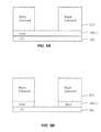
- FIGS. 1 and 2are a flow chart of a oxide deselective etch process and a shallow trench isolation (STI) structure according to disclosed embodiments.
- a gapis formed in a polysilicon adlayer 220 - 1 and an underlying silicon substrate 210 .
- the gapis filled with silicon oxide 230 to electrically isolate devices (not shown).
- the silicon oxideis polished such that the surface is roughly coplanar with the top of the polysilicon and the silicon oxide is trimmed back below the polysilicon to achieve the structure shown in FIG. 2 .
- the process of FIG. 1begins when the substrate is transferred into a processing chamber (operation 110 ). Note that regions of silicon oxide 230 and polysilicon 220 are exposed on the surface of the substrate.
- a flow of nitrogen trifluorideis initiated into a plasma region separate from the processing region (operation 120 ).
- Other sources of fluorinemay be used to augment or replace the nitrogen trifluoride.
- the fluorine-containing precursorcomprises at least one precursor selected from the group consisting of nitrogen trifluoride, diatomic fluorine, monatomic fluorine and fluorine-substituted hydrocarbons.
- the separate plasma regionmay be referred to as a remote plasma region herein and may be within a distinct module from the processing chamber or a compartment within the processing chamber.
- a flow of ammoniamay or may not be present into the remote plasma region during this operation.
- the hydrogen-containing precursorcomprises at least one precursor selected from the group consisting of atomic hydrogen, molecular hydrogen, ammonia, a hydrocarbon and an incompletely halogen-substituted hydrocarbon.
- the flows of nitrogen trifluoride and optional ammoniamay be selected such that the fluorine-to-hydrogen atomic flow ratio is greater than one of 2:1, 5:1 or 10:1.
- Products from the remote plasma(plasma effluents) are flowed into the processing region and allowed to interact with the patterned substrate surface (operation 125 ).
- the patterned layeris selectively etched (operation 130 ) such that the polysilicon adlayer is conformally trimmed while the silicon oxide gapfill 230 is etched more slowly in disclosed embodiments.
- the etch rate of the polysiliconmay be greater than five or ten times the etch rate of the silicon oxide gapfill depending on the ratio of the flow of fluorine to the flow of hydrogen.
- the flows of the gasesare then stopped (operation 135 ) and the substrate is removed from the processing region (operation 145 ).
- the polysiliconmay be trimmed by between 1 nm and 15 nm in disclosed embodiments. Including a significant flow of oxygen into the remote plasma region (and therefore in the plasma effluent flow) is not recommended since the silicon may be oxidized thwarting the desirable etch selectivity towards silicon.
- the plasma region and substrate processing regionare devoid or essentially devoid of oxygen during the etch process, according to embodiments of the invention.
- FIG. 3is a plot of etch quantities after a timed etch such as that used to trim the polysilicon adlayer 220 of FIG. 2 .
- a SiconiTMhaving about twice the atomic concentration of hydrogen as compared with fluorine, results in silicon oxide removal at a significantly greater rate than polysilicon.
- the selectivityinverts as the ratio of hydrogen to fluorine is reduced.
- Polysilicon and silicon oxideare removed at roughly the same rate when equal parts of hydrogen and fluorine are delivered to the remote plasma region. Below a ratio of 1:1 hydrogen:fluorine, the etch rate of polysilicon exceeds that of silicon oxide.
- etch selectivitygreater than 10:1 polysilicon:silicon oxide.
- the techniquemay also be applied to a gap in a silicon substrate without a polysilicon adlayer, in embodiments, and the oxide deselective etch would remove silicon at a greater rate than the silicon oxide gapfill.
- FIGS. 1-3The selective etch represented by FIGS. 1-3 was described in conjunction with a shallow-trench isolation application. A variety of other applications will benefit from this silicon-selective etch.
- this selective etchmay be used to trim the fin of a finFET structure without removing a detrimental quantity of exposed oxygen-containing material such as silicon oxide.
- a finFETcontains a vertical protrusion of single crystalline silicon whose thickness impacts device performance. Single crystalline silicon etches at a similar rate to polysilicon when processed with the remote plasma selective etch described herein.
- a wide variety of alternative geometries to the device structures described hereinare expected to emerge and will benefit from the oxide deselective etch.
- FIG. 4is a flow chart of a selective etch which removes silicon carbon nitride (SiCN) faster than silicon oxy-carbide (SiOC).
- SiCNsilicon carbon nitride
- SiOCsilicon oxy-carbide
- FIGS. 5A-5Bare schematics of an exemplary application before and after the selective etch. The exemplary application involves formation of an inter-metal dielectric layer.
- An underlying copper layer 550has a silicon carbon nitride (SiCN) 560 - 1 formed above it to prevent the diffusion of contaminants from overlying low-K film 570 .
- a suitable SiCN film 560 - 1is BlokTM and a suitable low-K film 570 is Black Diamond, each of which is available from Applied Materials, Santa Clara, Calif.
- the low-K film 570is formed above the layer of SiCN 560 - 1 and patterned with an oxide selective etch to form the trench shown in FIG. 5A .
- the trenchwill later be filled with metal to form a conducting link between different metal layers. Before an ohmic contact can be made, however, the dielectric SiCN must first be removed.
- the process of FIG. 4begins when the patterned substrate is transferred into a processing chamber (operation 410 ).
- a flow of nitrogen trifluorideis initiated into the remote plasma region (operation 420 ).
- the remote plasma regionmay be essentially devoid of hydrogen or have lesser flows of hydrogen as described previously with reference to FIGS. 1-2 . Hydrogen is impossible to completely eliminate from a vacuum system and “essentially devoid” of hydrogen is used to accommodate reasonable tolerances.
- Plasma effluentsare flowed into the processing region and allowed to interact with the patterned substrate surface (operation 425 ).
- the patterned layeris selectively etched (operation 430 ) such that the silicon carbon nitride layer is preferentially removed relative to the silicon oxy-carbide.
- the selective etchcontinues until the portion of the SiCN is removed from the bottom of the trench to allow a subsequent layer of metal to contact the newly exposed carbon surface.
- the flows of the precursorsare stopped (operation 435 ) and the substrate is removed from the processing region (operation 445 ).
- the SiCN film 560 - 2 following the selective etchis shown in FIG. 5B .
- FIG. 6is a plot indicating etch rates of silicon oxycarbide and silicon carbon nitride during an oxide deselective etch according to disclosed embodiments.
- the curvesshow the dependence of etch rate on the partial pressure of nitrogen trifluoride in the substrate processing region.
- the selectivityis further dependent on the concentration of nitrogen trifluoride in the vicinity of the patterned substrate.
- Lower partial pressuresenable an increase in the selectivity of SiCN over SiOC which is preferred in the exemplary application.
- Below about 50 mTorr partial pressure nitrogen trifluoridethe etch rate of both SiCN and SiOC reduce as the partial pressure is reduced. The rate of reduction is faster for the SiOC which allows the selectivity toward etching SiCN to be increased.
- the partial pressure of nitrogen trifluorideis below 50 mTorr, 30 mTorr or 20 mTorr in different embodiments.
- the oxide deselective etch described hereinetches materials which are essentially devoid of oxygen faster than oxygen-and-silicon containing films. It is noteworthy that a small amount of oxygen is often present in SiCN and polysilicon even when inclusion of oxygen is not intended. Furthermore, common measurement techniques used to determine elemental composition may over-report the presence of oxygen due to atmospheric contamination during sample preparation and measurement. Describing a material as “essentially devoid of oxygen” or “oxygen-free” accommodates these as acceptable tolerances. Even more generally, a silicon-containing film having less oxygen will etch more rapidly than a silicon-containing film having more oxygen. In embodiments, the silicon-containing film may consist essentially of silicon either in amorphous, crystalline or polycrystalline form.
- the oxygen-and-silicon-containing filmmay consist essentially of SiO 2 .
- the oxide deselective etchmay still have utility as long as both films have exposed surfaces since each will etch at a different rate.
- the etch rate of an exposed silicon-containing regionmay be greater than an etch rate of an exposed oxygen-and-silicon-containing region by a multiplicative factor greater than five in embodiments of the invention.
- Oxide deselective etcheshave been described thus far.
- the methods described hereinmay be used to selectively etch silicon faster than silicon nitride as shown in FIG. 3 .
- the selectivityis not as pronounced as is the case for silicon etch selectivity over silicon oxide.
- These etch processesmay be referred to herein as nitride deselective etches and have the same process parameter embodiments described with reference to oxide deselective etches.
- the remote plasma region and the substrate processing regionmay each be devoid or essentially devoid of nitrogen during these etch processes, according to embodiments of the invention.
- silicon-containing materialsmay be etched selectively compared to a nitrogen-and-silicon-containing material having a greater nitrogen concentration than the silicon-containing materials.
- the etch rate of an exposed silicon-containing regionmay be greater than an etch rate of an exposed nitrogen-and-silicon-containing material by a multiplicative factor greater than 1.5 in embodiments of the invention.
- Silicon-containing films, such as silicon,may also be etched faster than nitrogen-oxygen-and-silicon-containing films.
- Additional oxide deselective etch process parametersare disclosed in the course of describing an exemplary processing system.
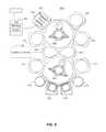
- FIG. 7is a partial cross sectional view showing an illustrative processing chamber 700 , in which, embodiments of the invention may be carried out.
- a hydrogen-containing precursor and a fluorine-containing precursormay be introduced through one or more apertures 751 into remote plasma region(s) 761 - 763 and excited by plasma power source 746 .
- the processing chamber 700includes a chamber body 712 , a lid assembly 702 , and a support assembly 710 .
- the lid assembly 702is disposed at an upper end of the chamber body 712
- the support assembly 710is at least partially disposed within the chamber body 712 .
- the processing chamber 700 and the associated hardwareare preferably formed from one or more process-compatible materials (e.g. aluminum, stainless steel, etc.).
- the chamber body 712includes a slit valve opening 760 formed in a sidewall thereof to provide access to the interior of the processing chamber 700 .
- the slit valve opening 760is selectively opened and closed to allow access to the interior of the chamber body 712 by a wafer handling robot (not shown).
- a wafercan be transported in and out of the processing chamber 700 through the slit valve opening 760 to an adjacent transfer chamber and/or load-lock chamber, or another chamber within a cluster tool.
- An exemplary cluster toolwhich may include processing chamber 700 is shown in FIG. 8 .
- chamber body 712includes a chamber body channel 713 for flowing a heat transfer fluid through chamber body 712 .
- the heat transfer fluidcan be a heating fluid or a coolant and is used to control the temperature of chamber body 712 during processing and substrate transfer. Heating the chamber body 712 may help to prevent unwanted condensation of the gas or byproducts on the chamber walls.
- Exemplary heat transfer fluidsinclude water, ethylene glycol, or a mixture thereof.
- An exemplary heat transfer fluidmay also include nitrogen gas.
- Support assembly 710may have a support assembly channel 704 for flowing a heat transfer fluid through support assembly 710 thereby affecting the substrate temperature.
- the chamber body 712can further include a liner 733 that surrounds the support assembly 710 .
- the liner 733is preferably removable for servicing and cleaning.
- the liner 733can be made of a metal such as aluminum, or a ceramic material. However, the liner 733 can be any process compatible material.
- the liner 733can be bead blasted to increase the adhesion of any material deposited thereon, thereby preventing flaking of material which results in contamination of the processing chamber 700 .
- the liner 733includes one or more apertures 735 and a pumping channel 729 formed therein that is in fluid communication with a vacuum system. The apertures 735 provide a flow path for gases into the pumping channel 729 , which provides an egress for the gases within the processing chamber 700 .
- the vacuum systemcan include a vacuum pump 725 and a throttle valve 727 to regulate flow of gases through the processing chamber 700 .
- the vacuum pump 725is coupled to a vacuum port 731 disposed on the chamber body 712 and therefore, in fluid communication with the pumping channel 729 formed within the liner 733 .
- gasesand “gases” are used interchangeably, unless otherwise noted, and refer to one or more reactants, catalysts, carrier, purge, cleaning, combinations thereof, as well as any other fluid introduced into the chamber body 712 .
- precursoris used to refer to any process gas which takes part in a reaction to either remove or deposit material from a surface.
- Apertures 735allow the pumping channel 729 to be in fluid communication with a processing region 740 within the chamber body 712 .
- the processing region 740is defined by a lower surface of the lid assembly 702 and an upper surface of the support assembly 710 , and is surrounded by the liner 733 .
- the apertures 735may be uniformly sized and evenly spaced about the liner 733 . However, any number, position, size or shape of apertures may be used, and each of those design parameters can vary depending on the desired flow pattern of gas across the substrate receiving surface as is discussed in more detail below. In addition, the size, number and position of the apertures 735 are configured to achieve uniform flow of gases exiting the processing chamber 700 .
- the aperture size and locationmay be configured to provide rapid or high capacity pumping to facilitate a rapid exhaust of gas from the chamber 700 .
- the number and size of apertures 735 in close proximity to the vacuum port 731may be smaller than the size of apertures 735 positioned farther away from the vacuum port 731 .
- a gas supply panel(not shown) is typically used to provide process gas(es) to the processing chamber 700 through one or more apertures 751 .
- the particular gas or gases that are useddepend upon the process or processes to be performed within the chamber 700 .
- Illustrative gasescan include, but are not limited to one or more precursors, reductants, catalysts, carriers, purge, cleaning, or any mixture or combination thereof.
- the one or more gases introduced to the processing chamber 700flow into plasma volume 761 through aperture(s) 751 in top plate 750 .
- processing gasesmay be introduced more directly through aperture(s) 752 into processing region 740 .
- Aperture(s) 752bypass the remote plasma excitation and are useful for processes involving gases that do not require plasma excitation or processes which do not benefit from additional excitation of the gases.
- Electronically operated valves and/or flow control mechanismsmay be used to control the flow of gas from the gas supply into the processing chamber 700 .
- any number of gasescan be delivered to the processing chamber 700 , and can be mixed either in the processing chamber 700 or before the gases are delivered to the processing chamber 700 .
- the lid assembly 702can further include an electrode 745 to generate a plasma of reactive species within the lid assembly 702 .
- the electrode 745is supported by top plate 750 and is electrically isolated therefrom by inserting electrically isolating ring(s) 747 made from aluminum oxide or any other insulating and process compatible material.
- the electrode 745is coupled to a power source 746 while the rest of lid assembly 702 is connected to ground. Accordingly, a plasma of one or more process gases can be generated in remote plasma region composed of volumes 761 , 762 and/or 763 between electrode 745 and annular mounting flange 722 .
- annular mounting flangecomprises or supports gas delivery plate 720 .
- the plasmamay be initiated and maintained between electrode 745 and one or both blocker plates of blocker assembly 730 .
- the plasmacan be struck and contained between the electrode 745 and gas delivery plate 720 , in the absence of blocker assembly 730 .
- the plasmais well confined or contained within the lid assembly 702 . Accordingly, the plasma is a “remote plasma” since no active plasma is in direct contact with the substrate disposed within the chamber body 712 . As a result, plasma damage to the substrate may be avoided since the plasma is separated from the substrate surface.
- a wide variety of power sources 746are capable of activating the nitrogen-containing precursor (nitrogen trifluoride).
- RFradio frequency
- DCdirect current
- MWmicrowave
- the activationmay also be generated by a thermally based technique, a gas breakdown technique, a high intensity light source (e.g., UV energy), or exposure to an x-ray source.
- a remote activation sourcemay be used, such as a remote plasma generator, to generate a plasma of reactive species which are then delivered into the chamber 700 .
- Exemplary remote plasma generatorsare available from vendors such as MKS Instruments, Inc. and Advanced Energy Industries, Inc.
- an RF power supplyis coupled to electrode 745 .
- a higher-power microwave power source 746is beneficial in the event that reactive oxygen will also be produced using power source 746 .
- the temperatures of the process chamber body 712 and the substratemay each be controlled by flowing a heat transfer medium through chamber body channel 713 and support assembly channel 704 , respectively.
- Support assembly channel 704may be formed within support assembly 710 to facilitate the transfer of thermal energy.
- Chamber body 712 and support assembly 710may be cooled or heated independently. For example, a heating fluid may be flown through one while a cooling fluid is flown through the other.
- the substratemay be heated by heating the support assembly 710 (or a portion thereof, such as a pedestal) with a resistive heater or by some other means.
- gas delivery plate 720may be maintained at a temperature higher than the substrate and the substrate can be elevated in order to raise the substrate temperature. In this case the substrate is heated radiatively or by using a gas to conduct heat from gas delivery plate 720 to the substrate.
- the substratemay be elevated by raising support assembly 710 or by employing lift pins.
- chamber body 712may be maintained within an approximate temperature range of between 50° C. and 80° C., between 55° C. and 75° C. or between 60° C. and 70° C. in different embodiments.
- the substratemay be maintained below about 100° C., below about 65° C., between about 15° C. and about 50° C. or between about 22° C. and about 40° C. in different embodiments.
- the substratemay also be held at elevated temperatures during the etch since the oxide deselective etch does not rely as heavily if at all on a sublimation step.
- the substratemay be maintained above 70° C., above 100° C. or above 130° C. in disclosed embodiments.
- Plasma effluentsinclude a variety of molecules, molecular fragments and ionized species. During oxide deselective etching, plasma effluents include fluorine radicals which react readily with exposed silicon-containing material which lacks oxygen or possesses a small amount of oxygen. Plasma effluents may react with a oxygen-free silicon-containing layer to form SiF and H 2 O vapor products which are removed from processing region 740 by vacuum pump 725 .
- the substratemay be heated to sublimate solid residue etch by-products formed upon exposing the substrate to the plasma effluents.
- the gas delivery plate 720is heatable by incorporating heating element 770 within or near gas delivery plate 720 .
- the substratemay be heated by reducing the distance between the substrate and the heated gas delivery plate.
- the gas delivery plate 720may be heated to between about 100° C. and 150° C., between about 110° C. and 140° C. or between about 120° C. and 130° C. in different embodiments.
- the substratemay be heated to above about 75° C., above about 90° C., above about 100° C. or between about 115° C. and about 150° C. in different embodiments.
- the heat radiated from gas delivery plate 720 to the substrateshould be made sufficient to dissociate or sublimate solid (NH 4 ) 2 SiF 6 from the oxide portions of the substrate into volatile SiF 4 , NH 3 and HF products which may be pumped away from processing region 740 .
- Nitrogen trifluoride(or another fluorine-containing precursor) may be flowed into remote plasma volume 761 at rates between about 25 sccm and about 200 sccm, between about 50 sccm and about 150 sccm or between about 75 sccm and about 125 sccm in different embodiments.
- Ammonia(or hydrogen-containing precursors in general) may be flowed into remote plasma volume 761 at rates below or about 20 sccm, below or about 15 sccm, below or about 10 sccm, below or about 5 sccm or below or about 2 sccm in different embodiments.
- Combined flow rates of hydrogen-containing and fluorine-containing precursors into the remote plasma regionmay account for 0.05% to about 20% by volume of the overall gas mixture; the remainder being a carrier gas.
- a purge or carrier gasis first initiated into the remote plasma region before those of the reactive gases to stabilize the pressure within the remote plasma region.
- Plasma powercan be a variety of frequencies or a combination of multiple frequencies.
- the plasmais provided by RF power delivered to electrode 745 .
- the RF powermay be between about 1 W and about 1000 W, between about 5 W and about 600 W, between about 10 W and about 300 W or between about 20 W and about 100 W in different embodiments.
- the RF frequency applied in the exemplary processing systemmay be less than about 200 kHz, less than about 150 kHz, less than about 120 kHz or between about 50 kHz and about 90 kHz in different embodiments.
- Processing region 740can be maintained at a variety of pressures during the flow of plasma effluents into processing region 740 .
- the pressuremay be maintained between about 500 mTorr and about 30 Torr, between about 1 Torr and about 10 Torr or between about 3 Torr and about 6 Torr in different embodiments. Lower pressures may also be used within processing region 740 .
- the pressuremay be maintained below or about 500 mTorr, below or about 250 mTorr, below or about 100 mTorr, below or about 50 mTorr or below or about 20 mTorr in different embodiments.
- the selectivity of the etch processmay be enhanced by neutralizing charged species generated in volumes 761 - 763 prior to flowing plasma effluents into the substrate processing region.
- Neutral reactive radicalsmolecular fragments
- the holes in the showerheadmay be narrowed to increase the neutralizing collisions as effluents migrate toward the substrate processing region.
- a separate showerheadmay also be included in the path of the plasma effluents to suppress the flow of ions into the substrate processing region.
- the separate showerheadmay be referred to as an ion suppressor (not shown).
- These neutral (uncharged) speciesmay still include highly reactive species that are transported with less reactive carrier gas through the holes.
- the flow of ionized effluents into the substrate processing regionmay be reduced to below the flow of neutral species on a per molecular fragment basis.
- the flowmay also be below 10% of the neutral species or may be essentially eliminated, in disclosed embodiments. Controlling the amount of ionic species passing into the substrate processing region provides increased control over the gas mixture brought into contact with the underlying wafer substrate, increasing control of the selectivity of the etch process.
- a plurality of holes in the ion suppressor and/or the showerheadmay be configured to control the passage of the activated gas (i.e., the ionic, radical, and/or neutral species) into the substrate processing region.
- the aspect ratio of the holes (i.e., the hole diameter to length) and/or the geometry of the holesmay be controlled so that the flow of ionically-charged species in the activated gas passing into the substrate processing region is reduced.
- the holesmay include a tapered portion that faces the remote plasma region (volumes 761 , 762 and/or 763 ). The taper may serve to allow a substantial number of effluents into the hole but force a large percentage of the effluents to undergo neutralizing collisions prior to entering the substrate processing region.
- An adjustable electrical biasmay also be applied to the ion suppressor and/or showerhead as an additional means to control the flow of ionic species through the suppressor.
- the processing chamber 700can be integrated into a variety of multi-processing platforms, including the ProducerTM GT, CenturaTM AP and EnduraTM platforms available from Applied Materials, Inc. located in Santa Clara, Calif. Such a processing platform is capable of performing several processing operations without breaking vacuum.
- FIG. 8is a schematic top-view diagram of an illustrative multi-chamber processing system 800 .
- the system 800can include one or more load lock chambers 802 , 804 for transferring of substrates into and out of the system 800 .
- the load lock chambers 802 , 804may “pump down” the substrates introduced into the system 800 .
- a first robot 810may transfer the substrates between the load lock chambers 802 , 804 , and a first set of one or more substrate processing chambers 812 , 814 , 816 , 818 (four are shown).
- Each processing chamber 812 , 814 , 816 , 818can be outfitted to perform a number of substrate processing operations including the dry etch processes described herein in addition to cyclical layer deposition (CLD), atomic layer deposition (ALD), chemical vapor deposition (CVD), physical vapor deposition (PVD), etch, pre-clean, degas, orientation and other substrate processes.
- CLDcyclical layer deposition
- ALDatomic layer deposition
- CVDchemical vapor deposition
- PVDphysical vapor deposition
- etchpre-clean, degas, orientation and other substrate processes.
- the first robot 810can also transfer substrates to/from one or more transfer chambers 822 , 824 .
- the transfer chambers 822 , 824can be used to maintain ultrahigh vacuum conditions while allowing substrates to be transferred within the system 800 .
- a second robot 830can transfer the substrates between the transfer chambers 822 , 824 and a second set of one or more processing chambers 832 , 834 , 836 , 838 .
- the processing chambers 832 , 834 , 836 , 838can be outfitted to perform a variety of substrate processing operations including the dry etch processes described herein in addition to cyclical layer deposition (CLD), atomic layer deposition (ALD), chemical vapor deposition (CVD), physical vapor deposition (PVD), etch, pre-clean, degas, and orientation, for example.
- CLDcyclical layer deposition
- ALDatomic layer deposition
- CVDchemical vapor deposition
- PVDphysical vapor deposition
- etchpre-clean, degas, and orientation, for example.
- Any of the substrate processing chambers 812 , 814 , 816 , 818 , 832 , 834 , 836 , 838may be removed from the system 800 if not necessary for a particular process to be performed by the system 800 .
- System controller 857is used to control motors, valves, flow controllers, power supplies and other functions required to carry out process recipes described herein.
- System controller 857may rely on feedback from optical sensors to determine and adjust the position of movable mechanical assemblies.
- Mechanical assembliesmay include the robot, throttle valves and susceptors which are moved by motors under the control of system controller 857 .
- system controller 857includes a hard disk drive (memory), USB ports, a floppy disk drive and a processor.
- System controller 857includes analog and digital input/output boards, interface boards and stepper motor controller boards.
- Various parts of multi-chamber processing system 800 which contains processing chamber 800are controlled by system controller 857 .
- the system controllerexecutes system control software in the form of a computer program stored on computer-readable medium such as a hard disk, a floppy disk or a flash memory thumb drive. Other types of memory can also be used.
- the computer programincludes sets of instructions that dictate the timing, mixture of gases, chamber pressure, chamber temperature, RF power levels, susceptor position, and other parameters of a particular process.
- a process for etching, depositing or otherwise processing a film on a substrate or a process for cleaning chambercan be implemented using a computer program product that is executed by the controller.
- the computer program codecan be written in any conventional computer readable programming language: for example, 68000 assembly language, C, C++, Pascal, Fortran or others.
- Suitable program codeis entered into a single file, or multiple files, using a conventional text editor, and stored or embodied in a computer usable medium, such as a memory system of the computer. If the entered code text is in a high level language, the code is compiled, and the resultant compiler code is then linked with an object code of precompiled Microsoft Windows® library routines. To execute the linked, compiled object code the system user invokes the object code, causing the computer system to load the code in memory. The CPU then reads and executes the code to perform the tasks identified in the program.
- the interface between a user and the controllermay be via a touch-sensitive monitor and may also include a mouse and keyboard.
- two monitorsare used, one mounted in the clean room wall for the operators and the other behind the wall for the service technicians.
- the two monitorsmay simultaneously display the same information, in which case only one is configured to accept input at a time.
- the operatortouches a designated area on the display screen with a finger or the mouse.
- the touched areachanges its highlighted color, or a new menu or screen is displayed, confirming the operator's selection.
- substratemay be a support substrate with or without layers formed thereon.
- the support substratemay be an insulator or a semiconductor of a variety of doping concentrations and profiles and may, for example, be a semiconductor substrate of the type used in the manufacture of integrated circuits.
- a gas in an “excited state”describes a gas wherein at least some of the gas molecules are in vibrationally-excited, dissociated and/or ionized states.
- a gasmay be a combination of two or more gases.
- Silicon oxideis predominantly SiO 2 but may include concentrations of other elemental constituents such as nitrogen, hydrogen, carbon and the like.
- the terms “gap” and “trench”are used throughout with no implication that the etched geometry has a large horizontal aspect ratio.
- a conformal etch processrefers to a generally uniform removal of material on a surface in the same shape as the surface, i.e., the surface of the etched layer and the pre-etch surface are generally parallel.
- the etched interfacelikely cannot be 100% conformal and thus the term “generally” allows for acceptable tolerances.
Landscapes
- Engineering & Computer Science (AREA)
- Physics & Mathematics (AREA)
- Microelectronics & Electronic Packaging (AREA)
- Power Engineering (AREA)
- Condensed Matter Physics & Semiconductors (AREA)
- General Physics & Mathematics (AREA)
- Manufacturing & Machinery (AREA)
- Computer Hardware Design (AREA)
- Chemical & Material Sciences (AREA)
- Plasma & Fusion (AREA)
- Chemical Kinetics & Catalysis (AREA)
- General Chemical & Material Sciences (AREA)
- Inorganic Chemistry (AREA)
- Electromagnetism (AREA)
- Spectroscopy & Molecular Physics (AREA)
- Drying Of Semiconductors (AREA)
- Internal Circuitry In Semiconductor Integrated Circuit Devices (AREA)
Abstract
Description
Claims (16)
Priority Applications (13)
| Application Number | Priority Date | Filing Date | Title |
|---|---|---|---|
| US13/088,930US9324576B2 (en) | 2010-05-27 | 2011-04-18 | Selective etch for silicon films |
| PCT/US2011/035598WO2011149638A2 (en) | 2010-05-27 | 2011-05-06 | Selective etch for silicon films |
| CN2011800261608ACN102918635A (en) | 2010-05-27 | 2011-05-06 | Selective etch for silicon films |
| KR1020127033885AKR101884262B1 (en) | 2010-05-27 | 2011-05-06 | Selective etch for silicon films |
| SG2012082921ASG185514A1 (en) | 2010-05-27 | 2011-05-06 | Selective etch for silicon films |
| JP2013512633AJP2013529391A (en) | 2010-05-27 | 2011-05-06 | Selective etching for silicon film |
| TW100116201ATWI555079B (en) | 2010-05-27 | 2011-05-09 | Selective etch for silicon films |
| US13/416,277US8999856B2 (en) | 2011-03-14 | 2012-03-09 | Methods for etch of sin films |
| US13/416,223US9064815B2 (en) | 2011-03-14 | 2012-03-09 | Methods for etch of metal and metal-oxide films |
| US14/679,242US9343327B2 (en) | 2011-03-14 | 2015-04-06 | Methods for etch of sin films |
| US14/746,670US10062578B2 (en) | 2011-03-14 | 2015-06-22 | Methods for etch of metal and metal-oxide films |
| US15/137,754US9754800B2 (en) | 2010-05-27 | 2016-04-25 | Selective etch for silicon films |
| US15/155,596US9842744B2 (en) | 2011-03-14 | 2016-05-16 | Methods for etch of SiN films |
Applications Claiming Priority (2)
| Application Number | Priority Date | Filing Date | Title |
|---|---|---|---|
| US34892010P | 2010-05-27 | 2010-05-27 | |
| US13/088,930US9324576B2 (en) | 2010-05-27 | 2011-04-18 | Selective etch for silicon films |
Related Child Applications (1)
| Application Number | Title | Priority Date | Filing Date |
|---|---|---|---|
| US15/137,754ContinuationUS9754800B2 (en) | 2010-05-27 | 2016-04-25 | Selective etch for silicon films |
Publications (2)
| Publication Number | Publication Date |
|---|---|
| US20110294300A1 US20110294300A1 (en) | 2011-12-01 |
| US9324576B2true US9324576B2 (en) | 2016-04-26 |
Family
ID=45004641
Family Applications (2)
| Application Number | Title | Priority Date | Filing Date |
|---|---|---|---|
| US13/088,930Active2032-01-02US9324576B2 (en) | 2010-05-27 | 2011-04-18 | Selective etch for silicon films |
| US15/137,754ActiveUS9754800B2 (en) | 2010-05-27 | 2016-04-25 | Selective etch for silicon films |
Family Applications After (1)
| Application Number | Title | Priority Date | Filing Date |
|---|---|---|---|
| US15/137,754ActiveUS9754800B2 (en) | 2010-05-27 | 2016-04-25 | Selective etch for silicon films |
Country Status (7)
| Country | Link |
|---|---|
| US (2) | US9324576B2 (en) |
| JP (1) | JP2013529391A (en) |
| KR (1) | KR101884262B1 (en) |
| CN (1) | CN102918635A (en) |
| SG (1) | SG185514A1 (en) |
| TW (1) | TWI555079B (en) |
| WO (1) | WO2011149638A2 (en) |
Cited By (106)
| Publication number | Priority date | Publication date | Assignee | Title |
|---|---|---|---|---|
| US9472417B2 (en) | 2013-11-12 | 2016-10-18 | Applied Materials, Inc. | Plasma-free metal etch |
| US9472412B2 (en) | 2013-12-02 | 2016-10-18 | Applied Materials, Inc. | Procedure for etch rate consistency |
| US9478432B2 (en) | 2014-09-25 | 2016-10-25 | Applied Materials, Inc. | Silicon oxide selective removal |
| US9478434B2 (en) | 2014-09-24 | 2016-10-25 | Applied Materials, Inc. | Chlorine-based hardmask removal |
| US9493879B2 (en) | 2013-07-12 | 2016-11-15 | Applied Materials, Inc. | Selective sputtering for pattern transfer |
| US9496167B2 (en) | 2014-07-31 | 2016-11-15 | Applied Materials, Inc. | Integrated bit-line airgap formation and gate stack post clean |
| US9499898B2 (en) | 2014-03-03 | 2016-11-22 | Applied Materials, Inc. | Layered thin film heater and method of fabrication |
| US9502258B2 (en) | 2014-12-23 | 2016-11-22 | Applied Materials, Inc. | Anisotropic gap etch |
| US9553102B2 (en) | 2014-08-19 | 2017-01-24 | Applied Materials, Inc. | Tungsten separation |
| US9564296B2 (en) | 2014-03-20 | 2017-02-07 | Applied Materials, Inc. | Radial waveguide systems and methods for post-match control of microwaves |
| US9576809B2 (en) | 2013-11-04 | 2017-02-21 | Applied Materials, Inc. | Etch suppression with germanium |
| US9607856B2 (en) | 2013-03-05 | 2017-03-28 | Applied Materials, Inc. | Selective titanium nitride removal |
| US9659792B2 (en) | 2013-03-15 | 2017-05-23 | Applied Materials, Inc. | Processing systems and methods for halide scavenging |
| US9659753B2 (en) | 2014-08-07 | 2017-05-23 | Applied Materials, Inc. | Grooved insulator to reduce leakage current |
| US9679780B1 (en)* | 2016-09-28 | 2017-06-13 | International Business Machines Corporation | Polysilicon residue removal in nanosheet MOSFETs |
| US9691645B2 (en) | 2015-08-06 | 2017-06-27 | Applied Materials, Inc. | Bolted wafer chuck thermal management systems and methods for wafer processing systems |
| US9721789B1 (en) | 2016-10-04 | 2017-08-01 | Applied Materials, Inc. | Saving ion-damaged spacers |
| US9728437B2 (en) | 2015-02-03 | 2017-08-08 | Applied Materials, Inc. | High temperature chuck for plasma processing systems |
| US9741593B2 (en) | 2015-08-06 | 2017-08-22 | Applied Materials, Inc. | Thermal management systems and methods for wafer processing systems |
| US9754800B2 (en) | 2010-05-27 | 2017-09-05 | Applied Materials, Inc. | Selective etch for silicon films |
| US9768034B1 (en) | 2016-11-11 | 2017-09-19 | Applied Materials, Inc. | Removal methods for high aspect ratio structures |
| US9773648B2 (en) | 2013-08-30 | 2017-09-26 | Applied Materials, Inc. | Dual discharge modes operation for remote plasma |
| US9842744B2 (en) | 2011-03-14 | 2017-12-12 | Applied Materials, Inc. | Methods for etch of SiN films |
| US9865484B1 (en) | 2016-06-29 | 2018-01-09 | Applied Materials, Inc. | Selective etch using material modification and RF pulsing |
| US9881805B2 (en) | 2015-03-02 | 2018-01-30 | Applied Materials, Inc. | Silicon selective removal |
| US9885117B2 (en) | 2014-03-31 | 2018-02-06 | Applied Materials, Inc. | Conditioned semiconductor system parts |
| US9934942B1 (en) | 2016-10-04 | 2018-04-03 | Applied Materials, Inc. | Chamber with flow-through source |
| US9947549B1 (en) | 2016-10-10 | 2018-04-17 | Applied Materials, Inc. | Cobalt-containing material removal |
| US9966240B2 (en) | 2014-10-14 | 2018-05-08 | Applied Materials, Inc. | Systems and methods for internal surface conditioning assessment in plasma processing equipment |
| US9978564B2 (en) | 2012-09-21 | 2018-05-22 | Applied Materials, Inc. | Chemical control features in wafer process equipment |
| US10026621B2 (en) | 2016-11-14 | 2018-07-17 | Applied Materials, Inc. | SiN spacer profile patterning |
| US10032606B2 (en) | 2012-08-02 | 2018-07-24 | Applied Materials, Inc. | Semiconductor processing with DC assisted RF power for improved control |
| US10043684B1 (en) | 2017-02-06 | 2018-08-07 | Applied Materials, Inc. | Self-limiting atomic thermal etching systems and methods |
| US10043674B1 (en) | 2017-08-04 | 2018-08-07 | Applied Materials, Inc. | Germanium etching systems and methods |
| US10049891B1 (en) | 2017-05-31 | 2018-08-14 | Applied Materials, Inc. | Selective in situ cobalt residue removal |
| US10062579B2 (en) | 2016-10-07 | 2018-08-28 | Applied Materials, Inc. | Selective SiN lateral recess |
| US10062578B2 (en) | 2011-03-14 | 2018-08-28 | Applied Materials, Inc. | Methods for etch of metal and metal-oxide films |
| US10062585B2 (en) | 2016-10-04 | 2018-08-28 | Applied Materials, Inc. | Oxygen compatible plasma source |
| US10062575B2 (en) | 2016-09-09 | 2018-08-28 | Applied Materials, Inc. | Poly directional etch by oxidation |
| US10062587B2 (en) | 2012-07-18 | 2018-08-28 | Applied Materials, Inc. | Pedestal with multi-zone temperature control and multiple purge capabilities |
| US10128086B1 (en) | 2017-10-24 | 2018-11-13 | Applied Materials, Inc. | Silicon pretreatment for nitride removal |
| US10163696B2 (en) | 2016-11-11 | 2018-12-25 | Applied Materials, Inc. | Selective cobalt removal for bottom up gapfill |
| US10170336B1 (en) | 2017-08-04 | 2019-01-01 | Applied Materials, Inc. | Methods for anisotropic control of selective silicon removal |
| US10224210B2 (en) | 2014-12-09 | 2019-03-05 | Applied Materials, Inc. | Plasma processing system with direct outlet toroidal plasma source |
| US10242908B2 (en) | 2016-11-14 | 2019-03-26 | Applied Materials, Inc. | Airgap formation with damage-free copper |
| US10256112B1 (en) | 2017-12-08 | 2019-04-09 | Applied Materials, Inc. | Selective tungsten removal |
| US10256079B2 (en) | 2013-02-08 | 2019-04-09 | Applied Materials, Inc. | Semiconductor processing systems having multiple plasma configurations |
| US10283321B2 (en) | 2011-01-18 | 2019-05-07 | Applied Materials, Inc. | Semiconductor processing system and methods using capacitively coupled plasma |
| US10283324B1 (en) | 2017-10-24 | 2019-05-07 | Applied Materials, Inc. | Oxygen treatment for nitride etching |
| US10297458B2 (en) | 2017-08-07 | 2019-05-21 | Applied Materials, Inc. | Process window widening using coated parts in plasma etch processes |
| US10319600B1 (en) | 2018-03-12 | 2019-06-11 | Applied Materials, Inc. | Thermal silicon etch |
| US10319649B2 (en) | 2017-04-11 | 2019-06-11 | Applied Materials, Inc. | Optical emission spectroscopy (OES) for remote plasma monitoring |
| US10319739B2 (en) | 2017-02-08 | 2019-06-11 | Applied Materials, Inc. | Accommodating imperfectly aligned memory holes |
| US20190211450A1 (en)* | 2018-01-10 | 2019-07-11 | Asm Ip Holding B.V. | Shower plate structure for supplying carrier and dry gas |
| US10354889B2 (en) | 2017-07-17 | 2019-07-16 | Applied Materials, Inc. | Non-halogen etching of silicon-containing materials |
| US10403507B2 (en) | 2017-02-03 | 2019-09-03 | Applied Materials, Inc. | Shaped etch profile with oxidation |
| US10424464B2 (en) | 2015-08-07 | 2019-09-24 | Applied Materials, Inc. | Oxide etch selectivity systems and methods |
| US10424485B2 (en) | 2013-03-01 | 2019-09-24 | Applied Materials, Inc. | Enhanced etching processes using remote plasma sources |
| US10431429B2 (en) | 2017-02-03 | 2019-10-01 | Applied Materials, Inc. | Systems and methods for radial and azimuthal control of plasma uniformity |
| US10465294B2 (en) | 2014-05-28 | 2019-11-05 | Applied Materials, Inc. | Oxide and metal removal |
| US10468267B2 (en) | 2017-05-31 | 2019-11-05 | Applied Materials, Inc. | Water-free etching methods |
| US10490406B2 (en) | 2018-04-10 | 2019-11-26 | Appled Materials, Inc. | Systems and methods for material breakthrough |
| US10497573B2 (en) | 2018-03-13 | 2019-12-03 | Applied Materials, Inc. | Selective atomic layer etching of semiconductor materials |
| US10504700B2 (en) | 2015-08-27 | 2019-12-10 | Applied Materials, Inc. | Plasma etching systems and methods with secondary plasma injection |
| US10504754B2 (en) | 2016-05-19 | 2019-12-10 | Applied Materials, Inc. | Systems and methods for improved semiconductor etching and component protection |
| US10522371B2 (en) | 2016-05-19 | 2019-12-31 | Applied Materials, Inc. | Systems and methods for improved semiconductor etching and component protection |
| US10541246B2 (en) | 2017-06-26 | 2020-01-21 | Applied Materials, Inc. | 3D flash memory cells which discourage cross-cell electrical tunneling |
| US10541184B2 (en) | 2017-07-11 | 2020-01-21 | Applied Materials, Inc. | Optical emission spectroscopic techniques for monitoring etching |
| US10546729B2 (en) | 2016-10-04 | 2020-01-28 | Applied Materials, Inc. | Dual-channel showerhead with improved profile |
| US10566206B2 (en) | 2016-12-27 | 2020-02-18 | Applied Materials, Inc. | Systems and methods for anisotropic material breakthrough |
| US10573527B2 (en) | 2018-04-06 | 2020-02-25 | Applied Materials, Inc. | Gas-phase selective etching systems and methods |
| US10573496B2 (en) | 2014-12-09 | 2020-02-25 | Applied Materials, Inc. | Direct outlet toroidal plasma source |
| US10593560B2 (en) | 2018-03-01 | 2020-03-17 | Applied Materials, Inc. | Magnetic induction plasma source for semiconductor processes and equipment |
| US10593523B2 (en) | 2014-10-14 | 2020-03-17 | Applied Materials, Inc. | Systems and methods for internal surface conditioning in plasma processing equipment |
| US10615047B2 (en) | 2018-02-28 | 2020-04-07 | Applied Materials, Inc. | Systems and methods to form airgaps |
| US10629473B2 (en) | 2016-09-09 | 2020-04-21 | Applied Materials, Inc. | Footing removal for nitride spacer |
| US10672642B2 (en) | 2018-07-24 | 2020-06-02 | Applied Materials, Inc. | Systems and methods for pedestal configuration |
| US10679870B2 (en) | 2018-02-15 | 2020-06-09 | Applied Materials, Inc. | Semiconductor processing chamber multistage mixing apparatus |
| US10699879B2 (en) | 2018-04-17 | 2020-06-30 | Applied Materials, Inc. | Two piece electrode assembly with gap for plasma control |
| US10727080B2 (en) | 2017-07-07 | 2020-07-28 | Applied Materials, Inc. | Tantalum-containing material removal |
| US10755941B2 (en) | 2018-07-06 | 2020-08-25 | Applied Materials, Inc. | Self-limiting selective etching systems and methods |
| US10804368B2 (en) | 2018-07-30 | 2020-10-13 | International Business Machines Corporation | Semiconductor device having two-part spacer |
| US10854426B2 (en) | 2018-01-08 | 2020-12-01 | Applied Materials, Inc. | Metal recess for semiconductor structures |
| US10872778B2 (en) | 2018-07-06 | 2020-12-22 | Applied Materials, Inc. | Systems and methods utilizing solid-phase etchants |
| US10886137B2 (en) | 2018-04-30 | 2021-01-05 | Applied Materials, Inc. | Selective nitride removal |
| US10892198B2 (en) | 2018-09-14 | 2021-01-12 | Applied Materials, Inc. | Systems and methods for improved performance in semiconductor processing |
| US10896816B2 (en) | 2017-09-26 | 2021-01-19 | International Business Machines Corporation | Silicon residue removal in nanosheet transistors |
| US10903054B2 (en) | 2017-12-19 | 2021-01-26 | Applied Materials, Inc. | Multi-zone gas distribution systems and methods |
| US10920320B2 (en) | 2017-06-16 | 2021-02-16 | Applied Materials, Inc. | Plasma health determination in semiconductor substrate processing reactors |
| US10920319B2 (en) | 2019-01-11 | 2021-02-16 | Applied Materials, Inc. | Ceramic showerheads with conductive electrodes |
| US10943834B2 (en) | 2017-03-13 | 2021-03-09 | Applied Materials, Inc. | Replacement contact process |
| US10964512B2 (en) | 2018-02-15 | 2021-03-30 | Applied Materials, Inc. | Semiconductor processing chamber multistage mixing apparatus and methods |
| US11049755B2 (en) | 2018-09-14 | 2021-06-29 | Applied Materials, Inc. | Semiconductor substrate supports with embedded RF shield |
| US11062887B2 (en) | 2018-09-17 | 2021-07-13 | Applied Materials, Inc. | High temperature RF heater pedestals |
| US11121002B2 (en) | 2018-10-24 | 2021-09-14 | Applied Materials, Inc. | Systems and methods for etching metals and metal derivatives |
| US11239061B2 (en) | 2014-11-26 | 2022-02-01 | Applied Materials, Inc. | Methods and systems to enhance process uniformity |
| US11257693B2 (en) | 2015-01-09 | 2022-02-22 | Applied Materials, Inc. | Methods and systems to improve pedestal temperature control |
| US11276559B2 (en) | 2017-05-17 | 2022-03-15 | Applied Materials, Inc. | Semiconductor processing chamber for multiple precursor flow |
| US11276590B2 (en) | 2017-05-17 | 2022-03-15 | Applied Materials, Inc. | Multi-zone semiconductor substrate supports |
| US11328909B2 (en) | 2017-12-22 | 2022-05-10 | Applied Materials, Inc. | Chamber conditioning and removal processes |
| US11417534B2 (en) | 2018-09-21 | 2022-08-16 | Applied Materials, Inc. | Selective material removal |
| US11437242B2 (en) | 2018-11-27 | 2022-09-06 | Applied Materials, Inc. | Selective removal of silicon-containing materials |
| US11594428B2 (en) | 2015-02-03 | 2023-02-28 | Applied Materials, Inc. | Low temperature chuck for plasma processing systems |
| US11682560B2 (en) | 2018-10-11 | 2023-06-20 | Applied Materials, Inc. | Systems and methods for hafnium-containing film removal |
| US11721527B2 (en) | 2019-01-07 | 2023-08-08 | Applied Materials, Inc. | Processing chamber mixing systems |
| US12340979B2 (en) | 2017-05-17 | 2025-06-24 | Applied Materials, Inc. | Semiconductor processing chamber for improved precursor flow |
Families Citing this family (73)
| Publication number | Priority date | Publication date | Assignee | Title |
|---|---|---|---|---|
| KR20120040761A (en)* | 2010-08-26 | 2012-04-30 | 삼성전자주식회사 | Method for manufacturing non-volatile memory device |
| US8741778B2 (en) | 2010-12-14 | 2014-06-03 | Applied Materials, Inc. | Uniform dry etch in two stages |
| US8771539B2 (en) | 2011-02-22 | 2014-07-08 | Applied Materials, Inc. | Remotely-excited fluorine and water vapor etch |
| US8771536B2 (en) | 2011-08-01 | 2014-07-08 | Applied Materials, Inc. | Dry-etch for silicon-and-carbon-containing films |
| US8679982B2 (en)* | 2011-08-26 | 2014-03-25 | Applied Materials, Inc. | Selective suppression of dry-etch rate of materials containing both silicon and oxygen |
| US8679983B2 (en) | 2011-09-01 | 2014-03-25 | Applied Materials, Inc. | Selective suppression of dry-etch rate of materials containing both silicon and nitrogen |
| US8927390B2 (en) | 2011-09-26 | 2015-01-06 | Applied Materials, Inc. | Intrench profile |
| US8808563B2 (en)* | 2011-10-07 | 2014-08-19 | Applied Materials, Inc. | Selective etch of silicon by way of metastable hydrogen termination |
| WO2013070436A1 (en) | 2011-11-08 | 2013-05-16 | Applied Materials, Inc. | Methods of reducing substrate dislocation during gapfill processing |
| US9418866B2 (en)* | 2012-06-08 | 2016-08-16 | Tokyo Electron Limited | Gas treatment method |
| US8916477B2 (en)* | 2012-07-02 | 2014-12-23 | Novellus Systems, Inc. | Polysilicon etch with high selectivity |
| US10283615B2 (en) | 2012-07-02 | 2019-05-07 | Novellus Systems, Inc. | Ultrahigh selective polysilicon etch with high throughput |
| US9034773B2 (en)* | 2012-07-02 | 2015-05-19 | Novellus Systems, Inc. | Removal of native oxide with high selectivity |
| US9034770B2 (en)* | 2012-09-17 | 2015-05-19 | Applied Materials, Inc. | Differential silicon oxide etch |
| US9023734B2 (en) | 2012-09-18 | 2015-05-05 | Applied Materials, Inc. | Radical-component oxide etch |
| US9390937B2 (en)* | 2012-09-20 | 2016-07-12 | Applied Materials, Inc. | Silicon-carbon-nitride selective etch |
| US8765574B2 (en) | 2012-11-09 | 2014-07-01 | Applied Materials, Inc. | Dry etch process |
| US8969212B2 (en) | 2012-11-20 | 2015-03-03 | Applied Materials, Inc. | Dry-etch selectivity |
| US9064816B2 (en) | 2012-11-30 | 2015-06-23 | Applied Materials, Inc. | Dry-etch for selective oxidation removal |
| US8980763B2 (en) | 2012-11-30 | 2015-03-17 | Applied Materials, Inc. | Dry-etch for selective tungsten removal |
| US9111877B2 (en) | 2012-12-18 | 2015-08-18 | Applied Materials, Inc. | Non-local plasma oxide etch |
| US8921234B2 (en) | 2012-12-21 | 2014-12-30 | Applied Materials, Inc. | Selective titanium nitride etching |
| US8801952B1 (en) | 2013-03-07 | 2014-08-12 | Applied Materials, Inc. | Conformal oxide dry etch |
| US10170282B2 (en) | 2013-03-08 | 2019-01-01 | Applied Materials, Inc. | Insulated semiconductor faceplate designs |
| US20140273451A1 (en)* | 2013-03-13 | 2014-09-18 | Applied Materials, Inc. | Tungsten deposition sequence |
| US8895449B1 (en) | 2013-05-16 | 2014-11-25 | Applied Materials, Inc. | Delicate dry clean |
| US9114438B2 (en) | 2013-05-21 | 2015-08-25 | Applied Materials, Inc. | Copper residue chamber clean |
| US8956980B1 (en) | 2013-09-16 | 2015-02-17 | Applied Materials, Inc. | Selective etch of silicon nitride |
| US8951429B1 (en) | 2013-10-29 | 2015-02-10 | Applied Materials, Inc. | Tungsten oxide processing |
| US9236265B2 (en) | 2013-11-04 | 2016-01-12 | Applied Materials, Inc. | Silicon germanium processing |
| US9117855B2 (en) | 2013-12-04 | 2015-08-25 | Applied Materials, Inc. | Polarity control for remote plasma |
| US9263278B2 (en) | 2013-12-17 | 2016-02-16 | Applied Materials, Inc. | Dopant etch selectivity control |
| US9287095B2 (en) | 2013-12-17 | 2016-03-15 | Applied Materials, Inc. | Semiconductor system assemblies and methods of operation |
| US9190293B2 (en) | 2013-12-18 | 2015-11-17 | Applied Materials, Inc. | Even tungsten etch for high aspect ratio trenches |
| US9287134B2 (en) | 2014-01-17 | 2016-03-15 | Applied Materials, Inc. | Titanium oxide etch |
| US9396989B2 (en) | 2014-01-27 | 2016-07-19 | Applied Materials, Inc. | Air gaps between copper lines |
| US9293568B2 (en) | 2014-01-27 | 2016-03-22 | Applied Materials, Inc. | Method of fin patterning |
| US9385028B2 (en) | 2014-02-03 | 2016-07-05 | Applied Materials, Inc. | Air gap process |
| US9368370B2 (en)* | 2014-03-14 | 2016-06-14 | Applied Materials, Inc. | Temperature ramping using gas distribution plate heat |
| US9299575B2 (en) | 2014-03-17 | 2016-03-29 | Applied Materials, Inc. | Gas-phase tungsten etch |
| US9299538B2 (en) | 2014-03-20 | 2016-03-29 | Applied Materials, Inc. | Radial waveguide systems and methods for post-match control of microwaves |
| US9136273B1 (en) | 2014-03-21 | 2015-09-15 | Applied Materials, Inc. | Flash gate air gap |
| US9190290B2 (en)* | 2014-03-31 | 2015-11-17 | Applied Materials, Inc. | Halogen-free gas-phase silicon etch |
| US9269590B2 (en) | 2014-04-07 | 2016-02-23 | Applied Materials, Inc. | Spacer formation |
| US9847289B2 (en) | 2014-05-30 | 2017-12-19 | Applied Materials, Inc. | Protective via cap for improved interconnect performance |
| US9406523B2 (en) | 2014-06-19 | 2016-08-02 | Applied Materials, Inc. | Highly selective doped oxide removal method |
| US9378969B2 (en) | 2014-06-19 | 2016-06-28 | Applied Materials, Inc. | Low temperature gas-phase carbon removal |
| CN105225955A (en)* | 2014-06-20 | 2016-01-06 | 中芯国际集成电路制造(上海)有限公司 | The manufacture method, semiconductor device and preparation method thereof of fin and sti structure |
| JP6235981B2 (en)* | 2014-07-01 | 2017-11-22 | 東京エレクトロン株式会社 | Method for processing an object |
| US9425058B2 (en) | 2014-07-24 | 2016-08-23 | Applied Materials, Inc. | Simplified litho-etch-litho-etch process |
| US9378978B2 (en) | 2014-07-31 | 2016-06-28 | Applied Materials, Inc. | Integrated oxide recess and floating gate fin trimming |
| US9159606B1 (en) | 2014-07-31 | 2015-10-13 | Applied Materials, Inc. | Metal air gap |
| US9165786B1 (en) | 2014-08-05 | 2015-10-20 | Applied Materials, Inc. | Integrated oxide and nitride recess for better channel contact in 3D architectures |
| US9558928B2 (en) | 2014-08-29 | 2017-01-31 | Lam Research Corporation | Contact clean in high-aspect ratio structures |
| US9355856B2 (en) | 2014-09-12 | 2016-05-31 | Applied Materials, Inc. | V trench dry etch |
| US9368364B2 (en) | 2014-09-24 | 2016-06-14 | Applied Materials, Inc. | Silicon etch process with tunable selectivity to SiO2 and other materials |
| US9299583B1 (en) | 2014-12-05 | 2016-03-29 | Applied Materials, Inc. | Aluminum oxide selective etch |
| US9343272B1 (en) | 2015-01-08 | 2016-05-17 | Applied Materials, Inc. | Self-aligned process |
| US9373522B1 (en) | 2015-01-22 | 2016-06-21 | Applied Mateials, Inc. | Titanium nitride removal |
| US9449846B2 (en) | 2015-01-28 | 2016-09-20 | Applied Materials, Inc. | Vertical gate separation |
| US9449843B1 (en) | 2015-06-09 | 2016-09-20 | Applied Materials, Inc. | Selectively etching metals and metal nitrides conformally |
| US9922840B2 (en)* | 2015-07-07 | 2018-03-20 | Applied Materials, Inc. | Adjustable remote dissociation |
| US9659791B2 (en) | 2015-07-16 | 2017-05-23 | Applied Materials, Inc. | Metal removal with reduced surface roughness |
| TWI727992B (en)* | 2015-11-11 | 2021-05-21 | 美商諾發系統有限公司 | Ultrahigh selective polysilicon etch with high throughput |
| US10141161B2 (en) | 2016-09-12 | 2018-11-27 | Varian Semiconductor Equipment Associates, Inc. | Angle control for radicals and reactive neutral ion beams |
| CN110178201B (en)* | 2017-01-13 | 2023-06-16 | 应用材料公司 | Method and equipment for low temperature silicon nitride film |
| KR102018075B1 (en)* | 2017-11-30 | 2019-09-04 | 무진전자 주식회사 | Dry clean apparatus and method for removing polysilicon seletively |
| KR102003362B1 (en)* | 2017-11-30 | 2019-10-17 | 무진전자 주식회사 | Dry clean apparatus and method for removing silicon oxide with high seletivity |
| TWI764021B (en)* | 2018-07-27 | 2022-05-11 | 美商應用材料股份有限公司 | Remote capacitively coupled plasma source with improved ion blocker |
| KR20230085954A (en)* | 2018-10-19 | 2023-06-14 | 램 리써치 코포레이션 | Doped or undoped silicon carbide deposition and remote hydrogen plasma exposure for gapfill |
| WO2020100338A1 (en)* | 2019-06-21 | 2020-05-22 | 株式会社日立ハイテク | Plasma processing method |
| KR20220025877A (en) | 2019-06-27 | 2022-03-03 | 램 리써치 코포레이션 | Deposition of self-assembled monolayers allowing selective deposition and etching |
| US11037851B2 (en) | 2019-08-30 | 2021-06-15 | Applied Materials, Inc. | Nitrogen-rich silicon nitride films for thin film transistors |
Citations (1001)
| Publication number | Priority date | Publication date | Assignee | Title |
|---|---|---|---|---|
| US2369620A (en) | 1941-03-07 | 1945-02-13 | Battelle Development Corp | Method of coating cupreous metal with tin |
| US3451840A (en) | 1965-10-06 | 1969-06-24 | Us Air Force | Wire coated with boron nitride and boron |
| US3937857A (en) | 1974-07-22 | 1976-02-10 | Amp Incorporated | Catalyst for electroless deposition of metals |
| US3969077A (en) | 1971-12-16 | 1976-07-13 | Varian Associates | Alkali metal leak detection method and apparatus |
| US4006047A (en) | 1974-07-22 | 1977-02-01 | Amp Incorporated | Catalysts for electroless deposition of metals on comparatively low-temperature polyolefin and polyester substrates |
| US4209357A (en) | 1979-05-18 | 1980-06-24 | Tegal Corporation | Plasma reactor apparatus |
| US4214946A (en)* | 1979-02-21 | 1980-07-29 | International Business Machines Corporation | Selective reactive ion etching of polysilicon against SiO2 utilizing SF6 -Cl2 -inert gas etchant |
| US4232060A (en) | 1979-01-22 | 1980-11-04 | Richardson Chemical Company | Method of preparing substrate surface for electroless plating and products produced thereby |
| US4234628A (en) | 1978-11-28 | 1980-11-18 | The Harshaw Chemical Company | Two-step preplate system for polymeric surfaces |
| US4265943A (en) | 1978-11-27 | 1981-05-05 | Macdermid Incorporated | Method and composition for continuous electroless copper deposition using a hypophosphite reducing agent in the presence of cobalt or nickel ions |
| JPS56100422A (en) | 1980-01-17 | 1981-08-12 | Toshiba Corp | Plasma etching method |
| US4364803A (en) | 1980-03-11 | 1982-12-21 | Oronzio De Nora Impianti Elettrochimici S.P.A. | Deposition of catalytic electrodes on ion-exchange membranes |
| US4368223A (en) | 1981-06-01 | 1983-01-11 | Asahi Glass Company, Ltd. | Process for preparing nickel layer |
| US4381441A (en) | 1980-10-30 | 1983-04-26 | Western Electric Company, Inc. | Methods of and apparatus for trimming film resistors |
| US4397812A (en) | 1974-05-24 | 1983-08-09 | Richardson Chemical Company | Electroless nickel polyalloys |
| US4468413A (en) | 1982-02-15 | 1984-08-28 | U.S. Philips Corporation | Method of manufacturing fluorine-doped optical fibers |
| US4565601A (en) | 1983-09-12 | 1986-01-21 | Hitachi, Ltd. | Method and apparatus for controlling sample temperature |
| US4571819A (en) | 1984-11-01 | 1986-02-25 | Ncr Corporation | Method for forming trench isolation structures |
| US4579618A (en) | 1984-01-06 | 1986-04-01 | Tegal Corporation | Plasma reactor apparatus |
| US4585920A (en) | 1982-05-21 | 1986-04-29 | Tegal Corporation | Plasma reactor removable insert |
| US4625678A (en) | 1982-05-28 | 1986-12-02 | Fujitsu Limited | Apparatus for plasma chemical vapor deposition |
| JPS61276977A (en) | 1985-05-30 | 1986-12-06 | Canon Inc | Deposited film formation method |
| US4632857A (en) | 1974-05-24 | 1986-12-30 | Richardson Chemical Company | Electrolessly plated product having a polymetallic catalytic film underlayer |
| US4656052A (en) | 1984-02-13 | 1987-04-07 | Kyocera Corporation | Process for production of high-hardness boron nitride film |
| US4690746A (en) | 1986-02-24 | 1987-09-01 | Genus, Inc. | Interlayer dielectric process |
| US4714520A (en) | 1985-07-25 | 1987-12-22 | Advanced Micro Devices, Inc. | Method for filling a trench in an integrated circuit structure without producing voids |
| US4715937A (en) | 1986-05-05 | 1987-12-29 | The Board Of Trustees Of The Leland Stanford Junior University | Low-temperature direct nitridation of silicon in nitrogen plasma generated by microwave discharge |
| US4749440A (en) | 1985-08-28 | 1988-06-07 | Fsi Corporation | Gaseous process and apparatus for removing films from substrates |
| US4753898A (en) | 1987-07-09 | 1988-06-28 | Motorola, Inc. | LDD CMOS process |
| US4786360A (en) | 1987-03-30 | 1988-11-22 | International Business Machines Corporation | Anisotropic etch process for tungsten metallurgy |
| US4793897A (en) | 1987-03-20 | 1988-12-27 | Applied Materials, Inc. | Selective thin film etch process |
| US4807016A (en) | 1985-07-15 | 1989-02-21 | Texas Instruments Incorporated | Dry etch of phosphosilicate glass with selectivity to undoped oxide |
| US4810520A (en) | 1987-09-23 | 1989-03-07 | Magnetic Peripherals Inc. | Method for controlling electroless magnetic plating |
| US4816638A (en) | 1987-02-20 | 1989-03-28 | Anelva Corporation | Vacuum processing apparatus |
| US4820377A (en) | 1987-07-16 | 1989-04-11 | Texas Instruments Incorporated | Method for cleanup processing chamber and vacuum process module |
| US4851370A (en) | 1987-12-28 | 1989-07-25 | American Telephone And Telegraph Company, At&T Bell Laboratories | Fabricating a semiconductor device with low defect density oxide |
| US4857140A (en) | 1987-07-16 | 1989-08-15 | Texas Instruments Incorporated | Method for etching silicon nitride |
| EP0329406A1 (en) | 1988-02-16 | 1989-08-23 | Polyonics Corporation | Metal coated laminate products made from textured polymide film |
| US4865685A (en) | 1987-11-03 | 1989-09-12 | North Carolina State University | Dry etching of silicon carbide |
| US4872947A (en) | 1986-12-19 | 1989-10-10 | Applied Materials, Inc. | CVD of silicon oxide using TEOS decomposition and in-situ planarization process |
| US4878994A (en) | 1987-07-16 | 1989-11-07 | Texas Instruments Incorporated | Method for etching titanium nitride local interconnects |
| US4886570A (en) | 1987-07-16 | 1989-12-12 | Texas Instruments Incorporated | Processing apparatus and method |
| US4892753A (en) | 1986-12-19 | 1990-01-09 | Applied Materials, Inc. | Process for PECVD of silicon oxide using TEOS decomposition |
| US4894352A (en) | 1988-10-26 | 1990-01-16 | Texas Instruments Inc. | Deposition of silicon-containing films using organosilicon compounds and nitrogen trifluoride |
| US4904621A (en) | 1987-07-16 | 1990-02-27 | Texas Instruments Incorporated | Remote plasma generation process using a two-stage showerhead |
| US4904341A (en) | 1988-08-22 | 1990-02-27 | Westinghouse Electric Corp. | Selective silicon dioxide etchant for superconductor integrated circuits |
| US4913929A (en) | 1987-04-21 | 1990-04-03 | The Board Of Trustees Of The Leland Stanford Junior University | Thermal/microwave remote plasma multiprocessing reactor and method of use |
| JPH02121330A (en) | 1988-10-31 | 1990-05-09 | Hitachi Ltd | Plasma treatment method and device |
| EP0376252A2 (en) | 1988-12-27 | 1990-07-04 | Kabushiki Kaisha Toshiba | Method of removing an oxide film on a substrate |
| US4951601A (en) | 1986-12-19 | 1990-08-28 | Applied Materials, Inc. | Multi-chamber integrated process system |
| US4960488A (en) | 1986-12-19 | 1990-10-02 | Applied Materials, Inc. | Reactor chamber self-cleaning process |
| JPH02256235A (en) | 1988-12-27 | 1990-10-17 | Toshiba Corp | Surface treatment method |
| US4980018A (en) | 1989-11-14 | 1990-12-25 | Intel Corporation | Plasma etching process for refractory metal vias |
| US4981551A (en) | 1987-11-03 | 1991-01-01 | North Carolina State University | Dry etching of silicon carbide |
| US4985372A (en) | 1989-02-17 | 1991-01-15 | Tokyo Electron Limited | Method of forming conductive layer including removal of native oxide |
| US4992136A (en) | 1987-07-29 | 1991-02-12 | Hitachi, Ltd. | Dry etching method |
| US4991542A (en) | 1987-10-14 | 1991-02-12 | The Furukawa Electric Co., Ltd. | Method of forming a thin film by plasma CVD and apapratus for forming a thin film |
| US4994404A (en) | 1989-08-28 | 1991-02-19 | Motorola, Inc. | Method for forming a lightly-doped drain (LDD) structure in a semiconductor device |
| US5000113A (en) | 1986-12-19 | 1991-03-19 | Applied Materials, Inc. | Thermal CVD/PECVD reactor and use for thermal chemical vapor deposition of silicon dioxide and in-situ multi-step planarized process |
| US5013691A (en) | 1989-07-31 | 1991-05-07 | At&T Bell Laboratories | Anisotropic deposition of silicon dioxide |
| US5028565A (en) | 1989-08-25 | 1991-07-02 | Applied Materials, Inc. | Process for CVD deposition of tungsten layer on semiconductor wafer |
| US5061838A (en) | 1989-06-23 | 1991-10-29 | Massachusetts Institute Of Technology | Toroidal electron cyclotron resonance reactor |
| US5083030A (en) | 1990-07-18 | 1992-01-21 | Applied Photonics Research | Double-sided radiation-assisted processing apparatus |
| US5089441A (en) | 1990-04-16 | 1992-02-18 | Texas Instruments Incorporated | Low-temperature in-situ dry cleaning process for semiconductor wafers |
| US5089442A (en) | 1990-09-20 | 1992-02-18 | At&T Bell Laboratories | Silicon dioxide deposition method using a magnetic field and both sputter deposition and plasma-enhanced cvd |
| EP0496543A2 (en) | 1991-01-23 | 1992-07-29 | Nec Corporation | Method of forming silicon oxide film containing fluorine |
| JPH04239723A (en) | 1991-01-23 | 1992-08-27 | Nec Corp | Manufacture of semiconductor device |
| US5147692A (en) | 1990-05-08 | 1992-09-15 | Macdermid, Incorporated | Electroless plating of nickel onto surfaces such as copper or fused tungston |
| US5156881A (en) | 1987-03-18 | 1992-10-20 | Kabushiki Kaisha Toshiba | Method for forming a film on a substrate by activating a reactive gas |
| WO1992020833A1 (en) | 1991-05-17 | 1992-11-26 | Lam Research Corporation | A PROCESS FOR DEPOSITING A SIOx FILM HAVING REDUCED INTRINSIC STRESS AND/OR REDUCED HYDROGEN CONTENT |
| JPH04341568A (en) | 1991-05-16 | 1992-11-27 | Toshiba Corp | Thin film forming method and thin film forming apparatus |
| US5180435A (en) | 1987-09-24 | 1993-01-19 | Research Triangle Institute, Inc. | Remote plasma enhanced CVD method and apparatus for growing an epitaxial semiconductor layer |
| US5186718A (en) | 1989-05-19 | 1993-02-16 | Applied Materials, Inc. | Staged-vacuum wafer processing system and method |
| US5188706A (en) | 1989-03-18 | 1993-02-23 | Kabushiki Kaisha Toshiba | Method of manufacturing an x-ray exposure mask and device for controlling the internal stress of thin films |
| US5198034A (en) | 1987-03-31 | 1993-03-30 | Epsilon Technology, Inc. | Rotatable substrate supporting mechanism with temperature sensing device for use in chemical vapor deposition equipment |
| US5203911A (en) | 1991-06-24 | 1993-04-20 | Shipley Company Inc. | Controlled electroless plating |
| US5228501A (en) | 1986-12-19 | 1993-07-20 | Applied Materials, Inc. | Physical vapor deposition clamping mechanism and heater/cooler |
| US5231690A (en) | 1990-03-12 | 1993-07-27 | Ngk Insulators, Ltd. | Wafer heaters for use in semiconductor-producing apparatus and heating units using such wafer heaters |
| US5235139A (en) | 1990-09-12 | 1993-08-10 | Macdermid, Incorprated | Method for fabricating printed circuits |
| US5238499A (en) | 1990-07-16 | 1993-08-24 | Novellus Systems, Inc. | Gas-based substrate protection during processing |
| US5240497A (en) | 1991-10-08 | 1993-08-31 | Cornell Research Foundation, Inc. | Alkaline free electroless deposition |
| US5248527A (en) | 1991-03-01 | 1993-09-28 | C. Uyemura And Company, Limited | Process for electroless plating tin, lead or tin-lead alloy |
| US5252178A (en) | 1992-06-24 | 1993-10-12 | Texas Instruments Incorporated | Multi-zone plasma processing method and apparatus |
| US5266157A (en) | 1990-10-04 | 1993-11-30 | Sony Corporation | Dry etching method |
| US5270125A (en) | 1989-07-11 | 1993-12-14 | Redwood Microsystems, Inc. | Boron nutride membrane in wafer structure |
| US5271972A (en) | 1992-08-17 | 1993-12-21 | Applied Materials, Inc. | Method for depositing ozone/TEOS silicon oxide films of reduced surface sensitivity |
| US5275977A (en) | 1990-03-19 | 1994-01-04 | Hitachi, Ltd. | Insulating film forming method for semiconductor device interconnection |
| US5279865A (en) | 1991-06-28 | 1994-01-18 | Digital Equipment Corporation | High throughput interlevel dielectric gap filling process |
| US5288518A (en) | 1991-06-07 | 1994-02-22 | Nec Corproation | Chemical vapor deposition method for forming fluorine containing silicon oxide film |
| US5290382A (en) | 1991-12-13 | 1994-03-01 | Hughes Aircraft Company | Methods and apparatus for generating a plasma for "downstream" rapid shaping of surfaces of substrates and films |
| US5300463A (en) | 1992-03-06 | 1994-04-05 | Micron Technology, Inc. | Method of selectively etching silicon dioxide dielectric layers on semiconductor wafers |
| US5302233A (en) | 1993-03-19 | 1994-04-12 | Micron Semiconductor, Inc. | Method for shaping features of a semiconductor structure using chemical mechanical planarization (CMP) |
| US5306530A (en) | 1992-11-23 | 1994-04-26 | Associated Universities, Inc. | Method for producing high quality thin layer films on substrates |
| US5314724A (en) | 1991-01-08 | 1994-05-24 | Fujitsu Limited | Process for forming silicon oxide film |
| US5316804A (en) | 1990-08-10 | 1994-05-31 | Sumitomo Electric Industries, Ltd. | Process for the synthesis of hard boron nitride |
| US5319247A (en) | 1990-10-30 | 1994-06-07 | Mitsubishi Denki Kabushiki Kaisha | Semiconductor device having an interlayer insulating film of high crack resistance |
| US5326427A (en) | 1992-09-11 | 1994-07-05 | Lsi Logic Corporation | Method of selectively etching titanium-containing materials on a semiconductor wafer using remote plasma generation |
| US5328810A (en) | 1990-05-07 | 1994-07-12 | Micron Technology, Inc. | Method for reducing, by a factor or 2-N, the minimum masking pitch of a photolithographic process |
| US5328558A (en) | 1992-03-25 | 1994-07-12 | Tokyo Electron Limited | Method for etching an SiO2 film |
| US5334552A (en) | 1991-12-04 | 1994-08-02 | Nec Corporation | Method for fabricating a semiconductor device having a multi-layered interconnection structure |
| US5345999A (en) | 1993-03-17 | 1994-09-13 | Applied Materials, Inc. | Method and apparatus for cooling semiconductor wafers |
| US5352636A (en) | 1992-01-16 | 1994-10-04 | Applied Materials, Inc. | In situ method for cleaning silicon surface and forming layer thereon in same chamber |
| US5356478A (en) | 1992-06-22 | 1994-10-18 | Lam Research Corporation | Plasma cleaning method for removing residues in a plasma treatment chamber |
| US5368897A (en) | 1987-04-03 | 1994-11-29 | Fujitsu Limited | Method for arc discharge plasma vapor deposition of diamond |
| US5380560A (en) | 1992-07-28 | 1995-01-10 | International Business Machines Corporation | Palladium sulfate solution for the selective seeding of the metal interconnections on polyimide dielectrics for electroless metal deposition |
| US5382311A (en) | 1992-12-17 | 1995-01-17 | Tokyo Electron Limited | Stage having electrostatic chuck and plasma processing apparatus using same |
| US5384284A (en) | 1993-10-01 | 1995-01-24 | Micron Semiconductor, Inc. | Method to form a low resistant bond pad interconnect |
| US5399237A (en) | 1994-01-27 | 1995-03-21 | Applied Materials, Inc. | Etching titanium nitride using carbon-fluoride and carbon-oxide gas |
| US5399529A (en) | 1992-05-27 | 1995-03-21 | Nec Corporation | Process for producing semiconductor devices |
| US5403434A (en) | 1994-01-06 | 1995-04-04 | Texas Instruments Incorporated | Low-temperature in-situ dry cleaning process for semiconductor wafer |
| US5413670A (en) | 1993-07-08 | 1995-05-09 | Air Products And Chemicals, Inc. | Method for plasma etching or cleaning with diluted NF3 |
| US5415890A (en) | 1994-01-03 | 1995-05-16 | Eaton Corporation | Modular apparatus and method for surface treatment of parts with liquid baths |
| US5416048A (en) | 1993-04-16 | 1995-05-16 | Micron Semiconductor, Inc. | Method to slope conductor profile prior to dielectric deposition to improve dielectric step-coverage |
| JPH07130713A (en) | 1993-11-04 | 1995-05-19 | Fujitsu Ltd | Downflow etching equipment |
| US5420075A (en) | 1992-04-15 | 1995-05-30 | Nec Corporation | Forming multi-layered interconnections with fluorine compound treatment permitting selective deposition of insulator |
| EP0658928A1 (en) | 1993-12-16 | 1995-06-21 | International Business Machines Corporation | Method of plasma etching silicon dioxide, selectively to silicon nitride and polysilicon |
| JPH07161703A (en) | 1993-12-03 | 1995-06-23 | Ricoh Co Ltd | Method for manufacturing semiconductor device |
| GB2285174A (en) | 1993-12-27 | 1995-06-28 | Mitsubishi Electric Corp | Via-hole and production method of via-hole |
| US5429995A (en) | 1992-07-17 | 1995-07-04 | Kabushiki Kaisha Toshiba | Method of manufacturing silicon oxide film containing fluorine |
| US5439553A (en) | 1994-03-30 | 1995-08-08 | Penn State Research Foundation | Controlled etching of oxides via gas phase reactions |
| US5451259A (en) | 1994-02-17 | 1995-09-19 | Krogh; Ole D. | ECR plasma source for remote processing |
| US5468342A (en) | 1994-04-28 | 1995-11-21 | Cypress Semiconductor Corp. | Method of etching an oxide layer |
| US5474589A (en) | 1990-11-28 | 1995-12-12 | Sumitomo Electric Industries, Ltd. | UV light-permeable glass and article comprising the same |
| US5478462A (en) | 1987-02-24 | 1995-12-26 | Polyonics Corporation, Inc. | Process for forming polyimide-metal laminates |
| US5478403A (en) | 1988-10-31 | 1995-12-26 | Fujitsu Limited | Process and apparatus for ashing treatment |
| US5483920A (en) | 1993-08-05 | 1996-01-16 | Board Of Governors Of Wayne State University | Method of forming cubic boron nitride films |
| EP0697467A1 (en) | 1994-07-21 | 1996-02-21 | Applied Materials, Inc. | Method and apparatus for cleaning a deposition chamber |
| US5500249A (en) | 1992-12-22 | 1996-03-19 | Applied Materials, Inc. | Uniform tungsten silicide films produced by chemical vapor deposition |
| US5510216A (en) | 1993-08-25 | 1996-04-23 | Shipley Company Inc. | Selective metallization process |
| US5516367A (en) | 1993-04-05 | 1996-05-14 | Applied Materials, Inc. | Chemical vapor deposition chamber with a purge guide |
| US5518962A (en) | 1992-11-26 | 1996-05-21 | Nec Corporation | Planarized interlayer insulating film formed of stacked BPSG film and ozone-teos NSG film in semiconductor device and method for forming the same |
| JPH08148470A (en) | 1994-11-21 | 1996-06-07 | Sanyo Electric Co Ltd | Manufacture of semiconductor device |
| US5531835A (en) | 1994-05-18 | 1996-07-02 | Applied Materials, Inc. | Patterned susceptor to reduce electrostatic force in a CVD chamber |
| US5534070A (en) | 1993-03-31 | 1996-07-09 | Canon Kabushiki Kaisha | Plasma CVD process using a very-high-frequency and plasma CVD apparatus |
| US5536360A (en) | 1993-04-09 | 1996-07-16 | International Business Machines Corporation | Method for etching boron nitride |
| US5549780A (en) | 1990-10-23 | 1996-08-27 | Semiconductor Energy Laboratory Co., Ltd. | Method for plasma processing and apparatus for plasma processing |
| US5558717A (en) | 1994-11-30 | 1996-09-24 | Applied Materials | CVD Processing chamber |
| US5560779A (en) | 1993-07-12 | 1996-10-01 | Olin Corporation | Apparatus for synthesizing diamond films utilizing an arc plasma |
| US5563105A (en) | 1994-09-30 | 1996-10-08 | International Business Machines Corporation | PECVD method of depositing fluorine doped oxide using a fluorine precursor containing a glass-forming element |
| US5567243A (en) | 1994-06-03 | 1996-10-22 | Sony Corporation | Apparatus for producing thin films by low temperature plasma-enhanced chemical vapor deposition using a rotating susceptor reactor |
| US5571576A (en) | 1995-02-10 | 1996-11-05 | Watkins-Johnson | Method of forming a fluorinated silicon oxide layer using plasma chemical vapor deposition |
| JPH08306671A (en) | 1995-05-08 | 1996-11-22 | Yasuhiro Horiike | Plasma etching equipment |
| US5578161A (en) | 1991-04-30 | 1996-11-26 | International Business Machines Corporation | Method and apparatus for in-situ and on-line monitoring of trench formation process |
| US5578130A (en) | 1990-12-12 | 1996-11-26 | Semiconductor Energy Laboratory Co., Ltd. | Apparatus and method for depositing a film |
| US5580421A (en) | 1994-06-14 | 1996-12-03 | Fsi International | Apparatus for surface conditioning |
| US5591269A (en) | 1993-06-24 | 1997-01-07 | Tokyo Electron Limited | Vacuum processing apparatus |
| US5599740A (en) | 1995-11-16 | 1997-02-04 | Taiwan Semiconductor Manufacturing Company, Ltd. | Deposit-etch-deposit ozone/teos insulator layer method |
| US5616518A (en) | 1990-09-27 | 1997-04-01 | Lucent Technologies Inc. | Process for fabricating integrating circuits |
| US5624582A (en) | 1993-01-21 | 1997-04-29 | Vlsi Technology, Inc. | Optimization of dry etching through the control of helium backside pressure |
| US5626922A (en) | 1990-09-25 | 1997-05-06 | Semiconductor Energy Laboratory Co., Ltd. | Plasma processing method |
| US5628829A (en) | 1994-06-03 | 1997-05-13 | Materials Research Corporation | Method and apparatus for low temperature deposition of CVD and PECVD films |
| US5635086A (en) | 1995-10-10 | 1997-06-03 | The Esab Group, Inc. | Laser-plasma arc metal cutting apparatus |
| JPH09153481A (en) | 1995-11-30 | 1997-06-10 | Sumitomo Metal Ind Ltd | Plasma processing equipment |
| US5645645A (en) | 1995-04-07 | 1997-07-08 | Board Of Trustees Operating Michigan State University | Method and apparatus for plasma treatment of a surface |
| US5648175A (en) | 1996-02-14 | 1997-07-15 | Applied Materials, Inc. | Chemical vapor deposition reactor system and integrated circuit |
| US5648125A (en) | 1995-11-16 | 1997-07-15 | Cane; Frank N. | Electroless plating process for the manufacture of printed circuit boards |
| JPH09205140A (en) | 1995-11-21 | 1997-08-05 | Toshiba Corp | Element-isolated semiconductor substrate and manufacturing method thereof |
| US5656093A (en) | 1996-03-08 | 1997-08-12 | Applied Materials, Inc. | Wafer spacing mask for a substrate support chuck and method of fabricating same |
| US5661093A (en) | 1996-09-12 | 1997-08-26 | Applied Materials, Inc. | Method for the stabilization of halogen-doped films through the use of multiple sealing layers |
| US5674787A (en) | 1996-01-16 | 1997-10-07 | Sematech, Inc. | Selective electroless copper deposited interconnect plugs for ULSI applications |
| US5676758A (en) | 1995-06-08 | 1997-10-14 | Anelva Corporation | CVD apparatus |
| US5679606A (en) | 1995-12-27 | 1997-10-21 | Taiwan Semiconductor Manufacturing Company, Ltd. | method of forming inter-metal-dielectric structure |
| US5685946A (en) | 1993-08-11 | 1997-11-11 | The United States Of America As Represented By The Administrator Of The National Aeronautics And Space Administration | Method of producing buried porous silicon-geramanium layers in monocrystalline silicon lattices |
| US5688331A (en) | 1993-05-27 | 1997-11-18 | Applied Materisls, Inc. | Resistance heated stem mounted aluminum susceptor assembly |
| US5695810A (en) | 1996-11-20 | 1997-12-09 | Cornell Research Foundation, Inc. | Use of cobalt tungsten phosphide as a barrier material for copper metallization |
| US5712185A (en) | 1996-04-23 | 1998-01-27 | United Microelectronics | Method for forming shallow trench isolation |
| US5716506A (en) | 1995-10-06 | 1998-02-10 | Board Of Trustees Of The University Of Illinois | Electrochemical sensors for gas detection |
| US5716500A (en) | 1993-10-18 | 1998-02-10 | Surfcoat Oy | Method and an apparatus for generation of a discharge in own vapors of a radio frequency electrode for sustained self-sputtering and evaporation of the electrode |
| US5719085A (en) | 1995-09-29 | 1998-02-17 | Intel Corporation | Shallow trench isolation technique |
| US5733816A (en) | 1995-12-13 | 1998-03-31 | Micron Technology, Inc. | Method for depositing a tungsten layer on silicon |
| US5747373A (en) | 1996-09-24 | 1998-05-05 | Taiwan Semiconductor Manufacturing Company Ltd. | Nitride-oxide sidewall spacer for salicide formation |
| US5756400A (en) | 1995-12-08 | 1998-05-26 | Applied Materials, Inc. | Method and apparatus for cleaning by-products from plasma chamber surfaces |
| US5756402A (en) | 1992-12-28 | 1998-05-26 | Kabushiki Kaisha Toshiba | Method of etching silicon nitride film |
| US5755859A (en) | 1995-08-24 | 1998-05-26 | International Business Machines Corporation | Cobalt-tin alloys and their applications for devices, chip interconnections and packaging |
| US5772770A (en) | 1995-01-27 | 1998-06-30 | Kokusai Electric Co, Ltd. | Substrate processing apparatus |
| JPH10178004A (en) | 1996-11-13 | 1998-06-30 | Applied Materials Inc | Method and apparatus for cleaning a surface in a substrate processing system |
| US5781693A (en) | 1996-07-24 | 1998-07-14 | Applied Materials, Inc. | Gas introduction showerhead for an RTP chamber with upper and lower transparent plates and gas flow therebetween |
| US5786276A (en) | 1997-03-31 | 1998-07-28 | Applied Materials, Inc. | Selective plasma etching of silicon nitride in presence of silicon or silicon oxides using mixture of CH3F or CH2F2 and CF4 and O2 |
| US5789300A (en) | 1997-02-25 | 1998-08-04 | Advanced Micro Devices, Inc. | Method of making IGFETs in densely and sparsely populated areas of a substrate |
| US5804259A (en) | 1996-11-07 | 1998-09-08 | Applied Materials, Inc. | Method and apparatus for depositing a multilayered low dielectric constant film |
| US5814365A (en) | 1997-08-15 | 1998-09-29 | Micro C Technologies, Inc. | Reactor and method of processing a semiconductor substate |
| US5820723A (en) | 1996-06-05 | 1998-10-13 | Lam Research Corporation | Universal vacuum chamber including equipment modules such as a plasma generating source, vacuum pumping arrangement and/or cantilevered substrate support |
| US5824599A (en) | 1996-01-16 | 1998-10-20 | Cornell Research Foundation, Inc. | Protected encapsulation of catalytic layer for electroless copper interconnect |
| US5830805A (en) | 1996-11-18 | 1998-11-03 | Cornell Research Foundation | Electroless deposition equipment or apparatus and method of performing electroless deposition |
| US5838055A (en) | 1997-05-29 | 1998-11-17 | International Business Machines Corporation | Trench sidewall patterned by vapor phase etching |
| US5843847A (en) | 1996-04-29 | 1998-12-01 | Applied Materials, Inc. | Method for etching dielectric layers with high selectivity and low microloading |
| US5843538A (en) | 1996-12-09 | 1998-12-01 | John L. Raymond | Method for electroless nickel plating of metal substrates |
| US5844195A (en) | 1996-11-18 | 1998-12-01 | Applied Materials, Inc. | Remote plasma source |
| US5846375A (en) | 1996-09-26 | 1998-12-08 | Micron Technology, Inc. | Area specific temperature control for electrode plates and chucks used in semiconductor processing equipment |
| US5846332A (en) | 1996-07-12 | 1998-12-08 | Applied Materials, Inc. | Thermally floating pedestal collar in a chemical vapor deposition chamber |
| US5846598A (en) | 1995-11-30 | 1998-12-08 | International Business Machines Corporation | Electroless plating of metallic features on nonmetallic or semiconductor layer without extraneous plating |
| US5850105A (en) | 1997-03-21 | 1998-12-15 | Advanced Micro Devices, Inc. | Substantially planar semiconductor topography using dielectrics and chemical mechanical polish |
| US5849639A (en) | 1997-11-26 | 1998-12-15 | Lucent Technologies Inc. | Method for removing etching residues and contaminants |
| US5855681A (en) | 1996-11-18 | 1999-01-05 | Applied Materials, Inc. | Ultra high throughput wafer vacuum processing system |
| US5858876A (en) | 1996-04-01 | 1999-01-12 | Chartered Semiconductor Manufacturing, Ltd. | Simultaneous deposit and etch method for forming a void-free and gap-filling insulator layer upon a patterned substrate layer |
| US5866483A (en) | 1997-04-04 | 1999-02-02 | Applied Materials, Inc. | Method for anisotropically etching tungsten using SF6, CHF3, and N2 |
| US5872052A (en) | 1996-02-12 | 1999-02-16 | Micron Technology, Inc. | Planarization using plasma oxidized amorphous silicon |
| US5872058A (en) | 1997-06-17 | 1999-02-16 | Novellus Systems, Inc. | High aspect ratio gapfill process by using HDP |
| US5882424A (en) | 1997-01-21 | 1999-03-16 | Applied Materials, Inc. | Plasma cleaning of a CVD or etch reactor using a low or mixed frequency excitation field |
| US5883012A (en) | 1995-12-21 | 1999-03-16 | Motorola, Inc. | Method of etching a trench into a semiconductor substrate |
| US5882786A (en) | 1996-11-15 | 1999-03-16 | C3, Inc. | Gemstones formed of silicon carbide with diamond coating |
| US5885749A (en) | 1997-06-20 | 1999-03-23 | Clear Logic, Inc. | Method of customizing integrated circuits by selective secondary deposition of layer interconnect material |
| US5885404A (en) | 1996-11-05 | 1999-03-23 | Samsung Electronics Co., Ltd. | Pedestal with self retaining sealing ring for semiconductor device etching system |
| US5888906A (en) | 1996-09-16 | 1999-03-30 | Micron Technology, Inc. | Plasmaless dry contact cleaning method using interhalogen compounds |
| US5891349A (en) | 1995-10-11 | 1999-04-06 | Anelva Corporation | Plasma enhanced CVD apparatus and process, and dry etching apparatus and process |
| US5891513A (en) | 1996-01-16 | 1999-04-06 | Cornell Research Foundation | Electroless CU deposition on a barrier layer by CU contact displacement for ULSI applications |
| US5897751A (en) | 1991-03-11 | 1999-04-27 | Regents Of The University Of California | Method of fabricating boron containing coatings |
| US5899752A (en) | 1993-07-30 | 1999-05-04 | Applied Materials, Inc. | Method for in-situ cleaning of native oxide from silicon surfaces |
| JPH11124682A (en) | 1997-10-15 | 1999-05-11 | Sumitomo Special Metals Co Ltd | Method for plating plastic microbead |
| US5904827A (en) | 1996-10-15 | 1999-05-18 | Reynolds Tech Fabricators, Inc. | Plating cell with rotary wiper and megasonic transducer |
| US5907790A (en) | 1993-07-15 | 1999-05-25 | Astarix Inc. | Aluminum-palladium alloy for initiation of electroless plating |
| WO1999026277A1 (en) | 1997-11-17 | 1999-05-27 | Mattson Technology, Inc. | Systems and methods for plasma enhanced processing of semiconductor wafers |
| US5910340A (en) | 1995-10-23 | 1999-06-08 | C. Uyemura & Co., Ltd. | Electroless nickel plating solution and method |
| US5913147A (en) | 1997-01-21 | 1999-06-15 | Advanced Micro Devices, Inc. | Method for fabricating copper-aluminum metallization |
| US5913140A (en) | 1996-12-23 | 1999-06-15 | Lam Research Corporation | Method for reduction of plasma charging damage during chemical vapor deposition |
| US5915190A (en) | 1995-12-27 | 1999-06-22 | Lam Research Corporation | Methods for filling trenches in a semiconductor wafer |
| US5918116A (en) | 1994-11-30 | 1999-06-29 | Lucent Technologies Inc. | Process for forming gate oxides possessing different thicknesses on a semiconductor substrate |
| US5920792A (en) | 1998-03-19 | 1999-07-06 | Winbond Electronics Corp | High density plasma enhanced chemical vapor deposition process in combination with chemical mechanical polishing process for preparation and planarization of intemetal dielectric layers |
| JPH11204442A (en) | 1998-01-12 | 1999-07-30 | Tokyo Electron Ltd | Single wafer heat treatment device |
| US5932077A (en) | 1998-02-09 | 1999-08-03 | Reynolds Tech Fabricators, Inc. | Plating cell with horizontal product load mechanism |
| US5933757A (en) | 1997-06-23 | 1999-08-03 | Lsi Logic Corporation | Etch process selective to cobalt silicide for formation of integrated circuit structures |
| US5935334A (en) | 1996-11-13 | 1999-08-10 | Applied Materials, Inc. | Substrate processing apparatus with bottom-mounted remote plasma system |
| US5937323A (en) | 1997-06-03 | 1999-08-10 | Applied Materials, Inc. | Sequencing of the recipe steps for the optimal low-k HDP-CVD processing |
| US5939831A (en) | 1996-11-13 | 1999-08-17 | Applied Materials, Inc. | Methods and apparatus for pre-stabilized plasma generation for microwave clean applications |
| US5942075A (en) | 1995-06-18 | 1999-08-24 | Tokyo Electron Limited | Plasma processing apparatus |
| US5944902A (en) | 1997-02-10 | 1999-08-31 | Applied Materials, Inc. | Plasma source for HDP-CVD chamber |
| US5948702A (en) | 1996-12-19 | 1999-09-07 | Texas Instruments Incorporated | Selective removal of TixNy |
| US5953635A (en) | 1996-12-19 | 1999-09-14 | Intel Corporation | Interlayer dielectric with a composite dielectric stack |
| US5951896A (en) | 1996-12-04 | 1999-09-14 | Micro C Technologies, Inc. | Rapid thermal processing heater technology and method of use |
| US5951776A (en) | 1996-10-25 | 1999-09-14 | Applied Materials, Inc. | Self aligning lift mechanism |
| US5953591A (en) | 1995-12-28 | 1999-09-14 | Nippon Sanso Corporation | Process for laser detection of gas and contaminants in a wafer transport gas tunnel |
| US5951601A (en) | 1996-03-25 | 1999-09-14 | Lesinski; S. George | Attaching an implantable hearing aid microactuator |
| US5969422A (en) | 1997-05-15 | 1999-10-19 | Advanced Micro Devices, Inc. | Plated copper interconnect structure |
| US5968610A (en) | 1997-04-02 | 1999-10-19 | United Microelectronics Corp. | Multi-step high density plasma chemical vapor deposition process |
| WO1999054920A2 (en) | 1998-04-21 | 1999-10-28 | Applied Materials, Inc. | Electro-chemical deposition cell for face-up processing of single semiconductor substrates |
| US5976327A (en) | 1997-12-12 | 1999-11-02 | Applied Materials, Inc. | Step coverage and overhang improvement by pedestal bias voltage modulation |
| US5990013A (en) | 1996-12-04 | 1999-11-23 | France Telecom | Process for treating a semiconductor substrate comprising a surface-treatment step |
| US5990000A (en) | 1997-02-20 | 1999-11-23 | Applied Materials, Inc. | Method and apparatus for improving gap-fill capability using chemical and physical etchbacks |
| US5993916A (en) | 1996-07-12 | 1999-11-30 | Applied Materials, Inc. | Method for substrate processing with improved throughput and yield |
| WO1999062108A2 (en) | 1998-05-22 | 1999-12-02 | Applied Materials, Inc. | Methods for forming self-planarized dielectric layer for shallow trench isolation |
| US6004884A (en) | 1996-02-15 | 1999-12-21 | Lam Research Corporation | Methods and apparatus for etching semiconductor wafers |
| US6007635A (en) | 1997-11-26 | 1999-12-28 | Micro C Technologies, Inc. | Platform for supporting a semiconductor substrate and method of supporting a substrate during rapid high temperature processing |
| US6010962A (en) | 1999-02-12 | 2000-01-04 | Taiwan Semiconductor Manufacturing Company | Copper chemical-mechanical-polishing (CMP) dishing |
| US6013584A (en) | 1997-02-19 | 2000-01-11 | Applied Materials, Inc. | Methods and apparatus for forming HDP-CVD PSG film used for advanced pre-metal dielectric layer applications |
| US6013191A (en) | 1997-10-27 | 2000-01-11 | Advanced Refractory Technologies, Inc. | Method of polishing CVD diamond films by oxygen plasma |
| JP2000012514A (en) | 1998-06-19 | 2000-01-14 | Hitachi Ltd | Post-treating method |
| US6015747A (en) | 1998-12-07 | 2000-01-18 | Advanced Micro Device | Method of metal/polysilicon gate formation in a field effect transistor |
| US6015724A (en) | 1995-11-02 | 2000-01-18 | Semiconductor Energy Laboratory Co. | Manufacturing method of a semiconductor device |
| US6020271A (en) | 1997-02-04 | 2000-02-01 | Sony Corporation | Manufacturing method of semiconductor device |
| KR20000008278A (en) | 1998-07-11 | 2000-02-07 | 황철주 | Apparatus for fabricating semiconductor |
| US6030666A (en) | 1997-03-31 | 2000-02-29 | Lam Research Corporation | Method for microwave plasma substrate heating |
| US6030881A (en) | 1998-05-05 | 2000-02-29 | Novellus Systems, Inc. | High throughput chemical vapor deposition process capable of filling high aspect ratio structures |
| US6035101A (en) | 1997-02-12 | 2000-03-07 | Applied Materials, Inc. | High temperature multi-layered alloy heater assembly and related methods |
| WO2000013225A1 (en) | 1998-08-31 | 2000-03-09 | Applied Materials, Inc. | A process for back-etching polysilicon and application to the fabrication of a trench capacitor |
| US6037266A (en) | 1998-09-28 | 2000-03-14 | Taiwan Semiconductor Manufacturing Company | Method for patterning a polysilicon gate with a thin gate oxide in a polysilicon etcher |
| US6037018A (en) | 1998-07-01 | 2000-03-14 | Taiwan Semiconductor Maufacturing Company | Shallow trench isolation filled by high density plasma chemical vapor deposition |
| US6039851A (en) | 1995-03-22 | 2000-03-21 | Micron Technology, Inc. | Reactive sputter faceting of silicon dioxide to enhance gap fill of spaces between metal lines |
| WO2000022671A1 (en) | 1998-10-14 | 2000-04-20 | Advanced Micro Devices, Inc. | Method of making dual damascene conductive interconnections and integrated circuit device comprising same |
| US6053982A (en) | 1995-09-01 | 2000-04-25 | Asm America, Inc. | Wafer support system |
| US6059643A (en) | 1997-02-21 | 2000-05-09 | Aplex, Inc. | Apparatus and method for polishing a flat surface using a belted polishing pad |
| US6063712A (en) | 1997-11-25 | 2000-05-16 | Micron Technology, Inc. | Oxide etch and method of etching |
| US6063683A (en) | 1998-07-27 | 2000-05-16 | Acer Semiconductor Manufacturing, Inc. | Method of fabricating a self-aligned crown-shaped capacitor for high density DRAM cells |
| US6065424A (en) | 1995-12-19 | 2000-05-23 | Cornell Research Foundation, Inc. | Electroless deposition of metal films with spray processor |
| US6072227A (en) | 1998-02-11 | 2000-06-06 | Applied Materials, Inc. | Low power method of depositing a low k dielectric with organo silane |
| US6072147A (en) | 1996-12-05 | 2000-06-06 | Tokyo Electron Limited | Plasma processing system |
| US6077780A (en) | 1997-12-03 | 2000-06-20 | Advanced Micro Devices, Inc. | Method for filling high aspect ratio openings of an integrated circuit to minimize electromigration failure |
| US6080529A (en) | 1997-12-12 | 2000-06-27 | Applied Materials, Inc. | Method of etching patterned layers useful as masking during subsequent etching or for damascene structures |
| US6083344A (en) | 1997-05-29 | 2000-07-04 | Applied Materials, Inc. | Multi-zone RF inductively coupled source configuration |
| US6083844A (en) | 1997-12-22 | 2000-07-04 | Lam Research Corporation | Techniques for etching an oxide layer |
| US6086677A (en) | 1998-06-16 | 2000-07-11 | Applied Materials, Inc. | Dual gas faceplate for a showerhead in a semiconductor wafer processing system |
| US6087278A (en) | 1998-06-16 | 2000-07-11 | Hyundai Electronics Industries Co., Ltd. | Method for fabricating semiconductor devices having an HDP-CVD oxide layer as a passivation layer |
| KR20000044928A (en) | 1998-12-30 | 2000-07-15 | 김영환 | Method for forming trench of semiconductor device |
| US6090212A (en) | 1997-08-15 | 2000-07-18 | Micro C Technologies, Inc. | Substrate platform for a semiconductor substrate during rapid high temperature processing and method of supporting a substrate |
| US6093457A (en) | 1997-03-27 | 2000-07-25 | Matsushita Electric Industrial Co., Ltd. | Method for plasma processing |
| US6093594A (en) | 1998-04-29 | 2000-07-25 | Advanced Micro Devices, Inc. | CMOS optimization method utilizing sacrificial sidewall spacer |
| US6099697A (en) | 1999-04-13 | 2000-08-08 | Applied Materials, Inc. | Method of and apparatus for restoring a support surface in a semiconductor wafer processing system |
| US6107199A (en) | 1998-10-24 | 2000-08-22 | International Business Machines Corporation | Method for improving the morphology of refractory metal thin films |
| US6110838A (en) | 1994-04-29 | 2000-08-29 | Texas Instruments Incorporated | Isotropic polysilicon plus nitride stripping |
| US6110836A (en) | 1999-04-22 | 2000-08-29 | Applied Materials, Inc. | Reactive plasma etch cleaning of high aspect ratio openings |
| US6110530A (en) | 1999-06-25 | 2000-08-29 | Applied Materials, Inc. | CVD method of depositing copper films by using improved organocopper precursor blend |
| US6113771A (en) | 1998-04-21 | 2000-09-05 | Applied Materials, Inc. | Electro deposition chemistry |
| US6117245A (en) | 1998-04-08 | 2000-09-12 | Applied Materials, Inc. | Method and apparatus for controlling cooling and heating fluids for a gas distribution plate |
| US6136685A (en) | 1997-06-03 | 2000-10-24 | Applied Materials, Inc. | High deposition rate recipe for low dielectric constant films |
| US6136693A (en) | 1997-10-27 | 2000-10-24 | Chartered Semiconductor Manufacturing Ltd. | Method for planarized interconnect vias using electroless plating and CMP |
| US6136163A (en) | 1999-03-05 | 2000-10-24 | Applied Materials, Inc. | Apparatus for electro-chemical deposition with thermal anneal chamber |
| US6140234A (en) | 1998-01-20 | 2000-10-31 | International Business Machines Corporation | Method to selectively fill recesses with conductive metal |
| US6144099A (en) | 1999-03-30 | 2000-11-07 | Advanced Micro Devices, Inc. | Semiconductor metalization barrier |
| US6147009A (en) | 1998-06-29 | 2000-11-14 | International Business Machines Corporation | Hydrogenated oxidized silicon carbon material |
| US6149828A (en) | 1997-05-05 | 2000-11-21 | Micron Technology, Inc. | Supercritical etching compositions and method of using same |
| US6150628A (en) | 1997-06-26 | 2000-11-21 | Applied Science And Technology, Inc. | Toroidal low-field reactive gas source |
| US6153935A (en) | 1999-09-30 | 2000-11-28 | International Business Machines Corporation | Dual etch stop/diffusion barrier for damascene interconnects |
| US6165912A (en) | 1998-09-17 | 2000-12-26 | Cfmt, Inc. | Electroless metal deposition of electronic components in an enclosable vessel |
| US6169021B1 (en) | 1998-07-06 | 2001-01-02 | Micron Technology, Inc. | Method of making a metallized recess in a substrate |
| US6171661B1 (en) | 1998-02-25 | 2001-01-09 | Applied Materials, Inc. | Deposition of copper with increased adhesion |
| US6170428B1 (en) | 1996-07-15 | 2001-01-09 | Applied Materials, Inc. | Symmetric tunable inductively coupled HDP-CVD reactor |
| US6174450B1 (en) | 1997-04-16 | 2001-01-16 | Lam Research Corporation | Methods and apparatus for controlling ion energy and plasma density in a plasma processing system |
| US6174812B1 (en) | 1999-06-08 | 2001-01-16 | United Microelectronics Corp. | Copper damascene technology for ultra large scale integration circuits |
| US6177245B1 (en) | 1994-06-16 | 2001-01-23 | Novartis Finance Corporation | Manipulation of protoporphyrinogen oxidase enzyme activity in eukaryotic organisms |
| US6176198B1 (en) | 1998-11-02 | 2001-01-23 | Applied Materials, Inc. | Apparatus and method for depositing low K dielectric materials |
| US6179924B1 (en) | 1998-04-28 | 2001-01-30 | Applied Materials, Inc. | Heater for use in substrate processing apparatus to deposit tungsten |
| US6180523B1 (en) | 1998-10-13 | 2001-01-30 | Industrial Technology Research Institute | Copper metallization of USLI by electroless process |
| US6184121B1 (en) | 1997-07-10 | 2001-02-06 | International Business Machines Corporation | Chip interconnect wiring structure with low dielectric constant insulator and methods for fabricating the same |
| US6190233B1 (en) | 1997-02-20 | 2001-02-20 | Applied Materials, Inc. | Method and apparatus for improving gap-fill capability using chemical and physical etchbacks |
| US6189483B1 (en) | 1997-05-29 | 2001-02-20 | Applied Materials, Inc. | Process kit |
| US6191026B1 (en) | 1996-01-09 | 2001-02-20 | Applied Materials, Inc. | Method for submicron gap filling on a semiconductor substrate |
| US6194038B1 (en) | 1998-03-20 | 2001-02-27 | Applied Materials, Inc. | Method for deposition of a conformal layer on a substrate |
| US6197680B1 (en) | 1999-01-25 | 2001-03-06 | United Semiconductor Corp. | Method for forming conductive line |
| US6197688B1 (en) | 1998-02-12 | 2001-03-06 | Motorola Inc. | Interconnect structure in a semiconductor device and method of formation |
| US6197181B1 (en) | 1998-03-20 | 2001-03-06 | Semitool, Inc. | Apparatus and method for electrolytically depositing a metal on a microelectronic workpiece |
| US6197364B1 (en) | 1995-08-22 | 2001-03-06 | International Business Machines Corporation | Production of electroless Co(P) with designed coercivity |
| US6197705B1 (en) | 1999-03-18 | 2001-03-06 | Chartered Semiconductor Manufacturing Ltd. | Method of silicon oxide and silicon glass films deposition |
| US6203863B1 (en) | 1998-11-27 | 2001-03-20 | United Microelectronics Corp. | Method of gap filling |
| US6204200B1 (en) | 1997-05-05 | 2001-03-20 | Texas Instruments Incorporated | Process scheme to form controlled airgaps between interconnect lines to reduce capacitance |
| US6210486B1 (en) | 1997-07-16 | 2001-04-03 | Tokyo Electron Limited | CVD film forming method in which a film formation preventing gas is supplied in a direction from a rear surface of an object to be processed |
| US6228751B1 (en) | 1995-09-08 | 2001-05-08 | Semiconductor Energy Laboratory Co., Ltd. | Method of manufacturing a semiconductor device |
| US6228233B1 (en) | 1998-11-30 | 2001-05-08 | Applied Materials, Inc. | Inflatable compliant bladder assembly |
| EP1099776A1 (en) | 1999-11-09 | 2001-05-16 | Applied Materials, Inc. | Plasma cleaning step in a salicide process |
| US6235643B1 (en) | 1999-08-10 | 2001-05-22 | Applied Materials, Inc. | Method for etching a trench having rounded top and bottom corners in a silicon substrate |
| US6237527B1 (en) | 1999-08-06 | 2001-05-29 | Axcelis Technologies, Inc. | System for improving energy purity and implant consistency, and for minimizing charge accumulation of an implanted substrate |
| US6238582B1 (en) | 1999-03-30 | 2001-05-29 | Veeco Instruments, Inc. | Reactive ion beam etching method and a thin film head fabricated using the method |
| US6238513B1 (en) | 1999-12-28 | 2001-05-29 | International Business Machines Corporation | Wafer lift assembly |
| US6241845B1 (en) | 1996-06-05 | 2001-06-05 | Lam Research Corporation | Apparatus for reducing process drift in inductive coupled plasma etching such as oxide layer |
| US6242349B1 (en) | 1998-12-09 | 2001-06-05 | Advanced Micro Devices, Inc. | Method of forming copper/copper alloy interconnection with reduced electromigration |
| US6245396B1 (en) | 1998-02-26 | 2001-06-12 | Anelva Corporation | CVD apparatus and method of using same |
| US6245670B1 (en) | 1999-02-19 | 2001-06-12 | Advanced Micro Devices, Inc. | Method for filling a dual damascene opening having high aspect ratio to minimize electromigration failure |
| EP1107288A2 (en) | 1999-11-30 | 2001-06-13 | Applied Materials, Inc. | Substrate processing system and method |
| US6251802B1 (en) | 1998-10-19 | 2001-06-26 | Micron Technology, Inc. | Methods of forming carbon-containing layers |
| US6251236B1 (en) | 1998-11-30 | 2001-06-26 | Applied Materials, Inc. | Cathode contact ring for electrochemical deposition |
| KR20010058774A (en) | 1999-12-30 | 2001-07-06 | 박종섭 | Method for manufacturing semiconductor device |
| US6258270B1 (en) | 1997-01-07 | 2001-07-10 | Gkss-Forschungszentrum Geesthacht Gmbh | Filtration apparatus having channeled flow guide elements |
| US6258223B1 (en) | 1999-07-09 | 2001-07-10 | Applied Materials, Inc. | In-situ electroless copper seed layer enhancement in an electroplating system |
| US6258220B1 (en) | 1998-11-30 | 2001-07-10 | Applied Materials, Inc. | Electro-chemical deposition system |
| US6261637B1 (en) | 1995-12-15 | 2001-07-17 | Enthone-Omi, Inc. | Use of palladium immersion deposition to selectively initiate electroless plating on Ti and W alloys for wafer fabrication |
| US20010008803A1 (en) | 1998-03-17 | 2001-07-19 | Toshi Takamatsu | Plasma surface treatment method and resulting device |
| US6277733B1 (en) | 1998-10-05 | 2001-08-21 | Texas Instruments Incorporated | Oxygen-free, dry plasma process for polymer removal |
| US6277752B1 (en) | 1999-06-28 | 2001-08-21 | Taiwan Semiconductor Manufacturing Company | Multiple etch method for forming residue free patterned hard mask layer |
| US6277763B1 (en) | 1999-12-16 | 2001-08-21 | Applied Materials, Inc. | Plasma processing of tungsten using a gas mixture comprising a fluorinated gas and oxygen |
| US20010015261A1 (en) | 1997-06-04 | 2001-08-23 | Tokyo Electro Limited | Processing method and apparatus for removing oxide film |
| US6281135B1 (en) | 1999-08-05 | 2001-08-28 | Axcelis Technologies, Inc. | Oxygen free plasma stripping process |
| US6281072B1 (en) | 1998-05-11 | 2001-08-28 | Micron Technology, Inc. | Multiple step methods for forming conformal layers |
| KR20010082109A (en) | 2000-02-10 | 2001-08-29 | 엔도 마코토 | Substrate processing apparatus and substrate processing method |
| US6291348B1 (en) | 2000-11-30 | 2001-09-18 | Advanced Micro Devices, Inc. | Method of forming Cu-Ca-O thin films on Cu surfaces in a chemical solution and semiconductor device thereby formed |
| US6291282B1 (en) | 1999-02-26 | 2001-09-18 | Texas Instruments Incorporated | Method of forming dual metal gate structures or CMOS devices |
| US20010028922A1 (en) | 1995-06-07 | 2001-10-11 | Sandhu Gurtej S. | High throughput ILD fill process for high aspect ratio gap fill |
| US20010028093A1 (en) | 2000-03-30 | 2001-10-11 | Kazuo Yamazaki | Fabrication method for semiconductor integrated circuit devices and semiconductor integrated circuit device |
| US6303044B1 (en) | 1997-03-31 | 2001-10-16 | Lam Research Corporation | Method of and apparatus for detecting and controlling in situ cleaning time of vacuum processing chambers |
| US6303418B1 (en) | 2000-06-30 | 2001-10-16 | Chartered Semiconductor Manufacturing Ltd. | Method of fabricating CMOS devices featuring dual gate structures and a high dielectric constant gate insulator layer |
| US20010030366A1 (en) | 2000-03-08 | 2001-10-18 | Hiroshi Nakano | Semiconducting system and production method |
| US20010034121A1 (en) | 1999-02-05 | 2001-10-25 | Taiwan Semiconductor Manufacturing Company | High selectivity Si-rich SiON etch-stop layer |
| US20010036706A1 (en) | 2000-04-21 | 2001-11-01 | Masayuki Kitamura | Thermal processing apparatus for introducing gas between a target object and a cooling unit for cooling the target object |
| US6313035B1 (en) | 1996-05-31 | 2001-11-06 | Micron Technology, Inc. | Chemical vapor deposition using organometallic precursors |
| US6312554B1 (en) | 1996-12-05 | 2001-11-06 | Applied Materials, Inc. | Apparatus and method for controlling the ratio of reactive to non-reactive ions in a semiconductor wafer processing chamber |
| US6312995B1 (en) | 1999-03-08 | 2001-11-06 | Advanced Micro Devices, Inc. | MOS transistor with assisted-gates and ultra-shallow “Psuedo” source and drain extensions for ultra-large-scale integration |
| US20010037856A1 (en) | 1996-12-24 | 2001-11-08 | Choul-Gue Park | Etching apparatus for manufacturing semiconductor devices |
| US20010041444A1 (en) | 1999-10-29 | 2001-11-15 | Jeffrey A. Shields | Tin contact barc for tungsten polished contacts |
| US6319387B1 (en) | 1998-06-30 | 2001-11-20 | Semitool, Inc. | Copper alloy electroplating bath for microelectronic applications |
| US6323128B1 (en) | 1999-05-26 | 2001-11-27 | International Business Machines Corporation | Method for forming Co-W-P-Au films |
| US6322716B1 (en) | 1999-08-30 | 2001-11-27 | Cypress Semiconductor Corp. | Method for conditioning a plasma etch chamber |
| US20010047760A1 (en) | 1996-07-10 | 2001-12-06 | Moslehi Mehrdad M. | Apparatus and method for multi-zone high-density inductively-coupled plasma generation |
| WO2001094719A1 (en) | 2000-06-09 | 2001-12-13 | United Solar System Corporation | Self-adhesive photovoltaic module |
| US20010053585A1 (en) | 2000-05-09 | 2001-12-20 | M-Fsi Ltd. | Cleaning process for substrate surface |
| US20010054381A1 (en) | 1998-12-14 | 2001-12-27 | Salvador P Umotoy | High temperature chemical vapor deposition chamber |
| US20010055842A1 (en) | 2000-03-09 | 2001-12-27 | Hyung-Soo Uh | Methods of forming self-aligned contact pads using a damascene gate process |
| US6335288B1 (en) | 2000-08-24 | 2002-01-01 | Applied Materials, Inc. | Gas chemistry cycling to achieve high aspect ratio gapfill with HDP-CVD |
| US6335261B1 (en) | 2000-05-31 | 2002-01-01 | International Business Machines Corporation | Directional CVD process with optimized etchback |
| US20020000202A1 (en) | 2000-06-29 | 2002-01-03 | Katsuhisa Yuda | Remote plasma apparatus for processing sustrate with two types of gases |
| US6340435B1 (en) | 1998-02-11 | 2002-01-22 | Applied Materials, Inc. | Integrated low K dielectrics and etch stops |
| US6342733B1 (en) | 1999-07-27 | 2002-01-29 | International Business Machines Corporation | Reduced electromigration and stressed induced migration of Cu wires by surface coating |
| US20020011210A1 (en) | 2000-01-18 | 2002-01-31 | Kiyoshi Satoh | Semiconductor-processing device provided with a remote plasma source for self-cleaning |
| US20020016085A1 (en) | 2000-07-14 | 2002-02-07 | Kegang Huang | Method and apparatus for treating low k dielectric layers to reduce diffusion |
| US20020016080A1 (en) | 2000-02-25 | 2002-02-07 | Anisul Khan | Two etchant etch method |
| US6350320B1 (en) | 2000-02-22 | 2002-02-26 | Applied Materials, Inc. | Heater for processing chamber |
| US6351013B1 (en) | 1999-07-13 | 2002-02-26 | Advanced Micro Devices, Inc. | Low-K sub spacer pocket formation for gate capacitance reduction |
| US6350697B1 (en) | 1999-12-22 | 2002-02-26 | Lam Research Corporation | Method of cleaning and conditioning plasma reaction chamber |
| US6352081B1 (en) | 1999-07-09 | 2002-03-05 | Applied Materials, Inc. | Method of cleaning a semiconductor device processing chamber after a copper etch process |
| US20020028582A1 (en) | 2000-07-12 | 2002-03-07 | Applied Materials, Inc. | Method of etching tungsten or tungsten nitride electrode gates in semiconductor structures |
| US20020028585A1 (en) | 2000-07-18 | 2002-03-07 | Samsung Electronics Co., Ltd. | Method of removing contaminants from integrated circuit substrates using cleaning solutions |
| US6355573B1 (en) | 1999-05-10 | 2002-03-12 | Matsushita Electric Industrial Co., Ltd. | Plasma processing method and apparatus |
| US20020029747A1 (en) | 1999-09-30 | 2002-03-14 | Novellus Systems, Inc. | Apparatus and method for injecting and modifying gas concentration of a meta-stable or atomic species in a downstream plasma reactor |
| US20020033233A1 (en) | 1999-06-08 | 2002-03-21 | Stephen E. Savas | Icp reactor having a conically-shaped plasma-generating section |
| US20020036143A1 (en) | 2000-04-10 | 2002-03-28 | Yuji Segawa | Method of electroless plating and electroless plating apparatus |
| US6364957B1 (en) | 1997-10-09 | 2002-04-02 | Applied Materials, Inc. | Support assembly with thermal expansion compensation |
| US6364949B1 (en) | 1999-10-19 | 2002-04-02 | Applied Materials, Inc. | 300 mm CVD chamber design for metal-organic thin film deposition |
| JP2002100578A (en) | 2000-09-25 | 2002-04-05 | Crystage Co Ltd | Thin film forming system |
| US20020040766A1 (en) | 1998-10-12 | 2002-04-11 | Kazue Takahashi | Plasma processing apparatus and a plasma processing method |
| US6372657B1 (en) | 2000-08-31 | 2002-04-16 | Micron Technology, Inc. | Method for selective etching of oxides |
| US20020045966A1 (en) | 2000-10-18 | 2002-04-18 | Hee-Tae Lee | Chemical vapor deposition process and apparatus for performing the same |
| US6375748B1 (en) | 1999-09-01 | 2002-04-23 | Applied Materials, Inc. | Method and apparatus for preventing edge deposition |
| US6376386B1 (en) | 1997-02-25 | 2002-04-23 | Fujitsu Limited | Method of etching silicon nitride by a mixture of CH2 F2, CH3F or CHF3 and an inert gas |
| US6379575B1 (en) | 1997-10-21 | 2002-04-30 | Applied Materials, Inc. | Treatment of etching chambers using activated cleaning gas |
| US6383951B1 (en) | 1998-09-03 | 2002-05-07 | Micron Technology, Inc. | Low dielectric constant material for integrated circuit fabrication |
| US20020054962A1 (en) | 1999-06-18 | 2002-05-09 | Judy Huang | Plasma treatment to enhance adhesion and to minimize oxidation of carbon-containing layers |
| US6387207B1 (en) | 2000-04-28 | 2002-05-14 | Applied Materials, Inc. | Integration of remote plasma generator with semiconductor processing chamber |
| US6391753B1 (en) | 2000-06-20 | 2002-05-21 | Advanced Micro Devices, Inc. | Process for forming gate conductors |
| US6395150B1 (en) | 1998-04-01 | 2002-05-28 | Novellus Systems, Inc. | Very high aspect ratio gapfill using HDP |
| US6403491B1 (en) | 2000-11-01 | 2002-06-11 | Applied Materials, Inc. | Etch method using a dielectric etch chamber with expanded process window |
| US20020069820A1 (en) | 2000-12-08 | 2002-06-13 | Applied Materials, Inc. | Heater with detachable ceramic top plate |
| US20020070414A1 (en) | 1999-01-14 | 2002-06-13 | Dirk Drescher | Semiconductor component and process for its fabrication |
| US20020074573A1 (en) | 1998-09-29 | 2002-06-20 | Yuji Takeuchi | Semiconductor device and semiconductor integrated circuit having a conductive film on element region |
| US6415736B1 (en) | 1999-06-30 | 2002-07-09 | Lam Research Corporation | Gas distribution apparatus for semiconductor processing |
| US6416874B1 (en) | 1998-03-12 | 2002-07-09 | Xerox Corporation | Coated photographic papers |
| US20020090781A1 (en) | 2001-01-11 | 2002-07-11 | Stmicroelectronics S.A. | DRAM cell with high integration density, and associated method |
| US6423284B1 (en) | 1999-10-18 | 2002-07-23 | Advanced Technology Materials, Inc. | Fluorine abatement using steam injection in oxidation treatment of semiconductor manufacturing effluent gases |
| US6427623B2 (en) | 2000-06-23 | 2002-08-06 | Anelva Corporation | Chemical vapor deposition system |
| US20020106845A1 (en) | 1999-11-29 | 2002-08-08 | John Chao | Method for rounding corners and removing damaged outer surfaces of a trench |
| JP2002222861A (en) | 2000-11-24 | 2002-08-09 | Samsung Electronics Co Ltd | Method for manufacturing semiconductor device in apparatus having plasma pretreatment module |
| US6432831B2 (en) | 1999-06-30 | 2002-08-13 | Lam Research Corporation | Gas distribution apparatus for semiconductor processing |
| US6432819B1 (en) | 1999-09-27 | 2002-08-13 | Applied Materials, Inc. | Method and apparatus of forming a sputtered doped seed layer |
| US6436193B1 (en) | 1999-04-07 | 2002-08-20 | Tokyo Electron Limited | Gas processing apparatus baffle member, and gas processing method |
| US6436816B1 (en) | 1998-07-31 | 2002-08-20 | Industrial Technology Research Institute | Method of electroless plating copper on nitride barrier |
| US6441492B1 (en) | 1999-09-10 | 2002-08-27 | James A. Cunningham | Diffusion barriers for copper interconnect systems |
| US6440863B1 (en) | 1998-09-04 | 2002-08-27 | Taiwan Semiconductor Manufacturing Company | Plasma etch method for forming patterned oxygen containing plasma etchable layer |
| US6446572B1 (en) | 2000-08-18 | 2002-09-10 | Tokyo Electron Limited | Embedded plasma source for plasma density improvement |
| US6448537B1 (en) | 2000-12-11 | 2002-09-10 | Eric Anton Nering | Single-wafer process chamber thermal convection processes |
| JP2002256235A (en) | 2001-03-01 | 2002-09-11 | Hitachi Chem Co Ltd | Adhesive sheet, method for producing semiconductor device and semiconductor device |
| US20020124867A1 (en) | 2001-01-08 | 2002-09-12 | Apl Co., Ltd. | Apparatus and method for surface cleaning using plasma |
| US20020129769A1 (en) | 2001-03-19 | 2002-09-19 | Apex Co. Ltd. | Chemical vapor deposition apparatus |
| US6458718B1 (en) | 2000-04-28 | 2002-10-01 | Asm Japan K.K. | Fluorine-containing materials and processes |
| US6462371B1 (en) | 1998-11-24 | 2002-10-08 | Micron Technology Inc. | Films doped with carbon for use in integrated circuit technology |
| US6461974B1 (en) | 2000-10-06 | 2002-10-08 | Lam Research Corporation | High temperature tungsten etching process |
| US6465366B1 (en) | 2000-09-12 | 2002-10-15 | Applied Materials, Inc. | Dual frequency plasma enhanced chemical vapor deposition of silicon carbide layers |
| US20020153808A1 (en) | 2001-04-03 | 2002-10-24 | Thomas Skotnicki | Vibratory beam electromechanical resonator |
| WO2002083981A1 (en) | 2001-04-06 | 2002-10-24 | Sony Corporation | Device and method for electroless plating |
| US20020164885A1 (en) | 2001-05-07 | 2002-11-07 | Lill Thorsten B. | Method of making small transistor lengths |
| US6479373B2 (en) | 1997-02-20 | 2002-11-12 | Infineon Technologies Ag | Method of structuring layers with a polysilicon layer and an overlying metal or metal silicide layer using a three step etching process with fluorine, chlorine, bromine containing gases |
| US6477980B1 (en) | 2000-01-20 | 2002-11-12 | Applied Materials, Inc. | Flexibly suspended gas distribution manifold for plasma chamber |
| US20020177322A1 (en) | 2001-03-30 | 2002-11-28 | Li Si Yi | Method of plasma etching of silicon carbide |
| US6488984B1 (en) | 1998-10-29 | 2002-12-03 | Applied Materials Inc. | Film deposition method and apparatus |
| US20020187280A1 (en)* | 1999-12-22 | 2002-12-12 | Tokyo Electron Limited | Method and system for reducing damage to substrates during plasma processing with a resonator source |
| US20020187655A1 (en) | 2001-05-11 | 2002-12-12 | Applied Materials, Inc. | HDP-CVD deposition process for filling high aspect ratio gaps |
| US6494959B1 (en) | 2000-01-28 | 2002-12-17 | Applied Materials, Inc. | Process and apparatus for cleaning a silicon surface |
| US20020197823A1 (en) | 2001-05-18 | 2002-12-26 | Yoo Jae-Yoon | Isolation method for semiconductor device |
| US6499425B1 (en) | 1999-01-22 | 2002-12-31 | Micron Technology, Inc. | Quasi-remote plasma processing method and apparatus |
| US6500728B1 (en) | 2002-05-24 | 2002-12-31 | Taiwan Semiconductor Manufacturing Company | Shallow trench isolation (STI) module to improve contact etch process window |
| US6503843B1 (en) | 1999-09-21 | 2003-01-07 | Applied Materials, Inc. | Multistep chamber cleaning and film deposition process using a remote plasma that also enhances film gap fill |
| US6506291B2 (en) | 2001-06-14 | 2003-01-14 | Applied Materials, Inc. | Substrate support with multilevel heat transfer mechanism |
| US20030010645A1 (en) | 2001-06-14 | 2003-01-16 | Mattson Technology, Inc. | Barrier enhancement process for copper interconnects |
| US6509623B2 (en) | 2000-06-15 | 2003-01-21 | Newport Fab, Llc | Microelectronic air-gap structures and methods of forming the same |
| JP2003019433A (en) | 2001-07-06 | 2003-01-21 | Sekisui Chem Co Ltd | Discharge plasma treating apparatus and treating method using the same |
| US20030019580A1 (en) | 2000-03-30 | 2003-01-30 | Strang Eric J. | Method of and apparatus for tunable gas injection in a plasma processing system |
| US20030019428A1 (en) | 2001-04-28 | 2003-01-30 | Applied Materials, Inc. | Chemical vapor deposition chamber |
| US6518548B2 (en) | 1997-04-02 | 2003-02-11 | Hitachi, Ltd. | Substrate temperature control system and method for controlling temperature of substrate |
| US6516815B1 (en) | 1999-07-09 | 2003-02-11 | Applied Materials, Inc. | Edge bead removal/spin rinse dry (EBR/SRD) module |
| US20030032284A1 (en) | 2001-08-07 | 2003-02-13 | Hiroyuki Enomoto | Fabrication method of semiconductor integrated circuit device |
| US20030029715A1 (en) | 2001-07-25 | 2003-02-13 | Applied Materials, Inc. | An Apparatus For Annealing Substrates In Physical Vapor Deposition Systems |
| US20030029566A1 (en) | 1998-01-08 | 2003-02-13 | The University Of Tennessee Research Corporation | Remote exposure of workpieces using a plasma |
| US20030038127A1 (en) | 2001-08-23 | 2003-02-27 | Yong Liu | System and method of fast ambient switching for rapid thermal processing |
| US20030038305A1 (en) | 2001-08-21 | 2003-02-27 | Wasshuber Christoph A. | Method for manufacturing and structure of transistor with low-k spacer |
| JP2003059914A (en) | 2001-08-21 | 2003-02-28 | Hitachi Kokusai Electric Inc | Plasma processing equipment |
| US6528409B1 (en) | 2002-04-29 | 2003-03-04 | Advanced Micro Devices, Inc. | Interconnect structure formed in porous dielectric material with minimized degradation and electromigration |
| US6527968B1 (en) | 2000-03-27 | 2003-03-04 | Applied Materials Inc. | Two-stage self-cleaning silicon etch process |
| US6531377B2 (en) | 2001-07-13 | 2003-03-11 | Infineon Technologies Ag | Method for high aspect ratio gap fill using sequential HDP-CVD |
| US20030054608A1 (en) | 2001-09-17 | 2003-03-20 | Vanguard International Semiconductor Corporation | Method for forming shallow trench isolation in semiconductor device |
| US6537733B2 (en) | 2001-02-23 | 2003-03-25 | Applied Materials, Inc. | Method of depositing low dielectric constant silicon carbide layers |
| US6541671B1 (en) | 2002-02-13 | 2003-04-01 | The Regents Of The University Of California | Synthesis of 2H- and 13C-substituted dithanes |
| US6541397B1 (en) | 2002-03-29 | 2003-04-01 | Applied Materials, Inc. | Removable amorphous carbon CMP stop |
| US6547977B1 (en) | 1998-04-02 | 2003-04-15 | Applied Materials Inc. | Method for etching low k dielectrics |
| US20030072639A1 (en) | 2001-10-17 | 2003-04-17 | Applied Materials, Inc. | Substrate support |
| US6551924B1 (en) | 1999-11-02 | 2003-04-22 | International Business Machines Corporation | Post metalization chem-mech polishing dielectric etch |
| CN1412861A (en) | 2001-10-12 | 2003-04-23 | 拜尔公司 | Photoelectric assembly with thermoplastic hotmelt adhesive layer, and its producing method |
| US20030077909A1 (en) | 2001-10-24 | 2003-04-24 | Nobuhiro Jiwari | Etching method |
| US20030075808A1 (en) | 2001-08-13 | 2003-04-24 | Hiroaki Inoue | Semiconductor device, method for manufacturing the same, and plating solution |
| US20030079686A1 (en) | 2001-10-26 | 2003-05-01 | Ling Chen | Gas delivery apparatus and method for atomic layer deposition |
| US20030087531A1 (en) | 2001-03-30 | 2003-05-08 | Lam Research Corporation | Method for etching silicon carbide |
| US20030091938A1 (en) | 2000-02-17 | 2003-05-15 | Applied Materials, Inc. | Method of depositing an amorphous carbon layer |
| US6565729B2 (en) | 1998-03-20 | 2003-05-20 | Semitool, Inc. | Method for electrochemically depositing metal on a semiconductor workpiece |
| US6569773B1 (en) | 1998-12-24 | 2003-05-27 | Temic Semiconductor Gmbh | Method for anisotropic plasma-chemical dry etching of silicon nitride layers using a gas mixture containing fluorine |
| US20030098125A1 (en) | 2001-11-29 | 2003-05-29 | Jae-Hyuck An | Method of and apparatus for performing sequential processes requiring different amounts of time in the manufacturing of semiconductor devices |
| US6573606B2 (en) | 2001-06-14 | 2003-06-03 | International Business Machines Corporation | Chip to wiring interface with single metal alloy layer applied to surface of copper interconnect |
| US20030109143A1 (en) | 2001-12-12 | 2003-06-12 | Applied Materials, Inc. | Process for selectively etching dielectric layers |
| US20030116439A1 (en) | 2001-12-21 | 2003-06-26 | International Business Machines Corporation | Method for forming encapsulated metal interconnect structures in semiconductor integrated circuit devices |
| US20030116087A1 (en) | 2001-12-21 | 2003-06-26 | Nguyen Anh N. | Chamber hardware design for titanium nitride atomic layer deposition |
| JP2003179038A (en) | 2002-12-17 | 2003-06-27 | Oki Electric Ind Co Ltd | Dry etching method |
| US6586163B1 (en) | 1999-06-02 | 2003-07-01 | Semiconductor Leading Edge Technologies Inc. | Method of forming fine pattern |
| US20030124842A1 (en) | 2001-12-27 | 2003-07-03 | Applied Materials, Inc. | Dual-gas delivery system for chemical vapor deposition processes |
| US20030124465A1 (en) | 2001-12-27 | 2003-07-03 | Sung-Kwon Lee | Method for fabricating semiconductor device capable of covering facet on plug |
| US20030121608A1 (en) | 2001-10-26 | 2003-07-03 | Applied Materials, Inc. | Gas delivery apparatus for atomic layer deposition |
| US20030127740A1 (en) | 2001-09-28 | 2003-07-10 | Sharp Laboratories Of America, Inc. | Air gaps copper interconnect structure |
| US20030129106A1 (en) | 2001-08-29 | 2003-07-10 | Applied Materials, Inc. | Semiconductor processing using an efficiently coupled gas source |
| US20030129827A1 (en) | 2001-12-14 | 2003-07-10 | Applied Materials, Inc. | Method of depositing dielectric materials in damascene applications |
| US20030132319A1 (en) | 2002-01-15 | 2003-07-17 | Hytros Mark M. | Showerhead assembly for a processing chamber |
| US6596602B2 (en) | 2001-01-29 | 2003-07-22 | Nec Corporation | Method of fabricating a high dielectric constant metal oxide capacity insulator film using atomic layer CVD |
| US6596654B1 (en) | 2001-08-24 | 2003-07-22 | Novellus Systems, Inc. | Gap fill for high aspect ratio structures |
| US6596599B1 (en) | 2001-07-16 | 2003-07-22 | Taiwan Semiconductor Manufacturing Company | Gate stack for high performance sub-micron CMOS devices |
| JP2003217898A (en) | 2002-01-16 | 2003-07-31 | Sekisui Chem Co Ltd | Discharge plasma processing device |
| US20030140844A1 (en) | 2002-01-31 | 2003-07-31 | Maa Jer-Shen | Method to form thick relaxed SiGe Layer with trench structure |
| US6603269B1 (en) | 2000-06-13 | 2003-08-05 | Applied Materials, Inc. | Resonant chamber applicator for remote plasma source |
| US6602434B1 (en) | 1998-03-27 | 2003-08-05 | Applied Materials, Inc. | Process for etching oxide using hexafluorobutadiene or related fluorocarbons and manifesting a wide process window |
| US20030148035A1 (en) | 2002-02-07 | 2003-08-07 | Applied Materials, Inc. | Article for use in a semiconductor processing chamber and method of fabricating same |
| US6605874B2 (en) | 2001-12-19 | 2003-08-12 | Intel Corporation | Method of making semiconductor device using an interconnect |
| US20030159307A1 (en) | 2002-02-28 | 2003-08-28 | Anelva Corporation | Substrate processing apparatus |
| US6616967B1 (en) | 2002-04-15 | 2003-09-09 | Texas Instruments Incorporated | Method to achieve continuous hydrogen saturation in sparingly used electroless nickel plating process |
| US20030173347A1 (en) | 2002-03-15 | 2003-09-18 | Guiver Harold Chris | Vacuum thermal annealer |
| US20030173675A1 (en) | 2002-03-15 | 2003-09-18 | Fujitsu Limited | Semiconductor device, method of manufacturing the same, and phase shift mask |
| US20030181040A1 (en) | 2002-03-22 | 2003-09-25 | Igor Ivanov | Apparatus and method for electroless deposition of materials on semiconductor substrates |
| US6627532B1 (en) | 1998-02-11 | 2003-09-30 | Applied Materials, Inc. | Method of decreasing the K value in SiOC layer deposited by chemical vapor deposition |
| US20030183244A1 (en) | 2002-04-02 | 2003-10-02 | Applied Materials, Inc. | Method of cleaning a semiconductor processing chamber |
| US20030190426A1 (en) | 2002-04-03 | 2003-10-09 | Deenesh Padhi | Electroless deposition method |
| KR20030081177A (en) | 2002-04-12 | 2003-10-17 | 에이에스엠 저펜 가부시기가이샤 | Apparatus and method for single-wafer-processing type cvd |
| US6635578B1 (en) | 1998-02-09 | 2003-10-21 | Applied Materials, Inc | Method of operating a dual chamber reactor with neutral density decoupled from ion density |
| US6638810B2 (en) | 2000-02-22 | 2003-10-28 | Applied Materials, Inc. | Tantalum nitride CVD deposition by tantalum oxide densification |
| US20030205329A1 (en) | 2000-02-28 | 2003-11-06 | Rudolf Gujer | Semiconductor wafer support lift-pin assembly |
| JP2003318158A (en) | 2002-04-19 | 2003-11-07 | Nordson Corp | Plasma treatment system |
| US6645301B2 (en) | 2000-11-30 | 2003-11-11 | Saintech Pty Limited | Ion source |
| US6645550B1 (en) | 2000-06-22 | 2003-11-11 | Applied Materials, Inc. | Method of treating a substrate |
| US20030215963A1 (en) | 2002-05-17 | 2003-11-20 | Amrhein Fred | Plasma etch resistant coating and process |
| US6656837B2 (en) | 2001-10-11 | 2003-12-02 | Applied Materials, Inc. | Method of eliminating photoresist poisoning in damascene applications |
| US6656831B1 (en) | 2000-01-26 | 2003-12-02 | Applied Materials, Inc. | Plasma-enhanced chemical vapor deposition of a metal nitride layer |
| US20030224617A1 (en) | 2002-06-04 | 2003-12-04 | Eun-Kyung Baek | Method of manufacturing a semiconductor device |
| US20030221780A1 (en) | 2002-01-26 | 2003-12-04 | Lei Lawrence C. | Clamshell and small volume chamber with fixed substrate support |
| US20030224217A1 (en) | 2002-05-31 | 2003-12-04 | Applied Materials, Inc. | Metal nitride formation |
| JP2003347278A (en) | 2002-05-23 | 2003-12-05 | Hitachi Kokusai Electric Inc | Substrate treatment apparatus and method for manufacturing semiconductor device |
| US6663715B1 (en) | 1999-11-10 | 2003-12-16 | Nec Corporation | Plasma CVD apparatus for large area CVD film |
| US20040005726A1 (en) | 2002-07-03 | 2004-01-08 | Taiwan Semiconductor Manufacturing Co., Ltd. | Plasma chamber equipped with temperature-controlled focus ring and method of operating |
| US6677247B2 (en) | 2002-01-07 | 2004-01-13 | Applied Materials Inc. | Method of increasing the etch selectivity of a contact sidewall to a preclean etchant |
| US6677242B1 (en) | 2000-08-12 | 2004-01-13 | Applied Materials Inc. | Integrated shallow trench isolation approach |
| US6679981B1 (en) | 2000-05-11 | 2004-01-20 | Applied Materials, Inc. | Inductive plasma loop enhancing magnetron sputtering |
| US20040020801A1 (en) | 2000-10-08 | 2004-02-05 | Tino Solling | Storage device for a data carrier |
| US20040026371A1 (en) | 2002-08-06 | 2004-02-12 | Tue Nguyen | Two-compartment chamber for sequential processing method |
| JP2004047956A (en) | 2002-04-24 | 2004-02-12 | Samsung Electronics Co Ltd | Insulating film of semiconductor device having multilayer nanolaminate structure and method of forming the same |
| US20040033678A1 (en) | 2002-08-14 | 2004-02-19 | Reza Arghavani | Method and apparatus to prevent lateral oxidation in a transistor utilizing an ultra thin oxygen-diffusion barrier |
| US20040050328A1 (en) | 2002-09-17 | 2004-03-18 | Akira Kumagai | Film-forming system and film-forming method |
| US20040058293A1 (en) | 2002-08-06 | 2004-03-25 | Tue Nguyen | Assembly line processing system |
| US6713835B1 (en) | 2003-05-22 | 2004-03-30 | International Business Machines Corporation | Method for manufacturing a multi-level interconnect structure |
| US6713356B1 (en) | 1999-06-28 | 2004-03-30 | FRANCE TéLéCOM | Method for making a semiconductor device comprising a stack alternately consisting of silicon layers and dielectric material layers |
| US6717189B2 (en) | 2001-06-01 | 2004-04-06 | Ebara Corporation | Electroless plating liquid and semiconductor device |
| US6720213B1 (en) | 2003-01-15 | 2004-04-13 | International Business Machines Corporation | Low-K gate spacers by fluorine implantation |
| US20040070346A1 (en) | 2002-10-10 | 2004-04-15 | Dae-Kyu Choi | Remote plasma generator |
| US20040072446A1 (en) | 2002-07-02 | 2004-04-15 | Applied Materials, Inc. | Method for fabricating an ultra shallow junction of a field effect transistor |
| US20040069225A1 (en) | 1996-11-18 | 2004-04-15 | Applied Materials, Inc. | Tandem process chamber |
| US20040092063A1 (en) | 2002-11-12 | 2004-05-13 | Renesas Technology Corp. | Semiconductor device and manufacturing method thereof |
| US20040099378A1 (en) | 2002-11-15 | 2004-05-27 | Tae-Wan Kim | Gas injection apparatus for semiconductor processing system |
| US20040101667A1 (en) | 2002-11-27 | 2004-05-27 | O'loughlin Jennifer | Adhesion between dielectric materials |
| US6743732B1 (en) | 2001-01-26 | 2004-06-01 | Taiwan Semiconductor Manufacturing Company | Organic low K dielectric etch with NH3 chemistry |
| US6743473B1 (en) | 2000-02-16 | 2004-06-01 | Applied Materials, Inc. | Chemical vapor deposition of barriers from novel precursors |
| US20040110354A1 (en) | 2002-12-10 | 2004-06-10 | International Business Machines Corporation | Low defect pre-emitter and pre-base oxide etch for bipolar transistors and related tooling |
| KR20040049739A (en) | 2002-12-07 | 2004-06-12 | 주식회사 하이닉스반도체 | Method of forming isolation layer for semiconductor device |
| US20040115876A1 (en) | 2002-10-10 | 2004-06-17 | Asm Japan K.K. | Method of manufacturing silicon carbide film |
| US6756235B1 (en) | 1999-08-20 | 2004-06-29 | Tokyo Electron Limited | Metal oxide film formation method and apparatus |
| US6759261B2 (en) | 1999-05-07 | 2004-07-06 | Tokyo Institute Of Technology | Thin film-structure and a method for producing the same |
| US20040129224A1 (en) | 2001-05-18 | 2004-07-08 | Koichi Yamazaki | Cooling mechanism with coolant, and treatment device with cooling mechanism |
| US6762435B2 (en) | 2000-11-20 | 2004-07-13 | Intel Corporation | Semiconductor device with boron containing carbon doped silicon oxide layer |
| US6762127B2 (en) | 2001-08-23 | 2004-07-13 | Yves Pierre Boiteux | Etch process for dielectric materials comprising oxidized organo silane materials |
| US6765273B1 (en) | 1997-06-30 | 2004-07-20 | Intel Corporation | Device structure and method for reducing silicide encroachment |
| US6764958B1 (en) | 2000-07-28 | 2004-07-20 | Applied Materials Inc. | Method of depositing dielectric films |
| US20040144490A1 (en) | 2003-01-27 | 2004-07-29 | Applied Materials, Inc. | Method and apparatus for cleaning a CVD chamber |
| US20040147126A1 (en) | 2000-04-19 | 2004-07-29 | Matsushita Electric Industrial Co., Ltd. | Dry etching method, fabrication method for semiconductor device, and dry etching apparatus |
| US20040152342A1 (en) | 2003-02-04 | 2004-08-05 | Micron Technology, Inc. | Method of eliminating residual carbon from flowable oxide fill |
| US6772827B2 (en) | 2000-01-20 | 2004-08-10 | Applied Materials, Inc. | Suspended gas distribution manifold for plasma chamber |
| US20040154535A1 (en) | 2002-10-18 | 2004-08-12 | Applied Materials, Inc. | Modular electrochemical processing system |
| WO2003014416A3 (en) | 2001-08-10 | 2004-08-19 | Ebara Corp | Plating device and method |
| US20040175929A1 (en) | 2003-03-07 | 2004-09-09 | Applied Materials, Inc. | Method of improving interlayer adhesion |
| US6794290B1 (en) | 2001-12-03 | 2004-09-21 | Novellus Systems, Inc. | Method of chemical modification of structure topography |
| US20040182315A1 (en) | 2003-03-17 | 2004-09-23 | Tokyo Electron Limited | Reduced maintenance chemical oxide removal (COR) processing system |
| US6796314B1 (en) | 2001-09-07 | 2004-09-28 | Novellus Systems, Inc. | Using hydrogen gas in a post-etch radio frequency-plasma contact cleaning process |
| US6797189B2 (en) | 1999-03-25 | 2004-09-28 | Hoiman (Raymond) Hung | Enhancement of silicon oxide etch rate and nitride selectivity using hexafluorobutadiene or other heavy perfluorocarbon |
| US20040192032A1 (en) | 2002-10-17 | 2004-09-30 | Renesas Technology Corp. | Semiconductor device and manufacturing method thereof |
| US6800830B2 (en) | 2000-08-18 | 2004-10-05 | Hitachi Kokusai Electric, Inc. | Chemistry for boron diffusion barrier layer and method of application in semiconductor device fabrication |
| US6802944B2 (en) | 2002-10-23 | 2004-10-12 | Applied Materials, Inc. | High density plasma CVD process for gapfill into high aspect ratio features |
| WO2004074932A3 (en) | 2003-02-14 | 2004-10-21 | Applied Materials Inc | Method and apparatus for cleaning of native oxides with hydroge-containing radicals |
| US6808748B2 (en) | 2003-01-23 | 2004-10-26 | Applied Materials, Inc. | Hydrogen assisted HDP-CVD deposition process for aggressive gap-fill technology |
| US6808564B2 (en) | 1998-06-30 | 2004-10-26 | Seh America, Inc. | In-situ post epitaxial treatment process |
| US20040211357A1 (en) | 2003-04-24 | 2004-10-28 | Gadgil Pradad N. | Method of manufacturing a gap-filled structure of a semiconductor device |
| KR20040096365A (en) | 2003-05-09 | 2004-11-16 | 주식회사 하이닉스반도체 | Manufacturing method for semiconductor device |
| US20040245091A1 (en) | 2003-06-04 | 2004-12-09 | Applied Materials, Inc. | Hdp-cvd multistep gapfill process |
| US6830624B2 (en) | 2003-05-02 | 2004-12-14 | Applied Materials, Inc. | Blocker plate by-pass for remote plasma clean |
| US20040263827A1 (en) | 2003-06-26 | 2004-12-30 | Applied Materials, Inc. | Novel methodology for in-situ and real-time chamber condition monitoring and process recovery during plasma processing |
| US20050003676A1 (en) | 2001-02-12 | 2005-01-06 | Ho Chok W. | Use of ammonia for etching organic low-k dielectrics |
| US20050001276A1 (en) | 2003-07-03 | 2005-01-06 | The Regents Of The University Of California | Selective etching of silicon carbide films |
| EP1496542A2 (en) | 2003-07-07 | 2005-01-12 | Ebara Corporation | Method and apparatus for forming capping film |
| US20050009358A1 (en)* | 2003-07-10 | 2005-01-13 | Applied Materials, Inc. | Method of fabricating a gate structure of a field effect transistor having a metal-containing gate electrode |
| US6846745B1 (en) | 2001-08-03 | 2005-01-25 | Novellus Systems, Inc. | High-density plasma process for filling high aspect ratio structures |
| US20050026430A1 (en) | 2003-08-01 | 2005-02-03 | Applied Materials, Inc. | Selective etching of carbon-doped low-k dielectrics |
| JP2005033023A (en) | 2003-07-07 | 2005-02-03 | Sony Corp | Semiconductor device and manufacturing method thereof |
| US20050026431A1 (en)* | 2003-07-30 | 2005-02-03 | Hitachi High-Technologies Corporation | LSI device etching method and apparatus thereof |
| US6852550B2 (en) | 2002-08-29 | 2005-02-08 | Micron Technology, Inc. | MRAM sense layer area control |
| US20050035455A1 (en) | 2003-08-14 | 2005-02-17 | Chenming Hu | Device with low-k dielectric in close proximity thereto and its method of fabrication |
| US6861097B1 (en) | 1997-10-17 | 2005-03-01 | Shipley Company, L.L.C. | Electroless plating processes |
| US6861332B2 (en) | 2002-11-21 | 2005-03-01 | Intel Corporation | Air gap interconnect method |
| US20050048801A1 (en) | 2003-09-03 | 2005-03-03 | Applied Materials, Inc. | In-situ-etch-assisted HDP deposition using SiF4 and hydrogen |
| US6867141B2 (en) | 2001-07-07 | 2005-03-15 | Samsung Electronics Co., Ltd. | Method for fabricating semiconductor device and forming interlayer dielectric film using high-density plasma |
| US6869880B2 (en) | 2002-01-24 | 2005-03-22 | Applied Materials, Inc. | In situ application of etch back for improved deposition into high-aspect-ratio features |
| US20050073051A1 (en) | 2003-09-24 | 2005-04-07 | Naoki Yamamoto | Semiconductor integrated circuit device and manufacturing method thereof |
| US6879981B2 (en) | 2001-01-16 | 2005-04-12 | Corigin Ltd. | Sharing live data with a non cooperative DBMS |
| US6878206B2 (en) | 2001-07-16 | 2005-04-12 | Applied Materials, Inc. | Lid assembly for a processing system to facilitate sequential deposition techniques |
| WO2005036615A2 (en) | 2003-10-06 | 2005-04-21 | Applied Materials, Inc. | Apparatus to improve wafer temperature uniformity for face-up wet processing |
| US20050090120A1 (en) | 2003-10-23 | 2005-04-28 | Norio Hasegawa | Manufacturing method of semiconductor integrated circuit device |
| KR20050042701A (en) | 2003-11-04 | 2005-05-10 | 삼성전자주식회사 | Helical resonator type plasma processing apparatus |
| US6892669B2 (en) | 1998-02-26 | 2005-05-17 | Anelva Corporation | CVD apparatus |
| US6893967B1 (en) | 2004-01-13 | 2005-05-17 | Advanced Micro Devices, Inc. | L-shaped spacer incorporating or patterned using amorphous carbon or CVD organic materials |
| US20050105991A1 (en) | 2002-07-22 | 2005-05-19 | Christopher Hofmeister | Substrate processing apparatus |
| US6897532B1 (en) | 2002-04-15 | 2005-05-24 | Cypress Semiconductor Corp. | Magnetic tunneling junction configuration and a method for making the same |
| US20050112876A1 (en) | 2003-11-26 | 2005-05-26 | Chih-Ta Wu | Method to form a robust TiCI4 based CVD TiN film |
| US20050112901A1 (en) | 2003-09-30 | 2005-05-26 | Bing Ji | Removal of transition metal ternary and/or quaternary barrier materials from a substrate |
| US6903511B2 (en) | 2003-05-06 | 2005-06-07 | Zond, Inc. | Generation of uniformly-distributed plasma |
| US20050121750A1 (en) | 2003-12-05 | 2005-06-09 | Taiwan Semiconductor Manufacturing Co., Ltd. | Microelectronic device having disposable spacer |
| US6908862B2 (en) | 2002-05-03 | 2005-06-21 | Applied Materials, Inc. | HDP-CVD dep/etch/dep process for improved deposition into high aspect ratio features |
| US6911401B2 (en) | 1999-12-03 | 2005-06-28 | Applied Materials, Inc. | Method for CVD process control for enhancing device performance |
| US20050164479A1 (en) | 2004-01-27 | 2005-07-28 | Taiwan Semiconductor Manufacturing Co. | Zirconium oxide and hafnium oxide etching using halogen containing chemicals |
| US6924191B2 (en) | 2002-06-20 | 2005-08-02 | Applied Materials, Inc. | Method for fabricating a gate structure of a field effect transistor |
| US6930047B2 (en) | 2000-10-04 | 2005-08-16 | Semiconductor Energy Laboratory Co., Ltd. | Dry etching apparatus, etching method, and method of forming a wiring |
| US20050181588A1 (en) | 2004-02-13 | 2005-08-18 | Kim Jeong-Ho | Method to form a contact hole |
| US6942753B2 (en) | 2003-04-16 | 2005-09-13 | Applied Materials, Inc. | Gas distribution plate assembly for large area plasma enhanced chemical vapor deposition |
| US20050199489A1 (en) | 2002-01-28 | 2005-09-15 | Applied Materials, Inc. | Electroless deposition apparatus |
| US6946033B2 (en) | 2002-09-16 | 2005-09-20 | Applied Materials Inc. | Heated gas distribution plate for a processing chamber |
| US20050205110A1 (en) | 2004-02-26 | 2005-09-22 | Applied Materials, Inc. | Method for front end of line fabrication |
| US20050208215A1 (en) | 2002-06-14 | 2005-09-22 | Yuji Eguchi | Oxide film forming method and oxide film forming apparatus |
| US20050205862A1 (en) | 2004-03-17 | 2005-09-22 | Lam Research Corporation | Dual doped polysilicon and silicon germanium etch |
| US20050214477A1 (en) | 2004-03-26 | 2005-09-29 | Applied Materials, Inc. | Chemical vapor deposition plasma process using an ion shower grid |
| US6951821B2 (en) | 2003-03-17 | 2005-10-04 | Tokyo Electron Limited | Processing system and method for chemically treating a substrate |
| US6958175B2 (en) | 2001-03-28 | 2005-10-25 | Kabushiki Kaisha Watanabe Shoko | Film forming method and film forming device |
| US6958286B2 (en) | 2004-01-02 | 2005-10-25 | International Business Machines Corporation | Method of preventing surface roughening during hydrogen prebake of SiGe substrates |
| US20050236694A1 (en) | 2004-04-27 | 2005-10-27 | Zhen-Cheng Wu | Silicon oxycarbide and silicon carbonitride based materials for MOS devices |
| US20050251990A1 (en) | 2004-05-12 | 2005-11-17 | Applied Materials, Inc. | Plasma uniformity control by gas diffuser hole design |
| US20050266622A1 (en) | 2004-05-25 | 2005-12-01 | Applied Materials, Inc., A Delaware Corporation | Method for forming a low thermal budget spacer |
| US20050266691A1 (en) | 2004-05-11 | 2005-12-01 | Applied Materials Inc. | Carbon-doped-Si oxide etch using H2 additive in fluorocarbon etch chemistry |
| US20050269030A1 (en) | 2004-06-04 | 2005-12-08 | Tokyo Electron Limited | Processing system and method for treating a substrate |
| US6974780B2 (en) | 1996-08-13 | 2005-12-13 | Micron Technology, Inc. | Semiconductor processing methods of chemical vapor depositing SiO2 on a substrate |
| US20050287755A1 (en) | 2002-12-20 | 2005-12-29 | Jens Bachmann | Capacitor assemblies |
| US20050287771A1 (en) | 2004-03-05 | 2005-12-29 | Applied Materials, Inc. | Liquid precursors for the CVD deposition of amorphous carbon films |
| US20060000805A1 (en) | 2004-06-30 | 2006-01-05 | Applied Materials, Inc. | Method and apparatus for stable plasma processing |
| US20060000802A1 (en) | 2004-06-30 | 2006-01-05 | Ajay Kumar | Method and apparatus for photomask plasma etching |
| US20060006057A1 (en) | 2002-06-28 | 2006-01-12 | Robert Bosch Gmbh | Device and method for the production of chlorotriflouride and system for etching semiconductor substrates using said device |
| US20060005856A1 (en) | 2004-06-29 | 2006-01-12 | Applied Materials, Inc. | Reduction of reactive gas attack on substrate heater |
| US20060011298A1 (en) | 2004-07-15 | 2006-01-19 | Ji-Eun Lim | Showerhead with branched gas receiving channel and apparatus including the same for use in manufacturing semiconductor substrates |
| US20060019486A1 (en) | 2003-09-24 | 2006-01-26 | Novellus Systems, Inc. | Novel film for copper diffusion barrier |
| US20060019456A1 (en) | 2004-07-26 | 2006-01-26 | Haowen Bu | Transistor fabrication methods using dual sidewall spacers |
| US20060016783A1 (en) | 2004-07-22 | 2006-01-26 | Dingjun Wu | Process for titanium nitride removal |
| US20060021574A1 (en) | 2004-08-02 | 2006-02-02 | Veeco Instruments Inc. | Multi-gas distribution injector for chemical vapor deposition reactors |
| US20060024956A1 (en) | 2004-07-30 | 2006-02-02 | Lu Zhijian | Method of eliminating etch ridges in a dual damascene process |
| US20060024954A1 (en) | 2004-08-02 | 2006-02-02 | Zhen-Cheng Wu | Copper damascene barrier and capping layer |
| US6995073B2 (en) | 2003-07-16 | 2006-02-07 | Intel Corporation | Air gap integration |
| US20060033678A1 (en) | 2004-01-26 | 2006-02-16 | Applied Materials, Inc. | Integrated electroless deposition system |
| US20060040055A1 (en) | 2002-08-06 | 2006-02-23 | Tegal Corporation | Method and system for sequential processing in a two-compartment chamber |
| US20060046412A1 (en) | 2002-08-06 | 2006-03-02 | Tegal Corporation | Method and system for sequential processing in a two-compartment chamber |
| US20060043066A1 (en) | 2004-08-26 | 2006-03-02 | Kamp Thomas A | Processes for pre-tapering silicon or silicon-germanium prior to etching shallow trenches |
| US20060046419A1 (en) | 2004-09-02 | 2006-03-02 | Sandhu Gurtej S | Double-sided container capacitors using a sacrificial layer |
| US20060046484A1 (en) | 2004-09-02 | 2006-03-02 | Abatchev Mirzafer K | Method for integrated circuit fabrication using pitch multiplication |
| US20060051968A1 (en) | 2001-12-13 | 2006-03-09 | Joshi Ajey M | Self-aligned contact etch with high sensitivity to nitride shoulder |
| US20060051966A1 (en) | 2004-02-26 | 2006-03-09 | Applied Materials, Inc. | In-situ chamber clean process to remove by-product deposits from chemical vapor etch chamber |
| US20060054184A1 (en) | 2003-05-08 | 2006-03-16 | Miran Mozetic | Plasma treatment for purifying copper or nickel |
| US20060060942A1 (en) | 2003-02-28 | 2006-03-23 | Austriamicrosystems Ag | Bipolar transistor with an improved base emitter junction and method for the production thereof |
| US7018941B2 (en) | 2004-04-21 | 2006-03-28 | Applied Materials, Inc. | Post treatment of low k dielectric films |
| US7030034B2 (en) | 2003-09-18 | 2006-04-18 | Micron Technology, Inc. | Methods of etching silicon nitride substantially selectively relative to an oxide of aluminum |
| US20060093756A1 (en) | 2004-11-03 | 2006-05-04 | Nagarajan Rajagopalan | High-power dielectric seasoning for stable wafer-to-wafer thickness uniformity of dielectric CVD films |
| US20060097397A1 (en) | 2004-11-10 | 2006-05-11 | Russell Stephen W | Method for forming a dual layer, low resistance metallization during the formation of a semiconductor device |
| US20060102076A1 (en) | 2003-11-25 | 2006-05-18 | Applied Materials, Inc. | Apparatus and method for the deposition of silicon nitride films |
| US20060121724A1 (en) | 2004-12-02 | 2006-06-08 | Texas Instruments, Inc. | Contact resistance reduction by new barrier stack process |
| US20060124242A1 (en) | 2004-10-27 | 2006-06-15 | Kanarik Keren J | Photoresist conditioning with hydrogen ramping |
| US20060130971A1 (en) | 2004-12-21 | 2006-06-22 | Applied Materials, Inc. | Apparatus for generating plasma by RF power |
| WO2006069085A2 (en) | 2004-12-21 | 2006-06-29 | Applied Materials, Inc. | An in-situ chamber clean process to remove by-product deposits from chemical vapor etch chamber |
| US7071532B2 (en) | 2003-09-30 | 2006-07-04 | International Business Machines Corporation | Adjustable self-aligned air gap dielectric for low capacitance wiring |
| US7078312B1 (en) | 2003-09-02 | 2006-07-18 | Novellus Systems, Inc. | Method for controlling etch process repeatability |
| US7081414B2 (en) | 2003-05-23 | 2006-07-25 | Applied Materials, Inc. | Deposition-selective etch-deposition process for dielectric film gapfill |
| US20060162661A1 (en) | 2005-01-22 | 2006-07-27 | Applied Materials, Inc. | Mixing energized and non-energized gases for silicon nitride deposition |
| US20060166107A1 (en) | 2005-01-27 | 2006-07-27 | Applied Materials, Inc. | Method for plasma etching a chromium layer suitable for photomask fabrication |
| US7084070B1 (en) | 2001-03-30 | 2006-08-01 | Lam Research Corporation | Treatment for corrosion in substrate processing |
| US20060178008A1 (en) | 2005-02-08 | 2006-08-10 | Taiwan Semiconductor Manufacturing Company, Ltd. | Post etch copper cleaning using dry plasma |
| US20060185592A1 (en) | 2005-02-18 | 2006-08-24 | Hiroyuki Matsuura | Vertical batch processing apparatus |
| US20060191479A1 (en) | 1998-07-09 | 2006-08-31 | Hiroyuki Mizukami | Surface treatment apparatus |
| US20060191637A1 (en) | 2001-06-21 | 2006-08-31 | John Zajac | Etching Apparatus and Process with Thickness and Uniformity Control |
| US20060210723A1 (en) | 2005-03-21 | 2006-09-21 | Tokyo Electron Limited | Plasma enhanced atomic layer deposition system and method |
| US20060211260A1 (en) | 2005-03-15 | 2006-09-21 | Luan Tran | Pitch reduced patterns relative to photolithography features |
| US20060207504A1 (en) | 2005-03-11 | 2006-09-21 | Kazuhide Hasebe | Film formation method and apparatus for semiconductor process |
| US20060216923A1 (en) | 2005-03-28 | 2006-09-28 | Tran Luan C | Integrated circuit fabrication |
| US20060216878A1 (en) | 2005-03-25 | 2006-09-28 | Hynix Semiconductor Inc. | Method for fabricating semiconductor device |
| US20060222481A1 (en) | 2002-03-08 | 2006-10-05 | Foree Michael T | Method of supporting a substrate in a gas cushion susceptor system |
| US20060228889A1 (en) | 2005-03-31 | 2006-10-12 | Edelberg Erik A | Methods of removing resist from substrates in resist stripping chambers |
| US20060226121A1 (en) | 1999-01-27 | 2006-10-12 | Matsushita Electric Industrial Co., Ltd. | Etching method |
| US7122949B2 (en) | 2004-06-21 | 2006-10-17 | Neocera, Inc. | Cylindrical electron beam generating/triggering device and method for generation of electrons |
| US20060240661A1 (en) | 2003-12-16 | 2006-10-26 | Rao Annapragada | Method of preventing damage to porous low-K materials during resist stripping |
| US20060244107A1 (en) | 2003-06-20 | 2006-11-02 | Toshinori Sugihara | Semiconductor device, manufacturing method, and electronic device |
| US20060246717A1 (en) | 2004-12-30 | 2006-11-02 | Jeng-Ho Wang | Method for fabricating a dual damascene and polymer removal |
| US20060251800A1 (en) | 2005-03-18 | 2006-11-09 | Weidman Timothy W | Contact metallization scheme using a barrier layer over a silicide layer |
| US20060264043A1 (en) | 2005-03-18 | 2006-11-23 | Stewart Michael P | Electroless deposition process on a silicon contact |
| US20060260750A1 (en) | 2004-08-30 | 2006-11-23 | Rueger Neal R | Plasma processing apparatuses and methods |
| US20060264003A1 (en) | 2005-05-18 | 2006-11-23 | Hynix Semiconductor Inc. | Trench isolation structure in a semiconductor device and method for fabricating the same |
| US20060261490A1 (en) | 2003-04-15 | 2006-11-23 | Chao-Yuan Su | Apparatus and method for manufacturing a semiconductor wafer with reduced delamination and peeling |
| US20060266288A1 (en) | 2005-05-27 | 2006-11-30 | Applied Materials, Inc. | High plasma utilization for remote plasma clean |
| US7145725B2 (en) | 2003-08-13 | 2006-12-05 | Seiko Epson Corporation | Micro lens and fabrication method of micro lens, optical device, optical transmitter, laser printer head, and laser printer |
| US7148155B1 (en) | 2004-10-26 | 2006-12-12 | Novellus Systems, Inc. | Sequential deposition/anneal film densification method |
| US7166233B2 (en) | 1999-08-17 | 2007-01-23 | Tokyo Electron Limited | Pulsed plasma processing method and apparatus |
| US7183214B2 (en) | 2005-03-29 | 2007-02-27 | Samsung Electronics Co., Lgd. | High-density plasma (HDP) chemical vapor deposition (CVD) methods and methods of fabricating semiconductor devices employing the same |
| US20070048977A1 (en) | 2005-08-24 | 2007-03-01 | Jung-Wook Lee | Method of depositing Ge-Sb-Te thin film |
| US7196342B2 (en) | 2004-03-10 | 2007-03-27 | Cymer, Inc. | Systems and methods for reducing the influence of plasma-generated debris on the internal components of an EUV light source |
| US20070071888A1 (en) | 2005-09-21 | 2007-03-29 | Arulkumar Shanmugasundram | Method and apparatus for forming device features in an integrated electroless deposition system |
| US20070090325A1 (en) | 2005-10-26 | 2007-04-26 | Hwang Dong-Won | Etching solution for silicon oxide and method of manufacturing a semiconductor device using the same |
| US20070099428A1 (en) | 2005-10-28 | 2007-05-03 | Denis Shamiryan | Plasma for patterning advanced gate stacks |
| US20070099438A1 (en) | 2005-10-28 | 2007-05-03 | Applied Materials, Inc. | Thin film deposition |
| US20070099431A1 (en) | 2005-11-01 | 2007-05-03 | Micron Technology, Inc. | Process for increasing feature density during the manufacture of a semiconductor device |
| US20070107750A1 (en) | 2005-11-14 | 2007-05-17 | Sawin Herbert H | Method of using NF3 for removing surface deposits from the interior of chemical vapor deposition chambers |
| US20070108404A1 (en) | 2005-10-28 | 2007-05-17 | Stewart Michael P | Method of selectively depositing a thin film material at a semiconductor interface |
| US20070111519A1 (en) | 2003-10-15 | 2007-05-17 | Applied Materials, Inc. | Integrated electroless deposition system |
| US20070117396A1 (en) | 2005-11-22 | 2007-05-24 | Dingjun Wu | Selective etching of titanium nitride with xenon difluoride |
| US7223701B2 (en) | 2002-09-06 | 2007-05-29 | Intel Corporation | In-situ sequential high density plasma deposition and etch processing for gap fill |
| US20070123051A1 (en) | 2004-02-26 | 2007-05-31 | Reza Arghavani | Oxide etch with nh4-nf3 chemistry |
| US20070119370A1 (en) | 2005-11-04 | 2007-05-31 | Paul Ma | Apparatus and process for plasma-enhanced atomic layer deposition |
| US7226805B2 (en) | 2004-03-18 | 2007-06-05 | Cree, Inc. | Sequential lithographic methods to reduce stacking fault nucleation sites |
| US7235137B2 (en) | 2001-01-23 | 2007-06-26 | Tokyo Electron Limited | Conductor treating single-wafer type treating device and method for semi-conductor treating |
| JP2007173383A (en) | 2005-12-20 | 2007-07-05 | Sharp Corp | Method for forming trench element isolation region, method for forming silicon nitride film liner, and method for manufacturing semiconductor device |
| US20070163440A1 (en) | 2006-01-19 | 2007-07-19 | Atto Co., Ltd. | Gas separation type showerhead |
| US7253123B2 (en) | 2005-01-10 | 2007-08-07 | Applied Materials, Inc. | Method for producing gate stack sidewall spacers |
| US20070181057A1 (en) | 2006-02-03 | 2007-08-09 | Applied Materials, Inc. | Epitaxial deposition process and apparatus |
| US20070197028A1 (en) | 2000-06-27 | 2007-08-23 | Byun Jeong S | Formation of boride barrier layers using chemisorption techniques |
| US20070193515A1 (en) | 2006-02-17 | 2007-08-23 | Industry-University Cooperation Foundation Hanyang University | Apparatus for generating remote plasma |
| US20070212288A1 (en) | 1996-12-31 | 2007-09-13 | Mark Holst | Effluent gas stream treatment system having utility for oxidation treatment of semiconductor manufacturing effluent gases |
| US20070231109A1 (en) | 2006-03-28 | 2007-10-04 | Pak Samuel S | Apparatus and method for processing substrates using one or more vacuum transfer chamber units |
| US20070232071A1 (en) | 2006-03-31 | 2007-10-04 | Applied Materials, Inc. | Method to improve the step coverage and pattern loading for dielectric films |
| US20070235134A1 (en) | 2006-03-28 | 2007-10-11 | Shunichi Iimuro | Multi-zone substrate temperature control system and method of operating |
| US20070238199A1 (en) | 2006-03-31 | 2007-10-11 | Tokyo Electron Limited | Method for conditioning a process chamber |
| US20070238321A1 (en) | 2006-04-10 | 2007-10-11 | Takuya Futase | Method of manufacturing semiconductor device |
| US20070243685A1 (en) | 2006-04-12 | 2007-10-18 | Semiconductor Manufacturing International (Shanghai) Corporation | Method and structure for self aligned formation of a gate polysilicon layer |
| US7288482B2 (en) | 2005-05-04 | 2007-10-30 | International Business Machines Corporation | Silicon nitride etching methods |
| US20070264820A1 (en) | 2006-05-15 | 2007-11-15 | Chartered Semiconductor Manufacturing Ltd | Protruded contact and insertion of inter-layer-dielectric material to match damascene hardmask to improve undercut for low-k interconnects |
| US20070269976A1 (en) | 2006-05-18 | 2007-11-22 | Takuya Futase | Method of manufacturing semiconductor device |
| US20070266946A1 (en) | 2006-05-22 | 2007-11-22 | Byung-Chul Choi | Semiconductor device manufacturing apparatus and method of using the same |
| US20070281106A1 (en) | 2006-05-30 | 2007-12-06 | Applied Materials, Inc. | Process chamber for dielectric gapfill |
| US20070277734A1 (en) | 2006-05-30 | 2007-12-06 | Applied Materials, Inc. | Process chamber for dielectric gapfill |
| US20080044990A1 (en) | 2006-08-18 | 2008-02-21 | Hynix Semiconductor Inc. | Method for Fabricating A Semiconductor Device Comprising Surface Cleaning |
| US7341633B2 (en) | 2003-10-15 | 2008-03-11 | Applied Materials, Inc. | Apparatus for electroless deposition |
| US20080063810A1 (en) | 2006-08-23 | 2008-03-13 | Applied Materials, Inc. | In-situ process state monitoring of chamber |
| US20080075668A1 (en) | 2006-09-27 | 2008-03-27 | Goldstein Alan H | Security Device Using Reversibly Self-Assembling Systems |
| US20080081483A1 (en) | 2006-09-30 | 2008-04-03 | Semiconductor Manufacturing International (Shanghai) Corporation | Pulsed plasma etching method and apparatus |
| US20080085604A1 (en) | 2004-07-07 | 2008-04-10 | Showa Denko K.K. | Plasma Treatment Method and Plasma Etching Method |
| US7358192B2 (en) | 2004-04-08 | 2008-04-15 | Applied Materials, Inc. | Method and apparatus for in-situ film stack processing |
| US7365016B2 (en) | 2004-12-27 | 2008-04-29 | Dalsa Semiconductor Inc. | Anhydrous HF release of process for MEMS devices |
| US20080099147A1 (en) | 2006-10-26 | 2008-05-01 | Nyi Oo Myo | Temperature controlled multi-gas distribution assembly |
| US20080099431A1 (en) | 2006-10-30 | 2008-05-01 | Applied Materials, Inc. | Method and apparatus for photomask plasma etching |
| US20080099876A1 (en) | 2006-10-27 | 2008-05-01 | Oki Electric Industry Co., Ltd. | Manufacturing method of semiconductor device and semiconductor device |
| US20080115726A1 (en) | 2004-08-27 | 2008-05-22 | Applied Materials, Inc. | gap-fill depositions introducing hydroxyl-containing precursors in the formation of silicon containing dielectric materials |
| US20080124919A1 (en) | 2006-11-06 | 2008-05-29 | Cheng-Lin Huang | Cleaning processes in the formation of integrated circuit interconnect structures |
| US20080124937A1 (en) | 2006-08-16 | 2008-05-29 | Songlin Xu | Selective etching method and apparatus |
| US20080121970A1 (en) | 2006-08-31 | 2008-05-29 | Micron Technology, Inc. | Finned memory cells and the fabrication thereof |
| US20080142483A1 (en) | 2006-12-07 | 2008-06-19 | Applied Materials, Inc. | Multi-step dep-etch-dep high density plasma chemical vapor deposition processes for dielectric gapfills |
| US7390710B2 (en) | 2004-09-02 | 2008-06-24 | Micron Technology, Inc. | Protection of tunnel dielectric using epitaxial silicon |
| US20080153306A1 (en) | 2006-12-11 | 2008-06-26 | Applied Materials, Inc. | Dry photoresist stripping process and apparatus |
| US20080162781A1 (en) | 2006-12-29 | 2008-07-03 | Gordon Haller | Method, apparatus, and system for flash memory |
| US20080160210A1 (en) | 2004-02-26 | 2008-07-03 | Haichun Yang | Passivation layer formation by plasma clean process to reduce native oxide growth |
| US20080156771A1 (en) | 2007-01-03 | 2008-07-03 | Samsung Electronics Co., Ltd. | Etching apparatus using neutral beam and method thereof |
| US20080171407A1 (en) | 2007-01-17 | 2008-07-17 | Tokyo Electron Limited | Manufacturing method of fin-type field effect transistor |
| US20080173906A1 (en) | 2007-01-19 | 2008-07-24 | International Business Machines Corporation | Enhanced mobility cmos transistors with a v-shaped channel with self-alignment to shallow trench isolation |
| US20080182383A1 (en) | 2007-01-31 | 2008-07-31 | Seung-Heon Lee | Method of removing an oxide and method of filling a trench using the same |
| US20080182381A1 (en) | 2006-10-20 | 2008-07-31 | Masahiro Kiyotoshi | Manufacturing method of semiconductor device using sti technique |
| US20080182382A1 (en) | 2006-12-07 | 2008-07-31 | Applied Materials, Inc. | Methods of thin film process |
| US7416989B1 (en) | 2006-06-30 | 2008-08-26 | Novellus Systems, Inc. | Adsorption based material removal process |
| US20080202892A1 (en) | 2007-02-27 | 2008-08-28 | Smith John M | Stacked process chambers for substrate vacuum processing tool |
| US20080233709A1 (en) | 2007-03-22 | 2008-09-25 | Infineon Technologies North America Corp. | Method for removing material from a semiconductor |
| US20080230519A1 (en) | 2007-03-23 | 2008-09-25 | Tokyo Electron Limited | Method and system for dry etching a metal nitride |
| US20080254635A1 (en) | 2005-09-30 | 2008-10-16 | Hubert Benzel | Method for Accelerated Etching of Silicon |
| US20080261404A1 (en) | 2005-12-13 | 2008-10-23 | Tokyo Electron Limited | Method of making semiconductor device |
| US20080292798A1 (en) | 2007-05-23 | 2008-11-27 | Jeong-Uk Huh | Boron nitride and boron nitride-derived materials deposition method |
| US20080293248A1 (en) | 2007-05-22 | 2008-11-27 | Tes Co., Ltd. | Method of forming amorphous carbon film and method of manufacturing semiconductor device using the same |
| CN101315889A (en) | 2007-05-30 | 2008-12-03 | 卡西欧计算机株式会社 | Dry etching method of silicon film |
| US7468319B2 (en) | 2004-07-20 | 2008-12-23 | Dongbu Electronics Co., Ltd. | Method for preventing a metal corrosion in a semiconductor device |
| US20090001480A1 (en) | 2007-06-27 | 2009-01-01 | International Business Machines Corporation | HIGH-k/METAL GATE MOSFET WITH REDUCED PARASITIC CAPACITANCE |
| US20090004849A1 (en) | 2007-06-28 | 2009-01-01 | Hynix Semiconductor Inc. | Method for fabricating an inter dielectric layer in semiconductor device |
| US20090017227A1 (en) | 2007-07-11 | 2009-01-15 | Applied Materials, Inc. | Remote Plasma Source for Pre-Treatment of Substrates Prior to Deposition |
| US7488688B2 (en) | 1999-10-25 | 2009-02-10 | Samsung Electronics Co., Ltd. | Method of removing oxide layer and semiconductor manufacturing apparatus for removing oxide layer |
| US20090045167A1 (en) | 2005-03-28 | 2009-02-19 | Tokyo Electron Limited | Plasma etching method and apparatus therefor |
| US20090072401A1 (en) | 2007-09-19 | 2009-03-19 | International Business Machines Corporation | Methods to mitigate plasma damage in organosilicate dielectrics using a protective sidewall spacer |
| US20090081878A1 (en) | 2007-09-25 | 2009-03-26 | Lam Research Corporation | Temperature control modules for showerhead electrode assemblies for plasma processing apparatuses |
| US20090087979A1 (en) | 2007-09-28 | 2009-04-02 | Usha Raghuram | Dual damascene with amorphous carbon for 3d deep via/trench application |
| US20090084317A1 (en) | 2007-09-28 | 2009-04-02 | Applied Materials, Inc. | Atomic layer deposition chamber and components |
| US20090104738A1 (en) | 2000-04-11 | 2009-04-23 | Cree, Inc. | Method of Forming Vias in Silicon Carbide and Resulting Devices and Circuits |
| US20090104764A1 (en) | 2007-10-22 | 2009-04-23 | Applied Materials, Inc. | Methods and Systems for Forming at Least One Dielectric Layer |
| US20090104782A1 (en)* | 2007-10-22 | 2009-04-23 | Applied Materials, Inc. | Selective etching of silicon nitride |
| US20090120464A1 (en) | 2007-11-08 | 2009-05-14 | Applied Materials, Inc. | Multi-port pumping system for substrate processing chambers |
| WO2009071627A2 (en) | 2007-12-04 | 2009-06-11 | Parabel Ag | Multilayer solar element |
| CN101465386A (en) | 2007-12-18 | 2009-06-24 | 高岛株式会社 | Flexible film-like solar cell composite layer |
| US7553756B2 (en) | 2005-11-16 | 2009-06-30 | Hitachi, Ltd. | Process for producing semiconductor integrated circuit device |
| US20090170221A1 (en) | 2007-12-28 | 2009-07-02 | Texas Instruments Incorporated | Etch residue reduction by ash methodology |
| US20090179300A1 (en) | 2008-01-14 | 2009-07-16 | Toshiba America Electronic Components, Inc. | Trench Sidewall Protection by a Carbon-Rich Layer in a Semiconductor Device |
| US20090189246A1 (en) | 2008-01-30 | 2009-07-30 | Hsiao-Che Wu | Method of forming trench isolation structures and semiconductor device produced thereby |
| US20090194810A1 (en) | 2008-01-31 | 2009-08-06 | Masahiro Kiyotoshi | Semiconductor device using element isolation region of trench isolation structure and manufacturing method thereof |
| US20090202721A1 (en) | 2005-03-15 | 2009-08-13 | Hiroshi Nogami | Method for Thin Film Formation |
| US7575007B2 (en) | 2006-08-23 | 2009-08-18 | Applied Materials, Inc. | Chamber recovery after opening barrier over copper |
| US7581511B2 (en) | 2003-10-10 | 2009-09-01 | Micron Technology, Inc. | Apparatus and methods for manufacturing microfeatures on workpieces using plasma vapor processes |
| US20090255902A1 (en) | 2004-11-15 | 2009-10-15 | Tokyo Electron Limited | Focus ring, plasma etching apparatus and plasma etching method |
| US20090258162A1 (en) | 2008-04-12 | 2009-10-15 | Applied Materials, Inc. | Plasma processing apparatus and method |
| US20090269934A1 (en) | 2008-04-25 | 2009-10-29 | Applied Materials, Inc. | Plasma treatment method for preventing defects in doped silicon oxide surfaces during exposure to atmosphere |
| US20090275206A1 (en) | 2008-05-05 | 2009-11-05 | Applied Materials, Inc. | Plasma process employing multiple zone gas distribution for improved uniformity of critical dimension bias |
| US20090275146A1 (en) | 2008-04-23 | 2009-11-05 | Ulvac, Inc. | Method and apparatus for manufacturing device |
| US20090275205A1 (en) | 2008-05-02 | 2009-11-05 | Micron Technology, Inc. | Methods of removing silicon oxide and gaseous mixtures for achieving same |
| US20090280650A1 (en) | 2008-05-09 | 2009-11-12 | Applied Materials, Inc. | Flowable dielectric equipment and processes |
| US20090277587A1 (en) | 2008-05-09 | 2009-11-12 | Applied Materials, Inc. | Flowable dielectric equipment and processes |
| US20090277874A1 (en) | 2008-05-09 | 2009-11-12 | Applied Materials, Inc. | Method and apparatus for removing polymer from a substrate |
| US20090286400A1 (en) | 2008-05-13 | 2009-11-19 | Lam Research Corporation | Plasma process with photoresist mask pretreatment |
| US20090294898A1 (en) | 2008-05-30 | 2009-12-03 | Frank Feustel | Microstructure device including a metallization structure with self-aligned air gaps between closely spaced metal lines |
| US7628897B2 (en) | 2002-10-23 | 2009-12-08 | Applied Materials, Inc. | Reactive ion etching for semiconductor device feature topography modification |
| US20100003824A1 (en) | 2008-07-07 | 2010-01-07 | Lam Research Corporation | Clamped showerhead electrode assembly |
| KR20100013980A (en) | 2008-08-01 | 2010-02-10 | 주식회사 하이닉스반도체 | Method of fabricating the trench isolation layer for semiconductor device |
| US20100048027A1 (en) | 2008-08-21 | 2010-02-25 | International Business Machines Corporation | Smooth and vertical semiconductor fin structure |
| US20100055408A1 (en) | 2008-08-26 | 2010-03-04 | Korea Kumho Petrochemical Co., Ltd. | Organic anti-reflective layer composition containing ring-opened phthalic anhydride and method for preparation thereof |
| US20100055917A1 (en) | 2008-09-02 | 2010-03-04 | Myung-Ok Kim | Method for forming active pillar of vertical channel transistor |
| US20100059889A1 (en) | 2006-12-20 | 2010-03-11 | Nxp, B.V. | Adhesion of diffusion barrier on copper-containing interconnect element |
| US20100062603A1 (en) | 2008-09-11 | 2010-03-11 | Udayan Ganguly | Semiconductor devices suitable for narrow pitch applications and methods of fabrication thereof |
| US7682518B2 (en) | 2003-08-28 | 2010-03-23 | Applied Materials, Inc. | Process for etching a metal layer suitable for use in photomask fabrication |
| US20100075503A1 (en) | 2008-09-19 | 2010-03-25 | Applied Materials, Inc. | Integral patterning of large features along with array using spacer mask patterning process flow |
| US20100098884A1 (en) | 2008-10-16 | 2010-04-22 | Applied Materials, Inc. | Boron film interface engineering |
| US20100099236A1 (en) | 2008-10-16 | 2010-04-22 | Applied Materials, Inc. | Gapfill improvement with low etch rate dielectric liners |
| US20100099263A1 (en)* | 2008-10-20 | 2010-04-22 | Applied Materials, Inc. | Nf3/h2 remote plasma process with high etch selectivity of psg/bpsg over thermal oxide and low density surface defects |
| US20100105209A1 (en) | 2008-10-23 | 2010-04-29 | Lam Research Corporation | Silicon etch with passivation using plasma enhanced oxidation |
| US20100101727A1 (en) | 2008-10-27 | 2010-04-29 | Helin Ji | Capacitively coupled remote plasma source with large operating pressure range |
| US7708859B2 (en) | 2004-04-30 | 2010-05-04 | Lam Research Corporation | Gas distribution system having fast gas switching capabilities |
| US7723221B2 (en) | 2006-05-16 | 2010-05-25 | Nec Corporation | Stacked film patterning method and gate electrode forming method |
| US7722925B2 (en) | 2004-02-24 | 2010-05-25 | Applied Materials, Inc. | Showerhead mounting to accommodate thermal expansion |
| US20100130001A1 (en) | 2008-10-28 | 2010-05-27 | Hitachi, Ltd. | Semiconductor device and manufacturing method thereof |
| US20100144140A1 (en) | 2008-12-10 | 2010-06-10 | Novellus Systems, Inc. | Methods for depositing tungsten films having low resistivity for gapfill applications |
| US20100164422A1 (en) | 2008-12-26 | 2010-07-01 | Hitachi, Ltd. | Variable magnetic flux electric rotary machine |
| KR20100074508A (en) | 2008-12-24 | 2010-07-02 | 주식회사 동부하이텍 | Method of manufacturing semiconductor device |
| US7749326B2 (en) | 2008-05-22 | 2010-07-06 | Samsung Led Co., Ltd. | Chemical vapor deposition apparatus |
| US20100173499A1 (en) | 2003-11-05 | 2010-07-08 | Taiwan Semiconductor Manufacturing Co., Ltd. | Low k dielectric surface damage control |
| US20100178755A1 (en) | 2009-01-14 | 2010-07-15 | Samsung Electronics Co., Ltd. | Method of fabricating nonvolatile memory device |
| US20100178748A1 (en) | 2007-12-03 | 2010-07-15 | Micron Technology, Inc. | Methods of Etching Trenches Into Silicon of a Semiconductor Substrate, Methods of Forming Trench Isolation in Silicon of a Semiconductor Substrate, and Methods of Forming a Plurality of Diodes |
| US20100180819A1 (en) | 2007-04-17 | 2010-07-22 | Ulvac, Inc. | Film-forming apparatus |
| US20100187534A1 (en) | 2004-05-21 | 2010-07-29 | Semiconductor Energy Laboratory Co., Ltd. | Semiconductor device and manufacturing method thereof |
| US20100187694A1 (en) | 2009-01-28 | 2010-07-29 | Chen-Hua Yu | Through-Silicon Via Sidewall Isolation Structure |
| US20100187588A1 (en) | 2009-01-29 | 2010-07-29 | Kim Gil-Sub | Semiconductor memory device including a cylinder type storage node and a method of fabricating the same |
| US20100190352A1 (en) | 2009-01-29 | 2010-07-29 | Rajneesh Jaiswal | Use of a biased precoat for reduced first wafer defects in high-density plasma process |
| US20100197143A1 (en) | 2009-02-03 | 2010-08-05 | Tokyo Electron Limited | Dry etching method for silicon nitride film |
| US20100203739A1 (en) | 2007-07-19 | 2010-08-12 | Volker Becker | Method for etching a layer on a silicon semiconductor substrate |
| US20100207205A1 (en) | 2009-02-19 | 2010-08-19 | Grebs Thomas E | Structures and Methods for Improving Trench-Shielded Semiconductor Devices and Schottky Barrier Rectifier Devices |
| US7785672B2 (en) | 2004-04-20 | 2010-08-31 | Applied Materials, Inc. | Method of controlling the film properties of PECVD-deposited thin films |
| US7790634B2 (en) | 2006-05-30 | 2010-09-07 | Applied Materials, Inc | Method for depositing and curing low-k films for gapfill and conformal film applications |
| US20100240205A1 (en) | 2009-03-19 | 2010-09-23 | Samsung Electronics Co., Ltd. | Methods of fabricating three-dimensional nonvolatile memory devices using expansions |
| US7807578B2 (en) | 2007-06-01 | 2010-10-05 | Applied Materials, Inc. | Frequency doubling using spacer mask |
| US7806078B2 (en) | 2002-08-09 | 2010-10-05 | Mitsubishi Heavy Industries, Ltd. | Plasma treatment apparatus |
| US7825038B2 (en) | 2006-05-30 | 2010-11-02 | Applied Materials, Inc. | Chemical vapor deposition of high quality flow-like silicon dioxide using a silicon containing precursor and atomic oxygen |
| US7837828B2 (en) | 2003-03-12 | 2010-11-23 | Tokyo Electron Limited | Substrate supporting structure for semiconductor processing, and plasma processing device |
| US20100294199A1 (en) | 2009-04-21 | 2010-11-25 | Applied Materials, Inc. | Cvd apparatus for improved film thickness non-uniformity and particle performance |
| US20100330814A1 (en) | 2009-06-29 | 2010-12-30 | Applied Materials, Inc. | Methods of forming oxide layers on substrates |
| US20110008950A1 (en) | 2009-04-20 | 2011-01-13 | Applied Materials, Inc. | Remote Hydrogen Plasma With Ion Filter for Terminating Silicon Dangling Bonds |
| US20110011338A1 (en) | 2009-07-15 | 2011-01-20 | Applied Materials, Inc. | Flow control features of cvd chambers |
| US20110034035A1 (en) | 2009-08-06 | 2011-02-10 | Applied Materials, Inc. | Stress management for tensile films |
| US20110039407A1 (en) | 2007-08-31 | 2011-02-17 | Tokyo Electron Limited | Semiconductor device manufacturing method |
| US20110045676A1 (en) | 2009-08-18 | 2011-02-24 | Applied Materials, Inc. | Remote plasma source seasoning |
| US20110053380A1 (en) | 2009-08-31 | 2011-03-03 | Applied Materials, Inc. | Silicon-selective dry etch for carbon-containing films |
| US20110061810A1 (en) | 2009-09-11 | 2011-03-17 | Applied Materials, Inc. | Apparatus and Methods for Cyclical Oxidation and Etching |
| US7915139B1 (en) | 2005-12-29 | 2011-03-29 | Novellus Systems, Inc. | CVD flowable gap fill |
| US20110081782A1 (en) | 2009-10-05 | 2011-04-07 | Applied Materials, Inc. | Post-planarization densification |
| US7932181B2 (en) | 2006-06-20 | 2011-04-26 | Lam Research Corporation | Edge gas injection for critical dimension uniformity improvement |
| US20110100489A1 (en) | 2009-11-04 | 2011-05-05 | Tokyo Electron Limited | Substrate process apparatus, substrate process method, and computer readable storage medium |
| US20110111596A1 (en) | 2009-11-06 | 2011-05-12 | International Business Machine Corporation | Sidewall Image Transfer Using the Lithographic Stack as the Mandrel |
| US20110114601A1 (en) | 2009-11-18 | 2011-05-19 | Applied Materials, Inc. | Plasma source design |
| US20110115378A1 (en) | 2009-11-18 | 2011-05-19 | Applied Materials, Inc. | Plasma source design |
| US20110124144A1 (en) | 2009-03-17 | 2011-05-26 | Roth & Rau Ag | Substrate processing system and substrate processing method |
| US20110143542A1 (en) | 2009-12-11 | 2011-06-16 | Tokyo Electron Limited | Method to remove capping layer of insulation dielectric in interconnect structures |
| US20110151674A1 (en) | 2009-12-23 | 2011-06-23 | Applied Materials, Inc. | Smooth siconi etch for silicon-containing films |
| US20110151678A1 (en) | 2009-12-09 | 2011-06-23 | Kaihan Ashtiani | Novel gap fill integration |
| US20110151677A1 (en) | 2009-12-21 | 2011-06-23 | Applied Materials, Inc. | Wet oxidation process performed on a dielectric material formed from a flowable cvd process |
| US7968441B2 (en) | 2008-10-08 | 2011-06-28 | Applied Materials, Inc. | Dopant activation anneal to achieve less dopant diffusion (better USJ profile) and higher activation percentage |
| US20110159690A1 (en) | 2009-08-04 | 2011-06-30 | Anand Chandrashekar | Depositing tungsten into high aspect ratio features |
| US20110155181A1 (en) | 2009-12-25 | 2011-06-30 | Tokyo Electron Limited | Substrate processing method, storage medium storing program for executing substrate processing method and substrate processing apparatus |
| US7976631B2 (en) | 2007-10-16 | 2011-07-12 | Applied Materials, Inc. | Multi-gas straight channel showerhead |
| KR101050454B1 (en) | 2007-07-02 | 2011-07-19 | 주식회사 하이닉스반도체 | Device Separation Film of Semiconductor Device and Formation Method Thereof |
| US7981806B2 (en) | 2007-03-19 | 2011-07-19 | Hynix Semiconductor Inc. | Method for forming trench and method for fabricating semiconductor device using the same |
| US20110180847A1 (en) | 2010-01-22 | 2011-07-28 | Keiji Ikeda | Semiconductor device and fabrication method thereof |
| US20110195575A1 (en) | 2010-02-11 | 2011-08-11 | Taiwan Semiconductor Manufacturing Company, Ltd. | novel hard mask removal method |
| US8008166B2 (en) | 2007-07-26 | 2011-08-30 | Applied Materials, Inc. | Method and apparatus for cleaning a substrate surface |
| US20110217851A1 (en) | 2010-03-05 | 2011-09-08 | Applied Materials, Inc. | Conformal layers by radical-component cvd |
| US20110230052A1 (en) | 2010-03-17 | 2011-09-22 | Applied Materials, Inc. | Invertable pattern loading with dry etch |
| US20110226734A1 (en) | 2010-03-16 | 2011-09-22 | Masahiro Sumiya | Plasma processing apparatus and plasma processing method |
| US20110266682A1 (en) | 2010-04-29 | 2011-11-03 | International Business Machines Corporation | Microelectronic structure including air gap |
| US20110266252A1 (en) | 2010-04-30 | 2011-11-03 | Applied Materials, Inc. | High-temperature selective dry etch having reduced post-etch solid residue |
| US8058179B1 (en) | 2008-12-23 | 2011-11-15 | Novellus Systems, Inc. | Atomic layer removal process with higher etch amount |
| KR20110126675A (en) | 2009-02-13 | 2011-11-23 | 어플라이드 머티어리얼스, 인코포레이티드 | RF bus and RF return bus for plasma chamber electrodes |
| US8071482B2 (en) | 2007-05-21 | 2011-12-06 | Fuji Electric Co., Ltd. | Manufacturing method of a silicon carbide semiconductor device |
| US20110298061A1 (en) | 2010-06-08 | 2011-12-08 | International Business Machines Corporation | Structure and method for replacement gate mosfet with self-aligned contact using sacrificial mandrel dielectric |
| US8074599B2 (en) | 2004-05-12 | 2011-12-13 | Applied Materials, Inc. | Plasma uniformity control by gas diffuser curvature |
| US20120003782A1 (en) | 2006-08-23 | 2012-01-05 | Jeong Soo Byun | Method for forming image sensor with shield structures |
| US20120009796A1 (en) | 2010-07-09 | 2012-01-12 | Applied Materials, Inc. | Post-ash sidewall healing |
| US20120025289A1 (en) | 2010-07-28 | 2012-02-02 | Jarrett Jun Liang | Metal control gate formation in non-volatile storage |
| US20120031559A1 (en) | 2010-08-04 | 2012-02-09 | Lam Research Corporation | Dual Plasma Volume Processing Apparatus for Neutral/Ion Flux Control |
| US8119530B2 (en) | 2006-12-25 | 2012-02-21 | National University Corporation Nagoya University | Pattern forming method and semiconductor device manufacturing method |
| US8133349B1 (en) | 2010-11-03 | 2012-03-13 | Lam Research Corporation | Rapid and uniform gas switching for a plasma etch process |
| US20120068242A1 (en) | 2010-09-16 | 2012-03-22 | Seung-Mok Shin | Semiconductor devices and methods of fabricating the same |
| US20120103518A1 (en) | 2010-10-29 | 2012-05-03 | Tokyo Electron Limited | Film formation apparatus |
| US8183134B2 (en) | 2010-10-19 | 2012-05-22 | Taiwan Semiconductor Manufacturing Company, Ltd. | Semiconductor device and manufacturing method with improved epitaxial quality of III-V compound on silicon surfaces |
| US20120129354A1 (en) | 2010-11-22 | 2012-05-24 | Tokyo Electron Limited | Process for etching silicon with selectivity to silicon-germanium |
| US8187486B1 (en) | 2007-12-13 | 2012-05-29 | Novellus Systems, Inc. | Modulating etch selectivity and etch rate of silicon nitride thin films |
| US20120135576A1 (en) | 2010-11-30 | 2012-05-31 | Hyun-Jung Lee | Method of fabricating semiconductor device |
| US20120161405A1 (en) | 2010-12-20 | 2012-06-28 | Mohn Jonathan D | System and apparatus for flowable deposition in semiconductor fabrication |
| US20120164839A1 (en) | 2010-12-24 | 2012-06-28 | Tokyo Electron Limited | Substrate processing method |
| US20120180954A1 (en) | 2011-01-18 | 2012-07-19 | Applied Materials, Inc. | Semiconductor processing system and methods using capacitively coupled plasma |
| KR20120082640A (en) | 2011-01-14 | 2012-07-24 | 성균관대학교산학협력단 | Apparatus and method for treating substrate using plasma |
| US20120196447A1 (en) | 2010-12-14 | 2012-08-02 | Applied Materials, Inc. | Uniform dry etch in two stages |
| US20120211462A1 (en) | 2011-02-22 | 2012-08-23 | Applied Materials, Inc. | Remotely-excited fluorine and water vapor etch |
| US20120223048A1 (en) | 2009-08-26 | 2012-09-06 | Veeco Process Equipment Inc. | System for Fabricating a Pattern on Magnetic Recording Media |
| US20120225557A1 (en) | 2011-03-01 | 2012-09-06 | The American University In Cairo | Silicon germanium mask for deep silicon etching |
| US20120228642A1 (en) | 2011-03-07 | 2012-09-13 | Michel Aube | Method of treating an oxidized layer of metal nitride |
| WO2012125654A2 (en) | 2011-03-14 | 2012-09-20 | Applied Materials, Inc. | Methods for etch of metal and metal-oxide films |
| US20120238102A1 (en) | 2011-03-14 | 2012-09-20 | Applied Materials, Inc. | Methods for etch of sin films |
| US20120247671A1 (en) | 2011-03-31 | 2012-10-04 | Tokyo Electron Limited | Substrate processing apparatus |
| US8298627B2 (en) | 2008-07-15 | 2012-10-30 | Canon Anelva Corporation | Method and apparatus of plasma treatment |
| US20120285621A1 (en) | 2011-05-10 | 2012-11-15 | Applied Materials, Inc. | Semiconductor chamber apparatus for dielectric processing |
| US20120292664A1 (en) | 2011-05-16 | 2012-11-22 | International Business Machines Corporation | Integrated Circuit (IC) Chip Having Both Metal and Silicon Gate Field Effect Transistors (FETs) and Method of Manufacture |
| US20120309204A1 (en) | 2011-05-31 | 2012-12-06 | Lam Research Corporation | Gas distribution showerhead for inductively coupled plasma etch reactor |
| US8328939B2 (en) | 2004-05-12 | 2012-12-11 | Applied Materials, Inc. | Diffuser plate with slit valve compensation |
| US20130005103A1 (en) | 2011-06-29 | 2013-01-03 | Globalfoundries Inc. | Methods for fabricating a finfet integrated circuit on a bulk silicon substrate |
| US20130005140A1 (en) | 2011-06-30 | 2013-01-03 | Novellus Systems, Inc. | Systems and methods for controlling etch selectivity of various materials |
| US8368308B2 (en) | 2009-03-05 | 2013-02-05 | Applied Materials, Inc. | Inductively coupled plasma reactor having RF phase control and methods of use thereof |
| US20130034968A1 (en) | 2011-08-01 | 2013-02-07 | Applied Materials, Inc. | Dry-etch for silicon-and-carbon-containing films |
| US20130045605A1 (en) | 2011-08-18 | 2013-02-21 | Applied Materials, Inc. | Dry-etch for silicon-and-nitrogen-containing films |
| US20130052833A1 (en) | 2011-08-25 | 2013-02-28 | Tokyo Electron Limited | Method for etching high-k dielectric using pulsed bias power |
| US20130052827A1 (en) | 2011-08-26 | 2013-02-28 | Applied Materials, Inc. | Selective suppression of dry-etch rate of materials containing both silicon and oxygen |
| US20130059440A1 (en) | 2011-09-01 | 2013-03-07 | Applied Materials, Inc. | Selective suppression of dry-etch rate of materials containing both silicon and nitrogen |
| US20130082197A1 (en) | 2011-01-18 | 2013-04-04 | Applied Materials, Inc. | Semiconductor processing system and methods using capacitively coupled plasma |
| US20130089988A1 (en) | 2011-10-07 | 2013-04-11 | Applied Materials, Inc. | Selective etch of silicon by way of metastable hydrogen termination |
| US20130119016A1 (en) | 2011-11-15 | 2013-05-16 | Hitachi High-Technologies Corporation | Plasma processing apparatus and plasma processing method |
| US20130119483A1 (en) | 2011-04-29 | 2013-05-16 | International Business Machines Corporation | Silicide contacts having different shapes on regions of a semiconductor device |
| US8491805B2 (en) | 2010-02-05 | 2013-07-23 | Tokyo Electron Limited | Semiconductor device manufacturing method and plasma etching apparatus |
| US20130187220A1 (en) | 2012-01-20 | 2013-07-25 | Micron Technology, Inc. | Vertical memory devices, apparatuses including vertical memory devices, and methods for forming such vertical memory devices and apparatuses |
| US20130193108A1 (en) | 2012-01-27 | 2013-08-01 | Applied Materials, Inc. | Methods of end point detection for substrate fabrication processes |
| US8506713B2 (en) | 2007-09-12 | 2013-08-13 | Tokyo Electron Limited | Film deposition apparatus and film deposition method |
| US8512509B2 (en) | 2007-12-19 | 2013-08-20 | Applied Materials, Inc. | Plasma reactor gas distribution plate with radially distributed path splitting manifold |
| US20130224960A1 (en) | 2010-10-29 | 2013-08-29 | Applied Materials, Inc. | Methods for etching oxide layers using process gas pulsing |
| US20130260564A1 (en) | 2011-09-26 | 2013-10-03 | Applied Materials, Inc. | Insensitive dry removal process for semiconductor integration |
| US20130260533A1 (en) | 2011-09-26 | 2013-10-03 | Applied Materials, Inc. | Intrench profile |
| US20130284370A1 (en) | 2012-04-26 | 2013-10-31 | Applied Materials, Inc. | Independent control of rf phases of separate coils of an inductively coupled plasma reactor |
| US20130284369A1 (en) | 2012-04-26 | 2013-10-31 | Applied Materials, Inc. | Two-phase operation of plasma chamber by phase locked loop |
| US20130302980A1 (en) | 2009-08-04 | 2013-11-14 | Anand Chandrashekar | Tungsten feature fill |
| US20130298942A1 (en) | 2012-05-14 | 2013-11-14 | Applied Materials, Inc. | Etch remnant removal |
| US20140004708A1 (en) | 2012-07-02 | 2014-01-02 | Novellus Systems, Inc. | Removal of native oxide with high selectivity |
| US8623148B2 (en) | 2009-09-10 | 2014-01-07 | Matheson Tri-Gas, Inc. | NF3 chamber clean additive |
| US20140021673A1 (en) | 2012-07-18 | 2014-01-23 | Applied Materials, Inc. | Pedestal with multi-zone temperature control and multiple purge capabilities |
| US20140057447A1 (en) | 2012-08-02 | 2014-02-27 | Applied Materials, Inc. | Semiconductor processing with dc assisted rf power for improved control |
| US20140065842A1 (en) | 2012-08-28 | 2014-03-06 | Jeffrey W. Anthis | Methods And Apparatus For Forming Tantalum Silicate Layers On Germanium Or III-V Semiconductor Devices |
| US20140080308A1 (en) | 2012-09-18 | 2014-03-20 | Applied Materials, Inc. | Radical-component oxide etch |
| US20140080309A1 (en) | 2012-09-17 | 2014-03-20 | Applied Materials, Inc. | Differential silicon oxide etch |
| US20140080310A1 (en) | 2012-09-20 | 2014-03-20 | Applied Materials Inc. | Silicon-carbon-nitride selective etch |
| US20140087488A1 (en) | 2012-09-24 | 2014-03-27 | Lam Research Corporation | Showerhead electrode assembly in a capacitively coupled plasma processing apparatus |
| US20140097270A1 (en) | 2012-09-21 | 2014-04-10 | Applied Materials, Inc. | Chemical control features in wafer process equipment |
| US20140099794A1 (en) | 2012-09-21 | 2014-04-10 | Applied Materials, Inc. | Radical chemistry modulation and control using multiple flow pathways |
| US20140141621A1 (en) | 2012-11-20 | 2014-05-22 | Applied Materials, Inc. | Dry-etch selectivity |
| US8747680B1 (en) | 2012-08-14 | 2014-06-10 | Everspin Technologies, Inc. | Method of manufacturing a magnetoresistive-based device |
| US20140166618A1 (en) | 2012-12-14 | 2014-06-19 | The Penn State Research Foundation | Ultra-high speed anisotropic reactive ion etching |
| US20140166617A1 (en) | 2012-12-18 | 2014-06-19 | Applied Materials, Inc. | Non-local plasma oxide etch |
| US8765574B2 (en) | 2012-11-09 | 2014-07-01 | Applied Materials, Inc. | Dry etch process |
| US8772888B2 (en) | 2012-08-10 | 2014-07-08 | Avalanche Technology Inc. | MTJ MRAM with stud patterning |
| US20140190410A1 (en) | 2011-08-02 | 2014-07-10 | Eugene Technology Co., Ltd. | Equipment for manufacturing semiconductor |
| US8778079B2 (en) | 2007-10-11 | 2014-07-15 | Valence Process Equipment, Inc. | Chemical vapor deposition reactor |
| US20140199851A1 (en) | 2013-01-16 | 2014-07-17 | Applied Materials, Inc. | Method of patterning a silicon nitride dielectric film |
| US8801952B1 (en) | 2013-03-07 | 2014-08-12 | Applied Materials, Inc. | Conformal oxide dry etch |
| US20140227881A1 (en) | 2013-02-08 | 2014-08-14 | Applied Materials, Inc. | Semiconductor processing systems having multiple plasma configurations |
| US20140234466A1 (en) | 2013-02-21 | 2014-08-21 | HGST Netherlands B.V. | Imprint mold and method for making using sidewall spacer line doubling |
| US20140248780A1 (en) | 2013-03-01 | 2014-09-04 | Applied Materials, Inc. | Enhanced etching processes using remote plasma sources |
| US20140256131A1 (en) | 2013-03-05 | 2014-09-11 | Applied Materials, Inc. | Selective titanium nitride removal |
| US20140273462A1 (en) | 2013-03-15 | 2014-09-18 | Micron Technology, Inc. | Methods of Fabricating Integrated Structures, and Methods of Forming Vertically-Stacked Memory Cells |
| US20140273406A1 (en) | 2013-03-15 | 2014-09-18 | Applied Materials, Inc. | Processing systems and methods for halide scavenging |
| US20140263272A1 (en) | 2013-03-14 | 2014-09-18 | Applied Materials, Inc. | Yttria-based material coated chemical vapor deposition chamber heater |
| US20140273451A1 (en) | 2013-03-13 | 2014-09-18 | Applied Materials, Inc. | Tungsten deposition sequence |
| US20140273492A1 (en) | 2013-03-13 | 2014-09-18 | Jeffrey W. Anthis | Methods Of Etching Films Comprising Transition Metals |
| US20140264533A1 (en) | 2013-03-15 | 2014-09-18 | Micron Technology, Inc. | Cell pillar structures and integrated flows |
| US20140262031A1 (en) | 2013-03-12 | 2014-09-18 | Sergey G. BELOSTOTSKIY | Multi-mode etch chamber source assembly |
| US20140273496A1 (en) | 2013-03-14 | 2014-09-18 | Chia-Ling Kao | Method of removing a metal hardmask |
| US20140288528A1 (en) | 2013-03-15 | 2014-09-25 | Dr. Py Institute, Llc | Single-use needle assembly and method |
| US20140302678A1 (en) | 2013-04-05 | 2014-10-09 | Lam Research Corporation | Internal plasma grid applications for semiconductor fabrication |
| US20140302680A1 (en) | 2013-04-05 | 2014-10-09 | Lam Research Corporation | Internal plasma grid for semiconductor fabrication |
| US20140308758A1 (en) | 2013-04-10 | 2014-10-16 | Applied Materials, Inc. | Patterning magnetic memory |
| US20140311581A1 (en) | 2013-04-19 | 2014-10-23 | Applied Materials, Inc. | Pressure controller configuration for semiconductor processing applications |
| US20140342569A1 (en) | 2013-05-16 | 2014-11-20 | Applied Materials, Inc. | Near surface etch selectivity enhancement |
| US20140342532A1 (en) | 2013-05-16 | 2014-11-20 | Applied Materials, Inc. | Delicate dry clean |
| US20140349477A1 (en) | 2013-05-24 | 2014-11-27 | Lam Research Corporation | Methods and apparatuses for void-free tungsten fill in three-dimensional semiconductor features |
| US8900364B2 (en) | 2011-11-29 | 2014-12-02 | Intermolecular, Inc. | High productivity vapor processing system |
| US8921234B2 (en) | 2012-12-21 | 2014-12-30 | Applied Materials, Inc. | Selective titanium nitride etching |
| US20150011096A1 (en) | 2013-07-03 | 2015-01-08 | Lam Research Corporation | Deposition apparatus including an isothermal processing zone |
| US20150014152A1 (en) | 2013-07-12 | 2015-01-15 | International Business Machines Corporation | Selective sputtering for pattern transfer |
| US8951429B1 (en) | 2013-10-29 | 2015-02-10 | Applied Materials, Inc. | Tungsten oxide processing |
| US8956980B1 (en) | 2013-09-16 | 2015-02-17 | Applied Materials, Inc. | Selective etch of silicon nitride |
| US20150060265A1 (en) | 2013-08-30 | 2015-03-05 | Applied Materials, Inc. | Dual discharge modes operation for remote plasma |
| US8980005B2 (en) | 2011-03-22 | 2015-03-17 | Applied Materials, Inc. | Liner assembly for chemical vapor deposition chamber |
| US8980758B1 (en) | 2013-09-17 | 2015-03-17 | Applied Materials, Inc. | Methods for etching an etching stop layer utilizing a cyclical etching process |
| US8980763B2 (en) | 2012-11-30 | 2015-03-17 | Applied Materials, Inc. | Dry-etch for selective tungsten removal |
| US8992733B2 (en) | 2010-02-15 | 2015-03-31 | Daikin Industries, Ltd. | Water and oil resistant agent for paper and paper treatment process |
| US8999839B2 (en) | 2010-02-18 | 2015-04-07 | Taiwan Semiconductor Manufacturing Company, Ltd. | Semiconductor structure having an air-gap region and a method of manufacturing the same |
| US9017481B1 (en) | 2011-10-28 | 2015-04-28 | Asm America, Inc. | Process feed management for semiconductor substrate processing |
| US20150126035A1 (en) | 2013-11-06 | 2015-05-07 | Mattson Technology, Inc. | Novel Mask Removal Process Strategy for Vertical NAND Device |
| US20150126039A1 (en) | 2013-11-04 | 2015-05-07 | Applied Materials, Inc. | Etch suppression with germanium |
| US20150126040A1 (en) | 2013-11-04 | 2015-05-07 | Applied Materials, Inc. | Silicon germanium processing |
| US20150129546A1 (en) | 2013-11-12 | 2015-05-14 | Applied Materials, Inc. | Plasma-free metal etch |
| US20150155177A1 (en) | 2013-12-02 | 2015-06-04 | Applied Materials, Inc. | Procedure for etch rate consistency |
| US20150170943A1 (en) | 2013-12-17 | 2015-06-18 | Applied Materials, Inc. | Semiconductor system assemblies and methods of operation |
| US20150171008A1 (en) | 2013-12-17 | 2015-06-18 | GLOBAL FOUNDRIES Singapore Ptd. Ltd. | Integrated circuits with dummy contacts and methods for producing such integrated circuits |
| US20150170920A1 (en) | 2013-12-17 | 2015-06-18 | Applied Materials, Inc. | Dopant etch selectivity control |
| US20150170879A1 (en) | 2013-12-17 | 2015-06-18 | Applied Materials, Inc. | Semiconductor system assemblies and methods of operation |
| US20150170935A1 (en) | 2013-12-18 | 2015-06-18 | Applied Materials, Inc. | Even tungsten etch for high aspect ratio trenches |
| US20150170924A1 (en) | 2013-12-17 | 2015-06-18 | Applied Materials, Inc. | Semiconductor system assemblies and methods of operation |
| US9064816B2 (en) | 2012-11-30 | 2015-06-23 | Applied Materials, Inc. | Dry-etch for selective oxidation removal |
| US9072158B2 (en) | 2010-01-18 | 2015-06-30 | Tokyo Electron Limited | Electromagnetic-radiation power-supply mechanism for exciting a coaxial waveguide by using first and second poles and a ring-shaped reflection portion |
| US20150206764A1 (en) | 2014-01-17 | 2015-07-23 | Applied Materials, Inc. | Titanium oxide etch |
| US20150214092A1 (en) | 2014-01-27 | 2015-07-30 | Applied Materials, Inc. | Air gaps between copper lines |
| US20150214066A1 (en) | 2014-01-27 | 2015-07-30 | Applied Materials, Inc. | Method for material removal in dry etch reactor |
| US20150214337A1 (en) | 2014-01-27 | 2015-07-30 | Applied Materials, Inc. | Method of fin patterning |
| US20150221541A1 (en) | 2014-02-03 | 2015-08-06 | Applied Materials, Inc. | Air gap process |
| US9117855B2 (en) | 2013-12-04 | 2015-08-25 | Applied Materials, Inc. | Polarity control for remote plasma |
| US9114438B2 (en) | 2013-05-21 | 2015-08-25 | Applied Materials, Inc. | Copper residue chamber clean |
| US20150247231A1 (en) | 2014-03-03 | 2015-09-03 | Applied Materials, Inc. | Layered thin film heater and method of fabrication |
| US9136273B1 (en) | 2014-03-21 | 2015-09-15 | Applied Materials, Inc. | Flash gate air gap |
| US20150275361A1 (en) | 2014-03-31 | 2015-10-01 | Applied Materials, Inc. | Conditioned semiconductor system parts |
| US9159606B1 (en) | 2014-07-31 | 2015-10-13 | Applied Materials, Inc. | Metal air gap |
| US9165786B1 (en) | 2014-08-05 | 2015-10-20 | Applied Materials, Inc. | Integrated oxide and nitride recess for better channel contact in 3D architectures |
Family Cites Families (349)
| Publication number | Priority date | Publication date | Assignee | Title |
|---|---|---|---|---|
| US3537474A (en) | 1968-02-19 | 1970-11-03 | Varian Associates | Push button vacuum control valve and vacuum system using same |
| US3756511A (en) | 1971-02-02 | 1973-09-04 | Kogyo Kaihatsu Kenyusho | Nozzle and torch for plasma jet |
| US4341592A (en) | 1975-08-04 | 1982-07-27 | Texas Instruments Incorporated | Method for removing photoresist layer from substrate by ozone treatment |
| US4361441A (en) | 1979-04-17 | 1982-11-30 | Plasma Holdings N.V. | Treatment of matter in low temperature plasmas |
| US4361418A (en) | 1980-05-06 | 1982-11-30 | Risdon Corporation | High vacuum processing system having improved recycle draw-down capability under high humidity ambient atmospheric conditions |
| NL8004005A (en) | 1980-07-11 | 1982-02-01 | Philips Nv | METHOD FOR MANUFACTURING A SEMICONDUCTOR DEVICE |
| JPS59126778A (en) | 1983-01-11 | 1984-07-21 | Tokyo Denshi Kagaku Kabushiki | Method and device for plasma etching |
| US4656076A (en) | 1985-04-26 | 1987-04-07 | Triquint Semiconductors, Inc. | Self-aligned recessed gate process |
| US4610775A (en) | 1985-07-26 | 1986-09-09 | Westinghouse Electric Corp. | Method and apparatus for clearing short-circuited, high-voltage cathodes in a sputtering chamber |
| US4668335A (en) | 1985-08-30 | 1987-05-26 | Advanced Micro Devices, Inc. | Anti-corrosion treatment for patterning of metallic layers |
| US4828649A (en) | 1987-07-16 | 1989-05-09 | Texas Instruments Incorporated | Method for etching an aluminum film doped with silicon |
| JP2804037B2 (en) | 1988-02-05 | 1998-09-24 | 株式会社東芝 | Dry etching method |
| JPH01297141A (en) | 1988-05-25 | 1989-11-30 | Canon Inc | Microwave plasma processing device |
| US4900856A (en) | 1988-05-26 | 1990-02-13 | Ethyl Corporation | Preparation of metal halide-amine complexes |
| JPH029115A (en) | 1988-06-28 | 1990-01-12 | Mitsubishi Electric Corp | semiconductor manufacturing equipment |
| JPH02114525A (en) | 1988-10-24 | 1990-04-26 | Toshiba Corp | Organic compound film removal method and removal device |
| US4946903A (en) | 1989-03-27 | 1990-08-07 | The Research Foundation Of State University Of Ny | Oxyfluoropolymers having chemically reactive surface functionality and increased surface energies |
| DE4107006A1 (en) | 1991-03-05 | 1992-09-10 | Siemens Ag | METHOD FOR ANISOTROPICALLY DRYING ALUMINUM OR BZW. ALUMINUM ALLOYS CONTAINING LADDER RAILINGS IN INTEGRATED SEMICONDUCTOR CIRCUITS |
| WO1992017900A1 (en) | 1991-04-03 | 1992-10-15 | Eastman Kodak Company | HIGH DURABILITY MASK FOR DRY ETCHING OF GaAs |
| US6074512A (en) | 1991-06-27 | 2000-06-13 | Applied Materials, Inc. | Inductively coupled RF plasma reactor having an overhead solenoidal antenna and modular confinement magnet liners |
| JPH0562936A (en) | 1991-09-03 | 1993-03-12 | Mitsubishi Electric Corp | Plasma processor and plasma cleaning method |
| US5279669A (en) | 1991-12-13 | 1994-01-18 | International Business Machines Corporation | Plasma reactor for processing substrates comprising means for inducing electron cyclotron resonance (ECR) and ion cyclotron resonance (ICR) conditions |
| US5286297A (en) | 1992-06-24 | 1994-02-15 | Texas Instruments Incorporated | Multi-electrode plasma processing apparatus |
| US5248371A (en) | 1992-08-13 | 1993-09-28 | General Signal Corporation | Hollow-anode glow discharge apparatus |
| US5292370A (en) | 1992-08-14 | 1994-03-08 | Martin Marietta Energy Systems, Inc. | Coupled microwave ECR and radio-frequency plasma source for plasma processing |
| US5292682A (en) | 1993-07-06 | 1994-03-08 | Eastman Kodak Company | Method of making two-phase charge coupled device |
| US5614055A (en) | 1993-08-27 | 1997-03-25 | Applied Materials, Inc. | High density plasma CVD and etching reactor |
| US5865896A (en) | 1993-08-27 | 1999-02-02 | Applied Materials, Inc. | High density plasma CVD reactor with combined inductive and capacitive coupling |
| JP3188363B2 (en) | 1994-01-21 | 2001-07-16 | エフエスアイ・インターナショナル・インコーポレーテッド | Temperature controller using circulating coolant and temperature control method therefor |
| EP0680072B1 (en) | 1994-04-28 | 2003-10-08 | Applied Materials, Inc. | A method of operating a high density plasma CVD reactor with combined inductive and capacitive coupling |
| JP3501524B2 (en) | 1994-07-01 | 2004-03-02 | 東京エレクトロン株式会社 | Vacuum exhaust system for processing equipment |
| JP3411678B2 (en) | 1994-07-08 | 2003-06-03 | 東京エレクトロン株式会社 | Processing equipment |
| JPH08279495A (en) | 1995-02-07 | 1996-10-22 | Seiko Epson Corp | Plasma processing apparatus and method |
| JPH08264510A (en) | 1995-03-27 | 1996-10-11 | Toshiba Corp | Silicon nitride film etching method and etching apparatus |
| US5997962A (en) | 1995-06-30 | 1999-12-07 | Tokyo Electron Limited | Plasma process utilizing an electrostatic chuck |
| US5814238A (en) | 1995-10-12 | 1998-09-29 | Sandia Corporation | Method for dry etching of transition metals |
| US6176667B1 (en) | 1996-04-30 | 2001-01-23 | Applied Materials, Inc. | Multideck wafer processing system |
| KR100230981B1 (en) | 1996-05-08 | 1999-11-15 | 김광호 | Plasma Etching Method in Semiconductor Device Manufacturing Process |
| US5660957A (en) | 1996-05-16 | 1997-08-26 | Fujitsu Limited | Electron-beam treatment procedure for patterned mask layers |
| JPH1068094A (en) | 1996-06-13 | 1998-03-10 | Samsung Electron Co Ltd | Etching gas mixture for transition metal thin film and method of etching transition metal thin film using the same |
| US5846373A (en) | 1996-06-28 | 1998-12-08 | Lam Research Corporation | Method for monitoring process endpoints in a plasma chamber and a process monitoring arrangement in a plasma chamber |
| US5835334A (en) | 1996-09-30 | 1998-11-10 | Lam Research | Variable high temperature chuck for high density plasma chemical vapor deposition |
| US6120640A (en) | 1996-12-19 | 2000-09-19 | Applied Materials, Inc. | Boron carbide parts and coatings in a plasma reactor |
| US5788825A (en) | 1996-12-30 | 1998-08-04 | Samsung Electronics Co., Ltd. | Vacuum pumping system for a sputtering device |
| US6328803B2 (en) | 1997-02-21 | 2001-12-11 | Micron Technology, Inc. | Method and apparatus for controlling rate of pressure change in a vacuum process chamber |
| TW418461B (en) | 1997-03-07 | 2001-01-11 | Tokyo Electron Ltd | Plasma etching device |
| US5944049A (en) | 1997-07-15 | 1999-08-31 | Applied Materials, Inc. | Apparatus and method for regulating a pressure in a chamber |
| US5926737A (en) | 1997-08-19 | 1999-07-20 | Tokyo Electron Limited | Use of TiCl4 etchback process during integrated CVD-Ti/TiN wafer processing |
| US6258170B1 (en) | 1997-09-11 | 2001-07-10 | Applied Materials, Inc. | Vaporization and deposition apparatus |
| US6063688A (en) | 1997-09-29 | 2000-05-16 | Intel Corporation | Fabrication of deep submicron structures and quantum wire transistors using hard-mask transistor width definition |
| US6688375B1 (en) | 1997-10-14 | 2004-02-10 | Applied Materials, Inc. | Vacuum processing system having improved substrate heating and cooling |
| US6186091B1 (en) | 1998-02-11 | 2001-02-13 | Silicon Genesis Corporation | Shielded platen design for plasma immersion ion implantation |
| US6081414A (en) | 1998-05-01 | 2000-06-27 | Applied Materials, Inc. | Apparatus for improved biasing and retaining of a workpiece in a workpiece processing system |
| US6007785A (en) | 1998-05-20 | 1999-12-28 | Academia Sinica | Apparatus for efficient ozone generation |
| US6263830B1 (en) | 1999-04-12 | 2001-07-24 | Matrix Integrated Systems, Inc. | Microwave choke for remote plasma generator |
| US6110832A (en) | 1999-04-28 | 2000-08-29 | International Business Machines Corporation | Method and apparatus for slurry polishing |
| EP1198610A4 (en) | 1999-05-14 | 2004-04-07 | Univ California | PLASMA POWER GENERATING DEVICE WITH A LARGE PRESSURE RANGE AT LOW TEMPERATURES |
| US6129829A (en) | 1999-05-14 | 2000-10-10 | Thompson; Donald E. | Electrostatic filter for dielectric fluid |
| US7091605B2 (en) | 2001-09-21 | 2006-08-15 | Eastman Kodak Company | Highly moisture-sensitive electronic device element and method for fabrication |
| JP2000331993A (en) | 1999-05-19 | 2000-11-30 | Mitsubishi Electric Corp | Plasma processing equipment |
| US6367413B1 (en) | 1999-06-15 | 2002-04-09 | Tokyo Electron Limited | Apparatus for monitoring substrate biasing during plasma processing of a substrate |
| US6161576A (en) | 1999-06-23 | 2000-12-19 | Mks Instruments, Inc. | Integrated turbo pump and control valve system |
| US6548414B2 (en) | 1999-09-14 | 2003-04-15 | Infineon Technologies Ag | Method of plasma etching thin films of difficult to dry etch materials |
| JP3514186B2 (en) | 1999-09-16 | 2004-03-31 | 日新電機株式会社 | Thin film forming method and apparatus |
| US6321587B1 (en) | 1999-10-15 | 2001-11-27 | Radian International Llc | Solid state fluorine sensor system and method |
| DE29919142U1 (en) | 1999-10-30 | 2001-03-08 | Agrodyn Hochspannungstechnik GmbH, 33803 Steinhagen | Plasma nozzle |
| US6162302A (en) | 1999-11-16 | 2000-12-19 | Agilent Technologies | Method of cleaning quartz substrates using conductive solutions |
| US8114245B2 (en) | 1999-11-26 | 2012-02-14 | Tadahiro Ohmi | Plasma etching device |
| WO2001040537A1 (en) | 1999-11-30 | 2001-06-07 | The Regents Of The University Of California | Method for producing fluorinated diamond-like carbon films |
| DE10060002B4 (en) | 1999-12-07 | 2016-01-28 | Komatsu Ltd. | Device for surface treatment |
| KR20010062209A (en) | 1999-12-10 | 2001-07-07 | 히가시 데쓰로 | Processing apparatus with a chamber having therein a high-etching resistant sprayed film |
| JP4695238B2 (en) | 1999-12-14 | 2011-06-08 | 東京エレクトロン株式会社 | Pressure control method |
| US6534809B2 (en) | 1999-12-22 | 2003-03-18 | Agilent Technologies, Inc. | Hardmask designs for dry etching FeRAM capacitor stacks |
| JP2001319885A (en) | 2000-03-02 | 2001-11-16 | Hitachi Kokusai Electric Inc | Substrate processing apparatus and semiconductor manufacturing method |
| US6537707B1 (en) | 2000-03-15 | 2003-03-25 | Agilent Technologies, Inc. | Two-stage roughing and controlled deposition rates for fabricating laser ablation masks |
| US6900596B2 (en) | 2002-07-09 | 2005-05-31 | Applied Materials, Inc. | Capacitively coupled plasma reactor with uniform radial distribution of plasma |
| JP3433721B2 (en) | 2000-03-28 | 2003-08-04 | ティーディーケイ株式会社 | Dry etching method and fine processing method |
| DE10016340C1 (en) | 2000-03-31 | 2001-12-06 | Promos Technologies Inc | Fabrication of deep trench in semiconductor substrate during e.g., fabrication of deep-trench type capacitor utilizes plasma etching composition comprising hydrogen bromide, nitrogen fluoride, chlorine gas, and helium/oxygen gas mixture |
| US6558564B1 (en) | 2000-04-05 | 2003-05-06 | Applied Materials Inc. | Plasma energy control by inducing plasma instability |
| KR100367662B1 (en) | 2000-05-02 | 2003-01-10 | 주식회사 셈테크놀러지 | Hyperthermal Neutral Particle Beam Source and Neutral Particle Beam Processing Apparatus Employing the Same |
| EP1435654A3 (en) | 2000-05-10 | 2004-07-14 | Ibiden Co., Ltd. | Electrostatic chuck |
| KR100638916B1 (en) | 2000-05-17 | 2006-10-25 | 동경 엘렉트론 주식회사 | Processing unit and its maintenance method |
| US6418874B1 (en) | 2000-05-25 | 2002-07-16 | Applied Materials, Inc. | Toroidal plasma source for plasma processing |
| JP2002194547A (en) | 2000-06-08 | 2002-07-10 | Applied Materials Inc | Method for depositing amorphous carbon layer |
| DE10032607B4 (en) | 2000-07-07 | 2004-08-12 | Leo Elektronenmikroskopie Gmbh | Particle beam device with a particle source to be operated in ultra-high vacuum and a cascade-shaped pump arrangement for such a particle beam device |
| US6939434B2 (en) | 2000-08-11 | 2005-09-06 | Applied Materials, Inc. | Externally excited torroidal plasma source with magnetic control of ion distribution |
| US6459066B1 (en) | 2000-08-25 | 2002-10-01 | Board Of Regents, The University Of Texas System | Transmission line based inductively coupled plasma source with stable impedance |
| US6533910B2 (en) | 2000-12-29 | 2003-03-18 | Lam Research Corporation | Carbonitride coated component of semiconductor processing equipment and method of manufacturing thereof |
| US6500772B2 (en) | 2001-01-08 | 2002-12-31 | International Business Machines Corporation | Methods and materials for depositing films on semiconductor substrates |
| US6849854B2 (en) | 2001-01-18 | 2005-02-01 | Saintech Pty Ltd. | Ion source |
| US6348407B1 (en) | 2001-03-15 | 2002-02-19 | Chartered Semiconductor Manufacturing Inc. | Method to improve adhesion of organic dielectrics in dual damascene interconnects |
| US20020144657A1 (en) | 2001-04-05 | 2002-10-10 | Chiang Tony P. | ALD reactor employing electrostatic chuck |
| US6685803B2 (en) | 2001-06-22 | 2004-02-03 | Applied Materials, Inc. | Plasma treatment of processing gases |
| US6770166B1 (en) | 2001-06-29 | 2004-08-03 | Lam Research Corp. | Apparatus and method for radio frequency de-coupling and bias voltage control in a plasma reactor |
| US6984288B2 (en) | 2001-08-08 | 2006-01-10 | Lam Research Corporation | Plasma processor in plasma confinement region within a vacuum chamber |
| KR100441297B1 (en) | 2001-09-14 | 2004-07-23 | 주성엔지니어링(주) | Remote plasma-Assisted CCP type PECVD apparatus |
| US6855906B2 (en) | 2001-10-16 | 2005-02-15 | Adam Alexander Brailove | Induction plasma reactor |
| KR100433091B1 (en) | 2001-10-23 | 2004-05-28 | 주식회사 하이닉스반도체 | Method for forming metal line using damascene process |
| JP2003158080A (en) | 2001-11-22 | 2003-05-30 | Mitsubishi Electric Corp | Semiconductor manufacturing apparatus, deposit removing method in semiconductor manufacturing apparatus, and semiconductor device manufacturing method |
| JP4392852B2 (en) | 2001-12-07 | 2010-01-06 | 東京エレクトロン株式会社 | Exhaust ring mechanism and plasma processing apparatus used in plasma processing apparatus |
| AU2002354103A1 (en) | 2001-12-07 | 2003-06-17 | Tokyo Electron Limited | Nitriding method for insulation film, semiconductor device and production method for semiconductor device, substrate treating device and substrate treating method |
| AU2002366943A1 (en) | 2001-12-20 | 2003-07-09 | Tokyo Electron Limited | Method and apparatus comprising a magnetic filter for plasma processing a workpiece |
| US6828241B2 (en) | 2002-01-07 | 2004-12-07 | Applied Materials, Inc. | Efficient cleaning by secondary in-situ activation of etch precursor from remote plasma source |
| US6998014B2 (en) | 2002-01-26 | 2006-02-14 | Applied Materials, Inc. | Apparatus and method for plasma assisted deposition |
| TWI239794B (en) | 2002-01-30 | 2005-09-11 | Alps Electric Co Ltd | Plasma processing apparatus and method |
| US6821348B2 (en) | 2002-02-14 | 2004-11-23 | 3M Innovative Properties Company | In-line deposition processes for circuit fabrication |
| US6656848B1 (en) | 2002-02-22 | 2003-12-02 | Scientific Systems Research Limited | Plasma chamber conditioning |
| US6646233B2 (en) | 2002-03-05 | 2003-11-11 | Hitachi High-Technologies Corporation | Wafer stage for wafer processing apparatus and wafer processing method |
| US20060252265A1 (en) | 2002-03-06 | 2006-11-09 | Guangxiang Jin | Etching high-kappa dielectric materials with good high-kappa foot control and silicon recess control |
| US7252011B2 (en) | 2002-03-11 | 2007-08-07 | Mks Instruments, Inc. | Surface area deposition trap |
| TW538497B (en) | 2002-05-16 | 2003-06-21 | Nanya Technology Corp | Method to form a bottle-shaped trench |
| US6838125B2 (en) | 2002-07-10 | 2005-01-04 | Applied Materials, Inc. | Method of film deposition using activated precursor gases |
| US7357138B2 (en) | 2002-07-18 | 2008-04-15 | Air Products And Chemicals, Inc. | Method for etching high dielectric constant materials and for cleaning deposition chambers for high dielectric constant materials |
| EP1585999A4 (en) | 2002-08-02 | 2008-09-17 | E A Fischione Instr Inc | Methods and apparatus for preparing specimens for microscopy |
| US7541270B2 (en) | 2002-08-13 | 2009-06-02 | Micron Technology, Inc. | Methods for forming openings in doped silicon dioxide |
| US6853043B2 (en) | 2002-11-04 | 2005-02-08 | Applied Materials, Inc. | Nitrogen-free antireflective coating for use with photolithographic patterning |
| US20040118344A1 (en) | 2002-12-20 | 2004-06-24 | Lam Research Corporation | System and method for controlling plasma with an adjustable coupling to ground circuit |
| US6806949B2 (en) | 2002-12-31 | 2004-10-19 | Tokyo Electron Limited | Monitoring material buildup on system components by optical emission |
| US7316761B2 (en) | 2003-02-03 | 2008-01-08 | Applied Materials, Inc. | Apparatus for uniformly etching a dielectric layer |
| US7078351B2 (en) | 2003-02-10 | 2006-07-18 | Taiwan Semiconductor Manufacturing Company, Ltd. | Photoresist intensive patterning and processing |
| US6982175B2 (en) | 2003-02-14 | 2006-01-03 | Unaxis Usa Inc. | End point detection in time division multiplexed etch processes |
| US7575692B2 (en) | 2003-04-11 | 2009-08-18 | Hoya Corporation | Method for etching chromium thin film and method for producing photomask |
| US7037376B2 (en) | 2003-04-11 | 2006-05-02 | Applied Materials Inc. | Backflush chamber clean |
| US6872909B2 (en) | 2003-04-16 | 2005-03-29 | Applied Science And Technology, Inc. | Toroidal low-field reactive gas and plasma source having a dielectric vacuum vessel |
| US7045020B2 (en) | 2003-05-22 | 2006-05-16 | Applied Materials, Inc. | Cleaning a component of a process chamber |
| US7361865B2 (en) | 2003-08-27 | 2008-04-22 | Kyocera Corporation | Heater for heating a wafer and method for fabricating the same |
| US7282244B2 (en) | 2003-09-05 | 2007-10-16 | General Electric Company | Replaceable plate expanded thermal plasma apparatus and method |
| JP4399227B2 (en) | 2003-10-06 | 2010-01-13 | 株式会社フジキン | Chamber internal pressure control device and internal pressure controlled chamber |
| US7125792B2 (en) | 2003-10-14 | 2006-10-24 | Infineon Technologies Ag | Dual damascene structure and method |
| JP2005129666A (en) | 2003-10-22 | 2005-05-19 | Canon Inc | Processing method and apparatus |
| US7053994B2 (en) | 2003-10-28 | 2006-05-30 | Lam Research Corporation | Method and apparatus for etch endpoint detection |
| KR100558925B1 (en) | 2003-11-24 | 2006-03-10 | 세메스 주식회사 | Wafer Edge Etching Equipment |
| US7361605B2 (en) | 2004-01-20 | 2008-04-22 | Mattson Technology, Inc. | System and method for removal of photoresist and residues following contact etch with a stop layer present |
| US7064078B2 (en) | 2004-01-30 | 2006-06-20 | Applied Materials | Techniques for the use of amorphous carbon (APF) for various etch and litho integration scheme |
| JP4707959B2 (en) | 2004-02-20 | 2011-06-22 | 日本エー・エス・エム株式会社 | Shower plate, plasma processing apparatus and plasma processing method |
| US8037896B2 (en) | 2004-03-09 | 2011-10-18 | Mks Instruments, Inc. | Pressure regulation in remote zones |
| US7695590B2 (en) | 2004-03-26 | 2010-04-13 | Applied Materials, Inc. | Chemical vapor deposition plasma reactor having plural ion shower grids |
| US7291360B2 (en) | 2004-03-26 | 2007-11-06 | Applied Materials, Inc. | Chemical vapor deposition plasma process using plural ion shower grids |
| US7697260B2 (en) | 2004-03-31 | 2010-04-13 | Applied Materials, Inc. | Detachable electrostatic chuck |
| TWI249774B (en) | 2004-04-23 | 2006-02-21 | Nanya Technology Corp | Forming method of self-aligned contact for semiconductor device |
| KR100624566B1 (en) | 2004-05-31 | 2006-09-19 | 주식회사 하이닉스반도체 | Semiconductor device having a fluid insulating film on top of capacitor and its manufacturing method |
| US20050274324A1 (en) | 2004-06-04 | 2005-12-15 | Tokyo Electron Limited | Plasma processing apparatus and mounting unit thereof |
| US7226852B1 (en) | 2004-06-10 | 2007-06-05 | Lam Research Corporation | Preventing damage to low-k materials during resist stripping |
| US7253107B2 (en) | 2004-06-17 | 2007-08-07 | Asm International N.V. | Pressure control system |
| US7097779B2 (en) | 2004-07-06 | 2006-08-29 | Tokyo Electron Limited | Processing system and method for chemically treating a TERA layer |
| US7845309B2 (en) | 2004-07-13 | 2010-12-07 | Nordson Corporation | Ultra high speed uniform plasma processing system |
| US7806077B2 (en) | 2004-07-30 | 2010-10-05 | Amarante Technologies, Inc. | Plasma nozzle array for providing uniform scalable microwave plasma generation |
| US7247570B2 (en) | 2004-08-19 | 2007-07-24 | Micron Technology, Inc. | Silicon pillars for vertical transistors |
| CN101053063B (en) | 2004-09-01 | 2012-10-03 | 艾克塞利斯技术公司 | Apparatus and plasma ashing method for increasing photoresist removal rate |
| US20060292846A1 (en) | 2004-09-17 | 2006-12-28 | Pinto Gustavo A | Material management in substrate processing |
| US7052553B1 (en) | 2004-12-01 | 2006-05-30 | Lam Research Corporation | Wet cleaning of electrostatic chucks |
| FR2878913B1 (en) | 2004-12-03 | 2007-01-19 | Cit Alcatel | CONTROL OF PARTIAL GAS PRESSURES FOR PROCESS OPTIMIZATION |
| JP2006179693A (en) | 2004-12-22 | 2006-07-06 | Shin Etsu Chem Co Ltd | Electrostatic chuck with heater |
| US7465953B1 (en) | 2005-01-07 | 2008-12-16 | Board Of Regents, The University Of Texas System | Positioning of nanoparticles and fabrication of single election devices |
| GB0502149D0 (en) | 2005-02-02 | 2005-03-09 | Boc Group Inc | Method of operating a pumping system |
| US7344912B1 (en) | 2005-03-01 | 2008-03-18 | Spansion Llc | Method for patterning electrically conducting poly(phenyl acetylene) and poly(diphenyl acetylene) |
| US7789962B2 (en) | 2005-03-31 | 2010-09-07 | Tokyo Electron Limited | Device and method for controlling temperature of a mounting table, a program therefor, and a processing apparatus including same |
| US7431856B2 (en) | 2005-05-18 | 2008-10-07 | National Research Council Of Canada | Nano-tip fabrication by spatially controlled etching |
| JP4853857B2 (en) | 2005-06-15 | 2012-01-11 | 東京エレクトロン株式会社 | Substrate processing method, computer-readable recording medium, and substrate processing apparatus |
| JP4554461B2 (en) | 2005-07-26 | 2010-09-29 | 株式会社日立ハイテクノロジーズ | Manufacturing method of semiconductor device |
| US20070056925A1 (en) | 2005-09-09 | 2007-03-15 | Lam Research Corporation | Selective etch of films with high dielectric constant with H2 addition |
| US8102123B2 (en) | 2005-10-04 | 2012-01-24 | Topanga Technologies, Inc. | External resonator electrode-less plasma lamp and method of exciting with radio-frequency energy |
| US7662723B2 (en) | 2005-12-13 | 2010-02-16 | Lam Research Corporation | Methods and apparatus for in-situ substrate processing |
| US7449538B2 (en) | 2005-12-30 | 2008-11-11 | Hynix Semiconductor Inc. | Hard mask composition and method for manufacturing semiconductor device |
| KR100712727B1 (en) | 2006-01-26 | 2007-05-04 | 주식회사 아토 | Shower head with insulator |
| KR100785164B1 (en) | 2006-02-04 | 2007-12-11 | 위순임 | Multiple output remote plasma generator and substrate processing system having same |
| US20070207275A1 (en) | 2006-02-21 | 2007-09-06 | Applied Materials, Inc. | Enhancement of remote plasma source clean for dielectric films |
| RU2008140382A (en) | 2006-03-16 | 2010-04-27 | Новартис АГ (CH) | HETEROCYCLIC ORGANIC COMPOUNDS, FOR example, FOR THE TREATMENT OF MELANOMA |
| US20070243714A1 (en) | 2006-04-18 | 2007-10-18 | Applied Materials, Inc. | Method of controlling silicon-containing polymer build up during etching by using a periodic cleaning step |
| US7488685B2 (en) | 2006-04-25 | 2009-02-10 | Micron Technology, Inc. | Process for improving critical dimension uniformity of integrated circuit arrays |
| US8226769B2 (en) | 2006-04-27 | 2012-07-24 | Applied Materials, Inc. | Substrate support with electrostatic chuck having dual temperature zones |
| US20070254169A1 (en) | 2006-04-28 | 2007-11-01 | Kamins Theodore I | Structures including organic self-assembled monolayers and methods of making the structures |
| US7297564B1 (en) | 2006-05-02 | 2007-11-20 | Sharp Laboratories Of America, Inc. | Fabrication of vertical sidewalls on (110) silicon substrates for use in Si/SiGe photodetectors |
| US20070296967A1 (en) | 2006-06-27 | 2007-12-27 | Bhupendra Kumra Gupta | Analysis of component for presence, composition and/or thickness of coating |
| US7618889B2 (en) | 2006-07-18 | 2009-11-17 | Applied Materials, Inc. | Dual damascene fabrication with low k materials |
| US9275887B2 (en) | 2006-07-20 | 2016-03-01 | Applied Materials, Inc. | Substrate processing with rapid temperature gradient control |
| US7611980B2 (en) | 2006-08-30 | 2009-11-03 | Micron Technology, Inc. | Single spacer process for multiplying pitch by a factor greater than two and related intermediate IC structures |
| US20080102640A1 (en) | 2006-10-30 | 2008-05-01 | Applied Materials, Inc. | Etching oxide with high selectivity to titanium nitride |
| US7880232B2 (en) | 2006-11-01 | 2011-02-01 | Micron Technology, Inc. | Processes and apparatus having a semiconductor fin |
| US7725974B2 (en)* | 2006-11-02 | 2010-06-01 | Hughes Randall L | Shoe and foot cleaning and disinfecting system |
| TWM318795U (en) | 2006-12-18 | 2007-09-11 | Lighthouse Technology Co Ltd | Package structure |
| US20080157225A1 (en) | 2006-12-29 | 2008-07-03 | Suman Datta | SRAM and logic transistors with variable height multi-gate transistor architecture |
| JP4299863B2 (en) | 2007-01-22 | 2009-07-22 | エルピーダメモリ株式会社 | Manufacturing method of semiconductor device |
| JP2010521820A (en) | 2007-03-12 | 2010-06-24 | 東京エレクトロン株式会社 | Dynamic temperature backside gas control to improve process uniformity within the substrate |
| JP4988402B2 (en) | 2007-03-30 | 2012-08-01 | 株式会社日立ハイテクノロジーズ | Plasma processing equipment |
| US8235001B2 (en) | 2007-04-02 | 2012-08-07 | Hitachi Kokusai Electric Inc. | Substrate processing apparatus and method for manufacturing semiconductor device |
| JP4438008B2 (en) | 2007-06-29 | 2010-03-24 | 東京エレクトロン株式会社 | Substrate processing equipment |
| US8197636B2 (en) | 2007-07-12 | 2012-06-12 | Applied Materials, Inc. | Systems for plasma enhanced chemical vapor deposition and bevel edge etching |
| JP5660753B2 (en) | 2007-07-13 | 2015-01-28 | アプライド マテリアルズ インコーポレイテッドApplied Materials,Incorporated | High temperature cathode for plasma etching |
| US8488971B2 (en) | 2007-07-19 | 2013-07-16 | Koninklijke Philips N.V. | Method, system and device for transmitting lighting device data |
| EP2042516A1 (en) | 2007-09-27 | 2009-04-01 | Protaffin Biotechnologie AG | Glycosaminoglycan-antagonising MCP-1 mutants and methods of using same |
| US7838361B2 (en) | 2007-09-28 | 2010-11-23 | Hynix Semiconductor Inc. | Method for fabricating recess gate in semiconductor device |
| US7838390B2 (en) | 2007-10-12 | 2010-11-23 | Samsung Electronics Co., Ltd. | Methods of forming integrated circuit devices having ion-cured electrically insulating layers therein |
| CN101889329B (en) | 2007-10-31 | 2012-07-04 | 朗姆研究公司 | High lifetime consumable silicon nitride-silicon dioxide plasma processing components |
| CN104037065A (en) | 2007-11-08 | 2014-09-10 | 朗姆研究公司 | Pitch reduction using oxide spacer |
| US7989329B2 (en) | 2007-12-21 | 2011-08-02 | Applied Materials, Inc. | Removal of surface dopants from a substrate |
| US20090170331A1 (en) | 2007-12-27 | 2009-07-02 | International Business Machines Corporation | Method of forming a bottle-shaped trench by ion implantation |
| WO2009084194A1 (en) | 2007-12-28 | 2009-07-09 | Tokyo Electron Limited | Etching method for metal film and metal oxide film, and manufacturing method for semiconductor device |
| TWI478275B (en) | 2008-02-26 | 2015-03-21 | Kyocera Corp | A wafer support portion and a method of manufacturing the same, and an electrostatic chuck using the same |
| DE102008016425B4 (en) | 2008-03-31 | 2015-11-19 | Advanced Micro Devices, Inc. | A method of patterning a metallization layer by reducing degradation of the dielectric material caused by resist removal |
| US20090274590A1 (en) | 2008-05-05 | 2009-11-05 | Applied Materials, Inc. | Plasma reactor electrostatic chuck having a coaxial rf feed and multizone ac heater power transmission through the coaxial feed |
| KR20090128913A (en) | 2008-06-11 | 2009-12-16 | 성균관대학교산학협력단 | Texturing device and method of silicon substrate for solar cell |
| JP2010003826A (en) | 2008-06-19 | 2010-01-07 | Toshiba Corp | Method of manufacturing semiconductor device |
| JP5222040B2 (en) | 2008-06-25 | 2013-06-26 | 東京エレクトロン株式会社 | Microwave plasma processing equipment |
| JP5211332B2 (en) | 2008-07-01 | 2013-06-12 | 株式会社ユーテック | Plasma CVD apparatus, DLC film and thin film manufacturing method |
| US8336188B2 (en) | 2008-07-17 | 2012-12-25 | Formfactor, Inc. | Thin wafer chuck |
| JP2011253832A (en) | 2008-07-24 | 2011-12-15 | Canon Anelva Corp | Resist trimming method and trimming device |
| KR101582785B1 (en) | 2008-08-12 | 2016-01-07 | 어플라이드 머티어리얼스, 인코포레이티드 | Electrostatic chuck assembly |
| EP2324687B1 (en) | 2008-08-20 | 2016-01-27 | Vision Dynamics Holding B.V. | Device for generating a plasma discharge for patterning the surface of a substrate |
| US20100081285A1 (en) | 2008-09-30 | 2010-04-01 | Tokyo Electron Limited | Apparatus and Method for Improving Photoresist Properties |
| US7928003B2 (en) | 2008-10-10 | 2011-04-19 | Applied Materials, Inc. | Air gap interconnects using carbon-based films |
| US8207470B2 (en) | 2008-10-20 | 2012-06-26 | Industry-University Cooperation Foundation Hanyang University | Apparatus for generating remote plasma |
| US20100116788A1 (en) | 2008-11-12 | 2010-05-13 | Lam Research Corporation | Substrate temperature control by using liquid controlled multizone substrate support |
| US20100147219A1 (en) | 2008-12-12 | 2010-06-17 | Jui Hai Hsieh | High temperature and high voltage electrode assembly design |
| US8540844B2 (en) | 2008-12-19 | 2013-09-24 | Lam Research Corporation | Plasma confinement structures in plasma processing systems |
| US20100183825A1 (en) | 2008-12-31 | 2010-07-22 | Cambridge Nanotech Inc. | Plasma atomic layer deposition system and method |
| KR101527195B1 (en) | 2009-02-02 | 2015-06-10 | 삼성전자주식회사 | Nonvolatile memory device having vertical structure |
| JP2010180458A (en) | 2009-02-06 | 2010-08-19 | Kit:Kk | Method for forming oxide layer on aluminum surface and method for manufacturing semiconductor device |
| US8312839B2 (en) | 2009-03-24 | 2012-11-20 | Applied Materials, Inc. | Mixing frequency at multiple feeding points |
| KR101534357B1 (en) | 2009-03-31 | 2015-07-06 | 도쿄엘렉트론가부시키가이샤 | Substrate support device and substrate support method |
| US8026179B2 (en) | 2009-04-09 | 2011-09-27 | Macronix International Co., Ltd. | Patterning method and integrated circuit structure |
| US8272346B2 (en) | 2009-04-10 | 2012-09-25 | Lam Research Corporation | Gasket with positioning feature for clamped monolithic showerhead electrode |
| US8623141B2 (en) | 2009-05-18 | 2014-01-07 | Taiwan Semiconductor Manufacturing Co., Ltd. | Piping system and control for semiconductor processing |
| US8997909B2 (en) | 2009-09-03 | 2015-04-07 | Game Changers, Llc | Air cushion transport |
| US20110061812A1 (en) | 2009-09-11 | 2011-03-17 | Applied Materials, Inc. | Apparatus and Methods for Cyclical Oxidation and Etching |
| US20110065276A1 (en) | 2009-09-11 | 2011-03-17 | Applied Materials, Inc. | Apparatus and Methods for Cyclical Oxidation and Etching |
| JP5648349B2 (en) | 2009-09-17 | 2015-01-07 | 東京エレクトロン株式会社 | Deposition equipment |
| EP2315028A1 (en) | 2009-10-26 | 2011-04-27 | Atlas Antibodies AB | PODXL protein in colorectal cancer |
| WO2011066508A2 (en) | 2009-11-30 | 2011-06-03 | Applied Materials, Inc. | Chamber for processing hard disk drive substrates |
| US20110140229A1 (en) | 2009-12-16 | 2011-06-16 | Willy Rachmady | Techniques for forming shallow trench isolation |
| US8329262B2 (en) | 2010-01-05 | 2012-12-11 | Applied Materials, Inc. | Dielectric film formation using inert gas excitation |
| EP2548238B8 (en) | 2010-03-16 | 2015-06-17 | SanDisk 3D, LLC | Method of forming bottom electrodes for use with metal oxide resistivity switching layers |
| KR20130055582A (en) | 2010-03-17 | 2013-05-28 | 어플라이드 머티어리얼스, 인코포레이티드 | Method and apparatus for remote plasma source assisted silicon-containing film deposition |
| US8361906B2 (en) | 2010-05-20 | 2013-01-29 | Applied Materials, Inc. | Ultra high selectivity ashable hard mask film |
| US20140154668A1 (en) | 2010-05-21 | 2014-06-05 | The Trustees Of Princeton University | Structures for Enhancement of Local Electric Field, Light Absorption, Light Radiation, Material Detection and Methods for Making and Using of the Same. |
| US9324576B2 (en) | 2010-05-27 | 2016-04-26 | Applied Materials, Inc. | Selective etch for silicon films |
| JP5463224B2 (en) | 2010-07-09 | 2014-04-09 | 日本発條株式会社 | Manufacturing method of plate with flow path, plate with flow path, temperature control plate, cold plate, and shower plate |
| US8869742B2 (en) | 2010-08-04 | 2014-10-28 | Lam Research Corporation | Plasma processing chamber with dual axial gas injection and exhaust |
| US9449793B2 (en) | 2010-08-06 | 2016-09-20 | Lam Research Corporation | Systems, methods and apparatus for choked flow element extraction |
| US8573152B2 (en) | 2010-09-03 | 2013-11-05 | Lam Research Corporation | Showerhead electrode |
| US8633423B2 (en) | 2010-10-14 | 2014-01-21 | Applied Materials, Inc. | Methods and apparatus for controlling substrate temperature in a process chamber |
| US9111994B2 (en) | 2010-11-01 | 2015-08-18 | Magnachip Semiconductor, Ltd. | Semiconductor device and method of fabricating the same |
| US8475103B2 (en) | 2010-12-09 | 2013-07-02 | Hamilton Sundstand Corporation | Sealing washer assembly for large diameter holes on flat surfaces |
| US8470713B2 (en) | 2010-12-13 | 2013-06-25 | International Business Machines Corporation | Nitride etch for improved spacer uniformity |
| US20120177846A1 (en) | 2011-01-07 | 2012-07-12 | Applied Materials, Inc. | Radical steam cvd |
| US9018692B2 (en) | 2011-01-19 | 2015-04-28 | Macronix International Co., Ltd. | Low cost scalable 3D memory |
| US8363476B2 (en) | 2011-01-19 | 2013-01-29 | Macronix International Co., Ltd. | Memory device, manufacturing method and operating method of the same |
| KR101732936B1 (en) | 2011-02-14 | 2017-05-08 | 삼성전자주식회사 | Method for forming fine patterns of a semiconductor device |
| WO2012118847A2 (en) | 2011-02-28 | 2012-09-07 | Inpria Corportion | Solution processible hardmarks for high resolusion lithography |
| US10453694B2 (en) | 2011-03-01 | 2019-10-22 | Applied Materials, Inc. | Abatement and strip process chamber in a dual loadlock configuration |
| JP5994772B2 (en) | 2011-03-23 | 2016-09-21 | 住友大阪セメント株式会社 | Electrostatic chuck device |
| US8980418B2 (en) | 2011-03-24 | 2015-03-17 | Uchicago Argonne, Llc | Sequential infiltration synthesis for advanced lithography |
| JP5815967B2 (en) | 2011-03-31 | 2015-11-17 | 東京エレクトロン株式会社 | Substrate cleaning apparatus and vacuum processing system |
| US8460569B2 (en) | 2011-04-07 | 2013-06-11 | Varian Semiconductor Equipment Associates, Inc. | Method and system for post-etch treatment of patterned substrate features |
| US8298954B1 (en) | 2011-05-06 | 2012-10-30 | International Business Machines Corporation | Sidewall image transfer process employing a cap material layer for a metal nitride layer |
| WO2012169747A2 (en) | 2011-06-09 | 2012-12-13 | 한국기초과학지원연구원 | Plasma-generating source comprising a belt-type magnet, and thin-film deposition system using same |
| US9117867B2 (en) | 2011-07-01 | 2015-08-25 | Applied Materials, Inc. | Electrostatic chuck assembly |
| US9054048B2 (en) | 2011-07-05 | 2015-06-09 | Applied Materials, Inc. | NH3 containing plasma nitridation of a layer on a substrate |
| KR20110086540A (en) | 2011-07-12 | 2011-07-28 | 조인숙 | Selective Etching Method of Film Using Fluorine Compound |
| US20130034666A1 (en) | 2011-08-01 | 2013-02-07 | Applied Materials, Inc. | Inductive plasma sources for wafer processing and chamber cleaning |
| CN102915902B (en) | 2011-08-02 | 2015-11-25 | 中微半导体设备(上海)有限公司 | A kind of plasma processing apparatus of capacitance coupling type and substrate processing method thereof |
| US20130217243A1 (en) | 2011-09-09 | 2013-08-22 | Applied Materials, Inc. | Doping of dielectric layers |
| US8808562B2 (en) | 2011-09-12 | 2014-08-19 | Tokyo Electron Limited | Dry metal etching method |
| US8664012B2 (en) | 2011-09-30 | 2014-03-04 | Tokyo Electron Limited | Combined silicon oxide etch and contamination removal process |
| US8551891B2 (en) | 2011-10-04 | 2013-10-08 | Applied Materials, Inc. | Remote plasma burn-in |
| JP5740281B2 (en) | 2011-10-20 | 2015-06-24 | 東京エレクトロン株式会社 | Metal film dry etching method |
| US8652298B2 (en) | 2011-11-21 | 2014-02-18 | Lam Research Corporation | Triode reactor design with multiple radiofrequency powers |
| US8440523B1 (en) | 2011-12-07 | 2013-05-14 | International Business Machines Corporation | Micromechanical device and methods to fabricate same using hard mask resistant to structure release etch |
| KR20130072911A (en) | 2011-12-22 | 2013-07-02 | 에스케이하이닉스 주식회사 | Nonvolatile memory device and method for fabricating the same |
| KR101878311B1 (en) | 2011-12-30 | 2018-07-17 | 삼성전자주식회사 | Method of forming semiconductor device using high-K layer for spacer etch stop and related device |
| US20130175654A1 (en) | 2012-02-10 | 2013-07-11 | Sylvain Muckenhirn | Bulk nanohole structures for thermoelectric devices and methods for making the same |
| US8937800B2 (en) | 2012-04-24 | 2015-01-20 | Applied Materials, Inc. | Electrostatic chuck with advanced RF and temperature uniformity |
| US9948214B2 (en) | 2012-04-26 | 2018-04-17 | Applied Materials, Inc. | High temperature electrostatic chuck with real-time heat zone regulating capability |
| CN104247003B (en) | 2012-04-26 | 2018-06-15 | 应用材料公司 | Method and apparatus for preventing bonding adhesive erosion of electrostatic chucks |
| US9394615B2 (en) | 2012-04-27 | 2016-07-19 | Applied Materials, Inc. | Plasma resistant ceramic coated conductive article |
| US9976215B2 (en) | 2012-05-01 | 2018-05-22 | Taiwan Semiconductor Manufacturing Co., Ltd. | Semiconductor film formation apparatus and process |
| JP2013235912A (en) | 2012-05-08 | 2013-11-21 | Tokyo Electron Ltd | Method for etching substrate to be processed and plasma etching device |
| FR2991320B1 (en) | 2012-06-05 | 2014-06-27 | Commissariat Energie Atomique | PROCESS FOR THE PREPARATION OF METHYL AMINES |
| US8974164B2 (en) | 2012-06-26 | 2015-03-10 | Newfrey Llc | Plastic high heat fastener |
| US8916477B2 (en) | 2012-07-02 | 2014-12-23 | Novellus Systems, Inc. | Polysilicon etch with high selectivity |
| US9184030B2 (en) | 2012-07-19 | 2015-11-10 | Lam Research Corporation | Edge exclusion control with adjustable plasma exclusion zone ring |
| US9631273B2 (en) | 2012-07-25 | 2017-04-25 | Taiwan Semiconductor Manufacturing Company, Ltd. | Apparatus for dielectric deposition process |
| US20140062285A1 (en) | 2012-08-29 | 2014-03-06 | Mks Instruments, Inc. | Method and Apparatus for a Large Area Inductive Plasma Source |
| JP6027374B2 (en) | 2012-09-12 | 2016-11-16 | 東京エレクトロン株式会社 | Plasma processing apparatus and filter unit |
| JP6035117B2 (en) | 2012-11-09 | 2016-11-30 | 東京エレクトロン株式会社 | Plasma etching method and plasma etching apparatus |
| US9777564B2 (en) | 2012-12-03 | 2017-10-03 | Pyrophase, Inc. | Stimulating production from oil wells using an RF dipole antenna |
| JP6328931B2 (en) | 2012-12-31 | 2018-05-23 | ローム アンド ハース エレクトロニック マテリアルズ エルエルシーRohm and Haas Electronic Materials LLC | Photoresist pattern trimming method |
| US9165823B2 (en) | 2013-01-08 | 2015-10-20 | Macronix International Co., Ltd. | 3D stacking semiconductor device and manufacturing method thereof |
| JP6080571B2 (en) | 2013-01-31 | 2017-02-15 | 東京エレクトロン株式会社 | Mounting table and plasma processing apparatus |
| JP2014154421A (en) | 2013-02-12 | 2014-08-25 | Tokyo Electron Ltd | Plasma processing apparatus, plasma processing method, and high-frequency generator |
| TWI487004B (en) | 2013-03-01 | 2015-06-01 | Winbond Electronics Corp | Patterning method and method of forming memory device |
| US8859433B2 (en) | 2013-03-11 | 2014-10-14 | International Business Machines Corporation | DSA grapho-epitaxy process with etch stop material |
| US8946023B2 (en) | 2013-03-12 | 2015-02-03 | Sandisk Technologies Inc. | Method of making a vertical NAND device using sequential etching of multilayer stacks |
| WO2014159427A1 (en) | 2013-03-14 | 2014-10-02 | Applied Materials, Inc | Resist hardening and development processes for semiconductor device manufacturing |
| JP5386046B1 (en) | 2013-03-27 | 2014-01-15 | エピクルー株式会社 | Susceptor support and epitaxial growth apparatus provided with this susceptor support |
| US20140357083A1 (en) | 2013-05-31 | 2014-12-04 | Applied Materials, Inc. | Directed block copolymer self-assembly patterns for advanced photolithography applications |
| US8871651B1 (en) | 2013-07-12 | 2014-10-28 | Globalfoundries Inc. | Mask formation processing |
| KR102154112B1 (en) | 2013-08-01 | 2020-09-09 | 삼성전자주식회사 | a semiconductor device including metal interconnections and method for fabricating the same |
| JP5837012B2 (en) | 2013-09-12 | 2015-12-24 | ラピスセミコンダクタ株式会社 | MONITORING METHOD, PLASMA MONITORING METHOD, MONITORING SYSTEM, AND PLASMA MONITORING SYSTEM |
| US9230980B2 (en) | 2013-09-15 | 2016-01-05 | Sandisk Technologies Inc. | Single-semiconductor-layer channel in a memory opening for a three-dimensional non-volatile memory device |
| US9051655B2 (en) | 2013-09-16 | 2015-06-09 | Applied Materials, Inc. | Boron ionization for aluminum oxide etch enhancement |
| US9330937B2 (en) | 2013-11-13 | 2016-05-03 | Intermolecular, Inc. | Etching of semiconductor structures that include titanium-based layers |
| US20150170926A1 (en) | 2013-12-16 | 2015-06-18 | David J. Michalak | Dielectric layers having ordered elongate pores |
| US9622375B2 (en) | 2013-12-31 | 2017-04-11 | Applied Materials, Inc. | Electrostatic chuck with external flow adjustments for improved temperature distribution |
| US9111907B2 (en) | 2014-01-02 | 2015-08-18 | Globalfoundries Inc. | Silicide protection during contact metallization and resulting semiconductor structures |
| US9299575B2 (en) | 2014-03-17 | 2016-03-29 | Applied Materials, Inc. | Gas-phase tungsten etch |
| US9299537B2 (en) | 2014-03-20 | 2016-03-29 | Applied Materials, Inc. | Radial waveguide systems and methods for post-match control of microwaves |
| US9299538B2 (en) | 2014-03-20 | 2016-03-29 | Applied Materials, Inc. | Radial waveguide systems and methods for post-match control of microwaves |
| US9269590B2 (en) | 2014-04-07 | 2016-02-23 | Applied Materials, Inc. | Spacer formation |
| KR102175763B1 (en) | 2014-04-09 | 2020-11-09 | 삼성전자주식회사 | Semiconductor Memory Device And Method Of Fabricating The Same |
| US9881788B2 (en) | 2014-05-22 | 2018-01-30 | Lam Research Corporation | Back side deposition apparatus and applications |
| US9309598B2 (en) | 2014-05-28 | 2016-04-12 | Applied Materials, Inc. | Oxide and metal removal |
| US20150345029A1 (en) | 2014-05-28 | 2015-12-03 | Applied Materials, Inc. | Metal removal |
| US9773683B2 (en) | 2014-06-09 | 2017-09-26 | American Air Liquide, Inc. | Atomic layer or cyclic plasma etching chemistries and processes |
| US20150371865A1 (en) | 2014-06-19 | 2015-12-24 | Applied Materials, Inc. | High selectivity gas phase silicon nitride removal |
| US9378969B2 (en) | 2014-06-19 | 2016-06-28 | Applied Materials, Inc. | Low temperature gas-phase carbon removal |
| US9406523B2 (en) | 2014-06-19 | 2016-08-02 | Applied Materials, Inc. | Highly selective doped oxide removal method |
| US20150371861A1 (en) | 2014-06-23 | 2015-12-24 | Applied Materials, Inc. | Protective silicon oxide patterning |
| KR102248205B1 (en) | 2014-06-25 | 2021-05-04 | 삼성전자주식회사 | Semiconductor device having vertical channel and air gap |
| US20160005833A1 (en) | 2014-07-03 | 2016-01-07 | Applied Materials, Inc. | Feol low-k spacers |
| US9425058B2 (en) | 2014-07-24 | 2016-08-23 | Applied Materials, Inc. | Simplified litho-etch-litho-etch process |
| US9496167B2 (en) | 2014-07-31 | 2016-11-15 | Applied Materials, Inc. | Integrated bit-line airgap formation and gate stack post clean |
| US9378978B2 (en) | 2014-07-31 | 2016-06-28 | Applied Materials, Inc. | Integrated oxide recess and floating gate fin trimming |
| US20160042968A1 (en) | 2014-08-05 | 2016-02-11 | Applied Materials, Inc. | Integrated oxide and si etch for 3d cell channel mobility improvements |
| US9553102B2 (en) | 2014-08-19 | 2017-01-24 | Applied Materials, Inc. | Tungsten separation |
| US9355856B2 (en) | 2014-09-12 | 2016-05-31 | Applied Materials, Inc. | V trench dry etch |
| US9355862B2 (en) | 2014-09-24 | 2016-05-31 | Applied Materials, Inc. | Fluorine-based hardmask removal |
| US9368364B2 (en) | 2014-09-24 | 2016-06-14 | Applied Materials, Inc. | Silicon etch process with tunable selectivity to SiO2 and other materials |
| US9613822B2 (en) | 2014-09-25 | 2017-04-04 | Applied Materials, Inc. | Oxide etch selectivity enhancement |
| US9355922B2 (en) | 2014-10-14 | 2016-05-31 | Applied Materials, Inc. | Systems and methods for internal surface conditioning in plasma processing equipment |
| US9966240B2 (en) | 2014-10-14 | 2018-05-08 | Applied Materials, Inc. | Systems and methods for internal surface conditioning assessment in plasma processing equipment |
| US11637002B2 (en) | 2014-11-26 | 2023-04-25 | Applied Materials, Inc. | Methods and systems to enhance process uniformity |
| US9299583B1 (en) | 2014-12-05 | 2016-03-29 | Applied Materials, Inc. | Aluminum oxide selective etch |
| US10573496B2 (en) | 2014-12-09 | 2020-02-25 | Applied Materials, Inc. | Direct outlet toroidal plasma source |
| US10224210B2 (en) | 2014-12-09 | 2019-03-05 | Applied Materials, Inc. | Plasma processing system with direct outlet toroidal plasma source |
| US9502258B2 (en) | 2014-12-23 | 2016-11-22 | Applied Materials, Inc. | Anisotropic gap etch |
| US9343272B1 (en) | 2015-01-08 | 2016-05-17 | Applied Materials, Inc. | Self-aligned process |
| US11257693B2 (en) | 2015-01-09 | 2022-02-22 | Applied Materials, Inc. | Methods and systems to improve pedestal temperature control |
| US9373522B1 (en) | 2015-01-22 | 2016-06-21 | Applied Mateials, Inc. | Titanium nitride removal |
| US9449846B2 (en) | 2015-01-28 | 2016-09-20 | Applied Materials, Inc. | Vertical gate separation |
| US9728437B2 (en) | 2015-02-03 | 2017-08-08 | Applied Materials, Inc. | High temperature chuck for plasma processing systems |
| US20160225652A1 (en) | 2015-02-03 | 2016-08-04 | Applied Materials, Inc. | Low temperature chuck for plasma processing systems |
| US20160237570A1 (en) | 2015-02-13 | 2016-08-18 | Applied Materials, Inc. | Gas delivery apparatus for process equipment |
| US9275834B1 (en) | 2015-02-20 | 2016-03-01 | Applied Materials, Inc. | Selective titanium nitride etch |
| US9881805B2 (en) | 2015-03-02 | 2018-01-30 | Applied Materials, Inc. | Silicon selective removal |
| US9741593B2 (en) | 2015-08-06 | 2017-08-22 | Applied Materials, Inc. | Thermal management systems and methods for wafer processing systems |
| US9691645B2 (en) | 2015-08-06 | 2017-06-27 | Applied Materials, Inc. | Bolted wafer chuck thermal management systems and methods for wafer processing systems |
| US9349605B1 (en) | 2015-08-07 | 2016-05-24 | Applied Materials, Inc. | Oxide etch selectivity systems and methods |
| US10504700B2 (en) | 2015-08-27 | 2019-12-10 | Applied Materials, Inc. | Plasma etching systems and methods with secondary plasma injection |
- 2011
- 2011-04-18USUS13/088,930patent/US9324576B2/enactiveActive
- 2011-05-06WOPCT/US2011/035598patent/WO2011149638A2/enactiveApplication Filing
- 2011-05-06JPJP2013512633Apatent/JP2013529391A/ennot_activeWithdrawn
- 2011-05-06CNCN2011800261608Apatent/CN102918635A/enactivePending
- 2011-05-06KRKR1020127033885Apatent/KR101884262B1/enactiveActive
- 2011-05-06SGSG2012082921Apatent/SG185514A1/enunknown
- 2011-05-09TWTW100116201Apatent/TWI555079B/enactive
- 2016
- 2016-04-25USUS15/137,754patent/US9754800B2/enactiveActive
Patent Citations (1153)
| Publication number | Priority date | Publication date | Assignee | Title |
|---|---|---|---|---|
| US2369620A (en) | 1941-03-07 | 1945-02-13 | Battelle Development Corp | Method of coating cupreous metal with tin |
| US3451840A (en) | 1965-10-06 | 1969-06-24 | Us Air Force | Wire coated with boron nitride and boron |
| US3969077A (en) | 1971-12-16 | 1976-07-13 | Varian Associates | Alkali metal leak detection method and apparatus |
| US4632857A (en) | 1974-05-24 | 1986-12-30 | Richardson Chemical Company | Electrolessly plated product having a polymetallic catalytic film underlayer |
| US4397812A (en) | 1974-05-24 | 1983-08-09 | Richardson Chemical Company | Electroless nickel polyalloys |
| US3937857A (en) | 1974-07-22 | 1976-02-10 | Amp Incorporated | Catalyst for electroless deposition of metals |
| US4006047A (en) | 1974-07-22 | 1977-02-01 | Amp Incorporated | Catalysts for electroless deposition of metals on comparatively low-temperature polyolefin and polyester substrates |
| US4265943A (en) | 1978-11-27 | 1981-05-05 | Macdermid Incorporated | Method and composition for continuous electroless copper deposition using a hypophosphite reducing agent in the presence of cobalt or nickel ions |
| US4234628A (en) | 1978-11-28 | 1980-11-18 | The Harshaw Chemical Company | Two-step preplate system for polymeric surfaces |
| US4232060A (en) | 1979-01-22 | 1980-11-04 | Richardson Chemical Company | Method of preparing substrate surface for electroless plating and products produced thereby |
| US4214946A (en)* | 1979-02-21 | 1980-07-29 | International Business Machines Corporation | Selective reactive ion etching of polysilicon against SiO2 utilizing SF6 -Cl2 -inert gas etchant |
| US4209357A (en) | 1979-05-18 | 1980-06-24 | Tegal Corporation | Plasma reactor apparatus |
| JPS56100422A (en) | 1980-01-17 | 1981-08-12 | Toshiba Corp | Plasma etching method |
| US4364803A (en) | 1980-03-11 | 1982-12-21 | Oronzio De Nora Impianti Elettrochimici S.P.A. | Deposition of catalytic electrodes on ion-exchange membranes |
| US4381441A (en) | 1980-10-30 | 1983-04-26 | Western Electric Company, Inc. | Methods of and apparatus for trimming film resistors |
| US4368223A (en) | 1981-06-01 | 1983-01-11 | Asahi Glass Company, Ltd. | Process for preparing nickel layer |
| US4468413A (en) | 1982-02-15 | 1984-08-28 | U.S. Philips Corporation | Method of manufacturing fluorine-doped optical fibers |
| US4585920A (en) | 1982-05-21 | 1986-04-29 | Tegal Corporation | Plasma reactor removable insert |
| US4625678A (en) | 1982-05-28 | 1986-12-02 | Fujitsu Limited | Apparatus for plasma chemical vapor deposition |
| US4565601A (en) | 1983-09-12 | 1986-01-21 | Hitachi, Ltd. | Method and apparatus for controlling sample temperature |
| US4579618A (en) | 1984-01-06 | 1986-04-01 | Tegal Corporation | Plasma reactor apparatus |
| US4656052A (en) | 1984-02-13 | 1987-04-07 | Kyocera Corporation | Process for production of high-hardness boron nitride film |
| US4571819A (en) | 1984-11-01 | 1986-02-25 | Ncr Corporation | Method for forming trench isolation structures |
| JPS61276977A (en) | 1985-05-30 | 1986-12-06 | Canon Inc | Deposited film formation method |
| US4807016A (en) | 1985-07-15 | 1989-02-21 | Texas Instruments Incorporated | Dry etch of phosphosilicate glass with selectivity to undoped oxide |
| US4714520A (en) | 1985-07-25 | 1987-12-22 | Advanced Micro Devices, Inc. | Method for filling a trench in an integrated circuit structure without producing voids |
| US4749440A (en) | 1985-08-28 | 1988-06-07 | Fsi Corporation | Gaseous process and apparatus for removing films from substrates |
| US4690746A (en) | 1986-02-24 | 1987-09-01 | Genus, Inc. | Interlayer dielectric process |
| US4715937A (en) | 1986-05-05 | 1987-12-29 | The Board Of Trustees Of The Leland Stanford Junior University | Low-temperature direct nitridation of silicon in nitrogen plasma generated by microwave discharge |
| US4892753A (en) | 1986-12-19 | 1990-01-09 | Applied Materials, Inc. | Process for PECVD of silicon oxide using TEOS decomposition |
| US5000113A (en) | 1986-12-19 | 1991-03-19 | Applied Materials, Inc. | Thermal CVD/PECVD reactor and use for thermal chemical vapor deposition of silicon dioxide and in-situ multi-step planarized process |
| US5228501A (en) | 1986-12-19 | 1993-07-20 | Applied Materials, Inc. | Physical vapor deposition clamping mechanism and heater/cooler |
| US6167834B1 (en) | 1986-12-19 | 2001-01-02 | Applied Materials, Inc. | Thermal CVD/PECVD reactor and use for thermal chemical vapor deposition of silicon dioxide and in-situ multi-step planarized process |
| US4960488A (en) | 1986-12-19 | 1990-10-02 | Applied Materials, Inc. | Reactor chamber self-cleaning process |
| US4951601A (en) | 1986-12-19 | 1990-08-28 | Applied Materials, Inc. | Multi-chamber integrated process system |
| US4872947A (en) | 1986-12-19 | 1989-10-10 | Applied Materials, Inc. | CVD of silicon oxide using TEOS decomposition and in-situ planarization process |
| US5362526A (en) | 1986-12-19 | 1994-11-08 | Applied Materials, Inc. | Plasma-enhanced CVD process using TEOS for depositing silicon oxide |
| US4816638A (en) | 1987-02-20 | 1989-03-28 | Anelva Corporation | Vacuum processing apparatus |
| US5478462A (en) | 1987-02-24 | 1995-12-26 | Polyonics Corporation, Inc. | Process for forming polyimide-metal laminates |
| US4868071A (en) | 1987-02-24 | 1989-09-19 | Polyonics Corporation | Thermally stable dual metal coated laminate products made from textured polyimide film |
| US5156881A (en) | 1987-03-18 | 1992-10-20 | Kabushiki Kaisha Toshiba | Method for forming a film on a substrate by activating a reactive gas |
| US5385763A (en) | 1987-03-18 | 1995-01-31 | Kabushiki Kaisha Toshiba | Method for forming a film on a substrate by activating a reactive gas |
| US4793897A (en) | 1987-03-20 | 1988-12-27 | Applied Materials, Inc. | Selective thin film etch process |
| US4786360A (en) | 1987-03-30 | 1988-11-22 | International Business Machines Corporation | Anisotropic etch process for tungsten metallurgy |
| US5198034A (en) | 1987-03-31 | 1993-03-30 | Epsilon Technology, Inc. | Rotatable substrate supporting mechanism with temperature sensing device for use in chemical vapor deposition equipment |
| US5368897A (en) | 1987-04-03 | 1994-11-29 | Fujitsu Limited | Method for arc discharge plasma vapor deposition of diamond |
| US4913929A (en) | 1987-04-21 | 1990-04-03 | The Board Of Trustees Of The Leland Stanford Junior University | Thermal/microwave remote plasma multiprocessing reactor and method of use |
| US4753898A (en) | 1987-07-09 | 1988-06-28 | Motorola, Inc. | LDD CMOS process |
| US4820377A (en) | 1987-07-16 | 1989-04-11 | Texas Instruments Incorporated | Method for cleanup processing chamber and vacuum process module |
| US4904621A (en) | 1987-07-16 | 1990-02-27 | Texas Instruments Incorporated | Remote plasma generation process using a two-stage showerhead |
| US4878994A (en) | 1987-07-16 | 1989-11-07 | Texas Instruments Incorporated | Method for etching titanium nitride local interconnects |
| US4886570A (en) | 1987-07-16 | 1989-12-12 | Texas Instruments Incorporated | Processing apparatus and method |
| US4857140A (en) | 1987-07-16 | 1989-08-15 | Texas Instruments Incorporated | Method for etching silicon nitride |
| US4992136A (en) | 1987-07-29 | 1991-02-12 | Hitachi, Ltd. | Dry etching method |
| US4810520A (en) | 1987-09-23 | 1989-03-07 | Magnetic Peripherals Inc. | Method for controlling electroless magnetic plating |
| US5180435A (en) | 1987-09-24 | 1993-01-19 | Research Triangle Institute, Inc. | Remote plasma enhanced CVD method and apparatus for growing an epitaxial semiconductor layer |
| US4991542A (en) | 1987-10-14 | 1991-02-12 | The Furukawa Electric Co., Ltd. | Method of forming a thin film by plasma CVD and apapratus for forming a thin film |
| US4981551A (en) | 1987-11-03 | 1991-01-01 | North Carolina State University | Dry etching of silicon carbide |
| US4865685A (en) | 1987-11-03 | 1989-09-12 | North Carolina State University | Dry etching of silicon carbide |
| US4851370A (en) | 1987-12-28 | 1989-07-25 | American Telephone And Telegraph Company, At&T Bell Laboratories | Fabricating a semiconductor device with low defect density oxide |
| EP0329406A1 (en) | 1988-02-16 | 1989-08-23 | Polyonics Corporation | Metal coated laminate products made from textured polymide film |
| US4904341A (en) | 1988-08-22 | 1990-02-27 | Westinghouse Electric Corp. | Selective silicon dioxide etchant for superconductor integrated circuits |
| US4894352A (en) | 1988-10-26 | 1990-01-16 | Texas Instruments Inc. | Deposition of silicon-containing films using organosilicon compounds and nitrogen trifluoride |
| JPH02121330A (en) | 1988-10-31 | 1990-05-09 | Hitachi Ltd | Plasma treatment method and device |
| US5478403A (en) | 1988-10-31 | 1995-12-26 | Fujitsu Limited | Process and apparatus for ashing treatment |
| EP0376252A2 (en) | 1988-12-27 | 1990-07-04 | Kabushiki Kaisha Toshiba | Method of removing an oxide film on a substrate |
| JPH02256235A (en) | 1988-12-27 | 1990-10-17 | Toshiba Corp | Surface treatment method |
| US5030319A (en) | 1988-12-27 | 1991-07-09 | Kabushiki Kaisha Toshiba | Method of oxide etching with condensed plasma reaction product |
| US4985372A (en) | 1989-02-17 | 1991-01-15 | Tokyo Electron Limited | Method of forming conductive layer including removal of native oxide |
| US5188706A (en) | 1989-03-18 | 1993-02-23 | Kabushiki Kaisha Toshiba | Method of manufacturing an x-ray exposure mask and device for controlling the internal stress of thin films |
| US5186718A (en) | 1989-05-19 | 1993-02-16 | Applied Materials, Inc. | Staged-vacuum wafer processing system and method |
| US5061838A (en) | 1989-06-23 | 1991-10-29 | Massachusetts Institute Of Technology | Toroidal electron cyclotron resonance reactor |
| US5270125A (en) | 1989-07-11 | 1993-12-14 | Redwood Microsystems, Inc. | Boron nutride membrane in wafer structure |
| US5013691A (en) | 1989-07-31 | 1991-05-07 | At&T Bell Laboratories | Anisotropic deposition of silicon dioxide |
| US5028565A (en) | 1989-08-25 | 1991-07-02 | Applied Materials, Inc. | Process for CVD deposition of tungsten layer on semiconductor wafer |
| US4994404A (en) | 1989-08-28 | 1991-02-19 | Motorola, Inc. | Method for forming a lightly-doped drain (LDD) structure in a semiconductor device |
| US4980018A (en) | 1989-11-14 | 1990-12-25 | Intel Corporation | Plasma etching process for refractory metal vias |
| US5231690A (en) | 1990-03-12 | 1993-07-27 | Ngk Insulators, Ltd. | Wafer heaters for use in semiconductor-producing apparatus and heating units using such wafer heaters |
| US5275977A (en) | 1990-03-19 | 1994-01-04 | Hitachi, Ltd. | Insulating film forming method for semiconductor device interconnection |
| US5089441A (en) | 1990-04-16 | 1992-02-18 | Texas Instruments Incorporated | Low-temperature in-situ dry cleaning process for semiconductor wafers |
| US5328810A (en) | 1990-05-07 | 1994-07-12 | Micron Technology, Inc. | Method for reducing, by a factor or 2-N, the minimum masking pitch of a photolithographic process |
| US5147692A (en) | 1990-05-08 | 1992-09-15 | Macdermid, Incorporated | Electroless plating of nickel onto surfaces such as copper or fused tungston |
| US5238499A (en) | 1990-07-16 | 1993-08-24 | Novellus Systems, Inc. | Gas-based substrate protection during processing |
| US5083030A (en) | 1990-07-18 | 1992-01-21 | Applied Photonics Research | Double-sided radiation-assisted processing apparatus |
| US5316804A (en) | 1990-08-10 | 1994-05-31 | Sumitomo Electric Industries, Ltd. | Process for the synthesis of hard boron nitride |
| US5235139A (en) | 1990-09-12 | 1993-08-10 | Macdermid, Incorprated | Method for fabricating printed circuits |
| EP0475567B1 (en) | 1990-09-12 | 1997-03-19 | Macdermid Incorporated | Method for fabricating printed circuits |
| US5089442A (en) | 1990-09-20 | 1992-02-18 | At&T Bell Laboratories | Silicon dioxide deposition method using a magnetic field and both sputter deposition and plasma-enhanced cvd |
| US5626922A (en) | 1990-09-25 | 1997-05-06 | Semiconductor Energy Laboratory Co., Ltd. | Plasma processing method |
| US5616518A (en) | 1990-09-27 | 1997-04-01 | Lucent Technologies Inc. | Process for fabricating integrating circuits |
| US5266157A (en) | 1990-10-04 | 1993-11-30 | Sony Corporation | Dry etching method |
| US5549780A (en) | 1990-10-23 | 1996-08-27 | Semiconductor Energy Laboratory Co., Ltd. | Method for plasma processing and apparatus for plasma processing |
| US5319247A (en) | 1990-10-30 | 1994-06-07 | Mitsubishi Denki Kabushiki Kaisha | Semiconductor device having an interlayer insulating film of high crack resistance |
| US5474589A (en) | 1990-11-28 | 1995-12-12 | Sumitomo Electric Industries, Ltd. | UV light-permeable glass and article comprising the same |
| US5578130A (en) | 1990-12-12 | 1996-11-26 | Semiconductor Energy Laboratory Co., Ltd. | Apparatus and method for depositing a film |
| US5314724A (en) | 1991-01-08 | 1994-05-24 | Fujitsu Limited | Process for forming silicon oxide film |
| JPH04239750A (en) | 1991-01-23 | 1992-08-27 | Nec Corp | Forming method for fluorine-containing silicon oxide film |
| EP0496543A2 (en) | 1991-01-23 | 1992-07-29 | Nec Corporation | Method of forming silicon oxide film containing fluorine |
| JPH04239723A (en) | 1991-01-23 | 1992-08-27 | Nec Corp | Manufacture of semiconductor device |
| US5215787A (en) | 1991-01-23 | 1993-06-01 | Nec Corporation | Method of forming silicon oxide film containing fluorine |
| US5248527A (en) | 1991-03-01 | 1993-09-28 | C. Uyemura And Company, Limited | Process for electroless plating tin, lead or tin-lead alloy |
| US5897751A (en) | 1991-03-11 | 1999-04-27 | Regents Of The University Of California | Method of fabricating boron containing coatings |
| US5578161A (en) | 1991-04-30 | 1996-11-26 | International Business Machines Corporation | Method and apparatus for in-situ and on-line monitoring of trench formation process |
| JPH04341568A (en) | 1991-05-16 | 1992-11-27 | Toshiba Corp | Thin film forming method and thin film forming apparatus |
| US5413967A (en) | 1991-05-16 | 1995-05-09 | Kabushiki Kaisha Toshiba | Method of manufacturing semiconductor devices |
| WO1992020833A1 (en) | 1991-05-17 | 1992-11-26 | Lam Research Corporation | A PROCESS FOR DEPOSITING A SIOx FILM HAVING REDUCED INTRINSIC STRESS AND/OR REDUCED HYDROGEN CONTENT |
| US5288518A (en) | 1991-06-07 | 1994-02-22 | Nec Corproation | Chemical vapor deposition method for forming fluorine containing silicon oxide film |
| US5203911A (en) | 1991-06-24 | 1993-04-20 | Shipley Company Inc. | Controlled electroless plating |
| US5279865A (en) | 1991-06-28 | 1994-01-18 | Digital Equipment Corporation | High throughput interlevel dielectric gap filling process |
| US5240497A (en) | 1991-10-08 | 1993-08-31 | Cornell Research Foundation, Inc. | Alkaline free electroless deposition |
| US5334552A (en) | 1991-12-04 | 1994-08-02 | Nec Corporation | Method for fabricating a semiconductor device having a multi-layered interconnection structure |
| US5290382A (en) | 1991-12-13 | 1994-03-01 | Hughes Aircraft Company | Methods and apparatus for generating a plasma for "downstream" rapid shaping of surfaces of substrates and films |
| US5352636A (en) | 1992-01-16 | 1994-10-04 | Applied Materials, Inc. | In situ method for cleaning silicon surface and forming layer thereon in same chamber |
| US5300463A (en) | 1992-03-06 | 1994-04-05 | Micron Technology, Inc. | Method of selectively etching silicon dioxide dielectric layers on semiconductor wafers |
| US5328558A (en) | 1992-03-25 | 1994-07-12 | Tokyo Electron Limited | Method for etching an SiO2 film |
| US5420075A (en) | 1992-04-15 | 1995-05-30 | Nec Corporation | Forming multi-layered interconnections with fluorine compound treatment permitting selective deposition of insulator |
| US5399529A (en) | 1992-05-27 | 1995-03-21 | Nec Corporation | Process for producing semiconductor devices |
| US5356478A (en) | 1992-06-22 | 1994-10-18 | Lam Research Corporation | Plasma cleaning method for removing residues in a plasma treatment chamber |
| US5252178A (en) | 1992-06-24 | 1993-10-12 | Texas Instruments Incorporated | Multi-zone plasma processing method and apparatus |
| US5429995A (en) | 1992-07-17 | 1995-07-04 | Kabushiki Kaisha Toshiba | Method of manufacturing silicon oxide film containing fluorine |
| US5380560A (en) | 1992-07-28 | 1995-01-10 | International Business Machines Corporation | Palladium sulfate solution for the selective seeding of the metal interconnections on polyimide dielectrics for electroless metal deposition |
| US5271972A (en) | 1992-08-17 | 1993-12-21 | Applied Materials, Inc. | Method for depositing ozone/TEOS silicon oxide films of reduced surface sensitivity |
| US5326427A (en) | 1992-09-11 | 1994-07-05 | Lsi Logic Corporation | Method of selectively etching titanium-containing materials on a semiconductor wafer using remote plasma generation |
| US5306530A (en) | 1992-11-23 | 1994-04-26 | Associated Universities, Inc. | Method for producing high quality thin layer films on substrates |
| US5518962A (en) | 1992-11-26 | 1996-05-21 | Nec Corporation | Planarized interlayer insulating film formed of stacked BPSG film and ozone-teos NSG film in semiconductor device and method for forming the same |
| US5382311A (en) | 1992-12-17 | 1995-01-17 | Tokyo Electron Limited | Stage having electrostatic chuck and plasma processing apparatus using same |
| US5500249A (en) | 1992-12-22 | 1996-03-19 | Applied Materials, Inc. | Uniform tungsten silicide films produced by chemical vapor deposition |
| US5756402A (en) | 1992-12-28 | 1998-05-26 | Kabushiki Kaisha Toshiba | Method of etching silicon nitride film |
| US5624582A (en) | 1993-01-21 | 1997-04-29 | Vlsi Technology, Inc. | Optimization of dry etching through the control of helium backside pressure |
| US5345999A (en) | 1993-03-17 | 1994-09-13 | Applied Materials, Inc. | Method and apparatus for cooling semiconductor wafers |
| US5302233A (en) | 1993-03-19 | 1994-04-12 | Micron Semiconductor, Inc. | Method for shaping features of a semiconductor structure using chemical mechanical planarization (CMP) |
| US5534070A (en) | 1993-03-31 | 1996-07-09 | Canon Kabushiki Kaisha | Plasma CVD process using a very-high-frequency and plasma CVD apparatus |
| US5516367A (en) | 1993-04-05 | 1996-05-14 | Applied Materials, Inc. | Chemical vapor deposition chamber with a purge guide |
| US5800686A (en) | 1993-04-05 | 1998-09-01 | Applied Materials, Inc. | Chemical vapor deposition chamber with substrate edge protection |
| US5856240A (en) | 1993-04-05 | 1999-01-05 | Applied Materials, Inc. | Chemical vapor deposition of a thin film onto a substrate |
| US5536360A (en) | 1993-04-09 | 1996-07-16 | International Business Machines Corporation | Method for etching boron nitride |
| US5416048A (en) | 1993-04-16 | 1995-05-16 | Micron Semiconductor, Inc. | Method to slope conductor profile prior to dielectric deposition to improve dielectric step-coverage |
| US5688331A (en) | 1993-05-27 | 1997-11-18 | Applied Materisls, Inc. | Resistance heated stem mounted aluminum susceptor assembly |
| US5591269A (en) | 1993-06-24 | 1997-01-07 | Tokyo Electron Limited | Vacuum processing apparatus |
| US5413670A (en) | 1993-07-08 | 1995-05-09 | Air Products And Chemicals, Inc. | Method for plasma etching or cleaning with diluted NF3 |
| US5560779A (en) | 1993-07-12 | 1996-10-01 | Olin Corporation | Apparatus for synthesizing diamond films utilizing an arc plasma |
| US5907790A (en) | 1993-07-15 | 1999-05-25 | Astarix Inc. | Aluminum-palladium alloy for initiation of electroless plating |
| US5899752A (en) | 1993-07-30 | 1999-05-04 | Applied Materials, Inc. | Method for in-situ cleaning of native oxide from silicon surfaces |
| US5483920A (en) | 1993-08-05 | 1996-01-16 | Board Of Governors Of Wayne State University | Method of forming cubic boron nitride films |
| US5685946A (en) | 1993-08-11 | 1997-11-11 | The United States Of America As Represented By The Administrator Of The National Aeronautics And Space Administration | Method of producing buried porous silicon-geramanium layers in monocrystalline silicon lattices |
| US5510216A (en) | 1993-08-25 | 1996-04-23 | Shipley Company Inc. | Selective metallization process |
| US5384284A (en) | 1993-10-01 | 1995-01-24 | Micron Semiconductor, Inc. | Method to form a low resistant bond pad interconnect |
| US5716500A (en) | 1993-10-18 | 1998-02-10 | Surfcoat Oy | Method and an apparatus for generation of a discharge in own vapors of a radio frequency electrode for sustained self-sputtering and evaporation of the electrode |
| JPH07130713A (en) | 1993-11-04 | 1995-05-19 | Fujitsu Ltd | Downflow etching equipment |
| JPH07161703A (en) | 1993-12-03 | 1995-06-23 | Ricoh Co Ltd | Method for manufacturing semiconductor device |
| US5505816A (en) | 1993-12-16 | 1996-04-09 | International Business Machines Corporation | Etching of silicon dioxide selectively to silicon nitride and polysilicon |
| EP0658928A1 (en) | 1993-12-16 | 1995-06-21 | International Business Machines Corporation | Method of plasma etching silicon dioxide, selectively to silicon nitride and polysilicon |
| GB2285174A (en) | 1993-12-27 | 1995-06-28 | Mitsubishi Electric Corp | Via-hole and production method of via-hole |
| US5415890A (en) | 1994-01-03 | 1995-05-16 | Eaton Corporation | Modular apparatus and method for surface treatment of parts with liquid baths |
| US5403434A (en) | 1994-01-06 | 1995-04-04 | Texas Instruments Incorporated | Low-temperature in-situ dry cleaning process for semiconductor wafer |
| US5399237A (en) | 1994-01-27 | 1995-03-21 | Applied Materials, Inc. | Etching titanium nitride using carbon-fluoride and carbon-oxide gas |
| US5451259A (en) | 1994-02-17 | 1995-09-19 | Krogh; Ole D. | ECR plasma source for remote processing |
| US5439553A (en) | 1994-03-30 | 1995-08-08 | Penn State Research Foundation | Controlled etching of oxides via gas phase reactions |
| US5468342A (en) | 1994-04-28 | 1995-11-21 | Cypress Semiconductor Corp. | Method of etching an oxide layer |
| US6110838A (en) | 1994-04-29 | 2000-08-29 | Texas Instruments Incorporated | Isotropic polysilicon plus nitride stripping |
| KR100236219B1 (en) | 1994-05-18 | 1999-12-15 | 제임스 조셉 드롱 | PATTERNED SUSCEPTOR TO REDUCE ELECTROSTATIC FORCE |
| US5531835A (en) | 1994-05-18 | 1996-07-02 | Applied Materials, Inc. | Patterned susceptor to reduce electrostatic force in a CVD chamber |
| US5628829A (en) | 1994-06-03 | 1997-05-13 | Materials Research Corporation | Method and apparatus for low temperature deposition of CVD and PECVD films |
| US5567243A (en) | 1994-06-03 | 1996-10-22 | Sony Corporation | Apparatus for producing thin films by low temperature plasma-enhanced chemical vapor deposition using a rotating susceptor reactor |
| US5580421A (en) | 1994-06-14 | 1996-12-03 | Fsi International | Apparatus for surface conditioning |
| US6177245B1 (en) | 1994-06-16 | 2001-01-23 | Novartis Finance Corporation | Manipulation of protoporphyrinogen oxidase enzyme activity in eukaryotic organisms |
| EP0697467A1 (en) | 1994-07-21 | 1996-02-21 | Applied Materials, Inc. | Method and apparatus for cleaning a deposition chamber |
| JP2004156143A (en) | 1994-07-21 | 2004-06-03 | Akt America Inc | Technique for cleaning deposition chamber using remote excitation source |
| US5563105A (en) | 1994-09-30 | 1996-10-08 | International Business Machines Corporation | PECVD method of depositing fluorine doped oxide using a fluorine precursor containing a glass-forming element |
| JPH08148470A (en) | 1994-11-21 | 1996-06-07 | Sanyo Electric Co Ltd | Manufacture of semiconductor device |
| US5558717A (en) | 1994-11-30 | 1996-09-24 | Applied Materials | CVD Processing chamber |
| US5918116A (en) | 1994-11-30 | 1999-06-29 | Lucent Technologies Inc. | Process for forming gate oxides possessing different thicknesses on a semiconductor substrate |
| US5772770A (en) | 1995-01-27 | 1998-06-30 | Kokusai Electric Co, Ltd. | Substrate processing apparatus |
| US5571576A (en) | 1995-02-10 | 1996-11-05 | Watkins-Johnson | Method of forming a fluorinated silicon oxide layer using plasma chemical vapor deposition |
| US6039851A (en) | 1995-03-22 | 2000-03-21 | Micron Technology, Inc. | Reactive sputter faceting of silicon dioxide to enhance gap fill of spaces between metal lines |
| US5645645A (en) | 1995-04-07 | 1997-07-08 | Board Of Trustees Operating Michigan State University | Method and apparatus for plasma treatment of a surface |
| JPH08306671A (en) | 1995-05-08 | 1996-11-22 | Yasuhiro Horiike | Plasma etching equipment |
| US20010028922A1 (en) | 1995-06-07 | 2001-10-11 | Sandhu Gurtej S. | High throughput ILD fill process for high aspect ratio gap fill |
| US5676758A (en) | 1995-06-08 | 1997-10-14 | Anelva Corporation | CVD apparatus |
| US5942075A (en) | 1995-06-18 | 1999-08-24 | Tokyo Electron Limited | Plasma processing apparatus |
| US6197364B1 (en) | 1995-08-22 | 2001-03-06 | International Business Machines Corporation | Production of electroless Co(P) with designed coercivity |
| US5755859A (en) | 1995-08-24 | 1998-05-26 | International Business Machines Corporation | Cobalt-tin alloys and their applications for devices, chip interconnections and packaging |
| US6053982A (en) | 1995-09-01 | 2000-04-25 | Asm America, Inc. | Wafer support system |
| US6228751B1 (en) | 1995-09-08 | 2001-05-08 | Semiconductor Energy Laboratory Co., Ltd. | Method of manufacturing a semiconductor device |
| US5719085A (en) | 1995-09-29 | 1998-02-17 | Intel Corporation | Shallow trench isolation technique |
| US5716506A (en) | 1995-10-06 | 1998-02-10 | Board Of Trustees Of The University Of Illinois | Electrochemical sensors for gas detection |
| US5635086A (en) | 1995-10-10 | 1997-06-03 | The Esab Group, Inc. | Laser-plasma arc metal cutting apparatus |
| US5891349A (en) | 1995-10-11 | 1999-04-06 | Anelva Corporation | Plasma enhanced CVD apparatus and process, and dry etching apparatus and process |
| US5910340A (en) | 1995-10-23 | 1999-06-08 | C. Uyemura & Co., Ltd. | Electroless nickel plating solution and method |
| US6015724A (en) | 1995-11-02 | 2000-01-18 | Semiconductor Energy Laboratory Co. | Manufacturing method of a semiconductor device |
| US5599740A (en) | 1995-11-16 | 1997-02-04 | Taiwan Semiconductor Manufacturing Company, Ltd. | Deposit-etch-deposit ozone/teos insulator layer method |
| US5648125A (en) | 1995-11-16 | 1997-07-15 | Cane; Frank N. | Electroless plating process for the manufacture of printed circuit boards |
| JPH09205140A (en) | 1995-11-21 | 1997-08-05 | Toshiba Corp | Element-isolated semiconductor substrate and manufacturing method thereof |
| US5846598A (en) | 1995-11-30 | 1998-12-08 | International Business Machines Corporation | Electroless plating of metallic features on nonmetallic or semiconductor layer without extraneous plating |
| JPH09153481A (en) | 1995-11-30 | 1997-06-10 | Sumitomo Metal Ind Ltd | Plasma processing equipment |
| US5756400A (en) | 1995-12-08 | 1998-05-26 | Applied Materials, Inc. | Method and apparatus for cleaning by-products from plasma chamber surfaces |
| US5733816A (en) | 1995-12-13 | 1998-03-31 | Micron Technology, Inc. | Method for depositing a tungsten layer on silicon |
| US6261637B1 (en) | 1995-12-15 | 2001-07-17 | Enthone-Omi, Inc. | Use of palladium immersion deposition to selectively initiate electroless plating on Ti and W alloys for wafer fabrication |
| US6065424A (en) | 1995-12-19 | 2000-05-23 | Cornell Research Foundation, Inc. | Electroless deposition of metal films with spray processor |
| US5883012A (en) | 1995-12-21 | 1999-03-16 | Motorola, Inc. | Method of etching a trench into a semiconductor substrate |
| US5915190A (en) | 1995-12-27 | 1999-06-22 | Lam Research Corporation | Methods for filling trenches in a semiconductor wafer |
| US5679606A (en) | 1995-12-27 | 1997-10-21 | Taiwan Semiconductor Manufacturing Company, Ltd. | method of forming inter-metal-dielectric structure |
| US5953591A (en) | 1995-12-28 | 1999-09-14 | Nippon Sanso Corporation | Process for laser detection of gas and contaminants in a wafer transport gas tunnel |
| US6191026B1 (en) | 1996-01-09 | 2001-02-20 | Applied Materials, Inc. | Method for submicron gap filling on a semiconductor substrate |
| US5891513A (en) | 1996-01-16 | 1999-04-06 | Cornell Research Foundation | Electroless CU deposition on a barrier layer by CU contact displacement for ULSI applications |
| US5674787A (en) | 1996-01-16 | 1997-10-07 | Sematech, Inc. | Selective electroless copper deposited interconnect plugs for ULSI applications |
| US5824599A (en) | 1996-01-16 | 1998-10-20 | Cornell Research Foundation, Inc. | Protected encapsulation of catalytic layer for electroless copper interconnect |
| US5872052A (en) | 1996-02-12 | 1999-02-16 | Micron Technology, Inc. | Planarization using plasma oxidized amorphous silicon |
| US5648175A (en) | 1996-02-14 | 1997-07-15 | Applied Materials, Inc. | Chemical vapor deposition reactor system and integrated circuit |
| US6004884A (en) | 1996-02-15 | 1999-12-21 | Lam Research Corporation | Methods and apparatus for etching semiconductor wafers |
| US5656093A (en) | 1996-03-08 | 1997-08-12 | Applied Materials, Inc. | Wafer spacing mask for a substrate support chuck and method of fabricating same |
| US5951601A (en) | 1996-03-25 | 1999-09-14 | Lesinski; S. George | Attaching an implantable hearing aid microactuator |
| US5858876A (en) | 1996-04-01 | 1999-01-12 | Chartered Semiconductor Manufacturing, Ltd. | Simultaneous deposit and etch method for forming a void-free and gap-filling insulator layer upon a patterned substrate layer |
| US5712185A (en) | 1996-04-23 | 1998-01-27 | United Microelectronics | Method for forming shallow trench isolation |
| US5843847A (en) | 1996-04-29 | 1998-12-01 | Applied Materials, Inc. | Method for etching dielectric layers with high selectivity and low microloading |
| US6313035B1 (en) | 1996-05-31 | 2001-11-06 | Micron Technology, Inc. | Chemical vapor deposition using organometallic precursors |
| US6241845B1 (en) | 1996-06-05 | 2001-06-05 | Lam Research Corporation | Apparatus for reducing process drift in inductive coupled plasma etching such as oxide layer |
| US5820723A (en) | 1996-06-05 | 1998-10-13 | Lam Research Corporation | Universal vacuum chamber including equipment modules such as a plasma generating source, vacuum pumping arrangement and/or cantilevered substrate support |
| US20010047760A1 (en) | 1996-07-10 | 2001-12-06 | Moslehi Mehrdad M. | Apparatus and method for multi-zone high-density inductively-coupled plasma generation |
| US5993916A (en) | 1996-07-12 | 1999-11-30 | Applied Materials, Inc. | Method for substrate processing with improved throughput and yield |
| US5846332A (en) | 1996-07-12 | 1998-12-08 | Applied Materials, Inc. | Thermally floating pedestal collar in a chemical vapor deposition chamber |
| US6170428B1 (en) | 1996-07-15 | 2001-01-09 | Applied Materials, Inc. | Symmetric tunable inductively coupled HDP-CVD reactor |
| US6182602B1 (en) | 1996-07-15 | 2001-02-06 | Applied Materials, Inc. | Inductively coupled HDP-CVD reactor |
| US5781693A (en) | 1996-07-24 | 1998-07-14 | Applied Materials, Inc. | Gas introduction showerhead for an RTP chamber with upper and lower transparent plates and gas flow therebetween |
| US6974780B2 (en) | 1996-08-13 | 2005-12-13 | Micron Technology, Inc. | Semiconductor processing methods of chemical vapor depositing SiO2 on a substrate |
| US5661093A (en) | 1996-09-12 | 1997-08-26 | Applied Materials, Inc. | Method for the stabilization of halogen-doped films through the use of multiple sealing layers |
| US5888906A (en) | 1996-09-16 | 1999-03-30 | Micron Technology, Inc. | Plasmaless dry contact cleaning method using interhalogen compounds |
| US5747373A (en) | 1996-09-24 | 1998-05-05 | Taiwan Semiconductor Manufacturing Company Ltd. | Nitride-oxide sidewall spacer for salicide formation |
| US5846375A (en) | 1996-09-26 | 1998-12-08 | Micron Technology, Inc. | Area specific temperature control for electrode plates and chucks used in semiconductor processing equipment |
| US5904827A (en) | 1996-10-15 | 1999-05-18 | Reynolds Tech Fabricators, Inc. | Plating cell with rotary wiper and megasonic transducer |
| US5951776A (en) | 1996-10-25 | 1999-09-14 | Applied Materials, Inc. | Self aligning lift mechanism |
| US5885404A (en) | 1996-11-05 | 1999-03-23 | Samsung Electronics Co., Ltd. | Pedestal with self retaining sealing ring for semiconductor device etching system |
| US5804259A (en) | 1996-11-07 | 1998-09-08 | Applied Materials, Inc. | Method and apparatus for depositing a multilayered low dielectric constant film |
| JPH10178004A (en) | 1996-11-13 | 1998-06-30 | Applied Materials Inc | Method and apparatus for cleaning a surface in a substrate processing system |
| US5935334A (en) | 1996-11-13 | 1999-08-10 | Applied Materials, Inc. | Substrate processing apparatus with bottom-mounted remote plasma system |
| US5939831A (en) | 1996-11-13 | 1999-08-17 | Applied Materials, Inc. | Methods and apparatus for pre-stabilized plasma generation for microwave clean applications |
| US5812403A (en) | 1996-11-13 | 1998-09-22 | Applied Materials, Inc. | Methods and apparatus for cleaning surfaces in a substrate processing system |
| US5882786A (en) | 1996-11-15 | 1999-03-16 | C3, Inc. | Gemstones formed of silicon carbide with diamond coating |
| US5855681A (en) | 1996-11-18 | 1999-01-05 | Applied Materials, Inc. | Ultra high throughput wafer vacuum processing system |
| US5844195A (en) | 1996-11-18 | 1998-12-01 | Applied Materials, Inc. | Remote plasma source |
| US5830805A (en) | 1996-11-18 | 1998-11-03 | Cornell Research Foundation | Electroless deposition equipment or apparatus and method of performing electroless deposition |
| US20040069225A1 (en) | 1996-11-18 | 2004-04-15 | Applied Materials, Inc. | Tandem process chamber |
| US5695810A (en) | 1996-11-20 | 1997-12-09 | Cornell Research Foundation, Inc. | Use of cobalt tungsten phosphide as a barrier material for copper metallization |
| US5951896A (en) | 1996-12-04 | 1999-09-14 | Micro C Technologies, Inc. | Rapid thermal processing heater technology and method of use |
| US5990013A (en) | 1996-12-04 | 1999-11-23 | France Telecom | Process for treating a semiconductor substrate comprising a surface-treatment step |
| US6072147A (en) | 1996-12-05 | 2000-06-06 | Tokyo Electron Limited | Plasma processing system |
| US6312554B1 (en) | 1996-12-05 | 2001-11-06 | Applied Materials, Inc. | Apparatus and method for controlling the ratio of reactive to non-reactive ions in a semiconductor wafer processing chamber |
| US5843538A (en) | 1996-12-09 | 1998-12-01 | John L. Raymond | Method for electroless nickel plating of metal substrates |
| US5953635A (en) | 1996-12-19 | 1999-09-14 | Intel Corporation | Interlayer dielectric with a composite dielectric stack |
| US5948702A (en) | 1996-12-19 | 1999-09-07 | Texas Instruments Incorporated | Selective removal of TixNy |
| US5913140A (en) | 1996-12-23 | 1999-06-15 | Lam Research Corporation | Method for reduction of plasma charging damage during chemical vapor deposition |
| US20010037856A1 (en) | 1996-12-24 | 2001-11-08 | Choul-Gue Park | Etching apparatus for manufacturing semiconductor devices |
| US20070212288A1 (en) | 1996-12-31 | 2007-09-13 | Mark Holst | Effluent gas stream treatment system having utility for oxidation treatment of semiconductor manufacturing effluent gases |
| US6258270B1 (en) | 1997-01-07 | 2001-07-10 | Gkss-Forschungszentrum Geesthacht Gmbh | Filtration apparatus having channeled flow guide elements |
| US5913147A (en) | 1997-01-21 | 1999-06-15 | Advanced Micro Devices, Inc. | Method for fabricating copper-aluminum metallization |
| US5882424A (en) | 1997-01-21 | 1999-03-16 | Applied Materials, Inc. | Plasma cleaning of a CVD or etch reactor using a low or mixed frequency excitation field |
| US6020271A (en) | 1997-02-04 | 2000-02-01 | Sony Corporation | Manufacturing method of semiconductor device |
| US5944902A (en) | 1997-02-10 | 1999-08-31 | Applied Materials, Inc. | Plasma source for HDP-CVD chamber |
| US6035101A (en) | 1997-02-12 | 2000-03-07 | Applied Materials, Inc. | High temperature multi-layered alloy heater assembly and related methods |
| US6013584A (en) | 1997-02-19 | 2000-01-11 | Applied Materials, Inc. | Methods and apparatus for forming HDP-CVD PSG film used for advanced pre-metal dielectric layer applications |
| US6190233B1 (en) | 1997-02-20 | 2001-02-20 | Applied Materials, Inc. | Method and apparatus for improving gap-fill capability using chemical and physical etchbacks |
| US5990000A (en) | 1997-02-20 | 1999-11-23 | Applied Materials, Inc. | Method and apparatus for improving gap-fill capability using chemical and physical etchbacks |
| US6479373B2 (en) | 1997-02-20 | 2002-11-12 | Infineon Technologies Ag | Method of structuring layers with a polysilicon layer and an overlying metal or metal silicide layer using a three step etching process with fluorine, chlorine, bromine containing gases |
| US6059643A (en) | 1997-02-21 | 2000-05-09 | Aplex, Inc. | Apparatus and method for polishing a flat surface using a belted polishing pad |
| US6376386B1 (en) | 1997-02-25 | 2002-04-23 | Fujitsu Limited | Method of etching silicon nitride by a mixture of CH2 F2, CH3F or CHF3 and an inert gas |
| US5789300A (en) | 1997-02-25 | 1998-08-04 | Advanced Micro Devices, Inc. | Method of making IGFETs in densely and sparsely populated areas of a substrate |
| US5850105A (en) | 1997-03-21 | 1998-12-15 | Advanced Micro Devices, Inc. | Substantially planar semiconductor topography using dielectrics and chemical mechanical polish |
| US6093457A (en) | 1997-03-27 | 2000-07-25 | Matsushita Electric Industrial Co., Ltd. | Method for plasma processing |
| US6030666A (en) | 1997-03-31 | 2000-02-29 | Lam Research Corporation | Method for microwave plasma substrate heating |
| US5786276A (en) | 1997-03-31 | 1998-07-28 | Applied Materials, Inc. | Selective plasma etching of silicon nitride in presence of silicon or silicon oxides using mixture of CH3F or CH2F2 and CF4 and O2 |
| US6303044B1 (en) | 1997-03-31 | 2001-10-16 | Lam Research Corporation | Method of and apparatus for detecting and controlling in situ cleaning time of vacuum processing chambers |
| US6518548B2 (en) | 1997-04-02 | 2003-02-11 | Hitachi, Ltd. | Substrate temperature control system and method for controlling temperature of substrate |
| US5968610A (en) | 1997-04-02 | 1999-10-19 | United Microelectronics Corp. | Multi-step high density plasma chemical vapor deposition process |
| US5866483A (en) | 1997-04-04 | 1999-02-02 | Applied Materials, Inc. | Method for anisotropically etching tungsten using SF6, CHF3, and N2 |
| US6174450B1 (en) | 1997-04-16 | 2001-01-16 | Lam Research Corporation | Methods and apparatus for controlling ion energy and plasma density in a plasma processing system |
| US6149828A (en) | 1997-05-05 | 2000-11-21 | Micron Technology, Inc. | Supercritical etching compositions and method of using same |
| US6204200B1 (en) | 1997-05-05 | 2001-03-20 | Texas Instruments Incorporated | Process scheme to form controlled airgaps between interconnect lines to reduce capacitance |
| US5969422A (en) | 1997-05-15 | 1999-10-19 | Advanced Micro Devices, Inc. | Plated copper interconnect structure |
| US5838055A (en) | 1997-05-29 | 1998-11-17 | International Business Machines Corporation | Trench sidewall patterned by vapor phase etching |
| US6189483B1 (en) | 1997-05-29 | 2001-02-20 | Applied Materials, Inc. | Process kit |
| US6083344A (en) | 1997-05-29 | 2000-07-04 | Applied Materials, Inc. | Multi-zone RF inductively coupled source configuration |
| US6217658B1 (en) | 1997-06-03 | 2001-04-17 | Applied Materials, Inc. | Sequencing of the recipe steps for the optimal low-dielectric constant HDP-CVD Processing |
| US6136685A (en) | 1997-06-03 | 2000-10-24 | Applied Materials, Inc. | High deposition rate recipe for low dielectric constant films |
| US5937323A (en) | 1997-06-03 | 1999-08-10 | Applied Materials, Inc. | Sequencing of the recipe steps for the optimal low-k HDP-CVD processing |
| US20010015261A1 (en) | 1997-06-04 | 2001-08-23 | Tokyo Electro Limited | Processing method and apparatus for removing oxide film |
| US5872058A (en) | 1997-06-17 | 1999-02-16 | Novellus Systems, Inc. | High aspect ratio gapfill process by using HDP |
| US5885749A (en) | 1997-06-20 | 1999-03-23 | Clear Logic, Inc. | Method of customizing integrated circuits by selective secondary deposition of layer interconnect material |
| US5933757A (en) | 1997-06-23 | 1999-08-03 | Lsi Logic Corporation | Etch process selective to cobalt silicide for formation of integrated circuit structures |
| US6150628A (en) | 1997-06-26 | 2000-11-21 | Applied Science And Technology, Inc. | Toroidal low-field reactive gas source |
| US6765273B1 (en) | 1997-06-30 | 2004-07-20 | Intel Corporation | Device structure and method for reducing silicide encroachment |
| US6184121B1 (en) | 1997-07-10 | 2001-02-06 | International Business Machines Corporation | Chip interconnect wiring structure with low dielectric constant insulator and methods for fabricating the same |
| US6210486B1 (en) | 1997-07-16 | 2001-04-03 | Tokyo Electron Limited | CVD film forming method in which a film formation preventing gas is supplied in a direction from a rear surface of an object to be processed |
| US5814365A (en) | 1997-08-15 | 1998-09-29 | Micro C Technologies, Inc. | Reactor and method of processing a semiconductor substate |
| USRE37546E1 (en) | 1997-08-15 | 2002-02-12 | Micro C Technologies, Inc. | Reactor and method of processing a semiconductor substrate |
| US6090212A (en) | 1997-08-15 | 2000-07-18 | Micro C Technologies, Inc. | Substrate platform for a semiconductor substrate during rapid high temperature processing and method of supporting a substrate |
| US6364957B1 (en) | 1997-10-09 | 2002-04-02 | Applied Materials, Inc. | Support assembly with thermal expansion compensation |
| JPH11124682A (en) | 1997-10-15 | 1999-05-11 | Sumitomo Special Metals Co Ltd | Method for plating plastic microbead |
| EP0913498B1 (en) | 1997-10-17 | 2005-05-25 | Shipley Company LLC | Electroless plating processes |
| US6861097B1 (en) | 1997-10-17 | 2005-03-01 | Shipley Company, L.L.C. | Electroless plating processes |
| US6379575B1 (en) | 1997-10-21 | 2002-04-30 | Applied Materials, Inc. | Treatment of etching chambers using activated cleaning gas |
| US6136693A (en) | 1997-10-27 | 2000-10-24 | Chartered Semiconductor Manufacturing Ltd. | Method for planarized interconnect vias using electroless plating and CMP |
| US6013191A (en) | 1997-10-27 | 2000-01-11 | Advanced Refractory Technologies, Inc. | Method of polishing CVD diamond films by oxygen plasma |
| WO1999026277A1 (en) | 1997-11-17 | 1999-05-27 | Mattson Technology, Inc. | Systems and methods for plasma enhanced processing of semiconductor wafers |
| US6063712A (en) | 1997-11-25 | 2000-05-16 | Micron Technology, Inc. | Oxide etch and method of etching |
| US5849639A (en) | 1997-11-26 | 1998-12-15 | Lucent Technologies Inc. | Method for removing etching residues and contaminants |
| US6007635A (en) | 1997-11-26 | 1999-12-28 | Micro C Technologies, Inc. | Platform for supporting a semiconductor substrate and method of supporting a substrate during rapid high temperature processing |
| US6077780A (en) | 1997-12-03 | 2000-06-20 | Advanced Micro Devices, Inc. | Method for filling high aspect ratio openings of an integrated circuit to minimize electromigration failure |
| US5976327A (en) | 1997-12-12 | 1999-11-02 | Applied Materials, Inc. | Step coverage and overhang improvement by pedestal bias voltage modulation |
| US6080529A (en) | 1997-12-12 | 2000-06-27 | Applied Materials, Inc. | Method of etching patterned layers useful as masking during subsequent etching or for damascene structures |
| US6083844A (en) | 1997-12-22 | 2000-07-04 | Lam Research Corporation | Techniques for etching an oxide layer |
| US20030029566A1 (en) | 1998-01-08 | 2003-02-13 | The University Of Tennessee Research Corporation | Remote exposure of workpieces using a plasma |
| JPH11204442A (en) | 1998-01-12 | 1999-07-30 | Tokyo Electron Ltd | Single wafer heat treatment device |
| US6140234A (en) | 1998-01-20 | 2000-10-31 | International Business Machines Corporation | Method to selectively fill recesses with conductive metal |
| US6635578B1 (en) | 1998-02-09 | 2003-10-21 | Applied Materials, Inc | Method of operating a dual chamber reactor with neutral density decoupled from ion density |
| US5932077A (en) | 1998-02-09 | 1999-08-03 | Reynolds Tech Fabricators, Inc. | Plating cell with horizontal product load mechanism |
| US6072227A (en) | 1998-02-11 | 2000-06-06 | Applied Materials, Inc. | Low power method of depositing a low k dielectric with organo silane |
| US6627532B1 (en) | 1998-02-11 | 2003-09-30 | Applied Materials, Inc. | Method of decreasing the K value in SiOC layer deposited by chemical vapor deposition |
| US6858153B2 (en) | 1998-02-11 | 2005-02-22 | Applied Materials Inc. | Integrated low K dielectrics and etch stops |
| US6340435B1 (en) | 1998-02-11 | 2002-01-22 | Applied Materials, Inc. | Integrated low K dielectrics and etch stops |
| US6197688B1 (en) | 1998-02-12 | 2001-03-06 | Motorola Inc. | Interconnect structure in a semiconductor device and method of formation |
| US6171661B1 (en) | 1998-02-25 | 2001-01-09 | Applied Materials, Inc. | Deposition of copper with increased adhesion |
| US6245396B1 (en) | 1998-02-26 | 2001-06-12 | Anelva Corporation | CVD apparatus and method of using same |
| US6892669B2 (en) | 1998-02-26 | 2005-05-17 | Anelva Corporation | CVD apparatus |
| US6416874B1 (en) | 1998-03-12 | 2002-07-09 | Xerox Corporation | Coated photographic papers |
| US20010008803A1 (en) | 1998-03-17 | 2001-07-19 | Toshi Takamatsu | Plasma surface treatment method and resulting device |
| US5920792A (en) | 1998-03-19 | 1999-07-06 | Winbond Electronics Corp | High density plasma enhanced chemical vapor deposition process in combination with chemical mechanical polishing process for preparation and planarization of intemetal dielectric layers |
| US6194038B1 (en) | 1998-03-20 | 2001-02-27 | Applied Materials, Inc. | Method for deposition of a conformal layer on a substrate |
| US6197181B1 (en) | 1998-03-20 | 2001-03-06 | Semitool, Inc. | Apparatus and method for electrolytically depositing a metal on a microelectronic workpiece |
| US6565729B2 (en) | 1998-03-20 | 2003-05-20 | Semitool, Inc. | Method for electrochemically depositing metal on a semiconductor workpiece |
| US6602434B1 (en) | 1998-03-27 | 2003-08-05 | Applied Materials, Inc. | Process for etching oxide using hexafluorobutadiene or related fluorocarbons and manifesting a wide process window |
| US6395150B1 (en) | 1998-04-01 | 2002-05-28 | Novellus Systems, Inc. | Very high aspect ratio gapfill using HDP |
| US6547977B1 (en) | 1998-04-02 | 2003-04-15 | Applied Materials Inc. | Method for etching low k dielectrics |
| US6117245A (en) | 1998-04-08 | 2000-09-12 | Applied Materials, Inc. | Method and apparatus for controlling cooling and heating fluids for a gas distribution plate |
| WO1999054920A2 (en) | 1998-04-21 | 1999-10-28 | Applied Materials, Inc. | Electro-chemical deposition cell for face-up processing of single semiconductor substrates |
| US6113771A (en) | 1998-04-21 | 2000-09-05 | Applied Materials, Inc. | Electro deposition chemistry |
| US6416647B1 (en) | 1998-04-21 | 2002-07-09 | Applied Materials, Inc. | Electro-chemical deposition cell for face-up processing of single semiconductor substrates |
| KR20010014064A (en) | 1998-04-21 | 2001-02-26 | 조셉 제이. 스위니 | Electro-chemical deposition cell for face-up processing of single semiconductor substrates |
| US6179924B1 (en) | 1998-04-28 | 2001-01-30 | Applied Materials, Inc. | Heater for use in substrate processing apparatus to deposit tungsten |
| US6093594A (en) | 1998-04-29 | 2000-07-25 | Advanced Micro Devices, Inc. | CMOS optimization method utilizing sacrificial sidewall spacer |
| US6030881A (en) | 1998-05-05 | 2000-02-29 | Novellus Systems, Inc. | High throughput chemical vapor deposition process capable of filling high aspect ratio structures |
| US6281072B1 (en) | 1998-05-11 | 2001-08-28 | Micron Technology, Inc. | Multiple step methods for forming conformal layers |
| WO1999062108A2 (en) | 1998-05-22 | 1999-12-02 | Applied Materials, Inc. | Methods for forming self-planarized dielectric layer for shallow trench isolation |
| US6087278A (en) | 1998-06-16 | 2000-07-11 | Hyundai Electronics Industries Co., Ltd. | Method for fabricating semiconductor devices having an HDP-CVD oxide layer as a passivation layer |
| US6086677A (en) | 1998-06-16 | 2000-07-11 | Applied Materials, Inc. | Dual gas faceplate for a showerhead in a semiconductor wafer processing system |
| JP2000012514A (en) | 1998-06-19 | 2000-01-14 | Hitachi Ltd | Post-treating method |
| US6147009A (en) | 1998-06-29 | 2000-11-14 | International Business Machines Corporation | Hydrogenated oxidized silicon carbon material |
| US6808564B2 (en) | 1998-06-30 | 2004-10-26 | Seh America, Inc. | In-situ post epitaxial treatment process |
| US6319387B1 (en) | 1998-06-30 | 2001-11-20 | Semitool, Inc. | Copper alloy electroplating bath for microelectronic applications |
| US6037018A (en) | 1998-07-01 | 2000-03-14 | Taiwan Semiconductor Maufacturing Company | Shallow trench isolation filled by high density plasma chemical vapor deposition |
| US6169021B1 (en) | 1998-07-06 | 2001-01-02 | Micron Technology, Inc. | Method of making a metallized recess in a substrate |
| US20060191479A1 (en) | 1998-07-09 | 2006-08-31 | Hiroyuki Mizukami | Surface treatment apparatus |
| KR20000008278A (en) | 1998-07-11 | 2000-02-07 | 황철주 | Apparatus for fabricating semiconductor |
| US6063683A (en) | 1998-07-27 | 2000-05-16 | Acer Semiconductor Manufacturing, Inc. | Method of fabricating a self-aligned crown-shaped capacitor for high density DRAM cells |
| US6436816B1 (en) | 1998-07-31 | 2002-08-20 | Industrial Technology Research Institute | Method of electroless plating copper on nitride barrier |
| WO2000013225A1 (en) | 1998-08-31 | 2000-03-09 | Applied Materials, Inc. | A process for back-etching polysilicon and application to the fabrication of a trench capacitor |
| US6835995B2 (en) | 1998-09-03 | 2004-12-28 | Micron Technology, Inc. | Low dielectric constant material for integrated circuit fabrication |
| US6383951B1 (en) | 1998-09-03 | 2002-05-07 | Micron Technology, Inc. | Low dielectric constant material for integrated circuit fabrication |
| US6440863B1 (en) | 1998-09-04 | 2002-08-27 | Taiwan Semiconductor Manufacturing Company | Plasma etch method for forming patterned oxygen containing plasma etchable layer |
| US6165912A (en) | 1998-09-17 | 2000-12-26 | Cfmt, Inc. | Electroless metal deposition of electronic components in an enclosable vessel |
| US6037266A (en) | 1998-09-28 | 2000-03-14 | Taiwan Semiconductor Manufacturing Company | Method for patterning a polysilicon gate with a thin gate oxide in a polysilicon etcher |
| US20020074573A1 (en) | 1998-09-29 | 2002-06-20 | Yuji Takeuchi | Semiconductor device and semiconductor integrated circuit having a conductive film on element region |
| US6277733B1 (en) | 1998-10-05 | 2001-08-21 | Texas Instruments Incorporated | Oxygen-free, dry plasma process for polymer removal |
| US20020040766A1 (en) | 1998-10-12 | 2002-04-11 | Kazue Takahashi | Plasma processing apparatus and a plasma processing method |
| US20060157449A1 (en) | 1998-10-12 | 2006-07-20 | Kazue Takahashi | Plasma processing apparatus and a plasma processing method |
| US6180523B1 (en) | 1998-10-13 | 2001-01-30 | Industrial Technology Research Institute | Copper metallization of USLI by electroless process |
| WO2000022671A1 (en) | 1998-10-14 | 2000-04-20 | Advanced Micro Devices, Inc. | Method of making dual damascene conductive interconnections and integrated circuit device comprising same |
| US6228758B1 (en) | 1998-10-14 | 2001-05-08 | Advanced Micro Devices, Inc. | Method of making dual damascene conductive interconnections and integrated circuit device comprising same |
| US6251802B1 (en) | 1998-10-19 | 2001-06-26 | Micron Technology, Inc. | Methods of forming carbon-containing layers |
| US6107199A (en) | 1998-10-24 | 2000-08-22 | International Business Machines Corporation | Method for improving the morphology of refractory metal thin films |
| US6488984B1 (en) | 1998-10-29 | 2002-12-03 | Applied Materials Inc. | Film deposition method and apparatus |
| US6176198B1 (en) | 1998-11-02 | 2001-01-23 | Applied Materials, Inc. | Apparatus and method for depositing low K dielectric materials |
| US6462371B1 (en) | 1998-11-24 | 2002-10-08 | Micron Technology Inc. | Films doped with carbon for use in integrated circuit technology |
| US6203863B1 (en) | 1998-11-27 | 2001-03-20 | United Microelectronics Corp. | Method of gap filling |
| US6258220B1 (en) | 1998-11-30 | 2001-07-10 | Applied Materials, Inc. | Electro-chemical deposition system |
| US6228233B1 (en) | 1998-11-30 | 2001-05-08 | Applied Materials, Inc. | Inflatable compliant bladder assembly |
| US6251236B1 (en) | 1998-11-30 | 2001-06-26 | Applied Materials, Inc. | Cathode contact ring for electrochemical deposition |
| US6015747A (en) | 1998-12-07 | 2000-01-18 | Advanced Micro Device | Method of metal/polysilicon gate formation in a field effect transistor |
| US6242349B1 (en) | 1998-12-09 | 2001-06-05 | Advanced Micro Devices, Inc. | Method of forming copper/copper alloy interconnection with reduced electromigration |
| US6364954B2 (en) | 1998-12-14 | 2002-04-02 | Applied Materials, Inc. | High temperature chemical vapor deposition chamber |
| US20010054381A1 (en) | 1998-12-14 | 2001-12-27 | Salvador P Umotoy | High temperature chemical vapor deposition chamber |
| US6569773B1 (en) | 1998-12-24 | 2003-05-27 | Temic Semiconductor Gmbh | Method for anisotropic plasma-chemical dry etching of silicon nitride layers using a gas mixture containing fluorine |
| KR20000044928A (en) | 1998-12-30 | 2000-07-15 | 김영환 | Method for forming trench of semiconductor device |
| US20020070414A1 (en) | 1999-01-14 | 2002-06-13 | Dirk Drescher | Semiconductor component and process for its fabrication |
| US6499425B1 (en) | 1999-01-22 | 2002-12-31 | Micron Technology, Inc. | Quasi-remote plasma processing method and apparatus |
| US6197680B1 (en) | 1999-01-25 | 2001-03-06 | United Semiconductor Corp. | Method for forming conductive line |
| US20060226121A1 (en) | 1999-01-27 | 2006-10-12 | Matsushita Electric Industrial Co., Ltd. | Etching method |
| US20010034121A1 (en) | 1999-02-05 | 2001-10-25 | Taiwan Semiconductor Manufacturing Company | High selectivity Si-rich SiON etch-stop layer |
| US6010962A (en) | 1999-02-12 | 2000-01-04 | Taiwan Semiconductor Manufacturing Company | Copper chemical-mechanical-polishing (CMP) dishing |
| US6245670B1 (en) | 1999-02-19 | 2001-06-12 | Advanced Micro Devices, Inc. | Method for filling a dual damascene opening having high aspect ratio to minimize electromigration failure |
| US6291282B1 (en) | 1999-02-26 | 2001-09-18 | Texas Instruments Incorporated | Method of forming dual metal gate structures or CMOS devices |
| US6136163A (en) | 1999-03-05 | 2000-10-24 | Applied Materials, Inc. | Apparatus for electro-chemical deposition with thermal anneal chamber |
| US6312995B1 (en) | 1999-03-08 | 2001-11-06 | Advanced Micro Devices, Inc. | MOS transistor with assisted-gates and ultra-shallow “Psuedo” source and drain extensions for ultra-large-scale integration |
| US6197705B1 (en) | 1999-03-18 | 2001-03-06 | Chartered Semiconductor Manufacturing Ltd. | Method of silicon oxide and silicon glass films deposition |
| US6797189B2 (en) | 1999-03-25 | 2004-09-28 | Hoiman (Raymond) Hung | Enhancement of silicon oxide etch rate and nitride selectivity using hexafluorobutadiene or other heavy perfluorocarbon |
| US6344410B1 (en) | 1999-03-30 | 2002-02-05 | Advanced Micro Devices, Inc. | Manufacturing method for semiconductor metalization barrier |
| US6144099A (en) | 1999-03-30 | 2000-11-07 | Advanced Micro Devices, Inc. | Semiconductor metalization barrier |
| US6238582B1 (en) | 1999-03-30 | 2001-05-29 | Veeco Instruments, Inc. | Reactive ion beam etching method and a thin film head fabricated using the method |
| US6436193B1 (en) | 1999-04-07 | 2002-08-20 | Tokyo Electron Limited | Gas processing apparatus baffle member, and gas processing method |
| US6099697A (en) | 1999-04-13 | 2000-08-08 | Applied Materials, Inc. | Method of and apparatus for restoring a support surface in a semiconductor wafer processing system |
| KR20010049274A (en) | 1999-04-22 | 2001-06-15 | 조셉 제이. 스위니 | Reactive plasma etch cleaning of high aspect ratio openings |
| US6110836A (en) | 1999-04-22 | 2000-08-29 | Applied Materials, Inc. | Reactive plasma etch cleaning of high aspect ratio openings |
| US6759261B2 (en) | 1999-05-07 | 2004-07-06 | Tokyo Institute Of Technology | Thin film-structure and a method for producing the same |
| US6355573B1 (en) | 1999-05-10 | 2002-03-12 | Matsushita Electric Industrial Co., Ltd. | Plasma processing method and apparatus |
| US6323128B1 (en) | 1999-05-26 | 2001-11-27 | International Business Machines Corporation | Method for forming Co-W-P-Au films |
| US6586163B1 (en) | 1999-06-02 | 2003-07-01 | Semiconductor Leading Edge Technologies Inc. | Method of forming fine pattern |
| US20020033233A1 (en) | 1999-06-08 | 2002-03-21 | Stephen E. Savas | Icp reactor having a conically-shaped plasma-generating section |
| US6174812B1 (en) | 1999-06-08 | 2001-01-16 | United Microelectronics Corp. | Copper damascene technology for ultra large scale integration circuits |
| US20020054962A1 (en) | 1999-06-18 | 2002-05-09 | Judy Huang | Plasma treatment to enhance adhesion and to minimize oxidation of carbon-containing layers |
| US6821571B2 (en) | 1999-06-18 | 2004-11-23 | Applied Materials Inc. | Plasma treatment to enhance adhesion and to minimize oxidation of carbon-containing layers |
| US6110530A (en) | 1999-06-25 | 2000-08-29 | Applied Materials, Inc. | CVD method of depositing copper films by using improved organocopper precursor blend |
| US6713356B1 (en) | 1999-06-28 | 2004-03-30 | FRANCE TéLéCOM | Method for making a semiconductor device comprising a stack alternately consisting of silicon layers and dielectric material layers |
| US6277752B1 (en) | 1999-06-28 | 2001-08-21 | Taiwan Semiconductor Manufacturing Company | Multiple etch method for forming residue free patterned hard mask layer |
| US6415736B1 (en) | 1999-06-30 | 2002-07-09 | Lam Research Corporation | Gas distribution apparatus for semiconductor processing |
| US6432831B2 (en) | 1999-06-30 | 2002-08-13 | Lam Research Corporation | Gas distribution apparatus for semiconductor processing |
| US6258223B1 (en) | 1999-07-09 | 2001-07-10 | Applied Materials, Inc. | In-situ electroless copper seed layer enhancement in an electroplating system |
| US6516815B1 (en) | 1999-07-09 | 2003-02-11 | Applied Materials, Inc. | Edge bead removal/spin rinse dry (EBR/SRD) module |
| US6352081B1 (en) | 1999-07-09 | 2002-03-05 | Applied Materials, Inc. | Method of cleaning a semiconductor device processing chamber after a copper etch process |
| US6351013B1 (en) | 1999-07-13 | 2002-02-26 | Advanced Micro Devices, Inc. | Low-K sub spacer pocket formation for gate capacitance reduction |
| US6342733B1 (en) | 1999-07-27 | 2002-01-29 | International Business Machines Corporation | Reduced electromigration and stressed induced migration of Cu wires by surface coating |
| US20020098681A1 (en) | 1999-07-27 | 2002-07-25 | Chao-Kun Hu | Reduced electromigration and stressed induced migration of Cu wires by surface coating |
| US6281135B1 (en) | 1999-08-05 | 2001-08-28 | Axcelis Technologies, Inc. | Oxygen free plasma stripping process |
| US6237527B1 (en) | 1999-08-06 | 2001-05-29 | Axcelis Technologies, Inc. | System for improving energy purity and implant consistency, and for minimizing charge accumulation of an implanted substrate |
| US6235643B1 (en) | 1999-08-10 | 2001-05-22 | Applied Materials, Inc. | Method for etching a trench having rounded top and bottom corners in a silicon substrate |
| US7166233B2 (en) | 1999-08-17 | 2007-01-23 | Tokyo Electron Limited | Pulsed plasma processing method and apparatus |
| US6756235B1 (en) | 1999-08-20 | 2004-06-29 | Tokyo Electron Limited | Metal oxide film formation method and apparatus |
| US6322716B1 (en) | 1999-08-30 | 2001-11-27 | Cypress Semiconductor Corp. | Method for conditioning a plasma etch chamber |
| US6375748B1 (en) | 1999-09-01 | 2002-04-23 | Applied Materials, Inc. | Method and apparatus for preventing edge deposition |
| US6441492B1 (en) | 1999-09-10 | 2002-08-27 | James A. Cunningham | Diffusion barriers for copper interconnect systems |
| US6503843B1 (en) | 1999-09-21 | 2003-01-07 | Applied Materials, Inc. | Multistep chamber cleaning and film deposition process using a remote plasma that also enhances film gap fill |
| US6432819B1 (en) | 1999-09-27 | 2002-08-13 | Applied Materials, Inc. | Method and apparatus of forming a sputtered doped seed layer |
| US20020029747A1 (en) | 1999-09-30 | 2002-03-14 | Novellus Systems, Inc. | Apparatus and method for injecting and modifying gas concentration of a meta-stable or atomic species in a downstream plasma reactor |
| US6153935A (en) | 1999-09-30 | 2000-11-28 | International Business Machines Corporation | Dual etch stop/diffusion barrier for damascene interconnects |
| US6423284B1 (en) | 1999-10-18 | 2002-07-23 | Advanced Technology Materials, Inc. | Fluorine abatement using steam injection in oxidation treatment of semiconductor manufacturing effluent gases |
| US6364949B1 (en) | 1999-10-19 | 2002-04-02 | Applied Materials, Inc. | 300 mm CVD chamber design for metal-organic thin film deposition |
| US7488688B2 (en) | 1999-10-25 | 2009-02-10 | Samsung Electronics Co., Ltd. | Method of removing oxide layer and semiconductor manufacturing apparatus for removing oxide layer |
| US20010041444A1 (en) | 1999-10-29 | 2001-11-15 | Jeffrey A. Shields | Tin contact barc for tungsten polished contacts |
| US6551924B1 (en) | 1999-11-02 | 2003-04-22 | International Business Machines Corporation | Post metalization chem-mech polishing dielectric etch |
| EP1099776A1 (en) | 1999-11-09 | 2001-05-16 | Applied Materials, Inc. | Plasma cleaning step in a salicide process |
| US6663715B1 (en) | 1999-11-10 | 2003-12-16 | Nec Corporation | Plasma CVD apparatus for large area CVD film |
| US20020106845A1 (en) | 1999-11-29 | 2002-08-08 | John Chao | Method for rounding corners and removing damaged outer surfaces of a trench |
| EP1107288A2 (en) | 1999-11-30 | 2001-06-13 | Applied Materials, Inc. | Substrate processing system and method |
| US6911401B2 (en) | 1999-12-03 | 2005-06-28 | Applied Materials, Inc. | Method for CVD process control for enhancing device performance |
| US6277763B1 (en) | 1999-12-16 | 2001-08-21 | Applied Materials, Inc. | Plasma processing of tungsten using a gas mixture comprising a fluorinated gas and oxygen |
| US6350697B1 (en) | 1999-12-22 | 2002-02-26 | Lam Research Corporation | Method of cleaning and conditioning plasma reaction chamber |
| US20020187280A1 (en)* | 1999-12-22 | 2002-12-12 | Tokyo Electron Limited | Method and system for reducing damage to substrates during plasma processing with a resonator source |
| US6238513B1 (en) | 1999-12-28 | 2001-05-29 | International Business Machines Corporation | Wafer lift assembly |
| KR20010058774A (en) | 1999-12-30 | 2001-07-06 | 박종섭 | Method for manufacturing semiconductor device |
| US20020011210A1 (en) | 2000-01-18 | 2002-01-31 | Kiyoshi Satoh | Semiconductor-processing device provided with a remote plasma source for self-cleaning |
| US7484473B2 (en) | 2000-01-20 | 2009-02-03 | Applied Materials, Inc. | Suspended gas distribution manifold for plasma chamber |
| US7017269B2 (en) | 2000-01-20 | 2006-03-28 | Applied Materials, Inc. | Suspended gas distribution plate |
| US6823589B2 (en) | 2000-01-20 | 2004-11-30 | Applied Materials, Inc. | Flexibly suspended gas distribution manifold for plasma chamber |
| US6772827B2 (en) | 2000-01-20 | 2004-08-10 | Applied Materials, Inc. | Suspended gas distribution manifold for plasma chamber |
| US6477980B1 (en) | 2000-01-20 | 2002-11-12 | Applied Materials, Inc. | Flexibly suspended gas distribution manifold for plasma chamber |
| US6656831B1 (en) | 2000-01-26 | 2003-12-02 | Applied Materials, Inc. | Plasma-enhanced chemical vapor deposition of a metal nitride layer |
| US6494959B1 (en) | 2000-01-28 | 2002-12-17 | Applied Materials, Inc. | Process and apparatus for cleaning a silicon surface |
| US6875280B2 (en) | 2000-02-10 | 2005-04-05 | Hitachi Kokusai Electric Inc | Substrate processing apparatus and substrate processing method |
| KR20010082109A (en) | 2000-02-10 | 2001-08-29 | 엔도 마코토 | Substrate processing apparatus and substrate processing method |
| US6743473B1 (en) | 2000-02-16 | 2004-06-01 | Applied Materials, Inc. | Chemical vapor deposition of barriers from novel precursors |
| US20030091938A1 (en) | 2000-02-17 | 2003-05-15 | Applied Materials, Inc. | Method of depositing an amorphous carbon layer |
| US6573030B1 (en) | 2000-02-17 | 2003-06-03 | Applied Materials, Inc. | Method for depositing an amorphous carbon layer |
| US6350320B1 (en) | 2000-02-22 | 2002-02-26 | Applied Materials, Inc. | Heater for processing chamber |
| US6638810B2 (en) | 2000-02-22 | 2003-10-28 | Applied Materials, Inc. | Tantalum nitride CVD deposition by tantalum oxide densification |
| US20020016080A1 (en) | 2000-02-25 | 2002-02-07 | Anisul Khan | Two etchant etch method |
| US20030205329A1 (en) | 2000-02-28 | 2003-11-06 | Rudolf Gujer | Semiconductor wafer support lift-pin assembly |
| US20010030366A1 (en) | 2000-03-08 | 2001-10-18 | Hiroshi Nakano | Semiconducting system and production method |
| US20010055842A1 (en) | 2000-03-09 | 2001-12-27 | Hyung-Soo Uh | Methods of forming self-aligned contact pads using a damascene gate process |
| US20030173333A1 (en) | 2000-03-27 | 2003-09-18 | Applied Materials, Inc. | Two-stage etching process |
| US6527968B1 (en) | 2000-03-27 | 2003-03-04 | Applied Materials Inc. | Two-stage self-cleaning silicon etch process |
| US20010028093A1 (en) | 2000-03-30 | 2001-10-11 | Kazuo Yamazaki | Fabrication method for semiconductor integrated circuit devices and semiconductor integrated circuit device |
| US20030019580A1 (en) | 2000-03-30 | 2003-01-30 | Strang Eric J. | Method of and apparatus for tunable gas injection in a plasma processing system |
| US20020036143A1 (en) | 2000-04-10 | 2002-03-28 | Yuji Segawa | Method of electroless plating and electroless plating apparatus |
| US20110165771A1 (en) | 2000-04-11 | 2011-07-07 | Cree, Inc. | Method of forming vias in silicon carbide and resulting devices and circuits |
| US20090104738A1 (en) | 2000-04-11 | 2009-04-23 | Cree, Inc. | Method of Forming Vias in Silicon Carbide and Resulting Devices and Circuits |
| US20040147126A1 (en) | 2000-04-19 | 2004-07-29 | Matsushita Electric Industrial Co., Ltd. | Dry etching method, fabrication method for semiconductor device, and dry etching apparatus |
| JP2001308023A (en) | 2000-04-21 | 2001-11-02 | Tokyo Electron Ltd | Heat treatment apparatus and method |
| US20010036706A1 (en) | 2000-04-21 | 2001-11-01 | Masayuki Kitamura | Thermal processing apparatus for introducing gas between a target object and a cooling unit for cooling the target object |
| US6458718B1 (en) | 2000-04-28 | 2002-10-01 | Asm Japan K.K. | Fluorine-containing materials and processes |
| US6387207B1 (en) | 2000-04-28 | 2002-05-14 | Applied Materials, Inc. | Integration of remote plasma generator with semiconductor processing chamber |
| US20010053585A1 (en) | 2000-05-09 | 2001-12-20 | M-Fsi Ltd. | Cleaning process for substrate surface |
| US6679981B1 (en) | 2000-05-11 | 2004-01-20 | Applied Materials, Inc. | Inductive plasma loop enhancing magnetron sputtering |
| US6335261B1 (en) | 2000-05-31 | 2002-01-01 | International Business Machines Corporation | Directional CVD process with optimized etchback |
| WO2001094719A1 (en) | 2000-06-09 | 2001-12-13 | United Solar System Corporation | Self-adhesive photovoltaic module |
| US6603269B1 (en) | 2000-06-13 | 2003-08-05 | Applied Materials, Inc. | Resonant chamber applicator for remote plasma source |
| US6509623B2 (en) | 2000-06-15 | 2003-01-21 | Newport Fab, Llc | Microelectronic air-gap structures and methods of forming the same |
| US6391753B1 (en) | 2000-06-20 | 2002-05-21 | Advanced Micro Devices, Inc. | Process for forming gate conductors |
| US6645550B1 (en) | 2000-06-22 | 2003-11-11 | Applied Materials, Inc. | Method of treating a substrate |
| US6427623B2 (en) | 2000-06-23 | 2002-08-06 | Anelva Corporation | Chemical vapor deposition system |
| US20070197028A1 (en) | 2000-06-27 | 2007-08-23 | Byun Jeong S | Formation of boride barrier layers using chemisorption techniques |
| US20020000202A1 (en) | 2000-06-29 | 2002-01-03 | Katsuhisa Yuda | Remote plasma apparatus for processing sustrate with two types of gases |
| US6303418B1 (en) | 2000-06-30 | 2001-10-16 | Chartered Semiconductor Manufacturing Ltd. | Method of fabricating CMOS devices featuring dual gate structures and a high dielectric constant gate insulator layer |
| US20020028582A1 (en) | 2000-07-12 | 2002-03-07 | Applied Materials, Inc. | Method of etching tungsten or tungsten nitride electrode gates in semiconductor structures |
| US20030003757A1 (en) | 2000-07-12 | 2003-01-02 | Padmapani Nallan | Method of etching tungsten or tungsten nitride in semiconductor structures |
| US20020016085A1 (en) | 2000-07-14 | 2002-02-07 | Kegang Huang | Method and apparatus for treating low k dielectric layers to reduce diffusion |
| US6794311B2 (en) | 2000-07-14 | 2004-09-21 | Applied Materials Inc. | Method and apparatus for treating low k dielectric layers to reduce diffusion |
| US20020028585A1 (en) | 2000-07-18 | 2002-03-07 | Samsung Electronics Co., Ltd. | Method of removing contaminants from integrated circuit substrates using cleaning solutions |
| US6764958B1 (en) | 2000-07-28 | 2004-07-20 | Applied Materials Inc. | Method of depositing dielectric films |
| US6677242B1 (en) | 2000-08-12 | 2004-01-13 | Applied Materials Inc. | Integrated shallow trench isolation approach |
| US6446572B1 (en) | 2000-08-18 | 2002-09-10 | Tokyo Electron Limited | Embedded plasma source for plasma density improvement |
| US6800830B2 (en) | 2000-08-18 | 2004-10-05 | Hitachi Kokusai Electric, Inc. | Chemistry for boron diffusion barrier layer and method of application in semiconductor device fabrication |
| US6335288B1 (en) | 2000-08-24 | 2002-01-01 | Applied Materials, Inc. | Gas chemistry cycling to achieve high aspect ratio gapfill with HDP-CVD |
| JP2002141349A (en) | 2000-08-24 | 2002-05-17 | Applied Materials Inc | Gas-chemical cycling to achieve high aspect ratio gap fill using HDP-CVD |
| US20020040764A1 (en) | 2000-08-24 | 2002-04-11 | Applied Materials, Inc. | Gas chemistry cycling to achieve high aspect ratio gapfill with HDP-CVD |
| US6372657B1 (en) | 2000-08-31 | 2002-04-16 | Micron Technology, Inc. | Method for selective etching of oxides |
| US6465366B1 (en) | 2000-09-12 | 2002-10-15 | Applied Materials, Inc. | Dual frequency plasma enhanced chemical vapor deposition of silicon carbide layers |
| JP2002100578A (en) | 2000-09-25 | 2002-04-05 | Crystage Co Ltd | Thin film forming system |
| US6930047B2 (en) | 2000-10-04 | 2005-08-16 | Semiconductor Energy Laboratory Co., Ltd. | Dry etching apparatus, etching method, and method of forming a wiring |
| US6461974B1 (en) | 2000-10-06 | 2002-10-08 | Lam Research Corporation | High temperature tungsten etching process |
| US20040020801A1 (en) | 2000-10-08 | 2004-02-05 | Tino Solling | Storage device for a data carrier |
| US20020045966A1 (en) | 2000-10-18 | 2002-04-18 | Hee-Tae Lee | Chemical vapor deposition process and apparatus for performing the same |
| US6403491B1 (en) | 2000-11-01 | 2002-06-11 | Applied Materials, Inc. | Etch method using a dielectric etch chamber with expanded process window |
| US6762435B2 (en) | 2000-11-20 | 2004-07-13 | Intel Corporation | Semiconductor device with boron containing carbon doped silicon oxide layer |
| JP2002222861A (en) | 2000-11-24 | 2002-08-09 | Samsung Electronics Co Ltd | Method for manufacturing semiconductor device in apparatus having plasma pretreatment module |
| US6767834B2 (en) | 2000-11-24 | 2004-07-27 | Samsung Electronics Co., Ltd. | Method of manufacturing a contact of a semiconductor device using cluster apparatus having at least one plasma pretreatment module |
| US6645301B2 (en) | 2000-11-30 | 2003-11-11 | Saintech Pty Limited | Ion source |
| US6291348B1 (en) | 2000-11-30 | 2001-09-18 | Advanced Micro Devices, Inc. | Method of forming Cu-Ca-O thin films on Cu surfaces in a chemical solution and semiconductor device thereby formed |
| US6544340B2 (en) | 2000-12-08 | 2003-04-08 | Applied Materials, Inc. | Heater with detachable ceramic top plate |
| US20020069820A1 (en) | 2000-12-08 | 2002-06-13 | Applied Materials, Inc. | Heater with detachable ceramic top plate |
| US6448537B1 (en) | 2000-12-11 | 2002-09-10 | Eric Anton Nering | Single-wafer process chamber thermal convection processes |
| US20020124867A1 (en) | 2001-01-08 | 2002-09-12 | Apl Co., Ltd. | Apparatus and method for surface cleaning using plasma |
| US20040194799A1 (en) | 2001-01-08 | 2004-10-07 | Kim Jeong-Ho | Apparatus and method for surface cleaning using plasma |
| US20020090781A1 (en) | 2001-01-11 | 2002-07-11 | Stmicroelectronics S.A. | DRAM cell with high integration density, and associated method |
| US6879981B2 (en) | 2001-01-16 | 2005-04-12 | Corigin Ltd. | Sharing live data with a non cooperative DBMS |
| US7235137B2 (en) | 2001-01-23 | 2007-06-26 | Tokyo Electron Limited | Conductor treating single-wafer type treating device and method for semi-conductor treating |
| US6743732B1 (en) | 2001-01-26 | 2004-06-01 | Taiwan Semiconductor Manufacturing Company | Organic low K dielectric etch with NH3 chemistry |
| US6596602B2 (en) | 2001-01-29 | 2003-07-22 | Nec Corporation | Method of fabricating a high dielectric constant metal oxide capacity insulator film using atomic layer CVD |
| US20050003676A1 (en) | 2001-02-12 | 2005-01-06 | Ho Chok W. | Use of ammonia for etching organic low-k dielectrics |
| US6537733B2 (en) | 2001-02-23 | 2003-03-25 | Applied Materials, Inc. | Method of depositing low dielectric constant silicon carbide layers |
| JP2002256235A (en) | 2001-03-01 | 2002-09-11 | Hitachi Chem Co Ltd | Adhesive sheet, method for producing semiconductor device and semiconductor device |
| US20020129769A1 (en) | 2001-03-19 | 2002-09-19 | Apex Co. Ltd. | Chemical vapor deposition apparatus |
| US6886491B2 (en) | 2001-03-19 | 2005-05-03 | Apex Co. Ltd. | Plasma chemical vapor deposition apparatus |
| CN1375575A (en) | 2001-03-19 | 2002-10-23 | 株式会社Apex | Chemical Vapor Deposition Equipment |
| US6958175B2 (en) | 2001-03-28 | 2005-10-25 | Kabushiki Kaisha Watanabe Shoko | Film forming method and film forming device |
| US7084070B1 (en) | 2001-03-30 | 2006-08-01 | Lam Research Corporation | Treatment for corrosion in substrate processing |
| US20030199170A1 (en) | 2001-03-30 | 2003-10-23 | Li Si Yi | Plasma etching of silicon carbide |
| US20030087531A1 (en) | 2001-03-30 | 2003-05-08 | Lam Research Corporation | Method for etching silicon carbide |
| US20020177322A1 (en) | 2001-03-30 | 2002-11-28 | Li Si Yi | Method of plasma etching of silicon carbide |
| US20020153808A1 (en) | 2001-04-03 | 2002-10-24 | Thomas Skotnicki | Vibratory beam electromechanical resonator |
| US20040137161A1 (en) | 2001-04-06 | 2004-07-15 | Yuji Segawa | Device and method for electroless plating |
| WO2002083981A1 (en) | 2001-04-06 | 2002-10-24 | Sony Corporation | Device and method for electroless plating |
| US20030019428A1 (en) | 2001-04-28 | 2003-01-30 | Applied Materials, Inc. | Chemical vapor deposition chamber |
| US20020164885A1 (en) | 2001-05-07 | 2002-11-07 | Lill Thorsten B. | Method of making small transistor lengths |
| US20020187655A1 (en) | 2001-05-11 | 2002-12-12 | Applied Materials, Inc. | HDP-CVD deposition process for filling high aspect ratio gaps |
| US20020197823A1 (en) | 2001-05-18 | 2002-12-26 | Yoo Jae-Yoon | Isolation method for semiconductor device |
| US20040129224A1 (en) | 2001-05-18 | 2004-07-08 | Koichi Yamazaki | Cooling mechanism with coolant, and treatment device with cooling mechanism |
| US6717189B2 (en) | 2001-06-01 | 2004-04-06 | Ebara Corporation | Electroless plating liquid and semiconductor device |
| US20030010645A1 (en) | 2001-06-14 | 2003-01-16 | Mattson Technology, Inc. | Barrier enhancement process for copper interconnects |
| US6506291B2 (en) | 2001-06-14 | 2003-01-14 | Applied Materials, Inc. | Substrate support with multilevel heat transfer mechanism |
| US6573606B2 (en) | 2001-06-14 | 2003-06-03 | International Business Machines Corporation | Chip to wiring interface with single metal alloy layer applied to surface of copper interconnect |
| US20060191637A1 (en) | 2001-06-21 | 2006-08-31 | John Zajac | Etching Apparatus and Process with Thickness and Uniformity Control |
| JP2003019433A (en) | 2001-07-06 | 2003-01-21 | Sekisui Chem Co Ltd | Discharge plasma treating apparatus and treating method using the same |
| US6867141B2 (en) | 2001-07-07 | 2005-03-15 | Samsung Electronics Co., Ltd. | Method for fabricating semiconductor device and forming interlayer dielectric film using high-density plasma |
| US6531377B2 (en) | 2001-07-13 | 2003-03-11 | Infineon Technologies Ag | Method for high aspect ratio gap fill using sequential HDP-CVD |
| US6878206B2 (en) | 2001-07-16 | 2005-04-12 | Applied Materials, Inc. | Lid assembly for a processing system to facilitate sequential deposition techniques |
| US6596599B1 (en) | 2001-07-16 | 2003-07-22 | Taiwan Semiconductor Manufacturing Company | Gate stack for high performance sub-micron CMOS devices |
| US6740585B2 (en) | 2001-07-25 | 2004-05-25 | Applied Materials, Inc. | Barrier formation using novel sputter deposition method with PVD, CVD, or ALD |
| US20030029715A1 (en) | 2001-07-25 | 2003-02-13 | Applied Materials, Inc. | An Apparatus For Annealing Substrates In Physical Vapor Deposition Systems |
| US6846745B1 (en) | 2001-08-03 | 2005-01-25 | Novellus Systems, Inc. | High-density plasma process for filling high aspect ratio structures |
| US20030032284A1 (en) | 2001-08-07 | 2003-02-13 | Hiroyuki Enomoto | Fabrication method of semiconductor integrated circuit device |
| US20070072408A1 (en) | 2001-08-07 | 2007-03-29 | Hiroyuki Enomoto | Fabrication Method of Semiconductor Integrated Circuit Device |
| WO2003014416A3 (en) | 2001-08-10 | 2004-08-19 | Ebara Corp | Plating device and method |
| US20030075808A1 (en) | 2001-08-13 | 2003-04-24 | Hiroaki Inoue | Semiconductor device, method for manufacturing the same, and plating solution |
| US20030038305A1 (en) | 2001-08-21 | 2003-02-27 | Wasshuber Christoph A. | Method for manufacturing and structure of transistor with low-k spacer |
| JP2003059914A (en) | 2001-08-21 | 2003-02-28 | Hitachi Kokusai Electric Inc | Plasma processing equipment |
| US20030038127A1 (en) | 2001-08-23 | 2003-02-27 | Yong Liu | System and method of fast ambient switching for rapid thermal processing |
| US6762127B2 (en) | 2001-08-23 | 2004-07-13 | Yves Pierre Boiteux | Etch process for dielectric materials comprising oxidized organo silane materials |
| US6596654B1 (en) | 2001-08-24 | 2003-07-22 | Novellus Systems, Inc. | Gap fill for high aspect ratio structures |
| US20030129106A1 (en) | 2001-08-29 | 2003-07-10 | Applied Materials, Inc. | Semiconductor processing using an efficiently coupled gas source |
| US6796314B1 (en) | 2001-09-07 | 2004-09-28 | Novellus Systems, Inc. | Using hydrogen gas in a post-etch radio frequency-plasma contact cleaning process |
| US20030054608A1 (en) | 2001-09-17 | 2003-03-20 | Vanguard International Semiconductor Corporation | Method for forming shallow trench isolation in semiconductor device |
| US20030127740A1 (en) | 2001-09-28 | 2003-07-10 | Sharp Laboratories Of America, Inc. | Air gaps copper interconnect structure |
| US6656837B2 (en) | 2001-10-11 | 2003-12-02 | Applied Materials, Inc. | Method of eliminating photoresist poisoning in damascene applications |
| US20070131274A1 (en) | 2001-10-12 | 2007-06-14 | Gunther Stollwerck | Photovoltaic modules with a thermoplastic hot-melt adhesive layer and a process for their production |
| CN1412861A (en) | 2001-10-12 | 2003-04-23 | 拜尔公司 | Photoelectric assembly with thermoplastic hotmelt adhesive layer, and its producing method |
| US20030072639A1 (en) | 2001-10-17 | 2003-04-17 | Applied Materials, Inc. | Substrate support |
| US20030077909A1 (en) | 2001-10-24 | 2003-04-24 | Nobuhiro Jiwari | Etching method |
| US20030121608A1 (en) | 2001-10-26 | 2003-07-03 | Applied Materials, Inc. | Gas delivery apparatus for atomic layer deposition |
| US20030079686A1 (en) | 2001-10-26 | 2003-05-01 | Ling Chen | Gas delivery apparatus and method for atomic layer deposition |
| US6911112B2 (en) | 2001-11-29 | 2005-06-28 | Samsung Electronics Co., Ltd. | Method of and apparatus for performing sequential processes requiring different amounts of time in the manufacturing of semiconductor devices |
| US20030098125A1 (en) | 2001-11-29 | 2003-05-29 | Jae-Hyuck An | Method of and apparatus for performing sequential processes requiring different amounts of time in the manufacturing of semiconductor devices |
| US6794290B1 (en) | 2001-12-03 | 2004-09-21 | Novellus Systems, Inc. | Method of chemical modification of structure topography |
| US20030109143A1 (en) | 2001-12-12 | 2003-06-12 | Applied Materials, Inc. | Process for selectively etching dielectric layers |
| US20060051968A1 (en) | 2001-12-13 | 2006-03-09 | Joshi Ajey M | Self-aligned contact etch with high sensitivity to nitride shoulder |
| US20030129827A1 (en) | 2001-12-14 | 2003-07-10 | Applied Materials, Inc. | Method of depositing dielectric materials in damascene applications |
| US6605874B2 (en) | 2001-12-19 | 2003-08-12 | Intel Corporation | Method of making semiconductor device using an interconnect |
| US20030116439A1 (en) | 2001-12-21 | 2003-06-26 | International Business Machines Corporation | Method for forming encapsulated metal interconnect structures in semiconductor integrated circuit devices |
| US20030116087A1 (en) | 2001-12-21 | 2003-06-26 | Nguyen Anh N. | Chamber hardware design for titanium nitride atomic layer deposition |
| US20030124842A1 (en) | 2001-12-27 | 2003-07-03 | Applied Materials, Inc. | Dual-gas delivery system for chemical vapor deposition processes |
| US20030124465A1 (en) | 2001-12-27 | 2003-07-03 | Sung-Kwon Lee | Method for fabricating semiconductor device capable of covering facet on plug |
| US6677247B2 (en) | 2002-01-07 | 2004-01-13 | Applied Materials Inc. | Method of increasing the etch selectivity of a contact sidewall to a preclean etchant |
| US20030132319A1 (en) | 2002-01-15 | 2003-07-17 | Hytros Mark M. | Showerhead assembly for a processing chamber |
| JP2003217898A (en) | 2002-01-16 | 2003-07-31 | Sekisui Chem Co Ltd | Discharge plasma processing device |
| US6869880B2 (en) | 2002-01-24 | 2005-03-22 | Applied Materials, Inc. | In situ application of etch back for improved deposition into high-aspect-ratio features |
| US20030221780A1 (en) | 2002-01-26 | 2003-12-04 | Lei Lawrence C. | Clamshell and small volume chamber with fixed substrate support |
| US20050199489A1 (en) | 2002-01-28 | 2005-09-15 | Applied Materials, Inc. | Electroless deposition apparatus |
| US20030140844A1 (en) | 2002-01-31 | 2003-07-31 | Maa Jer-Shen | Method to form thick relaxed SiGe Layer with trench structure |
| US20030148035A1 (en) | 2002-02-07 | 2003-08-07 | Applied Materials, Inc. | Article for use in a semiconductor processing chamber and method of fabricating same |
| US6541671B1 (en) | 2002-02-13 | 2003-04-01 | The Regents Of The University Of California | Synthesis of 2H- and 13C-substituted dithanes |
| US20090197418A1 (en) | 2002-02-28 | 2009-08-06 | Canon Anelva Corporation | Substrate processing apparatus |
| US20030159307A1 (en) | 2002-02-28 | 2003-08-28 | Anelva Corporation | Substrate processing apparatus |
| US20060222481A1 (en) | 2002-03-08 | 2006-10-05 | Foree Michael T | Method of supporting a substrate in a gas cushion susceptor system |
| US20030173347A1 (en) | 2002-03-15 | 2003-09-18 | Guiver Harold Chris | Vacuum thermal annealer |
| US20030173675A1 (en) | 2002-03-15 | 2003-09-18 | Fujitsu Limited | Semiconductor device, method of manufacturing the same, and phase shift mask |
| US7256370B2 (en) | 2002-03-15 | 2007-08-14 | Steed Technology, Inc. | Vacuum thermal annealer |
| US20030181040A1 (en) | 2002-03-22 | 2003-09-25 | Igor Ivanov | Apparatus and method for electroless deposition of materials on semiconductor substrates |
| US6541397B1 (en) | 2002-03-29 | 2003-04-01 | Applied Materials, Inc. | Removable amorphous carbon CMP stop |
| US20030183244A1 (en) | 2002-04-02 | 2003-10-02 | Applied Materials, Inc. | Method of cleaning a semiconductor processing chamber |
| US20030190426A1 (en) | 2002-04-03 | 2003-10-09 | Deenesh Padhi | Electroless deposition method |
| KR20030081177A (en) | 2002-04-12 | 2003-10-17 | 에이에스엠 저펜 가부시기가이샤 | Apparatus and method for single-wafer-processing type cvd |
| US6921556B2 (en) | 2002-04-12 | 2005-07-26 | Asm Japan K.K. | Method of film deposition using single-wafer-processing type CVD |
| US20050098111A1 (en) | 2002-04-12 | 2005-05-12 | Asm Japan K.K. | Apparatus for single-wafer-processing type CVD |
| US6897532B1 (en) | 2002-04-15 | 2005-05-24 | Cypress Semiconductor Corp. | Magnetic tunneling junction configuration and a method for making the same |
| US6616967B1 (en) | 2002-04-15 | 2003-09-09 | Texas Instruments Incorporated | Method to achieve continuous hydrogen saturation in sparingly used electroless nickel plating process |
| US8623471B2 (en) | 2002-04-19 | 2014-01-07 | Nordson Corporation | Plasma treatment system |
| JP2003318158A (en) | 2002-04-19 | 2003-11-07 | Nordson Corp | Plasma treatment system |
| JP2004047956A (en) | 2002-04-24 | 2004-02-12 | Samsung Electronics Co Ltd | Insulating film of semiconductor device having multilayer nanolaminate structure and method of forming the same |
| US6740977B2 (en) | 2002-04-24 | 2004-05-25 | Samsung Electronics Co., Ltd. | Insulating layers in semiconductor devices having a multi-layer nanolaminate structure of SiNx thin film and BN thin film and methods for forming the same |
| US6528409B1 (en) | 2002-04-29 | 2003-03-04 | Advanced Micro Devices, Inc. | Interconnect structure formed in porous dielectric material with minimized degradation and electromigration |
| US6908862B2 (en) | 2002-05-03 | 2005-06-21 | Applied Materials, Inc. | HDP-CVD dep/etch/dep process for improved deposition into high aspect ratio features |
| US20030215963A1 (en) | 2002-05-17 | 2003-11-20 | Amrhein Fred | Plasma etch resistant coating and process |
| JP2003347278A (en) | 2002-05-23 | 2003-12-05 | Hitachi Kokusai Electric Inc | Substrate treatment apparatus and method for manufacturing semiconductor device |
| US6500728B1 (en) | 2002-05-24 | 2002-12-31 | Taiwan Semiconductor Manufacturing Company | Shallow trench isolation (STI) module to improve contact etch process window |
| US20030224217A1 (en) | 2002-05-31 | 2003-12-04 | Applied Materials, Inc. | Metal nitride formation |
| US20030224617A1 (en) | 2002-06-04 | 2003-12-04 | Eun-Kyung Baek | Method of manufacturing a semiconductor device |
| US20050208215A1 (en) | 2002-06-14 | 2005-09-22 | Yuji Eguchi | Oxide film forming method and oxide film forming apparatus |
| US6924191B2 (en) | 2002-06-20 | 2005-08-02 | Applied Materials, Inc. | Method for fabricating a gate structure of a field effect transistor |
| US20060006057A1 (en) | 2002-06-28 | 2006-01-12 | Robert Bosch Gmbh | Device and method for the production of chlorotriflouride and system for etching semiconductor substrates using said device |
| WO2004006303A3 (en) | 2002-07-02 | 2004-04-15 | Applied Materials Inc | Method for fabricating an ultra shallow junction of a field effect transistor |
| US20040072446A1 (en) | 2002-07-02 | 2004-04-15 | Applied Materials, Inc. | Method for fabricating an ultra shallow junction of a field effect transistor |
| US20040005726A1 (en) | 2002-07-03 | 2004-01-08 | Taiwan Semiconductor Manufacturing Co., Ltd. | Plasma chamber equipped with temperature-controlled focus ring and method of operating |
| US20050105991A1 (en) | 2002-07-22 | 2005-05-19 | Christopher Hofmeister | Substrate processing apparatus |
| US20060046412A1 (en) | 2002-08-06 | 2006-03-02 | Tegal Corporation | Method and system for sequential processing in a two-compartment chamber |
| US20060040055A1 (en) | 2002-08-06 | 2006-02-23 | Tegal Corporation | Method and system for sequential processing in a two-compartment chamber |
| US20040026371A1 (en) | 2002-08-06 | 2004-02-12 | Tue Nguyen | Two-compartment chamber for sequential processing method |
| US20040058293A1 (en) | 2002-08-06 | 2004-03-25 | Tue Nguyen | Assembly line processing system |
| US7806078B2 (en) | 2002-08-09 | 2010-10-05 | Mitsubishi Heavy Industries, Ltd. | Plasma treatment apparatus |
| US20040033678A1 (en) | 2002-08-14 | 2004-02-19 | Reza Arghavani | Method and apparatus to prevent lateral oxidation in a transistor utilizing an ultra thin oxygen-diffusion barrier |
| US6852550B2 (en) | 2002-08-29 | 2005-02-08 | Micron Technology, Inc. | MRAM sense layer area control |
| US7223701B2 (en) | 2002-09-06 | 2007-05-29 | Intel Corporation | In-situ sequential high density plasma deposition and etch processing for gap fill |
| US6946033B2 (en) | 2002-09-16 | 2005-09-20 | Applied Materials Inc. | Heated gas distribution plate for a processing chamber |
| US20040050328A1 (en) | 2002-09-17 | 2004-03-18 | Akira Kumagai | Film-forming system and film-forming method |
| US20040115876A1 (en) | 2002-10-10 | 2004-06-17 | Asm Japan K.K. | Method of manufacturing silicon carbide film |
| US20040070346A1 (en) | 2002-10-10 | 2004-04-15 | Dae-Kyu Choi | Remote plasma generator |
| US20040192032A1 (en) | 2002-10-17 | 2004-09-30 | Renesas Technology Corp. | Semiconductor device and manufacturing method thereof |
| US20040154535A1 (en) | 2002-10-18 | 2004-08-12 | Applied Materials, Inc. | Modular electrochemical processing system |
| US7628897B2 (en) | 2002-10-23 | 2009-12-08 | Applied Materials, Inc. | Reactive ion etching for semiconductor device feature topography modification |
| US6802944B2 (en) | 2002-10-23 | 2004-10-12 | Applied Materials, Inc. | High density plasma CVD process for gapfill into high aspect ratio features |
| US20040092063A1 (en) | 2002-11-12 | 2004-05-13 | Renesas Technology Corp. | Semiconductor device and manufacturing method thereof |
| US7252716B2 (en) | 2002-11-15 | 2007-08-07 | Samsung Electronics Co., Ltd. | Gas injection apparatus for semiconductor processing system |
| US20040099378A1 (en) | 2002-11-15 | 2004-05-27 | Tae-Wan Kim | Gas injection apparatus for semiconductor processing system |
| US6861332B2 (en) | 2002-11-21 | 2005-03-01 | Intel Corporation | Air gap interconnect method |
| US20040101667A1 (en) | 2002-11-27 | 2004-05-27 | O'loughlin Jennifer | Adhesion between dielectric materials |
| KR20040049739A (en) | 2002-12-07 | 2004-06-12 | 주식회사 하이닉스반도체 | Method of forming isolation layer for semiconductor device |
| US20040110354A1 (en) | 2002-12-10 | 2004-06-10 | International Business Machines Corporation | Low defect pre-emitter and pre-base oxide etch for bipolar transistors and related tooling |
| JP2003179038A (en) | 2002-12-17 | 2003-06-27 | Oki Electric Ind Co Ltd | Dry etching method |
| US20050287755A1 (en) | 2002-12-20 | 2005-12-29 | Jens Bachmann | Capacitor assemblies |
| US6720213B1 (en) | 2003-01-15 | 2004-04-13 | International Business Machines Corporation | Low-K gate spacers by fluorine implantation |
| US6808748B2 (en) | 2003-01-23 | 2004-10-26 | Applied Materials, Inc. | Hydrogen assisted HDP-CVD deposition process for aggressive gap-fill technology |
| US20040144490A1 (en) | 2003-01-27 | 2004-07-29 | Applied Materials, Inc. | Method and apparatus for cleaning a CVD chamber |
| US20040152342A1 (en) | 2003-02-04 | 2004-08-05 | Micron Technology, Inc. | Method of eliminating residual carbon from flowable oxide fill |
| WO2004074932A3 (en) | 2003-02-14 | 2004-10-21 | Applied Materials Inc | Method and apparatus for cleaning of native oxides with hydroge-containing radicals |
| US20040219789A1 (en) | 2003-02-14 | 2004-11-04 | Applied Materials, Inc. | Cleaning of native oxide with hydrogen-containing radicals |
| US7604708B2 (en) | 2003-02-14 | 2009-10-20 | Applied Materials, Inc. | Cleaning of native oxide with hydrogen-containing radicals |
| US20060060942A1 (en) | 2003-02-28 | 2006-03-23 | Austriamicrosystems Ag | Bipolar transistor with an improved base emitter junction and method for the production thereof |
| US20040175929A1 (en) | 2003-03-07 | 2004-09-09 | Applied Materials, Inc. | Method of improving interlayer adhesion |
| US7837828B2 (en) | 2003-03-12 | 2010-11-23 | Tokyo Electron Limited | Substrate supporting structure for semiconductor processing, and plasma processing device |
| US20040182315A1 (en) | 2003-03-17 | 2004-09-23 | Tokyo Electron Limited | Reduced maintenance chemical oxide removal (COR) processing system |
| US6951821B2 (en) | 2003-03-17 | 2005-10-04 | Tokyo Electron Limited | Processing system and method for chemically treating a substrate |
| US20060261490A1 (en) | 2003-04-15 | 2006-11-23 | Chao-Yuan Su | Apparatus and method for manufacturing a semiconductor wafer with reduced delamination and peeling |
| US6942753B2 (en) | 2003-04-16 | 2005-09-13 | Applied Materials, Inc. | Gas distribution plate assembly for large area plasma enhanced chemical vapor deposition |
| US20040211357A1 (en) | 2003-04-24 | 2004-10-28 | Gadgil Pradad N. | Method of manufacturing a gap-filled structure of a semiconductor device |
| US6830624B2 (en) | 2003-05-02 | 2004-12-14 | Applied Materials, Inc. | Blocker plate by-pass for remote plasma clean |
| US6903511B2 (en) | 2003-05-06 | 2005-06-07 | Zond, Inc. | Generation of uniformly-distributed plasma |
| US20060054184A1 (en) | 2003-05-08 | 2006-03-16 | Miran Mozetic | Plasma treatment for purifying copper or nickel |
| KR20040096365A (en) | 2003-05-09 | 2004-11-16 | 주식회사 하이닉스반도체 | Manufacturing method for semiconductor device |
| US6713835B1 (en) | 2003-05-22 | 2004-03-30 | International Business Machines Corporation | Method for manufacturing a multi-level interconnect structure |
| US7081414B2 (en) | 2003-05-23 | 2006-07-25 | Applied Materials, Inc. | Deposition-selective etch-deposition process for dielectric film gapfill |
| WO2004114366A2 (en) | 2003-06-04 | 2004-12-29 | Applied Materials, Inc. | Hdp-cvd multistep gapfill process |
| US20040245091A1 (en) | 2003-06-04 | 2004-12-09 | Applied Materials, Inc. | Hdp-cvd multistep gapfill process |
| US7205240B2 (en) | 2003-06-04 | 2007-04-17 | Applied Materials, Inc. | HDP-CVD multistep gapfill process |
| US20060244107A1 (en) | 2003-06-20 | 2006-11-02 | Toshinori Sugihara | Semiconductor device, manufacturing method, and electronic device |
| US20040263827A1 (en) | 2003-06-26 | 2004-12-30 | Applied Materials, Inc. | Novel methodology for in-situ and real-time chamber condition monitoring and process recovery during plasma processing |
| US20050001276A1 (en) | 2003-07-03 | 2005-01-06 | The Regents Of The University Of California | Selective etching of silicon carbide films |
| EP1496542A2 (en) | 2003-07-07 | 2005-01-12 | Ebara Corporation | Method and apparatus for forming capping film |
| JP2005033023A (en) | 2003-07-07 | 2005-02-03 | Sony Corp | Semiconductor device and manufacturing method thereof |
| US20050009340A1 (en) | 2003-07-07 | 2005-01-13 | Yasuhiko Saijo | Method and apparatus for forming capping film |
| US20050009358A1 (en)* | 2003-07-10 | 2005-01-13 | Applied Materials, Inc. | Method of fabricating a gate structure of a field effect transistor having a metal-containing gate electrode |
| CN100514564C (en) | 2003-07-10 | 2009-07-15 | 应用材料有限公司 | Method of fabricating a gate structure of a field effect transistor having a metal-containing gate electrode |
| US6995073B2 (en) | 2003-07-16 | 2006-02-07 | Intel Corporation | Air gap integration |
| US20050026431A1 (en)* | 2003-07-30 | 2005-02-03 | Hitachi High-Technologies Corporation | LSI device etching method and apparatus thereof |
| US20050026430A1 (en) | 2003-08-01 | 2005-02-03 | Applied Materials, Inc. | Selective etching of carbon-doped low-k dielectrics |
| US7145725B2 (en) | 2003-08-13 | 2006-12-05 | Seiko Epson Corporation | Micro lens and fabrication method of micro lens, optical device, optical transmitter, laser printer head, and laser printer |
| US20050035455A1 (en) | 2003-08-14 | 2005-02-17 | Chenming Hu | Device with low-k dielectric in close proximity thereto and its method of fabrication |
| US7682518B2 (en) | 2003-08-28 | 2010-03-23 | Applied Materials, Inc. | Process for etching a metal layer suitable for use in photomask fabrication |
| US7078312B1 (en) | 2003-09-02 | 2006-07-18 | Novellus Systems, Inc. | Method for controlling etch process repeatability |
| US20050048801A1 (en) | 2003-09-03 | 2005-03-03 | Applied Materials, Inc. | In-situ-etch-assisted HDP deposition using SiF4 and hydrogen |
| US6903031B2 (en) | 2003-09-03 | 2005-06-07 | Applied Materials, Inc. | In-situ-etch-assisted HDP deposition using SiF4 and hydrogen |
| US20060166515A1 (en) | 2003-09-03 | 2006-07-27 | Applied Materials, Inc. | In-situ-etch-assisted HDP deposition |
| US7030034B2 (en) | 2003-09-18 | 2006-04-18 | Micron Technology, Inc. | Methods of etching silicon nitride substantially selectively relative to an oxide of aluminum |
| US20060019486A1 (en) | 2003-09-24 | 2006-01-26 | Novellus Systems, Inc. | Novel film for copper diffusion barrier |
| US20050073051A1 (en) | 2003-09-24 | 2005-04-07 | Naoki Yamamoto | Semiconductor integrated circuit device and manufacturing method thereof |
| US20050112901A1 (en) | 2003-09-30 | 2005-05-26 | Bing Ji | Removal of transition metal ternary and/or quaternary barrier materials from a substrate |
| US7071532B2 (en) | 2003-09-30 | 2006-07-04 | International Business Machines Corporation | Adjustable self-aligned air gap dielectric for low capacitance wiring |
| WO2005036615A2 (en) | 2003-10-06 | 2005-04-21 | Applied Materials, Inc. | Apparatus to improve wafer temperature uniformity for face-up wet processing |
| US7581511B2 (en) | 2003-10-10 | 2009-09-01 | Micron Technology, Inc. | Apparatus and methods for manufacturing microfeatures on workpieces using plasma vapor processes |
| US7341633B2 (en) | 2003-10-15 | 2008-03-11 | Applied Materials, Inc. | Apparatus for electroless deposition |
| US20070111519A1 (en) | 2003-10-15 | 2007-05-17 | Applied Materials, Inc. | Integrated electroless deposition system |
| US7465358B2 (en) | 2003-10-15 | 2008-12-16 | Applied Materials, Inc. | Measurement techniques for controlling aspects of a electroless deposition process |
| US20050090120A1 (en) | 2003-10-23 | 2005-04-28 | Norio Hasegawa | Manufacturing method of semiconductor integrated circuit device |
| KR20050042701A (en) | 2003-11-04 | 2005-05-10 | 삼성전자주식회사 | Helical resonator type plasma processing apparatus |
| US20100173499A1 (en) | 2003-11-05 | 2010-07-08 | Taiwan Semiconductor Manufacturing Co., Ltd. | Low k dielectric surface damage control |
| US20060102076A1 (en) | 2003-11-25 | 2006-05-18 | Applied Materials, Inc. | Apparatus and method for the deposition of silicon nitride films |
| US20050112876A1 (en) | 2003-11-26 | 2005-05-26 | Chih-Ta Wu | Method to form a robust TiCI4 based CVD TiN film |
| US20050121750A1 (en) | 2003-12-05 | 2005-06-09 | Taiwan Semiconductor Manufacturing Co., Ltd. | Microelectronic device having disposable spacer |
| US20060240661A1 (en) | 2003-12-16 | 2006-10-26 | Rao Annapragada | Method of preventing damage to porous low-K materials during resist stripping |
| US6958286B2 (en) | 2004-01-02 | 2005-10-25 | International Business Machines Corporation | Method of preventing surface roughening during hydrogen prebake of SiGe substrates |
| US6893967B1 (en) | 2004-01-13 | 2005-05-17 | Advanced Micro Devices, Inc. | L-shaped spacer incorporating or patterned using amorphous carbon or CVD organic materials |
| US20060033678A1 (en) | 2004-01-26 | 2006-02-16 | Applied Materials, Inc. | Integrated electroless deposition system |
| US20050164479A1 (en) | 2004-01-27 | 2005-07-28 | Taiwan Semiconductor Manufacturing Co. | Zirconium oxide and hafnium oxide etching using halogen containing chemicals |
| US20050181588A1 (en) | 2004-02-13 | 2005-08-18 | Kim Jeong-Ho | Method to form a contact hole |
| US7722925B2 (en) | 2004-02-24 | 2010-05-25 | Applied Materials, Inc. | Showerhead mounting to accommodate thermal expansion |
| US20050205110A1 (en) | 2004-02-26 | 2005-09-22 | Applied Materials, Inc. | Method for front end of line fabrication |
| US20080160210A1 (en) | 2004-02-26 | 2008-07-03 | Haichun Yang | Passivation layer formation by plasma clean process to reduce native oxide growth |
| US20120267346A1 (en) | 2004-02-26 | 2012-10-25 | Chien-Teh Kao | Support assembly |
| EP1568797B1 (en) | 2004-02-26 | 2014-07-23 | Applied Materials, Inc. | In-situ dry clean chamber for front end of line fabrication |
| US8846163B2 (en) | 2004-02-26 | 2014-09-30 | Applied Materials, Inc. | Method for removing oxides |
| US7396480B2 (en) | 2004-02-26 | 2008-07-08 | Applied Materials, Inc. | Method for front end of line fabrication |
| US20050230350A1 (en) | 2004-02-26 | 2005-10-20 | Applied Materials, Inc. | In-situ dry clean chamber for front end of line fabrication |
| US20050218507A1 (en) | 2004-02-26 | 2005-10-06 | Applied Materials, Inc. | Lid assembly for front end of line fabrication |
| US20070123051A1 (en) | 2004-02-26 | 2007-05-31 | Reza Arghavani | Oxide etch with nh4-nf3 chemistry |
| US20060051966A1 (en) | 2004-02-26 | 2006-03-09 | Applied Materials, Inc. | In-situ chamber clean process to remove by-product deposits from chemical vapor etch chamber |
| US20080268645A1 (en) | 2004-02-26 | 2008-10-30 | Chien-Teh Kao | Method for front end of line fabrication |
| US20090111280A1 (en) | 2004-02-26 | 2009-04-30 | Applied Materials, Inc. | Method for removing oxides |
| US20050221552A1 (en) | 2004-02-26 | 2005-10-06 | Applied Materials, Inc. | Substrate support for in-situ dry clean chamber for front end of line fabrication |
| US20090095621A1 (en) | 2004-02-26 | 2009-04-16 | Chien-Teh Kao | Support assembly |
| US20050287771A1 (en) | 2004-03-05 | 2005-12-29 | Applied Materials, Inc. | Liquid precursors for the CVD deposition of amorphous carbon films |
| US7196342B2 (en) | 2004-03-10 | 2007-03-27 | Cymer, Inc. | Systems and methods for reducing the influence of plasma-generated debris on the internal components of an EUV light source |
| US20050205862A1 (en) | 2004-03-17 | 2005-09-22 | Lam Research Corporation | Dual doped polysilicon and silicon germanium etch |
| US7226805B2 (en) | 2004-03-18 | 2007-06-05 | Cree, Inc. | Sequential lithographic methods to reduce stacking fault nucleation sites |
| US20050214477A1 (en) | 2004-03-26 | 2005-09-29 | Applied Materials, Inc. | Chemical vapor deposition plasma process using an ion shower grid |
| US7358192B2 (en) | 2004-04-08 | 2008-04-15 | Applied Materials, Inc. | Method and apparatus for in-situ film stack processing |
| US7785672B2 (en) | 2004-04-20 | 2010-08-31 | Applied Materials, Inc. | Method of controlling the film properties of PECVD-deposited thin films |
| US7018941B2 (en) | 2004-04-21 | 2006-03-28 | Applied Materials, Inc. | Post treatment of low k dielectric films |
| US20050236694A1 (en) | 2004-04-27 | 2005-10-27 | Zhen-Cheng Wu | Silicon oxycarbide and silicon carbonitride based materials for MOS devices |
| US7708859B2 (en) | 2004-04-30 | 2010-05-04 | Lam Research Corporation | Gas distribution system having fast gas switching capabilities |
| US20050266691A1 (en) | 2004-05-11 | 2005-12-01 | Applied Materials Inc. | Carbon-doped-Si oxide etch using H2 additive in fluorocarbon etch chemistry |
| US8083853B2 (en) | 2004-05-12 | 2011-12-27 | Applied Materials, Inc. | Plasma uniformity control by gas diffuser hole design |
| US20050251990A1 (en) | 2004-05-12 | 2005-11-17 | Applied Materials, Inc. | Plasma uniformity control by gas diffuser hole design |
| US8328939B2 (en) | 2004-05-12 | 2012-12-11 | Applied Materials, Inc. | Diffuser plate with slit valve compensation |
| US8074599B2 (en) | 2004-05-12 | 2011-12-13 | Applied Materials, Inc. | Plasma uniformity control by gas diffuser curvature |
| US20100187534A1 (en) | 2004-05-21 | 2010-07-29 | Semiconductor Energy Laboratory Co., Ltd. | Semiconductor device and manufacturing method thereof |
| US20050266622A1 (en) | 2004-05-25 | 2005-12-01 | Applied Materials, Inc., A Delaware Corporation | Method for forming a low thermal budget spacer |
| US7049200B2 (en) | 2004-05-25 | 2006-05-23 | Applied Materials Inc. | Method for forming a low thermal budget spacer |
| US20050269030A1 (en) | 2004-06-04 | 2005-12-08 | Tokyo Electron Limited | Processing system and method for treating a substrate |
| US7122949B2 (en) | 2004-06-21 | 2006-10-17 | Neocera, Inc. | Cylindrical electron beam generating/triggering device and method for generation of electrons |
| US20060005856A1 (en) | 2004-06-29 | 2006-01-12 | Applied Materials, Inc. | Reduction of reactive gas attack on substrate heater |
| US20060000802A1 (en) | 2004-06-30 | 2006-01-05 | Ajay Kumar | Method and apparatus for photomask plasma etching |
| US20060000805A1 (en) | 2004-06-30 | 2006-01-05 | Applied Materials, Inc. | Method and apparatus for stable plasma processing |
| US20080085604A1 (en) | 2004-07-07 | 2008-04-10 | Showa Denko K.K. | Plasma Treatment Method and Plasma Etching Method |
| US20060011298A1 (en) | 2004-07-15 | 2006-01-19 | Ji-Eun Lim | Showerhead with branched gas receiving channel and apparatus including the same for use in manufacturing semiconductor substrates |
| US7468319B2 (en) | 2004-07-20 | 2008-12-23 | Dongbu Electronics Co., Ltd. | Method for preventing a metal corrosion in a semiconductor device |
| US20060016783A1 (en) | 2004-07-22 | 2006-01-26 | Dingjun Wu | Process for titanium nitride removal |
| US20060019456A1 (en) | 2004-07-26 | 2006-01-26 | Haowen Bu | Transistor fabrication methods using dual sidewall spacers |
| US20060024956A1 (en) | 2004-07-30 | 2006-02-02 | Lu Zhijian | Method of eliminating etch ridges in a dual damascene process |
| US20060021574A1 (en) | 2004-08-02 | 2006-02-02 | Veeco Instruments Inc. | Multi-gas distribution injector for chemical vapor deposition reactors |
| US20060024954A1 (en) | 2004-08-02 | 2006-02-02 | Zhen-Cheng Wu | Copper damascene barrier and capping layer |
| US20060043066A1 (en) | 2004-08-26 | 2006-03-02 | Kamp Thomas A | Processes for pre-tapering silicon or silicon-germanium prior to etching shallow trenches |
| US20080115726A1 (en) | 2004-08-27 | 2008-05-22 | Applied Materials, Inc. | gap-fill depositions introducing hydroxyl-containing precursors in the formation of silicon containing dielectric materials |
| US20060260750A1 (en) | 2004-08-30 | 2006-11-23 | Rueger Neal R | Plasma processing apparatuses and methods |
| US20060046419A1 (en) | 2004-09-02 | 2006-03-02 | Sandhu Gurtej S | Double-sided container capacitors using a sacrificial layer |
| US7390710B2 (en) | 2004-09-02 | 2008-06-24 | Micron Technology, Inc. | Protection of tunnel dielectric using epitaxial silicon |
| US20060046484A1 (en) | 2004-09-02 | 2006-03-02 | Abatchev Mirzafer K | Method for integrated circuit fabrication using pitch multiplication |
| US7115525B2 (en) | 2004-09-02 | 2006-10-03 | Micron Technology, Inc. | Method for integrated circuit fabrication using pitch multiplication |
| US7148155B1 (en) | 2004-10-26 | 2006-12-12 | Novellus Systems, Inc. | Sequential deposition/anneal film densification method |
| US20060124242A1 (en) | 2004-10-27 | 2006-06-15 | Kanarik Keren J | Photoresist conditioning with hydrogen ramping |
| US20060093756A1 (en) | 2004-11-03 | 2006-05-04 | Nagarajan Rajagopalan | High-power dielectric seasoning for stable wafer-to-wafer thickness uniformity of dielectric CVD films |
| US20060097397A1 (en) | 2004-11-10 | 2006-05-11 | Russell Stephen W | Method for forming a dual layer, low resistance metallization during the formation of a semiconductor device |
| US20090255902A1 (en) | 2004-11-15 | 2009-10-15 | Tokyo Electron Limited | Focus ring, plasma etching apparatus and plasma etching method |
| US20060121724A1 (en) | 2004-12-02 | 2006-06-08 | Texas Instruments, Inc. | Contact resistance reduction by new barrier stack process |
| WO2006069085A2 (en) | 2004-12-21 | 2006-06-29 | Applied Materials, Inc. | An in-situ chamber clean process to remove by-product deposits from chemical vapor etch chamber |
| US20060130971A1 (en) | 2004-12-21 | 2006-06-22 | Applied Materials, Inc. | Apparatus for generating plasma by RF power |
| US7365016B2 (en) | 2004-12-27 | 2008-04-29 | Dalsa Semiconductor Inc. | Anhydrous HF release of process for MEMS devices |
| US20060246717A1 (en) | 2004-12-30 | 2006-11-02 | Jeng-Ho Wang | Method for fabricating a dual damascene and polymer removal |
| US7253123B2 (en) | 2005-01-10 | 2007-08-07 | Applied Materials, Inc. | Method for producing gate stack sidewall spacers |
| US20060162661A1 (en) | 2005-01-22 | 2006-07-27 | Applied Materials, Inc. | Mixing energized and non-energized gases for silicon nitride deposition |
| US20060166107A1 (en) | 2005-01-27 | 2006-07-27 | Applied Materials, Inc. | Method for plasma etching a chromium layer suitable for photomask fabrication |
| US20060178008A1 (en) | 2005-02-08 | 2006-08-10 | Taiwan Semiconductor Manufacturing Company, Ltd. | Post etch copper cleaning using dry plasma |
| US20060185592A1 (en) | 2005-02-18 | 2006-08-24 | Hiroyuki Matsuura | Vertical batch processing apparatus |
| US20060207504A1 (en) | 2005-03-11 | 2006-09-21 | Kazuhide Hasebe | Film formation method and apparatus for semiconductor process |
| US20090202721A1 (en) | 2005-03-15 | 2009-08-13 | Hiroshi Nogami | Method for Thin Film Formation |
| US20060211260A1 (en) | 2005-03-15 | 2006-09-21 | Luan Tran | Pitch reduced patterns relative to photolithography features |
| US20060251800A1 (en) | 2005-03-18 | 2006-11-09 | Weidman Timothy W | Contact metallization scheme using a barrier layer over a silicide layer |
| US20060252252A1 (en) | 2005-03-18 | 2006-11-09 | Zhize Zhu | Electroless deposition processes and compositions for forming interconnects |
| US20060251801A1 (en) | 2005-03-18 | 2006-11-09 | Weidman Timothy W | In-situ silicidation metallization process |
| US20060264043A1 (en) | 2005-03-18 | 2006-11-23 | Stewart Michael P | Electroless deposition process on a silicon contact |
| US20060210723A1 (en) | 2005-03-21 | 2006-09-21 | Tokyo Electron Limited | Plasma enhanced atomic layer deposition system and method |
| US20060216878A1 (en) | 2005-03-25 | 2006-09-28 | Hynix Semiconductor Inc. | Method for fabricating semiconductor device |
| US20090045167A1 (en) | 2005-03-28 | 2009-02-19 | Tokyo Electron Limited | Plasma etching method and apparatus therefor |
| US20060216923A1 (en) | 2005-03-28 | 2006-09-28 | Tran Luan C | Integrated circuit fabrication |
| US7183214B2 (en) | 2005-03-29 | 2007-02-27 | Samsung Electronics Co., Lgd. | High-density plasma (HDP) chemical vapor deposition (CVD) methods and methods of fabricating semiconductor devices employing the same |
| US20060228889A1 (en) | 2005-03-31 | 2006-10-12 | Edelberg Erik A | Methods of removing resist from substrates in resist stripping chambers |
| US7288482B2 (en) | 2005-05-04 | 2007-10-30 | International Business Machines Corporation | Silicon nitride etching methods |
| US20060264003A1 (en) | 2005-05-18 | 2006-11-23 | Hynix Semiconductor Inc. | Trench isolation structure in a semiconductor device and method for fabricating the same |
| US20060266288A1 (en) | 2005-05-27 | 2006-11-30 | Applied Materials, Inc. | High plasma utilization for remote plasma clean |
| US20070048977A1 (en) | 2005-08-24 | 2007-03-01 | Jung-Wook Lee | Method of depositing Ge-Sb-Te thin film |
| US20070071888A1 (en) | 2005-09-21 | 2007-03-29 | Arulkumar Shanmugasundram | Method and apparatus for forming device features in an integrated electroless deposition system |
| US20080254635A1 (en) | 2005-09-30 | 2008-10-16 | Hubert Benzel | Method for Accelerated Etching of Silicon |
| US20070090325A1 (en) | 2005-10-26 | 2007-04-26 | Hwang Dong-Won | Etching solution for silicon oxide and method of manufacturing a semiconductor device using the same |
| US20070099428A1 (en) | 2005-10-28 | 2007-05-03 | Denis Shamiryan | Plasma for patterning advanced gate stacks |
| US20070099438A1 (en) | 2005-10-28 | 2007-05-03 | Applied Materials, Inc. | Thin film deposition |
| US20070108404A1 (en) | 2005-10-28 | 2007-05-17 | Stewart Michael P | Method of selectively depositing a thin film material at a semiconductor interface |
| US20070099431A1 (en) | 2005-11-01 | 2007-05-03 | Micron Technology, Inc. | Process for increasing feature density during the manufacture of a semiconductor device |
| US20070119371A1 (en) | 2005-11-04 | 2007-05-31 | Paul Ma | Apparatus and process for plasma-enhanced atomic layer deposition |
| US20070119370A1 (en) | 2005-11-04 | 2007-05-31 | Paul Ma | Apparatus and process for plasma-enhanced atomic layer deposition |
| US20070107750A1 (en) | 2005-11-14 | 2007-05-17 | Sawin Herbert H | Method of using NF3 for removing surface deposits from the interior of chemical vapor deposition chambers |
| US7553756B2 (en) | 2005-11-16 | 2009-06-30 | Hitachi, Ltd. | Process for producing semiconductor integrated circuit device |
| US20070117396A1 (en) | 2005-11-22 | 2007-05-24 | Dingjun Wu | Selective etching of titanium nitride with xenon difluoride |
| US20080261404A1 (en) | 2005-12-13 | 2008-10-23 | Tokyo Electron Limited | Method of making semiconductor device |
| JP2007173383A (en) | 2005-12-20 | 2007-07-05 | Sharp Corp | Method for forming trench element isolation region, method for forming silicon nitride film liner, and method for manufacturing semiconductor device |
| US7915139B1 (en) | 2005-12-29 | 2011-03-29 | Novellus Systems, Inc. | CVD flowable gap fill |
| US20070163440A1 (en) | 2006-01-19 | 2007-07-19 | Atto Co., Ltd. | Gas separation type showerhead |
| US20070181057A1 (en) | 2006-02-03 | 2007-08-09 | Applied Materials, Inc. | Epitaxial deposition process and apparatus |
| US7494545B2 (en) | 2006-02-03 | 2009-02-24 | Applied Materials, Inc. | Epitaxial deposition process and apparatus |
| US20070193515A1 (en) | 2006-02-17 | 2007-08-23 | Industry-University Cooperation Foundation Hanyang University | Apparatus for generating remote plasma |
| US20070235134A1 (en) | 2006-03-28 | 2007-10-11 | Shunichi Iimuro | Multi-zone substrate temperature control system and method of operating |
| US20070231109A1 (en) | 2006-03-28 | 2007-10-04 | Pak Samuel S | Apparatus and method for processing substrates using one or more vacuum transfer chamber units |
| US20070232071A1 (en) | 2006-03-31 | 2007-10-04 | Applied Materials, Inc. | Method to improve the step coverage and pattern loading for dielectric films |
| US20070238199A1 (en) | 2006-03-31 | 2007-10-11 | Tokyo Electron Limited | Method for conditioning a process chamber |
| US20070238321A1 (en) | 2006-04-10 | 2007-10-11 | Takuya Futase | Method of manufacturing semiconductor device |
| US20070243685A1 (en) | 2006-04-12 | 2007-10-18 | Semiconductor Manufacturing International (Shanghai) Corporation | Method and structure for self aligned formation of a gate polysilicon layer |
| US20070264820A1 (en) | 2006-05-15 | 2007-11-15 | Chartered Semiconductor Manufacturing Ltd | Protruded contact and insertion of inter-layer-dielectric material to match damascene hardmask to improve undercut for low-k interconnects |
| US7723221B2 (en) | 2006-05-16 | 2010-05-25 | Nec Corporation | Stacked film patterning method and gate electrode forming method |
| US20070269976A1 (en) | 2006-05-18 | 2007-11-22 | Takuya Futase | Method of manufacturing semiconductor device |
| US20070266946A1 (en) | 2006-05-22 | 2007-11-22 | Byung-Chul Choi | Semiconductor device manufacturing apparatus and method of using the same |
| US20070277734A1 (en) | 2006-05-30 | 2007-12-06 | Applied Materials, Inc. | Process chamber for dielectric gapfill |
| US7825038B2 (en) | 2006-05-30 | 2010-11-02 | Applied Materials, Inc. | Chemical vapor deposition of high quality flow-like silicon dioxide using a silicon containing precursor and atomic oxygen |
| US20070281106A1 (en) | 2006-05-30 | 2007-12-06 | Applied Materials, Inc. | Process chamber for dielectric gapfill |
| US20140083362A1 (en) | 2006-05-30 | 2014-03-27 | Applied Materials, Inc. | Process chamber for dielectric gapfill |
| US7790634B2 (en) | 2006-05-30 | 2010-09-07 | Applied Materials, Inc | Method for depositing and curing low-k films for gapfill and conformal film applications |
| US7932181B2 (en) | 2006-06-20 | 2011-04-26 | Lam Research Corporation | Edge gas injection for critical dimension uniformity improvement |
| US7416989B1 (en) | 2006-06-30 | 2008-08-26 | Novellus Systems, Inc. | Adsorption based material removal process |
| US20080124937A1 (en) | 2006-08-16 | 2008-05-29 | Songlin Xu | Selective etching method and apparatus |
| US20080044990A1 (en) | 2006-08-18 | 2008-02-21 | Hynix Semiconductor Inc. | Method for Fabricating A Semiconductor Device Comprising Surface Cleaning |
| US20120003782A1 (en) | 2006-08-23 | 2012-01-05 | Jeong Soo Byun | Method for forming image sensor with shield structures |
| US7575007B2 (en) | 2006-08-23 | 2009-08-18 | Applied Materials, Inc. | Chamber recovery after opening barrier over copper |
| US20080063810A1 (en) | 2006-08-23 | 2008-03-13 | Applied Materials, Inc. | In-situ process state monitoring of chamber |
| US20080121970A1 (en) | 2006-08-31 | 2008-05-29 | Micron Technology, Inc. | Finned memory cells and the fabrication thereof |
| US20080075668A1 (en) | 2006-09-27 | 2008-03-27 | Goldstein Alan H | Security Device Using Reversibly Self-Assembling Systems |
| US20080081483A1 (en) | 2006-09-30 | 2008-04-03 | Semiconductor Manufacturing International (Shanghai) Corporation | Pulsed plasma etching method and apparatus |
| US20080182381A1 (en) | 2006-10-20 | 2008-07-31 | Masahiro Kiyotoshi | Manufacturing method of semiconductor device using sti technique |
| US20080099147A1 (en) | 2006-10-26 | 2008-05-01 | Nyi Oo Myo | Temperature controlled multi-gas distribution assembly |
| US20080099876A1 (en) | 2006-10-27 | 2008-05-01 | Oki Electric Industry Co., Ltd. | Manufacturing method of semiconductor device and semiconductor device |
| US20080099431A1 (en) | 2006-10-30 | 2008-05-01 | Applied Materials, Inc. | Method and apparatus for photomask plasma etching |
| US20080124919A1 (en) | 2006-11-06 | 2008-05-29 | Cheng-Lin Huang | Cleaning processes in the formation of integrated circuit interconnect structures |
| US20080182382A1 (en) | 2006-12-07 | 2008-07-31 | Applied Materials, Inc. | Methods of thin film process |
| US7939422B2 (en) | 2006-12-07 | 2011-05-10 | Applied Materials, Inc. | Methods of thin film process |
| US20080142483A1 (en) | 2006-12-07 | 2008-06-19 | Applied Materials, Inc. | Multi-step dep-etch-dep high density plasma chemical vapor deposition processes for dielectric gapfills |
| US20110151676A1 (en) | 2006-12-07 | 2011-06-23 | Applied Materials, Inc. | Methods of thin film process |
| US20080153306A1 (en) | 2006-12-11 | 2008-06-26 | Applied Materials, Inc. | Dry photoresist stripping process and apparatus |
| US20100059889A1 (en) | 2006-12-20 | 2010-03-11 | Nxp, B.V. | Adhesion of diffusion barrier on copper-containing interconnect element |
| US8119530B2 (en) | 2006-12-25 | 2012-02-21 | National University Corporation Nagoya University | Pattern forming method and semiconductor device manufacturing method |
| US20080162781A1 (en) | 2006-12-29 | 2008-07-03 | Gordon Haller | Method, apparatus, and system for flash memory |
| US20080156771A1 (en) | 2007-01-03 | 2008-07-03 | Samsung Electronics Co., Ltd. | Etching apparatus using neutral beam and method thereof |
| KR20080063988A (en) | 2007-01-03 | 2008-07-08 | 삼성전자주식회사 | Etching Device Using Neutral Beam |
| US20100093151A1 (en) | 2007-01-11 | 2010-04-15 | Reza Arghavani | Oxide etch with nh4-nf3 chemistry |
| US20080171407A1 (en) | 2007-01-17 | 2008-07-17 | Tokyo Electron Limited | Manufacturing method of fin-type field effect transistor |
| US20080173906A1 (en) | 2007-01-19 | 2008-07-24 | International Business Machines Corporation | Enhanced mobility cmos transistors with a v-shaped channel with self-alignment to shallow trench isolation |
| US20080182383A1 (en) | 2007-01-31 | 2008-07-31 | Seung-Heon Lee | Method of removing an oxide and method of filling a trench using the same |
| US20080202892A1 (en) | 2007-02-27 | 2008-08-28 | Smith John M | Stacked process chambers for substrate vacuum processing tool |
| US7981806B2 (en) | 2007-03-19 | 2011-07-19 | Hynix Semiconductor Inc. | Method for forming trench and method for fabricating semiconductor device using the same |
| US20080233709A1 (en) | 2007-03-22 | 2008-09-25 | Infineon Technologies North America Corp. | Method for removing material from a semiconductor |
| US20080230519A1 (en) | 2007-03-23 | 2008-09-25 | Tokyo Electron Limited | Method and system for dry etching a metal nitride |
| US20100180819A1 (en) | 2007-04-17 | 2010-07-22 | Ulvac, Inc. | Film-forming apparatus |
| US8071482B2 (en) | 2007-05-21 | 2011-12-06 | Fuji Electric Co., Ltd. | Manufacturing method of a silicon carbide semiconductor device |
| US20080293248A1 (en) | 2007-05-22 | 2008-11-27 | Tes Co., Ltd. | Method of forming amorphous carbon film and method of manufacturing semiconductor device using the same |
| US20080292798A1 (en) | 2007-05-23 | 2008-11-27 | Jeong-Uk Huh | Boron nitride and boron nitride-derived materials deposition method |
| CN101315889A (en) | 2007-05-30 | 2008-12-03 | 卡西欧计算机株式会社 | Dry etching method of silicon film |
| US7807578B2 (en) | 2007-06-01 | 2010-10-05 | Applied Materials, Inc. | Frequency doubling using spacer mask |
| US20090001480A1 (en) | 2007-06-27 | 2009-01-01 | International Business Machines Corporation | HIGH-k/METAL GATE MOSFET WITH REDUCED PARASITIC CAPACITANCE |
| US20090004849A1 (en) | 2007-06-28 | 2009-01-01 | Hynix Semiconductor Inc. | Method for fabricating an inter dielectric layer in semiconductor device |
| KR101050454B1 (en) | 2007-07-02 | 2011-07-19 | 주식회사 하이닉스반도체 | Device Separation Film of Semiconductor Device and Formation Method Thereof |
| US20090017227A1 (en) | 2007-07-11 | 2009-01-15 | Applied Materials, Inc. | Remote Plasma Source for Pre-Treatment of Substrates Prior to Deposition |
| US20100203739A1 (en) | 2007-07-19 | 2010-08-12 | Volker Becker | Method for etching a layer on a silicon semiconductor substrate |
| US8309440B2 (en) | 2007-07-26 | 2012-11-13 | Applied Materials, Inc. | Method and apparatus for cleaning a substrate surface |
| US8008166B2 (en) | 2007-07-26 | 2011-08-30 | Applied Materials, Inc. | Method and apparatus for cleaning a substrate surface |
| US20150235867A1 (en) | 2007-08-31 | 2015-08-20 | Tokyo Electron Limited | Semiconductor device manufacturing method |
| US20110039407A1 (en) | 2007-08-31 | 2011-02-17 | Tokyo Electron Limited | Semiconductor device manufacturing method |
| US8506713B2 (en) | 2007-09-12 | 2013-08-13 | Tokyo Electron Limited | Film deposition apparatus and film deposition method |
| US20090072401A1 (en) | 2007-09-19 | 2009-03-19 | International Business Machines Corporation | Methods to mitigate plasma damage in organosilicate dielectrics using a protective sidewall spacer |
| US20090081878A1 (en) | 2007-09-25 | 2009-03-26 | Lam Research Corporation | Temperature control modules for showerhead electrode assemblies for plasma processing apparatuses |
| US8313610B2 (en) | 2007-09-25 | 2012-11-20 | Lam Research Corporation | Temperature control modules for showerhead electrode assemblies for plasma processing apparatuses |
| US20090087979A1 (en) | 2007-09-28 | 2009-04-02 | Usha Raghuram | Dual damascene with amorphous carbon for 3d deep via/trench application |
| US20090084317A1 (en) | 2007-09-28 | 2009-04-02 | Applied Materials, Inc. | Atomic layer deposition chamber and components |
| US8778079B2 (en) | 2007-10-11 | 2014-07-15 | Valence Process Equipment, Inc. | Chemical vapor deposition reactor |
| US7976631B2 (en) | 2007-10-16 | 2011-07-12 | Applied Materials, Inc. | Multi-gas straight channel showerhead |
| US7871926B2 (en) | 2007-10-22 | 2011-01-18 | Applied Materials, Inc. | Methods and systems for forming at least one dielectric layer |
| US20090104764A1 (en) | 2007-10-22 | 2009-04-23 | Applied Materials, Inc. | Methods and Systems for Forming at Least One Dielectric Layer |
| US20090104782A1 (en)* | 2007-10-22 | 2009-04-23 | Applied Materials, Inc. | Selective etching of silicon nitride |
| US20090120464A1 (en) | 2007-11-08 | 2009-05-14 | Applied Materials, Inc. | Multi-port pumping system for substrate processing chambers |
| US20100178748A1 (en) | 2007-12-03 | 2010-07-15 | Micron Technology, Inc. | Methods of Etching Trenches Into Silicon of a Semiconductor Substrate, Methods of Forming Trench Isolation in Silicon of a Semiconductor Substrate, and Methods of Forming a Plurality of Diodes |
| US20110232737A1 (en) | 2007-12-04 | 2011-09-29 | Parabel Ag | Multilayer solar element |
| WO2009071627A2 (en) | 2007-12-04 | 2009-06-11 | Parabel Ag | Multilayer solar element |
| US8187486B1 (en) | 2007-12-13 | 2012-05-29 | Novellus Systems, Inc. | Modulating etch selectivity and etch rate of silicon nitride thin films |
| CN101465386A (en) | 2007-12-18 | 2009-06-24 | 高岛株式会社 | Flexible film-like solar cell composite layer |
| US8512509B2 (en) | 2007-12-19 | 2013-08-20 | Applied Materials, Inc. | Plasma reactor gas distribution plate with radially distributed path splitting manifold |
| US20090170221A1 (en) | 2007-12-28 | 2009-07-02 | Texas Instruments Incorporated | Etch residue reduction by ash methodology |
| US20090179300A1 (en) | 2008-01-14 | 2009-07-16 | Toshiba America Electronic Components, Inc. | Trench Sidewall Protection by a Carbon-Rich Layer in a Semiconductor Device |
| US20090189246A1 (en) | 2008-01-30 | 2009-07-30 | Hsiao-Che Wu | Method of forming trench isolation structures and semiconductor device produced thereby |
| US20090194810A1 (en) | 2008-01-31 | 2009-08-06 | Masahiro Kiyotoshi | Semiconductor device using element isolation region of trench isolation structure and manufacturing method thereof |
| US20090258162A1 (en) | 2008-04-12 | 2009-10-15 | Applied Materials, Inc. | Plasma processing apparatus and method |
| US20090275146A1 (en) | 2008-04-23 | 2009-11-05 | Ulvac, Inc. | Method and apparatus for manufacturing device |
| US20090269934A1 (en) | 2008-04-25 | 2009-10-29 | Applied Materials, Inc. | Plasma treatment method for preventing defects in doped silicon oxide surfaces during exposure to atmosphere |
| US20090275205A1 (en) | 2008-05-02 | 2009-11-05 | Micron Technology, Inc. | Methods of removing silicon oxide and gaseous mixtures for achieving same |
| US20090275206A1 (en) | 2008-05-05 | 2009-11-05 | Applied Materials, Inc. | Plasma process employing multiple zone gas distribution for improved uniformity of critical dimension bias |
| US20090280650A1 (en) | 2008-05-09 | 2009-11-12 | Applied Materials, Inc. | Flowable dielectric equipment and processes |
| US20090277587A1 (en) | 2008-05-09 | 2009-11-12 | Applied Materials, Inc. | Flowable dielectric equipment and processes |
| US20090277874A1 (en) | 2008-05-09 | 2009-11-12 | Applied Materials, Inc. | Method and apparatus for removing polymer from a substrate |
| US20090286400A1 (en) | 2008-05-13 | 2009-11-19 | Lam Research Corporation | Plasma process with photoresist mask pretreatment |
| US7749326B2 (en) | 2008-05-22 | 2010-07-06 | Samsung Led Co., Ltd. | Chemical vapor deposition apparatus |
| US20090294898A1 (en) | 2008-05-30 | 2009-12-03 | Frank Feustel | Microstructure device including a metallization structure with self-aligned air gaps between closely spaced metal lines |
| US20100003824A1 (en) | 2008-07-07 | 2010-01-07 | Lam Research Corporation | Clamped showerhead electrode assembly |
| US8298627B2 (en) | 2008-07-15 | 2012-10-30 | Canon Anelva Corporation | Method and apparatus of plasma treatment |
| KR20100013980A (en) | 2008-08-01 | 2010-02-10 | 주식회사 하이닉스반도체 | Method of fabricating the trench isolation layer for semiconductor device |
| US20100048027A1 (en) | 2008-08-21 | 2010-02-25 | International Business Machines Corporation | Smooth and vertical semiconductor fin structure |
| US20100055408A1 (en) | 2008-08-26 | 2010-03-04 | Korea Kumho Petrochemical Co., Ltd. | Organic anti-reflective layer composition containing ring-opened phthalic anhydride and method for preparation thereof |
| US20100055917A1 (en) | 2008-09-02 | 2010-03-04 | Myung-Ok Kim | Method for forming active pillar of vertical channel transistor |
| US20100062603A1 (en) | 2008-09-11 | 2010-03-11 | Udayan Ganguly | Semiconductor devices suitable for narrow pitch applications and methods of fabrication thereof |
| US20100075503A1 (en) | 2008-09-19 | 2010-03-25 | Applied Materials, Inc. | Integral patterning of large features along with array using spacer mask patterning process flow |
| US7709396B2 (en) | 2008-09-19 | 2010-05-04 | Applied Materials, Inc. | Integral patterning of large features along with array using spacer mask patterning process flow |
| US7968441B2 (en) | 2008-10-08 | 2011-06-28 | Applied Materials, Inc. | Dopant activation anneal to achieve less dopant diffusion (better USJ profile) and higher activation percentage |
| US7910491B2 (en) | 2008-10-16 | 2011-03-22 | Applied Materials, Inc. | Gapfill improvement with low etch rate dielectric liners |
| US20100099236A1 (en) | 2008-10-16 | 2010-04-22 | Applied Materials, Inc. | Gapfill improvement with low etch rate dielectric liners |
| US20100098884A1 (en) | 2008-10-16 | 2010-04-22 | Applied Materials, Inc. | Boron film interface engineering |
| US20100099263A1 (en)* | 2008-10-20 | 2010-04-22 | Applied Materials, Inc. | Nf3/h2 remote plasma process with high etch selectivity of psg/bpsg over thermal oxide and low density surface defects |
| US20100105209A1 (en) | 2008-10-23 | 2010-04-29 | Lam Research Corporation | Silicon etch with passivation using plasma enhanced oxidation |
| US20100101727A1 (en) | 2008-10-27 | 2010-04-29 | Helin Ji | Capacitively coupled remote plasma source with large operating pressure range |
| US20100130001A1 (en) | 2008-10-28 | 2010-05-27 | Hitachi, Ltd. | Semiconductor device and manufacturing method thereof |
| US20100144140A1 (en) | 2008-12-10 | 2010-06-10 | Novellus Systems, Inc. | Methods for depositing tungsten films having low resistivity for gapfill applications |
| US8058179B1 (en) | 2008-12-23 | 2011-11-15 | Novellus Systems, Inc. | Atomic layer removal process with higher etch amount |
| KR20100074508A (en) | 2008-12-24 | 2010-07-02 | 주식회사 동부하이텍 | Method of manufacturing semiconductor device |
| JP2010154699A (en) | 2008-12-26 | 2010-07-08 | Hitachi Ltd | Magnetic flux variable type rotating electrical machine |
| US20100164422A1 (en) | 2008-12-26 | 2010-07-01 | Hitachi, Ltd. | Variable magnetic flux electric rotary machine |
| US8076198B2 (en) | 2009-01-14 | 2011-12-13 | Samsung Electronics Co., Ltd. | Method of fabricating nonvolatile memory device |
| US20100178755A1 (en) | 2009-01-14 | 2010-07-15 | Samsung Electronics Co., Ltd. | Method of fabricating nonvolatile memory device |
| US20100187694A1 (en) | 2009-01-28 | 2010-07-29 | Chen-Hua Yu | Through-Silicon Via Sidewall Isolation Structure |
| US20100190352A1 (en) | 2009-01-29 | 2010-07-29 | Rajneesh Jaiswal | Use of a biased precoat for reduced first wafer defects in high-density plasma process |
| US20100187588A1 (en) | 2009-01-29 | 2010-07-29 | Kim Gil-Sub | Semiconductor memory device including a cylinder type storage node and a method of fabricating the same |
| US20100197143A1 (en) | 2009-02-03 | 2010-08-05 | Tokyo Electron Limited | Dry etching method for silicon nitride film |
| KR20110126675A (en) | 2009-02-13 | 2011-11-23 | 어플라이드 머티어리얼스, 인코포레이티드 | RF bus and RF return bus for plasma chamber electrodes |
| US20100207205A1 (en) | 2009-02-19 | 2010-08-19 | Grebs Thomas E | Structures and Methods for Improving Trench-Shielded Semiconductor Devices and Schottky Barrier Rectifier Devices |
| US8368308B2 (en) | 2009-03-05 | 2013-02-05 | Applied Materials, Inc. | Inductively coupled plasma reactor having RF phase control and methods of use thereof |
| US20110124144A1 (en) | 2009-03-17 | 2011-05-26 | Roth & Rau Ag | Substrate processing system and substrate processing method |
| US20100240205A1 (en) | 2009-03-19 | 2010-09-23 | Samsung Electronics Co., Ltd. | Methods of fabricating three-dimensional nonvolatile memory devices using expansions |
| US20110008950A1 (en) | 2009-04-20 | 2011-01-13 | Applied Materials, Inc. | Remote Hydrogen Plasma With Ion Filter for Terminating Silicon Dangling Bonds |
| US20100294199A1 (en) | 2009-04-21 | 2010-11-25 | Applied Materials, Inc. | Cvd apparatus for improved film thickness non-uniformity and particle performance |
| US20100330814A1 (en) | 2009-06-29 | 2010-12-30 | Applied Materials, Inc. | Methods of forming oxide layers on substrates |
| US20110011338A1 (en) | 2009-07-15 | 2011-01-20 | Applied Materials, Inc. | Flow control features of cvd chambers |
| US20130302980A1 (en) | 2009-08-04 | 2013-11-14 | Anand Chandrashekar | Tungsten feature fill |
| US20110159690A1 (en) | 2009-08-04 | 2011-06-30 | Anand Chandrashekar | Depositing tungsten into high aspect ratio features |
| US20110034035A1 (en) | 2009-08-06 | 2011-02-10 | Applied Materials, Inc. | Stress management for tensile films |
| US7989365B2 (en) | 2009-08-18 | 2011-08-02 | Applied Materials, Inc. | Remote plasma source seasoning |
| US20110045676A1 (en) | 2009-08-18 | 2011-02-24 | Applied Materials, Inc. | Remote plasma source seasoning |
| US20120223048A1 (en) | 2009-08-26 | 2012-09-06 | Veeco Process Equipment Inc. | System for Fabricating a Pattern on Magnetic Recording Media |
| US8211808B2 (en) | 2009-08-31 | 2012-07-03 | Applied Materials, Inc. | Silicon-selective dry etch for carbon-containing films |
| US20110053380A1 (en) | 2009-08-31 | 2011-03-03 | Applied Materials, Inc. | Silicon-selective dry etch for carbon-containing films |
| US8623148B2 (en) | 2009-09-10 | 2014-01-07 | Matheson Tri-Gas, Inc. | NF3 chamber clean additive |
| US20110061810A1 (en) | 2009-09-11 | 2011-03-17 | Applied Materials, Inc. | Apparatus and Methods for Cyclical Oxidation and Etching |
| US20110081782A1 (en) | 2009-10-05 | 2011-04-07 | Applied Materials, Inc. | Post-planarization densification |
| US20110100489A1 (en) | 2009-11-04 | 2011-05-05 | Tokyo Electron Limited | Substrate process apparatus, substrate process method, and computer readable storage medium |
| US20110111596A1 (en) | 2009-11-06 | 2011-05-12 | International Business Machine Corporation | Sidewall Image Transfer Using the Lithographic Stack as the Mandrel |
| US20110114601A1 (en) | 2009-11-18 | 2011-05-19 | Applied Materials, Inc. | Plasma source design |
| US20110115378A1 (en) | 2009-11-18 | 2011-05-19 | Applied Materials, Inc. | Plasma source design |
| US20110151678A1 (en) | 2009-12-09 | 2011-06-23 | Kaihan Ashtiani | Novel gap fill integration |
| US20110143542A1 (en) | 2009-12-11 | 2011-06-16 | Tokyo Electron Limited | Method to remove capping layer of insulation dielectric in interconnect structures |
| US20110151677A1 (en) | 2009-12-21 | 2011-06-23 | Applied Materials, Inc. | Wet oxidation process performed on a dielectric material formed from a flowable cvd process |
| US8501629B2 (en) | 2009-12-23 | 2013-08-06 | Applied Materials, Inc. | Smooth SiConi etch for silicon-containing films |
| WO2011087580A1 (en) | 2009-12-23 | 2011-07-21 | Applied Materials, Inc. | Smooth siconi etch for silicon-containing films |
| US20110151674A1 (en) | 2009-12-23 | 2011-06-23 | Applied Materials, Inc. | Smooth siconi etch for silicon-containing films |
| US20110155181A1 (en) | 2009-12-25 | 2011-06-30 | Tokyo Electron Limited | Substrate processing method, storage medium storing program for executing substrate processing method and substrate processing apparatus |
| US9072158B2 (en) | 2010-01-18 | 2015-06-30 | Tokyo Electron Limited | Electromagnetic-radiation power-supply mechanism for exciting a coaxial waveguide by using first and second poles and a ring-shaped reflection portion |
| US20110180847A1 (en) | 2010-01-22 | 2011-07-28 | Keiji Ikeda | Semiconductor device and fabrication method thereof |
| US8491805B2 (en) | 2010-02-05 | 2013-07-23 | Tokyo Electron Limited | Semiconductor device manufacturing method and plasma etching apparatus |
| US20110195575A1 (en) | 2010-02-11 | 2011-08-11 | Taiwan Semiconductor Manufacturing Company, Ltd. | novel hard mask removal method |
| US8992733B2 (en) | 2010-02-15 | 2015-03-31 | Daikin Industries, Ltd. | Water and oil resistant agent for paper and paper treatment process |
| US8999839B2 (en) | 2010-02-18 | 2015-04-07 | Taiwan Semiconductor Manufacturing Company, Ltd. | Semiconductor structure having an air-gap region and a method of manufacturing the same |
| US20110217851A1 (en) | 2010-03-05 | 2011-09-08 | Applied Materials, Inc. | Conformal layers by radical-component cvd |
| US20110226734A1 (en) | 2010-03-16 | 2011-09-22 | Masahiro Sumiya | Plasma processing apparatus and plasma processing method |
| US20110230052A1 (en) | 2010-03-17 | 2011-09-22 | Applied Materials, Inc. | Invertable pattern loading with dry etch |
| WO2011115761A2 (en) | 2010-03-17 | 2011-09-22 | Applied Materials, Inc. | Invertable pattern loading with dry etch |
| US8435902B2 (en) | 2010-03-17 | 2013-05-07 | Applied Materials, Inc. | Invertable pattern loading with dry etch |
| US20110266682A1 (en) | 2010-04-29 | 2011-11-03 | International Business Machines Corporation | Microelectronic structure including air gap |
| WO2011139435A2 (en) | 2010-04-30 | 2011-11-10 | Applied Materials, Inc. | High-temperature selective dry etch having reduced post-etch solid residue |
| US8475674B2 (en) | 2010-04-30 | 2013-07-02 | Applied Materials, Inc. | High-temperature selective dry etch having reduced post-etch solid residue |
| US20110266252A1 (en) | 2010-04-30 | 2011-11-03 | Applied Materials, Inc. | High-temperature selective dry etch having reduced post-etch solid residue |
| US20110298061A1 (en) | 2010-06-08 | 2011-12-08 | International Business Machines Corporation | Structure and method for replacement gate mosfet with self-aligned contact using sacrificial mandrel dielectric |
| US20120009796A1 (en) | 2010-07-09 | 2012-01-12 | Applied Materials, Inc. | Post-ash sidewall healing |
| US20120025289A1 (en) | 2010-07-28 | 2012-02-02 | Jarrett Jun Liang | Metal control gate formation in non-volatile storage |
| WO2012018449A2 (en) | 2010-08-04 | 2012-02-09 | Lam Research Corporation | Dual plasma volume processing apparatus for neutral/ion flux control |
| US20120031559A1 (en) | 2010-08-04 | 2012-02-09 | Lam Research Corporation | Dual Plasma Volume Processing Apparatus for Neutral/Ion Flux Control |
| US20120068242A1 (en) | 2010-09-16 | 2012-03-22 | Seung-Mok Shin | Semiconductor devices and methods of fabricating the same |
| US8183134B2 (en) | 2010-10-19 | 2012-05-22 | Taiwan Semiconductor Manufacturing Company, Ltd. | Semiconductor device and manufacturing method with improved epitaxial quality of III-V compound on silicon surfaces |
| US20120103518A1 (en) | 2010-10-29 | 2012-05-03 | Tokyo Electron Limited | Film formation apparatus |
| US20130224960A1 (en) | 2010-10-29 | 2013-08-29 | Applied Materials, Inc. | Methods for etching oxide layers using process gas pulsing |
| US8133349B1 (en) | 2010-11-03 | 2012-03-13 | Lam Research Corporation | Rapid and uniform gas switching for a plasma etch process |
| US20120129354A1 (en) | 2010-11-22 | 2012-05-24 | Tokyo Electron Limited | Process for etching silicon with selectivity to silicon-germanium |
| US20120135576A1 (en) | 2010-11-30 | 2012-05-31 | Hyun-Jung Lee | Method of fabricating semiconductor device |
| US8741778B2 (en) | 2010-12-14 | 2014-06-03 | Applied Materials, Inc. | Uniform dry etch in two stages |
| US20120196447A1 (en) | 2010-12-14 | 2012-08-02 | Applied Materials, Inc. | Uniform dry etch in two stages |
| US20120161405A1 (en) | 2010-12-20 | 2012-06-28 | Mohn Jonathan D | System and apparatus for flowable deposition in semiconductor fabrication |
| US20120164839A1 (en) | 2010-12-24 | 2012-06-28 | Tokyo Electron Limited | Substrate processing method |
| KR20120082640A (en) | 2011-01-14 | 2012-07-24 | 성균관대학교산학협력단 | Apparatus and method for treating substrate using plasma |
| US20130082197A1 (en) | 2011-01-18 | 2013-04-04 | Applied Materials, Inc. | Semiconductor processing system and methods using capacitively coupled plasma |
| US20120180954A1 (en) | 2011-01-18 | 2012-07-19 | Applied Materials, Inc. | Semiconductor processing system and methods using capacitively coupled plasma |
| US9144147B2 (en) | 2011-01-18 | 2015-09-22 | Applied Materials, Inc. | Semiconductor processing system and methods using capacitively coupled plasma |
| US8771539B2 (en) | 2011-02-22 | 2014-07-08 | Applied Materials, Inc. | Remotely-excited fluorine and water vapor etch |
| US20120211462A1 (en) | 2011-02-22 | 2012-08-23 | Applied Materials, Inc. | Remotely-excited fluorine and water vapor etch |
| US20120225557A1 (en) | 2011-03-01 | 2012-09-06 | The American University In Cairo | Silicon germanium mask for deep silicon etching |
| US20120228642A1 (en) | 2011-03-07 | 2012-09-13 | Michel Aube | Method of treating an oxidized layer of metal nitride |
| US20120238102A1 (en) | 2011-03-14 | 2012-09-20 | Applied Materials, Inc. | Methods for etch of sin films |
| US9064815B2 (en) | 2011-03-14 | 2015-06-23 | Applied Materials, Inc. | Methods for etch of metal and metal-oxide films |
| WO2012125654A2 (en) | 2011-03-14 | 2012-09-20 | Applied Materials, Inc. | Methods for etch of metal and metal-oxide films |
| US20120238103A1 (en) | 2011-03-14 | 2012-09-20 | Applied Materials, Inc. | Methods for etch of metal and metal-oxide films |
| US20150214067A1 (en) | 2011-03-14 | 2015-07-30 | Applied Materials, Inc. | Methods for etch of sin films |
| US8999856B2 (en) | 2011-03-14 | 2015-04-07 | Applied Materials, Inc. | Methods for etch of sin films |
| US8980005B2 (en) | 2011-03-22 | 2015-03-17 | Applied Materials, Inc. | Liner assembly for chemical vapor deposition chamber |
| US20120247671A1 (en) | 2011-03-31 | 2012-10-04 | Tokyo Electron Limited | Substrate processing apparatus |
| US20130119483A1 (en) | 2011-04-29 | 2013-05-16 | International Business Machines Corporation | Silicide contacts having different shapes on regions of a semiconductor device |
| US20120285621A1 (en) | 2011-05-10 | 2012-11-15 | Applied Materials, Inc. | Semiconductor chamber apparatus for dielectric processing |
| US20120292664A1 (en) | 2011-05-16 | 2012-11-22 | International Business Machines Corporation | Integrated Circuit (IC) Chip Having Both Metal and Silicon Gate Field Effect Transistors (FETs) and Method of Manufacture |
| US20120309204A1 (en) | 2011-05-31 | 2012-12-06 | Lam Research Corporation | Gas distribution showerhead for inductively coupled plasma etch reactor |
| US20130005103A1 (en) | 2011-06-29 | 2013-01-03 | Globalfoundries Inc. | Methods for fabricating a finfet integrated circuit on a bulk silicon substrate |
| US20130005140A1 (en) | 2011-06-30 | 2013-01-03 | Novellus Systems, Inc. | Systems and methods for controlling etch selectivity of various materials |
| US8771536B2 (en) | 2011-08-01 | 2014-07-08 | Applied Materials, Inc. | Dry-etch for silicon-and-carbon-containing films |
| US20130034968A1 (en) | 2011-08-01 | 2013-02-07 | Applied Materials, Inc. | Dry-etch for silicon-and-carbon-containing films |
| US20140273491A1 (en) | 2011-08-01 | 2014-09-18 | Applied Materials, Inc. | Dry-etch for silicon-and-carbon-containing films |
| US20140190410A1 (en) | 2011-08-02 | 2014-07-10 | Eugene Technology Co., Ltd. | Equipment for manufacturing semiconductor |
| US8642481B2 (en) | 2011-08-18 | 2014-02-04 | Applied Materials, Inc. | Dry-etch for silicon-and-nitrogen-containing films |
| US20130045605A1 (en) | 2011-08-18 | 2013-02-21 | Applied Materials, Inc. | Dry-etch for silicon-and-nitrogen-containing films |
| US20130130507A1 (en) | 2011-08-18 | 2013-05-23 | Applied Materials, Inc. | Dry-etch for silicon-and-nitrogen-containing films |
| US20130052833A1 (en) | 2011-08-25 | 2013-02-28 | Tokyo Electron Limited | Method for etching high-k dielectric using pulsed bias power |
| US8679982B2 (en) | 2011-08-26 | 2014-03-25 | Applied Materials, Inc. | Selective suppression of dry-etch rate of materials containing both silicon and oxygen |
| US20130052827A1 (en) | 2011-08-26 | 2013-02-28 | Applied Materials, Inc. | Selective suppression of dry-etch rate of materials containing both silicon and oxygen |
| US8679983B2 (en) | 2011-09-01 | 2014-03-25 | Applied Materials, Inc. | Selective suppression of dry-etch rate of materials containing both silicon and nitrogen |
| US20130059440A1 (en) | 2011-09-01 | 2013-03-07 | Applied Materials, Inc. | Selective suppression of dry-etch rate of materials containing both silicon and nitrogen |
| US20130260564A1 (en) | 2011-09-26 | 2013-10-03 | Applied Materials, Inc. | Insensitive dry removal process for semiconductor integration |
| US20150031211A1 (en) | 2011-09-26 | 2015-01-29 | Applied Materials, Inc. | Intrench profile |
| US20130260533A1 (en) | 2011-09-26 | 2013-10-03 | Applied Materials, Inc. | Intrench profile |
| US8927390B2 (en) | 2011-09-26 | 2015-01-06 | Applied Materials, Inc. | Intrench profile |
| US9012302B2 (en) | 2011-09-26 | 2015-04-21 | Applied Materials, Inc. | Intrench profile |
| US8808563B2 (en) | 2011-10-07 | 2014-08-19 | Applied Materials, Inc. | Selective etch of silicon by way of metastable hydrogen termination |
| US20130089988A1 (en) | 2011-10-07 | 2013-04-11 | Applied Materials, Inc. | Selective etch of silicon by way of metastable hydrogen termination |
| US20140308816A1 (en) | 2011-10-07 | 2014-10-16 | Applied Materials, Inc. | Selective etch of silicon by way of metastable hydrogen termination |
| US9017481B1 (en) | 2011-10-28 | 2015-04-28 | Asm America, Inc. | Process feed management for semiconductor substrate processing |
| US20130119016A1 (en) | 2011-11-15 | 2013-05-16 | Hitachi High-Technologies Corporation | Plasma processing apparatus and plasma processing method |
| US8900364B2 (en) | 2011-11-29 | 2014-12-02 | Intermolecular, Inc. | High productivity vapor processing system |
| US20130187220A1 (en) | 2012-01-20 | 2013-07-25 | Micron Technology, Inc. | Vertical memory devices, apparatuses including vertical memory devices, and methods for forming such vertical memory devices and apparatuses |
| US20130193108A1 (en) | 2012-01-27 | 2013-08-01 | Applied Materials, Inc. | Methods of end point detection for substrate fabrication processes |
| US20130284370A1 (en) | 2012-04-26 | 2013-10-31 | Applied Materials, Inc. | Independent control of rf phases of separate coils of an inductively coupled plasma reactor |
| US20130284369A1 (en) | 2012-04-26 | 2013-10-31 | Applied Materials, Inc. | Two-phase operation of plasma chamber by phase locked loop |
| US20130298942A1 (en) | 2012-05-14 | 2013-11-14 | Applied Materials, Inc. | Etch remnant removal |
| US20140004708A1 (en) | 2012-07-02 | 2014-01-02 | Novellus Systems, Inc. | Removal of native oxide with high selectivity |
| US20140021673A1 (en) | 2012-07-18 | 2014-01-23 | Applied Materials, Inc. | Pedestal with multi-zone temperature control and multiple purge capabilities |
| US20140057447A1 (en) | 2012-08-02 | 2014-02-27 | Applied Materials, Inc. | Semiconductor processing with dc assisted rf power for improved control |
| US8772888B2 (en) | 2012-08-10 | 2014-07-08 | Avalanche Technology Inc. | MTJ MRAM with stud patterning |
| US8747680B1 (en) | 2012-08-14 | 2014-06-10 | Everspin Technologies, Inc. | Method of manufacturing a magnetoresistive-based device |
| US20140065842A1 (en) | 2012-08-28 | 2014-03-06 | Jeffrey W. Anthis | Methods And Apparatus For Forming Tantalum Silicate Layers On Germanium Or III-V Semiconductor Devices |
| US20140080309A1 (en) | 2012-09-17 | 2014-03-20 | Applied Materials, Inc. | Differential silicon oxide etch |
| US20150249018A1 (en) | 2012-09-17 | 2015-09-03 | Applied Materials, Inc. | Differential silicon oxide etch |
| US9034770B2 (en) | 2012-09-17 | 2015-05-19 | Applied Materials, Inc. | Differential silicon oxide etch |
| US20140080308A1 (en) | 2012-09-18 | 2014-03-20 | Applied Materials, Inc. | Radical-component oxide etch |
| US9023734B2 (en) | 2012-09-18 | 2015-05-05 | Applied Materials, Inc. | Radical-component oxide etch |
| US20150235863A1 (en) | 2012-09-18 | 2015-08-20 | Applied Materials, Inc. | Radical-component oxide etch |
| US20140080310A1 (en) | 2012-09-20 | 2014-03-20 | Applied Materials Inc. | Silicon-carbon-nitride selective etch |
| US20140097270A1 (en) | 2012-09-21 | 2014-04-10 | Applied Materials, Inc. | Chemical control features in wafer process equipment |
| US9132436B2 (en) | 2012-09-21 | 2015-09-15 | Applied Materials, Inc. | Chemical control features in wafer process equipment |
| US20140099794A1 (en) | 2012-09-21 | 2014-04-10 | Applied Materials, Inc. | Radical chemistry modulation and control using multiple flow pathways |
| US20140087488A1 (en) | 2012-09-24 | 2014-03-27 | Lam Research Corporation | Showerhead electrode assembly in a capacitively coupled plasma processing apparatus |
| US8765574B2 (en) | 2012-11-09 | 2014-07-01 | Applied Materials, Inc. | Dry etch process |
| US8969212B2 (en) | 2012-11-20 | 2015-03-03 | Applied Materials, Inc. | Dry-etch selectivity |
| US20150132968A1 (en) | 2012-11-20 | 2015-05-14 | Applied Materials, Inc. | Dry-etch selectivity |
| US20140141621A1 (en) | 2012-11-20 | 2014-05-22 | Applied Materials, Inc. | Dry-etch selectivity |
| US8980763B2 (en) | 2012-11-30 | 2015-03-17 | Applied Materials, Inc. | Dry-etch for selective tungsten removal |
| US20150179464A1 (en) | 2012-11-30 | 2015-06-25 | Applied Materials, Inc. | Dry-etch for selective tungsten removal |
| US9064816B2 (en) | 2012-11-30 | 2015-06-23 | Applied Materials, Inc. | Dry-etch for selective oxidation removal |
| US20140166618A1 (en) | 2012-12-14 | 2014-06-19 | The Penn State Research Foundation | Ultra-high speed anisotropic reactive ion etching |
| US20140166617A1 (en) | 2012-12-18 | 2014-06-19 | Applied Materials, Inc. | Non-local plasma oxide etch |
| US9111877B2 (en) | 2012-12-18 | 2015-08-18 | Applied Materials, Inc. | Non-local plasma oxide etch |
| US8921234B2 (en) | 2012-12-21 | 2014-12-30 | Applied Materials, Inc. | Selective titanium nitride etching |
| US20140199851A1 (en) | 2013-01-16 | 2014-07-17 | Applied Materials, Inc. | Method of patterning a silicon nitride dielectric film |
| US20140227881A1 (en) | 2013-02-08 | 2014-08-14 | Applied Materials, Inc. | Semiconductor processing systems having multiple plasma configurations |
| US20140234466A1 (en) | 2013-02-21 | 2014-08-21 | HGST Netherlands B.V. | Imprint mold and method for making using sidewall spacer line doubling |
| US20140248780A1 (en) | 2013-03-01 | 2014-09-04 | Applied Materials, Inc. | Enhanced etching processes using remote plasma sources |
| US20140256131A1 (en) | 2013-03-05 | 2014-09-11 | Applied Materials, Inc. | Selective titanium nitride removal |
| US9040422B2 (en) | 2013-03-05 | 2015-05-26 | Applied Materials, Inc. | Selective titanium nitride removal |
| US8801952B1 (en) | 2013-03-07 | 2014-08-12 | Applied Materials, Inc. | Conformal oxide dry etch |
| US9093390B2 (en) | 2013-03-07 | 2015-07-28 | Applied Materials, Inc. | Conformal oxide dry etch |
| US20140262031A1 (en) | 2013-03-12 | 2014-09-18 | Sergey G. BELOSTOTSKIY | Multi-mode etch chamber source assembly |
| US20140273492A1 (en) | 2013-03-13 | 2014-09-18 | Jeffrey W. Anthis | Methods Of Etching Films Comprising Transition Metals |
| US20140273451A1 (en) | 2013-03-13 | 2014-09-18 | Applied Materials, Inc. | Tungsten deposition sequence |
| US20140263272A1 (en) | 2013-03-14 | 2014-09-18 | Applied Materials, Inc. | Yttria-based material coated chemical vapor deposition chamber heater |
| US20140273496A1 (en) | 2013-03-14 | 2014-09-18 | Chia-Ling Kao | Method of removing a metal hardmask |
| US9184055B2 (en) | 2013-03-15 | 2015-11-10 | Applied Materials, Inc. | Processing systems and methods for halide scavenging |
| US20140273489A1 (en) | 2013-03-15 | 2014-09-18 | Applied Materials, Inc. | Processing systems and methods for halide scavenging |
| US20140288528A1 (en) | 2013-03-15 | 2014-09-25 | Dr. Py Institute, Llc | Single-use needle assembly and method |
| US9153442B2 (en) | 2013-03-15 | 2015-10-06 | Applied Materials, Inc. | Processing systems and methods for halide scavenging |
| US20140271097A1 (en) | 2013-03-15 | 2014-09-18 | Applied Materials, Inc. | Processing systems and methods for halide scavenging |
| US20140273406A1 (en) | 2013-03-15 | 2014-09-18 | Applied Materials, Inc. | Processing systems and methods for halide scavenging |
| US20140262038A1 (en) | 2013-03-15 | 2014-09-18 | Applied Materials, Inc. | Processing systems and methods for halide scavenging |
| US9023732B2 (en) | 2013-03-15 | 2015-05-05 | Applied Materials, Inc. | Processing systems and methods for halide scavenging |
| US20150235865A1 (en) | 2013-03-15 | 2015-08-20 | Applied Materials, Inc. | Processing systems and methods for halide scavenging |
| US9093371B2 (en) | 2013-03-15 | 2015-07-28 | Applied Materials, Inc. | Processing systems and methods for halide scavenging |
| US20140273462A1 (en) | 2013-03-15 | 2014-09-18 | Micron Technology, Inc. | Methods of Fabricating Integrated Structures, and Methods of Forming Vertically-Stacked Memory Cells |
| US20140264533A1 (en) | 2013-03-15 | 2014-09-18 | Micron Technology, Inc. | Cell pillar structures and integrated flows |
| US20140302678A1 (en) | 2013-04-05 | 2014-10-09 | Lam Research Corporation | Internal plasma grid applications for semiconductor fabrication |
| US20140302680A1 (en) | 2013-04-05 | 2014-10-09 | Lam Research Corporation | Internal plasma grid for semiconductor fabrication |
| US20140308758A1 (en) | 2013-04-10 | 2014-10-16 | Applied Materials, Inc. | Patterning magnetic memory |
| US20140311581A1 (en) | 2013-04-19 | 2014-10-23 | Applied Materials, Inc. | Pressure controller configuration for semiconductor processing applications |
| US20140342532A1 (en) | 2013-05-16 | 2014-11-20 | Applied Materials, Inc. | Delicate dry clean |
| US20140342569A1 (en) | 2013-05-16 | 2014-11-20 | Applied Materials, Inc. | Near surface etch selectivity enhancement |
| US8895449B1 (en) | 2013-05-16 | 2014-11-25 | Applied Materials, Inc. | Delicate dry clean |
| US9114438B2 (en) | 2013-05-21 | 2015-08-25 | Applied Materials, Inc. | Copper residue chamber clean |
| US20140349477A1 (en) | 2013-05-24 | 2014-11-27 | Lam Research Corporation | Methods and apparatuses for void-free tungsten fill in three-dimensional semiconductor features |
| US20150011096A1 (en) | 2013-07-03 | 2015-01-08 | Lam Research Corporation | Deposition apparatus including an isothermal processing zone |
| US20150014152A1 (en) | 2013-07-12 | 2015-01-15 | International Business Machines Corporation | Selective sputtering for pattern transfer |
| US20150060265A1 (en) | 2013-08-30 | 2015-03-05 | Applied Materials, Inc. | Dual discharge modes operation for remote plasma |
| US20150079797A1 (en) | 2013-09-16 | 2015-03-19 | Applied Materials, Inc. | Selective etch of silicon nitride |
| US8956980B1 (en) | 2013-09-16 | 2015-02-17 | Applied Materials, Inc. | Selective etch of silicon nitride |
| US8980758B1 (en) | 2013-09-17 | 2015-03-17 | Applied Materials, Inc. | Methods for etching an etching stop layer utilizing a cyclical etching process |
| US8951429B1 (en) | 2013-10-29 | 2015-02-10 | Applied Materials, Inc. | Tungsten oxide processing |
| US20150126040A1 (en) | 2013-11-04 | 2015-05-07 | Applied Materials, Inc. | Silicon germanium processing |
| US20150126039A1 (en) | 2013-11-04 | 2015-05-07 | Applied Materials, Inc. | Etch suppression with germanium |
| US20150126035A1 (en) | 2013-11-06 | 2015-05-07 | Mattson Technology, Inc. | Novel Mask Removal Process Strategy for Vertical NAND Device |
| US20150129546A1 (en) | 2013-11-12 | 2015-05-14 | Applied Materials, Inc. | Plasma-free metal etch |
| US20150129541A1 (en) | 2013-11-12 | 2015-05-14 | Applied Materials, Inc. | Aluminum selective etch |
| US20150129545A1 (en) | 2013-11-12 | 2015-05-14 | Applied Materials, Inc. | Selective etch for metal-containing materials |
| US20150155177A1 (en) | 2013-12-02 | 2015-06-04 | Applied Materials, Inc. | Procedure for etch rate consistency |
| US9117855B2 (en) | 2013-12-04 | 2015-08-25 | Applied Materials, Inc. | Polarity control for remote plasma |
| US20150170924A1 (en) | 2013-12-17 | 2015-06-18 | Applied Materials, Inc. | Semiconductor system assemblies and methods of operation |
| US20150171008A1 (en) | 2013-12-17 | 2015-06-18 | GLOBAL FOUNDRIES Singapore Ptd. Ltd. | Integrated circuits with dummy contacts and methods for producing such integrated circuits |
| US20150170879A1 (en) | 2013-12-17 | 2015-06-18 | Applied Materials, Inc. | Semiconductor system assemblies and methods of operation |
| US20150170943A1 (en) | 2013-12-17 | 2015-06-18 | Applied Materials, Inc. | Semiconductor system assemblies and methods of operation |
| US20150170920A1 (en) | 2013-12-17 | 2015-06-18 | Applied Materials, Inc. | Dopant etch selectivity control |
| US20150170935A1 (en) | 2013-12-18 | 2015-06-18 | Applied Materials, Inc. | Even tungsten etch for high aspect ratio trenches |
| US20150206764A1 (en) | 2014-01-17 | 2015-07-23 | Applied Materials, Inc. | Titanium oxide etch |
| US20150214337A1 (en) | 2014-01-27 | 2015-07-30 | Applied Materials, Inc. | Method of fin patterning |
| US20150214066A1 (en) | 2014-01-27 | 2015-07-30 | Applied Materials, Inc. | Method for material removal in dry etch reactor |
| US20150214092A1 (en) | 2014-01-27 | 2015-07-30 | Applied Materials, Inc. | Air gaps between copper lines |
| US20150221541A1 (en) | 2014-02-03 | 2015-08-06 | Applied Materials, Inc. | Air gap process |
| US20150247231A1 (en) | 2014-03-03 | 2015-09-03 | Applied Materials, Inc. | Layered thin film heater and method of fabrication |
| US9136273B1 (en) | 2014-03-21 | 2015-09-15 | Applied Materials, Inc. | Flash gate air gap |
| US20150275375A1 (en) | 2014-03-31 | 2015-10-01 | Applied Materials, Inc. | Generation of compact alumina passivation layers on aluminum plasma equipment components |
| US20150275361A1 (en) | 2014-03-31 | 2015-10-01 | Applied Materials, Inc. | Conditioned semiconductor system parts |
| US9159606B1 (en) | 2014-07-31 | 2015-10-13 | Applied Materials, Inc. | Metal air gap |
| US9165786B1 (en) | 2014-08-05 | 2015-10-20 | Applied Materials, Inc. | Integrated oxide and nitride recess for better channel contact in 3D architectures |
Non-Patent Citations (68)
| Title |
|---|
| Abraham, Tom, "Reactive Facet Tapering of Plasma Oxide for Multilevel Interconnect Applications", IEEE, V-MIC Conference, Jun. 15-16, 1987, pp. 115-121. |
| Applied Materials, Inc., "Applied Siconi(TM) Preclean," printed on Aug. 7, 2009, 8 pages. |
| Applied Materials, Inc., "Applied Siconi™ Preclean," printed on Aug. 7, 2009, 8 pages. |
| C.K. Hu, et al. "Reduced Electromigration of Cu Wires by Surface Coating" Applied Physics Letters, vol. 81, No. 10, Sep. 2, 2002-pp. 1782-1784. |
| Carlson, Andrew et al., "A Negative Spacer Lithography Process for Sub-100nm Contact Holes and Vias". University of California at Berkeley, Jun. 19, 2007, 4 pp. |
| Chang et al. "Frequency Effects and Properties of Plasma Deposited Fluorinated Silicon Nitride", J. Vac Sci Technol B 6(2), Mar./Apr. 1988, pp. 524-532. |
| Cheng, Lie-Yea. et al , "New Test Structure to Identify Step Coverage Mechanisms in Chemical Vapor Deposition of Silicon Dioxide," Appl. Phys. Lett., 58 (19), May 13, 1991, p. 2147-2149. |
| EP Partial Search Report, Application No. 08150111.601235/1944796, dated Aug. 22, 2008. |
| European Examination Report dated Nov. 13, 2007 for EP Application No. 05251143.3. |
| European Search Report dated May 23, 2006 for EP Application No. 05251143.3. |
| Eze, F. C., "Eiectroless deposition of CoO thin films," J. Phys. D: Appl. Phys. 32 (1999), pp. 533-540. |
| Fukuda et al. "Preparation of SiOF Films with Low Dielectric Constant by ECR Plasma CVD", ISMIC, DUMIC Conference, Feb. 21-22, 1995, pp. 43-49. |
| Galiano et al. "Stress-Temperature Behavior of Oxide Films Used for Intermetal Dielectric Applications", VMIC Conference, Jun. 9-10, 1992, pp. 100-106. |
| Hausmann, Dennis et al., "Rapid Vapor Deposition of Highly Conformal Nanolaminates," Science, Oct. 11, 2002, p. 402-406, vol. 298. |
| Hayasaka, N. et al. "High Quality Low Dielectric Constant SiO2 CVD Using High Density Plasma," Proceedings of the Dry Process Symposium, 1993, pp. 163-168. |
| Hwang et al., "Smallest Bit-Line Contact of 76nm pitch on NAND Flash Cell by using Reversal PR (Photo Resist) and SADP (Self-Align Double Patterning) Process," IEEE/SEMI Advanced Semiconductor Manufacturing Conference, 2007, 3 pages. |
| Iijima, et al., "Highly Selective SiO2 Etch Employing Inductively Coupled Hydro-Fluorocarbon Plasma Chemistry for Self Aligned Contact Etch", Jpn. J. Appl. Phys., Sep. 1997, pp. 5498-5501, vol. 36, Part 1, No. 9A. |
| Ijima, Yukio et al., "Highly Selective SiO2 Etch Employing Inductively Coupled Hydro-Fluorocarbon Plasma Chemistry for Self Aligned Contact Etch", Jpn. J. Appl. Phys., Sep. 1997, pp. 5498-5501, vol. 36, Part 1, No. 9A. |
| International Search Report and Written Opinion for PCT Application No. PCT/US2011/027221, mailed on Nov. 1, 2011, 8 pages. |
| International Search Report and Written Opinion of PCT/US2010/057676 mailed on Jun. 27, 2011, 9 pages. |
| International Search Report and Written Opinion of PCT/US2011/030582 mailed Dec. 7, 2011, 9 pages. |
| International Search Report and Written Opinion of PCT/US2011/064724 mailed on Oct. 12, 2012, 8 pages. |
| International Search Report and Written Opinion of PCT/US2012/028952 mailed on Oct. 29, 2012, 9 pages. |
| International Search Report and Written Opinion of PCT/US2012/048842 mailed on Nov. 28, 2012, 10 pages. |
| International Search Report and Written Opinion of PCT/US2012/053329 mailed on Feb. 15, 2013, 8 pages. |
| International Search Report and Written Opinion of PCT/US2012/057294 mailed on Mar. 18, 2013, 12 pages. |
| International Search Report and Written Opinion of PCT/US2012/057358 mailed on Mar. 25, 2013, 10 pages. |
| International Search Report and Written Opinion of PCT/US2012/058818 mailed on Apr. 1, 2013, 9 pages. |
| International Search Report and Written Opinion of the International Searching Authority for PCT Application No. PCT/US2012/028957, mailed on Oct. 18, 2012, 9 pages. |
| International Search Report of PCT/2013/037202 mailed on Aug. 23, 2013, 11 pages. |
| International Search Report of PCT/2013/052039 mailed on Nov. 8, 2013, 9 pages. |
| International Search Report of PCT/US2009/059743 mailed on Apr. 26, 2010, 4 pages. |
| International Search Report of PCT/US2012/061726 mailed on May 16, 2013, 3 pages. |
| Japanese Patent Office, Official Action for Application No. 2007-317207 mailed on Dec. 21, 2011, 2 pages. |
| Jung, W. et al., "Patterning with amorphous carbon spacer for expanding the resolution limit of current lithography tool", Proc. SPIE , 2007, 9 pages, vol. 6520, 65201C. |
| Laxman, Ravi K., "Low epsilon Dielectrics: CVD Fluorinated Silicon Dioxides", Semiconductor International, May 1995, pp. 71-74. |
| Laxman, Ravi K., "Low ε Dielectrics: CVD Fluorinated Silicon Dioxides", Semiconductor International, May 1995, pp. 71-74. |
| Lee et al., "Dielectric Planarization Techniques for Narrow Pitch Multilevel Interconnects," IEEE, V-MIC Conference Jun. 15-16, 1987, pp. 85-92 (1987). |
| Lin, et al., "Manufacturing of Cu Electroless Nickei/Sn-Pb Flip Chip Solder Bumps", IEEE Transactions on Advanced Packaging, vol. 22, No. 4 (Nov. 1999), pp. 575-579. |
| Lopatin, et al., "Thin Electroless barrier for copper films", Part of the SPIE Conference of Multilevel Interconnect technology II, SPIE vol. 3508 (1998), pp. 65-77. |
| Matsuda, Testsuo et al. "Dual Frequency Plasma CVD Fluorosilicate Glass: Deposition for 0.25 um Interlevel Dielectrics", ISMIC, DUMIC Conference Feb. 21-22, 1995, pp. 22-28. |
| Meeks, Ellen et al., "Modeling of SiO2 deposition in high density plasma reactors and comparisons of model predictions with experimental measurements," J. Vac. Sci. Technol. A, Mar./Apr. 1998, pp. 544-563, vol. 16(2). |
| Mukai, Hidefumi et al., , "A Study of CD Budget in Space Patterning Process", Toshiba, SPIE 2008, Feb. 26, 2008. 12 pages. |
| Musaka, "Single Step Gap Filling Technology fo Subhalf Micron Metal Spacings on Plasma Enhanced TEOS/O2 Chemical Vapor Deposition System," Extended Abstracts of the 1993 International Conference on Solid State Devices and Materials pages, 1993, 510-512. |
| Office Action dated Dec. 31, 2014 for Chinese Patent Application No. 201180026160.8, 97 pages. |
| Office Action dated Jun. 30, 2015 for Chinese Patent Application No. 201180026160.8, 71 pages. |
| Office Action dated Oct. 10, 2015 for Chinese Patent Application No. 201180026160.8, 23 pages. |
| Ogawa, Hiroki, et al., "Dry Cleaning Technology for Removal of Silicon Native Oxide Employing Hot NH3/NF3 Exposure", Japanese Journal of Applied Physics, pp. 5349-5358, Aug. 2002, vol. 41 Part 1, No. 8. |
| Ota, K. et al., "Stress Controlled Shallow Trench Isolation Technology to Suppress the Novel Anti-Isotropic Impurity Diffusion for 45nm-Node High Performance CMOSFETs," Symposium on VLSI Technology Digest of Technical Papers, 2005, pp. 138-139. |
| Pearlstein, Fred. "Eiectroless Plating," J. Res. Natl. Bur. Stan., Ch. 31 (1974), pp. 710-747. |
| Qian et al., "High Density Plasma Deposition and Deep Submicron Gap Fill with Low Dieletric Constant SiOF Films," ISMIC, DUMIC Conference Feb. 21-22, 1995, pp. 50-56. |
| Robles et al. "Effects of RF Frequency and Deposition Rates on the Moisture Resistance of PECVD TEOS-Based Oxide Films", ECS Extended Abstracts, Abstract No. 129, May 1992, pp. 215-216, vol. 92-1. |
| Saito, et al., "Eiectroless deposition of Ni-B, Co-B and Ni-Co-B alloys using dimethylamineborane as a reducing agent," Journal of Applied Electrochemistry 28 (1998), pp. 559-563. |
| Schacham-Diamond, et al. "Material properties of electroless 100-200 nm thick CoWP films," Electrochemical Society Proceedings, vol. 99-34, pp. 102-110. |
| Schacham-Diamond, et al., "Electrochemically deposited thin film alloys for ULSI and MEMS applications," Microelectronic Engineering 50 (2000), pp. 525-531. |
| Shapiro et al. "Dual Frequency Plasma CVD Fluorosilicate Glass: Water Absorption and Stability", ISMIC, DUMIC Conference Feb. 21-22, 1995, pp. 118-123. |
| Smayling, et al., "APF® Pitch-Halving for 2nm Logic Cells using Gridded Design Rules", proceedings of the SPIE, 2008, 8 pages. |
| Smayling, Michael C. et al., "APF® Pitch-Halving for 2nm Logic Cells using Gridded Design Rules", proceedings of the SPIE, 2008, 8 pages. |
| U.S. Appl. No. 11/875,250, filed Oct. 19, 2007, 36 pages. |
| U.S. Appl. No. 60/803,499, filed May 30, 2006, 56 pages. |
| Usami, Takashi et al., "Low Dielectric Constant Interlayer Using Fluorine-Doped Silicon Oxide", Jpn. J. Appl. Phys., Jan. 19, 1994. pp. 408-412, vol. 33 Part 1, No. 1B. |
| Vassiliev et al., "Trends in void-free pre-metal CVD dielectrics," Solid State Technology, Mar. 2001, pp. 129-136. |
| Vassiliev, et al., "Trends in void-free pre-metal CVD dielectrics," Solid State Technology, Mar. 2001, pp. 129-136. |
| Weston, Charles W. et al., "Ammonium Compounds,"Kirk-Othmer Encyclopedia of Chemical Technology, 2003,30 pages see pp. 717-718, John Wiley & Sons, Inc. |
| Weston, et al., "Ammonium Compounds," Kirk-Othmer Encyclopedia of Chemical Technology, 2003, 30 pages see pp. 717-718, John Wiley & Sons, Inc. |
| Yosi Shacham-Diamond, et al. "High Aspect Ratio Quarter-Micron Electroless Copper Integrated Technology", Microelectronic Engineering 37/38 (1997), pp. 77-88. |
| Yu, D. et al., "Step Coverage Study of Peteos Deposition for Intermetal Dielectric Applications," abstract, VMIC conference, Jun. 12-13, 1990, 7 pages, No. 82. |
| Yutaka, et al., "Selective Etching of Silicon Native Oxide with Remote-Plasma-Excited Anhydrous Hydrogen Fluoride," Japanese Journal of Applied Physics, 1998, vol. 37, pp. L536-L538. |
Cited By (152)
| Publication number | Priority date | Publication date | Assignee | Title |
|---|---|---|---|---|
| US9754800B2 (en) | 2010-05-27 | 2017-09-05 | Applied Materials, Inc. | Selective etch for silicon films |
| US10283321B2 (en) | 2011-01-18 | 2019-05-07 | Applied Materials, Inc. | Semiconductor processing system and methods using capacitively coupled plasma |
| US9842744B2 (en) | 2011-03-14 | 2017-12-12 | Applied Materials, Inc. | Methods for etch of SiN films |
| US10062578B2 (en) | 2011-03-14 | 2018-08-28 | Applied Materials, Inc. | Methods for etch of metal and metal-oxide films |
| US10062587B2 (en) | 2012-07-18 | 2018-08-28 | Applied Materials, Inc. | Pedestal with multi-zone temperature control and multiple purge capabilities |
| US10032606B2 (en) | 2012-08-02 | 2018-07-24 | Applied Materials, Inc. | Semiconductor processing with DC assisted RF power for improved control |
| US11264213B2 (en) | 2012-09-21 | 2022-03-01 | Applied Materials, Inc. | Chemical control features in wafer process equipment |
| US9978564B2 (en) | 2012-09-21 | 2018-05-22 | Applied Materials, Inc. | Chemical control features in wafer process equipment |
| US10354843B2 (en) | 2012-09-21 | 2019-07-16 | Applied Materials, Inc. | Chemical control features in wafer process equipment |
| US10256079B2 (en) | 2013-02-08 | 2019-04-09 | Applied Materials, Inc. | Semiconductor processing systems having multiple plasma configurations |
| US11024486B2 (en) | 2013-02-08 | 2021-06-01 | Applied Materials, Inc. | Semiconductor processing systems having multiple plasma configurations |
| US10424485B2 (en) | 2013-03-01 | 2019-09-24 | Applied Materials, Inc. | Enhanced etching processes using remote plasma sources |
| US9607856B2 (en) | 2013-03-05 | 2017-03-28 | Applied Materials, Inc. | Selective titanium nitride removal |
| US9659792B2 (en) | 2013-03-15 | 2017-05-23 | Applied Materials, Inc. | Processing systems and methods for halide scavenging |
| US9704723B2 (en) | 2013-03-15 | 2017-07-11 | Applied Materials, Inc. | Processing systems and methods for halide scavenging |
| US9493879B2 (en) | 2013-07-12 | 2016-11-15 | Applied Materials, Inc. | Selective sputtering for pattern transfer |
| US9773648B2 (en) | 2013-08-30 | 2017-09-26 | Applied Materials, Inc. | Dual discharge modes operation for remote plasma |
| US9576809B2 (en) | 2013-11-04 | 2017-02-21 | Applied Materials, Inc. | Etch suppression with germanium |
| US9711366B2 (en) | 2013-11-12 | 2017-07-18 | Applied Materials, Inc. | Selective etch for metal-containing materials |
| US9472417B2 (en) | 2013-11-12 | 2016-10-18 | Applied Materials, Inc. | Plasma-free metal etch |
| US9520303B2 (en) | 2013-11-12 | 2016-12-13 | Applied Materials, Inc. | Aluminum selective etch |
| US9472412B2 (en) | 2013-12-02 | 2016-10-18 | Applied Materials, Inc. | Procedure for etch rate consistency |
| US9499898B2 (en) | 2014-03-03 | 2016-11-22 | Applied Materials, Inc. | Layered thin film heater and method of fabrication |
| US9564296B2 (en) | 2014-03-20 | 2017-02-07 | Applied Materials, Inc. | Radial waveguide systems and methods for post-match control of microwaves |
| US9837249B2 (en) | 2014-03-20 | 2017-12-05 | Applied Materials, Inc. | Radial waveguide systems and methods for post-match control of microwaves |
| US9885117B2 (en) | 2014-03-31 | 2018-02-06 | Applied Materials, Inc. | Conditioned semiconductor system parts |
| US9903020B2 (en) | 2014-03-31 | 2018-02-27 | Applied Materials, Inc. | Generation of compact alumina passivation layers on aluminum plasma equipment components |
| US10465294B2 (en) | 2014-05-28 | 2019-11-05 | Applied Materials, Inc. | Oxide and metal removal |
| US9773695B2 (en) | 2014-07-31 | 2017-09-26 | Applied Materials, Inc. | Integrated bit-line airgap formation and gate stack post clean |
| US9496167B2 (en) | 2014-07-31 | 2016-11-15 | Applied Materials, Inc. | Integrated bit-line airgap formation and gate stack post clean |
| US9659753B2 (en) | 2014-08-07 | 2017-05-23 | Applied Materials, Inc. | Grooved insulator to reduce leakage current |
| US9553102B2 (en) | 2014-08-19 | 2017-01-24 | Applied Materials, Inc. | Tungsten separation |
| US9478434B2 (en) | 2014-09-24 | 2016-10-25 | Applied Materials, Inc. | Chlorine-based hardmask removal |
| US9837284B2 (en) | 2014-09-25 | 2017-12-05 | Applied Materials, Inc. | Oxide etch selectivity enhancement |
| US9478432B2 (en) | 2014-09-25 | 2016-10-25 | Applied Materials, Inc. | Silicon oxide selective removal |
| US9613822B2 (en) | 2014-09-25 | 2017-04-04 | Applied Materials, Inc. | Oxide etch selectivity enhancement |
| US10593523B2 (en) | 2014-10-14 | 2020-03-17 | Applied Materials, Inc. | Systems and methods for internal surface conditioning in plasma processing equipment |
| US9966240B2 (en) | 2014-10-14 | 2018-05-08 | Applied Materials, Inc. | Systems and methods for internal surface conditioning assessment in plasma processing equipment |
| US10707061B2 (en) | 2014-10-14 | 2020-07-07 | Applied Materials, Inc. | Systems and methods for internal surface conditioning in plasma processing equipment |
| US10796922B2 (en) | 2014-10-14 | 2020-10-06 | Applied Materials, Inc. | Systems and methods for internal surface conditioning assessment in plasma processing equipment |
| US10490418B2 (en) | 2014-10-14 | 2019-11-26 | Applied Materials, Inc. | Systems and methods for internal surface conditioning assessment in plasma processing equipment |
| US11239061B2 (en) | 2014-11-26 | 2022-02-01 | Applied Materials, Inc. | Methods and systems to enhance process uniformity |
| US11637002B2 (en) | 2014-11-26 | 2023-04-25 | Applied Materials, Inc. | Methods and systems to enhance process uniformity |
| US10573496B2 (en) | 2014-12-09 | 2020-02-25 | Applied Materials, Inc. | Direct outlet toroidal plasma source |
| US10224210B2 (en) | 2014-12-09 | 2019-03-05 | Applied Materials, Inc. | Plasma processing system with direct outlet toroidal plasma source |
| US9502258B2 (en) | 2014-12-23 | 2016-11-22 | Applied Materials, Inc. | Anisotropic gap etch |
| US11257693B2 (en) | 2015-01-09 | 2022-02-22 | Applied Materials, Inc. | Methods and systems to improve pedestal temperature control |
| US11594428B2 (en) | 2015-02-03 | 2023-02-28 | Applied Materials, Inc. | Low temperature chuck for plasma processing systems |
| US12009228B2 (en) | 2015-02-03 | 2024-06-11 | Applied Materials, Inc. | Low temperature chuck for plasma processing systems |
| US10468285B2 (en) | 2015-02-03 | 2019-11-05 | Applied Materials, Inc. | High temperature chuck for plasma processing systems |
| US9728437B2 (en) | 2015-02-03 | 2017-08-08 | Applied Materials, Inc. | High temperature chuck for plasma processing systems |
| US9881805B2 (en) | 2015-03-02 | 2018-01-30 | Applied Materials, Inc. | Silicon selective removal |
| US9691645B2 (en) | 2015-08-06 | 2017-06-27 | Applied Materials, Inc. | Bolted wafer chuck thermal management systems and methods for wafer processing systems |
| US10607867B2 (en) | 2015-08-06 | 2020-03-31 | Applied Materials, Inc. | Bolted wafer chuck thermal management systems and methods for wafer processing systems |
| US10147620B2 (en) | 2015-08-06 | 2018-12-04 | Applied Materials, Inc. | Bolted wafer chuck thermal management systems and methods for wafer processing systems |
| US9741593B2 (en) | 2015-08-06 | 2017-08-22 | Applied Materials, Inc. | Thermal management systems and methods for wafer processing systems |
| US11158527B2 (en) | 2015-08-06 | 2021-10-26 | Applied Materials, Inc. | Thermal management systems and methods for wafer processing systems |
| US10468276B2 (en) | 2015-08-06 | 2019-11-05 | Applied Materials, Inc. | Thermal management systems and methods for wafer processing systems |
| US10424464B2 (en) | 2015-08-07 | 2019-09-24 | Applied Materials, Inc. | Oxide etch selectivity systems and methods |
| US10424463B2 (en) | 2015-08-07 | 2019-09-24 | Applied Materials, Inc. | Oxide etch selectivity systems and methods |
| US10504700B2 (en) | 2015-08-27 | 2019-12-10 | Applied Materials, Inc. | Plasma etching systems and methods with secondary plasma injection |
| US11476093B2 (en) | 2015-08-27 | 2022-10-18 | Applied Materials, Inc. | Plasma etching systems and methods with secondary plasma injection |
| US10504754B2 (en) | 2016-05-19 | 2019-12-10 | Applied Materials, Inc. | Systems and methods for improved semiconductor etching and component protection |
| US11735441B2 (en) | 2016-05-19 | 2023-08-22 | Applied Materials, Inc. | Systems and methods for improved semiconductor etching and component protection |
| US10522371B2 (en) | 2016-05-19 | 2019-12-31 | Applied Materials, Inc. | Systems and methods for improved semiconductor etching and component protection |
| US9865484B1 (en) | 2016-06-29 | 2018-01-09 | Applied Materials, Inc. | Selective etch using material modification and RF pulsing |
| US12057329B2 (en) | 2016-06-29 | 2024-08-06 | Applied Materials, Inc. | Selective etch using material modification and RF pulsing |
| US10062575B2 (en) | 2016-09-09 | 2018-08-28 | Applied Materials, Inc. | Poly directional etch by oxidation |
| US10629473B2 (en) | 2016-09-09 | 2020-04-21 | Applied Materials, Inc. | Footing removal for nitride spacer |
| US9997352B2 (en) | 2016-09-28 | 2018-06-12 | International Business Machines Corporation | Polysilicon residue removal in nanosheet MOSFETs |
| US9679780B1 (en)* | 2016-09-28 | 2017-06-13 | International Business Machines Corporation | Polysilicon residue removal in nanosheet MOSFETs |
| US9721789B1 (en) | 2016-10-04 | 2017-08-01 | Applied Materials, Inc. | Saving ion-damaged spacers |
| US11049698B2 (en) | 2016-10-04 | 2021-06-29 | Applied Materials, Inc. | Dual-channel showerhead with improved profile |
| US10541113B2 (en) | 2016-10-04 | 2020-01-21 | Applied Materials, Inc. | Chamber with flow-through source |
| US10224180B2 (en) | 2016-10-04 | 2019-03-05 | Applied Materials, Inc. | Chamber with flow-through source |
| US10062585B2 (en) | 2016-10-04 | 2018-08-28 | Applied Materials, Inc. | Oxygen compatible plasma source |
| US9934942B1 (en) | 2016-10-04 | 2018-04-03 | Applied Materials, Inc. | Chamber with flow-through source |
| US10546729B2 (en) | 2016-10-04 | 2020-01-28 | Applied Materials, Inc. | Dual-channel showerhead with improved profile |
| US10319603B2 (en) | 2016-10-07 | 2019-06-11 | Applied Materials, Inc. | Selective SiN lateral recess |
| US10062579B2 (en) | 2016-10-07 | 2018-08-28 | Applied Materials, Inc. | Selective SiN lateral recess |
| US9947549B1 (en) | 2016-10-10 | 2018-04-17 | Applied Materials, Inc. | Cobalt-containing material removal |
| US9768034B1 (en) | 2016-11-11 | 2017-09-19 | Applied Materials, Inc. | Removal methods for high aspect ratio structures |
| US10186428B2 (en) | 2016-11-11 | 2019-01-22 | Applied Materials, Inc. | Removal methods for high aspect ratio structures |
| US10770346B2 (en) | 2016-11-11 | 2020-09-08 | Applied Materials, Inc. | Selective cobalt removal for bottom up gapfill |
| US10163696B2 (en) | 2016-11-11 | 2018-12-25 | Applied Materials, Inc. | Selective cobalt removal for bottom up gapfill |
| US10242908B2 (en) | 2016-11-14 | 2019-03-26 | Applied Materials, Inc. | Airgap formation with damage-free copper |
| US10026621B2 (en) | 2016-11-14 | 2018-07-17 | Applied Materials, Inc. | SiN spacer profile patterning |
| US10600639B2 (en) | 2016-11-14 | 2020-03-24 | Applied Materials, Inc. | SiN spacer profile patterning |
| US10566206B2 (en) | 2016-12-27 | 2020-02-18 | Applied Materials, Inc. | Systems and methods for anisotropic material breakthrough |
| US10403507B2 (en) | 2017-02-03 | 2019-09-03 | Applied Materials, Inc. | Shaped etch profile with oxidation |
| US10903052B2 (en) | 2017-02-03 | 2021-01-26 | Applied Materials, Inc. | Systems and methods for radial and azimuthal control of plasma uniformity |
| US10431429B2 (en) | 2017-02-03 | 2019-10-01 | Applied Materials, Inc. | Systems and methods for radial and azimuthal control of plasma uniformity |
| US10043684B1 (en) | 2017-02-06 | 2018-08-07 | Applied Materials, Inc. | Self-limiting atomic thermal etching systems and methods |
| US10529737B2 (en) | 2017-02-08 | 2020-01-07 | Applied Materials, Inc. | Accommodating imperfectly aligned memory holes |
| US10319739B2 (en) | 2017-02-08 | 2019-06-11 | Applied Materials, Inc. | Accommodating imperfectly aligned memory holes |
| US10325923B2 (en) | 2017-02-08 | 2019-06-18 | Applied Materials, Inc. | Accommodating imperfectly aligned memory holes |
| US10943834B2 (en) | 2017-03-13 | 2021-03-09 | Applied Materials, Inc. | Replacement contact process |
| US10319649B2 (en) | 2017-04-11 | 2019-06-11 | Applied Materials, Inc. | Optical emission spectroscopy (OES) for remote plasma monitoring |
| US11276559B2 (en) | 2017-05-17 | 2022-03-15 | Applied Materials, Inc. | Semiconductor processing chamber for multiple precursor flow |
| US11276590B2 (en) | 2017-05-17 | 2022-03-15 | Applied Materials, Inc. | Multi-zone semiconductor substrate supports |
| US12340979B2 (en) | 2017-05-17 | 2025-06-24 | Applied Materials, Inc. | Semiconductor processing chamber for improved precursor flow |
| US11915950B2 (en) | 2017-05-17 | 2024-02-27 | Applied Materials, Inc. | Multi-zone semiconductor substrate supports |
| US11361939B2 (en) | 2017-05-17 | 2022-06-14 | Applied Materials, Inc. | Semiconductor processing chamber for multiple precursor flow |
| US10468267B2 (en) | 2017-05-31 | 2019-11-05 | Applied Materials, Inc. | Water-free etching methods |
| US10049891B1 (en) | 2017-05-31 | 2018-08-14 | Applied Materials, Inc. | Selective in situ cobalt residue removal |
| US10497579B2 (en) | 2017-05-31 | 2019-12-03 | Applied Materials, Inc. | Water-free etching methods |
| US10920320B2 (en) | 2017-06-16 | 2021-02-16 | Applied Materials, Inc. | Plasma health determination in semiconductor substrate processing reactors |
| US10541246B2 (en) | 2017-06-26 | 2020-01-21 | Applied Materials, Inc. | 3D flash memory cells which discourage cross-cell electrical tunneling |
| US10727080B2 (en) | 2017-07-07 | 2020-07-28 | Applied Materials, Inc. | Tantalum-containing material removal |
| US10541184B2 (en) | 2017-07-11 | 2020-01-21 | Applied Materials, Inc. | Optical emission spectroscopic techniques for monitoring etching |
| US10354889B2 (en) | 2017-07-17 | 2019-07-16 | Applied Materials, Inc. | Non-halogen etching of silicon-containing materials |
| US10593553B2 (en) | 2017-08-04 | 2020-03-17 | Applied Materials, Inc. | Germanium etching systems and methods |
| US10170336B1 (en) | 2017-08-04 | 2019-01-01 | Applied Materials, Inc. | Methods for anisotropic control of selective silicon removal |
| US10043674B1 (en) | 2017-08-04 | 2018-08-07 | Applied Materials, Inc. | Germanium etching systems and methods |
| US10297458B2 (en) | 2017-08-07 | 2019-05-21 | Applied Materials, Inc. | Process window widening using coated parts in plasma etch processes |
| US11101136B2 (en) | 2017-08-07 | 2021-08-24 | Applied Materials, Inc. | Process window widening using coated parts in plasma etch processes |
| US10896816B2 (en) | 2017-09-26 | 2021-01-19 | International Business Machines Corporation | Silicon residue removal in nanosheet transistors |
| US10283324B1 (en) | 2017-10-24 | 2019-05-07 | Applied Materials, Inc. | Oxygen treatment for nitride etching |
| US10128086B1 (en) | 2017-10-24 | 2018-11-13 | Applied Materials, Inc. | Silicon pretreatment for nitride removal |
| US10256112B1 (en) | 2017-12-08 | 2019-04-09 | Applied Materials, Inc. | Selective tungsten removal |
| US12148597B2 (en) | 2017-12-19 | 2024-11-19 | Applied Materials, Inc. | Multi-zone gas distribution systems and methods |
| US10903054B2 (en) | 2017-12-19 | 2021-01-26 | Applied Materials, Inc. | Multi-zone gas distribution systems and methods |
| US11328909B2 (en) | 2017-12-22 | 2022-05-10 | Applied Materials, Inc. | Chamber conditioning and removal processes |
| US10854426B2 (en) | 2018-01-08 | 2020-12-01 | Applied Materials, Inc. | Metal recess for semiconductor structures |
| US10861676B2 (en) | 2018-01-08 | 2020-12-08 | Applied Materials, Inc. | Metal recess for semiconductor structures |
| US11149350B2 (en)* | 2018-01-10 | 2021-10-19 | Asm Ip Holding B.V. | Shower plate structure for supplying carrier and dry gas |
| US20190211450A1 (en)* | 2018-01-10 | 2019-07-11 | Asm Ip Holding B.V. | Shower plate structure for supplying carrier and dry gas |
| US10679870B2 (en) | 2018-02-15 | 2020-06-09 | Applied Materials, Inc. | Semiconductor processing chamber multistage mixing apparatus |
| US10964512B2 (en) | 2018-02-15 | 2021-03-30 | Applied Materials, Inc. | Semiconductor processing chamber multistage mixing apparatus and methods |
| US10699921B2 (en) | 2018-02-15 | 2020-06-30 | Applied Materials, Inc. | Semiconductor processing chamber multistage mixing apparatus |
| US10615047B2 (en) | 2018-02-28 | 2020-04-07 | Applied Materials, Inc. | Systems and methods to form airgaps |
| US10593560B2 (en) | 2018-03-01 | 2020-03-17 | Applied Materials, Inc. | Magnetic induction plasma source for semiconductor processes and equipment |
| US10319600B1 (en) | 2018-03-12 | 2019-06-11 | Applied Materials, Inc. | Thermal silicon etch |
| US11004689B2 (en) | 2018-03-12 | 2021-05-11 | Applied Materials, Inc. | Thermal silicon etch |
| US10497573B2 (en) | 2018-03-13 | 2019-12-03 | Applied Materials, Inc. | Selective atomic layer etching of semiconductor materials |
| US10573527B2 (en) | 2018-04-06 | 2020-02-25 | Applied Materials, Inc. | Gas-phase selective etching systems and methods |
| US10490406B2 (en) | 2018-04-10 | 2019-11-26 | Appled Materials, Inc. | Systems and methods for material breakthrough |
| US10699879B2 (en) | 2018-04-17 | 2020-06-30 | Applied Materials, Inc. | Two piece electrode assembly with gap for plasma control |
| US10886137B2 (en) | 2018-04-30 | 2021-01-05 | Applied Materials, Inc. | Selective nitride removal |
| US10755941B2 (en) | 2018-07-06 | 2020-08-25 | Applied Materials, Inc. | Self-limiting selective etching systems and methods |
| US10872778B2 (en) | 2018-07-06 | 2020-12-22 | Applied Materials, Inc. | Systems and methods utilizing solid-phase etchants |
| US10672642B2 (en) | 2018-07-24 | 2020-06-02 | Applied Materials, Inc. | Systems and methods for pedestal configuration |
| US10804368B2 (en) | 2018-07-30 | 2020-10-13 | International Business Machines Corporation | Semiconductor device having two-part spacer |
| US10892198B2 (en) | 2018-09-14 | 2021-01-12 | Applied Materials, Inc. | Systems and methods for improved performance in semiconductor processing |
| US11049755B2 (en) | 2018-09-14 | 2021-06-29 | Applied Materials, Inc. | Semiconductor substrate supports with embedded RF shield |
| US11062887B2 (en) | 2018-09-17 | 2021-07-13 | Applied Materials, Inc. | High temperature RF heater pedestals |
| US11417534B2 (en) | 2018-09-21 | 2022-08-16 | Applied Materials, Inc. | Selective material removal |
| US11682560B2 (en) | 2018-10-11 | 2023-06-20 | Applied Materials, Inc. | Systems and methods for hafnium-containing film removal |
| US11121002B2 (en) | 2018-10-24 | 2021-09-14 | Applied Materials, Inc. | Systems and methods for etching metals and metal derivatives |
| US11437242B2 (en) | 2018-11-27 | 2022-09-06 | Applied Materials, Inc. | Selective removal of silicon-containing materials |
| US11721527B2 (en) | 2019-01-07 | 2023-08-08 | Applied Materials, Inc. | Processing chamber mixing systems |
| US10920319B2 (en) | 2019-01-11 | 2021-02-16 | Applied Materials, Inc. | Ceramic showerheads with conductive electrodes |
Also Published As
| Publication number | Publication date |
|---|---|
| KR101884262B1 (en) | 2018-08-01 |
| TW201207934A (en) | 2012-02-16 |
| US20110294300A1 (en) | 2011-12-01 |
| TWI555079B (en) | 2016-10-21 |
| WO2011149638A2 (en) | 2011-12-01 |
| JP2013529391A (en) | 2013-07-18 |
| WO2011149638A3 (en) | 2012-03-15 |
| US20160240389A1 (en) | 2016-08-18 |
| KR20130066636A (en) | 2013-06-20 |
| US9754800B2 (en) | 2017-09-05 |
| CN102918635A (en) | 2013-02-06 |
| SG185514A1 (en) | 2012-12-28 |
Similar Documents
| Publication | Publication Date | Title |
|---|---|---|
| US9754800B2 (en) | Selective etch for silicon films | |
| US8211808B2 (en) | Silicon-selective dry etch for carbon-containing films | |
| KR101931134B1 (en) | Uniform dry etch in two stages | |
| US9093390B2 (en) | Conformal oxide dry etch | |
| US8475674B2 (en) | High-temperature selective dry etch having reduced post-etch solid residue | |
| US8435902B2 (en) | Invertable pattern loading with dry etch | |
| US20120009796A1 (en) | Post-ash sidewall healing | |
| US9396989B2 (en) | Air gaps between copper lines | |
| US9418858B2 (en) | Selective etch of silicon by way of metastable hydrogen termination | |
| US8679982B2 (en) | Selective suppression of dry-etch rate of materials containing both silicon and oxygen | |
| US9159606B1 (en) | Metal air gap | |
| US8501629B2 (en) | Smooth SiConi etch for silicon-containing films | |
| US8748322B1 (en) | Silicon oxide recess etch | |
| US20120285621A1 (en) | Semiconductor chamber apparatus for dielectric processing | |
| JP2013048127A (en) | Side wall recovery after ash | |
| KR20130022433A (en) | Post-ash sidewall healing | |
| SG187276A1 (en) | Post-ash sidewall healing | |
| TW201306125A (en) | Post-ash sidewall healing |
Legal Events
| Date | Code | Title | Description |
|---|---|---|---|
| AS | Assignment | Owner name:APPLIED MATERIALS, INC., CALIFORNIA Free format text:ASSIGNMENT OF ASSIGNORS INTEREST;ASSIGNORS:ZHANG, JINGCHUN;WANG, ANCHUAN;INGLE, NITIN K.;REEL/FRAME:026252/0607 Effective date:20110415 | |
| AS | Assignment | Owner name:APPLIED MATERIALS, INC., CALIFORNIA Free format text:CORRECTIVE ASSIGNMENT TO CORRECT THE STREET ADDRESS OF ASSIGNEE FROM "BOWRS" TO BOWERS PREVIOUSLY RECORDED ON REEL 026252 FRAME 0607. ASSIGNOR(S) HEREBY CONFIRMS THE CORRECT SPELLING OF ASSIGNEE'S STREET TO BE BOWERS AVENUE;ASSIGNORS:ZHANG, JINGCHUN;WANG, ANCHUAN;INGLE, NITIN K.;REEL/FRAME:026319/0182 Effective date:20110415 | |
| STCF | Information on status: patent grant | Free format text:PATENTED CASE | |
| MAFP | Maintenance fee payment | Free format text:PAYMENT OF MAINTENANCE FEE, 4TH YEAR, LARGE ENTITY (ORIGINAL EVENT CODE: M1551); ENTITY STATUS OF PATENT OWNER: LARGE ENTITY Year of fee payment:4 | |
| MAFP | Maintenance fee payment | Free format text:PAYMENT OF MAINTENANCE FEE, 8TH YEAR, LARGE ENTITY (ORIGINAL EVENT CODE: M1552); ENTITY STATUS OF PATENT OWNER: LARGE ENTITY Year of fee payment:8 |