US9323994B2 - Multi-level hierarchical routing matrices for pattern-recognition processors - Google Patents
Multi-level hierarchical routing matrices for pattern-recognition processorsDownload PDFInfo
- Publication number
- US9323994B2 US9323994B2US12/638,759US63875909AUS9323994B2US 9323994 B2US9323994 B2US 9323994B2US 63875909 AUS63875909 AUS 63875909AUS 9323994 B2US9323994 B2US 9323994B2
- Authority
- US
- United States
- Prior art keywords
- feature
- connections
- group
- given
- cell
- Prior art date
- Legal status (The legal status is an assumption and is not a legal conclusion. Google has not performed a legal analysis and makes no representation as to the accuracy of the status listed.)
- Active, expires
Links
Images


Classifications
- G06K9/00986—
- G—PHYSICS
- G06—COMPUTING OR CALCULATING; COUNTING
- G06F—ELECTRIC DIGITAL DATA PROCESSING
- G06F18/00—Pattern recognition
- G—PHYSICS
- G06—COMPUTING OR CALCULATING; COUNTING
- G06F—ELECTRIC DIGITAL DATA PROCESSING
- G06F15/00—Digital computers in general; Data processing equipment in general
- G06F15/76—Architectures of general purpose stored program computers
- G06F15/80—Architectures of general purpose stored program computers comprising an array of processing units with common control, e.g. single instruction multiple data processors
- G—PHYSICS
- G06—COMPUTING OR CALCULATING; COUNTING
- G06F—ELECTRIC DIGITAL DATA PROCESSING
- G06F16/00—Information retrieval; Database structures therefor; File system structures therefor
- G—PHYSICS
- G06—COMPUTING OR CALCULATING; COUNTING
- G06F—ELECTRIC DIGITAL DATA PROCESSING
- G06F16/00—Information retrieval; Database structures therefor; File system structures therefor
- G06F16/30—Information retrieval; Database structures therefor; File system structures therefor of unstructured textual data
- G06F16/33—Querying
- G—PHYSICS
- G06—COMPUTING OR CALCULATING; COUNTING
- G06F—ELECTRIC DIGITAL DATA PROCESSING
- G06F16/00—Information retrieval; Database structures therefor; File system structures therefor
- G06F16/90—Details of database functions independent of the retrieved data types
- G06F16/903—Querying
- G06F16/90335—Query processing
- G06F16/90344—Query processing by using string matching techniques
- G06F17/30985—
- G—PHYSICS
- G06—COMPUTING OR CALCULATING; COUNTING
- G06F—ELECTRIC DIGITAL DATA PROCESSING
- G06F9/00—Arrangements for program control, e.g. control units
- G06F9/06—Arrangements for program control, e.g. control units using stored programs, i.e. using an internal store of processing equipment to receive or retain programs
- G—PHYSICS
- G06—COMPUTING OR CALCULATING; COUNTING
- G06N—COMPUTING ARRANGEMENTS BASED ON SPECIFIC COMPUTATIONAL MODELS
- G06N5/00—Computing arrangements using knowledge-based models
- G06N5/01—Dynamic search techniques; Heuristics; Dynamic trees; Branch-and-bound
- G—PHYSICS
- G06—COMPUTING OR CALCULATING; COUNTING
- G06V—IMAGE OR VIDEO RECOGNITION OR UNDERSTANDING
- G06V10/00—Arrangements for image or video recognition or understanding
- G06V10/70—Arrangements for image or video recognition or understanding using pattern recognition or machine learning
- G06V10/768—Arrangements for image or video recognition or understanding using pattern recognition or machine learning using context analysis, e.g. recognition aided by known co-occurring patterns
- G—PHYSICS
- G06—COMPUTING OR CALCULATING; COUNTING
- G06V—IMAGE OR VIDEO RECOGNITION OR UNDERSTANDING
- G06V10/00—Arrangements for image or video recognition or understanding
- G06V10/94—Hardware or software architectures specially adapted for image or video understanding
- G06V10/955—Hardware or software architectures specially adapted for image or video understanding using specific electronic processors
- H—ELECTRICITY
- H03—ELECTRONIC CIRCUITRY
- H03K—PULSE TECHNIQUE
- H03K19/00—Logic circuits, i.e. having at least two inputs acting on one output; Inverting circuits
- H03K19/02—Logic circuits, i.e. having at least two inputs acting on one output; Inverting circuits using specified components
- H03K19/173—Logic circuits, i.e. having at least two inputs acting on one output; Inverting circuits using specified components using elementary logic circuits as components
- H03K19/177—Logic circuits, i.e. having at least two inputs acting on one output; Inverting circuits using specified components using elementary logic circuits as components arranged in matrix form
- H03K19/17724—Structural details of logic blocks
- H03K19/17728—Reconfigurable logic blocks, e.g. lookup tables
- G—PHYSICS
- G06—COMPUTING OR CALCULATING; COUNTING
- G06F—ELECTRIC DIGITAL DATA PROCESSING
- G06F2218/00—Aspects of pattern recognition specially adapted for signal processing
Definitions
- Embodiments of the inventionrelate generally to pattern-recognition processors and, more specifically, in certain embodiments, to connection architectures of such processors.
- pattern recognition tasksare increasingly challenging. Ever larger volumes of data are transmitted between computers, and the number of patterns that users wish to identify is increasing. For example, spam or malware are often detected by searching for patterns in a data stream, e.g., particular phrases or pieces of code. The number of patterns increases with the variety of spam and malware, as new patterns may be implemented to search for new variants. Searching a data stream for each of these patterns can form a computing bottleneck. Often, as the data stream is received, it is searched for each pattern, one at a time. The delay before the system is ready to search the next portion of the data stream increases with the number of patterns. Thus, pattern recognition may slow the receipt of data.
- patter-recognition processorsmay include a large number of finite state machines (FSM) that move from state to state as inputs are processed.
- FSMfinite state machines
- Internal connections of conventional processorsrely on physical wires connected to a flip-fop or other memory element.
- Such connectionsmay be incapable of meeting the performance for a pattern-search processor.
- Further, such connectionsare generally not configurable or capable of meeting a desired functionality.
- the distance, speed, and configurability of the connections in a pattern-recognition processormay be challenging to implement in silicon.
- FIG. 1depicts an example of system that searches a data stream
- FIG. 2depicts an example of a pattern-recognition processor in the system of FIG. 1 ;
- FIG. 3depicts an example of a search-term cell in the pattern-recognition processor of FIG. 2 ;
- FIGS. 4 and 5depict the search-term cell of FIG. 3 searching the data stream for a single character
- FIGS. 6-8depict a recognition module including several search-term cells searching the data stream for a word
- FIG. 9depicts the recognition module configured to search the data stream for two words in parallel
- FIGS. 10-12depict the recognition module searching according to a search criterion that specifies multiple words with the same prefix
- FIGS. 13-16depict a hierarchical arrangement of feature cells of a pattern-recognition processor in accordance with an embodiment of the present invention
- FIGS. 17-20depict a multi-level hierarchical routing matrix of a pattern-recognition processor in accordance with an embodiment of the present invention
- FIG. 21depicts disabling of a portion of the feature cells of a pattern-recognition processor in accordance with an embodiment of the present invention.
- FIG. 22is a flowchart of a process for programming the connections of a multi-level hierarchical routing matrix in accordance with an embodiment of the present invention.
- FIG. 1depicts an example of a system 10 that searches a data stream 12 .
- the system 10may include a pattern-recognition processor 14 that searches the data stream 12 according to search criteria 16 .
- Each search criterionmay specify one or more target expressions, i.e., patterns.
- target expressionrefers to a sequence of data for which the pattern-recognition processor 14 is searching. Examples of target expressions include a sequence of characters that spell a certain word, a sequence of genetic base pairs that specify a gene, a sequence of bits in a picture or video file that form a portion of an image, a sequence of bits in an executable file that form a part of a program, or a sequence of bits in an audio file that form a part of a song or a spoken phrase.
- a search criterionmay specify more than one target expression.
- a search criterionmay specify all five-letter words beginning with the sequence of letters “cl”, any word beginning with the sequence of letters “cl”, a paragraph that includes the word “cloud” more than three times, etc.
- the number of possible sets of target expressionsis arbitrarily large, e.g., there may be as many target expressions as there are permutations of data that the data stream could present.
- the search criteriamay be expressed in a variety of formats, including as regular expressions, a programming language that concisely specifies sets of target expressions without necessarily listing each target expression.
- Each search criterionmay be constructed from one or more search terms.
- each target expression of a search criterionmay include one or more search terms and some target expressions may use common search terms.
- search termrefers to a sequence of data that is searched for, during a single search cycle.
- the sequence of datamay include multiple bits of data in a binary format or other formats, e.g., base ten, ASCII, etc.
- the sequencemay encode the data with a single digit or multiple digits, e.g., several binary digits.
- the pattern-recognition processor 14may search a text data stream 12 one character at a time, and the search terms may specify a set of single characters, e.g., the letter “a”, either the letters “a” or “e”, or a wildcard search term that specifies a set of all single characters.
- Search termsmay be smaller or larger than the number of bits that specify a character (or other grapheme—i.e., fundamental unit—of the information expressed by the data stream, e.g., a musical note, a genetic base pair, a base-10 digit, or a sub-pixel).
- a search termmay be 8 bits and a single character may be 16 bits, in which case two consecutive search terms may specify a single character.
- the search criteria 16may be formatted for the pattern-recognition processor 14 by a compiler 18 . Formatting may include deconstructing search terms from the search criteria. For example, if the graphemes expressed by the data stream 12 are larger than the search terms, the compiler may deconstruct the search criterion into multiple search terms to search for a single grapheme. Similarly, if the graphemes expressed by the data stream 12 are smaller than the search terms, the compiler 18 may provide a single search term, with unused bits, for each separate grapheme. The compiler 18 may also format the search criteria 16 to support various regular expressions operators that are not natively supported by the pattern-recognition processor 14 .
- the pattern-recognition processor 14may search the data stream 12 by evaluating each new term from the data stream 12 .
- the word “term” hererefers to the amount of data that could match a search term.
- the pattern-recognition processor 14may determine whether the currently presented term matches the current search term in the search criterion. If the term matches the search term, the evaluation is “advanced”, i.e., the next term is compared to the next search term in the search criterion. If the term does not match, the next term is compared to the first term in the search criterion, thereby resetting the search.
- Each search criterionmay be compiled into a different finite state machine (FSM) in the pattern-recognition processor 14 .
- the finite state machinesmay run in parallel, searching the data stream 12 according to the search criteria 16 .
- the finite state machinesmay step through each successive search term in a search criterion as the preceding search term is matched by the data stream 12 , or if the search term is unmatched, the finite state machines may begin searching for the first search term of the search criterion.
- the pattern-recognition processor 14may evaluate each new term according to several search criteria, and their respective search terms, at about the same time, e.g., during a single device cycle.
- the parallel finite state machinesmay each receive the term from the data stream 12 at about the same time, and each of the parallel finite state machines may determine whether the term advances the parallel finite state machine to the next search term in its search criterion.
- the parallel finite state machinesmay evaluate terms according to a relatively large number of search criteria, e.g., more than 100, more than 1000, or more than 10,000.
- search-cycle durationdoes not scale with the number of search criteria, so the number of search criteria may have little to no effect on the performance of the pattern-recognition processor 14 .
- the pattern-recognition processor 14may report the satisfaction of the criterion to a processing unit, such as a central processing unit (CPU) 20 .
- the central processing unit 20may control the pattern-recognition processor 14 and other portions of the system 10 .
- the system 10may be any of a variety of systems or devices that search a stream of data.
- the system 10may be a desktop, laptop, handheld or other type of computer that searches the data stream 12 .
- the system 10may also be a network node, such as a router, a server, or a client (e.g., one of the previously-described types of computers).
- the system 10may be some other sort of electronic device, such as a copier, a scanner, a printer, a game console, a television, a set-top video distribution or recording system, a cable box, a personal digital media player, a factory automation system, an automotive computer system, or a medical device. (The terms used to describe these various examples of systems, like many of the other terms used herein, may share some referents and, as such, should not be construed narrowly in virtue of the other items listed.)
- the data stream 12may be one or more of a variety of types of data streams that a user or other entity might wish to search.
- the data stream 12may be a stream of data received over a network, such as packets received over the Internet or voice or data received over a cellular network.
- the data stream 12may be data received from a sensor in communication with the system 10 , such as an imaging sensor, a temperature sensor, an accelerometer, or the like, or combinations thereof.
- the data stream 12may be received by the system 10 as a serial data stream, in which the data is received in an order that has meaning, such as in a temporally, lexically, or semantically significant order.
- the data stream 12may be received in parallel or out of order and, then, converted into a serial data stream, e.g., by reordering packets received over the Internet.
- the data stream 12may present terms serially, but the bits expressing each of the terms may be received in parallel.
- the data stream 12may be received from a source external to the system 10 , or may be formed by interrogating a memory device and forming the data stream 12 from stored data.
- search criteria 16may be a virus definition file. Viruses or other malware may be characterized, and aspects of the malware may be used to form search criteria that indicate whether the data stream 12 is likely delivering malware.
- the resulting search criteriamay be stored on a server, and an operator of a client system may subscribe to a service that downloads the search criteria to the system 10 .
- the search criteria 16may be periodically updated from the server as different types of malware emerge.
- the search criteriamay also be used to specify undesirable content that might be received over a network, for instance unwanted emails (commonly known as spam) or other content that a user finds objectionable.
- the data stream 12may be searched by a third party with an interest in the data being received by the system 10 .
- the data stream 12may be searched for text, a sequence of audio, or a sequence of video that occurs in a copyrighted work.
- the data stream 12may be searched for utterances that are relevant to a criminal investigation or civil proceeding or are of interest to an employer.
- monitoring a data stream for data of interestmay be an example of searching.
- the search criteria 16may also include patterns in the data stream 12 for which a translation is available, e.g., in memory addressable by the CPU 20 or the pattern-recognition processor 14 .
- the search criteria 16may each specify an English word for which a corresponding Spanish word is stored in memory.
- the search criteria 16may specify encoded versions of the data stream 12 , e.g., MP3, MPEG 4, FLAC, Ogg Vorbis, etc., for which a decoded version of the data stream 12 is available, or vice versa.
- the pattern-recognition processor 14may be hardware that is integrated with the CPU 20 into a single component (such as a single device) or may be formed as a separate component. For instance, the pattern-recognition processor 14 may be a separate integrated circuit.
- the pattern-recognition processor 14may be referred to as a “co-processor” or a “pattern-recognition co-processor”.
- FIG. 2depicts an example of the pattern-recognition processor 14 .
- the pattern-recognition processor 14may include a recognition module 22 and an aggregation module 24 .
- the recognition module 22may be configured to compare received terms to search terms, and both the recognition module 22 and the aggregation module 24 may cooperate to determine whether matching a term with a search term satisfies a search criterion.
- the recognition module 22may include a row decoder 28 and a plurality of feature cells 30 .
- Each feature cell 30may specify a search term, and groups of feature cells 30 may form a parallel finite state machine that forms a search criterion.
- Components of the feature cells 30may form a search-term array 32 , a detection array 34 , and an activation-routing matrix 36 .
- the search-term array 32may include a plurality of input conductors 37 , each of which may place each of the feature cells 30 in communication with the row decoder 28 .
- the row decoder 28may select particular conductors among the plurality of input conductors 37 based on the content of the data stream 12 .
- the row decoder 28may be a one byte to 256 row decoder that activates one of 256 rows based on the value of a received byte, which may represent one term.
- a one-byte term of 0000 0000may correspond to the top row among the plurality of input conductors 37
- a one-byte term of 1111 1111may correspond to the bottom row among the plurality of input conductors 37 .
- different input conductors 37may be selected, depending on which terms are received from the data stream 12 .
- the row decoder 28may deactivate the row corresponding to the previous term and activate the row corresponding to the new term.
- the detection array 34may couple to a detection bus 38 that outputs signals indicative of complete or partial satisfaction of search criteria to the aggregation module 24 .
- the activation-routing matrix 36may selectively activate and deactivate feature cells 30 based on, for example, the number of search terms in a search criterion that have been matched.
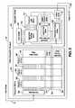
- the aggregation module 24may include a latch matrix 40 , an aggregation-routing matrix 42 , a threshold-logic matrix 44 , a logical-product matrix 46 , a logical-sum matrix 48 , and an initialization-routing matrix 50 .
- the latch matrix 40may implement portions of certain search criteria. Some search criteria, e.g., some regular expressions, count only the first occurrence of a match or group of matches.
- the latch matrix 40may include latches that record whether a match has occurred. The latches may be cleared during initialization, and periodically re-initialized during operation, as search criteria are determined to be satisfied or not further satisfiable—i.e., an earlier search term may need to be matched again before the search criterion could be satisfied.
- the aggregation-routing matrix 42may function similar to the activation-routing matrix 36 .
- the aggregation-routing matrix 42may receive signals indicative of matches on the detection bus 38 and may route the signals to different group-logic lines 53 connecting to the threshold-logic matrix 44 .
- the aggregation-routing matrix 42may also route outputs of the initialization-routing matrix 50 to the detection array 34 to reset portions of the detection array 34 when a search criterion is determined to be satisfied or not further satisfiable.
- the threshold-logic matrix 44may include a plurality of counters, e.g., 32-bit counters configured to count up or down.
- the threshold-logic matrix 44may be loaded with an initial count, and it may count up or down from the count based on matches signaled by the recognition module. For instance, the threshold-logic matrix 44 may count the number of occurrences of a word in some length of text.
- the outputs of the threshold-logic matrix 44may be inputs to the logical-product matrix 46 .
- the logical-product matrix 46may selectively generate “product” results (e.g., “AND” function in Boolean logic).
- the logical-product matrix 46may be implemented as a square matrix, in which the number of output products is equal the number of input lines from the threshold-logic matrix 44 , or the logical-product matrix 46 may have a different number of inputs than outputs.
- the resulting product valuesmay be output to the logical-sum matrix 48 .
- the logical-sum matrix 48may selectively generate sums (e.g., “OR” functions in Boolean logic.)
- the logical-sum matrix 48may also be a square matrix, or the logical-sum matrix 48 may have a different number of inputs than outputs. Since the inputs are logical products, the outputs of the logical-sum matrix 48 may be logical-Sums-of-Products (e.g., Boolean logic Sum-of-Product (SOP) form).
- SOPBoolean logic Sum-of-Product
- the initialization-routing matrix 50may reset portions of the detection array 34 and the aggregation module 24 via the aggregation-routing matrix 42 .
- the initialization-routing matrix 50may also be implemented as a square matrix, or the initialization-routing matrix 50 may have a different number of inputs than outputs.
- the initialization-routing matrix 50may respond to signals from the logical-sum matrix 48 and re-initialize other portions of the pattern-recognition processor 14 , such as when a search criterion is satisfied or determined to be not further satisfiable.
- the aggregation module 24may include an output buffer 51 that receives the outputs of the threshold-logic matrix 44 , the aggregation-routing matrix 42 , and the logical-sum matrix 48 .
- the output of the aggregation module 24may be transmitted from the output buffer 51 to the CPU 20 ( FIG. 1 ) on the output bus 26 .
- an output multiplexermay multiplex signals from these components 42 , 44 , and 48 and output signals indicative of satisfaction of criteria or matches of search terms to the CPU 20 ( FIG. 1 ).
- results from the pattern-recognition processor 14may be reported without transmitting the signals through the output multiplexer, which is not to suggest that any other feature described herein could not also be omitted.
- signals from the threshold-logic matrix 44 , the logical-product matrix 46 , the logical-sum matrix 48 , or the initialization routing matrix 50may be transmitted to the CPU in parallel on the output bus 26 .
- FIG. 3illustrates a portion of a single feature cell 30 in the search-term array 32 ( FIG. 2 ), a component referred to herein as a search-term cell 54 .
- the search-term cells 54may include an output conductor 56 and a plurality of memory cells 58 .
- Each of the memory cells 58may be coupled to both the output conductor 56 and one of the conductors among the plurality of input conductors 37 .
- each of the memory cells 58may output a value indicative of its stored value, outputting the data through the output conductor 56 .
- the plurality of input conductors 37may be referred to as “word lines”, and the output conductor 56 may be referred to as a “data line”.
- the memory cells 58may include any of a variety of types of memory cells.
- the memory cells 58may be volatile memory, such as dynamic random access memory (DRAM) cells having a transistor and a capacitor. The source and the drain of the transistor may be connected to a plate of the capacitor and the output conductor 56 , respectively, and the gate of the transistor may be connected to one of the input conductors 37 .
- each of the memory cells 58may include a static random access memory (SRAM) cell.
- the SRAM cellmay have an output that is selectively coupled to the output conductor 56 by an access transistor controlled by one of the input conductors 37 .
- the memory cells 58may also include nonvolatile memory, such as phase-change memory (e.g., an ovonic device), flash memory, silicon-oxide-nitride-oxide-silicon (SONOS) memory, magneto-resistive memory, or other types of nonvolatile memory.
- nonvolatile memorysuch as phase-change memory (e.g., an ovonic device), flash memory, silicon-oxide-nitride-oxide-silicon (SONOS) memory, magneto-resistive memory, or other types of nonvolatile memory.
- phase-change memorye.g., an ovonic device
- flash memorye.g., an ovonic device
- SONOSsilicon-oxide-nitride-oxide-silicon
- magneto-resistive memorye.g., magneto-resistive memory
- FIGS. 4 and 5depict an example of the search-term cell 54 in operation.
- FIG. 4illustrates the search-term cell 54 receiving a term that does not match the cell's search term
- FIG. 5illustrates a match.
- the search-term cell 54may be configured to search for one or more terms by storing data in the memory cells 58 .
- the memory cells 58may each represent a term that the data stream 12 might present, e.g., in FIG. 3 , each memory cell 58 represents a single letter or number, starting with the letter “a” and ending with the number “9”.
- Memory cells 58 representing terms that satisfy the search termmay be programmed to store a first value, and memory cells 58 that do not represent terms that satisfy the search term may be programmed to store a different value.
- the search-term cell 54is configured to search for the letter “b”.
- the memory cells 58 that represent “b”may store a 1, or logic high, and the memory cells 58 that do not represent “b” may be programmed to store a 0, or logic low.
- the row decoder 28may select the input conductor 37 coupled to memory cells 58 representing the received term.
- the data stream 12presents a lowercase “e”. This term may be presented by the data stream 12 in the form of an eight-bit ASCII code, and the row decoder 28 may interpret this byte as a row address, outputting a signal on the conductor 60 by energizing it.
- the memory cell 58 controlled by the conductor 60may output a signal indicative of the data that the memory cell 58 stores, and the signal may be conveyed by the output conductor 56 .
- the search-term cell 54because the letter “e” is not one of the terms specified by the search-term cell 54 , it does not match the search term, and the search-term cell 54 outputs a 0 value, indicating no match was found.
- the data stream 12presents a character “b”.
- the row decoder 28may interpret this term as an address, and the row decoder 28 may select the conductor 62 .
- the memory cell 58 representing the letter “b”outputs its stored value, which in this case is a 1, indicating a match.
- the search-term cells 54may be configured to search for more than one term at a time.
- Multiple memory cells 58may be programmed to store a 1, specifying a search term that matches with more than one term. For instance, the memory cells 58 representing the letters lowercase “a” and uppercase “A” may be programmed to store a 1, and the search-term cell 54 may search for either term. In another example, the search-term cell 54 may be configured to output a match if any character is received. All of the memory cells 58 may be programmed to store a 1, such that the search-term cell 54 may function as a wildcard term in a search criterion.
- FIGS. 6-8depict the recognition module 22 searching according to a multi-term search criterion, e.g., for a word. Specifically, FIG. 6 illustrates the recognition module 22 detecting the first letter of a word, FIG. 7 illustrates detection of the second letter, and FIG. 8 illustrates detection of the last letter.
- the recognition module 22may be configured to search for the word “big”.
- Three adjacent feature cells 63 , 64 , and 66are illustrated.
- the feature cell 63is configured to detect the letter “b”.
- the feature cell 64is configured to detect the letter “i”.
- the feature cell 66is configured to both detect the letter “g” and indicate that the search criterion is satisfied.
- FIG. 6also depicts additional details of the detection array 34 .
- the detection array 34may include a detection cell 68 in each of the feature cells 63 , 64 , and 66 .
- Each of the detection cells 68may include a memory cell 70 , such as one of the types of memory cells described above (e.g., a flip-flop), that indicates whether the feature cell 63 , 64 , or 66 is active or inactive.
- the detection cells 68may be configured to output a signal to the activation-routing matrix 36 indicating whether the detection cell both is active and has received a signal from its associated search-term cell 54 indicating a match. Inactive features cells 63 , 64 , and 66 may disregard matches.
- Each of the detection cells 68may include an AND gate with inputs from the memory cell 70 and the output conductor 56 . The output of the AND gate may be routed to both the detection bus 38 and the activation-routing matrix 36 , or one or the other.
- the activation-routing matrix 36may selectively activate the feature cells 63 , 64 , and 66 by writing to the memory cells 70 in the detection array 34 .
- the activation-routing matrix 36may activate feature cells 63 , 64 , or 66 according to the search criterion and which search term is being searched for next in the data stream 12 .
- each of the feature cells 63 , 64 , and 66may output a signal on their output conductor 56 , indicating the value stored in the memory cell 58 connected to the conductor 62 , which represents the letter “b”.
- the detection cells 56may then each determine whether they have received a signal indicating a match and whether they are active. Because the feature cell 63 is configured to detect the letter “b” and is active, as indicated by its memory cell 70 , the detection cell 68 in the feature cell 63 may output a signal to the activation-routing matrix 36 indicating that the first search term of the search criterion has been matched.
- the activation-routing matrix 36may activate the next feature cell 64 by writing a 1 to its memory cell 70 in its detection cell 68 .
- the activation-routing matrix 36may also maintain the active state of the feature cell 63 , in case the next term satisfies the first search term, e.g., if the sequence of terms “bbig” is received.
- the first search term of search criteriamay be maintained in an active state during a portion or substantially all of the time during which the data stream 12 is searched.
- the data stream 12presents the letter “i” to the recognition module 22 .
- each of the feature cells 63 , 64 , and 66may output a signal on their output conductor 56 , indicating the value stored in the memory cell 58 connected to the conductor 72 , which represents the letter “i”.
- the detection cells 56may then each determine whether they have received a signal indicating a match and whether they are active. Because the feature cell 64 is configured to detect the letter “i” and is active, as indicated by its memory cell 70 , the detection cell 68 in the feature cell 64 may output a signal to the activation-routing matrix 36 indicating that the next search term of its search criterion has been matched.
- the activation-routing matrix 36may activate the feature cell 66 , as illustrated by FIG. 8 .
- the feature cell 64may be deactivated.
- the feature cell 64may be deactivated by its detection cell 68 resetting its memory cell 70 between detection cycles or the activation-routing matrix 36 may deactivate the feature cell 64 , for example.
- the data stream 12presents the term “g” to the row decoder 28 , which selects the conductor 74 representing the term “g”.
- each of the feature cells 63 , 64 , and 66may output a signal on their output conductor 56 , indicating the value stored in the memory cell 58 connected to the conductor 74 , which represents the letter “g”.
- the detection cells 56may then each determine whether they have received a signal indicating a match and whether they are active.
- the detection cell 68 in the feature cell 66may output a signal to the activation routing matrix 36 indicating that the last search term of its search criterion has been matched.
- the end of a search criterion or a portion of a search criterionmay be identified by the activation-routing matrix 36 or the detection cell 68 .
- These components 36 or 68may include memory indicating whether their feature cell 63 , 64 , or 66 specifies the last search term of a search criterion or a component of a search criterion.
- a search criterionmay specify all sentences in which the word “cattle” occurs twice, and the recognition module may output a signal indicating each occurrence of “cattle” within a sentence to the aggregation module, which may count the occurrences to determine whether the search criterion is satisfied.
- Feature cells 63 , 64 , or 66may be activated under several conditions.
- a feature cell 63 , 64 , or 66may be “always active”, meaning that it remains active during all or substantially all of a search.
- An example of an always active feature cell 63 , 64 , or 66is the first feature cell of the search criterion, e.g., feature cell 63 .
- a feature cell 63 , 64 , or 66may be “active when requested”, meaning that the feature cell 63 , 64 , or 66 is active when some condition precedent is matched, e.g., when the preceding search terms in a search criterion are matched.
- An exampleis the feature cell 64 , which is active when requested by the feature cell 63 in FIGS. 6-8 , and the feature cell 66 , which active when requested by the feature cell 64 .
- a feature cell 63 , 64 , or 66may be “self activated”, meaning that once it is activated, it activates itself as long as its search term is matched. For example, a self activated feature cell having a search term that is matched by any numerical digit may remain active through the sequence “123456xy” until the letter “x” is reached. Each time the search term of the self activated feature cell is matched, it may activate the next feature cell in the search criterion.
- an always active feature cellmay be formed from a self activating feature cell and an active when requested feature cell: the self activating feature cell may be programmed with all of its memory cells 58 storing a 1, and it may repeatedly activate the active when requested feature cell after each term.
- each feature cell 63 , 64 , and 66may include a memory cell in its detection cell 68 or in the activation-routing matrix 36 that specifies whether the feature cell is always active, thereby forming an always active feature cell from a single feature cell.
- FIG. 9depicts an example of a recognition module 22 configured to search according to a first search criterion 75 and a second search criterion 76 in parallel.
- the first search criterion 75specifies the word “big”
- the second search criterion 76specifies the word “cab”.
- a signal indicative of the current term from the data stream 12may be communicated to feature cells in each search criterion 75 and 76 at generally the same time.
- Each of the input conductors 37spans both of the search criteria 75 and 76 .
- both of the search criteria 75 and 76may evaluate the current term generally simultaneously. This is believed to speed the evaluation of search criteria.
- Other embodimentsmay include more feature cells configured to evaluate more search criteria in parallel. For example, some embodiments may include more than 100, 500, 1000, 5000, or 10,000 feature cells operating in parallel. These feature cells may evaluate hundreds or thousands of search criteria generally simultaneously.
- Search criteria with different numbers of search termsmay be formed by allocating more or fewer feature cells to the search criteria.
- Simple search criteriamay consume fewer resources in the form of feature cells than complex search criteria. This is believed to reduce the cost of the pattern-recognition processor 14 ( FIG. 2 ) relative to processors with a large number of generally identical cores, all configured to evaluate complex search criteria.
- FIGS. 10-12depict both an example of a more complex search criterion and features of the activation-routing matrix 36 .
- the activation-routing matrix 36may include a plurality of activation-routing cells 78 , groups of which may be associated with each of the feature cells 63 , 64 , 66 , 80 , 82 , 84 , and 86 .
- each of the feature cellsmay include 5, 10, 20, 50, or more activation-routing cells 78 .
- the activation-routing cells 78may be configured to transmit activation signals to the next search term in a search criterion when a preceding search term is matched.
- the activation-routing cells 78may be configured to route activation signals to adjacent feature cells or other activation-routing cells 78 within the same feature cell.
- the activation-routing cells 78may include memory that indicates which feature cells correspond to the next search term in a search criterion.
- the recognition module 22may be configured to search according to complex search criteria than criteria that specify single words. For instance, the recognition module 22 may be configured to search for words beginning with a prefix 88 and ending with one of two suffixes 90 or 92 .
- the illustrated search criterionspecifies words beginning with the letters “c” and “1” in sequence and ending with either the sequence of letters “ap” or the sequence of letters “oud”. This is an example of a search criterion specifying multiple target expressions, e.g., the word “clap” or the word “cloud”.
- the data stream 12presents the letter “c” to the recognition module 22 , and feature cell 63 is both active and detects a match.
- the activation-routing matrix 36may activate the next feature cell 64 .
- the activation-routing matrix 36may also maintain the active state of the feature cell 63 , as the feature cell 63 is the first search term in the search criterion.
- the data stream 12presents a letter “1”, and the feature cell 64 recognizes a match and is active.
- the activation-routing matrix 36may transmit an activation signal both to the first feature cell 66 of the first suffix 90 and to the first feature cell 82 of the second suffix 92 .
- more suffixesmay be activated, or multiple prefixes may active one or more suffixes.
- the data stream 12presents the letter “o” to the recognition module 22 , and the feature cell 82 of the second suffix 92 detects a match and is active.
- the activation-routing matrix 36may activate the next feature cell 84 of the second suffix 92 .
- the search for the first suffix 90may die out, as the feature cell 66 is allowed to go inactive.
- the steps illustrated by FIGS. 10-12may continue through the letters “u” and “d”, or the search may die out until the next time the prefix 88 is matched.
- Embodiments of the pattern recognition processor 14may include any arrangement of feature cells 30 .
- FIGS. 13-16depict a hierarchical arrangement of feature cells 30 in accordance with an embodiment of the present invention.
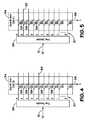
- a first level of a hierarchymay include the feature cells 30 arranged in groups 94 of two feature cells 30 , Feature Cell 1 and Feature Cell 0 .
- Each feature cell 30may receive an input, e.g., an Enable State signal, and may output a Next State signal to another group of feature cells.
- Each feature cell 30 in the group 94may be coupled to an output drive select 96 that provides an output from the group 94 based on the outputs of each feature cell 30 .
- the output drive select 96may be configured to output a Next State Out “0” signal, a Next State Out “1” signal, or the logical OR of the two Next State Out signals received from the feature cells 30 .
- a second hierarchical levelmay include each group 94 of feature cells arranged in a row 98 of groups 94 .
- Each row 98may include any number of groups 94 of feature cells 30 .
- the row 98may include eight groups 94 of two feature cells 30 , e.g. Group 0 through Group 7 .
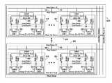
- a third level of a hierarchymay include multiple rows 98 grouped into blocks 100 , wherein each block 100 includes one or more rows 98 .
- each block 100may include 16 rows 98 , e.g., Row 0 through Row 15 .
- the pattern-recognition processor 14may then include any number of blocks 100 for implementing the programmed state machines and pattern searching described above.
- the pattern-recognition processor 14may include 512 blocks, e.g., Block 0 through Block 512 .
- a programmed state machinemay include any number of feature cells 30 .
- each group, row, or blockmay include multiple programmed state machines.
- each state of a programmed state machinee.g., one or more feature cells
- next state routingthe next state of the programmed state machine
- FIGS. 17-21describe a multi-level hierarchical routing matrix that provides next state routing, programmability, and high throughput, in accordance with an embodiment of the present invention.
- the term “routing matrix”refers to a plurality of connections for routing communications between components of the pattern-recognition processor 14 .
- the “routing matrix” described belowcan be functionally distinct from the matrices described above in FIGS. 1-12 .
- the routing matrixcan provide for programmable and/or non-programmable connections at, in, and between every level of the hierarchy of the pattern-recognition processor 14 described above.
- the connectionsmay connect routing lines between feature cells, groups, rows, and blocks of the pattern-recognition processor 14 .
- connectionsmay include, but are not limited to, the following types of connections: programmable and non-programmable; uni-directional and bi-directional; logical combinations (OR, AND, XOR, etc.); selectors (e.g., one of many); and isolators (break connections to a line).
- a programmable connectionmay be configured to perform any of the functionality listed above. For example, a programmable connection may be programmed as uni-directional, bi-directional, any logical combination, selector, isolator, etc.
- a non-programmable connectionmay perform any of the functionality described above, but is incapable of being programmed with a different functionality.
- FIGS. 17-21are depicted by connection symbols summarized below in Table 1:
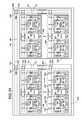
- FIG. 17depicts a hierarchy level that includes the group 94 of feature cells 30 described above in FIG. 13 and in accordance with an embodiment of the present invention.
- each feature cell 30may receive an input that enables the feature cell as the next state.
- the feature cell 30may generate an output that enables the next active state (next state signal).
- the routing of the input and output signals of the feature cells 30are determined by the connections.
- the feature cells 30 of the group 94may be interconnected by local route lines 102 (Local Route 0 and Local Route 1 ).
- the outputs of the feature cells 30 of the group 94are coupled to the local route lines 102 and the output drive select 96 by output connections 104 .
- Feature Cell 0is coupled to Local Route Line 0 by a first output connection 104 A and Feature Cell 1 is coupled to Local Route Line 1 by a second output connection 104 B.
- the output connectionsare non-programmable “1 st Level” connections.
- the connections 104are not removable and are not configurable.
- the output connections 104may be programmable.
- the output drive select 96may be programmed to drive any number or type of signals from the received outputs of the feature cells 30 . As mentioned above, in one embodiment, the output drive select 96 may be configured to output one of three possible logical outputs: “Next State Out 0 ”; “Next State Out 1 ”; or the logical OR of the two Next State Out signals. In other embodiments, the output drive select 96 may be configured to output other logical combinations, such as AND, NOR and/or XOR.
- the local route lines 102may be coupled to the inputs 105 (which may represent one or more input signals) of the feature cells 30 , by input connections 106 .
- the Feature Cell 0may be coupled to Local Route Lines 0 and 1 by input connections 106 A and 106 B respectively.
- Feature Cell 1may be coupled to Local Route Line 0 and Local Route Line 1 by input connections 106 C and 106 D respectively.
- the input connections 106may be programmable “1 st Level” connections. In such an embodiment, the input connections 106 may be configured to provide a logical OR of any of the connected inputs 105 .
- FIG. 18depicts a hierarchy level having the row 98 of the groups 94 as described above in FIG. 14 and in accordance with an embodiment of the present invention.
- each row 98may include any number of groups 94 of feature cells 30 , e.g., Group 0 through Group 7 shown in FIG. 18 .
- the groups of the row 98may be interconnected by row route lines 108 .
- row route lines 108may be provided for each row of the block 100 .
- 16 row route linesmay be provided, e.g., Row Route line 0 through Row Route line 15 .
- the outputs from the output drive selects 96 of each group 94may be coupled to each row route line 108 by output connections 110 .
- the output connectionsmay be programmable “2 nd level” connections.
- Group 0may be coupled to the row route lines 0 and 15 by output connections 110 A and 110 B respectively.
- Group 7may be coupled to the row route lines 0 and 15 by output connections 110 C and 110 D respectively. All other row route lines (not shown) may be coupled to the output drive selects of Groups 0 through Group 7 by output connections 110 .
- the output connections 110may be configured to enable the output drive select 96 of a group 94 to drive or not drive a particular row route line 108 .
- the row route lines 108may be coupled to the inputs 105 of each feature cell 30 by input connections 112 .
- the input connections 112may be programmable “2 nd level” connections.
- the row route lines 108may be coupled to the inputs of Feature Cell 0 of Group 0 by input connections 112 A and 112 B, and the row route lines 108 may be coupled to the inputs of Feature Cell 1 of Group 0 by input connections 112 C and 112 D.
- the row route lines 108may be coupled to the inputs of Feature Cell 0 of Group 7 by input connections 112 E and 112 F, and the row route lines 108 may be coupled to Feature Cell 1 of Group 7 by input connections 112 G and 112 H.
- Other row route lines(not shown) may be coupled to the inputs of each feature cell 30 of each group 94 of the row 98 .
- the input connections 112may be programmed to be a logical OR of any connected inputs to the feature cells 30 .
- the connectionsmay be non-programmable and/or bi-directional connections
- FIG. 19depicts a hierarchy level of a block 100 having multiple rows 98 as described above in FIG. 15 and in accordance with an embodiment of the present invention.
- the block 100may include any number of rows 98 , e.g., Row 0 through Row 15 .
- the rows 98 of the block 100may be connected by intra-block route lines 114 .
- the intra-block route lines 114may be coupled to the row route lines 112 by bi-directional connections 116 .
- the bi-directional connectionsmay be programmable “3 rd level” connections.
- intra-block line route line 0may be coupled to Row Route line 0 of Row 0 by bi-directional connection 116 A and Row Route line 15 of Row 0 by bi-directional connection 116 B.
- Intra-block line route line 0may be coupled to Row Route line 0 of Row 15 by bi-directional connections 116 C and Row Route line 15 of Row 15 by bi-directional connection 116 D.
- intra-block route line 23may be coupled to Row Route line 0 of Row 0 by bi-directional connection 116 E and Row Route line 15 of Row 0 by bi-directional connection 116 F.
- intra-block route line 23may be coupled to Row Route line 0 of Row 15 by bi-directional connections 116 G and Row Route line 15 of Row 15 by bi-directional connection 116 H.
- Other intra block lines(not shown) may be coupled to each row route line 116 of each row 98 by bi-directional connections 116 .
- the bi-directional connections 116may be programmable.
- the bi-directional connections 116may be programmed to enable one or more of the intra-block route lines 114 to drive a respective row route line 112 or to enable one or more row route lines 112 to drive a respective intra block route line 114 .
- Each bi-directional connection 116may be individually programmed, enabling configuration of connections between row route lines 112 and intra-block route lines 114 on a line-by-line basis. In other embodiments, the connections may be non-programmable and/or uni-directional connections.
- FIG. 20depicts a top hierarchy level 117 of the routing matrix having blocks 100 in accordance with an embodiment of the present invention.
- the top level 117may include 512 blocks 100 , e.g., Block 0 through Block 511 .
- the blocks 100may be interconnected by top level route lines 118 .
- the top level route lines 118may be connected to the intra-block route lines 114 by bi-directional connections 120 .
- top level route line 0may be coupled to intra-block route line 0 and intra-block route line 23 of Block 0 by bi-directional connections 120 A and 120 B respectively.
- top level route line 0may be coupled to intra-block line 0 and intra-block line 23 of Block 511 by bi-directional connections 120 C and 120 D respectively.
- top level route line 23may be coupled to intra-block route line 0 and intra-block route line 23 of Block 0 by bi-directional connections 120 E and 120 F respectively.
- top level route line 23may be coupled to intra-block line 0 and intra-block line 23 of Block 511 by bi-directional connections 120 G and 120 H respectively. All other top level route lines (not shown) may be coupled to the intra-block lines 114 of the blocks 100 by bi-directional connections 120 .
- the bi-directional connections 120may be programmable “4 th level connections.”
- the bi-directional connectionsmay be programmed to enable one or more intra-block route lines 114 to drive a respective top level route line 118 or to enable one or more top level route lines 118 to drive a respective intra-block route line 114 .
- the connections 120may be programmed and configured on a line-by-line basis. In other embodiments, the connections may be non-programmable and/or uni-directional connections
- the multi-level hierarchical routing matrix described abovemay provide regularity of the programmability of the device, implementation of redundancy for improvements in production and manufacturing yields, changeability for different applications, and easier visualization and implementation of logic changes.
- the connectionsmay be isolators that are capable of “breaking” a line such that no signals are routed over a line, enabling a redundant section of the pattern-recognition processor 14 to be disabled.
- FIG. 21depicts isolation of one or more feature cells 30 of the pattern-recognition processor 14 in accordance with an embodiment of the present invention.
- the pattern-recognition processor 14may include a block 130 of feature cells 30 that provide more capacity than used by the pattern-recognition processor 14 . That is, during manufacture, to increase yields a pattern-recognition processor 14 may be manufactured with excess memory capacity (excess feature cells 30 ) than specified for the function of the processor 14 .
- the excess feature cells 30may be “disabled” by removing the feature cells available for the programmed state machines used by the processor 14 . Some embodiments may not use all of the blocks of feature cells 30 . In such embodiments, the unused blocks may be disabled. Disabled blocks may not be “activated” and/or “powered-up,” and may not be refreshed during refresh cycles.
- the block 130may be coupled to the other portions of the pattern-recognition processor 14 by the connections 132 between the top level route lines and the intra-block route lines.
- the connections 132may be programmable “4 th level connections” that may be programmed to any desired functionality. Accordingly, if block 130 provides excess capacity, the connections 132 may be programmed to isolate block 130 from the rest of the route lines. Thus, the connection between the top level route lines 118 and the intra-block routing lines 114 may be “broken” by the programmable connections 132 .
- Block 130may be referred to as “disabled.” In addition, unused block 130 may be “powered down,” such as by setting an appropriate programming bit, in the block 130 .
- blocks that are used to provide memory capacity for programmed state machines of the pattern-recognition processor 14may be accessible through the top level route lines 118 and intra-block route lines 114 .
- block 134is also connected to the same top level route lines 118 as disabled block 132 , by connections 136 .
- the connections 136may be programmable 4 th level connections.
- the connections 136may be programmed to enable access to the memory capacity provided by block 134 , such as by allowing the top level route lines to drive the intra-block route lines or vice-versa.
- feature cells 30may be disabled at the row level, such as by programming the connections 138 between the intra-block route lines 114 and the row route lines 112 , and/or at the group level, such as by programming the connections 140 between the row route lines 112 and the local route lines 102 .
- the multi-level hierarchical routing matrix described abovemay vary in levels, connections, etc., based on the pattern-matching functionality implemented in the pattern-recognition processor 14 .
- other embodimentsmay include a different number of levels in the hierarchy, and/or different number of connections between levels, groups, rows, and/or blocks.
- other embodimentsmay include different programmable functions usable for the programmable connections, different types of connections and different points in the hierarchy, the ability to programmatically break connection lines into multiple lines, and the ability to add and/or delete different functionality at different levels in the hierarchy.
- FIG. 22depicts a process 142 of configuration of the multi-level hierarchical routing matrix described above in accordance with an embodiment of the present invention.
- the connections at and between each level of the hierarchymay be programmed in any order. Further, such connections may be programmed manually or automatically based on the specific pattern-matching implementation desired in the pattern-recognition processor 14 . It should also be appreciated that the programming of the connections at or between levels of the matrix may be dependent on the functionality programmed into other levels of the matrix. Initially, the connections at the first hierarchy level may be programmed (block 144 ).
- thismay include programming connections between the output of the feature cells 30 and the local route lines 102 and the inputs of the feature cells 30 and the local route lines 102 , such as programming the connections 106 described above in FIG. 17 .
- the input and/or output connections from the feature cells 30may be non-programmable connections and may not be programmed.
- the output connections 104may be non-programmable connections.
- connections at a second level of the hierarchymay be programmed (block 146 ).
- such programmingmay include programming the input connections between the row route lines 108 and a group 94 , as described above in FIG. 18 .
- the connections 112 between the input to the feature cells 30 and the row route lines 108may be programmed to be a logical OR (or other function) of the inputs 105 to the feature cells 30 .
- the output connections 110may be programmed to provide the desired functionality between the row route lines and the output drive selects 96 of the groups 94 .
- connections at a third level of the hierarchical routing matrixmay be programmed (block 148 ).
- the connections 116 between the row route lines 112 and the intra-block route lines 114may be programmed.
- the connections 116may be programmed to provide the desired functionality between the intra-block route lines 114 and the row route lines 112 , to isolate (disable) certain feature cells, or any other programmable function.
- the connections at a fourth hierarchy levelmay be programmed (block 150 ).
- such programmingmay include programming the connections between the intra-block route lines 114 and the top level route lines 118 .
- the connections 120 shown above in FIG. 20may be programmed to provide the desired functionality between the top level route lines 118 and the intra-block route lines 114 .
- such programmingmay include disabling redundant capacity (e.g., feature cells) of the pattern-recognition processor 14 .
- such programming of the connectionsmay continue up to the nth level of the routing matrix (block 152 ).
- the pattern-recognition processor 14may be configured to provide the desired logic and next state routing between feature cells (and state machines). As mentioned above, the programming of the connections provides knowledge of the configuration of the pattern-recognition processor 14 yet also provides routing flexibility and changeability for different implementations.
Landscapes
- Engineering & Computer Science (AREA)
- Theoretical Computer Science (AREA)
- Physics & Mathematics (AREA)
- General Physics & Mathematics (AREA)
- General Engineering & Computer Science (AREA)
- Databases & Information Systems (AREA)
- Data Mining & Analysis (AREA)
- Computing Systems (AREA)
- Software Systems (AREA)
- Computer Hardware Design (AREA)
- Computational Linguistics (AREA)
- Artificial Intelligence (AREA)
- Evolutionary Computation (AREA)
- Mathematical Physics (AREA)
- Multimedia (AREA)
- Computer Vision & Pattern Recognition (AREA)
- Medical Informatics (AREA)
- Health & Medical Sciences (AREA)
- General Health & Medical Sciences (AREA)
- Evolutionary Biology (AREA)
- Bioinformatics & Computational Biology (AREA)
- Bioinformatics & Cheminformatics (AREA)
- Life Sciences & Earth Sciences (AREA)
- Information Retrieval, Db Structures And Fs Structures Therefor (AREA)
- Image Processing (AREA)
- Character Discrimination (AREA)
- Image Analysis (AREA)
- Data Exchanges In Wide-Area Networks (AREA)
Abstract
Description
| TABLE 1 |
| Connections |
| Symbol | Description |
 | Non-programmable “1stlevel” output connection |
 | Programmable “1stlevel” input connection |
 | Programmable “2ndlevel” input connection |
| Programmable “2ndlevel” output connection |
 | Programmable “3rdlevel” connection |
 | Programmable “4thlevel” connection |
Claims (31)
Priority Applications (13)
| Application Number | Priority Date | Filing Date | Title |
|---|---|---|---|
| US12/638,759US9323994B2 (en) | 2009-12-15 | 2009-12-15 | Multi-level hierarchical routing matrices for pattern-recognition processors |
| JP2012544612AJP5753190B2 (en) | 2009-12-15 | 2010-12-07 | Multi-layer routing matrix for pattern recognition processor |
| PCT/US2010/059310WO2011081799A2 (en) | 2009-12-15 | 2010-12-07 | Multi-level hierarchical routing matrices for pattern-recognition processors |
| EP10795135.2AEP2513839B1 (en) | 2009-12-15 | 2010-12-07 | Multi-level hierarchical routing matrices for pattern-recognition processors |
| CN201710188802.3ACN106919959B (en) | 2009-12-15 | 2010-12-07 | Multi-level hierarchical routing matrix for pattern-recognition processors |
| CN2010800622175ACN102713936A (en) | 2009-12-15 | 2010-12-07 | Multilevel Hierarchical Routing Matrix for Pattern Recognition Processors |
| KR1020127018579AKR101960101B1 (en) | 2009-12-15 | 2010-12-07 | Multi-level hierarchical routing matrices for pattern-recognition processors |
| TW099144023ATWI479342B (en) | 2009-12-15 | 2010-12-15 | Multi-level hierarchical routing matrices for pattern-recognition processors |
| US15/137,877US10684983B2 (en) | 2009-12-15 | 2016-04-25 | Multi-level hierarchical routing matrices for pattern-recognition processors |
| US16/884,302US11226926B2 (en) | 2009-12-15 | 2020-05-27 | Multi-level hierarchical routing matrices for pattern-recognition processors |
| US17/550,593US11768798B2 (en) | 2009-12-15 | 2021-12-14 | Multi-level hierarchical routing matrices for pattern-recognition processors |
| US18/371,635US20240012787A1 (en) | 2009-12-15 | 2023-09-22 | Multi-level hierarchical routing matrices for pattern-recognition processors |
| US19/029,952US20250165429A1 (en) | 2009-12-15 | 2025-01-17 | Multi-level hierarchical routing matrices for pattern-recognition processors |
Applications Claiming Priority (1)
| Application Number | Priority Date | Filing Date | Title |
|---|---|---|---|
| US12/638,759US9323994B2 (en) | 2009-12-15 | 2009-12-15 | Multi-level hierarchical routing matrices for pattern-recognition processors |
Related Child Applications (1)
| Application Number | Title | Priority Date | Filing Date |
|---|---|---|---|
| US15/137,877ContinuationUS10684983B2 (en) | 2009-12-15 | 2016-04-25 | Multi-level hierarchical routing matrices for pattern-recognition processors |
Publications (2)
| Publication Number | Publication Date |
|---|---|
| US20110145544A1 US20110145544A1 (en) | 2011-06-16 |
| US9323994B2true US9323994B2 (en) | 2016-04-26 |
Family
ID=44070678
Family Applications (6)
| Application Number | Title | Priority Date | Filing Date |
|---|---|---|---|
| US12/638,759Active2033-05-14US9323994B2 (en) | 2009-12-15 | 2009-12-15 | Multi-level hierarchical routing matrices for pattern-recognition processors |
| US15/137,877Active2031-05-31US10684983B2 (en) | 2009-12-15 | 2016-04-25 | Multi-level hierarchical routing matrices for pattern-recognition processors |
| US16/884,302ActiveUS11226926B2 (en) | 2009-12-15 | 2020-05-27 | Multi-level hierarchical routing matrices for pattern-recognition processors |
| US17/550,593Active2030-01-28US11768798B2 (en) | 2009-12-15 | 2021-12-14 | Multi-level hierarchical routing matrices for pattern-recognition processors |
| US18/371,635PendingUS20240012787A1 (en) | 2009-12-15 | 2023-09-22 | Multi-level hierarchical routing matrices for pattern-recognition processors |
| US19/029,952PendingUS20250165429A1 (en) | 2009-12-15 | 2025-01-17 | Multi-level hierarchical routing matrices for pattern-recognition processors |
Family Applications After (5)
| Application Number | Title | Priority Date | Filing Date |
|---|---|---|---|
| US15/137,877Active2031-05-31US10684983B2 (en) | 2009-12-15 | 2016-04-25 | Multi-level hierarchical routing matrices for pattern-recognition processors |
| US16/884,302ActiveUS11226926B2 (en) | 2009-12-15 | 2020-05-27 | Multi-level hierarchical routing matrices for pattern-recognition processors |
| US17/550,593Active2030-01-28US11768798B2 (en) | 2009-12-15 | 2021-12-14 | Multi-level hierarchical routing matrices for pattern-recognition processors |
| US18/371,635PendingUS20240012787A1 (en) | 2009-12-15 | 2023-09-22 | Multi-level hierarchical routing matrices for pattern-recognition processors |
| US19/029,952PendingUS20250165429A1 (en) | 2009-12-15 | 2025-01-17 | Multi-level hierarchical routing matrices for pattern-recognition processors |
Country Status (7)
| Country | Link |
|---|---|
| US (6) | US9323994B2 (en) |
| EP (1) | EP2513839B1 (en) |
| JP (1) | JP5753190B2 (en) |
| KR (1) | KR101960101B1 (en) |
| CN (2) | CN106919959B (en) |
| TW (1) | TWI479342B (en) |
| WO (1) | WO2011081799A2 (en) |
Cited By (2)
| Publication number | Priority date | Publication date | Assignee | Title |
|---|---|---|---|---|
| US20170077930A1 (en)* | 2011-12-15 | 2017-03-16 | Micron Technology, Inc. | Boolean logic in a state machine lattice |
| US12277760B2 (en)* | 2010-06-10 | 2025-04-15 | Micron Technology, Inc. | Analyzing data using a hierarchical structure |
Families Citing this family (34)
| Publication number | Priority date | Publication date | Assignee | Title |
|---|---|---|---|---|
| US20100138575A1 (en) | 2008-12-01 | 2010-06-03 | Micron Technology, Inc. | Devices, systems, and methods to synchronize simultaneous dma parallel processing of a single data stream by multiple devices |
| US20100174887A1 (en) | 2009-01-07 | 2010-07-08 | Micron Technology Inc. | Buses for Pattern-Recognition Processors |
| US9323994B2 (en) | 2009-12-15 | 2016-04-26 | Micron Technology, Inc. | Multi-level hierarchical routing matrices for pattern-recognition processors |
| US8766666B2 (en) | 2010-06-10 | 2014-07-01 | Micron Technology, Inc. | Programmable device, hierarchical parallel machines, and methods for providing state information |
| KR101551045B1 (en) | 2011-01-25 | 2015-09-07 | 마이크론 테크놀로지, 인크. | State grouping for element utilization |
| JP5763783B2 (en) | 2011-01-25 | 2015-08-12 | マイクロン テクノロジー, インク. | Method and apparatus for compiling regular expressions |
| JP5857072B2 (en) | 2011-01-25 | 2016-02-10 | マイクロン テクノロジー, インク. | Expansion of quantifiers to control the order of entry and / or exit of automata |
| JP5848778B2 (en) | 2011-01-25 | 2016-01-27 | マイクロン テクノロジー, インク. | Use of dedicated elements to implement FSM |
| US8680888B2 (en) | 2011-12-15 | 2014-03-25 | Micron Technologies, Inc. | Methods and systems for routing in a state machine |
| US8782624B2 (en) | 2011-12-15 | 2014-07-15 | Micron Technology, Inc. | Methods and systems for detection in a state machine |
| US8648621B2 (en) | 2011-12-15 | 2014-02-11 | Micron Technology, Inc. | Counter operation in a state machine lattice |
| US9443156B2 (en) | 2011-12-15 | 2016-09-13 | Micron Technology, Inc. | Methods and systems for data analysis in a state machine |
| US20130275709A1 (en) | 2012-04-12 | 2013-10-17 | Micron Technology, Inc. | Methods for reading data from a storage buffer including delaying activation of a column select |
| US9524248B2 (en) | 2012-07-18 | 2016-12-20 | Micron Technology, Inc. | Memory management for a hierarchical memory system |
| US9304968B2 (en) | 2012-07-18 | 2016-04-05 | Micron Technology, Inc. | Methods and devices for programming a state machine engine |
| US9389841B2 (en) | 2012-07-18 | 2016-07-12 | Micron Technology, Inc. | Methods and systems for using state vector data in a state machine engine |
| US9235798B2 (en) | 2012-07-18 | 2016-01-12 | Micron Technology, Inc. | Methods and systems for handling data received by a state machine engine |
| US9075428B2 (en) | 2012-08-31 | 2015-07-07 | Micron Technology, Inc. | Results generation for state machine engines |
| US9501131B2 (en) | 2012-08-31 | 2016-11-22 | Micron Technology, Inc. | Methods and systems for power management in a pattern recognition processing system |
| US9448965B2 (en) | 2013-03-15 | 2016-09-20 | Micron Technology, Inc. | Receiving data streams in parallel and providing a first portion of data to a first state machine engine and a second portion to a second state machine |
| US9703574B2 (en) | 2013-03-15 | 2017-07-11 | Micron Technology, Inc. | Overflow detection and correction in state machine engines |
| TWI509441B (en)* | 2014-12-16 | 2015-11-21 | Can flexibly set the data width of the multi-character string alignment device | |
| US10430210B2 (en) | 2014-12-30 | 2019-10-01 | Micron Technology, Inc. | Systems and devices for accessing a state machine |
| US11366675B2 (en) | 2014-12-30 | 2022-06-21 | Micron Technology, Inc. | Systems and devices for accessing a state machine |
| WO2016109571A1 (en) | 2014-12-30 | 2016-07-07 | Micron Technology, Inc | Devices for time division multiplexing of state machine engine signals |
| US10846103B2 (en) | 2015-10-06 | 2020-11-24 | Micron Technology, Inc. | Methods and systems for representing processing resources |
| US10977309B2 (en) | 2015-10-06 | 2021-04-13 | Micron Technology, Inc. | Methods and systems for creating networks |
| US10691964B2 (en) | 2015-10-06 | 2020-06-23 | Micron Technology, Inc. | Methods and systems for event reporting |
| US10146555B2 (en) | 2016-07-21 | 2018-12-04 | Micron Technology, Inc. | Adaptive routing to avoid non-repairable memory and logic defects on automata processor |
| US10268602B2 (en) | 2016-09-29 | 2019-04-23 | Micron Technology, Inc. | System and method for individual addressing |
| US10019311B2 (en) | 2016-09-29 | 2018-07-10 | Micron Technology, Inc. | Validation of a symbol response memory |
| US10592450B2 (en) | 2016-10-20 | 2020-03-17 | Micron Technology, Inc. | Custom compute cores in integrated circuit devices |
| US12197510B2 (en) | 2016-10-20 | 2025-01-14 | Micron Technology, Inc. | Traversal of S portion of a graph problem to be solved using automata processor |
| US10929764B2 (en) | 2016-10-20 | 2021-02-23 | Micron Technology, Inc. | Boolean satisfiability |
Citations (27)
| Publication number | Priority date | Publication date | Assignee | Title |
|---|---|---|---|---|
| US5300830A (en) | 1992-05-15 | 1994-04-05 | Micron Semiconductor, Inc. | Programmable logic device macrocell with an exclusive feedback and exclusive external input lines for registered and combinatorial modes using a dedicated product term for control |
| US5331227A (en) | 1992-05-15 | 1994-07-19 | Micron Semiconductor, Inc. | Programmable logic device macrocell with an exclusive feedback line and an exclusive external input line |
| US5818254A (en)* | 1995-06-02 | 1998-10-06 | Advanced Micro Devices, Inc. | Multi-tiered hierarchical high speed switch matrix structure for very high-density complex programmable logic devices |
| US6240003B1 (en) | 2000-05-01 | 2001-05-29 | Micron Technology, Inc. | DRAM content addressable memory using part of the content as an address |
| US20010041012A1 (en) | 1999-12-10 | 2001-11-15 | U.S. Philips Corporation. | Parallel data processing |
| US6577160B2 (en)* | 1996-10-10 | 2003-06-10 | Altera Corporation | Programmable logic device with hierarchical interconnection resources |
| CN1559072A (en) | 2001-09-30 | 2004-12-29 | ÷ķ�����������ι�˾ | Reverse searching system and method |
| US6880087B1 (en) | 1999-10-08 | 2005-04-12 | Cisco Technology, Inc. | Binary state machine system and method for REGEX processing of a data stream in an intrusion detection system |
| US6906938B2 (en) | 2003-08-15 | 2005-06-14 | Micron Technology, Inc. | CAM memory architecture and a method of forming and operating a device according to a CAM memory architecture |
| US6944710B2 (en) | 2002-12-30 | 2005-09-13 | Micron Technology, Inc. | Multiple category CAM |
| JP2006018539A (en) | 2004-06-30 | 2006-01-19 | Fujitsu Ltd | Reconfigurable circuit capable of time-division multiplex processing |
| US7089352B2 (en) | 2002-12-23 | 2006-08-08 | Micron Technology, Inc. | CAM modified to be used for statistic calculation in network switches and routers |
| US7146643B2 (en) | 2002-10-29 | 2006-12-05 | Lockheed Martin Corporation | Intrusion detection accelerator |
| US20070075878A1 (en) | 2005-09-21 | 2007-04-05 | Stmicroelectronics Sa | Memory circuit for aho-corasick type character recognition automaton and method of storing data in such a circuit |
| US20070127482A1 (en)* | 2005-02-12 | 2007-06-07 | Curtis L. Harris | General Purpose Set Theoretic Processor |
| US20070282833A1 (en) | 2006-06-05 | 2007-12-06 | Mcmillen Robert J | Systems and methods for processing regular expressions |
| US20080265938A1 (en)* | 1993-08-03 | 2008-10-30 | Ting Benjamin S | Architecture and interconnect scheme for programmable logic circuits |
| US7487542B2 (en) | 2004-01-14 | 2009-02-03 | International Business Machines Corporation | Intrusion detection using a network processor and a parallel pattern detection engine |
| US7774286B1 (en) | 2006-10-24 | 2010-08-10 | Harris Curtis L | GPSTP with multiple thread functionality |
| US7916510B1 (en)* | 2009-08-10 | 2011-03-29 | Netlogic Microsystems, Inc. | Reformulating regular expressions into architecture-dependent bit groups |
| US8065249B1 (en) | 2006-10-13 | 2011-11-22 | Harris Curtis L | GPSTP with enhanced aggregation functionality |
| US20110307503A1 (en) | 2010-06-10 | 2011-12-15 | Paul Dlugosch | Analyzing data using a hierarchical structure |
| US20110307433A1 (en) | 2010-06-10 | 2011-12-15 | Paul Dlugosch | Programmable device, heirarchical parallel machines, methods for providing state information |
| US20120192165A1 (en) | 2011-01-25 | 2012-07-26 | Junjuan Xu | Unrolling quantifications to control in-degree and/or out-degree of automaton |
| US20120192163A1 (en) | 2011-01-25 | 2012-07-26 | Paul Glendenning | Method and apparatus for compiling regular expressions |
| US20120192164A1 (en) | 2011-01-25 | 2012-07-26 | Junjuan Xu | Utilizing special purpose elements to implement a fsm |
| US20120192166A1 (en) | 2011-01-25 | 2012-07-26 | Junjuan Xu | State grouping for element utilization |
Family Cites Families (159)
| Publication number | Priority date | Publication date | Assignee | Title |
|---|---|---|---|---|
| IL38603A (en) | 1972-01-21 | 1975-10-15 | Bar Lev H | Automatic pattern recognition method and apparatus particularly for optically recognizing alphanumeric characters |
| JPS4891935A (en) | 1972-03-08 | 1973-11-29 | ||
| US4011547A (en) | 1972-07-17 | 1977-03-08 | International Business Machines Corporation | Data processor for pattern recognition and the like |
| GB1518093A (en) | 1974-10-04 | 1978-07-19 | Mullard Ltd | Mark detection apparatus |
| JPS51112236A (en) | 1975-03-28 | 1976-10-04 | Hitachi Ltd | Shape position recognizer unit |
| JPS5313840A (en) | 1976-07-23 | 1978-02-07 | Hitachi Ltd | Analogy calculator |
| US4204193A (en) | 1978-11-03 | 1980-05-20 | International Business Machines Corporation | Adaptive alignment for pattern recognition system |
| US4414685A (en) | 1979-09-10 | 1983-11-08 | Sternberg Stanley R | Method and apparatus for pattern recognition and detection |
| US4748674A (en) | 1986-10-07 | 1988-05-31 | The Regents Of The University Of Calif. | Pattern learning and recognition device |
| US5014327A (en) | 1987-06-15 | 1991-05-07 | Digital Equipment Corporation | Parallel associative memory having improved selection and decision mechanisms for recognizing and sorting relevant patterns |
| US5216748A (en) | 1988-11-30 | 1993-06-01 | Bull, S.A. | Integrated dynamic programming circuit |
| US6253307B1 (en) | 1989-05-04 | 2001-06-26 | Texas Instruments Incorporated | Data processing device with mask and status bits for selecting a set of status conditions |
| JP2833062B2 (en) | 1989-10-30 | 1998-12-09 | 株式会社日立製作所 | Cache memory control method, processor and information processing apparatus using the cache memory control method |
| US5028821A (en) | 1990-03-01 | 1991-07-02 | Plus Logic, Inc. | Programmable logic device with programmable inverters at input/output pads |
| US5377129A (en) | 1990-07-12 | 1994-12-27 | Massachusetts Institute Of Technology | Particle interaction processing system |
| EP0476159B1 (en) | 1990-09-15 | 1996-12-11 | International Business Machines Corporation | Programmable neural logic device |
| US5287523A (en) | 1990-10-09 | 1994-02-15 | Motorola, Inc. | Method for servicing a peripheral interrupt request in a microcontroller |
| AU8966391A (en) | 1990-12-24 | 1992-06-25 | Ball Corporation | System for analysis of embedded computer systems |
| US6400996B1 (en) | 1999-02-01 | 2002-06-04 | Steven M. Hoffberg | Adaptive pattern recognition based control system and method |
| US5291482A (en) | 1992-07-24 | 1994-03-01 | At&T Bell Laboratories | High bandwidth packet switch |
| US5357512A (en) | 1992-12-30 | 1994-10-18 | Intel Corporation | Conditional carry scheduler for round robin scheduling |
| US5825921A (en) | 1993-03-19 | 1998-10-20 | Intel Corporation | Memory transfer apparatus and method useful within a pattern recognition system |
| US5459798A (en) | 1993-03-19 | 1995-10-17 | Intel Corporation | System and method of pattern recognition employing a multiprocessing pipelined apparatus with private pattern memory |
| US5586266A (en)* | 1993-10-15 | 1996-12-17 | International Business Machines Corporation | System and method for adaptive, active monitoring of a serial data stream having a characteristic pattern |
| CA2145361C (en) | 1994-03-24 | 1999-09-07 | Martin William Sotheran | Buffer manager |
| US20050251638A1 (en) | 1994-08-19 | 2005-11-10 | Frederic Boutaud | Devices, systems and methods for conditional instructions |
| JP3345515B2 (en) | 1994-08-31 | 2002-11-18 | アイワ株式会社 | Peak shift correction circuit and magnetic recording medium reproducing apparatus using the same |
| US5615237A (en) | 1994-09-16 | 1997-03-25 | Transwitch Corp. | Telecommunications framer utilizing state machine |
| JPH0887462A (en) | 1994-09-20 | 1996-04-02 | Fujitsu Ltd | State machine and communication control method |
| US5790531A (en) | 1994-12-23 | 1998-08-04 | Applied Digital Access, Inc. | Method and apparatus for determining the origin of a remote alarm indication signal |
| US6279128B1 (en) | 1994-12-29 | 2001-08-21 | International Business Machines Corporation | Autonomous system for recognition of patterns formed by stored data during computer memory scrubbing |
| US5794062A (en) | 1995-04-17 | 1998-08-11 | Ricoh Company Ltd. | System and method for dynamically reconfigurable computing using a processing unit having changeable internal hardware organization |
| US5659551A (en) | 1995-05-31 | 1997-08-19 | International Business Machines Corporation | Programmable computer system element with built-in self test method and apparatus for repair during power-on |
| US5723984A (en) | 1996-06-07 | 1998-03-03 | Advanced Micro Devices, Inc. | Field programmable gate array (FPGA) with interconnect encoding |
| US5680640A (en) | 1995-09-01 | 1997-10-21 | Emc Corporation | System for migrating data by selecting a first or second transfer means based on the status of a data element map initialized to a predetermined state |
| US5754878A (en) | 1996-03-18 | 1998-05-19 | Advanced Micro Devices, Inc. | CPU with DSP function preprocessor having pattern recognition detector that uses table for translating instruction sequences intended to perform DSP function into DSP macros |
| JPH10111862A (en) | 1996-08-13 | 1998-04-28 | Fujitsu Ltd | Time series analysis apparatus and method based on recursive neural network |
| JPH1069459A (en) | 1996-08-29 | 1998-03-10 | Hitachi Ltd | Serial interface control device and control method therefor |
| US6034963A (en) | 1996-10-31 | 2000-03-07 | Iready Corporation | Multiple network protocol encoder/decoder and data processor |
| JP2940496B2 (en) | 1996-11-05 | 1999-08-25 | 日本電気株式会社 | Pattern matching encoding apparatus and method |
| US6317427B1 (en) | 1997-04-24 | 2001-11-13 | Cabletron Systems, Inc. | Method and apparatus for adaptive port buffering |
| US6011407A (en) | 1997-06-13 | 2000-01-04 | Xilinx, Inc. | Field programmable gate array with dedicated computer bus interface and method for configuring both |
| US6362868B1 (en) | 1997-07-15 | 2002-03-26 | Silverbrook Research Pty Ltd. | Print media roll and ink replaceable cartridge |
| US6097212A (en) | 1997-10-09 | 2000-08-01 | Lattice Semiconductor Corporation | Variable grain architecture for FPGA integrated circuits |
| US6041405A (en) | 1997-12-18 | 2000-03-21 | Advanced Micro Devices, Inc. | Instruction length prediction using an instruction length pattern detector |
| DE19861088A1 (en) | 1997-12-22 | 2000-02-10 | Pact Inf Tech Gmbh | Repairing integrated circuits by replacing subassemblies with substitutes |
| US6219776B1 (en) | 1998-03-10 | 2001-04-17 | Billions Of Operations Per Second | Merged array controller and processing element |
| EP0943995A3 (en) | 1998-03-20 | 2000-12-06 | Texas Instruments Incorporated | Processor having real-time external instruction insertion for debug functions without a debug monitor |
| US6151644A (en) | 1998-04-17 | 2000-11-21 | I-Cube, Inc. | Dynamically configurable buffer for a computer network |
| US6052766A (en) | 1998-07-07 | 2000-04-18 | Lucent Technologies Inc. | Pointer register indirectly addressing a second register in the processor core of a digital processor |
| US9195784B2 (en) | 1998-08-31 | 2015-11-24 | Cadence Design Systems, Inc. | Common shared memory in a verification system |
| US7430171B2 (en) | 1998-11-19 | 2008-09-30 | Broadcom Corporation | Fibre channel arbitrated loop bufferless switch circuitry to increase bandwidth without significant increase in cost |
| US7899052B1 (en) | 1999-01-27 | 2011-03-01 | Broadcom Corporation | Memory structure for resolving addresses in a packet-based network switch |
| US6412057B1 (en) | 1999-02-08 | 2002-06-25 | Kabushiki Kaisha Toshiba | Microprocessor with virtual-to-physical address translation using flags |
| US6636483B1 (en) | 1999-02-25 | 2003-10-21 | Fairchild Semiconductor Corporation | Network switch with zero latency flow control |
| US6317849B1 (en) | 1999-04-28 | 2001-11-13 | Intel Corporation | Method and apparatus for controlling available capabilities of a device |
| JP2000347708A (en) | 1999-06-02 | 2000-12-15 | Nippon Telegr & Teleph Corp <Ntt> | Method and apparatus for controlling dynamic system using neural network and storage medium storing control program for dynamic system using neural network |
| US6650660B1 (en)* | 1999-07-27 | 2003-11-18 | Pluris, Inc. | Apparatus and method for synchronization of multiple data paths and recovery from lost synchronization |
| WO2001038978A1 (en) | 1999-11-24 | 2001-05-31 | Z-Force Corporation | Configurable state machine driver and methods of use |
| EP1109118A1 (en)* | 1999-12-16 | 2001-06-20 | Robert S. Lenzie | Circuit configuration |
| US6640262B1 (en) | 1999-12-20 | 2003-10-28 | 3Com Corporation | Method and apparatus for automatically configuring a configurable integrated circuit |
| US6614703B2 (en) | 2000-01-13 | 2003-09-02 | Texas Instruments Incorporated | Method and system for configuring integrated systems on a chip |
| US6625740B1 (en) | 2000-01-13 | 2003-09-23 | Cirrus Logic, Inc. | Dynamically activating and deactivating selected circuit blocks of a data processing integrated circuit during execution of instructions according to power code bits appended to selected instructions |
| US7080359B2 (en) | 2002-01-16 | 2006-07-18 | International Business Machines Corporation | Stack unique signatures for program procedures and methods |
| US6977897B1 (en) | 2000-05-08 | 2005-12-20 | Crossroads Systems, Inc. | System and method for jitter compensation in data transfers |
| US6476636B1 (en) | 2000-09-02 | 2002-11-05 | Actel Corporation | Tileable field-programmable gate array architecture |
| US6384627B1 (en)* | 2001-02-16 | 2002-05-07 | Xilinx, Inc. | Logic block used as dynamically configurable logic function |
| US7451216B2 (en)* | 2001-06-14 | 2008-11-11 | Invision Networks, Inc. | Content intelligent network recognition system and method |
| WO2003039001A1 (en) | 2001-10-29 | 2003-05-08 | Leopard Logic, Inc. | Programmable interface for field programmable gate array cores |
| US7333580B2 (en) | 2002-01-28 | 2008-02-19 | Broadcom Corporation | Pipelined parallel processing of feedback loops in a digital circuit |
| US6925510B2 (en) | 2002-02-22 | 2005-08-02 | Winbond Electronics, Corp. | Peripheral or memory device having a combined ISA bus and LPC bus |
| US7535913B2 (en)* | 2002-03-06 | 2009-05-19 | Nvidia Corporation | Gigabit ethernet adapter supporting the iSCSI and IPSEC protocols |
| US6650142B1 (en)* | 2002-08-13 | 2003-11-18 | Lattice Semiconductor Corporation | Enhanced CPLD macrocell module having selectable bypass of steering-based resource allocation and methods of use |
| US7349416B2 (en) | 2002-11-26 | 2008-03-25 | Cisco Technology, Inc. | Apparatus and method for distributing buffer status information in a switching fabric |
| US7386611B2 (en)* | 2002-12-10 | 2008-06-10 | International Business Machines Corporation | Apparatus and methods for co-location and offloading of web site traffic based on traffic pattern recognition |
| US7292572B2 (en) | 2002-12-11 | 2007-11-06 | Lsi Corporation | Multi-level register bank based configurable ethernet frame parser |
| US6800884B1 (en)* | 2002-12-30 | 2004-10-05 | Actel Corporation | Inter-tile buffer system for a field programmable gate array |
| US6880146B2 (en) | 2003-01-31 | 2005-04-12 | Hewlett-Packard Development Company, L.P. | Molecular-wire-based restorative multiplexer, and method for constructing a multiplexer based on a configurable, molecular-junction-nanowire crossbar |
| US7305047B1 (en) | 2003-03-12 | 2007-12-04 | Lattice Semiconductor Corporation | Automatic lane assignment for a receiver |
| US7366352B2 (en) | 2003-03-20 | 2008-04-29 | International Business Machines Corporation | Method and apparatus for performing fast closest match in pattern recognition |
| US7071908B2 (en) | 2003-05-20 | 2006-07-04 | Kagutech, Ltd. | Digital backplane |
| US7010639B2 (en) | 2003-06-12 | 2006-03-07 | Hewlett-Packard Development Company, L.P. | Inter integrated circuit bus router for preventing communication to an unauthorized port |
| DE102004045527B4 (en) | 2003-10-08 | 2009-12-03 | Siemens Ag | Configurable logic circuitry |
| US7849119B2 (en) | 2003-12-29 | 2010-12-07 | Xilinx, Inc. | Digital signal processing circuit having a pattern detector circuit |
| US7860915B2 (en) | 2003-12-29 | 2010-12-28 | Xilinx, Inc. | Digital signal processing circuit having a pattern circuit for determining termination conditions |
| US7243165B2 (en) | 2004-01-14 | 2007-07-10 | International Business Machines Corporation | Parallel pattern detection engine |
| US7331004B1 (en)* | 2004-03-30 | 2008-02-12 | Emc Corporation | Data storage system analyzer having self reset |
| GB0415850D0 (en) | 2004-07-15 | 2004-08-18 | Imagination Tech Ltd | Memory management system |
| US7716455B2 (en) | 2004-12-03 | 2010-05-11 | Stmicroelectronics, Inc. | Processor with automatic scheduling of operations |
| US7176717B2 (en) | 2005-01-14 | 2007-02-13 | Velogix, Inc. | Programmable logic and routing blocks with dedicated lines |
| US7358761B1 (en) | 2005-01-21 | 2008-04-15 | Csitch Corporation | Versatile multiplexer-structures in programmable logic using serial chaining and novel selection schemes |
| US7499464B2 (en) | 2005-04-06 | 2009-03-03 | Robert Ayrapetian | Buffered crossbar switch with a linear buffer to port relationship that supports cells and packets of variable size |
| US7672529B2 (en) | 2005-05-10 | 2010-03-02 | Intel Corporation | Techniques to detect Gaussian noise |
| US7276934B1 (en) | 2005-06-14 | 2007-10-02 | Xilinx, Inc. | Integrated circuit with programmable routing structure including diagonal interconnect lines |
| US7804719B1 (en) | 2005-06-14 | 2010-09-28 | Xilinx, Inc. | Programmable logic block having reduced output delay during RAM write processes when programmed to function in RAM mode |
| US20080126690A1 (en) | 2006-02-09 | 2008-05-29 | Rajan Suresh N | Memory module with memory stack |
| US7376782B2 (en) | 2005-06-29 | 2008-05-20 | Intel Corporation | Index/data register pair for indirect register access |
| US7360063B2 (en) | 2006-03-02 | 2008-04-15 | International Business Machines Corporation | Method for SIMD-oriented management of register maps for map-based indirect register-file access |
| US7725510B2 (en) | 2006-08-01 | 2010-05-25 | Alcatel-Lucent Usa Inc. | Method and system for multi-character multi-pattern pattern matching |
| JP5183049B2 (en) | 2006-09-20 | 2013-04-17 | 高砂香料工業株式会社 | Stabilizer for hair dye |
| US7890923B2 (en) | 2006-12-01 | 2011-02-15 | International Business Machines Corporation | Configurable pattern detection method and apparatus |
| US8051022B2 (en) | 2006-12-08 | 2011-11-01 | Pandya Ashish A | Embedded programmable intelligent search memory (PRISM) that simultaneously performs regular expression based search and signature pattern based search |
| KR100866604B1 (en) | 2007-01-23 | 2008-11-03 | 삼성전자주식회사 | Power control device and power control method |
| US7797521B2 (en) | 2007-04-12 | 2010-09-14 | International Business Machines Corporation | Method, system, and computer program product for path-correlated indirect address predictions |
| KR20080097573A (en) | 2007-05-02 | 2008-11-06 | 삼성전자주식회사 | Virtual memory approach |
| US20080320053A1 (en) | 2007-06-21 | 2008-12-25 | Michio Iijima | Data management method for accessing data storage area based on characteristic of stored data |
| US8447911B2 (en)* | 2007-07-05 | 2013-05-21 | Board Of Regents, University Of Texas System | Unordered load/store queue |
| US20090198952A1 (en) | 2008-02-04 | 2009-08-06 | Apple Inc | Memory Mapping Architecture |
| US7886089B2 (en) | 2008-02-13 | 2011-02-08 | International Business Machines Corporation | Method, system and computer program product for enhanced shared store buffer management scheme for differing buffer sizes with limited resources for optimized performance |
| WO2009104324A1 (en) | 2008-02-22 | 2009-08-27 | 日本電気株式会社 | Active metric learning device, active metric learning method, and program |
| US7735045B1 (en) | 2008-03-12 | 2010-06-08 | Xilinx, Inc. | Method and apparatus for mapping flip-flop logic onto shift register logic |
| US8015530B1 (en) | 2008-08-05 | 2011-09-06 | Xilinx, Inc. | Method of enabling the generation of reset signals in an integrated circuit |
| US8938590B2 (en) | 2008-10-18 | 2015-01-20 | Micron Technology, Inc. | Indirect register access method and system |
| US8209521B2 (en) | 2008-10-18 | 2012-06-26 | Micron Technology, Inc. | Methods of indirect register access including automatic modification of a directly accessible address register |
| US7917684B2 (en) | 2008-11-05 | 2011-03-29 | Micron Technology, Inc. | Bus translator |
| US7970964B2 (en) | 2008-11-05 | 2011-06-28 | Micron Technology, Inc. | Methods and systems to accomplish variable width data input |
| US9639493B2 (en) | 2008-11-05 | 2017-05-02 | Micron Technology, Inc. | Pattern-recognition processor with results buffer |
| US8402188B2 (en) | 2008-11-10 | 2013-03-19 | Micron Technology, Inc. | Methods and systems for devices with a self-selecting bus decoder |
| US20100118425A1 (en) | 2008-11-11 | 2010-05-13 | Menachem Rafaelof | Disturbance rejection in a servo control loop using pressure-based disc mode sensor |
| US10007486B2 (en) | 2008-12-01 | 2018-06-26 | Micron Technology, Inc. | Systems and methods to enable identification of different data sets |
| US9164945B2 (en) | 2008-12-01 | 2015-10-20 | Micron Technology, Inc. | Devices, systems, and methods to synchronize parallel processing of a single data stream |
| US9348784B2 (en) | 2008-12-01 | 2016-05-24 | Micron Technology, Inc. | Systems and methods for managing endian mode of a device |
| US20100138575A1 (en) | 2008-12-01 | 2010-06-03 | Micron Technology, Inc. | Devices, systems, and methods to synchronize simultaneous dma parallel processing of a single data stream by multiple devices |
| DE102008060719B4 (en) | 2008-12-05 | 2018-09-20 | Siemens Healthcare Gmbh | Method for controlling the recording operation of a magnetic resonance device during the recording of magnetic resonance data of a patient and associated magnetic resonance device |
| FR2939928B1 (en) | 2008-12-15 | 2012-08-03 | Snecma | STANDARDIZATION OF DATA USED FOR MONITORING AN AIRCRAFT ENGINE |
| US8140780B2 (en) | 2008-12-31 | 2012-03-20 | Micron Technology, Inc. | Systems, methods, and devices for configuring a device |
| US8214672B2 (en)* | 2009-01-07 | 2012-07-03 | Micron Technology, Inc. | Method and systems for power consumption management of a pattern-recognition processor |
| US20100174887A1 (en) | 2009-01-07 | 2010-07-08 | Micron Technology Inc. | Buses for Pattern-Recognition Processors |
| US8281395B2 (en) | 2009-01-07 | 2012-10-02 | Micron Technology, Inc. | Pattern-recognition processor with matching-data reporting module |
| US8843523B2 (en) | 2009-01-12 | 2014-09-23 | Micron Technology, Inc. | Devices, systems, and methods for communicating pattern matching results of a parallel pattern search engine |
| US8146040B1 (en) | 2009-06-11 | 2012-03-27 | Xilinx, Inc. | Method of evaluating an architecture for an integrated circuit device |
| US20100325352A1 (en) | 2009-06-19 | 2010-12-23 | Ocz Technology Group, Inc. | Hierarchically structured mass storage device and method |
| US9836555B2 (en) | 2009-06-26 | 2017-12-05 | Micron Technology, Inc. | Methods and devices for saving and/or restoring a state of a pattern-recognition processor |
| US20110014527A1 (en) | 2009-07-17 | 2011-01-20 | Leroy James Ohlsen | Polyoxometalate flow-cell power system |
| US8159900B2 (en) | 2009-08-06 | 2012-04-17 | Unisyn Medical Technologies, Inc. | Acoustic system quality assurance and testing |
| US9323994B2 (en) | 2009-12-15 | 2016-04-26 | Micron Technology, Inc. | Multi-level hierarchical routing matrices for pattern-recognition processors |
| US8489534B2 (en) | 2009-12-15 | 2013-07-16 | Paul D. Dlugosch | Adaptive content inspection |
| US9501705B2 (en) | 2009-12-15 | 2016-11-22 | Micron Technology, Inc. | Methods and apparatuses for reducing power consumption in a pattern recognition processor |
| US20110161620A1 (en) | 2009-12-29 | 2011-06-30 | Advanced Micro Devices, Inc. | Systems and methods implementing shared page tables for sharing memory resources managed by a main operating system with accelerator devices |
| US20110208900A1 (en) | 2010-02-23 | 2011-08-25 | Ocz Technology Group, Inc. | Methods and systems utilizing nonvolatile memory in a computer system main memory |
| GB2478727B (en) | 2010-03-15 | 2013-07-17 | Advanced Risc Mach Ltd | Translation table control |
| US9195623B2 (en) | 2010-06-23 | 2015-11-24 | International Business Machines Corporation | Multiple address spaces per adapter with address translation |
| US8294490B1 (en) | 2010-10-01 | 2012-10-23 | Xilinx, Inc. | Integrated circuit and method of asynchronously routing data in an integrated circuit |
| US8659415B2 (en) | 2011-07-15 | 2014-02-25 | General Electric Company | Alarm management |
| US9443156B2 (en) | 2011-12-15 | 2016-09-13 | Micron Technology, Inc. | Methods and systems for data analysis in a state machine |
| US8593175B2 (en) | 2011-12-15 | 2013-11-26 | Micron Technology, Inc. | Boolean logic in a state machine lattice |
| US8648621B2 (en) | 2011-12-15 | 2014-02-11 | Micron Technology, Inc. | Counter operation in a state machine lattice |
| US8782624B2 (en) | 2011-12-15 | 2014-07-15 | Micron Technology, Inc. | Methods and systems for detection in a state machine |
| US8680888B2 (en) | 2011-12-15 | 2014-03-25 | Micron Technologies, Inc. | Methods and systems for routing in a state machine |
| US20130275709A1 (en) | 2012-04-12 | 2013-10-17 | Micron Technology, Inc. | Methods for reading data from a storage buffer including delaying activation of a column select |
| US8536896B1 (en) | 2012-05-31 | 2013-09-17 | Xilinx, Inc. | Programmable interconnect element and method of implementing a programmable interconnect element |
| US9235798B2 (en) | 2012-07-18 | 2016-01-12 | Micron Technology, Inc. | Methods and systems for handling data received by a state machine engine |
| US9304968B2 (en) | 2012-07-18 | 2016-04-05 | Micron Technology, Inc. | Methods and devices for programming a state machine engine |
| US9524248B2 (en) | 2012-07-18 | 2016-12-20 | Micron Technology, Inc. | Memory management for a hierarchical memory system |
| US9501131B2 (en) | 2012-08-31 | 2016-11-22 | Micron Technology, Inc. | Methods and systems for power management in a pattern recognition processing system |
| US9075428B2 (en) | 2012-08-31 | 2015-07-07 | Micron Technology, Inc. | Results generation for state machine engines |
| US9063532B2 (en) | 2012-08-31 | 2015-06-23 | Micron Technology, Inc. | Instruction insertion in state machine engines |
| KR102029055B1 (en) | 2013-02-08 | 2019-10-07 | 삼성전자주식회사 | Method and apparatus for high-dimensional data visualization |
| US9448965B2 (en) | 2013-03-15 | 2016-09-20 | Micron Technology, Inc. | Receiving data streams in parallel and providing a first portion of data to a first state machine engine and a second portion to a second state machine |
- 2009
- 2009-12-15USUS12/638,759patent/US9323994B2/enactiveActive
- 2010
- 2010-12-07CNCN201710188802.3Apatent/CN106919959B/enactiveActive
- 2010-12-07CNCN2010800622175Apatent/CN102713936A/enactivePending
- 2010-12-07KRKR1020127018579Apatent/KR101960101B1/enactiveActive
- 2010-12-07WOPCT/US2010/059310patent/WO2011081799A2/enactiveApplication Filing
- 2010-12-07EPEP10795135.2Apatent/EP2513839B1/enactiveActive
- 2010-12-07JPJP2012544612Apatent/JP5753190B2/enactiveActive
- 2010-12-15TWTW099144023Apatent/TWI479342B/enactive
- 2016
- 2016-04-25USUS15/137,877patent/US10684983B2/enactiveActive
- 2020
- 2020-05-27USUS16/884,302patent/US11226926B2/enactiveActive
- 2021
- 2021-12-14USUS17/550,593patent/US11768798B2/enactiveActive
- 2023
- 2023-09-22USUS18/371,635patent/US20240012787A1/enactivePending
- 2025
- 2025-01-17USUS19/029,952patent/US20250165429A1/enactivePending
Patent Citations (29)
| Publication number | Priority date | Publication date | Assignee | Title |
|---|---|---|---|---|
| US5300830A (en) | 1992-05-15 | 1994-04-05 | Micron Semiconductor, Inc. | Programmable logic device macrocell with an exclusive feedback and exclusive external input lines for registered and combinatorial modes using a dedicated product term for control |
| US5331227A (en) | 1992-05-15 | 1994-07-19 | Micron Semiconductor, Inc. | Programmable logic device macrocell with an exclusive feedback line and an exclusive external input line |
| US20080265938A1 (en)* | 1993-08-03 | 2008-10-30 | Ting Benjamin S | Architecture and interconnect scheme for programmable logic circuits |
| US5818254A (en)* | 1995-06-02 | 1998-10-06 | Advanced Micro Devices, Inc. | Multi-tiered hierarchical high speed switch matrix structure for very high-density complex programmable logic devices |
| US6577160B2 (en)* | 1996-10-10 | 2003-06-10 | Altera Corporation | Programmable logic device with hierarchical interconnection resources |
| US6880087B1 (en) | 1999-10-08 | 2005-04-12 | Cisco Technology, Inc. | Binary state machine system and method for REGEX processing of a data stream in an intrusion detection system |
| US20010041012A1 (en) | 1999-12-10 | 2001-11-15 | U.S. Philips Corporation. | Parallel data processing |
| US6240003B1 (en) | 2000-05-01 | 2001-05-29 | Micron Technology, Inc. | DRAM content addressable memory using part of the content as an address |
| CN1559072A (en) | 2001-09-30 | 2004-12-29 | ÷ķ�����������ι�˾ | Reverse searching system and method |
| US7146643B2 (en) | 2002-10-29 | 2006-12-05 | Lockheed Martin Corporation | Intrusion detection accelerator |
| US7089352B2 (en) | 2002-12-23 | 2006-08-08 | Micron Technology, Inc. | CAM modified to be used for statistic calculation in network switches and routers |
| US6944710B2 (en) | 2002-12-30 | 2005-09-13 | Micron Technology, Inc. | Multiple category CAM |
| US6906938B2 (en) | 2003-08-15 | 2005-06-14 | Micron Technology, Inc. | CAM memory architecture and a method of forming and operating a device according to a CAM memory architecture |
| US7487542B2 (en) | 2004-01-14 | 2009-02-03 | International Business Machines Corporation | Intrusion detection using a network processor and a parallel pattern detection engine |
| JP2006018539A (en) | 2004-06-30 | 2006-01-19 | Fujitsu Ltd | Reconfigurable circuit capable of time-division multiplex processing |
| US20070127482A1 (en)* | 2005-02-12 | 2007-06-07 | Curtis L. Harris | General Purpose Set Theoretic Processor |
| US7392229B2 (en) | 2005-02-12 | 2008-06-24 | Curtis L. Harris | General purpose set theoretic processor |
| US7487131B2 (en) | 2005-02-12 | 2009-02-03 | Curtis L. Harris | General Purpose set theoretic processor |
| US20070075878A1 (en) | 2005-09-21 | 2007-04-05 | Stmicroelectronics Sa | Memory circuit for aho-corasick type character recognition automaton and method of storing data in such a circuit |
| US20070282833A1 (en) | 2006-06-05 | 2007-12-06 | Mcmillen Robert J | Systems and methods for processing regular expressions |
| US8065249B1 (en) | 2006-10-13 | 2011-11-22 | Harris Curtis L | GPSTP with enhanced aggregation functionality |
| US7774286B1 (en) | 2006-10-24 | 2010-08-10 | Harris Curtis L | GPSTP with multiple thread functionality |
| US7916510B1 (en)* | 2009-08-10 | 2011-03-29 | Netlogic Microsystems, Inc. | Reformulating regular expressions into architecture-dependent bit groups |
| US20110307503A1 (en) | 2010-06-10 | 2011-12-15 | Paul Dlugosch | Analyzing data using a hierarchical structure |
| US20110307433A1 (en) | 2010-06-10 | 2011-12-15 | Paul Dlugosch | Programmable device, heirarchical parallel machines, methods for providing state information |
| US20120192165A1 (en) | 2011-01-25 | 2012-07-26 | Junjuan Xu | Unrolling quantifications to control in-degree and/or out-degree of automaton |
| US20120192163A1 (en) | 2011-01-25 | 2012-07-26 | Paul Glendenning | Method and apparatus for compiling regular expressions |
| US20120192164A1 (en) | 2011-01-25 | 2012-07-26 | Junjuan Xu | Utilizing special purpose elements to implement a fsm |
| US20120192166A1 (en) | 2011-01-25 | 2012-07-26 | Junjuan Xu | State grouping for element utilization |
Non-Patent Citations (55)
| Title |
|---|
| Abhishek Mitra et al; Compiling PCRE to FPGA for Accelerating SNORT IDS; Department of Computer Science and Engineering University of California, Riverside; Dec. 3, 2007, pp. 127-135. |
| Anomynous; Field-Programmable Gate Array; Wikipedia, the free encyclopedia; Jun. 9, 2011, pp. 1-11; XP055000431, Retrieved from the Internet. |
| Anurag Tiwari et al; Saving Power by Mapping Finite-State Machines into Embedded Memory Blocks in FPGAs; Department of ECECS, University of Cincinnati, USA; Feb. 16-20, 2004, vol. 2, pp. 916-921. |
| Beesley, K. R.; Arabic Morphology Using Only Finite-State Operations; Xerox Research Centre Europe; (1998) pp. 50-57. |
| Bird, S. et al.; One-Level Phonology: Autosegmental Representations and Rules as Finite Automata; Association for Computational Linguistics; University of Edinburgh; vol. 20; No. 1; pp. 55-90; 1994. |
| Bispo, J. et al.; Regular Expression Matching for Reconfigurable Packet Inspection; IEEE (2006) pp. 119-126. |
| Bispo, J. et al.; Synthesis of Regular Expressions Targeting FPGAs: Current Status and Open Issues; IST/INESC-ID, Libson, Portugal; (2007) pp. 179-190. |
| Brodie, B. et al.; A scalable Architecture for High-Throughput Regular-Expression Pattern Matching; Exegy Inc.; pp. (2006) pp. 191-202. |
| Cheng-Hung Lin et al; Optimization of Pattern Matching Circuits for Regular Expression on FPGA; Piscataway, NJ, USA, vol. 12, Dec. 1, 2007, pp. 1303-1310. |
| Chinese Office Action dated Jan. 27, 2014. |
| Christopher R. Clark et al; Efficient Reconfigurable Logic Circuits for Matching Complex Network Intrusion Detection Patterns; 2003, School of Electrical and Computer Engineering, Georgia Institute of Technology, Atlanta, Georgia, vol. 2778, pp. 956-959. |
| Clark, C. et al.; A Unified Model of Pattern-Matching Circuit Architectures; Tech Report GIT-CERCS-05-20; Georgia Institute of Technology; pp. 1-17; www.cercs.gatech.edu/tech-reports/tr2005/git-cercs-05-20.pdf.PDF file1 A Unified Model of Pattern-Matching Circuit Architectures Tech Report GIT-CERCS-05-20 Christopher R. Clark and David E. Schimmel Center for Experimental . . . I (2005). |
| Clark, C. et al.; A Unified Model of Pattern-Matching Circuit Architectures; Tech Report GIT-CERCS-05-20; Georgia Institute of Technology; pp. 1-17; www.cercs.gatech.edu/tech-reports/tr2005/git-cercs-05-20.pdf•PDF file1 A Unified Model of Pattern-Matching Circuit Architectures Tech Report GIT-CERCS-05-20 Christopher R. Clark and David E. Schimmel Center for Experimental . . . I (2005). |
| Clark, C. et al.; Scalable Pattern Matching for High Speed Networks; Proceedings of the 12th Annual IEEE symposium on Field-Programmable Custom Computing Machines (FCCM'04);Georgia Institute of Technology; pp. 1-9; 2004. |
| Clark, C.; A Unified Model of Pattern-Matching Circuits for Field-Programmable Gate Arrays [Doctoral Dissertation]; Georgia Institute of Technology; pp. 1-177; 2006. |
| Clark, C.; Design of Efficient FPGA Circuits for Matching Complex Patterns in Network Intrusion Detection Systems (Master of Science Thesis); Georgia Institute of Technology; pp. 1-56; Dec. 2003. |
| European Patent Office, Office Action for Application No. 10 795 135.2-1901, PN804963EP. Apr. 17, 2015, 5 pages.* |
| Fide, S.; String Processing in Hardware; Scalable Parallel and Distributed Systems Lab; Proceedings of the 12th Annual IEEE symposium on Field-Programmable Custom Computing Machines (FCCM'04);School of Electrical and Computer Engineering; Georgia Institute of Technology; pp. 1-9; 2004. |
| Fisk, M. et al.; Applying Fast String Matching to Intrusion Detection; Los Alamos National Laboratory; University of California San Diego; (2001) pp. 1-21. |
| Freescale and Kaspersky® Accelerated Antivirus Solution Platform for OEM Vendors; Freescale Semiconductors Document; pp. 1-16; 2007. |
| Harris, U.S. Appl. No. 60/652,738, filed Feb. 12, 2005, "Means and Mechanism for Finding Meaningful Information in Databases or Data Sets by Topical Content Patterns at Speeds Exceeding Conventional Computers". |
| Hurson A. R.; VLSI Design for the Parallel Finite State Automation and Its Performance Evaluation as a Hardware Scanner; International Journal of Computer and Information Sciences, vol. 13, No. 6. (1984); pp. 491-508. |
| Japanese Office Action dated Apr. 10, 2014 and translation. |
| Joao Bispo; Regular Expression Matching for Reconfigurable Packet Inspection; Field Programmable Technology, 2006. FPT 2006. Dec. 1, 2006, pp. 119-126. |
| Korenek, J.; Traffic Scanner-Hardware Accelerated Intrusion Detection System; http://www.liberouter.org/ ; (2006) pp. 1-7. |
| Korenek, J.; Traffic Scanner-Hardware Accelerated Intrusion Detection System; http://www.liberouter.org/ ; (2007) pp. 1-23. |
| Kumar, S. et al.; Curing Regular Expressions matching Algorithms from Insomnia, Amnesia, and Acaluia; Department of Computer Science and Engineering; Washington University in St. Louis; pp. 1-17; Apr. 27, 2007. |
| Lin, C. et al.; Optimization of Pattern Matching Circuits for Regular Expression on FPGA; IEEE Transactions on Very Large Scale Integrations Systems; vol. 15, No. 12, pp. 1-6; Dec. 2007. |
| Lipovski, G.; Dynamic Systolic Associative Memory Chip; IEEE; Department of Electrical and Computer Engineering; University of Texas at Austin; pp. 481-492; 1990. |
| Moscola J et al; Implementation of Network Application Layer Parser for Multiple TCP/IP Flows in Reconfigurable Devices; Department of Computer Science and Engineering Washington University, St. Louis, MO, 2006, pp. 1-4. |
| Noyes, et al., U.S. Appl. No. 12/253,966, filed Oct. 18, 2008, "System and Method of Indirect Register Access". |
| Noyes, et al., U.S. Appl. No. 12/253,967, filed Oct. 18, 2008, "Indirect Register Access Method and System". |
| Noyes, et al., U.S. Appl. No. 12/265,436, filed Nov. 5, 2008, "Bus Translator". |
| Noyes, et al., U.S. Appl. No. 12/268,270, filed Nov. 10, 2008, "Methods and Systems for Directly Connecting Devices to Microcontrollers". |
| Noyes, U.S. Appl. No. 12/265,421, filed Nov. 5, 2008, "Methods and Systems to Accomplish Variable Width Data Input". |
| Noyes, U.S. Appl. No. 12/265,465, filed Nov. 5, 2008, "Pattern-Recognition Processor with Results Buffer". |
| Noyes, U.S. Appl. No. 12/325,875, filed Dec. 1, 2008, "Systems and Methods for Managing Endian Mode of a Device". |
| Noyes, U.S. Appl. No. 12/325,982, filed Dec. 1, 2008, "Systems and Methods to Enable Identification of Different Data Sets". |
| Noyes, U.S. Appl. No. 12/325,986, filed Dec. 1, 2008, "Devices, Systems, and Methods to Synchronize Simultaneous DMA Parallel Processing of a Single Data Stream by Multiple Devices". |
| Noyes, U.S. Appl. No. 12/325,990, filed Dec. 1, 2008, "Devices, Systems, and Methods to Synchronize Parallel Processing of a Single Data Stream". |
| Noyes, U.S. Appl. No. 12/347,403, filed Dec. 31, 2008, "Systems, Methods, and Devices for Configuring a Device". |
| Noyes, U.S. Appl. No. 12/352,311, filed Jan. 12, 2009, "Devices, Systems, and Methods for Communicating Pattern Matching Results of a Parallel Pattern Search Engine". |
| Noyes, U.S. Appl. No. 12/492,824, filed Jun. 26, 2009, "Methods and Devices for Saving and/or Restoring a State of a Pattern-Recognition Processor". |
| Pawlowski, U.S. Appl. No. 12,350,136, filed Jan. 7, 2009, "Buses for Pattern-Recognition Processors". |
| Pawlowski, U.S. Appl. No. 12/350,132, filed Jan. 7, 2009, "Pattern-Recognition Processor with Matching-Data Reporting Module". |
| Pawlowski, U.S. Appl. No. 12/350,142, filed Jan. 7, 2009, "Methods and Systems for Power Consumption Management of a Pattern-Recognition Processor". |
| Schultz, K. et al.; Fully Parallel Integrated CAM/RAM Using Preclassification to Enable Large Capacities; IEEE Journal on Solid-State Circuits; vol. 31; No. 5; pp. 689-699; May 1996. |
| Shafai, F. et al.; Fully Parallel 30-MHz, 2.5-Mb CAM; IEEE Journal of Solid-State Circuits, vol. 33; No. 11; pp. 1690-1696; Nov. 1998. |
| Sidhu et al., "A Self-Reconfigurable Gate Array Architecture", Aug. 2000, Proceedings of the The Roadmap to Reconfigurable Computing, 10th International Workshop on Field-Programmable Logic and Applications, pp. 106-120 (re-print pp. 1-14).* |
| Sidhu et atl., "String matching on multicontext FPGAs using self-reconfiguration", Feb. 1999, Proceedings of the 1999 ACM/SIGDA seventh international symposium on Field programmable gate arrays, pp. 217-226.* |
| Sidhu, R. et al.; Fast Regular Expression Pattern Matching using FPGAs; Department of EE-Systems; University of Southern California; (2001) pp. 1-12. |
| Taiwan Office Action issued Nov. 4, 2013. |
| Wada, T.; Multiobject Behavior Recognition Event Driven Selective Attention Method; IEEE; pp. 1-16; 2000. |
| Written Opinion for PCT/US2010/059310, pp. 1-9.* |
| Yu, F.; High Speed Deep Packet Inspection with Hardware Support; Electrical Engineering and Computer Sciences; University of California at Berkeley; pp. 1-217; Nov. 22, 2006. |
Cited By (3)
| Publication number | Priority date | Publication date | Assignee | Title |
|---|---|---|---|---|
| US12277760B2 (en)* | 2010-06-10 | 2025-04-15 | Micron Technology, Inc. | Analyzing data using a hierarchical structure |
| US20170077930A1 (en)* | 2011-12-15 | 2017-03-16 | Micron Technology, Inc. | Boolean logic in a state machine lattice |
| US9866218B2 (en)* | 2011-12-15 | 2018-01-09 | Micron Technology, Inc. | Boolean logic in a state machine lattice |
Also Published As
| Publication number | Publication date |
|---|---|
| KR101960101B1 (en) | 2019-03-19 |
| US20220100700A1 (en) | 2022-03-31 |
| CN106919959B (en) | 2021-07-02 |
| US20160239462A1 (en) | 2016-08-18 |
| CN102713936A (en) | 2012-10-03 |
| US11226926B2 (en) | 2022-01-18 |
| JP5753190B2 (en) | 2015-07-22 |
| JP2013513894A (en) | 2013-04-22 |
| US20240012787A1 (en) | 2024-01-11 |
| US10684983B2 (en) | 2020-06-16 |
| EP2513839A2 (en) | 2012-10-24 |
| WO2011081799A3 (en) | 2011-09-01 |
| US20110145544A1 (en) | 2011-06-16 |
| WO2011081799A2 (en) | 2011-07-07 |
| US20250165429A1 (en) | 2025-05-22 |
| US11768798B2 (en) | 2023-09-26 |
| EP2513839B1 (en) | 2020-02-26 |
| KR20120108987A (en) | 2012-10-05 |
| CN106919959A (en) | 2017-07-04 |
| US20200285604A1 (en) | 2020-09-10 |
| TW201131404A (en) | 2011-09-16 |
| TWI479342B (en) | 2015-04-01 |
Similar Documents
| Publication | Publication Date | Title |
|---|---|---|
| US11768798B2 (en) | Multi-level hierarchical routing matrices for pattern-recognition processors | |
| US11151140B2 (en) | Methods and apparatuses for reducing power consumption in a pattern recognition processor | |
| US10838966B2 (en) | Devices, systems, and methods to synchronize simultaneous DMA parallel processing of a single data stream by multiple devices | |
| US10466966B2 (en) | Systems and methods to enable identification of different data sets | |
| US10817569B2 (en) | Methods and devices for saving and/or restoring a state of a pattern-recognition processor | |
| US10152113B2 (en) | Dynamic power-down of a block of a pattern-recognition processor | |
| US9164945B2 (en) | Devices, systems, and methods to synchronize parallel processing of a single data stream | |
| EP2350921B1 (en) | Pattern-recognition processor with results buffer |
Legal Events
| Date | Code | Title | Description |
|---|---|---|---|
| AS | Assignment | Owner name:MICRON TECHNOLOGY, INC., IDAHO Free format text:ASSIGNMENT OF ASSIGNORS INTEREST;ASSIGNORS:NOYES, HAROLD B;BROWN, DAVID R.;SIGNING DATES FROM 20091130 TO 20091203;REEL/FRAME:023664/0299 | |
| STCF | Information on status: patent grant | Free format text:PATENTED CASE | |
| AS | Assignment | Owner name:U.S. BANK NATIONAL ASSOCIATION, AS COLLATERAL AGENT, CALIFORNIA Free format text:SECURITY INTEREST;ASSIGNOR:MICRON TECHNOLOGY, INC.;REEL/FRAME:038669/0001 Effective date:20160426 Owner name:U.S. BANK NATIONAL ASSOCIATION, AS COLLATERAL AGEN Free format text:SECURITY INTEREST;ASSIGNOR:MICRON TECHNOLOGY, INC.;REEL/FRAME:038669/0001 Effective date:20160426 | |
| AS | Assignment | Owner name:MORGAN STANLEY SENIOR FUNDING, INC., AS COLLATERAL AGENT, MARYLAND Free format text:PATENT SECURITY AGREEMENT;ASSIGNOR:MICRON TECHNOLOGY, INC.;REEL/FRAME:038954/0001 Effective date:20160426 Owner name:MORGAN STANLEY SENIOR FUNDING, INC., AS COLLATERAL Free format text:PATENT SECURITY AGREEMENT;ASSIGNOR:MICRON TECHNOLOGY, INC.;REEL/FRAME:038954/0001 Effective date:20160426 | |
| AS | Assignment | Owner name:U.S. BANK NATIONAL ASSOCIATION, AS COLLATERAL AGENT, CALIFORNIA Free format text:CORRECTIVE ASSIGNMENT TO CORRECT THE REPLACE ERRONEOUSLY FILED PATENT #7358718 WITH THE CORRECT PATENT #7358178 PREVIOUSLY RECORDED ON REEL 038669 FRAME 0001. ASSIGNOR(S) HEREBY CONFIRMS THE SECURITY INTEREST;ASSIGNOR:MICRON TECHNOLOGY, INC.;REEL/FRAME:043079/0001 Effective date:20160426 Owner name:U.S. BANK NATIONAL ASSOCIATION, AS COLLATERAL AGEN Free format text:CORRECTIVE ASSIGNMENT TO CORRECT THE REPLACE ERRONEOUSLY FILED PATENT #7358718 WITH THE CORRECT PATENT #7358178 PREVIOUSLY RECORDED ON REEL 038669 FRAME 0001. ASSIGNOR(S) HEREBY CONFIRMS THE SECURITY INTEREST;ASSIGNOR:MICRON TECHNOLOGY, INC.;REEL/FRAME:043079/0001 Effective date:20160426 | |
| AS | Assignment | Owner name:JPMORGAN CHASE BANK, N.A., AS COLLATERAL AGENT, ILLINOIS Free format text:SECURITY INTEREST;ASSIGNORS:MICRON TECHNOLOGY, INC.;MICRON SEMICONDUCTOR PRODUCTS, INC.;REEL/FRAME:047540/0001 Effective date:20180703 Owner name:JPMORGAN CHASE BANK, N.A., AS COLLATERAL AGENT, IL Free format text:SECURITY INTEREST;ASSIGNORS:MICRON TECHNOLOGY, INC.;MICRON SEMICONDUCTOR PRODUCTS, INC.;REEL/FRAME:047540/0001 Effective date:20180703 | |
| AS | Assignment | Owner name:MICRON TECHNOLOGY, INC., IDAHO Free format text:RELEASE BY SECURED PARTY;ASSIGNOR:U.S. BANK NATIONAL ASSOCIATION, AS COLLATERAL AGENT;REEL/FRAME:047243/0001 Effective date:20180629 | |
| AS | Assignment | Owner name:MICRON TECHNOLOGY, INC., IDAHO Free format text:RELEASE BY SECURED PARTY;ASSIGNOR:MORGAN STANLEY SENIOR FUNDING, INC., AS COLLATERAL AGENT;REEL/FRAME:050937/0001 Effective date:20190731 | |
| MAFP | Maintenance fee payment | Free format text:PAYMENT OF MAINTENANCE FEE, 4TH YEAR, LARGE ENTITY (ORIGINAL EVENT CODE: M1551); ENTITY STATUS OF PATENT OWNER: LARGE ENTITY Year of fee payment:4 | |
| AS | Assignment | Owner name:MICRON SEMICONDUCTOR PRODUCTS, INC., IDAHO Free format text:RELEASE BY SECURED PARTY;ASSIGNOR:JPMORGAN CHASE BANK, N.A., AS COLLATERAL AGENT;REEL/FRAME:051028/0001 Effective date:20190731 Owner name:MICRON TECHNOLOGY, INC., IDAHO Free format text:RELEASE BY SECURED PARTY;ASSIGNOR:JPMORGAN CHASE BANK, N.A., AS COLLATERAL AGENT;REEL/FRAME:051028/0001 Effective date:20190731 | |
| MAFP | Maintenance fee payment | Free format text:PAYMENT OF MAINTENANCE FEE, 8TH YEAR, LARGE ENTITY (ORIGINAL EVENT CODE: M1552); ENTITY STATUS OF PATENT OWNER: LARGE ENTITY Year of fee payment:8 |