US9318670B2 - Materials for photoluminescence wavelength converted solid-state light emitting devices and arrangements - Google Patents
Materials for photoluminescence wavelength converted solid-state light emitting devices and arrangementsDownload PDFInfo
- Publication number
- US9318670B2 US9318670B2US14/469,523US201414469523AUS9318670B2US 9318670 B2US9318670 B2US 9318670B2US 201414469523 AUS201414469523 AUS 201414469523AUS 9318670 B2US9318670 B2US 9318670B2
- Authority
- US
- United States
- Prior art keywords
- photoluminescence
- photoluminescence material
- paste
- material paste
- inorganic
- Prior art date
- Legal status (The legal status is an assumption and is not a legal conclusion. Google has not performed a legal analysis and makes no representation as to the accuracy of the status listed.)
- Active
Links
- 239000000463materialSubstances0.000titleclaimsabstractdescription456
- 238000005424photoluminescenceMethods0.000titleclaimsabstractdescription334
- 229920001296polysiloxanePolymers0.000claimsabstractdescription171
- 239000012530fluidSubstances0.000claimsabstractdescription103
- OAICVXFJPJFONN-UHFFFAOYSA-NPhosphorusChemical compound[P]OAICVXFJPJFONN-UHFFFAOYSA-N0.000claimsdescription89
- 239000002245particleSubstances0.000claimsdescription81
- 239000000203mixtureSubstances0.000claimsdescription41
- VYPSYNLAJGMNEJ-UHFFFAOYSA-NSilicium dioxideChemical compoundO=[Si]=OVYPSYNLAJGMNEJ-UHFFFAOYSA-N0.000claimsdescription30
- -1polyphenylmethylsiloxanePolymers0.000claimsdescription18
- 150000004767nitridesChemical class0.000claimsdescription15
- 239000004205dimethyl polysiloxaneSubstances0.000claimsdescription13
- 229920000435poly(dimethylsiloxane)Polymers0.000claimsdescription13
- 239000000377silicon dioxideSubstances0.000claimsdescription13
- 150000004645aluminatesChemical class0.000claimsdescription11
- 239000000126substanceSubstances0.000claimsdescription10
- 229910052684CeriumInorganic materials0.000claimsdescription9
- MCMNRKCIXSYSNV-UHFFFAOYSA-NZrO2Inorganic materialsO=[Zr]=OMCMNRKCIXSYSNV-UHFFFAOYSA-N0.000claimsdescription9
- CPLXHLVBOLITMK-UHFFFAOYSA-Nmagnesium oxideInorganic materials[Mg]=OCPLXHLVBOLITMK-UHFFFAOYSA-N0.000claimsdescription9
- 239000000395magnesium oxideSubstances0.000claimsdescription9
- AXZKOIWUVFPNLO-UHFFFAOYSA-Nmagnesium;oxygen(2-)Chemical compound[O-2].[Mg+2]AXZKOIWUVFPNLO-UHFFFAOYSA-N0.000claimsdescription9
- TWNQGVIAIRXVLR-UHFFFAOYSA-Noxo(oxoalumanyloxy)alumaneChemical compoundO=[Al]O[Al]=OTWNQGVIAIRXVLR-UHFFFAOYSA-N0.000claimsdescription9
- RVTZCBVAJQQJTK-UHFFFAOYSA-Noxygen(2-);zirconium(4+)Chemical compound[O-2].[O-2].[Zr+4]RVTZCBVAJQQJTK-UHFFFAOYSA-N0.000claimsdescription9
- GWEVSGVZZGPLCZ-UHFFFAOYSA-NTitan oxideChemical compoundO=[Ti]=OGWEVSGVZZGPLCZ-UHFFFAOYSA-N0.000claimsdescription8
- 230000005284excitationEffects0.000claimsdescription7
- 229910052765LutetiumInorganic materials0.000claimsdescription6
- XLOMVQKBTHCTTD-UHFFFAOYSA-NZinc monoxideChemical compound[Zn]=OXLOMVQKBTHCTTD-UHFFFAOYSA-N0.000claimsdescription6
- 229910052782aluminiumInorganic materials0.000claimsdescription6
- TZCXTZWJZNENPQ-UHFFFAOYSA-Lbarium sulfateChemical compound[Ba+2].[O-]S([O-])(=O)=OTZCXTZWJZNENPQ-UHFFFAOYSA-L0.000claimsdescription6
- GWXLDORMOJMVQZ-UHFFFAOYSA-NceriumChemical compound[Ce]GWXLDORMOJMVQZ-UHFFFAOYSA-N0.000claimsdescription6
- OHSVLFRHMCKCQY-UHFFFAOYSA-Nlutetium atomChemical compound[Lu]OHSVLFRHMCKCQY-UHFFFAOYSA-N0.000claimsdescription6
- 229910052751metalInorganic materials0.000claimsdescription6
- 239000002184metalSubstances0.000claimsdescription6
- 230000005855radiationEffects0.000claimsdescription5
- 235000012239silicon dioxideNutrition0.000claimsdescription5
- 229910052693EuropiumInorganic materials0.000claimsdescription3
- 229910052777PraseodymiumInorganic materials0.000claimsdescription3
- 229910052771TerbiumInorganic materials0.000claimsdescription3
- 229910052784alkaline earth metalInorganic materials0.000claimsdescription3
- 150000001342alkaline earth metalsChemical class0.000claimsdescription3
- XAGFODPZIPBFFR-UHFFFAOYSA-NaluminiumChemical compound[Al]XAGFODPZIPBFFR-UHFFFAOYSA-N0.000claimsdescription3
- QVGXLLKOCUKJST-UHFFFAOYSA-Natomic oxygenChemical compound[O]QVGXLLKOCUKJST-UHFFFAOYSA-N0.000claimsdescription3
- 229910052788bariumInorganic materials0.000claimsdescription3
- 229910052791calciumInorganic materials0.000claimsdescription3
- 229910052736halogenInorganic materials0.000claimsdescription3
- 150000002367halogensChemical class0.000claimsdescription3
- 229910052749magnesiumInorganic materials0.000claimsdescription3
- 239000011777magnesiumSubstances0.000claimsdescription3
- 229910052748manganeseInorganic materials0.000claimsdescription3
- 229910052760oxygenInorganic materials0.000claimsdescription3
- 239000001301oxygenSubstances0.000claimsdescription3
- 229910052712strontiumInorganic materials0.000claimsdescription3
- 229910052725zincInorganic materials0.000claimsdescription3
- 239000011701zincSubstances0.000claimsdescription3
- 239000004408titanium dioxideSubstances0.000claimsdescription2
- 239000011787zinc oxideSubstances0.000claims1
- 150000001875compoundsChemical class0.000description56
- 238000004519manufacturing processMethods0.000description36
- 238000006243chemical reactionMethods0.000description27
- 238000000034methodMethods0.000description26
- 239000000654additiveSubstances0.000description22
- 230000000996additive effectEffects0.000description13
- 239000011521glassSubstances0.000description11
- 238000002156mixingMethods0.000description11
- 125000000118dimethyl groupChemical group[H]C([H])([H])*0.000description10
- 238000001746injection mouldingMethods0.000description10
- 239000000758substrateSubstances0.000description10
- 238000004132cross linkingMethods0.000description8
- 238000005538encapsulationMethods0.000description7
- 238000000926separation methodMethods0.000description7
- 239000002105nanoparticleSubstances0.000description6
- 239000003054catalystSubstances0.000description5
- 239000003431cross linking reagentSubstances0.000description5
- 238000009877renderingMethods0.000description5
- 230000008901benefitEffects0.000description4
- 239000004020conductorSubstances0.000description4
- 239000008393encapsulating agentSubstances0.000description4
- 230000008569processEffects0.000description4
- 238000003860storageMethods0.000description4
- 125000000391vinyl groupChemical group[H]C([*])=C([H])[H]0.000description4
- 229910007161Si(CH3)3Inorganic materials0.000description3
- 239000002482conductive additiveSubstances0.000description3
- 230000002596correlated effectEffects0.000description3
- 238000002347injectionMethods0.000description3
- 239000007924injectionSubstances0.000description3
- 125000002496methyl groupChemical group[H]C([H])([H])*0.000description3
- 230000003287optical effectEffects0.000description3
- 239000007787solidSubstances0.000description3
- LCGLNKUTAGEVQW-UHFFFAOYSA-NDimethyl etherChemical compoundCOCLCGLNKUTAGEVQW-UHFFFAOYSA-N0.000description2
- BPQQTUXANYXVAA-UHFFFAOYSA-NOrthosilicateChemical compound[O-][Si]([O-])([O-])[O-]BPQQTUXANYXVAA-UHFFFAOYSA-N0.000description2
- QAOWNCQODCNURD-UHFFFAOYSA-LSulfateChemical compound[O-]S([O-])(=O)=OQAOWNCQODCNURD-UHFFFAOYSA-L0.000description2
- 238000000149argon plasma sinteringMethods0.000description2
- 125000001797benzyl groupChemical group[H]C1=C([H])C([H])=C(C([H])=C1[H])C([H])([H])*0.000description2
- 125000002915carbonyl groupChemical group[*:2]C([*:1])=O0.000description2
- 239000012876carrier materialSubstances0.000description2
- 239000003795chemical substances by applicationSubstances0.000description2
- 238000000151depositionMethods0.000description2
- KPUWHANPEXNPJT-UHFFFAOYSA-NdisiloxaneChemical class[SiH3]O[SiH3]KPUWHANPEXNPJT-UHFFFAOYSA-N0.000description2
- 238000009826distributionMethods0.000description2
- 150000004678hydridesChemical class0.000description2
- 125000002887hydroxy groupChemical group[H]O*0.000description2
- 238000000465mouldingMethods0.000description2
- 239000002861polymer materialSubstances0.000description2
- 238000007639printingMethods0.000description2
- 230000009467reductionEffects0.000description2
- 238000007650screen-printingMethods0.000description2
- 239000000725suspensionSubstances0.000description2
- 239000002562thickening agentSubstances0.000description2
- 238000009827uniform distributionMethods0.000description2
- 229920002554vinyl polymerPolymers0.000description2
- FRWYFWZENXDZMU-UHFFFAOYSA-N2-iodoquinolineChemical compoundC1=CC=CC2=NC(I)=CC=C21FRWYFWZENXDZMU-UHFFFAOYSA-N0.000description1
- 241000472351Echinopsis aureaSpecies0.000description1
- 229920005601base polymerPolymers0.000description1
- 230000009286beneficial effectEffects0.000description1
- LTPBRCUWZOMYOC-UHFFFAOYSA-Nberyllium oxideInorganic materialsO=[Be]LTPBRCUWZOMYOC-UHFFFAOYSA-N0.000description1
- 230000008859changeEffects0.000description1
- 238000004891communicationMethods0.000description1
- PMHQVHHXPFUNSP-UHFFFAOYSA-Mcopper(1+);methylsulfanylmethane;bromideChemical compoundBr[Cu].CSCPMHQVHHXPFUNSP-UHFFFAOYSA-M0.000description1
- 230000001419dependent effectEffects0.000description1
- 230000000694effectsEffects0.000description1
- 230000007613environmental effectEffects0.000description1
- 239000002223garnetSubstances0.000description1
- 230000005484gravityEffects0.000description1
- 239000011368organic materialSubstances0.000description1
- 238000004806packaging method and processMethods0.000description1
- 229920003023plasticPolymers0.000description1
- 239000004033plasticSubstances0.000description1
- 230000002028prematureEffects0.000description1
- 238000004062sedimentationMethods0.000description1
- 238000007493shaping processMethods0.000description1
- 238000001228spectrumMethods0.000description1
Images


Classifications
- H01L33/504—
- H—ELECTRICITY
- H10—SEMICONDUCTOR DEVICES; ELECTRIC SOLID-STATE DEVICES NOT OTHERWISE PROVIDED FOR
- H10H—INORGANIC LIGHT-EMITTING SEMICONDUCTOR DEVICES HAVING POTENTIAL BARRIERS
- H10H20/00—Individual inorganic light-emitting semiconductor devices having potential barriers, e.g. light-emitting diodes [LED]
- H10H20/80—Constructional details
- H10H20/85—Packages
- H10H20/851—Wavelength conversion means
- H10H20/8511—Wavelength conversion means characterised by their material, e.g. binder
- H10H20/8512—Wavelength conversion materials
- H10H20/8513—Wavelength conversion materials having two or more wavelength conversion materials
- C—CHEMISTRY; METALLURGY
- C09—DYES; PAINTS; POLISHES; NATURAL RESINS; ADHESIVES; COMPOSITIONS NOT OTHERWISE PROVIDED FOR; APPLICATIONS OF MATERIALS NOT OTHERWISE PROVIDED FOR
- C09K—MATERIALS FOR MISCELLANEOUS APPLICATIONS, NOT PROVIDED FOR ELSEWHERE
- C09K11/00—Luminescent, e.g. electroluminescent, chemiluminescent materials
- C09K11/02—Use of particular materials as binders, particle coatings or suspension media therefor
- C09K11/025—Use of particular materials as binders, particle coatings or suspension media therefor non-luminescent particle coatings or suspension media
- C—CHEMISTRY; METALLURGY
- C09—DYES; PAINTS; POLISHES; NATURAL RESINS; ADHESIVES; COMPOSITIONS NOT OTHERWISE PROVIDED FOR; APPLICATIONS OF MATERIALS NOT OTHERWISE PROVIDED FOR
- C09K—MATERIALS FOR MISCELLANEOUS APPLICATIONS, NOT PROVIDED FOR ELSEWHERE
- C09K11/00—Luminescent, e.g. electroluminescent, chemiluminescent materials
- C09K11/08—Luminescent, e.g. electroluminescent, chemiluminescent materials containing inorganic luminescent materials
- C09K11/0883—Arsenides; Nitrides; Phosphides
- C—CHEMISTRY; METALLURGY
- C09—DYES; PAINTS; POLISHES; NATURAL RESINS; ADHESIVES; COMPOSITIONS NOT OTHERWISE PROVIDED FOR; APPLICATIONS OF MATERIALS NOT OTHERWISE PROVIDED FOR
- C09K—MATERIALS FOR MISCELLANEOUS APPLICATIONS, NOT PROVIDED FOR ELSEWHERE
- C09K11/00—Luminescent, e.g. electroluminescent, chemiluminescent materials
- C09K11/08—Luminescent, e.g. electroluminescent, chemiluminescent materials containing inorganic luminescent materials
- C09K11/77—Luminescent, e.g. electroluminescent, chemiluminescent materials containing inorganic luminescent materials containing rare earth metals
- C09K11/7728—Luminescent, e.g. electroluminescent, chemiluminescent materials containing inorganic luminescent materials containing rare earth metals containing europium
- C09K11/7734—Aluminates
- C—CHEMISTRY; METALLURGY
- C09—DYES; PAINTS; POLISHES; NATURAL RESINS; ADHESIVES; COMPOSITIONS NOT OTHERWISE PROVIDED FOR; APPLICATIONS OF MATERIALS NOT OTHERWISE PROVIDED FOR
- C09K—MATERIALS FOR MISCELLANEOUS APPLICATIONS, NOT PROVIDED FOR ELSEWHERE
- C09K11/00—Luminescent, e.g. electroluminescent, chemiluminescent materials
- C09K11/08—Luminescent, e.g. electroluminescent, chemiluminescent materials containing inorganic luminescent materials
- C09K11/77—Luminescent, e.g. electroluminescent, chemiluminescent materials containing inorganic luminescent materials containing rare earth metals
- C09K11/7728—Luminescent, e.g. electroluminescent, chemiluminescent materials containing inorganic luminescent materials containing rare earth metals containing europium
- C09K11/77348—Silicon Aluminium Nitrides or Silicon Aluminium Oxynitrides
- C—CHEMISTRY; METALLURGY
- C09—DYES; PAINTS; POLISHES; NATURAL RESINS; ADHESIVES; COMPOSITIONS NOT OTHERWISE PROVIDED FOR; APPLICATIONS OF MATERIALS NOT OTHERWISE PROVIDED FOR
- C09K—MATERIALS FOR MISCELLANEOUS APPLICATIONS, NOT PROVIDED FOR ELSEWHERE
- C09K11/00—Luminescent, e.g. electroluminescent, chemiluminescent materials
- C09K11/08—Luminescent, e.g. electroluminescent, chemiluminescent materials containing inorganic luminescent materials
- C09K11/77—Luminescent, e.g. electroluminescent, chemiluminescent materials containing inorganic luminescent materials containing rare earth metals
- C09K11/7766—Luminescent, e.g. electroluminescent, chemiluminescent materials containing inorganic luminescent materials containing rare earth metals containing two or more rare earth metals
- C09K11/7774—Aluminates
- H01L33/0095—
- H—ELECTRICITY
- H10—SEMICONDUCTOR DEVICES; ELECTRIC SOLID-STATE DEVICES NOT OTHERWISE PROVIDED FOR
- H10H—INORGANIC LIGHT-EMITTING SEMICONDUCTOR DEVICES HAVING POTENTIAL BARRIERS
- H10H20/00—Individual inorganic light-emitting semiconductor devices having potential barriers, e.g. light-emitting diodes [LED]
- H10H20/01—Manufacture or treatment
- H—ELECTRICITY
- H01—ELECTRIC ELEMENTS
- H01L—SEMICONDUCTOR DEVICES NOT COVERED BY CLASS H10
- H01L2224/00—Indexing scheme for arrangements for connecting or disconnecting semiconductor or solid-state bodies and methods related thereto as covered by H01L24/00
- H01L2224/01—Means for bonding being attached to, or being formed on, the surface to be connected, e.g. chip-to-package, die-attach, "first-level" interconnects; Manufacturing methods related thereto
- H01L2224/26—Layer connectors, e.g. plate connectors, solder or adhesive layers; Manufacturing methods related thereto
- H01L2224/31—Structure, shape, material or disposition of the layer connectors after the connecting process
- H01L2224/32—Structure, shape, material or disposition of the layer connectors after the connecting process of an individual layer connector
- H01L2224/321—Disposition
- H01L2224/32151—Disposition the layer connector connecting between a semiconductor or solid-state body and an item not being a semiconductor or solid-state body, e.g. chip-to-substrate, chip-to-passive
- H01L2224/32221—Disposition the layer connector connecting between a semiconductor or solid-state body and an item not being a semiconductor or solid-state body, e.g. chip-to-substrate, chip-to-passive the body and the item being stacked
- H01L2224/32225—Disposition the layer connector connecting between a semiconductor or solid-state body and an item not being a semiconductor or solid-state body, e.g. chip-to-substrate, chip-to-passive the body and the item being stacked the item being non-metallic, e.g. insulating substrate with or without metallisation
- H—ELECTRICITY
- H01—ELECTRIC ELEMENTS
- H01L—SEMICONDUCTOR DEVICES NOT COVERED BY CLASS H10
- H01L2224/00—Indexing scheme for arrangements for connecting or disconnecting semiconductor or solid-state bodies and methods related thereto as covered by H01L24/00
- H01L2224/01—Means for bonding being attached to, or being formed on, the surface to be connected, e.g. chip-to-package, die-attach, "first-level" interconnects; Manufacturing methods related thereto
- H01L2224/42—Wire connectors; Manufacturing methods related thereto
- H01L2224/47—Structure, shape, material or disposition of the wire connectors after the connecting process
- H01L2224/48—Structure, shape, material or disposition of the wire connectors after the connecting process of an individual wire connector
- H01L2224/481—Disposition
- H01L2224/48151—Connecting between a semiconductor or solid-state body and an item not being a semiconductor or solid-state body, e.g. chip-to-substrate, chip-to-passive
- H01L2224/48221—Connecting between a semiconductor or solid-state body and an item not being a semiconductor or solid-state body, e.g. chip-to-substrate, chip-to-passive the body and the item being stacked
- H01L2224/48225—Connecting between a semiconductor or solid-state body and an item not being a semiconductor or solid-state body, e.g. chip-to-substrate, chip-to-passive the body and the item being stacked the item being non-metallic, e.g. insulating substrate with or without metallisation
- H01L2224/48227—Connecting between a semiconductor or solid-state body and an item not being a semiconductor or solid-state body, e.g. chip-to-substrate, chip-to-passive the body and the item being stacked the item being non-metallic, e.g. insulating substrate with or without metallisation connecting the wire to a bond pad of the item
- H—ELECTRICITY
- H01—ELECTRIC ELEMENTS
- H01L—SEMICONDUCTOR DEVICES NOT COVERED BY CLASS H10
- H01L2224/00—Indexing scheme for arrangements for connecting or disconnecting semiconductor or solid-state bodies and methods related thereto as covered by H01L24/00
- H01L2224/01—Means for bonding being attached to, or being formed on, the surface to be connected, e.g. chip-to-package, die-attach, "first-level" interconnects; Manufacturing methods related thereto
- H01L2224/42—Wire connectors; Manufacturing methods related thereto
- H01L2224/47—Structure, shape, material or disposition of the wire connectors after the connecting process
- H01L2224/49—Structure, shape, material or disposition of the wire connectors after the connecting process of a plurality of wire connectors
- H01L2224/491—Disposition
- H01L2224/49105—Connecting at different heights
- H01L2224/49107—Connecting at different heights on the semiconductor or solid-state body
- H—ELECTRICITY
- H01—ELECTRIC ELEMENTS
- H01L—SEMICONDUCTOR DEVICES NOT COVERED BY CLASS H10
- H01L2224/00—Indexing scheme for arrangements for connecting or disconnecting semiconductor or solid-state bodies and methods related thereto as covered by H01L24/00
- H01L2224/73—Means for bonding being of different types provided for in two or more of groups H01L2224/10, H01L2224/18, H01L2224/26, H01L2224/34, H01L2224/42, H01L2224/50, H01L2224/63, H01L2224/71
- H01L2224/732—Location after the connecting process
- H01L2224/73251—Location after the connecting process on different surfaces
- H01L2224/73265—Layer and wire connectors
- H—ELECTRICITY
- H01—ELECTRIC ELEMENTS
- H01L—SEMICONDUCTOR DEVICES NOT COVERED BY CLASS H10
- H01L2924/00—Indexing scheme for arrangements or methods for connecting or disconnecting semiconductor or solid-state bodies as covered by H01L24/00
- H01L2924/15—Details of package parts other than the semiconductor or other solid state devices to be connected
- H01L2924/181—Encapsulation
- H01L2933/0041—
- H—ELECTRICITY
- H10—SEMICONDUCTOR DEVICES; ELECTRIC SOLID-STATE DEVICES NOT OTHERWISE PROVIDED FOR
- H10H—INORGANIC LIGHT-EMITTING SEMICONDUCTOR DEVICES HAVING POTENTIAL BARRIERS
- H10H20/00—Individual inorganic light-emitting semiconductor devices having potential barriers, e.g. light-emitting diodes [LED]
- H10H20/01—Manufacture or treatment
- H10H20/036—Manufacture or treatment of packages
- H10H20/0361—Manufacture or treatment of packages of wavelength conversion means
Definitions
- This inventionrelates to materials for photoluminescence wavelength converted solid-state light emitting devices and arrangements. More specifically, though not exclusively, the invention concerns photoluminescence materials for manufacturing remote photoluminescence wavelength conversion components and photoluminescence wavelength converted solid-state light emitting device and methods of manufacture thereof.
- White light emitting diodesare known in the art and are a relatively recent innovation. It was not until LEDs emitting in the blue/ultraviolet of the electromagnetic spectrum were developed that it became practical to develop white light sources based on LEDs.
- white light generating LEDs(“white LEDs”) include a phosphor that is a photoluminescence material, which absorbs a portion of the radiation emitted by the LED and re-emits radiation of a different color (wavelength). For example the LED emits blue light and the phosphor re-emits yellow light. Alternatively the phosphor can emit a combination of green and red light, green and yellow or yellow and red light.
- the portion of the blue light emitted by the LED which is not absorbed by the phosphormixes with the yellow light emitted to provide light which appears to the eye as being white. It is predicted that white LEDs could potentially replace incandescent light sources due to their long operating lifetimes, typically many 100,000 of hours, and their high efficiency. Already high brightness white LEDs are widely used in general lighting, street lighting, automotive applications, aeronautical applications, backlighting in LCD displays, laptops, tablets and cell phones.
- the phosphor material that is used in the LED deviceis very carefully configured to have selected mixtures of different phosphor compositions at very particular loading percentages. This is because the exact color and quality of the light emissions from the LED device is highly dependent upon the type, quantity, and proportion of the phosphor compositions used in the device. Even slight variations in these parameters can cause a significant and visually perceptible change to the appearance of the light emissions from the device.
- Difficultiesmay arise when phosphor manufacturers attempt to provide a consistent phosphor product to customers, where the phosphor product is a mixture of different phosphor materials in particle form at precisely calculated mixing percentages.
- the problemis that the process of storage and/or transporting of the phosphor product to the end-customer (e.g., the lighting manufacturer that incorporates the phosphor product into an LED device) may cause separation and settling of the phosphor particles to create mixture inconsistencies within the product.
- phosphor manufacturesprovide the customer with individual phosphors, which the customer then blends to achieve a desired color temperature of emitted light.
- many customersfind it difficult to achieve consistent results with this approach since the end customers may not possess the correct equipment or expertise to achieve a mixture having a consistent distribution of the phosphor materials.
- Embodiments of the inventionconcern a photoluminescence material paste comprising a mixture of a light transmissive non-curable silicone fluid and particles of one or more inorganic photoluminescence materials, typically a phosphor material.
- curablerefers to the capability to which the silicone fluid is able to cross-link.
- silicone fluid to be curablerequires it to be capable of at least 50%, preferably 70% or higher, cross-linking
- non-curableis used in this specification to indicate that the silicone fluid is incapable of cross-linking, though it will be appreciated that it may be capable of some cross-linking though this will be very low and less than a few percent, typically less than 1%.
- “partially-cured” materialsrefer to curable materials that are capable of being fully cured, but are only processed to a state that is less than fully cured.
- the photoluminescence material pastecan then be mixed with a curable light transmissive silicone material, typically a two-part curable silicone material, to form a photoluminescence material compound.
- a curable light transmissive silicone materialtypically a two-part curable silicone material
- the photoluminescence material compoundcan be used in the manufacture of remote photoluminescence wavelength conversion components for solid-state, typically LED, light emitting devices and arrangements.
- the photoluminescence material compoundcan be deposited directly on the LED chips to manufacture photoluminescence wavelength converted solid-state light emitting devices.
- the phosphor pasteis composed of a non-curable silicone fluid that comprises one part of a two-part curable silicone material.
- a non-curable silicone fluidis non-curable by itself without the other respective part of the two-part material.
- a photoluminescence material pastecomprises a mixture of particles of two or more inorganic photoluminescence materials and a light transmissive non-curable silicone fluid, where each of the two or more inorganic photoluminescence materials have differing densities.
- the non-curable silicone fluidis non-curable by itself and is also non-curable when mixed with another material such as a cross-linking agent and/or catalyst.
- Such non-curable silicone fluidcan be termed “uncurable” and examples of such fluids include polydimethylsiloxane (PDMS) CH 3 [Si(CH 3 ) 2 O] n Si(CH 3 ) 3 and polyphenylmethylsiloxane.
- PDMSpolydimethylsiloxane
- Such silicone fluidsare uncurable since they do not contain end groups (active sites) by which cross-linking can take place.
- the non-curable silicone fluidis not curable by itself but is curable when mixed with another material such as a cross-linking agent and/or catalyst.
- silicone fluidsthat are curable with the addition of another material include PDMS containing end groups such as for example hydride (—H), vinyl (—CH ⁇ CH 2 ), hydroxyl (—OH) and carbonyl (ROH) groups.
- suitable materialsinclude polyphenylmethylsiloxane and polymethylhydrogensiloxane.
- the non-curable silicone fluidcan comprise one part of a two-part curable silicone material.
- a two-part curable siliconetypically comprises a base polymer common to both parts with a cross-linking agent and catalyst being provided in a respective part of the two part composition.
- non-curable silicone fluidmay depend on the curable silicone material into which the paste is to be incorporated.
- the curable silicone materialcomprises a two-part dimethyl-based curable silicone such as for example a dimethyl-based vinylated and trimethylated silica
- the non-curable silicone fluidcan comprise an uncurable polydimethylsiloxane.
- the photoluminescence material(s)comprise phosphor material(s) having an average particle size (D50) of between about 5 ⁇ m and about 35 ⁇ m. In some applications the photoluminescence material(s) have an average particle size of between about 15 ⁇ m and about 20 ⁇ m.
- the weight loading of the materials added to the non-curable silicone fluid to form the paste-like consistency of the photoluminescence material pasteis selected to be high enough to reduce or substantially eliminate settling and/or separation of different density materials.
- such materialscan comprise one or more photoluminescence materials by themselves, photoluminescence material(s) with light diffusive materials, and/or the inclusion of additional materials (e.g., anti-settling additives such as silica, refractive index additives, thermally conductive additives).
- the solid weight loading of the materials added to the non-curable silicone fluid in the pasteis in a range about 60% to about 95% with the solid loading depending on the viscosity of the non-curable silicone fluid.
- the non-curable silicone fluidshould be compatible with the intended use of the photoluminescence material paste which can determine the composition and/or viscosity of the non-curable silicone fluid, and which may then affect the weight loading of the photoluminescence material.
- the photoluminescence material pasteis to be premixed with a curable silicone material (typically a two-part curable silicone material) and the resultant photoluminescence material compound injection molded to form a remote photoluminescence wavelength conversion component
- the weight loading of material(s) in the pasteis in a range about 80% to about 90%. In one such embodiment the weight loading of materials in the paste is about 80% comprising 75.4% photoluminescence material(s) and 4.6% diffuser material.
- the photoluminescence material pastecan be diluted by the addition of additional non curable silicone fluid such that the weight loading of the materials in the paste is about 40% to about 50% during injection molding.
- additional non curable silicone fluidsuch that the weight loading of the materials in the paste is about 40% to about 50% during injection molding.
- the photoluminescence material pasteis to be premixed with a curable silicone material (typically two-part curable silicone material) and the resultant photoluminescence material compound dispensed directly onto an LED chip as part of an LED package (e.g., a Chip On Board COB device)
- the weight loading of material(s) in the photoluminescence material pasteis about 88%.
- the pastedoes not include a diffuser material.
- the photoluminescence material paste in some embodimentsis intended to be used as part of an encapsulation in a Chip On Glass (COG) light emitting device, the weight loading of material(s) in the paste is about 86% comprising 81% photoluminescence material and 4.7% diffuser.
- COGChip On Glass
- the viscosity of the non-curable silicone fluidcan be between about 500 and about 100,000 centistokes (cSt) in some embodiments. In some preferred embodiments the non-curable silicone fluid has a viscosity of about 5,000 cSt. Viscosity can depend on the viscosity of the curable silicone material it is intended to be used with.
- the photoluminescence materialpreferably comprises a mixture of particles of a first and second inorganic photoluminescence materials.
- the first photoluminescence materialhas a first density and the second photoluminescence material has a second, different, density.
- a particular advantage of the inventionis a reduction in a settling and/or separation of the first and second photoluminescence materials.
- the first and second photoluminescence materialscan comprise particles with an average particle size that are substantially equal.
- the photoluminescence material pastecan comprise a mixture of particles of a first photoluminescence material with a first particle size and a second photoluminescence material with a second, different, particle size.
- the inorganic photoluminescence materialcan comprise a silicate-based phosphor, an aluminate-based phosphor, a nitride-based phosphor, sulfate-based phosphor, a YAG phosphor or mixtures thereof.
- the first photoluminescence materialcomprises a green light emitting aluminate-based phosphor and the second photoluminescence material comprises a red light emitting nitride-based phosphor.
- the photoluminescence material pastecan further comprises particles of a light diffusive material.
- the inclusion of a light diffusive particlecan further improve color uniformity of emitted light.
- the particles of light diffusive materialcomprise nano-sized particles having an average particle size of between about 40 nm and about 500 nm. Particles of such size will scatter light differently depending on the light wavelength.
- the particle size of the light diffusive materialcan be selected to scatter excitation light more than photoluminescence generated light. Where the excitation light comprises blue light the particles of light diffusive material preferably have an average particle size of about 60 nm.
- the light diffusive materialcan comprise particles of Zinc Oxide (ZnO), titanium dioxide (TiO 2 ), barium sulfate (BaSO 4 ), magnesium oxide (MgO), silicon dioxide (SiO 2 ), aluminum oxide (Al 2 O 3 ), zirconium dioxide (ZrO 2 ), or mixtures thereof.
- ZnOZinc Oxide
- TiO 2titanium dioxide
- BaSO 4barium sulfate
- MgOmagnesium oxide
- silicon dioxideSiO 2
- Al 2 O 3aluminum oxide
- zirconium dioxide (ZrO 2 )zirconium dioxide
- the photoluminescence material pasteis to be deposited directly on a LED chip, and to aid in the dissipation of heat, the photoluminescence material paste can further comprise particles of a thermally conductive material.
- a quantity of an anti-settling additivesuch as silica
- the anti-settling additiveis an agent that is placed within the mixture to maintain uniform distribution and consistency of the phosphor within the non-curable silicone fluid, particularly to prevent or inhibit settling during storage of the photoluminescence material paste.
- the anti-settling additivecomprises a suspension, rheological, and/or thickening agent and may comprise silica. This may be particularly useful to prevent settling in the final photoluminescence material composition when dispensed on a chip, e.g., silicone dioxide nano particles to increase viscosity and with regards to organic materials that have strong bonding of phosphor to two-part silicone material.
- Refractive index additivesmay also be placed within the mixture to provide optimum light scattering properties for the photoluminescence material paste.
- the refractive index additivesare provided to promote index matching of the photoluminescence material paste and/or to increase the refractive index of the paste. This can be accomplished, for example, by selecting an additive (e.g., zirconium dioxide) having a desired refractive index, selecting a desired particle size for the additive (e.g., selected with regards to a given wavelength or wavelength range), and to then select a desired percentage loading of that additive within the paste.
- a light diffusive material pastecomprises: a mixture of a light transmissive non-curable silicone fluid and particles of light diffusive material.
- the light diffusive material pastecan then be mixed with a curable light transmissive silicone material (typically a two-part curable silicone material) and the resulting light diffusive material compound used in the manufacture of light diffusive optical components or a light diffusive portion of a remote photoluminescence wavelength conversion component.
- the non-curable silicone fluidcan comprise a linear polydimethylsiloxane (PDMS), phenylmethyl polysiloxane or a methylhydrogen polysiloxane.
- PDMSlinear polydimethylsiloxane
- phenylmethyl polysiloxanephenylmethyl polysiloxane
- methylhydrogen polysiloxanephenylmethyl polysiloxane
- the non-curable silicone fluidcan comprise one part of a two-part curable silicone material.
- the light diffusive materialcomprises nano-sized particles having an average particle size of between about 40 nm and about 100 nm. Particles of such size will scatter light differently depending on the wavelength of light. Where the light diffusive component is to be used in a blue light based LED system the particles of light diffusive material preferably have an average particle size of about 60 nm.
- the light diffusive materialcan comprise particles of Zinc Oxide (ZnO), titanium dioxide (TiO 2 ), barium sulfate (BaSO 4 ), magnesium oxide (MgO), silicon dioxide (SiO 2 ), aluminum oxide (Al 2 O 3 ), zirconium dioxide (ZrO 2 ) or mixtures thereof.
- the weight loading of the light diffusive material in the pastecan be in a range 10% to 60% depending on the intended method of manufacture of the light diffusive component. For example where a 2-D printing process (e.g., screen printing) is to used to deposit the light diffusive material the weight loading of the particles of the light diffusive material in the paste is in a range about 50% to about 60%. Where injection molding is to be used to manufacture the light diffusive component, the weight loading of light diffusive material to in the paste is in a range about 10% to about 20%.
- a 2-D printing processe.g., screen printing
- the viscosity of the curable silicone materialdepends on the intended method of manufacture of the photoluminescence wavelength conversion component and/or light diffusive component. For example where the component is to be manufactured using injection molding the curable silicone material can have a viscosity of between about 100,000 and about 1,500,000 cSt.
- the photoluminescence material paste of the inventioncan be mixed in high proportions with a curable silicone material and the resulting photoluminescence material compound is still curable. Accordingly the method in some embodiments can comprise mixing the photoluminescence paste with a curable silicone material in a quantity up to about 70% by weight in the photoluminescence material compound. In one embodiment the weight ratio of photoluminescence material paste is about 5 to 2 of photoluminescence material paste to curable silicone material.
- the curable silicone materialcan comprise a dimethyl-based two-part curable silicone.
- a method of manufacturing a remote photoluminescence wavelength conversion componentcomprises: forming a photoluminescence material compound by mixing a selected quantity of the photoluminescence material paste with a selected quantity of a curable silicone material, wherein the photoluminescence paste comprises a first inorganic photoluminescence material having a first density, a second inorganic photoluminescence material having a second density and a light transmissive non-curable silicone fluid, the first inorganic photoluminescence material and the second inorganic photoluminescence material being substantially homogenously distributed within the light transmissive non-curable silicone fluid, and a weight loading of the first and second photoluminescence materials in the photoluminescence paste is in a range of about 60% to about 95%; forming the photoluminescence component by one method selected from the group consisting of: molding the photoluminescence component with the photoluminescence material compound; depositing the photoluminescence material compound on a light transmissive substrate and depositing the photoluminescence material
- a method of manufacturing a solid-state light emitting devicecomprises: forming a photoluminescence material compound by mixing a selected quantity of the photoluminescence material paste with a selected quantity of a curable silicone material, wherein the photoluminescence paste comprises a first inorganic photoluminescence material having a first density, a second inorganic photoluminescence material having a second density and a light transmissive non-curable silicone fluid, the first inorganic photoluminescence material and the second inorganic photoluminescence material being substantially homogenously distributed within the light transmissive silicone fluid, and a weight loading of the first and second photoluminescence materials in the photoluminescence paste is in a range of about 60% to about 95%; dispensing the photoluminescence material compound onto a solid-state light source; and at least partially curing the photoluminescence material compound.
- the solid-state light emitting devicecomprises: a packaged LED chip, an LED chip on a light transmissive substrate, an LED Chip On Glass (COG) or an LED Chip On Board (COB).
- COGLED Chip On Glass
- COBLED Chip On Board
- a remote photoluminescence wavelength conversion component and photoluminescence wavelength converted solid-state light emitting devicesmanufactured using the photoluminescence material paste and methods of the invention.
- FIG. 1is a flow chart of an example approach to manufacturing a photoluminescence material paste in accordance with an embodiment of the invention
- FIG. 2is a flow chart of an example approach to manufacturing a remote photoluminescence wavelength conversion component in accordance with an embodiment of the invention
- FIG. 3is a flow chart of an example approach to manufacture a photoluminescence wavelength converted solid-state light emitting device in accordance with an embodiment of the invention
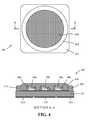
- FIG. 4shows schematic plan view and sectional view of a COB (Chip On Board) light emitting device in accordance with an embodiment of the invention
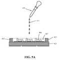
- FIGS. 5A and 5Bis a schematic of a method of manufacture of the COB light emitting device of FIG. 4 in accordance with an embodiment of the invention
- FIG. 6shows schematic plan and section views of a COG (Chip On Glass) light emitting device in accordance with an embodiment of the invention
- FIGS. 7A and 7Bis a schematic of a method of manufacture of the COG light emitting device of FIG. 6 in accordance with an embodiment of the invention.
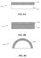
- FIGS. 8A-8Cshow schematic views of remote photoluminescence wavelength conversion component in accordance with embodiments of the invention which respectively show a light transmissive, light reflective and molded remote photoluminescence wavelength conversion components.
- Embodiments of the inventionconcern a photoluminescence material paste comprising a mixture of a light transmissive non-curable silicone fluid and particles of an inorganic photoluminescence material, typically a phosphor material.
- the photoluminescence material paste“phosphor paste”
- phosphor pastecan then be mixed with a curable light transmissive silicone material, typically a two-part curable silicone material, to form a photoluminescence material compound.
- the phosphor pastecan be formed as one part of a two-part curable silicone material rather than being separate from and then being added to the two-part curable silicone material.
- the photoluminescence material compoundcan be used in the manufacture of remote photoluminescence wavelength conversion components for solid-state, typically LED, light emitting devices and arrangements.
- the photoluminescence material compoundcan be deposited directly on the LED chips to manufacture photoluminescence wavelength converted solid-state light emitting devices.
- FIG. 1shows a flow chart of an approach to manufacture a photoluminescence material paste according to some embodiments of the invention.
- the first step at 102is to add a measured quantity of a light transmissive non-curable silicone fluid to a mixing vessel as a carrier material.
- a light transmissive non-curable silicone fluidcan be used in embodiments of the invention.
- curablerefers to the capability to which the silicone fluid is able to cross-link.
- non-curableis used in this specification to indicate that the silicone fluid is incapable of cross-linking, though it will be appreciated that it may be capable of some cross-linking though this will be very low and less than a few percent, typically less than 1%. It will be appreciated that non-curable can encompass a material that is significantly resistant to curing under normal environmental conditions for such materials (c.f. elevated temperatures or exposure to high levels of U.V. for extended periods of time). This is in contrast to “partially-cured” materials, which refer to curable materials that are capable of being fully cured, but are only processed to a state that is less than fully cured.
- the non-curable silicone fluidis not curable by itself but is curable when mixed with another material such as a cross-linking agent and/or catalyst.
- silicone fluidsthat are curable with the addition of another material include PDMS containing end groups such as for example hydride (—H), vinyl (—CH ⁇ CH 2 ), hydroxyl (—OH) and carbonyl (ROH) groups.
- suitable materialsinclude polyphenylmethylsiloxane and polymethylhydrogensiloxane.
- the non-curable silicone fluidcomprises one part of a two-part curable silicone material. Such a non-curable silicone fluid is non-curable by itself without the other respective part of the two-part material.
- the non-curable silicone fluidis non-curable by itself and is also non-curable when mixed with another material such as a cross-linking agent and/or catalyst.
- a cross-linking agent and/or catalystsuch non-curable silicone fluid can be termed “uncurable” and examples of such fluids include polydimethylsiloxane (PDMS) CH 3 [Si(CH 3 ) 2 O] n Si(CH 3 ) 3 and polyphenylmethylsiloxane.
- PDMSpolydimethylsiloxane
- Such silicone fluidsare uncurable since they do not contain end groups (active sites) by which cross-linking can take place.
- the non-curable silicone fluidcan be either a) a silicone fluid that is not curable by itself and is not curable when mixed with another material or b) a silicone fluid that is not curable by itself and is curable when mixed with a another material.
- the reason for using a non-curable silicone fluidis to avoid the “short shelf life” problem, since a curable carrier material may result in the premature curing of the photoluminescence paste during storage/transport.
- non-curable silicone fluidmay depend on the curable silicone material into which the paste is to be incorporated.
- the curable silicone materialcomprises a two-part dimethyl-based curable silicone such as for example a dimethyl-based vinylated and trimethylated silica
- the non-curable silicone fluidcan comprise an uncurable polydimethylsiloxane.
- any suitable viscositycan be selected for the non-curable silicone fluid, appropriate to promote even distribution of materials in the carrier fluid while minimizing the effects of particle settling.
- very small particlese.g., nano-sized light diffusive materials
- an appropriately high viscosity levelmay be desirable to avoid clumping of such materials.
- the viscosity of the non-curable silicone fluidis between about 500 and about 100,000 centistokes (cSt). In preferred embodiments the non-curable silicone fluid has a viscosity of about 60,000 centistokes (cSt).
- the next step at 104is to add a measured quantity of one or more photoluminescence materials, such as phosphor materials.
- the inorganic photoluminescence materialcomprises a phosphor material having an average particle size (D50) of between about 5 ⁇ m and about 35 ⁇ m.
- the particles of photoluminescence materialhave an average particle size of between about 15 ⁇ m and about 20 ⁇ m.
- two or more photoluminescence materialsare added to the mixture, where each of the two or more photoluminescence materials has different densities.
- the weight loading of the materials added to the silicone fluid to form the paste-like consistency of the photoluminescence material compoundis selected to be high enough to reduce or substantially eliminate settling and/or separation of different density materials within the paste.
- such materialscan comprise one or more photoluminescence materials by themselves, photoluminescence material(s) with diffuser materials, and/or the inclusion of additional materials (e.g., anti-settling additives, refractive index additives, thermally conductive additives).
- additional materialse.g., anti-settling additives, refractive index additives, thermally conductive additives.
- the weight loading of the materials added to the silicone fluid in the pasteis in a range about 60% to about 95% with the solid loading depending on the viscosity of the silicone fluid.
- silicone fluidneeds to be compatible with the intended use of the photoluminescence material paste which can determine the composition and/or viscosity of the silicone fluid, and which may then affect the weight loading of the photoluminescence material.
- the weight loading of photoluminescent materials in the pasteis in a range about 80% to about 90% or in a range about 70% to about 80%.
- the weight loading of material(s) in the pasteis in a range about 80% to about 90%.
- the weight loading of the materials in the pasteis about 80%.
- the weight loading of materials in the pasteis about 80% comprising 75.4% photoluminescence material(s) and 4.7% diffuser (Table 1).
- the photoluminescence material pasteis to be premixed with a two-part curable silicone material and the resultant photoluminescence material compound dispensed directly onto an LED chip as part of an LED package (e.g., a Chip On Board COB device), the weight loading of material(s) in the photoluminescence material paste is about 88%. Typically for an LED package the paste does not include a diffuser material (Table 1).
- the weight loading of material(s) in the pasteis about 85% comprising 81% photoluminescence material and 4% diffuser.
- the viscosity of the non-curable silicone fluidcan have a viscosity of between about 500 and about 100,000 centistokes (cSt). In preferred embodiments the non-curable silicone fluid has a viscosity of about 5,000 centistokes (cSt). Viscosity can depend on the viscosity of the curable silicone material it is intended to be used with.
- the photoluminescence materialpreferably comprises a mixture of particles of a first and second inorganic photoluminescence materials.
- the first photoluminescence materialhas a first density and the second photoluminescence material has a second, different, density.
- a particular advantage of the inventionis a reduction in a settling and/or separation of the first and second photoluminescence materials.
- the first and second photoluminescence materialscan comprise particles with an average particle size that are substantially equal.
- the photoluminescence material pastecan comprise a mixture of particles of a first photoluminescence material with a first particle size and a second photoluminescence material with a second, different, particle size.
- the inorganic photoluminescence materialcan comprise a silicate-based phosphor, an aluminate-based phosphor, a nitride-based phosphor, sulfate-based phosphor, a YAG phosphor or mixtures thereof.
- the first photoluminescence materialcomprises a green light emitting aluminate-based phosphor and the second photoluminescence material comprises a red light emitting nitride-based phosphor.
- the green light emitting aluminate-based phosphorcan comprise a garnet-based phosphor as taught in U.S. Pat. No.
- Such a green emitting phosphorcomprises a cerium-activated, green-emitting lutetium aluminate phosphor consisting of lutetium, cerium, at least one alkaline earth metal, aluminum, oxygen, and at least one halogen, wherein the phosphor is configured to absorb excitation radiation having a wavelength ranging from about 380 nm to about 480 nm, and to emit light having a peak emission wavelength ranging from about 500 nm to about 550 nm.
- the red light emitting nitride-based phosphorcomprises a as taught in U.S.
- Such a red emitting phosphorcomprises a nitride-based composition represented by the chemical formula M a Sr b Si c Al d N e Eu f , wherein: M is Ca, and 0.1 ⁇ a ⁇ 0.4; 1.5 ⁇ b ⁇ 2.5; 4.0 ⁇ c ⁇ 5.0; 0.1 ⁇ d ⁇ 0.15; 7.5 ⁇ e ⁇ 8.5; and 0 ⁇ f ⁇ 0.1; wherein a+b+f>2+d/v and v is the valence of M.
- the red-emitting phosphorcomprises a red light emitting nitride-based phosphor comprises a as taught in U.S. Pat. No. 8,663,502 entitled “Red-Emitting Nitride-Based Phosphors” which is hereby incorporated in its entirety.
- Such a red emitting phosphorcomprising a nitride-based composition represented by the chemical formula M (x/v) M′ 2 Si 5-x Al x N 8 :RE, wherein: M is at least one monovalent, divalent or trivalent metal with valence v; M′ is at least one of Mg, Ca, Sr, Ba, and Zn; and RE is at least one of Eu, Ce, Tb, Pr, and Mn; wherein x satisfies 0.1 ⁇ x ⁇ 0.4, and wherein said red-emitting phosphor has the general crystalline structure of M′ 2 Si 5 N 8 :RE, Al substitutes for Si within said general crystalline structure, and M is located within said general crystalline structure substantially at the interstitial sites.
- Mis at least one monovalent, divalent or trivalent metal with valence v
- M′is at least one of Mg, Ca, Sr, Ba, and Zn
- REis at least one of Eu, Ce, Tb, Pr, and Mn
- a measured quantity of a light diffusive materialcan be added so that the photoluminescence material paste can further comprises particles of a light diffusive material.
- the loading of particles of the light diffusive material in the photoluminescence material pastecan be in a range 0.1% to 10%.
- One reason for including the light diffusive materialis to reduce the quantity of photoluminescence material required to generate a selected color of emitted light.
- the inclusion of particles of a light diffusive materialcan further improve color uniformity of emitted light.
- the particles of light diffusive materialcomprise nano-sized particles having an average particle size of between about 40 nm and about 100 nm. Particles of such size will scatter light differently depending on the light wavelength.
- the particle size of the light diffusive materialcan be selected to scatter excitation light more than photoluminescence generated light. Where the excitation light comprises blue light the particles of light diffusive material preferably have an average particle size of about 60 nm.
- the light diffusive materialcan comprise particles of Zinc Oxide (ZnO), titanium dioxide (TiO 2 ), barium sulfate (BaSO 4 ), magnesium oxide (MgO), silicon dioxide (SiO 2 ), aluminum oxide (Al 2 O 3 ), zirconium dioxide (ZrO 2 ) or mixtures thereof.
- a measured quantity of thermally conductive materialcan be added to the photoluminescence material paste. This is useful, for example, where the photoluminescence material paste is to be deposited directly on a LED chip and the thermally conductive material is used to aid in the dissipation of heat. Any suitable thermally conductive material can be employed as desired, depending upon the specific needs of the application to which the invention is employed. For example, thermally conductive plastics or thermally conductive additives may be used included within the photoluminescence material paste.
- a quantity of an anti-settling additivesuch as silica, can be added to the material paste.
- the anti-settling additiveis an agent that is placed within the mixture to maintain uniform distribution and consistency of the phosphor within the silicone fluid, particularly to prevent or inhibit settling during storage of the photoluminescence material paste.
- the anti-settling additivecomprises a suspension, rheological, and/or thickening agent.
- Refractive index additivesmay also be placed within the mixture to provide optimum light scattering properties for the photoluminescence material paste.
- the refractive index additivesare provided to promote index matching of the photoluminescence material paste and/or to increase/decrease the refractive index of the paste. This can be accomplished, for example, by selecting an additive (e.g., titanium dioxide) having a desired refractive index, selecting a desired particle size for the additive (e.g., selected with regards to a given wavelength or wavelength range), and to then select a desired percentage loading of that additive within the paste.
- the componentsare mixed together at 110 to form the photoluminescence material paste. Any appropriate mixing/blending technique can be employed to mix the components.
- the non-curable silicone fluidcomprises a Xiameter® PMX-200 silicone fluid, which is a linear polymethyl siloxane (CH 3 ) 3 SiO[SiO(CH 3 ) 2 ] n Si(CH 3 ) 3 with a viscosity of 5,000 centistokes (cSt), the phosphor material comprises a mixture of and particles of nano-diffuser.
- the weight loading of phosphor/diffuser material to silicone fluidis about 80% to 88% depending on intended use of the paste (Table 1).
- a methodfor manufacturing a remote photoluminescence wavelength conversion component.
- the photoluminescence material pasteis itself non-curable, it can be used in conjunction with a separate curable material to form the final optical product.
- the photoluminescence material pasteis mixed with a selected quantity of a curable silicone material to form a photoluminescence compound which can then be cured.
- FIG. 2shows a flowchart of an approach that can be taken according to some embodiments for manufacturing a remote photoluminescence wavelength conversion component.
- the first step at 202is to add a selected quantity of the photoluminescence material paste to a curable silicone fluid.
- the curable silicone fluidcan comprise a two-part curable silicone material such as a dimethyl-based two-part curable silicone.
- An example of a suitable two-part curable siliconeis a dimethyl-based vinylated and trimethylated silica such as for example Dow Corning® OE-6370 HF when the phosphor paste carrier comprises a polymethyl siloxane.
- the viscosity of the curable silicone materialdepends on the intended method of manufacture of the photoluminescence wavelength conversion component. For example where the component is to be manufactured using injection molding the curable silicone fluid has a viscosity of between about 100,000 and about 1,500,000 centistokes (cSt).
- the photoluminescence material paste of the inventioncan be mixed in high proportions with the curable silicone fluid and the resulting photoluminescence material compound is still curable. Accordingly the method can comprise mixing the photoluminescence paste with the curable silicone fluid in a quantity up to about 70% by weight in the photoluminescence material compound that is a weight ratio of about 5 to 2 of photoluminescence material paste to curable silicone material.
- the componentsare then mixed at 204 to form the photoluminescence material compound.
- the photoluminescence wavelength conversion componente.g., for remote phosphor applications
- This shapingcan be performed, for example, by molding the photoluminescence compound.
- the shaped photoluminescence material compoundis cured (either fully or partially cured), e.g., by using application of heat, UV light, or appropriate chemicals.
- FIGS. 8A-8Cshow illustrative examples of remote photoluminescence wavelength conversion component manufactured in accordance with the method described in conjunction with FIG. 2 .
- the figuresrespectively show a light transmissive photoluminescence wavelength conversion component 800 , a light reflective photoluminescence wavelength conversion component 830 and a molded remote photoluminescence wavelength conversion component 860 .
- the light transmissive component 800comprises a light transmissive substrate 810 with a layer of photoluminescence material compound 820 deposited on one or more faces ( FIG. 8A ).
- the light transmissive substrate 810can be planar or alternatively 3-D in form and can comprise glass or a polymer material.
- the light reflective component 830comprises a light reflective substrate 840 with a layer of photoluminescence material compound 820 deposited on a face thereof ( FIG. 8B ).
- the light reflective substrate 840can be planar or alternatively 3-D in form and can comprise any light reflective material such as a metal or a polymer material.
- the molded component 850comprises a component which is fabricated entirely from the photoluminescence material compound 860 ( FIG. 8C ).
- the molded componentcan comprise a hemispherical shell or other shapes depending on intended application.
- the componentcan be injection molded.
- the correlated color temperature (CCT) and/or color rendering index (CRI) of light generated by such a componentdepends on the wall thickness of the component and the loading of photoluminescence within the component wall.
- the weight loading of the photoluminescence material paste in the photoluminescence material compoundis about 5% for a 6000K component.
- FIG. 3shows a flowchart of an approach that can be taken according to some embodiments for manufacturing a photoluminescence wavelength converted solid-state light emitting device.
- the first step at 302is to add a selected quantity of the photoluminescence material paste to a curable silicone material.
- the curable silicone materialcan comprise a dimethyl-based two-part curable silicone.
- the viscosity of the curable silicone materialdepends on the intended method of manufacture of the photoluminescence wavelength conversion component. For example where the component is to be manufactured by dispensing the photoluminescence material compound, the curable silicone material has a viscosity of between about 5,000 and about 10,000 centistokes (cSt).
- the componentsare then mixed at 304 to form the photoluminescence material compound.
- the photoluminescence wavelength conversion componentis dispensed onto a solid-state light source.
- the dispensed photoluminescence material compoundis cured (either fully or partially cured), e.g., by using application of heat, UV light, or appropriate chemicals.
- the solid-state light sourcecomprises: a packaged LED chip, an LED chip on a light transmissive substrate, an LED Chip On Glass (COG) or an LED Chip On Board (COB).
- COGLED Chip On Glass
- COBLED Chip On Board
- FIGS. 4, 5A, 5B, 6, 7A and 7Bprovide illustrative examples for this process of manufacturing a light emitting device in accordance with the method described in conjunction with FIG. 3 .
- FIG. 4shows schematic plan view and sectional view of a COB (Chip On Board) light emitting device 402 in accordance with an embodiment of the invention.
- COBChip On Board
- an entire array of packaged LED chips 406is placed within a packaging structure.
- the array of LEDs 406is placed on the circuit board 421 between annular walls 425 .
- the circuit board 421comprises a MCPCB (Metal Core Printed Circuit Board).
- the metal core base of the circuit board 421is mounted in thermal communication with a heatsink pad 430 , e.g., with the aid of a thermally conducting compound such as for example a material containing a standard heat sink compound containing beryllium oxide or aluminum nitride.
- Bond wires 408provide the connection paths from leads to each LED chip 406 .
- Contact pads 424provide electrical conductivity from the COB LED structure 402 to external control electronics.
- An encapsulant 420is deposited over and around the entire array of packaged LED chips.
- the encapsulant 420comprises the inventive photoluminescence material paste that was mixed with a curable light transmissive silicone material to form a photoluminescence material compound.
- FIGS. 5A and 5Bis a schematic of a method of manufacture of the COB light emitting device of FIG. 4 in accordance with an embodiment of the invention.
- the annular walls 425 of the package structuredefine a cylindrical cavity 427 containing the array of LEDs 406 .
- a dispenser 429is used to dispense a selected quantity of the photoluminescence material compound 431 within the cylindrical cavity 427 .
- the photoluminescence material compound 431comprises the photoluminescence material paste combined with a curable silicone material, e.g., where the curable silicone material is a dimethyl-based two-part curable silicone.
- the viscosity of the curable silicone materialhas a viscosity of, for example, between about 5,000 and about 10,000 centistokes (cSt).
- cStcentistokes
- the dispensed photoluminescence material compound 431is cured (either fully or partially cured), e.g., by using application of heat 435 , UV light 437 , and/or appropriate chemicals.
- the correlated color temperature (CCT) and/or color rendering index (CRI) of light generated bydepends on the thickness of the photoluminescence encapsulation 420 and the loading of photoluminescence material(s) within the encapsulation.
- the photoluminescence material pastetypically does not include a light diffusive material for LED packaged devices.
- FIG. 6shows schematic plan and section views of a COG (Chip On Glass) light emitting device in accordance with an embodiment of the invention.
- the COG (Chip On Glass) light emitting device 602includes an array of LEDs 606 that are aligned and mounted along a glass substrate 621 .
- the array of LED chips 606is bonded to the glass substrate 621 .
- Bond wires 608are affixed to the LED chips 606 , where the other end of the bond wires 608 are attached to contact pads 624 .
- the encapsulant 620is deposited over and around the array of LED chips 606 .
- the encapsulant 420comprises the inventive photoluminescence material paste that was mixed with a two-part curable light transmissive silicone fluid to form a photoluminescence material compound.
- FIGS. 7A and 7Bis a schematic of a method of manufacture of the COG light emitting device of FIG. 6 in accordance with an embodiment of the invention.
- a dispenser 729is employed to dispense a quantity of the photoluminescence material compound 731 over and around the array of LED chips 606 . If the photoluminescence material compound 731 has a sufficient level of viscosity, then the photoluminescence material compound 731 can be applied directly over the array of LED chips 606 without requiring the use of a surrounding form.
- the photoluminescence material compound 731comprises the photoluminescence material paste combined with a two-part curable silicone fluid, e.g., where the two-part curable silicone fluid is a dimethyl-based two-part curable silicone. Thereafter, as shown in FIG. 7B , the dispensed photoluminescence material compound 731 is cured (either fully or partially), e.g., by using application of heat 735 , UV light 737 , and/or appropriate chemicals.
- the correlated color temperature (CCT) and/or color rendering index (CRI) of light generated bydepends on the thickness of the photoluminescence encapsulation 620 and the loading of photoluminescence material(s) within the encapsulation. For example for an encapsulation thickness of 1 to 2 mm when using a two-part silicone material with a viscosity of 5,000 centistokes (cSt) the weight loading of the about 10%-30% photoluminescence material paste (Table 1) in the photoluminescence material compound depending on the required CCT and/or CRI.
- CCTcorrelated color temperature
- CRIcolor rendering index
- a light diffusive material pastecomprises: a mixture of a light transmissive non-curable silicone fluid and particles of light diffusive material.
- the light diffusive material pastecan then be mixed with a two-part curable light transmissive silicone material and the resulting light diffusive material compound used in the manufacture of light diffusive optical components or a light diffusive portion of a remote photoluminescence wavelength conversion component.
- the non-curable silicone fluidcan comprise a linear polydimethylsiloxane (PDMS), phenylmethyl polysiloxane or a methylhydrogen polysiloxane.
- the light diffusive materialcomprises nano-sized particles having an average particle size of between about 40 nm and about 100 nm. Particles of such size will scatter light differently depending on the wavelength of light. Where the light diffusive component is to be used in a blue light based LED system the particles of light diffusive material preferably have an average particle size of about 60 nm.
- the light diffusive materialcan comprise particles of Zinc Oxide (ZnO), titanium dioxide (TiO 2 ), barium sulfate (BaSO 4 ), magnesium oxide (MgO), silicon dioxide (SiO 2 ), aluminum oxide (Al 2 O 3 ), or mixtures thereof.
- the weight loading of the light diffusive material in the light diffusive pastecan be in a range 10% to 60% depending on the intended method of manufacture of the light diffusive component. For example where a 2-D printing process (e.g., screen printing) is to used to deposit the light diffusive material the weight loading of the particles of the light diffusive material in the paste is in a range about 50% to about 60%. Where injection molding is to be used to manufacture the light diffusive component, the weight loading of light diffusive material to in the paste is in a range about 10% to about 20%.
- a 2-D printing processe.g., screen printing
- an inventive photoluminescence material pastecomprising a mixture of a light transmissive non-curable silicone fluid and particles of one or more inorganic photoluminescence material, such as a phosphor material.
- the photoluminescence material pastecan then be mixed with a curable light transmissive silicone material, typically a two-part curable silicone material, and the resulting photoluminescence material compound used in the manufacture of remote photoluminescence wavelength conversion components for solid-state, typically LED, light emitting devices and arrangements.
- the photoluminescence material compoundcan be deposited directly on the LED chips to manufacture photoluminescence wavelength converted solid-state light emitting devices.
- This inventive approachprovides numerous benefits, since it serves to reduce clumping of phosphor particles used for manufacturing LED lights structures, reduces separation of different phosphor materials when multiple phosphor material are used that have different specific gravities, and increases the shelf life of phosphor mixing products.
Landscapes
- Chemical & Material Sciences (AREA)
- Engineering & Computer Science (AREA)
- Materials Engineering (AREA)
- Organic Chemistry (AREA)
- Inorganic Chemistry (AREA)
- Led Device Packages (AREA)
- Luminescent Compositions (AREA)
- Compositions Of Macromolecular Compounds (AREA)
Abstract
Description
| TABLE 1 |
| Photoluminescence material paste composition by intended application |
| Application | Weight loading of materials in paste (%) |
| Injection molding | 80 = 75.4 photoluminescence material(s), 4.7% |
| diffusive material | |
| LED package (e.g. COB) | 88 = photoluminescence material(s) |
| Chip On Glass (COG) | 85 = 81% photoluminescence material(s), |
| 4% diffusive material | |
Claims (30)
Priority Applications (5)
| Application Number | Priority Date | Filing Date | Title |
|---|---|---|---|
| US14/469,523US9318670B2 (en) | 2014-05-21 | 2014-08-26 | Materials for photoluminescence wavelength converted solid-state light emitting devices and arrangements |
| CN201580036569.6ACN106471598A (en) | 2014-05-21 | 2015-05-20 | Materials for photoluminescent wavelength-converted solid-state light-emitting devices and arrangements |
| EP15796791.0AEP3146556A1 (en) | 2014-05-21 | 2015-05-20 | Materials for photoluminescence wavelength converted solid-state light emitting devices and arrangements |
| PCT/US2015/031809WO2015179542A1 (en) | 2014-05-21 | 2015-05-20 | Materials for photoluminescence wavelength converted solid-state light emitting devices and arrangements |
| TW104116322ATW201601350A (en) | 2014-05-21 | 2015-05-21 | Solid-state light-emitting device and configuration material for photoluminescence wavelength conversion |
Applications Claiming Priority (2)
| Application Number | Priority Date | Filing Date | Title |
|---|---|---|---|
| US201462001596P | 2014-05-21 | 2014-05-21 | |
| US14/469,523US9318670B2 (en) | 2014-05-21 | 2014-08-26 | Materials for photoluminescence wavelength converted solid-state light emitting devices and arrangements |
Publications (2)
| Publication Number | Publication Date |
|---|---|
| US20150340573A1 US20150340573A1 (en) | 2015-11-26 |
| US9318670B2true US9318670B2 (en) | 2016-04-19 |
Family
ID=54554711
Family Applications (1)
| Application Number | Title | Priority Date | Filing Date |
|---|---|---|---|
| US14/469,523ActiveUS9318670B2 (en) | 2014-05-21 | 2014-08-26 | Materials for photoluminescence wavelength converted solid-state light emitting devices and arrangements |
Country Status (5)
| Country | Link |
|---|---|
| US (1) | US9318670B2 (en) |
| EP (1) | EP3146556A1 (en) |
| CN (1) | CN106471598A (en) |
| TW (1) | TW201601350A (en) |
| WO (1) | WO2015179542A1 (en) |
Cited By (2)
| Publication number | Priority date | Publication date | Assignee | Title |
|---|---|---|---|---|
| US20170077172A1 (en)* | 2015-09-10 | 2017-03-16 | Panasonic Intellectual Property Management Co., Ltd. | Light-emitting device and illumination light source |
| US10066160B2 (en) | 2015-05-01 | 2018-09-04 | Intematix Corporation | Solid-state white light generating lighting arrangements including photoluminescence wavelength conversion components |
Families Citing this family (8)
| Publication number | Priority date | Publication date | Assignee | Title |
|---|---|---|---|---|
| WO2017153216A1 (en)* | 2016-03-10 | 2017-09-14 | Lumileds Holding B.V. | Led module |
| JP6704182B2 (en)* | 2016-03-24 | 2020-06-03 | パナソニックIpマネジメント株式会社 | Lighting equipment |
| JP6775429B2 (en)* | 2017-01-16 | 2020-10-28 | 日本特殊陶業株式会社 | Manufacturing method of wavelength conversion member |
| KR102556257B1 (en) | 2017-04-03 | 2023-07-14 | 인터매틱스 코포레이션 | Color liquid crystal displays and display backlights |
| CN110914381A (en)* | 2017-05-23 | 2020-03-24 | 英特曼帝克司公司 | Color LCD Monitors and Display Backlights |
| US10371325B1 (en) | 2018-06-25 | 2019-08-06 | Intematix Corporation | Full spectrum white light emitting devices |
| CN111286330A (en)* | 2018-12-06 | 2020-06-16 | 松下知识产权经营株式会社 | Phosphor and semiconductor light emitting device using the same |
| CN119505601A (en)* | 2024-10-25 | 2025-02-25 | 华中科技大学 | A rare earth complex ink containing a thermally conductive material doped with a pyrazole boron Ce (III) complex, preparation and application thereof |
Citations (153)
| Publication number | Priority date | Publication date | Assignee | Title |
|---|---|---|---|---|
| US3290255A (en) | 1963-09-30 | 1966-12-06 | Gen Electric | White electroluminescent phosphor |
| US3593055A (en) | 1969-04-16 | 1971-07-13 | Bell Telephone Labor Inc | Electro-luminescent device |
| US3670193A (en) | 1970-05-14 | 1972-06-13 | Duro Test Corp | Electric lamps producing energy in the visible and ultra-violet ranges |
| US3676668A (en) | 1969-12-29 | 1972-07-11 | Gen Electric | Solid state lamp assembly |
| US3691482A (en) | 1970-01-19 | 1972-09-12 | Bell Telephone Labor Inc | Display system |
| US3709685A (en) | 1970-02-19 | 1973-01-09 | Ilford Ltd | Photoconductive zinc oxide sensitized by substituted thiazolidene dyes |
| US3743833A (en) | 1971-07-16 | 1973-07-03 | Eastman Kodak Co | Radiographic elements and binders |
| US3763405A (en) | 1970-12-21 | 1973-10-02 | Nippon Electric Co | Solid state luminescent display device |
| US3793046A (en) | 1970-12-04 | 1974-02-19 | Philips Corp | Method of manufacturing a pigment |
| US3819973A (en) | 1972-11-02 | 1974-06-25 | A Hosford | Electroluminescent filament |
| US3819974A (en) | 1973-03-12 | 1974-06-25 | D Stevenson | Gallium nitride metal-semiconductor junction light emitting diode |
| US3849707A (en) | 1973-03-07 | 1974-11-19 | Ibm | PLANAR GaN ELECTROLUMINESCENT DEVICE |
| US3875456A (en) | 1972-04-04 | 1975-04-01 | Hitachi Ltd | Multi-color semiconductor lamp |
| JPS5079379U (en) | 1973-11-24 | 1975-07-09 | ||
| US3932881A (en) | 1972-09-05 | 1976-01-13 | Nippon Electric Co., Inc. | Electroluminescent device including dichroic and infrared reflecting components |
| US3937998A (en) | 1973-10-05 | 1976-02-10 | U.S. Philips Corporation | Luminescent coating for low-pressure mercury vapour discharge lamp |
| US3972717A (en) | 1973-03-21 | 1976-08-03 | Hoechst Aktiengesellschaft | Electrophotographic recording material |
| US4047075A (en) | 1975-03-01 | 1977-09-06 | Licentia-Patent-Verwaltungs-G.M.B.H. | Encapsulated light-emitting diode structure and array thereof |
| US4081764A (en) | 1972-10-12 | 1978-03-28 | Minnesota Mining And Manufacturing Company | Zinc oxide light emitting diode |
| US4104076A (en) | 1970-03-17 | 1978-08-01 | Saint-Gobain Industries | Manufacture of novel grey and bronze glasses |
| US4143394A (en) | 1976-07-30 | 1979-03-06 | Licentia Patent-Verwaltungs-G.M.B.H. | Semiconductor luminescence device with housing |
| GB2017409A (en) | 1978-03-22 | 1979-10-03 | Bayraktaroglu B | Light-emitting diode |
| US4176299A (en) | 1975-10-03 | 1979-11-27 | Westinghouse Electric Corp. | Method for efficiently generating white light with good color rendition of illuminated objects |
| US4176294A (en) | 1975-10-03 | 1979-11-27 | Westinghouse Electric Corp. | Method and device for efficiently generating white light with good rendition of illuminated objects |
| US4211955A (en) | 1978-03-02 | 1980-07-08 | Ray Stephen W | Solid state lamp |
| US4305019A (en) | 1979-12-31 | 1981-12-08 | Westinghouse Electric Corp. | Warm-white fluorescent lamp having good efficacy and color rendering and using special phosphor blend as separate undercoat |
| US4315192A (en) | 1979-12-31 | 1982-02-09 | Westinghouse Electric Corp. | Fluorescent lamp using high performance phosphor blend which is protected from color shifts by a very thin overcoat of stable phosphor of similar chromaticity |
| US4443532A (en) | 1981-07-29 | 1984-04-17 | Bell Telephone Laboratories, Incorporated | Induced crystallographic modification of aromatic compounds |
| JPS60170194U (en) | 1984-04-20 | 1985-11-11 | 鈴木 悦三 | Roll paper holder that can be opened and closed |
| US4559470A (en) | 1981-04-22 | 1985-12-17 | Mitsubishi Denki Kabushiki Kaisha | Fluorescent discharge lamp |
| US4573766A (en) | 1983-12-19 | 1986-03-04 | Cordis Corporation | LED Staggered back lighting panel for LCD module |
| US4618555A (en) | 1984-01-11 | 1986-10-21 | Mitsubishi Chemical Ind., Ltd. | Electrophotographic photoreceptor comprising azo compounds |
| US4638214A (en) | 1985-03-25 | 1987-01-20 | General Electric Company | Fluorescent lamp containing aluminate phosphor |
| US4667036A (en) | 1983-08-27 | 1987-05-19 | Basf Aktiengesellschaft | Concentration of light over a particular area, and novel perylene-3,4,9,10-tetracarboxylic acid diimides |
| US4678285A (en) | 1984-01-13 | 1987-07-07 | Ricoh Company, Ltd. | Liquid crystal color display device |
| US4727003A (en) | 1985-09-30 | 1988-02-23 | Ricoh Company, Ltd. | Electroluminescence device |
| US4772885A (en) | 1984-11-22 | 1988-09-20 | Ricoh Company, Ltd. | Liquid crystal color display device |
| US4845223A (en) | 1985-12-19 | 1989-07-04 | Basf Aktiengesellschaft | Fluorescent aryloxy-substituted perylene-3,4,9,10-tetracarboxylic acid diimides |
| JPH01179471A (en) | 1988-01-07 | 1989-07-17 | Natl Inst For Res In Inorg Mater | Cubic boron nitride P-n junction light emitting device |
| US4859539A (en) | 1987-03-23 | 1989-08-22 | Eastman Kodak Company | Optically brightened polyolefin coated paper support |
| JPH01260707A (en) | 1988-04-11 | 1989-10-18 | Idec Izumi Corp | Device for emitting white light |
| JPH0291980A (en) | 1988-09-29 | 1990-03-30 | Toshiba Lighting & Technol Corp | solid state light emitting device |
| US4915478A (en) | 1988-10-05 | 1990-04-10 | The United States Of America As Represented By The Secretary Of The Navy | Low power liquid crystal display backlight |
| US4918497A (en) | 1988-12-14 | 1990-04-17 | Cree Research, Inc. | Blue light emitting diode formed in silicon carbide |
| US4946621A (en) | 1986-04-29 | 1990-08-07 | Centre National De La Recherche Scientifique (Cnrs) | Luminescent mixed borates based on rare earths |
| US4992704A (en) | 1989-04-17 | 1991-02-12 | Basic Electronics, Inc. | Variable color light emitting diode |
| JPH0324692Y2 (en) | 1987-08-06 | 1991-05-29 | ||
| WO1991008508A1 (en) | 1989-11-24 | 1991-06-13 | Innovare Limited | A display device |
| US5077161A (en) | 1990-05-31 | 1991-12-31 | Xerox Corporation | Imaging members with bichromophoric bisazo perylene photoconductive materials |
| US5110931A (en) | 1987-11-27 | 1992-05-05 | Hoechst Aktiengesellschaft | Process for the preparation of n,n'-dimethylperylene-3,4,9,10-tetracarboxylic diimide in high-hiding pigment form |
| US5126214A (en) | 1989-03-15 | 1992-06-30 | Idemitsu Kosan Co., Ltd. | Electroluminescent element |
| US5131916A (en) | 1990-03-01 | 1992-07-21 | Bayer Aktiengesellschaft | Colored fluorescent polymer emulsions for marker pens: graft copolymers and fluorescent dyes in aqueous phase |
| US5143433A (en) | 1991-11-01 | 1992-09-01 | Litton Systems Canada Limited | Night vision backlighting system for liquid crystal displays |
| US5143438A (en) | 1990-10-15 | 1992-09-01 | Thorn Emi Plc | Light sources |
| JPH04289691A (en) | 1990-12-07 | 1992-10-14 | Mitsubishi Cable Ind Ltd | El illuminant |
| JPH04321280A (en) | 1991-04-19 | 1992-11-11 | Nichia Chem Ind Ltd | Blue color light-emitting diode |
| US5166761A (en) | 1991-04-01 | 1992-11-24 | Midwest Research Institute | Tunnel junction multiple wavelength light-emitting diodes |
| US5208462A (en) | 1991-12-19 | 1993-05-04 | Allied-Signal Inc. | Wide bandwidth solid state optical source |
| US5210051A (en) | 1990-03-27 | 1993-05-11 | Cree Research, Inc. | High efficiency light emitting diodes from bipolar gallium nitride |
| US5211467A (en) | 1992-01-07 | 1993-05-18 | Rockwell International Corporation | Fluorescent lighting system |
| JPH05152609A (en) | 1991-11-25 | 1993-06-18 | Nichia Chem Ind Ltd | Light emitting diode |
| US5237182A (en) | 1990-11-29 | 1993-08-17 | Sharp Kabushiki Kaisha | Electroluminescent device of compound semiconductor with buffer layer |
| US5264034A (en) | 1989-08-11 | 1993-11-23 | Hoechst Aktiengesellschaft | Pigment preparations based on perylene compounds |
| US5283425A (en) | 1992-02-06 | 1994-02-01 | Rohm Co., Ltd. | Light emitting element array substrate with reflecting means |
| JPH06267301A (en) | 1993-03-15 | 1994-09-22 | Olympus Optical Co Ltd | Organic photoluminescence element |
| US5369289A (en) | 1991-10-30 | 1994-11-29 | Toyoda Gosei Co. Ltd. | Gallium nitride-based compound semiconductor light-emitting device and method for making the same |
| US5405709A (en) | 1993-09-13 | 1995-04-11 | Eastman Kodak Company | White light emitting internal junction organic electroluminescent device |
| JPH07176794A (en) | 1993-12-17 | 1995-07-14 | Nichia Chem Ind Ltd | Surface light source |
| US5439971A (en) | 1991-11-12 | 1995-08-08 | Eastman Chemical Company | Fluorescent pigment concentrates |
| JPH07235207A (en) | 1994-02-21 | 1995-09-05 | Copal Co Ltd | Back light |
| JPH0799345B2 (en) | 1988-10-31 | 1995-10-25 | 防衛庁技術研究本部長 | Method and apparatus for generating water temperature profile data |
| JPH07282609A (en) | 1994-04-06 | 1995-10-27 | Tsuzuki Shogo | Light source device for illumination using semiconductor laser device |
| JPH087614Y2 (en) | 1990-05-08 | 1996-03-04 | 中部電力株式会社 | Wire cap |
| US5518808A (en) | 1992-12-18 | 1996-05-21 | E. I. Du Pont De Nemours And Company | Luminescent materials prepared by coating luminescent compositions onto substrate particles |
| US5557168A (en) | 1993-04-02 | 1996-09-17 | Okaya Electric Industries Co., Ltd. | Gas-discharging type display device and a method of manufacturing |
| JPH08250281A (en) | 1995-03-08 | 1996-09-27 | Olympus Optical Co Ltd | Luminescent element and displaying apparatus |
| US5563621A (en) | 1991-11-18 | 1996-10-08 | Black Box Vision Limited | Display apparatus |
| US5578839A (en) | 1992-11-20 | 1996-11-26 | Nichia Chemical Industries, Ltd. | Light-emitting gallium nitride-based compound semiconductor device |
| US5583349A (en) | 1995-11-02 | 1996-12-10 | Motorola | Full color light emitting diode display |
| US5585640A (en) | 1995-01-11 | 1996-12-17 | Huston; Alan L. | Glass matrix doped with activated luminescent nanocrystalline particles |
| US5619356A (en) | 1993-09-16 | 1997-04-08 | Sharp Kabushiki Kaisha | Reflective liquid crystal display device having a compensator with a retardation value between 0.15 μm and 0.38 μm and a single polarizer |
| US5660461A (en) | 1994-12-08 | 1997-08-26 | Quantum Devices, Inc. | Arrays of optoelectronic devices and method of making same |
| US5677417A (en) | 1993-05-04 | 1997-10-14 | Max-Planck-Gesellschaft Zur Foerderung | Tetraaroxyperylene-3,4,9,10-tetracarboxylic polyimides |
| US5679152A (en) | 1994-01-27 | 1997-10-21 | Advanced Technology Materials, Inc. | Method of making a single crystals Ga*N article |
| US5763901A (en) | 1992-12-17 | 1998-06-09 | Kabushiki Kaisha Toshiba | Semiconductor light-emitting device and method for manufacturing the device |
| US5770887A (en) | 1993-10-08 | 1998-06-23 | Mitsubishi Cable Industries, Ltd. | GaN single crystal |
| US5771039A (en) | 1994-06-06 | 1998-06-23 | Ditzik; Richard J. | Direct view display device integration techniques |
| US5777350A (en) | 1994-12-02 | 1998-07-07 | Nichia Chemical Industries, Ltd. | Nitride semiconductor light-emitting device |
| US5869199A (en) | 1993-03-26 | 1999-02-09 | Sumitomo Electric Industries, Ltd. | Organic electroluminescent elements comprising triazoles |
| JP2900928B2 (en) | 1997-10-20 | 1999-06-02 | 日亜化学工業株式会社 | Light emitting diode |
| US5959316A (en) | 1998-09-01 | 1999-09-28 | Hewlett-Packard Company | Multiple encapsulation of phosphor-LED devices |
| US5962971A (en) | 1997-08-29 | 1999-10-05 | Chen; Hsing | LED structure with ultraviolet-light emission chip and multilayered resins to generate various colored lights |
| US5998925A (en) | 1996-07-29 | 1999-12-07 | Nichia Kagaku Kogyo Kabushiki Kaisha | Light emitting device having a nitride compound semiconductor and a phosphor containing a garnet fluorescent material |
| US6072272A (en) | 1998-05-04 | 2000-06-06 | Motorola, Inc. | Color flat panel display device |
| JP2000286454A (en) | 2000-01-01 | 2000-10-13 | Sanken Electric Co Ltd | Semiconductor planar light source |
| US6137217A (en) | 1992-08-28 | 2000-10-24 | Gte Products Corporation | Fluorescent lamp with improved phosphor blend |
| US20010019240A1 (en) | 1999-12-09 | 2001-09-06 | Kenji Takahashi | Display apparatus |
| US6340824B1 (en) | 1997-09-01 | 2002-01-22 | Kabushiki Kaisha Toshiba | Semiconductor light emitting device including a fluorescent material |
| JP2002241586A (en) | 2001-02-19 | 2002-08-28 | Matsushita Electric Ind Co Ltd | Wavelength conversion paste material, composite light-emitting element, semiconductor light-emitting device, and method for manufacturing the same |
| JP2002359404A (en) | 2001-05-31 | 2002-12-13 | Nichia Chem Ind Ltd | Light emitting device using phosphor |
| US6504301B1 (en) | 1999-09-03 | 2003-01-07 | Lumileds Lighting, U.S., Llc | Non-incandescent lightbulb package using light emitting diodes |
| JP2003046133A (en) | 2001-07-26 | 2003-02-14 | Matsushita Electric Works Ltd | Light emitting device and method of manufacturing the same |
| US6576488B2 (en) | 2001-06-11 | 2003-06-10 | Lumileds Lighting U.S., Llc | Using electrophoresis to produce a conformally coated phosphor-converted light emitting semiconductor |
| US6600175B1 (en) | 1996-03-26 | 2003-07-29 | Advanced Technology Materials, Inc. | Solid state white light emitter and display using same |
| US6642618B2 (en) | 2000-12-21 | 2003-11-04 | Lumileds Lighting U.S., Llc | Light-emitting device and production thereof |
| US6642652B2 (en) | 2001-06-11 | 2003-11-04 | Lumileds Lighting U.S., Llc | Phosphor-converted light emitting device |
| JP2004153109A (en) | 2002-10-31 | 2004-05-27 | Matsushita Electric Works Ltd | Light emitting device and manufacturing method thereof |
| US6869812B1 (en) | 2003-05-13 | 2005-03-22 | Heng Liu | High power AllnGaN based multi-chip light emitting diode |
| JP2005277441A (en) | 2001-09-03 | 2005-10-06 | Matsushita Electric Ind Co Ltd | Manufacturing method of semiconductor light emitting device |
| US20060158090A1 (en) | 2005-01-14 | 2006-07-20 | Intematix Corporation | Novel aluminate-based green phosphors |
| US7153015B2 (en) | 2001-12-31 | 2006-12-26 | Innovations In Optics, Inc. | Led white light optical system |
| US20070031097A1 (en) | 2003-12-08 | 2007-02-08 | University Of Cincinnati | Light Emissive Signage Devices Based on Lightwave Coupling |
| US20070138438A1 (en) | 1997-02-24 | 2007-06-21 | Cabot Corporation | Photoluminescent phosphor powders, methods for making phosphor powders and devices incorporating same |
| WO2007103394A2 (en) | 2006-03-08 | 2007-09-13 | Intematix Corporation | Light emitting sign and display surface therefor |
| JP4010665B2 (en) | 1998-09-08 | 2007-11-21 | 三洋電機株式会社 | Installation method of solar cell module |
| US7311858B2 (en) | 2004-08-04 | 2007-12-25 | Intematix Corporation | Silicate-based yellow-green phosphors |
| TW200814377A (en) | 2006-08-03 | 2008-03-16 | Intematix Corp | LED lighting arrangement including light emitting phosphor |
| US20080111472A1 (en) | 2006-11-10 | 2008-05-15 | Intematix Corporation | Aluminum-silicate based orange-red phosphors with mixed divalent and trivalent cations |
| US20080116785A1 (en) | 2004-11-25 | 2008-05-22 | Mitsubishi Chemical Corporation | Light-Emitting Device |
| JP2008130279A (en) | 2006-11-17 | 2008-06-05 | Nichia Chem Ind Ltd | Planar light emitting device and manufacturing method thereof |
| US7390437B2 (en) | 2004-08-04 | 2008-06-24 | Intematix Corporation | Aluminate-based blue phosphors |
| US20080218992A1 (en) | 2007-03-05 | 2008-09-11 | Intematix Corporation | Light emitting diode (LED) based lighting systems |
| US7479662B2 (en) | 2002-08-30 | 2009-01-20 | Lumination Llc | Coated LED with improved efficiency |
| JP2009102514A (en) | 2007-10-23 | 2009-05-14 | Mitsubishi Chemicals Corp | Method for producing phosphor-containing composition and method for producing semiconductor light-emitting device |
| TW200926459A (en) | 2007-10-01 | 2009-06-16 | Intematix Corp | Light emitting devices with phosphor wavelength conversion and methods of fabrication thereof |
| TW200929621A (en) | 2007-10-17 | 2009-07-01 | Intematix Corp | Light emitting device with phosphor wavelength conversion |
| JP2009158119A (en) | 2007-12-25 | 2009-07-16 | Stanley Electric Co Ltd | Surface light source device |
| US7575697B2 (en) | 2004-08-04 | 2009-08-18 | Intematix Corporation | Silicate-based green phosphors |
| JP2009530437A (en) | 2006-03-15 | 2009-08-27 | エルジー イノテック カンパニー リミテッド | Phosphorescent sheet |
| JP2009209316A (en) | 2008-03-06 | 2009-09-17 | Dainippon Toryo Co Ltd | Nonaqueous ink composition for inkjet |
| US7601276B2 (en) | 2004-08-04 | 2009-10-13 | Intematix Corporation | Two-phase silicate-based yellow phosphor |
| US20090283721A1 (en) | 2008-05-19 | 2009-11-19 | Intematix Corporation | Nitride-based red phosphors |
| US7655156B2 (en) | 2005-08-03 | 2010-02-02 | Intematix Corporation | Silicate-based orange phosphors |
| US20100079980A1 (en) | 2008-10-01 | 2010-04-01 | Mitsubishi Electric Corporation | Planar light source device and display apparatus incorporating same |
| WO2010074963A1 (en) | 2008-12-15 | 2010-07-01 | Intematix Corporation | Nitride-based red-emitting phosphors in rgb (red-green-blue) lighting systems |
| JP2010151877A (en) | 2008-12-24 | 2010-07-08 | Hiraoka & Co Ltd | Light emitting display body for sign, light emitting display body system for sign having emergency light function, and illumination method of the same |
| WO2010123059A1 (en) | 2009-04-22 | 2010-10-28 | シーシーエス株式会社 | Method for manufacturing led light emitting device |
| US20100276712A1 (en)* | 2009-11-03 | 2010-11-04 | Alexander Shaikevitch | Light emitting diode with thin multilayer phosphor film |
| US20100295079A1 (en) | 2009-05-19 | 2010-11-25 | Intematix Corporation | Manufacture of light emitting devices with phosphor wavelength conversion |
| US20100301758A1 (en) | 2009-06-02 | 2010-12-02 | Mitac Technology Corp. | Flat display device blacklight module thereof for night vision imaging system |
| US20100321339A1 (en) | 2009-06-18 | 2010-12-23 | Nokia Corporation | Diffractive optical touch input |
| US7863808B2 (en) | 2008-02-27 | 2011-01-04 | Fuji Electric Holdings Co., Ltd. | Resonant cavity color conversion EL device and organic EL display device using the same |
| US8044575B2 (en) | 2008-07-29 | 2011-10-25 | Fuji Electric Co., Ltd. | Color conversion type organic EL display |
| US20110261290A1 (en) | 2010-04-21 | 2011-10-27 | Sangcheon Kim | Display apparatus |
| US20120112130A1 (en)* | 2006-10-20 | 2012-05-10 | Intematix Corporation | Green-emitting, garnet-based phosphors in general and backlighting applications |
| US20120286208A1 (en)* | 2011-05-09 | 2012-11-15 | Hong Kong Applied Science and Technology Research Institute Company Limited | Phosphor ink composition |
| US8400396B2 (en) | 2004-05-04 | 2013-03-19 | Sharp Laboratories Of America, Inc. | Liquid crystal display with modulation for colored backlight |
| US8597545B1 (en)* | 2012-07-18 | 2013-12-03 | Intematix Corporation | Red-emitting nitride-based calcium-stabilized phosphors |
| US8618559B2 (en) | 2010-07-21 | 2013-12-31 | Canon Kabushiki Kaisha | Organic electroluminescent display |
| US8663502B2 (en)* | 2011-12-30 | 2014-03-04 | Intematix Corporation | Red-emitting nitride-based phosphors |
| US8796712B2 (en) | 2010-06-29 | 2014-08-05 | Nitto Denko Corporation | Phosphor layer and light-emitting device |
| US8796050B2 (en) | 2011-01-17 | 2014-08-05 | Samsung Electronics Co., Ltd. | Method and apparatus for manufacturing white light-emitting device |
| US8795817B2 (en) | 2010-08-25 | 2014-08-05 | Samsung Electronics Co., Ltd. | Phosphor film, method of manufacturing the same, coating method of phosphor layer, method of manufacturing LED package, and LED package manufactured thereby |
Family Cites Families (7)
| Publication number | Priority date | Publication date | Assignee | Title |
|---|---|---|---|---|
| US6604971B1 (en)* | 2000-05-02 | 2003-08-12 | General Electric Company | Fabrication of LED lamps by controlled deposition of a suspension media |
| US20070128745A1 (en)* | 2005-12-01 | 2007-06-07 | Brukilacchio Thomas J | Phosphor deposition method and apparatus for making light emitting diodes |
| US8461613B2 (en)* | 2008-05-27 | 2013-06-11 | Interlight Optotech Corporation | Light emitting device |
| US8835199B2 (en)* | 2010-07-28 | 2014-09-16 | GE Lighting Solutions, LLC | Phosphor suspended in silicone, molded/formed and used in a remote phosphor configuration |
| JP5767062B2 (en)* | 2010-09-30 | 2015-08-19 | 日東電工株式会社 | Light emitting diode sealing material and method for manufacturing light emitting diode device |
| US8610341B2 (en)* | 2010-10-05 | 2013-12-17 | Intematix Corporation | Wavelength conversion component |
| US20120138874A1 (en)* | 2010-12-02 | 2012-06-07 | Intematix Corporation | Solid-state light emitting devices and signage with photoluminescence wavelength conversion and photoluminescent compositions therefor |
- 2014
- 2014-08-26USUS14/469,523patent/US9318670B2/enactiveActive
- 2015
- 2015-05-20EPEP15796791.0Apatent/EP3146556A1/ennot_activeWithdrawn
- 2015-05-20WOPCT/US2015/031809patent/WO2015179542A1/enactiveApplication Filing
- 2015-05-20CNCN201580036569.6Apatent/CN106471598A/enactivePending
- 2015-05-21TWTW104116322Apatent/TW201601350A/enunknown
Patent Citations (166)
| Publication number | Priority date | Publication date | Assignee | Title |
|---|---|---|---|---|
| US3290255A (en) | 1963-09-30 | 1966-12-06 | Gen Electric | White electroluminescent phosphor |
| US3593055A (en) | 1969-04-16 | 1971-07-13 | Bell Telephone Labor Inc | Electro-luminescent device |
| US3676668A (en) | 1969-12-29 | 1972-07-11 | Gen Electric | Solid state lamp assembly |
| US3691482A (en) | 1970-01-19 | 1972-09-12 | Bell Telephone Labor Inc | Display system |
| US3709685A (en) | 1970-02-19 | 1973-01-09 | Ilford Ltd | Photoconductive zinc oxide sensitized by substituted thiazolidene dyes |
| US4104076A (en) | 1970-03-17 | 1978-08-01 | Saint-Gobain Industries | Manufacture of novel grey and bronze glasses |
| US3670193A (en) | 1970-05-14 | 1972-06-13 | Duro Test Corp | Electric lamps producing energy in the visible and ultra-violet ranges |
| US3793046A (en) | 1970-12-04 | 1974-02-19 | Philips Corp | Method of manufacturing a pigment |
| US3763405A (en) | 1970-12-21 | 1973-10-02 | Nippon Electric Co | Solid state luminescent display device |
| US3743833A (en) | 1971-07-16 | 1973-07-03 | Eastman Kodak Co | Radiographic elements and binders |
| US3875456A (en) | 1972-04-04 | 1975-04-01 | Hitachi Ltd | Multi-color semiconductor lamp |
| US3932881A (en) | 1972-09-05 | 1976-01-13 | Nippon Electric Co., Inc. | Electroluminescent device including dichroic and infrared reflecting components |
| US4081764A (en) | 1972-10-12 | 1978-03-28 | Minnesota Mining And Manufacturing Company | Zinc oxide light emitting diode |
| US3819973A (en) | 1972-11-02 | 1974-06-25 | A Hosford | Electroluminescent filament |
| US3849707A (en) | 1973-03-07 | 1974-11-19 | Ibm | PLANAR GaN ELECTROLUMINESCENT DEVICE |
| US3819974A (en) | 1973-03-12 | 1974-06-25 | D Stevenson | Gallium nitride metal-semiconductor junction light emitting diode |
| US3972717A (en) | 1973-03-21 | 1976-08-03 | Hoechst Aktiengesellschaft | Electrophotographic recording material |
| US3937998A (en) | 1973-10-05 | 1976-02-10 | U.S. Philips Corporation | Luminescent coating for low-pressure mercury vapour discharge lamp |
| JPS5079379U (en) | 1973-11-24 | 1975-07-09 | ||
| US4047075A (en) | 1975-03-01 | 1977-09-06 | Licentia-Patent-Verwaltungs-G.M.B.H. | Encapsulated light-emitting diode structure and array thereof |
| US4176299A (en) | 1975-10-03 | 1979-11-27 | Westinghouse Electric Corp. | Method for efficiently generating white light with good color rendition of illuminated objects |
| US4176294A (en) | 1975-10-03 | 1979-11-27 | Westinghouse Electric Corp. | Method and device for efficiently generating white light with good rendition of illuminated objects |
| US4143394A (en) | 1976-07-30 | 1979-03-06 | Licentia Patent-Verwaltungs-G.M.B.H. | Semiconductor luminescence device with housing |
| US4211955A (en) | 1978-03-02 | 1980-07-08 | Ray Stephen W | Solid state lamp |
| GB2017409A (en) | 1978-03-22 | 1979-10-03 | Bayraktaroglu B | Light-emitting diode |
| US4315192A (en) | 1979-12-31 | 1982-02-09 | Westinghouse Electric Corp. | Fluorescent lamp using high performance phosphor blend which is protected from color shifts by a very thin overcoat of stable phosphor of similar chromaticity |
| US4305019A (en) | 1979-12-31 | 1981-12-08 | Westinghouse Electric Corp. | Warm-white fluorescent lamp having good efficacy and color rendering and using special phosphor blend as separate undercoat |
| US4559470A (en) | 1981-04-22 | 1985-12-17 | Mitsubishi Denki Kabushiki Kaisha | Fluorescent discharge lamp |
| US4443532A (en) | 1981-07-29 | 1984-04-17 | Bell Telephone Laboratories, Incorporated | Induced crystallographic modification of aromatic compounds |
| US4667036A (en) | 1983-08-27 | 1987-05-19 | Basf Aktiengesellschaft | Concentration of light over a particular area, and novel perylene-3,4,9,10-tetracarboxylic acid diimides |
| US4573766A (en) | 1983-12-19 | 1986-03-04 | Cordis Corporation | LED Staggered back lighting panel for LCD module |
| US4618555A (en) | 1984-01-11 | 1986-10-21 | Mitsubishi Chemical Ind., Ltd. | Electrophotographic photoreceptor comprising azo compounds |
| US4678285A (en) | 1984-01-13 | 1987-07-07 | Ricoh Company, Ltd. | Liquid crystal color display device |
| JPS60170194U (en) | 1984-04-20 | 1985-11-11 | 鈴木 悦三 | Roll paper holder that can be opened and closed |
| US4772885A (en) | 1984-11-22 | 1988-09-20 | Ricoh Company, Ltd. | Liquid crystal color display device |
| US4638214A (en) | 1985-03-25 | 1987-01-20 | General Electric Company | Fluorescent lamp containing aluminate phosphor |
| US4727003A (en) | 1985-09-30 | 1988-02-23 | Ricoh Company, Ltd. | Electroluminescence device |
| US4845223A (en) | 1985-12-19 | 1989-07-04 | Basf Aktiengesellschaft | Fluorescent aryloxy-substituted perylene-3,4,9,10-tetracarboxylic acid diimides |
| US4946621A (en) | 1986-04-29 | 1990-08-07 | Centre National De La Recherche Scientifique (Cnrs) | Luminescent mixed borates based on rare earths |
| US4859539A (en) | 1987-03-23 | 1989-08-22 | Eastman Kodak Company | Optically brightened polyolefin coated paper support |
| JPH0324692Y2 (en) | 1987-08-06 | 1991-05-29 | ||
| US5110931A (en) | 1987-11-27 | 1992-05-05 | Hoechst Aktiengesellschaft | Process for the preparation of n,n'-dimethylperylene-3,4,9,10-tetracarboxylic diimide in high-hiding pigment form |
| JPH01179471A (en) | 1988-01-07 | 1989-07-17 | Natl Inst For Res In Inorg Mater | Cubic boron nitride P-n junction light emitting device |
| JPH01260707A (en) | 1988-04-11 | 1989-10-18 | Idec Izumi Corp | Device for emitting white light |
| JPH0291980A (en) | 1988-09-29 | 1990-03-30 | Toshiba Lighting & Technol Corp | solid state light emitting device |
| US4915478A (en) | 1988-10-05 | 1990-04-10 | The United States Of America As Represented By The Secretary Of The Navy | Low power liquid crystal display backlight |
| JPH0799345B2 (en) | 1988-10-31 | 1995-10-25 | 防衛庁技術研究本部長 | Method and apparatus for generating water temperature profile data |
| US4918497A (en) | 1988-12-14 | 1990-04-17 | Cree Research, Inc. | Blue light emitting diode formed in silicon carbide |
| US5126214A (en) | 1989-03-15 | 1992-06-30 | Idemitsu Kosan Co., Ltd. | Electroluminescent element |
| US4992704A (en) | 1989-04-17 | 1991-02-12 | Basic Electronics, Inc. | Variable color light emitting diode |
| US5264034A (en) | 1989-08-11 | 1993-11-23 | Hoechst Aktiengesellschaft | Pigment preparations based on perylene compounds |
| WO1991008508A1 (en) | 1989-11-24 | 1991-06-13 | Innovare Limited | A display device |
| US5131916A (en) | 1990-03-01 | 1992-07-21 | Bayer Aktiengesellschaft | Colored fluorescent polymer emulsions for marker pens: graft copolymers and fluorescent dyes in aqueous phase |
| US5210051A (en) | 1990-03-27 | 1993-05-11 | Cree Research, Inc. | High efficiency light emitting diodes from bipolar gallium nitride |
| JPH087614Y2 (en) | 1990-05-08 | 1996-03-04 | 中部電力株式会社 | Wire cap |
| US5077161A (en) | 1990-05-31 | 1991-12-31 | Xerox Corporation | Imaging members with bichromophoric bisazo perylene photoconductive materials |
| US5143438A (en) | 1990-10-15 | 1992-09-01 | Thorn Emi Plc | Light sources |
| US5237182A (en) | 1990-11-29 | 1993-08-17 | Sharp Kabushiki Kaisha | Electroluminescent device of compound semiconductor with buffer layer |
| JPH04289691A (en) | 1990-12-07 | 1992-10-14 | Mitsubishi Cable Ind Ltd | El illuminant |
| US5166761A (en) | 1991-04-01 | 1992-11-24 | Midwest Research Institute | Tunnel junction multiple wavelength light-emitting diodes |
| JPH04321280A (en) | 1991-04-19 | 1992-11-11 | Nichia Chem Ind Ltd | Blue color light-emitting diode |
| US5369289A (en) | 1991-10-30 | 1994-11-29 | Toyoda Gosei Co. Ltd. | Gallium nitride-based compound semiconductor light-emitting device and method for making the same |
| US5143433A (en) | 1991-11-01 | 1992-09-01 | Litton Systems Canada Limited | Night vision backlighting system for liquid crystal displays |
| US5439971A (en) | 1991-11-12 | 1995-08-08 | Eastman Chemical Company | Fluorescent pigment concentrates |
| US5563621A (en) | 1991-11-18 | 1996-10-08 | Black Box Vision Limited | Display apparatus |
| JPH05152609A (en) | 1991-11-25 | 1993-06-18 | Nichia Chem Ind Ltd | Light emitting diode |
| US5208462A (en) | 1991-12-19 | 1993-05-04 | Allied-Signal Inc. | Wide bandwidth solid state optical source |
| US5211467A (en) | 1992-01-07 | 1993-05-18 | Rockwell International Corporation | Fluorescent lighting system |
| US5283425A (en) | 1992-02-06 | 1994-02-01 | Rohm Co., Ltd. | Light emitting element array substrate with reflecting means |
| US6137217A (en) | 1992-08-28 | 2000-10-24 | Gte Products Corporation | Fluorescent lamp with improved phosphor blend |
| US5578839A (en) | 1992-11-20 | 1996-11-26 | Nichia Chemical Industries, Ltd. | Light-emitting gallium nitride-based compound semiconductor device |
| US5763901A (en) | 1992-12-17 | 1998-06-09 | Kabushiki Kaisha Toshiba | Semiconductor light-emitting device and method for manufacturing the device |
| US5518808A (en) | 1992-12-18 | 1996-05-21 | E. I. Du Pont De Nemours And Company | Luminescent materials prepared by coating luminescent compositions onto substrate particles |
| JPH06267301A (en) | 1993-03-15 | 1994-09-22 | Olympus Optical Co Ltd | Organic photoluminescence element |
| EP0647694B1 (en) | 1993-03-26 | 1999-09-15 | Sumitomo Electric Industries, Ltd. | Organic electroluminescent elements |
| US5869199A (en) | 1993-03-26 | 1999-02-09 | Sumitomo Electric Industries, Ltd. | Organic electroluminescent elements comprising triazoles |
| US5557168A (en) | 1993-04-02 | 1996-09-17 | Okaya Electric Industries Co., Ltd. | Gas-discharging type display device and a method of manufacturing |
| US5677417A (en) | 1993-05-04 | 1997-10-14 | Max-Planck-Gesellschaft Zur Foerderung | Tetraaroxyperylene-3,4,9,10-tetracarboxylic polyimides |
| US5405709A (en) | 1993-09-13 | 1995-04-11 | Eastman Kodak Company | White light emitting internal junction organic electroluminescent device |
| US5619356A (en) | 1993-09-16 | 1997-04-08 | Sharp Kabushiki Kaisha | Reflective liquid crystal display device having a compensator with a retardation value between 0.15 μm and 0.38 μm and a single polarizer |
| US5770887A (en) | 1993-10-08 | 1998-06-23 | Mitsubishi Cable Industries, Ltd. | GaN single crystal |
| JPH07176794A (en) | 1993-12-17 | 1995-07-14 | Nichia Chem Ind Ltd | Surface light source |
| US5679152A (en) | 1994-01-27 | 1997-10-21 | Advanced Technology Materials, Inc. | Method of making a single crystals Ga*N article |
| JPH07235207A (en) | 1994-02-21 | 1995-09-05 | Copal Co Ltd | Back light |
| US5535230A (en) | 1994-04-06 | 1996-07-09 | Shogo Tzuzuki | Illuminating light source device using semiconductor laser element |
| JPH07282609A (en) | 1994-04-06 | 1995-10-27 | Tsuzuki Shogo | Light source device for illumination using semiconductor laser device |
| US5771039A (en) | 1994-06-06 | 1998-06-23 | Ditzik; Richard J. | Direct view display device integration techniques |
| US5777350A (en) | 1994-12-02 | 1998-07-07 | Nichia Chemical Industries, Ltd. | Nitride semiconductor light-emitting device |
| US5660461A (en) | 1994-12-08 | 1997-08-26 | Quantum Devices, Inc. | Arrays of optoelectronic devices and method of making same |
| US5585640A (en) | 1995-01-11 | 1996-12-17 | Huston; Alan L. | Glass matrix doped with activated luminescent nanocrystalline particles |
| JPH08250281A (en) | 1995-03-08 | 1996-09-27 | Olympus Optical Co Ltd | Luminescent element and displaying apparatus |
| US5583349A (en) | 1995-11-02 | 1996-12-10 | Motorola | Full color light emitting diode display |
| US7943945B2 (en) | 1996-03-26 | 2011-05-17 | Cree, Inc. | Solid state white light emitter and display using same |
| US20040016938A1 (en) | 1996-03-26 | 2004-01-29 | Bruce Baretz | Solid state white light emitter and display using same |
| US20060049416A1 (en) | 1996-03-26 | 2006-03-09 | Bruce Baretz | Solid state white light emitter and display using same |
| US20080224598A1 (en) | 1996-03-26 | 2008-09-18 | Cree, Inc. | Solid state white light emitter and display using same |
| US20080224597A1 (en) | 1996-03-26 | 2008-09-18 | Cree, Inc. | Solid state white light emitter and display using same |
| US6600175B1 (en) | 1996-03-26 | 2003-07-29 | Advanced Technology Materials, Inc. | Solid state white light emitter and display using same |
| US7615795B2 (en) | 1996-03-26 | 2009-11-10 | Cree, Inc. | Solid state white light emitter and display using same |
| US5998925A (en) | 1996-07-29 | 1999-12-07 | Nichia Kagaku Kogyo Kabushiki Kaisha | Light emitting device having a nitride compound semiconductor and a phosphor containing a garnet fluorescent material |
| US20070138438A1 (en) | 1997-02-24 | 2007-06-21 | Cabot Corporation | Photoluminescent phosphor powders, methods for making phosphor powders and devices incorporating same |
| US5962971A (en) | 1997-08-29 | 1999-10-05 | Chen; Hsing | LED structure with ultraviolet-light emission chip and multilayered resins to generate various colored lights |
| US6340824B1 (en) | 1997-09-01 | 2002-01-22 | Kabushiki Kaisha Toshiba | Semiconductor light emitting device including a fluorescent material |
| JP2900928B2 (en) | 1997-10-20 | 1999-06-02 | 日亜化学工業株式会社 | Light emitting diode |
| US6072272A (en) | 1998-05-04 | 2000-06-06 | Motorola, Inc. | Color flat panel display device |
| US5959316A (en) | 1998-09-01 | 1999-09-28 | Hewlett-Packard Company | Multiple encapsulation of phosphor-LED devices |
| JP4010665B2 (en) | 1998-09-08 | 2007-11-21 | 三洋電機株式会社 | Installation method of solar cell module |
| US6504301B1 (en) | 1999-09-03 | 2003-01-07 | Lumileds Lighting, U.S., Llc | Non-incandescent lightbulb package using light emitting diodes |
| US20010019240A1 (en) | 1999-12-09 | 2001-09-06 | Kenji Takahashi | Display apparatus |
| JP2000286454A (en) | 2000-01-01 | 2000-10-13 | Sanken Electric Co Ltd | Semiconductor planar light source |
| US6642618B2 (en) | 2000-12-21 | 2003-11-04 | Lumileds Lighting U.S., Llc | Light-emitting device and production thereof |
| JP2002241586A (en) | 2001-02-19 | 2002-08-28 | Matsushita Electric Ind Co Ltd | Wavelength conversion paste material, composite light-emitting element, semiconductor light-emitting device, and method for manufacturing the same |
| JP2002359404A (en) | 2001-05-31 | 2002-12-13 | Nichia Chem Ind Ltd | Light emitting device using phosphor |
| US6642652B2 (en) | 2001-06-11 | 2003-11-04 | Lumileds Lighting U.S., Llc | Phosphor-converted light emitting device |
| US6576488B2 (en) | 2001-06-11 | 2003-06-10 | Lumileds Lighting U.S., Llc | Using electrophoresis to produce a conformally coated phosphor-converted light emitting semiconductor |
| JP2003046133A (en) | 2001-07-26 | 2003-02-14 | Matsushita Electric Works Ltd | Light emitting device and method of manufacturing the same |
| JP2005277441A (en) | 2001-09-03 | 2005-10-06 | Matsushita Electric Ind Co Ltd | Manufacturing method of semiconductor light emitting device |
| US7153015B2 (en) | 2001-12-31 | 2006-12-26 | Innovations In Optics, Inc. | Led white light optical system |
| US7479662B2 (en) | 2002-08-30 | 2009-01-20 | Lumination Llc | Coated LED with improved efficiency |
| JP2004153109A (en) | 2002-10-31 | 2004-05-27 | Matsushita Electric Works Ltd | Light emitting device and manufacturing method thereof |
| US6869812B1 (en) | 2003-05-13 | 2005-03-22 | Heng Liu | High power AllnGaN based multi-chip light emitting diode |
| US20070031097A1 (en) | 2003-12-08 | 2007-02-08 | University Of Cincinnati | Light Emissive Signage Devices Based on Lightwave Coupling |
| US8400396B2 (en) | 2004-05-04 | 2013-03-19 | Sharp Laboratories Of America, Inc. | Liquid crystal display with modulation for colored backlight |
| US7311858B2 (en) | 2004-08-04 | 2007-12-25 | Intematix Corporation | Silicate-based yellow-green phosphors |
| US7575697B2 (en) | 2004-08-04 | 2009-08-18 | Intematix Corporation | Silicate-based green phosphors |
| US7601276B2 (en) | 2004-08-04 | 2009-10-13 | Intematix Corporation | Two-phase silicate-based yellow phosphor |
| US7390437B2 (en) | 2004-08-04 | 2008-06-24 | Intematix Corporation | Aluminate-based blue phosphors |
| US20080116785A1 (en) | 2004-11-25 | 2008-05-22 | Mitsubishi Chemical Corporation | Light-Emitting Device |
| US20060158090A1 (en) | 2005-01-14 | 2006-07-20 | Intematix Corporation | Novel aluminate-based green phosphors |
| US7655156B2 (en) | 2005-08-03 | 2010-02-02 | Intematix Corporation | Silicate-based orange phosphors |
| US8539702B2 (en) | 2006-03-08 | 2013-09-24 | Intematix Corporation | Light emitting sign and display surface therefor |
| WO2007103394A2 (en) | 2006-03-08 | 2007-09-13 | Intematix Corporation | Light emitting sign and display surface therefor |
| US7937865B2 (en) | 2006-03-08 | 2011-05-10 | Intematix Corporation | Light emitting sign and display surface therefor |
| US20070240346A1 (en) | 2006-03-08 | 2007-10-18 | Intematix Corporation | Light emitting sign and display surface therefor |
| US8631598B2 (en) | 2006-03-08 | 2014-01-21 | Intematix Corporation | Light emitting sign and display surface therefor |
| JP2009530437A (en) | 2006-03-15 | 2009-08-27 | エルジー イノテック カンパニー リミテッド | Phosphorescent sheet |
| TW200814377A (en) | 2006-08-03 | 2008-03-16 | Intematix Corp | LED lighting arrangement including light emitting phosphor |
| US20120112130A1 (en)* | 2006-10-20 | 2012-05-10 | Intematix Corporation | Green-emitting, garnet-based phosphors in general and backlighting applications |
| US20080111472A1 (en) | 2006-11-10 | 2008-05-15 | Intematix Corporation | Aluminum-silicate based orange-red phosphors with mixed divalent and trivalent cations |
| JP2008130279A (en) | 2006-11-17 | 2008-06-05 | Nichia Chem Ind Ltd | Planar light emitting device and manufacturing method thereof |
| US20080218992A1 (en) | 2007-03-05 | 2008-09-11 | Intematix Corporation | Light emitting diode (LED) based lighting systems |
| TW200926459A (en) | 2007-10-01 | 2009-06-16 | Intematix Corp | Light emitting devices with phosphor wavelength conversion and methods of fabrication thereof |
| TW200929621A (en) | 2007-10-17 | 2009-07-01 | Intematix Corp | Light emitting device with phosphor wavelength conversion |
| JP2009102514A (en) | 2007-10-23 | 2009-05-14 | Mitsubishi Chemicals Corp | Method for producing phosphor-containing composition and method for producing semiconductor light-emitting device |
| JP2009158119A (en) | 2007-12-25 | 2009-07-16 | Stanley Electric Co Ltd | Surface light source device |
| US7863808B2 (en) | 2008-02-27 | 2011-01-04 | Fuji Electric Holdings Co., Ltd. | Resonant cavity color conversion EL device and organic EL display device using the same |
| JP2009209316A (en) | 2008-03-06 | 2009-09-17 | Dainippon Toryo Co Ltd | Nonaqueous ink composition for inkjet |
| US20090283721A1 (en) | 2008-05-19 | 2009-11-19 | Intematix Corporation | Nitride-based red phosphors |
| US8044575B2 (en) | 2008-07-29 | 2011-10-25 | Fuji Electric Co., Ltd. | Color conversion type organic EL display |
| US20100079980A1 (en) | 2008-10-01 | 2010-04-01 | Mitsubishi Electric Corporation | Planar light source device and display apparatus incorporating same |
| WO2010074963A1 (en) | 2008-12-15 | 2010-07-01 | Intematix Corporation | Nitride-based red-emitting phosphors in rgb (red-green-blue) lighting systems |
| US8274215B2 (en) | 2008-12-15 | 2012-09-25 | Intematix Corporation | Nitride-based, red-emitting phosphors |
| JP2010151877A (en) | 2008-12-24 | 2010-07-08 | Hiraoka & Co Ltd | Light emitting display body for sign, light emitting display body system for sign having emergency light function, and illumination method of the same |
| WO2010123059A1 (en) | 2009-04-22 | 2010-10-28 | シーシーエス株式会社 | Method for manufacturing led light emitting device |
| US20100295079A1 (en) | 2009-05-19 | 2010-11-25 | Intematix Corporation | Manufacture of light emitting devices with phosphor wavelength conversion |
| US20100301758A1 (en) | 2009-06-02 | 2010-12-02 | Mitac Technology Corp. | Flat display device blacklight module thereof for night vision imaging system |
| US20100321339A1 (en) | 2009-06-18 | 2010-12-23 | Nokia Corporation | Diffractive optical touch input |
| US20100276712A1 (en)* | 2009-11-03 | 2010-11-04 | Alexander Shaikevitch | Light emitting diode with thin multilayer phosphor film |
| US20110261290A1 (en) | 2010-04-21 | 2011-10-27 | Sangcheon Kim | Display apparatus |
| US8796712B2 (en) | 2010-06-29 | 2014-08-05 | Nitto Denko Corporation | Phosphor layer and light-emitting device |
| US8618559B2 (en) | 2010-07-21 | 2013-12-31 | Canon Kabushiki Kaisha | Organic electroluminescent display |
| US8795817B2 (en) | 2010-08-25 | 2014-08-05 | Samsung Electronics Co., Ltd. | Phosphor film, method of manufacturing the same, coating method of phosphor layer, method of manufacturing LED package, and LED package manufactured thereby |
| US8796050B2 (en) | 2011-01-17 | 2014-08-05 | Samsung Electronics Co., Ltd. | Method and apparatus for manufacturing white light-emitting device |
| US20120286208A1 (en)* | 2011-05-09 | 2012-11-15 | Hong Kong Applied Science and Technology Research Institute Company Limited | Phosphor ink composition |
| US8663502B2 (en)* | 2011-12-30 | 2014-03-04 | Intematix Corporation | Red-emitting nitride-based phosphors |
| US8597545B1 (en)* | 2012-07-18 | 2013-12-03 | Intematix Corporation | Red-emitting nitride-based calcium-stabilized phosphors |
Non-Patent Citations (106)
| Title |
|---|
| "Fraunhofer-Gesellschafl: Research News Special1997", http://www.fhg.de/press/md-e/md1997/sondert2.hlm,(accessed on Jul. 23, 1998), Jan. 1997, Publisher: Fraunhofer Institute. |
| 1st Foreign Office Action dated Aug. 5, 2015 for Chinese Appln. No. 201180063987.6. |
| Adachi, C. et al., "Blue light-emitting organic electroluminescent devices", "Appl. Phys. Lett.", Feb. 26, 1990, pp. 799-801, vol. 56, No. 9. |
| Akasaki, Isamu, et al., "Photoluminescence of Mg-doped p-type GaN and electroluminescence of GaN p-n junction LED", "Journal of Luminescence", Jan.-Feb. 1991, pp. 666-670, vol. 48-49 pt. 2. |
| Amano, H., et al., "UV and blue electroluminescence from Al/GaN:Mg/GaN LED treated with low-energy electron beam irradiation (LEEBI)", "Institute of Physics: Conference Series", 1990, pp. 725-730, vol. 106, No. 10. |
| Apr. 14, 2010 Office Action in U.S. Appl. No. 11/264,124. |
| Apr. 15, 2009 Office Action in U.S. Appl. No. 11/264,124, issued by Abu I Kalam. |
| Armaroli, N. et al., "Supramolecular Photochemistry and Photophysics. ", "J. Am. Chern. Soc.", 1994, pp. 5211-5217, vol. 116. |
| Aug. 21, 2006 Office Action in U.S. Appl. No. 10/623,198, issued by Thao X. Le. |
| Aug. 24, 2007 Office Action in U.S. Appl. No. 11/264,124, issued by Thao X. Le. |
| Aug. 26, 2010 Office Action in U.S. Appl. No. 12/131,118. |
| Berggren, M. et al., "Light-emitting diodes with variable colours from polymer blends", "Nature", Dec. 1, 1994, pp. 444-446, vol. 372. |
| Berggren, M., et al., "White light from an electroluminescent diode made from poly[3(4-octylphenyl)-2,2′-bithiophene] and an oxadiazole . . . ", "Journal of Applied Physics", Dec. 1994, pp. 7530-7534, vol. 76, No. 11. |
| Berggren, M., et al., "White light from an electroluminescent diode made from poly[3(4-octylphenyl)-2,2'-bithiophene] and an oxadiazole . . . ", "Journal of Applied Physics", Dec. 1994, pp. 7530-7534, vol. 76, No. 11. |
| Bradfield, P.L., et al., "Electroluminescence from sulfur impurities in a p-n junction formed in epitaxial silicon", "Appl. Phys. Lett", 07110/1989, pp. 10D-102, vol. 55, No. 2. |
| Chao, Zhang Jin, et al., "White light emitting glasses", "Journal of Solid State Chemistry", 1991, pp. 17-29, vol. 93. |
| Comrie, M. , "Full Color LED Added to Lumex's Lineup", "EBN", Jun. 19, 1995, p. 28. |
| CRC Handbook, 63rd Ed., (1983) p. E-201. |
| Das, N.C., et al., "Luminescence spectra of ann-channel metal-oxide-semiconductor field-effect transistor at breakdown", 1990, pp. 1152-1153, vol. 56, No. 12. |
| Dec. 16. 2004 Office Action in U.S. Appl. No. 10/623,198, issued by Thao X. Le. |
| Dictionary Definition of Phosphor, Oxford English Dictionary Online, Mar. 9, 2012 (Only partial available due to corrupt file, on Mar. 22, 2012 in U.S. Appl. No. 12/131,119; Request for Full Reference filed). |
| El Jouhari, N., et al., "White light generation using fluorescent glasses activated by Ce3+, Tb3+ and Mn2+ ions", "Journal De Physique IV, Colloque C2", Oct. 1992, pp. 257-260, vol. 2. |
| Feb. 21, 2012 Office Action in U.S. Appl. No. 12/131,118, issued by Abul Kalam. |
| Feb. 26, 2008 Office Action in U.S. Appl. No. 11/264,124, issued by Abu I Kalam. |
| Feb. 4, 2005 Office Action in U.S. Appl. No. 10/623,198, issued by Thao X. Le. |
| Feb. 7, 2007 Office Action in U.S. Appl. No. 11/264,124, issued by Thao X. Le. |
| Final Office Action dated Apr. 15, 2014 for U.S. Appl. No. 13/308,066. |
| Final Office Action dated Jun. 8, 2015 for U.S. Appl. No. 13/308,066. |
| Foreign Office Action dated Feb. 23, 2016 for Japanese Appln. No. 2013-542206. |
| Foreign Office Action dated Jun. 9, 2015 for Japanese Appln. No. 2013-542206. |
| Forrest, S. et al. , "Organic emitters promise a new generation of displays", "Laser Focus World", Feb. 1995, pp. 99-107. |
| Hamada, Y. et al. , "Blue-Light-Emitting Organic Electroluminescent Devices with Oxadiazole Dimer Dyes as an Emitter", "Jpn. J. Appl. Physics", Jun. 1992, pp. 1812-1816, vol. 31. |
| Hamakawa, Yoshihiro, et al., "Toward a visible light display by amorphous SiC:H alloy system", "Optoelectronics-Devices and Technologies", Dec. 1989, pp. 281-294, vol. 4, No. 2. |
| Hirano, Masao, et al., "Various performances of fiber-optical temperature sensor utilizing infrared-to-visible conversion phosphor", "Electrochemisty (JP)", Feb. 1987, pp. 158-164, vol. 55, No. 2, Publisher: Electrochemical Society of Japan. |
| International Preliminary Report on Patentability and Written Opinion of the International Searching Authority mailed on Aug. 23, 2012 for PCT/US2011/063057. |
| Jan. 29, 2007 Office Action in U.S. Appl. No. 10/623,198, issued by Thao X. Le. |
| Jan. 30, 2006 Office Action in U.S. Appl. No. 11/264,124, issued by Thao X. Le. |
| Jan. 7, 2011 Office Action in U.S. Appl. No. 12/131,119, issued by Steven Y. Horikoshi. |
| Jang, S., "Effect of Avalanche-Induced Light Emission on the Multiplication Factor in Bipolar Junction Transistors", "Solid-State Electronics", 1991, pp. 1191-1196, vol. 34, No. 11. |
| Jul. 10, 2008 Office Action in U.S. Appl. No. 11/264,124, issued by Abu I Kalam. |
| Jul. 14, 2005 Notice of Allowance, Notice of Allowability, and Examiners Statement of Reasons for Allowance in U.S. Appl. No. 10/623,198, issued by Thao X. Le. |
| Jul. 14, 2011 Office Action in U.S. Appl. No. 12/131,119, issued by Steve Horikoshi. |
| Jul. 7, 2011 Office Action in U.S. Appl. No. 12/131,118, issued by Abu I Kalam. |
| Jun. 14, 2006 Office Action in U.S. Appl. No. 11/264,124, issued by Thao X. Le. |
| Jun. 26, 2007 Office Action in U.S. Appl. No. 10/623,198, issued by Thao X. Le. |
| Kido, J. et al. , "1,2,4-Triazole Derivative as an Electron Transport Layer in Organic Luminescent Devices", "Jpn. J. Appl. Phys.", Jul. 1, 1993, pp. L917-L920, vol. 32. |
| Kido, J. et al. , "Bright blue electroluminescence from poly(N-vinylcarbazole)", "Appl. Phys. Letters", Nov. 8, 1993, pp. 2627-2629, vol. 63, No. 19. |
| Kido, J., et al., "White light-emitting organic electroluminescent devices using the poly(N-vinylcarbazole) emitter layer doped with . . . ", "Appl. Phys. Lett.", Feb. 14, 1994, pp. 815-817, vol. 64, No. 7. |
| Krames, M., et al., "Status and Future of High-Power Light-Emitting Diodes for Solid-Slate Lighting", "Journal of Display Technology", Jun. 2007, pp. 160-175, vol. 3, No. 2. |
| Kudryashov, V., et al., "Spectra of Superbright Blue and Green InGaN/AlGaN/GaN Light-Emitting diodes", "Journal of the European Ceramic Society", May 1996, pp. 2033-2037, vol. 17. |
| Larach, S., et al., "Blue emitting luminescent phosphors: Review and status", "Int'l Workshop on Electroluminescence", 1990, pp. 137-143. |
| LEDs and Laser Diodes, Electus Distribution, copyright 2001, available at URL:http://www.jaycar.com.au/images-uploaded/ledlaser.Pdf. |
| Lester, S., et al., "High dislocation densities in high efficiency GaN-based light-emitting diodes", "Appl. Phys. Lett.", Mar. 6, 1995, pp. 1249-1251, vol. 66, No. 10. |
| Lumogen® F Violet 570 Data Sheet; available at the BASF Chemical Company website Lumogen® F Violet 570 Data Sheet; available at the BASF Chemical Company website URL,http://worldaccount.basf.com/wa/EUen-GB/Catalog/Pigments/doc4/BASF/PRD/30048274/.pdt?title=Technicai%20Datasheet&asset-type=pds/pdf&language=EN&urn=urn:documentum:eCommerce-soi-EU :09007bb280021e27.pdf:09007bb280021e27.pdf. |
| Mar. 2, 2009 Office Action in U.S. Appl. No. 10/623,198, issued by Abu I Kalam. |
| Mar. 22, 2012 Office Action in U.S. Appl. No. 12/131,119, issued by Steven Y. Horikoshi. |
| Mar. 28, 2006 Office Action in U.S. Appl. No. 10/623,198, issued by Thao X. Le. |
| Mar. 4, 2011 Notice of Allowance, Notice of Allowability, Examiner's Interview Summary, Examiner's Amendment/Comment and Examiner's Statement of Reason for Allowance in U.S. Appl. No. 11/264,124, issued by Abu I Kalam. |
| Mar. 7, 2008 Office Action in U.S. Appl. No. 10/623,198, issued by Abu I Kalam. |
| Maruska, H.P., "Gallium nitride light-emitting diodes (dissertation)", "Dissertation Submitted to Stanford University", Nov. 1973. |
| Maruska, H.P., et al., "Violet luminescence of Mg-doped GaN", "Appl. Phys. Lett.", Mar. 15, 1973, pp. 303-305, vol. 22, No. 6. |
| May 4, 2010 Office Action in U.S. Appl. No. 12/131,119. |
| McGraw-Hill, "McGraw-Hill Dictionary of Scientific and Technical Terms, Third Edition", "McGraw-Hill Dictionary of Scientific and Technical Terms", 1984, p. 912 and 1446, Publisher: McGraw-Hill. |
| McGraw-Hill, "McGraw-Hill Encyclopedia of Science and Technology, Sixth Edition", "McGraw-Hill Encyclopedia of Science and Technology", 1987, p. 582 and 60-63, vol. 9-10, Publisher: McGraw-Hill. |
| Mimura, Hidenori, et al., "Visible electroluminescence from uc-SiC/porous Si/c-Si p-n junctions", "Int. J. Optoelectron.", 1994, pp. 211-215, vol. 9, No. 2. |
| Miura, Noboru, et al., "Several Blue-Emitting Thin-Film Electroluminescent Devices", "Jpn. J. Appl. Phys.", Jan. 15, 1992, pp. L46-L48, vol. 31, No. Part 2, No. 1A IB. |
| Morkoc et al., "Large-band-gap SIC, 111-V nitride, and II-VI ZnSe-based semiconductor device technologies", J. Appl. Phys. 76(3), 1; Mar. 17, 1994; Illinois University. |
| Muench, W.V., et al., "Silicon carbide light-emitting diodes with epitaxial junctions", "Solid-State Electronics", Oct. 1976, pp. 871-874, vol. 19, No. 10. |
| Mukai, T., et al., "Recent progress of nitride-based light emitting devices", "Phys. Stat. Sol.", Sep. 2003, p. 52-57, vol. 200, No. 1. |
| Nakamura, S., et al., "High-power InGaN single-quantum-well-structure blue and violet light-emitting diodes", "Appl. Phys. Lett.", Sep. 25, 1995, pp. 1868-1870, vol. 67, No. 13. |
| Nakamura, S., et al., "The Blue Laser Diode: GaN Based Light Emitters and Lasers", Mar. 21, 1997, p. 239, Publisher: Springer-Verlag. |
| Nakamura, S., et al., "The Blue Laser Diode: The Complete Story, 2nd Revised and Enlarged Edition", Oct. 2000, pp. 237-240, Publisher: Springer-Verlag. |
| Non-Final Office Action dated Aug. 19, 2013 for U.S. Appl. No. 13/308,066. |
| Non-Final Office Action dated Dec. 2, 2014 for U.S. Appl. No. 13/308,066. |
| Non-Final Office Action dated Jun. 2, 2014 for U.S. Appl. No. 13/941,236. |
| Notice of Allowance dated Nov. 21, 2014 for U.S. Appl. No. 13/941,236. |
| Nov. 30. 2010 Office Action in U.S. Appl. No. 12/131,118. |
| Oct. 20, 2008 Office Action in U.S. Appl. No. 10/623,198, issued by Abu I Kalam. |
| Pankove, J.I., et al., "Scanning electron microscopy studies of GaN", "Journal of Applied Physics", Apr. 1975, pp. 1647-1652, vol. 46, No. 4. |
| Pavan, P., et al., "Explanation of Current Crowding Phenomena Induced by Impact Ionization in Advanced Si Bipolar Transistors by Means of . . . ", "Microelectronic Engineering", 1992, pp. 699-702, vol. 19. |
| Pei, Q, et al., "Polymer Light-Emitting Electrochemical Cells", "Science", Aug. 25, 1995, pp. 1086-1088, vol. 269, No. 5227. |
| Reexam Advisory Action dated Sep. 28, 2012 for U.S. Appl. No. 90/010,940. |
| Reexam Final Office Action dated May 24, 2012 for U.S. Appl. No. 90/010,940. |
| Reexam Final Office Action dated Nov. 7, 2011 for U.S. Appl. No. 90/010,940. |
| Reexam Non-Final Office Action dated Jan. 26, 2012 for U.S. Appl. No. 90/010,940. |
| Reexam Non-Final Office Action dated Mar. 3, 2011 for U.S. Appl. No. 90/010,940. |
| Reexam Non-Final Office Action dated Sep. 20, 2010 for U.S. Appl. No. 90/010,940. |
| Roman. D., "LEDs Turn a Brighter Blue", "Electronic Buyers' News", Jun. 19, 1995, pp. 28 and 35, vol. 960, Publisher: CMP Media LLC. |
| Saleh and Teich, Fundamentals of Photonics, New York: John Wiley & Sons, 1991, pp. 592-594. |
| Sato, Yuichi, et al., "Full-color fluorescent display devices using a near-UV light-emitting diode", "Japanese Journal of Applied Physics", Jul. 1996, pp. L838-L839, vol. 35, No. ?A. |
| Sep. 17, 2009 Notice of Allowance, Notice of Allowability, Examiner's Amendmeni/Comment, and Examiner's Statement of Reasons for Allowance in U.S. Appl. No. 10/623,198, issued by Abul Kalam. |
| Sep. 29, 2009 Office Action in U.S. Appl. No. 11/264,124, issued by Abu I Kalam. |
| Tanaka, Shosaku, et al., "Bright white-light electroluminescence based on nonradiative energy transfer in Ce-and Eu-doped SrS thin films", "Applied Physics Letters", Nov. 23, 1987, pp. 1661-1663, vol. 51, No. 21. |
| Tanaka, Shosaku, et al., "White Light Emitting Thin-Film Electroluminescent Devices with SrS:Ce,Cl/ZnS:Mn Double Phosphor Layers", "Jpn. J. Appl. Phys.", Mar. 20, 1986, pp. L225-L227, vol. 25, No. 3. |
| The International Search Report mailed on Aug. 23, 2012 for PCT/US2011/063057. |
| The Penguin Dictionary of Electronics, 3rd edition, pp. 315,437-438, 509-510, copyright 1979, 1988, and 1998. |
| Ura, M. , "Recent trends of development of silicon monocarbide blue-light emission diodes", "Kinzoku", 1989, p. 11-15, vol. 59, No. 9. |
| Werner, K. , "Higher Visibility for LEDs", "IEEE Spectrum", Jul. 1994, pp. 30-39. |
| Wojciechowski, J. et al. , "Infrared-To-Blue Up-Converting Phosphor", "Electron Technology", 1978, pp. 31-47, vol. 11, No. 3. |
| Yamaguchi, Y. et al., "High-Brightness SiC Blue LEDs and Their Application to Full Color LED Lamps", "Optoelectronics-Devices and Technologies", Jun. 1992, pp. 57-67, vol. 7, No. 1. |
| Yang, Y., et al., "Voltage controlled two color light-emitting electrochemical cells", "Appl. Phys. Lett.", 1996, vol. 68, No. 19. |
| Yoshimi, Masashi, et al., "Amorphous carbon basis blue light electroluminescent device", "Optoelectronics- Devices and Technologies", Jun. 1992, pp. 69-81, vol. 7, No. 1. |
| Zanoni, E., et al., "Impact ionization, recombination, and visible light emission in ALGaAs/GaAs high electron mobility transistors", "J. Appl. Phys.", 1991, pp. 529-531, vol. 70, No. 1. |
| Zanoni, E., et al., "Measurements of Avalanche Effects and Light Emission in Advanced Si and SiGe Bipolar Transistors", "Microelectronic Engineering", 1991, pp. 23-26, vol. 15. |
| Zdanowski, Marek, "Pulse operating up-converting phosphor LED", "Electron Technol.", 1978, pp. 49-61, vol. 11, No. 3. |
| Zhiming, Chen, et al., "Amorphous thin film white-LED and its light-emitting mechanism", "Conference Record of the 1991 International Display Research Conference", Oct. 1991, pp. 122-125. |
Cited By (2)
| Publication number | Priority date | Publication date | Assignee | Title |
|---|---|---|---|---|
| US10066160B2 (en) | 2015-05-01 | 2018-09-04 | Intematix Corporation | Solid-state white light generating lighting arrangements including photoluminescence wavelength conversion components |
| US20170077172A1 (en)* | 2015-09-10 | 2017-03-16 | Panasonic Intellectual Property Management Co., Ltd. | Light-emitting device and illumination light source |
Also Published As
| Publication number | Publication date |
|---|---|
| EP3146556A1 (en) | 2017-03-29 |
| CN106471598A (en) | 2017-03-01 |
| WO2015179542A1 (en) | 2015-11-26 |
| US20150340573A1 (en) | 2015-11-26 |
| TW201601350A (en) | 2016-01-01 |
Similar Documents
| Publication | Publication Date | Title |
|---|---|---|
| US9318670B2 (en) | Materials for photoluminescence wavelength converted solid-state light emitting devices and arrangements | |
| TWI573298B (en) | Luminophor sheet, led and lumination device using thereof and method for producing led | |
| US9831396B2 (en) | Light emitting device including light emitting element with phosphor | |
| US9142731B2 (en) | Method for producing a luminescence conversion substance layer, a composition therefor and a component comprising such a luminescence conversion substance layer | |
| KR101397204B1 (en) | Light-conversion flexible polymer material and use thereof | |
| US20080054279A1 (en) | Phosphor Position in Light Emitting Diodes | |
| CN104164197B (en) | Packaging adhesive for light-emitting device and light-emitting device | |
| CN101023535B (en) | Light-emitting device, backlight and liquid crystal display device using the light-emitting device | |
| US8974852B2 (en) | Method of manufacturing light-emitting device with fluorescent layer | |
| JP2006294821A (en) | Light emitting device with excellent heat resistance and light resistance | |
| KR20060000313A (en) | Method for producing a color conversion light-emitting device comprising a large particle fluorescent powder and a resin composition used therein | |
| WO2014017501A1 (en) | Wavelength-conversion component for semiconductor light-emitting device, method for manufacturing wavelength-conversion component for semiconductor light-emitting device, and thermosetting silicone composition | |
| JP5374855B2 (en) | Method for producing phosphor-containing composition | |
| JP2013004923A (en) | Post attached reflector for semiconductor light-emitting device, resin package for semiconductor light-emitting device, and semiconductor light-emitting device | |
| CN106133114B (en) | Silicic acid anhydride fluorophor and light emitting device | |
| KR20140054321A (en) | Phosphor dispersion liquid and method for manufacturing led device | |
| JP5768816B2 (en) | Wavelength conversion element and method for manufacturing the same, light emitting device and method for manufacturing the same | |
| US9200200B2 (en) | Phosphor, light emitting device, surface light source device, display device and illumination device | |
| JP2011222852A (en) | Optical semiconductor device | |
| CN105226171A (en) | A kind of light-emitting diode (LED) module | |
| CN103872231B (en) | Semiconductor LED light emitting device | |
| JP6435594B2 (en) | Silicone resin composition | |
| Hyeon et al. | Effect of nano-silica filler on the uniform packaging of white light emitting diodes | |
| JP2008081831A (en) | Substrate surface treatment method, solid material, phosphor-containing composition, light emitting device, image display device, and lighting device | |
| JP2012077208A (en) | Carbonitride-based phosphor, light-emitting device using the same, and method for manufacturing the carbonitride-based phosphor |
Legal Events
| Date | Code | Title | Description |
|---|---|---|---|
| AS | Assignment | Owner name:INTEMATIX CORPORATION, CALIFORNIA Free format text:ASSIGNMENT OF ASSIGNORS INTEREST;ASSIGNORS:YUAN, XIANGLONG;CHAI, BINGHUA;LI, YI-QUN;SIGNING DATES FROM 20140825 TO 20140826;REEL/FRAME:033615/0076 | |
| AS | Assignment | Owner name:EAST WEST BANK, CALIFORNIA Free format text:SECURITY INTEREST;ASSIGNORS:INTEMATIX HONG KONG CO. LIMITED;INTEMATIX CORPORATION;REEL/FRAME:036967/0623 Effective date:20151022 | |
| STCF | Information on status: patent grant | Free format text:PATENTED CASE | |
| FEPP | Fee payment procedure | Free format text:ENTITY STATUS SET TO UNDISCOUNTED (ORIGINAL EVENT CODE: BIG.); ENTITY STATUS OF PATENT OWNER: LARGE ENTITY | |
| FEPP | Fee payment procedure | Free format text:MAINTENANCE FEE REMINDER MAILED (ORIGINAL EVENT CODE: REM.); ENTITY STATUS OF PATENT OWNER: LARGE ENTITY | |
| FEPP | Fee payment procedure | Free format text:SURCHARGE FOR LATE PAYMENT, LARGE ENTITY (ORIGINAL EVENT CODE: M1554); ENTITY STATUS OF PATENT OWNER: LARGE ENTITY | |
| MAFP | Maintenance fee payment | Free format text:PAYMENT OF MAINTENANCE FEE, 4TH YEAR, LARGE ENTITY (ORIGINAL EVENT CODE: M1551); ENTITY STATUS OF PATENT OWNER: LARGE ENTITY Year of fee payment:4 | |
| AS | Assignment | Owner name:INTEMATIX CORPORATION, CALIFORNIA Free format text:RELEASE BY SECURED PARTY;ASSIGNOR:EAST WEST BANK;REEL/FRAME:059910/0304 Effective date:20220414 Owner name:INTEMATIX HONG KONG CO. LIMITED, CALIFORNIA Free format text:RELEASE BY SECURED PARTY;ASSIGNOR:EAST WEST BANK;REEL/FRAME:059910/0304 Effective date:20220414 | |
| MAFP | Maintenance fee payment | Free format text:PAYMENT OF MAINTENANCE FEE, 8TH YEAR, LARGE ENTITY (ORIGINAL EVENT CODE: M1552); ENTITY STATUS OF PATENT OWNER: LARGE ENTITY Year of fee payment:8 |