US9312406B2 - Hybrid emitter all back contact solar cell - Google Patents
Hybrid emitter all back contact solar cellDownload PDFInfo
- Publication number
- US9312406B2 US9312406B2US13/720,721US201213720721AUS9312406B2US 9312406 B2US9312406 B2US 9312406B2US 201213720721 AUS201213720721 AUS 201213720721AUS 9312406 B2US9312406 B2US 9312406B2
- Authority
- US
- United States
- Prior art keywords
- emitter
- solar cell
- single crystalline
- crystalline silicon
- doped
- Prior art date
- Legal status (The legal status is an assumption and is not a legal conclusion. Google has not performed a legal analysis and makes no representation as to the accuracy of the status listed.)
- Active, expires
Links
Images


Classifications
- H01L31/022441—
- H—ELECTRICITY
- H10—SEMICONDUCTOR DEVICES; ELECTRIC SOLID-STATE DEVICES NOT OTHERWISE PROVIDED FOR
- H10F—INORGANIC SEMICONDUCTOR DEVICES SENSITIVE TO INFRARED RADIATION, LIGHT, ELECTROMAGNETIC RADIATION OF SHORTER WAVELENGTH OR CORPUSCULAR RADIATION
- H10F10/00—Individual photovoltaic cells, e.g. solar cells
- H10F10/10—Individual photovoltaic cells, e.g. solar cells having potential barriers
- H10F10/14—Photovoltaic cells having only PN homojunction potential barriers
- H10F10/146—Back-junction photovoltaic cells, e.g. having interdigitated base-emitter regions on the back side
- H—ELECTRICITY
- H10—SEMICONDUCTOR DEVICES; ELECTRIC SOLID-STATE DEVICES NOT OTHERWISE PROVIDED FOR
- H10F—INORGANIC SEMICONDUCTOR DEVICES SENSITIVE TO INFRARED RADIATION, LIGHT, ELECTROMAGNETIC RADIATION OF SHORTER WAVELENGTH OR CORPUSCULAR RADIATION
- H10F71/00—Manufacture or treatment of devices covered by this subclass
- H10F71/121—The active layers comprising only Group IV materials
- H10F71/1221—The active layers comprising only Group IV materials comprising polycrystalline silicon
- H01L31/068—
- H01L31/0682—
- H—ELECTRICITY
- H10—SEMICONDUCTOR DEVICES; ELECTRIC SOLID-STATE DEVICES NOT OTHERWISE PROVIDED FOR
- H10F—INORGANIC SEMICONDUCTOR DEVICES SENSITIVE TO INFRARED RADIATION, LIGHT, ELECTROMAGNETIC RADIATION OF SHORTER WAVELENGTH OR CORPUSCULAR RADIATION
- H10F10/00—Individual photovoltaic cells, e.g. solar cells
- H10F10/10—Individual photovoltaic cells, e.g. solar cells having potential barriers
- H10F10/14—Photovoltaic cells having only PN homojunction potential barriers
- H—ELECTRICITY
- H10—SEMICONDUCTOR DEVICES; ELECTRIC SOLID-STATE DEVICES NOT OTHERWISE PROVIDED FOR
- H10F—INORGANIC SEMICONDUCTOR DEVICES SENSITIVE TO INFRARED RADIATION, LIGHT, ELECTROMAGNETIC RADIATION OF SHORTER WAVELENGTH OR CORPUSCULAR RADIATION
- H10F71/00—Manufacture or treatment of devices covered by this subclass
- H10F71/121—The active layers comprising only Group IV materials
- H—ELECTRICITY
- H10—SEMICONDUCTOR DEVICES; ELECTRIC SOLID-STATE DEVICES NOT OTHERWISE PROVIDED FOR
- H10F—INORGANIC SEMICONDUCTOR DEVICES SENSITIVE TO INFRARED RADIATION, LIGHT, ELECTROMAGNETIC RADIATION OF SHORTER WAVELENGTH OR CORPUSCULAR RADIATION
- H10F77/00—Constructional details of devices covered by this subclass
- H10F77/10—Semiconductor bodies
- H10F77/16—Material structures, e.g. crystalline structures, film structures or crystal plane orientations
- H10F77/162—Non-monocrystalline materials, e.g. semiconductor particles embedded in insulating materials
- H10F77/164—Polycrystalline semiconductors
- H10F77/1642—Polycrystalline semiconductors including only Group IV materials
- H—ELECTRICITY
- H10—SEMICONDUCTOR DEVICES; ELECTRIC SOLID-STATE DEVICES NOT OTHERWISE PROVIDED FOR
- H10F—INORGANIC SEMICONDUCTOR DEVICES SENSITIVE TO INFRARED RADIATION, LIGHT, ELECTROMAGNETIC RADIATION OF SHORTER WAVELENGTH OR CORPUSCULAR RADIATION
- H10F77/00—Constructional details of devices covered by this subclass
- H10F77/20—Electrodes
- H10F77/206—Electrodes for devices having potential barriers
- H10F77/211—Electrodes for devices having potential barriers for photovoltaic cells
- H10F77/219—Arrangements for electrodes of back-contact photovoltaic cells
- H10F77/227—Arrangements for electrodes of back-contact photovoltaic cells for emitter wrap-through [EWT] photovoltaic cells, e.g. interdigitated emitter-base back-contacts
- H01L31/028—
- H—ELECTRICITY
- H10—SEMICONDUCTOR DEVICES; ELECTRIC SOLID-STATE DEVICES NOT OTHERWISE PROVIDED FOR
- H10F—INORGANIC SEMICONDUCTOR DEVICES SENSITIVE TO INFRARED RADIATION, LIGHT, ELECTROMAGNETIC RADIATION OF SHORTER WAVELENGTH OR CORPUSCULAR RADIATION
- H10F77/00—Constructional details of devices covered by this subclass
- H10F77/10—Semiconductor bodies
- H10F77/12—Active materials
- H10F77/122—Active materials comprising only Group IV materials
- Y—GENERAL TAGGING OF NEW TECHNOLOGICAL DEVELOPMENTS; GENERAL TAGGING OF CROSS-SECTIONAL TECHNOLOGIES SPANNING OVER SEVERAL SECTIONS OF THE IPC; TECHNICAL SUBJECTS COVERED BY FORMER USPC CROSS-REFERENCE ART COLLECTIONS [XRACs] AND DIGESTS
- Y02—TECHNOLOGIES OR APPLICATIONS FOR MITIGATION OR ADAPTATION AGAINST CLIMATE CHANGE
- Y02E—REDUCTION OF GREENHOUSE GAS [GHG] EMISSIONS, RELATED TO ENERGY GENERATION, TRANSMISSION OR DISTRIBUTION
- Y02E10/00—Energy generation through renewable energy sources
- Y02E10/50—Photovoltaic [PV] energy
- Y02E10/546—Polycrystalline silicon PV cells
- Y—GENERAL TAGGING OF NEW TECHNOLOGICAL DEVELOPMENTS; GENERAL TAGGING OF CROSS-SECTIONAL TECHNOLOGIES SPANNING OVER SEVERAL SECTIONS OF THE IPC; TECHNICAL SUBJECTS COVERED BY FORMER USPC CROSS-REFERENCE ART COLLECTIONS [XRACs] AND DIGESTS
- Y02—TECHNOLOGIES OR APPLICATIONS FOR MITIGATION OR ADAPTATION AGAINST CLIMATE CHANGE
- Y02E—REDUCTION OF GREENHOUSE GAS [GHG] EMISSIONS, RELATED TO ENERGY GENERATION, TRANSMISSION OR DISTRIBUTION
- Y02E10/00—Energy generation through renewable energy sources
- Y02E10/50—Photovoltaic [PV] energy
- Y02E10/547—Monocrystalline silicon PV cells
Definitions
- Embodiments of the subject matter described hereinrelate generally to solar cells. More particularly, embodiments of the subject matter relate to solar cell fabrication processes and structures.
- Solar cellsare well known devices for converting solar radiation to electrical energy.
- a solar cellhas a front side that faces the sun during normal operation to collect solar radiation and a backside opposite the front side.
- all metal contacts and corresponding emittersare formed on the backside of the solar cell.
- An external electrical circuite.g., a load, may be connected to the metal contacts to be powered by the solar cell.
- Embodiments of the present inventionpertain to a hybrid emitter design that simplifies the manufacture of solar cells while retaining efficiency.
- an all back contact solar cellhas a hybrid emitter design.
- the solar cellmay have a thin dielectric layer formed on a backside surface of a single crystalline silicon substrate.
- the thin dielectric layermay comprise silicon dioxide that is formed directly on the backside surface of the single crystalline silicon substrate.
- One emitter of the solar cellmay comprise doped polycrystalline silicon that is formed on the thin dielectric layer.
- the other emitter of the solar cellmay be formed in the single crystalline silicon substrate and comprise doped single crystalline silicon.
- the solar cellincludes contact holes that allow metal contacts to connect to corresponding emitters.
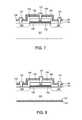
- FIGS. 1-12show cross-sections that schematically illustrate a method of manufacturing a solar cell in accordance with an embodiment of the present invention.
- FIG. 13shows a flow diagram of a method of manufacturing a solar cell in accordance with an embodiment of the present invention.
- FIGS. 1-12show cross-sections that schematically illustrate a method of manufacturing a solar cell in accordance with an embodiment of the present invention.
- FIGS. 1-12are not drawn to scale.
- a thin dielectric layer 102is formed on a single crystalline silicon substrate 101 .
- the substrate 101may comprise a high-lifetime N-type single crystalline silicon wafer.
- the thin dielectric layer 102comprises silicon dioxide formed directly on a backside surface 131 of the single crystalline silicon substrate 101 .
- the backside surface 131is opposite a front side surface 132 of the single crystalline silicon substrate 101 .
- the front side surface 132is on the front side of the solar cell, which is also referred to as the “sun side” because it faces the sun during normal operation.
- the backside surface 131is on the backside of the solar cell.
- the solar cell being manufacturedis an all back contact solar cell in that the emitters and corresponding metal contacts are all formed on the backside of the solar cell.
- the thin dielectric layer 102may provide a tunneling function, e.g., as a tunnel oxide.
- the thin dielectric layer 102comprises silicon dioxide thermally grown directly on the backside surface 131 to a thickness less than or equal to 40 Angstroms (e.g., between 5 to 40 Angstroms, preferably 20 Angstroms).
- a plurality of doped polycrystalline silicon emitters 103are formed on the thin dielectric layer 102 . Only one polycrystalline silicon emitter 103 is shown in the figures for clarity of illustration.
- the polycrystalline silicon emitter 103may be deposited doped or doped after deposition.
- the polycrystalline silicon emitter 103is doped with a P-type dopant, such as boron.
- the polycrystalline silicon emitter 103may also be doped with an N-type dopant with appropriate changes to the doping of other emitters and/or the single crystalline silicon substrate 101 .
- portions of the thin dielectric layer 102 that are not under the polycrystalline silicon emitter 103may be removed, e.g., by wet or dry etching.
- the solar cell being manufacturedonly has one polarity (P-type in this example) of polycrystalline silicon emitters; the opposite polarity emitters are single crystalline silicon emitter. This advantageously allows the polycrystalline silicon emitter 103 to be doped in situ.
- a polycrystalline silicon emitter 103may be formed by forming a layer of polycrystalline silicon layer 201 on the thin dielectric layer 102 as shown in FIG. 9 .
- the polycrystalline silicon layer 201may be formed by a deposition process, e.g., by low pressure chemical vapor deposition (LPCVD), to a thickness of around 1000 Angstroms to 5000 Angstroms, for example.
- a patterning stepsuch as masking and etching, follows to pattern the polycrystalline silicon layer 201 as shown in FIG. 10 .
- the thin dielectric layer 102is patterned during patterning of the thin dielectric layer 102 .
- the patterned polycrystalline silicon layer 201serves as the polycrystalline silicon emitter 103 .
- the polycrystalline silicon layer 201may be doped before or after the patterning step.
- the polycrystalline silicon emitter 103may also be formed using other processing steps, including by printing as shown in FIG. 11 .
- an emitter 203is selectively printed by a print head 205 of an inkjet printer.
- the emitter 203may comprise silicon nanoparticles that are inkjet printed on the thin dielectric layer 102 .
- the emitter 203may be doped before or after the printing step.
- a thermal treatment stepcoalesces the silicon nanoparticles to form polycrystalline silicon, which serves as the polycrystalline silicon emitter 103 .
- the thin dielectric layer 102does not have to be etched because dopants for forming the single crystalline silicon emitter in the single crystalline silicon 101 may be diffused through the thin dielectric layer 102 , advantageously removing a patterning step.
- a dopant source layer 104is formed on the polycrystalline silicon emitter 103 and the single crystalline silicon substrate 101 .
- the dopant source layer 104comprises N-type dopants, such as phosphorus, to subsequently form an N-type emitter in the single crystalline silicon substrate 101 .
- the dopants of the dopant source layer 104may be changed (e.g., to P-type) to accommodate different dopant polarity requirements.
- the dopant source layer 104comprises a blanket layer of phosphorus-silicate-glass (PSG) formed to a thickness of about 1000 Angstroms by atmospheric pressure chemical vapor deposition (APCVD), for example.
- PSGphosphorus-silicate-glass
- a diffusion stepis performed to diffuse dopants from the dopant source layer 104 to the single crystalline silicon substrate 101 to form single crystalline silicon emitters 108 .
- the resulting emitters 108comprise N-type doped single crystalline silicon.
- the diffusion stepmay be performed by thermal processing in a diffusion furnace, for example.
- some amount of dopants from the polycrystalline silicon emitter 103may diffuse through the thin dielectric layer 102 to form a doped region 109 in the single crystalline silicon substrate 101 .
- the doped region 109is a P-type doped region because the polycrystalline silicon emitter 103 is doped with a P-type dopant.
- a polycrystalline silicon emitter 103may cover more area of the back surface 131 of the single crystalline silicon substrate 101 compared to a single crystalline silicon emitter 108 .
- the polycrystalline silicon emitters 103may have a total area that covers at least 80% of the total area of the back surface 131 .
- a material stack 105is formed on the dopant source layer 104 .
- the material stack 105may comprise one or more layers of materials, such as moisture barrier, anti-reflective coating, and other materials depending on the particulars of the manufacturing process.
- the material stack 105may be formed before or after the diffusion step.
- contact holes 106are formed to expose the single crystalline silicon emitters 108 and polycrystalline silicon emitters 103 .
- contact holes 106are formed through the stack of materials 105 and dopant source layer 104 , but not through the thin dielectric layer 102 .
- contact holes 106are formed through the stack of materials 105 and the dopant source layer 104 .
- corresponding holes 106are also formed through the thin dielectric layer 102 to expose underlying emitters 108 .
- the contact holes 106may be formed by laser ablation, mask and etch, or other processing step.
- metal contacts 107are formed in the contact holes 106 to connect to corresponding emitters.
- a metal contact 107may comprise a single layer or multilayer metal contact.
- a metal contact 107may comprise aluminum formed on an emitter (e.g., emitter 103 or 108 ), a diffusion barrier comprising titanium-tungsten formed on the aluminum, and a seed layer comprising copper formed on the diffusion barrier.
- a metal contact 107 connected to a single crystalline silicon emitter 108is an N-polarity metal contact in that it is connected to an N-type doped emitter 108 .
- a metal contact 107 connected to a polycrystalline silicon emitter 103is a P-polarity metal contact in that it is connected to a P-type doped emitter 103 .
- N-polarity metal contactsare connected together and electrically insulated from P-polarity metal contacts, which are also connected together.
- N-polarity metal contactsmay be interdigitated with P-polarity metal contacts.
- the manufacture of the solar cellmay also incorporate additional processing steps.
- the front side surface 132 of the single crystalline silicon substrate 101may be textured.
- the front side surface 132is textured with random pyramids using a wet etch process comprising potassium hydroxide and isopropyl alcohol.
- the textured surfacehelps increase solar radiation collection.
- the front side surface 132may further include a stack of materials 133 , which may comprise one or more layers of materials, such as anti-reflective coating, passivation layer, and so on.
- the texturing process and other processing on or under the front side surface 132may be performed at any suitable step of the manufacturing process without detracting from the merits of the present invention.
- the resulting solar cellwhich is an all back contact solar cell in one embodiment, has a hybrid emitter design in that one polarity of emitters comprise doped polycrystalline silicon, while the other and opposite polarity of emitters comprise doped single crystalline silicon formed in a single crystalline silicon substrate. More particularly, in the example of FIG. 8 , the emitter 103 comprises P-type doped polycrystalline silicon, while the emitters 108 comprise N-type doped single crystalline silicon and are formed in an N-type doped single crystalline silicon substrate. As can be appreciated, the polarity of the doping of the emitter 103 , emitters 108 , and the substrate 101 may be changed with appropriate changes to the doping of the other features. For example, in other embodiments, the single crystalline silicon substrate 101 may be P-type doped, the single crystalline silicon emitters 108 may be P-type doped, and the polycrystalline silicon emitter 103 may be N-type doped.
- the dopant concentration in the emittersmust be balanced between high dopant concentration desired for low contact resistance and low dopant concentration desired for high minority carrier lifetimes.
- the conflicting demands of low contact resistance and high minority carrier lifetimeslead to suboptimal solar cell structures.
- Solar cells where both the P-type and N-type doped emitters are formed in polycrystalline siliconeliminate the trade-off between low contact resistance and high minority carrier lifetimes.
- a dielectric separating the polycrystalline silicon emitters from the single crystalline silicon substratescreens out minority carriers, allowing for higher dopant concentration while maintaining relatively high minority carrier lifetimes.
- a main disadvantageis the need to create a trench between the P-type and N-type doped emitters in the polycrystalline silicon. The trench requires an additional patterning step and specific passivation on the backside surface of the solar cell, increasing the cost of manufacturing the solar cell.
- the hybrid emitter design of the present disclosureprovides many benefits heretofore unrealized, including higher dopant concentration, and thus lower contact resistance, for the polycrystalline silicon emitters 103 . This is achieved without having to form trenches by providing single crystalline silicon emitters 108 in the single crystalline silicon substrate 101 . The absence of trenches between emitters saves on patterning and associated process steps. And because only one polarity of polycrystalline silicon emitters is involved, the polycrystalline silicon emitters may be doped in situ. The solar cells of the present disclosure thus provide most of the advantages of all polycrystalline silicon emitters with lower manufacturing cost.
- a thin dielectric layeris formed on a backside surface of a single crystalline silicon substrate (step 301 ).
- the silicon substratecomprises a high lifetime single crystalline silicon wafer that is doped with N-type dopants.
- the thin dielectric layermay comprise silicon dioxide thermally grown directly on the backside surface of the single crystalline silicon substrate.
- a first emitter comprising doped polycrystalline siliconis formed on the thin dielectric layer (step 302 ).
- the first emittermay be polycrystalline silicon doped to have a first polarity.
- the polycrystalline siliconmay be doped with a P-type dopant.
- the first emitter comprising polycrystalline siliconmay be formed in accordance with a method 400 by forming a doped polycrystalline silicon layer on the thin dielectric layer (step 401 ) and thereafter patterning the doped polycrystalline silicon layer to form the first emitter (step 402 ).
- the first emitter comprising polycrystalline siliconmay also be formed in accordance with a method 500 by printing doped silicon nanoparticles on the thin dielectric layer (step 501 ) and thereafter performing a heat treatment to coalesce the silicon nanoparticles to form polycrystalline silicon (step 502 ).
- the first emittermay be doped before or after formation on the thin dielectric layer.
- a second emitteris formed in the single crystalline silicon substrate (step 303 ).
- the second emitteris formed by forming a dopant source layer on the single crystalline silicon substrate, and thereafter diffusing dopants from the dopant source layer into the single crystalline silicon substrate to form the second emitter comprising single crystalline silicon.
- the second emittermay be doped to have a second polarity opposite to the first polarity of the polycrystalline silicon emitter.
- the polycrystalline silicon emitteris P-type doped
- the single crystalline silicon emittermay be doped with N-type dopants
- the single crystalline silicon substratemay be doped with N-type dopants.
- the polycrystalline silicon emitteris N-type doped
- the single crystalline silicon emittermay be doped with P-type dopants
- the single crystalline silicon substratemay be doped with P-type dopants.
- Interdigitated metal contactsare thereafter connected to the first and second emitters (step 304 ).
- Hybrid emitterall back contact solar cells and methods of manufacturing same have been disclosed. While specific embodiments of the present invention have been provided, it is to be understood that these embodiments are for illustration purposes and not limiting. Many additional embodiments will be apparent to persons of ordinary skill in the art reading this disclosure.
Landscapes
- Photovoltaic Devices (AREA)
- Engineering & Computer Science (AREA)
- Life Sciences & Earth Sciences (AREA)
- Sustainable Energy (AREA)
- Sustainable Development (AREA)
- Chemical & Material Sciences (AREA)
- Crystallography & Structural Chemistry (AREA)
- Manufacturing & Machinery (AREA)
Abstract
Description
Claims (11)
Priority Applications (16)
| Application Number | Priority Date | Filing Date | Title |
|---|---|---|---|
| US13/720,721US9312406B2 (en) | 2012-12-19 | 2012-12-19 | Hybrid emitter all back contact solar cell |
| TW102146403ATWI587529B (en) | 2012-12-19 | 2013-12-16 | Full back side contact solar cell of hybrid emitter |
| EP13865680.6AEP2936570B1 (en) | 2012-12-19 | 2013-12-17 | Hybrid emitter all back contact solar cell and method of manufacturing the same |
| SG11201504664RASG11201504664RA (en) | 2012-12-19 | 2013-12-17 | Hybrid emitter all back contact solar cell |
| CN201710080612.XACN107068778B (en) | 2012-12-19 | 2013-12-17 | Hybrid Emitter Full Back Contact Solar Cell |
| MYPI2015001506AMY172208A (en) | 2012-12-19 | 2013-12-17 | Hybrid emitter all back contact solar cell |
| PCT/US2013/075808WO2014100004A1 (en) | 2012-12-19 | 2013-12-17 | Hybrid emitter all back contact solar cell |
| CN201380067323.6ACN104885232B (en) | 2012-12-19 | 2013-12-17 | Hybrid emitter full back contact solar cell |
| MX2015007998AMX347995B (en) | 2012-12-19 | 2013-12-17 | SOLAR CELL HYBRID ISSUER WITH BACK CONTACT. |
| KR1020157018988AKR20150097647A (en) | 2012-12-19 | 2013-12-17 | Hybrid emitter all back contact solar cell |
| AU2013362916AAU2013362916B2 (en) | 2012-12-19 | 2013-12-17 | Hybrid emitter all back contact solar cell |
| KR1020217011335AKR102360479B1 (en) | 2012-12-19 | 2013-12-17 | Hybrid emitter all back contact solar cell |
| SG10201709897UASG10201709897UA (en) | 2012-12-19 | 2013-12-17 | Hybrid emitter all back contact solar cell |
| JP2015549587AJP6352940B2 (en) | 2012-12-19 | 2013-12-17 | Solar cell |
| US15/067,960US9564551B2 (en) | 2012-12-19 | 2016-03-11 | Method of manufacturing a hybrid emitter all back contact solar cell |
| MYPI2019000026AMY198456A (en) | 2012-12-19 | 2019-01-09 | Hybrid Emitter All Back Contact Solar Cell |
Applications Claiming Priority (1)
| Application Number | Priority Date | Filing Date | Title |
|---|---|---|---|
| US13/720,721US9312406B2 (en) | 2012-12-19 | 2012-12-19 | Hybrid emitter all back contact solar cell |
Related Child Applications (1)
| Application Number | Title | Priority Date | Filing Date |
|---|---|---|---|
| US15/067,960DivisionUS9564551B2 (en) | 2012-12-19 | 2016-03-11 | Method of manufacturing a hybrid emitter all back contact solar cell |
Publications (2)
| Publication Number | Publication Date |
|---|---|
| US20140166095A1 US20140166095A1 (en) | 2014-06-19 |
| US9312406B2true US9312406B2 (en) | 2016-04-12 |
Family
ID=50929539
Family Applications (2)
| Application Number | Title | Priority Date | Filing Date |
|---|---|---|---|
| US13/720,721Active2033-12-15US9312406B2 (en) | 2012-12-19 | 2012-12-19 | Hybrid emitter all back contact solar cell |
| US15/067,960Active2032-12-31US9564551B2 (en) | 2012-12-19 | 2016-03-11 | Method of manufacturing a hybrid emitter all back contact solar cell |
Family Applications After (1)
| Application Number | Title | Priority Date | Filing Date |
|---|---|---|---|
| US15/067,960Active2032-12-31US9564551B2 (en) | 2012-12-19 | 2016-03-11 | Method of manufacturing a hybrid emitter all back contact solar cell |
Country Status (11)
| Country | Link |
|---|---|
| US (2) | US9312406B2 (en) |
| EP (1) | EP2936570B1 (en) |
| JP (1) | JP6352940B2 (en) |
| KR (2) | KR102360479B1 (en) |
| CN (2) | CN104885232B (en) |
| AU (1) | AU2013362916B2 (en) |
| MX (1) | MX347995B (en) |
| MY (2) | MY172208A (en) |
| SG (2) | SG10201709897UA (en) |
| TW (1) | TWI587529B (en) |
| WO (1) | WO2014100004A1 (en) |
Cited By (18)
| Publication number | Priority date | Publication date | Assignee | Title |
|---|---|---|---|---|
| US20170162729A1 (en)* | 2013-12-09 | 2017-06-08 | Timothy Weidman | Solar Cell Emitter Region Fabrication Using Self-Aligned Implant and Cap |
| USD822890S1 (en) | 2016-09-07 | 2018-07-10 | Felxtronics Ap, Llc | Lighting apparatus |
| USD832494S1 (en) | 2017-08-09 | 2018-10-30 | Flex Ltd. | Lighting module heatsink |
| USD832495S1 (en) | 2017-08-18 | 2018-10-30 | Flex Ltd. | Lighting module locking mechanism |
| USD833061S1 (en) | 2017-08-09 | 2018-11-06 | Flex Ltd. | Lighting module locking endcap |
| USD846793S1 (en) | 2017-08-09 | 2019-04-23 | Flex Ltd. | Lighting module locking mechanism |
| USD862777S1 (en) | 2017-08-09 | 2019-10-08 | Flex Ltd. | Lighting module wide distribution lens |
| USD862778S1 (en) | 2017-08-22 | 2019-10-08 | Flex Ltd | Lighting module lens |
| USD872319S1 (en) | 2017-08-09 | 2020-01-07 | Flex Ltd. | Lighting module LED light board |
| USD877964S1 (en) | 2017-08-09 | 2020-03-10 | Flex Ltd. | Lighting module |
| US10629758B2 (en) | 2016-09-30 | 2020-04-21 | Sunpower Corporation | Solar cells with differentiated P-type and N-type region architectures |
| USD888323S1 (en) | 2017-09-07 | 2020-06-23 | Flex Ltd | Lighting module wire guard |
| US10775030B2 (en) | 2017-05-05 | 2020-09-15 | Flex Ltd. | Light fixture device including rotatable light modules |
| EP3982421A1 (en) | 2020-10-09 | 2022-04-13 | International Solar Energy Research Center Konstanz E.V. | Method for local modification of etching resistance in a silicon layer, use of this method in the production of passivating contact solar cells and thus-created solar cell |
| US11489080B1 (en)* | 2021-07-22 | 2022-11-01 | Solarlab Aiko Europe Gmbh | Passivated contact structure and solar cell comprising the same, cell assembly, and photovoltaic system |
| US11824126B2 (en) | 2019-12-10 | 2023-11-21 | Maxeon Solar Pte. Ltd. | Aligned metallization for solar cells |
| US20240290905A1 (en)* | 2021-07-22 | 2024-08-29 | Solarlab Aiko Europe Gmbh | Passivated contact structure and solar cell comprising the same, cell assembly, and photovoltaic system |
| WO2024228665A1 (en)* | 2023-04-30 | 2024-11-07 | Maxeon Solar Pte. Ltd. | Solar cell with cell architecture designed for reduced carrier recombination |
Families Citing this family (18)
| Publication number | Priority date | Publication date | Assignee | Title |
|---|---|---|---|---|
| NL2013722B1 (en)* | 2014-10-31 | 2016-10-04 | Univ Delft Tech | Back side contacted wafer-based solar cells with in-situ doped crystallized thin-film silicon and/or silicon oxide regions. |
| US9520507B2 (en)* | 2014-12-22 | 2016-12-13 | Sunpower Corporation | Solar cells with improved lifetime, passivation and/or efficiency |
| WO2019011681A1 (en) | 2017-07-12 | 2019-01-17 | Exeger Operations Ab | A photovoltaic device having a light absorbing layer including a plurality of grains of a doped semiconducting material |
| WO2018021952A1 (en) | 2016-07-29 | 2018-02-01 | Exeger Operations Ab | A light absorbing layer and a photovoltaic device including a light absorbing layer |
| SE540184C2 (en) | 2016-07-29 | 2018-04-24 | Exeger Operations Ab | A light absorbing layer and a photovoltaic device including a light absorbing layer |
| TWI580058B (en) | 2016-10-26 | 2017-04-21 | 財團法人工業技術研究院 | Solar battery |
| NL2017872B1 (en)* | 2016-11-25 | 2018-06-08 | Stichting Energieonderzoek Centrum Nederland | Photovoltaic cell with passivating contact |
| NL2019634B1 (en) | 2017-09-27 | 2019-04-03 | Univ Delft Tech | Solar cells with transparent contacts based on poly-silicon-oxide |
| WO2019206679A1 (en)* | 2018-04-24 | 2019-10-31 | CSEM Centre Suisse d'Electronique et de Microtechnique SA - Recherche et Développement | Passivated layer stack for a light harvesting device |
| MX2020012262A (en) | 2018-05-16 | 2021-01-29 | Exeger Operations Ab | A PHOTOVOLTAIC DEVICE. |
| EP3627527A1 (en) | 2018-09-20 | 2020-03-25 | Exeger Operations AB | Photovoltaic device for powering an external device and a method for producing the photovoltaic device |
| DE102020132245A1 (en) | 2020-12-04 | 2022-06-09 | EnPV GmbH | Backside contacted solar cell and production of such |
| CN112397596A (en)* | 2020-12-28 | 2021-02-23 | 东方日升新能源股份有限公司 | Low-cost high-efficiency solar cell and preparation method thereof |
| CN120500117A (en) | 2021-06-30 | 2025-08-15 | 晶科能源股份有限公司 | Solar cell and photovoltaic module |
| DE102022129955A1 (en) | 2022-11-11 | 2024-05-16 | EnPV GmbH | Back-contacted solar cell with aluminum metallization and manufacturing process |
| CN116093190B (en)* | 2023-02-10 | 2024-09-20 | 天合光能股份有限公司 | Back contact solar cell and preparation method thereof |
| CN120547982A (en)* | 2023-03-31 | 2025-08-26 | 天合光能股份有限公司 | Solar cell and method for preparing solar cell |
| DE102023130440B3 (en) | 2023-11-03 | 2025-03-06 | EnPV GmbH | Back-side contacted solar cell and method for producing a back-side contacted solar cell |
Citations (55)
| Publication number | Priority date | Publication date | Assignee | Title |
|---|---|---|---|---|
| US3961997A (en) | 1975-05-12 | 1976-06-08 | The United States Of America As Represented By The Administrator Of The National Aeronautics And Space Administration | Fabrication of polycrystalline solar cells on low-cost substrates |
| US4427839A (en) | 1981-11-09 | 1984-01-24 | General Electric Company | Faceted low absorptance solar cell |
| US4665277A (en) | 1986-03-11 | 1987-05-12 | The United States Of America As Represented By The Administrator Of The National Aeronautics And Space Administration | Floating emitter solar cell |
| US4927770A (en) | 1988-11-14 | 1990-05-22 | Electric Power Research Inst. Corp. Of District Of Columbia | Method of fabricating back surface point contact solar cells |
| US5030295A (en) | 1990-02-12 | 1991-07-09 | Electric Power Research Institut | Radiation resistant passivation of silicon solar cells |
| US5053083A (en) | 1989-05-08 | 1991-10-01 | The Board Of Trustees Of The Leland Stanford Junior University | Bilevel contact solar cells |
| US5057439A (en) | 1990-02-12 | 1991-10-15 | Electric Power Research Institute | Method of fabricating polysilicon emitters for solar cells |
| US5164019A (en) | 1991-07-31 | 1992-11-17 | Sunpower Corporation | Monolithic series-connected solar cells having improved cell isolation and method of making same |
| US5217539A (en) | 1991-09-05 | 1993-06-08 | The Boeing Company | III-V solar cells and doping processes |
| US5266125A (en) | 1992-05-12 | 1993-11-30 | Astropower, Inc. | Interconnected silicon film solar cell array |
| US5360990A (en) | 1993-03-29 | 1994-11-01 | Sunpower Corporation | P/N junction device having porous emitter |
| US5369291A (en) | 1993-03-29 | 1994-11-29 | Sunpower Corporation | Voltage controlled thyristor |
| US5449626A (en) | 1991-12-27 | 1995-09-12 | Hezel; Rudolf | Method for manufacture of a solar cell |
| US5479018A (en) | 1989-05-08 | 1995-12-26 | Westinghouse Electric Corp. | Back surface illuminated infrared detector |
| US5620904A (en) | 1996-03-15 | 1997-04-15 | Evergreen Solar, Inc. | Methods for forming wraparound electrical contacts on solar cells |
| US5641362A (en) | 1995-11-22 | 1997-06-24 | Ebara Solar, Inc. | Structure and fabrication process for an aluminum alloy junction self-aligned back contact silicon solar cell |
| US5693578A (en) | 1993-09-17 | 1997-12-02 | Fujitsu, Ltd. | Method of forming thin silicon oxide film with high dielectric breakdown and hot carrier resistance |
| US6262359B1 (en) | 1999-03-17 | 2001-07-17 | Ebara Solar, Inc. | Aluminum alloy back junction solar cell and a process for fabrication thereof |
| US6274402B1 (en) | 1999-12-30 | 2001-08-14 | Sunpower Corporation | Method of fabricating a silicon solar cell |
| US6313395B1 (en) | 2000-04-24 | 2001-11-06 | Sunpower Corporation | Interconnect structure for solar cells and method of making same |
| US6333457B1 (en) | 2000-08-29 | 2001-12-25 | Sunpower Corporation | Edge passivated silicon solar/photo cell and method of manufacture |
| US6337283B1 (en) | 1999-12-30 | 2002-01-08 | Sunpower Corporation | Method of fabricating a silicon solar cell |
| US6387726B1 (en) | 1999-12-30 | 2002-05-14 | Sunpower Corporation | Method of fabricating a silicon solar cell |
| US20020069911A1 (en) | 2000-09-05 | 2002-06-13 | Sanyo Electric Co., Ltd. | Photovoltaic device |
| US6423568B1 (en) | 1999-12-30 | 2002-07-23 | Sunpower Corporation | Method of fabricating a silicon solar cell |
| US6524880B2 (en) | 2001-04-23 | 2003-02-25 | Samsung Sdi Co., Ltd. | Solar cell and method for fabricating the same |
| US20030134469A1 (en) | 1996-12-24 | 2003-07-17 | Imec Vzw, A Research Center In The Country Of Belgium | Semiconductor device with selectively diffused regions |
| US6638788B2 (en) | 2001-02-07 | 2003-10-28 | Ebara Corporation | Solar cell and method of manufacturing same |
| US20040043528A1 (en) | 2000-09-13 | 2004-03-04 | Wolfgang Kruhler | Photovoltaic component and module |
| US20040200520A1 (en) | 2003-04-10 | 2004-10-14 | Sunpower Corporation | Metal contact structure for solar cell and method of manufacture |
| US20050016585A1 (en) | 2001-11-26 | 2005-01-27 | Adolf Munzer | Manufacturing a solar cell with backside contacts |
| US20050268963A1 (en) | 2004-02-24 | 2005-12-08 | David Jordan | Process for manufacturing photovoltaic cells |
| US6998288B1 (en) | 2003-10-03 | 2006-02-14 | Sunpower Corporation | Use of doped silicon dioxide in the fabrication of solar cells |
| US20060096635A1 (en) | 2004-11-10 | 2006-05-11 | Daystar Technologies, Inc. | Pallet based system for forming thin-film solar cells |
| US20060130891A1 (en) | 2004-10-29 | 2006-06-22 | Carlson David E | Back-contact photovoltaic cells |
| US20060157103A1 (en) | 2005-01-20 | 2006-07-20 | Nanosolar, Inc. | Optoelectronic architecture having compound conducting substrate cross-reference to related application |
| US20060185716A1 (en) | 2005-02-18 | 2006-08-24 | Clean Venture 21 Corporation | Method for producing photovoltaic device and photovoltaic device |
| US20070023081A1 (en) | 2005-07-28 | 2007-02-01 | General Electric Company | Compositionally-graded photovoltaic device and fabrication method, and related articles |
| US20070082206A1 (en) | 2005-10-11 | 2007-04-12 | Klaus Hartig | High infrared reflection coatings and associated technologies |
| US20070256733A1 (en) | 2005-11-28 | 2007-11-08 | Mitsubishi Electric Corporation | Solar Cell and Manufacturing Method Thereof |
| WO2008004791A1 (en) | 2006-07-03 | 2008-01-10 | Lg Electronics Inc. | High efficiency solar cell and manufacturing method thereof |
| US20080078444A1 (en) | 2006-06-05 | 2008-04-03 | Translucent Photonics, Inc. | Thin film solar cell |
| US20080173347A1 (en) | 2007-01-23 | 2008-07-24 | General Electric Company | Method And Apparatus For A Semiconductor Structure |
| US7468485B1 (en) | 2005-08-11 | 2008-12-23 | Sunpower Corporation | Back side contact solar cell with doped polysilicon regions |
| US20090159111A1 (en) | 2007-12-21 | 2009-06-25 | The Woodside Group Pte. Ltd | Photovoltaic device having a textured metal silicide layer |
| US20090223562A1 (en)* | 2006-10-27 | 2009-09-10 | Kyocera Corporation | Solar Cell Element Manufacturing Method and Solar Cell Element |
| US20110114171A1 (en) | 2010-01-08 | 2011-05-19 | Suniva, Inc. | Solar cell including sputtered reflective layer |
| US20110120537A1 (en) | 2009-09-21 | 2011-05-26 | Goujun Liu | Silicon inks for thin film solar cell formation, corresponding methods and solar cell structures |
| US20110126886A1 (en)* | 2008-07-30 | 2011-06-02 | Helmholtz-Zentrum Berlin Fuer Materialien Und Energie Gmbh | Thin-film solar module which is contact-connected on one side and has an internal contact layer |
| US20110139229A1 (en) | 2010-06-03 | 2011-06-16 | Ajeet Rohatgi | Selective emitter solar cells formed by a hybrid diffusion and ion implantation process |
| US20110230004A1 (en) | 2009-09-20 | 2011-09-22 | Jian Li | Methods of Building Crystalline Silicon Solar Cells For Use In Combinatorial Screening |
| US20120138135A1 (en) | 2010-12-02 | 2012-06-07 | Jane Manning | Method of forming contacts for a back-contact solar cell |
| US8207444B2 (en) | 2008-07-01 | 2012-06-26 | Sunpower Corporation | Front contact solar cell with formed electrically conducting layers on the front side and backside |
| US8222516B2 (en) | 2008-02-20 | 2012-07-17 | Sunpower Corporation | Front contact solar cell with formed emitter |
| US9130092B1 (en)* | 2007-11-01 | 2015-09-08 | Sandia Corporation | Photovoltaic solar cell |
Family Cites Families (10)
| Publication number | Priority date | Publication date | Assignee | Title |
|---|---|---|---|---|
| US7737357B2 (en)* | 2006-05-04 | 2010-06-15 | Sunpower Corporation | Solar cell having doped semiconductor heterojunction contacts |
| US7705237B2 (en)* | 2006-11-27 | 2010-04-27 | Sunpower Corporation | Solar cell having silicon nano-particle emitter |
| US8329503B1 (en)* | 2007-11-01 | 2012-12-11 | Sandia Corporation | Photovoltaic solar concentrator |
| US20090314341A1 (en)* | 2008-04-09 | 2009-12-24 | Borden Peter G | Simplified back contact for polysilicon emitter solar cells |
| US8242354B2 (en)* | 2008-12-04 | 2012-08-14 | Sunpower Corporation | Backside contact solar cell with formed polysilicon doped regions |
| CN101777603B (en)* | 2009-01-08 | 2012-03-07 | 北京北方微电子基地设备工艺研究中心有限责任公司 | Method for manufacturing back contact solar energy batteries |
| JP5906393B2 (en) | 2010-02-26 | 2016-04-20 | パナソニックIpマネジメント株式会社 | Solar cell and method for manufacturing solar cell |
| WO2012132995A1 (en) | 2011-03-25 | 2012-10-04 | 三洋電機株式会社 | Method for producing photoelectric conversion element |
| KR20120129264A (en)* | 2011-05-19 | 2012-11-28 | 삼성디스플레이 주식회사 | Solar cell and method of manufacturing the same |
| CN102856328B (en)* | 2012-10-10 | 2015-06-10 | 友达光电股份有限公司 | Solar cell and manufacturing method thereof |
- 2012
- 2012-12-19USUS13/720,721patent/US9312406B2/enactiveActive
- 2013
- 2013-12-16TWTW102146403Apatent/TWI587529B/enactive
- 2013-12-17EPEP13865680.6Apatent/EP2936570B1/enactiveActive
- 2013-12-17CNCN201380067323.6Apatent/CN104885232B/enactiveActive
- 2013-12-17KRKR1020217011335Apatent/KR102360479B1/enactiveActive
- 2013-12-17KRKR1020157018988Apatent/KR20150097647A/ennot_activeCeased
- 2013-12-17WOPCT/US2013/075808patent/WO2014100004A1/enactiveApplication Filing
- 2013-12-17JPJP2015549587Apatent/JP6352940B2/enactiveActive
- 2013-12-17MYMYPI2015001506Apatent/MY172208A/enunknown
- 2013-12-17AUAU2013362916Apatent/AU2013362916B2/enactiveActive
- 2013-12-17SGSG10201709897UApatent/SG10201709897UA/enunknown
- 2013-12-17CNCN201710080612.XApatent/CN107068778B/enactiveActive
- 2013-12-17MXMX2015007998Apatent/MX347995B/enactiveIP Right Grant
- 2013-12-17SGSG11201504664RApatent/SG11201504664RA/enunknown
- 2016
- 2016-03-11USUS15/067,960patent/US9564551B2/enactiveActive
- 2019
- 2019-01-09MYMYPI2019000026Apatent/MY198456A/enunknown
Patent Citations (57)
| Publication number | Priority date | Publication date | Assignee | Title |
|---|---|---|---|---|
| US3961997A (en) | 1975-05-12 | 1976-06-08 | The United States Of America As Represented By The Administrator Of The National Aeronautics And Space Administration | Fabrication of polycrystalline solar cells on low-cost substrates |
| US4427839A (en) | 1981-11-09 | 1984-01-24 | General Electric Company | Faceted low absorptance solar cell |
| US4665277A (en) | 1986-03-11 | 1987-05-12 | The United States Of America As Represented By The Administrator Of The National Aeronautics And Space Administration | Floating emitter solar cell |
| US4927770A (en) | 1988-11-14 | 1990-05-22 | Electric Power Research Inst. Corp. Of District Of Columbia | Method of fabricating back surface point contact solar cells |
| US5053083A (en) | 1989-05-08 | 1991-10-01 | The Board Of Trustees Of The Leland Stanford Junior University | Bilevel contact solar cells |
| US5479018A (en) | 1989-05-08 | 1995-12-26 | Westinghouse Electric Corp. | Back surface illuminated infrared detector |
| US5030295A (en) | 1990-02-12 | 1991-07-09 | Electric Power Research Institut | Radiation resistant passivation of silicon solar cells |
| US5057439A (en) | 1990-02-12 | 1991-10-15 | Electric Power Research Institute | Method of fabricating polysilicon emitters for solar cells |
| US5164019A (en) | 1991-07-31 | 1992-11-17 | Sunpower Corporation | Monolithic series-connected solar cells having improved cell isolation and method of making same |
| US5217539A (en) | 1991-09-05 | 1993-06-08 | The Boeing Company | III-V solar cells and doping processes |
| US5449626A (en) | 1991-12-27 | 1995-09-12 | Hezel; Rudolf | Method for manufacture of a solar cell |
| US5266125A (en) | 1992-05-12 | 1993-11-30 | Astropower, Inc. | Interconnected silicon film solar cell array |
| US5360990A (en) | 1993-03-29 | 1994-11-01 | Sunpower Corporation | P/N junction device having porous emitter |
| US5369291A (en) | 1993-03-29 | 1994-11-29 | Sunpower Corporation | Voltage controlled thyristor |
| US5693578A (en) | 1993-09-17 | 1997-12-02 | Fujitsu, Ltd. | Method of forming thin silicon oxide film with high dielectric breakdown and hot carrier resistance |
| US5641362A (en) | 1995-11-22 | 1997-06-24 | Ebara Solar, Inc. | Structure and fabrication process for an aluminum alloy junction self-aligned back contact silicon solar cell |
| US5620904A (en) | 1996-03-15 | 1997-04-15 | Evergreen Solar, Inc. | Methods for forming wraparound electrical contacts on solar cells |
| US20030134469A1 (en) | 1996-12-24 | 2003-07-17 | Imec Vzw, A Research Center In The Country Of Belgium | Semiconductor device with selectively diffused regions |
| US6262359B1 (en) | 1999-03-17 | 2001-07-17 | Ebara Solar, Inc. | Aluminum alloy back junction solar cell and a process for fabrication thereof |
| US6423568B1 (en) | 1999-12-30 | 2002-07-23 | Sunpower Corporation | Method of fabricating a silicon solar cell |
| US6274402B1 (en) | 1999-12-30 | 2001-08-14 | Sunpower Corporation | Method of fabricating a silicon solar cell |
| US6337283B1 (en) | 1999-12-30 | 2002-01-08 | Sunpower Corporation | Method of fabricating a silicon solar cell |
| US6387726B1 (en) | 1999-12-30 | 2002-05-14 | Sunpower Corporation | Method of fabricating a silicon solar cell |
| US6313395B1 (en) | 2000-04-24 | 2001-11-06 | Sunpower Corporation | Interconnect structure for solar cells and method of making same |
| US6333457B1 (en) | 2000-08-29 | 2001-12-25 | Sunpower Corporation | Edge passivated silicon solar/photo cell and method of manufacture |
| US20020069911A1 (en) | 2000-09-05 | 2002-06-13 | Sanyo Electric Co., Ltd. | Photovoltaic device |
| US20040043528A1 (en) | 2000-09-13 | 2004-03-04 | Wolfgang Kruhler | Photovoltaic component and module |
| US6638788B2 (en) | 2001-02-07 | 2003-10-28 | Ebara Corporation | Solar cell and method of manufacturing same |
| US6524880B2 (en) | 2001-04-23 | 2003-02-25 | Samsung Sdi Co., Ltd. | Solar cell and method for fabricating the same |
| US20050016585A1 (en) | 2001-11-26 | 2005-01-27 | Adolf Munzer | Manufacturing a solar cell with backside contacts |
| US20040200520A1 (en) | 2003-04-10 | 2004-10-14 | Sunpower Corporation | Metal contact structure for solar cell and method of manufacture |
| US7135350B1 (en) | 2003-10-03 | 2006-11-14 | Sunpower Corporation | Use of doped silicon dioxide in the fabrication of solar cells |
| US6998288B1 (en) | 2003-10-03 | 2006-02-14 | Sunpower Corporation | Use of doped silicon dioxide in the fabrication of solar cells |
| US20050268963A1 (en) | 2004-02-24 | 2005-12-08 | David Jordan | Process for manufacturing photovoltaic cells |
| US20060130891A1 (en) | 2004-10-29 | 2006-06-22 | Carlson David E | Back-contact photovoltaic cells |
| US20060096635A1 (en) | 2004-11-10 | 2006-05-11 | Daystar Technologies, Inc. | Pallet based system for forming thin-film solar cells |
| US20060157103A1 (en) | 2005-01-20 | 2006-07-20 | Nanosolar, Inc. | Optoelectronic architecture having compound conducting substrate cross-reference to related application |
| US20060185716A1 (en) | 2005-02-18 | 2006-08-24 | Clean Venture 21 Corporation | Method for producing photovoltaic device and photovoltaic device |
| US20070023081A1 (en) | 2005-07-28 | 2007-02-01 | General Electric Company | Compositionally-graded photovoltaic device and fabrication method, and related articles |
| US7633006B1 (en) | 2005-08-11 | 2009-12-15 | Sunpower Corporation | Back side contact solar cell with doped polysilicon regions |
| US7468485B1 (en) | 2005-08-11 | 2008-12-23 | Sunpower Corporation | Back side contact solar cell with doped polysilicon regions |
| US20070082206A1 (en) | 2005-10-11 | 2007-04-12 | Klaus Hartig | High infrared reflection coatings and associated technologies |
| US20070256733A1 (en) | 2005-11-28 | 2007-11-08 | Mitsubishi Electric Corporation | Solar Cell and Manufacturing Method Thereof |
| US20080078444A1 (en) | 2006-06-05 | 2008-04-03 | Translucent Photonics, Inc. | Thin film solar cell |
| WO2008004791A1 (en) | 2006-07-03 | 2008-01-10 | Lg Electronics Inc. | High efficiency solar cell and manufacturing method thereof |
| US20090223562A1 (en)* | 2006-10-27 | 2009-09-10 | Kyocera Corporation | Solar Cell Element Manufacturing Method and Solar Cell Element |
| US20080173347A1 (en) | 2007-01-23 | 2008-07-24 | General Electric Company | Method And Apparatus For A Semiconductor Structure |
| US9130092B1 (en)* | 2007-11-01 | 2015-09-08 | Sandia Corporation | Photovoltaic solar cell |
| US20090159111A1 (en) | 2007-12-21 | 2009-06-25 | The Woodside Group Pte. Ltd | Photovoltaic device having a textured metal silicide layer |
| US8222516B2 (en) | 2008-02-20 | 2012-07-17 | Sunpower Corporation | Front contact solar cell with formed emitter |
| US8207444B2 (en) | 2008-07-01 | 2012-06-26 | Sunpower Corporation | Front contact solar cell with formed electrically conducting layers on the front side and backside |
| US20110126886A1 (en)* | 2008-07-30 | 2011-06-02 | Helmholtz-Zentrum Berlin Fuer Materialien Und Energie Gmbh | Thin-film solar module which is contact-connected on one side and has an internal contact layer |
| US20110230004A1 (en) | 2009-09-20 | 2011-09-22 | Jian Li | Methods of Building Crystalline Silicon Solar Cells For Use In Combinatorial Screening |
| US20110120537A1 (en) | 2009-09-21 | 2011-05-26 | Goujun Liu | Silicon inks for thin film solar cell formation, corresponding methods and solar cell structures |
| US20110114171A1 (en) | 2010-01-08 | 2011-05-19 | Suniva, Inc. | Solar cell including sputtered reflective layer |
| US20110139229A1 (en) | 2010-06-03 | 2011-06-16 | Ajeet Rohatgi | Selective emitter solar cells formed by a hybrid diffusion and ion implantation process |
| US20120138135A1 (en) | 2010-12-02 | 2012-06-07 | Jane Manning | Method of forming contacts for a back-contact solar cell |
Non-Patent Citations (2)
| Title |
|---|
| PCT International Search Report and Written Opinion of the International Searching Authority for Application No. PCT/US2013/075808, 7 sheets, Apr. 16, 2014. |
| R.W. Miles, et al. "Photovoltaic solar cells: An overview of state-of-the-art cell development and environmental issues" 2005, pp. 1-42, Science Direct, vol. 51. |
Cited By (36)
| Publication number | Priority date | Publication date | Assignee | Title |
|---|---|---|---|---|
| US20170162729A1 (en)* | 2013-12-09 | 2017-06-08 | Timothy Weidman | Solar Cell Emitter Region Fabrication Using Self-Aligned Implant and Cap |
| US11316056B2 (en)* | 2013-12-09 | 2022-04-26 | Sunpower Corporation | Solar cell emitter region fabrication using self-aligned implant and cap |
| USD822890S1 (en) | 2016-09-07 | 2018-07-10 | Felxtronics Ap, Llc | Lighting apparatus |
| US12009441B2 (en) | 2016-09-30 | 2024-06-11 | Maxeon Solar Pte. Ltd. | Solar cells with differentiated p-type and n-type region architectures |
| DE112017004982B4 (en) | 2016-09-30 | 2024-02-15 | Maxeon Solar Pte. Ltd. | Solar cells with differentiated p-type and n-type region architectures |
| US11594648B2 (en) | 2016-09-30 | 2023-02-28 | Sunpower Corporation | Solar cells with differentiated P-type and N-type region architectures |
| US10629758B2 (en) | 2016-09-30 | 2020-04-21 | Sunpower Corporation | Solar cells with differentiated P-type and N-type region architectures |
| US10775030B2 (en) | 2017-05-05 | 2020-09-15 | Flex Ltd. | Light fixture device including rotatable light modules |
| USD853629S1 (en) | 2017-08-09 | 2019-07-09 | Flex Ltd | Lighting module locking mechanism |
| USD846793S1 (en) | 2017-08-09 | 2019-04-23 | Flex Ltd. | Lighting module locking mechanism |
| USD862777S1 (en) | 2017-08-09 | 2019-10-08 | Flex Ltd. | Lighting module wide distribution lens |
| USD832494S1 (en) | 2017-08-09 | 2018-10-30 | Flex Ltd. | Lighting module heatsink |
| USD872319S1 (en) | 2017-08-09 | 2020-01-07 | Flex Ltd. | Lighting module LED light board |
| USD877964S1 (en) | 2017-08-09 | 2020-03-10 | Flex Ltd. | Lighting module |
| USD1010915S1 (en) | 2017-08-09 | 2024-01-09 | Linmore Labs Led, Inc. | Lighting module |
| USD885615S1 (en) | 2017-08-09 | 2020-05-26 | Flex Ltd. | Lighting module LED light board |
| USD833061S1 (en) | 2017-08-09 | 2018-11-06 | Flex Ltd. | Lighting module locking endcap |
| USD853625S1 (en) | 2017-08-09 | 2019-07-09 | Flex Ltd | Lighting module heatsink |
| USD905325S1 (en) | 2017-08-09 | 2020-12-15 | Flex Ltd | Lighting module |
| USD853627S1 (en) | 2017-08-09 | 2019-07-09 | Flex Ltd | Lighting module locking endcap |
| USD853628S1 (en) | 2017-08-18 | 2019-07-09 | Flex Ltd. | Lighting module locking mechanism |
| USD832495S1 (en) | 2017-08-18 | 2018-10-30 | Flex Ltd. | Lighting module locking mechanism |
| USD862778S1 (en) | 2017-08-22 | 2019-10-08 | Flex Ltd | Lighting module lens |
| USD888323S1 (en) | 2017-09-07 | 2020-06-23 | Flex Ltd | Lighting module wire guard |
| US11824126B2 (en) | 2019-12-10 | 2023-11-21 | Maxeon Solar Pte. Ltd. | Aligned metallization for solar cells |
| US12166137B2 (en) | 2019-12-10 | 2024-12-10 | Maxeon Solar Pte. Ltd. | Aligned metallization for solar cells |
| WO2022074091A1 (en) | 2020-10-09 | 2022-04-14 | International Solar Energy Research Center Konstanz E.V. | Method for local modification of etching resistance in a silicon layer, use of this method in the production of passivating contact solar cells and thus-created solar cell |
| EP3982421A1 (en) | 2020-10-09 | 2022-04-13 | International Solar Energy Research Center Konstanz E.V. | Method for local modification of etching resistance in a silicon layer, use of this method in the production of passivating contact solar cells and thus-created solar cell |
| AU2022204102B1 (en)* | 2021-07-22 | 2023-01-19 | Zhejiang Aiko Solar Energy Technology Co., Ltd. | Passivated contact structure and solar cell comprising the same, cell assembly, and photovoltaic system |
| US11489080B1 (en)* | 2021-07-22 | 2022-11-01 | Solarlab Aiko Europe Gmbh | Passivated contact structure and solar cell comprising the same, cell assembly, and photovoltaic system |
| US20240290905A1 (en)* | 2021-07-22 | 2024-08-29 | Solarlab Aiko Europe Gmbh | Passivated contact structure and solar cell comprising the same, cell assembly, and photovoltaic system |
| US12211950B2 (en) | 2021-07-22 | 2025-01-28 | Solarlab Aiko Europe Gmbh | Passivated contact structure and solar cell comprising the same, cell assembly, and photovoltaic system |
| US12402432B2 (en) | 2021-07-22 | 2025-08-26 | Zhejiang Aiko Solar Energy Technology Co., Ltd. | Passivated contact structure and solar cell comprising the same, cell assembly, and photovoltaic system |
| US12408470B2 (en)* | 2021-07-22 | 2025-09-02 | Zhejiang Aiko Solar Energy Technology Co., Ltd. | Passivated contact structure and solar cell comprising the same, cell assembly, and photovoltaic system |
| US12426399B2 (en) | 2021-07-22 | 2025-09-23 | Zhejiang Aiko Solar Energy Technology Co., Ltd. | Passivated contact structure and solar cell comprising the same, cell assembly, and photovoltaic system |
| WO2024228665A1 (en)* | 2023-04-30 | 2024-11-07 | Maxeon Solar Pte. Ltd. | Solar cell with cell architecture designed for reduced carrier recombination |
Also Published As
| Publication number | Publication date |
|---|---|
| EP2936570A4 (en) | 2016-01-27 |
| CN107068778B (en) | 2020-08-14 |
| KR20150097647A (en) | 2015-08-26 |
| TW201432923A (en) | 2014-08-16 |
| CN107068778A (en) | 2017-08-18 |
| EP2936570B1 (en) | 2017-08-16 |
| US20160204288A1 (en) | 2016-07-14 |
| EP2936570A1 (en) | 2015-10-28 |
| US9564551B2 (en) | 2017-02-07 |
| MY198456A (en) | 2023-08-30 |
| JP2016501452A (en) | 2016-01-18 |
| JP6352940B2 (en) | 2018-07-04 |
| WO2014100004A1 (en) | 2014-06-26 |
| US20140166095A1 (en) | 2014-06-19 |
| SG10201709897UA (en) | 2017-12-28 |
| KR20210046826A (en) | 2021-04-28 |
| AU2013362916A1 (en) | 2015-06-18 |
| CN104885232A (en) | 2015-09-02 |
| TWI587529B (en) | 2017-06-11 |
| MX347995B (en) | 2017-05-22 |
| SG11201504664RA (en) | 2015-07-30 |
| MY172208A (en) | 2019-11-15 |
| CN104885232B (en) | 2017-03-15 |
| AU2013362916B2 (en) | 2017-06-22 |
| KR102360479B1 (en) | 2022-02-14 |
| MX2015007998A (en) | 2016-02-19 |
Similar Documents
| Publication | Publication Date | Title |
|---|---|---|
| US9564551B2 (en) | Method of manufacturing a hybrid emitter all back contact solar cell | |
| US20240282879A1 (en) | Front contact solar cell with formed electrically conducting layers on the front side and backside | |
| JP6145144B2 (en) | Solar cell and method for manufacturing solar cell | |
| EP2647056B1 (en) | Method of forming contacts for a back-contact solar cell | |
| AU2015267299B2 (en) | Relative dopant concentration levels in solar cells | |
| US20170133545A1 (en) | Passivated contacts for photovoltaic cells |
Legal Events
| Date | Code | Title | Description |
|---|---|---|---|
| AS | Assignment | Owner name:SUNPOWER CORPORATION, CALIFORNIA Free format text:ASSIGNMENT OF ASSIGNORS INTEREST;ASSIGNORS:LOSCUTOFF, PAUL;RIM, SEUNG;REEL/FRAME:029800/0176 Effective date:20121219 | |
| STCF | Information on status: patent grant | Free format text:PATENTED CASE | |
| MAFP | Maintenance fee payment | Free format text:PAYMENT OF MAINTENANCE FEE, 4TH YEAR, LARGE ENTITY (ORIGINAL EVENT CODE: M1551); ENTITY STATUS OF PATENT OWNER: LARGE ENTITY Year of fee payment:4 | |
| AS | Assignment | Owner name:MAXEON SOLAR PTE. LTD., SINGAPORE Free format text:ASSIGNMENT OF ASSIGNORS INTEREST;ASSIGNOR:SUNPOWER CORPORATION;REEL/FRAME:062490/0742 Effective date:20221214 | |
| MAFP | Maintenance fee payment | Free format text:PAYMENT OF MAINTENANCE FEE, 8TH YEAR, LARGE ENTITY (ORIGINAL EVENT CODE: M1552); ENTITY STATUS OF PATENT OWNER: LARGE ENTITY Year of fee payment:8 | |
| AS | Assignment | Owner name:DB TRUSTEES (HONG KONG) LIMITED, HONG KONG Free format text:SECURITY INTEREST;ASSIGNOR:MAXEON SOLAR PTE. LTD.;REEL/FRAME:067637/0598 Effective date:20240531 | |
| AS | Assignment | Owner name:DB TRUSTEES (HONG KONG) LIMITED, HONG KONG Free format text:SECOND LIEN SECURITY INTEREST AGREEMENT;ASSIGNOR:MAXEON SOLAR PTE. LTD;REEL/FRAME:071343/0553 Effective date:20240620 | |
| AS | Assignment | Owner name:DB TRUSTEES (HONG KONG) LIMITED, HONG KONG Free format text:SECURITY INTEREST;ASSIGNOR:MAXEON SOLAR PTE. LTD.;REEL/FRAME:067924/0062 Effective date:20240620 |