US9306255B1 - Microstructure including microstructural waveguide elements and/or IC chips that are mechanically interconnected to each other - Google Patents
Microstructure including microstructural waveguide elements and/or IC chips that are mechanically interconnected to each otherDownload PDFInfo
- Publication number
- US9306255B1 US9306255B1US14/211,749US201414211749AUS9306255B1US 9306255 B1US9306255 B1US 9306255B1US 201414211749 AUS201414211749 AUS 201414211749AUS 9306255 B1US9306255 B1US 9306255B1
- Authority
- US
- United States
- Prior art keywords
- microstructural
- coaxial waveguide
- waveguide element
- layers
- center conductor
- Prior art date
- Legal status (The legal status is an assumption and is not a legal conclusion. Google has not performed a legal analysis and makes no representation as to the accuracy of the status listed.)
- Active
Links
Images


Classifications
- H—ELECTRICITY
- H01—ELECTRIC ELEMENTS
- H01P—WAVEGUIDES; RESONATORS, LINES, OR OTHER DEVICES OF THE WAVEGUIDE TYPE
- H01P3/00—Waveguides; Transmission lines of the waveguide type
- H—ELECTRICITY
- H01—ELECTRIC ELEMENTS
- H01P—WAVEGUIDES; RESONATORS, LINES, OR OTHER DEVICES OF THE WAVEGUIDE TYPE
- H01P1/00—Auxiliary devices
- H01P1/04—Fixed joints
- H01P1/045—Coaxial joints
- H—ELECTRICITY
- H01—ELECTRIC ELEMENTS
- H01P—WAVEGUIDES; RESONATORS, LINES, OR OTHER DEVICES OF THE WAVEGUIDE TYPE
- H01P11/00—Apparatus or processes specially adapted for manufacturing waveguides or resonators, lines, or other devices of the waveguide type
- H01P11/001—Manufacturing waveguides or transmission lines of the waveguide type
- H—ELECTRICITY
- H01—ELECTRIC ELEMENTS
- H01P—WAVEGUIDES; RESONATORS, LINES, OR OTHER DEVICES OF THE WAVEGUIDE TYPE
- H01P3/00—Waveguides; Transmission lines of the waveguide type
- H01P3/02—Waveguides; Transmission lines of the waveguide type with two longitudinal conductors
- H01P3/06—Coaxial lines
- H—ELECTRICITY
- H01—ELECTRIC ELEMENTS
- H01P—WAVEGUIDES; RESONATORS, LINES, OR OTHER DEVICES OF THE WAVEGUIDE TYPE
- H01P3/00—Waveguides; Transmission lines of the waveguide type
- H01P3/18—Waveguides; Transmission lines of the waveguide type built-up from several layers to increase operating surface, i.e. alternately conductive and dielectric layers
- H—ELECTRICITY
- H01—ELECTRIC ELEMENTS
- H01P—WAVEGUIDES; RESONATORS, LINES, OR OTHER DEVICES OF THE WAVEGUIDE TYPE
- H01P5/00—Coupling devices of the waveguide type
- H—ELECTRICITY
- H01—ELECTRIC ELEMENTS
- H01P—WAVEGUIDES; RESONATORS, LINES, OR OTHER DEVICES OF THE WAVEGUIDE TYPE
- H01P5/00—Coupling devices of the waveguide type
- H01P5/02—Coupling devices of the waveguide type with invariable factor of coupling
- H—ELECTRICITY
- H01—ELECTRIC ELEMENTS
- H01P—WAVEGUIDES; RESONATORS, LINES, OR OTHER DEVICES OF THE WAVEGUIDE TYPE
- H01P5/00—Coupling devices of the waveguide type
- H01P5/08—Coupling devices of the waveguide type for linking dissimilar lines or devices
- H01P5/10—Coupling devices of the waveguide type for linking dissimilar lines or devices for coupling balanced lines or devices with unbalanced lines or devices
- H01P5/107—Hollow-waveguide/strip-line transitions
- H—ELECTRICITY
- H05—ELECTRIC TECHNIQUES NOT OTHERWISE PROVIDED FOR
- H05K—PRINTED CIRCUITS; CASINGS OR CONSTRUCTIONAL DETAILS OF ELECTRIC APPARATUS; MANUFACTURE OF ASSEMBLAGES OF ELECTRICAL COMPONENTS
- H05K1/00—Printed circuits
Definitions
- the present inventionrelates generally to structures and methods for interconnects and associated alignment, and more particularly, but not exclusively, to assembly mechanisms for and between chips, components, and 3D systems.
- the desktop computer industryapproached a similar but larger volume problem since at least the 1980s by creating motherboards and computer daughter cards with standardized connectors where the card and motherboard could be electrically and mechanically joined by one plugging into arrayed connectors and then being mechanically fastened to a metal chassis, for example, by screws.
- cardscould be replaced if defective, swapped to change functionality, and even motherboards replaced as necessary.
- Such boards and cardsmay be viewed as functional modules of a desired computer system that could be produced and tested independently of the final integrated computer system.
- Favorable benefitsincluded not only improved yield and decreased rework, but also reduction in size of the system by allowing the system to become compact in a 3D volume due to the perpendicular interconnect.
- the pitch of the needed antenna elementsare on a large spacing such that a wafer-level phased array does not appear to make sense even if the performance of the electronic components needed for each element were not the limiting factor.
- semiconductor technologieslike GaN integrated circuits may be able to provide it, but it would not be economic to waste the un-needed area required by the antenna element spacing for a monolithic semiconductor technology any more than it would make sense to provide the many functions of a computer motherboard through complete integration onto a large semiconductor wafer.
- a further problem in existing electronic and electromechanical systemsrelates to chip or component interconnects.
- a semiconductor circuit or MEMS deviceis formed on wafer and then diced or otherwise separated into chips.
- a MMIC power amplifier circuitmade on a GaAs wafer.
- the chipwould be formed with metal pads for probing and bonding to connect to the chip.
- the back surface of the chipwould be connected to a heatsink and electrical ground plane and then the front surface containing the bond pads would be wedgebonded or wirebonded into a surrounding circuit; alternatively the chip may be connected to a leadframe of a chip package, or packaged or used otherwise as is known in the art.
- metal connections made by fused small wires such as gold wires, or by soldersare used to electrically join the chip's bond pads typically located around a perimeter of a chip, to the rest of the circuit, or are connected to leads for example of a lead-frame, to package the circuit.
- high value chipscan often be packaged in a manner that they can be inserted and removed from a separately formed chip-socket, said socket typically disposed on a motherboard.
- the chip socketprovides the electrical and sometimes the thermal interfaces to and from the packaged chip.
- An example of thisis the CPU on computer motherboards.
- the chipis packaged in a way to work in conjunction with a partner socket, allowing the packaged chip to be removed and replaced—thereby maintaining and improving the serviceability, versatility, and lifetime of the computer system. It remains a desirable and unmet need to reduce the size, mass, and form factor of a chip interconnection system—while improving performance.
- the performance aspectbecomes of increasing interest on its own as frequency of operation of function on the chip increases from several to tens to hundreds of GHz where all aspects of chip become increasingly critical such as material properties, interconnect dimensions, transmission line properties, and any transitions to and from the chip.
- a chipoften must be designed for a specific method of packaging it.
- direct PolyStrata® board to board stacking or lateral joining connections between the coaxial RF, DC, waveguide, or thermal pathwaysmay be based on direct solder joints at transition regions typically of the edges or upper or lower surfaces.
- Those interconnections based on solder jointshave the disadvantage of often requiring the reflow of the solder to ensure a stable DC and RF junction that for example can allow testing or use in the field.
- Such reflow on a small scalebecomes a challenge as, in increasingly small areas, limiting the flow or wicking or capillary action of the solder—as well as maintaining a thermal solder reflow or bonding hierarchy that doesn't interfere with the attachment of nearby chips or other components or modules—becomes difficult to manage.
- solders in substantially small volumesbecome difficult to control compositionally due to mechanisms such as interdiffusion and consumption of noble metals and diffusion barriers that may be applied in the junction regions.
- Embrittlement of the jointare common issues from such problems.
- Exact height and position controlalso become a challenge when solder bumps or joints may be many 10's to 100's of microns in thickness even after reflow; meanwhile, an advantage present in a technology such as PolyStrata® technology is reproducibility and control of gaps and distances that may be on the order or several microns or less.
- a high degree of planaritymay be crucial for making multiple micron-scale interconnections across large, multiple centimeter distances.
- the present inventionprovides several innovations which can help enable systems, such as those described above, to be built with the desired modularity, while precision tolerances and high performance is maintained.
- the present inventionmay relate to formation mechanical structures in monolithically or sequentially formed planar subsystems that provide a spring force or clamping force within the microstructured metals and/or dielectrics by a deliberate design and tolerancing of elements disposed therein to create snap-together features that may elastically deform during the interconnection process and still maintain sufficient connection force after being joined.
- connectionare defined to denote mechanically joined to create a system wherein the subsystems are in communication electrically, thermally, optically, and/or fluidically and are mechanically interlocked permanently or temporarily to form a desired system.
- the present inventionmay provide innovations related to the first inventive concept in a somewhat different way to create “dry” planar subsystem to chip or component interconnects so that the chip does not need to be additionally packaged, and the “bare die” can be inserted and interconnected into the system and still removed to be replaced without rework that requires steps such as cutting wirebonds or desoldering bumps and/or removing difficult to service adhesive layers intended to be permanent.
- the present inventionmay provide a solution to both alignment and clamping is the direct formation of precision holes within or at the edges of the 2.5D layers in layer by layer build process such as PolyStrata® process or even solid printing applications.
- layer build processsuch as PolyStrata® process or even solid printing applications.
- the present inventionmay provide the ability to create threaded holes using only a 2.5D build process.
- the present inventionmay provide a hole-shaped interconnection that permits connection from a coaxial transmission line to any industry standard pin connector.
- the present inventionmay provide a method for utilizing precision fabrication techniques to create solder joints with controlled height, which is useful both for filters (setting capacitance), setting the precise height of cavities, and for ensuring good lifetime of a solder joint.
- FIG. 1schematically illustrates cross-sectional views of an exemplary mechanical latching clip in accordance with the present invention for joining two subsystems in the same plane as their formation, shown in both unjoined (upper) and joined, latched (lower) states;
- FIGS. 2A, 2Bschematically illustrate cross-sectional views of two exemplary styles of mechanical attachment interface for signal lines in accordance with the present invention, respectively, with each shown in both unjoined (upper) and joined (lower) states;
- FIG. 3schematically illustrates cross-sectional views of an exemplary orthogonally mated structures transmission line structures secured with a mechanical clip in accordance with the present invention, shown in both unjoined (upper) and joined, latched (lower) states;
- FIG. 4schematically illustrates cross-sectional views of an exemplary alternative mating structure for orthogonal connections between subsystems in accordance with the present invention, shown in both unjoined (left) and joined (right) states;
- FIG. 5schematically illustrates cross-sectional views of exemplary planar stacked subsystems secured with screws in accordance with the present invention shown in both unjoined (upper) and joined (lower) states;
- FIG. 6schematically illustrates an isometric view of an exemplary chip socket employing cantilever structures in the lid in accordance with the present invention to provide mechanical interface
- FIG. 7schematically illustrate cross-sectional views taken along the section line A-A of FIG. 6 of an exploded (upper) and assembled (lower) cross-section views of an exemplary conceptual signal interconnect which places a chip in facedown position, and applies pressure to the back of the chip using a mechanically design cantilever to hold the chip in position;
- FIGS. 8A, 8Bschematically illustrate isometric exploded and assembled views, respectively, of an exemplary conceptual MMIC socket using cantilever beams to conduct RF and DC signals in accordance with the present invention
- FIGS. 9A, 9Bschematically illustrate cross-sectional views of the exemplary conceptual signal interconnect of FIGS. 8A, 8B , respectively taken along the sectioning line B using the cantilever mechanical locking feature in accordance with the present invention as conductor;
- FIG. 10schematically illustrates cross-sectional views of an exemplary conceptual signal interconnect with dielectric support holding the interconnection in compression in accordance with the present invention, shown in both unjoined (upper) and joined, latched (lower) states;
- FIG. 11schematically illustrates cross-sectional views of exemplary highly toleranced alignment features, with tapered pins and holes allow for gross alignment by hand, shown in both unjoined (upper) and joined, latched (lower) states;
- FIG. 12schematically illustrates an isometric view of an exemplary self-mating, self-aligning substrate-free subsystem for use with a jumper interconnection in accordance with the present invention
- FIG. 13schematically illustrates an isometric view of the exemplary self-mating subsystem of FIG. 12 with jumper assembly
- FIG. 14schematically illustrates an exemplary alignment structure with tight tolerance on a single layer to mitigate layer registration related tolerancing issues in a 2.5-D process
- FIG. 15schematically illustrates a cross-sectional view of exemplary tapered fins for gross alignment of two orthogonally mated substrate-free subsystems in accordance with the present invention, shown in both unjoined (upper) and joined, latched (lower) states;
- FIG. 16schematically illustrates isometric views of an exemplary micro-fabricated threaded screws hole (left) using a 2.5D, multi-layer process in accordance with the present invention, a standard screw used with a micro-fabricated threaded hole in accordance with the present invention (center), and a micro-fabricated threaded screw in accordance with the present invention (right);
- FIG. 17schematically illustrates an isometric (upper) and side elevation (lower) views of an exemplary micro-fabricated tunable cavity resonator filter integrating PolyStrata® threaded holes and threaded screws in accordance with the present invention
- FIG. 18schematically illustrates a side elevation view of an exemplary connection between a coaxial connector, such as a 1.85 mm, 2.4 mm, 2.92 mm, 3.5 mm, or SSMA style connectors, and PolyStrata® coaxial-line in accordance with the present invention
- FIG. 19schematically illustrates an isometric view of an exemplary connection between a coaxial connector inner pin and PolyStrata® center conductor line in accordance with the present invention
- FIG. 20schematically illustrates an isometric cross-sectional view of the exemplary connection of FIG. 19 taken along the section line C-C;
- FIG. 21schematically illustrates an isometric view of the exemplary connector inner pin and PolyStrata® center conductor line of FIG. 19 with an exemplary top PolyStrata® enclosure to reduce radiation/loss of the transition structure;
- FIG. 22schematically illustrates a cross-sectional view of an exemplary precise thickness control used as a mechanical stop to control solder bond height in accordance with the present invention
- FIG. 23schematically illustrates a cross-sectional view of an exemplary precise thickness control to control gap height
- FIG. 24schematically illustrates a cross-sectional view of the use of an exemplary dielectric gasket to control bondgap height and cavity height, as well as prevent solder flow into the cavity, in accordance with the present invention
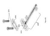
- FIG. 25schematically illustrates the components of a micro-coaxial transition to hollow-core waveguide, an “E-plane backshort” in accordance with the present invention
- FIG. 26schematically illustrates an exploded assembly view of the E-plane micro-coaxial transition to hollow-core waveguide for FIG. 25 ;
- FIG. 27schematically illustrates the assembled micro-coaxial transition to waveguide and the tool fixture containing hollow-core waveguide to which it mates;
- FIG. 28schematically illustrates a top-down and cross-sectional view of a micro-coaxial transition to hollow-core waveguide of FIG. 25 .
- the present inventionprovides several innovations which can help enable systems, such as those described above, to be built with the desired modularity, while precision tolerances and high performance is maintained.
- the present inventionmay relate to formation of mechanical structures in monolithically or sequentially formed planar subsystems that provide a spring force or clamping force within microstructured metals and/or dielectrics by a deliberate design and tolerancing of elements disposed therein to create snap-together features that may elastically deform during the interconnection process and still maintain sufficient connection force after being joined.
- first and second subsystems 14 , 16may be operably joined to one another via the action of a latching clip or spring 10 disposed on the first subsystem 14 which latches to a corresponding detent 12 on the second subsystems 16 , FIG. 1 .
- the mating junctions between the latching clip 10 and detent 12may be designed to ensure there is suitable force between the mating or joined surfaces 15 , 17 to show a negligible contact resistance between the typically metal to metal interface surfaces 15 , 17 , even under the added stress of mechanical or thermal changes, shocks, or vibrations that the junction may see during its intended use.
- the mating interconnectionssuch as latching clip 10 and detent 12 , may be disposed between subsystems 14 , 16 in the same plane as the plane of formation of the planar subsystems 14 , 16 or may be to planar subsystems being joined orthogonally to the plane of their formation, or the mating interconnections may be joined at any angle in any plane in any desired configuration that can be designed and meet the intended purpose and function.
- planar coaxial waveguides 20 , 21 , in FIG. 2A and planar coaxial waveguides 22 , 23may include center conductors having complementary angled end faces 24 , 25 shown in FIG. 2A , or complementary stepped end faces 26 , 27 , shown in FIG. 2B .
- Interfacesmay consist of direct butt connections, lap joints, sliding joints, or other mechanisms.
- Interconnectionsmay be fabricated protruding from a majority of the planar subsystems upper or lower surfaces, or regions of their end surfaces, to increase signal conductor interference and improve physical contact. This interference increasing feature can be readily seen with exemplary coaxial configurations in FIGS. 2A, 2B .
- post-processed bumps or additional materialmay be also be added to increase the conductor interference after fabrication of the structure is complete.
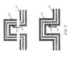
- first and second subsystems 30 , 31 incorporating coaxial waveguidesmay include a latching clip 32 and detent 33 , respectively, similar to the latching clip 10 and detent 12 shown FIG. 1 , and may be used to operably join first and second subsystems 30 , 31 to effect electrical communication between the respective waveguides of the first and second subsystems 30 , 31 , FIG. 3 .
- Typical versions of structures made with the PolyStrata® or similar processesare sometimes called “2.5D” devices. This is because 2.5D structures or devices can have nearly any pattern in the plane of formation of that layer but the layer has a predefined thickness. That layer can be called a strata and it can contain one or more materials and when using a sacrificial mold or scaffolding material, regions of what will become empty space. Layer after layer are formed over each other creating many fused layers of one or more materials. In the exemplary PolyStrata® process that layer may be a metal and a dielectric. At the end of the formation of the laminate of many layers, the sacrificial material may be removed leaving the intended materials behind.
- a limitation of a 2.5D constructionis that while it can have a nearly arbitrary definition in the plane of a particular strata or planar layer, there remains the difficulty that such clamping or snapping tongue-in-groove like structures are not readily fabricated out of the plane of fabrication. So for example, if an out of the plane of fabrication (that is, out of the plane of the layer(s), e.g., the X-Y plane or dimension) is taken as the vertical plane (that is, vertical being perpendicular to the plane of the layer(s), e.g., the Z-dimension or Z-direction), it is difficult to form a long vertical cantilever due to the excessive number of aligned layers required to make the structure.
- a somewhat related concept with advantages and challengescan be visualized for building structures out of LEGO® bricks.
- the mating structures, such as latching clip 32 and detent 33 , for one of the two subsystems 30 , 31may be limited by available Z-dimensional stackup, meaning the limitations of the total available build height or number of layers that can be joined monolithically in a single sequential build. This limits the interface structures to rectangular features in a Z-direction. For this reason, the mechanical clips used for these parts will most often be fabricated on the orthogonal pieces, such as first subsystem 40 as shown in FIG. 4 . Mechanical latches or clips 32 and detents 33 may be made in the same process to allow temporary or permanent retention of the interconnected subsystems 30 , 31 .
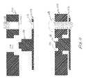
- first and second subsystems 40 , 41 including coaxial waveguides with respective center conductors 42 , 43may include respective dielectric posts 48 , 49 as both a guide and a means to keep the center conductor 42 of the first subsystem 40 in contact with the center conductor 43 of the second subsystem 41 .
- dielectric posts 48 , 49as both a guide and a means to keep the center conductor 42 of the first subsystem 40 in contact with the center conductor 43 of the second subsystem 41 .
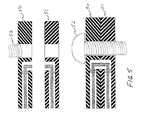
- subsystems 50 , 51may be held in place by the use of tiny screws 52 of the type used in watch-making, PIM fasteners, cotter pins, dowels with locking mechanisms, or any of a number of other mechanical fastening systems, FIG. 5 .
- arrayed connectorssuch as motherboard and daughter card connectors exits, in this case there are no separately formed connectors that are joined to a circuit board substrate. Instead, the interconnections are designed into terminal ends of the DC and RF transmission lines that form the substrate free planar subsystems.
- FIG. 5schematically illustrates a close-up cross-sectional view of a region of primarily air-dielectric coaxial transmission lines in each of two planar subsystems or modules, 50 and 51 that are being assembled by compression using screw 52 .
- a cross-sectional view of the coaxial transmission linecan be seen for each part.
- Most of the center conductoris shown parallel to the plane of fabrication, and turning out of plane to opposing surfaces near the entry point for the screw.
- the center conductorsare supported using dielectric supports located above and below the center conductor in proximity to where the center conductors turn out of plane. Each terminate near, and slightly beyond, the a surface of their respective ground planes.
- This compressive forcecan be engineered through several factors, including the choice of materials for the metal and dielectric, the dimensions and positions of the center conductors and dielectric blocks, the length of center conductor located past the final dielectric block, and the degree of protrusion of the terminal ends of the center conductors above their surrounding ground planes as found in their non-compressed state.
- the level of forcecan therefore be engineered to ensure a low resistance continuous DC connection is achieved between these conductors that will be maintained even under typical conditions of mechanical shock and vibration as well as thermal shock and thermal cycles.
- a noble surface finish for the conductorssuch a gold may be chosen for the surfaces in the region of contact to ensure low contact resistance is maintained before the parts are assembled.
- connectionscan be made between free-standing planar subsystem boards such as those build using the PolyStrata process.
- Such connectionsmay be typical in building complex systems such as phased arrays where layers may include feeds to hundreds of antenna elements, distribution networks, and layers of active devices.
- a benefit of this type of assembly over solder reflow attachmentif the ability to test the system and replace layers if needed. While such connections may be used independent of a semi-permanent attach such as solder, they may also be used to the system before additional surface layers of solder are reflowed to make the connections semi-permanent.
- Alignment featuresmay take the form of interlocking structures, lap joints, sliding structures, or visual alignment marks. Ideally, such alignment marks may incorporate features which facilitate self-alignment and/or coarse alignment, allowing the key aspects of the assembly of the substrate-free planar subsystems, as wells the joining of said subsystems together into systems, by hand and/or without the requirement of high-precision placement machines.
- micron accuracy chip placement toolsor automation stations with micron accuracy robotic motion, can cost on the order of hundreds of thousands to millions of US dollars.
- These self-aligning featuresmight include tapered pin-and-hole structures, nested visual crosshairs, or diagonal features on interlocking fins, which will be described in more detail below in connection with inventive concept three.
- the present inventionmay provide innovations related to the first inventive concept in a somewhat different way to create “dry” planar subsystem to chip or component interconnects, so that the chip does not need to be additionally packaged, and the “bare die” can be inserted and interconnected into the system and still removed to be replaced without rework that requires steps such as cutting wirebonds or desoldering bumps and/or removing difficult to service adhesive layers intended to be permanent, FIG. 6 .
- a lower planar subsystem 68 of the present inventionmay employ a bare die socket 69 .
- the electrical or electrical and thermal interconnectmay be achieved by cantilever probe 62 or spring forces between DC and RF transmission lines of upper and lower planar subsystems 60 , 68 and a chip 65 .
- the spring forcesmay be applied for example by using a clam-shell design for the sub-systems 60 , 68 such that the chip 65 with bond pads 67 , FIG. 7 , is mounted face down into a socket 69 , FIG. 6 .
- the spring forcesare illustrated in the flexed cantilever probes 62 illustrated in the lower panel of FIG. 7 .
- the socket 69may include spring-loaded electrical interconnects, and the chip 65 may have a thermal back surface applied.
- the upper and lower planar subsystems 60 , 68may be screwed down with screws provided in holes 64 , 66 , as shown in FIG. 6 , until the thermal back surface is in compression into the chip socket 69 provided by the upper and lower planar subsystems 60 , 68 to compress the chip 65 into thermal and electrical communication, FIGS. 6, 7 .
- a similar arrangementcan be done with the chip 85 face up and the electrical interconnect being transferred and applied by a specially constructed lid element 80 to complete the test socket via the very same cantilever beams 82 which provide the force to hold the chip 85 in place against a handling plate 88 , FIG. 8A .
- high-value MMICswill be permanently attached to plates of CuMo, CuW, or brass via epoxy or solder to improve thermal performance, improve CTE match to the tooling, or to alleviate general handling concerns.
- the handling plate 88can be secured using in-process mechanical features, or additional fastening structures such as screws or clips.
- the cantilever beams 82can be used to connect DC power and signals as well as RF signals and ground planes, FIGS.
- the cantilever beams 82may have post-processed material applied to their tips to increase the deflection and improve contact and may include dielectric posts 87 , as shown in FIGS. 9A, 9B , in a similar manner to the dielectric posts 48 , 49 of FIG. 4 .
- dielectric posts 87may be optionally coated with a dielectric to achieve a capacitive connection.
- a third implementation of this conceptmay include a compressible pad 108 made of dielectric or other material disposed within the lid 100 , which dampens the cantilever motion effect of the signal probe cantilever 102 . This allows for less range of motion, and increases the pressure on the chip bond pads 107 of the chip 105 as the lid 100 and base 110 are joined, thereby reducing potential interface issues, FIG. 10 .
- the bare chip 85may be replaced simply by removing the screws or other fastening elements, and removing any thermal grease or other transfer medium such as a phase change medium. Since no wirebonds, wedgebonds, or desoldering steps are needed, the bare chip 85 may be readily replaced, and, because there is no intermediate packaging of the chip, the parasitics of packaging the chip 85 may be minimized. This is particularly true when using PolyStrata® technology, since coax to CPW probe transitions may be employed—directly interfacing the planar subsystem transmission lines to the chip 85 without needing a separate chip package.
- dummy through-line structuresmay be inserted instead and removed in the same way.
- Butt-coupled junctions both in and out of planemay also be designed to have some degree of spring force, such as one may find in a cantilevered probe 82 ; however, to have a suitable sustaining force between formed subsystems, the layers require both precision alignment and mechanical clamping.
- Such structures and approach of the present invention of using a compression and spring force based electrical interconnect for bare chip 85can greatly increase the speed of assembly while reducing un-necessary bulk, size, and cost and while improving performance.
- this arrangementmay be desirable as a means to qualify chips which require complex environmental conditions or complicated passive networks to perform their desired functions. For example, a MMIC which requires placement in a custom cavity, with a complex bias network.
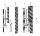
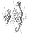
- first and second modules 110 , 112may include a mating tapered hole 114 and tapered alignment pin or dowel 116 .
- the tapered holes 114 within or at the edges of the 2.5D layers of the first module 110can be used to align independent modules 110 , 112 of PolyStrata® assemblies by receiving tightly toleranced tapered pins or dowels 116 which force the alignment of layers and through which a layer to layer alignment ranging from microns to submicron can be accomplished depending on the relative dimensions and tolerances of the tapered pins or dowels 116 and the formed PolyStrata® process tapered holes 114 .
- a semi-permanent downward forcecan be applied using small screws 118 placed through corresponding screw holes 111 , 113 of the first and second modules 110 , 112 , respectively. Screws 118 such as those employed historically in the precision mechanical wrist-watch industry may be used.
- the PolyStrata® modules 110 , 112may be formed and interconnected in both in-plane and perpendicular to the plane of their original formation.
- a great advantage of this approach for these meso-scale assembliesis that suitable forces may be created in the layer to layer coaxial or DC junctions, particularly between gold coated surfaces, such that a solder interface—for example one produced by the reflow of solder bumps—may not be needed.
- proper mechanical meansmay be designed into the PolyStrata® substrates or module fabrics to distribute the downward forces in the ground planes and suspended transmission lines using appropriate cantilever design.
- Separate substrate-free sub-systemswhich may comprise chips and other devices hybridly or monolithically, may also be formed in a plane using a modular build. It is desirable that these sub-systems contain testable circuits and that sub-systems, also called modules, can be precisely aligned and interconnected. Preferably such precision alignment and interconnection may be performed by hand assembly without needing expensive tools and machines to align, move, register, and bond the sub-systems or modules. As frequency increases and dimensions go down, for example in modules that may contain signals or power at 40 or 100 GHz, precision registration and alignment of the transmission lines may be required that allow one module to be in electrical communication with another. These needs can be met when constructing larger planar substrate-free subsystems from smaller ones by monolithically incorporating mating features for mechanical interlocking.
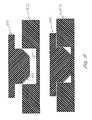
- a first subsystem 150may be provided with the tapered structure, such as a tapered fin 153 , which is configured to self-guide into a hole 154 provided in a second subsystem 152 , to effect alignment between the first and second subsystems 150 , 152 , FIG. 15 .
- the tapered edges of the fins 153allow for self-alignment, guiding the parts into their tightly tolerance final, attached state.
- the tapered fin 153 and hole 154may facilitate gross alignment.
- Alignment featuresmay be provided in the form of tapered fins 153 , as shown in FIG. 15 , or any other of a number of shapes.
- alignment featuresmay take advantage of the high dimensional tolerances available in X-Y dimensions relative to those available in Z dimensions.
- a gross alignment structurewould allow for the parts to be mated without the use of sub-micron accurate placement tools.
- the coarse alignmentcould be provided take by the tapered pins 116 and tapered hole 114 , FIG. 11 , slanted diagonal mating surfaces, FIG. 15 , dielectric gaskets, or a number of other structures. Alignment features designed to be universal may also be key.
- a first and second modules 120 , 126may be provided with a self-mating slots 122 , 122 a and a self-mating tabs 124 , 124 a , where the tabs 124 , 124 a are configured to mate with the slots 122 , 122 a .
- Such mechanical interlocking features as self-mating slots 122 , 122 a and tabs 124 , 124 acan then register input and output ports 128 , 128 a of the first and second modules 120 , 126 in a way that a third planar-subsystem “jumper” 125 may be aligned and bonded in place, FIG. 13 .
- Thismay be achieved by forming additional monolithic alignment features, such as tapered pins 123 , 123 a in the same build sequence that forms the in plane alignment between the two planar subsystems to align the first and second modules 120 , 126 to tapered holes 127 of the jumper 125 , FIG. 13 .
- tapered pins 123 , 123 amay protrude above the plane containing the first and second modules 120 , 126 to precisely register the jumper 125 providing the microwave and DC interconnect function between the ports 128 , 128 a of the first and second modules 120 , 126 , FIG. 13 .
- layer to layer misalignmentmay necessitate an increase of tolerance on the alignment features, reducing the possible alignment accuracy for interconnections.
- an approachis to tightly tolerance a single layer and its mate, as shown in FIG. 14 .
- the alignment accuracy between the fused layersmay be ultimately limited by some mechanism of human and/or machine motion. For example, if the layers are defined using a contact mask aligner, one may be limited by the ability to resolve the edges of alignment features on the wafer and/or the ability to mechanically align and a photomask to those features.
- a first component 126 having a pin 123 amay be a part comprised of a layer by layer build, in this case 6 layers are shown each of a determined thickness.
- a second component 125may be comprised of 5 layers shown.
- any layer to layer misalignment introduced in their fabricationcan be eliminated by using only the 4th layer in component 126 and the 3rd layer in component 125 to achieve the component to component registration, which would be limited to the gap 127 between them.
- the present inventionmay provide the ability to create threaded holes using only a 2.5D build process, FIG. 16 .
- threaded holesfollow a continuous screw pattern.
- a functionally equivalent structure to a continuous screw patterncan be made normal to the strata planes and also parallel to strata planes.
- a PolyStrata® threaded holecan be used to attach passive and active devices to PolyStrata® parts and also to attach two PolyStrata® pieces together.
- the PolyStrata® threaded holeeliminates the need for extra non-PolyStrata® tooling with threaded holes.
- the PolyStrata® threaded holehas a photo-lithographically defined diameter and location.
- the PolyStrata® threaded holecan be used for accurate alignment, eliminating the need for extra alignment features either in tooling or in other areas of the PolyStrata® part. If using screws, this may be the lowest weight design for non-permanent attach to substrate free planar subsystems.
- the left panel in FIG. 16schematically illustrates an example of stepwise thread holes 160 fabricated normal to the strata plane. Rather than contain a single continuous spiral thread, which is not possible due to the 2.5D nature of a layered build process, individual, planar, circumferential arcs 161 , 162 , 163 may be disposed in separate strata layers in angular offset locations from one another to approximate a continuous spiral thread in a stepwise- or digitized-manner.
- the PolyStrata® threaded hole 160can be used to attach passive and active devices to PolyStrata® parts and also to attach two PolyStrata® pieces together.
- the PolyStrata® threaded hole 160eliminates the need for extra non-PolyStrata® tooling to make continuously spiral-threaded holes.
- the center panel in FIG. 16schematically illustrates the use of a standard screw 165 within a stepwise threaded hole 160 .
- the right panel in FIG. 16schematically illustrates a micro-fabricated stepwise threaded screw 168 comprising circumferential arcs 169 disposed in separate strata layers in angularly offset locations from one another to approximate a continuous spiral thread on the screw 168 .
- This new micro-fabricated threaded hole 160permits the use of miniature sized screws needed for micro-assembly of parts requiring very-compact form factor. Furthermore, unlike normal tapped holes in tooling, the PolyStrata® threaded hole 160 has a photo-lithographically defined diameter and location. Therefore, the PolyStrata® threaded hole 160 can be used for accurate alignment, eliminating the need for extra alignment features either in tooling or in other areas of the part. By enabling micron level accuracy positioning very sensitive devices such resonators or filters can be fabricated and tune using this micro-screws.
- FIG. 17schematically illustrates an example of 60 GHz 5 -pole cavity filter 170 .
- the dimensions of the cavityare 6 mm in length and 2 mm in width.
- the micro-fabricated screws 172have a diameter of 200 um.
- a small tapped screw holemay be realized accurately and the diameter of the thread be positioned with micron scale accuracy.
- This approachoffers re-workability of parts by providing the ability to screw and unscrew the part, as well as tunability and reduced weight due to the small size of the PolyStrata® screws relative to precision standardized miniature screws, typically available off-the-shelf, and usually made by die-turning, lathe, CNC or other precision machining operations.
- the present inventionmay provide a hole-shaped interconnection that permits connection from a coaxial transmission line to any industry standard pin connector 182 , 184 .
- FIG. 18illustrates an interconnection with a 2.4 mm connector, however the design is functionally equivalent when applied to any coaxial connector such as SMA, SSMA, 1.0 mm, 1.85 mm, 2.92, mm or 3.5 mm.
- an RF signalcan pass through one connector 182 ; enter the coaxial transmission line of a transition structure 180 and transition back to the second connector 184 .
- FIGS. 19 and 20schematically illustrate a donut shape transition 187 from a connector pin 186 to the coaxial-line 183 of the transition structure 180 .
- transitionssuch as rectangular or square shape.
- This hole-shaped connectionenables better position accuracy between the connector input pin 186 and the coaxial line 187 than previous approach like standard PC board connectors.
- the electrical performance of the transitionis improved due to a better mechanical positioning of the pin 186 in relation to the coax line 187 .
- PolyStrata® micro-fabrication or a similar additive build processalso offers tighter tolerance resulting in better RF performance and more reproducible results. Such higher performance transition becomes critical for high volume and frequencies above 10 GHz.
- the electrical assemblycan be performed using solder or conductive epoxy. For certain applications and at certain frequency, it is also possible not to use any solder or conductive adhesive and only rely on capacitive RF coupling to provide the signal interconnection.
- the performancecan be further improved by closing the top of the transition structure 180 with an optional top plate 190 , FIG. 21 .
- the top plate 190may stop any radiation loss due from the pin 186 or the transition 187 , significantly reducing the loss.
- the present inventionmay provide a method for utilizing precision fabrication techniques to create solder or epoxy joints with controlled height. This is useful both for filters (setting capacitance), setting the precise height of cavities, and for ensuring good lifetime of a solder or epoxy joint.
- the height of a solder jointis often a critical element in the lifetime of the joint since it plays a key role in defining the stress that occurs in the solder over time. Utilizing this approach, all solder joints in a system can be designed to have a desired thickness with micron scale accuracy over the entire system.
- solder paste 221may be applied to horizontal PolyStrata® piece 222 before assembly.
- a vertical PolyStrata® piece 220may then be aligned and pushed down with sufficient force that the vertical PolyStrata® piece 220 rests against the horizontal piece 222 .
- the solder 221is then reflowed.
- pressureis continuously applied such that the final thickness of the solder to 21 is set by a value determined by the design of the vertical PolyStrata® piece 220 .
- This same technique to join pieces 226 , 228can be used to create gaps with precise control over the final thickness of the gap as schematically illustrated in FIG. 23 .
- a third exemplary implementation of this conceptcan be realized utilizing a precision fabricated collar or gasket 225 of incompressible dielectric material.
- the precise height of the solder bondline 227is set by a combination of the thicknesses of PolyStrata® pieces 220 , 222 and the thickness of the dielectric gasket 225 .
- the dielectric gasket 225in this instance may also function as a wick-stop or surface-flow stop, preventing solder from entering the cavity 224 and affecting its performance.
- the present inventionrelates to hollow waveguide structures, as follows. While air dielectric coax and strip-line waveguides structures are low loss and support a wide bandwidth, there is currently no known technology that can rival the loss per unit length of hollow waveguide structures. Meanwhile when interfacing to chips, the ability to reduce size and distance associated with other waveguide structures such as coaxial, microstrip, CPW, stripline, and suspended stripline structures, are better able to interface to microchips such as MMICs. It is therefore desirable to be able to move between waveguide structures such as micro-coax and hollow waveguide as needed depending on the function to be achieved in a component, circuit, subsystem, or system.
- a coaxial modeis transferred into a radiative mode to launch a wave into a hollow waveguide, using what is called an E-probe or an H-probe.
- E-probeor an H-probe.
- H-probean electric or magnetic field orientation of the transition structure and hollow waveguide.
- transition structuresare increasingly sensitive to fabricated and assembled dimensions and tolerances with increasing frequency.
- we present techniquesapplicable to a 2.5D or 3D fabrication processes to enable their integration and incorporation with the tolerances and precision required. They are particularly useful as frequency moves to mm-wave and sub-mm wave frequencies such as 60, 70, 100, 200 GHz or more.
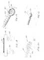
- FIGS. 25-28show an example of the use of two parts fabricated in the PolyStrata® process, and two screws used for assembly 307 .
- Component 301is referred to as the back-short lid.
- Component 302is a region of waveguide for a wave propagating up the page into the hollow waveguide cavity region 306 .
- the waveis converted to and from a coaxial waveguide mode using e-probe transition feature 305 which becomes part of the center conductor of the coax, the outer conductor of which exits to the right of the page.
- the lid 301is placed on the waveguide to coax transition 302 and the parts are in continuous electrical connection using compression applied by the screws once assembled.
Landscapes
- Engineering & Computer Science (AREA)
- Manufacturing & Machinery (AREA)
- Microelectronics & Electronic Packaging (AREA)
- Wire Bonding (AREA)
- Measuring Leads Or Probes (AREA)
- Micromachines (AREA)
- Combinations Of Printed Boards (AREA)
Abstract
Description
Claims (16)
Priority Applications (4)
| Application Number | Priority Date | Filing Date | Title |
|---|---|---|---|
| US14/211,749US9306255B1 (en) | 2013-03-15 | 2014-03-14 | Microstructure including microstructural waveguide elements and/or IC chips that are mechanically interconnected to each other |
| US15/074,083US10361471B2 (en) | 2013-03-15 | 2016-03-18 | Structures and methods for interconnects and associated alignment and assembly mechanisms for and between chips, components, and 3D systems |
| US15/861,283US10193203B2 (en) | 2013-03-15 | 2018-01-03 | Structures and methods for interconnects and associated alignment and assembly mechanisms for and between chips, components, and 3D systems |
| US16/257,887US20190393580A1 (en) | 2013-03-15 | 2019-01-25 | Structures and methods for interconnects and associated alignment and assembly mechanisms for and between chips, components, and 3d systems |
Applications Claiming Priority (2)
| Application Number | Priority Date | Filing Date | Title |
|---|---|---|---|
| US201361798018P | 2013-03-15 | 2013-03-15 | |
| US14/211,749US9306255B1 (en) | 2013-03-15 | 2014-03-14 | Microstructure including microstructural waveguide elements and/or IC chips that are mechanically interconnected to each other |
Related Child Applications (1)
| Application Number | Title | Priority Date | Filing Date |
|---|---|---|---|
| US15/074,083ContinuationUS10361471B2 (en) | 2013-03-15 | 2016-03-18 | Structures and methods for interconnects and associated alignment and assembly mechanisms for and between chips, components, and 3D systems |
Publications (1)
| Publication Number | Publication Date |
|---|---|
| US9306255B1true US9306255B1 (en) | 2016-04-05 |
Family
ID=55589105
Family Applications (4)
| Application Number | Title | Priority Date | Filing Date |
|---|---|---|---|
| US14/211,749ActiveUS9306255B1 (en) | 2013-03-15 | 2014-03-14 | Microstructure including microstructural waveguide elements and/or IC chips that are mechanically interconnected to each other |
| US15/074,083Expired - Fee RelatedUS10361471B2 (en) | 2013-03-15 | 2016-03-18 | Structures and methods for interconnects and associated alignment and assembly mechanisms for and between chips, components, and 3D systems |
| US15/861,283Expired - Fee RelatedUS10193203B2 (en) | 2013-03-15 | 2018-01-03 | Structures and methods for interconnects and associated alignment and assembly mechanisms for and between chips, components, and 3D systems |
| US16/257,887AbandonedUS20190393580A1 (en) | 2013-03-15 | 2019-01-25 | Structures and methods for interconnects and associated alignment and assembly mechanisms for and between chips, components, and 3d systems |
Family Applications After (3)
| Application Number | Title | Priority Date | Filing Date |
|---|---|---|---|
| US15/074,083Expired - Fee RelatedUS10361471B2 (en) | 2013-03-15 | 2016-03-18 | Structures and methods for interconnects and associated alignment and assembly mechanisms for and between chips, components, and 3D systems |
| US15/861,283Expired - Fee RelatedUS10193203B2 (en) | 2013-03-15 | 2018-01-03 | Structures and methods for interconnects and associated alignment and assembly mechanisms for and between chips, components, and 3D systems |
| US16/257,887AbandonedUS20190393580A1 (en) | 2013-03-15 | 2019-01-25 | Structures and methods for interconnects and associated alignment and assembly mechanisms for and between chips, components, and 3d systems |
Country Status (1)
| Country | Link |
|---|---|
| US (4) | US9306255B1 (en) |
Cited By (5)
| Publication number | Priority date | Publication date | Assignee | Title |
|---|---|---|---|---|
| US20160315401A1 (en)* | 2013-12-17 | 2016-10-27 | Robert Bosch Gmbh | Electrical Assembly |
| WO2017200634A1 (en)* | 2016-05-16 | 2017-11-23 | Maury Microwave, Inc. | Broadband rf capacitors for coaxial line |
| CN108428694A (en)* | 2017-02-13 | 2018-08-21 | 深圳市中兴微电子技术有限公司 | A kind of system in package chip and its packaging method |
| US11257771B2 (en)* | 2019-01-02 | 2022-02-22 | Keysight Technologies, Inc. | High-performance integrated circuit packaging platform compatible with surface mount assembly |
| US11605583B2 (en)* | 2019-01-02 | 2023-03-14 | Keysight Technologies, Inc. | High-performance integrated circuit packaging platform compatible with surface mount assembly |
Families Citing this family (7)
| Publication number | Priority date | Publication date | Assignee | Title |
|---|---|---|---|---|
| US20110123783A1 (en)* | 2009-11-23 | 2011-05-26 | David Sherrer | Multilayer build processses and devices thereof |
| US9306255B1 (en)* | 2013-03-15 | 2016-04-05 | Nuvotronics, Inc. | Microstructure including microstructural waveguide elements and/or IC chips that are mechanically interconnected to each other |
| US11196184B2 (en) | 2017-06-20 | 2021-12-07 | Cubic Corporation | Broadband antenna array |
| US10319654B1 (en) | 2017-12-01 | 2019-06-11 | Cubic Corporation | Integrated chip scale packages |
| WO2019209461A1 (en)* | 2018-04-25 | 2019-10-31 | Nuvotronics, Inc. | Microwave/millimeter-wave waveguide to circuit board connector |
| US11367948B2 (en) | 2019-09-09 | 2022-06-21 | Cubic Corporation | Multi-element antenna conformed to a conical surface |
| DE102023202890A1 (en)* | 2023-03-29 | 2024-10-02 | Continental Autonomous Mobility Germany GmbH | Waveguide arrangement, radar sensor and method for producing a waveguide arrangement |
Citations (185)
| Publication number | Priority date | Publication date | Assignee | Title |
|---|---|---|---|---|
| US2743505A (en)* | 1950-04-18 | 1956-05-01 | Int Standard Electric Corp | Joints for coaxial cable |
| US2812501A (en) | 1954-03-04 | 1957-11-05 | Sanders Associates Inc | Transmission line |
| US2914766A (en) | 1955-06-06 | 1959-11-24 | Sanders Associates Inc | Three conductor planar antenna |
| US2997519A (en) | 1959-10-08 | 1961-08-22 | Bell Telephone Labor Inc | Multicoaxial line cables |
| US3309632A (en) | 1965-04-13 | 1967-03-14 | Kollmorgen Corp | Microwave contactless coaxial connector |
| US3311966A (en) | 1962-09-24 | 1967-04-04 | North American Aviation Inc | Method of fabricating multilayer printed-wiring boards |
| US3335489A (en) | 1962-09-24 | 1967-08-15 | North American Aviation Inc | Interconnecting circuits with a gallium and indium eutectic |
| US3352730A (en) | 1964-08-24 | 1967-11-14 | Sanders Associates Inc | Method of making multilayer circuit boards |
| US3464855A (en) | 1966-09-06 | 1969-09-02 | North American Rockwell | Process for forming interconnections in a multilayer circuit board |
| US3537043A (en) | 1968-08-06 | 1970-10-27 | Us Air Force | Lightweight microwave components and wave guides |
| US3560896A (en) | 1967-07-06 | 1971-02-02 | Telefunken Patent | Inner conductor support for shielded microwave strip lines |
| US3577105A (en) | 1969-05-29 | 1971-05-04 | Us Army | Method and apparatus for joining plated dielectric-form waveguide components |
| US3598107A (en) | 1968-07-25 | 1971-08-10 | Hamamatsu T V Co Ltd | Pupillary motion observing apparatus |
| FR2086327A1 (en) | 1970-04-24 | 1971-12-31 | Spinner Gmbh Elektrotech | |
| US3775844A (en) | 1970-06-25 | 1973-12-04 | Bunker Ramo | Method of fabricating a multiwafer electrical circuit structure |
| US3789129A (en) | 1972-06-06 | 1974-01-29 | Felten & Guilleaume Ag | Air-insulated coaxial high-frequency cable |
| US3791858A (en) | 1971-12-13 | 1974-02-12 | Ibm | Method of forming multi-layer circuit panels |
| US3884549A (en) | 1973-04-30 | 1975-05-20 | Univ California | Two demensional distributed feedback devices and lasers |
| US3963999A (en) | 1975-05-29 | 1976-06-15 | The Furukawa Electric Co., Ltd. | Ultra-high-frequency leaky coaxial cable |
| US4021789A (en) | 1975-09-29 | 1977-05-03 | International Business Machines Corporation | Self-aligned integrated circuits |
| US4033656A (en) | 1975-09-02 | 1977-07-05 | Zero Manufacturing Company | Low profile integrated circuit socket |
| US4075757A (en) | 1975-12-17 | 1978-02-28 | Perstorp Ab | Process in the production of a multilayer printed board |
| US4275944A (en) | 1979-07-09 | 1981-06-30 | Sochor Jerzy R | Miniature connector receptacles employing contacts with bowed tines and parallel mounting arms |
| US4348253A (en) | 1981-11-12 | 1982-09-07 | Rca Corporation | Method for fabricating via holes in a semiconductor wafer |
| US4365222A (en) | 1981-04-06 | 1982-12-21 | Bell Telephone Laboratories, Incorporated | Stripline support assembly |
| US4414424A (en) | 1980-10-20 | 1983-11-08 | Tokyo Shibaura Denki Kabushiki Kaisha | Gas-insulated bus bar |
| US4417393A (en) | 1981-04-01 | 1983-11-29 | General Electric Company | Method of fabricating high density electronic circuits having very narrow conductors |
| US4437074A (en) | 1980-12-18 | 1984-03-13 | Thomson-Csf | Ultrahigh-frequency transmission line of the three-plate air type and uses thereof |
| US4521755A (en) | 1982-06-14 | 1985-06-04 | At&T Bell Laboratories | Symmetrical low-loss suspended substrate stripline |
| US4581301A (en) | 1984-04-10 | 1986-04-08 | Michaelson Henry W | Additive adhesive based process for the manufacture of printed circuit boards |
| US4591411A (en) | 1982-05-05 | 1986-05-27 | Hughes Aircraft Company | Method for forming a high density printed wiring board |
| US4641140A (en) | 1983-09-26 | 1987-02-03 | Harris Corporation | Miniaturized microwave transmission link |
| US4663497A (en) | 1982-05-05 | 1987-05-05 | Hughes Aircraft Company | High density printed wiring board |
| US4673904A (en) | 1984-11-14 | 1987-06-16 | Itt Corporation | Micro-coaxial substrate |
| US4700159A (en) | 1985-03-29 | 1987-10-13 | Weinschel Engineering Co., Inc. | Support structure for coaxial transmission line using spaced dielectric balls |
| US4717064A (en) | 1986-08-15 | 1988-01-05 | Unisys Corporation | Wave solder finger shield apparatus |
| DE3623093A1 (en) | 1986-07-09 | 1988-01-21 | Standard Elektrik Lorenz Ag | Method for producing through-connections in printed circuit boards or multilayer printed circuit boards having inorganic or organic/inorganic insulating layers |
| US4771294A (en) | 1986-09-10 | 1988-09-13 | Harris Corporation | Modular interface for monolithic millimeter wave antenna array |
| US4808273A (en) | 1988-05-10 | 1989-02-28 | Avantek, Inc. | Method of forming completely metallized via holes in semiconductors |
| US4832461A (en) | 1986-08-20 | 1989-05-23 | Fujitsu Limited | Projection-type multi-color liquid crystal display device |
| US4853656A (en) | 1987-08-03 | 1989-08-01 | Aerospatiale Societe Nationale Industrielle | Device for connecting together two ultra-high frequency structures which are coaxial and of different diameters |
| US4856184A (en) | 1988-06-06 | 1989-08-15 | Tektronix, Inc. | Method of fabricating a circuit board |
| US4857418A (en) | 1986-12-08 | 1989-08-15 | Honeywell Inc. | Resistive overlayer for magnetic films |
| US4876322A (en) | 1984-08-10 | 1989-10-24 | Siemens Aktiengesselschaft | Irradiation cross-linkable thermostable polymer system, for microelectronic applications |
| US4880684A (en) | 1988-03-11 | 1989-11-14 | International Business Machines Corporation | Sealing and stress relief layers and use thereof |
| JPH027587A (en) | 1988-06-27 | 1990-01-11 | Yokogawa Electric Corp | Variable frequency light source |
| US4969979A (en) | 1989-05-08 | 1990-11-13 | International Business Machines Corporation | Direct electroplating of through holes |
| US4975142A (en) | 1989-11-07 | 1990-12-04 | General Electric Company | Fabrication method for printed circuit board |
| US5069749A (en) | 1986-07-29 | 1991-12-03 | Digital Equipment Corporation | Method of fabricating interconnect layers on an integrated circuit chip using seed-grown conductors |
| US5072201A (en) | 1988-12-06 | 1991-12-10 | Thomson-Csf | Support for microwave transmission line, notably of the symmetrical strip line type |
| JPH041710A (en) | 1990-04-19 | 1992-01-07 | Matsushita Electric Ind Co Ltd | Lens adjusting device |
| US5100501A (en) | 1989-06-30 | 1992-03-31 | Texas Instruments Incorporated | Process for selectively depositing a metal in vias and contacts by using a sacrificial layer |
| CA2055116A1 (en) | 1990-11-13 | 1992-05-14 | Jurg Buhler | Automatic analysis apparatus |
| US5119049A (en) | 1991-04-12 | 1992-06-02 | Ail Systems, Inc. | Ultraminiature low loss coaxial delay line |
| US5191699A (en) | 1990-09-04 | 1993-03-09 | Gw-Elektronik Gmbh | Methods of producing a chip-type HF magnetic coil arrangement |
| US5227013A (en) | 1991-07-25 | 1993-07-13 | Microelectronics And Computer Technology Corporation | Forming via holes in a multilevel substrate in a single step |
| US5235208A (en)* | 1991-02-07 | 1993-08-10 | Mitsubishi Denki Kabushiki Kaisha | Package for microwave integrated circuit |
| US5274484A (en) | 1991-04-12 | 1993-12-28 | Fujitsu Limited | Gradation methods for driving phase transition liquid crystal using a holding signal |
| JPH0685510A (en) | 1992-03-31 | 1994-03-25 | Yokogawa Electric Corp | Multi-chip module |
| US5334956A (en) | 1992-03-30 | 1994-08-02 | Motorola, Inc. | Coaxial cable having an impedance matched terminating end |
| JPH06302964A (en) | 1993-04-16 | 1994-10-28 | Oki Electric Ind Co Ltd | Circuit board for high-speed signal transmission |
| US5381157A (en) | 1991-05-02 | 1995-01-10 | Sumitomo Electric Industries, Ltd. | Monolithic microwave integrated circuit receiving device having a space between antenna element and substrate |
| US5406423A (en) | 1990-10-01 | 1995-04-11 | Asahi Kogaku Kogyo Kabushiki Kaisha | Apparatus and method for retrieving audio signals from a recording medium |
| US5406235A (en) | 1990-12-26 | 1995-04-11 | Tdk Corporation | High frequency device |
| US5430257A (en) | 1992-08-12 | 1995-07-04 | Trw Inc. | Low stress waveguide window/feedthrough assembly |
| US5454161A (en) | 1993-04-29 | 1995-10-03 | Fujitsu Limited | Through hole interconnect substrate fabrication process |
| GB2265754B (en) | 1992-03-30 | 1995-10-25 | Awa Microelectronics | Silicon transducer |
| US5622895A (en) | 1994-05-09 | 1997-04-22 | Lucent Technologies Inc. | Metallization for polymer-dielectric multichip modules |
| US5633615A (en) | 1995-12-26 | 1997-05-27 | Hughes Electronics | Vertical right angle solderless interconnects from suspended stripline to three-wire lines on MIC substrates |
| US5682124A (en) | 1993-02-02 | 1997-10-28 | Ast Research, Inc. | Technique for increasing the range of impedances for circuit board transmission lines |
| US5682062A (en) | 1995-06-05 | 1997-10-28 | Harris Corporation | System for interconnecting stacked integrated circuits |
| US5712607A (en) | 1996-04-12 | 1998-01-27 | Dittmer; Timothy W. | Air-dielectric stripline |
| US5724012A (en) | 1994-02-03 | 1998-03-03 | Hollandse Signaalapparaten B.V. | Transmission-line network |
| US5746868A (en) | 1994-07-21 | 1998-05-05 | Fujitsu Limited | Method of manufacturing multilayer circuit substrate |
| EP0845831A2 (en) | 1996-11-28 | 1998-06-03 | Matsushita Electric Industrial Co., Ltd. | A millimeter waveguide and a circuit apparatus using the same |
| US5793272A (en) | 1996-08-23 | 1998-08-11 | International Business Machines Corporation | Integrated circuit toroidal inductor |
| US5814889A (en) | 1995-06-05 | 1998-09-29 | Harris Corporation | Intergrated circuit with coaxial isolation and method |
| US5860812A (en) | 1997-01-23 | 1999-01-19 | Litton Systems, Inc. | One piece molded RF/microwave coaxial connector |
| US5872399A (en) | 1996-04-01 | 1999-02-16 | Anam Semiconductor, Inc. | Solder ball land metal structure of ball grid semiconductor package |
| EP0911903A2 (en) | 1997-10-22 | 1999-04-28 | Nokia Mobile Phones Ltd. | Coaxcial cable, method for manufacturing a coaxial cable, and wireless communication device |
| US5925206A (en) | 1997-04-21 | 1999-07-20 | International Business Machines Corporation | Practical method to make blind vias in circuit boards and other substrates |
| US5961347A (en) | 1996-09-26 | 1999-10-05 | Hon Hai Precision Ind. Co., Ltd. | Micro connector |
| US5977842A (en) | 1998-07-01 | 1999-11-02 | Raytheon Company | High power broadband coaxial balun |
| US6008102A (en) | 1998-04-09 | 1999-12-28 | Motorola, Inc. | Method of forming a three-dimensional integrated inductor |
| WO2000007218A2 (en) | 1998-07-28 | 2000-02-10 | Korea Advanced Institute Of Science And Technology | Method for manufacturing a semiconductor device having a metal layer floating over a substrate |
| US6027630A (en) | 1997-04-04 | 2000-02-22 | University Of Southern California | Method for electrochemical fabrication |
| JP3027587B2 (en) | 1989-11-07 | 2000-04-04 | 株式会社リコー | Facsimile machine |
| US6054252A (en) | 1998-12-11 | 2000-04-25 | Morton International, Inc. | Photoimageable compositions having improved chemical resistance and stripping ability |
| WO2000039854A1 (en) | 1998-12-28 | 2000-07-06 | Telephus, Inc. | Coaxial type signal line and manufacturing method thereof |
| US6180261B1 (en) | 1997-10-21 | 2001-01-30 | Nitto Denko Corporation | Low thermal expansion circuit board and multilayer wiring circuit board |
| US6207901B1 (en)* | 1999-04-01 | 2001-03-27 | Trw Inc. | Low loss thermal block RF cable and method for forming RF cable |
| US6210221B1 (en) | 1999-10-13 | 2001-04-03 | Maury Microwave, Inc. | Microwave quick connect/disconnect coaxial connectors |
| US6228466B1 (en) | 1997-04-11 | 2001-05-08 | Ibiden Co. Ltd. | Printed wiring board and method for manufacturing the same |
| US6294965B1 (en) | 1999-03-11 | 2001-09-25 | Anaren Microwave, Inc. | Stripline balun |
| US6329605B1 (en) | 1998-03-26 | 2001-12-11 | Tessera, Inc. | Components with conductive solder mask layers |
| WO2002006152A2 (en) | 2000-07-14 | 2002-01-24 | Zyvex Corporation | System and method for constraining totally released microcomponents |
| US6350633B1 (en) | 2000-08-22 | 2002-02-26 | Charles W. C. Lin | Semiconductor chip assembly with simultaneously electroplated contact terminal and connection joint |
| US6388198B1 (en) | 1999-03-09 | 2002-05-14 | International Business Machines Corporation | Coaxial wiring within SOI semiconductor, PCB to system for high speed operation and signal quality |
| US6457979B1 (en) | 2001-10-29 | 2002-10-01 | Agilent Technologies, Inc. | Shielded attachment of coaxial RF connector to thick film integrally shielded transmission line on a substrate |
| WO2002080279A1 (en) | 2001-03-29 | 2002-10-10 | Korea Advanced Institute Of Science And Technology | Three-dimensional metal devices highly suspended above semiconductor substrate, their circuit model, and method for manufacturing the same |
| US6465747B2 (en) | 1998-03-25 | 2002-10-15 | Tessera, Inc. | Microelectronic assemblies having solder-wettable pads and conductive elements |
| US6514845B1 (en) | 1998-10-15 | 2003-02-04 | Texas Instruments Incorporated | Solder ball contact and method |
| US20030029729A1 (en) | 2001-08-10 | 2003-02-13 | Jao-Chin Cheng | Method of fabricating inter-layer solid conductive rods |
| US6535088B1 (en) | 2000-04-13 | 2003-03-18 | Raytheon Company | Suspended transmission line and method |
| US20030052755A1 (en) | 2002-10-10 | 2003-03-20 | Barnes Heidi L. | Shielded surface mount coaxial connector |
| US20030117237A1 (en) | 2001-12-20 | 2003-06-26 | Feng Niu | Reduced size, low loss MEMS torsional hinges and MEMS resonators employing such hinges |
| US6589594B1 (en) | 2000-08-31 | 2003-07-08 | Micron Technology, Inc. | Method for filling a wafer through-via with a conductive material |
| US6600395B1 (en) | 2000-12-28 | 2003-07-29 | Nortel Networks Limited | Embedded shielded stripline (ESS) structure using air channels within the ESS structure |
| US6603376B1 (en) | 2000-12-28 | 2003-08-05 | Nortel Networks Limited | Suspended stripline structures to reduce skin effect and dielectric loss to provide low loss transmission of signals with high data rates or high frequencies |
| US6648653B2 (en) | 2002-01-04 | 2003-11-18 | Insert Enterprise Co., Ltd. | Super mini coaxial microwave connector |
| US20030222738A1 (en) | 2001-12-03 | 2003-12-04 | Memgen Corporation | Miniature RF and microwave components and methods for fabricating such components |
| US20030221968A1 (en) | 2002-03-13 | 2003-12-04 | Memgen Corporation | Electrochemical fabrication method and apparatus for producing three-dimensional structures having improved surface finish |
| US6662443B2 (en) | 1999-03-24 | 2003-12-16 | Fujitsu Limited | Method of fabricating a substrate with a via connection |
| US20040000701A1 (en) | 2002-06-26 | 2004-01-01 | White George E. | Stand-alone organic-based passive devices |
| US20040004061A1 (en) | 2002-07-03 | 2004-01-08 | Merdan Kenneth M. | Tubular cutting process and system |
| WO2004004061A1 (en) | 2002-06-27 | 2004-01-08 | Memgen Corporation | Miniature rf and microwave components and methods for fabricating such components |
| US20040007468A1 (en) | 2002-05-07 | 2004-01-15 | Memgen Corporation | Multistep release method for electrochemically fabricated structures |
| US20040007470A1 (en) | 2002-05-07 | 2004-01-15 | Memgen Corporation | Methods of and apparatus for electrochemically fabricating structures via interlaced layers or via selective etching and filling of voids |
| US20040038586A1 (en) | 2002-08-22 | 2004-02-26 | Hall Richard D. | High frequency, blind mate, coaxial interconnect |
| US20040076806A1 (en) | 2001-02-08 | 2004-04-22 | Michimasa Miyanaga | Porous ceramics and method for preparation thereof, and microstrip substrate |
| US6735009B2 (en) | 2002-07-16 | 2004-05-11 | Motorola, Inc. | Electroptic device |
| US6746891B2 (en) | 2001-11-09 | 2004-06-08 | Turnstone Systems, Inc. | Trilayered beam MEMS device and related methods |
| US20040124961A1 (en) | 2002-12-16 | 2004-07-01 | Alps Electric Co., Ltd. | Printed inductor capable of raising Q value |
| US6800555B2 (en) | 2000-03-24 | 2004-10-05 | Texas Instruments Incorporated | Wire bonding process for copper-metallized integrated circuits |
| US20040196112A1 (en) | 2003-04-02 | 2004-10-07 | Sun Microsystems, Inc. | Circuit board including isolated signal transmission channels |
| US20040263290A1 (en) | 2003-03-04 | 2004-12-30 | Rohm And Haas Electronic Materials, L.L.C. | Coaxial waveguide microstructures and methods of formation thereof |
| US20050030124A1 (en) | 2003-06-30 | 2005-02-10 | Okamoto Douglas Seiji | Transmission line transition |
| US20050045484A1 (en) | 2003-05-07 | 2005-03-03 | Microfabrica Inc. | Electrochemical fabrication process using directly patterned masks |
| US6888427B2 (en) | 2003-01-13 | 2005-05-03 | Xandex, Inc. | Flex-circuit-based high speed transmission line |
| US6914513B1 (en) | 2001-11-08 | 2005-07-05 | Electro-Science Laboratories, Inc. | Materials system for low cost, non wire-wound, miniature, multilayer magnetic circuit components |
| US20050156693A1 (en) | 2004-01-20 | 2005-07-21 | Dove Lewis R. | Quasi-coax transmission lines |
| US20050230145A1 (en) | 2002-08-06 | 2005-10-20 | Toku Ishii | Thin-diameter coaxial cable and method of producing the same |
| US20050250253A1 (en) | 2002-10-23 | 2005-11-10 | Cheung Kin P | Processes for hermetically packaging wafer level microscopic structures |
| TWI244799B (en) | 2003-06-06 | 2005-12-01 | Microfabrica Inc | Miniature RF and microwave components and methods for fabricating such components |
| US6971913B1 (en) | 2004-07-01 | 2005-12-06 | Speed Tech Corp. | Micro coaxial connector |
| US6975267B2 (en) | 2003-02-05 | 2005-12-13 | Northrop Grumman Corporation | Low profile active electronically scanned antenna (AESA) for Ka-band radar systems |
| US6981414B2 (en) | 2001-06-19 | 2006-01-03 | Honeywell International Inc. | Coupled micromachined structure |
| US7005750B2 (en) | 2003-08-01 | 2006-02-28 | Advanced Semiconductor Engineering, Inc. | Substrate with reinforced contact pad structure |
| JP2006067621A (en) | 2005-10-19 | 2006-03-09 | Nec Corp | Electronic device |
| US7030712B2 (en) | 2004-03-01 | 2006-04-18 | Belair Networks Inc. | Radio frequency (RF) circuit board topology |
| US7064449B2 (en) | 2004-07-06 | 2006-06-20 | Himax Technologies, Inc. | Bonding pad and chip structure |
| US7077697B2 (en) | 2004-09-09 | 2006-07-18 | Corning Gilbert Inc. | Snap-in float-mount electrical connector |
| US7084722B2 (en) | 2004-07-22 | 2006-08-01 | Northrop Grumman Corp. | Switched filterbank and method of making the same |
| USD530674S1 (en) | 2005-08-11 | 2006-10-24 | Hon Hai Precision Ind. Co., Ltd. | Micro coaxial connector |
| US7129163B2 (en) | 2003-09-15 | 2006-10-31 | Rohm And Haas Electronic Materials Llc | Device package and method for the fabrication and testing thereof |
| US7148722B1 (en) | 1997-02-20 | 2006-12-12 | Altera Corporation | PCI-compatible programmable logic devices |
| US7148141B2 (en) | 2003-12-17 | 2006-12-12 | Samsung Electronics Co., Ltd. | Method for manufacturing metal structure having different heights |
| US7165974B2 (en) | 2004-10-14 | 2007-01-23 | Corning Gilbert Inc. | Multiple-position push-on electrical connector |
| US7217156B2 (en) | 2005-01-19 | 2007-05-15 | Insert Enterprise Co., Ltd. | RF microwave connector for telecommunication |
| US7222420B2 (en) | 2000-07-27 | 2007-05-29 | Fujitsu Limited | Method for making a front and back conductive substrate |
| US7239219B2 (en) | 2001-12-03 | 2007-07-03 | Microfabrica Inc. | Miniature RF and microwave components and methods for fabricating such components |
| US7400222B2 (en) | 2003-09-15 | 2008-07-15 | Korea Advanced Institute Of Science & Technology | Grooved coaxial-type transmission line, manufacturing method and packaging method thereof |
| US20080191817A1 (en) | 2006-12-30 | 2008-08-14 | Rohm And Haas Electronic Materials Llc | Three-dimensional microstructures and methods of formation thereof |
| US20080199656A1 (en) | 2006-12-30 | 2008-08-21 | Rohm And Haas Electronic Materials Llc | Three-dimensional microstructures and methods of formation thereof |
| US20080197946A1 (en) | 2006-12-30 | 2008-08-21 | Rohm And Haas Electronic Materials Llc | Three-dimensional microstructures and methods of formation thereof |
| US20080240656A1 (en) | 2007-03-20 | 2008-10-02 | Rohm And Haas Electronic Materials Llc | Integrated electronic components and methods of formation thereof |
| US20080246562A1 (en)* | 2007-03-20 | 2008-10-09 | Rohm And Haas Electronic Materials Llc | Coaxial transmission line microstructures and methods of formation thereof |
| US7478475B2 (en) | 2004-06-14 | 2009-01-20 | Corning Gilbert Inc. | Method of assembling coaxial connector |
| US20090051476A1 (en) | 2006-01-31 | 2009-02-26 | Hitachi Metals, Ltd. | Laminate device and module comprising same |
| US7532163B2 (en) | 2007-02-13 | 2009-05-12 | Raytheon Company | Conformal electronically scanned phased array antenna and communication system for helmets and other platforms |
| US20090154972A1 (en) | 2007-12-13 | 2009-06-18 | Fuji Xerox Co., Ltd. | Collected developer conveying device and image forming apparatus |
| US7555309B2 (en) | 2005-04-15 | 2009-06-30 | Evertz Microsystems Ltd. | Radio frequency router |
| US7575474B1 (en) | 2008-06-10 | 2009-08-18 | Harris Corporation | Surface mount right angle connector including strain relief and associated methods |
| US7602059B2 (en) | 2005-10-18 | 2009-10-13 | Nec Systems Technologies, Ltd. | Lead pin, circuit, semiconductor device, and method of forming lead pin |
| US7619441B1 (en) | 2008-03-03 | 2009-11-17 | Xilinx, Inc. | Apparatus for interconnecting stacked dice on a programmable integrated circuit |
| US7645940B2 (en) | 2004-02-06 | 2010-01-12 | Solectron Corporation | Substrate with via and pad structures |
| US20100007016A1 (en) | 2008-07-14 | 2010-01-14 | Infineon Technologies Ag | Device with contact elements |
| US20100015850A1 (en) | 2008-07-15 | 2010-01-21 | Casey Roy Stein | Low-profile mounted push-on connector |
| US7658831B2 (en) | 2005-12-21 | 2010-02-09 | Formfactor, Inc | Three dimensional microstructures and methods for making three dimensional microstructures |
| US7683842B1 (en) | 2007-05-30 | 2010-03-23 | Advanced Testing Technologies, Inc. | Distributed built-in test and performance monitoring system for electronic surveillance |
| US7705456B2 (en) | 2007-11-26 | 2010-04-27 | Phoenix Precision Technology Corporation | Semiconductor package substrate |
| US20100225435A1 (en) | 2009-03-04 | 2010-09-09 | Qualcomm Incorporated | Magnetic Film Enhanced Inductor |
| WO2010111455A2 (en) | 2009-03-25 | 2010-09-30 | E. I. Du Pont De Nemours And Company | Plastic articles, optionally with partial metal coating |
| US20110123783A1 (en) | 2009-11-23 | 2011-05-26 | David Sherrer | Multilayer build processses and devices thereof |
| US20110181377A1 (en) | 2010-01-22 | 2011-07-28 | Kenneth Vanhille | Thermal management |
| US20110181376A1 (en) | 2010-01-22 | 2011-07-28 | Kenneth Vanhille | Waveguide structures and processes thereof |
| US8011959B1 (en) | 2010-05-19 | 2011-09-06 | Advanced Connectek Inc. | High frequency micro connector |
| US8188932B2 (en) | 2007-12-12 | 2012-05-29 | The Boeing Company | Phased array antenna with lattice transformation |
| US8264297B2 (en) | 2007-08-29 | 2012-09-11 | Skyworks Solutions, Inc. | Balun signal splitter |
| US8304666B2 (en) | 2008-12-31 | 2012-11-06 | Industrial Technology Research Institute | Structure of multiple coaxial leads within single via in substrate and manufacturing method thereof |
| US8339232B2 (en) | 2007-09-10 | 2012-12-25 | Enpirion, Inc. | Micromagnetic device and method of forming the same |
| US20130050055A1 (en) | 2011-08-30 | 2013-02-28 | Harris Corporation | Phased array antenna module and method of making same |
| US8441118B2 (en) | 2005-06-30 | 2013-05-14 | Intel Corporation | Electromigration-resistant and compliant wire interconnects, nano-sized solder compositions, systems made thereof, and methods of assembling soldered packages |
| US8522430B2 (en) | 2008-01-27 | 2013-09-03 | International Business Macines Corporation | Clustered stacked vias for reliable electronic substrates |
| US8674872B2 (en) | 2010-09-21 | 2014-03-18 | Thales | Method for increasing the time for illumination of targets by a secondary surveillance radar |
Family Cites Families (58)
| Publication number | Priority date | Publication date | Assignee | Title |
|---|---|---|---|---|
| US3157847A (en) | 1961-07-11 | 1964-11-17 | Robert M Williams | Multilayered waveguide circuitry formed by stacking plates having surface grooves |
| US3526867A (en) | 1967-07-17 | 1970-09-01 | Keeler Brass Co | Interlocking electrical connector |
| NL141453B (en) | 1967-12-06 | 1974-03-15 | Guala Angelo Spa | CLOSURE FOR A BOTTLE. |
| US3925883A (en) | 1974-03-22 | 1975-12-16 | Varian Associates | Method for making waveguide components |
| US4539534A (en) | 1983-02-23 | 1985-09-03 | Hughes Aircraft Company | Square conductor coaxial coupler |
| FR2543746B1 (en) | 1983-03-28 | 1985-12-27 | Commissariat Energie Atomique | HIGH DENSITY CONTACT MICROCONNECTOR |
| US4647878A (en) | 1984-11-14 | 1987-03-03 | Itt Corporation | Coaxial shielded directional microwave coupler |
| US4729510A (en) | 1984-11-14 | 1988-03-08 | Itt Corporation | Coaxial shielded helical delay line and process |
| US4915983A (en) | 1985-06-10 | 1990-04-10 | The Foxboro Company | Multilayer circuit board fabrication process |
| US4677393A (en) | 1985-10-21 | 1987-06-30 | Rca Corporation | Phase-corrected waveguide power combiner/splitter and power amplifier |
| DE3812414A1 (en) | 1988-04-14 | 1989-10-26 | Standard Elektrik Lorenz Ag | METHOD FOR PRODUCING AN ALL-SIDED SHIELDED SIGNAL LINE |
| US4859806A (en) | 1988-05-17 | 1989-08-22 | Microelectronics And Computer Technology Corporation | Discretionary interconnect |
| US5089880A (en) | 1989-06-07 | 1992-02-18 | Amdahl Corporation | Pressurized interconnection system for semiconductor chips |
| US5312456A (en) | 1991-01-31 | 1994-05-17 | Carnegie Mellon University | Micromechanical barb and method for making the same |
| US5299939A (en) | 1992-03-05 | 1994-04-05 | International Business Machines Corporation | Spring array connector |
| US5213511A (en) | 1992-03-27 | 1993-05-25 | Hughes Aircraft Company | Dimple interconnect for flat cables and printed wiring boards |
| JP3537161B2 (en) | 1993-08-27 | 2004-06-14 | オリンパス株式会社 | Manufacturing method of three-dimensional structure |
| JPH07235803A (en) | 1994-02-25 | 1995-09-05 | Nec Corp | Coaxial high power low pass filter |
| US5529504A (en) | 1995-04-18 | 1996-06-25 | Hewlett-Packard Company | Electrically anisotropic elastomeric structure with mechanical compliance and scrub |
| US5903059A (en) | 1995-11-21 | 1999-05-11 | International Business Machines Corporation | Microconnectors |
| US5940674A (en) | 1997-04-09 | 1999-08-17 | Massachusetts Institute Of Technology | Three-dimensional product manufacture using masks |
| US6101705A (en) | 1997-11-18 | 2000-08-15 | Raytheon Company | Methods of fabricating true-time-delay continuous transverse stub array antennas |
| US6441315B1 (en) | 1998-11-10 | 2002-08-27 | Formfactor, Inc. | Contact structures with blades having a wiping motion |
| US6183268B1 (en) | 1999-04-27 | 2001-02-06 | The Whitaker Corporation | High-density electrical connectors and electrical receptacle contacts therefor |
| US6799976B1 (en) | 1999-07-28 | 2004-10-05 | Nanonexus, Inc. | Construction structures and manufacturing processes for integrated circuit wafer probe card assemblies |
| DE60030743T2 (en) | 1999-07-12 | 2007-09-06 | Ibiden Co., Ltd., Ogaki | Method for producing a printed circuit board |
| US6232669B1 (en) | 1999-10-12 | 2001-05-15 | Advantest Corp. | Contact structure having silicon finger contactors and total stack-up structure using same |
| US6673227B2 (en) | 2000-05-29 | 2004-01-06 | Siemens Production & Logistics Systems Ag | Process for producing three-dimensional, selectively metallized parts |
| US6690081B2 (en) | 2000-11-18 | 2004-02-10 | Georgia Tech Research Corporation | Compliant wafer-level packaging devices and methods of fabrication |
| KR100367474B1 (en) | 2001-06-12 | 2003-01-10 | 그랜드디스플레이 주식회사 | Flat neon sign device using flat electrode and lower plate structure |
| JP2003032007A (en) | 2001-07-19 | 2003-01-31 | Nippon Dengyo Kosaku Co Ltd | Coaxial feeding tube |
| JP3969523B2 (en) | 2002-02-25 | 2007-09-05 | 独立行政法人産業技術総合研究所 | Method for manufacturing printed wiring board |
| US20030236480A1 (en) | 2002-06-24 | 2003-12-25 | Landis Robert M. | Preformed nasal septum skin barrier device |
| US7628617B2 (en) | 2003-06-11 | 2009-12-08 | Neoconix, Inc. | Structure and process for a contact grid array formed in a circuitized substrate |
| US6915054B2 (en) | 2003-07-15 | 2005-07-05 | Agilent Technologies, Inc. | Methods for producing waveguides |
| US7612443B1 (en) | 2003-09-04 | 2009-11-03 | University Of Notre Dame Du Lac | Inter-chip communication |
| US7116190B2 (en) | 2003-12-24 | 2006-10-03 | Molex Incorporated | Slot transmission line patch connector |
| WO2005091998A2 (en) | 2004-03-19 | 2005-10-06 | Neoconix, Inc. | Electrical connector in a flexible host |
| US7005371B2 (en) | 2004-04-29 | 2006-02-28 | International Business Machines Corporation | Method of forming suspended transmission line structures in back end of line processing |
| TWI287634B (en) | 2004-12-31 | 2007-10-01 | Wen-Chang Dung | Micro-electromechanical probe circuit film, method for making the same and applications thereof |
| JP4901253B2 (en) | 2006-03-20 | 2012-03-21 | 独立行政法人理化学研究所 | Manufacturing method of three-dimensional metal microstructure |
| JP2008211159A (en) | 2007-01-30 | 2008-09-11 | Kyocera Corp | WIRING BOARD AND ELECTRONIC DEVICE USING THE SAME |
| US20090004385A1 (en) | 2007-06-29 | 2009-01-01 | Blackwell James M | Copper precursors for deposition processes |
| EP2664443B1 (en) | 2007-07-25 | 2021-08-25 | Stratasys Ltd. | Solid freeform fabrication using a plurality of modeling materials |
| US7741853B2 (en) | 2007-09-28 | 2010-06-22 | Rockwell Automation Technologies, Inc. | Differential-mode-current-sensing method and apparatus |
| US7584533B2 (en) | 2007-10-10 | 2009-09-08 | National Semiconductor Corporation | Method of fabricating an inductor structure on an integrated circuit structure |
| US7481673B1 (en)* | 2008-05-07 | 2009-01-27 | Jinliang Qu | Airtight RF coaxial connector with self-locking by snap-fastening |
| CN102164734B (en) | 2008-07-25 | 2014-06-11 | 康奈尔大学 | Apparatus and methods for digital manufacturing |
| EP2244291A1 (en) | 2009-04-20 | 2010-10-27 | Nxp B.V. | Multilevel interconnection system |
| KR101902558B1 (en)* | 2010-07-02 | 2018-10-01 | 누보트로닉스, 인크. | Three-dimensional microstructures |
| US8866300B1 (en) | 2011-06-05 | 2014-10-21 | Nuvotronics, Llc | Devices and methods for solder flow control in three-dimensional microstructures |
| US8814601B1 (en) | 2011-06-06 | 2014-08-26 | Nuvotronics, Llc | Batch fabricated microconnectors |
| US8641428B2 (en) | 2011-12-02 | 2014-02-04 | Neoconix, Inc. | Electrical connector and method of making it |
| US9325044B2 (en) | 2013-01-26 | 2016-04-26 | Nuvotronics, Inc. | Multi-layer digital elliptic filter and method |
| US9306254B1 (en) | 2013-03-15 | 2016-04-05 | Nuvotronics, Inc. | Substrate-free mechanical interconnection of electronic sub-systems using a spring configuration |
| US9306255B1 (en)* | 2013-03-15 | 2016-04-05 | Nuvotronics, Inc. | Microstructure including microstructural waveguide elements and/or IC chips that are mechanically interconnected to each other |
| US9778314B2 (en) | 2014-08-25 | 2017-10-03 | Teradyne, Inc. | Capacitive opens testing of low profile components |
| US9786975B2 (en) | 2015-08-04 | 2017-10-10 | Raytheon Company | Transmission line formed of printed self-supporting metallic material |
- 2014
- 2014-03-14USUS14/211,749patent/US9306255B1/enactiveActive
- 2016
- 2016-03-18USUS15/074,083patent/US10361471B2/ennot_activeExpired - Fee Related
- 2018
- 2018-01-03USUS15/861,283patent/US10193203B2/ennot_activeExpired - Fee Related
- 2019
- 2019-01-25USUS16/257,887patent/US20190393580A1/ennot_activeAbandoned
Patent Citations (221)
| Publication number | Priority date | Publication date | Assignee | Title |
|---|---|---|---|---|
| US2743505A (en)* | 1950-04-18 | 1956-05-01 | Int Standard Electric Corp | Joints for coaxial cable |
| US2812501A (en) | 1954-03-04 | 1957-11-05 | Sanders Associates Inc | Transmission line |
| US2914766A (en) | 1955-06-06 | 1959-11-24 | Sanders Associates Inc | Three conductor planar antenna |
| US2997519A (en) | 1959-10-08 | 1961-08-22 | Bell Telephone Labor Inc | Multicoaxial line cables |
| US3335489A (en) | 1962-09-24 | 1967-08-15 | North American Aviation Inc | Interconnecting circuits with a gallium and indium eutectic |
| US3311966A (en) | 1962-09-24 | 1967-04-04 | North American Aviation Inc | Method of fabricating multilayer printed-wiring boards |
| US3352730A (en) | 1964-08-24 | 1967-11-14 | Sanders Associates Inc | Method of making multilayer circuit boards |
| US3309632A (en) | 1965-04-13 | 1967-03-14 | Kollmorgen Corp | Microwave contactless coaxial connector |
| US3464855A (en) | 1966-09-06 | 1969-09-02 | North American Rockwell | Process for forming interconnections in a multilayer circuit board |
| US3560896A (en) | 1967-07-06 | 1971-02-02 | Telefunken Patent | Inner conductor support for shielded microwave strip lines |
| US3598107A (en) | 1968-07-25 | 1971-08-10 | Hamamatsu T V Co Ltd | Pupillary motion observing apparatus |
| US3537043A (en) | 1968-08-06 | 1970-10-27 | Us Air Force | Lightweight microwave components and wave guides |
| US3577105A (en) | 1969-05-29 | 1971-05-04 | Us Army | Method and apparatus for joining plated dielectric-form waveguide components |
| US3760306A (en) | 1970-04-24 | 1973-09-18 | G Spinner | Dielectric support for high frequency coaxial lines |
| FR2086327A1 (en) | 1970-04-24 | 1971-12-31 | Spinner Gmbh Elektrotech | |
| US3775844A (en) | 1970-06-25 | 1973-12-04 | Bunker Ramo | Method of fabricating a multiwafer electrical circuit structure |
| US3791858A (en) | 1971-12-13 | 1974-02-12 | Ibm | Method of forming multi-layer circuit panels |
| US3789129A (en) | 1972-06-06 | 1974-01-29 | Felten & Guilleaume Ag | Air-insulated coaxial high-frequency cable |
| US3884549A (en) | 1973-04-30 | 1975-05-20 | Univ California | Two demensional distributed feedback devices and lasers |
| US3963999A (en) | 1975-05-29 | 1976-06-15 | The Furukawa Electric Co., Ltd. | Ultra-high-frequency leaky coaxial cable |
| US4033656A (en) | 1975-09-02 | 1977-07-05 | Zero Manufacturing Company | Low profile integrated circuit socket |
| US4021789A (en) | 1975-09-29 | 1977-05-03 | International Business Machines Corporation | Self-aligned integrated circuits |
| US4075757A (en) | 1975-12-17 | 1978-02-28 | Perstorp Ab | Process in the production of a multilayer printed board |
| US4275944A (en) | 1979-07-09 | 1981-06-30 | Sochor Jerzy R | Miniature connector receptacles employing contacts with bowed tines and parallel mounting arms |
| US4414424A (en) | 1980-10-20 | 1983-11-08 | Tokyo Shibaura Denki Kabushiki Kaisha | Gas-insulated bus bar |
| US4437074A (en) | 1980-12-18 | 1984-03-13 | Thomson-Csf | Ultrahigh-frequency transmission line of the three-plate air type and uses thereof |
| US4417393A (en) | 1981-04-01 | 1983-11-29 | General Electric Company | Method of fabricating high density electronic circuits having very narrow conductors |
| US4365222A (en) | 1981-04-06 | 1982-12-21 | Bell Telephone Laboratories, Incorporated | Stripline support assembly |
| US4348253A (en) | 1981-11-12 | 1982-09-07 | Rca Corporation | Method for fabricating via holes in a semiconductor wafer |
| US4591411A (en) | 1982-05-05 | 1986-05-27 | Hughes Aircraft Company | Method for forming a high density printed wiring board |
| US4663497A (en) | 1982-05-05 | 1987-05-05 | Hughes Aircraft Company | High density printed wiring board |
| US4521755A (en) | 1982-06-14 | 1985-06-04 | At&T Bell Laboratories | Symmetrical low-loss suspended substrate stripline |
| US4641140A (en) | 1983-09-26 | 1987-02-03 | Harris Corporation | Miniaturized microwave transmission link |
| US4581301A (en) | 1984-04-10 | 1986-04-08 | Michaelson Henry W | Additive adhesive based process for the manufacture of printed circuit boards |
| US4876322A (en) | 1984-08-10 | 1989-10-24 | Siemens Aktiengesselschaft | Irradiation cross-linkable thermostable polymer system, for microelectronic applications |
| US4673904A (en) | 1984-11-14 | 1987-06-16 | Itt Corporation | Micro-coaxial substrate |
| US4700159A (en) | 1985-03-29 | 1987-10-13 | Weinschel Engineering Co., Inc. | Support structure for coaxial transmission line using spaced dielectric balls |
| DE3623093A1 (en) | 1986-07-09 | 1988-01-21 | Standard Elektrik Lorenz Ag | Method for producing through-connections in printed circuit boards or multilayer printed circuit boards having inorganic or organic/inorganic insulating layers |
| US5069749A (en) | 1986-07-29 | 1991-12-03 | Digital Equipment Corporation | Method of fabricating interconnect layers on an integrated circuit chip using seed-grown conductors |
| US4717064A (en) | 1986-08-15 | 1988-01-05 | Unisys Corporation | Wave solder finger shield apparatus |
| US4832461A (en) | 1986-08-20 | 1989-05-23 | Fujitsu Limited | Projection-type multi-color liquid crystal display device |
| US4771294A (en) | 1986-09-10 | 1988-09-13 | Harris Corporation | Modular interface for monolithic millimeter wave antenna array |
| US4857418A (en) | 1986-12-08 | 1989-08-15 | Honeywell Inc. | Resistive overlayer for magnetic films |
| US4853656A (en) | 1987-08-03 | 1989-08-01 | Aerospatiale Societe Nationale Industrielle | Device for connecting together two ultra-high frequency structures which are coaxial and of different diameters |
| US4880684A (en) | 1988-03-11 | 1989-11-14 | International Business Machines Corporation | Sealing and stress relief layers and use thereof |
| US4808273A (en) | 1988-05-10 | 1989-02-28 | Avantek, Inc. | Method of forming completely metallized via holes in semiconductors |
| US4856184A (en) | 1988-06-06 | 1989-08-15 | Tektronix, Inc. | Method of fabricating a circuit board |
| JPH027587A (en) | 1988-06-27 | 1990-01-11 | Yokogawa Electric Corp | Variable frequency light source |
| US5072201A (en) | 1988-12-06 | 1991-12-10 | Thomson-Csf | Support for microwave transmission line, notably of the symmetrical strip line type |
| US4969979A (en) | 1989-05-08 | 1990-11-13 | International Business Machines Corporation | Direct electroplating of through holes |
| EP0398019B1 (en) | 1989-05-08 | 1995-07-12 | International Business Machines Corporation | Direct electroplating of through-holes |
| US5100501A (en) | 1989-06-30 | 1992-03-31 | Texas Instruments Incorporated | Process for selectively depositing a metal in vias and contacts by using a sacrificial layer |
| JP3027587B2 (en) | 1989-11-07 | 2000-04-04 | 株式会社リコー | Facsimile machine |
| US4975142A (en) | 1989-11-07 | 1990-12-04 | General Electric Company | Fabrication method for printed circuit board |
| JPH041710A (en) | 1990-04-19 | 1992-01-07 | Matsushita Electric Ind Co Ltd | Lens adjusting device |
| US5191699A (en) | 1990-09-04 | 1993-03-09 | Gw-Elektronik Gmbh | Methods of producing a chip-type HF magnetic coil arrangement |
| US5406423A (en) | 1990-10-01 | 1995-04-11 | Asahi Kogaku Kogyo Kabushiki Kaisha | Apparatus and method for retrieving audio signals from a recording medium |
| CA2055116A1 (en) | 1990-11-13 | 1992-05-14 | Jurg Buhler | Automatic analysis apparatus |
| EP0485831A1 (en) | 1990-11-13 | 1992-05-20 | F. Hoffmann-La Roche Ag | Automatic analyser |
| US5406235A (en) | 1990-12-26 | 1995-04-11 | Tdk Corporation | High frequency device |
| US5235208A (en)* | 1991-02-07 | 1993-08-10 | Mitsubishi Denki Kabushiki Kaisha | Package for microwave integrated circuit |
| US5274484A (en) | 1991-04-12 | 1993-12-28 | Fujitsu Limited | Gradation methods for driving phase transition liquid crystal using a holding signal |
| US5119049A (en) | 1991-04-12 | 1992-06-02 | Ail Systems, Inc. | Ultraminiature low loss coaxial delay line |
| US5381157A (en) | 1991-05-02 | 1995-01-10 | Sumitomo Electric Industries, Ltd. | Monolithic microwave integrated circuit receiving device having a space between antenna element and substrate |
| US5227013A (en) | 1991-07-25 | 1993-07-13 | Microelectronics And Computer Technology Corporation | Forming via holes in a multilevel substrate in a single step |
| US5334956A (en) | 1992-03-30 | 1994-08-02 | Motorola, Inc. | Coaxial cable having an impedance matched terminating end |
| GB2265754B (en) | 1992-03-30 | 1995-10-25 | Awa Microelectronics | Silicon transducer |
| JPH0685510A (en) | 1992-03-31 | 1994-03-25 | Yokogawa Electric Corp | Multi-chip module |
| US5430257A (en) | 1992-08-12 | 1995-07-04 | Trw Inc. | Low stress waveguide window/feedthrough assembly |
| US5682124A (en) | 1993-02-02 | 1997-10-28 | Ast Research, Inc. | Technique for increasing the range of impedances for circuit board transmission lines |
| JPH06302964A (en) | 1993-04-16 | 1994-10-28 | Oki Electric Ind Co Ltd | Circuit board for high-speed signal transmission |
| US5454161A (en) | 1993-04-29 | 1995-10-03 | Fujitsu Limited | Through hole interconnect substrate fabrication process |
| US5724012A (en) | 1994-02-03 | 1998-03-03 | Hollandse Signaalapparaten B.V. | Transmission-line network |
| US5622895A (en) | 1994-05-09 | 1997-04-22 | Lucent Technologies Inc. | Metallization for polymer-dielectric multichip modules |
| US5746868A (en) | 1994-07-21 | 1998-05-05 | Fujitsu Limited | Method of manufacturing multilayer circuit substrate |
| US5682062A (en) | 1995-06-05 | 1997-10-28 | Harris Corporation | System for interconnecting stacked integrated circuits |
| US5814889A (en) | 1995-06-05 | 1998-09-29 | Harris Corporation | Intergrated circuit with coaxial isolation and method |
| US5633615A (en) | 1995-12-26 | 1997-05-27 | Hughes Electronics | Vertical right angle solderless interconnects from suspended stripline to three-wire lines on MIC substrates |
| US5872399A (en) | 1996-04-01 | 1999-02-16 | Anam Semiconductor, Inc. | Solder ball land metal structure of ball grid semiconductor package |
| US5712607A (en) | 1996-04-12 | 1998-01-27 | Dittmer; Timothy W. | Air-dielectric stripline |
| JPH1041710A (en) | 1996-04-12 | 1998-02-13 | Harris Corp | Air dielectric strip line |
| US5793272A (en) | 1996-08-23 | 1998-08-11 | International Business Machines Corporation | Integrated circuit toroidal inductor |
| US5961347A (en) | 1996-09-26 | 1999-10-05 | Hon Hai Precision Ind. Co., Ltd. | Micro connector |
| EP0845831A2 (en) | 1996-11-28 | 1998-06-03 | Matsushita Electric Industrial Co., Ltd. | A millimeter waveguide and a circuit apparatus using the same |
| US5990768A (en) | 1996-11-28 | 1999-11-23 | Matsushita Electric Industrial Co., Ltd. | Millimeter waveguide and a circuit apparatus using the same |
| US5860812A (en) | 1997-01-23 | 1999-01-19 | Litton Systems, Inc. | One piece molded RF/microwave coaxial connector |
| US7148722B1 (en) | 1997-02-20 | 2006-12-12 | Altera Corporation | PCI-compatible programmable logic devices |
| US6027630A (en) | 1997-04-04 | 2000-02-22 | University Of Southern California | Method for electrochemical fabrication |
| US6228466B1 (en) | 1997-04-11 | 2001-05-08 | Ibiden Co. Ltd. | Printed wiring board and method for manufacturing the same |
| US5925206A (en) | 1997-04-21 | 1999-07-20 | International Business Machines Corporation | Practical method to make blind vias in circuit boards and other substrates |
| US6180261B1 (en) | 1997-10-21 | 2001-01-30 | Nitto Denko Corporation | Low thermal expansion circuit board and multilayer wiring circuit board |
| EP0911903A2 (en) | 1997-10-22 | 1999-04-28 | Nokia Mobile Phones Ltd. | Coaxcial cable, method for manufacturing a coaxial cable, and wireless communication device |
| US6465747B2 (en) | 1998-03-25 | 2002-10-15 | Tessera, Inc. | Microelectronic assemblies having solder-wettable pads and conductive elements |
| US6329605B1 (en) | 1998-03-26 | 2001-12-11 | Tessera, Inc. | Components with conductive solder mask layers |
| US6008102A (en) | 1998-04-09 | 1999-12-28 | Motorola, Inc. | Method of forming a three-dimensional integrated inductor |
| US5977842A (en) | 1998-07-01 | 1999-11-02 | Raytheon Company | High power broadband coaxial balun |
| WO2000007218A2 (en) | 1998-07-28 | 2000-02-10 | Korea Advanced Institute Of Science And Technology | Method for manufacturing a semiconductor device having a metal layer floating over a substrate |
| US6518165B1 (en) | 1998-07-28 | 2003-02-11 | Korea Advanced Institute Of Science And Technology | Method for manufacturing a semiconductor device having a metal layer floating over a substrate |
| US6514845B1 (en) | 1998-10-15 | 2003-02-04 | Texas Instruments Incorporated | Solder ball contact and method |
| US6054252A (en) | 1998-12-11 | 2000-04-25 | Morton International, Inc. | Photoimageable compositions having improved chemical resistance and stripping ability |
| US6466112B1 (en) | 1998-12-28 | 2002-10-15 | Dynamic Solutions International, Inc. | Coaxial type signal line and manufacturing method thereof |
| US6677248B2 (en) | 1998-12-28 | 2004-01-13 | Dynamic Solutions International, Inc. | Coaxial type signal line and manufacturing method thereof |
| US20020075104A1 (en) | 1998-12-28 | 2002-06-20 | Dynamic Solutions International, Inc. A Seoul, Republic Of Korea Corporation | Coaxial type signal line and manufacturing method thereof |
| WO2000039854A1 (en) | 1998-12-28 | 2000-07-06 | Telephus, Inc. | Coaxial type signal line and manufacturing method thereof |
| US6943452B2 (en) | 1999-03-09 | 2005-09-13 | International Business Machines Corporation | Coaxial wiring within SOI semiconductor, PCB to system for high speed operation and signal quality |
| US6388198B1 (en) | 1999-03-09 | 2002-05-14 | International Business Machines Corporation | Coaxial wiring within SOI semiconductor, PCB to system for high speed operation and signal quality |
| US6294965B1 (en) | 1999-03-11 | 2001-09-25 | Anaren Microwave, Inc. | Stripline balun |
| US6662443B2 (en) | 1999-03-24 | 2003-12-16 | Fujitsu Limited | Method of fabricating a substrate with a via connection |
| US6207901B1 (en)* | 1999-04-01 | 2001-03-27 | Trw Inc. | Low loss thermal block RF cable and method for forming RF cable |
| US6210221B1 (en) | 1999-10-13 | 2001-04-03 | Maury Microwave, Inc. | Microwave quick connect/disconnect coaxial connectors |
| US6800555B2 (en) | 2000-03-24 | 2004-10-05 | Texas Instruments Incorporated | Wire bonding process for copper-metallized integrated circuits |
| US6535088B1 (en) | 2000-04-13 | 2003-03-18 | Raytheon Company | Suspended transmission line and method |
| WO2002006152B1 (en) | 2000-07-14 | 2002-08-08 | Zyvex Corp | System and method for constraining totally released microcomponents |
| WO2002006152A2 (en) | 2000-07-14 | 2002-01-24 | Zyvex Corporation | System and method for constraining totally released microcomponents |
| US7579553B2 (en) | 2000-07-27 | 2009-08-25 | Fujitsu Limited | Front-and-back electrically conductive substrate |
| US7222420B2 (en) | 2000-07-27 | 2007-05-29 | Fujitsu Limited | Method for making a front and back conductive substrate |
| US6350633B1 (en) | 2000-08-22 | 2002-02-26 | Charles W. C. Lin | Semiconductor chip assembly with simultaneously electroplated contact terminal and connection joint |
| US6589594B1 (en) | 2000-08-31 | 2003-07-08 | Micron Technology, Inc. | Method for filling a wafer through-via with a conductive material |
| US6850084B2 (en) | 2000-08-31 | 2005-02-01 | Micron Technology, Inc. | Assembly for testing silicon wafers which have a through-via |
| US6600395B1 (en) | 2000-12-28 | 2003-07-29 | Nortel Networks Limited | Embedded shielded stripline (ESS) structure using air channels within the ESS structure |
| US6603376B1 (en) | 2000-12-28 | 2003-08-05 | Nortel Networks Limited | Suspended stripline structures to reduce skin effect and dielectric loss to provide low loss transmission of signals with high data rates or high frequencies |
| US6800360B2 (en) | 2001-02-08 | 2004-10-05 | Sumitomo Electric Industries, Ltd. | Porous ceramics and method of preparing the same as well as microstrip substrate |
| US20040076806A1 (en) | 2001-02-08 | 2004-04-22 | Michimasa Miyanaga | Porous ceramics and method for preparation thereof, and microstrip substrate |
| WO2002080279A1 (en) | 2001-03-29 | 2002-10-10 | Korea Advanced Institute Of Science And Technology | Three-dimensional metal devices highly suspended above semiconductor substrate, their circuit model, and method for manufacturing the same |
| US6981414B2 (en) | 2001-06-19 | 2006-01-03 | Honeywell International Inc. | Coupled micromachined structure |
| US20030029729A1 (en) | 2001-08-10 | 2003-02-13 | Jao-Chin Cheng | Method of fabricating inter-layer solid conductive rods |
| US6749737B2 (en) | 2001-08-10 | 2004-06-15 | Unimicron Taiwan Corp. | Method of fabricating inter-layer solid conductive rods |
| US6457979B1 (en) | 2001-10-29 | 2002-10-01 | Agilent Technologies, Inc. | Shielded attachment of coaxial RF connector to thick film integrally shielded transmission line on a substrate |
| US6914513B1 (en) | 2001-11-08 | 2005-07-05 | Electro-Science Laboratories, Inc. | Materials system for low cost, non wire-wound, miniature, multilayer magnetic circuit components |
| US6746891B2 (en) | 2001-11-09 | 2004-06-08 | Turnstone Systems, Inc. | Trilayered beam MEMS device and related methods |
| US7259640B2 (en) | 2001-12-03 | 2007-08-21 | Microfabrica | Miniature RF and microwave components and methods for fabricating such components |
| US7239219B2 (en) | 2001-12-03 | 2007-07-03 | Microfabrica Inc. | Miniature RF and microwave components and methods for fabricating such components |
| US20030222738A1 (en) | 2001-12-03 | 2003-12-04 | Memgen Corporation | Miniature RF and microwave components and methods for fabricating such components |
| US20030117237A1 (en) | 2001-12-20 | 2003-06-26 | Feng Niu | Reduced size, low loss MEMS torsional hinges and MEMS resonators employing such hinges |
| US6648653B2 (en) | 2002-01-04 | 2003-11-18 | Insert Enterprise Co., Ltd. | Super mini coaxial microwave connector |
| US20030221968A1 (en) | 2002-03-13 | 2003-12-04 | Memgen Corporation | Electrochemical fabrication method and apparatus for producing three-dimensional structures having improved surface finish |
| US20040007468A1 (en) | 2002-05-07 | 2004-01-15 | Memgen Corporation | Multistep release method for electrochemically fabricated structures |
| US20040007470A1 (en) | 2002-05-07 | 2004-01-15 | Memgen Corporation | Methods of and apparatus for electrochemically fabricating structures via interlaced layers or via selective etching and filling of voids |
| US7252861B2 (en) | 2002-05-07 | 2007-08-07 | Microfabrica Inc. | Methods of and apparatus for electrochemically fabricating structures via interlaced layers or via selective etching and filling of voids |
| US20040000701A1 (en) | 2002-06-26 | 2004-01-01 | White George E. | Stand-alone organic-based passive devices |
| WO2004004061A1 (en) | 2002-06-27 | 2004-01-08 | Memgen Corporation | Miniature rf and microwave components and methods for fabricating such components |
| US20040004061A1 (en) | 2002-07-03 | 2004-01-08 | Merdan Kenneth M. | Tubular cutting process and system |
| US6735009B2 (en) | 2002-07-16 | 2004-05-11 | Motorola, Inc. | Electroptic device |
| US20050230145A1 (en) | 2002-08-06 | 2005-10-20 | Toku Ishii | Thin-diameter coaxial cable and method of producing the same |
| US20040038586A1 (en) | 2002-08-22 | 2004-02-26 | Hall Richard D. | High frequency, blind mate, coaxial interconnect |
| US6827608B2 (en) | 2002-08-22 | 2004-12-07 | Corning Gilbert Inc. | High frequency, blind mate, coaxial interconnect |
| US20030052755A1 (en) | 2002-10-10 | 2003-03-20 | Barnes Heidi L. | Shielded surface mount coaxial connector |
| US20050250253A1 (en) | 2002-10-23 | 2005-11-10 | Cheung Kin P | Processes for hermetically packaging wafer level microscopic structures |
| US20040124961A1 (en) | 2002-12-16 | 2004-07-01 | Alps Electric Co., Ltd. | Printed inductor capable of raising Q value |
| US6888427B2 (en) | 2003-01-13 | 2005-05-03 | Xandex, Inc. | Flex-circuit-based high speed transmission line |
| US6975267B2 (en) | 2003-02-05 | 2005-12-13 | Northrop Grumman Corporation | Low profile active electronically scanned antenna (AESA) for Ka-band radar systems |
| US20040263290A1 (en) | 2003-03-04 | 2004-12-30 | Rohm And Haas Electronic Materials, L.L.C. | Coaxial waveguide microstructures and methods of formation thereof |
| US7405638B2 (en) | 2003-03-04 | 2008-07-29 | Rohm And Haas Electronic Materials Llc | Coaxial waveguide microstructures having an active device and methods of formation thereof |
| US8742874B2 (en) | 2003-03-04 | 2014-06-03 | Nuvotronics, Llc | Coaxial waveguide microstructures having an active device and methods of formation thereof |
| US7012489B2 (en) | 2003-03-04 | 2006-03-14 | Rohm And Haas Electronic Materials Llc | Coaxial waveguide microstructures and methods of formation thereof |
| US7148772B2 (en) | 2003-03-04 | 2006-12-12 | Rohm And Haas Electronic Materials Llc | Coaxial waveguide microstructures having an active device and methods of formation thereof |
| US7948335B2 (en) | 2003-03-04 | 2011-05-24 | Nuvotronics, Llc | Coaxial waveguide microstructure having conductive and insulation materials defining voids therein |
| US20110210807A1 (en) | 2003-03-04 | 2011-09-01 | Sherrer David W | Coaxial waveguide microstructures and methods of formation thereof |
| US20040196112A1 (en) | 2003-04-02 | 2004-10-07 | Sun Microsystems, Inc. | Circuit board including isolated signal transmission channels |
| US20050045484A1 (en) | 2003-05-07 | 2005-03-03 | Microfabrica Inc. | Electrochemical fabrication process using directly patterned masks |
| TWI244799B (en) | 2003-06-06 | 2005-12-01 | Microfabrica Inc | Miniature RF and microwave components and methods for fabricating such components |
| US20050030124A1 (en) | 2003-06-30 | 2005-02-10 | Okamoto Douglas Seiji | Transmission line transition |
| US7005750B2 (en) | 2003-08-01 | 2006-02-28 | Advanced Semiconductor Engineering, Inc. | Substrate with reinforced contact pad structure |
| US7129163B2 (en) | 2003-09-15 | 2006-10-31 | Rohm And Haas Electronic Materials Llc | Device package and method for the fabrication and testing thereof |
| US7400222B2 (en) | 2003-09-15 | 2008-07-15 | Korea Advanced Institute Of Science & Technology | Grooved coaxial-type transmission line, manufacturing method and packaging method thereof |
| US7449784B2 (en) | 2003-09-15 | 2008-11-11 | Nuvotronics, Llc | Device package and methods for the fabrication and testing thereof |
| US7508065B2 (en) | 2003-09-15 | 2009-03-24 | Nuvotronics, Llc | Device package and methods for the fabrication and testing thereof |
| US7148141B2 (en) | 2003-12-17 | 2006-12-12 | Samsung Electronics Co., Ltd. | Method for manufacturing metal structure having different heights |
| US20050156693A1 (en) | 2004-01-20 | 2005-07-21 | Dove Lewis R. | Quasi-coax transmission lines |
| US7645940B2 (en) | 2004-02-06 | 2010-01-12 | Solectron Corporation | Substrate with via and pad structures |
| US7030712B2 (en) | 2004-03-01 | 2006-04-18 | Belair Networks Inc. | Radio frequency (RF) circuit board topology |
| US7478475B2 (en) | 2004-06-14 | 2009-01-20 | Corning Gilbert Inc. | Method of assembling coaxial connector |
| US6971913B1 (en) | 2004-07-01 | 2005-12-06 | Speed Tech Corp. | Micro coaxial connector |
| US7064449B2 (en) | 2004-07-06 | 2006-06-20 | Himax Technologies, Inc. | Bonding pad and chip structure |
| US7084722B2 (en) | 2004-07-22 | 2006-08-01 | Northrop Grumman Corp. | Switched filterbank and method of making the same |
| US7077697B2 (en) | 2004-09-09 | 2006-07-18 | Corning Gilbert Inc. | Snap-in float-mount electrical connector |
| US7165974B2 (en) | 2004-10-14 | 2007-01-23 | Corning Gilbert Inc. | Multiple-position push-on electrical connector |
| US7217156B2 (en) | 2005-01-19 | 2007-05-15 | Insert Enterprise Co., Ltd. | RF microwave connector for telecommunication |
| US7555309B2 (en) | 2005-04-15 | 2009-06-30 | Evertz Microsystems Ltd. | Radio frequency router |
| US8441118B2 (en) | 2005-06-30 | 2013-05-14 | Intel Corporation | Electromigration-resistant and compliant wire interconnects, nano-sized solder compositions, systems made thereof, and methods of assembling soldered packages |
| USD530674S1 (en) | 2005-08-11 | 2006-10-24 | Hon Hai Precision Ind. Co., Ltd. | Micro coaxial connector |
| US7602059B2 (en) | 2005-10-18 | 2009-10-13 | Nec Systems Technologies, Ltd. | Lead pin, circuit, semiconductor device, and method of forming lead pin |
| JP2006067621A (en) | 2005-10-19 | 2006-03-09 | Nec Corp | Electronic device |
| US7658831B2 (en) | 2005-12-21 | 2010-02-09 | Formfactor, Inc | Three dimensional microstructures and methods for making three dimensional microstructures |
| US20090051476A1 (en) | 2006-01-31 | 2009-02-26 | Hitachi Metals, Ltd. | Laminate device and module comprising same |
| US8031037B2 (en) | 2006-12-30 | 2011-10-04 | Nuvotronics, Llc | Three-dimensional microstructures and methods of formation thereof |
| US7656256B2 (en) | 2006-12-30 | 2010-02-02 | Nuvotronics, PLLC | Three-dimensional microstructures having an embedded support member with an aperture therein and method of formation thereof |
| US20080191817A1 (en) | 2006-12-30 | 2008-08-14 | Rohm And Haas Electronic Materials Llc | Three-dimensional microstructures and methods of formation thereof |
| US20100109819A1 (en) | 2006-12-30 | 2010-05-06 | Houck William D | Three-dimensional microstructures and methods of formation thereof |
| US20080197946A1 (en) | 2006-12-30 | 2008-08-21 | Rohm And Haas Electronic Materials Llc | Three-dimensional microstructures and methods of formation thereof |
| US7649432B2 (en) | 2006-12-30 | 2010-01-19 | Nuvotornics, LLC | Three-dimensional microstructures having an embedded and mechanically locked support member and method of formation thereof |
| US20080199656A1 (en) | 2006-12-30 | 2008-08-21 | Rohm And Haas Electronic Materials Llc | Three-dimensional microstructures and methods of formation thereof |
| US7532163B2 (en) | 2007-02-13 | 2009-05-12 | Raytheon Company | Conformal electronically scanned phased array antenna and communication system for helmets and other platforms |
| US20100296252A1 (en) | 2007-03-20 | 2010-11-25 | Rollin Jean-Marc | Integrated electronic components and methods of formation thereof |
| US20080240656A1 (en) | 2007-03-20 | 2008-10-02 | Rohm And Haas Electronic Materials Llc | Integrated electronic components and methods of formation thereof |
| US20110273241A1 (en) | 2007-03-20 | 2011-11-10 | Sherrer David W | Coaxial transmission line microstructures and methods of formation thereof |
| US8542079B2 (en) | 2007-03-20 | 2013-09-24 | Nuvotronics, Llc | Coaxial transmission line microstructure including an enlarged coaxial structure for transitioning to an electrical connector |
| US7755174B2 (en) | 2007-03-20 | 2010-07-13 | Nuvotonics, LLC | Integrated electronic components and methods of formation thereof |
| US20080246562A1 (en)* | 2007-03-20 | 2008-10-09 | Rohm And Haas Electronic Materials Llc | Coaxial transmission line microstructures and methods of formation thereof |
| US7898356B2 (en) | 2007-03-20 | 2011-03-01 | Nuvotronics, Llc | Coaxial transmission line microstructures and methods of formation thereof |
| US7683842B1 (en) | 2007-05-30 | 2010-03-23 | Advanced Testing Technologies, Inc. | Distributed built-in test and performance monitoring system for electronic surveillance |
| US8264297B2 (en) | 2007-08-29 | 2012-09-11 | Skyworks Solutions, Inc. | Balun signal splitter |
| US20130127577A1 (en) | 2007-09-10 | 2013-05-23 | Enpirion, Inc. | Micromagnetic Device and Method of Forming the Same |
| US8339232B2 (en) | 2007-09-10 | 2012-12-25 | Enpirion, Inc. | Micromagnetic device and method of forming the same |
| US7705456B2 (en) | 2007-11-26 | 2010-04-27 | Phoenix Precision Technology Corporation | Semiconductor package substrate |
| US8188932B2 (en) | 2007-12-12 | 2012-05-29 | The Boeing Company | Phased array antenna with lattice transformation |
| US20090154972A1 (en) | 2007-12-13 | 2009-06-18 | Fuji Xerox Co., Ltd. | Collected developer conveying device and image forming apparatus |
| US8522430B2 (en) | 2008-01-27 | 2013-09-03 | International Business Macines Corporation | Clustered stacked vias for reliable electronic substrates |
| US7619441B1 (en) | 2008-03-03 | 2009-11-17 | Xilinx, Inc. | Apparatus for interconnecting stacked dice on a programmable integrated circuit |
| US7575474B1 (en) | 2008-06-10 | 2009-08-18 | Harris Corporation | Surface mount right angle connector including strain relief and associated methods |
| US20100007016A1 (en) | 2008-07-14 | 2010-01-14 | Infineon Technologies Ag | Device with contact elements |
| US20100015850A1 (en) | 2008-07-15 | 2010-01-21 | Casey Roy Stein | Low-profile mounted push-on connector |
| US8304666B2 (en) | 2008-12-31 | 2012-11-06 | Industrial Technology Research Institute | Structure of multiple coaxial leads within single via in substrate and manufacturing method thereof |
| US20100225435A1 (en) | 2009-03-04 | 2010-09-09 | Qualcomm Incorporated | Magnetic Film Enhanced Inductor |
| WO2010111455A2 (en) | 2009-03-25 | 2010-09-30 | E. I. Du Pont De Nemours And Company | Plastic articles, optionally with partial metal coating |
| US20110123783A1 (en) | 2009-11-23 | 2011-05-26 | David Sherrer | Multilayer build processses and devices thereof |
| US20110181376A1 (en) | 2010-01-22 | 2011-07-28 | Kenneth Vanhille | Waveguide structures and processes thereof |
| US20110181377A1 (en) | 2010-01-22 | 2011-07-28 | Kenneth Vanhille | Thermal management |
| US8011959B1 (en) | 2010-05-19 | 2011-09-06 | Advanced Connectek Inc. | High frequency micro connector |
| US8674872B2 (en) | 2010-09-21 | 2014-03-18 | Thales | Method for increasing the time for illumination of targets by a secondary surveillance radar |
| US20130050055A1 (en) | 2011-08-30 | 2013-02-28 | Harris Corporation | Phased array antenna module and method of making same |
Non-Patent Citations (160)
| Title |
|---|
| "Multiplexer/LNA Module using PolyStrata®," GOMACTech-15, Mar. 26, 2015. |
| "Shiffman phase shifters designed to work over a 15-45GHz range," phys.org, Mar. 2014. [online: http://phys.org/wire-news/156496085/schiffman-phase-shifters-designed-to-work-over-a-15-45ghz-range.html]. |
| A. Boryssenko, J. Arroyo, R. Reid, M.S. Heimbeck, "Substrate free G-band Vivaldi antenna array design, fabrication and testing" 2014 IEEE International Conference on Infrared, Millimeter, and Terahertz Waves, Tucson, Sep. 2014. |
| A. Boryssenko, K. Vanhille, "300-GHz microfabricated waveguide slotted arrays" 2014 IEEE International Conference on Infrared, Millimeter, and Terahertz Waves, Tucson, Sep. 2014. |
| A.A. Immorlica Jr., R. Actis, D. Nair, K. Vanhille, C. Nichols, J.-M. Rollin, D. Fleming, R. Varghese, D. Sherrer, D. Filipovic, E. Cullens, N. Ehsan, and Z. Popovic, "Miniature 3D micromachined solid state amplifiers," in 2008 IEEE International Conference on Microwaves, Communications, Antennas, and Electronic Systems, Tel-Aviv, Israel, May 2008, pp. 1-7. |
| Ali Darwish et al.; Vertical Balun and Wilkinson Divider; 2002 IEEE MTT-S Digest; pp. 109-112. |
| B. Cannon, K. Vanhille, "Microfabricated Dual-Polarized, W-band Antenna Architecture for Scalable Line Array Feed," 2015 IEEE Antenna and Propagation Symposium, Vancouver, Canada, Jul. 2015. |
| Brown et al., 'A Low-Loss Ka-Band Filter in Rectangular Coax Made by Electrochemical Fabrication', submitted to Microwave and Wireless Components Letters, date unknown {downloaded from www.memgen.com, 2004). |
| Chance, G.I. et al., "A suspended-membrane balanced frequency doubler at 200GHz," 29th International Conference on Infrared and Millimeter Waves and Terahertz Electronics, pp. 321-322, Karlsrube, 2004. |
| Chwomnawang et al., 'On-chip 3D Air Core Micro-Inductor for High-Frequency Applications Using Deformation of Sacrificial Polymer', Proc. SPIE, vol. 4334, pp. 54-62, Mar. 2001. |
| Colantonio, P., et al., "High Efficiency RF and Microwave Solid State Power Amplifiers," pp. 380-395, 2009. |
| Cole, B.E., et al., Micromachined Pixel Arrays Integrated with CMOS for Infrared Applications, pp. 64-64 (2000). |
| D. Filipovic, G. Potvin, D. Fontaine, C. Nichols, Z. Popovic, S. Rondineau, M. Lukic, K. Vanhille, Y. Saito, D. Sherrer, W. Wilkins, E. Daniels, E. Adler, and J. Evans, "Integrated micro-coaxial Ka-band antenna and array," GomacTech 2007 Conference, Mar. 2007. |
| D. Filipovic, G. Potvin, D. Fontaine, Y. Saito, J.-M. Rollin, Z. Popovic, M. Lukic, K. Vanhille, C. Nichols,"mu-coaxial phased arrays for Ka-Band Communications," Antenna Applications Symposium, Monticello, IL, Sep. 2008, pp. 104-115. |
| D. Filipovic, G. Potvin, D. Fontaine, Y. Saito, J.-M. Rollin, Z. Popovic, M. Lukic, K. Vanhille, C. Nichols,"μ-coaxial phased arrays for Ka-Band Communications," Antenna Applications Symposium, Monticello, IL, Sep. 2008, pp. 104-115. |
| D. Filipovic, Z. Popovic, K. Vanhille, M. Lukic, S. Rondineau, M. Buck, G. Potvin, D. Fontaine, C. Nichols, D. Sherrer, S. Zhou, W. Houck, D. Fleming, E. Daniel, W. Wilkins, V. Sokolov, E. Adler, and J. Evans, "Quasi-planar rectangular ¼-coaxial structures for mm-wave applications," Proc. GomacTech., pp. 28-31, San Diego, Mar. 2006. |
| D. Sherrer, "Improving electronics\ functional density," MICROmanufacturing, May/Jun. 2015, pp. 16-18. |
| D.S. Filipovic, M. Lukic, Y. Lee and D. Fontaine, "Monolithic rectangular coaxial lines and resonators with embedded dielectric support," IEEE Microwave and Wireless Components Letters, vol. 18, No. 11, pp. 740-742, 2008. |
| De Los Santos, H.J., Introduction to Microelectromechanical (MEM) Microwave Systems {pp. 4, 7-8, 13) (1999). |
| Deyong, C, et al., A Microstructure Semiconductor Thermocouple for Microwave Power Sensors, 1997 Asia Pacific Microwave Conference, pp. 917-919. |
| E. Cullens, "Microfabricated Broadband Components for Microwave Front Ends," Thesis, 2011. |
| E. Cullens, K. Vanhille, Z. Popovic, "Miniature bias-tee networks integrated in microcoaxial lines," in Proc. 40th European Microwave Conf., Paris, France, Sep. 2010, pp. 413-416. |
| E. Cullens, L. Ranzani, E. Grossman, Z. Popovic, "G-Band Frequency Steering Antenna Array Design and Measurements," Proceedings of the URSI General Assembly, Istanbul, Turkey, Aug. 2011. |
| E. Cullens, L. Ranzani, K. Vanhille, E. Grossman, N. Ehsan, Z. Popovic, "Micro-Fabricated 130-180 GHz frequency scanning waveguide arrays," IEEE Trans. Antennas Propag., Aug. 2012, vol. 60, No. 8, pp. 3647-3653. |
| Ehsan, N. et al., "Microcoaxial lines for active hybrid-monolithic circuits," 2009 IEEE MTT-S Int. Microwave.Symp. Boston, MA, Jun. 2009. |
| Ehsan, N., "Broadband Microwave Litographic 3D Components," Dissertation 2009. |
| Elliott Brown/MEMGen Corporation, 'RF Applications of EFAB Technology', MTT-S IMS 2003, pp. 1-15. |
| Engelmann et al., 'Fabrication of High Depth-to-Width Aspect Ratio Microstructures', IEEE Micro Electro Mechanical Systems (Feb. 1992), pp. 93-98. |
| European Examination Report dated Mar. 21, 2013 for EP Application No. 07150463.3. |
| European Examination Report of corresponding European Patent Application No. 08 15 3144 dated Apr. 6, 2010. |
| European Examination Report of corresponding European Patent Application No. 08 15 3144 dated Feb. 22, 2012. |
| European Examination Report of corresponding European Patent Application No. 08 15 3144 dated Nov. 10, 2008. |
| European Examination Report of EP App. No. 07150463.3 dated Feb. 16, 2015. |
| European Search Report for corresponding EP Application No. 07150463.3 dated Apr. 23, 2012. |
| European Search Report of Corresponding European Application No. 07 15 0467 mailed Apr. 28, 2008. |
| European Search Report of corresponding European Application No. 08 15 3138 mailed Jul. 4, 2008. |
| European Search Report of corresponding European Application No. 08153138.6 mailed Jul. 15, 2008. |
| European Search Report of corresponding European Patent Application No. 08 15 3144 dated Jul. 2, 2008. |
| Extended EP Search Report for EP Application No. 12811132.5 dated Feb. 5, 2016. |
| Filipovic et al.; 'Modeling, Design, Fabrication, and Performance of Rectangular .mu.-Coaxial Lines and Components'; Microwave Symposium Digest, 2006, IEEE; Jun. 1, 2006; pp. 1393-1396. |
| Filipovic, D. et al., "Monolithic rectangular coaxial lines. Components and systems for commercial and defense applications," Presented at 2008 IASTED Antennas, Radar, and Wave Propagation Conferences, Baltimore, MD, USA, Apr. 2008. |
| Filipovic, D.S., "Design of microfabricated rectangular coaxial lines and components for mm-wave applications," Microwave Review, vol. 12, No. 2, Nov. 2006, pp. 11-16. |
| Franssila, S., Introduction to Microfabrication, (pp. 8) (2004). |
| Frazier et al., 'M ET ALlic Microstructures Fabricated Using Photosensitive Polyimide Electroplating Molds', Journal of Microelectromechanical Systems, vol. 2, No. 2, Jun. 1993, pp. 87-94. |
| Ghodisian, B., et al., Fabrication of Affordable M ET ALlic Microstructures by Electroplating and Photoresist Molds, 1996, pp. 68-71. |
| H. Guckel, 'High-Aspect-Ratio Micromachining Via Deep X-Ray Lithography', Proc. of IEEE, vol. 86, No. 8 (Aug. 1998), pp. 1586-1593. |
| H. Kazemi, "350mW G-band Medium Power Amplifier Fabricated Through a New Method of 3D-Copper Additive Manufacturing," IEEE 2015. |
| H. Kazemi, "Ultra-compact G-band 16way Power Splitter/Combiner Module Fabricated Through a New Method of 3D-Copper Additive Manufacturing," IEEE 2015. |
| H. Zhou, N. A. Sutton, D. S. Filipovic, "Surface micromachined millimeter-wave log-periodic dipole array antennas," IEEE Trans. Antennas Propag., Oct. 2012, vol. 60, No. 10, pp. 4573-4581. |
| H. Zhou, N. A. Sutton, D. S. Filipovic, "Wideband W-band patch antenna," 5th European Conference on Antennas and Propagation , Rome, Italy, Apr. 2011, pp. 1518-1521. |
| H. Zhou, N.A. Sutton, D. S. Filipovic, "W-band endfire log periodic dipole array," Proc. IEEE-APS/URSI Symposium, Spokane, WA, Jul. 2011, pp. 1233-1236. |
| Hawkins, C.F., The Microelectronics Failure Analysis, Desk Reference Edition (2004). |
| Immorlica, Jr., T. et al., "Miniature 3D micro-machined solid state power amplifiers," COMCAS 2008. |
| Ingram, D.L. et al., "A 427 mW 20% compact W-band InP HEMT MMIC power amplifier," IEEE RFIC Symp. Digest 1999, pp. 95-98. |
| International Preliminary Report on Patentability dated Jul. 24, 2012 for corresponding PCT/US2011/022173. |
| International Preliminary Report on Patentability dated May 19, 2006 on corresponding PCT/US04/06665. |
| International Search Report corresponding to PCT/US12/46734 dated Nov. 20, 2012. |
| International Search Report dated Aug. 29, 2005 on corresponding PCT/US04/06665. |
| J. M. Oliver, J.-M. Rollin, K. Vanhille, S. Raman, "A W-band micromachined 3-D cavity-backed patch antenna array with integrated diode detector," IEEE Trans. Microwave Theory Tech., Feb. 2012, vol. 60, No. 2, pp. 284-292. |
| J. M. Oliver, P. E. Ralston, E. Cullens, L. M. Ranzani, S. Raman, K. Vanhille, "A W-band Micro-coaxial Passive Monopulse Comparator Network with Integrated Cavity-Backed Patch Antenna Array," 2011 IEEE MTT-S Int. Microwave, Symp., Baltimore, MD, Jun. 2011. |
| J. Mruk, "Wideband Monolithically Integrated Front-End Subsystems and Components," Thesis, 2011. |
| J. Mruk, Z. Hongyu, M. Uhm, Y. Saito, D. Filipovic, "Wideband mm-Wave Log-Periodic Antennas," 3rd European Conference on Antennas and Propagation, pp. 2284-2287, Mar. 2009. |
| J. Oliver, "3D Micromachined Passive Components and Active Circuit Integration For Millimeter-Wave Radar Applications," Thesis, Feb. 10, 2011. |
| J. R. Mruk, H. Zhou, H. Levitt, D. Filipovic, "Dual wideband monolithically integrated millimeter-wave passive front-end sub-systems," in 2010 Int. Conf. on Infrared, Millimeter and Terahertz Waves , Sep. 2010, pp. 1-2. |
| J. R. Mruk, N. Sutton, D. S. Filipovic, "Micro-coaxial fed 18 to 110 GHz planar log-periodic Antennas with RF transitions," IEEE Trans. Antennas Propag., vol. 62, No. 2, Feb. 2014, pp. 968-972. |
| J. Reid, "PolyStrata Millimeter-wave Tunable Filters," GOMACTech-12, Mar. 22, 2012. |
| J.M. Oliver, H. Kazemi, J.-M. Rollin, D. Sherrer, S. Huettner, S. Raman, "Compact, low-loss, micromachined rectangular coaxial millimeter-wave power combining networks," 2013 IEEE MTT-S Int. Microwave, Symp., Seattle, WA, Jun. 2013. |
| J.R. Mruk, Y. Saito, K. Kim, M. Radway, D. Filipovic, "A directly fed Ku-to W-band 2-arm Archimedean spiral antenna," Proc. 41st European Microwave Conf., Oct. 2011, pp. 539-542. |
| J.R. Reid, D. Hanna, R.T. Webster, "A 40/50 GHz diplexer realized with three dimensional copper micromachining," in 2008 IEEE MTT-S Int. Microwave Symp., Atlanta, GA, Jun. 2008, pp. 1271-1274. |
| J.R. Reid, J.M. Oliver, K. Vanhille, D. Sherrer, "Three dimensional metal micromachining: A disruptive technology for millimeter-wave filters," 2012 IEEE Topical Meeting on Silicon Monolithic Integrated Circuits in RF Systems, Jan. 2012. |
| Jeong, I., et al., "High Performance Air-Gap Transmission Lines and Inductors for Milimeter-Wave Applications", Transactions on Microwave Theory and Techniques, vol. 50, No. 12, Dec. 2002. |
| Jeong, Inho et al., 'High-Performance Air-Gap Transmission Lines and Inductors for Millimeter-Wave Applications', IEEE Transactions on Microwave Theory and Techniques, Dec. 2002, pp. 2850-2855, vol. 50, No. 12. |
| K. J. Vanhille, D. L. Fontaine, C. Nichols, D. S. Filipovic, and Z. Popovic, "Quasi-planar high-Q millimeter-wave resonators," IEEE Trans. Microwave Theory Tech., vol. 54, No. 6, pp. 2439-2446, Jun. 2006. |
| K. M. Lambert, F. A. Miranda, R. R. Romanofsky, T. E. Durham, K. J. Vanhille, "Antenna characterization for the Wideband Instrument for Snow Measurements (WISM)," 2015 IEEE Antenna and Propagation Symposium, Vancouver, Canada, Jul. 2015. |
| K. Vanhille, "Design and Characterization of Microfabricated Three-Dimensional Millimeter-Wave Components," Thesis, 2007. |
| K. Vanhille, M. Buck, Z. Popovic, and D.S. Filipovic, "Miniature Ka-band recta-coax components: analysis and design," presented at 2005 AP-S/URSI Symposium, Washington, DC, Jul. 2005. |
| K. Vanhille, M. Lukic, S. Rondineau, D. Filipovic, and Z. Popovic, "Integrated micro-coaxial passive components for millimeter-wave antenna front ends," 2007 Antennas, Radar, and Wave Propagation Conference, May 2007. |
| K. Vanhille, T. Durham, W. Stacy, D. Karasiewicz, A. Caba, C. Trent, K. Lambert, F. Miranda, "A microfabricated 8-40 GHz dual-polarized reflector feed," 2014 Antenna Applications Symposium, Monticello, IL, Sep. 2014. pp. 241-257. |
| Katehi et al., 'MEMS and Si Micromachined Circuits for High-Frequency Applications', IEEE Transactions on Microwave Theory and Techniques, vol. 50, No. 3, Mar. 2002, pp. 858-866. |
| Kenneth J. Vanhille et al.; Micro-Coaxial Imedance Transformers; Journal of Latex Class Files; vol. 6; No. 1; Jan. 2007. |
| Kwok, P.Y., et al., Fluid Effects in Vibrating Micromachined Structures, Journal of Microelectromechanical Systems, vol. 14, No. 4, Aug. 2005, pp. 770-781. |
| L. Ranzani, D. Kuester, K. J. Vanhille, A Boryssenko, E. Grossman, Z. Popovic, "G-Band micro-fabricated frequency-steered arrays with 2° /GHz beam steering," IEEE Trans. on Terahertz Science and Technology, vol. 3, No. 5, Sep. 2013. |
| L. Ranzani, E. D. Cullens, D. Kuester, K. J. Vanhille, E. Grossman, Z. Popovic, "W-band micro-fabricated coaxially-fed frequency scanned slot arrays," IEEE Trans. Antennas Propag., vol. 61, No. 4, Apr. 2013. |
| L. Ranzani, I. Ramos, Z. Popovic, D. Maksimovic, "Microfabricated transmission-line transformers with DC isolation," URSI National Radio Science Meeting, Boulder, CO, Jan. 2014. |
| L. Ranzani, N. Ehsan, Z. Popovi, "G-band frequency-scanned antenna arrays," 2010 IEEE APS-URSI International Symposium, Toronto, Canada, Jul. 2010. |
| Lee et al., 'Micromachining Applications of a High Resolution Ultrathick Photoresist', J. Vac. Sci. Technol. B 13 (6), Nov./Dec. 1995, pp. 3012-3016. |
| Loechel et al., 'Application of Ultraviolet Depth Lithography for Surface Micromachining', J. Vac. Sci. Technol. B 13 (6), Nov./Dec. 1995, pp. 2934-2939. |
| Lukic, M. et al., "Surface-micromachined dual Ka-band cavity backed patch antennas," IEEE Trans. AtennasPropag., vol. 55, pp. 2107-2110, Jul. 2007. |
| M. Lukic, D. Filipovic, "Modeling of surface roughness effects on the performance of rectangular mu-coaxial lines," Proc. 22nd Ann. Rev. Prog. Applied Comp. Electromag. (ACES), pp. 620-625, Miami, Mar. 2006. |
| M. Lukic, D. Filipovic, "Modeling of surface roughness effects on the performance of rectangular μ-coaxial lines," Proc. 22nd Ann. Rev. Prog. Applied Comp. Electromag. (ACES), pp. 620-625, Miami, Mar. 2006. |
| M. Lukic, D. Fontaine, C. Nichols, D. Filipovic, "Surface micromachined Ka-band phased array antenna," Presented at Antenna Applic. Symposium, Monticello, IL, Sep. 2006. |
| M. Lukic, K. Kim, Y. Lee, Y. Saito, and D. S. Filipovic, "Multi-physics design and performance of a surface micromachined Ka-band cavity backed patch antenna," 2007 SBMO/IEEE Int. Microwave and Optoelectronics Conf., Oct. 2007, pp. 321-324. |
| M. Lukic, S. Rondineau, Z. Popovic, D. Filipovic, "Modeling of realistic rectangular mu-coaxial lines" IEEE Trans. Microwave Theory Tech., vol. 54, No. 5, pp. 2068-2076, May 2006. |
| M. Lukic, S. Rondineau, Z. Popovic, D. Filipovic, "Modeling of realistic rectangular μ-coaxial lines" IEEE Trans. Microwave Theory Tech., vol. 54, No. 5, pp. 2068-2076, May 2006. |
| M. V. Lukic, and D. S. Filipovic, "Integrated cavity-backed ka-band phased array antenna," Proc. IEEE-APS/URSI Symposium, Jun. 2007, pp. 133-135. |
| M. V. Lukic, and D. S. Filipovic, "Modeling of 3-D Surface Roughness Effects With Application to mu-Coaxial Lines," IEEE Trans. Microwave Theory Tech., Mar. 2007, pp. 518-525. |
| M. V. Lukic, and D. S. Filipovic, "Modeling of 3-D Surface Roughness Effects With Application to μ-Coaxial Lines," IEEE Trans. Microwave Theory Tech., Mar. 2007, pp. 518-525. |
| M. V. Lukic, and D. S. Filipovic, "Surface-micromachined dual Ka-and cavity backed patch antenna," IEEE Trans. Antennas Propag., vol. 55, No. 7, pp. 2107-2110, Jul. 2007. |
| Madou, M.J., Fundamentals of Microfabrication: The Science of Miniaturization, 2d Ed., 2002 (Roadmap; pp. 615-668). |
| Mruk, J.R., Filipovic, D.S, "Micro-coaxial V-/W-band filters and contiguous diplexers," Microwaves, Antennas & Propagation, IET, Jul. 17, 2012, vol. 6, issue 10, pp. 1142-1148. |
| Mruk, J.R., Saito, Y., Kim, K., Radway, M., Filipovic, D.S., "Directly fed millimetre-wave two-arm spiral antenna," Electronics Letters, Nov. 25, 2010, vol. 46 , issue 24, pp. 1585-1587. |
| N. Chamberlain, M. Sanchez Barbetty, G. Sadowy, E. Long, K. Vanhille, "A dual-polarized metal patch antenna element for phased array applications," 2014 IEEE Antenna and Propagation Symposium, Memphis, Jul. 2014. pp. 1640-1641. |
| N. Ehsan, "Broadband Microwave Lithographic 3D Components," Thesis, 2009. |
| N. Ehsan, K. Vanhille, S. Rondineau, E. Cullens, Z. Popovic, "Broadband Wilkinson Dividers," IEEE Trans. Microwave Theory Tech., Nov. 2009, pp. 2783-2789. |
| N. Ehsan, K.J. Vanhille, S. Rondineau, Z. Popovic, "Micro-coaxial impedance transformers," IEEE Trans. Microwave Theory Tech., Nov. 2010, pp. 2908-2914. |
| N. Jastram, "Design of a Wideband Millimeter Wave Micromachined Rotman Lens," IEEE Transactions on Antennas and Propagation, vol. 63, No. 6, Jun. 2015. |
| N. Jastram, "Wideband Millimeter-Wave Surface Micromachined Tapered Slot Antenna," IEEE Antennas and Wireless Propagation Letters, vol. 13, 2014. |
| N. Jastram, "Wideband Multibeam Millimeter Wave Arrays," IEEE 2014. |
| N. Jastram, D. Filipovic, "Monolithically integrated K/Ka array-based direction finding subsystem," Proc. IEEE-APS/URSI Symposium, Chicago, IL, Jul. 2012, pp. 1-2. |
| N. Jastram, D. S. Filipovic, "Parameter study and design of W-band micromachined tapered slot antenna," Proc. IEEE-APS/URSI Symposium, Orlando, FL, Jul. 2013, pp. 434-435. |
| N. Jastram, D. S. Filipovic, "PCB-based prototyping of 3-D micromachined RF subsystems," IEEE Trans. Antennas Propag., vol. 62, No. 1, Jan. 2014. pp. 420-429. |
| N. Sutton, D.S. Filipovic, "Design of a K-thru Ka-band modified Butler matrix feed for a 4-arm spiral antenna," 2010 Loughborough Antennas and Propagation Conference, Loughborough, UK, Nov. 2010, pp. 521-524. |
| N.A. Sutton, D. S. Filipovic, "V-band monolithically integrated four-arm spiral antenna and beamforming network," Proc. IEEE-APS/URSI Symposium, Chicago, IL, Jul. 2012, pp. 1-2. |
| N.A. Sutton, J. M. Oliver, D. S. Filipovic, "Wideband 15-50 GHz symmetric multi-section coupled line quadrature hybrid based on surface micromachining technology," 2012 IEEE MTT-S Int. Microwave, Symp., Montreal, Canada, Jun. 2012. |
| N.A. Sutton, J.M. Oliver, D.S. Filipovic, "Wideband 18-40 GHz surface micromachined branchline quadrature hybrid," IEEE Microwave and Wireless Components Letters, Sep. 2012, vol. 22, No. 9, pp. 462-464. |
| Oliver, J.M. et al., "A 3-D micromachined W-band cavity backed patch antenna array with integrated rectacoax transition to wave guide," 2009 Proc. IEEE International Microwave Symposium, Boston, MA 2009. |
| P. Ralston, K. Vanhille, A. Caba, M. Oliver, S. Raman, "Test and verification of micro coaxial line power performance," 2012 IEEE MTT-S Int. Microwave, Symp., Montreal, Canada, Jun. 2012. |
| P. Ralston, M. Oliver, K. Vummidi, S. Raman, "Liquid-metal vertical interconnects for flip chip assembly of GaAs C-band power amplifiers onto micro-rectangular coaxial transmission lines," IEEE Compound Semiconductor Integrated Circuit Symposium, Oct. 2011. |
| P. Ralston, M. Oliver, K. Vummidi, S. Raman, "Liquid-metal vertical interconnects for flip chip assembly of GaAs C-band power amplifiers onto micro-rectangular coaxial transmission lines," IEEE Journal of Solid-State Circuits, Oct. 2012, vol. 47, No. 10, pp. 2327-2334. |
| Park et al., 'Electroplated Micro-Inductors and Micro-Transformers for Wireless application', IMAPS 2002, Denver, CO, Sep. 2002. |
| PwrSoC Update 2012: Technology, Challenges, and Opportunities for Power Supply on Chip, Presentation (Mar. 18, 2013). |
| Rollin, J.M. et al., "A membrane planar diode for 200GHz mixing applications," 29th International Conference on Infrared and Millimeter Waves and Terahertz Electronics, pp. 205-206, Karlsrube, 2004. |
| Rollin, J.M. et al., "Integrated Schottky diode for a sub-harmonic mixer at millimetre wavelengths," 31st International Conference on Infrared and Millimeter Waves and Terahertz Electronics, Paris, 2006. |
| S. Huettner, "High Performance 3D Micro-Coax Technology," Microwave Journal, Nov. 2013. [online: http://www.microwavejournal.com/articles/21004-high-performance-3d-micro-coax-technology]. |
| S. Huettner, "Transmission lines withstand vibration," Microwaves and RF, Mar. 2011. [online: http://mwrf.com/passive-components/transmission-lines-withstand-vibration]. |
| S. Scholl, C. Gorle, F. Houshmand, T. Liu, H. Lee, Y. Won, H. Kazemi, M. Asheghi, K. Goodson, "Numerical Simulation of Advanced Monolithic Microcooler Designs for High Heat Flux Microelectronics," InterPACK, San Francisco, CA, Jul. 2015. |
| S. Scholl, C. Gorle, F. Houshmand, T. Verstraete, M. Asheghi, K. Goodson, "Optimization of a microchannel geometry for cooling high heat flux microelectronics using numerical methods," InterPACK, San Francisco, CA, Jul. 2015. |
| Saito et al., "Analysis and design of monolithic rectangular coaxial lines for minimum coupling," IEEE Trans. Microwave Theory Tech., vol. 55, pp. 2521-2530, Dec. 2007. |
| Saito, Y., Fontaine, D., Rollin, J-M., Filipovic, D., 'Micro-Coaxial Ka-Band Gysel Power Dividers,' Microwave Opt Technol Lett 52: 474-478, 2010, Feb. 2010. |
| Sedky, S., Post-Processing Techniques for Integrated MEMS (pp. 9, 11, 164) (2006). |
| Sherrer, D, Vanhille, K, Rollin, J.M., 'PolyStrata Technology: A Disruptive Approach for 3D Microwave Components and Modules,' Presentation (Apr. 23, 2010). |
| T. Durham, H.P. Marshall, L. Tsang, P. Racette, Q. Bonds, F. Miranda, K. Vanhille, "Wideband sensor technologies for measuring surface snow," Earthzine, Dec. 2013, [online: http://www.earthzine.org/2013/12/02/wideband-sensor-technologies-for-measuring-surface-snow/]. |
| T. E. Durham, C. Trent, K. Vanhille, K. M. Lambert, F. A. Miranda, "Design of an 8-40 GHz Antenna for the Wideband Instrument for Snow Measurements (WISM)," 2015 IEEE Antenna and Propagation Symposium, Vancouver, Canada, Jul. 2015. |
| T. Liu, F. Houshmand, C. Gorle, S. Scholl, H. Lee, Y. Won, H. Kazemi, K. Vanhille, M. Asheghi, K. Goodson, "Full-Scale Simulation of an Integrated Monolithic Heat Sink for Thermal Management of a High Power Density GaN-SiC Chip," InterPACK/ICNMM, San Francisco, CA, Jul. 2015. |
| T.E. Durham, "An 8-40GHz Wideband Instrument for Snow Measurements," Earth Science Technology Forum, Pasadena, CA, Jun. 2011. |
| Tummala et al.; 'Microelectronics Packaging Handbook'; Jan. 1, 1989; XP002477031; pp. 710-714. |
| Vanhille, K. et al., "Ka-Band surface mount directional coupler fabricated using micro-rectangular coaxial transmission lines," 2008 Proc. IEEE International Microwave Symposium, 2008. |
| Vanhille, K. et al., 'Balanced low-loss Ka-band-coaxial hybrids,' IEEE MTT-S Dig., Honolulu, Hawaii, Jun. 2007. |
| Vanhille, K., 'Design and Characterization of Microfabricated Three-Dimensional Millimeter-Wave Components,' Dissertation, 2007. |
| Vanhille, K.J. et al., "Ka-band miniaturized quasi-planar high-Q resonators," IEEE Trans. Microwave Theory Tech., vol. 55, No. 6, pp. 1272-1279, Jun. 2007. |
| Vyas R. et al., "Liquid Crystal Polymer (LCP): The ultimate solution for low-cost RF flexible electronics and antennas," Antennas and Propagation Society, International Symposium, p. 1729-1732 (2007). |
| Wang, H. et al., "Design of a low integrated sub-harmonic mixer at 183GHz using European Schottky diode technology," From Proceedings of the 4th ESA workshop on Millimetre-Wave Technology and Applications, pp. 249-252, Espoo, Finland, Feb. 2006. |
| Wang, H. et al., "Power-amplifier modules covering 70-113 GHz using MMICs,"IEEE Trans Microwave Theory and Tech., vol. 39, pp. 9-16, Jan. 2001. |
| Written Opinion corresponding to PCT/US12/46734 dated Nov. 20, 2012. |
| Written Opinion of the International Searching Authority dated Aug. 29, 2005 on corresponding PCT/US04/06665. |
| Y. Saito, D. Fontaine, J.-M. Rollin, D.S. Filipovic, "Monolithic micro-coaxial power dividers," Electronic Letts., Apr. 2009, pp. 469-470. |
| Y. Saito, J.R. Mruk, J.-M. Rollin, D.S. Filipovic, "X-through Q-band log-periodic antenna with monolithically integrated u-coaxial impedence transformer/feeder," Electronic Letts. Jul. 2009, pp. 775-776. |
| Y. Saito, M.V. Lukic, D. Fontaine, J.-M. Rollin, D.S. Filipovic, "Monolithically Integrated Corporate-Fed Cavity-Backed Antennas," IEEE Trans. Antennas Propag., vol. 57, No. 9, Sep. 2009, pp. 2583-2590. |
| Yeh, J.L., et al., Copper-Encapsulated Silicon Micromachined Structures, Journal of Microelectromechanical Systems, vol. 9, No. 3, Sep. 2000, pp. 281-287. |
| Yoon et al., "High-Performance Electroplated Solenoid-Type Integrated Inductor (S12) for RF Applications Using Simple 3D Surface Micromachining Technology", Int'l Election Devices Meeting, 1998, San Francisco, CA, Dec. 6-9, 1998, pp. 544-547. |
| Yoon et al., '3-D Lithography and M ET AL Surface Micromachining for RF and Microwave MEMs' IEEE MEMS 2002 Conference, Las Vegas, NV, Jan. 2002, pp. 673-676. |
| Yoon et al., 'CMOS-Compatible Surface Micromachined Suspended-Spiral Inductors for Multi-GHz Sillicon RF lcs', IEEE Electron Device Letters, vol. 23, No. 10, Oct. 2002, pp. 591-593. |
| Yoon et al., 'High-Performance Electroplated Solenoid-Type Integrated Inductor (SI2) for RF Applications Using Simple 3D Surface Micromachining Technology', Int'l Election Devices Meeting, 1998, San Francisco, CA, Dec. 6-9, 1998, pp. 544-547. |
| Yoon et al., 'High-Performance Three-Dimensional On-Chip Inductors Fabricated by Novel Micromahining Technology for RF MMIC', 1999 IEEE MTT-S Int'l Microwave Symposium Digest, vol. 4, Jun. 13-19, 1999, Anaheim, California, pp. 1523-1526. |
| Yoon et al., 'Monolithic High-Q Overhang Inductors Fabricated on Silicon and Glass Substrates', International Electron Devices Meeting, Washington D.C. (Dec. 1999), pp. 753-756. |
| Yoon et al., 'Monolithic Integration of 3-D Electroplated Microstructures with Unlimited Number of Levels Using Planarization with a Sacrificial M ET ALlic Mole (PSMm)', Twelfth IEEE Int'l Conf. on Micro Electro mechanical systems, Orlando Florida, Jan. 1999, pp. 624-629. |
| Yoon et al., 'Multilevel Microstructure Fabrication Using Single-Step 3D Photolithography and Single-Step Electroplating', Proc. of SPIE, vol. 3512, (Sep. 1998), pp. 358-366. |
| Z. Popovic, "Micro-coaxial micro-fabricated feeds for phased array antennas," in IEEE Int. Symp. on Phased Array Systems and Technology, Waltham, MA, Oct. 2010, pp. 1-10. (Invited). |
| Z. Popovic, K. Vanhille, N. Ehsan, E. Cullens, Y. Saito, J.-M. Rollin, C. Nichols, D. Sherrer, D. Fontaine, D. Filipovic, "Micro-fabricated micro-coaxial millimeter-wave components," in 2008 Int. Conf. on Infrared, Millimeter and Terahertz Waves, Pasadena, CA, Sep. 2008, pp. 1-3. |
| Z. Popovic, S. Rondineau, D. Filipovic, D. Sherrer, C. Nichols, J.-M. Rollin, and K. Vanhille, "An enabling new 3D architecture for microwave components and systems," Microwave Journal, Feb. 2008, pp. 66-86. |
Cited By (7)
| Publication number | Priority date | Publication date | Assignee | Title |
|---|---|---|---|---|
| US20160315401A1 (en)* | 2013-12-17 | 2016-10-27 | Robert Bosch Gmbh | Electrical Assembly |
| US10148020B2 (en)* | 2013-12-17 | 2018-12-04 | Robert Bosch Gmbh | Electrical assembly |
| WO2017200634A1 (en)* | 2016-05-16 | 2017-11-23 | Maury Microwave, Inc. | Broadband rf capacitors for coaxial line |
| CN108428694A (en)* | 2017-02-13 | 2018-08-21 | 深圳市中兴微电子技术有限公司 | A kind of system in package chip and its packaging method |
| CN108428694B (en)* | 2017-02-13 | 2020-02-07 | 深圳市中兴微电子技术有限公司 | System-level packaging chip and packaging method thereof |
| US11257771B2 (en)* | 2019-01-02 | 2022-02-22 | Keysight Technologies, Inc. | High-performance integrated circuit packaging platform compatible with surface mount assembly |
| US11605583B2 (en)* | 2019-01-02 | 2023-03-14 | Keysight Technologies, Inc. | High-performance integrated circuit packaging platform compatible with surface mount assembly |
Also Published As
| Publication number | Publication date |
|---|---|
| US20160294035A1 (en) | 2016-10-06 |
| US20190393580A1 (en) | 2019-12-26 |
| US20180123217A1 (en) | 2018-05-03 |
| US10361471B2 (en) | 2019-07-23 |
| US10193203B2 (en) | 2019-01-29 |
Similar Documents
| Publication | Publication Date | Title |
|---|---|---|
| US10193203B2 (en) | Structures and methods for interconnects and associated alignment and assembly mechanisms for and between chips, components, and 3D systems | |
| US10257951B2 (en) | Substrate-free interconnected electronic mechanical structural systems | |
| US9583856B2 (en) | Batch fabricated microconnectors | |
| EP3523854B1 (en) | A packaging structure comprising at least one transition forming a contactless interface | |
| US9761547B1 (en) | Crystalline tile | |
| KR101902558B1 (en) | Three-dimensional microstructures | |
| US11706851B2 (en) | RF circuit and enclosure having a micromachined interior using semiconductor fabrication | |
| US20160341790A1 (en) | Wafer scale test interfact unit: low loss and high isolation devices and methods for high speed and high density mixed signal interconnects and contactors | |
| US11105989B2 (en) | Optical assembly and method of forming the same | |
| US20080100394A1 (en) | Microstrip to Coplanar Waveguide Transition | |
| US20040051173A1 (en) | High frequency interconnect system using micromachined plugs and sockets | |
| Popović et al. | AN ENABLING NEW 3D ARCHITECTURE FOR MICROWAVE COMPONENTS AND SYSTEMS. | |
| US20250011160A1 (en) | Method for fabricating a microelectronics h-frame device | |
| JP4646969B2 (en) | Semiconductor device | |
| Kunkee et al. | Suspended SiC Filter with DRIE Silicon Subcovers | |
| US10511073B2 (en) | Systems and methods for manufacturing stacked circuits and transmission lines | |
| US20220295629A1 (en) | Radio frequency crossover with high isolation in microelectronics h-frame device | |
| WO2022079348A1 (en) | Wafer-level package for millimetre wave and thz signals | |
| Pavlidis et al. | 3-D printed substrates for MMIC packaging | |
| Aljarosha | Millimeter-wave microstrip-to-groove gap waveguide transition for use in gap-waveguide-integrated grid amplifiers and antenna arrays | |
| CN110071088B (en) | Semiconductor device with a plurality of semiconductor chips | |
| WO2025074036A1 (en) | High frequency waveguide and electronics module | |
| TW202431695A (en) | Rf modules with an enclosure having a micromachined interior using semiconductor fabrication | |
| WO2025084976A1 (en) | Integrated circuit package | |
| CN114441932A (en) | An architecture that can standardize space transformation substrates |
Legal Events
| Date | Code | Title | Description |
|---|---|---|---|
| AS | Assignment | Owner name:NUVOTRONICS, LLC., VIRGINIA Free format text:ASSIGNMENT OF ASSIGNORS INTEREST;ASSIGNORS:SHERRER, DAVID;OLIVER, J. MARCUS;STACY, WILL;AND OTHERS;SIGNING DATES FROM 20130419 TO 20130514;REEL/FRAME:032472/0388 | |
| AS | Assignment | Owner name:NUVOTRONICS, INC., VIRGINIA Free format text:CHANGE OF NAME;ASSIGNOR:NUVOTRONICS, LLC;REEL/FRAME:036851/0027 Effective date:20150630 | |
| STCF | Information on status: patent grant | Free format text:PATENTED CASE | |
| AS | Assignment | Owner name:CUBIC CORPORATION, CALIFORNIA Free format text:ASSIGNMENT OF ASSIGNORS INTEREST;ASSIGNOR:NUVOTRONICS, INC.;REEL/FRAME:048698/0301 Effective date:20190314 | |
| AS | Assignment | Owner name:CUBIC CORPORATION, CALIFORNIA Free format text:CORRECTIVE ASSIGNMENT TO CORRECT THE EFFECTIVE DATE INSIDE THE ASSIGNMENT DOCUMENTATION PREVIOUSLY RECORDED AT REEL: 048698 FRAME: 0301. ASSIGNOR(S) HEREBY CONFIRMS THE ASSIGNMENT;ASSIGNOR:NUVOTRONICS, INC.;REEL/FRAME:048843/0801 Effective date:20190314 | |
| MAFP | Maintenance fee payment | Free format text:PAYMENT OF MAINTENANCE FEE, 4TH YEAR, LARGE ENTITY (ORIGINAL EVENT CODE: M1551); ENTITY STATUS OF PATENT OWNER: LARGE ENTITY Year of fee payment:4 | |
| AS | Assignment | Owner name:BARCLAYS BANK PLC, NEW YORK Free format text:FIRST LIEN SECURITY AGREEMENT;ASSIGNORS:CUBIC CORPORATION;PIXIA CORP.;NUVOTRONICS, INC.;REEL/FRAME:056393/0281 Effective date:20210525 Owner name:ALTER DOMUS (US) LLC, ILLINOIS Free format text:SECOND LIEN SECURITY AGREEMENT;ASSIGNORS:CUBIC CORPORATION;PIXIA CORP.;NUVOTRONICS, INC.;REEL/FRAME:056393/0314 Effective date:20210525 | |
| MAFP | Maintenance fee payment | Free format text:PAYMENT OF MAINTENANCE FEE, 8TH YEAR, LARGE ENTITY (ORIGINAL EVENT CODE: M1552); ENTITY STATUS OF PATENT OWNER: LARGE ENTITY Year of fee payment:8 | |
| AS | Assignment | Owner name:ALTER DOMUS (US) LLC, ILLINOIS Free format text:SECURITY INTEREST;ASSIGNORS:CUBIC DEFENSE APPLICATIONS, INC.;CUBIC DIGITAL INTELLIGENCE, INC.;REEL/FRAME:071161/0299 Effective date:20250502 | |
| AS | Assignment | Owner name:NUVOTRONICS, INC., NORTH CAROLINA Free format text:ASSIGNMENT OF ASSIGNORS INTEREST;ASSIGNOR:CUBIC CORPORATION;REEL/FRAME:071255/0309 Effective date:20250505 | |
| AS | Assignment | Owner name:CUBIC CORPORATION, CALIFORNIA Free format text:RELEASE OF SECURITY INTEREST AT REEL/FRAME 056393/0281;ASSIGNOR:BARCLAYS BANK PLC, AS ADMINISTRATIVE AGENT;REEL/FRAME:072282/0124 Effective date:20250725 Owner name:CUBIC DEFENSE APPLICATIONS, INC., CALIFORNIA Free format text:RELEASE OF SECURITY INTEREST AT REEL/FRAME 056393/0281;ASSIGNOR:BARCLAYS BANK PLC, AS ADMINISTRATIVE AGENT;REEL/FRAME:072282/0124 Effective date:20250725 Owner name:CUBIC DIGITAL SOLUTIONS LLC (FORMERLY PIXIA CORP.), VIRGINIA Free format text:RELEASE OF SECURITY INTEREST AT REEL/FRAME 056393/0281;ASSIGNOR:BARCLAYS BANK PLC, AS ADMINISTRATIVE AGENT;REEL/FRAME:072282/0124 Effective date:20250725 | |
| AS | Assignment | Owner name:CUBIC CORPORATION, NEW YORK Free format text:RELEASE BY SECURED PARTY;ASSIGNOR:ALTER DOMUS (US) LLC;REEL/FRAME:072278/0272 Effective date:20250725 Owner name:CUBIC DEFENSE APPLICATIONS, INC., NEW YORK Free format text:RELEASE BY SECURED PARTY;ASSIGNOR:ALTER DOMUS (US) LLC;REEL/FRAME:072278/0272 Effective date:20250725 Owner name:CUBIC DIGITAL INTELLIGENCE, INC., NEW YORK Free format text:RELEASE BY SECURED PARTY;ASSIGNOR:ALTER DOMUS (US) LLC;REEL/FRAME:072278/0272 Effective date:20250725 Owner name:CUBIC CORPORATION, NEW YORK Free format text:RELEASE BY SECURED PARTY;ASSIGNOR:ALTER DOMUS (US) LLC;REEL/FRAME:072281/0176 Effective date:20250725 Owner name:CUBIC DIGITAL SOLUTIONS LLC, NEW YORK Free format text:RELEASE BY SECURED PARTY;ASSIGNOR:ALTER DOMUS (US) LLC;REEL/FRAME:072281/0176 Effective date:20250725 Owner name:NUVOTRONICS, INC., NEW YORK Free format text:RELEASE BY SECURED PARTY;ASSIGNOR:ALTER DOMUS (US) LLC;REEL/FRAME:072281/0176 Effective date:20250725 |