US9306254B1 - Substrate-free mechanical interconnection of electronic sub-systems using a spring configuration - Google Patents
Substrate-free mechanical interconnection of electronic sub-systems using a spring configurationDownload PDFInfo
- Publication number
- US9306254B1 US9306254B1US14/211,407US201414211407AUS9306254B1US 9306254 B1US9306254 B1US 9306254B1US 201414211407 AUS201414211407 AUS 201414211407AUS 9306254 B1US9306254 B1US 9306254B1
- Authority
- US
- United States
- Prior art keywords
- substrate
- electronic
- free
- subsystem
- interconnected
- Prior art date
- Legal status (The legal status is an assumption and is not a legal conclusion. Google has not performed a legal analysis and makes no representation as to the accuracy of the status listed.)
- Active
Links
Images


Classifications
- H—ELECTRICITY
- H05—ELECTRIC TECHNIQUES NOT OTHERWISE PROVIDED FOR
- H05K—PRINTED CIRCUITS; CASINGS OR CONSTRUCTIONAL DETAILS OF ELECTRIC APPARATUS; MANUFACTURE OF ASSEMBLAGES OF ELECTRICAL COMPONENTS
- H05K7/00—Constructional details common to different types of electric apparatus
- H05K7/005—Constructional details common to different types of electric apparatus arrangements of circuit components without supporting structure
- H—ELECTRICITY
- H01—ELECTRIC ELEMENTS
- H01P—WAVEGUIDES; RESONATORS, LINES, OR OTHER DEVICES OF THE WAVEGUIDE TYPE
- H01P1/00—Auxiliary devices
- H01P1/04—Fixed joints
- H01P1/045—Coaxial joints
- H—ELECTRICITY
- H01—ELECTRIC ELEMENTS
- H01P—WAVEGUIDES; RESONATORS, LINES, OR OTHER DEVICES OF THE WAVEGUIDE TYPE
- H01P11/00—Apparatus or processes specially adapted for manufacturing waveguides or resonators, lines, or other devices of the waveguide type
- H01P11/001—Manufacturing waveguides or transmission lines of the waveguide type
- H—ELECTRICITY
- H01—ELECTRIC ELEMENTS
- H01P—WAVEGUIDES; RESONATORS, LINES, OR OTHER DEVICES OF THE WAVEGUIDE TYPE
- H01P3/00—Waveguides; Transmission lines of the waveguide type
- H01P3/02—Waveguides; Transmission lines of the waveguide type with two longitudinal conductors
- H01P3/06—Coaxial lines
- H—ELECTRICITY
- H01—ELECTRIC ELEMENTS
- H01P—WAVEGUIDES; RESONATORS, LINES, OR OTHER DEVICES OF THE WAVEGUIDE TYPE
- H01P5/00—Coupling devices of the waveguide type
- H01P5/12—Coupling devices having more than two ports
- H05K13/0023—
- H—ELECTRICITY
- H05—ELECTRIC TECHNIQUES NOT OTHERWISE PROVIDED FOR
- H05K—PRINTED CIRCUITS; CASINGS OR CONSTRUCTIONAL DETAILS OF ELECTRIC APPARATUS; MANUFACTURE OF ASSEMBLAGES OF ELECTRICAL COMPONENTS
- H05K7/00—Constructional details common to different types of electric apparatus
- H05K7/02—Arrangements of circuit components or wiring on supporting structure
- H05K7/026—Multiple connections subassemblies
Definitions
- the present inventionrelates generally to substrate-free, interconnected electronic and/or electromechanical systems, and more particularly, but not exclusively, to substrate-free mechanical structural systems comprised of interconnected subsystems of electronic and/or electromechanical components.
- the desktop computer industryapproached a similar but larger volume problem since at least the 1980s by creating motherboards and computer daughter cards with standardized connectors where the card and motherboard could be electrically and mechanically joined by one plugging into arrayed connectors and then being mechanically fastened to a metal chassis, for example, by screws.
- cardscould be replaced if defective, swapped to change functionality, and even motherboards replaced as necessary.
- Such boards and cardsmay be viewed as functional modules of desired computer system that could be produced and tested independently of the final integrated computer system.
- Favorable benefitsincluded not only improved yield and decreased rework, but also reduction in size of the system by allowing it to become compact in a 3D volume due to the perpendicular interconnect.
- the pitch of the needed antenna elementsare on a large spacing such that a wafer-level phased array does not appear to make sense even if the performance of the electronic components needed for each element were not the limiting factor.
- semiconductor technologieslike GaN integrated circuits may be able to provide it, but it would not be economic to waste the un-needed area required by the antenna element spacing for a semiconductor technology any more than it would make sense to provide the many functions of a computer motherboard through complete integration onto a large semiconductor wafer.
- a further problem in existing electronic and electromechanical systemsrelates to chip or component interconnects.
- a semiconductor circuit or MEMS deviceis formed on wafer and then diced or otherwise separated into chips.
- a chipsuch as a MMIC power amplifier made on a GaAs wafer.
- the chipwould be formed with metal pads for probing and bonding to connect to the chip.
- the back surface of the chipwould be connected to a heatsink and electrical ground plane and then the front surface containing the bond pads would be wedgebonded or wirebonded into a surrounding circuit; alternatively the chip may be connected to a leadframe of a chip package, or packaged or used otherwise as is known in the art.
- metal connections made by fused small wires such as gold wires, or by soldersare used to electrically join the chip's bond pads typically located around a perimeter of a chip, to the rest of the circuit, or are connected to leads for example of a lead-frame, to package it.
- high value chipscan often be packaged in a manner that they can be inserted and removed from a separately formed chip-socket, said socket typically disposed on a motherboard.
- the chip socketprovides the electrical and sometimes the thermal interfaces to and from the packaged chip.
- An example of thisis the CPU on computer motherboards.
- the chipis packaged in a way to work in conjunction with a partner socket, allowing the packaged chip to be removed and replaced—thereby maintaining and improving the serviceability, versatility, and lifetime of the computer system. It remains a desirable and unmet need to reduce the size, mass, and form factor of a chip interconnection system—while improving performance. It would be desirable to have a system where the chip does not need to be additionally packaged and instead the “bare die” can be inserted and interconnected into the system and still removed to be replaced without rework that often requires steps such as cutting wirebonds or desoldering bumps and/or removing difficult to service adhesive or encapsulation layers intended to be permanent.
- direct PolyStrata® board to board stacking or lateral joining connections between the coaxial RF, DC, waveguide, or thermal pathwaysmay be based on direct solder joints at transition regions typically of the edges or upper or lower surfaces.
- Those interconnections based on solder jointshave the disadvantage of often requiring the reflow of the solder to ensure a stable DC and RF junction that for example can allow testing or use in the field.
- Such reflow on a small scalebecomes a challenge as, in increasingly small areas, limiting the flow or wicking or capillary action of the solder—as well as maintaining a thermal solder reflow or bonding hierarchy that doesn't interfere with the attach of nearby chips or other components or modules—becomes difficult to manage.
- solders in substantially small volumesbecome difficult to control compositionally due to mechanisms such as interdiffusion and consumption of noble metals and diffusion barriers that may be applied in the junction regions.
- Embrittlement of the jointare common issues that arise when small solder volumes are utilized.
- Exact height and position controlalso become a challenge when solder bumps or joints may be many 10's to 100's of microns in thickness even after reflow; meanwhile, an advantage present in a technology such as PolyStrata® technology is reproducibility and control of gaps and distances that may be on the order or several microns or less.
- a high degree of planaritymay be crucial for making multiple micron-scale interconnections across large, multiple-centimeter distances.
- the present inventionprovides “substrate-free” (or “free-standing”) mechanical structural systems comprised of interconnected subsystems of electronic and/or electromechanical components.
- Exemplary electronic and/or electromechanical componentsmay include, without limitation, waveguides, e.g. coaxial waveguides, DC and RF transmission lines, filters, couplers, combiners, antennas, distribution networks, integrated connectors, semiconductor devices, surface-mount electronic components, and mechanical features to enable alignment and joining of said subsystems.
- Such electronic and/or electromechanical componentsmay be heterogeneous or monolithic.
- “Heterogeneous component”is defined to include items that cannot be formed in a monolithic process, such as semiconductor devices, surface-mount electronic components and other devices, for example.
- “Monolithic component”is defined to mean items that are formed in a monolithic process, such as filters, couplers, combiners, antennas, distribution networks, integrated connectors, and mechanical features to enable alignment and joining of said subsystems, for example.
- the terms “substrate-free” or “free-standing”are defined to mean electronic and/or electromechanical subsystems that may be formed, grown, or otherwise created on a substrate but which are subsequently removed from, and no longer a part of, the substrate.
- the substratemay simply be a surface for formation that does not become a permanent part of the subsystem.
- the substratemay be a handle wafer such as a silicon, ceramic, metal or glass wafers or panels used to handle the substrate-free subsystems in their formation, for example.
- a substratemay have a surface shape that is circular, or rectangular, or of any shape that aids in handling during a standardized manufacturing process flow.
- a substratemay be any flat work surface, for example, on which the subsystem is formed such as a stainless steel sheet or blank silicon wafer or a glass sheet or a ceramic platen.
- a substratemay be used in an additive sequential build process such as PolyStrata® processing or in a machine-based build such as one using a 3D solid printer, for example. It is within the scope of the present disclosure that the substrate could be planar or non-planar, resulting in a planar or non-planar subsystem; for example, a substrate could contain curvature out of a plane if the subsystem to be formed on the substrate is to take on that non-planar shape once separated.
- substrate-free electronic and/or electromechanical componentscontain no board.
- a boardis the cohesive material that gives the circuit boards their primary shape, form, and stability.
- substrate-free components in accordance with the present inventioncontain no chip substrate.
- planar subsystems in accordance with the present inventionmay comprise substrate-free and mechanically interconnected DC and RF transmission lines, monolithic components, and mounting regions for heterogeneous component attachment.
- interconnectedmeans mechanically joined to create a system wherein the subsystems are in communication electrically, thermally, optically, and/or fluidically and are mechanically interlocked permanently or temporarily to form a desired system.
- a beneficial aspect of structural systems in accordance with the present inventionis that the majority of unnecessary material or substances which do not add value to, or may even detract from, the intended functions for the system can be eliminated.
- mass, bulk, physical properties mismatch (such as expansion coefficient mismatch) of the substratemay be eliminated by eliminating the substrate, thereby eliminating unnecessary impediments to access to various surfaces of the system or subsystem.
- the present inventionmay provide a substrate-free, interconnected electronic mechanical structural system, comprising first and second substrate-free, electronic subsystems each including electronic components therein.
- Each subsystemmay include respective mechanical connection features, which may be structured to cooperate with one another to mechanically interconnect the first and second substrate-free, electronic subsystems.
- the electronic components on at least one of the subsystemsmay include one or more of a heterogeneous component, a monolithic component, a coaxial waveguide, and an electromechanical component.
- the first and second substrate-free, electronic subsystemsmay be disposed in one or more of electrical, thermal, optical, and/or fluidic communication, and the electronic components on at least one of the subsystems may include mechanically interconnected DC and RF transmission lines.
- connection features of the first substrate-free, electronic subsystemmay include a slot or protrusion and the connection feature of the second substrate-free, electronic subsystem may include a slot for receiving the slot or protrusion of the first substrate-free, electronic subsystem.
- a spring or tapered fit or stepped interference fitmay also be provided to orient and retain the second-substrate-free, electronic subsystem in position relative to the first substrate-free, electronic subsystem.
- the present inventionmay provide a method of forming a substrate-free, interconnected electronic mechanical structural system, comprising creating a first electronic subsystem by depositing a plurality of layers on a substrate, wherein the layers comprise one or more of a conductive material, a sacrificial material, and a non-conductive material, thereby forming an electronic structure.
- the first electronic subsystemmay include electronic components and a first connection feature structured to permit interconnection with one or more additional electronic subsystems.
- the methodmay further include removing the sacrificial material, and removing the first electronic subsystem from the substrate to provide a first substrate-free, electronic subsystem.
- the electronic components formed by the methodmay include one or more of a heterogeneous component, a monolithic component, a coaxial waveguide, and an electromechanical component.
- the connection features formed by the methodmay include a slot or protrusion in the first substrate-free, electronic subsystem and may include a slot in the second substrate-free, electronic subsystem for receiving the slot or protrusion of the first substrate-free, electronic subsystem.
- the methodmay also provide a spring or interlock or latch to orient and retain the second-substrate-free, electronic subsystem in position relative to the first substrate-free, electronic subsystem.
- the methodmay also include creating a second electronic subsystem by depositing a plurality of layers on a substrate, wherein the layers comprise one or more of a conductive material, a sacrificial material, and a non-conductive material, thereby forming an electronic structure, comprising electronic components and a second connection feature structured to permit interconnection with the first electronic subsystem.
- the sacrificial materialmay be removed, and the second electronic subsystem may be removed from the substrate to provide a second substrate-free, electronic subsystem.
- the first and second substrate-free, electronic subsystemsmay be interconnected by joining the first and second connection features to provide the substrate-free, interconnected electronic mechanical structural system.
- the interconnected first and second substrate-free, electronic subsystemsmay be disposed in one or more of electrical, thermal, optical, and/or fluidic communication.
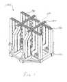
- FIG. 1schematically illustrates an isometric view of an exemplary assembled substrate-free, interconnected electronic mechanical structural system in accordance with the present invention
- FIG. 2schematically illustrates an exploded view of the assembled substrate-free, interconnected electronic mechanical structural system of FIG. 1 ;
- FIG. 3schematically illustrates isometric and front views of the first (horizontal) substrate-free, electronic mechanical subsystem of FIG. 1 ;
- FIG. 4schematically illustrates isometric and front views of the second (vertical) substrate-free, electronic mechanical subsystem of FIG. 1 ;
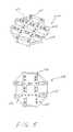
- FIG. 5schematically illustrates isometric and top views of the base plate of the substrate-free, interconnected electronic mechanical structural system of FIG. 1 ;
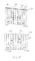
- FIG. 6Aschematically illustrates the top view of the assembled substrate-free, interconnected electronic mechanical structural system FIG. 1 ;
- FIG. 6Bschematically illustrates a cross-sectional view of the assembled substrate-free, interconnected electronic mechanical structural system of FIG. 6A taken along the sectioning line A-A;
- FIG. 7schematically illustrates an isometric cross-sectional view of the assembled substrate-free, interconnected electronic mechanical structural system of FIG. 6A taken along the sectioning line A-A;
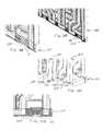
- FIG. 8schematically illustrates isometric and front cross-sectional views of an enlarged portion of the upper electronic mechanical structural system comprised of two interlocked subsystems, and also illustrates a justification spring for aligning the first and second substrate-free, electronic mechanical subsystems;
- FIG. 9schematically illustrates an isometric view of the assembled substrate-free, interconnected electronic mechanical structural system of FIG. 1 showing the location of the justification spring in the assembled system;
- FIG. 10schematically illustrates an enlarged view of the assembled substrate-free, interconnected electronic mechanical structural system of FIG. 9 showing the location of the justification spring in the assembled system;
- FIGS. 11A-11Dschematically illustrate isometric cross-sectional views ( FIGS. 11A, 11B ), an isometric view ( FIG. 11C ), and a front cross-sectional view ( FIG. 11D ) showing alignment pegs of the first and second substrate-free, electromechanical subsystems and corresponding mating holes of the base plate of FIG. 1 ;
- FIGS. 12A-12Cschematically illustrate isometric cross-sectional views ( FIGS. 12A, 12B ) and a front cross-sectional view ( FIG. 12C ) showing electrical and physical interconnection between coaxial waveguides of the first substrate-free electronic mechanical subsystem and coaxial waveguides of the base plate of FIG. 1 ;
- FIG. 13schematically illustrates an isometric view of a lower surface of the first substrate-free electronic mechanical subsystem, showing waveguide end portions at the lower surface for electrical and mechanical connection to the base plate of FIG. 1 ;
- FIG. 14schematically illustrates an isometric view of the upper surface of the base plate of FIG. 1 , showing waveguide end portions at the upper surface for electrical and mechanical connection to the first and second substrate-free electronic mechanical subsystems;
- FIG. 15Aschematically illustrates a cross-sectional front view of a portion of the first substrate-free electronic mechanical subsystem and base plate, showing mechanical and electrical interconnection between the respective waveguides thereof and cooperation between the mechanical mating features of the exemplary peg and hole;
- FIG. 15Bschematically illustrates isometric views of upper and lower surfaces of the second substrate-free electronic mechanical subsystem showing waveguide end portions at each of the upper and lower surfaces.
- FIGS. 1 and 2schematically illustrate isometric views of an exemplary substrate-free, interconnected electronic mechanical structural system 100 ( FIG. 1 ) in accordance with the present invention, in both assembled and exploded views, respectively.
- the interconnected electronic mechanical structural system 100may include first and second substrate-free, electronic subsystems 120 , 130 and a substrate-free, electronic base plate 110 each of which may include electronic components, such as coaxial waveguides 112 ( FIG. 2 ), 122 ( FIG. 1 ), 132 , ( FIG. 1 ) as well as mechanical connection features, such as complementary mating slots 126 , 136 , and mounting pegs 124 , 134 with complementary mounting holes 114 , for example, FIG.
- the mechanical connection featurese.g., slots 126 , 136 , pegs 124 , 134 , justification springs 128 and holes 114 , may be configured to permit the substrate-free, electronic subsystems 120 , 130 and base plate 110 to be reversibly or irreversibly pressfit together into a single interconnected structural system 100 FIG. 3 .
- the electronic componentse.g., coaxial waveguides 112 , 122 , 132
- the substrate-free, electronic subsystems 120 , 130 and base plate 110may be configured to include electronic components 112 , 122 , 132 that are operably and electrically interconnected upon assembly, which is aided and enabled by the mechanical connection features 114 , 124 , 126 , 134 , 136 .
- An enlarged view of the upper surface of the base plate 110 and coaxial waveguide 112 disposed thereinis shown in FIG. 14 .
- each subsystem 110 , 120 , 130may typically include monolithic features such as chip and SMT device mounting sockets or regions, phase controlled passive components such as hybrids, filters, baluns, couplers, combiners, and so forth.
- phase controlled passive componentssuch as hybrids, filters, baluns, couplers, combiners, and so forth.
- Antennas, beam forming networks, switching networks, and integrated inductors, capacitors, and resistorsmay be included.
- coaxial transmission lines 112 , 122 , 132could be substituted in part or entirely for regions hollow, ridge or co-planar waveguides, suspended DC bias and control lines, or suspended CPW, for example.
- Interconnected metal featuresmay be added for mechanical purposes or thermal transmission purposes, or both.
- the empty space between dielectrics and metalsmay typically be air, vacuum, a particular gas or fluid or liquid could fill the space.
- Alternative materials that allow a substitute for an air or vacuum dielectric to fill the spacesuch as a very low-k syntactic foam, as outlined in published US patent application publication number 2012/0067871, could alternatively fill part of the volume in a subsystem before or after the system assembly process, the contents of that application are incorporated herein by reference.
- the system 100could be submerged into a region of cold gas or liquid or have the gas or liquid flow through or around the mostly open 3D volume available to the system.
- subsystems 110 , 120 , 130may be rigid mechanically, it is possible that some subsystems could take advantage of the mechanical versatility of hinges, slides, pivots, turrets, gears, and flexures, for example, to allow the system to unfold from a folded position or adjust the position among or within the subsystems, for example, taking form after deployment. This may be advantageous for example if the system 100 needs to be launched into space in a compact form, and then have the system 100 self-position and adjust the electrical and mechanical relationships among and within the subsystems 110 , 120 , 130 that comprise the system once in space and reduced levels of acceleration and vibration are encountered. Such modularity may be equally important if repairs or reconfiguration after deployment is needed.
- FIG. 3schematically illustrates an isometric in front view of a first substrate-free, electronic subsystem 120 in accordance with the present invention.
- the substrate-free, electronic subsystem 120may include a plurality of rectangular coaxial waveguides 122 that may extend from a first end to a second end of the first subsystem 120 .
- a second substrate-free, electronic subsystem 130may include a plurality of rectangular coaxial waveguides 132 that may extend from a first end to a second end of the subsystem 130 , FIG. 4 . Since the first and second subsystems 120 , 130 are substrate-free, added structural support may be desired it may be provided by ribs or struts 121 ( FIG. 3 ), 131 ( FIG. 4 ) or other suitable structures.
- the coaxial waveguides 132may include end portions at respective opposing and faces of the first and second subsystems 130 , FIGS. 13, 15B , that are structured to permit coupling, e.g. butt coupling or end coupling, to other subsystem components such as electronic components of the substrate-free, electronic base plate 110 ( FIG. 15A ).
- the base plate 110may include a plurality of coaxial waveguides 112 ( FIG. 15A ) or waveguide coupling terminations 113 ( FIGS. 12A-12C ) for electrical and mechanical connection to the waveguides 122 , 132 of the first and second subsystems 120 , 130 , respectively, FIGS. 2, 5, 7, 14 .
- a first waveguide 132 of the first substrate-free, electronic subsystem 130may be butt coupled to a respective waveguide 112 of the base plate 110 , FIGS. 6A, 6B .
- the waveguide 112 of the base plate 110may extend along the base plate 110 to terminate at a second location in electrical and mechanical communication with a second waveguide 132 b of the second substrate-free, electronic subsystem 130 to electrically couple first and second waveguides 132 a , 132 b , FIGS. 6A, 7 .
- the substrate-free, electronic base plate 110may include waveguide coupling terminations 113 ( FIG. 6B ) to electrically connect two or more adjacent coaxial waveguides 132 c , 132 d , FIGS.
- the waveguide coupling termination 113may include a center conductor coupler 113 a to electrically couple the respective center conductors of the adjacent coaxial waveguides 132 c , 132 d , FIGS. 7, 12C .
- the waveguide coupling termination 113may include outer conductor (ground plane) couplers 113 b , 113 c ( FIG. 12C ) to electrically couple the respective outer conductors of the coaxial waveguides 132 c , 132 d ( FIG. 12C ).
- Sufficient control of the mechanical tolerancing that determines the relative placement and interconnection of the electronic components of the subsystems 120 , 130 and base plate 110may be provided by one or more mechanical features.
- complementary mating slots 126FIG. 3
- 136FIG. 4
- Respective slots 126 , 136 of the first and second subsystems 120 , 130may be inserted into one another to effect mechanical alignment and joining of the first and second subsystems 120 , 130 , FIGS. 2-4 .
- FIGS. 6B and 7schematically illustrate a cross-sectional view taken along an array of coaxial waveguides 132 of the second substrate-free, electronic subsystem 130 , and show cutaway portions of the first substrate-free, electronic subsystem 120 disposed in slots of the second subsystem 130 . Enlarged portions of FIGS. 6B and 7 are shown in FIG. 8 to better illustrate how the first substrate-free, electronic subsystem 120 may be disposed within a slot 136 of the second substrate-free, electronic subsystem 130 .
- the width of the slot 136may be wider than the width of the first subsystem 120 .
- the width of the slot 136may be wider than that permitted by the tolerances required to align the coaxial waveguides 122 , 132 of the first and second subsystems 120 , 130 and base plate 110 .
- lateral alignment tolerancesmay be maintained even though the slot 136 is wider than the first subsystem 120 , by providing a justification spring 138 ( FIGS. 3,4 ) that controls the location of the first substrate-free, electronic subsystem 120 within the slot 136 of the second substrate-free, electronic subsystem, FIGS. 8-10 .
- justification spring 138is shown in the form of a cylindrical bump-out, other suitable structures may be used such as a strap, beam, leaf spring, or cantilever to justify the first subsystem 120 against the opposing wall of the slot 136 of the second subsystem 130 .
- the first and second substrate-free, electronic subsystems 120 , 130may include a number of mechanical mounting features to permit mechanical interconnection with the base plate 110 .
- alignment pegs 124 ( FIG. 3 ), 134 ( FIG. 4 ) of the first and second substrate-free, electronic subsystems 120 , 130may be provided and may be clearance fit or pressfit into corresponding holes 114 of the base plate 110 , FIGS. 11A-11D .
- the slots 126 , 136 , holes 114 , and/or mounting pegs 124 , 134may include mounting ridges 117 ( FIG. 6B ), 137 ( FIG. 15B ), 237 ( FIG. 15B ) to further constrain the alignment between slots 126 , 136 to one another and/or mounting pegs 124 , 134 to holes 114 , FIGS. 15A, 15B .
- FIG. 15A, 15BFIG.
- FIG. 15Aschematically illustrates a cross-sectional front view of a portion of the first substrate-free electronic mechanical subsystem 130 and base plate 110 , showing mechanical and electrical interconnection between the respective waveguides 132 thereof.
- FIG. 15Bschematically illustrates isometric views of the second substrate-free electronic mechanical subsystem 130 showing end portions of waveguide 132 .
- One or more of the first and second substrate-free, electronic subsystems 120 , 130 and substrate-free, electronic base plate 110may be created by a suitable build layer manufacturing process, such as the PolyStrata® process of Nuvotronics, LLC as detailed above in the listed and incorporated US Patents.
- the present exemplary subsystems 110 , 120 , 130 and system 100 shownwere chosen to demonstrate not some higher level system end purpose or particular function, other than to display how such substrate free electro-mechanical additive build structures made by a micro or meso-scale fabrication process can be designed to be sufficiently durable.
- the exemplary structurescan serve as not only “board-less” circuit boards, but more so, they can have at least their mechanical, thermal, and electrical functions co-designed and modeled in such a way that durable systems can be assembled and formed from the subsystems joined both in plane and out their plane of fabrication. By eliminating excess material, they can truly be optimized for size, weight, performance, and power.
- a three dimensional volumemay be optimally filled allowing both form and function to cast off many of the usual shackles stemming from the traditional manufacturing method limitations that usually faced in their design and production. Accordingly, these and other advantages of the present invention will be apparent to those skilled in the art from the foregoing specification. Accordingly, it will be recognized by those skilled in the art that changes or modifications may be made to the above-described embodiments without departing from the broad inventive concepts of the invention. It should therefore be understood that this invention is not limited to the particular embodiments described herein, but is intended to include all changes and modifications that are within the scope and spirit of the invention as set forth in the claims.
Landscapes
- Engineering & Computer Science (AREA)
- Microelectronics & Electronic Packaging (AREA)
- Combinations Of Printed Boards (AREA)
- Manufacturing & Machinery (AREA)
Abstract
Description
Claims (13)
Priority Applications (4)
| Application Number | Priority Date | Filing Date | Title |
|---|---|---|---|
| US14/211,407US9306254B1 (en) | 2013-03-15 | 2014-03-14 | Substrate-free mechanical interconnection of electronic sub-systems using a spring configuration |
| US15/069,325US9888600B2 (en) | 2013-03-15 | 2016-03-14 | Substrate-free interconnected electronic mechanical structural systems |
| US15/854,917US10257951B2 (en) | 2013-03-15 | 2017-12-27 | Substrate-free interconnected electronic mechanical structural systems |
| US16/367,472US20200022277A1 (en) | 2013-03-15 | 2019-03-28 | Substrate-free interconnected electronic mechanical structural systems |
Applications Claiming Priority (2)
| Application Number | Priority Date | Filing Date | Title |
|---|---|---|---|
| US201361788675P | 2013-03-15 | 2013-03-15 | |
| US14/211,407US9306254B1 (en) | 2013-03-15 | 2014-03-14 | Substrate-free mechanical interconnection of electronic sub-systems using a spring configuration |
Related Child Applications (1)
| Application Number | Title | Priority Date | Filing Date |
|---|---|---|---|
| US15/069,325ContinuationUS9888600B2 (en) | 2013-03-15 | 2016-03-14 | Substrate-free interconnected electronic mechanical structural systems |
Publications (1)
| Publication Number | Publication Date |
|---|---|
| US9306254B1true US9306254B1 (en) | 2016-04-05 |
Family
ID=55589104
Family Applications (4)
| Application Number | Title | Priority Date | Filing Date |
|---|---|---|---|
| US14/211,407ActiveUS9306254B1 (en) | 2013-03-15 | 2014-03-14 | Substrate-free mechanical interconnection of electronic sub-systems using a spring configuration |
| US15/069,325Expired - Fee RelatedUS9888600B2 (en) | 2013-03-15 | 2016-03-14 | Substrate-free interconnected electronic mechanical structural systems |
| US15/854,917Expired - Fee RelatedUS10257951B2 (en) | 2013-03-15 | 2017-12-27 | Substrate-free interconnected electronic mechanical structural systems |
| US16/367,472AbandonedUS20200022277A1 (en) | 2013-03-15 | 2019-03-28 | Substrate-free interconnected electronic mechanical structural systems |
Family Applications After (3)
| Application Number | Title | Priority Date | Filing Date |
|---|---|---|---|
| US15/069,325Expired - Fee RelatedUS9888600B2 (en) | 2013-03-15 | 2016-03-14 | Substrate-free interconnected electronic mechanical structural systems |
| US15/854,917Expired - Fee RelatedUS10257951B2 (en) | 2013-03-15 | 2017-12-27 | Substrate-free interconnected electronic mechanical structural systems |
| US16/367,472AbandonedUS20200022277A1 (en) | 2013-03-15 | 2019-03-28 | Substrate-free interconnected electronic mechanical structural systems |
Country Status (1)
| Country | Link |
|---|---|
| US (4) | US9306254B1 (en) |
Cited By (21)
| Publication number | Priority date | Publication date | Assignee | Title |
|---|---|---|---|---|
| US20160341790A1 (en)* | 2014-01-17 | 2016-11-24 | Nuvotronics, Inc. | Wafer scale test interfact unit: low loss and high isolation devices and methods for high speed and high density mixed signal interconnects and contactors |
| US9888600B2 (en)* | 2013-03-15 | 2018-02-06 | Nuvotronics, Inc | Substrate-free interconnected electronic mechanical structural systems |
| US20180097271A1 (en)* | 2016-10-04 | 2018-04-05 | The Boeing Company | Simplification of Complex Waveguide Networks |
| US9993982B2 (en) | 2011-07-13 | 2018-06-12 | Nuvotronics, Inc. | Methods of fabricating electronic and mechanical structures |
| US10074885B2 (en) | 2003-03-04 | 2018-09-11 | Nuvotronics, Inc | Coaxial waveguide microstructures having conductors formed by plural conductive layers |
| US10076042B2 (en) | 2011-06-05 | 2018-09-11 | Nuvotronics, Inc | Devices and methods for solder flow control in three-dimensional microstructures |
| US10135109B2 (en) | 2007-03-20 | 2018-11-20 | Nuvotronics, Inc | Method of forming a coaxial line microstructure having an enlarged region on a substrate and removing the coaxial line microstructure from the substrate for mounting on a mounting substrate |
| US10193203B2 (en) | 2013-03-15 | 2019-01-29 | Nuvotronics, Inc | Structures and methods for interconnects and associated alignment and assembly mechanisms for and between chips, components, and 3D systems |
| US20190036193A1 (en)* | 2017-07-31 | 2019-01-31 | Space Systems/Loral, Llc | Additive manufactured rf module |
| US10256545B2 (en) | 2013-12-11 | 2019-04-09 | Nuvotronics, Inc | Dielectric-free metal-only dipole-coupled radiating array aperture with wide field of view |
| US10319654B1 (en) | 2017-12-01 | 2019-06-11 | Cubic Corporation | Integrated chip scale packages |
| US10431521B2 (en) | 2007-03-20 | 2019-10-01 | Cubic Corporation | Integrated electronic components and methods of formation thereof |
| JP2019527989A (en)* | 2016-08-10 | 2019-10-03 | エアバス ディフェンス アンド スペイス リミテッド | Waveguide assembly and manufacturing method thereof |
| US10497511B2 (en) | 2009-11-23 | 2019-12-03 | Cubic Corporation | Multilayer build processes and devices thereof |
| US10511073B2 (en) | 2014-12-03 | 2019-12-17 | Cubic Corporation | Systems and methods for manufacturing stacked circuits and transmission lines |
| US10847469B2 (en) | 2016-04-26 | 2020-11-24 | Cubic Corporation | CTE compensation for wafer-level and chip-scale packages and assemblies |
| US11014303B1 (en) | 2017-06-21 | 2021-05-25 | Space Systems/Loral, Llc | Additive manufacturing on-orbit |
| US11196184B2 (en) | 2017-06-20 | 2021-12-07 | Cubic Corporation | Broadband antenna array |
| US11342683B2 (en) | 2018-04-25 | 2022-05-24 | Cubic Corporation | Microwave/millimeter-wave waveguide to circuit board connector |
| US11367948B2 (en) | 2019-09-09 | 2022-06-21 | Cubic Corporation | Multi-element antenna conformed to a conical surface |
| US11858665B1 (en) | 2019-03-12 | 2024-01-02 | Maxar Space Llc | Deployment mechanism with integral actuation device |
Families Citing this family (1)
| Publication number | Priority date | Publication date | Assignee | Title |
|---|---|---|---|---|
| US11890676B2 (en)* | 2021-02-15 | 2024-02-06 | Raytheon Missiles & Defense (RMD) | Waveguide fence support |
Citations (184)
| Publication number | Priority date | Publication date | Assignee | Title |
|---|---|---|---|---|
| US2743505A (en) | 1950-04-18 | 1956-05-01 | Int Standard Electric Corp | Joints for coaxial cable |
| US2812501A (en) | 1954-03-04 | 1957-11-05 | Sanders Associates Inc | Transmission line |
| US2914766A (en) | 1955-06-06 | 1959-11-24 | Sanders Associates Inc | Three conductor planar antenna |
| US2997519A (en) | 1959-10-08 | 1961-08-22 | Bell Telephone Labor Inc | Multicoaxial line cables |
| US3309632A (en) | 1965-04-13 | 1967-03-14 | Kollmorgen Corp | Microwave contactless coaxial connector |
| US3311966A (en) | 1962-09-24 | 1967-04-04 | North American Aviation Inc | Method of fabricating multilayer printed-wiring boards |
| US3335489A (en) | 1962-09-24 | 1967-08-15 | North American Aviation Inc | Interconnecting circuits with a gallium and indium eutectic |
| US3352730A (en) | 1964-08-24 | 1967-11-14 | Sanders Associates Inc | Method of making multilayer circuit boards |
| US3464855A (en) | 1966-09-06 | 1969-09-02 | North American Rockwell | Process for forming interconnections in a multilayer circuit board |
| US3537043A (en)* | 1968-08-06 | 1970-10-27 | Us Air Force | Lightweight microwave components and wave guides |
| US3560896A (en) | 1967-07-06 | 1971-02-02 | Telefunken Patent | Inner conductor support for shielded microwave strip lines |
| US3577105A (en)* | 1969-05-29 | 1971-05-04 | Us Army | Method and apparatus for joining plated dielectric-form waveguide components |
| US3598107A (en) | 1968-07-25 | 1971-08-10 | Hamamatsu T V Co Ltd | Pupillary motion observing apparatus |
| FR2086327A1 (en) | 1970-04-24 | 1971-12-31 | Spinner Gmbh Elektrotech | |
| US3775844A (en) | 1970-06-25 | 1973-12-04 | Bunker Ramo | Method of fabricating a multiwafer electrical circuit structure |
| US3789129A (en) | 1972-06-06 | 1974-01-29 | Felten & Guilleaume Ag | Air-insulated coaxial high-frequency cable |
| US3791858A (en) | 1971-12-13 | 1974-02-12 | Ibm | Method of forming multi-layer circuit panels |
| US3884549A (en) | 1973-04-30 | 1975-05-20 | Univ California | Two demensional distributed feedback devices and lasers |
| US3963999A (en) | 1975-05-29 | 1976-06-15 | The Furukawa Electric Co., Ltd. | Ultra-high-frequency leaky coaxial cable |
| US4021789A (en) | 1975-09-29 | 1977-05-03 | International Business Machines Corporation | Self-aligned integrated circuits |
| US4033656A (en) | 1975-09-02 | 1977-07-05 | Zero Manufacturing Company | Low profile integrated circuit socket |
| US4075757A (en) | 1975-12-17 | 1978-02-28 | Perstorp Ab | Process in the production of a multilayer printed board |
| US4275944A (en) | 1979-07-09 | 1981-06-30 | Sochor Jerzy R | Miniature connector receptacles employing contacts with bowed tines and parallel mounting arms |
| US4348253A (en) | 1981-11-12 | 1982-09-07 | Rca Corporation | Method for fabricating via holes in a semiconductor wafer |
| US4365222A (en) | 1981-04-06 | 1982-12-21 | Bell Telephone Laboratories, Incorporated | Stripline support assembly |
| US4414424A (en) | 1980-10-20 | 1983-11-08 | Tokyo Shibaura Denki Kabushiki Kaisha | Gas-insulated bus bar |
| US4417393A (en) | 1981-04-01 | 1983-11-29 | General Electric Company | Method of fabricating high density electronic circuits having very narrow conductors |
| US4437074A (en) | 1980-12-18 | 1984-03-13 | Thomson-Csf | Ultrahigh-frequency transmission line of the three-plate air type and uses thereof |
| US4521755A (en) | 1982-06-14 | 1985-06-04 | At&T Bell Laboratories | Symmetrical low-loss suspended substrate stripline |
| US4581301A (en) | 1984-04-10 | 1986-04-08 | Michaelson Henry W | Additive adhesive based process for the manufacture of printed circuit boards |
| US4591411A (en) | 1982-05-05 | 1986-05-27 | Hughes Aircraft Company | Method for forming a high density printed wiring board |
| US4641140A (en) | 1983-09-26 | 1987-02-03 | Harris Corporation | Miniaturized microwave transmission link |
| US4663497A (en) | 1982-05-05 | 1987-05-05 | Hughes Aircraft Company | High density printed wiring board |
| US4673904A (en) | 1984-11-14 | 1987-06-16 | Itt Corporation | Micro-coaxial substrate |
| US4700159A (en) | 1985-03-29 | 1987-10-13 | Weinschel Engineering Co., Inc. | Support structure for coaxial transmission line using spaced dielectric balls |
| US4717064A (en) | 1986-08-15 | 1988-01-05 | Unisys Corporation | Wave solder finger shield apparatus |
| DE3623093A1 (en) | 1986-07-09 | 1988-01-21 | Standard Elektrik Lorenz Ag | Method for producing through-connections in printed circuit boards or multilayer printed circuit boards having inorganic or organic/inorganic insulating layers |
| US4771294A (en) | 1986-09-10 | 1988-09-13 | Harris Corporation | Modular interface for monolithic millimeter wave antenna array |
| US4808273A (en) | 1988-05-10 | 1989-02-28 | Avantek, Inc. | Method of forming completely metallized via holes in semiconductors |
| US4832461A (en) | 1986-08-20 | 1989-05-23 | Fujitsu Limited | Projection-type multi-color liquid crystal display device |
| US4853656A (en) | 1987-08-03 | 1989-08-01 | Aerospatiale Societe Nationale Industrielle | Device for connecting together two ultra-high frequency structures which are coaxial and of different diameters |
| US4857418A (en) | 1986-12-08 | 1989-08-15 | Honeywell Inc. | Resistive overlayer for magnetic films |
| US4856184A (en) | 1988-06-06 | 1989-08-15 | Tektronix, Inc. | Method of fabricating a circuit board |
| US4876322A (en) | 1984-08-10 | 1989-10-24 | Siemens Aktiengesselschaft | Irradiation cross-linkable thermostable polymer system, for microelectronic applications |
| US4880684A (en) | 1988-03-11 | 1989-11-14 | International Business Machines Corporation | Sealing and stress relief layers and use thereof |
| JPH027587A (en) | 1988-06-27 | 1990-01-11 | Yokogawa Electric Corp | Variable frequency light source |
| US4969979A (en) | 1989-05-08 | 1990-11-13 | International Business Machines Corporation | Direct electroplating of through holes |
| US4975142A (en) | 1989-11-07 | 1990-12-04 | General Electric Company | Fabrication method for printed circuit board |
| US5069749A (en) | 1986-07-29 | 1991-12-03 | Digital Equipment Corporation | Method of fabricating interconnect layers on an integrated circuit chip using seed-grown conductors |
| US5072201A (en) | 1988-12-06 | 1991-12-10 | Thomson-Csf | Support for microwave transmission line, notably of the symmetrical strip line type |
| JPH041710A (en) | 1990-04-19 | 1992-01-07 | Matsushita Electric Ind Co Ltd | Lens adjusting device |
| US5100501A (en) | 1989-06-30 | 1992-03-31 | Texas Instruments Incorporated | Process for selectively depositing a metal in vias and contacts by using a sacrificial layer |
| CA2055116A1 (en) | 1990-11-13 | 1992-05-14 | Jurg Buhler | Automatic analysis apparatus |
| US5119049A (en) | 1991-04-12 | 1992-06-02 | Ail Systems, Inc. | Ultraminiature low loss coaxial delay line |
| US5191699A (en) | 1990-09-04 | 1993-03-09 | Gw-Elektronik Gmbh | Methods of producing a chip-type HF magnetic coil arrangement |
| US5227013A (en) | 1991-07-25 | 1993-07-13 | Microelectronics And Computer Technology Corporation | Forming via holes in a multilevel substrate in a single step |
| US5235208A (en) | 1991-02-07 | 1993-08-10 | Mitsubishi Denki Kabushiki Kaisha | Package for microwave integrated circuit |
| US5274484A (en) | 1991-04-12 | 1993-12-28 | Fujitsu Limited | Gradation methods for driving phase transition liquid crystal using a holding signal |
| JPH0685510A (en) | 1992-03-31 | 1994-03-25 | Yokogawa Electric Corp | Multi-chip module |
| US5334956A (en) | 1992-03-30 | 1994-08-02 | Motorola, Inc. | Coaxial cable having an impedance matched terminating end |
| JPH06302964A (en) | 1993-04-16 | 1994-10-28 | Oki Electric Ind Co Ltd | Circuit board for high-speed signal transmission |
| US5381157A (en) | 1991-05-02 | 1995-01-10 | Sumitomo Electric Industries, Ltd. | Monolithic microwave integrated circuit receiving device having a space between antenna element and substrate |
| US5406235A (en) | 1990-12-26 | 1995-04-11 | Tdk Corporation | High frequency device |
| US5430257A (en) | 1992-08-12 | 1995-07-04 | Trw Inc. | Low stress waveguide window/feedthrough assembly |
| US5454161A (en) | 1993-04-29 | 1995-10-03 | Fujitsu Limited | Through hole interconnect substrate fabrication process |
| GB2265754B (en) | 1992-03-30 | 1995-10-25 | Awa Microelectronics | Silicon transducer |
| US5622895A (en) | 1994-05-09 | 1997-04-22 | Lucent Technologies Inc. | Metallization for polymer-dielectric multichip modules |
| US5633615A (en) | 1995-12-26 | 1997-05-27 | Hughes Electronics | Vertical right angle solderless interconnects from suspended stripline to three-wire lines on MIC substrates |
| US5682062A (en) | 1995-06-05 | 1997-10-28 | Harris Corporation | System for interconnecting stacked integrated circuits |
| US5682124A (en) | 1993-02-02 | 1997-10-28 | Ast Research, Inc. | Technique for increasing the range of impedances for circuit board transmission lines |
| US5712607A (en) | 1996-04-12 | 1998-01-27 | Dittmer; Timothy W. | Air-dielectric stripline |
| US5724012A (en) | 1994-02-03 | 1998-03-03 | Hollandse Signaalapparaten B.V. | Transmission-line network |
| US5746868A (en) | 1994-07-21 | 1998-05-05 | Fujitsu Limited | Method of manufacturing multilayer circuit substrate |
| EP0845831A2 (en) | 1996-11-28 | 1998-06-03 | Matsushita Electric Industrial Co., Ltd. | A millimeter waveguide and a circuit apparatus using the same |
| US5793272A (en) | 1996-08-23 | 1998-08-11 | International Business Machines Corporation | Integrated circuit toroidal inductor |
| US5814889A (en) | 1995-06-05 | 1998-09-29 | Harris Corporation | Intergrated circuit with coaxial isolation and method |
| US5860812A (en) | 1997-01-23 | 1999-01-19 | Litton Systems, Inc. | One piece molded RF/microwave coaxial connector |
| US5872399A (en) | 1996-04-01 | 1999-02-16 | Anam Semiconductor, Inc. | Solder ball land metal structure of ball grid semiconductor package |
| EP0911903A2 (en) | 1997-10-22 | 1999-04-28 | Nokia Mobile Phones Ltd. | Coaxcial cable, method for manufacturing a coaxial cable, and wireless communication device |
| US5925206A (en) | 1997-04-21 | 1999-07-20 | International Business Machines Corporation | Practical method to make blind vias in circuit boards and other substrates |
| US5961347A (en) | 1996-09-26 | 1999-10-05 | Hon Hai Precision Ind. Co., Ltd. | Micro connector |
| US5977842A (en) | 1998-07-01 | 1999-11-02 | Raytheon Company | High power broadband coaxial balun |
| US6008102A (en) | 1998-04-09 | 1999-12-28 | Motorola, Inc. | Method of forming a three-dimensional integrated inductor |
| WO2000007218A2 (en) | 1998-07-28 | 2000-02-10 | Korea Advanced Institute Of Science And Technology | Method for manufacturing a semiconductor device having a metal layer floating over a substrate |
| US6027630A (en) | 1997-04-04 | 2000-02-22 | University Of Southern California | Method for electrochemical fabrication |
| JP3027587B2 (en) | 1989-11-07 | 2000-04-04 | 株式会社リコー | Facsimile machine |
| US6054252A (en) | 1998-12-11 | 2000-04-25 | Morton International, Inc. | Photoimageable compositions having improved chemical resistance and stripping ability |
| WO2000039854A1 (en) | 1998-12-28 | 2000-07-06 | Telephus, Inc. | Coaxial type signal line and manufacturing method thereof |
| US6180261B1 (en) | 1997-10-21 | 2001-01-30 | Nitto Denko Corporation | Low thermal expansion circuit board and multilayer wiring circuit board |
| US6207901B1 (en)* | 1999-04-01 | 2001-03-27 | Trw Inc. | Low loss thermal block RF cable and method for forming RF cable |
| US6210221B1 (en) | 1999-10-13 | 2001-04-03 | Maury Microwave, Inc. | Microwave quick connect/disconnect coaxial connectors |
| US6228466B1 (en) | 1997-04-11 | 2001-05-08 | Ibiden Co. Ltd. | Printed wiring board and method for manufacturing the same |
| US6294965B1 (en) | 1999-03-11 | 2001-09-25 | Anaren Microwave, Inc. | Stripline balun |
| US6329605B1 (en) | 1998-03-26 | 2001-12-11 | Tessera, Inc. | Components with conductive solder mask layers |
| WO2002006152A2 (en) | 2000-07-14 | 2002-01-24 | Zyvex Corporation | System and method for constraining totally released microcomponents |
| US6350633B1 (en) | 2000-08-22 | 2002-02-26 | Charles W. C. Lin | Semiconductor chip assembly with simultaneously electroplated contact terminal and connection joint |
| US6388198B1 (en) | 1999-03-09 | 2002-05-14 | International Business Machines Corporation | Coaxial wiring within SOI semiconductor, PCB to system for high speed operation and signal quality |
| US6457979B1 (en) | 2001-10-29 | 2002-10-01 | Agilent Technologies, Inc. | Shielded attachment of coaxial RF connector to thick film integrally shielded transmission line on a substrate |
| WO2002080279A1 (en) | 2001-03-29 | 2002-10-10 | Korea Advanced Institute Of Science And Technology | Three-dimensional metal devices highly suspended above semiconductor substrate, their circuit model, and method for manufacturing the same |
| US6465747B2 (en) | 1998-03-25 | 2002-10-15 | Tessera, Inc. | Microelectronic assemblies having solder-wettable pads and conductive elements |
| US6514845B1 (en) | 1998-10-15 | 2003-02-04 | Texas Instruments Incorporated | Solder ball contact and method |
| US20030029729A1 (en) | 2001-08-10 | 2003-02-13 | Jao-Chin Cheng | Method of fabricating inter-layer solid conductive rods |
| US6535088B1 (en) | 2000-04-13 | 2003-03-18 | Raytheon Company | Suspended transmission line and method |
| US20030052755A1 (en) | 2002-10-10 | 2003-03-20 | Barnes Heidi L. | Shielded surface mount coaxial connector |
| US20030117237A1 (en) | 2001-12-20 | 2003-06-26 | Feng Niu | Reduced size, low loss MEMS torsional hinges and MEMS resonators employing such hinges |
| US6589594B1 (en) | 2000-08-31 | 2003-07-08 | Micron Technology, Inc. | Method for filling a wafer through-via with a conductive material |
| US6600395B1 (en) | 2000-12-28 | 2003-07-29 | Nortel Networks Limited | Embedded shielded stripline (ESS) structure using air channels within the ESS structure |
| US6603376B1 (en) | 2000-12-28 | 2003-08-05 | Nortel Networks Limited | Suspended stripline structures to reduce skin effect and dielectric loss to provide low loss transmission of signals with high data rates or high frequencies |
| US6648653B2 (en) | 2002-01-04 | 2003-11-18 | Insert Enterprise Co., Ltd. | Super mini coaxial microwave connector |
| US20030222738A1 (en) | 2001-12-03 | 2003-12-04 | Memgen Corporation | Miniature RF and microwave components and methods for fabricating such components |
| US20030221968A1 (en) | 2002-03-13 | 2003-12-04 | Memgen Corporation | Electrochemical fabrication method and apparatus for producing three-dimensional structures having improved surface finish |
| US6662443B2 (en) | 1999-03-24 | 2003-12-16 | Fujitsu Limited | Method of fabricating a substrate with a via connection |
| US20040000701A1 (en) | 2002-06-26 | 2004-01-01 | White George E. | Stand-alone organic-based passive devices |
| US20040004061A1 (en) | 2002-07-03 | 2004-01-08 | Merdan Kenneth M. | Tubular cutting process and system |
| WO2004004061A1 (en) | 2002-06-27 | 2004-01-08 | Memgen Corporation | Miniature rf and microwave components and methods for fabricating such components |
| US20040007470A1 (en) | 2002-05-07 | 2004-01-15 | Memgen Corporation | Methods of and apparatus for electrochemically fabricating structures via interlaced layers or via selective etching and filling of voids |
| US20040007468A1 (en) | 2002-05-07 | 2004-01-15 | Memgen Corporation | Multistep release method for electrochemically fabricated structures |
| US20040038586A1 (en) | 2002-08-22 | 2004-02-26 | Hall Richard D. | High frequency, blind mate, coaxial interconnect |
| US20040076806A1 (en) | 2001-02-08 | 2004-04-22 | Michimasa Miyanaga | Porous ceramics and method for preparation thereof, and microstrip substrate |
| US6735009B2 (en) | 2002-07-16 | 2004-05-11 | Motorola, Inc. | Electroptic device |
| US6746891B2 (en) | 2001-11-09 | 2004-06-08 | Turnstone Systems, Inc. | Trilayered beam MEMS device and related methods |
| US20040124961A1 (en) | 2002-12-16 | 2004-07-01 | Alps Electric Co., Ltd. | Printed inductor capable of raising Q value |
| US6800555B2 (en) | 2000-03-24 | 2004-10-05 | Texas Instruments Incorporated | Wire bonding process for copper-metallized integrated circuits |
| US20040196112A1 (en) | 2003-04-02 | 2004-10-07 | Sun Microsystems, Inc. | Circuit board including isolated signal transmission channels |
| US20040263290A1 (en) | 2003-03-04 | 2004-12-30 | Rohm And Haas Electronic Materials, L.L.C. | Coaxial waveguide microstructures and methods of formation thereof |
| US20050030124A1 (en) | 2003-06-30 | 2005-02-10 | Okamoto Douglas Seiji | Transmission line transition |
| US20050045484A1 (en) | 2003-05-07 | 2005-03-03 | Microfabrica Inc. | Electrochemical fabrication process using directly patterned masks |
| US6888427B2 (en) | 2003-01-13 | 2005-05-03 | Xandex, Inc. | Flex-circuit-based high speed transmission line |
| US6914513B1 (en) | 2001-11-08 | 2005-07-05 | Electro-Science Laboratories, Inc. | Materials system for low cost, non wire-wound, miniature, multilayer magnetic circuit components |
| US20050156693A1 (en) | 2004-01-20 | 2005-07-21 | Dove Lewis R. | Quasi-coax transmission lines |
| US20050230145A1 (en) | 2002-08-06 | 2005-10-20 | Toku Ishii | Thin-diameter coaxial cable and method of producing the same |
| US20050250253A1 (en) | 2002-10-23 | 2005-11-10 | Cheung Kin P | Processes for hermetically packaging wafer level microscopic structures |
| TWI244799B (en) | 2003-06-06 | 2005-12-01 | Microfabrica Inc | Miniature RF and microwave components and methods for fabricating such components |
| US6971913B1 (en) | 2004-07-01 | 2005-12-06 | Speed Tech Corp. | Micro coaxial connector |
| US6975267B2 (en) | 2003-02-05 | 2005-12-13 | Northrop Grumman Corporation | Low profile active electronically scanned antenna (AESA) for Ka-band radar systems |
| US6981414B2 (en) | 2001-06-19 | 2006-01-03 | Honeywell International Inc. | Coupled micromachined structure |
| US7005750B2 (en) | 2003-08-01 | 2006-02-28 | Advanced Semiconductor Engineering, Inc. | Substrate with reinforced contact pad structure |
| JP2006067621A (en) | 2005-10-19 | 2006-03-09 | Nec Corp | Electronic device |
| US7030712B2 (en) | 2004-03-01 | 2006-04-18 | Belair Networks Inc. | Radio frequency (RF) circuit board topology |
| US7064449B2 (en) | 2004-07-06 | 2006-06-20 | Himax Technologies, Inc. | Bonding pad and chip structure |
| US7077697B2 (en) | 2004-09-09 | 2006-07-18 | Corning Gilbert Inc. | Snap-in float-mount electrical connector |
| US7084722B2 (en) | 2004-07-22 | 2006-08-01 | Northrop Grumman Corp. | Switched filterbank and method of making the same |
| USD530674S1 (en) | 2005-08-11 | 2006-10-24 | Hon Hai Precision Ind. Co., Ltd. | Micro coaxial connector |
| US7129163B2 (en) | 2003-09-15 | 2006-10-31 | Rohm And Haas Electronic Materials Llc | Device package and method for the fabrication and testing thereof |
| US7148722B1 (en) | 1997-02-20 | 2006-12-12 | Altera Corporation | PCI-compatible programmable logic devices |
| US7148141B2 (en) | 2003-12-17 | 2006-12-12 | Samsung Electronics Co., Ltd. | Method for manufacturing metal structure having different heights |
| US7165974B2 (en) | 2004-10-14 | 2007-01-23 | Corning Gilbert Inc. | Multiple-position push-on electrical connector |
| US7217156B2 (en) | 2005-01-19 | 2007-05-15 | Insert Enterprise Co., Ltd. | RF microwave connector for telecommunication |
| US7222420B2 (en) | 2000-07-27 | 2007-05-29 | Fujitsu Limited | Method for making a front and back conductive substrate |
| US7239219B2 (en) | 2001-12-03 | 2007-07-03 | Microfabrica Inc. | Miniature RF and microwave components and methods for fabricating such components |
| US7400222B2 (en) | 2003-09-15 | 2008-07-15 | Korea Advanced Institute Of Science & Technology | Grooved coaxial-type transmission line, manufacturing method and packaging method thereof |
| US20080191817A1 (en) | 2006-12-30 | 2008-08-14 | Rohm And Haas Electronic Materials Llc | Three-dimensional microstructures and methods of formation thereof |
| US20080197946A1 (en) | 2006-12-30 | 2008-08-21 | Rohm And Haas Electronic Materials Llc | Three-dimensional microstructures and methods of formation thereof |
| US20080199656A1 (en) | 2006-12-30 | 2008-08-21 | Rohm And Haas Electronic Materials Llc | Three-dimensional microstructures and methods of formation thereof |
| US20080240656A1 (en) | 2007-03-20 | 2008-10-02 | Rohm And Haas Electronic Materials Llc | Integrated electronic components and methods of formation thereof |
| US7478475B2 (en) | 2004-06-14 | 2009-01-20 | Corning Gilbert Inc. | Method of assembling coaxial connector |
| US20090051476A1 (en) | 2006-01-31 | 2009-02-26 | Hitachi Metals, Ltd. | Laminate device and module comprising same |
| US7532163B2 (en) | 2007-02-13 | 2009-05-12 | Raytheon Company | Conformal electronically scanned phased array antenna and communication system for helmets and other platforms |
| US20090154972A1 (en) | 2007-12-13 | 2009-06-18 | Fuji Xerox Co., Ltd. | Collected developer conveying device and image forming apparatus |
| US7555309B2 (en) | 2005-04-15 | 2009-06-30 | Evertz Microsystems Ltd. | Radio frequency router |
| US7575474B1 (en) | 2008-06-10 | 2009-08-18 | Harris Corporation | Surface mount right angle connector including strain relief and associated methods |
| US7602059B2 (en) | 2005-10-18 | 2009-10-13 | Nec Systems Technologies, Ltd. | Lead pin, circuit, semiconductor device, and method of forming lead pin |
| US7619441B1 (en) | 2008-03-03 | 2009-11-17 | Xilinx, Inc. | Apparatus for interconnecting stacked dice on a programmable integrated circuit |
| US7645940B2 (en) | 2004-02-06 | 2010-01-12 | Solectron Corporation | Substrate with via and pad structures |
| US20100007016A1 (en) | 2008-07-14 | 2010-01-14 | Infineon Technologies Ag | Device with contact elements |
| US20100015850A1 (en) | 2008-07-15 | 2010-01-21 | Casey Roy Stein | Low-profile mounted push-on connector |
| US7658831B2 (en) | 2005-12-21 | 2010-02-09 | Formfactor, Inc | Three dimensional microstructures and methods for making three dimensional microstructures |
| US7683842B1 (en) | 2007-05-30 | 2010-03-23 | Advanced Testing Technologies, Inc. | Distributed built-in test and performance monitoring system for electronic surveillance |
| US7705456B2 (en) | 2007-11-26 | 2010-04-27 | Phoenix Precision Technology Corporation | Semiconductor package substrate |
| US20100225435A1 (en) | 2009-03-04 | 2010-09-09 | Qualcomm Incorporated | Magnetic Film Enhanced Inductor |
| WO2010111455A2 (en) | 2009-03-25 | 2010-09-30 | E. I. Du Pont De Nemours And Company | Plastic articles, optionally with partial metal coating |
| US7898356B2 (en) | 2007-03-20 | 2011-03-01 | Nuvotronics, Llc | Coaxial transmission line microstructures and methods of formation thereof |
| US20110123783A1 (en) | 2009-11-23 | 2011-05-26 | David Sherrer | Multilayer build processses and devices thereof |
| US20110181376A1 (en) | 2010-01-22 | 2011-07-28 | Kenneth Vanhille | Waveguide structures and processes thereof |
| US20110181377A1 (en) | 2010-01-22 | 2011-07-28 | Kenneth Vanhille | Thermal management |
| US8011959B1 (en) | 2010-05-19 | 2011-09-06 | Advanced Connectek Inc. | High frequency micro connector |
| US8188932B2 (en) | 2007-12-12 | 2012-05-29 | The Boeing Company | Phased array antenna with lattice transformation |
| US8264297B2 (en) | 2007-08-29 | 2012-09-11 | Skyworks Solutions, Inc. | Balun signal splitter |
| US8304666B2 (en) | 2008-12-31 | 2012-11-06 | Industrial Technology Research Institute | Structure of multiple coaxial leads within single via in substrate and manufacturing method thereof |
| US8339232B2 (en) | 2007-09-10 | 2012-12-25 | Enpirion, Inc. | Micromagnetic device and method of forming the same |
| US20130050055A1 (en) | 2011-08-30 | 2013-02-28 | Harris Corporation | Phased array antenna module and method of making same |
| US8441118B2 (en) | 2005-06-30 | 2013-05-14 | Intel Corporation | Electromigration-resistant and compliant wire interconnects, nano-sized solder compositions, systems made thereof, and methods of assembling soldered packages |
| US8522430B2 (en) | 2008-01-27 | 2013-09-03 | International Business Macines Corporation | Clustered stacked vias for reliable electronic substrates |
| US8674872B2 (en) | 2010-09-21 | 2014-03-18 | Thales | Method for increasing the time for illumination of targets by a secondary surveillance radar |
Family Cites Families (61)
| Publication number | Priority date | Publication date | Assignee | Title |
|---|---|---|---|---|
| US3157847A (en) | 1961-07-11 | 1964-11-17 | Robert M Williams | Multilayered waveguide circuitry formed by stacking plates having surface grooves |
| US3526867A (en) | 1967-07-17 | 1970-09-01 | Keeler Brass Co | Interlocking electrical connector |
| NL141453B (en) | 1967-12-06 | 1974-03-15 | Guala Angelo Spa | CLOSURE FOR A BOTTLE. |
| US3925883A (en) | 1974-03-22 | 1975-12-16 | Varian Associates | Method for making waveguide components |
| US4539534A (en) | 1983-02-23 | 1985-09-03 | Hughes Aircraft Company | Square conductor coaxial coupler |
| FR2543746B1 (en) | 1983-03-28 | 1985-12-27 | Commissariat Energie Atomique | HIGH DENSITY CONTACT MICROCONNECTOR |
| US4729510A (en) | 1984-11-14 | 1988-03-08 | Itt Corporation | Coaxial shielded helical delay line and process |
| US4647878A (en) | 1984-11-14 | 1987-03-03 | Itt Corporation | Coaxial shielded directional microwave coupler |
| US4915983A (en) | 1985-06-10 | 1990-04-10 | The Foxboro Company | Multilayer circuit board fabrication process |
| US4677393A (en) | 1985-10-21 | 1987-06-30 | Rca Corporation | Phase-corrected waveguide power combiner/splitter and power amplifier |
| DE3812414A1 (en) | 1988-04-14 | 1989-10-26 | Standard Elektrik Lorenz Ag | METHOD FOR PRODUCING AN ALL-SIDED SHIELDED SIGNAL LINE |
| US4859806A (en) | 1988-05-17 | 1989-08-22 | Microelectronics And Computer Technology Corporation | Discretionary interconnect |
| US5089880A (en) | 1989-06-07 | 1992-02-18 | Amdahl Corporation | Pressurized interconnection system for semiconductor chips |
| GB2249862B (en) | 1990-10-01 | 1994-08-17 | Asahi Optical Co Ltd | Device and method for retrieving audio signals |
| US5312456A (en) | 1991-01-31 | 1994-05-17 | Carnegie Mellon University | Micromechanical barb and method for making the same |
| US5299939A (en) | 1992-03-05 | 1994-04-05 | International Business Machines Corporation | Spring array connector |
| US5213511A (en) | 1992-03-27 | 1993-05-25 | Hughes Aircraft Company | Dimple interconnect for flat cables and printed wiring boards |
| US5381596A (en) | 1993-02-23 | 1995-01-17 | E-Systems, Inc. | Apparatus and method of manufacturing a 3-dimensional waveguide |
| JP3537161B2 (en) | 1993-08-27 | 2004-06-14 | オリンパス株式会社 | Manufacturing method of three-dimensional structure |
| JPH07235803A (en) | 1994-02-25 | 1995-09-05 | Nec Corp | Coaxial high power low pass filter |
| US5529504A (en) | 1995-04-18 | 1996-06-25 | Hewlett-Packard Company | Electrically anisotropic elastomeric structure with mechanical compliance and scrub |
| US5903059A (en) | 1995-11-21 | 1999-05-11 | International Business Machines Corporation | Microconnectors |
| US5940674A (en) | 1997-04-09 | 1999-08-17 | Massachusetts Institute Of Technology | Three-dimensional product manufacture using masks |
| US6101705A (en) | 1997-11-18 | 2000-08-15 | Raytheon Company | Methods of fabricating true-time-delay continuous transverse stub array antennas |
| US6441315B1 (en) | 1998-11-10 | 2002-08-27 | Formfactor, Inc. | Contact structures with blades having a wiping motion |
| US6183268B1 (en) | 1999-04-27 | 2001-02-06 | The Whitaker Corporation | High-density electrical connectors and electrical receptacle contacts therefor |
| US6799976B1 (en) | 1999-07-28 | 2004-10-05 | Nanonexus, Inc. | Construction structures and manufacturing processes for integrated circuit wafer probe card assemblies |
| DE60030743T2 (en) | 1999-07-12 | 2007-09-06 | Ibiden Co., Ltd., Ogaki | Method for producing a printed circuit board |
| JP2001042150A (en) | 1999-07-30 | 2001-02-16 | Canon Inc | Optical waveguide, method of manufacturing the same, and optical interconnection device using the same |
| US6232669B1 (en) | 1999-10-12 | 2001-05-15 | Advantest Corp. | Contact structure having silicon finger contactors and total stack-up structure using same |
| US6384473B1 (en) | 2000-05-16 | 2002-05-07 | Sandia Corporation | Microelectronic device package with an integral window |
| US6673227B2 (en) | 2000-05-29 | 2004-01-06 | Siemens Production & Logistics Systems Ag | Process for producing three-dimensional, selectively metallized parts |
| US6690081B2 (en) | 2000-11-18 | 2004-02-10 | Georgia Tech Research Corporation | Compliant wafer-level packaging devices and methods of fabrication |
| KR100367474B1 (en) | 2001-06-12 | 2003-01-10 | 그랜드디스플레이 주식회사 | Flat neon sign device using flat electrode and lower plate structure |
| JP2003032007A (en) | 2001-07-19 | 2003-01-31 | Nippon Dengyo Kosaku Co Ltd | Coaxial feeding tube |
| JP3969523B2 (en) | 2002-02-25 | 2007-09-05 | 独立行政法人産業技術総合研究所 | Method for manufacturing printed wiring board |
| US20030236480A1 (en) | 2002-06-24 | 2003-12-25 | Landis Robert M. | Preformed nasal septum skin barrier device |
| US7628617B2 (en) | 2003-06-11 | 2009-12-08 | Neoconix, Inc. | Structure and process for a contact grid array formed in a circuitized substrate |
| US6915054B2 (en) | 2003-07-15 | 2005-07-05 | Agilent Technologies, Inc. | Methods for producing waveguides |
| US7612443B1 (en) | 2003-09-04 | 2009-11-03 | University Of Notre Dame Du Lac | Inter-chip communication |
| US7116190B2 (en)* | 2003-12-24 | 2006-10-03 | Molex Incorporated | Slot transmission line patch connector |
| WO2005091998A2 (en) | 2004-03-19 | 2005-10-06 | Neoconix, Inc. | Electrical connector in a flexible host |
| US7005371B2 (en) | 2004-04-29 | 2006-02-28 | International Business Machines Corporation | Method of forming suspended transmission line structures in back end of line processing |
| TWI287634B (en) | 2004-12-31 | 2007-10-01 | Wen-Chang Dung | Micro-electromechanical probe circuit film, method for making the same and applications thereof |
| JP4901253B2 (en) | 2006-03-20 | 2012-03-21 | 独立行政法人理化学研究所 | Manufacturing method of three-dimensional metal microstructure |
| JP2008211159A (en) | 2007-01-30 | 2008-09-11 | Kyocera Corp | WIRING BOARD AND ELECTRONIC DEVICE USING THE SAME |
| US20090004385A1 (en) | 2007-06-29 | 2009-01-01 | Blackwell James M | Copper precursors for deposition processes |
| EP2664443B1 (en) | 2007-07-25 | 2021-08-25 | Stratasys Ltd. | Solid freeform fabrication using a plurality of modeling materials |
| US7741853B2 (en) | 2007-09-28 | 2010-06-22 | Rockwell Automation Technologies, Inc. | Differential-mode-current-sensing method and apparatus |
| US7584533B2 (en) | 2007-10-10 | 2009-09-08 | National Semiconductor Corporation | Method of fabricating an inductor structure on an integrated circuit structure |
| CN102164734B (en) | 2008-07-25 | 2014-06-11 | 康奈尔大学 | Apparatus and methods for digital manufacturing |
| EP2244291A1 (en) | 2009-04-20 | 2010-10-27 | Nxp B.V. | Multilevel interconnection system |
| US8693203B2 (en) | 2011-01-14 | 2014-04-08 | Harris Corporation | Method of making an electronic device having a liquid crystal polymer solder mask laminated to an interconnect layer stack and related devices |
| US8866300B1 (en) | 2011-06-05 | 2014-10-21 | Nuvotronics, Llc | Devices and methods for solder flow control in three-dimensional microstructures |
| US8814601B1 (en) | 2011-06-06 | 2014-08-26 | Nuvotronics, Llc | Batch fabricated microconnectors |
| US8641428B2 (en) | 2011-12-02 | 2014-02-04 | Neoconix, Inc. | Electrical connector and method of making it |
| US9325044B2 (en) | 2013-01-26 | 2016-04-26 | Nuvotronics, Inc. | Multi-layer digital elliptic filter and method |
| US9306254B1 (en)* | 2013-03-15 | 2016-04-05 | Nuvotronics, Inc. | Substrate-free mechanical interconnection of electronic sub-systems using a spring configuration |
| KR20150075347A (en) | 2013-12-25 | 2015-07-03 | 가부시끼가이샤 도시바 | Semiconductor package, semiconductor module and semiconductor device |
| US9778314B2 (en) | 2014-08-25 | 2017-10-03 | Teradyne, Inc. | Capacitive opens testing of low profile components |
| US9786975B2 (en) | 2015-08-04 | 2017-10-10 | Raytheon Company | Transmission line formed of printed self-supporting metallic material |
- 2014
- 2014-03-14USUS14/211,407patent/US9306254B1/enactiveActive
- 2016
- 2016-03-14USUS15/069,325patent/US9888600B2/ennot_activeExpired - Fee Related
- 2017
- 2017-12-27USUS15/854,917patent/US10257951B2/ennot_activeExpired - Fee Related
- 2019
- 2019-03-28USUS16/367,472patent/US20200022277A1/ennot_activeAbandoned
Patent Citations (219)
| Publication number | Priority date | Publication date | Assignee | Title |
|---|---|---|---|---|
| US2743505A (en) | 1950-04-18 | 1956-05-01 | Int Standard Electric Corp | Joints for coaxial cable |
| US2812501A (en) | 1954-03-04 | 1957-11-05 | Sanders Associates Inc | Transmission line |
| US2914766A (en) | 1955-06-06 | 1959-11-24 | Sanders Associates Inc | Three conductor planar antenna |
| US2997519A (en) | 1959-10-08 | 1961-08-22 | Bell Telephone Labor Inc | Multicoaxial line cables |
| US3335489A (en) | 1962-09-24 | 1967-08-15 | North American Aviation Inc | Interconnecting circuits with a gallium and indium eutectic |
| US3311966A (en) | 1962-09-24 | 1967-04-04 | North American Aviation Inc | Method of fabricating multilayer printed-wiring boards |
| US3352730A (en) | 1964-08-24 | 1967-11-14 | Sanders Associates Inc | Method of making multilayer circuit boards |
| US3309632A (en) | 1965-04-13 | 1967-03-14 | Kollmorgen Corp | Microwave contactless coaxial connector |
| US3464855A (en) | 1966-09-06 | 1969-09-02 | North American Rockwell | Process for forming interconnections in a multilayer circuit board |
| US3560896A (en) | 1967-07-06 | 1971-02-02 | Telefunken Patent | Inner conductor support for shielded microwave strip lines |
| US3598107A (en) | 1968-07-25 | 1971-08-10 | Hamamatsu T V Co Ltd | Pupillary motion observing apparatus |
| US3537043A (en)* | 1968-08-06 | 1970-10-27 | Us Air Force | Lightweight microwave components and wave guides |
| US3577105A (en)* | 1969-05-29 | 1971-05-04 | Us Army | Method and apparatus for joining plated dielectric-form waveguide components |
| US3760306A (en) | 1970-04-24 | 1973-09-18 | G Spinner | Dielectric support for high frequency coaxial lines |
| FR2086327A1 (en) | 1970-04-24 | 1971-12-31 | Spinner Gmbh Elektrotech | |
| US3775844A (en) | 1970-06-25 | 1973-12-04 | Bunker Ramo | Method of fabricating a multiwafer electrical circuit structure |
| US3791858A (en) | 1971-12-13 | 1974-02-12 | Ibm | Method of forming multi-layer circuit panels |
| US3789129A (en) | 1972-06-06 | 1974-01-29 | Felten & Guilleaume Ag | Air-insulated coaxial high-frequency cable |
| US3884549A (en) | 1973-04-30 | 1975-05-20 | Univ California | Two demensional distributed feedback devices and lasers |
| US3963999A (en) | 1975-05-29 | 1976-06-15 | The Furukawa Electric Co., Ltd. | Ultra-high-frequency leaky coaxial cable |
| US4033656A (en) | 1975-09-02 | 1977-07-05 | Zero Manufacturing Company | Low profile integrated circuit socket |
| US4021789A (en) | 1975-09-29 | 1977-05-03 | International Business Machines Corporation | Self-aligned integrated circuits |
| US4075757A (en) | 1975-12-17 | 1978-02-28 | Perstorp Ab | Process in the production of a multilayer printed board |
| US4275944A (en) | 1979-07-09 | 1981-06-30 | Sochor Jerzy R | Miniature connector receptacles employing contacts with bowed tines and parallel mounting arms |
| US4414424A (en) | 1980-10-20 | 1983-11-08 | Tokyo Shibaura Denki Kabushiki Kaisha | Gas-insulated bus bar |
| US4437074A (en) | 1980-12-18 | 1984-03-13 | Thomson-Csf | Ultrahigh-frequency transmission line of the three-plate air type and uses thereof |
| US4417393A (en) | 1981-04-01 | 1983-11-29 | General Electric Company | Method of fabricating high density electronic circuits having very narrow conductors |
| US4365222A (en) | 1981-04-06 | 1982-12-21 | Bell Telephone Laboratories, Incorporated | Stripline support assembly |
| US4348253A (en) | 1981-11-12 | 1982-09-07 | Rca Corporation | Method for fabricating via holes in a semiconductor wafer |
| US4591411A (en) | 1982-05-05 | 1986-05-27 | Hughes Aircraft Company | Method for forming a high density printed wiring board |
| US4663497A (en) | 1982-05-05 | 1987-05-05 | Hughes Aircraft Company | High density printed wiring board |
| US4521755A (en) | 1982-06-14 | 1985-06-04 | At&T Bell Laboratories | Symmetrical low-loss suspended substrate stripline |
| US4641140A (en) | 1983-09-26 | 1987-02-03 | Harris Corporation | Miniaturized microwave transmission link |
| US4581301A (en) | 1984-04-10 | 1986-04-08 | Michaelson Henry W | Additive adhesive based process for the manufacture of printed circuit boards |
| US4876322A (en) | 1984-08-10 | 1989-10-24 | Siemens Aktiengesselschaft | Irradiation cross-linkable thermostable polymer system, for microelectronic applications |
| US4673904A (en) | 1984-11-14 | 1987-06-16 | Itt Corporation | Micro-coaxial substrate |
| US4700159A (en) | 1985-03-29 | 1987-10-13 | Weinschel Engineering Co., Inc. | Support structure for coaxial transmission line using spaced dielectric balls |
| DE3623093A1 (en) | 1986-07-09 | 1988-01-21 | Standard Elektrik Lorenz Ag | Method for producing through-connections in printed circuit boards or multilayer printed circuit boards having inorganic or organic/inorganic insulating layers |
| US5069749A (en) | 1986-07-29 | 1991-12-03 | Digital Equipment Corporation | Method of fabricating interconnect layers on an integrated circuit chip using seed-grown conductors |
| US4717064A (en) | 1986-08-15 | 1988-01-05 | Unisys Corporation | Wave solder finger shield apparatus |
| US4832461A (en) | 1986-08-20 | 1989-05-23 | Fujitsu Limited | Projection-type multi-color liquid crystal display device |
| US4771294A (en) | 1986-09-10 | 1988-09-13 | Harris Corporation | Modular interface for monolithic millimeter wave antenna array |
| US4857418A (en) | 1986-12-08 | 1989-08-15 | Honeywell Inc. | Resistive overlayer for magnetic films |
| US4853656A (en) | 1987-08-03 | 1989-08-01 | Aerospatiale Societe Nationale Industrielle | Device for connecting together two ultra-high frequency structures which are coaxial and of different diameters |
| US4880684A (en) | 1988-03-11 | 1989-11-14 | International Business Machines Corporation | Sealing and stress relief layers and use thereof |
| US4808273A (en) | 1988-05-10 | 1989-02-28 | Avantek, Inc. | Method of forming completely metallized via holes in semiconductors |
| US4856184A (en) | 1988-06-06 | 1989-08-15 | Tektronix, Inc. | Method of fabricating a circuit board |
| JPH027587A (en) | 1988-06-27 | 1990-01-11 | Yokogawa Electric Corp | Variable frequency light source |
| US5072201A (en) | 1988-12-06 | 1991-12-10 | Thomson-Csf | Support for microwave transmission line, notably of the symmetrical strip line type |
| US4969979A (en) | 1989-05-08 | 1990-11-13 | International Business Machines Corporation | Direct electroplating of through holes |
| EP0398019B1 (en) | 1989-05-08 | 1995-07-12 | International Business Machines Corporation | Direct electroplating of through-holes |
| US5100501A (en) | 1989-06-30 | 1992-03-31 | Texas Instruments Incorporated | Process for selectively depositing a metal in vias and contacts by using a sacrificial layer |
| US4975142A (en) | 1989-11-07 | 1990-12-04 | General Electric Company | Fabrication method for printed circuit board |
| JP3027587B2 (en) | 1989-11-07 | 2000-04-04 | 株式会社リコー | Facsimile machine |
| JPH041710A (en) | 1990-04-19 | 1992-01-07 | Matsushita Electric Ind Co Ltd | Lens adjusting device |
| US5191699A (en) | 1990-09-04 | 1993-03-09 | Gw-Elektronik Gmbh | Methods of producing a chip-type HF magnetic coil arrangement |
| EP0485831A1 (en) | 1990-11-13 | 1992-05-20 | F. Hoffmann-La Roche Ag | Automatic analyser |
| CA2055116A1 (en) | 1990-11-13 | 1992-05-14 | Jurg Buhler | Automatic analysis apparatus |
| US5406235A (en) | 1990-12-26 | 1995-04-11 | Tdk Corporation | High frequency device |
| US5235208A (en) | 1991-02-07 | 1993-08-10 | Mitsubishi Denki Kabushiki Kaisha | Package for microwave integrated circuit |
| US5274484A (en) | 1991-04-12 | 1993-12-28 | Fujitsu Limited | Gradation methods for driving phase transition liquid crystal using a holding signal |
| US5119049A (en) | 1991-04-12 | 1992-06-02 | Ail Systems, Inc. | Ultraminiature low loss coaxial delay line |
| US5381157A (en) | 1991-05-02 | 1995-01-10 | Sumitomo Electric Industries, Ltd. | Monolithic microwave integrated circuit receiving device having a space between antenna element and substrate |
| US5227013A (en) | 1991-07-25 | 1993-07-13 | Microelectronics And Computer Technology Corporation | Forming via holes in a multilevel substrate in a single step |
| US5334956A (en) | 1992-03-30 | 1994-08-02 | Motorola, Inc. | Coaxial cable having an impedance matched terminating end |
| GB2265754B (en) | 1992-03-30 | 1995-10-25 | Awa Microelectronics | Silicon transducer |
| JPH0685510A (en) | 1992-03-31 | 1994-03-25 | Yokogawa Electric Corp | Multi-chip module |
| US5430257A (en) | 1992-08-12 | 1995-07-04 | Trw Inc. | Low stress waveguide window/feedthrough assembly |
| US5682124A (en) | 1993-02-02 | 1997-10-28 | Ast Research, Inc. | Technique for increasing the range of impedances for circuit board transmission lines |
| JPH06302964A (en) | 1993-04-16 | 1994-10-28 | Oki Electric Ind Co Ltd | Circuit board for high-speed signal transmission |
| US5454161A (en) | 1993-04-29 | 1995-10-03 | Fujitsu Limited | Through hole interconnect substrate fabrication process |
| US5724012A (en) | 1994-02-03 | 1998-03-03 | Hollandse Signaalapparaten B.V. | Transmission-line network |
| US5622895A (en) | 1994-05-09 | 1997-04-22 | Lucent Technologies Inc. | Metallization for polymer-dielectric multichip modules |
| US5746868A (en) | 1994-07-21 | 1998-05-05 | Fujitsu Limited | Method of manufacturing multilayer circuit substrate |
| US5682062A (en) | 1995-06-05 | 1997-10-28 | Harris Corporation | System for interconnecting stacked integrated circuits |
| US5814889A (en) | 1995-06-05 | 1998-09-29 | Harris Corporation | Intergrated circuit with coaxial isolation and method |
| US5633615A (en) | 1995-12-26 | 1997-05-27 | Hughes Electronics | Vertical right angle solderless interconnects from suspended stripline to three-wire lines on MIC substrates |
| US5872399A (en) | 1996-04-01 | 1999-02-16 | Anam Semiconductor, Inc. | Solder ball land metal structure of ball grid semiconductor package |
| US5712607A (en) | 1996-04-12 | 1998-01-27 | Dittmer; Timothy W. | Air-dielectric stripline |
| JPH1041710A (en) | 1996-04-12 | 1998-02-13 | Harris Corp | Air dielectric strip line |
| US5793272A (en) | 1996-08-23 | 1998-08-11 | International Business Machines Corporation | Integrated circuit toroidal inductor |
| US5961347A (en) | 1996-09-26 | 1999-10-05 | Hon Hai Precision Ind. Co., Ltd. | Micro connector |
| US5990768A (en) | 1996-11-28 | 1999-11-23 | Matsushita Electric Industrial Co., Ltd. | Millimeter waveguide and a circuit apparatus using the same |
| EP0845831A2 (en) | 1996-11-28 | 1998-06-03 | Matsushita Electric Industrial Co., Ltd. | A millimeter waveguide and a circuit apparatus using the same |
| US5860812A (en) | 1997-01-23 | 1999-01-19 | Litton Systems, Inc. | One piece molded RF/microwave coaxial connector |
| US7148722B1 (en) | 1997-02-20 | 2006-12-12 | Altera Corporation | PCI-compatible programmable logic devices |
| US6027630A (en) | 1997-04-04 | 2000-02-22 | University Of Southern California | Method for electrochemical fabrication |
| US6228466B1 (en) | 1997-04-11 | 2001-05-08 | Ibiden Co. Ltd. | Printed wiring board and method for manufacturing the same |
| US5925206A (en) | 1997-04-21 | 1999-07-20 | International Business Machines Corporation | Practical method to make blind vias in circuit boards and other substrates |
| US6180261B1 (en) | 1997-10-21 | 2001-01-30 | Nitto Denko Corporation | Low thermal expansion circuit board and multilayer wiring circuit board |
| EP0911903A2 (en) | 1997-10-22 | 1999-04-28 | Nokia Mobile Phones Ltd. | Coaxcial cable, method for manufacturing a coaxial cable, and wireless communication device |
| US6465747B2 (en) | 1998-03-25 | 2002-10-15 | Tessera, Inc. | Microelectronic assemblies having solder-wettable pads and conductive elements |
| US6329605B1 (en) | 1998-03-26 | 2001-12-11 | Tessera, Inc. | Components with conductive solder mask layers |
| US6008102A (en) | 1998-04-09 | 1999-12-28 | Motorola, Inc. | Method of forming a three-dimensional integrated inductor |
| US5977842A (en) | 1998-07-01 | 1999-11-02 | Raytheon Company | High power broadband coaxial balun |
| US6518165B1 (en) | 1998-07-28 | 2003-02-11 | Korea Advanced Institute Of Science And Technology | Method for manufacturing a semiconductor device having a metal layer floating over a substrate |
| WO2000007218A2 (en) | 1998-07-28 | 2000-02-10 | Korea Advanced Institute Of Science And Technology | Method for manufacturing a semiconductor device having a metal layer floating over a substrate |
| US6514845B1 (en) | 1998-10-15 | 2003-02-04 | Texas Instruments Incorporated | Solder ball contact and method |
| US6054252A (en) | 1998-12-11 | 2000-04-25 | Morton International, Inc. | Photoimageable compositions having improved chemical resistance and stripping ability |
| US6466112B1 (en) | 1998-12-28 | 2002-10-15 | Dynamic Solutions International, Inc. | Coaxial type signal line and manufacturing method thereof |
| US6677248B2 (en) | 1998-12-28 | 2004-01-13 | Dynamic Solutions International, Inc. | Coaxial type signal line and manufacturing method thereof |
| US20020075104A1 (en) | 1998-12-28 | 2002-06-20 | Dynamic Solutions International, Inc. A Seoul, Republic Of Korea Corporation | Coaxial type signal line and manufacturing method thereof |
| WO2000039854A1 (en) | 1998-12-28 | 2000-07-06 | Telephus, Inc. | Coaxial type signal line and manufacturing method thereof |
| US6943452B2 (en) | 1999-03-09 | 2005-09-13 | International Business Machines Corporation | Coaxial wiring within SOI semiconductor, PCB to system for high speed operation and signal quality |
| US6388198B1 (en) | 1999-03-09 | 2002-05-14 | International Business Machines Corporation | Coaxial wiring within SOI semiconductor, PCB to system for high speed operation and signal quality |
| US6294965B1 (en) | 1999-03-11 | 2001-09-25 | Anaren Microwave, Inc. | Stripline balun |
| US6662443B2 (en) | 1999-03-24 | 2003-12-16 | Fujitsu Limited | Method of fabricating a substrate with a via connection |
| US6207901B1 (en)* | 1999-04-01 | 2001-03-27 | Trw Inc. | Low loss thermal block RF cable and method for forming RF cable |
| US6210221B1 (en) | 1999-10-13 | 2001-04-03 | Maury Microwave, Inc. | Microwave quick connect/disconnect coaxial connectors |
| US6800555B2 (en) | 2000-03-24 | 2004-10-05 | Texas Instruments Incorporated | Wire bonding process for copper-metallized integrated circuits |
| US6535088B1 (en) | 2000-04-13 | 2003-03-18 | Raytheon Company | Suspended transmission line and method |
| WO2002006152B1 (en) | 2000-07-14 | 2002-08-08 | Zyvex Corp | System and method for constraining totally released microcomponents |
| WO2002006152A2 (en) | 2000-07-14 | 2002-01-24 | Zyvex Corporation | System and method for constraining totally released microcomponents |
| US7579553B2 (en) | 2000-07-27 | 2009-08-25 | Fujitsu Limited | Front-and-back electrically conductive substrate |
| US7222420B2 (en) | 2000-07-27 | 2007-05-29 | Fujitsu Limited | Method for making a front and back conductive substrate |
| US6350633B1 (en) | 2000-08-22 | 2002-02-26 | Charles W. C. Lin | Semiconductor chip assembly with simultaneously electroplated contact terminal and connection joint |
| US6589594B1 (en) | 2000-08-31 | 2003-07-08 | Micron Technology, Inc. | Method for filling a wafer through-via with a conductive material |
| US6850084B2 (en) | 2000-08-31 | 2005-02-01 | Micron Technology, Inc. | Assembly for testing silicon wafers which have a through-via |
| US6600395B1 (en) | 2000-12-28 | 2003-07-29 | Nortel Networks Limited | Embedded shielded stripline (ESS) structure using air channels within the ESS structure |
| US6603376B1 (en) | 2000-12-28 | 2003-08-05 | Nortel Networks Limited | Suspended stripline structures to reduce skin effect and dielectric loss to provide low loss transmission of signals with high data rates or high frequencies |
| US6800360B2 (en) | 2001-02-08 | 2004-10-05 | Sumitomo Electric Industries, Ltd. | Porous ceramics and method of preparing the same as well as microstrip substrate |
| US20040076806A1 (en) | 2001-02-08 | 2004-04-22 | Michimasa Miyanaga | Porous ceramics and method for preparation thereof, and microstrip substrate |
| WO2002080279A1 (en) | 2001-03-29 | 2002-10-10 | Korea Advanced Institute Of Science And Technology | Three-dimensional metal devices highly suspended above semiconductor substrate, their circuit model, and method for manufacturing the same |
| US6981414B2 (en) | 2001-06-19 | 2006-01-03 | Honeywell International Inc. | Coupled micromachined structure |
| US20030029729A1 (en) | 2001-08-10 | 2003-02-13 | Jao-Chin Cheng | Method of fabricating inter-layer solid conductive rods |
| US6749737B2 (en) | 2001-08-10 | 2004-06-15 | Unimicron Taiwan Corp. | Method of fabricating inter-layer solid conductive rods |
| US6457979B1 (en) | 2001-10-29 | 2002-10-01 | Agilent Technologies, Inc. | Shielded attachment of coaxial RF connector to thick film integrally shielded transmission line on a substrate |
| US6914513B1 (en) | 2001-11-08 | 2005-07-05 | Electro-Science Laboratories, Inc. | Materials system for low cost, non wire-wound, miniature, multilayer magnetic circuit components |
| US6746891B2 (en) | 2001-11-09 | 2004-06-08 | Turnstone Systems, Inc. | Trilayered beam MEMS device and related methods |
| US7259640B2 (en) | 2001-12-03 | 2007-08-21 | Microfabrica | Miniature RF and microwave components and methods for fabricating such components |
| US7239219B2 (en) | 2001-12-03 | 2007-07-03 | Microfabrica Inc. | Miniature RF and microwave components and methods for fabricating such components |
| US20030222738A1 (en) | 2001-12-03 | 2003-12-04 | Memgen Corporation | Miniature RF and microwave components and methods for fabricating such components |
| US20030117237A1 (en) | 2001-12-20 | 2003-06-26 | Feng Niu | Reduced size, low loss MEMS torsional hinges and MEMS resonators employing such hinges |
| US6648653B2 (en) | 2002-01-04 | 2003-11-18 | Insert Enterprise Co., Ltd. | Super mini coaxial microwave connector |
| US20030221968A1 (en) | 2002-03-13 | 2003-12-04 | Memgen Corporation | Electrochemical fabrication method and apparatus for producing three-dimensional structures having improved surface finish |
| US20040007468A1 (en) | 2002-05-07 | 2004-01-15 | Memgen Corporation | Multistep release method for electrochemically fabricated structures |
| US7252861B2 (en) | 2002-05-07 | 2007-08-07 | Microfabrica Inc. | Methods of and apparatus for electrochemically fabricating structures via interlaced layers or via selective etching and filling of voids |
| US20040007470A1 (en) | 2002-05-07 | 2004-01-15 | Memgen Corporation | Methods of and apparatus for electrochemically fabricating structures via interlaced layers or via selective etching and filling of voids |
| US20040000701A1 (en) | 2002-06-26 | 2004-01-01 | White George E. | Stand-alone organic-based passive devices |
| WO2004004061A1 (en) | 2002-06-27 | 2004-01-08 | Memgen Corporation | Miniature rf and microwave components and methods for fabricating such components |
| US20040004061A1 (en) | 2002-07-03 | 2004-01-08 | Merdan Kenneth M. | Tubular cutting process and system |
| US6735009B2 (en) | 2002-07-16 | 2004-05-11 | Motorola, Inc. | Electroptic device |
| US20050230145A1 (en) | 2002-08-06 | 2005-10-20 | Toku Ishii | Thin-diameter coaxial cable and method of producing the same |
| US20040038586A1 (en) | 2002-08-22 | 2004-02-26 | Hall Richard D. | High frequency, blind mate, coaxial interconnect |
| US6827608B2 (en) | 2002-08-22 | 2004-12-07 | Corning Gilbert Inc. | High frequency, blind mate, coaxial interconnect |
| US20030052755A1 (en) | 2002-10-10 | 2003-03-20 | Barnes Heidi L. | Shielded surface mount coaxial connector |
| US20050250253A1 (en) | 2002-10-23 | 2005-11-10 | Cheung Kin P | Processes for hermetically packaging wafer level microscopic structures |
| US20040124961A1 (en) | 2002-12-16 | 2004-07-01 | Alps Electric Co., Ltd. | Printed inductor capable of raising Q value |
| US6888427B2 (en) | 2003-01-13 | 2005-05-03 | Xandex, Inc. | Flex-circuit-based high speed transmission line |
| US6975267B2 (en) | 2003-02-05 | 2005-12-13 | Northrop Grumman Corporation | Low profile active electronically scanned antenna (AESA) for Ka-band radar systems |
| US8742874B2 (en) | 2003-03-04 | 2014-06-03 | Nuvotronics, Llc | Coaxial waveguide microstructures having an active device and methods of formation thereof |
| US7405638B2 (en) | 2003-03-04 | 2008-07-29 | Rohm And Haas Electronic Materials Llc | Coaxial waveguide microstructures having an active device and methods of formation thereof |
| US7012489B2 (en) | 2003-03-04 | 2006-03-14 | Rohm And Haas Electronic Materials Llc | Coaxial waveguide microstructures and methods of formation thereof |
| US7148772B2 (en) | 2003-03-04 | 2006-12-12 | Rohm And Haas Electronic Materials Llc | Coaxial waveguide microstructures having an active device and methods of formation thereof |
| US20110210807A1 (en) | 2003-03-04 | 2011-09-01 | Sherrer David W | Coaxial waveguide microstructures and methods of formation thereof |
| US20040263290A1 (en) | 2003-03-04 | 2004-12-30 | Rohm And Haas Electronic Materials, L.L.C. | Coaxial waveguide microstructures and methods of formation thereof |
| US7948335B2 (en) | 2003-03-04 | 2011-05-24 | Nuvotronics, Llc | Coaxial waveguide microstructure having conductive and insulation materials defining voids therein |
| US20040196112A1 (en) | 2003-04-02 | 2004-10-07 | Sun Microsystems, Inc. | Circuit board including isolated signal transmission channels |
| US20050045484A1 (en) | 2003-05-07 | 2005-03-03 | Microfabrica Inc. | Electrochemical fabrication process using directly patterned masks |
| TWI244799B (en) | 2003-06-06 | 2005-12-01 | Microfabrica Inc | Miniature RF and microwave components and methods for fabricating such components |
| US20050030124A1 (en) | 2003-06-30 | 2005-02-10 | Okamoto Douglas Seiji | Transmission line transition |
| US7005750B2 (en) | 2003-08-01 | 2006-02-28 | Advanced Semiconductor Engineering, Inc. | Substrate with reinforced contact pad structure |
| US7508065B2 (en) | 2003-09-15 | 2009-03-24 | Nuvotronics, Llc | Device package and methods for the fabrication and testing thereof |
| US7129163B2 (en) | 2003-09-15 | 2006-10-31 | Rohm And Haas Electronic Materials Llc | Device package and method for the fabrication and testing thereof |
| US7449784B2 (en) | 2003-09-15 | 2008-11-11 | Nuvotronics, Llc | Device package and methods for the fabrication and testing thereof |
| US7400222B2 (en) | 2003-09-15 | 2008-07-15 | Korea Advanced Institute Of Science & Technology | Grooved coaxial-type transmission line, manufacturing method and packaging method thereof |
| US7148141B2 (en) | 2003-12-17 | 2006-12-12 | Samsung Electronics Co., Ltd. | Method for manufacturing metal structure having different heights |
| US20050156693A1 (en) | 2004-01-20 | 2005-07-21 | Dove Lewis R. | Quasi-coax transmission lines |
| US7645940B2 (en) | 2004-02-06 | 2010-01-12 | Solectron Corporation | Substrate with via and pad structures |
| US7030712B2 (en) | 2004-03-01 | 2006-04-18 | Belair Networks Inc. | Radio frequency (RF) circuit board topology |
| US7478475B2 (en) | 2004-06-14 | 2009-01-20 | Corning Gilbert Inc. | Method of assembling coaxial connector |
| US6971913B1 (en) | 2004-07-01 | 2005-12-06 | Speed Tech Corp. | Micro coaxial connector |
| US7064449B2 (en) | 2004-07-06 | 2006-06-20 | Himax Technologies, Inc. | Bonding pad and chip structure |
| US7084722B2 (en) | 2004-07-22 | 2006-08-01 | Northrop Grumman Corp. | Switched filterbank and method of making the same |
| US7077697B2 (en) | 2004-09-09 | 2006-07-18 | Corning Gilbert Inc. | Snap-in float-mount electrical connector |
| US7165974B2 (en) | 2004-10-14 | 2007-01-23 | Corning Gilbert Inc. | Multiple-position push-on electrical connector |
| US7217156B2 (en) | 2005-01-19 | 2007-05-15 | Insert Enterprise Co., Ltd. | RF microwave connector for telecommunication |
| US7555309B2 (en) | 2005-04-15 | 2009-06-30 | Evertz Microsystems Ltd. | Radio frequency router |
| US8441118B2 (en) | 2005-06-30 | 2013-05-14 | Intel Corporation | Electromigration-resistant and compliant wire interconnects, nano-sized solder compositions, systems made thereof, and methods of assembling soldered packages |
| USD530674S1 (en) | 2005-08-11 | 2006-10-24 | Hon Hai Precision Ind. Co., Ltd. | Micro coaxial connector |
| US7602059B2 (en) | 2005-10-18 | 2009-10-13 | Nec Systems Technologies, Ltd. | Lead pin, circuit, semiconductor device, and method of forming lead pin |
| JP2006067621A (en) | 2005-10-19 | 2006-03-09 | Nec Corp | Electronic device |
| US7658831B2 (en) | 2005-12-21 | 2010-02-09 | Formfactor, Inc | Three dimensional microstructures and methods for making three dimensional microstructures |
| US20090051476A1 (en) | 2006-01-31 | 2009-02-26 | Hitachi Metals, Ltd. | Laminate device and module comprising same |
| US7656256B2 (en) | 2006-12-30 | 2010-02-02 | Nuvotronics, PLLC | Three-dimensional microstructures having an embedded support member with an aperture therein and method of formation thereof |
| US20080197946A1 (en) | 2006-12-30 | 2008-08-21 | Rohm And Haas Electronic Materials Llc | Three-dimensional microstructures and methods of formation thereof |
| US20080199656A1 (en) | 2006-12-30 | 2008-08-21 | Rohm And Haas Electronic Materials Llc | Three-dimensional microstructures and methods of formation thereof |
| US20080191817A1 (en) | 2006-12-30 | 2008-08-14 | Rohm And Haas Electronic Materials Llc | Three-dimensional microstructures and methods of formation thereof |
| US7649432B2 (en) | 2006-12-30 | 2010-01-19 | Nuvotornics, LLC | Three-dimensional microstructures having an embedded and mechanically locked support member and method of formation thereof |
| US20100109819A1 (en) | 2006-12-30 | 2010-05-06 | Houck William D | Three-dimensional microstructures and methods of formation thereof |
| US8031037B2 (en) | 2006-12-30 | 2011-10-04 | Nuvotronics, Llc | Three-dimensional microstructures and methods of formation thereof |
| US7532163B2 (en) | 2007-02-13 | 2009-05-12 | Raytheon Company | Conformal electronically scanned phased array antenna and communication system for helmets and other platforms |
| US20080240656A1 (en) | 2007-03-20 | 2008-10-02 | Rohm And Haas Electronic Materials Llc | Integrated electronic components and methods of formation thereof |
| US7898356B2 (en) | 2007-03-20 | 2011-03-01 | Nuvotronics, Llc | Coaxial transmission line microstructures and methods of formation thereof |
| US20110273241A1 (en) | 2007-03-20 | 2011-11-10 | Sherrer David W | Coaxial transmission line microstructures and methods of formation thereof |
| US7755174B2 (en) | 2007-03-20 | 2010-07-13 | Nuvotonics, LLC | Integrated electronic components and methods of formation thereof |
| US8542079B2 (en) | 2007-03-20 | 2013-09-24 | Nuvotronics, Llc | Coaxial transmission line microstructure including an enlarged coaxial structure for transitioning to an electrical connector |
| US20100296252A1 (en) | 2007-03-20 | 2010-11-25 | Rollin Jean-Marc | Integrated electronic components and methods of formation thereof |
| US7683842B1 (en) | 2007-05-30 | 2010-03-23 | Advanced Testing Technologies, Inc. | Distributed built-in test and performance monitoring system for electronic surveillance |
| US8264297B2 (en) | 2007-08-29 | 2012-09-11 | Skyworks Solutions, Inc. | Balun signal splitter |
| US20130127577A1 (en) | 2007-09-10 | 2013-05-23 | Enpirion, Inc. | Micromagnetic Device and Method of Forming the Same |
| US8339232B2 (en) | 2007-09-10 | 2012-12-25 | Enpirion, Inc. | Micromagnetic device and method of forming the same |
| US7705456B2 (en) | 2007-11-26 | 2010-04-27 | Phoenix Precision Technology Corporation | Semiconductor package substrate |
| US8188932B2 (en) | 2007-12-12 | 2012-05-29 | The Boeing Company | Phased array antenna with lattice transformation |
| US20090154972A1 (en) | 2007-12-13 | 2009-06-18 | Fuji Xerox Co., Ltd. | Collected developer conveying device and image forming apparatus |
| US8522430B2 (en) | 2008-01-27 | 2013-09-03 | International Business Macines Corporation | Clustered stacked vias for reliable electronic substrates |
| US7619441B1 (en) | 2008-03-03 | 2009-11-17 | Xilinx, Inc. | Apparatus for interconnecting stacked dice on a programmable integrated circuit |
| US7575474B1 (en) | 2008-06-10 | 2009-08-18 | Harris Corporation | Surface mount right angle connector including strain relief and associated methods |
| US20100007016A1 (en) | 2008-07-14 | 2010-01-14 | Infineon Technologies Ag | Device with contact elements |
| US20100015850A1 (en) | 2008-07-15 | 2010-01-21 | Casey Roy Stein | Low-profile mounted push-on connector |
| US8304666B2 (en) | 2008-12-31 | 2012-11-06 | Industrial Technology Research Institute | Structure of multiple coaxial leads within single via in substrate and manufacturing method thereof |
| US20100225435A1 (en) | 2009-03-04 | 2010-09-09 | Qualcomm Incorporated | Magnetic Film Enhanced Inductor |
| WO2010111455A2 (en) | 2009-03-25 | 2010-09-30 | E. I. Du Pont De Nemours And Company | Plastic articles, optionally with partial metal coating |
| US20110123783A1 (en) | 2009-11-23 | 2011-05-26 | David Sherrer | Multilayer build processses and devices thereof |
| US20110181377A1 (en) | 2010-01-22 | 2011-07-28 | Kenneth Vanhille | Thermal management |
| US20110181376A1 (en) | 2010-01-22 | 2011-07-28 | Kenneth Vanhille | Waveguide structures and processes thereof |
| US8011959B1 (en) | 2010-05-19 | 2011-09-06 | Advanced Connectek Inc. | High frequency micro connector |
| US8674872B2 (en) | 2010-09-21 | 2014-03-18 | Thales | Method for increasing the time for illumination of targets by a secondary surveillance radar |
| US20130050055A1 (en) | 2011-08-30 | 2013-02-28 | Harris Corporation | Phased array antenna module and method of making same |
Non-Patent Citations (160)
| Title |
|---|
| "Multiplexer/LNA Module using PolyStrata®," GOMACTech-15, Mar. 26, 2015. |
| "Shiffman phase shifters designed to work over a 15-45GHz range," phys.org, Mar. 2014. [online: http://phys.org/wire-news/156496085/schiffman-phase-shifters-designed-to-work-over-a-15-45ghz-range.html]. |
| A. Boryssenko, J. Arroyo, R. Reid, M.S. Heimbeck, "Substrate free G-band Vivaldi antenna array design, fabrication and testing" 2014 IEEE International Conference on Infrared, Millimeter, and Terahertz Waves, Tucson, Sep. 2014. |
| A. Boryssenko, K. Vanhille, "300-GHz microfabricated waveguide slotted arrays" 2014 IEEE International Conference on Infrared, Millimeter, and Terahertz Waves, Tucson, Sep. 2014. |
| A.A. Immorlica Jr., R. Actis, D. Nair, K. Vanhille, C. Nichols, J.-M. Rollin, D. Fleming, R. Varghese, D. Sherrer, D. Filipovic, E. Cullens, N. Ehsan, and Z. Popovic, "Miniature 3D micromachined solid state amplifiers," in 2008 IEEE International Conference on Microwaves, Communications, Antennas, and Electronic Systems, Tel-Aviv, Israel, May 2008, pp. 1-7. |
| Ali Darwish et al.; Vertical Balun and Wilkinson Divider; 2002 IEEE MTT-S Digest; pp. 109-112. NPL-30. |
| B. Cannon, K. Vanhille, "Microfabricated Dual-Polarized, W-band Antenna Architecture for Scalable Line Array Feed," 2015 IEEE Antenna and Propagation Symposium, Vancouver, Canada, Jul. 2015. |
| Brown et al., 'A Low-Loss Ka-Band Filter in Rectangular Coax Made by Electrochemical Fabrication', submitted to Microwave and Wireless Components Letters, date unknown {downloaded from www.memgen.com, 2004). NPL-1. |
| Chance, G.I. et al., "A suspended-membrane balanced frequency doubler at 200GHz," 29th International Conference on Infrared and Millimeter Waves and Terahertz Electronics, pp. 321-322, Karlsrube, 2004. |
| Chwomnawang et al., 'On-chip 3D Air Core Micro-Inductor for High-Frequency Applications Using Deformation of Sacrificial Polymer', Proc. SPIE, vol. 4334, pp. 54-62, Mar. 2001. NPL-2. |
| Colantonio, P., et al., "High Efficiency RF and Microwave Solid State Power Amplifiers," pp. 380-395, 2009. |
| Cole, B.E., et al., Micromachined Pixel Arrays Integrated with CMOS for Infrared Applications, pp. 64-64 (2000). NPL-3. |
| D. Filipovic, G. Potvin, D. Fontaine, C. Nichols, Z. Popovic, S. Rondineau, M. Lukic, K. Vanhille, Y. Saito, D. Sherrer, W. Wilkins, E. Daniels, E. Adler, and J. Evans, "Integrated micro-coaxial Ka-band antenna and array," GomacTech 2007 Conference, Mar. 2007. |
| D. Filipovic, G. Potvin, D. Fontaine, Y. Saito, J.-M. Rollin, Z. Popovic, M. Lukic, K. Vanhille, C. Nichols, "mu-coaxial phased arrays for Ka-Band Communications," Antenna Applications Symposium, Monticello, IL, Sep. 2008, pp. 104-115. |
| D. Filipovic, G. Potvin, D. Fontaine, Y. Saito, J.-M. Rollin, Z. Popovic, M. Lukic, K. Vanhille, C. Nichols, "μ-coaxial phased arrays for Ka-Band Communications," Antenna Applications Symposium, Monticello, IL, Sep. 2008, pp. 104-115. |
| D. Filipovic, Z. Popovic, K. Vanhille, M. Lukic, S. Rondineau, M. Buck, G. Potvin, D. Fontaine, C. Nichols, D. Sherrer, S. Zhou, W. Houck, D. Fleming, E. Daniel, W. Wilkins, V. Sokolov, E. Adler, and J. Evans, "Quasi-planar rectangular 1/4-coaxial structures for mm-wave applications," Proc. GomacTech., pp. 28-31, San Diego, Mar. 2006. |
| D. Sherrer. "Improving electronics/ functional density," MICROmanufacturing, May/Jun. 2015, pp. 16-18. |
| D.S. Filipovic, M. Lukic, Y. Lee and D. Fontaine, "Monolithic rectangular coaxial lines and resonators with embedded dielectric support," IEEE Microwave and Wireless Components Letters, vol. 18, No. 11, pp. 740-742, 2008. |
| De Los Santos, H.J., Introduction to Microelectromechanical (MEM) Microwave Systems {pp. 4, 7-8, 13) (1999). NPL-4. |
| Deyong, C, et al., A Microstructure Semiconductor Thermocouple for Microwave Power Sensors, 1997 Asia Pacific Microwave Conference, pp. 917-919. NPL-5. |
| E. Cullens, "Microfabricated Broadband Components for Microwave Front Ends," Thesis, 2011. |
| E. Cullens, K. Vanhille, Z. Popovic, "Miniature bias-tee networks integrated in microcoaxial lines," in Proc. 40th European Microwave Conf., Paris, France, Sep. 2010, pp. 413-416. |
| E. Cullens, L. Ranzani, E. Grossman, Z. Popovic, "G-Band Frequency Steering Antenna Array Design and Measurements," Proceedings of the XXXth URSI General Assembly, Istanbul, Turkey, Aug. 2011. |
| E. Cullens, L. Ranzani, K. Vanhille, E. Grossman, N. Ehsan, Z. Popovic, "Micro-Fabricated 130-180 GHz frequency scanning waveguide arrays," IEEE Trans. Antennas Propag., Aug. 2012, vol. 60, No. 8, pp. 3647-3653. |
| Ehsan, N. et al., "Microcoaxial lines for active hybrid-monolithic circuits," 2009 IEEE MTT-S Int. Microwave.Symp. Boston, MA, Jun. 2009. |
| Ehsan, N., "Broadband Microwave Litographic 3D Components," Dissertation 2009. |
| Elliott Brown/MEMGen Corporation, 'RF Applications of EFAB Technology', MTTS IMS 2003, pp. 1-15. NPL-6. |
| Engelmann et al., 'Fabrication of High Depth-to-Width Aspect Ratio Microstructures', IEEE Micro Electro Mechanical Systems (Feb. 1992), pp. 93-98. |
| European Examination Report dated Mar. 21, 2013 for EP Application No. 07150463.3. |
| European Examination Report of corresponding European Patent Application No. 08 15 3144 dated Apr. 6, 2010. |
| European Examination Report of corresponding European Patent Application No. 08 15 3144 dated Feb. 22, 2012. |
| European Examination Report of corresponding European Patent Application No. 08 15 3144 dated Nov. 10, 2008. |
| European Examination Report of EP App. No. 07150463.3 dated Feb. 16, 2015. |
| European Search Report for corresponding EP Application No. 07150463.3 dated Apr. 23, 2012. |
| European Search Report of Corresponding European Application No. 07 15 0467 mailed Apr. 28, 2008. |
| European Search Report of corresponding European Application No. 08 15 3138 mailed Jul. 4, 2008. |
| European Search Report of corresponding European Application No. 08153138.6 mailed Jul. 15, 2008. |
| European Search Report of corresponding European Patent Application No. 08 15 3144 dated Jul. 2, 2008. |
| Extended EP Search Report for EP Application No. 12811132.5 dated Feb. 5, 2016. |
| Filipovic et al.; 'Modeling, Design, Fabrication, and Performance of Rectangular .mu.-Coaxial Lines and Components'; Microwave Symposium Digest, 2006, IEEE; Jun. 1, 2006; pp. 1393-1396. |
| Filipovic, D. et al., "Monolithic rectangular coaxial lines. Components and systems for commercial and defense applications," Presented at 2008 IASTED Antennas, Radar, and Wave Propagation Conferences, Baltimore, MD, USA, Apr. 2008. |
| Filipovic, D.S., "Design of microfabricated rectangular coaxial lines and components for mm-wave applications," Microwave Review, vol. 12, No. 2, Nov. 2006, pp. 11-16. |
| Franssila, S., Introduction to Microfabrication, (pp. 8) (2004). NPL-7. |
| Frazier et al., 'M ET ALlic Microstructures Fabricated Using Photosensitive Polyimide Electroplating Molds', Journal of Microelectromechanical Systems, vol. 2, No. 2, Jun. 1993, pp. 87-94. NPL-8. |
| Ghodisian, B., et al., Fabrication of Affordable M ET ALlic Microstructures by Electroplating and Photoresist Molds, 1996, pp. 68-71. NPL-9. |
| H. Guckel, 'High-Aspect-Ratio Micromachining Via Deep X-Ray Lithography', Proc. of IEEE, vol. 86, No. 8 (Aug. 1998), pp. 1586-1593. NPL-10. |
| H. Kazemi, "350mW G-band Medium Power Amplifier Fabricated Through a New Method of 3D-Copper Additive Manufacturing," IEEE 2015. |
| H. Kazemi, "Ultra-compact G-band 16way Power Splitter/Combiner Module Fabricated Through a New Method of 3D-Copper Additive Manufacturing," IEEE 2015. |
| H. Zhou, N. A. Sutton, D. S. Filipovic, "Surface micromachined millimeter-wave long-periodic dipole array antennas," IEEE Trans. Antennas Propag., Oct. 2012, vol. 60, No. 10, pp. 4573-4581. |
| H. Zhou, N. A. Sutton, D. S. Filipovic, "Wideband W-band patch antenna," 5th European Conference on Antennas and Propagation , Rome, Italy, Apr. 2011, pp. 1518-1521. |
| H. Zhou, N.A. Sutton, D. S. Filipovic, "W-band endfire log periodic dipole array," Proc. IEEE-APS/URSI Symposium, Spokane, WA, Jul. 2011, pp. 1233-1236. |
| Hawkins, C.F., The Microelectronics Failure Analysis, Desk Reference Edition (2004). NPL-11. |
| Immorlica, Jr., T. et al., "Miniature 3D micro-machined solid state power amplifiers," COMCAS 2008. |
| Ingram, D.L. et al., "A 427 mW 20% compact W-band InP HEMT MMIC power amplifier," IEEE RFIC Symp. Digest 1999, pp. 95-98. |
| International Preliminary Report on Patentability dated Jul. 24, 2012 for corresponding PCT/US2011/022173. |
| International Preliminary Report on Patentability dated May 19, 2006 on corresponding PCT/US04/06665. |
| International Search Report corresponding to PCT/US12/46734 dated Nov. 20, 2012. |
| International Search Report dated Aug. 29, 2005 on corresponding PCT/US04/06665. |
| J. M. Oliver, J.-M. Rollin, K. Vanhille, S. Raman, "A W-band micromachined 3-D cavity-backed patch antenna array with integrated diode detector," IEEE Trans. Microwave Theory Tech., Feb. 2012, vol. 60, No. 2, pp. 284-292. |
| J. M. Oliver, P. E. Ralston, E. Cullens, L. M. Ranzani, S. Raman, K. Vanhille, "A W-band Micro-coaxial Passive Monopulse Comparator Network with Integrated Cavity-Backed Patch Antenna Array," 2011 IEEE MTT-S Int. Microwave, Symp., Baltimore, MD, Jun. 2011. |
| J. Mruk, "Wideband Monolithically Integrated Front-End Subsystems and Components," Thesis, 2011. |
| J. Mruk, Z. Hongyu, M. Uhm, Y. Saito, D. Filipovic, "Wideband mm-Wave Log-Periodic Antennas," 3rd European Conference on Antennas and Propagation, pp. 2284-2287, Mar. 2009. |
| J. Oliver, "3D Micromachined Passive Components and Active Circuit Integration for Millimeter-Wave Radar Applications," Thesis, Feb. 10, 2011. |
| J. R. Mruk, H. Zhou, H. Levitt, D. Filipovic, "Dual wideband monolithically integrated millimeter-wave passive front-end sub-systems," in 2010 Int. Conf. on Infrared, Millimeter and Terahertz Waves , Sep. 2010, pp. 1-2. |
| J. R. Mruk, N. Sutton, D. S. Filipovic, "Micro-coaxial fed 18 to 110 GHz planar log-periodic antennas with RF transitions," IEEE Trans. Antennas Propag., vol. 62, No. 2, Feb. 2014, pp. 968-972. |
| J. Reid, "PolyStrata Millimeter-wave Tunable Filters," GOMACTech-12, Mar. 22, 2012. |
| J.M. Oliver, H. Kazemi, J.-M. Rollin, D. Sherrer, S. Huettner, S. Raman, "Compact, low-loss, micromachined rectangular coaxial millimeter-wave power combining networks," 2013 IEEE MTT-S Int. Microwave, Symp., Seattle, WA, Jun. 2013. |
| J.R. Mruk, Y. Saito, K. Kim, M. Radway, D. Filipovic, "A directly fed Ku- to W-band 2-arm Archimedean spiral antenna," Proc. 41st European Microwave Conf., Oct. 2011, pp. 539-542. |
| J.R. Reid, D. Hanna, R.T. Webster, "A 40/50 GHz diplexer realized with three dimensional copper micromachining," in 2008 IEEE MTT-S Int. Microwave Symp., Atlanta, GA, Jun. 2008, pp. 1271-1274. |
| J.R. Reid, J.M. Oliver, K. Vanhille, D. Sherrer, "Three dimensional metal micromachining: A disruptive technology for millimeter-wave filters," 2012 IEEE Topical Meeting on Silicon Monolithic Integrated Circuits in RF Systems, Jan. 2012. |
| Jeong, I., et al., "High Performance Air-Gap Transmission Lines and Inductors for Milimeter-Wave Applications", Transactions on Microwave Theory and Techniques, vol. 50, No. 12, Dec. 2002. |
| Jeong, Inho et al., 'High-Performance Air-Gap Transmission Lines and Inductors for Millimeter-Wave Applications', IEEE Transactions on Microwave Theory and Techniques, Dec. 2002, pp. 2850-2855, vol. 50, No. 12. NPL-12. |
| K. J. Vanhille, D. L. Fontaine, C. Nichols, D. S. Filipovic, and Z. Popovic, "Quasi-planar high-Q millimeter-wave resonators," IEEE Trans. Microwave Theory Tech., vol. 54, No. 6, pp. 2439-2446, Jun. 2006. |
| K. M. Lambert, F. A. Miranda, R. R. Romanofsky, T. E. Durham, K. J. Vanhille, "Antenna characterization for the Wideband Instrument for Snow Measurements (WISM)," 2015 IEEE Antenna and Propagation Symposium, Vancouver, Canada, Jul. 2015. |
| K. Vanhille, "Design and Characterization of Microfabricated Three-Dimensional Millimeter-Wave Components," Thesis, 2007. |
| K. Vanhille, M. Buck, Z. Popovic, and D.S. Filipovic, "Miniature Ka-band recta-coax components: analysis and design," presented at 2005 AP-S/URSI Symposium, Washington, DC, Jul. 2005. |
| K. Vanhille, M. Lukic, S. Rondineau, D. Filipovic, and Z. Popovic, "Integrated micro-coaxial passive components for millimeter-wave antenna front ends," 2007 Antennas, Radar, and Wave Propagation Conference, May 2007. |
| K. Vanhille, T. Durham, W. Stacy, D. Karasiewicz, A. Caba, C. Trent, K. Lambert, F. Miranda, "A microfabricated 8-40 GHz dual-polarized reflector feed," 2014 Antenna Applications Symposium, Monticello, IL, Sep. 2014. pp. 241-257. |
| Katehi et al., 'MEMS and Si Micromachined Circuits for High-Frequency Applications', IEEE Transactions on Microwave Theory and Techniques, vol. 50, No. 3, Mar. 2002, pp. 858-866. NPL-13. |
| Kenneth J. Vanhille et al.; Micro-Coaxial Imedance Transformers; Journal of Latex Class Files; vol. 6; No. 1; Jan. 2007. NPL-29. |
| Kwok, P.Y., et al., Fluid Effects in Vibrating Micromachined Structures, Journal of Microelectromechanical Systems, vol. 14, No. 4, Aug. 2005, pp. 770-781. NPL-14. |
| L. Ranzani, D. Kuester, K. J. Vanhille, A Boryssenko, E. Grossman, Z. Popovic, "G-Band micro-fabricated frequency-steered arrays with 2°/GHz beam steering," IEEE Trans. on Terahertz Science and Technology, vol. 3, No. 5, Sep. 2013. |
| L. Ranzani, E. D. Cullens, D. Kuester, K. J. Vanhille, E. Grossman, Z. Popovic, "W-band micro-fabricated coaxially-fed frequency scanned slot arrays," IEEE Trans. Antennas Propag., vol. 61, No. 4, Apr. 2013. |
| L. Ranzani, I. Ramos, Z. Popovic, D. Maksimovic, "Microfabricated transmission-line transformers with DC isolation," URSI National Radio Science Meeting, Boulder, Co, Jan. 2014. |
| L. Ranzani, N. Ehsan, Z. Popovi‡, "G-band frequency-scanned antenna arrays," 2010 IEEE APS-URSI International Symposium, Toronto, Canada, Jul. 2010. |
| Lee et al., 'Micromachining Applications of a High Resolution Ultrathick Photoresist', J. Vac. Sci. Technol. B 13 (6), Nov./Dec. 1995, pp. 3012-3016. NPL-15. |
| Loechel et al., 'Application of Ultraviolet Depth Lithography for Surface Micromachining', J. Vac. Sci. Technol. B 13 (6), Nov./Dec. 1995, pp. 2934-2939. NPL-16. |
| Lukic, M. et al., "Surface-micromachined dual Ka-band cavity backed patch antennas," IEEE Trans. AtennasPropag., vol. 55, pp. 2107-2110, Jul. 2007. |
| M. Lukic, D. Filipovic, "Modeling of surface roughness effects on the performance of rectangular mu-coaxial lines," Proc. 22nd Ann. Rev. Prog. Applied Comp. Electromag. (ACES), pp. 620-625, Miami, Mar. 2006. |
| M. Lukic, D. Filipovic, "Modeling of surface roughness effects on the performance of rectangular μ-coaxial lines," Proc. 22nd Ann. Rev. Prog. Applied Comp. Electromag. (ACES), pp. 620-625, Miami, Mar. 2006. |
| M. Lukic, D. Fontaine, C. Nichols, D. Filipovic, "Surface micromachined Ka-band phased array antenna," Presented at Antenna Applic. Symposium, Monticello, IL, Sep. 2006. |
| M. Lukic, K. Kim, Y. Lee, Y. Saito, and D. S. Filipovic, "Multi-physics design and performance of a surface micromachined Ka-band cavity backed patch antenna," 2007 SBMO/IEEE Int. Microwave and Optoelectronics Conf., Oct. 2007, pp. 321-324. |
| M. Lukic, S. Rondineau, Z. Popovic, D. Filipovic, "Modeling of realistic rectangular mucoaxial lines," IEEE Trans. Microwave Theory Tech., vol. 54, No. 5, pp. 2068-2076, May 2006. |
| M. Lukic, S. Rondineau, Z. Popovic, D. Filipovic, "Modeling of realistic rectangular μcoaxial lines," IEEE Trans. Microwave Theory Tech., vol. 54, No. 5, pp. 2068-2076, May 2006. |
| M. V. Lukic, and D. S. Filipovic, "Integrated cavity-backed ka-band phased array antenna," Proc. IEEE-APS/URSI Symposium, Jun. 2007, pp. 133-135. |
| M. V. Lukic, and D. S. Filipovic, "Modeling of 3-D Surface Roughness Effects With Application to mu-Coaxial Lines," IEEE Trans. Microwave Theory Tech., Mar. 2007, pp. 518-525. |
| M. V. Lukic, and D. S. Filipovic, "Modeling of 3-D Surface Roughness Effects With Application to μ-Coaxial Lines," IEEE Trans. Microwave Theory Tech., Mar. 2007, pp. 518-525. |
| M. V. Lukic, and D. S. Filipovic, "Surface-micromachined dual Ka-and cavity backed patch antenna," IEEE Trans. Antennas Propag., vol. 55, No. 7, pp. 2107-2110, Jul. 2007. |
| Madou, M.J., Fundamentals of Microfabrication: The Science of Miniaturization, 2d Ed., 2002 (Roadmap; pp. 615-668). NPL-17. |
| Mruk, J.R., Filipovic, D.S, "Micro-coaxial V-/W-band filters and contiguous diplexers," Microwaves, Antennas & Propagation, IET, Jul. 17, 2012, vol. 6, issue 10, pp. 1142-1148. |
| Mruk, J.R., Saito, Y., Kim, K., Radway, M., Filipovic, D.S., "Directly fed millimetre-wave two-arm spiral antenna," Electronics Letters, Nov. 25, 2010, vol. 46 , issue 24, pp. 1585-1587. |
| N. Chamberlain, M. Sanchez Barbetty, G. Sadowy, E. Long, K. Vanhille, "A dual-polarized metal patch antenna element for phased array applications," 2014 IEEE Antenna and Propagation Symposium, Memphis, Jul. 2014. pp. 1640-1641. |
| N. Ehsan, "Broadband Microwave Lithographic 3D Components," Thesis, 2009. |
| N. Ehsan, K. Vanhille, S. Rondineau, E. Cullens, Z. Popovic, "Broadband Wilkinson Dividers," IEEE Trans. Microwave Theory Tech., Nov. 2009, pp. 2783-2789. |
| N. Ehsan, K.J. Vanhille, S. Rondineau, Z. Popovic, "Micro-coaxial impedance transformers," IEEE Trans. Microwave Theory Tech., Nov. 2010, pp. 2908-2914. |
| N. Jastram, "Design of a Wideband Millimeter Wave Micromachined Rotman Lens," IEEE Transactions on Antennas and Propagation, vol. 63, No. 6, Jun. 2015. |
| N. Jastram, "Wideband Millimeter-Wave Surface Micromachined Tapered Slot Antenna," IEEE Antennas and Wireless Propagation Letters, vol. 13, 2014. |
| N. Jastram, "Wideband Multibeam Millimeter Wave Arrays," IEEE 2014. |
| N. Jastram, D. Filipovic, "Monolithically integrated K/Ka array-based direction finding subsystem," Proc. IEEE-APS/URSI Symposium, Chicago, IL, Jul. 2012, pp. 1-2. |
| N. Jastram, D. S. Filipovic, "Parameter study and design of W-band micromachined tapered slot antenna," Proc. IEEE-APS/URSI Symposium, Orlando, FL, Jul. 2013, pp. 434-435. |
| N. Jastram, D. S. Filipovic, "PCB-based prototyping of 3-D micromachined RF subsystems," IEEE Trans. Antennas Propag., vol. 62, No. 1, Jan. 2014. pp. 420-429. |
| N. Sutton, D.S. Filipovic, "Design of a K- thru Ka-band modified Butler matrix feed for a 4-arm spiral antenna," 2010 Loughborough Antennas and Propagation Conference, Loughborough, UK, Nov. 2010, pp. 521-524. |
| N.A. Sutton, D. S. Filipovic, "V-band monolithically integrated four-arm spiral antenna and beamforming network," Proc. IEEE-APS/URSI Symposium, Chicago, IL, Jul. 2012, pp. 1-2. |
| N.A. Sutton, J. M. Oliver, D. S. Filipovic, "Wideband 15-50 GHz symmetric multi-section coupled line quadrature hybrid based on surface micromachining technology," 2012 IEEE MTT-S Int. Microwave, Symp., Montreal, Canada, Jun. 2012. |
| N.A. Sutton, J.M. Oliver, D.S. Filipovic, "Wideband 18-40 GHz surface micromachined branchline quadrature hybrid," IEEE Microwave and Wireless Components Letters, Sep. 2012, vol. 22, No. 9, pp. 462-464. |
| Oliver, J.M. et al., "A 3-D micromachined W-band cavity backed patch antenna array with integrated rectacoax transition to wave guide," 2009 Proc. IEEE International Microwave Symposium, Boston, MA 2009. |
| P. Ralston, K. Vanhille, A. Caba, M. Oliver, S. Raman, "Test and verification of micro coaxial line power performance," 2012 IEEE MTT-S Int. Microwave, Symp., Montreal, Canada, Jun. 2012. |
| P. Ralston, M. Oliver, K. Vummidi, S. Raman, "Liquid-metal vertical interconnects for flip chip assembly of GaAs C-band power amplifiers onto micro-rectangular coaxial transmission lines," IEEE Compound Semiconductor Integrated Circuit Symposium, Oct. 2011. |
| P. Ralston, M. Oliver, K. Vummidi, S. Raman, "Liquid-metal vertical interconnects for flip chip assembly of GaAs C-band power amplifiers onto micro-rectangular coaxial transmission lines," IEEE Journal of Solid-State Circuits, Oct. 2012, vol. 47, No. 10, pp. 2327-2334. |
| Park et al., 'Electroplated Micro-Inductors and Micro-Transformers for Wireless application', IMAPS 2002, Denver, CO, Sep. 2002. NPL-18. |
| PwrSoC Update 2012: Technology, Challenges, and Opportunities for Power Supply on Chip, Presentation (Mar. 18, 2013). |
| Rollin, J.M. et al., "A membrane planar diode for 200GHz mixing applications," 29th International Conference on Infrared and Millimeter Waves and Terahertz Electronics, pp. 205-206, Karlsrube, 2004. |
| Rollin, J.M. et al., "Integrated Schottky diode for a sub-harmonic mixer at millimetre wavelengths," 31st International Conference on Infrared and Millimeter Waves and Terahertz Electronics, Paris, 2006. |
| S. Huettner, "High Performance 3D Micro-Coax Technology," Microwave Journal, Nov. 2013. [online: http://www.microwavejournal.com/articles/21004-high-performance-3d-micro-coax-technology]. |
| S. Huettner, "Transmission lines withstand vibration," Microwaves and RF, Mar. 2011. [online: http://mwrf.com/passive-components/transmission-lines-withstand-vibration]. |
| S. Scholl, C. Gorle, F. Houshmand, T. Liu, H. Lee, Y. Won, H. Kazemi, M. Asheghi, K. Goodson, "Numerical Simulation of Advanced Monolithic Microcooler Designs for High Heat Flux Microelectronics," InterPACK, San Francisco, CA, Jul. 2015. |
| S. Scholl, C. Gorle, F. Houshmand, T. Verstraete, M. Asheghi, K. Goodson, "Optimization of a microchannel geometry for cooling high heat flux microelectronics using numerical methods," InterPACK, San Francisco, CA, Jul. 2015. |
| Saito et al., "Analysis and design of monolithic rectangular coaxial lines for minimum coupling," IEEE Trans. Microwave Theory Tech., vol. 55, pp. 2521-2530, Dec. 2007. |
| Saito, Y., Fontaine, D., Rollin, J-M., Filipovic, D., 'Micro-Coaxial Ka-Band Gysel Power Dividers,' Microwave Opt Technol Lett 52: 474-478, 2010, Feb. 2010. |
| Sedky, S., Post-Processing Techniques for Integrated MEMS (pp. 9, 11, 164) (2006). NPL-19. |
| Sherrer, D, Vanhille, K, Rollin, J.M., 'PolyStrata Technology: A Disruptive Approach for 3D Microwave Components and Modules,' Presentation (Apr. 23, 2010). |
| T. Durham, H.P. Marshall, L. Tsang, P. Racette, Q. Bonds, F. Miranda, K. Vanhille, "Wideband sensor technologies for measuring surface snow," Earthzine, Dec. 2013, [online: http://www.earthzine.org/2013/12/02/wideband-sensor-technologies-for-measuring-surface-snow/]. |
| T. E. Durham, C. Trent, K. Vanhille, K. M. Lambert, F. A. Miranda, "Design of an 8-40 GHz Antenna for the Wideband Instrument for Snow Measurements (WISM)," 2015 IEEE Antenna and Propagation Symposium, Vancouver, Canada, Jul. 2015. |
| T. Liu, F. Houshmand, C. Gorle, S. Scholl, H. Lee, Y. Won, H. Kazemi, K. Vanhille, M. Asheghi, K. Goodson, "Full-Scale Simulation of an Integrated Monolithic Heat Sink for Thermal Management of a High Power Density GaN-SiC Chip," InterPACK/ICNMM, San Francisco, CA, Jul. 2015. |
| T.E. Durham, "An 8-40GHz Wideband Instrument for Snow Measurements," Earth Science Technology Forum, Pasadena, CA, Jun. 2011. |
| Tummala et al.; 'Microelectronics Packaging Handbook'; Jan. 1, 1989; XP002477031; pp. 710-714. NPL-31. |
| Vanhille, K. 'Design and Characterization of Microfabricated Three-Dimensional Millimeter-Wave Components,' Dissertation, 2007. |
| Vanhille, K. et al., "Ka-Band surface mount directional coupler fabricated using.micro-rectangular coaxial transmission lines," 2008 Proc. IEEE International Microwave Symposium, 2008. |
| Vanhille, K. et al., 'Balanced low-loss Ka-band -coaxial hybrids,' IEEE MTT-S Dig., Honolulu, Hawaii, Jun. 2007. |
| Vanhille, K.J. et al., "Ka-band miniaturized quasi-planar high-Q resonators," IEEE.Trans. Microwave Theory Tech., vol. 55, No. 6, pp. 1272-1279, Jun. 2007. |
| Vyas R. et al., "Liquid Crystal Polymer (LCP): The ultimate solution for low-cost RF flexible electronics and antennas," Antennas and Propagation Society, International Symposium, p. 1729-1732 (2007). |
| Wang, H. et al., "Design of a low integrated sub-harmonic mixer at 183GHz using European Schottky diode technology," From Proceedings of the 4th ESA workshop on Millimetre-Wave Technology and Applications, pp. 249-252, Espoo, Finland, Feb. 2006. |
| Wang, H. et al., "Power-amplifier modules covering 70-113 GHz using MMICs," IEEE Trans Microwave Theory and Tech., vol. 39, pp. 9-16, Jan. 2001. |
| Written Opinion corresponding to PCT/US12/46734 dated Nov. 20, 2012. |
| Written Opinion of the International Searching Authority dated Aug. 29, 2005 on corresponding PCT/US04/06665. |
| Y. Saito, D. Fontaine, J.-M. Rollin, D.S. Filipovic, "Monolithic micro-coaxial power dividers," Electronic Letts., Apr. 2009, pp. 469-470. |
| Y. Saito, J.R. Mruk, J.-M. Rollin, D.S. Filipovic, "X- through Q- band log-periodic antenna with Monlithically integrated u-coaxial impedance transformer/feeder," Electronic Letts. Jul. 2009, pp. 775-776. |
| Y. Saito, M.V. Lukic, D. Fontaine, J.-M. Rollin, D.S. Filipovic, "Monolithically Integrated Corporate-Fed Cavity-Backed Antennas," IEEE Trans. Antennas Propag., vol. 57, No. 9, Sep. 2009, pp. 2583-2590. |
| Yeh, J.L., et al., Copper-Encapsulated Silicon Micromachined Structures, Journal of Microelectromechanical Systems, vol. 9, No. 3, Sep. 2000, pp. 281-287. NPL-20 . |
| Yoon et al., "High-Performance Electroplated Solenoid-Type Integrated Inductor (S12) for RF Applications Using Simple 3D Surface Micromachining Technology", Int'l Election Devices Meeting, 1998, San Francisco, CA, Dec. 6-9, 1998, pp. 544-547. |
| Yoon et al., '3-D Lithography and M et al Surface Micromachining for RF and Microwave MEMs' IEEE MEMS 2002 Conference, Las Vegas, NV, Jan. 2002, pp. 673-676. NPL-21. |
| Yoon et al., 'CMOS-Compatible Surface Micromachined Suspended-Spiral Inductors for Multi-GHz Sillicon RF lcs', IEEE Electron Device Letters, vol. 23, No. 10, Oct. 2002, pp. 591-593. NPL-22. |
| Yoon et al., 'High-Performance Electroplated Solenoid-Type Integrated Inductor (SI2) for RF Applications Using Simple 3D Surface Micromachining Technology', Int'l Election Devices Meeting, 1998, San Francisco, CA, Dec. 6-9, 1998, pp. 544-547. NPL-23. |
| Yoon et al., 'High-Performance Three-Dimensional On-Chip Inductors Fabricated by Novel Micromahining Technology for RF MMIC', 1999 IEEE MTT-S Int'l Microwave Symposium Digest, vol. 4, Jun. 13-19, 1999, Anaheim, California, pp. 1523-1526. NPL-24. |
| Yoon et al., 'Monolithic High-Q Overhang Inductors Fabricated on Silicon and Glass Substrates', International Electron Devices Meeting, Washington D.C. (Dec. 1999), pp. 753-756. NPL-25. |
| Yoon et al., 'Monolithic Integration of 3-D Electroplated Microstructures with Unlimited Number of Levels Using Planarization with a Sacrificial M ET ALlic Mole (PSMm)', Twelfth IEEE Int'l Conf. on Micro Electro mechanical systems, Orlando Florida, Jan. 1999, pp. 624-629. NPL-26. |
| Yoon et al., 'Multilevel Microstructure Fabrication Using Single-Step 3D Photolithography and Single-Step Electroplating', Proc. of SPIE, vol. 3512, (Sep. 1998), pp. 358-366. NPL-27. |
| Z. Popovic, "Micro-coaxial micro-fabricated feeds for phased array antennas," in IEEE Int. Symp. on Phased Array Systems and Technology, Waltham, MA, Oct. 2010, pp. 1-10. (Invited). |
| Z. Popovic, K. Vanhille, N. Ehsan, E. Cullens, Y. Saito, J.-M. Rollin, C. Nichols, D. Sherrer, D. Fontaine, D. Filipovic, "Micro-fabricated micro-coaxial millimeter-wave components," in 2008 Int. Conf. on Infrared, Millimeter and Terahertz Waves, Pasadena, CA, Sep. 2008, pp. 1-3. |
| Z. Popovic, S. Rondineau, D. Filipovic, D. Sherrer, C. Nichols, J.-M. Rollin, and K. Vanhille, "An enabling new 3D architecture for microwave components and systems," Microwave Journal, Feb. 2008, pp. 66-86. |
Cited By (33)
| Publication number | Priority date | Publication date | Assignee | Title |
|---|---|---|---|---|
| US10074885B2 (en) | 2003-03-04 | 2018-09-11 | Nuvotronics, Inc | Coaxial waveguide microstructures having conductors formed by plural conductive layers |
| US10431521B2 (en) | 2007-03-20 | 2019-10-01 | Cubic Corporation | Integrated electronic components and methods of formation thereof |
| US10135109B2 (en) | 2007-03-20 | 2018-11-20 | Nuvotronics, Inc | Method of forming a coaxial line microstructure having an enlarged region on a substrate and removing the coaxial line microstructure from the substrate for mounting on a mounting substrate |
| US10497511B2 (en) | 2009-11-23 | 2019-12-03 | Cubic Corporation | Multilayer build processes and devices thereof |
| US10076042B2 (en) | 2011-06-05 | 2018-09-11 | Nuvotronics, Inc | Devices and methods for solder flow control in three-dimensional microstructures |
| US9993982B2 (en) | 2011-07-13 | 2018-06-12 | Nuvotronics, Inc. | Methods of fabricating electronic and mechanical structures |
| US10193203B2 (en) | 2013-03-15 | 2019-01-29 | Nuvotronics, Inc | Structures and methods for interconnects and associated alignment and assembly mechanisms for and between chips, components, and 3D systems |
| US10257951B2 (en) | 2013-03-15 | 2019-04-09 | Nuvotronics, Inc | Substrate-free interconnected electronic mechanical structural systems |
| US9888600B2 (en)* | 2013-03-15 | 2018-02-06 | Nuvotronics, Inc | Substrate-free interconnected electronic mechanical structural systems |
| US10361471B2 (en) | 2013-03-15 | 2019-07-23 | Nuvotronics, Inc | Structures and methods for interconnects and associated alignment and assembly mechanisms for and between chips, components, and 3D systems |
| US10256545B2 (en) | 2013-12-11 | 2019-04-09 | Nuvotronics, Inc | Dielectric-free metal-only dipole-coupled radiating array aperture with wide field of view |
| US20160341790A1 (en)* | 2014-01-17 | 2016-11-24 | Nuvotronics, Inc. | Wafer scale test interfact unit: low loss and high isolation devices and methods for high speed and high density mixed signal interconnects and contactors |
| US10310009B2 (en)* | 2014-01-17 | 2019-06-04 | Nuvotronics, Inc | Wafer scale test interface unit and contactors |
| US10511073B2 (en) | 2014-12-03 | 2019-12-17 | Cubic Corporation | Systems and methods for manufacturing stacked circuits and transmission lines |
| US10847469B2 (en) | 2016-04-26 | 2020-11-24 | Cubic Corporation | CTE compensation for wafer-level and chip-scale packages and assemblies |
| JP2019527989A (en)* | 2016-08-10 | 2019-10-03 | エアバス ディフェンス アンド スペイス リミテッド | Waveguide assembly and manufacturing method thereof |
| US10403956B2 (en)* | 2016-10-04 | 2019-09-03 | The Boeing Company | Simplification of complex waveguide networks |
| JP2018067905A (en)* | 2016-10-04 | 2018-04-26 | ザ・ボーイング・カンパニーThe Boeing Company | Simplification of complex waveguide networks |
| US20180097271A1 (en)* | 2016-10-04 | 2018-04-05 | The Boeing Company | Simplification of Complex Waveguide Networks |
| EP3306738B1 (en)* | 2016-10-04 | 2021-03-03 | The Boeing Company | Simplification of complex waveguide networks |
| US11114737B2 (en) | 2016-10-04 | 2021-09-07 | The Boeing Company | Simplification of complex waveguide networks |
| RU2755173C2 (en)* | 2016-10-04 | 2021-09-13 | Зе Боинг Компани | Simplifying of complex waveguide circuits |
| US11196184B2 (en) | 2017-06-20 | 2021-12-07 | Cubic Corporation | Broadband antenna array |
| US11524459B1 (en) | 2017-06-21 | 2022-12-13 | Space Systems/Loral, Llc | Additive manufacturing on-orbit |
| US11014303B1 (en) | 2017-06-21 | 2021-05-25 | Space Systems/Loral, Llc | Additive manufacturing on-orbit |
| EP3439099A1 (en)* | 2017-07-31 | 2019-02-06 | Space Systems/Loral, LLC | Additive manufactured rf module |
| US20190036193A1 (en)* | 2017-07-31 | 2019-01-31 | Space Systems/Loral, Llc | Additive manufactured rf module |
| US10573949B2 (en)* | 2017-07-31 | 2020-02-25 | Space Systems/Loral, Llc | Additive manufactured RF module |
| US10553511B2 (en) | 2017-12-01 | 2020-02-04 | Cubic Corporation | Integrated chip scale packages |
| US10319654B1 (en) | 2017-12-01 | 2019-06-11 | Cubic Corporation | Integrated chip scale packages |
| US11342683B2 (en) | 2018-04-25 | 2022-05-24 | Cubic Corporation | Microwave/millimeter-wave waveguide to circuit board connector |
| US11858665B1 (en) | 2019-03-12 | 2024-01-02 | Maxar Space Llc | Deployment mechanism with integral actuation device |
| US11367948B2 (en) | 2019-09-09 | 2022-06-21 | Cubic Corporation | Multi-element antenna conformed to a conical surface |
Also Published As
| Publication number | Publication date |
|---|---|
| US20160198584A1 (en) | 2016-07-07 |
| US9888600B2 (en) | 2018-02-06 |
| US20180153055A1 (en) | 2018-05-31 |
| US10257951B2 (en) | 2019-04-09 |
| US20200022277A1 (en) | 2020-01-16 |
Similar Documents
| Publication | Publication Date | Title |
|---|---|---|
| US10257951B2 (en) | Substrate-free interconnected electronic mechanical structural systems | |
| US10193203B2 (en) | Structures and methods for interconnects and associated alignment and assembly mechanisms for and between chips, components, and 3D systems | |
| CN100585843C (en) | Silicon-based package structure with integrated passive components | |
| TWI455279B (en) | Multi-chip package and method for providing die-to-die interconnect in a multi-chip package | |
| KR101853599B1 (en) | Three-dimensional microstructures | |
| USRE42252E1 (en) | Thin multi-chip flex module | |
| US9761547B1 (en) | Crystalline tile | |
| US20130181360A1 (en) | Integrated circuit connectivity using flexible circuitry | |
| US11105989B2 (en) | Optical assembly and method of forming the same | |
| WO2018178745A1 (en) | Chip-carrier socket for microfluidic-cooled three-dimensional electronic/photonic integrated circuits | |
| EP3563447B1 (en) | An interconnection system for a multilayered radio frequency circuit and method of fabrication | |
| US7289063B2 (en) | LTCC-based modular MEMS phased array | |
| CN103489847B (en) | A kind of PGA/BGA three-dimensional structure for components and parts assembling and preparation method thereof | |
| EP2747528B1 (en) | Interconnection device for electronic circuits, in particular hyperfrequency electronic circuits | |
| CN105161453A (en) | Inductor/transformer outside of silicon wafer | |
| CN114122675A (en) | Expandable millimeter wave phased array unit, preparation method and active antenna array surface | |
| CN218957728U (en) | Packaging substrate and electronic package | |
| TWI708336B (en) | 3d electronic module comprising a stack of ball grid array packages | |
| US20250192077A1 (en) | High-aspect-ratio vertical interconnects for high-frequency applications | |
| CN221149355U (en) | Quantum chip and quantum computer | |
| WO2025074036A1 (en) | High frequency waveguide and electronics module | |
| CN116053252A (en) | Packaging substrate and electronic package | |
| Vendier et al. | Microwave 3D concept for beam forming networks |
Legal Events
| Date | Code | Title | Description |
|---|---|---|---|
| AS | Assignment | Owner name:NUVOTRONICS, LLC, VIRGINIA Free format text:ASSIGNMENT OF ASSIGNORS INTEREST;ASSIGNORS:HOVEY, IAN;REID, J. ROBERT;SHERRER, DAVID;AND OTHERS;SIGNING DATES FROM 20130419 TO 20130514;REEL/FRAME:032470/0727 | |
| AS | Assignment | Owner name:NUVOTRONICS, INC., VIRGINIA Free format text:CHANGE OF NAME;ASSIGNOR:NUVOTRONICS, LLC;REEL/FRAME:036851/0027 Effective date:20150630 | |
| STCF | Information on status: patent grant | Free format text:PATENTED CASE | |
| AS | Assignment | Owner name:CUBIC CORPORATION, CALIFORNIA Free format text:ASSIGNMENT OF ASSIGNORS INTEREST;ASSIGNOR:NUVOTRONICS, INC.;REEL/FRAME:048698/0301 Effective date:20190314 | |
| AS | Assignment | Owner name:CUBIC CORPORATION, CALIFORNIA Free format text:CORRECTIVE ASSIGNMENT TO CORRECT THE EFFECTIVE DATE INSIDE THE ASSIGNMENT DOCUMENTATION PREVIOUSLY RECORDED AT REEL: 048698 FRAME: 0301. ASSIGNOR(S) HEREBY CONFIRMS THE ASSIGNMENT;ASSIGNOR:NUVOTRONICS, INC.;REEL/FRAME:048843/0801 Effective date:20190314 | |
| MAFP | Maintenance fee payment | Free format text:PAYMENT OF MAINTENANCE FEE, 4TH YEAR, LARGE ENTITY (ORIGINAL EVENT CODE: M1551); ENTITY STATUS OF PATENT OWNER: LARGE ENTITY Year of fee payment:4 | |
| AS | Assignment | Owner name:BARCLAYS BANK PLC, NEW YORK Free format text:FIRST LIEN SECURITY AGREEMENT;ASSIGNORS:CUBIC CORPORATION;PIXIA CORP.;NUVOTRONICS, INC.;REEL/FRAME:056393/0281 Effective date:20210525 Owner name:ALTER DOMUS (US) LLC, ILLINOIS Free format text:SECOND LIEN SECURITY AGREEMENT;ASSIGNORS:CUBIC CORPORATION;PIXIA CORP.;NUVOTRONICS, INC.;REEL/FRAME:056393/0314 Effective date:20210525 | |
| MAFP | Maintenance fee payment | Free format text:PAYMENT OF MAINTENANCE FEE, 8TH YEAR, LARGE ENTITY (ORIGINAL EVENT CODE: M1552); ENTITY STATUS OF PATENT OWNER: LARGE ENTITY Year of fee payment:8 | |
| AS | Assignment | Owner name:ALTER DOMUS (US) LLC, ILLINOIS Free format text:SECURITY INTEREST;ASSIGNORS:CUBIC DEFENSE APPLICATIONS, INC.;CUBIC DIGITAL INTELLIGENCE, INC.;REEL/FRAME:071161/0299 Effective date:20250502 | |
| AS | Assignment | Owner name:NUVOTRONICS, INC., NORTH CAROLINA Free format text:ASSIGNMENT OF ASSIGNORS INTEREST;ASSIGNOR:CUBIC CORPORATION;REEL/FRAME:071255/0309 Effective date:20250505 | |
| AS | Assignment | Owner name:CUBIC CORPORATION, CALIFORNIA Free format text:RELEASE OF SECURITY INTEREST AT REEL/FRAME 056393/0281;ASSIGNOR:BARCLAYS BANK PLC, AS ADMINISTRATIVE AGENT;REEL/FRAME:072282/0124 Effective date:20250725 Owner name:CUBIC DEFENSE APPLICATIONS, INC., CALIFORNIA Free format text:RELEASE OF SECURITY INTEREST AT REEL/FRAME 056393/0281;ASSIGNOR:BARCLAYS BANK PLC, AS ADMINISTRATIVE AGENT;REEL/FRAME:072282/0124 Effective date:20250725 Owner name:CUBIC DIGITAL SOLUTIONS LLC (FORMERLY PIXIA CORP.), VIRGINIA Free format text:RELEASE OF SECURITY INTEREST AT REEL/FRAME 056393/0281;ASSIGNOR:BARCLAYS BANK PLC, AS ADMINISTRATIVE AGENT;REEL/FRAME:072282/0124 Effective date:20250725 | |
| AS | Assignment | Owner name:CUBIC CORPORATION, NEW YORK Free format text:RELEASE BY SECURED PARTY;ASSIGNOR:ALTER DOMUS (US) LLC;REEL/FRAME:072278/0272 Effective date:20250725 Owner name:CUBIC DEFENSE APPLICATIONS, INC., NEW YORK Free format text:RELEASE BY SECURED PARTY;ASSIGNOR:ALTER DOMUS (US) LLC;REEL/FRAME:072278/0272 Effective date:20250725 Owner name:CUBIC DIGITAL INTELLIGENCE, INC., NEW YORK Free format text:RELEASE BY SECURED PARTY;ASSIGNOR:ALTER DOMUS (US) LLC;REEL/FRAME:072278/0272 Effective date:20250725 Owner name:CUBIC CORPORATION, NEW YORK Free format text:RELEASE BY SECURED PARTY;ASSIGNOR:ALTER DOMUS (US) LLC;REEL/FRAME:072281/0176 Effective date:20250725 Owner name:CUBIC DIGITAL SOLUTIONS LLC, NEW YORK Free format text:RELEASE BY SECURED PARTY;ASSIGNOR:ALTER DOMUS (US) LLC;REEL/FRAME:072281/0176 Effective date:20250725 Owner name:NUVOTRONICS, INC., NEW YORK Free format text:RELEASE BY SECURED PARTY;ASSIGNOR:ALTER DOMUS (US) LLC;REEL/FRAME:072281/0176 Effective date:20250725 |