US9306025B2 - Memory transistor with multiple charge storing layers and a high work function gate electrode - Google Patents
Memory transistor with multiple charge storing layers and a high work function gate electrodeDownload PDFInfo
- Publication number
- US9306025B2 US9306025B2US14/307,858US201414307858AUS9306025B2US 9306025 B2US9306025 B2US 9306025B2US 201414307858 AUS201414307858 AUS 201414307858AUS 9306025 B2US9306025 B2US 9306025B2
- Authority
- US
- United States
- Prior art keywords
- layer
- gate electrode
- work function
- high work
- silicon
- Prior art date
- Legal status (The legal status is an assumption and is not a legal conclusion. Google has not performed a legal analysis and makes no representation as to the accuracy of the status listed.)
- Active
Links
Images


Classifications
- H01L29/513—
- H—ELECTRICITY
- H10—SEMICONDUCTOR DEVICES; ELECTRIC SOLID-STATE DEVICES NOT OTHERWISE PROVIDED FOR
- H10D—INORGANIC ELECTRIC SEMICONDUCTOR DEVICES
- H10D64/00—Electrodes of devices having potential barriers
- H10D64/60—Electrodes characterised by their materials
- H10D64/66—Electrodes having a conductor capacitively coupled to a semiconductor by an insulator, e.g. MIS electrodes
- H10D64/68—Electrodes having a conductor capacitively coupled to a semiconductor by an insulator, e.g. MIS electrodes characterised by the insulator, e.g. by the gate insulator
- H10D64/681—Electrodes having a conductor capacitively coupled to a semiconductor by an insulator, e.g. MIS electrodes characterised by the insulator, e.g. by the gate insulator having a compositional variation, e.g. multilayered
- H10D64/685—Electrodes having a conductor capacitively coupled to a semiconductor by an insulator, e.g. MIS electrodes characterised by the insulator, e.g. by the gate insulator having a compositional variation, e.g. multilayered being perpendicular to the channel plane
- H—ELECTRICITY
- H01—ELECTRIC ELEMENTS
- H01L—SEMICONDUCTOR DEVICES NOT COVERED BY CLASS H10
- H01L21/00—Processes or apparatus adapted for the manufacture or treatment of semiconductor or solid state devices or of parts thereof
- H01L21/02—Manufacture or treatment of semiconductor devices or of parts thereof
- H01L21/02104—Forming layers
- H01L21/02107—Forming insulating materials on a substrate
- H01L21/02109—Forming insulating materials on a substrate characterised by the type of layer, e.g. type of material, porous/non-porous, pre-cursors, mixtures or laminates
- H01L21/02112—Forming insulating materials on a substrate characterised by the type of layer, e.g. type of material, porous/non-porous, pre-cursors, mixtures or laminates characterised by the material of the layer
- H01L21/02123—Forming insulating materials on a substrate characterised by the type of layer, e.g. type of material, porous/non-porous, pre-cursors, mixtures or laminates characterised by the material of the layer the material containing silicon
- H01L21/02126—Forming insulating materials on a substrate characterised by the type of layer, e.g. type of material, porous/non-porous, pre-cursors, mixtures or laminates characterised by the material of the layer the material containing silicon the material containing Si, O, and at least one of H, N, C, F, or other non-metal elements, e.g. SiOC, SiOC:H or SiONC
- H01L21/0214—Forming insulating materials on a substrate characterised by the type of layer, e.g. type of material, porous/non-porous, pre-cursors, mixtures or laminates characterised by the material of the layer the material containing silicon the material containing Si, O, and at least one of H, N, C, F, or other non-metal elements, e.g. SiOC, SiOC:H or SiONC the material being a silicon oxynitride, e.g. SiON or SiON:H
- H—ELECTRICITY
- H01—ELECTRIC ELEMENTS
- H01L—SEMICONDUCTOR DEVICES NOT COVERED BY CLASS H10
- H01L21/00—Processes or apparatus adapted for the manufacture or treatment of semiconductor or solid state devices or of parts thereof
- H01L21/02—Manufacture or treatment of semiconductor devices or of parts thereof
- H01L21/02104—Forming layers
- H01L21/02107—Forming insulating materials on a substrate
- H01L21/02109—Forming insulating materials on a substrate characterised by the type of layer, e.g. type of material, porous/non-porous, pre-cursors, mixtures or laminates
- H01L21/02112—Forming insulating materials on a substrate characterised by the type of layer, e.g. type of material, porous/non-porous, pre-cursors, mixtures or laminates characterised by the material of the layer
- H01L21/02123—Forming insulating materials on a substrate characterised by the type of layer, e.g. type of material, porous/non-porous, pre-cursors, mixtures or laminates characterised by the material of the layer the material containing silicon
- H01L21/02164—Forming insulating materials on a substrate characterised by the type of layer, e.g. type of material, porous/non-porous, pre-cursors, mixtures or laminates characterised by the material of the layer the material containing silicon the material being a silicon oxide, e.g. SiO2
- H—ELECTRICITY
- H01—ELECTRIC ELEMENTS
- H01L—SEMICONDUCTOR DEVICES NOT COVERED BY CLASS H10
- H01L21/00—Processes or apparatus adapted for the manufacture or treatment of semiconductor or solid state devices or of parts thereof
- H01L21/02—Manufacture or treatment of semiconductor devices or of parts thereof
- H01L21/02104—Forming layers
- H01L21/02107—Forming insulating materials on a substrate
- H01L21/02109—Forming insulating materials on a substrate characterised by the type of layer, e.g. type of material, porous/non-porous, pre-cursors, mixtures or laminates
- H01L21/022—Forming insulating materials on a substrate characterised by the type of layer, e.g. type of material, porous/non-porous, pre-cursors, mixtures or laminates the layer being a laminate, i.e. composed of sublayers, e.g. stacks of alternating high-k metal oxides
- H—ELECTRICITY
- H01—ELECTRIC ELEMENTS
- H01L—SEMICONDUCTOR DEVICES NOT COVERED BY CLASS H10
- H01L21/00—Processes or apparatus adapted for the manufacture or treatment of semiconductor or solid state devices or of parts thereof
- H01L21/02—Manufacture or treatment of semiconductor devices or of parts thereof
- H01L21/02104—Forming layers
- H01L21/02107—Forming insulating materials on a substrate
- H01L21/02225—Forming insulating materials on a substrate characterised by the process for the formation of the insulating layer
- H01L21/0226—Forming insulating materials on a substrate characterised by the process for the formation of the insulating layer formation by a deposition process
- H01L21/02263—Forming insulating materials on a substrate characterised by the process for the formation of the insulating layer formation by a deposition process deposition from the gas or vapour phase
- H01L21/02271—Forming insulating materials on a substrate characterised by the process for the formation of the insulating layer formation by a deposition process deposition from the gas or vapour phase deposition by decomposition or reaction of gaseous or vapour phase compounds, i.e. chemical vapour deposition
- H—ELECTRICITY
- H01—ELECTRIC ELEMENTS
- H01L—SEMICONDUCTOR DEVICES NOT COVERED BY CLASS H10
- H01L21/00—Processes or apparatus adapted for the manufacture or treatment of semiconductor or solid state devices or of parts thereof
- H01L21/02—Manufacture or treatment of semiconductor devices or of parts thereof
- H01L21/04—Manufacture or treatment of semiconductor devices or of parts thereof the devices having potential barriers, e.g. a PN junction, depletion layer or carrier concentration layer
- H01L21/18—Manufacture or treatment of semiconductor devices or of parts thereof the devices having potential barriers, e.g. a PN junction, depletion layer or carrier concentration layer the devices having semiconductor bodies comprising elements of Group IV of the Periodic Table or AIIIBV compounds with or without impurities, e.g. doping materials
- H01L21/28—Manufacture of electrodes on semiconductor bodies using processes or apparatus not provided for in groups H01L21/20 - H01L21/268
- H01L21/28008—Making conductor-insulator-semiconductor electrodes
- H01L21/28017—Making conductor-insulator-semiconductor electrodes the insulator being formed after the semiconductor body, the semiconductor being silicon
- H01L21/28026—Making conductor-insulator-semiconductor electrodes the insulator being formed after the semiconductor body, the semiconductor being silicon characterised by the conductor
- H01L21/28035—Making conductor-insulator-semiconductor electrodes the insulator being formed after the semiconductor body, the semiconductor being silicon characterised by the conductor the final conductor layer next to the insulator being silicon, e.g. polysilicon, with or without impurities
- H01L21/28282—
- H01L27/11573—
- H01L29/4234—
- H01L29/4916—
- H01L29/518—
- H01L29/66833—
- H01L29/792—
- H—ELECTRICITY
- H10—SEMICONDUCTOR DEVICES; ELECTRIC SOLID-STATE DEVICES NOT OTHERWISE PROVIDED FOR
- H10B—ELECTRONIC MEMORY DEVICES
- H10B43/00—EEPROM devices comprising charge-trapping gate insulators
- H10B43/40—EEPROM devices comprising charge-trapping gate insulators characterised by the peripheral circuit region
- H—ELECTRICITY
- H10—SEMICONDUCTOR DEVICES; ELECTRIC SOLID-STATE DEVICES NOT OTHERWISE PROVIDED FOR
- H10D—INORGANIC ELECTRIC SEMICONDUCTOR DEVICES
- H10D30/00—Field-effect transistors [FET]
- H10D30/01—Manufacture or treatment
- H10D30/021—Manufacture or treatment of FETs having insulated gates [IGFET]
- H10D30/0413—Manufacture or treatment of FETs having insulated gates [IGFET] of FETs having charge-trapping gate insulators, e.g. MNOS transistors
- H—ELECTRICITY
- H10—SEMICONDUCTOR DEVICES; ELECTRIC SOLID-STATE DEVICES NOT OTHERWISE PROVIDED FOR
- H10D—INORGANIC ELECTRIC SEMICONDUCTOR DEVICES
- H10D30/00—Field-effect transistors [FET]
- H10D30/60—Insulated-gate field-effect transistors [IGFET]
- H10D30/69—IGFETs having charge trapping gate insulators, e.g. MNOS transistors
- H10D30/694—IGFETs having charge trapping gate insulators, e.g. MNOS transistors characterised by the shapes, relative sizes or dispositions of the gate electrodes
- H—ELECTRICITY
- H10—SEMICONDUCTOR DEVICES; ELECTRIC SOLID-STATE DEVICES NOT OTHERWISE PROVIDED FOR
- H10D—INORGANIC ELECTRIC SEMICONDUCTOR DEVICES
- H10D64/00—Electrodes of devices having potential barriers
- H10D64/01—Manufacture or treatment
- H10D64/031—Manufacture or treatment of data-storage electrodes
- H10D64/037—Manufacture or treatment of data-storage electrodes comprising charge-trapping insulators
- H—ELECTRICITY
- H10—SEMICONDUCTOR DEVICES; ELECTRIC SOLID-STATE DEVICES NOT OTHERWISE PROVIDED FOR
- H10D—INORGANIC ELECTRIC SEMICONDUCTOR DEVICES
- H10D64/00—Electrodes of devices having potential barriers
- H10D64/60—Electrodes characterised by their materials
- H10D64/66—Electrodes having a conductor capacitively coupled to a semiconductor by an insulator, e.g. MIS electrodes
- H10D64/661—Electrodes having a conductor capacitively coupled to a semiconductor by an insulator, e.g. MIS electrodes the conductor comprising a layer of silicon contacting the insulator, e.g. polysilicon having vertical doping variation
- H—ELECTRICITY
- H10—SEMICONDUCTOR DEVICES; ELECTRIC SOLID-STATE DEVICES NOT OTHERWISE PROVIDED FOR
- H10D—INORGANIC ELECTRIC SEMICONDUCTOR DEVICES
- H10D64/00—Electrodes of devices having potential barriers
- H10D64/60—Electrodes characterised by their materials
- H10D64/66—Electrodes having a conductor capacitively coupled to a semiconductor by an insulator, e.g. MIS electrodes
- H10D64/68—Electrodes having a conductor capacitively coupled to a semiconductor by an insulator, e.g. MIS electrodes characterised by the insulator, e.g. by the gate insulator
- H10D64/693—Electrodes having a conductor capacitively coupled to a semiconductor by an insulator, e.g. MIS electrodes characterised by the insulator, e.g. by the gate insulator the insulator comprising nitrogen, e.g. nitrides, oxynitrides or nitrogen-doped materials
- G—PHYSICS
- G11—INFORMATION STORAGE
- G11C—STATIC STORES
- G11C16/00—Erasable programmable read-only memories
- G11C16/02—Erasable programmable read-only memories electrically programmable
- G11C16/04—Erasable programmable read-only memories electrically programmable using variable threshold transistors, e.g. FAMOS
- G11C16/0466—Erasable programmable read-only memories electrically programmable using variable threshold transistors, e.g. FAMOS comprising cells with charge storage in an insulating layer, e.g. metal-nitride-oxide-silicon [MNOS], silicon-oxide-nitride-oxide-silicon [SONOS]
- G—PHYSICS
- G11—INFORMATION STORAGE
- G11C—STATIC STORES
- G11C16/00—Erasable programmable read-only memories
- G11C16/02—Erasable programmable read-only memories electrically programmable
- G11C16/06—Auxiliary circuits, e.g. for writing into memory
- G11C16/34—Determination of programming status, e.g. threshold voltage, overprogramming or underprogramming, retention
- G11C16/349—Arrangements for evaluating degradation, retention or wearout, e.g. by counting erase cycles
Definitions
- the present inventionrelates generally to semiconductor devices, and more particularly to integrated circuits including non-volatile semiconductor memories and methods of fabricating the same.
- Non-volatile semiconductor memoriesare devices that can be electrically erased and reprogrammed.
- One type of non-volatile memory that is widely used for general storage and transfer of data in and between computers and other electronic devicesis flash memory, such as a split gate flash memory.
- flash memorysuch as a split gate flash memory.
- a split gate flash memory transistorhas an architecture similar to that of a conventional logic transistor, such as Metal-Oxide-Semiconductor Field Effect Transistor (MOSFET), in that it also includes a control gate formed over a channel connecting a source and drain in a substrate.
- the memory transistorfurther includes a memory or charge trapping layer between the control gate and the channel and insulated from both by insulating or dielectric layers.
- MOSFETMetal-Oxide-Semiconductor Field Effect Transistor
- a programming voltage applied to the control gatetraps a charge on the charge trapping layer, partially canceling or screening an electric field from the control gate, thereby changing a threshold voltage (V T ) of the transistor and programming the memory cell.
- V Tthreshold voltage
- this shift in V Tis sensed by the presence or absence of current flow through the channel with application of a predetermined read-out voltage.
- an erase voltageis applied to the control gate to restore, or reverse the shift in V T .
- the charge trapping layertypically has poor or decreasing data retention over time, limiting the useful transistor lifetime.
- the charge trapping layeris silicon (Si) rich there is a large, initial window or difference between VTP, represented by graph or line 102 , and the VTE, represented by line 104 , but the window collapse very rapidly in retention mode to an end of life (EOL 106 ) of less than about 1.E+07 seconds.
- the charge trapping layeris if a high quality nitride layer, that is one having a low stoichiometric concentration of Si
- the rate of collapse of the window or Vt slope in retention modeis reduced, but the initial program-erase window is also reduced.
- the slope of Vt in retention modeis still appreciably steep and the leakage path is not sufficiently minimized to significantly improve data retention, thus EOL 106 is only moderately improved.
- Another problemis that increasingly semiconductor memories combine logic transistors, such as MOSFET's, with memory transistors in integrated circuits (ICs) fabricated on a common substrate for embedded memory or System-On-Chip (SOC) applications. Many of the current processes for forming performance of memory transistors are incompatible with those used for fabricating logic transistors.
- logic transistorssuch as MOSFET's
- ICsintegrated circuits
- SOCSystem-On-Chip
- the present inventionprovides a solution to these and other problems, and offers further advantages over conventional memory transistors or devices and methods of forming the same.
- the present inventionis directed to a non-volatile memory transistor including: (i) an oxide-nitride-oxide (ONO) dielectric stack on a surface of a semiconductor substrate; and (ii) high work function gate electrode formed over a surface of the ONO dielectric stack.
- the high work function gate electrodecomprises a doped polycrystalline silicon or polysilicon (poly) layer.
- the doped polysilicon layercomprises a P+ dopant, such as boron or difluoroborane (BF 2 ), and the substrate comprises a silicon surface on which the ONO dielectric stack is formed to form a silicon-oxide-nitride-oxide-silicon (SONOS) gate stack of a NMOS SONOS memory transistor.
- a P+ dopantsuch as boron or difluoroborane (BF 2 )
- the substratecomprises a silicon surface on which the ONO dielectric stack is formed to form a silicon-oxide-nitride-oxide-silicon (SONOS) gate stack of a NMOS SONOS memory transistor.
- SONOSsilicon-oxide-nitride-oxide-silicon
- the ONO dielectric stackcomprises a multi-layer charge storage layer including at least a substantially trap free bottom oxynitride layer and a charge trapping top oxynitride layer.
- the top oxynitride layeris formed under conditions selected to form a silicon-rich, oxygen-lean oxynitride layer
- the bottom oxynitride layeris formed under conditions selected to form a silicon-rich, oxygen-rich oxynitride layer.
- the present inventionis directed to a semiconductor device including both a non-volatile memory transistor and a metal oxide semiconductor (MOS) logic transistor and methods of forming the same.
- the memory transistorincludes an ONO dielectric stack including a multi-layer charge storage layer formed on a surface of a semiconductor substrate, and a high work function gate electrode formed over a surface of the ONO dielectric stack.
- the high work function gate electrode of the memory transistorcomprises a doped polysilicon layer.
- the MOS logic transistoralso includes a high work function gate electrode formed over a gate oxide on the surface of the substrate.
- the high work function gate electrodes of the memory transistor and the MOS logic transistorcomprise a P+ doped polysilicon layer deposited over the ONO stack and gate oxide on a silicon substrate to form an NMOS SONOS memory transistor and a P-type (PMOS) logic transistor.
- the multi-layer charge storing layercan include, for example, a substantially trap free bottom oxynitride layer and a charge trapping top oxynitride layer.
- a method of forming such a semiconductor devicecomprises steps of: (i) forming an ONO dielectric stack on a surface of a semiconductor substrate in at least a first region in which a non-volatile memory transistor is to be formed, the ONO dielectric stack including a multi-layer charge storage layer; (ii) forming an oxide layer on the surface of the substrate in a second region in which a MOS logic transistor is to be formed; and (iii) forming a high work function gate electrode on a surface of the ONO dielectric stack.
- the step of forming a high work function gate electrode on a surface of the ONO dielectric stackcomprises the step of forming a doped polysilicon layer on a surface of the ONO dielectric stack.
- the step of forming a doped polysilicon layer on a surface of the ONO dielectric stackfurther comprises the step of also forming the doped polysilicon layer on a surface of the oxide layer of the MOS logic transistor form a high work function gate electrode thereon.
- the semiconductor substrateincludes a silicon surface over which the ONO dielectric stack is formed
- the step of forming a doped polysilicon layercomprises the step of forming a P+ doped polysilicon layer to form an NMOS SONOS memory transistor and a PMOS logic transistor.
- the polysilicon layercan be doped by ion implantation with boron or BF 2 , before or after patterning the polysilicon layer, the ONO dielectric stack and the oxide layer to form gate stacks of the memory transistor and the MOS logic transistor.
- the step of forming the ONO dielectric stackcomprises the step of forming a multi-layer charge storage layer overlying a lower or tunnel oxide layer on the surface of the substrate, followed depositing or growing an upper or blocking oxide layer over the multi-layer charge storage layer.
- the step of forming the multi-layer charge storage layercomprises the step of forming a substantially trap free bottom oxynitride layer followed by forming a charge trapping top oxynitride layer overlying the trap free bottom oxynitride layer.
- the bottom oxynitride layeris formed under conditions selected to form a silicon-rich, oxygen-rich oxynitride layer
- the top oxynitride layeris formed under conditions selected to form a silicon-rich, oxygen-lean oxynitride layer.
- the charge trapping top oxynitride layerformed, for example, in a chemical vapor deposition (CVD) process using a process gas comprising Bis-TertiaryButylAminoSilane (BTBAS) selected to increase a concentration of carbon and thereby the number of traps therein.
- CVDchemical vapor deposition
- BBASBis-TertiaryButylAminoSilane
- FIG. 1Ais a graph showing data retention for a memory transistor using a charge storage layer formed according to a conventional method and having a large initial difference between programming and erase voltages but which loses charge quickly;
- FIG. 1Bis a graph showing data retention for a memory transistor using a charge storage layer formed according to a conventional method and having a smaller initial difference between programming and erase voltages;
- FIGS. 2A through 2Dare partial cross-sectional side views of a semiconductor device illustrating a process flow for forming a semiconductor device including a logic transistor and non-volatile memory transistor according to an embodiment of the present invention.
- FIG. 3is a partial cross-sectional side view of a semiconductor device including a logic transistor and non-volatile memory transistor comprising high work function gate electrodes according to an embodiment of the present invention.
- the present inventionis directed generally to non-volatile memory transistor including a multi-layer charge storage layer and high work function gate electrode to increase data retention and/or to improve programming time and efficiency.
- the structure and methodare particularly useful for embedded memory or System-On-Chip (SOC) applications in which a semiconductor device includes both a logic transistor and non-volatile memory transistor comprising high work function gate electrodes formed on a common substrate.
- SOCSystem-On-Chip
- a non-volatile memory transistorincludes a high work function gate electrode formed over an oxide-nitride-oxide (ONO) dielectric stack.
- high work function gate electrodeit is meant that the minimum energy needed to remove an electron from the gate electrode is increased.
- the high work function gate electrodecomprises a doped polycrystalline silicon or polysilicon (poly) layer, the fabrication of which can be can be readily integrated into standard complementary metal-oxide-semiconductor (CMOS) process flows, such as those used fabricate metal-oxide-semiconductor (MOS) logic transistors, to enable fabrication of semiconductor memories or devices including both memory and logic transistors.
- CMOScomplementary metal-oxide-semiconductor
- MOSmetal-oxide-semiconductor
- the same doped polysilicon layercan also be patterned to form a high work function gate electrode for the MOS logic transistor, thereby improving the performance of the logic transistor and increasing the efficiency of the fabrication process.
- the ONO dielectric stackincludes a multi-layer charge storage or charge trapping layer to further improve performance, and in particular data retention, of the memory transistor.
- FIGS. 2A through 2Dare partial cross-sectional side views of intermediate structures illustrating a process flow for forming a semiconductor device including both memory and logic transistors.
- FIGS. 2A through 2Dare partial cross-sectional side views of intermediate structures illustrating a process flow for forming a semiconductor device including both memory and logic transistors.
- the fabrication of the semiconductor devicebegins with formation of an ONO dielectric stack 202 over a surface 204 of a wafer or substrate 206 .
- the ONO dielectric stack 202includes a thin, lower oxide layer or tunneling oxide layer 208 that separates or electrically isolates a charge trapping or storage layer 210 from a channel region (not shown) of the memory transistor in the substrate 206 , and a top or blocking oxide layer 212 .
- the charge storage layer 210is a multi-layer charge storage layer including at least a top, charge trapping oxynitride layer 210 A and a lower, substantially trap free oxynitride layer 210 B.
- the substrate 206may include any known silicon-based semiconductor material including silicon, silicon-germanium, silicon-on-insulator, or silicon-on-sapphire substrate.
- the substrate 206may include a silicon layer formed on a non-silicon-based semiconductor material, such as gallium-arsenide, germanium, gallium-nitride, or aluminum-phosphide.
- the substrate 206is a doped or undoped silicon substrate.
- the lower oxide layer or tunneling oxide layer 208 of the ONO dielectric stack 202generally includes a relatively thin layer of silicon dioxide (SiO 2 ) of from about 15 angstrom ( ⁇ ) to about 22 ⁇ , and more preferably about 18 ⁇ .
- the tunneling oxide layer 208can be formed or deposited by any suitable means including, for example, being thermally grown or deposited using chemical vapor deposition (CVD).
- the tunnel oxide layeris formed or grown using a steam anneal.
- the processincludes a wet-oxidizing method in which the substrate 206 is placed in a deposition or processing chamber, heated to a temperature from about 700° C.
- exemplary process timesare from about 5 to about 20 minutes.
- the oxidationcan be performed at atmospheric or at low pressure.
- the oxynitride layers 210 A, 210 B, of the multi-layer charge storage layer 210are formed or deposited in separate steps utilizing different processes and process gases or source materials, and have an overall or combined thickness of from about 70 ⁇ to about 150 ⁇ , and more preferably about 100 ⁇ .
- the lower, trap free oxynitride layer 210 Bcan be formed or deposited by any suitable means including, for example, deposition in a low pressure CVD process using a process gas including a silicon source, such as silane (SiH 4 ), chlorosilane (SiH 3 Cl), dichlorosilane (SiH 2 Cl 2 ), tetrachlorosilane (SiCl 4 ), a nitrogen source, such as nitrogen (N 2 ), ammonia (NH 3 ), nitrogen trioxide (NO 3 ) or nitrous oxide (N 2 O), and an oxygen-containing gas, such as oxygen (O 2 ) or N 2 O.
- a silicon sourcesuch as silane (SiH 4 ), chlorosilane (SiH 3 Cl), dichlorosilane (SiH 2 Cl 2 ), tetrachlorosilane (SiCl 4
- a nitrogen sourcesuch as nitrogen (N 2 ), ammonia (NH 3 ), nitrogen trioxide (
- the trap free oxynitride layer 210 Bis deposited in a low pressure CVD process using a process gas including dichlorosilane, NH 3 and N 2 O, while maintaining the chamber at a pressure of from about 5 millitorr (mT) to about 500 mT, and maintaining the substrate at a temperature of from about 700° C. to about 850° C. and more preferably at least about 780° C., for a period of from about 2.5 minutes to about 20 minutes.
- a process gasincluding dichlorosilane, NH 3 and N 2 O
- the process gascan include a first gas mixture of N 2 O and NH 3 mixed in a ratio of from about 8:1 to about 1:8 and a second gas mixture of DCS and NH 3 mixed in a ratio of from about 1:7 to about 7:1, and can be introduced at a flow rate of from about 5 to about 200 standard cubic centimeters per minute (sccm).
- the top, charge trapping oxynitride layer 210 Acan be deposited over the bottom oxynitride layer 210 B in a CVD process using a process gas including Bis-TertiaryButylAminoSilane (BTBAS).
- BTBASBis-TertiaryButylAminoSilane
- the process gasincludes BTBAS and ammonia (NH 3 ) mixed at a predetermined ratio to provide a narrow band gap energy level in the oxynitride charge trapping layer.
- the process gascan include BTBAS and NH 3 mixed in a ratio of from about 7:1 to about 1:7.
- the charge trapping oxynitride layer 210 Ais deposited in a low pressure CVD process using BTBAS and ammonia NH 3 at a chamber pressure of from about 5 mT to about 500 mT, and at a substrate temperature of from about 700° C. to about 850° C. and more preferably at least about 780° C., for a period of from about 2.5 minutes to about 20 minutes.
- an oxynitride layer produced or deposited under the above conditionsyields a trap-rich oxynitride layer 210 A, which improves the program and erase speed and increases of the initial difference (window) between program and erase voltages without compromising a charge loss rate of the memory transistor, thereby extending the operating life (EOL) of the device.
- the charge trapping oxynitride layer 210 Ahas a charge trap density of at least about 1E10/cm 2 , and more preferably from about 1E12/cm 2 to about 1E14/cm 2 .
- the charge trapping oxynitride layer 210 Acan be deposited over the bottom oxynitride layer 210 B in a CVD process using a process gas including BTBAS and substantially not including ammonia (NH 3 ).
- the step of depositing the top, charge trapping oxynitride layer 210 Ais followed by a thermal annealing step in a nitrogen atmosphere including nitrous oxide (N 2 O), NH 3 , and/or nitrogen oxide (NO).
- the top, charge trapping oxynitride layer 210 Ais deposited sequentially in the same CVD tool used to form the bottom, trap free oxynitride layer 210 B, substantially without breaking vacuum on the deposition chamber. More preferably, the charge trapping oxynitride layer 210 A is deposited substantially without altering the temperature to which the substrate 206 was heated during deposition of the trap free oxynitride layer 210 B.
- a suitable thickness for the lower, trap free oxynitride layer 210 Bhas been found to be from about 10 ⁇ to about 80 ⁇ , and a ratio of thicknesses between the bottom layer and the top, charge trapping oxynitride layer has been found to be from about 1:6 to about 6:1, and more preferably at least about 1:4.
- the top oxide layer 212 of the ONO dielectric stack 202includes a relatively thick layer of SiO 2 of from about 20 ⁇ to about 70 ⁇ , and more preferably about 45 ⁇ .
- the top oxide layer 212can be formed or deposited by any suitable means including, for example, being thermally grown or deposited using CVD.
- the top oxide layer 212is a high-temperature-oxide (HTO) deposited using CVD process.
- the deposition processincludes exposing the substrate 308 to a silicon source, such as silane, chlorosilane, or dichlorosilane, and an oxygen-containing gas, such as O 2 or N 2 O in a deposition chamber at a pressure of from about 50 mT to about 1000 mT, for a period of from about 10 minutes to about 120 minutes while maintaining the substrate at a temperature of from about 650° C. to about 850° C.
- a silicon sourcesuch as silane, chlorosilane, or dichlorosilane
- an oxygen-containing gassuch as O 2 or N 2 O
- the top oxide layer 212is deposited sequentially in the same tool used to form the oxynitride layers 210 A, 210 B. More preferably, the oxynitride layers 210 A, 210 B, and the top oxide layer 212 are formed or deposited in the same tool used to grow the tunneling oxide layer 208 .
- Suitable toolsinclude, for example, an ONO AVP, commercially available from AVIZA technology of Scotts Valley, California.
- the semiconductor deviceis to further include a logic transistor, such as a MOS logic transistor, formed on the surface of the same substrate the ONO dielectric stack 202 is removed from a region or area of the surface 204 in which the logic transistor is to be formed, and an oxide layer 214 the formed thereon.
- a logic transistorsuch as a MOS logic transistor
- the ONO dielectric stack 202is removed from the desired region or area of the surface 204 using standard photolithographic and oxide etch techniques.
- a patterned mask layer(not shown) is formed from a photo-resist deposited on the ONO dielectric stack 202 , and the exposed region etched or removed using a low pressure radiofrequency (RF) coupled or generated plasma comprising fluorinated hydrocarbon and/or fluorinated carbon compounds, such as C 2 H 2 F 4 commonly referred to as Freon®.
- the processing gasfurther includes argon (Ar) and nitrogen (N 2 ) at flow rates selected to maintain a pressure in the etch chamber of from about 50 mT to about 250 mT during processing.
- the oxide layer 214 of the logic transistorcan include a layer of SiO 2 having a thickness of from about 30 to about 70 ⁇ , and can be thermally grown or deposited using CVD.
- the oxide layer 214is thermally grown using a steam oxidation process, for example, by maintaining the substrate 206 in a steam atmosphere at a temperature of from about 650° C. to about 850° C. for a period of from about 10 minutes to about 120 minutes.
- a doped polysilicon layeris formed on a surface of the ONO dielectric stack 202 and, preferably, the oxide layer 214 of the logic transistor. More preferably, the substrate 206 is a silicon substrate or has a silicon surface on which the ONO dielectric stack is formed to form a silicon-oxide-nitride-oxide-silicon (SONOS) gate stack of a SONOS memory transistor.
- SONOSsilicon-oxide-nitride-oxide-silicon
- forming of the doped polysilicon layerbegins with the deposition of a conformal polysilicon layer 216 having a thickness of from about 200 A to about 2000 ⁇ over the ONO dielectric stack 202 and the oxide layer 214 .
- the polysilicon layer 216can be formed or deposited by any suitable means including, for example, deposition in a low pressure CVD process using a silicon source or precursor.
- the polysilicon layer 216is deposited in a low pressure CVD process using a silicon containing process gas, such as silane or dichlorosilane, and N 2 , while maintaining the substrate 206 in a chamber at a pressure of from about 5 to 500 mT, and at a temperature of from about 600° C.
- the polysilicon layer 216can be formed or grown directly as a doped polysilicon layer through the addition of gases such as phosphine, arsine, diborane or difluoroborane (BF 2 ) to the CVD chamber during the low pressure CVD process.
- gasessuch as phosphine, arsine, diborane or difluoroborane (BF 2 ) to the CVD chamber during the low pressure CVD process.
- the polysilicon layer 216is doped following the growth or formation in the LPCVD process using ion implantation process.
- the polysilicon layer 216can be doped by implanting boron (B + ) or BF 2 ions at an energy of from about 5 to about 100 kilo-electron volts (keV), and a dose of from about 1e14 cm ⁇ 2 to about 1e16 cm ⁇ 2 to form an N-type (NMOS) SONOS memory transistor and, preferably, a P-type (PMOS) logic transistor having high work function gate electrodes.
- the polysilicon layer 216is doped to a concentration or dose selected so that the minimum energy needed to remove an electron from the gate electrode is from at least about 4.8 electron volts (eV) to about 5.3 eV.
- the polysilicon layer 216can be doped by ion implantation after patterning or etching the polysilicon layer and the underlying dielectric layers. It will be appreciated that this embodiment includes additional masking steps to protect exposed areas of the substrate 206 surface 204 and/or the dielectric layers from receiving undesired doping. However, generally such a masking step is included in existing process flows regardless of whether the implantation occurs before or after patterning.
- the polysilicon layer 216 and the underlying dielectric stack 202 and oxide layer 214are patterned or etched to form high work function gate electrodes 218 of the memory transistor 220 and logic transistor 222 .
- polysilicon layer 216can be etched or patterned using a plasma comprising hydrobromic acid (HBr), chlorine (CL 2 ) and/or oxygen (O 2 ) at a pressure of about 25 mTorr, and a power of about 450 W.
- the oxide layers 208 , 212 , 214 , and oxynitride layers 210 A, 210 Bcan be etched using standard photolithographic and oxide etch techniques as described.
- the patterned polysilicon layer 216is used as a mask, and the exposed oxide layers 208 , 212 , 214 , and oxynitride layers 210 A, 210 B, etched or removed using low pressure RF plasma.
- the plasmais formed from a processing gas comprising a fluorinated hydrocarbon and/or fluorinated carbon compounds, and further including Ar and N 2 at flow rates selected to maintain a pressure in the etch chamber of from about 50 mT to about 250 mT during processing.
- the substrateis thermal annealed with a single or multiple annealing steps at a temperature of from about 800° C. to about 1050° C. for a time of from about 1 second to about 5 minutes to drive in ions implanted in the polysilicon layer 216 , and to repair damage to the crystal structure of the polysilicon layer caused by ion implantation.
- advanced annealing techniquessuch as flash and laser, can be employed with temperatures as high as 1350° C. and anneal times as low as 1 millisecond.
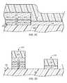
- FIG. 3A partial cross-sectional side view of a semiconductor device 300 including a logic transistor 302 and non-volatile memory transistor 304 comprising high work function gate electrodes according to an embodiment of the present invention is shown in FIG. 3 .
- the memory transistor 304is formed on a silicon substrate 306 and comprises a high work function gate electrode 308 formed from a doped polysilicon layer overlying a dielectric stack 310 .
- the dielectric stack 310overlies and controls current through a channel region 312 separating heavily doped source and drain (S/D) regions 314 .
- the dielectric stack 310includes a tunnel oxide 316 , a multi-layer charge storage layer 318 A, 318 B, and a top or blocking oxide layer 320 .
- the multi-layer charge storage layer 318 A, 318 Bincludes at least a top, charge trapping oxynitride layer 318 A and a lower, substantially trap free oxynitride layer 318 B.
- the memory transistor 304further includes one or more sidewall spacers 322 surrounding the gate stack to electrically insulate it from contacts (not shown) to the S/D regions 320 and from other transistors in the semiconductor device formed on the substrate 306 .
- the logic transistor 302comprises a gate electrode 324 overlying an oxide layer 326 formed over a channel region 328 separating heavily doped source and drain regions 330 , and, optionally, can include one or more sidewall spacers 332 surrounding the gate electrically insulate it from contacts (not shown) to the S/D regions.
- the gate electrode 324 of the logic transistor 302also comprises a high work function gate electrode formed from a doped polysilicon layer.
- the semiconductor device 300further includes a number of isolation structures 334 , such as a local oxidation of silicon (LOCOS) region or structure, a field oxidation region or structure (FOX), or a shallow trench isolation (STI) structure to electrically isolate individual transistors formed on the substrate 306 from one another.
- isolation structures 334such as a local oxidation of silicon (LOCOS) region or structure, a field oxidation region or structure (FOX), or a shallow trench isolation (STI) structure to electrically isolate individual transistors formed on the substrate 306 from one another.
- LOClocal oxidation of silicon
- FOXfield oxidation region or structure
- STIshallow trench isolation
Landscapes
- Engineering & Computer Science (AREA)
- Physics & Mathematics (AREA)
- Condensed Matter Physics & Semiconductors (AREA)
- General Physics & Mathematics (AREA)
- Manufacturing & Machinery (AREA)
- Computer Hardware Design (AREA)
- Microelectronics & Electronic Packaging (AREA)
- Power Engineering (AREA)
- Chemical & Material Sciences (AREA)
- Chemical Kinetics & Catalysis (AREA)
- Non-Volatile Memory (AREA)
- Semiconductor Memories (AREA)
Abstract
Description
Claims (20)
Priority Applications (1)
| Application Number | Priority Date | Filing Date | Title |
|---|---|---|---|
| US14/307,858US9306025B2 (en) | 2007-05-25 | 2014-06-18 | Memory transistor with multiple charge storing layers and a high work function gate electrode |
Applications Claiming Priority (4)
| Application Number | Priority Date | Filing Date | Title |
|---|---|---|---|
| US94016007P | 2007-05-25 | 2007-05-25 | |
| US12/152,518US8063434B1 (en) | 2007-05-25 | 2008-05-13 | Memory transistor with multiple charge storing layers and a high work function gate electrode |
| US13/288,919US8859374B1 (en) | 2007-05-25 | 2011-11-03 | Memory transistor with multiple charge storing layers and a high work function gate electrode |
| US14/307,858US9306025B2 (en) | 2007-05-25 | 2014-06-18 | Memory transistor with multiple charge storing layers and a high work function gate electrode |
Related Parent Applications (1)
| Application Number | Title | Priority Date | Filing Date |
|---|---|---|---|
| US13/288,919ContinuationUS8859374B1 (en) | 2007-05-25 | 2011-11-03 | Memory transistor with multiple charge storing layers and a high work function gate electrode |
Publications (2)
| Publication Number | Publication Date |
|---|---|
| US20150041880A1 US20150041880A1 (en) | 2015-02-12 |
| US9306025B2true US9306025B2 (en) | 2016-04-05 |
Family
ID=44936795
Family Applications (3)
| Application Number | Title | Priority Date | Filing Date |
|---|---|---|---|
| US12/152,518Active2029-09-16US8063434B1 (en) | 2007-05-25 | 2008-05-13 | Memory transistor with multiple charge storing layers and a high work function gate electrode |
| US13/288,919Active2029-04-14US8859374B1 (en) | 2007-05-25 | 2011-11-03 | Memory transistor with multiple charge storing layers and a high work function gate electrode |
| US14/307,858ActiveUS9306025B2 (en) | 2007-05-25 | 2014-06-18 | Memory transistor with multiple charge storing layers and a high work function gate electrode |
Family Applications Before (2)
| Application Number | Title | Priority Date | Filing Date |
|---|---|---|---|
| US12/152,518Active2029-09-16US8063434B1 (en) | 2007-05-25 | 2008-05-13 | Memory transistor with multiple charge storing layers and a high work function gate electrode |
| US13/288,919Active2029-04-14US8859374B1 (en) | 2007-05-25 | 2011-11-03 | Memory transistor with multiple charge storing layers and a high work function gate electrode |
Country Status (1)
| Country | Link |
|---|---|
| US (3) | US8063434B1 (en) |
Cited By (4)
| Publication number | Priority date | Publication date | Assignee | Title |
|---|---|---|---|---|
| US20150187960A1 (en) | 2007-05-25 | 2015-07-02 | Cypress Semiconductor Corporation | Radical Oxidation Process For Fabricating A Nonvolatile Charge Trap Memory Device |
| US9929240B2 (en) | 2007-05-25 | 2018-03-27 | Cypress Semiconductor Corporation | Memory transistor with multiple charge storing layers and a high work function gate electrode |
| US10374067B2 (en) | 2007-05-25 | 2019-08-06 | Longitude Flash Memory Solutions Ltd. | Oxide-nitride-oxide stack having multiple oxynitride layers |
| US10903068B2 (en) | 2007-05-25 | 2021-01-26 | Longitude Flash Memory Solutions Ltd. | Oxide-nitride-oxide stack having multiple oxynitride layers |
Families Citing this family (47)
| Publication number | Priority date | Publication date | Assignee | Title |
|---|---|---|---|---|
| US9299568B2 (en) | 2007-05-25 | 2016-03-29 | Cypress Semiconductor Corporation | SONOS ONO stack scaling |
| US8871595B2 (en)* | 2007-05-25 | 2014-10-28 | Cypress Semiconductor Corporation | Integration of non-volatile charge trap memory devices and logic CMOS devices |
| US8614124B2 (en)* | 2007-05-25 | 2013-12-24 | Cypress Semiconductor Corporation | SONOS ONO stack scaling |
| US8063434B1 (en)* | 2007-05-25 | 2011-11-22 | Cypress Semiconductor Corporation | Memory transistor with multiple charge storing layers and a high work function gate electrode |
| US8643124B2 (en) | 2007-05-25 | 2014-02-04 | Cypress Semiconductor Corporation | Oxide-nitride-oxide stack having multiple oxynitride layers |
| US9431549B2 (en) | 2007-12-12 | 2016-08-30 | Cypress Semiconductor Corporation | Nonvolatile charge trap memory device having a high dielectric constant blocking region |
| US8399310B2 (en) | 2010-10-29 | 2013-03-19 | Freescale Semiconductor, Inc. | Non-volatile memory and logic circuit process integration |
| US8669158B2 (en) | 2012-01-04 | 2014-03-11 | Mark D. Hall | Non-volatile memory (NVM) and logic integration |
| US8658497B2 (en) | 2012-01-04 | 2014-02-25 | Freescale Semiconductor, Inc. | Non-volatile memory (NVM) and logic integration |
| US8906764B2 (en)* | 2012-01-04 | 2014-12-09 | Freescale Semiconductor, Inc. | Non-volatile memory (NVM) and logic integration |
| US8685813B2 (en) | 2012-02-15 | 2014-04-01 | Cypress Semiconductor Corporation | Method of integrating a charge-trapping gate stack into a CMOS flow |
| EP2831918A4 (en)* | 2012-03-29 | 2015-11-18 | Cypress Semiconductor Corp | ONO INTEGRATION METHOD IN LOGICAL CMOS FLOW |
| EP3229276A1 (en)* | 2012-03-31 | 2017-10-11 | Cypress Semiconductor Corporation | Integration of non-volatile charge trap memory devices and logic cmos devices |
| JP6709051B2 (en)* | 2012-03-31 | 2020-06-10 | ロンギチュード フラッシュ メモリー ソリューションズ リミテッド | Oxide-nitride-oxide laminate with multi-layer oxynitride layer |
| US8951863B2 (en) | 2012-04-06 | 2015-02-10 | Freescale Semiconductor, Inc. | Non-volatile memory (NVM) and logic integration |
| US8722493B2 (en) | 2012-04-09 | 2014-05-13 | Freescale Semiconductor, Inc. | Logic transistor and non-volatile memory cell integration |
| US9087913B2 (en) | 2012-04-09 | 2015-07-21 | Freescale Semiconductor, Inc. | Integration technique using thermal oxide select gate dielectric for select gate and apartial replacement gate for logic |
| US8728886B2 (en) | 2012-06-08 | 2014-05-20 | Freescale Semiconductor, Inc. | Integrating formation of a replacement gate transistor and a non-volatile memory cell using a high-k dielectric |
| US9111865B2 (en) | 2012-10-26 | 2015-08-18 | Freescale Semiconductor, Inc. | Method of making a logic transistor and a non-volatile memory (NVM) cell |
| US8796098B1 (en)* | 2013-02-26 | 2014-08-05 | Cypress Semiconductor Corporation | Embedded SONOS based memory cells |
| US8741719B1 (en) | 2013-03-08 | 2014-06-03 | Freescale Semiconductor, Inc. | Integrating formation of a logic transistor and a non-volatile memory cell using a partial replacement gate technique |
| US8716089B1 (en) | 2013-03-08 | 2014-05-06 | Freescale Semiconductor, Inc. | Integrating formation of a replacement gate transistor and a non-volatile memory cell having thin film storage |
| US9331184B2 (en) | 2013-06-11 | 2016-05-03 | United Microelectronics Corp. | Sonos device and method for fabricating the same |
| US9006093B2 (en) | 2013-06-27 | 2015-04-14 | Freescale Semiconductor, Inc. | Non-volatile memory (NVM) and high voltage transistor integration |
| US8871598B1 (en) | 2013-07-31 | 2014-10-28 | Freescale Semiconductor, Inc. | Non-volatile memory (NVM) and high-k and metal gate integration using gate-first methodology |
| US8877585B1 (en) | 2013-08-16 | 2014-11-04 | Freescale Semiconductor, Inc. | Non-volatile memory (NVM) cell, high voltage transistor, and high-K and metal gate transistor integration |
| US9129996B2 (en) | 2013-07-31 | 2015-09-08 | Freescale Semiconductor, Inc. | Non-volatile memory (NVM) cell and high-K and metal gate transistor integration |
| US9082837B2 (en) | 2013-08-08 | 2015-07-14 | Freescale Semiconductor, Inc. | Nonvolatile memory bitcell with inlaid high k metal select gate |
| US9252246B2 (en) | 2013-08-21 | 2016-02-02 | Freescale Semiconductor, Inc. | Integrated split gate non-volatile memory cell and logic device |
| US9082650B2 (en) | 2013-08-21 | 2015-07-14 | Freescale Semiconductor, Inc. | Integrated split gate non-volatile memory cell and logic structure |
| US8932925B1 (en) | 2013-08-22 | 2015-01-13 | Freescale Semiconductor, Inc. | Split-gate non-volatile memory (NVM) cell and device structure integration |
| US9275864B2 (en) | 2013-08-22 | 2016-03-01 | Freescale Semiconductor,Inc. | Method to form a polysilicon nanocrystal thin film storage bitcell within a high k metal gate platform technology using a gate last process to form transistor gates |
| US9129855B2 (en) | 2013-09-30 | 2015-09-08 | Freescale Semiconductor, Inc. | Non-volatile memory (NVM) and high-k and metal gate integration using gate-first methodology |
| US8901632B1 (en) | 2013-09-30 | 2014-12-02 | Freescale Semiconductor, Inc. | Non-volatile memory (NVM) and high-K and metal gate integration using gate-last methodology |
| US9136129B2 (en) | 2013-09-30 | 2015-09-15 | Freescale Semiconductor, Inc. | Non-volatile memory (NVM) and high-k and metal gate integration using gate-last methodology |
| US9231077B2 (en) | 2014-03-03 | 2016-01-05 | Freescale Semiconductor, Inc. | Method of making a logic transistor and non-volatile memory (NVM) cell |
| US9252152B2 (en) | 2014-03-28 | 2016-02-02 | Freescale Semiconductor, Inc. | Method for forming a split-gate device |
| US9472418B2 (en) | 2014-03-28 | 2016-10-18 | Freescale Semiconductor, Inc. | Method for forming a split-gate device |
| US9112056B1 (en) | 2014-03-28 | 2015-08-18 | Freescale Semiconductor, Inc. | Method for forming a split-gate device |
| US9379222B2 (en) | 2014-05-30 | 2016-06-28 | Freescale Semiconductor, Inc. | Method of making a split gate non-volatile memory (NVM) cell |
| US9257445B2 (en) | 2014-05-30 | 2016-02-09 | Freescale Semiconductor, Inc. | Method of making a split gate non-volatile memory (NVM) cell and a logic transistor |
| US9343314B2 (en) | 2014-05-30 | 2016-05-17 | Freescale Semiconductor, Inc. | Split gate nanocrystal memory integration |
| US9580304B2 (en)* | 2015-05-07 | 2017-02-28 | Texas Instruments Incorporated | Low-stress low-hydrogen LPCVD silicon nitride |
| US9852801B1 (en)* | 2016-12-01 | 2017-12-26 | Commissariat A L'energie Atomique Et Aux Energies Alternatives | Method for determining a leakage current through an inter-gate dielectric structure of a flash memory cell |
| US20190103414A1 (en)* | 2017-10-04 | 2019-04-04 | Cypress Semiconductor Corporation | Embedded sonos with a high-k metal gate and manufacturing methods of the same |
| CN108054080B (en)* | 2017-11-30 | 2019-11-01 | 武汉新芯集成电路制造有限公司 | A method of in acquisition thermal oxide layer on substrate |
| US10943787B2 (en) | 2019-02-27 | 2021-03-09 | International Business Machines Corporation | Confined work function material for gate-all around transistor devices |
Citations (102)
| Publication number | Priority date | Publication date | Assignee | Title |
|---|---|---|---|---|
| US4843023A (en) | 1985-09-25 | 1989-06-27 | Hewlett-Packard Company | Process for forming lightly-doped-drain (LDD) without extra masking steps |
| US5404791A (en) | 1991-10-31 | 1995-04-11 | Alliedsignal Europe Services Techniques | Pressure regulation device for a hydraulic system |
| US5573963A (en) | 1995-05-03 | 1996-11-12 | Vanguard International Semiconductor Corporation | Method of forming self-aligned twin tub CMOS devices |
| US5793089A (en) | 1997-01-10 | 1998-08-11 | Advanced Micro Devices, Inc. | Graded MOS transistor junction formed by aligning a sequence of implants to a selectively removable polysilicon sidewall space and oxide thermally grown thereon |
| US5817170A (en) | 1993-06-22 | 1998-10-06 | Ceram Incorporated | Low temperature seeding process for ferroelectric memory device |
| US6015739A (en) | 1997-10-29 | 2000-01-18 | Advanced Micro Devices | Method of making gate dielectric for sub-half micron MOS transistors including a graded dielectric constant |
| US6153543A (en) | 1999-08-09 | 2000-11-28 | Lucent Technologies Inc. | High density plasma passivation layer and method of application |
| US6214689B1 (en) | 1998-03-02 | 2001-04-10 | Samsung Electronics Co., Ltd. | Apparatus for manufacturing semiconductor device, method of manufacturing capacitor of semiconductor device thereby, and resultant capacitor |
| US6287913B1 (en) | 1999-10-26 | 2001-09-11 | International Business Machines Corporation | Double polysilicon process for providing single chip high performance logic and compact embedded memory structure |
| US20010052615A1 (en) | 1998-11-04 | 2001-12-20 | Ichiro Fujiwara | Nonvolatile semiconductor memory device and process of production and write method thereof |
| US20020020890A1 (en) | 2000-08-09 | 2002-02-21 | Josef Willer | Memory cell and production method |
| US6429081B1 (en) | 2001-05-17 | 2002-08-06 | Taiwan Semiconductor Manufacturing Company | Parasitic surface transfer transistor cell (PASTT cell) for bi-level and multi-level NAND flash memory |
| US6461899B1 (en) | 1999-04-30 | 2002-10-08 | Semiconductor Energy Laboratory, Co., Ltd. | Oxynitride laminate “blocking layer” for thin film semiconductor devices |
| US6469343B1 (en) | 1998-04-02 | 2002-10-22 | Nippon Steel Corporation | Multi-level type nonvolatile semiconductor memory device |
| US6586349B1 (en) | 2002-02-21 | 2003-07-01 | Advanced Micro Devices, Inc. | Integrated process for fabrication of graded composite dielectric material layers for semiconductor devices |
| US20030122204A1 (en) | 2000-10-26 | 2003-07-03 | Kazumasa Nomoto | Nonvolatile semiconductor storage and method for manufacturing the same |
| US6610614B2 (en) | 2001-06-20 | 2003-08-26 | Texas Instruments Incorporated | Method for uniform nitridization of ultra-thin silicon dioxide layers in transistor gates |
| US20030169629A1 (en) | 2000-07-31 | 2003-09-11 | Bernd Goebel | Semiconductor memory cell configuration and a method for producing the configuration |
| US20030183869A1 (en) | 2002-01-31 | 2003-10-02 | Stmicroelectronics S.R.I. | Manufacturing process of an interpoly dielectric structure for non-volatile semiconductor integrated memories |
| US6709928B1 (en) | 2001-07-31 | 2004-03-23 | Cypress Semiconductor Corporation | Semiconductor device having silicon-rich layer and method of manufacturing such a device |
| US20040094793A1 (en) | 2002-11-15 | 2004-05-20 | Mitsuhiro Noguchi | Semiconductor memory device |
| US20040104424A1 (en) | 1997-11-18 | 2004-06-03 | Semiconductor Energy Laboratory Co., Ltd. | Nonvolatile memory and electronic apparatus |
| US20040173918A1 (en) | 2003-03-05 | 2004-09-09 | Tazrien Kamal | Charge-trapping memory arrays resistant to damage from contact hole formation |
| US20040251489A1 (en) | 2003-06-10 | 2004-12-16 | Sang-Hun Jeon | SONOS memory device and method of manufacturing the same |
| US6835621B2 (en) | 2002-07-10 | 2004-12-28 | Samsung Electronics Co., Ltd. | Method of fabricating non-volatile memory device having a structure of silicon-oxide-nitride-oxide-silicon |
| US20050026637A1 (en) | 2003-07-30 | 2005-02-03 | Fischer Michael Andrew | Intelligent downstream traffic delivery to multi-protocol stations |
| US20050070126A1 (en) | 2003-04-21 | 2005-03-31 | Yoshihide Senzaki | System and method for forming multi-component dielectric films |
| US20050093054A1 (en) | 2003-11-05 | 2005-05-05 | Jung Jin H. | Non-volatile memory devices and methods of fabricating the same |
| US20050098839A1 (en) | 2003-11-12 | 2005-05-12 | Lee Jong-Ho | Semiconductor devices having different gate dielectrics and methods for manufacturing the same |
| US6912163B2 (en) | 2003-01-14 | 2005-06-28 | Fasl, Llc | Memory device having high work function gate and method of erasing same |
| US20050141168A1 (en) | 2003-12-29 | 2005-06-30 | Lee Kee-Jeung | Capacitor with aluminum oxide and lanthanum oxide containing dielectric structure and fabrication method thereof |
| US20050186741A1 (en) | 2004-02-20 | 2005-08-25 | Tower Semiconductor Ltd. | SONOS embedded memory with CVD dielectric |
| US6946349B1 (en) | 2004-08-09 | 2005-09-20 | Chartered Semiconductor Manufacturing Ltd. | Method for integrating a SONOS gate oxide transistor into a logic/analog integrated circuit having several gate oxide thicknesses |
| US20050205920A1 (en) | 2004-03-17 | 2005-09-22 | Sang-Hun Jeon | SONOS type memory device |
| US20050245034A1 (en) | 2002-06-28 | 2005-11-03 | National Institute Of Advanced Indust Sci& Tech | Semiconductor device and its manufacturing method |
| US20050266637A1 (en) | 2004-06-01 | 2005-12-01 | Macronix International Co., Ltd. | Tunnel oxynitride in flash memories |
| US20050275012A1 (en) | 2004-06-15 | 2005-12-15 | Akiko Nara | Nonvolatile semiconductor memory device and method of manufacturing the same |
| US20060008959A1 (en) | 2002-05-16 | 2006-01-12 | Peter Hagemeyer | Layer arrangement and memory arrangement |
| US20060051880A1 (en) | 2004-09-07 | 2006-03-09 | Doczy Mark L | Method for making a semiconductor device having a high-k gate dielectric |
| US20060065919A1 (en) | 2004-09-29 | 2006-03-30 | Sony Corporation | Nonvolatile memory device and method for producing the same |
| US20060081331A1 (en) | 2003-10-15 | 2006-04-20 | Campian Jonathon R | Apparatus and method for holding materials for the forming and joining thereof |
| US7033957B1 (en) | 2003-02-05 | 2006-04-25 | Fasl, Llc | ONO fabrication process for increasing oxygen content at bottom oxide-substrate interface in flash memory devices |
| US7045424B2 (en) | 2003-08-14 | 2006-05-16 | Samsung Electronics Co., Ltd. | Method of fabricating local SONOS type gate structure and method of fabricating nonvolatile memory cell having the same |
| US20060111805A1 (en) | 1993-07-15 | 2006-05-25 | Renesas Technology Corp. | Fabrication system and fabrication method |
| US20060113627A1 (en) | 2004-11-29 | 2006-06-01 | Chung-I Chen | High-voltage transistor device having an interlayer dielectric etch stop layer for preventing leakage and improving breakdown voltage |
| US20060113586A1 (en) | 2004-11-29 | 2006-06-01 | Macronix International Co., Ltd. | Charge trapping dielectric structure for non-volatile memory |
| US20060131636A1 (en) | 2004-12-16 | 2006-06-22 | Samsung Electronics Co., Ltd. | Non-volatile memory device having improved erase efficiency and method of manufacturing the same |
| US20060202261A1 (en) | 2005-01-03 | 2006-09-14 | Macronix International Co., Ltd. | Non-volatile memory cells, memory arrays including the same and methods of operating cells and arrays |
| US7112486B2 (en) | 2004-07-06 | 2006-09-26 | Hynix Semiconductor Inc. | Method for fabricating semiconductor device by using radical oxidation |
| US20060220106A1 (en) | 2005-03-31 | 2006-10-05 | Choi Han-Mei | Gate structures of a non-volatile memory device and methods of manufacturing the same |
| US20060228899A1 (en) | 2002-08-30 | 2006-10-12 | Fujitsu Amd Semiconductor Limited | Semiconductor memory device and method for manufacturing semiconductor device |
| US20060237803A1 (en) | 2005-04-21 | 2006-10-26 | International Business Machines Corporation | ULTRA-THIN Hf-DOPED-SILICON OXYNITRIDE FILM FOR HIGH PERFORMANCE CMOS APPLICATIONS AND METHOD OF MANUFACTURE |
| US20070048916A1 (en) | 2005-08-23 | 2007-03-01 | Fujitsu Limited | Method for fabricating semiconductor device |
| US20070049048A1 (en) | 2005-08-31 | 2007-03-01 | Shahid Rauf | Method and apparatus for improving nitrogen profile during plasma nitridation |
| US20070051306A1 (en) | 2002-11-19 | 2007-03-08 | Ivanov Igor C | Spatially-arranged chemical processing station |
| US20070066087A1 (en) | 2005-09-20 | 2007-03-22 | Dongbuanam Semiconductors Inc. | Method of manufacturing a semiconductor device |
| US7262457B2 (en) | 2004-01-05 | 2007-08-28 | Ememory Technology Inc. | Non-volatile memory cell |
| US20070200168A1 (en) | 2006-02-16 | 2007-08-30 | Yoshio Ozawa | MONOS type nonvolatile memory cell, nonvolatile memory, and manufacturing method thereof |
| US20070215940A1 (en) | 2006-03-16 | 2007-09-20 | Spansion Llc | Vertical semiconductor device |
| US20070231991A1 (en)* | 2006-03-31 | 2007-10-04 | Josef Willer | Semiconductor memory device and method of operating a semiconductor memory device |
| US20070246753A1 (en) | 2006-04-20 | 2007-10-25 | Chu Jack O | Metal gated ultra short MOSFET devices |
| US20070262451A1 (en) | 2006-05-09 | 2007-11-15 | Willy Rachmady | Recessed workfunction metal in CMOS transistor gates |
| US20070267687A1 (en) | 2005-01-03 | 2007-11-22 | Macronix International Co., Ltd. | Bandgap engineered split gate memory |
| US20070272916A1 (en) | 2006-05-25 | 2007-11-29 | Taiwan Semiconductor Manufacturing Company, Ltd. | Flash memory with deep quantum well and high-K dielectric |
| US7312496B2 (en) | 1995-09-29 | 2007-12-25 | Pegre Semiconductors, Llc | Semiconductor device including transistor with composite gate structure and transistor with single gate structure, and method for manufacturing the same |
| US20080009115A1 (en)* | 2006-07-10 | 2008-01-10 | Josef Willer | Method of manufacturing at least one semiconductor component and memory cells |
| US7323742B2 (en) | 2003-04-04 | 2008-01-29 | Catalyst Semiconductor, Inc. | Non-volatile memory integrated circuit |
| US20080029399A1 (en) | 2006-02-28 | 2008-02-07 | Fujifilm Corporation | Method of manufacturing nanostructures |
| US20080048237A1 (en) | 2006-07-26 | 2008-02-28 | Kabushiki Kaisha Toshiba | Nonvolatile semiconductor memory device |
| US7365389B1 (en) | 2004-12-10 | 2008-04-29 | Spansion Llc | Memory cell having enhanced high-K dielectric |
| US20080135946A1 (en) | 2006-12-11 | 2008-06-12 | Innolux Display Corp. | Read only memory cell having multi-layer structure for storing charges and manufacturing method thereof |
| US20080150003A1 (en) | 2006-12-20 | 2008-06-26 | Jian Chen | Electron blocking layers for electronic devices |
| US20080175053A1 (en) | 2005-01-03 | 2008-07-24 | Macronix International Co., Ltd. | Silicon on insulator and thin film transistor bandgap engineered split gate memory |
| US20080237694A1 (en) | 2007-03-27 | 2008-10-02 | Michael Specht | Integrated circuit, cell, cell arrangement, method for manufacturing an integrated circuit, method for manufacturing a cell, memory module |
| US20080272424A1 (en) | 2007-05-03 | 2008-11-06 | Hynix Semiconductor Inc. | Nonvolatile Memory Device Having Fast Erase Speed And Improved Retention Characteristics And Method For Fabricating The Same |
| US20080290399A1 (en) | 2007-05-25 | 2008-11-27 | Cypress Semiconductor Corporation | Nonvolatile charge trap memory device having a deuterated layer in a multi-layer charge-trapping region |
| US20080290400A1 (en) | 2007-05-25 | 2008-11-27 | Cypress Semiconductor Corporation | SONOS ONO stack scaling |
| US20080293254A1 (en) | 2007-05-25 | 2008-11-27 | Cypress Semiconductor Corporation | Single-wafer process for fabricating a nonvolatile charge trap memory device |
| US20080293255A1 (en) | 2007-05-25 | 2008-11-27 | Krishnaswamy Ramkumar | Radical oxidation process for fabricating a nonvolatile charge trap memory device |
| US20080293207A1 (en) | 2007-05-25 | 2008-11-27 | Koutny Jr William W C | Integration of non-volatile charge trap memory devices and logic cmos devices |
| US7463530B2 (en) | 2006-06-20 | 2008-12-09 | Macronix International Co., Ltd. | Operating method of non-volatile memory device |
| US20090039414A1 (en) | 2007-08-09 | 2009-02-12 | Macronix International Co., Ltd. | Charge trapping memory cell with high speed erase |
| US20090045452A1 (en) | 2006-05-23 | 2009-02-19 | Macronix International Co., Ltd. | Structure and Method of Sub-Gate NAND Memory with Bandgap Engineered SONOS Devices |
| US20090152621A1 (en) | 2007-12-12 | 2009-06-18 | Igor Polishchuk | Nonvolatile charge trap memory device having a high dielectric constant blocking region |
| US20090179253A1 (en) | 2007-05-25 | 2009-07-16 | Cypress Semiconductor Corporation | Oxide-nitride-oxide stack having multiple oxynitride layers |
| US7576386B2 (en) | 2005-08-04 | 2009-08-18 | Macronix International Co., Ltd. | Non-volatile memory semiconductor device having an oxide-nitride-oxide (ONO) top dielectric layer |
| US7642585B2 (en) | 2005-01-03 | 2010-01-05 | Macronix International Co., Ltd. | Non-volatile memory cells, memory arrays including the same and methods of operating cells and arrays |
| US20100041222A1 (en) | 2008-05-15 | 2010-02-18 | Helmut Puchner | SONOS Type Stacks for Nonvolatile ChangeTrap Memory Devices and Methods to Form the Same |
| US20100117138A1 (en) | 2007-04-19 | 2010-05-13 | Nxp, B.V. | Nonvolatile memory cell comprising a nonwire and manufacturing method thereof |
| US20100117139A1 (en) | 2005-06-10 | 2010-05-13 | Macronix International Co., Ltd. | Methods of Operating Non-Volatile Memory Devices |
| US7723789B2 (en) | 2007-09-11 | 2010-05-25 | National Chiao Tung University | Nonvolatile memory device with nanowire channel and method for fabricating the same |
| US20100295118A1 (en) | 2007-10-15 | 2010-11-25 | Micron Technology, Inc. | Nanocrystal Based Universal Memory Cells, and Memory Cells |
| US20110018053A1 (en) | 2007-12-07 | 2011-01-27 | Agency For Science, Technology And Research | Memory cell and methods of manufacturing thereof |
| US20110163371A1 (en) | 2005-09-15 | 2011-07-07 | Song Ki-Whan | Methods of fabricating nonvolatile semiconductor memory devices |
| US7999295B2 (en) | 2005-12-09 | 2011-08-16 | Macronix International Co., Ltd. | Stacked thin film transistor, non-volatile memory devices and methods for fabricating the same |
| US20110248332A1 (en) | 2007-05-25 | 2011-10-13 | Sagy Levy | Oxide-Nitride-Oxide Stack Having Multiple Oxynitride Layers |
| US8063434B1 (en)* | 2007-05-25 | 2011-11-22 | Cypress Semiconductor Corporation | Memory transistor with multiple charge storing layers and a high work function gate electrode |
| US8067284B1 (en) | 2007-05-25 | 2011-11-29 | Cypress Semiconductor Corporation | Oxynitride bilayer formed using a precursor inducing a high charge trap density in a top layer of the bilayer |
| US20120068159A1 (en) | 2010-09-16 | 2012-03-22 | Kabushiki Kaisha Toshiba | Nonvolatile semiconductor memory device |
| US8222688B1 (en) | 2009-04-24 | 2012-07-17 | Cypress Semiconductor Corporation | SONOS stack with split nitride memory layer |
| US20130175604A1 (en) | 2007-12-12 | 2013-07-11 | Cypress Semiconductor Corporation | Nonvolatile charge trap memory device having a high dielectric constant blocking region |
| US20130309826A1 (en) | 2007-05-25 | 2013-11-21 | Cypress Semiconductor Corporation | Radical oxidation process for fabricating a nonvolatile charge trap memory device |
Family Cites Families (1)
| Publication number | Priority date | Publication date | Assignee | Title |
|---|---|---|---|---|
| WO2011162725A1 (en) | 2010-06-25 | 2011-12-29 | Agency For Science, Technology And Research | Nanowire transistor and method for manufacturing a nanowire transistor |
- 2008
- 2008-05-13USUS12/152,518patent/US8063434B1/enactiveActive
- 2011
- 2011-11-03USUS13/288,919patent/US8859374B1/enactiveActive
- 2014
- 2014-06-18USUS14/307,858patent/US9306025B2/enactiveActive
Patent Citations (122)
| Publication number | Priority date | Publication date | Assignee | Title |
|---|---|---|---|---|
| US4843023A (en) | 1985-09-25 | 1989-06-27 | Hewlett-Packard Company | Process for forming lightly-doped-drain (LDD) without extra masking steps |
| US5404791A (en) | 1991-10-31 | 1995-04-11 | Alliedsignal Europe Services Techniques | Pressure regulation device for a hydraulic system |
| US5817170A (en) | 1993-06-22 | 1998-10-06 | Ceram Incorporated | Low temperature seeding process for ferroelectric memory device |
| US20060111805A1 (en) | 1993-07-15 | 2006-05-25 | Renesas Technology Corp. | Fabrication system and fabrication method |
| US5573963A (en) | 1995-05-03 | 1996-11-12 | Vanguard International Semiconductor Corporation | Method of forming self-aligned twin tub CMOS devices |
| US7312496B2 (en) | 1995-09-29 | 2007-12-25 | Pegre Semiconductors, Llc | Semiconductor device including transistor with composite gate structure and transistor with single gate structure, and method for manufacturing the same |
| US5793089A (en) | 1997-01-10 | 1998-08-11 | Advanced Micro Devices, Inc. | Graded MOS transistor junction formed by aligning a sequence of implants to a selectively removable polysilicon sidewall space and oxide thermally grown thereon |
| US6015739A (en) | 1997-10-29 | 2000-01-18 | Advanced Micro Devices | Method of making gate dielectric for sub-half micron MOS transistors including a graded dielectric constant |
| US20040104424A1 (en) | 1997-11-18 | 2004-06-03 | Semiconductor Energy Laboratory Co., Ltd. | Nonvolatile memory and electronic apparatus |
| US6214689B1 (en) | 1998-03-02 | 2001-04-10 | Samsung Electronics Co., Ltd. | Apparatus for manufacturing semiconductor device, method of manufacturing capacitor of semiconductor device thereby, and resultant capacitor |
| US6469343B1 (en) | 1998-04-02 | 2002-10-22 | Nippon Steel Corporation | Multi-level type nonvolatile semiconductor memory device |
| US20010052615A1 (en) | 1998-11-04 | 2001-12-20 | Ichiro Fujiwara | Nonvolatile semiconductor memory device and process of production and write method thereof |
| US6461899B1 (en) | 1999-04-30 | 2002-10-08 | Semiconductor Energy Laboratory, Co., Ltd. | Oxynitride laminate “blocking layer” for thin film semiconductor devices |
| US6153543A (en) | 1999-08-09 | 2000-11-28 | Lucent Technologies Inc. | High density plasma passivation layer and method of application |
| US6287913B1 (en) | 1999-10-26 | 2001-09-11 | International Business Machines Corporation | Double polysilicon process for providing single chip high performance logic and compact embedded memory structure |
| US20030169629A1 (en) | 2000-07-31 | 2003-09-11 | Bernd Goebel | Semiconductor memory cell configuration and a method for producing the configuration |
| US20020020890A1 (en) | 2000-08-09 | 2002-02-21 | Josef Willer | Memory cell and production method |
| US20050230766A1 (en) | 2000-10-26 | 2005-10-20 | Kazumasa Nomoto | Non-volatile semiconductor memory device and method for producing same |
| US6906390B2 (en) | 2000-10-26 | 2005-06-14 | Sony Corporation | Nonvolatile semiconductor storage and method for manufacturing the same |
| US20030122204A1 (en) | 2000-10-26 | 2003-07-03 | Kazumasa Nomoto | Nonvolatile semiconductor storage and method for manufacturing the same |
| US6429081B1 (en) | 2001-05-17 | 2002-08-06 | Taiwan Semiconductor Manufacturing Company | Parasitic surface transfer transistor cell (PASTT cell) for bi-level and multi-level NAND flash memory |
| US6610614B2 (en) | 2001-06-20 | 2003-08-26 | Texas Instruments Incorporated | Method for uniform nitridization of ultra-thin silicon dioxide layers in transistor gates |
| US6709928B1 (en) | 2001-07-31 | 2004-03-23 | Cypress Semiconductor Corporation | Semiconductor device having silicon-rich layer and method of manufacturing such a device |
| US6818558B1 (en) | 2001-07-31 | 2004-11-16 | Cypress Semiconductor Corporation | Method of manufacturing a dielectric layer for a silicon-oxide-nitride-oxide-silicon (SONOS) type devices |
| US20030183869A1 (en) | 2002-01-31 | 2003-10-02 | Stmicroelectronics S.R.I. | Manufacturing process of an interpoly dielectric structure for non-volatile semiconductor integrated memories |
| US6586349B1 (en) | 2002-02-21 | 2003-07-01 | Advanced Micro Devices, Inc. | Integrated process for fabrication of graded composite dielectric material layers for semiconductor devices |
| US20060008959A1 (en) | 2002-05-16 | 2006-01-12 | Peter Hagemeyer | Layer arrangement and memory arrangement |
| US7713810B2 (en) | 2002-05-16 | 2010-05-11 | Infineon Technologies Ag | Method for fabricating a layer arrangement, layer arrangement and memory arrangement |
| US20050245034A1 (en) | 2002-06-28 | 2005-11-03 | National Institute Of Advanced Indust Sci& Tech | Semiconductor device and its manufacturing method |
| US6835621B2 (en) | 2002-07-10 | 2004-12-28 | Samsung Electronics Co., Ltd. | Method of fabricating non-volatile memory device having a structure of silicon-oxide-nitride-oxide-silicon |
| US20060228899A1 (en) | 2002-08-30 | 2006-10-12 | Fujitsu Amd Semiconductor Limited | Semiconductor memory device and method for manufacturing semiconductor device |
| US20040094793A1 (en) | 2002-11-15 | 2004-05-20 | Mitsuhiro Noguchi | Semiconductor memory device |
| US20070051306A1 (en) | 2002-11-19 | 2007-03-08 | Ivanov Igor C | Spatially-arranged chemical processing station |
| US6912163B2 (en) | 2003-01-14 | 2005-06-28 | Fasl, Llc | Memory device having high work function gate and method of erasing same |
| US7033957B1 (en) | 2003-02-05 | 2006-04-25 | Fasl, Llc | ONO fabrication process for increasing oxygen content at bottom oxide-substrate interface in flash memory devices |
| US20040173918A1 (en) | 2003-03-05 | 2004-09-09 | Tazrien Kamal | Charge-trapping memory arrays resistant to damage from contact hole formation |
| US7323742B2 (en) | 2003-04-04 | 2008-01-29 | Catalyst Semiconductor, Inc. | Non-volatile memory integrated circuit |
| US20050070126A1 (en) | 2003-04-21 | 2005-03-31 | Yoshihide Senzaki | System and method for forming multi-component dielectric films |
| US20040251489A1 (en) | 2003-06-10 | 2004-12-16 | Sang-Hun Jeon | SONOS memory device and method of manufacturing the same |
| US20050026637A1 (en) | 2003-07-30 | 2005-02-03 | Fischer Michael Andrew | Intelligent downstream traffic delivery to multi-protocol stations |
| US7045424B2 (en) | 2003-08-14 | 2006-05-16 | Samsung Electronics Co., Ltd. | Method of fabricating local SONOS type gate structure and method of fabricating nonvolatile memory cell having the same |
| US20060081331A1 (en) | 2003-10-15 | 2006-04-20 | Campian Jonathon R | Apparatus and method for holding materials for the forming and joining thereof |
| US20050093054A1 (en) | 2003-11-05 | 2005-05-05 | Jung Jin H. | Non-volatile memory devices and methods of fabricating the same |
| US20050098839A1 (en) | 2003-11-12 | 2005-05-12 | Lee Jong-Ho | Semiconductor devices having different gate dielectrics and methods for manufacturing the same |
| US20050141168A1 (en) | 2003-12-29 | 2005-06-30 | Lee Kee-Jeung | Capacitor with aluminum oxide and lanthanum oxide containing dielectric structure and fabrication method thereof |
| US7262457B2 (en) | 2004-01-05 | 2007-08-28 | Ememory Technology Inc. | Non-volatile memory cell |
| US20050186741A1 (en) | 2004-02-20 | 2005-08-25 | Tower Semiconductor Ltd. | SONOS embedded memory with CVD dielectric |
| US20050205920A1 (en) | 2004-03-17 | 2005-09-22 | Sang-Hun Jeon | SONOS type memory device |
| US20050266637A1 (en) | 2004-06-01 | 2005-12-01 | Macronix International Co., Ltd. | Tunnel oxynitride in flash memories |
| US20050275012A1 (en) | 2004-06-15 | 2005-12-15 | Akiko Nara | Nonvolatile semiconductor memory device and method of manufacturing the same |
| US7112486B2 (en) | 2004-07-06 | 2006-09-26 | Hynix Semiconductor Inc. | Method for fabricating semiconductor device by using radical oxidation |
| US6946349B1 (en) | 2004-08-09 | 2005-09-20 | Chartered Semiconductor Manufacturing Ltd. | Method for integrating a SONOS gate oxide transistor into a logic/analog integrated circuit having several gate oxide thicknesses |
| US20060051880A1 (en) | 2004-09-07 | 2006-03-09 | Doczy Mark L | Method for making a semiconductor device having a high-k gate dielectric |
| US20060065919A1 (en) | 2004-09-29 | 2006-03-30 | Sony Corporation | Nonvolatile memory device and method for producing the same |
| US20060113586A1 (en) | 2004-11-29 | 2006-06-01 | Macronix International Co., Ltd. | Charge trapping dielectric structure for non-volatile memory |
| US20060281331A1 (en) | 2004-11-29 | 2006-12-14 | Macronix International Co., Ltd. | Charge trapping dielectric structure for non-volatile memory |
| US20060113627A1 (en) | 2004-11-29 | 2006-06-01 | Chung-I Chen | High-voltage transistor device having an interlayer dielectric etch stop layer for preventing leakage and improving breakdown voltage |
| US7365389B1 (en) | 2004-12-10 | 2008-04-29 | Spansion Llc | Memory cell having enhanced high-K dielectric |
| US20060131636A1 (en) | 2004-12-16 | 2006-06-22 | Samsung Electronics Co., Ltd. | Non-volatile memory device having improved erase efficiency and method of manufacturing the same |
| US20080175053A1 (en) | 2005-01-03 | 2008-07-24 | Macronix International Co., Ltd. | Silicon on insulator and thin film transistor bandgap engineered split gate memory |
| US7688626B2 (en) | 2005-01-03 | 2010-03-30 | Macronix International Co., Ltd. | Depletion mode bandgap engineered memory |
| US8482052B2 (en) | 2005-01-03 | 2013-07-09 | Macronix International Co., Ltd. | Silicon on insulator and thin film transistor bandgap engineered split gate memory |
| US8315095B2 (en) | 2005-01-03 | 2012-11-20 | Macronix International Co., Ltd. | Multi-gate bandgap engineered memory |
| US8264028B2 (en) | 2005-01-03 | 2012-09-11 | Macronix International Co., Ltd. | Non-volatile memory cells, memory arrays including the same and methods of operating cells and arrays |
| US20080291726A1 (en) | 2005-01-03 | 2008-11-27 | Macronix International Co., Ltd. | Bandgap engineered split gate memory |
| US20100155823A1 (en) | 2005-01-03 | 2010-06-24 | Macronix International Co., Ltd. | Depletion mode bandgap engineered memory |
| US20070268753A1 (en) | 2005-01-03 | 2007-11-22 | Macronix International Co., Ltd. | Methods of operating bandgap engineered memory |
| US20070267687A1 (en) | 2005-01-03 | 2007-11-22 | Macronix International Co., Ltd. | Bandgap engineered split gate memory |
| US20060202261A1 (en) | 2005-01-03 | 2006-09-14 | Macronix International Co., Ltd. | Non-volatile memory cells, memory arrays including the same and methods of operating cells and arrays |
| US7642585B2 (en) | 2005-01-03 | 2010-01-05 | Macronix International Co., Ltd. | Non-volatile memory cells, memory arrays including the same and methods of operating cells and arrays |
| US20060220106A1 (en) | 2005-03-31 | 2006-10-05 | Choi Han-Mei | Gate structures of a non-volatile memory device and methods of manufacturing the same |
| US20060237803A1 (en) | 2005-04-21 | 2006-10-26 | International Business Machines Corporation | ULTRA-THIN Hf-DOPED-SILICON OXYNITRIDE FILM FOR HIGH PERFORMANCE CMOS APPLICATIONS AND METHOD OF MANUFACTURE |
| US20100117139A1 (en) | 2005-06-10 | 2010-05-13 | Macronix International Co., Ltd. | Methods of Operating Non-Volatile Memory Devices |
| US7576386B2 (en) | 2005-08-04 | 2009-08-18 | Macronix International Co., Ltd. | Non-volatile memory semiconductor device having an oxide-nitride-oxide (ONO) top dielectric layer |
| US20070048916A1 (en) | 2005-08-23 | 2007-03-01 | Fujitsu Limited | Method for fabricating semiconductor device |
| US20070049048A1 (en) | 2005-08-31 | 2007-03-01 | Shahid Rauf | Method and apparatus for improving nitrogen profile during plasma nitridation |
| US20110163371A1 (en) | 2005-09-15 | 2011-07-07 | Song Ki-Whan | Methods of fabricating nonvolatile semiconductor memory devices |
| US20070066087A1 (en) | 2005-09-20 | 2007-03-22 | Dongbuanam Semiconductors Inc. | Method of manufacturing a semiconductor device |
| US7999295B2 (en) | 2005-12-09 | 2011-08-16 | Macronix International Co., Ltd. | Stacked thin film transistor, non-volatile memory devices and methods for fabricating the same |
| US20070200168A1 (en) | 2006-02-16 | 2007-08-30 | Yoshio Ozawa | MONOS type nonvolatile memory cell, nonvolatile memory, and manufacturing method thereof |
| US20080029399A1 (en) | 2006-02-28 | 2008-02-07 | Fujifilm Corporation | Method of manufacturing nanostructures |
| US20070215940A1 (en) | 2006-03-16 | 2007-09-20 | Spansion Llc | Vertical semiconductor device |
| US20070231991A1 (en)* | 2006-03-31 | 2007-10-04 | Josef Willer | Semiconductor memory device and method of operating a semiconductor memory device |
| US20070246753A1 (en) | 2006-04-20 | 2007-10-25 | Chu Jack O | Metal gated ultra short MOSFET devices |
| US20070262451A1 (en) | 2006-05-09 | 2007-11-15 | Willy Rachmady | Recessed workfunction metal in CMOS transistor gates |
| US20090045452A1 (en) | 2006-05-23 | 2009-02-19 | Macronix International Co., Ltd. | Structure and Method of Sub-Gate NAND Memory with Bandgap Engineered SONOS Devices |
| US7948799B2 (en) | 2006-05-23 | 2011-05-24 | Macronix International Co., Ltd. | Structure and method of sub-gate NAND memory with bandgap engineered SONOS devices |
| US20070272916A1 (en) | 2006-05-25 | 2007-11-29 | Taiwan Semiconductor Manufacturing Company, Ltd. | Flash memory with deep quantum well and high-K dielectric |
| US7463530B2 (en) | 2006-06-20 | 2008-12-09 | Macronix International Co., Ltd. | Operating method of non-volatile memory device |
| US7790516B2 (en) | 2006-07-10 | 2010-09-07 | Qimonda Ag | Method of manufacturing at least one semiconductor component and memory cells |
| US20080009115A1 (en)* | 2006-07-10 | 2008-01-10 | Josef Willer | Method of manufacturing at least one semiconductor component and memory cells |
| US20080048237A1 (en) | 2006-07-26 | 2008-02-28 | Kabushiki Kaisha Toshiba | Nonvolatile semiconductor memory device |
| US20080135946A1 (en) | 2006-12-11 | 2008-06-12 | Innolux Display Corp. | Read only memory cell having multi-layer structure for storing charges and manufacturing method thereof |
| US20080150003A1 (en) | 2006-12-20 | 2008-06-26 | Jian Chen | Electron blocking layers for electronic devices |
| US20080237694A1 (en) | 2007-03-27 | 2008-10-02 | Michael Specht | Integrated circuit, cell, cell arrangement, method for manufacturing an integrated circuit, method for manufacturing a cell, memory module |
| US20100117138A1 (en) | 2007-04-19 | 2010-05-13 | Nxp, B.V. | Nonvolatile memory cell comprising a nonwire and manufacturing method thereof |
| US20080272424A1 (en) | 2007-05-03 | 2008-11-06 | Hynix Semiconductor Inc. | Nonvolatile Memory Device Having Fast Erase Speed And Improved Retention Characteristics And Method For Fabricating The Same |
| US8067284B1 (en) | 2007-05-25 | 2011-11-29 | Cypress Semiconductor Corporation | Oxynitride bilayer formed using a precursor inducing a high charge trap density in a top layer of the bilayer |
| US20080290400A1 (en) | 2007-05-25 | 2008-11-27 | Cypress Semiconductor Corporation | SONOS ONO stack scaling |
| US8859374B1 (en)* | 2007-05-25 | 2014-10-14 | Cypress Semiconductor Corporation | Memory transistor with multiple charge storing layers and a high work function gate electrode |
| US20130309826A1 (en) | 2007-05-25 | 2013-11-21 | Cypress Semiconductor Corporation | Radical oxidation process for fabricating a nonvolatile charge trap memory device |
| US20080290399A1 (en) | 2007-05-25 | 2008-11-27 | Cypress Semiconductor Corporation | Nonvolatile charge trap memory device having a deuterated layer in a multi-layer charge-trapping region |
| US20090179253A1 (en) | 2007-05-25 | 2009-07-16 | Cypress Semiconductor Corporation | Oxide-nitride-oxide stack having multiple oxynitride layers |
| US8318608B2 (en) | 2007-05-25 | 2012-11-27 | Cypress Semiconductor Corporation | Method of fabricating a nonvolatile charge trap memory device |
| US7670963B2 (en) | 2007-05-25 | 2010-03-02 | Cypress Semiconductor Corportion | Single-wafer process for fabricating a nonvolatile charge trap memory device |
| US8283261B2 (en) | 2007-05-25 | 2012-10-09 | Cypress Semiconductor Corporation | Radical oxidation process for fabricating a nonvolatile charge trap memory device |
| US20080293254A1 (en) | 2007-05-25 | 2008-11-27 | Cypress Semiconductor Corporation | Single-wafer process for fabricating a nonvolatile charge trap memory device |
| US20090011609A1 (en) | 2007-05-25 | 2009-01-08 | Krishnaswamy Ramkumar | Radical oxidation process for fabricating a nonvolatile charge trap memory device |
| US20080293207A1 (en) | 2007-05-25 | 2008-11-27 | Koutny Jr William W C | Integration of non-volatile charge trap memory devices and logic cmos devices |
| US20110248332A1 (en) | 2007-05-25 | 2011-10-13 | Sagy Levy | Oxide-Nitride-Oxide Stack Having Multiple Oxynitride Layers |
| US8063434B1 (en)* | 2007-05-25 | 2011-11-22 | Cypress Semiconductor Corporation | Memory transistor with multiple charge storing layers and a high work function gate electrode |
| US20080293255A1 (en) | 2007-05-25 | 2008-11-27 | Krishnaswamy Ramkumar | Radical oxidation process for fabricating a nonvolatile charge trap memory device |
| US20090039414A1 (en) | 2007-08-09 | 2009-02-12 | Macronix International Co., Ltd. | Charge trapping memory cell with high speed erase |
| US7737488B2 (en) | 2007-08-09 | 2010-06-15 | Macronix International Co., Ltd. | Blocking dielectric engineered charge trapping memory cell with high speed erase |
| US7723789B2 (en) | 2007-09-11 | 2010-05-25 | National Chiao Tung University | Nonvolatile memory device with nanowire channel and method for fabricating the same |
| US20100295118A1 (en) | 2007-10-15 | 2010-11-25 | Micron Technology, Inc. | Nanocrystal Based Universal Memory Cells, and Memory Cells |
| US20110018053A1 (en) | 2007-12-07 | 2011-01-27 | Agency For Science, Technology And Research | Memory cell and methods of manufacturing thereof |
| US20090152621A1 (en) | 2007-12-12 | 2009-06-18 | Igor Polishchuk | Nonvolatile charge trap memory device having a high dielectric constant blocking region |
| US20130175604A1 (en) | 2007-12-12 | 2013-07-11 | Cypress Semiconductor Corporation | Nonvolatile charge trap memory device having a high dielectric constant blocking region |
| US20100041222A1 (en) | 2008-05-15 | 2010-02-18 | Helmut Puchner | SONOS Type Stacks for Nonvolatile ChangeTrap Memory Devices and Methods to Form the Same |
| US8222688B1 (en) | 2009-04-24 | 2012-07-17 | Cypress Semiconductor Corporation | SONOS stack with split nitride memory layer |
| US20120068159A1 (en) | 2010-09-16 | 2012-03-22 | Kabushiki Kaisha Toshiba | Nonvolatile semiconductor memory device |
Non-Patent Citations (129)
| Title |
|---|
| "1.8V, 500-MHz, 10-Output JEDEC-Compliant Zero Delay Buffer," Cypress Advance Information, Feb. 12, 2004; 9 pages. |
| "10 Gigabit Ethernet Technology Overview White Paper", Revision 1.0, Retrieved from Internet: URL: http://www.10gea.org, May 2001. |
| "16K x 8/9 Dual-Port Static RAM with Sem, Int, Busy," Cypress Semiconductor Data Book, May 1995, CY7C006 and CY7C016, pp. 6:1-17; 10 pages. |
| "1K x 8 Dual-Port Static RAM," Cypress Semiconductor Data Book, May 1995, CY7C130/CY7C131 and CY7C140/CY7C141, pp. 6:37-49; 8 pages. |
| "1kHz to 30MHz Resistor Set SOT-23 Oscillator", Initial Release Final Electrical Specifications LTC1799, Linear Technology Corporation, Jan. 2001, pp. 1-4. |
| "200-MBaud HOTLink Transceiver," Cypress Semiconductor Corporation, Revised Feb. 13, 2004, CY7C924ADX, Document #38-02008 Rev. *D; 62 pages. |
| "2K x 16 Dual-Port Static RAM," Cypress Semiconductor Data Book, May 1995, CY7C133 and CY7C143, pp. 6:63-73; 7 pages. |
| "2K x 8 Dual-Port Static RAM," Cypress Semiconductor Data Book, May 1995, CY7C132/CY7C136 and CY7C142/CY7C146, pp. 6:50-62; 8 pages. |
| "A Novel Integration Technology of EEPROM Embedded CMOS Logic VLSI Suitable for ASIC Applications", By Masataka Takebuchi et al., IEEE 1992 Custom Integrated Circuits Conference, pp. 9.6.1-9.6.4. |
| "A Novel Robust and Low Cost Stack Chips Package and Its Thermal Performance", by Soon-Jin Cho et al., IEEE Transaction on Advanced Packaging, vol. 23, No. 2, May 2000, pp. 257-265. |
| "A Planar Type EEPROM Cell Structure by Standard CMOS Process for Integration with Gate Array, Standard Cell, Microprocessor and for Neural Chips", by Katsuhiko Ohsaki et al., IEEE 1993 Custom Integrated Circuits Conference, pp-23.6.1-23.6.4. |
| "A Single Chip Sensor & Image Processor for Fingerprint Verification" Anderson, S., et al., IEEE Custom Integrated Circuits Conference, May 12-15, 1991. |
| "A Single Poly EPROM for Custom CMOS Logic Applications", by Reza Kazerounian et al., IEEE 1986 Custom Integrated Circuits Conference, pp. 59-62. |
| "A Wide-Bandwidth Low-Voltage PLL for PowerPC.TM. Microprocessors", by Jose Alvarez et al., IEEE Journal of Solid-State Circuits, vol. 30, No. 4, Apr. 1995, pp. 383-391. |
| "About SMaL Camera Technologies, Inc.", SMaL Camera Technologies, 2001, 1 page. |
| "Achieving Uniform nMOS Device Power Distribution for Sub-micron ESD Reliability;" Charvaka Duvvuy, Carlos Diaz, and Tim Haddock; 1992; 92-131 through 92-134, no month. |
| "ADNS-2030 High Performance, Low Power Optical Mouse Sensor (Optimized for Cordless Mouse Applications)," Agilent Technologies, downloaded Oct. 10, 2005, ; 2 pages. |
| "ADNS-2030 High Performance, Low Power Optical Mouse Sensor (Optimized for Cordless Mouse Applications)," Agilent Technologies, downloaded Oct. 10, 2005, <http://www.home.agilent.com/USeng/nav/-536893734,536883737/pd.html>; 2 pages. |
| "ADNS-2051 High-Performance Optical Mouse Sensor," Agilent Technologies, downloaded Oct. 10, 2005, <http://www.home.agilent.com/USeng/nav/-536893734,536883737/pd.html>; 2 pages. |
| "Agilent ADNK-2030 Solid-State Optical Mouse Sensor," Agilent Technologies Inc., Sample Kit, 2003; 1 page. |
| "Agilent ADNS-2030 Low Power Optical Mouse Sensor," Agilent Technologies Inc., Data Sheet, 2005; 34 pages. |
| "Agilent ADNS-2051 Optical Mouse Sensor," Agilent Technologies Inc., Product Overview, 2003; 2 pages. |
| "Agilent Optical Mouse Sensors," Agilent Technologies Inc., Selection Guide, 2004; 3 pages. |
| "Algorithm for Managing Multiple First-In, First-Out Queues from a Single Shared Random-Access Memory," IBM Technical Disclosure Bulletin, Aug. 1989; 5 pages. |
| "Am99C10A 256.times.48 Content Addressable Memory", Advanced Micro Devices, Dec. 1992. |
| "An Analog PPL-Based Clock and Data Recovery Circuit with High Input Jitter Tolerance;" Sun, Reprinted from IEEE Journal of Solid-State Circuits, 1989; 4 pages. |
| "An EEPROM for Microprocessors and Custom Logic", by Roger Cuppens et al., IEEE Journal of Solid-State Circuits, vol. SC-20, No. 2, Apr. 1985, pp. 603-608. |
| "An EPROM Cell Structure foe EPLDs Compatible with Single Poly Gate Process", by Kuniyushi Yoshikawa et al., Extended Abstracts of the 18th (1986 International) Conference on Solid State Devices and Materials, Tokyo, 1986, pp. 323-326. |
| "An Experimental 5-V-Only 256-kbit CMOS EEPROM with a High-Performance Single-Polysilicon Cell", by Jun-Ichi Miyamoto et al., IEEE Journal of Solid State Circuits, vol. SC-21, No. 5, Oct. 1986, pp. 852-860. |
| "MAX 9000 Programmable Logic Device Family," Altera, Jul. 1999, Version 6.01, pp. 1-40; 41 pages. |
| Chen et al., "Performance Improvement of SONOS Memory by Bandgap Engineering of Charge-Trapping Layer," IEEE Electron Device Letters, Apr. 2004, vol. 25, No. 4, pp. 205-207; 3 pages. |
| International Search Report and Written Opinion for International Application No. PCT/US07/20965 filed Sep. 28, 2007, mailed Apr. 21, 2008, 2 pages. |
| International Search Report for International Application No. PCT/US07/20966 dated Apr. 21, 2008; 2 pages. |
| International Search Report for International Application No. PCT/US07/20988 dated Mar. 14, 2008; 2 pages. |
| International Search Report for International Application No. PCT/US08/06627 dated Aug. 26, 2008; 2 pages. |
| International Search Report for International Application No. PCT/US13/48885 dated Nov. 14, 2013; 2 pages. |
| International Search Report for International Application No. PCT/US2012/021583 dated May 8, 2012; 2 pages. |
| L. Richard Carley, "Trimming Analog Circuits Using Floating-Gate Analog MOS Memory," IEEE Journal of Solid-State Circuits, vol. 24, No. 6, Dec. 1989, pp. 1569-1575; 7 pages. |
| Lue et al., "BE-SONOS: A Bandgap Engineered SONOS with Excellent Performance and Reliability," IEEE, 2005; 4 pages. |
| Lue, Hang-Ting et al., "Reliability Model of Bandgap Engineered SONOS (be-SONOS)", IEEE, 2006, 4 pgs. |
| Office Action Receive for Application No. 10-2007-7001931 dated Dec. 26, 2012; 6 pages. |
| SIPO Office Action for Application No. 200780035963.3 dated Feb. 29, 2012; 4 pages. |
| SIPO Office Action for Chinese Application No. 201210327771.2 dated Jun. 6, 2014; 3 pages. |
| U.S. Appl. No. 11/904,506: "SONOS ONO stack scaling," Fredrick B. Jenne, filed Sep. 26, 2007; 46 pages. |
| U.S. Appl. No. 12/124,855: "Radical Oxidation Process for Fabricating a Nonvolatile Charge Trap Memory Device" Krishnaswamy Ramkumar et al., filed May 21, 2008; 67 pages. |
| U.S. Appl. No. 12/152,518: "Memory Transistor With Multiple Charge Storing Layers and a High Work Function Gate Electrode" Igor Polishchuk et al., filed May 13, 2008; 29 pages. |
| U.S. Appl. No. 13/288,919: "Memory Transistor With Multiple Charge Storing Layers and a High Work Function Gate Electrode," Igor Polishchuk, filed Nov. 3, 2011; 29 pages. |
| U.S. Appl. No. 13/428,201: "Method of Integrating a Charge-Trapping Gate Stack Into a CMOS Flow" Krishnaswamy Ramkumar et al., filed Mar. 23, 2012; 38 Pages. |
| U.S. Appl. No. 13/431,069: "SONOS Stack With Split Nitride Memory Layer" Fredrick Jenne et al., filed Mar. 27, 2012; 59 pages. |
| U.S. Appl. No. 13/436,872: "Oxide-Nitride-Oxide Stack Having Multiple Oxynitride Layers" Sagy Levy, Zichron-Yoakev et al., filed Mar. 31, 2012; 53 pages. |
| U.S. Appl. No. 13/436,875: "Nonvolatile Charge Trap Memory Device Having a High Dielectric Constant Blocking Region" Igor Polishchuk et al., filed Mar. 31, 2012; 70 Pages. |
| U.S. Appl. No. 13/436,878: "Integration of Non-Volatile Charge Trap Memory Devices and Logic CMOS Devices" Krishnaswamy Ramkumar et al., filed Mar. 31, 2012; 90 pages. |
| U.S. Appl. No. 13/539,461: "SONOS ONO Stack Scaling," Fredrick Jenne, filed Jul. 1, 2012; 91 pages. |
| U.S. Appl. No. 13/551,237: "SONOS Stack With Split Nitride Memory Layer" Fredrick Jenne et al., filed Jul. 17, 2012; 37 pages. |
| U.S. Appl. No. 13/620,071: "Method of Fabricating a Nonvolatile Charge Trap Memory Device" Krishnaswamy Ramkumar et al., filled on Sep. 14, 2012; 69 pages. |
| U.S. Appl. No. 14/159,315: "Memory Transistor With Multiple Charge Storing Layers and a High Work Function Gate Electrode" Igor Polishchuk et al., filed Jan. 20, 2014; 60 pages. |
| U.S. Appl. No. 60/931,947: "Oxide-nitride- Oxide Stack Having Multiple Oxynitride Layers" Sagy Levy et al., filed May 25, 2007; 27 pages. |
| U.S. Appl. No. 60/931,948: "SONOS stack with oxynitride bilayer made of BTBAS and NH3" Sagy Levy et al., filed May 25, 2007; 11 Pages. |
| U.S. Appl. No. 60/940,128: "Single Wafer Process for ONO Stack" Krishnaswamy Ramkumar et al., filed May 25, 2007; 3 pages. |
| U.S. Appl. No. 61/007,566: "Nonvolatile Charge Trap Memory Device Having a High Dielectric Constant Blocking Region" Igor Polishchuk et al., filed Dec. 12, 2007; 37 pages. |
| U.S. Appl. No. 61/599,258 "New Integration of SONOS Stack" Krishnaswamy Ramkumar et al., filed Feb. 15, 2012: 4 pages. |
| USPTO Advisory Action for U.S. Appl. No. 11/904,506 dated Aug. 30, 2011; 4 pages. |
| USPTO Advisory Action for U.S. Appl. No. 13/114,889 dated Aug. 2, 2013; 2 pages. |
| USPTO Advisory Action for U.S. Appl. No. 13/114,889 dated Aug. 29, 2012; 3 pages. |
| USPTO Final Rejection for U.S. Appl. No. 11/904,506 dated Jun. 7, 2011; 15 pages. |
| USPTO Final Rejection for U.S. Appl. No. 12/005,813 dated Mar. 6, 2012; 5 pages. |
| USPTO Final Rejection for U.S. Appl. No. 12/030,644 dated Jan. 24, 2011; 22 pages. |
| USPTO Final Rejection for U.S. Appl. No. 12/125,864 dated Jul. 1, 2010; 18 pages. |
| USPTO Final Rejection for U.S. Appl. No. 12/185,747 dated Feb. 25, 2010; 12 pages. |
| USPTO Final Rejection for U.S. Appl. No. 13/114,889 dated Apr. 2, 2013; 12 pages. |
| USPTO Final Rejection for U.S. Appl. No. 13/114,889 dated Jun. 4, 2012; 12 pages. |
| USPTO Miscellaneous Internal Document for U.S. Appl. No. 12/030,644 dated May 28, 2010; 6 pages. |
| USPTO Missing Parts for U.S. Appl. No. 13/539,466 dated Jul. 17, 2012; 2 pages. |
| USPTO Non Final Rejection for U.S. Appl. No. 11/904,506 dated Aug. 31, 2010; 17 pages. |
| USPTO Non Final Rejection for U.S. Appl. No. 11/904,506 dated Feb. 3, 2011; 13 pages. |
| USPTO Non Final Rejection for U.S. Appl. No. 12/005,813 dated Sep. 23, 2011; 12 pages. |
| USPTO Non Final Rejection for U.S. Appl. No. 12/185,747 dated Aug. 6, 2009; 15 pages. |
| USPTO Non Final Rejection for U.S. Appl. No. 12/185,751 dated Aug. 4, 2009; 19 pages. |
| USPTO Non Final Rejection for U.S. Appl. No. 12/767,105 dated Apr. 21, 2011; 7 pages. |
| USPTO Non Final Rejection for U.S. Appl. No. 12/767,105 dated Oct. 18, 2011; 7 pages. |
| USPTO Non Final Rejection for U.S. Appl. No. 13/114,889 dated Nov. 25, 2011; 13 pages. |
| USPTO Non Final Rejection for U.S. Appl. No. 13/114,889 dated Sep. 5, 2013; 11 pages. |
| USPTO Non Final Rejection for U.S. Appl. No. 13/620,071 dated Apr. 3, 2014; 12 pages. |
| USPTO Non Final Rejection for U.S. Appl. No. 13/620,071 dated Jul. 18, 2014; 5 pages. |
| USPTO Non-Final Rejection for U.S. Appl. No. 12/030,644 dated May 28, 2010; 19 pages. |
| USPTO Non-Final Rejection for U.S. Appl. No. 12/152,518 dated Mar. 9, 2011; 4 pages. |
| USPTO Non-Final Rejection for U.S. Appl. No. 12/152,518 dated Sep. 29, 2010; 5 pages. |
| USPTO Non-Final Rejection for U.S. Appl. No. 13/114,889 dated Oct. 10, 2012; 11 pages. |
| USPTO Non-Final Rejection for U.S. Appl. No. 13/288,919 dated Dec. 5, 2013; 4 pages. |
| USPTO Non-Final Rejection for U.S. Appl. No. 13/288,919 dated Jun. 19, 2014; 5 pages. |
| USPTO Non-Final Rejection for U.S. Appl. No. 13/539,466 dated Sep. 28, 2012; 9 pages. |
| USPTO Non-Final Rejection for U.S. Appl. No. 14/159,315 dated Oct. 21, 2014; 12 pages. |
| USPTO Notice of Allowance for U.S. Appl. No. 11/983,578 dated Mar. 14, 2013; 10 pages. |
| USPTO Notice of Allowance for U.S. Appl. No. 12/125,864 dated Apr. 19, 2011; 11 pages. |
| USPTO Notice of Allowance for U.S. Appl. No. 12/152,518 dated Jul. 14, 2011; 6 pages. |
| USPTO Notice of Allowance for U.S. Appl. No. 12/185,751 dated Aug. 11, 2010; 7 pages. |
| USPTO Notice of Allowance for U.S. Appl. No. 12/185,751 dated Feb. 4, 2010; 7 pages. |
| USPTO Notice of Allowance for U.S. Appl. No. 12/185,751 dated Jan. 31, 2011; 5 pages. |
| USPTO Notice of Allowance for U.S. Appl. No. 12/185,751 dated May 15, 2013; 9 pages. |
| USPTO Notice of Allowance for U.S. Appl. No. 12/207,104 dated Apr. 30, 2010; 7 pages. |
| USPTO Notice of Allowance for U.S. Appl. No. 12/767,105 dated Apr. 4, 2012; 8 pages. |
| USPTO Notice of Allowance for U.S. Appl. No. 12/767,105 dated May 7, 2012; 7 pages. |
| USPTO Notice of Allowance for U.S. Appl. No. 13/288,919 dated Apr. 28, 2014; 5 pages. |
| USPTO Notice of Allowance for U.S. Appl. No. 13/288,919 dated Aug. 26, 2014; 7 pages. |
| USPTO Notice of Allowance for U.S. Appl. No. 13/288,919 dated Jul. 8, 2014; 5 pages. |
| USPTO Notice of Allowance for U.S. Appl. No. 13/436,878 dated Aug. 11, 2014; 6 pages. |
| USPTO Notice of Allowance for U.S. Appl. No. 13/539,458 dated Aug. 4, 2014; 7 pages. |
| USPTO Notice of Allowance for U.S. Appl. No. 13/539,458 dated May 24, 2013; 8 pages. |
| USPTO Notice of Allowance for U.S. Appl. No. 13/539,458 dated Nov. 3, 2014; 7 pages. |
| USPTO Notice of Allowance for U.S. Appl. No. 13/539,466 dated Nov. 13, 2013; 9 pages. |
| USPTO Notice of Allowance for U.S. Appl. No. 13/539,466 dated Nov. 27, 2012; 8 pages. |
| USPTO Notice of Allowance for U.S. Appl. No. 13/539,466 dated Sep. 4, 2013; 9 pages. |
| USPTO Notice of Allowance for U.S. Appl. No. 13/620,071 dated Jan. 23, 2015; 5 pages. |
| USPTO Notice of Allowance for U.S. Appl. No. 13/620,071 dated Oct. 27, 2014; 7 pages. |
| USPTO Notice of Allowance for U.S. Appl. No. 14/159,315 dated Feb. 18, 2015; 9 pages. |
| USPTO Notice of Allowance for U.S. Appl. No. 14/265,129 dated Mar. 13, 2015; 8 pages. |
| USPTO Requirement for Restriction for U.S. Appl. No. 11/904,506 dated Apr. 13, 2010; 7 pages. |
| USPTO Requirement for Restriction for U.S. Appl. No. 12/152,518 dated Jun. 9, 2010; 5 pages. |
| USPTO Requirement for Restriction for U.S. Appl. No. 12/185,751 dated Apr. 20, 2009; 7 pages. |
| USPTO Requirement for Restriction for U.S. Appl. No. 12/767,105 dated Mar. 1, 2011; 6 pages. |
| USPTO Requirement for Restriction for U.S. Appl. No. 13/114,889 dated Sep. 7, 2011; 6 pages. |
| Wang, Szu-Yu et al., "Reliability and processing effects of bandgap engineered SONOS flash memory", 2007 IEEE, International Reliability Symposium, Apr. 18, 2007, 5 pgs. |
| Written Opinion of the International Searching Authority for International Application No. PCT/US07/20966 mailed Apr. 21, 2008; 1 pages. |
| Written Opinion of the International Searching Authority for International Application No. PCT/US07/20988 mailed Mar. 14, 2008; 1 page. |
| Written Opinion of the International Searching Authority for International Application No. PCT/US13/48876 dated Jul. 26, 2013; 3 pages. |
| Written Opinion of the International Searching Authority for International Application No. PCT/US2012/21583 mailed May 8, 2012; 4 pages. |
| Written Opinion of the International Searching Authority for International Application No. PCT/US2013/048885 mailed Nov. 14, 2013; 7 pages. |
| Wu et al., "SONOS Device with Tapered Bandgap Nitride Layer," IEEE Transactions on Electron Devices, May 2005, vol. 52, No. 5, pp. 987-992; 6 pages. |
| Yang et al., "Reliability considerations in scaled SONOS nonvolatile memory devices, solid state Electronics", 43(1999) 2025-2032. |
Cited By (17)
| Publication number | Priority date | Publication date | Assignee | Title |
|---|---|---|---|---|
| US20150187960A1 (en) | 2007-05-25 | 2015-07-02 | Cypress Semiconductor Corporation | Radical Oxidation Process For Fabricating A Nonvolatile Charge Trap Memory Device |
| US9929240B2 (en) | 2007-05-25 | 2018-03-27 | Cypress Semiconductor Corporation | Memory transistor with multiple charge storing layers and a high work function gate electrode |
| US10304968B2 (en) | 2007-05-25 | 2019-05-28 | Cypress Semiconductor Corporation | Radical oxidation process for fabricating a nonvolatile charge trap memory device |
| US10312336B2 (en) | 2007-05-25 | 2019-06-04 | Cypress Semiconductor Corporation | Memory transistor with multiple charge storing layers and a high work function gate electrode |
| US10374067B2 (en) | 2007-05-25 | 2019-08-06 | Longitude Flash Memory Solutions Ltd. | Oxide-nitride-oxide stack having multiple oxynitride layers |
| US10446656B2 (en) | 2007-05-25 | 2019-10-15 | Longitude Flash Memory Solutions Ltd. | Memory transistor with multiple charge storing layers and a high work function gate electrode |
| US10593812B2 (en) | 2007-05-25 | 2020-03-17 | Longitude Flash Memory Solutions Ltd. | Radical oxidation process for fabricating a nonvolatile charge trap memory device |
| US10896973B2 (en) | 2007-05-25 | 2021-01-19 | Longitude Flash Memory Solutions Ltd. | Oxide-nitride-oxide stack having multiple oxynitride layers |
| US10903342B2 (en) | 2007-05-25 | 2021-01-26 | Longitude Flash Memory Solutions Ltd. | Oxide-nitride-oxide stack having multiple oxynitride layers |
| US10903068B2 (en) | 2007-05-25 | 2021-01-26 | Longitude Flash Memory Solutions Ltd. | Oxide-nitride-oxide stack having multiple oxynitride layers |
| US11056565B2 (en) | 2007-05-25 | 2021-07-06 | Longitude Flash Memory Solutions Ltd. | Flash memory device and method |
| US11222965B2 (en) | 2007-05-25 | 2022-01-11 | Longitude Flash Memory Solutions Ltd | Oxide-nitride-oxide stack having multiple oxynitride layers |
| US11456365B2 (en) | 2007-05-25 | 2022-09-27 | Longitude Flash Memory Solutions Ltd. | Memory transistor with multiple charge storing layers and a high work function gate electrode |
| US11721733B2 (en) | 2007-05-25 | 2023-08-08 | Longitude Flash Memory Solutions Ltd. | Memory transistor with multiple charge storing layers and a high work function gate electrode |
| US11784243B2 (en) | 2007-05-25 | 2023-10-10 | Longitude Flash Memory Solutions Ltd | Oxide-nitride-oxide stack having multiple oxynitride layers |
| US12009401B2 (en) | 2007-05-25 | 2024-06-11 | Longitude Flash Memory Solutions Ltd. | Memory transistor with multiple charge storing layers and a high work function gate electrode |
| US12266521B2 (en) | 2007-05-25 | 2025-04-01 | Longitude Flash Memory Solutions Ltd. | Oxide-nitride-oxide stack having multiple oxynitride layers |
Also Published As
| Publication number | Publication date |
|---|---|
| US8063434B1 (en) | 2011-11-22 |
| US8859374B1 (en) | 2014-10-14 |
| US20150041880A1 (en) | 2015-02-12 |
Similar Documents
| Publication | Publication Date | Title |
|---|---|---|
| US11721733B2 (en) | Memory transistor with multiple charge storing layers and a high work function gate electrode | |
| US9306025B2 (en) | Memory transistor with multiple charge storing layers and a high work function gate electrode | |
| KR101947363B1 (en) | Method of fabricating a charge-trapping gate stack using a cmos process flow | |
| US9553175B2 (en) | SONOS type stacks for nonvolatile charge trap memory devices and methods to form the same | |
| US11641745B2 (en) | Embedded sonos with a high-K metal gate and manufacturing methods of the same | |
| US6818558B1 (en) | Method of manufacturing a dielectric layer for a silicon-oxide-nitride-oxide-silicon (SONOS) type devices | |
| JP2018041977A (en) | ОNO stack formation method | |
| CN111180525B (en) | Oxide nitride oxide stack with multiple oxynitride layers | |
| KR102078611B1 (en) | Memory transistor with multiple charge storing layers | |
| US8592891B1 (en) | Methods for fabricating semiconductor memory with process induced strain | |
| US20070269972A1 (en) | Method of manufacturing a semiconductor device | |
| US6828201B1 (en) | Method of manufacturing a top insulating layer for a sonos-type device |
Legal Events
| Date | Code | Title | Description |
|---|---|---|---|
| AS | Assignment | Owner name:CYPRESS SEMICONDUCTOR CORPORATION, CALIFORNIA Free format text:ASSIGNMENT OF ASSIGNORS INTEREST;ASSIGNORS:POLISHCHUK, IGOR;LEVY, SAGY;RAMKUMAR, KRISHNASWAMY;SIGNING DATES FROM 20080227 TO 20080310;REEL/FRAME:034089/0812 | |
| AS | Assignment | Owner name:MORGAN STANLEY SENIOR FUNDING, INC., NEW YORK Free format text:SECURITY INTEREST;ASSIGNORS:CYPRESS SEMICONDUCTOR CORPORATION;SPANSION LLC;REEL/FRAME:035240/0429 Effective date:20150312 | |
| STCF | Information on status: patent grant | Free format text:PATENTED CASE | |
| AS | Assignment | Owner name:LONGITUDE FLASH MEMORY SOLUTIONS LTD., IRELAND Free format text:ASSIGNMENT OF ASSIGNORS INTEREST;ASSIGNOR:CYPRESS SEMICONDUCTOR CORPORATION;REEL/FRAME:049086/0803 Effective date:20190503 | |
| AS | Assignment | Owner name:SPANSION LLC, CALIFORNIA Free format text:RELEASE BY SECURED PARTY;ASSIGNOR:MORGAN STANLEY SENIOR FUNDING, INC.;REEL/FRAME:049109/0573 Effective date:20190503 Owner name:CYPRESS SEMICONDUCTOR CORPORATION, CALIFORNIA Free format text:RELEASE BY SECURED PARTY;ASSIGNOR:MORGAN STANLEY SENIOR FUNDING, INC.;REEL/FRAME:049109/0573 Effective date:20190503 | |
| MAFP | Maintenance fee payment | Free format text:PAYMENT OF MAINTENANCE FEE, 4TH YEAR, LARGE ENTITY (ORIGINAL EVENT CODE: M1551); ENTITY STATUS OF PATENT OWNER: LARGE ENTITY Year of fee payment:4 | |
| AS | Assignment | Owner name:MORGAN STANLEY SENIOR FUNDING, INC., NEW YORK Free format text:CORRECTIVE ASSIGNMENT TO CORRECT THE 8647899 PREVIOUSLY RECORDED ON REEL 035240 FRAME 0429. ASSIGNOR(S) HEREBY CONFIRMS THE SECURITY INTERST;ASSIGNORS:CYPRESS SEMICONDUCTOR CORPORATION;SPANSION LLC;REEL/FRAME:058002/0470 Effective date:20150312 | |
| MAFP | Maintenance fee payment | Free format text:PAYMENT OF MAINTENANCE FEE, 8TH YEAR, LARGE ENTITY (ORIGINAL EVENT CODE: M1552); ENTITY STATUS OF PATENT OWNER: LARGE ENTITY Year of fee payment:8 |