US9305862B2 - Support mounted electrically interconnected die assembly - Google Patents
Support mounted electrically interconnected die assemblyDownload PDFInfo
- Publication number
- US9305862B2 US9305862B2US13/456,126US201213456126AUS9305862B2US 9305862 B2US9305862 B2US 9305862B2US 201213456126 AUS201213456126 AUS 201213456126AUS 9305862 B2US9305862 B2US 9305862B2
- Authority
- US
- United States
- Prior art keywords
- die
- support
- stack
- interconnect
- assembly
- Prior art date
- Legal status (The legal status is an assumption and is not a legal conclusion. Google has not performed a legal analysis and makes no representation as to the accuracy of the status listed.)
- Expired - Fee Related
Links
Images


Classifications
- H—ELECTRICITY
- H01—ELECTRIC ELEMENTS
- H01L—SEMICONDUCTOR DEVICES NOT COVERED BY CLASS H10
- H01L23/00—Details of semiconductor or other solid state devices
- H01L23/48—Arrangements for conducting electric current to or from the solid state body in operation, e.g. leads, terminal arrangements ; Selection of materials therefor
- H—ELECTRICITY
- H01—ELECTRIC ELEMENTS
- H01L—SEMICONDUCTOR DEVICES NOT COVERED BY CLASS H10
- H01L21/00—Processes or apparatus adapted for the manufacture or treatment of semiconductor or solid state devices or of parts thereof
- H01L21/02—Manufacture or treatment of semiconductor devices or of parts thereof
- H01L21/04—Manufacture or treatment of semiconductor devices or of parts thereof the devices having potential barriers, e.g. a PN junction, depletion layer or carrier concentration layer
- H01L21/50—Assembly of semiconductor devices using processes or apparatus not provided for in a single one of the groups H01L21/18 - H01L21/326 or H10D48/04 - H10D48/07 e.g. sealing of a cap to a base of a container
- H01L21/56—Encapsulations, e.g. encapsulation layers, coatings
- H01L21/58—
- H—ELECTRICITY
- H01—ELECTRIC ELEMENTS
- H01L—SEMICONDUCTOR DEVICES NOT COVERED BY CLASS H10
- H01L24/00—Arrangements for connecting or disconnecting semiconductor or solid-state bodies; Methods or apparatus related thereto
- H01L24/01—Means for bonding being attached to, or being formed on, the surface to be connected, e.g. chip-to-package, die-attach, "first-level" interconnects; Manufacturing methods related thereto
- H01L24/18—High density interconnect [HDI] connectors; Manufacturing methods related thereto
- H01L24/23—Structure, shape, material or disposition of the high density interconnect connectors after the connecting process
- H01L24/24—Structure, shape, material or disposition of the high density interconnect connectors after the connecting process of an individual high density interconnect connector
- H—ELECTRICITY
- H01—ELECTRIC ELEMENTS
- H01L—SEMICONDUCTOR DEVICES NOT COVERED BY CLASS H10
- H01L24/00—Arrangements for connecting or disconnecting semiconductor or solid-state bodies; Methods or apparatus related thereto
- H01L24/80—Methods for connecting semiconductor or other solid state bodies using means for bonding being attached to, or being formed on, the surface to be connected
- H01L24/82—Methods for connecting semiconductor or other solid state bodies using means for bonding being attached to, or being formed on, the surface to be connected by forming build-up interconnects at chip-level, e.g. for high density interconnects [HDI]
- H—ELECTRICITY
- H01—ELECTRIC ELEMENTS
- H01L—SEMICONDUCTOR DEVICES NOT COVERED BY CLASS H10
- H01L25/00—Assemblies consisting of a plurality of semiconductor or other solid state devices
- H01L25/03—Assemblies consisting of a plurality of semiconductor or other solid state devices all the devices being of a type provided for in a single subclass of subclasses H10B, H10D, H10F, H10H, H10K or H10N, e.g. assemblies of rectifier diodes
- H01L25/04—Assemblies consisting of a plurality of semiconductor or other solid state devices all the devices being of a type provided for in a single subclass of subclasses H10B, H10D, H10F, H10H, H10K or H10N, e.g. assemblies of rectifier diodes the devices not having separate containers
- H01L25/065—Assemblies consisting of a plurality of semiconductor or other solid state devices all the devices being of a type provided for in a single subclass of subclasses H10B, H10D, H10F, H10H, H10K or H10N, e.g. assemblies of rectifier diodes the devices not having separate containers the devices being of a type provided for in group H10D89/00
- H01L25/0657—Stacked arrangements of devices
- H01L29/0657—
- H—ELECTRICITY
- H10—SEMICONDUCTOR DEVICES; ELECTRIC SOLID-STATE DEVICES NOT OTHERWISE PROVIDED FOR
- H10D—INORGANIC ELECTRIC SEMICONDUCTOR DEVICES
- H10D62/00—Semiconductor bodies, or regions thereof, of devices having potential barriers
- H10D62/10—Shapes, relative sizes or dispositions of the regions of the semiconductor bodies; Shapes of the semiconductor bodies
- H10D62/117—Shapes of semiconductor bodies
- H—ELECTRICITY
- H01—ELECTRIC ELEMENTS
- H01L—SEMICONDUCTOR DEVICES NOT COVERED BY CLASS H10
- H01L2224/00—Indexing scheme for arrangements for connecting or disconnecting semiconductor or solid-state bodies and methods related thereto as covered by H01L24/00
- H01L2224/01—Means for bonding being attached to, or being formed on, the surface to be connected, e.g. chip-to-package, die-attach, "first-level" interconnects; Manufacturing methods related thereto
- H01L2224/18—High density interconnect [HDI] connectors; Manufacturing methods related thereto
- H01L2224/23—Structure, shape, material or disposition of the high density interconnect connectors after the connecting process
- H01L2224/24—Structure, shape, material or disposition of the high density interconnect connectors after the connecting process of an individual high density interconnect connector
- H01L2224/241—Disposition
- H01L2224/24135—Connecting between different semiconductor or solid-state bodies, i.e. chip-to-chip
- H01L2224/24145—Connecting between different semiconductor or solid-state bodies, i.e. chip-to-chip the bodies being stacked
- H—ELECTRICITY
- H01—ELECTRIC ELEMENTS
- H01L—SEMICONDUCTOR DEVICES NOT COVERED BY CLASS H10
- H01L2224/00—Indexing scheme for arrangements for connecting or disconnecting semiconductor or solid-state bodies and methods related thereto as covered by H01L24/00
- H01L2224/01—Means for bonding being attached to, or being formed on, the surface to be connected, e.g. chip-to-package, die-attach, "first-level" interconnects; Manufacturing methods related thereto
- H01L2224/26—Layer connectors, e.g. plate connectors, solder or adhesive layers; Manufacturing methods related thereto
- H01L2224/31—Structure, shape, material or disposition of the layer connectors after the connecting process
- H01L2224/32—Structure, shape, material or disposition of the layer connectors after the connecting process of an individual layer connector
- H01L2224/321—Disposition
- H01L2224/32135—Disposition the layer connector connecting between different semiconductor or solid-state bodies, i.e. chip-to-chip
- H01L2224/32145—Disposition the layer connector connecting between different semiconductor or solid-state bodies, i.e. chip-to-chip the bodies being stacked
- H—ELECTRICITY
- H01—ELECTRIC ELEMENTS
- H01L—SEMICONDUCTOR DEVICES NOT COVERED BY CLASS H10
- H01L2224/00—Indexing scheme for arrangements for connecting or disconnecting semiconductor or solid-state bodies and methods related thereto as covered by H01L24/00
- H01L2224/01—Means for bonding being attached to, or being formed on, the surface to be connected, e.g. chip-to-package, die-attach, "first-level" interconnects; Manufacturing methods related thereto
- H01L2224/26—Layer connectors, e.g. plate connectors, solder or adhesive layers; Manufacturing methods related thereto
- H01L2224/31—Structure, shape, material or disposition of the layer connectors after the connecting process
- H01L2224/32—Structure, shape, material or disposition of the layer connectors after the connecting process of an individual layer connector
- H01L2224/321—Disposition
- H01L2224/32151—Disposition the layer connector connecting between a semiconductor or solid-state body and an item not being a semiconductor or solid-state body, e.g. chip-to-substrate, chip-to-passive
- H01L2224/32221—Disposition the layer connector connecting between a semiconductor or solid-state body and an item not being a semiconductor or solid-state body, e.g. chip-to-substrate, chip-to-passive the body and the item being stacked
- H01L2224/32225—Disposition the layer connector connecting between a semiconductor or solid-state body and an item not being a semiconductor or solid-state body, e.g. chip-to-substrate, chip-to-passive the body and the item being stacked the item being non-metallic, e.g. insulating substrate with or without metallisation
- H—ELECTRICITY
- H01—ELECTRIC ELEMENTS
- H01L—SEMICONDUCTOR DEVICES NOT COVERED BY CLASS H10
- H01L2224/00—Indexing scheme for arrangements for connecting or disconnecting semiconductor or solid-state bodies and methods related thereto as covered by H01L24/00
- H01L2224/74—Apparatus for manufacturing arrangements for connecting or disconnecting semiconductor or solid-state bodies and for methods related thereto
- H01L2224/76—Apparatus for connecting with build-up interconnects
- H01L2224/7615—Means for depositing
- H01L2224/76151—Means for direct writing
- H01L2224/76155—Jetting means, e.g. ink jet
- H—ELECTRICITY
- H01—ELECTRIC ELEMENTS
- H01L—SEMICONDUCTOR DEVICES NOT COVERED BY CLASS H10
- H01L2224/00—Indexing scheme for arrangements for connecting or disconnecting semiconductor or solid-state bodies and methods related thereto as covered by H01L24/00
- H01L2224/80—Methods for connecting semiconductor or other solid state bodies using means for bonding being attached to, or being formed on, the surface to be connected
- H01L2224/82—Methods for connecting semiconductor or other solid state bodies using means for bonding being attached to, or being formed on, the surface to be connected by forming build-up interconnects at chip-level, e.g. for high density interconnects [HDI]
- H01L2224/821—Forming a build-up interconnect
- H01L2224/82101—Forming a build-up interconnect by additive methods, e.g. direct writing
- H01L2224/82102—Forming a build-up interconnect by additive methods, e.g. direct writing using jetting, e.g. ink jet
- H—ELECTRICITY
- H01—ELECTRIC ELEMENTS
- H01L—SEMICONDUCTOR DEVICES NOT COVERED BY CLASS H10
- H01L2225/00—Details relating to assemblies covered by the group H01L25/00 but not provided for in its subgroups
- H01L2225/03—All the devices being of a type provided for in the same main group of the same subclass of class H10, e.g. assemblies of rectifier diodes
- H01L2225/04—All the devices being of a type provided for in the same main group of the same subclass of class H10, e.g. assemblies of rectifier diodes the devices not having separate containers
- H01L2225/065—All the devices being of a type provided for in the same main group of the same subclass of class H10
- H01L2225/06503—Stacked arrangements of devices
- H01L2225/06524—Electrical connections formed on device or on substrate, e.g. a deposited or grown layer
- H—ELECTRICITY
- H01—ELECTRIC ELEMENTS
- H01L—SEMICONDUCTOR DEVICES NOT COVERED BY CLASS H10
- H01L2225/00—Details relating to assemblies covered by the group H01L25/00 but not provided for in its subgroups
- H01L2225/03—All the devices being of a type provided for in the same main group of the same subclass of class H10, e.g. assemblies of rectifier diodes
- H01L2225/04—All the devices being of a type provided for in the same main group of the same subclass of class H10, e.g. assemblies of rectifier diodes the devices not having separate containers
- H01L2225/065—All the devices being of a type provided for in the same main group of the same subclass of class H10
- H01L2225/06503—Stacked arrangements of devices
- H01L2225/06551—Conductive connections on the side of the device
- H—ELECTRICITY
- H01—ELECTRIC ELEMENTS
- H01L—SEMICONDUCTOR DEVICES NOT COVERED BY CLASS H10
- H01L2225/00—Details relating to assemblies covered by the group H01L25/00 but not provided for in its subgroups
- H01L2225/03—All the devices being of a type provided for in the same main group of the same subclass of class H10, e.g. assemblies of rectifier diodes
- H01L2225/04—All the devices being of a type provided for in the same main group of the same subclass of class H10, e.g. assemblies of rectifier diodes the devices not having separate containers
- H01L2225/065—All the devices being of a type provided for in the same main group of the same subclass of class H10
- H01L2225/06503—Stacked arrangements of devices
- H01L2225/06555—Geometry of the stack, e.g. form of the devices, geometry to facilitate stacking
- H01L2225/06562—Geometry of the stack, e.g. form of the devices, geometry to facilitate stacking at least one device in the stack being rotated or offset
- H—ELECTRICITY
- H01—ELECTRIC ELEMENTS
- H01L—SEMICONDUCTOR DEVICES NOT COVERED BY CLASS H10
- H01L2924/00—Indexing scheme for arrangements or methods for connecting or disconnecting semiconductor or solid-state bodies as covered by H01L24/00
- H—ELECTRICITY
- H01—ELECTRIC ELEMENTS
- H01L—SEMICONDUCTOR DEVICES NOT COVERED BY CLASS H10
- H01L2924/00—Indexing scheme for arrangements or methods for connecting or disconnecting semiconductor or solid-state bodies as covered by H01L24/00
- H01L2924/01—Chemical elements
- H01L2924/01005—Boron [B]
- H—ELECTRICITY
- H01—ELECTRIC ELEMENTS
- H01L—SEMICONDUCTOR DEVICES NOT COVERED BY CLASS H10
- H01L2924/00—Indexing scheme for arrangements or methods for connecting or disconnecting semiconductor or solid-state bodies as covered by H01L24/00
- H01L2924/01—Chemical elements
- H01L2924/01006—Carbon [C]
- H—ELECTRICITY
- H01—ELECTRIC ELEMENTS
- H01L—SEMICONDUCTOR DEVICES NOT COVERED BY CLASS H10
- H01L2924/00—Indexing scheme for arrangements or methods for connecting or disconnecting semiconductor or solid-state bodies as covered by H01L24/00
- H01L2924/01—Chemical elements
- H01L2924/01013—Aluminum [Al]
- H—ELECTRICITY
- H01—ELECTRIC ELEMENTS
- H01L—SEMICONDUCTOR DEVICES NOT COVERED BY CLASS H10
- H01L2924/00—Indexing scheme for arrangements or methods for connecting or disconnecting semiconductor or solid-state bodies as covered by H01L24/00
- H01L2924/01—Chemical elements
- H01L2924/01015—Phosphorus [P]
- H—ELECTRICITY
- H01—ELECTRIC ELEMENTS
- H01L—SEMICONDUCTOR DEVICES NOT COVERED BY CLASS H10
- H01L2924/00—Indexing scheme for arrangements or methods for connecting or disconnecting semiconductor or solid-state bodies as covered by H01L24/00
- H01L2924/01—Chemical elements
- H01L2924/01033—Arsenic [As]
- H—ELECTRICITY
- H01—ELECTRIC ELEMENTS
- H01L—SEMICONDUCTOR DEVICES NOT COVERED BY CLASS H10
- H01L2924/00—Indexing scheme for arrangements or methods for connecting or disconnecting semiconductor or solid-state bodies as covered by H01L24/00
- H01L2924/01—Chemical elements
- H01L2924/01038—Strontium [Sr]
- H—ELECTRICITY
- H01—ELECTRIC ELEMENTS
- H01L—SEMICONDUCTOR DEVICES NOT COVERED BY CLASS H10
- H01L2924/00—Indexing scheme for arrangements or methods for connecting or disconnecting semiconductor or solid-state bodies as covered by H01L24/00
- H01L2924/01—Chemical elements
- H01L2924/01047—Silver [Ag]
- H—ELECTRICITY
- H01—ELECTRIC ELEMENTS
- H01L—SEMICONDUCTOR DEVICES NOT COVERED BY CLASS H10
- H01L2924/00—Indexing scheme for arrangements or methods for connecting or disconnecting semiconductor or solid-state bodies as covered by H01L24/00
- H01L2924/01—Chemical elements
- H01L2924/01067—Holmium [Ho]
- H—ELECTRICITY
- H01—ELECTRIC ELEMENTS
- H01L—SEMICONDUCTOR DEVICES NOT COVERED BY CLASS H10
- H01L2924/00—Indexing scheme for arrangements or methods for connecting or disconnecting semiconductor or solid-state bodies as covered by H01L24/00
- H01L2924/01—Chemical elements
- H01L2924/01082—Lead [Pb]
- H—ELECTRICITY
- H01—ELECTRIC ELEMENTS
- H01L—SEMICONDUCTOR DEVICES NOT COVERED BY CLASS H10
- H01L2924/00—Indexing scheme for arrangements or methods for connecting or disconnecting semiconductor or solid-state bodies as covered by H01L24/00
- H01L2924/013—Alloys
- H01L2924/014—Solder alloys
- H—ELECTRICITY
- H01—ELECTRIC ELEMENTS
- H01L—SEMICONDUCTOR DEVICES NOT COVERED BY CLASS H10
- H01L2924/00—Indexing scheme for arrangements or methods for connecting or disconnecting semiconductor or solid-state bodies as covered by H01L24/00
- H01L2924/095—Indexing scheme for arrangements or methods for connecting or disconnecting semiconductor or solid-state bodies as covered by H01L24/00 with a principal constituent of the material being a combination of two or more materials provided in the groups H01L2924/013 - H01L2924/0715
- H01L2924/097—Glass-ceramics, e.g. devitrified glass
- H01L2924/09701—Low temperature co-fired ceramic [LTCC]
- H—ELECTRICITY
- H01—ELECTRIC ELEMENTS
- H01L—SEMICONDUCTOR DEVICES NOT COVERED BY CLASS H10
- H01L2924/00—Indexing scheme for arrangements or methods for connecting or disconnecting semiconductor or solid-state bodies as covered by H01L24/00
- H01L2924/10—Details of semiconductor or other solid state devices to be connected
- H01L2924/11—Device type
- H01L2924/14—Integrated circuits
- H—ELECTRICITY
- H01—ELECTRIC ELEMENTS
- H01L—SEMICONDUCTOR DEVICES NOT COVERED BY CLASS H10
- H01L2924/00—Indexing scheme for arrangements or methods for connecting or disconnecting semiconductor or solid-state bodies as covered by H01L24/00
- H01L2924/15—Details of package parts other than the semiconductor or other solid state devices to be connected
- H01L2924/151—Die mounting substrate
- H01L2924/153—Connection portion
- H01L2924/1531—Connection portion the connection portion being formed only on the surface of the substrate opposite to the die mounting surface
- H01L2924/15311—Connection portion the connection portion being formed only on the surface of the substrate opposite to the die mounting surface being a ball array, e.g. BGA
- H—ELECTRICITY
- H01—ELECTRIC ELEMENTS
- H01L—SEMICONDUCTOR DEVICES NOT COVERED BY CLASS H10
- H01L2924/00—Indexing scheme for arrangements or methods for connecting or disconnecting semiconductor or solid-state bodies as covered by H01L24/00
- H01L2924/15—Details of package parts other than the semiconductor or other solid state devices to be connected
- H01L2924/151—Die mounting substrate
- H01L2924/156—Material
- H01L2924/15786—Material with a principal constituent of the material being a non metallic, non metalloid inorganic material
- H01L2924/15787—Ceramics, e.g. crystalline carbides, nitrides or oxides
Definitions
- This inventionrelates to electrical interconnection of integrated circuit chips and, particularly, to mounting interconnected stacked die onto a support.
- a typical semiconductor diehas a front (“active”) side, in which the integrated circuitry is formed, a back side, and sidewalls. The sidewalls meet the front side at front edges and the back side at back edges.
- Semiconductor dietypically are provided with interconnect pads (die pads) located at the front side for electrical interconnection of the circuitry on the die with other circuitry in the device in which the die is deployed.
- Some die as providedhave die pads on the front side along one or more of the die margins, and these may be referred to as peripheral pad die.
- Other die as providedhave die pads arranged in one or two rows at the front side near the center of the die, and these may be referred to as center pad die. The die may be “rerouted” to provide a suitable arrangement of interconnect pads at or near one or more of the margins of the die.
- Semiconductor diemay be electrically connected with other circuitry in a package, for example on a package substrate or on a leadframe, by any of several means. Such z-interconnection may be made, for example, by wire bonds, or by flip chip interconnects, or by tab interconnects.
- the package substrate or leadframeprovides for electrical connection of the package to underlying circuitry (second-level interconnection), such as circuitry on a printed circuit board, in a device in which the package is installed for use.
- a number of approacheshave been proposed for increasing the density of active semiconductor circuitry in integrated circuit chip packages, while minimizing package size (package footprint, package thickness).
- package sizepackage footprint, package thickness.
- two or more semiconductor die, of the same or different functionalityare stacked one over another and mounted on a package substrate.
- U.S. Pat. No. 7,245,021describes a vertically stacked die assembly including a plurality of integrated circuit die electrically interconnected by “vertical conducting elements”.
- the dieare covered with an electrically insulative conformal coating.
- the vertical conducting elementsare formed of a conductive polymer material, applied adjacent the edge of the die.
- the dieare provided with metallic conducting elements, each having one end attached to electrical connection points at the die periphery and having the other end embedded in a vertical conducting polymer element.
- the disclosure of U.S. Pat. No. 7,215,018describes a similar vertically stacked die assembly mounted onto a ball grid array (“BGA”) or land grid array (“LGA”) substrate.
- BGAball grid array
- LGAland grid array
- the stacked die assemblyis mounted onto the BGA or LGA substrate by electrical and physical connection of the vertical conducting elements (“vertical interconnects”) to electrical connection lands on the surface of the substrate.
- the electrical connectionis said to be done by use of a conductive polymer “dot” or “puddle” between the vertical interconnect of the stack of die and the substrate.
- the substratecan include means for making electrical connection between the bottom of the substrate and a printed circuit board, such as solder balls or bumps, or “LGA contacts” on the bottom of the substrate.
- the inventionfeatures electrical connection of stacked die assemblies to connection sites on any support, without electrical connection to any interposed die or substrate or leadframe or package.
- Each die in the stacked die assemblyhas peripheral interconnect terminals, and the die in the stack are electrically interconnected by lines or traces of an electrically conductive material, which may be an electrically conductive polymer, or an electrically conductive ink, that contacts interconnect terminals on the respective die.
- the interconnect materialmay include a curable polymer.
- the stacked die assemblymay be mounted directly onto a surface of the support to which the die stack assembly is electrically connected.
- the stacked die assemblymay be mounted onto a surface of an additional support (such as an additional die or substrate or leadframe or package) and electrically connected to connection sites on the support.
- the additional supportincludes a semiconductor construct that is electrically connected to additional connection sites on the support to which the stacked die assembly is electrically connected.
- the inventionfeatures a support having electrical connection sites at a surface thereof, and a stacked die assembly mounted onto the surface and electrically connected to one or more of the connection sites, wherein each die in the stacked die assembly has peripheral interconnect terminals, and the die in the stack are electrically interconnected by lines or traces of an electrically conductive material, which may be an electrically conductive polymer, or an electrically conductive ink, that contacts interconnect terminals on the respective die.
- the traces of electrically conductive material that interconnect the die in the stackmay also connect to the connection sites on the support.
- the die stackis positioned on or in relation to the support so that the interconnect terminals on the die are suitably aligned with corresponding connection sites on the support circuitry, and then the interconnect material is applied in a suitable pattern over the interconnect terminal on the die and the connection sites on the support.
- the interconnect materialincludes a curable polymer
- the materialmay be cured following the application of the curable material to the die and the connection sites.
- an additional quantity of an electrically conductive materialmay be provided to make contact between the die stack interconnects and the connection sites on the support.
- the die stack assembly interconnectionis completed prior to positioning the assembly on or in relation to the support, and in such embodiments where the interconnect material includes a curable polymer, the material may be cured or partially cured following the application of the curable material to the die and prior to positioning the assembly on or in relation to the support. Cured or partially cured interconnects can improve mechanical stability of the stack assembly during subsequent handling, such as during installation of the assembly on the support.
- the additional materialmay be applied to the connection sites on the support, or to contact sites on the interconnects, prior to positioning the assembly on or in relation to the support.
- the additional materialmay be the same as, or may be different from, the material of the die stack interconnects; and, where the additional material is a curable polymer, a final cure is carried out following the positioning of the assembly on or in relation to the support.
- the inventionfeatures a first support having electrical connection sites at a surface thereof, a second support mounted on the first support, and a stacked die assembly mounted onto a surface of the second support and electrically connected to one or more of the connection sites on the first support, wherein each die in the stacked die assembly has peripheral interconnect terminals, and the die in the stack are electrically interconnected by lines or traces of an electrically conductive material, which may be an electrically conductive polymer, or an electrically conductive ink, that contacts interconnect terminals on the respective die.
- the additional supportis electrically connected to the first support. In such embodiments at least some of the electrical connections of the die in the stacked die units or assemblies are not electrically connected to the additional support and, in some such embodiments there is no direct electrical connection between the die unit or assembly and interconnect pads or sites on the additional support.
- the additional supportserves as a mechanical or structural support for the die assembly or unit, and includes no electrical or electronic components. It may include, for example, a dummy die; or a sheet of dielectric material; or a heat dissipating sheet or block of a material having a high heat capacity or high thermal conductivity.
- the additional supportmay include only passive electrical features.
- the passive electrical features in the additional supportmay be electrically connected to one or more sites in the first support; or they may be connected to a selected number (less than all) of the interconnections in the die unit or assembly; or they may be connected to a selected number (less than all) of the interconnections in the die unit or assembly as well as to one or more sites in the support.
- the additional supportmay include, for example, a ground plane.
- the additional supportmay include electronic circuitry, and may include one or more semiconductor devices.
- the additional supportmay be a semiconductor package; or an additional die.
- one or more connection sites in the additional supportmay be electrically connected to sites in the first support; or to a selected number (less than all) of the interconnections in the die unit or assembly; or to a selected number (less than all) of the interconnections in the die unit or assembly as well as to one or more sites in the support.
- the additional supportincludes electronic circuitry
- the electronic circuitry in the second support and the die assembly or unitare separately connected to the first support. That is, the electrical connections between the die assembly or unit and the first support bypass the second support, and the respective connections may be made to separate sets of sites on the first support.
- the additional supportis a die; pads on the die are connected to a second set of bond sites on the first support, and interconnects in the die assembly or unit are connected to a first set of bond sites on the first support.
- the additional supportis a semiconductor package, and lands on the package are connected to a second set of bond pads on the first support, and interconnects in the die assembly or unit are connected to a first set of bond sites on the first support.
- Installation of the die stack and electrical connection of the die to connection sites on the support according to the inventionrequires no solder, or wires, sockets, pins, or other connectors.
- the interconnect materialis an electrically conductive polymer, such as an electrically conductive epoxy, for example; or an electrically conductive ink.
- the electrically conductive polymeris a curable polymer, and may be curable in stages.
- the interconnect materialmay include, for example, a matrix containing an electrically conductive filler; the matrix may be a curable or settable material, and the electrically conductive fill may be in particulate form, for example, such that when the matrix sets or is cured, the material is itself electrically conductive.
- the materialis a conductive epoxy such as a silver filled epoxy; for example, a filled epoxy having 60-90% (more usually 80-85%) silver may be suitable. The epoxy is cured following dispensing, resulting in some embodiments in a fusion of the series of dots into a continuous interconnect strand.
- the interconnect materialcan be applied using an application tool such as, for example, a syringe or a nozzle or a needle.
- the materialexits the tool in a deposition direction generally toward the die pads or interconnect terminals, and the tool is moved over the presented stack face in a work direction.
- the materialmay be extruded from the tool in a continuous flow, or, the material may exit the tool dropwise.
- the materialexits the tool as a jet of droplets, and is deposited as dots which coalesce upon contact, or following contact, with a stack face surface.
- the deposition directionis generally perpendicular to the sidewall surface of the die, and in other embodiments the deposition direction is at an angle off perpendicular to the sidewall surface of the die.
- the toolmay be moved in a generally linear work direction, or in a zig-zag work direction, depending upon the location on the various die of the corresponding terminals to be connected.
- a plurality of interconnect tracesare formed in a single operation, and in some such embodiments all the interconnect traces on a given stacked assembly are formed in a single operation (or in a number of operations fewer than the number of traces).
- the application toolmay in such instances include a number of needles or nozzles ganged together in a row generally parallel to the die edges.
- the interconnectsare applied by printing, for example using a print head (which may have a suitable array of nozzles), or for example by screen printing or using a mask.
- the interconnectsare formed using a photosensitive material, and photoexposure procedure to pattern the material.
- the materialmay be a photocurable electrically conductive material, such as a metal-filled photopolymerizable organic polymer, for example; and the material is applied generally over an area that includes pads or interconnect terminals, then is exposed to light in the desired patterned, and the uncured material is removed.
- the additional small amount of materialmay be applied to the die stack interconnects in a transfer operation, for example by dipping shallowly into a reservoir of the interconnect material, or by screen printing or stencil printing, for example.
- the additional small amount of materialmay be applied to the connection sites on the support by a dispense operation.
- the materialmay be dispensed using an application tool, and the material may exit the tool under control of an apparatus using pressure dispense (for example under a controlled time and pressure regime), piston dispense (for example under a controlled time and piston travel regime), or auger dispense (for example under a controlled time and auger rotation regime).
- the materialmay be applied to the connection sites on the support by a patterned print operation, using for example an array of jets or apertures.
- the materialmay be dispensed by droplets, or in a continuous stream.
- Suitable supportsinclude, in one general category, any dielectric substrate carrying patterned electrical conductors in one or more layers.
- the dielectric substratemay be or include a natural or synthetic organic or inorganic material.
- circuitry formed on or in a glass or ceramic or silicon or other dielectric sheet or filmcan constitute a suitable support.
- Other suitable supportsinclude conventional circuit boards such as printed circuit boards, which may be, for example, motherboards, or module boards, or daughterboards.
- the inventionfeatures stacked die units or stacked die assemblies electrically interconnected with circuitry on a support in a device for use.
- the stacked die assemblyis interconnected such that the active side of the die faces toward the underlying circuitry; in other embodiments the stacked die assembly is interconnected such that the back side of the die faces toward the underlying circuitry.
- one or more die in the stackmay be oriented facing away from the underlying circuitry while one or more other die in the stack face toward the underlying circuitry.
- the die or the stack of dieis oriented so that the plane of the die is nonparallel with the die mount surface of the support; in some such embodiments the plane of the die is oriented perpendicular to the plane of the die mount surface of the support; or is oriented at some other angle between parallel and perpendicular.
- the dieare provided with an electrically insulative conformal coating over at least the front surface and the sidewalls adjacent the die margin on which the interconnect pads are arranged, and in some such embodiments the die are provided with a electrically insulative conformal coating over the front surface, the back surface, and the sidewall surfaces of the die.
- the conformal coatingprotects the die during assembly, and serves to electrically insulate the die from electrically conductive parts that it may contact.
- the material of the conformal coatingincludes an organic polymer, for example a polymer of p-xylene or a derivative thereof, such as a polyxylylene polymer, e.g., a parylene C or a parylene N, or a parylene A, or a parylene SR.
- the conformal coatingis formed by deposition, for example by vapor deposition, or liquid phase deposition, or by solid phase deposition.
- an underfill materialis applied between the die stack and the support. In some embodiments it may be preferred to select an underfill material that is rigid, to provide mechanical stability to the die and support assembly.
- the assemblies according to the inventioncan be used for building computers, telecommunications equipment, and consumer and industrial electronics devices.
- FIG. 1is a diagrammatic representation illustrating a generalized support to which a die assembly can be electrically connected according to the invention.
- FIG. 2is a diagrammatic sketch in partial sectional view showing a stack of four die mounted on a BGA substrate.
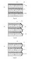
- FIGS. 3A-3Fare diagrammatic sketches in sectional view showing examples of various die edge configurations.
- FIGS. 4A-4Fare diagrammatic sketches in sectional view showing stacks of die having die edge configurations as in FIGS. 3A-3F .
- FIGS. 5A-5Fare diagrammatic sketches in sectional view showing stacks of die having die edge configurations as in FIGS. 3A-3F , in which the respective die are covered by a conformal dielectric coating.
- FIGS. 6A, 6Bare diagrammatic sketches in plan and sectional views illustrating die stacked in an offset configuration.
- FIGS. 7A-7Care diagrammatic sketches in sectional views illustrating die stacks constructed generally as in FIGS. 6A, 6B mounted on a support according to examples of the invention.
- FIGS. 8 and 9are diagrammatic representations each illustrating generalized first and second supports to which a die assembly can be mounted and electrically connected according to other embodiments of the invention.
- FIGS. 10A, 10Bare diagrammatic sketches in plan and sectional views illustrating a die assembly in an offset configuration, mounted onto a die (serving as a second substrate) and electrically connected to a first substrate according to an embodiment of the invention.
- stacked die assembliesare electrically connected to interconnect sites on any support, without an interposed substrate or leadframe; and electrical interconnection of the die in the stack, and of the die stack to the support, is made by way of an electrically conductive polymer or an electrically conductive ink, without solder, or wires, sockets, pins, or other connectors.
- FIG. 1illustrates symbolically in a sectional view a generalized support 10 , having a connection side 12 and a reverse side 14 . Interconnect sites 16 are present at least at the connection side of the support.
- the thickness of the supportis not indicated in the FIG., as the support may range from very thick to very thin, depending among other things upon the character of the support; for instance, a printed circuit board may have a greater thickness than substrate having two metal layers separated by a single dielectric layer.
- the supportmay have greater or lesser length and width dimensions, as suggested by dashed arrows 11 and 13 .
- the die stackmay be directly connected to interconnect sites at an attachment side of any of a wide variety of categories of supports, including for example: other die, including for example logic chips; other die stacks; other packaged devices or components; circuit boards, including system circuit boards, motherboards, daughterboards, module boards, and the like; leadframes; and the like.
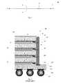
- FIG. 2shows generally at 20 such a stack 21 of four die 12 , 14 , 16 , 18 mounted on a BGA substrate 22 in a partial sectional view.
- each diee.g., die 12
- an interconnect terminale.g., off-die terminal 129
- Adjacent die in the stackmay optionally be mounted one upon the other using an adhesive.
- the term “adjacent” with reference to die in a stackmeans the die are vertically adjacent; die may also be horizontally adjacent, for example in a wafer or in a die array or, in some configurations, on a common support.).
- a film adhesive pieceis employed (e.g., 33 between adjacent die 14 and 16 ).
- Bond pads 228are arranged at the die mount surface 224 of the substrate 22 .
- the dieare arranged one over another with the respective interconnect terminals 129 , 149 , 169 , 189 aligned vertically (that is, generally perpendicular to the front or back side of the die).
- the die stack 21is mounted on the substrate with the respective interconnect terminals aligned at least partly over the respective bond pad 228 .
- Solder balls 227are attached in a reflow process to an array of lands 226 exposed at the side of the substrate 225 opposite the die mount side 224 .
- the array of solder ballsprovides for second-level interconnection of the assembly 20 onto underlying circuitry in a device for use, for example on a leadframe, or a printed circuit board, for example.
- the die stackmay be mounted on the substrate using an adhesive.
- the die 18 adjacent the substrate 22is affixed to the die mount side 224 of the substrate 22 using a film adhesive 37 .
- a configuration as shown in FIG. 2may be made by forming the die stack and then mounting the die stack on a substrate 22 ; or, alternatively, it may be made in a build-up manner, by stacking the die serially on the substrate, that is by mounting die 18 on the substrate 22 (optionally using an adhesive 37 ), then mounting die 16 on die 18 (optionally using an adhesive 33 ), then mounting die 14 on die 18 , etc., and then applying the interconnect material to the terminals on the die as well as to the bond pad on the substrate in a continuous operation.
- FIG. 2shows the stacked die assembly on the substrate following cure of the interconnect.
- the assembly in this examplehas a stack of four die mounted on a substrate, in which the die are electrically interconnected to one another, and to the substrate circuitry (z-interconnection) by the interconnect 410 ; that is the interconnect 410 provides electrical continuity between the interconnect terminals 129 , 149 , 169 , 189 and the bond pad 228 on the substrate 22 .
- FIGS. 3A-3Fshow examples of various die edge configurations in die to be interconnected according to various embodiments of the invention.
- FIG. 3Ashows a die having an “off-die” interconnect.
- the dieis shown in a partial sectional view, having an active side 315 at which the integrated circuitry 311 of the die is formed, and a die sidewall 319 .
- an interconnect terminal 322is bonded to an interconnect pad (die pad) 313 .
- the die padmay be a peripheral die pad in the die as provided, or it may be situated at or near the die periphery as a result of rerouting of the die circuitry.
- the interconnect terminalmay be, for example, a wire (formed for example in a wire bond operation) or a tab or ribbon (formed for example in a ribbon bond operation).
- the interconnect terminal 322extends outwardly beyond the die edge 319 (hence, “off-die” terminal).
- FIG. 3Bshows a die having a bump or glob 323 of an electrically conductive polymer material deposited onto the die pad 313 .
- the globmay be shaped so that it extends toward the die edge, and may extend to the die edge or (as in the example shown in FIG. 3B ) slightly beyond the die edge 19 ; it may be in the shape of a thumb, for example. Alternatively, the glob may be formed entirely above the pad, as shown for example in FIG. 5B .
- the conductive polymer materialmay be, for example, a curable conductive polymer such as a conductive epoxy.
- FIG. 3Cshows a die having an interconnect terminal 324 formed in or at the active side of the die, at or near the margin of the die where the active side 315 of the die meets the die sidewall 319 .
- a marginal interconnect terminalmay be an extension of a die pad, for example, and may be situated at or near the die margin as a result of rerouting of the die circuitry.
- FIG. 3Dshows a die having an interconnect terminal 326 formed in the die sidewall 319 .
- the interconnect terminalmay be connected to the integrated circuitry of the die by attachment of a pad of conductive material to an extension of the die pad, for example, or to rerouting circuitry.
- FIG. 3Eshows a die having an interconnect terminal formed so that it wraps around a chamfer that is formed at the front side die edge (at the intersection of the die sidewall 319 with active side 315 of the die).
- a wraparound terminalhas a terminal portion 327 on the chamfer, and a terminal portion 328 on the die sidewall.
- a similar wraparound terminalmay be formed over the back side die edge (at the intersection of the die sidewall with back side 317 of the die), where no chamfer is present.
- FIG. 3Fshows a die having an interconnect terminal formed so that it wraps around a chamfer that is formed at the front side die edge (at the intersection of the die sidewall with active side 315 of the die), and further around a chamfer that is formed at the back side die edge (at the intersection of the die sidewall with back side 317 of the die).
- Such a wraparound terminalhas a terminal portion 327 on the front edge chamfer, and a terminal portion 328 on the die sidewall, and a terminal portion 329 on the back edge chamfer.
- FIGS. 4A-4Fshow arrangements of die as in, respectively, FIGS. 3A-3F , oriented one over another (in these examples, each having three die in the stack).
- the dieare shown “vertically” arranged; that is, they are aligned generally vertically with respect to an arbitrarily assigned “horizontal” plane of the front or back sides of the die, and, accordingly, they may be vertically interconnected at the vertical stack face, for example using a trace of electrically conductive epoxy.
- FIGS. 4A and 4Bshow, the off-die terminals 322 , 323 project at the stack face, making them available for connection by a variety of methods.
- FIG. 4Cshows, interconnect terminals 324 in the margin of the active side of the die are beneath the margins of die stacked over them (except that the active side of one of the die is exposed and readily accessible for interconnection).
- FIGS. 4D, 4E, and 4Fshow, by contrast, interconnect terminals 326 formed in the die edge ( FIG. 4D ), and wraparound interconnect terminals 327 , 328 ( FIG. 4E ) or 327 , 328 , 329 ( FIG. 4F ) are presented at the stack face for interconnection.
- FIGS. 5A-5Fshow stacked die arranged generally as in FIGS. 4A-4F , respectively.
- each die 52is covered with a conformal insulative coating 54 , having openings 55 over the die pads.
- FIG. 5Ashows a three-die stack of die having off-die terminals 522 . Because the off die interconnect terminals in this example stand above the front side of the die, adjacent die in the stack are separated by a space 53 . A spacer may optionally be interposed in the space 53 to support adjacent die; optionally the spacer may be a film adhesive of suitable thickness both to fill the space and to affix the die to one another.
- the off-die interconnect terminals 522are vertically aligned, and are presented at the stack face as indicated by arrows 50 , so that they may be readily interconnected using, for example, a vertically-oriented interconnect, as described generally in U.S. Pat. No. 7,245,021, for example.
- FIG. 5Bshows a three-die stack of die having globs 523 of an electrically conductive polymer material deposited onto the die pad.
- the globis formed entirely above the exposed die pad, and does not extend toward the stack face (compare, FIGS. 3B, 4B .
- the globsstand above the front side of the die, so that adjacent die in the stack are separated by a space 53 and, optionally, a spacer may be interposed in the space 53 to support adjacent die; and optionally the spacer may be a film adhesive of suitable thickness both to fill the space and to affix the die to one another.
- the glob 523 in this exampledoes not extend toward the stack face, it permits access to a portion of the interconnect material (not shown in this FIG.) that intrudes into the space between the die at the die edge, as suggested by the arrows 50 .
- FIG. 5Cshows a three-die stack of die having an interconnect terminal 524 formed in or at the active side of the die, at or near the margin of the die where the active side of the die meets the die sidewall.
- the interconnect terminals 524 of lower die in the stack(that is, all the die except the uppermost die in the stack) are overlain by die stacked over them.
- Interconnection of die in such a stackmay be made by a vertically-oriented interconnect at the stack face, provided that the interconnect intrudes between adjacent die onto the interconnect terminals 524 .
- the interconnect material as applied(such as an electrically conductive epoxy) has some capacity to flow into the space at the margin between adjacent die, to make electrical connection with interconnect terminals in the margin at the active side of the die. This necessitates providing a separation 53 between adjacent die sufficient to permit the intrusion.
- a spacermay optionally be interposed in the space 53 to support adjacent die; and optionally the spacer may be a film adhesive of suitable thickness both to fill the space and to affix the die to one another.
- FIGS. 5D, 5E, and 5Fshows a three-die stack of die having an interconnect terminal formed in or at the die sidewall and presented at the stack face as shown by the arrows 50 .
- the conformal coatingcovers at least the front side and the back side of the die.
- Such a configurationmay be made by coating the entirety of all surfaces of the die and then forming openings through the coating to expose the underlying interconnect terminals; or such a configuration may be made by coating only the front surface and the back surface of the die, leaving the interconnect terminals uncoated. Because the interconnect terminals are presented at the stack face, and because the interconnect terminals do not stand above the front side of the die, no space is required between adjacent die in the stack. Accordingly, as the FIGs. illustrate, the surface of the coating at the backside of an upper die can rest directly upon the surface of the coating on the front (“active”) side of the adjacent lower die in the stack.
- Stacked die in configurations as shown for example in FIGS. 5D, 5E, and 5Fcan be readily interconnected using, for example, an interconnect applied to the stack face, that is, by an interconnect applied to the sidewalls of the die in the stack.
- Die in a stack electrically interconnected in this mannercan according to the invention be electrically connected with connection sites on any of a variety of supports by direct connection without use of solder and without any interposed substrate or leadframe.
- the dieare stacked so that the die sidewalls are vertically aligned, substantially flush with an imaginary plane perpendicular to the plane of the x-y plane of the die, the plane being referred to at some points as the stack face. Because the interconnect material is applied in a generally liquid state, the interconnect material as applied is flowable or deformable to some extent. Accordingly, misalignment of the die sidewalls can be tolerated without compromising the integrity of the interconnections.
- the dieare offset by design, so that the stack has a stepped configuration at the die edges having interconnect terminals to be interconnected. This may be particularly useful where the interconnect terminals are not directly accessible at the die sidewall, for example as for die configured as shown in FIG. 5C .
- An interconnected die stack having offset dieis shown by way of example in FIGS. 6A, 6B .
- FIG. 6Ashows in a plan view an arrangement of stacked die, each die having interconnect terminals arranged in one margin adjacent a front die edge, and showing interconnect material formed over corresponding interconnect terminals; and FIG. 6B shows the stack in a sectional view as indicated at 6 B- 6 B in FIG. 6A .
- the interconnect terminalsare in this example situated in a row alongside a front die edge.
- the die in this exampleis covered on all surfaces (back surface, front surface, sidewalls) by a conformal coating, provided with openings exposing the interconnect terminals.
- Successive coated die in the stackmay, as in these examples, rest directly one upon another, such that the coating on the back side of an upper die can contact the coating on the front side of the underlying die.
- the dieare all of the same size, and the pads are located along only one die edge. Accordingly, successive die in the stack are displaced only in a direction orthogonal to a die edge along which the pads are situated.
- Each dieneed be displaced only to an extent at least sufficient to expose enough of the area of the pads in the underlying die to permit the interconnect material to make reliable electrical contact with the pads and, accordingly, the extent of displacement, indicated for example at d in the FIGs., is shown greater than necessary.
- the displacementmay be sufficient if at least a fraction of the area of the pads is left uncovered by the overlying die.
- the interconnect material as depositedmay not contact the pad over an area great enough to establish a reliable electrical connection when the material is cured. It may be preferred to minimize the extent of displacement, so as to minimize the footprint of the stack.
- the stackmay be supported, for example, at the back side of the lowest of the die in the stack, and the interconnect material may be applied along a trajectory over the pads to be connected and the die surfaces between them.
- the interconnect materialmay be applied using an application tool such as, for example, a syringe or a nozzle. The material exits the tool in a deposition direction generally toward the interconnect terminals, and the tool is moved over the die stack face in a work direction.
- Die stacks having resulting traces of interconnect materialare shown by way of illustration at 62 in FIGS. 6A, 6B . This procedure is repeated to deposit traces connecting all the pads for which electrical interconnection is desired, and following deposition the material is cured.
- Assemblies of electrically interconnected stacked diecan optionally be tested prior to further processing.
- Complete assembliescan be mounted on a support, and interconnected die in the stack can be connected with underlying circuitry by way of secured electrical contact with the interconnections.
- a printed circuit board or package substratecan be provided, having bond pads arranged at a die attach side to correspond with the ends 61 or 63 of the die stack interconnects.
- the interconnect 62has an end 63 at the margin of the active side of a die at the top (or, if the assembly is inverted, at the bottom) of the assembly, and an end 61 at a back side edge of a die at the bottom (or, if the assembly is inverted, at the top) of the assembly.
- a supportsuch as a circuit board, for example, can be provided having z-interconnect sites arranged in a manner corresponding to the arrangement of interconnect ends 61 or 63 .
- the assemblycan be mounted on the support for example with the active sides of the die facing toward the support, and with the interconnect ends 63 aligned with and contacting the z-interconnect sites (see, for example, FIG.
- the assemblycan be mounted with the die oriented perpendicularly (or at any other angle) to the support (see, for example, FIG. 7C ), with the interconnect ends 61 aligned with and contacting the z-interconnect sites.
- the die in the stacked die assemblymay be all of the same size, as shown for example in the FIGS. 6A, 6B , but die of different sizes may according to the invention be stacked and interconnected by conductive polymer traces.
- a smaller diemay be stacked on a larger die, with the smaller die situated so that peripheral die pads in the margin near at least one die edge of the larger die are available for interconnection.
- the stack of diemay appear in section as a stepped pyramid; or, the die may be displaced in one direction with respect to a first die edge, but vertically interconnected on another die edge.
- An upper diemay be larger in one dimension (that is, the die may be same width but one longer than the other), or in both directions (that is, one die both wider and longer than the other) than a lower die.
- a 10 ⁇ 10 mm diemay be stacked over a 10 ⁇ 12 mm die having peripheral pads at the shorter edges.
- the smaller dieis situated over the larger die such that the die pads at the narrow ends of the larger die are exposed adjacent two edges of the smaller die.
- a 10 ⁇ 10 mm diemay be stacked over a 12 ⁇ 12 mm die, and situated such that peripheral pads along any one or more (or all four) edges of the larger die are available for interconnection.
- Stacked die assemblies according to the inventionmay have as many die as may be desired, and there may as a matter of mechanical design be no upper limit.
- the illustrated examplesshow three or four or seven die in each stack, but assemblies having two or more die in the stack are contemplated. Particularly, for example, assemblies having four, or six, or eight, or 16 or 17 die may be made and mounted without solder and without an interposed substrate or leadframe directly onto a support.
- larger stacked die assembliesmay be made by constructing stacked die units in a modular design, and then stacking modular units.
- the stackable modular unitscan be robust and testable.
- particular two-die units and four die unitsmay constitute modules; from these modules a six-die assembly may be made by stacking a two-die unit and a four-die unit, or an eight-die assembly may be made by stacking two four-die units, for example.
- stacked die units or assemblies constructed according to the inventioncan be mounted on and electrically interconnected with circuitry directly on a support.
- a stacked die unitcan be mounted upon a circuit side of package substrate, and electrically interconnected by connection of all or selected ones of the interconnect ends of the unit with bond pads on the substrate.
- the substratemay be any of a variety of package substrates, including for example laminated or buildup substrates having one or more patterned metal films and one or more dielectric layers, such a BT substrates or ceramic substrates for example; and flex substrates, for example.
- a stacked die unitcan be mounted upon the active side of another die, and electrically interconnected by connection of all or selected ones of the interconnect ends of the unit with pads on the die.
- a die stack assemblycan be mounted on a leadframe, and electrically interconnected by connection of all or selected ones of the interconnect ends of the unit with sites on the leads.
- a die stack assemblycan be mounted on a printed circuit board (such as a motherboard, for example), and electrically interconnected by connection of all or selected ones of the interconnect ends of the unit with sites on the printed circuit.
- the stacked die units or assembliesmay be electrically connected to a first support by connection of all or selected ones of the interconnect ends of the unit with sites on the support, and mounted on an additional support.
- the additional supportmay itself be electrically connected to the first support.
- at least some of the electrical connections of the die in the stacked die units or assembliesare not electrically connected to the additional support and, in some such embodiments there is no direct electrical connection between the die unit or assembly and interconnect pads or sites on the additional support.
- the additional supportmay have no electrical or electronic components, so that it serves simply as a mechanical or structural support for the die assembly or unit. It may include, for example, a dummy die; or a sheet of dielectric material; or a heat dissipating sheet or block of a material having a high heat capacity or high thermal conductivity.
- the additional supportmay include only passive electrical features.
- the passive electrical features in the additional supportmay be electrically connected to one or more sites in the first support; or they may be connected to a selected number (less than all) of the interconnections in the die unit or assembly; or they may be connected to a selected number (less than all) of the interconnections in the die unit or assembly as well as to one or more sites in the support. It may include, for example, a ground plane.
- the additional supportmay include electrical circuitry. It may include, for example, a printed circuit board; or a package substrate; or a leadframe.
- the additional supportmay include electronic circuitry, and may include one or more semiconductor devices.
- the additional supportmay be a semiconductor package; or an additional die.
- one or more connection sites in the additional supportmay be electrically connected to sites in the first support; or to a selected number (less than all) of the interconnections in the die unit or assembly; or to a selected number (less than all) of the interconnections in the die unit or assembly as well as to one or more sites in the support.
- the additional supportincludes electronic circuitry
- the electronic circuitry in the second support and the die assembly or unitare separately connected to the first support. That is, the electrical connections between the die assembly or unit and the first support bypass the second support, and the respective connections may be made to separate sets of sites on the first support.
- the additional supportis a die; pads on the die are connected to a second set of bond sites on the first support, and interconnects in the die assembly or unit are connected to a first set of bond sites on the first support.
- the additional supportis a semiconductor package, and lands on the package are connected to a second set of bond pads on the first support, and interconnects in the die assembly or unit are connected to a first set of bond sites on the first support.
- FIG. 8illustrates symbolically in a sectional view a generalized second support 80 , having a die mount side 82 and a reverse side 84 , arranged generally parallel to a generalized first support 10 configured as described in FIG. 1 .
- FIG. 9illustrates symbolically in a sectional view a generalized second support 90 , having a die mount side 92 and a reverse side 94 , arranged generally perpendicular to a generalized first support 10 configured as described in FIG. 1 .
- a die assembly or unitcan be mounted on the die mount side 82 or 92 of the second support 80 or 90 , and the die assembly can be electrically connected to the Interconnect sites 16 at the connection side of the first support, generally as described above.
- the thickness of the second supportis not indicated in the FIG., as the support may range from very thick to very thin, depending among other things upon the character of the second support.
- a printed circuit boardmay have a greater thickness than a laminated substrate having two metal layers separated by a single dielectric layer, or than a flex substrate;
- the first and second supportsmay have greater or lesser length and width dimensions, as suggested in FIGS. 8 and 9 by dashed arrows 11 and 13 and arrow 81 .
- FIGS. 10A and 10Billustrate an example of an embodiment in which the additional support is a die, mounted onto and electrically connected to the first support by flip chip interconnect; and in which the die assembly is an offset stack of die that is connected to the first support and is not electrically connected to the flip-chip die.
- the first support 110has a circuit surface 112 at which a row of first bond sites 116 and an array of second bond sites 118 exposed for electrical connection.
- the additional support 180is a die (a “supporting die”) having an array of pads 184 at one surface, and having solder bumps 186 attached to the die pads 184 .
- the array of die pads 184 and the array of second bond sites 118are arranged so that the bumps align with corresponding second bond sites when the supporting die is positioned in a die-down orientation over the first support.
- the row of first bond sites 116is arranged so that when the supporting die 180 is so aligned, an edge of the supporting die 180 is parallel to and adjacent to the row of first bond sites 116 or (as in the example shown in the FIGs.) partly overlying the row of first bond sites 116 .
- the bumps 186are mated to and electrically connected to the pads 118 by reflow of the solder bumps.
- the backside 182 of the die 180faces away from the first support, and provides a mounting surface for the die assembly 60 , which is configured in this example generally as described with reference to FIGS. 6A, 6B .
- the interconnect edge of the die assemblyis situated near (and in this example is set back slightly from) the edge of the die 180 that is oriented parallel the row of bond sites 116 .
- the die-to-die electrical interconnectsare extended as illustrated at 162 , to connect the electrical interconnects 62 to corresponding respective first bonds sites 116 .
- the additional supportis a die, and is mounted die-down, as in the FIGs.
- the diemay be electrically connected to the first support by tab interconnects.
- the second supportmay be a leadframe package, oriented with exposed package leads or lands facing the first support, and the package may be mounted in a conventional surface mount fashion; or, for example, the second support may be a LGA or BGA package, oriented with the land side facing the first support, and the package may be mounted and electrically connected in a conventional solder ball grid or surface mount fashion.
- the supporting diemay have any of a variety of functionalities.
- the die assemblymay be a stack of memory die and the supporting die may include processor functionality, such as an analog or digital signal processing, for example.
- the supporting diemay be a base band controller IC, for example, and the die assembly may include a stack of memory die.
- the die assemblymay be a stack of memory die and the additional package may include one or more die having any of a variety of functionalities, including one or more signal processing functionalities, for example.
- the additional supportmay be a die mounted die-up, that is, with the active side facing away from the first support, and electrically connected to the first support by wire bonds connecting rows or arrays of die pads along one or more die margins to corresponding bond sites on the first support.
- one or more edges of the supporting diehas no die pads, and the supporting die is situated such the pad-free edge of the supporting die is parallel to and adjacent to (or partly overlying) a row of first bond sites in the first support.
- the die unit or assemblyis then mounted over the upward-facing surface of the supporting die and situated such that the interconnect edge of the die assembly is situated near (and may be set back slightly from) the pad-free edge of the supporting die.
- the die-to-die electrical interconnectsare extended to connect the electrical interconnects to corresponding first bonds sites in the first support, generally as described above.
- the second supportmay be a leadframe package or LGA package, oriented with exposed package leads or lands facing away from the first support, and the package may be mounted is a suitable position on the first substrate and electrically connected to the first support by, for example wire bonds connecting leads or lands on the supporting package to bond sites in the first support.
Landscapes
- Engineering & Computer Science (AREA)
- Power Engineering (AREA)
- Microelectronics & Electronic Packaging (AREA)
- Computer Hardware Design (AREA)
- General Physics & Mathematics (AREA)
- Condensed Matter Physics & Semiconductors (AREA)
- Physics & Mathematics (AREA)
- Manufacturing & Machinery (AREA)
- Encapsulation Of And Coatings For Semiconductor Or Solid State Devices (AREA)
- Combinations Of Printed Boards (AREA)
- Structures Or Materials For Encapsulating Or Coating Semiconductor Devices Or Solid State Devices (AREA)
- Wire Bonding (AREA)
- Structures For Mounting Electric Components On Printed Circuit Boards (AREA)
- Coupling Device And Connection With Printed Circuit (AREA)
Abstract
Description
Claims (17)
Priority Applications (2)
| Application Number | Priority Date | Filing Date | Title |
|---|---|---|---|
| US13/456,126US9305862B2 (en) | 2008-03-12 | 2012-04-25 | Support mounted electrically interconnected die assembly |
| US15/086,693US20160218088A1 (en) | 2008-03-12 | 2016-03-31 | Support mounted electrically interconnected die assembly |
Applications Claiming Priority (3)
| Application Number | Priority Date | Filing Date | Title |
|---|---|---|---|
| US3598908P | 2008-03-12 | 2008-03-12 | |
| US12/403,175US8178978B2 (en) | 2008-03-12 | 2009-03-12 | Support mounted electrically interconnected die assembly |
| US13/456,126US9305862B2 (en) | 2008-03-12 | 2012-04-25 | Support mounted electrically interconnected die assembly |
Related Parent Applications (1)
| Application Number | Title | Priority Date | Filing Date |
|---|---|---|---|
| US12/403,175ContinuationUS8178978B2 (en) | 2008-03-12 | 2009-03-12 | Support mounted electrically interconnected die assembly |
Related Child Applications (1)
| Application Number | Title | Priority Date | Filing Date |
|---|---|---|---|
| US15/086,693ContinuationUS20160218088A1 (en) | 2008-03-12 | 2016-03-31 | Support mounted electrically interconnected die assembly |
Publications (2)
| Publication Number | Publication Date |
|---|---|
| US20130099392A1 US20130099392A1 (en) | 2013-04-25 |
| US9305862B2true US9305862B2 (en) | 2016-04-05 |
Family
ID=41062125
Family Applications (3)
| Application Number | Title | Priority Date | Filing Date |
|---|---|---|---|
| US12/403,175Expired - Fee RelatedUS8178978B2 (en) | 2008-03-12 | 2009-03-12 | Support mounted electrically interconnected die assembly |
| US13/456,126Expired - Fee RelatedUS9305862B2 (en) | 2008-03-12 | 2012-04-25 | Support mounted electrically interconnected die assembly |
| US15/086,693AbandonedUS20160218088A1 (en) | 2008-03-12 | 2016-03-31 | Support mounted electrically interconnected die assembly |
Family Applications Before (1)
| Application Number | Title | Priority Date | Filing Date |
|---|---|---|---|
| US12/403,175Expired - Fee RelatedUS8178978B2 (en) | 2008-03-12 | 2009-03-12 | Support mounted electrically interconnected die assembly |
Family Applications After (1)
| Application Number | Title | Priority Date | Filing Date |
|---|---|---|---|
| US15/086,693AbandonedUS20160218088A1 (en) | 2008-03-12 | 2016-03-31 | Support mounted electrically interconnected die assembly |
Country Status (6)
| Country | Link |
|---|---|
| US (3) | US8178978B2 (en) |
| JP (1) | JP5763924B2 (en) |
| KR (1) | KR101554761B1 (en) |
| CN (2) | CN101999167B (en) |
| TW (1) | TWI515863B (en) |
| WO (1) | WO2009114670A2 (en) |
Cited By (4)
| Publication number | Priority date | Publication date | Assignee | Title |
|---|---|---|---|---|
| US11751338B1 (en) | 2011-05-11 | 2023-09-05 | Vicor Corporation | Panel-molded electronic assemblies |
| US12096549B1 (en)* | 2015-06-04 | 2024-09-17 | Vicor Corporation | Panel molded electronic assemblies with multi-surface conductive contacts |
| US12200862B1 (en) | 2018-12-12 | 2025-01-14 | Vicor Corporation | Panel molded electronic assemblies with integral terminals |
| USRE50365E1 (en) | 2015-01-14 | 2025-04-08 | Vicor Corporation | Power adapter packaging |
Families Citing this family (91)
| Publication number | Priority date | Publication date | Assignee | Title |
|---|---|---|---|---|
| US7215018B2 (en) | 2004-04-13 | 2007-05-08 | Vertical Circuits, Inc. | Stacked die BGA or LGA component assembly |
| US7999383B2 (en)* | 2006-07-21 | 2011-08-16 | Bae Systems Information And Electronic Systems Integration Inc. | High speed, high density, low power die interconnect system |
| US8723332B2 (en) | 2007-06-11 | 2014-05-13 | Invensas Corporation | Electrically interconnected stacked die assemblies |
| JP5049684B2 (en)* | 2007-07-20 | 2012-10-17 | 新光電気工業株式会社 | Multilayer semiconductor device and manufacturing method thereof |
| WO2009035849A2 (en) | 2007-09-10 | 2009-03-19 | Vertical Circuits, Inc. | Semiconductor die mount by conformal die coating |
| US8004071B2 (en)* | 2007-12-27 | 2011-08-23 | Kabushiki Kaisha Toshiba | Semiconductor memory device |
| CN101999167B (en) | 2008-03-12 | 2013-07-17 | 伊文萨思公司 | Support mounted electrically interconnected die assembly |
| US8829677B2 (en) | 2010-10-14 | 2014-09-09 | Invensas Corporation | Semiconductor die having fine pitch electrical interconnects |
| US9153517B2 (en) | 2008-05-20 | 2015-10-06 | Invensas Corporation | Electrical connector between die pad and z-interconnect for stacked die assemblies |
| US7863159B2 (en) | 2008-06-19 | 2011-01-04 | Vertical Circuits, Inc. | Semiconductor die separation method |
| US9536815B2 (en) | 2009-05-28 | 2017-01-03 | Hsio Technologies, Llc | Semiconductor socket with direct selective metalization |
| WO2011153298A1 (en) | 2010-06-03 | 2011-12-08 | Hsio Technologies, Llc | Electrical connector insulator housing |
| US8955215B2 (en) | 2009-05-28 | 2015-02-17 | Hsio Technologies, Llc | High performance surface mount electrical interconnect |
| US9276336B2 (en) | 2009-05-28 | 2016-03-01 | Hsio Technologies, Llc | Metalized pad to electrical contact interface |
| WO2010147939A1 (en) | 2009-06-17 | 2010-12-23 | Hsio Technologies, Llc | Semiconductor socket |
| US9603249B2 (en) | 2009-06-02 | 2017-03-21 | Hsio Technologies, Llc | Direct metalization of electrical circuit structures |
| WO2010141296A1 (en) | 2009-06-02 | 2010-12-09 | Hsio Technologies, Llc | Compliant printed circuit semiconductor package |
| WO2012074963A1 (en) | 2010-12-01 | 2012-06-07 | Hsio Technologies, Llc | High performance surface mount electrical interconnect |
| US9231328B2 (en) | 2009-06-02 | 2016-01-05 | Hsio Technologies, Llc | Resilient conductive electrical interconnect |
| WO2011002709A1 (en) | 2009-06-29 | 2011-01-06 | Hsio Technologies, Llc | Compliant printed circuit semiconductor tester interface |
| US9054097B2 (en) | 2009-06-02 | 2015-06-09 | Hsio Technologies, Llc | Compliant printed circuit area array semiconductor device package |
| US8988093B2 (en) | 2009-06-02 | 2015-03-24 | Hsio Technologies, Llc | Bumped semiconductor wafer or die level electrical interconnect |
| US9320133B2 (en) | 2009-06-02 | 2016-04-19 | Hsio Technologies, Llc | Electrical interconnect IC device socket |
| US9276339B2 (en) | 2009-06-02 | 2016-03-01 | Hsio Technologies, Llc | Electrical interconnect IC device socket |
| US9184145B2 (en) | 2009-06-02 | 2015-11-10 | Hsio Technologies, Llc | Semiconductor device package adapter |
| WO2010141313A1 (en) | 2009-06-02 | 2010-12-09 | Hsio Technologies, Llc | Compliant printed circuit socket diagnostic tool |
| US9613841B2 (en) | 2009-06-02 | 2017-04-04 | Hsio Technologies, Llc | Area array semiconductor device package interconnect structure with optional package-to-package or flexible circuit to package connection |
| US9699906B2 (en) | 2009-06-02 | 2017-07-04 | Hsio Technologies, Llc | Hybrid printed circuit assembly with low density main core and embedded high density circuit regions |
| US9232654B2 (en) | 2009-06-02 | 2016-01-05 | Hsio Technologies, Llc | High performance electrical circuit structure |
| US8955216B2 (en) | 2009-06-02 | 2015-02-17 | Hsio Technologies, Llc | Method of making a compliant printed circuit peripheral lead semiconductor package |
| US8912812B2 (en) | 2009-06-02 | 2014-12-16 | Hsio Technologies, Llc | Compliant printed circuit wafer probe diagnostic tool |
| US9196980B2 (en) | 2009-06-02 | 2015-11-24 | Hsio Technologies, Llc | High performance surface mount electrical interconnect with external biased normal force loading |
| WO2010141298A1 (en) | 2009-06-02 | 2010-12-09 | Hsio Technologies, Llc | Composite polymer-metal electrical contacts |
| WO2010147934A1 (en)* | 2009-06-16 | 2010-12-23 | Hsio Technologies, Llc | Semiconductor die terminal |
| US9930775B2 (en) | 2009-06-02 | 2018-03-27 | Hsio Technologies, Llc | Copper pillar full metal via electrical circuit structure |
| US9414500B2 (en) | 2009-06-02 | 2016-08-09 | Hsio Technologies, Llc | Compliant printed flexible circuit |
| US9136196B2 (en) | 2009-06-02 | 2015-09-15 | Hsio Technologies, Llc | Compliant printed circuit wafer level semiconductor package |
| US9318862B2 (en) | 2009-06-02 | 2016-04-19 | Hsio Technologies, Llc | Method of making an electronic interconnect |
| WO2010147782A1 (en) | 2009-06-16 | 2010-12-23 | Hsio Technologies, Llc | Simulated wirebond semiconductor package |
| WO2010151578A2 (en) | 2009-06-26 | 2010-12-29 | Vertical Circuits, Inc. | Electrical interconnect for die stacked in zig-zag configuration |
| US8984748B2 (en) | 2009-06-29 | 2015-03-24 | Hsio Technologies, Llc | Singulated semiconductor device separable electrical interconnect |
| US8664748B2 (en)* | 2009-08-17 | 2014-03-04 | Mosaid Technologies Incorporated | Package-level integrated circuit connection without top metal pads or bonding wire |
| KR101563630B1 (en)* | 2009-09-17 | 2015-10-28 | 에스케이하이닉스 주식회사 | Semiconductor package |
| WO2011056668A2 (en) | 2009-10-27 | 2011-05-12 | Vertical Circuits, Inc. | Selective die electrical insulation additive process |
| TWI544604B (en) | 2009-11-04 | 2016-08-01 | 英維瑟斯公司 | Stacked die assembly having reduced stress electrical interconnects |
| KR101096042B1 (en)* | 2010-03-18 | 2011-12-19 | 주식회사 하이닉스반도체 | Semiconductor package and manufacturing method thereof |
| US9350093B2 (en) | 2010-06-03 | 2016-05-24 | Hsio Technologies, Llc | Selective metalization of electrical connector or socket housing |
| US9689897B2 (en) | 2010-06-03 | 2017-06-27 | Hsio Technologies, Llc | Performance enhanced semiconductor socket |
| US10159154B2 (en) | 2010-06-03 | 2018-12-18 | Hsio Technologies, Llc | Fusion bonded liquid crystal polymer circuit structure |
| US8283766B2 (en)* | 2010-09-02 | 2012-10-09 | Oracle America, Inc | Ramp-stack chip package with static bends |
| US8541262B2 (en) | 2010-09-02 | 2013-09-24 | Taiwan Semiconductor Manufacturing Company, Ltd. | Die edge contacts for semiconductor devices |
| TWI411090B (en)* | 2010-11-05 | 2013-10-01 | 矽品精密工業股份有限公司 | Multi-chip stack package structure |
| CN102468278B (en)* | 2010-11-15 | 2014-02-12 | 矽品精密工业股份有限公司 | Multi-chip stack package structure |
| TWI426593B (en)* | 2010-11-18 | 2014-02-11 | 矽品精密工業股份有限公司 | Chip for use with multi-chip stack package and its stack package structure |
| US8587088B2 (en) | 2011-02-17 | 2013-11-19 | Apple Inc. | Side-mounted controller and methods for making the same |
| KR20120135626A (en)* | 2011-06-07 | 2012-12-17 | 삼성전자주식회사 | Method for manufacturing semiconductor chip package |
| KR101917331B1 (en)* | 2012-02-08 | 2018-11-13 | 삼성전자주식회사 | Semiconductor package and method of manufacturing the same |
| US20130234330A1 (en)* | 2012-03-08 | 2013-09-12 | Infineon Technologies Ag | Semiconductor Packages and Methods of Formation Thereof |
| TWI467731B (en)* | 2012-05-03 | 2015-01-01 | 矽品精密工業股份有限公司 | Semiconductor package and method for fabricating the same |
| US9082632B2 (en) | 2012-05-10 | 2015-07-14 | Oracle International Corporation | Ramp-stack chip package with variable chip spacing |
| US9761520B2 (en) | 2012-07-10 | 2017-09-12 | Hsio Technologies, Llc | Method of making an electrical connector having electrodeposited terminals |
| US9899339B2 (en)* | 2012-11-05 | 2018-02-20 | Texas Instruments Incorporated | Discrete device mounted on substrate |
| KR20140109134A (en)* | 2013-03-05 | 2014-09-15 | 삼성전자주식회사 | Semiconductor package having multi-channel and related electronic system |
| US10506722B2 (en) | 2013-07-11 | 2019-12-10 | Hsio Technologies, Llc | Fusion bonded liquid crystal polymer electrical circuit structure |
| US10667410B2 (en) | 2013-07-11 | 2020-05-26 | Hsio Technologies, Llc | Method of making a fusion bonded circuit structure |
| TWI569403B (en)* | 2014-05-30 | 2017-02-01 | 旺宏電子股份有限公司 | Three-dimensional multiple chip packages including multiple chip stacks |
| CN104485291B (en)* | 2014-12-23 | 2018-06-05 | 通富微电子股份有限公司 | A kind of semiconductor laminated method for packing |
| US9559447B2 (en) | 2015-03-18 | 2017-01-31 | Hsio Technologies, Llc | Mechanical contact retention within an electrical connector |
| US9490195B1 (en) | 2015-07-17 | 2016-11-08 | Invensas Corporation | Wafer-level flipped die stacks with leadframes or metal foil interconnects |
| US9825002B2 (en) | 2015-07-17 | 2017-11-21 | Invensas Corporation | Flipped die stack |
| US9871019B2 (en) | 2015-07-17 | 2018-01-16 | Invensas Corporation | Flipped die stack assemblies with leadframe interconnects |
| US9508691B1 (en) | 2015-12-16 | 2016-11-29 | Invensas Corporation | Flipped die stacks with multiple rows of leadframe interconnects |
| TWI604591B (en)* | 2015-12-23 | 2017-11-01 | 力成科技股份有限公司 | Thin fan-out type multi-chip stacked package and method for manufacturing the same |
| US10566310B2 (en) | 2016-04-11 | 2020-02-18 | Invensas Corporation | Microelectronic packages having stacked die and wire bond interconnects |
| US9595511B1 (en) | 2016-05-12 | 2017-03-14 | Invensas Corporation | Microelectronic packages and assemblies with improved flyby signaling operation |
| US9728524B1 (en) | 2016-06-30 | 2017-08-08 | Invensas Corporation | Enhanced density assembly having microelectronic packages mounted at substantial angle to board |
| KR20180004413A (en) | 2016-07-04 | 2018-01-12 | 삼성전자주식회사 | Semiconductor package and method for fabricating the same |
| KR102579877B1 (en)* | 2016-11-22 | 2023-09-18 | 삼성전자주식회사 | Semiconductor package and method of manufacturing the same |
| US10199354B2 (en) | 2016-12-20 | 2019-02-05 | Intel Corporation | Die sidewall interconnects for 3D chip assemblies |
| US11031341B2 (en)* | 2017-03-29 | 2021-06-08 | Intel Corporation | Side mounted interconnect bridges |
| US10879212B2 (en)* | 2017-05-11 | 2020-12-29 | Invensas Bonding Technologies, Inc. | Processed stacked dies |
| KR20180130043A (en)* | 2017-05-25 | 2018-12-06 | 에스케이하이닉스 주식회사 | Semiconductor package with chip stacks |
| JP2021530098A (en)* | 2018-06-05 | 2021-11-04 | パック テック−パッケージング テクノロジーズ ゲーエムベーハー | Semiconductor chip stacking arrangements, and semiconductor chips for manufacturing such semiconductor chip stacking arrangements |
| US11145623B2 (en)* | 2019-06-14 | 2021-10-12 | Taiwan Semiconductor Manufacturing Company, Ltd. | Integrated circuit packages and methods of forming the same |
| CN110349933A (en)* | 2019-07-23 | 2019-10-18 | 上海先方半导体有限公司 | A kind of encapsulating structure and preparation method of wafer bonding stacked chips |
| US11024604B2 (en)* | 2019-08-10 | 2021-06-01 | Amkor Technology Singapore Holding Pte. Ltd. | Semiconductor devices and methods of manufacturing semiconductor devices |
| US11171109B2 (en)* | 2019-09-23 | 2021-11-09 | Micron Technology, Inc. | Techniques for forming semiconductor device packages and related packages, intermediate products, and methods |
| US11335671B2 (en)* | 2020-05-28 | 2022-05-17 | Sandisk Technologies Llc | Stacked die assembly including double-sided inter-die bonding connections and methods of forming the same |
| US11309301B2 (en) | 2020-05-28 | 2022-04-19 | Sandisk Technologies Llc | Stacked die assembly including double-sided inter-die bonding connections and methods of forming the same |
| CN117650133A (en)* | 2022-08-10 | 2024-03-05 | 长鑫存储技术有限公司 | Semiconductor structure and method for manufacturing semiconductor structure |
| US11804413B1 (en)* | 2022-08-29 | 2023-10-31 | Intel Corporation | Product design for test to enable electrical non-destructive test for measuring multi-chip interconnect defects |
Citations (234)
| Publication number | Priority date | Publication date | Assignee | Title |
|---|---|---|---|---|
| US4323914A (en) | 1979-02-01 | 1982-04-06 | International Business Machines Corporation | Heat transfer structure for integrated circuit package |
| US4336551A (en) | 1977-05-30 | 1982-06-22 | Hitachi, Ltd. | Thick-film printed circuit board and method for producing the same |
| US4363076A (en) | 1980-12-29 | 1982-12-07 | Honeywell Information Systems Inc. | Integrated circuit package |
| US4500905A (en) | 1981-09-30 | 1985-02-19 | Tokyo Shibaura Denki Kabushiki Kaisha | Stacked semiconductor device with sloping sides |
| US4784972A (en) | 1984-08-18 | 1988-11-15 | Matsushita Electric Industrial Co. Ltd. | Method of joining beam leads with projections to device electrodes |
| US5107325A (en) | 1989-04-17 | 1992-04-21 | Seiko Epson Corporation | Structure and method of packaging a semiconductor device |
| US5138438A (en) | 1987-06-24 | 1992-08-11 | Akita Electronics Co. Ltd. | Lead connections means for stacked tab packaged IC chips |
| US5200362A (en) | 1989-09-06 | 1993-04-06 | Motorola, Inc. | Method of attaching conductive traces to an encapsulated semiconductor die using a removable transfer film |
| US5218234A (en) | 1991-12-23 | 1993-06-08 | Motorola, Inc. | Semiconductor device with controlled spread polymeric underfill |
| US5311401A (en) | 1991-07-09 | 1994-05-10 | Hughes Aircraft Company | Stacked chip assembly and manufacturing method therefor |
| US5331591A (en) | 1993-02-01 | 1994-07-19 | At&T Bell Laboratories | Electronic module including a programmable memory |
| US5334872A (en) | 1990-01-29 | 1994-08-02 | Mitsubishi Denki Kabushiki Kaisha | Encapsulated semiconductor device having a hanging heat spreading plate electrically insulated from the die pad |
| FR2704690A1 (en) | 1993-04-27 | 1994-11-04 | Thomson Csf | Method for encapsulating semiconductor wafers, device obtained by this process and application to the interconnection of wafers in three dimensions. |
| US5434745A (en) | 1994-07-26 | 1995-07-18 | White Microelectronics Div. Of Bowmar Instrument Corp. | Stacked silicon die carrier assembly |
| US5466634A (en) | 1994-12-20 | 1995-11-14 | International Business Machines Corporation | Electronic modules with interconnected surface metallization layers and fabrication methods therefore |
| US5538758A (en) | 1995-10-27 | 1996-07-23 | Specialty Coating Systems, Inc. | Method and apparatus for the deposition of parylene AF4 onto semiconductor wafers |
| US5571754A (en) | 1995-07-26 | 1996-11-05 | International Business Machines Corporation | Method of fabrication of endcap chip with conductive, monolithic L-connect for multichip stack |
| US5616953A (en) | 1994-09-01 | 1997-04-01 | Micron Technology, Inc. | Lead frame surface finish enhancement |
| US5629566A (en) | 1994-08-15 | 1997-05-13 | Kabushiki Kaisha Toshiba | Flip-chip semiconductor devices having two encapsulants |
| US5675180A (en) | 1994-06-23 | 1997-10-07 | Cubic Memory, Inc. | Vertical interconnect process for silicon segments |
| US5691248A (en) | 1995-07-26 | 1997-11-25 | International Business Machines Corporation | Methods for precise definition of integrated circuit chip edges |
| US5698895A (en) | 1994-06-23 | 1997-12-16 | Cubic Memory, Inc. | Silicon segment programming method and apparatus |
| US5716759A (en) | 1993-09-02 | 1998-02-10 | Shellcase Ltd. | Method and apparatus for producing integrated circuit devices |
| US5721151A (en) | 1995-06-07 | 1998-02-24 | Lsi Logic Corporation | Method of fabricating a gate array integrated circuit including interconnectable macro-arrays |
| US5731631A (en) | 1996-02-01 | 1998-03-24 | Mitsubishi Denki Kabushiki Kaisha | Semiconductor device with tape automated bonding element |
| US5737191A (en) | 1995-04-07 | 1998-04-07 | Shinko Electric Industries Co., Ltd. | Structure and process for mounting semiconductor chip |
| US5870351A (en) | 1994-10-21 | 1999-02-09 | The Board Of Trustees Of The Leland Stanford Junior University | Broadband microfabriated ultrasonic transducer and method of fabrication |
| WO1999007015A1 (en) | 1997-07-29 | 1999-02-11 | Cubic Memory, Inc. | Conductive epoxy flip-chip on chip |
| WO1999009599A2 (en) | 1997-08-21 | 1999-02-25 | Cubic Memory, Inc. | Vertical interconnect process for silicon segments with dielectric isolation |
| KR19990008537U (en) | 1997-08-06 | 1999-03-05 | 전주범 | Drum motor mounting structure of head drum assembly |
| US5879965A (en) | 1997-06-19 | 1999-03-09 | Micron Technology, Inc. | Plastic lead frames for semiconductor devices, packages including same, and methods of fabrication |
| US5891761A (en) | 1994-06-23 | 1999-04-06 | Cubic Memory, Inc. | Method for forming vertical interconnect process for silicon segments with thermally conductive epoxy preform |
| US5910687A (en) | 1997-01-24 | 1999-06-08 | Chipscale, Inc. | Wafer fabrication of die-bottom contacts for electronic devices |
| US5946545A (en) | 1994-03-30 | 1999-08-31 | Internatinal Business Machines Corporation | Semiconductor stack structures and fabrication/sparing methods utilizing programmable spare circuit |
| JPH11260851A (en) | 1998-03-11 | 1999-09-24 | Matsushita Electric Ind Co Ltd | Semiconductor device and method of manufacturing the semiconductor device |
| US5965947A (en) | 1996-08-20 | 1999-10-12 | Samsung Electronics Co., Ltd. | Structure of a semiconductor package including chips bonded to die bonding pad with conductive adhesive and chips bonded with non-conductive adhesive containing insulating beads |
| US6030854A (en) | 1996-03-29 | 2000-02-29 | Intel Corporation | Method for producing a multilayer interconnection structure |
| US6034438A (en) | 1996-10-18 | 2000-03-07 | The Regents Of The University Of California | L-connect routing of die surface pads to the die edge for stacking in a 3D array |
| US6087716A (en) | 1997-02-03 | 2000-07-11 | Nec Corporation | Semiconductor device package having a connection substrate with turned back leads and method thereof |
| US6107164A (en) | 1998-08-18 | 2000-08-22 | Oki Electric Industry Co., Ltd. | Using grooves as alignment marks when dicing an encapsulated semiconductor wafer |
| JP2000269411A (en) | 1999-03-17 | 2000-09-29 | Shinko Electric Ind Co Ltd | Semiconductor device and manufacture thereof |
| EP1041624A1 (en) | 1999-04-02 | 2000-10-04 | Interuniversitair Microelektronica Centrum Vzw | Method of transferring ultra-thin substrates and application of the method to the manufacture of a multilayer thin film device |
| US6175158B1 (en) | 1998-09-08 | 2001-01-16 | Lucent Technologies Inc. | Interposer for recessed flip-chip package |
| US6225689B1 (en)* | 1998-08-21 | 2001-05-01 | Micron Technology, Inc. | Low profile multi-IC chip package connector |
| US6228686B1 (en) | 1995-09-18 | 2001-05-08 | Tessera, Inc. | Method of fabricating a microelectronic assembly using sheets with gaps to define lead regions |
| US6255726B1 (en) | 1994-06-23 | 2001-07-03 | Cubic Memory, Inc. | Vertical interconnect process for silicon segments with dielectric isolation |
| KR20010062722A (en) | 1999-12-28 | 2001-07-07 | 루이스 에이. 헥트 | System for testing bare ic chips and a socket for such chips |
| US6262476B1 (en) | 1998-07-27 | 2001-07-17 | Siemens Aktiengesellschaft | Composite member composed of at least two integrated circuits and method for the manufacture of a composite member composed of at least two integrated circuits |
| JP2001210782A (en) | 2000-01-27 | 2001-08-03 | Seiko Epson Corp | Semiconductor chip, multi-chip package, semiconductor device, and electronic device using the same |
| WO2001064344A2 (en) | 2000-03-02 | 2001-09-07 | Microchips, Inc. | Microfabricated devices for the storage and selective exposure of chemicals and devices |
| US6297657B1 (en) | 1999-01-11 | 2001-10-02 | Wentworth Laboratories, Inc. | Temperature compensated vertical pin probing device |
| US6303977B1 (en) | 1998-12-03 | 2001-10-16 | Texas Instruments Incorporated | Fully hermetic semiconductor chip, including sealed edge sides |
| US20010031548A1 (en) | 1997-10-20 | 2001-10-18 | Peter Elenius | Method for forming chip scale package |
| US6315856B1 (en) | 1998-03-19 | 2001-11-13 | Kabushiki Kaisha Toshiba | Method of mounting electronic component |
| US6326244B1 (en) | 1998-09-03 | 2001-12-04 | Micron Technology, Inc. | Method of making a cavity ball grid array apparatus |
| US6326689B1 (en) | 1999-07-26 | 2001-12-04 | Stmicroelectronics, Inc. | Backside contact for touchchip |
| US6338980B1 (en) | 1999-08-13 | 2002-01-15 | Citizen Watch Co., Ltd. | Method for manufacturing chip-scale package and manufacturing IC chip |
| US20020006686A1 (en) | 2000-07-12 | 2002-01-17 | Cloud Eugene H. | Die to die connection method and assemblies and packages including dice so connected |
| TW475244B (en) | 2000-09-29 | 2002-02-01 | Ind Tech Res Inst | Stacked type module packaging structure and the generation method thereof |
| US6351030B2 (en) | 1997-09-29 | 2002-02-26 | International Business Machines Corporation | Electronic package utilizing protective coating |
| US20020027257A1 (en) | 2000-06-02 | 2002-03-07 | Kinsman Larry D. | Method for fabricating a chip scale package using wafer level processing and devices resulting therefrom |
| US20020045290A1 (en)* | 1996-02-20 | 2002-04-18 | Michael B. Ball | Flip chip and conventional stack |
| US20020096349A1 (en) | 2001-01-24 | 2002-07-25 | Harry Hedler | Electronic component with a semiconductor chip and method of producing the electronic component |
| US20020127775A1 (en) | 1999-12-23 | 2002-09-12 | Rambus Inc. | Redistributed bond pads in stacked integrated circuit die package |
| CN2512114Y (en) | 2001-10-31 | 2002-09-18 | 威盛电子股份有限公司 | Duplicated piled reversing welding-ball matrix package body |
| US6472746B2 (en) | 2000-08-02 | 2002-10-29 | Fujitsu Limited | Semiconductor device having bonding wires serving as external connection terminals |
| US6476467B2 (en) | 1997-01-31 | 2002-11-05 | Hitachi, Ltd. | Semiconductor device and process for producing the same |
| US20020168798A1 (en) | 1996-10-31 | 2002-11-14 | Glenn Thomas P. | Method of making near chip size integrated circuit package |
| US20020180010A1 (en) | 1996-11-21 | 2002-12-05 | Kunihiro Tsubosaki | Semiconductor device and manufacturing method thereof |
| US20020187260A1 (en) | 2001-05-30 | 2002-12-12 | Sheppard Norman F. | Conformal coated microchip reservoir devices |
| US20020190368A1 (en) | 2001-06-19 | 2002-12-19 | Kabushiki Kaishi Toshiba | Semiconductor laminated module |
| US20030038356A1 (en) | 2001-08-24 | 2003-02-27 | Derderian James M | Semiconductor devices including stacking spacers thereon, assemblies including the semiconductor devices, and methods |
| US20030038353A1 (en) | 2001-08-23 | 2003-02-27 | Derderian James M. | Assemblies including stacked semiconductor devices separated by discrete conductive elements therebetween, packages including the assemblies, and methods |
| US20030038357A1 (en) | 2001-08-24 | 2003-02-27 | Derderian James M. | Spacer for semiconductor devices, semiconductor devices and assemblies including the spacer, and methods |
| US20030071341A1 (en) | 2001-10-16 | 2003-04-17 | Jeung Boon Suan | Apparatus and method for leadless packaging of semiconductor devices |
| US20030092326A1 (en) | 2000-06-16 | 2003-05-15 | Hidenobu Nishikawa | Electronic parts packaging method and electronic parts package |
| JP2003142518A (en) | 2001-11-02 | 2003-05-16 | Nec Electronics Corp | Device and method for manufacturing semiconductor, semiconductor device, and electronic device |
| US20030096454A1 (en) | 2001-11-16 | 2003-05-22 | Poo Chia Yong | Stackable semiconductor package and wafer level fabrication method |
| US6569709B2 (en) | 2001-10-15 | 2003-05-27 | Micron Technology, Inc. | Assemblies including stacked semiconductor devices separated a distance defined by adhesive material interposed therebetween, packages including the assemblies, and methods |
| US20030099085A1 (en) | 2001-11-26 | 2003-05-29 | Delaware Capital Formation, Inc. | Surface flashover resistant capacitors and method for producing same |
| JP2003163324A (en) | 2001-11-27 | 2003-06-06 | Nec Corp | Unit semiconductor device and manufacturing method thereof, and three-dimensional laminated semiconductor device |
| USD475981S1 (en) | 2002-03-29 | 2003-06-17 | Mitsubishi Denki Kabushiki Kaisha | Integrated circuits substrate |
| US6580165B1 (en) | 2000-11-16 | 2003-06-17 | Fairchild Semiconductor Corporation | Flip chip with solder pre-plated leadframe including locating holes |
| US20030122243A1 (en) | 2001-12-31 | 2003-07-03 | Jin-Yuan Lee | Integrated chip package structure using organic substrate and method of manufacturing the same |
| US6593648B2 (en) | 2000-08-31 | 2003-07-15 | Seiko Epson Corporation | Semiconductor device and method of making the same, circuit board and electronic equipment |
| US20030143819A1 (en) | 2002-01-25 | 2003-07-31 | Infineon Technologies Ag | Method of producing semiconductor chips with a chip edge guard, in particular for wafer level packaging chips |
| US6607938B2 (en) | 2001-07-19 | 2003-08-19 | Samsung Electronics Co., Ltd. | Wafer level stack chip package and method for manufacturing same |
| US6607941B2 (en) | 2002-01-11 | 2003-08-19 | National Semiconductor Corporation | Process and structure improvements to shellcase style packaging technology |
| US20030162369A1 (en) | 2002-02-26 | 2003-08-28 | Seiko Epson Corporation | Semiconductor device and method for fabricating the same |
| US6621172B2 (en) | 1999-09-03 | 2003-09-16 | Seiko Epson Corporation | Semiconductor device and method of fabricating the same, circuit board, and electronic equipment |
| US6621155B1 (en) | 1999-12-23 | 2003-09-16 | Rambus Inc. | Integrated circuit device having stacked dies and impedance balanced transmission lines |
| US6624505B2 (en) | 1998-02-06 | 2003-09-23 | Shellcase, Ltd. | Packaged integrated circuits and methods of producing thereof |
| US20030209772A1 (en) | 2002-05-13 | 2003-11-13 | National Semiconductor Corporation | Electrical die contact structure and fabrication method |
| US6656827B1 (en) | 2002-10-17 | 2003-12-02 | Taiwan Semiconductor Manufacturing Co., Ltd. | Electrical performance enhanced wafer level chip scale package with ground |
| US6667543B1 (en) | 2002-10-29 | 2003-12-23 | Motorola, Inc. | Optical sensor package |
| US6670701B2 (en) | 2001-02-01 | 2003-12-30 | Mitsubishi Denki Kabushiki Kaisha | Semiconductor module and electronic component |
| US6674159B1 (en) | 2000-05-16 | 2004-01-06 | Sandia National Laboratories | Bi-level microelectronic device package with an integral window |
| US6706971B2 (en) | 2001-01-26 | 2004-03-16 | Irvine Sensors Corporation | Stackable microcircuit layer formed from a plastic encapsulated microcircuit |
| JP2004119473A (en) | 2002-09-24 | 2004-04-15 | Seiko Epson Corp | Semiconductor device and its manufacturing method, circuit board, and electronic equipment |
| US6722213B2 (en) | 2000-02-06 | 2004-04-20 | Minitubes Gmbh | Temperature-adjusted sampler for fluids |
| US6737743B2 (en) | 2001-07-10 | 2004-05-18 | Kabushiki Kaisha Toshiba | Memory chip and semiconductor device using the memory chip and manufacturing method of those |
| JP2004153130A (en) | 2002-10-31 | 2004-05-27 | Olympus Corp | Semiconductor device and its manufacturing method |
| JP2004158536A (en) | 2002-11-05 | 2004-06-03 | Fujitsu Ltd | Semiconductor device and method of manufacturing semiconductor device |
| US6750547B2 (en) | 2001-12-26 | 2004-06-15 | Micron Technology, Inc. | Multi-substrate microelectronic packages and methods for manufacture |
| US20040113283A1 (en) | 2002-03-06 | 2004-06-17 | Farnworth Warren M. | Method for fabricating encapsulated semiconductor components by etching |
| US6756252B2 (en) | 2002-07-17 | 2004-06-29 | Texas Instrument Incorporated | Multilayer laser trim interconnect method |
| JP2004214548A (en) | 2003-01-08 | 2004-07-29 | Mitsubishi Electric Corp | Component built-in board type module, board on which it is mounted, method of manufacturing component built-in board type module, and method of manufacturing board mounted with component built-in board type module |
| US20040150095A1 (en) | 2003-01-30 | 2004-08-05 | Endicott Interconnect Technologies, Inc. | Stacked chip electronic package having laminate carrier and method of making same |
| US6777767B2 (en) | 1999-12-10 | 2004-08-17 | Shellcase Ltd. | Methods for producing packaged integrated circuit devices & packaged integrated circuit devices produced thereby |
| CN1531069A (en) | 2003-03-13 | 2004-09-22 | ������������ʽ���� | Electronic device and manufacturing method thereof |
| US20040198033A1 (en) | 2002-08-20 | 2004-10-07 | Lee Teck Kheng | Double bumping of flexible substrate for first and second level interconnects |
| US20040195667A1 (en) | 2003-04-04 | 2004-10-07 | Chippac, Inc | Semiconductor multipackage module including processor and memory package assemblies |
| US6802446B2 (en) | 2002-02-01 | 2004-10-12 | Delphi Technologies, Inc. | Conductive adhesive material with metallurgically-bonded conductive particles |
| US20040212083A1 (en)* | 2000-09-21 | 2004-10-28 | Jicheng Yang | Method to prevent die attach adhesive contamination in stacked chips |
| US20040217446A1 (en) | 2003-01-02 | 2004-11-04 | Headley William R. | Method and apparatus for preparing a plurality of dice in wafers |
| TW200425356A (en) | 2002-12-09 | 2004-11-16 | Advanced Interconnect Tech Ltd | Package having exposed integrated circuit device |
| US20040238933A1 (en) | 2003-05-27 | 2004-12-02 | Shou-Lung Chen | Stacked package for electronic elements and packaging method thereof |
| US20040251520A1 (en) | 2003-06-10 | 2004-12-16 | Sanyo Electric Co., Ltd. | Method for manufacturing semiconductor device |
| US20040262035A1 (en) | 2003-06-30 | 2004-12-30 | Bing-Hong Ko | Electronic component mounting structure |
| JP2005005529A (en) | 2003-06-12 | 2005-01-06 | Toshiba Corp | 3D mounting semiconductor module and 3D mounting semiconductor system |
| US6844623B1 (en) | 2000-05-16 | 2005-01-18 | Sandia Corporation | Temporary coatings for protection of microelectronic devices during packaging |
| US20050013927A1 (en) | 2003-02-06 | 2005-01-20 | Semiconductor Energy Laboratory Co., Ltd. | Manufacturing method for display device |
| KR20050009036A (en) | 2003-07-15 | 2005-01-24 | 삼성전자주식회사 | Stack package and manufacturing method thereof |
| JP2005026564A (en) | 2003-07-04 | 2005-01-27 | Matsushita Electric Ind Co Ltd | Chip stacked semiconductor device and manufacturing method thereof |
| US6849802B2 (en) | 2002-02-06 | 2005-02-01 | Samsung Electronics Co., Ltd | Semiconductor chip, chip stack package and manufacturing method |
| US20050067694A1 (en) | 2003-09-30 | 2005-03-31 | Pon Florence R. | Spacerless die stacking |
| US20050067680A1 (en) | 2003-09-30 | 2005-03-31 | Boon Suan Jeung | Castellated chip-scale packages and methods for fabricating the same |
| US20050085050A1 (en) | 2003-10-21 | 2005-04-21 | Draney Nathan R. | Substrate thinning including planarization |
| US20050082651A1 (en) | 2003-10-20 | 2005-04-21 | Farnworth Warren M. | Methods of coating and singulating wafers and chip-scale packages formed therefrom |
| US20050101039A1 (en) | 2002-10-30 | 2005-05-12 | John Chen | Apparatus and method for stacking laser bars for uniform facet coating |
| US20050104179A1 (en) | 2003-07-03 | 2005-05-19 | Shellcase Ltd. | Methods and apparatus for packaging integrated circuit devices |
| US6910268B2 (en) | 2001-03-27 | 2005-06-28 | Formfactor, Inc. | Method for fabricating an IC interconnect system including an in-street integrated circuit wafer via |
| CN1638118A (en) | 2004-01-08 | 2005-07-13 | 松下电器产业株式会社 | Semiconductor apparatus |
| TW200527549A (en) | 2004-02-05 | 2005-08-16 | United Microelectronics Corp | Ultra-thin wafer level stack packaging method and structure using thereof |
| DE102004039906A1 (en) | 2004-08-18 | 2005-08-18 | Infineon Technologies Ag | Electronic component with a number of integrated members, is formed by producing members with a surface that contains a circuit, and connecting components using bond wires |
| WO2005081315A2 (en) | 2004-02-18 | 2005-09-01 | Infineon Technologies Ag | Semiconductor component comprising a stack of semiconductor chips and method for producing the same |
| US6940022B1 (en) | 1997-12-18 | 2005-09-06 | Vlt, Inc. | Protective coating for an electronic device |
| US6956283B1 (en) | 2000-05-16 | 2005-10-18 | Peterson Kenneth A | Encapsulants for protecting MEMS devices during post-packaging release etch |
| US20050230802A1 (en) | 2004-04-13 | 2005-10-20 | Al Vindasius | Stacked die BGA or LGA component assembly |
| US20050248021A1 (en) | 2004-05-06 | 2005-11-10 | Henrik Morkner | Multi-mode integrated circuit structure |
| US20050258530A1 (en) | 2004-04-13 | 2005-11-24 | Al Vindasius | Micropede stacked die component assembly |
| US6972480B2 (en) | 2003-06-16 | 2005-12-06 | Shellcase Ltd. | Methods and apparatus for packaging integrated circuit devices |
| US20050287705A1 (en) | 2004-06-25 | 2005-12-29 | Advanced Semiconductor Engineering, Inc. | Flip chip on leadframe package and method for manufacturing the same |
| US20050287709A1 (en) | 2004-06-23 | 2005-12-29 | Advanced Semiconductor Engineering Inc. | Process for manufacturing leadless semiconductor packages including an electrical test in a matrix of a leadless leadframe |
| US20060003552A1 (en) | 2004-07-01 | 2006-01-05 | Disco Corporation | Wafer dividing method |
| US6984885B1 (en) | 2000-02-10 | 2006-01-10 | Renesas Technology Corp. | Semiconductor device having densely stacked semiconductor chips |
| US20060046436A1 (en) | 2000-09-11 | 2006-03-02 | Shinji Ohuchi | Manufacturing method of stack-type semiconductor device |
| US20060055050A1 (en) | 2004-09-10 | 2006-03-16 | Hideo Numata | Semiconductor device and manufacturing method thereof |
| US20060068567A1 (en) | 2004-09-24 | 2006-03-30 | Eric Beyne | Method for chip singulation |
| US20060076690A1 (en) | 2004-09-27 | 2006-04-13 | Formfactor, Inc. | Stacked Die Module |
| US20060094165A1 (en) | 2004-10-29 | 2006-05-04 | Harry Hedler | Method for fabricating semiconductor components |
| US20060097356A1 (en) | 2004-11-11 | 2006-05-11 | Fujitsu Limited | Semiconductor substrate, manufacturing method of a semiconductor device and testing method of a semiconductor device |
| US20060103000A1 (en) | 2004-11-16 | 2006-05-18 | Seiko Epson Corporation | Electronic device package and electronic equipment |
| US20060121645A1 (en) | 1996-05-20 | 2006-06-08 | Ball Michael B | Method of fabrication of stacked semiconductor devices |
| US7061125B2 (en) | 2003-02-07 | 2006-06-13 | Samsung Electronics, Co. Ltd. | Semiconductor package with pattern leads and method for manufacturing the same |
| US20060138626A1 (en) | 2004-12-29 | 2006-06-29 | Tessera, Inc. | Microelectronic packages using a ceramic substrate having a window and a conductive surface region |
| US7115986B2 (en) | 2001-05-02 | 2006-10-03 | Micron Technology, Inc. | Flexible ball grid array chip scale packages |
| US20060220262A1 (en) | 2005-04-04 | 2006-10-05 | Torsten Meyer | Stacked die package |
| US20060267173A1 (en) | 2005-05-26 | 2006-11-30 | Sandisk Corporation | Integrated circuit package having stacked integrated circuits and method therefor |
| US20060273365A1 (en) | 2002-11-21 | 2006-12-07 | Fujitsu Limited | Semiconductor device and its manufacture method, and measurement fixture for the semiconductor device |
| US20060278971A1 (en) | 2005-06-10 | 2006-12-14 | Honeywell International Inc. | Method and apparatus for applying external coating to grid array packages for increased reliability and performance |
| JP2006351793A (en) | 2005-06-15 | 2006-12-28 | Fujitsu Ltd | Semiconductor device |
| CN1905148A (en) | 2005-07-27 | 2007-01-31 | 精工爱普生株式会社 | Bonding pad, method for fabricating a bonding pad and an electronic device, and its fabricating method |
| US20070029684A1 (en) | 2005-08-02 | 2007-02-08 | Disco Corporation | Wafer dividing method |
| KR20070018057A (en) | 2004-03-23 | 2007-02-13 | 텍사스 인스트루먼츠 인코포레이티드 | Vertically stacked semiconductor devices, manufacturing method and process thereof |
| US7190060B1 (en) | 2002-01-09 | 2007-03-13 | Bridge Semiconductor Corporation | Three-dimensional stacked semiconductor package device with bent and flat leads and method of making same |
| US20070065987A1 (en) | 2001-06-21 | 2007-03-22 | Mess Leonard E | Stacked mass storage flash memory package |
| JP2007073803A (en) | 2005-09-08 | 2007-03-22 | Toshiba Corp | Semiconductor device and manufacturing method thereof |
| US7196262B2 (en) | 2005-06-20 | 2007-03-27 | Solyndra, Inc. | Bifacial elongated solar cell devices |
| US7208345B2 (en) | 2005-05-11 | 2007-04-24 | Infineon Technologies Ag | Method of manufacturing a semiconductor device comprising stacked chips and a corresponding semiconductor device |
| US20070102801A1 (en) | 2005-11-10 | 2007-05-10 | Kabushiki Kaisha Toshiba | Stack-type semiconductor device and method of manufacturing the same |
| US7221051B2 (en) | 2004-01-23 | 2007-05-22 | Sharp Kabushiki Kaisha | Semiconductor device, module for optical devices, and manufacturing method of semiconductor device |
| TW200721471A (en) | 2005-09-01 | 2007-06-01 | Micron Technology Inc | Microelectronic imaging units and methods of manufacturing microelectronic imaging units at the wafer level |
| US20070132082A1 (en) | 2005-12-12 | 2007-06-14 | Intel Corporation | Copper plating connection for multi-die stack in substrate package |
| US20070158799A1 (en) | 2005-12-29 | 2007-07-12 | Chin-Tien Chiu | Interconnected IC packages with vertical SMT pads |
| US20070158807A1 (en) | 2005-12-29 | 2007-07-12 | Daoqiang Lu | Edge interconnects for die stacking |
| US20070170572A1 (en) | 2006-01-26 | 2007-07-26 | Siliconware Precision Industries Co., Ltd. | Multichip stack structure |
| US20070181989A1 (en) | 2006-02-08 | 2007-08-09 | Micron Technology, Inc. | Microelectronic devices, stacked microelectronic devices, and methods for manufacturing such devices |
| US7259455B2 (en) | 2004-03-09 | 2007-08-21 | Kabushiki Kaisha Toshiba | Semiconductor device |
| US20070194462A1 (en) | 2006-02-21 | 2007-08-23 | Young Cheol Kim | Integrated circuit package system with bonding lands |
| US20070222054A1 (en)* | 2005-04-08 | 2007-09-27 | Hembree David R | Semiconductor components with through wire interconnects |
| US7279363B2 (en) | 2004-03-23 | 2007-10-09 | Texas Instruments Incorporated | Vertically stacked semiconductor device |
| US7285865B2 (en) | 2005-07-15 | 2007-10-23 | Samsung Electronic Co., Ltd. | Micro-package, multi-stack micro-package, and manufacturing method therefor |
| KR100813624B1 (en) | 2006-10-25 | 2008-03-17 | 삼성전자주식회사 | Semiconductor package and manufacturing method |
| US7355274B2 (en) | 2004-12-10 | 2008-04-08 | Samsung Electronics Co., Ltd. | Semiconductor package, manufacturing method thereof and IC chip |
| US20080083976A1 (en) | 2006-10-10 | 2008-04-10 | Tessera, Inc. | Edge connect wafer level stacking |
| US20080083977A1 (en) | 2006-10-10 | 2008-04-10 | Tessera, Inc. | Edge connect wafer level stacking |
| US20080112150A1 (en) | 2006-11-13 | 2008-05-15 | Trident Space & Defense, Llc | Radiation-shielded semiconductor assembly |
| US20080150158A1 (en) | 2006-12-20 | 2008-06-26 | Chee Keong Chin | Integrated circuit package system with offset stacked die |
| US20080166836A1 (en) | 2003-06-03 | 2008-07-10 | Casio Computer Co., Ltd. | Semiconductor package including connected upper and lower interconnections, and manufacturing method thereof |
| US20080173792A1 (en) | 2007-01-23 | 2008-07-24 | Advanced Chip Engineering Technology Inc. | Image sensor module and the method of the same |
| US20080180242A1 (en) | 2007-01-29 | 2008-07-31 | Cottingham Hugh V | Micron-scale implantable transponder |
| US7408243B2 (en) | 2005-12-14 | 2008-08-05 | Honeywell International Inc. | High temperature package flip-chip bonding to ceramic |
| US20080203566A1 (en) | 2007-02-27 | 2008-08-28 | Chao-Yuan Su | Stress buffer layer for packaging process |
| US20080208043A1 (en) | 2004-05-06 | 2008-08-28 | Smith Scott R | Apparatus and construction for intravascular device |
| JP2008205453A (en) | 2007-01-26 | 2008-09-04 | Teijin Ltd | Heat dissipating mounting board and manufacturing method thereof |
| JP2008236688A (en) | 2007-03-23 | 2008-10-02 | Hitachi Ltd | TV broadcast receiver |
| KR20080091980A (en) | 2007-04-10 | 2008-10-15 | 삼성전자주식회사 | Chip stack package and manufacturing method thereof |
| US20080251913A1 (en) | 2006-09-14 | 2008-10-16 | Nec Electronics Corporation | Semiconductor device including wiring substrate having element mounting surface coated by resin layer |
| US20080284044A1 (en) | 2006-03-30 | 2008-11-20 | Myers Preston T | Capillary underfill of stacked wafers |
| US20080290493A1 (en) | 2003-11-28 | 2008-11-27 | Renesas Technology Corp. | Stacked chip semiconductor device |
| US20080303131A1 (en)* | 2007-06-11 | 2008-12-11 | Vertical Circuits, Inc. | Electrically interconnected stacked die assemblies |
| US20080308921A1 (en) | 2007-06-18 | 2008-12-18 | Jong Hoon Kim | Molded reconfigured wafer, stack package using the same, and method for manufacturing the stack package |
| US20080315407A1 (en) | 2007-06-20 | 2008-12-25 | Vertical Circuits, Inc. | Three-dimensional circuitry formed on integrated circuit device using two-dimensional fabrication |
| US20090020887A1 (en) | 2007-07-20 | 2009-01-22 | Shinko Electric Industries Co., Ltd. | Semiconductor apparatus and manufacturing method thereof |
| US20090020889A1 (en) | 2007-07-20 | 2009-01-22 | Shinko Electric Industries Co., Ltd. | Semiconductor apparatus and manufacturing method thereof |
| WO2009032371A1 (en) | 2007-09-07 | 2009-03-12 | Vertical Circuits, Inc. | Electrical interconnect formed by pulsed dispense |
| US20090065948A1 (en) | 2007-09-06 | 2009-03-12 | Micron Technology, Inc. | Package structure for multiple die stack |
| US7514350B2 (en) | 2003-03-13 | 2009-04-07 | Seiko Epson Corporation | Electronic device and method of manufacturing the same, circuit board, and electronic instrument |
| US20090102038A1 (en) | 2007-10-18 | 2009-04-23 | Vertical Circuits, Inc. | Chip scale stacked die package |
| US20090160065A1 (en) | 2006-10-10 | 2009-06-25 | Tessera, Inc. | Reconstituted Wafer Level Stacking |
| WO2009114670A2 (en) | 2008-03-12 | 2009-09-17 | Vertical Circuits, Inc. | Support mounted electrically interconnected die assembly |
| US7595222B2 (en) | 2001-07-04 | 2009-09-29 | Panasonic Corporation | Semiconductor device and manufacturing method thereof |
| TW200940570A (en) | 2008-02-27 | 2009-10-01 | Daicel Chem | Active energy ray-curable resin and production method thereof |
| US7601039B2 (en) | 1993-11-16 | 2009-10-13 | Formfactor, Inc. | Microelectronic contact structure and method of making same |
| US20090316378A1 (en) | 2008-06-16 | 2009-12-24 | Tessera Research Llc | Wafer level edge stacking |
| US7638869B2 (en) | 2007-03-28 | 2009-12-29 | Qimonda Ag | Semiconductor device |
| US7662671B2 (en) | 2005-09-27 | 2010-02-16 | Oki Semiconductor Co., Ltd. | Semiconductor device and method for manufacturing the same |
| US7662670B2 (en) | 2002-10-30 | 2010-02-16 | Sanyo Electric Co., Ltd. | Manufacturing method of semiconductor device |
| US7732912B2 (en) | 2006-08-11 | 2010-06-08 | Tessera, Inc. | Semiconductor chip packages and assemblies with chip carrier units |
| US20100140811A1 (en)* | 2008-12-09 | 2010-06-10 | Vertical Circuits, Inc. | Semiconductor die interconnect formed by aerosol application of electrically conductive material |
| US20100148352A1 (en)* | 1995-12-19 | 2010-06-17 | Micron Technology, Inc. | Grid array packages and assemblies including the same |
| US7768795B2 (en) | 2004-09-08 | 2010-08-03 | Panasonic Corporation | Electronic circuit device, electronic device using the same, and method for manufacturing the same |
| US20100327461A1 (en)* | 2009-06-26 | 2010-12-30 | Vertical Circuits, Inc. | Electrical interconnect for die stacked in zig-zag configuration |
| US7863159B2 (en) | 2008-06-19 | 2011-01-04 | Vertical Circuits, Inc. | Semiconductor die separation method |
| US20110006432A1 (en) | 2007-07-27 | 2011-01-13 | Tessera, Inc. | Reconstituted wafer stack packaging with after-applied pad extensions |
| US7888185B2 (en)* | 2006-08-17 | 2011-02-15 | Micron Technology, Inc. | Semiconductor device assemblies and systems including at least one conductive pathway extending around a side of at least one semiconductor device |
| US7923349B2 (en) | 2007-06-19 | 2011-04-12 | Vertical Circuits, Inc. | Wafer level surface passivation of stackable integrated circuit chips |
| US7952195B2 (en) | 2006-12-28 | 2011-05-31 | Tessera, Inc. | Stacked packages with bridging traces |
| US20110248410A1 (en) | 2007-08-03 | 2011-10-13 | Tessera, Inc. | Stack packages using reconstituted wafers |
| US20110266684A1 (en)* | 2009-10-27 | 2011-11-03 | Vertical Circuits, Inc. | Selective Die Electrical Insulation By Additive Process |
| US20120211878A1 (en)* | 2011-02-17 | 2012-08-23 | Oracle International Corporation | Chip package with plank stack of semiconductor dies |
| US20130119542A1 (en)* | 2011-11-14 | 2013-05-16 | Mosaid Technologies Incorporated | Package having stacked memory dies with serially connected buffer dies |
| US20130154117A1 (en)* | 2002-01-09 | 2013-06-20 | Micron Technology, Inc. | Stacked die in die bga package |
Family Cites Families (1)
| Publication number | Priority date | Publication date | Assignee | Title |
|---|---|---|---|---|
| JP4672556B2 (en) | 2006-01-11 | 2011-04-20 | ダイニチ工業株式会社 | Printed wiring board |
- 2009
- 2009-03-12CNCN200980112952XApatent/CN101999167B/ennot_activeExpired - Fee Related
- 2009-03-12JPJP2010550853Apatent/JP5763924B2/ennot_activeExpired - Fee Related
- 2009-03-12CNCN201310240369.5Apatent/CN103325764B/ennot_activeExpired - Fee Related
- 2009-03-12USUS12/403,175patent/US8178978B2/ennot_activeExpired - Fee Related
- 2009-03-12WOPCT/US2009/036921patent/WO2009114670A2/enactiveApplication Filing
- 2009-03-12TWTW098108067Apatent/TWI515863B/ennot_activeIP Right Cessation
- 2009-03-12KRKR1020107019834Apatent/KR101554761B1/ennot_activeExpired - Fee Related
- 2012
- 2012-04-25USUS13/456,126patent/US9305862B2/ennot_activeExpired - Fee Related
- 2016
- 2016-03-31USUS15/086,693patent/US20160218088A1/ennot_activeAbandoned
Patent Citations (302)
| Publication number | Priority date | Publication date | Assignee | Title |
|---|---|---|---|---|
| US4336551A (en) | 1977-05-30 | 1982-06-22 | Hitachi, Ltd. | Thick-film printed circuit board and method for producing the same |
| US4323914A (en) | 1979-02-01 | 1982-04-06 | International Business Machines Corporation | Heat transfer structure for integrated circuit package |
| US4363076A (en) | 1980-12-29 | 1982-12-07 | Honeywell Information Systems Inc. | Integrated circuit package |
| US4500905A (en) | 1981-09-30 | 1985-02-19 | Tokyo Shibaura Denki Kabushiki Kaisha | Stacked semiconductor device with sloping sides |
| US4784972A (en) | 1984-08-18 | 1988-11-15 | Matsushita Electric Industrial Co. Ltd. | Method of joining beam leads with projections to device electrodes |
| US5138438A (en) | 1987-06-24 | 1992-08-11 | Akita Electronics Co. Ltd. | Lead connections means for stacked tab packaged IC chips |
| US5107325A (en) | 1989-04-17 | 1992-04-21 | Seiko Epson Corporation | Structure and method of packaging a semiconductor device |
| US5200362A (en) | 1989-09-06 | 1993-04-06 | Motorola, Inc. | Method of attaching conductive traces to an encapsulated semiconductor die using a removable transfer film |
| US5334872A (en) | 1990-01-29 | 1994-08-02 | Mitsubishi Denki Kabushiki Kaisha | Encapsulated semiconductor device having a hanging heat spreading plate electrically insulated from the die pad |
| US5311401A (en) | 1991-07-09 | 1994-05-10 | Hughes Aircraft Company | Stacked chip assembly and manufacturing method therefor |
| US5218234A (en) | 1991-12-23 | 1993-06-08 | Motorola, Inc. | Semiconductor device with controlled spread polymeric underfill |
| US5331591A (en) | 1993-02-01 | 1994-07-19 | At&T Bell Laboratories | Electronic module including a programmable memory |
| JPH07509104A (en) | 1993-04-27 | 1995-10-05 | トムソン−セーエスエフ | Method for encapsulating semiconductor chips, device obtained by this method, and application to three-dimensional chip interconnection |
| FR2704690A1 (en) | 1993-04-27 | 1994-11-04 | Thomson Csf | Method for encapsulating semiconductor wafers, device obtained by this process and application to the interconnection of wafers in three dimensions. |
| WO1994025987A1 (en) | 1993-04-27 | 1994-11-10 | Thomson-Csf | Semiconductor chip encapsulation method, device produced by this method and its application to three dimensional chip interconnection |
| US5716759A (en) | 1993-09-02 | 1998-02-10 | Shellcase Ltd. | Method and apparatus for producing integrated circuit devices |
| US7601039B2 (en) | 1993-11-16 | 2009-10-13 | Formfactor, Inc. | Microelectronic contact structure and method of making same |
| US5946545A (en) | 1994-03-30 | 1999-08-31 | Internatinal Business Machines Corporation | Semiconductor stack structures and fabrication/sparing methods utilizing programmable spare circuit |
| US5698895A (en) | 1994-06-23 | 1997-12-16 | Cubic Memory, Inc. | Silicon segment programming method and apparatus |
| US5891761A (en) | 1994-06-23 | 1999-04-06 | Cubic Memory, Inc. | Method for forming vertical interconnect process for silicon segments with thermally conductive epoxy preform |
| US6255726B1 (en) | 1994-06-23 | 2001-07-03 | Cubic Memory, Inc. | Vertical interconnect process for silicon segments with dielectric isolation |
| US5675180A (en) | 1994-06-23 | 1997-10-07 | Cubic Memory, Inc. | Vertical interconnect process for silicon segments |
| US5434745A (en) | 1994-07-26 | 1995-07-18 | White Microelectronics Div. Of Bowmar Instrument Corp. | Stacked silicon die carrier assembly |
| US5629566A (en) | 1994-08-15 | 1997-05-13 | Kabushiki Kaisha Toshiba | Flip-chip semiconductor devices having two encapsulants |
| US5616953A (en) | 1994-09-01 | 1997-04-01 | Micron Technology, Inc. | Lead frame surface finish enhancement |
| US5870351A (en) | 1994-10-21 | 1999-02-09 | The Board Of Trustees Of The Leland Stanford Junior University | Broadband microfabriated ultrasonic transducer and method of fabrication |
| US5466634A (en) | 1994-12-20 | 1995-11-14 | International Business Machines Corporation | Electronic modules with interconnected surface metallization layers and fabrication methods therefore |
| US5737191A (en) | 1995-04-07 | 1998-04-07 | Shinko Electric Industries Co., Ltd. | Structure and process for mounting semiconductor chip |
| US5721151A (en) | 1995-06-07 | 1998-02-24 | Lsi Logic Corporation | Method of fabricating a gate array integrated circuit including interconnectable macro-arrays |
| US5691248A (en) | 1995-07-26 | 1997-11-25 | International Business Machines Corporation | Methods for precise definition of integrated circuit chip edges |
| US5571754A (en) | 1995-07-26 | 1996-11-05 | International Business Machines Corporation | Method of fabrication of endcap chip with conductive, monolithic L-connect for multichip stack |
| US6228686B1 (en) | 1995-09-18 | 2001-05-08 | Tessera, Inc. | Method of fabricating a microelectronic assembly using sheets with gaps to define lead regions |
| US5538758A (en) | 1995-10-27 | 1996-07-23 | Specialty Coating Systems, Inc. | Method and apparatus for the deposition of parylene AF4 onto semiconductor wafers |
| US20100148352A1 (en)* | 1995-12-19 | 2010-06-17 | Micron Technology, Inc. | Grid array packages and assemblies including the same |
| US5731631A (en) | 1996-02-01 | 1998-03-24 | Mitsubishi Denki Kabushiki Kaisha | Semiconductor device with tape automated bonding element |
| US20020045290A1 (en)* | 1996-02-20 | 2002-04-18 | Michael B. Ball | Flip chip and conventional stack |
| US6030854A (en) | 1996-03-29 | 2000-02-29 | Intel Corporation | Method for producing a multilayer interconnection structure |
| US20060121645A1 (en) | 1996-05-20 | 2006-06-08 | Ball Michael B | Method of fabrication of stacked semiconductor devices |
| US5965947A (en) | 1996-08-20 | 1999-10-12 | Samsung Electronics Co., Ltd. | Structure of a semiconductor package including chips bonded to die bonding pad with conductive adhesive and chips bonded with non-conductive adhesive containing insulating beads |
| US6034438A (en) | 1996-10-18 | 2000-03-07 | The Regents Of The University Of California | L-connect routing of die surface pads to the die edge for stacking in a 3D array |
| US20020168798A1 (en) | 1996-10-31 | 2002-11-14 | Glenn Thomas P. | Method of making near chip size integrated circuit package |
| US20020180010A1 (en) | 1996-11-21 | 2002-12-05 | Kunihiro Tsubosaki | Semiconductor device and manufacturing method thereof |
| US5910687A (en) | 1997-01-24 | 1999-06-08 | Chipscale, Inc. | Wafer fabrication of die-bottom contacts for electronic devices |
| US6476467B2 (en) | 1997-01-31 | 2002-11-05 | Hitachi, Ltd. | Semiconductor device and process for producing the same |
| US6087716A (en) | 1997-02-03 | 2000-07-11 | Nec Corporation | Semiconductor device package having a connection substrate with turned back leads and method thereof |
| US5879965A (en) | 1997-06-19 | 1999-03-09 | Micron Technology, Inc. | Plastic lead frames for semiconductor devices, packages including same, and methods of fabrication |
| US6271598B1 (en) | 1997-07-29 | 2001-08-07 | Cubic Memory, Inc. | Conductive epoxy flip-chip on chip |
| WO1999007015A1 (en) | 1997-07-29 | 1999-02-11 | Cubic Memory, Inc. | Conductive epoxy flip-chip on chip |
| KR19990008537U (en) | 1997-08-06 | 1999-03-05 | 전주범 | Drum motor mounting structure of head drum assembly |
| WO1999009599A2 (en) | 1997-08-21 | 1999-02-25 | Cubic Memory, Inc. | Vertical interconnect process for silicon segments with dielectric isolation |
| US6351030B2 (en) | 1997-09-29 | 2002-02-26 | International Business Machines Corporation | Electronic package utilizing protective coating |
| US20010031548A1 (en) | 1997-10-20 | 2001-10-18 | Peter Elenius | Method for forming chip scale package |
| US6940022B1 (en) | 1997-12-18 | 2005-09-06 | Vlt, Inc. | Protective coating for an electronic device |
| US6624505B2 (en) | 1998-02-06 | 2003-09-23 | Shellcase, Ltd. | Packaged integrated circuits and methods of producing thereof |
| JPH11260851A (en) | 1998-03-11 | 1999-09-24 | Matsushita Electric Ind Co Ltd | Semiconductor device and method of manufacturing the semiconductor device |
| US6315856B1 (en) | 1998-03-19 | 2001-11-13 | Kabushiki Kaisha Toshiba | Method of mounting electronic component |
| US6262476B1 (en) | 1998-07-27 | 2001-07-17 | Siemens Aktiengesellschaft | Composite member composed of at least two integrated circuits and method for the manufacture of a composite member composed of at least two integrated circuits |
| US6107164A (en) | 1998-08-18 | 2000-08-22 | Oki Electric Industry Co., Ltd. | Using grooves as alignment marks when dicing an encapsulated semiconductor wafer |
| US6686655B2 (en) | 1998-08-21 | 2004-02-03 | Micron Technology, Inc. | Low profile multi-IC chip package connector |
| US6225689B1 (en)* | 1998-08-21 | 2001-05-01 | Micron Technology, Inc. | Low profile multi-IC chip package connector |
| US20020185725A1 (en) | 1998-08-21 | 2002-12-12 | Moden Walter L. | Low profile multi-IC chip package connector |
| US6326244B1 (en) | 1998-09-03 | 2001-12-04 | Micron Technology, Inc. | Method of making a cavity ball grid array apparatus |
| US6175158B1 (en) | 1998-09-08 | 2001-01-16 | Lucent Technologies Inc. | Interposer for recessed flip-chip package |
| US6303977B1 (en) | 1998-12-03 | 2001-10-16 | Texas Instruments Incorporated | Fully hermetic semiconductor chip, including sealed edge sides |
| US6297657B1 (en) | 1999-01-11 | 2001-10-02 | Wentworth Laboratories, Inc. | Temperature compensated vertical pin probing device |
| JP2000269411A (en) | 1999-03-17 | 2000-09-29 | Shinko Electric Ind Co Ltd | Semiconductor device and manufacture thereof |
| US20030060034A1 (en) | 1999-04-02 | 2003-03-27 | Imec Vzw, A Research Center In The Country Of Belgium | Method of transferring ultra-thin substrates and application of the method to the manufacture of a multi-layer thin film device |
| US6730997B2 (en) | 1999-04-02 | 2004-05-04 | Imec Vzw | Method of transferring ultra-thin substrates and application of the method to the manufacture of a multi-layered thin film device |
| EP1041624A1 (en) | 1999-04-02 | 2000-10-04 | Interuniversitair Microelektronica Centrum Vzw | Method of transferring ultra-thin substrates and application of the method to the manufacture of a multilayer thin film device |
| US6326689B1 (en) | 1999-07-26 | 2001-12-04 | Stmicroelectronics, Inc. | Backside contact for touchchip |
| US6338980B1 (en) | 1999-08-13 | 2002-01-15 | Citizen Watch Co., Ltd. | Method for manufacturing chip-scale package and manufacturing IC chip |
| US6621172B2 (en) | 1999-09-03 | 2003-09-16 | Seiko Epson Corporation | Semiconductor device and method of fabricating the same, circuit board, and electronic equipment |
| US6777767B2 (en) | 1999-12-10 | 2004-08-17 | Shellcase Ltd. | Methods for producing packaged integrated circuit devices & packaged integrated circuit devices produced thereby |
| US20020127775A1 (en) | 1999-12-23 | 2002-09-12 | Rambus Inc. | Redistributed bond pads in stacked integrated circuit die package |
| US6621155B1 (en) | 1999-12-23 | 2003-09-16 | Rambus Inc. | Integrated circuit device having stacked dies and impedance balanced transmission lines |
| US20010012725A1 (en) | 1999-12-28 | 2001-08-09 | Ryu Maeda | System for testing bare IC chips and a socket for such chips |
| KR20010062722A (en) | 1999-12-28 | 2001-07-07 | 루이스 에이. 헥트 | System for testing bare ic chips and a socket for such chips |
| JP2001210782A (en) | 2000-01-27 | 2001-08-03 | Seiko Epson Corp | Semiconductor chip, multi-chip package, semiconductor device, and electronic device using the same |
| US6722213B2 (en) | 2000-02-06 | 2004-04-20 | Minitubes Gmbh | Temperature-adjusted sampler for fluids |
| US6984885B1 (en) | 2000-02-10 | 2006-01-10 | Renesas Technology Corp. | Semiconductor device having densely stacked semiconductor chips |
| WO2001064344A2 (en) | 2000-03-02 | 2001-09-07 | Microchips, Inc. | Microfabricated devices for the storage and selective exposure of chemicals and devices |
| US6844623B1 (en) | 2000-05-16 | 2005-01-18 | Sandia Corporation | Temporary coatings for protection of microelectronic devices during packaging |
| US6674159B1 (en) | 2000-05-16 | 2004-01-06 | Sandia National Laboratories | Bi-level microelectronic device package with an integral window |
| US6956283B1 (en) | 2000-05-16 | 2005-10-18 | Peterson Kenneth A | Encapsulants for protecting MEMS devices during post-packaging release etch |
| US20020027257A1 (en) | 2000-06-02 | 2002-03-07 | Kinsman Larry D. | Method for fabricating a chip scale package using wafer level processing and devices resulting therefrom |
| US20030092326A1 (en) | 2000-06-16 | 2003-05-15 | Hidenobu Nishikawa | Electronic parts packaging method and electronic parts package |
| US20020006686A1 (en) | 2000-07-12 | 2002-01-17 | Cloud Eugene H. | Die to die connection method and assemblies and packages including dice so connected |
| US6472746B2 (en) | 2000-08-02 | 2002-10-29 | Fujitsu Limited | Semiconductor device having bonding wires serving as external connection terminals |
| US6593648B2 (en) | 2000-08-31 | 2003-07-15 | Seiko Epson Corporation | Semiconductor device and method of making the same, circuit board and electronic equipment |
| US20060046436A1 (en) | 2000-09-11 | 2006-03-02 | Shinji Ohuchi | Manufacturing method of stack-type semiconductor device |
| US7405138B2 (en) | 2000-09-11 | 2008-07-29 | Oki Electric Industry Co., Ltd. | Manufacturing method of stack-type semiconductor device |
| US20040212083A1 (en)* | 2000-09-21 | 2004-10-28 | Jicheng Yang | Method to prevent die attach adhesive contamination in stacked chips |
| TW475244B (en) | 2000-09-29 | 2002-02-01 | Ind Tech Res Inst | Stacked type module packaging structure and the generation method thereof |
| US6580165B1 (en) | 2000-11-16 | 2003-06-17 | Fairchild Semiconductor Corporation | Flip chip with solder pre-plated leadframe including locating holes |
| US20020096349A1 (en) | 2001-01-24 | 2002-07-25 | Harry Hedler | Electronic component with a semiconductor chip and method of producing the electronic component |
| US6706971B2 (en) | 2001-01-26 | 2004-03-16 | Irvine Sensors Corporation | Stackable microcircuit layer formed from a plastic encapsulated microcircuit |
| US6670701B2 (en) | 2001-02-01 | 2003-12-30 | Mitsubishi Denki Kabushiki Kaisha | Semiconductor module and electronic component |
| US6910268B2 (en) | 2001-03-27 | 2005-06-28 | Formfactor, Inc. | Method for fabricating an IC interconnect system including an in-street integrated circuit wafer via |
| US7115986B2 (en) | 2001-05-02 | 2006-10-03 | Micron Technology, Inc. | Flexible ball grid array chip scale packages |
| US6973718B2 (en) | 2001-05-30 | 2005-12-13 | Microchips, Inc. | Methods for conformal coating and sealing microchip reservoir devices |
| US20020187260A1 (en) | 2001-05-30 | 2002-12-12 | Sheppard Norman F. | Conformal coated microchip reservoir devices |
| US20020190368A1 (en) | 2001-06-19 | 2002-12-19 | Kabushiki Kaishi Toshiba | Semiconductor laminated module |
| US7704794B2 (en) | 2001-06-21 | 2010-04-27 | Micron Technology, Inc. | Method of forming a semiconductor device |
| US20070065987A1 (en) | 2001-06-21 | 2007-03-22 | Mess Leonard E | Stacked mass storage flash memory package |
| US7595222B2 (en) | 2001-07-04 | 2009-09-29 | Panasonic Corporation | Semiconductor device and manufacturing method thereof |
| US6737743B2 (en) | 2001-07-10 | 2004-05-18 | Kabushiki Kaisha Toshiba | Memory chip and semiconductor device using the memory chip and manufacturing method of those |
| US6607938B2 (en) | 2001-07-19 | 2003-08-19 | Samsung Electronics Co., Ltd. | Wafer level stack chip package and method for manufacturing same |
| US20030038353A1 (en) | 2001-08-23 | 2003-02-27 | Derderian James M. | Assemblies including stacked semiconductor devices separated by discrete conductive elements therebetween, packages including the assemblies, and methods |
| US20030038357A1 (en) | 2001-08-24 | 2003-02-27 | Derderian James M. | Spacer for semiconductor devices, semiconductor devices and assemblies including the spacer, and methods |
| US20060035408A1 (en) | 2001-08-24 | 2006-02-16 | Derderian James M | Methods for designing spacers for use in stacking semiconductor devices or semiconductor device components |
| US20030038356A1 (en) | 2001-08-24 | 2003-02-27 | Derderian James M | Semiconductor devices including stacking spacers thereon, assemblies including the semiconductor devices, and methods |
| US6569709B2 (en) | 2001-10-15 | 2003-05-27 | Micron Technology, Inc. | Assemblies including stacked semiconductor devices separated a distance defined by adhesive material interposed therebetween, packages including the assemblies, and methods |
| US7335533B2 (en) | 2001-10-15 | 2008-02-26 | Micron Technology, Inc. | Methods for assembling semiconductor devices in superimposed relation with adhesive material defining the distance adjacent semiconductor devices are spaced apart from one another |
| US20030071338A1 (en) | 2001-10-16 | 2003-04-17 | Jeung Boon Suan | Apparatus and method for leadless packaging of semiconductor devices |
| US6747348B2 (en) | 2001-10-16 | 2004-06-08 | Micron Technology, Inc. | Apparatus and method for leadless packaging of semiconductor devices |
| US20030080403A1 (en) | 2001-10-16 | 2003-05-01 | Jeung Boon Suan | Apparatus and method for leadless packaging of semiconductor devices |
| US20030071341A1 (en) | 2001-10-16 | 2003-04-17 | Jeung Boon Suan | Apparatus and method for leadless packaging of semiconductor devices |
| CN2512114Y (en) | 2001-10-31 | 2002-09-18 | 威盛电子股份有限公司 | Duplicated piled reversing welding-ball matrix package body |
| JP2003142518A (en) | 2001-11-02 | 2003-05-16 | Nec Electronics Corp | Device and method for manufacturing semiconductor, semiconductor device, and electronic device |
| US6582992B2 (en) | 2001-11-16 | 2003-06-24 | Micron Technology, Inc. | Stackable semiconductor package and wafer level fabrication method |
| US20030096454A1 (en) | 2001-11-16 | 2003-05-22 | Poo Chia Yong | Stackable semiconductor package and wafer level fabrication method |
| US20030099085A1 (en) | 2001-11-26 | 2003-05-29 | Delaware Capital Formation, Inc. | Surface flashover resistant capacitors and method for producing same |
| JP2003163324A (en) | 2001-11-27 | 2003-06-06 | Nec Corp | Unit semiconductor device and manufacturing method thereof, and three-dimensional laminated semiconductor device |
| US6750547B2 (en) | 2001-12-26 | 2004-06-15 | Micron Technology, Inc. | Multi-substrate microelectronic packages and methods for manufacture |
| US20030122243A1 (en) | 2001-12-31 | 2003-07-03 | Jin-Yuan Lee | Integrated chip package structure using organic substrate and method of manufacturing the same |
| US20130154117A1 (en)* | 2002-01-09 | 2013-06-20 | Micron Technology, Inc. | Stacked die in die bga package |
| US7190060B1 (en) | 2002-01-09 | 2007-03-13 | Bridge Semiconductor Corporation | Three-dimensional stacked semiconductor package device with bent and flat leads and method of making same |
| US6607941B2 (en) | 2002-01-11 | 2003-08-19 | National Semiconductor Corporation | Process and structure improvements to shellcase style packaging technology |
| US20030143819A1 (en) | 2002-01-25 | 2003-07-31 | Infineon Technologies Ag | Method of producing semiconductor chips with a chip edge guard, in particular for wafer level packaging chips |
| US6802446B2 (en) | 2002-02-01 | 2004-10-12 | Delphi Technologies, Inc. | Conductive adhesive material with metallurgically-bonded conductive particles |
| US6849802B2 (en) | 2002-02-06 | 2005-02-01 | Samsung Electronics Co., Ltd | Semiconductor chip, chip stack package and manufacturing method |
| US20030162369A1 (en) | 2002-02-26 | 2003-08-28 | Seiko Epson Corporation | Semiconductor device and method for fabricating the same |
| US20040113283A1 (en) | 2002-03-06 | 2004-06-17 | Farnworth Warren M. | Method for fabricating encapsulated semiconductor components by etching |
| US7029949B2 (en) | 2002-03-06 | 2006-04-18 | Micron Technology, Inc. | Method for fabricating encapsulated semiconductor components having conductive vias |
| US6964915B2 (en) | 2002-03-06 | 2005-11-15 | Micron Technology, Inc. | Method of fabricating encapsulated semiconductor components by etching |
| US6908784B1 (en) | 2002-03-06 | 2005-06-21 | Micron Technology, Inc. | Method for fabricating encapsulated semiconductor components |
| US20050148160A1 (en) | 2002-03-06 | 2005-07-07 | Farnworth Warren M. | Encapsulated semiconductor components and methods of fabrication |
| USD475981S1 (en) | 2002-03-29 | 2003-06-17 | Mitsubishi Denki Kabushiki Kaisha | Integrated circuits substrate |
| US20030209772A1 (en) | 2002-05-13 | 2003-11-13 | National Semiconductor Corporation | Electrical die contact structure and fabrication method |
| US6756252B2 (en) | 2002-07-17 | 2004-06-29 | Texas Instrument Incorporated | Multilayer laser trim interconnect method |
| US20040173892A1 (en) | 2002-07-17 | 2004-09-09 | Noboru Nakanishi | Multilayer laser trim interconnect method |
| US20040198033A1 (en) | 2002-08-20 | 2004-10-07 | Lee Teck Kheng | Double bumping of flexible substrate for first and second level interconnects |
| US7005324B2 (en) | 2002-09-24 | 2006-02-28 | Seiko Epson Corporation | Method of fabricating stacked semiconductor chips |
| JP2004119473A (en) | 2002-09-24 | 2004-04-15 | Seiko Epson Corp | Semiconductor device and its manufacturing method, circuit board, and electronic equipment |
| US20040142509A1 (en) | 2002-09-24 | 2004-07-22 | Seiko Epson Corporation | Semiconductor device and method of manufacturing the same, circuit board, and electronic instrument |
| US7180168B2 (en) | 2002-09-24 | 2007-02-20 | Seiko Epson Corporation | Stacked semiconductor chips |
| US6656827B1 (en) | 2002-10-17 | 2003-12-02 | Taiwan Semiconductor Manufacturing Co., Ltd. | Electrical performance enhanced wafer level chip scale package with ground |
| US6667543B1 (en) | 2002-10-29 | 2003-12-23 | Motorola, Inc. | Optical sensor package |
| US20050101039A1 (en) | 2002-10-30 | 2005-05-12 | John Chen | Apparatus and method for stacking laser bars for uniform facet coating |
| US7662670B2 (en) | 2002-10-30 | 2010-02-16 | Sanyo Electric Co., Ltd. | Manufacturing method of semiconductor device |
| JP2004153130A (en) | 2002-10-31 | 2004-05-27 | Olympus Corp | Semiconductor device and its manufacturing method |
| JP2004158536A (en) | 2002-11-05 | 2004-06-03 | Fujitsu Ltd | Semiconductor device and method of manufacturing semiconductor device |
| US20060273365A1 (en) | 2002-11-21 | 2006-12-07 | Fujitsu Limited | Semiconductor device and its manufacture method, and measurement fixture for the semiconductor device |
| TW200425356A (en) | 2002-12-09 | 2004-11-16 | Advanced Interconnect Tech Ltd | Package having exposed integrated circuit device |
| US20040217446A1 (en) | 2003-01-02 | 2004-11-04 | Headley William R. | Method and apparatus for preparing a plurality of dice in wafers |
| JP2004214548A (en) | 2003-01-08 | 2004-07-29 | Mitsubishi Electric Corp | Component built-in board type module, board on which it is mounted, method of manufacturing component built-in board type module, and method of manufacturing board mounted with component built-in board type module |
| US20040150095A1 (en) | 2003-01-30 | 2004-08-05 | Endicott Interconnect Technologies, Inc. | Stacked chip electronic package having laminate carrier and method of making same |
| US20050013927A1 (en) | 2003-02-06 | 2005-01-20 | Semiconductor Energy Laboratory Co., Ltd. | Manufacturing method for display device |
| US20080206915A1 (en) | 2003-02-06 | 2008-08-28 | Semiconductor Energy Laboratory Co., Ltd. | Manufacturing method for display device |
| US7061125B2 (en) | 2003-02-07 | 2006-06-13 | Samsung Electronics, Co. Ltd. | Semiconductor package with pattern leads and method for manufacturing the same |
| US7514350B2 (en) | 2003-03-13 | 2009-04-07 | Seiko Epson Corporation | Electronic device and method of manufacturing the same, circuit board, and electronic instrument |
| US7564142B2 (en) | 2003-03-13 | 2009-07-21 | Seiko Epson Corporation | Electronic device and method of manufacturing the same, circuit board, and electronic instrument |
| CN1531069A (en) | 2003-03-13 | 2004-09-22 | ������������ʽ���� | Electronic device and manufacturing method thereof |
| US20040227235A1 (en) | 2003-03-13 | 2004-11-18 | Seiko Epson Corporation | Electronic device and method of manufacturing the same, circuit board, and electronic instrument |
| US20040195667A1 (en) | 2003-04-04 | 2004-10-07 | Chippac, Inc | Semiconductor multipackage module including processor and memory package assemblies |
| US20040238933A1 (en) | 2003-05-27 | 2004-12-02 | Shou-Lung Chen | Stacked package for electronic elements and packaging method thereof |
| US20080166836A1 (en) | 2003-06-03 | 2008-07-10 | Casio Computer Co., Ltd. | Semiconductor package including connected upper and lower interconnections, and manufacturing method thereof |
| US20040251520A1 (en) | 2003-06-10 | 2004-12-16 | Sanyo Electric Co., Ltd. | Method for manufacturing semiconductor device |
| JP2005005529A (en) | 2003-06-12 | 2005-01-06 | Toshiba Corp | 3D mounting semiconductor module and 3D mounting semiconductor system |
| US6972480B2 (en) | 2003-06-16 | 2005-12-06 | Shellcase Ltd. | Methods and apparatus for packaging integrated circuit devices |
| US20040262035A1 (en) | 2003-06-30 | 2004-12-30 | Bing-Hong Ko | Electronic component mounting structure |
| US20050104179A1 (en) | 2003-07-03 | 2005-05-19 | Shellcase Ltd. | Methods and apparatus for packaging integrated circuit devices |
| JP2005026564A (en) | 2003-07-04 | 2005-01-27 | Matsushita Electric Ind Co Ltd | Chip stacked semiconductor device and manufacturing method thereof |
| US20070187811A1 (en) | 2003-07-04 | 2007-08-16 | Matsushita Electric Industrial Co., Ltd. | Stacked chip semiconductor device and method for manufacturing the same |
| TW200504995A (en) | 2003-07-04 | 2005-02-01 | Matsushita Electric Industrial Co Ltd | Stacked chip semiconductor device and method for manufacturing the same |
| US7521288B2 (en) | 2003-07-04 | 2009-04-21 | Panasonic Corporation | Stacked chip semiconductor device and method for manufacturing the same |
| KR20050009036A (en) | 2003-07-15 | 2005-01-24 | 삼성전자주식회사 | Stack package and manufacturing method thereof |
| US7208335B2 (en) | 2003-09-30 | 2007-04-24 | Micron Technology, Inc. | Castellated chip-scale packages and methods for fabricating the same |
| US20050067694A1 (en) | 2003-09-30 | 2005-03-31 | Pon Florence R. | Spacerless die stacking |
| US20050067680A1 (en) | 2003-09-30 | 2005-03-31 | Boon Suan Jeung | Castellated chip-scale packages and methods for fabricating the same |
| US20050082651A1 (en) | 2003-10-20 | 2005-04-21 | Farnworth Warren M. | Methods of coating and singulating wafers and chip-scale packages formed therefrom |
| US20050085050A1 (en) | 2003-10-21 | 2005-04-21 | Draney Nathan R. | Substrate thinning including planarization |
| US20080290493A1 (en) | 2003-11-28 | 2008-11-27 | Renesas Technology Corp. | Stacked chip semiconductor device |
| CN1638118A (en) | 2004-01-08 | 2005-07-13 | 松下电器产业株式会社 | Semiconductor apparatus |
| US20050156323A1 (en) | 2004-01-08 | 2005-07-21 | Matsushita Electric Industrial Co., Ltd. | Semiconductor apparatus |
| US7221051B2 (en) | 2004-01-23 | 2007-05-22 | Sharp Kabushiki Kaisha | Semiconductor device, module for optical devices, and manufacturing method of semiconductor device |
| TW200527549A (en) | 2004-02-05 | 2005-08-16 | United Microelectronics Corp | Ultra-thin wafer level stack packaging method and structure using thereof |
| US20100207277A1 (en) | 2004-02-18 | 2010-08-19 | Infineon Technologies Ag | Semiconductor component having a stack of semiconductor chips and method for producing the same |
| WO2005081315A2 (en) | 2004-02-18 | 2005-09-01 | Infineon Technologies Ag | Semiconductor component comprising a stack of semiconductor chips and method for producing the same |
| JP2007523482A (en) | 2004-02-18 | 2007-08-16 | インフィネオン テクノロジーズ アクチエンゲゼルシャフト | SEMICONDUCTOR ELEMENT HAVING LAMINATED SEMICONDUCTOR CHIP AND METHOD FOR MANUFACTURING SAME |
| US7259455B2 (en) | 2004-03-09 | 2007-08-21 | Kabushiki Kaisha Toshiba | Semiconductor device |
| US7279363B2 (en) | 2004-03-23 | 2007-10-09 | Texas Instruments Incorporated | Vertically stacked semiconductor device |
| KR20070018057A (en) | 2004-03-23 | 2007-02-13 | 텍사스 인스트루먼츠 인코포레이티드 | Vertically stacked semiconductor devices, manufacturing method and process thereof |
| US20070252262A1 (en) | 2004-04-13 | 2007-11-01 | Vertical Circuits, Inc. | Die Assembly Having Electrical Interconnect |
| EP1763894A2 (en) | 2004-04-13 | 2007-03-21 | Vertical Circuits, Inc. | Stacked die bga or lga component assembly |
| TW200605298A (en) | 2004-04-13 | 2006-02-01 | Vertical Circuits Inc | Stacked die BGA or LGA component assembly |
| US7535109B2 (en) | 2004-04-13 | 2009-05-19 | Vertical Circuits, Inc. | Die assembly having electrical interconnect |
| US20050230802A1 (en) | 2004-04-13 | 2005-10-20 | Al Vindasius | Stacked die BGA or LGA component assembly |
| US7245021B2 (en) | 2004-04-13 | 2007-07-17 | Vertical Circuits, Inc. | Micropede stacked die component assembly |
| WO2005101492A2 (en) | 2004-04-13 | 2005-10-27 | Vertical Circuits, Inc. | Stacked die bga or lga component assembly |
| US7215018B2 (en) | 2004-04-13 | 2007-05-08 | Vertical Circuits, Inc. | Stacked die BGA or LGA component assembly |
| US20050258530A1 (en) | 2004-04-13 | 2005-11-24 | Al Vindasius | Micropede stacked die component assembly |
| US20070284716A1 (en) | 2004-04-13 | 2007-12-13 | Vertical Circuits, Inc. | Assembly Having Stacked Die Mounted On Substrate |
| US20080208043A1 (en) | 2004-05-06 | 2008-08-28 | Smith Scott R | Apparatus and construction for intravascular device |
| US20050248021A1 (en) | 2004-05-06 | 2005-11-10 | Henrik Morkner | Multi-mode integrated circuit structure |
| US20050287709A1 (en) | 2004-06-23 | 2005-12-29 | Advanced Semiconductor Engineering Inc. | Process for manufacturing leadless semiconductor packages including an electrical test in a matrix of a leadless leadframe |
| US20050287705A1 (en) | 2004-06-25 | 2005-12-29 | Advanced Semiconductor Engineering, Inc. | Flip chip on leadframe package and method for manufacturing the same |
| US20060003552A1 (en) | 2004-07-01 | 2006-01-05 | Disco Corporation | Wafer dividing method |
| DE102004039906A1 (en) | 2004-08-18 | 2005-08-18 | Infineon Technologies Ag | Electronic component with a number of integrated members, is formed by producing members with a surface that contains a circuit, and connecting components using bond wires |
| US7768795B2 (en) | 2004-09-08 | 2010-08-03 | Panasonic Corporation | Electronic circuit device, electronic device using the same, and method for manufacturing the same |
| US20060055050A1 (en) | 2004-09-10 | 2006-03-16 | Hideo Numata | Semiconductor device and manufacturing method thereof |
| US20060068567A1 (en) | 2004-09-24 | 2006-03-30 | Eric Beyne | Method for chip singulation |
| US20060076690A1 (en) | 2004-09-27 | 2006-04-13 | Formfactor, Inc. | Stacked Die Module |
| US20060094165A1 (en) | 2004-10-29 | 2006-05-04 | Harry Hedler | Method for fabricating semiconductor components |
| US20060097356A1 (en) | 2004-11-11 | 2006-05-11 | Fujitsu Limited | Semiconductor substrate, manufacturing method of a semiconductor device and testing method of a semiconductor device |
| US20060103000A1 (en) | 2004-11-16 | 2006-05-18 | Seiko Epson Corporation | Electronic device package and electronic equipment |
| US7355274B2 (en) | 2004-12-10 | 2008-04-08 | Samsung Electronics Co., Ltd. | Semiconductor package, manufacturing method thereof and IC chip |
| US20060138626A1 (en) | 2004-12-29 | 2006-06-29 | Tessera, Inc. | Microelectronic packages using a ceramic substrate having a window and a conductive surface region |
| US20060220262A1 (en) | 2005-04-04 | 2006-10-05 | Torsten Meyer | Stacked die package |
| US20070222054A1 (en)* | 2005-04-08 | 2007-09-27 | Hembree David R | Semiconductor components with through wire interconnects |
| US7919846B2 (en)* | 2005-04-08 | 2011-04-05 | Micron Technology, Inc. | Stacked semiconductor component having through wire interconnect |
| US20100140753A1 (en)* | 2005-04-08 | 2010-06-10 | Hembree David R | Stacked Semiconductor Component Having Through Wire Interconnect And Method Of Fabrication |
| US7208345B2 (en) | 2005-05-11 | 2007-04-24 | Infineon Technologies Ag | Method of manufacturing a semiconductor device comprising stacked chips and a corresponding semiconductor device |
| US20060267173A1 (en) | 2005-05-26 | 2006-11-30 | Sandisk Corporation | Integrated circuit package having stacked integrated circuits and method therefor |
| US20060278971A1 (en) | 2005-06-10 | 2006-12-14 | Honeywell International Inc. | Method and apparatus for applying external coating to grid array packages for increased reliability and performance |
| JP2006351793A (en) | 2005-06-15 | 2006-12-28 | Fujitsu Ltd | Semiconductor device |
| US7196262B2 (en) | 2005-06-20 | 2007-03-27 | Solyndra, Inc. | Bifacial elongated solar cell devices |
| US7285865B2 (en) | 2005-07-15 | 2007-10-23 | Samsung Electronic Co., Ltd. | Micro-package, multi-stack micro-package, and manufacturing method therefor |
| US20070023900A1 (en) | 2005-07-27 | 2007-02-01 | Seiko Epson Corporation | Bonding pad fabrication method, method for fabricating a bonding pad and an electronic device, and electronic device |
| CN1905148A (en) | 2005-07-27 | 2007-01-31 | 精工爱普生株式会社 | Bonding pad, method for fabricating a bonding pad and an electronic device, and its fabricating method |
| US20070029684A1 (en) | 2005-08-02 | 2007-02-08 | Disco Corporation | Wafer dividing method |
| US7452743B2 (en) | 2005-09-01 | 2008-11-18 | Aptina Imaging Corporation | Microelectronic imaging units and methods of manufacturing microelectronic imaging units at the wafer level |
| TW200721471A (en) | 2005-09-01 | 2007-06-01 | Micron Technology Inc | Microelectronic imaging units and methods of manufacturing microelectronic imaging units at the wafer level |
| KR20080045259A (en) | 2005-09-01 | 2008-05-22 | 마이크론 테크놀로지, 인크 | Microelectronic Imaging Units and Methods of Making Microelectronic Imaging Units at the Wafer Level |
| JP2007073803A (en) | 2005-09-08 | 2007-03-22 | Toshiba Corp | Semiconductor device and manufacturing method thereof |
| US7662671B2 (en) | 2005-09-27 | 2010-02-16 | Oki Semiconductor Co., Ltd. | Semiconductor device and method for manufacturing the same |
| US20070102801A1 (en) | 2005-11-10 | 2007-05-10 | Kabushiki Kaisha Toshiba | Stack-type semiconductor device and method of manufacturing the same |
| US20070132082A1 (en) | 2005-12-12 | 2007-06-14 | Intel Corporation | Copper plating connection for multi-die stack in substrate package |
| US7408243B2 (en) | 2005-12-14 | 2008-08-05 | Honeywell International Inc. | High temperature package flip-chip bonding to ceramic |
| US20070158807A1 (en) | 2005-12-29 | 2007-07-12 | Daoqiang Lu | Edge interconnects for die stacking |
| US20070158799A1 (en) | 2005-12-29 | 2007-07-12 | Chin-Tien Chiu | Interconnected IC packages with vertical SMT pads |
| US20070170572A1 (en) | 2006-01-26 | 2007-07-26 | Siliconware Precision Industries Co., Ltd. | Multichip stack structure |
| US20070181989A1 (en) | 2006-02-08 | 2007-08-09 | Micron Technology, Inc. | Microelectronic devices, stacked microelectronic devices, and methods for manufacturing such devices |
| US20070194462A1 (en) | 2006-02-21 | 2007-08-23 | Young Cheol Kim | Integrated circuit package system with bonding lands |
| US20080284044A1 (en) | 2006-03-30 | 2008-11-20 | Myers Preston T | Capillary underfill of stacked wafers |
| US7732912B2 (en) | 2006-08-11 | 2010-06-08 | Tessera, Inc. | Semiconductor chip packages and assemblies with chip carrier units |
| US7888185B2 (en)* | 2006-08-17 | 2011-02-15 | Micron Technology, Inc. | Semiconductor device assemblies and systems including at least one conductive pathway extending around a side of at least one semiconductor device |
| US20080251913A1 (en) | 2006-09-14 | 2008-10-16 | Nec Electronics Corporation | Semiconductor device including wiring substrate having element mounting surface coated by resin layer |
| US20110033979A1 (en) | 2006-10-10 | 2011-02-10 | Tessera, Inc. | Edge connect wafer level stacking |
| US20120080807A1 (en) | 2006-10-10 | 2012-04-05 | Tessera, Inc. | Off-chip vias in stacked chips |
| US20080083976A1 (en) | 2006-10-10 | 2008-04-10 | Tessera, Inc. | Edge connect wafer level stacking |
| US8022527B2 (en) | 2006-10-10 | 2011-09-20 | Tessera, Inc. | Edge connect wafer level stacking |
| US7901989B2 (en) | 2006-10-10 | 2011-03-08 | Tessera, Inc. | Reconstituted wafer level stacking |
| US20110049696A1 (en) | 2006-10-10 | 2011-03-03 | Tessera, Inc. | Off-chip vias in stacked chips |
| US8076788B2 (en) | 2006-10-10 | 2011-12-13 | Tessera, Inc. | Off-chip vias in stacked chips |
| US20110187007A1 (en) | 2006-10-10 | 2011-08-04 | Tessera, Inc. | Edge connect wafer level stacking |
| US20120133057A1 (en) | 2006-10-10 | 2012-05-31 | Tessera, Inc. | Edge connect wafer level stacking |
| US20110031629A1 (en) | 2006-10-10 | 2011-02-10 | Tessera, Inc. | Edge connect wafer level stacking |
| US7829438B2 (en) | 2006-10-10 | 2010-11-09 | Tessera, Inc. | Edge connect wafer level stacking |
| US20080083977A1 (en) | 2006-10-10 | 2008-04-10 | Tessera, Inc. | Edge connect wafer level stacking |
| US20090160065A1 (en) | 2006-10-10 | 2009-06-25 | Tessera, Inc. | Reconstituted Wafer Level Stacking |
| KR100813624B1 (en) | 2006-10-25 | 2008-03-17 | 삼성전자주식회사 | Semiconductor package and manufacturing method |
| US20080112150A1 (en) | 2006-11-13 | 2008-05-15 | Trident Space & Defense, Llc | Radiation-shielded semiconductor assembly |
| JP2008160119A (en) | 2006-12-20 | 2008-07-10 | Stats Chippac Ltd | Integrated circuit package system |
| US20080150158A1 (en) | 2006-12-20 | 2008-06-26 | Chee Keong Chin | Integrated circuit package system with offset stacked die |
| US7952195B2 (en) | 2006-12-28 | 2011-05-31 | Tessera, Inc. | Stacked packages with bridging traces |
| KR20080069549A (en) | 2007-01-23 | 2008-07-28 | 어드벤스드 칩 엔지니어링 테크놀로지, 인크. | Image sensor module and its method |
| US20080173792A1 (en) | 2007-01-23 | 2008-07-24 | Advanced Chip Engineering Technology Inc. | Image sensor module and the method of the same |
| JP2008205453A (en) | 2007-01-26 | 2008-09-04 | Teijin Ltd | Heat dissipating mounting board and manufacturing method thereof |
| US20080180242A1 (en) | 2007-01-29 | 2008-07-31 | Cottingham Hugh V | Micron-scale implantable transponder |
| US20080203566A1 (en) | 2007-02-27 | 2008-08-28 | Chao-Yuan Su | Stress buffer layer for packaging process |
| JP2008236688A (en) | 2007-03-23 | 2008-10-02 | Hitachi Ltd | TV broadcast receiver |
| US7638869B2 (en) | 2007-03-28 | 2009-12-29 | Qimonda Ag | Semiconductor device |
| KR20080091980A (en) | 2007-04-10 | 2008-10-15 | 삼성전자주식회사 | Chip stack package and manufacturing method thereof |
| US20080251939A1 (en) | 2007-04-10 | 2008-10-16 | Samsung Electronics Co., Ltd. | Chip stack package and method of fabricating the same |
| US20080303131A1 (en)* | 2007-06-11 | 2008-12-11 | Vertical Circuits, Inc. | Electrically interconnected stacked die assemblies |
| US20080308921A1 (en) | 2007-06-18 | 2008-12-18 | Jong Hoon Kim | Molded reconfigured wafer, stack package using the same, and method for manufacturing the stack package |
| US7923349B2 (en) | 2007-06-19 | 2011-04-12 | Vertical Circuits, Inc. | Wafer level surface passivation of stackable integrated circuit chips |
| US20080315407A1 (en) | 2007-06-20 | 2008-12-25 | Vertical Circuits, Inc. | Three-dimensional circuitry formed on integrated circuit device using two-dimensional fabrication |
| JP2009027039A (en) | 2007-07-20 | 2009-02-05 | Shinko Electric Ind Co Ltd | Laminated semiconductor device and manufacturing method therefor |
| US20090020887A1 (en) | 2007-07-20 | 2009-01-22 | Shinko Electric Industries Co., Ltd. | Semiconductor apparatus and manufacturing method thereof |
| US20090020889A1 (en) | 2007-07-20 | 2009-01-22 | Shinko Electric Industries Co., Ltd. | Semiconductor apparatus and manufacturing method thereof |
| JP2009026969A (en) | 2007-07-20 | 2009-02-05 | Shinko Electric Ind Co Ltd | Multilayer semiconductor device and manufacturing method thereof |
| US20110006432A1 (en) | 2007-07-27 | 2011-01-13 | Tessera, Inc. | Reconstituted wafer stack packaging with after-applied pad extensions |
| US20110248410A1 (en) | 2007-08-03 | 2011-10-13 | Tessera, Inc. | Stack packages using reconstituted wafers |
| US20090065948A1 (en) | 2007-09-06 | 2009-03-12 | Micron Technology, Inc. | Package structure for multiple die stack |
| US20090068790A1 (en)* | 2007-09-07 | 2009-03-12 | Vertical Circuits, Inc. | Electrical Interconnect Formed by Pulsed Dispense |
| WO2009032371A1 (en) | 2007-09-07 | 2009-03-12 | Vertical Circuits, Inc. | Electrical interconnect formed by pulsed dispense |
| WO2009052150A1 (en) | 2007-10-18 | 2009-04-23 | Vertical Circuits, Inc. | Chip scale stacked die package |
| US20090102038A1 (en) | 2007-10-18 | 2009-04-23 | Vertical Circuits, Inc. | Chip scale stacked die package |
| TW200940570A (en) | 2008-02-27 | 2009-10-01 | Daicel Chem | Active energy ray-curable resin and production method thereof |
| US8178978B2 (en)* | 2008-03-12 | 2012-05-15 | Vertical Circuits, Inc. | Support mounted electrically interconnected die assembly |
| US20090230528A1 (en)* | 2008-03-12 | 2009-09-17 | Vertical Circuits, Inc. | Support Mounted Electrically Interconnected Die Assembly |
| WO2009114670A2 (en) | 2008-03-12 | 2009-09-17 | Vertical Circuits, Inc. | Support mounted electrically interconnected die assembly |
| US20130099392A1 (en) | 2008-03-12 | 2013-04-25 | Vertical Circuits, Inc. | Support mounted electrically interconnected die assembly |
| US20090316378A1 (en) | 2008-06-16 | 2009-12-24 | Tessera Research Llc | Wafer level edge stacking |
| US7863159B2 (en) | 2008-06-19 | 2011-01-04 | Vertical Circuits, Inc. | Semiconductor die separation method |
| US20100140811A1 (en)* | 2008-12-09 | 2010-06-10 | Vertical Circuits, Inc. | Semiconductor die interconnect formed by aerosol application of electrically conductive material |
| US20100327461A1 (en)* | 2009-06-26 | 2010-12-30 | Vertical Circuits, Inc. | Electrical interconnect for die stacked in zig-zag configuration |
| US20110266684A1 (en)* | 2009-10-27 | 2011-11-03 | Vertical Circuits, Inc. | Selective Die Electrical Insulation By Additive Process |
| US20120211878A1 (en)* | 2011-02-17 | 2012-08-23 | Oracle International Corporation | Chip package with plank stack of semiconductor dies |
| US20130119542A1 (en)* | 2011-11-14 | 2013-05-16 | Mosaid Technologies Incorporated | Package having stacked memory dies with serially connected buffer dies |
Non-Patent Citations (123)
| Title |
|---|
| Advisory Action mailed Oct. 10, 2007, U.S. Appl. No. 11/016,558. |
| Advisory Action, mailed Oct. 20, 2008, App. No. 111744,153. |
| Advisory Action, mailed Oct. 20, 2008, U.S. Appl. No. 11/744,153. |
| Amendment A filed Aug. 7, 2006 in response to Feb. 7, 2006 Office Action, U.S. Appl. No. 11/097,829. |
| Amendment A filed Aug. 7, 2006 in response to Feb. 7, 2006 Quayle Action, U.S. Appl. No. 11/090,969. |
| Amendment and RCE filed Feb. 7, 2011 in repsonse to Aug. 5, 2010 Office Action, U.S. Appl. No. 12/143,157. |
| Amendment and RCE filed Mar. 16, 2011 in response to Mar. 18, 2010 Office Action, U.S. Appl. No. 11/744,142. |
| Amendment and RCE filed Nov. 26, 2008 in response to Oct. 20, 2008 Advisory Action, U.S. Appl. No. 11/744,153. |
| Amendment filed Apr. 1, 2008 in response to Dec. 31, 2007 Office Action , U.S. Appl. No. 11/744,153. |
| Amendment filed Apr. 11, 2008 in response to Dec. 31, 2007 Office Action, U.S. Appl. No. 11/744,153. |
| Amendment filed Apr. 8, 2009 in response to Dec. 15, 2008 Office Action, U.S. Appl. No. 11/016,558. |
| Amendment filed Dec. 3, 2009 in response to 813109 Office Action, U.S. Appl. No. 11/744,142. |
| Amendment filed Dec. 3, 2009 in response to Aug. 3, 2009 Office Action, U.S. Appl. No. 11/744,142. |
| Amendment filed Dec. 9, 2010 in response to Jun. 9, 2010 Office Action, U.S. Appl. No. 12/251,624. |
| Amendment filed Feb. 14, 2011 in response to Oct. 14, 2010 Office Action, U.S. Appl. No. 12/124,097. |
| Amendment filed Feb. 22, 2010 in response to Feb. 21, 2010 Office Action, U.S. Appl. No. 12/046,651. |
| Amendment filed Jan. 18, 2011 in response to Aug. 18, 2010 Office Action, U.S. Appl. No. 12/046,651. |
| Amendment filed Jan. 21, 2011 in response to Jul. 21, 2010 Office Action, U.S. Appl. No. 11/849,162. |
| Amendment filed Jan. 22, 2007 in response to Jul. 19, 2007 Office Action, U.S. Appl. No. 11/016,558. |
| Amendment filed Jan. 24, 2007 in response to Jan. 8, 2007 Office Action, App. No. 111097,829. |
| Amendment filed Jan. 24, 2007 in response to Jan. 8, 2007 Office Action, U.S. Appl. No. 11/097,829. |
| Amendment filed Jan. 29, 2010 in response to Dec. 28, 2010 Office Action, U.S. Appl. No. 12/403,175. |
| Amendment filed Jul. 26, 2010 in response to May 24, 2010 Office Action, U.S. Appl. No. 12/124,097. |
| Amendment filed Jul. 8, 2009 in response to Jun. 24, 2009 Office Action, U.S. Appl. No. 11/849,162. |
| Amendment filed Jun. 21, 2007 in response to Dec. 22, 2006 Office Action, U.S. Appl. No. 11/016,558. |
| Amendment filed Jun. 26, 2010 in response to May 24, 2010 Office Action, U.S. Appl. No. 12/124,097. |
| Amendment filed Jun. 27, 2008 in response to Mar. 27, 2008 Office Action, U.S. Appl. No. 11/016,558. |
| Amendment filed Jun. 30, 2009 in response to Dec. 30, 2009 Office Action, U.S. Appl. No. 12/143,157. |
| Amendment filed Mar. 1, 2010, U.S. Appl. No. 12/142,589, in response to Office Action mailed Dec. 1, 2009. |
| Amendment filed Mar. 27, 2009 in response to Jan. 27, 2009 Office Action, U.S. Appl. No. 11/849,162. |
| Amendment filed Mar. 4, 2010 in response to Feb. 4, 2010 Office Action, U.S. Appl. No. 12/251,624. |
| Amendment filed May 22, 2009 in response to Apr. 20, 2009 Office Action, U.S. Appl. No. 11/744,142. |
| Amendment filed May 29, 2007 in response to Mar. 30, 2007 Notice, U.S. Appl. No. 11/097,829. |
| Amendment filed Nov. 9, 2009 in response to Oct. 7, 2009 Office Action, U.S. Appl. No. 11/849,162. |
| Amendment filed Nov. 9, 2009 in response to Oct. 7, 2009 Office Action, U.S. Appl. No. 12/143,157. |
| Amendment filed Oct. 1, 2008 in response to Jul. 1, 2010 Office Action, U.S. Appl. No. 11/744,153. |
| Amendment filed Oct. 11, 2008 in response to Jul. 1, 2010 Office Action, App. No. 111744,153. |
| Amendment filed Oct. 14, 2008 in response to Sep. 15, 2008 Office Action, U.S. Appl. No. 11/016,558. |
| Amendment filed Sep. 19, 2007 in response to Jul. 19, 2007 Office Action, U.S. Appl. No. 11/016,558. |
| Chinese Office Action for Application No. 200980149285.2 dated Feb. 28, 2014. |
| Chinese Office Action for Application No. 201080035256.6 dated Jul. 17, 2014. |
| Chinese Office Action for Application No. 201180031606.6 dated Dec. 11, 2014. |
| EP Supplemental Search Report mailed Nov. 5, 2007, EP Application No. 05736129.7. |
| EP Supplementary Search Report dated Jun. 5, 2008 and mailed Jun. 12, 2008 for EP App. No. 05735136.3. |
| EP Supplementary Search Report mailed Jun. 5, 2008, EP App. No. 05735136.3. |
| Ex Parte Quayle Action mailed 217/06, U.S. Appl. No. 11/090,969. |
| Final Office Action mailed 118/07, U.S. Appl. No. 11/097,829. |
| Final Office Action mailed Jan. 8, 2007, U.S. Appl. No. 11/097,829. |
| Final Office Action mailed Jul. 1, 2010, U.S. Appl. No. 11/744,153. |
| Final Office Action mailed Jul. 19, 2007, U.S. Appl. No. 11/016,558. |
| Final Office Action mailed Mar. 1, 2011, U.S. Appl. No. 12/251,624. |
| Final Office Action mailed Mar. 18, 2010, App No. 111744,142. |
| Final Office Action mailed Mar. 18, 2010, U.S. Appl. No. 11/744,142. |
| Final Office Action mailed Sep. 15, 2008, U.S. Appl. No. 11/016,558. |
| Final Office Action, mailed Aug. 5, 2010, U.S. Appl. No. 12/143,157. |
| International Preliminary Report on Patentability for Application PCT/US2008/067541 mailed Jan. 7, 2010. |
| International Search Report & Wrillen Opinion, Application N90. PCT/US2008/066561, dated Dec. 31, 2008. |
| International Search Report and Wrillen Opinion, Appl. No. PCTIUS2008/067722, dated Feb. 25, 2009. |
| International Search Report and Written Opinion dated Apr. 12, 2010, App. No. PCTIUS2009/55421. |
| International Search Report and Written Opinion dated Jan. 26, 2011, App. No. PCT/US2010/39639. |
| International Search Report and Written Opinion dated Mar. 17, 2009, App. No. PCTIUS2008/079948. |
| International Search Report and Written Opinion dated Mar. 6, 2009, App. No. PCT/US2008/173365. |
| International Search Report and Written Opinion dated Oct. 6, 2009 , App. No. PCTIUS2009/36921. |
| International Search Report and Written Opinion for Application No. PCT/US2009/047389 dated Jan. 14, 2010. |
| International Search Report and Written Opinion for Application No. PCT/US2010/054325 dated Jul. 28, 2011. |
| International Search Report and Written Opinion for PCT Application No. PCT/US2008/065788, mailed Sep. 30, 2008. |
| International Search Report and Written Opinion, PCT/US08/09207, dated Jan. 16, 2009. |
| International Search Report and Written Opnion, PCT/US2007/021552 dated May 29, 2008. |
| International Search Report for Application No. PCT/US2009/067386 dated Jul. 1, 2010. |
| International Search Report for Application No. PCT/US2010/039639 dated Jan. 26, 2011. |
| International Search Report for Application No. PCT/US2010/055472 dated Jul. 27, 2011. |
| International Search Report for PCT Application No. PCT/US2008/065793, mailed Dec. 22, 2008. |
| International Search Report for PCT Application No. PCT/US2008/067541 mailed Oct. 27, 2008. |
| International Search Report mailed Mar. 23, 2009, International Application No. PCT/US2008/74450. |
| International Search Report, PCT/US2009/003643, dated Aug. 28, 2009. |
| Japanese Office Action for Application No. 2010-550853 dated Sep. 18, 2013. |
| Japanese Office Action for Application No. 2011540873 dated Jan. 22, 2014. |
| Japanese Office Action for Application No. 2012-517680 dated Jul. 25, 2014. |
| Japanese Office Action for Application No. 2012-517680 dated Jun. 1, 2015. |
| Ko, et al. Development of three-dimensional memory die stack packages using polymer insulated sidewall technique, 1999. |
| Notice of Allowability, mailed Oct. 19, 2006 U.S. Appl. No. 11/090,969. |
| Notice of Allowability, mailed Oct. 19, 2006, U.S. Appl. No. 11/090,969. |
| Notice of Allowance mailed Dec. 17, 2009, U.S. Appl. No. 11/016,558. |
| Notice of Allowance mailed Feb. 27, 2009, U.S. Appl. No. 11/744,153. |
| Notice of Allowance, mailed Feb. 12, 2007, U.S. Appl. No. 11/097,829. |
| Notice of Appeal filed Sep. 16, 2010 in response to Mar. 18, 2010 Office Action, U.S. Appl. No. 11/744,142. |
| Notice to File Corrected Papers, mailed Mar. 30, 2007, U.S. Appl. No. 11/097,829. |
| Office Action (Restriction) mailed Apr. 20, 2009, U.S. Appl. No. 11/744,142. |
| Office Action (Restriction) mailed Dec. 28, 2010, U.S. Appl. No. 12/403,175. |
| Office Action (Restriction) mailed Feb. 4, 2010, U.S. Appl. No. 12/251,624. |
| Office Action (Restriction) mailed Jan. 21, 2010, U.S. Appl. No. 12/046,651. |
| Office Action (Restriction) mailed Jun. 24, 2009, U.S. Appl. No. 11/849,162. |
| Office Action (Restriction) mailed May 24, 2010, U.S. Appl. No. 12/124,097. |
| Office Action (Restriction) mailed Oct. 7, 2009, U.S. Appl. No. 11/849,162. |
| Office Action (Restriction) mailed Oct. 7, 2009, U.S. Appl. No. 12/143,157. |
| Office Action mailed 217106, U.S. Appl. No. 11/097,829. |
| Office Action mailed Aug. 18, 2010, U.S. Appl. No. 12/046,651. |
| Office Action mailed Aug. 3, 2009, App No. 111744,142. |
| Office Action mailed Aug. 3, 2009, U.S. Appl. No. 11/744,142. |
| Office Action mailed Dec. 1, 2009, U.S. Appl. No. 12/142,589, titled "Wafer level surface passivation of stackable integrated circuit chips". |
| Office Action mailed Dec. 15, 2008, U.S. Appl. No. 11/016,558. |
| Office Action mailed Dec. 22, 2006, U.S. Appl. No. 11/016,558. |
| Office Action mailed Dec. 30, 2009, U.S. Appl. No. 12/143,157. |
| Office Action mailed Dec. 31, 2007, U.S. Appl. No. 11/744,153. |
| Office Action mailed Feb. 7, 2006, U.S. Appl. No. 11/097,829. |
| Office Action mailed Jan. 27, 2009, U.S. Appl. No. 11/849,162. |
| Office Action mailed Jul. 15, 2009, U.S. Appl. No. 11/016,558. |
| Office Action mailed Jul. 21, 2010, U.S. Appl. No. 11/849,162. |
| Office Action mailed Jun. 9, 2010, U.S. Appl. No. 12/251,624. |
| Office Action mailed Mar. 1, 2011, U.S. Appl. No. 12/143,157. |
| Office Action mailed Mar. 19, 2008, EP Application No. 05736129.7. |
| Office Action mailed Mar. 27, 2008, U.S. Appl. No. 11/016,558. |
| Office Action mailed Oct. 14, 2010, U.S. Appl. No. 12/124,097. |
| Response filed Aug. 5, 2009 in response to Jul. 15, 2009 Office Action, U.S. Appl. No. 11/016,558. |
| Response filed Oct. 19, 2007 to Oct. 10, 2007 Advisory Action, U.S. Appl. No. 11/016,558. |
| Supplemental Amendement filed Aug. 5, 2009, App. No. 111849,162. |
| Taiwanese Office Action for Application No. 098108067 dated Dec. 25, 2013. |
| Taiwanese Office Action for Application No. 098119939 dated Aug. 29, 2014. |
| Taiwanese Office Action for Application No. 099136720 dated May 18, 2015. |
| U.S. Appl. No. 12/124,097, filed May 20, 2008. |
| Written Opinion of the International Searching Authority for Application No. PCT/US2009/067386 dated Jul. 1, 2010. |
| Written Opinion of the International Searching Authority for Application No. PCT/US2010/039639 dated Jan. 26, 2011. |
| Written Opinion of the International Searching Authority for Application No. PCT/US2010/055472 dated Jul. 27, 2011. |
Cited By (4)
| Publication number | Priority date | Publication date | Assignee | Title |
|---|---|---|---|---|
| US11751338B1 (en) | 2011-05-11 | 2023-09-05 | Vicor Corporation | Panel-molded electronic assemblies |
| USRE50365E1 (en) | 2015-01-14 | 2025-04-08 | Vicor Corporation | Power adapter packaging |
| US12096549B1 (en)* | 2015-06-04 | 2024-09-17 | Vicor Corporation | Panel molded electronic assemblies with multi-surface conductive contacts |
| US12200862B1 (en) | 2018-12-12 | 2025-01-14 | Vicor Corporation | Panel molded electronic assemblies with integral terminals |
Also Published As
| Publication number | Publication date |
|---|---|
| KR20100123858A (en) | 2010-11-25 |
| TW201005916A (en) | 2010-02-01 |
| US20130099392A1 (en) | 2013-04-25 |
| CN103325764A (en) | 2013-09-25 |
| JP5763924B2 (en) | 2015-08-12 |
| US20090230528A1 (en) | 2009-09-17 |
| US8178978B2 (en) | 2012-05-15 |
| WO2009114670A3 (en) | 2009-11-26 |
| CN101999167A (en) | 2011-03-30 |
| TWI515863B (en) | 2016-01-01 |
| CN101999167B (en) | 2013-07-17 |
| KR101554761B1 (en) | 2015-09-21 |
| CN103325764B (en) | 2016-09-07 |
| WO2009114670A2 (en) | 2009-09-17 |
| JP2011514012A (en) | 2011-04-28 |
| US20160218088A1 (en) | 2016-07-28 |
Similar Documents
| Publication | Publication Date | Title |
|---|---|---|
| US9305862B2 (en) | Support mounted electrically interconnected die assembly | |
| US8723332B2 (en) | Electrically interconnected stacked die assemblies | |
| US7915718B2 (en) | Apparatus for flip-chip packaging providing testing capability | |
| US20100140811A1 (en) | Semiconductor die interconnect formed by aerosol application of electrically conductive material | |
| US20090102038A1 (en) | Chip scale stacked die package | |
| US8394672B2 (en) | Method of manufacturing and assembling semiconductor chips with offset pads | |
| US6104088A (en) | Complementary wiring package and method for mounting a semi-conductive IC package in a high-density board | |
| US8766441B2 (en) | Methods and apparatus for solder on slot connections in package on package structures | |
| US7763983B2 (en) | Stackable microelectronic device carriers, stacked device carriers and methods of making the same | |
| WO2020132977A1 (en) | Semiconductor package and electronic device | |
| KR20240026722A (en) | semiconductor package | |
| CN101465341A (en) | Stacked chip packaging structure | |
| US20240429110A1 (en) | Semiconductor package and method of manufacturing the semiconductor package | |
| US9659848B1 (en) | Stiffened wires for offset BVA | |
| TWI866639B (en) | Electronic structure and manufacturing method thereof, and electronic package and manufacturing method thereof | |
| KR20240177682A (en) | Semiconductor package and method of manufacturing the semiconductor package | |
| US20250309205A1 (en) | Semiconductor package having chips arranged in a step type structure |
Legal Events
| Date | Code | Title | Description |
|---|---|---|---|
| AS | Assignment | Owner name:VERTICAL CIRCUITS (ASSIGNMENT FOR THE BENEFIT OF C Free format text:ASSIGNMENT OF ASSIGNORS INTEREST;ASSIGNOR:VERTICAL CIRCUITS, INC.;REEL/FRAME:029186/0755 Effective date:20121023 | |
| AS | Assignment | Owner name:INVENSAS CORPORATION, CALIFORNIA Free format text:ASSIGNMENT OF ASSIGNORS INTEREST;ASSIGNOR:VERTICAL CIRCUITS (ASSIGNMENT FOR THE BENEFIT OF CREDITORS), LLC;REEL/FRAME:029458/0905 Effective date:20121109 | |
| AS | Assignment | Owner name:VERTICAL CIRCUITS, INC., CALIFORNIA Free format text:ASSIGNMENT OF ASSIGNORS INTEREST;ASSIGNORS:MCELREA, SIMON J. S.;ROBINSON, MARC E.;ANDREWS, JR., LAWRENCE DOUGLAS;SIGNING DATES FROM 20090401 TO 20090415;REEL/FRAME:034654/0626 | |
| STCF | Information on status: patent grant | Free format text:PATENTED CASE | |
| AS | Assignment | Owner name:ROYAL BANK OF CANADA, AS COLLATERAL AGENT, CANADA Free format text:SECURITY INTEREST;ASSIGNORS:INVENSAS CORPORATION;TESSERA, INC.;TESSERA ADVANCED TECHNOLOGIES, INC.;AND OTHERS;REEL/FRAME:040797/0001 Effective date:20161201 | |
| FEPP | Fee payment procedure | Free format text:MAINTENANCE FEE REMINDER MAILED (ORIGINAL EVENT CODE: REM.); ENTITY STATUS OF PATENT OWNER: LARGE ENTITY | |
| LAPS | Lapse for failure to pay maintenance fees | Free format text:PATENT EXPIRED FOR FAILURE TO PAY MAINTENANCE FEES (ORIGINAL EVENT CODE: EXP.); ENTITY STATUS OF PATENT OWNER: LARGE ENTITY | |
| STCH | Information on status: patent discontinuation | Free format text:PATENT EXPIRED DUE TO NONPAYMENT OF MAINTENANCE FEES UNDER 37 CFR 1.362 | |
| FP | Lapsed due to failure to pay maintenance fee | Effective date:20200405 | |
| AS | Assignment | Owner name:INVENSAS BONDING TECHNOLOGIES, INC. (F/K/A ZIPTRONIX, INC.), CALIFORNIA Free format text:RELEASE BY SECURED PARTY;ASSIGNOR:ROYAL BANK OF CANADA;REEL/FRAME:052920/0001 Effective date:20200601 Owner name:TESSERA, INC., CALIFORNIA Free format text:RELEASE BY SECURED PARTY;ASSIGNOR:ROYAL BANK OF CANADA;REEL/FRAME:052920/0001 Effective date:20200601 Owner name:TESSERA ADVANCED TECHNOLOGIES, INC, CALIFORNIA Free format text:RELEASE BY SECURED PARTY;ASSIGNOR:ROYAL BANK OF CANADA;REEL/FRAME:052920/0001 Effective date:20200601 Owner name:DTS LLC, CALIFORNIA Free format text:RELEASE BY SECURED PARTY;ASSIGNOR:ROYAL BANK OF CANADA;REEL/FRAME:052920/0001 Effective date:20200601 Owner name:INVENSAS CORPORATION, CALIFORNIA Free format text:RELEASE BY SECURED PARTY;ASSIGNOR:ROYAL BANK OF CANADA;REEL/FRAME:052920/0001 Effective date:20200601 Owner name:DTS, INC., CALIFORNIA Free format text:RELEASE BY SECURED PARTY;ASSIGNOR:ROYAL BANK OF CANADA;REEL/FRAME:052920/0001 Effective date:20200601 Owner name:IBIQUITY DIGITAL CORPORATION, MARYLAND Free format text:RELEASE BY SECURED PARTY;ASSIGNOR:ROYAL BANK OF CANADA;REEL/FRAME:052920/0001 Effective date:20200601 Owner name:FOTONATION CORPORATION (F/K/A DIGITALOPTICS CORPORATION AND F/K/A DIGITALOPTICS CORPORATION MEMS), CALIFORNIA Free format text:RELEASE BY SECURED PARTY;ASSIGNOR:ROYAL BANK OF CANADA;REEL/FRAME:052920/0001 Effective date:20200601 Owner name:PHORUS, INC., CALIFORNIA Free format text:RELEASE BY SECURED PARTY;ASSIGNOR:ROYAL BANK OF CANADA;REEL/FRAME:052920/0001 Effective date:20200601 |