US9299691B2 - Semiconductor device including alternating source and drain regions, and respective source and drain metallic strips - Google Patents
Semiconductor device including alternating source and drain regions, and respective source and drain metallic stripsDownload PDFInfo
- Publication number
- US9299691B2 US9299691B2US14/091,739US201314091739AUS9299691B2US 9299691 B2US9299691 B2US 9299691B2US 201314091739 AUS201314091739 AUS 201314091739AUS 9299691 B2US9299691 B2US 9299691B2
- Authority
- US
- United States
- Prior art keywords
- layer
- metallic
- semiconductor device
- source
- drain
- Prior art date
- Legal status (The legal status is an assumption and is not a legal conclusion. Google has not performed a legal analysis and makes no representation as to the accuracy of the status listed.)
- Active
Links
- 239000004065semiconductorSubstances0.000titleclaimsabstractdescription272
- 239000000758substrateSubstances0.000claimsabstractdescription99
- 238000000034methodMethods0.000claimsabstractdescription66
- RYGMFSIKBFXOCR-UHFFFAOYSA-NCopperChemical compound[Cu]RYGMFSIKBFXOCR-UHFFFAOYSA-N0.000claimsdescription62
- 229910052802copperInorganic materials0.000claimsdescription62
- 239000010949copperSubstances0.000claimsdescription62
- 229910021332silicideInorganic materials0.000claimsdescription35
- FVBUAEGBCNSCDD-UHFFFAOYSA-Nsilicide(4-)Chemical compound[Si-4]FVBUAEGBCNSCDD-UHFFFAOYSA-N0.000claimsdescription35
- 239000004642PolyimideSubstances0.000claimsdescription24
- 229920001721polyimidePolymers0.000claimsdescription24
- 229910052782aluminiumInorganic materials0.000claimsdescription22
- XAGFODPZIPBFFR-UHFFFAOYSA-NaluminiumChemical compound[Al]XAGFODPZIPBFFR-UHFFFAOYSA-N0.000claimsdescription22
- 229910044991metal oxideInorganic materials0.000claimsdescription17
- 150000004706metal oxidesChemical class0.000claimsdescription17
- 239000008393encapsulating agentSubstances0.000claimsdescription11
- 230000008878couplingEffects0.000claimsdescription9
- 238000010168coupling processMethods0.000claimsdescription9
- 238000005859coupling reactionMethods0.000claimsdescription9
- 238000004382pottingMethods0.000claimsdescription5
- 229920002120photoresistant polymerPolymers0.000description99
- XUIMIQQOPSSXEZ-UHFFFAOYSA-NSiliconChemical compound[Si]XUIMIQQOPSSXEZ-UHFFFAOYSA-N0.000description66
- 229910052710siliconInorganic materials0.000description66
- 239000010703siliconSubstances0.000description66
- 229910021420polycrystalline siliconInorganic materials0.000description63
- 229920005591polysiliconPolymers0.000description63
- 150000002500ionsChemical class0.000description38
- 238000002955isolationMethods0.000description34
- VYPSYNLAJGMNEJ-UHFFFAOYSA-NSilicium dioxideChemical compoundO=[Si]=OVYPSYNLAJGMNEJ-UHFFFAOYSA-N0.000description32
- 230000008569processEffects0.000description31
- 238000012545processingMethods0.000description24
- 239000003990capacitorSubstances0.000description18
- 238000005530etchingMethods0.000description18
- 230000015572biosynthetic processEffects0.000description16
- 239000007943implantSubstances0.000description16
- 239000000377silicon dioxideSubstances0.000description16
- 239000011248coating agentSubstances0.000description15
- 238000000576coating methodMethods0.000description15
- 238000004519manufacturing processMethods0.000description14
- 235000012239silicon dioxideNutrition0.000description14
- 238000000059patterningMethods0.000description13
- -1boron ionsChemical class0.000description12
- 238000001465metallisationMethods0.000description12
- 229910000679solderInorganic materials0.000description12
- 229910052581Si3N4Inorganic materials0.000description11
- 239000000696magnetic materialSubstances0.000description11
- 239000000463materialSubstances0.000description11
- 229910052796boronInorganic materials0.000description10
- 230000000717retained effectEffects0.000description10
- HQVNEWCFYHHQES-UHFFFAOYSA-Nsilicon nitrideChemical compoundN12[Si]34N5[Si]62N3[Si]51N64HQVNEWCFYHHQES-UHFFFAOYSA-N0.000description10
- ZOXJGFHDIHLPTG-UHFFFAOYSA-NBoronChemical compound[B]ZOXJGFHDIHLPTG-UHFFFAOYSA-N0.000description9
- 230000008901benefitEffects0.000description9
- 238000013461designMethods0.000description9
- 239000004593EpoxySubstances0.000description8
- 229910052785arsenicInorganic materials0.000description8
- 229910017052cobaltInorganic materials0.000description8
- 239000010941cobaltSubstances0.000description8
- 229910052751metalInorganic materials0.000description8
- 239000002184metalSubstances0.000description8
- RQNWIZPPADIBDY-UHFFFAOYSA-Narsenic atomChemical compound[As]RQNWIZPPADIBDY-UHFFFAOYSA-N0.000description7
- 238000010276constructionMethods0.000description7
- 238000000151depositionMethods0.000description7
- 238000005468ion implantationMethods0.000description7
- 239000000203mixtureSubstances0.000description7
- 241000894007speciesSpecies0.000description7
- NRTOMJZYCJJWKI-UHFFFAOYSA-NTitanium nitrideChemical compound[Ti]#NNRTOMJZYCJJWKI-UHFFFAOYSA-N0.000description6
- 230000004888barrier functionEffects0.000description6
- 230000008021depositionEffects0.000description6
- 239000003870refractory metalSubstances0.000description6
- 125000006850spacer groupChemical group0.000description6
- 229910052721tungstenInorganic materials0.000description6
- 239000010937tungstenSubstances0.000description6
- 239000000853adhesiveSubstances0.000description5
- 230000001070adhesive effectEffects0.000description5
- 229910021417amorphous siliconInorganic materials0.000description5
- QVGXLLKOCUKJST-UHFFFAOYSA-Natomic oxygenChemical compound[O]QVGXLLKOCUKJST-UHFFFAOYSA-N0.000description5
- 230000015556catabolic processEffects0.000description5
- 230000000295complement effectEffects0.000description5
- 239000002019doping agentSubstances0.000description5
- 239000012776electronic materialSubstances0.000description5
- 229910052760oxygenInorganic materials0.000description5
- 239000001301oxygenSubstances0.000description5
- 238000001020plasma etchingMethods0.000description5
- 239000000243solutionSubstances0.000description5
- 229910020781SixOyInorganic materials0.000description4
- 230000005540biological transmissionEffects0.000description4
- 238000009713electroplatingMethods0.000description4
- 230000007704transitionEffects0.000description4
- 240000002834Paulownia tomentosaSpecies0.000description3
- 235000010678Paulownia tomentosaNutrition0.000description3
- 239000002253acidSubstances0.000description3
- 238000006243chemical reactionMethods0.000description3
- 239000004020conductorSubstances0.000description3
- 230000000694effectsEffects0.000description3
- 238000004070electrodepositionMethods0.000description3
- 230000000873masking effectEffects0.000description3
- 238000005476solderingMethods0.000description3
- 238000001771vacuum depositionMethods0.000description3
- VEXZGXHMUGYJMC-UHFFFAOYSA-NHydrochloric acidChemical classClVEXZGXHMUGYJMC-UHFFFAOYSA-N0.000description2
- OAICVXFJPJFONN-UHFFFAOYSA-NPhosphorusChemical compound[P]OAICVXFJPJFONN-UHFFFAOYSA-N0.000description2
- RTAQQCXQSZGOHL-UHFFFAOYSA-NTitaniumChemical compound[Ti]RTAQQCXQSZGOHL-UHFFFAOYSA-N0.000description2
- QZPSXPBJTPJTSZ-UHFFFAOYSA-Naqua regiaChemical compoundCl.O[N+]([O-])=OQZPSXPBJTPJTSZ-UHFFFAOYSA-N0.000description2
- GUTLYIVDDKVIGB-UHFFFAOYSA-Ncobalt atomChemical compound[Co]GUTLYIVDDKVIGB-UHFFFAOYSA-N0.000description2
- 229910052681coesiteInorganic materials0.000description2
- 229910052906cristobaliteInorganic materials0.000description2
- 230000003247decreasing effectEffects0.000description2
- 238000005137deposition processMethods0.000description2
- 230000001066destructive effectEffects0.000description2
- 238000010586diagramMethods0.000description2
- 239000003989dielectric materialSubstances0.000description2
- 238000009826distributionMethods0.000description2
- 238000005538encapsulationMethods0.000description2
- 238000005516engineering processMethods0.000description2
- 239000007789gasSubstances0.000description2
- PCHJSUWPFVWCPO-UHFFFAOYSA-NgoldChemical compound[Au]PCHJSUWPFVWCPO-UHFFFAOYSA-N0.000description2
- WMIYKQLTONQJES-UHFFFAOYSA-NhexafluoroethaneChemical compoundFC(F)(F)C(F)(F)FWMIYKQLTONQJES-UHFFFAOYSA-N0.000description2
- 235000011167hydrochloric acidNutrition0.000description2
- 238000002513implantationMethods0.000description2
- 230000006872improvementEffects0.000description2
- 238000002347injectionMethods0.000description2
- 239000007924injectionSubstances0.000description2
- 230000000670limiting effectEffects0.000description2
- 150000002739metalsChemical class0.000description2
- 239000012778molding materialSubstances0.000description2
- 238000012544monitoring processMethods0.000description2
- 230000000737periodic effectEffects0.000description2
- 229910052698phosphorusInorganic materials0.000description2
- 239000011574phosphorusSubstances0.000description2
- 239000004033plasticSubstances0.000description2
- 230000002829reductive effectEffects0.000description2
- 230000001105regulatory effectEffects0.000description2
- 238000000926separation methodMethods0.000description2
- 229910052682stishoviteInorganic materials0.000description2
- MZLGASXMSKOWSE-UHFFFAOYSA-Ntantalum nitrideChemical compound[Ta]#NMZLGASXMSKOWSE-UHFFFAOYSA-N0.000description2
- 239000010936titaniumSubstances0.000description2
- 229910052719titaniumInorganic materials0.000description2
- 229910052905tridymiteInorganic materials0.000description2
- WFKWXMTUELFFGS-UHFFFAOYSA-NtungstenChemical compound[W]WFKWXMTUELFFGS-UHFFFAOYSA-N0.000description2
- 238000004804windingMethods0.000description2
- 230000002411adverseEffects0.000description1
- 229910045601alloyInorganic materials0.000description1
- 239000000956alloySubstances0.000description1
- 230000004075alterationEffects0.000description1
- 230000009286beneficial effectEffects0.000description1
- 230000033228biological regulationEffects0.000description1
- 230000001276controlling effectEffects0.000description1
- KUNSUQLRTQLHQQ-UHFFFAOYSA-Ncopper tinChemical compound[Cu].[Sn]KUNSUQLRTQLHQQ-UHFFFAOYSA-N0.000description1
- 230000007423decreaseEffects0.000description1
- 230000007812deficiencyEffects0.000description1
- 230000001934delayEffects0.000description1
- 230000001419dependent effectEffects0.000description1
- 230000007613environmental effectEffects0.000description1
- 230000005669field effectEffects0.000description1
- 239000010931goldSubstances0.000description1
- 229910052737goldInorganic materials0.000description1
- 230000017525heat dissipationEffects0.000description1
- 238000009616inductively coupled plasmaMethods0.000description1
- 238000001459lithographyMethods0.000description1
- 239000007769metal materialSubstances0.000description1
- 239000002991molded plasticSubstances0.000description1
- 230000036961partial effectEffects0.000description1
- 238000002161passivationMethods0.000description1
- 230000002093peripheral effectEffects0.000description1
- 230000009467reductionEffects0.000description1
- 230000000979retarding effectEffects0.000description1
- 238000012216screeningMethods0.000description1
- 238000005549size reductionMethods0.000description1
- 238000004544sputter depositionMethods0.000description1
- 238000006467substitution reactionMethods0.000description1
- 230000001360synchronised effectEffects0.000description1
- 230000002123temporal effectEffects0.000description1
- 238000007740vapor depositionMethods0.000description1
- 208000030402vitamin D-dependent ricketsDiseases0.000description1
Images


Classifications
- H01L27/0207—
- H01L21/8234—
- H01L21/823871—
- H—ELECTRICITY
- H01—ELECTRIC ELEMENTS
- H01L—SEMICONDUCTOR DEVICES NOT COVERED BY CLASS H10
- H01L23/00—Details of semiconductor or other solid state devices
- H01L23/34—Arrangements for cooling, heating, ventilating or temperature compensation ; Temperature sensing arrangements
- H01L23/36—Selection of materials, or shaping, to facilitate cooling or heating, e.g. heatsinks
- H—ELECTRICITY
- H01—ELECTRIC ELEMENTS
- H01L—SEMICONDUCTOR DEVICES NOT COVERED BY CLASS H10
- H01L23/00—Details of semiconductor or other solid state devices
- H01L23/48—Arrangements for conducting electric current to or from the solid state body in operation, e.g. leads, terminal arrangements ; Selection of materials therefor
- H01L23/482—Arrangements for conducting electric current to or from the solid state body in operation, e.g. leads, terminal arrangements ; Selection of materials therefor consisting of lead-in layers inseparably applied to the semiconductor body (electrodes)
- H01L23/4824—Pads with extended contours, e.g. grid structure, branch structure, finger structure
- H—ELECTRICITY
- H01—ELECTRIC ELEMENTS
- H01L—SEMICONDUCTOR DEVICES NOT COVERED BY CLASS H10
- H01L23/00—Details of semiconductor or other solid state devices
- H01L23/48—Arrangements for conducting electric current to or from the solid state body in operation, e.g. leads, terminal arrangements ; Selection of materials therefor
- H01L23/488—Arrangements for conducting electric current to or from the solid state body in operation, e.g. leads, terminal arrangements ; Selection of materials therefor consisting of soldered or bonded constructions
- H01L23/495—Lead-frames or other flat leads
- H01L23/49589—Capacitor integral with or on the leadframe
- H—ELECTRICITY
- H01—ELECTRIC ELEMENTS
- H01L—SEMICONDUCTOR DEVICES NOT COVERED BY CLASS H10
- H01L23/00—Details of semiconductor or other solid state devices
- H01L23/52—Arrangements for conducting electric current within the device in operation from one component to another, i.e. interconnections, e.g. wires, lead frames
- H01L23/522—Arrangements for conducting electric current within the device in operation from one component to another, i.e. interconnections, e.g. wires, lead frames including external interconnections consisting of a multilayer structure of conductive and insulating layers inseparably formed on the semiconductor body
- H—ELECTRICITY
- H01—ELECTRIC ELEMENTS
- H01L—SEMICONDUCTOR DEVICES NOT COVERED BY CLASS H10
- H01L24/00—Arrangements for connecting or disconnecting semiconductor or solid-state bodies; Methods or apparatus related thereto
- H01L24/80—Methods for connecting semiconductor or other solid state bodies using means for bonding being attached to, or being formed on, the surface to be connected
- H01L24/83—Methods for connecting semiconductor or other solid state bodies using means for bonding being attached to, or being formed on, the surface to be connected using a layer connector
- H—ELECTRICITY
- H01—ELECTRIC ELEMENTS
- H01L—SEMICONDUCTOR DEVICES NOT COVERED BY CLASS H10
- H01L25/00—Assemblies consisting of a plurality of semiconductor or other solid state devices
- H01L25/50—Multistep manufacturing processes of assemblies consisting of devices, the devices being individual devices of subclass H10D or integrated devices of class H10
- H01L27/0203—
- H01L27/0688—
- H01L27/088—
- H01L27/092—
- H01L27/0922—
- H01L29/41758—
- H01L29/665—
- H01L29/66659—
- H01L29/7835—
- H—ELECTRICITY
- H10—SEMICONDUCTOR DEVICES; ELECTRIC SOLID-STATE DEVICES NOT OTHERWISE PROVIDED FOR
- H10D—INORGANIC ELECTRIC SEMICONDUCTOR DEVICES
- H10D30/00—Field-effect transistors [FET]
- H10D30/01—Manufacture or treatment
- H10D30/021—Manufacture or treatment of FETs having insulated gates [IGFET]
- H10D30/0212—Manufacture or treatment of FETs having insulated gates [IGFET] using self-aligned silicidation
- H—ELECTRICITY
- H10—SEMICONDUCTOR DEVICES; ELECTRIC SOLID-STATE DEVICES NOT OTHERWISE PROVIDED FOR
- H10D—INORGANIC ELECTRIC SEMICONDUCTOR DEVICES
- H10D30/00—Field-effect transistors [FET]
- H10D30/01—Manufacture or treatment
- H10D30/021—Manufacture or treatment of FETs having insulated gates [IGFET]
- H10D30/0221—Manufacture or treatment of FETs having insulated gates [IGFET] having asymmetry in the channel direction, e.g. lateral high-voltage MISFETs having drain offset region or extended-drain MOSFETs [EDMOS]
- H—ELECTRICITY
- H10—SEMICONDUCTOR DEVICES; ELECTRIC SOLID-STATE DEVICES NOT OTHERWISE PROVIDED FOR
- H10D—INORGANIC ELECTRIC SEMICONDUCTOR DEVICES
- H10D30/00—Field-effect transistors [FET]
- H10D30/60—Insulated-gate field-effect transistors [IGFET]
- H10D30/601—Insulated-gate field-effect transistors [IGFET] having lightly-doped drain or source extensions, e.g. LDD IGFETs or DDD IGFETs
- H10D30/603—Insulated-gate field-effect transistors [IGFET] having lightly-doped drain or source extensions, e.g. LDD IGFETs or DDD IGFETs having asymmetry in the channel direction, e.g. lateral high-voltage MISFETs having drain offset region or extended drain IGFETs [EDMOS]
- H—ELECTRICITY
- H10—SEMICONDUCTOR DEVICES; ELECTRIC SOLID-STATE DEVICES NOT OTHERWISE PROVIDED FOR
- H10D—INORGANIC ELECTRIC SEMICONDUCTOR DEVICES
- H10D64/00—Electrodes of devices having potential barriers
- H10D64/20—Electrodes characterised by their shapes, relative sizes or dispositions
- H10D64/23—Electrodes carrying the current to be rectified, amplified, oscillated or switched, e.g. sources, drains, anodes or cathodes
- H10D64/251—Source or drain electrodes for field-effect devices
- H10D64/257—Source or drain electrodes for field-effect devices for lateral devices wherein the source or drain electrodes are characterised by top-view geometrical layouts, e.g. interdigitated, semi-circular, annular or L-shaped electrodes
- H—ELECTRICITY
- H10—SEMICONDUCTOR DEVICES; ELECTRIC SOLID-STATE DEVICES NOT OTHERWISE PROVIDED FOR
- H10D—INORGANIC ELECTRIC SEMICONDUCTOR DEVICES
- H10D84/00—Integrated devices formed in or on semiconductor substrates that comprise only semiconducting layers, e.g. on Si wafers or on GaAs-on-Si wafers
- H10D84/01—Manufacture or treatment
- H10D84/0123—Integrating together multiple components covered by H10D12/00 or H10D30/00, e.g. integrating multiple IGBTs
- H10D84/0126—Integrating together multiple components covered by H10D12/00 or H10D30/00, e.g. integrating multiple IGBTs the components including insulated gates, e.g. IGFETs
- H10D84/0165—Integrating together multiple components covered by H10D12/00 or H10D30/00, e.g. integrating multiple IGBTs the components including insulated gates, e.g. IGFETs the components including complementary IGFETs, e.g. CMOS devices
- H10D84/0186—Manufacturing their interconnections or electrodes, e.g. source or drain electrodes
- H—ELECTRICITY
- H10—SEMICONDUCTOR DEVICES; ELECTRIC SOLID-STATE DEVICES NOT OTHERWISE PROVIDED FOR
- H10D—INORGANIC ELECTRIC SEMICONDUCTOR DEVICES
- H10D84/00—Integrated devices formed in or on semiconductor substrates that comprise only semiconducting layers, e.g. on Si wafers or on GaAs-on-Si wafers
- H10D84/01—Manufacture or treatment
- H10D84/02—Manufacture or treatment characterised by using material-based technologies
- H10D84/03—Manufacture or treatment characterised by using material-based technologies using Group IV technology, e.g. silicon technology or silicon-carbide [SiC] technology
- H10D84/038—Manufacture or treatment characterised by using material-based technologies using Group IV technology, e.g. silicon technology or silicon-carbide [SiC] technology using silicon technology, e.g. SiGe
- H—ELECTRICITY
- H10—SEMICONDUCTOR DEVICES; ELECTRIC SOLID-STATE DEVICES NOT OTHERWISE PROVIDED FOR
- H10D—INORGANIC ELECTRIC SEMICONDUCTOR DEVICES
- H10D84/00—Integrated devices formed in or on semiconductor substrates that comprise only semiconducting layers, e.g. on Si wafers or on GaAs-on-Si wafers
- H10D84/80—Integrated devices formed in or on semiconductor substrates that comprise only semiconducting layers, e.g. on Si wafers or on GaAs-on-Si wafers characterised by the integration of at least one component covered by groups H10D12/00 or H10D30/00, e.g. integration of IGFETs
- H10D84/82—Integrated devices formed in or on semiconductor substrates that comprise only semiconducting layers, e.g. on Si wafers or on GaAs-on-Si wafers characterised by the integration of at least one component covered by groups H10D12/00 or H10D30/00, e.g. integration of IGFETs of only field-effect components
- H10D84/83—Integrated devices formed in or on semiconductor substrates that comprise only semiconducting layers, e.g. on Si wafers or on GaAs-on-Si wafers characterised by the integration of at least one component covered by groups H10D12/00 or H10D30/00, e.g. integration of IGFETs of only field-effect components of only insulated-gate FETs [IGFET]
- H10D84/85—Complementary IGFETs, e.g. CMOS
- H10D84/856—Complementary IGFETs, e.g. CMOS the complementary IGFETs having different architectures than each other, e.g. high-voltage and low-voltage CMOS
- H—ELECTRICITY
- H10—SEMICONDUCTOR DEVICES; ELECTRIC SOLID-STATE DEVICES NOT OTHERWISE PROVIDED FOR
- H10D—INORGANIC ELECTRIC SEMICONDUCTOR DEVICES
- H10D88/00—Three-dimensional [3D] integrated devices
- H—ELECTRICITY
- H10—SEMICONDUCTOR DEVICES; ELECTRIC SOLID-STATE DEVICES NOT OTHERWISE PROVIDED FOR
- H10D—INORGANIC ELECTRIC SEMICONDUCTOR DEVICES
- H10D89/00—Aspects of integrated devices not covered by groups H10D84/00 - H10D88/00
- H—ELECTRICITY
- H10—SEMICONDUCTOR DEVICES; ELECTRIC SOLID-STATE DEVICES NOT OTHERWISE PROVIDED FOR
- H10D—INORGANIC ELECTRIC SEMICONDUCTOR DEVICES
- H10D89/00—Aspects of integrated devices not covered by groups H10D84/00 - H10D88/00
- H10D89/10—Integrated device layouts
- H—ELECTRICITY
- H01—ELECTRIC ELEMENTS
- H01L—SEMICONDUCTOR DEVICES NOT COVERED BY CLASS H10
- H01L21/00—Processes or apparatus adapted for the manufacture or treatment of semiconductor or solid state devices or of parts thereof
- H01L21/02—Manufacture or treatment of semiconductor devices or of parts thereof
- H01L21/04—Manufacture or treatment of semiconductor devices or of parts thereof the devices having potential barriers, e.g. a PN junction, depletion layer or carrier concentration layer
- H01L21/18—Manufacture or treatment of semiconductor devices or of parts thereof the devices having potential barriers, e.g. a PN junction, depletion layer or carrier concentration layer the devices having semiconductor bodies comprising elements of Group IV of the Periodic Table or AIIIBV compounds with or without impurities, e.g. doping materials
- H01L21/28—Manufacture of electrodes on semiconductor bodies using processes or apparatus not provided for in groups H01L21/20 - H01L21/268
- H01L21/283—Deposition of conductive or insulating materials for electrodes conducting electric current
- H01L21/285—Deposition of conductive or insulating materials for electrodes conducting electric current from a gas or vapour, e.g. condensation
- H01L21/28506—Deposition of conductive or insulating materials for electrodes conducting electric current from a gas or vapour, e.g. condensation of conductive layers
- H01L21/28512—Deposition of conductive or insulating materials for electrodes conducting electric current from a gas or vapour, e.g. condensation of conductive layers on semiconductor bodies comprising elements of Group IV of the Periodic Table
- H01L21/28518—Deposition of conductive or insulating materials for electrodes conducting electric current from a gas or vapour, e.g. condensation of conductive layers on semiconductor bodies comprising elements of Group IV of the Periodic Table the conductive layers comprising silicides
- H—ELECTRICITY
- H01—ELECTRIC ELEMENTS
- H01L—SEMICONDUCTOR DEVICES NOT COVERED BY CLASS H10
- H01L21/00—Processes or apparatus adapted for the manufacture or treatment of semiconductor or solid state devices or of parts thereof
- H01L21/70—Manufacture or treatment of devices consisting of a plurality of solid state components formed in or on a common substrate or of parts thereof; Manufacture of integrated circuit devices or of parts thereof
- H01L21/71—Manufacture of specific parts of devices defined in group H01L21/70
- H01L21/768—Applying interconnections to be used for carrying current between separate components within a device comprising conductors and dielectrics
- H01L21/76801—Applying interconnections to be used for carrying current between separate components within a device comprising conductors and dielectrics characterised by the formation and the after-treatment of the dielectrics, e.g. smoothing
- H—ELECTRICITY
- H01—ELECTRIC ELEMENTS
- H01L—SEMICONDUCTOR DEVICES NOT COVERED BY CLASS H10
- H01L21/00—Processes or apparatus adapted for the manufacture or treatment of semiconductor or solid state devices or of parts thereof
- H01L21/70—Manufacture or treatment of devices consisting of a plurality of solid state components formed in or on a common substrate or of parts thereof; Manufacture of integrated circuit devices or of parts thereof
- H01L21/71—Manufacture of specific parts of devices defined in group H01L21/70
- H01L21/768—Applying interconnections to be used for carrying current between separate components within a device comprising conductors and dielectrics
- H01L21/76838—Applying interconnections to be used for carrying current between separate components within a device comprising conductors and dielectrics characterised by the formation and the after-treatment of the conductors
- H01L21/76895—Local interconnects; Local pads, as exemplified by patent document EP0896365
- H—ELECTRICITY
- H01—ELECTRIC ELEMENTS
- H01L—SEMICONDUCTOR DEVICES NOT COVERED BY CLASS H10
- H01L2224/00—Indexing scheme for arrangements for connecting or disconnecting semiconductor or solid-state bodies and methods related thereto as covered by H01L24/00
- H01L2224/01—Means for bonding being attached to, or being formed on, the surface to be connected, e.g. chip-to-package, die-attach, "first-level" interconnects; Manufacturing methods related thereto
- H01L2224/02—Bonding areas; Manufacturing methods related thereto
- H01L2224/04—Structure, shape, material or disposition of the bonding areas prior to the connecting process
- H01L2224/0401—Bonding areas specifically adapted for bump connectors, e.g. under bump metallisation [UBM]
- H—ELECTRICITY
- H01—ELECTRIC ELEMENTS
- H01L—SEMICONDUCTOR DEVICES NOT COVERED BY CLASS H10
- H01L2224/00—Indexing scheme for arrangements for connecting or disconnecting semiconductor or solid-state bodies and methods related thereto as covered by H01L24/00
- H01L2224/01—Means for bonding being attached to, or being formed on, the surface to be connected, e.g. chip-to-package, die-attach, "first-level" interconnects; Manufacturing methods related thereto
- H01L2224/02—Bonding areas; Manufacturing methods related thereto
- H01L2224/04—Structure, shape, material or disposition of the bonding areas prior to the connecting process
- H01L2224/04042—Bonding areas specifically adapted for wire connectors, e.g. wirebond pads
- H—ELECTRICITY
- H01—ELECTRIC ELEMENTS
- H01L—SEMICONDUCTOR DEVICES NOT COVERED BY CLASS H10
- H01L2224/00—Indexing scheme for arrangements for connecting or disconnecting semiconductor or solid-state bodies and methods related thereto as covered by H01L24/00
- H01L2224/01—Means for bonding being attached to, or being formed on, the surface to be connected, e.g. chip-to-package, die-attach, "first-level" interconnects; Manufacturing methods related thereto
- H01L2224/02—Bonding areas; Manufacturing methods related thereto
- H01L2224/04—Structure, shape, material or disposition of the bonding areas prior to the connecting process
- H01L2224/05—Structure, shape, material or disposition of the bonding areas prior to the connecting process of an individual bonding area
- H01L2224/0554—External layer
- H01L2224/05599—Material
- H01L2224/056—Material with a principal constituent of the material being a metal or a metalloid, e.g. boron [B], silicon [Si], germanium [Ge], arsenic [As], antimony [Sb], tellurium [Te] and polonium [Po], and alloys thereof
- H01L2224/05638—Material with a principal constituent of the material being a metal or a metalloid, e.g. boron [B], silicon [Si], germanium [Ge], arsenic [As], antimony [Sb], tellurium [Te] and polonium [Po], and alloys thereof the principal constituent melting at a temperature of greater than or equal to 950°C and less than 1550°C
- H01L2224/05647—Copper [Cu] as principal constituent
- H—ELECTRICITY
- H01—ELECTRIC ELEMENTS
- H01L—SEMICONDUCTOR DEVICES NOT COVERED BY CLASS H10
- H01L2224/00—Indexing scheme for arrangements for connecting or disconnecting semiconductor or solid-state bodies and methods related thereto as covered by H01L24/00
- H01L2224/01—Means for bonding being attached to, or being formed on, the surface to be connected, e.g. chip-to-package, die-attach, "first-level" interconnects; Manufacturing methods related thereto
- H01L2224/10—Bump connectors; Manufacturing methods related thereto
- H01L2224/15—Structure, shape, material or disposition of the bump connectors after the connecting process
- H01L2224/16—Structure, shape, material or disposition of the bump connectors after the connecting process of an individual bump connector
- H01L2224/161—Disposition
- H01L2224/16151—Disposition the bump connector connecting between a semiconductor or solid-state body and an item not being a semiconductor or solid-state body, e.g. chip-to-substrate, chip-to-passive
- H01L2224/16221—Disposition the bump connector connecting between a semiconductor or solid-state body and an item not being a semiconductor or solid-state body, e.g. chip-to-substrate, chip-to-passive the body and the item being stacked
- H01L2224/16225—Disposition the bump connector connecting between a semiconductor or solid-state body and an item not being a semiconductor or solid-state body, e.g. chip-to-substrate, chip-to-passive the body and the item being stacked the item being non-metallic, e.g. insulating substrate with or without metallisation
- H01L2224/16235—Disposition the bump connector connecting between a semiconductor or solid-state body and an item not being a semiconductor or solid-state body, e.g. chip-to-substrate, chip-to-passive the body and the item being stacked the item being non-metallic, e.g. insulating substrate with or without metallisation the bump connector connecting to a via metallisation of the item
- H—ELECTRICITY
- H01—ELECTRIC ELEMENTS
- H01L—SEMICONDUCTOR DEVICES NOT COVERED BY CLASS H10
- H01L2224/00—Indexing scheme for arrangements for connecting or disconnecting semiconductor or solid-state bodies and methods related thereto as covered by H01L24/00
- H01L2224/01—Means for bonding being attached to, or being formed on, the surface to be connected, e.g. chip-to-package, die-attach, "first-level" interconnects; Manufacturing methods related thereto
- H01L2224/26—Layer connectors, e.g. plate connectors, solder or adhesive layers; Manufacturing methods related thereto
- H01L2224/31—Structure, shape, material or disposition of the layer connectors after the connecting process
- H01L2224/32—Structure, shape, material or disposition of the layer connectors after the connecting process of an individual layer connector
- H01L2224/321—Disposition
- H01L2224/32151—Disposition the layer connector connecting between a semiconductor or solid-state body and an item not being a semiconductor or solid-state body, e.g. chip-to-substrate, chip-to-passive
- H01L2224/32221—Disposition the layer connector connecting between a semiconductor or solid-state body and an item not being a semiconductor or solid-state body, e.g. chip-to-substrate, chip-to-passive the body and the item being stacked
- H01L2224/32245—Disposition the layer connector connecting between a semiconductor or solid-state body and an item not being a semiconductor or solid-state body, e.g. chip-to-substrate, chip-to-passive the body and the item being stacked the item being metallic
- H—ELECTRICITY
- H01—ELECTRIC ELEMENTS
- H01L—SEMICONDUCTOR DEVICES NOT COVERED BY CLASS H10
- H01L2224/00—Indexing scheme for arrangements for connecting or disconnecting semiconductor or solid-state bodies and methods related thereto as covered by H01L24/00
- H01L2224/01—Means for bonding being attached to, or being formed on, the surface to be connected, e.g. chip-to-package, die-attach, "first-level" interconnects; Manufacturing methods related thereto
- H01L2224/42—Wire connectors; Manufacturing methods related thereto
- H01L2224/44—Structure, shape, material or disposition of the wire connectors prior to the connecting process
- H01L2224/45—Structure, shape, material or disposition of the wire connectors prior to the connecting process of an individual wire connector
- H01L2224/45001—Core members of the connector
- H01L2224/45099—Material
- H01L2224/451—Material with a principal constituent of the material being a metal or a metalloid, e.g. boron (B), silicon (Si), germanium (Ge), arsenic (As), antimony (Sb), tellurium (Te) and polonium (Po), and alloys thereof
- H01L2224/45138—Material with a principal constituent of the material being a metal or a metalloid, e.g. boron (B), silicon (Si), germanium (Ge), arsenic (As), antimony (Sb), tellurium (Te) and polonium (Po), and alloys thereof the principal constituent melting at a temperature of greater than or equal to 950°C and less than 1550°C
- H01L2224/45144—Gold (Au) as principal constituent
- H—ELECTRICITY
- H01—ELECTRIC ELEMENTS
- H01L—SEMICONDUCTOR DEVICES NOT COVERED BY CLASS H10
- H01L2224/00—Indexing scheme for arrangements for connecting or disconnecting semiconductor or solid-state bodies and methods related thereto as covered by H01L24/00
- H01L2224/01—Means for bonding being attached to, or being formed on, the surface to be connected, e.g. chip-to-package, die-attach, "first-level" interconnects; Manufacturing methods related thereto
- H01L2224/42—Wire connectors; Manufacturing methods related thereto
- H01L2224/47—Structure, shape, material or disposition of the wire connectors after the connecting process
- H01L2224/48—Structure, shape, material or disposition of the wire connectors after the connecting process of an individual wire connector
- H01L2224/481—Disposition
- H01L2224/48151—Connecting between a semiconductor or solid-state body and an item not being a semiconductor or solid-state body, e.g. chip-to-substrate, chip-to-passive
- H01L2224/48221—Connecting between a semiconductor or solid-state body and an item not being a semiconductor or solid-state body, e.g. chip-to-substrate, chip-to-passive the body and the item being stacked
- H01L2224/48245—Connecting between a semiconductor or solid-state body and an item not being a semiconductor or solid-state body, e.g. chip-to-substrate, chip-to-passive the body and the item being stacked the item being metallic
- H01L2224/48247—Connecting between a semiconductor or solid-state body and an item not being a semiconductor or solid-state body, e.g. chip-to-substrate, chip-to-passive the body and the item being stacked the item being metallic connecting the wire to a bond pad of the item
- H—ELECTRICITY
- H01—ELECTRIC ELEMENTS
- H01L—SEMICONDUCTOR DEVICES NOT COVERED BY CLASS H10
- H01L2224/00—Indexing scheme for arrangements for connecting or disconnecting semiconductor or solid-state bodies and methods related thereto as covered by H01L24/00
- H01L2224/01—Means for bonding being attached to, or being formed on, the surface to be connected, e.g. chip-to-package, die-attach, "first-level" interconnects; Manufacturing methods related thereto
- H01L2224/42—Wire connectors; Manufacturing methods related thereto
- H01L2224/47—Structure, shape, material or disposition of the wire connectors after the connecting process
- H01L2224/48—Structure, shape, material or disposition of the wire connectors after the connecting process of an individual wire connector
- H01L2224/485—Material
- H01L2224/48505—Material at the bonding interface
- H01L2224/48599—Principal constituent of the connecting portion of the wire connector being Gold (Au)
- H01L2224/486—Principal constituent of the connecting portion of the wire connector being Gold (Au) with a principal constituent of the bonding area being a metal or a metalloid, e.g. boron (B), silicon (Si), germanium (Ge), arsenic (As), antimony (Sb), tellurium (Te) and polonium (Po), and alloys thereof
- H01L2224/48638—Principal constituent of the connecting portion of the wire connector being Gold (Au) with a principal constituent of the bonding area being a metal or a metalloid, e.g. boron (B), silicon (Si), germanium (Ge), arsenic (As), antimony (Sb), tellurium (Te) and polonium (Po), and alloys thereof the principal constituent melting at a temperature of greater than or equal to 950°C and less than 1550°C
- H01L2224/48647—Copper (Cu) as principal constituent
- H—ELECTRICITY
- H01—ELECTRIC ELEMENTS
- H01L—SEMICONDUCTOR DEVICES NOT COVERED BY CLASS H10
- H01L2224/00—Indexing scheme for arrangements for connecting or disconnecting semiconductor or solid-state bodies and methods related thereto as covered by H01L24/00
- H01L2224/01—Means for bonding being attached to, or being formed on, the surface to be connected, e.g. chip-to-package, die-attach, "first-level" interconnects; Manufacturing methods related thereto
- H01L2224/42—Wire connectors; Manufacturing methods related thereto
- H01L2224/47—Structure, shape, material or disposition of the wire connectors after the connecting process
- H01L2224/49—Structure, shape, material or disposition of the wire connectors after the connecting process of a plurality of wire connectors
- H01L2224/491—Disposition
- H01L2224/4912—Layout
- H01L2224/49175—Parallel arrangements
- H—ELECTRICITY
- H01—ELECTRIC ELEMENTS
- H01L—SEMICONDUCTOR DEVICES NOT COVERED BY CLASS H10
- H01L2224/00—Indexing scheme for arrangements for connecting or disconnecting semiconductor or solid-state bodies and methods related thereto as covered by H01L24/00
- H01L2224/73—Means for bonding being of different types provided for in two or more of groups H01L2224/10, H01L2224/18, H01L2224/26, H01L2224/34, H01L2224/42, H01L2224/50, H01L2224/63, H01L2224/71
- H01L2224/732—Location after the connecting process
- H01L2224/73251—Location after the connecting process on different surfaces
- H01L2224/73253—Bump and layer connectors
- H—ELECTRICITY
- H01—ELECTRIC ELEMENTS
- H01L—SEMICONDUCTOR DEVICES NOT COVERED BY CLASS H10
- H01L2224/00—Indexing scheme for arrangements for connecting or disconnecting semiconductor or solid-state bodies and methods related thereto as covered by H01L24/00
- H01L2224/73—Means for bonding being of different types provided for in two or more of groups H01L2224/10, H01L2224/18, H01L2224/26, H01L2224/34, H01L2224/42, H01L2224/50, H01L2224/63, H01L2224/71
- H01L2224/732—Location after the connecting process
- H01L2224/73251—Location after the connecting process on different surfaces
- H01L2224/73265—Layer and wire connectors
- H—ELECTRICITY
- H01—ELECTRIC ELEMENTS
- H01L—SEMICONDUCTOR DEVICES NOT COVERED BY CLASS H10
- H01L2224/00—Indexing scheme for arrangements for connecting or disconnecting semiconductor or solid-state bodies and methods related thereto as covered by H01L24/00
- H01L2224/80—Methods for connecting semiconductor or other solid state bodies using means for bonding being attached to, or being formed on, the surface to be connected
- H01L2224/81—Methods for connecting semiconductor or other solid state bodies using means for bonding being attached to, or being formed on, the surface to be connected using a bump connector
- H01L2224/818—Bonding techniques
- H01L2224/81801—Soldering or alloying
- H01L2224/81815—Reflow soldering
- H—ELECTRICITY
- H01—ELECTRIC ELEMENTS
- H01L—SEMICONDUCTOR DEVICES NOT COVERED BY CLASS H10
- H01L23/00—Details of semiconductor or other solid state devices
- H01L23/28—Encapsulations, e.g. encapsulating layers, coatings, e.g. for protection
- H01L23/31—Encapsulations, e.g. encapsulating layers, coatings, e.g. for protection characterised by the arrangement or shape
- H01L23/3107—Encapsulations, e.g. encapsulating layers, coatings, e.g. for protection characterised by the arrangement or shape the device being completely enclosed
- H—ELECTRICITY
- H01—ELECTRIC ELEMENTS
- H01L—SEMICONDUCTOR DEVICES NOT COVERED BY CLASS H10
- H01L23/00—Details of semiconductor or other solid state devices
- H01L23/58—Structural electrical arrangements for semiconductor devices not otherwise provided for, e.g. in combination with batteries
- H01L23/64—Impedance arrangements
- H01L23/642—Capacitive arrangements
- H—ELECTRICITY
- H01—ELECTRIC ELEMENTS
- H01L—SEMICONDUCTOR DEVICES NOT COVERED BY CLASS H10
- H01L24/00—Arrangements for connecting or disconnecting semiconductor or solid-state bodies; Methods or apparatus related thereto
- H01L24/01—Means for bonding being attached to, or being formed on, the surface to be connected, e.g. chip-to-package, die-attach, "first-level" interconnects; Manufacturing methods related thereto
- H01L24/10—Bump connectors ; Manufacturing methods related thereto
- H01L24/15—Structure, shape, material or disposition of the bump connectors after the connecting process
- H01L24/16—Structure, shape, material or disposition of the bump connectors after the connecting process of an individual bump connector
- H—ELECTRICITY
- H01—ELECTRIC ELEMENTS
- H01L—SEMICONDUCTOR DEVICES NOT COVERED BY CLASS H10
- H01L24/00—Arrangements for connecting or disconnecting semiconductor or solid-state bodies; Methods or apparatus related thereto
- H01L24/01—Means for bonding being attached to, or being formed on, the surface to be connected, e.g. chip-to-package, die-attach, "first-level" interconnects; Manufacturing methods related thereto
- H01L24/26—Layer connectors, e.g. plate connectors, solder or adhesive layers; Manufacturing methods related thereto
- H01L24/31—Structure, shape, material or disposition of the layer connectors after the connecting process
- H01L24/32—Structure, shape, material or disposition of the layer connectors after the connecting process of an individual layer connector
- H—ELECTRICITY
- H01—ELECTRIC ELEMENTS
- H01L—SEMICONDUCTOR DEVICES NOT COVERED BY CLASS H10
- H01L24/00—Arrangements for connecting or disconnecting semiconductor or solid-state bodies; Methods or apparatus related thereto
- H01L24/01—Means for bonding being attached to, or being formed on, the surface to be connected, e.g. chip-to-package, die-attach, "first-level" interconnects; Manufacturing methods related thereto
- H01L24/42—Wire connectors; Manufacturing methods related thereto
- H01L24/44—Structure, shape, material or disposition of the wire connectors prior to the connecting process
- H01L24/45—Structure, shape, material or disposition of the wire connectors prior to the connecting process of an individual wire connector
- H—ELECTRICITY
- H01—ELECTRIC ELEMENTS
- H01L—SEMICONDUCTOR DEVICES NOT COVERED BY CLASS H10
- H01L24/00—Arrangements for connecting or disconnecting semiconductor or solid-state bodies; Methods or apparatus related thereto
- H01L24/01—Means for bonding being attached to, or being formed on, the surface to be connected, e.g. chip-to-package, die-attach, "first-level" interconnects; Manufacturing methods related thereto
- H01L24/42—Wire connectors; Manufacturing methods related thereto
- H01L24/47—Structure, shape, material or disposition of the wire connectors after the connecting process
- H01L24/48—Structure, shape, material or disposition of the wire connectors after the connecting process of an individual wire connector
- H—ELECTRICITY
- H01—ELECTRIC ELEMENTS
- H01L—SEMICONDUCTOR DEVICES NOT COVERED BY CLASS H10
- H01L24/00—Arrangements for connecting or disconnecting semiconductor or solid-state bodies; Methods or apparatus related thereto
- H01L24/01—Means for bonding being attached to, or being formed on, the surface to be connected, e.g. chip-to-package, die-attach, "first-level" interconnects; Manufacturing methods related thereto
- H01L24/42—Wire connectors; Manufacturing methods related thereto
- H01L24/47—Structure, shape, material or disposition of the wire connectors after the connecting process
- H01L24/49—Structure, shape, material or disposition of the wire connectors after the connecting process of a plurality of wire connectors
- H—ELECTRICITY
- H01—ELECTRIC ELEMENTS
- H01L—SEMICONDUCTOR DEVICES NOT COVERED BY CLASS H10
- H01L24/00—Arrangements for connecting or disconnecting semiconductor or solid-state bodies; Methods or apparatus related thereto
- H01L24/73—Means for bonding being of different types provided for in two or more of groups H01L24/10, H01L24/18, H01L24/26, H01L24/34, H01L24/42, H01L24/50, H01L24/63, H01L24/71
- H—ELECTRICITY
- H01—ELECTRIC ELEMENTS
- H01L—SEMICONDUCTOR DEVICES NOT COVERED BY CLASS H10
- H01L24/00—Arrangements for connecting or disconnecting semiconductor or solid-state bodies; Methods or apparatus related thereto
- H01L24/80—Methods for connecting semiconductor or other solid state bodies using means for bonding being attached to, or being formed on, the surface to be connected
- H01L24/81—Methods for connecting semiconductor or other solid state bodies using means for bonding being attached to, or being formed on, the surface to be connected using a bump connector
- H01L29/0847—
- H01L29/1045—
- H01L29/1083—
- H01L29/456—
- H01L29/4933—
- H—ELECTRICITY
- H01—ELECTRIC ELEMENTS
- H01L—SEMICONDUCTOR DEVICES NOT COVERED BY CLASS H10
- H01L2924/00—Indexing scheme for arrangements or methods for connecting or disconnecting semiconductor or solid-state bodies as covered by H01L24/00
- H—ELECTRICITY
- H01—ELECTRIC ELEMENTS
- H01L—SEMICONDUCTOR DEVICES NOT COVERED BY CLASS H10
- H01L2924/00—Indexing scheme for arrangements or methods for connecting or disconnecting semiconductor or solid-state bodies as covered by H01L24/00
- H01L2924/0001—Technical content checked by a classifier
- H01L2924/00012—Relevant to the scope of the group, the symbol of which is combined with the symbol of this group
- H—ELECTRICITY
- H01—ELECTRIC ELEMENTS
- H01L—SEMICONDUCTOR DEVICES NOT COVERED BY CLASS H10
- H01L2924/00—Indexing scheme for arrangements or methods for connecting or disconnecting semiconductor or solid-state bodies as covered by H01L24/00
- H01L2924/0001—Technical content checked by a classifier
- H01L2924/00014—Technical content checked by a classifier the subject-matter covered by the group, the symbol of which is combined with the symbol of this group, being disclosed without further technical details
- H—ELECTRICITY
- H01—ELECTRIC ELEMENTS
- H01L—SEMICONDUCTOR DEVICES NOT COVERED BY CLASS H10
- H01L2924/00—Indexing scheme for arrangements or methods for connecting or disconnecting semiconductor or solid-state bodies as covered by H01L24/00
- H01L2924/10—Details of semiconductor or other solid state devices to be connected
- H01L2924/102—Material of the semiconductor or solid state bodies
- H01L2924/1025—Semiconducting materials
- H01L2924/10251—Elemental semiconductors, i.e. Group IV
- H01L2924/10253—Silicon [Si]
- H—ELECTRICITY
- H01—ELECTRIC ELEMENTS
- H01L—SEMICONDUCTOR DEVICES NOT COVERED BY CLASS H10
- H01L2924/00—Indexing scheme for arrangements or methods for connecting or disconnecting semiconductor or solid-state bodies as covered by H01L24/00
- H01L2924/10—Details of semiconductor or other solid state devices to be connected
- H01L2924/11—Device type
- H01L2924/13—Discrete devices, e.g. 3 terminal devices
- H01L2924/1304—Transistor
- H01L2924/1306—Field-effect transistor [FET]
- H01L2924/13091—Metal-Oxide-Semiconductor Field-Effect Transistor [MOSFET]
- H—ELECTRICITY
- H01—ELECTRIC ELEMENTS
- H01L—SEMICONDUCTOR DEVICES NOT COVERED BY CLASS H10
- H01L2924/00—Indexing scheme for arrangements or methods for connecting or disconnecting semiconductor or solid-state bodies as covered by H01L24/00
- H01L2924/15—Details of package parts other than the semiconductor or other solid state devices to be connected
- H01L2924/151—Die mounting substrate
- H01L2924/156—Material
- H01L2924/157—Material with a principal constituent of the material being a metal or a metalloid, e.g. boron [B], silicon [Si], germanium [Ge], arsenic [As], antimony [Sb], tellurium [Te] and polonium [Po], and alloys thereof
- H01L2924/15738—Material with a principal constituent of the material being a metal or a metalloid, e.g. boron [B], silicon [Si], germanium [Ge], arsenic [As], antimony [Sb], tellurium [Te] and polonium [Po], and alloys thereof the principal constituent melting at a temperature of greater than or equal to 950 C and less than 1550 C
- H01L2924/15747—Copper [Cu] as principal constituent
- H—ELECTRICITY
- H01—ELECTRIC ELEMENTS
- H01L—SEMICONDUCTOR DEVICES NOT COVERED BY CLASS H10
- H01L2924/00—Indexing scheme for arrangements or methods for connecting or disconnecting semiconductor or solid-state bodies as covered by H01L24/00
- H01L2924/15—Details of package parts other than the semiconductor or other solid state devices to be connected
- H01L2924/181—Encapsulation
- H—ELECTRICITY
- H01—ELECTRIC ELEMENTS
- H01L—SEMICONDUCTOR DEVICES NOT COVERED BY CLASS H10
- H01L2924/00—Indexing scheme for arrangements or methods for connecting or disconnecting semiconductor or solid-state bodies as covered by H01L24/00
- H01L2924/19—Details of hybrid assemblies other than the semiconductor or other solid state devices to be connected
- H01L2924/1901—Structure
- H01L2924/1904—Component type
- H01L2924/19041—Component type being a capacitor
- H—ELECTRICITY
- H01—ELECTRIC ELEMENTS
- H01L—SEMICONDUCTOR DEVICES NOT COVERED BY CLASS H10
- H01L2924/00—Indexing scheme for arrangements or methods for connecting or disconnecting semiconductor or solid-state bodies as covered by H01L24/00
- H01L2924/19—Details of hybrid assemblies other than the semiconductor or other solid state devices to be connected
- H01L2924/191—Disposition
- H01L2924/19101—Disposition of discrete passive components
- H01L2924/19105—Disposition of discrete passive components in a side-by-side arrangement on a common die mounting substrate
- H—ELECTRICITY
- H01—ELECTRIC ELEMENTS
- H01L—SEMICONDUCTOR DEVICES NOT COVERED BY CLASS H10
- H01L2924/00—Indexing scheme for arrangements or methods for connecting or disconnecting semiconductor or solid-state bodies as covered by H01L24/00
- H01L2924/19—Details of hybrid assemblies other than the semiconductor or other solid state devices to be connected
- H01L2924/191—Disposition
- H01L2924/19101—Disposition of discrete passive components
- H01L2924/19106—Disposition of discrete passive components in a mirrored arrangement on two different side of a common die mounting substrate
- H—ELECTRICITY
- H01—ELECTRIC ELEMENTS
- H01L—SEMICONDUCTOR DEVICES NOT COVERED BY CLASS H10
- H01L2924/00—Indexing scheme for arrangements or methods for connecting or disconnecting semiconductor or solid-state bodies as covered by H01L24/00
- H01L2924/30—Technical effects
- H01L2924/301—Electrical effects
- H01L2924/30107—Inductance
- H—ELECTRICITY
- H01—ELECTRIC ELEMENTS
- H01L—SEMICONDUCTOR DEVICES NOT COVERED BY CLASS H10
- H01L2924/00—Indexing scheme for arrangements or methods for connecting or disconnecting semiconductor or solid-state bodies as covered by H01L24/00
- H01L2924/30—Technical effects
- H01L2924/301—Electrical effects
- H01L2924/3011—Impedance
- H—ELECTRICITY
- H10—SEMICONDUCTOR DEVICES; ELECTRIC SOLID-STATE DEVICES NOT OTHERWISE PROVIDED FOR
- H10D—INORGANIC ELECTRIC SEMICONDUCTOR DEVICES
- H10D62/00—Semiconductor bodies, or regions thereof, of devices having potential barriers
- H10D62/10—Shapes, relative sizes or dispositions of the regions of the semiconductor bodies; Shapes of the semiconductor bodies
- H10D62/13—Semiconductor regions connected to electrodes carrying current to be rectified, amplified or switched, e.g. source or drain regions
- H10D62/149—Source or drain regions of field-effect devices
- H10D62/151—Source or drain regions of field-effect devices of IGFETs
- H—ELECTRICITY
- H10—SEMICONDUCTOR DEVICES; ELECTRIC SOLID-STATE DEVICES NOT OTHERWISE PROVIDED FOR
- H10D—INORGANIC ELECTRIC SEMICONDUCTOR DEVICES
- H10D62/00—Semiconductor bodies, or regions thereof, of devices having potential barriers
- H10D62/10—Shapes, relative sizes or dispositions of the regions of the semiconductor bodies; Shapes of the semiconductor bodies
- H10D62/17—Semiconductor regions connected to electrodes not carrying current to be rectified, amplified or switched, e.g. channel regions
- H10D62/213—Channel regions of field-effect devices
- H10D62/221—Channel regions of field-effect devices of FETs
- H10D62/235—Channel regions of field-effect devices of FETs of IGFETs
- H10D62/299—Channel regions of field-effect devices of FETs of IGFETs having lateral doping variations
- H10D62/307—Channel regions of field-effect devices of FETs of IGFETs having lateral doping variations the doping variations being parallel to the channel lengths
- H—ELECTRICITY
- H10—SEMICONDUCTOR DEVICES; ELECTRIC SOLID-STATE DEVICES NOT OTHERWISE PROVIDED FOR
- H10D—INORGANIC ELECTRIC SEMICONDUCTOR DEVICES
- H10D62/00—Semiconductor bodies, or regions thereof, of devices having potential barriers
- H10D62/10—Shapes, relative sizes or dispositions of the regions of the semiconductor bodies; Shapes of the semiconductor bodies
- H10D62/17—Semiconductor regions connected to electrodes not carrying current to be rectified, amplified or switched, e.g. channel regions
- H10D62/351—Substrate regions of field-effect devices
- H10D62/357—Substrate regions of field-effect devices of FETs
- H10D62/364—Substrate regions of field-effect devices of FETs of IGFETs
- H10D62/371—Inactive supplementary semiconductor regions, e.g. for preventing punch-through, improving capacity effect or leakage current
- H—ELECTRICITY
- H10—SEMICONDUCTOR DEVICES; ELECTRIC SOLID-STATE DEVICES NOT OTHERWISE PROVIDED FOR
- H10D—INORGANIC ELECTRIC SEMICONDUCTOR DEVICES
- H10D62/00—Semiconductor bodies, or regions thereof, of devices having potential barriers
- H10D62/80—Semiconductor bodies, or regions thereof, of devices having potential barriers characterised by the materials
- H10D62/83—Semiconductor bodies, or regions thereof, of devices having potential barriers characterised by the materials being Group IV materials, e.g. B-doped Si or undoped Ge
- H—ELECTRICITY
- H10—SEMICONDUCTOR DEVICES; ELECTRIC SOLID-STATE DEVICES NOT OTHERWISE PROVIDED FOR
- H10D—INORGANIC ELECTRIC SEMICONDUCTOR DEVICES
- H10D64/00—Electrodes of devices having potential barriers
- H10D64/60—Electrodes characterised by their materials
- H10D64/62—Electrodes ohmically coupled to a semiconductor
- H—ELECTRICITY
- H10—SEMICONDUCTOR DEVICES; ELECTRIC SOLID-STATE DEVICES NOT OTHERWISE PROVIDED FOR
- H10D—INORGANIC ELECTRIC SEMICONDUCTOR DEVICES
- H10D64/00—Electrodes of devices having potential barriers
- H10D64/60—Electrodes characterised by their materials
- H10D64/66—Electrodes having a conductor capacitively coupled to a semiconductor by an insulator, e.g. MIS electrodes
- H10D64/661—Electrodes having a conductor capacitively coupled to a semiconductor by an insulator, e.g. MIS electrodes the conductor comprising a layer of silicon contacting the insulator, e.g. polysilicon having vertical doping variation
- H10D64/662—Electrodes having a conductor capacitively coupled to a semiconductor by an insulator, e.g. MIS electrodes the conductor comprising a layer of silicon contacting the insulator, e.g. polysilicon having vertical doping variation the conductor further comprising additional layers, e.g. multiple silicon layers having different crystal structures
- H10D64/663—Electrodes having a conductor capacitively coupled to a semiconductor by an insulator, e.g. MIS electrodes the conductor comprising a layer of silicon contacting the insulator, e.g. polysilicon having vertical doping variation the conductor further comprising additional layers, e.g. multiple silicon layers having different crystal structures the additional layers comprising a silicide layer contacting the layer of silicon, e.g. polycide gates
Definitions
- the present inventionis directed, in general, to semiconductor devices and, more specifically, to a metal oxide semiconductor device and method of forming the same.
- a lateral power switch/transistorcan be fabricated on a silicon wafer in a customized, high speed, laterally diffused metal oxide semiconductor (“LDMOS”) process.
- the lateral power switchis formed of a large number of cells with routing in and out of device terminals allowed on the top side of a wafer. Unlike traditional vertical- and trench-style devices, back-side routing is not typically employed.
- the pitch (or half-pitch) of a celldrops below five microns (micrometers (“ ⁇ m”)), which makes source and drain metallizations tighter with less available space to couple to upper-level metal contacts.
- the upper-level metal contactsare routed to an external package pin located at a periphery of a semiconductor package. This difficulty translates into two adverse challenges.
- a first challengeis decreased metal widths, which leads to increased resistance between high-current drain and source terminals of the switch and external package pins.
- a second challengeis greater amounts of switch drain and source metal overlap, which leads to increased switch output capacitance, commonly referred to as “Coss.”
- a distributed transmission line problemarises when source, drain, and gate lines are electrically distant from their respective single-point input signal generator. Absent a remedy, electrically long connections become, in effect, delay lines, which cause a problem in turning on or off an unusually large, fine-pitch switch. The effect is a gradual and slow turn-on (or turn-off) behavior that propagates from the input signal generator to an effective current sink from one end of a transmission line to the other end, resulting in portions of the lateral power switch remaining on when other portions have been turned off, or vice versa. This results in a potentially destructive condition for a lateral power switch referred to as “shoot through” since the condition causes a supply rail to short-circuit momentarily to local circuit ground, resulting in a potentially destructive current.
- switchese.g., an LDMOS device
- method of forming the sameovercomes switching-speed, layout deficiencies, and switch device structures limitations in the prior art. Additionally, there is a need for a compact LDMOS device that can be switched at high speed and is capable of being used to construct a power converter or portions thereof.
- the semiconductor deviceincludes a substrate and a plurality of source and drain regions formed as alternating pattern on the substrate.
- the semiconductor devicealso includes a plurality of gates formed over the substrate between and parallel to ones of the plurality of source and drain regions.
- the semiconductor devicealso includes a first plurality of alternating source and drain metallic strips formed in a first metallic layer above the substrate and parallel to and forming an electrical contact with respective ones of the plurality of source and drain regions.
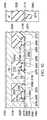
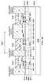
- FIG. 1illustrates a block diagram of an embodiment of a power converter including a semiconductor device
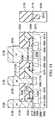
- FIGS. 2A and 2Billustrate isometric views of an embodiment of an electronic device/power converter before encapsulation
- FIG. 3illustrates a cross-sectional view of an embodiment of a portion of a semiconductor device
- FIG. 4illustrates an elevation view of an embodiment of a semiconductor device showing an inverted semiconductor die coupled to a plurality of decoupling devices by metallic pillars;
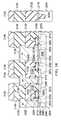
- FIG. 5illustrates a plan view of an embodiment of a semiconductor device formed with a circumferential ring distribution system
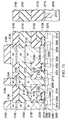
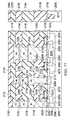
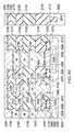
- FIG. 6illustrates a plan view of an embodiment of a redistribution layer formed as a deposition on a semiconductor die
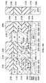
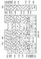
- FIG. 7illustrates a plan view of the redistribution layer illustrated in FIG. 6 with an overlay of an outline showing an N-LDMOS device and a P-LDMOS device;
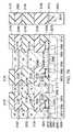
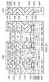
- FIGS. 8 and 9illustrate magnified plan views of the redistribution layer illustrated in FIG. 6 ;
- FIG. 10illustrates a schematic view of an embodiment of an N-type metal oxide semiconductor (“NMOS”) inverter chain configured to produce a large amplitude gate-drive signal illustrated in FIG. 1 for an N-LDMOS device from a pulse width modulated (“PWM”) signal;
- NMOSN-type metal oxide semiconductor
- PWMpulse width modulated
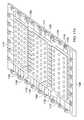
- FIG. 11illustrates a simplified three-dimensional view of an embodiment of a portion of a partially constructed N-LDMOS device embodied in a semiconductor device, or portions thereof;
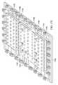
- FIG. 12illustrates a simplified three-dimensional view of a portion of the partially constructed N-LDMOS device after formation of a substantially planar second metallic layer
- FIG. 13illustrates a simplified plan view of a portion of the partially constructed N-LDMOS device after formation of the second-metallic layer
- FIG. 14illustrates a simplified three-dimensional view of a portion of the partially constructed N-LDMOS device after formation of a substantially planar third metallic layer
- FIG. 15illustrates a simplified plan view of a portion of the partially constructed N-LDMOS device after formation of the third metallic layer
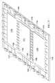
- FIG. 16illustrates a simplified three-dimensional view of an embodiment of a partially constructed semiconductor device including N-LDMOS and P-LDMOS devices illustrating a geometry of the source metallic strips and the drain metallic strips in a second metallic layer thereof;
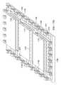
- FIG. 17illustrates a simplified three-dimensional view of the partially constructed semiconductor device including N-LDMOS and P-LDMOS devices illustrating a geometry of source and drain contacts in the third metallic layer;
- FIG. 17Aillustrates a simplified three-dimensional view of the partially constructed semiconductor device including N-LDMOS and P-LDMOS devices illustrating a geometry of vias for a redistribution layer;
- FIG. 17Billustrates a simplified three-dimensional view of the partially constructed semiconductor device including N-LDMOS and P-LDMOS devices illustrating a geometry of a redistribution layer;
- FIG. 17Cillustrates a simplified three-dimensional view of the partially constructed semiconductor device including N-LDMOS and P-LDMOS devices illustrating a geometry of pillars for the redistribution layer;
- FIG. 17Dillustrates a simplified three-dimensional view of the partially constructed semiconductor device including N-LDMOS and P-LDMOS devices illustrating a geometry of a conductive patterned leadframe;
- FIG. 18illustrates a three-dimensional external view of an embodiment of a potted semiconductor device including N-LDMOS and P-LDMOS devices;
- FIG. 19illustrates an elevational view of an embodiment of a portion of a semiconductor device including N-LDMOS and/or P-LDMOS devices;
- FIG. 20illustrates a cross-sectional view of an embodiment of an N-LDMOS device embodied in a semiconductor device, or portions thereof;
- FIGS. 21 through 87illustrate cross-sectional views of an embodiment of forming an N-LDMOS device embodied in a semiconductor device, or portions thereof;
- FIG. 88illustrates a cross-sectional view of an embodiment of a P-LDMOS device embodied in a semiconductor device, or portions thereof.
- FIG. 89illustrates a cross-sectional view of an embodiment of a P-LDMOS device embodied in a semiconductor device, or portions thereof.
- Embodimentswill be described in a specific context, namely, a switch (e.g., embodied in an LDMOS device), a semiconductor device incorporating the LDMOS device and methods of forming the same. While the principles of the present invention will be described in the environment of a power converter employing an LDMOS device, any application or related semiconductor technology that may benefit from a device that can switch at high speeds on a semiconductor substrate is well within the broad scope of the present invention.
- FIG. 1illustrated is a block diagram of an embodiment of a power converter including a semiconductor device.
- the power converterincludes a power train 110 , a controller 120 , and a driver 130 , and provides power to a system such as a microprocessor. While in the illustrated embodiment, the power train 110 employs a buck converter topology, those skilled in the art should understand that other converter topologies such as a forward converter topology are well within the broad scope of the present invention.
- the power train 110 of the power converterreceives an input voltage V in from a source of electrical power (represented by a battery) at an input thereof and provides a regulated output voltage V out to power, for instance, a microprocessor at an output of the power converter.
- a source of electrical powerrepresented by a battery
- V outa regulated output voltage
- the output voltage V outis generally less than the input voltage V in such that a switching operation of the power converter can regulate the output voltage V out .
- a main switch Qis generally less than the input voltage V in such that a switching operation of the power converter can regulate the output voltage V out .
- a P-channel metal oxide semiconductor field effect transistor (“MOSFET”) embodied in a P-type laterally diffused metal oxide semiconductor (“P-LDMOS”) deviceis enabled to conduct for a primary interval (generally co-existent with a primary duty cycle “D” of the main switch Q mn ) and couples the input voltage V in to an output filter inductor L out .
- a primary intervalgenerally co-existent with a primary duty cycle “D” of the main switch Q mn
- an inductor current L out flowing through the output filter inductor L outincreases as current flows from the input to the output of the power train 110 .
- An ac component of the inductor current L outis filtered by the output filter capacitor C out .
- auxiliary switch Q auxe.g., an N-channel MOSFET embodied in an N-type laterally diffused metal oxide semiconductor (“N-LDMOS”) device
- the auxiliary switch Q auxprovides a path to maintain a continuity of the inductor current I Lout flowing through the output filter inductor L out .
- the inductor current I Lout through the output filter inductor L outdecreases.
- the respective duty cycle of the main and auxiliary switches Q mn , Q auxcan be adjusted to maintain a regulation of the output voltage V out of the power converter.
- the conduction periods for the main and auxiliary switches Q mn , Q auxmay be separated by a small time interval to avoid cross conduction therebetween and beneficially to reduce the switching losses associated with the power converter.
- the controller 120 of the power converterreceives a desired power converter characteristic such as a desired system voltage V system from an internal or external source that may be associated with the microprocessor, and the output voltage V out of the power converter.
- a desired power converter characteristicsuch as a desired system voltage V system from an internal or external source that may be associated with the microprocessor, and the output voltage V out of the power converter.
- the controller 120provides a signal (e.g., a pulse width modulated (“PWM”) signal S PWM ) to control a duty cycle and a frequency of the main and auxiliary switches Q mn , Q aux of the power train 110 to regulate the output voltage V out thereof.
- PWMpulse width modulated
- the power converteralso includes the driver 130 configured to provide drive signals S DRV1 , S DRV2 to the main and auxiliary switches Q mn , Q aux , respectively, based on the PWM signal S PWM provided by the controller 120 .
- the driver 130typically includes switching circuitry incorporating a plurality of driver switches that cooperate to provide the drive signals S DRV1 , S DRV2 to the main and auxiliary switches Q mn , Q aux .
- any driver 130 capable of providing the drive signals S DRV1 , S DRV2 to control a switchis well within the broad scope of the present invention.
- the main and auxiliary switches Q mn , Q auxare power switches that can be incorporated into a semiconductor device proximate control or signal processing devices that perform the control functions of the controller 120 of the power converter.
- the control and signal processing devicesare typically complementary metal oxide semiconductor (“CMOS”) devices such as P-type metal oxide semiconductor (“PMOS”) devices and N-type metal oxide semiconductor (“NMOS”) devices.
- CMOScomplementary metal oxide semiconductor
- PMOSP-type metal oxide semiconductor
- NMOSN-type metal oxide semiconductor
- the PMOS and NMOS devicesmay also be referred to as P-channel and N-channel MOSFETs, respectively.
- Low voltagese.g., 2.5 volts
- the control and signal processing devicesare employed with the control and signal processing devices (hence, also referred to as “low voltage devices”) to prevent flashover between the fine line structures thereof.
- the main and auxiliary switches Q mn , Q aux of the power train 110 and ones of the plurality of driver switches of the driver 130may be formed by LDMOS devices that handle higher voltages (e.g., ten volts) and hence are referred to as higher voltage devices. Integrating the control and signal processing devices, power switches and driver switches on a semiconductor substrate provides opportunities for substantial reductions in cost and size of the power converter or other apparatus employing like devices.
- an input of the controller 120is coupled to or receives the output voltage V out of a power converter to regulate the output voltage V out .
- a controller 120may employ an error amplifier constructed with an analog operational amplifier with an inverting input coupled to the output voltage V out of the power converter.
- a non-inverting input of the error amplifieris coupled to a reference voltage representative of a desired, regulated output voltage of the power converter.
- a duty cycle of a power switch of the power converteris initiated by a clock signal. To terminate the duty cycle, the output of the error amplifier is compared by an analog comparator with a sloped voltage waveform that is typically a periodic ramp voltage waveform, or a periodic ramp voltage waveform with a superimposed scaled switch or inductor current.
- the duty cycle of the power switchis terminated by the analog comparator.
- the result of this controller structureis a feedback arrangement wherein the analog comparator continuously makes a decision to terminate the power switch duty cycle during the interval of time when the power switch is enabled to conduct.
- This analog controller architectureenables termination of a power switch duty cycle with fine temporal granularity that is not dependent on a clock frequency or on a computation rate of digital logic.
- Digital circuitrycan also be employed to construct a controller.
- the power converterincludes a magnetic device (e.g., an inductor), an integrated circuit, and surface-mount components.
- the power convertermay include power conversion circuitry that includes or may be embodied in the magnetic device, the integrated circuit, and at least one of the surface-mount components.
- the power conversion circuitrymay form a power converter that often includes a switching regulator or power converter such as a buck switching regulator with an integrated control circuit for reduced component count, and synchronous rectifiers for high power conversion efficiency.
- a switching regulator or power convertersuch as a buck switching regulator with an integrated control circuit for reduced component count, and synchronous rectifiers for high power conversion efficiency.
- an embodimentis not limited to a power module, power converter or the like, and may be applicable to other electronic devices.
- a conductive substrate (or leadframe) 210is patterned and etched to form an electrically conductive interconnect layer for the lower portion of a winding for the inductor as well as the electrical interconnections among surface-mount components, the integrated circuit, and the inductor.
- a typical thickness of the leadframe 210is about eight mils (thousandths of an inch). While the leadframe 210 is often constructed of copper, alternative electrically conductive materials can be used therefor.
- the leadframe 210provides external connections for the power module, as well as a support base for a magnetic material for the inductor. The external connections are formed as fingers of the leadframe 210 , referenced as leadframe fingers (two of which are designated 215 , 216 ).
- the leadframe 210is generally constructed with an integral metallic strip surrounding the electrically conductive pattern to provide mechanical support during the manufacturing steps, which metallic strip is discarded later in the manufacturing process.
- the surrounding metallic stripis generally sheared off after the electronic device has been constructed, for example to provide unconnected traces.
- the leadframe 210is generally produced in an array of repeating of patterns (not shown), such as a 16-by-16 array, to form, for example, 256 substantially identical electronic devices. Forming an array of leadframes 210 is a process well known in the art to reduce a manufacturing cost of producing electronic devices.
- Solder pasteis selectively applied to the leadframe 210 in a thin layer to areas (designated 225 ) for screening processes, to provide electrical and mechanical attachment for surface-mount components.
- the surface-mount componentssuch as capacitors (one of which is designated 220 ) are placed with their conductive ends in the solder paste.
- the solder pastemay be composed of lead-based as well as lead-free compositions.
- the array of leadframes 210 with the surface-mount components 220is reflowed in an oven to mechanically and electrically attach the surface-mount components 220 to the leadframe 210 .
- the steps as described abovegenerally do not require execution in a highly controlled environment of a clean room.
- the following steps, however,are preferably performed in a clean-room environment such as typically used for assembly of integrated circuits into a molded plastic package, as is generally well known in the art.
- An adhesivee.g., a die attach adhesive such as Abletherm 2600AT by Ablestik of Rancho Dominguez, Calif.
- a magnetic coree.g., a bar of magnetic material
- the bar of magnetic material 230 and the semiconductor die 240are positioned on the leadframe 210 over the die-attach adhesive.
- a lower surface of the bar of magnetic material 230faces, and is preferably adhered to, the leadframe 210 .
- the bar of magnetic material 230is included to enhance the magnetic properties of the inductor and may be about 250 micrometers (“ ⁇ m”) thick, four mils wide and 7.5 mils long.
- the adhesiveis cured, typically in a controlled thermal process, to secure the bar of magnetic material 230 and the semiconductor die 240 to the leadframe 210 .
- solder pasteis applied to areas (generally designated 260 ) of the leadframe 210 wherein ends of conductive clips 250 are placed.
- the solder pastemay be composed of lead-based as well as lead-free compositions.
- the conductive clips 250(e.g., about 8-12 mils thick) are placed on the leadframe 210 above the bars of magnetic material 230 with their ends in the solder paste.
- the conductive clips 250are formed with their ends bent toward the leadframe 210 about ends of the bar of magnetic material 230 without mechanical interference. Thus, an upper surface of the bar of magnetic material 230 faces the conductive clips 250 .
- An insulating gapfor example, about a five mil air gap, is thus preferably left between the upper surfaces of the bars of magnetic material 230 and the lower surfaces of the conductive clips 250 , which gap may be filled later by an encapsulant.
- the conductive clips 250provide a portion of the electrically conductive inductor winding above each bar of magnetic material 230 .
- the leadframe 210is heated in a reflow oven to mechanically and electrically bond the conductive clips 250 to the leadframe 210 .
- Wire bonds that may be formed of gold wire such as a first wire bond 265are attached to each semiconductor die 240 and to the leadframe 210 to electrically couple pads on the semiconductor die 240 to bonding areas of the leadframe 210 , thereby providing electrical circuit connections therebetween.
- Wire bonds such as a second wire bond 266may also be used to selectively electrically couple portions of the leadframe 210 to provide circuit interconnections that cannot be easily wired in a single planar layout, thus producing the topological layout functionality for the leadframe 210 of a two-layer printed circuit board (also referred to as “printed wiring board”) or substrate.
- the arrayis placed in a mold, and an encapsulant such as a molding material, preferably epoxy, is deposited (e.g., injected) thereover as is well known in the art to provide environmental and mechanical protection as well as a thermally conductive covering to facilitate heat dissipation during operation.
- an encapsulantsuch as a molding material, preferably epoxy
- a molding materialpreferably epoxy
- Other molding materials and processes as well as electronic devices constructed without an encapsulantare well within the broad scope of the present invention.
- FIG. 3illustrated is a cross-sectional view of an embodiment of a portion of a semiconductor device.
- processing steps to construct the semiconductor device illustrated with respect to FIG. 3are analogous to processing steps described by U.S. Pat. No. 7,230,302 entitled “Laterally Diffused Metal Oxide Semiconductor Device and Method of Forming the Same,” by Lotfi, et al., filed Jan. 29, 2004, U.S. Pat. No. 8,212,315 entitled “Integrated Circuit with a Laterally Diffused Metal Oxide Semiconductor Device and Method of Forming the Same,” by Lotfi, et al., filed Aug. 28, 2009, U.S. Patent Application Publication No.
- 2007/0284658entitled “Laterally Diffused Metal Oxide Semiconductor Device and Method of Forming the Same,” by Lotfi, et al., filed Aug. 20, 2007, U.S. Patent Application Publication No. 2012/0306011, entitled “Integrated Circuit with a Laterally Diffused Metal Oxide Semiconductor Device and Method of Forming the Same,” by Lotfi, et al., filed Aug. 15, 2012, which are hereby incorporated herein by reference, the steps in the process will not be described at this point in detail. Nonetheless, process steps will be described later herein for construction of a similar device.
- the cross-sectional view illustrated in FIG. 3illustrates individual LDMOS cells of P-LDMOS and N-LDMOS devices that are constructed with a large number of such individual cells.
- the pattern of individual cells illustrated in FIG. 3is repeated with mirroring as necessary to produce a P-LDMOS or N-LDMOS device with a suitable current rating for an application.
- a substrateis thereby formed, e.g., with a plurality of heavily doped source regions and heavily doped drain regions.
- the semiconductor deviceis formed in a semiconductor die including shallow trench isolation regions 310 within a substrate 315 (e.g., a P-type substrate) to provide dielectric separation between PMOS, NMOS, P-LDMOS and N-LDMOS devices.
- An epitaxial layer 316e.g., a P-type epitaxial layer
- a buried layer (e.g., an N-type buried layer) 320is recessed within the substrate 315 in the area that accommodates the P-LDMOS device and the N-LDMOS device.
- the semiconductor devicealso includes wells (e.g., N-type wells) 325 formed in the substrate 315 in the areas that accommodate the PMOS device and the P-LDMOS device, and under the shallow trench isolation regions 310 above the N-type buried layer 320 (for the P-LDMOS).
- the N-type wells 325are formed to provide electrical isolation for the PMOS device and the P-LDMOS device and operate cooperatively with the N-type buried layer 320 (in the case of the P-LDMOS device) and the shallow trench isolation regions 310 to provide the isolation.
- the N-type well 325 above the N-type buried layer 320does not cover the entire area that accommodates the P-LDMOS device in the substrate 315 between the shallow trench isolation regions 310 thereof.
- the N-type wells 325 for the P-LDMOSare constructed as such for the reasons as set forth herein.
- the semiconductor deviceincludes additional wells (e.g., P-type wells) 330 formed in the substrate 315 between the shallow trench isolation regions 310 substantially in the areas that accommodate the NMOS device and N-LDMOS device. While the P-type well 330 above the N-type buried layer 320 covers the entire area that accommodates the N-LDMOS device in the substrate 315 between the shallow trench isolation regions 310 thereof, it is well within the broad scope of the present invention to define the P-type well 330 to cover a portion of the area that accommodates the N-LDMOS device in the substrate 315 .
- the semiconductor devicealso includes gates 340 for the PMOS, NMOS, P-LDMOS and N-LDMOS devices located over a gate dielectric layer 335 and including gate sidewall spacers 355 about the gates 340 thereof.
- the N-LDMOS deviceincludes lightly doped voltage withstand enhancement regions (e.g., N-type lightly doped regions) 345 for the drain thereof.
- the P-LDMOS devicealso includes lightly doped voltage withstand enhancement regions (e.g., P-type lightly doped regions) 350 for the drain thereof.
- the N-type and P-type lightly doped regions 345 , 350provide higher voltage ratings for the N-LDMOS and P-LDMOS devices, respectively.
- the N-LDMOS and P-LDMOS deviceshandle higher voltages from the drain-to-source thereof, but the devices can handle a higher voltage from a source-to-gate thereof when the source is more positive than the gate 340 .
- the width of the N-type and P-type lightly doped regions 345 , 350may be individually varied to alter breakdown voltage characteristics of the respective N-LDMOS and P-LDMOS devices without departing from the scope of the present invention. Additionally, the N-type and P-type lightly doped regions 345 , 350 may be formed in a manner similar to the respective N-LDMOS and P-LDMOS devices illustrated and described with respect to FIGS. 2 through 15 in U.S. Pat. No. 7,230,302, cited previously hereinabove.
- the semiconductor devicealso includes heavily doped regions (e.g., N-type heavily doped regions) 360 for the source and drain of the NMOS device that preferably have a different doping concentration profile than heavily doped regions (e.g., N-type heavily doped regions) 362 for the source and drain of the N-LDMOS device.
- the N-type heavily doped regions 360 for the NMOS deviceare formed within the P-type well 330 thereof and, as alluded to above, form the source and the drain for the NMOS device.
- the N-type heavily doped regions 362 for the N-LDMOS deviceare formed within the P-type well 330 thereof.
- the N-type heavily doped region 362 of the drain for the N-LDMOS deviceis adjacent to the N-type lightly doped drain region 345 thereof.
- the semiconductor devicealso includes heavily doped regions (e.g., P-type heavily doped regions) 365 for the source and drain of the PMOS device that preferably have a different doping concentration profile than heavily doped regions (e.g., P-type heavily doped regions) 367 for the source and drain of the P-LDMOS device.
- the P-type heavily doped regions 365 for the PMOS deviceare formed within the N-type well 325 thereof and, as alluded to above, form the source and the drain for the PMOS device.
- the P-type heavily doped regions 367 for the P-LDMOS deviceare formed within the N-type well 325 or in regions adjacent to the N-type well 325 thereof and form a portion of the source and the drain for the P-LDMOS device.
- the P-type heavily doped region 367 of the drain for the P-LDMOS deviceis adjacent to the P-type lightly doped region 350 thereof.
- the N-type well 325 above the N-type buried layer 320does not cover the entire area that accommodates the P-LDMOS device in the substrate 315 between the shallow trench isolation regions 310 thereof.
- the N-type well 325is located under and within a channel region 370 , and the N-type well 325 and N-type buried layer 320 are oppositely doped in comparison to the P-type lightly and heavily doped regions 350 , 367 .
- doped regions (e.g., P-type doped regions) 372 of a same doping type as the lightly doped regions 350extend between the P-type heavily doped regions 367 of the drain and the N-type well 325 of the P-LDMOS device and have a doping concentration profile less than a doping concentration profile of the P-type heavily doped regions 367 .
- the P-type heavily doped regions 367preferably have the same doping concentration profiles, it is well within the broad scope of the present invention that the P-type heavily doped region 367 for the source has a different doping concentration profile than the counterpart of the drain. The same principle applies to other like regions of the devices of the semiconductor device.
- the doped regions 372 of same doping type as the lightly doped regions 350together separate the heavily doped regions 367 of the drain from the channel regions 370 formed in the oppositely doped N-type wells 325 .
- the P-type doped regions 372may happen to be embodied in the substrate 315 which has a doping concentration profile between 1 ⁇ 10 14 and 1 ⁇ 10 16 atoms/cm 3 .
- Employing the substrate 315 as the P-type doped regions 372provides an opportunity to omit a masking and a processing step in the manufacture of the semiconductor device.
- the P-type doped regions 372may be formed by an ion implantation process prior to implanting the P-type heavily doped regions 367 for the source and the drain of the P-LDMOS device.
- the P-type doped regions 372may be formed with any doping concentration profile less than the P-type heavily doped regions 367 .
- incorporación of the P-type doped regions 372 into the P-LDMOS devicefurther increases a breakdown voltage between the P-type heavily doped regions 367 and the N-type well 325 of the P-LDMOS device.
- the P-LDMOS devicetherefore, exhibits a higher drain-to-source voltage handing capability due to the higher breakdown voltage thereof and provides a higher source-to-gate voltage handling capability as well when the source is more positive than the gate 340 . It should be understood that while the doped regions have been described with respect to the P-LDMOS device, the principles are equally applicable to the N-LDMOS device and, for that matter, other transistors of analogous construction.
- the P-LDMOS and N-LDMOS devices illustrated and described with respect to FIG. 3are referred to as asymmetrical devices.
- the asymmetrical nature of the source and drain of the semiconductor device of FIG. 3provide for an asymmetrical device.
- the semiconductor devicealso includes metal contacts 385 defined by dielectric regions 380 formed over silicide layers (one of which is designated 375 ) for the gate, source, and drain of the PMOS, NMOS, P-LDMOS, and N-LDMOS devices.
- a semiconductor devicealso referred to as a “power semiconductor device” includes one or more decoupling capacitors placed under a semiconductor die including a MOSFET embodied in an LDMOS device (also referred to as a “power MOSFET” or “enhanced MOSFET”), preferably in a distributed fashion, to reduce an impedance of a voltage source employed for the drivers.
- the driverscan be distributed on the periphery of the semiconductor die to substantially equalize timing of drive signals coupled to individual MOS cells for MOS devices and LDMOS cells for LDMOS devices.
- an LDMOS deviceis formed by coupling sources and drains of a large number of small LDMOS cells in parallel in a common die (e.g., 100,000 or more cells), and driving the individual gates of the LDMOS cells in parallel from a common circuit node.
- a design challengeis to match the timing of signals coupled to the individual gates so that the LDMOS cells are turned on or off substantially simultaneously. Inability to maintain synchronization of the signals to the individual gates can result in semiconductor device failure. In conventional designs, high-frequency characteristics of gate signals are suppressed so that the resulting lower-frequency signals arrive substantially simultaneously.
- a structure to efficiently route signals into and out of an LDMOS device formed within a semiconductor dieIn an embodiment, a plurality of LDMOS cells are formed within the semiconductor die. Distributed circumferential signal paths are formed within the semiconductor die with distributed three-dimensional decoupling using metallic pillars (e.g., elongated copper pillars) that can be formed with an aspect ratio (e.g., equal to or greater 1 to 1), to extract current from the drain or source contacts (or from emitter or collector contacts) of the LDMOS device to distributed decoupling devices.
- This structuredoes not rely on an intermediary conventional package pin and solder joint to a board with a single point of decoupling.
- the drain and source contactsare contacted, but need not be routed, through traditional top-level chip metallization as used in conventional integrated circuit devices. Rather, a grid of metallic pillars is used that contact a conductive, patterned leadframe such as a conductive, patterned leadframe formed on an upper surface of a printed circuit board in multiple locations with a plurality of small decoupling devices (e.g., decoupling capacitors).
- the decoupling devicesare distributed and placed in a third dimension beneath the printed circuit board.
- the decoupling devicesare placed on a conductive, patterned leadframe on a lower surface of the printed circuit board below the semiconductor die.
- the conductive, patterned leadframe on the upper surface of the printed circuit boardis coupled to the conductive, patterned leadframe on the lower surface of the printed circuit board by a plurality of vias.
- the effect of an electrically long transmission lineis thus defeated by using multiple, distributed, decoupling devices that are placed in the third dimension via the leadframes and the vias below the grid of metallic pillars.
- a conductive, patterned leadframemay be packaged with the semiconductor die and then placed on a printed circuit board.
- a bumpis typically formed using deposition methods such as vapor deposition of solder material or by ball bumping with wire-bonding equipment.
- deposition methodssuch as vapor deposition of solder material or by ball bumping with wire-bonding equipment.
- the manufacturing implications for such a manufacturing processmay be too costly to be deemed practical as described in U.S. Pat. No. 7,989,963, entitled “Transistor Circuit Formation Substrate,” by Simon Tam, filed Mar. 14, 2008.
- a plurality of driversis positioned on the periphery of the power semiconductor die to equalize gate timing and to provide low gate-drive impedance for a driver.
- Physical structuresare produced on metallic strips and on the semiconductor die to improve a redistribution layer (“RDL”) and the switch output capacitance C oss .
- the metallic stripssuch as aluminum strips are formed and positioned to route gate signals to individual LDMOS cells to reduce gate resistance and improve equalization of timing of gate-drive signals.
- a gate-drive bias voltage “VDDR” bus and ground (“GND” or “PGND”) railsare bumped to reduce gate-drive supply impedance.
- This structureenables gate-drive signals to arrive at the respective gates of the LDMOS cells at effectively the same time.
- Decoupling devices for the gate-drive bias voltage busare placed in paths lying directly under the semiconductor die in a distributed way. The result is that low impedance is presented to signals conducted along gate-drive transmission lines formed as metallic strips.
- the metallic strips for the gate-drive signalsextend on the semiconductor die from the periphery for connections to the LDMOS cells in a central region thereof.
- the metallic stripsare employed for the gate-drive connections from the die periphery to the LDMOS cells.
- Metallic pillarsare formed as electroplated metallic (e.g., copper) columns to couple an external decoupling device positioned under the semiconductor die to a point thereon.
- at least one decoupling deviceis positioned directly under the semiconductor die.
- a pillar and a decoupling deviceare coupled to an end of ones of the metallic strips for the gate-drive signals.
- pottingis formed over to provide structural support and protection for the metallic pillars.
- FIG. 4illustrated is an elevational view of an embodiment of a semiconductor device 405 showing an inverted semiconductor die 410 coupled to a plurality of decoupling devices (e.g., decoupling or chip capacitors 440 , 441 ) by metallic pillars (such as an elongated copper pillar or pillar 490 ).
- decoupling devicese.g., decoupling or chip capacitors 440 , 441
- metallic pillarssuch as an elongated copper pillar or pillar 490 .
- Localized decouplingis achieved by use of the metallic pillars 490 and the decoupling capacitors 440 , 441 at positions needing decoupling such as at positions at the periphery of the semiconductor die 410 .
- Placement of one or more decoupling capacitors 440 , 441can be made substantially below a corresponding pillar 490 , either directly above or directly below the semiconductor die 410 , to reduce circuit path inductance.
- Placement of a decoupling devicee.g., decoupling or chip capacitor 445
- a low inductance zone 450that is substantially under the semiconductor die 410 (e.g., in a zone 455 that is outside the semiconductor die area) produces a higher inductance that may reduce the performance of the decoupling capacitor 445 .
- the decoupling capacitors 440 , 441are located entirely under the semiconductor die area of the semiconductor device 405 .
- the metallic pillars 490can also be used to couple to high-current source and drain terminals of the LDMOS cells of a LDMOS device located in a more centralized region of the semiconductor die 410 .
- a photoresiste.g., a half mil ( ⁇ 12 ⁇ m) photoresist
- the photoresistis then removed so that cantilevered, conductive pillars remain.
- aluminumis deposited first, followed by a tin-copper or flash/seed layer copper deposit and electroplating.
- the metallic pillars 490are surrounded with plastic 495 (e.g., an encapsulant such as epoxy or a polyimide) with an end of each metallic pillar 490 exposed on a surface of the plastic 495 .
- the metallic pillars 490may be formed in, and may extend from, a polyimide layer.
- the metallic pillars 490contact lands of a conductive patterned leadframe 420 defined by artwork on an upper surface of a printed circuit board 430 .
- the metallic pillars 490are reflow soldered to the conductive patterned leadframe 420 .
- Viase.g., one of which is designated 461 ) are constructed in the printed circuit board 430 to provide a coupling of the metallic pillars 490 to a conductive patterned leadframe 421 on a lower surface of the printed circuit board 430 and to terminals of the decoupling capacitors 440 , 441 , 445 .
- the decoupling capacitors 440 , 441 , 445are reflow soldered with an array of solder bumps (e.g., one of which is designated 463 ) to lands of the conductive patterned leadframe 421 on the lower surface of printed circuit board 430 .
- the landsare small geometric structures such as circular areas in the patterned leadframe conducive to a reflow soldering operation to attach a component.
- An array of solder bumps(e.g., one of which is designated 462 ) is positioned on lands of the conductive patterned leadframe 420 on the upper surface of printed circuit board 430 .
- the decoupling capacitors 440 , 441 , 445are placed on lands a short vertical distance from nodes on the periphery of the semiconductor die 410 to produce low impedance to local circuit ground for these nodes.
- the metallic pillars 490are coupled by the solder bumps 462 to the conductive patterned leadframe 420 .
- the semiconductor die 410is flipped before attachment to the printed circuit board 430 as illustrated in FIG. 4 , and as a result the metallic pillars 490 under the semiconductor die 410 provide electrical contacts with the “top” side thereof. Since the device is a high-power device, a heat sink 470 is mounted on a “lower” surface of the semiconductor die 410 (via an adhesive 480 ), which is illustrated above the semiconductor die 410 in the top portion of FIG. 4 , so that the decoupling capacitors 440 , 441 , 445 can be mounted on the printed circuit board 430 below the top side of the flipped semiconductor die 410 . The heat sink 470 thus contacts the lower surface of the semiconductor die 410 .
- the metallic pillars 490enable the decoupling capacitors 440 , 441 , 445 to be placed on the printed circuit board 430 in close proximity to the top side of the semiconductor die 410 , and the vias 461 are formed through the printed circuit board 430 to couple the semiconductor die 410 to the array of decoupling capacitors 440 , 441 , 445 under the printed circuit board 430 .
- a distributed decoupling functionis provided for the power semiconductor device 405 .
- the same or a different leadframecan be used to couple to the grid of solder bumps or pillars and other circuit elements.
- An example leadframeis 6 millimeters (“mm”) ⁇ 6 mm. The structure illustrated in FIG.
- an inverted semiconductor (e.g., silicon) dieis coupled to an upper surface of a printed wiring or circuit board by elongated metallic pillars, and decoupling devices are coupled to a lower surface of the printed circuit board below the semiconductor die.
- decoupling devicesare coupled to a lower surface of the printed circuit board directly below the semiconductor die.
- the conductive patterned leadframe 420may be packaged with the semiconductor die 410 and metallic pillars 490 within a packaged semiconductor device and then placed on a printed circuit board 430 with the array of decoupling capacitors 440 , 441 , 445 thereunder (see, e.g., FIG. 18 for the packaged semiconductor device).
- FIG. 5illustrated is a plan view of an embodiment of a semiconductor device formed with a circumferential ring distribution system.
- An N-LDMOS device 530 and a P-LDMOS device 531represent a pair of LDMOS devices that form a power stage of, for example, a buck or boost dc-dc power converter. As stated previously hereinabove, each LDMOS device is formed of a large number of individual LDMOS cells.
- FIG. 5shows the N-LDMOS device 530 and the P-LDMOS device 531 and drive final stages such as the N gate-drive final stage 510 and the P gate-drive final stage 520 that are on the periphery of the semiconductor die (of the power semiconductor device).
- a conventional designemploys only one structure for the N gate-drive final stage 510 and only one structure for the P gate-drive final stage 520 located on one end of the semiconductor die. Distributing a plurality of drive final stages around a periphery of the semiconductor die for each of the LDMOS device 530 and the P-LDMOS device 531 substantially improves timing of the drive signals coupled to the individual LDMOS cells.
- Within each drive final stageis a totem-pole arrangement of P-MOS cells coupled in series with N-MOS cells driven by a cascaded buffer. The drive final stages are electrically coupled in parallel.
- the gate-drive signals on the control or gate terminalsshould arrive at substantially the same time and with substantially the same amplitude. Attenuating high-frequency characteristics of the gate-drive signals with a capacitor to improve relative simultaneity compromises efficiency of high-frequency operation.
- a plurality of decoupling devicesare included in the design to provide low impedance for the gate-drive bias voltage VDDG bus for the gate drivers, not to slow down the gate drivers. The decoupling devices reduce the impedance of the gate-drive bias voltage VDDG bus that is supplied to the distributed drivers. Some propagation delay variation for gate-drive signals still remains, but the largest part thereof is removed by the distributed gate-drive structure.
- FIG. 6illustrated is a plan view of an embodiment of a redistribution layer formed as a deposition on a semiconductor die.
- the redistribution layere.g., a copper redistribution layer
- the redistribution layeris also employed to distribute control and monitoring signals to the gate drivers.
- the small round circlesare locations of elongated metallic (e.g., copper) pillars that couple the LDMOS cells and other circuit nodes to a conductive (e.g., copper) patterned leadframe 420 that was described previously hereinabove with reference to FIG. 4 or a leadframe 1179 described below with reference to FIG. 17 D.
- the small round circles labeled “SW”(one of which is designated 610 ) form a circuit node coupling the drains of the P- and N-LDMOS cells together and to an external output inductor such as the output inductor L out illustrated in FIG. 1 .
- the small round circles labeled “PVIN,”(one of which is designated 620 ) provide a positive bias voltage to the sources of the LDMOS cells forming the high-side P-LDMOS device, and the small round circles labeled “PGND,” (one of which is designated 630 ) provide local circuit ground to the sources of the LDMOS cells forming the low-side N-LDMOS device.
- VDDGsmall round circles labeled “VDDG,” (one of which is designated 640 ) supplies positive bias voltage to the gate-drive inverters (also referred to as “gate drivers” or “drivers”) that drive the gates of the LDMOS cells, and the small round circle labeled “PGND,” (one of which is designated 650 ) supplies local circuit ground to the gate-drive inverters.
- gate-drive invertersalso referred to as “gate drivers” or “drivers”
- PGNDsmall round circle labeled “PGND”
- FIG. 7illustrated is a plan view of the redistribution layer illustrated in FIG. 6 with an overlay of an outline showing the N-LDMOS device 530 and the P-LDMOS device 531 (see FIG. 5 ).
- outlines showing the locations of the N gate-drive final stage 510 and P gate-drive final stage 520are also shown.
- the N-LDMOS device 530is formed with 220,000 stripes, each stripe representing an N-LDMOS cell being about 20 microns wide and about 2-3 microns in channel length.
- the P-LDMOS device 531is formed with 120,000 stripes of about the same size.
- FIGS. 8 and 9illustrated are magnified plan views of the redistribution layer illustrated in FIG. 6 .
- a path 800provides the positive gate-drive bias voltage VDDG bus for the gate-drive inverters, and a path 805 provides local circuit ground for the inverters.
- a path N_Dry 810is the gate-drive signals produced by the gate-drive inverters.
- a path N_Dry 830is on another copper/metallic layer and is electrically common with the path N_Dry 810 . The path N_Dry 830 is coupled to the gates of the N-LDMOS cells.
- the paths 820are further metallizations (e.g., 20 ⁇ m metallizations) under the redistribution layer, and the paths 840 are representations of 20 ⁇ m metallizations coupled to gate polysilicon layers or strips (generally referred to as “gates”) of the N-LDMOS cells.
- FIG. 9illustrates gate polysilicon strips 910 of the N-LDMOS cells. It should be understood that the gates may be formed from other materials such as an electrically conductive metallic material.
- FIG. 10illustrated is a schematic view of an embodiment of an NMOS inverter chain configured to produce a large amplitude gate-drive signal S DRV2 illustrated in FIG. 1 , for an N-LDMOS device from a PWM signal S PWM .
- An even number (e.g., four) sequence of inverters as illustrated in FIG. 10produces the large amplitude gate-drive signal S DRV2 with a same sense from the low amplitude duty-cycle signal S PWM .
- the NMOS inverter chainsare labeled “N gate drive final stage” on FIGS. 5 and 7 , and are distributed around the periphery of the device.
- the output stage of the inverter chainis formed with a parallel-drive arrangement of first and second inverters 1010 , 1020 .
- the first inverter 1010is formed with PMOS device 1011 and NMOS device 1012 .
- the second inverter 1020is formed with PMOS device 1021 and a NMOS device 1022 .
- the first inverter 1010is driven by a third inverter 1030 which is formed with smaller MOS devices, typically about one third the size of the MOS devices in the first inverter 1010 .
- the third inverter 1030is driven by a fourth inverter 1040 formed with MOS devices that are about one third the size of the MOS devices in the third inverter 1030 .
- the PWM signal S PWM illustrated in FIG. 1is successively amplified in stages formed with successively larger MOS devices to produce the gate-drive signal S DRV2 illustrated in FIG. 1 of sufficient amplitude to drive the auxiliary switch Q aux illustrated in FIG. 1 .
- a PMOS inverter chain corresponding to the NMOS inverter chain illustrated in FIG. 10can be constructed with an even number of inverter stages to produce a large amplitude, same-sense gate-drive signal for a P-LDMOS device from the low-amplitude input signal S PWM .
- the PMOS inverter chainwould thus be operated in a complementary time period to the NMOS inverter chain, and with sufficient time separation to avoid shoot-through currents in the series-circuit arrangement of a main switch Q mn and the auxiliary switch Q aux illustrated in FIG. 1 . While the NMOS and PMOS inverter chains are described employing NMOS and PMOS devices, it should be understood that N-LDMOS and P-LDMOS devices may be used to advantage.
- the semiconductor deviceincludes a semiconductor die formed with a plurality of LDMOS cells, a redistribution layer electrically coupled to the plurality of LDMOS cells, a plurality of metallic pillars (e.g., copper pillars formed as electroplated columns) distributed over and electrically coupled to the redistribution layer, and a conductive patterned leadframe electrically coupled to the redistribution layer by the plurality of metallic pillars.
- the semiconductor devicefurther includes a gate driver electrically coupled to the redistribution layer and to gates of the plurality of LDMOS cells through the redistribution layer.
- the semiconductor deviceis potted with an encapulant with portions of the conductive patterned leadframe being exposed to serve as external contacts for the semiconductor device.
- Ones of the external contactsare coupled to a printed circuit board and ones of the external contacts are coupled to a plurality of decoupling devices (e.g., through vias on an opposing surface of the printed circuit board). At least one of the plurality of decoupling devices is located under the semiconductor die.
- Ones of the external contactsare coupled to gate drivers electrically coupled to the redistribution layer and to gates of the plurality of LDMOS cells through the redistribution layer and ones of the external contacts are coupled to drains or sources of the plurality of the LDMOS cells through the redistribution layer.
- FIG. 11illustrated is a simplified three-dimensional view of an embodiment of a portion of a partially constructed N-LDMOS device embodied in a semiconductor device, or portions thereof.
- various features in this and subsequent drawingsare not drawn to scale. The dimensions of the various features may be arbitrarily increased or decreased for clarity of the discussion herein, and like reference numbers may be employed for analogous features of different devices that make up the semiconductor device.
- the N-LDMOS deviceis formed in a semiconductor die including a lightly doped P substrate 1105 and a P-well 1108 implanted in the lightly doped P substrate 1105 .
- the P-well 1108includes a sequence of doped source regions “s” and drain regions “d” in an alternating pattern, laid out as parallel strips in the P-well 1108 or directly on the lightly doped P substrate 1105 when the optional P-well 1108 is not implanted.
- Source metallic (e.g., aluminum) stripsare formed in a substantially planar first metallic (e.g., aluminum) layer M 1 and lie over and electrically contact the doped source regions “s,” but not to each other.
- drain metallic (e.g., aluminum) stripsare also formed in the first metallic layer M 1 and lie over and electrically contact the doped drain regions “d,” but not to each other.
- a plurality of alternating source and drain metallic stripsare formed in the first metallic layer M 1 above the lightly doped P substrate 1105 and parallel to and forming an electrical contact (e.g., through a silicide layer) with respective ones of a plurality of source and drain regions.
- Gate oxide stripsisolate polysilicon gate strips (one of which is designated 1150 ) from the underlying P-well 1108 or from the lightly doped P substrate 1105 when the optional P-well 1108 is not implanted.
- a plurality of gate polysilicon strips 1150are formed over the lightly doped P substrate 1105 between and parallel to ones of the plurality of source and drain regions and oriented parallel to the plurality of alternating source and drain metallic strips.
- Not shown in FIG. 11are additional and differently doped strips formed in the P-well 1108 or in the lightly doped P substrate 1105 that lie between and separate the doped source regions “s” and the doped drain regions “d”.
- a gate metallic (e.g., aluminum) strip 1130 in the first metallic layer M 1is positioned over, aligned perpendicular to, and is electrically coupled to the gate polysilicon strips 1150 .
- FIG. 12illustrated is a simplified three-dimensional view of a portion of the partially constructed N-LDMOS device after formation of a substantially planar second metallic (e.g., aluminum) layer M 2 .
- the second metallic layer M 2is formed in strips such as source metallic (e.g., aluminum) strips (one of which is designated 1160 ) and drain metallic (e.g., aluminum) strips (ones of which is designated 1161 ) that lie over respective source metallic strips 1111 , 1112 and drain metallic strips 1121 , 1122 formed in the first metallic layer M1.
- An isolation or insulating layer of silicon oxynitride(see, e.g., FIG. 19 ) separates and electrically isolates the first metallic layer from the second metallic layer.
- the source metallic strips 1160 in the second metallic layer M 2 layer that lie over the source metallic strips 1111 , 1112 in the first metallic layer M 1are coupled thereto by electrically conductive vias.
- the drain metallic strips 1161 in the second metallic layer M 2 layer that lie over the drain metallic strips 1121 , 1122 in the first metallic layer M 1are coupled thereto by electrically conductive vias.
- a second plurality of alternating source and drain metallic stripsare formed in the second metallic layer M 2 above the first metallic layer M 1 overlying and parallel to ones of the first plurality of alternating source and drain metallic strips.
- the first plurality of source and drain metallic stripsare electrically coupled by vias to the respective second plurality of alternating source and drain metallic strips.
- the source and drain metallic strips 1160 , 1161 in the second metallic layer M 2are not coupled to the gate metallic strip 1130 in the first metallic layer M 1 that intersects and is electrically coupled to the gate polysilicon strips 1150 .
- FIG. 13illustrated is a simplified plan view of a portion of the partially constructed N-LDMOS device after formation of the second-metallic layer M 2 .
- FIG. 13illustrates vias (one of which is designated 1175 ) that electrically couple source metallic strips 1111 , 1112 , 1113 , 1114 in the first metallic layer M 1 to source metallic strips 1160 , 1162 in the second metallic layer M 2 .
- vias(one of which is designated 1176 ) electrically couple drain metallic strips 1121 , 1122 , 1123 , 1124 in the first metallic layer M 1 to drain metallic strips 1161 , 1163 in the second metallic layer M 2 .
- the vias 1175 , 1176enetrate an isolation or insulating layer (see, e.g., insulating layers 1915 in FIG. 19 ) that separate and electrically isolates (insulates) the first metallic layer M 1 from the second metallic layer M 2 . It is noted that, in an embodiment, vias do not electrically couple the gate metallic strip 1130 in the first metallic layer M 1 to either the source metallic strips 1160 , 1162 or the drain metallic strips 1161 , 1163 in the second metallic layer M 2 .
- FIG. 14illustrated is a simplified three-dimensional view of a portion of the partially constructed N-LDMOS device after formation of a substantially planar third metallic (e.g., aluminum) layer M 3 .
- the third metallic layer M 3overlies the second metallic layer M 2 .
- FIG. 14illustrates N-LDMOS device source contact 1170 formed in the third metallic layer M 3 , and N-LDMOS device drain contact 1171 , also formed in the third metallic layer M 3 .
- An isolation or insulating layer of silicon oxynitride(see, e.g., FIG. 19 ) separates and electrically isolates the second metallic layer from the third metallic layer.
- the N-LDMOS device drain contact 1171is shared with a P-LDMOS device drain contact formed on the same die (also referred to as an “N-LDMOS/P-LDMOS device drain contact” 1171 ).
- the N-LDMOS device source contact 1170is electrically coupled to the source metallic strips (one of which is designated 1160 ) in the second metallic layer M 2 by vias (e.g., aluminum vias not shown in FIG. 14 ).
- the N-LDMOS/P-LDMOS device drain contact 1171is electrically coupled to the drain metallic strips (one of which is designated 1161 ) in the second metallic layer M 2 by vias (e.g., aluminum vias not shown in FIG. 14 ).
- the source and drain contacts formed in the third metallic layer M 3are electrically coupled by vias to ones of the second plurality of alternating source and drain metallic strips in the second metallic layer M 2 and substantially cover the plurality of source and drain regions.
- FIG. 15illustrated is a simplified plan view of a portion of the partially constructed N-LDMOS device after formation of the third metallic layer M 3 .
- FIG. 15illustrates vias (one of which is designated 1180 ) that electrically couple the N-LDMOS device source contact 1170 formed in the third metallic layer M 3 to the source metallic strips 1160 , 1162 , 1164 in the second metallic layer M 2 .
- viasone of which is designated 1181
- viasthat electrically couple the N-LDMOS/P-LDMOS device drain contact 1171 formed in the third metallic layer M 3 to P-LDMOS device drain metallic strips 1185 , 1187 , 1189 in the second metallic layer M 2 of a P-LDMOS device.
- P-LDMOS source metallic strips 1184 , 1186 , 1188 in the second metallic layer M 2 of the P-LDMOS deviceare electrically coupled by vias to a P-LDMOS device source contact in the third metallic layer M 3 (not shown in FIG. 15 ).
- the vias 1180 , 1181 , 1182penetrate an isolation or insulating layer (see, e.g., insulating layers 1915 in FIG.
- FIG. 15Also illustrated in FIG. 15 is the gate metallic strip 1130 in the first metallic layer M 1 that intersects and is electrically coupled to the gate polysilicon strips 1150 (see FIG. 14 ).
- FIG. 16illustrated is a simplified three-dimensional view of an embodiment of a partially constructed semiconductor device including N-LDMOS and P-LDMOS devices illustrating a geometry of the source metallic strips and the drain metallic strips in the second metallic layer M 2 thereof.
- FIG. 16illustrates gate drivers at the periphery of the semiconductor die coupled to the N-LDMOS and P-LDMOS devices such as an N-gate driver 1191 and P-gate driver 1192 .
- the N-LDMOS devicehas a plurality of N-gate drivers (such as N-gate driver 1191 ) and P-LDMOS device has a plurality of P-gate drivers (such as P-gate driver 1192 ) around the periphery of the semiconductor die. Also illustrated in FIG.
- FIG. 16are logic circuit elements located at the periphery of the semiconductor die such as logic circuit element 1193 .
- the metallizations on the second metallic layer M 2overlie and are electrically coupled to respective metallizations on the first metallic layer M 1 by vias as previously described hereinabove.
- portions of the first metallic layer M 1 underlying the second metallic layer M 2are not illustrated in FIG. 16 .
- Also shown in FIG. 16are gate metallic strips 1130 , 1131 in the first metallic layer M 1 that intersect and are electrically coupled to the gate polysilicon strips (not shown) of the N-LDMOS and P-LDMOS devices.
- the source metallic strip 1160 and the drain metallic strip 1161 in the second metallic layer M 2 of the N-LDMOS device and the source metallic strip 1184 and the drain metallic strip 1185 in the second metallic layer M 2 of the P-LDMOS deviceare designated in FIG. 16 .
- FIG. 17illustrated is a simplified three-dimensional view of the partially constructed semiconductor device including N-LDMOS and P-LDMOS devices illustrating a geometry of source and drain contacts (i.e., conductive regions) in the third metallic layer M 3 .
- the lightly P-doped substrate 1105is illustrated in FIG. 17 , but the optional P-well located in an upper portion thereof is not shown.
- the N-LDMOS/P-LDMOS device drain contact 1171is positioned between the N-LDMOS device source contact 1170 and a P-LDMOS device source contact 1172 in the third metallic layer M 3 .
- FIG. 17also illustrates gate driver and logic circuit element contacts (one of which is designated 1173 ) that are located at the periphery of the semiconductor device in the third metallic layer M 3 .
- FIG. 17Aillustrated is a simplified three-dimensional view of the partially constructed semiconductor device including N-LDMOS and P-LDMOS devices illustrating a geometry of vias (e.g., copper vias one of which is designated 1174 ) for a redistribution layer (e.g., a copper redistribution layer).
- the copper vias 1174provide electrical contact between the third metallic layer M 3 and the redistribution layer.
- the copper vias 1174penetrate an isolation or insulating layer (see, e.g., first polyimide layer 1935 in FIG. 19 ) that separate and electrically isolates (insulates) the third metallic layer M 3 from the redistribution layer.
- FIG. 17Billustrated is a simplified three-dimensional view of the partially constructed semiconductor device including N-LDMOS and P-LDMOS devices illustrating a geometry of a redistribution layer (e.g., a copper redistribution layer) 1177 .
- the redistribution layer 1177is shown as patterned over respective metallizations on the third metallic layer M 3 and electrically coupled to the metallizations on the third metallic layer M 3 by the copper vias 1174 (see FIG. 17A ). Again, the redistribution layer 1177 is separated from the third metallic layer M 3 by an isolation or insulating layer (see FIG. 19 ).
- FIG. 17Cillustrated is a simplified three-dimensional view of the partially constructed semiconductor device including N-LDMOS and P-LDMOS devices illustrating a geometry of pillars (e.g., copper pillars one of which is designated 1178 ) for the redistribution layer 1177 .
- the copper pillars 1178provide electrical contact between the redistribution layer 1177 and a conductive patterned leadframe.
- FIG. 17Dillustrated is a simplified three-dimensional view of the partially constructed semiconductor device including N-LDMOS and P-LDMOS devices illustrating a geometry of a conductive patterned leadframe 1179 .
- the leadframe 1179is shown as patterned over the redistribution layer 1177 and electrically coupled to the redistribution layer 1177 by the copper pillars 1178 (see FIG. 17C ).
- FIG. 18illustrated is a three-dimensional external view of an embodiment of a potted semiconductor device (with an encapsulant such as epoxy) including N-LDMOS and P-LDMOS devices. Portions of the leadframe 1179 (see FIG. 17D ) are exposed to serve as external contacts for the semiconductor device.
- An external N-LDMOS/P-LDMOS device drain contact 1194is positioned between an external N-LDMOS device source contact 1195 and an external P-LDMOS device source contact 1196 , and external gate driver and logic circuit element contacts (one of which is designated 1197 ) are located about a periphery of the semiconductor device.
- a potting material employable in an embodimentis an encapsulant such as epoxy, but other potting materials including potting materials with enhanced thermal characteristics are contemplated within the broad scope of the present invention.
- the external electrical contact surfaces of the semiconductor devicecan be coated with a copper flash/seed layer and then electroplated with copper to form an easily solderable metallic surface.
- the external surfacecan also be plated with a thin layer of gold or other inert metal or alloy to provide a further level of passivation for a soldering or other attachment process.
- the potted or packaged semiconductor device of FIG. 18may be placed on a printed circuit board proximate a decoupling device to provide the advantages as set forth above.
- FIG. 19illustrated is an elevation view of an embodiment of a portion of a semiconductor device including N-LDMOS and/or P-LDMOS devices.
- the N-LDMOS and/or P-LDMOS devicesare formed in a semiconductor die including a well 1910 located above a lightly doped substrate 1905 with the doped source regions “s” and drain regions “d” located therein.
- First, second and third metallic layers M 1 , M 2 , M 3are separated and insulated from one another by silicon oxynitride layers (generally designated 1915 ) and lie above and are in electrical contact with the doped source regions “s” and doped drain regions “d”.
- Vias(one of which is designated 1920 ) provide electrical contact between metallizations on the first and second metallic layers M 1 , M 2 .
- Vias(one of which is designated 1925 ) provide electrical contact between metallizations on the second and third metallic layers M 2 , M 3 .
- Copper vias(one of which is designated 1930 ) are formed in a first polyimide layer 1935 to provide electrical contact between the third metallic layer M 3 and a copper redistribution layer 1940 that is formed above the first polyimide layer 1935 .
- Copper pillars(one of which is designated 1945 ) are formed in a second polyimide layer 1950 to provide electrical contact between the copper redistribution layer 1940 and a copper leadframe 1955 that is formed above the second polyimide layer 1950 .
- the specified materials for the respective layersare only examples and other materials bearing similar properties may be employed to advantage.
- the semiconductor deviceincludes a semiconductor die formed with a plurality of LDMOS cells, a metallic layer (e.g., plurality of copper layers forming a redistribution layer) electrically coupled to the plurality of LDMOS cells, and gate drivers (e.g., ones of the gate drivers including driver switches formed as MOS devices) positioned along a periphery of the semiconductor die and electrically coupled to gates of the plurality of LDMOS cells through the metallic layer.
- the metallic layeris employed to couple ones of the gate drivers to a gate-drive bias voltage and to control and monitoring signals.
- the semiconductor devicealso includes a plurality of metallic pillars distributed over and electrically coupled to the metallic layer, and a conductive, patterned leadframe electrically coupled to the plurality of metallic pillars.
- the semiconductor deviceis potted with an encapulant with portions of the conductive patterned leadframe being exposed to serve as external contacts for the semiconductor device.
- Ones of the external contactsare coupled to a plurality of decoupling devices through vias on an opposing surface of a printed circuit board.
- Ones of the external contactsare coupled to the gate drivers ones of the external contacts are coupled to drains or sources of the plurality of the LDMOS cells through the metallic layer.
- FIG. 20illustrated is a cross-sectional view of an embodiment of an N-LDMOS device embodied in a semiconductor device, or portions thereof. While some of the layers of the N-LDMOS device will be introduced with respect to FIG. 20 , a more detailed explanation of the process to construct the layers will be described with respect to FIG. 21 , et seq.
- the N-LDMOS deviceis formed in a semiconductor die including a P-doped semiconductor substrate (also referred to as a “substrate”) 2005 and, on a surface thereof, an optional epitaxial layer can be grown (e.g., a lightly doped P-type epitaxial layer, not shown). Although in the illustrated embodiment the substrate 2005 is a P-type substrate, one skilled in the art understands that the substrate 2005 could be an N-type substrate without departing from the scope of the present invention.
- a P-doped semiconductor substratealso referred to as a “substrate”
- an optional epitaxial layercan be grown (e.g.
- the N-LDMOS deviceis formed of a plurality of N-LDMOS cells, such as N-LDMOS cell 2001 illustrated in FIG. 20 .
- the N-LDMOS deviceincludes P-type wells 2015 and heavily doped P-type regions 2090 formed thereover. Heavily doped N-type regions 2060 , 2080 are formed on either side of or above the heavily doped P-type regions 2090 .
- the heavily doped N-type regions 2060are formed with a lower doping density than the heavily doped N-type regions 2080 , particularly in a lateral direction away from the heavily doped N-type region 2080 .
- the heavily doped N-type regions 2060 , 2080provide an ohmic junction through a silicide layer 2115 formed thereover.
- the silicide layer 2115provides a heavily conductive junction between the heavily doped N-type regions 2060 , 2080 and a first metallic (e.g., aluminum) layer M 1 to ultimately provide source contacts (designated “joined sources (contact)”) for the N-LDMOS device.
- the heavily doped N-type region 2080 that lies over the heavily doped P-type region 2090is thin (e.g., about 10 to 100 ⁇ ) so that the resulting P-N junction that is thereby formed between the heavily doped N-type region 2080 and the heavily doped P-type region 2090 will be substantially an ohmic junction highly conductive in both directions. Accordingly, the P-N junction formed therebetween will not be operable as a diode.
- the silicide layer 2115provides a heavily conductive junction between the heavily doped N-type regions 2080 and the first metallic layer M 1 to ultimately provide drain contacts (designated “joined drains (contact)”) for the N-LDMOS device.
- the first metallic layers M 1 for the sources and drainsare separated by an insulating layer such as amorphous silicon oxynitride (“Si x O y N z ”) layers 2120 .
- P-type regions 2055are formed adjacent to the heavily doped N-type regions 2060 and the heavily doped P-type regions 2090 within the P-type wells 2015 .
- Channel regions 2003are formed under the gates between the heavily doped N-type regions 2060 and lightly doped N-type regions 2070 .
- the P-type regions 2055are formed in the P-type wells 2015 by ion injection at an angle off vertical under the gates that will be formed above the channel regions 2003 and are used to control a threshold voltage of the N-LDMOS device.
- the gatesare formed with gate polysilicon layers 2025 with underlying and overlying gate oxide layers 2020 , 2030 and sidewall spacers (one of which is designated 2040 ) thereabout.
- the gate polysilicon layers 2025 above the channel regions 2003control a level of conductivity therein.
- the underlying gate oxide layers 2020form an isolation layer between the gate polysilicon layers 2025 and the P-type wells 2015 and the P-type regions 2055 .
- a portion of the overlying gate oxide layers 2030is removed over the gate polysilicon layers 2025 and a silicide layer 2115 is formed thereover to reduce gate resistance.
- the gate polysilicon layers 2025(with the silicide layers 2115 ) form gate polysilicon strips 1150 across many N-LDMOS cells of the N-LDMOS device and are coupled to gate metallic strips 1130 in the first metallic layer M 1 (see, e.g., FIG. 11 ).
- the gate metallic strips 1130are routed to a plurality of gate drivers located at the periphery of the semiconductor device (see, e.g., FIG. 16 ).
- a substantially time-aligned switching signal to the gates of the N-LDMOS cellsis thereby enabled by coupling the gate metallic strips 1130 in the first metallic layer M 1 , which have a substantially greater electrical conductivity than the gate polysilicon strips 1150 , to the plurality of gate drivers.
- Providing a time-aligned switching signal to the plurality of gates of individual N-LDMOS cellsis an important design consideration in view of substantial effective capacitance that is created between the gates and the sources and drains, which requires a substantial gate-drive current to achieve a rapid switching transition. Failure to produce a temporally-aligned gate-drive signal to the gates of the individual N-LDMOS cells can enable some of the N-LDMOS cells to be turned on before others, which forces the early-switched cells to conduct high-current pulses during the temporally misaligned switching transitions. Temporally misaligned high-current pulses expose the N-LDMOS cells to device failure.
- the illustrated structuresalso enable N-LDMOS and P-LDMOS devices to be formed with substantially the same structure in a common semiconductor die, and enable each LDMOS type to be coupled with a low-inductance, high-current path to an external circuit.
- Each LDMOSis formed with a single, large, source contact, and both with a single, large, and shared drain contact (see, e.g., FIG. 17 ), which can simplify circuit board layout and attachment issues to an external circuit.
- the large source and drain contactsare readily overlaid with a copper redistribution layer of substantially the same footprint as the large source and drain contacts (see, e.g., FIG. 17B ), and ultimately a leadframe (see, e.g., FIG.
- the source contacts and the shared drain contactsoverlie substantially the entire active area of the N-LDMOS and P-LDMOS devices, with little die area wasted by high current contacts that do not overlie active switching areas.
- the sourceis embodied in at least the heavily doped N-type region 2060 and the drain (or drain region) is embodied in the lightly doped N-type region 2070 (e.g., a lightly doped drain (“LDD”) region) and an adjacent heavily doped N-type region 2080 opposite the channel region 2003 .
- the gateresides above the channel region 2003 with the layers as introduced herein.
- the LDD regionprovides a higher breakdown voltage for the N-LDMOS devices over conventional designs.
- the N-LDMOS deviceis formed in a semiconductor die including a P-doped semiconductor substrate (also referred to as a “substrate”) 2005 and, on a surface thereof, an optional epitaxial layer can be grown (e.g., a lightly doped P-type epitaxial layer, not shown).
- the substrate 2005is preferably lightly P-doped (e.g., with boron) between about 1 ⁇ 10 14 and 1 ⁇ 10 16 atoms/cm 3 .
- the optional epitaxial layer grown on the substrate 2005may not be needed, particularly if the substrate 2005 is a lightly doped P-type substrate. Although in the illustrated embodiment the substrate 2005 is a P-type substrate, one skilled in the art understands that the substrate 2005 could be an N-type substrate without departing from the scope of the present invention.
- the substrate 2005is formed with isolation regions (e.g., shallow trench isolation regions 2010 ).
- the shallow trench isolation regions 2010may also be formed within a substrate or within an epitaxial layer grown thereon to provide dielectric isolation between devices implemented on the substrate or on the epitaxial layer.
- the shallow trench isolation regions 2010are formed by applying, patterning, and etching the substrate 2005 with a photoresist to define the respective regions therein.
- An example photoresistis an AZ Electronic Materials photoresist.
- the shallow trench isolation regions 2010are then etched and backfilled with a dielectric such as silicon dioxide, silicon nitride, a combination thereof, or any other suitable dielectric material.
- the epitaxial layer of the substrate 2005 and the shallow trench isolation regions 2010are planarized by a lapping process such as a chemical-mechanical planarization (“CMP”) lapping process to planarize the device while limiting surface damage to the die.
- CMPchemical-mechanical planarization
- the steps of masking, etching, backfilling with dielectric, and lappingare well known in the art and will not hereinafter be described in further detail.
- the P-type substrate 2005is divided into dielectrically separated areas by the shallow trench isolation regions 2010 to accommodate in the illustrated embodiment a plurality of N-LDMOS and P-LDMOS devices as well as gate drivers and other PMOS and NMOS devices embedded in control circuits located thereon that operate as low-voltage devices.
- the low-voltage devicesare operable within, for instance, a controller of a power converter (e.g., within control and signal-processing devices that may be formed on a surface of the semiconductor device).
- the P-type substrate 2005can accommodate the N-LDMOS and P-LDMOS devices that operate as higher voltage devices within, for instance, a power train, as well as a driver of a power converter (i.e., power switches and driver switches).
- P-type wells 2015are formed by applying and patterning a photoresist mask (not shown), followed by etching of the photoresist mask to define regions to be occupied by the P-type wells 2015 .
- the P-type wells 2015are formed by an ion implantation process (e.g., at a controlled energy of about 100 to 300 kiloelectron volts (“keV”)) of an appropriate P-type dopant specie such as boron, and results in a doping concentration profile preferably in a range of about 1 ⁇ 10 17 to 2 ⁇ 10 19 atoms/cm 3 .
- a gate oxide layer 2020(an insulating layer) is formed over the surface of the semiconductor device of a thickness consistent with the intended operating voltage of the gates.
- the gate oxide layer 2020is typically silicon dioxide, for instance, formed by placing the wafer on which the silicon device is being formed in an oven and reacting the exposed surface of the wafer with oxygen or other suitable material (such as to produce a high- ⁇ (dielectric constant) stack) for 10 to 100 minutes at 500 to 900° C.) with a thickness of about 30 to 50 Angstroms (“ ⁇ ”) for devices employing about 0.25-micrometer (“ ⁇ m”) feature sizes and operating at low gate voltages (e.g., 2.5 volts).
- the gate oxide layer 2020can be formed with a gate dielectric layer thickness as set forth above.
- the gate oxide layer 2020is constructed with a uniform thickness to provide a gate-to-source voltage rating for the devices of approximately 2.5 volts that completely or nearly completely saturates the forward-conduction properties of the device.
- the aforementioned gate voltage ranges for the devicesare provided for illustrative purposes only, and other voltage ranges are contemplated within the broad scope of the present invention.
- a gate polysilicon layer 2025is deposited over a surface of the gate oxide layer 2020 and is doped N-type (or P-type) in a later processing step to obtain a suitable level of conductivity using an appropriate doping specie such as arsenic with a doping density in a range of about 1 ⁇ 10 19 to 5 ⁇ 10 20 .
- the gate polysilicon layer 2025is annealed in an oven at an elevated temperature (e.g., at a temperature of 800 to 1000 degrees Celsius (“° C.”) for 2 to 60 minutes) to properly diffuse and activate the dopant.
- the gate polysilicon layer 2025may have a range of thicknesses that may range from about 100 to about 500 nanometers, but may be even smaller or larger depending on an application.
- an overlying gate oxide layer 2030(an insulating layer) is formed over an upper surface of the gate polysilicon layer 2025 by placing the wafer on which the silicon device is being formed in an oven and reacting the exposed surface of the gate polysilicon layer 2025 with oxygen at an elevated temperature (e.g., at a temperature of 500-900° C. for 1 to 60 minutes).
- the overlying gate oxide layer 2030can be formed with a thickness of about 50 to 500 ⁇ .
- the gate oxide layer 2020 , the gate polysilicon layer 2025 , and the overlying gate oxide layer 2030are patterned and etched to define and form horizontal dimensions therefor.
- a photoresist maskis employed with an etch to define the lateral dimensions of the gate polysilicon layer 2025 , and the gate oxide layer 2020 and the overlying gate oxide layer 2030 .
- Only one of the gatesis designated with the reference numbers for the gate polysilicon layer 2025 and the gate oxide layers 2020 , 2030 in the following FIGUREs.
- An example photoresistis AZ Electronic Materials photoresist.
- the gate polysilicon layer 2025can include or otherwise be formed with a wide range of materials including various metals, other doped semiconductors, or other conductive materials. It is noted that the horizontal dimensions of the gate polysilicon layer 2025 and the gate oxide layers 2020 , 2030 as well as a number of other structures for both a N-LDMOS and P-LDMOS devices formed on the same silicon can be masked and etched in the same processing steps.
- an overlying layer of silicon nitride (“Si 3 N 4 ”) 2035(an insulating layer) has been deposited over the semiconductor device.
- the deposition of the overlying layer of silicon nitride 2035 over the semiconductor deviceis a well-known process in the art and will not herein be described in further detail.
- the overlying layer of silicon nitride 2035is etched back almost everywhere with exception of the vertically thick portions of the silicon nitride layer 2035 adjacent to the lateral walls formed by the gate polysilicon layer 2025 and the underlying and overlying oxide layers 2020 , 2030 .
- sidewall spacersare formed from the silicon nitride layer 2035 adjacent to the gate polysilicon layer 2025 and the underlying and overlying oxide layers 2020 , 2030 in a self-aligned process without the need to mask and etch a photoresist.
- a photoresist 2045has been applied, patterned, and etched to define source regions for the N-LDMOS device to enable P-type ions such as boron ions to be implanted into selected regions of the semiconductor device in a later processing step.
- the photoresistis etched to expose half a gate width, which is about 0.2 ⁇ m (designated 2050 ) to accommodate tolerance issues in patterning and etching the photoresist.
- the lateral location of P-type ion implantationsis controlled by a photoresist mask using techniques well known in the art.
- the steps of applying, patterning, and etching a photoresistare well known in the art and will not be described herein in further detail.
- P-type ionshave been implanted (e.g., about 5 ⁇ 10 17 to 1 ⁇ 10 19 atoms/cm 3 at a controlled energy of about 20 to 100 keV) to form P-type regions 2055 .
- the P-type regions 2055are ion-implanted with a suitable atomic species such as boron to achieve a usable gate threshold voltage for the N-LDMOS device that is being formed.
- N-type ionse.g., arsenic
- the heavily doped N-type regions 2060are implanted (e.g., at a controlled energy of about 5 to 50 keV) with a doping concentration profile preferably in a range of 5 ⁇ 10 18 to 1 ⁇ 10 20 atoms/cm 3 to achieve a low source resistance for the N-LDMOS device that is being formed.
- the semiconductor deviceis annealed (e.g., in an oven at a temperature of 700 to 1000° C. for 1 to 60 minutes) to transform the P-type regions 2055 and the heavily doped N-type regions 2060 into active substrate sites.
- a photoresist 2065is applied, patterned, and etched so that at a later processing step N-type ions can be selectively implanted in areas between the gates formed by the gate polysilicon layer 2025 and the underlying and overlying oxide layers 2020 , 2030 .
- N-type ionse.g., arsenic ions
- the implant density of the lightly doped N-type regions 2070is preferably in the range of 1 ⁇ 10 17 to 1 ⁇ 10 19 atoms/cm 3 , and is implanted at a controlled energy of 10 to 200 keV.
- the semiconductor deviceis annealed in an oven to transform the lightly doped N-type regions 2070 into active substrate sites (e.g., at a temperature of 700 to 1000° C. for 1-60 minutes).
- a photoresist 2075is applied, patterned, and etched for later selective implantation of ions in areas between the gates formed by the gate polysilicon layer 2025 and the underlying and overlying oxide layers 2020 , 2030 .
- heavily doped N-type regions 2080are implanted with the semiconductor device.
- the heavily doped N-type regions 2080are doped, for instance, with arsenic to a density in a range of about 1 ⁇ 10 19 to 5 ⁇ 10 20 atoms/cm ⁇ 3 , and are implanted at a controlled energy of 10 to 100 keV.
- the gate polysilicon layer 2025is similarly doped N-type with arsenic with a doping density in a range of about 1 ⁇ 10 19 to 5 ⁇ 10 20 to obtain a suitable level of gate conductivity.
- the semiconductor deviceis annealed in an oven to transform the heavily doped N-type regions 2080 into active substrate sites (e.g., at a temperature of 700 to 1000° C. for 1 to 60 minutes).
- a photoresist 2085is applied, patterned, and etched for later selective implantation of P-type ions in selected areas in a later step between source and drain regions of the N-LDMOS device.
- heavily doped P-type regions 2090are formed with ion implantation of, for instance, boron.
- the heavily doped P-type regions 2090are doped to a density of about 1 ⁇ 10 19 to 5 ⁇ 10 20 atoms/cm ⁇ 3 , and are implanted at a controlled energy of 5 to 50 keV.
- the semiconductor deviceis annealed in an oven to transform the heavily doped P-type regions 2090 into active substrate sites (e.g., at a temperature of 700 to 1000° C. for 1 to 60 minutes).
- the heavily doped N-type regions 2080 above the heavily doped P-type regions 2090are relatively thin (e.g., about 10 to 100 ⁇ ).
- a low-temperature silicon dioxide (“SiO 2 ”) layer 2095(an insulating layer) is formed, for instance, in a chamber with oxygen and silicon source gas for 30 to 90 minutes at 550 to 900° C. on the surface of the semiconductor device.
- the low-temperature silicon dioxide layer 2095is deposited, and then photoresist is applied and processed to define regions with a self-aligned block (“SAB,” a self-aligned silicide/salicide block), where silicide will be formed.
- SABself-aligned block
- Silicideonly forms on exposed silicon. In regions where silicon is covered by a layer of SiO 2 , a silicide layer will not be formed.
- a photoresist 2100is patterned and etched to enable formation of silicide regions over selected areas of the semiconductor device (the half a gate width 2050 is illustrated for subsequent processing).
- silicon dioxide regions 2105are left behind.
- the overlying gate oxide layer 2030is also partially removed as illustrated in FIG. 44 .
- a nonreactive refractory metal 2110is applied over the surface of the semiconductor device.
- Example refractory metalsinclude tungsten, titanium, and cobalt.
- Silicidee.g., a thickness preferably in the range of 100-800 angstroms (“ ⁇ ”) is formed over exposed silicon and polysilicon surfaces with a low-temperature bake (e.g., at a temperature of 400 to 550° C. for 1 to 20 minutes), followed by a high-temperature anneal (e.g., at a temperature of 600 to 800° C. for 1 to 20 minutes) to reduce silicide sheet resistance.
- a low-temperature bakee.g., at a temperature of 400 to 550° C. for 1 to 20 minutes
- a high-temperature anneale.g., at a temperature of 600 to 800° C. for 1 to 20 minutes
- the nonreactive refractory metal 2110is etched with a wet etch leaving behind a silicide layer 2115 .
- the portion of the silicide layer 2115 that was formed over exposed regions of silicon and polysiliconare not substantially reactive to the wet etch and are not removed by the wet etch.
- An example wet etchis aqua regia, a mixture of nitric and hydrochloric acids.
- the silicide layer 2115 that overlies gate polysilicon layer 2025is electrically coupled to the gate metallic strips 1130 formed in a first metallic layer M 1 as discussed with respect to FIG. 11 , et seq.
- an amorphous silicon oxynitride (“Si x O y N z ”) layer 2120(an insulating layer) is deposited employing a plasma deposition process over the surface of the semiconductor device. Formation of an amorphous silicon oxynitride layer 2120 employing a plasma deposition process is well known in the art, and will not be described further herein. As illustrated in FIG. 48 , a photoresist layer 2125 is deposited over the silicon oxynitride layer 2120 . The photoresist layer 2125 is patterned and etched to expose portions of the silicide layer 2115 in a later processing step.
- the silicon oxynitride layer 2120is etched with a suitable etch, such as a reactive ion etch (“RIE”), to expose portions of the silicide layer 2115 .
- RIEreactive ion etch
- the remaining portions of the photoresist layer 2125are stripped.
- a first metallic (e.g., aluminum) layer M 1is then vacuum-deposited over the surface of the semiconductor device as illustrated in FIG. 51 .
- an etch-stop refractory layer 2130is deposited over the first metallic layer M 1 .
- the etch-stop refractory layer 2130is titanium nitride, cobalt nitride, or tungsten nitride.
- a process for deposition of an etch stop refractory layer over an aluminum layeris well known in the art and will not be described further herein.
- a photoresist layer 2135is deposited over the semiconductor device, which is then patterned and etched to cover areas of the first metallic layer M 1 that will be retained.
- etch-stop refractory layer 2130 and exposed areas of the first metallic layer M 1are removed with a suitable etch, such as an RIE, as illustrated in FIG. 54 . Additionally, the remaining portions of the photoresist layer 2135 are stripped, thereby exposing remaining portions of the etch-stop refractory layer 2130 and the silicon oxynitride layer 2120 as illustrated in FIG. 55 .
- a suitable etchsuch as an RIE
- FIG. 56another silicon oxynitride layer 2140 (an insulating layer) is deposited over the semiconductor device, and planarized by chemical-mechanical planarization. As illustrated in FIG. 57 , a photoresist layer 2145 is deposited and patterned over the silicon oxynitride layer 2140 to enable formation of low-resistance, metallic, source and drain contacts for the N-LDMOS in a sequence of processing steps. Thereafter, the silicon oxynitride layer 2140 is etched down to the etch-stop refractory layer 2130 as illustrated in FIG. 58 .
- An example silicon oxynitride etchant apparatusemploys hexafluoroethane (“C 2 F 6 ”) gas in an inductively coupled plasma etching apparatus.
- the photoresist layer 2145is stripped off. Thereafter, a second metallic (e.g., aluminum) layer M 2 is then vacuum-deposited over the surface of the semiconductor device as illustrated in FIG. 60 .
- An etch-stop refractory layer 2150is deposited over the second metallic layer M 2 as illustrated in FIG. 61 .
- the etch-stop refractory layer 2150is titanium nitride, cobalt nitride, or tungsten nitride.
- a photoresist layer 2155is deposited and patterned over the etch-stop refractory layer 2150 to cover areas of the second metallic layer M 2 to be retained.
- etch-stop refractory layer 2150 and exposed areas of the second metallic layer M 2are removed with a suitable etch, such as an RIE, as illustrated in FIG. 63 . Additionally, the remaining portions of photoresist layer 2155 are stripped, thereby exposing remaining portions of the etch-stop refractory layer 2150 and the silicon oxynitride layer 2140 as illustrated in FIG. 64 .
- FIG. 65another silicon oxynitride layer 2160 (an insulating layer) is deposited over the semiconductor device, and planarized by chemical-mechanical planarization.
- a photoresist layer 2165is deposited and patterned over the silicon oxynitride layer 2160 to cover areas of the silicon oxynitride layer 2160 to be retained.
- FIG. 67illustrates the partially completed semiconductor device after etching the silicon oxynitride layer 2160 down to the etch-stop refractory layer 2150 . Thereafter, the photoresist layer 2165 is stripped as illustrated in FIG. 68 .
- a third metallic (e.g., aluminum) layer M 3is then vacuum-deposited over the surface of the semiconductor device.
- a photoresist layer 2165is deposited and patterned to cover areas of the third metallic layer M 3 to be retained. Thereafter, exposed areas of the second metallic layer M 3 are removed with a suitable etch, such as an RIE, as illustrated in FIG. 71 . Additionally, the remaining portions of photoresist layer 2165 are stripped, thereby exposing remaining portions of the third metallic layer M 3 and the silicon oxynitride layer 2160 as illustrated in FIG. 72 .
- a final silicon oxynitride layer 2170(an insulating layer) is deposited over the semiconductor device and planarized by chemical-mechanical planarization.
- a photoresist layer 2175is deposited and patterned over the silicon oxynitride layer 2170 to cover areas to be retained. Thereafter, exposed areas of the silicon oxynitride layer 2170 are removed with a suitable etch, such as an RIE, thereby exposing remaining portions of the third metallic layer M 3 as illustrated in FIG. 75 . Additionally, the remaining portions of the photoresist layer 2175 are stripped, thereby exposing remaining portions of the silicon oxynitride layer 2170 as illustrated in FIG. 76 .
- a polyimide coating 2180(an insulating layer) is deposited over the semiconductor device.
- a photoresist layer 2185is deposited and patterned over the polyimide coating 2180 to cover areas of the third metallic layer M 3 over the drains of the N-LDMOS device.
- exposed areas of the polyimide coating 2180are removed with a suitable etch, thereby exposing remaining portions of the third metallic layer M 3 above the sources of the N-LDMOS device as illustrated in FIG. 79 .
- the remaining portions of the photoresist layer 2185are stripped, thereby exposing remaining portions of the polyimide coating 2180 .
- a refractory barrier layer 2190e.g., titanium nitride, tantalum nitride, or cobalt nitride
- a thin metallic (e.g., copper) seed layer 2195is then deposited of over the refractory barrier layer 2190 as illustrated in FIG. 81 .
- the copper seed layer 2195is then electroplated to form an electroplated copper layer 2200 as illustrated in FIG. 82 .
- another polyimide coating 2205is deposited over the copper layer 2200 as illustrated in FIG. 83 .
- a photoresist layer 2210is then deposited and patterned over the polyimide coating 2205 .
- the photoresist layer 2210is etched and the underlying polyimide coating 2205 is etched to expose the underlying copper layer 2200 over the sources of the N-LDMOS device.
- another thin metallic (e.g., copper) seed layer 2215is deposited over the semiconductor device.
- Deposition of the copper seed layer 2215is an optional step to produce a fresh surface for later electrodeposition of metallic (e.g., copper) pillars.
- the photoresist layer 2210 with the portion of the copper seed layer 2215 that overlies the photoresist layer 2210are lifted off the semiconductor device as illustrated in FIG. 86 .
- metallic (e.g., copper) pillars 2220are formed by an electroplating process employing an acid solution.
- the copper pillars 2220serve as low-resistance source contacts to a conductive, patterned leadframe, traces of which terminals of the completed semiconductor device are solderably attached, as illustrated and described hereinabove with reference to FIG. 4 .
- Corresponding stepscan be employed in conjunction with the steps described hereinabove for construction of the source contacts to form low-resistance drain contacts for the N-LDMOS device.
- an encapsulante.g., an epoxy
- an encapsulant 2225can be selectively deposited between the copper pillars 2220 and a patterned leadframe 2230 placed thereabove to create external contacts for a packaged semiconductor device (see, e.g., FIG. 18 ).
- FIG. 88illustrated is a cross-sectional view of an embodiment of a P-LDMOS device embodied in a semiconductor device, or portions thereof. While some of the layers of the P-LDMOS device will be introduced with respect to FIG. 88 , a more detailed explanation of the layers will be described with respect to FIG. 89 . Additionally, since many of the processing steps to build the semiconductor device including the P-LDMOS device are similar to the processing steps to build the semiconductor device including the N-LDMOS device set forth above, the discussion that follows will be limited to the layers that form P-LDMOS device.
- the P-LDMOS deviceis formed in a semiconductor die including a P-doped semiconductor substrate (also referred to as a “substrate”) 8005 and, on a surface thereof, an optional epitaxial layer can be grown (e.g., a lightly doped P-type epitaxial layer, not shown).
- a P-doped semiconductor substratealso referred to as a “substrate” 8005
- an optional epitaxial layercan be grown (e.g., a lightly doped P-type epitaxial layer, not shown).
- the substrate 8005is a P-type substrate, one skilled in the art understands that the substrate 8005 could be an N-type substrate without departing from the scope of the present invention.
- the P-LDMOS deviceis formed of a plurality of P-LDMOS cells, such as P-LDMOS cell 8001 illustrated in FIG. 88 .
- the P-LDMOS deviceincludes a lightly doped N-type well 8015 with N-type wells 8017 formed thereover. Within the N-type wells 8017 are heavily doped N-type regions 8090 formed therein. Heavily doped P-type regions 8060 , 8080 are formed on either side of or above the heavily doped N-type regions 8090 .
- the heavily doped P-type regions 8060are formed with a lower doping density than the heavily doped P-type regions 8080 , particularly in a lateral direction away from the heavily doped P-type region 8080 .
- the heavily doped P-type regions 8060 , 8080provide an ohmic junction through a silicide layer 8115 formed thereover.
- the silicide layer 8115provides a heavily conductive junction between the heavily doped P-type regions 8060 , 8080 and a first metallic (e.g., aluminum) layer M 1 to ultimately provide source contacts (designated “joined sources (contact)”) for the P-LDMOS device.
- the heavily doped P-type region 8080 that lies over the heavily doped N-type region 8090is thin (e.g., about 10 to 100 ⁇ ) so that the resulting P-N junction that is thereby formed between the heavily doped P-type region 8080 and the heavily doped N-type region 8090 will be substantially an ohmic junction highly conductive in both directions. Accordingly, the P-N junction formed therebetween will not be operable as a diode.
- the silicide layer 8115provides a heavily conductive junction between the heavily doped P-type regions 8080 and the first metallic layer M 1 to ultimately provide drain contacts (designated “joined drains (contact)”) for the P-LDMOS device.
- the first metallic layers M 1 for the sources and drainsare separated by insulating layers such as an amorphous silicon oxynitride (“Si x O y N z ”) layers 8120 .
- N-type regions 8055are formed adjacent to the heavily doped P-type regions 2060 and the heavily doped N-type regions 8090 within the N-type wells 8017 .
- Channel regions 8003are formed under the gates between the heavily doped P-type regions 8060 and lightly doped P-type regions 8070 .
- the N-type regions 8055are formed in the N-type wells 8017 by ion injection at an angle off vertical under the gates that will be formed above the channel regions 8003 and are used to control a threshold voltage of the P-LDMOS device.
- the gatesare formed with gate polysilicon layers 8025 with underlying and overlying gate oxide layers 8020 , 8030 and sidewall spacers (one of which is designated 8040 ) thereabout.
- the gate polysilicon layers 8025 above the channel regions 8003control a level of conductivity therein.
- the underlying gate oxide layers 8020form an isolation layer between the gate polysilicon layers 8025 and the N-type wells 8017 and the N-type regions 8055 .
- a portion of the overlying gate oxide layers 8030is removed over the gate polysilicon layers 8025 and a silicide layer 8115 is formed thereover to reduce gate resistance.
- the gate polysilicon layers 8025(with the silicide layers 8115 ) form gate polysilicon strips across many P-LDMOS cells of the P-LDMOS device and are coupled to gate metallic strips 1131 in the first metallic layer M 1 (see, e.g., FIG. 16 ).
- the gate metallic strips 1131are routed to a plurality of gate drivers located at the periphery of the semiconductor device (see, e.g., FIG. 16 ).
- a substantially time-aligned switching signal to the gates of the P-LDMOS cellsis thereby enabled by coupling the gate metallic strips 1131 in the first metallic layer M 1 , which have a substantially greater electrical conductivity than the gate polysilicon strips to the plurality of gate drivers.
- Providing a time-aligned switching signal to the plurality of gates of individual P-LDMOS cellsis an important design consideration in view of substantial effective capacitance that is created between the gates and the sources and drains, which requires a substantial gate-drive current to achieve a rapid switching transition. Failure to produce a temporally-aligned gate-drive signal to the gates of the individual P-LDMOS cells can enable some of the P-LDMOS cells to be turned on before others, which forces the early-switched cells to conduct high-current pulses during the temporally misaligned switching transitions. Temporally misaligned high-current pulses expose the P-LDMOS cells to device failure.
- the illustrated structuresalso enable N-LDMOS and P-LDMOS devices to be formed with substantially the same structure in a common semiconductor die, and enable each LDMOS type to be coupled with a low-inductance, high-current path to an external circuit.
- Each LDMOSis formed with a single, large, source contact, and both with a single, large, and shared drain contact (see, e.g., FIG. 17 ), which can simplify circuit board layout and attachment issues to an external circuit.
- the large source and drain contactsare readily overlaid with a copper redistribution layer of substantially the same footprint as the large source and drain contacts (see, e.g., FIG. 17B ), and ultimately a leadframe (see, e.g., FIG.
- the source contacts and the shared drain contactsoverlie substantially the entire active area of the N-LDMOS and P-LDMOS devices, with little die area wasted by high current contacts that do not overlie active switching areas.
- the source (or source region)is embodied in at least the heavily doped P-type region 8060 and the drain (or drain region) is embodied in the lightly doped P-type region 8070 (e.g., a lightly doped drain (“LDD”) region) and an adjacent heavily doped P-type region 8080 opposite the channel region 8003 .
- the gateresides above the channel region 8003 with the layers as introduced above.
- the LDD regionprovides a higher breakdown voltage for the P-LDMOS devices over conventional designs. These regions are formed in the sequence “heavily doped source region,” “gate,” “lightly doped drain region,” and “heavily doped drain region.”
- FIG. 89illustrated is a cross-sectional view of an embodiment of a P-LDMOS device embodied in a semiconductor device, or portions thereof.
- the P-LDMOS deviceis formed in a semiconductor die including a P-doped semiconductor substrate (also referred to as a “substrate”) 8005 and, on a surface thereof, an optional epitaxial layer can be grown (e.g., a lightly doped P-type epitaxial layer, not shown).
- the substrate 8005is preferably lightly P-doped (e.g., with boron) between about 1 ⁇ 10 14 and 1 ⁇ 10 16 atoms/cm 3 .
- the optional epitaxial layer grown on the substrate 8005may not be needed, particularly if the substrate 8005 is a lightly doped P-type substrate. Although in the illustrated embodiment the substrate 8005 is a P-type substrate, one skilled in the art understands that the substrate 8005 could be an N-type substrate without departing from the scope of the present invention.
- the substrate 8005is formed with isolation regions (e.g., shallow trench isolation regions 8010 ).
- the shallow trench isolation regions 8010may also be formed within a substrate or within an epitaxial layer grown thereon to provide dielectric isolation between devices implemented on the substrate or on the epitaxial layer.
- the shallow trench isolation regions 8010are formed by applying, patterning, and etching the substrate 8005 with a photoresist to define the respective regions therein.
- An example photoresistis an AZ Electronic Materials photoresist.
- the shallow trench isolation regions 8010are then etched and backfilled with a dielectric such as silicon dioxide, silicon nitride, a combination thereof, or any other suitable dielectric material.
- the epitaxial layer of the substrate 8005 and the shallow trench isolation regions 8010are planarized by a lapping process such as a chemical-mechanical planarization (“CMP”) lapping process to planarize the device while limiting surface damage to the die.
- CMPchemical-mechanical planarization
- the steps of masking, etching, backfilling with dielectric, and lappingare well known in the art and will not hereinafter be described in further detail.
- the P-type substrate 8005is divided into dielectrically separated areas by the shallow trench isolation regions 8010 to accommodate in the illustrated embodiment a plurality of N-LDMOS and P-LDMOS devices as well as gate drivers and other PMOS and NMOS devices embedded in control circuits located thereon that operate as low-voltage devices.
- the low-voltage devicesare operable within, for instance, a controller of a power converter (e.g., within control and signal-processing devices that may be formed on a surface of the semiconductor device).
- the P-type substrate 8005can accommodate the N-LDMOS and P-LDMOS devices that operate as higher voltage devices within, for instance, a power train, as well as a driver of a power converter (i.e., power switches and driver switches).
- a lightly doped N-type well 8015is formed by applying and patterning a photoresist mask (not shown), followed by etching of the photoresist mask to define regions to be occupied by the lightly doped N-type well 8015 .
- a photoresist mask(not shown), followed by etching of the photoresist mask to define regions to be occupied by the lightly doped N-type well 8015 .
- An example photoresistis AZ Electronic Materials photoresist. The steps of patterning and etching to define horizontal dimensions of the lightly doped N-type well 8015 are well known in the art and will not hereinafter be described in further detail.
- the lightly doped N-type well 8015is formed by an ion-implantation process (e.g., at a controlled energy of about 100 to 300 keV) of an appropriate N-type dopant specie such as arsenic, and results in a light doping concentration profile preferably in a range of about 1 ⁇ 10 14 to 1 ⁇ 10 16 atoms/cm 3 .
- N-type wells 8017are formed in the lightly doped N-type well 8015 by applying and patterning a photoresist mask (not shown), followed by etching of the mask to define regions to be occupied by the N-type wells 8017 .
- the N-type wells 8017are formed by an ion-implantation process (e.g., at a controlled energy of about 100 to 300 keV) of an appropriate N-type dopant specie such as phosphorus, and results in a doping concentration profile preferably in a range of about 1 ⁇ 10 17 to 2 ⁇ 10 19 atoms/cm 3 .
- the gatesare formed above a gate oxide layer 8020 (an insulating layer) is formed over the surface of the semiconductor device of a thickness consistent with the intended operating voltage of the gates.
- the gate oxide layer 8020is typically silicon dioxide, for instance, formed by placing the wafer on which the silicon device is being formed in an oven and reacting the exposed surface of the wafer with oxygen or other suitable material (such as to produce a high- ⁇ (dielectric constant) stack) for 10 to 100 minutes at 500 to 900° C.) with a thickness of about 30 to 50 Angstroms (“ ⁇ ”) for devices employing about 0.25-micrometer (“ ⁇ m”) feature sizes and operating at low gate voltages (e.g., 2.5 volts).
- the gate oxide layer 8020can be formed with a gate dielectric layer thickness as set forth above.
- the gate oxide layer 8020is constructed with a uniform thickness to provide a gate-to-source voltage rating for the devices of approximately 2.5 volts that completely or nearly completely saturates the forward-conduction properties of the device.
- the aforementioned gate voltage ranges for the devicesare provided for illustrative purposes only, and other voltage ranges are contemplated within the broad scope of the present invention.
- the gatesinclude a gate polysilicon layer 8025 deposited over a surface of the gate oxide layer 8020 and is doped N-type (or P-type) in a later processing step to obtain a suitable level of conductivity using an appropriate doping specie such as arsenic with a doping density in a range of about 1 ⁇ 10 19 to 5 ⁇ 10 20 .
- the gate polysilicon layer 8025is annealed in an oven at an elevated temperature (e.g., at a temperature of 800 to 1000 degrees Celsius (“° C.”) for 2 to 60 minutes) to properly diffuse and activate the dopant.
- the gate polysilicon layer 8025may have a range of thicknesses that may range from about 100 to about 500 nanometers, but may be even smaller or larger depending on an application.
- the gatesare formed with an overlying gate oxide layer 8030 (an insulating layer) is formed over an upper surface of the gate polysilicon layer 8025 by placing the wafer on which the silicon device is being formed in an oven and reacting the exposed surface of the gate polysilicon layer 8025 with oxygen at an elevated temperature (e.g., at a temperature of 500-900° C. for 1 to 60 minutes).
- the overlying gate oxide layer 8030can be formed with a thickness of about 50 to 500 ⁇ .
- the gate oxide layer 8020 , the gate polysilicon layer 8025 , and the overlying gate oxide layer 8030are patterned and etched to define and form horizontal dimensions therefor.
- a photoresist maskis employed with an etch to define the lateral dimensions of the gate polysilicon layer 8025 , and the gate oxide layer 8020 and the overlying gate oxide layer 8030 .
- Only one of the gatesis designated with the reference numbers for the gate polysilicon layer 8025 and the gate oxide layers 8020 , 8030 in the FIG. 89 .
- An example photoresistis AZ Electronic Materials photoresist.
- the steps of patterning and etching to define and form horizontal dimensions of the gate polysilicon layer 8025 and the gate oxide layers 8020 , 8030are well known in the art and will not hereinafter be described in further detail.
- the gate polysilicon layer 8025can include or otherwise be formed with a wide range of materials including various metals, other doped semiconductors, or other conductive materials. It is noted that the horizontal dimensions of the gate polysilicon layer 8025 and the gate oxide layers 8020 , 8030 as well as a number of other structures for both a N-LDMOS and P-LDMOS devices formed on the same silicon can be masked and etched in the same processing steps.
- sidewall spacersare formed from an insulating layer such as silicon nitride adjacent to the gate polysilicon layer 8025 and the underlying and overlying oxide layers 8020 , 8030 in a self-aligned process without the need to mask and etch a photoresist. It should be noted that a portion (about half a gate width, which is about 0.2 ⁇ m) of the overlying gate oxide layer 8030 is removed above the gate polysilicon layer 8025 .
- the heavily doped N-type regions 8090are doped to a density of about 1 ⁇ 10 19 to 5 ⁇ 10 20 atoms/cm ⁇ 3 , and are implanted at a controlled energy of 5 to 50 keV.
- N-type regions 8055that are ion-implanted with a suitable atomic species such as phosphorus to achieve a usable gate threshold voltage for the P-LDMOS device that is being formed.
- the N-type regions 8055have a doping concentration profile in the range of about 5 ⁇ 10 17 to 1 ⁇ 10 19 atoms/cm 3 and are implanted at a controlled energy of about 20 to 100 keV.
- Above the N-type regions 8055are heavily doped P-type regions 8060 of P-type ions (e.g., boron).
- the heavily doped P-type regions 8060are implanted (e.g., at a controlled energy of about 5 to 50 keV) with a doping concentration profile preferably in a range of 5 ⁇ 10 18 to 1 ⁇ 10 20 atoms/cm 3 to achieve a low source resistance for the P-LDMOS device that is being formed.
- the heavily doped N-type regions 8090(and within other locations within the lightly doped N-type well 8015 ) are heavily doped P-type regions 8080 doped, for instance, with boron to a density in a range of about 1 ⁇ 10 19 to 5 ⁇ 10 20 atoms/cm ⁇ 3 , and implanted at a controlled energy of 10 to 100 keV.
- the heavily doped P-type regions 8080 above the heavily doped N-type regions 8090are relatively thin (e.g., about 10 to 100 ⁇ ).
- the gate polysilicon layer 8025is similarly doped P-type with boron with a doping density in a range of about 1 ⁇ 10 19 to 5 ⁇ 10 20 to obtain a suitable level of gate conductivity.
- lightly doped P-type regions 8070doped, for instance, with boron to a density in the range of 1 ⁇ 10 17 to 1 ⁇ 10 19 atoms/cm 3 , and implanted at a controlled energy of 10 to 200 keV.
- silicon dioxide regions 8105Over portions of the gate and the lightly doped P-type regions 8070 are silicon dioxide regions 8105 (an insulating region). Silicide only forms on exposed silicon. In regions where silicon is covered by the silicon dioxide regions 8105 , a silicide layer will not be formed. A silicide layer 8115 is then formed over exposed regions of silicon and polysilicon are not substantially reactive to the wet etch and are not removed by the wet etch.
- An example wet etchis aqua regia, a mixture of nitric and hydrochloric acids.
- the silicide layer 8115 that overlies gate polysilicon layer 8025is electrically coupled to the gate metallic strips 1131 formed in a first metallic layer M 1 (see, e.g., FIG. 16 ).
- the silicide layer 8115may be formed with refractory metals such as tungsten, titanium, and cobalt having a thickness preferably in the range of 100-800 ⁇ .
- An amorphous silicon oxynitride (“Si x O y N z ”) layer 8120(an insulating layer) is deposited and patterned over the gates and silicon dioxide regions 8105 .
- a first metallic (e.g., aluminum) layer M 1is located (e.g., via a vacuum deposition) between the silicon oxynitride regions 8120 down to portions of the silicide layer 8115 in a region for the source and drain contacts.
- An etch-stop refractory layer 8130is deposited over the first metallic layer M 1 .
- the etch-stop refractory layer 8130is titanium nitride, cobalt nitride, or tungsten nitride.
- Another silicon oxynitride layer 8140(an insulating layer) is deposited and patterned over the silicon oxynitride layer 8120 .
- the silicon oxynitride layers 8120 , 8140enable formation of low-resistance, metallic, source and drain contacts for the P-LDMOS in a sequence of processing steps.
- a second metallic (e.g., aluminum) layer M 2is located (e.g., via a vacuum deposition) between the silicon oxynitride regions 8140 down to the etch-stop refractory layers 8130 above the first metallic layers M 1 in a region for the source and drain contacts.
- An etch-stop refractory layer 8150is deposited over the second metallic layer M 2 .
- the etch-stop refractory layer 8150is titanium nitride, cobalt nitride, or tungsten nitride.
- Another silicon oxynitride layer 8160(an insulating layer) is deposited and patterned over the silicon oxynitride layer 8140 .
- the silicon oxynitride layers 8120 , 8140 , 8160enable formation of low-resistance, metallic, source and drain contacts for the P-LDMOS in a sequence of processing steps.
- a third metallic (e.g., aluminum) layer M 3is located (e.g., via a vacuum deposition) between the silicon oxynitride regions 8160 down to the etch-stop refractory layers 8150 above the second metallic layers M 2 in a region for the source and drain contacts.
- a final silicon oxynitride layer 8170(an insulating layer) is deposited and patterned over the silicon oxynitride layer 8160 .
- the silicon oxynitride layers 8120 , 8140 , 8160 , 8170enable formation of low-resistance, metallic, source and drain contacts for the P-LDMOS in a sequence of processing steps.
- a polyimide coating 8180(an insulating layer) is deposited and patterned over the silicon oxynitride layer 8170 and the third metallic layers M 3 .
- a refractory barrier layer 8190e.g., titanium nitride, tantalum nitride, or cobalt nitride is deposited over the semiconductor device.
- a thin metallic (e.g., copper) seed layeris then deposited of over the refractory barrier layer 8190 , which is then electroplated to form an electroplated copper layer 8200 .
- Another polyimide coating 8205(an insulating layer) is deposited and patterned above the copper layer 8200 in the regions defined by the polyimide coating 8180 .
- Another thin metallic (e.g., copper) seed layer 8215is deposited and patterned above the electroplated copper layer 8200 between the another polyimide coating 8205 in the regions of the sources of the P-LDMOS device. Deposition of the copper seed layer 8215 is an optional step to produce a fresh surface for later electrodeposition of metallic (e.g., copper) pillars.
- Metallic (e.g., copper) pillars 8220are formed by an electroplating process employing an acid solution and located over the copper seed layer 8215 .
- the copper pillars 8220serve as low-resistance source contacts to a conductive, patterned leadframe, traces of which terminals of the completed semiconductor device are solderably attached, as illustrated and described hereinabove with reference to FIG. 4 .
- Corresponding stepscan be employed in conjunction with the steps described hereinabove for construction of the source contacts to form low-resistance drain contacts for the P-LDMOS device.
- an encapsulante.g., an epoxy
- an encapsulant 8225can be selectively deposited between the copper pillars 8200 and a patterned leadframe 8230 placed thereabove to create external contacts for a packaged semiconductor device (see, e.g., FIG. 18 ).
- stepsare numbered in the leftmost column.
- process stepsare identified that apply to both the N-LDMOS and P-LDMOS devices.
- process steps that apply only to the N-LDMOS and P-LDMOS devicesare identified.
- N-LDMOS deviceCommon processing steps steps 1. Form shallow trench isolation regions in a P-doped semiconductor substrate 2. Form lightly doped N-type well 8015 by applying, patterning and etching a photoresist and ion implanting 3. Form P-type wells 2015 by applying, patterning, and etching a photoresist and ion implanting 4. Form N-type wells 8017 by applying, patterning, and etching a photoresist and ion implanting 5. Deposit gate oxide layer 2020, 8020 over surface of the die 6. Deposit gate polysilicon layer 2025, 8025 over the gate oxide layer 2020, 8020 7. Deposit overlying gate oxide layer 2030, 8030 over the gate polysilicon layer 2025, 8025 8.
- Photoresist layerover silicon oxynitride layers 2120, 8120, pattern and etch to expose portions of the silicide layers2115, 8115 47. Etch silicon oxynitride layers 2120, 8120 with suitable etch to expose portions of silicide layers 2115, 8115 48. Strip remaining photoresist layer 49. Vacuum-deposit first metallic layer M1 over the semiconductor device 50. Deposit etch-stop refractory layers 2130, 8130 over the first metallic layer M1 51. Deposit photoresist layer over of the first metallic layer M1, pattern and etch to protect areas of the first metallic layer M1 to be retained 52. Remove exposed areas of etch-stop refractory layer 2130, 8130 and exposed areas of the first metallic layer M1 53.
Landscapes
- Engineering & Computer Science (AREA)
- Power Engineering (AREA)
- Microelectronics & Electronic Packaging (AREA)
- Computer Hardware Design (AREA)
- Condensed Matter Physics & Semiconductors (AREA)
- General Physics & Mathematics (AREA)
- Physics & Mathematics (AREA)
- Chemical & Material Sciences (AREA)
- Materials Engineering (AREA)
- Manufacturing & Machinery (AREA)
- Insulated Gate Type Field-Effect Transistor (AREA)
- Metal-Oxide And Bipolar Metal-Oxide Semiconductor Integrated Circuits (AREA)
- General Engineering & Computer Science (AREA)
- Coupling Device And Connection With Printed Circuit (AREA)
Abstract
Description
| TABLE 1 | ||||
| N-LDMOS device | P-LDMOS device | |||
| Common processing steps | steps | steps | ||
| 1. | Form shallow trench isolation regions in | ||
| a P-doped semiconductor substrate | |||
| 2. | Form lightly doped | ||
| N- | |||
| applying, patterning | |||
| and etching a | |||
| photoresist and ion | |||
| implanting | |||
| 3. | Form P- | ||
| 2015 by applying, | |||
| patterning, and | |||
| etching a photoresist | |||
| and ion implanting | |||
| 4. | Form N- | ||
| 8017 by applying, | |||
| patterning, and | |||
| etching a photoresist | |||
| and ion implanting | |||
| 5. | Deposit | ||
| surface of the die | |||
| 6. | Deposit | ||
| over the | |||
| 7. | Deposit overlying | ||
| 8030 over the | |||
| 2025, 8025 | |||
| 8. | Apply photoresist and etch to define | ||
| gates | |||
| 9. | Apply silicon nitride blanket over surface | ||
| of the | |||
| 10. | Etch back the silicon nitride to form | ||
| adjacent to the gates | |||
| 11. | Apply photoresist | ||
| layer and pattern, and | |||
| etch for later | |||
| selectively | |||
| implanting ions | |||
| 12. | Ion-implant P-type | ||
| ions to form P- | |||
| regions | |||
| 2055 | |||
| 13. | Ion-implant N-type | ||
| ions to form heavily | |||
| doped N- | |||
| 2060 | |||
| 14. | Strip photoresist | ||
| 15. | Apply photoresist | ||
| layer, pattern, and | |||
| etch for later | |||
| selectively | |||
| implanting ions | |||
| 16. | Ion-implant N-type | ||
| ions to form N- | |||
| regions | |||
| 8055 | |||
| 17. | Ion-implant P-type | ||
| ions to form heavily | |||
| doped P- | |||
| 8060 and in the | |||
| polysilicon layer | |||
| 8025 | |||
| 18. | Strip photoresist | ||
| 19. | Anneal to transform implants into | ||
| substrate-active sites to activate | |||
| 20. | Apply photoresist, | ||
| pattern, and etch for | |||
| later selectively | |||
| implanting ions | |||
| 21. | Ion implant N-type | ||
| ions to form lightly | |||
| doped N- | |||
| 2070 | |||
| 22. | Strip photoresist | ||
| 23. | Apply photoresist, | ||
| pattern, and etch for | |||
| later selectively | |||
| implanting ions | |||
| 24. | Ion implant P-type | ||
| ions to form lightly | |||
| doped P- | |||
| 8070 | |||
| 25. | Anneal to transform implants into active | ||
| substrate sites | |||
| 26. | Apply photoresist, | ||
| pattern, and etch for | |||
| later selectively | |||
| implanting ions | |||
| 27. | Ion implant N-type | ||
| ions to form heavily | |||
| doped N- | |||
| 2080 and in the | |||
| polysilicon layer | |||
| 2025 | |||
| 28. | Strip photoresist | ||
| 29. | Apply photoresist, | ||
| pattern, and etch for | |||
| later selectively | |||
| implanting ions | |||
| 30. | Ion implant P-type | ||
| ions to form heavily | |||
| doped P- | |||
| 8080 and in the | |||
| polysilicon layer | |||
| 8025 | |||
| 31. | Strip photoresist | ||
| 32. | Anneal to transform implants into active | ||
| substrate sites | |||
| 33. | Apply photoresist, | ||
| pattern, and etch for | |||
| later selectively | |||
| implanting ions | |||
| 34. | Ion implant P-type | ||
| ions to form heavily | |||
| doped P- | |||
| 2090 | |||
| 35. | Strip photoresist | ||
| 36. | Apply photoresist, | ||
| pattern, and etch for | |||
| later selectively | |||
| implanting ions | |||
| 37. | Ion implant N-type | ||
| ions to form heavily | |||
| doped N- | |||
| 8090 | |||
| 38. | Strip photoresist | ||
| 39. | Anneal to transform implants into active | ||
| substrate sites | |||
| 40. | Form silicon dioxide layer over surface | ||
| of the semiconductor device | |||
| 41. | Apply photoresist above silicon dioxide | ||
| layer, pattern, and etch to form | |||
| dioxide regions | |||
| 2105, 8105 and partial | |||
| removal of overlying | |||
| 2030, 8030 | |||
| 42. | Strip photoresist to enable formation of | ||
| silicide regions | |||
| 43. | Deposit refractory metal layer over | ||
| surface of the semiconductor | |||
| 44. | Etch refractory metal layer with a wet | ||
| etch, leaving behind | |||
| 8115 formed over exposed regions of | |||
| silicon and polysilicon | |||
| 45. | Deposit | ||
| 8120 over semiconductor device | |||
| 46. | Deposit photoresist layer over | ||
| oxynitride layers | |||
| 2120, 8120, pattern and | |||
| etch to expose portions of the silicide | |||
| layers2115, 8115 | |||
| 47. | Etch | ||
| with suitable etch to expose portions of | |||
| 48. | Strip remaining photoresist layer | ||
| 49. | Vacuum-deposit first metallic layer M1 | ||
| over the semiconductor device | |||
| 50. | Deposit etch-stop | ||
| 8130 over the first metallic layer M1 | |||
| 51. | Deposit photoresist layer over of the first | ||
| metallic layer M1, pattern and etch to | |||
| protect areas of the first metallic layer | |||
| M1 to be retained | |||
| 52. | Remove exposed areas of etch-stop | ||
| areas of the first metallic layer M1 | |||
| 53. | Strip off remaining photoresist layer | ||
| exposing remaining etch-stop | |||
| layers | |||
| 2130, 8130 and | |||
| layers | |||
| 2120, 8120 | |||
| 54. | Deposit another | ||
| 2140, 8140 over semiconductor device | |||
| and planarize by chemical-mechanical | |||
| planarization | |||
| 55. | Deposit, pattern, and etch photoresist | ||
| layer over the | |||
| 2140, 8140 | |||
| 56. | Etch | ||
| down to the etch-stop | |||
| 2130, 8130 | |||
| 57. | Strip off photoresist layer | ||
| 58. | Vacuum-deposit second metallic layer | ||
| M2 over the semiconductor device | |||
| 59. | Deposit etch-stop | ||
| 8150 over the second metallic layer M2 | |||
| 60. | Deposit photoresist layer over of the | ||
| second metallic layer M2, pattern and | |||
| etch to protect areas of the second | |||
| metallic layer M2 to be retained | |||
| 61. | Remove exposed areas of etch-stop | ||
| areas of the second metallic layer M2 | |||
| 62. | Strip off remaining photoresist layer | ||
| exposing remaining etch-stop | |||
| layers | |||
| 2150, 8150 and | |||
| layers | |||
| 2140, 8140 | |||
| 63. | Deposit another | ||
| 2160, 8160 over semiconductor device | |||
| and planarize by chemical-mechanical | |||
| planarization | |||
| 64. | Deposit, pattern, and etch a photoresist | ||
| layer to cover areas of the | |||
| oxynitride layer | |||
| 2160, 8160 to be | |||
| retained | |||
| 65. | Etch | ||
| down to etch-stop | |||
| 8150 | |||
| 66. | Strip off photoresist layer | ||
| 67. | Vacuum-deposit third metallic layer M3 | ||
| over the semiconductor device | |||
| 68. | Deposit, pattern, and etch a photoresist | ||
| layer to cover areas of the third metallic | |||
| layer M3 to be retained | |||
| 69. | Remove exposed areas of the third | ||
| metallic layer M3 with a suitable etch | |||
| 70. | Strip off remaining photoresist layer, | ||
| exposing remaining the third metallic | |||
| layer M3 and | |||
| 2160, 8160 | |||
| 71. | Deposit final | ||
| 2170, 8170 over semiconductor device | |||
| and planarize by chemical-mechanical | |||
| planarization | |||
| 72. | Deposit, pattern, and etch a photoresist | ||
| layer through the | |||
| 2170, 8170 to expose areas of the | |||
| oxynitride layers | |||
| 2170, 8170 to be | |||
| retained | |||
| 73. | Etch the | ||
| 8170 down to the third metallic layer M3 | |||
| 74. | Strip off the photoresist layer | ||
| 75. | |||
| over the semiconductor device | |||
| 76. | Deposit and pattern a photoresist layer | ||
| over the | |||
| expose the third metallic layer M3 over | |||
| sources of the N- and P-LDMOS devices | |||
| 77. | |||
| expose the third metallic layer M3 over | |||
| the sources and remove the photoresist | |||
| layer | |||
| 78. | Deposit | ||
| 8190 over semiconductor device | |||
| 79. | Deposit thin copper seed layer over the | ||
| 80. | Electroplate to form electroplated | ||
| layer | |||
| 2200, 8200 | |||
| 81. | Form another | ||
| 8205 over the | |||
| 82. | Deposit and pattern photoresist layer over | ||
| the | |||
| the same to expose the sources | |||
| 83. | Deposit another thin | ||
| 2215, 8215 over semiconductor device. | |||
| This is an optional step is to produce a | |||
| fresh surface for later electrodeposition | |||
| of copper pillars | |||
| 84. | Lift off photoresist layer with a portion of | ||
| thin | |||
| overlies the photoresist | |||
| 85. | |||
| electroplating process with an acid | |||
| solution | |||
| 86. | Deposit encapsulant (e.g., an epoxy) | ||
| 2225, 8225 between the | |||
| 2220, 8220 | |||
| 87. | Place a conductive | ||
| 2230, 8230 thereabove to create external | |||
| contacts for a packaged semiconductor | |||
| device | |||
Claims (30)
Priority Applications (3)
| Application Number | Priority Date | Filing Date | Title |
|---|---|---|---|
| US14/091,739US9299691B2 (en) | 2012-11-30 | 2013-11-27 | Semiconductor device including alternating source and drain regions, and respective source and drain metallic strips |
| US14/671,959US9673192B1 (en) | 2013-11-27 | 2015-03-27 | Semiconductor device including a resistor metallic layer and method of forming the same |
| US14/671,956US9536938B1 (en) | 2013-11-27 | 2015-03-27 | Semiconductor device including a resistor metallic layer and method of forming the same |
Applications Claiming Priority (2)
| Application Number | Priority Date | Filing Date | Title |
|---|---|---|---|
| US201261732208P | 2012-11-30 | 2012-11-30 | |
| US14/091,739US9299691B2 (en) | 2012-11-30 | 2013-11-27 | Semiconductor device including alternating source and drain regions, and respective source and drain metallic strips |
Related Child Applications (1)
| Application Number | Title | Priority Date | Filing Date |
|---|---|---|---|
| US14/227,666Continuation-In-PartUS10020739B2 (en) | 2013-11-27 | 2014-03-27 | Integrated current replicator and method of operating the same |
Publications (2)
| Publication Number | Publication Date |
|---|---|
| US20140151797A1 US20140151797A1 (en) | 2014-06-05 |
| US9299691B2true US9299691B2 (en) | 2016-03-29 |
Family
ID=49667043
Family Applications (4)
| Application Number | Title | Priority Date | Filing Date |
|---|---|---|---|
| US14/091,839AbandonedUS20140159130A1 (en) | 2012-11-30 | 2013-11-27 | Apparatus including a semiconductor device coupled to a decoupling device |
| US14/091,739ActiveUS9299691B2 (en) | 2012-11-30 | 2013-11-27 | Semiconductor device including alternating source and drain regions, and respective source and drain metallic strips |
| US14/091,626Expired - Fee RelatedUS9553081B2 (en) | 2012-11-30 | 2013-11-27 | Semiconductor device including a redistribution layer and metallic pillars coupled thereto |
| US14/091,718ActiveUS9443839B2 (en) | 2012-11-30 | 2013-11-27 | Semiconductor device including gate drivers around a periphery thereof |
Family Applications Before (1)
| Application Number | Title | Priority Date | Filing Date |
|---|---|---|---|
| US14/091,839AbandonedUS20140159130A1 (en) | 2012-11-30 | 2013-11-27 | Apparatus including a semiconductor device coupled to a decoupling device |
Family Applications After (2)
| Application Number | Title | Priority Date | Filing Date |
|---|---|---|---|
| US14/091,626Expired - Fee RelatedUS9553081B2 (en) | 2012-11-30 | 2013-11-27 | Semiconductor device including a redistribution layer and metallic pillars coupled thereto |
| US14/091,718ActiveUS9443839B2 (en) | 2012-11-30 | 2013-11-27 | Semiconductor device including gate drivers around a periphery thereof |
Country Status (4)
| Country | Link |
|---|---|
| US (4) | US20140159130A1 (en) |
| EP (4) | EP2738806A3 (en) |
| CN (4) | CN103855134A (en) |
| TW (4) | TWI585946B (en) |
Cited By (6)
| Publication number | Priority date | Publication date | Assignee | Title |
|---|---|---|---|---|
| US9443839B2 (en) | 2012-11-30 | 2016-09-13 | Enpirion, Inc. | Semiconductor device including gate drivers around a periphery thereof |
| US9673192B1 (en) | 2013-11-27 | 2017-06-06 | Altera Corporation | Semiconductor device including a resistor metallic layer and method of forming the same |
| US9680008B2 (en) | 2004-01-29 | 2017-06-13 | Empirion, Inc. | Laterally diffused metal oxide semiconductor device and method of forming the same |
| US9843322B2 (en)* | 2016-03-11 | 2017-12-12 | Texas Instruments Incorporated | Integrated high-side driver for P-N bimodal power device |
| US10103627B2 (en) | 2015-02-26 | 2018-10-16 | Altera Corporation | Packaged integrated circuit including a switch-mode regulator and method of forming the same |
| US10601300B2 (en) | 2017-05-19 | 2020-03-24 | Efficient Power Conversion Corporation | Integrated gallium nitride based DC-DC converter |
Families Citing this family (41)
| Publication number | Priority date | Publication date | Assignee | Title |
|---|---|---|---|---|
| JP5702460B2 (en)* | 2011-03-18 | 2015-04-15 | ルネサスエレクトロニクス株式会社 | Semiconductor device and manufacturing method thereof |
| US9786663B2 (en) | 2013-08-23 | 2017-10-10 | Qualcomm Incorporated | Layout construction for addressing electromigration |
| US9972624B2 (en) | 2013-08-23 | 2018-05-15 | Qualcomm Incorporated | Layout construction for addressing electromigration |
| CN104916575B (en)* | 2014-03-11 | 2018-03-16 | 中芯国际集成电路制造(上海)有限公司 | A kind of manufacture method of semiconductor devices |
| US9718678B2 (en)* | 2014-09-25 | 2017-08-01 | Infineon Technologies Ag | Package arrangement, a package, and a method of manufacturing a package arrangement |
| CN107112278B (en)* | 2014-12-15 | 2021-05-04 | 应用材料公司 | Ultrathin Dielectric Diffusion Barriers and Etch Stop Layers for Advanced Interconnect Applications |
| JP2016174021A (en)* | 2015-03-16 | 2016-09-29 | 株式会社東芝 | Semiconductor device |
| DE102015104956A1 (en)* | 2015-03-31 | 2016-10-06 | Infineon Technologies Ag | Printed circuit board with a lead frame with inserted packaged semiconductor chips |
| US9530765B1 (en) | 2015-04-30 | 2016-12-27 | Silanna Asia Pte Ltd | Distributing capacitance with gate driver for power switch |
| US9543192B2 (en)* | 2015-05-18 | 2017-01-10 | Globalfoundries Singapore Pte. Ltd. | Stitched devices |
| US10134641B2 (en)* | 2015-05-21 | 2018-11-20 | CoolStar Technology, Inc. | Enhanced integration of DMOS and CMOS semiconductor devices |
| US9570395B1 (en)* | 2015-11-17 | 2017-02-14 | Samsung Electronics Co., Ltd. | Semiconductor device having buried power rail |
| WO2017091152A1 (en)* | 2015-11-23 | 2017-06-01 | Agency For Science, Technology And Research | Wafer level integration of high power switching devices on cmos driver integrated circuit |
| JP6485705B2 (en)* | 2015-12-18 | 2019-03-20 | 株式会社デンソー | Power converter and rotating electric machine |
| GB2547661A (en)* | 2016-02-24 | 2017-08-30 | Jiang Quanzhong | Layered vertical field effect transistor and methods of fabrication |
| KR102382635B1 (en)* | 2016-06-09 | 2022-04-05 | 매그나칩 반도체 유한회사 | Wafer level chip scale package of power semiconductor and manufacturing method thereof |
| CN107492572B (en)* | 2016-06-13 | 2022-05-17 | 联华电子股份有限公司 | Semiconductor transistor element and manufacturing method thereof |
| US10134658B2 (en)* | 2016-08-10 | 2018-11-20 | Macom Technology Solutions Holdings, Inc. | High power transistors |
| CN107785349B (en) | 2016-08-26 | 2019-12-17 | 台达电子企业管理(上海)有限公司 | power chip |
| US11501908B2 (en) | 2016-10-04 | 2022-11-15 | Nanohenry, Inc. | Miniature inductors and related circuit components and methods of making same |
| KR102772593B1 (en)* | 2016-12-05 | 2025-02-25 | 삼성디스플레이 주식회사 | Chip on film package and display device including the same |
| US11569176B2 (en)* | 2017-03-21 | 2023-01-31 | Amkor Technology Singapore Holding Pte. Ltd. | Semiconductor device and method of manufacturing thereof |
| US10269951B2 (en)* | 2017-05-16 | 2019-04-23 | General Electric Company | Semiconductor device layout and method for forming same |
| US10622342B2 (en) | 2017-11-08 | 2020-04-14 | Taiwan Semiconductor Manufacturing Company Ltd. | Stacked LED structure and associated manufacturing method |
| EP3483921A1 (en) | 2017-11-11 | 2019-05-15 | AT & S Austria Technologie & Systemtechnik Aktiengesellschaft | Embedding known-good component in known-good cavity of known-good component carrier material with pre-formed electric connection structure |
| US20190165129A1 (en)* | 2017-11-28 | 2019-05-30 | Texas Instruments Incorporated | Fabricating transistors with a dielectric formed on a sidewall of a gate material and a gate oxide before forming silicide |
| DE102018205141A1 (en)* | 2018-04-05 | 2019-10-10 | Siemens Aktiengesellschaft | Vibration-damped circuit arrangement, converter and aircraft with such an arrangement |
| US10818635B2 (en)* | 2018-04-23 | 2020-10-27 | Deca Technologies Inc. | Fully molded semiconductor package for power devices and method of making the same |
| JP2019192729A (en)* | 2018-04-23 | 2019-10-31 | 株式会社村田製作所 | Semiconductor device |
| JP7178184B2 (en)* | 2018-06-07 | 2022-11-25 | ローム株式会社 | semiconductor equipment |
| TWI748233B (en)* | 2018-08-29 | 2021-12-01 | 美商高效電源轉換公司 | Lateral power device with reduced on-resistance |
| WO2020092290A1 (en) | 2018-10-30 | 2020-05-07 | Exceutas Canada, Inc. | Low inductance laser driver packaging using lead-frame and thin dielectric layer mask pad definition |
| CN112956090A (en) | 2018-11-01 | 2021-06-11 | 埃赛力达加拿大有限公司 | Quad flat no-lead package for side-emitting laser diode |
| CN111199922A (en) | 2018-11-20 | 2020-05-26 | 奥特斯科技(重庆)有限公司 | Component carrier and method for producing the same |
| US10777517B1 (en)* | 2019-05-07 | 2020-09-15 | Qorvo Us, Inc. | RF switch |
| US11270962B2 (en)* | 2019-10-28 | 2022-03-08 | Nanya Technology Corporation | Semiconductor device and method of manufacturing the same |
| EP3885961A1 (en)* | 2020-03-26 | 2021-09-29 | Elsyca N.V. | Pcb metal balancing |
| US11317545B1 (en)* | 2020-10-26 | 2022-04-26 | Modular Power Technology, Inc. | Apparatus for an inductor disposed in a band for method of heat dispersion |
| US20220285260A1 (en)* | 2021-03-04 | 2022-09-08 | Jialun Du | Metallization structure of distributed gate drive for improving monolithic fet robustness |
| US11848244B2 (en)* | 2021-09-30 | 2023-12-19 | Texas Instruments Incorporated | Leaded wafer chip scale packages |
| IT202300011085A1 (en)* | 2023-05-31 | 2024-12-01 | St Microelectronics Int Nv | HEMT POWER DEVICE WITH REDUCED GATE OSCILLATION AND RELATED MANUFACTURING PROCESS |
Citations (173)
| Publication number | Priority date | Publication date | Assignee | Title |
|---|---|---|---|---|
| US4761725A (en) | 1986-08-01 | 1988-08-02 | Unisys Corporation | Digitally controlled A.C. to D.C. power conditioner |
| US4918026A (en) | 1989-03-17 | 1990-04-17 | Delco Electronics Corporation | Process for forming vertical bipolar transistors and high voltage CMOS in a single integrated circuit chip |
| US4922327A (en) | 1987-12-24 | 1990-05-01 | University Of Toronto Innovations Foundation | Semiconductor LDMOS device with upper and lower passages |
| US4947192A (en) | 1988-03-07 | 1990-08-07 | Xerox Corporation | Monolithic silicon integrated circuit chip for a thermal ink jet printer |
| US4982353A (en) | 1989-09-28 | 1991-01-01 | General Electric Company | Subsampling time-domain digital filter using sparsely clocked output latch |
| US5014098A (en) | 1990-02-26 | 1991-05-07 | Delco Electronic Corporation | CMOS integrated circuit with EEPROM and method of manufacture |
| US5029283A (en) | 1990-03-28 | 1991-07-02 | Ncr Corporation | Low current driver for gate array |
| US5047358A (en) | 1989-03-17 | 1991-09-10 | Delco Electronics Corporation | Process for forming high and low voltage CMOS transistors on a single integrated circuit chip |
| US5156989A (en) | 1988-11-08 | 1992-10-20 | Siliconix, Incorporated | Complementary, isolated DMOS IC technology |
| US5169794A (en) | 1991-03-22 | 1992-12-08 | National Semiconductor Corporation | Method of fabrication of pnp structure in a common substrate containing npn or MOS structures |
| US5264782A (en) | 1992-08-10 | 1993-11-23 | International Business Machines Corporation | Dropout recovery circuit |
| US5321319A (en) | 1992-06-08 | 1994-06-14 | Advanced Micro Devices, Inc. | High speed CMOS bus driver circuit that provides minimum output signal oscillation |
| US5345670A (en) | 1992-12-11 | 1994-09-13 | At&T Bell Laboratories | Method of making a surface-mount power magnetic device |
| US5366916A (en) | 1993-02-04 | 1994-11-22 | Delco Electronics Corporation | Method of making a high voltage implanted channel device for VLSI and ULSI processes |
| US5405791A (en) | 1994-10-04 | 1995-04-11 | Micron Semiconductor, Inc. | Process for fabricating ULSI CMOS circuits using a single polysilicon gate layer and disposable spacers |
| US5407844A (en) | 1990-11-23 | 1995-04-18 | Texas Instruments Incorporated | Process for simultaneously fabricating an insulated gate field-effect transistor and a bipolar transistor |
| US5457624A (en) | 1994-06-13 | 1995-10-10 | Texas Instruments Incorporated | Efficient switched mode power converter circuit and method |
| US5469334A (en) | 1991-09-09 | 1995-11-21 | Power Integrations, Inc. | Plastic quad-packaged switched-mode integrated circuit with integrated transformer windings and mouldings for transformer core pieces |
| US5504450A (en) | 1993-12-08 | 1996-04-02 | At&T Corp. | High voltage components for EEPROM system |
| US5594324A (en) | 1995-03-31 | 1997-01-14 | Space Systems/Loral, Inc. | Stabilized power converter having quantized duty cycle |
| US5610421A (en) | 1993-12-15 | 1997-03-11 | Sgs-Thomson Microelectronics S.R.L. | Integrated circuit with EPROM cells |
| US5644266A (en) | 1995-11-13 | 1997-07-01 | Chen; Ming-Jer | Dynamic threshold voltage scheme for low voltage CMOS inverter |
| US5668024A (en) | 1996-07-17 | 1997-09-16 | Taiwan Semiconductor Manufacturing Company | CMOS device structure with reduced risk of salicide bridging and reduced resistance via use of a ultra shallow, junction extension, ion implantation process |
| US5689213A (en) | 1995-08-23 | 1997-11-18 | Micron Technology, Inc. | Post-fabrication programmable integrated circuit ring oscillator |
| US5796276A (en) | 1994-12-30 | 1998-08-18 | Sgs-Thomson Microelectronics, Inc. | High-side-driver gate drive circuit |
| US5833585A (en) | 1987-06-11 | 1998-11-10 | Medx 96, Inc. | Method and apparatus for exercising muscles |
| US5859606A (en) | 1997-07-25 | 1999-01-12 | Linear Technology Corporation | Interpolation circuit for digital-to-analog converter |
| US5877611A (en) | 1996-10-09 | 1999-03-02 | Lucent Technologies Inc. | Simple and efficient switching regulator for fast transient loads such as microprocessors |
| US5889315A (en) | 1994-08-18 | 1999-03-30 | National Semiconductor Corporation | Semiconductor structure having two levels of buried regions |
| US5888861A (en) | 1997-06-06 | 1999-03-30 | Integrated Device Technology, Inc. | Method of manufacturing a BiCMOS integrated circuit fully integrated within a CMOS process flow |
| US5899732A (en) | 1997-04-11 | 1999-05-04 | Advanced Micro Devices, Inc. | Method of implanting silicon through a polysilicon gate for punchthrough control of a semiconductor device |
| US5930642A (en) | 1997-06-09 | 1999-07-27 | Advanced Micro Devices, Inc. | Transistor with buried insulative layer beneath the channel region |
| US5982645A (en) | 1992-08-25 | 1999-11-09 | Square D Company | Power conversion and distribution system |
| US6005377A (en) | 1997-09-17 | 1999-12-21 | Lucent Technologies Inc. | Programmable digital controller for switch mode power conversion and power supply employing the same |
| US6022778A (en) | 1995-03-09 | 2000-02-08 | Sgs-Thomson Microelectronics, S.R.L. | Process for the manufacturing of integrated circuits comprising low-voltage and high-voltage DMOS-technology power devices and non-volatile memory cells |
| US6118351A (en) | 1997-06-10 | 2000-09-12 | Lucent Technologies Inc. | Micromagnetic device for power processing applications and method of manufacture therefor |
| US6166989A (en) | 1998-07-28 | 2000-12-26 | Mitsubishi Denki Kabushiki Kaisha | Clock synchronous type semiconductor memory device that can switch word configuration |
| US6204542B1 (en) | 1997-09-29 | 2001-03-20 | Kawasaki Steel Corporation | Field effect transistor with improved driving capability |
| US6255714B1 (en) | 1999-06-22 | 2001-07-03 | Agere Systems Guardian Corporation | Integrated circuit having a micromagnetic device including a ferromagnetic core and method of manufacture therefor |
| US6262564B1 (en) | 2000-11-10 | 2001-07-17 | Lucent Technologies Inc. | Driver for a controllable switch in a power converter |
| US6271063B1 (en) | 1997-06-24 | 2001-08-07 | Stmicroelectronics, Inc. | Method of making an SRAM cell and structure |
| US6278264B1 (en) | 2000-02-04 | 2001-08-21 | Volterra Semiconductor Corporation | Flip-chip switching regulator |
| US6285539B1 (en) | 1999-07-13 | 2001-09-04 | Mitsubishi Denki Kabushiki Kaisha | Switch driver |
| US6288424B1 (en) | 1998-09-23 | 2001-09-11 | U.S. Philips Corporation | Semiconductor device having LDMOS transistors and a screening layer |
| US6297108B1 (en) | 2000-03-10 | 2001-10-02 | United Microelectronics Corp. | Method of forming a high voltage MOS transistor on a semiconductor wafer |
| US6320449B1 (en) | 1999-10-22 | 2001-11-20 | Stmicroelectronics S.R.L. | Driver circuit for P-channel MOS switches |
| US6333217B1 (en) | 1999-05-14 | 2001-12-25 | Matsushita Electric Industrial Co., Ltd. | Method of forming MOSFET with channel, extension and pocket implants |
| US6365475B1 (en) | 2000-03-27 | 2002-04-02 | United Microelectronics Corp. | Method of forming a MOS transistor |
| US6380004B2 (en) | 2000-02-02 | 2002-04-30 | International Rectifier Corp. | Process for manufacturing radhard power integrated circuit |
| US6384643B1 (en) | 1999-12-16 | 2002-05-07 | Texas Instruments Incorporated | Temperature and process compensated LDMOS drain-source voltage |
| US6384447B2 (en) | 1999-12-17 | 2002-05-07 | Micron Technology, Inc. | Flash memory cell for high efficiency programming |
| US6388468B1 (en) | 2000-08-30 | 2002-05-14 | Yazaki North America | Circuit and method for operating a MOSFET control circuit with a system operating voltage greater than a maximum supply voltage limit |
| US6392275B1 (en) | 1998-11-20 | 2002-05-21 | Fairchild Korea Semiconductor, Ltd. | Semiconductor device with DMOS, BJT and CMOS structures |
| US6407579B1 (en) | 2000-01-20 | 2002-06-18 | Koninklijke Philips Electronics N.V. | Fast high voltage level shifter with gate oxide protection |
| US6413806B1 (en) | 2000-02-23 | 2002-07-02 | Motorola, Inc. | Semiconductor device and method for protecting such device from a reversed drain voltage |
| US6420771B2 (en) | 1999-04-19 | 2002-07-16 | National Semiconductor Corporation | Trench isolated bipolar transistor structure integrated with CMOS technology |
| US20020135338A1 (en) | 2001-02-08 | 2002-09-26 | Hobrecht Stephen W. | Multiple phase switching regulators with stage shedding |
| US6477065B2 (en) | 1994-10-31 | 2002-11-05 | Texas Instruments Incorporated | Resonant gate driver |
| US20020164844A1 (en) | 2001-05-07 | 2002-11-07 | Institute Of Microelectronics | Stacked LDD high frequency LDMOSFET |
| US20020175366A1 (en) | 2001-05-24 | 2002-11-28 | Lotfi Ashraf W. | Semiconductor device having non-power enhanced and power enhanced metal oxide semiconductor devices and a method of manufacture therefor |
| US20020185681A1 (en) | 2001-06-06 | 2002-12-12 | Takashi Nakano | Power MOS transistor having capability for setting substrate potential independently of source potential |
| US6495019B1 (en) | 2000-04-19 | 2002-12-17 | Agere Systems Inc. | Device comprising micromagnetic components for power applications and process for forming device |
| US6510976B2 (en) | 2001-05-18 | 2003-01-28 | Advanpack Solutions Pte. Ltd. | Method for forming a flip chip semiconductor package |
| US6521960B2 (en) | 1999-12-30 | 2003-02-18 | Hyundai Electronics Industries Co., Ltd. | Column transistor for semiconductor devices |
| US6545360B1 (en) | 1999-09-07 | 2003-04-08 | Nec Corporation | Semiconductor device and manufacturing method thereof |
| US6550666B2 (en) | 2001-08-21 | 2003-04-22 | Advanpack Solutions Pte Ltd | Method for forming a flip chip on leadframe semiconductor package |
| US6551871B2 (en) | 2000-05-19 | 2003-04-22 | Sharp Kabushiki Kaisha | Process of manufacturing a dual gate CMOS transistor |
| US6573694B2 (en) | 2001-06-27 | 2003-06-03 | Texas Instruments Incorporated | Stable low dropout, low impedance driver for linear regulators |
| US20030109112A1 (en) | 2001-12-07 | 2003-06-12 | Texas Instruments Incorporated | Method of manufacturing and structure of semiconductor device with field oxide structure |
| US6578754B1 (en) | 2000-04-27 | 2003-06-17 | Advanpack Solutions Pte. Ltd. | Pillar connections for semiconductor chips and method of manufacture |
| US6592019B2 (en) | 2000-04-27 | 2003-07-15 | Advanpack Solutions Pte. Ltd | Pillar connections for semiconductor chips and method of manufacture |
| US20030147226A1 (en) | 2002-02-07 | 2003-08-07 | International Business Machines Corporation | Method and structure for reduction of impedance using decoupling capacitor |
| US6650169B2 (en) | 2001-10-01 | 2003-11-18 | Koninklijke Philips Electronics N.V. | Gate driver apparatus having an energy recovering circuit |
| US6653174B1 (en) | 1998-06-05 | 2003-11-25 | T-Ram, Inc. | Thyristor-based device over substrate surface |
| US6688985B2 (en) | 2001-02-07 | 2004-02-10 | Mattel, Inc. | Electrically controlled racing game with information and control center |
| US6713823B1 (en) | 2002-03-08 | 2004-03-30 | Volterra Semiconductor Corporation | Conductive routings in integrated circuits |
| US20040094806A1 (en) | 2002-10-09 | 2004-05-20 | Antonino Schillaci | High performance, integrated, MOS-type semiconductor device and related manufacturing process |
| US6744676B2 (en) | 1998-08-14 | 2004-06-01 | Monolithic System Technology, Inc. | DRAM cell having a capacitor structure fabricated partially in a cavity and method for operating same |
| US20040121547A1 (en) | 2002-12-18 | 2004-06-24 | Lee Dae Woo | Structures of high voltage device and low voltage device, and method of manufacturing the same |
| US6765272B2 (en) | 2001-04-27 | 2004-07-20 | Nec Electronics Corporation | Semiconductor device |
| US6791305B2 (en) | 2002-02-28 | 2004-09-14 | Tdk Corporation | Switching power supply control circuit and switching power supply using same |
| US20040227190A1 (en) | 2003-05-14 | 2004-11-18 | Jun Cai | ESD protection for semiconductor products |
| US6822882B1 (en) | 2003-08-01 | 2004-11-23 | Tyco Electronics Power Systems, Inc. | Gate driver with a DC offset bias circuit and a power converter employing the same |
| US20040246077A1 (en) | 2001-12-14 | 2004-12-09 | Koichiro Misu | Filter circuit |
| US6833585B2 (en) | 2001-04-16 | 2004-12-21 | Fairchild Korea Semiconductor | High voltage lateral DMOS transistor having low on-resistance and high breakdown voltage |
| US6855985B2 (en) | 2002-09-29 | 2005-02-15 | Advanced Analogic Technologies, Inc. | Modular bipolar-CMOS-DMOS analog integrated circuit & power transistor technology |
| US6879137B2 (en) | 2002-06-17 | 2005-04-12 | Hitachi, Ltd. | Power-supply device |
| US20050110080A1 (en) | 2003-11-21 | 2005-05-26 | Infineon Technologies Ag | LDMOS transistor device, integrated circuit, and fabrication method thereof |
| US20050112822A1 (en) | 2003-11-21 | 2005-05-26 | Andrej Litwin | Method in the fabrication of a monolithically integrated high frequency circuit |
| US6900101B2 (en) | 2003-06-13 | 2005-05-31 | Texas Instruments Incorporated | LDMOS transistors and methods for making the same |
| US6911694B2 (en) | 2001-06-27 | 2005-06-28 | Ricoh Company, Ltd. | Semiconductor device and method for fabricating such device |
| US20050167756A1 (en) | 2004-01-29 | 2005-08-04 | Enpirion, Incorporated | Laterally diffused metal oxide semiconductor device and method of forming the same |
| US20050168203A1 (en) | 2004-01-29 | 2005-08-04 | Enpirion, Incorporated | Driver for a power converter and a method of driving a switch thereof |
| US20050168205A1 (en) | 2004-01-29 | 2005-08-04 | Enpirion, Incorporated | Controller for a power converter and a method of controlling a switch thereof |
| US20050169024A1 (en) | 2004-01-29 | 2005-08-04 | Enpirion, Incorporated, A Delaware Corporation | Controller for a power converter and a method of controlling a switch thereof |
| US20050179472A1 (en) | 2003-12-18 | 2005-08-18 | Kazutoshi Nakamura | Semiconductor device including power MOS field-effect transistor and driver circuit driving thereof |
| US20050179084A1 (en) | 2003-10-06 | 2005-08-18 | Robb Stephen P. | Power switch structure with low RDSon and low current limit and method |
| US6960512B2 (en) | 2003-06-24 | 2005-11-01 | Taiwain Semiconductor Manufacturing Company, Ltd. | Method for manufacturing a semiconductor device having an improved disposable spacer |
| US6998674B2 (en) | 2001-06-05 | 2006-02-14 | Renesas Technology Corp. | Semiconductor integrated circuit device with reduced leakage current |
| US20060040452A1 (en) | 2004-08-23 | 2006-02-23 | Lotfi Ashraf W | Method of forming an integrated circuit incorporating higher voltage devices and low voltage devices therein |
| US20060038238A1 (en) | 2004-08-23 | 2006-02-23 | Lotfi Ashraf W | Integrated circuit incorporating higher voltage devices and low voltage devices therein |
| US20060038225A1 (en) | 2004-08-23 | 2006-02-23 | Lotfi Ashraf W | Integrated circuit employable with a power converter |
| US20060040441A1 (en) | 2004-08-23 | 2006-02-23 | Lotfi Ashraf W | Method of forming an integrated circuit employable with a power converter |
| US20060040451A1 (en) | 2004-08-23 | 2006-02-23 | Lotfi Ashraf W | Method of forming an integrated circuit employable with a power converter |
| US20060039224A1 (en) | 2004-08-23 | 2006-02-23 | Lotfi Ashraf W | Integrated circuit employable with a power converter |
| US20060038237A1 (en) | 2004-08-23 | 2006-02-23 | Lotfi Ashraf W | Integrated circuit incorporating higher voltage devices and low voltage devices therein |
| US20060040449A1 (en) | 2004-08-23 | 2006-02-23 | Lotfi Ashraf W | Method of forming an integrated circuit incorporating higher voltage devices and low voltage devices therein |
| US7012792B2 (en) | 2001-12-26 | 2006-03-14 | Nec Electronics Corporation | Semiconductor integrated circuit |
| US7071044B1 (en) | 2004-05-05 | 2006-07-04 | Advanced Micro Devices, Inc. | Method of making a test structure for gate-body current and direct extraction of physical gate length using conventional CMOS |
| US20060145250A1 (en) | 2005-01-06 | 2006-07-06 | Infineon Technologies North America Corp. | LDMOS transistor |
| US7074684B2 (en) | 2002-06-14 | 2006-07-11 | International Business Machines Corporation | Elevated source drain disposable spacer CMOS |
| US7129143B2 (en) | 2003-10-23 | 2006-10-31 | Dongbu Electronics Co., Ltd. | Semiconductor devices having dual spacers and methods of fabricating the same |
| US20060278931A1 (en)* | 2005-06-11 | 2006-12-14 | Lee Yoon S | Electrostatic protection device for semiconductor circuit |
| US7211516B2 (en) | 2005-04-01 | 2007-05-01 | Texas Instruments Incorporated | Nickel silicide including indium and a method of manufacture therefor |
| US7230316B2 (en) | 2002-12-27 | 2007-06-12 | Semiconductor Energy Laboratory Co., Ltd. | Semiconductor device having transferred integrated circuit |
| US7232762B2 (en) | 2004-06-16 | 2007-06-19 | Taiwan Semiconductor Manufacturing Co., Ltd. | Method for forming an improved low power SRAM contact |
| US7256674B2 (en) | 2004-11-10 | 2007-08-14 | Enpirion, Inc. | Power module |
| US7262476B2 (en) | 2004-11-30 | 2007-08-28 | Agere Systems Inc. | Semiconductor device having improved power density |
| US7276998B2 (en) | 2004-11-10 | 2007-10-02 | Enpirion, Inc. | Encapsulated package for a magnetic device |
| US20070295996A1 (en)* | 2006-06-23 | 2007-12-27 | Alpha & Omega Semiconductor, Ltd | Closed cell configuration to increase channel density for sub-micron planar semiconductor power device |
| US20080001233A1 (en)* | 2006-05-11 | 2008-01-03 | Ashok Kumar Kapoor | Semiconductor device with circuits formed with essentially uniform pattern density |
| US20080061400A1 (en) | 2006-05-31 | 2008-03-13 | Advanced Analogic Technologies, Inc. | High-voltage bipolar-CMOS-DMOS integrated circuit devices and modular methods of forming the same |
| US7344985B2 (en) | 2005-04-01 | 2008-03-18 | Texas Instruments Incorporated | Nickel alloy silicide including indium and a method of manufacture therefor |
| US20080080111A1 (en)* | 2006-09-29 | 2008-04-03 | Megica Corporation | Integrated circuit chips with fine-line metal and over-passivation metal |
| US7355217B1 (en)* | 2005-11-22 | 2008-04-08 | National Semiconductor Corporation | MOS transistor structure with easy access to all nodes |
| US20080142899A1 (en) | 2006-08-04 | 2008-06-19 | Silicon Space Technology Corporation | Radiation immunity of integrated circuits using backside die contact and electrically conductive layers |
| US20080153221A1 (en) | 2006-12-20 | 2008-06-26 | Texas Instruments Incorporated | Use of a Single Mask During the Formation of a Transistor's Drain Extension and Recessed Strained Epi Regions |
| US7408211B2 (en) | 2006-11-10 | 2008-08-05 | United Microelectronics Corp. | Transfer transistor of CMOS image sensor |
| US20080199999A1 (en) | 2007-02-21 | 2008-08-21 | Texas Instruments Incorporated | Formation of a Selective Carbon-Doped Epitaxial Cap Layer on Selective Epitaxial SiGe |
| US7420247B2 (en) | 2005-08-12 | 2008-09-02 | Cicion Semiconductor Device Corp. | Power LDMOS transistor |
| US7422968B2 (en) | 2004-07-29 | 2008-09-09 | Texas Instruments Incorporated | Method for manufacturing a semiconductor device having silicided regions |
| US7422967B2 (en) | 2005-05-12 | 2008-09-09 | Texas Instruments Incorporated | Method for manufacturing a semiconductor device containing metal silicide regions |
| US7426780B2 (en) | 2004-11-10 | 2008-09-23 | Enpirion, Inc. | Method of manufacturing a power module |
| US20080242032A1 (en) | 2007-03-29 | 2008-10-02 | Texas Instruments Incorporated | Carbon-Doped Epitaxial SiGe |
| TW200847330A (en) | 2007-03-28 | 2008-12-01 | Advanced Analogic Tech Inc | Isolated integrated circuit devices |
| US7462317B2 (en) | 2004-11-10 | 2008-12-09 | Enpirion, Inc. | Method of manufacturing an encapsulated package for a magnetic device |
| US20090096435A1 (en) | 2007-10-12 | 2009-04-16 | Monolithic Power Systems, Inc. | Layout schemes and apparatus for high performance dc-dc output stage |
| US7544558B2 (en) | 2006-03-13 | 2009-06-09 | Bcd Semiconductor Manufacturing Limited | Method for integrating DMOS into sub-micron CMOS process |
| US7544995B2 (en) | 2007-09-10 | 2009-06-09 | Enpirion, Inc. | Power converter employing a micromagnetic device |
| US20090167267A1 (en) | 2007-12-27 | 2009-07-02 | Mirmira Ramarao Dwarakanath | Power Converter with Monotonic Turn-On for Pre-Charged Output Capacitor |
| US20090212751A1 (en) | 2006-03-06 | 2009-08-27 | Pedro Alou Cervera | Controller for a Power Converter and Method of Operating The Same |
| US20090261791A1 (en) | 2008-04-16 | 2009-10-22 | Lopata Douglas D | Power Converter with Power Switch Operable in Controlled Current Mode |
| US7626233B2 (en) | 2007-04-23 | 2009-12-01 | Infineon Technologies Ag | LDMOS device |
| US20090296310A1 (en) | 2008-06-03 | 2009-12-03 | Azuma Chikara | Chip capacitor precursors, packaged semiconductors, and assembly method for converting the precursors to capacitors |
| US20100044789A1 (en) | 2004-01-29 | 2010-02-25 | Enpirion, Incorporated | Integrated Circuit with a Laterally Diffused Metal Oxide Semiconductor Device and Method of Forming the Same |
| US20100052052A1 (en) | 2004-01-29 | 2010-03-04 | Enpirion, Incorporated | Integrated Circuit with a Laterally Diffused Metal Oxide Semiconductor Device and Method of Forming the Same |
| US20100052051A1 (en) | 2004-01-29 | 2010-03-04 | Enpirion, Incorporated, A Delaware Corporation | Integrated Circuit with a Laterally Diffused Metal Oxide Semiconductor Device and Method of Forming the Same |
| US20100052049A1 (en) | 2004-01-29 | 2010-03-04 | Enpirion, Incorporated, A Delaware Corporation | Integrated Circuit with a Laterally Diffused Metal Oxide Semiconductor Device and Method of Forming the Same |
| US20100052050A1 (en) | 2004-01-29 | 2010-03-04 | Enpirion, Incorporated | Integrated Circuit with a Laterally Diffused Metal Oxide Semiconductor Device and Method of Forming the Same |
| US20100087036A1 (en) | 2008-10-02 | 2010-04-08 | Lotfi Ashraf W | Module having a stacked passive element and method of forming the same |
| US20100164650A1 (en) | 2008-12-29 | 2010-07-01 | Ahmed Mohamed Abou-Alfotouh | Power Converter with a Dynamically Configurable Controller and Output Filter |
| US20100164449A1 (en) | 2008-12-29 | 2010-07-01 | Mirmira Ramarao Dwarakanath | Power Converter with a Dynamically Configurable Controller and Output Filter |
| US20100244106A1 (en) | 2009-03-27 | 2010-09-30 | National Semiconductor Corporation | Fabrication and structure of asymmetric field-effect transistors using L-shaped spacers |
| US20100244152A1 (en) | 2009-03-27 | 2010-09-30 | Bahl Sandeep R | Configuration and fabrication of semiconductor structure having extended-drain field-effect transistor |
| US20100267212A1 (en) | 2005-10-14 | 2010-10-21 | Morris Wesley H | Fabrication methods for radiation hardened isolation structures |
| US20100301496A1 (en) | 2009-05-28 | 2010-12-02 | Texas Instruments Incorporated | Structure and Method for Power Field Effect Transistor |
| US20110006763A1 (en)* | 2009-07-07 | 2011-01-13 | Anthonius Bakker | Hall effect current sensor system and associated flip-chip packaging |
| US20110031947A1 (en) | 2009-08-10 | 2011-02-10 | Silergy Technology | Flip chip package for monolithic switching regulator |
| US20110049621A1 (en) | 2004-01-29 | 2011-03-03 | Enpirion Incorporated, A Delaware Corporation | Integrated Circuit with a Laterally Diffused Metal Oxide Semiconductor Device and Method of Forming the Same |
| US20110074498A1 (en) | 2009-09-30 | 2011-03-31 | Suvolta, Inc. | Electronic Devices and Systems, and Methods for Making and Using the Same |
| US20110095742A1 (en) | 2008-04-16 | 2011-04-28 | Douglas Dean Lopata | Power Converter with Controller Operable in Selected Modes of Operation |
| US20110101949A1 (en) | 2008-04-16 | 2011-05-05 | Douglas Dean Lopata | Power Converter with Controller Operable in Selected Modes of Operation |
| US20110101933A1 (en) | 2008-04-16 | 2011-05-05 | Douglas Dean Lopata | Power Converter with Controller Operable in Selected Modes of Operation |
| US20110101948A1 (en) | 2008-04-16 | 2011-05-05 | Douglas Dean Lopata | Power Converter with Controller Operable in Selected Modes of Operation |
| US20110101934A1 (en) | 2008-04-16 | 2011-05-05 | Douglas Dean Lopata | Power Converter with Controller Operable in Selected Modes of Operation |
| US7952459B2 (en) | 2007-09-10 | 2011-05-31 | Enpirion, Inc. | Micromagnetic device and method of forming the same |
| US7989963B2 (en) | 2007-03-16 | 2011-08-02 | Seiko Epson Corporation | Transistor circuit formation substrate |
| US20110221000A1 (en) | 2009-09-15 | 2011-09-15 | Fujitsu Semiconductor Limited | Semiconductor device and method for manufacturing semiconductor device |
| US20110316053A1 (en)* | 2010-06-24 | 2011-12-29 | Dialog Semiconductor Gmbh | MOS transistor structure with easy access to all nodes |
| TW201225298A (en) | 2005-08-12 | 2012-06-16 | Ciclon Semiconductor Device Corp | Power LDMOS transistor |
| US8258575B2 (en) | 2007-03-28 | 2012-09-04 | Advanced Analogic Technologies, Inc. | Isolated drain-centric lateral MOSFET |
| US8520402B1 (en) | 2005-10-25 | 2013-08-27 | Xilinx, Inc. | Decoupling capacitor circuit assembly |
| US20150280558A1 (en) | 2014-03-27 | 2015-10-01 | Altera Corporation | Integrated current replicator and method of operating the same |
Family Cites Families (28)
| Publication number | Priority date | Publication date | Assignee | Title |
|---|---|---|---|---|
| JP2862584B2 (en)* | 1989-08-31 | 1999-03-03 | 株式会社東芝 | Nonvolatile semiconductor memory device |
| KR100323554B1 (en) | 1997-05-14 | 2002-03-08 | 니시무로 타이죠 | Non-volatile semiconductor memory |
| JP3255147B2 (en)* | 1998-06-19 | 2002-02-12 | 株式会社デンソー | Surge protection circuit for insulated gate transistor |
| US6583663B1 (en)* | 2002-04-22 | 2003-06-24 | Power Integrations, Inc. | Power integrated circuit with distributed gate driver |
| US7851872B2 (en)* | 2003-10-22 | 2010-12-14 | Marvell World Trade Ltd. | Efficient transistor structure |
| US7688172B2 (en) | 2005-10-05 | 2010-03-30 | Enpirion, Inc. | Magnetic device having a conductive clip |
| FR2911005B1 (en) | 2006-12-27 | 2009-06-12 | St Microelectronics Sa | TRANSISTOR MOS ADAPTED TO KEEP STRONG FORTS |
| JP2009016686A (en)* | 2007-07-06 | 2009-01-22 | Toshiba Corp | High frequency transistor |
| US20090032941A1 (en)* | 2007-08-01 | 2009-02-05 | Mclellan Neil | Under Bump Routing Layer Method and Apparatus |
| US7808222B2 (en) | 2007-10-12 | 2010-10-05 | Monolithic Power Systems, Inc. | Method and apparatus for high performance switch mode voltage regulators |
| US8169081B1 (en)* | 2007-12-27 | 2012-05-01 | Volterra Semiconductor Corporation | Conductive routings in integrated circuits using under bump metallization |
| US8102679B2 (en) | 2008-08-15 | 2012-01-24 | Infineon Technologies Ag | Utilization of a multifunctional pin to control a switched-mode power converter |
| US8183087B2 (en)* | 2008-09-09 | 2012-05-22 | Stats Chippac, Ltd. | Semiconductor device and method of forming a fan-out structure with integrated passive device and discrete component |
| US7710094B1 (en) | 2008-12-12 | 2010-05-04 | Hong Kong Applied Science And Technology Research Institute Co., Ltd. | Current-mode-controlled current sensor circuit for power switching converter |
| US8159070B2 (en)* | 2009-03-31 | 2012-04-17 | Megica Corporation | Chip packages |
| US8278733B2 (en)* | 2009-08-25 | 2012-10-02 | Mediatek Inc. | Bonding pad structure and integrated circuit chip using such bonding pad structure |
| US8803332B2 (en)* | 2009-09-11 | 2014-08-12 | Taiwan Semiconductor Manufacturing Company, Ltd. | Delamination resistance of stacked dies in die saw |
| KR20110041115A (en)* | 2009-10-15 | 2011-04-21 | 삼성전자주식회사 | Method and apparatus for improving power noise in vizie package |
| US8470641B2 (en)* | 2009-12-17 | 2013-06-25 | Texas Instruments Incorporated | Exposed mold |
| JP2011187809A (en)* | 2010-03-10 | 2011-09-22 | Renesas Electronics Corp | Semiconductor device and multilayer wiring board |
| US20110241125A1 (en)* | 2010-03-31 | 2011-10-06 | Semtech Corporation | Power Semiconductor Device with Low Parasitic Metal and Package Resistance |
| US8631706B2 (en)* | 2010-07-21 | 2014-01-21 | International Business Machines Corporation | Noise suppressor for semiconductor packages |
| JP2012073131A (en) | 2010-09-29 | 2012-04-12 | Sanken Electric Co Ltd | Current detection circuit |
| JP2012084743A (en)* | 2010-10-13 | 2012-04-26 | Fujitsu Semiconductor Ltd | Semiconductor device and power supply device |
| TW201244037A (en)* | 2011-04-26 | 2012-11-01 | Richtek Technology Corp | Integrated circuit chip package and manufacturing method thereof |
| CN102280391B (en)* | 2011-09-01 | 2013-05-08 | 苏州晶方半导体科技股份有限公司 | Wafer level package structure and formation method thereof |
| US8868893B2 (en) | 2011-12-13 | 2014-10-21 | Active-Semi, Inc. | Multi-mode power manager for power management integrated circuit |
| US20140159130A1 (en) | 2012-11-30 | 2014-06-12 | Enpirion, Inc. | Apparatus including a semiconductor device coupled to a decoupling device |
- 2013
- 2013-11-27USUS14/091,839patent/US20140159130A1/ennot_activeAbandoned
- 2013-11-27USUS14/091,739patent/US9299691B2/enactiveActive
- 2013-11-27USUS14/091,626patent/US9553081B2/ennot_activeExpired - Fee Related
- 2013-11-27CNCN201310613426.XApatent/CN103855134A/enactivePending
- 2013-11-27EPEP13194661.8Apatent/EP2738806A3/ennot_activeWithdrawn
- 2013-11-27EPEP13194700.4Apatent/EP2738807A3/ennot_activeWithdrawn
- 2013-11-27CNCN201310613218.XApatent/CN103855117B/enactiveActive
- 2013-11-27TWTW102143346Apatent/TWI585946B/ennot_activeIP Right Cessation
- 2013-11-27CNCN201310616865.6Apatent/CN103855158B/enactiveActive
- 2013-11-27TWTW102143347Apatent/TWI655718B/enactive
- 2013-11-27TWTW102143348Apatent/TWI566379B/enactive
- 2013-11-27USUS14/091,718patent/US9443839B2/enactiveActive
- 2013-11-27TWTW102143349Apatent/TWI544591B/enactive
- 2013-11-27EPEP13194698.0Apatent/EP2738809A3/ennot_activeWithdrawn
- 2013-11-27EPEP13194673.3Apatent/EP2738813A3/ennot_activeWithdrawn
- 2013-11-27CNCN201310616727.8Apatent/CN103855216B/enactiveActive
Patent Citations (236)
| Publication number | Priority date | Publication date | Assignee | Title |
|---|---|---|---|---|
| US4761725A (en) | 1986-08-01 | 1988-08-02 | Unisys Corporation | Digitally controlled A.C. to D.C. power conditioner |
| US5833585A (en) | 1987-06-11 | 1998-11-10 | Medx 96, Inc. | Method and apparatus for exercising muscles |
| US4922327A (en) | 1987-12-24 | 1990-05-01 | University Of Toronto Innovations Foundation | Semiconductor LDMOS device with upper and lower passages |
| US4947192A (en) | 1988-03-07 | 1990-08-07 | Xerox Corporation | Monolithic silicon integrated circuit chip for a thermal ink jet printer |
| US5156989A (en) | 1988-11-08 | 1992-10-20 | Siliconix, Incorporated | Complementary, isolated DMOS IC technology |
| US5485027A (en) | 1988-11-08 | 1996-01-16 | Siliconix Incorporated | Isolated DMOS IC technology |
| US4918026A (en) | 1989-03-17 | 1990-04-17 | Delco Electronics Corporation | Process for forming vertical bipolar transistors and high voltage CMOS in a single integrated circuit chip |
| US5047358A (en) | 1989-03-17 | 1991-09-10 | Delco Electronics Corporation | Process for forming high and low voltage CMOS transistors on a single integrated circuit chip |
| US4982353A (en) | 1989-09-28 | 1991-01-01 | General Electric Company | Subsampling time-domain digital filter using sparsely clocked output latch |
| US5014098A (en) | 1990-02-26 | 1991-05-07 | Delco Electronic Corporation | CMOS integrated circuit with EEPROM and method of manufacture |
| US5029283A (en) | 1990-03-28 | 1991-07-02 | Ncr Corporation | Low current driver for gate array |
| US5029283B1 (en) | 1990-03-28 | 1993-04-06 | Ncr Co | |
| US5407844A (en) | 1990-11-23 | 1995-04-18 | Texas Instruments Incorporated | Process for simultaneously fabricating an insulated gate field-effect transistor and a bipolar transistor |
| US5169794A (en) | 1991-03-22 | 1992-12-08 | National Semiconductor Corporation | Method of fabrication of pnp structure in a common substrate containing npn or MOS structures |
| US5469334A (en) | 1991-09-09 | 1995-11-21 | Power Integrations, Inc. | Plastic quad-packaged switched-mode integrated circuit with integrated transformer windings and mouldings for transformer core pieces |
| US5321319A (en) | 1992-06-08 | 1994-06-14 | Advanced Micro Devices, Inc. | High speed CMOS bus driver circuit that provides minimum output signal oscillation |
| US5264782A (en) | 1992-08-10 | 1993-11-23 | International Business Machines Corporation | Dropout recovery circuit |
| US5982645A (en) | 1992-08-25 | 1999-11-09 | Square D Company | Power conversion and distribution system |
| US5345670A (en) | 1992-12-11 | 1994-09-13 | At&T Bell Laboratories | Method of making a surface-mount power magnetic device |
| US5366916A (en) | 1993-02-04 | 1994-11-22 | Delco Electronics Corporation | Method of making a high voltage implanted channel device for VLSI and ULSI processes |
| US5504450A (en) | 1993-12-08 | 1996-04-02 | At&T Corp. | High voltage components for EEPROM system |
| US5610421A (en) | 1993-12-15 | 1997-03-11 | Sgs-Thomson Microelectronics S.R.L. | Integrated circuit with EPROM cells |
| US5457624A (en) | 1994-06-13 | 1995-10-10 | Texas Instruments Incorporated | Efficient switched mode power converter circuit and method |
| US5889315A (en) | 1994-08-18 | 1999-03-30 | National Semiconductor Corporation | Semiconductor structure having two levels of buried regions |
| US5405791A (en) | 1994-10-04 | 1995-04-11 | Micron Semiconductor, Inc. | Process for fabricating ULSI CMOS circuits using a single polysilicon gate layer and disposable spacers |
| US6477065B2 (en) | 1994-10-31 | 2002-11-05 | Texas Instruments Incorporated | Resonant gate driver |
| US5796276A (en) | 1994-12-30 | 1998-08-18 | Sgs-Thomson Microelectronics, Inc. | High-side-driver gate drive circuit |
| US6022778A (en) | 1995-03-09 | 2000-02-08 | Sgs-Thomson Microelectronics, S.R.L. | Process for the manufacturing of integrated circuits comprising low-voltage and high-voltage DMOS-technology power devices and non-volatile memory cells |
| US5594324A (en) | 1995-03-31 | 1997-01-14 | Space Systems/Loral, Inc. | Stabilized power converter having quantized duty cycle |
| US5689213A (en) | 1995-08-23 | 1997-11-18 | Micron Technology, Inc. | Post-fabrication programmable integrated circuit ring oscillator |
| US5644266A (en) | 1995-11-13 | 1997-07-01 | Chen; Ming-Jer | Dynamic threshold voltage scheme for low voltage CMOS inverter |
| US5668024A (en) | 1996-07-17 | 1997-09-16 | Taiwan Semiconductor Manufacturing Company | CMOS device structure with reduced risk of salicide bridging and reduced resistance via use of a ultra shallow, junction extension, ion implantation process |
| US5757045A (en) | 1996-07-17 | 1998-05-26 | Taiwan Semiconductor Manufacturing Company Ltd. | CMOS device structure with reduced risk of salicide bridging and reduced resistance via use of a ultra shallow, junction extension, ion implantation |
| US5877611A (en) | 1996-10-09 | 1999-03-02 | Lucent Technologies Inc. | Simple and efficient switching regulator for fast transient loads such as microprocessors |
| US5899732A (en) | 1997-04-11 | 1999-05-04 | Advanced Micro Devices, Inc. | Method of implanting silicon through a polysilicon gate for punchthrough control of a semiconductor device |
| US5888861A (en) | 1997-06-06 | 1999-03-30 | Integrated Device Technology, Inc. | Method of manufacturing a BiCMOS integrated circuit fully integrated within a CMOS process flow |
| US5930642A (en) | 1997-06-09 | 1999-07-27 | Advanced Micro Devices, Inc. | Transistor with buried insulative layer beneath the channel region |
| US6118351A (en) | 1997-06-10 | 2000-09-12 | Lucent Technologies Inc. | Micromagnetic device for power processing applications and method of manufacture therefor |
| US6271063B1 (en) | 1997-06-24 | 2001-08-07 | Stmicroelectronics, Inc. | Method of making an SRAM cell and structure |
| US5859606A (en) | 1997-07-25 | 1999-01-12 | Linear Technology Corporation | Interpolation circuit for digital-to-analog converter |
| US6005377A (en) | 1997-09-17 | 1999-12-21 | Lucent Technologies Inc. | Programmable digital controller for switch mode power conversion and power supply employing the same |
| US6204542B1 (en) | 1997-09-29 | 2001-03-20 | Kawasaki Steel Corporation | Field effect transistor with improved driving capability |
| US6653174B1 (en) | 1998-06-05 | 2003-11-25 | T-Ram, Inc. | Thyristor-based device over substrate surface |
| US6166989A (en) | 1998-07-28 | 2000-12-26 | Mitsubishi Denki Kabushiki Kaisha | Clock synchronous type semiconductor memory device that can switch word configuration |
| US6744676B2 (en) | 1998-08-14 | 2004-06-01 | Monolithic System Technology, Inc. | DRAM cell having a capacitor structure fabricated partially in a cavity and method for operating same |
| US6288424B1 (en) | 1998-09-23 | 2001-09-11 | U.S. Philips Corporation | Semiconductor device having LDMOS transistors and a screening layer |
| US6392275B1 (en) | 1998-11-20 | 2002-05-21 | Fairchild Korea Semiconductor, Ltd. | Semiconductor device with DMOS, BJT and CMOS structures |
| US6420771B2 (en) | 1999-04-19 | 2002-07-16 | National Semiconductor Corporation | Trench isolated bipolar transistor structure integrated with CMOS technology |
| US6333217B1 (en) | 1999-05-14 | 2001-12-25 | Matsushita Electric Industrial Co., Ltd. | Method of forming MOSFET with channel, extension and pocket implants |
| US6255714B1 (en) | 1999-06-22 | 2001-07-03 | Agere Systems Guardian Corporation | Integrated circuit having a micromagnetic device including a ferromagnetic core and method of manufacture therefor |
| US6285539B1 (en) | 1999-07-13 | 2001-09-04 | Mitsubishi Denki Kabushiki Kaisha | Switch driver |
| US6545360B1 (en) | 1999-09-07 | 2003-04-08 | Nec Corporation | Semiconductor device and manufacturing method thereof |
| US6320449B1 (en) | 1999-10-22 | 2001-11-20 | Stmicroelectronics S.R.L. | Driver circuit for P-channel MOS switches |
| US6384643B1 (en) | 1999-12-16 | 2002-05-07 | Texas Instruments Incorporated | Temperature and process compensated LDMOS drain-source voltage |
| US6384447B2 (en) | 1999-12-17 | 2002-05-07 | Micron Technology, Inc. | Flash memory cell for high efficiency programming |
| US6521960B2 (en) | 1999-12-30 | 2003-02-18 | Hyundai Electronics Industries Co., Ltd. | Column transistor for semiconductor devices |
| US6407579B1 (en) | 2000-01-20 | 2002-06-18 | Koninklijke Philips Electronics N.V. | Fast high voltage level shifter with gate oxide protection |
| US6380004B2 (en) | 2000-02-02 | 2002-04-30 | International Rectifier Corp. | Process for manufacturing radhard power integrated circuit |
| US6462522B2 (en) | 2000-02-04 | 2002-10-08 | Volterra Semiconductor Corporation | Transistor pattern for voltage regulator |
| US6278264B1 (en) | 2000-02-04 | 2001-08-21 | Volterra Semiconductor Corporation | Flip-chip switching regulator |
| US6413806B1 (en) | 2000-02-23 | 2002-07-02 | Motorola, Inc. | Semiconductor device and method for protecting such device from a reversed drain voltage |
| US6297108B1 (en) | 2000-03-10 | 2001-10-02 | United Microelectronics Corp. | Method of forming a high voltage MOS transistor on a semiconductor wafer |
| US6365475B1 (en) | 2000-03-27 | 2002-04-02 | United Microelectronics Corp. | Method of forming a MOS transistor |
| US6495019B1 (en) | 2000-04-19 | 2002-12-17 | Agere Systems Inc. | Device comprising micromagnetic components for power applications and process for forming device |
| US6681982B2 (en) | 2000-04-27 | 2004-01-27 | Advanpak Solutions Pte. Ltd. | Pillar connections for semiconductor chips and method of manufacture |
| US6592019B2 (en) | 2000-04-27 | 2003-07-15 | Advanpack Solutions Pte. Ltd | Pillar connections for semiconductor chips and method of manufacture |
| US6578754B1 (en) | 2000-04-27 | 2003-06-17 | Advanpack Solutions Pte. Ltd. | Pillar connections for semiconductor chips and method of manufacture |
| US6551871B2 (en) | 2000-05-19 | 2003-04-22 | Sharp Kabushiki Kaisha | Process of manufacturing a dual gate CMOS transistor |
| US6388468B1 (en) | 2000-08-30 | 2002-05-14 | Yazaki North America | Circuit and method for operating a MOSFET control circuit with a system operating voltage greater than a maximum supply voltage limit |
| US6262564B1 (en) | 2000-11-10 | 2001-07-17 | Lucent Technologies Inc. | Driver for a controllable switch in a power converter |
| US6688985B2 (en) | 2001-02-07 | 2004-02-10 | Mattel, Inc. | Electrically controlled racing game with information and control center |
| US20020135338A1 (en) | 2001-02-08 | 2002-09-26 | Hobrecht Stephen W. | Multiple phase switching regulators with stage shedding |
| US6833585B2 (en) | 2001-04-16 | 2004-12-21 | Fairchild Korea Semiconductor | High voltage lateral DMOS transistor having low on-resistance and high breakdown voltage |
| US6765272B2 (en) | 2001-04-27 | 2004-07-20 | Nec Electronics Corporation | Semiconductor device |
| US20020164844A1 (en) | 2001-05-07 | 2002-11-07 | Institute Of Microelectronics | Stacked LDD high frequency LDMOSFET |
| US6510976B2 (en) | 2001-05-18 | 2003-01-28 | Advanpack Solutions Pte. Ltd. | Method for forming a flip chip semiconductor package |
| US6541819B2 (en) | 2001-05-24 | 2003-04-01 | Agere Systems Inc. | Semiconductor device having non-power enhanced and power enhanced metal oxide semiconductor devices and a method of manufacture therefor |
| US20020175366A1 (en) | 2001-05-24 | 2002-11-28 | Lotfi Ashraf W. | Semiconductor device having non-power enhanced and power enhanced metal oxide semiconductor devices and a method of manufacture therefor |
| US7964484B2 (en) | 2001-06-05 | 2011-06-21 | Renesas Electronics Corporation | Semiconductor integrated circuit device with reduced leakage current |
| US6998674B2 (en) | 2001-06-05 | 2006-02-14 | Renesas Technology Corp. | Semiconductor integrated circuit device with reduced leakage current |
| US20090269899A1 (en) | 2001-06-05 | 2009-10-29 | Renesas Technology Corporation | Semiconductor integrated circuit device with reduced leakage current |
| US20110215414A1 (en) | 2001-06-05 | 2011-09-08 | Renesas Electronics Corporation | Semiconductor integrated circuit device with reduced leakage current |
| US20020185681A1 (en) | 2001-06-06 | 2002-12-12 | Takashi Nakano | Power MOS transistor having capability for setting substrate potential independently of source potential |
| US20050194639A1 (en) | 2001-06-27 | 2005-09-08 | Takaaki Negoro | Semiconductor device and method for fabricating such device |
| US6911694B2 (en) | 2001-06-27 | 2005-06-28 | Ricoh Company, Ltd. | Semiconductor device and method for fabricating such device |
| US6573694B2 (en) | 2001-06-27 | 2003-06-03 | Texas Instruments Incorporated | Stable low dropout, low impedance driver for linear regulators |
| US20060027864A1 (en) | 2001-06-27 | 2006-02-09 | Takaaki Negoro | Semiconductor device and method for fabricating such device |
| US6550666B2 (en) | 2001-08-21 | 2003-04-22 | Advanpack Solutions Pte Ltd | Method for forming a flip chip on leadframe semiconductor package |
| US6650169B2 (en) | 2001-10-01 | 2003-11-18 | Koninklijke Philips Electronics N.V. | Gate driver apparatus having an energy recovering circuit |
| US6730962B2 (en) | 2001-12-07 | 2004-05-04 | Texas Instruments Incorporated | Method of manufacturing and structure of semiconductor device with field oxide structure |
| US20030109112A1 (en) | 2001-12-07 | 2003-06-12 | Texas Instruments Incorporated | Method of manufacturing and structure of semiconductor device with field oxide structure |
| US20040246077A1 (en) | 2001-12-14 | 2004-12-09 | Koichiro Misu | Filter circuit |
| US7012792B2 (en) | 2001-12-26 | 2006-03-14 | Nec Electronics Corporation | Semiconductor integrated circuit |
| US20030147226A1 (en) | 2002-02-07 | 2003-08-07 | International Business Machines Corporation | Method and structure for reduction of impedance using decoupling capacitor |
| US6791305B2 (en) | 2002-02-28 | 2004-09-14 | Tdk Corporation | Switching power supply control circuit and switching power supply using same |
| US6713823B1 (en) | 2002-03-08 | 2004-03-30 | Volterra Semiconductor Corporation | Conductive routings in integrated circuits |
| US7074684B2 (en) | 2002-06-14 | 2006-07-11 | International Business Machines Corporation | Elevated source drain disposable spacer CMOS |
| US6879137B2 (en) | 2002-06-17 | 2005-04-12 | Hitachi, Ltd. | Power-supply device |
| US6855985B2 (en) | 2002-09-29 | 2005-02-15 | Advanced Analogic Technologies, Inc. | Modular bipolar-CMOS-DMOS analog integrated circuit & power transistor technology |
| US7576391B2 (en) | 2002-09-29 | 2009-08-18 | Advanced Analogic Technologies, Inc. | High-voltage lateral trench MOSFET |
| US20080067585A1 (en) | 2002-09-29 | 2008-03-20 | Advanced Analogic Technologies, Inc. | High-voltage bipolar-CMOS-DMOS integrated circuit devices and modular methods of forming the same |
| US20040094806A1 (en) | 2002-10-09 | 2004-05-20 | Antonino Schillaci | High performance, integrated, MOS-type semiconductor device and related manufacturing process |
| US20040121547A1 (en) | 2002-12-18 | 2004-06-24 | Lee Dae Woo | Structures of high voltage device and low voltage device, and method of manufacturing the same |
| US7230316B2 (en) | 2002-12-27 | 2007-06-12 | Semiconductor Energy Laboratory Co., Ltd. | Semiconductor device having transferred integrated circuit |
| US6873017B2 (en) | 2003-05-14 | 2005-03-29 | Fairchild Semiconductor Corporation | ESD protection for semiconductor products |
| US20040227190A1 (en) | 2003-05-14 | 2004-11-18 | Jun Cai | ESD protection for semiconductor products |
| US6900101B2 (en) | 2003-06-13 | 2005-05-31 | Texas Instruments Incorporated | LDMOS transistors and methods for making the same |
| US6960512B2 (en) | 2003-06-24 | 2005-11-01 | Taiwain Semiconductor Manufacturing Company, Ltd. | Method for manufacturing a semiconductor device having an improved disposable spacer |
| US6822882B1 (en) | 2003-08-01 | 2004-11-23 | Tyco Electronics Power Systems, Inc. | Gate driver with a DC offset bias circuit and a power converter employing the same |
| US20050179084A1 (en) | 2003-10-06 | 2005-08-18 | Robb Stephen P. | Power switch structure with low RDSon and low current limit and method |
| US7129143B2 (en) | 2003-10-23 | 2006-10-31 | Dongbu Electronics Co., Ltd. | Semiconductor devices having dual spacers and methods of fabricating the same |
| US7391080B2 (en) | 2003-11-21 | 2008-06-24 | Infineon Technologies Ag | LDMOS transistor device employing spacer structure gates |
| US20050112822A1 (en) | 2003-11-21 | 2005-05-26 | Andrej Litwin | Method in the fabrication of a monolithically integrated high frequency circuit |
| US20050110080A1 (en) | 2003-11-21 | 2005-05-26 | Infineon Technologies Ag | LDMOS transistor device, integrated circuit, and fabrication method thereof |
| US20050179472A1 (en) | 2003-12-18 | 2005-08-18 | Kazutoshi Nakamura | Semiconductor device including power MOS field-effect transistor and driver circuit driving thereof |
| US7019505B2 (en) | 2004-01-29 | 2006-03-28 | Enpirion, Inc. | Digital controller for a power converter employing selectable phases of a clock signal |
| US20100052050A1 (en) | 2004-01-29 | 2010-03-04 | Enpirion, Incorporated | Integrated Circuit with a Laterally Diffused Metal Oxide Semiconductor Device and Method of Forming the Same |
| US8987815B2 (en) | 2004-01-29 | 2015-03-24 | Enpirion, Inc. | Integrated circuit with a laterally diffused metal oxide semiconductor device and method of forming the same |
| US20050169024A1 (en) | 2004-01-29 | 2005-08-04 | Enpirion, Incorporated, A Delaware Corporation | Controller for a power converter and a method of controlling a switch thereof |
| US20120306011A1 (en) | 2004-01-29 | 2012-12-06 | Enpirion, Inc. | Integrated Circuit With A Laterally Diffused Metal Oxide Semiconductor Device And Method Of Forming The Same |
| US20060081937A1 (en) | 2004-01-29 | 2006-04-20 | Lotfi Ashraf W | Laterally diffused metal oxide semiconductor device and method of forming the same |
| US7038438B2 (en) | 2004-01-29 | 2006-05-02 | Enpirion, Inc. | Controller for a power converter and a method of controlling a switch thereof |
| US20050168205A1 (en) | 2004-01-29 | 2005-08-04 | Enpirion, Incorporated | Controller for a power converter and a method of controlling a switch thereof |
| US20110049621A1 (en) | 2004-01-29 | 2011-03-03 | Enpirion Incorporated, A Delaware Corporation | Integrated Circuit with a Laterally Diffused Metal Oxide Semiconductor Device and Method of Forming the Same |
| US20100044789A1 (en) | 2004-01-29 | 2010-02-25 | Enpirion, Incorporated | Integrated Circuit with a Laterally Diffused Metal Oxide Semiconductor Device and Method of Forming the Same |
| US20100052052A1 (en) | 2004-01-29 | 2010-03-04 | Enpirion, Incorporated | Integrated Circuit with a Laterally Diffused Metal Oxide Semiconductor Device and Method of Forming the Same |
| US20050168203A1 (en) | 2004-01-29 | 2005-08-04 | Enpirion, Incorporated | Driver for a power converter and a method of driving a switch thereof |
| US20100052051A1 (en) | 2004-01-29 | 2010-03-04 | Enpirion, Incorporated, A Delaware Corporation | Integrated Circuit with a Laterally Diffused Metal Oxide Semiconductor Device and Method of Forming the Same |
| US20100052049A1 (en) | 2004-01-29 | 2010-03-04 | Enpirion, Incorporated, A Delaware Corporation | Integrated Circuit with a Laterally Diffused Metal Oxide Semiconductor Device and Method of Forming the Same |
| US8253197B2 (en) | 2004-01-29 | 2012-08-28 | Enpirion, Inc. | Integrated circuit with a laterally diffused metal oxide semiconductor device and method of forming the same |
| US20050167756A1 (en) | 2004-01-29 | 2005-08-04 | Enpirion, Incorporated | Laterally diffused metal oxide semiconductor device and method of forming the same |
| US8253196B2 (en) | 2004-01-29 | 2012-08-28 | Enpirion, Inc. | Integrated circuit with a laterally diffused metal oxide semiconductor device and method of forming the same |
| US7330017B2 (en) | 2004-01-29 | 2008-02-12 | Enpirion, Inc. | Driver for a power converter and a method of driving a switch thereof |
| US7230302B2 (en) | 2004-01-29 | 2007-06-12 | Enpirion, Inc. | Laterally diffused metal oxide semiconductor device and method of forming the same |
| US8253195B2 (en) | 2004-01-29 | 2012-08-28 | Enpirion, Inc. | Integrated circuit with a laterally diffused metal oxide semiconductor device and method of forming the same |
| US8212316B2 (en) | 2004-01-29 | 2012-07-03 | Enpirion, Inc. | Integrated circuit with a laterally diffused metal oxide semiconductor device and method of forming the same |
| US20070284658A1 (en) | 2004-01-29 | 2007-12-13 | Lotfi Ashraf W | Laterally Diffused Metal Oxide Semiconductor Device and Method of Forming the Same |
| US7244994B2 (en) | 2004-01-29 | 2007-07-17 | Enpirion, Inc. | Laterally diffused metal oxide semiconductor device and method of forming the same |
| US7759184B2 (en) | 2004-01-29 | 2010-07-20 | Enpirion, Inc. | Laterally diffused metal oxide semiconductor device and method of forming the same |
| US8212317B2 (en) | 2004-01-29 | 2012-07-03 | Enpirion, Inc. | Integrated circuit with a laterally diffused metal oxide semiconductor device and method of forming the same |
| US20070224752A1 (en) | 2004-01-29 | 2007-09-27 | Lotfi Ashraf W | Laterally diffused metal oxide semiconductor device and method of forming the same |
| US8212315B2 (en) | 2004-01-29 | 2012-07-03 | Enpirion, Inc. | Integrated circuit with a laterally diffused metal oxide semiconductor device and method of forming the same |
| US7071044B1 (en) | 2004-05-05 | 2006-07-04 | Advanced Micro Devices, Inc. | Method of making a test structure for gate-body current and direct extraction of physical gate length using conventional CMOS |
| US7232762B2 (en) | 2004-06-16 | 2007-06-19 | Taiwan Semiconductor Manufacturing Co., Ltd. | Method for forming an improved low power SRAM contact |
| US7422968B2 (en) | 2004-07-29 | 2008-09-09 | Texas Instruments Incorporated | Method for manufacturing a semiconductor device having silicided regions |
| US7190026B2 (en) | 2004-08-23 | 2007-03-13 | Enpirion, Inc. | Integrated circuit employable with a power converter |
| US7186606B2 (en) | 2004-08-23 | 2007-03-06 | Enpirion, Inc. | Method of forming an integrated circuit employable with a power converter |
| US7214985B2 (en) | 2004-08-23 | 2007-05-08 | Enpirion, Inc. | Integrated circuit incorporating higher voltage devices and low voltage devices therein |
| US7195981B2 (en) | 2004-08-23 | 2007-03-27 | Enpirion, Inc. | Method of forming an integrated circuit employable with a power converter |
| US20060038225A1 (en) | 2004-08-23 | 2006-02-23 | Lotfi Ashraf W | Integrated circuit employable with a power converter |
| US7229886B2 (en) | 2004-08-23 | 2007-06-12 | Enpirion, Inc. | Method of forming an integrated circuit incorporating higher voltage devices and low voltage devices therein |
| US20060038238A1 (en) | 2004-08-23 | 2006-02-23 | Lotfi Ashraf W | Integrated circuit incorporating higher voltage devices and low voltage devices therein |
| US7335948B2 (en) | 2004-08-23 | 2008-02-26 | Enpirion, Inc. | Integrated circuit incorporating higher voltage devices and low voltage devices therein |
| US20060040441A1 (en) | 2004-08-23 | 2006-02-23 | Lotfi Ashraf W | Method of forming an integrated circuit employable with a power converter |
| US20060040451A1 (en) | 2004-08-23 | 2006-02-23 | Lotfi Ashraf W | Method of forming an integrated circuit employable with a power converter |
| US7232733B2 (en) | 2004-08-23 | 2007-06-19 | Enpirion, Inc. | Method of forming an integrated circuit incorporating higher voltage devices and low voltage devices therein |
| US20060039224A1 (en) | 2004-08-23 | 2006-02-23 | Lotfi Ashraf W | Integrated circuit employable with a power converter |
| US7015544B2 (en) | 2004-08-23 | 2006-03-21 | Enpirion, Inc. | Intergrated circuit employable with a power converter |
| US20060040452A1 (en) | 2004-08-23 | 2006-02-23 | Lotfi Ashraf W | Method of forming an integrated circuit incorporating higher voltage devices and low voltage devices therein |
| US20060040449A1 (en) | 2004-08-23 | 2006-02-23 | Lotfi Ashraf W | Method of forming an integrated circuit incorporating higher voltage devices and low voltage devices therein |
| US20060038237A1 (en) | 2004-08-23 | 2006-02-23 | Lotfi Ashraf W | Integrated circuit incorporating higher voltage devices and low voltage devices therein |
| US7256674B2 (en) | 2004-11-10 | 2007-08-14 | Enpirion, Inc. | Power module |
| US7276998B2 (en) | 2004-11-10 | 2007-10-02 | Enpirion, Inc. | Encapsulated package for a magnetic device |
| US7426780B2 (en) | 2004-11-10 | 2008-09-23 | Enpirion, Inc. | Method of manufacturing a power module |
| US20090065964A1 (en) | 2004-11-10 | 2009-03-12 | Lotfi Ashraf W | Method of Manufacturing an Encapsulated Package for a Magnetic Device |
| US7462317B2 (en) | 2004-11-10 | 2008-12-09 | Enpirion, Inc. | Method of manufacturing an encapsulated package for a magnetic device |
| US20080301929A1 (en) | 2004-11-10 | 2008-12-11 | Lotfi Ashraf W | Method of Manufacturing a Power Module |
| US7262476B2 (en) | 2004-11-30 | 2007-08-28 | Agere Systems Inc. | Semiconductor device having improved power density |
| US20060145250A1 (en) | 2005-01-06 | 2006-07-06 | Infineon Technologies North America Corp. | LDMOS transistor |
| US7365402B2 (en) | 2005-01-06 | 2008-04-29 | Infineon Technologies Ag | LDMOS transistor |
| US7344985B2 (en) | 2005-04-01 | 2008-03-18 | Texas Instruments Incorporated | Nickel alloy silicide including indium and a method of manufacture therefor |
| US7355255B2 (en) | 2005-04-01 | 2008-04-08 | Texas Instruments Incorporated | Nickel silicide including indium and a method of manufacture therefor |
| US7511350B2 (en) | 2005-04-01 | 2009-03-31 | Texas Instruments Incorporated | Nickel alloy silicide including indium and a method of manufacture therefor |
| US7211516B2 (en) | 2005-04-01 | 2007-05-01 | Texas Instruments Incorporated | Nickel silicide including indium and a method of manufacture therefor |
| US7422967B2 (en) | 2005-05-12 | 2008-09-09 | Texas Instruments Incorporated | Method for manufacturing a semiconductor device containing metal silicide regions |
| US20060278931A1 (en)* | 2005-06-11 | 2006-12-14 | Lee Yoon S | Electrostatic protection device for semiconductor circuit |
| US7420247B2 (en) | 2005-08-12 | 2008-09-02 | Cicion Semiconductor Device Corp. | Power LDMOS transistor |
| TW201225298A (en) | 2005-08-12 | 2012-06-16 | Ciclon Semiconductor Device Corp | Power LDMOS transistor |
| US20100267212A1 (en) | 2005-10-14 | 2010-10-21 | Morris Wesley H | Fabrication methods for radiation hardened isolation structures |
| US8520402B1 (en) | 2005-10-25 | 2013-08-27 | Xilinx, Inc. | Decoupling capacitor circuit assembly |
| US7355217B1 (en)* | 2005-11-22 | 2008-04-08 | National Semiconductor Corporation | MOS transistor structure with easy access to all nodes |
| US20090212751A1 (en) | 2006-03-06 | 2009-08-27 | Pedro Alou Cervera | Controller for a Power Converter and Method of Operating The Same |
| US7544558B2 (en) | 2006-03-13 | 2009-06-09 | Bcd Semiconductor Manufacturing Limited | Method for integrating DMOS into sub-micron CMOS process |
| US20080001233A1 (en)* | 2006-05-11 | 2008-01-03 | Ashok Kumar Kapoor | Semiconductor device with circuits formed with essentially uniform pattern density |
| US7489007B2 (en) | 2006-05-31 | 2009-02-10 | Advanced Analogic Technologies, Inc. | High-voltage lateral DMOS device |
| US7605428B2 (en) | 2006-05-31 | 2009-10-20 | Advanced Analogic Technologies, Inc. | High-voltage depletion mode MOSFET |
| US20080067586A1 (en) | 2006-05-31 | 2008-03-20 | Advanced Analogic Technologies, Inc. | High-voltage bipolar-CMOS-DMOS integrated circuit devices and modular methods of forming the same |
| US20080067588A1 (en) | 2006-05-31 | 2008-03-20 | Advanced Analogic Technologies, Inc. | High-voltage bipolar-CMOS-DMOS integrated circuit devices and modular methods of forming the same |
| US20080061368A1 (en) | 2006-05-31 | 2008-03-13 | Advanced Analogic Technologies, Inc. | High-voltage bipolar-CMOS-DMOS integrated circuit devices and modular methods of forming the same |
| US7683426B2 (en) | 2006-05-31 | 2010-03-23 | Advanced Analogic Technologies, Inc. | High-voltage lateral DMOS device with diode clamp |
| US7683453B2 (en) | 2006-05-31 | 2010-03-23 | Advanced Analogic Technologies, Inc. | Edge termination region for high-voltage bipolar-CMOS-DMOS integrated circuit devices |
| US20080061400A1 (en) | 2006-05-31 | 2008-03-13 | Advanced Analogic Technologies, Inc. | High-voltage bipolar-CMOS-DMOS integrated circuit devices and modular methods of forming the same |
| US7719054B2 (en) | 2006-05-31 | 2010-05-18 | Advanced Analogic Technologies, Inc. | High-voltage lateral DMOS device |
| US7812393B2 (en) | 2006-05-31 | 2010-10-12 | Advanced Analogic Technologies, Inc. | High-voltage extended drain MOSFET |
| US20070295996A1 (en)* | 2006-06-23 | 2007-12-27 | Alpha & Omega Semiconductor, Ltd | Closed cell configuration to increase channel density for sub-micron planar semiconductor power device |
| US20080142899A1 (en) | 2006-08-04 | 2008-06-19 | Silicon Space Technology Corporation | Radiation immunity of integrated circuits using backside die contact and electrically conductive layers |
| US20080080111A1 (en)* | 2006-09-29 | 2008-04-03 | Megica Corporation | Integrated circuit chips with fine-line metal and over-passivation metal |
| US7408211B2 (en) | 2006-11-10 | 2008-08-05 | United Microelectronics Corp. | Transfer transistor of CMOS image sensor |
| US7892931B2 (en) | 2006-12-20 | 2011-02-22 | Texas Instruments Incorporated | Use of a single mask during the formation of a transistor's drain extension and recessed strained epi regions |
| US20080153221A1 (en) | 2006-12-20 | 2008-06-26 | Texas Instruments Incorporated | Use of a Single Mask During the Formation of a Transistor's Drain Extension and Recessed Strained Epi Regions |
| US20080199999A1 (en) | 2007-02-21 | 2008-08-21 | Texas Instruments Incorporated | Formation of a Selective Carbon-Doped Epitaxial Cap Layer on Selective Epitaxial SiGe |
| US7989963B2 (en) | 2007-03-16 | 2011-08-02 | Seiko Epson Corporation | Transistor circuit formation substrate |
| US7737526B2 (en) | 2007-03-28 | 2010-06-15 | Advanced Analogic Technologies, Inc. | Isolated trench MOSFET in epi-less semiconductor sustrate |
| US8258575B2 (en) | 2007-03-28 | 2012-09-04 | Advanced Analogic Technologies, Inc. | Isolated drain-centric lateral MOSFET |
| TW200847330A (en) | 2007-03-28 | 2008-12-01 | Advanced Analogic Tech Inc | Isolated integrated circuit devices |
| US20100038727A1 (en) | 2007-03-29 | 2010-02-18 | Texas Instruments Incorporated | Carbon-Doped Epitaxial SiGe |
| US20080242032A1 (en) | 2007-03-29 | 2008-10-02 | Texas Instruments Incorporated | Carbon-Doped Epitaxial SiGe |
| US7626233B2 (en) | 2007-04-23 | 2009-12-01 | Infineon Technologies Ag | LDMOS device |
| US7544995B2 (en) | 2007-09-10 | 2009-06-09 | Enpirion, Inc. | Power converter employing a micromagnetic device |
| US7952459B2 (en) | 2007-09-10 | 2011-05-31 | Enpirion, Inc. | Micromagnetic device and method of forming the same |
| US20090096435A1 (en) | 2007-10-12 | 2009-04-16 | Monolithic Power Systems, Inc. | Layout schemes and apparatus for high performance dc-dc output stage |
| US7876080B2 (en) | 2007-12-27 | 2011-01-25 | Enpirion, Inc. | Power converter with monotonic turn-on for pre-charged output capacitor |
| US20090167267A1 (en) | 2007-12-27 | 2009-07-02 | Mirmira Ramarao Dwarakanath | Power Converter with Monotonic Turn-On for Pre-Charged Output Capacitor |
| US20100156374A1 (en) | 2008-04-16 | 2010-06-24 | Lopata Douglas D | Power Converter with Power Switch Operable in Controlled Current Mode |
| US20110101948A1 (en) | 2008-04-16 | 2011-05-05 | Douglas Dean Lopata | Power Converter with Controller Operable in Selected Modes of Operation |
| US20110101934A1 (en) | 2008-04-16 | 2011-05-05 | Douglas Dean Lopata | Power Converter with Controller Operable in Selected Modes of Operation |
| US20110101949A1 (en) | 2008-04-16 | 2011-05-05 | Douglas Dean Lopata | Power Converter with Controller Operable in Selected Modes of Operation |
| US20110095742A1 (en) | 2008-04-16 | 2011-04-28 | Douglas Dean Lopata | Power Converter with Controller Operable in Selected Modes of Operation |
| US20090261791A1 (en) | 2008-04-16 | 2009-10-22 | Lopata Douglas D | Power Converter with Power Switch Operable in Controlled Current Mode |
| US7679342B2 (en) | 2008-04-16 | 2010-03-16 | Enpirion, Inc. | Power converter with power switch operable in controlled current mode |
| US20100141228A1 (en) | 2008-04-16 | 2010-06-10 | Lopata Douglas D | Power Converter with Power Switch Operable in Controlled Current Mode |
| US20110101933A1 (en) | 2008-04-16 | 2011-05-05 | Douglas Dean Lopata | Power Converter with Controller Operable in Selected Modes of Operation |
| US20090296310A1 (en) | 2008-06-03 | 2009-12-03 | Azuma Chikara | Chip capacitor precursors, packaged semiconductors, and assembly method for converting the precursors to capacitors |
| US20100087036A1 (en) | 2008-10-02 | 2010-04-08 | Lotfi Ashraf W | Module having a stacked passive element and method of forming the same |
| US20100164650A1 (en) | 2008-12-29 | 2010-07-01 | Ahmed Mohamed Abou-Alfotouh | Power Converter with a Dynamically Configurable Controller and Output Filter |
| US20100164449A1 (en) | 2008-12-29 | 2010-07-01 | Mirmira Ramarao Dwarakanath | Power Converter with a Dynamically Configurable Controller and Output Filter |
| US20100244106A1 (en) | 2009-03-27 | 2010-09-30 | National Semiconductor Corporation | Fabrication and structure of asymmetric field-effect transistors using L-shaped spacers |
| US8101479B2 (en) | 2009-03-27 | 2012-01-24 | National Semiconductor Corporation | Fabrication of asymmetric field-effect transistors using L-shaped spacers |
| US20100244152A1 (en) | 2009-03-27 | 2010-09-30 | Bahl Sandeep R | Configuration and fabrication of semiconductor structure having extended-drain field-effect transistor |
| US20100301496A1 (en) | 2009-05-28 | 2010-12-02 | Texas Instruments Incorporated | Structure and Method for Power Field Effect Transistor |
| US20110006763A1 (en)* | 2009-07-07 | 2011-01-13 | Anthonius Bakker | Hall effect current sensor system and associated flip-chip packaging |
| US20110031947A1 (en) | 2009-08-10 | 2011-02-10 | Silergy Technology | Flip chip package for monolithic switching regulator |
| US20110221000A1 (en) | 2009-09-15 | 2011-09-15 | Fujitsu Semiconductor Limited | Semiconductor device and method for manufacturing semiconductor device |
| US20110074498A1 (en) | 2009-09-30 | 2011-03-31 | Suvolta, Inc. | Electronic Devices and Systems, and Methods for Making and Using the Same |
| US20110316053A1 (en)* | 2010-06-24 | 2011-12-29 | Dialog Semiconductor Gmbh | MOS transistor structure with easy access to all nodes |
| US20150280558A1 (en) | 2014-03-27 | 2015-10-01 | Altera Corporation | Integrated current replicator and method of operating the same |
Non-Patent Citations (5)
| Title |
|---|
| Betancourt-Zamora, R.J. et al., "A 1.5 mW, 200 MHz CMOS VCO for Wireless Biotelemetry," First International Workshop on Design of Mixed-Mode Integrated Circuits and Applications, Cancun, Mexico, pp. 72-74, Jul. 1997. |
| Goodman, J. et al., "An Energy/Security Scalable Encryp-tion Processor Using an Embedded Variable Voltage DC/DC Converter," IEEE Journal of Solid-State Circuits, vol. 33, No. 11 (Nov. 1998). |
| Horowitz, P., et al., "The Art of Electronics," Second Edi-tion, 1989, pp. 288-291, Cambridge University Press, Cambridge, MA. |
| Lotfi, A.W., et al., "Issues and Advances in High-Frequency Magnetics for Switching Power Supplies," Proceedings of the IEEE, Jun. 2001, vol. 89, No. 6, pp. 833-845. |
| Ludikhuize, A.W., "A Review of Resurf Technology," Proceedings of IEEE ISPSD 2000, May 22, 2000, pp. 11-18. |
Cited By (9)
| Publication number | Priority date | Publication date | Assignee | Title |
|---|---|---|---|---|
| US9680008B2 (en) | 2004-01-29 | 2017-06-13 | Empirion, Inc. | Laterally diffused metal oxide semiconductor device and method of forming the same |
| US9443839B2 (en) | 2012-11-30 | 2016-09-13 | Enpirion, Inc. | Semiconductor device including gate drivers around a periphery thereof |
| US9553081B2 (en) | 2012-11-30 | 2017-01-24 | Enpirion, Inc. | Semiconductor device including a redistribution layer and metallic pillars coupled thereto |
| US9673192B1 (en) | 2013-11-27 | 2017-06-06 | Altera Corporation | Semiconductor device including a resistor metallic layer and method of forming the same |
| US10103627B2 (en) | 2015-02-26 | 2018-10-16 | Altera Corporation | Packaged integrated circuit including a switch-mode regulator and method of forming the same |
| US9843322B2 (en)* | 2016-03-11 | 2017-12-12 | Texas Instruments Incorporated | Integrated high-side driver for P-N bimodal power device |
| US10601422B2 (en) | 2016-03-11 | 2020-03-24 | Texas Instruments Incorporated | Integrated high-side driver for P-N bimodal power device |
| US10601300B2 (en) | 2017-05-19 | 2020-03-24 | Efficient Power Conversion Corporation | Integrated gallium nitride based DC-DC converter |
| US11050339B2 (en) | 2017-05-19 | 2021-06-29 | Efficient Power Conversion Corporation | Integrated circuit with multiple gallium nitride transistor sets |
Also Published As
| Publication number | Publication date |
|---|---|
| EP2738807A2 (en) | 2014-06-04 |
| US20140151794A1 (en) | 2014-06-05 |
| CN103855117B (en) | 2017-01-11 |
| EP2738809A2 (en) | 2014-06-04 |
| TW201426977A (en) | 2014-07-01 |
| EP2738806A3 (en) | 2017-01-11 |
| US9553081B2 (en) | 2017-01-24 |
| TWI566379B (en) | 2017-01-11 |
| TWI585946B (en) | 2017-06-01 |
| TW201431021A (en) | 2014-08-01 |
| EP2738807A3 (en) | 2017-01-11 |
| TWI544591B (en) | 2016-08-01 |
| US20140159130A1 (en) | 2014-06-12 |
| CN103855216A (en) | 2014-06-11 |
| EP2738813A2 (en) | 2014-06-04 |
| US9443839B2 (en) | 2016-09-13 |
| TWI655718B (en) | 2019-04-01 |
| CN103855158A (en) | 2014-06-11 |
| TW201431011A (en) | 2014-08-01 |
| TW201431045A (en) | 2014-08-01 |
| EP2738809A3 (en) | 2017-05-10 |
| US20140151795A1 (en) | 2014-06-05 |
| EP2738806A2 (en) | 2014-06-04 |
| US20140151797A1 (en) | 2014-06-05 |
| CN103855216B (en) | 2017-04-26 |
| CN103855134A (en) | 2014-06-11 |
| CN103855117A (en) | 2014-06-11 |
| EP2738813A3 (en) | 2015-07-22 |
| CN103855158B (en) | 2017-01-04 |
Similar Documents
| Publication | Publication Date | Title |
|---|---|---|
| US9299691B2 (en) | Semiconductor device including alternating source and drain regions, and respective source and drain metallic strips | |
| US9876012B2 (en) | Single die output power stage using trench-gate low-side and LDMOS high-side MOSFETs, structure and method | |
| WO2019147558A1 (en) | Trench capacitor with warpage reduction | |
| US8193583B2 (en) | Monolithic output stage with vertical high-side PMOS and vertical low-side NMOS interconnected using buried metal, structure and method | |
| US11335627B2 (en) | Connection arrangements for integrated lateral diffusion field effect transistors having a backside contact | |
| TW201242036A (en) | Monolithic integrated capacitors for high-efficiency power converters | |
| JP2012044185A (en) | Semiconductor device and method for forming low voltage mosfet for portable electrical element and data-processing center | |
| US20120126313A1 (en) | Ultra thin die to improve series resistance of a fet | |
| WO2019147556A1 (en) | Integrated trench capacitor formed in an epitaxial layer | |
| US9673192B1 (en) | Semiconductor device including a resistor metallic layer and method of forming the same | |
| US9536938B1 (en) | Semiconductor device including a resistor metallic layer and method of forming the same | |
| KR20110084106A (en) | Monolithic output stage with vertical high side PMOS and vertical low side NMOS, interconnected using a buried metal structure | |
| TW202533705A (en) | Power converter apparatus | |
| CN116093057A (en) | Semiconductor device, semiconductor chip and method for manufacturing the same |
Legal Events
| Date | Code | Title | Description |
|---|---|---|---|
| AS | Assignment | Owner name:ENPIRION, INC., NEW JERSEY Free format text:ASSIGNMENT OF ASSIGNORS INTEREST;ASSIGNORS:LOTFI, ASHRAF W.;DEMSKI, JEFFREY;FEYGENSON, ANATOLY;AND OTHERS;REEL/FRAME:032117/0437 Effective date:20140123 | |
| STCF | Information on status: patent grant | Free format text:PATENTED CASE | |
| MAFP | Maintenance fee payment | Free format text:PAYMENT OF MAINTENANCE FEE, 4TH YEAR, LARGE ENTITY (ORIGINAL EVENT CODE: M1551); ENTITY STATUS OF PATENT OWNER: LARGE ENTITY Year of fee payment:4 | |
| AS | Assignment | Owner name:ALTERA CORPORATION, CALIFORNIA Free format text:ASSIGNMENT OF ASSIGNORS INTEREST;ASSIGNOR:ENPIRION, INC.;REEL/FRAME:060390/0187 Effective date:20220616 | |
| AS | Assignment | Owner name:INTEL CORPORATION, CALIFORNIA Free format text:ASSIGNMENT OF ASSIGNORS INTEREST;ASSIGNOR:ALTERA CORPORATION;REEL/FRAME:061159/0694 Effective date:20220616 | |
| MAFP | Maintenance fee payment | Free format text:PAYMENT OF MAINTENANCE FEE, 8TH YEAR, LARGE ENTITY (ORIGINAL EVENT CODE: M1552); ENTITY STATUS OF PATENT OWNER: LARGE ENTITY Year of fee payment:8 | |
| AS | Assignment | Owner name:ALTERA CORPORATION, CALIFORNIA Free format text:ASSIGNMENT OF ASSIGNORS INTEREST;ASSIGNOR:INTEL CORPORATION;REEL/FRAME:066353/0886 Effective date:20231219 | |
| AS | Assignment | Owner name:CSI MEDICAL, INC., TENNESSEE Free format text:RELEASE (REEL047028/FRAME0743);ASSIGNOR:ROYAL BANK OF CANADA;REEL/FRAME:068195/0243 Effective date:20240729 Owner name:THERMAL CORP. (NOW KNOWN AS AAVID THERMAL CORP., NEW HAMPSHIRE Free format text:RELEASE (REEL047028/FRAME0743);ASSIGNOR:ROYAL BANK OF CANADA;REEL/FRAME:068195/0243 Effective date:20240729 Owner name:NUVENTIX, INC., NEW HAMPSHIRE Free format text:RELEASE (REEL047028/FRAME0743);ASSIGNOR:ROYAL BANK OF CANADA;REEL/FRAME:068195/0243 Effective date:20240729 Owner name:AAVID THERMALLOY, LLC (NOW KNOWN AS BOYD LACONIA, LLC, NEW HAMPSHIRE Free format text:RELEASE (REEL047028/FRAME0743);ASSIGNOR:ROYAL BANK OF CANADA;REEL/FRAME:068195/0243 Effective date:20240729 Owner name:LIFETIME INDUSTRIES, INC., CALIFORNIA Free format text:RELEASE (REEL047028/FRAME0743);ASSIGNOR:ROYAL BANK OF CANADA;REEL/FRAME:068195/0243 Effective date:20240729 Owner name:LTI FLEXIBLE PRODUCTS, INC., CALIFORNIA Free format text:RELEASE (REEL047028/FRAME0743);ASSIGNOR:ROYAL BANK OF CANADA;REEL/FRAME:068195/0243 Effective date:20240729 |