US9298608B2 - Biasing for wear leveling in storage systems - Google Patents
Biasing for wear leveling in storage systemsDownload PDFInfo
- Publication number
- US9298608B2 US9298608B2US14/137,440US201314137440AUS9298608B2US 9298608 B2US9298608 B2US 9298608B2US 201314137440 AUS201314137440 AUS 201314137440AUS 9298608 B2US9298608 B2US 9298608B2
- Authority
- US
- United States
- Prior art keywords
- erase
- metric
- erase unit
- garbage collection
- units
- Prior art date
- Legal status (The legal status is an assumption and is not a legal conclusion. Google has not performed a legal analysis and makes no representation as to the accuracy of the status listed.)
- Active, expires
Links
Images


Classifications
- G—PHYSICS
- G06—COMPUTING OR CALCULATING; COUNTING
- G06F—ELECTRIC DIGITAL DATA PROCESSING
- G06F12/00—Accessing, addressing or allocating within memory systems or architectures
- G06F12/02—Addressing or allocation; Relocation
- G06F12/0223—User address space allocation, e.g. contiguous or non contiguous base addressing
- G06F12/023—Free address space management
- G06F12/0238—Memory management in non-volatile memory, e.g. resistive RAM or ferroelectric memory
- G06F12/0246—Memory management in non-volatile memory, e.g. resistive RAM or ferroelectric memory in block erasable memory, e.g. flash memory
- G—PHYSICS
- G06—COMPUTING OR CALCULATING; COUNTING
- G06F—ELECTRIC DIGITAL DATA PROCESSING
- G06F12/00—Accessing, addressing or allocating within memory systems or architectures
- G06F12/02—Addressing or allocation; Relocation
- G06F12/0223—User address space allocation, e.g. contiguous or non contiguous base addressing
- G06F12/023—Free address space management
- G06F12/0253—Garbage collection, i.e. reclamation of unreferenced memory
- G—PHYSICS
- G11—INFORMATION STORAGE
- G11C—STATIC STORES
- G11C16/00—Erasable programmable read-only memories
- G11C16/02—Erasable programmable read-only memories electrically programmable
- G11C16/06—Auxiliary circuits, e.g. for writing into memory
- G11C16/34—Determination of programming status, e.g. threshold voltage, overprogramming or underprogramming, retention
- G11C16/349—Arrangements for evaluating degradation, retention or wearout, e.g. by counting erase cycles
- G11C16/3495—Circuits or methods to detect or delay wearout of nonvolatile EPROM or EEPROM memory devices, e.g. by counting numbers of erase or reprogram cycles, by using multiple memory areas serially or cyclically
- G—PHYSICS
- G06—COMPUTING OR CALCULATING; COUNTING
- G06F—ELECTRIC DIGITAL DATA PROCESSING
- G06F2212/00—Indexing scheme relating to accessing, addressing or allocation within memory systems or architectures
- G06F2212/10—Providing a specific technical effect
- G06F2212/1032—Reliability improvement, data loss prevention, degraded operation etc
- G06F2212/1036—Life time enhancement
- G—PHYSICS
- G06—COMPUTING OR CALCULATING; COUNTING
- G06F—ELECTRIC DIGITAL DATA PROCESSING
- G06F2212/00—Indexing scheme relating to accessing, addressing or allocation within memory systems or architectures
- G06F2212/72—Details relating to flash memory management
- G06F2212/7205—Cleaning, compaction, garbage collection, erase control
- G—PHYSICS
- G06—COMPUTING OR CALCULATING; COUNTING
- G06F—ELECTRIC DIGITAL DATA PROCESSING
- G06F2212/00—Indexing scheme relating to accessing, addressing or allocation within memory systems or architectures
- G06F2212/72—Details relating to flash memory management
- G06F2212/7211—Wear leveling
Definitions
- the disclosed embodimentsrelate generally to memory systems, and in particular, to biasing for wear leveling for a storage medium in a storage system.
- Flash memorytypically utilize memory cells to store data as an electrical value, such as an electrical charge or voltage.
- a flash memory cellfor example, includes a single transistor with a floating gate that is used to store a charge representative of a data value.
- Flash memoryis a non-volatile data storage device that can be electrically erased and reprogrammed. More generally, non-volatile memory (e.g., flash memory, as well as other types of non-volatile memory implemented using any of a variety of technologies) retains stored information even when not powered, as opposed to volatile memory, which requires power to maintain the stored information.
- wear levelinghas been defined as a technique used to distribute program-erase cycles as evenly as possible across units of a memory device. For example, for a flash memory device, if a particular block of memory is programmed and erased repeatedly without writing to any other blocks, the one block of memory would wear out before all the other blocks, prematurely ending the life of the memory device. Ideally, wear leveling would enable every block to be used to its maximum life. However, even with uniform workloads, simply distributing program-erase cycles as evenly as possible across all the units of a memory device may not maximize the life of the memory device. Since different units of a memory device may have different wear characteristics, it is important to utilize a wear leveling scheme that accounts for different wear characteristics.
- garbage collectionis performed in accordance with garbage collection control metrics of a plurality of erase units, each garbage collection control metric biased in accordance with an age metric of a respective erase unit in relation to the representative age metric of the plurality of erase units.
- FIG. 1is a block diagram illustrating an implementation of a data storage system, in accordance with some embodiments.
- FIG. 2Ais a block diagram illustrating an implementation of a management module, in accordance with some embodiments.
- FIG. 2Bis a block diagram illustrating an implementation of a characterization vector table included in FIG. 2A , in accordance with some embodiments.
- FIG. 2Cis a block diagram illustrating an implementation of a characterization vector included in FIG. 2B , in accordance with some embodiments.
- FIG. 3is a block diagram of a plurality of erase units, in accordance with some embodiments.
- FIGS. 4A-4Dillustrate a flowchart representation of a method of wear leveling for a storage medium, in accordance with some embodiments.
- the various implementations described hereininclude systems, methods and/or devices used to enable biasing for wear leveling for a storage medium in a storage system. Some implementations include systems, methods and/or devices to perform garbage collection in accordance with garbage collection control metrics of a plurality of erase units, each garbage collection control metric biased in accordance with an age metric of a respective erase unit in relation to the representative age metric of the plurality of erase units.
- some implementationsinclude a method of wear leveling for a storage medium in a storage system.
- the methodincludes (1) determining, for each erase unit of a plurality of erase units in the storage medium, an age metric, (2) determining a representative age metric of the plurality of erase units, (3) for each respective erase unit of the plurality of erase units, biasing a respective garbage collection control metric for the respective erase unit in accordance with the age metric of the respective erase unit in relation to the representative age metric of the plurality of erase units to generate an adjusted garbage collection control metric for the respective erase unit, and (4) performing garbage collection for the storage medium in accordance with the adjusted garbage collection control metrics of the plurality of erase units.
- the garbage collection control metricis a valid-page count
- biasing the respective valid-page count for the respective erase unitincludes (1) determining the respective valid-page count, wherein the respective valid-page count is a count of valid pages in the respective erase unit, (2) calculating a bias value for the respective erase unit in accordance with the age metric of the respective erase unit in relation to the representative age metric of the plurality of erase units, (3) in accordance with a first determination, the first determination including a determination that the age metric of the respective erase unit is greater than the representative age metric of the plurality of erase units, adding the bias value to the respective valid-page count for the respective erase unit to generate the adjusted valid-page count for the respective erase unit, and (4) in accordance with a second determination, the second determination including a determination that the age metric of the respective erase unit is less than the representative age metric of the plurality of erase units, subtracting the bias value from the respective valid-page count for the respective erase unit to generate the adjusted valid-page count for the respective erase unit.
- calculating the bias value for the respective erase unitincludes (1) calculating a difference between the age metric of the respective erase unit and the representative age metric of the plurality of erase units, (2) calculating a first value, the first value determined by multiplying the absolute value of the calculated difference by a predefined number of valid pages, wherein the first value is limited to a predefined maximum, and (3) setting the bias value equal to the first value.
- performing garbage collection for the storage mediumincludes selecting an erase unit with the lowest adjusted valid-page count for garbage collection.
- performing garbage collection for the storage mediumincludes performing garbage collection on a first erase unit with a first adjusted valid-page count prior to performing garbage collection on a second erase unit with a second adjusted valid-page count, wherein the first adjusted valid-page count is less than the second adjusted valid-page count.
- biasing the respective garbage collection control metric for the respective erase unitincludes (1) determining the respective garbage collection control metric, (2) calculating a bias value for the respective erase unit in accordance with the age metric of the respective erase unit in relation to the representative age metric of the plurality of erase units, including limiting a range of the bias value to a predefined range, and (3) mathematically adjusting the respective garbage collection control metric for the respective erase unit with the calculated bias value to generate the adjusted garbage collection control metric for the respective erase unit.
- the age metric for each erase unitis determined in accordance with a metric corresponding to an estimated remaining life of each erase unit.
- the erase unitis a single erase block.
- the erase unitis a super block, wherein the super block includes a plurality of erase blocks.
- the storage mediumcomprises one or more flash memory devices.
- determining, for each erase unit of a plurality of erase units in the storage medium, the age metricincludes determining, for each storage unit of a plurality of storage units in the storage medium, an age metric for a respective storage unit, wherein each storage unit comprises a plurality of the erase units.
- any of the methods described aboveare performed by a device operable to perform wear leveling for a storage medium, the device including (1) a storage medium interface for coupling the device to the storage medium, and (2) one or more modules, including a memory management module that includes one or more processors and memory storing one or more programs configured for execution by the one or more processors, the one or more modules coupled to the storage medium interface and configured to perform any of the methods described above.
- any of the methods described aboveare performed by a device operable to perform wear leveling for a storage medium.
- the deviceincludes (1) a storage medium interface for coupling the device to the storage medium, (2) means for determining, for each erase unit of a plurality of erase units in the storage medium, an age metric, (3) means for determining a representative age metric of the plurality of erase units, (4) means for biasing, for each respective erase unit of the plurality of erase units, a respective garbage collection control metric for the respective erase unit in accordance with the age metric of the respective erase unit in relation to the representative age metric of the plurality of erase units to generate an adjusted garbage collection control metric for the respective erase unit, and (5) means for performing garbage collection for the storage medium in accordance with the adjusted garbage collection control metrics of the plurality of erase units.
- any of the methods described aboveare performed by a storage system comprising (1) a storage medium (e.g., comprising one or more non-volatile storage devices, such as flash memory devices) (2) one or more processors, and (3) memory storing one or more programs, which when executed by the one or more processors cause the storage system to perform or control performance of any of the methods described above.
- a storage mediume.g., comprising one or more non-volatile storage devices, such as flash memory devices
- processorse.g., comprising one or more non-volatile storage devices, such as flash memory devices
- a non-transitory computer readable storage mediumstores one or more programs configured for execution by a device coupled to a storage medium, the one or more programs comprising instructions for causing the device and/or storage medium to perform any of the methods described above.
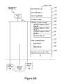
- FIG. 1is a diagram of an implementation of a data storage system 100 , in accordance with some embodiments. While some example features are illustrated, various other features have not been illustrated for the sake of brevity and so as not to obscure more pertinent aspects of the example implementations disclosed herein. To that end, as a non-limiting example, the data storage system 100 includes a memory controller 120 , and a storage medium 130 , and is used in conjunction with a computer system 110 .
- storage medium 130is a single flash memory device while in other implementations storage medium 130 includes a plurality of flash memory devices.
- storage medium 130is NAND-type flash memory or NOR-type flash memory.
- memory controller 120is a solid-state drive (SSD) controller.
- SSDsolid-state drive
- Computer system 110is coupled to memory controller 120 through data connections 101 .
- computer system 110includes memory controller 120 as a component and/or a sub-system.
- Computer system 110may be any suitable computer device, such as a computer, a laptop computer, a tablet device, a netbook, an internet kiosk, a personal digital assistant, a mobile phone, a smart phone, a gaming device, a computer server, or any other computing device.
- Computer system 110is sometimes called a host or host system.
- computer system 110includes one or more processors, one or more types of memory, a display and/or other user interface components such as a keyboard, a touch screen display, a mouse, a track-pad, a digital camera and/or any number of supplemental devices to add functionality.
- Storage medium 130is coupled to memory controller 120 through connections 103 .
- Connections 103are sometimes called data connections, but typically convey commands in addition to data, and optionally convey metadata, error correction information and/or other information in addition to data values to be stored in storage medium 130 and data values read from storage medium 130 .
- memory controller 120 and storage medium 130are included in the same device as components thereof.
- memory controller 120 and storage medium 130are embedded in a host device, such as a mobile device, tablet, other computer or computer controlled device, and the methods described herein are performed by the embedded memory controller.
- Storage medium 130may include any number (i.e., one or more) of memory devices including, without limitation, non-volatile semiconductor memory devices, such as flash memory.
- flash memory devicescan be configured for enterprise storage suitable for applications such as cloud computing, or for caching data stored (or to be stored) in secondary storage, such as hard disk drives. Additionally and/or alternatively, flash memory can also be configured for relatively smaller-scale applications such as personal flash drives or hard-disk replacements for personal, laptop and tablet computers.
- Storage medium 130is divided into a number of addressable and individually selectable blocks, such as selectable portion 131 .
- the individually selectable blocksare the minimum size erasable units in a flash memory device. In other words, each block contains the minimum number of memory cells that can be erased simultaneously.
- Each blockis usually further divided into a plurality of pages and/or word lines, where each page or word line is typically an instance of the smallest individually accessible (readable) portion in a block.
- the smallest individually accessible unit of a data setis a sector, which is a subunit of a page. That is, a block includes a plurality of pages, each page contains a plurality of sectors, and each sector is the minimum unit of data for reading data from the flash memory device.
- one blockcomprises any number of pages, for example, 64 pages, 128 pages, 256 pages or another suitable number of pages.
- Blocksare typically grouped into a plurality of zones. Each block zone can be independently managed to some extent, which increases the degree of parallelism for parallel operations and simplifies management of storage medium 130 .
- memory controller 120includes a management module 121 , a host interface 129 , a storage medium interface (I/O) 128 , and additional module(s) 125 .
- Memory controller 120may include various additional features that have not been illustrated for the sake of brevity and so as not to obscure more pertinent features of the example implementations disclosed herein, and a different arrangement of features may be possible.
- Host interface 129provides an interface to computer system 110 through data connections 101 .
- storage medium I/O 128provides an interface to storage medium 130 though connections 103 .
- storage medium I/O 128includes read and write circuitry, including circuitry capable of providing reading signals to storage medium 130 (e.g., reading threshold voltages for NAND-type flash memory).
- management module 121includes one or more processing units (CPUs, also sometimes called processors) 122 configured to execute instructions in one or more programs (e.g., in management module 121 ).
- the one or more CPUs 122are shared by one or more components within, and in some cases, beyond the function of memory controller 120 .
- Management module 121is coupled to host interface 129 , additional module(s) 125 and storage medium I/O 128 in order to coordinate the operation of these components.
- Additional module(s) 125are coupled to storage medium I/O 128 , host interface 129 , and management module 121 .
- additional module(s) 125may include an error control module to limit the number of uncorrectable errors inadvertently introduced into data during writes to memory or reads from memory.
- additional module(s) 125are executed in software by the one or more CPUs 122 of management module 121 , and, in other embodiments, additional module(s) 125 are implemented in whole or in part using special purpose circuitry (e.g., to perform encoding and decoding functions).
- host interface 129receives data to be stored in storage medium 130 from computer system 110 .
- the data held in host interface 129is made available to an encoder (e.g., in additional module(s) 125 ), which encodes the data to produce one or more codewords.
- the one or more codewordsare made available to storage medium I/O 128 , which transfers the one or more codewords to storage medium 130 in a manner dependent on the type of storage medium being utilized.
- a read operationis initiated when computer system (host) 110 sends one or more host read commands on control line 111 to memory controller 120 requesting data from storage medium 130 .
- Memory controller 120sends one or more read access commands to storage medium 130 , via storage medium I/O 128 , to obtain raw read data in accordance with memory locations (addresses) specified by the one or more host read commands.
- Storage medium I/O 128provides the raw read data (e.g., comprising one or more codewords) to a decoder (e.g., in additional module(s) 125 ). If the decoding is successful, the decoded data is provided to host interface 129 , where the decoded data is made available to computer system 110 . In some implementations, if the decoding is not successful, memory controller 120 may resort to a number of remedial actions or provide an indication of an irresolvable error condition.
- Flash memory devicesutilize memory cells to store data as electrical values, such as electrical charges or voltages.
- Each flash memory celltypically includes a single transistor with a floating gate that is used to store a charge, which modifies the threshold voltage of the transistor (i.e., the voltage needed to turn the transistor on).
- the magnitude of the charge, and the corresponding threshold voltage the charge creates,is used to represent one or more data values.
- a reading threshold voltageis applied to the control gate of the transistor and the resulting sensed current or voltage is mapped to a data value.
- cell voltageand “memory cell voltage,” in the context of flash memory cells, means the threshold voltage of the memory cell, which is the minimum voltage that needs to be applied to the gate of the memory cell's transistor in order for the transistor to conduct current.
- reading threshold voltagessometimes also called reading signals and reading voltages
- gate voltagesapplied to the gates of the flash memory cells to determine whether the memory cells conduct current at that gate voltage.
- the raw data value for that read operationis a “1,” and otherwise the raw data value is a “0.”
- a storage mediume.g., storage medium 130
- each blockis optionally (but typically) further divided into a plurality of pages and/or word lines and/or sectors. While erasure of a storage medium is performed on a block basis, in many embodiments, reading and programming of the storage medium is performed on a smaller subunit of a block (e.g., on a page basis, word line basis, or sector basis). In some embodiments, the smaller subunit of a block consists of multiple memory cells (e.g., single-level cells or multi-level cells). In some embodiments, programming is performed on an entire page.
- pages in the storage mediummay contain invalid (e.g., stale) data, but those pages cannot be overwritten until the whole block containing those pages is erased.
- the pages with valid data in that blockare read and re-written to a new block and the old block is erased (or put on a queue for erasing). This process is called garbage collection.
- garbage collectionthe new block contains pages with valid data and free pages that are available for new data to be written, and the old block that was erased is also available for new data to be written. Since flash memory can only be programmed and erased a limited number of times, the efficiency of the algorithm used to pick the next block(s) to re-write and erase has a significant impact on the lifetime and reliability of flash-based storage systems.
- Write amplificationis a phenomenon where the actual amount of physical data written to a storage medium (e.g., storage medium 130 ) is a multiple of the logical amount of data intended to be written by a host (e.g., computer system 110 , sometimes called a host).
- a hoste.g., computer system 110 , sometimes called a host.
- the garbage collection process to perform these operationsresults in re-writing data one or more times. This multiplying effect increases the number of writes required over the life of a storage medium, which shortens the time it can reliably operate.
- the formula to calculate the write amplification of a storage systemis given by equation (1):
- garbage collectionis performed on erase blocks with the fewest number of valid pages for best performance and best write amplification.
- garbage collectionthat is performed based on characteristics of erase blocks (e.g., an age metric) helps to improve wear leveling, thus extending the life of the memory device.
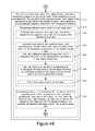
- FIG. 2Ais a block diagram illustrating an exemplary management module 121 , in accordance with some embodiments.
- Management module 121typically includes one or more processing units (CPUs) 122 for executing modules, programs and/or instructions stored in memory 206 and thereby performing processing operations, memory 206 , and one or more communication buses 208 for interconnecting these components.
- Communication buses 208optionally include circuitry (sometimes called a chipset) that interconnects and controls communications between system components.
- Management module 121is coupled to host interface 129 , additional module(s) 125 , and storage medium I/O 128 by communication buses 208 .
- Memory 206includes high-speed random access memory, such as DRAM, SRAM, DDR RAM or other random access solid state memory devices, and may include non-volatile memory, such as one or more magnetic disk storage devices, optical disk storage devices, flash memory devices, or other non-volatile solid state storage devices. Memory 206 optionally includes one or more storage devices remotely located from the CPU(s) 122 . Memory 206 , or alternately the non-volatile memory device(s) within memory 206 , comprises a non-transitory computer readable storage medium. In some embodiments, memory 206 , or the computer readable storage medium of memory 206 stores the following programs, modules, and data structures, or a subset thereof:
- the garbage collection module 224optionally includes the following modules or sub-modules, or a subset thereof:
- the wear leveling module 234optionally includes the following modules or sub-modules, or a subset thereof:
- Each of the above identified elementsmay be stored in one or more of the previously mentioned memory devices, and corresponds to a set of instructions for performing a function described above.
- the above identified modules or programsi.e., sets of instructions
- memory 206may store a subset of the modules and data structures identified above.
- memory 206may store additional modules and data structures not described above.
- the programs, modules, and data structures stored in memory 206 , or the computer readable storage medium of memory 206provide instructions for implementing any of the methods described below with reference to FIGS. 4A-4D .
- FIG. 2Ashows a management module 121
- FIG. 2Ais intended more as functional description of the various features which may be present in a management module than as a structural schematic of the embodiments described herein. In practice, and as recognized by those of ordinary skill in the art, items shown separately could be combined and some items could be separated.
- FIG. 2Bis a block diagram illustrating an implementation of a characterization vector table 240 , in accordance with some embodiments.
- Characterization vector table 240includes a collection of characterization vectors 242 , that each store characterization data associated with a respective portion of a storage medium (e.g., a distinct device, die, block zone, block, word line, word line zone or page portion of storage medium 130 , FIG. 1 ).
- the characterization data stored in characterization vectors 242is statistically derived.
- a storage mediume.g., storage medium 130 , FIG.
- characterization vector table 240includes at least one characterization vector for each erase unit.
- characterization vector table 240includes a set of distinct characterization vectors 242 for each erase unit in the storage medium (e.g., storage medium 130 , FIG. 1 ), and the set of distinct characterization vectors 242 for each erase unit includes at least one distinct characterization vector for each block in the erase unit.
- a storage mediume.g., storage medium 130 , FIG.
- characterization vector table 240includes at least one characterization vector for each storage unit. More detailed example embodiments of characterization vectors 242 are described below with reference to FIG. 2C .
- FIG. 2Cis a block diagram illustrating an implementation of a characterization vector 244 (e.g., corresponding to one of characterization vectors 242 shown in FIG. 2B ) for a respective erase unit, in accordance with some embodiments.
- characterization data stored in characterization vector 244 for the respective erase unitincludes storage medium characterization parameter values such as an age metric field 246 indicating an age of the respective erase unit (e.g., a metric corresponding to estimated remaining life of the respective erase unit), and, optionally, a bias value field 248 indicating a bias value with which to adjust a garbage collection control metric for the respective erase unit.
- the one or more storage medium characterization parameter valuesprovide an indication of at least one of: a physical characteristic associated with the respective portion of the storage medium (e.g., a distinct flash memory device, die, block zone, block, word line, word line zone or page portion of storage medium 130 , FIG. 1 ), a mode of operation associated with the respective portion of the storage medium, a history of use associated with the respective portion of the storage medium, a condition characteristic associated with the respective portion of the storage medium, a read type associated with the respective portion of the storage medium, and location(s) associated with the respective portion of the storage medium.
- a physical characteristic associated with the respective portion of the storage mediume.g., a distinct flash memory device, die, block zone, block, word line, word line zone or page portion of storage medium 130 , FIG. 1
- a mode of operationassociated with the respective portion of the storage medium
- a history of useassociated with the respective portion of the storage medium
- a condition characteristic associated with the respective portion of the storage mediume.g., a read
- FIG. 3is a block diagram of a plurality of erase units, in accordance with some embodiments. Since different erase units have different characteristics (e.g., some erase units can withstand more program-erase cycles than other erase units), it is important to use the different erase units accordingly (e.g., applying more program-erase cycles to “stronger” erase units and applying fewer program-erase cycles to “weaker” erase units). In some embodiments, in order to wear level erase units based on estimated remaining life of each erase unit, rather than simply the number of program-erase cycles performed on each erase unit, garbage collection is performed on the “stronger” or “younger” erase units more quickly than average and garbage collection is performed on the “weaker” or “older” erase units more slowly than average.
- garbage collectionis performed on the “stronger” or “younger” erase units more quickly than average and garbage collection is performed on the “weaker” or “older” erase units more slowly than average.
- a garbage collection control metric used for prioritizing garbage collectionis a valid-page count.
- garbage collectionis generally performed on erase units with the fewest number of valid pages for best performance and best write amplification.
- garbage collectioncan be prioritized accordingly.
- the age metric for each erase unitis inversely related to the estimated remaining life of the erase unit.
- weaker or older erase unitsare erase units having less estimated remaining life than the average erase units in the storage medium, and these weaker or older erase units have greater (i.e., higher) age metrics than erase units that have more estimated remaining life.
- stronger or younger erase unitsare erase units having more estimated remaining life than the average erase units in the storage medium, and these stronger or younger erase units have lower age metrics than erase units that have less estimated remaining life.
- erase unit A 302(age 7)
- erase unit B 304(age 11)
- erase unit C 306(age 5)
- erase unit D 308(age 7).
- the representative age of erase units in the storage mediumis 7.
- the average age of erase units in the storage mediumis 7, and the median age of erase units in the storage medium is 7.
- the average age of erase units in the storage mediumis different from the median age of erase units in the storage medium.
- erase unit B 304is older than average (e.g., older than the representative age of 7)
- a biase.g., stored in bias value field 248 , FIG. 2C
- erase unit C 306is younger than average (e.g., younger than the representative age of 7)
- a biase.g., stored in bias value field 248 , FIG. 2C
- erase unit C 306has fewer valid pages, thus expediting garbage collection.
- a predefined number of valid pagesis added or subtracted for each age that the erase unit differs from the representative age of erase units in the storage medium, up to maximum bias limits imposed by firmware.
- the maximum bias limitsensure that the biasing for wear leveling does not increase write amplification more than what has been determined as acceptable.
- the bias added to the valid-page count for erase unit B 304is 1,024 pages (i.e., 256 pages*4 age units).
- the bias subtracted from the valid-page count for erase unit C 306is 512 pages (i.e., 256 pages*2 age units).
- erase unit A 302 (age 7) and erase unit D 308 (age 7)are the same age as the representative age of erase units in the storage medium, the valid-page counts for erase unit A 302 and erase unit D 308 are not biased for garbage collection purposes.
- the maximum bias limitis, say, 6 times the predefined number of valid pages, even if an erase unit is 7 or more age units older or younger than the representative age, the bias added or subtracted from the valid-page count is limited to 6 times the predefined number of valid pages.
- erase unit E(not pictured) is age 14, which is 7 age units older than the representative age of 7, and the predefined number of valid pages is 256
- the bias to be added to the valid-page count for erase unit Ewould be 1,792 pages.
- the bias valueis limited to a predefined maximum of 1,536 pages, only 1,536 pages would be added to the valid-page count for erase unit E.
- a garbage collection control metric used for prioritizing garbage collectionis an invalid-page count (e.g., a count of invalid or dirty or “freeable” pages) and bias values are subtracted from the invalid-page counts for “older” erase units and added to invalid-page counts for “younger” erase units.
- FIGS. 4A-4Dillustrate a flowchart representation of a method 400 of wear leveling for a storage medium in a storage system, in accordance with some embodiments.
- the storage systeme.g., data storage system 100 , FIG. 1
- garbage collectionuses garbage collection to reclaim portions of memory (e.g., storage medium 130 , FIG. 1 ) that no longer contain valid data, which includes performance of method 400 .
- method 400is performed by a storage system (e.g., data storage system 100 , FIG. 1 ) or one or more components of the storage system (e.g., memory controller 120 and/or storage medium 130 , FIG. 1 ).
- method 400is governed by instructions that are stored in a non-transitory computer readable storage medium and that are executed by one or more processors of a device, such as the one or more processing units (CPUs) 122 of management module 121 , shown in FIGS. 1 and 2A .
- CPUsprocessing units
- a storage systemdetermines ( 402 ), for each erase unit of a plurality of erase units in a storage medium (e.g., storage medium 130 , FIG. 1 ), an age metric.
- an age modulee.g., age module 236 , FIG. 2A
- an age metricis used to determine, for each erase unit of a plurality of erase units in a storage medium, an age metric, as described above with respect to FIG. 2A .
- the erase unitis ( 404 ) a single erase block.
- the erase unitis a single erase block, the minimum size erasable unit in a flash memory device.
- the erase unitis ( 406 ) a super block, wherein the super block includes a plurality of erase blocks.
- a super blockincludes 16 erase blocks.
- the storage mediumcomprises ( 408 ) one or more non-volatile storage devices, such as flash memory devices.
- the non-volatile storage mediume.g., storage medium 130 , FIG. 1
- the non-volatile storage mediumis a single flash memory device, while in other implementations the non-volatile storage medium includes a plurality of flash memory devices.
- the non-volatile storage mediume.g., storage medium 130 , FIG. 1
- the age metric for each erase unitis ( 410 ) determined in accordance with a metric corresponding to estimated remaining life of each erase unit.
- some erase unitscan withstand more program-erase cycles than other erase units, and the age metric for each erase unit is determined in accordance with a metric corresponding to estimated remaining life of each erase unit (as opposed to simply the number of program-erase cycles completed for each erase unit). For example, if an erase unit can withstand more program-erase cycles than the average erase unit (e.g., with an age equal to the representative age metric of the plurality of erase units), then that erase unit has more estimated remaining life and is considered “younger” than the average erase unit.
- the age metricis determined periodically (e.g., an updated age metric for an erase unit is determined every 100 program-erase cycles of the erase unit).
- determining ( 402 ), for each erase unit of a plurality of erase units in the storage medium, the age metriccomprises determining ( 412 ), for each storage unit of a plurality of storage units in the storage medium, an age metric for a respective storage unit, wherein each storage unit comprises a plurality of the erase units.
- the age metric for an erase unitcomprises the age metric determined for the corresponding storage unit.
- the age metric for the storage unitis the worst (e.g., “oldest”) age metric for any of the erase units in the storage unit.
- the age metric for the storage unitis the average age metric of the erase units in the storage unit.
- the age metric for the storage unitis the median age metric of the erase units in the storage unit.
- an age modulee.g., age module 236 , FIG. 2A ) is used to determine, for each storage unit of a plurality of storage units in the storage medium, an age metric for a respective storage unit, wherein each storage unit comprises a plurality of the erase units, as described above with respect to FIG. 2A .
- the storage systemdetermines ( 414 ) a representative age metric of the plurality of erase units.
- the representative age metric of the plurality of erase unitsis an average age metric of the plurality of erase units.
- the representative age metric of the plurality of erase unitsis a median age metric of the plurality of erase units. For example, if a storage medium (e.g., storage medium 130 , FIG. 1 ) includes 4 erase units with ages of 5, 7, 7, and 9, respectively, and the representative age metric of the plurality of erase units is an average age metric of the plurality of erase units, the storage system determines the average age metric of the plurality of erase units to be 7 (i.e., (5+7+7+9)/4).
- the representative age metric of the plurality of erase unitsis determined periodically. For example, in some implementations, the storage system accumulates N age metric measurements, where N is a predetermined number (e.g., N is equal to 2048), and then divides the accumulated total by N, once N age metric measurements have been accumulated. In some implementations, an age module (e.g., age module 236 , FIG. 2A ) is used to determine a representative age metric of the plurality of erase units, as described above with respect to FIG. 2A .
- the storage systembiases ( 416 ) a respective garbage collection control metric for the respective erase unit in accordance with the age metric of the respective erase unit in relation to the representative age metric of the plurality of erase units to generate an adjusted garbage collection control metric for the respective erase unit.
- a bias modulee.g., bias module 238 , FIG. 2A
- bias module 238FIG. 2A
- the garbage collection control metricis ( 418 ) a valid-page count and biasing the respective valid-page count for the respective erase unit includes determining ( 420 ) the respective valid-page count, wherein the respective valid-page count is a count of valid pages in the respective erase unit. For example, if an erase unit has 10,240 pages, 2,500 of which are valid and 7,740 of which are invalid, the valid-page count is 2,500.
- a respective valid-page countis updated when data on the respective erase unit is written to another location (e.g., the host system rewrote the logical location for that data), since at that time, the respective erase unit has an invalid (e.g., stale) version of that data.
- the valid-page countis tracked loosely while in other implementations, the valid-page count is tracked precisely.
- a bias modulee.g., bias module 238 , FIG. 2A . is used to determine the respective valid-page count, wherein the respective valid-page count is a count of valid pages in the respective erase unit, as described above with respect to FIG. 2A .
- biasing the respective valid-page count for the respective erase unitincludes calculating ( 422 ) a bias value for the respective erase unit in accordance with the age metric of the respective erase unit in relation to the representative age metric of the plurality of erase units. For example, if a first erase unit (e.g., erase unit B 304 , FIG. 3 ) is 4 age units older than the representative age metric of the plurality of erase units, the bias value for the first erase unit will be greater than the bias value for a second erase unit that is 2 age units older than the representative age metric.
- a bias modulee.g., bias module 238 , FIG. 2A
- bias moduleis used to calculate a bias value for the respective erase unit in accordance with the age metric of the respective erase unit in relation to the representative age metric of the plurality of erase units, as described above with respect to FIG. 2A .
- calculating ( 422 ) the bias value for the respective erase unitincludes calculating ( 424 ) a difference between the age metric of the respective erase unit and the representative age metric of the plurality of erase units. For example, if the age metric of the respective erase unit is age 5 and the representative age metric of the plurality of erase units is age 7, the difference between the age metric of the respective erase unit and the representative age metric is 2 age units.
- a bias modulee.g., bias module 238 , FIG. 2A ) is used to calculate a difference between the age metric of the respective erase unit and the representative age metric of the plurality of erase units, as described above with respect to FIG. 2A .
- calculating ( 422 ) the bias value for the respective erase unitincludes calculating ( 426 ) a first value, the first value determined by multiplying the absolute value of the calculated difference by a predefined number of valid pages, wherein the first value is limited to a predefined maximum. For example, if the calculated difference is 2 age units and the predefined number of valid pages is 256 pages, the first value is 512 pages (i.e., 2*256 pages), assuming the predefined maximum is greater than 512 pages.
- a bias modulee.g., bias module 238 , FIG. 2A ) is used to calculate a first value, the first value determined by multiplying the absolute value of the calculated difference by a predefined number of valid pages, wherein the first value is limited to a predefined maximum, as described above with respect to FIG. 2A .
- calculating ( 422 ) the bias value for the respective erase unitincludes setting ( 428 ) the bias value equal to the first value. For example, if the first value is calculated to be 512 pages, the bias value is set to be 512 pages.
- a bias modulee.g., bias module 238 , FIG. 2A ) is used to set the bias value equal to the first value, as described above with respect to FIG. 2A .
- the storage systemAfter calculating ( 422 ) the bias value for the respective erase unit, the storage system, in accordance with a first determination that the age metric of the respective erase unit corresponds to a shorter estimated remaining life than erase units having the representative age metric of the plurality of erase units, adds ( 430 ) the bias value to the respective valid-page count for the respective erase unit to generate the adjusted valid-page count for the respective erase unit.
- an erase unit with an age metric greater than the representative age metricis weaker, or has a shorter estimated remaining life, than an erase unit with an age metric equal to the representative age metric.
- the storage systemadds 512 pages to 2,500 pages to generate the adjusted valid-page count of 3,012 pages.
- a bias modulee.g., bias module 238 , FIG.
- the second erase unit 2Ais used to add, in accordance with a first determination, the first determination including a determination that the age metric of the respective erase unit is greater than the representative age metric of the plurality of erase units, the bias value to the respective valid-page count for the respective erase unit to generate the adjusted valid-page count for the respective erase unit, as described above with respect to FIG. 2A .
- the storage systemafter calculating ( 422 ) the bias value for the respective erase unit, the storage system, in accordance with a second determination that the age metric of the respective erase unit corresponds to a longer estimated remaining life than erase units having the representative age metric of the plurality of erase units, subtracts ( 432 ) the bias value from the respective valid-page count for the respective erase unit to generate the adjusted valid-page count for the respective erase unit.
- the storage systemsubtracts 512 pages from 2,500 pages to generate the adjusted valid-page count of 1,988 pages.
- a bias modulee.g., bias module 238 , FIG.
- 2Ais used to subtract, in accordance with a second determination, the second determination including a determination that the age metric of the respective erase unit is less than the representative age metric of the plurality of erase units, the bias value from the respective valid-page count for the respective erase unit to generate the adjusted valid-page count for the respective erase unit, as described above with respect to FIG. 2A .
- biasing ( 416 ) the respective garbage collection control metric for the respective erase unitincludes determining ( 434 ) the respective garbage collection control metric.
- the respective garbage collection control metricis a count of a metric for prioritizing garbage collection in the respective erase unit.
- the garbage collection control metricis a valid-page count and determining the respective garbage collection control metric includes determining the respective valid-page count, wherein the respective valid-page count is a count of valid pages in the respective erase unit.
- the garbage collection control metricis an invalid-page count and determining the respective garbage collection control metric includes determining the respective invalid-page count, wherein the respective invalid-page count is a count of invalid (e.g., dirty or “freeable”) pages in the respective erase unit.
- the garbage collection control metricis a count of some other metric for prioritizing garbage collection.
- a bias modulee.g., bias module 238 , FIG. 2A ) is used to determine the respective garbage collection control metric, as described above with respect to FIG. 2A .
- biasing ( 416 ) the respective garbage collection control metric for the respective erase unitincludes calculating ( 436 ) a bias value for the respective erase unit in accordance with the age metric of the respective erase unit in relation to the representative age metric of the plurality of erase units, including limiting a range of the bias value to a predefined range. For example, if a first erase unit (e.g., erase unit B 304 , FIG. 3 ) is 4 age units older than the representative age metric of the plurality of erase units, the bias value for the first erase unit will be greater than the bias value for a second erase unit that is 2 age units older than the representative age metric.
- a bias modulee.g., bias module 238 , FIG.
- 2Ais used to calculate a bias value for the respective erase unit in accordance with the age metric of the respective erase unit in relation to the representative age metric of the plurality of erase units, including limiting a range of the bias value to a predefined range, as described above with respect to FIG. 2A .
- biasing ( 416 ) the respective garbage collection control metric for the respective erase unitincludes mathematically adjusting ( 438 ) the respective garbage collection control metric for the respective erase unit with the calculated bias value to generate the adjusted garbage collection control metric for the respective erase unit. For example, if the garbage collection control metric is a valid-page count, the storage system mathematically adjusts the respective garbage collection control metric by adding or subtracting the calculated bias value as described in operations 430 and 432 . As another example, if the garbage collection control metric is an invalid-page count, the storage system mathematically adjusts the respective garbage collection control metric by subtracting the calculated bias values for “older” erase units and adding the calculated bias values for “younger” erase units.
- a bias module(e.g., bias module 238 , FIG. 2A ) is used to mathematically adjust the respective garbage collection control metric for the respective erase unit with the calculated bias value to generate the adjusted garbage collection control metric for the respective erase unit, as described above with respect to FIG. 2A .
- the storage systemAfter biasing ( 416 ), for each respective erase unit of the plurality of erase units, a respective garbage collection control metric for the respective erase unit to generate an adjusted garbage collection control metric for the respective erase unit, the storage system performs ( 440 ) garbage collection for the storage medium in accordance with the adjusted garbage collection control metrics of the plurality of erase units. For example, in some embodiments (e.g., in which the garbage collection control metric is a valid-page count), the storage system performs garbage collection, giving priority to the erase units with the lowest adjusted garbage collection control metric. As another example, in some embodiments (e.g., in which the garbage collection control metric is an invalid-page count), the storage system performs garbage collection, giving priority to the erase units with the highest adjusted garbage collection control metric.
- a garbage collection module(e.g., garbage collection module 224 , FIG. 2A ) is used to perform garbage collection for the storage medium in accordance with the adjusted garbage collection control metrics of the plurality of erase units, as described above with respect to FIG. 2A .
- the garbage collection control metricis ( 418 ) a valid-page count and performing ( 440 ) garbage collection for the storage medium in accordance with the adjusted garbage collection control metrics of the plurality of erase units includes selecting ( 442 ) an erase unit with the lowest adjusted valid-page count for garbage collection.
- the garbage collection control metricis an invalid-page count and performing garbage collection for the storage medium in accordance with the adjusted garbage collection control metrics of the plurality of erase units includes selecting an erase unit with the highest adjusted invalid-page count for garbage collection.
- a selection modulee.g., selection module 232 , FIG. 2A ) is used to select an erase unit with the lowest adjusted valid-page count for garbage collection, as described above with respect to FIG. 2A .
- garbage collection control metricis ( 418 ) a valid-page count and performing ( 440 ) garbage collection for the storage medium in accordance with the adjusted garbage collection control metrics of the plurality of erase units includes performing ( 444 ) garbage collection on a first erase unit with a first adjusted valid-page count prior to performing garbage collection on a second erase unit with a second adjusted valid-page count, wherein the first adjusted valid-page count is less than the second adjusted valid-page count.
- a garbage collection modulee.g., garbage collection module 224 , FIG. 2A
- garbage collection module 224FIG. 2A
- the storage mediumis a single flash memory device, while in other implementations, the storage medium includes a plurality of flash memory devices.
- any of the methods described aboveare performed by a device operable to perform wear leveling for a storage medium, the device including (1) a storage medium interface for coupling the device to the storage medium, and (2) one or more modules, including a memory management module that includes one or more processors and memory storing one or more programs configured for execution by the one or more processors, the one or more modules coupled to the storage medium interface and configured to perform or control performance of any of the methods described above.
- firstfirst
- secondsecond
- first contactfirst contact
- first contactsecond contact
- first contactsecond contact
- the term “if”may be construed to mean “when” or “upon” or “in response to determining” or “in accordance with a determination” or “in response to detecting,” that a stated condition precedent is true, depending on the context.
- the phrase “if it is determined [that a stated condition precedent is true]” or “if [a stated condition precedent is true]” or “when [a stated condition precedent is true]”may be construed to mean “upon determining” or “in response to determining” or “in accordance with a determination” or “upon detecting” or “in response to detecting” that the stated condition precedent is true, depending on the context.
Landscapes
- Engineering & Computer Science (AREA)
- Theoretical Computer Science (AREA)
- Physics & Mathematics (AREA)
- General Engineering & Computer Science (AREA)
- General Physics & Mathematics (AREA)
- Techniques For Improving Reliability Of Storages (AREA)
- Memory System (AREA)
Abstract
Description
- a data read
module 216 that is used for reading data from one or more blocks in a storage medium; - a
data write module 218 that is used for writing data to one or more blocks in a storage medium; - a data erase
module 220 that is used for erasing data from one or more blocks in a storage medium; - a translation table222 that is used for mapping logical addresses to physical addresses;
- a
garbage collection module 224 that is used for garbage collection for one or more blocks in a storage medium; - a
wear leveling module 234 that is used for wear leveling for a storage medium; and - a characterization vector table240 that includes a collection of characterization vectors (e.g.,
characterization vectors 242,FIG. 2B ), each characterization vector storing characterization data for a respective portion of a storage medium (e.g., a flash memory device, die, block zone, block, word line, word line zone or page portion ofstorage medium 130,FIG. 1 ).
- a data read
- a garbage collection read
module 226 that is used for reading data from one or more blocks in a storage medium during a garbage collection operation; - a garbage
collection write module 228 that is used for writing data to one or more blocks in a storage medium during a garbage collection operation; - a garbage collection erase
module 230 that is used for erasing data from one or more blocks in a storage medium during a garbage collection operation; and - a
selection module 232 that is used for selecting one or more blocks (e.g., an erase unit) in a storage medium for garbage collection.
- a garbage collection read
- an
age module 236 that is used for determining an age metric for one or more erase units (e.g., one or more blocks) in a storage medium; and - a
bias module 238 that is used for biasing a garbage collection control metric (e.g., valid-page count).
- an
Claims (20)
Priority Applications (4)
| Application Number | Priority Date | Filing Date | Title |
|---|---|---|---|
| US14/137,440US9298608B2 (en) | 2013-10-18 | 2013-12-20 | Biasing for wear leveling in storage systems |
| DE112014004761.9TDE112014004761B4 (en) | 2013-10-18 | 2014-10-08 | Influencing wear leveling in storage systems |
| CN201480067219.1ACN105934748B (en) | 2013-10-18 | 2014-10-08 | Biasing for the wear leveling in stocking system |
| PCT/US2014/059747WO2015057458A1 (en) | 2013-10-18 | 2014-10-08 | Biasing for wear leveling in storage systems |
Applications Claiming Priority (2)
| Application Number | Priority Date | Filing Date | Title |
|---|---|---|---|
| US201361893102P | 2013-10-18 | 2013-10-18 | |
| US14/137,440US9298608B2 (en) | 2013-10-18 | 2013-12-20 | Biasing for wear leveling in storage systems |
Publications (2)
| Publication Number | Publication Date |
|---|---|
| US20150113206A1 US20150113206A1 (en) | 2015-04-23 |
| US9298608B2true US9298608B2 (en) | 2016-03-29 |
Family
ID=52827219
Family Applications (1)
| Application Number | Title | Priority Date | Filing Date |
|---|---|---|---|
| US14/137,440Active2034-05-26US9298608B2 (en) | 2013-10-18 | 2013-12-20 | Biasing for wear leveling in storage systems |
Country Status (4)
| Country | Link |
|---|---|
| US (1) | US9298608B2 (en) |
| CN (1) | CN105934748B (en) |
| DE (1) | DE112014004761B4 (en) |
| WO (1) | WO2015057458A1 (en) |
Cited By (4)
| Publication number | Priority date | Publication date | Assignee | Title |
|---|---|---|---|---|
| US9875039B2 (en) | 2014-09-30 | 2018-01-23 | Sandisk Technologies Llc | Method and apparatus for wear-leveling non-volatile memory |
| US10324648B1 (en) | 2016-04-28 | 2019-06-18 | Seagate Technology Llc | Wear-based access optimization |
| US10896126B2 (en)* | 2018-10-25 | 2021-01-19 | Samsung Electronics Co., Ltd. | Storage device, method and non-volatile memory device performing garbage collection using estimated number of valid pages |
| US11049009B2 (en) | 2017-06-12 | 2021-06-29 | Western Digital Technologies, Inc. | Identifying memory block write endurance using machine learning |
Families Citing this family (39)
| Publication number | Priority date | Publication date | Assignee | Title |
|---|---|---|---|---|
| TWI516922B (en)* | 2014-03-12 | 2016-01-11 | 慧榮科技股份有限公司 | Data storage device and flash memory garbage collection method |
| US9652415B2 (en) | 2014-07-09 | 2017-05-16 | Sandisk Technologies Llc | Atomic non-volatile memory data transfer |
| US9904621B2 (en) | 2014-07-15 | 2018-02-27 | Sandisk Technologies Llc | Methods and systems for flash buffer sizing |
| KR20160024530A (en)* | 2014-08-26 | 2016-03-07 | 에스케이하이닉스 주식회사 | Semiconductor device and operating method thereof |
| US9753649B2 (en) | 2014-10-27 | 2017-09-05 | Sandisk Technologies Llc | Tracking intermix of writes and un-map commands across power cycles |
| US9952978B2 (en) | 2014-10-27 | 2018-04-24 | Sandisk Technologies, Llc | Method for improving mixed random performance in low queue depth workloads |
| US9817752B2 (en) | 2014-11-21 | 2017-11-14 | Sandisk Technologies Llc | Data integrity enhancement to protect against returning old versions of data |
| US9824007B2 (en) | 2014-11-21 | 2017-11-21 | Sandisk Technologies Llc | Data integrity enhancement to protect against returning old versions of data |
| US20160179399A1 (en)* | 2014-12-23 | 2016-06-23 | Sandisk Technologies Inc. | System and Method for Selecting Blocks for Garbage Collection Based on Block Health |
| US9652175B2 (en) | 2015-04-09 | 2017-05-16 | Sandisk Technologies Llc | Locally generating and storing RAID stripe parity with single relative memory address for storing data segments and parity in multiple non-volatile memory portions |
| US10372529B2 (en) | 2015-04-20 | 2019-08-06 | Sandisk Technologies Llc | Iterative soft information correction and decoding |
| US9778878B2 (en) | 2015-04-22 | 2017-10-03 | Sandisk Technologies Llc | Method and system for limiting write command execution |
| US9811462B2 (en) | 2015-04-30 | 2017-11-07 | Toshiba Memory Corporation | Memory system executing garbage collection |
| US9870149B2 (en)* | 2015-07-08 | 2018-01-16 | Sandisk Technologies Llc | Scheduling operations in non-volatile memory devices using preference values |
| US9715939B2 (en) | 2015-08-10 | 2017-07-25 | Sandisk Technologies Llc | Low read data storage management |
| TWI585770B (en)* | 2015-08-11 | 2017-06-01 | 群聯電子股份有限公司 | Memory management method, memory control circuit unit and memory storage device |
| US9804787B2 (en)* | 2015-11-03 | 2017-10-31 | Samsung Electronics Co., Ltd. | Mitigating GC effect in a raid configuration |
| US10228990B2 (en) | 2015-11-12 | 2019-03-12 | Sandisk Technologies Llc | Variable-term error metrics adjustment |
| KR102437591B1 (en)* | 2015-12-03 | 2022-08-30 | 삼성전자주식회사 | Operation method of nonvolatile memory system and method operation of memory controller |
| US10126970B2 (en) | 2015-12-11 | 2018-11-13 | Sandisk Technologies Llc | Paired metablocks in non-volatile storage device |
| US9837146B2 (en) | 2016-01-08 | 2017-12-05 | Sandisk Technologies Llc | Memory system temperature management |
| US10732856B2 (en) | 2016-03-03 | 2020-08-04 | Sandisk Technologies Llc | Erase health metric to rank memory portions |
| JP6215401B1 (en)* | 2016-06-27 | 2017-10-18 | 株式会社東芝 | Database management apparatus, database management method, and database management program |
| JP6181247B1 (en)* | 2016-07-01 | 2017-08-16 | 株式会社東芝 | Database management apparatus, database management method, and database management program |
| US10481830B2 (en) | 2016-07-25 | 2019-11-19 | Sandisk Technologies Llc | Selectively throttling host reads for read disturbs in non-volatile memory system |
| JP6524039B2 (en)* | 2016-09-23 | 2019-06-05 | 東芝メモリ株式会社 | Memory system and control method |
| US10489064B2 (en)* | 2016-10-03 | 2019-11-26 | Cypress Semiconductor Corporation | Systems, methods, and devices for user configurable wear leveling of non-volatile memory |
| US10552288B2 (en)* | 2016-12-12 | 2020-02-04 | International Business Machines Corporation | Health-aware garbage collection in a memory system |
| KR20180125694A (en)* | 2017-05-16 | 2018-11-26 | 에스케이하이닉스 주식회사 | Memory system and operating method thereof |
| JP6325728B2 (en)* | 2017-08-07 | 2018-05-16 | 株式会社東芝 | Database management apparatus, database management method, and database management program |
| US10936199B2 (en)* | 2018-07-17 | 2021-03-02 | Silicon Motion, Inc. | Flash controllers, methods, and corresponding storage devices capable of rapidly/fast generating or updating contents of valid page count table |
| KR102848209B1 (en)* | 2019-03-27 | 2025-08-22 | 에스케이하이닉스 주식회사 | Controller, memory system and operating method thereof |
| CN111949560B (en)* | 2019-05-16 | 2024-01-23 | 兆易创新科技集团股份有限公司 | Data writing method and device and storage equipment |
| US11074177B2 (en)* | 2019-06-19 | 2021-07-27 | Micron Technology, Inc. | Garbage collection adapted to host write activity |
| US11287998B2 (en) | 2019-08-02 | 2022-03-29 | Micron Technology, Inc. | Read count scaling factor for data integrity scan |
| US10950317B2 (en)* | 2019-08-02 | 2021-03-16 | Micron Technology, Inc. | Read disturb scan consolidation |
| CN110580932B (en)* | 2019-08-29 | 2021-04-06 | 华中科技大学 | A storage unit quality measurement method applied to wear leveling |
| US11599286B2 (en)* | 2021-06-03 | 2023-03-07 | Micron Technology, Inc. | Data age and validity-based memory management |
| US11914882B2 (en)* | 2022-04-06 | 2024-02-27 | Dell Products L.P. | Data protection against mass deletion based on data storage period |
Citations (389)
| Publication number | Priority date | Publication date | Assignee | Title |
|---|---|---|---|---|
| US4173737A (en) | 1978-05-04 | 1979-11-06 | Zenith Radio Corporation | Limited position, non-volatile memory tuning system |
| US4888750A (en) | 1986-03-07 | 1989-12-19 | Kryder Mark H | Method and system for erase before write magneto-optic recording |
| US4916652A (en) | 1987-09-30 | 1990-04-10 | International Business Machines Corporation | Dynamic multiple instruction stream multiple data multiple pipeline apparatus for floating-point single instruction stream single data architectures |
| US5129089A (en) | 1987-12-18 | 1992-07-07 | Digital Equipment Corporation | Distributed interlock apparatus and distributed interlock management method |
| US5270979A (en) | 1991-03-15 | 1993-12-14 | Sundisk Corporation | Method for optimum erasing of EEPROM |
| US5329491A (en) | 1993-06-30 | 1994-07-12 | Intel Corporation | Nonvolatile memory card with automatic power supply configuration |
| US5381528A (en) | 1992-10-15 | 1995-01-10 | Maxtor Corporation | Demand allocation of read/write buffer partitions favoring sequential read cache |
| US5519847A (en) | 1993-06-30 | 1996-05-21 | Intel Corporation | Method of pipelining sequential writes in a flash memory |
| US5530705A (en) | 1995-02-08 | 1996-06-25 | International Business Machines Corporation | Soft error recovery system and method |
| US5537555A (en) | 1993-03-22 | 1996-07-16 | Compaq Computer Corporation | Fully pipelined and highly concurrent memory controller |
| US5551003A (en) | 1992-12-11 | 1996-08-27 | International Business Machines Corporation | System for managing log structured array (LSA) of DASDS by managing segment space availability and reclaiming regions of segments using garbage collection procedure |
| US5636342A (en) | 1995-02-17 | 1997-06-03 | Dell Usa, L.P. | Systems and method for assigning unique addresses to agents on a system management bus |
| US5657332A (en) | 1992-05-20 | 1997-08-12 | Sandisk Corporation | Soft errors handling in EEPROM devices |
| US5666114A (en) | 1994-11-22 | 1997-09-09 | International Business Machines Corporation | Method and means for managing linear mapped address spaces storing compressed data at the storage subsystem control unit or device level |
| US5708849A (en) | 1994-01-26 | 1998-01-13 | Intel Corporation | Implementing scatter/gather operations in a direct memory access device on a personal computer |
| US5765185A (en) | 1995-03-17 | 1998-06-09 | Atmel Corporation | EEPROM array with flash-like core having ECC or a write cache or interruptible load cycles |
| US5890193A (en) | 1995-07-28 | 1999-03-30 | Micron Technology, Inc. | Architecture for state machine for controlling internal operations of flash memory |
| US5936884A (en) | 1995-09-29 | 1999-08-10 | Intel Corporation | Multiple writes per a single erase for a nonvolatile memory |
| US5943692A (en) | 1997-04-30 | 1999-08-24 | International Business Machines Corporation | Mobile client computer system with flash memory management utilizing a virtual address map and variable length data |
| US5982664A (en) | 1997-10-22 | 1999-11-09 | Oki Electric Industry Co., Ltd. | Semiconductor memory capable of writing and reading data |
| US6000006A (en) | 1997-08-25 | 1999-12-07 | Bit Microsystems, Inc. | Unified re-map and cache-index table with dual write-counters for wear-leveling of non-volatile flash RAM mass storage |
| US6006345A (en) | 1997-05-09 | 1999-12-21 | International Business Machines Corporation | Pattern generator for memory burn-in and test |
| US6016560A (en) | 1995-06-14 | 2000-01-18 | Hitachi, Ltd. | Semiconductor memory, memory device, and memory card |
| US6018304A (en) | 1997-12-18 | 2000-01-25 | Texas Instruments Incorporated | Method and apparatus for high-rate n/n+1 low-complexity modulation codes with adjustable codeword length and error control capability |
| US6044472A (en) | 1996-06-21 | 2000-03-28 | Archos | Device and method for supplying power to an external data medium reader unit connected to a computer, and external reader unit including this device |
| US6070074A (en) | 1998-04-24 | 2000-05-30 | Trw Inc. | Method for enhancing the performance of a regenerative satellite communications system |
| US6119250A (en) | 1996-05-07 | 2000-09-12 | Matsushita Electric Industrial Co., Ltd. | Semiconductor integrated circuit |
| US6138261A (en) | 1998-04-29 | 2000-10-24 | Trw Inc. | Concatenated coding system for satellite communications |
| US6182264B1 (en) | 1998-05-22 | 2001-01-30 | Vlsi Technology, Inc. | Smart dynamic selection of error correction methods for DECT based data services |
| US6192092B1 (en) | 1998-06-15 | 2001-02-20 | Intel Corp. | Method and apparatus for clock skew compensation |
| US6295592B1 (en) | 1998-07-31 | 2001-09-25 | Micron Technology, Inc. | Method of processing memory requests in a pipelined memory controller |
| US6311263B1 (en) | 1994-09-23 | 2001-10-30 | Cambridge Silicon Radio Limited | Data processing circuits and interfaces |
| US20010050824A1 (en) | 1999-01-04 | 2001-12-13 | Maxtor Corporation | Servo area numbering strategy for computer disk drives |
| US20020024846A1 (en) | 1996-09-30 | 2002-02-28 | Takayuki Kawahara | Semiconductor integrated circuit and data processing system |
| US20020036515A1 (en) | 2000-01-18 | 2002-03-28 | Formfactor, Inc. | Apparatus for reducing power supply noise in an integrated circuit |
| US6408394B1 (en) | 1998-11-18 | 2002-06-18 | Compaq Computer Corp. | System and method for applying initialization power to SCSI devices |
| US6412042B1 (en) | 1999-11-17 | 2002-06-25 | Maxtor Corporation | System and method for improved disk drive performance and reliability |
| US20020083299A1 (en) | 2000-12-22 | 2002-06-27 | International Business Machines Corporation | High speed remote storage controller |
| US6442076B1 (en) | 2000-06-30 | 2002-08-27 | Micron Technology, Inc. | Flash memory with multiple status reading capability |
| US20020122334A1 (en) | 2001-01-03 | 2002-09-05 | Samsung Electronics Co., Ltd. | Flash memory device with cell current measuring scheme using write driver |
| US6449625B1 (en) | 1999-04-20 | 2002-09-10 | Lucent Technologies Inc. | Use of a two-way stack approach to optimize flash memory management for embedded database systems |
| US20020152305A1 (en) | 2000-03-03 | 2002-10-17 | Jackson Gregory J. | Systems and methods for resource utilization analysis in information management environments |
| US20020162075A1 (en) | 2001-04-30 | 2002-10-31 | Talagala Nisha D. | Storage array employing scrubbing operations at the disk-controller level |
| US20020165896A1 (en) | 2001-05-02 | 2002-11-07 | Kim Jason Seung-Min | Multiprocessor communication system and method |
| US6484224B1 (en) | 1999-11-29 | 2002-11-19 | Cisco Technology Inc. | Multi-interface symmetric multiprocessor |
| US6516437B1 (en) | 2000-03-07 | 2003-02-04 | General Electric Company | Turbo decoder control for use with a programmable interleaver, variable block length, and multiple code rates |
| US20030041299A1 (en) | 2001-08-23 | 2003-02-27 | Fujitsu Limited | Memory controller for multilevel cell memory |
| US20030043829A1 (en) | 2001-07-06 | 2003-03-06 | Abbas Rashid | Cross-bar switch employing a multiple entry point FIFO |
| US20030079172A1 (en) | 2001-07-18 | 2003-04-24 | Hiroyuki Yamagishi | Encoding method and encoder |
| US20030088805A1 (en) | 2001-09-28 | 2003-05-08 | Tim Majni | Error indication in a raid memory system |
| US6564285B1 (en) | 1994-06-03 | 2003-05-13 | Intel Corporation | Synchronous interface for a nonvolatile memory |
| US20030093628A1 (en) | 2001-11-14 | 2003-05-15 | Matter Eugene P. | Memory adaptedt to provide dedicated and or shared memory to multiple processors and method therefor |
| US20030163594A1 (en) | 2002-02-27 | 2003-08-28 | Aasheim Jered Donald | Open-architecture file system |
| US20030163629A1 (en) | 2002-02-22 | 2003-08-28 | Conley Kevin M. | Pipelined parallel programming operation in a non-volatile memory system |
| US20030188045A1 (en) | 2000-04-13 | 2003-10-02 | Jacobson Michael B. | System and method for distributing storage controller tasks |
| US20030189856A1 (en) | 2002-04-04 | 2003-10-09 | Samsung Electronics Co., Ltd. | Multi-level flash memory with temperature compensation |
| US20030198100A1 (en) | 2001-12-04 | 2003-10-23 | Hitachi, Ltd. | Method of controlling the operation of non-volatile semiconductor memory chips |
| US20030204341A1 (en) | 2000-03-30 | 2003-10-30 | Guliani Sandeep K. | Method and apparatus for flash voltage detection and lockout |
| US20030212719A1 (en) | 2002-05-08 | 2003-11-13 | Hitachi, Ltd. | Method for heap memory management and computer system using the same method |
| US6678788B1 (en) | 2000-05-26 | 2004-01-13 | Emc Corporation | Data type and topological data categorization and ordering for a mass storage system |
| US20040024963A1 (en) | 2002-08-05 | 2004-02-05 | Nisha Talagala | Method and system for striping data to accommodate integrity metadata |
| US20040024957A1 (en) | 2001-08-07 | 2004-02-05 | Chun-Hung Lin | Window-based flash memory storage system and management and access methods thereof |
| US20040057575A1 (en) | 2002-09-25 | 2004-03-25 | Tong Zhang | LDPC code and encoder/decoder regarding same |
| US20040062157A1 (en) | 2001-03-30 | 2004-04-01 | Fujitsu Limited | Storage apparatus and its focus control method |
| US20040073829A1 (en) | 1998-07-16 | 2004-04-15 | Olarig Sompong P. | Fail-over of multiple memory blocks in multiple memory modules in computer system |
| US20040114265A1 (en) | 2002-12-16 | 2004-06-17 | Xerox Corporation | User-selectable automatic secure data file erasure of job after job completion |
| US6757768B1 (en) | 2001-05-17 | 2004-06-29 | Cisco Technology, Inc. | Apparatus and technique for maintaining order among requests issued over an external bus of an intermediate network node |
| US20040143710A1 (en) | 2002-12-02 | 2004-07-22 | Walmsley Simon Robert | Cache updating method and apparatus |
| US20040148561A1 (en) | 2003-01-23 | 2004-07-29 | Ba-Zhong Shen | Stopping and/or reducing oscillations in low density parity check (LDPC) decoding |
| US20040153902A1 (en) | 2003-01-21 | 2004-08-05 | Nexflash Technologies, Inc. | Serial flash integrated circuit having error detection and correction |
| US6775792B2 (en) | 2001-01-29 | 2004-08-10 | Snap Appliance, Inc. | Discrete mapping of parity blocks |
| US20040167898A1 (en) | 2003-02-26 | 2004-08-26 | Margolus Norman H. | History preservation in a computer storage system |
| US20040181734A1 (en) | 2003-03-14 | 2004-09-16 | Saliba George A. | Extended error correction codes |
| EP1465203A1 (en) | 2003-04-03 | 2004-10-06 | Samsung Electronics Co., Ltd. | Nonvolatile memory with page copy capability and method thereof |
| US20040199714A1 (en) | 1995-07-31 | 2004-10-07 | Petro Estakhri | Increasing the memory performance of flash memory devices by writing sectors simultaneously to multiple flash memory devices |
| US6810440B2 (en) | 1999-06-09 | 2004-10-26 | Qlogic Corporation | Method and apparatus for automatically transferring I/O blocks between a host system and a host adapter |
| US20040237018A1 (en) | 2003-05-23 | 2004-11-25 | Riley Dwight D. | Dual decode scheme |
| US6836815B1 (en) | 2001-07-11 | 2004-12-28 | Pasternak Solutions Llc | Layered crossbar for interconnection of multiple processors and shared memories |
| US6836808B2 (en) | 2002-02-25 | 2004-12-28 | International Business Machines Corporation | Pipelined packet processing |
| US6842436B2 (en) | 1999-12-17 | 2005-01-11 | Siemens Aktiengesellschaft | Multiport-RAM memory device |
| US6865650B1 (en) | 2000-09-29 | 2005-03-08 | Emc Corporation | System and method for hierarchical data storage |
| US20050060501A1 (en) | 2003-09-16 | 2005-03-17 | Denali Software, Inc. | Port independent data transaction interface for multi-port devices |
| US20050060456A1 (en) | 2003-09-16 | 2005-03-17 | Denali Software, Inc. | Method and apparatus for multi-port memory controller |
| US20050073884A1 (en) | 2003-10-03 | 2005-04-07 | Gonzalez Carlos J. | Flash memory data correction and scrub techniques |
| US6895464B2 (en) | 2002-06-03 | 2005-05-17 | Honeywell International Inc. | Flash memory management system and method utilizing multiple block list windows |
| US20050108588A1 (en) | 2003-11-14 | 2005-05-19 | Ming-Huan Yuan | System and method for starting up plural electronic devices in an orderly manner |
| US20050114587A1 (en) | 2003-11-22 | 2005-05-26 | Super Talent Electronics Inc. | ExpressCard with On-Card Flash Memory with Shared Flash-Control Bus but Separate Ready Lines |
| US20050172065A1 (en) | 2004-01-30 | 2005-08-04 | Micron Technology, Inc. | Data move method and apparatus |
| US20050172207A1 (en) | 2004-01-30 | 2005-08-04 | Radke William H. | Error detection and correction scheme for a memory device |
| US20050193161A1 (en) | 2004-02-26 | 2005-09-01 | Lee Charles C. | System and method for controlling flash memory |
| US20050201148A1 (en) | 2004-03-12 | 2005-09-15 | Super Talent Electronics, Inc. | Flash memory device and architecture with multi level cells |
| US20050231765A1 (en) | 2003-12-16 | 2005-10-20 | Matsushita Electric Industrial Co., Ltd. | Information recording medium, data processing apparatus and data processing method |
| US20050251617A1 (en) | 2004-05-07 | 2005-11-10 | Sinclair Alan W | Hybrid non-volatile memory system |
| US20050249013A1 (en) | 2004-04-01 | 2005-11-10 | Janzen Jeffery W | Techniques for storing accurate operating current values |
| US6966006B2 (en) | 2002-05-09 | 2005-11-15 | International Business Machines Corporation | Adaptive startup policy for accelerating multi-disk array spin-up |
| US20050257120A1 (en) | 2004-05-13 | 2005-11-17 | Gorobets Sergey A | Pipelined data relocation and improved chip architectures |
| US20050273560A1 (en) | 2004-06-03 | 2005-12-08 | Hulbert Jared E | Method and apparatus to avoid incoherency between a cache memory and flash memory |
| US6978343B1 (en) | 2002-08-05 | 2005-12-20 | Netlogic Microsystems, Inc. | Error-correcting content addressable memory |
| US6981205B2 (en) | 2001-10-23 | 2005-12-27 | Lenovo (Singapore) Pte Ltd | Data storage apparatus, read data processor, and read data processing method |
| US6980985B1 (en) | 2000-08-30 | 2005-12-27 | At&T Corp. | Distributed evalulation of directory queries using a topology cache |
| US20050289314A1 (en) | 2004-06-23 | 2005-12-29 | Adusumilli Vijaya P | Simultaneous external read operation during internal programming in a flash memory device |
| US20060010174A1 (en) | 2004-07-09 | 2006-01-12 | Lu Nguyen | Method and system for backing up and restoring data |
| US6988171B2 (en) | 1999-03-03 | 2006-01-17 | International Business Machines Corporation | Method and system for recovery of meta data in a storage controller |
| US20060039227A1 (en) | 2004-08-17 | 2006-02-23 | Lawrence Lai | Memory device having staggered memory operations |
| US20060039196A1 (en) | 2003-10-03 | 2006-02-23 | Gorobets Sergey A | Corrected data storage and handling methods |
| US20060053246A1 (en) | 2004-08-30 | 2006-03-09 | Lee Schweiray J | Systems and methods for providing nonvolatile memory management in wireless phones |
| US7020017B2 (en) | 2004-04-06 | 2006-03-28 | Sandisk Corporation | Variable programming of non-volatile memory |
| US20060069932A1 (en) | 2004-09-30 | 2006-03-30 | Hitachi Global Storage Technologies Netherlands B.V. | Data storage device and control method for power-saving modes of serial interface thereof |
| US7028165B2 (en) | 2000-12-06 | 2006-04-11 | Intel Corporation | Processor stalling |
| US7032123B2 (en) | 2001-10-19 | 2006-04-18 | Sun Microsystems, Inc. | Error recovery |
| US20060087893A1 (en) | 2004-10-27 | 2006-04-27 | Sony Corporation | Storage device and information processing system |
| US7043505B1 (en) | 2003-01-28 | 2006-05-09 | Unisys Corporation | Method variation for collecting stability data from proprietary systems |
| US20060107181A1 (en) | 2004-10-13 | 2006-05-18 | Sameep Dave | Decoder architecture system and method |
| US20060136681A1 (en) | 2004-12-21 | 2006-06-22 | Sanjeev Jain | Method and apparatus to support multiple memory banks with a memory block |
| US20060136570A1 (en) | 2003-06-10 | 2006-06-22 | Pandya Ashish A | Runtime adaptable search processor |
| US7076598B2 (en) | 2003-09-09 | 2006-07-11 | Solid State System Co., Ltd. | Pipeline accessing method to a large block memory |
| US20060156177A1 (en) | 2004-12-29 | 2006-07-13 | Sailesh Kottapalli | Method and apparatus for recovering from soft errors in register files |
| US20060195650A1 (en) | 2005-02-25 | 2006-08-31 | Su Zhiqiang J | Method to detect NAND-flash parameters by hardware automatically |
| US7102860B2 (en) | 2002-06-11 | 2006-09-05 | Stmicroelectronics, Inc. | Power limiting time delay circuit |
| US7111293B1 (en) | 1998-06-03 | 2006-09-19 | Ants Software, Inc. | Method for increased concurrency in a computer system |
| US7126873B2 (en) | 2004-06-29 | 2006-10-24 | Super Talent Electronics, Inc. | Method and system for expanding flash storage device capacity |
| US20060244049A1 (en) | 2002-10-04 | 2006-11-02 | Sharp Kabushiki Kaisha | Semiconductor memory device, method for controlling the same, and mobile electronic device |
| US7133282B2 (en) | 2004-05-19 | 2006-11-07 | Hitachi, Ltd. | Disk array device |
| US20060259528A1 (en) | 2005-05-13 | 2006-11-16 | Microsoft Corporation | Implementation for collecting unmanaged memory |
| US20060291301A1 (en) | 2005-06-24 | 2006-12-28 | Marco Ziegelmayer | Memory device and method for operating the memory device |
| US20070011413A1 (en) | 2004-01-29 | 2007-01-11 | Yusuke Nonaka | Storage system having a plurality of interfaces |
| US20070058446A1 (en) | 2005-09-15 | 2007-03-15 | Hynix Semiconductor Inc. | Erase and Program Method of Flash Memory Device for Increasing Program Speed of Flash Memory Device |
| US20070061597A1 (en) | 2005-09-14 | 2007-03-15 | Micky Holtzman | Secure yet flexible system architecture for secure devices with flash mass storage memory |
| US20070076479A1 (en) | 2005-09-30 | 2007-04-05 | Mosaid Technologies Incorporated | Multiple independent serial link memory |
| WO2007036834A2 (en) | 2005-09-27 | 2007-04-05 | Nxp B.V. | Error detection / correction circuit and corresponding method |
| US20070083697A1 (en) | 2005-10-07 | 2007-04-12 | Microsoft Corporation | Flash memory management |
| US20070081408A1 (en) | 2005-10-06 | 2007-04-12 | Oh Suk Kwon | Multi-chip semiconductor memory device having internal power supply voltage generation circuit for decreasing current consumption |
| US20070088716A1 (en) | 2005-10-13 | 2007-04-19 | Microsoft Corporation | Extensible meta-data |
| US20070091677A1 (en) | 2005-10-25 | 2007-04-26 | M-Systems Flash Disk Pioneers Ltd. | Method for recovering from errors in flash memory |
| US20070113019A1 (en) | 2005-11-17 | 2007-05-17 | International Business Machines Corporation | Fast path memory read request processing in a multi-level memory architecture |
| US20070133312A1 (en) | 2000-05-10 | 2007-06-14 | Micron Technology, Inc. | Flash with consistent latency for read operations |
| US20070150790A1 (en) | 2005-12-27 | 2007-06-28 | Gross Stephen J | Method of storing downloadable firmware on bulk media |
| US20070147113A1 (en) | 2005-12-28 | 2007-06-28 | Nima Mokhlesi | Alternate sensing techniques for non-volatile memories |
| US20070157064A1 (en) | 2005-12-27 | 2007-07-05 | D.S.P. Group Ltd. | Systems and methods for error corrections |
| US20070156842A1 (en) | 2005-12-29 | 2007-07-05 | Vermeulen Allan H | Distributed storage system with web services client interface |
| WO2007080586A2 (en) | 2006-01-10 | 2007-07-19 | Saifun Semiconductors Ltd. | Rd algorithm improvement for nrom technology |
| US20070174579A1 (en) | 2006-01-20 | 2007-07-26 | Samsung Electronics Co., Ltd. | Apparatus for collecting garbage block of nonvolatile memory according to power state and method of collecting the same |
| US20070180188A1 (en) | 2006-02-02 | 2007-08-02 | Akira Fujibayashi | Virtual path storage system and control method for the same |
| US20070180346A1 (en) | 2006-01-18 | 2007-08-02 | Sandisk Il Ltd. | Method Of Arranging Data In A Multi-Level Cell Memory Device |
| US20070201274A1 (en) | 2000-01-06 | 2007-08-30 | Super Talent Electronics Inc. | Cell-Downgrading and Reference-Voltage Adjustment for a Multi-Bit-Cell Flash Memory |
| US7275170B2 (en) | 2003-02-04 | 2007-09-25 | Fujitsu Limited | Performance controller of electronic device, performance controlling method and computer program product |
| US20070234143A1 (en) | 2006-01-25 | 2007-10-04 | Samsung Electronics Co., Ltd. | Semiconductor memory devices and methods of testing for failed bits of semiconductor memory devices |
| US20070245099A1 (en) | 2005-12-07 | 2007-10-18 | Microsoft Corporation | Cache metadata for implementing bounded transactional memory |
| US20070245061A1 (en) | 2006-04-13 | 2007-10-18 | Intel Corporation | Multiplexing a parallel bus interface and a flash memory interface |
| US20070263442A1 (en) | 2006-05-15 | 2007-11-15 | Apple Inc. | Off-Die Charge Pump that Supplies Multiple Flash Devices |
| US20070277036A1 (en) | 2003-05-23 | 2007-11-29 | Washington University, A Corporation Of The State Of Missouri | Intelligent data storage and processing using fpga devices |
| US20070279988A1 (en) | 2006-05-17 | 2007-12-06 | Micron Technology, Inc. | Apparatus and method for reduced peak power consumption during common operation of multi-NAND flash memory devices |
| US20070294496A1 (en) | 2006-06-19 | 2007-12-20 | Texas Instruments Incorporated | Methods, apparatus, and systems for secure demand paging and other paging operations for processor devices |
| US20070291556A1 (en) | 2006-06-19 | 2007-12-20 | Teruhiko Kamei | Programming Differently Sized Margins and Sensing with Compensations at Select States for Improved Read Operations in Non-Volatile Memory |
| US20070300130A1 (en) | 2006-05-17 | 2007-12-27 | Sandisk Corporation | Method of Error Correction Coding for Multiple-Sector Pages in Flash Memory Devices |
| US20080013390A1 (en) | 2006-07-12 | 2008-01-17 | Volker Zipprich-Rasch | Memory array architecture and method for high-speed distribution measurements |
| US20080022163A1 (en) | 2006-06-28 | 2008-01-24 | Hitachi, Ltd. | Storage system and data protection method therefor |
| US20080019182A1 (en) | 2006-07-20 | 2008-01-24 | Kosuke Yanagidaira | Semiconductor memory device and control method of the same |
| US20080028275A1 (en) | 2006-06-29 | 2008-01-31 | Digital Fountain, Inc. | Efficient Encoding and Decoding Methods for Representing Schedules and Processing Forward Error Correction Codes |
| US7328377B1 (en) | 2004-01-27 | 2008-02-05 | Altera Corporation | Error correction for programmable logic integrated circuits |
| US20080043871A1 (en) | 2004-09-15 | 2008-02-21 | Eads Secure Networks | Insertion of a Secondary Binary Information Stream into a Main Symbol Stream of a Digital Modulation |
| EP1299800B1 (en) | 2000-06-02 | 2008-02-27 | Sun Microsystems, Inc. | System and method for migrating processes on a network |
| US20080052446A1 (en) | 2006-08-28 | 2008-02-28 | Sandisk Il Ltd. | Logical super block mapping for NAND flash memory |
| US20080056005A1 (en) | 2006-08-30 | 2008-03-06 | Micron Technology, Inc. | Non-volatile memory cell read failure reduction |
| US20080071971A1 (en) | 2006-09-20 | 2008-03-20 | Samsung Electronics Co., Ltd. | Apparatus and method for reorganization of mapping information in flash memory |
| US20080077841A1 (en) | 2006-09-27 | 2008-03-27 | Gonzalez Carlos J | Methods of Cell Population Distribution Assisted Read Margining |
| US20080077937A1 (en) | 2006-07-28 | 2008-03-27 | Samsung Electronics Co., Ltd. | Multipath accessible semiconductor memory device with host interface between processors |
| US20080086677A1 (en) | 2006-10-10 | 2008-04-10 | Xueshi Yang | Adaptive systems and methods for storing and retrieving data to and from memory cells |
| US20080112226A1 (en) | 2006-11-13 | 2008-05-15 | Nima Mokhlesi | Non-volatile memory with boost structures |
| US20080141043A1 (en) | 2006-12-06 | 2008-06-12 | David Flynn | Apparatus, system, and method for managing data using a data pipeline |
| US20080147998A1 (en) | 2006-12-18 | 2008-06-19 | Samsung Electronics Co., Ltd. | Method and apparatus for detecting static data area, wear-leveling, and merging data units in nonvolatile data storage device |
| US20080144371A1 (en) | 2005-10-12 | 2008-06-19 | Macronix International Co., Ltd. | Systems and methods for programming a memory device |
| US20080148124A1 (en) | 2004-06-04 | 2008-06-19 | Yan Zhang | Method and system for detecting and correcting errors while accessing memory devices in microprocessor systems |
| US20080147964A1 (en) | 2004-02-26 | 2008-06-19 | Chow David Q | Using various flash memory cells to build usb data flash cards with multiple partitions and autorun function |
| US20080147714A1 (en) | 2006-12-19 | 2008-06-19 | Mauricio Breternitz | Efficient bloom filter |
| WO2008075292A2 (en) | 2006-12-18 | 2008-06-26 | Nxp B.V. | Power-on temperature sensor/spd detect |
| US20080168319A1 (en) | 2007-01-08 | 2008-07-10 | Samsung Electronics Co., Ltd. | Flash memory Device Error Correction Code Controllers and Related Methods and Memory Systems |
| US20080168191A1 (en) | 2007-01-10 | 2008-07-10 | Giora Biran | Barrier and Interrupt Mechanism for High Latency and Out of Order DMA Device |
| US20080170460A1 (en) | 2007-01-17 | 2008-07-17 | Samsung Electronics Co., Ltd | Multi-path accessible semiconductor memory device having mailbox areas and mailbox access control method thereof |
| US20080229176A1 (en) | 2003-12-22 | 2008-09-18 | International Business Machines Corporation | Method for fast ecc memory testing by software including ecc check byte |
| US20080229003A1 (en) | 2007-03-15 | 2008-09-18 | Nagamasa Mizushima | Storage system and method of preventing deterioration of write performance in storage system |
| US20080229000A1 (en) | 2007-03-12 | 2008-09-18 | Samsung Electronics Co., Ltd. | Flash memory device and memory system |
| WO2008121553A1 (en) | 2007-03-29 | 2008-10-09 | Sandisk Corporation | Non-volatile storage with decoding of data using reliability metrics based on multiple reads |
| WO2008121577A1 (en) | 2007-03-31 | 2008-10-09 | Sandisk Corporation | Soft bit data transmission for error correction control in non-volatile memory |
| US20080270680A1 (en) | 2005-11-17 | 2008-10-30 | Chee Keng Chang | Controller for Non-Volatile Memories and Methods of Operating the Memory Controller |
| EP1990921A2 (en) | 2007-05-07 | 2008-11-12 | Broadcom Corporation | Operational parameter adaptable LDPC (low density parity check) decoder |
| US20080282128A1 (en) | 1999-08-04 | 2008-11-13 | Super Talent Electronics, Inc. | Method of Error Correction Code on Solid State Disk to Gain Data Security and Higher Performance |
| US20080285351A1 (en) | 2007-05-14 | 2008-11-20 | Mark Shlick | Measuring threshold voltage distribution in memory using an aggregate characteristic |
| US20080313132A1 (en) | 2007-06-15 | 2008-12-18 | Fang Hao | High accuracy bloom filter using partitioned hashing |
| US20090003058A1 (en) | 2007-06-28 | 2009-01-01 | Samsung Electronics Co., Ltd. | Flash memory device and method for adjusting read voltage of flash memory device |
| US20090019216A1 (en) | 2007-07-15 | 2009-01-15 | Shuhji Yamada | Disk drive device and method for saving a table for managing data in non-volatile semiconductor memory in disk drive device |
| US20090031083A1 (en) | 2007-07-25 | 2009-01-29 | Kenneth Lewis Willis | Storage control unit with memory cash protection via recorded log |
| US20090037652A1 (en) | 2003-12-02 | 2009-02-05 | Super Talent Electronics Inc. | Command Queuing Smart Storage Transfer Manager for Striping Data to Raw-NAND Flash Modules |
| WO2009028281A1 (en) | 2007-08-31 | 2009-03-05 | Kabushiki Kaisha Toshiba | Semiconductor memory device and method of controlling the same |
| US20090070608A1 (en) | 2007-09-12 | 2009-03-12 | Denso Corporation | Electronic control unit and signal monitoring circuit |
| WO2009032945A1 (en) | 2007-09-06 | 2009-03-12 | Siliconsystems, Inc. | Storage subsystem capable of adjusting ecc settings based on monitored conditions |
| US7516292B2 (en) | 2003-05-09 | 2009-04-07 | Fujitsu Limited | Method for predicting and avoiding danger in execution environment |
| US7523157B2 (en) | 2003-09-25 | 2009-04-21 | International Business Machines Corporation | Managing a plurality of processors as devices |
| US7529466B2 (en) | 2001-08-06 | 2009-05-05 | Sony Corporation | Signal processing method and signal processing apparatus |
| US7527466B2 (en) | 2003-04-03 | 2009-05-05 | Simmons Robert J | Building-erection structural member transporter |
| WO2009058140A1 (en) | 2007-10-31 | 2009-05-07 | Agere Systems Inc. | Systematic error correction for multi-level flash memory |
| US20090116283A1 (en) | 2007-11-07 | 2009-05-07 | Micron Technology, Inc. | Controlling a memory device responsive to degradation |
| US20090125671A1 (en) | 2006-12-06 | 2009-05-14 | David Flynn | Apparatus, system, and method for storage space recovery after reaching a read count limit |
| US20090144598A1 (en) | 2007-11-30 | 2009-06-04 | Tony Yoon | Error correcting code predication system and method |
| US7546478B2 (en) | 2006-02-10 | 2009-06-09 | International Business Machines Corporation | Apparatus and method to provide power to a plurality of data storage devices disposed in a data storage system |
| US20090172335A1 (en) | 2007-12-31 | 2009-07-02 | Anand Krishnamurthi Kulkarni | Flash devices with raid |
| US20090172259A1 (en) | 2007-12-27 | 2009-07-02 | Pliant Technology, Inc. | Mass storage controller volatile memory containing metadata related to flash memory storage |
| WO2009084724A1 (en) | 2007-12-28 | 2009-07-09 | Kabushiki Kaisha Toshiba | Semiconductor storage device |
| US7566987B2 (en) | 2006-09-14 | 2009-07-28 | Lutron Electronics Co., Inc. | Method of powering up a plurality of loads in sequence |
| US20090193058A1 (en) | 2008-01-29 | 2009-07-30 | Denali Software, Inc. | System and method for providing copyback data integrity in a non-volatile memory system |
| US7571277B2 (en) | 2006-11-06 | 2009-08-04 | Hitachi, Ltd. | Semiconductor memory system for flash memory |
| US20090204823A1 (en) | 2008-02-07 | 2009-08-13 | Analog Devices, Inc. | Method and apparatus for controlling system access during protected modes of operation |
| US20090213649A1 (en) | 2002-08-29 | 2009-08-27 | Renesas Technology Corp. | Semiconductor processing device and IC card |
| US20090222708A1 (en) | 2008-03-01 | 2009-09-03 | Kabushiki Kaisha Toshiba | Error correcting device and error correcting method |
| US20090228761A1 (en) | 2008-03-07 | 2009-09-10 | Anobit Technologies Ltd | Efficient readout from analog memory cells using data compression |
| US7596643B2 (en) | 2007-02-07 | 2009-09-29 | Siliconsystems, Inc. | Storage subsystem with configurable buffer |
| US20090249160A1 (en) | 2005-06-27 | 2009-10-01 | Wen Gao | Methods and apparatus for power reduction in iterative decoders |
| US20090268521A1 (en) | 2008-04-28 | 2009-10-29 | Koki Ueno | Non-volatile semiconductor memory device |
| WO2009134576A1 (en) | 2008-04-30 | 2009-11-05 | Apple Inc. | Copyback optimization for memory system |
| US20090292972A1 (en) | 2008-05-23 | 2009-11-26 | Samsung Electronics Co., Ltd. | Error correction apparatus, method thereof and memory device comprising the apparatus |
| US20090296486A1 (en) | 2008-05-28 | 2009-12-03 | Samsung Electronics Co., Ltd. | Memory device and memory programming method |
| US20090296466A1 (en) | 2008-05-28 | 2009-12-03 | Samsung Electronics Co., Ltd. | Memory device and memory programming method |
| US20090310422A1 (en) | 2008-06-11 | 2009-12-17 | Kabushiki Kaisha Toshiba | Non-volatile semiconductor storage device |
| US20090319864A1 (en) | 2008-06-20 | 2009-12-24 | Denali Software, Inc. | Method and apparatus for dynamically configurable multi level error correction |
| US20100002506A1 (en) | 2008-07-04 | 2010-01-07 | Samsung Electronics Co., Ltd. | Memory device and memory programming method |
| US20100008175A1 (en) | 2008-07-10 | 2010-01-14 | Sanmina-Sci Corporation | Battery-less cache memory module with integrated backup |
| US20100011261A1 (en) | 2008-07-08 | 2010-01-14 | International Business Machines Corporation | Verifying Data Integrity of a Non-Volatile Memory System during Data Caching Process |
| US20100020620A1 (en) | 2008-07-23 | 2010-01-28 | Samsung Electronics Co., Ltd | Memory device and method of programming thereof |
| US20100061151A1 (en) | 2008-09-11 | 2010-03-11 | Toru Miwa | Multi-pass programming for memory with reduced data storage requirement |
| US7681106B2 (en) | 2006-03-29 | 2010-03-16 | Freescale Semiconductor, Inc. | Error correction device and methods thereof |
| US7685494B1 (en) | 2006-05-08 | 2010-03-23 | Marvell International, Ltd. | Error correction coding for varying signal-to-noise ratio channels |
| US20100091535A1 (en) | 2007-03-12 | 2010-04-15 | Anobit Technologies Ltd | Adaptive estimation of memory cell read thresholds |
| US7707481B2 (en) | 2006-05-16 | 2010-04-27 | Pitney Bowes Inc. | System and method for efficient uncorrectable error detection in flash memory |
| US20100103737A1 (en) | 2008-10-28 | 2010-04-29 | Ki Tae Park | Read Compensation Circuits and Apparatus Using Same |
| US20100110798A1 (en) | 2008-10-31 | 2010-05-06 | Jung-Sheng Hoei | Program window adjust for memory cell signal line delay |
| US20100118608A1 (en) | 2008-11-10 | 2010-05-13 | Samsung Electronics Co., Ltd. | Non-volatile memory device, memory card and system, and method determining read voltage in same |
| US20100138592A1 (en) | 2008-12-02 | 2010-06-03 | Samsung Electronics Co. Ltd. | Memory device, memory system and mapping information recovering method |
| US20100153616A1 (en) | 2008-12-16 | 2010-06-17 | Intel Corporation | Methods and systems to allocate addresses in a high-endurance/low-endurance hybrid flash memory |
| US20100161936A1 (en) | 2008-12-22 | 2010-06-24 | Robert Royer | Method and system for queuing transfers of multiple non-contiguous address ranges with a single command |
| US20100174959A1 (en) | 2009-01-06 | 2010-07-08 | Samsung Electronics Co., Ltd. | Decoding method and memory system device using the same |
| US7765454B2 (en) | 2005-05-24 | 2010-07-27 | Sgi International, Inc. | Fault tolerant memory system |
| US20100199125A1 (en) | 2009-02-04 | 2010-08-05 | Micron Technology, Inc. | Systems and Methods for Storing and Recovering Controller Data in Non-Volatile Memory Devices |
| US20100199138A1 (en) | 2009-02-02 | 2010-08-05 | Jun Rye Rho | Nonvolatile memory device and method of operating the same |
| US20100202239A1 (en) | 2009-02-11 | 2010-08-12 | Stec, Inc. | Staged-backup flash backed dram module |
| US20100202196A1 (en) | 2009-02-06 | 2010-08-12 | Sang Kyu Lee | Method of reading nonvolatile memory device and nonvolatile memory device for implementing the method |
| US20100208521A1 (en) | 2009-02-17 | 2010-08-19 | Samsung Electronics Co., Ltd. | Nonvolatile memory device, method of operating nonvolatile memory device and memory system including nonvolatile memory device |
| US20100262889A1 (en) | 2006-06-30 | 2010-10-14 | Bains Kuljit S | Reliability, availability, and serviceability in a memory device |
| US20100281342A1 (en) | 2009-04-30 | 2010-11-04 | Samsung Electronics Co., Ltd. | Memory controller and memory system |
| US20100281207A1 (en) | 2009-04-30 | 2010-11-04 | Miller Steven C | Flash-based data archive storage system |
| US20100332858A1 (en) | 2009-06-26 | 2010-12-30 | Jon David Trantham | Systems, methods and devices for regulation or isolation of backup power in memory devices |
| US7870326B2 (en) | 2006-07-28 | 2011-01-11 | Samsung Electronics Co., Ltd. | Multiprocessor system and method thereof |
| US20110010514A1 (en) | 2009-07-07 | 2011-01-13 | International Business Machines Corporation | Adjusting Location of Tiered Storage Residence Based on Usage Patterns |
| US7890818B2 (en) | 2007-03-28 | 2011-02-15 | Samsung Electronics Co., Ltd. | Read level control apparatuses and methods |
| US20110051513A1 (en) | 2009-08-25 | 2011-03-03 | Micron Technology, Inc. | Methods, devices, and systems for dealing with threshold voltage change in memory devices |
| WO2011024015A1 (en) | 2009-08-25 | 2011-03-03 | Sandisk Il Ltd. | Restoring data into a flash storage device |
| US20110066597A1 (en) | 2009-09-14 | 2011-03-17 | Vmware, Inc. | Method and System for Performing Live Migration of Persistent Data of a Virtual Machine |
| US7913022B1 (en) | 2007-02-14 | 2011-03-22 | Xilinx, Inc. | Port interface modules (PIMs) in a multi-port memory controller (MPMC) |
| US20110072302A1 (en) | 2009-09-24 | 2011-03-24 | Agiga Tech Inc. | Solid state memory cartridge with wear indication |
| US20110078407A1 (en) | 2009-09-25 | 2011-03-31 | Russell Lee Lewis | Determining an end of valid log in a log of write records |
| US20110083060A1 (en) | 2009-10-05 | 2011-04-07 | Kabushiki Kaisha Toshiba | Memory system and control method for the same |
| US7925960B2 (en) | 2006-11-07 | 2011-04-12 | Macronix International Co., Ltd. | Memory and method for checking reading errors thereof |
| US20110099460A1 (en) | 2009-10-28 | 2011-04-28 | Gautam Ashok Dusija | Non-Volatile Memory And Method With Post-Write Read And Adaptive Re-Write To Manage Errors |
| US20110113281A1 (en) | 2009-11-12 | 2011-05-12 | Via Technologies, Inc. | Data storage system and method |
| US7945825B2 (en) | 2007-11-25 | 2011-05-17 | Spansion Isreal, Ltd | Recovery while programming non-volatile memory (NVM) |
| US20110122691A1 (en) | 2009-11-20 | 2011-05-26 | Sandisk Corporation | Power management of memory systems |
| US7954041B2 (en) | 2005-10-31 | 2011-05-31 | Samsung Electronics Co., Ltd | Apparatus and method for transmitting/receiving a signal in a communication system using a low density parity check code |
| US20110131444A1 (en) | 2009-12-02 | 2011-06-02 | Seagate Technology Llc | Systems and methods for low wear operation of solid state memory |
| US20110138260A1 (en) | 2009-12-09 | 2011-06-09 | Commissariat A L'energie Atomique Et Aux Ene Alt | LDPC coding process with incremental redundancy |
| US7971112B2 (en) | 2008-02-05 | 2011-06-28 | Fujitsu Limited | Memory diagnosis method |
| US7974368B2 (en) | 2006-09-25 | 2011-07-05 | Sunplus Technology Co., Ltd. | Decoding method and system for real-time wireless channel estimation |
| US20110173378A1 (en) | 2009-08-24 | 2011-07-14 | Ocz Technology Group, Inc. | Computer system with backup function and method therefor |
| US20110179249A1 (en) | 2010-01-15 | 2011-07-21 | Silicon Motion, Inc. | Data Storage Device and Method for Handling Data Read Out from Memory |
| US7996642B1 (en) | 2007-04-25 | 2011-08-09 | Marvell International Ltd. | Digital locked loop on channel tagged memory requests for memory optimization |
| US20110199825A1 (en) | 2010-02-17 | 2011-08-18 | Samsung Electronics Co., Ltd. | Nonvolatile memory device, operating method thereof, and memory system including the same |
| US8006161B2 (en) | 2005-10-26 | 2011-08-23 | Samsung Electronics Co., Ltd | Apparatus and method for receiving signal in a communication system using a low density parity check code |
| US20110205823A1 (en) | 2010-02-19 | 2011-08-25 | Gerrit Jan Hemink | Non-Volatile Storage With Temperature Compensation Based On Neighbor State Information |
| US20110213920A1 (en) | 2009-08-11 | 2011-09-01 | Texas Memory Systems, Inc. | FLASH-based Memory System with Static or Variable Length Page Stripes Including Data Protection Information and Auxiliary Protection Stripes |
| US20110222342A1 (en) | 2010-03-09 | 2011-09-15 | Samsung Electronics Co., Ltd. | Data storage system having multi-bit memory device and operating method thereof |
| US20110225346A1 (en) | 2010-03-10 | 2011-09-15 | Seagate Technology Llc | Garbage collection in a storage device |
| US20110228601A1 (en) | 2010-03-17 | 2011-09-22 | Olbrich Aaron K | Mlc self-raid flash data protection scheme |
| US20110231600A1 (en) | 2006-03-29 | 2011-09-22 | Hitachi, Ltd. | Storage System Comprising Flash Memory Modules Subject to Two Wear - Leveling Process |
| US20110239077A1 (en) | 2006-10-20 | 2011-09-29 | Dong Bai | Method for constructing checking matrix of ldpc code and coding and decoding apparatus utilizing the method |
| US8032724B1 (en) | 2007-04-04 | 2011-10-04 | Marvell International Ltd. | Demand-driven opportunistic garbage collection in memory components |
| US8042011B2 (en) | 2009-04-28 | 2011-10-18 | Synopsys, Inc. | Runtime programmable BIST for testing a multi-port memory device |
| US20110264843A1 (en) | 2010-04-22 | 2011-10-27 | Seagate Technology Llc | Data segregation in a storage device |
| US20110271040A1 (en) | 2010-04-30 | 2011-11-03 | Kabushiki Kaisha Toshiba | Memory system having nonvolatile semiconductor storage devices |
| EP2386958A1 (en) | 2010-05-13 | 2011-11-16 | Assa Abloy AB | Method for incremental anti-tear garbage collection |
| US20110283119A1 (en) | 2010-05-13 | 2011-11-17 | GCCA Inc. | System and Method for Providing Energy Efficient Cloud Computing |
| US8069390B2 (en) | 2006-07-25 | 2011-11-29 | Commuications Coding Corporation | Universal error control coding scheme for digital communication and data storage systems |
| US20120011393A1 (en) | 2010-07-06 | 2012-01-12 | Roberts Richard B | Bios recovery |
| US20120017053A1 (en) | 2010-07-15 | 2012-01-19 | Hynix Semiconductor Inc. | Nonvolatile memory apparatus for performing wear-leveling and method for controlling the same |
| US20120023144A1 (en)* | 2010-07-21 | 2012-01-26 | Seagate Technology Llc | Managing Wear in Flash Memory |
| US20120054414A1 (en) | 2010-09-01 | 2012-03-01 | Lite-On It Corp. | Solid state drive and data control method thereof |
| US20120063234A1 (en) | 2010-09-06 | 2012-03-15 | Hitoshi Shiga | Memory system having nonvolatile semiconductor memories |
| US20120072639A1 (en) | 2010-09-20 | 2012-03-22 | Seagate Technology Llc | Selection of Units for Garbage Collection in Flash Memory |
| US20120096217A1 (en) | 2010-10-15 | 2012-04-19 | Kyquang Son | File system-aware solid-state storage management system |
| US20120110250A1 (en) | 2010-11-03 | 2012-05-03 | Densbits Technologies Ltd. | Meethod, system and computer readable medium for copy back |
| US20120117317A1 (en) | 2009-08-20 | 2012-05-10 | Rambus Inc. | Atomic memory device |
| US8190967B2 (en) | 2006-12-08 | 2012-05-29 | Samsung Electronics Co., Ltd. | Parity check matrix storing method, block LDPC coding method, and apparatus using parity check matrix storing method |
| US20120151124A1 (en) | 2010-12-08 | 2012-06-14 | Sung Hoon Baek | Non-Volatile Memory Device, Devices Having the Same, and Method of Operating the Same |
| US20120151253A1 (en) | 2010-12-14 | 2012-06-14 | Western Digital Technologies, Inc. | System and method for maintaining a data redundancy scheme in a solid state memory in the event of a power loss |
| US20120151294A1 (en) | 2010-12-09 | 2012-06-14 | Samsung Electronics Co., Ltd. | Method and apparatus for correcting errors in memory device |
| US20120173797A1 (en) | 2010-12-31 | 2012-07-05 | Yang-Chih Shen | Method for performing block management/flash memory management, and associated memory device and controller thereof |
| US20120173826A1 (en) | 2009-09-25 | 2012-07-05 | Fujitsu Limited | Memory system and method for controlling memory system |
| US20120185750A1 (en) | 2011-01-19 | 2012-07-19 | JVC Kenwood Corporation | Decoding device and decoding method for decoding data encoded by ldpc |
| US20120195126A1 (en) | 2008-01-22 | 2012-08-02 | Micron Technology, Inc. | Cell operation monitoring |
| US20120203951A1 (en) | 2010-01-27 | 2012-08-09 | Fusion-Io, Inc. | Apparatus, system, and method for determining a configuration parameter for solid-state storage media |
| US20120210095A1 (en) | 2011-02-11 | 2012-08-16 | Fusion-Io, Inc. | Apparatus, system, and method for application direct virtual memory management |
| US8250380B2 (en) | 2009-12-17 | 2012-08-21 | Hitachi Global Storage Technologies Netherlands B.V. | Implementing secure erase for solid state drives |
| US20120216079A1 (en) | 2011-02-22 | 2012-08-23 | Apple Inc. | Obtaining Debug Information from a Flash Memory Device |
| US8254181B2 (en) | 2008-11-24 | 2012-08-28 | Samsung Electronics Co., Ltd. | Nonvolatile memory device and programming method |
| US8259506B1 (en) | 2009-03-25 | 2012-09-04 | Apple Inc. | Database of memory read thresholds |
| US20120233391A1 (en) | 2009-08-12 | 2012-09-13 | Texas Memory Systems, Inc. | Efficient Reduction of Read Disturb Errors in NAND FLASH Memory |
| US20120239976A1 (en) | 2010-07-09 | 2012-09-20 | Stec, Inc. | Apparatus and method for determining a read level of a flash memory after an inactive period of time |
| US20120236658A1 (en) | 2010-03-24 | 2012-09-20 | Apple Inc. | Systems and methods for refreshing non-volatile memory |
| US20120239868A1 (en) | 2009-09-23 | 2012-09-20 | National Digital Research Centre Limited | Flash Memory Device and Control Method |
| US20120239858A1 (en) | 2010-07-07 | 2012-09-20 | Stec, Inc. | Apparatus and method for determining an operating condition of a memory cell based on cycle information |
| US20120259863A1 (en) | 2011-04-11 | 2012-10-11 | Bodwin James M | Low Level Object Version Tracking Using Non-Volatile Memory Write Generations |
| US20120275466A1 (en) | 2010-10-21 | 2012-11-01 | Texas Instruments Incorporated | System and method for classifying packets |
| US20120278564A1 (en) | 2011-04-29 | 2012-11-01 | Seagate Technology Llc | Secure erasure of data from a non-volatile memory |
| US20120284574A1 (en) | 2011-05-03 | 2012-11-08 | Chris Nga Yee Avila | Non-Volatile Memory and Method Having Efficient On-Chip Block-Copying with Controlled Error Rate |
| US20120284587A1 (en) | 2008-06-18 | 2012-11-08 | Super Talent Electronics, Inc. | Super-Endurance Solid-State Drive with Endurance Translation Layer (ETL) and Diversion of Temp Files for Reduced Flash Wear |
| US8312349B2 (en) | 2009-10-27 | 2012-11-13 | Micron Technology, Inc. | Error detection/correction based memory management |
| US20130007073A1 (en) | 2011-06-29 | 2013-01-03 | International Business Machines Corporation | Conservative garbage collection and access protection |
| US20130007543A1 (en) | 2011-06-30 | 2013-01-03 | Seagate Technology Llc | Estimating temporal degradation of non-volatile solid-state memory |
| US20130007343A1 (en) | 2011-06-28 | 2013-01-03 | Seagate Technology Llc | Parameter Tracking for Memory Devices |
| US20130024735A1 (en) | 2011-07-19 | 2013-01-24 | Ocz Technology Group Inc. | Solid-state memory-based storage method and device with low error rate |
| US20130031438A1 (en) | 2011-07-29 | 2013-01-31 | Stec, Inc. | Multi-rate ldpc decoding |
| US20130036418A1 (en) | 2010-12-22 | 2013-02-07 | Vmware, Inc. | In-Place Snapshots of a Virtual Disk Configured with Sparse Extent |
| US20130038380A1 (en) | 2011-08-11 | 2013-02-14 | International Business Machines Corporation | Iimplementing chip to chip calibration within a tsv stack |
| US20130047045A1 (en) | 2011-08-19 | 2013-02-21 | Stec, Inc. | Error indicator from ecc decoder |
| US20130073924A1 (en) | 2011-09-15 | 2013-03-21 | Sandisk Technologies Inc. | Data storage device and method to correct bit values using multiple read voltages |
| US20130079942A1 (en) | 2010-06-01 | 2013-03-28 | Koninklijke Philips Electronics N.V. | System and method for sequential application of power to electrical loads |
| US8412985B1 (en) | 2009-06-30 | 2013-04-02 | Micron Technology, Inc. | Hardwired remapped memory |
| US20130086132A1 (en) | 2011-10-03 | 2013-04-04 | Oracle International Corporation | Time-based object aging for generational garbage collectors |
| US20130086131A1 (en) | 2011-10-03 | 2013-04-04 | Oracle International Corporation | Time-based object aging for generational garbage collectors |
| US20130094288A1 (en) | 2011-10-18 | 2013-04-18 | Seagate Technology Llc | Categorizing bit errors of solid-state, non-volatile memory |
| US8429436B2 (en) | 2009-09-09 | 2013-04-23 | Fusion-Io, Inc. | Apparatus, system, and method for power reduction in a storage device |
| US20130111279A1 (en) | 2011-11-02 | 2013-05-02 | Sandisk Technologies Inc. | Systems and methods of generating a replacement default read threshold |
| US20130111298A1 (en) | 2011-10-31 | 2013-05-02 | Apple Inc. | Systems and methods for obtaining and using nonvolatile memory health information |
| US8438459B2 (en) | 2004-12-22 | 2013-05-07 | Lg Electronics Inc. | Apparatus and method for decoding using channel code |
| US20130117606A1 (en) | 2011-11-09 | 2013-05-09 | Micha Anholt | Data protection from write failures in nonvolatile memory |
| US20130121084A1 (en) | 2011-11-10 | 2013-05-16 | Sandisk Technologies Inc. | Method and apparatus to provide data including hard bit data and soft bit data to a rank modulation decoder |
| US20130124888A1 (en) | 2010-06-29 | 2013-05-16 | Panasonic Corporation | Nonvolatile storage system, power supply circuit for memory system, flash memory, flash memory controller, and nonvolatile semiconductor storage device |
| US20130132652A1 (en) | 2010-01-27 | 2013-05-23 | Fusion-Io, Inc. | Managing non-volatile media |
| US20130128666A1 (en) | 2011-11-21 | 2013-05-23 | Chris Avila | Scrub Techniques for Use with Dynamic Read |
| US8453022B2 (en) | 2007-12-05 | 2013-05-28 | Densbits Technologies Ltd. | Apparatus and methods for generating row-specific reading thresholds in flash memory |
| US20130176784A1 (en) | 2011-03-30 | 2013-07-11 | Stec, Inc. | Adjusting operating parameters for memory cells based on wordline address and cycle information |
| US20130179646A1 (en) | 2012-01-10 | 2013-07-11 | Sony Corporation | Storage control device, storage device, and control method for controlling storage control device |
| US20130191601A1 (en) | 2012-01-24 | 2013-07-25 | Fusion-Io, Inc. | Apparatus, system, and method for managing a cache |
| EP2620946A2 (en) | 2012-01-24 | 2013-07-31 | Apple Inc. | Adaptive programming and erasure methods for analog memory cells |
| US20130194874A1 (en) | 2012-01-30 | 2013-08-01 | Fuchen Mu | Dynamic Healing Of Non-Volatile Memory Cells |
| US20130194865A1 (en) | 2012-01-30 | 2013-08-01 | Hitachi Global Storage Technologies Netherlands B.V. | Implementing enhanced data read for multi-level cell (mlc) memory using threshold voltage-drift or resistance drift tolerant moving baseline memory data encoding |
| US20130232289A1 (en) | 2008-11-10 | 2013-09-05 | Fusion-Io, Inc. | Apparatus, system, and method for wear management |
| US20130254507A1 (en) | 2012-03-26 | 2013-09-26 | International Business Machines Corporation | Using different secure erase algorithms to erase chunks from a file associated with different security levels |
| US20130258738A1 (en) | 2011-12-28 | 2013-10-03 | Apple Inc. | Optimized threshold search in analog memory cells using separator pages of the same type as read pages |
| US20130265838A1 (en) | 2012-03-19 | 2013-10-10 | Sandisk Technologies Inc. | Immunity Against Temporary and Short Power Drops in Non-Volatile Memory: Pausing Techninques |
| US20130282955A1 (en) | 2012-04-19 | 2013-10-24 | Liam M. Parker | System and method for limiting fragmentation |
| US20130290611A1 (en) | 2012-03-23 | 2013-10-31 | Violin Memory Inc. | Power management in a flash memory |
| US20130301373A1 (en) | 2012-05-14 | 2013-11-14 | Eugene Jinglun Tam | Memory Chip Power Management |
| US20130304980A1 (en) | 2011-09-30 | 2013-11-14 | Intel Corporation | Autonomous initialization of non-volatile random access memory in a computer system |
| US20130343131A1 (en) | 2012-06-26 | 2013-12-26 | Lsi Corporation | Fast tracking for flash channels |
| US8627117B2 (en) | 2009-06-26 | 2014-01-07 | Seagate Technology Llc | Device with power control feature involving backup power reservoir circuit |
| US20140013188A1 (en) | 2010-07-21 | 2014-01-09 | Sk Hynix Memory Solutions Inc. | Error recovery for flash memory |
| US8634248B1 (en) | 2012-11-09 | 2014-01-21 | Sandisk Technologies Inc. | On-device data analytics using NAND flash based intelligent memory |
| US20140063905A1 (en) | 2012-08-29 | 2014-03-06 | SK Hynix Inc. | Semiconductor memory device capable of measuring write current and method for measuring write current |
| US20140075133A1 (en) | 2012-09-10 | 2014-03-13 | Sandisk Technologies Inc. | Peak Current Management in Multi-Die Non-Volatile Memory Devices |
| US20140082261A1 (en) | 2011-10-05 | 2014-03-20 | Lsi Corporation | Self-journaling and hierarchical consistency for non-volatile storage |
| US20140082456A1 (en) | 2012-09-14 | 2014-03-20 | Sandisk Technologies Inc. | Data storage device with intermediate ecc stage |
| US20140095775A1 (en) | 2012-01-12 | 2014-04-03 | Fusion-io-Inc. | Systems and methods for cache endurance |
| US8694854B1 (en) | 2010-08-17 | 2014-04-08 | Apple Inc. | Read threshold setting based on soft readout statistics |
| US20140122818A1 (en) | 2012-10-31 | 2014-05-01 | Hitachi Computer Peripherals Co., Ltd. | Storage apparatus and method for controlling storage apparatus |
| US8724789B2 (en) | 2007-08-06 | 2014-05-13 | Yellow Pages | Systems and methods to connect people for real time communications via directory assistance |
| US20140136927A1 (en) | 2010-10-27 | 2014-05-15 | Lsi Corporation | Adaptive ecc techniques for flash memory based data storage |
| US20140136883A1 (en) | 2012-11-15 | 2014-05-15 | Lsi Corporation | Read disturb effect determination |
| US20140143505A1 (en) | 2012-11-19 | 2014-05-22 | Advanced Micro Devices, Inc. | Dynamically Configuring Regions of a Main Memory in a Write-Back Mode or a Write-Through Mode |
| US20140201596A1 (en) | 2013-01-17 | 2014-07-17 | Apple Inc. | Adaptation of Analog Memory Cell Read Thresholds Using Partial ECC Syndromes |
| US20140223084A1 (en) | 2013-02-06 | 2014-08-07 | Samsung Electronics Co., Ltd. | Memory system and related method of operation |
| US20140258755A1 (en) | 2013-03-10 | 2014-09-11 | Lsi Corporation | Storage device power failure infrastructure |
| US20140269090A1 (en) | 2013-03-15 | 2014-09-18 | Fusion-Io, Inc. | Periodic Erase Operation for a Non-Volatile Medium |
| US20140310494A1 (en) | 2013-04-12 | 2014-10-16 | SMART Storage Systems, Inc. | Storage control system with data management mechanism and method of operation thereof |
| US8885434B2 (en) | 2009-06-17 | 2014-11-11 | Stmicroelectronics International N.V. | Retention of data during stand-by mode |
| US8898373B1 (en) | 2011-06-29 | 2014-11-25 | Western Digital Technologies, Inc. | System and method for improving wear-leveling performance in solid-state memory |
| US20140359381A1 (en) | 2011-11-02 | 2014-12-04 | The University Of Tokyo | Memory controller and data storage device |
| US8910030B2 (en) | 2008-09-24 | 2014-12-09 | Netapp, Inc. | Redistributing parity in a storage system |
| US8923066B1 (en) | 2012-04-09 | 2014-12-30 | Sk Hynix Memory Solutions Inc. | Storage of read thresholds for NAND flash storage using linear approximation |
| US20150023097A1 (en) | 2013-07-16 | 2015-01-22 | Seagate Technology Llc | Partial reprogramming of solid-state non-volatile memory cells |
| US20150153799A1 (en) | 2013-12-04 | 2015-06-04 | Sandisk Enterprise Ip Llc | Startup Performance and Power Isolation |
| US9128690B2 (en) | 2012-09-24 | 2015-09-08 | Texas Instruments Incorporated | Bus pin reduction and power management |
Family Cites Families (2)
| Publication number | Priority date | Publication date | Assignee | Title |
|---|---|---|---|---|
| US6985992B1 (en)* | 2002-10-28 | 2006-01-10 | Sandisk Corporation | Wear-leveling in non-volatile storage systems |
| US9176862B2 (en)* | 2011-12-29 | 2015-11-03 | Sandisk Technologies Inc. | SLC-MLC wear balancing |
- 2013
- 2013-12-20USUS14/137,440patent/US9298608B2/enactiveActive
- 2014
- 2014-10-08DEDE112014004761.9Tpatent/DE112014004761B4/enactiveActive
- 2014-10-08WOPCT/US2014/059747patent/WO2015057458A1/enactiveApplication Filing
- 2014-10-08CNCN201480067219.1Apatent/CN105934748B/enactiveActive
Patent Citations (416)
| Publication number | Priority date | Publication date | Assignee | Title |
|---|---|---|---|---|
| US4173737A (en) | 1978-05-04 | 1979-11-06 | Zenith Radio Corporation | Limited position, non-volatile memory tuning system |
| US4888750A (en) | 1986-03-07 | 1989-12-19 | Kryder Mark H | Method and system for erase before write magneto-optic recording |
| US4916652A (en) | 1987-09-30 | 1990-04-10 | International Business Machines Corporation | Dynamic multiple instruction stream multiple data multiple pipeline apparatus for floating-point single instruction stream single data architectures |
| US5129089A (en) | 1987-12-18 | 1992-07-07 | Digital Equipment Corporation | Distributed interlock apparatus and distributed interlock management method |
| US5270979A (en) | 1991-03-15 | 1993-12-14 | Sundisk Corporation | Method for optimum erasing of EEPROM |
| US5657332A (en) | 1992-05-20 | 1997-08-12 | Sandisk Corporation | Soft errors handling in EEPROM devices |
| US5381528A (en) | 1992-10-15 | 1995-01-10 | Maxtor Corporation | Demand allocation of read/write buffer partitions favoring sequential read cache |
| US5551003A (en) | 1992-12-11 | 1996-08-27 | International Business Machines Corporation | System for managing log structured array (LSA) of DASDS by managing segment space availability and reclaiming regions of segments using garbage collection procedure |
| US5537555A (en) | 1993-03-22 | 1996-07-16 | Compaq Computer Corporation | Fully pipelined and highly concurrent memory controller |
| US5519847A (en) | 1993-06-30 | 1996-05-21 | Intel Corporation | Method of pipelining sequential writes in a flash memory |
| US5329491A (en) | 1993-06-30 | 1994-07-12 | Intel Corporation | Nonvolatile memory card with automatic power supply configuration |
| US5708849A (en) | 1994-01-26 | 1998-01-13 | Intel Corporation | Implementing scatter/gather operations in a direct memory access device on a personal computer |
| US6564285B1 (en) | 1994-06-03 | 2003-05-13 | Intel Corporation | Synchronous interface for a nonvolatile memory |
| US6311263B1 (en) | 1994-09-23 | 2001-10-30 | Cambridge Silicon Radio Limited | Data processing circuits and interfaces |
| US5666114A (en) | 1994-11-22 | 1997-09-09 | International Business Machines Corporation | Method and means for managing linear mapped address spaces storing compressed data at the storage subsystem control unit or device level |
| US5530705A (en) | 1995-02-08 | 1996-06-25 | International Business Machines Corporation | Soft error recovery system and method |
| US5636342A (en) | 1995-02-17 | 1997-06-03 | Dell Usa, L.P. | Systems and method for assigning unique addresses to agents on a system management bus |
| US5765185A (en) | 1995-03-17 | 1998-06-09 | Atmel Corporation | EEPROM array with flash-like core having ECC or a write cache or interruptible load cycles |
| US6016560A (en) | 1995-06-14 | 2000-01-18 | Hitachi, Ltd. | Semiconductor memory, memory device, and memory card |
| US5890193A (en) | 1995-07-28 | 1999-03-30 | Micron Technology, Inc. | Architecture for state machine for controlling internal operations of flash memory |
| US20040199714A1 (en) | 1995-07-31 | 2004-10-07 | Petro Estakhri | Increasing the memory performance of flash memory devices by writing sectors simultaneously to multiple flash memory devices |
| US5936884A (en) | 1995-09-29 | 1999-08-10 | Intel Corporation | Multiple writes per a single erase for a nonvolatile memory |
| US6119250A (en) | 1996-05-07 | 2000-09-12 | Matsushita Electric Industrial Co., Ltd. | Semiconductor integrated circuit |
| US6044472A (en) | 1996-06-21 | 2000-03-28 | Archos | Device and method for supplying power to an external data medium reader unit connected to a computer, and external reader unit including this device |
| US20020024846A1 (en) | 1996-09-30 | 2002-02-28 | Takayuki Kawahara | Semiconductor integrated circuit and data processing system |
| US5943692A (en) | 1997-04-30 | 1999-08-24 | International Business Machines Corporation | Mobile client computer system with flash memory management utilizing a virtual address map and variable length data |
| US6006345A (en) | 1997-05-09 | 1999-12-21 | International Business Machines Corporation | Pattern generator for memory burn-in and test |
| US6000006A (en) | 1997-08-25 | 1999-12-07 | Bit Microsystems, Inc. | Unified re-map and cache-index table with dual write-counters for wear-leveling of non-volatile flash RAM mass storage |
| US5982664A (en) | 1997-10-22 | 1999-11-09 | Oki Electric Industry Co., Ltd. | Semiconductor memory capable of writing and reading data |
| US6018304A (en) | 1997-12-18 | 2000-01-25 | Texas Instruments Incorporated | Method and apparatus for high-rate n/n+1 low-complexity modulation codes with adjustable codeword length and error control capability |
| US6070074A (en) | 1998-04-24 | 2000-05-30 | Trw Inc. | Method for enhancing the performance of a regenerative satellite communications system |
| US6138261A (en) | 1998-04-29 | 2000-10-24 | Trw Inc. | Concatenated coding system for satellite communications |
| US6182264B1 (en) | 1998-05-22 | 2001-01-30 | Vlsi Technology, Inc. | Smart dynamic selection of error correction methods for DECT based data services |
| US7111293B1 (en) | 1998-06-03 | 2006-09-19 | Ants Software, Inc. | Method for increased concurrency in a computer system |
| US6192092B1 (en) | 1998-06-15 | 2001-02-20 | Intel Corp. | Method and apparatus for clock skew compensation |
| US20040073829A1 (en) | 1998-07-16 | 2004-04-15 | Olarig Sompong P. | Fail-over of multiple memory blocks in multiple memory modules in computer system |
| US6295592B1 (en) | 1998-07-31 | 2001-09-25 | Micron Technology, Inc. | Method of processing memory requests in a pipelined memory controller |
| US6408394B1 (en) | 1998-11-18 | 2002-06-18 | Compaq Computer Corp. | System and method for applying initialization power to SCSI devices |
| US20010050824A1 (en) | 1999-01-04 | 2001-12-13 | Maxtor Corporation | Servo area numbering strategy for computer disk drives |
| US6988171B2 (en) | 1999-03-03 | 2006-01-17 | International Business Machines Corporation | Method and system for recovery of meta data in a storage controller |
| US6449625B1 (en) | 1999-04-20 | 2002-09-10 | Lucent Technologies Inc. | Use of a two-way stack approach to optimize flash memory management for embedded database systems |
| US6810440B2 (en) | 1999-06-09 | 2004-10-26 | Qlogic Corporation | Method and apparatus for automatically transferring I/O blocks between a host system and a host adapter |
| US20080282128A1 (en) | 1999-08-04 | 2008-11-13 | Super Talent Electronics, Inc. | Method of Error Correction Code on Solid State Disk to Gain Data Security and Higher Performance |
| US6412042B1 (en) | 1999-11-17 | 2002-06-25 | Maxtor Corporation | System and method for improved disk drive performance and reliability |
| US6484224B1 (en) | 1999-11-29 | 2002-11-19 | Cisco Technology Inc. | Multi-interface symmetric multiprocessor |
| US6842436B2 (en) | 1999-12-17 | 2005-01-11 | Siemens Aktiengesellschaft | Multiport-RAM memory device |
| US20070201274A1 (en) | 2000-01-06 | 2007-08-30 | Super Talent Electronics Inc. | Cell-Downgrading and Reference-Voltage Adjustment for a Multi-Bit-Cell Flash Memory |
| US20020036515A1 (en) | 2000-01-18 | 2002-03-28 | Formfactor, Inc. | Apparatus for reducing power supply noise in an integrated circuit |
| US20020152305A1 (en) | 2000-03-03 | 2002-10-17 | Jackson Gregory J. | Systems and methods for resource utilization analysis in information management environments |
| US6516437B1 (en) | 2000-03-07 | 2003-02-04 | General Electric Company | Turbo decoder control for use with a programmable interleaver, variable block length, and multiple code rates |
| US20030204341A1 (en) | 2000-03-30 | 2003-10-30 | Guliani Sandeep K. | Method and apparatus for flash voltage detection and lockout |
| US20030188045A1 (en) | 2000-04-13 | 2003-10-02 | Jacobson Michael B. | System and method for distributing storage controller tasks |
| US20070133312A1 (en) | 2000-05-10 | 2007-06-14 | Micron Technology, Inc. | Flash with consistent latency for read operations |
| US6678788B1 (en) | 2000-05-26 | 2004-01-13 | Emc Corporation | Data type and topological data categorization and ordering for a mass storage system |
| EP1299800B1 (en) | 2000-06-02 | 2008-02-27 | Sun Microsystems, Inc. | System and method for migrating processes on a network |
| US6442076B1 (en) | 2000-06-30 | 2002-08-27 | Micron Technology, Inc. | Flash memory with multiple status reading capability |
| US6980985B1 (en) | 2000-08-30 | 2005-12-27 | At&T Corp. | Distributed evalulation of directory queries using a topology cache |
| US6865650B1 (en) | 2000-09-29 | 2005-03-08 | Emc Corporation | System and method for hierarchical data storage |
| US7028165B2 (en) | 2000-12-06 | 2006-04-11 | Intel Corporation | Processor stalling |
| US20020083299A1 (en) | 2000-12-22 | 2002-06-27 | International Business Machines Corporation | High speed remote storage controller |
| US20020122334A1 (en) | 2001-01-03 | 2002-09-05 | Samsung Electronics Co., Ltd. | Flash memory device with cell current measuring scheme using write driver |
| US6775792B2 (en) | 2001-01-29 | 2004-08-10 | Snap Appliance, Inc. | Discrete mapping of parity blocks |
| US20040062157A1 (en) | 2001-03-30 | 2004-04-01 | Fujitsu Limited | Storage apparatus and its focus control method |
| US20020162075A1 (en) | 2001-04-30 | 2002-10-31 | Talagala Nisha D. | Storage array employing scrubbing operations at the disk-controller level |
| US20020165896A1 (en) | 2001-05-02 | 2002-11-07 | Kim Jason Seung-Min | Multiprocessor communication system and method |
| US6757768B1 (en) | 2001-05-17 | 2004-06-29 | Cisco Technology, Inc. | Apparatus and technique for maintaining order among requests issued over an external bus of an intermediate network node |
| US7184446B2 (en) | 2001-07-06 | 2007-02-27 | Juniper Networks, Inc. | Cross-bar switch employing a multiple entry point FIFO |
| US20030043829A1 (en) | 2001-07-06 | 2003-03-06 | Abbas Rashid | Cross-bar switch employing a multiple entry point FIFO |
| US20070208901A1 (en) | 2001-07-11 | 2007-09-06 | Purcell Stephen C | Layered crossbar for interconnection of multiple processors and shared memories |
| US6836815B1 (en) | 2001-07-11 | 2004-12-28 | Pasternak Solutions Llc | Layered crossbar for interconnection of multiple processors and shared memories |
| US20030079172A1 (en) | 2001-07-18 | 2003-04-24 | Hiroyuki Yamagishi | Encoding method and encoder |
| US7529466B2 (en) | 2001-08-06 | 2009-05-05 | Sony Corporation | Signal processing method and signal processing apparatus |
| US20040024957A1 (en) | 2001-08-07 | 2004-02-05 | Chun-Hung Lin | Window-based flash memory storage system and management and access methods thereof |
| US20030041299A1 (en) | 2001-08-23 | 2003-02-27 | Fujitsu Limited | Memory controller for multilevel cell memory |
| US20030088805A1 (en) | 2001-09-28 | 2003-05-08 | Tim Majni | Error indication in a raid memory system |
| US20060085671A1 (en) | 2001-09-28 | 2006-04-20 | Tim Majni | Error indication in a raid memory system |
| US7032123B2 (en) | 2001-10-19 | 2006-04-18 | Sun Microsystems, Inc. | Error recovery |
| US6981205B2 (en) | 2001-10-23 | 2005-12-27 | Lenovo (Singapore) Pte Ltd | Data storage apparatus, read data processor, and read data processing method |
| US20030093628A1 (en) | 2001-11-14 | 2003-05-15 | Matter Eugene P. | Memory adaptedt to provide dedicated and or shared memory to multiple processors and method therefor |
| US20030198100A1 (en) | 2001-12-04 | 2003-10-23 | Hitachi, Ltd. | Method of controlling the operation of non-volatile semiconductor memory chips |
| US6871257B2 (en) | 2002-02-22 | 2005-03-22 | Sandisk Corporation | Pipelined parallel programming operation in a non-volatile memory system |
| US20030163629A1 (en) | 2002-02-22 | 2003-08-28 | Conley Kevin M. | Pipelined parallel programming operation in a non-volatile memory system |
| US6836808B2 (en) | 2002-02-25 | 2004-12-28 | International Business Machines Corporation | Pipelined packet processing |
| US7533214B2 (en) | 2002-02-27 | 2009-05-12 | Microsoft Corporation | Open architecture flash driver |
| US20030163594A1 (en) | 2002-02-27 | 2003-08-28 | Aasheim Jered Donald | Open-architecture file system |
| US20030189856A1 (en) | 2002-04-04 | 2003-10-09 | Samsung Electronics Co., Ltd. | Multi-level flash memory with temperature compensation |
| US20030212719A1 (en) | 2002-05-08 | 2003-11-13 | Hitachi, Ltd. | Method for heap memory management and computer system using the same method |
| US6966006B2 (en) | 2002-05-09 | 2005-11-15 | International Business Machines Corporation | Adaptive startup policy for accelerating multi-disk array spin-up |
| US6895464B2 (en) | 2002-06-03 | 2005-05-17 | Honeywell International Inc. | Flash memory management system and method utilizing multiple block list windows |
| US7102860B2 (en) | 2002-06-11 | 2006-09-05 | Stmicroelectronics, Inc. | Power limiting time delay circuit |
| US20040024963A1 (en) | 2002-08-05 | 2004-02-05 | Nisha Talagala | Method and system for striping data to accommodate integrity metadata |
| US6978343B1 (en) | 2002-08-05 | 2005-12-20 | Netlogic Microsystems, Inc. | Error-correcting content addressable memory |
| US20090213649A1 (en) | 2002-08-29 | 2009-08-27 | Renesas Technology Corp. | Semiconductor processing device and IC card |
| US20040057575A1 (en) | 2002-09-25 | 2004-03-25 | Tong Zhang | LDPC code and encoder/decoder regarding same |
| US20060244049A1 (en) | 2002-10-04 | 2006-11-02 | Sharp Kabushiki Kaisha | Semiconductor memory device, method for controlling the same, and mobile electronic device |
| US20040143710A1 (en) | 2002-12-02 | 2004-07-22 | Walmsley Simon Robert | Cache updating method and apparatus |
| US20040114265A1 (en) | 2002-12-16 | 2004-06-17 | Xerox Corporation | User-selectable automatic secure data file erasure of job after job completion |
| US20040153902A1 (en) | 2003-01-21 | 2004-08-05 | Nexflash Technologies, Inc. | Serial flash integrated circuit having error detection and correction |
| US20040148561A1 (en) | 2003-01-23 | 2004-07-29 | Ba-Zhong Shen | Stopping and/or reducing oscillations in low density parity check (LDPC) decoding |
| US7043505B1 (en) | 2003-01-28 | 2006-05-09 | Unisys Corporation | Method variation for collecting stability data from proprietary systems |
| US7275170B2 (en) | 2003-02-04 | 2007-09-25 | Fujitsu Limited | Performance controller of electronic device, performance controlling method and computer program product |
| US20040167898A1 (en) | 2003-02-26 | 2004-08-26 | Margolus Norman H. | History preservation in a computer storage system |
| US7162678B2 (en) | 2003-03-14 | 2007-01-09 | Quantum Corporation | Extended error correction codes |
| US20040181734A1 (en) | 2003-03-14 | 2004-09-16 | Saliba George A. | Extended error correction codes |
| US20080163030A1 (en) | 2003-04-03 | 2008-07-03 | Samsung Electronics Co., Ltd. | Nonvolatile memory with error correction for page copy operation and method thereof |
| EP1465203A1 (en) | 2003-04-03 | 2004-10-06 | Samsung Electronics Co., Ltd. | Nonvolatile memory with page copy capability and method thereof |
| US7527466B2 (en) | 2003-04-03 | 2009-05-05 | Simmons Robert J | Building-erection structural member transporter |
| US7516292B2 (en) | 2003-05-09 | 2009-04-07 | Fujitsu Limited | Method for predicting and avoiding danger in execution environment |
| US20070277036A1 (en) | 2003-05-23 | 2007-11-29 | Washington University, A Corporation Of The State Of Missouri | Intelligent data storage and processing using fpga devices |
| US20040237018A1 (en) | 2003-05-23 | 2004-11-25 | Riley Dwight D. | Dual decode scheme |
| US20060136570A1 (en) | 2003-06-10 | 2006-06-22 | Pandya Ashish A | Runtime adaptable search processor |
| US7076598B2 (en) | 2003-09-09 | 2006-07-11 | Solid State System Co., Ltd. | Pipeline accessing method to a large block memory |
| US7100002B2 (en) | 2003-09-16 | 2006-08-29 | Denali Software, Inc. | Port independent data transaction interface for multi-port devices |
| US20050060501A1 (en) | 2003-09-16 | 2005-03-17 | Denali Software, Inc. | Port independent data transaction interface for multi-port devices |
| US20050060456A1 (en) | 2003-09-16 | 2005-03-17 | Denali Software, Inc. | Method and apparatus for multi-port memory controller |
| US7523157B2 (en) | 2003-09-25 | 2009-04-21 | International Business Machines Corporation | Managing a plurality of processors as devices |
| US20050073884A1 (en) | 2003-10-03 | 2005-04-07 | Gonzalez Carlos J. | Flash memory data correction and scrub techniques |
| US7173852B2 (en) | 2003-10-03 | 2007-02-06 | Sandisk Corporation | Corrected data storage and handling methods |
| US20060039196A1 (en) | 2003-10-03 | 2006-02-23 | Gorobets Sergey A | Corrected data storage and handling methods |
| US20050108588A1 (en) | 2003-11-14 | 2005-05-19 | Ming-Huan Yuan | System and method for starting up plural electronic devices in an orderly manner |
| US20050114587A1 (en) | 2003-11-22 | 2005-05-26 | Super Talent Electronics Inc. | ExpressCard with On-Card Flash Memory with Shared Flash-Control Bus but Separate Ready Lines |
| US20090037652A1 (en) | 2003-12-02 | 2009-02-05 | Super Talent Electronics Inc. | Command Queuing Smart Storage Transfer Manager for Striping Data to Raw-NAND Flash Modules |
| US20050231765A1 (en) | 2003-12-16 | 2005-10-20 | Matsushita Electric Industrial Co., Ltd. | Information recording medium, data processing apparatus and data processing method |
| US20080229176A1 (en) | 2003-12-22 | 2008-09-18 | International Business Machines Corporation | Method for fast ecc memory testing by software including ecc check byte |
| US7328377B1 (en) | 2004-01-27 | 2008-02-05 | Altera Corporation | Error correction for programmable logic integrated circuits |
| US20070011413A1 (en) | 2004-01-29 | 2007-01-11 | Yusuke Nonaka | Storage system having a plurality of interfaces |
| US20050172065A1 (en) | 2004-01-30 | 2005-08-04 | Micron Technology, Inc. | Data move method and apparatus |
| US20050172207A1 (en) | 2004-01-30 | 2005-08-04 | Radke William H. | Error detection and correction scheme for a memory device |
| US20050193161A1 (en) | 2004-02-26 | 2005-09-01 | Lee Charles C. | System and method for controlling flash memory |
| US20080147964A1 (en) | 2004-02-26 | 2008-06-19 | Chow David Q | Using various flash memory cells to build usb data flash cards with multiple partitions and autorun function |
| US20050201148A1 (en) | 2004-03-12 | 2005-09-15 | Super Talent Electronics, Inc. | Flash memory device and architecture with multi level cells |
| US20050249013A1 (en) | 2004-04-01 | 2005-11-10 | Janzen Jeffery W | Techniques for storing accurate operating current values |
| US7020017B2 (en) | 2004-04-06 | 2006-03-28 | Sandisk Corporation | Variable programming of non-volatile memory |
| US20050251617A1 (en) | 2004-05-07 | 2005-11-10 | Sinclair Alan W | Hybrid non-volatile memory system |
| US20050257120A1 (en) | 2004-05-13 | 2005-11-17 | Gorobets Sergey A | Pipelined data relocation and improved chip architectures |
| US7133282B2 (en) | 2004-05-19 | 2006-11-07 | Hitachi, Ltd. | Disk array device |
| US20050273560A1 (en) | 2004-06-03 | 2005-12-08 | Hulbert Jared E | Method and apparatus to avoid incoherency between a cache memory and flash memory |
| US20080148124A1 (en) | 2004-06-04 | 2008-06-19 | Yan Zhang | Method and system for detecting and correcting errors while accessing memory devices in microprocessor systems |
| US20050289314A1 (en) | 2004-06-23 | 2005-12-29 | Adusumilli Vijaya P | Simultaneous external read operation during internal programming in a flash memory device |
| US7126873B2 (en) | 2004-06-29 | 2006-10-24 | Super Talent Electronics, Inc. | Method and system for expanding flash storage device capacity |
| US20060010174A1 (en) | 2004-07-09 | 2006-01-12 | Lu Nguyen | Method and system for backing up and restoring data |
| US20060039227A1 (en) | 2004-08-17 | 2006-02-23 | Lawrence Lai | Memory device having staggered memory operations |
| US20060053246A1 (en) | 2004-08-30 | 2006-03-09 | Lee Schweiray J | Systems and methods for providing nonvolatile memory management in wireless phones |
| US20080043871A1 (en) | 2004-09-15 | 2008-02-21 | Eads Secure Networks | Insertion of a Secondary Binary Information Stream into a Main Symbol Stream of a Digital Modulation |
| US20060069932A1 (en) | 2004-09-30 | 2006-03-30 | Hitachi Global Storage Technologies Netherlands B.V. | Data storage device and control method for power-saving modes of serial interface thereof |
| US20060107181A1 (en) | 2004-10-13 | 2006-05-18 | Sameep Dave | Decoder architecture system and method |
| US20060087893A1 (en) | 2004-10-27 | 2006-04-27 | Sony Corporation | Storage device and information processing system |
| US20060136681A1 (en) | 2004-12-21 | 2006-06-22 | Sanjeev Jain | Method and apparatus to support multiple memory banks with a memory block |
| US8438459B2 (en) | 2004-12-22 | 2013-05-07 | Lg Electronics Inc. | Apparatus and method for decoding using channel code |
| US20060156177A1 (en) | 2004-12-29 | 2006-07-13 | Sailesh Kottapalli | Method and apparatus for recovering from soft errors in register files |
| US20060195650A1 (en) | 2005-02-25 | 2006-08-31 | Su Zhiqiang J | Method to detect NAND-flash parameters by hardware automatically |
| US20060259528A1 (en) | 2005-05-13 | 2006-11-16 | Microsoft Corporation | Implementation for collecting unmanaged memory |
| US7765454B2 (en) | 2005-05-24 | 2010-07-27 | Sgi International, Inc. | Fault tolerant memory system |
| US20060291301A1 (en) | 2005-06-24 | 2006-12-28 | Marco Ziegelmayer | Memory device and method for operating the memory device |
| US20090249160A1 (en) | 2005-06-27 | 2009-10-01 | Wen Gao | Methods and apparatus for power reduction in iterative decoders |
| US20070061597A1 (en) | 2005-09-14 | 2007-03-15 | Micky Holtzman | Secure yet flexible system architecture for secure devices with flash mass storage memory |
| US20090207660A1 (en) | 2005-09-15 | 2009-08-20 | Hynix Semiconductor Inc. | Program method of flash memory device |
| US20070058446A1 (en) | 2005-09-15 | 2007-03-15 | Hynix Semiconductor Inc. | Erase and Program Method of Flash Memory Device for Increasing Program Speed of Flash Memory Device |
| WO2007036834A2 (en) | 2005-09-27 | 2007-04-05 | Nxp B.V. | Error detection / correction circuit and corresponding method |
| US20070076479A1 (en) | 2005-09-30 | 2007-04-05 | Mosaid Technologies Incorporated | Multiple independent serial link memory |
| US20070081408A1 (en) | 2005-10-06 | 2007-04-12 | Oh Suk Kwon | Multi-chip semiconductor memory device having internal power supply voltage generation circuit for decreasing current consumption |
| US20070083697A1 (en) | 2005-10-07 | 2007-04-12 | Microsoft Corporation | Flash memory management |
| US20080144371A1 (en) | 2005-10-12 | 2008-06-19 | Macronix International Co., Ltd. | Systems and methods for programming a memory device |
| US20070088716A1 (en) | 2005-10-13 | 2007-04-19 | Microsoft Corporation | Extensible meta-data |
| US20070091677A1 (en) | 2005-10-25 | 2007-04-26 | M-Systems Flash Disk Pioneers Ltd. | Method for recovering from errors in flash memory |
| US8006161B2 (en) | 2005-10-26 | 2011-08-23 | Samsung Electronics Co., Ltd | Apparatus and method for receiving signal in a communication system using a low density parity check code |
| US7954041B2 (en) | 2005-10-31 | 2011-05-31 | Samsung Electronics Co., Ltd | Apparatus and method for transmitting/receiving a signal in a communication system using a low density parity check code |
| US8041884B2 (en) | 2005-11-17 | 2011-10-18 | Chee Keng Chang | Controller for non-volatile memories and methods of operating the memory controller |
| US20080270680A1 (en) | 2005-11-17 | 2008-10-30 | Chee Keng Chang | Controller for Non-Volatile Memories and Methods of Operating the Memory Controller |
| US20070113019A1 (en) | 2005-11-17 | 2007-05-17 | International Business Machines Corporation | Fast path memory read request processing in a multi-level memory architecture |
| US20070245099A1 (en) | 2005-12-07 | 2007-10-18 | Microsoft Corporation | Cache metadata for implementing bounded transactional memory |
| US20070157064A1 (en) | 2005-12-27 | 2007-07-05 | D.S.P. Group Ltd. | Systems and methods for error corrections |
| US20070150790A1 (en) | 2005-12-27 | 2007-06-28 | Gross Stephen J | Method of storing downloadable firmware on bulk media |
| US20070147113A1 (en) | 2005-12-28 | 2007-06-28 | Nima Mokhlesi | Alternate sensing techniques for non-volatile memories |
| US20070156842A1 (en) | 2005-12-29 | 2007-07-05 | Vermeulen Allan H | Distributed storage system with web services client interface |
| WO2007080586A2 (en) | 2006-01-10 | 2007-07-19 | Saifun Semiconductors Ltd. | Rd algorithm improvement for nrom technology |
| US20070180346A1 (en) | 2006-01-18 | 2007-08-02 | Sandisk Il Ltd. | Method Of Arranging Data In A Multi-Level Cell Memory Device |
| US7774390B2 (en) | 2006-01-20 | 2010-08-10 | Samsung Electronics Co., Ltd. | Apparatus for collecting garbage block of nonvolatile memory according to power state and method of collecting the same |
| US20070174579A1 (en) | 2006-01-20 | 2007-07-26 | Samsung Electronics Co., Ltd. | Apparatus for collecting garbage block of nonvolatile memory according to power state and method of collecting the same |
| US20070234143A1 (en) | 2006-01-25 | 2007-10-04 | Samsung Electronics Co., Ltd. | Semiconductor memory devices and methods of testing for failed bits of semiconductor memory devices |
| US20070180188A1 (en) | 2006-02-02 | 2007-08-02 | Akira Fujibayashi | Virtual path storage system and control method for the same |
| US7546478B2 (en) | 2006-02-10 | 2009-06-09 | International Business Machines Corporation | Apparatus and method to provide power to a plurality of data storage devices disposed in a data storage system |
| US7681106B2 (en) | 2006-03-29 | 2010-03-16 | Freescale Semiconductor, Inc. | Error correction device and methods thereof |
| US20110231600A1 (en) | 2006-03-29 | 2011-09-22 | Hitachi, Ltd. | Storage System Comprising Flash Memory Modules Subject to Two Wear - Leveling Process |
| US20070245061A1 (en) | 2006-04-13 | 2007-10-18 | Intel Corporation | Multiplexing a parallel bus interface and a flash memory interface |
| US7685494B1 (en) | 2006-05-08 | 2010-03-23 | Marvell International, Ltd. | Error correction coding for varying signal-to-noise ratio channels |
| US20070263442A1 (en) | 2006-05-15 | 2007-11-15 | Apple Inc. | Off-Die Charge Pump that Supplies Multiple Flash Devices |
| US7707481B2 (en) | 2006-05-16 | 2010-04-27 | Pitney Bowes Inc. | System and method for efficient uncorrectable error detection in flash memory |
| US20070300130A1 (en) | 2006-05-17 | 2007-12-27 | Sandisk Corporation | Method of Error Correction Coding for Multiple-Sector Pages in Flash Memory Devices |
| US20070279988A1 (en) | 2006-05-17 | 2007-12-06 | Micron Technology, Inc. | Apparatus and method for reduced peak power consumption during common operation of multi-NAND flash memory devices |
| US20070294496A1 (en) | 2006-06-19 | 2007-12-20 | Texas Instruments Incorporated | Methods, apparatus, and systems for secure demand paging and other paging operations for processor devices |
| US20070291556A1 (en) | 2006-06-19 | 2007-12-20 | Teruhiko Kamei | Programming Differently Sized Margins and Sensing with Compensations at Select States for Improved Read Operations in Non-Volatile Memory |
| US7574554B2 (en) | 2006-06-28 | 2009-08-11 | Hitachi, Ltd. | Storage system and data protection method therefor |
| US20080022163A1 (en) | 2006-06-28 | 2008-01-24 | Hitachi, Ltd. | Storage system and data protection method therefor |
| US20080028275A1 (en) | 2006-06-29 | 2008-01-31 | Digital Fountain, Inc. | Efficient Encoding and Decoding Methods for Representing Schedules and Processing Forward Error Correction Codes |
| US20100262889A1 (en) | 2006-06-30 | 2010-10-14 | Bains Kuljit S | Reliability, availability, and serviceability in a memory device |
| US20080013390A1 (en) | 2006-07-12 | 2008-01-17 | Volker Zipprich-Rasch | Memory array architecture and method for high-speed distribution measurements |
| US20080019182A1 (en) | 2006-07-20 | 2008-01-24 | Kosuke Yanagidaira | Semiconductor memory device and control method of the same |
| US8069390B2 (en) | 2006-07-25 | 2011-11-29 | Commuications Coding Corporation | Universal error control coding scheme for digital communication and data storage systems |
| US7870326B2 (en) | 2006-07-28 | 2011-01-11 | Samsung Electronics Co., Ltd. | Multiprocessor system and method thereof |
| US20080077937A1 (en) | 2006-07-28 | 2008-03-27 | Samsung Electronics Co., Ltd. | Multipath accessible semiconductor memory device with host interface between processors |
| US20080052446A1 (en) | 2006-08-28 | 2008-02-28 | Sandisk Il Ltd. | Logical super block mapping for NAND flash memory |
| US20080056005A1 (en) | 2006-08-30 | 2008-03-06 | Micron Technology, Inc. | Non-volatile memory cell read failure reduction |
| US7566987B2 (en) | 2006-09-14 | 2009-07-28 | Lutron Electronics Co., Inc. | Method of powering up a plurality of loads in sequence |
| US20080071971A1 (en) | 2006-09-20 | 2008-03-20 | Samsung Electronics Co., Ltd. | Apparatus and method for reorganization of mapping information in flash memory |
| US7974368B2 (en) | 2006-09-25 | 2011-07-05 | Sunplus Technology Co., Ltd. | Decoding method and system for real-time wireless channel estimation |
| US20080077841A1 (en) | 2006-09-27 | 2008-03-27 | Gonzalez Carlos J | Methods of Cell Population Distribution Assisted Read Margining |
| US20080086677A1 (en) | 2006-10-10 | 2008-04-10 | Xueshi Yang | Adaptive systems and methods for storing and retrieving data to and from memory cells |
| US20110239077A1 (en) | 2006-10-20 | 2011-09-29 | Dong Bai | Method for constructing checking matrix of ldpc code and coding and decoding apparatus utilizing the method |
| US7571277B2 (en) | 2006-11-06 | 2009-08-04 | Hitachi, Ltd. | Semiconductor memory system for flash memory |
| US7925960B2 (en) | 2006-11-07 | 2011-04-12 | Macronix International Co., Ltd. | Memory and method for checking reading errors thereof |
| US20080112226A1 (en) | 2006-11-13 | 2008-05-15 | Nima Mokhlesi | Non-volatile memory with boost structures |
| US20090125671A1 (en) | 2006-12-06 | 2009-05-14 | David Flynn | Apparatus, system, and method for storage space recovery after reaching a read count limit |
| US20080141043A1 (en) | 2006-12-06 | 2008-06-12 | David Flynn | Apparatus, system, and method for managing data using a data pipeline |
| US8190967B2 (en) | 2006-12-08 | 2012-05-29 | Samsung Electronics Co., Ltd. | Parity check matrix storing method, block LDPC coding method, and apparatus using parity check matrix storing method |
| US20080147998A1 (en) | 2006-12-18 | 2008-06-19 | Samsung Electronics Co., Ltd. | Method and apparatus for detecting static data area, wear-leveling, and merging data units in nonvolatile data storage device |
| WO2008075292A2 (en) | 2006-12-18 | 2008-06-26 | Nxp B.V. | Power-on temperature sensor/spd detect |
| US20080147714A1 (en) | 2006-12-19 | 2008-06-19 | Mauricio Breternitz | Efficient bloom filter |
| US20080168319A1 (en) | 2007-01-08 | 2008-07-10 | Samsung Electronics Co., Ltd. | Flash memory Device Error Correction Code Controllers and Related Methods and Memory Systems |
| US20080168191A1 (en) | 2007-01-10 | 2008-07-10 | Giora Biran | Barrier and Interrupt Mechanism for High Latency and Out of Order DMA Device |
| US7840762B2 (en) | 2007-01-17 | 2010-11-23 | Samsung Electronics Co., Ltd | Multi-path accessible semiconductor memory device having mailbox areas and mailbox access control method thereof |
| US20080170460A1 (en) | 2007-01-17 | 2008-07-17 | Samsung Electronics Co., Ltd | Multi-path accessible semiconductor memory device having mailbox areas and mailbox access control method thereof |
| US7596643B2 (en) | 2007-02-07 | 2009-09-29 | Siliconsystems, Inc. | Storage subsystem with configurable buffer |
| US7913022B1 (en) | 2007-02-14 | 2011-03-22 | Xilinx, Inc. | Port interface modules (PIMs) in a multi-port memory controller (MPMC) |
| US20100091535A1 (en) | 2007-03-12 | 2010-04-15 | Anobit Technologies Ltd | Adaptive estimation of memory cell read thresholds |
| US20080229000A1 (en) | 2007-03-12 | 2008-09-18 | Samsung Electronics Co., Ltd. | Flash memory device and memory system |
| US20080229003A1 (en) | 2007-03-15 | 2008-09-18 | Nagamasa Mizushima | Storage system and method of preventing deterioration of write performance in storage system |
| US7761655B2 (en) | 2007-03-15 | 2010-07-20 | Hitachi, Ltd. | Storage system and method of preventing deterioration of write performance in storage system |
| US7890818B2 (en) | 2007-03-28 | 2011-02-15 | Samsung Electronics Co., Ltd. | Read level control apparatuses and methods |
| WO2008121553A1 (en) | 2007-03-29 | 2008-10-09 | Sandisk Corporation | Non-volatile storage with decoding of data using reliability metrics based on multiple reads |
| WO2008121577A1 (en) | 2007-03-31 | 2008-10-09 | Sandisk Corporation | Soft bit data transmission for error correction control in non-volatile memory |
| US8032724B1 (en) | 2007-04-04 | 2011-10-04 | Marvell International Ltd. | Demand-driven opportunistic garbage collection in memory components |
| US7996642B1 (en) | 2007-04-25 | 2011-08-09 | Marvell International Ltd. | Digital locked loop on channel tagged memory requests for memory optimization |
| EP1990921A2 (en) | 2007-05-07 | 2008-11-12 | Broadcom Corporation | Operational parameter adaptable LDPC (low density parity check) decoder |
| US20080285351A1 (en) | 2007-05-14 | 2008-11-20 | Mark Shlick | Measuring threshold voltage distribution in memory using an aggregate characteristic |
| US20080313132A1 (en) | 2007-06-15 | 2008-12-18 | Fang Hao | High accuracy bloom filter using partitioned hashing |
| US20090003058A1 (en) | 2007-06-28 | 2009-01-01 | Samsung Electronics Co., Ltd. | Flash memory device and method for adjusting read voltage of flash memory device |
| US20090019216A1 (en) | 2007-07-15 | 2009-01-15 | Shuhji Yamada | Disk drive device and method for saving a table for managing data in non-volatile semiconductor memory in disk drive device |
| US20090031083A1 (en) | 2007-07-25 | 2009-01-29 | Kenneth Lewis Willis | Storage control unit with memory cash protection via recorded log |
| US8724789B2 (en) | 2007-08-06 | 2014-05-13 | Yellow Pages | Systems and methods to connect people for real time communications via directory assistance |
| WO2009028281A1 (en) | 2007-08-31 | 2009-03-05 | Kabushiki Kaisha Toshiba | Semiconductor memory device and method of controlling the same |
| WO2009032945A1 (en) | 2007-09-06 | 2009-03-12 | Siliconsystems, Inc. | Storage subsystem capable of adjusting ecc settings based on monitored conditions |
| US20090070608A1 (en) | 2007-09-12 | 2009-03-12 | Denso Corporation | Electronic control unit and signal monitoring circuit |
| WO2009058140A1 (en) | 2007-10-31 | 2009-05-07 | Agere Systems Inc. | Systematic error correction for multi-level flash memory |
| US20090116283A1 (en) | 2007-11-07 | 2009-05-07 | Micron Technology, Inc. | Controlling a memory device responsive to degradation |
| US7945825B2 (en) | 2007-11-25 | 2011-05-17 | Spansion Isreal, Ltd | Recovery while programming non-volatile memory (NVM) |
| US20090144598A1 (en) | 2007-11-30 | 2009-06-04 | Tony Yoon | Error correcting code predication system and method |
| US8453022B2 (en) | 2007-12-05 | 2013-05-28 | Densbits Technologies Ltd. | Apparatus and methods for generating row-specific reading thresholds in flash memory |
| US20090168525A1 (en) | 2007-12-27 | 2009-07-02 | Pliant Technology, Inc. | Flash memory controller having reduced pinout |
| US20090172259A1 (en) | 2007-12-27 | 2009-07-02 | Pliant Technology, Inc. | Mass storage controller volatile memory containing metadata related to flash memory storage |
| US20090172258A1 (en) | 2007-12-27 | 2009-07-02 | Pliant Technology, Inc | Flash memory controller garbage collection operations performed independently in multiple flash memory groups |
| US20090172260A1 (en) | 2007-12-27 | 2009-07-02 | Pliant Technology, Inc. | Flash memory controller and system including data pipelines incorporating multiple buffers |
| US7978516B2 (en) | 2007-12-27 | 2011-07-12 | Pliant Technology, Inc. | Flash memory controller having reduced pinout |
| US20090172262A1 (en) | 2007-12-27 | 2009-07-02 | Pliant Technology, Inc. | Metadata rebuild in a flash memory controller following a loss of power |
| US20090172308A1 (en) | 2007-12-27 | 2009-07-02 | Pliant Technology, Inc. | Storage controller for flash memory including a crossbar switch connecting a plurality of processors with a plurality of internal memories |
| US20090172261A1 (en) | 2007-12-27 | 2009-07-02 | Pliant Technology, Inc. | Multiprocessor storage controller |
| US20090172499A1 (en) | 2007-12-27 | 2009-07-02 | Pliant Technology, Inc. | Patrol function used in flash storage controller to detect data errors |
| US7934052B2 (en) | 2007-12-27 | 2011-04-26 | Pliant Technology, Inc. | System and method for performing host initiated mass storage commands using a hierarchy of data structures |
| WO2009084724A1 (en) | 2007-12-28 | 2009-07-09 | Kabushiki Kaisha Toshiba | Semiconductor storage device |
| US20100037012A1 (en) | 2007-12-28 | 2010-02-11 | Hirokuni Yano | Semiconductor Storage Device, Method of Controlling the Same, Controller and Information Processing Apparatus |
| US20090172335A1 (en) | 2007-12-31 | 2009-07-02 | Anand Krishnamurthi Kulkarni | Flash devices with raid |
| US20120195126A1 (en) | 2008-01-22 | 2012-08-02 | Micron Technology, Inc. | Cell operation monitoring |
| US20090193058A1 (en) | 2008-01-29 | 2009-07-30 | Denali Software, Inc. | System and method for providing copyback data integrity in a non-volatile memory system |
| US7971112B2 (en) | 2008-02-05 | 2011-06-28 | Fujitsu Limited | Memory diagnosis method |
| US20090204823A1 (en) | 2008-02-07 | 2009-08-13 | Analog Devices, Inc. | Method and apparatus for controlling system access during protected modes of operation |
| US20090222708A1 (en) | 2008-03-01 | 2009-09-03 | Kabushiki Kaisha Toshiba | Error correcting device and error correcting method |
| US20090228761A1 (en) | 2008-03-07 | 2009-09-10 | Anobit Technologies Ltd | Efficient readout from analog memory cells using data compression |
| US20090268521A1 (en) | 2008-04-28 | 2009-10-29 | Koki Ueno | Non-volatile semiconductor memory device |
| WO2009134576A1 (en) | 2008-04-30 | 2009-11-05 | Apple Inc. | Copyback optimization for memory system |
| US20090292972A1 (en) | 2008-05-23 | 2009-11-26 | Samsung Electronics Co., Ltd. | Error correction apparatus, method thereof and memory device comprising the apparatus |
| US20090296466A1 (en) | 2008-05-28 | 2009-12-03 | Samsung Electronics Co., Ltd. | Memory device and memory programming method |
| US20090296486A1 (en) | 2008-05-28 | 2009-12-03 | Samsung Electronics Co., Ltd. | Memory device and memory programming method |
| US20090310422A1 (en) | 2008-06-11 | 2009-12-17 | Kabushiki Kaisha Toshiba | Non-volatile semiconductor storage device |
| US20120284587A1 (en) | 2008-06-18 | 2012-11-08 | Super Talent Electronics, Inc. | Super-Endurance Solid-State Drive with Endurance Translation Layer (ETL) and Diversion of Temp Files for Reduced Flash Wear |
| US20090319864A1 (en) | 2008-06-20 | 2009-12-24 | Denali Software, Inc. | Method and apparatus for dynamically configurable multi level error correction |
| US20100002506A1 (en) | 2008-07-04 | 2010-01-07 | Samsung Electronics Co., Ltd. | Memory device and memory programming method |
| US20100011261A1 (en) | 2008-07-08 | 2010-01-14 | International Business Machines Corporation | Verifying Data Integrity of a Non-Volatile Memory System during Data Caching Process |
| US20100008175A1 (en) | 2008-07-10 | 2010-01-14 | Sanmina-Sci Corporation | Battery-less cache memory module with integrated backup |
| US20100020620A1 (en) | 2008-07-23 | 2010-01-28 | Samsung Electronics Co., Ltd | Memory device and method of programming thereof |
| US20100061151A1 (en) | 2008-09-11 | 2010-03-11 | Toru Miwa | Multi-pass programming for memory with reduced data storage requirement |
| US8910030B2 (en) | 2008-09-24 | 2014-12-09 | Netapp, Inc. | Redistributing parity in a storage system |
| US20100103737A1 (en) | 2008-10-28 | 2010-04-29 | Ki Tae Park | Read Compensation Circuits and Apparatus Using Same |
| US20100110798A1 (en) | 2008-10-31 | 2010-05-06 | Jung-Sheng Hoei | Program window adjust for memory cell signal line delay |
| US20130232289A1 (en) | 2008-11-10 | 2013-09-05 | Fusion-Io, Inc. | Apparatus, system, and method for wear management |
| US20100118608A1 (en) | 2008-11-10 | 2010-05-13 | Samsung Electronics Co., Ltd. | Non-volatile memory device, memory card and system, and method determining read voltage in same |
| US8254181B2 (en) | 2008-11-24 | 2012-08-28 | Samsung Electronics Co., Ltd. | Nonvolatile memory device and programming method |
| US20100138592A1 (en) | 2008-12-02 | 2010-06-03 | Samsung Electronics Co. Ltd. | Memory device, memory system and mapping information recovering method |
| US20100153616A1 (en) | 2008-12-16 | 2010-06-17 | Intel Corporation | Methods and systems to allocate addresses in a high-endurance/low-endurance hybrid flash memory |
| US20100161936A1 (en) | 2008-12-22 | 2010-06-24 | Robert Royer | Method and system for queuing transfers of multiple non-contiguous address ranges with a single command |
| US20100174959A1 (en) | 2009-01-06 | 2010-07-08 | Samsung Electronics Co., Ltd. | Decoding method and memory system device using the same |
| US20100199138A1 (en) | 2009-02-02 | 2010-08-05 | Jun Rye Rho | Nonvolatile memory device and method of operating the same |
| US20100199125A1 (en) | 2009-02-04 | 2010-08-05 | Micron Technology, Inc. | Systems and Methods for Storing and Recovering Controller Data in Non-Volatile Memory Devices |
| US20100202196A1 (en) | 2009-02-06 | 2010-08-12 | Sang Kyu Lee | Method of reading nonvolatile memory device and nonvolatile memory device for implementing the method |
| US20100202239A1 (en) | 2009-02-11 | 2010-08-12 | Stec, Inc. | Staged-backup flash backed dram module |
| US20100208521A1 (en) | 2009-02-17 | 2010-08-19 | Samsung Electronics Co., Ltd. | Nonvolatile memory device, method of operating nonvolatile memory device and memory system including nonvolatile memory device |
| US8259506B1 (en) | 2009-03-25 | 2012-09-04 | Apple Inc. | Database of memory read thresholds |
| US8042011B2 (en) | 2009-04-28 | 2011-10-18 | Synopsys, Inc. | Runtime programmable BIST for testing a multi-port memory device |
| US20100281207A1 (en) | 2009-04-30 | 2010-11-04 | Miller Steven C | Flash-based data archive storage system |
| US20100281342A1 (en) | 2009-04-30 | 2010-11-04 | Samsung Electronics Co., Ltd. | Memory controller and memory system |
| US8885434B2 (en) | 2009-06-17 | 2014-11-11 | Stmicroelectronics International N.V. | Retention of data during stand-by mode |
| US20140122907A1 (en) | 2009-06-26 | 2014-05-01 | Seagate Technology Llc | Device with power control feature involving backup power reservoir circuit |
| US8627117B2 (en) | 2009-06-26 | 2014-01-07 | Seagate Technology Llc | Device with power control feature involving backup power reservoir circuit |
| US20100332858A1 (en) | 2009-06-26 | 2010-12-30 | Jon David Trantham | Systems, methods and devices for regulation or isolation of backup power in memory devices |
| US8412985B1 (en) | 2009-06-30 | 2013-04-02 | Micron Technology, Inc. | Hardwired remapped memory |
| US20110010514A1 (en) | 2009-07-07 | 2011-01-13 | International Business Machines Corporation | Adjusting Location of Tiered Storage Residence Based on Usage Patterns |
| US20110213920A1 (en) | 2009-08-11 | 2011-09-01 | Texas Memory Systems, Inc. | FLASH-based Memory System with Static or Variable Length Page Stripes Including Data Protection Information and Auxiliary Protection Stripes |
| US20120233391A1 (en) | 2009-08-12 | 2012-09-13 | Texas Memory Systems, Inc. | Efficient Reduction of Read Disturb Errors in NAND FLASH Memory |
| US20120117317A1 (en) | 2009-08-20 | 2012-05-10 | Rambus Inc. | Atomic memory device |
| US20110173378A1 (en) | 2009-08-24 | 2011-07-14 | Ocz Technology Group, Inc. | Computer system with backup function and method therefor |
| US20110051513A1 (en) | 2009-08-25 | 2011-03-03 | Micron Technology, Inc. | Methods, devices, and systems for dealing with threshold voltage change in memory devices |
| WO2011024015A1 (en) | 2009-08-25 | 2011-03-03 | Sandisk Il Ltd. | Restoring data into a flash storage device |
| US8429436B2 (en) | 2009-09-09 | 2013-04-23 | Fusion-Io, Inc. | Apparatus, system, and method for power reduction in a storage device |
| US20110066597A1 (en) | 2009-09-14 | 2011-03-17 | Vmware, Inc. | Method and System for Performing Live Migration of Persistent Data of a Virtual Machine |
| US20120239868A1 (en) | 2009-09-23 | 2012-09-20 | National Digital Research Centre Limited | Flash Memory Device and Control Method |
| US20110072302A1 (en) | 2009-09-24 | 2011-03-24 | Agiga Tech Inc. | Solid state memory cartridge with wear indication |
| US20120173826A1 (en) | 2009-09-25 | 2012-07-05 | Fujitsu Limited | Memory system and method for controlling memory system |
| US20110078407A1 (en) | 2009-09-25 | 2011-03-31 | Russell Lee Lewis | Determining an end of valid log in a log of write records |
| US20110083060A1 (en) | 2009-10-05 | 2011-04-07 | Kabushiki Kaisha Toshiba | Memory system and control method for the same |
| US8312349B2 (en) | 2009-10-27 | 2012-11-13 | Micron Technology, Inc. | Error detection/correction based memory management |
| US20110099460A1 (en) | 2009-10-28 | 2011-04-28 | Gautam Ashok Dusija | Non-Volatile Memory And Method With Post-Write Read And Adaptive Re-Write To Manage Errors |
| US20110113281A1 (en) | 2009-11-12 | 2011-05-12 | Via Technologies, Inc. | Data storage system and method |
| US20110122691A1 (en) | 2009-11-20 | 2011-05-26 | Sandisk Corporation | Power management of memory systems |
| US20110131444A1 (en) | 2009-12-02 | 2011-06-02 | Seagate Technology Llc | Systems and methods for low wear operation of solid state memory |
| US20110138260A1 (en) | 2009-12-09 | 2011-06-09 | Commissariat A L'energie Atomique Et Aux Ene Alt | LDPC coding process with incremental redundancy |
| US8250380B2 (en) | 2009-12-17 | 2012-08-21 | Hitachi Global Storage Technologies Netherlands B.V. | Implementing secure erase for solid state drives |
| US20110179249A1 (en) | 2010-01-15 | 2011-07-21 | Silicon Motion, Inc. | Data Storage Device and Method for Handling Data Read Out from Memory |
| US20130132652A1 (en) | 2010-01-27 | 2013-05-23 | Fusion-Io, Inc. | Managing non-volatile media |
| US20120203951A1 (en) | 2010-01-27 | 2012-08-09 | Fusion-Io, Inc. | Apparatus, system, and method for determining a configuration parameter for solid-state storage media |
| US20110199825A1 (en) | 2010-02-17 | 2011-08-18 | Samsung Electronics Co., Ltd. | Nonvolatile memory device, operating method thereof, and memory system including the same |
| US20110205823A1 (en) | 2010-02-19 | 2011-08-25 | Gerrit Jan Hemink | Non-Volatile Storage With Temperature Compensation Based On Neighbor State Information |
| US20110222342A1 (en) | 2010-03-09 | 2011-09-15 | Samsung Electronics Co., Ltd. | Data storage system having multi-bit memory device and operating method thereof |
| US20110225346A1 (en) | 2010-03-10 | 2011-09-15 | Seagate Technology Llc | Garbage collection in a storage device |
| US20110228601A1 (en) | 2010-03-17 | 2011-09-22 | Olbrich Aaron K | Mlc self-raid flash data protection scheme |
| US20120236658A1 (en) | 2010-03-24 | 2012-09-20 | Apple Inc. | Systems and methods for refreshing non-volatile memory |
| US20110264843A1 (en) | 2010-04-22 | 2011-10-27 | Seagate Technology Llc | Data segregation in a storage device |
| US20110271040A1 (en) | 2010-04-30 | 2011-11-03 | Kabushiki Kaisha Toshiba | Memory system having nonvolatile semiconductor storage devices |
| EP2386958A1 (en) | 2010-05-13 | 2011-11-16 | Assa Abloy AB | Method for incremental anti-tear garbage collection |
| US20110289125A1 (en) | 2010-05-13 | 2011-11-24 | Assa Abloy Ab | Method for incremental anti-tear garbage collection |
| US20110283119A1 (en) | 2010-05-13 | 2011-11-17 | GCCA Inc. | System and Method for Providing Energy Efficient Cloud Computing |
| US20130079942A1 (en) | 2010-06-01 | 2013-03-28 | Koninklijke Philips Electronics N.V. | System and method for sequential application of power to electrical loads |
| US20130124888A1 (en) | 2010-06-29 | 2013-05-16 | Panasonic Corporation | Nonvolatile storage system, power supply circuit for memory system, flash memory, flash memory controller, and nonvolatile semiconductor storage device |
| US20120011393A1 (en) | 2010-07-06 | 2012-01-12 | Roberts Richard B | Bios recovery |
| US20120239858A1 (en) | 2010-07-07 | 2012-09-20 | Stec, Inc. | Apparatus and method for determining an operating condition of a memory cell based on cycle information |
| US20120239976A1 (en) | 2010-07-09 | 2012-09-20 | Stec, Inc. | Apparatus and method for determining a read level of a flash memory after an inactive period of time |
| US20120017053A1 (en) | 2010-07-15 | 2012-01-19 | Hynix Semiconductor Inc. | Nonvolatile memory apparatus for performing wear-leveling and method for controlling the same |
| US20120023144A1 (en)* | 2010-07-21 | 2012-01-26 | Seagate Technology Llc | Managing Wear in Flash Memory |
| US20140013188A1 (en) | 2010-07-21 | 2014-01-09 | Sk Hynix Memory Solutions Inc. | Error recovery for flash memory |
| US8694854B1 (en) | 2010-08-17 | 2014-04-08 | Apple Inc. | Read threshold setting based on soft readout statistics |
| US20120054414A1 (en) | 2010-09-01 | 2012-03-01 | Lite-On It Corp. | Solid state drive and data control method thereof |
| US20120063234A1 (en) | 2010-09-06 | 2012-03-15 | Hitoshi Shiga | Memory system having nonvolatile semiconductor memories |
| US20120072639A1 (en) | 2010-09-20 | 2012-03-22 | Seagate Technology Llc | Selection of Units for Garbage Collection in Flash Memory |
| US20120096217A1 (en) | 2010-10-15 | 2012-04-19 | Kyquang Son | File system-aware solid-state storage management system |
| US20120275466A1 (en) | 2010-10-21 | 2012-11-01 | Texas Instruments Incorporated | System and method for classifying packets |
| US20140136927A1 (en) | 2010-10-27 | 2014-05-15 | Lsi Corporation | Adaptive ecc techniques for flash memory based data storage |
| US20120110250A1 (en) | 2010-11-03 | 2012-05-03 | Densbits Technologies Ltd. | Meethod, system and computer readable medium for copy back |
| US20120151124A1 (en) | 2010-12-08 | 2012-06-14 | Sung Hoon Baek | Non-Volatile Memory Device, Devices Having the Same, and Method of Operating the Same |
| US20120151294A1 (en) | 2010-12-09 | 2012-06-14 | Samsung Electronics Co., Ltd. | Method and apparatus for correcting errors in memory device |
| US20120151253A1 (en) | 2010-12-14 | 2012-06-14 | Western Digital Technologies, Inc. | System and method for maintaining a data redundancy scheme in a solid state memory in the event of a power loss |
| US20130036418A1 (en) | 2010-12-22 | 2013-02-07 | Vmware, Inc. | In-Place Snapshots of a Virtual Disk Configured with Sparse Extent |
| US20120173797A1 (en) | 2010-12-31 | 2012-07-05 | Yang-Chih Shen | Method for performing block management/flash memory management, and associated memory device and controller thereof |
| US20120185750A1 (en) | 2011-01-19 | 2012-07-19 | JVC Kenwood Corporation | Decoding device and decoding method for decoding data encoded by ldpc |
| US20120210095A1 (en) | 2011-02-11 | 2012-08-16 | Fusion-Io, Inc. | Apparatus, system, and method for application direct virtual memory management |
| US20120216079A1 (en) | 2011-02-22 | 2012-08-23 | Apple Inc. | Obtaining Debug Information from a Flash Memory Device |
| US20130176784A1 (en) | 2011-03-30 | 2013-07-11 | Stec, Inc. | Adjusting operating parameters for memory cells based on wordline address and cycle information |
| US20120259863A1 (en) | 2011-04-11 | 2012-10-11 | Bodwin James M | Low Level Object Version Tracking Using Non-Volatile Memory Write Generations |
| US20120278564A1 (en) | 2011-04-29 | 2012-11-01 | Seagate Technology Llc | Secure erasure of data from a non-volatile memory |
| US20120284574A1 (en) | 2011-05-03 | 2012-11-08 | Chris Nga Yee Avila | Non-Volatile Memory and Method Having Efficient On-Chip Block-Copying with Controlled Error Rate |
| US20130007343A1 (en) | 2011-06-28 | 2013-01-03 | Seagate Technology Llc | Parameter Tracking for Memory Devices |
| US8898373B1 (en) | 2011-06-29 | 2014-11-25 | Western Digital Technologies, Inc. | System and method for improving wear-leveling performance in solid-state memory |
| US20130007073A1 (en) | 2011-06-29 | 2013-01-03 | International Business Machines Corporation | Conservative garbage collection and access protection |
| US20130007543A1 (en) | 2011-06-30 | 2013-01-03 | Seagate Technology Llc | Estimating temporal degradation of non-volatile solid-state memory |
| US20130024735A1 (en) | 2011-07-19 | 2013-01-24 | Ocz Technology Group Inc. | Solid-state memory-based storage method and device with low error rate |
| US20130031438A1 (en) | 2011-07-29 | 2013-01-31 | Stec, Inc. | Multi-rate ldpc decoding |
| US20130038380A1 (en) | 2011-08-11 | 2013-02-14 | International Business Machines Corporation | Iimplementing chip to chip calibration within a tsv stack |
| US20130047045A1 (en) | 2011-08-19 | 2013-02-21 | Stec, Inc. | Error indicator from ecc decoder |
| US20130073924A1 (en) | 2011-09-15 | 2013-03-21 | Sandisk Technologies Inc. | Data storage device and method to correct bit values using multiple read voltages |
| US20130304980A1 (en) | 2011-09-30 | 2013-11-14 | Intel Corporation | Autonomous initialization of non-volatile random access memory in a computer system |
| US20130086131A1 (en) | 2011-10-03 | 2013-04-04 | Oracle International Corporation | Time-based object aging for generational garbage collectors |
| US20130086132A1 (en) | 2011-10-03 | 2013-04-04 | Oracle International Corporation | Time-based object aging for generational garbage collectors |
| US20140082261A1 (en) | 2011-10-05 | 2014-03-20 | Lsi Corporation | Self-journaling and hierarchical consistency for non-volatile storage |
| US20130094288A1 (en) | 2011-10-18 | 2013-04-18 | Seagate Technology Llc | Categorizing bit errors of solid-state, non-volatile memory |
| US20130111298A1 (en) | 2011-10-31 | 2013-05-02 | Apple Inc. | Systems and methods for obtaining and using nonvolatile memory health information |
| US20140359381A1 (en) | 2011-11-02 | 2014-12-04 | The University Of Tokyo | Memory controller and data storage device |
| US20130111279A1 (en) | 2011-11-02 | 2013-05-02 | Sandisk Technologies Inc. | Systems and methods of generating a replacement default read threshold |
| US20130117606A1 (en) | 2011-11-09 | 2013-05-09 | Micha Anholt | Data protection from write failures in nonvolatile memory |
| US20130121084A1 (en) | 2011-11-10 | 2013-05-16 | Sandisk Technologies Inc. | Method and apparatus to provide data including hard bit data and soft bit data to a rank modulation decoder |
| US20130128666A1 (en) | 2011-11-21 | 2013-05-23 | Chris Avila | Scrub Techniques for Use with Dynamic Read |
| US20130258738A1 (en) | 2011-12-28 | 2013-10-03 | Apple Inc. | Optimized threshold search in analog memory cells using separator pages of the same type as read pages |
| US20130179646A1 (en) | 2012-01-10 | 2013-07-11 | Sony Corporation | Storage control device, storage device, and control method for controlling storage control device |
| US20140095775A1 (en) | 2012-01-12 | 2014-04-03 | Fusion-io-Inc. | Systems and methods for cache endurance |
| EP2620946A2 (en) | 2012-01-24 | 2013-07-31 | Apple Inc. | Adaptive programming and erasure methods for analog memory cells |
| US20130191601A1 (en) | 2012-01-24 | 2013-07-25 | Fusion-Io, Inc. | Apparatus, system, and method for managing a cache |
| US20130194865A1 (en) | 2012-01-30 | 2013-08-01 | Hitachi Global Storage Technologies Netherlands B.V. | Implementing enhanced data read for multi-level cell (mlc) memory using threshold voltage-drift or resistance drift tolerant moving baseline memory data encoding |
| US20130194874A1 (en) | 2012-01-30 | 2013-08-01 | Fuchen Mu | Dynamic Healing Of Non-Volatile Memory Cells |
| US20130265838A1 (en) | 2012-03-19 | 2013-10-10 | Sandisk Technologies Inc. | Immunity Against Temporary and Short Power Drops in Non-Volatile Memory: Pausing Techninques |
| US20130290611A1 (en) | 2012-03-23 | 2013-10-31 | Violin Memory Inc. | Power management in a flash memory |
| US20130254507A1 (en) | 2012-03-26 | 2013-09-26 | International Business Machines Corporation | Using different secure erase algorithms to erase chunks from a file associated with different security levels |
| US8923066B1 (en) | 2012-04-09 | 2014-12-30 | Sk Hynix Memory Solutions Inc. | Storage of read thresholds for NAND flash storage using linear approximation |
| US20130282955A1 (en) | 2012-04-19 | 2013-10-24 | Liam M. Parker | System and method for limiting fragmentation |
| US20130301373A1 (en) | 2012-05-14 | 2013-11-14 | Eugene Jinglun Tam | Memory Chip Power Management |
| US20130343131A1 (en) | 2012-06-26 | 2013-12-26 | Lsi Corporation | Fast tracking for flash channels |
| US20140063905A1 (en) | 2012-08-29 | 2014-03-06 | SK Hynix Inc. | Semiconductor memory device capable of measuring write current and method for measuring write current |
| US20140075133A1 (en) | 2012-09-10 | 2014-03-13 | Sandisk Technologies Inc. | Peak Current Management in Multi-Die Non-Volatile Memory Devices |
| US20140082456A1 (en) | 2012-09-14 | 2014-03-20 | Sandisk Technologies Inc. | Data storage device with intermediate ecc stage |
| US9128690B2 (en) | 2012-09-24 | 2015-09-08 | Texas Instruments Incorporated | Bus pin reduction and power management |
| US20140122818A1 (en) | 2012-10-31 | 2014-05-01 | Hitachi Computer Peripherals Co., Ltd. | Storage apparatus and method for controlling storage apparatus |
| US8634248B1 (en) | 2012-11-09 | 2014-01-21 | Sandisk Technologies Inc. | On-device data analytics using NAND flash based intelligent memory |
| US20140136883A1 (en) | 2012-11-15 | 2014-05-15 | Lsi Corporation | Read disturb effect determination |
| US20140143505A1 (en) | 2012-11-19 | 2014-05-22 | Advanced Micro Devices, Inc. | Dynamically Configuring Regions of a Main Memory in a Write-Back Mode or a Write-Through Mode |
| US20140201596A1 (en) | 2013-01-17 | 2014-07-17 | Apple Inc. | Adaptation of Analog Memory Cell Read Thresholds Using Partial ECC Syndromes |
| US20140223084A1 (en) | 2013-02-06 | 2014-08-07 | Samsung Electronics Co., Ltd. | Memory system and related method of operation |
| US20140258755A1 (en) | 2013-03-10 | 2014-09-11 | Lsi Corporation | Storage device power failure infrastructure |
| US20140269090A1 (en) | 2013-03-15 | 2014-09-18 | Fusion-Io, Inc. | Periodic Erase Operation for a Non-Volatile Medium |
| US20140310494A1 (en) | 2013-04-12 | 2014-10-16 | SMART Storage Systems, Inc. | Storage control system with data management mechanism and method of operation thereof |
| US20150023097A1 (en) | 2013-07-16 | 2015-01-22 | Seagate Technology Llc | Partial reprogramming of solid-state non-volatile memory cells |
| US20150153799A1 (en) | 2013-12-04 | 2015-06-04 | Sandisk Enterprise Ip Llc | Startup Performance and Power Isolation |
Non-Patent Citations (61)
| Title |
|---|
| Ashkenazi et aL., "Platform independent overall security architecture in multi-processor system-on-chip integrated circuits for use in mobile phones and handheld devices," ScienceDirect, Computers and Electrical Engineering 33 (2007), 18 pages. |
| Barr, Introduction to Watchdog Timers, Oct. 2001, 3 pgs. |
| Bayer, "Prefix B-Trees", IP.COM Journal, IP.COM Inc., West Henrietta, NY, Mar. 30, 2007, 29 pages. |
| Bhattacharjee et al., "Efficient Index Compression in DB2 LUW", IBM Research Report, Jun. 23, 2009, http://domino.research.ibm.com/library/cyberdig.nsf/papers/40B2C45876D0D747852575E100620CE7/$File/rc24815.pdf, 13 pages. |
| Canim, Buffered Bloom ilters on Solid State Storage, ADMS*10, Singapore, Sep. 13-17, 2010, 8 pgs. |
| Gasior, "Gigabyte's i-Ram storage device, Ram disk without the fuss," The Tech Report, p. 1, Jan. 25, 2006, 5 pages. |
| IBM Research-Zurich, "The Fundamental Limit of Flash Random Write Performance: Understanding, Analysis and Performance Modeling," Mar. 31, 2010, pp. 1-15. |
| International Search Report and Written Opinion dated Apr. 20, 2015, received in International Patent Application No. PCT/US2014/063949, which corresponds to U.S. Appl. No. 14/135,433, 21 pages (Delpapa). |
| International Search Report and Written Opinion dated Feb. 18, 2015, received in International Application No. PCT/US2014/066921, which corresponds to U.S. Appl. No. 14/135,280, 13 pages (Fitzpatrick). |
| International Search Report and Written Opinion dated Jul. 23, 2015, received in International Patent Application No. PCT/US2015/030850, which corresponds to U.S. Appl. No. 14/298,843, 12 pages (Ellis). |
| International Search Report and Written Opinion dated Jul. 25, 2014, received in International Patent Application No. PCT/US2014/029453, which corresponds to U.S. Appl. No. 13/963,444, 9 pages (Frayer). |
| International Search Report and Written Opinion dated Jun. 2, 2015, received in International Patent Application No. PCT/US2015/018255, which corresponds to U.S. Appl. No. 14/336,967, 14 pages (Chander). |
| International Search Report and Written Opinion dated Jun. 30, 2015, received in International Patent Application No. PCT/US2015/023927, which corresponds to U.S. Appl. No. 14/454,687, 11 pages (Kadayam). |
| International Search Report and Written Opinion dated Jun. 8, 2015, received in International Patent Application No. PCT/US2015/018252, which corresponds to U.S. Appl. No. 14/339,072, 9 pages (Busch). |
| International Search Report and Written Opinion dated Mar. 17, 2015, received in International Patent Application No. PCT/US2014/067407, which corresponds to U.S. Appl. No. 14/135,420, 13 pages (Lucas). |
| International Search Report and Written Opinion dated Mar. 24, 2014, received in International Patent Application No. PCT/US2013/074777, which corresponds to U.S. Appl. No. 13/831,308, 10 pages (George). |
| International Search Report and Written Opinion dated Mar. 7, 2014, received in International Patent Application No. PCT/US2013/074772, which corresponds to U.S. Appl. No. 13/831,218, 10 pages (George). |
| International Search Report and Written Opinion dated Mar. 7, 2014, received in International Patent Application No. PCT/US2013/074779, which corresponds to U.S. Appl. No. 13/831,374, 8 pages (George). |
| International Search Report and Written Opinion dated Mar. 9, 2015, received in International Patent Appilcation No. PCT/U52014/059747, which corresponds to U.S. Appl. No. 14/137,440, 9 pages (Fitzpatrick). |
| International Search Report and Written Opinion dated May 4, 2015, received in International Patent Application No. PCT/US2014/065987, which corresponds to U.S. Appl. No. 14/135,400, 12 pages (George). |
| International Search Report and Written Opinion dated Sep. 14, 2015, received in International Patent Application No. PCT/US2015/036807, which corresponds to U.S. Appl. No. 14/311,152, 9 pages (Higgins). |
| International Search Report and Wrltten Opinion dated Jan. 21, 2015, received in International Application No. PCT/US2014/059748, which corresponds to U.S. Appl. No. 14/137,511, 13 pages (Dancho). |
| Invitation to Pay Additional Fees dated Feb. 13, 2015, received in international Patent Application No. PCT/US2014/063949, which corresponds to U.S. Appl. No. 14/135,433, 6 pages (Delpapa). |
| Kang, A Multi-Channel Architecture for High-Performance NAND Flash-Based Storage System, J. Syst. Archit., 53, 9, Sep. 2007, 15 pgs. |
| Kim, A Space-Efficient Flash Translation Layer for CompactFlash Systems, May 2002, 10 pgs. |
| Lee et al., "A Semi-Preemptive Garbage Collector for Solid State Drives," Apr 2011, IEEE, pp. 12-21. |
| Lu, A Forest-structured Bloom Filter with Flash Memory, MSST 2011, Denver, CO, May 23-27, 2011, article, 6 pgs. |
| Lu, A Forest-structured Bloom Filter with Flash Memory, MSST 2011, Denver, CO, May 23-27, 2011, presentation slides, 25 pgs. |
| McLean, Information Technology-AT Attachment with Packet Interface Extension, Aug. 19, 1998, 339 pgs. |
| Office Action dated Dec. 8, 2014, received in Chinese Patent Application No. 201180021660.2, which corresponds to U.S. Appl. No. 12/726,200, 7 pages (Olbrich). |
| Office Action dated Feb. 17, 2015, received in Chinese Patent Application No. 201210334987.1, which corresponds to U.S. Appl. No. 12/082,207, 9 pages (Prins). |
| Office Action dated Jul. 31, 2015, received in Chinese Patent Application No. 201180021660.2, which corresponds to U.S. Appl. No. 12/726,200, 9 pages (Olbrich). |
| Oracle, "Oracle9i: Database Concepts", Jul. 2001, http://docs.oracle.com/cd/A91202-01/901 doc/server.901/a88856.pdf, 49 pages. |
| Park, A High Performance Controller for NAND Flash-Based Solid State Disk (NSSD), Feb. 12-16, 2006, 4 pgs. |
| Pliant Technology, International Search Report / Written Opinion, PCT/US08/88133, Mar. 19, 2009, 7 pgs. |
| Pliant Technology, International Search Report / Written Opinion, PCT/US08/88136, Mar. 19, 2009, 7 pgs. |
| Pliant Technology, International Search Report / Written Opinion, PCT/US08/88146, Feb. 26, 2009, 10 pgs. |
| Pliant Technology, International Search Report / Written Opinion, PCT/US08/88154, Feb. 27, 2009, 8 pgs. |
| Pliant Technology, International Search Report / Written Opinion, PCT/US08/88164, Feb. 13, 2009, 6 pgs. |
| Pliant Technology, International Search Report / Written Opinion, PCT/US08/88206, Feb. 18, 2009, 8 pgs. |
| Pliant Technology, International Search Report / Written Opinion, PCT/US08/88217, Feb. 19, 2009, 7 pgs. |
| Pliant Technology, International Search Report / Written Opinion, PCT/US08/88229, Feb. 13, 2009, 7 pgs. |
| Pliant Technology, International Search Report / Written Opinion, PCT/US08/88232, Feb. 19, 2009, 8 pgs. |
| Pliant Technology, International Search Report / Written Opinion, PCT/US08/88236, Feb. 19, 2009, 7 pgs. |
| Pliant Technology, International Search Report / Written Opinion, PCT/US2011/028637, Oct. 27, 2011, 11 pgs. |
| Pliant Technology, Supplementary ESR, 08866997.3, Feb. 23, 2012, 6 pgs. |
| SanDisk Enterprise IP LLC, International Search Report / Written Opinion, PCT/US2012/042764, Aug. 31, 2012, 12 pgs. |
| SanDisk Enterprise IP LLC, International Search Report / Written Opinion, PCT/US2012/042771, Mar. 4, 2013, 14 pgs. |
| SanDisk Enterprise IP LLC, International Search Report / Written Opinion, PCT/US2012/042775, Sep. 26, 2012, 8 pgs. |
| SanDisk Enterprise IP LLC, International Search Report / Written Opinion, PCT/US2012/059447, Jun. 6, 2013, 12 pgs. |
| SanDisk Enterprise IP LLC, International Search Report / Written Opinion, PCT/US2012/059453, Jun. 6, 2013, 12 pgs. |
| Sandisk Enterprise IP LLC, International Search Report / Written Opinion, PCT/US2012/059459, Feb. 14, 2013, 9 pgs. |
| SanDisk Enterprise IP LLC, International Search Report / Written Opinion, PCT/US2012/065914, May 23, 2013, 7 pgs. |
| SanDisk Enterprise IP LLC, International Search Report / Written Opinion, PCT/US2012/065916, Apr. 5, 2013, 7 pgs. |
| SanDisk Enterprise IP LLC, International Search Report / Written Opinion, PCT/US2012/065919, Jun. 17, 2013, 8 pgs. |
| SanDisk Enterprise IP LLC, Notification of the Decision to Grant a Patent Right for Patent for Invention, CN 200880127623.8, Jul. 4, 2013, 1 pg. |
| SanDisk Enterprise IP LLC, Office Action, CN 200880127623.8, Apr. 18, 2012, 12 pgs. |
| SanDisk Enterprise IP LLC, Office Action, CN 200880127623.8, Dec. 31, 2012, 9 pgs. |
| SanDisk Enterprise IP LLC, Office Action, JP 2010-540863, Jul. 24, 2012, 3 pgs. |
| Watchdog Timer and Power Savin Modes, Microchip Technology Inc., 2005, 14 pgs. |
| Zeidman, 1999 Verilog Designer's Library, 9 pgs. |
Cited By (5)
| Publication number | Priority date | Publication date | Assignee | Title |
|---|---|---|---|---|
| US9875039B2 (en) | 2014-09-30 | 2018-01-23 | Sandisk Technologies Llc | Method and apparatus for wear-leveling non-volatile memory |
| US10635326B2 (en) | 2014-09-30 | 2020-04-28 | Sandisk Technologies Llc | Method and apparatus for wear-levelling non-volatile memory |
| US10324648B1 (en) | 2016-04-28 | 2019-06-18 | Seagate Technology Llc | Wear-based access optimization |
| US11049009B2 (en) | 2017-06-12 | 2021-06-29 | Western Digital Technologies, Inc. | Identifying memory block write endurance using machine learning |
| US10896126B2 (en)* | 2018-10-25 | 2021-01-19 | Samsung Electronics Co., Ltd. | Storage device, method and non-volatile memory device performing garbage collection using estimated number of valid pages |
Also Published As
| Publication number | Publication date |
|---|---|
| US20150113206A1 (en) | 2015-04-23 |
| CN105934748A (en) | 2016-09-07 |
| WO2015057458A1 (en) | 2015-04-23 |
| DE112014004761B4 (en) | 2022-05-12 |
| DE112014004761T5 (en) | 2016-09-29 |
| CN105934748B (en) | 2019-03-01 |
Similar Documents
| Publication | Publication Date | Title |
|---|---|---|
| US9298608B2 (en) | Biasing for wear leveling in storage systems | |
| US9864525B2 (en) | Variable bit encoding per NAND flash cell to extend life of flash-based storage devices and preserve over-provisioning | |
| US9715939B2 (en) | Low read data storage management | |
| US9891844B2 (en) | Variable bit encoding per NAND flash cell to improve device endurance and extend life of flash-based storage devices | |
| US9778878B2 (en) | Method and system for limiting write command execution | |
| US9916087B2 (en) | Method and system for throttling bandwidth based on temperature | |
| US20160118132A1 (en) | Low Impact Read Disturb Handling | |
| US9442662B2 (en) | Device and method for managing die groups | |
| US8621266B2 (en) | Nonvolatile memory system and related method of performing erase refresh operation | |
| US9639463B1 (en) | Heuristic aware garbage collection scheme in storage systems | |
| US9880605B2 (en) | Method and system for throttling power consumption | |
| US9864545B2 (en) | Open erase block read automation | |
| US20160306553A1 (en) | High-Priority NAND Operations Management | |
| US20170168716A1 (en) | Paired Metablocks in Non-Volatile Storage Device | |
| CN107924700B (en) | Adaptive multi-stage erase | |
| US9361221B1 (en) | Write amplification reduction through reliable writes during garbage collection | |
| US10732856B2 (en) | Erase health metric to rank memory portions | |
| US10642525B2 (en) | Multiple-stage data lifetime management for storage devices | |
| US9952978B2 (en) | Method for improving mixed random performance in low queue depth workloads | |
| US11636913B2 (en) | Tracking and refreshing state metrics in memory sub-systems | |
| US20210034541A1 (en) | Memory system, memory control device, and memory control method | |
| US10042789B2 (en) | Programming interruption management | |
| US12007838B2 (en) | Accessing data using error correction operation(s) to reduce latency at a memory sub-system | |
| US20250264530A1 (en) | Distributing select gate scan across erase cycles | |
| US20240176496A1 (en) | Optimizing data reliability using erase retention |
Legal Events
| Date | Code | Title | Description |
|---|---|---|---|
| AS | Assignment | Owner name:SANDISK ENTERPRISE IP LLC, CALIFORNIA Free format text:ASSIGNMENT OF ASSIGNORS INTEREST;ASSIGNORS:FITZPATRICK, JAMES;HIGGINS, JAMES;SIGNING DATES FROM 20131219 TO 20131220;REEL/FRAME:032040/0898 | |
| STCF | Information on status: patent grant | Free format text:PATENTED CASE | |
| AS | Assignment | Owner name:SANDISK TECHNOLOGIES INC., TEXAS Free format text:ASSIGNMENT OF ASSIGNORS INTEREST;ASSIGNOR:SANDISK ENTERPRISE IP LLC;REEL/FRAME:038295/0225 Effective date:20160324 | |
| AS | Assignment | Owner name:SANDISK TECHNOLOGIES LLC, TEXAS Free format text:CHANGE OF NAME;ASSIGNOR:SANDISK TECHNOLOGIES INC;REEL/FRAME:038807/0948 Effective date:20160516 | |
| MAFP | Maintenance fee payment | Free format text:PAYMENT OF MAINTENANCE FEE, 4TH YEAR, LARGE ENTITY (ORIGINAL EVENT CODE: M1551); ENTITY STATUS OF PATENT OWNER: LARGE ENTITY Year of fee payment:4 | |
| MAFP | Maintenance fee payment | Free format text:PAYMENT OF MAINTENANCE FEE, 8TH YEAR, LARGE ENTITY (ORIGINAL EVENT CODE: M1552); ENTITY STATUS OF PATENT OWNER: LARGE ENTITY Year of fee payment:8 | |
| AS | Assignment | Owner name:SANDISK TECHNOLOGIES, INC., CALIFORNIA Free format text:ASSIGNMENT OF ASSIGNORS INTEREST;ASSIGNOR:SANDISK TECHNOLOGIES LLC;REEL/FRAME:069796/0423 Effective date:20241227 | |
| AS | Assignment | Owner name:SANDISK TECHNOLOGIES, INC., CALIFORNIA Free format text:PARTIAL RELEASE OF SECURITY INTERESTS;ASSIGNOR:JPMORGAN CHASE BANK, N.A., AS AGENT;REEL/FRAME:071382/0001 Effective date:20250424 Owner name:JPMORGAN CHASE BANK, N.A., AS COLLATERAL AGENT, ILLINOIS Free format text:SECURITY AGREEMENT;ASSIGNOR:SANDISK TECHNOLOGIES, INC.;REEL/FRAME:071050/0001 Effective date:20250424 |