US9297705B2 - Smart temperature measuring device - Google Patents
Smart temperature measuring deviceDownload PDFInfo
- Publication number
- US9297705B2 US9297705B2US12/436,306US43630609AUS9297705B2US 9297705 B2US9297705 B2US 9297705B2US 43630609 AUS43630609 AUS 43630609AUS 9297705 B2US9297705 B2US 9297705B2
- Authority
- US
- United States
- Prior art keywords
- electronic circuit
- thermocouple assembly
- thermocouple
- identification number
- temperature
- Prior art date
- Legal status (The legal status is an assumption and is not a legal conclusion. Google has not performed a legal analysis and makes no representation as to the accuracy of the status listed.)
- Active, expires
Links
- 238000006243chemical reactionMethods0.000claimsdescription19
- 238000012546transferMethods0.000claimsdescription7
- 230000004044responseEffects0.000claimsdescription3
- 229910010293ceramic materialInorganic materials0.000claimsdescription2
- 239000000758substrateSubstances0.000description48
- 238000000034methodMethods0.000description28
- 238000012545processingMethods0.000description22
- 230000008569processEffects0.000description13
- 238000000429assemblyMethods0.000description10
- 230000000712assemblyEffects0.000description10
- 238000010438heat treatmentMethods0.000description10
- 239000004065semiconductorSubstances0.000description10
- 238000012795verificationMethods0.000description10
- 239000007789gasSubstances0.000description7
- 238000005229chemical vapour depositionMethods0.000description6
- 239000000376reactantSubstances0.000description6
- 238000009529body temperature measurementMethods0.000description5
- 238000000151depositionMethods0.000description4
- 239000000463materialSubstances0.000description4
- 230000007246mechanismEffects0.000description4
- 230000008021depositionEffects0.000description3
- 238000005137deposition processMethods0.000description3
- 238000010586diagramMethods0.000description3
- 238000005516engineering processMethods0.000description3
- 238000000231atomic layer depositionMethods0.000description2
- 238000013500data storageMethods0.000description2
- 238000009434installationMethods0.000description2
- 238000004519manufacturing processMethods0.000description2
- 238000012986modificationMethods0.000description2
- 230000004048modificationEffects0.000description2
- 239000010453quartzSubstances0.000description2
- VYPSYNLAJGMNEJ-UHFFFAOYSA-Nsilicon dioxideInorganic materialsO=[Si]=OVYPSYNLAJGMNEJ-UHFFFAOYSA-N0.000description2
- XUIMIQQOPSSXEZ-UHFFFAOYSA-NSiliconChemical compound[Si]XUIMIQQOPSSXEZ-UHFFFAOYSA-N0.000description1
- 238000010521absorption reactionMethods0.000description1
- 230000005540biological transmissionEffects0.000description1
- 239000006227byproductSubstances0.000description1
- 238000004891communicationMethods0.000description1
- 238000012790confirmationMethods0.000description1
- 238000009792diffusion processMethods0.000description1
- 238000009826distributionMethods0.000description1
- 239000002019doping agentSubstances0.000description1
- 238000001312dry etchingMethods0.000description1
- 238000012423maintenanceMethods0.000description1
- 229910052751metalInorganic materials0.000description1
- 239000002184metalSubstances0.000description1
- 150000002739metalsChemical class0.000description1
- 230000003647oxidationEffects0.000description1
- 238000007254oxidation reactionMethods0.000description1
- 238000000206photolithographyMethods0.000description1
- 229910052710siliconInorganic materials0.000description1
- 239000010703siliconSubstances0.000description1
- 238000004544sputter depositionMethods0.000description1
- 238000007669thermal treatmentMethods0.000description1
- 235000012431wafersNutrition0.000description1
Images


Classifications
- G—PHYSICS
- G01—MEASURING; TESTING
- G01K—MEASURING TEMPERATURE; MEASURING QUANTITY OF HEAT; THERMALLY-SENSITIVE ELEMENTS NOT OTHERWISE PROVIDED FOR
- G01K7/00—Measuring temperature based on the use of electric or magnetic elements directly sensitive to heat ; Power supply therefor, e.g. using thermoelectric elements
- G01K7/02—Measuring temperature based on the use of electric or magnetic elements directly sensitive to heat ; Power supply therefor, e.g. using thermoelectric elements using thermoelectric elements, e.g. thermocouples
- G—PHYSICS
- G01—MEASURING; TESTING
- G01K—MEASURING TEMPERATURE; MEASURING QUANTITY OF HEAT; THERMALLY-SENSITIVE ELEMENTS NOT OTHERWISE PROVIDED FOR
- G01K1/00—Details of thermometers not specially adapted for particular types of thermometer
- G01K1/02—Means for indicating or recording specially adapted for thermometers
- G—PHYSICS
- G05—CONTROLLING; REGULATING
- G05D—SYSTEMS FOR CONTROLLING OR REGULATING NON-ELECTRIC VARIABLES
- G05D23/00—Control of temperature
- G05D23/19—Control of temperature characterised by the use of electric means
- G05D23/1927—Control of temperature characterised by the use of electric means using a plurality of sensors
- G05D23/193—Control of temperature characterised by the use of electric means using a plurality of sensors sensing the temperaure in different places in thermal relationship with one or more spaces
- G05D23/1931—Control of temperature characterised by the use of electric means using a plurality of sensors sensing the temperaure in different places in thermal relationship with one or more spaces to control the temperature of one space
- G—PHYSICS
- G05—CONTROLLING; REGULATING
- G05D—SYSTEMS FOR CONTROLLING OR REGULATING NON-ELECTRIC VARIABLES
- G05D23/00—Control of temperature
- G05D23/19—Control of temperature characterised by the use of electric means
- G05D23/20—Control of temperature characterised by the use of electric means with sensing elements having variation of electric or magnetic properties with change of temperature
- G05D23/22—Control of temperature characterised by the use of electric means with sensing elements having variation of electric or magnetic properties with change of temperature the sensing element being a thermocouple
Definitions
- the present inventionrelates to a temperature measuring device, and more particularly to a temperature measuring device configured to enhance accuracy of temperature control in a semiconductor processing apparatus.
- Temperature controlled semiconductor processing chambersare used for depositing various material layers onto a substrate surface or surfaces.
- one or more substrates or workpiecessuch as silicon wafers, are placed on a workpiece support within the processing chamber. Both the substrate and workpiece support are heated to a desired temperature.
- reactant gasesare introduced into the processing chamber and passed over each heated substrate, whereby a chemical vapor deposition (CVD) or an atomic layer deposition (ALD) process deposits a thin layer of the reactant material in the reactant gases on the substrate surface(s).
- CVDchemical vapor deposition
- ALDatomic layer deposition
- One such critical parameteris the temperature of the substrate during each processing step.
- the deposition gasesreact at particular temperatures to deposit the thin layer on the substrate. If the temperature varies greatly across the surface of the substrate, the deposited layer could be uneven. Accordingly, it is important that the substrate temperature be stable and uniform at the desired temperature during processing of the substrate. Similarly, non-uniformity or instability of temperatures across a substrate during other thermal treatments can affect the uniformity of resulting structures on the surface of the substrate.
- Other processes for which temperature control can be criticalinclude, but are not limited to, oxidation, nitridation, dopant diffusion, sputter depositions, photolithography, dry etching, plasma processes, and high temperature anneals.
- thermocouple assembliesare disposed at various locations near the substrate being processed, and these thermocouple assemblies are operatively connected to a controller to assist in providing a more uniform temperature across the entire surface of the substrate.
- U.S. Pat. No. 6,121,061 issued to Van Bilsengenerally teaches a plurality of temperature sensors measuring the temperature at various points surrounding the substrate, including a thermocouple assembly placed near the leading edge of the substrate, another near the trailing edge, one at a side, and another below the substrate near the center of the substrate.
- thermocouple assemblyA problem often associated with the replacement of thermocouple assemblies, either because of failure or for regular maintenance, is the variability between each thermocouple assembly.
- the variability between each thermocouple assemblymay be due to any number of factors including, but not limited to, materials used or the methods for producing the thermocouple assemblies.
- the variability of each thermocouple assemblymay result in varying temperature measurements, or a different temperature measurement at the same temperature relative to a previous thermocouple assembly, which in turn may affect the deposition process if the measured temperature is substantially different than the actual temperature within the reaction chamber. Because the temperature control system is based on the calibrated temperature measured by each thermocouple assembly connected to the system, any variability of the calibration between successive thermocouple assemblies will cause variations in the temperature control scheme that may lead to non-uniform deposition of layers on the substrates.
- thermocouple assemblyin one aspect of the present invention, includes at least one thermocouple junction for measuring temperature.
- the thermocouple assemblyalso includes an electronic circuit on which calibration data and a unique identification number is stored.
- the thermocouple junctionis operatively connected to the electronic circuit.
- a temperature control systemin another aspect of the present invention, includes at least one heating element and a temperature controller. Each heating element(s) is operatively connected to the temperature controller, and the temperature controller controls output of the heating element(s).
- the temperature control systemfurther includes a temperature measuring device operatively connected to the temperature controller.
- the temperature measuring deviceincludes an electronic circuit integrated therein.
- a method for verifying a temperature measuring device for a semiconductor processing toolincludes providing a temperature measuring device having an electronic circuit integrated therein, wherein the electronic circuit includes at least a unique identification number or data saved thereon.
- the methodalso includes providing module controller operatively connected to the temperature measuring device.
- the methodfurther includes providing a temperature controller operatively connected to the module controller and the temperature measuring device.
- the methodalso includes verifying the unique identification number or data saved on said temperature measuring device prior to a transfer of data between the temperature measuring device and the temperature controller or module controller.
- a method for verifying a temperature measuring device for a semiconductor processing toolincludes providing a module controller operatively connected to a temperature controller. The method further includes connecting a temperature measuring device to the module controller, wherein the module controller queries the temperature measuring device for a unique identification number stored on an electronic circuit integrated with the temperature measuring device. The method also includes entering an identification number into a graphical user interface (GUI). The GUI is operatively connected to the module controller. The method also includes comparing the unique identification number stored on the electronic circuit of the temperature measuring device with the identification number entered into the GUI.
- GUIgraphical user interface
- the methodincludes allowing data transfer between the temperature measuring device and the temperature controller if the unique identification number stored on the electronic circuit of the temperature measuring device is equivalent to the identification number entered into the GUI.
- the methodfurther includes preventing data transfer between the temperature measuring device and the temperature controller if the unique identification number stored on the electronic circuit of the temperature measuring device is not equivalent to the identification number entered into the GUI.
- FIG. 1is a side cross-sectional view of an embodiment of a reactor of a semiconductor processing tool
- FIG. 2is a schematic diagram of an exemplary temperature control system
- FIG. 3is an isometric view of an exemplary temperature measuring device
- FIG. 4illustrates an electrical schematic diagram of a temperature control system.
- the reactor 10includes a reaction chamber 12 defining a reaction space 14 , heating elements 16 located on opposing sides of the reaction chamber 12 , and a substrate support mechanism 18 .
- the reaction chamber 12is an elongated member having an inlet 20 for allowing reactant gases to be introduced into the reaction space 14 and an outlet 22 through which the reactant gases and process by-products exit the reaction space 14 .
- the reaction chamber 12is formed of transparent quartz that is configured to allow substantially all of the radiant energy from the heating elements 16 to pass through the walls of the reaction chamber 12 .
- the heating elements 16provide radiant energy to the reaction chamber 12 without appreciable absorption by the reaction chamber 12 walls.
- the heating elements 16are configured to provide radiant heat of wavelengths absorbed by the substrate being processed as well as portions of the substrate support mechanism 18 .
- the substrate support mechanism 18includes a substrate holder 24 upon which a substrate 40 is disposed during a deposition process, as illustrated in FIG. 1 .
- the substrate support mechanism 18also includes a support member 26 configured to support the substrate holder 24 .
- the support member 26is connected to a shaft 28 that extends downwardly through a tube 30 extending from the lower wall of the reaction chamber 12 .
- a motor(not shown) is configured to rotate the shaft 28 , thereby rotating the substrate holder 24 and substrate 40 in a like manner during the deposition process.
- a susceptor ring 25is disposed about the edge of the substrate 40 and substrate holder 24 to counteract the heat loss from the edges therefrom.
- Temperature measuring devices 32such as thermocouple assemblies, pyrometers, or the like, are disposed within the susceptor ring 25 to measure the localized temperature at pre-determine positions about the substrate 40 and substrate holder 24 .
- the illustrated temperature controlling system 34 for a chemical vapor deposition reactor 10includes a plurality of temperature measuring devices 32 that are located adjacent to the substrate 40 and the substrate holder 24 for measuring temperatures at pre-determined locations.
- the temperature measuring devices 32are operatively connected to a temperature controller 36 .
- the temperature controller 36is operatively connected to the heating elements 16 to control the heating scheme within the reaction chamber 12 .
- the illustrated embodiment of the a temperature control system 34includes a plurality of temperature measuring devices 32 disposed about the substrate 40 , wherein the temperature measuring devices 32 include: a central temperature sensor 32 a located adjacent to the lower surface of the substrate holder 24 , a leading edge temperature sensor 32 b , a trailing edge temperature sensor 32 c , and at least one side edge temperature sensor 32 d .
- the leading and trailing edge temperature sensors 32 b , 32 care located adjacent to the front and rear edges of the substrate 40 relative to the direction of flow A of the reactant gases within the reaction space 14 .
- the temperature measuring devices 32are configured to measure the temperature in the localized area and transmit temperature measurement data to the temperature controller 36 .
- the temperature controller 36is configured to selectively adjust the energy emitted from the heating element(s) 16 in response to data provided by the temperature measuring devices 32 to maintain a substantially uniform temperature distribution across the entire substrate 40 being processed. It should be understood by one skilled in the art that the temperature control system 34 may include any number of temperature measuring devices 32 disposed at different locations within, or external to, the reaction chamber 12 for providing data to the temperature controller 36 of the temperature of the substrate 40 being processed or locations adjacent to the substrate 40 .
- the temperature measuring devices 32may include thermocouple assemblies, pyrometers, thermometers, or any other temperature measuring device capable of measuring temperatures within semiconductor manufacturing equipment. In an embodiment, each of the temperature measuring devices 32 is the same as the others. In another embodiment, at least one temperature measuring device 32 is different than the others. In an embodiment, each of the temperature measuring devices 32 is a thermocouple assembly such as the thermocouple assembly described in U.S. patent application Ser. No. 12/140,809. Although the illustrated temperature control system 34 includes four temperature measuring devices 32 , it should be understood by one skilled in the art that the temperature control system 34 may include any number and type of temperature measuring devices 32 .
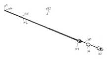
- thermocouple assembly 132includes a sheath 150 , a support member 152 , a pair of wires 154 , a junction 156 , a cap 158 , an electronic circuit 160 , and a plug 162 .
- the sheath 150is an elongated, tubular member having a measuring tip 164 that forms a closed end.
- the opposing end of the sheath 150forms an open end to which the cap 158 is connected.
- the sheath 150is formed of quartz, however, it should be understood by one skilled in the art that the sheath 150 can be formed of any material sufficient to withstand the temperature variations as well as be substantially inert with respect to the gases introduced into the reaction chamber.
- the support member 152is disposed within the sheath 150 and extends at least a portion of the length of the sheath 150 .
- the support member 152is configured to receive the pair of wires 154 therein.
- the support member 152is formed of a ceramic material.
- the pair of wires 154extend from the end of the support member 152 adjacent the measuring tip 164 of the sheath 150 to the electronic circuit 160 .
- the wires 154are formed of dissimilar metals, and an end of each wire is fused to the end of the other wire to form the junction 156 that provides a thermocouple therebetween.
- thermocouple assembly 132may include a plurality of junctions located at any position(s) along the length of the sheath 150 .
- the wires 154operatively connect the junction 156 to the electronic circuit 160 and the plug 162 , as shown in FIG. 3 .
- the plug 162provides an interface between the thermocouple assembly 132 and the temperature controller 36 , as illustrated in FIG. 4 .
- the plug 162provides a physical connection between the thermocouple assembly 132 and the temperature controller 36 , but it should be understood by one skilled in the art that the thermocouple assembly 132 may alternatively include a wireless transmitter (not shown) to operatively connect the thermocouple assembly 132 to the temperature controller 36 without requiring a physical connection therebetween.
- the junction 156is operatively connected to the electronic circuit 160 .
- the illustrated embodimentshows the electronic circuit 160 positioned between the cap 158 and the plug 162 , but it should be understood by one skilled in the art that the electronic circuit 160 can be located at any position between the junction and the interface to which the thermocouple assembly 132 is connected.
- the electronic circuit 160is integrated within the cap 158 .
- the electronic circuit 160is integrated within the plug 162 . It should be understood by one skilled in the art that the electronic circuit 160 can be located at any location on the thermocouple assembly 132 while maintaining an operative connection to the junction 156 .
- thermocouple assembly 132is calibrated using a National Institute of Standards and Technology (NIST) traceable calibration device to verify the accuracy of the thermocouple assembly 132 .
- NISTNational Institute of Standards and Technology
- each thermocouple assembly 132is provided with a unique identification number or data, such as a serial number or the like, that is specific to that thermocouple assembly.
- the calibration data and the unique identification numberare stored on the electronic circuit 160 and travel with and within the smart thermocouple assembly 132 . It should be understood by one skilled in the art that other data or identifiers may also be stored on the electronic circuit 160 in addition to the calibration data and the unique identification number.
- the electronic circuit 160includes a data storage device on which the calibration data and the unique identification number of the thermocouple assembly 132 are stored.
- the electronic circuit 160includes an electrically erasable programmable read-only memory (EEPROM) on which the calibration data and unique identification number are stored.
- the electronic circuit 160includes a flash memory on which the calibration data and unique identification number are stored. It should be understood by one skilled in the art that any other data storage device on which the calibration data and the unique identification number of the thermocouple assembly are stored can be incorporated with the electronic circuit 160 . It should also be understood by one skilled in the art that the calibration data and unique identification number may be stored on the same memory device or different memory devices within the electronic circuit 160 .
- the smart thermocouple assembly 132is configured to improve the accuracy and performance of the temperature control system 34 by providing verification of the thermocouple assembly as well as providing pre-calibration settings to reduce or eliminate the time and effort needed to calibrate thermocouple assemblies once they are installed.
- the smart thermocouple assembly 132is also configured to ensure the proper type of temperature measuring device is used with the temperature control system 34 , thereby allowing proper communication therebetween the thermocouple assembly and the temperature control system 34 .
- the smart thermocouple assembly 132will also reduce the probability of error due to incorrect or inadequate calibration data because the thermocouple assembly is pre-calibrated using a calibration device as opposed to on-the-fly calibration after installation in the reactor 10 ( FIG. 1 ).
- FIG. 4illustrates an exemplary schematic of a temperature control system 34 having an operative connection between the smart thermocouple assembly 132 and the temperature controller 36 of the temperature control system 34 .
- the thermocouple junction 156is operatively connected to the electronic circuit 160 integrated within the thermocouple assembly 132 .
- the thermocouple assembly 132is operatively connected to the temperature controller 36 by way of a module controller 166 .
- a graphical user interface (GUI) 168is also operatively connected to the module controller 166 .
- the GUI 168provides an interface between the operator and the module controller 166 whereby information can be transferred between the GUI 168 and the module controller 166 .
- the module controller 166is configured to verify the thermocouple assembly 132 connected to the temperature controller 36 prior to data, or a temperature measurement, being transferred from the thermocouple assembly 132 to the temperature controller 36 .
- the module controller 166acts as a switch between the thermocouple assembly 132 and the temperature controller 36 such that temperature measurements from the junction 156 are not transferred to the temperature controller prior to the module controller 166 verifying the thermocouple assembly 132 .
- thermocouple assembly 132In operation, an operator installing the thermocouple assembly 132 into a reactor 10 operatively connects the thermocouple assembly 132 to the module controller 166 . Once the thermocouple assembly 132 is operatively connected, the module controller 166 transmits a signal to the electronic circuit 160 to query the electronic circuit 160 for the unique identification number or data stored thereon. If a thermocouple assembly 132 is installed in the reactor 10 that does not include a electronic circuit 160 integrated therein, the module controller 166 receives no return transmission or data from the thermocouple assembly and then transmits a signal to the GUI 168 to provide an error message to the operator indicating that the thermocouple assembly 132 is not compatible with the temperature control system 34 .
- thermocouple assembly 132does include a electronic circuit 160 integrated therein, the electronic circuit 160 transmits a signal to the module controller 166 that includes the unique identification number or data of the particular thermocouple assembly 132 .
- the module controller 166queries the operator to enter the same unique identification number or data that corresponds to the particular thermocouple assembly 132 for confirmation and verification of the unique identification number or data of the particular thermocouple assembly 132 via the GUI 168 .
- the identification number or datais transmitted to the module controller 166 .
- the modular controller 166compares the unique identification number of the thermocouple assembly 132 with the identification number or data entered by the operator.
- the module controller 166transmits a signal to the GUI 168 to instruct the GUI 168 to display an error message for the operator to indicate that the identification number or data that the operator entered did not correspond with the unique identification number or data of the particular thermocouple assembly 132 .
- the module controller 166also prevents the transfer of data between the thermocouple assembly 132 and the temperature controller 36 when the identification number or data input by the operator into the GUI 168 does not correspond to the unique identification number or data of the particular thermocouple assembly 132 .
- the process for verification of the thermocouple assembly 132 explained abovecan be performed at any time after the thermocouple assembly 132 is installed and operatively connected to the module controller 166 .
- the verification processis performed immediately after the thermocouple assembly 132 is operatively connected to the module controller 166 .
- the verification processis performed immediately prior to the operation of the reactor 10 such that processing of a substrate 40 within the reactor 10 will begin only after the thermocouple assembly 132 is verified. Verifying the thermocouple assembly 132 immediately prior to processing within the reactor 10 ensures that another thermocouple assembly 132 was not switched, because switching of the thermocouple assembly 132 may result in poor processing results due to different calibration data of different thermocouple assemblies.
- the verification processcan be performed at regular intervals during processing, for example, between processing a random pair of substrates. It should be understood by one skilled in the art that the thermocouple assembly verification process can be performed at any time to ensure the proper thermocouple assembly 132 is being used during processing to ensure optimized processing results.
- the module controller 166compares the unique identification number of the thermocouple assembly 132 with the identification number or data entered by the operator to determine the numbers or data are equivalent and verifies the thermocouple assembly 132 . Once the thermocouple assembly 132 has been verified, the module controller 166 transmits a signal to the electronic circuit 160 to query the electronic circuit 160 for the calibration data stored thereon. The electronic circuit 160 then transfers the calibration data to the temperature controller 36 either directly or via the module controller 166 . The temperature controller 36 receives the calibration data and adjusts the temperature control system 34 accordingly. Once the module controller 166 has verified the thermocouple assembly 132 and the calibration data on the electronic circuit 160 is transferred to the temperature control system 34 , data and information can freely be transmitted between the thermocouple assembly 132 and the temperature controller 36 .
- Verification of the temperature measuring device having an integrated electronic circuit 160reduces the possibility of error in the temperature measuring device by ensuring the temperature measuring device was properly calibrated prior to installation. Verification of the temperature measuring device having an integrated electronic circuit 160 also reduces the possibility of error in the temperature measuring device by confirming that only temperature measuring devices having an electronic circuit that has calibration data of the temperature measuring device and a unique identification number or data stored thereon are being used in the semiconductor processing tool. This verification process further reduces the amount of time necessary for an operator to install or replace a temperature measuring device in the reactor by integrating the calibration data into the temperature measuring device assembly.
- thermocouple assemblyAs the measuring device, but it should be understood by one skilled in the art that the technology for validating and confirming the temperature measuring device can be incorporated with any other temperature measuring device, including a pyrometer, a thermometer, or the like.
Landscapes
- Physics & Mathematics (AREA)
- General Physics & Mathematics (AREA)
- Engineering & Computer Science (AREA)
- Automation & Control Theory (AREA)
- Remote Sensing (AREA)
- Control Of Temperature (AREA)
- Measuring Temperature Or Quantity Of Heat (AREA)
- Chemical Vapour Deposition (AREA)
Abstract
Description
The present invention relates to a temperature measuring device, and more particularly to a temperature measuring device configured to enhance accuracy of temperature control in a semiconductor processing apparatus.
Temperature controlled semiconductor processing chambers are used for depositing various material layers onto a substrate surface or surfaces. In processing substrates within the processing chamber, one or more substrates or workpieces, such as silicon wafers, are placed on a workpiece support within the processing chamber. Both the substrate and workpiece support are heated to a desired temperature. In a typical processing step, reactant gases are introduced into the processing chamber and passed over each heated substrate, whereby a chemical vapor deposition (CVD) or an atomic layer deposition (ALD) process deposits a thin layer of the reactant material in the reactant gases on the substrate surface(s). Through subsequent processes, these layers are formed into integrated circuits, and tens to thousands or even millions of integrated devices, depending on the size of the substrate and the complexity of the circuits, are cut from the processed substrate.
Various process parameters must be carefully controlled to ensure the high quality of the resulting deposited layers. One such critical parameter is the temperature of the substrate during each processing step. During CVD, for example, the deposition gases react at particular temperatures to deposit the thin layer on the substrate. If the temperature varies greatly across the surface of the substrate, the deposited layer could be uneven. Accordingly, it is important that the substrate temperature be stable and uniform at the desired temperature during processing of the substrate. Similarly, non-uniformity or instability of temperatures across a substrate during other thermal treatments can affect the uniformity of resulting structures on the surface of the substrate. Other processes for which temperature control can be critical include, but are not limited to, oxidation, nitridation, dopant diffusion, sputter depositions, photolithography, dry etching, plasma processes, and high temperature anneals.
Methods and systems are known for measuring the temperature at various locations near and immediately adjacent to the substrate being processed. Typically, thermocouple assemblies are disposed at various locations near the substrate being processed, and these thermocouple assemblies are operatively connected to a controller to assist in providing a more uniform temperature across the entire surface of the substrate. For example, U.S. Pat. No. 6,121,061 issued to Van Bilsen generally teaches a plurality of temperature sensors measuring the temperature at various points surrounding the substrate, including a thermocouple assembly placed near the leading edge of the substrate, another near the trailing edge, one at a side, and another below the substrate near the center of the substrate.
A problem often associated with the replacement of thermocouple assemblies, either because of failure or for regular maintenance, is the variability between each thermocouple assembly. The variability between each thermocouple assembly may be due to any number of factors including, but not limited to, materials used or the methods for producing the thermocouple assemblies. The variability of each thermocouple assembly may result in varying temperature measurements, or a different temperature measurement at the same temperature relative to a previous thermocouple assembly, which in turn may affect the deposition process if the measured temperature is substantially different than the actual temperature within the reaction chamber. Because the temperature control system is based on the calibrated temperature measured by each thermocouple assembly connected to the system, any variability of the calibration between successive thermocouple assemblies will cause variations in the temperature control scheme that may lead to non-uniform deposition of layers on the substrates.
A need therefore exists for a temperature measuring device that includes pre-calibrated parameters such that the deposition tool can be automatically adjusted to account for the pre-calibrated parameters of the temperature measuring device. A need also exists for a temperature measuring device in which pre-calibrated parameters are integrally included with the temperature measuring device.
In one aspect of the present invention, a thermocouple assembly is provided. The thermocouple assembly includes at least one thermocouple junction for measuring temperature. The thermocouple assembly also includes an electronic circuit on which calibration data and a unique identification number is stored. The thermocouple junction is operatively connected to the electronic circuit.
In another aspect of the present invention, a temperature control system is provided. The temperature control system includes at least one heating element and a temperature controller. Each heating element(s) is operatively connected to the temperature controller, and the temperature controller controls output of the heating element(s). The temperature control system further includes a temperature measuring device operatively connected to the temperature controller. The temperature measuring device includes an electronic circuit integrated therein.
In yet another aspect of the present invention, a method for verifying a temperature measuring device for a semiconductor processing tool is provided. The method includes providing a temperature measuring device having an electronic circuit integrated therein, wherein the electronic circuit includes at least a unique identification number or data saved thereon. The method also includes providing module controller operatively connected to the temperature measuring device. The method further includes providing a temperature controller operatively connected to the module controller and the temperature measuring device. The method also includes verifying the unique identification number or data saved on said temperature measuring device prior to a transfer of data between the temperature measuring device and the temperature controller or module controller.
In a further aspect of the present invention, a method for verifying a temperature measuring device for a semiconductor processing tool is provided. The method includes providing a module controller operatively connected to a temperature controller. The method further includes connecting a temperature measuring device to the module controller, wherein the module controller queries the temperature measuring device for a unique identification number stored on an electronic circuit integrated with the temperature measuring device. The method also includes entering an identification number into a graphical user interface (GUI). The GUI is operatively connected to the module controller. The method also includes comparing the unique identification number stored on the electronic circuit of the temperature measuring device with the identification number entered into the GUI. The method includes allowing data transfer between the temperature measuring device and the temperature controller if the unique identification number stored on the electronic circuit of the temperature measuring device is equivalent to the identification number entered into the GUI. The method further includes preventing data transfer between the temperature measuring device and the temperature controller if the unique identification number stored on the electronic circuit of the temperature measuring device is not equivalent to the identification number entered into the GUI.
Advantages of the present invention will become more apparent to those skilled in the art from the following description of the embodiments of the invention which have been shown and described by way of illustration. As will be realized, the invention is capable of other and different embodiments, and its details are capable of modification in various respects. Accordingly, the drawing(s) and description are to be regarded as illustrative in nature and not as restrictive.
Referring toFIG. 1 , an exemplary embodiment of a chemical vapor deposition (“CVD”) reactor10 is shown. While the illustrated embodiment is a single substrate, horizontal flow, cold-wall reactor, it should be understood by one skilled in the art that the thermocouple technology described herein may be used in other types of semiconductor processing reactors as well as other applications requiring accurate temperature sensors. The reactor10 includes areaction chamber 12 defining areaction space 14,heating elements 16 located on opposing sides of thereaction chamber 12, and asubstrate support mechanism 18. Thereaction chamber 12 is an elongated member having aninlet 20 for allowing reactant gases to be introduced into thereaction space 14 and an outlet22 through which the reactant gases and process by-products exit thereaction space 14. In an embodiment, thereaction chamber 12 is formed of transparent quartz that is configured to allow substantially all of the radiant energy from theheating elements 16 to pass through the walls of thereaction chamber 12. Theheating elements 16 provide radiant energy to thereaction chamber 12 without appreciable absorption by thereaction chamber 12 walls. Theheating elements 16 are configured to provide radiant heat of wavelengths absorbed by the substrate being processed as well as portions of thesubstrate support mechanism 18.
In an embodiment, thesubstrate support mechanism 18 includes a substrate holder24 upon which asubstrate 40 is disposed during a deposition process, as illustrated inFIG. 1 . Thesubstrate support mechanism 18 also includes asupport member 26 configured to support the substrate holder24. Thesupport member 26 is connected to ashaft 28 that extends downwardly through atube 30 extending from the lower wall of thereaction chamber 12. A motor (not shown) is configured to rotate theshaft 28, thereby rotating the substrate holder24 andsubstrate 40 in a like manner during the deposition process. Asusceptor ring 25 is disposed about the edge of thesubstrate 40 and substrate holder24 to counteract the heat loss from the edges therefrom. Temperature measuring devices32, such as thermocouple assemblies, pyrometers, or the like, are disposed within thesusceptor ring 25 to measure the localized temperature at pre-determine positions about thesubstrate 40 and substrate holder24.
Referring toFIG. 2 , an embodiment of atemperature control system 34 within a reaction chamber is illustrated. The illustratedtemperature controlling system 34 for a chemical vapor deposition reactor10 includes a plurality of temperature measuring devices32 that are located adjacent to thesubstrate 40 and the substrate holder24 for measuring temperatures at pre-determined locations. The temperature measuring devices32 are operatively connected to atemperature controller 36. Thetemperature controller 36 is operatively connected to theheating elements 16 to control the heating scheme within thereaction chamber 12.
In the schematic diagram ofFIG. 2 , the illustrated embodiment of the atemperature control system 34 includes a plurality of temperature measuring devices32 disposed about thesubstrate 40, wherein the temperature measuring devices32 include: acentral temperature sensor 32alocated adjacent to the lower surface of the substrate holder24, a leading edge temperature sensor32b, a trailingedge temperature sensor 32c, and at least one sideedge temperature sensor 32d. The leading and trailingedge temperature sensors 32b,32care located adjacent to the front and rear edges of thesubstrate 40 relative to the direction of flow A of the reactant gases within thereaction space 14. The temperature measuring devices32 are configured to measure the temperature in the localized area and transmit temperature measurement data to thetemperature controller 36. Thetemperature controller 36 is configured to selectively adjust the energy emitted from the heating element(s)16 in response to data provided by the temperature measuring devices32 to maintain a substantially uniform temperature distribution across theentire substrate 40 being processed. It should be understood by one skilled in the art that thetemperature control system 34 may include any number of temperature measuring devices32 disposed at different locations within, or external to, thereaction chamber 12 for providing data to thetemperature controller 36 of the temperature of thesubstrate 40 being processed or locations adjacent to thesubstrate 40.
The temperature measuring devices32 may include thermocouple assemblies, pyrometers, thermometers, or any other temperature measuring device capable of measuring temperatures within semiconductor manufacturing equipment. In an embodiment, each of the temperature measuring devices32 is the same as the others. In another embodiment, at least one temperature measuring device32 is different than the others. In an embodiment, each of the temperature measuring devices32 is a thermocouple assembly such as the thermocouple assembly described in U.S. patent application Ser. No. 12/140,809. Although the illustratedtemperature control system 34 includes four temperature measuring devices32, it should be understood by one skilled in the art that thetemperature control system 34 may include any number and type of temperature measuring devices32.
Referring toFIG. 3 , an exemplary embodiment of asmart thermocouple assembly 132 is shown. While the preferred embodiments of a temperature measuring device of the present invention are discussed in the context of a thermocouple assembly, one skilled in the art will appreciate that the principles and advantages taught herein will have application to other temperature measuring devices that can be used for measuring temperatures within semiconductor processing reactors or semiconductor manufacturing equipment. In an embodiment, thethermocouple assembly 132 includes asheath 150, asupport member 152, a pair ofwires 154, ajunction 156, acap 158, anelectronic circuit 160, and aplug 162. Thesheath 150 is an elongated, tubular member having a measuringtip 164 that forms a closed end. The opposing end of thesheath 150 forms an open end to which thecap 158 is connected. In an embodiment, thesheath 150 is formed of quartz, however, it should be understood by one skilled in the art that thesheath 150 can be formed of any material sufficient to withstand the temperature variations as well as be substantially inert with respect to the gases introduced into the reaction chamber.
In the embodiment illustrated inFIG. 3 , thesupport member 152 is disposed within thesheath 150 and extends at least a portion of the length of thesheath 150. Thesupport member 152 is configured to receive the pair ofwires 154 therein. In an embodiment, thesupport member 152 is formed of a ceramic material. In an embodiment, the pair ofwires 154 extend from the end of thesupport member 152 adjacent the measuringtip 164 of thesheath 150 to theelectronic circuit 160. Thewires 154 are formed of dissimilar metals, and an end of each wire is fused to the end of the other wire to form thejunction 156 that provides a thermocouple therebetween. The illustrated embodiment shows thejunction 156 being located adjacent the measuringtip 164 of thesheath 150, but it should be understood by one skilled in the art that thethermocouple assembly 132 may include a plurality of junctions located at any position(s) along the length of thesheath 150.
In an embodiment, thewires 154 operatively connect thejunction 156 to theelectronic circuit 160 and theplug 162, as shown inFIG. 3 . Theplug 162 provides an interface between thethermocouple assembly 132 and thetemperature controller 36, as illustrated inFIG. 4 . Theplug 162 provides a physical connection between thethermocouple assembly 132 and thetemperature controller 36, but it should be understood by one skilled in the art that thethermocouple assembly 132 may alternatively include a wireless transmitter (not shown) to operatively connect thethermocouple assembly 132 to thetemperature controller 36 without requiring a physical connection therebetween.
As illustrated inFIGS. 3-4 , thejunction 156 is operatively connected to theelectronic circuit 160. The illustrated embodiment shows theelectronic circuit 160 positioned between thecap 158 and theplug 162, but it should be understood by one skilled in the art that theelectronic circuit 160 can be located at any position between the junction and the interface to which thethermocouple assembly 132 is connected. In an embodiment, theelectronic circuit 160 is integrated within thecap 158. In another embodiment, theelectronic circuit 160 is integrated within theplug 162. It should be understood by one skilled in the art that theelectronic circuit 160 can be located at any location on thethermocouple assembly 132 while maintaining an operative connection to thejunction 156.
During assembly of thethermocouple assembly 132, thethermocouple assembly 132 is calibrated using a National Institute of Standards and Technology (NIST) traceable calibration device to verify the accuracy of thethermocouple assembly 132. Also during assembly of thethermocouple assemblies 132, eachthermocouple assembly 132 is provided with a unique identification number or data, such as a serial number or the like, that is specific to that thermocouple assembly. The calibration data and the unique identification number are stored on theelectronic circuit 160 and travel with and within thesmart thermocouple assembly 132. It should be understood by one skilled in the art that other data or identifiers may also be stored on theelectronic circuit 160 in addition to the calibration data and the unique identification number. In an embodiment, theelectronic circuit 160 includes a data storage device on which the calibration data and the unique identification number of thethermocouple assembly 132 are stored. In an embodiment, theelectronic circuit 160 includes an electrically erasable programmable read-only memory (EEPROM) on which the calibration data and unique identification number are stored. In another embodiment, theelectronic circuit 160 includes a flash memory on which the calibration data and unique identification number are stored. It should be understood by one skilled in the art that any other data storage device on which the calibration data and the unique identification number of the thermocouple assembly are stored can be incorporated with theelectronic circuit 160. It should also be understood by one skilled in the art that the calibration data and unique identification number may be stored on the same memory device or different memory devices within theelectronic circuit 160.
Thesmart thermocouple assembly 132 is configured to improve the accuracy and performance of thetemperature control system 34 by providing verification of the thermocouple assembly as well as providing pre-calibration settings to reduce or eliminate the time and effort needed to calibrate thermocouple assemblies once they are installed. Thesmart thermocouple assembly 132 is also configured to ensure the proper type of temperature measuring device is used with thetemperature control system 34, thereby allowing proper communication therebetween the thermocouple assembly and thetemperature control system 34. Thesmart thermocouple assembly 132 will also reduce the probability of error due to incorrect or inadequate calibration data because the thermocouple assembly is pre-calibrated using a calibration device as opposed to on-the-fly calibration after installation in the reactor10 (FIG. 1 ).
In operation, an operator installing thethermocouple assembly 132 into a reactor10 operatively connects thethermocouple assembly 132 to themodule controller 166. Once thethermocouple assembly 132 is operatively connected, themodule controller 166 transmits a signal to theelectronic circuit 160 to query theelectronic circuit 160 for the unique identification number or data stored thereon. If athermocouple assembly 132 is installed in the reactor10 that does not include aelectronic circuit 160 integrated therein, themodule controller 166 receives no return transmission or data from the thermocouple assembly and then transmits a signal to theGUI 168 to provide an error message to the operator indicating that thethermocouple assembly 132 is not compatible with thetemperature control system 34. If thethermocouple assembly 132 does include aelectronic circuit 160 integrated therein, theelectronic circuit 160 transmits a signal to themodule controller 166 that includes the unique identification number or data of theparticular thermocouple assembly 132. Once themodule controller 166 receives the unique identification number or data from theelectronic circuit 160, themodule controller 166 queries the operator to enter the same unique identification number or data that corresponds to theparticular thermocouple assembly 132 for confirmation and verification of the unique identification number or data of theparticular thermocouple assembly 132 via theGUI 168. Once the operator has entered an identification number or data, the identification number or data is transmitted to themodule controller 166. Themodular controller 166 compares the unique identification number of thethermocouple assembly 132 with the identification number or data entered by the operator. If the identification number or data is not equivalent to the unique identification number or data of theparticular thermocouple assembly 132, themodule controller 166 transmits a signal to theGUI 168 to instruct theGUI 168 to display an error message for the operator to indicate that the identification number or data that the operator entered did not correspond with the unique identification number or data of theparticular thermocouple assembly 132. Themodule controller 166 also prevents the transfer of data between thethermocouple assembly 132 and thetemperature controller 36 when the identification number or data input by the operator into theGUI 168 does not correspond to the unique identification number or data of theparticular thermocouple assembly 132.
The process for verification of thethermocouple assembly 132 explained above can be performed at any time after thethermocouple assembly 132 is installed and operatively connected to themodule controller 166. In an embodiment, the verification process is performed immediately after thethermocouple assembly 132 is operatively connected to themodule controller 166. In another embodiment, the verification process is performed immediately prior to the operation of the reactor10 such that processing of asubstrate 40 within the reactor10 will begin only after thethermocouple assembly 132 is verified. Verifying thethermocouple assembly 132 immediately prior to processing within the reactor10 ensures that anotherthermocouple assembly 132 was not switched, because switching of thethermocouple assembly 132 may result in poor processing results due to different calibration data of different thermocouple assemblies. In yet another embodiment, the verification process can be performed at regular intervals during processing, for example, between processing a random pair of substrates. It should be understood by one skilled in the art that the thermocouple assembly verification process can be performed at any time to ensure theproper thermocouple assembly 132 is being used during processing to ensure optimized processing results.
If the operator enters an identification number or data into theGUI 168 that corresponds to the unique identification number or data of theparticular thermocouple assembly 132, themodule controller 166 compares the unique identification number of thethermocouple assembly 132 with the identification number or data entered by the operator to determine the numbers or data are equivalent and verifies thethermocouple assembly 132. Once thethermocouple assembly 132 has been verified, themodule controller 166 transmits a signal to theelectronic circuit 160 to query theelectronic circuit 160 for the calibration data stored thereon. Theelectronic circuit 160 then transfers the calibration data to thetemperature controller 36 either directly or via themodule controller 166. Thetemperature controller 36 receives the calibration data and adjusts thetemperature control system 34 accordingly. Once themodule controller 166 has verified thethermocouple assembly 132 and the calibration data on theelectronic circuit 160 is transferred to thetemperature control system 34, data and information can freely be transmitted between thethermocouple assembly 132 and thetemperature controller 36.
Verification of the temperature measuring device having an integratedelectronic circuit 160 reduces the possibility of error in the temperature measuring device by ensuring the temperature measuring device was properly calibrated prior to installation. Verification of the temperature measuring device having an integratedelectronic circuit 160 also reduces the possibility of error in the temperature measuring device by confirming that only temperature measuring devices having an electronic circuit that has calibration data of the temperature measuring device and a unique identification number or data stored thereon are being used in the semiconductor processing tool. This verification process further reduces the amount of time necessary for an operator to install or replace a temperature measuring device in the reactor by integrating the calibration data into the temperature measuring device assembly.
The smart temperature measuring device described above was directed to a thermocouple assembly as the measuring device, but it should be understood by one skilled in the art that the technology for validating and confirming the temperature measuring device can be incorporated with any other temperature measuring device, including a pyrometer, a thermometer, or the like.
While preferred embodiments of the present invention have been described, it should be understood that the present invention is not so limited and modifications may be made without departing from the present invention. The scope of the present invention is defined by the appended claims, and all devices, process, and methods that come within the meaning of the claims, either literally or by equivalence, are intended to be embraced therein.
Claims (14)
1. A thermocouple assembly for measuring a temperature within a reaction chamber, the thermocouple assembly comprising:
a thermocouple junction of a pair of wires for measuring temperature within the reaction chamber;
a support member to receive the pair of wires, the support member disposed within a sheath;
an interface plug for operatively connecting the thermocouple assembly to a temperature controller; and
an electronic circuit on which calibration data and a unique identification number are stored, wherein said at least one thermocouple junction is operatively connected to said electronic circuit, wherein the electronic circuit is disposed between the thermocouple junction and the interface plug, wherein said electronic circuit transmits said unique identification number via said interface plug to said temperature controller in order to uniquely identify said thermocouple assembly, wherein said calibration data comprises pre-calibrated parameters integrally included in said electronic circuit wherein said pre-calibrated parameters are determined using a NIST traceable calibration device during assembly of said thermocouple, wherein said electronic circuit transfers the calibration data to the temperature controller for adjusting the temperature controller, wherein the electronic circuit is integrated with the thermocouple assembly, and wherein a module controller connected to the electronic circuit prevents data transfer between the thermocouple assembly and the temperature controller by verifying if the unique identification number stored in the electronic circuit is not equivalent to the identification number entered into a graphical user interface connected to the module controller.
2. The thermocouple assembly ofclaim 1 , wherein said electronic circuit includes an electrically erasable programmable read-only memory (EEPROM).
3. The thermocouple assembly ofclaim 2 , wherein said unique identification number is stored on said EEPROM.
4. The thermocouple assembly ofclaim 1 , wherein said electronic circuit includes a flash memory.
5. The thermocouple assembly ofclaim 2 , wherein said unique identification number is stored on said flash memory.
6. The thermocouple assembly ofclaim 1 , further comprising a plurality of junctions operatively connected to said electronic circuit.
7. The thermocouple assembly ofclaim 1 , further comprising a cap disposed between the thermocouple junction and the interface.
8. The thermocouple assembly ofclaim 7 , wherein the electronic circuit is disposed between the cap and the interface.
9. The thermocouple assembly ofclaim 7 , wherein the interface comprises a plug, and the electronic circuit is disposed between the cap and the plug.
10. The thermocouple assembly ofclaim 1 , wherein the electronic circuit includes a memory device, and wherein the calibration data and unique identification number are stored on the memory device.
11. The thermocouple assembly ofclaim 1 , wherein the electronic circuit is configured to transmit, via the interface, the unique identification number in response to a query received by the electronic circuit via the interface.
12. The thermocouple assembly ofclaim 1 , wherein the electronic circuit is configured to transmit, via the interface, the calibration data in response to a query received by the electronic circuit via the interface.
13. The thermocouple assembly ofclaim 1 , wherein the electronic circuit is configured to transmit, via the interface, data regarding a temperature measured by the thermocouple junction.
14. The thermocouple assembly ofclaim 1 , wherein the support member is formed of ceramic material.
Priority Applications (4)
| Application Number | Priority Date | Filing Date | Title |
|---|---|---|---|
| US12/436,306US9297705B2 (en) | 2009-05-06 | 2009-05-06 | Smart temperature measuring device |
| CN201080020268.1ACN102439402B (en) | 2009-05-06 | 2010-04-30 | Intellectual Gauge of Temperature |
| PCT/US2010/033248WO2010129430A1 (en) | 2009-05-06 | 2010-04-30 | Smart temperature measuring device |
| TW099114331ATWI506256B (en) | 2009-05-06 | 2010-05-05 | Smart temperature measuring device |
Applications Claiming Priority (1)
| Application Number | Priority Date | Filing Date | Title |
|---|---|---|---|
| US12/436,306US9297705B2 (en) | 2009-05-06 | 2009-05-06 | Smart temperature measuring device |
Publications (2)
| Publication Number | Publication Date |
|---|---|
| US20100286842A1 US20100286842A1 (en) | 2010-11-11 |
| US9297705B2true US9297705B2 (en) | 2016-03-29 |
Family
ID=43050381
Family Applications (1)
| Application Number | Title | Priority Date | Filing Date |
|---|---|---|---|
| US12/436,306Active2030-12-21US9297705B2 (en) | 2009-05-06 | 2009-05-06 | Smart temperature measuring device |
Country Status (4)
| Country | Link |
|---|---|
| US (1) | US9297705B2 (en) |
| CN (1) | CN102439402B (en) |
| TW (1) | TWI506256B (en) |
| WO (1) | WO2010129430A1 (en) |
Cited By (354)
| Publication number | Priority date | Publication date | Assignee | Title |
|---|---|---|---|---|
| US20140185646A1 (en)* | 2007-09-21 | 2014-07-03 | Siemens Industry, Inc. | Systems, devices, and/or methods for managing a thermocouple module |
| US20150030053A1 (en)* | 2012-02-23 | 2015-01-29 | Testo Ag | Temperature measuring device, temperature measuring device set and method for configuring a temperature measuring device that can be operated with a thermocouple |
| US10229833B2 (en) | 2016-11-01 | 2019-03-12 | Asm Ip Holding B.V. | Methods for forming a transition metal nitride film on a substrate by atomic layer deposition and related semiconductor device structures |
| US10249577B2 (en) | 2016-05-17 | 2019-04-02 | Asm Ip Holding B.V. | Method of forming metal interconnection and method of fabricating semiconductor apparatus using the method |
| US10249524B2 (en) | 2017-08-09 | 2019-04-02 | Asm Ip Holding B.V. | Cassette holder assembly for a substrate cassette and holding member for use in such assembly |
| US10262859B2 (en) | 2016-03-24 | 2019-04-16 | Asm Ip Holding B.V. | Process for forming a film on a substrate using multi-port injection assemblies |
| US10269558B2 (en) | 2016-12-22 | 2019-04-23 | Asm Ip Holding B.V. | Method of forming a structure on a substrate |
| US10276355B2 (en) | 2015-03-12 | 2019-04-30 | Asm Ip Holding B.V. | Multi-zone reactor, system including the reactor, and method of using the same |
| US10283353B2 (en) | 2017-03-29 | 2019-05-07 | Asm Ip Holding B.V. | Method of reforming insulating film deposited on substrate with recess pattern |
| US10290508B1 (en) | 2017-12-05 | 2019-05-14 | Asm Ip Holding B.V. | Method for forming vertical spacers for spacer-defined patterning |
| US10312055B2 (en) | 2017-07-26 | 2019-06-04 | Asm Ip Holding B.V. | Method of depositing film by PEALD using negative bias |
| US10312129B2 (en) | 2015-09-29 | 2019-06-04 | Asm Ip Holding B.V. | Variable adjustment for precise matching of multiple chamber cavity housings |
| US10319588B2 (en) | 2017-10-10 | 2019-06-11 | Asm Ip Holding B.V. | Method for depositing a metal chalcogenide on a substrate by cyclical deposition |
| US10322384B2 (en) | 2015-11-09 | 2019-06-18 | Asm Ip Holding B.V. | Counter flow mixer for process chamber |
| US10340135B2 (en) | 2016-11-28 | 2019-07-02 | Asm Ip Holding B.V. | Method of topologically restricted plasma-enhanced cyclic deposition of silicon or metal nitride |
| US10340125B2 (en) | 2013-03-08 | 2019-07-02 | Asm Ip Holding B.V. | Pulsed remote plasma method and system |
| US10343920B2 (en) | 2016-03-18 | 2019-07-09 | Asm Ip Holding B.V. | Aligned carbon nanotubes |
| US10361201B2 (en) | 2013-09-27 | 2019-07-23 | Asm Ip Holding B.V. | Semiconductor structure and device formed using selective epitaxial process |
| US10364493B2 (en) | 2016-08-25 | 2019-07-30 | Asm Ip Holding B.V. | Exhaust apparatus and substrate processing apparatus having an exhaust line with a first ring having at least one hole on a lateral side thereof placed in the exhaust line |
| US10364496B2 (en) | 2011-06-27 | 2019-07-30 | Asm Ip Holding B.V. | Dual section module having shared and unshared mass flow controllers |
| US10367080B2 (en) | 2016-05-02 | 2019-07-30 | Asm Ip Holding B.V. | Method of forming a germanium oxynitride film |
| US10366864B2 (en) | 2013-03-08 | 2019-07-30 | Asm Ip Holding B.V. | Method and system for in-situ formation of intermediate reactive species |
| US10381226B2 (en) | 2016-07-27 | 2019-08-13 | Asm Ip Holding B.V. | Method of processing substrate |
| US10378106B2 (en) | 2008-11-14 | 2019-08-13 | Asm Ip Holding B.V. | Method of forming insulation film by modified PEALD |
| US10381219B1 (en) | 2018-10-25 | 2019-08-13 | Asm Ip Holding B.V. | Methods for forming a silicon nitride film |
| US10388509B2 (en) | 2016-06-28 | 2019-08-20 | Asm Ip Holding B.V. | Formation of epitaxial layers via dislocation filtering |
| US10388513B1 (en) | 2018-07-03 | 2019-08-20 | Asm Ip Holding B.V. | Method for depositing silicon-free carbon-containing film as gap-fill layer by pulse plasma-assisted deposition |
| US10395919B2 (en) | 2016-07-28 | 2019-08-27 | Asm Ip Holding B.V. | Method and apparatus for filling a gap |
| US10403504B2 (en) | 2017-10-05 | 2019-09-03 | Asm Ip Holding B.V. | Method for selectively depositing a metallic film on a substrate |
| US10410943B2 (en) | 2016-10-13 | 2019-09-10 | Asm Ip Holding B.V. | Method for passivating a surface of a semiconductor and related systems |
| US10435790B2 (en) | 2016-11-01 | 2019-10-08 | Asm Ip Holding B.V. | Method of subatmospheric plasma-enhanced ALD using capacitively coupled electrodes with narrow gap |
| US10438965B2 (en) | 2014-12-22 | 2019-10-08 | Asm Ip Holding B.V. | Semiconductor device and manufacturing method thereof |
| US10446393B2 (en) | 2017-05-08 | 2019-10-15 | Asm Ip Holding B.V. | Methods for forming silicon-containing epitaxial layers and related semiconductor device structures |
| US10458018B2 (en) | 2015-06-26 | 2019-10-29 | Asm Ip Holding B.V. | Structures including metal carbide material, devices including the structures, and methods of forming same |
| US10468261B2 (en) | 2017-02-15 | 2019-11-05 | Asm Ip Holding B.V. | Methods for forming a metallic film on a substrate by cyclical deposition and related semiconductor device structures |
| US10468251B2 (en) | 2016-02-19 | 2019-11-05 | Asm Ip Holding B.V. | Method for forming spacers using silicon nitride film for spacer-defined multiple patterning |
| US10480072B2 (en) | 2009-04-06 | 2019-11-19 | Asm Ip Holding B.V. | Semiconductor processing reactor and components thereof |
| US10483099B1 (en) | 2018-07-26 | 2019-11-19 | Asm Ip Holding B.V. | Method for forming thermally stable organosilicon polymer film |
| US10504742B2 (en) | 2017-05-31 | 2019-12-10 | Asm Ip Holding B.V. | Method of atomic layer etching using hydrogen plasma |
| US10501866B2 (en) | 2016-03-09 | 2019-12-10 | Asm Ip Holding B.V. | Gas distribution apparatus for improved film uniformity in an epitaxial system |
| US10510536B2 (en) | 2018-03-29 | 2019-12-17 | Asm Ip Holding B.V. | Method of depositing a co-doped polysilicon film on a surface of a substrate within a reaction chamber |
| US10529563B2 (en) | 2017-03-29 | 2020-01-07 | Asm Ip Holdings B.V. | Method for forming doped metal oxide films on a substrate by cyclical deposition and related semiconductor device structures |
| US10529554B2 (en) | 2016-02-19 | 2020-01-07 | Asm Ip Holding B.V. | Method for forming silicon nitride film selectively on sidewalls or flat surfaces of trenches |
| US10529542B2 (en) | 2015-03-11 | 2020-01-07 | Asm Ip Holdings B.V. | Cross-flow reactor and method |
| US10535516B2 (en) | 2018-02-01 | 2020-01-14 | Asm Ip Holdings B.V. | Method for depositing a semiconductor structure on a surface of a substrate and related semiconductor structures |
| US10541333B2 (en) | 2017-07-19 | 2020-01-21 | Asm Ip Holding B.V. | Method for depositing a group IV semiconductor and related semiconductor device structures |
| US10541173B2 (en) | 2016-07-08 | 2020-01-21 | Asm Ip Holding B.V. | Selective deposition method to form air gaps |
| US10559458B1 (en) | 2018-11-26 | 2020-02-11 | Asm Ip Holding B.V. | Method of forming oxynitride film |
| US10566223B2 (en) | 2012-08-28 | 2020-02-18 | Asm Ip Holdings B.V. | Systems and methods for dynamic semiconductor process scheduling |
| US10561975B2 (en) | 2014-10-07 | 2020-02-18 | Asm Ip Holdings B.V. | Variable conductance gas distribution apparatus and method |
| US10590535B2 (en) | 2017-07-26 | 2020-03-17 | Asm Ip Holdings B.V. | Chemical treatment, deposition and/or infiltration apparatus and method for using the same |
| US10600673B2 (en) | 2015-07-07 | 2020-03-24 | Asm Ip Holding B.V. | Magnetic susceptor to baseplate seal |
| US10605530B2 (en) | 2017-07-26 | 2020-03-31 | Asm Ip Holding B.V. | Assembly of a liner and a flange for a vertical furnace as well as the liner and the vertical furnace |
| US10604847B2 (en) | 2014-03-18 | 2020-03-31 | Asm Ip Holding B.V. | Gas distribution system, reactor including the system, and methods of using the same |
| US10607895B2 (en) | 2017-09-18 | 2020-03-31 | Asm Ip Holdings B.V. | Method for forming a semiconductor device structure comprising a gate fill metal |
| US10612136B2 (en) | 2018-06-29 | 2020-04-07 | ASM IP Holding, B.V. | Temperature-controlled flange and reactor system including same |
| USD880437S1 (en) | 2018-02-01 | 2020-04-07 | Asm Ip Holding B.V. | Gas supply plate for semiconductor manufacturing apparatus |
| US10612137B2 (en) | 2016-07-08 | 2020-04-07 | Asm Ip Holdings B.V. | Organic reactants for atomic layer deposition |
| US10622375B2 (en) | 2016-11-07 | 2020-04-14 | Asm Ip Holding B.V. | Method of processing a substrate and a device manufactured by using the method |
| US10643826B2 (en) | 2016-10-26 | 2020-05-05 | Asm Ip Holdings B.V. | Methods for thermally calibrating reaction chambers |
| US10643904B2 (en) | 2016-11-01 | 2020-05-05 | Asm Ip Holdings B.V. | Methods for forming a semiconductor device and related semiconductor device structures |
| US10655221B2 (en) | 2017-02-09 | 2020-05-19 | Asm Ip Holding B.V. | Method for depositing oxide film by thermal ALD and PEALD |
| US10658205B2 (en) | 2017-09-28 | 2020-05-19 | Asm Ip Holdings B.V. | Chemical dispensing apparatus and methods for dispensing a chemical to a reaction chamber |
| US10658181B2 (en) | 2018-02-20 | 2020-05-19 | Asm Ip Holding B.V. | Method of spacer-defined direct patterning in semiconductor fabrication |
| US10665452B2 (en) | 2016-05-02 | 2020-05-26 | Asm Ip Holdings B.V. | Source/drain performance through conformal solid state doping |
| US10685834B2 (en) | 2017-07-05 | 2020-06-16 | Asm Ip Holdings B.V. | Methods for forming a silicon germanium tin layer and related semiconductor device structures |
| US10683571B2 (en) | 2014-02-25 | 2020-06-16 | Asm Ip Holding B.V. | Gas supply manifold and method of supplying gases to chamber using same |
| US10692741B2 (en) | 2017-08-08 | 2020-06-23 | Asm Ip Holdings B.V. | Radiation shield |
| US10707106B2 (en) | 2011-06-06 | 2020-07-07 | Asm Ip Holding B.V. | High-throughput semiconductor-processing apparatus equipped with multiple dual-chamber modules |
| US10714350B2 (en) | 2016-11-01 | 2020-07-14 | ASM IP Holdings, B.V. | Methods for forming a transition metal niobium nitride film on a substrate by atomic layer deposition and related semiconductor device structures |
| US10714385B2 (en) | 2016-07-19 | 2020-07-14 | Asm Ip Holding B.V. | Selective deposition of tungsten |
| US10714335B2 (en) | 2017-04-25 | 2020-07-14 | Asm Ip Holding B.V. | Method of depositing thin film and method of manufacturing semiconductor device |
| US10714315B2 (en) | 2012-10-12 | 2020-07-14 | Asm Ip Holdings B.V. | Semiconductor reaction chamber showerhead |
| US10731249B2 (en) | 2018-02-15 | 2020-08-04 | Asm Ip Holding B.V. | Method of forming a transition metal containing film on a substrate by a cyclical deposition process, a method for supplying a transition metal halide compound to a reaction chamber, and related vapor deposition apparatus |
| US10734244B2 (en) | 2017-11-16 | 2020-08-04 | Asm Ip Holding B.V. | Method of processing a substrate and a device manufactured by the same |
| US10734497B2 (en) | 2017-07-18 | 2020-08-04 | Asm Ip Holding B.V. | Methods for forming a semiconductor device structure and related semiconductor device structures |
| US10741385B2 (en) | 2016-07-28 | 2020-08-11 | Asm Ip Holding B.V. | Method and apparatus for filling a gap |
| US10755922B2 (en) | 2018-07-03 | 2020-08-25 | Asm Ip Holding B.V. | Method for depositing silicon-free carbon-containing film as gap-fill layer by pulse plasma-assisted deposition |
| US10770286B2 (en) | 2017-05-08 | 2020-09-08 | Asm Ip Holdings B.V. | Methods for selectively forming a silicon nitride film on a substrate and related semiconductor device structures |
| US10767789B2 (en) | 2018-07-16 | 2020-09-08 | Asm Ip Holding B.V. | Diaphragm valves, valve components, and methods for forming valve components |
| US10770336B2 (en) | 2017-08-08 | 2020-09-08 | Asm Ip Holding B.V. | Substrate lift mechanism and reactor including same |
| US10787741B2 (en) | 2014-08-21 | 2020-09-29 | Asm Ip Holding B.V. | Method and system for in situ formation of gas-phase compounds |
| US10797133B2 (en) | 2018-06-21 | 2020-10-06 | Asm Ip Holding B.V. | Method for depositing a phosphorus doped silicon arsenide film and related semiconductor device structures |
| US10804098B2 (en) | 2009-08-14 | 2020-10-13 | Asm Ip Holding B.V. | Systems and methods for thin-film deposition of metal oxides using excited nitrogen-oxygen species |
| US10811256B2 (en) | 2018-10-16 | 2020-10-20 | Asm Ip Holding B.V. | Method for etching a carbon-containing feature |
| USD900036S1 (en) | 2017-08-24 | 2020-10-27 | Asm Ip Holding B.V. | Heater electrical connector and adapter |
| US10818758B2 (en) | 2018-11-16 | 2020-10-27 | Asm Ip Holding B.V. | Methods for forming a metal silicate film on a substrate in a reaction chamber and related semiconductor device structures |
| US10832903B2 (en) | 2011-10-28 | 2020-11-10 | Asm Ip Holding B.V. | Process feed management for semiconductor substrate processing |
| US10829852B2 (en) | 2018-08-16 | 2020-11-10 | Asm Ip Holding B.V. | Gas distribution device for a wafer processing apparatus |
| US10844484B2 (en) | 2017-09-22 | 2020-11-24 | Asm Ip Holding B.V. | Apparatus for dispensing a vapor phase reactant to a reaction chamber and related methods |
| US10847371B2 (en) | 2018-03-27 | 2020-11-24 | Asm Ip Holding B.V. | Method of forming an electrode on a substrate and a semiconductor device structure including an electrode |
| US10847365B2 (en) | 2018-10-11 | 2020-11-24 | Asm Ip Holding B.V. | Method of forming conformal silicon carbide film by cyclic CVD |
| US10847366B2 (en) | 2018-11-16 | 2020-11-24 | Asm Ip Holding B.V. | Methods for depositing a transition metal chalcogenide film on a substrate by a cyclical deposition process |
| USD903477S1 (en) | 2018-01-24 | 2020-12-01 | Asm Ip Holdings B.V. | Metal clamp |
| US10851456B2 (en) | 2016-04-21 | 2020-12-01 | Asm Ip Holding B.V. | Deposition of metal borides |
| US10854498B2 (en) | 2011-07-15 | 2020-12-01 | Asm Ip Holding B.V. | Wafer-supporting device and method for producing same |
| US10858737B2 (en) | 2014-07-28 | 2020-12-08 | Asm Ip Holding B.V. | Showerhead assembly and components thereof |
| US10865475B2 (en) | 2016-04-21 | 2020-12-15 | Asm Ip Holding B.V. | Deposition of metal borides and silicides |
| US10867788B2 (en) | 2016-12-28 | 2020-12-15 | Asm Ip Holding B.V. | Method of forming a structure on a substrate |
| US10867786B2 (en) | 2018-03-30 | 2020-12-15 | Asm Ip Holding B.V. | Substrate processing method |
| US10872771B2 (en) | 2018-01-16 | 2020-12-22 | Asm Ip Holding B. V. | Method for depositing a material film on a substrate within a reaction chamber by a cyclical deposition process and related device structures |
| US10886123B2 (en) | 2017-06-02 | 2021-01-05 | Asm Ip Holding B.V. | Methods for forming low temperature semiconductor layers and related semiconductor device structures |
| US10883175B2 (en) | 2018-08-09 | 2021-01-05 | Asm Ip Holding B.V. | Vertical furnace for processing substrates and a liner for use therein |
| US10892156B2 (en) | 2017-05-08 | 2021-01-12 | Asm Ip Holding B.V. | Methods for forming a silicon nitride film on a substrate and related semiconductor device structures |
| US10896820B2 (en) | 2018-02-14 | 2021-01-19 | Asm Ip Holding B.V. | Method for depositing a ruthenium-containing film on a substrate by a cyclical deposition process |
| US10910262B2 (en) | 2017-11-16 | 2021-02-02 | Asm Ip Holding B.V. | Method of selectively depositing a capping layer structure on a semiconductor device structure |
| US10914004B2 (en) | 2018-06-29 | 2021-02-09 | Asm Ip Holding B.V. | Thin-film deposition method and manufacturing method of semiconductor device |
| US10923344B2 (en) | 2017-10-30 | 2021-02-16 | Asm Ip Holding B.V. | Methods for forming a semiconductor structure and related semiconductor structures |
| US10928731B2 (en) | 2017-09-21 | 2021-02-23 | Asm Ip Holding B.V. | Method of sequential infiltration synthesis treatment of infiltrateable material and structures and devices formed using same |
| US10934619B2 (en) | 2016-11-15 | 2021-03-02 | Asm Ip Holding B.V. | Gas supply unit and substrate processing apparatus including the gas supply unit |
| US10941490B2 (en) | 2014-10-07 | 2021-03-09 | Asm Ip Holding B.V. | Multiple temperature range susceptor, assembly, reactor and system including the susceptor, and methods of using the same |
| US10975470B2 (en) | 2018-02-23 | 2021-04-13 | Asm Ip Holding B.V. | Apparatus for detecting or monitoring for a chemical precursor in a high temperature environment |
| US11001925B2 (en) | 2016-12-19 | 2021-05-11 | Asm Ip Holding B.V. | Substrate processing apparatus |
| US11018047B2 (en) | 2018-01-25 | 2021-05-25 | Asm Ip Holding B.V. | Hybrid lift pin |
| US11015245B2 (en) | 2014-03-19 | 2021-05-25 | Asm Ip Holding B.V. | Gas-phase reactor and system having exhaust plenum and components thereof |
| US11018002B2 (en) | 2017-07-19 | 2021-05-25 | Asm Ip Holding B.V. | Method for selectively depositing a Group IV semiconductor and related semiconductor device structures |
| US11024523B2 (en) | 2018-09-11 | 2021-06-01 | Asm Ip Holding B.V. | Substrate processing apparatus and method |
| US11022879B2 (en) | 2017-11-24 | 2021-06-01 | Asm Ip Holding B.V. | Method of forming an enhanced unexposed photoresist layer |
| US11031242B2 (en) | 2018-11-07 | 2021-06-08 | Asm Ip Holding B.V. | Methods for depositing a boron doped silicon germanium film |
| USD922229S1 (en) | 2019-06-05 | 2021-06-15 | Asm Ip Holding B.V. | Device for controlling a temperature of a gas supply unit |
| US11049751B2 (en) | 2018-09-14 | 2021-06-29 | Asm Ip Holding B.V. | Cassette supply system to store and handle cassettes and processing apparatus equipped therewith |
| US11056344B2 (en) | 2017-08-30 | 2021-07-06 | Asm Ip Holding B.V. | Layer forming method |
| US11053591B2 (en) | 2018-08-06 | 2021-07-06 | Asm Ip Holding B.V. | Multi-port gas injection system and reactor system including same |
| US11056567B2 (en) | 2018-05-11 | 2021-07-06 | Asm Ip Holding B.V. | Method of forming a doped metal carbide film on a substrate and related semiconductor device structures |
| US11069510B2 (en) | 2017-08-30 | 2021-07-20 | Asm Ip Holding B.V. | Substrate processing apparatus |
| US11081345B2 (en) | 2018-02-06 | 2021-08-03 | Asm Ip Holding B.V. | Method of post-deposition treatment for silicon oxide film |
| US11088002B2 (en) | 2018-03-29 | 2021-08-10 | Asm Ip Holding B.V. | Substrate rack and a substrate processing system and method |
| US11087997B2 (en) | 2018-10-31 | 2021-08-10 | Asm Ip Holding B.V. | Substrate processing apparatus for processing substrates |
| US11114283B2 (en) | 2018-03-16 | 2021-09-07 | Asm Ip Holding B.V. | Reactor, system including the reactor, and methods of manufacturing and using same |
| US11114294B2 (en) | 2019-03-08 | 2021-09-07 | Asm Ip Holding B.V. | Structure including SiOC layer and method of forming same |
| USD930782S1 (en) | 2019-08-22 | 2021-09-14 | Asm Ip Holding B.V. | Gas distributor |
| US11127617B2 (en) | 2017-11-27 | 2021-09-21 | Asm Ip Holding B.V. | Storage device for storing wafer cassettes for use with a batch furnace |
| US11127589B2 (en) | 2019-02-01 | 2021-09-21 | Asm Ip Holding B.V. | Method of topology-selective film formation of silicon oxide |
| USD931978S1 (en) | 2019-06-27 | 2021-09-28 | Asm Ip Holding B.V. | Showerhead vacuum transport |
| US11139308B2 (en) | 2015-12-29 | 2021-10-05 | Asm Ip Holding B.V. | Atomic layer deposition of III-V compounds to form V-NAND devices |
| US11139191B2 (en) | 2017-08-09 | 2021-10-05 | Asm Ip Holding B.V. | Storage apparatus for storing cassettes for substrates and processing apparatus equipped therewith |
| WO2021204436A1 (en)* | 2020-04-09 | 2021-10-14 | Ipetronik Gmbh & Co. Kg | Electrical connection for connecting a thermal element |
| US11158513B2 (en) | 2018-12-13 | 2021-10-26 | Asm Ip Holding B.V. | Methods for forming a rhenium-containing film on a substrate by a cyclical deposition process and related semiconductor device structures |
| USD935572S1 (en) | 2019-05-24 | 2021-11-09 | Asm Ip Holding B.V. | Gas channel plate |
| US11171025B2 (en) | 2019-01-22 | 2021-11-09 | Asm Ip Holding B.V. | Substrate processing device |
| US11205585B2 (en) | 2016-07-28 | 2021-12-21 | Asm Ip Holding B.V. | Substrate processing apparatus and method of operating the same |
| US11217444B2 (en) | 2018-11-30 | 2022-01-04 | Asm Ip Holding B.V. | Method for forming an ultraviolet radiation responsive metal oxide-containing film |
| US11222772B2 (en) | 2016-12-14 | 2022-01-11 | Asm Ip Holding B.V. | Substrate processing apparatus |
| USD940837S1 (en) | 2019-08-22 | 2022-01-11 | Asm Ip Holding B.V. | Electrode |
| US11227782B2 (en) | 2019-07-31 | 2022-01-18 | Asm Ip Holding B.V. | Vertical batch furnace assembly |
| US11227789B2 (en) | 2019-02-20 | 2022-01-18 | Asm Ip Holding B.V. | Method and apparatus for filling a recess formed within a substrate surface |
| US11232963B2 (en) | 2018-10-03 | 2022-01-25 | Asm Ip Holding B.V. | Substrate processing apparatus and method |
| US11233133B2 (en) | 2015-10-21 | 2022-01-25 | Asm Ip Holding B.V. | NbMC layers |
| US11230766B2 (en) | 2018-03-29 | 2022-01-25 | Asm Ip Holding B.V. | Substrate processing apparatus and method |
| US11251068B2 (en) | 2018-10-19 | 2022-02-15 | Asm Ip Holding B.V. | Substrate processing apparatus and substrate processing method |
| US11251040B2 (en) | 2019-02-20 | 2022-02-15 | Asm Ip Holding B.V. | Cyclical deposition method including treatment step and apparatus for same |
| USD944946S1 (en) | 2019-06-14 | 2022-03-01 | Asm Ip Holding B.V. | Shower plate |
| US11270899B2 (en) | 2018-06-04 | 2022-03-08 | Asm Ip Holding B.V. | Wafer handling chamber with moisture reduction |
| US11274369B2 (en) | 2018-09-11 | 2022-03-15 | Asm Ip Holding B.V. | Thin film deposition method |
| US11282698B2 (en) | 2019-07-19 | 2022-03-22 | Asm Ip Holding B.V. | Method of forming topology-controlled amorphous carbon polymer film |
| US11286558B2 (en) | 2019-08-23 | 2022-03-29 | Asm Ip Holding B.V. | Methods for depositing a molybdenum nitride film on a surface of a substrate by a cyclical deposition process and related semiconductor device structures including a molybdenum nitride film |
| US11289326B2 (en) | 2019-05-07 | 2022-03-29 | Asm Ip Holding B.V. | Method for reforming amorphous carbon polymer film |
| US11286562B2 (en) | 2018-06-08 | 2022-03-29 | Asm Ip Holding B.V. | Gas-phase chemical reactor and method of using same |
| US11295980B2 (en) | 2017-08-30 | 2022-04-05 | Asm Ip Holding B.V. | Methods for depositing a molybdenum metal film over a dielectric surface of a substrate by a cyclical deposition process and related semiconductor device structures |
| USD947913S1 (en) | 2019-05-17 | 2022-04-05 | Asm Ip Holding B.V. | Susceptor shaft |
| USD948463S1 (en) | 2018-10-24 | 2022-04-12 | Asm Ip Holding B.V. | Susceptor for semiconductor substrate supporting apparatus |
| US11306395B2 (en) | 2017-06-28 | 2022-04-19 | Asm Ip Holding B.V. | Methods for depositing a transition metal nitride film on a substrate by atomic layer deposition and related deposition apparatus |
| USD949319S1 (en) | 2019-08-22 | 2022-04-19 | Asm Ip Holding B.V. | Exhaust duct |
| US11315794B2 (en) | 2019-10-21 | 2022-04-26 | Asm Ip Holding B.V. | Apparatus and methods for selectively etching films |
| US11342216B2 (en) | 2019-02-20 | 2022-05-24 | Asm Ip Holding B.V. | Cyclical deposition method and apparatus for filling a recess formed within a substrate surface |
| US11339476B2 (en) | 2019-10-08 | 2022-05-24 | Asm Ip Holding B.V. | Substrate processing device having connection plates, substrate processing method |
| US11345999B2 (en) | 2019-06-06 | 2022-05-31 | Asm Ip Holding B.V. | Method of using a gas-phase reactor system including analyzing exhausted gas |
| US11355338B2 (en) | 2019-05-10 | 2022-06-07 | Asm Ip Holding B.V. | Method of depositing material onto a surface and structure formed according to the method |
| US11361990B2 (en) | 2018-05-28 | 2022-06-14 | Asm Ip Holding B.V. | Substrate processing method and device manufactured by using the same |
| US11374112B2 (en) | 2017-07-19 | 2022-06-28 | Asm Ip Holding B.V. | Method for depositing a group IV semiconductor and related semiconductor device structures |
| US11378337B2 (en) | 2019-03-28 | 2022-07-05 | Asm Ip Holding B.V. | Door opener and substrate processing apparatus provided therewith |
| US11393690B2 (en) | 2018-01-19 | 2022-07-19 | Asm Ip Holding B.V. | Deposition method |
| US11390946B2 (en) | 2019-01-17 | 2022-07-19 | Asm Ip Holding B.V. | Methods of forming a transition metal containing film on a substrate by a cyclical deposition process |
| US11390945B2 (en) | 2019-07-03 | 2022-07-19 | Asm Ip Holding B.V. | Temperature control assembly for substrate processing apparatus and method of using same |
| US11401605B2 (en) | 2019-11-26 | 2022-08-02 | Asm Ip Holding B.V. | Substrate processing apparatus |
| US11414760B2 (en) | 2018-10-08 | 2022-08-16 | Asm Ip Holding B.V. | Substrate support unit, thin film deposition apparatus including the same, and substrate processing apparatus including the same |
| US11424119B2 (en) | 2019-03-08 | 2022-08-23 | Asm Ip Holding B.V. | Method for selective deposition of silicon nitride layer and structure including selectively-deposited silicon nitride layer |
| US11430640B2 (en) | 2019-07-30 | 2022-08-30 | Asm Ip Holding B.V. | Substrate processing apparatus |
| US11430674B2 (en) | 2018-08-22 | 2022-08-30 | Asm Ip Holding B.V. | Sensor array, apparatus for dispensing a vapor phase reactant to a reaction chamber and related methods |
| US11437241B2 (en) | 2020-04-08 | 2022-09-06 | Asm Ip Holding B.V. | Apparatus and methods for selectively etching silicon oxide films |
| US11443926B2 (en) | 2019-07-30 | 2022-09-13 | Asm Ip Holding B.V. | Substrate processing apparatus |
| US11447864B2 (en) | 2019-04-19 | 2022-09-20 | Asm Ip Holding B.V. | Layer forming method and apparatus |
| US11447861B2 (en) | 2016-12-15 | 2022-09-20 | Asm Ip Holding B.V. | Sequential infiltration synthesis apparatus and a method of forming a patterned structure |
| US11453943B2 (en) | 2016-05-25 | 2022-09-27 | Asm Ip Holding B.V. | Method for forming carbon-containing silicon/metal oxide or nitride film by ALD using silicon precursor and hydrocarbon precursor |
| USD965044S1 (en) | 2019-08-19 | 2022-09-27 | Asm Ip Holding B.V. | Susceptor shaft |
| USD965524S1 (en) | 2019-08-19 | 2022-10-04 | Asm Ip Holding B.V. | Susceptor support |
| US11469098B2 (en) | 2018-05-08 | 2022-10-11 | Asm Ip Holding B.V. | Methods for depositing an oxide film on a substrate by a cyclical deposition process and related device structures |
| US11473195B2 (en) | 2018-03-01 | 2022-10-18 | Asm Ip Holding B.V. | Semiconductor processing apparatus and a method for processing a substrate |
| US11476109B2 (en) | 2019-06-11 | 2022-10-18 | Asm Ip Holding B.V. | Method of forming an electronic structure using reforming gas, system for performing the method, and structure formed using the method |
| US11482418B2 (en) | 2018-02-20 | 2022-10-25 | Asm Ip Holding B.V. | Substrate processing method and apparatus |
| US11482412B2 (en) | 2018-01-19 | 2022-10-25 | Asm Ip Holding B.V. | Method for depositing a gap-fill layer by plasma-assisted deposition |
| US11482533B2 (en) | 2019-02-20 | 2022-10-25 | Asm Ip Holding B.V. | Apparatus and methods for plug fill deposition in 3-D NAND applications |
| US11488854B2 (en) | 2020-03-11 | 2022-11-01 | Asm Ip Holding B.V. | Substrate handling device with adjustable joints |
| US11488819B2 (en) | 2018-12-04 | 2022-11-01 | Asm Ip Holding B.V. | Method of cleaning substrate processing apparatus |
| US11495459B2 (en) | 2019-09-04 | 2022-11-08 | Asm Ip Holding B.V. | Methods for selective deposition using a sacrificial capping layer |
| US11492703B2 (en) | 2018-06-27 | 2022-11-08 | Asm Ip Holding B.V. | Cyclic deposition methods for forming metal-containing material and films and structures including the metal-containing material |
| US11499226B2 (en) | 2018-11-02 | 2022-11-15 | Asm Ip Holding B.V. | Substrate supporting unit and a substrate processing device including the same |
| US11501968B2 (en) | 2019-11-15 | 2022-11-15 | Asm Ip Holding B.V. | Method for providing a semiconductor device with silicon filled gaps |
| US11499222B2 (en) | 2018-06-27 | 2022-11-15 | Asm Ip Holding B.V. | Cyclic deposition methods for forming metal-containing material and films and structures including the metal-containing material |
| US11515187B2 (en) | 2020-05-01 | 2022-11-29 | Asm Ip Holding B.V. | Fast FOUP swapping with a FOUP handler |
| US11515188B2 (en) | 2019-05-16 | 2022-11-29 | Asm Ip Holding B.V. | Wafer boat handling device, vertical batch furnace and method |
| US11521851B2 (en) | 2020-02-03 | 2022-12-06 | Asm Ip Holding B.V. | Method of forming structures including a vanadium or indium layer |
| US11527403B2 (en) | 2019-12-19 | 2022-12-13 | Asm Ip Holding B.V. | Methods for filling a gap feature on a substrate surface and related semiconductor structures |
| US11527400B2 (en) | 2019-08-23 | 2022-12-13 | Asm Ip Holding B.V. | Method for depositing silicon oxide film having improved quality by peald using bis(diethylamino)silane |
| US11530876B2 (en) | 2020-04-24 | 2022-12-20 | Asm Ip Holding B.V. | Vertical batch furnace assembly comprising a cooling gas supply |
| US11530483B2 (en) | 2018-06-21 | 2022-12-20 | Asm Ip Holding B.V. | Substrate processing system |
| US11532757B2 (en) | 2016-10-27 | 2022-12-20 | Asm Ip Holding B.V. | Deposition of charge trapping layers |
| US11551925B2 (en) | 2019-04-01 | 2023-01-10 | Asm Ip Holding B.V. | Method for manufacturing a semiconductor device |
| US11551912B2 (en) | 2020-01-20 | 2023-01-10 | Asm Ip Holding B.V. | Method of forming thin film and method of modifying surface of thin film |
| US11557474B2 (en) | 2019-07-29 | 2023-01-17 | Asm Ip Holding B.V. | Methods for selective deposition utilizing n-type dopants and/or alternative dopants to achieve high dopant incorporation |
| USD975665S1 (en) | 2019-05-17 | 2023-01-17 | Asm Ip Holding B.V. | Susceptor shaft |
| US11562901B2 (en) | 2019-09-25 | 2023-01-24 | Asm Ip Holding B.V. | Substrate processing method |
| US11572620B2 (en) | 2018-11-06 | 2023-02-07 | Asm Ip Holding B.V. | Methods for selectively depositing an amorphous silicon film on a substrate |
| US11581186B2 (en) | 2016-12-15 | 2023-02-14 | Asm Ip Holding B.V. | Sequential infiltration synthesis apparatus |
| US11587814B2 (en) | 2019-07-31 | 2023-02-21 | Asm Ip Holding B.V. | Vertical batch furnace assembly |
| US11587815B2 (en) | 2019-07-31 | 2023-02-21 | Asm Ip Holding B.V. | Vertical batch furnace assembly |
| USD979506S1 (en) | 2019-08-22 | 2023-02-28 | Asm Ip Holding B.V. | Insulator |
| US11594600B2 (en) | 2019-11-05 | 2023-02-28 | Asm Ip Holding B.V. | Structures with doped semiconductor layers and methods and systems for forming same |
| US11594450B2 (en) | 2019-08-22 | 2023-02-28 | Asm Ip Holding B.V. | Method for forming a structure with a hole |
| USD980814S1 (en) | 2021-05-11 | 2023-03-14 | Asm Ip Holding B.V. | Gas distributor for substrate processing apparatus |
| USD980813S1 (en) | 2021-05-11 | 2023-03-14 | Asm Ip Holding B.V. | Gas flow control plate for substrate processing apparatus |
| US11605528B2 (en) | 2019-07-09 | 2023-03-14 | Asm Ip Holding B.V. | Plasma device using coaxial waveguide, and substrate treatment method |
| US11610774B2 (en) | 2019-10-02 | 2023-03-21 | Asm Ip Holding B.V. | Methods for forming a topographically selective silicon oxide film by a cyclical plasma-enhanced deposition process |
| US11610775B2 (en) | 2016-07-28 | 2023-03-21 | Asm Ip Holding B.V. | Method and apparatus for filling a gap |
| USD981973S1 (en) | 2021-05-11 | 2023-03-28 | Asm Ip Holding B.V. | Reactor wall for substrate processing apparatus |
| US11615970B2 (en) | 2019-07-17 | 2023-03-28 | Asm Ip Holding B.V. | Radical assist ignition plasma system and method |
| US11626316B2 (en) | 2019-11-20 | 2023-04-11 | Asm Ip Holding B.V. | Method of depositing carbon-containing material on a surface of a substrate, structure formed using the method, and system for forming the structure |
| US11626308B2 (en) | 2020-05-13 | 2023-04-11 | Asm Ip Holding B.V. | Laser alignment fixture for a reactor system |
| US11629407B2 (en) | 2019-02-22 | 2023-04-18 | Asm Ip Holding B.V. | Substrate processing apparatus and method for processing substrates |
| US11629406B2 (en) | 2018-03-09 | 2023-04-18 | Asm Ip Holding B.V. | Semiconductor processing apparatus comprising one or more pyrometers for measuring a temperature of a substrate during transfer of the substrate |
| US11637014B2 (en) | 2019-10-17 | 2023-04-25 | Asm Ip Holding B.V. | Methods for selective deposition of doped semiconductor material |
| US11637011B2 (en) | 2019-10-16 | 2023-04-25 | Asm Ip Holding B.V. | Method of topology-selective film formation of silicon oxide |
| US11639548B2 (en) | 2019-08-21 | 2023-05-02 | Asm Ip Holding B.V. | Film-forming material mixed-gas forming device and film forming device |
| US11639811B2 (en) | 2017-11-27 | 2023-05-02 | Asm Ip Holding B.V. | Apparatus including a clean mini environment |
| US11644758B2 (en) | 2020-07-17 | 2023-05-09 | Asm Ip Holding B.V. | Structures and methods for use in photolithography |
| US11646204B2 (en) | 2020-06-24 | 2023-05-09 | Asm Ip Holding B.V. | Method for forming a layer provided with silicon |
| US11646205B2 (en) | 2019-10-29 | 2023-05-09 | Asm Ip Holding B.V. | Methods of selectively forming n-type doped material on a surface, systems for selectively forming n-type doped material, and structures formed using same |
| US11646184B2 (en) | 2019-11-29 | 2023-05-09 | Asm Ip Holding B.V. | Substrate processing apparatus |
| US11643724B2 (en) | 2019-07-18 | 2023-05-09 | Asm Ip Holding B.V. | Method of forming structures using a neutral beam |
| US11658035B2 (en) | 2020-06-30 | 2023-05-23 | Asm Ip Holding B.V. | Substrate processing method |
| US11658029B2 (en) | 2018-12-14 | 2023-05-23 | Asm Ip Holding B.V. | Method of forming a device structure using selective deposition of gallium nitride and system for same |
| US11664245B2 (en) | 2019-07-16 | 2023-05-30 | Asm Ip Holding B.V. | Substrate processing device |
| US11664199B2 (en) | 2018-10-19 | 2023-05-30 | Asm Ip Holding B.V. | Substrate processing apparatus and substrate processing method |
| US11664267B2 (en) | 2019-07-10 | 2023-05-30 | Asm Ip Holding B.V. | Substrate support assembly and substrate processing device including the same |
| US11674220B2 (en) | 2020-07-20 | 2023-06-13 | Asm Ip Holding B.V. | Method for depositing molybdenum layers using an underlayer |
| US11680839B2 (en) | 2019-08-05 | 2023-06-20 | Asm Ip Holding B.V. | Liquid level sensor for a chemical source vessel |
| USD990534S1 (en) | 2020-09-11 | 2023-06-27 | Asm Ip Holding B.V. | Weighted lift pin |
| US11688603B2 (en) | 2019-07-17 | 2023-06-27 | Asm Ip Holding B.V. | Methods of forming silicon germanium structures |
| US11685991B2 (en) | 2018-02-14 | 2023-06-27 | Asm Ip Holding B.V. | Method for depositing a ruthenium-containing film on a substrate by a cyclical deposition process |
| USD990441S1 (en) | 2021-09-07 | 2023-06-27 | Asm Ip Holding B.V. | Gas flow control plate |
| US11705333B2 (en) | 2020-05-21 | 2023-07-18 | Asm Ip Holding B.V. | Structures including multiple carbon layers and methods of forming and using same |
| US11718913B2 (en) | 2018-06-04 | 2023-08-08 | Asm Ip Holding B.V. | Gas distribution system and reactor system including same |
| US11725277B2 (en) | 2011-07-20 | 2023-08-15 | Asm Ip Holding B.V. | Pressure transmitter for a semiconductor processing environment |
| US11725280B2 (en) | 2020-08-26 | 2023-08-15 | Asm Ip Holding B.V. | Method for forming metal silicon oxide and metal silicon oxynitride layers |
| US11735422B2 (en) | 2019-10-10 | 2023-08-22 | Asm Ip Holding B.V. | Method of forming a photoresist underlayer and structure including same |
| US11742198B2 (en) | 2019-03-08 | 2023-08-29 | Asm Ip Holding B.V. | Structure including SiOCN layer and method of forming same |
| US11767589B2 (en) | 2020-05-29 | 2023-09-26 | Asm Ip Holding B.V. | Substrate processing device |
| US11769682B2 (en) | 2017-08-09 | 2023-09-26 | Asm Ip Holding B.V. | Storage apparatus for storing cassettes for substrates and processing apparatus equipped therewith |
| US11776846B2 (en) | 2020-02-07 | 2023-10-03 | Asm Ip Holding B.V. | Methods for depositing gap filling fluids and related systems and devices |
| US11781243B2 (en) | 2020-02-17 | 2023-10-10 | Asm Ip Holding B.V. | Method for depositing low temperature phosphorous-doped silicon |
| US11781221B2 (en) | 2019-05-07 | 2023-10-10 | Asm Ip Holding B.V. | Chemical source vessel with dip tube |
| US11804364B2 (en) | 2020-05-19 | 2023-10-31 | Asm Ip Holding B.V. | Substrate processing apparatus |
| US11814747B2 (en) | 2019-04-24 | 2023-11-14 | Asm Ip Holding B.V. | Gas-phase reactor system-with a reaction chamber, a solid precursor source vessel, a gas distribution system, and a flange assembly |
| US11823876B2 (en) | 2019-09-05 | 2023-11-21 | Asm Ip Holding B.V. | Substrate processing apparatus |
| US11823866B2 (en) | 2020-04-02 | 2023-11-21 | Asm Ip Holding B.V. | Thin film forming method |
| US11821078B2 (en) | 2020-04-15 | 2023-11-21 | Asm Ip Holding B.V. | Method for forming precoat film and method for forming silicon-containing film |
| US11827981B2 (en) | 2020-10-14 | 2023-11-28 | Asm Ip Holding B.V. | Method of depositing material on stepped structure |
| US11828707B2 (en) | 2020-02-04 | 2023-11-28 | Asm Ip Holding B.V. | Method and apparatus for transmittance measurements of large articles |
| US11830730B2 (en) | 2017-08-29 | 2023-11-28 | Asm Ip Holding B.V. | Layer forming method and apparatus |
| US11830738B2 (en) | 2020-04-03 | 2023-11-28 | Asm Ip Holding B.V. | Method for forming barrier layer and method for manufacturing semiconductor device |
| US11840761B2 (en) | 2019-12-04 | 2023-12-12 | Asm Ip Holding B.V. | Substrate processing apparatus |
| US11876356B2 (en) | 2020-03-11 | 2024-01-16 | Asm Ip Holding B.V. | Lockout tagout assembly and system and method of using same |
| US11873557B2 (en) | 2020-10-22 | 2024-01-16 | Asm Ip Holding B.V. | Method of depositing vanadium metal |
| US11885020B2 (en) | 2020-12-22 | 2024-01-30 | Asm Ip Holding B.V. | Transition metal deposition method |
| US11885013B2 (en) | 2019-12-17 | 2024-01-30 | Asm Ip Holding B.V. | Method of forming vanadium nitride layer and structure including the vanadium nitride layer |
| USD1012873S1 (en) | 2020-09-24 | 2024-01-30 | Asm Ip Holding B.V. | Electrode for semiconductor processing apparatus |
| US11885023B2 (en) | 2018-10-01 | 2024-01-30 | Asm Ip Holding B.V. | Substrate retaining apparatus, system including the apparatus, and method of using same |
| US11887857B2 (en) | 2020-04-24 | 2024-01-30 | Asm Ip Holding B.V. | Methods and systems for depositing a layer comprising vanadium, nitrogen, and a further element |
| US11891696B2 (en) | 2020-11-30 | 2024-02-06 | Asm Ip Holding B.V. | Injector configured for arrangement within a reaction chamber of a substrate processing apparatus |
| US11901179B2 (en) | 2020-10-28 | 2024-02-13 | Asm Ip Holding B.V. | Method and device for depositing silicon onto substrates |
| US11898243B2 (en) | 2020-04-24 | 2024-02-13 | Asm Ip Holding B.V. | Method of forming vanadium nitride-containing layer |
| US11915929B2 (en) | 2019-11-26 | 2024-02-27 | Asm Ip Holding B.V. | Methods for selectively forming a target film on a substrate comprising a first dielectric surface and a second metallic surface |
| US11923181B2 (en) | 2019-11-29 | 2024-03-05 | Asm Ip Holding B.V. | Substrate processing apparatus for minimizing the effect of a filling gas during substrate processing |
| US11929251B2 (en) | 2019-12-02 | 2024-03-12 | Asm Ip Holding B.V. | Substrate processing apparatus having electrostatic chuck and substrate processing method |
| US11946137B2 (en) | 2020-12-16 | 2024-04-02 | Asm Ip Holding B.V. | Runout and wobble measurement fixtures |
| US11961741B2 (en) | 2020-03-12 | 2024-04-16 | Asm Ip Holding B.V. | Method for fabricating layer structure having target topological profile |
| US11959168B2 (en) | 2020-04-29 | 2024-04-16 | Asm Ip Holding B.V. | Solid source precursor vessel |
| USD1023959S1 (en) | 2021-05-11 | 2024-04-23 | Asm Ip Holding B.V. | Electrode for substrate processing apparatus |
| US11967488B2 (en) | 2013-02-01 | 2024-04-23 | Asm Ip Holding B.V. | Method for treatment of deposition reactor |
| US11976359B2 (en) | 2020-01-06 | 2024-05-07 | Asm Ip Holding B.V. | Gas supply assembly, components thereof, and reactor system including same |
| US11986868B2 (en) | 2020-02-28 | 2024-05-21 | Asm Ip Holding B.V. | System dedicated for parts cleaning |
| US11987881B2 (en) | 2020-05-22 | 2024-05-21 | Asm Ip Holding B.V. | Apparatus for depositing thin films using hydrogen peroxide |
| US11996309B2 (en) | 2019-05-16 | 2024-05-28 | Asm Ip Holding B.V. | Wafer boat handling device, vertical batch furnace and method |
| US11996289B2 (en) | 2020-04-16 | 2024-05-28 | Asm Ip Holding B.V. | Methods of forming structures including silicon germanium and silicon layers, devices formed using the methods, and systems for performing the methods |
| US11993843B2 (en) | 2017-08-31 | 2024-05-28 | Asm Ip Holding B.V. | Substrate processing apparatus |
| US11996292B2 (en) | 2019-10-25 | 2024-05-28 | Asm Ip Holding B.V. | Methods for filling a gap feature on a substrate surface and related semiconductor structures |
| US11993847B2 (en) | 2020-01-08 | 2024-05-28 | Asm Ip Holding B.V. | Injector |
| US12009241B2 (en) | 2019-10-14 | 2024-06-11 | Asm Ip Holding B.V. | Vertical batch furnace assembly with detector to detect cassette |
| US12009224B2 (en) | 2020-09-29 | 2024-06-11 | Asm Ip Holding B.V. | Apparatus and method for etching metal nitrides |
| US12006572B2 (en) | 2019-10-08 | 2024-06-11 | Asm Ip Holding B.V. | Reactor system including a gas distribution assembly for use with activated species and method of using same |
| US12020934B2 (en) | 2020-07-08 | 2024-06-25 | Asm Ip Holding B.V. | Substrate processing method |
| US12025484B2 (en) | 2018-05-08 | 2024-07-02 | Asm Ip Holding B.V. | Thin film forming method |
| US12027365B2 (en) | 2020-11-24 | 2024-07-02 | Asm Ip Holding B.V. | Methods for filling a gap and related systems and devices |
| US12033885B2 (en) | 2020-01-06 | 2024-07-09 | Asm Ip Holding B.V. | Channeled lift pin |
| US12040200B2 (en) | 2017-06-20 | 2024-07-16 | Asm Ip Holding B.V. | Semiconductor processing apparatus and methods for calibrating a semiconductor processing apparatus |
| US12040199B2 (en) | 2018-11-28 | 2024-07-16 | Asm Ip Holding B.V. | Substrate processing apparatus for processing substrates |
| US12040177B2 (en) | 2020-08-18 | 2024-07-16 | Asm Ip Holding B.V. | Methods for forming a laminate film by cyclical plasma-enhanced deposition processes |
| US12043899B2 (en) | 2017-01-10 | 2024-07-23 | Asm Ip Holding B.V. | Reactor system and method to reduce residue buildup during a film deposition process |
| US12051602B2 (en) | 2020-05-04 | 2024-07-30 | Asm Ip Holding B.V. | Substrate processing system for processing substrates with an electronics module located behind a door in a front wall of the substrate processing system |
| US12051567B2 (en) | 2020-10-07 | 2024-07-30 | Asm Ip Holding B.V. | Gas supply unit and substrate processing apparatus including gas supply unit |
| US12057314B2 (en) | 2020-05-15 | 2024-08-06 | Asm Ip Holding B.V. | Methods for silicon germanium uniformity control using multiple precursors |
| US12074022B2 (en) | 2020-08-27 | 2024-08-27 | Asm Ip Holding B.V. | Method and system for forming patterned structures using multiple patterning process |
| US12087586B2 (en) | 2020-04-15 | 2024-09-10 | Asm Ip Holding B.V. | Method of forming chromium nitride layer and structure including the chromium nitride layer |
| US12106944B2 (en) | 2020-06-02 | 2024-10-01 | Asm Ip Holding B.V. | Rotating substrate support |
| US12107005B2 (en) | 2020-10-06 | 2024-10-01 | Asm Ip Holding B.V. | Deposition method and an apparatus for depositing a silicon-containing material |
| US12112940B2 (en) | 2019-07-19 | 2024-10-08 | Asm Ip Holding B.V. | Method of forming topology-controlled amorphous carbon polymer film |
| US12125700B2 (en) | 2020-01-16 | 2024-10-22 | Asm Ip Holding B.V. | Method of forming high aspect ratio features |
| US12131885B2 (en) | 2020-12-22 | 2024-10-29 | Asm Ip Holding B.V. | Plasma treatment device having matching box |
| US12129545B2 (en) | 2020-12-22 | 2024-10-29 | Asm Ip Holding B.V. | Precursor capsule, a vessel and a method |
| US12148609B2 (en) | 2020-09-16 | 2024-11-19 | Asm Ip Holding B.V. | Silicon oxide deposition method |
| US12154824B2 (en) | 2020-08-14 | 2024-11-26 | Asm Ip Holding B.V. | Substrate processing method |
| US12159788B2 (en) | 2020-12-14 | 2024-12-03 | Asm Ip Holding B.V. | Method of forming structures for threshold voltage control |
| US12169361B2 (en) | 2019-07-30 | 2024-12-17 | Asm Ip Holding B.V. | Substrate processing apparatus and method |
| US12173404B2 (en) | 2020-03-17 | 2024-12-24 | Asm Ip Holding B.V. | Method of depositing epitaxial material, structure formed using the method, and system for performing the method |
| US12195852B2 (en) | 2020-11-23 | 2025-01-14 | Asm Ip Holding B.V. | Substrate processing apparatus with an injector |
| US12209308B2 (en) | 2020-11-12 | 2025-01-28 | Asm Ip Holding B.V. | Reactor and related methods |
| US12211742B2 (en) | 2020-09-10 | 2025-01-28 | Asm Ip Holding B.V. | Methods for depositing gap filling fluid |
| US12217954B2 (en) | 2020-08-25 | 2025-02-04 | Asm Ip Holding B.V. | Method of cleaning a surface |
| US12218269B2 (en) | 2020-02-13 | 2025-02-04 | Asm Ip Holding B.V. | Substrate processing apparatus including light receiving device and calibration method of light receiving device |
| US12217946B2 (en) | 2020-10-15 | 2025-02-04 | Asm Ip Holding B.V. | Method of manufacturing semiconductor device, and substrate treatment apparatus using ether-CAT |
| US12218000B2 (en) | 2020-09-25 | 2025-02-04 | Asm Ip Holding B.V. | Semiconductor processing method |
| USD1060598S1 (en) | 2021-12-03 | 2025-02-04 | Asm Ip Holding B.V. | Split showerhead cover |
| US12221357B2 (en) | 2020-04-24 | 2025-02-11 | Asm Ip Holding B.V. | Methods and apparatus for stabilizing vanadium compounds |
| US12230531B2 (en) | 2018-04-09 | 2025-02-18 | Asm Ip Holding B.V. | Substrate supporting apparatus, substrate processing apparatus including the same, and substrate processing method |
| US12243747B2 (en) | 2020-04-24 | 2025-03-04 | Asm Ip Holding B.V. | Methods of forming structures including vanadium boride and vanadium phosphide layers |
| US12241158B2 (en) | 2020-07-20 | 2025-03-04 | Asm Ip Holding B.V. | Method for forming structures including transition metal layers |
| US12243742B2 (en) | 2020-04-21 | 2025-03-04 | Asm Ip Holding B.V. | Method for processing a substrate |
| US12243757B2 (en) | 2020-05-21 | 2025-03-04 | Asm Ip Holding B.V. | Flange and apparatus for processing substrates |
| US12247286B2 (en) | 2019-08-09 | 2025-03-11 | Asm Ip Holding B.V. | Heater assembly including cooling apparatus and method of using same |
| US12252785B2 (en) | 2019-06-10 | 2025-03-18 | Asm Ip Holding B.V. | Method for cleaning quartz epitaxial chambers |
| US12255053B2 (en) | 2020-12-10 | 2025-03-18 | Asm Ip Holding B.V. | Methods and systems for depositing a layer |
| US12266524B2 (en) | 2020-06-16 | 2025-04-01 | Asm Ip Holding B.V. | Method for depositing boron containing silicon germanium layers |
| US12272527B2 (en) | 2018-05-09 | 2025-04-08 | Asm Ip Holding B.V. | Apparatus for use with hydrogen radicals and method of using same |
| US12278129B2 (en) | 2020-03-04 | 2025-04-15 | Asm Ip Holding B.V. | Alignment fixture for a reactor system |
| US12276023B2 (en) | 2017-08-04 | 2025-04-15 | Asm Ip Holding B.V. | Showerhead assembly for distributing a gas within a reaction chamber |
| US12288710B2 (en) | 2020-12-18 | 2025-04-29 | Asm Ip Holding B.V. | Wafer processing apparatus with a rotatable table |
| US12322591B2 (en) | 2020-07-27 | 2025-06-03 | Asm Ip Holding B.V. | Thin film deposition process |
| US12378665B2 (en) | 2018-10-26 | 2025-08-05 | Asm Ip Holding B.V. | High temperature coatings for a preclean and etch apparatus and related methods |
| US12406846B2 (en) | 2020-05-26 | 2025-09-02 | Asm Ip Holding B.V. | Method for depositing boron and gallium containing silicon germanium layers |
| US12410515B2 (en) | 2020-01-29 | 2025-09-09 | Asm Ip Holding B.V. | Contaminant trap system for a reactor system |
| US12428726B2 (en) | 2019-10-08 | 2025-09-30 | Asm Ip Holding B.V. | Gas injection system and reactor system including same |
| US12431334B2 (en) | 2020-02-13 | 2025-09-30 | Asm Ip Holding B.V. | Gas distribution assembly |
| US12431354B2 (en) | 2020-07-01 | 2025-09-30 | Asm Ip Holding B.V. | Silicon nitride and silicon oxide deposition methods using fluorine inhibitor |
| US12442082B2 (en) | 2021-05-04 | 2025-10-14 | Asm Ip Holding B.V. | Reactor system comprising a tuning circuit |
Families Citing this family (7)
| Publication number | Priority date | Publication date | Assignee | Title |
|---|---|---|---|---|
| US8262287B2 (en) | 2008-12-08 | 2012-09-11 | Asm America, Inc. | Thermocouple |
| US8382370B2 (en) | 2009-05-06 | 2013-02-26 | Asm America, Inc. | Thermocouple assembly with guarded thermocouple junction |
| US9297705B2 (en) | 2009-05-06 | 2016-03-29 | Asm America, Inc. | Smart temperature measuring device |
| USD702188S1 (en) | 2013-03-08 | 2014-04-08 | Asm Ip Holding B.V. | Thermocouple |
| DE102015106805A1 (en)* | 2015-04-30 | 2016-11-03 | Anton Paar Optotec Gmbh | Temperature calibration for meter |
| TWI636519B (en)* | 2016-02-08 | 2018-09-21 | 瓦特洛威電子製造公司 | Temperature sensing system for rotatable wafer support assembly |
| CN106020287B (en)* | 2016-06-07 | 2018-08-21 | 中国南方航空工业(集团)有限公司 | Gas turbine temperature limit device |
Citations (186)
| Publication number | Priority date | Publication date | Assignee | Title |
|---|---|---|---|---|
| US154695A (en) | 1874-09-01 | Improvement in processes of brightening tobacco | ||
| US2059480A (en) | 1933-09-20 | 1936-11-03 | John A Obermaier | Thermocouple |
| US2266416A (en) | 1939-01-14 | 1941-12-16 | Western Electric Co | Control apparatus |
| US2563931A (en) | 1946-04-02 | 1951-08-14 | Honeywell Regulator Co | Rate responsive thermocouple |
| US2660061A (en) | 1949-03-05 | 1953-11-24 | Dominion Eng Works Ltd | Immersion type thermocouple temperature measuring device |
| US3011006A (en) | 1958-11-10 | 1961-11-28 | Carborundum Co | Process and apparatus for measuring high temperatures |
| US3038951A (en) | 1961-01-19 | 1962-06-12 | Leeds & Northrup Co | Fast acting totally expendable immersion thermocouple |
| FR1408266A (en) | 1964-06-30 | 1965-08-13 | Realisations Electr Et Electro | Connection socket for thermocouples |
| US3263502A (en) | 1964-01-21 | 1966-08-02 | Redwood L Springfield | Multiple thermocouple support |
| US3588192A (en) | 1969-06-02 | 1971-06-28 | Trw Inc | Hydraulic skid control system |
| US3647716A (en)* | 1970-04-03 | 1972-03-07 | Westvaco Corp | Transport reactor with a venturi tube connection to a combustion chamber for producing activated carbon |
| US3867205A (en) | 1972-04-20 | 1975-02-18 | Commissariat Energie Atomique | Refractory metal hot-junction thermocouple |
| US3913058A (en) | 1972-07-25 | 1975-10-14 | Ngk Spark Plug Co | Thermosensor |
| US4093491A (en) | 1971-06-24 | 1978-06-06 | Whelpton Hugh G | Fastener installation method |
| US4217463A (en) | 1978-03-13 | 1980-08-12 | National Distillers And Chemical Corporation | Fast responsive, high pressure thermocouple |
| US4234449A (en) | 1979-05-30 | 1980-11-18 | The United States Of America As Represented By The United States Department Of Energy | Method of handling radioactive alkali metal waste |
| US4355912A (en) | 1980-09-12 | 1982-10-26 | Haak Raymond L | Spring loaded sensor fitting |
| US4377347A (en) | 1979-07-09 | 1983-03-22 | Nippon Kokan Kabushiki Kaisha | Method for measuring temperature of molten metal received in vessel |
| US4444990A (en) | 1982-09-08 | 1984-04-24 | Servo Corporation Of America | Heat sensing device |
| US4454370A (en) | 1982-09-07 | 1984-06-12 | Wahl Instruments, Inc. | Thermocouple surface probe |
| US4527005A (en) | 1984-03-13 | 1985-07-02 | The United States Of America As Represented By The United States Department Of Energy | Spring loaded thermocouple module |
| US4590326A (en)* | 1984-06-14 | 1986-05-20 | Texaco Inc. | Multi-element thermocouple |
| US4592307A (en) | 1985-02-28 | 1986-06-03 | Rca Corporation | Vapor phase deposition apparatus |
| EP0229488A1 (en) | 1985-12-05 | 1987-07-22 | Anicon, Inc. | Etch resistant wafer boat and process |
| US4692556A (en) | 1984-06-29 | 1987-09-08 | Electro-Nite Company | Repeating temperature sensing immersion probe |
| US4721534A (en) | 1985-09-12 | 1988-01-26 | System Planning Corporation | Immersion pyrometer |
| US4721533A (en) | 1986-08-01 | 1988-01-26 | System Planning Corporation | Protective structure for an immersion pyrometer |
| US4749416A (en) | 1986-08-01 | 1988-06-07 | System Planning Corporation | Immersion pyrometer with protective structure for sidewall use |
| US4830515A (en) | 1987-12-28 | 1989-05-16 | Omega Engineering, Inc. | Mounting clip for a thermocouple assembly |
| US4934831A (en) | 1989-03-20 | 1990-06-19 | Claud S. Gordon Company | Temperature sensing device |
| JPH02185038A (en) | 1989-01-11 | 1990-07-19 | Nec Corp | Thermal treatment equipment |
| US4976996A (en) | 1987-02-17 | 1990-12-11 | Lam Research Corporation | Chemical vapor deposition reactor and method of use thereof |
| US4978567A (en) | 1988-03-31 | 1990-12-18 | Materials Technology Corporation, Subsidiary Of The Carbon/Graphite Group, Inc. | Wafer holding fixture for chemical reaction processes in rapid thermal processing equipment and method for making same |
| US4984904A (en) | 1987-12-24 | 1991-01-15 | Kawaso Electric Industrial Co., Ltd. | Apparatus for continuously measuring temperature of molten metal and method for making same |
| US4989992A (en) | 1988-07-29 | 1991-02-05 | Pomini Farrel S.P.A. | Device for measuring the temperature of the material contained in a closed apparatus |
| US5027746A (en) | 1988-03-22 | 1991-07-02 | U.S. Philips Corporation | Epitaxial reactor having a wall which is protected from deposits |
| US5061083A (en) | 1989-06-19 | 1991-10-29 | The United States Of America As Represented By The Department Of Energy | Temperature monitoring device and thermocouple assembly therefor |
| US5065698A (en) | 1988-04-11 | 1991-11-19 | Canon Kabushiki Kaisha | Film forming apparatus capable of preventing adhesion of film deposits |
| US5071258A (en) | 1991-02-01 | 1991-12-10 | Vesuvius Crucible Company | Thermocouple assembly |
| CN2101223U (en) | 1991-06-10 | 1992-04-08 | 李国飞 | Protective sleeve for thermal-couple thermometer |
| US5104514A (en) | 1991-05-16 | 1992-04-14 | The United States Of America As Represented By The Secretary Of The Navy | Protective coating system for aluminum |
| US5108192A (en) | 1990-03-07 | 1992-04-28 | Paul Wurth S.A. | Probe for taking gas samples and heat measurements in a shaft furnace |
| US5158128A (en) | 1988-09-01 | 1992-10-27 | Sumitec, Inc. | Thermocouple for a continuous casting machine |
| US5176451A (en) | 1990-07-02 | 1993-01-05 | Matsushita Electric Industrial Co., Ltd. | Temperature sensor |
| US5181779A (en) | 1989-11-22 | 1993-01-26 | Nippon Steel Corporation | Thermocouple temperature sensor and a method of measuring the temperature of molten iron |
| US5193912A (en) | 1991-11-18 | 1993-03-16 | Saunders Roger I | Probe for sensing and measuring temperature |
| JPH05118928A (en) | 1991-10-25 | 1993-05-14 | Tokyo Electron Ltd | Contact type temperature measuring method |
| JPH0523079Y2 (en) | 1988-11-19 | 1993-06-14 | ||
| US5228114A (en)* | 1990-10-30 | 1993-07-13 | Tokyo Electron Sagami Limited | Heat-treating apparatus with batch scheme having improved heat controlling capability |
| JPH0564627B2 (en) | 1985-04-10 | 1993-09-16 | Mitsui Toatsu Chemicals | |
| US5246500A (en) | 1991-09-05 | 1993-09-21 | Kabushiki Kaisha Toshiba | Vapor phase epitaxial growth apparatus |
| US5271967A (en) | 1992-08-21 | 1993-12-21 | General Motors Corporation | Method and apparatus for application of thermal spray coatings to engine blocks |
| US5294778A (en) | 1991-09-11 | 1994-03-15 | Lam Research Corporation | CVD platen heater system utilizing concentric electric heating elements |
| US5315092A (en) | 1990-10-11 | 1994-05-24 | Dainippon Screen Mfg. Co., Ltd. | Apparatus for heat-treating wafer by light-irradiation and device for measuring temperature of substrate used in such apparatus |
| US5336327A (en) | 1992-06-01 | 1994-08-09 | Motorola, Inc. | CVD reactor with uniform layer depositing ability |
| US5360269A (en) | 1989-05-10 | 1994-11-01 | Tokyo Kogyo Kabushiki Kaisha | Immersion-type temperature measuring apparatus using thermocouple |
| US5374315A (en) | 1987-03-31 | 1994-12-20 | Advanced Semiconductor Materials America, Inc. | Rotatable substrate supporting mechanism with temperature sensing device for use in chemical vapor deposition equipment |
| US5421893A (en) | 1993-02-26 | 1995-06-06 | Applied Materials, Inc. | Susceptor drive and wafer displacement mechanism |
| JPH07209093A (en) | 1994-01-20 | 1995-08-11 | Tokyo Electron Ltd | Thermometer |
| US5456761A (en) | 1993-07-15 | 1995-10-10 | Alcan International Limited | High temperature and abrasion resistant temperature measuring device |
| WO1995031582A1 (en) | 1994-05-16 | 1995-11-23 | Ag Associates, Inc. | Chemical vapor deposition reactor and method |
| US5474618A (en) | 1994-04-19 | 1995-12-12 | Rdc Controle Ltee | Protective ceramic device for immersion pyrometer |
| US5514439A (en) | 1994-10-14 | 1996-05-07 | Sibley; Thomas | Wafer support fixtures for rapid thermal processing |
| US5527111A (en) | 1992-12-24 | 1996-06-18 | Pruftechnik Dieter Busch Ag | Contact temperature sensor |
| US5562774A (en) | 1994-08-23 | 1996-10-08 | Heraeus Quarzglas Gmbh | Coated quartz glass component |
| US5571333A (en) | 1994-06-02 | 1996-11-05 | Shin-Etsu Handotai Co. Ltd. | Heat treatment furnace with an exhaust baffle |
| WO1997006288A1 (en) | 1995-08-03 | 1997-02-20 | Advanced Semiconductor Materials America, Inc. | Process chamber with inner support |
| US5611265A (en) | 1996-09-13 | 1997-03-18 | Ronci; Fernando F. | Combination charbroiler and fryer with spinning food basket |
| JPH0989676A (en) | 1995-09-21 | 1997-04-04 | Casio Comput Co Ltd | Electronic thermometer |
| US5663899A (en)* | 1995-06-05 | 1997-09-02 | Advanced Micro Devices | Redundant thermocouple |
| TW321717B (en) | 1996-04-24 | 1997-12-01 | Samsung Electronics Co Ltd | |
| US5697706A (en) | 1995-12-26 | 1997-12-16 | Chrysler Corporation | Multi-point temperature probe |
| US5716133A (en) | 1995-01-17 | 1998-02-10 | Applied Komatsu Technology, Inc. | Shielded heat sensor for measuring temperature |
| US5753835A (en) | 1996-12-12 | 1998-05-19 | Caterpillar Inc. | Receptacle for holding a sensing device |
| JPH10153494A (en) | 1996-11-25 | 1998-06-09 | Yamari Sangyo Kk | Thermocouple |
| US5788799A (en) | 1996-06-11 | 1998-08-04 | Applied Materials, Inc. | Apparatus and method for cleaning of semiconductor process chamber surfaces |
| US5791782A (en) | 1995-09-21 | 1998-08-11 | Fusion Systems Corporation | Contact temperature probe with unrestrained orientation |
| JPH10227703A (en) | 1997-02-13 | 1998-08-25 | Mitsubishi Heavy Ind Ltd | Heat flux meter |
| US5806980A (en) | 1996-09-11 | 1998-09-15 | Novellus Systems, Inc. | Methods and apparatus for measuring temperatures at high potential |
| EP0887632A1 (en) | 1997-06-24 | 1998-12-30 | Isuzu Ceramics Research Institute Co., Ltd. | A ceramic thermocouple for measuring temperature of molten metal |
| US5857777A (en)* | 1996-09-25 | 1999-01-12 | Claud S. Gordon Company | Smart temperature sensing device |
| JPH11118615A (en) | 1997-10-09 | 1999-04-30 | Kakunenryo Cycle Kaihatsu Kiko | Temperature sensor for object to be measured having stretchability |
| WO1999023690A1 (en) | 1997-11-03 | 1999-05-14 | Asm America, Inc. | Method of processing wafers with low mass support |
| US5904778A (en) | 1996-07-26 | 1999-05-18 | Applied Materials, Inc. | Silicon carbide composite article particularly useful for plasma reactors |
| US5910221A (en) | 1997-06-18 | 1999-06-08 | Applied Materials, Inc. | Bonded silicon carbide parts in a plasma reactor |
| US5914472A (en) | 1997-09-23 | 1999-06-22 | At&T Corp | Credit card spending authorization control system |
| JPH11183264A (en) | 1997-12-16 | 1999-07-09 | Tokyo Yogyo Co Ltd | Temperature measuring instrument with thermocouple |
| JPH11183265A (en) | 1997-12-16 | 1999-07-09 | Tokyo Yogyo Co Ltd | Temperature measuring instrument with thermocouple |
| US5953710A (en) | 1996-10-09 | 1999-09-14 | Fleming; Stephen S. | Children's credit or debit card system |
| WO1999023276A8 (en) | 1997-11-03 | 1999-09-16 | Asm Inc | Long life high temperature process chamber |
| JPH11281497A (en) | 1998-03-27 | 1999-10-15 | Kawasaki Steel Corp | Mounting method of sheath thermocouple for measuring temperature inside metal body |
| JPH11287715A (en) | 1998-04-02 | 1999-10-19 | Canon Inc | thermocouple |
| US6045260A (en)* | 1994-09-27 | 2000-04-04 | Rosemount Inc. | Switch for selectively coupling a sensor or calibration element to a terminal block |
| US6054678A (en) | 1997-03-14 | 2000-04-25 | Hakko Corporation | Heater-sensor complex |
| US6056823A (en) | 1997-09-11 | 2000-05-02 | Applied Materials, Inc. | Temperature controlled gas feedthrough |
| KR20000031098A (en) | 1998-11-03 | 2000-06-05 | 윤종용 | Spike thermocouple element for detecting temperature of heating furnace |
| US6091062A (en) | 1998-01-27 | 2000-07-18 | Kinetrix, Inc. | Method and apparatus for temperature control of a semiconductor electrical-test contractor assembly |
| US6102565A (en) | 1996-07-12 | 2000-08-15 | Isuzu Ceramics Research Institute Co., Ltd. | Ceramic sheath type thermocouple |
| US6104011A (en) | 1997-09-04 | 2000-08-15 | Watlow Electric Manufacturing Company | Sheathed thermocouple with internal coiled wires |
| US6120640A (en) | 1996-12-19 | 2000-09-19 | Applied Materials, Inc. | Boron carbide parts and coatings in a plasma reactor |
| US6129808A (en) | 1998-03-31 | 2000-10-10 | Lam Research Corporation | Low contamination high density plasma etch chambers and methods for making the same |
| US6170429B1 (en) | 1998-09-30 | 2001-01-09 | Lam Research Corporation | Chamber liner for semiconductor process chambers |
| WO2001011223A1 (en) | 1999-08-05 | 2001-02-15 | Robert Bosch Gmbh | Fuel injection valve |
| US6193414B1 (en) | 1998-01-06 | 2001-02-27 | Alfiero Balzano | Dual protected instant temperature detector |
| US6227140B1 (en) | 1999-09-23 | 2001-05-08 | Lam Research Corporation | Semiconductor processing equipment having radiant heated ceramic liner |
| US6235858B1 (en) | 1992-10-30 | 2001-05-22 | Ppg Industries Ohio, Inc. | Aminoplast curable film-forming compositions providing films having resistance to acid etching |
| US6243654B1 (en)* | 1997-10-07 | 2001-06-05 | Telemonitor, Inc. | Transducer assembly with smart connector |
| US6257758B1 (en) | 1998-10-09 | 2001-07-10 | Claud S. Gordon Company | Surface temperature sensor |
| US6293700B1 (en)* | 1999-09-24 | 2001-09-25 | Fluke Corporation | Calibrated isothermal assembly for a thermocouple thermometer |
| US6311016B1 (en)* | 1997-02-27 | 2001-10-30 | Sony Corporation | Substrate temperature measuring apparatus, substrate temperature measuring method, substrate heating method and heat treatment apparatus |
| US20010040511A1 (en)* | 1998-10-20 | 2001-11-15 | Brendyl Trent Bushner | Remote securities based data reception and order system |
| US20020009119A1 (en)* | 2000-02-11 | 2002-01-24 | Matthew William T. | Environmental heat stress monitor |
| US6342691B1 (en) | 1999-11-12 | 2002-01-29 | Mattson Technology, Inc. | Apparatus and method for thermal processing of semiconductor substrates |
| US20020011211A1 (en) | 2000-04-06 | 2002-01-31 | Halpin Michael W. | Barrier coating for vitreous materials |
| US20020014483A1 (en)* | 2000-07-06 | 2002-02-07 | Fujio Suzuki | Batch type heat treatment system, method for controlling same, and heat treatment method |
| US20020043337A1 (en) | 1997-11-03 | 2002-04-18 | Goodman Matthew G. | Low mass wafer support system |
| US6422462B1 (en) | 1998-03-30 | 2002-07-23 | Morris E. Cohen | Apparatus and methods for improved credit cards and credit card transactions |
| US6438502B1 (en)* | 1992-10-07 | 2002-08-20 | Dallas Semiconductor Corporation | Environmental condition sensor device and method |
| US6441350B1 (en)* | 1998-05-11 | 2002-08-27 | Brooks Automation Inc. | Temperature control system for a thermal reactor |
| KR20020086763A (en) | 2001-05-10 | 2002-11-20 | 주식회사 엘지이아이 | Thermocouple for continuous polymerizing system using plasma |
| US20030002562A1 (en)* | 2001-06-27 | 2003-01-02 | Yerlikaya Y. Denis | Temperature probe adapter |
| JP2003035574A (en) | 2001-07-23 | 2003-02-07 | Mitsubishi Heavy Ind Ltd | Responsive sensor and application measurement system |
| US20030029303A1 (en)* | 2001-08-09 | 2003-02-13 | Yutaka Hasegawa | Electronic musical instrument with customization of auxiliary capability |
| US20030035905A1 (en) | 2001-08-16 | 2003-02-20 | Richter Precision, Inc. | Carbon nitride coating for optical media discs |
| US6536950B1 (en)* | 1999-10-13 | 2003-03-25 | Texaco Inc. | Sapphire reinforced thermocouple protection tube |
| US6580050B1 (en)* | 2002-01-16 | 2003-06-17 | Pace, Incorporated | Soldering station with built-in self-calibration function |
| US20030192435A1 (en) | 2002-04-11 | 2003-10-16 | Mcnair John Duncan | Cooking appliance |
| KR20030092305A (en) | 2002-05-29 | 2003-12-06 | 삼성전자주식회사 | A MEAN MEASURING ON A TEMPERATURE OF A CHAMBER's OUTER WALL IN A MACHINE DEPOSITING HTUSG |
| US20030231698A1 (en)* | 2002-03-29 | 2003-12-18 | Takatomo Yamaguchi | Apparatus and method for fabricating a semiconductor device and a heat treatment apparatus |
| US6676290B1 (en) | 2002-11-15 | 2004-01-13 | Hsueh-Yu Lu | Electronic clinical thermometer |
| JP2004113270A (en) | 2002-09-24 | 2004-04-15 | Pegasus Net Kk | Earhole type saw clinical thermometer and body temperature management system based on the clinical thermometer |
| US20040107125A1 (en) | 1999-05-27 | 2004-06-03 | Accenture Llp | Business alliance identification in a web architecture |
| US20050042778A1 (en) | 2003-06-26 | 2005-02-24 | Infineon Technologies Ag | System and method for determining the temperature of a semiconductor wafer |
| US6889211B1 (en)* | 1999-07-28 | 2005-05-03 | Hitachi, Ltd. | Method and system for distributing multimedia data with management information |
| US20050092733A1 (en) | 2000-08-30 | 2005-05-05 | Ibiden Co., Ltd. | Ceramic heater for semiconductor manufacturing and inspecting equipment |
| US20050101843A1 (en) | 2003-11-06 | 2005-05-12 | Welch Allyn, Inc. | Wireless disposable physiological sensor |
| US20050119942A1 (en) | 2001-12-07 | 2005-06-02 | Darin Horrocks | Method and system for completing transactions involving partial shipments |
| JP2005172489A (en) | 2003-12-09 | 2005-06-30 | Tokyo Yogyo Co Ltd | Temperature measuring probe for molten metal |
| US20050141591A1 (en) | 2002-03-20 | 2005-06-30 | Kazuhito Sakano | Temperature measuring device and temperature measuring method |
| US20060026314A1 (en)* | 2004-07-30 | 2006-02-02 | Franchuk Brian A | Communication controller with automatic time stamping |
| US7008802B2 (en) | 2001-05-29 | 2006-03-07 | Asm America, Inc. | Method and apparatus to correct water drift |
| JP2006090762A (en) | 2004-09-22 | 2006-04-06 | Kawaso Electric Industrial Co Ltd | Temperature measuring device |
| JP2006153706A (en) | 2004-11-30 | 2006-06-15 | Taiyo Nippon Sanso Corp | Thermometer and vapor phase growth apparatus |
| CN1815155A (en) | 2006-02-24 | 2006-08-09 | 吴加伦 | Linear dynamic surface electric coupler and its detection and temperature-measuring method |
| US7090394B2 (en)* | 2002-10-08 | 2006-08-15 | Sumitomo Electric Industries, Ltd. | Temperature gauge and ceramic susceptor in which it is utilized |
| US20060275933A1 (en) | 2005-06-02 | 2006-12-07 | Applied Materials, Inc. | Thermally conductive ceramic tipped contact thermocouple |
| US7168852B2 (en)* | 2001-12-17 | 2007-01-30 | Sintercast Ab | Method and a device for thermal analysis of cast iron |
| US20070040020A1 (en) | 2005-02-09 | 2007-02-22 | American Express Travel Related Services Company, Inc | System and method for calculating expected approval rates |
| US20070062439A1 (en) | 2005-09-21 | 2007-03-22 | Naoyuki Wada | Temperature Control Method of Epitaxial Growth Apparatus |
| US7223014B2 (en)* | 2003-03-28 | 2007-05-29 | Intempco Controls Ltd. | Remotely programmable integrated sensor transmitter |
| US20070129621A1 (en)* | 2005-12-05 | 2007-06-07 | Sontra Medical Corporation | System and method for continuous non-invasive glucose monitoring |
| US20070258506A1 (en) | 2006-05-02 | 2007-11-08 | Schwagerman William H | Temperature sensors and methods of manufacture thereof |
| US7320544B2 (en) | 2005-07-13 | 2008-01-22 | Actherm, Inc. | Conducting structure and electronic clinical thermometer embodying the structure |
| US20080043803A1 (en) | 2006-07-06 | 2008-02-21 | Komatsu Ltd. | Temperature sensor, temperature control device, temperature controller and temperature-control method |
| US7410290B2 (en) | 2005-03-14 | 2008-08-12 | Kabushiki Kaisha Bio Echo Net | Ear-type clinical thermometer |
| US20080205483A1 (en) | 2007-02-26 | 2008-08-28 | Rempe Joy L | High temperature thermocouple design and fabrication |
| US20080228306A1 (en)* | 2004-07-07 | 2008-09-18 | Sensarray Corporation | Data collection and analysis system |
| US20080289574A1 (en) | 2007-05-24 | 2008-11-27 | Asm America, Inc. | Thermocouple |
| US20080291964A1 (en)* | 2007-05-22 | 2008-11-27 | Goodrich Control Systems Limited | Temperature Sensing |
| US20090034582A1 (en) | 2007-08-02 | 2009-02-05 | Tokyo Electron Limited Tbs Broadcast Center | Apparatus for hot plate substrate monitoring and control |
| US20090052498A1 (en) | 2007-08-24 | 2009-02-26 | Asm America, Inc. | Thermocouple |
| US20090124131A1 (en)* | 2007-11-09 | 2009-05-14 | Electronic Controls Design | Thermocouple adapter |
| US20090159000A1 (en) | 2007-12-20 | 2009-06-25 | Asm America, Inc. | Redundant temperature sensor for semiconductor processing chambers |
| US7561982B2 (en)* | 2005-11-10 | 2009-07-14 | Shake Awake Products, LLC | Physical attribute recording method and system |
| US20090204403A1 (en)* | 2003-05-07 | 2009-08-13 | Omega Engineering, Inc. | Speech generating means for use with signal sensors |
| US7621672B2 (en) | 2007-03-19 | 2009-11-24 | Babcock & Wilcox Technical Services Y-12, Llc | Thermocouple shield |
| US20090308425A1 (en) | 2008-06-17 | 2009-12-17 | Asm America, Inc. | Thermocouple |
| US7651269B2 (en) | 2007-07-19 | 2010-01-26 | Lam Research Corporation | Temperature probes having a thermally isolated tip |
| US7661299B2 (en)* | 2007-01-30 | 2010-02-16 | Toyota Jidosha Kabushiki Kaisha | Wheel state monitoring system and wheel state detecting apparatus |
| US20100144968A1 (en)* | 2006-05-26 | 2010-06-10 | Ineos Manufacturing Belgium Nv | Slurry phase polymerisation process |
| US20100145547A1 (en) | 2008-12-08 | 2010-06-10 | Asm America, Inc. | Thermocouple |
| US7753584B2 (en)* | 2006-03-31 | 2010-07-13 | Mesoscribe Technologies, Inc. | Thermocouples |
| US7789559B2 (en) | 2006-09-06 | 2010-09-07 | Kistler Holding Ag | Temperature sensor with processable front |
| US20100246630A1 (en)* | 2009-03-31 | 2010-09-30 | Rosemount Inc. | Thermocouple temperature sensor with connection detection circuitry |
| US7806587B2 (en) | 2004-09-29 | 2010-10-05 | Citizen Holdings Co., Ltd. | Electronic clinical thermometer and method of producing the same |
| US20100284438A1 (en) | 2009-05-06 | 2010-11-11 | Asm America, Inc. | Thermocouple |
| WO2010129430A1 (en) | 2009-05-06 | 2010-11-11 | Asm America, Inc. | Smart temperature measuring device |
| WO2010129428A1 (en) | 2009-05-06 | 2010-11-11 | Asm America, Inc. | Thermocouple assembly with guarded thermocouple junction |
| US7835960B2 (en) | 2000-03-07 | 2010-11-16 | American Express Travel Related Services Company, Inc. | System for facilitating a transaction |
| US7957708B2 (en)* | 2004-03-02 | 2011-06-07 | Rosemount Inc. | Process device with improved power generation |
| US8078310B2 (en)* | 2006-10-02 | 2011-12-13 | Panasonic Corporation | Component crimping apparatus control method, component crimping apparatus, and measuring tool |
| US20120231771A1 (en)* | 2008-10-27 | 2012-09-13 | Ebay, Inc. | Method and apparatus for authorizing a payment via a remote device |
| US8496377B2 (en) | 2007-12-31 | 2013-07-30 | Covidien Lp | Thermometer having molded probe component |
| US8506162B2 (en)* | 2005-12-05 | 2013-08-13 | Parker-Hannifin Corporation | Disposable, pre-calibrated, pre-validated sensors for use in bio-processing applications |
| US20150110147A1 (en)* | 2013-02-04 | 2015-04-23 | Yoshiro Mizuno | Thermometer Management System |
| JP5819462B2 (en) | 2014-03-25 | 2015-11-24 | 彰浩 田坂 | Hand arm separation type cover |
Family Cites Families (4)
| Publication number | Priority date | Publication date | Assignee | Title |
|---|---|---|---|---|
| IL115833A (en)* | 1994-11-25 | 1998-10-27 | Zeneca Ltd | 6,6-Dihalo-3,3-dimethyl-5-hydroxy-7,7,7-trifluoroheptanoic acids and their alkyl esters useful as intermediates for insecticides and their preparation |
| US5937541A (en)* | 1997-09-15 | 1999-08-17 | Siemens Aktiengesellschaft | Semiconductor wafer temperature measurement and control thereof using gas temperature measurement |
| US7380982B2 (en)* | 2005-04-01 | 2008-06-03 | Lam Research Corporation | Accurate temperature measurement for semiconductor applications |
| US7578616B2 (en)* | 2005-09-22 | 2009-08-25 | Lam Research Corporation | Apparatus for determining a temperature of a substrate and methods therefor |
- 2009
- 2009-05-06USUS12/436,306patent/US9297705B2/enactiveActive
- 2010
- 2010-04-30WOPCT/US2010/033248patent/WO2010129430A1/enactiveApplication Filing
- 2010-04-30CNCN201080020268.1Apatent/CN102439402B/enactiveActive
- 2010-05-05TWTW099114331Apatent/TWI506256B/enactive
Patent Citations (221)
| Publication number | Priority date | Publication date | Assignee | Title |
|---|---|---|---|---|
| US154695A (en) | 1874-09-01 | Improvement in processes of brightening tobacco | ||
| US2059480A (en) | 1933-09-20 | 1936-11-03 | John A Obermaier | Thermocouple |
| US2266416A (en) | 1939-01-14 | 1941-12-16 | Western Electric Co | Control apparatus |
| US2563931A (en) | 1946-04-02 | 1951-08-14 | Honeywell Regulator Co | Rate responsive thermocouple |
| US2660061A (en) | 1949-03-05 | 1953-11-24 | Dominion Eng Works Ltd | Immersion type thermocouple temperature measuring device |
| US3011006A (en) | 1958-11-10 | 1961-11-28 | Carborundum Co | Process and apparatus for measuring high temperatures |
| US3038951A (en) | 1961-01-19 | 1962-06-12 | Leeds & Northrup Co | Fast acting totally expendable immersion thermocouple |
| US3263502A (en) | 1964-01-21 | 1966-08-02 | Redwood L Springfield | Multiple thermocouple support |
| FR1408266A (en) | 1964-06-30 | 1965-08-13 | Realisations Electr Et Electro | Connection socket for thermocouples |
| US3588192A (en) | 1969-06-02 | 1971-06-28 | Trw Inc | Hydraulic skid control system |
| US3647716A (en)* | 1970-04-03 | 1972-03-07 | Westvaco Corp | Transport reactor with a venturi tube connection to a combustion chamber for producing activated carbon |
| US4093491A (en) | 1971-06-24 | 1978-06-06 | Whelpton Hugh G | Fastener installation method |
| US3867205A (en) | 1972-04-20 | 1975-02-18 | Commissariat Energie Atomique | Refractory metal hot-junction thermocouple |
| US3913058A (en) | 1972-07-25 | 1975-10-14 | Ngk Spark Plug Co | Thermosensor |
| US4217463A (en) | 1978-03-13 | 1980-08-12 | National Distillers And Chemical Corporation | Fast responsive, high pressure thermocouple |
| US4234449A (en) | 1979-05-30 | 1980-11-18 | The United States Of America As Represented By The United States Department Of Energy | Method of handling radioactive alkali metal waste |
| US4377347A (en) | 1979-07-09 | 1983-03-22 | Nippon Kokan Kabushiki Kaisha | Method for measuring temperature of molten metal received in vessel |
| US4355912A (en) | 1980-09-12 | 1982-10-26 | Haak Raymond L | Spring loaded sensor fitting |
| US4454370A (en) | 1982-09-07 | 1984-06-12 | Wahl Instruments, Inc. | Thermocouple surface probe |
| US4444990A (en) | 1982-09-08 | 1984-04-24 | Servo Corporation Of America | Heat sensing device |
| US4527005A (en) | 1984-03-13 | 1985-07-02 | The United States Of America As Represented By The United States Department Of Energy | Spring loaded thermocouple module |
| US4590326A (en)* | 1984-06-14 | 1986-05-20 | Texaco Inc. | Multi-element thermocouple |
| US4692556A (en) | 1984-06-29 | 1987-09-08 | Electro-Nite Company | Repeating temperature sensing immersion probe |
| US4592307A (en) | 1985-02-28 | 1986-06-03 | Rca Corporation | Vapor phase deposition apparatus |
| JPH0564627B2 (en) | 1985-04-10 | 1993-09-16 | Mitsui Toatsu Chemicals | |
| US4721534A (en) | 1985-09-12 | 1988-01-26 | System Planning Corporation | Immersion pyrometer |
| EP0229488A1 (en) | 1985-12-05 | 1987-07-22 | Anicon, Inc. | Etch resistant wafer boat and process |
| US4749416A (en) | 1986-08-01 | 1988-06-07 | System Planning Corporation | Immersion pyrometer with protective structure for sidewall use |
| US4721533A (en) | 1986-08-01 | 1988-01-26 | System Planning Corporation | Protective structure for an immersion pyrometer |
| US4976996A (en) | 1987-02-17 | 1990-12-11 | Lam Research Corporation | Chemical vapor deposition reactor and method of use thereof |
| US5902407A (en) | 1987-03-31 | 1999-05-11 | Deboer; Wiebe B. | Rotatable substrate supporting mechanism with temperature sensing device for use in chemical vapor deposition equipment |
| US5374315A (en) | 1987-03-31 | 1994-12-20 | Advanced Semiconductor Materials America, Inc. | Rotatable substrate supporting mechanism with temperature sensing device for use in chemical vapor deposition equipment |
| US4984904A (en) | 1987-12-24 | 1991-01-15 | Kawaso Electric Industrial Co., Ltd. | Apparatus for continuously measuring temperature of molten metal and method for making same |
| US4830515A (en) | 1987-12-28 | 1989-05-16 | Omega Engineering, Inc. | Mounting clip for a thermocouple assembly |
| US5027746A (en) | 1988-03-22 | 1991-07-02 | U.S. Philips Corporation | Epitaxial reactor having a wall which is protected from deposits |
| US4978567A (en) | 1988-03-31 | 1990-12-18 | Materials Technology Corporation, Subsidiary Of The Carbon/Graphite Group, Inc. | Wafer holding fixture for chemical reaction processes in rapid thermal processing equipment and method for making same |
| US5065698A (en) | 1988-04-11 | 1991-11-19 | Canon Kabushiki Kaisha | Film forming apparatus capable of preventing adhesion of film deposits |
| US4989992A (en) | 1988-07-29 | 1991-02-05 | Pomini Farrel S.P.A. | Device for measuring the temperature of the material contained in a closed apparatus |
| US5158128A (en) | 1988-09-01 | 1992-10-27 | Sumitec, Inc. | Thermocouple for a continuous casting machine |
| JPH0523079Y2 (en) | 1988-11-19 | 1993-06-14 | ||
| JPH02185038A (en) | 1989-01-11 | 1990-07-19 | Nec Corp | Thermal treatment equipment |
| US4934831A (en) | 1989-03-20 | 1990-06-19 | Claud S. Gordon Company | Temperature sensing device |
| US5360269A (en) | 1989-05-10 | 1994-11-01 | Tokyo Kogyo Kabushiki Kaisha | Immersion-type temperature measuring apparatus using thermocouple |
| US5061083A (en) | 1989-06-19 | 1991-10-29 | The United States Of America As Represented By The Department Of Energy | Temperature monitoring device and thermocouple assembly therefor |
| US5181779A (en) | 1989-11-22 | 1993-01-26 | Nippon Steel Corporation | Thermocouple temperature sensor and a method of measuring the temperature of molten iron |
| US5108192A (en) | 1990-03-07 | 1992-04-28 | Paul Wurth S.A. | Probe for taking gas samples and heat measurements in a shaft furnace |
| US5176451A (en) | 1990-07-02 | 1993-01-05 | Matsushita Electric Industrial Co., Ltd. | Temperature sensor |
| US5315092A (en) | 1990-10-11 | 1994-05-24 | Dainippon Screen Mfg. Co., Ltd. | Apparatus for heat-treating wafer by light-irradiation and device for measuring temperature of substrate used in such apparatus |
| US5228114A (en)* | 1990-10-30 | 1993-07-13 | Tokyo Electron Sagami Limited | Heat-treating apparatus with batch scheme having improved heat controlling capability |
| US5071258A (en) | 1991-02-01 | 1991-12-10 | Vesuvius Crucible Company | Thermocouple assembly |
| US5104514A (en) | 1991-05-16 | 1992-04-14 | The United States Of America As Represented By The Secretary Of The Navy | Protective coating system for aluminum |
| CN2101223U (en) | 1991-06-10 | 1992-04-08 | 李国飞 | Protective sleeve for thermal-couple thermometer |
| US5246500A (en) | 1991-09-05 | 1993-09-21 | Kabushiki Kaisha Toshiba | Vapor phase epitaxial growth apparatus |
| US5294778A (en) | 1991-09-11 | 1994-03-15 | Lam Research Corporation | CVD platen heater system utilizing concentric electric heating elements |
| JPH05118928A (en) | 1991-10-25 | 1993-05-14 | Tokyo Electron Ltd | Contact type temperature measuring method |
| US5193912A (en) | 1991-11-18 | 1993-03-16 | Saunders Roger I | Probe for sensing and measuring temperature |
| US5336327A (en) | 1992-06-01 | 1994-08-09 | Motorola, Inc. | CVD reactor with uniform layer depositing ability |
| US5271967A (en) | 1992-08-21 | 1993-12-21 | General Motors Corporation | Method and apparatus for application of thermal spray coatings to engine blocks |
| US6438502B1 (en)* | 1992-10-07 | 2002-08-20 | Dallas Semiconductor Corporation | Environmental condition sensor device and method |
| US6235858B1 (en) | 1992-10-30 | 2001-05-22 | Ppg Industries Ohio, Inc. | Aminoplast curable film-forming compositions providing films having resistance to acid etching |
| US5527111A (en) | 1992-12-24 | 1996-06-18 | Pruftechnik Dieter Busch Ag | Contact temperature sensor |
| US5421893A (en) | 1993-02-26 | 1995-06-06 | Applied Materials, Inc. | Susceptor drive and wafer displacement mechanism |
| US5456761A (en) | 1993-07-15 | 1995-10-10 | Alcan International Limited | High temperature and abrasion resistant temperature measuring device |
| JPH07209093A (en) | 1994-01-20 | 1995-08-11 | Tokyo Electron Ltd | Thermometer |
| US5474618A (en) | 1994-04-19 | 1995-12-12 | Rdc Controle Ltee | Protective ceramic device for immersion pyrometer |
| US5493987A (en) | 1994-05-16 | 1996-02-27 | Ag Associates, Inc. | Chemical vapor deposition reactor and method |
| WO1995031582A1 (en) | 1994-05-16 | 1995-11-23 | Ag Associates, Inc. | Chemical vapor deposition reactor and method |
| US5571333A (en) | 1994-06-02 | 1996-11-05 | Shin-Etsu Handotai Co. Ltd. | Heat treatment furnace with an exhaust baffle |
| US5562774A (en) | 1994-08-23 | 1996-10-08 | Heraeus Quarzglas Gmbh | Coated quartz glass component |
| US6045260A (en)* | 1994-09-27 | 2000-04-04 | Rosemount Inc. | Switch for selectively coupling a sensor or calibration element to a terminal block |
| US5514439A (en) | 1994-10-14 | 1996-05-07 | Sibley; Thomas | Wafer support fixtures for rapid thermal processing |
| EP0723141B1 (en) | 1995-01-17 | 2002-05-15 | Applied Materials, Inc. | Sensors for measuring temperature and methods of measuring workpiece temperatures |
| US5716133A (en) | 1995-01-17 | 1998-02-10 | Applied Komatsu Technology, Inc. | Shielded heat sensor for measuring temperature |
| US5663899A (en)* | 1995-06-05 | 1997-09-02 | Advanced Micro Devices | Redundant thermocouple |
| WO1997006288A1 (en) | 1995-08-03 | 1997-02-20 | Advanced Semiconductor Materials America, Inc. | Process chamber with inner support |
| JPH0989676A (en) | 1995-09-21 | 1997-04-04 | Casio Comput Co Ltd | Electronic thermometer |
| US5791782A (en) | 1995-09-21 | 1998-08-11 | Fusion Systems Corporation | Contact temperature probe with unrestrained orientation |
| US5697706A (en) | 1995-12-26 | 1997-12-16 | Chrysler Corporation | Multi-point temperature probe |
| US5863123A (en) | 1996-04-24 | 1999-01-26 | Samsung Electronics Co., Ltd. | Profile thermocouple of a transverse-type diffusion furnace |
| TW321717B (en) | 1996-04-24 | 1997-12-01 | Samsung Electronics Co Ltd | |
| US5788799A (en) | 1996-06-11 | 1998-08-04 | Applied Materials, Inc. | Apparatus and method for cleaning of semiconductor process chamber surfaces |
| US6102565A (en) | 1996-07-12 | 2000-08-15 | Isuzu Ceramics Research Institute Co., Ltd. | Ceramic sheath type thermocouple |
| US5904778A (en) | 1996-07-26 | 1999-05-18 | Applied Materials, Inc. | Silicon carbide composite article particularly useful for plasma reactors |
| US5806980A (en) | 1996-09-11 | 1998-09-15 | Novellus Systems, Inc. | Methods and apparatus for measuring temperatures at high potential |
| US5611265A (en) | 1996-09-13 | 1997-03-18 | Ronci; Fernando F. | Combination charbroiler and fryer with spinning food basket |
| US5857777A (en)* | 1996-09-25 | 1999-01-12 | Claud S. Gordon Company | Smart temperature sensing device |
| US5953710A (en) | 1996-10-09 | 1999-09-14 | Fleming; Stephen S. | Children's credit or debit card system |
| JPH10153494A (en) | 1996-11-25 | 1998-06-09 | Yamari Sangyo Kk | Thermocouple |
| US5753835A (en) | 1996-12-12 | 1998-05-19 | Caterpillar Inc. | Receptacle for holding a sensing device |
| US6120640A (en) | 1996-12-19 | 2000-09-19 | Applied Materials, Inc. | Boron carbide parts and coatings in a plasma reactor |
| JPH10227703A (en) | 1997-02-13 | 1998-08-25 | Mitsubishi Heavy Ind Ltd | Heat flux meter |
| US6311016B1 (en)* | 1997-02-27 | 2001-10-30 | Sony Corporation | Substrate temperature measuring apparatus, substrate temperature measuring method, substrate heating method and heat treatment apparatus |
| US6054678A (en) | 1997-03-14 | 2000-04-25 | Hakko Corporation | Heater-sensor complex |
| US5910221A (en) | 1997-06-18 | 1999-06-08 | Applied Materials, Inc. | Bonded silicon carbide parts in a plasma reactor |
| EP0887632A1 (en) | 1997-06-24 | 1998-12-30 | Isuzu Ceramics Research Institute Co., Ltd. | A ceramic thermocouple for measuring temperature of molten metal |
| US6104011A (en) | 1997-09-04 | 2000-08-15 | Watlow Electric Manufacturing Company | Sheathed thermocouple with internal coiled wires |
| US6056823A (en) | 1997-09-11 | 2000-05-02 | Applied Materials, Inc. | Temperature controlled gas feedthrough |
| US6066209A (en) | 1997-09-11 | 2000-05-23 | Applied Materials, Inc. | Cold trap |
| US5914472A (en) | 1997-09-23 | 1999-06-22 | At&T Corp | Credit card spending authorization control system |
| US6243654B1 (en)* | 1997-10-07 | 2001-06-05 | Telemonitor, Inc. | Transducer assembly with smart connector |
| JPH11118615A (en) | 1997-10-09 | 1999-04-30 | Kakunenryo Cycle Kaihatsu Kiko | Temperature sensor for object to be measured having stretchability |
| WO1999023276A8 (en) | 1997-11-03 | 1999-09-16 | Asm Inc | Long life high temperature process chamber |
| WO1999023690A1 (en) | 1997-11-03 | 1999-05-14 | Asm America, Inc. | Method of processing wafers with low mass support |
| US6121061A (en) | 1997-11-03 | 2000-09-19 | Asm America, Inc. | Method of processing wafers with low mass support |
| US20020043337A1 (en) | 1997-11-03 | 2002-04-18 | Goodman Matthew G. | Low mass wafer support system |
| US6325858B1 (en) | 1997-11-03 | 2001-12-04 | Asm America, Inc. | Long life high temperature process chamber |
| JPH11183265A (en) | 1997-12-16 | 1999-07-09 | Tokyo Yogyo Co Ltd | Temperature measuring instrument with thermocouple |
| JPH11183264A (en) | 1997-12-16 | 1999-07-09 | Tokyo Yogyo Co Ltd | Temperature measuring instrument with thermocouple |
| US6193414B1 (en) | 1998-01-06 | 2001-02-27 | Alfiero Balzano | Dual protected instant temperature detector |
| US6091062A (en) | 1998-01-27 | 2000-07-18 | Kinetrix, Inc. | Method and apparatus for temperature control of a semiconductor electrical-test contractor assembly |
| JPH11281497A (en) | 1998-03-27 | 1999-10-15 | Kawasaki Steel Corp | Mounting method of sheath thermocouple for measuring temperature inside metal body |
| US6422462B1 (en) | 1998-03-30 | 2002-07-23 | Morris E. Cohen | Apparatus and methods for improved credit cards and credit card transactions |
| US6129808A (en) | 1998-03-31 | 2000-10-10 | Lam Research Corporation | Low contamination high density plasma etch chambers and methods for making the same |
| JPH11287715A (en) | 1998-04-02 | 1999-10-19 | Canon Inc | thermocouple |
| US6441350B1 (en)* | 1998-05-11 | 2002-08-27 | Brooks Automation Inc. | Temperature control system for a thermal reactor |
| US6170429B1 (en) | 1998-09-30 | 2001-01-09 | Lam Research Corporation | Chamber liner for semiconductor process chambers |
| US6257758B1 (en) | 1998-10-09 | 2001-07-10 | Claud S. Gordon Company | Surface temperature sensor |
| US20010040511A1 (en)* | 1998-10-20 | 2001-11-15 | Brendyl Trent Bushner | Remote securities based data reception and order system |
| KR20000031098A (en) | 1998-11-03 | 2000-06-05 | 윤종용 | Spike thermocouple element for detecting temperature of heating furnace |
| US20040107125A1 (en) | 1999-05-27 | 2004-06-03 | Accenture Llp | Business alliance identification in a web architecture |
| US6889211B1 (en)* | 1999-07-28 | 2005-05-03 | Hitachi, Ltd. | Method and system for distributing multimedia data with management information |
| WO2001011223A1 (en) | 1999-08-05 | 2001-02-15 | Robert Bosch Gmbh | Fuel injection valve |
| US6227140B1 (en) | 1999-09-23 | 2001-05-08 | Lam Research Corporation | Semiconductor processing equipment having radiant heated ceramic liner |
| US6293700B1 (en)* | 1999-09-24 | 2001-09-25 | Fluke Corporation | Calibrated isothermal assembly for a thermocouple thermometer |
| US6536950B1 (en)* | 1999-10-13 | 2003-03-25 | Texaco Inc. | Sapphire reinforced thermocouple protection tube |
| US6342691B1 (en) | 1999-11-12 | 2002-01-29 | Mattson Technology, Inc. | Apparatus and method for thermal processing of semiconductor substrates |
| US20020009119A1 (en)* | 2000-02-11 | 2002-01-24 | Matthew William T. | Environmental heat stress monitor |
| US7835960B2 (en) | 2000-03-07 | 2010-11-16 | American Express Travel Related Services Company, Inc. | System for facilitating a transaction |
| US20020011211A1 (en) | 2000-04-06 | 2002-01-31 | Halpin Michael W. | Barrier coating for vitreous materials |
| US7166165B2 (en) | 2000-04-06 | 2007-01-23 | Asm America, Inc. | Barrier coating for vitreous materials |
| US20070119377A1 (en) | 2000-04-06 | 2007-05-31 | Halpin Michael W | Barrier coating for vitreous materials |
| US20020014483A1 (en)* | 2000-07-06 | 2002-02-07 | Fujio Suzuki | Batch type heat treatment system, method for controlling same, and heat treatment method |
| US20050092733A1 (en) | 2000-08-30 | 2005-05-05 | Ibiden Co., Ltd. | Ceramic heater for semiconductor manufacturing and inspecting equipment |
| KR20020086763A (en) | 2001-05-10 | 2002-11-20 | 주식회사 엘지이아이 | Thermocouple for continuous polymerizing system using plasma |
| US7008802B2 (en) | 2001-05-29 | 2006-03-07 | Asm America, Inc. | Method and apparatus to correct water drift |
| US20030002562A1 (en)* | 2001-06-27 | 2003-01-02 | Yerlikaya Y. Denis | Temperature probe adapter |
| JP2003035574A (en) | 2001-07-23 | 2003-02-07 | Mitsubishi Heavy Ind Ltd | Responsive sensor and application measurement system |
| US20030029303A1 (en)* | 2001-08-09 | 2003-02-13 | Yutaka Hasegawa | Electronic musical instrument with customization of auxiliary capability |
| US20030035905A1 (en) | 2001-08-16 | 2003-02-20 | Richter Precision, Inc. | Carbon nitride coating for optical media discs |
| US20050119942A1 (en) | 2001-12-07 | 2005-06-02 | Darin Horrocks | Method and system for completing transactions involving partial shipments |
| US7168852B2 (en)* | 2001-12-17 | 2007-01-30 | Sintercast Ab | Method and a device for thermal analysis of cast iron |
| US6580050B1 (en)* | 2002-01-16 | 2003-06-17 | Pace, Incorporated | Soldering station with built-in self-calibration function |
| US20050141591A1 (en) | 2002-03-20 | 2005-06-30 | Kazuhito Sakano | Temperature measuring device and temperature measuring method |
| US20030231698A1 (en)* | 2002-03-29 | 2003-12-18 | Takatomo Yamaguchi | Apparatus and method for fabricating a semiconductor device and a heat treatment apparatus |
| US20030192435A1 (en) | 2002-04-11 | 2003-10-16 | Mcnair John Duncan | Cooking appliance |
| KR20030092305A (en) | 2002-05-29 | 2003-12-06 | 삼성전자주식회사 | A MEAN MEASURING ON A TEMPERATURE OF A CHAMBER's OUTER WALL IN A MACHINE DEPOSITING HTUSG |
| JP2004113270A (en) | 2002-09-24 | 2004-04-15 | Pegasus Net Kk | Earhole type saw clinical thermometer and body temperature management system based on the clinical thermometer |
| US7090394B2 (en)* | 2002-10-08 | 2006-08-15 | Sumitomo Electric Industries, Ltd. | Temperature gauge and ceramic susceptor in which it is utilized |
| US6676290B1 (en) | 2002-11-15 | 2004-01-13 | Hsueh-Yu Lu | Electronic clinical thermometer |
| US7223014B2 (en)* | 2003-03-28 | 2007-05-29 | Intempco Controls Ltd. | Remotely programmable integrated sensor transmitter |
| US20090204403A1 (en)* | 2003-05-07 | 2009-08-13 | Omega Engineering, Inc. | Speech generating means for use with signal sensors |
| US7274867B2 (en) | 2003-06-26 | 2007-09-25 | Infineon Technologies Ag | System and method for determining the temperature of a semiconductor wafer |
| US20050042778A1 (en) | 2003-06-26 | 2005-02-24 | Infineon Technologies Ag | System and method for determining the temperature of a semiconductor wafer |
| US20050101843A1 (en) | 2003-11-06 | 2005-05-12 | Welch Allyn, Inc. | Wireless disposable physiological sensor |
| JP2005172489A (en) | 2003-12-09 | 2005-06-30 | Tokyo Yogyo Co Ltd | Temperature measuring probe for molten metal |
| US7957708B2 (en)* | 2004-03-02 | 2011-06-07 | Rosemount Inc. | Process device with improved power generation |
| US8046193B2 (en)* | 2004-07-07 | 2011-10-25 | Kla-Tencor Corporation | Determining process condition in substrate processing module |
| US20080228306A1 (en)* | 2004-07-07 | 2008-09-18 | Sensarray Corporation | Data collection and analysis system |
| US20060026314A1 (en)* | 2004-07-30 | 2006-02-02 | Franchuk Brian A | Communication controller with automatic time stamping |
| JP2006090762A (en) | 2004-09-22 | 2006-04-06 | Kawaso Electric Industrial Co Ltd | Temperature measuring device |
| US7806587B2 (en) | 2004-09-29 | 2010-10-05 | Citizen Holdings Co., Ltd. | Electronic clinical thermometer and method of producing the same |
| JP2006153706A (en) | 2004-11-30 | 2006-06-15 | Taiyo Nippon Sanso Corp | Thermometer and vapor phase growth apparatus |
| US20070040020A1 (en) | 2005-02-09 | 2007-02-22 | American Express Travel Related Services Company, Inc | System and method for calculating expected approval rates |
| US7410290B2 (en) | 2005-03-14 | 2008-08-12 | Kabushiki Kaisha Bio Echo Net | Ear-type clinical thermometer |
| US20060275933A1 (en) | 2005-06-02 | 2006-12-07 | Applied Materials, Inc. | Thermally conductive ceramic tipped contact thermocouple |
| US7320544B2 (en) | 2005-07-13 | 2008-01-22 | Actherm, Inc. | Conducting structure and electronic clinical thermometer embodying the structure |
| US20070062439A1 (en) | 2005-09-21 | 2007-03-22 | Naoyuki Wada | Temperature Control Method of Epitaxial Growth Apparatus |
| US7561982B2 (en)* | 2005-11-10 | 2009-07-14 | Shake Awake Products, LLC | Physical attribute recording method and system |
| US20070129621A1 (en)* | 2005-12-05 | 2007-06-07 | Sontra Medical Corporation | System and method for continuous non-invasive glucose monitoring |
| US8506162B2 (en)* | 2005-12-05 | 2013-08-13 | Parker-Hannifin Corporation | Disposable, pre-calibrated, pre-validated sensors for use in bio-processing applications |
| CN1815155A (en) | 2006-02-24 | 2006-08-09 | 吴加伦 | Linear dynamic surface electric coupler and its detection and temperature-measuring method |
| US7753584B2 (en)* | 2006-03-31 | 2010-07-13 | Mesoscribe Technologies, Inc. | Thermocouples |
| US20070258506A1 (en) | 2006-05-02 | 2007-11-08 | Schwagerman William H | Temperature sensors and methods of manufacture thereof |
| US7997795B2 (en)* | 2006-05-02 | 2011-08-16 | Watlow Electric Manufacturing Company | Temperature sensors and methods of manufacture thereof |
| US20100144968A1 (en)* | 2006-05-26 | 2010-06-10 | Ineos Manufacturing Belgium Nv | Slurry phase polymerisation process |
| US20080043803A1 (en) | 2006-07-06 | 2008-02-21 | Komatsu Ltd. | Temperature sensor, temperature control device, temperature controller and temperature-control method |
| US7789559B2 (en) | 2006-09-06 | 2010-09-07 | Kistler Holding Ag | Temperature sensor with processable front |
| US8078310B2 (en)* | 2006-10-02 | 2011-12-13 | Panasonic Corporation | Component crimping apparatus control method, component crimping apparatus, and measuring tool |
| US7661299B2 (en)* | 2007-01-30 | 2010-02-16 | Toyota Jidosha Kabushiki Kaisha | Wheel state monitoring system and wheel state detecting apparatus |
| US7871198B2 (en) | 2007-02-26 | 2011-01-18 | Battelle Energy Alliance, Llc | High-temperature thermocouples and related methods |
| US20080205483A1 (en) | 2007-02-26 | 2008-08-28 | Rempe Joy L | High temperature thermocouple design and fabrication |
| US7621672B2 (en) | 2007-03-19 | 2009-11-24 | Babcock & Wilcox Technical Services Y-12, Llc | Thermocouple shield |
| US20080291964A1 (en)* | 2007-05-22 | 2008-11-27 | Goodrich Control Systems Limited | Temperature Sensing |
| US20080289574A1 (en) | 2007-05-24 | 2008-11-27 | Asm America, Inc. | Thermocouple |
| EP2156155B1 (en) | 2007-05-24 | 2011-02-09 | ASM America, Inc. | Thermocouple |
| US7874726B2 (en) | 2007-05-24 | 2011-01-25 | Asm America, Inc. | Thermocouple |
| WO2008147731A1 (en) | 2007-05-24 | 2008-12-04 | Asm America, Inc. | Thermocouple |
| US7651269B2 (en) | 2007-07-19 | 2010-01-26 | Lam Research Corporation | Temperature probes having a thermally isolated tip |
| US20090034582A1 (en) | 2007-08-02 | 2009-02-05 | Tokyo Electron Limited Tbs Broadcast Center | Apparatus for hot plate substrate monitoring and control |
| WO2009029532A2 (en) | 2007-08-24 | 2009-03-05 | Asm America, Inc. | Thermocouple |
| EP2185745A2 (en) | 2007-08-24 | 2010-05-19 | ASM America, Inc. | Thermocouple |
| US20090052498A1 (en) | 2007-08-24 | 2009-02-26 | Asm America, Inc. | Thermocouple |
| JP2010537202A (en) | 2007-08-24 | 2010-12-02 | エーエスエム アメリカ インコーポレイテッド | thermocouple |
| US20090124131A1 (en)* | 2007-11-09 | 2009-05-14 | Electronic Controls Design | Thermocouple adapter |
| US20090159000A1 (en) | 2007-12-20 | 2009-06-25 | Asm America, Inc. | Redundant temperature sensor for semiconductor processing chambers |
| US8496377B2 (en) | 2007-12-31 | 2013-07-30 | Covidien Lp | Thermometer having molded probe component |
| EP2304402A1 (en) | 2008-06-17 | 2011-04-06 | ASM America, Inc. | Thermocouple |
| US7946762B2 (en) | 2008-06-17 | 2011-05-24 | Asm America, Inc. | Thermocouple |
| US20090308425A1 (en) | 2008-06-17 | 2009-12-17 | Asm America, Inc. | Thermocouple |
| WO2009154896A1 (en) | 2008-06-17 | 2009-12-23 | Asm America, Inc. | Thermocouple |
| US20120231771A1 (en)* | 2008-10-27 | 2012-09-13 | Ebay, Inc. | Method and apparatus for authorizing a payment via a remote device |
| US8262287B2 (en) | 2008-12-08 | 2012-09-11 | Asm America, Inc. | Thermocouple |
| US20120310440A1 (en) | 2008-12-08 | 2012-12-06 | Asm America, Inc. | Thermocouple |
| US8616765B2 (en) | 2008-12-08 | 2013-12-31 | Asm America, Inc. | Thermocouple |
| US20100145547A1 (en) | 2008-12-08 | 2010-06-10 | Asm America, Inc. | Thermocouple |
| EP2370996A2 (en) | 2008-12-08 | 2011-10-05 | ASM America, Inc. | Thermocouple |
| WO2010077533A2 (en) | 2008-12-08 | 2010-07-08 | Asm America, Inc. | Thermocouple |
| US20100246630A1 (en)* | 2009-03-31 | 2010-09-30 | Rosemount Inc. | Thermocouple temperature sensor with connection detection circuitry |
| WO2010129428A1 (en) | 2009-05-06 | 2010-11-11 | Asm America, Inc. | Thermocouple assembly with guarded thermocouple junction |
| US20100284438A1 (en) | 2009-05-06 | 2010-11-11 | Asm America, Inc. | Thermocouple |
| WO2010129431A2 (en) | 2009-05-06 | 2010-11-11 | Asm America, Inc. | Thermocouple |
| JP2012526282A (en) | 2009-05-06 | 2012-10-25 | エイエスエム・アメリカ・インコーポレイテッド | Thermocouple assembly with protected thermocouple junction |
| WO2010129430A1 (en) | 2009-05-06 | 2010-11-11 | Asm America, Inc. | Smart temperature measuring device |
| US8382370B2 (en) | 2009-05-06 | 2013-02-26 | Asm America, Inc. | Thermocouple assembly with guarded thermocouple junction |
| US8100583B2 (en) | 2009-05-06 | 2012-01-24 | Asm America, Inc. | Thermocouple |
| US20100286842A1 (en) | 2009-05-06 | 2010-11-11 | Asm America, Inc. | Smart Temperature Measuring Device |
| US20100282163A1 (en) | 2009-05-06 | 2010-11-11 | Asm America, Inc. | Thermocouple assembly with guarded thermocouple junction |
| CN102439712B (en) | 2009-05-06 | 2014-12-10 | Asm美国股份有限公司 | Thermocouple and temperature measuring system |
| CN102439402B (en) | 2009-05-06 | 2016-01-20 | Asm美国股份有限公司 | Intellectual Gauge of Temperature |
| US20150110147A1 (en)* | 2013-02-04 | 2015-04-23 | Yoshiro Mizuno | Thermometer Management System |
| JP5819462B2 (en) | 2014-03-25 | 2015-11-24 | 彰浩 田坂 | Hand arm separation type cover |
Non-Patent Citations (67)
| Title |
|---|
| "Thermocouples for Silicon Process Technologies," Vulcan Electric Company brochure. |
| "Thermocouples for the Semiconductor Industry," Engelhard Corporation brochure (2004). |
| Advisory Action dated Jul. 9, 2013 in U.S. Appl. No. 12/193,924. |
| Advisory Action dated Mar. 6, 2012 for U.S. Appl. No. 12/436,300. |
| CN; Office Action dated Jul. 14, 2010 in Application No. 200880012927.X. |
| Examination Report Dated May 26, 2011 for App. No. 09733043.5-2313. |
| Extended Search Report dated Nov. 9, 2012 in European Application No. 08798519.8. |
| Final Office Action dated Apr. 17, 2013 in U.S. Appl. No. 12/193,924. |
| Final Office Action dated Jan. 13, 2012 for U.S. Appl. No. 12/330,096. |
| Final Office Action dated Jan. 23, 2012 for U.S. Appl. No. 12/436,300. |
| Final Office Action dated Sep. 25, 2014 in U.S. Appl. No. 13/760,160. |
| Final Office Action for U.S. Appl. No. 12/140,809 dated Dec. 28, 2010. |
| International Preliminary Report on Patentability dated Jun. 23, 2011 in Application No. PCT/US2009/066377. |
| International Preliminary Report on Patentability for International Application No. PCT/US2008/074063 dated Feb. 24, 2010. |
| International Preliminary Report on Patentability for International Application No. PCT/US2010/033244 dated Nov. 9, 2011. |
| International Search Report and Written Opinion for Application No. PCT/US2010/033252 dated Jan. 28, 2011. |
| International Search Report and Written Opinion for International Application No. PCT/US2009/066377 dated Jul. 1, 2010. |
| International Search Report and Written Opinion for International Application No. PCT/US2010/033244 dated Jun. 29, 2010. |
| Introduction to Materials Science for Engineers, 3rd Ed., James F. Schackelford, pp. 398, Macmillan Publishing Co. (1992). |
| Linke, J. and Vietzke, E., "Behavior of Boron Doped Graphites, Plasma Sprayed Boron Carbides and a-C/B H as Plasma Facing Material," J. Fusion Tech., V.20, pp. 228-231 (Sep. 1991). |
| Non-Final Office Action dated Aug. 3, 2011 for U.S. Appl. No. 12/436,300. |
| Non-Final Office Action dated Aug. 3, 2011 for U.S. Appl. No. 12/436,315. |
| Non-Final Office Action dated Jan. 28, 2015 in U.S. Appl. No. 13/760,136. |
| Non-Final Office Action dated Jul. 28, 2011 for U.S. Appl. No. 12/330,096. |
| Non-Final Office Action dated Mar. 15, 2011 for U.S. Appl. No. 12/193,924. |
| Non-Final Office Action dated Mar. 20, 2012 for U.S. Appl. No. 12/330,096. |
| Non-Final Office Action dated May 22, 2012 in U.S. Appl. No. 12/436,300. |
| Non-Final Office Action for U.S. Appl. No. 12/121,085 dated Apr. 28, 2010. |
| Notice of Allowance dated Dec. 21, 2012 in Japanese Application No. 2011-514650. |
| Notice of Allowance dated Jul. 26, 2010 in U.S. Appl. No. 12/121,085. |
| Notice of Allowance dated Jun. 7, 2012 in U.S. Appl. No. 12/330,096. |
| Notice of Allowance dated Mar. 17, 2011 for U.S. Appl. No. 12/140,809. |
| Notice of Allowance dated Mar. 6, 2012 for U.S. Appl. No. 12/330,096. |
| Notice of Allowance dated Nov. 28, 2012 in U.S. Appl. No. 12/436,300. |
| Notice of Allowance dated Oct. 4, 2010 in U.S. Appl. No. 12/121,085. |
| Notice of Allowance dated Sep. 27, 2013 in U.S. Appl. No. 13/563,274. |
| Office Action dated Apr. 3, 2014 in Chinese Application No. 201080020268.1. |
| Office Action dated Aug. 1, 2014 in Taiwan Application No. 099114329. |
| Office Action dated Aug. 14, 2014 in Taiwan Application No. 099114331. |
| Office Action dated Aug. 30, 2013 in Taiwanese Application No. 97132391. |
| Office Action dated Dec. 10, 2013 in Chinese Application No. 201080020267.7. |
| Office Action dated Dec. 20, 2013 in Taiwan Application No. 98117513. |
| Office Action dated Dec. 27, 2013 in U.S. Appl. No. 13/760,160. |
| Office Action dated Dec. 30, 2014 in Taiwan Application No. 099114330. |
| Office Action dated Jan. 21, 2013 in Chinese Application No. 201080020268.1. |
| Office Action dated Jun. 4, 2012 in Japanese Application No. 2011-514650. |
| Office Action dated May 28, 2013 in U.S. Appl. No. 13/563,274. |
| Office Action dated Oct. 24, 2012 in U.S. Appl. No. 12/193,924. |
| Office Action dated Sep. 13, 2012 in Japanese Application No. 2011-514650. |
| Office Action dated Sep. 16, 2013 in U.S. Appl. No. 13/760,160. |
| Office Action dated Sep. 23, 2014 in Chinese Application No. 201080020268.1. |
| Office Action dated Sep. 26, 2013 in Chinese Application No. 201080020268.1. |
| Official Action for Japanese Patent Application 2010-522075 dated Dec. 20, 2011. |
| Official Action for Japanese Patent Application 2010-522075 mailed on Apr. 13, 2012. |
| PCT Notification of Transmittal of the International Search Report and the Written Opinion of the International Searching Authority, or the Declaration, dated Aug. 21, 2008, for International App. No. PCT/US2008/063919. |
| PCT Notification of Transmittal of the International Search Report and the Written Opinion of the International Searching Authority, or the Declaration, dated Mar. 5, 2009 for International App. No. PCT/US2008/074063. |
| PCT Notification of Transmittal of the International Search Report and the Written Opinion of the International Searching Authority, or the Declaration, dated Nov. 27, 2009, for International App. No. PCT/US2009/043454. |
| PCT; International Preliminary Report on Patentability dated Apr. 1, 2011 in Application No. PCT/US2009/066311. |
| PCT; International Search Report and Written Opinion dated Jul. 29, 2010 in Application No. PCT/US2010/033248. |
| PCT; International Search Report dated Jan. 29, 2010 in Application No. PCT/US2009/066311. |
| PCT; Written Opinion dated Jan. 29, 2010 in Application No. PCT/US2009/066311. |
| Ponnekanti et al., "Failure Mechanisms of Anodized Aluminum Parts Used in Chemical Vapor Deposition Chambers," J. Vac. Sci. Technol. A 14(3) (May 1, 1996). |
| Summary of Office Action received Apr. 25, 2013 in Japanese Application No. 2012-509857. |
| USPTO; Final Office Action dated Sep. 7, 2011 in U.S. Appl. No. 12/355,576. |
| USPTO; Office Action dated Mar. 1, 2011 in U.S. Appl. No. 12/355,576. |
| USPTO; Office Action dated Sep. 13, 2010 in U.S. Appl. No. 12/140,809. |
| USPTO; Office Action Restriction dated Jan. 10, 2011 in U.S. Appl. No. 12/355,576. |
Cited By (455)
| Publication number | Priority date | Publication date | Assignee | Title |
|---|---|---|---|---|
| US9995640B2 (en)* | 2007-09-21 | 2018-06-12 | Siemens Industry, Inc. | Systems, devices, and/or methods for managing a thermocouple module |
| US20140185646A1 (en)* | 2007-09-21 | 2014-07-03 | Siemens Industry, Inc. | Systems, devices, and/or methods for managing a thermocouple module |
| US10378106B2 (en) | 2008-11-14 | 2019-08-13 | Asm Ip Holding B.V. | Method of forming insulation film by modified PEALD |
| US10480072B2 (en) | 2009-04-06 | 2019-11-19 | Asm Ip Holding B.V. | Semiconductor processing reactor and components thereof |
| US10844486B2 (en) | 2009-04-06 | 2020-11-24 | Asm Ip Holding B.V. | Semiconductor processing reactor and components thereof |
| US10804098B2 (en) | 2009-08-14 | 2020-10-13 | Asm Ip Holding B.V. | Systems and methods for thin-film deposition of metal oxides using excited nitrogen-oxygen species |
| US10707106B2 (en) | 2011-06-06 | 2020-07-07 | Asm Ip Holding B.V. | High-throughput semiconductor-processing apparatus equipped with multiple dual-chamber modules |
| US10364496B2 (en) | 2011-06-27 | 2019-07-30 | Asm Ip Holding B.V. | Dual section module having shared and unshared mass flow controllers |
| US10854498B2 (en) | 2011-07-15 | 2020-12-01 | Asm Ip Holding B.V. | Wafer-supporting device and method for producing same |
| US11725277B2 (en) | 2011-07-20 | 2023-08-15 | Asm Ip Holding B.V. | Pressure transmitter for a semiconductor processing environment |
| US10832903B2 (en) | 2011-10-28 | 2020-11-10 | Asm Ip Holding B.V. | Process feed management for semiconductor substrate processing |
| US9658115B2 (en)* | 2012-02-23 | 2017-05-23 | Testo Ag | Temperature measuring device, temperature measuring device set and method for configuring a temperature measuring device that can be operated with a thermocouple |
| US20150030053A1 (en)* | 2012-02-23 | 2015-01-29 | Testo Ag | Temperature measuring device, temperature measuring device set and method for configuring a temperature measuring device that can be operated with a thermocouple |
| US10566223B2 (en) | 2012-08-28 | 2020-02-18 | Asm Ip Holdings B.V. | Systems and methods for dynamic semiconductor process scheduling |
| US10714315B2 (en) | 2012-10-12 | 2020-07-14 | Asm Ip Holdings B.V. | Semiconductor reaction chamber showerhead |
| US11501956B2 (en) | 2012-10-12 | 2022-11-15 | Asm Ip Holding B.V. | Semiconductor reaction chamber showerhead |
| US11967488B2 (en) | 2013-02-01 | 2024-04-23 | Asm Ip Holding B.V. | Method for treatment of deposition reactor |
| US10340125B2 (en) | 2013-03-08 | 2019-07-02 | Asm Ip Holding B.V. | Pulsed remote plasma method and system |
| US10366864B2 (en) | 2013-03-08 | 2019-07-30 | Asm Ip Holding B.V. | Method and system for in-situ formation of intermediate reactive species |
| US10361201B2 (en) | 2013-09-27 | 2019-07-23 | Asm Ip Holding B.V. | Semiconductor structure and device formed using selective epitaxial process |
| US10683571B2 (en) | 2014-02-25 | 2020-06-16 | Asm Ip Holding B.V. | Gas supply manifold and method of supplying gases to chamber using same |
| US10604847B2 (en) | 2014-03-18 | 2020-03-31 | Asm Ip Holding B.V. | Gas distribution system, reactor including the system, and methods of using the same |
| US11015245B2 (en) | 2014-03-19 | 2021-05-25 | Asm Ip Holding B.V. | Gas-phase reactor and system having exhaust plenum and components thereof |
| US10858737B2 (en) | 2014-07-28 | 2020-12-08 | Asm Ip Holding B.V. | Showerhead assembly and components thereof |
| US10787741B2 (en) | 2014-08-21 | 2020-09-29 | Asm Ip Holding B.V. | Method and system for in situ formation of gas-phase compounds |
| US10561975B2 (en) | 2014-10-07 | 2020-02-18 | Asm Ip Holdings B.V. | Variable conductance gas distribution apparatus and method |
| US11795545B2 (en) | 2014-10-07 | 2023-10-24 | Asm Ip Holding B.V. | Multiple temperature range susceptor, assembly, reactor and system including the susceptor, and methods of using the same |
| US10941490B2 (en) | 2014-10-07 | 2021-03-09 | Asm Ip Holding B.V. | Multiple temperature range susceptor, assembly, reactor and system including the susceptor, and methods of using the same |
| US10438965B2 (en) | 2014-12-22 | 2019-10-08 | Asm Ip Holding B.V. | Semiconductor device and manufacturing method thereof |
| US10529542B2 (en) | 2015-03-11 | 2020-01-07 | Asm Ip Holdings B.V. | Cross-flow reactor and method |
| US11742189B2 (en) | 2015-03-12 | 2023-08-29 | Asm Ip Holding B.V. | Multi-zone reactor, system including the reactor, and method of using the same |
| US10276355B2 (en) | 2015-03-12 | 2019-04-30 | Asm Ip Holding B.V. | Multi-zone reactor, system including the reactor, and method of using the same |
| US11242598B2 (en) | 2015-06-26 | 2022-02-08 | Asm Ip Holding B.V. | Structures including metal carbide material, devices including the structures, and methods of forming same |
| US10458018B2 (en) | 2015-06-26 | 2019-10-29 | Asm Ip Holding B.V. | Structures including metal carbide material, devices including the structures, and methods of forming same |
| US10600673B2 (en) | 2015-07-07 | 2020-03-24 | Asm Ip Holding B.V. | Magnetic susceptor to baseplate seal |
| US10312129B2 (en) | 2015-09-29 | 2019-06-04 | Asm Ip Holding B.V. | Variable adjustment for precise matching of multiple chamber cavity housings |
| US11233133B2 (en) | 2015-10-21 | 2022-01-25 | Asm Ip Holding B.V. | NbMC layers |
| US10322384B2 (en) | 2015-11-09 | 2019-06-18 | Asm Ip Holding B.V. | Counter flow mixer for process chamber |
| US11139308B2 (en) | 2015-12-29 | 2021-10-05 | Asm Ip Holding B.V. | Atomic layer deposition of III-V compounds to form V-NAND devices |
| US11956977B2 (en) | 2015-12-29 | 2024-04-09 | Asm Ip Holding B.V. | Atomic layer deposition of III-V compounds to form V-NAND devices |
| US10720322B2 (en) | 2016-02-19 | 2020-07-21 | Asm Ip Holding B.V. | Method for forming silicon nitride film selectively on top surface |
| US10468251B2 (en) | 2016-02-19 | 2019-11-05 | Asm Ip Holding B.V. | Method for forming spacers using silicon nitride film for spacer-defined multiple patterning |
| US10529554B2 (en) | 2016-02-19 | 2020-01-07 | Asm Ip Holding B.V. | Method for forming silicon nitride film selectively on sidewalls or flat surfaces of trenches |
| US11676812B2 (en) | 2016-02-19 | 2023-06-13 | Asm Ip Holding B.V. | Method for forming silicon nitride film selectively on top/bottom portions |
| US10501866B2 (en) | 2016-03-09 | 2019-12-10 | Asm Ip Holding B.V. | Gas distribution apparatus for improved film uniformity in an epitaxial system |
| US12240760B2 (en) | 2016-03-18 | 2025-03-04 | Asm Ip Holding B.V. | Aligned carbon nanotubes |
| US10343920B2 (en) | 2016-03-18 | 2019-07-09 | Asm Ip Holding B.V. | Aligned carbon nanotubes |
| US10262859B2 (en) | 2016-03-24 | 2019-04-16 | Asm Ip Holding B.V. | Process for forming a film on a substrate using multi-port injection assemblies |
| US10865475B2 (en) | 2016-04-21 | 2020-12-15 | Asm Ip Holding B.V. | Deposition of metal borides and silicides |
| US10851456B2 (en) | 2016-04-21 | 2020-12-01 | Asm Ip Holding B.V. | Deposition of metal borides |
| US10367080B2 (en) | 2016-05-02 | 2019-07-30 | Asm Ip Holding B.V. | Method of forming a germanium oxynitride film |
| US11101370B2 (en) | 2016-05-02 | 2021-08-24 | Asm Ip Holding B.V. | Method of forming a germanium oxynitride film |
| US10665452B2 (en) | 2016-05-02 | 2020-05-26 | Asm Ip Holdings B.V. | Source/drain performance through conformal solid state doping |
| US10249577B2 (en) | 2016-05-17 | 2019-04-02 | Asm Ip Holding B.V. | Method of forming metal interconnection and method of fabricating semiconductor apparatus using the method |
| US11453943B2 (en) | 2016-05-25 | 2022-09-27 | Asm Ip Holding B.V. | Method for forming carbon-containing silicon/metal oxide or nitride film by ALD using silicon precursor and hydrocarbon precursor |
| US10388509B2 (en) | 2016-06-28 | 2019-08-20 | Asm Ip Holding B.V. | Formation of epitaxial layers via dislocation filtering |
| US10541173B2 (en) | 2016-07-08 | 2020-01-21 | Asm Ip Holding B.V. | Selective deposition method to form air gaps |
| US11749562B2 (en) | 2016-07-08 | 2023-09-05 | Asm Ip Holding B.V. | Selective deposition method to form air gaps |
| US11094582B2 (en) | 2016-07-08 | 2021-08-17 | Asm Ip Holding B.V. | Selective deposition method to form air gaps |
| US10612137B2 (en) | 2016-07-08 | 2020-04-07 | Asm Ip Holdings B.V. | Organic reactants for atomic layer deposition |
| US11649546B2 (en) | 2016-07-08 | 2023-05-16 | Asm Ip Holding B.V. | Organic reactants for atomic layer deposition |
| US10714385B2 (en) | 2016-07-19 | 2020-07-14 | Asm Ip Holding B.V. | Selective deposition of tungsten |
| US10381226B2 (en) | 2016-07-27 | 2019-08-13 | Asm Ip Holding B.V. | Method of processing substrate |
| US11205585B2 (en) | 2016-07-28 | 2021-12-21 | Asm Ip Holding B.V. | Substrate processing apparatus and method of operating the same |
| US10741385B2 (en) | 2016-07-28 | 2020-08-11 | Asm Ip Holding B.V. | Method and apparatus for filling a gap |
| US11694892B2 (en) | 2016-07-28 | 2023-07-04 | Asm Ip Holding B.V. | Method and apparatus for filling a gap |
| US10395919B2 (en) | 2016-07-28 | 2019-08-27 | Asm Ip Holding B.V. | Method and apparatus for filling a gap |
| US11610775B2 (en) | 2016-07-28 | 2023-03-21 | Asm Ip Holding B.V. | Method and apparatus for filling a gap |
| US11107676B2 (en) | 2016-07-28 | 2021-08-31 | Asm Ip Holding B.V. | Method and apparatus for filling a gap |
| US10364493B2 (en) | 2016-08-25 | 2019-07-30 | Asm Ip Holding B.V. | Exhaust apparatus and substrate processing apparatus having an exhaust line with a first ring having at least one hole on a lateral side thereof placed in the exhaust line |
| US10410943B2 (en) | 2016-10-13 | 2019-09-10 | Asm Ip Holding B.V. | Method for passivating a surface of a semiconductor and related systems |
| US10943771B2 (en) | 2016-10-26 | 2021-03-09 | Asm Ip Holding B.V. | Methods for thermally calibrating reaction chambers |
| US10643826B2 (en) | 2016-10-26 | 2020-05-05 | Asm Ip Holdings B.V. | Methods for thermally calibrating reaction chambers |
| US11532757B2 (en) | 2016-10-27 | 2022-12-20 | Asm Ip Holding B.V. | Deposition of charge trapping layers |
| US11810788B2 (en) | 2016-11-01 | 2023-11-07 | Asm Ip Holding B.V. | Methods for forming a transition metal niobium nitride film on a substrate by atomic layer deposition and related semiconductor device structures |
| US10229833B2 (en) | 2016-11-01 | 2019-03-12 | Asm Ip Holding B.V. | Methods for forming a transition metal nitride film on a substrate by atomic layer deposition and related semiconductor device structures |
| US10435790B2 (en) | 2016-11-01 | 2019-10-08 | Asm Ip Holding B.V. | Method of subatmospheric plasma-enhanced ALD using capacitively coupled electrodes with narrow gap |
| US10720331B2 (en) | 2016-11-01 | 2020-07-21 | ASM IP Holdings, B.V. | Methods for forming a transition metal nitride film on a substrate by atomic layer deposition and related semiconductor device structures |
| US10714350B2 (en) | 2016-11-01 | 2020-07-14 | ASM IP Holdings, B.V. | Methods for forming a transition metal niobium nitride film on a substrate by atomic layer deposition and related semiconductor device structures |
| US10643904B2 (en) | 2016-11-01 | 2020-05-05 | Asm Ip Holdings B.V. | Methods for forming a semiconductor device and related semiconductor device structures |
| US10622375B2 (en) | 2016-11-07 | 2020-04-14 | Asm Ip Holding B.V. | Method of processing a substrate and a device manufactured by using the method |
| US10644025B2 (en) | 2016-11-07 | 2020-05-05 | Asm Ip Holding B.V. | Method of processing a substrate and a device manufactured by using the method |
| US10934619B2 (en) | 2016-11-15 | 2021-03-02 | Asm Ip Holding B.V. | Gas supply unit and substrate processing apparatus including the gas supply unit |
| US11396702B2 (en) | 2016-11-15 | 2022-07-26 | Asm Ip Holding B.V. | Gas supply unit and substrate processing apparatus including the gas supply unit |
| US10340135B2 (en) | 2016-11-28 | 2019-07-02 | Asm Ip Holding B.V. | Method of topologically restricted plasma-enhanced cyclic deposition of silicon or metal nitride |
| US11222772B2 (en) | 2016-12-14 | 2022-01-11 | Asm Ip Holding B.V. | Substrate processing apparatus |
| US11447861B2 (en) | 2016-12-15 | 2022-09-20 | Asm Ip Holding B.V. | Sequential infiltration synthesis apparatus and a method of forming a patterned structure |
| US12000042B2 (en) | 2016-12-15 | 2024-06-04 | Asm Ip Holding B.V. | Sequential infiltration synthesis apparatus and a method of forming a patterned structure |
| US11970766B2 (en) | 2016-12-15 | 2024-04-30 | Asm Ip Holding B.V. | Sequential infiltration synthesis apparatus |
| US11851755B2 (en) | 2016-12-15 | 2023-12-26 | Asm Ip Holding B.V. | Sequential infiltration synthesis apparatus and a method of forming a patterned structure |
| US11581186B2 (en) | 2016-12-15 | 2023-02-14 | Asm Ip Holding B.V. | Sequential infiltration synthesis apparatus |
| US11001925B2 (en) | 2016-12-19 | 2021-05-11 | Asm Ip Holding B.V. | Substrate processing apparatus |
| US10269558B2 (en) | 2016-12-22 | 2019-04-23 | Asm Ip Holding B.V. | Method of forming a structure on a substrate |
| US10784102B2 (en) | 2016-12-22 | 2020-09-22 | Asm Ip Holding B.V. | Method of forming a structure on a substrate |
| US11251035B2 (en) | 2016-12-22 | 2022-02-15 | Asm Ip Holding B.V. | Method of forming a structure on a substrate |
| US10867788B2 (en) | 2016-12-28 | 2020-12-15 | Asm Ip Holding B.V. | Method of forming a structure on a substrate |
| US12043899B2 (en) | 2017-01-10 | 2024-07-23 | Asm Ip Holding B.V. | Reactor system and method to reduce residue buildup during a film deposition process |
| US10655221B2 (en) | 2017-02-09 | 2020-05-19 | Asm Ip Holding B.V. | Method for depositing oxide film by thermal ALD and PEALD |
| US10468261B2 (en) | 2017-02-15 | 2019-11-05 | Asm Ip Holding B.V. | Methods for forming a metallic film on a substrate by cyclical deposition and related semiconductor device structures |
| US12106965B2 (en) | 2017-02-15 | 2024-10-01 | Asm Ip Holding B.V. | Methods for forming a metallic film on a substrate by cyclical deposition and related semiconductor device structures |
| US11410851B2 (en) | 2017-02-15 | 2022-08-09 | Asm Ip Holding B.V. | Methods for forming a metallic film on a substrate by cyclical deposition and related semiconductor device structures |
| US10468262B2 (en) | 2017-02-15 | 2019-11-05 | Asm Ip Holding B.V. | Methods for forming a metallic film on a substrate by a cyclical deposition and related semiconductor device structures |
| US10283353B2 (en) | 2017-03-29 | 2019-05-07 | Asm Ip Holding B.V. | Method of reforming insulating film deposited on substrate with recess pattern |
| US10529563B2 (en) | 2017-03-29 | 2020-01-07 | Asm Ip Holdings B.V. | Method for forming doped metal oxide films on a substrate by cyclical deposition and related semiconductor device structures |
| US11658030B2 (en) | 2017-03-29 | 2023-05-23 | Asm Ip Holding B.V. | Method for forming doped metal oxide films on a substrate by cyclical deposition and related semiconductor device structures |
| US10714335B2 (en) | 2017-04-25 | 2020-07-14 | Asm Ip Holding B.V. | Method of depositing thin film and method of manufacturing semiconductor device |
| US10950432B2 (en) | 2017-04-25 | 2021-03-16 | Asm Ip Holding B.V. | Method of depositing thin film and method of manufacturing semiconductor device |
| US11848200B2 (en) | 2017-05-08 | 2023-12-19 | Asm Ip Holding B.V. | Methods for selectively forming a silicon nitride film on a substrate and related semiconductor device structures |
| US10446393B2 (en) | 2017-05-08 | 2019-10-15 | Asm Ip Holding B.V. | Methods for forming silicon-containing epitaxial layers and related semiconductor device structures |
| US10892156B2 (en) | 2017-05-08 | 2021-01-12 | Asm Ip Holding B.V. | Methods for forming a silicon nitride film on a substrate and related semiconductor device structures |
| US10770286B2 (en) | 2017-05-08 | 2020-09-08 | Asm Ip Holdings B.V. | Methods for selectively forming a silicon nitride film on a substrate and related semiconductor device structures |
| US10504742B2 (en) | 2017-05-31 | 2019-12-10 | Asm Ip Holding B.V. | Method of atomic layer etching using hydrogen plasma |
| US10886123B2 (en) | 2017-06-02 | 2021-01-05 | Asm Ip Holding B.V. | Methods for forming low temperature semiconductor layers and related semiconductor device structures |
| US12040200B2 (en) | 2017-06-20 | 2024-07-16 | Asm Ip Holding B.V. | Semiconductor processing apparatus and methods for calibrating a semiconductor processing apparatus |
| US11976361B2 (en) | 2017-06-28 | 2024-05-07 | Asm Ip Holding B.V. | Methods for depositing a transition metal nitride film on a substrate by atomic layer deposition and related deposition apparatus |
| US11306395B2 (en) | 2017-06-28 | 2022-04-19 | Asm Ip Holding B.V. | Methods for depositing a transition metal nitride film on a substrate by atomic layer deposition and related deposition apparatus |
| US10685834B2 (en) | 2017-07-05 | 2020-06-16 | Asm Ip Holdings B.V. | Methods for forming a silicon germanium tin layer and related semiconductor device structures |
| US11695054B2 (en) | 2017-07-18 | 2023-07-04 | Asm Ip Holding B.V. | Methods for forming a semiconductor device structure and related semiconductor device structures |
| US10734497B2 (en) | 2017-07-18 | 2020-08-04 | Asm Ip Holding B.V. | Methods for forming a semiconductor device structure and related semiconductor device structures |
| US11164955B2 (en) | 2017-07-18 | 2021-11-02 | Asm Ip Holding B.V. | Methods for forming a semiconductor device structure and related semiconductor device structures |
| US11374112B2 (en) | 2017-07-19 | 2022-06-28 | Asm Ip Holding B.V. | Method for depositing a group IV semiconductor and related semiconductor device structures |
| US11018002B2 (en) | 2017-07-19 | 2021-05-25 | Asm Ip Holding B.V. | Method for selectively depositing a Group IV semiconductor and related semiconductor device structures |
| US10541333B2 (en) | 2017-07-19 | 2020-01-21 | Asm Ip Holding B.V. | Method for depositing a group IV semiconductor and related semiconductor device structures |
| US12363960B2 (en) | 2017-07-19 | 2025-07-15 | Asm Ip Holding B.V. | Method for depositing a Group IV semiconductor and related semiconductor device structures |
| US11004977B2 (en) | 2017-07-19 | 2021-05-11 | Asm Ip Holding B.V. | Method for depositing a group IV semiconductor and related semiconductor device structures |
| US10590535B2 (en) | 2017-07-26 | 2020-03-17 | Asm Ip Holdings B.V. | Chemical treatment, deposition and/or infiltration apparatus and method for using the same |
| US10312055B2 (en) | 2017-07-26 | 2019-06-04 | Asm Ip Holding B.V. | Method of depositing film by PEALD using negative bias |
| US10605530B2 (en) | 2017-07-26 | 2020-03-31 | Asm Ip Holding B.V. | Assembly of a liner and a flange for a vertical furnace as well as the liner and the vertical furnace |
| US11802338B2 (en) | 2017-07-26 | 2023-10-31 | Asm Ip Holding B.V. | Chemical treatment, deposition and/or infiltration apparatus and method for using the same |
| US12276023B2 (en) | 2017-08-04 | 2025-04-15 | Asm Ip Holding B.V. | Showerhead assembly for distributing a gas within a reaction chamber |
| US11417545B2 (en) | 2017-08-08 | 2022-08-16 | Asm Ip Holding B.V. | Radiation shield |
| US10692741B2 (en) | 2017-08-08 | 2020-06-23 | Asm Ip Holdings B.V. | Radiation shield |
| US10770336B2 (en) | 2017-08-08 | 2020-09-08 | Asm Ip Holding B.V. | Substrate lift mechanism and reactor including same |
| US11587821B2 (en) | 2017-08-08 | 2023-02-21 | Asm Ip Holding B.V. | Substrate lift mechanism and reactor including same |
| US10672636B2 (en) | 2017-08-09 | 2020-06-02 | Asm Ip Holding B.V. | Cassette holder assembly for a substrate cassette and holding member for use in such assembly |
| US11769682B2 (en) | 2017-08-09 | 2023-09-26 | Asm Ip Holding B.V. | Storage apparatus for storing cassettes for substrates and processing apparatus equipped therewith |
| US11139191B2 (en) | 2017-08-09 | 2021-10-05 | Asm Ip Holding B.V. | Storage apparatus for storing cassettes for substrates and processing apparatus equipped therewith |
| US10249524B2 (en) | 2017-08-09 | 2019-04-02 | Asm Ip Holding B.V. | Cassette holder assembly for a substrate cassette and holding member for use in such assembly |
| USD900036S1 (en) | 2017-08-24 | 2020-10-27 | Asm Ip Holding B.V. | Heater electrical connector and adapter |
| US11830730B2 (en) | 2017-08-29 | 2023-11-28 | Asm Ip Holding B.V. | Layer forming method and apparatus |
| US11581220B2 (en) | 2017-08-30 | 2023-02-14 | Asm Ip Holding B.V. | Methods for depositing a molybdenum metal film over a dielectric surface of a substrate by a cyclical deposition process and related semiconductor device structures |
| US11056344B2 (en) | 2017-08-30 | 2021-07-06 | Asm Ip Holding B.V. | Layer forming method |
| US11295980B2 (en) | 2017-08-30 | 2022-04-05 | Asm Ip Holding B.V. | Methods for depositing a molybdenum metal film over a dielectric surface of a substrate by a cyclical deposition process and related semiconductor device structures |
| US11069510B2 (en) | 2017-08-30 | 2021-07-20 | Asm Ip Holding B.V. | Substrate processing apparatus |
| US11993843B2 (en) | 2017-08-31 | 2024-05-28 | Asm Ip Holding B.V. | Substrate processing apparatus |
| US10607895B2 (en) | 2017-09-18 | 2020-03-31 | Asm Ip Holdings B.V. | Method for forming a semiconductor device structure comprising a gate fill metal |
| US10928731B2 (en) | 2017-09-21 | 2021-02-23 | Asm Ip Holding B.V. | Method of sequential infiltration synthesis treatment of infiltrateable material and structures and devices formed using same |
| US10844484B2 (en) | 2017-09-22 | 2020-11-24 | Asm Ip Holding B.V. | Apparatus for dispensing a vapor phase reactant to a reaction chamber and related methods |
| US10658205B2 (en) | 2017-09-28 | 2020-05-19 | Asm Ip Holdings B.V. | Chemical dispensing apparatus and methods for dispensing a chemical to a reaction chamber |
| US11387120B2 (en) | 2017-09-28 | 2022-07-12 | Asm Ip Holding B.V. | Chemical dispensing apparatus and methods for dispensing a chemical to a reaction chamber |
| US11094546B2 (en) | 2017-10-05 | 2021-08-17 | Asm Ip Holding B.V. | Method for selectively depositing a metallic film on a substrate |
| US12033861B2 (en) | 2017-10-05 | 2024-07-09 | Asm Ip Holding B.V. | Method for selectively depositing a metallic film on a substrate |
| US10403504B2 (en) | 2017-10-05 | 2019-09-03 | Asm Ip Holding B.V. | Method for selectively depositing a metallic film on a substrate |
| US10319588B2 (en) | 2017-10-10 | 2019-06-11 | Asm Ip Holding B.V. | Method for depositing a metal chalcogenide on a substrate by cyclical deposition |
| US10734223B2 (en) | 2017-10-10 | 2020-08-04 | Asm Ip Holding B.V. | Method for depositing a metal chalcogenide on a substrate by cyclical deposition |
| US10923344B2 (en) | 2017-10-30 | 2021-02-16 | Asm Ip Holding B.V. | Methods for forming a semiconductor structure and related semiconductor structures |
| US12040184B2 (en) | 2017-10-30 | 2024-07-16 | Asm Ip Holding B.V. | Methods for forming a semiconductor structure and related semiconductor structures |
| US10910262B2 (en) | 2017-11-16 | 2021-02-02 | Asm Ip Holding B.V. | Method of selectively depositing a capping layer structure on a semiconductor device structure |
| US10734244B2 (en) | 2017-11-16 | 2020-08-04 | Asm Ip Holding B.V. | Method of processing a substrate and a device manufactured by the same |
| US11022879B2 (en) | 2017-11-24 | 2021-06-01 | Asm Ip Holding B.V. | Method of forming an enhanced unexposed photoresist layer |
| US11682572B2 (en) | 2017-11-27 | 2023-06-20 | Asm Ip Holdings B.V. | Storage device for storing wafer cassettes for use with a batch furnace |
| US11127617B2 (en) | 2017-11-27 | 2021-09-21 | Asm Ip Holding B.V. | Storage device for storing wafer cassettes for use with a batch furnace |
| US11639811B2 (en) | 2017-11-27 | 2023-05-02 | Asm Ip Holding B.V. | Apparatus including a clean mini environment |
| US10290508B1 (en) | 2017-12-05 | 2019-05-14 | Asm Ip Holding B.V. | Method for forming vertical spacers for spacer-defined patterning |
| US10872771B2 (en) | 2018-01-16 | 2020-12-22 | Asm Ip Holding B. V. | Method for depositing a material film on a substrate within a reaction chamber by a cyclical deposition process and related device structures |
| US11501973B2 (en) | 2018-01-16 | 2022-11-15 | Asm Ip Holding B.V. | Method for depositing a material film on a substrate within a reaction chamber by a cyclical deposition process and related device structures |
| US11482412B2 (en) | 2018-01-19 | 2022-10-25 | Asm Ip Holding B.V. | Method for depositing a gap-fill layer by plasma-assisted deposition |
| US12119228B2 (en) | 2018-01-19 | 2024-10-15 | Asm Ip Holding B.V. | Deposition method |
| US11972944B2 (en) | 2018-01-19 | 2024-04-30 | Asm Ip Holding B.V. | Method for depositing a gap-fill layer by plasma-assisted deposition |
| US11393690B2 (en) | 2018-01-19 | 2022-07-19 | Asm Ip Holding B.V. | Deposition method |
| USD903477S1 (en) | 2018-01-24 | 2020-12-01 | Asm Ip Holdings B.V. | Metal clamp |
| US11018047B2 (en) | 2018-01-25 | 2021-05-25 | Asm Ip Holding B.V. | Hybrid lift pin |
| USD880437S1 (en) | 2018-02-01 | 2020-04-07 | Asm Ip Holding B.V. | Gas supply plate for semiconductor manufacturing apparatus |
| US10535516B2 (en) | 2018-02-01 | 2020-01-14 | Asm Ip Holdings B.V. | Method for depositing a semiconductor structure on a surface of a substrate and related semiconductor structures |
| USD913980S1 (en) | 2018-02-01 | 2021-03-23 | Asm Ip Holding B.V. | Gas supply plate for semiconductor manufacturing apparatus |
| US11081345B2 (en) | 2018-02-06 | 2021-08-03 | Asm Ip Holding B.V. | Method of post-deposition treatment for silicon oxide film |
| US11735414B2 (en) | 2018-02-06 | 2023-08-22 | Asm Ip Holding B.V. | Method of post-deposition treatment for silicon oxide film |
| US11685991B2 (en) | 2018-02-14 | 2023-06-27 | Asm Ip Holding B.V. | Method for depositing a ruthenium-containing film on a substrate by a cyclical deposition process |
| US11387106B2 (en) | 2018-02-14 | 2022-07-12 | Asm Ip Holding B.V. | Method for depositing a ruthenium-containing film on a substrate by a cyclical deposition process |
| US10896820B2 (en) | 2018-02-14 | 2021-01-19 | Asm Ip Holding B.V. | Method for depositing a ruthenium-containing film on a substrate by a cyclical deposition process |
| US12173402B2 (en) | 2018-02-15 | 2024-12-24 | Asm Ip Holding B.V. | Method of forming a transition metal containing film on a substrate by a cyclical deposition process, a method for supplying a transition metal halide compound to a reaction chamber, and related vapor deposition apparatus |
| US10731249B2 (en) | 2018-02-15 | 2020-08-04 | Asm Ip Holding B.V. | Method of forming a transition metal containing film on a substrate by a cyclical deposition process, a method for supplying a transition metal halide compound to a reaction chamber, and related vapor deposition apparatus |
| US10658181B2 (en) | 2018-02-20 | 2020-05-19 | Asm Ip Holding B.V. | Method of spacer-defined direct patterning in semiconductor fabrication |
| US11482418B2 (en) | 2018-02-20 | 2022-10-25 | Asm Ip Holding B.V. | Substrate processing method and apparatus |
| US10975470B2 (en) | 2018-02-23 | 2021-04-13 | Asm Ip Holding B.V. | Apparatus for detecting or monitoring for a chemical precursor in a high temperature environment |
| US11939673B2 (en) | 2018-02-23 | 2024-03-26 | Asm Ip Holding B.V. | Apparatus for detecting or monitoring for a chemical precursor in a high temperature environment |
| US11473195B2 (en) | 2018-03-01 | 2022-10-18 | Asm Ip Holding B.V. | Semiconductor processing apparatus and a method for processing a substrate |
| US11629406B2 (en) | 2018-03-09 | 2023-04-18 | Asm Ip Holding B.V. | Semiconductor processing apparatus comprising one or more pyrometers for measuring a temperature of a substrate during transfer of the substrate |
| US11114283B2 (en) | 2018-03-16 | 2021-09-07 | Asm Ip Holding B.V. | Reactor, system including the reactor, and methods of manufacturing and using same |
| US10847371B2 (en) | 2018-03-27 | 2020-11-24 | Asm Ip Holding B.V. | Method of forming an electrode on a substrate and a semiconductor device structure including an electrode |
| US11398382B2 (en) | 2018-03-27 | 2022-07-26 | Asm Ip Holding B.V. | Method of forming an electrode on a substrate and a semiconductor device structure including an electrode |
| US12020938B2 (en) | 2018-03-27 | 2024-06-25 | Asm Ip Holding B.V. | Method of forming an electrode on a substrate and a semiconductor device structure including an electrode |
| US11230766B2 (en) | 2018-03-29 | 2022-01-25 | Asm Ip Holding B.V. | Substrate processing apparatus and method |
| US11088002B2 (en) | 2018-03-29 | 2021-08-10 | Asm Ip Holding B.V. | Substrate rack and a substrate processing system and method |
| US10510536B2 (en) | 2018-03-29 | 2019-12-17 | Asm Ip Holding B.V. | Method of depositing a co-doped polysilicon film on a surface of a substrate within a reaction chamber |
| US10867786B2 (en) | 2018-03-30 | 2020-12-15 | Asm Ip Holding B.V. | Substrate processing method |
| US12230531B2 (en) | 2018-04-09 | 2025-02-18 | Asm Ip Holding B.V. | Substrate supporting apparatus, substrate processing apparatus including the same, and substrate processing method |
| US12025484B2 (en) | 2018-05-08 | 2024-07-02 | Asm Ip Holding B.V. | Thin film forming method |
| US11469098B2 (en) | 2018-05-08 | 2022-10-11 | Asm Ip Holding B.V. | Methods for depositing an oxide film on a substrate by a cyclical deposition process and related device structures |
| US12272527B2 (en) | 2018-05-09 | 2025-04-08 | Asm Ip Holding B.V. | Apparatus for use with hydrogen radicals and method of using same |
| US11056567B2 (en) | 2018-05-11 | 2021-07-06 | Asm Ip Holding B.V. | Method of forming a doped metal carbide film on a substrate and related semiconductor device structures |
| US11361990B2 (en) | 2018-05-28 | 2022-06-14 | Asm Ip Holding B.V. | Substrate processing method and device manufactured by using the same |
| US11908733B2 (en) | 2018-05-28 | 2024-02-20 | Asm Ip Holding B.V. | Substrate processing method and device manufactured by using the same |
| US11837483B2 (en) | 2018-06-04 | 2023-12-05 | Asm Ip Holding B.V. | Wafer handling chamber with moisture reduction |
| US11718913B2 (en) | 2018-06-04 | 2023-08-08 | Asm Ip Holding B.V. | Gas distribution system and reactor system including same |
| US11270899B2 (en) | 2018-06-04 | 2022-03-08 | Asm Ip Holding B.V. | Wafer handling chamber with moisture reduction |
| US11286562B2 (en) | 2018-06-08 | 2022-03-29 | Asm Ip Holding B.V. | Gas-phase chemical reactor and method of using same |
| US11530483B2 (en) | 2018-06-21 | 2022-12-20 | Asm Ip Holding B.V. | Substrate processing system |
| US10797133B2 (en) | 2018-06-21 | 2020-10-06 | Asm Ip Holding B.V. | Method for depositing a phosphorus doped silicon arsenide film and related semiconductor device structures |
| US11296189B2 (en) | 2018-06-21 | 2022-04-05 | Asm Ip Holding B.V. | Method for depositing a phosphorus doped silicon arsenide film and related semiconductor device structures |
| US11814715B2 (en) | 2018-06-27 | 2023-11-14 | Asm Ip Holding B.V. | Cyclic deposition methods for forming metal-containing material and films and structures including the metal-containing material |
| US11499222B2 (en) | 2018-06-27 | 2022-11-15 | Asm Ip Holding B.V. | Cyclic deposition methods for forming metal-containing material and films and structures including the metal-containing material |
| US11952658B2 (en) | 2018-06-27 | 2024-04-09 | Asm Ip Holding B.V. | Cyclic deposition methods for forming metal-containing material and films and structures including the metal-containing material |
| US11492703B2 (en) | 2018-06-27 | 2022-11-08 | Asm Ip Holding B.V. | Cyclic deposition methods for forming metal-containing material and films and structures including the metal-containing material |
| US11168395B2 (en) | 2018-06-29 | 2021-11-09 | Asm Ip Holding B.V. | Temperature-controlled flange and reactor system including same |
| US10914004B2 (en) | 2018-06-29 | 2021-02-09 | Asm Ip Holding B.V. | Thin-film deposition method and manufacturing method of semiconductor device |
| US10612136B2 (en) | 2018-06-29 | 2020-04-07 | ASM IP Holding, B.V. | Temperature-controlled flange and reactor system including same |
| US11646197B2 (en) | 2018-07-03 | 2023-05-09 | Asm Ip Holding B.V. | Method for depositing silicon-free carbon-containing film as gap-fill layer by pulse plasma-assisted deposition |
| US10755922B2 (en) | 2018-07-03 | 2020-08-25 | Asm Ip Holding B.V. | Method for depositing silicon-free carbon-containing film as gap-fill layer by pulse plasma-assisted deposition |
| US11923190B2 (en) | 2018-07-03 | 2024-03-05 | Asm Ip Holding B.V. | Method for depositing silicon-free carbon-containing film as gap-fill layer by pulse plasma-assisted deposition |
| US10388513B1 (en) | 2018-07-03 | 2019-08-20 | Asm Ip Holding B.V. | Method for depositing silicon-free carbon-containing film as gap-fill layer by pulse plasma-assisted deposition |
| US10755923B2 (en) | 2018-07-03 | 2020-08-25 | Asm Ip Holding B.V. | Method for depositing silicon-free carbon-containing film as gap-fill layer by pulse plasma-assisted deposition |
| US10767789B2 (en) | 2018-07-16 | 2020-09-08 | Asm Ip Holding B.V. | Diaphragm valves, valve components, and methods for forming valve components |
| US10483099B1 (en) | 2018-07-26 | 2019-11-19 | Asm Ip Holding B.V. | Method for forming thermally stable organosilicon polymer film |
| US11053591B2 (en) | 2018-08-06 | 2021-07-06 | Asm Ip Holding B.V. | Multi-port gas injection system and reactor system including same |
| US10883175B2 (en) | 2018-08-09 | 2021-01-05 | Asm Ip Holding B.V. | Vertical furnace for processing substrates and a liner for use therein |
| US10829852B2 (en) | 2018-08-16 | 2020-11-10 | Asm Ip Holding B.V. | Gas distribution device for a wafer processing apparatus |
| US11430674B2 (en) | 2018-08-22 | 2022-08-30 | Asm Ip Holding B.V. | Sensor array, apparatus for dispensing a vapor phase reactant to a reaction chamber and related methods |
| US11804388B2 (en) | 2018-09-11 | 2023-10-31 | Asm Ip Holding B.V. | Substrate processing apparatus and method |
| US11274369B2 (en) | 2018-09-11 | 2022-03-15 | Asm Ip Holding B.V. | Thin film deposition method |
| US11024523B2 (en) | 2018-09-11 | 2021-06-01 | Asm Ip Holding B.V. | Substrate processing apparatus and method |
| US11049751B2 (en) | 2018-09-14 | 2021-06-29 | Asm Ip Holding B.V. | Cassette supply system to store and handle cassettes and processing apparatus equipped therewith |
| US11885023B2 (en) | 2018-10-01 | 2024-01-30 | Asm Ip Holding B.V. | Substrate retaining apparatus, system including the apparatus, and method of using same |
| US11232963B2 (en) | 2018-10-03 | 2022-01-25 | Asm Ip Holding B.V. | Substrate processing apparatus and method |
| US11414760B2 (en) | 2018-10-08 | 2022-08-16 | Asm Ip Holding B.V. | Substrate support unit, thin film deposition apparatus including the same, and substrate processing apparatus including the same |
| US10847365B2 (en) | 2018-10-11 | 2020-11-24 | Asm Ip Holding B.V. | Method of forming conformal silicon carbide film by cyclic CVD |
| US10811256B2 (en) | 2018-10-16 | 2020-10-20 | Asm Ip Holding B.V. | Method for etching a carbon-containing feature |
| US11664199B2 (en) | 2018-10-19 | 2023-05-30 | Asm Ip Holding B.V. | Substrate processing apparatus and substrate processing method |
| US11251068B2 (en) | 2018-10-19 | 2022-02-15 | Asm Ip Holding B.V. | Substrate processing apparatus and substrate processing method |
| USD948463S1 (en) | 2018-10-24 | 2022-04-12 | Asm Ip Holding B.V. | Susceptor for semiconductor substrate supporting apparatus |
| US10381219B1 (en) | 2018-10-25 | 2019-08-13 | Asm Ip Holding B.V. | Methods for forming a silicon nitride film |
| US12378665B2 (en) | 2018-10-26 | 2025-08-05 | Asm Ip Holding B.V. | High temperature coatings for a preclean and etch apparatus and related methods |
| US11735445B2 (en) | 2018-10-31 | 2023-08-22 | Asm Ip Holding B.V. | Substrate processing apparatus for processing substrates |
| US11087997B2 (en) | 2018-10-31 | 2021-08-10 | Asm Ip Holding B.V. | Substrate processing apparatus for processing substrates |
| US11499226B2 (en) | 2018-11-02 | 2022-11-15 | Asm Ip Holding B.V. | Substrate supporting unit and a substrate processing device including the same |
| US11866823B2 (en) | 2018-11-02 | 2024-01-09 | Asm Ip Holding B.V. | Substrate supporting unit and a substrate processing device including the same |
| US11572620B2 (en) | 2018-11-06 | 2023-02-07 | Asm Ip Holding B.V. | Methods for selectively depositing an amorphous silicon film on a substrate |
| US11031242B2 (en) | 2018-11-07 | 2021-06-08 | Asm Ip Holding B.V. | Methods for depositing a boron doped silicon germanium film |
| US11798999B2 (en) | 2018-11-16 | 2023-10-24 | Asm Ip Holding B.V. | Methods for forming a metal silicate film on a substrate in a reaction chamber and related semiconductor device structures |
| US10818758B2 (en) | 2018-11-16 | 2020-10-27 | Asm Ip Holding B.V. | Methods for forming a metal silicate film on a substrate in a reaction chamber and related semiconductor device structures |
| US11411088B2 (en) | 2018-11-16 | 2022-08-09 | Asm Ip Holding B.V. | Methods for forming a metal silicate film on a substrate in a reaction chamber and related semiconductor device structures |
| US11244825B2 (en) | 2018-11-16 | 2022-02-08 | Asm Ip Holding B.V. | Methods for depositing a transition metal chalcogenide film on a substrate by a cyclical deposition process |
| US10847366B2 (en) | 2018-11-16 | 2020-11-24 | Asm Ip Holding B.V. | Methods for depositing a transition metal chalcogenide film on a substrate by a cyclical deposition process |
| US10559458B1 (en) | 2018-11-26 | 2020-02-11 | Asm Ip Holding B.V. | Method of forming oxynitride film |
| US12040199B2 (en) | 2018-11-28 | 2024-07-16 | Asm Ip Holding B.V. | Substrate processing apparatus for processing substrates |
| US11217444B2 (en) | 2018-11-30 | 2022-01-04 | Asm Ip Holding B.V. | Method for forming an ultraviolet radiation responsive metal oxide-containing film |
| US11488819B2 (en) | 2018-12-04 | 2022-11-01 | Asm Ip Holding B.V. | Method of cleaning substrate processing apparatus |
| US11158513B2 (en) | 2018-12-13 | 2021-10-26 | Asm Ip Holding B.V. | Methods for forming a rhenium-containing film on a substrate by a cyclical deposition process and related semiconductor device structures |
| US11769670B2 (en) | 2018-12-13 | 2023-09-26 | Asm Ip Holding B.V. | Methods for forming a rhenium-containing film on a substrate by a cyclical deposition process and related semiconductor device structures |
| US11658029B2 (en) | 2018-12-14 | 2023-05-23 | Asm Ip Holding B.V. | Method of forming a device structure using selective deposition of gallium nitride and system for same |
| US11390946B2 (en) | 2019-01-17 | 2022-07-19 | Asm Ip Holding B.V. | Methods of forming a transition metal containing film on a substrate by a cyclical deposition process |
| US11959171B2 (en) | 2019-01-17 | 2024-04-16 | Asm Ip Holding B.V. | Methods of forming a transition metal containing film on a substrate by a cyclical deposition process |
| US11171025B2 (en) | 2019-01-22 | 2021-11-09 | Asm Ip Holding B.V. | Substrate processing device |
| US11127589B2 (en) | 2019-02-01 | 2021-09-21 | Asm Ip Holding B.V. | Method of topology-selective film formation of silicon oxide |
| US11482533B2 (en) | 2019-02-20 | 2022-10-25 | Asm Ip Holding B.V. | Apparatus and methods for plug fill deposition in 3-D NAND applications |
| US11798834B2 (en) | 2019-02-20 | 2023-10-24 | Asm Ip Holding B.V. | Cyclical deposition method and apparatus for filling a recess formed within a substrate surface |
| US11342216B2 (en) | 2019-02-20 | 2022-05-24 | Asm Ip Holding B.V. | Cyclical deposition method and apparatus for filling a recess formed within a substrate surface |
| US11227789B2 (en) | 2019-02-20 | 2022-01-18 | Asm Ip Holding B.V. | Method and apparatus for filling a recess formed within a substrate surface |
| US11615980B2 (en) | 2019-02-20 | 2023-03-28 | Asm Ip Holding B.V. | Method and apparatus for filling a recess formed within a substrate surface |
| US11251040B2 (en) | 2019-02-20 | 2022-02-15 | Asm Ip Holding B.V. | Cyclical deposition method including treatment step and apparatus for same |
| US12176243B2 (en) | 2019-02-20 | 2024-12-24 | Asm Ip Holding B.V. | Method and apparatus for filling a recess formed within a substrate surface |
| US12410522B2 (en) | 2019-02-22 | 2025-09-09 | Asm Ip Holding B.V. | Substrate processing apparatus and method for processing substrates |
| US11629407B2 (en) | 2019-02-22 | 2023-04-18 | Asm Ip Holding B.V. | Substrate processing apparatus and method for processing substrates |
| US11742198B2 (en) | 2019-03-08 | 2023-08-29 | Asm Ip Holding B.V. | Structure including SiOCN layer and method of forming same |
| US11901175B2 (en) | 2019-03-08 | 2024-02-13 | Asm Ip Holding B.V. | Method for selective deposition of silicon nitride layer and structure including selectively-deposited silicon nitride layer |
| US11114294B2 (en) | 2019-03-08 | 2021-09-07 | Asm Ip Holding B.V. | Structure including SiOC layer and method of forming same |
| US11424119B2 (en) | 2019-03-08 | 2022-08-23 | Asm Ip Holding B.V. | Method for selective deposition of silicon nitride layer and structure including selectively-deposited silicon nitride layer |
| US11378337B2 (en) | 2019-03-28 | 2022-07-05 | Asm Ip Holding B.V. | Door opener and substrate processing apparatus provided therewith |
| US11551925B2 (en) | 2019-04-01 | 2023-01-10 | Asm Ip Holding B.V. | Method for manufacturing a semiconductor device |
| US11447864B2 (en) | 2019-04-19 | 2022-09-20 | Asm Ip Holding B.V. | Layer forming method and apparatus |
| US11814747B2 (en) | 2019-04-24 | 2023-11-14 | Asm Ip Holding B.V. | Gas-phase reactor system-with a reaction chamber, a solid precursor source vessel, a gas distribution system, and a flange assembly |
| US11781221B2 (en) | 2019-05-07 | 2023-10-10 | Asm Ip Holding B.V. | Chemical source vessel with dip tube |
| US11289326B2 (en) | 2019-05-07 | 2022-03-29 | Asm Ip Holding B.V. | Method for reforming amorphous carbon polymer film |
| US11355338B2 (en) | 2019-05-10 | 2022-06-07 | Asm Ip Holding B.V. | Method of depositing material onto a surface and structure formed according to the method |
| US11996309B2 (en) | 2019-05-16 | 2024-05-28 | Asm Ip Holding B.V. | Wafer boat handling device, vertical batch furnace and method |
| US11515188B2 (en) | 2019-05-16 | 2022-11-29 | Asm Ip Holding B.V. | Wafer boat handling device, vertical batch furnace and method |
| USD975665S1 (en) | 2019-05-17 | 2023-01-17 | Asm Ip Holding B.V. | Susceptor shaft |
| USD947913S1 (en) | 2019-05-17 | 2022-04-05 | Asm Ip Holding B.V. | Susceptor shaft |
| USD935572S1 (en) | 2019-05-24 | 2021-11-09 | Asm Ip Holding B.V. | Gas channel plate |
| USD922229S1 (en) | 2019-06-05 | 2021-06-15 | Asm Ip Holding B.V. | Device for controlling a temperature of a gas supply unit |
| US12195855B2 (en) | 2019-06-06 | 2025-01-14 | Asm Ip Holding B.V. | Gas-phase reactor system including a gas detector |
| US11345999B2 (en) | 2019-06-06 | 2022-05-31 | Asm Ip Holding B.V. | Method of using a gas-phase reactor system including analyzing exhausted gas |
| US11453946B2 (en) | 2019-06-06 | 2022-09-27 | Asm Ip Holding B.V. | Gas-phase reactor system including a gas detector |
| US12252785B2 (en) | 2019-06-10 | 2025-03-18 | Asm Ip Holding B.V. | Method for cleaning quartz epitaxial chambers |
| US11908684B2 (en) | 2019-06-11 | 2024-02-20 | Asm Ip Holding B.V. | Method of forming an electronic structure using reforming gas, system for performing the method, and structure formed using the method |
| US11476109B2 (en) | 2019-06-11 | 2022-10-18 | Asm Ip Holding B.V. | Method of forming an electronic structure using reforming gas, system for performing the method, and structure formed using the method |
| USD944946S1 (en) | 2019-06-14 | 2022-03-01 | Asm Ip Holding B.V. | Shower plate |
| USD931978S1 (en) | 2019-06-27 | 2021-09-28 | Asm Ip Holding B.V. | Showerhead vacuum transport |
| US11390945B2 (en) | 2019-07-03 | 2022-07-19 | Asm Ip Holding B.V. | Temperature control assembly for substrate processing apparatus and method of using same |
| US11746414B2 (en) | 2019-07-03 | 2023-09-05 | Asm Ip Holding B.V. | Temperature control assembly for substrate processing apparatus and method of using same |
| US11605528B2 (en) | 2019-07-09 | 2023-03-14 | Asm Ip Holding B.V. | Plasma device using coaxial waveguide, and substrate treatment method |
| US11664267B2 (en) | 2019-07-10 | 2023-05-30 | Asm Ip Holding B.V. | Substrate support assembly and substrate processing device including the same |
| US12107000B2 (en) | 2019-07-10 | 2024-10-01 | Asm Ip Holding B.V. | Substrate support assembly and substrate processing device including the same |
| US11996304B2 (en) | 2019-07-16 | 2024-05-28 | Asm Ip Holding B.V. | Substrate processing device |
| US11664245B2 (en) | 2019-07-16 | 2023-05-30 | Asm Ip Holding B.V. | Substrate processing device |
| US11688603B2 (en) | 2019-07-17 | 2023-06-27 | Asm Ip Holding B.V. | Methods of forming silicon germanium structures |
| US11615970B2 (en) | 2019-07-17 | 2023-03-28 | Asm Ip Holding B.V. | Radical assist ignition plasma system and method |
| US12129548B2 (en) | 2019-07-18 | 2024-10-29 | Asm Ip Holding B.V. | Method of forming structures using a neutral beam |
| US11643724B2 (en) | 2019-07-18 | 2023-05-09 | Asm Ip Holding B.V. | Method of forming structures using a neutral beam |
| US12112940B2 (en) | 2019-07-19 | 2024-10-08 | Asm Ip Holding B.V. | Method of forming topology-controlled amorphous carbon polymer film |
| US11282698B2 (en) | 2019-07-19 | 2022-03-22 | Asm Ip Holding B.V. | Method of forming topology-controlled amorphous carbon polymer film |
| US11557474B2 (en) | 2019-07-29 | 2023-01-17 | Asm Ip Holding B.V. | Methods for selective deposition utilizing n-type dopants and/or alternative dopants to achieve high dopant incorporation |
| US11430640B2 (en) | 2019-07-30 | 2022-08-30 | Asm Ip Holding B.V. | Substrate processing apparatus |
| US11443926B2 (en) | 2019-07-30 | 2022-09-13 | Asm Ip Holding B.V. | Substrate processing apparatus |
| US12169361B2 (en) | 2019-07-30 | 2024-12-17 | Asm Ip Holding B.V. | Substrate processing apparatus and method |
| US11227782B2 (en) | 2019-07-31 | 2022-01-18 | Asm Ip Holding B.V. | Vertical batch furnace assembly |
| US11876008B2 (en) | 2019-07-31 | 2024-01-16 | Asm Ip Holding B.V. | Vertical batch furnace assembly |
| US11587814B2 (en) | 2019-07-31 | 2023-02-21 | Asm Ip Holding B.V. | Vertical batch furnace assembly |
| US11587815B2 (en) | 2019-07-31 | 2023-02-21 | Asm Ip Holding B.V. | Vertical batch furnace assembly |
| US11680839B2 (en) | 2019-08-05 | 2023-06-20 | Asm Ip Holding B.V. | Liquid level sensor for a chemical source vessel |
| US12247286B2 (en) | 2019-08-09 | 2025-03-11 | Asm Ip Holding B.V. | Heater assembly including cooling apparatus and method of using same |
| USD965524S1 (en) | 2019-08-19 | 2022-10-04 | Asm Ip Holding B.V. | Susceptor support |
| USD965044S1 (en) | 2019-08-19 | 2022-09-27 | Asm Ip Holding B.V. | Susceptor shaft |
| US11639548B2 (en) | 2019-08-21 | 2023-05-02 | Asm Ip Holding B.V. | Film-forming material mixed-gas forming device and film forming device |
| US11594450B2 (en) | 2019-08-22 | 2023-02-28 | Asm Ip Holding B.V. | Method for forming a structure with a hole |
| USD979506S1 (en) | 2019-08-22 | 2023-02-28 | Asm Ip Holding B.V. | Insulator |
| US12040229B2 (en) | 2019-08-22 | 2024-07-16 | Asm Ip Holding B.V. | Method for forming a structure with a hole |
| USD930782S1 (en) | 2019-08-22 | 2021-09-14 | Asm Ip Holding B.V. | Gas distributor |
| USD940837S1 (en) | 2019-08-22 | 2022-01-11 | Asm Ip Holding B.V. | Electrode |
| USD949319S1 (en) | 2019-08-22 | 2022-04-19 | Asm Ip Holding B.V. | Exhaust duct |
| US12033849B2 (en) | 2019-08-23 | 2024-07-09 | Asm Ip Holding B.V. | Method for depositing silicon oxide film having improved quality by PEALD using bis(diethylamino)silane |
| US11898242B2 (en) | 2019-08-23 | 2024-02-13 | Asm Ip Holding B.V. | Methods for forming a polycrystalline molybdenum film over a surface of a substrate and related structures including a polycrystalline molybdenum film |
| US11827978B2 (en) | 2019-08-23 | 2023-11-28 | Asm Ip Holding B.V. | Methods for depositing a molybdenum nitride film on a surface of a substrate by a cyclical deposition process and related semiconductor device structures including a molybdenum nitride film |
| US11527400B2 (en) | 2019-08-23 | 2022-12-13 | Asm Ip Holding B.V. | Method for depositing silicon oxide film having improved quality by peald using bis(diethylamino)silane |
| US11286558B2 (en) | 2019-08-23 | 2022-03-29 | Asm Ip Holding B.V. | Methods for depositing a molybdenum nitride film on a surface of a substrate by a cyclical deposition process and related semiconductor device structures including a molybdenum nitride film |
| US11495459B2 (en) | 2019-09-04 | 2022-11-08 | Asm Ip Holding B.V. | Methods for selective deposition using a sacrificial capping layer |
| US11823876B2 (en) | 2019-09-05 | 2023-11-21 | Asm Ip Holding B.V. | Substrate processing apparatus |
| US11562901B2 (en) | 2019-09-25 | 2023-01-24 | Asm Ip Holding B.V. | Substrate processing method |
| US12230497B2 (en) | 2019-10-02 | 2025-02-18 | Asm Ip Holding B.V. | Methods for forming a topographically selective silicon oxide film by a cyclical plasma-enhanced deposition process |
| US11610774B2 (en) | 2019-10-02 | 2023-03-21 | Asm Ip Holding B.V. | Methods for forming a topographically selective silicon oxide film by a cyclical plasma-enhanced deposition process |
| US12006572B2 (en) | 2019-10-08 | 2024-06-11 | Asm Ip Holding B.V. | Reactor system including a gas distribution assembly for use with activated species and method of using same |
| US12428726B2 (en) | 2019-10-08 | 2025-09-30 | Asm Ip Holding B.V. | Gas injection system and reactor system including same |
| US11339476B2 (en) | 2019-10-08 | 2022-05-24 | Asm Ip Holding B.V. | Substrate processing device having connection plates, substrate processing method |
| US11735422B2 (en) | 2019-10-10 | 2023-08-22 | Asm Ip Holding B.V. | Method of forming a photoresist underlayer and structure including same |
| US12009241B2 (en) | 2019-10-14 | 2024-06-11 | Asm Ip Holding B.V. | Vertical batch furnace assembly with detector to detect cassette |
| US11637011B2 (en) | 2019-10-16 | 2023-04-25 | Asm Ip Holding B.V. | Method of topology-selective film formation of silicon oxide |
| US11637014B2 (en) | 2019-10-17 | 2023-04-25 | Asm Ip Holding B.V. | Methods for selective deposition of doped semiconductor material |
| US11315794B2 (en) | 2019-10-21 | 2022-04-26 | Asm Ip Holding B.V. | Apparatus and methods for selectively etching films |
| US11996292B2 (en) | 2019-10-25 | 2024-05-28 | Asm Ip Holding B.V. | Methods for filling a gap feature on a substrate surface and related semiconductor structures |
| US11646205B2 (en) | 2019-10-29 | 2023-05-09 | Asm Ip Holding B.V. | Methods of selectively forming n-type doped material on a surface, systems for selectively forming n-type doped material, and structures formed using same |
| US11594600B2 (en) | 2019-11-05 | 2023-02-28 | Asm Ip Holding B.V. | Structures with doped semiconductor layers and methods and systems for forming same |
| US12266695B2 (en) | 2019-11-05 | 2025-04-01 | Asm Ip Holding B.V. | Structures with doped semiconductor layers and methods and systems for forming same |
| US11501968B2 (en) | 2019-11-15 | 2022-11-15 | Asm Ip Holding B.V. | Method for providing a semiconductor device with silicon filled gaps |
| US11626316B2 (en) | 2019-11-20 | 2023-04-11 | Asm Ip Holding B.V. | Method of depositing carbon-containing material on a surface of a substrate, structure formed using the method, and system for forming the structure |
| US11915929B2 (en) | 2019-11-26 | 2024-02-27 | Asm Ip Holding B.V. | Methods for selectively forming a target film on a substrate comprising a first dielectric surface and a second metallic surface |
| US11401605B2 (en) | 2019-11-26 | 2022-08-02 | Asm Ip Holding B.V. | Substrate processing apparatus |
| US11923181B2 (en) | 2019-11-29 | 2024-03-05 | Asm Ip Holding B.V. | Substrate processing apparatus for minimizing the effect of a filling gas during substrate processing |
| US11646184B2 (en) | 2019-11-29 | 2023-05-09 | Asm Ip Holding B.V. | Substrate processing apparatus |
| US11929251B2 (en) | 2019-12-02 | 2024-03-12 | Asm Ip Holding B.V. | Substrate processing apparatus having electrostatic chuck and substrate processing method |
| US11840761B2 (en) | 2019-12-04 | 2023-12-12 | Asm Ip Holding B.V. | Substrate processing apparatus |
| US11885013B2 (en) | 2019-12-17 | 2024-01-30 | Asm Ip Holding B.V. | Method of forming vanadium nitride layer and structure including the vanadium nitride layer |
| US12119220B2 (en) | 2019-12-19 | 2024-10-15 | Asm Ip Holding B.V. | Methods for filling a gap feature on a substrate surface and related semiconductor structures |
| US11527403B2 (en) | 2019-12-19 | 2022-12-13 | Asm Ip Holding B.V. | Methods for filling a gap feature on a substrate surface and related semiconductor structures |
| US12033885B2 (en) | 2020-01-06 | 2024-07-09 | Asm Ip Holding B.V. | Channeled lift pin |
| US11976359B2 (en) | 2020-01-06 | 2024-05-07 | Asm Ip Holding B.V. | Gas supply assembly, components thereof, and reactor system including same |
| US11993847B2 (en) | 2020-01-08 | 2024-05-28 | Asm Ip Holding B.V. | Injector |
| US12125700B2 (en) | 2020-01-16 | 2024-10-22 | Asm Ip Holding B.V. | Method of forming high aspect ratio features |
| US11551912B2 (en) | 2020-01-20 | 2023-01-10 | Asm Ip Holding B.V. | Method of forming thin film and method of modifying surface of thin film |
| US12410515B2 (en) | 2020-01-29 | 2025-09-09 | Asm Ip Holding B.V. | Contaminant trap system for a reactor system |
| US11521851B2 (en) | 2020-02-03 | 2022-12-06 | Asm Ip Holding B.V. | Method of forming structures including a vanadium or indium layer |
| US11828707B2 (en) | 2020-02-04 | 2023-11-28 | Asm Ip Holding B.V. | Method and apparatus for transmittance measurements of large articles |
| US11776846B2 (en) | 2020-02-07 | 2023-10-03 | Asm Ip Holding B.V. | Methods for depositing gap filling fluids and related systems and devices |
| US12431334B2 (en) | 2020-02-13 | 2025-09-30 | Asm Ip Holding B.V. | Gas distribution assembly |
| US12218269B2 (en) | 2020-02-13 | 2025-02-04 | Asm Ip Holding B.V. | Substrate processing apparatus including light receiving device and calibration method of light receiving device |
| US11781243B2 (en) | 2020-02-17 | 2023-10-10 | Asm Ip Holding B.V. | Method for depositing low temperature phosphorous-doped silicon |
| US11986868B2 (en) | 2020-02-28 | 2024-05-21 | Asm Ip Holding B.V. | System dedicated for parts cleaning |
| US12278129B2 (en) | 2020-03-04 | 2025-04-15 | Asm Ip Holding B.V. | Alignment fixture for a reactor system |
| US11837494B2 (en) | 2020-03-11 | 2023-12-05 | Asm Ip Holding B.V. | Substrate handling device with adjustable joints |
| US11488854B2 (en) | 2020-03-11 | 2022-11-01 | Asm Ip Holding B.V. | Substrate handling device with adjustable joints |
| US11876356B2 (en) | 2020-03-11 | 2024-01-16 | Asm Ip Holding B.V. | Lockout tagout assembly and system and method of using same |
| US11961741B2 (en) | 2020-03-12 | 2024-04-16 | Asm Ip Holding B.V. | Method for fabricating layer structure having target topological profile |
| US12173404B2 (en) | 2020-03-17 | 2024-12-24 | Asm Ip Holding B.V. | Method of depositing epitaxial material, structure formed using the method, and system for performing the method |
| US11823866B2 (en) | 2020-04-02 | 2023-11-21 | Asm Ip Holding B.V. | Thin film forming method |
| US11830738B2 (en) | 2020-04-03 | 2023-11-28 | Asm Ip Holding B.V. | Method for forming barrier layer and method for manufacturing semiconductor device |
| US11437241B2 (en) | 2020-04-08 | 2022-09-06 | Asm Ip Holding B.V. | Apparatus and methods for selectively etching silicon oxide films |
| WO2021204436A1 (en)* | 2020-04-09 | 2021-10-14 | Ipetronik Gmbh & Co. Kg | Electrical connection for connecting a thermal element |
| US11821078B2 (en) | 2020-04-15 | 2023-11-21 | Asm Ip Holding B.V. | Method for forming precoat film and method for forming silicon-containing film |
| US12087586B2 (en) | 2020-04-15 | 2024-09-10 | Asm Ip Holding B.V. | Method of forming chromium nitride layer and structure including the chromium nitride layer |
| US11996289B2 (en) | 2020-04-16 | 2024-05-28 | Asm Ip Holding B.V. | Methods of forming structures including silicon germanium and silicon layers, devices formed using the methods, and systems for performing the methods |
| US12243742B2 (en) | 2020-04-21 | 2025-03-04 | Asm Ip Holding B.V. | Method for processing a substrate |
| US12130084B2 (en) | 2020-04-24 | 2024-10-29 | Asm Ip Holding B.V. | Vertical batch furnace assembly comprising a cooling gas supply |
| US12243747B2 (en) | 2020-04-24 | 2025-03-04 | Asm Ip Holding B.V. | Methods of forming structures including vanadium boride and vanadium phosphide layers |
| US11898243B2 (en) | 2020-04-24 | 2024-02-13 | Asm Ip Holding B.V. | Method of forming vanadium nitride-containing layer |
| US11530876B2 (en) | 2020-04-24 | 2022-12-20 | Asm Ip Holding B.V. | Vertical batch furnace assembly comprising a cooling gas supply |
| US12221357B2 (en) | 2020-04-24 | 2025-02-11 | Asm Ip Holding B.V. | Methods and apparatus for stabilizing vanadium compounds |
| US11887857B2 (en) | 2020-04-24 | 2024-01-30 | Asm Ip Holding B.V. | Methods and systems for depositing a layer comprising vanadium, nitrogen, and a further element |
| US11959168B2 (en) | 2020-04-29 | 2024-04-16 | Asm Ip Holding B.V. | Solid source precursor vessel |
| US11515187B2 (en) | 2020-05-01 | 2022-11-29 | Asm Ip Holding B.V. | Fast FOUP swapping with a FOUP handler |
| US11798830B2 (en) | 2020-05-01 | 2023-10-24 | Asm Ip Holding B.V. | Fast FOUP swapping with a FOUP handler |
| US12051602B2 (en) | 2020-05-04 | 2024-07-30 | Asm Ip Holding B.V. | Substrate processing system for processing substrates with an electronics module located behind a door in a front wall of the substrate processing system |
| US11626308B2 (en) | 2020-05-13 | 2023-04-11 | Asm Ip Holding B.V. | Laser alignment fixture for a reactor system |
| US12057314B2 (en) | 2020-05-15 | 2024-08-06 | Asm Ip Holding B.V. | Methods for silicon germanium uniformity control using multiple precursors |
| US11804364B2 (en) | 2020-05-19 | 2023-10-31 | Asm Ip Holding B.V. | Substrate processing apparatus |
| US12243757B2 (en) | 2020-05-21 | 2025-03-04 | Asm Ip Holding B.V. | Flange and apparatus for processing substrates |
| US11705333B2 (en) | 2020-05-21 | 2023-07-18 | Asm Ip Holding B.V. | Structures including multiple carbon layers and methods of forming and using same |
| US11987881B2 (en) | 2020-05-22 | 2024-05-21 | Asm Ip Holding B.V. | Apparatus for depositing thin films using hydrogen peroxide |
| US12406846B2 (en) | 2020-05-26 | 2025-09-02 | Asm Ip Holding B.V. | Method for depositing boron and gallium containing silicon germanium layers |
| US11767589B2 (en) | 2020-05-29 | 2023-09-26 | Asm Ip Holding B.V. | Substrate processing device |
| US12106944B2 (en) | 2020-06-02 | 2024-10-01 | Asm Ip Holding B.V. | Rotating substrate support |
| US12266524B2 (en) | 2020-06-16 | 2025-04-01 | Asm Ip Holding B.V. | Method for depositing boron containing silicon germanium layers |
| US11646204B2 (en) | 2020-06-24 | 2023-05-09 | Asm Ip Holding B.V. | Method for forming a layer provided with silicon |
| US11658035B2 (en) | 2020-06-30 | 2023-05-23 | Asm Ip Holding B.V. | Substrate processing method |
| US12431354B2 (en) | 2020-07-01 | 2025-09-30 | Asm Ip Holding B.V. | Silicon nitride and silicon oxide deposition methods using fluorine inhibitor |
| US12020934B2 (en) | 2020-07-08 | 2024-06-25 | Asm Ip Holding B.V. | Substrate processing method |
| US11644758B2 (en) | 2020-07-17 | 2023-05-09 | Asm Ip Holding B.V. | Structures and methods for use in photolithography |
| US12055863B2 (en) | 2020-07-17 | 2024-08-06 | Asm Ip Holding B.V. | Structures and methods for use in photolithography |
| US11674220B2 (en) | 2020-07-20 | 2023-06-13 | Asm Ip Holding B.V. | Method for depositing molybdenum layers using an underlayer |
| US12241158B2 (en) | 2020-07-20 | 2025-03-04 | Asm Ip Holding B.V. | Method for forming structures including transition metal layers |
| US12322591B2 (en) | 2020-07-27 | 2025-06-03 | Asm Ip Holding B.V. | Thin film deposition process |
| US12154824B2 (en) | 2020-08-14 | 2024-11-26 | Asm Ip Holding B.V. | Substrate processing method |
| US12040177B2 (en) | 2020-08-18 | 2024-07-16 | Asm Ip Holding B.V. | Methods for forming a laminate film by cyclical plasma-enhanced deposition processes |
| US12217954B2 (en) | 2020-08-25 | 2025-02-04 | Asm Ip Holding B.V. | Method of cleaning a surface |
| US11725280B2 (en) | 2020-08-26 | 2023-08-15 | Asm Ip Holding B.V. | Method for forming metal silicon oxide and metal silicon oxynitride layers |
| US12074022B2 (en) | 2020-08-27 | 2024-08-27 | Asm Ip Holding B.V. | Method and system for forming patterned structures using multiple patterning process |
| US12211742B2 (en) | 2020-09-10 | 2025-01-28 | Asm Ip Holding B.V. | Methods for depositing gap filling fluid |
| USD990534S1 (en) | 2020-09-11 | 2023-06-27 | Asm Ip Holding B.V. | Weighted lift pin |
| US12148609B2 (en) | 2020-09-16 | 2024-11-19 | Asm Ip Holding B.V. | Silicon oxide deposition method |
| USD1012873S1 (en) | 2020-09-24 | 2024-01-30 | Asm Ip Holding B.V. | Electrode for semiconductor processing apparatus |
| US12218000B2 (en) | 2020-09-25 | 2025-02-04 | Asm Ip Holding B.V. | Semiconductor processing method |
| US12009224B2 (en) | 2020-09-29 | 2024-06-11 | Asm Ip Holding B.V. | Apparatus and method for etching metal nitrides |
| US12107005B2 (en) | 2020-10-06 | 2024-10-01 | Asm Ip Holding B.V. | Deposition method and an apparatus for depositing a silicon-containing material |
| US12051567B2 (en) | 2020-10-07 | 2024-07-30 | Asm Ip Holding B.V. | Gas supply unit and substrate processing apparatus including gas supply unit |
| US11827981B2 (en) | 2020-10-14 | 2023-11-28 | Asm Ip Holding B.V. | Method of depositing material on stepped structure |
| US12217946B2 (en) | 2020-10-15 | 2025-02-04 | Asm Ip Holding B.V. | Method of manufacturing semiconductor device, and substrate treatment apparatus using ether-CAT |
| US11873557B2 (en) | 2020-10-22 | 2024-01-16 | Asm Ip Holding B.V. | Method of depositing vanadium metal |
| US11901179B2 (en) | 2020-10-28 | 2024-02-13 | Asm Ip Holding B.V. | Method and device for depositing silicon onto substrates |
| US12209308B2 (en) | 2020-11-12 | 2025-01-28 | Asm Ip Holding B.V. | Reactor and related methods |
| US12195852B2 (en) | 2020-11-23 | 2025-01-14 | Asm Ip Holding B.V. | Substrate processing apparatus with an injector |
| US12027365B2 (en) | 2020-11-24 | 2024-07-02 | Asm Ip Holding B.V. | Methods for filling a gap and related systems and devices |
| US11891696B2 (en) | 2020-11-30 | 2024-02-06 | Asm Ip Holding B.V. | Injector configured for arrangement within a reaction chamber of a substrate processing apparatus |
| US12255053B2 (en) | 2020-12-10 | 2025-03-18 | Asm Ip Holding B.V. | Methods and systems for depositing a layer |
| US12159788B2 (en) | 2020-12-14 | 2024-12-03 | Asm Ip Holding B.V. | Method of forming structures for threshold voltage control |
| US11946137B2 (en) | 2020-12-16 | 2024-04-02 | Asm Ip Holding B.V. | Runout and wobble measurement fixtures |
| US12288710B2 (en) | 2020-12-18 | 2025-04-29 | Asm Ip Holding B.V. | Wafer processing apparatus with a rotatable table |
| US12129545B2 (en) | 2020-12-22 | 2024-10-29 | Asm Ip Holding B.V. | Precursor capsule, a vessel and a method |
| US11885020B2 (en) | 2020-12-22 | 2024-01-30 | Asm Ip Holding B.V. | Transition metal deposition method |
| US12131885B2 (en) | 2020-12-22 | 2024-10-29 | Asm Ip Holding B.V. | Plasma treatment device having matching box |
| US12442082B2 (en) | 2021-05-04 | 2025-10-14 | Asm Ip Holding B.V. | Reactor system comprising a tuning circuit |
| USD1023959S1 (en) | 2021-05-11 | 2024-04-23 | Asm Ip Holding B.V. | Electrode for substrate processing apparatus |
| USD981973S1 (en) | 2021-05-11 | 2023-03-28 | Asm Ip Holding B.V. | Reactor wall for substrate processing apparatus |
| USD980814S1 (en) | 2021-05-11 | 2023-03-14 | Asm Ip Holding B.V. | Gas distributor for substrate processing apparatus |
| USD980813S1 (en) | 2021-05-11 | 2023-03-14 | Asm Ip Holding B.V. | Gas flow control plate for substrate processing apparatus |
| USD990441S1 (en) | 2021-09-07 | 2023-06-27 | Asm Ip Holding B.V. | Gas flow control plate |
| USD1060598S1 (en) | 2021-12-03 | 2025-02-04 | Asm Ip Holding B.V. | Split showerhead cover |
| US12444599B2 (en) | 2021-12-08 | 2025-10-14 | Asm Ip Holding B.V. | Method for forming an ultraviolet radiation responsive metal oxide-containing film |
Also Published As
| Publication number | Publication date |
|---|---|
| WO2010129430A1 (en) | 2010-11-11 |
| US20100286842A1 (en) | 2010-11-11 |
| CN102439402A (en) | 2012-05-02 |
| CN102439402B (en) | 2016-01-20 |
| TWI506256B (en) | 2015-11-01 |
| TW201113510A (en) | 2011-04-16 |
Similar Documents
| Publication | Publication Date | Title |
|---|---|---|
| US9297705B2 (en) | Smart temperature measuring device | |
| KR102627235B1 (en) | Methods for thermally calibrating reaction chambers | |
| TWI806966B (en) | Semiconductor processing apparatus and methods for monitoring and controlling a semiconductor processing apparatus | |
| US6596973B1 (en) | Pyrometer calibrated wafer temperature estimator | |
| US8616765B2 (en) | Thermocouple | |
| US6191399B1 (en) | System of controlling the temperature of a processing chamber | |
| US7946762B2 (en) | Thermocouple | |
| US11747209B2 (en) | System and method for thermally calibrating semiconductor process chambers | |
| CN115161623A (en) | Dual pyrometer system for substrate temperature control during film deposition | |
| JP2009147170A (en) | Semiconductor device manufacturing method and semiconductor device manufacturing apparatus | |
| JP2008098214A (en) | Heat treatment temperature correction method and heat treatment method | |
| JP2010040575A (en) | Temperature calibration method of vapor deposition equipment, method of manufacturing semiconductor wafer | |
| KR20050020317A (en) | An apparatus for Chemical Vapor Deposition | |
| KR20060059317A (en) | Thin film processing equipment |
Legal Events
| Date | Code | Title | Description |
|---|---|---|---|
| AS | Assignment | Owner name:ASM AMERICA, INC., ARIZONA Free format text:ASSIGNMENT OF ASSIGNORS INTEREST;ASSIGNORS:AGGARWAL, RAVINDER K.;CONNER, RAND;REEL/FRAME:022909/0771 Effective date:20090622 | |
| STCF | Information on status: patent grant | Free format text:PATENTED CASE | |
| MAFP | Maintenance fee payment | Free format text:PAYMENT OF MAINTENANCE FEE, 4TH YEAR, LARGE ENTITY (ORIGINAL EVENT CODE: M1551); ENTITY STATUS OF PATENT OWNER: LARGE ENTITY Year of fee payment:4 | |
| AS | Assignment | Owner name:ASM IP HOLDING B.V., NETHERLANDS Free format text:ASSIGNMENT OF ASSIGNORS INTEREST;ASSIGNOR:ASM AMERICA, INC.;REEL/FRAME:055146/0536 Effective date:20201215 | |
| MAFP | Maintenance fee payment | Free format text:PAYMENT OF MAINTENANCE FEE, 8TH YEAR, LARGE ENTITY (ORIGINAL EVENT CODE: M1552); ENTITY STATUS OF PATENT OWNER: LARGE ENTITY Year of fee payment:8 |