US9294314B2 - Receiver having limiter-enhanced data eye openings - Google Patents
Receiver having limiter-enhanced data eye openingsDownload PDFInfo
- Publication number
- US9294314B2 US9294314B2US14/228,913US201414228913AUS9294314B2US 9294314 B2US9294314 B2US 9294314B2US 201414228913 AUS201414228913 AUS 201414228913AUS 9294314 B2US9294314 B2US 9294314B2
- Authority
- US
- United States
- Prior art keywords
- signal
- data signal
- limiter
- path
- received data
- Prior art date
- Legal status (The legal status is an assumption and is not a legal conclusion. Google has not performed a legal analysis and makes no representation as to the accuracy of the status listed.)
- Active
Links
- 238000004891communicationMethods0.000claimsabstractdescription21
- 238000000034methodMethods0.000claimsdescription33
- 230000003111delayed effectEffects0.000claimsdescription6
- 230000000670limiting effectEffects0.000claimsdescription6
- 230000003044adaptive effectEffects0.000claimsdescription5
- 230000001360synchronised effectEffects0.000claimsdescription4
- 230000008878couplingEffects0.000claimsdescription2
- 238000010168coupling processMethods0.000claimsdescription2
- 238000005859coupling reactionMethods0.000claimsdescription2
- 238000011084recoveryMethods0.000abstractdescription9
- 239000000284extractSubstances0.000abstract1
- 230000007704transitionEffects0.000description14
- 230000006978adaptationEffects0.000description10
- 238000005070samplingMethods0.000description10
- 230000004044responseEffects0.000description9
- 230000005540biological transmissionEffects0.000description4
- 230000008859changeEffects0.000description4
- 238000012937correctionMethods0.000description4
- 238000001514detection methodMethods0.000description4
- 230000000694effectsEffects0.000description4
- 230000008569processEffects0.000description4
- 238000012549trainingMethods0.000description4
- 238000010586diagramMethods0.000description3
- 238000012545processingMethods0.000description3
- 230000008901benefitEffects0.000description2
- 239000004020conductorSubstances0.000description2
- 230000001419dependent effectEffects0.000description2
- 230000008713feedback mechanismEffects0.000description2
- 230000002829reductive effectEffects0.000description2
- 230000002411adverseEffects0.000description1
- 230000002238attenuated effectEffects0.000description1
- 230000006835compressionEffects0.000description1
- 238000007906compressionMethods0.000description1
- 230000006735deficitEffects0.000description1
- 230000000593degrading effectEffects0.000description1
- 239000000835fiberSubstances0.000description1
- 230000006872improvementEffects0.000description1
- 238000002372labellingMethods0.000description1
- 239000000463materialSubstances0.000description1
- 239000002184metalSubstances0.000description1
- 230000002441reversible effectEffects0.000description1
- 229920006395saturated elastomerPolymers0.000description1
- 230000011664signalingEffects0.000description1
- 239000000758substrateSubstances0.000description1
Images


Classifications
- H—ELECTRICITY
- H04—ELECTRIC COMMUNICATION TECHNIQUE
- H04L—TRANSMISSION OF DIGITAL INFORMATION, e.g. TELEGRAPHIC COMMUNICATION
- H04L25/00—Baseband systems
- H04L25/02—Details ; arrangements for supplying electrical power along data transmission lines
- H04L25/03—Shaping networks in transmitter or receiver, e.g. adaptive shaping networks
- H04L25/03006—Arrangements for removing intersymbol interference
- H04L25/03012—Arrangements for removing intersymbol interference operating in the time domain
- H04L25/03019—Arrangements for removing intersymbol interference operating in the time domain adaptive, i.e. capable of adjustment during data reception
- H04L25/03057—Arrangements for removing intersymbol interference operating in the time domain adaptive, i.e. capable of adjustment during data reception with a recursive structure
- H04L25/03063—Arrangements for removing intersymbol interference operating in the time domain adaptive, i.e. capable of adjustment during data reception with a recursive structure using fractionally spaced delay lines or combinations of fractionally and integrally spaced taps
- H—ELECTRICITY
- H04—ELECTRIC COMMUNICATION TECHNIQUE
- H04L—TRANSMISSION OF DIGITAL INFORMATION, e.g. TELEGRAPHIC COMMUNICATION
- H04L7/00—Arrangements for synchronising receiver with transmitter
- H04L7/04—Speed or phase control by synchronisation signals
- H04L7/10—Arrangements for initial synchronisation
- H—ELECTRICITY
- H04—ELECTRIC COMMUNICATION TECHNIQUE
- H04L—TRANSMISSION OF DIGITAL INFORMATION, e.g. TELEGRAPHIC COMMUNICATION
- H04L25/00—Baseband systems
- H04L25/02—Details ; arrangements for supplying electrical power along data transmission lines
- H04L25/03—Shaping networks in transmitter or receiver, e.g. adaptive shaping networks
- H04L25/03006—Arrangements for removing intersymbol interference
- H04L2025/03592—Adaptation methods
- H04L2025/03598—Algorithms
- H04L2025/03611—Iterative algorithms
- H04L2025/03636—Algorithms using least mean square [LMS]
- H—ELECTRICITY
- H04—ELECTRIC COMMUNICATION TECHNIQUE
- H04L—TRANSMISSION OF DIGITAL INFORMATION, e.g. TELEGRAPHIC COMMUNICATION
- H04L27/00—Modulated-carrier systems
- H04L27/0002—Modulated-carrier systems analog front ends; means for connecting modulators, demodulators or transceivers to a transmission line
Definitions
- Multi-gigabit per second (Gbps) communication between various chips or “ports” on a circuit board or modules on a backplanehas been in use for quite a while.
- Data transmissionis usually from a transmitter that serializes parallel data for transmission over a communication media, such as twisted pair conductors as a cable or embedded in a backplane, fiber optic cable, or coaxial cable(s), to a receiver that recovers the transmitted data and deserializer the data into parallel form.
- One way to improve the quality of the received signalis for the signal transmitter, operating in conjunction with the signal processing circuitry in the receiver, to drive the channel with signals that have been pre-distorted by a filter.
- One such filter used to pre-distort the transmitted signalis a finite-impulse response (FIR) filter with adjustable coefficients or taps, referred to herein as a TXFIR filter.
- FIRfinite-impulse response
- TXFIR filterfinite-impulse response
- most common data communication standardse.g., PCIe Gen3, SAS-3, 16GFC, and 10GBASE-KR, all of which are included herein by reference in their entirety
- the coefficients of the TXFIR filterare controlled by the receiver using a back channel from the receiver to the transmitter.
- the high data ratesare approaching the speed of the transistors in the transmitter, thereby reducing the amount of pre-distortion the TXFIR can provide.
- the voltage handling capability of the transistorsis concomitantly reduced so that the amplitude of the data signals from the transmitter are reduced and further degrading the quality of the signals at the receiver.
- One embodiment of the inventionis a receiver having an input and adapted to receive a signal from a communication channel.
- the receivercomprises an equalizer, a limiter, a decision circuit, and a clock recovery circuit.
- the equalizeris coupled to the input of the receiver and the limiter is coupled to an output of the equalizer.
- the decision circuithaving a clock input, is coupled to an output of the limiter.
- the clock recovery circuitcoupled to an output of the equalizer and not connected to the output of the limiter, generates a clock signal that is coupled to the clock input of the decision circuit.
- a method of receiving a data signal in a receiver having a linear path and a nonlinear pathcomprises the steps of recovering, from the nonlinear path, data from the received data signal; and recovering, from the linear path, a clock synchronized to the received data signal.
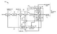
- FIG. 1is a simplified block diagram of a communication system having a transmitter and a receiver communicating over a communication channel as well as a back channel according to one embodiment of the invention
- FIGS. 2 and 3are simplified eye diagrams of received baseband signals
- FIG. 4illustrate the effects of an ideal limiter on eye openings
- FIG. 5is a simplified flowchart illustrating initialization of the communication system shown in FIG. 1 according to an embodiment of the invention.
- each numerical value and rangeshould be interpreted as being approximate as if the word “about” or “approximately” preceded the value of the value or range.
- the term “or”should be interpreted as inclusive unless stated otherwise.
- signals and corresponding nodes, ports, inputs, or outputsmay be referred to by the same name and are interchangeable.
- reference herein to “one embodiment” or “an embodiment”means that a particular feature, structure, or characteristic described in connection with the embodiment can be included in at least one embodiment of the invention.
- the appearances of the phrase “in one embodiment” in various places in the specificationare not necessarily all referring to the same embodiment, nor are separate or alternative embodiments necessarily mutually exclusive of other embodiments. The same applies to the terms “implementation” and “example”.
- Couplerefers to any manner known in the art or later developed in which a signal is allowed to be transferred between two or more elements and the interposition of one or more additional elements is contemplated, although not required. Conversely, the terms “directly coupled”, “directly connected”, etc., imply the absence of such additional elements.
- DFEdecision feedback equalization
- FIRfinite impulse response
- RXanalog equalizer within a receiver
- a digital receiversuch as the receiver 10 shown in FIG. 1 and explained in more detail below, recovers digital signals by sampling a baseband analog waveform (the received signal) and then reliably detect the sampled data.
- Signals arriving at a receiverare typically corrupted by intersymbol interference (ISI), crosstalk, echo, and other noise.
- ISIintersymbol interference
- the receivermust both equalize the channel, to compensate for such corruptions, and detect the encoded signals at increasingly higher clock rates.
- DFEDecision-feedback equalization
- DFEDecision-feedback equalization
- decision-feedback equalizationutilizes a multi-tap equalizer to equalize the channel using a feedback loop based on previously detected (or decided) data.
- a received analog signalis sampled after DFE correction and compared to one or more first thresholds to generate the detected data and one or more second thresholds (usually but not necessarily different from the first) to generate adaption error signals as will be described below.
- the DFE correctionis subtracted in a feedback fashion to produce a DFE-corrected signal.
- a clockgenerated from the received signal by a Clock Recovery (CR) circuit, is generally used to sample the DFE-corrected signal and for the DFE operation.
- Clock RecoveryClock Recovery
- a DFE-based receivermight include an analog front end (AFE), typically having an adjustable gain amplifier (AGA) used to control the input signal level, and an equalizer used to compensate for frequency-based distortions in the input signal to the receiver.
- the analog equalizeralso referred to herein as a continuous-time linear equalizer or CTLE
- CTLEcontinuous-time linear equalizer
- high frequency portions of the received signalsmight be attenuated as the signals pass though a transmission line, rounding off what are otherwise sharp, square-wave signals as originally transmitted.
- the CTLE's coefficients or peaking parametersin response to a controller within the receiver, are adjusted to add gain to the high frequency components of the signal, referred to herein as “peaking”, to at least partially restore the received signal to its original shape.
- peakingthe high frequency components of the signal
- the analog circuitry in the AFEmight have inherent limitations, one of which is the amount of nonlinear distortion introduced onto the received signal by various analog circuits in the AFE. Any distortion introduced by the AFE can seriously degrade performance of the overall receiver.
- SERDESserializer/deserializer
- the “quality” of the channel mediadegrades dramatically even over short distances between the ends of the communication channel.
- One technique typically used in conjunction with the receiver's DFE and analog equalizers to achieve the desired channel performance needed for reliable communications over the degraded channelis to pre-distort the transmitted signal to counteract the effects of the channel on the signal presented to the receiver.
- the pre-distortion characteristicsare adjusted through a back or reverse channel to adapt the pre-distortion to the channel's characteristics.
- FIG. 1is a block diagram of a typical SERDES communication channel 100 having a receiver 10 and a transmitter 20 , the transmitter having an equalizer and the receiver having an analog equalizer and a DFE-based equalizer in tandem.
- baseband data from the transmitter 20is transmitted through a backplane communications channel 120 after optionally being equalized or filtered through a transmit FIR filter (TXFIR) 110 .
- TXFIRtransmit FIR filter
- BKPLNbackplane
- metal traces in a substrate (not shown), a cable (not shown), or a combination thereofthe analog data signal received by the receiver 10 is processed by equalizer 130 .
- the received signalmay optionally be filtered or equalized by an analog front end (AFE) 132 having a variable gain amplifier (not shown) for amplitude control and may include, for example, a continuous-time filter or the equivalent.
- AFEanalog front end
- the analog signal output r k of the AFE 132passes through subtractor 134 , used in conjunction with a decision feedback equalizer (DFE) 136 having L taps and well understood in the art, to produce an output signal y k .
- DFEdecision feedback equalizer
- the output signal y kis delayed by a variable delay circuit 170 and the delayed signal on node 175 is then sampled by a clock recovery (CR) circuit 150 .
- CRclock recovery
- a limiter 155amplifies the signal y k and limits the amplified signal on node 157 to a given amplitude centered about a midpoint value, in this example, approximately zero although this value is not critical and can be adjusted as desired but is generally determined by the circuit implementation of the limiter, e.g., a high gain amplifier that is driven into saturation by the signal y k .
- a slicer 160(described below) digitizes the output of the limiter 155 by comparing the signal from the limiter to a threshold value and latches the result in response to the data clock generated by the CR 150 . In one embodiment, the threshold of the slicer 160 is approximately the same as the midpoint value of the signal from the limiter 155 .
- the limiter 155is a conventional amplifier (not shown) having enough gain for it to saturate when amplifying the DFE-corrected signal y k .
- the saturation of the amplifierwill limit or clamp the amplified signals to voltage levels related to power supply voltages coupled to the limiter 155 .
- a saturated amplifiermight exhibit a propagation delay that results from the amplifier “switching” from one output level to the other in response to a change in the input signal thereto and may be several picoseconds long, a significant portion of the received data's bit period.
- the amplifiermight have anti-saturation circuitry added thereto as is known in the art.
- the variable delay circuit 170is provided to time-align the DFE-corrected analog signal y k with the limited signal on node 157 , as described in more detail below.
- a conventional slicer 160might be implemented using one or more slicer-latches (i.e., a decision device based on an amplitude threshold and a latch to hold the results of the decision device) or a more complicated detector such as a sequence detector.
- the slicer 160is often implemented as two slicer-latches 162 , 164 that each sample the limited signal on node 157 in response to a locally generated sample clock, here sample clock C m from CR 150 .
- each slicer-latch in slicer 160essentially quantizes the signal to a binary “1” or “0” based on the analog value of the signal applied to the slicer, represented here as s, and a slicer threshold, s t . If the input to the slicer 160 at time k is s k , then the detected data bit output â k of the slicer 160 is given as follows:
- the slicer-latch 162has a slicer threshold s t and the slicer-latch 164 has a slicer threshold—s t , where s t is the residual post-cursor tap value of the DFE 136 .
- the slicer threshold valuesare a fixed value, e.g., zero.
- the DFE 136 and the post-cursor tap values of the DFEare well known in the art.
- the phase of the analog input signalis typically unknown and there may be a frequency offset between the frequency at which the original data was transmitted and the nominal receiver sampling clock frequency.
- the function of the CR 150is to generate a clock that allows for the proper sampling of the limited analog signal from limiter 155 such that the data is recovered properly when the signal on node 157 is sampled by slicer 160 .
- the CR 150may be conventional and is often an adaptive feedback circuit where a feedback loop adjusts the phase and frequency of the nominal clock to produce the modified recovered clock C m that is used by slicer 160 sample the signal from limiter 155 in the center of the eye opening in the signal to allow proper data detection with margins, as will be illustrated in connection with FIG. 3 .
- the CR 150provides a recovered clock signal for use by a utilization device or data sink (not shown) that utilizes the detected data bits â k , as well as an error detector 180 and the DFE 136 .
- the CR 150may be composed of several components, such as a phase detector, a loop filter, and a clock generation circuit (not shown).
- the CR 150comprises a bang-bang phase detector (BBPD).
- BBPDbang-bang phase detector
- the CR 150comprises a Mueller-Muller CR where the signals are sampled at the band-rate.
- Mueller-Muller CRsee, for example, K. Mueller and K. Muller, “Timing Recovery in Digital Synchronous Data Receivers,” IEEE Trans. Comm., Vol. 24, No. 5, May 1976, pp. 516-531, incorporated by reference herein in its entirety.
- a conventional error detector 180has two sampling latches (not shown) that, in response to the sampling clock C m , samples the time-aligned DFE-corrected signal on node 175 using two different slicing levels to generate an error signal e k .
- the error signalis used as part of a feedback mechanism to adjust the coefficients of DFE filter 136 via path 140 , AFE 132 (if provided) via path 142 , and the TXFIR 110 (if provided) via path 144 , thereby improving the performance of the system 100 .
- the slicing levels of the sampling latches in the error detector 180are set to be approximately equal to the magnitude of the primary cursor tap value in the DFE 136 .
- the DFE 136 and the primary cursor tap value of the DFEare well known in the art.
- a conventional adaptation controller 138responsive to the error signal e k and the detected data bits â k , generates the coefficient control signals for adjusting the one or more coefficient values of the L-tap DFE 136 and the AFE 132 .
- the controller 138responsive to the detected data bits â k and the error signal e k , converges one or more coefficient values of the AFE 132 to reduce intersymbol interference during eye openings or to reduce signal transition jitter.
- An exemplary technique for adapting the AFEis described in “Adaptation Algorithms for a Class of Continuous Time Analog Equalizers With Application to Serial Links”, by P. M. Aziz and A V.
- L-tap DFE 136Malipatil, Proceedings of the 2011 IEEE International Symposium on Circuits and Systems (ISCAS 2011), pp. 1383-1386, included by reference herein in its entirely.
- the controller 138in response to the error signal e k from the error detector 180 and the detected data bits A k from slicer 160 , adjusts the filter coefficient values for the DFE filter 136 at least during the above-mentioned training or adaptation phase by the receiver.
- the controller 138uses the well-known least-mean-square algorithm or the like to minimize or reduce below a threshold value the mean-square of the error signal e k .
- the DFE-corrected signal y kis limited by limiter 155 then detected by the slicer 160 to produce the detected data bits â k .
- the threshold values for the slicer 160 and sampling latches in the error detector 180might be determined by the tap values of the DFE 136 as set by the adaption controller 138 .
- the threshold valuesmight be determined by feedback mechanisms such as that described in the aforementioned U.S. patent application Ser. No. 11/864,110 and U.S. Pat. No. 7,711,043.
- the controller 138might also adjust the coefficients of the TXFIR filter 110 via path 144 .
- data to be transmittedis filtered through the TXFIR filter 110 disposed between a serializer and the communication channel media to improve the performance of the system 100 by pre-distorting the signals applied to the conductors in the channel media.
- An exemplary implementation and technique for adapting the TXFIRis described in the above-identified U.S. patent application Ser. No. 13/360,978, filed 30 Jan. 2012, titled “Transmitter Adaptation Loop Using Adjustable Gain and Convergence Detection”, by Mohammad Mobin et al. It is understood that alternative methods and embodiments may be used to implement the TXFIR and the control thereof.
- FIG. 2illustrates simulated representative traces of the DFE-corrected signal y k after the DFE, AFE, and TXFIR coefficients have stabilized, i.e., converged, but without the benefit of using a limiter.
- This imageillustrates that the eye opening might have too slow a rise/fall time and is distorted, even with equalization, to make accurate placement of the slicer 160 's thresholds (vertical axis) and sample clock phase (horizontal axis) in approximately the middle of the eye opening problematic without using potentially complex and power-hungry adaptive eye placement and DFE adaptation techniques, such as that described in above-identified U.S. patent application Ser. No. 11/541,379, that might not be fast enough for 20 Gbps data rates.
- FIG. 1illustrates simulated representative traces of the DFE-corrected signal y k after the DFE, AFE, and TXFIR coefficients have stabilized, i.e., converged, but without the benefit of using a limit
- the size of the data eye 270is constrained because of remaining distortion in the 1 ⁇ x data transitions 210 and the 0 ⁇ x data transitions 220 even though the DFE and AFE have both converged.
- the distortion that would normally be associated with the 0 ⁇ x transitionsis absent and the resulting upper DFE eye, approximately associated with the circle 280 , is larger than the small data eye 270 associated with both sets of transitions.
- the upper DFE-corrected eye 280has an associated timing margin 240 and noise margin 250 .
- the distortion that would normally be associated with the 1 ⁇ x transitionsis absent and the resulting lower DFE eye is larger than the small data eye associated with both data transitions present.
- sample point 282 and corresponding sample point 284(positioned to have approximately the same phase as the sample point 282 but with the threshold value of ⁇ s t ) to sample the DFE-corrected signal y k , there is an improvement in performance of the receiver but the phase of the sample clock is advanced from that of sample point 272 and might still have margin problems that limit the performance of the receiver.
- the adjustment of the sample clockcan be difficult and processing intensive, such as that disclosed in the aforementioned U.S. patent application Ser. No. 11/541,379.
- One effect of the limiter 155 ( FIG. 1 ) on the DFE-corrected signal y k shown in FIG. 2is to increase the height (along the vertical axis) of eye opening as illustrated in the signal traces shown in FIG. 3 .
- the vertical opening of the eye 310is now at least as large as the difference between the extremes of the eye openings for the individual 0 ⁇ x and 1 ⁇ x transitions, illustrated by noise margin 290 and 390 in FIGS. 2 and 3 , respectively.
- Another effect of the limiter 155is that the data eye 310 of the amplitude-limited signal (here the signal on node 157 in FIG. 1 ) shown in FIG. 3 has more symmetry than that of the signal shown in FIG.
- the larger data eyeallows for the placement of the slicer thresholds s t , ⁇ s t (illustrated here as levels 365 A and 365 B, corresponding to slicer levels s t and s t for slicer-latches 162 , 164 in slicer 160 of FIG.
- the height, width, and symmetry of the eye opening in FIG. 3is also dependent on how “hard” the limiting action is and the amount of gain provided by the limiter 155 .
- a perfect limiterhas infinite gain and no variation in the amplitudes of the output signal to produce, for example, a perfect “square wave” having variable width pulses with amplitudes limited by the voltage of the limiter's power supply. Because of the essentially rectangular opening of the data eye 410 , sample points 482 , 484 (corresponding to the slicing thresholds s t , ⁇ s t of slicer 160 ) is simply placed in the center of the data eye 410 . There is no need to adjust the phase of the sampling clock C m to move the sample point 482 , 484 either earlier or later in time.
- a practical limitersuch as that used to produce the signal traces in FIG. 3 , has high but finite gain resulting in an output signal having a peak amplitude that varies somewhat with the amplitude of the input signal. While the use of a less than ideal limiter 155 will result a smaller eye opening with less steep transitions due to slower rise and fall times, an increase in the opening vertically will result nonetheless, making placement of the slicing thresholds s t , ⁇ s t of slicer 160 relatively less critical. In one exemplary embodiment the gain of the limiter is approximately 6 to 12 dB. Moreover, the phase of the sample clock C m can be fixed in the center of the eye 310 ( FIG. 3 ) but may also be either advanced or retarded by an amount as needed to provide additional timing margin but without the need for adaptive clock adjustment as taught in the aforementioned U.S. patent application Ser. No. 11/541,379.
- the CR 150derives timing information from the time-aligned DFE-corrected signal on node 175 , referred to as the “linear path”, instead of from the amplitude-limited signal on node 157 , referred to herein as the “nonlinear path”.
- the delay 170is used to time-align the DFE-corrected signal y k from the subtractor 134 with the output signal from the limiter 155 .
- a controller(not shown but might be implemented by the controller 138 ) adjusts the amount of delay provided by the delay circuit 170 such that the signals on node 175 are approximately time-aligned with the signals on node 157 .
- the calibration of the delay circuit 170occurs after the AFE 132 and the DFE 136 have converged.
- the delay circuit 170is merged with the CR 150 such that the CR 150 is configured to adjust the phase of the clock C m as required, as is well known in the phase-locked or delay-locked loop art.
- FIG. 5an exemplary initialization process 500 of the system 100 ( FIG. 1 ) is shown.
- the coefficients in the TXFIR 110 , AFE 130 , and DFE 136( FIG. 1 ) are set or initialized to a known value in step 502 .
- a training sequencee.g., a randomized data pattern
- the controller 138 in step 506begins the adaptation of the filter coefficients in the AFE 130 and DFE 136 either concurrently or sequentially and repeats step 506 until in step 508 the coefficients have been determined to converge.
- step 514the variable delay circuit 170 is adjusted until the signals on nodes 157 and 175 are approximately aligned.
- step 516the training sequence is terminated and system 100 begins normal operation.
- the CR 150is enabled during the entire initialization process 500 so that it locks onto the delayed signal on node 175 to generate the sampling clock C m and the recovered clock.
- the CR 150may be enabled in step 502 and subsequent steps are not performed until the CR 150 has achieved lock.
Landscapes
- Engineering & Computer Science (AREA)
- Computer Networks & Wireless Communication (AREA)
- Signal Processing (AREA)
- Power Engineering (AREA)
- Dc Digital Transmission (AREA)
- Cable Transmission Systems, Equalization Of Radio And Reduction Of Echo (AREA)
Abstract
Description
- U.S. Pat. No. 7,599,461, titled “Method and Apparatus for Generating One or More Clock Signals for a Decision-Feedback Equalizer Using DFE Detected Data in the Presence of an Adverse Pattern”, by Aziz et al.
- U.S. patent application Ser. No. 12/776,681, titled “A Compensated Phase Detector for Generating One or More Clock Signals Using DFE Detected Data in a Receiver”, by Aziz et al.
- U.S. Pat. No. 8,040,984, titled “Methods and Apparatus for Improved Jitter Tolerance in an SFP Limit Amplified Signal”, by Pervez Aziz et al.
- U.S. patent application Ser. No. 13/360,978, filed 30 Jan. 2012, titled “Transmitter Adaptation Loop Using Adjustable Gain and Convergence Detection”, by Mohammad Mobin et al.
- U.S. patent application Ser. No. 11/541,379, filed 29 Sep. 2006, titled “Method and Apparatus for Non-Linear Decision-Feedback Equalization In the Presence of Asymmetric Channel”, by Mohammad Mobin et al.
- U.S. patent application Ser. No. 12/493,435, filed 29 Jun. 2009, titled “Real-Time Eye Monitor for Statistical Filter Parameter Calibration”, by Mohammad Mobin et al.
- U.S. patent application Ser. No. 11/864,110, filed 28 Sep. 2007, titled “Methods and Apparatus for Determining Threshold of One or More DFE Transition Latches Based on Incoming Data Eye”, by Pervez Aziz et al.
- U.S. Pat. No. 7,711,043, filed 29 Sep. 2006, titled “Method and Apparatus for Determining Latch Position for Decision-Feedback Equalization Using Single-Sided Eye”, by Mohammad Mobin et al.
In this example, the slicer-
Claims (14)
Priority Applications (1)
| Application Number | Priority Date | Filing Date | Title |
|---|---|---|---|
| US14/228,913US9294314B2 (en) | 2012-04-30 | 2014-03-28 | Receiver having limiter-enhanced data eye openings |
Applications Claiming Priority (2)
| Application Number | Priority Date | Filing Date | Title |
|---|---|---|---|
| US13/459,871US8737549B2 (en) | 2012-04-30 | 2012-04-30 | Receiver having limiter-enhanced data eye openings |
| US14/228,913US9294314B2 (en) | 2012-04-30 | 2014-03-28 | Receiver having limiter-enhanced data eye openings |
Related Parent Applications (1)
| Application Number | Title | Priority Date | Filing Date |
|---|---|---|---|
| US13/459,871DivisionUS8737549B2 (en) | 2012-04-30 | 2012-04-30 | Receiver having limiter-enhanced data eye openings |
Publications (2)
| Publication Number | Publication Date |
|---|---|
| US20140211839A1 US20140211839A1 (en) | 2014-07-31 |
| US9294314B2true US9294314B2 (en) | 2016-03-22 |
Family
ID=49477254
Family Applications (2)
| Application Number | Title | Priority Date | Filing Date |
|---|---|---|---|
| US13/459,871Active2032-05-19US8737549B2 (en) | 2012-04-30 | 2012-04-30 | Receiver having limiter-enhanced data eye openings |
| US14/228,913ActiveUS9294314B2 (en) | 2012-04-30 | 2014-03-28 | Receiver having limiter-enhanced data eye openings |
Family Applications Before (1)
| Application Number | Title | Priority Date | Filing Date |
|---|---|---|---|
| US13/459,871Active2032-05-19US8737549B2 (en) | 2012-04-30 | 2012-04-30 | Receiver having limiter-enhanced data eye openings |
Country Status (1)
| Country | Link |
|---|---|
| US (2) | US8737549B2 (en) |
Cited By (3)
| Publication number | Priority date | Publication date | Assignee | Title |
|---|---|---|---|---|
| TWI799001B (en)* | 2021-12-15 | 2023-04-11 | 瑞昱半導體股份有限公司 | Amplifier circuit |
| US11757681B1 (en) | 2022-09-23 | 2023-09-12 | Apple Inc. | Serial data receiver circuit with dither assisted equalization |
| US12413454B1 (en)* | 2023-10-30 | 2025-09-09 | Synopsys, Inc. | Decision feedback equalizer with feedforward finite impulse response filter |
Families Citing this family (25)
| Publication number | Priority date | Publication date | Assignee | Title |
|---|---|---|---|---|
| US8995514B1 (en)* | 2012-09-28 | 2015-03-31 | Xilinx, Inc. | Methods of and circuits for analyzing a phase of a clock signal for receiving data |
| US8964818B2 (en)* | 2012-11-30 | 2015-02-24 | Broadcom Corporation | Use of multi-level modulation signaling for short reach data communications |
| US9886402B2 (en)* | 2012-12-20 | 2018-02-06 | Nvidia Corporation | Equalization coefficient search algorithm |
| US9143371B1 (en) | 2013-07-15 | 2015-09-22 | Pmc-Sierra Us, Inc. | Method for reducing jitter in receivers |
| US9020022B1 (en)* | 2013-08-02 | 2015-04-28 | Pmc-Sierra Us, Inc. | Analog finite impulse response adaptation method and apparatus |
| DE102014206092B4 (en)* | 2014-03-31 | 2019-06-19 | Fraunhofer-Gesellschaft zur Förderung der angewandten Forschung e.V. | Apparatus and method for equalizing a received data signal |
| US9762418B2 (en) | 2014-11-06 | 2017-09-12 | Dell Products, Lp | Repeatable backchannel link adaptation for high speed serial interfaces |
| US9281971B1 (en)* | 2015-02-10 | 2016-03-08 | Oracle International Corporation | Vertical eye margin measurement using channel receiver equalizer |
| US9680436B1 (en) | 2016-03-28 | 2017-06-13 | Samsung Display Co., Ltd. | System and method for setting analog front end DC gain |
| US10193716B2 (en) | 2016-04-28 | 2019-01-29 | Kandou Labs, S.A. | Clock data recovery with decision feedback equalization |
| US9882710B2 (en)* | 2016-06-23 | 2018-01-30 | Macom Connectivity Solutions, Llc | Resolving interaction between channel estimation and timing recovery |
| US9900121B1 (en)* | 2016-09-08 | 2018-02-20 | Futurewei Technologies, Inc. | Apparatus, system, and method for reducing a number of intersymbol interference components to be suppressed |
| US10135606B2 (en) | 2016-10-27 | 2018-11-20 | Macom Connectivity Solutions, Llc | Mitigating interaction between adaptive equalization and timing recovery |
| US9998303B1 (en)* | 2016-12-15 | 2018-06-12 | Cadence Design Systems, Inc. | Method of adaptively controlling a low frequency equalizer |
| US10038575B1 (en)* | 2017-08-31 | 2018-07-31 | Stmicroelectronics S.R.L. | Decision feedback equalizer with post-cursor non-linearity correction |
| US10554380B2 (en) | 2018-01-26 | 2020-02-04 | Kandou Labs, S.A. | Dynamically weighted exclusive or gate having weighted output segments for phase detection and phase interpolation |
| KR102445856B1 (en) | 2018-06-12 | 2022-09-21 | 칸도우 랩스 에스에이 | Low Latency Combination Clock Data Recovery Logic Circuitry and Charge Pump Circuitry |
| US10404496B1 (en)* | 2018-09-07 | 2019-09-03 | MACOM Technology Solutions Holding, Inc. | Mitigating interaction between adaptive equalization and timing recovery in multi-rate receiver |
| US11381431B2 (en)* | 2019-05-22 | 2022-07-05 | Nvidia Corporation | Receiver and transmitter adaptation using stochastic gradient hill climbing with genetic mutation |
| US12034576B2 (en) | 2019-05-22 | 2024-07-09 | Nvidia Corporation | Receiver and transmitter adaptation using stochastic gradient hill climbing with genetic mutation |
| US11418370B2 (en) | 2021-01-14 | 2022-08-16 | Micron Technology, Inc. | Time-variable decision feedback equalization |
| US11563605B2 (en) | 2021-04-07 | 2023-01-24 | Kandou Labs SA | Horizontal centering of sampling point using multiple vertical voltage measurements |
| US11496282B1 (en)* | 2021-06-04 | 2022-11-08 | Kandou Labs, S.A. | Horizontal centering of sampling point using vertical vernier |
| US12328380B2 (en) | 2022-05-26 | 2025-06-10 | Samsung Display Co., Ltd. | System and method for configuring serial receiver |
| US12113651B2 (en)* | 2022-07-18 | 2024-10-08 | Cisco Technology, Inc. | Transmitter equalization optimization for ethernet chip-to-module (C2M) compliance |
Citations (17)
| Publication number | Priority date | Publication date | Assignee | Title |
|---|---|---|---|---|
| US4561091A (en) | 1983-09-23 | 1985-12-24 | Codenoll Technology Corporation | Data receiver |
| US4754465A (en) | 1984-05-07 | 1988-06-28 | Trimble Navigation, Inc. | Global positioning system course acquisition code receiver |
| US5438692A (en) | 1992-11-26 | 1995-08-01 | U.S. Philips Corporation | Direct conversion receiver |
| US5451899A (en) | 1993-09-14 | 1995-09-19 | Plessey Semiconductors Limited | Direct conversion FSK receiver using frequency tracking filters |
| US5533064A (en) | 1990-10-25 | 1996-07-02 | Nec Corporation | Digital radio receiver having limiter amplifiers and logarithmic detector |
| US5943370A (en) | 1995-05-10 | 1999-08-24 | Roke Manor Research Limited | Direct conversion receiver |
| US20060256849A1 (en)* | 2005-05-12 | 2006-11-16 | Rdc Semiconductor Co., Ltd. | Adaptive blind start-up receiver architecture with fractional baud rate sampling for full-duplex multi-level PAM systems |
| US7155660B1 (en)* | 2002-01-03 | 2006-12-26 | Marvell International Ltd. | Detection in the presence of media noise |
| US20080080609A1 (en) | 2006-09-29 | 2008-04-03 | Mobin Mohammad S | Method and apparatus for non-linear decision-feedback equalization in the presence of asymmetric channel |
| US20090086807A1 (en) | 2007-09-28 | 2009-04-02 | Aziz Pervez M | Methods and apparatus for determining threshold of one or more dfe transition latches based on incoming data eye |
| US7551667B2 (en) | 2004-09-27 | 2009-06-23 | Intel Corporation | Feed forward equalizer |
| US7564866B2 (en) | 2000-07-21 | 2009-07-21 | Broadcom Corporation | Methods and systems for digitally processing optical data signals |
| US7711043B2 (en) | 2006-09-29 | 2010-05-04 | Agere Systems Inc. | Method and apparatus for determining latch position for decision-feedback equalization using single-sided eye |
| US20100202506A1 (en)* | 2009-02-06 | 2010-08-12 | Bulzacchelli John F | Circuits and methods for dfe with reduced area and power consumption |
| US20100329322A1 (en) | 2009-06-29 | 2010-12-30 | Lsi Corporation | Real-Time Eye Monitor for Statistical Filter Parameter Calibration |
| US8005135B1 (en)* | 2000-04-28 | 2011-08-23 | National Semiconductor Corporation | Receiver system with interdependent adaptive analog and digital signal equalization |
| US8040984B2 (en) | 2007-12-31 | 2011-10-18 | Agere System Inc. | Methods and apparatus for improved jitter tolerance in an SFP limit amplified signal |
Family Cites Families (4)
| Publication number | Priority date | Publication date | Assignee | Title |
|---|---|---|---|---|
| US6917789B1 (en)* | 1999-10-21 | 2005-07-12 | Broadcom Corporation | Adaptive radio transceiver with an antenna matching circuit |
| US6614842B1 (en)* | 2000-07-13 | 2003-09-02 | Infineon Technologies North America | FIR filter architecture for 100Base-TX receiver |
| US6870881B1 (en)* | 2000-08-24 | 2005-03-22 | Marvell International Ltd. | Feedforward equalizer for DFE based detector |
| JP4362141B2 (en)* | 2007-10-05 | 2009-11-11 | Okiセミコンダクタ株式会社 | Equalizer |
- 2012
- 2012-04-30USUS13/459,871patent/US8737549B2/enactiveActive
- 2014
- 2014-03-28USUS14/228,913patent/US9294314B2/enactiveActive
Patent Citations (18)
| Publication number | Priority date | Publication date | Assignee | Title |
|---|---|---|---|---|
| US4561091A (en) | 1983-09-23 | 1985-12-24 | Codenoll Technology Corporation | Data receiver |
| US4754465A (en) | 1984-05-07 | 1988-06-28 | Trimble Navigation, Inc. | Global positioning system course acquisition code receiver |
| US5533064A (en) | 1990-10-25 | 1996-07-02 | Nec Corporation | Digital radio receiver having limiter amplifiers and logarithmic detector |
| US5438692A (en) | 1992-11-26 | 1995-08-01 | U.S. Philips Corporation | Direct conversion receiver |
| US5451899A (en) | 1993-09-14 | 1995-09-19 | Plessey Semiconductors Limited | Direct conversion FSK receiver using frequency tracking filters |
| US5943370A (en) | 1995-05-10 | 1999-08-24 | Roke Manor Research Limited | Direct conversion receiver |
| US8005135B1 (en)* | 2000-04-28 | 2011-08-23 | National Semiconductor Corporation | Receiver system with interdependent adaptive analog and digital signal equalization |
| US7564866B2 (en) | 2000-07-21 | 2009-07-21 | Broadcom Corporation | Methods and systems for digitally processing optical data signals |
| US7155660B1 (en)* | 2002-01-03 | 2006-12-26 | Marvell International Ltd. | Detection in the presence of media noise |
| US7551667B2 (en) | 2004-09-27 | 2009-06-23 | Intel Corporation | Feed forward equalizer |
| US7447262B2 (en) | 2005-05-12 | 2008-11-04 | Rdc Semiconductor Co., Ltd. | Adaptive blind start-up receiver architecture with fractional baud rate sampling for full-duplex multi-level PAM systems |
| US20060256849A1 (en)* | 2005-05-12 | 2006-11-16 | Rdc Semiconductor Co., Ltd. | Adaptive blind start-up receiver architecture with fractional baud rate sampling for full-duplex multi-level PAM systems |
| US20080080609A1 (en) | 2006-09-29 | 2008-04-03 | Mobin Mohammad S | Method and apparatus for non-linear decision-feedback equalization in the presence of asymmetric channel |
| US7711043B2 (en) | 2006-09-29 | 2010-05-04 | Agere Systems Inc. | Method and apparatus for determining latch position for decision-feedback equalization using single-sided eye |
| US20090086807A1 (en) | 2007-09-28 | 2009-04-02 | Aziz Pervez M | Methods and apparatus for determining threshold of one or more dfe transition latches based on incoming data eye |
| US8040984B2 (en) | 2007-12-31 | 2011-10-18 | Agere System Inc. | Methods and apparatus for improved jitter tolerance in an SFP limit amplified signal |
| US20100202506A1 (en)* | 2009-02-06 | 2010-08-12 | Bulzacchelli John F | Circuits and methods for dfe with reduced area and power consumption |
| US20100329322A1 (en) | 2009-06-29 | 2010-12-30 | Lsi Corporation | Real-Time Eye Monitor for Statistical Filter Parameter Calibration |
Non-Patent Citations (2)
| Title |
|---|
| David G. Ross, Stanley F. Moyer, Wallace H. Eckton, Jr., Robert M. Paski, David G. Ehrenberg; Regenerator Chip Set for High-Speed Digital Transmission; IEEE Journal of Solid-State Circuits, vol. SC-21, No. 2, Apr. 1986. |
| Jeffrey H. Sinsky, Marcus Duelk, Andrew Adamiecki; High-Speed Electrical Backplane Transmission Using Duobinary Signaling; IEEE Transactions on Microwave Theory and Techniques, vol. 53, No. 1, Jan. 2005. |
Cited By (3)
| Publication number | Priority date | Publication date | Assignee | Title |
|---|---|---|---|---|
| TWI799001B (en)* | 2021-12-15 | 2023-04-11 | 瑞昱半導體股份有限公司 | Amplifier circuit |
| US11757681B1 (en) | 2022-09-23 | 2023-09-12 | Apple Inc. | Serial data receiver circuit with dither assisted equalization |
| US12413454B1 (en)* | 2023-10-30 | 2025-09-09 | Synopsys, Inc. | Decision feedback equalizer with feedforward finite impulse response filter |
Also Published As
| Publication number | Publication date |
|---|---|
| US20130287088A1 (en) | 2013-10-31 |
| US8737549B2 (en) | 2014-05-27 |
| US20140211839A1 (en) | 2014-07-31 |
Similar Documents
| Publication | Publication Date | Title |
|---|---|---|
| US9294314B2 (en) | Receiver having limiter-enhanced data eye openings | |
| US9025655B1 (en) | Transmitter training using receiver equalizer coefficients | |
| US8705672B2 (en) | Method of compensating for nonlinearity in a DFE-based receiver | |
| US8761237B2 (en) | Low nonlinear distortion variable gain amplifier | |
| US8837626B2 (en) | Conditional adaptation of linear filters in a system having nonlinearity | |
| US10135647B2 (en) | Methods and circuits for asymmetric distribution of channel equalization between devices | |
| US7616686B2 (en) | Method and apparatus for generating one or more clock signals for a decision-feedback equalizer using DFE detected data | |
| US8831142B2 (en) | Adaptive cancellation of voltage offset in a communication system | |
| US8649476B2 (en) | Adjusting sampling phase in a baud-rate CDR using timing skew | |
| US8804889B2 (en) | Receiver with dual clock recovery circuits | |
| US9455848B1 (en) | DFE-skewed CDR circuit | |
| US8467440B2 (en) | Compensated phase detector for generating one or more clock signals using DFE detected data in a receiver | |
| US7623600B2 (en) | High speed receive equalizer architecture | |
| US8908816B2 (en) | Receiver with distortion compensation circuit | |
| US9385897B2 (en) | Methods and apparatus for adapting transmitter equalization coefficients based on receiver gain adaptation | |
| US20150256364A1 (en) | Group delay based back channel post cursor adaptation | |
| US8902963B2 (en) | Methods and apparatus for determining threshold of one or more DFE transition latches based on incoming data eye | |
| US20050002475A1 (en) | Apparatus for transmitting and receiving data | |
| KR20140103012A (en) | Pattern-based loss of signal detector | |
| US20050238092A1 (en) | Method and system for error estimation for adaptive equalization in communication systems | |
| US20130195154A1 (en) | Transmitter Adaptation Loop Using Adjustable Gain and Convergence Detection | |
| US20070286315A1 (en) | Digital signal processor, receiver, corrector and methods for the same | |
| US8665929B1 (en) | Method and device for deterministic timing acquiring and tracking | |
| US8867603B1 (en) | Method and system for balancing an equalizer at a receiver | |
| US8259784B2 (en) | High-speed continuous-time feedback equalizer for serial link receiver |
Legal Events
| Date | Code | Title | Description |
|---|---|---|---|
| AS | Assignment | Owner name:LSI CORPORATION, CALIFORNIA Free format text:ASSIGNMENT OF ASSIGNORS INTEREST;ASSIGNORS:MOBIN, MOHAMMAD S.;AZIZ, PERVEZ M.;LIU, YE;SIGNING DATES FROM 20120419 TO 20120425;REEL/FRAME:032552/0368 | |
| AS | Assignment | Owner name:DEUTSCHE BANK AG NEW YORK BRANCH, AS COLLATERAL AG Free format text:PATENT SECURITY AGREEMENT;ASSIGNORS:LSI CORPORATION;AGERE SYSTEMS LLC;REEL/FRAME:032856/0031 Effective date:20140506 | |
| AS | Assignment | Owner name:AVAGO TECHNOLOGIES GENERAL IP (SINGAPORE) PTE. LTD Free format text:ASSIGNMENT OF ASSIGNORS INTEREST;ASSIGNOR:LSI CORPORATION;REEL/FRAME:035390/0388 Effective date:20140814 | |
| AS | Assignment | Owner name:AGERE SYSTEMS LLC, PENNSYLVANIA Free format text:TERMINATION AND RELEASE OF SECURITY INTEREST IN PATENT RIGHTS (RELEASES RF 032856-0031);ASSIGNOR:DEUTSCHE BANK AG NEW YORK BRANCH, AS COLLATERAL AGENT;REEL/FRAME:037684/0039 Effective date:20160201 Owner name:LSI CORPORATION, CALIFORNIA Free format text:TERMINATION AND RELEASE OF SECURITY INTEREST IN PATENT RIGHTS (RELEASES RF 032856-0031);ASSIGNOR:DEUTSCHE BANK AG NEW YORK BRANCH, AS COLLATERAL AGENT;REEL/FRAME:037684/0039 Effective date:20160201 | |
| AS | Assignment | Owner name:BANK OF AMERICA, N.A., AS COLLATERAL AGENT, NORTH CAROLINA Free format text:PATENT SECURITY AGREEMENT;ASSIGNOR:AVAGO TECHNOLOGIES GENERAL IP (SINGAPORE) PTE. LTD.;REEL/FRAME:037808/0001 Effective date:20160201 Owner name:BANK OF AMERICA, N.A., AS COLLATERAL AGENT, NORTH Free format text:PATENT SECURITY AGREEMENT;ASSIGNOR:AVAGO TECHNOLOGIES GENERAL IP (SINGAPORE) PTE. LTD.;REEL/FRAME:037808/0001 Effective date:20160201 | |
| STCF | Information on status: patent grant | Free format text:PATENTED CASE | |
| AS | Assignment | Owner name:AVAGO TECHNOLOGIES GENERAL IP (SINGAPORE) PTE. LTD., SINGAPORE Free format text:TERMINATION AND RELEASE OF SECURITY INTEREST IN PATENTS;ASSIGNOR:BANK OF AMERICA, N.A., AS COLLATERAL AGENT;REEL/FRAME:041710/0001 Effective date:20170119 Owner name:AVAGO TECHNOLOGIES GENERAL IP (SINGAPORE) PTE. LTD Free format text:TERMINATION AND RELEASE OF SECURITY INTEREST IN PATENTS;ASSIGNOR:BANK OF AMERICA, N.A., AS COLLATERAL AGENT;REEL/FRAME:041710/0001 Effective date:20170119 | |
| AS | Assignment | Owner name:AVAGO TECHNOLOGIES INTERNATIONAL SALES PTE. LIMITE Free format text:MERGER;ASSIGNOR:AVAGO TECHNOLOGIES GENERAL IP (SINGAPORE) PTE. LTD.;REEL/FRAME:047422/0464 Effective date:20180509 | |
| AS | Assignment | Owner name:AVAGO TECHNOLOGIES INTERNATIONAL SALES PTE. LIMITE Free format text:CORRECTIVE ASSIGNMENT TO CORRECT THE EXECUTION DATE PREVIOUSLY RECORDED AT REEL: 047422 FRAME: 0464. ASSIGNOR(S) HEREBY CONFIRMS THE MERGER;ASSIGNOR:AVAGO TECHNOLOGIES GENERAL IP (SINGAPORE) PTE. LTD.;REEL/FRAME:048883/0702 Effective date:20180905 | |
| MAFP | Maintenance fee payment | Free format text:PAYMENT OF MAINTENANCE FEE, 4TH YEAR, LARGE ENTITY (ORIGINAL EVENT CODE: M1551); ENTITY STATUS OF PATENT OWNER: LARGE ENTITY Year of fee payment:4 | |
| AS | Assignment | Owner name:BROADCOM INTERNATIONAL PTE. LTD., SINGAPORE Free format text:ASSIGNMENT OF ASSIGNORS INTEREST;ASSIGNOR:AVAGO TECHNOLOGIES INTERNATIONAL SALES PTE. LIMITED;REEL/FRAME:053771/0901 Effective date:20200826 | |
| AS | Assignment | Owner name:AVAGO TECHNOLOGIES INTERNATIONAL SALES PTE. LIMITED, SINGAPORE Free format text:MERGER;ASSIGNORS:AVAGO TECHNOLOGIES INTERNATIONAL SALES PTE. LIMITED;BROADCOM INTERNATIONAL PTE. LTD.;REEL/FRAME:062952/0850 Effective date:20230202 | |
| MAFP | Maintenance fee payment | Free format text:PAYMENT OF MAINTENANCE FEE, 8TH YEAR, LARGE ENTITY (ORIGINAL EVENT CODE: M1552); ENTITY STATUS OF PATENT OWNER: LARGE ENTITY Year of fee payment:8 |