US9287195B2 - Stub minimization using duplicate sets of terminals having modulo-x symmetry for wirebond assemblies without windows - Google Patents
Stub minimization using duplicate sets of terminals having modulo-x symmetry for wirebond assemblies without windowsDownload PDFInfo
- Publication number
- US9287195B2 US9287195B2US14/186,380US201414186380AUS9287195B2US 9287195 B2US9287195 B2US 9287195B2US 201414186380 AUS201414186380 AUS 201414186380AUS 9287195 B2US9287195 B2US 9287195B2
- Authority
- US
- United States
- Prior art keywords
- terminals
- microelectronic
- package
- contacts
- chip
- Prior art date
- Legal status (The legal status is an assumption and is not a legal conclusion. Google has not performed a legal analysis and makes no representation as to the accuracy of the status listed.)
- Active, expires
Links
Images


Classifications
- H—ELECTRICITY
- H01—ELECTRIC ELEMENTS
- H01L—SEMICONDUCTOR DEVICES NOT COVERED BY CLASS H10
- H01L25/00—Assemblies consisting of a plurality of semiconductor or other solid state devices
- H01L25/03—Assemblies consisting of a plurality of semiconductor or other solid state devices all the devices being of a type provided for in a single subclass of subclasses H10B, H10D, H10F, H10H, H10K or H10N, e.g. assemblies of rectifier diodes
- H01L25/04—Assemblies consisting of a plurality of semiconductor or other solid state devices all the devices being of a type provided for in a single subclass of subclasses H10B, H10D, H10F, H10H, H10K or H10N, e.g. assemblies of rectifier diodes the devices not having separate containers
- H01L25/065—Assemblies consisting of a plurality of semiconductor or other solid state devices all the devices being of a type provided for in a single subclass of subclasses H10B, H10D, H10F, H10H, H10K or H10N, e.g. assemblies of rectifier diodes the devices not having separate containers the devices being of a type provided for in group H10D89/00
- H01L25/0657—Stacked arrangements of devices
- G—PHYSICS
- G11—INFORMATION STORAGE
- G11C—STATIC STORES
- G11C5/00—Details of stores covered by group G11C11/00
- G11C5/02—Disposition of storage elements, e.g. in the form of a matrix array
- G11C5/04—Supports for storage elements, e.g. memory modules; Mounting or fixing of storage elements on such supports
- G—PHYSICS
- G11—INFORMATION STORAGE
- G11C—STATIC STORES
- G11C5/00—Details of stores covered by group G11C11/00
- G11C5/06—Arrangements for interconnecting storage elements electrically, e.g. by wiring
- G11C5/063—Voltage and signal distribution in integrated semi-conductor memory access lines, e.g. word-line, bit-line, cross-over resistance, propagation delay
- G—PHYSICS
- G11—INFORMATION STORAGE
- G11C—STATIC STORES
- G11C5/00—Details of stores covered by group G11C11/00
- G11C5/06—Arrangements for interconnecting storage elements electrically, e.g. by wiring
- G11C5/066—Means for reducing external access-lines for a semiconductor memory clip, e.g. by multiplexing at least address and data signals
- G—PHYSICS
- G11—INFORMATION STORAGE
- G11C—STATIC STORES
- G11C8/00—Arrangements for selecting an address in a digital store
- G11C8/18—Address timing or clocking circuits; Address control signal generation or management, e.g. for row address strobe [RAS] or column address strobe [CAS] signals
- H—ELECTRICITY
- H01—ELECTRIC ELEMENTS
- H01L—SEMICONDUCTOR DEVICES NOT COVERED BY CLASS H10
- H01L23/00—Details of semiconductor or other solid state devices
- H01L23/02—Containers; Seals
- H—ELECTRICITY
- H01—ELECTRIC ELEMENTS
- H01L—SEMICONDUCTOR DEVICES NOT COVERED BY CLASS H10
- H01L23/00—Details of semiconductor or other solid state devices
- H01L23/12—Mountings, e.g. non-detachable insulating substrates
- H01L23/13—Mountings, e.g. non-detachable insulating substrates characterised by the shape
- H—ELECTRICITY
- H01—ELECTRIC ELEMENTS
- H01L—SEMICONDUCTOR DEVICES NOT COVERED BY CLASS H10
- H01L23/00—Details of semiconductor or other solid state devices
- H01L23/48—Arrangements for conducting electric current to or from the solid state body in operation, e.g. leads, terminal arrangements ; Selection of materials therefor
- H01L23/488—Arrangements for conducting electric current to or from the solid state body in operation, e.g. leads, terminal arrangements ; Selection of materials therefor consisting of soldered or bonded constructions
- H01L23/498—Leads, i.e. metallisations or lead-frames on insulating substrates, e.g. chip carriers
- H01L23/49838—Geometry or layout
- H—ELECTRICITY
- H01—ELECTRIC ELEMENTS
- H01L—SEMICONDUCTOR DEVICES NOT COVERED BY CLASS H10
- H01L23/00—Details of semiconductor or other solid state devices
- H01L23/48—Arrangements for conducting electric current to or from the solid state body in operation, e.g. leads, terminal arrangements ; Selection of materials therefor
- H01L23/50—Arrangements for conducting electric current to or from the solid state body in operation, e.g. leads, terminal arrangements ; Selection of materials therefor for integrated circuit devices, e.g. power bus, number of leads
- H—ELECTRICITY
- H01—ELECTRIC ELEMENTS
- H01L—SEMICONDUCTOR DEVICES NOT COVERED BY CLASS H10
- H01L24/00—Arrangements for connecting or disconnecting semiconductor or solid-state bodies; Methods or apparatus related thereto
- H01L24/01—Means for bonding being attached to, or being formed on, the surface to be connected, e.g. chip-to-package, die-attach, "first-level" interconnects; Manufacturing methods related thereto
- H01L24/42—Wire connectors; Manufacturing methods related thereto
- H01L24/47—Structure, shape, material or disposition of the wire connectors after the connecting process
- H01L24/49—Structure, shape, material or disposition of the wire connectors after the connecting process of a plurality of wire connectors
- H—ELECTRICITY
- H01—ELECTRIC ELEMENTS
- H01L—SEMICONDUCTOR DEVICES NOT COVERED BY CLASS H10
- H01L24/00—Arrangements for connecting or disconnecting semiconductor or solid-state bodies; Methods or apparatus related thereto
- H01L24/93—Batch processes
- H01L24/95—Batch processes at chip-level, i.e. with connecting carried out on a plurality of singulated devices, i.e. on diced chips
- H01L24/97—Batch processes at chip-level, i.e. with connecting carried out on a plurality of singulated devices, i.e. on diced chips the devices being connected to a common substrate, e.g. interposer, said common substrate being separable into individual assemblies after connecting
- H—ELECTRICITY
- H01—ELECTRIC ELEMENTS
- H01L—SEMICONDUCTOR DEVICES NOT COVERED BY CLASS H10
- H01L25/00—Assemblies consisting of a plurality of semiconductor or other solid state devices
- H01L25/03—Assemblies consisting of a plurality of semiconductor or other solid state devices all the devices being of a type provided for in a single subclass of subclasses H10B, H10D, H10F, H10H, H10K or H10N, e.g. assemblies of rectifier diodes
- H01L25/04—Assemblies consisting of a plurality of semiconductor or other solid state devices all the devices being of a type provided for in a single subclass of subclasses H10B, H10D, H10F, H10H, H10K or H10N, e.g. assemblies of rectifier diodes the devices not having separate containers
- H01L25/065—Assemblies consisting of a plurality of semiconductor or other solid state devices all the devices being of a type provided for in a single subclass of subclasses H10B, H10D, H10F, H10H, H10K or H10N, e.g. assemblies of rectifier diodes the devices not having separate containers the devices being of a type provided for in group H10D89/00
- H01L25/0655—Assemblies consisting of a plurality of semiconductor or other solid state devices all the devices being of a type provided for in a single subclass of subclasses H10B, H10D, H10F, H10H, H10K or H10N, e.g. assemblies of rectifier diodes the devices not having separate containers the devices being of a type provided for in group H10D89/00 the devices being arranged next to each other
- H—ELECTRICITY
- H01—ELECTRIC ELEMENTS
- H01L—SEMICONDUCTOR DEVICES NOT COVERED BY CLASS H10
- H01L2224/00—Indexing scheme for arrangements for connecting or disconnecting semiconductor or solid-state bodies and methods related thereto as covered by H01L24/00
- H01L2224/01—Means for bonding being attached to, or being formed on, the surface to be connected, e.g. chip-to-package, die-attach, "first-level" interconnects; Manufacturing methods related thereto
- H01L2224/10—Bump connectors; Manufacturing methods related thereto
- H01L2224/15—Structure, shape, material or disposition of the bump connectors after the connecting process
- H01L2224/16—Structure, shape, material or disposition of the bump connectors after the connecting process of an individual bump connector
- H01L2224/161—Disposition
- H01L2224/16135—Disposition the bump connector connecting between different semiconductor or solid-state bodies, i.e. chip-to-chip
- H01L2224/16145—Disposition the bump connector connecting between different semiconductor or solid-state bodies, i.e. chip-to-chip the bodies being stacked
- H—ELECTRICITY
- H01—ELECTRIC ELEMENTS
- H01L—SEMICONDUCTOR DEVICES NOT COVERED BY CLASS H10
- H01L2224/00—Indexing scheme for arrangements for connecting or disconnecting semiconductor or solid-state bodies and methods related thereto as covered by H01L24/00
- H01L2224/01—Means for bonding being attached to, or being formed on, the surface to be connected, e.g. chip-to-package, die-attach, "first-level" interconnects; Manufacturing methods related thereto
- H01L2224/10—Bump connectors; Manufacturing methods related thereto
- H01L2224/15—Structure, shape, material or disposition of the bump connectors after the connecting process
- H01L2224/16—Structure, shape, material or disposition of the bump connectors after the connecting process of an individual bump connector
- H01L2224/161—Disposition
- H01L2224/16151—Disposition the bump connector connecting between a semiconductor or solid-state body and an item not being a semiconductor or solid-state body, e.g. chip-to-substrate, chip-to-passive
- H01L2224/16221—Disposition the bump connector connecting between a semiconductor or solid-state body and an item not being a semiconductor or solid-state body, e.g. chip-to-substrate, chip-to-passive the body and the item being stacked
- H01L2224/16225—Disposition the bump connector connecting between a semiconductor or solid-state body and an item not being a semiconductor or solid-state body, e.g. chip-to-substrate, chip-to-passive the body and the item being stacked the item being non-metallic, e.g. insulating substrate with or without metallisation
- H—ELECTRICITY
- H01—ELECTRIC ELEMENTS
- H01L—SEMICONDUCTOR DEVICES NOT COVERED BY CLASS H10
- H01L2224/00—Indexing scheme for arrangements for connecting or disconnecting semiconductor or solid-state bodies and methods related thereto as covered by H01L24/00
- H01L2224/01—Means for bonding being attached to, or being formed on, the surface to be connected, e.g. chip-to-package, die-attach, "first-level" interconnects; Manufacturing methods related thereto
- H01L2224/26—Layer connectors, e.g. plate connectors, solder or adhesive layers; Manufacturing methods related thereto
- H01L2224/28—Structure, shape, material or disposition of the layer connectors prior to the connecting process
- H01L2224/29—Structure, shape, material or disposition of the layer connectors prior to the connecting process of an individual layer connector
- H01L2224/29001—Core members of the layer connector
- H01L2224/29099—Material
- H01L2224/2919—Material with a principal constituent of the material being a polymer, e.g. polyester, phenolic based polymer, epoxy
- H—ELECTRICITY
- H01—ELECTRIC ELEMENTS
- H01L—SEMICONDUCTOR DEVICES NOT COVERED BY CLASS H10
- H01L2224/00—Indexing scheme for arrangements for connecting or disconnecting semiconductor or solid-state bodies and methods related thereto as covered by H01L24/00
- H01L2224/01—Means for bonding being attached to, or being formed on, the surface to be connected, e.g. chip-to-package, die-attach, "first-level" interconnects; Manufacturing methods related thereto
- H01L2224/26—Layer connectors, e.g. plate connectors, solder or adhesive layers; Manufacturing methods related thereto
- H01L2224/31—Structure, shape, material or disposition of the layer connectors after the connecting process
- H01L2224/32—Structure, shape, material or disposition of the layer connectors after the connecting process of an individual layer connector
- H01L2224/321—Disposition
- H01L2224/32135—Disposition the layer connector connecting between different semiconductor or solid-state bodies, i.e. chip-to-chip
- H01L2224/32145—Disposition the layer connector connecting between different semiconductor or solid-state bodies, i.e. chip-to-chip the bodies being stacked
- H—ELECTRICITY
- H01—ELECTRIC ELEMENTS
- H01L—SEMICONDUCTOR DEVICES NOT COVERED BY CLASS H10
- H01L2224/00—Indexing scheme for arrangements for connecting or disconnecting semiconductor or solid-state bodies and methods related thereto as covered by H01L24/00
- H01L2224/01—Means for bonding being attached to, or being formed on, the surface to be connected, e.g. chip-to-package, die-attach, "first-level" interconnects; Manufacturing methods related thereto
- H01L2224/26—Layer connectors, e.g. plate connectors, solder or adhesive layers; Manufacturing methods related thereto
- H01L2224/31—Structure, shape, material or disposition of the layer connectors after the connecting process
- H01L2224/32—Structure, shape, material or disposition of the layer connectors after the connecting process of an individual layer connector
- H01L2224/321—Disposition
- H01L2224/32151—Disposition the layer connector connecting between a semiconductor or solid-state body and an item not being a semiconductor or solid-state body, e.g. chip-to-substrate, chip-to-passive
- H01L2224/32221—Disposition the layer connector connecting between a semiconductor or solid-state body and an item not being a semiconductor or solid-state body, e.g. chip-to-substrate, chip-to-passive the body and the item being stacked
- H01L2224/32225—Disposition the layer connector connecting between a semiconductor or solid-state body and an item not being a semiconductor or solid-state body, e.g. chip-to-substrate, chip-to-passive the body and the item being stacked the item being non-metallic, e.g. insulating substrate with or without metallisation
- H—ELECTRICITY
- H01—ELECTRIC ELEMENTS
- H01L—SEMICONDUCTOR DEVICES NOT COVERED BY CLASS H10
- H01L2224/00—Indexing scheme for arrangements for connecting or disconnecting semiconductor or solid-state bodies and methods related thereto as covered by H01L24/00
- H01L2224/01—Means for bonding being attached to, or being formed on, the surface to be connected, e.g. chip-to-package, die-attach, "first-level" interconnects; Manufacturing methods related thereto
- H01L2224/42—Wire connectors; Manufacturing methods related thereto
- H01L2224/44—Structure, shape, material or disposition of the wire connectors prior to the connecting process
- H01L2224/45—Structure, shape, material or disposition of the wire connectors prior to the connecting process of an individual wire connector
- H01L2224/45001—Core members of the connector
- H01L2224/45099—Material
- H—ELECTRICITY
- H01—ELECTRIC ELEMENTS
- H01L—SEMICONDUCTOR DEVICES NOT COVERED BY CLASS H10
- H01L2224/00—Indexing scheme for arrangements for connecting or disconnecting semiconductor or solid-state bodies and methods related thereto as covered by H01L24/00
- H01L2224/01—Means for bonding being attached to, or being formed on, the surface to be connected, e.g. chip-to-package, die-attach, "first-level" interconnects; Manufacturing methods related thereto
- H01L2224/42—Wire connectors; Manufacturing methods related thereto
- H01L2224/47—Structure, shape, material or disposition of the wire connectors after the connecting process
- H01L2224/48—Structure, shape, material or disposition of the wire connectors after the connecting process of an individual wire connector
- H01L2224/481—Disposition
- H01L2224/48135—Connecting between different semiconductor or solid-state bodies, i.e. chip-to-chip
- H01L2224/48145—Connecting between different semiconductor or solid-state bodies, i.e. chip-to-chip the bodies being stacked
- H—ELECTRICITY
- H01—ELECTRIC ELEMENTS
- H01L—SEMICONDUCTOR DEVICES NOT COVERED BY CLASS H10
- H01L2224/00—Indexing scheme for arrangements for connecting or disconnecting semiconductor or solid-state bodies and methods related thereto as covered by H01L24/00
- H01L2224/01—Means for bonding being attached to, or being formed on, the surface to be connected, e.g. chip-to-package, die-attach, "first-level" interconnects; Manufacturing methods related thereto
- H01L2224/42—Wire connectors; Manufacturing methods related thereto
- H01L2224/47—Structure, shape, material or disposition of the wire connectors after the connecting process
- H01L2224/48—Structure, shape, material or disposition of the wire connectors after the connecting process of an individual wire connector
- H01L2224/481—Disposition
- H01L2224/48151—Connecting between a semiconductor or solid-state body and an item not being a semiconductor or solid-state body, e.g. chip-to-substrate, chip-to-passive
- H01L2224/48221—Connecting between a semiconductor or solid-state body and an item not being a semiconductor or solid-state body, e.g. chip-to-substrate, chip-to-passive the body and the item being stacked
- H01L2224/48225—Connecting between a semiconductor or solid-state body and an item not being a semiconductor or solid-state body, e.g. chip-to-substrate, chip-to-passive the body and the item being stacked the item being non-metallic, e.g. insulating substrate with or without metallisation
- H01L2224/48227—Connecting between a semiconductor or solid-state body and an item not being a semiconductor or solid-state body, e.g. chip-to-substrate, chip-to-passive the body and the item being stacked the item being non-metallic, e.g. insulating substrate with or without metallisation connecting the wire to a bond pad of the item
- H—ELECTRICITY
- H01—ELECTRIC ELEMENTS
- H01L—SEMICONDUCTOR DEVICES NOT COVERED BY CLASS H10
- H01L2224/00—Indexing scheme for arrangements for connecting or disconnecting semiconductor or solid-state bodies and methods related thereto as covered by H01L24/00
- H01L2224/01—Means for bonding being attached to, or being formed on, the surface to be connected, e.g. chip-to-package, die-attach, "first-level" interconnects; Manufacturing methods related thereto
- H01L2224/42—Wire connectors; Manufacturing methods related thereto
- H01L2224/47—Structure, shape, material or disposition of the wire connectors after the connecting process
- H01L2224/48—Structure, shape, material or disposition of the wire connectors after the connecting process of an individual wire connector
- H01L2224/481—Disposition
- H01L2224/48151—Connecting between a semiconductor or solid-state body and an item not being a semiconductor or solid-state body, e.g. chip-to-substrate, chip-to-passive
- H01L2224/48221—Connecting between a semiconductor or solid-state body and an item not being a semiconductor or solid-state body, e.g. chip-to-substrate, chip-to-passive the body and the item being stacked
- H01L2224/48225—Connecting between a semiconductor or solid-state body and an item not being a semiconductor or solid-state body, e.g. chip-to-substrate, chip-to-passive the body and the item being stacked the item being non-metallic, e.g. insulating substrate with or without metallisation
- H01L2224/4824—Connecting between the body and an opposite side of the item with respect to the body
- H—ELECTRICITY
- H01—ELECTRIC ELEMENTS
- H01L—SEMICONDUCTOR DEVICES NOT COVERED BY CLASS H10
- H01L2224/00—Indexing scheme for arrangements for connecting or disconnecting semiconductor or solid-state bodies and methods related thereto as covered by H01L24/00
- H01L2224/01—Means for bonding being attached to, or being formed on, the surface to be connected, e.g. chip-to-package, die-attach, "first-level" interconnects; Manufacturing methods related thereto
- H01L2224/42—Wire connectors; Manufacturing methods related thereto
- H01L2224/47—Structure, shape, material or disposition of the wire connectors after the connecting process
- H01L2224/49—Structure, shape, material or disposition of the wire connectors after the connecting process of a plurality of wire connectors
- H01L2224/491—Disposition
- H01L2224/4911—Disposition the connectors being bonded to at least one common bonding area, e.g. daisy chain
- H01L2224/49113—Disposition the connectors being bonded to at least one common bonding area, e.g. daisy chain the connectors connecting different bonding areas on the semiconductor or solid-state body to a common bonding area outside the body, e.g. converging wires
- H—ELECTRICITY
- H01—ELECTRIC ELEMENTS
- H01L—SEMICONDUCTOR DEVICES NOT COVERED BY CLASS H10
- H01L2224/00—Indexing scheme for arrangements for connecting or disconnecting semiconductor or solid-state bodies and methods related thereto as covered by H01L24/00
- H01L2224/73—Means for bonding being of different types provided for in two or more of groups H01L2224/10, H01L2224/18, H01L2224/26, H01L2224/34, H01L2224/42, H01L2224/50, H01L2224/63, H01L2224/71
- H01L2224/732—Location after the connecting process
- H01L2224/73201—Location after the connecting process on the same surface
- H01L2224/73203—Bump and layer connectors
- H01L2224/73204—Bump and layer connectors the bump connector being embedded into the layer connector
- H—ELECTRICITY
- H01—ELECTRIC ELEMENTS
- H01L—SEMICONDUCTOR DEVICES NOT COVERED BY CLASS H10
- H01L2224/00—Indexing scheme for arrangements for connecting or disconnecting semiconductor or solid-state bodies and methods related thereto as covered by H01L24/00
- H01L2224/73—Means for bonding being of different types provided for in two or more of groups H01L2224/10, H01L2224/18, H01L2224/26, H01L2224/34, H01L2224/42, H01L2224/50, H01L2224/63, H01L2224/71
- H01L2224/732—Location after the connecting process
- H01L2224/73201—Location after the connecting process on the same surface
- H01L2224/73207—Bump and wire connectors
- H—ELECTRICITY
- H01—ELECTRIC ELEMENTS
- H01L—SEMICONDUCTOR DEVICES NOT COVERED BY CLASS H10
- H01L2224/00—Indexing scheme for arrangements for connecting or disconnecting semiconductor or solid-state bodies and methods related thereto as covered by H01L24/00
- H01L2224/73—Means for bonding being of different types provided for in two or more of groups H01L2224/10, H01L2224/18, H01L2224/26, H01L2224/34, H01L2224/42, H01L2224/50, H01L2224/63, H01L2224/71
- H01L2224/732—Location after the connecting process
- H01L2224/73201—Location after the connecting process on the same surface
- H01L2224/73215—Layer and wire connectors
- H—ELECTRICITY
- H01—ELECTRIC ELEMENTS
- H01L—SEMICONDUCTOR DEVICES NOT COVERED BY CLASS H10
- H01L2224/00—Indexing scheme for arrangements for connecting or disconnecting semiconductor or solid-state bodies and methods related thereto as covered by H01L24/00
- H01L2224/73—Means for bonding being of different types provided for in two or more of groups H01L2224/10, H01L2224/18, H01L2224/26, H01L2224/34, H01L2224/42, H01L2224/50, H01L2224/63, H01L2224/71
- H01L2224/732—Location after the connecting process
- H01L2224/73251—Location after the connecting process on different surfaces
- H01L2224/73265—Layer and wire connectors
- H—ELECTRICITY
- H01—ELECTRIC ELEMENTS
- H01L—SEMICONDUCTOR DEVICES NOT COVERED BY CLASS H10
- H01L2224/00—Indexing scheme for arrangements for connecting or disconnecting semiconductor or solid-state bodies and methods related thereto as covered by H01L24/00
- H01L2224/93—Batch processes
- H01L2224/95—Batch processes at chip-level, i.e. with connecting carried out on a plurality of singulated devices, i.e. on diced chips
- H01L2224/97—Batch processes at chip-level, i.e. with connecting carried out on a plurality of singulated devices, i.e. on diced chips the devices being connected to a common substrate, e.g. interposer, said common substrate being separable into individual assemblies after connecting
- H—ELECTRICITY
- H01—ELECTRIC ELEMENTS
- H01L—SEMICONDUCTOR DEVICES NOT COVERED BY CLASS H10
- H01L2225/00—Details relating to assemblies covered by the group H01L25/00 but not provided for in its subgroups
- H01L2225/03—All the devices being of a type provided for in the same main group of the same subclass of class H10, e.g. assemblies of rectifier diodes
- H01L2225/04—All the devices being of a type provided for in the same main group of the same subclass of class H10, e.g. assemblies of rectifier diodes the devices not having separate containers
- H01L2225/065—All the devices being of a type provided for in the same main group of the same subclass of class H10
- H01L2225/06503—Stacked arrangements of devices
- H01L2225/06506—Wire or wire-like electrical connections between devices
- H—ELECTRICITY
- H01—ELECTRIC ELEMENTS
- H01L—SEMICONDUCTOR DEVICES NOT COVERED BY CLASS H10
- H01L2225/00—Details relating to assemblies covered by the group H01L25/00 but not provided for in its subgroups
- H01L2225/03—All the devices being of a type provided for in the same main group of the same subclass of class H10, e.g. assemblies of rectifier diodes
- H01L2225/04—All the devices being of a type provided for in the same main group of the same subclass of class H10, e.g. assemblies of rectifier diodes the devices not having separate containers
- H01L2225/065—All the devices being of a type provided for in the same main group of the same subclass of class H10
- H01L2225/06503—Stacked arrangements of devices
- H01L2225/0651—Wire or wire-like electrical connections from device to substrate
- H—ELECTRICITY
- H01—ELECTRIC ELEMENTS
- H01L—SEMICONDUCTOR DEVICES NOT COVERED BY CLASS H10
- H01L2225/00—Details relating to assemblies covered by the group H01L25/00 but not provided for in its subgroups
- H01L2225/03—All the devices being of a type provided for in the same main group of the same subclass of class H10, e.g. assemblies of rectifier diodes
- H01L2225/04—All the devices being of a type provided for in the same main group of the same subclass of class H10, e.g. assemblies of rectifier diodes the devices not having separate containers
- H01L2225/065—All the devices being of a type provided for in the same main group of the same subclass of class H10
- H01L2225/06503—Stacked arrangements of devices
- H01L2225/06513—Bump or bump-like direct electrical connections between devices, e.g. flip-chip connection, solder bumps
- H—ELECTRICITY
- H01—ELECTRIC ELEMENTS
- H01L—SEMICONDUCTOR DEVICES NOT COVERED BY CLASS H10
- H01L2225/00—Details relating to assemblies covered by the group H01L25/00 but not provided for in its subgroups
- H01L2225/03—All the devices being of a type provided for in the same main group of the same subclass of class H10, e.g. assemblies of rectifier diodes
- H01L2225/04—All the devices being of a type provided for in the same main group of the same subclass of class H10, e.g. assemblies of rectifier diodes the devices not having separate containers
- H01L2225/065—All the devices being of a type provided for in the same main group of the same subclass of class H10
- H01L2225/06503—Stacked arrangements of devices
- H01L2225/06517—Bump or bump-like direct electrical connections from device to substrate
- H—ELECTRICITY
- H01—ELECTRIC ELEMENTS
- H01L—SEMICONDUCTOR DEVICES NOT COVERED BY CLASS H10
- H01L2225/00—Details relating to assemblies covered by the group H01L25/00 but not provided for in its subgroups
- H01L2225/03—All the devices being of a type provided for in the same main group of the same subclass of class H10, e.g. assemblies of rectifier diodes
- H01L2225/04—All the devices being of a type provided for in the same main group of the same subclass of class H10, e.g. assemblies of rectifier diodes the devices not having separate containers
- H01L2225/065—All the devices being of a type provided for in the same main group of the same subclass of class H10
- H01L2225/06503—Stacked arrangements of devices
- H01L2225/0652—Bump or bump-like direct electrical connections from substrate to substrate
- H—ELECTRICITY
- H01—ELECTRIC ELEMENTS
- H01L—SEMICONDUCTOR DEVICES NOT COVERED BY CLASS H10
- H01L2225/00—Details relating to assemblies covered by the group H01L25/00 but not provided for in its subgroups
- H01L2225/03—All the devices being of a type provided for in the same main group of the same subclass of class H10, e.g. assemblies of rectifier diodes
- H01L2225/04—All the devices being of a type provided for in the same main group of the same subclass of class H10, e.g. assemblies of rectifier diodes the devices not having separate containers
- H01L2225/065—All the devices being of a type provided for in the same main group of the same subclass of class H10
- H01L2225/06503—Stacked arrangements of devices
- H01L2225/06541—Conductive via connections through the device, e.g. vertical interconnects, through silicon via [TSV]
- H—ELECTRICITY
- H01—ELECTRIC ELEMENTS
- H01L—SEMICONDUCTOR DEVICES NOT COVERED BY CLASS H10
- H01L2225/00—Details relating to assemblies covered by the group H01L25/00 but not provided for in its subgroups
- H01L2225/03—All the devices being of a type provided for in the same main group of the same subclass of class H10, e.g. assemblies of rectifier diodes
- H01L2225/04—All the devices being of a type provided for in the same main group of the same subclass of class H10, e.g. assemblies of rectifier diodes the devices not having separate containers
- H01L2225/065—All the devices being of a type provided for in the same main group of the same subclass of class H10
- H01L2225/06503—Stacked arrangements of devices
- H01L2225/06548—Conductive via connections through the substrate, container, or encapsulation
- H—ELECTRICITY
- H01—ELECTRIC ELEMENTS
- H01L—SEMICONDUCTOR DEVICES NOT COVERED BY CLASS H10
- H01L2225/00—Details relating to assemblies covered by the group H01L25/00 but not provided for in its subgroups
- H01L2225/03—All the devices being of a type provided for in the same main group of the same subclass of class H10, e.g. assemblies of rectifier diodes
- H01L2225/04—All the devices being of a type provided for in the same main group of the same subclass of class H10, e.g. assemblies of rectifier diodes the devices not having separate containers
- H01L2225/065—All the devices being of a type provided for in the same main group of the same subclass of class H10
- H01L2225/06503—Stacked arrangements of devices
- H01L2225/06555—Geometry of the stack, e.g. form of the devices, geometry to facilitate stacking
- H01L2225/06562—Geometry of the stack, e.g. form of the devices, geometry to facilitate stacking at least one device in the stack being rotated or offset
- H—ELECTRICITY
- H01—ELECTRIC ELEMENTS
- H01L—SEMICONDUCTOR DEVICES NOT COVERED BY CLASS H10
- H01L2225/00—Details relating to assemblies covered by the group H01L25/00 but not provided for in its subgroups
- H01L2225/03—All the devices being of a type provided for in the same main group of the same subclass of class H10, e.g. assemblies of rectifier diodes
- H01L2225/04—All the devices being of a type provided for in the same main group of the same subclass of class H10, e.g. assemblies of rectifier diodes the devices not having separate containers
- H01L2225/065—All the devices being of a type provided for in the same main group of the same subclass of class H10
- H01L2225/06503—Stacked arrangements of devices
- H01L2225/06572—Auxiliary carrier between devices, the carrier having an electrical connection structure
- H—ELECTRICITY
- H01—ELECTRIC ELEMENTS
- H01L—SEMICONDUCTOR DEVICES NOT COVERED BY CLASS H10
- H01L2225/00—Details relating to assemblies covered by the group H01L25/00 but not provided for in its subgroups
- H01L2225/03—All the devices being of a type provided for in the same main group of the same subclass of class H10, e.g. assemblies of rectifier diodes
- H01L2225/04—All the devices being of a type provided for in the same main group of the same subclass of class H10, e.g. assemblies of rectifier diodes the devices not having separate containers
- H01L2225/065—All the devices being of a type provided for in the same main group of the same subclass of class H10
- H01L2225/06503—Stacked arrangements of devices
- H01L2225/06589—Thermal management, e.g. cooling
- H—ELECTRICITY
- H01—ELECTRIC ELEMENTS
- H01L—SEMICONDUCTOR DEVICES NOT COVERED BY CLASS H10
- H01L2225/00—Details relating to assemblies covered by the group H01L25/00 but not provided for in its subgroups
- H01L2225/03—All the devices being of a type provided for in the same main group of the same subclass of class H10, e.g. assemblies of rectifier diodes
- H01L2225/10—All the devices being of a type provided for in the same main group of the same subclass of class H10, e.g. assemblies of rectifier diodes the devices having separate containers
- H01L2225/1005—All the devices being of a type provided for in the same main group of the same subclass of class H10, e.g. assemblies of rectifier diodes the devices having separate containers the devices being integrated devices of class H10
- H01L2225/1011—All the devices being of a type provided for in the same main group of the same subclass of class H10, e.g. assemblies of rectifier diodes the devices having separate containers the devices being integrated devices of class H10 the containers being in a stacked arrangement
- H01L2225/1047—Details of electrical connections between containers
- H01L2225/107—Indirect electrical connections, e.g. via an interposer, a flexible substrate, using TAB
- H—ELECTRICITY
- H01—ELECTRIC ELEMENTS
- H01L—SEMICONDUCTOR DEVICES NOT COVERED BY CLASS H10
- H01L24/00—Arrangements for connecting or disconnecting semiconductor or solid-state bodies; Methods or apparatus related thereto
- H01L24/01—Means for bonding being attached to, or being formed on, the surface to be connected, e.g. chip-to-package, die-attach, "first-level" interconnects; Manufacturing methods related thereto
- H01L24/10—Bump connectors ; Manufacturing methods related thereto
- H01L24/15—Structure, shape, material or disposition of the bump connectors after the connecting process
- H01L24/16—Structure, shape, material or disposition of the bump connectors after the connecting process of an individual bump connector
- H—ELECTRICITY
- H01—ELECTRIC ELEMENTS
- H01L—SEMICONDUCTOR DEVICES NOT COVERED BY CLASS H10
- H01L24/00—Arrangements for connecting or disconnecting semiconductor or solid-state bodies; Methods or apparatus related thereto
- H01L24/01—Means for bonding being attached to, or being formed on, the surface to be connected, e.g. chip-to-package, die-attach, "first-level" interconnects; Manufacturing methods related thereto
- H01L24/26—Layer connectors, e.g. plate connectors, solder or adhesive layers; Manufacturing methods related thereto
- H01L24/31—Structure, shape, material or disposition of the layer connectors after the connecting process
- H01L24/32—Structure, shape, material or disposition of the layer connectors after the connecting process of an individual layer connector
- H—ELECTRICITY
- H01—ELECTRIC ELEMENTS
- H01L—SEMICONDUCTOR DEVICES NOT COVERED BY CLASS H10
- H01L24/00—Arrangements for connecting or disconnecting semiconductor or solid-state bodies; Methods or apparatus related thereto
- H01L24/01—Means for bonding being attached to, or being formed on, the surface to be connected, e.g. chip-to-package, die-attach, "first-level" interconnects; Manufacturing methods related thereto
- H01L24/42—Wire connectors; Manufacturing methods related thereto
- H01L24/47—Structure, shape, material or disposition of the wire connectors after the connecting process
- H01L24/48—Structure, shape, material or disposition of the wire connectors after the connecting process of an individual wire connector
- H—ELECTRICITY
- H01—ELECTRIC ELEMENTS
- H01L—SEMICONDUCTOR DEVICES NOT COVERED BY CLASS H10
- H01L24/00—Arrangements for connecting or disconnecting semiconductor or solid-state bodies; Methods or apparatus related thereto
- H01L24/73—Means for bonding being of different types provided for in two or more of groups H01L24/10, H01L24/18, H01L24/26, H01L24/34, H01L24/42, H01L24/50, H01L24/63, H01L24/71
- H—ELECTRICITY
- H01—ELECTRIC ELEMENTS
- H01L—SEMICONDUCTOR DEVICES NOT COVERED BY CLASS H10
- H01L2924/00—Indexing scheme for arrangements or methods for connecting or disconnecting semiconductor or solid-state bodies as covered by H01L24/00
- H—ELECTRICITY
- H01—ELECTRIC ELEMENTS
- H01L—SEMICONDUCTOR DEVICES NOT COVERED BY CLASS H10
- H01L2924/00—Indexing scheme for arrangements or methods for connecting or disconnecting semiconductor or solid-state bodies as covered by H01L24/00
- H01L2924/0001—Technical content checked by a classifier
- H01L2924/00012—Relevant to the scope of the group, the symbol of which is combined with the symbol of this group
- H—ELECTRICITY
- H01—ELECTRIC ELEMENTS
- H01L—SEMICONDUCTOR DEVICES NOT COVERED BY CLASS H10
- H01L2924/00—Indexing scheme for arrangements or methods for connecting or disconnecting semiconductor or solid-state bodies as covered by H01L24/00
- H01L2924/0001—Technical content checked by a classifier
- H01L2924/00014—Technical content checked by a classifier the subject-matter covered by the group, the symbol of which is combined with the symbol of this group, being disclosed without further technical details
- H—ELECTRICITY
- H01—ELECTRIC ELEMENTS
- H01L—SEMICONDUCTOR DEVICES NOT COVERED BY CLASS H10
- H01L2924/00—Indexing scheme for arrangements or methods for connecting or disconnecting semiconductor or solid-state bodies as covered by H01L24/00
- H01L2924/013—Alloys
- H01L2924/0132—Binary Alloys
- H01L2924/01322—Eutectic Alloys, i.e. obtained by a liquid transforming into two solid phases
- H—ELECTRICITY
- H01—ELECTRIC ELEMENTS
- H01L—SEMICONDUCTOR DEVICES NOT COVERED BY CLASS H10
- H01L2924/00—Indexing scheme for arrangements or methods for connecting or disconnecting semiconductor or solid-state bodies as covered by H01L24/00
- H01L2924/15—Details of package parts other than the semiconductor or other solid state devices to be connected
- H01L2924/151—Die mounting substrate
- H01L2924/153—Connection portion
- H01L2924/1531—Connection portion the connection portion being formed only on the surface of the substrate opposite to the die mounting surface
- H01L2924/15311—Connection portion the connection portion being formed only on the surface of the substrate opposite to the die mounting surface being a ball array, e.g. BGA
- H—ELECTRICITY
- H01—ELECTRIC ELEMENTS
- H01L—SEMICONDUCTOR DEVICES NOT COVERED BY CLASS H10
- H01L2924/00—Indexing scheme for arrangements or methods for connecting or disconnecting semiconductor or solid-state bodies as covered by H01L24/00
- H01L2924/15—Details of package parts other than the semiconductor or other solid state devices to be connected
- H01L2924/181—Encapsulation
- H01L2924/1815—Shape
- H01L2924/1816—Exposing the passive side of the semiconductor or solid-state body
- H01L2924/18161—Exposing the passive side of the semiconductor or solid-state body of a flip chip
- H—ELECTRICITY
- H01—ELECTRIC ELEMENTS
- H01L—SEMICONDUCTOR DEVICES NOT COVERED BY CLASS H10
- H01L2924/00—Indexing scheme for arrangements or methods for connecting or disconnecting semiconductor or solid-state bodies as covered by H01L24/00
- H01L2924/30—Technical effects
- H01L2924/301—Electrical effects
- H01L2924/3011—Impedance
Definitions
- the subject matter of the present applicationrelates to microelectronic packages and assemblies incorporating microelectronic packages.
- a standard chiphas a flat, rectangular body with a large front face having contacts connected to the internal circuitry of the chip.
- Each individual chiptypically is contained in a package having external terminals connected to the contacts of the chip.
- the terminalsi.e., the external connection points of the package, are configured to electrically connect to a circuit panel, such as a printed circuit board.
- the chip packageoccupies an area of the circuit panel considerably larger than the area of the chip itself.
- the “area of the chip”should be understood as referring to the area of the front face.
- Sizeis a significant consideration in any physical arrangement of chips.
- devices commonly referred to as “smart phones”integrate the functions of a cellular telephone with powerful data processors, memory and ancillary devices such as global positioning system receivers, electronic cameras, and local area network connections along with high-resolution displays and associated image processing chips.
- Such devicescan provide capabilities such as full internet connectivity, entertainment including full-resolution video, navigation, electronic banking and more, all in a pocket-size device.
- Complex portable devicesrequire packing numerous chips into a small space.
- I/Osinput and output connections
- the components which form the interconnectionsshould not greatly increase the size of the assembly. Similar needs arise in other applications as, for example, in data servers such as those used in internet search engines where increased performance and size reduction are needed.
- DRAMsdynamic random access memory chips
- flash memory chipsare commonly packaged in single- or multiple-chip packages and assemblies.
- Each packagehas many electrical connections for carrying signals, power and ground between terminals and the chips therein.
- the electrical connectionscan include different kinds of conductors such as horizontal conductors, e.g., traces, beam leads, etc., which extend in a horizontal direction relative to a contact-bearing surface of a chip, vertical conductors such as vias, which extend in a vertical direction relative to the surface of the chip, and wire bonds which extend in both horizontal and vertical directions relative to the surface of the chip.
- microelectronic packagescan incorporate a microelectronic element which is configured to predominantly provide memory storage array function, i.e., a microelectronic element that embodies a greater number of active devices to provide memory storage array function than any other function.
- the microelectronic elementmay be or include a DRAM chip, or a stacked electrically interconnected assembly of such semiconductor chips.
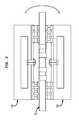
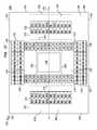
- all of the terminals of such packageare placed in sets of columns adjacent to one or more peripheral edges of a package substrate to which the microelectronic element is mounted. For example, in one conventional microelectronic package 12 seen in FIG.
- FIG. 1further shows a semiconductor chip 11 within the package having element contacts on a face 28 thereof which are electrically interconnected with the columns 14 , 18 of terminals of the package 12 through wire bonds 30 extending through an aperture, e.g., bond window, in the central region 24 of package substrate 20 .
- an adhesive layer 32may be disposed between the face 28 of the microelectronic element 11 and the substrate 20 to reinforce the mechanical connection between the microelectronic element and the substrate, with the wire bonds extending through an opening in the adhesive layer 32 .
- a microelectronic packagecan include a substrate having a first surface with a plurality of substrate contacts thereon, and a second surface is opposite the first surface.
- a microelectronic elementhas a rear face facing the first surface, a front face facing away from the first surface, and first and second opposed edges extending between the front and rear surfaces. Each of the first and second edges may extend in a first direction parallel to the front face. At least one column of element contacts extends in the first direction along the front face.
- the first and second edgesdefine an axial plane extending in the first direction and also in a third direction normal to the face of the microelectronic element, the axial plane being centered relative to the first and second edges.
- conductive structuresuch as wire bonds extends above the front face and beyond at least one of the first or second edges, the conductive structure electrically connecting the element contacts with the substrate contacts.
- terminals of the packageinclude first terminals which are disposed at a central region of the second surface of the substrate.
- the central regionmay be such that it is not wider than three and one-half times a minimum pitch between adjacent ones of parallel columns of the terminals.
- the central region of the surface of the substrateis located such that the axial plane intersects the central region.
- these first terminals in the central regionare configured to carry address information usable by circuitry within the package to determine an addressable memory location from among all the available addressable memory locations of a memory storage array within the microelectronic element.
- the first terminalscan be configured to carry all of the address information usable to determine such addressable memory location from available addressable memory locations of such memory storage array.
- the first terminalscan be configured to carry a majority of the address information or in a particular case, at least three quarters of the address information.
- the first terminalscan be configured to receive the address information transmitted thereto as a plurality of states or changes in state on respective terminals of the microelectronic package.
- the first terminalscan be configured to receive the address information encoded as a plurality of states or changes in state on one or on a combination of the first terminals.
- the first terminalscan be configured to carry information that controls an operating mode of the microelectronic element. As in the case of the address information, such information can be encoded as a plurality of states or changes in state on one or on a plurality of terminals.
- the first terminalscan be configured to carry all of a group of command signals, address signals, bank address signals and clock signals transferred to the microelectronic package on a “command-address bus” of a circuit panel.
- the command signalsin such case may be among or may be restricted to the following: command signals such as write enable, row address strobe, and column address strobe, and the clock signals are sampling clocks used for sampling the address signals.
- the clock signalscan be of various types, in one embodiment, the clock signals carried by these terminals can be one or more pairs of differential clock signals transmitted as differential clock signals or as true and complement clock signals.
- the signals of the command-address buscan be bussed on a circuit panel such as a printed circuit board or module card to multiple microelectronic packages in parallel, particularly to first and second microelectronic packages mounted to opposite surfaces of the circuit panel.
- a circuit panelsuch as a printed circuit board or module card
- terminals which carry the address information, or in a particular example, command-address bus signalsin the central region of the package surface, rather than in peripheral regions near the edges of the microelectronic package, it is possible to reduce the lengths of stubs used to carry signals from the command-address bus 36 ( FIG. 2 ) on the circuit panel to the individual connection sites on the surfaces of the circuit panel where microelectronic packages are electrically connected. Reducing the lengths of stubs can improve electrical performance in such assembly by reducing one or more of settling time, ringing, jitter, and intersymbol interference, among others of the signals conducted on the stubs to the packages.
- the microelectronic packagemay have no more than four columns of terminals in the central region configured to carry all of the command signals, address signals, bank address signals and clock signals as described above. In certain embodiments, there may be only two columns of such terminals. In other embodiments there may only be one column of such terminals.
- the microelectronic packagemay have second terminals other than the above-described command-address bus signal terminals, such second terminals being disposed in one or more of the peripheral regions and being configured to carry data signals.
- the second terminalscan include terminals used for carrying uni-directional or bi-directional data signals to and or from the microelectronic element, and data strobe signals, as well as data masks and ODT or “on die termination” signals used to turn on or off parallel terminations to termination resistors. It is possible in some embodiments for some or all terminals which are configured to carry signals other than the command-address bus signals to also be disposed in the central region of the package surface.
- Signals or reference potentialssuch as chip select, reset, power supply voltages, e.g., Vdd, Vddq, or ground, e.g., Vss and Vssq, can be carried by the second terminals, or may in some cases be carried by the first terminals.
- a microelectronic elementmay include a first semiconductor chip mounted adjacent the substrate and electrically connected thereto, and one or more second semiconductor chips overlying the first semiconductor chip and electrically connected therewith, in which the second semiconductor chips embody a greater number of active devices configured to provide memory storage array function than any other function.
- a microelectronic assemblycan include a circuit panel having first and second opposed surfaces and first and second panel contacts at the first and second surfaces, respectively, and first and second microelectronic packages each having terminals mounted to the respective panel contacts.
- each microelectronic packagecan include a substrate having first and second opposed surfaces, the first surface having substrate contacts thereon; and a microelectronic element embodying a greater number of active devices to provide memory storage array function than any other function.
- the microelectronic elementcan have a rear face facing the first surface, a front face opposite the rear face, and contacts on the front face electrically connected with the substrate contacts through conductive structure extending above the front face.
- a plurality of terminals on the second surfacecan be configured for connecting the microelectronic package with at least one component external to the package.
- the terminalscan be electrically connected with the substrate contacts and include first terminals disposed at locations within first and second parallel grids.
- Each of the first and second gridscan be configured to carry address information usable by circuitry within the package to determine an addressable memory location from among all the available addressable memory locations of a memory storage array within the microelectronic element.
- Signal assignments of the first terminals in the first gridcan be a mirror image of the signal assignments of the first terminals in the second grid.
- the first terminals of each of the first and second grids of each microelectronic packagecan be configured to carry all of the address information usable by the circuitry within the respective microelectronic package to determine the addressable memory location.
- the first terminals of each of the first and second grids of each microelectronic packagecan be configured to carry information that controls an operating mode the microelectronic element of the respective microelectronic package.
- the first terminals of each of the first and second grids of each microelectronic packagecan be configured to carry all of the command signals transferred to the respective microelectronic package, the command signals being write enable, row address strobe, and column address strobe signals.
- the first terminals of each of the first and second grids of each microelectronic packagecan be configured to carry clock signals transferred to the respective microelectronic package, the clock signals including clocks used for sampling signals carrying the address information.
- the first terminals of each of the first and second grids of each microelectronic packagecan be configured to carry all of the bank address signals transferred to the respective microelectronic package.
- the first terminals in the second grid of the first packagecan be connected through the circuit panel to the first terminals in the first grid of the second package.
- the first terminals of the second grid of the first packagecan be aligned within one ball pitch of the corresponding first terminals to which they are connected of the first grid on the second package in x and y orthogonal directions parallel to the first and second circuit panel surfaces.
- the gridscan be aligned with one another in the x and y orthogonal directions such that the terminals of the grids can be coincident with one another.
- each position of each gridcan be occupied by one of the terminals.
- At least one position of each gridmay not be occupied by a terminal.
- the grids of the first and second microelectronic packagescan be functionally and mechanically matched.
- a length of a stub of at least one of electrical connections between one of the first terminals of the first microelectronic package and a corresponding one of the first terminals of the second microelectronic packagecan be less than seven times a minimum pitch of the first terminals of each of the microelectronic packages.
- At least some of the electrical connections through the circuit panel between the first terminals of the first and second microelectronic packagescan have an electrical length of approximately a thickness of the circuit panel.
- the total combined length of the conductive elements connecting a pair of electrically coupled first and second panel contacts exposed at the first and second surfaces of the circuit panelcan be less than seven times a smallest pitch of the panel contacts.
- the circuit panelcan include a bus having a plurality of conductors configured to carry all of the address information transferred to each of the microelectronic packages.
- the conductorsmay extend in a first direction parallel to the first and second surfaces.
- the first terminalscan be disposed within an individual column in each of the first and second grids.
- the circuit panelmay include no more than one routing layer for global routing of all of the address information between a connection site on the circuit panel at which the first terminals of the first and second packages can be electrically connected and a different connection site on the circuit panel at which the first terminals of at least a third microelectronic package can be electrically connected.
- each of the first and second grids of first terminals of each microelectronic packagecan have two parallel columns, and wherein the circuit panel includes no more than two routing layers for global routing of all of the address information between respective connection sites on the circuit panel at which the terminals of one or more of the microelectronic packages can be electrically connected.
- each microelectronic packagecan include a buffer element electrically connected to at least some of the respective terminals and the microelectronic element in the respective microelectronic package.
- Each buffer elementcan be configured to at least one of: regenerate, or at least partially decode at least one signal received at one or more of the terminals of the respective microelectronic package for transfer to the microelectronic element.
- the microelectronic element of each microelectronic packagecan be a first microelectronic element, and each of the microelectronic packages may further include a second microelectronic element having a rear face facing the substrate and a front facing opposite the rear face, a plurality of element contacts on the front face being electrically connected with the substrate contacts through conductive structure extending above the front face.
- the second microelectronic elementcan embody a greater number of active devices to provide memory storage array function than any other function.
- the first terminals of each of the first and second grids of each microelectronic packagecan be configured to carry address information usable by circuitry within the respective microelectronic package to determine an addressable memory location from among all the available addressable memory locations of a memory storage array within the first and second microelectronic elements of the respective microelectronic package.
- a microelectronic assemblycan include a microelectronic package and a circuit panel electrically connected with the microelectronic package.
- microelectronic packagecan include: a substrate having first and second opposed surfaces, the first surface having substrate contacts thereon; and a microelectronic element embodying a greater number of active devices to provide memory storage array function than any other function.
- the microelectronic elementcan have a rear face facing the first surface, a front face opposite the rear face, and contacts on the front face electrically connected with the substrate contacts through conductive structure extending above the front face.
- a plurality of terminals on the second surfacecan be configured for connecting the microelectronic package with the circuit panel.
- the terminalscan be electrically connected with the substrate contacts and include first terminals disposed at locations within first and second parallel grids.
- Each of the first and second gridsmay be configured to carry address information usable by circuitry within the package to determine an addressable memory location from among all the available addressable memory locations of a memory storage array within the microelectronic element.
- Signal assignments of the first terminals in the first gridcan be a mirror image of the signal assignments of the first terminals in the second grid.
- the systemmay further include a housing, the microelectronic assembly and the one or more other electronic components being assembled with the housing.
- the microelectronic assemblycan be a first microelectronic assembly, and the system may further include a second such microelectronic assembly.
- each microelectronic assemblycan be mounted to, and electrically connected with a second circuit panel for transport of signals to and from each microelectronic assembly.
- a microelectronic assemblycan include a circuit panel having first and second opposed surfaces and first and second panel contacts at the first and second surfaces, respectively, and first and second microelectronic packages each having terminals mounted to the respective panel contacts.
- each microelectronic packagecan include a substrate having first and second opposed surfaces, the first surface having substrate contacts thereon; and a microelectronic element embodying a greater number of active devices to provide memory storage array function than any other function.
- the microelectronic elementcan have a rear face facing the first surface, a front face opposite the rear face, and contacts on the front face electrically connected with the substrate contacts through conductive structure extending above the front face.
- a plurality of terminals on the second surfacecan be configured for connecting the microelectronic package with at least one component external to the package.
- the terminalscan be electrically connected with the substrate contacts and include first terminals disposed at locations within first and second parallel grids.
- the first terminals in each of the first and second gridscan be configured to carry a majority of address information usable by circuitry within the package to determine an addressable memory location from among all the available addressable memory locations of a memory storage array within the microelectronic element.
- Signal assignments of the first terminals in the first gridcan be a mirror image of the signal assignments of the first terminals in the second grid.
- the first terminals of each of the first and second grids of each microelectronic packagecan be configured to carry at least three-quarters of the address information usable by the circuitry within the respective microelectronic package to determine the addressable memory location.
- a microelectronic assemblycan include a circuit panel having first and second opposed surfaces and first and second panel contacts at the first and second surfaces, respectively, and first and second microelectronic packages each having terminals mounted to the respective panel contacts.
- each microelectronic packagecan include a substrate having first and second opposed surfaces, the first surface having substrate contacts thereon; and a microelectronic element embodying a greater number of active devices to provide memory storage array function than any other function.
- the microelectronic elementcan have a rear face facing the first surface, a front face opposite the rear face, and contacts on the front face electrically connected with the substrate contacts through conductive structure extending above the front face.
- a plurality of terminals on the second surfacecan be configured for connecting the microelectronic package with at least one component external to the package.
- the terminalscan be electrically connected with the substrate contacts and include a first set of first terminals arranged in a first individual column and second set of the first terminals arranged in a second individual column.
- the first terminals of each of the first and second individual columnscan be configured to carry address information usable by circuitry within the microelectronic package to determine an addressable memory location from among all the available addressable memory locations of a memory storage array within the microelectronic element.
- Signal assignments of the first terminals in the first columncan be symmetric about an axis extending between the first and second columns with respect to the signal assignments of the first terminals in the second column.
- FIG. 1is a sectional view illustrating a conventional microelectronic package.
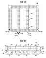
- FIG. 2is a schematic perspective view illustrating a microelectronic assembly referred to herein.
- FIG. 3is a sectional view illustrating a microelectronic assembly referred to herein.
- FIG. 4is a schematic diagram illustrating an electrical interconnection between a pair of microelectronic packages in an assembly as seen in FIG. 3 .
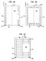
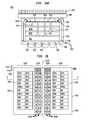
- FIG. 5Ais a plan view illustrating an arrangement of terminals on a microelectronic package according to an embodiment of the invention.
- FIG. 5Bis a further plan view illustrating a possible arrangement of terminals on a package such as seen in FIG. 5A .
- FIG. 5Cis a sectional view illustrating a microelectronic package according to an embodiment of the invention.
- FIGS. 6A , 6 B and 6 Care plan views illustrating various arrangements of element contacts on microelectronic elements incorporated in a package according to an embodiment of the invention.
- FIG. 7Ais a sectional view illustrating a microelectronic assembly according to an embodiment of the invention.
- FIG. 7Bis a schematic perspective view illustrating a microelectronic assembly according to an embodiment of the invention.
- FIG. 8is a sectional view illustrating a microelectronic package according to an embodiment of the invention.
- FIG. 9is a sectional view illustrating a microelectronic package according to an embodiment of the invention.
- FIG. 10is a sectional view illustrating a microelectronic package according to an embodiment of the invention.
- FIG. 11is a sectional view illustrating a microelectronic package according to an embodiment of the invention.
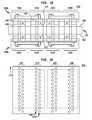
- FIG. 12is a plan view illustrating a microelectronic package according to an embodiment of the invention.
- FIG. 13is a sectional view illustrating a microelectronic package according to an embodiment of the invention.
- FIG. 14is a sectional view illustrating a microelectronic package according to an embodiment of the invention.
- FIG. 15Ais a sectional view illustrating a microelectronic package according to an embodiment of the invention.
- FIG. 15Bis a sectional view illustrating a microelectronic package according to an embodiment of the invention.
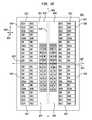
- FIG. 16is a plan view illustrating a microelectronic package according to an embodiment of the invention.
- FIG. 17is a sectional view further illustrating a microelectronic package as seen in FIG. 16 .
- FIG. 18is a plan view further illustrating a microelectronic package according to an embodiment of the invention as seen in FIG. 16 .
- FIG. 19is a sectional view illustrating a microelectronic assembly incorporating first and second microelectronic packages such as seen in FIG. 16 .
- FIGS. 20 and 21illustrate alternative terminal arrangements in a microelectronic package according to an embodiment of the invention as seen in FIG. 16 .
- FIG. 22is a sectional view illustrating a microelectronic package according to a variation of the embodiment of the invention seen in FIG. 16 .
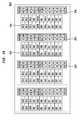
- FIG. 23is a plan view illustrating a microelectronic package according to an embodiment of the invention.
- FIG. 24is a plan view illustrating a microelectronic package according to an embodiment of the invention.
- FIG. 25is a plan view illustrating a microelectronic package according to an embodiment of the invention.
- FIG. 26is a plan view illustrating a microelectronic package according to an embodiment of the invention.
- FIG. 27is a plan view illustrating a microelectronic package according to an embodiment of the invention.
- FIG. 28is a plan view illustrating a microelectronic package according to an embodiment of the invention.
- FIG. 29is a plan view illustrating a microelectronic package according to an embodiment of the invention.
- FIG. 30is a plan view illustrating a microelectronic package according to an embodiment of the invention.
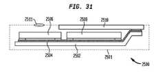
- FIG. 31is a schematic sectional view illustrating a system according to an embodiment of the invention.
- the inventorshave recognized improvements which can be made that may help improve the electrical performance of a package incorporating a memory storage array chip, and an assembly which incorporates such package.
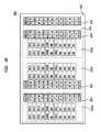
- Improvementscan be made particularly for use of a microelectronic package when provided in an assembly such as shown in FIGS. 2-4 , in which a package 12 A is mounted to a surface of a circuit panel with another like package 12 B mounted opposite thereto on an opposite surface of the circuit panel.
- the packages 12 A, 12 Btypically are functionally and mechanically equivalent to one another.
- Other pairs 12 C and 12 D; and 12 E and 12 F, of functionally and mechanically equivalent packagestypically can also be mounted to the same circuit panel 34 .
- the circuit panel and the packages assembled theretomay form a portion of an assembly commonly referred to as a dual in-line memory module (“DIMM”).
- DIMMdual in-line memory module
- the packages in each oppositely mounted pair of packagesconnect to contacts on opposite surfaces of the circuit panel so that the packages in each pair overlie one another typically by more than 90% of their respective areas.
- Local wiring within the circuit panel 34connects terminals, e.g., the terminals labeled “1” and “5” on each package to global wiring on the circuit panel.
- the global wiringincludes the signal conductors of a bus 36 used to conduct some signals to connection sites on the circuit panel 34 such as connection sites I, II and III.
- packages 12 A, 12 Bare electrically connected to the bus 36 by local wiring coupled to a connection site I
- packages 12 C, 12 Dare electrically connected to the bus by local wiring coupled to connection site II
- packages 12 E, 12 Fare electrically connected to the bus by local wiring coupled to connection site III.
- the circuit panel 34electrically interconnects the terminals of the respective packages 12 A, 12 B using local interconnect wiring that appears similar to a crisscross or “shoelace” pattern in which a terminal labeled “1” near one edge of package 12 A connects through the circuit panel 34 to a terminal labeled “1” of package 12 B near the same edge 16 of package 12 B.
- the edge 16 of package 12 B as assembled to circuit panel 34is far from the edge 16 of package 12 A.
- FIGS. 2-4further shows that a terminal labeled “5” near an edge 22 of package 12 A is connected through the circuit panel 34 to a terminal labeled “5” of package 12 B near the same edge 22 of package 12 B. In assembly 38 the edge 22 of package 12 A is far from the edge 22 of package 12 B.
- connections through the circuit panel between terminals on each package, e.g., package 12 A, to the corresponding terminals on the package mounted opposite thereto, i.e., package 12 B,are fairly long.
- the circuit panel 34may electrically interconnect a signal conductor of the bus 36 with the terminal of package 12 A marked “1” and the corresponding terminal of package 12 B marked “1”, when the same signal from the bus is to be transmitted to each package.
- the circuit panel 34may electrically interconnect another signal conductor of the bus 36 with the terminal of package 12 A marked “2” and the corresponding terminal of package 12 B marked “2”.
- connection through circuit panel 34 of the terminals marked “3” of each package 12 A, 12 BThe same connection arrangement may also apply to other signal conductors of the bus and corresponding terminals of each package.
- Local wiring between the bus 36 on the circuit panel 34 and each package of the respective pair of packages, e.g., packages 12 A, 12 B ( FIG. 2 ) at a connection site I of the boardcan be in form of unterminated stubs. Such local wiring when relatively long may in some cases impact the performance of the assembly 38 as discussed below.
- circuit panel 34also requires local wiring to electrically interconnect certain terminals of other packages: the pair of packages 12 C and 12 D, and the pair of packages 12 E and 12 F to the global wiring of the bus 36 , and such wiring can also impact the performance of the assembly in the same way.
- FIG. 4further illustrates the interconnection between microelectronic packages 12 A, 12 B of respective pairs of terminals assigned to carry signals “1”, “2”, “3”, “4”, “5”, “6”, “7”, and “8”.
- the wiring needed to traverse the circuit panel 34 in a direction 40 transverse to the direction 42 in which the columns 14 , 18 of terminals extendcan be quite long.
- the length of the local wiring in a circuit panel 34 in an assembly 38 seen in FIGS. 2-4that is required to route the same signal to the corresponding terminals of two oppositely mounted packages 12 A, 12 B can range up to five to ten millimeters in some cases, and may typically be about seven millimeters.
- the lengths of the circuit panel wiring required to connect the terminals of such oppositely mounted microelectronic packagesmay not severely impact the electrical performance of the assembly.
- the signal carried by the connected pair of terminals on the packages 12 A, 12 Bis a signal from a bus 36 used to carry address information or other information such as clock information usable to sample address information which is common to operation of the memory storage array function of a plurality of packages connected to the circuit panel
- the inventorsrecognize that the wiring length of the stubs extending from the bus 36 to the terminals on each package may significantly affect performance.
- the interconnecting wiringis relatively long, a more severe impact occurs, which can increase settling time, ringing, jitter, or intersymbol interference for a transmitted signal to an unacceptable degree.
- the bus 36 used to carry address informationcan be a command-address bus 36 configured to carry command information, address information, bank address information and clock information.
- the command informationcan be transmitted as command signals on respective signal conductors on the circuit panel. It is also possible for the address information to be transmitted as address signals on respective signal conductors, as it is also possible for the bank address information to be transmitted as bank address signals on respective signal conductors, and it is also possible for the clock information to be transmitted as clock signals on respective signal conductors.
- the command signals which can be carried by the bus 36can be write enable, row address strobe and column address strobe, and the clock signals which can be carried by the bus 36 can be clock signals used at least for sampling address signals carried by the bus 36 .
- certain embodiments of the invention described hereinprovide a microelectronic package configured so as to permit the lengths of stubs on a circuit panel to be reduced when first and second such packages are mounted opposite one another on opposite surfaces of a circuit panel, e.g., a circuit board, module board or card, or flexible circuit panel.
- Assemblies which incorporate first and second microelectronic packages mounted opposite one another on a circuit panelcan have significantly reduced stub lengths between the respective packages. Reducing the stub lengths within such assemblies can improve electrical performance, such as by reducing one or more of settling time, ringing, jitter, or intersymbol interference, among others.
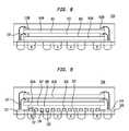
- the package 100can include a microelectronic element 101 configured to predominantly provide memory storage array function, in that the microelectronic element has a greater number of active devices, e.g., transistors, configured to provide memory storage array function than any other function, as indicated above.
- active devicese.g., transistors
- the microelectronic elementhas element contacts 111 , 113 at a front face 105 thereof which are electrically connected to respective substrate contacts 121 , 123 at a first surface 108 of the substrate 102 .
- wirebonds 112may electrically connect the element contacts 111 , 113 with the substrate contacts 121 , 123 .
- other types of conductorse.g., portions of a lead frame, flexible ribbon bonds, etc.
- each one of some contacts of the element contacts 111 , 113may be configured to receive particular address information of the address information supplied to the microelectronic element.
- each of such contacts 111 , 113may be configured to receive a respective address signal of a plurality of address signals supplied to the microelectronic element 101 from the outside the microelectronic element, i.e., through wiring of the package such as wire bonds 112 , and through terminals 104 , 106 .
- the address information present at the element contacts 111 , 113can be sampled relative to an edge of a clock used by the respective microelectronic element, i.e., upon on a transition of the clock between first and second different voltage states. That is, each address signal can be sampled upon a rising transition between a lower voltage state and a higher voltage state of the clock, or upon a falling transition between a higher voltage state and a lower voltage state of the clock.
- the plurality of address signalsmay all be sampled upon the rising transition of the clock, or such address signals may all be sampled upon the falling transition of the clock, or in another example, the address signal at one of the element contacts 111 , 113 can be sampled upon the rising transition of the clock and the address signal at one other external contact can be sampled upon the falling transition of the clock.
- one or more of the address contacts thereoncan be used in a multiplexed manner.
- a particular element contact 111 , 113 of the respective microelectronic element 101can receive two or more different signals supplied to the microelectronic element from the outside.
- a first address signalcan be sampled at the particular contact 111 , 113 upon a first transition of the clock between the first and second different voltage states (e.g., a rising transition)
- a signal other than the first address signalcan be sampled at the particular contact upon a second transition of the clock (e.g., a falling transition) between the first and second voltage states that is opposite the first transition.
- multiplexing in this mannercan allow a first address signal and a different signal to be received in the same clock cycle on the same element contact 111 , 113 of the respective microelectronic element 101 .
- multiplexing in this mannercan allow a first address signal and a second different address signal to be received in the same clock cycle on the same element contact 111 , 113 of the respective microelectronic element 101 .
- the substrate 102can include a sheet-like or board-like dielectric element, which may consist essentially of polymeric material, e.g., a resin or polyimide, among others.
- the substratecan include a dielectric element having a composite construction such as glass-reinforced epoxy, e.g., of BT resin or FR-4 construction.
- the dielectric elementhas a coefficient of thermal expansion in the plane of the dielectric element, i.e., in a direction parallel to a first surface 108 thereof, of up to 30 parts per million per degree Celsius (hereinafter, “ppm/° C.”).
- the substratecan include a supporting element of material having a coefficient of thermal expansion (“CTE”) of less than 12 parts per million per degree Celsius, on which the terminals and other conductive structure are disposed.
- CTEcoefficient of thermal expansion
- such low CTE elementcan consist essentially of glass, ceramic or semiconductor material or liquid crystal polymer material, or a combination of such materials.
- a first set 121 and a second set 123 of substrate contactscan be exposed at a first surface 108 of the substrate.
- the first set 121 of substrate contactscan be electrically connected with a column 111 ( FIG. 6A ) of element contacts 132 of the microelectronic element, such as through electrically conductive structure extending above the face 105 of the microelectronic element.
- the conductive structurecan be wire bonds 112 .
- a die attach adhesivemay be disposed between a rear face 107 of the microelectronic element and the surface 108 of the substrate 102 , which may mechanically reinforce the connection between the microelectronic element and the substrate.
- the second set 123 of the substrate contactscan be electrically connected with a column 113 ( FIG. 6A ) of element contacts 132 .
- an edge 170 of microelectronic element 130can extend in the first direction 142 and a column 111 of contacts 132 adjacent to edge 170 can extend in the same first direction 142 along the face 105 .
- Another edge 172 of microelectronic element 130parallel to edge 170 , extends in the first direction 142 and a second column 113 of contacts 132 may extend in the same first direction 142 along the face 105 adjacent to edge 172 .
- a column of contacts on the microelectronic elementcan be fully populated as in the case of column 111 , or a column of contacts may have only have contacts at some of the positions within the column, as in the case of column 113 .
- Conductive structuresuch as wire bonds 112 ( FIG. 5C ) may electrically connect the contacts 111 , 113 with corresponding contacts 121 , 123 on a first surface 108 of the substrate.
- FIG. 6Billustrates a variation of the embodiment shown in FIG. 6A in which contacts 132 of a microelectronic element 180 can disposed in columns and rows adjacent to and aligned with respective peripheral edges 170 , 172 , 176 , 178 of the microelectronic element 180 . Edges 170 , 172 are parallel and extend in a first direction 142 .
- FIG. 6Cillustrates another variation of the embodiment shown in FIG. 6A in which the contacts of a microelectronic element 190 are disposed in columns 188 and 189 adjacent to edges 170 , 172 of the microelectronic element.
- the microelectronic element 190includes a semiconductor chip having a conductive redistribution layer thereon, and the contacts 132 can include columns 188 , 189 of redistribution contacts which are connected to the contacts 192 , 194 of the semiconductor chip by conductive traces, or metalized vias formed in contact with the contacts 192 , 194 of the semiconductor chip (or which can be connected to the contacts 192 , 194 of the chip by both metalized vias and traces).
- contacts 192 , 194may in some cases be connected with active devices of the semiconductor chip through back end of line (“BEOL”) wiring of the semiconductor which may include vias or other electrically conductive structure and which may in some cases be disposed underneath the contacts 192 , 194 .
- BEOLback end of line
- the contacts of the microelectronic elementmay be arranged in a single column as shown for contacts 192 , or the contacts may be arranged in a plurality of columns as shown for contacts 111 , 113 .
- Each columnmay contain a contact at each vertical layout position of the column along direction 142 , or a contact may be missing from one or more positions of a column, as in the case of one of the columns of contacts 113 .
- the contactsmay be arranged in an area array over the face 105 of the microelectronic element.
- the contacts of a microelectronic elementcan be arranged in one or more sets of contacts adjacent one or more peripheral edges of the microelectronic element indicated by the dashed lines marking the boundaries of the microelectronic element in FIG. 5B .
- the microelectronic elementcan be a single semiconductor chip and the contacts 111 , or 113 thereon may be “chip contacts” which are the contacts of the semiconductor chip.
- the contacts 111 , or 113 thereonmay be “chip contacts” which are the contacts of the semiconductor chip.
- a particular microelectronic element 190can include one or more semiconductor chips each having chip contacts, and the contacts 111 , or 113 may include redistribution contacts which are formed on a face 105 thereof, and which are electrically connected to the chip contacts by conductive elements such as traces and vias, for example.
- the “contacts” of the microelectronic elements in each of the examples hereincan be arranged in any of these described ways.
- the microelectronic elementmay also include additional contacts that may not be disposed within a column of the element contacts. These additional contacts may be used for connection to power, ground, or as contacts available for contact with a probing device, such as may be used for testing.
- the package 100can have first terminals 104 and second terminals 106 for electrically and mechanically connecting the package 100 with a component external to the package 100 , such as a circuit panel, for example.
- the terminals 104 , 106can be electrically conductive pads, posts, or other electrically conductive structure.
- the terminalsin some cases may include joining elements 133 , such as may include a bond metal such as solder, tin, indium, gold, or a eutectic material, among others, or other conductive bond material, and may in some cases also include additional structure such as a conductive bump attached to conductive structure of the substrate such as conductive pads or posts.
- the first terminals 104 and the second terminals 106can be electrically connected with the substrate contacts 121 , 123 through electrically conductive structure on the substrate, such as traces and vias, for example.
- a first set of the first terminals 104can be arranged at positions within a first grid 114 at a second surface 110 of the substrate 102 opposite from the first surface 108 .
- a second set of the first terminals 104can be arranged at positions within a second grid 124 at the second surface 110 of the substrate.
- the first and second gridsare shown extending beyond the outer boundaries of the front surface of the microelectronic elements, that need not be the case.
- each of the first and second grids 114 , 124 of first terminalscan be configured to carry the above-noted address information or, in a particular embodiment, certain signals of the command-address bus.
- each of the first and second grids 114 , 124is configured to carry address information transferred to the microelectronic package 100 which is usable by circuitry within the package, e.g., row address and column address decoders, and bank selection circuitry, if present, to determine an addressable memory location from among all the available addressable memory locations of a memory storage array within a microelectronic element in the package.
- each of the first and second grids 114 , 124can be configured to carry all the address information used by such circuitry within the microelectronic package 100 to determine an addressable memory location within such memory storage array.
- the first terminals of each of the first and second grids 114 , 124can be configured to carry a majority of the address information that is used by such circuitry within the microelectronic package 100 to determine an addressable memory location within such memory storage array, and then other terminals such as at least some of the above-referenced second terminals 106 on the microelectronic package would then be configured to carry the remaining part of the address information.
- the first terminals in each of the first and second grids 114 , 124are configured to carry three-quarters or more of the address information that is used by such circuitry within the microelectronic package 100 to determine an addressable memory location within such memory storage array.
- each of the first and second grids 114 , 124may not be configured to carry chip select information, e.g., information usable to select a particular chip within the microelectronic package 100 for access to a memory storage location within the chip.
- chip select informatione.g., information usable to select a particular chip within the microelectronic package 100 for access to a memory storage location within the chip.
- at least one of the first and second grids 114 , 124may indeed carry chip select information.
- the address information in one embodimentcan include all address information transferred to the package from a component external to the package, e.g., a circuit panel such as the circuit panel 154 ( FIG. 7A ) described below, which is used for determining a random access addressable memory location within the microelectronic package for read access thereto, or for either read or write access thereto.
- a component external to the packagee.g., a circuit panel such as the circuit panel 154 ( FIG. 7A ) described below, which is used for determining a random access addressable memory location within the microelectronic package for read access thereto, or for either read or write access thereto.
- At least some of the second terminals 106can be configured to carry signals other than the address signals that are carried by the first terminals 104 of the first and second grids 114 , 124 .
- the second terminals 106may carry one or more of data, data strobe signals, or other signals or reference potentials such as chip select, reset, power supply voltages, e.g., Vdd, Vddq, and ground, e.g., Vss and Vssq.
- Some or all second terminalscan be disposed at locations within the first and second grids 114 , 124 .
- some terminals disposed at locations within the first and second grids 114 , 124can be configured to carry one or more of data, data strobe signals, or other signals or reference potentials such as chip select, reset, power supply voltages, e.g., Vdd, Vddq, and ground, e.g., Vss and Vssq.
- Some terminals disposed at locations within the third and fourth grids 116 , 126can be configured to carry one or more of data, data strobe signals, or other signals or reference potentials such as chip select, reset, power supply voltages, e.g., Vdd, Vddq, and ground, e.g., Vss and Vssq.
- the first terminals of each of the first and second grids 114 , 124 of each microelectronic packagecan be configured to carry information that controls an operating mode of the microelectronic element 101 . More specifically, each of the first and second grids 114 , 124 can be configured to carry all of a particular set of command signals and/or clock signals transferred to the microelectronic package 100 . In one embodiment, the first terminals 104 can be configured to carry all of the command signals, address signals, bank address signals, and clock signals transferred to the microelectronic package 100 from an external component, e.g., circuit panel or other device, wherein the command signals include row address strobe, column address strobe and write enable.
- the command signalsinclude row address strobe, column address strobe and write enable.
- the command signalscan be write enable, row address strobe, and column address strobe signals.
- Other signalssuch as ODT (on die termination), chip select, clock enable, may or may not be carried by terminals disposed within the first and second grids 114 , 124 .
- the clock signalscan be clocks used by one or more of the microelectronic elements for sampling the address signals. For example, in the microelectronic package of FIG. 7 and as further shown in FIG.
- the first terminals 104can be configured to carry clock signals CK and CKB, row address strobe RAS, column address strobe CAS and write enable signals WE, as well as address signals A 0 through A 15 inclusive, and bank address signals BA 0 , BA 1 and BA 2 .
- the second terminals 106which can be disposed at positions within third and fourth grids 116 , 126 , can be configured to carry signals other than the command signals, address signals, and clock signals that are carried by the first terminals 104 of the first and second grids 114 , 124 .
- Signals or reference potentialssuch as chip select, reset, power supply voltages, e.g., Vdd, Vddq, and ground, e.g., Vss and Vssq, may or may not be carried by the second terminals 106 in any of the embodiments referred to herein, unless otherwise noted.
- At least some of the second terminals 106 that are configured to carry signals other than the address signalscan be arranged at positions within the first and second grids 114 , 124 . In one example, at least some of the second terminals 106 that are configured to carry signals other than the command signals, address signals, and clock signals can be arranged at positions within the first and second grids 114 , 124 .
- second terminals 106can also include terminals that are configured to be connected to power or ground signals.
- each grid 114 , 124may include first and second parallel columns 136 of terminals.
- the columns 136 of terminals in each gridcan be adjacent to one other.
- at least one terminalmay be disposed between the first and second columns of terminals.
- the gridsmay include a column of terminals for which a column axis 119 extends through a majority of the terminals 104 of such column, i.e., is centered relative thereto.
- one or more of the terminalsmight not be centered relative to the column axis 119 , as in the case of terminals 104 ′.
- these one or more terminalsare considered part of a particular column, even though such terminal(s) might not be centered relative to axis 119 because they are closer to the axis 119 of that particular column than to the axis of any other column.
- the column axis 119may extend through these one or more terminals which are not centered relative to the column axis, or, in some cases, the non-centered terminals may be farther from the column axis such that the column axis 119 may not even pass through these non-centered terminals of the column.
- an encapsulant 146may overlie the first surface 108 of the substrate and may contact the microelectronic element 101 therein. In some cases, the encapsulant may overlie a front surface 105 of the microelectronic element which faces away from the substrate 102 .
- the signal assignments of the first terminals in the second grid 124are a mirror image of the signal assignments 124 of the first terminals in the first grid 114 .
- the signal assignments of the first terminals in the first and second gridsare symmetric about an axis 131 between the first and second grids 114 , 124 , the axis 131 in this case extending in a direction 142 in which columns 136 of the first terminals extend.
- a first terminal 104 of the first grid 114 which is assigned to carry the signal A 3is in the same relative vertical position (in direction 142 ) within the grid as the corresponding first terminal 104 of the second grid 114 which is assigned to carry the signal A 3 .
- the first grid 114contains two columns 136 and the terminal of the first grid 114 assigned to carry the signal A 3 is in the left column among the two columns 136 of the first grid 114 , the mirror image arrangement requires that the corresponding terminal of the second grid 124 assigned to carry the signal A 3 is in the right column among the two columns of the second grid 124 .
- the terminal assigned to carry the signal A 9is also in the same relative vertical position within the grid in each of the first and second grids 114 , 124 .
- the terminal assigned to carry A 9is in the right column among the two columns 136 of the first grid, and the mirror image arrangement requires that the corresponding terminal of the second grid 124 assigned to carry the signal A 9 is in the left column among the two columns of the second grid 124 .
- the same relationshipapplies for each first terminal in each of the first and second grids, at least for each first terminal assigned to carry a command-address bus signal as discussed above.
- the axis 131 about which the signal assignments of the first terminals are symmetriccan be located at various positions on the substrate.
- the axiscan be a central axis of the package that is located equidistant from first and second opposed edges 140 , 141 of the substrate particularly when the columns 136 of the first terminals extend in a direction parallel to the edges 140 , 141 and the first and second grids are disposed at locations which are symmetric about this central axis.
- the axis 131may be located within a distance no greater than three and one-half times a minimum pitch between any two adjacent columns of terminals from a line which is parallel to and equidistant from the first and second edges 140 , 141 of the substrate.
- this axis of symmetry 131can be offset in a horizontal direction 135 from the central axis that is equidistant between edges 140 , 141 .
- terminals in the first and second gridscan be located in a central region of the package.
- at least one column 136 of terminals in each of the first and second grids 114 , 124can be disposed within a distance not greater than three and one-half times the minimum pitch between any two adjacent parallel columns 136 of the terminals from a line which is equidistant from and parallel to the first and second edges 140 , 141 of the substrate.
- the second terminals 106can be configured to carry information other than the above-noted address information or other than signals of the above-noted command-address bus.
- the second terminals 106can include terminals used for carrying uni-directional or bi-directional data signals to and or from the microelectronic element, and data strobe signals, as well as data masks and ODT or “on die termination” signals used to turn on or off parallel terminations to termination resistors.
- the second terminalsmay carry signals such as chip select, reset, clock enable, as well as reference potentials such as power supply voltages, e.g., Vdd, Vddq, or ground, e.g., Vss and Vssq.
- some or all terminals that are configured to carry signals other than the command-address bus signalscan be disposed as second terminals 106 on the package, wherever they can be suitably placed.
- some or all of the second terminals 106can be arranged in the same grids 114 , 124 on the substrate 102 in which the first terminals 104 are arranged.
- Some or all of the second terminals 106may be disposed in the same column or in different columns as some or all of the first terminals 104 .
- one or more second terminalscan be interspersed with the first terminals in the same grids or column thereof.
- some or all of the second terminals 106can be disposed in a third grid 116 on the second surface 110 of the substrate, and another set of the second terminals can be disposed in a fourth grid 126 on the package surface 110 .
- the signal assignments of the second terminals in the third grid 116can be a mirror image of the signal assignments of the second terminals in the fourth grid 126 , in like manner to that described above for the first and second grids.
- the third and fourth grids 116 , 126may in some cases extend in the direction 134 in which the first and second grids extend and can be parallel to one another.
- the third and fourth gridsmay also be parallel to the first and second grids 114 , 124 .
- grids 127 , 129 in which second terminals are disposedcan extend in another direction 135 which is transverse to or even orthogonal to direction 142 .
- some second terminalscan be disposed within each of the grids 116 , 126 , 127 and 129 shown in FIG. 5A .
- Some second terminalsmay or may not also be disposed at positions within the first and second grids 114 , 124 .
- the signal class assignments of the second terminals in grid 127can be symmetric about the vertical axis 132
- the signal class assignments of the second terminals in grid 129can be symmetric about the vertical axis 132
- two signal class assignmentscan be symmetric with respect to one another if the signal assignments are in the same class of assignments, even if the numerical index within the class differs.
- Exemplary signal class assignmentscan include data signals, data strobe signals, data strobe complement signals, and data mask signals.
- the second terminals having signal assignments DQSH and DQSLare symmetric about the vertical axis 132 with respect to their signal class assignment, which is data strobe, even though those second terminals have different signal assignments.
- the assignments of the data signals to the spatial positions of the second terminals on the microelectronic packagecan have modulo-X symmetry about the vertical axis 132 .
- the modulo-X symmetrycan help preserve signal integrity in an assembly 200 or 354 such as seen in FIGS. 7A and 7B , in which one or more pairs of first and second packages are mounted opposite one another to a circuit panel, and the circuit panel electrically connects corresponding pairs of second terminals of those first and second packages in each oppositely mounted package pair.
- modulo-X symmetrycan permit electrical connections to be made through the circuit panel so that a terminal DQ 0 of a first package can be electrically connected through the circuit panel to a terminal DQ 8 of the second package which has the same number modulo X (X being 8 in this case), so that the connection can be made in a direction essentially straight through, i.e., normal to, the thickness of the circuit panel.
- a number such as 8 modulo 8is 0, and a number such as 9 modulo 8 is 1. Therefore, when the signal assignments have modulo-8 symmetry, a terminal which is configured to carry a signal such as DQ 1 , for which the modulo 8 operation yields a result of “1”, is disposed at a position on the substrate which is symmetric about an axis with another terminal configured to carry a signal such as DQ 9 or DQ 17 for which the modulo 8 operation yields the same result, i.e., “1”.
- “X”can be a number 2′ (2 to the power of n), wherein n is greater than or equal to 2, or X can be 8 ⁇ N, N being two or more.
- Xmay be equal to the number of bits in a half-byte (4 bits), byte (8 bits), multiple bytes (8 ⁇ N, N being two or more), a word (32 bits) or multiple words.
- the signal assignment of a package terminal DQ 0 in grid 127is configured to carry data signal DQ 0 is symmetric about the vertical axis 132 with the signal assignment of another package terminal DQ 8 configured to carry data signal DQ 8 .
- the signal assignments of package terminals DQ 2 and DQ 10 in grid 127have modulo-8 symmetry about the vertical axis, and the same is also true for grid 129 .
- Modulo-8 symmetrysuch as described herein can be seen in grids 127 , 129 with respect to each of the signal assignments of package terminals DQ 0 through DQ 15 .
- the modulo number “X”can be a number other than 2 n (2 to the power of n) and can be any number greater than two.
- the modulo number X upon which the symmetry is basedcan depend upon how many bits are present in a data size for which the package is constructed or configured. For example, when the data size is 10 bits instead of 8, then the signal assignments may have modulo-10 symmetry. It may even be the case that when the data size has an odd number of bits, the modulo number X can have such number.
- FIG. 7Aillustrates an assembly 200 of first and second microelectronic packages 100 A, 100 B, each being a microelectronic package 100 as described with reference to FIGS. 5A-C above, as mounted to opposite first and second surfaces 150 , 152 of a circuit panel 154 .
- the circuit panelcan be of various types, such as a printed circuit board used in a dual-inline memory module (“DIMM”) module, a circuit board or panel to be connected with other components in a system, or a motherboard, among others.
- DIMMdual-inline memory module
- the first and second microelectronic packages 100 A, 100 Bcan be mounted to corresponding contacts 160 , 162 exposed at the first and second surfaces 150 , 152 of the circuit panel 154 , respectively.
- each first terminal in the first grid 114 A of the first package 100 Acan be aligned with the corresponding first terminal in the second grid 124 B of the second package 100 B which has the same signal assignment and to which it is electrically connected.
- each first terminal in the second grid 124 A of the first package 100 Acan be aligned with the corresponding first terminal in the first grid 114 B which has the same signal assignment and to which it is electrically connected.
- each pair of connected terminalscan be within a tolerance, such that each pair of connected terminals can be aligned within one ball pitch of one another in orthogonal x and y directions along the first surface 150 of the circuit panel 154 .
- the first terminals of each gridcan be aligned within one ball pitch of one another in x and y orthogonal directions parallel to the surface 350 of the circuit panel, the ball pitch being no greater than a minimum pitch between any two adjacent parallel columns of the terminals on either package.
- the gridsmay be aligned with one another in the x and y directions such that at least some of the first terminals on the first and second microelectronic packages are coincident with one another.
- the alignmentcan be within customary manufacturing tolerances or can be within a tolerance of less than one-half of one ball pitch of one another in x and y orthogonal directions parallel to the first and second circuit panel surfaces, the ball pitch being as described above.
- At least half of the positions of the aligned grids of the respective first and second packages 100 A, 100 Bcan be aligned with one another in orthogonal x and y directions along the first surface 150 of the circuit panel 154 .
- a particular first terminal that carries a signal marked “A” in grid 114 A of the first package 100 Ais aligned with the corresponding first terminal of grid 124 B of the second package 100 B that carries the same signal “A”.
- the lengths of the electrical connections through the circuit panel between each pair of electrically connected first terminals of the first and second packages 100 A, 100 Bcan be significantly reduced, in that the terminals in each of these pairs of electrically connected second terminals may overlie one another, or at least be aligned within one ball pitch of one another.
- the reductions in the lengths of these electrical connectionscan reduce stub lengths in the circuit panel and the assembly, which can help improve the electrical performance, such as reducing settling time, ringing, jitter, or intersymbol interference, among others, for the above-noted signals which are carried by the first terminals and which are transferred to microelectronic elements in both the first and second packages.
- the electrical lengths of stubs on the circuit panel 354 which electrically connect a first terminal 104 of the first package 100 A with the corresponding first terminal 104 on the second package 100 Bcan be less than seven times a minimum pitch of the first terminals on each package, for example, less than seven times the pitch 151 between columns 104 A, 104 B of first terminals in FIG. 5B .
- a minimum pitch of the first terminals on each packagefor example, less than seven times the pitch 151 between columns 104 A, 104 B of first terminals in FIG. 5B .
- the total combined length of the conductive elements connecting a pair of electrically coupled first and second panel contacts 160 , 162 exposed at the first and second surfaces of the circuit panel 150 , 152 for electrically interconnecting the first and second panel contacts with one of the command signals, address signals, bank address signals or clock signalscan be less than seven times a smallest pitch of the panel contacts.
- each terminal of each package's third gridcan be aligned with the corresponding second terminal of the other package's fourth grid which has the same signal assignment and to which it is electrically connected.
- each terminal in the third grid 116 A of the first package 100 Acan be aligned within one ball pitch of the corresponding terminal in the fourth grid 126 B of the second package 100 B which has the same signal assignment and to which it is electrically connected.
- each terminal in the grid 126 A of the first package 100 Acan be aligned within one ball pitch of the corresponding terminal in the third grid 116 B which has the same signal assignment and to which it is electrically connected.
- the alignment of each pair of connected terminalsis within a tolerance, such that each pair of connected terminals can be aligned within one ball pitch of one another in orthogonal x and y directions along the first surface 150 of the circuit panel 154 .
- the alignmentcan be such that the corresponding connected terminals of the packages 100 A, 100 B are coincident with one another.
- a particular first terminal that carries a signal marked “B” in grid 116 A of the first package 100 Acan be aligned within one ball pitch of the corresponding first terminal of grid 126 B of the second package 100 B that carries the same signal “B” and to which it is electrically connected.
- a particular first terminal that carries a signal marked “B” in grid 126 A of the first package 100 Athat can be aligned within one ball pitch of the corresponding first terminal of grid 116 B of the second package 100 B that carries the same signal “B” and to which it is electrically connected.
- the lengths of the electrical connections through the circuit panel between pairs of electrically connected second terminals 106 of the first and second packagescan be significantly reduced, in that the terminals in each of these pairs of electrically connected second terminals may be coincident with one another, or at least be aligned within one ball pitch of one another in orthogonal x and y directions parallel to the circuit panel surface.
- FIG. 7Bfurther illustrates that two pairs 100 A- 100 B, or a greater number of pairs of microelectronic packages each having a construction either as described above or hereinafter can be electrically interconnected with respective panel contacts on a circuit panel 354 , e.g., a board of a dual-inline memory module (“DIMM”), in similar orientations as packages 100 A, 100 B.
- a circuit panel 354e.g., a board of a dual-inline memory module (“DIMM”)
- DIMMdual-inline memory module
- FIG. 7Billustrates a microelectronic assembly such as, for example, a DIMM, among others, incorporating a circuit panel and a plurality of microelectronic packages mounted opposite one another to first and second opposite surfaces thereof.
- a bus 36e.g., an address bus or command-address bus on the circuit panel or circuit board 354 , in at least one direction 143 between connection sites I, II or III at which respective pairs of microelectronic packages 100 A- 100 B are connected to opposite sides of the circuit panel.
- Signals of such bus 36reach each pair of packages at the respective connection sites I, II or III at slightly different times.
- the at least one direction 143can be transverse to or orthogonal to a direction 142 in which at least one column 111 of a plurality of contacts on at least one microelectronic element within each package 100 A or 100 B extends.
- the signal conductors of the bus 36 on (i.e., on or within) the circuit panel 354can in some cases be spaced apart from one another in a direction 142 which is parallel to the at least one column 111 of contacts on a microelectronic element within a package 100 A, or 100 B connected to the circuit panel.
- Such a configurationmay help simplify the routing of signal conductors of one or more global routing layers on the circuit panel used to route the signals of the bus 36 .
- the first and second grids 114 , 124 of each packagehave only four terminals disposed at the same vertical layout position, such as, for example, the terminals of the first and second grids 114 , 124 configured to receive address signals A 3 and A 1 , as further shown in FIG. 5A .
- the microelectronic assembly 354can have a microelectronic element 358 that can include a semiconductor chip configured to perform buffering of at least some signals transferred to the microelectronic packages 100 A, 100 B of the assembly 354 .
- a microelectronic element 358 having a buffering functioncan be configured to help provide impedance isolation for each of the microelectronic elements in the microelectronic packages 100 A and 100 B with respect to components external to the microelectronic assembly 354 .
- the microelectronic assembly 354can have a microelectronic element 358 that can include a semiconductor chip configured predominantly to perform a logic function, such as a solid state drive controller, and one or more of the microelectronic elements in the microelectronic packages 100 A and 100 B can each include memory storage elements such as nonvolatile flash memory.
- the microelectronic element 358can include a special purpose processor that is configured to relieve a central processing unit of a system such as the system 2500 ( FIG. 31 ) from supervision of transfers of data to and from the memory storage elements included in the microelectronic elements.
- Such a microelectronic element 354 including a solid state drive controllercan provide direct memory access to and from a data bus on a motherboard (e.g., the circuit panel 2502 shown in FIG. 31 ) of a system such as the system 2500 .
- the command-address bus signalscan be routed between the microelectronic element 358 and each pair of packages 100 A and 100 B at respective connection sites I, II or III.
- a portion of the command-address bus 36 that extends past the connection sites I, II or IIIcan extend in the direction 143 or in another direction transverse to the direction 143 to reach contacts of the microelectronic element 358 .
- the command-address bus 36can extend in the direction 143 to reach contacts of the microelectronic element 358 .
- FIG. 8illustrates a microelectronic package 200 according to a variation of the embodiment described above relative to FIGS. 5A-7A in which a microelectronic element has a composite structure which includes first and second semiconductor chips 101 A, 101 B.
- the second semiconductor chip 101 Blike the first semiconductor chip, also has element contacts 111 B, 113 B on its front face 105 which are electrically connected with the substrate contacts 121 , 123 .
- a spacer element 103can be disposed between the front face 105 of the first semiconductor chip and the rear face 107 of the second semiconductor chip, which can facilitate forming wire bonds 112 connected to the first semiconductor chip 101 A at a stage of processing after the second semiconductor chip 101 B has been stacked with the spacer element 103 atop the first semiconductor chip.
- FIG. 9illustrates another variation of the embodiment shown in FIG. 8 in which the microelectronic element further includes another semiconductor chip 109 disposed between the first surface 108 of the substrate and the rear face 107 of the first semiconductor chip 101 A.
- Semiconductor chip 109can have contacts 129 on a front face 125 thereof which face corresponding contacts 115 , 117 and are joined thereto.
- the joints between the chip 109 and the corresponding substrate contacts 115 , 117can be made using electrically conductive joining elements 118 , which can include a bond metal, a deposited electrically conductive material, posts or pillars of a metal, e.g., a rigid metal such as copper, nickel or combination thereof.
- the semiconductor chip 109can be a bare chip, i.e., unpackaged chip.
- the semiconductor chip 109may include conductive structure such as leads, traces, or vias thereon, among others, or may be a packaged semiconductor element.
- the microelectronic packageincludes a vertically stacked arrangement of semiconductor chips such as seen in FIG. 8 or FIG. 9 , or as seen in examples described in the following
- one or more of the chips within the packagecan be configured, e.g., designed, constructed, or set up, to buffer signals or otherwise regenerate information received at the terminals 104 or 106 of the package, or both such terminals, for transfer to another semiconductor chip within the package.
- a first semiconductor chip 101 A adjacent the substratecan buffer or otherwise regenerate one or more signals or information for transfer to the second semiconductor chip.
- FIG. 8a configuration as seen in FIG.
- a semiconductor chip 109can buffer signals or otherwise regenerate information for transfer to one or more of semiconductor chips 101 A, 101 B.
- semiconductor chip 109can regenerate signals received from one or more of the semiconductor chips 101 A, 101 B for transfer to the terminals 104 , 106 or both 104 , 106 , or can regenerate signals being transferred in both directions from the terminals to the semiconductor chips 101 A, 101 B; or signals being transferred from the semiconductor chips 101 A, 101 B to the terminals of the microelectronic package.
- the first chip in such a composite microelectronic elementcan be configured to partially or fully decode information that controls an operating mode of the microelectronic element.
- the first semiconductor chip in such composite microelectronic elementcan be configured to partially or fully decode at least one of address information or command information received at the terminals, such as at the first terminals of the microelectronic package. The first chip can then output the result of such partial or full decoding for transfer to the one or more second semiconductor chips 101 A, 101 B.
- Signals or information received at the terminals of the packagecan be routed to substrate contacts 115 and through joining elements 118 to semiconductor chip 109 .
- Semiconductor chip 109can then regenerate and transfer the received signals or information to substrate contacts 117 .
- the signals or informationmay be routed by the substrate, such as through conductive traces thereon to substrate contacts 111 , 113 where they are then routed to the semiconductor chips 101 A, 101 B such as through wirebonds 112 .
- the semiconductor chip 109can be configured to buffer the above-noted command signals, address signals and clock signals transferred to the semiconductor chips 101 A, 101 B.
- FIG. 10illustrates a microelectronic package 600 according to a particular example in which the microelectronic element includes a vertical stack 630 of an electrically interconnected first semiconductor chip 632 and a plurality of second semiconductor chips 634 , each having a contact-bearing face 631 that faces away from the substrate 602 .
- Wire bonds 635electrically interconnect the contacts 626 on the semiconductor chips 632 , 634 with corresponding contacts 636 on the substrate.
- Spacers 638can be disposed between adjacent faces of the semiconductor chips 634 , and a spacer 638 can be disposed between the contact-bearing face 631 of the semiconductor chip 632 and a rear face of semiconductor chip 634 .
- adhesive layerscan be provided between each spacer and the faces of the semiconductor chips adjacent to such spacer.
- the one or more second semiconductor chips 634are electrically interconnected with the first semiconductor chip 632 .
- each of the first and second semiconductor chips 632 , 634can be configured such that each such semiconductor chip embodies a greater number of active devices to provide memory storage array function than any other function.
- each of the first and second semiconductor chipsmay include a memory storage array and all circuitry required for inputting data to and outputting data from the memory storage array.
- each of the semiconductor chipsmay include circuitry configured to receive external data input from terminals of the package, as well as circuitry configured to transfer data output from such semiconductor chip to terminals of the package.
- each first and each second semiconductor chip 632 , 634can be a dynamic random access memory (“DRAM”) chip or other memory chip which is capable of inputting and outputting data from the memory storage array within such semiconductor chip and receiving and transmitting such data to a component external to the microelectronic package.
- DRAMdynamic random access memory
- signals to and from the memory storage array within each DRAM chip or other memory chipdoes not require buffering by an additional semiconductor chip within the microelectronic package.
- the one or more second semiconductor chips 634may embody a greater number of active devices to provide memory storage array function than any other function, but the first semiconductor chip 632 may be a different type of chip.
- the first semiconductor chip 632can be configured, e.g., designed, constructed, or set up, to buffer signals, i.e., regenerate signals received at the terminals for transfer to the one or more second semiconductor chips 634 , or to regenerate signals received from one or more of the second semiconductor chips 634 for transfer to the terminals, or to regenerate signals being transferred in both directions from the terminals to the one or more second semiconductor chips 634 ; and from the one or more semiconductor chips to the terminals of the microelectronic package.
- the first semiconductor chipcan be configured to buffer address information or may be configured to buffer command signals, address signals and clock signals which are transferred to the one or more second semiconductor chips.
- the first semiconductor chip 632can be a buffer chip which embodies a greater number of active devices to provide a buffering function in transferring signals to other devices, e.g., to the one or more second semiconductor chips 634 , than for any other function.
- the one or more second semiconductor chipsmay be reduced function chips which have memory storage arrays but which can omit circuitry common to DRAM chips, such as buffer circuitry, decoders or predecoders or wordline drivers, among others.
- the first chip 632may function as a “master” chip in the stack and to control operations in each of the second semiconductor chips 634 .
- the second semiconductor chipsmay be configured such that they are not capable of performing the buffering function, and so the stacked arrangement of the first and second semiconductor chips is configured such that the buffering function required in the microelectronic package can be performed by the first semiconductor chip, and cannot be performed by any of the second semiconductor chips in the stacked arrangement.
- the first semiconductor chipmay be configured to partially or fully decode information received at the first terminals that controls an operating mode of the microelectronic element made up of the first and second semiconductor chips.
- the first semiconductor chipmay be configured to partially or fully decode at least one of address or command information received at the first terminals.
- one or more of the second semiconductor chipsmay not be configured to fully decode information received at the first terminals of the microelectronic package, such as address information, command information or information that controls an operating mode of the microelectronic element.
- the one or more second semiconductor chipscan be implemented in one or more of the following technologies: DRAM, NAND flash memory, RRAM (“resistive RAM” or “resistive random access memory”), phase-change memory (“PCM”), magnetoresistive random access memory, e.g. such as may embodiment tunnel junction devices, spin-torque RAM, or content-addressable memory, among others.
- FIG. 11is a sectional view and FIG. 12 is a corresponding plan view illustrating a microelectronic package 660 according to a further variation in which the second semiconductor chips 634 are mounted in stair-step manner relative to one another such that the contacts of the first semiconductor chip 632 are exposed beyond an edge 618 of the second semiconductor chip 634 A immediately above the first semiconductor chip 632 , and the contacts of that semiconductor chip 634 A are exposed beyond an edge 618 of the second semiconductor chip 634 B immediately above that second semiconductor chip.
- Electrical connections between the first and second chips and the substrate and among the chipscan be provided by wire bonds 635 which electrically connect adjacent chips within the stack of semiconductor chips, or wire bonds 637 which electrically connect the chips directly to the package substrate 662 .
- FIG. 13illustrates a microelectronic package 670 according to a further variation of the embodiment described above relative to FIG. 10 , in which connections between contacts of the one or more second semiconductor chips 634 can include traces or leads 640 which extend along one or more edges of a unit of stacked semiconductor chips 630 , i.e., along edges of the semiconductor chips 634 within such unit 630 .
- Unit 630is mounted and electrically interconnected with contacts 627 of the first semiconductor chip 632 , such as with a bond metal, e.g., solder, tin, gold, indium, a eutectic, or electrically conductive bumps, or both, which may in some cases include conductive posts, e.g., micropillars.
- Traces 654may extend along a face 631 of the first semiconductor chip from the contacts 627 to second contacts 626 , which in turn can be electrically connected with the substrate, such as through wire bonds 645 .
- the electrical connections between the second semiconductor chips 634may further include traces 644 which extend along front faces of the second semiconductor chips 634 . As further shown in FIG. 13 , the front faces 642 of the second semiconductor chips may face upwardly away from the substrate 602 or downwardly towards the substrate 602 .
- FIG. 14further illustrates a microelectronic package 680 in which a second semiconductor chip 634 has contacts 647 facing contacts 627 of the first chip and joined thereto in flip-chip manner, such as through a bond metal, e.g., solder, tin, gold, indium, a eutectic, or electrically conductive bumps, or both.
- Traces 654may electrically connect the contacts 627 with other contacts 626 on the first chip which are electrically connected to the substrate, such as through wire bonds.
- FIG. 15Afurther illustrates a microelectronic package 690 according to a particular example in which the one or more second semiconductor chips 634 are electrically connected with one another by through-silicon-vias (“TSVs”) 650 which extend in a direction of the thicknesses 652 of at least some of the second semiconductor chips 634 , i.e., in a direction normal to the faces 642 of the chips 634 .
- TSVsthrough-silicon-vias
- the TSVs 650can be electrically connected with contacts 627 of the first semiconductor chip 632 , such as through a bond metal, e.g., solder, tin, gold, indium, a eutectic, or electrically conductive bumps, or both, which may in some cases include conductive posts, e.g., micropillars.
- Traces 654may extend along a face 631 of the first semiconductor chip from the contacts 627 to second contacts 626 , which in turn can be wire-bonded to the substrate.
- information or signals received at terminals of the package 690can be received by the first semiconductor chip 632 through wire bonds 645 which are joined to substrate contacts 636 , which in turn are joined to such terminals of the microelectronic package.
- the first semiconductor chip 632operating as a buffer element, can then regenerate the received information or signals and then transfer the regenerated information or signals to the one or more second semiconductor chips, e.g., through the connections between the first and second chips 632 , 634 and through the TSVs 650 within the stack of second chips 634 .
- FIG. 15Billustrates a variation of the microelectronic package shown in FIG. 15A .
- semiconductor chip 664which is configured to regenerate or at least partially decode address information or other information, e.g., regenerate signals for transfer to other semiconductor chips in the package, is not located adjacent to the first surface 108 of the substrate 602 . Rather, in this case, the semiconductor chip 664 can be disposed at a position within the package that overlies one or more other semiconductor chips. For example, as shown in FIG.
- chip 664at least partially overlies semiconductor chip 662 that is disposed adjacent to the first surface 108 of the substrate 602 and chip 664 at least partially overlies semiconductor chips 663 A, 663 B and 663 C which are disposed atop semiconductor chip 662 .
- semiconductor chips 662 and 663 A, 663 B and 663 Cmay include memory storage arrays. As in the examples described above, such chips 662 , and 663 A, 663 B and 663 C may each incorporate circuits configured to buffer, e.g., temporarily store, data that is to be written to such chip, or data that is being read from such chip, or both.
- the chips 662 , and 663 A, 663 B and 663 Cmay be more limited in function and may need to be used together with at least one other chip which is configured to temporarily store data that is to be written to such chip or data that is being read from such chip, or both.
- Semiconductor chip 664can be electrically connected to terminals of the microelectronic package, e.g., to grids in which the first terminals 604 and the second terminals 606 are disposed, through electrically conductive structure, e.g., wire bonds 665 , which partially overlies a front face 631 of semiconductor chip 663 A and which connects to contacts 636 exposed at the first surface 108 of the substrate.
- electrically conductive structuree.g., wire bonds 665
- the electrically conductive structuree.g., wire bonds 665
- the electrically conductive structurecan electrically connect to semiconductor chip 664 through contacts 638 on a chip 663 A and through conductors (not shown) which extend along the face 631 of chip 663 A or along confronting face 641 of chip 664 , or which conductors extend along the faces 631 , 641 of both of the chips 663 A, 664 .
- semiconductor chip 664may be configured to regenerate or at least partially decode signals or information that it receives through the conductive structure, e.g., wire bonds 665 , and be configured to transfer the regenerated or at least partially decoded signals or information to other chips within the package such as to chips 662 , and 663 A, 663 B and 663 C.
- semiconductor chips 662 , 663 A, 663 B and 663 Ccan be electrically connected to semiconductor chip 664 and to one another by a plurality of through silicon vias 672 , 674 and 676 which can extend through one, two or three or more of such chips.
- Each such through silicon viamay electrically connect with wiring, e.g., conductive pads or traces of two or more of the semiconductor chips 662 , 663 A, 663 B and 663 C and 664 within the package.
- through silicon viasmay extend through the thicknesses of all semiconductor chips 662 , 663 A, 663 B and 663 C, even though each through silicon via may not electrically connect with each such semiconductor chip through which it extends.
- a heat sink or heat spreader 668which may include a plurality of fins 671 , can be thermally coupled to a face of semiconductor chip 664 , e.g., a rear face 633 thereof, such as through a thermally conductive material 669 such as thermal adhesive, thermally conductive grease, or solder, among others.
- the microelectronic assembly 695 shown in FIG. 15Bmay be configured to operate as a memory module capable of transferring a designated number of data bits per cycle onto or off of the microelectronic package through the first and second terminals provided therefor on the substrate.
- the microelectronic assemblymay be configured to transfer a number of data bits such as thirty-two data bits, sixty-four data bits, or ninety-six data bits, among other possible configurations, to or from an external component such as a circuit panel which can be electrically connected with terminals 604 , 606 .
- the number of bits transferred per cycle to or from the packagemay be thirty-six bits, seventy-two bits or one hundred eight bits. Other data widths are possible than those which are specifically described here.
- FIGS. 16-18illustrate a microelectronic package 1400 according to another embodiment of the invention in which the first terminals on the package are disposed at locations within first and second parallel grids 1414 , 1424 , each grid 1414 , 1424 being configured to carry the above-noted address information.
- the first terminals in each gridcan be configured to carry all of a group of the command-address bus signals: i.e., command signals, address signals, bank address signals and clock signals which are transferred to the microelectronic package, wherein the command signals include write enable, row address strobe, and column address strobe signals, and the clock signals can be used for sampling the address signals.
- the terminals in the grids 1414 , 1424are electrically connected with corresponding contacts of the microelectronic elements 1401 , 1403 within the package 1400 and each grid is constructed to conduct all of the above-noted signals of the command-address bus to a microelectronic element within the package.
- the signal assignments of the terminals in the first grid 1414are a mirror image of the signal assignments of the terminals in the second grid 1424 .
- Providing duplicate sets of first terminals in first and second parallel grids in which the signal assignments in one grid are a mirror image of the signal assignments in the other gridcan help reduce the lengths of stubs in an assembly of first and second microelectronic packages mounted opposite one another to a circuit panel.
- first and second microelectronic packagesare connected to opposite mounting surfaces of a circuit panel with the circuit panel electrically interconnecting the packages, each of the first terminals of the first grid of the first package can be aligned within one ball pitch of the corresponding first terminal of the second, mirror image grid of the second package to which it is electrically connected.
- each of the first terminals of the first grid of the second packagecan be so aligned within one ball pitch of the corresponding first terminals of the second, mirror image grid of the first package to which they connect.
- each first terminal of the first packagecan be electrically connected with a corresponding first terminal of the second package, with the mounting locations of each pair of terminals on the opposite circuit panel surfaces being within one ball pitch of each other in orthogonal x and y directions parallel to one of the surfaces of the circuit panel.
- the mounting locations of each pair of connected terminals on the opposite circuit panel surfacesmay even be coincident with one another.
- the lengths of the electrical connections through the circuit panel between pairs of electrically connected first terminals of the first and second packagescan be significantly reduced, in that the terminals in each of these pairs of electrically connected first terminals may be coincident with one another, or otherwise aligned within one ball pitch of one another in x and y orthogonal directions along the first circuit panel surface.
- the circuit panel constructionmay also be simplified in an assembly having this construction because the routing between each electrically connected pair of first terminals can be mostly in a vertical direction, i.e., in a direction through the thickness of the circuit panel. That is, via connections on the circuit panel may be all that is needed to electrically connect each pair of corresponding first terminals of the packages mounted to the opposite surfaces of the circuit panel.
- the number of global routing layers of wiring on the circuit panel required to route the above-noted address information on a bus 36 ( FIG. 7B ) along the circuit panel between connection sites where respective pairs of microelectronic packages are connectedcan also be reduced when the microelectronic packages attached thereto are constructed according to the principles herein.
- the number of global routing layers required to route such signals along the circuit panelmay in some cases be reduced to two or fewer routing layers.
- the microelectronic packagemay also have second terminals other than the first terminals, such terminals typically being configured to carry signals other than the above-noted command-address bus signals.
- the second terminalscan include terminals used for carrying uni-directional or bi-directional data signals to and or from the microelectronic element, and data strobe signals, as well as data masks and ODT or “on die termination” signals used to turn on or off parallel terminations to termination resistors.
- Signals or reference potentialssuch as chip select, reset, power supply voltages, e.g., Vdd, Vddq, and ground, e.g., Vss and Vssq, may also be carried by the second terminals; none of the signals or reference potentials needs to be carried by the first terminals.
- Vddchip select
- Vddqpower supply voltage
- grounde.g., Vss and Vssq
- some or all terminals which are configured to carry signals other than the command-address bus signalsmay also be disposed in the first grid and within the second, mirror image grid of first terminals on the package. In this way, it may be possible to reduce the stub lengths in the electrical connections provided on a circuit panel between these corresponding first terminals, as described above.
- some or all of the terminals which are configured to carry signals other than the command-address bus signalscan be arranged as a set of second terminals in a third grid on the package surface, and another set of the second terminals can be arranged in a fourth grid on the same package surface, in which the signal assignments of the second terminals in the third grid are a mirror image of the signal assignments of the second terminals in the fourth grid.
- the lengths of the electrical connections through the circuit panel between pairs of electrically connected second terminals of the first and second packagescan be significantly reduced, in that the terminals in each of these pairs of electrically connected second terminals may be coincident with one another, or otherwise aligned within one ball pitch of one another.
- benefits similar to those described above for reducing stub lengths and simplifying the construction of a circuit panel for the connections between the first and second packagesmay be obtained when second terminals of a microelectronic package are arranged in this way.
- the package 1400can include first and second microelectronic elements 1401 , 1403 each being configured, i.e., constructed to predominantly provide memory storage array function, in that each of the first and second microelectronic elements 1401 , 1403 has a greater number of active devices, such as transistors which are configured to provide memory storage array function than any other function, as indicated above.
- the first and second microelectronic elementshave element contacts 1436 at faces 1431 of the microelectronic elements which face away from the substrate 1402 and are electrically connected with corresponding substrate contacts 1446 exposed at the first surface 1408 of the substrate, as seen in FIG. 17 .
- the package 1400can have first terminals 1414 , 1424 and second terminals 106 for electrically and mechanically connecting the package 1400 with a component external to the package 1400 , such as a circuit panel, for example.
- the terminalscan be electrically conductive pads, posts, or other electrically conductive structure.
- joining units 1430which may include a bond metal such as solder, tin, indium, gold, or a eutectic material, among others, or other conductive bond material, may be attached to the first and second grids 1404 , 1406 of terminals.
- the first terminals 1404 and the second terminals 1406can be electrically connected with the substrate contacts 1446 through electrically conductive structure on the substrate, such as traces and vias, for example.
- each grid 1414 , 1424may include first and second parallel columns 1438 of terminals.
- the columns 1438 of terminals in each gridcan be adjacent to one other.
- at least one terminalmay be disposed between the first and second columns of terminals.
- the signal assignments of the first terminals in the second grid 1424are a mirror image of the signal assignments 1424 of the first terminals in the first grid 1414 .
- the signal assignments of the first terminals in the first and second gridsare symmetric about an axial plane 1432 which extends in a direction orthogonal to the surface 1410 of the substrate and intersects the surface 1410 along a line centered between the first and second grids 1414 , 1424 , the axial plane 1432 in this case extending in a direction 1434 in which columns 1438 of the first terminals extend.
- a first terminal 1404 of the first grid 1414 which is assigned to carry the signal CK (clock)is in the same relative vertical position (in direction 1434 ) within the grid as the corresponding first terminal 1404 of the second grid 1414 which is assigned to carry the signal CK.
- the first grid 1414contains two columns 1438 and the terminal of the first grid 1414 assigned to carry the signal CK is in the left column thereof among the two columns 1438 of the first grid.
- the mirror image signal assignmentrequires that the corresponding terminal of the second grid 1424 assigned to carry the signal CK is in the right column 1438 among the two columns of the second grid.
- the terminal assigned to carry the signal WE(write enable) is also in the same relative vertical position within the grid in each of the first and second grids 1414 , 1424 .
- the terminal assigned to carry WEis in the right column among the two columns 1438 of the first grid, and the mirror image arrangement requires that the corresponding terminal of the second grid 1424 assigned to carry the signal WE is in the left column 1438 among the two columns of the second grid 1424 .
- the same relationshipapplies for each first terminal in each of the first and second grids, at least for each first terminal assigned to carry a command-address bus signal as discussed above.
- the axial plane 1432 about which the signal assignments of the first terminals are symmetriccan be located at various positions on the substrate.
- the axial planecan intersect the surface 1410 of the substrate along a line on the surface that is located equidistant from first and second opposed edges 1440 , 1442 of the substrate, particularly when the columns 1438 of the first terminals extend in a direction parallel to the edges 1440 , 1442 and the first and second grids are disposed at locations which are symmetric about this central axis.
- the first terminals 1404 of the first grid 1414can be electrically connected with the first microelectronic element 1401
- the first terminals 1404 of the second grid 1424can be electrically connected with the second microelectronic element 1403 .
- the first terminals 1404 of the first grid 1414may also be not electrically connected with the second microelectronic element 1403
- the first terminals 1404 of the second grid 1424 of the package 1400may also be not electrically connected with the first microelectronic element 1401
- the first terminals 1404 of each of the first and second grids 1414can be electrically connected with each of the first and second microelectronic elements 1401 , 1403 .
- the second terminals 1406can be configured to carry information or signals other than the above-noted address information or signals of the command-address bus.
- the second terminals 1406can include terminals used for carrying uni-directional or bi-directional data signals to and or from the microelectronic element, and data strobe signals, as well as data masks and ODT or “on die termination” signals used by the chip to turn on or off parallel terminations to termination resistors.
- Signals such as chip select, reset, clock enable, as well as reference potentials such as power supply voltages, e.g., Vdd, Vddq, or ground, e.g., Vss and Vssq,can be among the signals carried by either the first terminals 1404 or the second terminals 1406 . However, none of these signals or reference potentials needs to be carried by the first terminals 1404 .
- second terminals 1406can be disposed in a third grid 1416 on the second surface 1410 of the substrate, and another set of the second terminals can be disposed in a fourth grid 1426 on the package surface 1410 .
- the signal assignments of the second terminals in the third grid 1416can be a mirror image of the signal assignments of the second terminals in the fourth grid 1426 , in like manner to that described above for the first and second grids.
- the third and fourth grids 1416 , 1426can extend in the direction 1434 in which the first and second grids extend and can be parallel to one another.
- the third and fourth gridsmay also be parallel to the first and second grids 1414 , 1424 .
- each of the third and fourth grids 1416 , 1426can extend in another direction 1435 which is orthogonal to direction 1434 .
- an encapsulant 1448may overlie the first surface 1408 of the substrate and may contact the microelectronic elements 1401 , 1403 therein. In some cases, the encapsulant may overlie surfaces 1431 of the microelectronic elements which face away from the substrate 1402 .
- FIG. 19illustrates an assembly 1450 of first and second microelectronic packages 1400 A, 1400 B, each being a microelectronic package 1400 as described with reference to FIGS. 16-18 above, as mounted to opposite first and second surfaces 1460 , 1462 of a circuit panel 1464 .
- the circuit panelcan be of various types, such as a printed circuit board used in a dual inline memory module (“DIMM”) module, a circuit board or panel to be connected with other components in a system, or a motherboard, among others.
- DIMMdual inline memory module
- the first and second microelectronic packages 1400 A, 1400 Bcan be mounted to corresponding contacts 1470 , 1472 exposed at the first and second surfaces 1460 , 1462 of the circuit panel 1464 .
- each first terminal in the first grid 1414 A of the first package 1400 Ais aligned with the corresponding first terminal in the second grid 1424 B of the second package 1400 B which has the same signal assignment and to which it is electrically connected.
- each first terminal in the second grid 1424 A of the first package 1400 Ais aligned with the corresponding first terminal in the first grid 1414 B which has the same signal assignment and to which it is electrically connected.
- the alignment of each pair of connected terminalsis within a tolerance, such that each pair of connected terminals can be aligned within one ball pitch of one another in orthogonal x and y directions along the first surface 1460 of the circuit panel 1464 .
- a particular first terminal that carries a signal marked “A” in grid 1414 A of the first package 1400 Ais aligned with the corresponding first terminal of grid 1424 B of the second package 1400 B that carries the same signal “A”.
- the lengths of the electrical connections through the circuit panel between each pair of electrically connected first terminals of the first and second packages 1400 A, 1400 Bcan be significantly reduced, in that the terminals in each of these pairs of electrically connected second terminals may overlie one another, or at least be aligned within one ball pitch of one another.
- the reductions in the lengths of these electrical connectionscan reduce stub lengths in the circuit panel and the assembly, which can help improve the electrical performance, such as reducing settling time, ringing, jitter, or intersymbol interference, among others, for the above-noted signals which are carried by the first terminals and which are transferred to microelectronic elements in both the first and second packages.
- each second terminal of each package's first gridcan be aligned with the corresponding second terminal of the other package's second grid which has the same signal assignment and to which it is electrically connected.
- each second terminal 1406 in the third grid 1416 A of the first package 1400 Ais aligned with the corresponding second terminal in the fourth grid 1426 B of the second package 1400 B which has the same signal assignment and to which it is electrically connected.
- each second terminal in the fourth grid 1426 A of the first package 1400 Ais aligned with the corresponding second terminal in the third grid 1416 B which has the same signal assignment and to which it is electrically connected.
- the alignment of each pair of connected terminalsis within a tolerance, such that each pair of connected terminals can be aligned within one ball pitch of one another in orthogonal x and y directions along the first surface 1460 of the circuit panel 1464 .
- a particular first terminal that carries a signal marked “B” in grid 1416 A of the first package 1400 Ais aligned with the corresponding first terminal of grid 1426 B of the second package 1400 B that carries the same signal “B” and to which it is electrically connected.
- a particular first terminal that carries a signal marked “B” in grid 1426 A of the first package 1400 Athat is aligned with the corresponding first terminal of grid 1416 B of the second package 1400 B that carries the same signal “B” and to which it is electrically connected.
- the lengths of the electrical connections through the circuit panel between pairs of electrically connected second terminals 1406 of the first and second packagescan be significantly reduced, in that the terminals in each of these pairs of electrically connected second terminals may overlie one another, or at least be aligned within one ball pitch of one another in orthogonal x and y directions parallel to the circuit panel surface.
- FIG. 20illustrates a particular arrangement of terminals within respective first grids 1474 , 1484 , and second grids 1476 , 1486 of the package 1480 , illustrating a staggered arrangement in which terminals at the same relative vertical position in adjacent columns 1438 , 1439 in each grid may be disposed at positions which are offset from one another in the vertical layout direction 1434 of the package.
- FIG. 21illustrates a particular arrangement of first terminals in first and second parallel grids 1478 , 1488 on a microelectronic package, in which each grid includes three adjacent columns of terminals.
- signals other than the above-noted command-address bus signalsmay be assigned to terminals within the same grids which also carry the above-noted command-address bus signals.
- Other arrangementsmay also be provided in which each of a pair of grids 1478 , 1488 having mirror image signal assignments as described above has four columns of terminals rather than two or three.
- the first terminals arranged to carry the above-noted command-address bus signalscan be provided in first and second individual columns of terminals, wherein each respective individual column contains a set of first terminals configured to carry all of the above-noted command address bus signals.
- the first terminalscan further be arranged such that the signal assignments in the first and second columns are a mirror image of each other, in that the signal assignments are symmetric about an axis extending in the same direction in which the first and second columns extend. In this way, the signal assignments of the first terminals in the first column are the same as the signal assignments of the first terminals at the same relative vertical positions in the second column on the package.
- FIG. 22illustrates a microelectronic package 1490 according to yet another variation in which microelectronic elements 1401 , 1403 are vertically stacked assemblies of semiconductor chips.
- the microelectronic elements 1401 , 1403can include a first semiconductor chip 1451 having a contact-bearing face 1431 facing away from the substrate 1402 , and contacts 1436 on the face 1431 wire-bonded to substrate contacts on the substrate 1402 as described relative to FIGS. 16-18 above.
- a second semiconductor chip 1453 of such microelectronic elementcan have contacts 1455 facing corresponding contacts 1445 of the first semiconductor chip 1451 and be joined thereto, such as through electrically conductive bumps, e.g., a bond metal, as described above.
- one or more of the microelectronic elements 1401 , 1403 in the package 1490can be constructed as described above with reference to FIG. 10 , 11 - 12 , 13 , 14 or 15 .
- FIG. 23illustrates a microelectronic package 1500 according to a variation of the above-described embodiment of FIGS. 16-18 in which first, second, third and fourth microelectronic elements 1501 , 1503 , 1505 and 1507 are incorporated therein.
- the packagefurther depicts four grids 1514 , 1524 , 1534 , 1544 of first terminals assigned to carry the above-noted signals of the command-address bus.
- each grid of first terminalscan be electrically connected with just one of the microelectronic elements, or can be connected to two or more of the microelectronic elements.
- FIG. 23illustrates one possible arrangement of the package 1500 showing the grids 1514 , 1524 , 1534 , and 1544 of first terminals and one possible arrangement of grids 1516 , 1526 , 1536 , and 1546 of second terminals.
- each of the microelectronic elementstypically has two “long” parallel edges 1510 , which extend in the same direction as the direction in which the one or more columns of contacts on the microelectronic element extend, as described above relative to FIGS. 6B , 6 C, 6 D, and 7 A.
- these “long” edgesmay each be longer than two short parallel edges 1512 of each microelectronic element.
- these “long” edges 1510may merely extend in the same direction as the one or more columns of contacts, while in fact being shorter than the “short” edges 1512 of the same microelectronic element. References to the “long” and “short” edges of microelectronic elements in each of the packages described below incorporate these definitions.
- two of the grids 1524 , 1534can be disposed close to a centerline 1530 of the package separating microelectronic elements 1503 , 1505 , while the other grids 1514 , 1544 can be disposed near peripheral edges 1550 , 1552 of the package.
- FIG. 24is a plan view illustrating a package 1560 according to a variation of that shown in FIG. 23 , in which the positions of the grids of the first terminals on the package are varied.
- the position of the grid 1534 within package 1560is exchanged with the position of the grid 1536 of second terminals, such that the grid 1536 is now disposed between the grids 1524 , 1534 of the first terminals.
- the position of the grid 1544 within the package 1560is exchanged with the position of the grid 1546 of second terminals, such that the grid 1546 is now disposed between the grids 1534 , 1544 of the first terminals.
- FIG. 25is a plan view illustrating a package 1570 according to another variation of that shown in FIG. 23 , in which the positions of the grids of the first terminals are varied.
- the position of the grid 1524 of first terminals within the package 1570is exchanged with the position of the grid 1526 of second terminals, such that the grid 1524 is now disposed between and adjacent to grids 1514 , 1526 .
- the position of the grid 1534 within the package 1570is exchanged with the position of the grid 1536 of second terminals relative to that shown in FIG. 23 , such that the grid 1534 is now disposed between and adjacent to grids 1536 , 1544 .
- FIG. 26is a plan view illustrating a package 1600 according to a further variation of the above-described embodiment of FIGS. 16-18 in which first, second, third and fourth microelectronic elements 1601 , 1603 , 1605 , 1607 are arranged in a matrix on the substrate, wherein each microelectronic element has parallel first edges 1610 which extend in a first direction 1620 , and parallel second edges 1612 which extend in a second direction 1622 parallel to the first surface 1408 ( FIG. 17 ) of the substrate and transverse to the first direction, such as orthogonal to the first direction 1620 .
- the first edges 1610may be “long edges” when such edges represent a dimension of a length of the respective microelectronic element
- the second edges 1612may be “short edges” when such edges represent a dimension of the respective microelectronic element which is shorter than the length.
- the second edges 1612may be “long edges” when such edges represent a dimension of a length of the respective microelectronic element
- the first edges 1610may be “short edges” when such edges represent a dimension of the respective microelectronic element which is shorter than the length.
- the microelectronic elementscan be arranged with the first edges 1610 of microelectronic elements 1601 , 1603 adjacent and parallel to one another.
- the first edges 1610 of microelectronic elements 1605 , 1607can be adjacent and parallel to one another, as well.
- the microelectronic elementsare also arranged such that one second edge 1612 of microelectronic element 1601 is adjacent and parallel to the second edge 1612 of the other microelectronic element 1607 , and one second edge 1612 of microelectronic element 1603 is adjacent and parallel to one second edge 1612 of the other microelectronic element 1605 .
- Each of the first edges 1610 of microelectronic element 1601can in some cases be collinear with the first edges 1610 of microelectronic element 1607 .
- each of the first edges 1610 of microelectronic element 1603can in some cases be collinear with the first edges 1610 of microelectronic element 1605 .
- Grids 1651 , 1653 , 1655 , 1657 of second terminalswhich may overlie portions of respective microelectronic elements 1601 , 1603 , 1605 , 1607 and are electrically connected therewith, can have terminals disposed in any suitable arrangement, there being no requirement to place these second terminals in grids in which the signal assignments in any one of the grids 1651 , 1653 , 1655 , or 1657 are a mirror image of the signal assignments of the terminals in any one of the other grids 1651 , 1653 , 1655 , or 1657 .
- the signal assignments of the second terminals in any one of the grids 1651 , 1653 , 1655 , or 1657can be a mirror image of the signal assignments of the second terminals in one or two other ones of the grids 1651 , 1653 , 1655 , or 1657 , in that the signal assignments of any one of the grids can be symmetric about a vertical axis 1680 in a vertical layout direction parallel to the substrate surface 1602 with respect to the signal assignments of another grid.
- the signal assignments of any one of the gridscan be symmetric about a horizontal axis 1682 with respect to the signal assignments of another grid.
- the signal assignments of grid 1651are symmetric about the vertical axis 1680 with respect to the signal assignments of the grid 1653 , where the vertical axis 1680 extends in a vertical layout direction 1620 which in the example shown is between the grids 1651 and 1653 .
- the signal assignments of the grid 1651are symmetric about the horizontal axis 1682 with respect to the signal assignments of the grid 1657 , where the horizontal axis 1682 can extend in a horizontal layout direction 1622 , which in the example shown is between the grids 1651 and 1657 .
- each of the grids 1651 and 1657may extend to portions of the substrate surface on both sides of the horizontal axis 1682 , and the relationships described above can otherwise be present.
- such arrangementmay exist for grids 1653 and 1655 .
- the signal assignments of the grids 1651 and 1657are symmetric about the vertical axis 1680 with respect to the signal assignments of the respective grids 1653 and 1655 . Also, the signal assignments of the grids 1651 and 1653 are symmetric about the horizontal axis with respect to the signal assignments of the respective grids 1657 and 1655 .
- FIG. 27is a plan view illustrating a microelectronic package 1700 according to another variation of the above-described embodiment ( FIG. 23 ), in which the first edges 1710 of first and second microelectronic elements 1701 , 1703 extend in a first direction 1720 parallel to the first peripheral edges 1740 of the terminal-bearing substrate surface 1704 , and where the second edges 1712 of microelectronic elements 1701 , 1703 extend in a second direction 1722 parallel to the terminal-bearing surface 1704 of the substrate.
- the package 1700further includes third and fourth microelectronic elements 1705 , 1707 .
- first edges 1730 of the third and fourth microelectronic elements 1705 , 1707extend in the second direction 1722
- the second edges 1732 of the third and fourth microelectronic elements 1705 , 1707extend in the first direction 1720 .
- first and second grids 1714 , 1724 of first terminals configured to carry the above-noted command-address bus signalscan be provided in a central region of the substrate surface, away from the substrate's first and second peripheral edges 1740 , 1742 where the signal assignments in the second grid 1724 are a mirror image of the signal assignments in the first grid 1714 , as described above. In one example as shown in FIG.
- the first and second grids 1714 , 1724 of first terminalsmay be disposed between adjacent first edges 1710 of the first and second microelectronic elements 1701 , 1703 and may overlie portions of the third and fourth microelectronic elements 1705 , 1707 .
- Grids of second terminals 1751 , 1753 , 1755 , 1757may at least partially overlie respective microelectronic elements 1701 , 1703 , 1705 , 1707 to which the second terminals therein electrically connect.
- the signal assignments of the second terminals in grid 1753can be a mirror image of the signal assignments of the second terminals in the grid 1751 .
- the mirror image signal assignments of terminals in grids 1714 , 1724 , and grids 1751 , 1753may permit the above-described reduction in stub lengths in a circuit panel to be achieved when two packages 1700 of like configurations are mounted opposite one another on opposite surfaces of the circuit panel.
- Grids 1755 , 1757 of second terminalswhich may overlie portions of microelectronic elements 1705 , 1707 and are electrically connected therewith, can have terminals disposed in any suitable arrangement, there being no requirement to place these second terminals in grids in which the signal assignments in one of the grids 1755 are a mirror image of the signal assignments of the terminals in the other grid 1757 .
- the signal assignments of the second terminals in a grid 1755can be a mirror image of the signal assignments of the second terminals in another grid 1757 , in that the signal assignments can be symmetric about an axis 1735 extending in a direction 1722 between grids 1755 and 1758 . In this case, there can be symmetry about an axis 1735 extending in the horizontal direction of FIG. 27 for these second terminals in the grids 1755 , 1757 .
- such configurationcan be provided in a microelectronic package in which symmetries in the signal assignments between the grids of first terminals or between the other grids 1751 , 1753 of second terminals may optionally be provided.
- the terminals in grids 1755 , 1757may have one or more of the signal class symmetry or modulo-X symmetry as described above with reference to FIG. 5A .
- FIG. 27further illustrates that one or more buffer elements 1750 can be provided as a microelectronic element disposed in a central region of the package 1700 between adjacent edges 1730 , 1710 of the first, second, third and fourth microelectronic elements 1701 , 1703 , 1705 , and 1707 .
- Each such buffer elementcan be used to provide signal isolation between terminals of the package, particularly for the above-noted command address bus signals received at the first terminals of the package, and one or more of the microelectronic elements in the package.
- the one or more buffer elementsregenerate signals received at the first terminals, or received at the second terminals, and transfers the regenerated signals to one or more of the microelectronic elements in the package.
- the area of the substrate 1702 between the adjacent edges 1710 , 1730 of the microelectronic elementsmay permit one or more decoupling capacitors to be provided on or in the package which are connected to internal power supply or ground buses of the package.
- FIG. 28illustrates a variation of the embodiment seen in FIG. 27 , in which the positions of the first and second grids 1714 , 1724 can be varied so as to overlie at least portions of the first and second microelectronic elements 1701 , 1703 .
- the positions of the third and fourth microelectronic elements 1705 , 1707may also change such that portions of first edges 1730 of the third and fourth microelectronic elements 1705 , 1707 may be moved away from the center of the package.
- the first edges 1730 of the third and fourth microelectronic elementsare parallel to and are spaced apart from portions of the second edges 1712 of the first and second microelectronic elements in direction 1720 .
- FIG. 28also illustrates an arrangement in which the signal assignments of second terminals disposed within grids adjacent first and second edges 1736 , 1738 of the substrate can exhibit symmetry about an axis (not shown) extending in a first direction 1720 parallel to edges 1736 , 1738 .
- the signal assignments of second terminals disposed within grids adjacent third and fourth edges 1737 , 1739 of the substratecan exhibit symmetry about an axis (not shown) extending in a second direction transverse to the first direction 1720 , e.g., which can be parallel to the third and fourth edges 1737 , 1739 .
- FIG. 29illustrates a microelectronic package 1800 according to a variation of the above-described embodiment ( FIG. 28 ).
- the microelectronic elements 1801 , 1803 , 1805 , 1807are arranged in a pinwheel-like configuration in which the first edges 1810 of microelectronic elements 1801 , 1803 extend in the same direction 1820 as the second edges 1830 of microelectronic elements 1805 , 1807 .
- the first edges 1830 of microelectronic elements 1805 , 1808extend in the same direction 1822 as the second edges 1812 of the microelectronic elements 1801 , 1803 .
- a portion of one of the first edges of microelectronic element 1801is spaced apart from and parallel to a portion of one of the second edges 1830 of microelectronic element 1807 .
- a portion of the one of the first edges of microelectronic element 1805is spaced apart from and parallel to one of the second edges of microelectronic element 1801 .
- the packagecan be constructed so that the planes containing a first edge of one microelectronic element intersect a first edge of at most one other microelectronic element within the package.
- FIG. 29further illustrates that the grids 1814 , 1824 of first terminals having mirror image signal assignments may each partially or fully overlie one or more of the microelectronic elements in the package 1800 .
- the signal assignments within the grids containing first terminals and the grids containing second terminalscan be as described above relative to FIG. 27 or 28 .
- a central area 1850 of the substratewhich is disposed between adjacent edges 1810 , 1832 of the microelectronic elements, and over which none of the faces of the microelectronic elements is disposed, may accommodate one or more buffer elements or decoupling capacitors or both as described above relative to FIGS. 27-28 .
- FIG. 30illustrates a microelectronic package according to a variation of the microelectronic package 1570 described above with respect to FIG. 25 which includes three microelectronic elements 1901 A, 1902 B, and 1902 C spaced apart from one another on the substrate 1902 instead of four microelectronic elements.
- the signal assignments of the first terminals in the first grid 1914 of the package 1900can be a mirror image of the signal assignments of the first terminals in the second grid 1924 .
- the first grid 1914may overlie the first microelectronic element 1901 A
- the second grid 1924may overlie the second microelectronic element 1901 B.
- the third grid 1934may overlie the third microelectronic element 1901 C.
- the fourth grid 1944may overlie a portion of a surface of the substrate 1902 beyond an edge 1942 of the third microelectronic element 1901 C, as seen in FIG. 30 .
- the fourth grid 1944may also overlie the third microelectronic element 1901 C.
- microelectronic packages and microelectronic assemblies described above with reference to FIGS. 5 through 30 abovecan be utilized in construction of diverse electronic systems, such as the system 2500 shown in FIG. 31 .
- the system 2500 in accordance with a further embodiment of the inventionincludes a plurality of modules or components 2506 such as the microelectronic packages and/or microelectronic assemblies as described above in conjunction with other electronic components 2508 , 2510 and 2511 .
- the systemcan include a circuit panel, motherboard, or riser panel 2502 such as a flexible printed circuit board, and the circuit panel can include numerous conductors 2504 , of which only one is depicted in FIG. 31 , interconnecting the modules or components 2506 , 2508 , 2510 with one another.
- a circuit panel 2502can transport signals to and from each of the microelectronic packages and/or microelectronic assemblies included in the system 2500 .
- thisis merely exemplary; any suitable structure for making electrical connections between the modules or components 2506 can be used.
- a riser panel 2502can provide electrical interconnection with a plurality of modules or microelectronic assemblies each of which includes at least one microelectronic package and a circuit panel.
- the system 2500can also include a processor such as the semiconductor chip 2508 , such that each module or component 2506 can be configured to transfer a number N of data bits in parallel in a clock cycle, and the processor can be configured to transfer a number M of data bits in parallel in a clock cycle, M being greater than or equal to N.
- a processorsuch as the semiconductor chip 2508 , such that each module or component 2506 can be configured to transfer a number N of data bits in parallel in a clock cycle, and the processor can be configured to transfer a number M of data bits in parallel in a clock cycle, M being greater than or equal to N.
- the system 2500can include a processor chip 2508 that is configured to transfer thirty-two data bits in parallel in a clock cycle, and the system can also include four modules 2506 such as the microelectronic package 100 described with reference to FIGS. 5A-5C , each module 2506 configured to transfer eight data bits in parallel in a clock cycle (i.e., each module 2506 can include first and second microelectronic elements, each of the two microelectronic elements being configured to transfer four data bits in parallel in a clock cycle).
- the system 2500can include a processor chip 2508 that is configured to transfer sixty-four data bits in parallel in a clock cycle, and the system can also include four modules 2506 such as the microelectronic package described with reference to any one of FIGS. 23-29 , each module 2506 configured to transfer sixteen data bits in parallel in a clock cycle (i.e., each module 2506 can include four microelectronic elements, each of the four microelectronic elements being configured to transfer four data bits in parallel in a clock cycle).
- the component 2508is a semiconductor chip and component 2510 is a display screen, but any other components can be used in the system 2500 .
- the system 2500can include any number of such components.
- Modules or components 2506 and components 2508 and 2511can be mounted in a common housing 2501 , schematically depicted in broken lines, and can be electrically interconnected with one another as necessary to form the desired circuit.
- the housing 2501is depicted as a portable housing of the type usable, for example, in a cellular telephone or personal digital assistant, and screen 2510 can be exposed at the surface of the housing.
- a structure 2506includes a light-sensitive element such as an imaging chip
- a lens 2511 or other optical devicealso can be provided for routing light to the structure.
- the simplified system shown in FIG. 31is merely exemplary; other systems, including systems commonly regarded as fixed structures, such as desktop computers, routers and the like can be made using the structures discussed above.
Landscapes
- Engineering & Computer Science (AREA)
- Microelectronics & Electronic Packaging (AREA)
- Power Engineering (AREA)
- Computer Hardware Design (AREA)
- Physics & Mathematics (AREA)
- Condensed Matter Physics & Semiconductors (AREA)
- General Physics & Mathematics (AREA)
- Geometry (AREA)
- Semiconductor Memories (AREA)
- Dram (AREA)
- Semiconductor Integrated Circuits (AREA)
Abstract
Description
Claims (28)
Priority Applications (4)
| Application Number | Priority Date | Filing Date | Title |
|---|---|---|---|
| US14/186,380US9287195B2 (en) | 2011-10-03 | 2014-02-21 | Stub minimization using duplicate sets of terminals having modulo-x symmetry for wirebond assemblies without windows |
| US15/069,131US9496243B2 (en) | 2011-10-03 | 2016-03-14 | Microelectronic assembly with opposing microelectronic packages each having terminals with signal assignments that mirror each other with respect to a central axis |
| US15/348,238US10032752B2 (en) | 2011-10-03 | 2016-11-10 | Microelectronic package having stub minimization using symmetrically-positioned duplicate sets of terminals for wirebond assemblies without windows |
| US16/037,453US10643977B2 (en) | 2011-10-03 | 2018-07-17 | Microelectronic package having stub minimization using symmetrically-positioned duplicate sets of terminals for wirebond assemblies without windows |
Applications Claiming Priority (6)
| Application Number | Priority Date | Filing Date | Title |
|---|---|---|---|
| US201161542553P | 2011-10-03 | 2011-10-03 | |
| US201161542488P | 2011-10-03 | 2011-10-03 | |
| US201161542495P | 2011-10-03 | 2011-10-03 | |
| US201261600527P | 2012-02-17 | 2012-02-17 | |
| US13/440,280US8659141B2 (en) | 2011-10-03 | 2012-04-05 | Stub minimization using duplicate sets of terminals for wirebond assemblies without windows |
| US14/186,380US9287195B2 (en) | 2011-10-03 | 2014-02-21 | Stub minimization using duplicate sets of terminals having modulo-x symmetry for wirebond assemblies without windows |
Related Parent Applications (1)
| Application Number | Title | Priority Date | Filing Date |
|---|---|---|---|
| US13/440,280ContinuationUS8659141B2 (en) | 2011-10-03 | 2012-04-05 | Stub minimization using duplicate sets of terminals for wirebond assemblies without windows |
Related Child Applications (1)
| Application Number | Title | Priority Date | Filing Date |
|---|---|---|---|
| US15/069,131ContinuationUS9496243B2 (en) | 2011-10-03 | 2016-03-14 | Microelectronic assembly with opposing microelectronic packages each having terminals with signal assignments that mirror each other with respect to a central axis |
Publications (2)
| Publication Number | Publication Date |
|---|---|
| US20140167278A1 US20140167278A1 (en) | 2014-06-19 |
| US9287195B2true US9287195B2 (en) | 2016-03-15 |
Family
ID=47991799
Family Applications (7)
| Application Number | Title | Priority Date | Filing Date |
|---|---|---|---|
| US13/440,199Active2032-04-06US8653646B2 (en) | 2011-10-03 | 2012-04-05 | Stub minimization using duplicate sets of terminals for wirebond assemblies without windows |
| US13/440,212Expired - Fee RelatedUS8513813B2 (en) | 2011-10-03 | 2012-04-05 | Stub minimization using duplicate sets of terminals for wirebond assemblies without windows |
| US13/440,280Active2032-04-14US8659141B2 (en) | 2011-10-03 | 2012-04-05 | Stub minimization using duplicate sets of terminals for wirebond assemblies without windows |
| US14/186,380Active2032-04-22US9287195B2 (en) | 2011-10-03 | 2014-02-21 | Stub minimization using duplicate sets of terminals having modulo-x symmetry for wirebond assemblies without windows |
| US15/069,131ActiveUS9496243B2 (en) | 2011-10-03 | 2016-03-14 | Microelectronic assembly with opposing microelectronic packages each having terminals with signal assignments that mirror each other with respect to a central axis |
| US15/348,238ActiveUS10032752B2 (en) | 2011-10-03 | 2016-11-10 | Microelectronic package having stub minimization using symmetrically-positioned duplicate sets of terminals for wirebond assemblies without windows |
| US16/037,453Active2032-04-29US10643977B2 (en) | 2011-10-03 | 2018-07-17 | Microelectronic package having stub minimization using symmetrically-positioned duplicate sets of terminals for wirebond assemblies without windows |
Family Applications Before (3)
| Application Number | Title | Priority Date | Filing Date |
|---|---|---|---|
| US13/440,199Active2032-04-06US8653646B2 (en) | 2011-10-03 | 2012-04-05 | Stub minimization using duplicate sets of terminals for wirebond assemblies without windows |
| US13/440,212Expired - Fee RelatedUS8513813B2 (en) | 2011-10-03 | 2012-04-05 | Stub minimization using duplicate sets of terminals for wirebond assemblies without windows |
| US13/440,280Active2032-04-14US8659141B2 (en) | 2011-10-03 | 2012-04-05 | Stub minimization using duplicate sets of terminals for wirebond assemblies without windows |
Family Applications After (3)
| Application Number | Title | Priority Date | Filing Date |
|---|---|---|---|
| US15/069,131ActiveUS9496243B2 (en) | 2011-10-03 | 2016-03-14 | Microelectronic assembly with opposing microelectronic packages each having terminals with signal assignments that mirror each other with respect to a central axis |
| US15/348,238ActiveUS10032752B2 (en) | 2011-10-03 | 2016-11-10 | Microelectronic package having stub minimization using symmetrically-positioned duplicate sets of terminals for wirebond assemblies without windows |
| US16/037,453Active2032-04-29US10643977B2 (en) | 2011-10-03 | 2018-07-17 | Microelectronic package having stub minimization using symmetrically-positioned duplicate sets of terminals for wirebond assemblies without windows |
Country Status (1)
| Country | Link |
|---|---|
| US (7) | US8653646B2 (en) |
Families Citing this family (28)
| Publication number | Priority date | Publication date | Assignee | Title |
|---|---|---|---|---|
| US9782949B2 (en) | 2008-05-30 | 2017-10-10 | Corning Incorporated | Glass laminated articles and layered articles |
| US8823165B2 (en) | 2011-07-12 | 2014-09-02 | Invensas Corporation | Memory module in a package |
| JP5947904B2 (en) | 2011-10-03 | 2016-07-06 | インヴェンサス・コーポレイション | Stub minimization for multi-die wirebond assemblies with orthogonal windows |
| US8653646B2 (en) | 2011-10-03 | 2014-02-18 | Invensas Corporation | Stub minimization using duplicate sets of terminals for wirebond assemblies without windows |
| US8436477B2 (en) | 2011-10-03 | 2013-05-07 | Invensas Corporation | Stub minimization using duplicate sets of signal terminals in assemblies without wirebonds to package substrate |
| US8405207B1 (en) | 2011-10-03 | 2013-03-26 | Invensas Corporation | Stub minimization for wirebond assemblies without windows |
| TWI515864B (en) | 2011-10-03 | 2016-01-01 | 英帆薩斯公司 | Stub minimization with terminal grids offset from center of package |
| US8525327B2 (en) | 2011-10-03 | 2013-09-03 | Invensas Corporation | Stub minimization for assemblies without wirebonds to package substrate |
| KR101894823B1 (en) | 2011-10-03 | 2018-09-04 | 인벤사스 코포레이션 | Stub minimization for multi-die wirebond assemblies with parallel windows |
| US8848392B2 (en) | 2012-08-27 | 2014-09-30 | Invensas Corporation | Co-support module and microelectronic assembly |
| US9368477B2 (en) | 2012-08-27 | 2016-06-14 | Invensas Corporation | Co-support circuit panel and microelectronic packages |
| US8848391B2 (en) | 2012-08-27 | 2014-09-30 | Invensas Corporation | Co-support component and microelectronic assembly |
| KR102053349B1 (en)* | 2013-05-16 | 2019-12-06 | 삼성전자주식회사 | Semiconductor package |
| US9070423B2 (en) | 2013-06-11 | 2015-06-30 | Invensas Corporation | Single package dual channel memory with co-support |
| US9281296B2 (en) | 2014-07-31 | 2016-03-08 | Invensas Corporation | Die stacking techniques in BGA memory package for small footprint CPU and memory motherboard design |
| JP6398451B2 (en)* | 2014-08-11 | 2018-10-03 | 富士通株式会社 | Semiconductor circuit device and method for testing semiconductor circuit device |
| US9691437B2 (en) | 2014-09-25 | 2017-06-27 | Invensas Corporation | Compact microelectronic assembly having reduced spacing between controller and memory packages |
| US9484080B1 (en) | 2015-11-09 | 2016-11-01 | Invensas Corporation | High-bandwidth memory application with controlled impedance loading |
| JP2017188545A (en)* | 2016-04-05 | 2017-10-12 | 太陽誘電株式会社 | Electronic component with interposer |
| US9679613B1 (en) | 2016-05-06 | 2017-06-13 | Invensas Corporation | TFD I/O partition for high-speed, high-density applications |
| KR102639101B1 (en)* | 2017-02-24 | 2024-02-22 | 에스케이하이닉스 주식회사 | Semiconductor package having electro-magnetic interference shielding structure |
| JP6679528B2 (en) | 2017-03-22 | 2020-04-15 | キオクシア株式会社 | Semiconductor device |
| US10998291B2 (en) | 2018-05-07 | 2021-05-04 | Micron Technology, Inc. | Channel routing for memory devices |
| JP2020043258A (en)* | 2018-09-12 | 2020-03-19 | キオクシア株式会社 | Semiconductor memory and manufacturing method thereof |
| US11043246B2 (en) | 2019-04-18 | 2021-06-22 | Samsung Electronics Co, Ltd. | Memory modules including a mirroring circuit and methods of operating the same |
| US12224260B2 (en) | 2020-12-09 | 2025-02-11 | Samsung Electronics Co., Ltd. | Semiconductor package including a dualized signal wiring structure |
| US11742295B2 (en)* | 2020-12-28 | 2023-08-29 | Global Unichip Corporation | Interface of integrated circuit die and method for arranging interface thereof |
| US12362270B2 (en)* | 2022-02-23 | 2025-07-15 | Taiwan Semiconductor Manufacturing Company, Ltd. | Package structure and method of fabricating the same |
Citations (221)
| Publication number | Priority date | Publication date | Assignee | Title |
|---|---|---|---|---|
| US3670208A (en) | 1970-07-13 | 1972-06-13 | Logic Dynamics Inc | Microelectronic package, buss strip and printed circuit base assembly |
| US4747081A (en) | 1983-12-30 | 1988-05-24 | Texas Instruments Incorporated | Video display system using memory with parallel and serial access employing serial shift registers selected by column address |
| JPS641257A (en) | 1987-06-23 | 1989-01-05 | Fujitsu Ltd | Semiconductor device |
| US5148265A (en) | 1990-09-24 | 1992-09-15 | Ist Associates, Inc. | Semiconductor chip assemblies with fan-in leads |
| US5148266A (en) | 1990-09-24 | 1992-09-15 | Ist Associates, Inc. | Semiconductor chip assemblies having interposer and flexible lead |
| US5163024A (en) | 1983-12-30 | 1992-11-10 | Texas Instruments Incorporated | Video display system using memory with parallel and serial access employing serial shift registers selected by column address |
| US5210639A (en) | 1983-12-30 | 1993-05-11 | Texas Instruments, Inc. | Dual-port memory with inhibited random access during transfer cycles with serial access |
| US5480840A (en) | 1992-07-14 | 1996-01-02 | At&T Global Information Solutions Company | Multi-chip module with multiple compartments |
| TW312044B (en) | 1996-02-23 | 1997-08-01 | Mitsubishi Electric Corp | The semiconductor package |
| US5679977A (en) | 1990-09-24 | 1997-10-21 | Tessera, Inc. | Semiconductor chip assemblies, methods of making same and components for same |
| US5691570A (en) | 1993-09-29 | 1997-11-25 | Kabushiki Kaisha Toshiba | Integrated circuits having patterns of mirror images and packages incorporating the same |
| US5751553A (en) | 1992-09-16 | 1998-05-12 | Clayton; James E. | Thin multichip module including a connector frame socket having first and second apertures |
| US5777391A (en) | 1994-12-20 | 1998-07-07 | Hitachi, Ltd. | Semiconductor device having an improved connection arrangement between a semiconductor pellet and base substrate electrodes and a method of manufacture thereof |
| US5821614A (en) | 1994-05-06 | 1998-10-13 | Seiko Epson Corporation | Card type semiconductor device |
| US5899705A (en) | 1997-11-20 | 1999-05-04 | Akram; Salman | Stacked leads-over chip multi-chip module |
| US5929517A (en) | 1994-12-29 | 1999-07-27 | Tessera, Inc. | Compliant integrated circuit package and method of fabricating the same |
| US5949700A (en) | 1998-05-26 | 1999-09-07 | International Business Machines Corporation | Five square vertical dynamic random access memory cell |
| US5973403A (en) | 1996-11-20 | 1999-10-26 | Micron Technology, Inc. | Device and method for stacking wire-bonded integrated circuit dice on flip-chip bonded integrated circuit dice |
| US6086386A (en) | 1996-05-24 | 2000-07-11 | Tessera, Inc. | Flexible connectors for microelectronic elements |
| US6130116A (en) | 1996-12-13 | 2000-10-10 | Tessera, Inc. | Method of encapsulating a microelectronic assembly utilizing a barrier |
| US6159837A (en) | 1998-07-16 | 2000-12-12 | Kabushiki Kaisha Toshiba | Manufacturing method of semiconductor device |
| KR20010002214A (en) | 1999-06-12 | 2001-01-05 | 마이클 디. 오브라이언 | A semiconductor packages and manufacturing method for it |
| US6177636B1 (en) | 1994-12-29 | 2001-01-23 | Tessera, Inc. | Connection components with posts |
| US6197665B1 (en) | 1998-04-15 | 2001-03-06 | Tessera, Inc. | Lamination machine and method to laminate a coverlay to a microelectronic package |
| TW428258B (en) | 1998-11-10 | 2001-04-01 | Nippon Electric Co | Semiconductor device with connection terminals in the form of a grid array |
| TW429561B (en) | 1999-05-31 | 2001-04-11 | Mitsubishi Electric Corp | Semiconductor package |
| US20010002727A1 (en) | 1997-09-16 | 2001-06-07 | Tsukasa Shiraishi | Semiconductor device and module of the same |
| US6252264B1 (en) | 1999-07-30 | 2001-06-26 | International Business Machines Corporation | Integrated circuit chip with features that facilitate a multi-chip module having a number of the chips |
| US6255899B1 (en) | 1999-09-01 | 2001-07-03 | International Business Machines Corporation | Method and apparatus for increasing interchip communications rates |
| US6261867B1 (en) | 1998-03-13 | 2001-07-17 | Stratedge Corporation | Method of making a package for microelectronic devices using iron oxide as a bonding agent |
| US20010013662A1 (en) | 1996-02-29 | 2001-08-16 | Manami Kudou | Pad layout and lead layout in semiconductor device |
| US20010022740A1 (en) | 1999-09-02 | 2001-09-20 | Nuxoll James P. | Semiconductor devices having mirrored terminal arrangements, devices including same, and methods of testing such semiconductor devices |
| US6297960B1 (en) | 1998-06-30 | 2001-10-02 | Micron Technology, Inc. | Heat sink with alignment and retaining features |
| US20010038106A1 (en) | 2000-04-24 | 2001-11-08 | Coteus Paul William | AC drive cross point adjust method and apparatus |
| US6323436B1 (en) | 1997-04-08 | 2001-11-27 | International Business Machines Corporation | High density printed wiring board possessing controlled coefficient of thermal expansion with thin film redistribution layer |
| US20020000583A1 (en) | 1995-11-09 | 2002-01-03 | Goro Kitsukawa | System with meshed power and signal buses on cell array |
| US6343019B1 (en) | 1997-12-22 | 2002-01-29 | Micron Technology, Inc. | Apparatus and method of stacking die on a substrate |
| US20020016056A1 (en) | 1999-02-19 | 2002-02-07 | Corisis David J. | Methods of packaging an integrated circuit |
| TW478137B (en) | 2000-02-10 | 2002-03-01 | Mitsubishi Electric Corp | Semiconductor device |
| US20020027019A1 (en) | 2000-09-05 | 2002-03-07 | Seiko Epson Corporation | Semiconductor device and method of manufacture thereof, circuit board, and electronic instrument |
| US20020030261A1 (en) | 1999-12-17 | 2002-03-14 | Rolda Ruben A. | Multi-flip-chip semiconductor assembly |
| JP2002076252A (en) | 2000-08-31 | 2002-03-15 | Nec Kyushu Ltd | Semiconductor device |
| US20020043719A1 (en) | 1999-05-06 | 2002-04-18 | Hitachi, Ltd. | Semiconductor device |
| US6376769B1 (en) | 1999-05-18 | 2002-04-23 | Amerasia International Technology, Inc. | High-density electronic package, and method for making same |
| US6380318B1 (en) | 1997-07-25 | 2002-04-30 | Nippon Mektron, Limited | Process for producing modified acrylic rubber |
| US6384473B1 (en) | 2000-05-16 | 2002-05-07 | Sandia Corporation | Microelectronic device package with an integral window |
| EP1205977A2 (en) | 2000-11-07 | 2002-05-15 | Infineon Technologies AG | Memory device with central connecting area |
| US20020066950A1 (en) | 2000-12-04 | 2002-06-06 | Fairchild Semiconductor Corporation | Flip chip in leaded molded package with two dies |
| US6426560B1 (en) | 1999-08-06 | 2002-07-30 | Hitachi, Ltd. | Semiconductor device and memory module |
| US20020130412A1 (en) | 1999-12-30 | 2002-09-19 | Akira Nagai | Semiconductor device and method of manufacture thereof |
| US6461895B1 (en) | 1999-01-05 | 2002-10-08 | Intel Corporation | Process for making active interposer for high performance packaging applications |
| US6462423B1 (en) | 2000-08-31 | 2002-10-08 | Micron Technology, Inc. | Flip-chip with matched lines and ground plane |
| US20020171142A1 (en) | 2001-05-21 | 2002-11-21 | Kinsman Larry D. | Bumped die and wire bonded board-on-chip package |
| US6521981B2 (en) | 1996-03-22 | 2003-02-18 | Hitachi, Ltd. | Semiconductor device and manufacturing method thereof |
| US20030064547A1 (en) | 1999-02-01 | 2003-04-03 | Salman Akram | High density modularity for IC's |
| US20030089978A1 (en) | 1999-02-26 | 2003-05-15 | Hitachi, Ltd. | Memory-module and a method of manufacturing the same |
| US20030089982A1 (en) | 2001-08-16 | 2003-05-15 | Robert Feurle | Sharing of multiple-access signal line in a printed circuit board |
| US6577004B1 (en) | 2000-08-31 | 2003-06-10 | Micron Technology, Inc. | Solder ball landpad design to improve laminate performance |
| US20030107118A1 (en) | 2001-10-09 | 2003-06-12 | Tessera, Inc. | Stacked packages |
| US20030107908A1 (en) | 2001-12-06 | 2003-06-12 | Samsung Electronics Co., Ltd. | Integrated circuit device and module with integrated circuits |
| US6611057B2 (en) | 2000-11-09 | 2003-08-26 | Nec Corporation | Semiconductor device attaining both high speed processing and sufficient cooling capacity |
| US6617695B1 (en) | 2000-05-30 | 2003-09-09 | Mitsubishi Denki Kabushiki Kaisha | Semiconductor device and semiconductor module using the same |
| US6620648B2 (en) | 1999-08-17 | 2003-09-16 | Micron Technology, Inc. | Multi-chip module with extension |
| US6619973B2 (en) | 1995-05-26 | 2003-09-16 | Rambus, Inc. | Chip socket assembly and chip file assembly for semiconductor chips |
| US6633078B2 (en) | 2000-03-21 | 2003-10-14 | Mitsubishi Denki Kabushiki Kaisha | Semiconductor device, method for manufacturing an electronic equipment, electronic equipment and portable information terminal |
| US20030205801A1 (en) | 2002-05-03 | 2003-11-06 | Baik Hyung Gil | Ball grid array package with stacked center pad chips and method for manufacturing the same |
| US20030211660A1 (en) | 2001-12-12 | 2003-11-13 | Micron Technology, Inc. | BOC BGA package for die with I-shaped bond pad layout |
| US6658530B1 (en) | 2000-10-12 | 2003-12-02 | Sun Microsystems, Inc. | High-performance memory module |
| US6661089B2 (en) | 2000-05-19 | 2003-12-09 | Siliconware Precision Industries Co., Ltd. | Semiconductor package which has no resinous flash formed on lead frame and method for manufacturing the same |
| TW567593B (en) | 2002-03-21 | 2003-12-21 | Nanya Technology Corp | Packaging method of memory and apparatus of the same |
| US20040016999A1 (en) | 2002-07-29 | 2004-01-29 | Mitsubishi Denki Kabushiki Kaisha | Semiconductor device |
| US6692987B2 (en) | 2001-12-12 | 2004-02-17 | Micron Technology, Inc. | BOC BGA package for die with I-shaped bond pad layout |
| US20040061211A1 (en) | 2002-10-01 | 2004-04-01 | Mitsubishi Denki Kabushiki Kaisha | Semiconductor package |
| US20040061577A1 (en) | 2002-02-01 | 2004-04-01 | James Breisch | Dual referenced microstrip |
| US20040090756A1 (en) | 2002-11-07 | 2004-05-13 | Kwun-Yo Ho | Chip packaging structure and manufacturing process thereof |
| US6742098B1 (en) | 2000-10-03 | 2004-05-25 | Intel Corporation | Dual-port buffer-to-memory interface |
| US20040112088A1 (en) | 2000-11-30 | 2004-06-17 | Tetsuji Ueda | Blank for an optical member as well as vessel and method of producing the same |
| US6765288B2 (en) | 2002-08-05 | 2004-07-20 | Tessera, Inc. | Microelectronic adaptors, assemblies and methods |
| US20040145042A1 (en) | 2003-01-14 | 2004-07-29 | Sadayuki Morita | Semiconductor device |
| US20040145054A1 (en) | 2002-09-06 | 2004-07-29 | Tessera, Inc. | Components, methods and assemblies for stacked packages |
| US6781220B2 (en) | 2001-05-30 | 2004-08-24 | Infineon Technologies Ag | Printed circuit board for semiconductor memory device |
| US20040164382A1 (en) | 2003-02-21 | 2004-08-26 | Gerber Mark A. | Multi-die semiconductor package |
| US20040168826A1 (en) | 2002-03-01 | 2004-09-02 | Tongbi Jiang | Selectively configurable circuit board |
| US20040184240A1 (en) | 2003-03-18 | 2004-09-23 | Ultratera Corporation | Semiconductor package with heat sink |
| US20040201111A1 (en) | 2003-04-09 | 2004-10-14 | Thurgood Blaine J. | Interposer substrates with multisegment interconnect slots, semiconductor die packages including same, semiconductor dice for use therewith and methods of fabrication |
| US6876088B2 (en) | 2003-01-16 | 2005-04-05 | International Business Machines Corporation | Flex-based IC package construction employing a balanced lamination |
| US6894381B2 (en) | 2002-12-17 | 2005-05-17 | Infineon Technologies Ag | Electronic device having a stack of semiconductor chips and method for the production thereof |
| US20050116358A1 (en) | 2003-11-12 | 2005-06-02 | Tessera,Inc. | Stacked microelectronic assemblies with central contacts |
| US6906415B2 (en) | 2002-06-27 | 2005-06-14 | Micron Technology, Inc. | Semiconductor device assemblies and packages including multiple semiconductor devices and methods |
| US20050194672A1 (en) | 2003-11-04 | 2005-09-08 | Tessera, Inc. | Stacked packages and systems incorporating the same |
| US6943057B1 (en) | 2004-08-31 | 2005-09-13 | Stats Chippac Ltd. | Multichip module package and fabrication method |
| US20050206585A1 (en) | 2000-09-27 | 2005-09-22 | Stewart Roger G | Display devices and integrated circuits |
| US20050243590A1 (en) | 2003-01-23 | 2005-11-03 | Lee Terry R | Apparatus and methods for optically-coupled memory systems |
| US20050258532A1 (en) | 2004-05-24 | 2005-11-24 | Yasuhiro Yoshikawa | Semiconductor device |
| US6977440B2 (en) | 2001-10-09 | 2005-12-20 | Tessera, Inc. | Stacked packages |
| KR20050119414A (en) | 2004-06-16 | 2005-12-21 | 삼성전자주식회사 | Stacked package comprising two edge pad-type semiconductor chips and method of manufacturing the same |
| US6982485B1 (en) | 2002-02-13 | 2006-01-03 | Amkor Technology, Inc. | Stacking structure for semiconductor chips and a semiconductor package using it |
| US20060004981A1 (en) | 2004-06-30 | 2006-01-05 | Bains Kuljit S | Apparatus and method for initialization of a double-sided dimm having at least one pair of mirrored pins |
| US20060081983A1 (en) | 2004-10-14 | 2006-04-20 | Giles Humpston | Wafer level microelectronic packaging with double isolation |
| US20060087013A1 (en) | 2004-10-21 | 2006-04-27 | Etron Technology, Inc. | Stacked multiple integrated circuit die package assembly |
| US20060091518A1 (en) | 2004-10-08 | 2006-05-04 | Jurgen Grafe | Semiconductor module having an internal semiconductor chip stack, and method for producing said semiconductor module |
| US7061105B2 (en) | 2000-01-31 | 2006-06-13 | Hitachi, Ltd. | Semiconductor device and a method of manufacturing the same |
| US20060170093A1 (en) | 2003-11-08 | 2006-08-03 | Chippac, Inc. | Flip chip interconnection pad layout |
| US7091064B2 (en) | 2002-04-04 | 2006-08-15 | Micron Technology, Inc. | Method and apparatus for attaching microelectronic substrates and support members |
| US20060207788A1 (en) | 2005-03-15 | 2006-09-21 | Chil-Nam Yoon | Memory module and signal line arrangement method thereof |
| US7122897B2 (en) | 2004-05-12 | 2006-10-17 | Fujitsu Limited | Semiconductor device and method of manufacturing the semiconductor device |
| US7123497B2 (en) | 2003-04-21 | 2006-10-17 | Elpida Memory, Inc. | Memory module and memory system |
| US7138709B2 (en) | 2003-06-30 | 2006-11-21 | Intel Corporation | Microelectronic package array |
| KR20060120365A (en) | 2005-05-19 | 2006-11-27 | 삼성테크윈 주식회사 | Semiconductor chip stack package |
| US7141879B2 (en) | 2000-10-10 | 2006-11-28 | Renesas Technology Corp. | Semiconductor device |
| US7151319B2 (en) | 2003-06-27 | 2006-12-19 | Hitachi, Ltd. | Semiconductor device |
| US20060290005A1 (en) | 2005-06-28 | 2006-12-28 | Jochen Thomas | Multi-chip device and method for producing a multi-chip device |
| US7164149B2 (en) | 2003-04-18 | 2007-01-16 | Kabushiki Kaisha Toshiba | Semiconductor device, semiconductor device manufacturing method, and semiconductor device test method |
| US7170158B2 (en) | 2001-06-29 | 2007-01-30 | Samsung Electronics Co., Ltd. | Double-sided circuit board and multi-chip package including such a circuit board and method for manufacture |
| US20070025131A1 (en) | 2005-07-29 | 2007-02-01 | Hermann Ruckerbauer | Semiconductor memory module and system |
| US20070108592A1 (en) | 2004-12-02 | 2007-05-17 | Siliconware Precision Industries Co., Ltd. | Method for fabricating semiconductor package |
| US20070120245A1 (en) | 2005-11-28 | 2007-05-31 | Yasuhiro Yoshikawa | Semiconductor device |
| US20070143553A1 (en) | 2004-02-05 | 2007-06-21 | Micron Technology, Inc. | Dynamic command and/or address mirroring system and method for memory modules |
| US20070187836A1 (en) | 2006-02-15 | 2007-08-16 | Texas Instruments Incorporated | Package on package design a combination of laminate and tape substrate, with back-to-back die combination |
| US7262507B2 (en) | 2003-12-26 | 2007-08-28 | Nec Electronics Corporation | Semiconductor-mounted device and method for producing same |
| KR20070088177A (en) | 2006-02-24 | 2007-08-29 | 삼성테크윈 주식회사 | Semiconductor package and manufacturing method thereof |
| US7272888B2 (en) | 1996-03-07 | 2007-09-25 | Tessera, Inc. | Method of fabricating semiconductor chip assemblies |
| US20070241441A1 (en) | 2006-04-17 | 2007-10-18 | Stats Chippac Ltd. | Multichip package system |
| US20070260841A1 (en) | 2006-05-02 | 2007-11-08 | Hampel Craig E | Memory module with reduced access granularity |
| US20080012110A1 (en) | 2006-07-17 | 2008-01-17 | Micron Technology, Inc. | Microelectronic packages with leadframes, including leadframes configured for stacked die packages, and associated systems and methods |
| US7324352B2 (en) | 2004-09-03 | 2008-01-29 | Staktek Group L.P. | High capacity thin module system and method |
| US20080052462A1 (en) | 2006-08-24 | 2008-02-28 | Blakely Robert J | Buffered memory architecture |
| US20080061423A1 (en) | 2006-09-12 | 2008-03-13 | Martin Brox | Method for producing a circuit module comprising at least one integrated circuit |
| US20080088033A1 (en) | 2006-10-17 | 2008-04-17 | Tessera, Inc. | Microelectronic packages and methods therefor |
| US20080098277A1 (en) | 2006-10-23 | 2008-04-24 | International Business Machines Corporation | High density high reliability memory module with power gating and a fault tolerant address and command bus |
| US7368319B2 (en) | 2006-03-17 | 2008-05-06 | Stats Chippac Ltd. | Stacked integrated circuit package-in-package system |
| US7372169B2 (en) | 2005-10-11 | 2008-05-13 | Via Technologies, Inc. | Arrangement of conductive pads on grid array package and on circuit board |
| US7389937B2 (en) | 2004-12-15 | 2008-06-24 | Kabushiki Kaisha Toshiba | Card-shaped memory device incorporating IC card function |
| US20080150155A1 (en) | 2006-12-20 | 2008-06-26 | Shanggar Periaman | Stacked-die packages with silicon vias and surface activated bonding |
| US7405471B2 (en) | 2000-10-16 | 2008-07-29 | Legacy Electronics, Inc. | Carrier-based electronic module |
| US20080182443A1 (en) | 2006-10-12 | 2008-07-31 | International Business Machines Corporation | Socket and Method for Compensating for Differing Coefficients of Thermal Expansion |
| JP3143893U (en) | 2008-02-14 | 2008-08-07 | 華泰電子股▲分▼有限公司 | Multi-chip sealed package |
| US20080185705A1 (en) | 2005-12-23 | 2008-08-07 | Tessera, Inc. | Microelectronic packages and methods therefor |
| US20080191338A1 (en)* | 2007-02-14 | 2008-08-14 | Samsung Electronics Co., Ltd | Semiconductor memory device, memory device support and memory module |
| US7414312B2 (en) | 2005-05-24 | 2008-08-19 | Kingston Technology Corp. | Memory-module board layout for use with memory chips of different data widths |
| JP2008198841A (en) | 2007-02-14 | 2008-08-28 | Elpida Memory Inc | Semiconductor device |
| US7420284B2 (en) | 1996-03-22 | 2008-09-02 | Renesas Technology Corp. | Semiconductor device and manufacturing method thereof |
| US20080230888A1 (en) | 2007-03-19 | 2008-09-25 | Nec Electronics Corporation | Semiconductor device |
| US20080256281A1 (en) | 2007-04-16 | 2008-10-16 | International Business Machines Corporation | System and method for providing an adapter for re-use of legacy dimms in a fully buffered memory environment |
| US20080265397A1 (en) | 2007-04-30 | 2008-10-30 | Chipmos Technology Inc. | Chip-Stacked Package Structure |
| TW200842998A (en) | 2007-04-18 | 2008-11-01 | Siliconware Precision Industries Co Ltd | Semiconductor device and manufacturing method thereof |
| TW200901194A (en) | 2007-02-16 | 2009-01-01 | Mosaid Technologies Inc | Clock mode determination in a memory system |
| US7476975B2 (en) | 2004-08-23 | 2009-01-13 | Seiko Epson Corporation | Semiconductor device and resin structure therefor |
| KR20090008341A (en) | 2006-05-15 | 2009-01-21 | 산요덴키가부시키가이샤 | Refrigeration unit |
| US20090065948A1 (en) | 2007-09-06 | 2009-03-12 | Micron Technology, Inc. | Package structure for multiple die stack |
| US7518226B2 (en) | 2007-02-06 | 2009-04-14 | Stats Chippac Ltd. | Integrated circuit packaging system with interposer |
| US20090108425A1 (en) | 2007-10-30 | 2009-04-30 | Samsung Electronics Co. Ltd. | Stacked package and method of manufacturing the same |
| US7535110B2 (en) | 2006-06-15 | 2009-05-19 | Marvell World Trade Ltd. | Stack die packages |
| US20090140442A1 (en) | 2007-12-03 | 2009-06-04 | Stats Chippac, Ltd. | Wafer Level Package Integration and Method |
| US7550842B2 (en) | 2002-12-12 | 2009-06-23 | Formfactor, Inc. | Integrated circuit assembly |
| TWM363079U (en) | 2009-03-24 | 2009-08-11 | Xintec Inc | Semiconductor device and layout structure for array package |
| KR20090086314A (en) | 2008-02-08 | 2009-08-12 | 가부시끼가이샤 르네사스 테크놀로지 | Semiconductor devices |
| US20090250255A1 (en) | 2008-04-02 | 2009-10-08 | Spansion Llc | Connections for electronic devices on double-sided circuit board |
| US20090250822A1 (en) | 2008-04-07 | 2009-10-08 | Nanya Technology Corporation | Multi-chip stack package |
| US20090294938A1 (en) | 2008-05-27 | 2009-12-03 | Nan-Cheng Chen | Flip-chip package with fan-out wlcsp |
| US7633147B2 (en) | 2002-09-26 | 2009-12-15 | Elpida Memory, Inc. | Semiconductor unit having two device terminals for every one input/output signal |
| US20090314538A1 (en) | 2008-06-20 | 2009-12-24 | Houssam Jomaa | Dual epoxy dielectric and photosensitive solder mask coatings, and processes of making same |
| US7642635B2 (en) | 2003-02-28 | 2010-01-05 | Elpida Memory, Inc. | Stacked semiconductor package |
| US20100052111A1 (en) | 2008-08-26 | 2010-03-04 | Kabushiki Kaisha Toshiba | Stacked-chip device |
| US20100102428A1 (en) | 2008-10-28 | 2010-04-29 | Samsung Electronics Co., Ltd | Semiconductor package |
| JP2010098098A (en) | 2008-10-16 | 2010-04-30 | Denso Corp | Method of manufacturing electronic apparatus |
| US20100182040A1 (en) | 2009-01-22 | 2010-07-22 | International Business Machines Corporation | Programmable through silicon via |
| US7763964B2 (en) | 2007-02-20 | 2010-07-27 | Kabushiki Kaisha Toshiba | Semiconductor device and semiconductor module using the same |
| US7763969B2 (en) | 2005-12-23 | 2010-07-27 | Phoenix Precision Technology Corporation | Structure with semiconductor chips embeded therein |
| US7795721B2 (en) | 2004-06-30 | 2010-09-14 | Nec Electronics Corporation | Semiconductor device and method for manufacturing the same |
| US20100244272A1 (en) | 2008-06-10 | 2010-09-30 | Micron Technology, Inc. | Packaged microelectronic devices and methods for manufacturing packaged microelectronic devices |
| US20100244278A1 (en) | 2009-03-27 | 2010-09-30 | Chipmos Technologies Inc. | Stacked multichip package |
| WO2010120310A1 (en) | 2009-04-17 | 2010-10-21 | Hewlett-Packard Company | Method and system for reducing trace length and capacitance in a large memory footprint background |
| US20100295166A1 (en) | 2009-05-21 | 2010-11-25 | Samsung Electronics Co., Ltd. | Semiconductor package |
| USRE41972E1 (en) | 1994-07-20 | 2010-11-30 | Sandvik Intellectual Property Ab | Aluminum oxide coated tool |
| US20100301466A1 (en) | 2009-05-29 | 2010-12-02 | Renesas Technology Corp. | Semiconductor device |
| US7855445B2 (en) | 2008-04-29 | 2010-12-21 | Silicon Laboratories, Inc. | Circuit device including rotated stacked die |
| US20100327457A1 (en) | 2008-02-19 | 2010-12-30 | Liquid Design Systems, Inc. | Semiconductor chip and semiconductor device |
| TWM398313U (en) | 2009-03-27 | 2011-02-11 | Molex Inc | Microelectronic component support with reinforced structure |
| US20110042824A1 (en) | 2009-08-20 | 2011-02-24 | Fujitsu Limited | Multi-chip module and method of manufacturing the same |
| US20110084758A1 (en) | 2009-10-09 | 2011-04-14 | Elpida Memory, Inc. | Semiconductor device |
| TW201115659A (en) | 2009-10-22 | 2011-05-01 | Powertech Technology Inc | Back-to-back chip assembly stacked packaging method and structure |
| US20110140247A1 (en) | 2009-12-11 | 2011-06-16 | Reza Argenty Pagaila | Integrated circuit packaging system with shielded package and method of manufacture thereof |
| US7989940B2 (en) | 2003-12-19 | 2011-08-02 | Tessera, Inc. | System and method for increasing the number of IO-s on a ball grid package by wire bond stacking of same size packages through apertures |
| US20110193226A1 (en) | 2010-02-08 | 2011-08-11 | Micron Technology, Inc. | Microelectronic devices with through-substrate interconnects and associated methods of manufacturing |
| US20110193178A1 (en) | 2010-02-09 | 2011-08-11 | Taiwan Semiconductor Manufacturing Company, Ltd. | Bottom-Notched SiGe FinFET Formation Using Condensation |
| US20110254156A1 (en) | 2007-12-03 | 2011-10-20 | Stats Chippac, Ltd. | Semiconductor Device and Method of Wafer Level Package Integration |
| US8072037B2 (en) | 2001-10-15 | 2011-12-06 | Micron Technology, Inc. | Method and system for electrically coupling a chip to chip package |
| US20120020026A1 (en) | 2010-07-23 | 2012-01-26 | Tessera Research Llc | Microelectronic elements with post-assembly planarization |
| US20120018863A1 (en) | 2010-07-23 | 2012-01-26 | Tessera Research Llc | Microelectronic elements with rear contacts connected with via first or via middle structures |
| TW201208004A (en) | 2010-08-13 | 2012-02-16 | King Dragon Internat Inc | Semiconductor device package structure and forming method of the same |
| US8138015B2 (en) | 2008-04-28 | 2012-03-20 | International Business Machines Corporation | Interconnection in multi-chip with interposers and bridges |
| TWM426922U (en) | 2011-11-08 | 2012-04-11 | Wistron Neweb Corp | Memory card connector |
| TW201222684A (en) | 2010-08-13 | 2012-06-01 | Tesa Se | Method for encapsulating an electronic arrangement |
| US20120155049A1 (en) | 2010-12-17 | 2012-06-21 | Tessera Research Llc | Enhanced stacked microelectronic assemblies with central contacts |
| US20120153435A1 (en) | 2010-12-17 | 2012-06-21 | Tessera, Inc. | Enhanced stacked microelectronic assemblies with central contacts and improved ground or power distribution |
| US20120206181A1 (en) | 2011-02-15 | 2012-08-16 | Cavium, Inc. | Multi-function delay locked loop |
| US8254155B1 (en) | 2011-10-03 | 2012-08-28 | Invensas Corporation | Stub minimization for multi-die wirebond assemblies with orthogonal windows |
| US20120217645A1 (en) | 2011-02-25 | 2012-08-30 | Stats Chippac, Ltd. | Semiconductor Device and Method of Forming Interposer and Opposing Build-Up Interconnect Structure with Connecting Conductive TMV for Electrical Interconnect of FO-WLCSP |
| US20120313253A1 (en) | 2011-06-08 | 2012-12-13 | c/o Tessera, Inc. | Fan-out wlp with package |
| US20120313239A1 (en) | 2011-06-13 | 2012-12-13 | Tessera, Inc. | Flip chip assembly and process with sintering material on metal bumps |
| US8338963B2 (en) | 2011-04-21 | 2012-12-25 | Tessera, Inc. | Multiple die face-down stacking for two or more die |
| US8345441B1 (en) | 2011-10-03 | 2013-01-01 | Invensas Corporation | Stub minimization for multi-die wirebond assemblies with parallel windows |
| US20130009308A1 (en) | 2011-07-06 | 2013-01-10 | Heung-Kyu Kwon | Semiconductor stack package apparatus |
| US20130015590A1 (en) | 2011-07-12 | 2013-01-17 | Invensas Corporation | Memory module in a package |
| US8378478B2 (en) | 2010-11-24 | 2013-02-19 | Tessera, Inc. | Enhanced stacked microelectronic assemblies with central contacts and vias connected to the central contacts |
| US8405207B1 (en) | 2011-10-03 | 2013-03-26 | Invensas Corporation | Stub minimization for wirebond assemblies without windows |
| US20130083583A1 (en) | 2011-10-03 | 2013-04-04 | Invensas Corporation | Stub minimization for multi-die wirebond assemblies with parallel windows |
| US8436477B2 (en) | 2011-10-03 | 2013-05-07 | Invensas Corporation | Stub minimization using duplicate sets of signal terminals in assemblies without wirebonds to package substrate |
| US20130168843A1 (en) | 2011-12-29 | 2013-07-04 | Invensas Corporation | Embedded heat spreader for package with multiple microelectronic elements and face-down connection |
| US8502390B2 (en) | 2011-07-12 | 2013-08-06 | Tessera, Inc. | De-skewed multi-die packages |
| US8513817B2 (en) | 2011-07-12 | 2013-08-20 | Invensas Corporation | Memory module in a package |
| US8513813B2 (en) | 2011-10-03 | 2013-08-20 | Invensas Corporation | Stub minimization using duplicate sets of terminals for wirebond assemblies without windows |
| US8525327B2 (en) | 2011-10-03 | 2013-09-03 | Invensas Corporation | Stub minimization for assemblies without wirebonds to package substrate |
| US20130286707A1 (en) | 2011-10-03 | 2013-10-31 | Invensas Corporation | Stub minimization using duplicate sets of signal terminals |
| US20140042644A1 (en) | 2011-04-21 | 2014-02-13 | Tessera, Inc. | Flip-chip, face-up and face-down wirebond combination package |
| US20140055942A1 (en) | 2012-08-27 | 2014-02-27 | Invensas Corp. | Co-support module and microelectronic assembly |
| US20140055941A1 (en) | 2012-08-27 | 2014-02-27 | Invensas Corporation | Co-support system and microelectronic assembly |
| US20140055970A1 (en) | 2012-08-27 | 2014-02-27 | Invensas Corporation | Co-support component and microelectronic assembly |
| US8902680B2 (en) | 2013-01-23 | 2014-12-02 | Micron Technology, Inc. | Identifying stacked dice |
| US8917532B2 (en) | 2011-10-03 | 2014-12-23 | Invensas Corporation | Stub minimization with terminal grids offset from center of package |
Family Cites Families (75)
| Publication number | Priority date | Publication date | Assignee | Title |
|---|---|---|---|---|
| US4599634A (en) | 1978-08-15 | 1986-07-08 | National Semiconductor Corporation | Stress insensitive integrated circuit |
| JPS6193694A (en) | 1984-10-15 | 1986-05-12 | 松下電器産業株式会社 | integrated circuit device |
| JPH0115997Y2 (en) | 1984-11-27 | 1989-05-11 | ||
| JPS63232389A (en) | 1987-03-20 | 1988-09-28 | 株式会社日立製作所 | Wiring method for surface mount package |
| JP2626604B2 (en) | 1994-12-28 | 1997-07-02 | 日本電気株式会社 | Lead processing equipment for semiconductor devices |
| JPH08186227A (en) | 1995-01-05 | 1996-07-16 | Hitachi Ltd | Semiconductor device and electronic device |
| US6125419A (en) | 1996-06-13 | 2000-09-26 | Hitachi, Ltd. | Bus system, printed circuit board, signal transmission line, series circuit and memory module |
| JP3335575B2 (en) | 1997-06-06 | 2002-10-21 | 松下電器産業株式会社 | Semiconductor device and manufacturing method thereof |
| JPH1187640A (en) | 1997-09-09 | 1999-03-30 | Hitachi Ltd | Semiconductor device and electronic device |
| JP3484985B2 (en) | 1998-08-17 | 2004-01-06 | 東亞合成株式会社 | Photocurable adhesive composition |
| JP3490314B2 (en) | 1998-12-24 | 2004-01-26 | シャープ株式会社 | Multi-chip type semiconductor device |
| JP3685947B2 (en) | 1999-03-15 | 2005-08-24 | 新光電気工業株式会社 | Semiconductor device and manufacturing method thereof |
| JP3815936B2 (en) | 2000-01-25 | 2006-08-30 | 株式会社ルネサステクノロジ | IC card |
| EP1143506A3 (en) | 2000-04-04 | 2004-02-25 | Nippon Telegraph and Telephone Corporation | Pattern forming method |
| US6628528B2 (en) | 2000-11-30 | 2003-09-30 | Theodore Zale Schoenborn | Current sharing in memory packages |
| JP2002359346A (en) | 2001-05-30 | 2002-12-13 | Sharp Corp | Semiconductor device and method of stacking semiconductor chips |
| JP5004385B2 (en) | 2001-08-03 | 2012-08-22 | ルネサスエレクトロニクス株式会社 | Semiconductor memory chip and semiconductor memory device using the same |
| JP3785083B2 (en) | 2001-11-07 | 2006-06-14 | 株式会社東芝 | Semiconductor device, electronic card and pad rearrangement substrate |
| JP2003264256A (en)* | 2002-03-08 | 2003-09-19 | Hitachi Ltd | Semiconductor device |
| DE10234951B4 (en) | 2002-07-31 | 2009-01-02 | Qimonda Ag | Process for the production of semiconductor circuit modules |
| US6969914B2 (en) | 2002-08-29 | 2005-11-29 | Micron Technology, Inc. | Electronic device package |
| US7071547B2 (en) | 2002-09-11 | 2006-07-04 | Tessera, Inc. | Assemblies having stacked semiconductor chips and methods of making same |
| JP3742051B2 (en) | 2002-10-31 | 2006-02-01 | エルピーダメモリ株式会社 | Memory module, memory chip, and memory system |
| US20040245617A1 (en) | 2003-05-06 | 2004-12-09 | Tessera, Inc. | Dense multichip module |
| US6947304B1 (en) | 2003-05-12 | 2005-09-20 | Pericon Semiconductor Corp. | DDR memory modules with input buffers driving split traces with trace-impedance matching at trace junctions |
| JP4543755B2 (en) | 2004-05-31 | 2010-09-15 | パナソニック株式会社 | Semiconductor integrated circuit |
| US7139183B2 (en) | 2004-07-21 | 2006-11-21 | Hewlett-Packard Development Company, L.P. | Logical arrangement of memory arrays |
| JP4674850B2 (en)* | 2005-02-25 | 2011-04-20 | ルネサスエレクトロニクス株式会社 | Semiconductor device |
| JP4707446B2 (en) | 2005-04-26 | 2011-06-22 | 富士通セミコンダクター株式会社 | Semiconductor device |
| CN101278394B (en) | 2005-10-03 | 2010-05-19 | 罗姆股份有限公司 | Semiconductor device |
| JP2007013146A (en) | 2006-06-26 | 2007-01-18 | Renesas Technology Corp | Semiconductor integrated circuit device |
| JP4362784B2 (en) | 2006-07-06 | 2009-11-11 | エルピーダメモリ株式会社 | Semiconductor device |
| JP4791924B2 (en) | 2006-09-22 | 2011-10-12 | 株式会社東芝 | Semiconductor memory device |
| US20080088030A1 (en) | 2006-10-16 | 2008-04-17 | Formfactor, Inc. | Attaching and interconnecting dies to a substrate |
| KR100817073B1 (en) | 2006-11-03 | 2008-03-26 | 삼성전자주식회사 | Semiconductor chip stack package with bending prevention reinforcement connected to the board |
| JP4389228B2 (en) | 2006-11-29 | 2009-12-24 | エルピーダメモリ株式会社 | Memory module |
| JP2008166430A (en) | 2006-12-27 | 2008-07-17 | Toshiba Microelectronics Corp | Semiconductor device |
| SG148054A1 (en) | 2007-05-17 | 2008-12-31 | Micron Technology Inc | Semiconductor packages and method for fabricating semiconductor packages with discrete components |
| US8301833B1 (en) | 2007-06-01 | 2012-10-30 | Netlist, Inc. | Non-volatile memory module |
| TWI335055B (en) | 2007-06-29 | 2010-12-21 | Chipmos Technologies Inc | Chip-stacked package structure |
| JP5497266B2 (en) | 2008-01-31 | 2014-05-21 | ピーエスフォー ルクスコ エスエイアールエル | Semiconductor module, substrate and wiring method |
| JP2009206429A (en)* | 2008-02-29 | 2009-09-10 | Toshiba Corp | Storage |
| US8264085B2 (en) | 2008-05-05 | 2012-09-11 | Infineon Technologies Ag | Semiconductor device package interconnections |
| US8093704B2 (en) | 2008-06-03 | 2012-01-10 | Intel Corporation | Package on package using a bump-less build up layer (BBUL) package |
| JP5430880B2 (en)* | 2008-06-04 | 2014-03-05 | ピーエスフォー ルクスコ エスエイアールエル | Memory module, method of using the same, and memory system |
| US8294251B2 (en) | 2008-06-30 | 2012-10-23 | Sandisk Technologies Inc. | Stacked semiconductor package with localized cavities for wire bonding |
| US8245105B2 (en) | 2008-07-01 | 2012-08-14 | International Business Machines Corporation | Cascade interconnect memory system with enhanced reliability |
| KR20100020772A (en) | 2008-08-13 | 2010-02-23 | 주식회사 하이닉스반도체 | Semiconductor package |
| JP2010080801A (en)* | 2008-09-29 | 2010-04-08 | Hitachi Ltd | Semiconductor device |
| JP2010093109A (en)* | 2008-10-09 | 2010-04-22 | Renesas Technology Corp | Semiconductor device, method of manufacturing the same, and method of manufacturing semiconductor module |
| KR101479461B1 (en) | 2008-10-14 | 2015-01-06 | 삼성전자주식회사 | Laminated package and method of manufacturing the same |
| JP2010147070A (en) | 2008-12-16 | 2010-07-01 | Elpida Memory Inc | Semiconductor device |
| JP2010282510A (en) | 2009-06-05 | 2010-12-16 | Elpida Memory Inc | Memory module |
| US8508954B2 (en) | 2009-12-17 | 2013-08-13 | Samsung Electronics Co., Ltd. | Systems employing a stacked semiconductor package |
| JP2011155203A (en) | 2010-01-28 | 2011-08-11 | Elpida Memory Inc | Semiconductor device |
| US8705392B2 (en) | 2010-04-05 | 2014-04-22 | Nec Laboratories America, Inc. | MU-MIMO-OFDMA multi-rank CQI and precoder signaling schemes |
| KR20110138945A (en) | 2010-06-22 | 2011-12-28 | 하나 마이크론(주) | Stacked Semiconductor Packages |
| WO2011160311A1 (en) | 2010-06-25 | 2011-12-29 | Biwin Technology Limited | Memory device |
| US8357563B2 (en) | 2010-08-10 | 2013-01-22 | Spansion Llc | Stitch bump stacking design for overall package size reduction for multiple stack |
| US8815645B2 (en) | 2010-09-23 | 2014-08-26 | Walton Advanced Engineering, Inc. | Multi-chip stacking method to reduce voids between stacked chips |
| KR101766725B1 (en)* | 2010-10-06 | 2017-08-09 | 삼성전자 주식회사 | Semiconductor device having a chip stack, Semiconductor system and fabrication method thereof |
| JP4979097B2 (en) | 2010-12-06 | 2012-07-18 | ルネサスエレクトロニクス株式会社 | Multi-chip module |
| US9171792B2 (en) | 2011-02-28 | 2015-10-27 | Advanced Semiconductor Engineering, Inc. | Semiconductor device packages having a side-by-side device arrangement and stacking functionality |
| US9431375B2 (en) | 2011-04-01 | 2016-08-30 | Schlumberger Technology Corporation | High density microelectronics packaging |
| US9432298B1 (en) | 2011-12-09 | 2016-08-30 | P4tents1, LLC | System, method, and computer program product for improving memory systems |
| JP2012222326A (en)* | 2011-04-14 | 2012-11-12 | Elpida Memory Inc | Semiconductor device |
| US8633576B2 (en) | 2011-04-21 | 2014-01-21 | Tessera, Inc. | Stacked chip-on-board module with edge connector |
| US8421237B2 (en) | 2011-07-07 | 2013-04-16 | Cisco Technology, Inc. | Stacked memory layers having multiple orientations and through-layer interconnects |
| KR101894823B1 (en) | 2011-10-03 | 2018-09-04 | 인벤사스 코포레이션 | Stub minimization for multi-die wirebond assemblies with parallel windows |
| US8723329B1 (en) | 2013-03-15 | 2014-05-13 | Invensas Corporation | In-package fly-by signaling |
| US9070423B2 (en) | 2013-06-11 | 2015-06-30 | Invensas Corporation | Single package dual channel memory with co-support |
| KR20150017276A (en) | 2013-08-06 | 2015-02-16 | 삼성전자주식회사 | Refresh method of volatile memory device for improving refresh leveraging efficiency |
| KR102064870B1 (en) | 2013-08-16 | 2020-02-11 | 삼성전자주식회사 | Semiconductor package including the same |
| US9281296B2 (en) | 2014-07-31 | 2016-03-08 | Invensas Corporation | Die stacking techniques in BGA memory package for small footprint CPU and memory motherboard design |
| US9484080B1 (en) | 2015-11-09 | 2016-11-01 | Invensas Corporation | High-bandwidth memory application with controlled impedance loading |
- 2012
- 2012-04-05USUS13/440,199patent/US8653646B2/enactiveActive
- 2012-04-05USUS13/440,212patent/US8513813B2/ennot_activeExpired - Fee Related
- 2012-04-05USUS13/440,280patent/US8659141B2/enactiveActive
- 2014
- 2014-02-21USUS14/186,380patent/US9287195B2/enactiveActive
- 2016
- 2016-03-14USUS15/069,131patent/US9496243B2/enactiveActive
- 2016-11-10USUS15/348,238patent/US10032752B2/enactiveActive
- 2018
- 2018-07-17USUS16/037,453patent/US10643977B2/enactiveActive
Patent Citations (267)
| Publication number | Priority date | Publication date | Assignee | Title |
|---|---|---|---|---|
| US3670208A (en) | 1970-07-13 | 1972-06-13 | Logic Dynamics Inc | Microelectronic package, buss strip and printed circuit base assembly |
| US5163024A (en) | 1983-12-30 | 1992-11-10 | Texas Instruments Incorporated | Video display system using memory with parallel and serial access employing serial shift registers selected by column address |
| US4747081A (en) | 1983-12-30 | 1988-05-24 | Texas Instruments Incorporated | Video display system using memory with parallel and serial access employing serial shift registers selected by column address |
| US5210639A (en) | 1983-12-30 | 1993-05-11 | Texas Instruments, Inc. | Dual-port memory with inhibited random access during transfer cycles with serial access |
| JPS641257A (en) | 1987-06-23 | 1989-01-05 | Fujitsu Ltd | Semiconductor device |
| US5148265A (en) | 1990-09-24 | 1992-09-15 | Ist Associates, Inc. | Semiconductor chip assemblies with fan-in leads |
| US5148266A (en) | 1990-09-24 | 1992-09-15 | Ist Associates, Inc. | Semiconductor chip assemblies having interposer and flexible lead |
| US5679977A (en) | 1990-09-24 | 1997-10-21 | Tessera, Inc. | Semiconductor chip assemblies, methods of making same and components for same |
| US5480840A (en) | 1992-07-14 | 1996-01-02 | At&T Global Information Solutions Company | Multi-chip module with multiple compartments |
| US5751553A (en) | 1992-09-16 | 1998-05-12 | Clayton; James E. | Thin multichip module including a connector frame socket having first and second apertures |
| US5691570A (en) | 1993-09-29 | 1997-11-25 | Kabushiki Kaisha Toshiba | Integrated circuits having patterns of mirror images and packages incorporating the same |
| US5821614A (en) | 1994-05-06 | 1998-10-13 | Seiko Epson Corporation | Card type semiconductor device |
| USRE41972E1 (en) | 1994-07-20 | 2010-11-30 | Sandvik Intellectual Property Ab | Aluminum oxide coated tool |
| USRE42972E1 (en) | 1994-12-20 | 2011-11-29 | Renesas Electronics Corporation | Semiconductor device having an improved connection arrangement between a semiconductor pellet and base substrate electrodes and a method of manufacture thereof |
| USRE41478E1 (en) | 1994-12-20 | 2010-08-10 | Renesas Electronics Corporation | Semiconductor device having an improved connection arrangement between a semiconductor pellet and base substrate electrodes and a method of manufacture thereof |
| USRE41721E1 (en) | 1994-12-20 | 2010-09-21 | Renesas Electronics Corporation | Semiconductor device having an improved connected arrangement between a semiconductor pellet and base substrate electrodes |
| USRE41722E1 (en) | 1994-12-20 | 2010-09-21 | Renesas Electronics Corp. | Semiconductor device having an improved connection arrangement between a semiconductor pellet and base substrate electrodes and a method of manufacture thereof |
| US5777391A (en) | 1994-12-20 | 1998-07-07 | Hitachi, Ltd. | Semiconductor device having an improved connection arrangement between a semiconductor pellet and base substrate electrodes and a method of manufacture thereof |
| US6177636B1 (en) | 1994-12-29 | 2001-01-23 | Tessera, Inc. | Connection components with posts |
| US5929517A (en) | 1994-12-29 | 1999-07-27 | Tessera, Inc. | Compliant integrated circuit package and method of fabricating the same |
| US6619973B2 (en) | 1995-05-26 | 2003-09-16 | Rambus, Inc. | Chip socket assembly and chip file assembly for semiconductor chips |
| US20020000583A1 (en) | 1995-11-09 | 2002-01-03 | Goro Kitsukawa | System with meshed power and signal buses on cell array |
| TW312044B (en) | 1996-02-23 | 1997-08-01 | Mitsubishi Electric Corp | The semiconductor package |
| US20010013662A1 (en) | 1996-02-29 | 2001-08-16 | Manami Kudou | Pad layout and lead layout in semiconductor device |
| US7272888B2 (en) | 1996-03-07 | 2007-09-25 | Tessera, Inc. | Method of fabricating semiconductor chip assemblies |
| US7420284B2 (en) | 1996-03-22 | 2008-09-02 | Renesas Technology Corp. | Semiconductor device and manufacturing method thereof |
| US6521981B2 (en) | 1996-03-22 | 2003-02-18 | Hitachi, Ltd. | Semiconductor device and manufacturing method thereof |
| US6086386A (en) | 1996-05-24 | 2000-07-11 | Tessera, Inc. | Flexible connectors for microelectronic elements |
| US6707141B2 (en) | 1996-06-26 | 2004-03-16 | Micron Technology, Inc. | Multi-chip module substrate for use with leads-over chip type semiconductor devices |
| US5973403A (en) | 1996-11-20 | 1999-10-26 | Micron Technology, Inc. | Device and method for stacking wire-bonded integrated circuit dice on flip-chip bonded integrated circuit dice |
| US6130116A (en) | 1996-12-13 | 2000-10-10 | Tessera, Inc. | Method of encapsulating a microelectronic assembly utilizing a barrier |
| US6821815B2 (en) | 1996-12-13 | 2004-11-23 | Tessera, Inc. | Method of assembling a semiconductor chip package |
| US6323436B1 (en) | 1997-04-08 | 2001-11-27 | International Business Machines Corporation | High density printed wiring board possessing controlled coefficient of thermal expansion with thin film redistribution layer |
| US6380318B1 (en) | 1997-07-25 | 2002-04-30 | Nippon Mektron, Limited | Process for producing modified acrylic rubber |
| US20010002727A1 (en) | 1997-09-16 | 2001-06-07 | Tsukasa Shiraishi | Semiconductor device and module of the same |
| US5936305A (en) | 1997-11-20 | 1999-08-10 | Micron Technology, Inc. | Stacked leads-over chip multi-chip module |
| US5899705A (en) | 1997-11-20 | 1999-05-04 | Akram; Salman | Stacked leads-over chip multi-chip module |
| US6343019B1 (en) | 1997-12-22 | 2002-01-29 | Micron Technology, Inc. | Apparatus and method of stacking die on a substrate |
| US6261867B1 (en) | 1998-03-13 | 2001-07-17 | Stratedge Corporation | Method of making a package for microelectronic devices using iron oxide as a bonding agent |
| US6197665B1 (en) | 1998-04-15 | 2001-03-06 | Tessera, Inc. | Lamination machine and method to laminate a coverlay to a microelectronic package |
| US5949700A (en) | 1998-05-26 | 1999-09-07 | International Business Machines Corporation | Five square vertical dynamic random access memory cell |
| US6297960B1 (en) | 1998-06-30 | 2001-10-02 | Micron Technology, Inc. | Heat sink with alignment and retaining features |
| US6159837A (en) | 1998-07-16 | 2000-12-12 | Kabushiki Kaisha Toshiba | Manufacturing method of semiconductor device |
| US20020105096A1 (en) | 1998-11-10 | 2002-08-08 | Masayoshi Hirata | Semiconductor device with connection terminals in the form of a grid array |
| TW428258B (en) | 1998-11-10 | 2001-04-01 | Nippon Electric Co | Semiconductor device with connection terminals in the form of a grid array |
| US6461895B1 (en) | 1999-01-05 | 2002-10-08 | Intel Corporation | Process for making active interposer for high performance packaging applications |
| US20030064547A1 (en) | 1999-02-01 | 2003-04-03 | Salman Akram | High density modularity for IC's |
| US7061092B2 (en) | 1999-02-01 | 2006-06-13 | Micron Technology, Inc. | High-density modularity for ICS |
| US20020016056A1 (en) | 1999-02-19 | 2002-02-07 | Corisis David J. | Methods of packaging an integrated circuit |
| US20030089978A1 (en) | 1999-02-26 | 2003-05-15 | Hitachi, Ltd. | Memory-module and a method of manufacturing the same |
| US6452266B1 (en) | 1999-05-06 | 2002-09-17 | Hitachi, Ltd. | Semiconductor device |
| US20020053732A1 (en) | 1999-05-06 | 2002-05-09 | Hitachi, Ltd. | Semiconductor device |
| US20020043719A1 (en) | 1999-05-06 | 2002-04-18 | Hitachi, Ltd. | Semiconductor device |
| US6376769B1 (en) | 1999-05-18 | 2002-04-23 | Amerasia International Technology, Inc. | High-density electronic package, and method for making same |
| TW429561B (en) | 1999-05-31 | 2001-04-11 | Mitsubishi Electric Corp | Semiconductor package |
| US6433422B1 (en) | 1999-05-31 | 2002-08-13 | Mitsubishi Denki Kabushiki Kaisha | Semiconductor integrated circuit having semiconductor packages for mounting integrated circuit chips on both sides of a substrate |
| KR20010002214A (en) | 1999-06-12 | 2001-01-05 | 마이클 디. 오브라이언 | A semiconductor packages and manufacturing method for it |
| US6252264B1 (en) | 1999-07-30 | 2001-06-26 | International Business Machines Corporation | Integrated circuit chip with features that facilitate a multi-chip module having a number of the chips |
| US6426560B1 (en) | 1999-08-06 | 2002-07-30 | Hitachi, Ltd. | Semiconductor device and memory module |
| US6620648B2 (en) | 1999-08-17 | 2003-09-16 | Micron Technology, Inc. | Multi-chip module with extension |
| US6255899B1 (en) | 1999-09-01 | 2001-07-03 | International Business Machines Corporation | Method and apparatus for increasing interchip communications rates |
| US20010022740A1 (en) | 1999-09-02 | 2001-09-20 | Nuxoll James P. | Semiconductor devices having mirrored terminal arrangements, devices including same, and methods of testing such semiconductor devices |
| US20020030261A1 (en) | 1999-12-17 | 2002-03-14 | Rolda Ruben A. | Multi-flip-chip semiconductor assembly |
| US20020130412A1 (en) | 1999-12-30 | 2002-09-19 | Akira Nagai | Semiconductor device and method of manufacture thereof |
| US7633146B2 (en) | 2000-01-31 | 2009-12-15 | Elpida Memory Inc. | Semiconductor device and a method of manufacturing the same |
| US7061105B2 (en) | 2000-01-31 | 2006-06-13 | Hitachi, Ltd. | Semiconductor device and a method of manufacturing the same |
| TW478137B (en) | 2000-02-10 | 2002-03-01 | Mitsubishi Electric Corp | Semiconductor device |
| US6445594B1 (en) | 2000-02-10 | 2002-09-03 | Mitsubishi Denki Kabushiki Kaisha | Semiconductor device having stacked semiconductor elements |
| US6633078B2 (en) | 2000-03-21 | 2003-10-14 | Mitsubishi Denki Kabushiki Kaisha | Semiconductor device, method for manufacturing an electronic equipment, electronic equipment and portable information terminal |
| US20010038106A1 (en) | 2000-04-24 | 2001-11-08 | Coteus Paul William | AC drive cross point adjust method and apparatus |
| US6384473B1 (en) | 2000-05-16 | 2002-05-07 | Sandia Corporation | Microelectronic device package with an integral window |
| US6661089B2 (en) | 2000-05-19 | 2003-12-09 | Siliconware Precision Industries Co., Ltd. | Semiconductor package which has no resinous flash formed on lead frame and method for manufacturing the same |
| US6617695B1 (en) | 2000-05-30 | 2003-09-09 | Mitsubishi Denki Kabushiki Kaisha | Semiconductor device and semiconductor module using the same |
| US6462423B1 (en) | 2000-08-31 | 2002-10-08 | Micron Technology, Inc. | Flip-chip with matched lines and ground plane |
| US6577004B1 (en) | 2000-08-31 | 2003-06-10 | Micron Technology, Inc. | Solder ball landpad design to improve laminate performance |
| JP2002076252A (en) | 2000-08-31 | 2002-03-15 | Nec Kyushu Ltd | Semiconductor device |
| US20020053727A1 (en) | 2000-08-31 | 2002-05-09 | Naoto Kimura | Semiconductor device |
| US20020027019A1 (en) | 2000-09-05 | 2002-03-07 | Seiko Epson Corporation | Semiconductor device and method of manufacture thereof, circuit board, and electronic instrument |
| US20050206585A1 (en) | 2000-09-27 | 2005-09-22 | Stewart Roger G | Display devices and integrated circuits |
| US6742098B1 (en) | 2000-10-03 | 2004-05-25 | Intel Corporation | Dual-port buffer-to-memory interface |
| US7141879B2 (en) | 2000-10-10 | 2006-11-28 | Renesas Technology Corp. | Semiconductor device |
| US6658530B1 (en) | 2000-10-12 | 2003-12-02 | Sun Microsystems, Inc. | High-performance memory module |
| US7405471B2 (en) | 2000-10-16 | 2008-07-29 | Legacy Electronics, Inc. | Carrier-based electronic module |
| US6560134B2 (en) | 2000-11-07 | 2003-05-06 | Infineon Technologies Ag | Memory configuration with a central connection area |
| EP1205977A2 (en) | 2000-11-07 | 2002-05-15 | Infineon Technologies AG | Memory device with central connecting area |
| US6611057B2 (en) | 2000-11-09 | 2003-08-26 | Nec Corporation | Semiconductor device attaining both high speed processing and sufficient cooling capacity |
| US20040112088A1 (en) | 2000-11-30 | 2004-06-17 | Tetsuji Ueda | Blank for an optical member as well as vessel and method of producing the same |
| US20020066950A1 (en) | 2000-12-04 | 2002-06-06 | Fairchild Semiconductor Corporation | Flip chip in leaded molded package with two dies |
| US20020171142A1 (en) | 2001-05-21 | 2002-11-21 | Kinsman Larry D. | Bumped die and wire bonded board-on-chip package |
| US6744137B2 (en) | 2001-05-21 | 2004-06-01 | Micron Technology, Inc. | Bumped die and wire bonded board-on-chip package |
| US6781220B2 (en) | 2001-05-30 | 2004-08-24 | Infineon Technologies Ag | Printed circuit board for semiconductor memory device |
| US7170158B2 (en) | 2001-06-29 | 2007-01-30 | Samsung Electronics Co., Ltd. | Double-sided circuit board and multi-chip package including such a circuit board and method for manufacture |
| US20030089982A1 (en) | 2001-08-16 | 2003-05-15 | Robert Feurle | Sharing of multiple-access signal line in a printed circuit board |
| US6894379B2 (en) | 2001-08-16 | 2005-05-17 | Infineon Technologies Ag | Sharing of multiple-access signal line in a printed circuit board |
| US20030107118A1 (en) | 2001-10-09 | 2003-06-12 | Tessera, Inc. | Stacked packages |
| US6977440B2 (en) | 2001-10-09 | 2005-12-20 | Tessera, Inc. | Stacked packages |
| US8072037B2 (en) | 2001-10-15 | 2011-12-06 | Micron Technology, Inc. | Method and system for electrically coupling a chip to chip package |
| US20030107908A1 (en) | 2001-12-06 | 2003-06-12 | Samsung Electronics Co., Ltd. | Integrated circuit device and module with integrated circuits |
| US20030211660A1 (en) | 2001-12-12 | 2003-11-13 | Micron Technology, Inc. | BOC BGA package for die with I-shaped bond pad layout |
| US6720666B2 (en) | 2001-12-12 | 2004-04-13 | Micron Technology, Inc. | BOC BGA package for die with I-shaped bond pad layout |
| US6692987B2 (en) | 2001-12-12 | 2004-02-17 | Micron Technology, Inc. | BOC BGA package for die with I-shaped bond pad layout |
| US20040061577A1 (en) | 2002-02-01 | 2004-04-01 | James Breisch | Dual referenced microstrip |
| US6982485B1 (en) | 2002-02-13 | 2006-01-03 | Amkor Technology, Inc. | Stacking structure for semiconductor chips and a semiconductor package using it |
| US20040168826A1 (en) | 2002-03-01 | 2004-09-02 | Tongbi Jiang | Selectively configurable circuit board |
| TW567593B (en) | 2002-03-21 | 2003-12-21 | Nanya Technology Corp | Packaging method of memory and apparatus of the same |
| US7091064B2 (en) | 2002-04-04 | 2006-08-15 | Micron Technology, Inc. | Method and apparatus for attaching microelectronic substrates and support members |
| US20030205801A1 (en) | 2002-05-03 | 2003-11-06 | Baik Hyung Gil | Ball grid array package with stacked center pad chips and method for manufacturing the same |
| US6906415B2 (en) | 2002-06-27 | 2005-06-14 | Micron Technology, Inc. | Semiconductor device assemblies and packages including multiple semiconductor devices and methods |
| US20040016999A1 (en) | 2002-07-29 | 2004-01-29 | Mitsubishi Denki Kabushiki Kaisha | Semiconductor device |
| JP2004063767A (en) | 2002-07-29 | 2004-02-26 | Renesas Technology Corp | Semiconductor device |
| US6765288B2 (en) | 2002-08-05 | 2004-07-20 | Tessera, Inc. | Microelectronic adaptors, assemblies and methods |
| US7294928B2 (en) | 2002-09-06 | 2007-11-13 | Tessera, Inc. | Components, methods and assemblies for stacked packages |
| US20040145054A1 (en) | 2002-09-06 | 2004-07-29 | Tessera, Inc. | Components, methods and assemblies for stacked packages |
| US7633147B2 (en) | 2002-09-26 | 2009-12-15 | Elpida Memory, Inc. | Semiconductor unit having two device terminals for every one input/output signal |
| US6836007B2 (en) | 2002-10-01 | 2004-12-28 | Renesas Technology Corp. | Semiconductor package including stacked semiconductor chips |
| US20040061211A1 (en) | 2002-10-01 | 2004-04-01 | Mitsubishi Denki Kabushiki Kaisha | Semiconductor package |
| US20040090756A1 (en) | 2002-11-07 | 2004-05-13 | Kwun-Yo Ho | Chip packaging structure and manufacturing process thereof |
| US7550842B2 (en) | 2002-12-12 | 2009-06-23 | Formfactor, Inc. | Integrated circuit assembly |
| US6894381B2 (en) | 2002-12-17 | 2005-05-17 | Infineon Technologies Ag | Electronic device having a stack of semiconductor chips and method for the production thereof |
| US20040145042A1 (en) | 2003-01-14 | 2004-07-29 | Sadayuki Morita | Semiconductor device |
| US6876088B2 (en) | 2003-01-16 | 2005-04-05 | International Business Machines Corporation | Flex-based IC package construction employing a balanced lamination |
| US20050243590A1 (en) | 2003-01-23 | 2005-11-03 | Lee Terry R | Apparatus and methods for optically-coupled memory systems |
| US20040164382A1 (en) | 2003-02-21 | 2004-08-26 | Gerber Mark A. | Multi-die semiconductor package |
| US7642635B2 (en) | 2003-02-28 | 2010-01-05 | Elpida Memory, Inc. | Stacked semiconductor package |
| US20040184240A1 (en) | 2003-03-18 | 2004-09-23 | Ultratera Corporation | Semiconductor package with heat sink |
| US20040201111A1 (en) | 2003-04-09 | 2004-10-14 | Thurgood Blaine J. | Interposer substrates with multisegment interconnect slots, semiconductor die packages including same, semiconductor dice for use therewith and methods of fabrication |
| US7164149B2 (en) | 2003-04-18 | 2007-01-16 | Kabushiki Kaisha Toshiba | Semiconductor device, semiconductor device manufacturing method, and semiconductor device test method |
| US7123497B2 (en) | 2003-04-21 | 2006-10-17 | Elpida Memory, Inc. | Memory module and memory system |
| US7151319B2 (en) | 2003-06-27 | 2006-12-19 | Hitachi, Ltd. | Semiconductor device |
| US7138709B2 (en) | 2003-06-30 | 2006-11-21 | Intel Corporation | Microelectronic package array |
| US7145226B2 (en) | 2003-06-30 | 2006-12-05 | Intel Corporation | Scalable microelectronic package using conductive risers |
| US20050194672A1 (en) | 2003-11-04 | 2005-09-08 | Tessera, Inc. | Stacked packages and systems incorporating the same |
| US7589409B2 (en) | 2003-11-04 | 2009-09-15 | Tessera, Inc. | Stacked packages and microelectronic assemblies incorporating the same |
| US20060170093A1 (en) | 2003-11-08 | 2006-08-03 | Chippac, Inc. | Flip chip interconnection pad layout |
| US20050116358A1 (en) | 2003-11-12 | 2005-06-02 | Tessera,Inc. | Stacked microelectronic assemblies with central contacts |
| US7061121B2 (en) | 2003-11-12 | 2006-06-13 | Tessera, Inc. | Stacked microelectronic assemblies with central contacts |
| US7989940B2 (en) | 2003-12-19 | 2011-08-02 | Tessera, Inc. | System and method for increasing the number of IO-s on a ball grid package by wire bond stacking of same size packages through apertures |
| US7262507B2 (en) | 2003-12-26 | 2007-08-28 | Nec Electronics Corporation | Semiconductor-mounted device and method for producing same |
| US20070143553A1 (en) | 2004-02-05 | 2007-06-21 | Micron Technology, Inc. | Dynamic command and/or address mirroring system and method for memory modules |
| US7122897B2 (en) | 2004-05-12 | 2006-10-17 | Fujitsu Limited | Semiconductor device and method of manufacturing the semiconductor device |
| US20050258532A1 (en) | 2004-05-24 | 2005-11-24 | Yasuhiro Yoshikawa | Semiconductor device |
| KR20050119414A (en) | 2004-06-16 | 2005-12-21 | 삼성전자주식회사 | Stacked package comprising two edge pad-type semiconductor chips and method of manufacturing the same |
| US7795721B2 (en) | 2004-06-30 | 2010-09-14 | Nec Electronics Corporation | Semiconductor device and method for manufacturing the same |
| US20060004981A1 (en) | 2004-06-30 | 2006-01-05 | Bains Kuljit S | Apparatus and method for initialization of a double-sided dimm having at least one pair of mirrored pins |
| US7476975B2 (en) | 2004-08-23 | 2009-01-13 | Seiko Epson Corporation | Semiconductor device and resin structure therefor |
| US6943057B1 (en) | 2004-08-31 | 2005-09-13 | Stats Chippac Ltd. | Multichip module package and fabrication method |
| US7324352B2 (en) | 2004-09-03 | 2008-01-29 | Staktek Group L.P. | High capacity thin module system and method |
| US20060091518A1 (en) | 2004-10-08 | 2006-05-04 | Jurgen Grafe | Semiconductor module having an internal semiconductor chip stack, and method for producing said semiconductor module |
| US20060081983A1 (en) | 2004-10-14 | 2006-04-20 | Giles Humpston | Wafer level microelectronic packaging with double isolation |
| US20060087013A1 (en) | 2004-10-21 | 2006-04-27 | Etron Technology, Inc. | Stacked multiple integrated circuit die package assembly |
| US20070108592A1 (en) | 2004-12-02 | 2007-05-17 | Siliconware Precision Industries Co., Ltd. | Method for fabricating semiconductor package |
| US7389937B2 (en) | 2004-12-15 | 2008-06-24 | Kabushiki Kaisha Toshiba | Card-shaped memory device incorporating IC card function |
| US20060207788A1 (en) | 2005-03-15 | 2006-09-21 | Chil-Nam Yoon | Memory module and signal line arrangement method thereof |
| KR20060120365A (en) | 2005-05-19 | 2006-11-27 | 삼성테크윈 주식회사 | Semiconductor chip stack package |
| US7414312B2 (en) | 2005-05-24 | 2008-08-19 | Kingston Technology Corp. | Memory-module board layout for use with memory chips of different data widths |
| US20060290005A1 (en) | 2005-06-28 | 2006-12-28 | Jochen Thomas | Multi-chip device and method for producing a multi-chip device |
| US20070025131A1 (en) | 2005-07-29 | 2007-02-01 | Hermann Ruckerbauer | Semiconductor memory module and system |
| US7372169B2 (en) | 2005-10-11 | 2008-05-13 | Via Technologies, Inc. | Arrangement of conductive pads on grid array package and on circuit board |
| US20070120245A1 (en) | 2005-11-28 | 2007-05-31 | Yasuhiro Yoshikawa | Semiconductor device |
| US20080185705A1 (en) | 2005-12-23 | 2008-08-07 | Tessera, Inc. | Microelectronic packages and methods therefor |
| US7763969B2 (en) | 2005-12-23 | 2010-07-27 | Phoenix Precision Technology Corporation | Structure with semiconductor chips embeded therein |
| US20070187836A1 (en) | 2006-02-15 | 2007-08-16 | Texas Instruments Incorporated | Package on package design a combination of laminate and tape substrate, with back-to-back die combination |
| KR20070088177A (en) | 2006-02-24 | 2007-08-29 | 삼성테크윈 주식회사 | Semiconductor package and manufacturing method thereof |
| US7368319B2 (en) | 2006-03-17 | 2008-05-06 | Stats Chippac Ltd. | Stacked integrated circuit package-in-package system |
| US20070241441A1 (en) | 2006-04-17 | 2007-10-18 | Stats Chippac Ltd. | Multichip package system |
| US20070260841A1 (en) | 2006-05-02 | 2007-11-08 | Hampel Craig E | Memory module with reduced access granularity |
| KR20090008341A (en) | 2006-05-15 | 2009-01-21 | 산요덴키가부시키가이샤 | Refrigeration unit |
| US7535110B2 (en) | 2006-06-15 | 2009-05-19 | Marvell World Trade Ltd. | Stack die packages |
| US7692931B2 (en) | 2006-07-17 | 2010-04-06 | Micron Technology, Inc. | Microelectronic packages with leadframes, including leadframes configured for stacked die packages, and associated systems and methods |
| US20080012110A1 (en) | 2006-07-17 | 2008-01-17 | Micron Technology, Inc. | Microelectronic packages with leadframes, including leadframes configured for stacked die packages, and associated systems and methods |
| US20080052462A1 (en) | 2006-08-24 | 2008-02-28 | Blakely Robert J | Buffered memory architecture |
| US20080061423A1 (en) | 2006-09-12 | 2008-03-13 | Martin Brox | Method for producing a circuit module comprising at least one integrated circuit |
| US20080182443A1 (en) | 2006-10-12 | 2008-07-31 | International Business Machines Corporation | Socket and Method for Compensating for Differing Coefficients of Thermal Expansion |
| US20080088033A1 (en) | 2006-10-17 | 2008-04-17 | Tessera, Inc. | Microelectronic packages and methods therefor |
| US20080098277A1 (en) | 2006-10-23 | 2008-04-24 | International Business Machines Corporation | High density high reliability memory module with power gating and a fault tolerant address and command bus |
| US20080150155A1 (en) | 2006-12-20 | 2008-06-26 | Shanggar Periaman | Stacked-die packages with silicon vias and surface activated bonding |
| US7518226B2 (en) | 2007-02-06 | 2009-04-14 | Stats Chippac Ltd. | Integrated circuit packaging system with interposer |
| JP2008198841A (en) | 2007-02-14 | 2008-08-28 | Elpida Memory Inc | Semiconductor device |
| US20080191338A1 (en)* | 2007-02-14 | 2008-08-14 | Samsung Electronics Co., Ltd | Semiconductor memory device, memory device support and memory module |
| TW200901194A (en) | 2007-02-16 | 2009-01-01 | Mosaid Technologies Inc | Clock mode determination in a memory system |
| US20110110165A1 (en) | 2007-02-16 | 2011-05-12 | Mosaid Technologies Incorporated | Clock mode determination in a memory system |
| US7763964B2 (en) | 2007-02-20 | 2010-07-27 | Kabushiki Kaisha Toshiba | Semiconductor device and semiconductor module using the same |
| US20080230888A1 (en) | 2007-03-19 | 2008-09-25 | Nec Electronics Corporation | Semiconductor device |
| US20080256281A1 (en) | 2007-04-16 | 2008-10-16 | International Business Machines Corporation | System and method for providing an adapter for re-use of legacy dimms in a fully buffered memory environment |
| TW200842998A (en) | 2007-04-18 | 2008-11-01 | Siliconware Precision Industries Co Ltd | Semiconductor device and manufacturing method thereof |
| US20080265397A1 (en) | 2007-04-30 | 2008-10-30 | Chipmos Technology Inc. | Chip-Stacked Package Structure |
| US20090065948A1 (en) | 2007-09-06 | 2009-03-12 | Micron Technology, Inc. | Package structure for multiple die stack |
| US20090108425A1 (en) | 2007-10-30 | 2009-04-30 | Samsung Electronics Co. Ltd. | Stacked package and method of manufacturing the same |
| US20110254156A1 (en) | 2007-12-03 | 2011-10-20 | Stats Chippac, Ltd. | Semiconductor Device and Method of Wafer Level Package Integration |
| TW200926312A (en) | 2007-12-03 | 2009-06-16 | Stats Chippac Ltd | Wafer level package integration and method |
| US20090140442A1 (en) | 2007-12-03 | 2009-06-04 | Stats Chippac, Ltd. | Wafer Level Package Integration and Method |
| US20090200680A1 (en) | 2008-02-08 | 2009-08-13 | Renesas Technology Corp. | Semiconductor device |
| KR20090086314A (en) | 2008-02-08 | 2009-08-12 | 가부시끼가이샤 르네사스 테크놀로지 | Semiconductor devices |
| JP3143893U (en) | 2008-02-14 | 2008-08-07 | 華泰電子股▲分▼有限公司 | Multi-chip sealed package |
| TWM338433U (en) | 2008-02-14 | 2008-08-11 | Orient Semiconductor Elect Ltd | Multi-chip package structure |
| US20100327457A1 (en) | 2008-02-19 | 2010-12-30 | Liquid Design Systems, Inc. | Semiconductor chip and semiconductor device |
| US20090250255A1 (en) | 2008-04-02 | 2009-10-08 | Spansion Llc | Connections for electronic devices on double-sided circuit board |
| US20090250822A1 (en) | 2008-04-07 | 2009-10-08 | Nanya Technology Corporation | Multi-chip stack package |
| US8138015B2 (en) | 2008-04-28 | 2012-03-20 | International Business Machines Corporation | Interconnection in multi-chip with interposers and bridges |
| US7855445B2 (en) | 2008-04-29 | 2010-12-21 | Silicon Laboratories, Inc. | Circuit device including rotated stacked die |
| US20090294938A1 (en) | 2008-05-27 | 2009-12-03 | Nan-Cheng Chen | Flip-chip package with fan-out wlcsp |
| US20100244272A1 (en) | 2008-06-10 | 2010-09-30 | Micron Technology, Inc. | Packaged microelectronic devices and methods for manufacturing packaged microelectronic devices |
| US20090314538A1 (en) | 2008-06-20 | 2009-12-24 | Houssam Jomaa | Dual epoxy dielectric and photosensitive solder mask coatings, and processes of making same |
| US20100052111A1 (en) | 2008-08-26 | 2010-03-04 | Kabushiki Kaisha Toshiba | Stacked-chip device |
| JP2010098098A (en) | 2008-10-16 | 2010-04-30 | Denso Corp | Method of manufacturing electronic apparatus |
| US20100102428A1 (en) | 2008-10-28 | 2010-04-29 | Samsung Electronics Co., Ltd | Semiconductor package |
| US20100182040A1 (en) | 2009-01-22 | 2010-07-22 | International Business Machines Corporation | Programmable through silicon via |
| TWM363079U (en) | 2009-03-24 | 2009-08-11 | Xintec Inc | Semiconductor device and layout structure for array package |
| TWM398313U (en) | 2009-03-27 | 2011-02-11 | Molex Inc | Microelectronic component support with reinforced structure |
| US20100244278A1 (en) | 2009-03-27 | 2010-09-30 | Chipmos Technologies Inc. | Stacked multichip package |
| WO2010120310A1 (en) | 2009-04-17 | 2010-10-21 | Hewlett-Packard Company | Method and system for reducing trace length and capacitance in a large memory footprint background |
| US20100295166A1 (en) | 2009-05-21 | 2010-11-25 | Samsung Electronics Co., Ltd. | Semiconductor package |
| US20100301466A1 (en) | 2009-05-29 | 2010-12-02 | Renesas Technology Corp. | Semiconductor device |
| US20110042824A1 (en) | 2009-08-20 | 2011-02-24 | Fujitsu Limited | Multi-chip module and method of manufacturing the same |
| US20110084758A1 (en) | 2009-10-09 | 2011-04-14 | Elpida Memory, Inc. | Semiconductor device |
| TW201115659A (en) | 2009-10-22 | 2011-05-01 | Powertech Technology Inc | Back-to-back chip assembly stacked packaging method and structure |
| US20110140247A1 (en) | 2009-12-11 | 2011-06-16 | Reza Argenty Pagaila | Integrated circuit packaging system with shielded package and method of manufacture thereof |
| US20110193226A1 (en) | 2010-02-08 | 2011-08-11 | Micron Technology, Inc. | Microelectronic devices with through-substrate interconnects and associated methods of manufacturing |
| US20110193178A1 (en) | 2010-02-09 | 2011-08-11 | Taiwan Semiconductor Manufacturing Company, Ltd. | Bottom-Notched SiGe FinFET Formation Using Condensation |
| US20120020026A1 (en) | 2010-07-23 | 2012-01-26 | Tessera Research Llc | Microelectronic elements with post-assembly planarization |
| US20120018863A1 (en) | 2010-07-23 | 2012-01-26 | Tessera Research Llc | Microelectronic elements with rear contacts connected with via first or via middle structures |
| TW201208004A (en) | 2010-08-13 | 2012-02-16 | King Dragon Internat Inc | Semiconductor device package structure and forming method of the same |
| TW201222684A (en) | 2010-08-13 | 2012-06-01 | Tesa Se | Method for encapsulating an electronic arrangement |
| US8378478B2 (en) | 2010-11-24 | 2013-02-19 | Tessera, Inc. | Enhanced stacked microelectronic assemblies with central contacts and vias connected to the central contacts |
| TW201234556A (en) | 2010-12-17 | 2012-08-16 | Tessera Inc | Enhanced stacked microelectronic assemblies with central contacts and improved ground or power distribution |
| US20120153435A1 (en) | 2010-12-17 | 2012-06-21 | Tessera, Inc. | Enhanced stacked microelectronic assemblies with central contacts and improved ground or power distribution |
| US20120155049A1 (en) | 2010-12-17 | 2012-06-21 | Tessera Research Llc | Enhanced stacked microelectronic assemblies with central contacts |
| US20120206181A1 (en) | 2011-02-15 | 2012-08-16 | Cavium, Inc. | Multi-function delay locked loop |
| US20120217645A1 (en) | 2011-02-25 | 2012-08-30 | Stats Chippac, Ltd. | Semiconductor Device and Method of Forming Interposer and Opposing Build-Up Interconnect Structure with Connecting Conductive TMV for Electrical Interconnect of FO-WLCSP |
| US20140042644A1 (en) | 2011-04-21 | 2014-02-13 | Tessera, Inc. | Flip-chip, face-up and face-down wirebond combination package |
| US8338963B2 (en) | 2011-04-21 | 2012-12-25 | Tessera, Inc. | Multiple die face-down stacking for two or more die |
| US20120313253A1 (en) | 2011-06-08 | 2012-12-13 | c/o Tessera, Inc. | Fan-out wlp with package |
| US20120313239A1 (en) | 2011-06-13 | 2012-12-13 | Tessera, Inc. | Flip chip assembly and process with sintering material on metal bumps |
| US20130009308A1 (en) | 2011-07-06 | 2013-01-10 | Heung-Kyu Kwon | Semiconductor stack package apparatus |
| US20130307138A1 (en) | 2011-07-12 | 2013-11-21 | Tessera, Inc. | Deskewed multi-die packages |
| US8513817B2 (en) | 2011-07-12 | 2013-08-20 | Invensas Corporation | Memory module in a package |
| US20130015590A1 (en) | 2011-07-12 | 2013-01-17 | Invensas Corporation | Memory module in a package |
| US8823165B2 (en) | 2011-07-12 | 2014-09-02 | Invensas Corporation | Memory module in a package |
| US8502390B2 (en) | 2011-07-12 | 2013-08-06 | Tessera, Inc. | De-skewed multi-die packages |
| US8436457B2 (en) | 2011-10-03 | 2013-05-07 | Invensas Corporation | Stub minimization for multi-die wirebond assemblies with parallel windows |
| US8629545B2 (en) | 2011-10-03 | 2014-01-14 | Invensas Corporation | Stub minimization for assemblies without wirebonds to package substrate |
| US20130082394A1 (en) | 2011-10-03 | 2013-04-04 | Invensas Corporation | Stub minimization for multi-die wirebond assemblies with parallel windows |
| US8436477B2 (en) | 2011-10-03 | 2013-05-07 | Invensas Corporation | Stub minimization using duplicate sets of signal terminals in assemblies without wirebonds to package substrate |
| US8441111B2 (en) | 2011-10-03 | 2013-05-14 | Invensas Corporation | Stub minimization for multi-die wirebond assemblies with parallel windows |
| US8917532B2 (en) | 2011-10-03 | 2014-12-23 | Invensas Corporation | Stub minimization with terminal grids offset from center of package |
| US8405207B1 (en) | 2011-10-03 | 2013-03-26 | Invensas Corporation | Stub minimization for wirebond assemblies without windows |
| US8345441B1 (en) | 2011-10-03 | 2013-01-01 | Invensas Corporation | Stub minimization for multi-die wirebond assemblies with parallel windows |
| US8513813B2 (en) | 2011-10-03 | 2013-08-20 | Invensas Corporation | Stub minimization using duplicate sets of terminals for wirebond assemblies without windows |
| US8525327B2 (en) | 2011-10-03 | 2013-09-03 | Invensas Corporation | Stub minimization for assemblies without wirebonds to package substrate |
| US20130286707A1 (en) | 2011-10-03 | 2013-10-31 | Invensas Corporation | Stub minimization using duplicate sets of signal terminals |
| US8278764B1 (en) | 2011-10-03 | 2012-10-02 | Invensas Corporation | Stub minimization for multi-die wirebond assemblies with orthogonal windows |
| US8610260B2 (en) | 2011-10-03 | 2013-12-17 | Invensas Corporation | Stub minimization for assemblies without wirebonds to package substrate |
| US20130083583A1 (en) | 2011-10-03 | 2013-04-04 | Invensas Corporation | Stub minimization for multi-die wirebond assemblies with parallel windows |
| US8254155B1 (en) | 2011-10-03 | 2012-08-28 | Invensas Corporation | Stub minimization for multi-die wirebond assemblies with orthogonal windows |
| US8653646B2 (en) | 2011-10-03 | 2014-02-18 | Invensas Corporation | Stub minimization using duplicate sets of terminals for wirebond assemblies without windows |
| US8659143B2 (en) | 2011-10-03 | 2014-02-25 | Invensas Corporation | Stub minimization for wirebond assemblies without windows |
| US8659141B2 (en) | 2011-10-03 | 2014-02-25 | Invensas Corporation | Stub minimization using duplicate sets of terminals for wirebond assemblies without windows |
| US8659140B2 (en) | 2011-10-03 | 2014-02-25 | Invensas Corporation | Stub minimization using duplicate sets of signal terminals in assemblies without wirebonds to package substrate |
| US8659142B2 (en) | 2011-10-03 | 2014-02-25 | Invensas Corporation | Stub minimization for wirebond assemblies without windows |
| US8659139B2 (en) | 2011-10-03 | 2014-02-25 | Invensas Corporation | Stub minimization using duplicate sets of signal terminals in assemblies without wirebonds to package substrate |
| US8670261B2 (en) | 2011-10-03 | 2014-03-11 | Invensas Corporation | Stub minimization using duplicate sets of signal terminals |
| TWM426922U (en) | 2011-11-08 | 2012-04-11 | Wistron Neweb Corp | Memory card connector |
| US20130168843A1 (en) | 2011-12-29 | 2013-07-04 | Invensas Corporation | Embedded heat spreader for package with multiple microelectronic elements and face-down connection |
| US20140055941A1 (en) | 2012-08-27 | 2014-02-27 | Invensas Corporation | Co-support system and microelectronic assembly |
| US20140055970A1 (en) | 2012-08-27 | 2014-02-27 | Invensas Corporation | Co-support component and microelectronic assembly |
| US20140055942A1 (en) | 2012-08-27 | 2014-02-27 | Invensas Corp. | Co-support module and microelectronic assembly |
| US8902680B2 (en) | 2013-01-23 | 2014-12-02 | Micron Technology, Inc. | Identifying stacked dice |
Non-Patent Citations (86)
| Title |
|---|
| Elpida User's Manual, "Introduction to GDDR5 SGRAM", Document No. E1600E10 (Ver. 1.0), Published Mar. 2010, Japan, URL: http:www.elpida.com. |
| Hynix, "2GB (64Mx32) GDDR5 SGRAM HRGQ2H24AFR", Nov. 2011-Feb. 2012. |
| International Search Report and Written Opinion dated Mar. 21, 2013 for Application No. PCT/US2012/000425. |
| International Search Report and Written Opinion dated Mar. 21, 2013 for Application No. PCT/US2012/057911. |
| International Search Report and Written Opinion for Application No. PCT/US2012/046049 dated Jan. 10, 2013. |
| International Search Report and Written Opinion for Application No. PCT/US2012/046049 dated Nov. 29, 2012. |
| International Search Report and Written Opinion for Application No. PCT/US2012/046249 dated Mar. 20, 2013. |
| International Search Report and Written Opinion for Application No. PCT/US2012/046255 dated Mar. 20, 2013. |
| International Search Report and Written Opinion for Application No. PCT/US2012/057170 dated Mar. 22, 2013. |
| International Search Report and Written Opinion for Application No. PCT/US2012/057179 dated Apr. 4, 2013. |
| International Search Report and Written Opinion for Application No. PCT/US2012/057200 dated Mar. 1, 2013. |
| International Search Report and Written Opinion for Application No. PCT/US2012/057204 dated Aug. 30, 2013. |
| International Search Report and Written Opinion for Application No. PCT/US2012/057554 dated Feb. 28, 2013. |
| International Search Report and Written Opinion for Application No. PCT/US2012/057563 dated Mar. 5, 2013. |
| International Search Report and Written Opinion for Application No. PCT/US2012/057810 dated Jul. 23, 2013. |
| International Search Report and Written Opinion for Application No. PCT/US2012/057895 dated Jun. 10, 2013. |
| International Search Report and Written Opinion for Application No. PCT/US2012/058229 dated Jul. 3, 2013. |
| International Search Report and Written Opinion for Application No. PCT/US2012/058273 dated Mar. 6, 2013. |
| International Search Report and Written Opinion for Application No. PCT/US2012/058398 dated Jul. 4, 2013. |
| International Search Report and Written Opinion for Application No. PCT/US2012/058407 dated Mar. 28, 2013. |
| International Search Report and Written Opinion for Application No. PCT/US2012/058423 dated Mar. 20, 2013. |
| International Search Report and Written Opinion for Application No. PCT/US2012/058434 dated Jun. 21, 2013. |
| International Search Report and Written Opinion for Application No. PCT/US2012/058557 dated Mar. 12, 2013. |
| International Search Report and Written Opinion for Application No. PCT/US2013/056773 dated Dec. 4, 2013. |
| International Search Report and Written Opinion for Application No. PCT/US2013/056777 dated Jan. 21, 2015. |
| International Search Report and Written Opinion for Application No. PCT/US2014/041709 dated Nov. 4, 2014. |
| International Search Report and Written Opinion for Application PCT/US2013/056777 dated Jan. 2, 2014. |
| International Search Report for Application No. PCT/US2012/057173 dated Aug. 5, 2013. |
| International Search Report for Application No. PCT/US2012/057905 dated Aug. 20, 2013. |
| Kang, et al., 8Gb 3D DDR3 DRAM Using Through-Silicon-Via Technology, IEEE, International Solid-State Circuits Conference, 2009, pp. 130-132. |
| Kang, et al., 8Gb 3D DDR3 DRAM Using Through-Silicon-Via Technology, IEEE, International Solid-State Circuits Conference, 2009, Samsung Electronics, Hwasung, Korea. |
| Office Action from Taiwan for Application No. 101125197 dated May 19, 2014. |
| Partial International Search Report dated Oct. 12, 2012 in International Patent Appl. No. PCT/US2012/046249. |
| Partial International Search Report dated Oct. 12, 2012 in International Patent Appl. No. PCT/US2012/046255. |
| Partial International Search Report dated Oct. 26, 2012 in International Patent Appl. No. PCT/US2012/046049. |
| Partial Search Report for Application No. PCT/US2012/000425 dated Jan. 30, 2013. |
| Partial Search Report for Application No. PCT/US2012/057170 dated Jan. 31, 2013. |
| Partial Search Report for Application No. PCT/US2012/057554 dated Jan. 24, 2013. |
| Partial Search Report for Application No. PCT/US2012/058273 dated Jan. 24, 2013. |
| Partial Search Report for Application No. PCT/US2012/058557 dated Feb. 4, 2013. |
| Sandforce, "SF-2200 & SF-2100 Client SSD Processors", 2011. |
| Taiwanese Allowance and Search Report for Application No. 101136592 dated Jun. 27, 2014. |
| Taiwanese Notice of Allowance for Application No. 102130518 dated Mar. 31, 2015. |
| Taiwanese Office Action for Application No. 101125193 dated Aug. 4, 2015. |
| Taiwanese Office Action for Application No. 101136575 dated Oct. 28, 2014. |
| Taiwanese Office Action for Application No. 101136577 dated May 12, 2015. |
| Taiwanese Office Action for Application No. 101136578 dated May 12, 2015. |
| Taiwanese Office Action for Application No. 101136585 dated Jan. 21, 2015. |
| Taiwanese Office Action for Application No. 101136594 dated Aug. 13, 2014. |
| Taiwanese Office Action for Application No. 101136595 dated Oct. 27, 2014. |
| Taiwanese Office Action for Application No. 101136606 dated Mar. 27, 2015. |
| Taiwanese Office Action for Application No. 102130519 dated May 7, 2015. |
| U.S. Appl. No. 13/080,876, filed Apr. 6, 2011. |
| U.S. Appl. No. 13/306,068, filed Nov. 29, 2011. |
| U.S. Appl. No. 13/306,300, filed Nov. 29, 2011. |
| U.S. Appl. No. 13/337,565, filed Dec. 27, 2011. |
| U.S. Appl. No. 13/337,575, filed Dec. 27, 2011. |
| U.S. Appl. No. 13/346,185, filed Jan. 9, 2012. |
| U.S. Appl. No. 13/346,201, filed Jan. 9, 2012. |
| U.S. Appl. No. 13/354,747, filed Jan. 20, 2012. |
| U.S. Appl. No. 13/354,772, filed Jan. 20, 2012. |
| U.S. Appl. No. 13/439,228, filed Apr. 4, 2012. |
| U.S. Appl. No. 13/439,273, filed Apr. 4, 2012. |
| U.S. Appl. No. 13/439,286, filed Apr. 5, 2012. |
| U.S. Appl. No. 13/439,299, filed Apr. 4, 2012. |
| U.S. Appl. No. 13/439,317, filed Apr. 5, 2012. |
| U.S. Appl. No. 13/439,354, filed Apr. 4, 2012. |
| U.S. Appl. No. 13/440,199, filed Apr. 5, 2012. |
| U.S. Appl. No. 13/440,212, filed Apr. 5, 2012. |
| U.S. Appl. No. 13/440,280, filed Apr. 5, 2012. |
| U.S. Appl. No. 13/440,290, filed Apr. 5, 2012. |
| U.S. Appl. No. 13/440,299, filed Apr. 5, 2012. |
| U.S. Appl. No. 13/440,313, filed Apr. 5, 2012. |
| U.S. Appl. No. 13/440,515, filed Apr. 5, 2012. |
| U.S. Appl. No. 13/839,402, filed Mar. 15, 2013. |
| U.S. Appl. No. 13/840,353, filed Mar. 15, 2013. |
| U.S. Appl. No. 13/840,542, filed Mar. 15, 2013. |
| U.S. Appl. No. 13/841,052, filed Mar. 15, 2013. |
| U.S. Appl. No. 61/477,877, filed Apr. 21, 2011. |
| US Amendment for U.S. Appl. No. 13/439,299 dated Jan. 18, 2013. |
| US Amendment for U.S. Appl. No. 13/440,199 dated Nov. 30, 2012. |
| US Amendment for U.S. Appl. No. 13/440,280 dated Nov. 30, 2012. |
| US Non Final Office Action dated Oct. 18, 2012 for U.S. Appl. No. 13/439,299. |
| US Non-Final Office Action for U.S. Appl. No. 13/440,199 dated Aug. 31, 2012. |
| US Non-Final Office Action for U.S. Appl. No. 13/440,280 dated Aug. 31, 2012. |
| Written Opinion of the International Preliminary Examining Authority for Application No. PCT/US2014/041709 dated Jun. 1, 2015. |
Also Published As
| Publication number | Publication date |
|---|---|
| US20170062389A1 (en) | 2017-03-02 |
| US8659141B2 (en) | 2014-02-25 |
| US20130082390A1 (en) | 2013-04-04 |
| US8653646B2 (en) | 2014-02-18 |
| US20180331074A1 (en) | 2018-11-15 |
| US20130082381A1 (en) | 2013-04-04 |
| US10032752B2 (en) | 2018-07-24 |
| US10643977B2 (en) | 2020-05-05 |
| US20130082396A1 (en) | 2013-04-04 |
| US20160197058A1 (en) | 2016-07-07 |
| US8513813B2 (en) | 2013-08-20 |
| US9496243B2 (en) | 2016-11-15 |
| US20140167278A1 (en) | 2014-06-19 |
Similar Documents
| Publication | Publication Date | Title |
|---|---|---|
| US10643977B2 (en) | Microelectronic package having stub minimization using symmetrically-positioned duplicate sets of terminals for wirebond assemblies without windows | |
| US9530458B2 (en) | Stub minimization using duplicate sets of signal terminals | |
| US10090280B2 (en) | Microelectronic package including microelectronic elements having stub minimization for wirebond assemblies without windows | |
| US9515053B2 (en) | Microelectronic packaging without wirebonds to package substrate having terminals with signal assignments that mirror each other with respect to a central axis | |
| US9679838B2 (en) | Stub minimization for assemblies without wirebonds to package substrate | |
| EP2764549B1 (en) | Stub minimization using duplicate sets of terminals for wirebond assemblies without windows |
Legal Events
| Date | Code | Title | Description |
|---|---|---|---|
| AS | Assignment | Owner name:INVENSAS CORPORATION, CALIFORNIA Free format text:ASSIGNMENT OF ASSIGNORS INTEREST;ASSIGNORS:CRISP, RICHARD DEWITT;ZOHNI, WAEL;HABA, BELGACEM;AND OTHERS;REEL/FRAME:032302/0568 Effective date:20120402 | |
| STCF | Information on status: patent grant | Free format text:PATENTED CASE | |
| AS | Assignment | Owner name:ROYAL BANK OF CANADA, AS COLLATERAL AGENT, CANADA Free format text:SECURITY INTEREST;ASSIGNORS:INVENSAS CORPORATION;TESSERA, INC.;TESSERA ADVANCED TECHNOLOGIES, INC.;AND OTHERS;REEL/FRAME:040797/0001 Effective date:20161201 | |
| MAFP | Maintenance fee payment | Free format text:PAYMENT OF MAINTENANCE FEE, 4TH YEAR, LARGE ENTITY (ORIGINAL EVENT CODE: M1551); ENTITY STATUS OF PATENT OWNER: LARGE ENTITY Year of fee payment:4 | |
| AS | Assignment | Owner name:BANK OF AMERICA, N.A., NORTH CAROLINA Free format text:SECURITY INTEREST;ASSIGNORS:ROVI SOLUTIONS CORPORATION;ROVI TECHNOLOGIES CORPORATION;ROVI GUIDES, INC.;AND OTHERS;REEL/FRAME:053468/0001 Effective date:20200601 | |
| AS | Assignment | Owner name:INVENSAS CORPORATION, CALIFORNIA Free format text:RELEASE BY SECURED PARTY;ASSIGNOR:ROYAL BANK OF CANADA;REEL/FRAME:052920/0001 Effective date:20200601 Owner name:DTS, INC., CALIFORNIA Free format text:RELEASE BY SECURED PARTY;ASSIGNOR:ROYAL BANK OF CANADA;REEL/FRAME:052920/0001 Effective date:20200601 Owner name:IBIQUITY DIGITAL CORPORATION, MARYLAND Free format text:RELEASE BY SECURED PARTY;ASSIGNOR:ROYAL BANK OF CANADA;REEL/FRAME:052920/0001 Effective date:20200601 Owner name:TESSERA ADVANCED TECHNOLOGIES, INC, CALIFORNIA Free format text:RELEASE BY SECURED PARTY;ASSIGNOR:ROYAL BANK OF CANADA;REEL/FRAME:052920/0001 Effective date:20200601 Owner name:PHORUS, INC., CALIFORNIA Free format text:RELEASE BY SECURED PARTY;ASSIGNOR:ROYAL BANK OF CANADA;REEL/FRAME:052920/0001 Effective date:20200601 Owner name:INVENSAS BONDING TECHNOLOGIES, INC. (F/K/A ZIPTRONIX, INC.), CALIFORNIA Free format text:RELEASE BY SECURED PARTY;ASSIGNOR:ROYAL BANK OF CANADA;REEL/FRAME:052920/0001 Effective date:20200601 Owner name:TESSERA, INC., CALIFORNIA Free format text:RELEASE BY SECURED PARTY;ASSIGNOR:ROYAL BANK OF CANADA;REEL/FRAME:052920/0001 Effective date:20200601 Owner name:DTS LLC, CALIFORNIA Free format text:RELEASE BY SECURED PARTY;ASSIGNOR:ROYAL BANK OF CANADA;REEL/FRAME:052920/0001 Effective date:20200601 Owner name:FOTONATION CORPORATION (F/K/A DIGITALOPTICS CORPORATION AND F/K/A DIGITALOPTICS CORPORATION MEMS), CALIFORNIA Free format text:RELEASE BY SECURED PARTY;ASSIGNOR:ROYAL BANK OF CANADA;REEL/FRAME:052920/0001 Effective date:20200601 | |
| MAFP | Maintenance fee payment | Free format text:PAYMENT OF MAINTENANCE FEE, 8TH YEAR, LARGE ENTITY (ORIGINAL EVENT CODE: M1552); ENTITY STATUS OF PATENT OWNER: LARGE ENTITY Year of fee payment:8 |