US9281296B2 - Die stacking techniques in BGA memory package for small footprint CPU and memory motherboard design - Google Patents
Die stacking techniques in BGA memory package for small footprint CPU and memory motherboard designDownload PDFInfo
- Publication number
- US9281296B2 US9281296B2US14/448,040US201414448040AUS9281296B2US 9281296 B2US9281296 B2US 9281296B2US 201414448040 AUS201414448040 AUS 201414448040AUS 9281296 B2US9281296 B2US 9281296B2
- Authority
- US
- United States
- Prior art keywords
- microelectronic
- contacts
- terminals
- substrate
- edges
- Prior art date
- Legal status (The legal status is an assumption and is not a legal conclusion. Google has not performed a legal analysis and makes no representation as to the accuracy of the status listed.)
- Active
Links
Images


Classifications
- H—ELECTRICITY
- H01—ELECTRIC ELEMENTS
- H01L—SEMICONDUCTOR DEVICES NOT COVERED BY CLASS H10
- H01L25/00—Assemblies consisting of a plurality of semiconductor or other solid state devices
- H01L25/03—Assemblies consisting of a plurality of semiconductor or other solid state devices all the devices being of a type provided for in a single subclass of subclasses H10B, H10D, H10F, H10H, H10K or H10N, e.g. assemblies of rectifier diodes
- H01L25/04—Assemblies consisting of a plurality of semiconductor or other solid state devices all the devices being of a type provided for in a single subclass of subclasses H10B, H10D, H10F, H10H, H10K or H10N, e.g. assemblies of rectifier diodes the devices not having separate containers
- H01L25/065—Assemblies consisting of a plurality of semiconductor or other solid state devices all the devices being of a type provided for in a single subclass of subclasses H10B, H10D, H10F, H10H, H10K or H10N, e.g. assemblies of rectifier diodes the devices not having separate containers the devices being of a type provided for in group H10D89/00
- H01L25/0657—Stacked arrangements of devices
- H—ELECTRICITY
- H01—ELECTRIC ELEMENTS
- H01L—SEMICONDUCTOR DEVICES NOT COVERED BY CLASS H10
- H01L23/00—Details of semiconductor or other solid state devices
- H01L23/48—Arrangements for conducting electric current to or from the solid state body in operation, e.g. leads, terminal arrangements ; Selection of materials therefor
- H01L23/488—Arrangements for conducting electric current to or from the solid state body in operation, e.g. leads, terminal arrangements ; Selection of materials therefor consisting of soldered or bonded constructions
- H01L23/498—Leads, i.e. metallisations or lead-frames on insulating substrates, e.g. chip carriers
- H01L23/49811—Additional leads joined to the metallisation on the insulating substrate, e.g. pins, bumps, wires, flat leads
- H01L23/49816—Spherical bumps on the substrate for external connection, e.g. ball grid arrays [BGA]
- H—ELECTRICITY
- H01—ELECTRIC ELEMENTS
- H01L—SEMICONDUCTOR DEVICES NOT COVERED BY CLASS H10
- H01L24/00—Arrangements for connecting or disconnecting semiconductor or solid-state bodies; Methods or apparatus related thereto
- H01L24/01—Means for bonding being attached to, or being formed on, the surface to be connected, e.g. chip-to-package, die-attach, "first-level" interconnects; Manufacturing methods related thereto
- H01L24/42—Wire connectors; Manufacturing methods related thereto
- H01L24/47—Structure, shape, material or disposition of the wire connectors after the connecting process
- H01L24/49—Structure, shape, material or disposition of the wire connectors after the connecting process of a plurality of wire connectors
- H—ELECTRICITY
- H01—ELECTRIC ELEMENTS
- H01L—SEMICONDUCTOR DEVICES NOT COVERED BY CLASS H10
- H01L2224/00—Indexing scheme for arrangements for connecting or disconnecting semiconductor or solid-state bodies and methods related thereto as covered by H01L24/00
- H01L2224/01—Means for bonding being attached to, or being formed on, the surface to be connected, e.g. chip-to-package, die-attach, "first-level" interconnects; Manufacturing methods related thereto
- H01L2224/02—Bonding areas; Manufacturing methods related thereto
- H01L2224/04—Structure, shape, material or disposition of the bonding areas prior to the connecting process
- H01L2224/05—Structure, shape, material or disposition of the bonding areas prior to the connecting process of an individual bonding area
- H01L2224/0554—External layer
- H01L2224/05599—Material
- H01L2224/056—Material with a principal constituent of the material being a metal or a metalloid, e.g. boron [B], silicon [Si], germanium [Ge], arsenic [As], antimony [Sb], tellurium [Te] and polonium [Po], and alloys thereof
- H01L2224/05617—Material with a principal constituent of the material being a metal or a metalloid, e.g. boron [B], silicon [Si], germanium [Ge], arsenic [As], antimony [Sb], tellurium [Te] and polonium [Po], and alloys thereof the principal constituent melting at a temperature of greater than or equal to 400°C and less than 950°C
- H01L2224/05624—Aluminium [Al] as principal constituent
- H—ELECTRICITY
- H01—ELECTRIC ELEMENTS
- H01L—SEMICONDUCTOR DEVICES NOT COVERED BY CLASS H10
- H01L2224/00—Indexing scheme for arrangements for connecting or disconnecting semiconductor or solid-state bodies and methods related thereto as covered by H01L24/00
- H01L2224/01—Means for bonding being attached to, or being formed on, the surface to be connected, e.g. chip-to-package, die-attach, "first-level" interconnects; Manufacturing methods related thereto
- H01L2224/02—Bonding areas; Manufacturing methods related thereto
- H01L2224/04—Structure, shape, material or disposition of the bonding areas prior to the connecting process
- H01L2224/05—Structure, shape, material or disposition of the bonding areas prior to the connecting process of an individual bonding area
- H01L2224/0554—External layer
- H01L2224/05599—Material
- H01L2224/056—Material with a principal constituent of the material being a metal or a metalloid, e.g. boron [B], silicon [Si], germanium [Ge], arsenic [As], antimony [Sb], tellurium [Te] and polonium [Po], and alloys thereof
- H01L2224/05638—Material with a principal constituent of the material being a metal or a metalloid, e.g. boron [B], silicon [Si], germanium [Ge], arsenic [As], antimony [Sb], tellurium [Te] and polonium [Po], and alloys thereof the principal constituent melting at a temperature of greater than or equal to 950°C and less than 1550°C
- H01L2224/05647—Copper [Cu] as principal constituent
- H—ELECTRICITY
- H01—ELECTRIC ELEMENTS
- H01L—SEMICONDUCTOR DEVICES NOT COVERED BY CLASS H10
- H01L2224/00—Indexing scheme for arrangements for connecting or disconnecting semiconductor or solid-state bodies and methods related thereto as covered by H01L24/00
- H01L2224/01—Means for bonding being attached to, or being formed on, the surface to be connected, e.g. chip-to-package, die-attach, "first-level" interconnects; Manufacturing methods related thereto
- H01L2224/10—Bump connectors; Manufacturing methods related thereto
- H01L2224/15—Structure, shape, material or disposition of the bump connectors after the connecting process
- H01L2224/16—Structure, shape, material or disposition of the bump connectors after the connecting process of an individual bump connector
- H01L2224/161—Disposition
- H01L2224/16151—Disposition the bump connector connecting between a semiconductor or solid-state body and an item not being a semiconductor or solid-state body, e.g. chip-to-substrate, chip-to-passive
- H01L2224/16221—Disposition the bump connector connecting between a semiconductor or solid-state body and an item not being a semiconductor or solid-state body, e.g. chip-to-substrate, chip-to-passive the body and the item being stacked
- H01L2224/16225—Disposition the bump connector connecting between a semiconductor or solid-state body and an item not being a semiconductor or solid-state body, e.g. chip-to-substrate, chip-to-passive the body and the item being stacked the item being non-metallic, e.g. insulating substrate with or without metallisation
- H01L2224/16227—Disposition the bump connector connecting between a semiconductor or solid-state body and an item not being a semiconductor or solid-state body, e.g. chip-to-substrate, chip-to-passive the body and the item being stacked the item being non-metallic, e.g. insulating substrate with or without metallisation the bump connector connecting to a bond pad of the item
- H—ELECTRICITY
- H01—ELECTRIC ELEMENTS
- H01L—SEMICONDUCTOR DEVICES NOT COVERED BY CLASS H10
- H01L2224/00—Indexing scheme for arrangements for connecting or disconnecting semiconductor or solid-state bodies and methods related thereto as covered by H01L24/00
- H01L2224/01—Means for bonding being attached to, or being formed on, the surface to be connected, e.g. chip-to-package, die-attach, "first-level" interconnects; Manufacturing methods related thereto
- H01L2224/26—Layer connectors, e.g. plate connectors, solder or adhesive layers; Manufacturing methods related thereto
- H01L2224/28—Structure, shape, material or disposition of the layer connectors prior to the connecting process
- H01L2224/29—Structure, shape, material or disposition of the layer connectors prior to the connecting process of an individual layer connector
- H01L2224/29001—Core members of the layer connector
- H01L2224/29099—Material
- H01L2224/2919—Material with a principal constituent of the material being a polymer, e.g. polyester, phenolic based polymer, epoxy
- H—ELECTRICITY
- H01—ELECTRIC ELEMENTS
- H01L—SEMICONDUCTOR DEVICES NOT COVERED BY CLASS H10
- H01L2224/00—Indexing scheme for arrangements for connecting or disconnecting semiconductor or solid-state bodies and methods related thereto as covered by H01L24/00
- H01L2224/01—Means for bonding being attached to, or being formed on, the surface to be connected, e.g. chip-to-package, die-attach, "first-level" interconnects; Manufacturing methods related thereto
- H01L2224/26—Layer connectors, e.g. plate connectors, solder or adhesive layers; Manufacturing methods related thereto
- H01L2224/31—Structure, shape, material or disposition of the layer connectors after the connecting process
- H01L2224/32—Structure, shape, material or disposition of the layer connectors after the connecting process of an individual layer connector
- H01L2224/3201—Structure
- H01L2224/32012—Structure relative to the bonding area, e.g. bond pad
- H01L2224/32014—Structure relative to the bonding area, e.g. bond pad the layer connector being smaller than the bonding area, e.g. bond pad
- H—ELECTRICITY
- H01—ELECTRIC ELEMENTS
- H01L—SEMICONDUCTOR DEVICES NOT COVERED BY CLASS H10
- H01L2224/00—Indexing scheme for arrangements for connecting or disconnecting semiconductor or solid-state bodies and methods related thereto as covered by H01L24/00
- H01L2224/01—Means for bonding being attached to, or being formed on, the surface to be connected, e.g. chip-to-package, die-attach, "first-level" interconnects; Manufacturing methods related thereto
- H01L2224/26—Layer connectors, e.g. plate connectors, solder or adhesive layers; Manufacturing methods related thereto
- H01L2224/31—Structure, shape, material or disposition of the layer connectors after the connecting process
- H01L2224/32—Structure, shape, material or disposition of the layer connectors after the connecting process of an individual layer connector
- H01L2224/321—Disposition
- H01L2224/32135—Disposition the layer connector connecting between different semiconductor or solid-state bodies, i.e. chip-to-chip
- H01L2224/32145—Disposition the layer connector connecting between different semiconductor or solid-state bodies, i.e. chip-to-chip the bodies being stacked
- H—ELECTRICITY
- H01—ELECTRIC ELEMENTS
- H01L—SEMICONDUCTOR DEVICES NOT COVERED BY CLASS H10
- H01L2224/00—Indexing scheme for arrangements for connecting or disconnecting semiconductor or solid-state bodies and methods related thereto as covered by H01L24/00
- H01L2224/01—Means for bonding being attached to, or being formed on, the surface to be connected, e.g. chip-to-package, die-attach, "first-level" interconnects; Manufacturing methods related thereto
- H01L2224/26—Layer connectors, e.g. plate connectors, solder or adhesive layers; Manufacturing methods related thereto
- H01L2224/31—Structure, shape, material or disposition of the layer connectors after the connecting process
- H01L2224/32—Structure, shape, material or disposition of the layer connectors after the connecting process of an individual layer connector
- H01L2224/321—Disposition
- H01L2224/32151—Disposition the layer connector connecting between a semiconductor or solid-state body and an item not being a semiconductor or solid-state body, e.g. chip-to-substrate, chip-to-passive
- H01L2224/32221—Disposition the layer connector connecting between a semiconductor or solid-state body and an item not being a semiconductor or solid-state body, e.g. chip-to-substrate, chip-to-passive the body and the item being stacked
- H01L2224/32225—Disposition the layer connector connecting between a semiconductor or solid-state body and an item not being a semiconductor or solid-state body, e.g. chip-to-substrate, chip-to-passive the body and the item being stacked the item being non-metallic, e.g. insulating substrate with or without metallisation
- H—ELECTRICITY
- H01—ELECTRIC ELEMENTS
- H01L—SEMICONDUCTOR DEVICES NOT COVERED BY CLASS H10
- H01L2224/00—Indexing scheme for arrangements for connecting or disconnecting semiconductor or solid-state bodies and methods related thereto as covered by H01L24/00
- H01L2224/01—Means for bonding being attached to, or being formed on, the surface to be connected, e.g. chip-to-package, die-attach, "first-level" interconnects; Manufacturing methods related thereto
- H01L2224/42—Wire connectors; Manufacturing methods related thereto
- H01L2224/47—Structure, shape, material or disposition of the wire connectors after the connecting process
- H01L2224/48—Structure, shape, material or disposition of the wire connectors after the connecting process of an individual wire connector
- H01L2224/4805—Shape
- H01L2224/4809—Loop shape
- H01L2224/48091—Arched
- H—ELECTRICITY
- H01—ELECTRIC ELEMENTS
- H01L—SEMICONDUCTOR DEVICES NOT COVERED BY CLASS H10
- H01L2224/00—Indexing scheme for arrangements for connecting or disconnecting semiconductor or solid-state bodies and methods related thereto as covered by H01L24/00
- H01L2224/01—Means for bonding being attached to, or being formed on, the surface to be connected, e.g. chip-to-package, die-attach, "first-level" interconnects; Manufacturing methods related thereto
- H01L2224/42—Wire connectors; Manufacturing methods related thereto
- H01L2224/47—Structure, shape, material or disposition of the wire connectors after the connecting process
- H01L2224/48—Structure, shape, material or disposition of the wire connectors after the connecting process of an individual wire connector
- H01L2224/481—Disposition
- H01L2224/48105—Connecting bonding areas at different heights
- H01L2224/48108—Connecting bonding areas at different heights the connector not being orthogonal to a side surface of the semiconductor or solid-state body, e.g. fanned-out connectors, radial layout
- H—ELECTRICITY
- H01—ELECTRIC ELEMENTS
- H01L—SEMICONDUCTOR DEVICES NOT COVERED BY CLASS H10
- H01L2224/00—Indexing scheme for arrangements for connecting or disconnecting semiconductor or solid-state bodies and methods related thereto as covered by H01L24/00
- H01L2224/01—Means for bonding being attached to, or being formed on, the surface to be connected, e.g. chip-to-package, die-attach, "first-level" interconnects; Manufacturing methods related thereto
- H01L2224/42—Wire connectors; Manufacturing methods related thereto
- H01L2224/47—Structure, shape, material or disposition of the wire connectors after the connecting process
- H01L2224/48—Structure, shape, material or disposition of the wire connectors after the connecting process of an individual wire connector
- H01L2224/481—Disposition
- H01L2224/48151—Connecting between a semiconductor or solid-state body and an item not being a semiconductor or solid-state body, e.g. chip-to-substrate, chip-to-passive
- H01L2224/48221—Connecting between a semiconductor or solid-state body and an item not being a semiconductor or solid-state body, e.g. chip-to-substrate, chip-to-passive the body and the item being stacked
- H01L2224/48225—Connecting between a semiconductor or solid-state body and an item not being a semiconductor or solid-state body, e.g. chip-to-substrate, chip-to-passive the body and the item being stacked the item being non-metallic, e.g. insulating substrate with or without metallisation
- H01L2224/48227—Connecting between a semiconductor or solid-state body and an item not being a semiconductor or solid-state body, e.g. chip-to-substrate, chip-to-passive the body and the item being stacked the item being non-metallic, e.g. insulating substrate with or without metallisation connecting the wire to a bond pad of the item
- H—ELECTRICITY
- H01—ELECTRIC ELEMENTS
- H01L—SEMICONDUCTOR DEVICES NOT COVERED BY CLASS H10
- H01L2224/00—Indexing scheme for arrangements for connecting or disconnecting semiconductor or solid-state bodies and methods related thereto as covered by H01L24/00
- H01L2224/73—Means for bonding being of different types provided for in two or more of groups H01L2224/10, H01L2224/18, H01L2224/26, H01L2224/34, H01L2224/42, H01L2224/50, H01L2224/63, H01L2224/71
- H01L2224/732—Location after the connecting process
- H01L2224/73251—Location after the connecting process on different surfaces
- H01L2224/73265—Layer and wire connectors
- H—ELECTRICITY
- H01—ELECTRIC ELEMENTS
- H01L—SEMICONDUCTOR DEVICES NOT COVERED BY CLASS H10
- H01L2225/00—Details relating to assemblies covered by the group H01L25/00 but not provided for in its subgroups
- H01L2225/03—All the devices being of a type provided for in the same main group of the same subclass of class H10, e.g. assemblies of rectifier diodes
- H01L2225/04—All the devices being of a type provided for in the same main group of the same subclass of class H10, e.g. assemblies of rectifier diodes the devices not having separate containers
- H01L2225/065—All the devices being of a type provided for in the same main group of the same subclass of class H10
- H01L2225/06503—Stacked arrangements of devices
- H01L2225/0651—Wire or wire-like electrical connections from device to substrate
- H—ELECTRICITY
- H01—ELECTRIC ELEMENTS
- H01L—SEMICONDUCTOR DEVICES NOT COVERED BY CLASS H10
- H01L2225/00—Details relating to assemblies covered by the group H01L25/00 but not provided for in its subgroups
- H01L2225/03—All the devices being of a type provided for in the same main group of the same subclass of class H10, e.g. assemblies of rectifier diodes
- H01L2225/04—All the devices being of a type provided for in the same main group of the same subclass of class H10, e.g. assemblies of rectifier diodes the devices not having separate containers
- H01L2225/065—All the devices being of a type provided for in the same main group of the same subclass of class H10
- H01L2225/06503—Stacked arrangements of devices
- H01L2225/06555—Geometry of the stack, e.g. form of the devices, geometry to facilitate stacking
- H01L2225/06562—Geometry of the stack, e.g. form of the devices, geometry to facilitate stacking at least one device in the stack being rotated or offset
- H—ELECTRICITY
- H01—ELECTRIC ELEMENTS
- H01L—SEMICONDUCTOR DEVICES NOT COVERED BY CLASS H10
- H01L2225/00—Details relating to assemblies covered by the group H01L25/00 but not provided for in its subgroups
- H01L2225/03—All the devices being of a type provided for in the same main group of the same subclass of class H10, e.g. assemblies of rectifier diodes
- H01L2225/10—All the devices being of a type provided for in the same main group of the same subclass of class H10, e.g. assemblies of rectifier diodes the devices having separate containers
- H01L2225/1005—All the devices being of a type provided for in the same main group of the same subclass of class H10, e.g. assemblies of rectifier diodes the devices having separate containers the devices being integrated devices of class H10
- H01L2225/1011—All the devices being of a type provided for in the same main group of the same subclass of class H10, e.g. assemblies of rectifier diodes the devices having separate containers the devices being integrated devices of class H10 the containers being in a stacked arrangement
- H01L2225/1017—All the devices being of a type provided for in the same main group of the same subclass of class H10, e.g. assemblies of rectifier diodes the devices having separate containers the devices being integrated devices of class H10 the containers being in a stacked arrangement the lowermost container comprising a device support
- H01L2225/1023—All the devices being of a type provided for in the same main group of the same subclass of class H10, e.g. assemblies of rectifier diodes the devices having separate containers the devices being integrated devices of class H10 the containers being in a stacked arrangement the lowermost container comprising a device support the support being an insulating substrate
- H—ELECTRICITY
- H01—ELECTRIC ELEMENTS
- H01L—SEMICONDUCTOR DEVICES NOT COVERED BY CLASS H10
- H01L2225/00—Details relating to assemblies covered by the group H01L25/00 but not provided for in its subgroups
- H01L2225/03—All the devices being of a type provided for in the same main group of the same subclass of class H10, e.g. assemblies of rectifier diodes
- H01L2225/10—All the devices being of a type provided for in the same main group of the same subclass of class H10, e.g. assemblies of rectifier diodes the devices having separate containers
- H01L2225/1005—All the devices being of a type provided for in the same main group of the same subclass of class H10, e.g. assemblies of rectifier diodes the devices having separate containers the devices being integrated devices of class H10
- H01L2225/1011—All the devices being of a type provided for in the same main group of the same subclass of class H10, e.g. assemblies of rectifier diodes the devices having separate containers the devices being integrated devices of class H10 the containers being in a stacked arrangement
- H01L2225/1047—Details of electrical connections between containers
- H01L2225/1058—Bump or bump-like electrical connections, e.g. balls, pillars, posts
- H—ELECTRICITY
- H01—ELECTRIC ELEMENTS
- H01L—SEMICONDUCTOR DEVICES NOT COVERED BY CLASS H10
- H01L24/00—Arrangements for connecting or disconnecting semiconductor or solid-state bodies; Methods or apparatus related thereto
- H01L24/01—Means for bonding being attached to, or being formed on, the surface to be connected, e.g. chip-to-package, die-attach, "first-level" interconnects; Manufacturing methods related thereto
- H01L24/26—Layer connectors, e.g. plate connectors, solder or adhesive layers; Manufacturing methods related thereto
- H01L24/28—Structure, shape, material or disposition of the layer connectors prior to the connecting process
- H01L24/29—Structure, shape, material or disposition of the layer connectors prior to the connecting process of an individual layer connector
- H—ELECTRICITY
- H01—ELECTRIC ELEMENTS
- H01L—SEMICONDUCTOR DEVICES NOT COVERED BY CLASS H10
- H01L24/00—Arrangements for connecting or disconnecting semiconductor or solid-state bodies; Methods or apparatus related thereto
- H01L24/01—Means for bonding being attached to, or being formed on, the surface to be connected, e.g. chip-to-package, die-attach, "first-level" interconnects; Manufacturing methods related thereto
- H01L24/26—Layer connectors, e.g. plate connectors, solder or adhesive layers; Manufacturing methods related thereto
- H01L24/31—Structure, shape, material or disposition of the layer connectors after the connecting process
- H01L24/32—Structure, shape, material or disposition of the layer connectors after the connecting process of an individual layer connector
- H—ELECTRICITY
- H01—ELECTRIC ELEMENTS
- H01L—SEMICONDUCTOR DEVICES NOT COVERED BY CLASS H10
- H01L24/00—Arrangements for connecting or disconnecting semiconductor or solid-state bodies; Methods or apparatus related thereto
- H01L24/01—Means for bonding being attached to, or being formed on, the surface to be connected, e.g. chip-to-package, die-attach, "first-level" interconnects; Manufacturing methods related thereto
- H01L24/42—Wire connectors; Manufacturing methods related thereto
- H01L24/47—Structure, shape, material or disposition of the wire connectors after the connecting process
- H01L24/48—Structure, shape, material or disposition of the wire connectors after the connecting process of an individual wire connector
- H—ELECTRICITY
- H01—ELECTRIC ELEMENTS
- H01L—SEMICONDUCTOR DEVICES NOT COVERED BY CLASS H10
- H01L24/00—Arrangements for connecting or disconnecting semiconductor or solid-state bodies; Methods or apparatus related thereto
- H01L24/73—Means for bonding being of different types provided for in two or more of groups H01L24/10, H01L24/18, H01L24/26, H01L24/34, H01L24/42, H01L24/50, H01L24/63, H01L24/71
- H—ELECTRICITY
- H01—ELECTRIC ELEMENTS
- H01L—SEMICONDUCTOR DEVICES NOT COVERED BY CLASS H10
- H01L2924/00—Indexing scheme for arrangements or methods for connecting or disconnecting semiconductor or solid-state bodies as covered by H01L24/00
- H01L2924/0001—Technical content checked by a classifier
- H01L2924/00014—Technical content checked by a classifier the subject-matter covered by the group, the symbol of which is combined with the symbol of this group, being disclosed without further technical details
- H—ELECTRICITY
- H01—ELECTRIC ELEMENTS
- H01L—SEMICONDUCTOR DEVICES NOT COVERED BY CLASS H10
- H01L2924/00—Indexing scheme for arrangements or methods for connecting or disconnecting semiconductor or solid-state bodies as covered by H01L24/00
- H01L2924/10—Details of semiconductor or other solid state devices to be connected
- H01L2924/1015—Shape
- H01L2924/1016—Shape being a cuboid
- H01L2924/10161—Shape being a cuboid with a rectangular active surface
- H—ELECTRICITY
- H01—ELECTRIC ELEMENTS
- H01L—SEMICONDUCTOR DEVICES NOT COVERED BY CLASS H10
- H01L2924/00—Indexing scheme for arrangements or methods for connecting or disconnecting semiconductor or solid-state bodies as covered by H01L24/00
- H01L2924/10—Details of semiconductor or other solid state devices to be connected
- H01L2924/11—Device type
- H01L2924/14—Integrated circuits
- H01L2924/143—Digital devices
- H01L2924/1434—Memory
- H01L2924/1435—Random access memory [RAM]
- H01L2924/1436—Dynamic random-access memory [DRAM]
- H—ELECTRICITY
- H01—ELECTRIC ELEMENTS
- H01L—SEMICONDUCTOR DEVICES NOT COVERED BY CLASS H10
- H01L2924/00—Indexing scheme for arrangements or methods for connecting or disconnecting semiconductor or solid-state bodies as covered by H01L24/00
- H01L2924/15—Details of package parts other than the semiconductor or other solid state devices to be connected
- H01L2924/151—Die mounting substrate
- H01L2924/1517—Multilayer substrate
- H01L2924/15192—Resurf arrangement of the internal vias
- H—ELECTRICITY
- H01—ELECTRIC ELEMENTS
- H01L—SEMICONDUCTOR DEVICES NOT COVERED BY CLASS H10
- H01L2924/00—Indexing scheme for arrangements or methods for connecting or disconnecting semiconductor or solid-state bodies as covered by H01L24/00
- H01L2924/15—Details of package parts other than the semiconductor or other solid state devices to be connected
- H01L2924/151—Die mounting substrate
- H01L2924/153—Connection portion
- H01L2924/1531—Connection portion the connection portion being formed only on the surface of the substrate opposite to the die mounting surface
- H01L2924/15311—Connection portion the connection portion being formed only on the surface of the substrate opposite to the die mounting surface being a ball array, e.g. BGA
- H—ELECTRICITY
- H01—ELECTRIC ELEMENTS
- H01L—SEMICONDUCTOR DEVICES NOT COVERED BY CLASS H10
- H01L2924/00—Indexing scheme for arrangements or methods for connecting or disconnecting semiconductor or solid-state bodies as covered by H01L24/00
- H01L2924/15—Details of package parts other than the semiconductor or other solid state devices to be connected
- H01L2924/181—Encapsulation
Definitions
- the subject matter of the present applicationrelates to microelectronic packaging, and more specifically to multi-chip microelectronic memory packages, such as those that include multiple dynamic random access memory (“DRAM”) chips in the same package.
- DRAMdynamic random access memory
- Microelectronic elementsgenerally comprise a thin slab of a semiconductor material, such as silicon or gallium arsenide, commonly called a die or a semiconductor chip.
- Semiconductor chipsare commonly provided as individual, packaged units in form of microelectronic packages.
- the semiconductor chipis mounted to a substrate or chip carrier, which is in turn mounted on a circuit panel, such as a printed circuit board.
- the active circuitryis fabricated in a first face of the semiconductor chip (e.g., a front face or surface).
- the chipis provided with bond pads on the same face.
- the bond padsare typically placed in a regular array either around the edges of the die or, for many memory chips, in the die center.
- the bond padsare generally made of a conductive metal, such as copper, or aluminum, around 0.5 micron ( ⁇ m) thick.
- the bond padscould include a single layer or multiple layers of metal.
- the size of the bond padswill vary with the specific type of chip but will typically measure tens to hundreds of microns on a side.
- Sizeis a significant consideration in any physical arrangement of chips.
- devices commonly referred to as “smart phones” and “tablet computers”integrate the functions of a cellular telephone with powerful data processors, memory and ancillary devices such as global positioning system receivers, electronic cameras, and local area network connections along with high-resolution displays and associated image processing chips.
- Such devicescan provide capabilities such as full internet connectivity, entertainment including full-resolution video, navigation, electronic banking and more, all in a pocket-size device.
- Complex portable devicesrequire packing numerous chips into a small space.
- I/Osinput and output connections
- the components which form the interconnectionsshould not greatly increase the size of the assembly. Similar needs arise in other applications as, for example, in data servers such as those used in internet search engines. For example, structures which provide numerous short, interconnects between complex chips can increase the bandwidth of the search engine and reduce its power consumption.
- a microelectronic packagecan include a substrate comprising a dielectric element having first and second opposite surfaces, and a microelectronic element having a face extending parallel to the first surface.
- the substratecan also include a plurality of peripheral edges extending between the first and second surfaces defining a generally rectangular or square periphery of the substrate.
- the substratecan further include a plurality of contacts and terminals, the contacts being at the first surface, the terminals being at at least one of the first or second surfaces.
- the microelectronic elementscan have a plurality of edges bounding the face, and a plurality of element contacts at the face electrically coupled with the terminals through the contacts of the substrate. Each edge of the microelectronic element can be oriented at an oblique angle with respect to the peripheral edges of the substrate.
- a microelectronic assemblycan include the microelectronic package as described above, a processor, and a circuit panel having panel contacts. The terminals of the microelectronic package can be bonded to the panel contacts. The processor can be electrically coupled to the microelectronic package through conductive elements of the circuit panel.
- a systemcan include the microelectronic package as described above and one or more other electronic components electrically connected to the microelectronic package. The system can also include a housing, the microelectronic package and the other electronic components being mounted to the housing.
- FIGS. 1A and 1Bare diagrammatic top plan views of a microelectronic package according to an embodiment of the present invention.
- FIG. 1Cis an enlarged side elevational view of the microelectronic package of FIGS. 1A and 1B shown with some of the wire bonds omitted, taken from the east edge of the package.
- FIG. 2Ais a diagrammatic top plan view of a microelectronic package according to another embodiment of the present invention.
- FIG. 2Bis an enlarged side elevational view of the microelectronic package of FIG. 2A mounted to a circuit panel, shown with some of the wire bonds omitted, taken from the southwest corner of the package.
- FIG. 2Cis a diagrammatic top plan view of a microelectronic package according to yet another embodiment of the present invention.
- FIG. 2Dis a diagrammatic top plan view of a microelectronic package according to still another embodiment of the present invention, showing some of the signal connections to the first microelectronic element.
- FIG. 2Eis a diagrammatic top plan view of the microelectronic package of FIG. 2D , showing some of the signal connections to the second microelectronic element.
- FIG. 3Ais a diagrammatic top plan view of a microelectronic package having four microelectronic elements, according to another embodiment of the present invention, showing some of the signal connections to the first microelectronic element.
- FIG. 3Bis a diagrammatic top plan view of the microelectronic package of FIG. 3A , showing some of the signal connections to the second microelectronic element.
- FIG. 3Cis a diagrammatic top plan view of the microelectronic package of FIG. 3A , showing some of the signal connections to the third microelectronic element.
- FIG. 3Dis a diagrammatic top plan view of the microelectronic package of FIG. 3A , showing some of the signal connections to the fourth microelectronic element.
- FIG. 3Eis an enlarged side elevational view of the microelectronic package of FIGS. 3A-3D mounted to a circuit panel, shown with some of the wire bonds omitted, taken from the southwest corner of the package.
- FIG. 4Ais a schematic diagram illustrating a possible interconnection arrangement of the microelectronic package of FIGS. 1A-1C in a system and its interconnections with a processor.
- FIG. 4Bis a schematic diagram illustrating a possible interconnection arrangement of the microelectronic package of FIG. 2A in a system and its interconnections with a processor.
- FIG. 5Ais a schematic diagram illustrating another possible interconnection arrangement of the microelectronic package of FIGS. 1A-1C in a system and its interconnections with a processor.
- FIG. 5Bis a schematic diagram illustrating a possible interconnection arrangement of the microelectronic package of FIG. 2B in a system and its interconnections with a processor.
- FIG. 6is a diagrammatic top plan view of a microelectronic element that can be included in the microelectronic package of FIGS. 1A-3E .
- FIG. 7is a diagrammatic top plan view of another microelectronic element that can be included in the microelectronic package of FIGS. 1A-3E .
- FIG. 8is a diagrammatic top plan view of yet another microelectronic element that can be included in the microelectronic package of FIGS. 1A-3E .
- FIG. 9is a schematic diagram illustrating a possible interconnection arrangement of the microelectronic package of FIGS. 3A-3E in a package-on-package system.
- FIG. 10Ais a diagrammatic top plan view of a microelectronic package having eight microelectronic elements, according to another embodiment of the present invention, with the signal connections between the microelectronic elements and the substrate omitted.
- FIG. 10Bis an enlarged side elevational view of the microelectronic package of FIG. 10A mounted to a circuit panel, shown with some of the wire bonds omitted, taken from the southwest corner of the package.
- FIG. 11is a schematic depiction of a system according to one embodiment of the invention.
- a variety of multi-chip microelectronic package configurationsare provided that can each have a common package terminal bailout on a surface of the package for interconnection of terminals to a common interface on a circuit panel or other component of a system.
- the common interface on the circuit panel or other componentcan be standardized for connection to all such microelectronic packages, even though the particular microelectronic package may vary significantly from another such microelectronic package in the number of semiconductor memory chips (hereinafter, “chips”) therein, the particular type of chip, and the particular standard by which input signals are provided thereto, e.g., address information, or command address bus signals, as well as number of ranks of memory supported by the package.
- chipssemiconductor memory chips
- Certain embodiments of the inventionprovide a package or microelectronic assembly in which a microelectronic element, e.g., a semiconductor chip, or stacked arrangement of semiconductor chips, is configured to predominantly provide a memory storage array function.
- a microelectronic elemente.g., a semiconductor chip, or stacked arrangement of semiconductor chips
- the number of active devices, e.g., transistors, therein that are configured, i.e., constructed and interconnected with other devices, to provide memory storage array functionis greater than the number of active devices that are configured to provide any other function.
- a microelectronic elementsuch as a DRAM chip may have memory storage array function as its primary or sole function.
- such microelectronic elementmay have mixed use and may incorporate active devices configured to provide memory storage array function, and may also incorporate other active devices configured to provide another function such as processor function, or signal processor or graphics processor function, among others.
- the microelectronic elementmay still have a greater number of active devices configured to provide the memory storage array function than any other function of the microelectronic element.
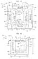
- FIGS. 1A-1Cillustrate an example implementation of a microelectronic package 100 according to an embodiment herein.
- a first microelectronic element 1 and a second microelectronic element 2are stacked face up above a substrate 102 such as a supporting dielectric element, e.g., a tape used in tape automated bonding (“TAB”).
- the substrate 102can consist essentially of a dielectric element having a coefficient of thermal expansion in a plane of the substrate of less than 10 parts per million per degree Centigrade in a plane of the substrate (“ppm/° C.”).
- the substrate 102can consist essentially of a dielectric element having a coefficient of thermal expansion in a plane of the substrate of between about 10 and about 20 ppm/° C. in a plane of the substrate.
- the dielectric element of the substrate 102can have first and second opposite surfaces 120 , 122 and a plurality of peripheral edges 130 , 132 , 134 , 136 extending between the first and second surfaces and defining a generally rectangular or square periphery of the substrate.
- the substrate 102can have oppositely-facing north and south peripheral edges 130 , 132 adjacent to oppositely-facing east and west peripheral edges 136 , 134 each extending between the north and south peripheral edges.
- north, south, east and westare merely used for convenience in describing the orientations and directions in the frame of reference of a particular microelectronic package and do not correspond to geographic directions.
- Each surface 120 , 122 of the substrate 102can have first and second dimensions in orthogonal directions D 1 , D 2 .
- each surface 120 , 122can have a first dimension L 1 extending between the west and east peripheral edges 134 , 136 in a first direction D 1
- each surfacecan have a second dimension L 2 extending between the north and south peripheral edges 130 , 132 in a second direction D 2 orthogonal to the first direction.
- Each microelectronic element 1 , 2can have a front face 105 extending parallel to the first surface 120 of the substrate 102 , a plurality of edges bounding the front face, and a plurality of element contacts 104 at the front face electrically coupled with terminals 124 of the substrate through contacts 106 of the substrate.
- the first and second microelectronic elements 1 , 2can be arranged in a stack on the same side of the substrate 102 .
- element contacts 104 at a front face 105 of each of the microelectronic elements 1 and 2are wire bonded to corresponding substrate contacts 106 at a first surface 120 of the substrate 102 .
- the wire bonds 101can extend above the front face 105 of each of the microelectronic elements 1 and 2 , the wire bonds being electrically coupled to the element contacts 104 of each of the microelectronic elements and the substrate contacts 106 .
- the first microelectronic element 1can have first and second opposite edges 111 , 113 of the front face 105 , and third and fourth opposite edges 191 , 193 of the front face each extending between the first and second edges.
- the second microelectronic element 2can have first and second opposite edges 115 , 117 of the front face 105 , and third and fourth opposite edges 195 , 197 of the front face each extending between the first and second edges.
- the microelectronic elements 1 and 2are placed in the stack in a configuration such that a rear face 107 of the first microelectronic element 1 opposite the front face 105 thereof can be disposed adjacent the first surface 120 of the substrate 102 .
- the rear face 107 of the second microelectronic element 2can overlie the front face 105 of the first microelectronic element 1 .
- the configuration of the stack of the microelectronic elements 1 and 2can be such that the second microelectronic element appears to be rotated 90 degrees in its horizontal plane relative to the first microelectronic element.
- each of the first and second edges 115 , 117 of the second microelectronic element 2are oriented at a perpendicular angle relative to the first and second edges 111 , 113 of the first microelectronic element 1 , respectively.
- edges of a microelectronic element that are oriented at a “perpendicular” angle to edges of another microelectronic elementmeans that the edges are perpendicular to one another within a typical manufacturing tolerance known to one skilled in the relevant art.
- each of the first and second edges 115 , 117 of the second microelectronic element 2can be oriented at an angle between 60 degrees and 120 degrees relative to the first and second edges 111 , 113 of the first microelectronic element 1 , respectively.
- the first and second microelectronic elements 1 , 2can be arranged in the stack such that the first edge 111 of the first microelectronic element 1 extends beyond the third edge 195 of the second microelectronic element 2 and the second edge 113 of the first microelectronic element extends beyond the fourth edge 197 of the second microelectronic element. Also, the first edge 115 of the second microelectronic element 2 can extend beyond the third edge 191 of the first microelectronic element 1 and the second edge 117 of the second microelectronic element can extend beyond the fourth edge 193 of the first microelectronic element.
- one or more adhesive layers 103can be disposed between the rear face 107 of the first microelectronic element 1 and the first surface 120 of the substrate 102 , and one or more adhesive layers can be disposed between confronting faces of the first and second microelectronic elements.
- the first microelectronic element 1can be electrically coupled with the substrate contacts 106 through element contacts 104 in at least first and second rows 110 and 112 .
- the first and second rows 110 , 112 of element contacts 104 of the first microelectronic element 1can extend along the front face 105 of the microelectronic element adjacent and parallel to first and second opposite edges 111 , 113 of the front face, respectively.
- the first and second edges 111 , 113 of the front face 105 of the first microelectronic element 1can be oriented towards the south and north edges 132 , 130 of the substrate 102 , respectively.
- an element contact being “adjacent” to an edge of a microelectronic elementmeans that the element contact is disposed within a distance of no more than one-third of a distance between the first and second edges of the microelectronic element.
- the first and second rows 110 , 112 of element contacts 104 of the first microelectronic elements 1can be wire bonded to corresponding ones of the substrate contacts 106 at the first surface 120 of the substrate 102 that lie between the south and north peripheral edges 132 , 130 of the substrate and the corresponding edges 111 , 113 of the front face 105 of the first microelectronic element 1 .
- Each of the microelectronic elements 1 and 2can have a memory storage array.
- the first row 110 of element contacts 104 of the first microelectronic element 1can be first contacts 141 configured to carry all of the data information usable by circuitry within the first microelectronic element, the data information including data signals.
- the second row 112 of element contacts 104 of the first microelectronic element 1can be second contacts 142 configured to carry information other than the data information that is carried by the first contacts 141 .
- the second contacts 142can be configured to carry all of the address information usable by circuitry within the first microelectronic element 1 to determine an addressable memory location from among all the available addressable memory locations of a memory storage array within the first microelectronic element. In a particular embodiment, one or more of the second contacts 142 can be configured to carry address information and information that controls an operating mode of the first microelectronic element 1 .
- the second contacts 142can be configured to carry all of a particular set of command signals and control signals transferred to the first microelectronic element 1 from an external component, wherein the command signals include row address strobe (RAS), column address strobe (CAS) and write enable (WE), and wherein the control signals include chip select (CS), clock enable (CKE), and on die termination (ODT).
- the clock signalscan be clocks used by the first microelectronic element 1 for sampling address signals.
- the first contacts 141can be at positions of at least one row 110 of contacts 104 adjacent to and parallel to the first edge 111 of first microelectronic element 1
- the second contacts 142can be at positions of at least one row 112 of contacts 104 adjacent to and parallel to the second edge 113 of the first microelectronic element.
- a “first contact”is a contact for transferring data at least one of: to or from an addressable storage location of a memory storage array provided in a microelectronic element.
- a “second contact”is a contact for transferring at least one of: address information to a microelectronic element to specify an addressable storage location of a memory storage array provided in the microelectronic element, command information (i.e., row address strobe (RAS), column address strobe (CAS) and write enable (WE)), or control information (i.e., chip select (CS), clock enable (CKE), and on die termination (ODT)).
- command informationi.e., row address strobe (RAS), column address strobe (CAS) and write enable (WE)
- control informationi.e., chip select (CS), clock enable (CKE), and on die termination (ODT)
- all of the first contacts 141can be disposed at positions within a first connection region 110 a adjacent to the first edge 111 of the first microelectronic element 1
- all of the second contacts 142can be disposed at positions within a second connection region 112 a adjacent to the second edge 113 of the first microelectronic element.
- the second microelectronic element 2can be electrically coupled with the substrate contacts 106 through element contacts 104 in at least first and second rows 114 and 116 .
- the first and second rows 114 , 116 of element contacts 104 of the second microelectronic element 2can extend along the front face 105 of the second microelectronic element adjacent and parallel to first and second opposite edges 115 , 117 of the front face, respectively.
- the first and second edges 115 , 117 of the front face 105 of the second microelectronic element 2can be oriented towards the east and west edges 136 , 134 of the substrate 102 , respectively.
- the first and second rows 114 , 116 of element contacts 104 of the second microelectronic element 2can be wire bonded to corresponding ones of the substrate contacts 106 at the first surface 120 of the substrate 102 that lie between the east and west peripheral edges 136 , 134 of the substrate and the corresponding edges 115 , 117 of the front face 105 of the second microelectronic element 2 .
- the first row 114 of element contacts 104 of the second microelectronic element 2can be first contacts 143 configured to carry all of the data information usable by circuitry within the second microelectronic element, the data information including data signals.
- the second row 116 of element contacts 104 of the second microelectronic element 2can be second contacts 144 configured to carry information other than the data information that is carried by the first contacts 143 .
- the second contacts 144can be configured to carry all of the address information usable by circuitry within the second microelectronic element 2 to determine an addressable memory location from among all the available addressable memory locations of a memory storage array within the second microelectronic element. In a particular embodiment, one or more of the second contacts 144 can be configured to carry address information and information that controls an operating mode of the second microelectronic element 2 .
- the second contacts 144can be configured to carry all of a particular set of command signals and control signals transferred to the second microelectronic element 2 from an external component, wherein the command signals include row address strobe (RAS), column address strobe (CAS) and write enable (WE), and wherein the control signals include chip select (CS), clock enable (CKE), and on die termination (ODT).
- the clock signalscan be clocks used by the second microelectronic element 2 for sampling address signals.
- the first contacts 143can be at positions of at least one row 114 of contacts 104 adjacent to and parallel to the first edge 115 of second microelectronic element 2
- the second contacts 144can be at positions of at least one row 118 of contacts 104 adjacent to and parallel to the second edge 117 of the second microelectronic element.
- all of the first contacts 143can be disposed at positions within a first connection region 114 a adjacent to the first edge 115 of the second microelectronic element 2
- all of the second contacts 144can be disposed at positions within a second connection region 116 a adjacent to the second edge 117 of the second microelectronic element.
- the microelectronic package 100can have terminals 124 at at least one of the first or second surfaces 120 , 122 of the substrate 102 electrically coupled with the first and second microelectronic elements 1 , 2 via the substrate contacts 106 .
- the terminals 124can include first terminals 125 configured to carry all of the data information usable by circuitry within the within the microelectronic package 100 , the data information including data signals.
- the terminals 124can also include second terminals 126 configured to carry information other than the data information that is carried by the first terminals 125 .
- the second terminals 126can configured to carry all of the address information usable by circuitry within the microelectronic package 100 to determine an addressable memory location from among all the available addressable memory locations of the memory storage arrays of the first and second microelectronic elements 1 , 2 .
- one or more of the second terminals 126can be configured to carry address information and information that controls an operating mode of at least one of the first microelectronic element 1 and the second microelectronic element 2 .
- the second terminals 126can be configured to carry all of a particular set of command signals and control signals transferred to the microelectronic package 100 from an external component, wherein the command signals include row address strobe (RAS), column address strobe (CAS) and write enable (WE), and wherein the control signals include chip select (CS), clock enable (CKE), and on die termination (ODT).
- the clock signalscan be clocks used by at least one of the first microelectronic element 1 and the second microelectronic element 2 for sampling address signals.
- data signals to and from the microelectronic package 100can be carried, for example, by DQ signals and data strobe signals DQS corresponding to the respective memory channels.
- DQ signals and data strobe signals DQScorresponding to the respective memory channels.
- a first subset 151 of first terminals 125 electrically coupled to the first microelectronic element 1 and carrying all of the DQ signals and DQ strobe signals for a first memory channel 131 (“DQ CH 0” in FIG. 1A )can be provided adjacent to the south peripheral edge 132 of the substrate 102
- first and second memory channels 131 and 133can be configured to be operated independently from one another.
- all of the first terminals 125 of the microelectronic package 100can be exposed adjacent to south and east peripheral edges 132 , 136 of the substrate 102 , such that the first terminals can be configured to carry all data signals to and from the microelectronic package.
- address informationi.e., information that is sufficient to specify an addressable memory location of a memory storage array within each microelectronic element, is disposed in second terminals 126 adjacent to the north and west peripheral edges 130 , 134 of the substrate 102 .
- the exemplary terminal bailout of terminals 124can be arranged in an area array arranged in rows and columns at at least one of the first or second surfaces 120 , 122 of the substrate 102 .
- Such address informationwhich may be grouped together with command information such as write enable, column address strobe and row address strobe, and with control information such as a clock used to sample the address information, chip select, and on die termination, collectively, “command address information”, can be received on second terminals 126 seen in FIG. 1A that appear, for example, in a first subset 152 of second terminals for a first memory channel 131 (“C/A CH 0” in FIG. 1A ) adjacent the north peripheral edge 130 of the substrate 102 , and that appear, for example, in a second subset 154 of second terminals for a second memory channel 133 (“C/A CH 1” in FIG. 1A ) adjacent the west peripheral edge 134 of the substrate. As seen in FIG. 1A , all of such address information can be input to the package at second terminals 126 that are disposed adjacent to north and west peripheral edges 130 , 134 of the substrate 102 .
- the second terminals 126can be configured to carry all of the address information usable by circuitry within the microelectronic package 100 to determine an addressable memory location from among all the available addressable memory locations of the memory storage arrays of the first and second microelectronic elements 1 , 2 .
- All of the second terminals 126need not be limited to only carrying address information, although they can be so limited in some embodiments.
- the second terminals 126can be configured to carry clock signals and all of the command signals, address signals, and bank address signals transferred to the microelectronic package 100 , the command signals being write enable, row address strobe, and column address strobe, and the clock signals being clocks used for sampling signals carrying the address information or time multiplexed versions thereof.
- the second terminals 126can be configured to carry all of the command signals transferred to the microelectronic package, the command signals being write enable, row address strobe, and column address strobe signals.
- the first microelectronic element 1which has its element contacts 104 oriented towards the south and north peripheral edges 132 , 130 of the substrate 102 , can be electrically coupled with terminals 124 adjacent the south and north peripheral edges. More specifically, the first subset 151 of first terminals 125 adjacent the south peripheral edge 132 can be electrically coupled with the first contacts 141 adjacent the first edge 111 of the first microelectronic element 1 . Also, the first subset 152 of second terminals 126 adjacent the north peripheral edge 130 can be electrically coupled with the second contacts 142 adjacent the second edge 113 of the first microelectronic element 1 .
- the first subset 152 of second terminals 126 adjacent the north peripheral edge 130can be configured to carry control information for the first microelectronic element 1
- the first subset 151 of first terminals 125 adjacent the south peripheral edge 132can be configured to transfer data signals in accordance with the control information for the first microelectronic element.
- the first subset 152 of second terminals 126 adjacent the north peripheral edge 130can be configured to carry address information for the first microelectronic element 1
- the first subset 151 of first terminals 125 adjacent the south peripheral edge 132can be configured to transfer data signals to memory storage array locations for the first microelectronic element specified by the address information.
- the second microelectronic element 2which has its element contacts 104 oriented towards the east and west peripheral edges 136 , 134 of the substrate 102 , can be electrically coupled with terminals 124 adjacent the east and west peripheral edges. More specifically, the second subset 153 of first terminals 125 adjacent the east peripheral edge 136 can be electrically coupled with the first contacts 143 adjacent the first edge 115 of the second microelectronic element 2 . Also, the second subset 154 of second terminals 126 adjacent the west peripheral edge 134 can be electrically coupled with the second contacts 144 adjacent the second edge 117 of the second microelectronic element 2 .
- the second subset 154 of second terminals 126 adjacent the west peripheral edge 134can be configured to carry control information for the second microelectronic element 2
- the second subset 153 of first terminals 125 adjacent the east peripheral edge 136can be configured to transfer data signals in accordance with the control information for the second microelectronic element.
- the second subset 154 of second terminals 126 adjacent the west peripheral edge 134can be configured to carry address information for the second microelectronic element 2
- the second subset 153 of first terminals 125 adjacent the east peripheral edge 136can be configured to transfer data signals to memory storage array locations for the second microelectronic element specified by the address information.
- the second terminals 126can be configured to operate the first microelectronic element 1 independently from the second microelectronic element 2 .
- the microelectronic package 100can permit the first microelectronic element 1 to be operated independently from the second microelectronic element 2 , such that data signals in accordance with the control information for the first microelectronic element 1 can be transferred at a time independent from the data signals in accordance with the control information for the second microelectronic element 2 .
- microelectronic packageshaving structures similar to that of the microelectronic package 100 of FIGS. 1A-1C can be found in the co-owned and co-pending patent application Ser. No. 14/075,020, filed Nov. 8, 2013, the disclosure of which is hereby incorporated herein by reference.
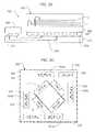
- FIGS. 2A and 2Billustrate an example implementation of a microelectronic package 200 according to an embodiment herein.
- the microelectronic package 200is a variation of the microelectronic package 100 shown in FIGS. 1A-1C .
- the microelectronic package 200is similar to the microelectronic package 100 , but the edges of the first and second microelectronic elements 1 , 2 are oriented at oblique angles with respect to the peripheral edges of the substrate.
- first subset 251 of first terminals 225i.e., data information terminals
- first subset 252 of second terminals 226i.e., command/address information terminals
- first microelectronic element 1disposed adjacent a first pair of adjacent peripheral edges of the substrate (south and west peripheral edges 232 , 234 )
- second subset 253 of first terminals and the second subset 254 of second terminals that are electrically coupled with the second microelectronic element 2are disposed adjacent a second pair of adjacent peripheral edges of the substrate (east and north peripheral edges 236 , 230 ).
- the first and second edges 111 , 113 of the first microelectronic element 1 and the first and second edges 115 , 117 of the second microelectronic element 2are oriented at oblique angles with respect to the peripheral edges 130 , 132 , 134 , 136 of the substrate 202 .
- each edge of the first and second microelectronic elements 1 , 2can be oriented at an oblique angle with respect to each of the peripheral edges 130 , 132 , 134 , 136 of the substrate 202 .
- an “oblique angle”is defined as an angle between 5 and 85 degrees.
- each edge of the first and second microelectronic elements 1 , 2can be oriented at an at an angle between 30 and 60 degrees with respect to each of the peripheral edges 130 , 132 , 134 , 136 of the substrate 202 .
- each edge of the first and second microelectronic elements 1 , 2can be oriented at an at an angle of approximately 45 degrees with respect to each of the peripheral edges 130 , 132 , 134 , 136 of the substrate 202 .
- a first subset 241 of the first terminals 225 that are electrically coupled with the first contacts 151 of the first microelectronic element 1is disposed adjacent the south peripheral edge 232 .
- a first subset 242 of the second terminals 226 that are electrically coupled with the second contacts 152 of the first microelectronic element 1are disposed adjacent the west peripheral edge 234 , the south and west peripheral edges being adjacent one another.
- a second subset 243 of the first terminals 225 that are electrically coupled with the first contacts 153 of the second microelectronic element 2is disposed adjacent the east peripheral edge 236 .
- a second subset 244 of the second terminals 226 that are electrically coupled with the second contacts 154 of the second microelectronic element 2are disposed adjacent the north peripheral edge 230 , the east and north peripheral edges being adjacent one another.
- FIG. 2Bshows the microelectronic assembly 200 of FIG. 2A in a microelectronic assembly 250 and its interconnections with a processor 260 , both the microelectronic packages and the processor mounted to a support structure such as a circuit panel 270 .
- the microelectronic package 250 and the processor 260can be mounted to a major surface 271 of the circuit panel 270 .
- the microelectronic assembly 250can also have a set of conductors on the circuit panel 270 configured to carry address information between the microelectronic package 200 and the processor 260 .
- the microelectronic package 200can have an encapsulant 290 at least partially covering the microelectronic elements 1 , 2 .
- the microelectronic package 200can have terminals 224 at the second surface 222 of the substrate 202 , the terminals being bonded with corresponding panel contacts 274 at the major surface 271 of the circuit panel 270 .
- the terminals 224 of the microelectronic package 200can include first terminals 225 configured to carry all of the data information usable by circuitry within the within the microelectronic package 200 , the data information including data signals.
- the terminals 224can also include second terminals 226 configured to carry information other than the data information that is carried by the first terminals 225 , such as address information, command information, and control information.
- the processor 260can be electrically coupled to the microelectronic package 200 through conductive elements 276 of the circuit panel 270 , the conductive elements including the panel contacts 274 .
- Rotating the edges of the first and second microelectronic elements 1 , 2 to form oblique angles with respect to the peripheral edges of the substrate, and having first terminals 225 and second terminals 226 coupled with a particular microelectronic element disposed at adjacent peripheral edges of the substratemay provide the microelectronic package of FIG. 2A with some advantages relative to the microelectronic package of FIGS. 1A-1C .
- the configuration of FIG. 2Acan permit additional space on the substrate for routing of traces extending between the substrate contacts and the corresponding terminals.
- the configuration of FIG. 2Acan permit the total electrical lead length between first contacts (e.g., data contacts) of a microelectronic element and the corresponding first terminals (e.g., data terminals) of the substrate to have a lower variation between the longest and shortest first contact/terminal pairs compared to the configuration of FIGS. 1A-1C .
- 2Acan also permit the total electrical lead length between second contacts (e.g., command/address information contacts) of a microelectronic element and the corresponding second terminals (e.g., command/address information terminals) of the substrate to have a lower variation between the longest and shortest second contact/terminal pairs compared to the configuration of FIGS. 1A-1C .
- second contactse.g., command/address information contacts
- second terminalse.g., command/address information terminals
- rotating the edges of the first and second microelectronic elements 1 , 2 to form oblique angles with respect to the peripheral edges of the substratecan permit the variation between the electrical lead length between the longest and shortest first contact/terminal pairs to be lower compared to the configuration of FIGS. 1A-1C .
- a difference in total electrical length between a shortest lead 255 and a longest lead 256 extending between the first subset of data terminals 251 and the data contacts 141 of the first microelectronic element 1can be less than 2% of an inverse of a frequency at which the first microelectronic element is configured to operate.
- a difference in total electrical length between a shortest lead 255 and a longest lead 256 extending between the first subset of data terminals 251 and the data contacts 141 of the first microelectronic element 1can be less than 1% of an inverse of a frequency at which the first microelectronic element is configured to operate
- the greater distance between some second terminals and each corresponding second contact coupled theretocan permit the variation between the electrical lead length between the longest and shortest second contact/terminal pairs to be lower compared to the configuration of FIGS. 1A-1C .
- a geometric distance between each second terminal 226 in the second subset 254 and each corresponding second contact 144 of the second microelectronic element 2 coupled theretocan be greater than 25% of a shortest dimension of the first and second dimensions L 1 , L 2 of the microelectronic package 200 .
- a geometric distance between each second terminal 226 in the second subset 254 and each corresponding second contact 144 of the second microelectronic element 2 coupled theretocan be greater than 40% of a shortest dimension of the first and second dimensions L 1 , L 2 of the microelectronic package 200 .
- the smaller difference between data or address information electrical connections within a particular subset of data contacts/terminals or address information contacts/terminals within the microelectronic package 200can reduce inductance, and loading from the microelectronic package back onto a command address bus on a circuit panel (e.g., 2 B). By reducing these parameters on the command address bus, signals can be received at the microelectronic package 200 at higher speeds than otherwise possible. Accordingly, the package arrangement shown can provide a particular performance advantage, for example, when used with LPDDRx-type microelectronic elements.
- FIG. 2Cillustrates an example implementation of a microelectronic package 300 according to an embodiment herein.
- the microelectronic package 300is a variation of the microelectronic package 200 shown in FIGS. 2A and 2B .
- the microelectronic package 300is similar to the microelectronic package 200 , but a first subset 351 of first terminals 325 (i.e., data information terminals) that are electrically coupled with the first microelectronic element 1 are split into first and second groups 351 a , 351 b disposed adjacent a first pair of adjacent peripheral edges of the substrate 302 (south and west peripheral edges 332 , 334 , respectively), and a second subset 353 of first terminals that are electrically coupled with the second microelectronic element 2 are split into first and second groups 353 a , 353 b disposed adjacent a second pair of adjacent peripheral edges of the substrate (north and east peripheral edges 330 , 336 , respectively).
- FIGS. 2D and 2Eillustrate an example implementation of a microelectronic package 400 according to an embodiment herein.
- the microelectronic package 400is a variation of the microelectronic package 300 shown in FIG. 2C .
- the microelectronic package 400is similar to the microelectronic package 300 , but as shown in FIG. 2D , a first subset 452 of second terminals 426 (e.g., command/address information terminals) that are electrically coupled with the first microelectronic element 1 are disposed in a region adjacent both of a first pair of adjacent peripheral edges of the substrate 402 (south and east peripheral edges 432 , 436 ), and as shown in FIG.
- second terminals 426e.g., command/address information terminals
- a second subset 454 of second terminals that are electrically coupled with the second microelectronic element 2are disposed in a region adjacent a second pair of adjacent peripheral edges of the substrate (north and west peripheral edges 430 , 434 , respectively).
- the microelectronic package 400has first and second subsets 451 , 453 of first terminals 425 (i.e., data information terminals) that are electrically coupled with the first and second microelectronic elements 1 , 2 , respectively.
- the first subset 451 of first terminals 425are split into first and second groups 451 a , 451 b disposed adjacent the south and east peripheral edges 432 , 436 , respectively.
- the second subset 453 of first terminals 425are split into first and second groups 453 a , 453 b disposed adjacent the north and west peripheral edges 430 , 434 , respectively.
- FIGS. 2 C and 2 D/ 2 Ecan have many of the same advantages described above with respect to the embodiment of FIGS. 2A and 2B .
- Rotating the edges of the first and second microelectronic elements 1 , 2 to form oblique angles with respect to the peripheral edges of the substrate, and splitting each subset of first terminals into groups disposed against adjacent pairs of peripheral edges of the substratecan permit additional space on the substrate for routing of traces extending between the substrate contacts and the corresponding terminals.
- Such features of the embodiments of FIGS. 2 C and 2 D/ 2 Ecan also permit the total electrical lead length between a particular group of first or second terminals ( 451 a , 451 b , 452 , 453 a , 453 b , 454 ) and the corresponding first or second contacts of a microelectronic element to have a lower variation between the longest and shortest contact/terminal pairs compared to the configuration of FIGS. 1A-1C .
- a difference in total electrical length between a shortest lead 491 a and a longest lead 491 b extending between the first group 451 a of the first subset of first terminals and corresponding ones of the first contacts 141 of the first microelectronic element 1can be less than 2% of an inverse of a frequency at which the first microelectronic element is configured to operate.
- a difference in total electrical length between a shortest lead 492 a and a longest lead 492 b extending between the second group 451 b of the first subset of first terminals and corresponding ones of the first contacts 141 of the first microelectronic element 1can be less than 2% of an inverse of a frequency at which the first microelectronic element is configured to operate.
- a difference in total electrical length between a shortest lead 493 a and a longest lead 493 b extending between the first subset of second terminals 452 and corresponding ones of the second contacts 142 of the first microelectronic element 1can be less than 2% of an inverse of a frequency at which the first microelectronic element is configured to operate.
- a difference in total electrical length between a shortest lead 494 a and a longest lead 494 b extending between the first group 453 a of the second subset of first terminals and corresponding ones of the first contacts 143 of the second microelectronic element 2can be less than 2% of an inverse of a frequency at which the second microelectronic element is configured to operate.
- a difference in total electrical length between a shortest lead 495 a and a longest lead 495 b extending between the second group 453 b of the second subset of first terminals and corresponding ones of the first contacts 143 of the second microelectronic element 2can be less than 2% of an inverse of a frequency at which the second microelectronic element is configured to operate.
- a difference in total electrical length between a shortest lead 496 a and a longest lead 496 b extending between the second subset of second terminals 454 and corresponding ones of the second contacts 144 of the second microelectronic element 2can be less than 2% of an inverse of a frequency at which the second microelectronic element is configured to operate.
- the traces that form portions of the leads connecting the first or second terminals of the substrate and the corresponding first or second contacts of the microelectronic elementscan be disposed in as few as two substrate routing layers.
- the tracesincluding leads 491 a , 491 b , 492 a , 492 b , 494 a , 494 b , 495 a , and 495 b ) shown in solid lines extending between first terminals and corresponding first contacts can be disposed in a first substrate routing layer
- the traces (including leads 493 a , 493 b , 496 a , and 496 b ) shown in dashed lines extending between second terminals and corresponding second contactscan be disposed in a second substrate routing layer.
- microelectronic packages 200 , 300 , and 400 shown in FIGS. 2A-2Eare each shown having two microelectronic elements 1 , 2 , in other embodiments, the microelectronic packages 200 , 300 , and 400 may have only a single microelectronic element, such a single microelectronic element having each of its edges oriented at an oblique angle with respect to the peripheral edges of the substrate.
- the address information terminals of the microelectronic packagecan be configured to carry address information usable by circuitry within the microelectronic package to determine an addressable memory location from among all the available addressable memory locations of a memory storage array of the single microelectronic element therein.
- FIGS. 3A-3Eillustrate an example implementation of a microelectronic package 500 according to an embodiment herein.
- the microelectronic package 500is a variation of the microelectronic package 200 shown in FIGS. 2A and 2B .
- the microelectronic package 500is similar to the microelectronic package 200 , but as shown in FIGS. 3A-3D , element contacts of first, second, third, and fourth microelectronic elements 1 , 2 , 3 , 4 are electrically coupled with corresponding subsets of substrate terminals at the west, north, east, and south peripheral edges 534 , 530 , 536 , 532 , respectively.
- a first subset 551 of first terminals 525 that are electrically coupled with first contacts 141 of the first microelectronic element 1 , and a first subset 552 of second terminals 526 that are electrically coupled with second contacts 142 of the first microelectronic elementare disposed in respective regions adjacent the west peripheral edge 534 .
- a second subset 553 of first terminals 525 that are electrically coupled with first contacts 143 of the second microelectronic element 2 , and a second subset 554 of second terminals 526 that are electrically coupled with second contacts 144 of the second microelectronic elementare disposed in respective regions adjacent the north peripheral edge 530 .
- a third subset 555 of first terminals 525 that are electrically coupled with first contacts 145 of the third microelectronic element 3 , and a third subset 556 of second terminals 526 that are electrically coupled with second contacts 146 of the third microelectronic elementare disposed in respective regions adjacent the east peripheral edge 536 .
- a fourth subset 557 of first terminals 525 that are electrically coupled with first contacts 147 of the fourth microelectronic element 4and a fourth subset 558 of second terminals 526 that are electrically coupled with second contacts 148 of the fourth microelectronic element are disposed in respective regions adjacent the south peripheral edge 532 .
- each microelectronic element 1 , 2 , 3 , 4can have a front face 105 extending parallel to the first surface 520 of the substrate 502 , a plurality of edges bounding the front face, and a plurality of element contacts 104 at the front face electrically coupled with terminals 524 of the substrate through contacts of the substrate 506 .
- the microelectronic elements 1 , 2 , 3 , 4can be arranged in a stack on the same side of the substrate 502 . As shown in FIG.
- element contacts 104 at a front face 105 of each of the microelectronic elements 1 , 2 , 3 , 4are wire bonded to corresponding substrate contacts at the first surface 520 of the substrate 502 .
- the wire bondscan extend above the front face 105 of each of the microelectronic elements 1 , 2 , 3 , 4 , the wire bonds being electrically coupled to the element contacts 104 of each of the microelectronic elements and the substrate contacts 506 .
- the microelectronic elements 1 , 2 , 3 , 4are placed in the stack in an interleaved configuration such that the odd-numbered microelectronic elements (i.e., 1 , 3 ) are spaced by or alternatingly interleaved in a single stacked arrangement with the even-numbered microelectronic elements (i.e., 2 , 4 ).
- the microelectronic elements 1 , 2 , 3 , 4are placed in the stack in a configuration such that a rear face 107 of the first microelectronic element 1 opposite the front face 105 thereof can be disposed adjacent the first surface 520 of the substrate 502 .
- the rear face 107 of the second microelectronic element 2can overlie the front face 105 of the first microelectronic element 1 .
- the rear face 107 of the third microelectronic element 3can overlie the front face 105 of the second microelectronic element 2
- the rear face 107 of the fourth microelectronic element 4can overlie the front face 105 of the third microelectronic element.
- the microelectronic elements 1 , 2 , 3 , 4are placed in the stack in a configuration such that the even-numbered microelectronic elements appear to be rotated 90 degrees in their horizontal planes relative to the odd-numbered microelectronic elements. As shown in FIGS. 3A-3D , each of the first and second edges 115 , 117 of the second and fourth microelectronic elements 2 , 4 are oriented at a perpendicular angle relative to the first and second edges 111 , 113 of the first and third microelectronic elements 1 , respectively.
- each of the first and second edges 115 , 117 of the second and fourth microelectronic elements 2can be oriented at an angle between 60 degrees and 120 degrees relative to the first and second edges 111 , 113 of the first and third microelectronic elements 1 , 3 , respectively.
- Data signals to and from the microelectronic package 500can be carried, for example, by DQ signals and data strobe signals DQS corresponding to the respective memory channels.
- DQ signals and data strobe signals DQScorresponding to the respective memory channels.
- the first subset 551 of first terminals 525 electrically coupled to the first microelectronic element 1 and carrying all of the DQ signals and DQ strobe signals for a first memory channel 531 (“DQ CH 0” in FIG. 3A )can be provided adjacent to the west peripheral edge 534 of the substrate 502 .
- the second subset 553 of first terminals 525 electrically coupled to the second microelectronic element 2 and carrying all of the DQ signals and DQ strobe signals for a second memory channel 533 (“DQ CH 1” in FIG. 3B )can be provided adjacent to the north peripheral edge 530 of the substrate 502 .
- the third subset 555 of first terminals 525 electrically coupled to the third microelectronic element 3 and carrying all of the DQ signals and DQ strobe signals for a third memory channel 535 (“DQ CH 0” in FIG. 3A )can be provided adjacent to the east peripheral edge 536 of the substrate 502 .
- the fourth subset 557 of first terminals 525 electrically coupled to the fourth microelectronic element 4 and carrying all of the DQ signals and DQ strobe signals for a fourth memory channel 537 (“DQ CH 0” in FIG. 3A )can be provided adjacent to the south peripheral edge 532 of the substrate 502 .
- Each of the first, second, third, and fourth memory channels 531 , 533 , 535 , 537can be configured to be operated independently from one another.
- FIG. 3Eshows the microelectronic assembly 500 of FIGS. 3A-3D in a microelectronic assembly 550 and its interconnections with a processor 560 , both the microelectronic packages and the processor mounted to a support structure such as a circuit panel 570 .
- the microelectronic package 550 and the processor 560can be mounted to a major surface 571 of the circuit panel 570 .
- the microelectronic assembly 550can also have a set of conductors on the circuit panel 570 configured to carry address information between the microelectronic package 500 and the processor 560 .
- the microelectronic package 500can have an encapsulant 590 at least partially covering the microelectronic elements 1 , 2 , 3 , 4 .
- the microelectronic package 500can have terminals 524 at the second surface 522 of the substrate 502 , the terminals being bonded with corresponding panel contacts 574 at the major surface 571 of the circuit panel 570 .
- the terminals 524 of the microelectronic package 500can include first terminals 525 configured to carry all of the data information usable by circuitry within the within the microelectronic package 500 , the data information including data signals.
- the terminals 524can also include second terminals 526 configured to carry information other than the data information that is carried by the first terminals 525 , such as address information, command information, and control information.
- the processor 560can be electrically coupled to the microelectronic package 500 through conductive elements 576 of the circuit panel 570 , the conductive elements including the panel contacts 574 .
- FIGS. 3A-3Ecan have many of the same advantages described above with respect to the embodiments of FIGS. 2A-2E .
- Rotating the edges of the microelectronic elements 1 , 2 , 3 , 4 to form oblique angles with respect to the peripheral edges of the substrate, and disposing each subset of data terminals and address terminals electrically coupled to a particular microelectronic element adjacent a corresponding one of the peripheral edges of the substratecan permit additional space on the substrate for routing of traces extending between the substrate contacts and the corresponding terminals.
- FIGS. 3A-3Ecan also permit the total electrical lead length between a particular group of first or second terminals and the corresponding first or second contacts of a microelectronic element to have a lower variation between the longest and shortest contact/terminal pairs compared to the configuration of FIGS. 1A-1C .
- the traces that form portions of the leads connecting the first or second terminals of the substrate and the corresponding first or second contacts of the microelectronic elementscan be disposed in as few as two substrate routing layers.
- the traces shown in solid lines extending between first terminals and corresponding first contactscan be disposed in a first substrate routing layer
- the traces shown in dashed lines extending between second terminals and corresponding second contactscan be disposed in a second substrate routing layer.
- FIG. 4Ashows the microelectronic assembly 600 a , which is a possible interconnection arrangement of the microelectronic package 100 of FIGS. 1A-1C in a system and its interconnections with a processor 660 .
- the first subset 151 of first terminalsi.e., data information terminals
- the first subset 152 of second terminalse.g., address information terminals
- the second subset 153 of first terminalsare positioned at the east peripheral edge of the substrate opposite the second subset 154 of second terminals at the west peripheral edge.
- leads 691 extending between the first subset 152 of second terminals of the microelectronic package 100 and a first subset 661 of second terminals (e.g., address information terminals) of a processor 660are much longer than leads 692 extending between the second subset 154 of second terminals of the microelectronic package and a corresponding second subset 662 of second terminals of the processor.
- FIG. 4Bshows the microelectronic assembly 600 b , which is a possible interconnection arrangement of the microelectronic package 200 of FIGS. 2A and 2B in a system and its interconnections with a processor 660 .
- the first subset 251 of first terminalsare positioned at the south peripheral edge of the substrate adjacent the first subset 252 of second terminals at the west peripheral edge, and the second subset 253 of first terminals are positioned at the east peripheral edge of the substrate adjacent the second subset 254 of second terminals at the north peripheral edge.
- the leads 693 extending between the first subset 252 of second terminals of the microelectronic package 200 and the first subset 661 of second terminals of the processor 660are much closer in length (compared to FIG. 4A ) to the leads 694 extending between the second subset 254 of second terminals of the microelectronic package and the corresponding second subset 662 of second terminals of the processor.
- the shorter address information electrical connections between the microelectronic package 200 and the processor 660can reduce signal propagation time, inductance, and loading from the microelectronic package back onto a command address bus on a circuit panel (e.g., FIG. 2B ). By reducing these parameters on the command address bus, signals can be received at the microelectronic package 200 at higher speeds than otherwise possible. Accordingly, the package arrangement shown provides a particular performance advantage when used with LPDDRx-type microelectronic elements.
- FIG. 5Ashows the microelectronic assembly 700 a , which is a possible interconnection arrangement of the microelectronic package 100 of FIGS. 1A-1C in another system and its interconnections with another processor 760 .
- the first and second terminalsare positioned in the same locations as the first and second terminals in the microelectronic package 100 shown in FIG. 4A .
- leads 791 extending between the first subset 152 of second terminals of the microelectronic package 100 and a first subset 761 of second terminals (e.g., address information terminals) of a processor 760are much longer than leads 792 extending between the second subset 154 of second terminals of the microelectronic package and a corresponding second subset 762 of second terminals of the processor.
- Leads 793 extending between the first and second subsets of first terminals 151 , 153 and corresponding first terminals (i.e., data information terminals) of the processor 760are relatively compressed toward the south edge 132 of the microelectronic package 100 and the south edge 765 of the processor 760 .
- FIG. 5Bshows the microelectronic assembly 700 b , which is a possible interconnection arrangement of the microelectronic package 300 of FIG. 2C in a system and its interconnections with a processor 760 .
- the first and second groups 351 a , 351 b of the first subset of first terminalsare positioned at the south and west peripheral edges of the substrate adjacent the first subset 352 of second terminals at the south peripheral edge, and the first and second groups 353 a , 353 b of the second subset of first terminals are positioned at the north and east peripheral edges of the substrate adjacent the second subset 354 of second terminals at the north peripheral edge.
- the leads 794 extending between the first subset 352 of second terminals of the microelectronic package 300 and the first subset 761 of second terminals (e.g., address information terminals) of the processor 760are much closer in length (compared to FIG. 5A ) to the leads 795 extending between the second subset 354 of second terminals of the microelectronic package and the corresponding second subset 762 of second terminals of the processor.
- leads 796 extending between the first and second subsets of first terminals 351 , 353 and corresponding first terminals (i.e., data information terminals) of the processor 760are more spread out (compared to FIG. 5A ) between the north and south edges 130 , 132 of the microelectronic package 100 and the north and south edges 765 , 766 of the processor.
- the shorter address information electrical connections between the microelectronic package 300 and the processor 760can produce similar benefits as described above with reference to FIG. 4B .
- the additional space for routing of leads 794 , 795 , and 796may permit the microelectronic assembly 700 b to have a fewer number of routing layers in a circuit panel to which the microelectronic package 300 and the processor 760 can be mounted, or it may permit the leads 794 , 795 , and 796 to be shorter in length (compared to FIG. 5A ).
- FIG. 6further illustrates a common arrangement of element contacts 104 at the front face 105 of an LPDDRx-type microelectronic element (e.g., contact pads provided at the front face of a memory microelectronic element in accordance with LPDDRx) that can be used in the microelectronic packages of FIGS. 1A-3E .
- This arrangement of element contacts 104shows the second contacts (e.g., address, command, control information contacts) in a first column 110 or 114 adjacent one edge of the microelectronic element, and the first contacts (i.e., data information contacts) in a second column 112 or 116 adjacent an opposite edge of the microelectronic element.
- DDRx microelectronic elementstypically have central chip contacts 104 a as originally provided in which the chip contacts extend in one or two rows along or adjacent to a central ‘axis’ of the microelectronic element.
- a redistribution layercan be provided or formed on the chip that redistributes the contacts from the central spine to opposite edges, thereby providing element contacts 104 b for carrying address information or command/control/address information in a first column 110 or 114 adjacent one edge of the microelectronic element, and element contacts for carrying data signals in a second column 112 or 116 adjacent an opposite edge of the microelectronic element.
- FIG. 8further illustrates that for some DDRx chips, for example, DDR3 or DDR4 chips (which can be used in the microelectronic packages of FIGS. 1A-3E ), the redistribution can be made in the manner shown in which the original central chip contacts 104 a are in the middle and the element contacts 104 b for carrying address information or command/control/address information in a first column 110 or 114 adjacent one edge of the microelectronic element, and the element contacts for carrying data signals in a second column 112 or 116 adjacent an opposite edge of the microelectronic element, the first and second columns of element contacts extending along the edges parallel to the central axis of the original central chip contacts as shown.
- DDR3 or DDR4 chipswhich can be used in the microelectronic packages of FIGS. 1A-3E
- FIG. 9is a schematic diagram illustrating a possible interconnection arrangement of an upper microelectronic package 500 ( FIGS. 3A-3E ) stacked with a lower microelectronic package 500 b in a microelectronic assembly 550 a and its interconnections with a processor 560 , both the microelectronic packages and the processor mounted to a support structure such as a circuit panel 570 .
- the lower microelectronic package 500 b and the processor 560can be mounted to a major surface 571 of the circuit panel 570
- the upper microelectronic package 500can be mounted to the lower microelectronic package.
- the microelectronic assembly 550 acan also have a set of conductors on the support structure 570 configured to carry the address information between the microelectronic packages and the processor 560 .
- the lower microelectronic package 500 bcan have terminals 524 (bottom terminals) at the second surface 522 of the substrate 502 .
- the lower microelectronic packagecan have an encapsulant 590 at least partially covering the microelectronic elements.
- top terminals 527 at a top surface 591 of the encapsulantcan be electrically coupled with the microelectronic elements of the lower microelectronic package via the substrate contacts 506 .
- the lower microelectronic package 500 bcan have top terminals that are exposed at a surface of the substrate 502 , or other locations.
- the terminals 524 of the upper microelectronic package 500can be joined to the top terminals 527 of the lower microelectronic package 500 b .
- the upper microelectronic package 500may take the form of the lower microelectronic package 500 b (with both top and bottom terminals), such that the upper and lower microelectronic packages are identical except for the location of chip select terminals.
- the terminals 524 of each of the upper and lower microelectronic packages 500 , 500 bcan include first terminals configured to carry all of the data information usable by circuitry within the within the respective microelectronic package, the data information including data signals.
- the circuit panel 570 of the microelectronic assembly 550 acan have a set of conductors configured to carry 64 bits of the data information between the microelectronic packages 500 , 500 b and the processor 560 , where the first terminals of the upper microelectronic package are configured to transfer 32 bits per clock cycle to the set of conductors, and the first terminals of the lower microelectronic package are configured to transfer 32 bits per clock cycle to the set of conductors.
- FIGS. 10A and 10Billustrates an example implementation of a microelectronic package 800 according to an embodiment herein.
- the microelectronic package 800is a variation of the microelectronic package 300 shown in FIGS. 3A-3E .
- the microelectronic package 800is similar to the microelectronic package 300 , but element contacts of first, second, third, and fourth microelectronic elements 1 , 2 , 3 , 4 are electrically coupled with corresponding subsets of substrate terminals at the west, north, east, and south peripheral edges 834 , 830 , 836 , 832 , respectively, and element contacts of fifth, sixth, seventh, and eighth microelectronic elements 5 , 6 , 7 , and 8 are electrically coupled with the same corresponding subsets of substrate terminals at the west, north, east, and south peripheral edges 834 , 830 , 836 , 832 , respectively, with the exception of the terminals configured to receive control information, i.e., chip
- first and fifth microelectronic elements 1 and 5are both electrically coupled with the same corresponding subsets of first and second substrate terminals at the west peripheral edge 834
- the second and sixth microelectronic elements 2 and 6are both electrically coupled with the same corresponding subsets of first and second substrate terminals at the north peripheral edge 830
- the third and seventh microelectronic elements 3 and 7are both electrically coupled with the same corresponding subsets of first and second substrate terminals at the east peripheral edge 836
- the fourth and eighth microelectronic elements 4 and 8are both electrically coupled with the same corresponding subsets of first and second substrate terminals at the south peripheral edge 832 .
- each pair of microelectronic elements that are electrically coupled with a common set of first and second substrate terminalsare connected to separate control information terminals (i.e., CS, CKE, ODT), which are configured to select which one of the pair of microelectronic elements will receive a particular data, address, or command information signal, for example.
- CScontrol information terminal
- CKECKE
- ODTODT
- the package 800can be configured to have two channels and two ranks of memory storage.
- the microelectronic elements 1 - 8is configured to receive 32 bits of data information twice per clock cycle (e.g., LPDDRx)
- microelectronic elements 1 and 2can comprise a first 64-bit memory channel in a first rank
- microelectronic elements 3 and 4can together comprise a second 64-bit memory channel in the first rank
- microelectronic elements 5 and 6can comprise a first 64-bit memory channel in a second rank
- microelectronic elements 7 and 8can comprise a second 64-bit memory channel in the second rank.
- microelectronic packages and microelectronic assemblies described above with reference to FIGS. 1A through 10 abovecan be utilized in construction of diverse electronic systems, such as the system 900 shown in FIG. 11 .
- the system 900 in accordance with a further embodiment of the inventionincludes a plurality of modules or components 906 such as the microelectronic packages or microelectronic assemblies as described above, in conjunction with other electronic components 908 , 910 and 911 .
- the systemcan include a circuit panel, motherboard, or riser panel 902 such as a flexible printed circuit board, and the circuit panel can include numerous conductors 904 , of which only one is depicted in FIG. 11 , interconnecting the modules or components 906 , 908 , 910 with one another.
- a circuit panel 902can transport signals to and from each of the microelectronic packages and/or microelectronic assemblies included in the system 900 .
- thisis merely exemplary; any suitable structure for making electrical connections between the modules or components 906 can be used.
- the system 900can also include a processor such as the semiconductor chip 908 , such that each module or component 906 can be configured to transfer a number N of data bits in parallel in a clock cycle, and the processor can be configured to transfer a number M of data bits in parallel in a clock cycle, M being greater than or equal to N.
- a processorsuch as the semiconductor chip 908 , such that each module or component 906 can be configured to transfer a number N of data bits in parallel in a clock cycle, and the processor can be configured to transfer a number M of data bits in parallel in a clock cycle, M being greater than or equal to N.
- the component 908is a semiconductor chip and component 910 is a display screen, but any other components can be used in the system 900 .
- the system 900can include any number of such components.
- Modules or components 906 and components 908 and 911can be mounted in a common housing 901 , schematically depicted in broken lines, and can be electrically interconnected with one another as necessary to form the desired circuit.
- the housing 901is depicted as a portable housing of the type usable, for example, in a cellular telephone or personal digital assistant, and screen 910 can be exposed at the surface of the housing.
- a structure 906includes a light-sensitive element such as an imaging chip
- a lens 911 or other optical devicealso can be provided for routing light to the structure.
- the simplified system shown in FIG. 11is merely exemplary; other systems, including systems commonly regarded as fixed structures, such as desktop computers, routers and the like can be made using the structures discussed above.
Landscapes
- Engineering & Computer Science (AREA)
- Microelectronics & Electronic Packaging (AREA)
- Power Engineering (AREA)
- Computer Hardware Design (AREA)
- Physics & Mathematics (AREA)
- Condensed Matter Physics & Semiconductors (AREA)
- General Physics & Mathematics (AREA)
- Semiconductor Memories (AREA)
Abstract
Description
Claims (23)
Priority Applications (3)
| Application Number | Priority Date | Filing Date | Title |
|---|---|---|---|
| US14/448,040US9281296B2 (en) | 2014-07-31 | 2014-07-31 | Die stacking techniques in BGA memory package for small footprint CPU and memory motherboard design |
| TW104124627ATWI591773B (en) | 2014-07-31 | 2015-07-29 | Die stacking techniques in bga memory package for small footprint cpu and memory motherboard design |
| PCT/US2015/042726WO2016019056A1 (en) | 2014-07-31 | 2015-07-29 | Die stacking techniques in bga memory package for small footprint cpu and memory motherboard design |
Applications Claiming Priority (1)
| Application Number | Priority Date | Filing Date | Title |
|---|---|---|---|
| US14/448,040US9281296B2 (en) | 2014-07-31 | 2014-07-31 | Die stacking techniques in BGA memory package for small footprint CPU and memory motherboard design |
Publications (2)
| Publication Number | Publication Date |
|---|---|
| US20160035703A1 US20160035703A1 (en) | 2016-02-04 |
| US9281296B2true US9281296B2 (en) | 2016-03-08 |
Family
ID=53794531
Family Applications (1)
| Application Number | Title | Priority Date | Filing Date |
|---|---|---|---|
| US14/448,040ActiveUS9281296B2 (en) | 2014-07-31 | 2014-07-31 | Die stacking techniques in BGA memory package for small footprint CPU and memory motherboard design |
Country Status (3)
| Country | Link |
|---|---|
| US (1) | US9281296B2 (en) |
| TW (1) | TWI591773B (en) |
| WO (1) | WO2016019056A1 (en) |
Cited By (1)
| Publication number | Priority date | Publication date | Assignee | Title |
|---|---|---|---|---|
| US9928883B2 (en) | 2016-05-06 | 2018-03-27 | Invensas Corporation | TFD I/O partition for high-speed, high-density applications |
Families Citing this family (8)
| Publication number | Priority date | Publication date | Assignee | Title |
|---|---|---|---|---|
| US8653646B2 (en) | 2011-10-03 | 2014-02-18 | Invensas Corporation | Stub minimization using duplicate sets of terminals for wirebond assemblies without windows |
| US8405207B1 (en) | 2011-10-03 | 2013-03-26 | Invensas Corporation | Stub minimization for wirebond assemblies without windows |
| US9780782B2 (en) | 2014-07-23 | 2017-10-03 | Intel Corporation | On-die termination control without a dedicated pin in a multi-rank system |
| US9691437B2 (en) | 2014-09-25 | 2017-06-27 | Invensas Corporation | Compact microelectronic assembly having reduced spacing between controller and memory packages |
| US9484080B1 (en) | 2015-11-09 | 2016-11-01 | Invensas Corporation | High-bandwidth memory application with controlled impedance loading |
| EP3301717A1 (en)* | 2016-09-29 | 2018-04-04 | Siemens Aktiengesellschaft | Power module and device |
| KR102371893B1 (en)* | 2017-05-18 | 2022-03-08 | 삼성전자주식회사 | Semiconductor memory chip, semiconductor memory package, and electronic system using the same |
| US11222850B2 (en) | 2019-05-15 | 2022-01-11 | Mediatek Inc. | Electronic package with rotated semiconductor die |
Citations (223)
| Publication number | Priority date | Publication date | Assignee | Title |
|---|---|---|---|---|
| US3670208A (en) | 1970-07-13 | 1972-06-13 | Logic Dynamics Inc | Microelectronic package, buss strip and printed circuit base assembly |
| US4747081A (en) | 1983-12-30 | 1988-05-24 | Texas Instruments Incorporated | Video display system using memory with parallel and serial access employing serial shift registers selected by column address |
| JPS641257A (en) | 1987-06-23 | 1989-01-05 | Fujitsu Ltd | Semiconductor device |
| US5148265A (en) | 1990-09-24 | 1992-09-15 | Ist Associates, Inc. | Semiconductor chip assemblies with fan-in leads |
| US5148266A (en) | 1990-09-24 | 1992-09-15 | Ist Associates, Inc. | Semiconductor chip assemblies having interposer and flexible lead |
| US5163024A (en) | 1983-12-30 | 1992-11-10 | Texas Instruments Incorporated | Video display system using memory with parallel and serial access employing serial shift registers selected by column address |
| US5210639A (en) | 1983-12-30 | 1993-05-11 | Texas Instruments, Inc. | Dual-port memory with inhibited random access during transfer cycles with serial access |
| US5480840A (en) | 1992-07-14 | 1996-01-02 | At&T Global Information Solutions Company | Multi-chip module with multiple compartments |
| TW312044B (en) | 1996-02-23 | 1997-08-01 | Mitsubishi Electric Corp | The semiconductor package |
| US5679977A (en) | 1990-09-24 | 1997-10-21 | Tessera, Inc. | Semiconductor chip assemblies, methods of making same and components for same |
| US5691570A (en) | 1993-09-29 | 1997-11-25 | Kabushiki Kaisha Toshiba | Integrated circuits having patterns of mirror images and packages incorporating the same |
| US5751553A (en) | 1992-09-16 | 1998-05-12 | Clayton; James E. | Thin multichip module including a connector frame socket having first and second apertures |
| US5777391A (en) | 1994-12-20 | 1998-07-07 | Hitachi, Ltd. | Semiconductor device having an improved connection arrangement between a semiconductor pellet and base substrate electrodes and a method of manufacture thereof |
| US5821614A (en) | 1994-05-06 | 1998-10-13 | Seiko Epson Corporation | Card type semiconductor device |
| US5899705A (en) | 1997-11-20 | 1999-05-04 | Akram; Salman | Stacked leads-over chip multi-chip module |
| US5929517A (en) | 1994-12-29 | 1999-07-27 | Tessera, Inc. | Compliant integrated circuit package and method of fabricating the same |
| US5949700A (en) | 1998-05-26 | 1999-09-07 | International Business Machines Corporation | Five square vertical dynamic random access memory cell |
| US5973403A (en) | 1996-11-20 | 1999-10-26 | Micron Technology, Inc. | Device and method for stacking wire-bonded integrated circuit dice on flip-chip bonded integrated circuit dice |
| US6086386A (en) | 1996-05-24 | 2000-07-11 | Tessera, Inc. | Flexible connectors for microelectronic elements |
| US6130116A (en) | 1996-12-13 | 2000-10-10 | Tessera, Inc. | Method of encapsulating a microelectronic assembly utilizing a barrier |
| US6159837A (en) | 1998-07-16 | 2000-12-12 | Kabushiki Kaisha Toshiba | Manufacturing method of semiconductor device |
| KR20010002214A (en) | 1999-06-12 | 2001-01-05 | 마이클 디. 오브라이언 | A semiconductor packages and manufacturing method for it |
| US6177636B1 (en) | 1994-12-29 | 2001-01-23 | Tessera, Inc. | Connection components with posts |
| US6197665B1 (en) | 1998-04-15 | 2001-03-06 | Tessera, Inc. | Lamination machine and method to laminate a coverlay to a microelectronic package |
| TW428258B (en) | 1998-11-10 | 2001-04-01 | Nippon Electric Co | Semiconductor device with connection terminals in the form of a grid array |
| TW429561B (en) | 1999-05-31 | 2001-04-11 | Mitsubishi Electric Corp | Semiconductor package |
| US20010002727A1 (en) | 1997-09-16 | 2001-06-07 | Tsukasa Shiraishi | Semiconductor device and module of the same |
| US6252264B1 (en) | 1999-07-30 | 2001-06-26 | International Business Machines Corporation | Integrated circuit chip with features that facilitate a multi-chip module having a number of the chips |
| US6255899B1 (en) | 1999-09-01 | 2001-07-03 | International Business Machines Corporation | Method and apparatus for increasing interchip communications rates |
| US6261867B1 (en) | 1998-03-13 | 2001-07-17 | Stratedge Corporation | Method of making a package for microelectronic devices using iron oxide as a bonding agent |
| US20010013662A1 (en) | 1996-02-29 | 2001-08-16 | Manami Kudou | Pad layout and lead layout in semiconductor device |
| US20010022740A1 (en) | 1999-09-02 | 2001-09-20 | Nuxoll James P. | Semiconductor devices having mirrored terminal arrangements, devices including same, and methods of testing such semiconductor devices |
| US6297960B1 (en) | 1998-06-30 | 2001-10-02 | Micron Technology, Inc. | Heat sink with alignment and retaining features |
| US20010038106A1 (en) | 2000-04-24 | 2001-11-08 | Coteus Paul William | AC drive cross point adjust method and apparatus |
| US6323436B1 (en) | 1997-04-08 | 2001-11-27 | International Business Machines Corporation | High density printed wiring board possessing controlled coefficient of thermal expansion with thin film redistribution layer |
| US20020000583A1 (en) | 1995-11-09 | 2002-01-03 | Goro Kitsukawa | System with meshed power and signal buses on cell array |
| US6343019B1 (en) | 1997-12-22 | 2002-01-29 | Micron Technology, Inc. | Apparatus and method of stacking die on a substrate |
| US20020016056A1 (en) | 1999-02-19 | 2002-02-07 | Corisis David J. | Methods of packaging an integrated circuit |
| TW478137B (en) | 2000-02-10 | 2002-03-01 | Mitsubishi Electric Corp | Semiconductor device |
| US20020027019A1 (en) | 2000-09-05 | 2002-03-07 | Seiko Epson Corporation | Semiconductor device and method of manufacture thereof, circuit board, and electronic instrument |
| US20020030261A1 (en) | 1999-12-17 | 2002-03-14 | Rolda Ruben A. | Multi-flip-chip semiconductor assembly |
| JP2002076252A (en) | 2000-08-31 | 2002-03-15 | Nec Kyushu Ltd | Semiconductor device |
| US20020043719A1 (en) | 1999-05-06 | 2002-04-18 | Hitachi, Ltd. | Semiconductor device |
| US6376769B1 (en) | 1999-05-18 | 2002-04-23 | Amerasia International Technology, Inc. | High-density electronic package, and method for making same |
| US6380318B1 (en) | 1997-07-25 | 2002-04-30 | Nippon Mektron, Limited | Process for producing modified acrylic rubber |
| US6384473B1 (en) | 2000-05-16 | 2002-05-07 | Sandia Corporation | Microelectronic device package with an integral window |
| EP1205977A2 (en) | 2000-11-07 | 2002-05-15 | Infineon Technologies AG | Memory device with central connecting area |
| US20020066950A1 (en) | 2000-12-04 | 2002-06-06 | Fairchild Semiconductor Corporation | Flip chip in leaded molded package with two dies |
| US6426560B1 (en) | 1999-08-06 | 2002-07-30 | Hitachi, Ltd. | Semiconductor device and memory module |
| US20020130412A1 (en) | 1999-12-30 | 2002-09-19 | Akira Nagai | Semiconductor device and method of manufacture thereof |
| US6462423B1 (en) | 2000-08-31 | 2002-10-08 | Micron Technology, Inc. | Flip-chip with matched lines and ground plane |
| US6461895B1 (en) | 1999-01-05 | 2002-10-08 | Intel Corporation | Process for making active interposer for high performance packaging applications |
| US20020171142A1 (en) | 2001-05-21 | 2002-11-21 | Kinsman Larry D. | Bumped die and wire bonded board-on-chip package |
| US6521981B2 (en) | 1996-03-22 | 2003-02-18 | Hitachi, Ltd. | Semiconductor device and manufacturing method thereof |
| US20030064547A1 (en) | 1999-02-01 | 2003-04-03 | Salman Akram | High density modularity for IC's |
| US20030089978A1 (en) | 1999-02-26 | 2003-05-15 | Hitachi, Ltd. | Memory-module and a method of manufacturing the same |
| US20030089982A1 (en) | 2001-08-16 | 2003-05-15 | Robert Feurle | Sharing of multiple-access signal line in a printed circuit board |
| US6577004B1 (en) | 2000-08-31 | 2003-06-10 | Micron Technology, Inc. | Solder ball landpad design to improve laminate performance |
| US20030107118A1 (en) | 2001-10-09 | 2003-06-12 | Tessera, Inc. | Stacked packages |
| US20030107908A1 (en) | 2001-12-06 | 2003-06-12 | Samsung Electronics Co., Ltd. | Integrated circuit device and module with integrated circuits |
| US6611057B2 (en) | 2000-11-09 | 2003-08-26 | Nec Corporation | Semiconductor device attaining both high speed processing and sufficient cooling capacity |
| US6617695B1 (en) | 2000-05-30 | 2003-09-09 | Mitsubishi Denki Kabushiki Kaisha | Semiconductor device and semiconductor module using the same |
| US6620648B2 (en) | 1999-08-17 | 2003-09-16 | Micron Technology, Inc. | Multi-chip module with extension |
| US6619973B2 (en) | 1995-05-26 | 2003-09-16 | Rambus, Inc. | Chip socket assembly and chip file assembly for semiconductor chips |
| US6633078B2 (en) | 2000-03-21 | 2003-10-14 | Mitsubishi Denki Kabushiki Kaisha | Semiconductor device, method for manufacturing an electronic equipment, electronic equipment and portable information terminal |
| US20030205801A1 (en) | 2002-05-03 | 2003-11-06 | Baik Hyung Gil | Ball grid array package with stacked center pad chips and method for manufacturing the same |
| US20030211660A1 (en) | 2001-12-12 | 2003-11-13 | Micron Technology, Inc. | BOC BGA package for die with I-shaped bond pad layout |
| US6658530B1 (en) | 2000-10-12 | 2003-12-02 | Sun Microsystems, Inc. | High-performance memory module |
| US6661089B2 (en) | 2000-05-19 | 2003-12-09 | Siliconware Precision Industries Co., Ltd. | Semiconductor package which has no resinous flash formed on lead frame and method for manufacturing the same |
| TW567593B (en) | 2002-03-21 | 2003-12-21 | Nanya Technology Corp | Packaging method of memory and apparatus of the same |
| US20040016999A1 (en) | 2002-07-29 | 2004-01-29 | Mitsubishi Denki Kabushiki Kaisha | Semiconductor device |
| US6692987B2 (en) | 2001-12-12 | 2004-02-17 | Micron Technology, Inc. | BOC BGA package for die with I-shaped bond pad layout |
| US20040061577A1 (en) | 2002-02-01 | 2004-04-01 | James Breisch | Dual referenced microstrip |
| US20040061211A1 (en) | 2002-10-01 | 2004-04-01 | Mitsubishi Denki Kabushiki Kaisha | Semiconductor package |
| US20040090756A1 (en) | 2002-11-07 | 2004-05-13 | Kwun-Yo Ho | Chip packaging structure and manufacturing process thereof |
| US6742098B1 (en) | 2000-10-03 | 2004-05-25 | Intel Corporation | Dual-port buffer-to-memory interface |
| US20040112088A1 (en) | 2000-11-30 | 2004-06-17 | Tetsuji Ueda | Blank for an optical member as well as vessel and method of producing the same |
| US6765288B2 (en) | 2002-08-05 | 2004-07-20 | Tessera, Inc. | Microelectronic adaptors, assemblies and methods |
| US20040145042A1 (en) | 2003-01-14 | 2004-07-29 | Sadayuki Morita | Semiconductor device |
| US20040145054A1 (en) | 2002-09-06 | 2004-07-29 | Tessera, Inc. | Components, methods and assemblies for stacked packages |
| US6781220B2 (en) | 2001-05-30 | 2004-08-24 | Infineon Technologies Ag | Printed circuit board for semiconductor memory device |
| US20040164382A1 (en) | 2003-02-21 | 2004-08-26 | Gerber Mark A. | Multi-die semiconductor package |
| US20040168826A1 (en) | 2002-03-01 | 2004-09-02 | Tongbi Jiang | Selectively configurable circuit board |
| US20040184240A1 (en) | 2003-03-18 | 2004-09-23 | Ultratera Corporation | Semiconductor package with heat sink |
| US20040201111A1 (en) | 2003-04-09 | 2004-10-14 | Thurgood Blaine J. | Interposer substrates with multisegment interconnect slots, semiconductor die packages including same, semiconductor dice for use therewith and methods of fabrication |
| US6876088B2 (en) | 2003-01-16 | 2005-04-05 | International Business Machines Corporation | Flex-based IC package construction employing a balanced lamination |
| US6894381B2 (en) | 2002-12-17 | 2005-05-17 | Infineon Technologies Ag | Electronic device having a stack of semiconductor chips and method for the production thereof |
| US20050116358A1 (en) | 2003-11-12 | 2005-06-02 | Tessera,Inc. | Stacked microelectronic assemblies with central contacts |
| US6906415B2 (en) | 2002-06-27 | 2005-06-14 | Micron Technology, Inc. | Semiconductor device assemblies and packages including multiple semiconductor devices and methods |
| US20050194672A1 (en) | 2003-11-04 | 2005-09-08 | Tessera, Inc. | Stacked packages and systems incorporating the same |
| US6943057B1 (en) | 2004-08-31 | 2005-09-13 | Stats Chippac Ltd. | Multichip module package and fabrication method |
| US20050206585A1 (en) | 2000-09-27 | 2005-09-22 | Stewart Roger G | Display devices and integrated circuits |
| US20050243590A1 (en) | 2003-01-23 | 2005-11-03 | Lee Terry R | Apparatus and methods for optically-coupled memory systems |
| US20050258532A1 (en) | 2004-05-24 | 2005-11-24 | Yasuhiro Yoshikawa | Semiconductor device |
| US6977440B2 (en) | 2001-10-09 | 2005-12-20 | Tessera, Inc. | Stacked packages |
| KR20050119414A (en) | 2004-06-16 | 2005-12-21 | 삼성전자주식회사 | Stacked package comprising two edge pad-type semiconductor chips and method of manufacturing the same |
| US6982485B1 (en) | 2002-02-13 | 2006-01-03 | Amkor Technology, Inc. | Stacking structure for semiconductor chips and a semiconductor package using it |
| US20060004981A1 (en) | 2004-06-30 | 2006-01-05 | Bains Kuljit S | Apparatus and method for initialization of a double-sided dimm having at least one pair of mirrored pins |
| US20060081983A1 (en) | 2004-10-14 | 2006-04-20 | Giles Humpston | Wafer level microelectronic packaging with double isolation |
| US20060087013A1 (en)* | 2004-10-21 | 2006-04-27 | Etron Technology, Inc. | Stacked multiple integrated circuit die package assembly |
| US20060091518A1 (en) | 2004-10-08 | 2006-05-04 | Jurgen Grafe | Semiconductor module having an internal semiconductor chip stack, and method for producing said semiconductor module |
| US7061105B2 (en) | 2000-01-31 | 2006-06-13 | Hitachi, Ltd. | Semiconductor device and a method of manufacturing the same |
| US20060170093A1 (en) | 2003-11-08 | 2006-08-03 | Chippac, Inc. | Flip chip interconnection pad layout |
| US7091064B2 (en) | 2002-04-04 | 2006-08-15 | Micron Technology, Inc. | Method and apparatus for attaching microelectronic substrates and support members |
| US20060207788A1 (en) | 2005-03-15 | 2006-09-21 | Chil-Nam Yoon | Memory module and signal line arrangement method thereof |
| US7122897B2 (en) | 2004-05-12 | 2006-10-17 | Fujitsu Limited | Semiconductor device and method of manufacturing the semiconductor device |
| US7123497B2 (en) | 2003-04-21 | 2006-10-17 | Elpida Memory, Inc. | Memory module and memory system |
| US7138709B2 (en) | 2003-06-30 | 2006-11-21 | Intel Corporation | Microelectronic package array |
| KR20060120365A (en) | 2005-05-19 | 2006-11-27 | 삼성테크윈 주식회사 | Semiconductor chip stack package |
| US7141879B2 (en) | 2000-10-10 | 2006-11-28 | Renesas Technology Corp. | Semiconductor device |
| US7151319B2 (en) | 2003-06-27 | 2006-12-19 | Hitachi, Ltd. | Semiconductor device |
| US20060290005A1 (en) | 2005-06-28 | 2006-12-28 | Jochen Thomas | Multi-chip device and method for producing a multi-chip device |
| US7164149B2 (en) | 2003-04-18 | 2007-01-16 | Kabushiki Kaisha Toshiba | Semiconductor device, semiconductor device manufacturing method, and semiconductor device test method |
| US7170158B2 (en) | 2001-06-29 | 2007-01-30 | Samsung Electronics Co., Ltd. | Double-sided circuit board and multi-chip package including such a circuit board and method for manufacture |
| US20070025131A1 (en) | 2005-07-29 | 2007-02-01 | Hermann Ruckerbauer | Semiconductor memory module and system |
| US20070108592A1 (en) | 2004-12-02 | 2007-05-17 | Siliconware Precision Industries Co., Ltd. | Method for fabricating semiconductor package |
| US20070120245A1 (en) | 2005-11-28 | 2007-05-31 | Yasuhiro Yoshikawa | Semiconductor device |
| US20070143553A1 (en) | 2004-02-05 | 2007-06-21 | Micron Technology, Inc. | Dynamic command and/or address mirroring system and method for memory modules |
| US20070187836A1 (en) | 2006-02-15 | 2007-08-16 | Texas Instruments Incorporated | Package on package design a combination of laminate and tape substrate, with back-to-back die combination |
| US7262507B2 (en) | 2003-12-26 | 2007-08-28 | Nec Electronics Corporation | Semiconductor-mounted device and method for producing same |
| KR20070088177A (en) | 2006-02-24 | 2007-08-29 | 삼성테크윈 주식회사 | Semiconductor package and manufacturing method thereof |
| US7272888B2 (en) | 1996-03-07 | 2007-09-25 | Tessera, Inc. | Method of fabricating semiconductor chip assemblies |
| US20070241441A1 (en) | 2006-04-17 | 2007-10-18 | Stats Chippac Ltd. | Multichip package system |
| US20070260841A1 (en) | 2006-05-02 | 2007-11-08 | Hampel Craig E | Memory module with reduced access granularity |
| US20080012110A1 (en) | 2006-07-17 | 2008-01-17 | Micron Technology, Inc. | Microelectronic packages with leadframes, including leadframes configured for stacked die packages, and associated systems and methods |
| US7324352B2 (en) | 2004-09-03 | 2008-01-29 | Staktek Group L.P. | High capacity thin module system and method |
| US20080052462A1 (en) | 2006-08-24 | 2008-02-28 | Blakely Robert J | Buffered memory architecture |
| US20080061423A1 (en) | 2006-09-12 | 2008-03-13 | Martin Brox | Method for producing a circuit module comprising at least one integrated circuit |
| US20080088033A1 (en) | 2006-10-17 | 2008-04-17 | Tessera, Inc. | Microelectronic packages and methods therefor |
| US20080098277A1 (en) | 2006-10-23 | 2008-04-24 | International Business Machines Corporation | High density high reliability memory module with power gating and a fault tolerant address and command bus |
| US7368319B2 (en) | 2006-03-17 | 2008-05-06 | Stats Chippac Ltd. | Stacked integrated circuit package-in-package system |
| US7372169B2 (en) | 2005-10-11 | 2008-05-13 | Via Technologies, Inc. | Arrangement of conductive pads on grid array package and on circuit board |
| US7389937B2 (en) | 2004-12-15 | 2008-06-24 | Kabushiki Kaisha Toshiba | Card-shaped memory device incorporating IC card function |
| US20080150155A1 (en) | 2006-12-20 | 2008-06-26 | Shanggar Periaman | Stacked-die packages with silicon vias and surface activated bonding |
| US7405471B2 (en) | 2000-10-16 | 2008-07-29 | Legacy Electronics, Inc. | Carrier-based electronic module |
| US20080182443A1 (en) | 2006-10-12 | 2008-07-31 | International Business Machines Corporation | Socket and Method for Compensating for Differing Coefficients of Thermal Expansion |
| US20080185705A1 (en) | 2005-12-23 | 2008-08-07 | Tessera, Inc. | Microelectronic packages and methods therefor |
| JP3143893U (en) | 2008-02-14 | 2008-08-07 | 華泰電子股▲分▼有限公司 | Multi-chip sealed package |
| US20080191338A1 (en) | 2007-02-14 | 2008-08-14 | Samsung Electronics Co., Ltd | Semiconductor memory device, memory device support and memory module |
| US7414312B2 (en) | 2005-05-24 | 2008-08-19 | Kingston Technology Corp. | Memory-module board layout for use with memory chips of different data widths |
| JP2008198841A (en) | 2007-02-14 | 2008-08-28 | Elpida Memory Inc | Semiconductor device |
| US7420284B2 (en) | 1996-03-22 | 2008-09-02 | Renesas Technology Corp. | Semiconductor device and manufacturing method thereof |
| US20080230888A1 (en) | 2007-03-19 | 2008-09-25 | Nec Electronics Corporation | Semiconductor device |
| US20080256281A1 (en) | 2007-04-16 | 2008-10-16 | International Business Machines Corporation | System and method for providing an adapter for re-use of legacy dimms in a fully buffered memory environment |
| US20080265397A1 (en) | 2007-04-30 | 2008-10-30 | Chipmos Technology Inc. | Chip-Stacked Package Structure |
| TW200842998A (en) | 2007-04-18 | 2008-11-01 | Siliconware Precision Industries Co Ltd | Semiconductor device and manufacturing method thereof |
| TW200901194A (en) | 2007-02-16 | 2009-01-01 | Mosaid Technologies Inc | Clock mode determination in a memory system |
| US20090001574A1 (en) | 2007-06-29 | 2009-01-01 | Fang Chun-Fu | Multi-chips Stacked package structure |
| US7476975B2 (en) | 2004-08-23 | 2009-01-13 | Seiko Epson Corporation | Semiconductor device and resin structure therefor |
| KR20090008341A (en) | 2006-05-15 | 2009-01-21 | 산요덴키가부시키가이샤 | Refrigeration unit |
| US20090065948A1 (en) | 2007-09-06 | 2009-03-12 | Micron Technology, Inc. | Package structure for multiple die stack |
| US7518226B2 (en) | 2007-02-06 | 2009-04-14 | Stats Chippac Ltd. | Integrated circuit packaging system with interposer |
| US20090108425A1 (en) | 2007-10-30 | 2009-04-30 | Samsung Electronics Co. Ltd. | Stacked package and method of manufacturing the same |
| US7535110B2 (en) | 2006-06-15 | 2009-05-19 | Marvell World Trade Ltd. | Stack die packages |
| US20090140442A1 (en) | 2007-12-03 | 2009-06-04 | Stats Chippac, Ltd. | Wafer Level Package Integration and Method |
| US7550842B2 (en) | 2002-12-12 | 2009-06-23 | Formfactor, Inc. | Integrated circuit assembly |
| TWM363079U (en) | 2009-03-24 | 2009-08-11 | Xintec Inc | Semiconductor device and layout structure for array package |
| KR20090086314A (en) | 2008-02-08 | 2009-08-12 | 가부시끼가이샤 르네사스 테크놀로지 | Semiconductor devices |
| US20090250822A1 (en) | 2008-04-07 | 2009-10-08 | Nanya Technology Corporation | Multi-chip stack package |
| US20090250255A1 (en) | 2008-04-02 | 2009-10-08 | Spansion Llc | Connections for electronic devices on double-sided circuit board |
| US20090294938A1 (en) | 2008-05-27 | 2009-12-03 | Nan-Cheng Chen | Flip-chip package with fan-out wlcsp |
| US7633147B2 (en) | 2002-09-26 | 2009-12-15 | Elpida Memory, Inc. | Semiconductor unit having two device terminals for every one input/output signal |
| US20090314538A1 (en) | 2008-06-20 | 2009-12-24 | Houssam Jomaa | Dual epoxy dielectric and photosensitive solder mask coatings, and processes of making same |
| US7642635B2 (en) | 2003-02-28 | 2010-01-05 | Elpida Memory, Inc. | Stacked semiconductor package |
| US20100052111A1 (en) | 2008-08-26 | 2010-03-04 | Kabushiki Kaisha Toshiba | Stacked-chip device |
| US20100102428A1 (en) | 2008-10-28 | 2010-04-29 | Samsung Electronics Co., Ltd | Semiconductor package |
| JP2010098098A (en) | 2008-10-16 | 2010-04-30 | Denso Corp | Method of manufacturing electronic apparatus |
| US20100182040A1 (en) | 2009-01-22 | 2010-07-22 | International Business Machines Corporation | Programmable through silicon via |
| US7763969B2 (en) | 2005-12-23 | 2010-07-27 | Phoenix Precision Technology Corporation | Structure with semiconductor chips embeded therein |
| US7763964B2 (en) | 2007-02-20 | 2010-07-27 | Kabushiki Kaisha Toshiba | Semiconductor device and semiconductor module using the same |
| US7795721B2 (en) | 2004-06-30 | 2010-09-14 | Nec Electronics Corporation | Semiconductor device and method for manufacturing the same |
| US20100244278A1 (en) | 2009-03-27 | 2010-09-30 | Chipmos Technologies Inc. | Stacked multichip package |
| US20100244272A1 (en) | 2008-06-10 | 2010-09-30 | Micron Technology, Inc. | Packaged microelectronic devices and methods for manufacturing packaged microelectronic devices |
| WO2010120310A1 (en) | 2009-04-17 | 2010-10-21 | Hewlett-Packard Company | Method and system for reducing trace length and capacitance in a large memory footprint background |
| US20100295166A1 (en) | 2009-05-21 | 2010-11-25 | Samsung Electronics Co., Ltd. | Semiconductor package |
| USRE41972E1 (en) | 1994-07-20 | 2010-11-30 | Sandvik Intellectual Property Ab | Aluminum oxide coated tool |
| US20100301466A1 (en) | 2009-05-29 | 2010-12-02 | Renesas Technology Corp. | Semiconductor device |
| US7855445B2 (en)* | 2008-04-29 | 2010-12-21 | Silicon Laboratories, Inc. | Circuit device including rotated stacked die |
| US20100327457A1 (en) | 2008-02-19 | 2010-12-30 | Liquid Design Systems, Inc. | Semiconductor chip and semiconductor device |
| TWM398313U (en) | 2009-03-27 | 2011-02-11 | Molex Inc | Microelectronic component support with reinforced structure |
| US20110042824A1 (en) | 2009-08-20 | 2011-02-24 | Fujitsu Limited | Multi-chip module and method of manufacturing the same |
| US20110084758A1 (en) | 2009-10-09 | 2011-04-14 | Elpida Memory, Inc. | Semiconductor device |
| TW201115659A (en) | 2009-10-22 | 2011-05-01 | Powertech Technology Inc | Back-to-back chip assembly stacked packaging method and structure |
| US20110140247A1 (en) | 2009-12-11 | 2011-06-16 | Reza Argenty Pagaila | Integrated circuit packaging system with shielded package and method of manufacture thereof |
| US7989940B2 (en) | 2003-12-19 | 2011-08-02 | Tessera, Inc. | System and method for increasing the number of IO-s on a ball grid package by wire bond stacking of same size packages through apertures |
| US20110193226A1 (en) | 2010-02-08 | 2011-08-11 | Micron Technology, Inc. | Microelectronic devices with through-substrate interconnects and associated methods of manufacturing |
| US20110193178A1 (en) | 2010-02-09 | 2011-08-11 | Taiwan Semiconductor Manufacturing Company, Ltd. | Bottom-Notched SiGe FinFET Formation Using Condensation |
| US20110254156A1 (en) | 2007-12-03 | 2011-10-20 | Stats Chippac, Ltd. | Semiconductor Device and Method of Wafer Level Package Integration |
| US8072037B2 (en) | 2001-10-15 | 2011-12-06 | Micron Technology, Inc. | Method and system for electrically coupling a chip to chip package |
| US20120020026A1 (en) | 2010-07-23 | 2012-01-26 | Tessera Research Llc | Microelectronic elements with post-assembly planarization |
| US20120018863A1 (en) | 2010-07-23 | 2012-01-26 | Tessera Research Llc | Microelectronic elements with rear contacts connected with via first or via middle structures |
| TW201208004A (en) | 2010-08-13 | 2012-02-16 | King Dragon Internat Inc | Semiconductor device package structure and forming method of the same |
| US8138015B2 (en) | 2008-04-28 | 2012-03-20 | International Business Machines Corporation | Interconnection in multi-chip with interposers and bridges |
| TWM426922U (en) | 2011-11-08 | 2012-04-11 | Wistron Neweb Corp | Memory card connector |
| TW201222684A (en) | 2010-08-13 | 2012-06-01 | Tesa Se | Method for encapsulating an electronic arrangement |
| US20120155049A1 (en) | 2010-12-17 | 2012-06-21 | Tessera Research Llc | Enhanced stacked microelectronic assemblies with central contacts |
| US20120153435A1 (en) | 2010-12-17 | 2012-06-21 | Tessera, Inc. | Enhanced stacked microelectronic assemblies with central contacts and improved ground or power distribution |
| US20120206181A1 (en) | 2011-02-15 | 2012-08-16 | Cavium, Inc. | Multi-function delay locked loop |
| US8254155B1 (en) | 2011-10-03 | 2012-08-28 | Invensas Corporation | Stub minimization for multi-die wirebond assemblies with orthogonal windows |
| US20120217645A1 (en) | 2011-02-25 | 2012-08-30 | Stats Chippac, Ltd. | Semiconductor Device and Method of Forming Interposer and Opposing Build-Up Interconnect Structure with Connecting Conductive TMV for Electrical Interconnect of FO-WLCSP |
| US20120313253A1 (en) | 2011-06-08 | 2012-12-13 | c/o Tessera, Inc. | Fan-out wlp with package |
| US20120313239A1 (en) | 2011-06-13 | 2012-12-13 | Tessera, Inc. | Flip chip assembly and process with sintering material on metal bumps |
| US8338963B2 (en) | 2011-04-21 | 2012-12-25 | Tessera, Inc. | Multiple die face-down stacking for two or more die |
| US8345441B1 (en) | 2011-10-03 | 2013-01-01 | Invensas Corporation | Stub minimization for multi-die wirebond assemblies with parallel windows |
| US20130009318A1 (en) | 2011-07-07 | 2013-01-10 | Pierre Chor-Fung Chia | Stacked memory layers having multiple orientations and through-layer interconnects |
| US20130009308A1 (en) | 2011-07-06 | 2013-01-10 | Heung-Kyu Kwon | Semiconductor stack package apparatus |
| US20130015590A1 (en) | 2011-07-12 | 2013-01-17 | Invensas Corporation | Memory module in a package |
| US8378478B2 (en) | 2010-11-24 | 2013-02-19 | Tessera, Inc. | Enhanced stacked microelectronic assemblies with central contacts and vias connected to the central contacts |
| US8405207B1 (en) | 2011-10-03 | 2013-03-26 | Invensas Corporation | Stub minimization for wirebond assemblies without windows |
| US20130083583A1 (en) | 2011-10-03 | 2013-04-04 | Invensas Corporation | Stub minimization for multi-die wirebond assemblies with parallel windows |
| US8436477B2 (en) | 2011-10-03 | 2013-05-07 | Invensas Corporation | Stub minimization using duplicate sets of signal terminals in assemblies without wirebonds to package substrate |
| US20130168843A1 (en) | 2011-12-29 | 2013-07-04 | Invensas Corporation | Embedded heat spreader for package with multiple microelectronic elements and face-down connection |
| US8502390B2 (en) | 2011-07-12 | 2013-08-06 | Tessera, Inc. | De-skewed multi-die packages |
| US8513817B2 (en) | 2011-07-12 | 2013-08-20 | Invensas Corporation | Memory module in a package |
| US8513813B2 (en) | 2011-10-03 | 2013-08-20 | Invensas Corporation | Stub minimization using duplicate sets of terminals for wirebond assemblies without windows |
| US8525327B2 (en) | 2011-10-03 | 2013-09-03 | Invensas Corporation | Stub minimization for assemblies without wirebonds to package substrate |
| US20130286707A1 (en) | 2011-10-03 | 2013-10-31 | Invensas Corporation | Stub minimization using duplicate sets of signal terminals |
| US20140042644A1 (en) | 2011-04-21 | 2014-02-13 | Tessera, Inc. | Flip-chip, face-up and face-down wirebond combination package |
| US20140055942A1 (en) | 2012-08-27 | 2014-02-27 | Invensas Corp. | Co-support module and microelectronic assembly |
| US20140055970A1 (en) | 2012-08-27 | 2014-02-27 | Invensas Corporation | Co-support component and microelectronic assembly |
| US20140055941A1 (en) | 2012-08-27 | 2014-02-27 | Invensas Corporation | Co-support system and microelectronic assembly |
| US8902680B2 (en) | 2013-01-23 | 2014-12-02 | Micron Technology, Inc. | Identifying stacked dice |
| US8917532B2 (en) | 2011-10-03 | 2014-12-23 | Invensas Corporation | Stub minimization with terminal grids offset from center of package |
- 2014
- 2014-07-31USUS14/448,040patent/US9281296B2/enactiveActive
- 2015
- 2015-07-29WOPCT/US2015/042726patent/WO2016019056A1/enactiveApplication Filing
- 2015-07-29TWTW104124627Apatent/TWI591773B/enactive
Patent Citations (269)
| Publication number | Priority date | Publication date | Assignee | Title |
|---|---|---|---|---|
| US3670208A (en) | 1970-07-13 | 1972-06-13 | Logic Dynamics Inc | Microelectronic package, buss strip and printed circuit base assembly |
| US5163024A (en) | 1983-12-30 | 1992-11-10 | Texas Instruments Incorporated | Video display system using memory with parallel and serial access employing serial shift registers selected by column address |
| US4747081A (en) | 1983-12-30 | 1988-05-24 | Texas Instruments Incorporated | Video display system using memory with parallel and serial access employing serial shift registers selected by column address |
| US5210639A (en) | 1983-12-30 | 1993-05-11 | Texas Instruments, Inc. | Dual-port memory with inhibited random access during transfer cycles with serial access |
| JPS641257A (en) | 1987-06-23 | 1989-01-05 | Fujitsu Ltd | Semiconductor device |
| US5148265A (en) | 1990-09-24 | 1992-09-15 | Ist Associates, Inc. | Semiconductor chip assemblies with fan-in leads |
| US5148266A (en) | 1990-09-24 | 1992-09-15 | Ist Associates, Inc. | Semiconductor chip assemblies having interposer and flexible lead |
| US5679977A (en) | 1990-09-24 | 1997-10-21 | Tessera, Inc. | Semiconductor chip assemblies, methods of making same and components for same |
| US5480840A (en) | 1992-07-14 | 1996-01-02 | At&T Global Information Solutions Company | Multi-chip module with multiple compartments |
| US5751553A (en) | 1992-09-16 | 1998-05-12 | Clayton; James E. | Thin multichip module including a connector frame socket having first and second apertures |
| US5691570A (en) | 1993-09-29 | 1997-11-25 | Kabushiki Kaisha Toshiba | Integrated circuits having patterns of mirror images and packages incorporating the same |
| US5821614A (en) | 1994-05-06 | 1998-10-13 | Seiko Epson Corporation | Card type semiconductor device |
| USRE41972E1 (en) | 1994-07-20 | 2010-11-30 | Sandvik Intellectual Property Ab | Aluminum oxide coated tool |
| USRE42972E1 (en) | 1994-12-20 | 2011-11-29 | Renesas Electronics Corporation | Semiconductor device having an improved connection arrangement between a semiconductor pellet and base substrate electrodes and a method of manufacture thereof |
| USRE41478E1 (en) | 1994-12-20 | 2010-08-10 | Renesas Electronics Corporation | Semiconductor device having an improved connection arrangement between a semiconductor pellet and base substrate electrodes and a method of manufacture thereof |
| USRE41721E1 (en) | 1994-12-20 | 2010-09-21 | Renesas Electronics Corporation | Semiconductor device having an improved connected arrangement between a semiconductor pellet and base substrate electrodes |
| USRE41722E1 (en) | 1994-12-20 | 2010-09-21 | Renesas Electronics Corp. | Semiconductor device having an improved connection arrangement between a semiconductor pellet and base substrate electrodes and a method of manufacture thereof |
| US5777391A (en) | 1994-12-20 | 1998-07-07 | Hitachi, Ltd. | Semiconductor device having an improved connection arrangement between a semiconductor pellet and base substrate electrodes and a method of manufacture thereof |
| US6177636B1 (en) | 1994-12-29 | 2001-01-23 | Tessera, Inc. | Connection components with posts |
| US5929517A (en) | 1994-12-29 | 1999-07-27 | Tessera, Inc. | Compliant integrated circuit package and method of fabricating the same |
| US6619973B2 (en) | 1995-05-26 | 2003-09-16 | Rambus, Inc. | Chip socket assembly and chip file assembly for semiconductor chips |
| US20020000583A1 (en) | 1995-11-09 | 2002-01-03 | Goro Kitsukawa | System with meshed power and signal buses on cell array |
| TW312044B (en) | 1996-02-23 | 1997-08-01 | Mitsubishi Electric Corp | The semiconductor package |
| US20010013662A1 (en) | 1996-02-29 | 2001-08-16 | Manami Kudou | Pad layout and lead layout in semiconductor device |
| US7272888B2 (en) | 1996-03-07 | 2007-09-25 | Tessera, Inc. | Method of fabricating semiconductor chip assemblies |
| US7420284B2 (en) | 1996-03-22 | 2008-09-02 | Renesas Technology Corp. | Semiconductor device and manufacturing method thereof |
| US6521981B2 (en) | 1996-03-22 | 2003-02-18 | Hitachi, Ltd. | Semiconductor device and manufacturing method thereof |
| US6086386A (en) | 1996-05-24 | 2000-07-11 | Tessera, Inc. | Flexible connectors for microelectronic elements |
| US6707141B2 (en) | 1996-06-26 | 2004-03-16 | Micron Technology, Inc. | Multi-chip module substrate for use with leads-over chip type semiconductor devices |
| US5973403A (en) | 1996-11-20 | 1999-10-26 | Micron Technology, Inc. | Device and method for stacking wire-bonded integrated circuit dice on flip-chip bonded integrated circuit dice |
| US6130116A (en) | 1996-12-13 | 2000-10-10 | Tessera, Inc. | Method of encapsulating a microelectronic assembly utilizing a barrier |
| US6821815B2 (en) | 1996-12-13 | 2004-11-23 | Tessera, Inc. | Method of assembling a semiconductor chip package |
| US6323436B1 (en) | 1997-04-08 | 2001-11-27 | International Business Machines Corporation | High density printed wiring board possessing controlled coefficient of thermal expansion with thin film redistribution layer |
| US6380318B1 (en) | 1997-07-25 | 2002-04-30 | Nippon Mektron, Limited | Process for producing modified acrylic rubber |
| US20010002727A1 (en) | 1997-09-16 | 2001-06-07 | Tsukasa Shiraishi | Semiconductor device and module of the same |
| US5936305A (en) | 1997-11-20 | 1999-08-10 | Micron Technology, Inc. | Stacked leads-over chip multi-chip module |
| US5899705A (en) | 1997-11-20 | 1999-05-04 | Akram; Salman | Stacked leads-over chip multi-chip module |
| US6343019B1 (en) | 1997-12-22 | 2002-01-29 | Micron Technology, Inc. | Apparatus and method of stacking die on a substrate |
| US6261867B1 (en) | 1998-03-13 | 2001-07-17 | Stratedge Corporation | Method of making a package for microelectronic devices using iron oxide as a bonding agent |
| US6197665B1 (en) | 1998-04-15 | 2001-03-06 | Tessera, Inc. | Lamination machine and method to laminate a coverlay to a microelectronic package |
| US5949700A (en) | 1998-05-26 | 1999-09-07 | International Business Machines Corporation | Five square vertical dynamic random access memory cell |
| US6297960B1 (en) | 1998-06-30 | 2001-10-02 | Micron Technology, Inc. | Heat sink with alignment and retaining features |
| US6159837A (en) | 1998-07-16 | 2000-12-12 | Kabushiki Kaisha Toshiba | Manufacturing method of semiconductor device |
| US20020105096A1 (en) | 1998-11-10 | 2002-08-08 | Masayoshi Hirata | Semiconductor device with connection terminals in the form of a grid array |
| TW428258B (en) | 1998-11-10 | 2001-04-01 | Nippon Electric Co | Semiconductor device with connection terminals in the form of a grid array |
| US6461895B1 (en) | 1999-01-05 | 2002-10-08 | Intel Corporation | Process for making active interposer for high performance packaging applications |
| US20030064547A1 (en) | 1999-02-01 | 2003-04-03 | Salman Akram | High density modularity for IC's |
| US7061092B2 (en) | 1999-02-01 | 2006-06-13 | Micron Technology, Inc. | High-density modularity for ICS |
| US20020016056A1 (en) | 1999-02-19 | 2002-02-07 | Corisis David J. | Methods of packaging an integrated circuit |
| US20030089978A1 (en) | 1999-02-26 | 2003-05-15 | Hitachi, Ltd. | Memory-module and a method of manufacturing the same |
| US6452266B1 (en) | 1999-05-06 | 2002-09-17 | Hitachi, Ltd. | Semiconductor device |
| US20020053732A1 (en) | 1999-05-06 | 2002-05-09 | Hitachi, Ltd. | Semiconductor device |
| US20020043719A1 (en) | 1999-05-06 | 2002-04-18 | Hitachi, Ltd. | Semiconductor device |
| US6376769B1 (en) | 1999-05-18 | 2002-04-23 | Amerasia International Technology, Inc. | High-density electronic package, and method for making same |
| TW429561B (en) | 1999-05-31 | 2001-04-11 | Mitsubishi Electric Corp | Semiconductor package |
| US6433422B1 (en) | 1999-05-31 | 2002-08-13 | Mitsubishi Denki Kabushiki Kaisha | Semiconductor integrated circuit having semiconductor packages for mounting integrated circuit chips on both sides of a substrate |
| KR20010002214A (en) | 1999-06-12 | 2001-01-05 | 마이클 디. 오브라이언 | A semiconductor packages and manufacturing method for it |
| US6252264B1 (en) | 1999-07-30 | 2001-06-26 | International Business Machines Corporation | Integrated circuit chip with features that facilitate a multi-chip module having a number of the chips |
| US6426560B1 (en) | 1999-08-06 | 2002-07-30 | Hitachi, Ltd. | Semiconductor device and memory module |
| US6620648B2 (en) | 1999-08-17 | 2003-09-16 | Micron Technology, Inc. | Multi-chip module with extension |
| US6255899B1 (en) | 1999-09-01 | 2001-07-03 | International Business Machines Corporation | Method and apparatus for increasing interchip communications rates |
| US20010022740A1 (en) | 1999-09-02 | 2001-09-20 | Nuxoll James P. | Semiconductor devices having mirrored terminal arrangements, devices including same, and methods of testing such semiconductor devices |
| US20020030261A1 (en) | 1999-12-17 | 2002-03-14 | Rolda Ruben A. | Multi-flip-chip semiconductor assembly |
| US20020130412A1 (en) | 1999-12-30 | 2002-09-19 | Akira Nagai | Semiconductor device and method of manufacture thereof |
| US7633146B2 (en) | 2000-01-31 | 2009-12-15 | Elpida Memory Inc. | Semiconductor device and a method of manufacturing the same |
| US7061105B2 (en) | 2000-01-31 | 2006-06-13 | Hitachi, Ltd. | Semiconductor device and a method of manufacturing the same |
| TW478137B (en) | 2000-02-10 | 2002-03-01 | Mitsubishi Electric Corp | Semiconductor device |
| US6445594B1 (en) | 2000-02-10 | 2002-09-03 | Mitsubishi Denki Kabushiki Kaisha | Semiconductor device having stacked semiconductor elements |
| US6633078B2 (en) | 2000-03-21 | 2003-10-14 | Mitsubishi Denki Kabushiki Kaisha | Semiconductor device, method for manufacturing an electronic equipment, electronic equipment and portable information terminal |
| US20010038106A1 (en) | 2000-04-24 | 2001-11-08 | Coteus Paul William | AC drive cross point adjust method and apparatus |
| US6384473B1 (en) | 2000-05-16 | 2002-05-07 | Sandia Corporation | Microelectronic device package with an integral window |
| US6661089B2 (en) | 2000-05-19 | 2003-12-09 | Siliconware Precision Industries Co., Ltd. | Semiconductor package which has no resinous flash formed on lead frame and method for manufacturing the same |
| US6617695B1 (en) | 2000-05-30 | 2003-09-09 | Mitsubishi Denki Kabushiki Kaisha | Semiconductor device and semiconductor module using the same |
| US6462423B1 (en) | 2000-08-31 | 2002-10-08 | Micron Technology, Inc. | Flip-chip with matched lines and ground plane |
| US6577004B1 (en) | 2000-08-31 | 2003-06-10 | Micron Technology, Inc. | Solder ball landpad design to improve laminate performance |
| JP2002076252A (en) | 2000-08-31 | 2002-03-15 | Nec Kyushu Ltd | Semiconductor device |
| US20020053727A1 (en) | 2000-08-31 | 2002-05-09 | Naoto Kimura | Semiconductor device |
| US20020027019A1 (en) | 2000-09-05 | 2002-03-07 | Seiko Epson Corporation | Semiconductor device and method of manufacture thereof, circuit board, and electronic instrument |
| US20050206585A1 (en) | 2000-09-27 | 2005-09-22 | Stewart Roger G | Display devices and integrated circuits |
| US6742098B1 (en) | 2000-10-03 | 2004-05-25 | Intel Corporation | Dual-port buffer-to-memory interface |
| US7141879B2 (en) | 2000-10-10 | 2006-11-28 | Renesas Technology Corp. | Semiconductor device |
| US6658530B1 (en) | 2000-10-12 | 2003-12-02 | Sun Microsystems, Inc. | High-performance memory module |
| US7405471B2 (en) | 2000-10-16 | 2008-07-29 | Legacy Electronics, Inc. | Carrier-based electronic module |
| US6560134B2 (en) | 2000-11-07 | 2003-05-06 | Infineon Technologies Ag | Memory configuration with a central connection area |
| EP1205977A2 (en) | 2000-11-07 | 2002-05-15 | Infineon Technologies AG | Memory device with central connecting area |
| US6611057B2 (en) | 2000-11-09 | 2003-08-26 | Nec Corporation | Semiconductor device attaining both high speed processing and sufficient cooling capacity |
| US20040112088A1 (en) | 2000-11-30 | 2004-06-17 | Tetsuji Ueda | Blank for an optical member as well as vessel and method of producing the same |
| US20020066950A1 (en) | 2000-12-04 | 2002-06-06 | Fairchild Semiconductor Corporation | Flip chip in leaded molded package with two dies |
| US20020171142A1 (en) | 2001-05-21 | 2002-11-21 | Kinsman Larry D. | Bumped die and wire bonded board-on-chip package |
| US6744137B2 (en) | 2001-05-21 | 2004-06-01 | Micron Technology, Inc. | Bumped die and wire bonded board-on-chip package |
| US6781220B2 (en) | 2001-05-30 | 2004-08-24 | Infineon Technologies Ag | Printed circuit board for semiconductor memory device |
| US7170158B2 (en) | 2001-06-29 | 2007-01-30 | Samsung Electronics Co., Ltd. | Double-sided circuit board and multi-chip package including such a circuit board and method for manufacture |
| US20030089982A1 (en) | 2001-08-16 | 2003-05-15 | Robert Feurle | Sharing of multiple-access signal line in a printed circuit board |
| US6894379B2 (en) | 2001-08-16 | 2005-05-17 | Infineon Technologies Ag | Sharing of multiple-access signal line in a printed circuit board |
| US20030107118A1 (en) | 2001-10-09 | 2003-06-12 | Tessera, Inc. | Stacked packages |
| US6977440B2 (en) | 2001-10-09 | 2005-12-20 | Tessera, Inc. | Stacked packages |
| US8072037B2 (en) | 2001-10-15 | 2011-12-06 | Micron Technology, Inc. | Method and system for electrically coupling a chip to chip package |
| US20030107908A1 (en) | 2001-12-06 | 2003-06-12 | Samsung Electronics Co., Ltd. | Integrated circuit device and module with integrated circuits |
| US20030211660A1 (en) | 2001-12-12 | 2003-11-13 | Micron Technology, Inc. | BOC BGA package for die with I-shaped bond pad layout |
| US6720666B2 (en) | 2001-12-12 | 2004-04-13 | Micron Technology, Inc. | BOC BGA package for die with I-shaped bond pad layout |
| US6692987B2 (en) | 2001-12-12 | 2004-02-17 | Micron Technology, Inc. | BOC BGA package for die with I-shaped bond pad layout |
| US20040061577A1 (en) | 2002-02-01 | 2004-04-01 | James Breisch | Dual referenced microstrip |
| US6982485B1 (en) | 2002-02-13 | 2006-01-03 | Amkor Technology, Inc. | Stacking structure for semiconductor chips and a semiconductor package using it |
| US20040168826A1 (en) | 2002-03-01 | 2004-09-02 | Tongbi Jiang | Selectively configurable circuit board |
| TW567593B (en) | 2002-03-21 | 2003-12-21 | Nanya Technology Corp | Packaging method of memory and apparatus of the same |
| US7091064B2 (en) | 2002-04-04 | 2006-08-15 | Micron Technology, Inc. | Method and apparatus for attaching microelectronic substrates and support members |
| US20030205801A1 (en) | 2002-05-03 | 2003-11-06 | Baik Hyung Gil | Ball grid array package with stacked center pad chips and method for manufacturing the same |
| US6906415B2 (en) | 2002-06-27 | 2005-06-14 | Micron Technology, Inc. | Semiconductor device assemblies and packages including multiple semiconductor devices and methods |
| US20040016999A1 (en) | 2002-07-29 | 2004-01-29 | Mitsubishi Denki Kabushiki Kaisha | Semiconductor device |
| JP2004063767A (en) | 2002-07-29 | 2004-02-26 | Renesas Technology Corp | Semiconductor device |
| US6765288B2 (en) | 2002-08-05 | 2004-07-20 | Tessera, Inc. | Microelectronic adaptors, assemblies and methods |
| US7294928B2 (en)* | 2002-09-06 | 2007-11-13 | Tessera, Inc. | Components, methods and assemblies for stacked packages |
| US20040145054A1 (en) | 2002-09-06 | 2004-07-29 | Tessera, Inc. | Components, methods and assemblies for stacked packages |
| US7633147B2 (en) | 2002-09-26 | 2009-12-15 | Elpida Memory, Inc. | Semiconductor unit having two device terminals for every one input/output signal |
| US6836007B2 (en) | 2002-10-01 | 2004-12-28 | Renesas Technology Corp. | Semiconductor package including stacked semiconductor chips |
| US20040061211A1 (en) | 2002-10-01 | 2004-04-01 | Mitsubishi Denki Kabushiki Kaisha | Semiconductor package |
| US20040090756A1 (en) | 2002-11-07 | 2004-05-13 | Kwun-Yo Ho | Chip packaging structure and manufacturing process thereof |
| US7550842B2 (en) | 2002-12-12 | 2009-06-23 | Formfactor, Inc. | Integrated circuit assembly |
| US6894381B2 (en) | 2002-12-17 | 2005-05-17 | Infineon Technologies Ag | Electronic device having a stack of semiconductor chips and method for the production thereof |
| US20040145042A1 (en) | 2003-01-14 | 2004-07-29 | Sadayuki Morita | Semiconductor device |
| US6876088B2 (en) | 2003-01-16 | 2005-04-05 | International Business Machines Corporation | Flex-based IC package construction employing a balanced lamination |
| US20050243590A1 (en) | 2003-01-23 | 2005-11-03 | Lee Terry R | Apparatus and methods for optically-coupled memory systems |
| US20040164382A1 (en) | 2003-02-21 | 2004-08-26 | Gerber Mark A. | Multi-die semiconductor package |
| US7642635B2 (en) | 2003-02-28 | 2010-01-05 | Elpida Memory, Inc. | Stacked semiconductor package |
| US20040184240A1 (en) | 2003-03-18 | 2004-09-23 | Ultratera Corporation | Semiconductor package with heat sink |
| US20040201111A1 (en) | 2003-04-09 | 2004-10-14 | Thurgood Blaine J. | Interposer substrates with multisegment interconnect slots, semiconductor die packages including same, semiconductor dice for use therewith and methods of fabrication |
| US7164149B2 (en) | 2003-04-18 | 2007-01-16 | Kabushiki Kaisha Toshiba | Semiconductor device, semiconductor device manufacturing method, and semiconductor device test method |
| US7123497B2 (en) | 2003-04-21 | 2006-10-17 | Elpida Memory, Inc. | Memory module and memory system |
| US7151319B2 (en) | 2003-06-27 | 2006-12-19 | Hitachi, Ltd. | Semiconductor device |
| US7138709B2 (en) | 2003-06-30 | 2006-11-21 | Intel Corporation | Microelectronic package array |
| US7145226B2 (en) | 2003-06-30 | 2006-12-05 | Intel Corporation | Scalable microelectronic package using conductive risers |
| US20050194672A1 (en) | 2003-11-04 | 2005-09-08 | Tessera, Inc. | Stacked packages and systems incorporating the same |
| US7589409B2 (en) | 2003-11-04 | 2009-09-15 | Tessera, Inc. | Stacked packages and microelectronic assemblies incorporating the same |
| US20060170093A1 (en) | 2003-11-08 | 2006-08-03 | Chippac, Inc. | Flip chip interconnection pad layout |
| US20050116358A1 (en) | 2003-11-12 | 2005-06-02 | Tessera,Inc. | Stacked microelectronic assemblies with central contacts |
| US7061121B2 (en) | 2003-11-12 | 2006-06-13 | Tessera, Inc. | Stacked microelectronic assemblies with central contacts |
| US7989940B2 (en) | 2003-12-19 | 2011-08-02 | Tessera, Inc. | System and method for increasing the number of IO-s on a ball grid package by wire bond stacking of same size packages through apertures |
| US7262507B2 (en) | 2003-12-26 | 2007-08-28 | Nec Electronics Corporation | Semiconductor-mounted device and method for producing same |
| US20070143553A1 (en) | 2004-02-05 | 2007-06-21 | Micron Technology, Inc. | Dynamic command and/or address mirroring system and method for memory modules |
| US7122897B2 (en) | 2004-05-12 | 2006-10-17 | Fujitsu Limited | Semiconductor device and method of manufacturing the semiconductor device |
| US20050258532A1 (en) | 2004-05-24 | 2005-11-24 | Yasuhiro Yoshikawa | Semiconductor device |
| KR20050119414A (en) | 2004-06-16 | 2005-12-21 | 삼성전자주식회사 | Stacked package comprising two edge pad-type semiconductor chips and method of manufacturing the same |
| US7795721B2 (en) | 2004-06-30 | 2010-09-14 | Nec Electronics Corporation | Semiconductor device and method for manufacturing the same |
| US20060004981A1 (en) | 2004-06-30 | 2006-01-05 | Bains Kuljit S | Apparatus and method for initialization of a double-sided dimm having at least one pair of mirrored pins |
| US7476975B2 (en) | 2004-08-23 | 2009-01-13 | Seiko Epson Corporation | Semiconductor device and resin structure therefor |
| US6943057B1 (en) | 2004-08-31 | 2005-09-13 | Stats Chippac Ltd. | Multichip module package and fabrication method |
| US7324352B2 (en) | 2004-09-03 | 2008-01-29 | Staktek Group L.P. | High capacity thin module system and method |
| US20060091518A1 (en) | 2004-10-08 | 2006-05-04 | Jurgen Grafe | Semiconductor module having an internal semiconductor chip stack, and method for producing said semiconductor module |
| US20060081983A1 (en) | 2004-10-14 | 2006-04-20 | Giles Humpston | Wafer level microelectronic packaging with double isolation |
| US20060087013A1 (en)* | 2004-10-21 | 2006-04-27 | Etron Technology, Inc. | Stacked multiple integrated circuit die package assembly |
| US20070108592A1 (en) | 2004-12-02 | 2007-05-17 | Siliconware Precision Industries Co., Ltd. | Method for fabricating semiconductor package |
| US7389937B2 (en) | 2004-12-15 | 2008-06-24 | Kabushiki Kaisha Toshiba | Card-shaped memory device incorporating IC card function |
| US20060207788A1 (en) | 2005-03-15 | 2006-09-21 | Chil-Nam Yoon | Memory module and signal line arrangement method thereof |
| KR20060120365A (en) | 2005-05-19 | 2006-11-27 | 삼성테크윈 주식회사 | Semiconductor chip stack package |
| US7414312B2 (en) | 2005-05-24 | 2008-08-19 | Kingston Technology Corp. | Memory-module board layout for use with memory chips of different data widths |
| US20060290005A1 (en) | 2005-06-28 | 2006-12-28 | Jochen Thomas | Multi-chip device and method for producing a multi-chip device |
| US20070025131A1 (en) | 2005-07-29 | 2007-02-01 | Hermann Ruckerbauer | Semiconductor memory module and system |
| US7372169B2 (en) | 2005-10-11 | 2008-05-13 | Via Technologies, Inc. | Arrangement of conductive pads on grid array package and on circuit board |
| US20070120245A1 (en) | 2005-11-28 | 2007-05-31 | Yasuhiro Yoshikawa | Semiconductor device |
| US20080185705A1 (en) | 2005-12-23 | 2008-08-07 | Tessera, Inc. | Microelectronic packages and methods therefor |
| US7763969B2 (en) | 2005-12-23 | 2010-07-27 | Phoenix Precision Technology Corporation | Structure with semiconductor chips embeded therein |
| US20070187836A1 (en) | 2006-02-15 | 2007-08-16 | Texas Instruments Incorporated | Package on package design a combination of laminate and tape substrate, with back-to-back die combination |
| KR20070088177A (en) | 2006-02-24 | 2007-08-29 | 삼성테크윈 주식회사 | Semiconductor package and manufacturing method thereof |
| US7368319B2 (en) | 2006-03-17 | 2008-05-06 | Stats Chippac Ltd. | Stacked integrated circuit package-in-package system |
| US20070241441A1 (en) | 2006-04-17 | 2007-10-18 | Stats Chippac Ltd. | Multichip package system |
| US20070260841A1 (en) | 2006-05-02 | 2007-11-08 | Hampel Craig E | Memory module with reduced access granularity |
| KR20090008341A (en) | 2006-05-15 | 2009-01-21 | 산요덴키가부시키가이샤 | Refrigeration unit |
| US7535110B2 (en) | 2006-06-15 | 2009-05-19 | Marvell World Trade Ltd. | Stack die packages |
| US7692931B2 (en) | 2006-07-17 | 2010-04-06 | Micron Technology, Inc. | Microelectronic packages with leadframes, including leadframes configured for stacked die packages, and associated systems and methods |
| US20080012110A1 (en) | 2006-07-17 | 2008-01-17 | Micron Technology, Inc. | Microelectronic packages with leadframes, including leadframes configured for stacked die packages, and associated systems and methods |
| US20080052462A1 (en) | 2006-08-24 | 2008-02-28 | Blakely Robert J | Buffered memory architecture |
| US20080061423A1 (en) | 2006-09-12 | 2008-03-13 | Martin Brox | Method for producing a circuit module comprising at least one integrated circuit |
| US20080182443A1 (en) | 2006-10-12 | 2008-07-31 | International Business Machines Corporation | Socket and Method for Compensating for Differing Coefficients of Thermal Expansion |
| US20080088033A1 (en) | 2006-10-17 | 2008-04-17 | Tessera, Inc. | Microelectronic packages and methods therefor |
| US20080098277A1 (en) | 2006-10-23 | 2008-04-24 | International Business Machines Corporation | High density high reliability memory module with power gating and a fault tolerant address and command bus |
| US20080150155A1 (en) | 2006-12-20 | 2008-06-26 | Shanggar Periaman | Stacked-die packages with silicon vias and surface activated bonding |
| US7518226B2 (en) | 2007-02-06 | 2009-04-14 | Stats Chippac Ltd. | Integrated circuit packaging system with interposer |
| JP2008198841A (en) | 2007-02-14 | 2008-08-28 | Elpida Memory Inc | Semiconductor device |
| US20080191338A1 (en) | 2007-02-14 | 2008-08-14 | Samsung Electronics Co., Ltd | Semiconductor memory device, memory device support and memory module |
| TW200901194A (en) | 2007-02-16 | 2009-01-01 | Mosaid Technologies Inc | Clock mode determination in a memory system |
| US20110110165A1 (en) | 2007-02-16 | 2011-05-12 | Mosaid Technologies Incorporated | Clock mode determination in a memory system |
| US7763964B2 (en) | 2007-02-20 | 2010-07-27 | Kabushiki Kaisha Toshiba | Semiconductor device and semiconductor module using the same |
| US20080230888A1 (en) | 2007-03-19 | 2008-09-25 | Nec Electronics Corporation | Semiconductor device |
| US20080256281A1 (en) | 2007-04-16 | 2008-10-16 | International Business Machines Corporation | System and method for providing an adapter for re-use of legacy dimms in a fully buffered memory environment |
| TW200842998A (en) | 2007-04-18 | 2008-11-01 | Siliconware Precision Industries Co Ltd | Semiconductor device and manufacturing method thereof |
| US20080265397A1 (en) | 2007-04-30 | 2008-10-30 | Chipmos Technology Inc. | Chip-Stacked Package Structure |
| US20090001574A1 (en) | 2007-06-29 | 2009-01-01 | Fang Chun-Fu | Multi-chips Stacked package structure |
| US20090065948A1 (en) | 2007-09-06 | 2009-03-12 | Micron Technology, Inc. | Package structure for multiple die stack |
| US20090108425A1 (en) | 2007-10-30 | 2009-04-30 | Samsung Electronics Co. Ltd. | Stacked package and method of manufacturing the same |
| US20110254156A1 (en) | 2007-12-03 | 2011-10-20 | Stats Chippac, Ltd. | Semiconductor Device and Method of Wafer Level Package Integration |
| US20090140442A1 (en) | 2007-12-03 | 2009-06-04 | Stats Chippac, Ltd. | Wafer Level Package Integration and Method |
| TW200926312A (en) | 2007-12-03 | 2009-06-16 | Stats Chippac Ltd | Wafer level package integration and method |
| KR20090086314A (en) | 2008-02-08 | 2009-08-12 | 가부시끼가이샤 르네사스 테크놀로지 | Semiconductor devices |
| US20090200680A1 (en) | 2008-02-08 | 2009-08-13 | Renesas Technology Corp. | Semiconductor device |
| TWM338433U (en) | 2008-02-14 | 2008-08-11 | Orient Semiconductor Elect Ltd | Multi-chip package structure |
| JP3143893U (en) | 2008-02-14 | 2008-08-07 | 華泰電子股▲分▼有限公司 | Multi-chip sealed package |
| US20100327457A1 (en) | 2008-02-19 | 2010-12-30 | Liquid Design Systems, Inc. | Semiconductor chip and semiconductor device |
| US20090250255A1 (en) | 2008-04-02 | 2009-10-08 | Spansion Llc | Connections for electronic devices on double-sided circuit board |
| US20090250822A1 (en) | 2008-04-07 | 2009-10-08 | Nanya Technology Corporation | Multi-chip stack package |
| US8138015B2 (en) | 2008-04-28 | 2012-03-20 | International Business Machines Corporation | Interconnection in multi-chip with interposers and bridges |
| US7855445B2 (en)* | 2008-04-29 | 2010-12-21 | Silicon Laboratories, Inc. | Circuit device including rotated stacked die |
| US20090294938A1 (en) | 2008-05-27 | 2009-12-03 | Nan-Cheng Chen | Flip-chip package with fan-out wlcsp |
| US20100244272A1 (en) | 2008-06-10 | 2010-09-30 | Micron Technology, Inc. | Packaged microelectronic devices and methods for manufacturing packaged microelectronic devices |
| US20090314538A1 (en) | 2008-06-20 | 2009-12-24 | Houssam Jomaa | Dual epoxy dielectric and photosensitive solder mask coatings, and processes of making same |
| US20100052111A1 (en) | 2008-08-26 | 2010-03-04 | Kabushiki Kaisha Toshiba | Stacked-chip device |
| JP2010098098A (en) | 2008-10-16 | 2010-04-30 | Denso Corp | Method of manufacturing electronic apparatus |
| US20100102428A1 (en) | 2008-10-28 | 2010-04-29 | Samsung Electronics Co., Ltd | Semiconductor package |
| US20100182040A1 (en) | 2009-01-22 | 2010-07-22 | International Business Machines Corporation | Programmable through silicon via |
| TWM363079U (en) | 2009-03-24 | 2009-08-11 | Xintec Inc | Semiconductor device and layout structure for array package |
| TWM398313U (en) | 2009-03-27 | 2011-02-11 | Molex Inc | Microelectronic component support with reinforced structure |
| US20100244278A1 (en) | 2009-03-27 | 2010-09-30 | Chipmos Technologies Inc. | Stacked multichip package |
| WO2010120310A1 (en) | 2009-04-17 | 2010-10-21 | Hewlett-Packard Company | Method and system for reducing trace length and capacitance in a large memory footprint background |
| US20100295166A1 (en) | 2009-05-21 | 2010-11-25 | Samsung Electronics Co., Ltd. | Semiconductor package |
| US20100301466A1 (en) | 2009-05-29 | 2010-12-02 | Renesas Technology Corp. | Semiconductor device |
| US20110042824A1 (en) | 2009-08-20 | 2011-02-24 | Fujitsu Limited | Multi-chip module and method of manufacturing the same |
| US20110084758A1 (en) | 2009-10-09 | 2011-04-14 | Elpida Memory, Inc. | Semiconductor device |
| TW201115659A (en) | 2009-10-22 | 2011-05-01 | Powertech Technology Inc | Back-to-back chip assembly stacked packaging method and structure |
| US20110140247A1 (en) | 2009-12-11 | 2011-06-16 | Reza Argenty Pagaila | Integrated circuit packaging system with shielded package and method of manufacture thereof |
| US20110193226A1 (en) | 2010-02-08 | 2011-08-11 | Micron Technology, Inc. | Microelectronic devices with through-substrate interconnects and associated methods of manufacturing |
| US20110193178A1 (en) | 2010-02-09 | 2011-08-11 | Taiwan Semiconductor Manufacturing Company, Ltd. | Bottom-Notched SiGe FinFET Formation Using Condensation |
| US20120020026A1 (en) | 2010-07-23 | 2012-01-26 | Tessera Research Llc | Microelectronic elements with post-assembly planarization |
| US20120018863A1 (en) | 2010-07-23 | 2012-01-26 | Tessera Research Llc | Microelectronic elements with rear contacts connected with via first or via middle structures |
| TW201208004A (en) | 2010-08-13 | 2012-02-16 | King Dragon Internat Inc | Semiconductor device package structure and forming method of the same |
| TW201222684A (en) | 2010-08-13 | 2012-06-01 | Tesa Se | Method for encapsulating an electronic arrangement |
| US8378478B2 (en) | 2010-11-24 | 2013-02-19 | Tessera, Inc. | Enhanced stacked microelectronic assemblies with central contacts and vias connected to the central contacts |
| TW201234556A (en) | 2010-12-17 | 2012-08-16 | Tessera Inc | Enhanced stacked microelectronic assemblies with central contacts and improved ground or power distribution |
| US20120153435A1 (en) | 2010-12-17 | 2012-06-21 | Tessera, Inc. | Enhanced stacked microelectronic assemblies with central contacts and improved ground or power distribution |
| US20120155049A1 (en) | 2010-12-17 | 2012-06-21 | Tessera Research Llc | Enhanced stacked microelectronic assemblies with central contacts |
| US20120206181A1 (en) | 2011-02-15 | 2012-08-16 | Cavium, Inc. | Multi-function delay locked loop |
| US20120217645A1 (en) | 2011-02-25 | 2012-08-30 | Stats Chippac, Ltd. | Semiconductor Device and Method of Forming Interposer and Opposing Build-Up Interconnect Structure with Connecting Conductive TMV for Electrical Interconnect of FO-WLCSP |
| US20140042644A1 (en) | 2011-04-21 | 2014-02-13 | Tessera, Inc. | Flip-chip, face-up and face-down wirebond combination package |
| US8338963B2 (en) | 2011-04-21 | 2012-12-25 | Tessera, Inc. | Multiple die face-down stacking for two or more die |
| US20120313253A1 (en) | 2011-06-08 | 2012-12-13 | c/o Tessera, Inc. | Fan-out wlp with package |
| US20120313239A1 (en) | 2011-06-13 | 2012-12-13 | Tessera, Inc. | Flip chip assembly and process with sintering material on metal bumps |
| US20130009308A1 (en) | 2011-07-06 | 2013-01-10 | Heung-Kyu Kwon | Semiconductor stack package apparatus |
| US20130009318A1 (en) | 2011-07-07 | 2013-01-10 | Pierre Chor-Fung Chia | Stacked memory layers having multiple orientations and through-layer interconnects |
| US20130307138A1 (en) | 2011-07-12 | 2013-11-21 | Tessera, Inc. | Deskewed multi-die packages |
| US8513817B2 (en) | 2011-07-12 | 2013-08-20 | Invensas Corporation | Memory module in a package |
| US20130015590A1 (en) | 2011-07-12 | 2013-01-17 | Invensas Corporation | Memory module in a package |
| US8823165B2 (en) | 2011-07-12 | 2014-09-02 | Invensas Corporation | Memory module in a package |
| US8502390B2 (en) | 2011-07-12 | 2013-08-06 | Tessera, Inc. | De-skewed multi-die packages |
| US20130083583A1 (en) | 2011-10-03 | 2013-04-04 | Invensas Corporation | Stub minimization for multi-die wirebond assemblies with parallel windows |
| US8629545B2 (en) | 2011-10-03 | 2014-01-14 | Invensas Corporation | Stub minimization for assemblies without wirebonds to package substrate |
| US8436477B2 (en) | 2011-10-03 | 2013-05-07 | Invensas Corporation | Stub minimization using duplicate sets of signal terminals in assemblies without wirebonds to package substrate |
| US8436457B2 (en) | 2011-10-03 | 2013-05-07 | Invensas Corporation | Stub minimization for multi-die wirebond assemblies with parallel windows |
| US8441111B2 (en) | 2011-10-03 | 2013-05-14 | Invensas Corporation | Stub minimization for multi-die wirebond assemblies with parallel windows |
| US8917532B2 (en) | 2011-10-03 | 2014-12-23 | Invensas Corporation | Stub minimization with terminal grids offset from center of package |
| US8405207B1 (en) | 2011-10-03 | 2013-03-26 | Invensas Corporation | Stub minimization for wirebond assemblies without windows |
| US8345441B1 (en) | 2011-10-03 | 2013-01-01 | Invensas Corporation | Stub minimization for multi-die wirebond assemblies with parallel windows |
| US8513813B2 (en) | 2011-10-03 | 2013-08-20 | Invensas Corporation | Stub minimization using duplicate sets of terminals for wirebond assemblies without windows |
| US8525327B2 (en) | 2011-10-03 | 2013-09-03 | Invensas Corporation | Stub minimization for assemblies without wirebonds to package substrate |
| US20130286707A1 (en) | 2011-10-03 | 2013-10-31 | Invensas Corporation | Stub minimization using duplicate sets of signal terminals |
| US8278764B1 (en) | 2011-10-03 | 2012-10-02 | Invensas Corporation | Stub minimization for multi-die wirebond assemblies with orthogonal windows |
| US8610260B2 (en) | 2011-10-03 | 2013-12-17 | Invensas Corporation | Stub minimization for assemblies without wirebonds to package substrate |
| US20130082394A1 (en) | 2011-10-03 | 2013-04-04 | Invensas Corporation | Stub minimization for multi-die wirebond assemblies with parallel windows |
| US8254155B1 (en) | 2011-10-03 | 2012-08-28 | Invensas Corporation | Stub minimization for multi-die wirebond assemblies with orthogonal windows |
| US8653646B2 (en) | 2011-10-03 | 2014-02-18 | Invensas Corporation | Stub minimization using duplicate sets of terminals for wirebond assemblies without windows |
| US8659142B2 (en) | 2011-10-03 | 2014-02-25 | Invensas Corporation | Stub minimization for wirebond assemblies without windows |
| US8659139B2 (en) | 2011-10-03 | 2014-02-25 | Invensas Corporation | Stub minimization using duplicate sets of signal terminals in assemblies without wirebonds to package substrate |
| US8659141B2 (en) | 2011-10-03 | 2014-02-25 | Invensas Corporation | Stub minimization using duplicate sets of terminals for wirebond assemblies without windows |
| US8659143B2 (en) | 2011-10-03 | 2014-02-25 | Invensas Corporation | Stub minimization for wirebond assemblies without windows |
| US8659140B2 (en) | 2011-10-03 | 2014-02-25 | Invensas Corporation | Stub minimization using duplicate sets of signal terminals in assemblies without wirebonds to package substrate |
| US8670261B2 (en) | 2011-10-03 | 2014-03-11 | Invensas Corporation | Stub minimization using duplicate sets of signal terminals |
| TWM426922U (en) | 2011-11-08 | 2012-04-11 | Wistron Neweb Corp | Memory card connector |
| US20130168843A1 (en) | 2011-12-29 | 2013-07-04 | Invensas Corporation | Embedded heat spreader for package with multiple microelectronic elements and face-down connection |
| US20140055970A1 (en) | 2012-08-27 | 2014-02-27 | Invensas Corporation | Co-support component and microelectronic assembly |
| US20140055941A1 (en) | 2012-08-27 | 2014-02-27 | Invensas Corporation | Co-support system and microelectronic assembly |
| US20140055942A1 (en) | 2012-08-27 | 2014-02-27 | Invensas Corp. | Co-support module and microelectronic assembly |
| US8902680B2 (en) | 2013-01-23 | 2014-12-02 | Micron Technology, Inc. | Identifying stacked dice |
Non-Patent Citations (87)
| Title |
|---|
| Elpida User's Manual, "Introduction to GDDR5 SGRAM", Document No. E1600E10 (Ver 1.0), Published Mar. 2010, Japan, URL: http:'www.elpida.com. |
| Hynix, "2GB (64Mx32) GDDR5 SGRAM HRGQ2H24AFR", Nov. 2011-Feb. 2012. |
| International Search Report and Written Opinion dated Mar. 21, 2013 for Application No. PCT/US2012/000425. |
| International Search Report and Written Opinion dated Mar. 21, 2013 for Application No. PCT/US2012/057911. |
| International Search Report and Written Opinion for Application No. PCT/US2012/046049 dated Jan. 10, 2013. |
| International Search Report and Written Opinion for Application No. PCT/US2012/046049 dated Nov. 29, 2012. |
| International Search Report and Written Opinion for Application No. PCT/US2012/046249 dated Mar. 20, 2013. |
| International Search Report and Written Opinion for Application No. PCT/US2012/046255 dated Mar. 20, 2013. |
| International Search Report and Written Opinion for Application No. PCT/US2012/057170 dated Mar. 22, 2013. |
| International Search Report and Written Opinion for Application No. PCT/US2012/057179 dated Apr. 4, 2013. |
| International Search Report and Written Opinion for Application No. PCT/US2012/057200 dated Mar. 1, 2013. |
| International Search Report and Written Opinion for Application No. PCT/US2012/057204 dated Aug. 30, 2013. |
| International Search Report and Written Opinion for Application No. PCT/US2012/057554 dated Feb. 28, 2013. |
| International Search Report and Written Opinion for Application No. PCT/US2012/057563 dated Mar. 5, 2013. |
| International Search Report and Written Opinion for Application No. PCT/US2012/057810 dated Jul. 23, 2013. |
| International Search Report and Written Opinion for Application No. PCT/US2012/057895 dated Jun. 10, 2013. |
| International Search Report and Written Opinion for Application No. PCT/US2012/058229 dated Jul. 3, 2013. |
| International Search Report and Written Opinion for Application No. PCT/US2012/058273 dated Mar. 6, 2013. |
| International Search Report and Written Opinion for Application No. PCT/US2012/058398 dated Jul. 4, 2013. |
| International Search Report and Written Opinion for Application No. PCT/US2012/058407 dated Mar. 28, 2013. |
| International Search Report and Written Opinion for Application No. PCT/US2012/058423 dated Mar. 20, 2013. |
| International Search Report and Written Opinion for Application No. PCT/US2012/058434 dated Jun. 21, 2013. |
| International Search Report and Written Opinion for Application No. PCT/US2012/058557 dated Mar. 12, 2013. |
| International Search Report and Written Opinion for Application No. PCT/US2013/056773 dated Dec. 4, 2013. |
| International Search Report and Written Opinion for Application No. PCT/US2013/056777 dated Jan. 21, 2015. |
| International Search Report and Written Opinion for Application No. PCT/US2014/041709 dated Nov. 4, 2014. |
| International Search Report and Written Opinion for Application No. PCT/US2015/042726 dated Nov. 12, 2015. |
| International Search Report and Written Opinion for Application PCT/US2013/056777 dated Jan. 2, 2014. |
| International Search Report for Application No. PCT/US2012/057173 dated Aug. 5, 2013. |
| International Search Report for Application No. PCT/US2012/057905 dated Aug. 20, 2013. |
| Kang, et al., 8Gb 3D DDR3 DRAM Using Through-Silicon-Via Technology, IEEE, International Solid-State Circuits Conference, 2009, pp. 130-132. |
| Kang, et al., 8Gb 3D DDR3 DRAM Using Through-Silicon-Via Technology, IEEE, International Solid-State Circuits Conference, 2009, Samsung Electronics, Hwasung, Korea. |
| Office Action from Taiwan for Application No. 101125197 dated May 19, 2014. |
| Partial International Search Report dated Oct. 12, 2012 in International Patent Appl. No. PCT/US2012/046249. |
| Partial International Search Report dated Oct. 12, 2012 in International Patent Appl. No. PCT/US2012/046255. |
| Partial International Search Report dated Oct. 26, 2012 in International Patent Appl. No. PCT/US2012/046049. |
| Partial Search Report for Application No. PCT/US2012/000425 dated Jan. 30, 2013. |
| Partial Search Report for Application No. PCT/US2012/057170 dated Jan. 31, 2013. |
| Partial Search Report for Application No. PCT/US2012/057554 dated Jan. 24, 2013. |
| Partial Search Report for Application No. PCT/US2012/058273 dated Jan. 24, 2013. |
| Partial Search Report for Application No. PCT/US2012/058557 dated Feb. 4, 2013. |
| Sandforce, "SF-2200 & SF-2100 Client SSD Processors", 2011. |
| Taiwanese Allowance and Search Report for Application No. 101136592 dated Jun. 27, 2014. |
| Taiwanese Notice of Allowance for Application No. 102130518 dated Mar. 31, 2015. |
| Taiwanese Office Action for Application No. 101125193 dated Aug. 4, 2015. |
| Taiwanese Office Action for Application No. 101136575 dated Oct. 28, 2014. |
| Taiwanese Office Action for Application No. 101136577 dated May 12, 2015. |
| Taiwanese Office Action for Application No. 101136578 dated May 12, 2015. |
| Taiwanese Office Action for Application No. 101136585 dated Jan. 21, 2015. |
| Taiwanese Office Action for Application No. 101136594 dated Aug. 13, 2014. |
| Taiwanese Office Action for Application No. 101136595 dated Oct. 27, 2014. |
| Taiwanese Office Action for Application No. 101136606 dated Mar. 27, 2015. |
| Taiwanese Office Action for Application No. 102130519 dated May 7, 2015. |
| U.S. Appl. No. 13/080,876, filed Apr. 6, 2011. |
| U.S. Appl. No. 13/306,068, filed Nov. 29, 2011. |
| U.S. Appl. No. 13/306,300, filed on Nov. 29, 2011. |
| U.S. Appl. No. 13/337,565, filed Dec. 27, 2011. |
| U.S. Appl. No. 13/337,575, filed Dec. 27, 2011. |
| U.S. Appl. No. 13/346,185, filed Jan. 9, 2012. |
| U.S. Appl. No. 13/346,201, filed Jan. 9, 2012. |
| U.S. Appl. No. 13/354,747, filed Jan. 20, 2012. |
| U.S. Appl. No. 13/354,772, filed Jan. 20, 2012. |
| U.S. Appl. No. 13/439,228, filed Apr. 4, 2012. |
| U.S. Appl. No. 13/439,273, filed Apr. 4, 2012. |
| U.S. Appl. No. 13/439,286, filed Apr. 5, 2012. |
| U.S. Appl. No. 13/439,299, filed Apr. 4, 2012. |
| U.S. Appl. No. 13/439,317, filed Apr. 5, 2012. |
| U.S. Appl. No. 13/439,354, filed Apr. 4, 2012. |
| U.S. Appl. No. 13/440,199, filed Apr. 5, 2012. |
| U.S. Appl. No. 13/440,212, filed Apr. 5, 2012. |
| U.S. Appl. No. 13/440,280, filed Apr. 5, 2012. |
| U.S. Appl. No. 13/440,290, filed Apr. 5, 2012. |
| U.S. Appl. No. 13/440,299, filed Apr. 5, 2012. |
| U.S. Appl. No. 13/440,313, filed Apr. 5, 2012. |
| U.S. Appl. No. 13/440,515, filed Apr. 5, 2012. |
| U.S. Appl. No. 13/839,402, filed Mar. 15, 2013. |
| U.S. Appl. No. 13/840,353, filed Mar. 15, 2013. |
| U.S. Appl. No. 13/840,542, filed Mar. 15, 2013. |
| U.S. Appl. No. 13/841,052, filed Mar. 15, 2013. |
| U.S. Appl. No. 61/477,877, filed Apr. 21, 2011. |
| US Amendment for U.S. Appl. No. 13/439,299 dated Jan. 18, 2013. |
| US Amendment for U.S. Appl. No. 13/440,199 dated Nov. 30, 2012. |
| US Amendment for U.S. Appl. No. 13/440,280 dated Nov. 30, 2012. |
| US Non Final Office Action dated Oct. 18, 2012 U.S. Appl. No. 13/439,299. |
| US Non-Final Office Action for Application U.S. Appl. No. 13/440,199 dated Aug. 31, 2012. |
| US Non-Final Office Action for U.S. Appl. No. 13/440,280 dated Aug. 31, 2012. |
| Written Opinion of the International Preliminary Examining Authority for Application No. PCT/US2014/041709 dated Jun. 1, 2015. |
Cited By (1)
| Publication number | Priority date | Publication date | Assignee | Title |
|---|---|---|---|---|
| US9928883B2 (en) | 2016-05-06 | 2018-03-27 | Invensas Corporation | TFD I/O partition for high-speed, high-density applications |
Also Published As
| Publication number | Publication date |
|---|---|
| TW201618238A (en) | 2016-05-16 |
| WO2016019056A1 (en) | 2016-02-04 |
| US20160035703A1 (en) | 2016-02-04 |
| TWI591773B (en) | 2017-07-11 |
Similar Documents
| Publication | Publication Date | Title |
|---|---|---|
| US9281296B2 (en) | Die stacking techniques in BGA memory package for small footprint CPU and memory motherboard design | |
| US9460758B2 (en) | Single package dual channel memory with co-support | |
| US10643977B2 (en) | Microelectronic package having stub minimization using symmetrically-positioned duplicate sets of terminals for wirebond assemblies without windows | |
| US8848391B2 (en) | Co-support component and microelectronic assembly | |
| US8848392B2 (en) | Co-support module and microelectronic assembly | |
| US8787034B2 (en) | Co-support system and microelectronic assembly | |
| US9368477B2 (en) | Co-support circuit panel and microelectronic packages | |
| US20230352412A1 (en) | Multiple die package using an embedded bridge connecting dies | |
| US8723329B1 (en) | In-package fly-by signaling | |
| US10026467B2 (en) | High-bandwidth memory application with controlled impedance loading | |
| US9928883B2 (en) | TFD I/O partition for high-speed, high-density applications | |
| US9640282B1 (en) | Flexible I/O partition of multi-die memory solution |
Legal Events
| Date | Code | Title | Description |
|---|---|---|---|
| AS | Assignment | Owner name:INVENSAS CORPORATION, CALIFORNIA Free format text:ASSIGNMENT OF ASSIGNORS INTEREST;ASSIGNORS:SUN, ZHUOWEN;CHEN, YONG;BANG, KYONG-MO;REEL/FRAME:033438/0415 Effective date:20140731 | |
| STCF | Information on status: patent grant | Free format text:PATENTED CASE | |
| AS | Assignment | Owner name:ROYAL BANK OF CANADA, AS COLLATERAL AGENT, CANADA Free format text:SECURITY INTEREST;ASSIGNORS:INVENSAS CORPORATION;TESSERA, INC.;TESSERA ADVANCED TECHNOLOGIES, INC.;AND OTHERS;REEL/FRAME:040797/0001 Effective date:20161201 | |
| MAFP | Maintenance fee payment | Free format text:PAYMENT OF MAINTENANCE FEE, 4TH YEAR, LARGE ENTITY (ORIGINAL EVENT CODE: M1551); ENTITY STATUS OF PATENT OWNER: LARGE ENTITY Year of fee payment:4 | |
| AS | Assignment | Owner name:BANK OF AMERICA, N.A., NORTH CAROLINA Free format text:SECURITY INTEREST;ASSIGNORS:ROVI SOLUTIONS CORPORATION;ROVI TECHNOLOGIES CORPORATION;ROVI GUIDES, INC.;AND OTHERS;REEL/FRAME:053468/0001 Effective date:20200601 | |
| AS | Assignment | Owner name:TESSERA ADVANCED TECHNOLOGIES, INC, CALIFORNIA Free format text:RELEASE BY SECURED PARTY;ASSIGNOR:ROYAL BANK OF CANADA;REEL/FRAME:052920/0001 Effective date:20200601 Owner name:INVENSAS BONDING TECHNOLOGIES, INC. (F/K/A ZIPTRONIX, INC.), CALIFORNIA Free format text:RELEASE BY SECURED PARTY;ASSIGNOR:ROYAL BANK OF CANADA;REEL/FRAME:052920/0001 Effective date:20200601 Owner name:INVENSAS CORPORATION, CALIFORNIA Free format text:RELEASE BY SECURED PARTY;ASSIGNOR:ROYAL BANK OF CANADA;REEL/FRAME:052920/0001 Effective date:20200601 Owner name:DTS LLC, CALIFORNIA Free format text:RELEASE BY SECURED PARTY;ASSIGNOR:ROYAL BANK OF CANADA;REEL/FRAME:052920/0001 Effective date:20200601 Owner name:IBIQUITY DIGITAL CORPORATION, MARYLAND Free format text:RELEASE BY SECURED PARTY;ASSIGNOR:ROYAL BANK OF CANADA;REEL/FRAME:052920/0001 Effective date:20200601 Owner name:DTS, INC., CALIFORNIA Free format text:RELEASE BY SECURED PARTY;ASSIGNOR:ROYAL BANK OF CANADA;REEL/FRAME:052920/0001 Effective date:20200601 Owner name:PHORUS, INC., CALIFORNIA Free format text:RELEASE BY SECURED PARTY;ASSIGNOR:ROYAL BANK OF CANADA;REEL/FRAME:052920/0001 Effective date:20200601 Owner name:TESSERA, INC., CALIFORNIA Free format text:RELEASE BY SECURED PARTY;ASSIGNOR:ROYAL BANK OF CANADA;REEL/FRAME:052920/0001 Effective date:20200601 Owner name:FOTONATION CORPORATION (F/K/A DIGITALOPTICS CORPORATION AND F/K/A DIGITALOPTICS CORPORATION MEMS), CALIFORNIA Free format text:RELEASE BY SECURED PARTY;ASSIGNOR:ROYAL BANK OF CANADA;REEL/FRAME:052920/0001 Effective date:20200601 | |
| MAFP | Maintenance fee payment | Free format text:PAYMENT OF MAINTENANCE FEE, 8TH YEAR, LARGE ENTITY (ORIGINAL EVENT CODE: M1552); ENTITY STATUS OF PATENT OWNER: LARGE ENTITY Year of fee payment:8 |