US9281266B2 - Stacked chip-on-board module with edge connector - Google Patents
Stacked chip-on-board module with edge connectorDownload PDFInfo
- Publication number
- US9281266B2 US9281266B2US14/156,967US201414156967AUS9281266B2US 9281266 B2US9281266 B2US 9281266B2US 201414156967 AUS201414156967 AUS 201414156967AUS 9281266 B2US9281266 B2US 9281266B2
- Authority
- US
- United States
- Prior art keywords
- microelectronic
- microelectronic element
- module
- contacts
- edge
- Prior art date
- Legal status (The legal status is an assumption and is not a legal conclusion. Google has not performed a legal analysis and makes no representation as to the accuracy of the status listed.)
- Active
Links
Images


Classifications
- H—ELECTRICITY
- H01—ELECTRIC ELEMENTS
- H01L—SEMICONDUCTOR DEVICES NOT COVERED BY CLASS H10
- H01L25/00—Assemblies consisting of a plurality of semiconductor or other solid state devices
- H01L25/03—Assemblies consisting of a plurality of semiconductor or other solid state devices all the devices being of a type provided for in a single subclass of subclasses H10B, H10D, H10F, H10H, H10K or H10N, e.g. assemblies of rectifier diodes
- H01L25/04—Assemblies consisting of a plurality of semiconductor or other solid state devices all the devices being of a type provided for in a single subclass of subclasses H10B, H10D, H10F, H10H, H10K or H10N, e.g. assemblies of rectifier diodes the devices not having separate containers
- H01L25/065—Assemblies consisting of a plurality of semiconductor or other solid state devices all the devices being of a type provided for in a single subclass of subclasses H10B, H10D, H10F, H10H, H10K or H10N, e.g. assemblies of rectifier diodes the devices not having separate containers the devices being of a type provided for in group H10D89/00
- H—ELECTRICITY
- H01—ELECTRIC ELEMENTS
- H01L—SEMICONDUCTOR DEVICES NOT COVERED BY CLASS H10
- H01L23/00—Details of semiconductor or other solid state devices
- H01L23/48—Arrangements for conducting electric current to or from the solid state body in operation, e.g. leads, terminal arrangements ; Selection of materials therefor
- H01L23/488—Arrangements for conducting electric current to or from the solid state body in operation, e.g. leads, terminal arrangements ; Selection of materials therefor consisting of soldered or bonded constructions
- H01L23/495—Lead-frames or other flat leads
- H01L23/49575—Assemblies of semiconductor devices on lead frames
- G—PHYSICS
- G11—INFORMATION STORAGE
- G11C—STATIC STORES
- G11C5/00—Details of stores covered by group G11C11/00
- G11C5/02—Disposition of storage elements, e.g. in the form of a matrix array
- G11C5/04—Supports for storage elements, e.g. memory modules; Mounting or fixing of storage elements on such supports
- G—PHYSICS
- G11—INFORMATION STORAGE
- G11C—STATIC STORES
- G11C5/00—Details of stores covered by group G11C11/00
- G11C5/06—Arrangements for interconnecting storage elements electrically, e.g. by wiring
- H—ELECTRICITY
- H01—ELECTRIC ELEMENTS
- H01L—SEMICONDUCTOR DEVICES NOT COVERED BY CLASS H10
- H01L23/00—Details of semiconductor or other solid state devices
- H01L23/12—Mountings, e.g. non-detachable insulating substrates
- H—ELECTRICITY
- H01—ELECTRIC ELEMENTS
- H01L—SEMICONDUCTOR DEVICES NOT COVERED BY CLASS H10
- H01L23/00—Details of semiconductor or other solid state devices
- H01L23/48—Arrangements for conducting electric current to or from the solid state body in operation, e.g. leads, terminal arrangements ; Selection of materials therefor
- H01L23/488—Arrangements for conducting electric current to or from the solid state body in operation, e.g. leads, terminal arrangements ; Selection of materials therefor consisting of soldered or bonded constructions
- H01L23/495—Lead-frames or other flat leads
- H01L23/49503—Lead-frames or other flat leads characterised by the die pad
- H01L23/4951—Chip-on-leads or leads-on-chip techniques, i.e. inner lead fingers being used as die pad
- H—ELECTRICITY
- H01—ELECTRIC ELEMENTS
- H01L—SEMICONDUCTOR DEVICES NOT COVERED BY CLASS H10
- H01L23/00—Details of semiconductor or other solid state devices
- H01L23/48—Arrangements for conducting electric current to or from the solid state body in operation, e.g. leads, terminal arrangements ; Selection of materials therefor
- H01L23/488—Arrangements for conducting electric current to or from the solid state body in operation, e.g. leads, terminal arrangements ; Selection of materials therefor consisting of soldered or bonded constructions
- H01L23/495—Lead-frames or other flat leads
- H01L23/49541—Geometry of the lead-frame
- H—ELECTRICITY
- H01—ELECTRIC ELEMENTS
- H01L—SEMICONDUCTOR DEVICES NOT COVERED BY CLASS H10
- H01L24/00—Arrangements for connecting or disconnecting semiconductor or solid-state bodies; Methods or apparatus related thereto
- H01L24/01—Means for bonding being attached to, or being formed on, the surface to be connected, e.g. chip-to-package, die-attach, "first-level" interconnects; Manufacturing methods related thereto
- H01L24/26—Layer connectors, e.g. plate connectors, solder or adhesive layers; Manufacturing methods related thereto
- H01L24/31—Structure, shape, material or disposition of the layer connectors after the connecting process
- H01L24/32—Structure, shape, material or disposition of the layer connectors after the connecting process of an individual layer connector
- H—ELECTRICITY
- H01—ELECTRIC ELEMENTS
- H01L—SEMICONDUCTOR DEVICES NOT COVERED BY CLASS H10
- H01L24/00—Arrangements for connecting or disconnecting semiconductor or solid-state bodies; Methods or apparatus related thereto
- H01L24/01—Means for bonding being attached to, or being formed on, the surface to be connected, e.g. chip-to-package, die-attach, "first-level" interconnects; Manufacturing methods related thereto
- H01L24/42—Wire connectors; Manufacturing methods related thereto
- H01L24/47—Structure, shape, material or disposition of the wire connectors after the connecting process
- H01L24/49—Structure, shape, material or disposition of the wire connectors after the connecting process of a plurality of wire connectors
- H—ELECTRICITY
- H01—ELECTRIC ELEMENTS
- H01L—SEMICONDUCTOR DEVICES NOT COVERED BY CLASS H10
- H01L24/00—Arrangements for connecting or disconnecting semiconductor or solid-state bodies; Methods or apparatus related thereto
- H01L24/73—Means for bonding being of different types provided for in two or more of groups H01L24/10, H01L24/18, H01L24/26, H01L24/34, H01L24/42, H01L24/50, H01L24/63, H01L24/71
- H—ELECTRICITY
- H01—ELECTRIC ELEMENTS
- H01L—SEMICONDUCTOR DEVICES NOT COVERED BY CLASS H10
- H01L24/00—Arrangements for connecting or disconnecting semiconductor or solid-state bodies; Methods or apparatus related thereto
- H01L24/80—Methods for connecting semiconductor or other solid state bodies using means for bonding being attached to, or being formed on, the surface to be connected
- H01L24/83—Methods for connecting semiconductor or other solid state bodies using means for bonding being attached to, or being formed on, the surface to be connected using a layer connector
- H—ELECTRICITY
- H01—ELECTRIC ELEMENTS
- H01L—SEMICONDUCTOR DEVICES NOT COVERED BY CLASS H10
- H01L24/00—Arrangements for connecting or disconnecting semiconductor or solid-state bodies; Methods or apparatus related thereto
- H01L24/80—Methods for connecting semiconductor or other solid state bodies using means for bonding being attached to, or being formed on, the surface to be connected
- H01L24/85—Methods for connecting semiconductor or other solid state bodies using means for bonding being attached to, or being formed on, the surface to be connected using a wire connector
- H—ELECTRICITY
- H01—ELECTRIC ELEMENTS
- H01L—SEMICONDUCTOR DEVICES NOT COVERED BY CLASS H10
- H01L24/00—Arrangements for connecting or disconnecting semiconductor or solid-state bodies; Methods or apparatus related thereto
- H01L24/91—Methods for connecting semiconductor or solid state bodies including different methods provided for in two or more of groups H01L24/80 - H01L24/90
- H01L24/92—Specific sequence of method steps
- H—ELECTRICITY
- H01—ELECTRIC ELEMENTS
- H01L—SEMICONDUCTOR DEVICES NOT COVERED BY CLASS H10
- H01L25/00—Assemblies consisting of a plurality of semiconductor or other solid state devices
- H01L25/03—Assemblies consisting of a plurality of semiconductor or other solid state devices all the devices being of a type provided for in a single subclass of subclasses H10B, H10D, H10F, H10H, H10K or H10N, e.g. assemblies of rectifier diodes
- H01L25/04—Assemblies consisting of a plurality of semiconductor or other solid state devices all the devices being of a type provided for in a single subclass of subclasses H10B, H10D, H10F, H10H, H10K or H10N, e.g. assemblies of rectifier diodes the devices not having separate containers
- H01L25/065—Assemblies consisting of a plurality of semiconductor or other solid state devices all the devices being of a type provided for in a single subclass of subclasses H10B, H10D, H10F, H10H, H10K or H10N, e.g. assemblies of rectifier diodes the devices not having separate containers the devices being of a type provided for in group H10D89/00
- H01L25/0652—Assemblies consisting of a plurality of semiconductor or other solid state devices all the devices being of a type provided for in a single subclass of subclasses H10B, H10D, H10F, H10H, H10K or H10N, e.g. assemblies of rectifier diodes the devices not having separate containers the devices being of a type provided for in group H10D89/00 the devices being arranged next and on each other, i.e. mixed assemblies
- H—ELECTRICITY
- H01—ELECTRIC ELEMENTS
- H01L—SEMICONDUCTOR DEVICES NOT COVERED BY CLASS H10
- H01L25/00—Assemblies consisting of a plurality of semiconductor or other solid state devices
- H01L25/03—Assemblies consisting of a plurality of semiconductor or other solid state devices all the devices being of a type provided for in a single subclass of subclasses H10B, H10D, H10F, H10H, H10K or H10N, e.g. assemblies of rectifier diodes
- H01L25/04—Assemblies consisting of a plurality of semiconductor or other solid state devices all the devices being of a type provided for in a single subclass of subclasses H10B, H10D, H10F, H10H, H10K or H10N, e.g. assemblies of rectifier diodes the devices not having separate containers
- H01L25/065—Assemblies consisting of a plurality of semiconductor or other solid state devices all the devices being of a type provided for in a single subclass of subclasses H10B, H10D, H10F, H10H, H10K or H10N, e.g. assemblies of rectifier diodes the devices not having separate containers the devices being of a type provided for in group H10D89/00
- H01L25/0655—Assemblies consisting of a plurality of semiconductor or other solid state devices all the devices being of a type provided for in a single subclass of subclasses H10B, H10D, H10F, H10H, H10K or H10N, e.g. assemblies of rectifier diodes the devices not having separate containers the devices being of a type provided for in group H10D89/00 the devices being arranged next to each other
- H—ELECTRICITY
- H01—ELECTRIC ELEMENTS
- H01L—SEMICONDUCTOR DEVICES NOT COVERED BY CLASS H10
- H01L25/00—Assemblies consisting of a plurality of semiconductor or other solid state devices
- H01L25/03—Assemblies consisting of a plurality of semiconductor or other solid state devices all the devices being of a type provided for in a single subclass of subclasses H10B, H10D, H10F, H10H, H10K or H10N, e.g. assemblies of rectifier diodes
- H01L25/04—Assemblies consisting of a plurality of semiconductor or other solid state devices all the devices being of a type provided for in a single subclass of subclasses H10B, H10D, H10F, H10H, H10K or H10N, e.g. assemblies of rectifier diodes the devices not having separate containers
- H01L25/065—Assemblies consisting of a plurality of semiconductor or other solid state devices all the devices being of a type provided for in a single subclass of subclasses H10B, H10D, H10F, H10H, H10K or H10N, e.g. assemblies of rectifier diodes the devices not having separate containers the devices being of a type provided for in group H10D89/00
- H01L25/0657—Stacked arrangements of devices
- H—ELECTRICITY
- H01—ELECTRIC ELEMENTS
- H01L—SEMICONDUCTOR DEVICES NOT COVERED BY CLASS H10
- H01L25/00—Assemblies consisting of a plurality of semiconductor or other solid state devices
- H01L25/03—Assemblies consisting of a plurality of semiconductor or other solid state devices all the devices being of a type provided for in a single subclass of subclasses H10B, H10D, H10F, H10H, H10K or H10N, e.g. assemblies of rectifier diodes
- H01L25/10—Assemblies consisting of a plurality of semiconductor or other solid state devices all the devices being of a type provided for in a single subclass of subclasses H10B, H10D, H10F, H10H, H10K or H10N, e.g. assemblies of rectifier diodes the devices having separate containers
- H01L25/105—Assemblies consisting of a plurality of semiconductor or other solid state devices all the devices being of a type provided for in a single subclass of subclasses H10B, H10D, H10F, H10H, H10K or H10N, e.g. assemblies of rectifier diodes the devices having separate containers the devices being integrated devices of class H10
- H—ELECTRICITY
- H01—ELECTRIC ELEMENTS
- H01L—SEMICONDUCTOR DEVICES NOT COVERED BY CLASS H10
- H01L25/00—Assemblies consisting of a plurality of semiconductor or other solid state devices
- H01L25/50—Multistep manufacturing processes of assemblies consisting of devices, the devices being individual devices of subclass H10D or integrated devices of class H10
- H—ELECTRICITY
- H01—ELECTRIC ELEMENTS
- H01L—SEMICONDUCTOR DEVICES NOT COVERED BY CLASS H10
- H01L2224/00—Indexing scheme for arrangements for connecting or disconnecting semiconductor or solid-state bodies and methods related thereto as covered by H01L24/00
- H01L2224/01—Means for bonding being attached to, or being formed on, the surface to be connected, e.g. chip-to-package, die-attach, "first-level" interconnects; Manufacturing methods related thereto
- H01L2224/02—Bonding areas; Manufacturing methods related thereto
- H01L2224/04—Structure, shape, material or disposition of the bonding areas prior to the connecting process
- H01L2224/0401—Bonding areas specifically adapted for bump connectors, e.g. under bump metallisation [UBM]
- H—ELECTRICITY
- H01—ELECTRIC ELEMENTS
- H01L—SEMICONDUCTOR DEVICES NOT COVERED BY CLASS H10
- H01L2224/00—Indexing scheme for arrangements for connecting or disconnecting semiconductor or solid-state bodies and methods related thereto as covered by H01L24/00
- H01L2224/01—Means for bonding being attached to, or being formed on, the surface to be connected, e.g. chip-to-package, die-attach, "first-level" interconnects; Manufacturing methods related thereto
- H01L2224/02—Bonding areas; Manufacturing methods related thereto
- H01L2224/04—Structure, shape, material or disposition of the bonding areas prior to the connecting process
- H01L2224/06—Structure, shape, material or disposition of the bonding areas prior to the connecting process of a plurality of bonding areas
- H01L2224/061—Disposition
- H01L2224/0612—Layout
- H01L2224/0613—Square or rectangular array
- H01L2224/06134—Square or rectangular array covering only portions of the surface to be connected
- H01L2224/06135—Covering only the peripheral area of the surface to be connected, i.e. peripheral arrangements
- H—ELECTRICITY
- H01—ELECTRIC ELEMENTS
- H01L—SEMICONDUCTOR DEVICES NOT COVERED BY CLASS H10
- H01L2224/00—Indexing scheme for arrangements for connecting or disconnecting semiconductor or solid-state bodies and methods related thereto as covered by H01L24/00
- H01L2224/01—Means for bonding being attached to, or being formed on, the surface to be connected, e.g. chip-to-package, die-attach, "first-level" interconnects; Manufacturing methods related thereto
- H01L2224/02—Bonding areas; Manufacturing methods related thereto
- H01L2224/04—Structure, shape, material or disposition of the bonding areas prior to the connecting process
- H01L2224/06—Structure, shape, material or disposition of the bonding areas prior to the connecting process of a plurality of bonding areas
- H01L2224/061—Disposition
- H01L2224/0612—Layout
- H01L2224/0613—Square or rectangular array
- H01L2224/06134—Square or rectangular array covering only portions of the surface to be connected
- H01L2224/06136—Covering only the central area of the surface to be connected, i.e. central arrangements
- H—ELECTRICITY
- H01—ELECTRIC ELEMENTS
- H01L—SEMICONDUCTOR DEVICES NOT COVERED BY CLASS H10
- H01L2224/00—Indexing scheme for arrangements for connecting or disconnecting semiconductor or solid-state bodies and methods related thereto as covered by H01L24/00
- H01L2224/01—Means for bonding being attached to, or being formed on, the surface to be connected, e.g. chip-to-package, die-attach, "first-level" interconnects; Manufacturing methods related thereto
- H01L2224/02—Bonding areas; Manufacturing methods related thereto
- H01L2224/04—Structure, shape, material or disposition of the bonding areas prior to the connecting process
- H01L2224/06—Structure, shape, material or disposition of the bonding areas prior to the connecting process of a plurality of bonding areas
- H01L2224/061—Disposition
- H01L2224/0612—Layout
- H01L2224/0615—Mirror array, i.e. array having only a reflection symmetry, i.e. bilateral symmetry
- H01L2224/06154—Mirror array, i.e. array having only a reflection symmetry, i.e. bilateral symmetry covering only portions of the surface to be connected
- H01L2224/06156—Covering only the central area of the surface to be connected, i.e. central arrangements
- H—ELECTRICITY
- H01—ELECTRIC ELEMENTS
- H01L—SEMICONDUCTOR DEVICES NOT COVERED BY CLASS H10
- H01L2224/00—Indexing scheme for arrangements for connecting or disconnecting semiconductor or solid-state bodies and methods related thereto as covered by H01L24/00
- H01L2224/01—Means for bonding being attached to, or being formed on, the surface to be connected, e.g. chip-to-package, die-attach, "first-level" interconnects; Manufacturing methods related thereto
- H01L2224/10—Bump connectors; Manufacturing methods related thereto
- H01L2224/12—Structure, shape, material or disposition of the bump connectors prior to the connecting process
- H01L2224/13—Structure, shape, material or disposition of the bump connectors prior to the connecting process of an individual bump connector
- H01L2224/13001—Core members of the bump connector
- H01L2224/13099—Material
- H01L2224/131—Material with a principal constituent of the material being a metal or a metalloid, e.g. boron [B], silicon [Si], germanium [Ge], arsenic [As], antimony [Sb], tellurium [Te] and polonium [Po], and alloys thereof
- H—ELECTRICITY
- H01—ELECTRIC ELEMENTS
- H01L—SEMICONDUCTOR DEVICES NOT COVERED BY CLASS H10
- H01L2224/00—Indexing scheme for arrangements for connecting or disconnecting semiconductor or solid-state bodies and methods related thereto as covered by H01L24/00
- H01L2224/01—Means for bonding being attached to, or being formed on, the surface to be connected, e.g. chip-to-package, die-attach, "first-level" interconnects; Manufacturing methods related thereto
- H01L2224/10—Bump connectors; Manufacturing methods related thereto
- H01L2224/15—Structure, shape, material or disposition of the bump connectors after the connecting process
- H01L2224/16—Structure, shape, material or disposition of the bump connectors after the connecting process of an individual bump connector
- H01L2224/161—Disposition
- H01L2224/16151—Disposition the bump connector connecting between a semiconductor or solid-state body and an item not being a semiconductor or solid-state body, e.g. chip-to-substrate, chip-to-passive
- H01L2224/16221—Disposition the bump connector connecting between a semiconductor or solid-state body and an item not being a semiconductor or solid-state body, e.g. chip-to-substrate, chip-to-passive the body and the item being stacked
- H01L2224/16225—Disposition the bump connector connecting between a semiconductor or solid-state body and an item not being a semiconductor or solid-state body, e.g. chip-to-substrate, chip-to-passive the body and the item being stacked the item being non-metallic, e.g. insulating substrate with or without metallisation
- H01L2224/16227—Disposition the bump connector connecting between a semiconductor or solid-state body and an item not being a semiconductor or solid-state body, e.g. chip-to-substrate, chip-to-passive the body and the item being stacked the item being non-metallic, e.g. insulating substrate with or without metallisation the bump connector connecting to a bond pad of the item
- H—ELECTRICITY
- H01—ELECTRIC ELEMENTS
- H01L—SEMICONDUCTOR DEVICES NOT COVERED BY CLASS H10
- H01L2224/00—Indexing scheme for arrangements for connecting or disconnecting semiconductor or solid-state bodies and methods related thereto as covered by H01L24/00
- H01L2224/01—Means for bonding being attached to, or being formed on, the surface to be connected, e.g. chip-to-package, die-attach, "first-level" interconnects; Manufacturing methods related thereto
- H01L2224/26—Layer connectors, e.g. plate connectors, solder or adhesive layers; Manufacturing methods related thereto
- H01L2224/28—Structure, shape, material or disposition of the layer connectors prior to the connecting process
- H01L2224/29—Structure, shape, material or disposition of the layer connectors prior to the connecting process of an individual layer connector
- H01L2224/29001—Core members of the layer connector
- H01L2224/29099—Material
- H01L2224/2919—Material with a principal constituent of the material being a polymer, e.g. polyester, phenolic based polymer, epoxy
- H—ELECTRICITY
- H01—ELECTRIC ELEMENTS
- H01L—SEMICONDUCTOR DEVICES NOT COVERED BY CLASS H10
- H01L2224/00—Indexing scheme for arrangements for connecting or disconnecting semiconductor or solid-state bodies and methods related thereto as covered by H01L24/00
- H01L2224/01—Means for bonding being attached to, or being formed on, the surface to be connected, e.g. chip-to-package, die-attach, "first-level" interconnects; Manufacturing methods related thereto
- H01L2224/26—Layer connectors, e.g. plate connectors, solder or adhesive layers; Manufacturing methods related thereto
- H01L2224/31—Structure, shape, material or disposition of the layer connectors after the connecting process
- H01L2224/32—Structure, shape, material or disposition of the layer connectors after the connecting process of an individual layer connector
- H01L2224/321—Disposition
- H01L2224/32135—Disposition the layer connector connecting between different semiconductor or solid-state bodies, i.e. chip-to-chip
- H01L2224/32145—Disposition the layer connector connecting between different semiconductor or solid-state bodies, i.e. chip-to-chip the bodies being stacked
- H—ELECTRICITY
- H01—ELECTRIC ELEMENTS
- H01L—SEMICONDUCTOR DEVICES NOT COVERED BY CLASS H10
- H01L2224/00—Indexing scheme for arrangements for connecting or disconnecting semiconductor or solid-state bodies and methods related thereto as covered by H01L24/00
- H01L2224/01—Means for bonding being attached to, or being formed on, the surface to be connected, e.g. chip-to-package, die-attach, "first-level" interconnects; Manufacturing methods related thereto
- H01L2224/26—Layer connectors, e.g. plate connectors, solder or adhesive layers; Manufacturing methods related thereto
- H01L2224/31—Structure, shape, material or disposition of the layer connectors after the connecting process
- H01L2224/32—Structure, shape, material or disposition of the layer connectors after the connecting process of an individual layer connector
- H01L2224/321—Disposition
- H01L2224/32151—Disposition the layer connector connecting between a semiconductor or solid-state body and an item not being a semiconductor or solid-state body, e.g. chip-to-substrate, chip-to-passive
- H01L2224/32221—Disposition the layer connector connecting between a semiconductor or solid-state body and an item not being a semiconductor or solid-state body, e.g. chip-to-substrate, chip-to-passive the body and the item being stacked
- H01L2224/32225—Disposition the layer connector connecting between a semiconductor or solid-state body and an item not being a semiconductor or solid-state body, e.g. chip-to-substrate, chip-to-passive the body and the item being stacked the item being non-metallic, e.g. insulating substrate with or without metallisation
- H—ELECTRICITY
- H01—ELECTRIC ELEMENTS
- H01L—SEMICONDUCTOR DEVICES NOT COVERED BY CLASS H10
- H01L2224/00—Indexing scheme for arrangements for connecting or disconnecting semiconductor or solid-state bodies and methods related thereto as covered by H01L24/00
- H01L2224/01—Means for bonding being attached to, or being formed on, the surface to be connected, e.g. chip-to-package, die-attach, "first-level" interconnects; Manufacturing methods related thereto
- H01L2224/26—Layer connectors, e.g. plate connectors, solder or adhesive layers; Manufacturing methods related thereto
- H01L2224/31—Structure, shape, material or disposition of the layer connectors after the connecting process
- H01L2224/32—Structure, shape, material or disposition of the layer connectors after the connecting process of an individual layer connector
- H01L2224/321—Disposition
- H01L2224/32151—Disposition the layer connector connecting between a semiconductor or solid-state body and an item not being a semiconductor or solid-state body, e.g. chip-to-substrate, chip-to-passive
- H01L2224/32221—Disposition the layer connector connecting between a semiconductor or solid-state body and an item not being a semiconductor or solid-state body, e.g. chip-to-substrate, chip-to-passive the body and the item being stacked
- H01L2224/32245—Disposition the layer connector connecting between a semiconductor or solid-state body and an item not being a semiconductor or solid-state body, e.g. chip-to-substrate, chip-to-passive the body and the item being stacked the item being metallic
- H—ELECTRICITY
- H01—ELECTRIC ELEMENTS
- H01L—SEMICONDUCTOR DEVICES NOT COVERED BY CLASS H10
- H01L2224/00—Indexing scheme for arrangements for connecting or disconnecting semiconductor or solid-state bodies and methods related thereto as covered by H01L24/00
- H01L2224/01—Means for bonding being attached to, or being formed on, the surface to be connected, e.g. chip-to-package, die-attach, "first-level" interconnects; Manufacturing methods related thereto
- H01L2224/42—Wire connectors; Manufacturing methods related thereto
- H01L2224/44—Structure, shape, material or disposition of the wire connectors prior to the connecting process
- H01L2224/45—Structure, shape, material or disposition of the wire connectors prior to the connecting process of an individual wire connector
- H01L2224/45001—Core members of the connector
- H01L2224/4501—Shape
- H01L2224/45012—Cross-sectional shape
- H01L2224/45015—Cross-sectional shape being circular
- H—ELECTRICITY
- H01—ELECTRIC ELEMENTS
- H01L—SEMICONDUCTOR DEVICES NOT COVERED BY CLASS H10
- H01L2224/00—Indexing scheme for arrangements for connecting or disconnecting semiconductor or solid-state bodies and methods related thereto as covered by H01L24/00
- H01L2224/01—Means for bonding being attached to, or being formed on, the surface to be connected, e.g. chip-to-package, die-attach, "first-level" interconnects; Manufacturing methods related thereto
- H01L2224/42—Wire connectors; Manufacturing methods related thereto
- H01L2224/44—Structure, shape, material or disposition of the wire connectors prior to the connecting process
- H01L2224/45—Structure, shape, material or disposition of the wire connectors prior to the connecting process of an individual wire connector
- H01L2224/45001—Core members of the connector
- H01L2224/45099—Material
- H—ELECTRICITY
- H01—ELECTRIC ELEMENTS
- H01L—SEMICONDUCTOR DEVICES NOT COVERED BY CLASS H10
- H01L2224/00—Indexing scheme for arrangements for connecting or disconnecting semiconductor or solid-state bodies and methods related thereto as covered by H01L24/00
- H01L2224/01—Means for bonding being attached to, or being formed on, the surface to be connected, e.g. chip-to-package, die-attach, "first-level" interconnects; Manufacturing methods related thereto
- H01L2224/42—Wire connectors; Manufacturing methods related thereto
- H01L2224/47—Structure, shape, material or disposition of the wire connectors after the connecting process
- H01L2224/48—Structure, shape, material or disposition of the wire connectors after the connecting process of an individual wire connector
- H01L2224/481—Disposition
- H01L2224/48151—Connecting between a semiconductor or solid-state body and an item not being a semiconductor or solid-state body, e.g. chip-to-substrate, chip-to-passive
- H01L2224/48221—Connecting between a semiconductor or solid-state body and an item not being a semiconductor or solid-state body, e.g. chip-to-substrate, chip-to-passive the body and the item being stacked
- H01L2224/48225—Connecting between a semiconductor or solid-state body and an item not being a semiconductor or solid-state body, e.g. chip-to-substrate, chip-to-passive the body and the item being stacked the item being non-metallic, e.g. insulating substrate with or without metallisation
- H01L2224/48227—Connecting between a semiconductor or solid-state body and an item not being a semiconductor or solid-state body, e.g. chip-to-substrate, chip-to-passive the body and the item being stacked the item being non-metallic, e.g. insulating substrate with or without metallisation connecting the wire to a bond pad of the item
- H—ELECTRICITY
- H01—ELECTRIC ELEMENTS
- H01L—SEMICONDUCTOR DEVICES NOT COVERED BY CLASS H10
- H01L2224/00—Indexing scheme for arrangements for connecting or disconnecting semiconductor or solid-state bodies and methods related thereto as covered by H01L24/00
- H01L2224/01—Means for bonding being attached to, or being formed on, the surface to be connected, e.g. chip-to-package, die-attach, "first-level" interconnects; Manufacturing methods related thereto
- H01L2224/42—Wire connectors; Manufacturing methods related thereto
- H01L2224/47—Structure, shape, material or disposition of the wire connectors after the connecting process
- H01L2224/48—Structure, shape, material or disposition of the wire connectors after the connecting process of an individual wire connector
- H01L2224/481—Disposition
- H01L2224/48151—Connecting between a semiconductor or solid-state body and an item not being a semiconductor or solid-state body, e.g. chip-to-substrate, chip-to-passive
- H01L2224/48221—Connecting between a semiconductor or solid-state body and an item not being a semiconductor or solid-state body, e.g. chip-to-substrate, chip-to-passive the body and the item being stacked
- H01L2224/48225—Connecting between a semiconductor or solid-state body and an item not being a semiconductor or solid-state body, e.g. chip-to-substrate, chip-to-passive the body and the item being stacked the item being non-metallic, e.g. insulating substrate with or without metallisation
- H01L2224/4824—Connecting between the body and an opposite side of the item with respect to the body
- H—ELECTRICITY
- H01—ELECTRIC ELEMENTS
- H01L—SEMICONDUCTOR DEVICES NOT COVERED BY CLASS H10
- H01L2224/00—Indexing scheme for arrangements for connecting or disconnecting semiconductor or solid-state bodies and methods related thereto as covered by H01L24/00
- H01L2224/01—Means for bonding being attached to, or being formed on, the surface to be connected, e.g. chip-to-package, die-attach, "first-level" interconnects; Manufacturing methods related thereto
- H01L2224/42—Wire connectors; Manufacturing methods related thereto
- H01L2224/47—Structure, shape, material or disposition of the wire connectors after the connecting process
- H01L2224/48—Structure, shape, material or disposition of the wire connectors after the connecting process of an individual wire connector
- H01L2224/481—Disposition
- H01L2224/48151—Connecting between a semiconductor or solid-state body and an item not being a semiconductor or solid-state body, e.g. chip-to-substrate, chip-to-passive
- H01L2224/48221—Connecting between a semiconductor or solid-state body and an item not being a semiconductor or solid-state body, e.g. chip-to-substrate, chip-to-passive the body and the item being stacked
- H01L2224/48245—Connecting between a semiconductor or solid-state body and an item not being a semiconductor or solid-state body, e.g. chip-to-substrate, chip-to-passive the body and the item being stacked the item being metallic
- H01L2224/48247—Connecting between a semiconductor or solid-state body and an item not being a semiconductor or solid-state body, e.g. chip-to-substrate, chip-to-passive the body and the item being stacked the item being metallic connecting the wire to a bond pad of the item
- H—ELECTRICITY
- H01—ELECTRIC ELEMENTS
- H01L—SEMICONDUCTOR DEVICES NOT COVERED BY CLASS H10
- H01L2224/00—Indexing scheme for arrangements for connecting or disconnecting semiconductor or solid-state bodies and methods related thereto as covered by H01L24/00
- H01L2224/01—Means for bonding being attached to, or being formed on, the surface to be connected, e.g. chip-to-package, die-attach, "first-level" interconnects; Manufacturing methods related thereto
- H01L2224/42—Wire connectors; Manufacturing methods related thereto
- H01L2224/47—Structure, shape, material or disposition of the wire connectors after the connecting process
- H01L2224/48—Structure, shape, material or disposition of the wire connectors after the connecting process of an individual wire connector
- H01L2224/481—Disposition
- H01L2224/48151—Connecting between a semiconductor or solid-state body and an item not being a semiconductor or solid-state body, e.g. chip-to-substrate, chip-to-passive
- H01L2224/48221—Connecting between a semiconductor or solid-state body and an item not being a semiconductor or solid-state body, e.g. chip-to-substrate, chip-to-passive the body and the item being stacked
- H01L2224/48245—Connecting between a semiconductor or solid-state body and an item not being a semiconductor or solid-state body, e.g. chip-to-substrate, chip-to-passive the body and the item being stacked the item being metallic
- H01L2224/4826—Connecting between the body and an opposite side of the item with respect to the body
- H—ELECTRICITY
- H01—ELECTRIC ELEMENTS
- H01L—SEMICONDUCTOR DEVICES NOT COVERED BY CLASS H10
- H01L2224/00—Indexing scheme for arrangements for connecting or disconnecting semiconductor or solid-state bodies and methods related thereto as covered by H01L24/00
- H01L2224/73—Means for bonding being of different types provided for in two or more of groups H01L2224/10, H01L2224/18, H01L2224/26, H01L2224/34, H01L2224/42, H01L2224/50, H01L2224/63, H01L2224/71
- H01L2224/732—Location after the connecting process
- H01L2224/73201—Location after the connecting process on the same surface
- H01L2224/73203—Bump and layer connectors
- H—ELECTRICITY
- H01—ELECTRIC ELEMENTS
- H01L—SEMICONDUCTOR DEVICES NOT COVERED BY CLASS H10
- H01L2224/00—Indexing scheme for arrangements for connecting or disconnecting semiconductor or solid-state bodies and methods related thereto as covered by H01L24/00
- H01L2224/73—Means for bonding being of different types provided for in two or more of groups H01L2224/10, H01L2224/18, H01L2224/26, H01L2224/34, H01L2224/42, H01L2224/50, H01L2224/63, H01L2224/71
- H01L2224/732—Location after the connecting process
- H01L2224/73201—Location after the connecting process on the same surface
- H01L2224/73215—Layer and wire connectors
- H—ELECTRICITY
- H01—ELECTRIC ELEMENTS
- H01L—SEMICONDUCTOR DEVICES NOT COVERED BY CLASS H10
- H01L2224/00—Indexing scheme for arrangements for connecting or disconnecting semiconductor or solid-state bodies and methods related thereto as covered by H01L24/00
- H01L2224/73—Means for bonding being of different types provided for in two or more of groups H01L2224/10, H01L2224/18, H01L2224/26, H01L2224/34, H01L2224/42, H01L2224/50, H01L2224/63, H01L2224/71
- H01L2224/732—Location after the connecting process
- H01L2224/73251—Location after the connecting process on different surfaces
- H01L2224/73253—Bump and layer connectors
- H—ELECTRICITY
- H01—ELECTRIC ELEMENTS
- H01L—SEMICONDUCTOR DEVICES NOT COVERED BY CLASS H10
- H01L2224/00—Indexing scheme for arrangements for connecting or disconnecting semiconductor or solid-state bodies and methods related thereto as covered by H01L24/00
- H01L2224/73—Means for bonding being of different types provided for in two or more of groups H01L2224/10, H01L2224/18, H01L2224/26, H01L2224/34, H01L2224/42, H01L2224/50, H01L2224/63, H01L2224/71
- H01L2224/732—Location after the connecting process
- H01L2224/73251—Location after the connecting process on different surfaces
- H01L2224/73265—Layer and wire connectors
- H—ELECTRICITY
- H01—ELECTRIC ELEMENTS
- H01L—SEMICONDUCTOR DEVICES NOT COVERED BY CLASS H10
- H01L2225/00—Details relating to assemblies covered by the group H01L25/00 but not provided for in its subgroups
- H01L2225/03—All the devices being of a type provided for in the same main group of the same subclass of class H10, e.g. assemblies of rectifier diodes
- H01L2225/04—All the devices being of a type provided for in the same main group of the same subclass of class H10, e.g. assemblies of rectifier diodes the devices not having separate containers
- H01L2225/065—All the devices being of a type provided for in the same main group of the same subclass of class H10
- H01L2225/06503—Stacked arrangements of devices
- H01L2225/0651—Wire or wire-like electrical connections from device to substrate
- H—ELECTRICITY
- H01—ELECTRIC ELEMENTS
- H01L—SEMICONDUCTOR DEVICES NOT COVERED BY CLASS H10
- H01L2225/00—Details relating to assemblies covered by the group H01L25/00 but not provided for in its subgroups
- H01L2225/03—All the devices being of a type provided for in the same main group of the same subclass of class H10, e.g. assemblies of rectifier diodes
- H01L2225/04—All the devices being of a type provided for in the same main group of the same subclass of class H10, e.g. assemblies of rectifier diodes the devices not having separate containers
- H01L2225/065—All the devices being of a type provided for in the same main group of the same subclass of class H10
- H01L2225/06503—Stacked arrangements of devices
- H01L2225/06517—Bump or bump-like direct electrical connections from device to substrate
- H—ELECTRICITY
- H01—ELECTRIC ELEMENTS
- H01L—SEMICONDUCTOR DEVICES NOT COVERED BY CLASS H10
- H01L2225/00—Details relating to assemblies covered by the group H01L25/00 but not provided for in its subgroups
- H01L2225/03—All the devices being of a type provided for in the same main group of the same subclass of class H10, e.g. assemblies of rectifier diodes
- H01L2225/04—All the devices being of a type provided for in the same main group of the same subclass of class H10, e.g. assemblies of rectifier diodes the devices not having separate containers
- H01L2225/065—All the devices being of a type provided for in the same main group of the same subclass of class H10
- H01L2225/06503—Stacked arrangements of devices
- H01L2225/06555—Geometry of the stack, e.g. form of the devices, geometry to facilitate stacking
- H01L2225/06562—Geometry of the stack, e.g. form of the devices, geometry to facilitate stacking at least one device in the stack being rotated or offset
- H—ELECTRICITY
- H01—ELECTRIC ELEMENTS
- H01L—SEMICONDUCTOR DEVICES NOT COVERED BY CLASS H10
- H01L2225/00—Details relating to assemblies covered by the group H01L25/00 but not provided for in its subgroups
- H01L2225/03—All the devices being of a type provided for in the same main group of the same subclass of class H10, e.g. assemblies of rectifier diodes
- H01L2225/04—All the devices being of a type provided for in the same main group of the same subclass of class H10, e.g. assemblies of rectifier diodes the devices not having separate containers
- H01L2225/065—All the devices being of a type provided for in the same main group of the same subclass of class H10
- H01L2225/06503—Stacked arrangements of devices
- H01L2225/06555—Geometry of the stack, e.g. form of the devices, geometry to facilitate stacking
- H01L2225/06565—Geometry of the stack, e.g. form of the devices, geometry to facilitate stacking the devices having the same size and there being no auxiliary carrier between the devices
- H—ELECTRICITY
- H01—ELECTRIC ELEMENTS
- H01L—SEMICONDUCTOR DEVICES NOT COVERED BY CLASS H10
- H01L2225/00—Details relating to assemblies covered by the group H01L25/00 but not provided for in its subgroups
- H01L2225/03—All the devices being of a type provided for in the same main group of the same subclass of class H10, e.g. assemblies of rectifier diodes
- H01L2225/10—All the devices being of a type provided for in the same main group of the same subclass of class H10, e.g. assemblies of rectifier diodes the devices having separate containers
- H01L2225/1005—All the devices being of a type provided for in the same main group of the same subclass of class H10, e.g. assemblies of rectifier diodes the devices having separate containers the devices being integrated devices of class H10
- H01L2225/1011—All the devices being of a type provided for in the same main group of the same subclass of class H10, e.g. assemblies of rectifier diodes the devices having separate containers the devices being integrated devices of class H10 the containers being in a stacked arrangement
- H01L2225/1017—All the devices being of a type provided for in the same main group of the same subclass of class H10, e.g. assemblies of rectifier diodes the devices having separate containers the devices being integrated devices of class H10 the containers being in a stacked arrangement the lowermost container comprising a device support
- H01L2225/1023—All the devices being of a type provided for in the same main group of the same subclass of class H10, e.g. assemblies of rectifier diodes the devices having separate containers the devices being integrated devices of class H10 the containers being in a stacked arrangement the lowermost container comprising a device support the support being an insulating substrate
- H—ELECTRICITY
- H01—ELECTRIC ELEMENTS
- H01L—SEMICONDUCTOR DEVICES NOT COVERED BY CLASS H10
- H01L23/00—Details of semiconductor or other solid state devices
- H01L23/12—Mountings, e.g. non-detachable insulating substrates
- H01L23/13—Mountings, e.g. non-detachable insulating substrates characterised by the shape
- H—ELECTRICITY
- H01—ELECTRIC ELEMENTS
- H01L—SEMICONDUCTOR DEVICES NOT COVERED BY CLASS H10
- H01L24/00—Arrangements for connecting or disconnecting semiconductor or solid-state bodies; Methods or apparatus related thereto
- H01L24/01—Means for bonding being attached to, or being formed on, the surface to be connected, e.g. chip-to-package, die-attach, "first-level" interconnects; Manufacturing methods related thereto
- H01L24/10—Bump connectors ; Manufacturing methods related thereto
- H01L24/12—Structure, shape, material or disposition of the bump connectors prior to the connecting process
- H01L24/13—Structure, shape, material or disposition of the bump connectors prior to the connecting process of an individual bump connector
- H—ELECTRICITY
- H01—ELECTRIC ELEMENTS
- H01L—SEMICONDUCTOR DEVICES NOT COVERED BY CLASS H10
- H01L24/00—Arrangements for connecting or disconnecting semiconductor or solid-state bodies; Methods or apparatus related thereto
- H01L24/01—Means for bonding being attached to, or being formed on, the surface to be connected, e.g. chip-to-package, die-attach, "first-level" interconnects; Manufacturing methods related thereto
- H01L24/10—Bump connectors ; Manufacturing methods related thereto
- H01L24/15—Structure, shape, material or disposition of the bump connectors after the connecting process
- H01L24/16—Structure, shape, material or disposition of the bump connectors after the connecting process of an individual bump connector
- H—ELECTRICITY
- H01—ELECTRIC ELEMENTS
- H01L—SEMICONDUCTOR DEVICES NOT COVERED BY CLASS H10
- H01L24/00—Arrangements for connecting or disconnecting semiconductor or solid-state bodies; Methods or apparatus related thereto
- H01L24/01—Means for bonding being attached to, or being formed on, the surface to be connected, e.g. chip-to-package, die-attach, "first-level" interconnects; Manufacturing methods related thereto
- H01L24/26—Layer connectors, e.g. plate connectors, solder or adhesive layers; Manufacturing methods related thereto
- H01L24/28—Structure, shape, material or disposition of the layer connectors prior to the connecting process
- H01L24/29—Structure, shape, material or disposition of the layer connectors prior to the connecting process of an individual layer connector
- H—ELECTRICITY
- H01—ELECTRIC ELEMENTS
- H01L—SEMICONDUCTOR DEVICES NOT COVERED BY CLASS H10
- H01L24/00—Arrangements for connecting or disconnecting semiconductor or solid-state bodies; Methods or apparatus related thereto
- H01L24/01—Means for bonding being attached to, or being formed on, the surface to be connected, e.g. chip-to-package, die-attach, "first-level" interconnects; Manufacturing methods related thereto
- H01L24/42—Wire connectors; Manufacturing methods related thereto
- H01L24/47—Structure, shape, material or disposition of the wire connectors after the connecting process
- H01L24/48—Structure, shape, material or disposition of the wire connectors after the connecting process of an individual wire connector
- H—ELECTRICITY
- H01—ELECTRIC ELEMENTS
- H01L—SEMICONDUCTOR DEVICES NOT COVERED BY CLASS H10
- H01L2924/00—Indexing scheme for arrangements or methods for connecting or disconnecting semiconductor or solid-state bodies as covered by H01L24/00
- H—ELECTRICITY
- H01—ELECTRIC ELEMENTS
- H01L—SEMICONDUCTOR DEVICES NOT COVERED BY CLASS H10
- H01L2924/00—Indexing scheme for arrangements or methods for connecting or disconnecting semiconductor or solid-state bodies as covered by H01L24/00
- H01L2924/0001—Technical content checked by a classifier
- H01L2924/00012—Relevant to the scope of the group, the symbol of which is combined with the symbol of this group
- H—ELECTRICITY
- H01—ELECTRIC ELEMENTS
- H01L—SEMICONDUCTOR DEVICES NOT COVERED BY CLASS H10
- H01L2924/00—Indexing scheme for arrangements or methods for connecting or disconnecting semiconductor or solid-state bodies as covered by H01L24/00
- H01L2924/0001—Technical content checked by a classifier
- H01L2924/00014—Technical content checked by a classifier the subject-matter covered by the group, the symbol of which is combined with the symbol of this group, being disclosed without further technical details
- H—ELECTRICITY
- H01—ELECTRIC ELEMENTS
- H01L—SEMICONDUCTOR DEVICES NOT COVERED BY CLASS H10
- H01L2924/00—Indexing scheme for arrangements or methods for connecting or disconnecting semiconductor or solid-state bodies as covered by H01L24/00
- H01L2924/01—Chemical elements
- H01L2924/01029—Copper [Cu]
- H—ELECTRICITY
- H01—ELECTRIC ELEMENTS
- H01L—SEMICONDUCTOR DEVICES NOT COVERED BY CLASS H10
- H01L2924/00—Indexing scheme for arrangements or methods for connecting or disconnecting semiconductor or solid-state bodies as covered by H01L24/00
- H01L2924/01—Chemical elements
- H01L2924/01087—Francium [Fr]
- H—ELECTRICITY
- H01—ELECTRIC ELEMENTS
- H01L—SEMICONDUCTOR DEVICES NOT COVERED BY CLASS H10
- H01L2924/00—Indexing scheme for arrangements or methods for connecting or disconnecting semiconductor or solid-state bodies as covered by H01L24/00
- H01L2924/013—Alloys
- H01L2924/0132—Binary Alloys
- H01L2924/01322—Eutectic Alloys, i.e. obtained by a liquid transforming into two solid phases
- H—ELECTRICITY
- H01—ELECTRIC ELEMENTS
- H01L—SEMICONDUCTOR DEVICES NOT COVERED BY CLASS H10
- H01L2924/00—Indexing scheme for arrangements or methods for connecting or disconnecting semiconductor or solid-state bodies as covered by H01L24/00
- H01L2924/013—Alloys
- H01L2924/014—Solder alloys
- H—ELECTRICITY
- H01—ELECTRIC ELEMENTS
- H01L—SEMICONDUCTOR DEVICES NOT COVERED BY CLASS H10
- H01L2924/00—Indexing scheme for arrangements or methods for connecting or disconnecting semiconductor or solid-state bodies as covered by H01L24/00
- H01L2924/06—Polymers
- H01L2924/078—Adhesive characteristics other than chemical
- H01L2924/0781—Adhesive characteristics other than chemical being an ohmic electrical conductor
- H01L2924/07811—Extrinsic, i.e. with electrical conductive fillers
- H—ELECTRICITY
- H01—ELECTRIC ELEMENTS
- H01L—SEMICONDUCTOR DEVICES NOT COVERED BY CLASS H10
- H01L2924/00—Indexing scheme for arrangements or methods for connecting or disconnecting semiconductor or solid-state bodies as covered by H01L24/00
- H01L2924/10—Details of semiconductor or other solid state devices to be connected
- H01L2924/11—Device type
- H01L2924/14—Integrated circuits
- H01L2924/143—Digital devices
- H01L2924/1434—Memory
- H—ELECTRICITY
- H01—ELECTRIC ELEMENTS
- H01L—SEMICONDUCTOR DEVICES NOT COVERED BY CLASS H10
- H01L2924/00—Indexing scheme for arrangements or methods for connecting or disconnecting semiconductor or solid-state bodies as covered by H01L24/00
- H01L2924/15—Details of package parts other than the semiconductor or other solid state devices to be connected
- H01L2924/181—Encapsulation
- H—ELECTRICITY
- H01—ELECTRIC ELEMENTS
- H01L—SEMICONDUCTOR DEVICES NOT COVERED BY CLASS H10
- H01L2924/00—Indexing scheme for arrangements or methods for connecting or disconnecting semiconductor or solid-state bodies as covered by H01L24/00
- H01L2924/20—Parameters
- H01L2924/207—Diameter ranges
- H—ELECTRICITY
- H01—ELECTRIC ELEMENTS
- H01L—SEMICONDUCTOR DEVICES NOT COVERED BY CLASS H10
- H01L2924/00—Indexing scheme for arrangements or methods for connecting or disconnecting semiconductor or solid-state bodies as covered by H01L24/00
- H01L2924/30—Technical effects
- H01L2924/301—Electrical effects
- H01L2924/3011—Impedance
Definitions
- the present inventionrelates to stacked microelectronic assemblies and methods of making such assemblies, and to components useful in such assemblies.
- a standard chiphas a flat, rectangular body with a large front face having contacts connected to the internal circuitry of the chip.
- Each individual chiptypically is mounted in a package which, in turn, is mounted on a circuit panel such as a printed circuit board and which connects the contacts of the chip to conductors of the circuit panel.
- the chip packageoccupies an area of the circuit panel considerably larger than the area of the chip itself.
- the “area of the chip”should be understood as referring to the area of the front face.
- the front face of the chipconfronts the face of a package substrate, i.e., the chip carrier, and the contacts on the chip are bonded directly to contacts of the chip carrier by solder balls or other connecting elements.
- the chip carriercan be bonded to a circuit panel through terminals overlying the front face of the chip.
- the “flip chip” designprovides a relatively compact arrangement; each chip occupies an area of the circuit panel equal to or slightly larger than the area of the chip's front face, such as disclosed, for example, in certain embodiments of commonly-assigned U.S. Pat. Nos. 5,148,265; 5,148,266; and 5,679,977, the disclosures of which are incorporated herein by reference.
- Chip-sized packagesare commonly referred to as “chip-sized packages.”
- microelectronic assemblyBesides minimizing the planar area of the circuit panel occupied by microelectronic assembly, it is also desirable to produce a chip package that presents a low overall height or dimension perpendicular to the plane of the circuit panel.
- Such thin microelectronic packagesallow for placement of a circuit panel having the packages mounted therein in close proximity to neighboring structures, thus reducing the overall size of the product incorporating the circuit panel.
- a modulecan include a module card and first and second microelectronic elements having front surfaces facing a first surface of the module card.
- the module cardcan also have a second surface and a plurality of parallel exposed edge contacts adjacent an edge of at least one of the first and second surfaces for mating with corresponding contacts of a socket when the module is inserted in the socket.
- Each microelectronic elementcan be electrically connected to the module card.
- the front surface of the second microelectronic elementcan partially overlie a rear surface of the first microelectronic element and can be attached thereto.
- the second microelectronic elementcan have a plurality of chip contacts exposed at the front surface thereof projecting beyond a lateral edge of the first microelectronic element.
- the edge contactscan be exposed at at least one of the first or second surfaces of the module card.
- at least some of the edge contactscan be exposed at the second surface.
- the modulecan also include an encapsulant covering the first and second microelectronic elements and a portion of the module card.
- the encapsulantcan be an overmold.
- at least one of the first and second microelectronic elementscan include a memory storage element.
- at least one of the first and second microelectronic elementscan include a DRAM element.
- the modulecan also include a plurality of leads extending from chip contacts of the at least one of the first and second microelectronic elements to the edge contacts.
- the leadscan be usable to carry an address signal usable to address the memory storage element in at least one of the first and second microelectronic elements.
- at least some of the edge contactscan be usable to carry at least one of a signal or a reference potential between the respective edge contact and each of the first and second microelectronic elements.
- the module cardcan consist essentially of a material having a coefficient of thermal expansion of less than 30 ppm/° C.
- the modulecan also include a spacer extending between the front surface of the second microelectronic element and the first surface of the module card.
- the spacercan have substantially the same thickness in a vertical direction substantially perpendicular to the first surface as the first microelectronic element.
- the modulecan also include a compliant die attachment adhesive bonding the front surface of the first microelectronic element to the first surface of the module card.
- the first microelectronic elementcan be flip-chip bonded to the module card.
- the second microelectronic elementcan be flip-chip bonded to the module card.
- the module cardcan also include an aperture extending between the first and second surfaces.
- the modulecan also include a plurality of leads extending within the aperture from chip contacts of at least one of the first and second microelectronic elements to the edge contacts.
- the aperturecan be aligned with the chip contacts of the at least one of the first and second microelectronic elements.
- the aperturecan be aligned with the chip contacts of the first and second microelectronic elements.
- the leadscan extend along the first surface. In one embodiment, the leads can extend along the second surface.
- the aperturecan have a long dimension extending in a direction away from an edge of the module card.
- the aperturecan be a first aperture
- the module cardcan also include a second aperture extending between the first and second surfaces.
- Each of the first and second aperturescan be aligned with the chip contacts of the respective first and second microelectronic elements.
- the modulecan also include an encapsulant covering portions of the leads between the chip contacts and the module card.
- the leadscan include conductive elements on the module card and wire bonds extending from the conductive elements to the chip contacts of the at least one of the first and second microelectronic elements.
- the leadscan include conductive elements on the module card and lead bonds extending from the conductive elements to the chip contacts of the at least one of the first and second microelectronic elements.
- the plurality of leadscan extend from chip contacts of the first microelectronic element to the edge contacts.
- the plurality of leadscan extend from chip contacts of the second microelectronic element to the edge contacts.
- the modulecan also include a plurality of third microelectronic elements.
- Each third microelectronic elementcan be electrically connected to the module card.
- the plurality of third microelectronic elementscan be arranged in a stacked configuration.
- Each of the third microelectronic elementscan have a front or rear surface confronting a front or rear surface of an adjacent one of the third microelectronic elements.
- the plurality of third microelectronic elementscan be arranged in a planar configuration.
- Each of the third microelectronic elementscan have a peripheral surface confronting a peripheral surface of an adjacent one of the third microelectronic elements.
- the second microelectronic elementcan include volatile RAM
- the third microelectronic elementscan each include nonvolatile flash memory
- the first microelectronic elementcan include a processor configured to predominantly control transfers of data between an external component and the second and third microelectronic elements.
- the second microelectronic elementcan include a volatile frame buffer memory storage element
- the third microelectronic elementscan each include nonvolatile flash memory
- the first microelectronic elementcan include a graphics processor.
- a modulecan include a module card, first and second microelectronic elements, and a plurality of leads.
- the module cardcan have a first surface, a second surface, and a plurality of parallel exposed edge contacts adjacent an edge of at least one of the first and second surfaces for mating with corresponding contacts of a socket when the module is inserted in the socket.
- the first microelectronic elementcan have a rear surface facing the first surface of the module card.
- the second microelectronic elementcan have a front surface facing the first surface of the module card.
- Each microelectronic elementcan be electrically connected to the module card.
- the second microelectronic elementcan partially overlie a front surface of the first microelectronic element and can be attached thereto.
- the plurality of leadscan extend from chip contacts of the second microelectronic element to the edge contacts.
- the module cardcan further include an aperture extending between the first and second surfaces.
- the plurality of leadscan extend within the aperture.
- the second microelectronic elementcan be flip-chip bonded to the module card.
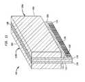
- a componentcan include first and second modules as described above bonded to one another. The second surfaces of the module cards can face one another.
- a modulecan include a lead frame, first and second microelectronic elements having front surfaces facing a first surface of the lead frame, and an encapsulant covering the first and second microelectronic elements and a portion of the lead frame.
- the lead framecan also have a second surface and a plurality of exposed module contacts adjacent an edge of at least one of the first and second surfaces for mating with corresponding contacts of a socket when the module is inserted in the socket.
- Each microelectronic elementcan be electrically connected to the lead frame.
- the front surface of the second microelectronic elementcan partially overlie a rear surface of the first microelectronic element and can be attached thereto.
- a componentcan include first and second modules as described above bonded to one another.
- the second surfaces of the lead framescan face one another.
- a systemcan include a plurality of modules as described above, a circuit panel, and a processor.
- the exposed contacts of the modulescan be inserted into a mating socket electrically connected with the circuit panel.
- Each modulecan be configured to transfer a number N of data bits in parallel in a clock cycle.
- the processorcan be configured to transfer a number M of data bits in parallel in a clock cycle. M can be greater than or equal to N.
- FIG. 1For example, the system can be disposed in and/or mounted to a single housing, which can be a portable housing.
- Systems according to preferred embodiments in this aspect of the inventioncan be more compact than comparable conventional systems.
- a method of fabricating a modulecan include providing a module card, mounting first and second microelectronic elements onto the module card, and electrically connecting the first and second microelectronic elements to the module card.
- the module cardcan have a first surface, a second surface, and a plurality of exposed edge contacts adjacent an edge of at least one of the first and second surfaces for mating with corresponding contacts of a socket when the module is inserted in the socket.
- Front surfaces of the first and second microelectronic elementscan face the first surface of the module card.
- the front surface of the second microelectronic elementcan partially overlie a rear surface of the first microelectronic element and can be attached thereto.
- the module cardcan further include an aperture extending between the first and second surfaces.
- the modulecan also include a plurality of leads extending within the aperture from chip contacts of at least one of the first and second microelectronic elements to the edge contacts.
- the leadscan include conductive elements on the module card. The step of electrically connecting the first and second microelectronic elements to the module card can electrically connect the conductive elements to the chip contacts of at least one of the first and second microelectronic elements using a bonding tool inserted through the aperture.
- the leadscan include wire bonds extending from the conductive elements to the chip contacts. In an exemplary embodiment, the leads can include lead bonds extending from the conductive elements to the chip contacts. In a particular embodiment, the method can also include the step of injecting an encapsulant onto the rear surfaces of the microelectronic elements and the first surface of the module card. In one embodiment, the encapsulant can be a first encapsulant. The method can also include the step of injecting a second encapsulant into the aperture such that portions of the leads between the chip contacts and the module card are covered by the second encapsulant.
- the step of mounting first and second microelectronic elements onto the module cardcan include applying a compliant die attachment adhesive between the first surface of the module card and the front surface of the first microelectronic element.
- the methodcan also include the step of mounting a spacer between the front surface of the second microelectronic element and the first surface of the module card. The spacer can have substantially the same thickness in a vertical direction substantially perpendicular to the first surface as the first microelectronic element.
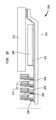
- FIG. 1Ais a diagrammatic sectional view of a stacked microelectronic assembly according to an embodiment of the present invention.
- FIG. 1Bis a bottom sectional view of the stacked assembly of FIG. 1A , taken along the line 1 B- 1 B of FIG. 1A .
- FIG. 1Cis a side sectional view of the stacked assembly of FIG. 1B , taken along the line 1 C- 1 C of FIG. 1B .
- FIG. 2is a diagrammatic sectional view of a stacked microelectronic assembly according to another embodiment having a flip-chip bonded microelectronic element.
- FIG. 3is a diagrammatic sectional view of a stacked microelectronic assembly according to another embodiment having a face-up microelectronic element.
- FIG. 4is a diagrammatic sectional view of a stacked microelectronic assembly according to another embodiment having a single window in the module card through which wire bonds attached to two microelectronic elements extend.
- FIG. 5is a diagrammatic sectional view of a stacked microelectronic assembly according to another embodiment having lead bonds.
- FIG. 6is a diagrammatic sectional view of a stacked microelectronic assembly according to another embodiment having elongated solder connects.
- FIG. 7is a diagrammatic sectional view of a stacked microelectronic assembly according to another embodiment having a microelectronic element with contacts located near an edge thereof.
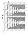
- FIG. 8is a variation of the bottom sectional view of the stacked assembly of FIG. 1B , in which one microelectronic elements has rows of central contacts oriented substantially perpendicular to rows of central contacts of another microelectronic element.
- FIG. 9Ais a diagrammatic sectional view of a stacked microelectronic assembly according to another embodiment having a lead frame.
- FIG. 9Bis a bottom sectional view of the stacked assembly of FIG. 9A , taken along the line 9 B- 9 B of FIG. 9A .
- FIG. 9Cis a side sectional view of the stacked assembly of FIG. 9B , taken along the line 9 C- 9 C of FIG. 9B .
- FIG. 10Ais a diagrammatic top view of a stacked microelectronic assembly according to another embodiment having a plurality of stacked microelectronic elements, shown without an encapsulant.
- FIG. 10Bis a side sectional view of the stacked assembly of FIG. 10A , taken along the line 10 B- 10 B of FIG. 10A .
- FIG. 10Cis a diagrammatic top view of a stacked microelectronic assembly according to another embodiment having a plurality of microelectronic elements adjacent to one another.
- FIG. 11is a diagrammatic perspective view of a stacked microelectronic assembly according to another embodiment including two module cards bonded to one another.
- FIG. 12is a schematic depiction of a system according to one embodiment including a plurality of modules.
- FIG. 13is a top plan view of a microelectronic element in the embodiment of FIG. 1A .
- FIG. 14is a top plan view of another microelectronic element in the embodiment of FIG. 1A .
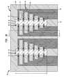
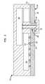
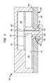
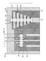
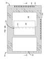
- a module 10can include a first microelectronic element 20 , a second microelectronic element 30 , and a module card 40 having exposed edge contacts 50 .
- a first encapsulant 60can cover the microelectronic elements 20 and 30 and a portion of the module card 40 .
- At least one of the first and second microelectronic elements 20 and 30can be a semiconductor chip, a wafer, or the like.
- one or both of the first microelectronic element 20 and the second microelectronic element 30can include a memory storage element such as a DRAM.
- a “memory storage element”refers to a multiplicity of memory cells arranged in an array, together with circuitry usable to store and retrieve data therefrom, such as for transport of the data over an electrical interface.
- the module 10can be included in a single in-line memory module (“SIMM”) or a dual in-line memory module (“DIMM”).
- the first microelectronic element 20can have a front surface 21 , a rear surface 22 remote therefrom, and lateral edges 23 extending between the front and rear surfaces. Electrical contacts 24 are exposed at the front surface 21 of the first microelectronic element 20 . As described herein, the electrical contacts 24 of the first microelectronic element 20 can also be referred to as “chip contacts.” As used in this disclosure, a statement that an electrically conductive element is “exposed at” a surface of a structure indicates that the electrically conductive element is available for contact with a theoretical point moving in a direction perpendicular to the surface toward the surface from outside the structure.
- a terminal or other conductive element which is exposed at a surface of a structurecan project from such surface; can be flush with such surface; or can be recessed relative to such surface and exposed through a hole or depression in the structure.
- the contacts 24 of the first microelectronic element 20are exposed at the front surface 21 within a central region 25 of the first microelectronic element.
- the contacts 24can be arranged in one or two parallel rows adjacent the center of the front surface 21 .
- the second microelectronic element 30can have a front surface 31 , a rear surface 32 remote therefrom, and lateral edges 33 extending between the front and rear surfaces. Electrical contacts 34 are exposed at the front surface 31 of the second microelectronic element 30 . As described herein, the electrical contacts 34 of the second microelectronic element 30 can also be referred to as “chip contacts.” The contacts 34 of the second microelectronic element 30 are exposed at the front surface 31 within a central region 35 of the second microelectronic element. For example, the contacts 34 can be arranged in one or two parallel rows adjacent the center of the front surface 31 .
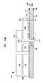
- the first and second microelectronic elements 20 and 30can be stacked relative to one another.
- the front surface 31 of the second microelectronic element 30 and the rear surface 22 of the first microelectronic element 20can face one another.
- At least a portion of the front surface 31 of the second microelectronic element 30can overlie at least a portion of the rear surface 22 of the first microelectronic element 20 .
- At least a portion of the central region 35 of the second microelectronic element 30can project beyond a lateral edge 23 of the first microelectronic element 20 .
- the contacts 34 of the second microelectronic element 30can be positioned in a location projecting beyond the lateral edge 23 of the first microelectronic element 20 .
- the microelectronic assembly 10can further include a module card 40 having oppositely-facing first and second surfaces 41 and 42 .
- One or more electrically conductive contacts 44can be exposed at the second surface 42 of the module card 40 .
- the module card 40can further include one or more apertures such as the first aperture 45 and the second aperture 46 .
- the front surfaces 21 , 31 of the respective first and second microelectronic elements 20 , 30can face the first surface 41 of the module card 40 .
- the module card 40can be partly or entirely made of any suitable dielectric material.
- the module card 40may comprise a relatively rigid, board-like material such as a thick layer of fiber-reinforced epoxy, such as Fr-4 or Fr-5 board. Regardless of the material employed, the module card 40 may include a single layer or multiple layers of dielectric material.
- the module card 40can consist essentially of a material having a coefficient of thermal expansion (“CTE”) of less than 30 ppm/° C.
- CTEcoefficient of thermal expansion
- the module card 40may extend beyond a lateral edge 23 of the first microelectronic element 20 and a lateral edge 33 of the second microelectronic element 30 .
- the first surface 41 of the module card 40may be juxtaposed with the front surface 21 of the first microelectronic element 20 .
- the module card 40includes a first aperture 45 substantially aligned with the central region 25 of the first microelectronic element 20 and a second aperture 46 substantially aligned with the central region 35 of the second microelectronic element 30 , thereby providing access to contacts 24 and 34 through the respective first and second apertures.
- the first and second apertures 45 and 46can extend between the first and second surfaces 41 and 42 of the module card 40 .
- the apertures 45 and 46can be aligned with the corresponding chip contacts 24 or 34 of the respective first and second microelectronic elements 20 and 30 .
- the module card 40may also include electrically conductive contacts 44 exposed at the second surface 42 thereof and electrically conductive traces 55 extending between the contacts 44 and the exposed edge contacts 50 .
- the electrically conductive traces 55electrically couple the contacts 44 to the exposed edge contacts 50 .
- the contacts 44can be end portions of respective ones of the traces 55 .
- the module card 40can have a plurality of parallel exposed edge contacts 50 adjacent an insertion edge 43 of at least one of the first and second surfaces 41 , 42 for mating with corresponding contacts of a socket (shown in FIG. 12 ) when the module 10 is inserted in the socket.
- the insertion edge 43can be located such that each of the apertures 45 and 46 have a long dimension L extending in a direction away from the insertion edge of the module card 40 .
- Some or all of the edge contacts 50can be exposed at either or both of the first or second surfaces 41 , 42 of the module card 40 .
- the exposed edge contacts 50 and the insertion edgecan be sized for insertion into a corresponding socket ( FIG. 12 ) of other connector of a system, such as can be provided on a motherboard.
- Such exposed edge contacts 50can be suitable for mating with a plurality of corresponding spring contacts ( FIG. 12 ) within such socket connector.
- Such spring contactscan be disposed on single or multiple sides of each slot to mate with corresponding ones of the exposed edge contacts 50 .
- at least some of the edge contacts 50can be usable to carry at least one of a signal or a reference potential between the respective edge contact and each of the first and second microelectronic elements 20 , 30 .
- electrical connections or leads 70can electrically connect the contacts 24 of the first microelectronic element 20 and the contacts 34 of the second microelectronic element 30 to the exposed edge contacts 50 .
- the leads 70may include wire bonds 71 and 72 and the conductive traces 55 .
- the leads 70can be considered to electrically connect each microelectronic element 20 , 30 to the module card 40 .
- the leads 70can be usable to carry an address signal usable to address a memory storage element in at least one of the first and second microelectronic elements 20 , 30 .
- a “lead”is a portion of or the entire electrical connection extending between two electrically conductive elements, such as the lead 70 comprising wire bonds 71 and a conductive trace 55 that extends from one of the contacts 24 of the first microelectronic element 20 , through the first aperture 45 , to one of the exposed edge contacts 50 .
- the module 10can include a plurality of leads 70 extending within the apertures 45 and 46 from chip contacts 24 and 34 of at least one of the first and second microelectronic elements 20 and 30 to the exposed edge contacts 50 .
- the leads 70can include the conductive traces 55 on the module card 40 and the wire bonds 71 , 72 extending from the conductive traces to the chip contacts 24 , 34 of at least one of the first and second microelectronic elements 20 , 30 .
- the conductive traces 55 of the leads 70can extend along the second surface 42 of the module card 40 .
- the conductive traces 55 of the leads 70can extend along the first surface 41 of the module card 40 , or the conductive traces of the leads can extend along both the first and second surfaces 41 , 42 of the module card.
- Portions of the conductive traces 55can extend along a surface 41 or 42 of the module card 40 in a direction approximately parallel to the long dimensions L of the apertures 45 and 46 from the respective contacts 24 and 34 to the exposed edge contacts 50 .
- the conductive traces 55be arranged in a pattern along a surface 41 or 42 of the module card 40 such that the length of the leads 70 between the respective contacts 24 and 34 and the exposed edge contacts 50 can be minimized.
- Each of the wire bonds 71 and 72can extend through the respective first or second aperture 45 or 46 and can electrically couple a contact respective 24 or 34 to a corresponding contact 44 of the module card 40 .
- the process of forming the wire bonds 71 and 72can include inserting a bonding tool through the apertures 45 , 46 to electrically connect the conductive contacts 24 , 34 to corresponding conductive contacts 44 of the module card 40 .
- each of the wire bonds 71 and 72can be a multiple wire bond including a plurality of wire bonds oriented substantially parallel to one another.
- Such a multiple wire bond structure including a plurality of wire bonds 71 or 72can provide electrically parallel conductive paths between a contact 24 or 34 and a corresponding contact 44 of the module card 40 .
- a spacer 12can be positioned between the front surface 31 of the second microelectronic element 30 and a portion of the first surface 41 of the module card 40 .
- a spacer 12can be made, for example, from a dielectric material such as silicon dioxide, a semiconductor material such as silicon, or one or more layers of adhesive. If the spacer 12 includes adhesives, the adhesives can connect the second microelectronic element 30 to the module card 40 .
- the spacer 12can have substantially the same thickness T1 in a vertical direction V substantially perpendicular to the first surface 41 of the module card 40 as the thickness T2 of the first microelectronic element 20 between the front and rear surfaces 21 , 22 thereof.
- the spacer 12can be replaced by a buffering chip having a surface facing the first surface 41 of the module card 40 .
- a buffering chipcan be flip-chip bonded to contacts exposed at the first surface 41 of the module card 40 .
- Such a buffering chipcan be configured to help provide impedance isolation for each of the microelectronic elements 20 and 30 with respect to components external to the module 10 .
- One or more adhesive layers 14can be positioned between the first microelectronic element 20 and the module card 40 , between the first and second microelectronic elements 20 and 30 , between the second microelectronic element 30 and the spacer 12 , and between the spacer 12 and the module card 40 .
- Such adhesive layers 14can include adhesive for bonding the aforementioned components of the module 10 to one another.
- the one or more adhesive layers 14can extend between the first surface 41 of the module card 40 and the front surface 21 of the first microelectronic element 20 .
- the one or more adhesive layers 14can attach at least a portion of the front surface of the second microelectronic element 30 to at least a portion of the rear surface 22 of the first microelectronic element 20 .
- each adhesive layer 14can be partly or entirely made of a die attachment adhesive and can be comprised of a low elastic modulus material such as silicone elastomer. In one embodiment, the die attachment adhesive can be compliant. In another example, each adhesive layer 14 can be entirely or partly made of a thin layer of high elastic modulus adhesive or solder if the two microelectronic elements 20 and 30 are conventional semiconductor chips formed of the same material, because the microelectronic elements will tend to expand and contract in unison in response to temperature changes. Regardless of the materials employed, each of the adhesive layers 14 can include a single layer or multiple layers therein. In a particular embodiment where the spacer 12 is made from an adhesive, the adhesive layers 14 positioned between the spacer 12 and the second microelectronic element 30 and the module card 40 can be omitted.
- the module 10can also include a first encapsulant 60 and a second encapsulant 65 .
- the first encapsulant 60can cover, for example, the rear surfaces 22 and 32 of the respective first and second microelectronic elements 20 and 30 and a portion of the first surface 41 of the module card 40 .
- the first encapsulant 60can be an overmold.
- One or more second encapsulants 65can cover portions of the front surfaces 21 and 31 of the respective microelectronic elements 20 and 30 exposed within the respective apertures 45 and 46 , a portion of the second surface 42 of the module card 40 , the contacts 24 , 34 , and 44 , and the wire bonds 71 and 72 extending between the respective contacts 24 and 34 and the corresponding contacts 44 .
- a second encapsulant 65can cover portions of the leads 70 extending between the chip contacts 24 and 34 and the module card 40 .
- the first encapsulant 60can be injected onto the rear surfaces 22 and 32 of the respective first and second microelectronic elements 20 and 30 and onto the first surface of the module card 40 .
- the second encapsulant 65can be injected into the first and second apertures 45 , 46 such that portions of the leads 70 between the chip contacts 24 , 34 and the module card 40 are covered by the second encapsulant.
- FIG. 2shows a variation of the embodiment described above with respect to FIGS. 1A through 1C .
- a module 210is the same as the module 10 described above, except that the first microelectronic element 220 is flip-chip bonded to the first surface 241 of the module card 240 , rather than being wire-bonded to the second surface of the module card.
- Conductive contacts 224are exposed at the front surface 221 of the first microelectronic element 220 .
- the conductive contacts or chip contacts 224can be electrically connected to conductive contacts 247 exposed at the first surface 241 of the module card 240 , for example, by conductive masses 273 .
- the conductive masses 273can comprise a fusible metal having a relatively low melting temperature, e.g., solder, tin, or a eutectic mixture including a plurality of metals.
- the conductive masses 273can include a wettable metal, e.g., copper or other noble metal or non-noble metal having a melting temperature higher than that of solder or another fusible metal.
- the conductive masses 273can include a conductive material interspersed in a medium, e.g., a conductive paste, e.g., metal-filled paste, solder-filled paste or isotropic conductive adhesive or anisotropic conductive adhesive.
- a conductive pastee.g., metal-filled paste, solder-filled paste or isotropic conductive adhesive or anisotropic conductive adhesive.
- Conductive tracescan extend from the conductive contacts 247 along the first surface 241 of the module card 240 to exposed edge contacts at an insertion edge of the module card such as the insertion edge 43 shown in FIGS. 1B and 1C .
- chip contacts 234 of the second microelectronic element 230can be electrically connected to corresponding conductive contacts 244 of the module card 240 by wire bonds 272 extending through an aperture 246 of the module card.
- Conductive tracescan also extend from the conductive contacts 244 along the second surface 242 of the module card 240 to exposed edge contacts at an insertion edge of the module card such as the insertion edge 43 shown in FIGS. 1B and 1C .
- FIG. 3shows another variation of the embodiment described above with respect to FIGS. 1A through 1C .
- a module 310is the same as the module 10 described above, except that the first microelectronic element 320 is positioned with the rear surface 322 thereof facing the first surface 341 of the module card 340 and at least a portion of the front surface 321 thereof facing and partially overlying at least a portion of the front surface 331 of the second microelectronic element 330 .
- the rear surface 322 of the first microelectronic element 320can be attached to the first surface 341 of the module card 340 by one or more adhesive layers such as the adhesive layers 14 shown in FIGS. 1A and 1C .
- Conductive contacts 324 a and 324 bcan be exposed at the front surface 321 of the first microelectronic element 320 .
- the chip contacts 324 of the first microelectronic element 320can include any configuration of conductive contacts 324 a and/or 324 b.
- the conductive contacts 324 a of the first microelectronic element 320can be exposed at the front surface 321 within a central region 325 of the first microelectronic element.
- the contacts 324 acan be arranged in one or two parallel rows adjacent the center of the front surface 321 .
- the conductive contacts 324 acan be electrically connected to conductive contacts 347 exposed at the first surface 341 of the module card 340 , for example, by wire bonds 371 a.
- the conductive contacts 324 b of the first microelectronic element 320can be exposed at the front surface 321 near a lateral edge 323 of the first microelectronic element.
- the contacts 324 bcan be arranged in one or two parallel rows adjacent the lateral edge 323 of the first microelectronic element 320 .
- the conductive contacts 324 bcan be electrically connected to conductive contacts 347 exposed at the first surface 341 of the module card 340 , for example, by wire bonds 371 b.
- conductive tracescan extend from the conductive contacts 347 and 344 along the respective first and second surfaces 341 , 342 of the module card 340 to exposed edge contacts at insertion edges of the module card such as the insertion edge 43 shown in FIGS. 1B and 1C .
- the second microelectronic element 330can be electrically connected to the module card in various other ways, including for example, lead bonds (as shown in FIG. 5 ) or flip-chip bonding with solder (as shown in FIGS. 6 and 7 ).
- FIG. 4shows another variation of the embodiment described above with respect to FIGS. 1A through 1C .
- a module 410is the same as the module 10 described above, except that first and second microelectronic elements 410 and 420 are electrically connected to the module card 440 by respective wire bonds 471 and 472 extending through a common aperture 446 extending between first and second surfaces 441 , 442 of the module card, rather than having each microelectronic element be electrically connected to the module card by wire bonds extending through respective separate apertures of the module card.
- the conductive contacts 424 of the first microelectronic element 420can be exposed at the front surface 421 near a lateral edge 423 of the first microelectronic element.
- the contacts 424can be arranged in a row adjacent the lateral edge 423 of the first microelectronic element 420 .
- the conductive contacts 424can be electrically connected to conductive contacts 444 exposed at the second surface 442 of the module card 440 , for example, by wire bonds 471 .
- the conductive contacts 434 of the second microelectronic element 430can be exposed at the front surface 431 within a central region 435 of the second microelectronic element.
- the contacts 434can be arranged in a row approximately at the center of the front surface 431 .
- the conductive contacts 434can be electrically connected to conductive contacts 444 exposed at the second surface 442 of the module card 440 , for example, by wire bonds 472 .
- the module 410can include a single second encapsulant 465 .
- a second encapsulant 65can cover portions of the front surfaces 421 and 431 of the respective microelectronic elements 420 and 430 exposed within the single common aperture 446 , a portion of the second surface 442 of the module card 440 , the contacts 424 , 434 , and 444 , and the wire bonds 471 and 472 extending between the respective contacts 424 and 434 and the corresponding contacts 444 .
- FIG. 5shows another variation of the embodiment described above with respect to FIGS. 1A through 1C .
- a module 510is the same as the module 10 described above, except that the first microelectronic element 520 is flip-chip bonded to the first surface 541 of the module card 540 (in the same manner as in FIG. 2 ), and the second microelectronic element 530 is electrically connected to the module card 540 by lead bonds 574 a and 574 b (collectively the lead bonds 574 ) extending from conductive traces to the chip contacts 534 rather than by wire bonds.
- the conductive contacts 534 a and 534 b (collectively the conductive contacts 534 ) of the second microelectronic element 530can be exposed at the front surface 531 within a central region 535 of the second microelectronic element.
- the contacts 534can be arranged in one or two parallel rows adjacent the center of the front surface 531 .
- Some of the conductive contacts 534 acan be electrically connected to conductive contacts 544 exposed at the second surface 542 of the module card 540 , for example, by lead bonds 574 a .
- Others of the conductive contacts 534 bcan be electrically connected to conductive contacts 547 exposed at the first surface 541 of the module card 540 , for example, by lead bonds 574 b .
- the conductive contacts 544 and 547can be conductive contact portions of the respective lead bonds 574 a and 574 b.
- each lead 570can be displaced downwardly by a tool such as a thermosonic bonding tool into engagement with a corresponding conductive contact 534 .
- a bonding toolcan be inserted through the aperture 546 to electrically connect the leads 570 to the corresponding conductive contacts 534 .
- Frangible sections of the leads 570can be broken during this process.
- FIG. 6shows another variation of the embodiment described above with respect to FIGS. 1A through 1C .
- a module 610is the same as the module 10 described above, except that the first microelectronic element 620 is flip-chip bonded to the first surface 641 of the module card 640 (in the same manner as in FIG. 2 ), and the second microelectronic element 630 is flip-chip bonded to the first surface of the module card by conductive masses 675 extending between the conductive contacts 634 of the second microelectronic element and conductive contacts 647 exposed at the first surface of the module card rather than by wire bonds.
- the module card 640can be devoid of leads extending through apertures between the first and second surfaces 641 , 642 thereof, such as the apertures 45 and 46 shown in FIG. 1A .
- the conductive contacts 634 of the second microelectronic element 630can be exposed at the front surface 631 within a central region 635 of the second microelectronic element.
- the contacts 634can be arranged in one or two parallel rows adjacent the center of the front surface 631 .
- the conductive masses 675can be, for example, elongated solder connects, solder balls, or any other material described above with reference to the conductive masses 273 . Such conductive masses 675 can extend through the space between the spacer 612 and the lateral edge 623 of the first microelectronic element 620 to electrically connect the second microelectronic element 630 with the module card 640 .
- FIG. 7shows another variation of the embodiment described above with respect to FIG. 6 .
- a module 710is the same as the module 610 described above, except that the second microelectronic element 730 is flip-chip bonded to the first surface 741 of the module card 740 by conductive masses 775 extending between conductive contacts 734 located adjacent a lateral edge 733 of the second microelectronic element and conductive contacts 747 exposed at the first surface of the module card, rather than having the conductive masses extend between conductive contacts exposed at the front surface of the second microelectronic element within a central region of the second microelectronic element.
- the contacts 734can be arranged in a row adjacent the lateral edge 733 of the second microelectronic element 730 , such that the contacts 734 can project beyond the lateral edge 723 of the first microelectronic element 720 .
- the module card 740can be devoid of leads extending through apertures between the first and second surfaces 741 , 742 thereof.
- FIG. 8shows another variation of the embodiment described above with respect to FIG. 1B .
- a module 810is the same as the module 10 described above, except that the rows of conductive contacts 824 of the first conductive element 820 can be substantially perpendicular to the rows of conductive contacts 834 of the second conductive element 830 .
- the second aperture 846can have a long dimension L extending in a direction away from the insertion edge 843 of the module card 840 , similar to the second aperture 46 shown in FIG. 1B .
- the first aperture 845can be have a long dimension L′ extending in a direction substantially parallel to the insertion edge 843 of the module card 840 and substantially perpendicular to the long dimension L of the second aperture 846 .
- the leads 870can include a pattern of conductive traces 855 a that is the same as the pattern of conductive traces 55 shown in FIG. 1B .
- the leads 870can further include an alternate pattern of conductive traces 855 b extending from the conductive contacts 844 b exposed at the second surface 842 of the module card 840 to the exposed edge contacts 850 .
- some of the conductive traces 855 bcan extend around lateral edges 848 of the first aperture 845 .
- FIG. 9shows a variation of the embodiment described above with respect to FIGS. 1A through 1C .
- a module 910is the same as the module 10 described above, except that the first and second microelectronic elements 920 and 930 are mounted onto a lead frame 980 rather than being mounted onto a module card such as the module card 40 shown in FIG. 1A .
- the front surfaces 921 , 931 of the first and second microelectronic elements 920 , 930can face a first surface 981 of the lead frame 980 , each microelectronic element being electrically connected to the lead frame.
- a lead framesuch as the lead frame 980 is a structure formed from a sheet of conductive metal, such as copper, that is patterned into segments including a plurality of leads or conductive trace portions 985 .
- at least one of the first and second microelectronic element 920 , 930can be mounted directly onto the leads, which can extend under the microelectronic elements.
- contacts 924 , 934 on the microelectronic elementscan be electrically connected to respective leads by solder balls or the like.
- the leadscan then be used to form electrical connections to various other conductive structures for carrying an electronic signal potential to and from the microelectronic elements 920 , 930 .
- temporary elementssuch as a frame (not shown) can be removed from the leads of the lead frame 980 , so as to form individual leads or conductive trace portions 985 .
- the first microelectronic element 920can be attached to the lead frame 980 by one or more adhesive layers 914 extending between the front surface 921 of the first microelectronic element and a first surface 981 of the lead frame.
- adhesive layers 914can be similar to the adhesive layers 14 described above with reference to FIGS. 1A through 1C .
- the spacer 912can be attached to the lead frame 980 be one or more adhesive layers 914 extending between a front surface 913 of the spacer and the first surface 981 of the lead frame. At least a portion of the front surface 931 of the second microelectronic element 930 can partially overlie the rear surface 922 of the first microelectronic element 920 and a rear surface 915 of the spacer 912 .
- the front surface 931 of the second microelectronic element 930can be attached to the rear surface 922 of the first microelectronic element 920 and the rear surface 915 of the spacer 912 by one or more adhesive layers 914 .
- electrical connections or leads 970can electrically connect the contacts 924 of the first microelectronic element 920 and the contacts 934 of the second microelectronic element 930 to the exposed module contacts 950 .
- the leads 970may include wire bonds 971 and 972 and conductive trace portions 985 of the lead frame 980 .
- the leads 970can be usable to carry an address signal usable to address a memory storage element in at least one of the first and second microelectronic elements 920 , 930 .
- the lead frame 980can define a first gap 945 and a second gap 946 extending between the first surface 981 of the lead frame and a second surface 982 of the lead frame opposite the first surface.
- the first gap 945can be aligned with the chip contacts 924 of the first microelectronic element 920 , such that the wire bonds 971 can extend between the chip contacts 924 and the second surface 982 of the lead frame through the first gap.
- the second gap 946can be aligned with the chip contacts 934 of the second microelectronic element 930 , such that the wire bonds 972 can extend between the chip contacts 934 and the second surface 982 of the lead frame through the second gap.
- the module 910can also include an encapsulant 960 that can cover the first and second microelectronic elements 20 , 30 and a portion of the lead frame 980 , such that the exposed module contacts 950 can be exposed at a lower surface 962 of an insertion portion 961 of the encapsulant.
- the encapsulant 960can also cover the contacts 924 , 934 , and the wire bonds 971 and 972 extending between the respective contacts 924 and 934 and the lead frame 980 .
- the insertion portion 961 of the encapsulant 960can have an appropriate size and shape for mating with a corresponding socket (shown in FIG. 12 ) when the module 910 is inserted in the socket.
- the module 910can have a plurality of parallel exposed module contacts 950 adjacent an insertion edge 983 of at least one of the first and second surfaces 981 , 982 for mating with corresponding contacts of a socket (shown in FIG. 12 ) when the module 910 is inserted in the socket. Some or all of the module contacts 950 can be exposed at either or both of the first or second surfaces 981 , 982 of the lead frame 980 .
- FIGS. 10A and 10Bshow a variation of the embodiment described above with respect to FIG. 2 .
- a module 1010is the same as the module 210 described above, except that the module 1010 also includes a stack of third microelectronic elements 1090 mounted onto the module card 1040 .
- the first microelectronic element 1020is flip-chip bonded to the first surface 1041 of the module card 1040 .
- the conductive contacts or chip contacts 1024 of the first microelectronic element 1020can be electrically connected to conductive contacts 1047 exposed at the first surface 1041 of the module card 1040 , for example, by conductive masses 1073 .
- Chip contacts 1034 of the second microelectronic element 1030can be electrically connected to corresponding conductive contacts 1044 of the module card 1040 by wire bonds 1072 extending through an aperture 1046 of the module card.
- Conductive traces(not shown in FIGS.
- the edge contacts 1050can be exposed at the first surface 1041 , the second surface 1042 , or both surfaces.
- third microelectronic elements 1090there can be any number of third microelectronic elements 1090 in the stack, including, for example, two third microelectronic elements 1090 a and 1090 b as shown in FIG. 10B .
- the third microelectronic elements 1090can be connected with one another and/or with the edge contacts 1050 by any interconnection configuration.
- the lower third microelectronic element 1090 acan be connected with contacts exposed at a surface of the module card 1040 via flip-chip bonding, wire bonds, lead bonds, or other interconnection configurations.
- One or more upper third microelectronic elements 1090 bcan be connected with contacts of the module card 1040 through conductive vias extending through the lower third microelectronic element 1090 a , wire bonds, lead bonds, or other interconnection configurations.
- the module 1010can be configured to function as a solid state memory drive.
- the first microelectronic element 1020can include a semiconductor chip configured predominantly to perform a logic function, such as a solid state drive controller, and the second microelectronic element 1030 can include a memory storage element such as volatile RAM, for example, DRAM.
- the third microelectronic elements 1090can each include memory storage elements such as nonvolatile flash memory.
- the first microelectronic element 1020can include a special purpose processor that is configured to relieve a central processing unit of a system such as the system 1200 ( FIG.
- Such a first microelectronic element 1020 including a solid state drive controllercan provide direct memory access to and from a data bus on a motherboard (e.g., the circuit panel 1202 shown in FIG. 12 ) of a system such as the system 1200 .
- the module 1010can be configured to function as a graphics module, for example, that can be plugged into a PCI express slot of a notebook personal computer.
- the first microelectronic element 1020can include a semiconductor chip configured predominantly to perform a logic function, such as a graphics processor
- the second microelectronic element 1030can include a memory storage element such as volatile RAM (e.g., DRAM) that can serve as a volatile frame buffer for computational graphics rendering.
- the third microelectronic elements 1090can each include memory storage elements such as nonvolatile flash memory.
- FIG. 10Cshows a variation of the embodiment described above with respect to FIGS. 10A and 10B .
- a module 1010 ′is the same as the module 1010 described above, except that the module 1010 ′ includes a plurality of third microelectronic elements 1090 ′ mounted onto the module card 1040 adjacent to one another rather than in a stacked configuration. Similar to the module 1010 , the third microelectronic elements 1090 ′ can be connected with contacts exposed at a surface of the module card 1040 by any interconnection configuration, such as flip-chip bonding, wire bonds, lead bonds, or other interconnection configurations.
- the module 1010 ′can be used for similar exemplary functions as the module 1010 , such as a solid state memory drive or a graphics module.
- FIG. 11depicts a component 1100 including first and second modules 1110 a and 1110 b according to any of the embodiments described above, such as for example, the module 10 described with reference to FIGS. 1A through 1C .
- the first and second modules 1110 a , 1110 bcan be bonded to one another with at least one layer 1165 , such that the second surfaces 1142 of the respective module cards 1140 of the modules can face one another.
- the at least one layer 1165can be a single common encapsulant such as the second encapsulant 65 shown in FIGS. 1A and 1B .
- the at least one layer 1165can be one or more adhesive layers, similar to the adhesive layers 14 described with reference to FIGS. 1A through 1C .
- the component 1100can have one or more rows of parallel exposed edge contacts 1150 adjacent an insertion edge 1143 of the component.
- Each of the first and second modules 1110 a , 1110 bcan have a row of edge contacts 1150 exposed at the first surface 1141 of the respective module card 1140 , such that the edge contacts can be suitable for mating with corresponding contacts of a socket (similar to the socket shown in FIG. 12 ) when the component 1100 is inserted in the socket.
- the modules and components described above with reference to FIGS. 1A through 10can be utilized in construction of diverse electronic systems, such as the system 1200 shown in FIG. 12 .
- the system 1200 in accordance with a further embodiment of the inventionincludes a plurality of modules or components 1206 as described above in conjunction with other electronic components 1208 and 1210 .
- the system 1200can includes a plurality of sockets 1205 , each socket including a plurality of contacts 1207 at one or both sides of the socket, such that each socket 1205 can be suitable for mating with corresponding exposed edge contacts or exposed module contacts of a corresponding module or component 1206 .
- the systemcan include a circuit panel or motherboard 1202 such as a flexible printed circuit board, and the circuit panel can include numerous conductors 1204 , of which only one is depicted in FIG. 12 , interconnecting the modules or components 1206 with one another.
- thisis merely exemplary; any suitable structure for making electrical connections between the modules or components 1206 can be used.
- the system 1200can also include a processor such as the semiconductor chip 1208 , such that each module or component 1206 can be configured to transfer a number N of data bits in parallel in a clock cycle, and the processor can be configured to transfer a number M of data bits in parallel in a clock cycle, M being greater than or equal to N.
- a processorsuch as the semiconductor chip 1208 , such that each module or component 1206 can be configured to transfer a number N of data bits in parallel in a clock cycle, and the processor can be configured to transfer a number M of data bits in parallel in a clock cycle, M being greater than or equal to N.
- the system 1200can include a processor chip 1208 that is configured to transfer thirty-two data bits in parallel in a clock cycle, and the system can also include four modules 1206 such as the module 10 described with reference to FIGS. 1A through 1C , each module 1206 configured to transfer eight data bits in parallel in a clock cycle (i.e., each module 1206 can include first and second microelectronic elements, each of the two microelectronic elements being configured to transfer four data bits in parallel in a clock cycle).
- the system 1200can include a processor chip 1208 that is configured to transfer sixty-four data bits in parallel in a clock cycle, and the system can also include four modules 1206 such as the component 1000 described with reference to FIG. 12 , each module 1206 configured to transfer sixteen data bits in parallel in a clock cycle (i.e., each module 1206 can include two sets of first and second microelectronic elements, each of the four microelectronic elements being configured to transfer four data bits in parallel in a clock cycle).
- the component 1208is a semiconductor chip and component 1210 is a display screen, but any other components can be used in the system 1200 .
- the system 1200can include any number of such components.
- Modules or components 1206 and components 1208 and 1210can be mounted in a common housing 1201 , schematically depicted in broken lines, and can be electrically interconnected with one another as necessary to form the desired circuit.
- the housing 1201is depicted as a portable housing of the type usable, for example, in a cellular telephone or personal digital assistant, and screen 1210 can be exposed at the surface of the housing.
- a structure 1206includes a light-sensitive element such as an imaging chip
- a lens 1211 or other optical devicealso can be provided for routing light to the structure.
- the simplified system shown in FIG. 12is merely exemplary; other systems, including systems commonly regarded as fixed structures, such as desktop computers, routers and the like can be made using the structures discussed above.
- the first microelectronic element 136may be any type of semiconductor chip.
- the first microelectronic element 136can be a DRAM (dynamic random access memory) chip having conductive elements thereon.
- the surface area of the front surface 140 of the first microelectronic element 136may be divided into three regions having substantially equal widths in a direction between the first and second edges of the first microelectronic element: a first outer region 1320 , a second outer region 1322 , and a central region 1324 positioned between the first outer region 1320 and second outer region 1322 .
- the respective lengths of the first outer, second outer, and central regionsmay be 2 microns.
- the central region 1324would therefore be positioned 2 microns from the first edge 144 and 2 microns from the second edge 144 .
- the central regioncan be positioned in the middle third of the first microelectronic element 136 .
- the conductive elementsmay include first bond pads 142 that extend along the central region 1324 of the front surface 140 of the first microelectronic element 136 .
- the conductive elementsprovide for an electrical connection between the first microelectronic element 136 and the first set of contacts 109 positioned on the second surface 106 of the substrate 102 .
- An adhesive 101can be used to attach the first microelectronic element 136 to the substrate 102 .
- the second microelectronic element 153may be similar to the first microelectronic element 136 .
- the second microelectronic element 153has opposed first and second edges 161 , 162 and opposed third and fourth edges 163 , 164 extending between the rear surface 155 and front surface 157 of the second microelectronic element 153 and adjacent first and second edges 161 , 162 .
- Conductive elementsextend along the front surface 157 of the second microelectronic element 153 .
- the second microelectronic element 153may be a semiconductor chip, such as a DRAM chip, with bond pads 159 positioned along a central region 1332 of the second microelectronic element 153 , which is positioned between a first outer region 1328 and a second outer region 1330 .
- bond pads 159can extend in a direction transverse to the direction bond pads 142 on the first microelectronic element 136 extend.
- a possible benefit of a module or component according to the inventionfor example the module 10 described above with reference to FIGS. 1A through 1C , whereby a surface of the first microelectronic element overlies at least a portion of the rear surface of the second microelectronic element can be to provide relatively short leads electrically connecting a particular exposed edge contact (e.g., the exposed edge contact 50 ) a particular electrical contact (e.g., the electrical contact 24 ) exposed at a front surface of a particular microelectronic element (e.g., the first microelectronic element 20 ).
- Parasitic capacitancecan be considerable between adjacent leads, particularly in microelectronic assemblies that have high contact density and fine pitch.
- parasitic capacitancecan be reduced, particularly between adjacent leads.
- leads 70can electrically connect data input/output signal terminals (e.g., the exposed edge contacts 50 ) with electrical contacts 24 , 34 at the front surfaces of respective first and second microelectronic elements 20 , 30 .
- data input/output signal terminalse.g., the exposed edge contacts 50
- electrical contacts 24 , 34at the front surfaces of respective first and second microelectronic elements 20 , 30 .
- having relatively similar-length leads 70can allow the propagation delay for data input/output signals between each microelectronic element and the exposed edge contacts to be relatively closely matched.
- leads 70can electrically connect shared clock signal terminals and/or shared data strobe signal terminals (e.g., the exposed edge contacts 50 ) with electrical contacts 24 , 34 at the front surfaces of respective first and second microelectronic elements 20 , 30 .
- the data strobe signal terminals or the clock signal terminals or bothmay have substantially the same loading and electrical path lengths to the respective microelectronic elements 20 , 30 and the path lengths to each microelectronic element can be relatively short.
- the rear surface of one or more of the first or second microelectronic elementscan be at least partially exposed at an exterior surface of the microelectronic assembly after completing fabrication.
- one or both of the rear surfaces 22 , 32 of the first and second microelectronic elements 20 , 30can be partially or fully exposed in the completed module 10 .
- the rear surfaces 22 , 32can be partially or fully exposed although an overmold such as the first encapsulant 60 , or other encapsulating or packaging structures can contact or be disposed adjacent the microelectronic elements.
- the microelectronic assemblymay include a heat spreader made of metal, graphite or any other suitable thermally conductive material.
- the heat spreaderincludes a metallic layer disposed adjacent to the first microelectronic element. The metallic layer may be exposed on the rear surface of the first microelectronic element.
- the heat spreadercan include an overmold or an encapsulant covering at least the rear surface of the first microelectronic element.
Landscapes
- Engineering & Computer Science (AREA)
- Microelectronics & Electronic Packaging (AREA)
- Power Engineering (AREA)
- Computer Hardware Design (AREA)
- Physics & Mathematics (AREA)
- Condensed Matter Physics & Semiconductors (AREA)
- General Physics & Mathematics (AREA)
- Manufacturing & Machinery (AREA)
- Semiconductor Memories (AREA)
- Credit Cards Or The Like (AREA)
- Manufacturing Of Electrical Connectors (AREA)
- Structures For Mounting Electric Components On Printed Circuit Boards (AREA)
Abstract
Description
Claims (13)
Priority Applications (3)
| Application Number | Priority Date | Filing Date | Title |
|---|---|---|---|
| US14/156,967US9281266B2 (en) | 2011-04-21 | 2014-01-16 | Stacked chip-on-board module with edge connector |
| US15/061,149US9735093B2 (en) | 2011-04-21 | 2016-03-04 | Stacked chip-on-board module with edge connector |
| US15/606,134US10622289B2 (en) | 2011-04-21 | 2017-05-26 | Stacked chip-on-board module with edge connector |
Applications Claiming Priority (3)
| Application Number | Priority Date | Filing Date | Title |
|---|---|---|---|
| US201161477820P | 2011-04-21 | 2011-04-21 | |
| US13/306,203US8633576B2 (en) | 2011-04-21 | 2011-11-29 | Stacked chip-on-board module with edge connector |
| US14/156,967US9281266B2 (en) | 2011-04-21 | 2014-01-16 | Stacked chip-on-board module with edge connector |
Related Parent Applications (1)
| Application Number | Title | Priority Date | Filing Date |
|---|---|---|---|
| US13/306,203DivisionUS8633576B2 (en) | 2011-04-21 | 2011-11-29 | Stacked chip-on-board module with edge connector |
Related Child Applications (1)
| Application Number | Title | Priority Date | Filing Date |
|---|---|---|---|
| US15/061,149DivisionUS9735093B2 (en) | 2011-04-21 | 2016-03-04 | Stacked chip-on-board module with edge connector |
Publications (2)
| Publication Number | Publication Date |
|---|---|
| US20140131849A1 US20140131849A1 (en) | 2014-05-15 |
| US9281266B2true US9281266B2 (en) | 2016-03-08 |
Family
ID=47020659
Family Applications (4)
| Application Number | Title | Priority Date | Filing Date |
|---|---|---|---|
| US13/306,203ActiveUS8633576B2 (en) | 2011-04-21 | 2011-11-29 | Stacked chip-on-board module with edge connector |
| US14/156,967ActiveUS9281266B2 (en) | 2011-04-21 | 2014-01-16 | Stacked chip-on-board module with edge connector |
| US15/061,149Expired - Fee RelatedUS9735093B2 (en) | 2011-04-21 | 2016-03-04 | Stacked chip-on-board module with edge connector |
| US15/606,134Active2032-05-29US10622289B2 (en) | 2011-04-21 | 2017-05-26 | Stacked chip-on-board module with edge connector |
Family Applications Before (1)
| Application Number | Title | Priority Date | Filing Date |
|---|---|---|---|
| US13/306,203ActiveUS8633576B2 (en) | 2011-04-21 | 2011-11-29 | Stacked chip-on-board module with edge connector |
Family Applications After (2)
| Application Number | Title | Priority Date | Filing Date |
|---|---|---|---|
| US15/061,149Expired - Fee RelatedUS9735093B2 (en) | 2011-04-21 | 2016-03-04 | Stacked chip-on-board module with edge connector |
| US15/606,134Active2032-05-29US10622289B2 (en) | 2011-04-21 | 2017-05-26 | Stacked chip-on-board module with edge connector |
Country Status (8)
| Country | Link |
|---|---|
| US (4) | US8633576B2 (en) |
| EP (1) | EP2700096A1 (en) |
| JP (1) | JP5883119B2 (en) |
| KR (1) | KR20140027999A (en) |
| CN (1) | CN103620775A (en) |
| BR (1) | BR112013027143A2 (en) |
| TW (1) | TWI493795B (en) |
| WO (1) | WO2012145115A1 (en) |
Families Citing this family (18)
| Publication number | Priority date | Publication date | Assignee | Title |
|---|---|---|---|---|
| US8405207B1 (en) | 2011-10-03 | 2013-03-26 | Invensas Corporation | Stub minimization for wirebond assemblies without windows |
| US8653646B2 (en) | 2011-10-03 | 2014-02-18 | Invensas Corporation | Stub minimization using duplicate sets of terminals for wirebond assemblies without windows |
| KR20130118175A (en)* | 2012-04-19 | 2013-10-29 | 삼성전자주식회사 | Semiconductor package and method for fabricating the same |
| US8907500B2 (en) | 2013-02-04 | 2014-12-09 | Invensas Corporation | Multi-die wirebond packages with elongated windows |
| US9490195B1 (en) | 2015-07-17 | 2016-11-08 | Invensas Corporation | Wafer-level flipped die stacks with leadframes or metal foil interconnects |
| US9825002B2 (en) | 2015-07-17 | 2017-11-21 | Invensas Corporation | Flipped die stack |
| US9871019B2 (en) | 2015-07-17 | 2018-01-16 | Invensas Corporation | Flipped die stack assemblies with leadframe interconnects |
| US9484080B1 (en) | 2015-11-09 | 2016-11-01 | Invensas Corporation | High-bandwidth memory application with controlled impedance loading |
| US9508691B1 (en) | 2015-12-16 | 2016-11-29 | Invensas Corporation | Flipped die stacks with multiple rows of leadframe interconnects |
| US20170186474A1 (en)* | 2015-12-28 | 2017-06-29 | Invensas Corporation | Dual-channel dimm |
| WO2017135967A1 (en)* | 2016-02-05 | 2017-08-10 | Hewlett Packard Enterprise Development Lp | Dual in-line memory module |
| US10629351B2 (en) | 2016-02-16 | 2020-04-21 | Sony Corporation | Semiconductor device, semiconductor chip, and system |
| US10566310B2 (en) | 2016-04-11 | 2020-02-18 | Invensas Corporation | Microelectronic packages having stacked die and wire bond interconnects |
| US9595511B1 (en) | 2016-05-12 | 2017-03-14 | Invensas Corporation | Microelectronic packages and assemblies with improved flyby signaling operation |
| US9728524B1 (en) | 2016-06-30 | 2017-08-08 | Invensas Corporation | Enhanced density assembly having microelectronic packages mounted at substantial angle to board |
| KR102358842B1 (en)* | 2017-08-21 | 2022-02-07 | 쑤저우 레킨 세미컨덕터 컴퍼니 리미티드 | Light emitting device package and lighting source unit |
| TWI657237B (en)* | 2018-02-21 | 2019-04-21 | 茂達電子股份有限公司 | Optical detecting device and optical package structure |
| KR20230018399A (en) | 2020-05-29 | 2023-02-07 | 폼팩터, 인크. | 3D Electrical Integration Using Component Carrier Edge Connections to 2D Contact Array |
Citations (180)
| Publication number | Priority date | Publication date | Assignee | Title |
|---|---|---|---|---|
| JPS62107391A (en) | 1985-11-06 | 1987-05-18 | Nippon Texas Instr Kk | information storage medium |
| US4941033A (en) | 1988-12-27 | 1990-07-10 | Mitsubishi Denki Kabushiki Kaisha | Semiconductor integrated circuit device |
| US5148265A (en) | 1990-09-24 | 1992-09-15 | Ist Associates, Inc. | Semiconductor chip assemblies with fan-in leads |
| US5148266A (en) | 1990-09-24 | 1992-09-15 | Ist Associates, Inc. | Semiconductor chip assemblies having interposer and flexible lead |
| US5480840A (en) | 1992-07-14 | 1996-01-02 | At&T Global Information Solutions Company | Multi-chip module with multiple compartments |
| US5679977A (en) | 1990-09-24 | 1997-10-21 | Tessera, Inc. | Semiconductor chip assemblies, methods of making same and components for same |
| WO1998012568A1 (en) | 1996-09-18 | 1998-03-26 | Hitachi, Ltd. | Process for producing semiconductor device and semiconductor device |
| US5861666A (en) | 1995-08-30 | 1999-01-19 | Tessera, Inc. | Stacked chip assembly |
| US5977640A (en) | 1998-06-26 | 1999-11-02 | International Business Machines Corporation | Highly integrated chip-on-chip packaging |
| US5998864A (en) | 1995-05-26 | 1999-12-07 | Formfactor, Inc. | Stacking semiconductor devices, particularly memory chips |
| JPH11345932A (en) | 1998-05-19 | 1999-12-14 | Lucent Technol Inc | Integrated circuit package |
| US6021048A (en) | 1998-02-17 | 2000-02-01 | Smith; Gary W. | High speed memory module |
| US6150724A (en) | 1998-03-02 | 2000-11-21 | Motorola, Inc. | Multi-chip semiconductor device and method for making the device by using multiple flip chip interfaces |
| US6169325B1 (en)* | 1997-12-17 | 2001-01-02 | Hitachi, Ltd. | Semiconductor device |
| KR20010002214A (en) | 1999-06-12 | 2001-01-05 | 마이클 디. 오브라이언 | A semiconductor packages and manufacturing method for it |
| US6199743B1 (en) | 1999-08-19 | 2001-03-13 | Micron Technology, Inc. | Apparatuses for forming wire bonds from circuitry on a substrate to a semiconductor chip, and methods of forming semiconductor chip assemblies |
| US6218731B1 (en) | 1999-05-21 | 2001-04-17 | Siliconware Precision Industries Co., Ltd. | Tiny ball grid array package |
| US6218728B1 (en) | 1997-10-28 | 2001-04-17 | Nec Corporation | Mold-BGA-type semiconductor device and method for making the same |
| US20010005311A1 (en) | 1998-10-26 | 2001-06-28 | Duesman Kevin G. | Heat sink for chip stacking applications |
| JP2001196407A (en) | 2000-01-14 | 2001-07-19 | Seiko Instruments Inc | Semiconductor device and method of forming the same |
| JP2001223324A (en) | 2000-02-10 | 2001-08-17 | Mitsubishi Electric Corp | Semiconductor device |
| KR20010094894A (en) | 2000-04-07 | 2001-11-03 | 마이클 디. 오브라이언 | Semiconductor package and its manufacturing method |
| US6353539B1 (en) | 1998-07-21 | 2002-03-05 | Intel Corporation | Method and apparatus for matched length routing of back-to-back package placement |
| US20020030267A1 (en) | 2000-09-08 | 2002-03-14 | Fujitsu Quantum Devices Limited | Compound semiconductor device |
| JP2002076252A (en) | 2000-08-31 | 2002-03-15 | Nec Kyushu Ltd | Semiconductor device |
| US6369448B1 (en) | 2000-01-21 | 2002-04-09 | Lsi Logic Corporation | Vertically integrated flip chip semiconductor package |
| US6385049B1 (en) | 2001-07-05 | 2002-05-07 | Walsin Advanced Electronics Ltd | Multi-board BGA package |
| US6392292B1 (en) | 1999-07-08 | 2002-05-21 | Nec Corporation | Multi-level stacked semiconductor bear chips with the same electrode pad patterns |
| US6414396B1 (en) | 2000-01-24 | 2002-07-02 | Amkor Technology, Inc. | Package for stacked integrated circuits |
| US6426560B1 (en)* | 1999-08-06 | 2002-07-30 | Hitachi, Ltd. | Semiconductor device and memory module |
| US6472741B1 (en) | 2001-07-14 | 2002-10-29 | Siliconware Precision Industries Co., Ltd. | Thermally-enhanced stacked-die ball grid array semiconductor package and method of fabricating the same |
| US20020175421A1 (en) | 2001-05-25 | 2002-11-28 | Naoto Kimura | Semiconductor device |
| US6492726B1 (en) | 2000-09-22 | 2002-12-10 | Chartered Semiconductor Manufacturing Ltd. | Chip scale packaging with multi-layer flip chip arrangement and ball grid array interconnection |
| US20030064547A1 (en) | 1999-02-01 | 2003-04-03 | Salman Akram | High density modularity for IC's |
| JP2003101207A (en) | 2001-09-27 | 2003-04-04 | Nec Kyushu Ltd | Solder ball and component connecting structure using the same |
| US6583502B2 (en) | 2001-04-17 | 2003-06-24 | Micron Technology, Inc. | Apparatus for package reduction in stacked chip and board assemblies |
| US20030116349A1 (en) | 2000-09-05 | 2003-06-26 | Seiko Epson Corporation | Semiconductor device and method of manufacture thereof, circuit board, and electronic instrument |
| US20030179549A1 (en) | 2002-03-22 | 2003-09-25 | Zhong Chong Hua | Low voltage drop and high thermal perfor mance ball grid array package |
| US20030183917A1 (en) | 2002-02-07 | 2003-10-02 | Macronix International Co., Ltd. | Stacked semiconductor packaging device |
| US20030193788A1 (en) | 1996-08-29 | 2003-10-16 | Farnworth Warren M. | Single-piece molded module housing |
| US20030224553A1 (en)* | 2002-05-31 | 2003-12-04 | Michael Manansala | System for flexible interconnect packaging |
| US20040016999A1 (en) | 2002-07-29 | 2004-01-29 | Mitsubishi Denki Kabushiki Kaisha | Semiconductor device |
| US20040016939A1 (en) | 2002-07-26 | 2004-01-29 | Masayuki Akiba | Encapsulation of a stack of semiconductor dice |
| US6703713B1 (en)* | 2002-09-10 | 2004-03-09 | Siliconware Precision Industries Co., Ltd. | Window-type multi-chip semiconductor package |
| US6720666B2 (en) | 2001-12-12 | 2004-04-13 | Micron Technology, Inc. | BOC BGA package for die with I-shaped bond pad layout |
| US6731009B1 (en) | 2000-03-20 | 2004-05-04 | Cypress Semiconductor Corporation | Multi-die assembly |
| US6734542B2 (en) | 2000-12-27 | 2004-05-11 | Matsushita Electric Industrial Co., Ltd. | Component built-in module and method for producing the same |
| US6742098B1 (en) | 2000-10-03 | 2004-05-25 | Intel Corporation | Dual-port buffer-to-memory interface |
| US20040124520A1 (en) | 2002-10-22 | 2004-07-01 | Rinne Glenn A. | Stacked electronic structures including offset substrates |
| US6762942B1 (en) | 2002-09-05 | 2004-07-13 | Gary W. Smith | Break away, high speed, folded, jumperless electronic assembly |
| US20040184240A1 (en) | 2003-03-18 | 2004-09-23 | Ultratera Corporation | Semiconductor package with heat sink |
| US6811580B1 (en) | 1999-05-06 | 2004-11-02 | Sandvik Ab | Inserts for metal cutting purposes |
| US6818474B2 (en) | 2001-12-29 | 2004-11-16 | Hynix Semiconductor Inc. | Method for manufacturing stacked chip package |
| US20040262774A1 (en) | 2003-06-27 | 2004-12-30 | In-Ku Kang | Multi-chip packages having a plurality of flip chips and methods of manufacturing the same |
| US20050110125A1 (en) | 2003-11-21 | 2005-05-26 | International Business Machines Corporation | Overlap stacking of center bus bonded memory chips for double density and method of manufacturing the same |
| US20050110162A1 (en) | 2002-04-09 | 2005-05-26 | Georg Meyer-Berg | Electronic component having at least one semiconductor chip and flip-chip contacts, and method for producing the same |
| US20050116358A1 (en) | 2003-11-12 | 2005-06-02 | Tessera,Inc. | Stacked microelectronic assemblies with central contacts |
| US20050116326A1 (en) | 2003-10-06 | 2005-06-02 | Tessera, Inc. | Formation of circuitry with modification of feature height |
| JP2005166892A (en) | 2003-12-02 | 2005-06-23 | Kingpak Technology Inc | Stack type small-sized memory card |
| US20050133932A1 (en) | 2003-12-19 | 2005-06-23 | Jens Pohl | Semiconductor module with a semiconductor stack, and methods for its production |
| US20050164486A1 (en) | 2003-07-22 | 2005-07-28 | Lua Edmund K.T. | Semiconductor substrates including I/O redistribution using wire bonds and anisotropically conductive film, methods of fabrication and assemblies including same |
| US20050173807A1 (en) | 2004-02-05 | 2005-08-11 | Jianbai Zhu | High density vertically stacked semiconductor device |
| JP2005251957A (en) | 2004-03-04 | 2005-09-15 | Renesas Technology Corp | Semiconductor device |
| US20050218514A1 (en) | 2004-04-05 | 2005-10-06 | Massingill Thomas J | Cavity down semiconductor package |
| US20050258538A1 (en) | 2004-05-20 | 2005-11-24 | Texas Instruments Incorporated | Double density method for wirebond interconnect |
| US6977440B2 (en) | 2001-10-09 | 2005-12-20 | Tessera, Inc. | Stacked packages |
| KR20050119414A (en) | 2004-06-16 | 2005-12-21 | 삼성전자주식회사 | Stacked package comprising two edge pad-type semiconductor chips and method of manufacturing the same |
| KR20060004298A (en) | 2004-07-09 | 2006-01-12 | 삼성테크윈 주식회사 | Wireless electronic labels |
| US20060006405A1 (en) | 2003-05-05 | 2006-01-12 | Lamina Ceramics, Inc. | Surface mountable light emitting diode assemblies packaged for high temperature operation |
| US20060027902A1 (en) | 2004-08-05 | 2006-02-09 | Ararao Virgil C | Method and apparatus for stacked die packaging |
| JP2006079629A (en) | 2005-09-12 | 2006-03-23 | Renesas Technology Corp | Manufacturing method of ic card |
| JP2006093189A (en) | 2004-09-21 | 2006-04-06 | Renesas Technology Corp | Semiconductor device |
| US20060081583A1 (en) | 1998-09-02 | 2006-04-20 | Hembree David R | Method and process of contact to a heat softened solder ball array |
| US20060097379A1 (en) | 2004-11-10 | 2006-05-11 | Chung-Cheng Wang | Substrate for electrical device and methods for making the same |
| US20060097400A1 (en) | 2004-11-03 | 2006-05-11 | Texas Instruments Incorporated | Substrate via pad structure providing reliable connectivity in array package devices |
| US20060113653A1 (en) | 2004-12-01 | 2006-06-01 | Sherry Xiaoqi | Stack package for high density integrated circuits |
| US7061105B2 (en) | 2000-01-31 | 2006-06-13 | Hitachi, Ltd. | Semiconductor device and a method of manufacturing the same |
| US20060145323A1 (en) | 2005-01-05 | 2006-07-06 | Chang-Hwan Lee | Multi-chip package mounted memory card |
| JP2006210892A (en) | 2004-12-27 | 2006-08-10 | Nec Corp | Semiconductor device |
| US20060197210A1 (en) | 2005-03-04 | 2006-09-07 | Hyun-Ki Kim | Stack semiconductor package formed by multiple molding and method of manufacturing the same |
| US20060231938A1 (en) | 2005-04-18 | 2006-10-19 | Mangrum Marc A | Structure for stacking an integrated circuit on another integrated circuit |
| US20060249827A1 (en) | 2005-05-05 | 2006-11-09 | International Business Machines Corporation | Method and apparatus for forming stacked die and substrate structures for increased packing density |
| KR20060120365A (en) | 2005-05-19 | 2006-11-27 | 삼성테크윈 주식회사 | Semiconductor chip stack package |
| US20060290005A1 (en) | 2005-06-28 | 2006-12-28 | Jochen Thomas | Multi-chip device and method for producing a multi-chip device |
| KR100690247B1 (en) | 2006-01-16 | 2007-03-12 | 삼성전자주식회사 | Double-sealed semiconductor package and manufacturing method thereof |
| US20070066139A1 (en)* | 2005-08-31 | 2007-03-22 | Heiko Roeper | Electronic plug unit |
| US20070075409A1 (en) | 2005-10-05 | 2007-04-05 | Semiconductor Components Industries, Llc. | Method of forming a molded array package device having an exposed tab and structure |
| US7205656B2 (en) | 2005-02-22 | 2007-04-17 | Micron Technology, Inc. | Stacked device package for peripheral and center device pad layout device |
| US20070108592A1 (en) | 2004-12-02 | 2007-05-17 | Siliconware Precision Industries Co., Ltd. | Method for fabricating semiconductor package |
| US20070120238A1 (en) | 2001-03-15 | 2007-05-31 | Micron Technology, Inc. | Semiconductor/printed circuit board assembly, and computer system |
| US20070152310A1 (en) | 2005-12-29 | 2007-07-05 | Tessera, Inc. | Electrical ground method for ball stack package |
| US20070160817A1 (en) | 2006-01-11 | 2007-07-12 | Samsung Techwin Co., Ltd. | Printed circuit board and method of manufacturing semiconductor package using the same |
| US20070176298A1 (en) | 2006-01-11 | 2007-08-02 | Hitachi, Ltd. | Semiconductor device |
| US20070176297A1 (en) | 2006-01-31 | 2007-08-02 | Tessera, Inc. | Reworkable stacked chip assembly |
| US20070181989A1 (en) | 2006-02-08 | 2007-08-09 | Micron Technology, Inc. | Microelectronic devices, stacked microelectronic devices, and methods for manufacturing such devices |
| WO2007088757A1 (en) | 2006-02-02 | 2007-08-09 | Matsushita Electric Industrial Co., Ltd. | Memory card and memory card manufacturing method |
| KR20070088177A (en) | 2006-02-24 | 2007-08-29 | 삼성테크윈 주식회사 | Semiconductor package and manufacturing method thereof |
| US20070218689A1 (en) | 2006-03-17 | 2007-09-20 | Stats Chippac Ltd. | Stacked integrated circuit package-in-package system |
| US20070235886A1 (en) | 2006-04-06 | 2007-10-11 | Hamza Yilmaz | Semiconductor die packages using thin dies and metal substrates |
| CN101055840A (en) | 2006-04-14 | 2007-10-17 | 泰特科技股份有限公司 | Lead Frame Chip Scale Packaging Method |
| US20070257376A1 (en) | 2004-08-31 | 2007-11-08 | Kabushiki Kaisha Toshiba | Semiconductor module |
| US20080001309A1 (en) | 2004-05-21 | 2008-01-03 | Nec Corporation | Semiconductor Device, Wiring Board, And Manufacturing Method Thereof |
| US20080001241A1 (en) | 2006-03-01 | 2008-01-03 | Tessera, Inc. | Structure and method of making lidded chips |
| US20080023805A1 (en) | 2006-07-26 | 2008-01-31 | Texas Instruments Incorporated | Array-Processed Stacked Semiconductor Packages |
| US20080036067A1 (en) | 2006-08-07 | 2008-02-14 | Chipmos Technologies Inc. | Package structure with leadframe on offset chip-stacked structure |
| US20080042249A1 (en) | 2006-08-16 | 2008-02-21 | Tessera, Inc. | Microelectronic package |
| US20080048777A1 (en) | 1998-07-06 | 2008-02-28 | Renesas Technology Corp. | Semiconductor device |
| US20080073777A1 (en) | 2006-09-26 | 2008-03-27 | Compass Technology Co. Ltd. | Multiple integrated circuit die package with thermal performance |
| US20080093725A1 (en) | 2006-10-18 | 2008-04-24 | Samsung Electronics Co., Ltd. | Semiconductor package preventing warping and wire severing defects, and method of manufacturing the semiconductor package |
| US20080116557A1 (en) | 2006-11-16 | 2008-05-22 | Samsung Electronics Co., Ltd. | Semiconductor package having improved heat spreading performance |
| US20080122067A1 (en) | 2006-11-27 | 2008-05-29 | Chung-Cheng Wang | Heat spreader for an electrical device |
| US20080136006A1 (en) | 2006-12-09 | 2008-06-12 | Stats Chippac Ltd. | Stacked integrated circuit package-in-package system |
| US7389937B2 (en) | 2004-12-15 | 2008-06-24 | Kabushiki Kaisha Toshiba | Card-shaped memory device incorporating IC card function |
| JP2008177241A (en) | 2007-01-16 | 2008-07-31 | Toshiba Corp | Semiconductor package |
| JP2008187146A (en) | 2007-01-31 | 2008-08-14 | Sanyo Electric Co Ltd | Circuit equipment |
| JP2008198841A (en) | 2007-02-14 | 2008-08-28 | Elpida Memory Inc | Semiconductor device |
| US20080237891A1 (en) | 2007-03-28 | 2008-10-02 | Qimonda Ag | Semiconductor device |
| US20080237844A1 (en) | 2007-03-28 | 2008-10-02 | Aleksandar Aleksov | Microelectronic package and method of manufacturing same |
| US20080237887A1 (en) | 2007-03-29 | 2008-10-02 | Hem Takiar | Semiconductor die stack having heightened contact for wire bond |
| JP2008235576A (en) | 2007-03-20 | 2008-10-02 | Fujitsu Ltd | Electronic component heat dissipation structure and semiconductor device |
| US20080246130A1 (en) | 2004-12-20 | 2008-10-09 | Semiconductor Components Industries, L.L.C. | Semiconductor Package Structure Having Enhanced Thermal Dissipation Characteristics |
| US20080296717A1 (en) | 2007-06-01 | 2008-12-04 | Tessera, Inc. | Packages and assemblies including lidded chips |
| US20080303153A1 (en) | 2007-06-11 | 2008-12-11 | Shinko Electric Industries Co., Ltd. | Semiconductor device, manufacturing method thereof, and semiconductor device product |
| US20080315377A1 (en) | 2007-06-25 | 2008-12-25 | Epic Technologies, Inc. | Packaged electronic modules and fabrication methods thereof implementing a cell phone or other electronic system |
| KR20090008341A (en) | 2006-05-15 | 2009-01-21 | 산요덴키가부시키가이샤 | Refrigeration unit |
| US20090045524A1 (en) | 2007-08-16 | 2009-02-19 | Tessera, Inc. | Microelectronic package |
| US20090051043A1 (en) | 2007-08-21 | 2009-02-26 | Spansion Llc | Die stacking in multi-die stacks using die support mechanisms |
| US20090057864A1 (en) | 2007-08-31 | 2009-03-05 | Daesik Choi | Integrated circuit package system employing an offset stacked configuration |
| US20090068858A1 (en) | 2007-08-17 | 2009-03-12 | Centipede Systems, Inc. | Miniature electrical ball and tube socket assembly with self-capturing multiple-contact-point coupling |
| US7504284B2 (en) | 2005-08-26 | 2009-03-17 | Micron Technology, Inc. | Microelectronic device packages, stacked microelectronic device packages, and methods for manufacturing microelectronic devices |
| US20090079061A1 (en) | 2003-03-05 | 2009-03-26 | Debendra Mallik | Thermally enhanced electronic flip-chip packaging with external-connector-side die and method |
| US20090104734A1 (en) | 2007-10-18 | 2009-04-23 | Infineon Technologies Ag | Power semiconductor module method |
| US20090108422A1 (en) | 2002-06-05 | 2009-04-30 | Renesas Technology Corp. | Semiconductor device |
| US20090166839A1 (en) | 2007-12-28 | 2009-07-02 | Panasonic Corporation | Semiconductor stack device and mounting method |
| US20090168366A1 (en) | 2008-01-02 | 2009-07-02 | Clayton James E | Thin multi-chip flex module |
| US20090179321A1 (en) | 2006-03-15 | 2009-07-16 | Kozo Sakamoto | Power semiconductor device |
| US20090185317A1 (en) | 2006-06-20 | 2009-07-23 | Nxp B.V. | Integrated circuit and assembly therewith |
| TWI313049B (en) | 2003-04-23 | 2009-08-01 | Advanced Semiconductor Eng | Multi-chips stacked package |
| KR20090086314A (en) | 2008-02-08 | 2009-08-12 | 가부시끼가이샤 르네사스 테크놀로지 | Semiconductor devices |
| US20090200652A1 (en) | 2008-02-08 | 2009-08-13 | Jong Hoon Oh | Method for stacking chips in a multi-chip package |
| US20090236700A1 (en) | 2007-01-31 | 2009-09-24 | Fujitsu Microelectronics Limited | Semiconductor device and manufacturing method of the same |
| US20090243064A1 (en)* | 2008-03-31 | 2009-10-01 | Stats Chippac, Ltd. | Method and Apparatus For a Package Having Multiple Stacked Die |
| US20090256266A1 (en) | 2008-04-10 | 2009-10-15 | Sierra Monolithics, Inc. | Apparatus and method for a chip assembly including a frequency extending device |
| US20100019377A1 (en) | 2008-07-22 | 2010-01-28 | International Business Machines Corporation | Segmentation of a die stack for 3d packaging thermal management |
| US20100044861A1 (en) | 2008-08-20 | 2010-02-25 | Chin-Tien Chiu | Semiconductor die support in an offset die stack |
| US20100065955A1 (en) | 2006-04-19 | 2010-03-18 | Micron Technology, Inc. | Integrated Circuit Devices with Stacked Package Interposers |
| US20100072602A1 (en) | 2008-09-23 | 2010-03-25 | Sehat Sutardja | Stacked integrated circuit package using a window substrate |
| US20100090326A1 (en)* | 2008-10-14 | 2010-04-15 | Samsung Electronics Co., Ltd. | Stack package |
| JP2010098098A (en) | 2008-10-16 | 2010-04-30 | Denso Corp | Method of manufacturing electronic apparatus |
| US20100127362A1 (en) | 2008-11-24 | 2010-05-27 | Powertech Technology Inc. | Semiconductor package having isolated inner lead |
| US20100127044A1 (en) | 2008-11-18 | 2010-05-27 | Ryo Ota | Solder ball |
| US20100133665A1 (en) | 2008-11-29 | 2010-06-03 | Jong-Woo Ha | Integrated circuit packaging system with lead frame and method of manufacture thereof |
| US20100193930A1 (en) | 2009-02-02 | 2010-08-05 | Samsung Electronics Co., Ltd. | Multi-chip semiconductor devices having conductive vias and methods of forming the same |
| US20100230795A1 (en) | 2009-03-13 | 2010-09-16 | Tessera Technologies Hungary Kft. | Stacked microelectronic assemblies having vias extending through bond pads |
| US20100244278A1 (en) | 2009-03-27 | 2010-09-30 | Chipmos Technologies Inc. | Stacked multichip package |
| US20100258928A1 (en) | 2009-04-14 | 2010-10-14 | Chi Heejo | Integrated circuit packaging system with stacked integrated circuit and method of manufacture thereof |
| US20100295166A1 (en) | 2009-05-21 | 2010-11-25 | Samsung Electronics Co., Ltd. | Semiconductor package |
| US20100314740A1 (en)* | 2009-06-15 | 2010-12-16 | Samsung Electronics Co., Ltd. | Semiconductor package, stack module, card, and electronic system |
| US7855462B2 (en) | 2007-07-09 | 2010-12-21 | Micron Technology, Inc. | Packaged semiconductor assemblies and methods for manufacturing such assemblies |
| US20100321885A1 (en) | 2009-06-19 | 2010-12-23 | Huang Fu-Chih | Modular computer |
| US20100327419A1 (en) | 2009-06-26 | 2010-12-30 | Sriram Muthukumar | Stacked-chip packages in package-on-package apparatus, methods of assembling same, and systems containing same |
| KR101011863B1 (en) | 2008-12-02 | 2011-01-31 | 앰코 테크놀로지 코리아 주식회사 | Semiconductor package and manufacturing method thereof |
| US7880310B2 (en) | 2007-09-28 | 2011-02-01 | Intel Corporation | Direct device attachment on dual-mode wirebond die |
| US20110079905A1 (en) | 2007-05-16 | 2011-04-07 | Qualcomm Incorporated | Die Stacking System and Method |
| US20110085304A1 (en) | 2009-10-14 | 2011-04-14 | Irvine Sensors Corporation | Thermal management device comprising thermally conductive heat spreader with electrically isolated through-hole vias |
| US7969006B2 (en) | 2006-09-29 | 2011-06-28 | Megica Corporation | Integrated circuit chips with fine-line metal and over-passivation metal |
| US20110193582A1 (en) | 2007-07-10 | 2011-08-11 | Byeong-Hwan Cho | Socket, and test apparatus and method using the socket |
| KR101061531B1 (en) | 2010-12-17 | 2011-09-01 | 테세라 리써치 엘엘씨 | Enhanced stacked microelectronic assemblies with central contacts and improved ground or power distribution |
| US8026589B1 (en) | 2009-02-23 | 2011-09-27 | Amkor Technology, Inc. | Reduced profile stackable semiconductor package |
| US20120092832A1 (en)* | 2010-10-19 | 2012-04-19 | Tessera Research Llc | Enhanced stacked microelectronic assemblies with central contacts and improved thermal characteristics |
| US20120091574A1 (en) | 2010-10-14 | 2012-04-19 | Taiwan Semiconductor Manufacturing Company, Ltd. | Conductive pillar structure |
| US20120126389A1 (en) | 2010-11-24 | 2012-05-24 | Tessera Research Llc | Enhanced stacked microelectronic assemblies with central contacts and vias connected to the central contacts |
| US8254155B1 (en) | 2011-10-03 | 2012-08-28 | Invensas Corporation | Stub minimization for multi-die wirebond assemblies with orthogonal windows |
| TW201239998A (en) | 2011-03-16 | 2012-10-01 | Walton Advanced Eng Inc | Method for mold array process to prevent peripheries of substrate exposed |
| US20120267796A1 (en)* | 2011-04-21 | 2012-10-25 | Tessera, Inc. | Flip-chip, face-up and face-down centerbond memory wirebond assemblies |
| US20120267798A1 (en) | 2011-04-21 | 2012-10-25 | Tessera, Inc. | Multiple die face-down stacking for two or more die |
| US8304881B1 (en) | 2011-04-21 | 2012-11-06 | Tessera, Inc. | Flip-chip, face-up and face-down wirebond combination package |
| US20130015586A1 (en)* | 2011-07-12 | 2013-01-17 | Tessera, Inc. | De-skewed multi-die packages |
| US20130099387A1 (en)* | 2011-10-20 | 2013-04-25 | Invensas Corp. | Microelectronic package with stacked microelectronic units and method for manufacture thereof |
| US20130168843A1 (en) | 2011-12-29 | 2013-07-04 | Invensas Corporation | Embedded heat spreader for package with multiple microelectronic elements and face-down connection |
Family Cites Families (46)
| Publication number | Priority date | Publication date | Assignee | Title |
|---|---|---|---|---|
| US5138438A (en) | 1987-06-24 | 1992-08-11 | Akita Electronics Co. Ltd. | Lead connections means for stacked tab packaged IC chips |
| US5222014A (en) | 1992-03-02 | 1993-06-22 | Motorola, Inc. | Three-dimensional multi-chip pad array carrier |
| WO1994003036A1 (en) | 1992-07-24 | 1994-02-03 | Tessera, Inc. | Semiconductor connection components and methods with releasable lead support |
| JP3487524B2 (en) | 1994-12-20 | 2004-01-19 | 株式会社ルネサステクノロジ | Semiconductor device and manufacturing method thereof |
| KR100204753B1 (en) | 1996-03-08 | 1999-06-15 | 윤종용 | ELC Type Stacked Chip Package |
| JP2806357B2 (en) | 1996-04-18 | 1998-09-30 | 日本電気株式会社 | Stack module |
| JP3619523B2 (en) | 1996-12-04 | 2005-02-09 | 株式会社ルネサステクノロジ | Semiconductor device |
| JP3393800B2 (en) | 1997-11-05 | 2003-04-07 | 新光電気工業株式会社 | Manufacturing method of semiconductor device |
| US6343019B1 (en)* | 1997-12-22 | 2002-01-29 | Micron Technology, Inc. | Apparatus and method of stacking die on a substrate |
| US6072233A (en) | 1998-05-04 | 2000-06-06 | Micron Technology, Inc. | Stackable ball grid array package |
| US6180881B1 (en) | 1998-05-05 | 2001-01-30 | Harlan Ruben Isaak | Chip stack and method of making same |
| JP3484985B2 (en) | 1998-08-17 | 2004-01-06 | 東亞合成株式会社 | Photocurable adhesive composition |
| US6093029A (en) | 1998-09-08 | 2000-07-25 | S3 Incorporated | Vertically stackable integrated circuit |
| JP2000243875A (en) | 1999-02-23 | 2000-09-08 | Shinko Electric Ind Co Ltd | Semiconductor device |
| JP4526651B2 (en) | 1999-08-12 | 2010-08-18 | 富士通セミコンダクター株式会社 | Semiconductor device |
| JP2001085609A (en) | 1999-09-17 | 2001-03-30 | Hitachi Ltd | Semiconductor device and method of manufacturing the same |
| TW579555B (en) | 2000-03-13 | 2004-03-11 | Ibm | Semiconductor chip package and packaging of integrated circuit chip in electronic apparatus |
| JP2002043875A (en) | 2000-07-24 | 2002-02-08 | Nec Corp | Variable gain amplifier and electronic equipment provided with the same |
| US6765287B1 (en) | 2001-07-27 | 2004-07-20 | Charles W. C. Lin | Three-dimensional stacked semiconductor package |
| US7176506B2 (en) | 2001-08-28 | 2007-02-13 | Tessera, Inc. | High frequency chip packages with connecting elements |
| SG121705A1 (en) | 2002-02-21 | 2006-05-26 | United Test & Assembly Ct Ltd | Semiconductor package |
| JP3866178B2 (en) | 2002-10-08 | 2007-01-10 | 株式会社ルネサステクノロジ | IC card |
| JP4110992B2 (en) | 2003-02-07 | 2008-07-02 | セイコーエプソン株式会社 | Semiconductor device, electronic device, electronic apparatus, semiconductor device manufacturing method, and electronic device manufacturing method |
| WO2004080134A2 (en) | 2003-02-25 | 2004-09-16 | Tessera, Inc. | High frequency chip packages with connecting elements |
| KR100493063B1 (en) | 2003-07-18 | 2005-06-02 | 삼성전자주식회사 | BGA package with stacked semiconductor chips and manufacturing method thereof |
| US8998620B2 (en) | 2003-12-02 | 2015-04-07 | Super Talent Technology, Corp. | Molding method for COB-EUSB devices and metal housing package |
| US7440286B2 (en) | 2005-04-21 | 2008-10-21 | Super Talent Electronics, Inc. | Extended USB dual-personality card reader |
| JP4370513B2 (en) | 2004-02-27 | 2009-11-25 | エルピーダメモリ株式会社 | Semiconductor device |
| US20060049513A1 (en) | 2004-09-03 | 2006-03-09 | Staktek Group L.P. | Thin module system and method with thermal management |
| US7112875B1 (en) | 2005-02-17 | 2006-09-26 | Amkor Technology, Inc. | Secure digital memory card using land grid array structure |
| JP4704800B2 (en) | 2005-04-19 | 2011-06-22 | エルピーダメモリ株式会社 | Multilayer semiconductor device and manufacturing method thereof |
| JP2007123595A (en) | 2005-10-28 | 2007-05-17 | Nec Corp | Semiconductor device and its mounting structure |
| JP2007134426A (en) | 2005-11-09 | 2007-05-31 | Renesas Technology Corp | Multichip module |
| US20070241441A1 (en) | 2006-04-17 | 2007-10-18 | Stats Chippac Ltd. | Multichip package system |
| JP4389228B2 (en) | 2006-11-29 | 2009-12-24 | エルピーダメモリ株式会社 | Memory module |
| JP5616636B2 (en) | 2006-12-14 | 2014-10-29 | ラムバス・インコーポレーテッド | Multi-die memory device |
| CN101232004A (en) | 2007-01-23 | 2008-07-30 | 联华电子股份有限公司 | Chip stacking and packaging structure |
| KR100876889B1 (en) | 2007-06-26 | 2009-01-07 | 주식회사 하이닉스반도체 | Semiconductor package and multichip semiconductor package using same |
| JP5671681B2 (en) | 2009-03-05 | 2015-02-18 | ピーエスフォー ルクスコ エスエイアールエルPS4 Luxco S.a.r.l. | Multilayer semiconductor device |
| US8026608B2 (en) | 2009-03-24 | 2011-09-27 | General Electric Company | Stackable electronic package |
| KR101566407B1 (en) | 2009-03-25 | 2015-11-05 | 삼성전자주식회사 | The stacked memory element |
| TWI474331B (en) | 2009-06-30 | 2015-02-21 | Hitachi Ltd | Semiconductor device |
| US20110309152A1 (en) | 2010-06-22 | 2011-12-22 | Kim Young-Sun | Plastic card package and plastic card package manufacturing method |
| KR101118711B1 (en) | 2010-12-17 | 2012-03-12 | 테세라, 인코포레이티드 | Enhanced stacked microelectric assemblies with central contacts |
| US9013033B2 (en) | 2011-04-21 | 2015-04-21 | Tessera, Inc. | Multiple die face-down stacking for two or more die |
| KR102642330B1 (en)* | 2016-07-19 | 2024-03-05 | 삼성디스플레이 주식회사 | Organic light emitting diode and display device including the same |
- 2011
- 2011-11-29USUS13/306,203patent/US8633576B2/enactiveActive
- 2012
- 2012-03-21CNCN201280030800.7Apatent/CN103620775A/enactivePending
- 2012-03-21BRBR112013027143Apatent/BR112013027143A2/ennot_activeApplication Discontinuation
- 2012-03-21WOPCT/US2012/029876patent/WO2012145115A1/enactiveSearch and Examination
- 2012-03-21EPEP12712037.6Apatent/EP2700096A1/ennot_activeWithdrawn
- 2012-03-21JPJP2014506417Apatent/JP5883119B2/ennot_activeExpired - Fee Related
- 2012-03-21KRKR1020137030220Apatent/KR20140027999A/ennot_activeWithdrawn
- 2012-04-09TWTW101112511Apatent/TWI493795B/ennot_activeIP Right Cessation
- 2014
- 2014-01-16USUS14/156,967patent/US9281266B2/enactiveActive
- 2016
- 2016-03-04USUS15/061,149patent/US9735093B2/ennot_activeExpired - Fee Related
- 2017
- 2017-05-26USUS15/606,134patent/US10622289B2/enactiveActive
Patent Citations (206)
| Publication number | Priority date | Publication date | Assignee | Title |
|---|---|---|---|---|
| JPS62107391A (en) | 1985-11-06 | 1987-05-18 | Nippon Texas Instr Kk | information storage medium |
| US4941033A (en) | 1988-12-27 | 1990-07-10 | Mitsubishi Denki Kabushiki Kaisha | Semiconductor integrated circuit device |
| US5148265A (en) | 1990-09-24 | 1992-09-15 | Ist Associates, Inc. | Semiconductor chip assemblies with fan-in leads |
| US5148266A (en) | 1990-09-24 | 1992-09-15 | Ist Associates, Inc. | Semiconductor chip assemblies having interposer and flexible lead |
| US5347159A (en) | 1990-09-24 | 1994-09-13 | Tessera, Inc. | Semiconductor chip assemblies with face-up mounting and rear-surface connection to substrate |
| US5679977A (en) | 1990-09-24 | 1997-10-21 | Tessera, Inc. | Semiconductor chip assemblies, methods of making same and components for same |
| US5480840A (en) | 1992-07-14 | 1996-01-02 | At&T Global Information Solutions Company | Multi-chip module with multiple compartments |
| US5998864A (en) | 1995-05-26 | 1999-12-07 | Formfactor, Inc. | Stacking semiconductor devices, particularly memory chips |
| US5861666A (en) | 1995-08-30 | 1999-01-19 | Tessera, Inc. | Stacked chip assembly |
| US20030193788A1 (en) | 1996-08-29 | 2003-10-16 | Farnworth Warren M. | Single-piece molded module housing |
| WO1998012568A1 (en) | 1996-09-18 | 1998-03-26 | Hitachi, Ltd. | Process for producing semiconductor device and semiconductor device |
| US6218728B1 (en) | 1997-10-28 | 2001-04-17 | Nec Corporation | Mold-BGA-type semiconductor device and method for making the same |
| US6169325B1 (en)* | 1997-12-17 | 2001-01-02 | Hitachi, Ltd. | Semiconductor device |
| US6021048A (en) | 1998-02-17 | 2000-02-01 | Smith; Gary W. | High speed memory module |
| US6150724A (en) | 1998-03-02 | 2000-11-21 | Motorola, Inc. | Multi-chip semiconductor device and method for making the device by using multiple flip chip interfaces |
| JPH11345932A (en) | 1998-05-19 | 1999-12-14 | Lucent Technol Inc | Integrated circuit package |
| US5977640A (en) | 1998-06-26 | 1999-11-02 | International Business Machines Corporation | Highly integrated chip-on-chip packaging |
| US20080048777A1 (en) | 1998-07-06 | 2008-02-28 | Renesas Technology Corp. | Semiconductor device |
| US6353539B1 (en) | 1998-07-21 | 2002-03-05 | Intel Corporation | Method and apparatus for matched length routing of back-to-back package placement |
| US20060081583A1 (en) | 1998-09-02 | 2006-04-20 | Hembree David R | Method and process of contact to a heat softened solder ball array |
| US20010005311A1 (en) | 1998-10-26 | 2001-06-28 | Duesman Kevin G. | Heat sink for chip stacking applications |
| US20030064547A1 (en) | 1999-02-01 | 2003-04-03 | Salman Akram | High density modularity for IC's |
| US6811580B1 (en) | 1999-05-06 | 2004-11-02 | Sandvik Ab | Inserts for metal cutting purposes |
| US6218731B1 (en) | 1999-05-21 | 2001-04-17 | Siliconware Precision Industries Co., Ltd. | Tiny ball grid array package |
| KR20010002214A (en) | 1999-06-12 | 2001-01-05 | 마이클 디. 오브라이언 | A semiconductor packages and manufacturing method for it |
| KR100393095B1 (en) | 1999-06-12 | 2003-07-31 | 앰코 테크놀로지 코리아 주식회사 | A semiconductor packages and manufacturing method for it |
| US6392292B1 (en) | 1999-07-08 | 2002-05-21 | Nec Corporation | Multi-level stacked semiconductor bear chips with the same electrode pad patterns |
| US6426560B1 (en)* | 1999-08-06 | 2002-07-30 | Hitachi, Ltd. | Semiconductor device and memory module |
| US6199743B1 (en) | 1999-08-19 | 2001-03-13 | Micron Technology, Inc. | Apparatuses for forming wire bonds from circuitry on a substrate to a semiconductor chip, and methods of forming semiconductor chip assemblies |
| JP2001196407A (en) | 2000-01-14 | 2001-07-19 | Seiko Instruments Inc | Semiconductor device and method of forming the same |
| US6369448B1 (en) | 2000-01-21 | 2002-04-09 | Lsi Logic Corporation | Vertically integrated flip chip semiconductor package |
| US6414396B1 (en) | 2000-01-24 | 2002-07-02 | Amkor Technology, Inc. | Package for stacked integrated circuits |
| US7061105B2 (en) | 2000-01-31 | 2006-06-13 | Hitachi, Ltd. | Semiconductor device and a method of manufacturing the same |
| US7633146B2 (en) | 2000-01-31 | 2009-12-15 | Elpida Memory Inc. | Semiconductor device and a method of manufacturing the same |
| US6445594B1 (en) | 2000-02-10 | 2002-09-03 | Mitsubishi Denki Kabushiki Kaisha | Semiconductor device having stacked semiconductor elements |
| JP2001223324A (en) | 2000-02-10 | 2001-08-17 | Mitsubishi Electric Corp | Semiconductor device |
| KR100382035B1 (en) | 2000-02-10 | 2003-05-01 | 미쓰비시덴키 가부시키가이샤 | Semiconductor device |
| KR20010081922A (en) | 2000-02-10 | 2001-08-29 | 다니구찌 이찌로오, 기타오카 다카시 | Semiconductor device |
| US6731009B1 (en) | 2000-03-20 | 2004-05-04 | Cypress Semiconductor Corporation | Multi-die assembly |
| KR20010094894A (en) | 2000-04-07 | 2001-11-03 | 마이클 디. 오브라이언 | Semiconductor package and its manufacturing method |
| US20020053727A1 (en) | 2000-08-31 | 2002-05-09 | Naoto Kimura | Semiconductor device |
| JP2002076252A (en) | 2000-08-31 | 2002-03-15 | Nec Kyushu Ltd | Semiconductor device |
| US20030116349A1 (en) | 2000-09-05 | 2003-06-26 | Seiko Epson Corporation | Semiconductor device and method of manufacture thereof, circuit board, and electronic instrument |
| US20020030267A1 (en) | 2000-09-08 | 2002-03-14 | Fujitsu Quantum Devices Limited | Compound semiconductor device |
| US6492726B1 (en) | 2000-09-22 | 2002-12-10 | Chartered Semiconductor Manufacturing Ltd. | Chip scale packaging with multi-layer flip chip arrangement and ball grid array interconnection |
| US6742098B1 (en) | 2000-10-03 | 2004-05-25 | Intel Corporation | Dual-port buffer-to-memory interface |
| US6734542B2 (en) | 2000-12-27 | 2004-05-11 | Matsushita Electric Industrial Co., Ltd. | Component built-in module and method for producing the same |
| US20070120238A1 (en) | 2001-03-15 | 2007-05-31 | Micron Technology, Inc. | Semiconductor/printed circuit board assembly, and computer system |
| US6583502B2 (en) | 2001-04-17 | 2003-06-24 | Micron Technology, Inc. | Apparatus for package reduction in stacked chip and board assemblies |
| US20020175421A1 (en) | 2001-05-25 | 2002-11-28 | Naoto Kimura | Semiconductor device |
| US6385049B1 (en) | 2001-07-05 | 2002-05-07 | Walsin Advanced Electronics Ltd | Multi-board BGA package |
| US6472741B1 (en) | 2001-07-14 | 2002-10-29 | Siliconware Precision Industries Co., Ltd. | Thermally-enhanced stacked-die ball grid array semiconductor package and method of fabricating the same |
| JP2003101207A (en) | 2001-09-27 | 2003-04-04 | Nec Kyushu Ltd | Solder ball and component connecting structure using the same |
| US6793116B2 (en) | 2001-09-27 | 2004-09-21 | Nec Electronics Corporation | Solder ball and interconnection structure using the same |
| US6977440B2 (en) | 2001-10-09 | 2005-12-20 | Tessera, Inc. | Stacked packages |
| US6720666B2 (en) | 2001-12-12 | 2004-04-13 | Micron Technology, Inc. | BOC BGA package for die with I-shaped bond pad layout |
| US6818474B2 (en) | 2001-12-29 | 2004-11-16 | Hynix Semiconductor Inc. | Method for manufacturing stacked chip package |
| US20030183917A1 (en) | 2002-02-07 | 2003-10-02 | Macronix International Co., Ltd. | Stacked semiconductor packaging device |
| US20090267222A1 (en) | 2002-03-22 | 2009-10-29 | Broadcom Corporation | Low Voltage Drop and High Thermal Performance Ball Grid Array Package |
| US20030179549A1 (en) | 2002-03-22 | 2003-09-25 | Zhong Chong Hua | Low voltage drop and high thermal perfor mance ball grid array package |
| TWI301314B (en) | 2002-03-22 | 2008-09-21 | Broadcom Corp | Low voltage drop and high thermal performance ball grid array package |
| US20050110162A1 (en) | 2002-04-09 | 2005-05-26 | Georg Meyer-Berg | Electronic component having at least one semiconductor chip and flip-chip contacts, and method for producing the same |
| US20030224553A1 (en)* | 2002-05-31 | 2003-12-04 | Michael Manansala | System for flexible interconnect packaging |
| US20090108422A1 (en) | 2002-06-05 | 2009-04-30 | Renesas Technology Corp. | Semiconductor device |
| US20040016939A1 (en) | 2002-07-26 | 2004-01-29 | Masayuki Akiba | Encapsulation of a stack of semiconductor dice |
| JP2004063767A (en) | 2002-07-29 | 2004-02-26 | Renesas Technology Corp | Semiconductor device |
| US20040016999A1 (en) | 2002-07-29 | 2004-01-29 | Mitsubishi Denki Kabushiki Kaisha | Semiconductor device |
| US6762942B1 (en) | 2002-09-05 | 2004-07-13 | Gary W. Smith | Break away, high speed, folded, jumperless electronic assembly |
| US6703713B1 (en)* | 2002-09-10 | 2004-03-09 | Siliconware Precision Industries Co., Ltd. | Window-type multi-chip semiconductor package |
| US20040124520A1 (en) | 2002-10-22 | 2004-07-01 | Rinne Glenn A. | Stacked electronic structures including offset substrates |
| US20090079061A1 (en) | 2003-03-05 | 2009-03-26 | Debendra Mallik | Thermally enhanced electronic flip-chip packaging with external-connector-side die and method |
| US20040184240A1 (en) | 2003-03-18 | 2004-09-23 | Ultratera Corporation | Semiconductor package with heat sink |
| TWI313049B (en) | 2003-04-23 | 2009-08-01 | Advanced Semiconductor Eng | Multi-chips stacked package |
| US20060006405A1 (en) | 2003-05-05 | 2006-01-12 | Lamina Ceramics, Inc. | Surface mountable light emitting diode assemblies packaged for high temperature operation |
| US20040262774A1 (en) | 2003-06-27 | 2004-12-30 | In-Ku Kang | Multi-chip packages having a plurality of flip chips and methods of manufacturing the same |
| US20050164486A1 (en) | 2003-07-22 | 2005-07-28 | Lua Edmund K.T. | Semiconductor substrates including I/O redistribution using wire bonds and anisotropically conductive film, methods of fabrication and assemblies including same |
| US20050116326A1 (en) | 2003-10-06 | 2005-06-02 | Tessera, Inc. | Formation of circuitry with modification of feature height |
| US7462936B2 (en) | 2003-10-06 | 2008-12-09 | Tessera, Inc. | Formation of circuitry with modification of feature height |
| US7061121B2 (en) | 2003-11-12 | 2006-06-13 | Tessera, Inc. | Stacked microelectronic assemblies with central contacts |
| US20050116358A1 (en) | 2003-11-12 | 2005-06-02 | Tessera,Inc. | Stacked microelectronic assemblies with central contacts |
| US7095104B2 (en) | 2003-11-21 | 2006-08-22 | International Business Machines Corporation | Overlap stacking of center bus bonded memory chips for double density and method of manufacturing the same |
| US20050110125A1 (en) | 2003-11-21 | 2005-05-26 | International Business Machines Corporation | Overlap stacking of center bus bonded memory chips for double density and method of manufacturing the same |
| JP2005166892A (en) | 2003-12-02 | 2005-06-23 | Kingpak Technology Inc | Stack type small-sized memory card |
| US20050133932A1 (en) | 2003-12-19 | 2005-06-23 | Jens Pohl | Semiconductor module with a semiconductor stack, and methods for its production |
| US20050173807A1 (en) | 2004-02-05 | 2005-08-11 | Jianbai Zhu | High density vertically stacked semiconductor device |
| JP2005251957A (en) | 2004-03-04 | 2005-09-15 | Renesas Technology Corp | Semiconductor device |
| US20050218514A1 (en) | 2004-04-05 | 2005-10-06 | Massingill Thomas J | Cavity down semiconductor package |
| US20050258538A1 (en) | 2004-05-20 | 2005-11-24 | Texas Instruments Incorporated | Double density method for wirebond interconnect |
| US20080001309A1 (en) | 2004-05-21 | 2008-01-03 | Nec Corporation | Semiconductor Device, Wiring Board, And Manufacturing Method Thereof |
| KR20050119414A (en) | 2004-06-16 | 2005-12-21 | 삼성전자주식회사 | Stacked package comprising two edge pad-type semiconductor chips and method of manufacturing the same |
| KR20060004298A (en) | 2004-07-09 | 2006-01-12 | 삼성테크윈 주식회사 | Wireless electronic labels |
| US20060027902A1 (en) | 2004-08-05 | 2006-02-09 | Ararao Virgil C | Method and apparatus for stacked die packaging |
| US20070257376A1 (en) | 2004-08-31 | 2007-11-08 | Kabushiki Kaisha Toshiba | Semiconductor module |
| JP2006093189A (en) | 2004-09-21 | 2006-04-06 | Renesas Technology Corp | Semiconductor device |
| US20060097400A1 (en) | 2004-11-03 | 2006-05-11 | Texas Instruments Incorporated | Substrate via pad structure providing reliable connectivity in array package devices |
| US20060097379A1 (en) | 2004-11-10 | 2006-05-11 | Chung-Cheng Wang | Substrate for electrical device and methods for making the same |
| US20060113653A1 (en) | 2004-12-01 | 2006-06-01 | Sherry Xiaoqi | Stack package for high density integrated circuits |
| US20070108592A1 (en) | 2004-12-02 | 2007-05-17 | Siliconware Precision Industries Co., Ltd. | Method for fabricating semiconductor package |
| US7389937B2 (en) | 2004-12-15 | 2008-06-24 | Kabushiki Kaisha Toshiba | Card-shaped memory device incorporating IC card function |
| US20080246130A1 (en) | 2004-12-20 | 2008-10-09 | Semiconductor Components Industries, L.L.C. | Semiconductor Package Structure Having Enhanced Thermal Dissipation Characteristics |
| JP2006210892A (en) | 2004-12-27 | 2006-08-10 | Nec Corp | Semiconductor device |
| US20060145323A1 (en) | 2005-01-05 | 2006-07-06 | Chang-Hwan Lee | Multi-chip package mounted memory card |
| US7205656B2 (en) | 2005-02-22 | 2007-04-17 | Micron Technology, Inc. | Stacked device package for peripheral and center device pad layout device |
| US20060197210A1 (en) | 2005-03-04 | 2006-09-07 | Hyun-Ki Kim | Stack semiconductor package formed by multiple molding and method of manufacturing the same |
| US20060231938A1 (en) | 2005-04-18 | 2006-10-19 | Mangrum Marc A | Structure for stacking an integrated circuit on another integrated circuit |
| US20060249827A1 (en) | 2005-05-05 | 2006-11-09 | International Business Machines Corporation | Method and apparatus for forming stacked die and substrate structures for increased packing density |
| KR20060120365A (en) | 2005-05-19 | 2006-11-27 | 삼성테크윈 주식회사 | Semiconductor chip stack package |
| US20060290005A1 (en) | 2005-06-28 | 2006-12-28 | Jochen Thomas | Multi-chip device and method for producing a multi-chip device |
| US7504284B2 (en) | 2005-08-26 | 2009-03-17 | Micron Technology, Inc. | Microelectronic device packages, stacked microelectronic device packages, and methods for manufacturing microelectronic devices |
| US20070066139A1 (en)* | 2005-08-31 | 2007-03-22 | Heiko Roeper | Electronic plug unit |
| JP2006079629A (en) | 2005-09-12 | 2006-03-23 | Renesas Technology Corp | Manufacturing method of ic card |
| US20070075409A1 (en) | 2005-10-05 | 2007-04-05 | Semiconductor Components Industries, Llc. | Method of forming a molded array package device having an exposed tab and structure |
| US20070152310A1 (en) | 2005-12-29 | 2007-07-05 | Tessera, Inc. | Electrical ground method for ball stack package |
| US20070176298A1 (en) | 2006-01-11 | 2007-08-02 | Hitachi, Ltd. | Semiconductor device |
| US20070160817A1 (en) | 2006-01-11 | 2007-07-12 | Samsung Techwin Co., Ltd. | Printed circuit board and method of manufacturing semiconductor package using the same |
| KR100690247B1 (en) | 2006-01-16 | 2007-03-12 | 삼성전자주식회사 | Double-sealed semiconductor package and manufacturing method thereof |
| US20090017583A1 (en) | 2006-01-16 | 2009-01-15 | Samsung Electronics Co., Ltd. | Double encapsulated semiconductor package and manufacturing method thereof |
| US20070164407A1 (en) | 2006-01-16 | 2007-07-19 | Samsung Electronics Co., Ltd. | Double encapsulated semiconductor package and manufacturing method thereof |
| US20070176297A1 (en) | 2006-01-31 | 2007-08-02 | Tessera, Inc. | Reworkable stacked chip assembly |
| WO2007088757A1 (en) | 2006-02-02 | 2007-08-09 | Matsushita Electric Industrial Co., Ltd. | Memory card and memory card manufacturing method |
| US20070181989A1 (en) | 2006-02-08 | 2007-08-09 | Micron Technology, Inc. | Microelectronic devices, stacked microelectronic devices, and methods for manufacturing such devices |
| KR20070088177A (en) | 2006-02-24 | 2007-08-29 | 삼성테크윈 주식회사 | Semiconductor package and manufacturing method thereof |
| US20080001241A1 (en) | 2006-03-01 | 2008-01-03 | Tessera, Inc. | Structure and method of making lidded chips |
| US20090179321A1 (en) | 2006-03-15 | 2009-07-16 | Kozo Sakamoto | Power semiconductor device |
| US20070218689A1 (en) | 2006-03-17 | 2007-09-20 | Stats Chippac Ltd. | Stacked integrated circuit package-in-package system |
| US20070235886A1 (en) | 2006-04-06 | 2007-10-11 | Hamza Yilmaz | Semiconductor die packages using thin dies and metal substrates |
| CN101055840A (en) | 2006-04-14 | 2007-10-17 | 泰特科技股份有限公司 | Lead Frame Chip Scale Packaging Method |
| US20100065955A1 (en) | 2006-04-19 | 2010-03-18 | Micron Technology, Inc. | Integrated Circuit Devices with Stacked Package Interposers |
| KR20090008341A (en) | 2006-05-15 | 2009-01-21 | 산요덴키가부시키가이샤 | Refrigeration unit |
| US20090185317A1 (en) | 2006-06-20 | 2009-07-23 | Nxp B.V. | Integrated circuit and assembly therewith |
| US20080023805A1 (en) | 2006-07-26 | 2008-01-31 | Texas Instruments Incorporated | Array-Processed Stacked Semiconductor Packages |
| US7892889B2 (en) | 2006-07-26 | 2011-02-22 | Texas Instruments Incorporated | Array-processed stacked semiconductor packages |
| US20080036067A1 (en) | 2006-08-07 | 2008-02-14 | Chipmos Technologies Inc. | Package structure with leadframe on offset chip-stacked structure |
| US7638868B2 (en) | 2006-08-16 | 2009-12-29 | Tessera, Inc. | Microelectronic package |
| US20080042249A1 (en) | 2006-08-16 | 2008-02-21 | Tessera, Inc. | Microelectronic package |
| JP2010501118A (en) | 2006-08-16 | 2010-01-14 | テッセラ,インコーポレイテッド | Microelectronics package |
| US20080073777A1 (en) | 2006-09-26 | 2008-03-27 | Compass Technology Co. Ltd. | Multiple integrated circuit die package with thermal performance |
| US7969006B2 (en) | 2006-09-29 | 2011-06-28 | Megica Corporation | Integrated circuit chips with fine-line metal and over-passivation metal |
| US20080093725A1 (en) | 2006-10-18 | 2008-04-24 | Samsung Electronics Co., Ltd. | Semiconductor package preventing warping and wire severing defects, and method of manufacturing the semiconductor package |
| US20080116557A1 (en) | 2006-11-16 | 2008-05-22 | Samsung Electronics Co., Ltd. | Semiconductor package having improved heat spreading performance |
| US20080122067A1 (en) | 2006-11-27 | 2008-05-29 | Chung-Cheng Wang | Heat spreader for an electrical device |
| US20080136006A1 (en) | 2006-12-09 | 2008-06-12 | Stats Chippac Ltd. | Stacked integrated circuit package-in-package system |
| JP2008177241A (en) | 2007-01-16 | 2008-07-31 | Toshiba Corp | Semiconductor package |
| US20090236700A1 (en) | 2007-01-31 | 2009-09-24 | Fujitsu Microelectronics Limited | Semiconductor device and manufacturing method of the same |
| JP2008187146A (en) | 2007-01-31 | 2008-08-14 | Sanyo Electric Co Ltd | Circuit equipment |
| JP2008198841A (en) | 2007-02-14 | 2008-08-28 | Elpida Memory Inc | Semiconductor device |
| JP2008235576A (en) | 2007-03-20 | 2008-10-02 | Fujitsu Ltd | Electronic component heat dissipation structure and semiconductor device |
| US20080237891A1 (en) | 2007-03-28 | 2008-10-02 | Qimonda Ag | Semiconductor device |
| US20080237844A1 (en) | 2007-03-28 | 2008-10-02 | Aleksandar Aleksov | Microelectronic package and method of manufacturing same |
| US20080237887A1 (en) | 2007-03-29 | 2008-10-02 | Hem Takiar | Semiconductor die stack having heightened contact for wire bond |
| US20110079905A1 (en) | 2007-05-16 | 2011-04-07 | Qualcomm Incorporated | Die Stacking System and Method |
| US20080296717A1 (en) | 2007-06-01 | 2008-12-04 | Tessera, Inc. | Packages and assemblies including lidded chips |
| US20080303153A1 (en) | 2007-06-11 | 2008-12-11 | Shinko Electric Industries Co., Ltd. | Semiconductor device, manufacturing method thereof, and semiconductor device product |
| US20080315377A1 (en) | 2007-06-25 | 2008-12-25 | Epic Technologies, Inc. | Packaged electronic modules and fabrication methods thereof implementing a cell phone or other electronic system |
| US7855462B2 (en) | 2007-07-09 | 2010-12-21 | Micron Technology, Inc. | Packaged semiconductor assemblies and methods for manufacturing such assemblies |
| US20110193582A1 (en) | 2007-07-10 | 2011-08-11 | Byeong-Hwan Cho | Socket, and test apparatus and method using the socket |
| US20130249116A1 (en) | 2007-08-16 | 2013-09-26 | Tessera, Inc. | Microelectronic package |
| US20090045524A1 (en) | 2007-08-16 | 2009-02-19 | Tessera, Inc. | Microelectronic package |
| US20090068858A1 (en) | 2007-08-17 | 2009-03-12 | Centipede Systems, Inc. | Miniature electrical ball and tube socket assembly with self-capturing multiple-contact-point coupling |
| US20090051043A1 (en) | 2007-08-21 | 2009-02-26 | Spansion Llc | Die stacking in multi-die stacks using die support mechanisms |
| US20090057864A1 (en) | 2007-08-31 | 2009-03-05 | Daesik Choi | Integrated circuit package system employing an offset stacked configuration |
| US7880310B2 (en) | 2007-09-28 | 2011-02-01 | Intel Corporation | Direct device attachment on dual-mode wirebond die |
| US20090104734A1 (en) | 2007-10-18 | 2009-04-23 | Infineon Technologies Ag | Power semiconductor module method |
| US20090166839A1 (en) | 2007-12-28 | 2009-07-02 | Panasonic Corporation | Semiconductor stack device and mounting method |
| US20090168366A1 (en) | 2008-01-02 | 2009-07-02 | Clayton James E | Thin multi-chip flex module |
| KR20090086314A (en) | 2008-02-08 | 2009-08-12 | 가부시끼가이샤 르네사스 테크놀로지 | Semiconductor devices |
| US20090200652A1 (en) | 2008-02-08 | 2009-08-13 | Jong Hoon Oh | Method for stacking chips in a multi-chip package |
| US20090200680A1 (en) | 2008-02-08 | 2009-08-13 | Renesas Technology Corp. | Semiconductor device |
| US20090243064A1 (en)* | 2008-03-31 | 2009-10-01 | Stats Chippac, Ltd. | Method and Apparatus For a Package Having Multiple Stacked Die |
| US20090256266A1 (en) | 2008-04-10 | 2009-10-15 | Sierra Monolithics, Inc. | Apparatus and method for a chip assembly including a frequency extending device |
| US20100019377A1 (en) | 2008-07-22 | 2010-01-28 | International Business Machines Corporation | Segmentation of a die stack for 3d packaging thermal management |
| US20100044861A1 (en) | 2008-08-20 | 2010-02-25 | Chin-Tien Chiu | Semiconductor die support in an offset die stack |
| US20100072602A1 (en) | 2008-09-23 | 2010-03-25 | Sehat Sutardja | Stacked integrated circuit package using a window substrate |
| KR20100041430A (en) | 2008-10-14 | 2010-04-22 | 삼성전자주식회사 | Stack package and method of manufacturing the same |
| US20100090326A1 (en)* | 2008-10-14 | 2010-04-15 | Samsung Electronics Co., Ltd. | Stack package |
| JP2010098098A (en) | 2008-10-16 | 2010-04-30 | Denso Corp | Method of manufacturing electronic apparatus |
| US20100127044A1 (en) | 2008-11-18 | 2010-05-27 | Ryo Ota | Solder ball |
| US20100127362A1 (en) | 2008-11-24 | 2010-05-27 | Powertech Technology Inc. | Semiconductor package having isolated inner lead |
| US20100133665A1 (en) | 2008-11-29 | 2010-06-03 | Jong-Woo Ha | Integrated circuit packaging system with lead frame and method of manufacture thereof |
| KR101011863B1 (en) | 2008-12-02 | 2011-01-31 | 앰코 테크놀로지 코리아 주식회사 | Semiconductor package and manufacturing method thereof |
| US20100193930A1 (en) | 2009-02-02 | 2010-08-05 | Samsung Electronics Co., Ltd. | Multi-chip semiconductor devices having conductive vias and methods of forming the same |
| US8026589B1 (en) | 2009-02-23 | 2011-09-27 | Amkor Technology, Inc. | Reduced profile stackable semiconductor package |
| US20100230795A1 (en) | 2009-03-13 | 2010-09-16 | Tessera Technologies Hungary Kft. | Stacked microelectronic assemblies having vias extending through bond pads |
| US20100244278A1 (en) | 2009-03-27 | 2010-09-30 | Chipmos Technologies Inc. | Stacked multichip package |
| US20100258928A1 (en) | 2009-04-14 | 2010-10-14 | Chi Heejo | Integrated circuit packaging system with stacked integrated circuit and method of manufacture thereof |
| US20100295166A1 (en) | 2009-05-21 | 2010-11-25 | Samsung Electronics Co., Ltd. | Semiconductor package |
| US20100314740A1 (en)* | 2009-06-15 | 2010-12-16 | Samsung Electronics Co., Ltd. | Semiconductor package, stack module, card, and electronic system |
| US20100321885A1 (en) | 2009-06-19 | 2010-12-23 | Huang Fu-Chih | Modular computer |
| US20100327419A1 (en) | 2009-06-26 | 2010-12-30 | Sriram Muthukumar | Stacked-chip packages in package-on-package apparatus, methods of assembling same, and systems containing same |
| US20110085304A1 (en) | 2009-10-14 | 2011-04-14 | Irvine Sensors Corporation | Thermal management device comprising thermally conductive heat spreader with electrically isolated through-hole vias |
| US20120091574A1 (en) | 2010-10-14 | 2012-04-19 | Taiwan Semiconductor Manufacturing Company, Ltd. | Conductive pillar structure |
| US20140035121A1 (en) | 2010-10-19 | 2014-02-06 | Tessera, Inc. | Enhanced stacked microelectronic assemblies with central contacts and improved thermal characteristics |
| US20120092832A1 (en)* | 2010-10-19 | 2012-04-19 | Tessera Research Llc | Enhanced stacked microelectronic assemblies with central contacts and improved thermal characteristics |
| US20120126389A1 (en) | 2010-11-24 | 2012-05-24 | Tessera Research Llc | Enhanced stacked microelectronic assemblies with central contacts and vias connected to the central contacts |
| US8378478B2 (en) | 2010-11-24 | 2013-02-19 | Tessera, Inc. | Enhanced stacked microelectronic assemblies with central contacts and vias connected to the central contacts |
| US20120153435A1 (en) | 2010-12-17 | 2012-06-21 | Tessera, Inc. | Enhanced stacked microelectronic assemblies with central contacts and improved ground or power distribution |
| KR101061531B1 (en) | 2010-12-17 | 2011-09-01 | 테세라 리써치 엘엘씨 | Enhanced stacked microelectronic assemblies with central contacts and improved ground or power distribution |
| TW201239998A (en) | 2011-03-16 | 2012-10-01 | Walton Advanced Eng Inc | Method for mold array process to prevent peripheries of substrate exposed |
| US20120267796A1 (en)* | 2011-04-21 | 2012-10-25 | Tessera, Inc. | Flip-chip, face-up and face-down centerbond memory wirebond assemblies |
| US20120267798A1 (en) | 2011-04-21 | 2012-10-25 | Tessera, Inc. | Multiple die face-down stacking for two or more die |
| US8304881B1 (en) | 2011-04-21 | 2012-11-06 | Tessera, Inc. | Flip-chip, face-up and face-down wirebond combination package |
| US20130015586A1 (en)* | 2011-07-12 | 2013-01-17 | Tessera, Inc. | De-skewed multi-die packages |
| US8254155B1 (en) | 2011-10-03 | 2012-08-28 | Invensas Corporation | Stub minimization for multi-die wirebond assemblies with orthogonal windows |
| US20130082394A1 (en) | 2011-10-03 | 2013-04-04 | Invensas Corporation | Stub minimization for multi-die wirebond assemblies with parallel windows |
| US20130099387A1 (en)* | 2011-10-20 | 2013-04-25 | Invensas Corp. | Microelectronic package with stacked microelectronic units and method for manufacture thereof |
| US20130168843A1 (en) | 2011-12-29 | 2013-07-04 | Invensas Corporation | Embedded heat spreader for package with multiple microelectronic elements and face-down connection |
Non-Patent Citations (33)
| Title |
|---|
| Asinash Roy et al: "Effects of Coupling Capacitance and Inductance on Delay Uncertainty and Clock Skew" , 2007 44th ACM/IEEE Design Automation Conference , San Diego, CA, Jun. 4-8, 2007, IEEE, Piscataway, NJ , Jun. 1, 2007, pp. 184-187, XP031183328. |
| European Examination Report for Application No. 11776969.5 dated Jun. 27, 2014. |
| International Preliminary Report on Patentability for Application No. PCT/US2011/056352 dated Apr. 23, 2013. |
| International Search Report and Written Opinion for application No. PCT/US2012/029873 dated Jun. 4, 2012. |
| International Search Report and Written Opinion for Application No. PCT/US2012/029876 dated Aug. 17, 2012. |
| International Search Report and Written Opinion for Application No. PCT/US2012/032997 dated Aug. 7, 2012. |
| International Search Report and Written Opinion for Application No. PCT/US2012/071630 dated Apr. 4, 2013. |
| International Search Report and Written Opinion for Application No. PCT/US2013/053240 dated Sep. 16, 2013. |
| International Search Report and Written Opinion for Application No. PCT/US2013/065605 dated Feb. 21, 2014. |
| International Search Report and Written Opinion for PCT/US2012/034196 dated Jun. 4, 2012. |
| International Search Report Application No. PCT/US2011/031391, dated Dec. 12, 2011. |
| International Search Report for Application No. PCT/US2011/056352 dated Apr. 5, 2012. |
| Japanese Office Action for Application No. 2014-506416 dated Jun. 19, 2015. |
| Japanese Office Action for Application No. 2014-506417 dated Apr. 14, 2015. |
| Japanese Office Action for Application No. 2014-506417 dated Aug. 4, 2015. |
| Korean Application No. 10-2011-0041843, dated May, 3, 2011 (English translation of Spec and drawings). |
| Korean Search Report from U.S. Appl. No. 61/477,820, dated Sep. 6, 2011. |
| Korean Search Report from U.S. Appl. No. 61/477,877, dated Sep. 6, 2011. |
| Korean Search Report from U.S. Appl. No. 61/477,883, dated Sep. 6, 2011. |
| Korean Search Report from U.S. Appl. No. 61/477,967, dated Sep. 6, 2011. |
| Office Action from Korean Patent Application No. 10-2010-0129888 dated Jan. 18, 2011. |
| Office Action from Korean Patent Application No. 10-2010-0129890 dated Jan. 18, 2011. |
| Partial International Search Report Application No. PCT/US2011/031391, dated Aug. 25, 2011. |
| Partial International Search Report for Application No. PCT/US2012/032997 dated Jun. 27, 2012. |
| Partial Search Report for Application No. PCT/US2013/065605 dated Nov. 28, 2013. |
| Search Report from Korean Patent Application No. 10-2010-0129888 dated Jan. 18, 2011. |
| Search Report from Korean Patent Application No. 10-2010-0129890 dated Jan. 18, 2011. |
| Second Written Opinion for Application No. PCt/US2013/053240 dated Jul. 29, 2014. |
| Taiwanese Office Action for Application No. 101112511 dated Sep. 30, 2014. |
| Taiwanese Office Action for Application No. 101112514 dated Mar. 13, 2014. |
| Taiwanese Office Action for Application No. 102138051 dated Apr. 7, 2015. |
| U.S. Appl. No. 61/477,877, filed Apr. 21, 2011. |
| Written Opinion of the International Preliminary Examining Authority dated Apr. 16, 2013 for Application No. PCT/US2012/029876. |
Also Published As
| Publication number | Publication date |
|---|---|
| BR112013027143A2 (en) | 2017-01-10 |
| TWI493795B (en) | 2015-07-21 |
| US20170263540A1 (en) | 2017-09-14 |
| US20160190048A1 (en) | 2016-06-30 |
| JP2014512686A (en) | 2014-05-22 |
| KR20140027999A (en) | 2014-03-07 |
| JP5883119B2 (en) | 2016-03-09 |
| WO2012145115A1 (en) | 2012-10-26 |
| CN103620775A (en) | 2014-03-05 |
| US20140131849A1 (en) | 2014-05-15 |
| US20120267771A1 (en) | 2012-10-25 |
| US8633576B2 (en) | 2014-01-21 |
| US10622289B2 (en) | 2020-04-14 |
| US9735093B2 (en) | 2017-08-15 |
| TW201304287A (en) | 2013-01-16 |
| EP2700096A1 (en) | 2014-02-26 |
Similar Documents
| Publication | Publication Date | Title |
|---|---|---|
| US10622289B2 (en) | Stacked chip-on-board module with edge connector | |
| US9640515B2 (en) | Multiple die stacking for two or more die | |
| TWI503947B (en) | Multiple die stacking for two or more die in microelectronic packages, modules, and systems | |
| US9508629B2 (en) | Memory module in a package | |
| US8338963B2 (en) | Multiple die face-down stacking for two or more die | |
| US9633975B2 (en) | Multi-die wirebond packages with elongated windows | |
| US9461015B2 (en) | Enhanced stacked microelectronic assemblies with central contacts | |
| US8513817B2 (en) | Memory module in a package | |
| US9437579B2 (en) | Multiple die face-down stacking for two or more die |
Legal Events
| Date | Code | Title | Description |
|---|---|---|---|
| AS | Assignment | Owner name:TESSERA, INC., CALIFORNIA Free format text:ASSIGNMENT OF ASSIGNORS INTEREST;ASSIGNORS:ZOHNI, WAEL;HABA, BELGACEM;SIGNING DATES FROM 20140122 TO 20140211;REEL/FRAME:032321/0940 | |
| STCF | Information on status: patent grant | Free format text:PATENTED CASE | |
| AS | Assignment | Owner name:ROYAL BANK OF CANADA, AS COLLATERAL AGENT, CANADA Free format text:SECURITY INTEREST;ASSIGNORS:INVENSAS CORPORATION;TESSERA, INC.;TESSERA ADVANCED TECHNOLOGIES, INC.;AND OTHERS;REEL/FRAME:040797/0001 Effective date:20161201 | |
| MAFP | Maintenance fee payment | Free format text:PAYMENT OF MAINTENANCE FEE, 4TH YEAR, LARGE ENTITY (ORIGINAL EVENT CODE: M1551); ENTITY STATUS OF PATENT OWNER: LARGE ENTITY Year of fee payment:4 | |
| AS | Assignment | Owner name:BANK OF AMERICA, N.A., NORTH CAROLINA Free format text:SECURITY INTEREST;ASSIGNORS:ROVI SOLUTIONS CORPORATION;ROVI TECHNOLOGIES CORPORATION;ROVI GUIDES, INC.;AND OTHERS;REEL/FRAME:053468/0001 Effective date:20200601 | |
| AS | Assignment | Owner name:INVENSAS BONDING TECHNOLOGIES, INC. (F/K/A ZIPTRONIX, INC.), CALIFORNIA Free format text:RELEASE BY SECURED PARTY;ASSIGNOR:ROYAL BANK OF CANADA;REEL/FRAME:052920/0001 Effective date:20200601 Owner name:FOTONATION CORPORATION (F/K/A DIGITALOPTICS CORPORATION AND F/K/A DIGITALOPTICS CORPORATION MEMS), CALIFORNIA Free format text:RELEASE BY SECURED PARTY;ASSIGNOR:ROYAL BANK OF CANADA;REEL/FRAME:052920/0001 Effective date:20200601 Owner name:DTS LLC, CALIFORNIA Free format text:RELEASE BY SECURED PARTY;ASSIGNOR:ROYAL BANK OF CANADA;REEL/FRAME:052920/0001 Effective date:20200601 Owner name:INVENSAS CORPORATION, CALIFORNIA Free format text:RELEASE BY SECURED PARTY;ASSIGNOR:ROYAL BANK OF CANADA;REEL/FRAME:052920/0001 Effective date:20200601 Owner name:PHORUS, INC., CALIFORNIA Free format text:RELEASE BY SECURED PARTY;ASSIGNOR:ROYAL BANK OF CANADA;REEL/FRAME:052920/0001 Effective date:20200601 Owner name:DTS, INC., CALIFORNIA Free format text:RELEASE BY SECURED PARTY;ASSIGNOR:ROYAL BANK OF CANADA;REEL/FRAME:052920/0001 Effective date:20200601 Owner name:TESSERA ADVANCED TECHNOLOGIES, INC, CALIFORNIA Free format text:RELEASE BY SECURED PARTY;ASSIGNOR:ROYAL BANK OF CANADA;REEL/FRAME:052920/0001 Effective date:20200601 Owner name:IBIQUITY DIGITAL CORPORATION, MARYLAND Free format text:RELEASE BY SECURED PARTY;ASSIGNOR:ROYAL BANK OF CANADA;REEL/FRAME:052920/0001 Effective date:20200601 Owner name:TESSERA, INC., CALIFORNIA Free format text:RELEASE BY SECURED PARTY;ASSIGNOR:ROYAL BANK OF CANADA;REEL/FRAME:052920/0001 Effective date:20200601 | |
| MAFP | Maintenance fee payment | Free format text:PAYMENT OF MAINTENANCE FEE, 8TH YEAR, LARGE ENTITY (ORIGINAL EVENT CODE: M1552); ENTITY STATUS OF PATENT OWNER: LARGE ENTITY Year of fee payment:8 |