US9281241B2 - Methods for forming interconnects in microelectronic workpieces and microelectronic workpieces formed using such methods - Google Patents
Methods for forming interconnects in microelectronic workpieces and microelectronic workpieces formed using such methodsDownload PDFInfo
- Publication number
- US9281241B2 US9281241B2US13/590,862US201213590862AUS9281241B2US 9281241 B2US9281241 B2US 9281241B2US 201213590862 AUS201213590862 AUS 201213590862AUS 9281241 B2US9281241 B2US 9281241B2
- Authority
- US
- United States
- Prior art keywords
- substrate
- opening
- back side
- depositing
- terminal
- Prior art date
- Legal status (The legal status is an assumption and is not a legal conclusion. Google has not performed a legal analysis and makes no representation as to the accuracy of the status listed.)
- Active
Links
Images


Classifications
- H—ELECTRICITY
- H01—ELECTRIC ELEMENTS
- H01L—SEMICONDUCTOR DEVICES NOT COVERED BY CLASS H10
- H01L21/00—Processes or apparatus adapted for the manufacture or treatment of semiconductor or solid state devices or of parts thereof
- H01L21/70—Manufacture or treatment of devices consisting of a plurality of solid state components formed in or on a common substrate or of parts thereof; Manufacture of integrated circuit devices or of parts thereof
- H01L21/71—Manufacture of specific parts of devices defined in group H01L21/70
- H01L21/768—Applying interconnections to be used for carrying current between separate components within a device comprising conductors and dielectrics
- H01L21/76898—Applying interconnections to be used for carrying current between separate components within a device comprising conductors and dielectrics formed through a semiconductor substrate
- H—ELECTRICITY
- H01—ELECTRIC ELEMENTS
- H01L—SEMICONDUCTOR DEVICES NOT COVERED BY CLASS H10
- H01L23/00—Details of semiconductor or other solid state devices
- H01L23/48—Arrangements for conducting electric current to or from the solid state body in operation, e.g. leads, terminal arrangements ; Selection of materials therefor
- H01L23/481—Internal lead connections, e.g. via connections, feedthrough structures
- H—ELECTRICITY
- H01—ELECTRIC ELEMENTS
- H01L—SEMICONDUCTOR DEVICES NOT COVERED BY CLASS H10
- H01L2924/00—Indexing scheme for arrangements or methods for connecting or disconnecting semiconductor or solid-state bodies as covered by H01L24/00
- H—ELECTRICITY
- H01—ELECTRIC ELEMENTS
- H01L—SEMICONDUCTOR DEVICES NOT COVERED BY CLASS H10
- H01L2924/00—Indexing scheme for arrangements or methods for connecting or disconnecting semiconductor or solid-state bodies as covered by H01L24/00
- H01L2924/0001—Technical content checked by a classifier
- H01L2924/0002—Not covered by any one of groups H01L24/00, H01L24/00 and H01L2224/00
Definitions
- the present disclosureis related to methods for forming interconnects in microelectronic workpieces and microelectronic workpieces formed using such methods.
- Microelectronic imagersare used in digital cameras, wireless devices with picture capabilities, and many other applications.
- Cell phones and Personal Digital Assistants (PDAs)for example, are incorporating microelectronic imagers for capturing and sending pictures.
- PDAsPersonal Digital Assistants
- the growth rate of microelectronic imagershas been steadily increasing as they become smaller and produce better images with higher pixel counts.
- Microelectronic imagersinclude image sensors that use Charged Coupled Device (CCD) systems, Complementary Metal-Oxide Semiconductor (CMOS) systems, or other systems.
- CCD image sensorshave been widely used in digital cameras and other applications.
- CMOS image sensorsare also very popular because they are expected to have low production costs, high yields, and small sizes.
- CMOS image sensorscan provide these advantages because they are manufactured using technology and equipment developed for fabricating semiconductor devices.
- CMOS image sensors, as well as CCD image sensors,are accordingly “packaged” to protect the delicate components and to provide external electrical contacts.
- imaging devicesinclude semiconductor dies having image sensors located on a front surface of the die to receive incoming radiation.
- the diesalso include external contacts or terminals for electrically coupling the sensors to other circuit elements.
- the external contacts at the front surfacecan be electrically coupled to corresponding external contacts positioned on the opposite side of the die from the sensors (e.g., on the back surface of the die).
- Through-wafer interconnectsTWIs are typically used to conduct electrical signals from the sensors, front side external contacts, and associated internal circuitry through the die to the external contacts at the back surface.
- the TWIsare typically formed by (a) making openings or holes in the die and aligned with the corresponding external contacts, (b) lining the sidewalls of the openings with a dielectric material, and (c) filling the openings with a conductor. Solder balls or other type of electrical couplers can then be attached to the back side external contacts and can be reflowed to couple the die to external devices.
- FIG. 1is a side cross-sectional view of a portion of a microelectronic workpiece configured in accordance with several embodiments of the disclosure.
- FIGS. 2A-2Hare schematic, side cross-sectional views illustrating various stages in a method for forming an electrically conductive interconnect structure for providing a back side array of contact pads in accordance with an embodiment of the disclosure.
- FIGS. 3A-3Gare schematic, side cross-sectional views illustrating various stages in a method for forming an electrically conductive interconnect structure for providing a back side array of contact pads in accordance with another embodiment of the disclosure.
- FIG. 4is a schematic view of a system incorporating one or more microelectronic imagers.
- interconnectselectrically couple terminals or other conductive elements proximate to one side of the workpiece to conductive elements proximate to the other side of the workpiece.
- CMOS image sensorsSpecific details of several embodiments are described below with reference to CMOS image sensors to provide a thorough understanding of these embodiments, but other embodiments can use CCD image sensors or other types of solid-state imaging devices.
- aspects of the disclosurecan be practiced in connection with devices that do not include image sensors.
- Such devicesinclude SRAM, DRAM, Flash, and other devices.
- the devicescan be stacked on each other, and the vias can provide electrical communication among the stacked devices.
- microelectronic workpieceand “workpiece” refer to substrates on and/or in which microfeature electronic devices (including, but not limited to, image sensors) are integrally formed.
- a microelectronic workpiececan include a wafer and/or individual dies or combinations of dies that make up the wafer.
- Typical electronic devices formed on and/or in microelectronic workpiecesinclude processors, memory, imagers, thin-film recording heads, data storage elements, and other products with integrated circuits.
- Micromachines and other micromechanical devicesare included within this definition because they are manufactured using much of the same technology that is used in the fabrication of integrated circuits.
- the substratescan be semi-conductive pieces (e.g., doped silicon wafers or gallium arsenide wafers), non-conductive pieces (e.g., various ceramic substrates), or conductive pieces.
- the workpiecesare generally round, and in other cases the workpieces can have other shapes, including rectilinear shapes.
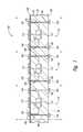
- FIG. 1is a side cross-sectional view of a portion of a microelectronic workpiece 100 configured in accordance with several embodiments of the disclosure.
- the workpiece 100can include a semiconductor substrate 101 with a plurality of dies 110 (e.g., imaging dies) formed in and/or on the substrate 101 .
- the substrate 101has a first or front side 102 and a second or back side 103 .
- the substrate 101may be a semiconductor wafer with the dies 110 arranged in a die pattern on the wafer.
- a first dielectric layer 104e.g., a passivation layer or other insulating layer
- the first dielectric layer 104can include silicon dioxide (SiO 2 ), silicon nitride (Si 3 N 4 ), borophosphosilicate glass (BPSG), borosilicate glass (BSG), or another suitable dielectric material.
- Individual dies 110can include integrated circuitry 112 , external contacts 120 electrically coupled to the integrated circuitry 112 with couplers 122 , and an image sensor 114 .
- the image sensors 114can be CMOS image sensors or CCD image sensors for capturing pictures or other images in the visible spectrum. In other embodiments, the image sensors 114 can detect radiation in other spectrums (e.g., IR or UV ranges).
- the illustrated dies 110have the same structure, in other embodiments the dies 110 can have different features to perform different functions.
- the external contacts 120 shown in FIG. 1provide a small array of back side contacts within the footprint of each die 110 .
- Each external contact 120can include a terminal or bond site 124 (e.g., a bond-pad), an external contact pad 126 (e.g., a ball-pad), and an interconnect 128 coupling the terminal 124 to the contact pad 126 .
- the terminals 124are external features at the front side 102 of the substrate 101
- the contact pads 126are external features at the back side 103 of the substrate 101
- the interconnects 128are through-substrate or through-wafer interconnects that extend completely through the substrate 101 to couple the terminals 124 to corresponding contact pads 126 .
- the terminals 124can be internal features that are embedded at an intermediate depth within the substrate 101 .
- the dies 110may not include the terminals 124 at the front side 102 of the substrate 101 such that the integrated circuitry 112 is coupled directly to the contact pads 126 at the back side 103 of the substrate 101 by interconnects that extend only through a portion of the substrate 101 .
- the workpiece 100can be cut along lines A-A to singulate the imaging dies 110 .
- the interconnects 128enable the external contact pads 126 to be located at the back side 103 of the substrate 101 .
- the back side arrays of contact pads 126allow the dies 110 to be stacked on other devices or attached directly to an interposer substrate without peripheral wire-bonds.
- the dies 110 with the interconnects 128can be more robust than dies that require wire-bonds, and the individual dies 110 also have a significantly smaller footprint and profile than conventional dies having wire-bonds extending outboard of the periphery portions of the respective die. Accordingly, the resulting imaging devices can have a significantly smaller footprint and lower profile than conventional imagers that require large interposing structures, and can be used in smaller electronic devices or other applications where space is limited.
- FIGS. 2A-3G described belowillustrate various embodiments of methods for forming the interconnects 128 shown in FIG. 1 . Although the following description illustrates formation of only a single interconnect, it will be appreciated that a plurality of interconnects are constructed simultaneously through a plurality of imaging dies on a wafer.
- FIGS. 2A-2Hillustrate various stages of a method for forming one embodiment of the interconnects 128 of FIG. 1 .
- FIG. 2Ais a schematic side cross-sectional view of the area 2 A shown in FIG. 1 at an initial stage of this process.
- the front side 102 of the substrate 101was attached to a support member 132 (e.g., a carrier substrate) with an adhesive material 134 .
- the support member 132(only a portion of which is shown) can be sized and shaped to receive the workpiece 100 and provide support to the workpiece during subsequent processing steps to prevent the workpiece from breaking and/or excessively warping.
- the support member 132is generally rigid and has a planform shape at least approximately identical to that of the workpiece 100 . In other embodiments, however, the support member 132 can have a different planform shape than the workpiece 100 .
- the support member 132can include a glass substrate, a silicon substrate, or a substrate formed from another suitable material.
- the substrate 101is thinned to a desired thickness “T” by removing material from the back side 103 of the substrate 101 .
- Tthe final thickness T of the substrate 101 is about 100-150 microns. In other embodiments, however, the substrate 101 can have a different final thickness T.
- the thickness of the support member 132 and/or the adhesive layer 134may also be adjusted so that the overall assembly has a desired thickness.
- the support member 132can have a thickness of about 600-650 microns so that the aggregate thickness of the assembly (about, for example, 700-750 ⁇ m) can be suitable for the form factor of typical semiconductor processing equipment used for subsequent processing of the workpiece 100 .
- the back side 103 of the substrate 101can be thinned using chemical-mechanical planarization (CMP) processes, dry etching processes, chemical etching processes, chemical polishing, grinding procedures, or other suitable processes.
- CMPchemical-mechanical planarization
- the back side 103 of the substrate 101can undergo further processing after thinning.
- the back side 103can be polished before any subsequent processing. This polishing step, however, is an optional step that may be omitted and/or performed at a different processing stage.
- a first mask 140is applied over the back side 103 and patterned.
- the first mask 140can be a layer of resist that is patterned according to the arrangement of terminals 122 at the front side 102 of the substrate 101 .
- the first mask 140is aligned with a corresponding terminal 124 .
- the individual mask portionscan remain on the workpiece 100 during a number of processing steps. Accordingly, the portions of the first mask 140 at the back side 103 of the substrate 101 can be “overbaked” to harden the mask portions so that they do not easily wash away or become damaged during subsequent processing steps.
- the back side 103 of the substrate 101is etched to an intermediate depth using a first etching process, such as an anisotropic etch, to form a pillar 142 .
- a first etching processsuch as an anisotropic etch
- the etchantremoves exposed material, but not material protected beneath the remaining portions of the mask 140 . Accordingly, the sidewalls of the pillar 142 are generally normal to the front side 102 of the substrate 101 . In other embodiments, however, other suitable etching processes may be used.
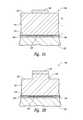
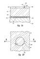
- FIG. 2Ca second mask 144 is applied onto the back side 103 and patterned to form a first opening 146 around the pillar 142 .
- FIG. 2Dis a top plan view of the portion of the back side 103 of the substrate 101 shown in FIG. 2C . Referring to FIGS. 2C and 2D together, the second mask 144 is patterned such that the first opening 146 is (a) inboard of a periphery portion of the terminal 124 , and (b) outboard of a periphery portion 143 of the pillar 142 to define an annulus 147 .
- the annulus 147is superimposed relative to the terminal 124 and has a first diameter or cross-sectional dimension less than a second diameter or cross-sectional dimension of the terminal 124 .
- an “annulus” or an opening have an “annular cross-sectional profile”refers to an opening or region between two generally concentric structures (e.g., a generally circular ring).
- the annulus 147has a width W 1 of about 15 microns. In other embodiments, however, the width W 1 of the annulus 147 can vary between about 1 micron and about 150 microns.
- the selected width W 1can be based at least in part on the arrangement or pitch of the terminals 124 and the composition of the dielectric or passivation material that is subsequently disposed onto an opening defined by the annulus 147 (as described in greater detail below with reference to FIG. 2F ).
- the second opening 150is a blind hole or via having a generally annular cross-sectional profile that extends from the back side 103 of the substrate 101 to expose at least a portion of the first dielectric layer 104 .
- a “blind hole” or a “blind via”refers to a hole or aperture that extends only partially through the substrate 101 or is otherwise closed at one end.
- the second opening 150separates the pillar 142 from the other remaining portions of the substrate 101 , thus forming an isolated island, core, or plug 151 of substrate material.
- the second etching processcan include, for example, a deep reactive ion etching process or another suitable etching process that is highly selective to the material of the substrate 101 relative to the material of the first dielectric layer 104 .
- the first dielectric layer 104can accordingly act as an etch-stop for the second etching process.
- an insulating material 152is deposited into the second opening 150 and over the entire back side 103 of the substrate 101 .
- the insulating layer 152electrically insulates components in the substrate 101 from the interconnect that will be subsequently be formed through the substrate 101 .
- the insulating material 152forms a continuous film or layer over the entire back side 103 of the substrate 101 and within the second opening 150 , but does not cover or otherwise extend outwardly past an upper surface 154 of the island 151 . In other embodiments, however, the insulating material 152 may not extend over the entire back side 103 of the substrate 101 .
- the insulating material 152can be composed of a polymer material, such as a filled epoxy material.
- the epoxy materialis typically filled with very small beads or particles of materials (e.g., silica, etc.) to produce the desired CTE within the epoxy material that matches or at least approximates the CTE of the surrounding materials.
- the insulating material 152can include Hysol® FP-4511, commercially available from Henkel Loctite Corporation of Industry, California. In other embodiments, however, the insulating material 152 can include other suitable materials.
- a third etching process(e.g., a wet or dry etch) is used to remove the portions of the substrate that compose the island 151 ( FIG. 2F ) to define a blind hole or via 160 .
- a fourth etching process(e.g., a dry etch) is used to remove the exposed portions of the first dielectric layer 104 within the blind hole 160 and expose at least a portion of the terminal 124 .
- the fourth etching processcan be highly selective to the material of the first dielectric layer 104 relative to the material of the terminal 124 .
- the fourth etching processaccordingly does not damage or significantly alter the general structure of the terminal 124 .
- the workpiece 100can undergo further processing prior to singulating the individual imaging dies 110 ( FIG. 1 ).
- a seed layer(not shown) can be deposited into the blind hole 160 and over at least a portion of the insulating material 152 using a suitable vapor deposition technique, such as physical vapor deposition (PVD), chemical vapor deposition (CVD), atomic layer deposition (ALD), and/or plating.
- the seed layercan be composed of copper or other suitable materials.
- a conductive fill material 162(shown in broken lines) can then be deposited into the blind hole 160 to form the interconnect 128 .
- the fill material 162can include Cu, Ni, Co, Ag, Au, solder, or other suitable materials or alloys of materials having the desired conductivity.
- the fill material 162can be deposited into the blind hole 160 using plating processes (e.g., electroless or electroplating processes), solder wave processes, screen printing techniques, vapor deposition processes, or other suitable techniques.
- the fill material 162does not completely fill the blind hole 160 .
- the fill material 162may only line the sidewalls of the blind hole 160 , thus leaving a portion of the blind hole hollow.
- a redistribution layer(not shown) may be formed at the back side 103 of the substrate 101 , and the support member 132 and adhesive material 134 can be removed from the front side 102 of the substrate 101 .
- interconnects 128may provide improved package reliability and robustness as compared with conventional packaged microelectronic devices.
- thermal cyclinginduces stresses that can cause components to delaminate.
- the stressesare induced because many of the materials in a microelectronic package have different CTEs so that they do not expand and contract the same amount during thermal cycling.
- delaminationoften occurs at the interfaces between various components and/or materials in the device. This in turn often leads to failure or malfunction of such devices.
- the insulating material 152 deposited into the second opening 150 and over the back side 103 of the substrate 101is composed of a polymer material (e.g., a filled epoxy material) that has a CTE approximately the same as the adjacent material.
- the insulating material 152can have a CTE of between about 22 and about 30 ppm/° C.
- the substrate 101e.g., a silicon material
- the insulating material 152is expected to help prevent excessive warping and/or undesirable relative movement between the various components during thermal processing.
- the sidewalls of the openings or through-holes formed in the substrateare lined with one or more dielectric layers before depositing a conductive fill material into the corresponding opening.
- the dielectric layer(s)electrically insulate components in the substrate from the interconnect that is subsequently formed in the opening.
- Conventional dielectric layer(s)are typically composed of a low temperature CVD material (e.g., a low temperature CVD oxide applied using a pulsed layer deposition process, tetraethylorthosilicate, Si 3 N 4 , SiO 2 , parylene) and/or other suitable dielectric materials that can be deposited onto the walls within the opening.
- embodiments of the methods described hereinallow a wide variety of different dielectric or insulating materials to be used to electrically insulate the components in the substrate 101 from the interconnect 128 .
- any type of insulating material 152 that can flow into the annular-shaped second opening 150can be used.
- the material selectionis not limited to only materials that can conformally coat the sidewalls of the via 160 . Accordingly, insulating materials having any of a variety of desired properties may be used when forming the interconnects 128 , thereby resulting in improved processes and microelectronic packages.
- FIGS. 3A-3Gillustrate various stages of another embodiment of a method for forming the interconnects 128 of FIG. 1 .
- FIG. 3Ais a schematic side cross-sectional view of a portion of a workpiece 200 at an initial stage of this process
- FIG. 3Bis a top view of the portion of the back side 103 of the substrate 101 shown in FIG. 3A .
- the first part of this methodis generally similar to the steps described above with reference to FIG. 2A .
- the support member 132has been attached to the front side 102 of the substrate 101 with the adhesive material 134 , and the substrate 101 has been thinned to a desired thickness.
- the stage of the method shown in FIGS. 3A and 3Bdiffers from that described above in FIG. 2A in that a first mask 240 is deposited onto the back side 103 and patterned differently than the first mask 140 described above with reference to FIG. 2A .
- the first mask 240can be a layer of resist that is patterned and etched to form a first opening 242 aligned with each terminal 124 .
- the first opening 242defines an annulus 244 having an outer periphery 245 inboard of a periphery portion of the terminal 124 .
- the annulus 244is superimposed relative to the terminal 124 and has a first diameter or cross-sectional dimension less than a second diameter or cross-sectional dimension of the terminal 124 .
- the annulus 244has a width W 2 generally similar to the width W 1 of the annulus 147 described above with reference to FIGS. 2C and 2D . In other embodiments, however, the annulus 244 can have a different width W 2 .
- the portions of the first mask 240 at the back side 103 of the substrate 101are typically not overbaked because they do not need to remain on the substrate 101 during a number of subsequent processing steps.
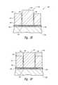
- the exposed portions of the substrate 101 within the annulus 244are etched using a first etching process to form a second opening 248 .
- the second opening 248is generally similar to the second opening 150 described above with reference to FIG. 2E .
- the second opening 248is a blind hole or via having a generally annular cross-sectional profile that extends from the back side 103 of the substrate 101 to the first dielectric layer 104 .
- the first etching processe.g., a reactive ion etching process
- the remaining portion of the substrate 101 within the second opening 248defines an island 250 that is isolated from the rest of the substrate 101 by the second opening 248 .
- the first mask 240FIG. 3A is removed from workpiece 200 .
- an insulating material 252is deposited into the second opening 248 and over the entire back side 103 of the substrate 101 .
- the insulating material 252can be composed of a polymer material (e.g., a filled epoxy material) generally similar to the insulating material 152 described above with reference to FIG. 2F . In other embodiments, however, the insulating material 252 can include other suitable materials.
- the overburden portion of the insulating material 252 on the back side 103 of the substrate 101is removed to leave insulating material 252 only in the second opening 248 .
- the overburden portion of the insulating material 252can be removed using a chemical-mechanical planarization (CMP) process, an etching process, and/or other suitable processes.
- CMPchemical-mechanical planarization
- the back side 103 of the substrate 101was not previously polished and, accordingly, the back side 103 can be polished during and/or after removing the overburden portion of the insulating material 252 .
- the back side 103may be polished before the processing steps described above with reference to FIG. 3A .
- the overburden portion of insulating material 252may be removed from the back side 103 using an “ashing” process at least generally similar to the process described above with reference to FIG. 2D rather than a CMP or etching process.
- a second dielectric layer 254(e.g., an RDL insulating layer) is deposited over the back side 103 and patterned to form a third opening 256 .
- the third opening 256is sized such that a periphery portion of the second opening 256 is at least partially aligned with the insulating material 252 within the second opening 248 and an exterior surface 251 of the island 250 is completely exposed.
- the second dielectric layer 254can include a photosensitive polymer material (e.g., a resist material) or another suitable material.
- a second etching processe.g., a wet etch
- a third etching processe.g., a dry etch
- the workpiece 200can undergo additional steps that are at least generally similar to those described above with reference to FIG. 2F to construct an interconnect 128 ( FIG. 1 ).
- any one of the imaging dies formed using the methods described above with reference to FIGS. 1-3Gcan be incorporated into any of a myriad of larger and/or more complex systems, a representative example of which is system 400 shown schematically in FIG. 4 .
- the system 400can include a processor 402 , a memory 404 (e.g., SRAM, DRAM, flash, and/or other memory device), input/output devices 406 , and/or other subsystems or components 408 .
- the foregoing imager devices described above with reference to FIGS. 1-3Gmay be included in any of the components shown in FIG. 4 .
- the resulting system 400can perform any of a wide variety of computing, processing, storage, sensing, imaging, and/or other functions.
- representative systems 400include, without limitation, cameras, computers and/or other data processors, for example, desktop computers, laptop computers, Internet appliances, hand-held devices (e.g., palm-top computers, wearable computers, cellular or mobile phones, personal digital assistants, etc.), light or other radiation sensors, multiprocessor systems, processor-based or programmable consumer electronics, network computers, and minicomputers.
- Other representative systems 400include servers and associated server subsystems, display devices, and/or memory devices. Components of the system 400 may be housed in a single unit or distributed over multiple, interconnected units (e.g., through a communications network). The components of the system 400 can accordingly include local and/or remote memory storage devices, and any of a wide variety of computer readable media.
Landscapes
- Engineering & Computer Science (AREA)
- Physics & Mathematics (AREA)
- Condensed Matter Physics & Semiconductors (AREA)
- General Physics & Mathematics (AREA)
- Computer Hardware Design (AREA)
- Microelectronics & Electronic Packaging (AREA)
- Power Engineering (AREA)
- Manufacturing & Machinery (AREA)
- Internal Circuitry In Semiconductor Integrated Circuit Devices (AREA)
Abstract
Description
Claims (17)
Priority Applications (1)
| Application Number | Priority Date | Filing Date | Title |
|---|---|---|---|
| US13/590,862US9281241B2 (en) | 2007-12-06 | 2012-08-21 | Methods for forming interconnects in microelectronic workpieces and microelectronic workpieces formed using such methods |
Applications Claiming Priority (3)
| Application Number | Priority Date | Filing Date | Title |
|---|---|---|---|
| US11/951,751US7884015B2 (en) | 2007-12-06 | 2007-12-06 | Methods for forming interconnects in microelectronic workpieces and microelectronic workpieces formed using such methods |
| US13/020,656US8247907B2 (en) | 2007-12-06 | 2011-02-03 | Methods for forming interconnects in microelectronic workpieces and microelectronic workpieces formed using such methods |
| US13/590,862US9281241B2 (en) | 2007-12-06 | 2012-08-21 | Methods for forming interconnects in microelectronic workpieces and microelectronic workpieces formed using such methods |
Related Parent Applications (1)
| Application Number | Title | Priority Date | Filing Date |
|---|---|---|---|
| US13/020,656DivisionUS8247907B2 (en) | 2007-12-06 | 2011-02-03 | Methods for forming interconnects in microelectronic workpieces and microelectronic workpieces formed using such methods |
Publications (2)
| Publication Number | Publication Date |
|---|---|
| US20130196501A1 US20130196501A1 (en) | 2013-08-01 |
| US9281241B2true US9281241B2 (en) | 2016-03-08 |
Family
ID=40348046
Family Applications (3)
| Application Number | Title | Priority Date | Filing Date |
|---|---|---|---|
| US11/951,751Active2028-11-17US7884015B2 (en) | 2007-12-06 | 2007-12-06 | Methods for forming interconnects in microelectronic workpieces and microelectronic workpieces formed using such methods |
| US13/020,656ActiveUS8247907B2 (en) | 2007-12-06 | 2011-02-03 | Methods for forming interconnects in microelectronic workpieces and microelectronic workpieces formed using such methods |
| US13/590,862ActiveUS9281241B2 (en) | 2007-12-06 | 2012-08-21 | Methods for forming interconnects in microelectronic workpieces and microelectronic workpieces formed using such methods |
Family Applications Before (2)
| Application Number | Title | Priority Date | Filing Date |
|---|---|---|---|
| US11/951,751Active2028-11-17US7884015B2 (en) | 2007-12-06 | 2007-12-06 | Methods for forming interconnects in microelectronic workpieces and microelectronic workpieces formed using such methods |
| US13/020,656ActiveUS8247907B2 (en) | 2007-12-06 | 2011-02-03 | Methods for forming interconnects in microelectronic workpieces and microelectronic workpieces formed using such methods |
Country Status (3)
| Country | Link |
|---|---|
| US (3) | US7884015B2 (en) |
| TW (1) | TWI433266B (en) |
| WO (1) | WO2009073367A1 (en) |
Families Citing this family (45)
| Publication number | Priority date | Publication date | Assignee | Title |
|---|---|---|---|---|
| US8084866B2 (en) | 2003-12-10 | 2011-12-27 | Micron Technology, Inc. | Microelectronic devices and methods for filling vias in microelectronic devices |
| SG120200A1 (en) | 2004-08-27 | 2006-03-28 | Micron Technology Inc | Slanted vias for electrical circuits on circuit boards and other substrates |
| US7795134B2 (en) | 2005-06-28 | 2010-09-14 | Micron Technology, Inc. | Conductive interconnect structures and formation methods using supercritical fluids |
| US20070045120A1 (en)* | 2005-09-01 | 2007-03-01 | Micron Technology, Inc. | Methods and apparatus for filling features in microfeature workpieces |
| US7863187B2 (en) | 2005-09-01 | 2011-01-04 | Micron Technology, Inc. | Microfeature workpieces and methods for forming interconnects in microfeature workpieces |
| US7262134B2 (en) | 2005-09-01 | 2007-08-28 | Micron Technology, Inc. | Microfeature workpieces and methods for forming interconnects in microfeature workpieces |
| US7629249B2 (en) | 2006-08-28 | 2009-12-08 | Micron Technology, Inc. | Microfeature workpieces having conductive interconnect structures formed by chemically reactive processes, and associated systems and methods |
| US7902643B2 (en) | 2006-08-31 | 2011-03-08 | Micron Technology, Inc. | Microfeature workpieces having interconnects and conductive backplanes, and associated systems and methods |
| SG149710A1 (en) | 2007-07-12 | 2009-02-27 | Micron Technology Inc | Interconnects for packaged semiconductor devices and methods for manufacturing such devices |
| SG150410A1 (en)* | 2007-08-31 | 2009-03-30 | Micron Technology Inc | Partitioned through-layer via and associated systems and methods |
| US7884015B2 (en)* | 2007-12-06 | 2011-02-08 | Micron Technology, Inc. | Methods for forming interconnects in microelectronic workpieces and microelectronic workpieces formed using such methods |
| US8084854B2 (en) | 2007-12-28 | 2011-12-27 | Micron Technology, Inc. | Pass-through 3D interconnect for microelectronic dies and associated systems and methods |
| US8253230B2 (en) | 2008-05-15 | 2012-08-28 | Micron Technology, Inc. | Disabling electrical connections using pass-through 3D interconnects and associated systems and methods |
| US8053336B2 (en)* | 2008-11-12 | 2011-11-08 | Taiwan Semiconductor Manufacturing Company, Ltd. | Method for reducing chip warpage |
| CN101494951A (en)* | 2009-02-18 | 2009-07-29 | 旭丽电子(广州)有限公司 | Printed circuit board |
| US7947601B2 (en)* | 2009-03-24 | 2011-05-24 | Micron Technology, Inc. | Semiconductor devices and methods for forming patterned radiation blocking on a semiconductor device |
| US9406561B2 (en)* | 2009-04-20 | 2016-08-02 | International Business Machines Corporation | Three dimensional integrated circuit integration using dielectric bonding first and through via formation last |
| FR2946795B1 (en)* | 2009-06-12 | 2011-07-22 | 3D Plus | METHOD FOR POSITIONING CHIPS WHEN MANUFACTURING A RECONSTITUTED PLATE |
| US8278756B2 (en)* | 2010-02-24 | 2012-10-02 | Inpaq Technology Co., Ltd. | Single chip semiconductor coating structure and manufacturing method thereof |
| FR2957481B1 (en)* | 2010-03-10 | 2012-08-31 | Commissariat Energie Atomique | INTERCONNECTION STRUCTURE COMPRISING VIAS BORGNES FOR METALLIZATION |
| DE102011010248B3 (en)* | 2011-02-03 | 2012-07-12 | Infineon Technologies Ag | Method for manufacturing power semiconductor device e.g. insulated gate bipolar transistor, involves forming trenches partially filled with insulating material starting from side to side in regions of semiconductor structure |
| JP2012222323A (en) | 2011-04-14 | 2012-11-12 | Canon Inc | Through-hole substrate and manufacturing method thereof |
| US8742574B2 (en) | 2011-08-09 | 2014-06-03 | Maxim Integrated Products, Inc. | Semiconductor device having a through-substrate via |
| US8748828B2 (en)* | 2011-09-21 | 2014-06-10 | Kla-Tencor Corporation | Interposer based imaging sensor for high-speed image acquisition and inspection systems |
| DE102012200840A1 (en)* | 2012-01-20 | 2013-07-25 | Robert Bosch Gmbh | Component with a via |
| DE102012210472B4 (en)* | 2012-06-21 | 2024-12-12 | Robert Bosch Gmbh | Method for producing a component with an electrical via |
| US8563403B1 (en) | 2012-06-27 | 2013-10-22 | International Business Machines Corporation | Three dimensional integrated circuit integration using alignment via/dielectric bonding first and through via formation last |
| US9667900B2 (en)* | 2013-12-09 | 2017-05-30 | Optiz, Inc. | Three dimensional system-on-chip image sensor package |
| US9476927B2 (en) | 2014-01-22 | 2016-10-25 | GlobalFoundries, Inc. | Structure and method to determine through silicon via build integrity |
| KR102473664B1 (en) | 2016-01-19 | 2022-12-02 | 삼성전자주식회사 | Multi-Stacked Device Having a TSV Structure |
| US10236208B2 (en)* | 2016-06-16 | 2019-03-19 | Advanced Semiconductor Engineering, Inc. | Semiconductor package structure and method of manufacturing the same |
| IT201900006740A1 (en) | 2019-05-10 | 2020-11-10 | Applied Materials Inc | SUBSTRATE STRUCTURING PROCEDURES |
| IT201900006736A1 (en) | 2019-05-10 | 2020-11-10 | Applied Materials Inc | PACKAGE MANUFACTURING PROCEDURES |
| US11931855B2 (en) | 2019-06-17 | 2024-03-19 | Applied Materials, Inc. | Planarization methods for packaging substrates |
| US11862546B2 (en) | 2019-11-27 | 2024-01-02 | Applied Materials, Inc. | Package core assembly and fabrication methods |
| US11257790B2 (en) | 2020-03-10 | 2022-02-22 | Applied Materials, Inc. | High connectivity device stacking |
| US11454884B2 (en) | 2020-04-15 | 2022-09-27 | Applied Materials, Inc. | Fluoropolymer stamp fabrication method |
| US11400545B2 (en) | 2020-05-11 | 2022-08-02 | Applied Materials, Inc. | Laser ablation for package fabrication |
| US20230207385A1 (en)* | 2020-06-19 | 2023-06-29 | Corning Incorporated | Techniques for creating blind annular vias for metallized vias |
| US11232951B1 (en) | 2020-07-14 | 2022-01-25 | Applied Materials, Inc. | Method and apparatus for laser drilling blind vias |
| US11676832B2 (en) | 2020-07-24 | 2023-06-13 | Applied Materials, Inc. | Laser ablation system for package fabrication |
| US11521937B2 (en) | 2020-11-16 | 2022-12-06 | Applied Materials, Inc. | Package structures with built-in EMI shielding |
| US11404318B2 (en) | 2020-11-20 | 2022-08-02 | Applied Materials, Inc. | Methods of forming through-silicon vias in substrates for advanced packaging |
| US11705365B2 (en) | 2021-05-18 | 2023-07-18 | Applied Materials, Inc. | Methods of micro-via formation for advanced packaging |
| US12183684B2 (en) | 2021-10-26 | 2024-12-31 | Applied Materials, Inc. | Semiconductor device packaging methods |
Citations (477)
| Publication number | Priority date | Publication date | Assignee | Title |
|---|---|---|---|---|
| US2821959A (en) | 1956-03-29 | 1958-02-04 | Bell Telephone Labor Inc | Mass soldering of electrical assemblies |
| US3006318A (en) | 1958-03-26 | 1961-10-31 | Western Electric Co | Apparatus for applying solder coatings to surfaces |
| US3345134A (en) | 1962-04-21 | 1967-10-03 | Knapsack Ag | Process and apparatus for the manufacture of titanium nitride |
| US3865298A (en) | 1973-08-14 | 1975-02-11 | Atomic Energy Commission | Solder leveling |
| US3902036A (en) | 1974-05-02 | 1975-08-26 | Western Electric Co | Control system using multiplexed laser beams |
| US4040168A (en) | 1975-11-24 | 1977-08-09 | Rca Corporation | Fabrication method for a dual gate field-effect transistor |
| US4368106A (en) | 1980-10-27 | 1983-01-11 | General Electric Company | Implantation of electrical feed-through conductors |
| EP0127946A1 (en) | 1983-05-10 | 1984-12-12 | BRITISH TELECOMMUNICATIONS public limited company | Method of producing a via in a semiconductor device |
| US4534100A (en) | 1982-06-28 | 1985-08-13 | The United States Of America As Represented By The Secretary Of The Air Force | Electrical method of making conductive paths in silicon |
| US4581301A (en) | 1984-04-10 | 1986-04-08 | Michaelson Henry W | Additive adhesive based process for the manufacture of printed circuit boards |
| US4608480A (en) | 1983-06-15 | 1986-08-26 | S.N.E.C.M.A. | Process and apparatus for laser drilling |
| US4614427A (en) | 1983-05-20 | 1986-09-30 | Hitachi, Ltd. | Automatic contaminants detection apparatus |
| US4627971A (en) | 1985-04-22 | 1986-12-09 | Alza Corporation | Osmotic device with self-sealing passageway |
| US4660063A (en) | 1985-03-18 | 1987-04-21 | General Electric Company | Immersion type ISFET |
| JPS6352432A (en) | 1986-08-22 | 1988-03-05 | Hitachi Vlsi Eng Corp | semiconductor equipment |
| US4756765A (en) | 1982-01-26 | 1988-07-12 | Avco Research Laboratory, Inc. | Laser removal of poor thermally-conductive materials |
| US4818728A (en) | 1986-12-03 | 1989-04-04 | Sharp Kabushiki Kaisha | Method of making a hybrid semiconductor device |
| JPH01252308A (en) | 1988-03-31 | 1989-10-09 | Toppan Printing Co Ltd | Hole formation method for multilayer circuit wiring board |
| US4907127A (en) | 1988-03-21 | 1990-03-06 | Lee John K C | Printed circuit board construction and method for producing printed circuit end products |
| JPH02235589A (en) | 1989-03-09 | 1990-09-18 | Fuji Electric Co Ltd | Laser beam machining method |
| US4959705A (en) | 1988-10-17 | 1990-09-25 | Ford Microelectronics, Inc. | Three metal personalization of application specific monolithic microwave integrated circuit |
| US4964212A (en) | 1988-09-29 | 1990-10-23 | Commissariat A L'energie Atomique | Process for producing electrical connections through a substrate |
| US5006922A (en) | 1990-02-14 | 1991-04-09 | Motorola, Inc. | Packaged semiconductor device having a low cost ceramic PGA package |
| US5024966A (en) | 1988-12-21 | 1991-06-18 | At&T Bell Laboratories | Method of forming a silicon-based semiconductor optical device mount |
| US5027184A (en) | 1981-03-02 | 1991-06-25 | Rockwell International Corporation | NPN type lateral transistor with minimal substrate operation interference |
| US5026964A (en) | 1986-02-28 | 1991-06-25 | General Electric Company | Optical breakthrough sensor for laser drill |
| US5037782A (en) | 1989-03-29 | 1991-08-06 | Mitsubishi Denki Kabushiki Kaisha | Method of making a semiconductor device including via holes |
| US5098864A (en) | 1989-11-29 | 1992-03-24 | Olin Corporation | Process for manufacturing a metal pin grid array package |
| US5102829A (en) | 1991-07-22 | 1992-04-07 | At&T Bell Laboratories | Plastic pin grid array package |
| US5123902A (en) | 1988-09-13 | 1992-06-23 | Carl-Zeiss-Stiftung | Method and apparatus for performing surgery on tissue wherein a laser beam is applied to the tissue |
| US5144412A (en) | 1987-02-19 | 1992-09-01 | Olin Corporation | Process for manufacturing plastic pin grid arrays and the product produced thereby |
| US5145099A (en) | 1990-07-13 | 1992-09-08 | Micron Technology, Inc. | Method for combining die attach and lead bond in the assembly of a semiconductor package |
| US5158911A (en) | 1990-08-03 | 1992-10-27 | Thomson Composants Microondes | Method for interconnection between an integrated circuit and a support circuit, and integrated circuit adapted to this method |
| US5200366A (en) | 1990-04-27 | 1993-04-06 | Hitachi, Ltd. | Semiconductor device, its fabrication method and molding apparatus used therefor |
| JPH05104316A (en) | 1991-10-15 | 1993-04-27 | Nec Corp | Counter boring device |
| US5219344A (en) | 1988-06-09 | 1993-06-15 | Visx, Incorporated | Methods and apparatus for laser sculpture of the cornea |
| US5233448A (en) | 1992-05-04 | 1993-08-03 | Industrial Technology Research Institute | Method of manufacturing a liquid crystal display panel including photoconductive electrostatic protection |
| US5237148A (en) | 1990-10-04 | 1993-08-17 | Brother Kogyo Kabushiki | Device for manufacturing a nozzle and its manufacturing method |
| US5291062A (en) | 1993-03-01 | 1994-03-01 | Motorola, Inc. | Area array semiconductor device having a lid with functional contacts |
| US5289631A (en) | 1992-03-04 | 1994-03-01 | Mcnc | Method for testing, burn-in, and/or programming of integrated circuit chips |
| US5292686A (en) | 1991-08-21 | 1994-03-08 | Triquint Semiconductor, Inc. | Method of forming substrate vias in a GaAs wafer |
| US5304743A (en) | 1992-05-12 | 1994-04-19 | Lsi Logic Corporation | Multilayer IC semiconductor package |
| US5378313A (en) | 1993-12-22 | 1995-01-03 | Pace; Benedict G. | Hybrid circuits and a method of manufacture |
| US5378312A (en) | 1993-12-07 | 1995-01-03 | International Business Machines Corporation | Process for fabricating a semiconductor structure having sidewalls |
| US5380681A (en) | 1994-03-21 | 1995-01-10 | United Microelectronics Corporation | Three-dimensional multichip package and methods of fabricating |
| US5402435A (en) | 1993-03-05 | 1995-03-28 | Matsushita Electric Industrial Co., Ltd. | Optical device |
| US5406630A (en) | 1992-05-04 | 1995-04-11 | Motorola, Inc. | Tamperproof arrangement for an integrated circuit device |
| US5424573A (en) | 1992-03-04 | 1995-06-13 | Hitachi, Ltd. | Semiconductor package having optical interconnection access |
| TW250597B (en) | 1993-06-04 | 1995-07-01 | Framatome & Cie | |
| US5438212A (en) | 1993-02-25 | 1995-08-01 | Mitsubishi Denki Kabushiki Kaisha | Semiconductor device with heat dissipation structure |
| US5447871A (en) | 1993-03-05 | 1995-09-05 | Goldstein; Edward F. | Electrically conductive interconnection through a body of semiconductor material |
| US5464960A (en) | 1993-01-12 | 1995-11-07 | Iatrotech, Inc. | Laser calibration device |
| US5481483A (en) | 1992-11-23 | 1996-01-02 | Ford Motor Company | Non-contact method of obtaining dimensional information about an object for comparing similar objects |
| US5485039A (en) | 1991-12-27 | 1996-01-16 | Hitachi, Ltd. | Semiconductor substrate having wiring conductors at a first main surface electrically connected to plural pins at a second main surface |
| US5496755A (en) | 1989-11-29 | 1996-03-05 | Texas Instruments Incorporated | Integrated circuit and method |
| US5515167A (en) | 1994-09-13 | 1996-05-07 | Hughes Aircraft Company | Transparent optical chuck incorporating optical monitoring |
| US5518956A (en) | 1993-09-02 | 1996-05-21 | General Electric Company | Method of isolating vertical shorts in an electronic array using laser ablation |
| US5550403A (en) | 1994-06-02 | 1996-08-27 | Lsi Logic Corporation | Improved laminate package for an integrated circuit and integrated circuit having such a package |
| US5585308A (en) | 1993-12-23 | 1996-12-17 | Sgs-Thomson Microelectronics, Inc. | Method for improved pre-metal planarization |
| US5585675A (en) | 1994-05-11 | 1996-12-17 | Harris Corporation | Semiconductor die packaging tub having angularly offset pad-to-pad via structure configured to allow three-dimensional stacking and electrical interconnections among multiple identical tubs |
| US5614743A (en) | 1994-07-26 | 1997-03-25 | Kabushiki Kaisha Toshiba | Microwave integrated circuit (MIC) having a reactance element formed on a groove |
| US5618752A (en) | 1995-06-05 | 1997-04-08 | Harris Corporation | Method of fabrication of surface mountable integrated circuits |
| US5624437A (en) | 1995-03-28 | 1997-04-29 | Freeman; Jerre M. | High resolution, high speed, programmable laser beam modulating apparatus for microsurgery |
| US5627106A (en) | 1994-05-06 | 1997-05-06 | United Microelectronics Corporation | Trench method for three dimensional chip connecting during IC fabrication |
| US5646067A (en) | 1995-06-05 | 1997-07-08 | Harris Corporation | Method of bonding wafers having vias including conductive material |
| US5654221A (en) | 1994-10-17 | 1997-08-05 | International Business Machines Corporation | Method for forming semiconductor chip and electronic module with integrated surface interconnects/components |
| US5673846A (en) | 1995-08-24 | 1997-10-07 | International Business Machines Corporation | Solder anchor decal and method |
| US5684642A (en) | 1994-02-22 | 1997-11-04 | Mitsubishi Denki Kabushiki Kaisha | Optical transmission system and light radiating method |
| US5690841A (en) | 1993-12-10 | 1997-11-25 | Pharmacia Biotech Ab | Method of producing cavity structures |
| US5718791A (en) | 1995-06-05 | 1998-02-17 | R + S Stanztechnik Gmbh | Method of laminating a trim panel and folding a cover sheet edge around the panel rim |
| US5723904A (en) | 1993-03-10 | 1998-03-03 | Sumitomo Electric Industries, Ltd. | Packaged semiconductor device suitable to be mounted and connected to microstrip line structure board |
| US5726493A (en) | 1994-06-13 | 1998-03-10 | Fujitsu Limited | Semiconductor device and semiconductor device unit having ball-grid-array type package structure |
| US5734555A (en) | 1994-03-30 | 1998-03-31 | Intel Corporation | Shared socket multi-chip module and/or piggyback pin grid array package |
| US5771158A (en) | 1995-09-21 | 1998-06-23 | Mitsubishi Denki Kabushiki Kaisha | Printed circuit board, printed circuit board used for flat panel display drive circuit, and flat panel display device |
| US5773359A (en) | 1995-12-26 | 1998-06-30 | Motorola, Inc. | Interconnect system and method of fabrication |
| US5776824A (en) | 1995-12-22 | 1998-07-07 | Micron Technology, Inc. | Method for producing laminated film/metal structures for known good die ("KG") applications |
| US5811799A (en) | 1997-07-31 | 1998-09-22 | Wu; Liang-Chung | Image sensor package having a wall with a sealed cover |
| US5821532A (en) | 1997-06-16 | 1998-10-13 | Eastman Kodak Company | Imager package substrate |
| US5825080A (en) | 1995-12-18 | 1998-10-20 | Atr Optical And Radio Communications Research Laboratories | Semiconductor device provided with surface grounding conductor for covering surfaces of electrically insulating films |
| US5826628A (en) | 1996-01-24 | 1998-10-27 | Micron Technology, Inc. | Form tooling and method of forming semiconductor package leads |
| US5847454A (en) | 1993-02-04 | 1998-12-08 | Cornell Research Foundcatton, Inc. | Electrically isolated released microstructures |
| US5851845A (en) | 1995-12-18 | 1998-12-22 | Micron Technology, Inc. | Process for packaging a semiconductor die using dicing and testing |
| US5857963A (en) | 1996-07-17 | 1999-01-12 | Welch Allyn, Inc. | Tab imager assembly for use in an endoscope |
| US5861654A (en) | 1995-11-28 | 1999-01-19 | Eastman Kodak Company | Image sensor assembly |
| US5870289A (en) | 1994-12-15 | 1999-02-09 | Hitachi, Ltd. | Chip connection structure having diret through-hole connections through adhesive film and wiring substrate |
| US5870823A (en) | 1996-11-27 | 1999-02-16 | International Business Machines Corporation | Method of forming a multilayer electronic packaging substrate with integral cooling channels |
| US5893828A (en) | 1996-05-02 | 1999-04-13 | Uram; Martin | Contact laser surgical endoscope and associated myringotomy procedure |
| US5904499A (en) | 1994-12-22 | 1999-05-18 | Pace; Benedict G | Package for power semiconductor chips |
| US5969422A (en) | 1997-05-15 | 1999-10-19 | Advanced Micro Devices, Inc. | Plated copper interconnect structure |
| US5998240A (en) | 1996-07-22 | 1999-12-07 | Northrop Grumman Corporation | Method of extracting heat from a semiconductor body and forming microchannels therein |
| US5998292A (en) | 1997-11-12 | 1999-12-07 | International Business Machines Corporation | Method for making three dimensional circuit integration |
| US6004867A (en) | 1996-12-16 | 1999-12-21 | Samsung Electronics Co., Ltd. | Chip-size packages assembled using mass production techniques at the wafer-level |
| US6008914A (en) | 1994-04-28 | 1999-12-28 | Mitsubishi Denki Kabushiki Kaisha | Laser transfer machining apparatus |
| US6008070A (en) | 1998-05-21 | 1999-12-28 | Micron Technology, Inc. | Wafer level fabrication and assembly of chip scale packages |
| US6080291A (en) | 1998-07-10 | 2000-06-27 | Semitool, Inc. | Apparatus for electrochemically processing a workpiece including an electrical contact assembly having a seal member |
| US6097087A (en) | 1997-10-31 | 2000-08-01 | Micron Technology, Inc. | Semiconductor package including flex circuit, interconnects and dense array external contacts |
| US6103547A (en) | 1997-01-17 | 2000-08-15 | Micron Technology, Inc. | High speed IC package configuration |
| US6107679A (en) | 1997-12-22 | 2000-08-22 | Oki Electric Industry Co., Ltd. | Semiconductor device |
| US6107186A (en) | 1999-01-27 | 2000-08-22 | Advanced Micro Devices, Inc. | High planarity high-density in-laid metallization patterns by damascene-CMP processing |
| US6107180A (en) | 1998-01-30 | 2000-08-22 | Motorola, Inc. | Method for forming interconnect bumps on a semiconductor die |
| US6110825A (en) | 1997-11-26 | 2000-08-29 | Stmicroelectronics, S.R.L. | Process for forming front-back through contacts in micro-integrated electronic devices |
| US6114240A (en) | 1997-12-18 | 2000-09-05 | Micron Technology, Inc. | Method for fabricating semiconductor components using focused laser beam |
| US6119335A (en) | 1997-12-02 | 2000-09-19 | Samsung Electro-Mechanics Co., Ltd. | Method for manufacturing multi-layer printed circuit board |
| US6124634A (en) | 1996-03-07 | 2000-09-26 | Micron Technology, Inc. | Micromachined chip scale package |
| US6130141A (en) | 1998-10-14 | 2000-10-10 | Lucent Technologies Inc. | Flip chip metallization |
| US6137182A (en) | 1996-07-23 | 2000-10-24 | Advanced Micro Devices, Inc. | Method of reducing via and contact dimensions beyond photolithography equipment limits |
| US6137163A (en) | 1997-09-12 | 2000-10-24 | Hyundai Electronics Industries Co., Ltd. | Semiconductor substrate and stackable semiconductor package and fabrication method thereof |
| US6140604A (en) | 1998-06-18 | 2000-10-31 | General Electric Company | Laser drilling breakthrough detector |
| US6143588A (en) | 1997-09-09 | 2000-11-07 | Amkor Technology, Inc. | Method of making an integrated circuit package employing a transparent encapsulant |
| US6148509A (en) | 1997-04-07 | 2000-11-21 | Micron Technology, Inc. | Method for supporting an integrated circuit die |
| US6159764A (en) | 1997-07-02 | 2000-12-12 | Micron Technology, Inc. | Varied-thickness heat sink for integrated circuit (IC) packages and method of fabricating IC packages |
| US6180518B1 (en) | 1999-10-29 | 2001-01-30 | Lucent Technologies Inc. | Method for forming vias in a low dielectric constant material |
| US6184060B1 (en) | 1996-10-29 | 2001-02-06 | Trusi Technologies Llc | Integrated circuits and methods for their fabrication |
| US6184465B1 (en) | 1998-11-12 | 2001-02-06 | Micron Technology, Inc. | Semiconductor package |
| US6187615B1 (en) | 1998-08-28 | 2001-02-13 | Samsung Electronics Co., Ltd. | Chip scale packages and methods for manufacturing the chip scale packages at wafer level |
| US6191487B1 (en) | 1998-04-23 | 2001-02-20 | Minco Technology Labs, Inc. | Semiconductor and flip chip packages and method having a back-side connection |
| KR20010018694A (en) | 1999-08-21 | 2001-03-15 | 윤종용 | Manufacturing method for three demensional stack chip package |
| US6203539B1 (en) | 1993-05-07 | 2001-03-20 | Visx, Incorporated | Method and system for laser treatment of refractive errors using offset imaging |
| JP2001077496A (en) | 1999-09-06 | 2001-03-23 | Ngk Insulators Ltd | Substrate for printed circuit and its manufacture |
| JP2001082931A (en) | 1999-09-09 | 2001-03-30 | Toshiba Corp | Hole depth measuring method and hole depth measuring device |
| US6221769B1 (en) | 1999-03-05 | 2001-04-24 | International Business Machines Corporation | Method for integrated circuit power and electrical connections via through-wafer interconnects |
| US6222270B1 (en) | 1997-06-24 | 2001-04-24 | Samsung Electronics Co., Ltd. | Integrated circuit bonding pads including closed vias and closed conductive patterns |
| US6222136B1 (en) | 1997-11-12 | 2001-04-24 | International Business Machines Corporation | Printed circuit board with continuous connective bumps |
| US6228687B1 (en) | 1999-06-28 | 2001-05-08 | Micron Technology, Inc. | Wafer-level package and methods of fabricating |
| US6229202B1 (en) | 2000-01-10 | 2001-05-08 | Micron Technology, Inc. | Semiconductor package having downset leadframe for reducing package bow |
| US6235552B1 (en) | 1999-07-09 | 2001-05-22 | Samsung Electronics Co., Ltd. | Chip scale package and method for manufacturing the same using a redistribution substrate |
| US6246108B1 (en) | 1997-09-15 | 2001-06-12 | Micron Technology, Inc. | Integrated circuit package including lead frame with electrically isolated alignment feature |
| US6252300B1 (en) | 1999-01-14 | 2001-06-26 | United Microelectronics Corp. | Direct contact through hole type wafer structure |
| US6268114B1 (en) | 1998-09-18 | 2001-07-31 | Taiwan Semiconductor Manufacturing Company, Ltd | Method for forming fine-pitched solder bumps |
| US6271580B1 (en) | 1996-12-30 | 2001-08-07 | Micron Technology, Inc. | Leads under chip in conventional IC package |
| US6277757B1 (en) | 1999-06-01 | 2001-08-21 | Winbond Electronics Corp. | Methods to modify wet by dry etched via profile |
| US20010020739A1 (en) | 2000-03-09 | 2001-09-13 | Nec Corporation | Flip chip type semiconductor device and method for manufacturing the same |
| US6291894B1 (en) | 1998-08-31 | 2001-09-18 | Micron Technology, Inc. | Method and apparatus for a semiconductor package for vertical surface mounting |
| US6294837B1 (en) | 1997-12-18 | 2001-09-25 | Micron Technology, Inc. | Semiconductor interconnect having laser machined contacts |
| US6297155B1 (en) | 1999-05-03 | 2001-10-02 | Motorola Inc. | Method for forming a copper layer over a semiconductor wafer |
| JP2001298147A (en) | 2000-04-18 | 2001-10-26 | Kawasaki Steel Corp | Semiconductor device and manufacturing method thereof |
| EP1154474A1 (en) | 1999-08-23 | 2001-11-14 | Rohm Co., Ltd. | Semiconductor device and method of manufacture thereof |
| US6324253B1 (en) | 1998-08-26 | 2001-11-27 | Yuyama Mfg. Co., Ltd. | Tablet inspection apparatus |
| US6326689B1 (en) | 1999-07-26 | 2001-12-04 | Stmicroelectronics, Inc. | Backside contact for touchchip |
| US6329632B1 (en) | 1998-07-30 | 2001-12-11 | Societe Nationale d'Etude et de Construction de Moteurs d'Aviation “SNECMA” | Method and device for machining holes or shapes of varying profile using an excimer laser |
| US20020005583A1 (en) | 2000-06-07 | 2002-01-17 | Mitsubishi Denki Kabushiki Kaisha | Semiconductor device and fabrication process therefor |
| US6341009B1 (en) | 2000-02-24 | 2002-01-22 | Quantronix Corporation | Laser delivery system and method for photolithographic mask repair |
| JP2002018585A (en) | 1999-12-23 | 2002-01-22 | Matsushita Electric Ind Co Ltd | Method and apparatus for drilling holes with a sub-wavelength pitch using a laser |
| US6344976B1 (en) | 1997-04-07 | 2002-02-05 | Micron Technology, Inc. | Interdigitated leads-over-chip lead frame device and method for supporting an integrated circuit die |
| US20020020898A1 (en) | 2000-08-16 | 2002-02-21 | Vu Quat T. | Microelectronic substrates with integrated devices |
| US6353262B1 (en) | 1997-04-03 | 2002-03-05 | Yamatake Corporation | Circuit substrate, detector, and method of manufacturing the same |
| US20020027293A1 (en) | 2001-06-28 | 2002-03-07 | Fujitsu Limited | Three dimensional semiconductor integrated circuit device and method for making the same |
| US6359254B1 (en) | 1999-09-30 | 2002-03-19 | United Technologies Corporation | Method for producing shaped hole in a structure |
| US6359328B1 (en) | 1998-12-31 | 2002-03-19 | Intel Corporation | Methods for making interconnects and diffusion barriers in integrated circuits |
| KR20020022122A (en) | 2000-07-27 | 2002-03-25 | 크리스띠앙 쥘랭 | Process for fabricating a multilevel circuitry comprising tracks and microvias |
| US6372548B2 (en) | 1998-06-04 | 2002-04-16 | Matsushita Electric Industrial Co., Ltd. | Method for fabricating a semiconductor package with a semiconductor device attached to a multilayered substrate |
| US6388208B1 (en) | 1999-06-11 | 2002-05-14 | Teradyne, Inc. | Multi-connection via with electrically isolated segments |
| US20020057468A1 (en) | 2000-11-14 | 2002-05-16 | Masao Segawa | Image pickup apparatus, method thereof, and electric apparatus |
| US6391770B2 (en) | 1997-04-24 | 2002-05-21 | Mitsubishi Denki Kabushiki Kaisha | Method of manufacturing semiconductor device |
| US20020059722A1 (en) | 1995-07-27 | 2002-05-23 | Nec Corporation | Method of mounting a semiconductor device to a substrate and a mounted structure |
| US6406636B1 (en) | 1999-06-02 | 2002-06-18 | Megasense, Inc. | Methods for wafer to wafer bonding using microstructures |
| US20020094607A1 (en) | 2001-01-16 | 2002-07-18 | Uta Gebauer | Electronic component with stacked semiconductor chips and method of producing the component |
| US20020096729A1 (en) | 2001-01-24 | 2002-07-25 | Tu Hsiu Wen | Stacked package structure of image sensor |
| KR20020061812A (en) | 2001-01-18 | 2002-07-25 | 삼성전자 주식회사 | Ball grid array type multi chip package and stack package |
| US6433304B2 (en) | 1999-12-22 | 2002-08-13 | Honda Giken Kogyo Kabushiki Kaisha | Perforating machining method with laser beam |
| US6432821B1 (en) | 2000-12-18 | 2002-08-13 | Intel Corporation | Method of copper electroplating |
| US6433303B1 (en) | 2000-03-31 | 2002-08-13 | Matsushita Electric Industrial Co., Ltd. | Method and apparatus using laser pulses to make an array of microcavity holes |
| US6437441B1 (en) | 1997-07-10 | 2002-08-20 | Kawasaki Microelectronics, Inc. | Wiring structure of a semiconductor integrated circuit and a method of forming the wiring structure |
| US6437284B1 (en) | 1999-06-25 | 2002-08-20 | Mitsubishi Denki Kabushiki Kaisha | Optical system and apparatus for laser heat treatment and method for producing semiconductor devices by using the same |
| US6441487B2 (en) | 1997-10-20 | 2002-08-27 | Flip Chip Technologies, L.L.C. | Chip scale package using large ductile solder balls |
| US6444576B1 (en) | 2000-06-16 | 2002-09-03 | Chartered Semiconductor Manufacturing, Ltd. | Three dimensional IC package module |
| US6448106B1 (en) | 1999-11-09 | 2002-09-10 | Fujitsu Limited | Modules with pins and methods for making modules with pins |
| US6452270B1 (en) | 2000-10-13 | 2002-09-17 | Advanced Semiconductor Engineering, Inc. | Semiconductor device having bump electrode |
| US20020130390A1 (en) | 2001-03-13 | 2002-09-19 | Ming-Dou Ker | ESD protection circuit with very low input capacitance for high-frequency I/O ports |
| US6455425B1 (en) | 2000-01-18 | 2002-09-24 | Advanced Micro Devices, Inc. | Selective deposition process for passivating top interface of damascene-type Cu interconnect lines |
| US6459150B1 (en) | 2000-08-17 | 2002-10-01 | Industrial Technology Research Institute | Electronic substrate having an aperture position through a substrate, conductive pads, and an insulating layer |
| US6457515B1 (en) | 1999-08-06 | 2002-10-01 | The Ohio State University | Two-layered micro channel heat sink, devices and systems incorporating same |
| US6459039B1 (en) | 2000-06-19 | 2002-10-01 | International Business Machines Corporation | Method and apparatus to manufacture an electronic package with direct wiring pattern |
| US6468889B1 (en) | 2000-08-08 | 2002-10-22 | Advanced Micro Devices, Inc. | Backside contact for integrated circuit and method of forming same |
| US6486549B1 (en) | 2001-11-10 | 2002-11-26 | Bridge Semiconductor Corporation | Semiconductor module with encapsulant base |
| US20020190371A1 (en) | 2001-06-14 | 2002-12-19 | Shinko Electric Industries Co., Ltd. | Semiconductor device and method of production of same |
| US20030014895A1 (en) | 1999-10-08 | 2003-01-23 | Lizotte Todd E. | Control system for ablating high-density array of vias or indentation in surface of object |
| US6521516B2 (en) | 2001-06-29 | 2003-02-18 | Intel Corporation | Process for local on-chip cooling of semiconductor devices using buried microchannels |
| US6521530B2 (en) | 1998-11-13 | 2003-02-18 | Fujitsu Limited | Composite interposer and method for producing a composite interposer |
| US20030042564A1 (en) | 2000-12-04 | 2003-03-06 | Fujitsu Limited | Semiconductor device having an interconnecting post formed on an interposer within a sealing resin |
| US6534863B2 (en) | 2001-02-09 | 2003-03-18 | International Business Machines Corporation | Common ball-limiting metallurgy for I/O sites |
| US6534192B1 (en) | 1999-09-24 | 2003-03-18 | Lucent Technologies Inc. | Multi-purpose finish for printed wiring boards and method of manufacture of such boards |
| US6545563B1 (en) | 1990-07-16 | 2003-04-08 | Raytheon Company | Digitally controlled monolithic microwave integrated circuits |
| US6555782B2 (en) | 1997-12-12 | 2003-04-29 | Matsushita Electric Industrial Co., Ltd. | Laser machining method, laser machining apparatus, and its control method |
| US6560047B2 (en) | 2001-08-29 | 2003-05-06 | Samsung Electro-Mechanics Co., Ltd. | Image module |
| US6569777B1 (en) | 2002-10-02 | 2003-05-27 | Taiwan Semiconductor Manufacturing Co., Ltd | Plasma etching method to form dual damascene with improved via profile |
| US6569711B1 (en) | 1998-04-28 | 2003-05-27 | International Business Machines Corporation | Methods and apparatus for balancing differences in thermal expansion in electronic packaging |
| DE10205026C1 (en) | 2002-02-07 | 2003-05-28 | Bosch Gmbh Robert | Semiconductor substrate used for vertical integration of integrated circuits comprises a first conductor strip on its front side, and a region formed by insulating trenches and electrically insulated from the substrate |
| US6572606B2 (en) | 2000-01-12 | 2003-06-03 | Lasersight Technologies, Inc. | Laser fluence compensation of a curved surface |
| US6576531B2 (en) | 2001-08-24 | 2003-06-10 | Micron Technology, Inc. | Method for cutting semiconductor wafers |
| US6580174B2 (en) | 2001-09-28 | 2003-06-17 | Intel Corporation | Vented vias for via in pad technology yield improvements |
| US6582992B2 (en) | 2001-11-16 | 2003-06-24 | Micron Technology, Inc. | Stackable semiconductor package and wafer level fabrication method |
| US6582987B2 (en) | 2000-12-30 | 2003-06-24 | Electronics And Telecommunications Research Institute | Method of fabricating microchannel array structure embedded in silicon substrate |
| US20030119308A1 (en) | 2001-12-20 | 2003-06-26 | Geefay Frank S. | Sloped via contacts |
| US6593644B2 (en) | 2001-04-19 | 2003-07-15 | International Business Machines Corporation | System of a package fabricated on a semiconductor or dielectric wafer with wiring on one face, vias extending through the wafer, and external connections on the opposing face |
| US6599436B1 (en) | 2001-12-06 | 2003-07-29 | Sandia Corporation | Formation of interconnections to microfluidic devices |
| US20030148597A1 (en) | 2002-01-09 | 2003-08-07 | Tan Hock Chuan | Stacked die in die BGA package |
| US6606251B1 (en) | 2002-02-07 | 2003-08-12 | Cooligy Inc. | Power conditioning module |
| US6614033B2 (en) | 1998-04-17 | 2003-09-02 | Kabushiki Kaisha Toshiba | Ion implantation apparatus, ion generating apparatus and semiconductor manufacturing method with ion implantation processes |
| US6620731B1 (en) | 1997-12-18 | 2003-09-16 | Micron Technology, Inc. | Method for fabricating semiconductor components and interconnects with contacts on opposing sides |
| US6621045B1 (en) | 2002-07-25 | 2003-09-16 | Matsushita Electric Industrial Co., Ltd. | Workpiece stabilization with gas flow |
| US6620031B2 (en) | 2001-04-04 | 2003-09-16 | Lam Research Corporation | Method for optimizing the planarizing length of a polishing pad |
| US6638410B2 (en) | 1998-03-20 | 2003-10-28 | Semitool, Inc. | Apparatus and method for electrolytically depositing copper on a semiconductor workpiece |
| US20030216023A1 (en) | 1997-03-26 | 2003-11-20 | Wark James M. | Projected contact structures for engaging bumped semiconductor devices and methods of making the same |
| US6653236B2 (en) | 2002-03-29 | 2003-11-25 | Micron Technology, Inc. | Methods of forming metal-containing films over surfaces of semiconductor substrates; and semiconductor constructions |
| US20030222354A1 (en) | 2002-04-05 | 2003-12-04 | Stmicroelectronics S.R.I. | Process for manufacturing a through insulated interconnection in a body of semiconductor material |
| US6658818B2 (en) | 2001-02-03 | 2003-12-09 | Hassia Verpackungsmaschinen Gmbh | Process and machine for dividing a multi-layered web utilized in aseptic packaging into a plurality of individual webs of equal width |
| US6660630B1 (en) | 2002-10-10 | 2003-12-09 | Taiwan Semiconductor Manufacturing Co. Ltd. | Method for forming a tapered dual damascene via portion with improved performance |
| US6660622B2 (en) | 2000-11-01 | 2003-12-09 | Applied Materials, Inc. | Process for removing an underlying layer and depositing a barrier layer in one reactor |
| US6664485B2 (en) | 1998-03-25 | 2003-12-16 | International Business Machines Corporation | Full additive process with filled plated through holes |
| US6664129B2 (en) | 1996-10-29 | 2003-12-16 | Tri-Si Technologies, Inc. | Integrated circuits and methods for their fabrication |
| US6667551B2 (en) | 2000-01-21 | 2003-12-23 | Seiko Epson Corporation | Semiconductor device and manufacturing thereof, including a through-hole with a wider intermediate cavity |
| US20040004280A1 (en) | 2002-07-04 | 2004-01-08 | Manabu Shibata | Semiconductor device and system having semiconductor device mounted thereon |
| US6680459B2 (en) | 2001-06-22 | 2004-01-20 | Nippei Toyama Corporation | Laser beam machining apparatus and laser beam machining method |
| US20040018712A1 (en) | 2002-07-29 | 2004-01-29 | Plas Hubert Vander | Method of forming a through-substrate interconnect |
| US20040023447A1 (en) | 2002-08-02 | 2004-02-05 | Semiconductor Energy Laboratory Co., Ltd. | Organic thin film transistor and method of manufacturing the same, and semiconductor device having the organic thin film transistor |
| US6699787B2 (en) | 2001-06-14 | 2004-03-02 | Shinko Electric Industries Co., Ltd. | Semiconductor device and method of production of same |
| US20040043607A1 (en) | 2002-08-29 | 2004-03-04 | Farnworth Warren M. | Methods for creating electrophoretically insulated vias in semiconductive substrates and resulting structures |
| US20040041261A1 (en) | 2002-08-29 | 2004-03-04 | Kinsman Larry D. | Flip-chip image sensor packages and methods of fabrication |
| US20040046251A1 (en) | 2002-08-20 | 2004-03-11 | Seung-Whan Lee | Semiconductor contact structure and method of forming the same |
| US6708405B2 (en) | 2000-08-28 | 2004-03-23 | Infineon Technologies Ag | Method for producing an electrically conducting connection |
| US20040073607A1 (en) | 2002-09-25 | 2004-04-15 | Su Chi Chung | Multimedia messaging system and method |
| US20040087441A1 (en) | 2002-10-29 | 2004-05-06 | Christina Bock | Platinum based nano-size catalysts |
| EP1415950A2 (en) | 2002-10-17 | 2004-05-06 | Institute of Microelectronics | Wafer-level package for micro-electro-mechanical systems |
| US20040094389A1 (en) | 2002-11-19 | 2004-05-20 | Boyce Keith W. | Conveyor having carriers with movable jaws |
| US6746971B1 (en) | 2002-12-05 | 2004-06-08 | Advanced Micro Devices, Inc. | Method of forming copper sulfide for memory cell |
| US6750144B2 (en) | 2002-02-15 | 2004-06-15 | Faraday Technology Marketing Group, Llc | Method for electrochemical metallization and planarization of semiconductor substrates having features of different sizes |
| US6756564B2 (en) | 2001-12-31 | 2004-06-29 | Andrx Pharmaceuticals Llc | System and method for removing particulate created from a drilled or cut surface |
| US20040137661A1 (en) | 2003-01-15 | 2004-07-15 | Shinko Electric Industries Co., Ltd. | Semiconductor device manufacturing method |
| US20040137701A1 (en) | 2002-10-11 | 2004-07-15 | Sanyo Electric Co., Ltd. | Semiconductor device and manufacturing method thereof |
| US20040141536A1 (en) | 2001-12-31 | 2004-07-22 | Honeywell International Inc. | Optoelectronic devices and methods of production |
| US6770958B2 (en) | 2002-05-17 | 2004-08-03 | Taiwan Semiconductor Manufacturing Company | Under bump metallization structure |
| US6774486B2 (en) | 2001-10-10 | 2004-08-10 | Micron Technology, Inc. | Circuit boards containing vias and methods for producing same |
| US6777244B2 (en) | 2000-12-06 | 2004-08-17 | Hrl Laboratories, Llc | Compact sensor using microcavity structures |
| US20040159668A1 (en) | 2003-01-23 | 2004-08-19 | Vasilios Vasiadis | Device for handling and orienting pills or tablets in a precise manner |
| US20040159958A1 (en) | 2003-02-14 | 2004-08-19 | Renesas Technology Corp. | Semiconductor device and method of manufacturing the same |
| US6780749B2 (en) | 2000-07-26 | 2004-08-24 | Texas Instruments Incorporated | Method of manufacturing a semiconductor chip comprising multiple bonding pads in staggard rows on edges |
| US6790775B2 (en) | 2002-10-31 | 2004-09-14 | Hewlett-Packard Development Company, L.P. | Method of forming a through-substrate interconnect |
| US20040178491A1 (en) | 1997-12-18 | 2004-09-16 | Salman Akram | Method for fabricating semiconductor components by forming conductive members using solder |
| US20040180539A1 (en) | 2002-12-20 | 2004-09-16 | Fujikura Ltd | Method of forming a penetration electrode and substrate having a penetration electrode |
| US20040192033A1 (en) | 2003-01-15 | 2004-09-30 | Kazumi Hara | Semiconductor device, method of manufacturing the same, circuit board, and electronic instrument |
| US20040188260A1 (en) | 2003-03-31 | 2004-09-30 | Matthias Bonkabeta | Method of plating a semiconductor structure |
| US20040198033A1 (en) | 2002-08-20 | 2004-10-07 | Lee Teck Kheng | Double bumping of flexible substrate for first and second level interconnects |
| US6809025B2 (en) | 1997-02-18 | 2004-10-26 | Micron Technology, Inc. | Method of making a void-free aluminum film |
| US6809421B1 (en) | 1996-12-02 | 2004-10-26 | Kabushiki Kaisha Toshiba | Multichip semiconductor device, chip therefor and method of formation thereof |
| US20040219342A1 (en) | 2003-01-07 | 2004-11-04 | Boggs David W. | Electronic substrate with direct inner layer component interconnection |
| US20040219763A1 (en) | 2002-02-20 | 2004-11-04 | Kim Sarah E. | Process of vertically stacking multiple wafers supporting different active integrated circuit (IC) devices |
| US20040222082A1 (en) | 2003-05-05 | 2004-11-11 | Applied Materials, Inc. | Oblique ion milling of via metallization |
| US6818464B2 (en) | 2001-10-17 | 2004-11-16 | Hymite A/S | Double-sided etching technique for providing a semiconductor structure with through-holes, and a feed-through metalization process for sealing the through-holes |
| US6825557B2 (en) | 2002-12-17 | 2004-11-30 | Intel Corporation | Localized backside chip cooling with integrated smart valves |
| US6825127B2 (en) | 2001-07-24 | 2004-11-30 | Zarlink Semiconductor Inc. | Micro-fluidic devices |
| US6828175B2 (en) | 2002-08-29 | 2004-12-07 | Micron Technology, Inc. | Semiconductor component with backside contacts and method of fabrication |
| US6828223B2 (en) | 2001-12-14 | 2004-12-07 | Taiwan Semiconductor Manufacturing Co. | Localized slots for stress relieve in copper |
| US20040245649A1 (en) | 2003-04-16 | 2004-12-09 | Seiko Epson Corporation | Optical device, optical module, semiconductor apparatus and its manufacturing method, and electronic apparatus |
| WO2004109770A2 (en) | 2003-06-05 | 2004-12-16 | Oticon A/S | Through wafer via process and amplifier with through wafer via |
| US20040255258A1 (en) | 2003-06-13 | 2004-12-16 | Sun Microsystems, Inc. | Method, apparatus, and computer program product for generation of a via array within a fill area of a design layout |
| US20040262753A1 (en) | 2003-06-27 | 2004-12-30 | Denso Corporation | Flip chip packaging structure and related packaging method |
| US20040265562A1 (en) | 2003-01-30 | 2004-12-30 | Uzoh Cyprian E | Method of electroplating copper layers with flat topography |
| US6838377B2 (en) | 2001-03-05 | 2005-01-04 | Murata Manufacturing Co., Ltd. | High frequency circuit chip and method of producing the same |
| US6841849B2 (en) | 2002-03-19 | 2005-01-11 | Seiko Epson Corporation | Semiconductor device and method of manufacturing the same, circuit board and electronic instrument |
| US6847109B2 (en) | 2002-09-25 | 2005-01-25 | Samsung Electronics Co., Ltd. | Area array semiconductor package and 3-dimensional stack thereof |
| US20050026443A1 (en) | 2003-08-01 | 2005-02-03 | Goo Ju-Seon | Method for forming a silicon oxide layer using spin-on glass |
| US6856023B2 (en) | 2002-01-22 | 2005-02-15 | Canon Kabushiki Kaisha | Semiconductor device and method of manufacturing semiconductor device |
| US20050037608A1 (en) | 2003-08-13 | 2005-02-17 | Ibm | Deep filled vias |
| US6858891B2 (en) | 2002-03-06 | 2005-02-22 | Micron Technology, Inc. | Nanotube semiconductor devices and methods for making the same |
| US20050046002A1 (en) | 2003-08-26 | 2005-03-03 | Kang-Wook Lee | Chip stack package and manufacturing method thereof |
| US6864172B2 (en) | 2002-06-18 | 2005-03-08 | Sanyo Electric Co., Ltd. | Manufacturing method of semiconductor device |
| US6864457B1 (en) | 2002-02-25 | 2005-03-08 | The Board Of Regents Of The University Of Nebraska | Laser machining of materials |
| WO2005022965A2 (en) | 2003-08-29 | 2005-03-10 | Thermalworks, Inc. | Expansion constrained die stack |
| US6867390B2 (en) | 2001-04-30 | 2005-03-15 | Lsp Technologies, Inc | Automated positioning of mobile laser peening head |
| US20050064707A1 (en) | 2003-09-23 | 2005-03-24 | Nishant Sinha | Process and integration scheme for fabricating conductive components, through-vias and semiconductor components including conductive through-wafer vias |
| US6873054B2 (en) | 2002-04-24 | 2005-03-29 | Seiko Epson Corporation | Semiconductor device and a method of manufacturing the same, a circuit board and an electronic apparatus |
| US20050069782A1 (en) | 2003-09-26 | 2005-03-31 | Flip Chip Technologies, L.L.C. | Forming partial-depth features in polymer film |
| US20050067620A1 (en) | 2003-09-30 | 2005-03-31 | International Business Machines Corporation | Three dimensional CMOS integrated circuits having device layers built on different crystal oriented wafers |
| JP2005093980A (en) | 2003-09-16 | 2005-04-07 | Irvine Sensors Corp | Stackable layer, mini stack, and laminated electronic module |
| WO2005036940A1 (en) | 2003-10-09 | 2005-04-21 | Qualcomm Incorporated | Telescoping blind via in three-layer core |
| US20050101116A1 (en) | 2003-11-10 | 2005-05-12 | Shih-Hsien Tseng | Integrated circuit device and the manufacturing method thereof |
| US20050104228A1 (en) | 2003-11-13 | 2005-05-19 | Rigg Sidney B. | Microelectronic devices, methods for forming vias in microelectronic devices, and methods for packaging microelectronic devices |
| US20050106834A1 (en) | 2003-11-03 | 2005-05-19 | Andry Paul S. | Method and apparatus for filling vias |
| US20050110889A1 (en) | 2003-11-26 | 2005-05-26 | Tuttle Mark E. | Packaged microelectronic imagers and methods of packaging microelectronic imagers |
| US20050110095A1 (en) | 2003-11-20 | 2005-05-26 | Taiwan Semiconductor Manufacturing Co. | Novel stacked string for power protection and power connection |
| US20050127478A1 (en) | 2003-12-10 | 2005-06-16 | Hiatt William M. | Microelectronic devices and methods for filling vias in microelectronic devices |
| US20050136646A1 (en) | 2003-12-18 | 2005-06-23 | Endicott Interconnect Technologies, Inc. | Method of providing printed circuit board with conductive holes and board resulting therefrom |
| US6910268B2 (en) | 2001-03-27 | 2005-06-28 | Formfactor, Inc. | Method for fabricating an IC interconnect system including an in-street integrated circuit wafer via |
| US20050139390A1 (en) | 2003-12-24 | 2005-06-30 | Han Kim | Printed circuit board and package having oblique vias |
| US6913952B2 (en) | 2003-07-03 | 2005-07-05 | Micron Technology, Inc. | Methods of forming circuit traces and contact pads for interposers utilized in semiconductor packages |
| US6916725B2 (en) | 2003-01-24 | 2005-07-12 | Seiko Epson Corporation | Method for manufacturing semiconductor device, and method for manufacturing semiconductor module |
| US20050150683A1 (en) | 2004-01-12 | 2005-07-14 | Farnworth Warren M. | Methods of fabricating substrates and substrate precursor structures resulting therefrom |
| US20050151228A1 (en) | 2003-12-04 | 2005-07-14 | Kazumasa Tanida | Semiconductor chip and manufacturing method for the same, and semiconductor device |
| US20050164500A1 (en) | 2002-08-13 | 2005-07-28 | Lindgren Joseph T. | Selective passivation of exposed silicon |
| US20050184219A1 (en) | 2004-02-23 | 2005-08-25 | Kirby Kyle K. | Packaged microelectronic imagers and methods of packaging microelectronic imagers |
| US6936536B2 (en) | 2002-10-09 | 2005-08-30 | Micron Technology, Inc. | Methods of forming conductive through-wafer vias |
| US20050189637A1 (en) | 2004-02-17 | 2005-09-01 | Sanyo Electric Co., Ltd. | Semiconductor device and manufacturing method thereof |
| US20050191861A1 (en) | 2003-03-21 | 2005-09-01 | Steven Verhaverbeke | Using supercritical fluids and/or dense fluids in semiconductor applications |
| US6939343B2 (en) | 2003-02-28 | 2005-09-06 | Nidex Co., Ltd. | Ophthalmic laser surgical apparatus |
| US20050194169A1 (en) | 2004-03-05 | 2005-09-08 | Tonomura Samuel D. | Periodic interleaved star with vias electromagnetic bandgap structure for microstrip and flip chip on board applications |
| US6943056B2 (en) | 2002-04-16 | 2005-09-13 | Renesas Technology Corp. | Semiconductor device manufacturing method and electronic equipment using same |
| US6946325B2 (en) | 2003-03-14 | 2005-09-20 | Micron Technology, Inc. | Methods for packaging microelectronic devices |
| US20050208766A1 (en) | 2004-03-19 | 2005-09-22 | Kirby Kyle K | Etch solution for selectively removing silicon and methods of selectively removing silicon |
| US6951627B2 (en) | 2002-04-26 | 2005-10-04 | Matsushita Electric Industrial Co., Ltd. | Method of drilling holes with precision laser micromachining |
| US6953748B2 (en) | 2003-07-31 | 2005-10-11 | Seiko Epson Corporation | Method of manufacturing semiconductor device |
| US20050227382A1 (en) | 2004-04-02 | 2005-10-13 | Hui Angela T | In-situ surface treatment for memory cell formation |
| US20050236708A1 (en) | 2004-04-27 | 2005-10-27 | Farnworth Warren M | Microelectronic imaging devices and methods of packaging microelectronic imaging devices |
| JP2005310817A (en) | 2004-04-16 | 2005-11-04 | Seiko Epson Corp | Semiconductor device manufacturing method, circuit board, and electronic apparatus |
| US6962867B2 (en) | 2002-07-31 | 2005-11-08 | Microntechnology, Inc. | Methods of fabrication of semiconductor dice having back side redistribution layer accessed using through-silicon vias and assemblies thereof |
| US20050247894A1 (en) | 2004-05-05 | 2005-11-10 | Watkins Charles M | Systems and methods for forming apertures in microfeature workpieces |
| US20050254133A1 (en) | 2004-05-13 | 2005-11-17 | Salman Akram | Integrated optics units and methods of manufacturing integrated optics units for use with microelectronic imagers |
| US20050253213A1 (en) | 2004-05-13 | 2005-11-17 | Tongbi Jiang | Covers for microelectronic imagers and methods for wafer-level packaging of microelectronics imagers |
| US20050258530A1 (en) | 2004-04-13 | 2005-11-24 | Al Vindasius | Micropede stacked die component assembly |
| US6970775B2 (en) | 2003-03-21 | 2005-11-29 | Robert Bosch Gmbh | Method of tank leak diagnosis |
| US20050272221A1 (en) | 2004-06-08 | 2005-12-08 | Yen Yu L | Method of reducing alignment measurement errors between device layers |
| US20050275049A1 (en)* | 2004-06-10 | 2005-12-15 | Kirby Kyle K | Packaged microelectronic imagers and methods of packging microelectronic imagers |
| US20050275750A1 (en) | 2004-06-09 | 2005-12-15 | Salman Akram | Wafer-level packaged microelectronic imagers and processes for wafer-level packaging |
| US20050275048A1 (en) | 2004-06-14 | 2005-12-15 | Farnworth Warren M | Microelectronic imagers and methods of packaging microelectronic imagers |
| US20050277293A1 (en) | 2004-06-15 | 2005-12-15 | Kim Soon-Bum | Fabrication method of wafer level chip scale packages |
| US20050275051A1 (en) | 2004-06-14 | 2005-12-15 | Farnworth Warren M | Prefabricated housings for microelectronic imagers and methods for packaging microelectronic imagers |
| US20050282374A1 (en) | 2004-06-22 | 2005-12-22 | Samsung Electronics Co., Ltd. | Method of forming a thin wafer stack for a wafer level package |
| US20050285154A1 (en) | 2004-06-29 | 2005-12-29 | Salman Akram | Packaged microelectronic imagers and methods of packaging microelectronic imagers |
| US6982487B2 (en) | 2003-03-25 | 2006-01-03 | Samsung Electronics Co., Ltd. | Wafer level package and multi-package stack |
| US20060003566A1 (en) | 2004-06-30 | 2006-01-05 | Ismail Emesh | Methods and apparatuses for semiconductor fabrication utilizing through-wafer interconnects |
| US20060011809A1 (en) | 2004-07-19 | 2006-01-19 | Farnworth Warren M | Microelectronic imagers with optical devices and methods of manufacturing such microelectronic imagers |
| US20060014313A1 (en) | 2004-07-16 | 2006-01-19 | Hall Frank L | Microelectronic imaging units and methods of manufacturing microelectronic imaging units |
| US20060023107A1 (en) | 2004-08-02 | 2006-02-02 | Bolken Todd O | Microelectronic imagers with optics supports having threadless interfaces and methods for manufacturing such microelectronic imagers |
| US20060024856A1 (en) | 2004-07-28 | 2006-02-02 | Derderian James M | Microelectronic imaging units and methods of manufacturing microelectronic imaging units |
| US20060035402A1 (en) | 2004-08-10 | 2006-02-16 | Street Bret K | Microelectronic imaging units and methods of manufacturing microelectronic imaging units |
| US20060035415A1 (en) | 2004-08-16 | 2006-02-16 | Wood Alan G | Frame structure and semiconductor attach process for use therewith for fabrication of image sensor packages and the like, and resulting packages |
| US20060040421A1 (en) | 2004-08-19 | 2006-02-23 | Farnworth Warren M | Spacers for packaged microelectronic imagers and methods of making and using spacers for wafer-level packaging of imagers |
| US20060038272A1 (en) | 2004-08-17 | 2006-02-23 | Texas Instruments Incorporated | Stacked wafer scale package |
| US20060040428A1 (en) | 2004-08-19 | 2006-02-23 | Johnson Mark S | Conductive structures for microfeature devices and methods for fabricating microfeature devices |
| US20060038183A1 (en) | 2004-08-19 | 2006-02-23 | Oliver Steven D | Microelectronic imagers with curved image sensors and methods for manufacturing microelectronic imagers |
| US20060043262A1 (en) | 2004-08-30 | 2006-03-02 | Micron Technology, Inc. | Microelectronic imagers with integrated optical devices and methods for manufacturing such microelectronic imagers |
| US20060046471A1 (en) | 2004-08-27 | 2006-03-02 | Kirby Kyle K | Methods for forming vias of varying lateral dimensions and semiconductor components and assemblies including same |
| US20060043569A1 (en) | 2004-08-27 | 2006-03-02 | Benson Peter A | Low temperature methods of forming back side redistribution layers in association with through wafer interconnects, semiconductor devices including same, and assemblies |
| US20060042952A1 (en) | 2004-08-24 | 2006-03-02 | Oliver Steven D | Methods for forming interconnects in vias and microelectronic workpieces including such interconnects |
| US20060046468A1 (en) | 2004-08-31 | 2006-03-02 | Salman Akram | Through-substrate interconnect fabrication methods and resulting structures and assemblies |
| US20060044433A1 (en) | 2004-08-31 | 2006-03-02 | Micron Technology, Inc. | Microelectronic imagers having front side contacts and methods of packaging such microelectronic imagers |
| US20060043512A1 (en) | 2004-08-24 | 2006-03-02 | Oliver Steven D | Microelectronic imagers with optical devices having integral reference features and methods for manufacturing such microelectronic imagers |
| US20060043509A1 (en) | 2004-08-24 | 2006-03-02 | Watkins Charles M | Packaged microelectronic imaging devices and methods of packaging microelectronic imaging devices |
| US20060046332A1 (en) | 2004-08-26 | 2006-03-02 | Derderian James M | Microelectronic Imaging units and methods of manufacturing microelectronic imaging units |
| US20060046438A1 (en) | 2004-08-31 | 2006-03-02 | Kirby Kyle K | Wafer reinforcement structure and methods of fabrication |
| US20060057836A1 (en) | 2004-09-10 | 2006-03-16 | Agency For Science, Technology And Research | Method of stacking thin substrates by transfer bonding |
| US20060057776A1 (en) | 2004-09-10 | 2006-03-16 | Advanced Semiconductor Engineering Inc. | Wafer stacking package method |
| US7023090B2 (en) | 2003-01-29 | 2006-04-04 | Taiwan Semiconductor Manufacturing Company, Ltd. | Bonding pad and via structure design |
| US7022609B2 (en) | 2002-08-30 | 2006-04-04 | Fujikura Ltd. | Manufacturing method of a semiconductor substrate provided with a through hole electrode |
| US20060071347A1 (en) | 2004-10-04 | 2006-04-06 | Sharp Kabushiki Kaisha | Semiconductor device and fabrication method thereof |
| US7029937B2 (en) | 2002-03-19 | 2006-04-18 | Seiko Epson Corporation | Semiconductor device and method of manufacturing the same, circuit board, and electronic instrument |
| US7033927B2 (en) | 2004-06-22 | 2006-04-25 | International Business Machines Corporation | Apparatus and method for thermal isolation, circuit cooling and electromagnetic shielding of a wafer |
| US7037836B2 (en) | 2002-12-16 | 2006-05-02 | Dongbuanam Semiconductor Inc. | Method of manufacturing a semiconductor device without oxidized copper layer |
| US7041598B2 (en) | 2003-06-25 | 2006-05-09 | Hewlett-Packard Development Company, L.P. | Directional ion etching process for patterning self-aligned via contacts |
| US7045015B2 (en) | 1998-09-30 | 2006-05-16 | Optomec Design Company | Apparatuses and method for maskless mesoscale material deposition |
| WO2006053036A2 (en) | 2004-11-10 | 2006-05-18 | Unitive International Limited | Non-circular via holes for bumping pads and related structures |
| US20060148250A1 (en) | 2004-12-30 | 2006-07-06 | Micron Technology, Inc. | Methods for forming interconnects in microelectronic workpieces and microelectronic workpieces formed using such methods |
| US20060151880A1 (en) | 2005-01-10 | 2006-07-13 | Micron Technology, Inc. | Interconnect structures with bond-pads and methods of forming bump sites on bond-pads |
| US20060154153A1 (en) | 2005-01-10 | 2006-07-13 | Taiwan Semiconductor Manufacturing Co., Ltd. | Anti-ESD photomask blank |
| US20060160367A1 (en) | 2005-01-19 | 2006-07-20 | Micron Technology, Inc. And Idaho Research Foundation | Methods of treating semiconductor substrates |
| US7083425B2 (en) | 2004-08-27 | 2006-08-01 | Micron Technology, Inc. | Slanted vias for electrical circuits on circuit boards and other substrates |
| US7084073B2 (en) | 2002-11-12 | 2006-08-01 | Samsung Electronics Co., Ltd. | Method of forming a via hole through a glass wafer |
| US20060177999A1 (en) | 2005-02-10 | 2006-08-10 | Micron Technology, Inc. | Microelectronic workpieces and methods for forming interconnects in microelectronic workpieces |
| US20060177959A1 (en) | 2005-02-10 | 2006-08-10 | Micron Technology, Inc. | Microfeature workpieces having microlenses and methods of forming microlenses on microfeature workpieces |
| US7092284B2 (en) | 2004-08-20 | 2006-08-15 | Infineon Technologies Ag | MRAM with magnetic via for storage of information and field sensor |
| US20060180941A1 (en) | 2004-08-31 | 2006-08-17 | Kirby Kyle K | Substrate, semiconductor die, multichip module, and system including a via structure comprising a plurality of conductive elements |
| US20060186492A1 (en) | 2005-02-18 | 2006-08-24 | Micron Technology, Inc. | Microelectronic imagers with shaped image sensors and methods for manufacturing microelectronic imagers |
| US20060195729A1 (en) | 2001-12-05 | 2006-08-31 | Arbor Company Llp | Reconfigurable processor module comprising hybrid stacked integrated circuit die elements |
| US20060199363A1 (en) | 2004-06-29 | 2006-09-07 | Micron Technology, Inc. | Microelectronic devices and methods for forming interconnects in microelectronic devices |
| US20060204651A1 (en) | 2005-03-09 | 2006-09-14 | Micron Technology, Inc. | Formation of insulator oxide films with acid or base catalyzed hydrolysis of alkoxides in supercritical carbon dioxide |
| US7111149B2 (en) | 2003-07-07 | 2006-09-19 | Intel Corporation | Method and apparatus for generating a device ID for stacked devices |
| US20060208360A1 (en) | 2005-03-17 | 2006-09-21 | Taiwan Semiconductor Manufacturing Co., Ltd. | Top via pattern for bond pad structure |
| US20060223301A1 (en) | 2004-12-17 | 2006-10-05 | Serge Vanhaelemeersch | Formation of deep via airgaps for three dimensional wafer to wafer interconnect |
| US7129112B2 (en) | 2003-03-25 | 2006-10-31 | Seiko Epson Corporation | Manufacturing method for semiconductor device, semiconductor device, and electronic apparatus |
| US20060252254A1 (en) | 2005-05-06 | 2006-11-09 | Basol Bulent M | Filling deep and wide openings with defect-free conductor |
| US20060249849A1 (en) | 2004-06-18 | 2006-11-09 | Uri Cohen | Methods and structures for interconnect passivation |
| US20060252262A1 (en) | 2005-05-03 | 2006-11-09 | Rockwell Scientific Licensing, Llc | Semiconductor structures having via structures between planar frontside and backside surfaces and methods of fabricating the same |
| US20060255443A1 (en) | 2005-05-10 | 2006-11-16 | Samsung Electronics Co., Ltd. | Multi stack packaging chip and method of manufacturing the same |
| WO2006124597A2 (en) | 2005-05-12 | 2006-11-23 | Foster Ron B | Infinitely stackable interconnect device and method |
| US20060270108A1 (en) | 2003-03-31 | 2006-11-30 | Farnworth Warren M | Method for fabricating semiconductor components with thinned substrate, circuit side contacts, conductive vias and backside contacts |
| US20060278989A1 (en) | 2005-06-14 | 2006-12-14 | John Trezza | Triaxial through-chip connection |
| US20060281243A1 (en)* | 2005-06-14 | 2006-12-14 | John Trezza | Through chip connection |
| US20060281224A1 (en) | 2004-01-06 | 2006-12-14 | International Business Machines Corporation | Compliant passivated edge seal for low-k interconnect structures |
| US20060278979A1 (en) | 2005-06-09 | 2006-12-14 | Intel Corporation | Die stacking recessed pad wafer design |
| US7151009B2 (en) | 2004-06-18 | 2006-12-19 | Samsung Electronics Co., Ltd. | Method for manufacturing wafer level chip stack package |
| US20060292877A1 (en) | 2005-06-28 | 2006-12-28 | Lake Rickie C | Semiconductor substrates including vias of nonuniform cross section, methods of forming and associated structures |
| US20060289968A1 (en) | 2005-06-28 | 2006-12-28 | Micron Technology, Inc. | Conductive interconnect structures and formation methods using supercritical fluids |
| US20060289967A1 (en) | 2005-06-22 | 2006-12-28 | John Heck | Through-wafer vias and surface metallization for coupling thereto |
| US20060290001A1 (en) | 2005-06-28 | 2006-12-28 | Micron Technology, Inc. | Interconnect vias and associated methods of formation |
| US20070004079A1 (en) | 2005-06-30 | 2007-01-04 | Geefay Frank S | Method for making contact through via contact to an offset contactor inside a cap for the wafer level packaging of FBAR chips |
| US7164565B2 (en) | 2002-11-29 | 2007-01-16 | Sigmatel, Inc. | ESD protection circuit |
| US20070012655A1 (en) | 2005-07-15 | 2007-01-18 | Samsung Electronics Co., Ltd. | Micro-package, multi-stack micro-package, and manufacturing method therefor |
| US7166247B2 (en) | 2002-06-24 | 2007-01-23 | Micron Technology, Inc. | Foamed mechanical planarization pads made with supercritical fluid |
| US20070020805A1 (en) | 2002-02-20 | 2007-01-25 | Kim Sarah E | Etch stop layer for silicon (Si) via etch in three-dimensional (3-D) wafer-to-wafer vertical stack |
| US20070020935A1 (en) | 2005-07-19 | 2007-01-25 | Taylor Theodore M | Process for enhancing solubility and reaction rates in supercritical fluids |
| US7170183B1 (en) | 2005-05-13 | 2007-01-30 | Amkor Technology, Inc. | Wafer level stacked package |
| US20070023121A1 (en) | 2005-07-29 | 2007-02-01 | Freescale Semiconductor, Inc. | Fabrication of three dimensional integrated circuit employing multiple die panels |
| US20070032061A1 (en) | 2005-08-05 | 2007-02-08 | Farnworth Warren M | Methods of forming through-wafer interconnects and structures resulting therefrom |
| US20070035033A1 (en) | 2005-05-26 | 2007-02-15 | Volkan Ozguz | Stackable tier structure comprising high density feedthrough |
| US20070037379A1 (en) | 2005-08-11 | 2007-02-15 | Ziptronix | 3D IC method and device |
| US20070042598A1 (en) | 2003-03-04 | 2007-02-22 | Hyun-Mog Park | Dielectric with sidewall passivating layer |
| US7183176B2 (en) | 2004-08-25 | 2007-02-27 | Agency For Science, Technology And Research | Method of forming through-wafer interconnects for vertical wafer level packaging |
| US7183653B2 (en) | 2003-12-17 | 2007-02-27 | Intel Corporation | Via including multiple electrical paths |
| US20070045826A1 (en) | 2005-09-01 | 2007-03-01 | Micron Technology, Inc. | Microfeature workpiece substrates having through-substrate vias, and associated methods of formation |
| US20070045120A1 (en) | 2005-09-01 | 2007-03-01 | Micron Technology, Inc. | Methods and apparatus for filling features in microfeature workpieces |
| US20070045834A1 (en) | 2005-08-31 | 2007-03-01 | Micron Technology, Inc. | Interconnecting substrates for microelectronic dies, methods for forming vias in such substrates, and methods for packaging microelectronic devices |
| US20070045812A1 (en) | 2005-08-31 | 2007-03-01 | Micron Technology, Inc. | Microfeature assemblies including interconnect structures and methods for forming such interconnect structures |
| US20070048896A1 (en)* | 2005-08-30 | 2007-03-01 | International Business Machines Corporation | Conductive through via structure and process for electronic device carriers |
| US20070045632A1 (en) | 2005-09-01 | 2007-03-01 | Micron Technology, Inc. | Microelectronic imaging units and methods of manufacturing microelectronic imaging units at the wafer level |
| US20070045806A1 (en) | 2004-02-05 | 2007-03-01 | United Microelectronics Corp. | Structure of an ultra-thin wafer level stack package |
| US20070045515A1 (en) | 2005-09-01 | 2007-03-01 | Micron Technology, Inc. | Microelectronic imaging devices and associated methods for attaching transmissive elements |
| US20070045388A1 (en) | 2005-08-31 | 2007-03-01 | Micron Technology, Inc. | Microfeature workpieces having alloyed conductive structures, and associated methods |
| US20070049019A1 (en) | 2005-09-01 | 2007-03-01 | Wai Chien M | Method of selectively depositing materials on a substrate using a supercritical fluid |
| US20070048994A1 (en) | 2005-09-01 | 2007-03-01 | Tuttle Mark E | Methods for forming through-wafer interconnects and structures resulting therefrom |
| US20070049016A1 (en) | 2005-09-01 | 2007-03-01 | Micron Technology, Inc. | Microfeature workpieces and methods for forming interconnects in microfeature workpieces |
| US20070045779A1 (en) | 2005-09-01 | 2007-03-01 | Hiatt W M | Methods for forming through-wafer interconnects, intermediate structures so formed, and devices and systems having at least one solder dam structure |
| US7186650B1 (en) | 2004-08-02 | 2007-03-06 | Advanced Micro Devices, Inc. | Control of bottom dimension of tapered contact via variation(s) of etch process |
| WO2007025812A1 (en) | 2005-08-31 | 2007-03-08 | Forschungsverbund Berlin E.V. | Method for producing through-contacts in semi-conductor wafers |
| US7190061B2 (en) | 2003-01-03 | 2007-03-13 | Samsung Electronics Co., Ltd. | stack package made of chip scale packages |
| US20070057028A1 (en) | 2005-08-30 | 2007-03-15 | Micron Technology, Inc. | Systems and methods for depositing conductive material into openings in microfeature workpieces |
| US20070069364A1 (en)* | 2005-09-29 | 2007-03-29 | Nec Electronics Corporation | Semiconductor device and method for manufacturing same |
| US7199050B2 (en) | 2004-08-24 | 2007-04-03 | Micron Technology, Inc. | Pass through via technology for use during the manufacture of a semiconductor device |
| US20070077753A1 (en) | 2004-09-09 | 2007-04-05 | Iwatake Michael M | Fabrication of via contacts having dual silicide layers |
| US20070082427A1 (en) | 2005-10-12 | 2007-04-12 | Mitsubishi Electric Corporation | Method for manufacturing a compound semiconductor device having an improved via hole |
| WO2007043718A1 (en) | 2005-10-11 | 2007-04-19 | Tae-Seok Park | Wafer level package using silicon via contacts for cmos image sensor and method of fabricating the same |
| US20070096263A1 (en) | 2005-11-03 | 2007-05-03 | International Business Machines Corporation | Accessible chip stack and process of manufacturing thereof |
| US20070099395A1 (en) | 2005-11-03 | 2007-05-03 | Uppili Sridhar | Wafer level packaging process |
| US7214615B2 (en) | 2003-03-17 | 2007-05-08 | Seiko Epson Corporation | Method of manufacturing semiconductor device, semiconductor device, circuit substrate and electronic apparatus |
| US7217888B2 (en) | 2002-11-26 | 2007-05-15 | Shinko Electric Industries Co., Ltd. | Electronic parts packaging structure and method of manufacturing the same |
| US7217596B2 (en) | 2002-05-08 | 2007-05-15 | Micron Technology, Inc. | Stacked die module and techniques for forming a stacked die module |
| US7223634B2 (en) | 2003-07-31 | 2007-05-29 | Seiko Epson Corporation | Semiconductor device, method for manufacturing the same, circuit board, and electronic apparatus |
| US20070122940A1 (en) | 2005-11-30 | 2007-05-31 | Viswanadam Gautham | Method for packaging a semiconductor device |
| US20070126091A1 (en)* | 2005-12-07 | 2007-06-07 | Wood Alan G | Semiconductor components having through wire interconnects (TWI) |
| US20070145563A1 (en) | 2005-12-28 | 2007-06-28 | Punzalan Nelson V | Stacked packages with interconnecting pins |
| US20070155997A1 (en) | 2002-12-30 | 2007-07-05 | Bo Li | Organic compositions |
| US20070152342A1 (en) | 2005-12-30 | 2007-07-05 | Taiwan Semiconductor Manufacturing Co., Ltd. | Via structure and process for forming the same |
| US20070161235A1 (en) | 2005-06-14 | 2007-07-12 | John Trezza | Back-to-front via process |
| US20070166997A1 (en) | 2006-01-18 | 2007-07-19 | Andreas Knorr | Semiconductor devices and methods of manufacture thereof |
| US20070170574A1 (en) | 2006-01-25 | 2007-07-26 | Teledyne Licensing, Llc | Buried via technology for three dimensional integrated circuits |
| US7256073B2 (en) | 2003-04-24 | 2007-08-14 | Sanyo Electric Co., Ltd. | Semiconductor device and manufacturing method thereof |
| US20070190803A1 (en) | 2004-05-21 | 2007-08-16 | Agere Systems Inc. | Device and method to eliminate shorting induced by via to metal misalignment |
| US7262134B2 (en) | 2005-09-01 | 2007-08-28 | Micron Technology, Inc. | Microfeature workpieces and methods for forming interconnects in microfeature workpieces |
| US7262495B2 (en) | 2004-10-07 | 2007-08-28 | Hewlett-Packard Development Company, L.P. | 3D interconnect with protruding contacts |
| US20070202617A1 (en) | 2005-04-08 | 2007-08-30 | Hembree David R | Method for fabricating stacked semiconductor components with through wire interconnects |
| US20070222050A1 (en) | 2006-03-17 | 2007-09-27 | Seung Hyun Lee | Stack package utilizing through vias and re-distribution lines |
| US20070228926A1 (en) | 2006-03-29 | 2007-10-04 | Teo Kiat C | Carbon nanotube via interconnect |
| US7279776B2 (en) | 2004-05-25 | 2007-10-09 | Canon Kabushiki Kaisha | Method of manufacturing semiconductor device and semiconductor device |
| US20070267138A1 (en) | 2003-03-28 | 2007-11-22 | White George E | Methods for Fabricating Three-Dimensional All Organic Interconnect Structures |
| US7300857B2 (en) | 2004-09-02 | 2007-11-27 | Micron Technology, Inc. | Through-wafer interconnects for photoimager and memory wafers |
| US20070281473A1 (en) | 2006-06-01 | 2007-12-06 | Micron Technology, Inc. | Microelectronic workpieces and methods and systems for forming interconnects in microelectronic workpieces |
| US20070293040A1 (en) | 2006-03-29 | 2007-12-20 | Asm Nutool, Inc. | Filling deep features with conductors in semiconductor manufacturing |
| US7317256B2 (en) | 2005-06-01 | 2008-01-08 | Intel Corporation | Electronic packaging including die with through silicon via |
| US20080006850A1 (en) | 2006-07-10 | 2008-01-10 | Innovative Micro Technology | System and method for forming through wafer vias using reverse pulse plating |
| US20080050911A1 (en) | 2006-08-28 | 2008-02-28 | Micron Technology, Inc. | Microfeature workpieces having conductive interconnect structures formed by chemically reactive processes, and associated systems and methods |
| US20080050904A1 (en) | 2006-08-28 | 2008-02-28 | Micron Technology, Inc. | Methods for attaching microfeature dies to external devices |
| US20080054444A1 (en) | 2006-08-31 | 2008-03-06 | Micron Technology, Inc. | Microfeature workpieces having interconnects and conductive backplanes, and associated systems and methods |
| US20080057620A1 (en) | 2006-08-30 | 2008-03-06 | Micron Technology, Inc. | Redistribution layers for microfeature workpieces, and associated systems and methods |
| US20080079121A1 (en) | 2006-09-30 | 2008-04-03 | Kwon Whan Han | Through-silicon via and method for forming the same |
| US20080081386A1 (en) | 2006-09-29 | 2008-04-03 | Raravikar Nachiket R | Through-die metal vias with a dispersed phase of graphitic structures of carbon for reduced thermal expansion and increased electrical conductance |
| US20080081398A1 (en) | 2006-10-02 | 2008-04-03 | Fionix Inc. | Cap Wafer for Wafer Bonded Packaging and Method for Manufacturing the Same |
| US20080079120A1 (en) | 2006-10-03 | 2008-04-03 | Innovative Micro Technology | Interconnect structure using through wafer vias and method of fabrication |
| US7408265B2 (en) | 2002-08-15 | 2008-08-05 | Micron Technology, Inc. | Use of a dual-tone resist to form photomasks including alignment mark protection, intermediate semiconductor device structures and bulk semiconductor device substrates |
| US20080203556A1 (en) | 2005-05-18 | 2008-08-28 | Kolo Technologies, Inc. | Through-Wafer Interconnection |
| US20080265933A1 (en) | 2005-09-07 | 2008-10-30 | Nec Corporation | Semiconductor Device Testing Apparatus and Power Supply Unit |
| US7449098B1 (en) | 1999-10-05 | 2008-11-11 | Novellus Systems, Inc. | Method for planar electroplating |
| US20080299759A1 (en) | 2007-05-29 | 2008-12-04 | Freescale Semiconductor, Inc. | Method to form a via |
| US20080299762A1 (en) | 2007-05-29 | 2008-12-04 | Freescale Semiconductor, Inc. | Method for forming interconnects for 3-D applications |
| US20080318361A1 (en) | 2007-06-20 | 2008-12-25 | Kwon Whan Han | Method for manufacturing semiconductor package |
| US20090007934A1 (en) | 2007-07-06 | 2009-01-08 | Micron Technology, Inc. | Systems and methods for exposing semiconductor workpieces to vapors for through-hole cleaning and/or other processes |
| US20090014859A1 (en) | 2007-07-12 | 2009-01-15 | Micron Technology, Inc. | Interconnects for packaged semiconductor devices and methods for manufacturing such devices |
| US7491582B2 (en) | 2004-08-31 | 2009-02-17 | Seiko Epson Corporation | Method for manufacturing semiconductor device and semiconductor device |
| US20090057912A1 (en) | 2007-08-31 | 2009-03-05 | Micron Technology, Inc. | Partitioned through-layer via and associated systems and methods |
| US20090091962A1 (en) | 2007-10-04 | 2009-04-09 | Samsung Electronics Co., Ltd. | Multi-chip memory device with stacked memory chips, method of stacking memory chips, and method of controlling operation of multi-chip package memory |
| US20090127668A1 (en) | 2007-11-21 | 2009-05-21 | Samsung Electronics Co., Ltd. | Stacked semiconductor device and method of forming serial path thereof |
| US20090166846A1 (en) | 2007-12-28 | 2009-07-02 | Micron Technology, Inc. | Pass-through 3d interconnect for microelectronic dies and associated systems and methods |
| US20090180257A1 (en) | 2008-01-15 | 2009-07-16 | Samsung Electronics Co., Ltd. | Stacked semiconductor apparatus, system and method of fabrication |
| US20090224405A1 (en) | 2008-03-07 | 2009-09-10 | Taiwan Semiconductor Manufacturing Co., Ltd. | Through via process |
| US20090283898A1 (en) | 2008-05-15 | 2009-11-19 | Janzen Jeffery W | Disabling electrical connections using pass-through 3d interconnects and associated systems and methods |
| US20090315154A1 (en) | 2008-06-19 | 2009-12-24 | Micron Technology, Inc. | Semiconductor with through-substrate interconnect |
| US20090321947A1 (en) | 2008-06-27 | 2009-12-31 | Micron Technology, Inc. | Surface depressions for die-to-die interconnects and associated systems and methods |
| US20100264538A1 (en)* | 2007-10-15 | 2010-10-21 | Imec | Method for producing electrical interconnects and devices made thereof |
| US7884015B2 (en)* | 2007-12-06 | 2011-02-08 | Micron Technology, Inc. | Methods for forming interconnects in microelectronic workpieces and microelectronic workpieces formed using such methods |
- 2007
- 2007-12-06USUS11/951,751patent/US7884015B2/enactiveActive
- 2008
- 2008-11-19WOPCT/US2008/084045patent/WO2009073367A1/enactiveApplication Filing
- 2008-12-05TWTW097147507Apatent/TWI433266B/enactive
- 2011
- 2011-02-03USUS13/020,656patent/US8247907B2/enactiveActive
- 2012
- 2012-08-21USUS13/590,862patent/US9281241B2/enactiveActive
Patent Citations (519)
| Publication number | Priority date | Publication date | Assignee | Title |
|---|---|---|---|---|
| US2821959A (en) | 1956-03-29 | 1958-02-04 | Bell Telephone Labor Inc | Mass soldering of electrical assemblies |
| US3006318A (en) | 1958-03-26 | 1961-10-31 | Western Electric Co | Apparatus for applying solder coatings to surfaces |
| US3345134A (en) | 1962-04-21 | 1967-10-03 | Knapsack Ag | Process and apparatus for the manufacture of titanium nitride |
| US3865298A (en) | 1973-08-14 | 1975-02-11 | Atomic Energy Commission | Solder leveling |
| US3902036A (en) | 1974-05-02 | 1975-08-26 | Western Electric Co | Control system using multiplexed laser beams |
| US4040168A (en) | 1975-11-24 | 1977-08-09 | Rca Corporation | Fabrication method for a dual gate field-effect transistor |
| US4368106A (en) | 1980-10-27 | 1983-01-11 | General Electric Company | Implantation of electrical feed-through conductors |
| US5027184A (en) | 1981-03-02 | 1991-06-25 | Rockwell International Corporation | NPN type lateral transistor with minimal substrate operation interference |
| US4756765A (en) | 1982-01-26 | 1988-07-12 | Avco Research Laboratory, Inc. | Laser removal of poor thermally-conductive materials |
| US4534100A (en) | 1982-06-28 | 1985-08-13 | The United States Of America As Represented By The Secretary Of The Air Force | Electrical method of making conductive paths in silicon |
| EP0127946A1 (en) | 1983-05-10 | 1984-12-12 | BRITISH TELECOMMUNICATIONS public limited company | Method of producing a via in a semiconductor device |
| US4614427A (en) | 1983-05-20 | 1986-09-30 | Hitachi, Ltd. | Automatic contaminants detection apparatus |
| US4608480A (en) | 1983-06-15 | 1986-08-26 | S.N.E.C.M.A. | Process and apparatus for laser drilling |
| US4581301A (en) | 1984-04-10 | 1986-04-08 | Michaelson Henry W | Additive adhesive based process for the manufacture of printed circuit boards |
| US4660063A (en) | 1985-03-18 | 1987-04-21 | General Electric Company | Immersion type ISFET |
| US4627971A (en) | 1985-04-22 | 1986-12-09 | Alza Corporation | Osmotic device with self-sealing passageway |
| US5026964A (en) | 1986-02-28 | 1991-06-25 | General Electric Company | Optical breakthrough sensor for laser drill |
| JPS6352432A (en) | 1986-08-22 | 1988-03-05 | Hitachi Vlsi Eng Corp | semiconductor equipment |
| US4818728A (en) | 1986-12-03 | 1989-04-04 | Sharp Kabushiki Kaisha | Method of making a hybrid semiconductor device |
| US5144412A (en) | 1987-02-19 | 1992-09-01 | Olin Corporation | Process for manufacturing plastic pin grid arrays and the product produced thereby |
| US4907127A (en) | 1988-03-21 | 1990-03-06 | Lee John K C | Printed circuit board construction and method for producing printed circuit end products |
| JPH01252308A (en) | 1988-03-31 | 1989-10-09 | Toppan Printing Co Ltd | Hole formation method for multilayer circuit wiring board |
| US5219344A (en) | 1988-06-09 | 1993-06-15 | Visx, Incorporated | Methods and apparatus for laser sculpture of the cornea |
| US5123902A (en) | 1988-09-13 | 1992-06-23 | Carl-Zeiss-Stiftung | Method and apparatus for performing surgery on tissue wherein a laser beam is applied to the tissue |
| US4964212A (en) | 1988-09-29 | 1990-10-23 | Commissariat A L'energie Atomique | Process for producing electrical connections through a substrate |
| US4959705A (en) | 1988-10-17 | 1990-09-25 | Ford Microelectronics, Inc. | Three metal personalization of application specific monolithic microwave integrated circuit |
| US5024966A (en) | 1988-12-21 | 1991-06-18 | At&T Bell Laboratories | Method of forming a silicon-based semiconductor optical device mount |
| JPH02235589A (en) | 1989-03-09 | 1990-09-18 | Fuji Electric Co Ltd | Laser beam machining method |
| US5037782A (en) | 1989-03-29 | 1991-08-06 | Mitsubishi Denki Kabushiki Kaisha | Method of making a semiconductor device including via holes |
| US5098864A (en) | 1989-11-29 | 1992-03-24 | Olin Corporation | Process for manufacturing a metal pin grid array package |
| US5496755A (en) | 1989-11-29 | 1996-03-05 | Texas Instruments Incorporated | Integrated circuit and method |
| US5006922A (en) | 1990-02-14 | 1991-04-09 | Motorola, Inc. | Packaged semiconductor device having a low cost ceramic PGA package |
| US5200366A (en) | 1990-04-27 | 1993-04-06 | Hitachi, Ltd. | Semiconductor device, its fabrication method and molding apparatus used therefor |
| US5145099A (en) | 1990-07-13 | 1992-09-08 | Micron Technology, Inc. | Method for combining die attach and lead bond in the assembly of a semiconductor package |
| US6545563B1 (en) | 1990-07-16 | 2003-04-08 | Raytheon Company | Digitally controlled monolithic microwave integrated circuits |
| US5158911A (en) | 1990-08-03 | 1992-10-27 | Thomson Composants Microondes | Method for interconnection between an integrated circuit and a support circuit, and integrated circuit adapted to this method |
| US5237148A (en) | 1990-10-04 | 1993-08-17 | Brother Kogyo Kabushiki | Device for manufacturing a nozzle and its manufacturing method |
| US5102829A (en) | 1991-07-22 | 1992-04-07 | At&T Bell Laboratories | Plastic pin grid array package |
| US5292686A (en) | 1991-08-21 | 1994-03-08 | Triquint Semiconductor, Inc. | Method of forming substrate vias in a GaAs wafer |
| JPH05104316A (en) | 1991-10-15 | 1993-04-27 | Nec Corp | Counter boring device |
| US5485039A (en) | 1991-12-27 | 1996-01-16 | Hitachi, Ltd. | Semiconductor substrate having wiring conductors at a first main surface electrically connected to plural pins at a second main surface |
| US5289631A (en) | 1992-03-04 | 1994-03-01 | Mcnc | Method for testing, burn-in, and/or programming of integrated circuit chips |
| US5424573A (en) | 1992-03-04 | 1995-06-13 | Hitachi, Ltd. | Semiconductor package having optical interconnection access |
| US5233448A (en) | 1992-05-04 | 1993-08-03 | Industrial Technology Research Institute | Method of manufacturing a liquid crystal display panel including photoconductive electrostatic protection |
| US5406630A (en) | 1992-05-04 | 1995-04-11 | Motorola, Inc. | Tamperproof arrangement for an integrated circuit device |
| US5304743A (en) | 1992-05-12 | 1994-04-19 | Lsi Logic Corporation | Multilayer IC semiconductor package |
| US5481483A (en) | 1992-11-23 | 1996-01-02 | Ford Motor Company | Non-contact method of obtaining dimensional information about an object for comparing similar objects |
| US5464960A (en) | 1993-01-12 | 1995-11-07 | Iatrotech, Inc. | Laser calibration device |
| US5847454A (en) | 1993-02-04 | 1998-12-08 | Cornell Research Foundcatton, Inc. | Electrically isolated released microstructures |
| US5438212A (en) | 1993-02-25 | 1995-08-01 | Mitsubishi Denki Kabushiki Kaisha | Semiconductor device with heat dissipation structure |
| US5291062A (en) | 1993-03-01 | 1994-03-01 | Motorola, Inc. | Area array semiconductor device having a lid with functional contacts |
| US5402435A (en) | 1993-03-05 | 1995-03-28 | Matsushita Electric Industrial Co., Ltd. | Optical device |
| US5447871A (en) | 1993-03-05 | 1995-09-05 | Goldstein; Edward F. | Electrically conductive interconnection through a body of semiconductor material |
| US5723904A (en) | 1993-03-10 | 1998-03-03 | Sumitomo Electric Industries, Ltd. | Packaged semiconductor device suitable to be mounted and connected to microstrip line structure board |
| US6203539B1 (en) | 1993-05-07 | 2001-03-20 | Visx, Incorporated | Method and system for laser treatment of refractive errors using offset imaging |
| TW250597B (en) | 1993-06-04 | 1995-07-01 | Framatome & Cie | |
| US5518956A (en) | 1993-09-02 | 1996-05-21 | General Electric Company | Method of isolating vertical shorts in an electronic array using laser ablation |
| US5378312A (en) | 1993-12-07 | 1995-01-03 | International Business Machines Corporation | Process for fabricating a semiconductor structure having sidewalls |
| US5690841A (en) | 1993-12-10 | 1997-11-25 | Pharmacia Biotech Ab | Method of producing cavity structures |
| US5378313A (en) | 1993-12-22 | 1995-01-03 | Pace; Benedict G. | Hybrid circuits and a method of manufacture |
| US5585308A (en) | 1993-12-23 | 1996-12-17 | Sgs-Thomson Microelectronics, Inc. | Method for improved pre-metal planarization |
| US5684642A (en) | 1994-02-22 | 1997-11-04 | Mitsubishi Denki Kabushiki Kaisha | Optical transmission system and light radiating method |
| US5380681A (en) | 1994-03-21 | 1995-01-10 | United Microelectronics Corporation | Three-dimensional multichip package and methods of fabricating |
| US5734555A (en) | 1994-03-30 | 1998-03-31 | Intel Corporation | Shared socket multi-chip module and/or piggyback pin grid array package |
| US6008914A (en) | 1994-04-28 | 1999-12-28 | Mitsubishi Denki Kabushiki Kaisha | Laser transfer machining apparatus |
| US5627106A (en) | 1994-05-06 | 1997-05-06 | United Microelectronics Corporation | Trench method for three dimensional chip connecting during IC fabrication |
| US5585675A (en) | 1994-05-11 | 1996-12-17 | Harris Corporation | Semiconductor die packaging tub having angularly offset pad-to-pad via structure configured to allow three-dimensional stacking and electrical interconnections among multiple identical tubs |
| US5550403A (en) | 1994-06-02 | 1996-08-27 | Lsi Logic Corporation | Improved laminate package for an integrated circuit and integrated circuit having such a package |
| US5726493A (en) | 1994-06-13 | 1998-03-10 | Fujitsu Limited | Semiconductor device and semiconductor device unit having ball-grid-array type package structure |
| US5614743A (en) | 1994-07-26 | 1997-03-25 | Kabushiki Kaisha Toshiba | Microwave integrated circuit (MIC) having a reactance element formed on a groove |
| US5515167A (en) | 1994-09-13 | 1996-05-07 | Hughes Aircraft Company | Transparent optical chuck incorporating optical monitoring |
| US5654221A (en) | 1994-10-17 | 1997-08-05 | International Business Machines Corporation | Method for forming semiconductor chip and electronic module with integrated surface interconnects/components |
| US5870289A (en) | 1994-12-15 | 1999-02-09 | Hitachi, Ltd. | Chip connection structure having diret through-hole connections through adhesive film and wiring substrate |
| US5904499A (en) | 1994-12-22 | 1999-05-18 | Pace; Benedict G | Package for power semiconductor chips |
| US5624437A (en) | 1995-03-28 | 1997-04-29 | Freeman; Jerre M. | High resolution, high speed, programmable laser beam modulating apparatus for microsurgery |
| US5718791A (en) | 1995-06-05 | 1998-02-17 | R + S Stanztechnik Gmbh | Method of laminating a trim panel and folding a cover sheet edge around the panel rim |
| US5618752A (en) | 1995-06-05 | 1997-04-08 | Harris Corporation | Method of fabrication of surface mountable integrated circuits |
| US5646067A (en) | 1995-06-05 | 1997-07-08 | Harris Corporation | Method of bonding wafers having vias including conductive material |
| US20020059722A1 (en) | 1995-07-27 | 2002-05-23 | Nec Corporation | Method of mounting a semiconductor device to a substrate and a mounted structure |
| US5673846A (en) | 1995-08-24 | 1997-10-07 | International Business Machines Corporation | Solder anchor decal and method |
| US5771158A (en) | 1995-09-21 | 1998-06-23 | Mitsubishi Denki Kabushiki Kaisha | Printed circuit board, printed circuit board used for flat panel display drive circuit, and flat panel display device |
| US5861654A (en) | 1995-11-28 | 1999-01-19 | Eastman Kodak Company | Image sensor assembly |
| US5825080A (en) | 1995-12-18 | 1998-10-20 | Atr Optical And Radio Communications Research Laboratories | Semiconductor device provided with surface grounding conductor for covering surfaces of electrically insulating films |
| US5851845A (en) | 1995-12-18 | 1998-12-22 | Micron Technology, Inc. | Process for packaging a semiconductor die using dicing and testing |
| US5776824A (en) | 1995-12-22 | 1998-07-07 | Micron Technology, Inc. | Method for producing laminated film/metal structures for known good die ("KG") applications |
| US5773359A (en) | 1995-12-26 | 1998-06-30 | Motorola, Inc. | Interconnect system and method of fabrication |
| US5826628A (en) | 1996-01-24 | 1998-10-27 | Micron Technology, Inc. | Form tooling and method of forming semiconductor package leads |
| US6124634A (en) | 1996-03-07 | 2000-09-26 | Micron Technology, Inc. | Micromachined chip scale package |
| US5893828A (en) | 1996-05-02 | 1999-04-13 | Uram; Martin | Contact laser surgical endoscope and associated myringotomy procedure |
| US5857963A (en) | 1996-07-17 | 1999-01-12 | Welch Allyn, Inc. | Tab imager assembly for use in an endoscope |
| US5998240A (en) | 1996-07-22 | 1999-12-07 | Northrop Grumman Corporation | Method of extracting heat from a semiconductor body and forming microchannels therein |
| US6137182A (en) | 1996-07-23 | 2000-10-24 | Advanced Micro Devices, Inc. | Method of reducing via and contact dimensions beyond photolithography equipment limits |
| US6184060B1 (en) | 1996-10-29 | 2001-02-06 | Trusi Technologies Llc | Integrated circuits and methods for their fabrication |
| US6664129B2 (en) | 1996-10-29 | 2003-12-16 | Tri-Si Technologies, Inc. | Integrated circuits and methods for their fabrication |
| US6882030B2 (en) | 1996-10-29 | 2005-04-19 | Tru-Si Technologies, Inc. | Integrated circuit structures with a conductor formed in a through hole in a semiconductor substrate and protruding from a surface of the substrate |
| US5870823A (en) | 1996-11-27 | 1999-02-16 | International Business Machines Corporation | Method of forming a multilayer electronic packaging substrate with integral cooling channels |
| US6809421B1 (en) | 1996-12-02 | 2004-10-26 | Kabushiki Kaisha Toshiba | Multichip semiconductor device, chip therefor and method of formation thereof |
| US6004867A (en) | 1996-12-16 | 1999-12-21 | Samsung Electronics Co., Ltd. | Chip-size packages assembled using mass production techniques at the wafer-level |
| US6271580B1 (en) | 1996-12-30 | 2001-08-07 | Micron Technology, Inc. | Leads under chip in conventional IC package |
| US6133622A (en) | 1997-01-17 | 2000-10-17 | Micron Technology, Inc. | High speed IC package configuration |
| US6103547A (en) | 1997-01-17 | 2000-08-15 | Micron Technology, Inc. | High speed IC package configuration |
| US6809025B2 (en) | 1997-02-18 | 2004-10-26 | Micron Technology, Inc. | Method of making a void-free aluminum film |
| US20030216023A1 (en) | 1997-03-26 | 2003-11-20 | Wark James M. | Projected contact structures for engaging bumped semiconductor devices and methods of making the same |
| US6353262B1 (en) | 1997-04-03 | 2002-03-05 | Yamatake Corporation | Circuit substrate, detector, and method of manufacturing the same |
| US20020074615A1 (en) | 1997-04-03 | 2002-06-20 | Nobuaki Honda | Circuit substrate, detector, and method of manufacturing the same |
| US6148509A (en) | 1997-04-07 | 2000-11-21 | Micron Technology, Inc. | Method for supporting an integrated circuit die |
| US6344976B1 (en) | 1997-04-07 | 2002-02-05 | Micron Technology, Inc. | Interdigitated leads-over-chip lead frame device and method for supporting an integrated circuit die |
| US6391770B2 (en) | 1997-04-24 | 2002-05-21 | Mitsubishi Denki Kabushiki Kaisha | Method of manufacturing semiconductor device |
| US5969422A (en) | 1997-05-15 | 1999-10-19 | Advanced Micro Devices, Inc. | Plated copper interconnect structure |
| US5821532A (en) | 1997-06-16 | 1998-10-13 | Eastman Kodak Company | Imager package substrate |
| US6222270B1 (en) | 1997-06-24 | 2001-04-24 | Samsung Electronics Co., Ltd. | Integrated circuit bonding pads including closed vias and closed conductive patterns |
| US6159764A (en) | 1997-07-02 | 2000-12-12 | Micron Technology, Inc. | Varied-thickness heat sink for integrated circuit (IC) packages and method of fabricating IC packages |
| US6437441B1 (en) | 1997-07-10 | 2002-08-20 | Kawasaki Microelectronics, Inc. | Wiring structure of a semiconductor integrated circuit and a method of forming the wiring structure |
| US5811799A (en) | 1997-07-31 | 1998-09-22 | Wu; Liang-Chung | Image sensor package having a wall with a sealed cover |
| US6143588A (en) | 1997-09-09 | 2000-11-07 | Amkor Technology, Inc. | Method of making an integrated circuit package employing a transparent encapsulant |
| US6137163A (en) | 1997-09-12 | 2000-10-24 | Hyundai Electronics Industries Co., Ltd. | Semiconductor substrate and stackable semiconductor package and fabrication method thereof |
| US6246108B1 (en) | 1997-09-15 | 2001-06-12 | Micron Technology, Inc. | Integrated circuit package including lead frame with electrically isolated alignment feature |
| US6441487B2 (en) | 1997-10-20 | 2002-08-27 | Flip Chip Technologies, L.L.C. | Chip scale package using large ductile solder balls |
| US6097087A (en) | 1997-10-31 | 2000-08-01 | Micron Technology, Inc. | Semiconductor package including flex circuit, interconnects and dense array external contacts |
| US5998292A (en) | 1997-11-12 | 1999-12-07 | International Business Machines Corporation | Method for making three dimensional circuit integration |
| US6222136B1 (en) | 1997-11-12 | 2001-04-24 | International Business Machines Corporation | Printed circuit board with continuous connective bumps |
| US6110825A (en) | 1997-11-26 | 2000-08-29 | Stmicroelectronics, S.R.L. | Process for forming front-back through contacts in micro-integrated electronic devices |
| US6119335A (en) | 1997-12-02 | 2000-09-19 | Samsung Electro-Mechanics Co., Ltd. | Method for manufacturing multi-layer printed circuit board |
| US6555782B2 (en) | 1997-12-12 | 2003-04-29 | Matsushita Electric Industrial Co., Ltd. | Laser machining method, laser machining apparatus, and its control method |
| US6903443B2 (en) | 1997-12-18 | 2005-06-07 | Micron Technology, Inc. | Semiconductor component and interconnect having conductive members and contacts on opposing sides |
| US6294837B1 (en) | 1997-12-18 | 2001-09-25 | Micron Technology, Inc. | Semiconductor interconnect having laser machined contacts |
| US6620731B1 (en) | 1997-12-18 | 2003-09-16 | Micron Technology, Inc. | Method for fabricating semiconductor components and interconnects with contacts on opposing sides |
| US20040178491A1 (en) | 1997-12-18 | 2004-09-16 | Salman Akram | Method for fabricating semiconductor components by forming conductive members using solder |
| US6114240A (en) | 1997-12-18 | 2000-09-05 | Micron Technology, Inc. | Method for fabricating semiconductor components using focused laser beam |
| US6107679A (en) | 1997-12-22 | 2000-08-22 | Oki Electric Industry Co., Ltd. | Semiconductor device |
| US6107180A (en) | 1998-01-30 | 2000-08-22 | Motorola, Inc. | Method for forming interconnect bumps on a semiconductor die |
| US6638410B2 (en) | 1998-03-20 | 2003-10-28 | Semitool, Inc. | Apparatus and method for electrolytically depositing copper on a semiconductor workpiece |
| US6664485B2 (en) | 1998-03-25 | 2003-12-16 | International Business Machines Corporation | Full additive process with filled plated through holes |
| US6614033B2 (en) | 1998-04-17 | 2003-09-02 | Kabushiki Kaisha Toshiba | Ion implantation apparatus, ion generating apparatus and semiconductor manufacturing method with ion implantation processes |
| US6191487B1 (en) | 1998-04-23 | 2001-02-20 | Minco Technology Labs, Inc. | Semiconductor and flip chip packages and method having a back-side connection |
| US6569711B1 (en) | 1998-04-28 | 2003-05-27 | International Business Machines Corporation | Methods and apparatus for balancing differences in thermal expansion in electronic packaging |
| US6008070A (en) | 1998-05-21 | 1999-12-28 | Micron Technology, Inc. | Wafer level fabrication and assembly of chip scale packages |
| US6326697B1 (en) | 1998-05-21 | 2001-12-04 | Micron Technology, Inc. | Hermetically sealed chip scale packages formed by wafer level fabrication and assembly |
| US6372548B2 (en) | 1998-06-04 | 2002-04-16 | Matsushita Electric Industrial Co., Ltd. | Method for fabricating a semiconductor package with a semiconductor device attached to a multilayered substrate |
| US6140604A (en) | 1998-06-18 | 2000-10-31 | General Electric Company | Laser drilling breakthrough detector |
| US6080291A (en) | 1998-07-10 | 2000-06-27 | Semitool, Inc. | Apparatus for electrochemically processing a workpiece including an electrical contact assembly having a seal member |
| US6329632B1 (en) | 1998-07-30 | 2001-12-11 | Societe Nationale d'Etude et de Construction de Moteurs d'Aviation “SNECMA” | Method and device for machining holes or shapes of varying profile using an excimer laser |
| US6324253B1 (en) | 1998-08-26 | 2001-11-27 | Yuyama Mfg. Co., Ltd. | Tablet inspection apparatus |
| US6187615B1 (en) | 1998-08-28 | 2001-02-13 | Samsung Electronics Co., Ltd. | Chip scale packages and methods for manufacturing the chip scale packages at wafer level |
| US6291894B1 (en) | 1998-08-31 | 2001-09-18 | Micron Technology, Inc. | Method and apparatus for a semiconductor package for vertical surface mounting |
| US6268114B1 (en) | 1998-09-18 | 2001-07-31 | Taiwan Semiconductor Manufacturing Company, Ltd | Method for forming fine-pitched solder bumps |
| US7045015B2 (en) | 1998-09-30 | 2006-05-16 | Optomec Design Company | Apparatuses and method for maskless mesoscale material deposition |
| US6130141A (en) | 1998-10-14 | 2000-10-10 | Lucent Technologies Inc. | Flip chip metallization |
| US6184465B1 (en) | 1998-11-12 | 2001-02-06 | Micron Technology, Inc. | Semiconductor package |
| US6521530B2 (en) | 1998-11-13 | 2003-02-18 | Fujitsu Limited | Composite interposer and method for producing a composite interposer |
| US6359328B1 (en) | 1998-12-31 | 2002-03-19 | Intel Corporation | Methods for making interconnects and diffusion barriers in integrated circuits |
| US6252300B1 (en) | 1999-01-14 | 2001-06-26 | United Microelectronics Corp. | Direct contact through hole type wafer structure |
| US6107186A (en) | 1999-01-27 | 2000-08-22 | Advanced Micro Devices, Inc. | High planarity high-density in-laid metallization patterns by damascene-CMP processing |
| US6221769B1 (en) | 1999-03-05 | 2001-04-24 | International Business Machines Corporation | Method for integrated circuit power and electrical connections via through-wafer interconnects |
| US6297155B1 (en) | 1999-05-03 | 2001-10-02 | Motorola Inc. | Method for forming a copper layer over a semiconductor wafer |
| US6277757B1 (en) | 1999-06-01 | 2001-08-21 | Winbond Electronics Corp. | Methods to modify wet by dry etched via profile |
| US6406636B1 (en) | 1999-06-02 | 2002-06-18 | Megasense, Inc. | Methods for wafer to wafer bonding using microstructures |
| US6388208B1 (en) | 1999-06-11 | 2002-05-14 | Teradyne, Inc. | Multi-connection via with electrically isolated segments |
| US6437284B1 (en) | 1999-06-25 | 2002-08-20 | Mitsubishi Denki Kabushiki Kaisha | Optical system and apparatus for laser heat treatment and method for producing semiconductor devices by using the same |
| US6228687B1 (en) | 1999-06-28 | 2001-05-08 | Micron Technology, Inc. | Wafer-level package and methods of fabricating |
| US6235552B1 (en) | 1999-07-09 | 2001-05-22 | Samsung Electronics Co., Ltd. | Chip scale package and method for manufacturing the same using a redistribution substrate |
| US6326689B1 (en) | 1999-07-26 | 2001-12-04 | Stmicroelectronics, Inc. | Backside contact for touchchip |
| US6457515B1 (en) | 1999-08-06 | 2002-10-01 | The Ohio State University | Two-layered micro channel heat sink, devices and systems incorporating same |
| KR20010018694A (en) | 1999-08-21 | 2001-03-15 | 윤종용 | Manufacturing method for three demensional stack chip package |
| EP1154474A1 (en) | 1999-08-23 | 2001-11-14 | Rohm Co., Ltd. | Semiconductor device and method of manufacture thereof |
| JP2001077496A (en) | 1999-09-06 | 2001-03-23 | Ngk Insulators Ltd | Substrate for printed circuit and its manufacture |
| JP2001082931A (en) | 1999-09-09 | 2001-03-30 | Toshiba Corp | Hole depth measuring method and hole depth measuring device |
| US6534192B1 (en) | 1999-09-24 | 2003-03-18 | Lucent Technologies Inc. | Multi-purpose finish for printed wiring boards and method of manufacture of such boards |
| US6359254B1 (en) | 1999-09-30 | 2002-03-19 | United Technologies Corporation | Method for producing shaped hole in a structure |
| US7449098B1 (en) | 1999-10-05 | 2008-11-11 | Novellus Systems, Inc. | Method for planar electroplating |
| US20030014895A1 (en) | 1999-10-08 | 2003-01-23 | Lizotte Todd E. | Control system for ablating high-density array of vias or indentation in surface of object |
| US6180518B1 (en) | 1999-10-29 | 2001-01-30 | Lucent Technologies Inc. | Method for forming vias in a low dielectric constant material |
| US6448106B1 (en) | 1999-11-09 | 2002-09-10 | Fujitsu Limited | Modules with pins and methods for making modules with pins |
| US6433304B2 (en) | 1999-12-22 | 2002-08-13 | Honda Giken Kogyo Kabushiki Kaisha | Perforating machining method with laser beam |
| US20020060208A1 (en) | 1999-12-23 | 2002-05-23 | Xinbing Liu | Apparatus for drilling holes with sub-wavelength pitch with laser |
| JP2002018585A (en) | 1999-12-23 | 2002-01-22 | Matsushita Electric Ind Co Ltd | Method and apparatus for drilling holes with a sub-wavelength pitch using a laser |
| US6229202B1 (en) | 2000-01-10 | 2001-05-08 | Micron Technology, Inc. | Semiconductor package having downset leadframe for reducing package bow |
| US6572606B2 (en) | 2000-01-12 | 2003-06-03 | Lasersight Technologies, Inc. | Laser fluence compensation of a curved surface |
| US6455425B1 (en) | 2000-01-18 | 2002-09-24 | Advanced Micro Devices, Inc. | Selective deposition process for passivating top interface of damascene-type Cu interconnect lines |
| US6667551B2 (en) | 2000-01-21 | 2003-12-23 | Seiko Epson Corporation | Semiconductor device and manufacturing thereof, including a through-hole with a wider intermediate cavity |
| US6852621B2 (en) | 2000-01-21 | 2005-02-08 | Seiko Epson Corporation | Semiconductor device and manufacturing method therefor, circuit board, and electronic equipment |
| US6341009B1 (en) | 2000-02-24 | 2002-01-22 | Quantronix Corporation | Laser delivery system and method for photolithographic mask repair |
| US20010020739A1 (en) | 2000-03-09 | 2001-09-13 | Nec Corporation | Flip chip type semiconductor device and method for manufacturing the same |
| US6433303B1 (en) | 2000-03-31 | 2002-08-13 | Matsushita Electric Industrial Co., Ltd. | Method and apparatus using laser pulses to make an array of microcavity holes |
| JP2001298147A (en) | 2000-04-18 | 2001-10-26 | Kawasaki Steel Corp | Semiconductor device and manufacturing method thereof |
| US20020005583A1 (en) | 2000-06-07 | 2002-01-17 | Mitsubishi Denki Kabushiki Kaisha | Semiconductor device and fabrication process therefor |
| US6444576B1 (en) | 2000-06-16 | 2002-09-03 | Chartered Semiconductor Manufacturing, Ltd. | Three dimensional IC package module |
| US6459039B1 (en) | 2000-06-19 | 2002-10-01 | International Business Machines Corporation | Method and apparatus to manufacture an electronic package with direct wiring pattern |
| US6780749B2 (en) | 2000-07-26 | 2004-08-24 | Texas Instruments Incorporated | Method of manufacturing a semiconductor chip comprising multiple bonding pads in staggard rows on edges |
| KR20020022122A (en) | 2000-07-27 | 2002-03-25 | 크리스띠앙 쥘랭 | Process for fabricating a multilevel circuitry comprising tracks and microvias |
| US6468889B1 (en) | 2000-08-08 | 2002-10-22 | Advanced Micro Devices, Inc. | Backside contact for integrated circuit and method of forming same |
| US20020020898A1 (en) | 2000-08-16 | 2002-02-21 | Vu Quat T. | Microelectronic substrates with integrated devices |
| US6459150B1 (en) | 2000-08-17 | 2002-10-01 | Industrial Technology Research Institute | Electronic substrate having an aperture position through a substrate, conductive pads, and an insulating layer |
| US6708405B2 (en) | 2000-08-28 | 2004-03-23 | Infineon Technologies Ag | Method for producing an electrically conducting connection |
| US6452270B1 (en) | 2000-10-13 | 2002-09-17 | Advanced Semiconductor Engineering, Inc. | Semiconductor device having bump electrode |
| US6660622B2 (en) | 2000-11-01 | 2003-12-09 | Applied Materials, Inc. | Process for removing an underlying layer and depositing a barrier layer in one reactor |
| US20020057468A1 (en) | 2000-11-14 | 2002-05-16 | Masao Segawa | Image pickup apparatus, method thereof, and electric apparatus |
| US20030042564A1 (en) | 2000-12-04 | 2003-03-06 | Fujitsu Limited | Semiconductor device having an interconnecting post formed on an interposer within a sealing resin |
| US6777244B2 (en) | 2000-12-06 | 2004-08-17 | Hrl Laboratories, Llc | Compact sensor using microcavity structures |
| US6432821B1 (en) | 2000-12-18 | 2002-08-13 | Intel Corporation | Method of copper electroplating |
| US6582987B2 (en) | 2000-12-30 | 2003-06-24 | Electronics And Telecommunications Research Institute | Method of fabricating microchannel array structure embedded in silicon substrate |
| US20020094607A1 (en) | 2001-01-16 | 2002-07-18 | Uta Gebauer | Electronic component with stacked semiconductor chips and method of producing the component |
| KR20020061812A (en) | 2001-01-18 | 2002-07-25 | 삼성전자 주식회사 | Ball grid array type multi chip package and stack package |
| US20020096729A1 (en) | 2001-01-24 | 2002-07-25 | Tu Hsiu Wen | Stacked package structure of image sensor |
| US6658818B2 (en) | 2001-02-03 | 2003-12-09 | Hassia Verpackungsmaschinen Gmbh | Process and machine for dividing a multi-layered web utilized in aseptic packaging into a plurality of individual webs of equal width |
| US6534863B2 (en) | 2001-02-09 | 2003-03-18 | International Business Machines Corporation | Common ball-limiting metallurgy for I/O sites |
| US6838377B2 (en) | 2001-03-05 | 2005-01-04 | Murata Manufacturing Co., Ltd. | High frequency circuit chip and method of producing the same |
| US20020130390A1 (en) | 2001-03-13 | 2002-09-19 | Ming-Dou Ker | ESD protection circuit with very low input capacitance for high-frequency I/O ports |
| US6910268B2 (en) | 2001-03-27 | 2005-06-28 | Formfactor, Inc. | Method for fabricating an IC interconnect system including an in-street integrated circuit wafer via |
| US6620031B2 (en) | 2001-04-04 | 2003-09-16 | Lam Research Corporation | Method for optimizing the planarizing length of a polishing pad |
| US6593644B2 (en) | 2001-04-19 | 2003-07-15 | International Business Machines Corporation | System of a package fabricated on a semiconductor or dielectric wafer with wiring on one face, vias extending through the wafer, and external connections on the opposing face |
| US6867390B2 (en) | 2001-04-30 | 2005-03-15 | Lsp Technologies, Inc | Automated positioning of mobile laser peening head |
| US6699787B2 (en) | 2001-06-14 | 2004-03-02 | Shinko Electric Industries Co., Ltd. | Semiconductor device and method of production of same |
| US20020190371A1 (en) | 2001-06-14 | 2002-12-19 | Shinko Electric Industries Co., Ltd. | Semiconductor device and method of production of same |
| US6703310B2 (en) | 2001-06-14 | 2004-03-09 | Shinko Electric Industries Co., Ltd. | Semiconductor device and method of production of same |
| US6680459B2 (en) | 2001-06-22 | 2004-01-20 | Nippei Toyama Corporation | Laser beam machining apparatus and laser beam machining method |
| US20020027293A1 (en) | 2001-06-28 | 2002-03-07 | Fujitsu Limited | Three dimensional semiconductor integrated circuit device and method for making the same |
| US6521516B2 (en) | 2001-06-29 | 2003-02-18 | Intel Corporation | Process for local on-chip cooling of semiconductor devices using buried microchannels |
| US6825127B2 (en) | 2001-07-24 | 2004-11-30 | Zarlink Semiconductor Inc. | Micro-fluidic devices |
| US6576531B2 (en) | 2001-08-24 | 2003-06-10 | Micron Technology, Inc. | Method for cutting semiconductor wafers |
| US6560047B2 (en) | 2001-08-29 | 2003-05-06 | Samsung Electro-Mechanics Co., Ltd. | Image module |
| US6580174B2 (en) | 2001-09-28 | 2003-06-17 | Intel Corporation | Vented vias for via in pad technology yield improvements |
| US6797616B2 (en) | 2001-10-10 | 2004-09-28 | Micron Technology, Inc. | Circuit boards containing vias and methods for producing same |
| US6774486B2 (en) | 2001-10-10 | 2004-08-10 | Micron Technology, Inc. | Circuit boards containing vias and methods for producing same |
| US6818464B2 (en) | 2001-10-17 | 2004-11-16 | Hymite A/S | Double-sided etching technique for providing a semiconductor structure with through-holes, and a feed-through metalization process for sealing the through-holes |
| US6486549B1 (en) | 2001-11-10 | 2002-11-26 | Bridge Semiconductor Corporation | Semiconductor module with encapsulant base |
| US6582992B2 (en) | 2001-11-16 | 2003-06-24 | Micron Technology, Inc. | Stackable semiconductor package and wafer level fabrication method |
| US20060195729A1 (en) | 2001-12-05 | 2006-08-31 | Arbor Company Llp | Reconfigurable processor module comprising hybrid stacked integrated circuit die elements |
| US6599436B1 (en) | 2001-12-06 | 2003-07-29 | Sandia Corporation | Formation of interconnections to microfluidic devices |
| US6828223B2 (en) | 2001-12-14 | 2004-12-07 | Taiwan Semiconductor Manufacturing Co. | Localized slots for stress relieve in copper |
| US6903012B2 (en) | 2001-12-20 | 2005-06-07 | Agilent Technologies, Inc. | Sloped via contacts |
| US20030119308A1 (en) | 2001-12-20 | 2003-06-26 | Geefay Frank S. | Sloped via contacts |
| US20040198040A1 (en) | 2001-12-20 | 2004-10-07 | Geefay Frank S. | Sloped via contacts |
| US6756564B2 (en) | 2001-12-31 | 2004-06-29 | Andrx Pharmaceuticals Llc | System and method for removing particulate created from a drilled or cut surface |
| US20040141536A1 (en) | 2001-12-31 | 2004-07-22 | Honeywell International Inc. | Optoelectronic devices and methods of production |
| US20030148597A1 (en) | 2002-01-09 | 2003-08-07 | Tan Hock Chuan | Stacked die in die BGA package |
| US6856023B2 (en) | 2002-01-22 | 2005-02-15 | Canon Kabushiki Kaisha | Semiconductor device and method of manufacturing semiconductor device |
| US6606251B1 (en) | 2002-02-07 | 2003-08-12 | Cooligy Inc. | Power conditioning module |
| DE10205026C1 (en) | 2002-02-07 | 2003-05-28 | Bosch Gmbh Robert | Semiconductor substrate used for vertical integration of integrated circuits comprises a first conductor strip on its front side, and a region formed by insulating trenches and electrically insulated from the substrate |
| US6750144B2 (en) | 2002-02-15 | 2004-06-15 | Faraday Technology Marketing Group, Llc | Method for electrochemical metallization and planarization of semiconductor substrates having features of different sizes |
| US20070020805A1 (en) | 2002-02-20 | 2007-01-25 | Kim Sarah E | Etch stop layer for silicon (Si) via etch in three-dimensional (3-D) wafer-to-wafer vertical stack |
| US20040219763A1 (en) | 2002-02-20 | 2004-11-04 | Kim Sarah E. | Process of vertically stacking multiple wafers supporting different active integrated circuit (IC) devices |
| US20070111386A1 (en) | 2002-02-20 | 2007-05-17 | Kim Sarah E | Process of vertically stacking multiple wafers supporting different active integrated circuit (IC) devices |
| US6864457B1 (en) | 2002-02-25 | 2005-03-08 | The Board Of Regents Of The University Of Nebraska | Laser machining of materials |
| US6858891B2 (en) | 2002-03-06 | 2005-02-22 | Micron Technology, Inc. | Nanotube semiconductor devices and methods for making the same |
| US6841849B2 (en) | 2002-03-19 | 2005-01-11 | Seiko Epson Corporation | Semiconductor device and method of manufacturing the same, circuit board and electronic instrument |
| US7029937B2 (en) | 2002-03-19 | 2006-04-18 | Seiko Epson Corporation | Semiconductor device and method of manufacturing the same, circuit board, and electronic instrument |
| US6653236B2 (en) | 2002-03-29 | 2003-11-25 | Micron Technology, Inc. | Methods of forming metal-containing films over surfaces of semiconductor substrates; and semiconductor constructions |
| US20050101054A1 (en) | 2002-04-05 | 2005-05-12 | Stmicroelectronics S.R.L. | Process for manufacturing a through insulated interconnection in a body of semiconductor material |
| US20030222354A1 (en) | 2002-04-05 | 2003-12-04 | Stmicroelectronics S.R.I. | Process for manufacturing a through insulated interconnection in a body of semiconductor material |
| US6943056B2 (en) | 2002-04-16 | 2005-09-13 | Renesas Technology Corp. | Semiconductor device manufacturing method and electronic equipment using same |
| US6873054B2 (en) | 2002-04-24 | 2005-03-29 | Seiko Epson Corporation | Semiconductor device and a method of manufacturing the same, a circuit board and an electronic apparatus |
| US6951627B2 (en) | 2002-04-26 | 2005-10-04 | Matsushita Electric Industrial Co., Ltd. | Method of drilling holes with precision laser micromachining |
| US7217596B2 (en) | 2002-05-08 | 2007-05-15 | Micron Technology, Inc. | Stacked die module and techniques for forming a stacked die module |
| US6770958B2 (en) | 2002-05-17 | 2004-08-03 | Taiwan Semiconductor Manufacturing Company | Under bump metallization structure |
| US6864172B2 (en) | 2002-06-18 | 2005-03-08 | Sanyo Electric Co., Ltd. | Manufacturing method of semiconductor device |
| US7166247B2 (en) | 2002-06-24 | 2007-01-23 | Micron Technology, Inc. | Foamed mechanical planarization pads made with supercritical fluid |
| US20040004280A1 (en) | 2002-07-04 | 2004-01-08 | Manabu Shibata | Semiconductor device and system having semiconductor device mounted thereon |
| US6621045B1 (en) | 2002-07-25 | 2003-09-16 | Matsushita Electric Industrial Co., Ltd. | Workpiece stabilization with gas flow |
| US20040018712A1 (en) | 2002-07-29 | 2004-01-29 | Plas Hubert Vander | Method of forming a through-substrate interconnect |
| US6962867B2 (en) | 2002-07-31 | 2005-11-08 | Microntechnology, Inc. | Methods of fabrication of semiconductor dice having back side redistribution layer accessed using through-silicon vias and assemblies thereof |
| US20040023447A1 (en) | 2002-08-02 | 2004-02-05 | Semiconductor Energy Laboratory Co., Ltd. | Organic thin film transistor and method of manufacturing the same, and semiconductor device having the organic thin film transistor |
| US20050164500A1 (en) | 2002-08-13 | 2005-07-28 | Lindgren Joseph T. | Selective passivation of exposed silicon |
| US7408265B2 (en) | 2002-08-15 | 2008-08-05 | Micron Technology, Inc. | Use of a dual-tone resist to form photomasks including alignment mark protection, intermediate semiconductor device structures and bulk semiconductor device substrates |
| US20040198033A1 (en) | 2002-08-20 | 2004-10-07 | Lee Teck Kheng | Double bumping of flexible substrate for first and second level interconnects |
| US20040046251A1 (en) | 2002-08-20 | 2004-03-11 | Seung-Whan Lee | Semiconductor contact structure and method of forming the same |
| US6885107B2 (en) | 2002-08-29 | 2005-04-26 | Micron Technology, Inc. | Flip-chip image sensor packages and methods of fabrication |
| US6903442B2 (en) | 2002-08-29 | 2005-06-07 | Micron Technology, Inc. | Semiconductor component having backside pin contacts |
| US6828175B2 (en) | 2002-08-29 | 2004-12-07 | Micron Technology, Inc. | Semiconductor component with backside contacts and method of fabrication |
| US20040041261A1 (en) | 2002-08-29 | 2004-03-04 | Kinsman Larry D. | Flip-chip image sensor packages and methods of fabrication |
| US20040043607A1 (en) | 2002-08-29 | 2004-03-04 | Farnworth Warren M. | Methods for creating electrophoretically insulated vias in semiconductive substrates and resulting structures |
| US7022609B2 (en) | 2002-08-30 | 2006-04-04 | Fujikura Ltd. | Manufacturing method of a semiconductor substrate provided with a through hole electrode |
| US20040073607A1 (en) | 2002-09-25 | 2004-04-15 | Su Chi Chung | Multimedia messaging system and method |
| US6847109B2 (en) | 2002-09-25 | 2005-01-25 | Samsung Electronics Co., Ltd. | Area array semiconductor package and 3-dimensional stack thereof |
| US6569777B1 (en) | 2002-10-02 | 2003-05-27 | Taiwan Semiconductor Manufacturing Co., Ltd | Plasma etching method to form dual damascene with improved via profile |
| US6936536B2 (en) | 2002-10-09 | 2005-08-30 | Micron Technology, Inc. | Methods of forming conductive through-wafer vias |
| US20070158853A1 (en) | 2002-10-09 | 2007-07-12 | Micron Technology, Inc. | Device with novel conductive via structure |
| US7265052B2 (en) | 2002-10-09 | 2007-09-04 | Micron Technology, Inc. | Methods of forming conductive through-wafer vias |
| US6660630B1 (en) | 2002-10-10 | 2003-12-09 | Taiwan Semiconductor Manufacturing Co. Ltd. | Method for forming a tapered dual damascene via portion with improved performance |
| US20040137701A1 (en) | 2002-10-11 | 2004-07-15 | Sanyo Electric Co., Ltd. | Semiconductor device and manufacturing method thereof |
| EP1415950A2 (en) | 2002-10-17 | 2004-05-06 | Institute of Microelectronics | Wafer-level package for micro-electro-mechanical systems |
| US20040087441A1 (en) | 2002-10-29 | 2004-05-06 | Christina Bock | Platinum based nano-size catalysts |
| US6790775B2 (en) | 2002-10-31 | 2004-09-14 | Hewlett-Packard Development Company, L.P. | Method of forming a through-substrate interconnect |
| US7084073B2 (en) | 2002-11-12 | 2006-08-01 | Samsung Electronics Co., Ltd. | Method of forming a via hole through a glass wafer |
| US20040094389A1 (en) | 2002-11-19 | 2004-05-20 | Boyce Keith W. | Conveyor having carriers with movable jaws |
| US7217888B2 (en) | 2002-11-26 | 2007-05-15 | Shinko Electric Industries Co., Ltd. | Electronic parts packaging structure and method of manufacturing the same |
| US7164565B2 (en) | 2002-11-29 | 2007-01-16 | Sigmatel, Inc. | ESD protection circuit |
| US6746971B1 (en) | 2002-12-05 | 2004-06-08 | Advanced Micro Devices, Inc. | Method of forming copper sulfide for memory cell |
| US7037836B2 (en) | 2002-12-16 | 2006-05-02 | Dongbuanam Semiconductor Inc. | Method of manufacturing a semiconductor device without oxidized copper layer |
| US6825557B2 (en) | 2002-12-17 | 2004-11-30 | Intel Corporation | Localized backside chip cooling with integrated smart valves |
| US20040180539A1 (en) | 2002-12-20 | 2004-09-16 | Fujikura Ltd | Method of forming a penetration electrode and substrate having a penetration electrode |
| US7094677B2 (en) | 2002-12-20 | 2006-08-22 | Fujikura Ltd. | Method of forming a penetration electrode and substrate having a penetration electrode |
| US20070155997A1 (en) | 2002-12-30 | 2007-07-05 | Bo Li | Organic compositions |
| US7190061B2 (en) | 2003-01-03 | 2007-03-13 | Samsung Electronics Co., Ltd. | stack package made of chip scale packages |
| US20040219342A1 (en) | 2003-01-07 | 2004-11-04 | Boggs David W. | Electronic substrate with direct inner layer component interconnection |
| US20040192033A1 (en) | 2003-01-15 | 2004-09-30 | Kazumi Hara | Semiconductor device, method of manufacturing the same, circuit board, and electronic instrument |
| US20040137661A1 (en) | 2003-01-15 | 2004-07-15 | Shinko Electric Industries Co., Ltd. | Semiconductor device manufacturing method |
| US20040159668A1 (en) | 2003-01-23 | 2004-08-19 | Vasilios Vasiadis | Device for handling and orienting pills or tablets in a precise manner |
| US6916725B2 (en) | 2003-01-24 | 2005-07-12 | Seiko Epson Corporation | Method for manufacturing semiconductor device, and method for manufacturing semiconductor module |
| US7023090B2 (en) | 2003-01-29 | 2006-04-04 | Taiwan Semiconductor Manufacturing Company, Ltd. | Bonding pad and via structure design |
| US20040265562A1 (en) | 2003-01-30 | 2004-12-30 | Uzoh Cyprian E | Method of electroplating copper layers with flat topography |
| US20040159958A1 (en) | 2003-02-14 | 2004-08-19 | Renesas Technology Corp. | Semiconductor device and method of manufacturing the same |
| US6939343B2 (en) | 2003-02-28 | 2005-09-06 | Nidex Co., Ltd. | Ophthalmic laser surgical apparatus |
| US20070042598A1 (en) | 2003-03-04 | 2007-02-22 | Hyun-Mog Park | Dielectric with sidewall passivating layer |
| US6946325B2 (en) | 2003-03-14 | 2005-09-20 | Micron Technology, Inc. | Methods for packaging microelectronic devices |
| US7214615B2 (en) | 2003-03-17 | 2007-05-08 | Seiko Epson Corporation | Method of manufacturing semiconductor device, semiconductor device, circuit substrate and electronic apparatus |
| US6970775B2 (en) | 2003-03-21 | 2005-11-29 | Robert Bosch Gmbh | Method of tank leak diagnosis |
| US20050191861A1 (en) | 2003-03-21 | 2005-09-01 | Steven Verhaverbeke | Using supercritical fluids and/or dense fluids in semiconductor applications |
| US7129112B2 (en) | 2003-03-25 | 2006-10-31 | Seiko Epson Corporation | Manufacturing method for semiconductor device, semiconductor device, and electronic apparatus |
| US6982487B2 (en) | 2003-03-25 | 2006-01-03 | Samsung Electronics Co., Ltd. | Wafer level package and multi-package stack |
| US7498661B2 (en) | 2003-03-25 | 2009-03-03 | Seiko Epson Corporation | Manufacturing method for semiconductor device, semiconductor device, and electronic apparatus |
| US20070267138A1 (en) | 2003-03-28 | 2007-11-22 | White George E | Methods for Fabricating Three-Dimensional All Organic Interconnect Structures |
| US20040188260A1 (en) | 2003-03-31 | 2004-09-30 | Matthias Bonkabeta | Method of plating a semiconductor structure |
| US20060270108A1 (en) | 2003-03-31 | 2006-11-30 | Farnworth Warren M | Method for fabricating semiconductor components with thinned substrate, circuit side contacts, conductive vias and backside contacts |
| US20040245649A1 (en) | 2003-04-16 | 2004-12-09 | Seiko Epson Corporation | Optical device, optical module, semiconductor apparatus and its manufacturing method, and electronic apparatus |
| US7256073B2 (en) | 2003-04-24 | 2007-08-14 | Sanyo Electric Co., Ltd. | Semiconductor device and manufacturing method thereof |
| US20040222082A1 (en) | 2003-05-05 | 2004-11-11 | Applied Materials, Inc. | Oblique ion milling of via metallization |
| WO2004109770A2 (en) | 2003-06-05 | 2004-12-16 | Oticon A/S | Through wafer via process and amplifier with through wafer via |
| US20040255258A1 (en) | 2003-06-13 | 2004-12-16 | Sun Microsystems, Inc. | Method, apparatus, and computer program product for generation of a via array within a fill area of a design layout |
| US7041598B2 (en) | 2003-06-25 | 2006-05-09 | Hewlett-Packard Development Company, L.P. | Directional ion etching process for patterning self-aligned via contacts |
| US20040262753A1 (en) | 2003-06-27 | 2004-12-30 | Denso Corporation | Flip chip packaging structure and related packaging method |
| US6913952B2 (en) | 2003-07-03 | 2005-07-05 | Micron Technology, Inc. | Methods of forming circuit traces and contact pads for interposers utilized in semiconductor packages |
| US7111149B2 (en) | 2003-07-07 | 2006-09-19 | Intel Corporation | Method and apparatus for generating a device ID for stacked devices |
| US7223634B2 (en) | 2003-07-31 | 2007-05-29 | Seiko Epson Corporation | Semiconductor device, method for manufacturing the same, circuit board, and electronic apparatus |
| US6953748B2 (en) | 2003-07-31 | 2005-10-11 | Seiko Epson Corporation | Method of manufacturing semiconductor device |
| US20050026443A1 (en) | 2003-08-01 | 2005-02-03 | Goo Ju-Seon | Method for forming a silicon oxide layer using spin-on glass |
| US20050037608A1 (en) | 2003-08-13 | 2005-02-17 | Ibm | Deep filled vias |
| US20050046002A1 (en) | 2003-08-26 | 2005-03-03 | Kang-Wook Lee | Chip stack package and manufacturing method thereof |
| WO2005022965A2 (en) | 2003-08-29 | 2005-03-10 | Thermalworks, Inc. | Expansion constrained die stack |
| JP2005093980A (en) | 2003-09-16 | 2005-04-07 | Irvine Sensors Corp | Stackable layer, mini stack, and laminated electronic module |
| US20070166991A1 (en) | 2003-09-23 | 2007-07-19 | Nishant Sinha | Methods for forming conductive vias in semiconductor device components |
| US20050064707A1 (en) | 2003-09-23 | 2005-03-24 | Nishant Sinha | Process and integration scheme for fabricating conductive components, through-vias and semiconductor components including conductive through-wafer vias |
| US20050069782A1 (en) | 2003-09-26 | 2005-03-31 | Flip Chip Technologies, L.L.C. | Forming partial-depth features in polymer film |
| US20050067620A1 (en) | 2003-09-30 | 2005-03-31 | International Business Machines Corporation | Three dimensional CMOS integrated circuits having device layers built on different crystal oriented wafers |
| WO2005036940A1 (en) | 2003-10-09 | 2005-04-21 | Qualcomm Incorporated | Telescoping blind via in three-layer core |
| US20050106834A1 (en) | 2003-11-03 | 2005-05-19 | Andry Paul S. | Method and apparatus for filling vias |
| US20050101116A1 (en) | 2003-11-10 | 2005-05-12 | Shih-Hsien Tseng | Integrated circuit device and the manufacturing method thereof |
| US20060216862A1 (en) | 2003-11-13 | 2006-09-28 | Micron Technology, Inc. | Microelectronic devices, methods for forming vias in microelectronic devices, and methods for packaging microelectronic devices |
| US7091124B2 (en) | 2003-11-13 | 2006-08-15 | Micron Technology, Inc. | Methods for forming vias in microelectronic devices, and methods for packaging microelectronic devices |
| US20050104228A1 (en) | 2003-11-13 | 2005-05-19 | Rigg Sidney B. | Microelectronic devices, methods for forming vias in microelectronic devices, and methods for packaging microelectronic devices |
| US20060264041A1 (en) | 2003-11-13 | 2006-11-23 | Micron Technology, Inc. | Microelectronic devices, methods for forming vias in microelectronic devices, and methods for packaging microelectronic devices |
| US20050110095A1 (en) | 2003-11-20 | 2005-05-26 | Taiwan Semiconductor Manufacturing Co. | Novel stacked string for power protection and power connection |
| US20050231626A1 (en) | 2003-11-26 | 2005-10-20 | Micron Technology, Inc. | Packaged microelectronic imagers and methods of packaging microelectronic imagers |
| US20050110889A1 (en) | 2003-11-26 | 2005-05-26 | Tuttle Mark E. | Packaged microelectronic imagers and methods of packaging microelectronic imagers |
| US20050151228A1 (en) | 2003-12-04 | 2005-07-14 | Kazumasa Tanida | Semiconductor chip and manufacturing method for the same, and semiconductor device |
| US20050127478A1 (en) | 2003-12-10 | 2005-06-16 | Hiatt William M. | Microelectronic devices and methods for filling vias in microelectronic devices |
| US7183653B2 (en) | 2003-12-17 | 2007-02-27 | Intel Corporation | Via including multiple electrical paths |
| US20050136646A1 (en) | 2003-12-18 | 2005-06-23 | Endicott Interconnect Technologies, Inc. | Method of providing printed circuit board with conductive holes and board resulting therefrom |
| US20050139390A1 (en) | 2003-12-24 | 2005-06-30 | Han Kim | Printed circuit board and package having oblique vias |
| US20060281224A1 (en) | 2004-01-06 | 2006-12-14 | International Business Machines Corporation | Compliant passivated edge seal for low-k interconnect structures |
| US20050150683A1 (en) | 2004-01-12 | 2005-07-14 | Farnworth Warren M. | Methods of fabricating substrates and substrate precursor structures resulting therefrom |
| US20070045806A1 (en) | 2004-02-05 | 2007-03-01 | United Microelectronics Corp. | Structure of an ultra-thin wafer level stack package |
| US20050189637A1 (en) | 2004-02-17 | 2005-09-01 | Sanyo Electric Co., Ltd. | Semiconductor device and manufacturing method thereof |
| US20050184219A1 (en) | 2004-02-23 | 2005-08-25 | Kirby Kyle K. | Packaged microelectronic imagers and methods of packaging microelectronic imagers |
| US20050194169A1 (en) | 2004-03-05 | 2005-09-08 | Tonomura Samuel D. | Periodic interleaved star with vias electromagnetic bandgap structure for microstrip and flip chip on board applications |
| US20050208766A1 (en) | 2004-03-19 | 2005-09-22 | Kirby Kyle K | Etch solution for selectively removing silicon and methods of selectively removing silicon |
| US20050227382A1 (en) | 2004-04-02 | 2005-10-13 | Hui Angela T | In-situ surface treatment for memory cell formation |
| US20050258530A1 (en) | 2004-04-13 | 2005-11-24 | Al Vindasius | Micropede stacked die component assembly |
| JP2005310817A (en) | 2004-04-16 | 2005-11-04 | Seiko Epson Corp | Semiconductor device manufacturing method, circuit board, and electronic apparatus |
| US20050236708A1 (en) | 2004-04-27 | 2005-10-27 | Farnworth Warren M | Microelectronic imaging devices and methods of packaging microelectronic imaging devices |
| US20050247894A1 (en) | 2004-05-05 | 2005-11-10 | Watkins Charles M | Systems and methods for forming apertures in microfeature workpieces |
| US20060191882A1 (en) | 2004-05-05 | 2006-08-31 | Micron Technology, Inc. | Systems and methods for forming apertures in microfeature workpieces |
| US20060186097A1 (en) | 2004-05-05 | 2006-08-24 | Micron Technology, Inc. | Systems and methods for forming apertures in microfeature workpieces |
| US20050254133A1 (en) | 2004-05-13 | 2005-11-17 | Salman Akram | Integrated optics units and methods of manufacturing integrated optics units for use with microelectronic imagers |
| US20050253213A1 (en) | 2004-05-13 | 2005-11-17 | Tongbi Jiang | Covers for microelectronic imagers and methods for wafer-level packaging of microelectronics imagers |
| US20070190803A1 (en) | 2004-05-21 | 2007-08-16 | Agere Systems Inc. | Device and method to eliminate shorting induced by via to metal misalignment |
| US7279776B2 (en) | 2004-05-25 | 2007-10-09 | Canon Kabushiki Kaisha | Method of manufacturing semiconductor device and semiconductor device |
| US20050272221A1 (en) | 2004-06-08 | 2005-12-08 | Yen Yu L | Method of reducing alignment measurement errors between device layers |
| US20050275750A1 (en) | 2004-06-09 | 2005-12-15 | Salman Akram | Wafer-level packaged microelectronic imagers and processes for wafer-level packaging |
| US20050275049A1 (en)* | 2004-06-10 | 2005-12-15 | Kirby Kyle K | Packaged microelectronic imagers and methods of packging microelectronic imagers |
| US20050275048A1 (en) | 2004-06-14 | 2005-12-15 | Farnworth Warren M | Microelectronic imagers and methods of packaging microelectronic imagers |
| US20050275051A1 (en) | 2004-06-14 | 2005-12-15 | Farnworth Warren M | Prefabricated housings for microelectronic imagers and methods for packaging microelectronic imagers |
| US20050277293A1 (en) | 2004-06-15 | 2005-12-15 | Kim Soon-Bum | Fabrication method of wafer level chip scale packages |
| US20060249849A1 (en) | 2004-06-18 | 2006-11-09 | Uri Cohen | Methods and structures for interconnect passivation |
| US7151009B2 (en) | 2004-06-18 | 2006-12-19 | Samsung Electronics Co., Ltd. | Method for manufacturing wafer level chip stack package |
| US20050282374A1 (en) | 2004-06-22 | 2005-12-22 | Samsung Electronics Co., Ltd. | Method of forming a thin wafer stack for a wafer level package |
| US7033927B2 (en) | 2004-06-22 | 2006-04-25 | International Business Machines Corporation | Apparatus and method for thermal isolation, circuit cooling and electromagnetic shielding of a wafer |
| US20060199363A1 (en) | 2004-06-29 | 2006-09-07 | Micron Technology, Inc. | Microelectronic devices and methods for forming interconnects in microelectronic devices |
| US7232754B2 (en) | 2004-06-29 | 2007-06-19 | Micron Technology, Inc. | Microelectronic devices and methods for forming interconnects in microelectronic devices |
| US20050285154A1 (en) | 2004-06-29 | 2005-12-29 | Salman Akram | Packaged microelectronic imagers and methods of packaging microelectronic imagers |
| US20060003566A1 (en) | 2004-06-30 | 2006-01-05 | Ismail Emesh | Methods and apparatuses for semiconductor fabrication utilizing through-wafer interconnects |
| US20060014313A1 (en) | 2004-07-16 | 2006-01-19 | Hall Frank L | Microelectronic imaging units and methods of manufacturing microelectronic imaging units |
| US20060011809A1 (en) | 2004-07-19 | 2006-01-19 | Farnworth Warren M | Microelectronic imagers with optical devices and methods of manufacturing such microelectronic imagers |
| US20060024856A1 (en) | 2004-07-28 | 2006-02-02 | Derderian James M | Microelectronic imaging units and methods of manufacturing microelectronic imaging units |
| US20060023107A1 (en) | 2004-08-02 | 2006-02-02 | Bolken Todd O | Microelectronic imagers with optics supports having threadless interfaces and methods for manufacturing such microelectronic imagers |
| US7186650B1 (en) | 2004-08-02 | 2007-03-06 | Advanced Micro Devices, Inc. | Control of bottom dimension of tapered contact via variation(s) of etch process |
| US20060035402A1 (en) | 2004-08-10 | 2006-02-16 | Street Bret K | Microelectronic imaging units and methods of manufacturing microelectronic imaging units |
| US20060035415A1 (en) | 2004-08-16 | 2006-02-16 | Wood Alan G | Frame structure and semiconductor attach process for use therewith for fabrication of image sensor packages and the like, and resulting packages |
| US20060038272A1 (en) | 2004-08-17 | 2006-02-23 | Texas Instruments Incorporated | Stacked wafer scale package |
| US20060038183A1 (en) | 2004-08-19 | 2006-02-23 | Oliver Steven D | Microelectronic imagers with curved image sensors and methods for manufacturing microelectronic imagers |
| US20060040428A1 (en) | 2004-08-19 | 2006-02-23 | Johnson Mark S | Conductive structures for microfeature devices and methods for fabricating microfeature devices |
| US20060040421A1 (en) | 2004-08-19 | 2006-02-23 | Farnworth Warren M | Spacers for packaged microelectronic imagers and methods of making and using spacers for wafer-level packaging of imagers |
| US7092284B2 (en) | 2004-08-20 | 2006-08-15 | Infineon Technologies Ag | MRAM with magnetic via for storage of information and field sensor |
| US20070178694A1 (en) | 2004-08-24 | 2007-08-02 | Hiatt William M | Pass through via technology for use during the manufacture of a semiconductor device |
| US20060042952A1 (en) | 2004-08-24 | 2006-03-02 | Oliver Steven D | Methods for forming interconnects in vias and microelectronic workpieces including such interconnects |
| US7199050B2 (en) | 2004-08-24 | 2007-04-03 | Micron Technology, Inc. | Pass through via technology for use during the manufacture of a semiconductor device |
| US20060043512A1 (en) | 2004-08-24 | 2006-03-02 | Oliver Steven D | Microelectronic imagers with optical devices having integral reference features and methods for manufacturing such microelectronic imagers |
| US20060043509A1 (en) | 2004-08-24 | 2006-03-02 | Watkins Charles M | Packaged microelectronic imaging devices and methods of packaging microelectronic imaging devices |
| US7183176B2 (en) | 2004-08-25 | 2007-02-27 | Agency For Science, Technology And Research | Method of forming through-wafer interconnects for vertical wafer level packaging |
| US20060046332A1 (en) | 2004-08-26 | 2006-03-02 | Derderian James M | Microelectronic Imaging units and methods of manufacturing microelectronic imaging units |
| US20060046471A1 (en) | 2004-08-27 | 2006-03-02 | Kirby Kyle K | Methods for forming vias of varying lateral dimensions and semiconductor components and assemblies including same |
| US7083425B2 (en) | 2004-08-27 | 2006-08-01 | Micron Technology, Inc. | Slanted vias for electrical circuits on circuit boards and other substrates |
| US20060043569A1 (en) | 2004-08-27 | 2006-03-02 | Benson Peter A | Low temperature methods of forming back side redistribution layers in association with through wafer interconnects, semiconductor devices including same, and assemblies |
| US20060043262A1 (en) | 2004-08-30 | 2006-03-02 | Micron Technology, Inc. | Microelectronic imagers with integrated optical devices and methods for manufacturing such microelectronic imagers |
| US7109068B2 (en) | 2004-08-31 | 2006-09-19 | Micron Technology, Inc. | Through-substrate interconnect fabrication methods |
| US20060046468A1 (en) | 2004-08-31 | 2006-03-02 | Salman Akram | Through-substrate interconnect fabrication methods and resulting structures and assemblies |
| US20060046438A1 (en) | 2004-08-31 | 2006-03-02 | Kirby Kyle K | Wafer reinforcement structure and methods of fabrication |
| US20060044433A1 (en) | 2004-08-31 | 2006-03-02 | Micron Technology, Inc. | Microelectronic imagers having front side contacts and methods of packaging such microelectronic imagers |
| US20060180941A1 (en) | 2004-08-31 | 2006-08-17 | Kirby Kyle K | Substrate, semiconductor die, multichip module, and system including a via structure comprising a plurality of conductive elements |
| US7491582B2 (en) | 2004-08-31 | 2009-02-17 | Seiko Epson Corporation | Method for manufacturing semiconductor device and semiconductor device |
| US7300857B2 (en) | 2004-09-02 | 2007-11-27 | Micron Technology, Inc. | Through-wafer interconnects for photoimager and memory wafers |
| US20070077753A1 (en) | 2004-09-09 | 2007-04-05 | Iwatake Michael M | Fabrication of via contacts having dual silicide layers |
| US20060057836A1 (en) | 2004-09-10 | 2006-03-16 | Agency For Science, Technology And Research | Method of stacking thin substrates by transfer bonding |
| US20060057776A1 (en) | 2004-09-10 | 2006-03-16 | Advanced Semiconductor Engineering Inc. | Wafer stacking package method |
| US20060071347A1 (en) | 2004-10-04 | 2006-04-06 | Sharp Kabushiki Kaisha | Semiconductor device and fabrication method thereof |
| US7262495B2 (en) | 2004-10-07 | 2007-08-28 | Hewlett-Packard Development Company, L.P. | 3D interconnect with protruding contacts |
| WO2006053036A2 (en) | 2004-11-10 | 2006-05-18 | Unitive International Limited | Non-circular via holes for bumping pads and related structures |
| US20060223301A1 (en) | 2004-12-17 | 2006-10-05 | Serge Vanhaelemeersch | Formation of deep via airgaps for three dimensional wafer to wafer interconnect |
| US7271482B2 (en) | 2004-12-30 | 2007-09-18 | Micron Technology, Inc. | Methods for forming interconnects in microelectronic workpieces and microelectronic workpieces formed using such methods |
| US20060148250A1 (en) | 2004-12-30 | 2006-07-06 | Micron Technology, Inc. | Methods for forming interconnects in microelectronic workpieces and microelectronic workpieces formed using such methods |
| US20060154153A1 (en) | 2005-01-10 | 2006-07-13 | Taiwan Semiconductor Manufacturing Co., Ltd. | Anti-ESD photomask blank |
| US20060151880A1 (en) | 2005-01-10 | 2006-07-13 | Micron Technology, Inc. | Interconnect structures with bond-pads and methods of forming bump sites on bond-pads |
| US20060160367A1 (en) | 2005-01-19 | 2006-07-20 | Micron Technology, Inc. And Idaho Research Foundation | Methods of treating semiconductor substrates |
| US20060177959A1 (en) | 2005-02-10 | 2006-08-10 | Micron Technology, Inc. | Microfeature workpieces having microlenses and methods of forming microlenses on microfeature workpieces |
| US20060177999A1 (en) | 2005-02-10 | 2006-08-10 | Micron Technology, Inc. | Microelectronic workpieces and methods for forming interconnects in microelectronic workpieces |
| US20060186492A1 (en) | 2005-02-18 | 2006-08-24 | Micron Technology, Inc. | Microelectronic imagers with shaped image sensors and methods for manufacturing microelectronic imagers |
| US20060204651A1 (en) | 2005-03-09 | 2006-09-14 | Micron Technology, Inc. | Formation of insulator oxide films with acid or base catalyzed hydrolysis of alkoxides in supercritical carbon dioxide |
| US20060208360A1 (en) | 2005-03-17 | 2006-09-21 | Taiwan Semiconductor Manufacturing Co., Ltd. | Top via pattern for bond pad structure |
| US20070222054A1 (en) | 2005-04-08 | 2007-09-27 | Hembree David R | Semiconductor components with through wire interconnects |
| US20070202617A1 (en) | 2005-04-08 | 2007-08-30 | Hembree David R | Method for fabricating stacked semiconductor components with through wire interconnects |
| US20060252262A1 (en) | 2005-05-03 | 2006-11-09 | Rockwell Scientific Licensing, Llc | Semiconductor structures having via structures between planar frontside and backside surfaces and methods of fabricating the same |
| US20060252254A1 (en) | 2005-05-06 | 2006-11-09 | Basol Bulent M | Filling deep and wide openings with defect-free conductor |
| US20060255443A1 (en) | 2005-05-10 | 2006-11-16 | Samsung Electronics Co., Ltd. | Multi stack packaging chip and method of manufacturing the same |
| WO2006124597A2 (en) | 2005-05-12 | 2006-11-23 | Foster Ron B | Infinitely stackable interconnect device and method |
| US7170183B1 (en) | 2005-05-13 | 2007-01-30 | Amkor Technology, Inc. | Wafer level stacked package |
| US20080203556A1 (en) | 2005-05-18 | 2008-08-28 | Kolo Technologies, Inc. | Through-Wafer Interconnection |
| US20070035033A1 (en) | 2005-05-26 | 2007-02-15 | Volkan Ozguz | Stackable tier structure comprising high density feedthrough |
| US7317256B2 (en) | 2005-06-01 | 2008-01-08 | Intel Corporation | Electronic packaging including die with through silicon via |
| US20060278979A1 (en) | 2005-06-09 | 2006-12-14 | Intel Corporation | Die stacking recessed pad wafer design |
| US20060278989A1 (en) | 2005-06-14 | 2006-12-14 | John Trezza | Triaxial through-chip connection |
| US20070158839A1 (en) | 2005-06-14 | 2007-07-12 | John Trezza | Thermally balanced via |
| US20070161235A1 (en) | 2005-06-14 | 2007-07-12 | John Trezza | Back-to-front via process |
| US20060281243A1 (en)* | 2005-06-14 | 2006-12-14 | John Trezza | Through chip connection |
| US20070182020A1 (en) | 2005-06-14 | 2007-08-09 | John Trezza | Chip connector |
| US20070197013A1 (en) | 2005-06-14 | 2007-08-23 | Cubic Wafer, Inc. | Processed Wafer Via |
| US20070228576A1 (en) | 2005-06-14 | 2007-10-04 | John Trezza | Isolating chip-to-chip contact |
| US20070138562A1 (en) | 2005-06-14 | 2007-06-21 | Cubic Wafer, Inc. | Coaxial through chip connection |
| US20060278988A1 (en) | 2005-06-14 | 2006-12-14 | John Trezza | Profiled contact |
| US20070167004A1 (en) | 2005-06-14 | 2007-07-19 | John Trezza | Triaxial through-chip connection |
| US20060278980A1 (en) | 2005-06-14 | 2006-12-14 | John Trezza | Patterned contact |
| US20060289967A1 (en) | 2005-06-22 | 2006-12-28 | John Heck | Through-wafer vias and surface metallization for coupling thereto |
| US20060289968A1 (en) | 2005-06-28 | 2006-12-28 | Micron Technology, Inc. | Conductive interconnect structures and formation methods using supercritical fluids |
| US20060290001A1 (en) | 2005-06-28 | 2006-12-28 | Micron Technology, Inc. | Interconnect vias and associated methods of formation |
| US20060292877A1 (en) | 2005-06-28 | 2006-12-28 | Lake Rickie C | Semiconductor substrates including vias of nonuniform cross section, methods of forming and associated structures |
| US20070004079A1 (en) | 2005-06-30 | 2007-01-04 | Geefay Frank S | Method for making contact through via contact to an offset contactor inside a cap for the wafer level packaging of FBAR chips |
| US20070012655A1 (en) | 2005-07-15 | 2007-01-18 | Samsung Electronics Co., Ltd. | Micro-package, multi-stack micro-package, and manufacturing method therefor |
| US20070020935A1 (en) | 2005-07-19 | 2007-01-25 | Taylor Theodore M | Process for enhancing solubility and reaction rates in supercritical fluids |
| US20070023121A1 (en) | 2005-07-29 | 2007-02-01 | Freescale Semiconductor, Inc. | Fabrication of three dimensional integrated circuit employing multiple die panels |
| US20070032061A1 (en) | 2005-08-05 | 2007-02-08 | Farnworth Warren M | Methods of forming through-wafer interconnects and structures resulting therefrom |
| US20070037379A1 (en) | 2005-08-11 | 2007-02-15 | Ziptronix | 3D IC method and device |
| US20070048896A1 (en)* | 2005-08-30 | 2007-03-01 | International Business Machines Corporation | Conductive through via structure and process for electronic device carriers |
| US20070057028A1 (en) | 2005-08-30 | 2007-03-15 | Micron Technology, Inc. | Systems and methods for depositing conductive material into openings in microfeature workpieces |
| US20070045812A1 (en) | 2005-08-31 | 2007-03-01 | Micron Technology, Inc. | Microfeature assemblies including interconnect structures and methods for forming such interconnect structures |
| US20070045834A1 (en) | 2005-08-31 | 2007-03-01 | Micron Technology, Inc. | Interconnecting substrates for microelectronic dies, methods for forming vias in such substrates, and methods for packaging microelectronic devices |
| WO2007025812A1 (en) | 2005-08-31 | 2007-03-08 | Forschungsverbund Berlin E.V. | Method for producing through-contacts in semi-conductor wafers |
| US20070045388A1 (en) | 2005-08-31 | 2007-03-01 | Micron Technology, Inc. | Microfeature workpieces having alloyed conductive structures, and associated methods |
| US20070049016A1 (en) | 2005-09-01 | 2007-03-01 | Micron Technology, Inc. | Microfeature workpieces and methods for forming interconnects in microfeature workpieces |
| US20070045632A1 (en) | 2005-09-01 | 2007-03-01 | Micron Technology, Inc. | Microelectronic imaging units and methods of manufacturing microelectronic imaging units at the wafer level |
| US20070049019A1 (en) | 2005-09-01 | 2007-03-01 | Wai Chien M | Method of selectively depositing materials on a substrate using a supercritical fluid |
| US20070045779A1 (en) | 2005-09-01 | 2007-03-01 | Hiatt W M | Methods for forming through-wafer interconnects, intermediate structures so formed, and devices and systems having at least one solder dam structure |
| US7262134B2 (en) | 2005-09-01 | 2007-08-28 | Micron Technology, Inc. | Microfeature workpieces and methods for forming interconnects in microfeature workpieces |
| US20070045515A1 (en) | 2005-09-01 | 2007-03-01 | Micron Technology, Inc. | Microelectronic imaging devices and associated methods for attaching transmissive elements |
| US20070262424A1 (en) | 2005-09-01 | 2007-11-15 | Micron Technology, Inc. | Methods for forming through-wafer interconnects and devices and systems having at least one dam structure |
| US20070048994A1 (en) | 2005-09-01 | 2007-03-01 | Tuttle Mark E | Methods for forming through-wafer interconnects and structures resulting therefrom |
| US20070045826A1 (en) | 2005-09-01 | 2007-03-01 | Micron Technology, Inc. | Microfeature workpiece substrates having through-substrate vias, and associated methods of formation |
| US20070045120A1 (en) | 2005-09-01 | 2007-03-01 | Micron Technology, Inc. | Methods and apparatus for filling features in microfeature workpieces |
| US20080265933A1 (en) | 2005-09-07 | 2008-10-30 | Nec Corporation | Semiconductor Device Testing Apparatus and Power Supply Unit |
| US20070069364A1 (en)* | 2005-09-29 | 2007-03-29 | Nec Electronics Corporation | Semiconductor device and method for manufacturing same |
| WO2007043718A1 (en) | 2005-10-11 | 2007-04-19 | Tae-Seok Park | Wafer level package using silicon via contacts for cmos image sensor and method of fabricating the same |
| US20070082427A1 (en) | 2005-10-12 | 2007-04-12 | Mitsubishi Electric Corporation | Method for manufacturing a compound semiconductor device having an improved via hole |
| US20070096263A1 (en) | 2005-11-03 | 2007-05-03 | International Business Machines Corporation | Accessible chip stack and process of manufacturing thereof |
| US20070099395A1 (en) | 2005-11-03 | 2007-05-03 | Uppili Sridhar | Wafer level packaging process |
| US20070122940A1 (en) | 2005-11-30 | 2007-05-31 | Viswanadam Gautham | Method for packaging a semiconductor device |
| US20070126091A1 (en)* | 2005-12-07 | 2007-06-07 | Wood Alan G | Semiconductor components having through wire interconnects (TWI) |
| US7378726B2 (en) | 2005-12-28 | 2008-05-27 | Intel Corporation | Stacked packages with interconnecting pins |
| US20070145563A1 (en) | 2005-12-28 | 2007-06-28 | Punzalan Nelson V | Stacked packages with interconnecting pins |
| US20070152342A1 (en) | 2005-12-30 | 2007-07-05 | Taiwan Semiconductor Manufacturing Co., Ltd. | Via structure and process for forming the same |
| US20070166997A1 (en) | 2006-01-18 | 2007-07-19 | Andreas Knorr | Semiconductor devices and methods of manufacture thereof |
| US20070170574A1 (en) | 2006-01-25 | 2007-07-26 | Teledyne Licensing, Llc | Buried via technology for three dimensional integrated circuits |
| US20070222050A1 (en) | 2006-03-17 | 2007-09-27 | Seung Hyun Lee | Stack package utilizing through vias and re-distribution lines |
| US20070228926A1 (en) | 2006-03-29 | 2007-10-04 | Teo Kiat C | Carbon nanotube via interconnect |
| US20070293040A1 (en) | 2006-03-29 | 2007-12-20 | Asm Nutool, Inc. | Filling deep features with conductors in semiconductor manufacturing |
| US20070281473A1 (en) | 2006-06-01 | 2007-12-06 | Micron Technology, Inc. | Microelectronic workpieces and methods and systems for forming interconnects in microelectronic workpieces |
| US20080006850A1 (en) | 2006-07-10 | 2008-01-10 | Innovative Micro Technology | System and method for forming through wafer vias using reverse pulse plating |
| US20080050904A1 (en) | 2006-08-28 | 2008-02-28 | Micron Technology, Inc. | Methods for attaching microfeature dies to external devices |
| US20080050911A1 (en) | 2006-08-28 | 2008-02-28 | Micron Technology, Inc. | Microfeature workpieces having conductive interconnect structures formed by chemically reactive processes, and associated systems and methods |
| US20080057620A1 (en) | 2006-08-30 | 2008-03-06 | Micron Technology, Inc. | Redistribution layers for microfeature workpieces, and associated systems and methods |
| US20080054444A1 (en) | 2006-08-31 | 2008-03-06 | Micron Technology, Inc. | Microfeature workpieces having interconnects and conductive backplanes, and associated systems and methods |
| US20080081386A1 (en) | 2006-09-29 | 2008-04-03 | Raravikar Nachiket R | Through-die metal vias with a dispersed phase of graphitic structures of carbon for reduced thermal expansion and increased electrical conductance |
| US20080079121A1 (en) | 2006-09-30 | 2008-04-03 | Kwon Whan Han | Through-silicon via and method for forming the same |
| US20080081398A1 (en) | 2006-10-02 | 2008-04-03 | Fionix Inc. | Cap Wafer for Wafer Bonded Packaging and Method for Manufacturing the Same |
| US20080079120A1 (en) | 2006-10-03 | 2008-04-03 | Innovative Micro Technology | Interconnect structure using through wafer vias and method of fabrication |
| US20080299759A1 (en) | 2007-05-29 | 2008-12-04 | Freescale Semiconductor, Inc. | Method to form a via |
| US20080299762A1 (en) | 2007-05-29 | 2008-12-04 | Freescale Semiconductor, Inc. | Method for forming interconnects for 3-D applications |
| US20080318361A1 (en) | 2007-06-20 | 2008-12-25 | Kwon Whan Han | Method for manufacturing semiconductor package |
| US20090007934A1 (en) | 2007-07-06 | 2009-01-08 | Micron Technology, Inc. | Systems and methods for exposing semiconductor workpieces to vapors for through-hole cleaning and/or other processes |
| US20090014859A1 (en) | 2007-07-12 | 2009-01-15 | Micron Technology, Inc. | Interconnects for packaged semiconductor devices and methods for manufacturing such devices |
| US20090057912A1 (en) | 2007-08-31 | 2009-03-05 | Micron Technology, Inc. | Partitioned through-layer via and associated systems and methods |
| US20090091962A1 (en) | 2007-10-04 | 2009-04-09 | Samsung Electronics Co., Ltd. | Multi-chip memory device with stacked memory chips, method of stacking memory chips, and method of controlling operation of multi-chip package memory |
| US20100264538A1 (en)* | 2007-10-15 | 2010-10-21 | Imec | Method for producing electrical interconnects and devices made thereof |
| US20090127668A1 (en) | 2007-11-21 | 2009-05-21 | Samsung Electronics Co., Ltd. | Stacked semiconductor device and method of forming serial path thereof |
| US7884015B2 (en)* | 2007-12-06 | 2011-02-08 | Micron Technology, Inc. | Methods for forming interconnects in microelectronic workpieces and microelectronic workpieces formed using such methods |
| US20110133302A1 (en) | 2007-12-06 | 2011-06-09 | Micron Technology, Inc. | Methods for forming interconnects in microelectronic workpieces and microelectronic workpieces formed using such methods |
| US20090166846A1 (en) | 2007-12-28 | 2009-07-02 | Micron Technology, Inc. | Pass-through 3d interconnect for microelectronic dies and associated systems and methods |
| US20090180257A1 (en) | 2008-01-15 | 2009-07-16 | Samsung Electronics Co., Ltd. | Stacked semiconductor apparatus, system and method of fabrication |
| US20090224405A1 (en) | 2008-03-07 | 2009-09-10 | Taiwan Semiconductor Manufacturing Co., Ltd. | Through via process |
| US20090283898A1 (en) | 2008-05-15 | 2009-11-19 | Janzen Jeffery W | Disabling electrical connections using pass-through 3d interconnects and associated systems and methods |
| US20090315154A1 (en) | 2008-06-19 | 2009-12-24 | Micron Technology, Inc. | Semiconductor with through-substrate interconnect |
| US20090321947A1 (en) | 2008-06-27 | 2009-12-31 | Micron Technology, Inc. | Surface depressions for die-to-die interconnects and associated systems and methods |
Non-Patent Citations (50)
| Title |
|---|
| Aachboun, S. and P. Ranson, "Cryogenic etching of deep narrow trenches in silicon," J. Vac. Sci. Technol. A 18 (4), Jul./Aug. 2000, pp. 1848-1852. |
| Aachboun, S. and P. Ranson, "Deep anisotropic etching of silicon," J. Vac. Sci. Technol. A 17(4), Jul./Aug. 1999, pp. 2270-2273. |
| Amazawa, T. et al., "Planarized Multilevel Interconnection Using Chemical Mechanical Polishing of Selective CVD-AI Via Plugs," IEEE Transactions on Electron Devices, vol. 45, No. 4, pp. 815-820, Apr. 1998. |
| Armacost, M. et al., "Plasma-Etching Processes for ULSI Semiconductor Circuits," IBM J. Res. Develop., vol. 43, No. 1/2, pp. 39-72, Jan./Mar. 1999, . |
| Armacost, M. et al., "Plasma-Etching Processes for ULSI Semiconductor Circuits," IBM J. Res. Develop., vol. 43, No. 1/2, pp. 39-72, Jan./Mar. 1999, <http://www.research.ibm.com/journal/rd/431/armacostpdf>. |
| Arunasalam, P. et al., "Thermo-Mechanical Analysis of Thru-Silicon-Via Based High Density Compliant Interconnect," Electronic Components and Technology Conference, 2007, ECTC '07, Proceedings, 57th, May 29, 2007-Jun. 1, 2007, pp. 1179-1185. |
| Bernstein, K. et al., "Interconnects in the Third Dimension: Design Challenges for 3D ICs," Design Automation Conference, 2007, DAC '07, 44th ACM/IEEE, Jun. 4-8, 2007, pp. 562-567. |
| Blackburn, J.M. et al., "Deposition of Conformal Copper and Nickel Films from Supercritical Carbon Dioxide," Science, vol. 94, Oct. 2001, pp. 141-145. |
| Cheung, T.S.D. et al., "On-Chip Interconnect for mm-Wave Applications Using an All-Copper Technology and Wavelength Reduction," 2003 IEEE International Solid-State Circuits Conference. |
| Chou, Bill et al., "Ultra Via Substrate for Advanced BGA Applications," Pan Pacific Symposium, Jan. 25, 2000, . |
| Chou, Bill et al., "Ultra Via Substrate for Advanced BGA Applications," Pan Pacific Symposium, Jan. 25, 2000, <http://www.smta.org/files/PanPac00-ChouBill.pdf>. |
| De Boer, M.J. et al., "Micromachining of Buried Micro Channels in Silicon," Journal of Microelectromechanical Systems, vol. 9, No. 1, Mar. 2000, IEEE, ISSN: 1057-7157. |
| Gutmann, R.J., "Wafer-Level Three-Dimensional Monolithic Integration for Heterogeneous Silicon ICs," 2004 Topical Meeting on Silicon Monolithic Integrated Circuits in RF Systems, IEEE, Sep. 8-10, 2004, pp. 45-48. |
| Hirafune, S. et al., "Packaging Technology for Imager Using Through-hole Interconnection in Si Substrate," Proceeding of HDP'04, IEEE, pp. 303-306, Jul. 2004. |
| International Search Report and Written Opinion issued Mar. 2, 2009 in International Application No. PCT/US2008/084045. |
| Jang, D.M. et al., "Development and Evaluation of 3-D SiP with Vertically Interconnected Through Silicon Vias (TSV)," Proceedings of the 57th Electronic Components and Technology Conference, IEEE, May 29, 2007-Jun. 1, 2007, pp. 847-852, ISBN: 1-4244-0985-3. |
| Kada, M. et al., "Advancements in Stacked Chip Scale Packaging (S-CSP) Provides System-in-a-Package Functionality for Wireless and Handheld Applications," Future Fab Intl., vol. 9, Jan. 7, 2000. |
| Keigler, A. et al., "Enabling 3-D Design," Semiconductor International, Aug. 2007. |
| Kim, J.Y. et al., "S-RCAT (Sphere-shaped-Recess-Channel-Array Transistor) Technology for 70nm DRAM Feature Size and Beyond," 2005 Symposium on VLSI Technology, Digest of Technical Papers, Jun. 14-16, 2005, pp. 34-35, IEEE, ISBN: 4-900784-02-8. |
| Kuhn, Markus and Jose A. Rodriguez, "Adsorption of sulfur on bimetallic surfaces: Formation of copper sulfides on Pt (111) and Ru(001)," J. Vac. Sci. Technol. A 13(3), pp. 1569-1573, May/Jun. 1995. |
| Kurita, Y. et al., "A 3D Stacked Memory Integrated on a Logic Device Using SMAFTI Technology," 2007 IEEE Electronic Components and Technology Conference, pp. 821-829, May 29-Jun. 1, 2007, ISBN 1-4244-0985-3. |
| Kyocera Corporation, Memory Package, 1 page, retrieved from the Internet on Dec. 3, 2004, . |
| Kyocera Corporation, Memory Package, 1 page, retrieved from the Internet on Dec. 3, 2004, <http://global.kyocera.com/prdct/semicon/ic-pkg/memory-p.html>. |
| Lee, H.M. et al., Abstract of "Abatement of Sulfur Hexaflouride Emissions from the Semiconductor Manufacturing Process by Atmospheric-Pressure Plasmas," 1 page, Aug. 2004, . |
| Lee, H.M. et al., Abstract of "Abatement of Sulfur Hexaflouride Emissions from the Semiconductor Manufacturing Process by Atmospheric-Pressure Plasmas," 1 page, Aug. 2004, <http:www.awma.org/journal/ShowAbstract.asp?Year=&PaperID=1256>. |
| Lee, R.A. et al., "Laser Created Silicon Vias for Stacking Dies in MCMs," IEEE/CHMT IEMT Symposium, 1991, pp. 262-265. |
| Lee, T.K. et al., "A Novel Joint-in-Via Flip-Chip Chip-Scale Package," IEEE Transactions on Advanced Packaging, vol. 29, No. 1, pp. 186-194, Feb. 2006. |
| Moffat, T.P., et al. "Superconformal film growth; Mechanism and quantification," IBM J. Res. & Dev., vol. 49, No. 1, pp. 19-36, Jan. 2005. |
| Morrow, P.R. et al., "Three-Dimensional Wafer Stacking Via Cu-Cu Bonding Integrated With 65-nm Strained-Si/Low-k CMOS Technology," IEEE Electron Device Letters, vol. 27, No. 5, pp. 335-337, May 2006, ISBN: 0741-3106. |
| Pienimaa, S.K. et al., "Stacked Thin Dice Package," Proceedings of the 51st Electronic Components and Technology Conference, 2001, pp. 361-366, IEEE. |
| Rasmussen, F.E., et al., "Fabrication of High Aspect Ratio Through-Wafer Vias in CMOS Wafers for 3-D Packaging Applications," The 12th International Conference on Solid State Sensors, Actuators and Microsystems, Boston, Jun. 8-12, 2003. |
| Savastiouk, S. et al., "Thru-silicon interconnect technology," 26th IEEE/CPMT International Electronics Manufacturing Technology Symposium, 2000, abstract. |
| Schaper, L. et al., "Integrated System Development for 3-D VLSI," Electronic Components and Technology Conference, 2007, ECTC '07, Proceedings, 57th, May 29, 2007-Jun. 1, 2007, pp. 853-857. |
| Solberg, V., "Innovative 3-D Solutions for Multiple Die Packaging," SMTA International Conference, Sep. 21, 2003. |
| Takahashi, K. et al., "Current Status of Research and Development for Three-Dimensional Chip Stack Technology," Jpn. J. Appl. Phys., vol. 40 (2001), pp. 3032-3037, Part 1, No. 4B, Apr. 30, 2001, abstract. |
| Takahashi, K. et al., "Through Silicon Via and 3-D Wafer/Chip Stacking Technology," 2006 Symposium on VLSI Circuits, Digest of Technical Papers, pp. 89-92, IEEE, ISBN: 1-4244-006-6. |
| Takizawa, T. et al., "Conductive Interconnections Through Thick Silicon Substrates for 3D Packaging," The Fifteenth International Conference on Micro Electro Mechanical Systems, Las Vegas, Jan. 20-24, 2002. |
| Tezcan, D.S. et al., "Sloped Through Wafer Vias for 3D Wafer Level Packaging," Electronic Components and Technology Conference, 2007, ECTC '07, Proceedings, 57th, May 29, 2007-Jun. 1, 2007, pp. 643-647. |
| Thomas, D.J. et al., "Etching of Vias and Trenches Through Low k Dielectrics with Feature Sizes Down to 0.1 mm Using MORI(TM) High Density Plasmas," presented at the 197th Meeting of the Electrochemical Society, Toronto 2000, . |
| Thomas, D.J. et al., "Etching of Vias and Trenches Through Low k Dielectrics with Feature Sizes Down to 0.1 mm Using MORI™ High Density Plasmas," presented at the 197th Meeting of the Electrochemical Society, Toronto 2000, <http://www.trikon.com/pdfs/ECS2b.pdf>. |
| Trigas, C., "System-In-Package or System-On-Chip?," EE Times, Sep. 19, 2003, . |
| Trigas, C., "System-In-Package or System-On-Chip?," EE Times, Sep. 19, 2003, <http://www.eetimes.com/story/OEG20030919S0049>. |
| Vereecken, P.M. et al., "The chemistry of additives in damascene copper plating," IBM J. Res. & Dev., vol. 49, No. 1, pp. 3-18, Jan. 2005. |
| Xsil, Via Applications, 1 page, , retrieved from the Internet on Jul. 22, 2003. |
| Xsil, Via Applications, 1 page, <http://www.xsil.com/viaapplications/index.htm>, retrieved from the Internet on Jul. 22, 2003. |
| Xsil, Vias for 3D Packaging, 1 page, , retrieved from the Internet on Jul. 22, 2003. |
| Xsil, Vias for 3D Packaging, 1 page, <http://www.xsil.com/viaapplications/3dpackaging/index.htm>, retrieved from the Internet on Jul. 22, 2003. |
| XSiL, xise200 for vias and micro-machining, , retrieved from the Internet on Aug. 16, 2003. |
| XSiL, xise200 for vias and micro-machining, <http://www.xsil.com/products/index/html>, retrieved from the Internet on Aug. 16, 2003. |
| Yamamoto, S. et al., "Si Through-Hole Interconnections Filled with Au-Sn Solder by Molten Metal Suction Method," pp. 642-645, IEEE, MEMS-03 Kyoto, The Sixteenth Annual International Conference on Micro Electro Mechanical Systems, Jan. 2003, ISBN 0-7803-7744-3. |
Also Published As
| Publication number | Publication date |
|---|---|
| US7884015B2 (en) | 2011-02-08 |
| US8247907B2 (en) | 2012-08-21 |
| US20110133302A1 (en) | 2011-06-09 |
| WO2009073367A1 (en) | 2009-06-11 |
| US20090146312A1 (en) | 2009-06-11 |
| US20130196501A1 (en) | 2013-08-01 |
| TW200937579A (en) | 2009-09-01 |
| TWI433266B (en) | 2014-04-01 |
Similar Documents
| Publication | Publication Date | Title |
|---|---|---|
| US9281241B2 (en) | Methods for forming interconnects in microelectronic workpieces and microelectronic workpieces formed using such methods | |
| US12014958B2 (en) | Microfeature workpieces and methods for forming interconnects in microfeature workpieces | |
| US7902643B2 (en) | Microfeature workpieces having interconnects and conductive backplanes, and associated systems and methods | |
| KR101474586B1 (en) | Semiconductor device having backside redistribution layers and method for fabricating the same | |
| US7781868B2 (en) | Semiconductor components having through interconnects and backside redistribution conductors | |
| US7232754B2 (en) | Microelectronic devices and methods for forming interconnects in microelectronic devices | |
| CN104425453B (en) | 3DIC interconnection device and method | |
| US10978386B2 (en) | Microelectronic devices with through-silicon vias and associated methods of manufacturing | |
| US20080111223A1 (en) | Wafer Level Chip Size Packaged Chip Device With A Double-Layer Lead Structure And Method Of Fabricating The Same | |
| TW202013632A (en) | Chip package and method for forming the same | |
| US9373564B2 (en) | Semiconductor device, manufacturing method and stacking structure thereof | |
| TWI792433B (en) | Semiconductor device and method for manufacturing semiconductor device | |
| US20140353820A1 (en) | Semiconductor device and method for fabricating the same |
Legal Events
| Date | Code | Title | Description |
|---|---|---|---|
| FEPP | Fee payment procedure | Free format text:PAYOR NUMBER ASSIGNED (ORIGINAL EVENT CODE: ASPN); ENTITY STATUS OF PATENT OWNER: LARGE ENTITY | |
| STCF | Information on status: patent grant | Free format text:PATENTED CASE | |
| AS | Assignment | Owner name:U.S. BANK NATIONAL ASSOCIATION, AS COLLATERAL AGENT, CALIFORNIA Free format text:SECURITY INTEREST;ASSIGNOR:MICRON TECHNOLOGY, INC.;REEL/FRAME:038669/0001 Effective date:20160426 Owner name:U.S. BANK NATIONAL ASSOCIATION, AS COLLATERAL AGEN Free format text:SECURITY INTEREST;ASSIGNOR:MICRON TECHNOLOGY, INC.;REEL/FRAME:038669/0001 Effective date:20160426 | |
| AS | Assignment | Owner name:MORGAN STANLEY SENIOR FUNDING, INC., AS COLLATERAL AGENT, MARYLAND Free format text:PATENT SECURITY AGREEMENT;ASSIGNOR:MICRON TECHNOLOGY, INC.;REEL/FRAME:038954/0001 Effective date:20160426 Owner name:MORGAN STANLEY SENIOR FUNDING, INC., AS COLLATERAL Free format text:PATENT SECURITY AGREEMENT;ASSIGNOR:MICRON TECHNOLOGY, INC.;REEL/FRAME:038954/0001 Effective date:20160426 | |
| AS | Assignment | Owner name:U.S. BANK NATIONAL ASSOCIATION, AS COLLATERAL AGENT, CALIFORNIA Free format text:CORRECTIVE ASSIGNMENT TO CORRECT THE REPLACE ERRONEOUSLY FILED PATENT #7358718 WITH THE CORRECT PATENT #7358178 PREVIOUSLY RECORDED ON REEL 038669 FRAME 0001. ASSIGNOR(S) HEREBY CONFIRMS THE SECURITY INTEREST;ASSIGNOR:MICRON TECHNOLOGY, INC.;REEL/FRAME:043079/0001 Effective date:20160426 Owner name:U.S. BANK NATIONAL ASSOCIATION, AS COLLATERAL AGEN Free format text:CORRECTIVE ASSIGNMENT TO CORRECT THE REPLACE ERRONEOUSLY FILED PATENT #7358718 WITH THE CORRECT PATENT #7358178 PREVIOUSLY RECORDED ON REEL 038669 FRAME 0001. ASSIGNOR(S) HEREBY CONFIRMS THE SECURITY INTEREST;ASSIGNOR:MICRON TECHNOLOGY, INC.;REEL/FRAME:043079/0001 Effective date:20160426 | |
| AS | Assignment | Owner name:JPMORGAN CHASE BANK, N.A., AS COLLATERAL AGENT, ILLINOIS Free format text:SECURITY INTEREST;ASSIGNORS:MICRON TECHNOLOGY, INC.;MICRON SEMICONDUCTOR PRODUCTS, INC.;REEL/FRAME:047540/0001 Effective date:20180703 Owner name:JPMORGAN CHASE BANK, N.A., AS COLLATERAL AGENT, IL Free format text:SECURITY INTEREST;ASSIGNORS:MICRON TECHNOLOGY, INC.;MICRON SEMICONDUCTOR PRODUCTS, INC.;REEL/FRAME:047540/0001 Effective date:20180703 | |
| AS | Assignment | Owner name:MICRON TECHNOLOGY, INC., IDAHO Free format text:RELEASE BY SECURED PARTY;ASSIGNOR:U.S. BANK NATIONAL ASSOCIATION, AS COLLATERAL AGENT;REEL/FRAME:047243/0001 Effective date:20180629 | |
| MAFP | Maintenance fee payment | Free format text:PAYMENT OF MAINTENANCE FEE, 4TH YEAR, LARGE ENTITY (ORIGINAL EVENT CODE: M1551); ENTITY STATUS OF PATENT OWNER: LARGE ENTITY Year of fee payment:4 | |
| AS | Assignment | Owner name:MICRON TECHNOLOGY, INC., IDAHO Free format text:RELEASE BY SECURED PARTY;ASSIGNOR:MORGAN STANLEY SENIOR FUNDING, INC., AS COLLATERAL AGENT;REEL/FRAME:050937/0001 Effective date:20190731 | |
| AS | Assignment | Owner name:MICRON SEMICONDUCTOR PRODUCTS, INC., IDAHO Free format text:RELEASE BY SECURED PARTY;ASSIGNOR:JPMORGAN CHASE BANK, N.A., AS COLLATERAL AGENT;REEL/FRAME:051028/0001 Effective date:20190731 Owner name:MICRON TECHNOLOGY, INC., IDAHO Free format text:RELEASE BY SECURED PARTY;ASSIGNOR:JPMORGAN CHASE BANK, N.A., AS COLLATERAL AGENT;REEL/FRAME:051028/0001 Effective date:20190731 | |
| MAFP | Maintenance fee payment | Free format text:PAYMENT OF MAINTENANCE FEE, 8TH YEAR, LARGE ENTITY (ORIGINAL EVENT CODE: M1552); ENTITY STATUS OF PATENT OWNER: LARGE ENTITY Year of fee payment:8 |