US9279906B2 - Microstructure film - Google Patents
Microstructure filmDownload PDFInfo
- Publication number
- US9279906B2 US9279906B2US13/601,767US201213601767AUS9279906B2US 9279906 B2US9279906 B2US 9279906B2US 201213601767 AUS201213601767 AUS 201213601767AUS 9279906 B2US9279906 B2US 9279906B2
- Authority
- US
- United States
- Prior art keywords
- microstructures
- edge areas
- embossing
- film
- assembly
- Prior art date
- Legal status (The legal status is an assumption and is not a legal conclusion. Google has not performed a legal analysis and makes no representation as to the accuracy of the status listed.)
- Active, expires
Links
- 238000004049embossingMethods0.000claimsdescription43
- 125000006850spacer groupChemical group0.000claimsdescription11
- 238000004519manufacturing processMethods0.000claimsdescription6
- 239000000203mixtureSubstances0.000claimsdescription5
- 238000003825pressingMethods0.000claimsdescription2
- 238000000034methodMethods0.000description8
- 230000001788irregularEffects0.000description6
- 239000012530fluidSubstances0.000description4
- 239000000758substrateSubstances0.000description3
- 238000012986modificationMethods0.000description2
- 230000004048modificationEffects0.000description2
- 239000002245particleSubstances0.000description2
- 239000000049pigmentSubstances0.000description2
- 238000007789sealingMethods0.000description2
- 239000002904solventSubstances0.000description2
- 239000011877solvent mixtureSubstances0.000description2
- 238000009826distributionMethods0.000description1
- AMGQUBHHOARCQH-UHFFFAOYSA-Nindium;oxotinChemical compound[In].[Sn]=OAMGQUBHHOARCQH-UHFFFAOYSA-N0.000description1
- 238000010030laminatingMethods0.000description1
- 239000000463materialSubstances0.000description1
- 239000002985plastic filmSubstances0.000description1
- 229920006255plastic filmPolymers0.000description1
- -1polyethylene terephthalatePolymers0.000description1
- 229920000139polyethylene terephthalatePolymers0.000description1
- 239000005020polyethylene terephthalateSubstances0.000description1
- 239000007779soft materialSubstances0.000description1
Images


Classifications
- G—PHYSICS
- G02—OPTICS
- G02B—OPTICAL ELEMENTS, SYSTEMS OR APPARATUS
- G02B1/00—Optical elements characterised by the material of which they are made; Optical coatings for optical elements
- B—PERFORMING OPERATIONS; TRANSPORTING
- B29—WORKING OF PLASTICS; WORKING OF SUBSTANCES IN A PLASTIC STATE IN GENERAL
- B29D—PRODUCING PARTICULAR ARTICLES FROM PLASTICS OR FROM SUBSTANCES IN A PLASTIC STATE
- B29D11/00—Producing optical elements, e.g. lenses or prisms
- B29D11/00009—Production of simple or compound lenses
- B29D11/00317—Production of lenses with markings or patterns
- B29D11/00326—Production of lenses with markings or patterns having particular surface properties, e.g. a micropattern
- B29D11/00336—Production of lenses with markings or patterns having particular surface properties, e.g. a micropattern by making depressions in the lens surfaces
- B—PERFORMING OPERATIONS; TRANSPORTING
- B29—WORKING OF PLASTICS; WORKING OF SUBSTANCES IN A PLASTIC STATE IN GENERAL
- B29D—PRODUCING PARTICULAR ARTICLES FROM PLASTICS OR FROM SUBSTANCES IN A PLASTIC STATE
- B29D11/00—Producing optical elements, e.g. lenses or prisms
- B29D11/0074—Production of other optical elements not provided for in B29D11/00009- B29D11/0073
- B29D11/00788—Producing optical films
- B—PERFORMING OPERATIONS; TRANSPORTING
- B32—LAYERED PRODUCTS
- B32B—LAYERED PRODUCTS, i.e. PRODUCTS BUILT-UP OF STRATA OF FLAT OR NON-FLAT, e.g. CELLULAR OR HONEYCOMB, FORM
- B32B3/00—Layered products comprising a layer with external or internal discontinuities or unevennesses, or a layer of non-planar shape; Layered products comprising a layer having particular features of form
- B32B3/26—Layered products comprising a layer with external or internal discontinuities or unevennesses, or a layer of non-planar shape; Layered products comprising a layer having particular features of form characterised by a particular shape of the outline of the cross-section of a continuous layer; characterised by a layer with cavities or internal voids ; characterised by an apertured layer
- G—PHYSICS
- G02—OPTICS
- G02F—OPTICAL DEVICES OR ARRANGEMENTS FOR THE CONTROL OF LIGHT BY MODIFICATION OF THE OPTICAL PROPERTIES OF THE MEDIA OF THE ELEMENTS INVOLVED THEREIN; NON-LINEAR OPTICS; FREQUENCY-CHANGING OF LIGHT; OPTICAL LOGIC ELEMENTS; OPTICAL ANALOGUE/DIGITAL CONVERTERS
- G02F1/00—Devices or arrangements for the control of the intensity, colour, phase, polarisation or direction of light arriving from an independent light source, e.g. switching, gating or modulating; Non-linear optics
- G02F1/01—Devices or arrangements for the control of the intensity, colour, phase, polarisation or direction of light arriving from an independent light source, e.g. switching, gating or modulating; Non-linear optics for the control of the intensity, phase, polarisation or colour
- G02F1/165—Devices or arrangements for the control of the intensity, colour, phase, polarisation or direction of light arriving from an independent light source, e.g. switching, gating or modulating; Non-linear optics for the control of the intensity, phase, polarisation or colour based on translational movement of particles in a fluid under the influence of an applied field
- G02F1/1675—Constructional details
- G02F1/1679—Gaskets; Spacers; Sealing of cells; Filling or closing of cells
- G02F1/1681—Gaskets; Spacers; Sealing of cells; Filling or closing of cells having two or more microcells partitioned by walls, e.g. of microcup type
- G02F2001/1672—
- Y—GENERAL TAGGING OF NEW TECHNOLOGICAL DEVELOPMENTS; GENERAL TAGGING OF CROSS-SECTIONAL TECHNOLOGIES SPANNING OVER SEVERAL SECTIONS OF THE IPC; TECHNICAL SUBJECTS COVERED BY FORMER USPC CROSS-REFERENCE ART COLLECTIONS [XRACs] AND DIGESTS
- Y10—TECHNICAL SUBJECTS COVERED BY FORMER USPC
- Y10T—TECHNICAL SUBJECTS COVERED BY FORMER US CLASSIFICATION
- Y10T428/00—Stock material or miscellaneous articles
- Y10T428/24—Structurally defined web or sheet [e.g., overall dimension, etc.]
- Y10T428/24355—Continuous and nonuniform or irregular surface on layer or component [e.g., roofing, etc.]
- Y10T428/24372—Particulate matter
Definitions
- the present inventionis directed to a microstructure film comprising an area of microstructures and two edge areas outside of the microstructure area and methods for the manufacture of such a film.
- U.S. Pat. No. 6,930,818describes how microstructures, such as microcups, may be prepared using an embossing process.
- the embossing processmay be carried out roll to roll using an embossing assembly comprising a rotating drum.
- embossing assemblycomprising a rotating drum.
- U.S. Pat. No. 6,930,818also describes how the microcups may be filled with a display fluid which becomes an essential part of a display device.
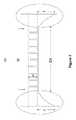
- FIG. 1illustrates a prior art embossing assembly
- FIG. 2depicts microposts (i.e., a three dimensional pattern) on a flat sheet which may be mounted on a drum to form an embossing assembly.
- FIG. 3shows the top view of a film prepared from the embossing assembly of FIG. 1 .
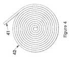
- FIG. 4shows how a microstructure film is rolled.
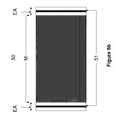
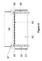
- FIG. 5 ais a cross-sectional view of a microstructure film of the present invention.
- FIG. 5 bis a top view of a microstructure film of the present invention.
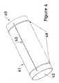
- FIG. 6depicts an embossing assembly used for the manufacture of the film of FIGS. 5 a and 5 b.
- FIG. 7is a cross-sectional view of an alternative microstructure film of the present invention.
- FIG. 8depicts an embossing assembly used for the manufacture of the film of FIG. 7 .
- One aspect of the present inventionis directed to a microstructure film comprising an area of microstructures and two edge areas, wherein the height of the highest part in the edge areas exceeds the height of the highest point in the microstructures.
- the height of the highest part in the edge areasexceeds the height of the highest point in the microstructures by about 1 ⁇ m to about 1 mm.
- the height of the highest part in the edge areasis the thickness of the thickest part in the edge areas.
- the thickest or highest part in the edge areasis on the same side as the microstructures. In another embodiment, the thickest or highest part in the edge areas is on the opposite side of the microstructures.
- the highest part in the edge areasis a spacer line.
- the spacer linehas a width which is in the range of about 3 ⁇ m to about 30 mm.
- the microstructuresare microcups which may be filled with an electrophoretic fluid comprising charged pigment particles dispersed in a solvent or solvent mixture and sealed with a sealing layer.
- Another aspect of the present inventionis directed to an embossing assembly for the manufacture of a microstructure film of the present invention, which comprises (a)
- a further aspect of the present inventionis directed to another embossing assembly for the manufactured of a microstructure film of the present invention, which comprises (a) a drum; (b) an embossing shim tightly wrapped around the drum; (c) a tape laminated around each end of the embossing shim; and (d) a nip roller capable of pressing against the tape and the embossing shim to create spaces for an embossing composition to enter.
- FIG. 1depicts an embossing assembly ( 10 ) which may be used in a roll to roll manufacture of a microstructure film.
- the assemblycomprises an embossing shim ( 11 ) mounted over a drum ( 12 ).
- the embossing shimusually formed from an embossing sheet, is securely wrapped around the drum.
- the embossing shimhas a three-dimensional pattern ( 21 ) (e.g., microposts) on one side of the shim ( 20 ), as shown in FIG. 2 , and the pattern is on the outer surface of the embossing assembly in FIG. 1 when the shim is mounted onto the drum. It is noted that, as a representative, only a few number of the microposts are shown in FIG. 2 and their size is exaggerated for clarity.
- a three-dimensional patterne.g., microposts
- the dimensions of the microposts in the region, on or close to the seam line, and the dimensions of the microposts in the other regionsmay not be uniform.
- the film produced, at a regular intervalwill have areas of microstructures which have irregular dimensions (such as irregular shapes or heights).
- FIG. 3is a top view of such a film to illustrate this phenomenon.
- the distance (d) between the areas ( 31 ) having microstructures of irregular dimensions on the filmis usually the circumference of the drum.
- the present inventorshave now design a microstructure film which could eliminate the deformation problem illustrated above.
- the filmcomprises an area of microstructures and two edge areas outside of the area of microstructures wherein the height of the highest part in the two edge areas exceeds the height of the highest point in the microstructures, preferably by about 1 ⁇ m to about 1 mm.
- FIGS. 5 across-sectional view
- 5 btop view
- the film ( 50 )comprises an area of microstructures (M) and two edge areas (EAs) which are outside of the area of microstructures.
- Each of the edge areashas a spacer line ( 51 ).
- the spacer lines and the microstructuresare on the same side of the film. Such spacer lines representing the highest part in the edge areas would prevent layers of microstructures in a roll from being in contact with each other, thus preventing microstructures of normal dimensions from being affected by microstructures of irregular dimensions.
- the width (w) of the spacer line ( 51 ) in FIG. 5 amay be in the range of about 3 ⁇ m to about 30 mm, or 10 ⁇ m to about 10 mm, or 100 ⁇ m to about 1 mm.
- the height (h) of the spacer line ( 51 )exceeds the height (h′) of the highest point in the microstructures, preferably by about 1 ⁇ m to about 1 mm, or 10 ⁇ m to 100 ⁇ m. Both heights are measured from the same base line in the film.
- Such a filmmay be manufactured by an embossing assembly as shown in FIG. 6 .
- This assemblyalso has an embossing shim ( 61 ) mounted on a drum ( 62 ) and the embossing shim may have a seam line ( 63 ).
- each of the two edge areas of the embossing shimalso has a groove ( 64 ). The dimensions of the groove would correspond to the desired dimensions of the spacer line discussed above.
- each spacer linemay also be achieved by laminating a tape in the edge area.
- the tapeis laminated before the film is being rolled up.
- the thickness of the tapeshould be more than the height (h′) of the highest point in the microstructures, preferably by about 1 ⁇ m to about 1 mm.
- FIG. 7illustrates an alternative design of the present invention.
- a film of microstructurescomprises an area of microstructures (M) and two edge areas (EAs) which are outside of the area of microstructures.
- the highest part in the edge areas and the microstructuresare on the opposite sides of the film.
- the height of the highest part in the edge areasexceeds the height (h′) of the highest point in the microstructures, preferably by about 1 ⁇ m to about 1 mm.
- the highest part in the edge areascorresponds to the thickest part (t) in the edge areas, in this case.
- the thickness and the heightare measured from the same base line.
- an embossing assemblycomprises a drum ( 81 ) with an embossing shim ( 82 ) tightly secured around the drum.
- a three-dimensional pattern ( 83 )is on the outside of the assembly.
- an electrode layere.g., indium tin oxide layer
- plastic filme.g., polyethylene terephthalate film
- a tape ( 85 )is laminated around the embossing shim in the edge areas.
- the tapepreferably has a thickness in the range of about 3 ⁇ m to about 10 mm.
- microstructures referred to in the present applicationmay be microcups as described in U.S. Pat. No. 6,930,818, the content of which is incorporated herein by reference in its entirety.
- the microcupsare filled with a display fluid such as an electrophoretic fluid comprising charged pigment particles dispersed in a solvent or solvent mixture.
- the filled microcupsare then sealed with a sealing layer.
- the filled and sealed microcupsmay be sandwiched between two electrode layers to form a display device.
Landscapes
- Engineering & Computer Science (AREA)
- Health & Medical Sciences (AREA)
- Manufacturing & Machinery (AREA)
- Ophthalmology & Optometry (AREA)
- Mechanical Engineering (AREA)
- Physics & Mathematics (AREA)
- General Physics & Mathematics (AREA)
- Optics & Photonics (AREA)
- Shaping Of Tube Ends By Bending Or Straightening (AREA)
Abstract
Description
Claims (6)
Priority Applications (3)
| Application Number | Priority Date | Filing Date | Title |
|---|---|---|---|
| US13/601,767US9279906B2 (en) | 2012-08-31 | 2012-08-31 | Microstructure film |
| PCT/US2013/055426WO2014035697A1 (en) | 2012-08-31 | 2013-08-16 | Microstructure film |
| TW102129972ATWI623800B (en) | 2012-08-31 | 2013-08-22 | Microstructure film |
Applications Claiming Priority (1)
| Application Number | Priority Date | Filing Date | Title |
|---|---|---|---|
| US13/601,767US9279906B2 (en) | 2012-08-31 | 2012-08-31 | Microstructure film |
Publications (2)
| Publication Number | Publication Date |
|---|---|
| US20140065369A1 US20140065369A1 (en) | 2014-03-06 |
| US9279906B2true US9279906B2 (en) | 2016-03-08 |
Family
ID=50184153
Family Applications (1)
| Application Number | Title | Priority Date | Filing Date |
|---|---|---|---|
| US13/601,767Active2034-06-18US9279906B2 (en) | 2012-08-31 | 2012-08-31 | Microstructure film |
Country Status (3)
| Country | Link |
|---|---|
| US (1) | US9279906B2 (en) |
| TW (1) | TWI623800B (en) |
| WO (1) | WO2014035697A1 (en) |
Cited By (149)
| Publication number | Priority date | Publication date | Assignee | Title |
|---|---|---|---|---|
| US9995987B1 (en) | 2017-03-20 | 2018-06-12 | E Ink Corporation | Composite particles and method for making the same |
| US10209530B2 (en) | 2015-12-07 | 2019-02-19 | E Ink Corporation | Three-dimensional display |
| US10254622B2 (en) | 2017-02-15 | 2019-04-09 | E Ink California, Llc | Polymer additives used in color electrophoretic display medium |
| US10276109B2 (en) | 2016-03-09 | 2019-04-30 | E Ink Corporation | Method for driving electro-optic displays |
| US10317767B2 (en) | 2014-02-07 | 2019-06-11 | E Ink Corporation | Electro-optic display backplane structure with drive components and pixel electrodes on opposed surfaces |
| US10324577B2 (en) | 2017-02-28 | 2019-06-18 | E Ink Corporation | Writeable electrophoretic displays including sensing circuits and styli configured to interact with sensing circuits |
| WO2019144097A1 (en) | 2018-01-22 | 2019-07-25 | E Ink Corporation | Electro-optic displays, and methods for driving same |
| US10388233B2 (en) | 2015-08-31 | 2019-08-20 | E Ink Corporation | Devices and techniques for electronically erasing a drawing device |
| US10401668B2 (en) | 2012-05-30 | 2019-09-03 | E Ink California, Llc | Display device with visually-distinguishable watermark area and non-watermark area |
| US10467984B2 (en) | 2017-03-06 | 2019-11-05 | E Ink Corporation | Method for rendering color images |
| US10466565B2 (en) | 2017-03-28 | 2019-11-05 | E Ink Corporation | Porous backplane for electro-optic display |
| WO2019222587A1 (en) | 2018-05-17 | 2019-11-21 | E Ink California, Llc | Piezo electrophoretic display |
| US10495941B2 (en) | 2017-05-19 | 2019-12-03 | E Ink Corporation | Foldable electro-optic display including digitization and touch sensing |
| US10503041B2 (en) | 2016-11-30 | 2019-12-10 | E Ink Corporation | Laminated electro-optic displays and methods of making same |
| US10509294B2 (en) | 2017-01-25 | 2019-12-17 | E Ink Corporation | Dual sided electrophoretic display |
| WO2020005676A1 (en) | 2018-06-28 | 2020-01-02 | E Ink Corporation | Driving methods for variable transmission electro-phoretic media |
| WO2020023432A1 (en) | 2018-07-25 | 2020-01-30 | E Ink Corporation | Flexible transparent intumescent coatings and composites incorporating the same |
| WO2020033175A1 (en) | 2018-08-10 | 2020-02-13 | E Ink California, Llc | Switchable light-collimating layer including bistable electrophoretic fluid |
| WO2020033176A1 (en) | 2018-08-07 | 2020-02-13 | E Ink Corporation | Flexible encapsulated electro-optic media |
| WO2020033787A1 (en) | 2018-08-10 | 2020-02-13 | E Ink California, Llc | Driving waveforms for switchable light-collimating layer including bistable electrophoretic fluid |
| WO2020036908A1 (en) | 2018-08-14 | 2020-02-20 | E Ink California, Llc | Piezo electrophoretic display |
| US10573257B2 (en) | 2017-05-30 | 2020-02-25 | E Ink Corporation | Electro-optic displays |
| US10585325B2 (en) | 2017-03-09 | 2020-03-10 | E Ink California, Llc | Photo-thermally induced polymerization inhibitors for electrophoretic media |
| US10593272B2 (en) | 2016-03-09 | 2020-03-17 | E Ink Corporation | Drivers providing DC-balanced refresh sequences for color electrophoretic displays |
| WO2020060797A1 (en) | 2018-09-20 | 2020-03-26 | E Ink Corporation | Three-dimensional display apparatuses |
| WO2020092190A1 (en) | 2018-10-30 | 2020-05-07 | E Ink Corporation | Electro-optic medium and writable device incorporating the same |
| WO2020097462A1 (en) | 2018-11-09 | 2020-05-14 | E Ink Corporation | Electro-optic displays |
| US10670892B2 (en) | 2016-04-22 | 2020-06-02 | E Ink Corporation | Foldable electro-optic display apparatus |
| US10698265B1 (en) | 2017-10-06 | 2020-06-30 | E Ink California, Llc | Quantum dot film |
| US10782586B2 (en) | 2017-01-20 | 2020-09-22 | E Ink California, Llc | Color organic pigments and electrophoretic display media containing the same |
| US10795233B2 (en) | 2015-11-18 | 2020-10-06 | E Ink Corporation | Electro-optic displays |
| US10803813B2 (en) | 2015-09-16 | 2020-10-13 | E Ink Corporation | Apparatus and methods for driving displays |
| US10802373B1 (en) | 2017-06-26 | 2020-10-13 | E Ink Corporation | Reflective microcells for electrophoretic displays and methods of making the same |
| US10809590B2 (en) | 2017-06-16 | 2020-10-20 | E Ink Corporation | Variable transmission electrophoretic devices |
| WO2020219274A1 (en) | 2019-04-24 | 2020-10-29 | E Ink Corporation | Electrophoretic particles, media, and displays and processes for the production thereof |
| US10824042B1 (en) | 2017-10-27 | 2020-11-03 | E Ink Corporation | Electro-optic display and composite materials having low thermal sensitivity for use therein |
| US10823373B2 (en) | 2018-12-17 | 2020-11-03 | E Ink Corporation | Light emitting device including variable transmission film to control intensity and pattern |
| US10832622B2 (en) | 2017-04-04 | 2020-11-10 | E Ink Corporation | Methods for driving electro-optic displays |
| US10921676B2 (en) | 2017-08-30 | 2021-02-16 | E Ink Corporation | Electrophoretic medium |
| WO2021071600A1 (en) | 2019-10-07 | 2021-04-15 | E Ink Corporation | An adhesive composition comprising a polyurethane and a cationic dopant |
| US10983410B2 (en) | 2017-06-16 | 2021-04-20 | E Ink Corporation | Electro-optic media including encapsulated pigments in gelatin binder |
| US11030969B2 (en) | 2019-03-29 | 2021-06-08 | E Ink Corporation | Electro-optic displays and methods of driving the same |
| WO2021126616A1 (en) | 2019-12-17 | 2021-06-24 | E Ink Corporation | Autostereoscopic devices and methods for producing 3d images |
| WO2021133541A1 (en) | 2019-12-23 | 2021-07-01 | E Ink Corporation | Transferable light-transmissive electrode films for electro-optic devices |
| US11079651B2 (en) | 2017-12-15 | 2021-08-03 | E Ink Corporation | Multi-color electro-optic media |
| WO2021178753A1 (en) | 2020-03-05 | 2021-09-10 | E Ink Corporation | Light modulator having bonded structures embedded in viewing area |
| US11139594B2 (en) | 2019-04-30 | 2021-10-05 | E Ink Corporation | Connectors for electro-optic displays |
| US11143929B2 (en) | 2018-03-09 | 2021-10-12 | E Ink Corporation | Reflective electrophoretic displays including photo-luminescent material and color filter arrays |
| US11175561B1 (en) | 2018-04-12 | 2021-11-16 | E Ink Corporation | Electrophoretic display media with network electrodes and methods of making and using the same |
| WO2021247991A1 (en) | 2020-06-05 | 2021-12-09 | E Ink California, Llc | Electrophoretic display device |
| WO2021247470A1 (en) | 2020-06-03 | 2021-12-09 | E Ink Corporation | Foldable electrophoretic display module including non-conductive support plate |
| US11248122B2 (en) | 2017-12-30 | 2022-02-15 | E Ink Corporation | Pigments for electrophoretic displays |
| US11249367B2 (en) | 2018-11-30 | 2022-02-15 | E Ink Corporation | Pressure-sensitive writing media comprising electrophoretic materials |
| US11257445B2 (en) | 2019-11-18 | 2022-02-22 | E Ink Corporation | Methods for driving electro-optic displays |
| US11289036B2 (en) | 2019-11-14 | 2022-03-29 | E Ink Corporation | Methods for driving electro-optic displays |
| US11314098B2 (en) | 2018-08-10 | 2022-04-26 | E Ink California, Llc | Switchable light-collimating layer with reflector |
| US11402719B2 (en) | 2018-12-11 | 2022-08-02 | E Ink Corporation | Retroreflective electro-optic displays |
| US11404013B2 (en) | 2017-05-30 | 2022-08-02 | E Ink Corporation | Electro-optic displays with resistors for discharging remnant charges |
| WO2022169920A1 (en) | 2021-02-04 | 2022-08-11 | E Ink California, Llc | Sealing layers comprising a conductive filler for sealing microcells of electrophoretic displays |
| WO2022169919A1 (en) | 2021-02-04 | 2022-08-11 | E Ink California, Llc | Sealing layers for sealing microcells of electro-optic devices |
| US11422427B2 (en) | 2017-12-19 | 2022-08-23 | E Ink Corporation | Applications of electro-optic displays |
| US11423852B2 (en) | 2017-09-12 | 2022-08-23 | E Ink Corporation | Methods for driving electro-optic displays |
| US11450262B2 (en) | 2020-10-01 | 2022-09-20 | E Ink Corporation | Electro-optic displays, and methods for driving same |
| US11456397B2 (en) | 2019-03-12 | 2022-09-27 | E Ink Corporation | Energy harvesting electro-optic displays |
| US11520202B2 (en) | 2020-06-11 | 2022-12-06 | E Ink Corporation | Electro-optic displays, and methods for driving same |
| US11520210B2 (en) | 2019-09-30 | 2022-12-06 | E Ink Corporation | Electrically-actuated variable transmission film having very low haze and a visible grid in a clear state |
| US11520211B2 (en) | 2018-12-17 | 2022-12-06 | E Ink Corporation | Anisotropically conductive moisture barrier films and electro-optic assemblies containing the same |
| US11521565B2 (en) | 2018-12-28 | 2022-12-06 | E Ink Corporation | Crosstalk reduction for electro-optic displays |
| US11537024B2 (en) | 2018-12-30 | 2022-12-27 | E Ink California, Llc | Electro-optic displays |
| US11568786B2 (en) | 2020-05-31 | 2023-01-31 | E Ink Corporation | Electro-optic displays, and methods for driving same |
| US11567388B2 (en) | 2019-02-25 | 2023-01-31 | E Ink Corporation | Composite electrophoretic particles and variable transmission films containing the same |
| US11579510B2 (en) | 2019-05-07 | 2023-02-14 | E Ink Corporation | Driving methods for a variable light transmission device |
| US11580920B2 (en) | 2021-05-25 | 2023-02-14 | E Ink California, Llc | Synchronized driving waveforms for four-particle electrophoretic displays |
| WO2023043714A1 (en) | 2021-09-14 | 2023-03-23 | E Ink Corporation | Coordinated top electrode - drive electrode voltages for switching optical state of electrophoretic displays using positive and negative voltages of different magnitudes |
| US11620959B2 (en) | 2020-11-02 | 2023-04-04 | E Ink Corporation | Enhanced push-pull (EPP) waveforms for achieving primary color sets in multi-color electrophoretic displays |
| US11635640B2 (en) | 2018-10-01 | 2023-04-25 | E Ink Corporation | Switching fibers for textiles |
| US11640803B2 (en) | 2021-09-06 | 2023-05-02 | E Ink California, Llc | Method for driving electrophoretic display device |
| US11656525B2 (en) | 2018-10-01 | 2023-05-23 | E Ink Corporation | Electro-optic fiber and methods of making the same |
| US11656522B2 (en) | 2018-09-28 | 2023-05-23 | E Ink Corporation | Solar temperature regulation system for a fluid |
| US11657774B2 (en) | 2015-09-16 | 2023-05-23 | E Ink Corporation | Apparatus and methods for driving displays |
| US11657772B2 (en) | 2020-12-08 | 2023-05-23 | E Ink Corporation | Methods for driving electro-optic displays |
| US11686989B2 (en) | 2020-09-15 | 2023-06-27 | E Ink Corporation | Four particle electrophoretic medium providing fast, high-contrast optical state switching |
| US11688357B2 (en) | 2021-04-29 | 2023-06-27 | E Ink California, Llc | Disaggregation driving sequences for four particle electrophoretic displays |
| WO2023122142A1 (en) | 2021-12-22 | 2023-06-29 | E Ink Corporation | Methods for driving electro-optic displays |
| WO2023129533A1 (en) | 2021-12-27 | 2023-07-06 | E Ink Corporation | Methods for measuring electrical properties of electro-optic displays |
| WO2023132958A1 (en) | 2022-01-04 | 2023-07-13 | E Ink Corporation | Electrophoretic media comprising electrophoretic particles and a combination of charge control agents |
| US11708720B2 (en) | 2013-10-22 | 2023-07-25 | E Ink Corporation | Light-modulating electrophoretic device |
| US11721295B2 (en) | 2017-09-12 | 2023-08-08 | E Ink Corporation | Electro-optic displays, and methods for driving same |
| US11740530B2 (en) | 2019-11-14 | 2023-08-29 | E Ink Corporation | Electro-optic media including oppositely charged particles and variable transmission device incorporating the same |
| WO2023164443A1 (en) | 2022-02-28 | 2023-08-31 | E Ink California, Llc | Piezo-electrophoretic film including patterned piezo polarities for creating images via electrophoretic media |
| WO2023164446A1 (en) | 2022-02-28 | 2023-08-31 | E Ink California, Llc | Piezoelectric film including ionic liquid and electrophoretic display film including the piezoelectric film |
| WO2023167901A1 (en) | 2022-03-01 | 2023-09-07 | E Ink California, Llc | Temperature compensation in electro-optic displays |
| US11756494B2 (en) | 2020-11-02 | 2023-09-12 | E Ink Corporation | Driving sequences to remove prior state information from color electrophoretic displays |
| US11761123B2 (en) | 2019-08-07 | 2023-09-19 | E Ink Corporation | Switching ribbons for textiles |
| US11762257B2 (en) | 2019-08-26 | 2023-09-19 | E Ink Corporation | Electro-optic device comprising an identification marker |
| US11776496B2 (en) | 2020-09-15 | 2023-10-03 | E Ink Corporation | Driving voltages for advanced color electrophoretic displays and displays with improved driving voltages |
| WO2023196915A1 (en) | 2022-04-08 | 2023-10-12 | E Ink California, Llc | A water-resistant sealing layer for sealing microcells of electro-optic devices |
| WO2023200859A1 (en) | 2022-04-13 | 2023-10-19 | E Ink Corporation | Display material including patterned areas of encapsulated electrophoretic media |
| WO2023211867A1 (en) | 2022-04-27 | 2023-11-02 | E Ink Corporation | Color displays configured to convert rgb image data for display on advanced color electronic paper |
| US11830448B2 (en) | 2021-11-04 | 2023-11-28 | E Ink Corporation | Methods for driving electro-optic displays |
| US11846863B2 (en) | 2020-09-15 | 2023-12-19 | E Ink Corporation | Coordinated top electrode—drive electrode voltages for switching optical state of electrophoretic displays using positive and negative voltages of different magnitudes |
| WO2024006668A1 (en) | 2022-07-01 | 2024-01-04 | E Ink Corporation | Sealing films and sealing compositions for sealing microcells of electro-optic devices |
| US11886090B2 (en) | 2018-12-12 | 2024-01-30 | E Ink Corporation | Edible electrodes and uses in electrophoretic displays |
| WO2024044119A1 (en) | 2022-08-25 | 2024-02-29 | E Ink Corporation | Transitional driving modes for impulse balancing when switching between global color mode and direct update mode for electrophoretic displays |
| US11922893B2 (en) | 2021-12-22 | 2024-03-05 | E Ink Corporation | High voltage driving using top plane switching with zero voltage frames between driving frames |
| US11935495B2 (en) | 2021-08-18 | 2024-03-19 | E Ink Corporation | Methods for driving electro-optic displays |
| WO2024091547A1 (en) | 2022-10-25 | 2024-05-02 | E Ink Corporation | Methods for driving electro-optic displays |
| US12025901B2 (en) | 2020-02-06 | 2024-07-02 | E Ink Corporation | Electrophoretic core-shell particles having an organic pigment core and a shell with a thin metal oxide layer and a silane layer |
| WO2024145324A1 (en) | 2022-12-30 | 2024-07-04 | E Ink Corporation | A variable light transmission device and a method of manufacture of the same |
| WO2024145345A1 (en) | 2022-12-30 | 2024-07-04 | E Ink Corporation | A variable light transmission device comprising electrophoretic medium having a compination of light reflective and light absorbing pigment particles |
| WO2024145318A1 (en) | 2022-12-30 | 2024-07-04 | E Ink Corporation | A variable light transmission device and a method of operation of the same |
| WO2024158855A1 (en) | 2023-01-27 | 2024-08-02 | E Ink Corporation | Multi-element pixel electrode circuits for electro-optic displays and methods for driving the same |
| WO2024182264A1 (en) | 2023-02-28 | 2024-09-06 | E Ink Corporation | Drive scheme for improved color gamut in color electrophoretic displays |
| US12105396B2 (en) | 2020-07-22 | 2024-10-01 | E Ink Corporation | Electro-optic device comprising integrated conductive edge seal and a method of production of the same |
| US12125449B2 (en) | 2021-02-09 | 2024-10-22 | E Ink Corporation | Continuous waveform driving in multi-color electrophoretic displays |
| US12127469B2 (en) | 2021-12-20 | 2024-10-22 | E Ink Corporation | Multi-layer device comprising a repair layer having conductive a hydrogel film or beads |
| WO2024253934A1 (en) | 2023-06-05 | 2024-12-12 | E Ink Corporation | Color electrophoretic medium having four pigment particle system addressable by waveforms having four voltage levels |
| US12181767B2 (en) | 2020-09-15 | 2024-12-31 | E Ink Corporation | Five-particle electrophoretic medium with improved black optical state |
| WO2025006440A1 (en) | 2023-06-27 | 2025-01-02 | E Ink Corporation | Time-shifted waveforms for multi-particle electrophoretic displays providing low-flash image updates |
| WO2025006476A1 (en) | 2023-06-27 | 2025-01-02 | E Ink Corporation | Multi-particle electrophoretic display having low-flash image updates |
| WO2025006130A1 (en) | 2023-06-27 | 2025-01-02 | E Ink Corporation | Electrophoretic device with ambient light sensor and adaptive whiteness restoring and color balancing frontlight |
| US12195586B2 (en) | 2019-05-10 | 2025-01-14 | E Ink Corporation | Charge control agents and particle dispersions including the same |
| WO2025019101A1 (en) | 2023-07-18 | 2025-01-23 | E Ink Corporation | Switchable electrophoretic light modulator having reduced aperture diffraction |
| WO2025034396A1 (en) | 2023-08-08 | 2025-02-13 | E Ink Corporation | Backplanes for segmented electro-optic displays and methods of manufacturing same |
| WO2025049590A1 (en) | 2023-08-29 | 2025-03-06 | E Ink Corporation | Piezo-electrophoretic films and displays, and methods for manufacturing the same |
| WO2025049160A1 (en) | 2023-08-29 | 2025-03-06 | E Ink Corporation | Electrophoretic particles comprising an organic pigment and graphene oxide |
| WO2025072227A1 (en) | 2023-09-29 | 2025-04-03 | E Ink Corporation | An electro-optic device comprising a barrier layer |
| WO2025076061A1 (en) | 2023-10-05 | 2025-04-10 | E Ink Corporation | Staged gate voltage control |
| WO2025075769A1 (en) | 2023-10-06 | 2025-04-10 | E Ink Corporation | Large-area electro-optic light modulator or display |
| WO2025096100A1 (en) | 2023-10-31 | 2025-05-08 | E Ink Corporation | Reflective display and projected capacitive touch sensor with shared transparent electrode |
| WO2025101330A1 (en) | 2023-11-08 | 2025-05-15 | E Ink Corporation | Continuous photolithographic fabrication process for producing seamless microstructures used in electro-optic displays and light modulating films |
| US12313951B2 (en) | 2016-06-10 | 2025-05-27 | E Ink Corporation | Electro-optic display apparatus |
| WO2025117316A2 (en) | 2023-11-30 | 2025-06-05 | E Ink Corporation | Electrophoretic media comprising cationic charge control agent |
| US12326641B2 (en) | 2020-10-02 | 2025-06-10 | E Ink Corporation | Front plane laminates with outer surface electrical connections |
| WO2025122853A1 (en) | 2023-12-06 | 2025-06-12 | E Ink Corporation | Method of driving a color electophoretic display to form images without dithering |
| WO2025128843A1 (en) | 2023-12-15 | 2025-06-19 | E Ink Corporation | Fast response color waveforms for multiparticle electrophoretic displays |
| US12339559B1 (en) | 2021-12-09 | 2025-06-24 | E Ink Corporation | Electro-optic displays and methods for discharging remnant voltage using backlight |
| WO2025136446A1 (en) | 2023-12-22 | 2025-06-26 | E Ink Corporation | Five-particle electrophoretic medium with improved black optical state |
| WO2025136583A1 (en) | 2023-12-20 | 2025-06-26 | E Ink Corporation | Driving sequences for multi-particle electrophoretic displays providing improved color states |
| WO2025144956A1 (en) | 2023-12-31 | 2025-07-03 | E Ink Corporation | Piezo-electrophoretic films and displays, and methods for manufacturing the same |
| WO2025147504A1 (en) | 2024-01-05 | 2025-07-10 | E Ink Corporation | An electrophoretic medium comprising particles having a pigment core and a polymeric shell |
| WO2025147410A2 (en) | 2024-01-02 | 2025-07-10 | E Ink Corporation | Electrophoretic media comprising a cationic charge control agent |
| WO2025151355A1 (en) | 2024-01-08 | 2025-07-17 | E Ink Corporation | Electrophoretic device having an adhesive layer comprising conductive filler particles and a polymeric dispersant |
| WO2025155412A1 (en) | 2024-01-19 | 2025-07-24 | E Ink Corporation | Flexible segmented electro-optic displays and methods of manufacture |
| WO2025155697A1 (en) | 2024-01-20 | 2025-07-24 | E Ink Corporation | Methods for delivering low-ghosting partial updates in color electrophoretic displays |
| WO2025160290A1 (en) | 2024-01-24 | 2025-07-31 | E Ink Corporation | Improved methods for producing full-color epaper images with low grain |
| WO2025183989A1 (en) | 2024-02-28 | 2025-09-04 | E Ink Corporation | A variable light transmission device comprising microcells |
| WO2025189016A1 (en) | 2024-03-06 | 2025-09-12 | E Ink Corporation | Electro-optic displays with color filter arrays for reducing visible texture patterns in displayed images |
| WO2025198932A1 (en) | 2024-03-19 | 2025-09-25 | E Ink Corporation | Methods and systems for managing remnant voltage during fast updates in electrophoretic displays |
Families Citing this family (1)
| Publication number | Priority date | Publication date | Assignee | Title |
|---|---|---|---|---|
| EP3350798B1 (en) | 2015-09-16 | 2023-07-26 | E Ink Corporation | Apparatus and methods for driving displays |
Citations (7)
| Publication number | Priority date | Publication date | Assignee | Title |
|---|---|---|---|---|
| JPH07256760A (en) | 1994-01-18 | 1995-10-09 | Branson Ultraschall Niederlassung Der Emerson Technol Gmbh & Co | Production of fiber-coated plastic component part |
| WO2001067170A1 (en) | 2000-03-03 | 2001-09-13 | Sipix Imaging, Inc. | Electrophoretic display |
| US20040229018A1 (en)* | 2003-05-16 | 2004-11-18 | Graham Paul D | Complex microstructure film |
| US20060262249A1 (en) | 2001-01-11 | 2006-11-23 | Rong-Chang Liang | Transmissive or reflective liquid crystal display and process for its manufacture |
| US20080018021A1 (en) | 2001-03-30 | 2008-01-24 | Minolta Co., Ltd. | Method for producing resin-molded substrate and method for producing reversible image display medium |
| JP2008203776A (en) | 2007-02-22 | 2008-09-04 | Sony Corp | Lens film, roller for molding, manufacturing device for lens film, and method for molding lens film |
| US20100129527A1 (en) | 2007-03-08 | 2010-05-27 | Ricoh Company, Ltd. | Manufacturing method and manufacturing apparatus for image display element structure, and manufacturing method and manufacturing apparatus for electrophoretic image display element |
Family Cites Families (1)
| Publication number | Priority date | Publication date | Assignee | Title |
|---|---|---|---|---|
| US6795138B2 (en)* | 2001-01-11 | 2004-09-21 | Sipix Imaging, Inc. | Transmissive or reflective liquid crystal display and novel process for its manufacture |
- 2012
- 2012-08-31USUS13/601,767patent/US9279906B2/enactiveActive
- 2013
- 2013-08-16WOPCT/US2013/055426patent/WO2014035697A1/enactiveApplication Filing
- 2013-08-22TWTW102129972Apatent/TWI623800B/enactive
Patent Citations (9)
| Publication number | Priority date | Publication date | Assignee | Title |
|---|---|---|---|---|
| JPH07256760A (en) | 1994-01-18 | 1995-10-09 | Branson Ultraschall Niederlassung Der Emerson Technol Gmbh & Co | Production of fiber-coated plastic component part |
| WO2001067170A1 (en) | 2000-03-03 | 2001-09-13 | Sipix Imaging, Inc. | Electrophoretic display |
| US6930818B1 (en) | 2000-03-03 | 2005-08-16 | Sipix Imaging, Inc. | Electrophoretic display and novel process for its manufacture |
| US20060262249A1 (en) | 2001-01-11 | 2006-11-23 | Rong-Chang Liang | Transmissive or reflective liquid crystal display and process for its manufacture |
| US20080018021A1 (en) | 2001-03-30 | 2008-01-24 | Minolta Co., Ltd. | Method for producing resin-molded substrate and method for producing reversible image display medium |
| US7604706B2 (en)* | 2001-03-30 | 2009-10-20 | Minolta Co., Ltd. | Method for producing resin-molded substrate and method for producing reversible image display medium |
| US20040229018A1 (en)* | 2003-05-16 | 2004-11-18 | Graham Paul D | Complex microstructure film |
| JP2008203776A (en) | 2007-02-22 | 2008-09-04 | Sony Corp | Lens film, roller for molding, manufacturing device for lens film, and method for molding lens film |
| US20100129527A1 (en) | 2007-03-08 | 2010-05-27 | Ricoh Company, Ltd. | Manufacturing method and manufacturing apparatus for image display element structure, and manufacturing method and manufacturing apparatus for electrophoretic image display element |
Non-Patent Citations (39)
| Title |
|---|
| Allen, K. (Oct. 2003). Electrophoretics Fulfilled. Emerging Displays Review: Emerging Display Technologies, Monthly Report -Oct. 2003, 9-14. |
| Bardsley, J.N. & Pinnel, M.R. (Nov. 2004) Microcup(TM) Electrophoretic Displays. USDC Flexible Display Report, 3.1.2. pp. 3-12-3-16. |
| Bardsley, J.N. & Pinnel, M.R. (Nov. 2004) Microcup™ Electrophoretic Displays. USDC Flexible Display Report, 3.1.2. pp. 3-12-3-16. |
| Chaug, Y.S., Haubrich, J.E., Sereda, M. and Liang, R.C. (Apr. 2004). Roll-to-Roll Processes for the Manufacturing of Patterned Conductive Electrodes on Flexible Substrates. Mat. Res. Soc. Symp. Proc., vol. 814, I9.6.1. |
| Chen, S.M. (Jul. 2003) The Applications for the Revolutionary Electronic Paper Technology. OPTO News & Letters, 102, 37-41. (in Chinese, English abstract attached). |
| Chen, S.M. (May 2003) The New Application and the Dynamics of Companies. TRI. 1-10. (In Chinese, English abstract attached). |
| Chung, J., Hou, J., Wang, W., Chu, L.Y., Yao, W., & Liang, R.C. (Dec. 2003). Microcup® Electrophoretic Displays, Grayscale and Color Rendition. IDW, AMD2/EP1-2, 243-246. |
| Ho, Andrew. (Nov. 2006) Embedding e-Paper in Smart Cards, Pricing Labels & Indicators. Presentation conducted at Smart Paper Conference Nov. 15-16, 2006, Atlanta, GA, USA. |
| Ho, C., & Liang, R.C. (Dec. 2003). Microcup® Electronic Paper by Roll-to-Roll Manufacturing Processes. Presentation conducted at FEG, Nei-Li, Taiwan. |
| Ho, Candice. (Feb. 1, 2005) Microcupt® Electronic Paper Device and Application. Presentation conducted at USDC 4th Annual Flexible Display Conference 2005. |
| Hou, J., Chen, Y., Li, Y., Weng, X., Li, H. and Pereira, C. (May 2004). Reliability and Performance of Flexible Electrophoretic Displays by Roll-to-Roll Manufacturing Processes. SID Digest, 32.3, 1066-1069. |
| Lee, H., & Liang, R.C. (Jun. 2003) SiPix Microcup® Electronic Paper-An Introduction. Advanced Display, Issue 37, 4-9 (in Chinese, English abstract attached). |
| Liang, R.C. (Apr. 2004). Microcup Electronic Paper by Roll-to-Roll Manufacturing Process. Presentation at the Flexible Displays & Electronics 2004 of Intertech, San Fransisco, California, USA. |
| Liang, R.C. (Feb. 2003) Microcup® Electrophoretic and Liquid Crystal Displays by Roll-to-Roll Manufacturing Processes. Presentation conducted at the Flexible Microelectronics & Displays Conference of U.S. Display Consortium, Phoenix, Arizona, USA. |
| Liang, R.C. (Oct. 2004) Flexible and Roll-able Displays/Electronic Paper-A Technology Overview. Paper presented at the METS 2004 Conference in Taipie, Taiwan. |
| Liang, R.C., & Tseng, S. (Feb. 2003). Microcup® LCD, A New Type of Dispersed LCD by A Roll-to-Roll Manufacturing Process. Paper presented at the IDMC, Taipei, Taiwan. |
| Liang, R.C., (Feb. 2005) Flexible and Roll-able Displays/Electronic Paper-A Brief Technology Overview. Flexible Display Forum, 2005, Taiwan. |
| Liang, R.C., Hou, J., & Zang, H.M. (Dec. 2002) Microcup Electrophoretic Displays by Roll-to-Roll Manufacturing Processes. IDW, EP2-2, 1337-1340. |
| Liang, R.C., Hou, J., Chung, J., Wang, X., Pereira, C., & Chen, Y. (May 2003). Microcup® Active and Passive Matrix Electrophoretic Displays by a Roll-to-Roll Manufacturing Processes. SID Digest, vol. 34, Issue 1, pp. 838-841, 20.1. |
| Liang, R.C., Hou, J., Zang, H.M., & Chung, J. (Feb. 2003). Passive Matrix Microcup® Electrophoretic Displays. Paper presented at the IDMC, Taipei, Taiwan. |
| Liang, R.C., Hou, J., Zang, H.M., Chung, J., & Tseng, S. (Feb. 2003). Microcup® Displays: Electronic Paper by Roll-to-Roll Manufacturing Processes. Journal of the SID, 11(4), 621-628. |
| Liang, R.C., Zang, H.M., Wang, X., Chung, J. & Lee, H., (Jun./Jul. 2004) <<Format Flexible Microcup® Electronic Paper by Roll-to-Roll Manufacturing Process >>, Presentation conducted at the 14th FPD Manufacturing Technology EXPO & Conference. |
| Liang, R.C., Zang, H.M., Wang, X., Chung, J. & Lee, H., (Jun./Jul. 2004) >, Presentation conducted at the 14th FPD Manufacturing Technology EXPO & Conference. |
| Nikkei Microdevices. (Dec. 2002) Newly-Developed Color Electronic Paper Promises-Unbeatable Production Efficiency. Nikkei Microdevices, p. 3. (in Japanese, with English translation). |
| PCT International Search Report, mailed Oct 17, 2013. |
| Sprague, R.A. (Sep. 23, 2009) SiPix Microcup Electrophoretic Epaper for Ebooks. NIP 25, 2009 pp. 460-462. (Presentation conducted on Sep. 23, 2009 at the 25th Int] Conference on Digital Printing Technologies, Digital Fabrication 2009 (NIP 25) by Society for Imaaina Science and Technoloay. In Louisville. Kentucky. USA.). |
| Wang, X., Kiluk, S., Chang, C., & Liang, R.C. (Feb. 2004). Mirocup® Electronic Paper and the Converting Processes. ASID, 10.1.2-26, 396-399, Nanjing, China. |
| Wang, X., Kiluk, S., Chang, C., & Liang, R.C., (Jun. 2004) Microcup® Electronic Paper and the Converting Processes. Advanced Display, Issue 43, 48-51 (in Chinese, with English abstract). |
| Wang, X., Li, P., Sodhi, D., Xu, T. and Bruner, S. et al., (Feb. 2006) Inkjet Fabrication of Multi-Color Microcup® Electrophorectic Display. The Flexible Microelectronics & Displays Conference of U.S. Display Consortium. |
| Wang, X., Zang, H.M. and Li, P. (Jun. 2006) Roll-to-Roll Manufacturing Process for Full Color Electrophoretic film. SID Digest, 2006, pp. 1587-1589. |
| Zang, H.M, Hwang, J.J., Gu, H., Hou, J., Weng, X., Chen, Y., et al. (Jan. 2004). Threshold and Grayscale Stability of Microcup® Electronic Paper. Proceeding of SPIE-IS&T Electronic Imaging, SPIE vol. 5289, 102-108. |
| Zang, H.M. & Hou, Jack, (Feb. 2005) Flexible Microcup® EPD by RTR Process. Presentation conducted at 2nd Annual Paper-Like Displays Conference, Feb. 9-11, 2005, St. Pete Beach, Florida. |
| Zang, H.M. (Feb. 2004). Microcup Electronic Paper. Presentation conducted at the Displays & Microelectronics Conference of U.S. Display Consortium, Phoenix, Arizona, USA. |
| Zang, H.M. (Feb. 2007) Developments in Microcup® Flexible Displays. Presentation conducted at the 6th Annual Flexible Display and Microelectronics Conference, Phoenix, AZ Feb. 6-8. |
| Zang, H.M. (Oct. 2003). Microcup ® Electronic Paper by Roll-to-Roll Manufacturing Processes. Presentation conducted at the Advisory Board Meeting, Bowling Green State University, Ohio, USA. |
| Zang, H.M. (Sep. 2006) Monochrome and Area Color Microcup®EPDs by Roll-to-Roll Manufacturing Process. Presentation conducted at the Fourth Organic Electronics Conference and Exhibition (OEC-06), Sep. 25-27, 2006, Frankfurt, Germany. |
| Zang, H.M., & Liang, R.C. (2003) Microcup Electronic Paper by Roll-to-Roll Manufacturing Processes. The Spectrum, 16(2), 16-21. |
| Zang, H.M., Wang, F., Kang, Y.M., Chen, Y. and Lin, W. (Jul. 2007) Microcup® e-Paper for Embedded and Flexible Designs. IDMC'07, Taipei International Convention Center, Taiwan. |
| Zang, H.M., Wang, W., Sun, C., Gu, H., and Chen, Y. (May 2006) Monochrome and Area Color Microcup® EPDs by Roll-to-Roll Manufacturing Processes. ICIS' 06 International Congress of Imaging Science Final Program and Proceedings, pp. 362-365. |
Cited By (264)
| Publication number | Priority date | Publication date | Assignee | Title |
|---|---|---|---|---|
| US10401668B2 (en) | 2012-05-30 | 2019-09-03 | E Ink California, Llc | Display device with visually-distinguishable watermark area and non-watermark area |
| US10831052B2 (en) | 2012-05-30 | 2020-11-10 | E Ink California, Llc | Display device with visually-distinguishable watermark area and non-watermark area |
| US11708720B2 (en) | 2013-10-22 | 2023-07-25 | E Ink Corporation | Light-modulating electrophoretic device |
| US12000207B2 (en) | 2013-10-22 | 2024-06-04 | E Ink Corporation | Light-modulating electrophoretic device |
| US12305444B2 (en) | 2013-10-22 | 2025-05-20 | E Ink Corporation | Light-modulating electrophoretic device |
| US10317767B2 (en) | 2014-02-07 | 2019-06-11 | E Ink Corporation | Electro-optic display backplane structure with drive components and pixel electrodes on opposed surfaces |
| US10388233B2 (en) | 2015-08-31 | 2019-08-20 | E Ink Corporation | Devices and techniques for electronically erasing a drawing device |
| US11657774B2 (en) | 2015-09-16 | 2023-05-23 | E Ink Corporation | Apparatus and methods for driving displays |
| US10803813B2 (en) | 2015-09-16 | 2020-10-13 | E Ink Corporation | Apparatus and methods for driving displays |
| US11450286B2 (en) | 2015-09-16 | 2022-09-20 | E Ink Corporation | Apparatus and methods for driving displays |
| US10795233B2 (en) | 2015-11-18 | 2020-10-06 | E Ink Corporation | Electro-optic displays |
| US10209530B2 (en) | 2015-12-07 | 2019-02-19 | E Ink Corporation | Three-dimensional display |
| US10276109B2 (en) | 2016-03-09 | 2019-04-30 | E Ink Corporation | Method for driving electro-optic displays |
| US10593272B2 (en) | 2016-03-09 | 2020-03-17 | E Ink Corporation | Drivers providing DC-balanced refresh sequences for color electrophoretic displays |
| US11404012B2 (en) | 2016-03-09 | 2022-08-02 | E Ink Corporation | Drivers providing DC-balanced refresh sequences for color electrophoretic displays |
| US11030965B2 (en) | 2016-03-09 | 2021-06-08 | E Ink Corporation | Drivers providing DC-balanced refresh sequences for color electrophoretic displays |
| US10670892B2 (en) | 2016-04-22 | 2020-06-02 | E Ink Corporation | Foldable electro-optic display apparatus |
| US12313951B2 (en) | 2016-06-10 | 2025-05-27 | E Ink Corporation | Electro-optic display apparatus |
| EP4550042A2 (en) | 2016-11-30 | 2025-05-07 | E Ink Corporation | Laminated electro-optic displays and methods of making the same |
| US11829047B2 (en) | 2016-11-30 | 2023-11-28 | E Ink Corporation | Top plane connections for electro-optic devices including a through-hole in rear substrate |
| US10503041B2 (en) | 2016-11-30 | 2019-12-10 | E Ink Corporation | Laminated electro-optic displays and methods of making same |
| US11397362B2 (en) | 2016-11-30 | 2022-07-26 | E Ink Corporation | Top plane connections for electro-optic devices including a through-hole in rear substrate |
| EP3992706A1 (en) | 2016-11-30 | 2022-05-04 | E Ink Corporation | Laminated electro-optic displays and methods of making the same |
| US10782586B2 (en) | 2017-01-20 | 2020-09-22 | E Ink California, Llc | Color organic pigments and electrophoretic display media containing the same |
| US11099452B2 (en) | 2017-01-20 | 2021-08-24 | E Ink California, Llc | Color organic pigments and electrophoretic display media containing the same |
| US11493820B2 (en) | 2017-01-20 | 2022-11-08 | E Ink California, Llc | Color organic pigments and electrophoretic display media containing the same |
| US10509294B2 (en) | 2017-01-25 | 2019-12-17 | E Ink Corporation | Dual sided electrophoretic display |
| US10254622B2 (en) | 2017-02-15 | 2019-04-09 | E Ink California, Llc | Polymer additives used in color electrophoretic display medium |
| US10324577B2 (en) | 2017-02-28 | 2019-06-18 | E Ink Corporation | Writeable electrophoretic displays including sensing circuits and styli configured to interact with sensing circuits |
| US11527216B2 (en) | 2017-03-06 | 2022-12-13 | E Ink Corporation | Method for rendering color images |
| US12100369B2 (en) | 2017-03-06 | 2024-09-24 | E Ink Corporation | Method for rendering color images |
| US11094288B2 (en) | 2017-03-06 | 2021-08-17 | E Ink Corporation | Method and apparatus for rendering color images |
| US10467984B2 (en) | 2017-03-06 | 2019-11-05 | E Ink Corporation | Method for rendering color images |
| US10585325B2 (en) | 2017-03-09 | 2020-03-10 | E Ink California, Llc | Photo-thermally induced polymerization inhibitors for electrophoretic media |
| US10705405B2 (en) | 2017-03-20 | 2020-07-07 | E Ink Corporation | Composite particles and method for making the same |
| US11614671B2 (en) | 2017-03-20 | 2023-03-28 | E Ink Corporation | Composite particles and method for making the same |
| US11231634B2 (en) | 2017-03-20 | 2022-01-25 | E Ink Corporation | Composite particles and method for making the same |
| US9995987B1 (en) | 2017-03-20 | 2018-06-12 | E Ink Corporation | Composite particles and method for making the same |
| US10466565B2 (en) | 2017-03-28 | 2019-11-05 | E Ink Corporation | Porous backplane for electro-optic display |
| US11016358B2 (en) | 2017-03-28 | 2021-05-25 | E Ink Corporation | Porous backplane for electro-optic display |
| US11398196B2 (en) | 2017-04-04 | 2022-07-26 | E Ink Corporation | Methods for driving electro-optic displays |
| US10832622B2 (en) | 2017-04-04 | 2020-11-10 | E Ink Corporation | Methods for driving electro-optic displays |
| US10495941B2 (en) | 2017-05-19 | 2019-12-03 | E Ink Corporation | Foldable electro-optic display including digitization and touch sensing |
| US11404013B2 (en) | 2017-05-30 | 2022-08-02 | E Ink Corporation | Electro-optic displays with resistors for discharging remnant charges |
| US11107425B2 (en) | 2017-05-30 | 2021-08-31 | E Ink Corporation | Electro-optic displays with resistors for discharging remnant charges |
| US10573257B2 (en) | 2017-05-30 | 2020-02-25 | E Ink Corporation | Electro-optic displays |
| US10825405B2 (en) | 2017-05-30 | 2020-11-03 | E Ink Corporatior | Electro-optic displays |
| US10983410B2 (en) | 2017-06-16 | 2021-04-20 | E Ink Corporation | Electro-optic media including encapsulated pigments in gelatin binder |
| US11749218B2 (en) | 2017-06-16 | 2023-09-05 | E Ink Corporation | Method of forming an electro-optic medium |
| US12347397B2 (en) | 2017-06-16 | 2025-07-01 | E Ink Corporation | Method of forming an electro-optic medium |
| EP4086318A2 (en) | 2017-06-16 | 2022-11-09 | E Ink Corporation | Variable transmission electrophoretic devices |
| US10809590B2 (en) | 2017-06-16 | 2020-10-20 | E Ink Corporation | Variable transmission electrophoretic devices |
| US11774827B2 (en) | 2017-06-26 | 2023-10-03 | E Ink Corporation | Reflective microcells for electrophoretic displays and methods of making the same |
| US11372306B2 (en) | 2017-06-26 | 2022-06-28 | E Ink Corporation | Reflective microcells for electrophoretic displays and methods of making the same |
| US10802373B1 (en) | 2017-06-26 | 2020-10-13 | E Ink Corporation | Reflective microcells for electrophoretic displays and methods of making the same |
| US11977310B2 (en) | 2017-08-30 | 2024-05-07 | E Ink Corporation | Electrophoretic medium |
| US10921676B2 (en) | 2017-08-30 | 2021-02-16 | E Ink Corporation | Electrophoretic medium |
| US11935496B2 (en) | 2017-09-12 | 2024-03-19 | E Ink Corporation | Electro-optic displays, and methods for driving same |
| US11721295B2 (en) | 2017-09-12 | 2023-08-08 | E Ink Corporation | Electro-optic displays, and methods for driving same |
| US11568827B2 (en) | 2017-09-12 | 2023-01-31 | E Ink Corporation | Methods for driving electro-optic displays to minimize edge ghosting |
| US11423852B2 (en) | 2017-09-12 | 2022-08-23 | E Ink Corporation | Methods for driving electro-optic displays |
| US11493805B2 (en) | 2017-10-06 | 2022-11-08 | E Ink California, Llc | Quantum dot film with sealed microcells |
| US10698265B1 (en) | 2017-10-06 | 2020-06-30 | E Ink California, Llc | Quantum dot film |
| US10824042B1 (en) | 2017-10-27 | 2020-11-03 | E Ink Corporation | Electro-optic display and composite materials having low thermal sensitivity for use therein |
| US11079651B2 (en) | 2017-12-15 | 2021-08-03 | E Ink Corporation | Multi-color electro-optic media |
| US11422427B2 (en) | 2017-12-19 | 2022-08-23 | E Ink Corporation | Applications of electro-optic displays |
| US12130530B2 (en) | 2017-12-19 | 2024-10-29 | E Ink Corporation | Applications of electro-optic displays |
| US11613654B2 (en) | 2017-12-30 | 2023-03-28 | E Ink Corporation | Pigments for electrophoretic displays |
| US11248122B2 (en) | 2017-12-30 | 2022-02-15 | E Ink Corporation | Pigments for electrophoretic displays |
| WO2019144097A1 (en) | 2018-01-22 | 2019-07-25 | E Ink Corporation | Electro-optic displays, and methods for driving same |
| US11656523B2 (en) | 2018-03-09 | 2023-05-23 | E Ink Corporation | Reflective electrophoretic displays including photo-luminescent material and color filter arrays |
| US11143929B2 (en) | 2018-03-09 | 2021-10-12 | E Ink Corporation | Reflective electrophoretic displays including photo-luminescent material and color filter arrays |
| US11656524B2 (en) | 2018-04-12 | 2023-05-23 | E Ink Corporation | Electrophoretic display media with network electrodes and methods of making and using the same |
| US11175561B1 (en) | 2018-04-12 | 2021-11-16 | E Ink Corporation | Electrophoretic display media with network electrodes and methods of making and using the same |
| US12298645B2 (en) | 2018-05-17 | 2025-05-13 | E Ink Corporation | Piezo electrophoretic display |
| EP4343420A2 (en) | 2018-05-17 | 2024-03-27 | E Ink Corporation | Method of producing a piezo electrophoretic display |
| US11181799B2 (en) | 2018-05-17 | 2021-11-23 | E Ink California, Llc | Piezo electrophoretic display |
| WO2019222587A1 (en) | 2018-05-17 | 2019-11-21 | E Ink California, Llc | Piezo electrophoretic display |
| US11892740B2 (en) | 2018-05-17 | 2024-02-06 | E Ink Corporation | Piezo electrophoretic display |
| EP4369090A2 (en) | 2018-06-28 | 2024-05-15 | E Ink Corporation | Driving methods for variable transmission electro-phoretic media |
| WO2020005676A1 (en) | 2018-06-28 | 2020-01-02 | E Ink Corporation | Driving methods for variable transmission electro-phoretic media |
| US11143930B2 (en) | 2018-06-28 | 2021-10-12 | E Ink Corporation | Driving methods for variable transmission electro-phoretic media |
| WO2020023432A1 (en) | 2018-07-25 | 2020-01-30 | E Ink Corporation | Flexible transparent intumescent coatings and composites incorporating the same |
| US11378824B2 (en) | 2018-08-07 | 2022-07-05 | E Ink Corporation | Flexible encapsulated electro-optic media |
| US11886050B2 (en) | 2018-08-07 | 2024-01-30 | E Ink Corporation | Flexible encapsulated electro-optic media |
| WO2020033176A1 (en) | 2018-08-07 | 2020-02-13 | E Ink Corporation | Flexible encapsulated electro-optic media |
| WO2020033175A1 (en) | 2018-08-10 | 2020-02-13 | E Ink California, Llc | Switchable light-collimating layer including bistable electrophoretic fluid |
| US11435606B2 (en) | 2018-08-10 | 2022-09-06 | E Ink California, Llc | Driving waveforms for switchable light-collimating layer including bistable electrophoretic fluid |
| US11656526B2 (en) | 2018-08-10 | 2023-05-23 | E Ink California, Llc | Switchable light-collimating layer including bistable electrophoretic fluid |
| US11719953B2 (en) | 2018-08-10 | 2023-08-08 | E Ink California, Llc | Switchable light-collimating layer with reflector |
| US11397366B2 (en) | 2018-08-10 | 2022-07-26 | E Ink California, Llc | Switchable light-collimating layer including bistable electrophoretic fluid |
| WO2020033787A1 (en) | 2018-08-10 | 2020-02-13 | E Ink California, Llc | Driving waveforms for switchable light-collimating layer including bistable electrophoretic fluid |
| US11314098B2 (en) | 2018-08-10 | 2022-04-26 | E Ink California, Llc | Switchable light-collimating layer with reflector |
| US11493821B2 (en) | 2018-08-14 | 2022-11-08 | E Ink California, Llc | Piezo electrophoretic display |
| WO2020036908A1 (en) | 2018-08-14 | 2020-02-20 | E Ink California, Llc | Piezo electrophoretic display |
| US10969604B2 (en) | 2018-09-20 | 2021-04-06 | E Ink Corporation | Three dimensional display apparatus |
| WO2020060797A1 (en) | 2018-09-20 | 2020-03-26 | E Ink Corporation | Three-dimensional display apparatuses |
| US11656522B2 (en) | 2018-09-28 | 2023-05-23 | E Ink Corporation | Solar temperature regulation system for a fluid |
| US11934049B2 (en) | 2018-10-01 | 2024-03-19 | E Ink Corporation | Switching fibers for textiles |
| US11656525B2 (en) | 2018-10-01 | 2023-05-23 | E Ink Corporation | Electro-optic fiber and methods of making the same |
| US11635640B2 (en) | 2018-10-01 | 2023-04-25 | E Ink Corporation | Switching fibers for textiles |
| US12007630B2 (en) | 2018-10-01 | 2024-06-11 | E Ink Corporation | Switching fibers for textiles |
| US11513413B2 (en) | 2018-10-30 | 2022-11-29 | E Ink Corporation | Electro-optic media and writable display incorporating the same |
| WO2020092190A1 (en) | 2018-10-30 | 2020-05-07 | E Ink Corporation | Electro-optic medium and writable device incorporating the same |
| US11835835B2 (en) | 2018-10-30 | 2023-12-05 | E Ink Corporation | Electro-optic media and writable display incorporating the same |
| US11145262B2 (en) | 2018-11-09 | 2021-10-12 | E Ink Corporation | Electro-optic displays |
| WO2020097462A1 (en) | 2018-11-09 | 2020-05-14 | E Ink Corporation | Electro-optic displays |
| US11450287B2 (en) | 2018-11-09 | 2022-09-20 | E Ink Corporation | Electro-optic displays |
| US11809057B2 (en) | 2018-11-30 | 2023-11-07 | E Ink Corporation | Pressure-sensitive writing media comprising electrophoretic materials |
| US11249367B2 (en) | 2018-11-30 | 2022-02-15 | E Ink Corporation | Pressure-sensitive writing media comprising electrophoretic materials |
| US12298647B2 (en) | 2018-11-30 | 2025-05-13 | E Ink Corporation | Pressure-sensitive writing media comprising electrophoretic materials |
| US11402719B2 (en) | 2018-12-11 | 2022-08-02 | E Ink Corporation | Retroreflective electro-optic displays |
| US11886090B2 (en) | 2018-12-12 | 2024-01-30 | E Ink Corporation | Edible electrodes and uses in electrophoretic displays |
| US10823373B2 (en) | 2018-12-17 | 2020-11-03 | E Ink Corporation | Light emitting device including variable transmission film to control intensity and pattern |
| US11333323B2 (en) | 2018-12-17 | 2022-05-17 | E Ink Corporation | Light emitting device including variable transmission film to control intensity and pattern |
| US11782322B2 (en) | 2018-12-17 | 2023-10-10 | E Ink Corporation | Anisotropically conductive moisture barrier films and electro-optic assemblies containing the same |
| US11520211B2 (en) | 2018-12-17 | 2022-12-06 | E Ink Corporation | Anisotropically conductive moisture barrier films and electro-optic assemblies containing the same |
| US11521565B2 (en) | 2018-12-28 | 2022-12-06 | E Ink Corporation | Crosstalk reduction for electro-optic displays |
| US11537024B2 (en) | 2018-12-30 | 2022-12-27 | E Ink California, Llc | Electro-optic displays |
| US12339560B2 (en) | 2018-12-30 | 2025-06-24 | E Ink Corporation | Electro-optic displays |
| US12032264B2 (en) | 2018-12-30 | 2024-07-09 | E Ink Corporation | Electro-optic displays |
| US11567388B2 (en) | 2019-02-25 | 2023-01-31 | E Ink Corporation | Composite electrophoretic particles and variable transmission films containing the same |
| US12130531B2 (en) | 2019-02-25 | 2024-10-29 | E Ink Corporation | Composite electrophoretic particles and variable transmission films containing the same |
| US11616162B2 (en) | 2019-03-12 | 2023-03-28 | E Ink Corporation | Energy harvesting electro-optic displays |
| US11456397B2 (en) | 2019-03-12 | 2022-09-27 | E Ink Corporation | Energy harvesting electro-optic displays |
| US11398204B2 (en) | 2019-03-29 | 2022-07-26 | E Ink Corporation | Electro-optic displays and methods of driving the same |
| US11030969B2 (en) | 2019-03-29 | 2021-06-08 | E Ink Corporation | Electro-optic displays and methods of driving the same |
| US11520209B2 (en) | 2019-04-24 | 2022-12-06 | E Ink Corporation | Electrophoretic particles, media, and displays and processes for the production thereof |
| WO2020219274A1 (en) | 2019-04-24 | 2020-10-29 | E Ink Corporation | Electrophoretic particles, media, and displays and processes for the production thereof |
| US11139594B2 (en) | 2019-04-30 | 2021-10-05 | E Ink Corporation | Connectors for electro-optic displays |
| US11579510B2 (en) | 2019-05-07 | 2023-02-14 | E Ink Corporation | Driving methods for a variable light transmission device |
| US12248226B2 (en) | 2019-05-07 | 2025-03-11 | E Ink Corporation | Driving methods for a variable light transmission device |
| US12195586B2 (en) | 2019-05-10 | 2025-01-14 | E Ink Corporation | Charge control agents and particle dispersions including the same |
| US11761123B2 (en) | 2019-08-07 | 2023-09-19 | E Ink Corporation | Switching ribbons for textiles |
| US12099281B2 (en) | 2019-08-26 | 2024-09-24 | E Ink Corporation | Method of authenticating an electro-optic device and any of its components |
| US12130532B2 (en) | 2019-08-26 | 2024-10-29 | E Ink Corporation | Method of authenticating an electro-optic device and any of its components |
| US11762257B2 (en) | 2019-08-26 | 2023-09-19 | E Ink Corporation | Electro-optic device comprising an identification marker |
| US12153322B2 (en) | 2019-09-30 | 2024-11-26 | E Ink Corporation | Electrically-actuated variable transmission film having very low haze and a visible grid in a clear state |
| US11762258B2 (en) | 2019-09-30 | 2023-09-19 | E Ink Corporation | Electrically-actuated variable transmission film having very low haze and a visible grid in a clear state |
| US12372847B2 (en) | 2019-09-30 | 2025-07-29 | E Ink Corporation | Electrically-actuated variable transmission film having very low haze and a visible grid in a clear state |
| US11520210B2 (en) | 2019-09-30 | 2022-12-06 | E Ink Corporation | Electrically-actuated variable transmission film having very low haze and a visible grid in a clear state |
| US11827816B2 (en) | 2019-10-07 | 2023-11-28 | E Ink Corporation | Adhesive composition comprising a polyurethane and a cationic dopant |
| WO2021071600A1 (en) | 2019-10-07 | 2021-04-15 | E Ink Corporation | An adhesive composition comprising a polyurethane and a cationic dopant |
| US12031065B2 (en) | 2019-10-07 | 2024-07-09 | E Ink Corporation | Adhesive composition comprising a polyurethane and a cationic dopant |
| US11740530B2 (en) | 2019-11-14 | 2023-08-29 | E Ink Corporation | Electro-optic media including oppositely charged particles and variable transmission device incorporating the same |
| US11289036B2 (en) | 2019-11-14 | 2022-03-29 | E Ink Corporation | Methods for driving electro-optic displays |
| US11257445B2 (en) | 2019-11-18 | 2022-02-22 | E Ink Corporation | Methods for driving electro-optic displays |
| WO2021126616A1 (en) | 2019-12-17 | 2021-06-24 | E Ink Corporation | Autostereoscopic devices and methods for producing 3d images |
| US11641458B2 (en) | 2019-12-17 | 2023-05-02 | E Ink Corporation | Autostereoscopic devices and methods for producing 3D images |
| US11882264B2 (en) | 2019-12-17 | 2024-01-23 | E Ink Corporation | Autostereoscopic devices and methods for producing 3D images |
| WO2021133541A1 (en) | 2019-12-23 | 2021-07-01 | E Ink Corporation | Transferable light-transmissive electrode films for electro-optic devices |
| US11934081B2 (en) | 2019-12-23 | 2024-03-19 | E Ink Corporation | Transferrable light-transmissive electrode films for electro-optic devices |
| US12025901B2 (en) | 2020-02-06 | 2024-07-02 | E Ink Corporation | Electrophoretic core-shell particles having an organic pigment core and a shell with a thin metal oxide layer and a silane layer |
| US12189259B2 (en) | 2020-02-06 | 2025-01-07 | E Ink Corporation | Electrophoretic core-shell particles having an organic pigment core and a shell with a thin metal oxide layer and a silane layer |
| WO2021178753A1 (en) | 2020-03-05 | 2021-09-10 | E Ink Corporation | Light modulator having bonded structures embedded in viewing area |
| US11567356B2 (en) | 2020-03-05 | 2023-01-31 | E Ink Corporation | Switchable light modulator device comprising a polymer wall structure having a plurality of cavities disposed between first and second substrates and method of making the same |
| US11237419B2 (en) | 2020-03-05 | 2022-02-01 | E Ink Corporation | Switchable light modulator comprising a polymer wall structure having a mould part and a cast part disposed between first and second substrates |
| US11774791B2 (en) | 2020-03-05 | 2023-10-03 | E Ink Corporation | Switchable light modulator device comprising polymer structures that create a plurality of cavities that are sealed with a fluid comprising electrophoretic particles |
| US12147108B2 (en) | 2020-03-05 | 2024-11-19 | E Ink Corporation | Method of making a switchable light modulator by embossing a polymer film to create a polymer wall structure surrounding each of a plurality of cavities |
| US11568786B2 (en) | 2020-05-31 | 2023-01-31 | E Ink Corporation | Electro-optic displays, and methods for driving same |
| US12347356B2 (en) | 2020-05-31 | 2025-07-01 | E Ink Corporation | Electro-optic displays, and methods for driving same |
| US11513415B2 (en) | 2020-06-03 | 2022-11-29 | E Ink Corporation | Foldable electrophoretic display module including non-conductive support plate |
| US11874580B2 (en) | 2020-06-03 | 2024-01-16 | E Ink Corporation | Foldable electrophoretic display module including non-conductive support plate |
| WO2021247470A1 (en) | 2020-06-03 | 2021-12-09 | E Ink Corporation | Foldable electrophoretic display module including non-conductive support plate |
| US11868020B2 (en) | 2020-06-05 | 2024-01-09 | E Ink Corporation | Electrophoretic display device |
| WO2021247991A1 (en) | 2020-06-05 | 2021-12-09 | E Ink California, Llc | Electrophoretic display device |
| US12360429B2 (en) | 2020-06-05 | 2025-07-15 | E Ink Corporation | Electrophoretic display device |
| US11520202B2 (en) | 2020-06-11 | 2022-12-06 | E Ink Corporation | Electro-optic displays, and methods for driving same |
| US12105396B2 (en) | 2020-07-22 | 2024-10-01 | E Ink Corporation | Electro-optic device comprising integrated conductive edge seal and a method of production of the same |
| US11686989B2 (en) | 2020-09-15 | 2023-06-27 | E Ink Corporation | Four particle electrophoretic medium providing fast, high-contrast optical state switching |
| US12181767B2 (en) | 2020-09-15 | 2024-12-31 | E Ink Corporation | Five-particle electrophoretic medium with improved black optical state |
| US11846863B2 (en) | 2020-09-15 | 2023-12-19 | E Ink Corporation | Coordinated top electrode—drive electrode voltages for switching optical state of electrophoretic displays using positive and negative voltages of different magnitudes |
| US11948523B1 (en) | 2020-09-15 | 2024-04-02 | E Ink Corporation | Driving voltages for advanced color electrophoretic displays and displays with improved driving voltages |
| US12197099B2 (en) | 2020-09-15 | 2025-01-14 | E Ink Corporation | Coordinated top electrode—drive electrode voltages for switching optical state of electrophoretic displays using positive and negative voltages of different magnitudes |
| US12361902B2 (en) | 2020-09-15 | 2025-07-15 | E Ink Corporation | Driving voltages for advanced color electrophoretic displays and displays with improved driving voltages |
| US11837184B2 (en) | 2020-09-15 | 2023-12-05 | E Ink Corporation | Driving voltages for advanced color electrophoretic displays and displays with improved driving voltages |
| US12044945B2 (en) | 2020-09-15 | 2024-07-23 | E Ink Corporation | Four particle electrophoretic medium providing fast, high-contrast optical state switching |
| US11776496B2 (en) | 2020-09-15 | 2023-10-03 | E Ink Corporation | Driving voltages for advanced color electrophoretic displays and displays with improved driving voltages |
| US11450262B2 (en) | 2020-10-01 | 2022-09-20 | E Ink Corporation | Electro-optic displays, and methods for driving same |
| US12326641B2 (en) | 2020-10-02 | 2025-06-10 | E Ink Corporation | Front plane laminates with outer surface electrical connections |
| US11620959B2 (en) | 2020-11-02 | 2023-04-04 | E Ink Corporation | Enhanced push-pull (EPP) waveforms for achieving primary color sets in multi-color electrophoretic displays |
| US11756494B2 (en) | 2020-11-02 | 2023-09-12 | E Ink Corporation | Driving sequences to remove prior state information from color electrophoretic displays |
| US12347398B2 (en) | 2020-11-02 | 2025-07-01 | E Ink Corporation | Enhanced push-pull (EPP) waveforms for achieving primary color sets in multi-color electrophoretic displays |
| US12087244B2 (en) | 2020-11-02 | 2024-09-10 | E Ink Corporation | Enhanced push-pull (EPP) waveforms for achieving primary color sets in multi-color electrophoretic displays |
| US11798506B2 (en) | 2020-11-02 | 2023-10-24 | E Ink Corporation | Enhanced push-pull (EPP) waveforms for achieving primary color sets in multi-color electrophoretic displays |
| US12307989B2 (en) | 2020-11-02 | 2025-05-20 | E Ink Corporation | Driving sequences to remove prior state information from color electrophoretic displays |
| US11657772B2 (en) | 2020-12-08 | 2023-05-23 | E Ink Corporation | Methods for driving electro-optic displays |
| WO2022169919A1 (en) | 2021-02-04 | 2022-08-11 | E Ink California, Llc | Sealing layers for sealing microcells of electro-optic devices |
| WO2022169920A1 (en) | 2021-02-04 | 2022-08-11 | E Ink California, Llc | Sealing layers comprising a conductive filler for sealing microcells of electrophoretic displays |
| US12276894B2 (en) | 2021-02-04 | 2025-04-15 | E Ink Corporation | Sealing layers comprising a conductive filler for sealing microcells of electrophoretic displays |
| US12125449B2 (en) | 2021-02-09 | 2024-10-22 | E Ink Corporation | Continuous waveform driving in multi-color electrophoretic displays |
| US12131713B2 (en) | 2021-02-09 | 2024-10-29 | E Ink Corporation | Continuous waveform driving in multi-color electrophoretic displays |
| US12406632B2 (en) | 2021-02-09 | 2025-09-02 | E Ink Corporation | Continuous waveform driving in multi-color electrophoretic displays |
| US11984089B2 (en) | 2021-04-29 | 2024-05-14 | E Ink Corporation | Disaggregation driving sequences for four particle electrophoretic displays |
| US11688357B2 (en) | 2021-04-29 | 2023-06-27 | E Ink California, Llc | Disaggregation driving sequences for four particle electrophoretic displays |
| US11580920B2 (en) | 2021-05-25 | 2023-02-14 | E Ink California, Llc | Synchronized driving waveforms for four-particle electrophoretic displays |
| US11984090B2 (en) | 2021-05-25 | 2024-05-14 | E Ink Corporation | Four-particle electrophoretic displays with synchronized driving waveforms |
| US11935495B2 (en) | 2021-08-18 | 2024-03-19 | E Ink Corporation | Methods for driving electro-optic displays |
| US12094429B2 (en) | 2021-09-06 | 2024-09-17 | E Ink Corporation | Method for driving electrophoretic display device |
| US11640803B2 (en) | 2021-09-06 | 2023-05-02 | E Ink California, Llc | Method for driving electrophoretic display device |
| US11804190B2 (en) | 2021-09-06 | 2023-10-31 | E Ink California, Llc | Method for driving electrophoretic display device |
| WO2023043714A1 (en) | 2021-09-14 | 2023-03-23 | E Ink Corporation | Coordinated top electrode - drive electrode voltages for switching optical state of electrophoretic displays using positive and negative voltages of different magnitudes |
| US11830448B2 (en) | 2021-11-04 | 2023-11-28 | E Ink Corporation | Methods for driving electro-optic displays |
| US12339559B1 (en) | 2021-12-09 | 2025-06-24 | E Ink Corporation | Electro-optic displays and methods for discharging remnant voltage using backlight |
| US12127469B2 (en) | 2021-12-20 | 2024-10-22 | E Ink Corporation | Multi-layer device comprising a repair layer having conductive a hydrogel film or beads |
| US12189260B2 (en) | 2021-12-20 | 2025-01-07 | E Ink Corporation | Multi-layer device including a light-transmissive electrode layer comprising a porous mesh or porous spheres |
| WO2023122142A1 (en) | 2021-12-22 | 2023-06-29 | E Ink Corporation | Methods for driving electro-optic displays |
| US12400611B2 (en) | 2021-12-22 | 2025-08-26 | E Ink Corporation | High voltage driving using top plane switching with zero voltage frames between driving frames |
| US11922893B2 (en) | 2021-12-22 | 2024-03-05 | E Ink Corporation | High voltage driving using top plane switching with zero voltage frames between driving frames |
| US12307988B2 (en) | 2021-12-22 | 2025-05-20 | E Ink Corporation | Methods for globally applying voltages to the display pixels of electro-optic displays |
| US11854448B2 (en) | 2021-12-27 | 2023-12-26 | E Ink Corporation | Methods for measuring electrical properties of electro-optic displays |
| US12249262B2 (en) | 2021-12-27 | 2025-03-11 | E Ink Corporation | Methods for measuring electrical properties of electro-optic displays |
| WO2023129533A1 (en) | 2021-12-27 | 2023-07-06 | E Ink Corporation | Methods for measuring electrical properties of electro-optic displays |
| WO2023132958A1 (en) | 2022-01-04 | 2023-07-13 | E Ink Corporation | Electrophoretic media comprising electrophoretic particles and a combination of charge control agents |
| WO2023164446A1 (en) | 2022-02-28 | 2023-08-31 | E Ink California, Llc | Piezoelectric film including ionic liquid and electrophoretic display film including the piezoelectric film |
| WO2023164443A1 (en) | 2022-02-28 | 2023-08-31 | E Ink California, Llc | Piezo-electrophoretic film including patterned piezo polarities for creating images via electrophoretic media |
| US11830449B2 (en) | 2022-03-01 | 2023-11-28 | E Ink Corporation | Electro-optic displays |
| WO2023167901A1 (en) | 2022-03-01 | 2023-09-07 | E Ink California, Llc | Temperature compensation in electro-optic displays |
| WO2023196915A1 (en) | 2022-04-08 | 2023-10-12 | E Ink California, Llc | A water-resistant sealing layer for sealing microcells of electro-optic devices |
| WO2023200859A1 (en) | 2022-04-13 | 2023-10-19 | E Ink Corporation | Display material including patterned areas of encapsulated electrophoretic media |
| US11984088B2 (en) | 2022-04-27 | 2024-05-14 | E Ink Corporation | Color displays configured to convert RGB image data for display on advanced color electronic paper |
| WO2023211867A1 (en) | 2022-04-27 | 2023-11-02 | E Ink Corporation | Color displays configured to convert rgb image data for display on advanced color electronic paper |
| US12334029B2 (en) | 2022-04-27 | 2025-06-17 | E Ink Corporation | Color displays configured to convert RGB image data for display on advanced color electronic paper |
| WO2024006668A1 (en) | 2022-07-01 | 2024-01-04 | E Ink Corporation | Sealing films and sealing compositions for sealing microcells of electro-optic devices |
| WO2024044119A1 (en) | 2022-08-25 | 2024-02-29 | E Ink Corporation | Transitional driving modes for impulse balancing when switching between global color mode and direct update mode for electrophoretic displays |
| WO2024091547A1 (en) | 2022-10-25 | 2024-05-02 | E Ink Corporation | Methods for driving electro-optic displays |
| WO2024145318A1 (en) | 2022-12-30 | 2024-07-04 | E Ink Corporation | A variable light transmission device and a method of operation of the same |
| WO2024145324A1 (en) | 2022-12-30 | 2024-07-04 | E Ink Corporation | A variable light transmission device and a method of manufacture of the same |
| WO2024145345A1 (en) | 2022-12-30 | 2024-07-04 | E Ink Corporation | A variable light transmission device comprising electrophoretic medium having a compination of light reflective and light absorbing pigment particles |
| US12190836B2 (en) | 2023-01-27 | 2025-01-07 | E Ink Corporation | Multi-element pixel electrode circuits for electro-optic displays and methods for driving the same |
| WO2024158855A1 (en) | 2023-01-27 | 2024-08-02 | E Ink Corporation | Multi-element pixel electrode circuits for electro-optic displays and methods for driving the same |
| WO2024182264A1 (en) | 2023-02-28 | 2024-09-06 | E Ink Corporation | Drive scheme for improved color gamut in color electrophoretic displays |
| US12272324B2 (en) | 2023-02-28 | 2025-04-08 | E Ink Corporation | Drive scheme for improved color gamut in color electrophoretic displays |
| WO2024253934A1 (en) | 2023-06-05 | 2024-12-12 | E Ink Corporation | Color electrophoretic medium having four pigment particle system addressable by waveforms having four voltage levels |
| WO2025006476A1 (en) | 2023-06-27 | 2025-01-02 | E Ink Corporation | Multi-particle electrophoretic display having low-flash image updates |
| US12394388B2 (en) | 2023-06-27 | 2025-08-19 | E Ink Corporation | Time-shifted waveforms for multi-particle electrophoretic displays providing low-flash image updates |
| WO2025006440A1 (en) | 2023-06-27 | 2025-01-02 | E Ink Corporation | Time-shifted waveforms for multi-particle electrophoretic displays providing low-flash image updates |
| WO2025006130A1 (en) | 2023-06-27 | 2025-01-02 | E Ink Corporation | Electrophoretic device with ambient light sensor and adaptive whiteness restoring and color balancing frontlight |
| US12406631B2 (en) | 2023-06-27 | 2025-09-02 | E Ink Corporation | Multi-particle electrophoretic display having low-flash image updates |
| US12412538B2 (en) | 2023-06-27 | 2025-09-09 | E Ink Corporation | Electrophoretic device with ambient light sensor and adaptive whiteness restoring and color balancing frontlight |
| WO2025019101A1 (en) | 2023-07-18 | 2025-01-23 | E Ink Corporation | Switchable electrophoretic light modulator having reduced aperture diffraction |
| WO2025034396A1 (en) | 2023-08-08 | 2025-02-13 | E Ink Corporation | Backplanes for segmented electro-optic displays and methods of manufacturing same |
| WO2025049160A1 (en) | 2023-08-29 | 2025-03-06 | E Ink Corporation | Electrophoretic particles comprising an organic pigment and graphene oxide |
| WO2025049590A1 (en) | 2023-08-29 | 2025-03-06 | E Ink Corporation | Piezo-electrophoretic films and displays, and methods for manufacturing the same |
| WO2025072227A1 (en) | 2023-09-29 | 2025-04-03 | E Ink Corporation | An electro-optic device comprising a barrier layer |
| WO2025076061A1 (en) | 2023-10-05 | 2025-04-10 | E Ink Corporation | Staged gate voltage control |
| WO2025075769A1 (en) | 2023-10-06 | 2025-04-10 | E Ink Corporation | Large-area electro-optic light modulator or display |
| WO2025096100A1 (en) | 2023-10-31 | 2025-05-08 | E Ink Corporation | Reflective display and projected capacitive touch sensor with shared transparent electrode |
| WO2025101330A1 (en) | 2023-11-08 | 2025-05-15 | E Ink Corporation | Continuous photolithographic fabrication process for producing seamless microstructures used in electro-optic displays and light modulating films |
| WO2025117316A2 (en) | 2023-11-30 | 2025-06-05 | E Ink Corporation | Electrophoretic media comprising cationic charge control agent |
| WO2025122853A1 (en) | 2023-12-06 | 2025-06-12 | E Ink Corporation | Method of driving a color electophoretic display to form images without dithering |
| WO2025128843A1 (en) | 2023-12-15 | 2025-06-19 | E Ink Corporation | Fast response color waveforms for multiparticle electrophoretic displays |
| WO2025136583A1 (en) | 2023-12-20 | 2025-06-26 | E Ink Corporation | Driving sequences for multi-particle electrophoretic displays providing improved color states |
| WO2025136446A1 (en) | 2023-12-22 | 2025-06-26 | E Ink Corporation | Five-particle electrophoretic medium with improved black optical state |
| WO2025144956A1 (en) | 2023-12-31 | 2025-07-03 | E Ink Corporation | Piezo-electrophoretic films and displays, and methods for manufacturing the same |
| WO2025147410A2 (en) | 2024-01-02 | 2025-07-10 | E Ink Corporation | Electrophoretic media comprising a cationic charge control agent |
| WO2025147504A1 (en) | 2024-01-05 | 2025-07-10 | E Ink Corporation | An electrophoretic medium comprising particles having a pigment core and a polymeric shell |
| WO2025151355A1 (en) | 2024-01-08 | 2025-07-17 | E Ink Corporation | Electrophoretic device having an adhesive layer comprising conductive filler particles and a polymeric dispersant |
| WO2025155412A1 (en) | 2024-01-19 | 2025-07-24 | E Ink Corporation | Flexible segmented electro-optic displays and methods of manufacture |
| WO2025155697A1 (en) | 2024-01-20 | 2025-07-24 | E Ink Corporation | Methods for delivering low-ghosting partial updates in color electrophoretic displays |
| WO2025160290A1 (en) | 2024-01-24 | 2025-07-31 | E Ink Corporation | Improved methods for producing full-color epaper images with low grain |
| WO2025183989A1 (en) | 2024-02-28 | 2025-09-04 | E Ink Corporation | A variable light transmission device comprising microcells |
| WO2025189016A1 (en) | 2024-03-06 | 2025-09-12 | E Ink Corporation | Electro-optic displays with color filter arrays for reducing visible texture patterns in displayed images |
| WO2025198932A1 (en) | 2024-03-19 | 2025-09-25 | E Ink Corporation | Methods and systems for managing remnant voltage during fast updates in electrophoretic displays |
Also Published As
| Publication number | Publication date |
|---|---|
| TW201418861A (en) | 2014-05-16 |
| TWI623800B (en) | 2018-05-11 |
| US20140065369A1 (en) | 2014-03-06 |
| WO2014035697A1 (en) | 2014-03-06 |
Similar Documents
| Publication | Publication Date | Title |
|---|---|---|
| US9279906B2 (en) | Microstructure film | |
| TWI411985B (en) | Curved display panel | |
| US20180107047A1 (en) | Adhesive Tape, Fabricating Method Thereof, and Display Device | |
| TWI454809B (en) | Liquid crystal display panel | |
| CN100398335C (en) | Printing plate, printing machine, printing method, and liquid crystal device manufacturing apparatus and manufacturing method | |
| US8491986B2 (en) | Panel module and manufacturing method thereof | |
| CN105204237B (en) | A kind of liquid crystal display panel and display device | |
| US11474402B2 (en) | Color film substrate comprising a display region and a non-display region, display device and color film substrate fabricating method | |
| CA2617455A1 (en) | Patch package structure | |
| CN104950527A (en) | Display substrate, manufacturing method thereof, display panel and display device | |
| TWI504978B (en) | Liquid crystal display panel and preparation method thereof | |
| CN103454803A (en) | Liquid crystal display device, substrate for same and method for manufacturing substrate | |
| US20150362767A1 (en) | Liquid Crystal Panel and Manufacturing Method Thereof, and Display Apparatus | |
| CN103336328A (en) | Polaroid assembly and display equipment | |
| KR20160111568A (en) | Flexible display device and manufacturing method thereof | |
| KR20170067895A (en) | Liquid crystal panel and manufacturing method thereof | |
| CN102262256B (en) | Patterned phase retardation film and manufacturing method thereof | |
| US10642388B2 (en) | Protective cover of touch key structure, method of fabrication thereof, and touch panel with covered touch key structure | |
| JP5508858B2 (en) | Newton ring prevention sheet and touch panel using the same | |
| US10203450B2 (en) | Backlight module and the manufacturing method thereof | |
| JPH10186384A5 (en) | ||
| CN104460101A (en) | Colored film substrate as well as preparation method, display panel and display device thereof | |
| WO2014187142A1 (en) | Display panel and display device | |
| CN108873528B (en) | Array substrate, manufacturing method thereof and display panel | |
| JP2008090294A5 (en) |
Legal Events
| Date | Code | Title | Description |
|---|---|---|---|
| AS | Assignment | Owner name:SIPIX IMAGING, INC., CALIFORNIA Free format text:ASSIGNMENT OF ASSIGNORS INTEREST;ASSIGNORS:LIN, CRAIG;KANG, GARY YIH-MING;CHAN, BRYAN HANS;AND OTHERS;SIGNING DATES FROM 20120905 TO 20120907;REEL/FRAME:028982/0129 | |
| AS | Assignment | Owner name:E INK CALIFORNIA, LLC, CALIFORNIA Free format text:CHANGE OF NAME;ASSIGNOR:SIPIX IMAGING, INC.;REEL/FRAME:033280/0408 Effective date:20140701 | |
| STCF | Information on status: patent grant | Free format text:PATENTED CASE | |
| MAFP | Maintenance fee payment | Free format text:PAYMENT OF MAINTENANCE FEE, 4TH YEAR, LARGE ENTITY (ORIGINAL EVENT CODE: M1551); ENTITY STATUS OF PATENT OWNER: LARGE ENTITY Year of fee payment:4 | |
| MAFP | Maintenance fee payment | Free format text:PAYMENT OF MAINTENANCE FEE, 8TH YEAR, LARGE ENTITY (ORIGINAL EVENT CODE: M1552); ENTITY STATUS OF PATENT OWNER: LARGE ENTITY Year of fee payment:8 | |
| AS | Assignment | Owner name:E INK CORPORATION, MASSACHUSETTS Free format text:ASSIGNMENT OF ASSIGNORS INTEREST;ASSIGNOR:E INK CALIFORNIA, LLC;REEL/FRAME:065154/0965 Effective date:20230925 |