US9275933B2 - Semiconductor device - Google Patents
Semiconductor deviceDownload PDFInfo
- Publication number
- US9275933B2 US9275933B2US13/526,533US201213526533AUS9275933B2US 9275933 B2US9275933 B2US 9275933B2US 201213526533 AUS201213526533 AUS 201213526533AUS 9275933 B2US9275933 B2US 9275933B2
- Authority
- US
- United States
- Prior art keywords
- disposed
- tsv
- substrate
- semiconductor device
- contact ring
- Prior art date
- Legal status (The legal status is an assumption and is not a legal conclusion. Google has not performed a legal analysis and makes no representation as to the accuracy of the status listed.)
- Active, expires
Links
- 239000004065semiconductorSubstances0.000titleclaimsabstractdescription40
- 239000000758substrateSubstances0.000claimsabstractdescription52
- 229910052751metalInorganic materials0.000claimsabstractdescription47
- 239000002184metalSubstances0.000claimsabstractdescription47
- 230000000149penetrating effectEffects0.000claimsabstractdescription8
- 239000011229interlayerSubstances0.000claimsabstractdescription7
- 238000002955isolationMethods0.000claimsabstractdescription4
- 239000010410layerSubstances0.000claimsdescription23
- 230000004888barrier functionEffects0.000claimsdescription13
- 229910052710siliconInorganic materials0.000claimsdescription8
- 239000010703siliconSubstances0.000claimsdescription8
- 229910021420polycrystalline siliconInorganic materials0.000claimsdescription4
- 229920005591polysiliconPolymers0.000claimsdescription3
- 238000000034methodMethods0.000abstractdescription33
- 230000008569processEffects0.000abstractdescription27
- 238000011109contaminationMethods0.000abstractdescription6
- XEEYBQQBJWHFJM-UHFFFAOYSA-NIronChemical compound[Fe]XEEYBQQBJWHFJM-UHFFFAOYSA-N0.000description12
- 239000010949copperSubstances0.000description12
- 238000005530etchingMethods0.000description12
- 238000004519manufacturing processMethods0.000description10
- 238000005516engineering processMethods0.000description9
- 239000010936titaniumSubstances0.000description7
- XUIMIQQOPSSXEZ-UHFFFAOYSA-NSiliconChemical compound[Si]XUIMIQQOPSSXEZ-UHFFFAOYSA-N0.000description6
- RYGMFSIKBFXOCR-UHFFFAOYSA-NCopperChemical compound[Cu]RYGMFSIKBFXOCR-UHFFFAOYSA-N0.000description5
- 229910052802copperInorganic materials0.000description5
- MZLGASXMSKOWSE-UHFFFAOYSA-Ntantalum nitrideChemical compound[Ta]#NMZLGASXMSKOWSE-UHFFFAOYSA-N0.000description5
- NRTOMJZYCJJWKI-UHFFFAOYSA-NTitanium nitrideChemical compound[Ti]#NNRTOMJZYCJJWKI-UHFFFAOYSA-N0.000description4
- 238000010586diagramMethods0.000description4
- 239000000463materialSubstances0.000description4
- WFKWXMTUELFFGS-UHFFFAOYSA-NtungstenChemical compound[W]WFKWXMTUELFFGS-UHFFFAOYSA-N0.000description4
- 229910052721tungstenInorganic materials0.000description4
- 239000010937tungstenSubstances0.000description4
- RTAQQCXQSZGOHL-UHFFFAOYSA-NTitaniumChemical compound[Ti]RTAQQCXQSZGOHL-UHFFFAOYSA-N0.000description3
- 229910052782aluminiumInorganic materials0.000description3
- XAGFODPZIPBFFR-UHFFFAOYSA-NaluminiumChemical compound[Al]XAGFODPZIPBFFR-UHFFFAOYSA-N0.000description3
- 229910052715tantalumInorganic materials0.000description3
- GUVRBAGPIYLISA-UHFFFAOYSA-Ntantalum atomChemical compound[Ta]GUVRBAGPIYLISA-UHFFFAOYSA-N0.000description3
- 229910052719titaniumInorganic materials0.000description3
- VYPSYNLAJGMNEJ-UHFFFAOYSA-NSilicium dioxideChemical compoundO=[Si]=OVYPSYNLAJGMNEJ-UHFFFAOYSA-N0.000description2
- 230000000694effectsEffects0.000description2
- 230000010354integrationEffects0.000description2
- 229910000577Silicon-germaniumInorganic materials0.000description1
- LEVVHYCKPQWKOP-UHFFFAOYSA-N[Si].[Ge]Chemical compound[Si].[Ge]LEVVHYCKPQWKOP-UHFFFAOYSA-N0.000description1
- 230000004075alterationEffects0.000description1
- 229910052681coesiteInorganic materials0.000description1
- 239000004020conductorSubstances0.000description1
- 229910052906cristobaliteInorganic materials0.000description1
- 230000008021depositionEffects0.000description1
- 238000000151depositionMethods0.000description1
- 238000013461designMethods0.000description1
- 238000011161developmentMethods0.000description1
- 238000001312dry etchingMethods0.000description1
- 238000009713electroplatingMethods0.000description1
- 238000007667floatingMethods0.000description1
- 230000006870functionEffects0.000description1
- 239000012212insulatorSubstances0.000description1
- 230000015654memoryEffects0.000description1
- 150000002739metalsChemical class0.000description1
- 238000010295mobile communicationMethods0.000description1
- 238000012986modificationMethods0.000description1
- 230000004048modificationEffects0.000description1
- 238000004806packaging method and processMethods0.000description1
- 238000001259photo etchingMethods0.000description1
- 238000000206photolithographyMethods0.000description1
- HBMJWWWQQXIZIP-UHFFFAOYSA-Nsilicon carbideChemical compound[Si+]#[C-]HBMJWWWQQXIZIP-UHFFFAOYSA-N0.000description1
- 229910010271silicon carbideInorganic materials0.000description1
- 239000000377silicon dioxideSubstances0.000description1
- 235000012239silicon dioxideNutrition0.000description1
- 239000002356single layerSubstances0.000description1
- 229910052682stishoviteInorganic materials0.000description1
- 229910052905tridymiteInorganic materials0.000description1
- 238000001039wet etchingMethods0.000description1
Images


Classifications
- H—ELECTRICITY
- H01—ELECTRIC ELEMENTS
- H01L—SEMICONDUCTOR DEVICES NOT COVERED BY CLASS H10
- H01L21/00—Processes or apparatus adapted for the manufacture or treatment of semiconductor or solid state devices or of parts thereof
- H01L21/70—Manufacture or treatment of devices consisting of a plurality of solid state components formed in or on a common substrate or of parts thereof; Manufacture of integrated circuit devices or of parts thereof
- H01L21/71—Manufacture of specific parts of devices defined in group H01L21/70
- H01L21/768—Applying interconnections to be used for carrying current between separate components within a device comprising conductors and dielectrics
- H01L21/76898—Applying interconnections to be used for carrying current between separate components within a device comprising conductors and dielectrics formed through a semiconductor substrate
- H—ELECTRICITY
- H01—ELECTRIC ELEMENTS
- H01L—SEMICONDUCTOR DEVICES NOT COVERED BY CLASS H10
- H01L21/00—Processes or apparatus adapted for the manufacture or treatment of semiconductor or solid state devices or of parts thereof
- H01L21/70—Manufacture or treatment of devices consisting of a plurality of solid state components formed in or on a common substrate or of parts thereof; Manufacture of integrated circuit devices or of parts thereof
- H01L21/71—Manufacture of specific parts of devices defined in group H01L21/70
- H01L21/768—Applying interconnections to be used for carrying current between separate components within a device comprising conductors and dielectrics
- H01L21/76801—Applying interconnections to be used for carrying current between separate components within a device comprising conductors and dielectrics characterised by the formation and the after-treatment of the dielectrics, e.g. smoothing
- H01L21/76802—Applying interconnections to be used for carrying current between separate components within a device comprising conductors and dielectrics characterised by the formation and the after-treatment of the dielectrics, e.g. smoothing by forming openings in dielectrics
- H—ELECTRICITY
- H01—ELECTRIC ELEMENTS
- H01L—SEMICONDUCTOR DEVICES NOT COVERED BY CLASS H10
- H01L21/00—Processes or apparatus adapted for the manufacture or treatment of semiconductor or solid state devices or of parts thereof
- H01L21/70—Manufacture or treatment of devices consisting of a plurality of solid state components formed in or on a common substrate or of parts thereof; Manufacture of integrated circuit devices or of parts thereof
- H01L21/71—Manufacture of specific parts of devices defined in group H01L21/70
- H01L21/768—Applying interconnections to be used for carrying current between separate components within a device comprising conductors and dielectrics
- H01L21/76838—Applying interconnections to be used for carrying current between separate components within a device comprising conductors and dielectrics characterised by the formation and the after-treatment of the conductors
- H01L21/76841—Barrier, adhesion or liner layers
- H01L21/76843—Barrier, adhesion or liner layers formed in openings in a dielectric
- H—ELECTRICITY
- H01—ELECTRIC ELEMENTS
- H01L—SEMICONDUCTOR DEVICES NOT COVERED BY CLASS H10
- H01L21/00—Processes or apparatus adapted for the manufacture or treatment of semiconductor or solid state devices or of parts thereof
- H01L21/70—Manufacture or treatment of devices consisting of a plurality of solid state components formed in or on a common substrate or of parts thereof; Manufacture of integrated circuit devices or of parts thereof
- H01L21/71—Manufacture of specific parts of devices defined in group H01L21/70
- H01L21/768—Applying interconnections to be used for carrying current between separate components within a device comprising conductors and dielectrics
- H01L21/76838—Applying interconnections to be used for carrying current between separate components within a device comprising conductors and dielectrics characterised by the formation and the after-treatment of the conductors
- H01L21/76877—Filling of holes, grooves or trenches, e.g. vias, with conductive material
- H—ELECTRICITY
- H01—ELECTRIC ELEMENTS
- H01L—SEMICONDUCTOR DEVICES NOT COVERED BY CLASS H10
- H01L23/00—Details of semiconductor or other solid state devices
- H01L23/48—Arrangements for conducting electric current to or from the solid state body in operation, e.g. leads, terminal arrangements ; Selection of materials therefor
- H01L23/481—Internal lead connections, e.g. via connections, feedthrough structures
- H—ELECTRICITY
- H10—SEMICONDUCTOR DEVICES; ELECTRIC SOLID-STATE DEVICES NOT OTHERWISE PROVIDED FOR
- H10D—INORGANIC ELECTRIC SEMICONDUCTOR DEVICES
- H10D62/00—Semiconductor bodies, or regions thereof, of devices having potential barriers
- H10D62/10—Shapes, relative sizes or dispositions of the regions of the semiconductor bodies; Shapes of the semiconductor bodies
- H10D62/113—Isolations within a component, i.e. internal isolations
- H10D62/115—Dielectric isolations, e.g. air gaps
- H—ELECTRICITY
- H10—SEMICONDUCTOR DEVICES; ELECTRIC SOLID-STATE DEVICES NOT OTHERWISE PROVIDED FOR
- H10D—INORGANIC ELECTRIC SEMICONDUCTOR DEVICES
- H10D84/00—Integrated devices formed in or on semiconductor substrates that comprise only semiconducting layers, e.g. on Si wafers or on GaAs-on-Si wafers
- H10D84/01—Manufacture or treatment
- H10D84/0123—Integrating together multiple components covered by H10D12/00 or H10D30/00, e.g. integrating multiple IGBTs
- H10D84/0126—Integrating together multiple components covered by H10D12/00 or H10D30/00, e.g. integrating multiple IGBTs the components including insulated gates, e.g. IGFETs
- H10D84/0149—Manufacturing their interconnections or electrodes, e.g. source or drain electrodes
- H—ELECTRICITY
- H10—SEMICONDUCTOR DEVICES; ELECTRIC SOLID-STATE DEVICES NOT OTHERWISE PROVIDED FOR
- H10D—INORGANIC ELECTRIC SEMICONDUCTOR DEVICES
- H10D84/00—Integrated devices formed in or on semiconductor substrates that comprise only semiconducting layers, e.g. on Si wafers or on GaAs-on-Si wafers
- H10D84/01—Manufacture or treatment
- H10D84/02—Manufacture or treatment characterised by using material-based technologies
- H10D84/03—Manufacture or treatment characterised by using material-based technologies using Group IV technology, e.g. silicon technology or silicon-carbide [SiC] technology
- H10D84/038—Manufacture or treatment characterised by using material-based technologies using Group IV technology, e.g. silicon technology or silicon-carbide [SiC] technology using silicon technology, e.g. SiGe
- H—ELECTRICITY
- H01—ELECTRIC ELEMENTS
- H01L—SEMICONDUCTOR DEVICES NOT COVERED BY CLASS H10
- H01L2924/00—Indexing scheme for arrangements or methods for connecting or disconnecting semiconductor or solid-state bodies as covered by H01L24/00
- H—ELECTRICITY
- H01—ELECTRIC ELEMENTS
- H01L—SEMICONDUCTOR DEVICES NOT COVERED BY CLASS H10
- H01L2924/00—Indexing scheme for arrangements or methods for connecting or disconnecting semiconductor or solid-state bodies as covered by H01L24/00
- H01L2924/0001—Technical content checked by a classifier
- H01L2924/00012—Relevant to the scope of the group, the symbol of which is combined with the symbol of this group
- H—ELECTRICITY
- H01—ELECTRIC ELEMENTS
- H01L—SEMICONDUCTOR DEVICES NOT COVERED BY CLASS H10
- H01L2924/00—Indexing scheme for arrangements or methods for connecting or disconnecting semiconductor or solid-state bodies as covered by H01L24/00
- H01L2924/0001—Technical content checked by a classifier
- H01L2924/0002—Not covered by any one of groups H01L24/00, H01L24/00 and H01L2224/00
Definitions
- the present inventionrelates to a semiconductor device, and more particularly, a semiconductor device comprising a through silicon via (TSV) and a contact ring.
- TSVthrough silicon via
- micro-processor systemsincluding integrated circuits (IC) are polyvalent devices, and are used in diverse fields such as automatic control electronics, mobile communication devices and personal computers.
- ICintegrated circuits
- IC devicesare produced from dies that are fabricated through conventional semiconductor manufacturing processes.
- a process to manufacture a diestarts with a wafer: first, different regions are marked on the wafer; then conventional semiconductor manufacture processes, such as deposition, photolithography, etching or planarization are used to form required circuit traces; then each region of the wafer is separated to form a die and packaged to form a chip; finally, the chips are attached onto boards, for example a printed circuit board (PCB), and the chips are electrically coupled to the pins on the PCB.
- PCBprinted circuit board
- TSVThrough Silicon Via
- the first step to fabricate a TSVis to form a via on a wafer by an etching or a laser process, then fill the via with copper, polycrystalline silicon, tungsten, or other conductive materials; then, the chips are thinned and packaged or bonded to form a 3D package structure.
- the interconnection route between the chipsis shorter.
- the TSVhas the advantages of faster speed, less noise and better efficiency, and therefore looks set to become one of the most popular technologies in the future.
- a semiconductor devicecomprising a substrate; an ILD (inter layer dielectric) disposed on the substrate; a TSV (through silicon via) penetrating the substrate and the ILD; and a contact ring, disposed in the ILD and surrounding the TSV.
- ILDinter layer dielectric
- TSVthrough silicon via
- a semiconductor devicecomprising a substrate; an ILD (inter layer dielectric) disposed on the substrate; a TSV (through silicon via) penetrating the substrate and the ILD; and a liner disposed in the TSV, wherein the liner is only disposed in the substrate.
- ILDinter layer dielectric
- TSVthrough silicon via
- the present inventionprovides a manufacturing method of a semiconductor device, comprising the following steps: first, a substrate with a front surface and a back surface is provided; then, an ILD (inter layer dielectric) is formed on the front surface; afterward, a metal trace is formed on the ILD; an opening is formed on the back surface of the substrate, penetrating the substrate so as to expose the ILD; a liner is formed in the opening; the liner and the ILD are then etched through the opening to form a TSV hole and expose the metal trace; then, a barrier layer is formed in the TSV hole; finally, a conductive layer is formed on the barrier layer.
- ILDinter layer dielectric
- the present inventionprovides a semiconductor device with a TSV having a contact ring and a liner surrounding the TSV, the contact ring and the liner can protect components from metal contamination during the process of forming the TSV.
- FIGS. 1-5are schematic, cross-sectional diagrams illustrating a method for fabricating a semiconductor device in accordance with the first preferred embodiment of the invention.
- FIG. 6is a schematic, cross-sectional diagram showing a semiconductor device in accordance with the second preferred embodiment of the invention.
- FIGS. 1-5are schematic, cross-sectional view diagrams showing a method for fabricating a semiconductor device with a TSV according to the first preferred embodiment of the present invention.
- a substrate 10is provided, such as silicon substrate, an epitaxial silicon substrate, a silicon germanium substrate, a silicon carbide substrate or a silicon-on-insulator (SOI), wherein the substrate 10 has a front surface 12 and a back surface 14 .
- An N-well or a P-wellis then formed in the substrate 10 (not shown), and a plurality of STI (shallow trench isolations) 16 is then formed in the substrate 10 .
- STIshallow trench isolations
- At least one gate structure 18is formed on the substrate 10 , and an S/D region 20 is then formed in the substrate 10 wherein the S/D region 20 is located at both sides of the gate structure 18 .
- the gate structure 18includes a polysilicon gate, a metal gate or a dummy gate, but not limited thereto.
- the method for fabricating the gate structure 18 , the S/D region 20 , or a salicide (not shown) layer disposed on the S/D region 20are well known to persons of ordinary skills in the art and the details will not be described here.
- ILD 22inter layer dielectric 22 is deposited on the gate structure 18 and the front surface 12 , an inter metal dielectric (IMD) process is then carried out to form a plurality of IMD (inter metal dielectric) (not shown) and a plurality of metal traces which are disposed in each IMD (not shown) on the ILD 22 .
- FIG. 2only illustrates a metal trace 24 formed on the ILD 22 , which corresponds to a TSV formed in following steps and neglect others IMD and others metal traces disposed in the IMD.
- a bottom surface of the metal trace 24can directly contact the TSV; hence the TSV can be electrically connected to other components through the metal traces disposed in the IMD.
- a contact etching stop layer (CESL)may be selectively formed between the ILD 22 and the substrate 10 to cover the gate structure 18 and the S/D region 20 .
- a via plug processis carried out before the metal trace 24 is formed, in order to form a plurality of contact plugs 28 , and a contact ring 26 can be formed in the ILD 22 during the via plug process simultaneously.
- the contact plugs 28are disposed on the gate structure 18 and the S/D region 20 is electrically connected to the metal traces (not shown) disposed in the IMD above the ILD 22 .
- the contact ring 26is disposed on the STI 16 , is preferably ring-shaped and doesn't contact the TSV, so that the inner diameter of the contact ring 26 is larger than the outer diameter of the TSV, but smaller than the width of the metal trace 24 .
- the contact ring 26directly contacts the metal trace 24 , so the contact ring 26 is electrically connected to the metal trace 24 to obtain a better shield performance.
- the materials of the metal trace 24 , the contact ring 26 and the contact plug 28can be selected from the group of copper (Cu), aluminum (Al), tungsten (W), titanium (Ti), titanium nitride (TiN), tantalum (Ta) or tantalum nitride (TaN), but not limited thereto.
- the back surface 14 of the substrate 10is grinded to thin down the substrate 10 .
- an opening 30is formed on the back surface 14 through a photo-etching process, wherein the opening 30 is used to define the location of the TSV that is formed in following steps.
- the opening 30penetrates the substrate 10 and the STI 16 .
- a bottom of the opening 30is stopped on a bottom of the ILD 22 .
- the etchingmay be carried out through a dry etching process using CF 4 , O2 and Ar, or a wet etching process, such as dilute HF.
- a liner 32is formed on the back surface 14 and in the opening 30 to cover the bottom surface and the sidewalls of the opening 30 , the liner 32 is a single layer structure such as SiN or SiO2, or a multi-layer structure, but not limited thereto. It is worth noting that, since the bottom of the opening 30 is only stopped on the surface of the ILD 22 , the liner 32 formed in the opening 30 will therefore not be disposed in the ILD 22 , but only disposed in the substrate 10 .
- an etching processis then performed on the opening 30 again, as shown in FIG. 4 , in order to form a TSV hole 34 , and a bottom of the TSV hole 34 is stopped on a bottom of the metal trace 24 .
- the etching processonly penetrates the liner 32 and the ILD 22 through the opening 30 , so that the etching time is short and easy to control, thereby increasing the uniformity of the etching surface.
- a barrier layer 36is then deposited in the TSV hole 34 to cover the bottom and the sidewalls of the TSV hole 34 , and the barrier layer 36 is substantially connected to the metal trace 24 .
- the barrier layer 36includes Ti, TiN, Ta or TaN, but not limited thereto.
- a conductive layer 38is then formed on the barrier layer 36 and fills the TSV hole 34 to form a TSV 40 .
- the conductive layer 38includes metals with high conductivity, such as Copper (Cu).
- the manufacturing method to form the conductive layer 38comprises the following steps: first, a Cu seed layer can be formed on the barrier layer 36 , and a backside-bump process is carried out to form a patterned photo resistor (not shown), after electroplating Cu layer on the Cu seed layer, the patterned photo resistor is removed and a semiconductor device with a TSV is completed.
- a semiconductor device 1 of the present inventionincludes a substrate 10 , a plurality of STI 16 on the substrate 10 , an ILD 22 disposed on the substrate 10 , a TSV 40 penetrating the substrate 10 , the STI 16 and the ILD 22 , a contact ring 26 disposed in the ILD 22 and surrounding the TSV 40 , and disposed on the STI 16 , and a liner 32 disposed only in the substrate 10 , surrounding the TSV 40 , and not disposed in the ILD 22 .
- a specific feature of the present inventionis to etch the back surface 14 to form the opening 30 wherein the bottom of the opening 30 stops on the surface of the ILD 22 , but not directly exposing the metal trace 24 , then to form the liner 32 on the bottom and the sidewalls of the opening 30 , and penetrate the ILD 22 through a short time etching process so as to form a TSV hole 34 and expose the metal trace 24 .
- the problem that of the metal trace 24 directly exposed through the opening 30 that causes metal contamination affecting others adjacent components, such as the gate structure 18can be prevented.
- the present inventionfurther overcomes the problem of the metal trace 24 being destroyed through the etching process that directly penetrates the substrate 10 , the STI 16 and the ILD 22 .
- the contact ring 26is formed in the ILD 22 and surrounds the TSV 40 before the metal trace 24 is formed. Therefore, when the opening 30 is penetrated through the etching process to expose the metal trace 24 , the contact ring can protect adjacent components from metal contamination.
- the TSV 40usually connects others semiconductor components, such as transistors, memories, inductors or resistors. When the TSV 40 acts as a power pin, the massive current transmitted through the TSV 40 will cause serious electromagnetic interference (EMI) to the adjacent components, such as the gate structure 18 .
- EMIelectromagnetic interference
- the contact ring 26can solve this problem.
- the contact ring 26is disposed on the periphery of the TSV 40 .
- the material of the contact ring 26can be selected from a group consisting of copper (Cu), aluminum (Al), tungsten (W), titanium (Ti), titanium nitride (TiN), tantalum (Ta) or tantalum nitride (TaN).
- the material of the contact ring 26depends on the integration of the semiconductor manufacture process and is not limited to the above.
- FIG. 6is a schematic, cross-sectional diagram showing a semiconductor device in accordance with the second preferred embodiment of the invention.
- a semiconductor device 2includes a substrate 10 , a plurality of STI 16 disposed in the substrate 10 , an ILD 22 disposed on the substrate 10 , a TSV 40 penetrating the substrate 10 and the ILD 22 , and a liner 32 which is only disposed in the substrate 10 and surrounds the TSV 40 .
- the difference with the first preferred embodimentis that the contact ring 42 and the metal trace are formed at the same time, in other words, the contact ring 42 is a monolithic structure together with the metal trace.
- the metal traceis formed after the contact ring is formed, but in this embodiment, the contact ring 42 and the metal trace are formed simultaneously. Besides, each of the contact plugs 28 and the contact ring 42 can be formed simultaneously too, or formed in different steps. If the contact plugs 28 and the contact ring 42 are formed together, the manufacturing process can be further simplified.
- the contact ring 42 and the contact plug 28includes metal with high conductivity such as copper (Cu), aluminum (Al), tungsten (W), titanium (Ti), titanium nitride (TiN), tantalum (Ta) or tantalum nitride (TaN), but not limited thereto.
- the other components, material properties, and manufacturing method of the semiconductor device 2are similar to those of the first preferred embodiment detailed above and will not be redundantly described
- the contact ring 26 structure in the present inventionis further coupled with a ground connection or a floating connection (not shown).
- the ground connectionmay be connected to a stable grounding device, such as a system plate installed with a semiconductor package (not shown), or a chip-scale ground connection, in order to control the noise more efficiently.
- a high-frequency wave filtermay be used between the system plate and the contact ring 26 to selectively remove the high-frequency noise.
- the present inventionis not only applied in via-last process, it also may be obtained through using a via-middle process or a via-first process.
- Each processcan be substantially integrated into existing semiconductor manufacture processes.
- the present inventionprovides a semiconductor device with a TSV having a contact ring and a liner surrounding the TSV.
- the liner and the contact ringcan protect the components adjacent to the TSV from metal contamination during the process of forming the TSV.
Landscapes
- Engineering & Computer Science (AREA)
- Physics & Mathematics (AREA)
- Condensed Matter Physics & Semiconductors (AREA)
- General Physics & Mathematics (AREA)
- Computer Hardware Design (AREA)
- Microelectronics & Electronic Packaging (AREA)
- Power Engineering (AREA)
- Manufacturing & Machinery (AREA)
- Internal Circuitry In Semiconductor Integrated Circuit Devices (AREA)
Abstract
Description
1. Field of the Invention
The present invention relates to a semiconductor device, and more particularly, a semiconductor device comprising a through silicon via (TSV) and a contact ring.
2. Description of the Prior Art
Nowadays micro-processor systems including integrated circuits (IC) are polyvalent devices, and are used in diverse fields such as automatic control electronics, mobile communication devices and personal computers. With the development of technology and the increasingly imaginative applications of electrical products, the IC devices are increasingly smaller, more precise and more diversified.
As known in the art, IC devices are produced from dies that are fabricated through conventional semiconductor manufacturing processes. A process to manufacture a die starts with a wafer: first, different regions are marked on the wafer; then conventional semiconductor manufacture processes, such as deposition, photolithography, etching or planarization are used to form required circuit traces; then each region of the wafer is separated to form a die and packaged to form a chip; finally, the chips are attached onto boards, for example a printed circuit board (PCB), and the chips are electrically coupled to the pins on the PCB. Thus, each of the programs on the chip can be performed.
In order to evaluate the functions and the efficiency of a chip and increase the capacitance density in order to accommodate more IC components in a limited space, many semiconductor packaging are built up by stacking each die and/or chip, for example, Flip-Chip technology, Multi-chip Package (MCP) technology, Package on Package (PoP) technology and Package in Package (PiP) technology. Besides these technologies, a “Through Silicon Via (TSV)” technique has been well developed in recent years. The TSV can improve the interconnections between the dies in the package so as to increase the package efficiency.
The first step to fabricate a TSV is to form a via on a wafer by an etching or a laser process, then fill the via with copper, polycrystalline silicon, tungsten, or other conductive materials; then, the chips are thinned and packaged or bonded to form a 3D package structure. When using the TSV technique, the interconnection route between the chips is shorter. Thus, in comparison to other technologies, the TSV has the advantages of faster speed, less noise and better efficiency, and therefore looks set to become one of the most popular technologies in the future.
However, there are some issues in the integration process of the TSV with others components. For example, during the step of forming the TSV, vias formed through etching or laser processes may directly expose the metal pad, causing metal contamination and influence others components surrounding the TSV.
According to one embodiment of the present invention, a semiconductor device is provided comprising a substrate; an ILD (inter layer dielectric) disposed on the substrate; a TSV (through silicon via) penetrating the substrate and the ILD; and a contact ring, disposed in the ILD and surrounding the TSV.
According to another embodiment of the present invention, a semiconductor device is provided, comprising a substrate; an ILD (inter layer dielectric) disposed on the substrate; a TSV (through silicon via) penetrating the substrate and the ILD; and a liner disposed in the TSV, wherein the liner is only disposed in the substrate.
The present invention provides a manufacturing method of a semiconductor device, comprising the following steps: first, a substrate with a front surface and a back surface is provided; then, an ILD (inter layer dielectric) is formed on the front surface; afterward, a metal trace is formed on the ILD; an opening is formed on the back surface of the substrate, penetrating the substrate so as to expose the ILD; a liner is formed in the opening; the liner and the ILD are then etched through the opening to form a TSV hole and expose the metal trace; then, a barrier layer is formed in the TSV hole; finally, a conductive layer is formed on the barrier layer.
The present invention provides a semiconductor device with a TSV having a contact ring and a liner surrounding the TSV, the contact ring and the liner can protect components from metal contamination during the process of forming the TSV.
These and other objectives of the present invention will no doubt become obvious to those of ordinary skill in the art after reading the following detailed description of the preferred embodiment that is illustrated in the various figures and drawings.
To provide a better understanding of the present invention to users skilled in the technology of the present invention, preferred embodiments are detailed as follows. The preferred embodiments of the present invention are illustrated in the accompanying drawings with numbered elements to clarify the contents and effects to be achieved.
Please note that the figures are only for illustration and the figures may not be to scale. The scale may be further modified according to different design considerations. Referring to the words “up” or “down” that describe the relationship between components in the text, it is well known in the art and should be clearly understood that these words refer to relative positions that can be inverted to obtain a same structure, and these structures should therefore not be precluded from the scope of the claims in the present invention.
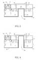
Please refer toFIGS. 1˜5 .FIGS. 1-5 are schematic, cross-sectional view diagrams showing a method for fabricating a semiconductor device with a TSV according to the first preferred embodiment of the present invention. As shown inFIG. 1 , at first, asubstrate 10 is provided, such as silicon substrate, an epitaxial silicon substrate, a silicon germanium substrate, a silicon carbide substrate or a silicon-on-insulator (SOI), wherein thesubstrate 10 has afront surface 12 and aback surface 14. An N-well or a P-well is then formed in the substrate10 (not shown), and a plurality of STI (shallow trench isolations)16 is then formed in thesubstrate 10.
As shown inFIG. 2 , at least onegate structure 18 is formed on thesubstrate 10, and an S/D region 20 is then formed in thesubstrate 10 wherein the S/D region 20 is located at both sides of thegate structure 18. Thegate structure 18 includes a polysilicon gate, a metal gate or a dummy gate, but not limited thereto. The method for fabricating thegate structure 18, the S/D region 20, or a salicide (not shown) layer disposed on the S/D region 20 are well known to persons of ordinary skills in the art and the details will not be described here. An ILD (inter layer dielectric)22 is deposited on thegate structure 18 and thefront surface 12, an inter metal dielectric (IMD) process is then carried out to form a plurality of IMD (inter metal dielectric) (not shown) and a plurality of metal traces which are disposed in each IMD (not shown) on theILD 22. To simplify the description,FIG. 2 only illustrates ametal trace 24 formed on theILD 22, which corresponds to a TSV formed in following steps and neglect others IMD and others metal traces disposed in the IMD. A bottom surface of themetal trace 24 can directly contact the TSV; hence the TSV can be electrically connected to other components through the metal traces disposed in the IMD. Besides, a contact etching stop layer (CESL) (not shown) may be selectively formed between theILD 22 and thesubstrate 10 to cover thegate structure 18 and the S/D region 20.
It is worth noting that, in the present invention, a via plug process is carried out before themetal trace 24 is formed, in order to form a plurality ofcontact plugs 28, and acontact ring 26 can be formed in the ILD22 during the via plug process simultaneously. Thecontact plugs 28 are disposed on thegate structure 18 and the S/D region 20 is electrically connected to the metal traces (not shown) disposed in the IMD above theILD 22. Additionally, thecontact ring 26 is disposed on theSTI 16, is preferably ring-shaped and doesn't contact the TSV, so that the inner diameter of thecontact ring 26 is larger than the outer diameter of the TSV, but smaller than the width of themetal trace 24. In addition, thecontact ring 26 directly contacts themetal trace 24, so thecontact ring 26 is electrically connected to themetal trace 24 to obtain a better shield performance. In the present invention, the materials of themetal trace 24, thecontact ring 26 and thecontact plug 28 can be selected from the group of copper (Cu), aluminum (Al), tungsten (W), titanium (Ti), titanium nitride (TiN), tantalum (Ta) or tantalum nitride (TaN), but not limited thereto.
After the IMD process is carried out and a bonding pad disposed on the IMD is formed on thefront surface 12, theback surface 14 of thesubstrate 10 is grinded to thin down thesubstrate 10. Then, as shown inFIG. 3 , anopening 30 is formed on theback surface 14 through a photo-etching process, wherein theopening 30 is used to define the location of the TSV that is formed in following steps. The opening30 penetrates thesubstrate 10 and theSTI 16. Besides, a bottom of the opening30 is stopped on a bottom of the ILD22. The etching may be carried out through a dry etching process using CF4, O2 and Ar, or a wet etching process, such as dilute HF. In a following step, aliner 32 is formed on theback surface 14 and in theopening 30 to cover the bottom surface and the sidewalls of theopening 30, theliner 32 is a single layer structure such as SiN or SiO2, or a multi-layer structure, but not limited thereto. It is worth noting that, since the bottom of the opening30 is only stopped on the surface of theILD 22, theliner 32 formed in theopening 30 will therefore not be disposed in theILD 22, but only disposed in thesubstrate 10.
Afterward, an etching process is then performed on theopening 30 again, as shown inFIG. 4 , in order to form aTSV hole 34, and a bottom of the TSVhole 34 is stopped on a bottom of themetal trace 24. The etching process only penetrates theliner 32 and the ILD22 through theopening 30, so that the etching time is short and easy to control, thereby increasing the uniformity of the etching surface. Abarrier layer 36 is then deposited in the TSVhole 34 to cover the bottom and the sidewalls of the TSVhole 34, and thebarrier layer 36 is substantially connected to themetal trace 24. Thebarrier layer 36 includes Ti, TiN, Ta or TaN, but not limited thereto.
As shown inFIG. 5 , aconductive layer 38 is then formed on thebarrier layer 36 and fills theTSV hole 34 to form a TSV40. Theconductive layer 38 includes metals with high conductivity, such as Copper (Cu). The manufacturing method to form theconductive layer 38 comprises the following steps: first, a Cu seed layer can be formed on thebarrier layer 36, and a backside-bump process is carried out to form a patterned photo resistor (not shown), after electroplating Cu layer on the Cu seed layer, the patterned photo resistor is removed and a semiconductor device with a TSV is completed. This way, a semiconductor device1 of the present invention includes asubstrate 10, a plurality ofSTI 16 on thesubstrate 10, an ILD22 disposed on thesubstrate 10, aTSV 40 penetrating thesubstrate 10, theSTI 16 and the ILD22, acontact ring 26 disposed in theILD 22 and surrounding theTSV 40, and disposed on theSTI 16, and aliner 32 disposed only in thesubstrate 10, surrounding theTSV 40, and not disposed in theILD 22.
A specific feature of the present invention is to etch theback surface 14 to form theopening 30 wherein the bottom of theopening 30 stops on the surface of theILD 22, but not directly exposing themetal trace 24, then to form theliner 32 on the bottom and the sidewalls of theopening 30, and penetrate theILD 22 through a short time etching process so as to form aTSV hole 34 and expose themetal trace 24. Hence, the problem that of themetal trace 24 directly exposed through theopening 30 that causes metal contamination affecting others adjacent components, such as thegate structure 18, can be prevented. In addition, the present invention further overcomes the problem of themetal trace 24 being destroyed through the etching process that directly penetrates thesubstrate 10, theSTI 16 and theILD 22.
Another specific feature of the present invention is to have thecontact ring 26. In the present invention, thecontact ring 26 is formed in theILD 22 and surrounds theTSV 40 before themetal trace 24 is formed. Therefore, when theopening 30 is penetrated through the etching process to expose themetal trace 24, the contact ring can protect adjacent components from metal contamination. Besides, theTSV 40 usually connects others semiconductor components, such as transistors, memories, inductors or resistors. When theTSV 40 acts as a power pin, the massive current transmitted through theTSV 40 will cause serious electromagnetic interference (EMI) to the adjacent components, such as thegate structure 18. Thecontact ring 26 can solve this problem. Thecontact ring 26 is disposed on the periphery of theTSV 40. As a result, the EMI produced by the massive current conducting through theTSV 40 can be prevented by thecontact ring 26. The material of thecontact ring 26 can be selected from a group consisting of copper (Cu), aluminum (Al), tungsten (W), titanium (Ti), titanium nitride (TiN), tantalum (Ta) or tantalum nitride (TaN). However, the material of thecontact ring 26 depends on the integration of the semiconductor manufacture process and is not limited to the above.
The following description will detail different embodiments of the semiconductor device with TSV and the manufacturing method of the present invention. To simplify the description, the following descriptions will detail the dissimilarities among the different embodiments and the identical features will not be redundantly described. In order to easily compare the differences between the embodiments, the identical components in each of the following embodiments are marked with identical symbols.
Please refer toFIG. 6 ,FIG. 6 is a schematic, cross-sectional diagram showing a semiconductor device in accordance with the second preferred embodiment of the invention. Similarly to the first preferred embodiment of the present invention, asemiconductor device 2 includes asubstrate 10, a plurality ofSTI 16 disposed in thesubstrate 10, anILD 22 disposed on thesubstrate 10, aTSV 40 penetrating thesubstrate 10 and theILD 22, and aliner 32 which is only disposed in thesubstrate 10 and surrounds theTSV 40. The difference with the first preferred embodiment is that thecontact ring 42 and the metal trace are formed at the same time, in other words, thecontact ring 42 is a monolithic structure together with the metal trace. In the first preferred embodiment, the metal trace is formed after the contact ring is formed, but in this embodiment, thecontact ring 42 and the metal trace are formed simultaneously. Besides, each of the contact plugs28 and thecontact ring 42 can be formed simultaneously too, or formed in different steps. If the contact plugs28 and thecontact ring 42 are formed together, the manufacturing process can be further simplified. In addition, thecontact ring 42 and thecontact plug 28 includes metal with high conductivity such as copper (Cu), aluminum (Al), tungsten (W), titanium (Ti), titanium nitride (TiN), tantalum (Ta) or tantalum nitride (TaN), but not limited thereto. Apart from thecontact ring 42, the other components, material properties, and manufacturing method of thesemiconductor device 2 are similar to those of the first preferred embodiment detailed above and will not be redundantly described
In order to increase the contact ringing effect, thecontact ring 26 structure in the present invention is further coupled with a ground connection or a floating connection (not shown). The ground connection may be connected to a stable grounding device, such as a system plate installed with a semiconductor package (not shown), or a chip-scale ground connection, in order to control the noise more efficiently. Furthermore, a high-frequency wave filter may be used between the system plate and thecontact ring 26 to selectively remove the high-frequency noise.
In addition, the present invention is not only applied in via-last process, it also may be obtained through using a via-middle process or a via-first process. Each process can be substantially integrated into existing semiconductor manufacture processes.
To summarize the above descriptions, the present invention provides a semiconductor device with a TSV having a contact ring and a liner surrounding the TSV. The liner and the contact ring can protect the components adjacent to the TSV from metal contamination during the process of forming the TSV.
Those skilled in the art will readily observe that numerous modifications and alterations of the device and method may be made while retaining the teachings of the invention. Accordingly, the above disclosure should be construed as limited only by the metes and bounds of the appended claims.
Claims (15)
1. A semiconductor device, comprising:
a substrate;
an ILD (inter layer dielectric) disposed on the substrate;
a TSV (through silicon via) penetrating the substrate and the ILD; and
a contact ring, disposed in the ILD and surrounding the TSV, wherein the contact ring comprises a hollowed center region completely therethrough, the contact ring is an entirely enclosed structure, and parts of the ILD are disposed between the contact ring and the TSV.
2. The semiconductor device ofclaim 1 , further comprising a metal trace disposed on a surface of the ILD, wherein the TSV contacts the metal trace.
3. The semiconductor device ofclaim 2 , wherein the contact ring is electrically connected to the metal trace.
4. The semiconductor device ofclaim 2 , further comprising a barrier layer disposed in the TSV, wherein the barrier layer substantially contacts the metal trace, and the barrier layer is located inside the ILD.
5. The semiconductor device ofclaim 1 , further comprising a liner disposed in the TSV, wherein the liner is only disposed in the substrate.
6. The semiconductor device ofclaim 1 , further comprising a gate structure disposed on the substrate, and the gate structure includes a metal gate, a polysilicon gate or a dummy gate.
7. The semiconductor device ofclaim 1 , further comprising at least a STI (shallow trench isolation) disposed in the substrate, wherein the contact ring is disposed on the STI.
8. A semiconductor device, comprising:
a substrate;
an ILD (inter layer dielectric) disposed on the substrate;
a TSV (through silicon via) penetrating the substrate and the ILD;
a contact ring disposed surrounding the TSV side by side lie within a same plane, the contact ring comprises a hollowed center region completely therethrough, the contact ring is an entirely enclosed structure, and parts of the ILD are disposed between the contact ring and the TSV; and
a liner disposed in the TSV, wherein the liner is only disposed in the substrate.
9. The semiconductor device ofclaim 8 , further comprising a wherein the contact ring disposed in the ILD and surrounding the TSV and a plurality of STI (shallow trench isolation) disposed in the substrate, wherein and the contact ring is disposed on the STI.
10. The semiconductor device ofclaim 8 , further comprising a metal trace disposed on a surface of the ILD, wherein the TSV contacts the metal trace.
11. The semiconductor device ofclaim 10 , wherein the contact ring is electrically connected to the metal trace.
12. The semiconductor device ofclaim 10 , further comprising a barrier layer disposed in the TSV, wherein the barrier layer substantially contacts the metal trace, and the barrier layer is located inside the ILD.
13. The semiconductor device ofclaim 8 , further comprising a gate structure disposed on the substrate, wherein the gate structure includes a metal gate, a polysilicon gate or a dummy gate.
14. The semiconductor device ofclaim 1 , wherein a top surface of the contact ring and the TSV being even with respect to each other.
15. The semiconductor device ofclaim 8 , wherein a top surface of the contact ring and the TSV being even with respect to each other.
Priority Applications (2)
| Application Number | Priority Date | Filing Date | Title |
|---|---|---|---|
| US13/526,533US9275933B2 (en) | 2012-06-19 | 2012-06-19 | Semiconductor device |
| US14/997,594US10199273B2 (en) | 2012-06-19 | 2016-01-18 | Method for forming semiconductor device with through silicon via |
Applications Claiming Priority (1)
| Application Number | Priority Date | Filing Date | Title |
|---|---|---|---|
| US13/526,533US9275933B2 (en) | 2012-06-19 | 2012-06-19 | Semiconductor device |
Related Child Applications (1)
| Application Number | Title | Priority Date | Filing Date |
|---|---|---|---|
| US14/997,594DivisionUS10199273B2 (en) | 2012-06-19 | 2016-01-18 | Method for forming semiconductor device with through silicon via |
Publications (2)
| Publication Number | Publication Date |
|---|---|
| US20130334669A1 US20130334669A1 (en) | 2013-12-19 |
| US9275933B2true US9275933B2 (en) | 2016-03-01 |
Family
ID=49755140
Family Applications (2)
| Application Number | Title | Priority Date | Filing Date |
|---|---|---|---|
| US13/526,533Active2032-09-09US9275933B2 (en) | 2012-06-19 | 2012-06-19 | Semiconductor device |
| US14/997,594ActiveUS10199273B2 (en) | 2012-06-19 | 2016-01-18 | Method for forming semiconductor device with through silicon via |
Family Applications After (1)
| Application Number | Title | Priority Date | Filing Date |
|---|---|---|---|
| US14/997,594ActiveUS10199273B2 (en) | 2012-06-19 | 2016-01-18 | Method for forming semiconductor device with through silicon via |
Country Status (1)
| Country | Link |
|---|---|
| US (2) | US9275933B2 (en) |
Cited By (12)
| Publication number | Priority date | Publication date | Assignee | Title |
|---|---|---|---|---|
| US10468334B2 (en) | 2017-03-17 | 2019-11-05 | Toshiba Memory Corporation | Semiconductor device and manufacturing method thereof |
| US11587849B2 (en)* | 2020-09-11 | 2023-02-21 | Kioxia Corporation | Semiconductor device and manufacturing method thereof |
| US12154852B2 (en) | 2022-01-03 | 2024-11-26 | United Microelectronics Corp. | Interconnection structure and manufacturing method thereof |
| US12206000B2 (en) | 2020-08-11 | 2025-01-21 | United Microelectronics Corp. | High electron mobility transistor and method for forming the same |
| US12216072B2 (en) | 2021-08-02 | 2025-02-04 | United Semiconductor (Xiamen) Co., Ltd. | Reticle thermal expansion calibration method capable of improving sub-recipe |
| US12262555B2 (en) | 2022-04-08 | 2025-03-25 | United Microelectronics Corp. | Semiconductor device and method of fabricating the same |
| US12276020B2 (en) | 2023-06-01 | 2025-04-15 | United Semiconductor (Xiamen) Co., Ltd. | Semiconductor cleaning step |
| US12342567B2 (en) | 2020-11-19 | 2025-06-24 | United Microelectronics Corp. | Semiconductor device and fabricating method thereof |
| US12402367B2 (en) | 2022-05-12 | 2025-08-26 | United Microelectronics Corp. | Semiconductor structure and manufacturing method thereof |
| US12419093B2 (en) | 2019-10-31 | 2025-09-16 | United Microelectronics Corp. | Structure of flash memory cell |
| US12417984B2 (en) | 2021-04-01 | 2025-09-16 | Changxin Memory Technologies, Inc. | Semiconductor structure with an air gap, method for forming same, and stacked structure |
| US12441606B2 (en) | 2022-11-11 | 2025-10-14 | United Microelectronics Corp. | MEMS device including coil structure with corrugated polymer film |
Families Citing this family (18)
| Publication number | Priority date | Publication date | Assignee | Title |
|---|---|---|---|---|
| US9257392B2 (en) | 2012-04-11 | 2016-02-09 | Mediatek Inc. | Semiconductor package with through silicon via interconnect |
| US9275933B2 (en) | 2012-06-19 | 2016-03-01 | United Microelectronics Corp. | Semiconductor device |
| US9577035B2 (en)* | 2012-08-24 | 2017-02-21 | Newport Fab, Llc | Isolated through silicon vias in RF technologies |
| US9245790B2 (en)* | 2013-01-23 | 2016-01-26 | GlobalFoundries, Inc. | Integrated circuits and methods of forming the same with multiple embedded interconnect connection to same through-semiconductor via |
| US9123789B2 (en)* | 2013-01-23 | 2015-09-01 | United Microelectronics Corp. | Chip with through silicon via electrode and method of forming the same |
| KR101968351B1 (en)* | 2013-01-28 | 2019-08-13 | 서울대학교산학협력단 | Semiconductor device and method of fabricating the same |
| US9054106B2 (en)* | 2013-11-13 | 2015-06-09 | United Microelectronics Corp. | Semiconductor structure and method for manufacturing the same |
| US9252047B2 (en) | 2014-01-23 | 2016-02-02 | Taiwan Semiconductor Manufacturing Co., Ltd | Interconnect arrangement with stress-reducing structure and method of fabricating the same |
| US9832867B2 (en)* | 2015-11-23 | 2017-11-28 | Medtronic, Inc. | Embedded metallic structures in glass |
| KR102450580B1 (en) | 2017-12-22 | 2022-10-07 | 삼성전자주식회사 | Semiconductor Device having a Structure for Insulating Layer under Metal Line |
| KR20210012084A (en) | 2019-07-23 | 2021-02-03 | 삼성전자주식회사 | Semiconductor device |
| US11264340B2 (en)* | 2019-11-26 | 2022-03-01 | Advanced Semiconductor Engineering, Inc. | Semiconductor devices, semiconductor device packages and method for manufacturing the same |
| KR102833169B1 (en) | 2020-07-20 | 2025-07-11 | 삼성전자주식회사 | Semiconductor device and method of manufacturing the semiconductor device |
| US11527439B2 (en) | 2020-09-22 | 2022-12-13 | Taiwan Semiconductor Manufacturing Co., Ltd. | TSV structure and method forming same |
| DE102021100529A1 (en)* | 2020-08-13 | 2022-02-17 | Taiwan Semiconductor Manufacturing Co., Ltd. | TSV STRUCTURE AND METHODS OF FORMING THEREOF |
| CN115172324B (en)* | 2021-04-01 | 2025-01-10 | 长鑫存储技术有限公司 | Semiconductor structure and method for forming the same, and stacked structure |
| CN113394185A (en)* | 2021-06-10 | 2021-09-14 | 武汉新芯集成电路制造有限公司 | Semiconductor device, manufacturing method thereof and chip |
| US12014997B2 (en) | 2021-07-01 | 2024-06-18 | Taiwan Semiconductor Manufacturing Co., Ltd. | Dummy stacked structures surrounding TSVs and method forming the same |
Citations (98)
| Publication number | Priority date | Publication date | Assignee | Title |
|---|---|---|---|---|
| US3150299A (en) | 1959-09-11 | 1964-09-22 | Fairchild Camera Instr Co | Semiconductor circuit complex having isolation means |
| US3256465A (en) | 1962-06-08 | 1966-06-14 | Signetics Corp | Semiconductor device assembly with true metallurgical bonds |
| US3323198A (en) | 1965-01-27 | 1967-06-06 | Texas Instruments Inc | Electrical interconnections |
| US3343256A (en) | 1964-12-28 | 1967-09-26 | Ibm | Methods of making thru-connections in semiconductor wafers |
| US3372070A (en) | 1965-07-30 | 1968-03-05 | Bell Telephone Labor Inc | Fabrication of semiconductor integrated devices with a pn junction running through the wafer |
| US3462650A (en) | 1951-01-28 | 1969-08-19 | Telefunken Patent | Electrical circuit manufacture |
| US3577005A (en)* | 1969-11-24 | 1971-05-04 | Shell Oil Co | Transistor inverter circuit |
| US3648131A (en) | 1969-11-07 | 1972-03-07 | Ibm | Hourglass-shaped conductive connection through semiconductor structures |
| US4394712A (en) | 1981-03-18 | 1983-07-19 | General Electric Company | Alignment-enhancing feed-through conductors for stackable silicon-on-sapphire wafers |
| US4395302A (en) | 1981-12-10 | 1983-07-26 | Enthone Incorporated | Metal dissolution process using H2 O2 --H2 SO4 etchant |
| US4616247A (en) | 1983-11-10 | 1986-10-07 | At&T Bell Laboratories | P-I-N and avalanche photodiodes |
| US4773972A (en) | 1986-10-30 | 1988-09-27 | Ford Motor Company | Method of making silicon capacitive pressure sensor with glass layer between silicon wafers |
| US4939568A (en) | 1986-03-20 | 1990-07-03 | Fujitsu Limited | Three-dimensional integrated circuit and manufacturing method thereof |
| US5214000A (en) | 1991-12-19 | 1993-05-25 | Raychem Corporation | Thermal transfer posts for high density multichip substrates and formation method |
| US5229647A (en) | 1991-03-27 | 1993-07-20 | Micron Technology, Inc. | High density data storage using stacked wafers |
| US5286926A (en) | 1991-04-16 | 1994-02-15 | Ngk Spark Plug Co., Ltd. | Integrated circuit package and process for producing same |
| US5372969A (en) | 1991-12-31 | 1994-12-13 | Texas Instruments Incorporated | Low-RC multi-level interconnect technology for high-performance integrated circuits |
| US5399898A (en) | 1992-07-17 | 1995-03-21 | Lsi Logic Corporation | Multi-chip semiconductor arrangements using flip chip dies |
| US5463246A (en) | 1988-12-29 | 1995-10-31 | Sharp Kabushiki Kaisha | Large scale high density semiconductor apparatus |
| US5484073A (en) | 1994-03-28 | 1996-01-16 | I/O Sensors, Inc. | Method for fabricating suspension members for micromachined sensors |
| US5502333A (en) | 1994-03-30 | 1996-03-26 | International Business Machines Corporation | Semiconductor stack structures and fabrication/sparing methods utilizing programmable spare circuit |
| US5627106A (en) | 1994-05-06 | 1997-05-06 | United Microelectronics Corporation | Trench method for three dimensional chip connecting during IC fabrication |
| US5793115A (en) | 1993-09-30 | 1998-08-11 | Kopin Corporation | Three dimensional processor using transferred thin film circuits |
| US5977640A (en) | 1998-06-26 | 1999-11-02 | International Business Machines Corporation | Highly integrated chip-on-chip packaging |
| US6018196A (en) | 1996-11-08 | 2000-01-25 | W. L. Gore & Associates, Inc. | Semiconductor flip chip package |
| US6143616A (en) | 1997-08-22 | 2000-11-07 | Micron Technology, Inc. | Methods of forming coaxial integrated circuitry interconnect lines |
| US6274937B1 (en) | 1999-02-01 | 2001-08-14 | Micron Technology, Inc. | Silicon multi-chip module packaging with integrated passive components and method of making |
| US6309956B1 (en) | 1997-09-30 | 2001-10-30 | Intel Corporation | Fabricating low K dielectric interconnect systems by using dummy structures to enhance process |
| US20010038972A1 (en) | 1998-11-20 | 2001-11-08 | Christopher F. Lyons | Ultra-thin resist shallow trench process using metal hard mask |
| US6391777B1 (en) | 2001-05-02 | 2002-05-21 | Taiwan Semiconductor Manufacturing Company | Two-stage Cu anneal to improve Cu damascene process |
| US6407002B1 (en) | 2000-08-10 | 2002-06-18 | Taiwan Semiconductor Manufacturing Company | Partial resist free approach in contact etch to improve W-filling |
| US6440640B1 (en) | 1998-12-01 | 2002-08-27 | Advanced Micro Devices, Inc. | Thin resist with transition metal hard mask for via etch application |
| US6483147B1 (en) | 1999-10-25 | 2002-11-19 | Advanced Micro Devices, Inc. | Through wafer backside contact to improve SOI heat dissipation |
| US6525419B1 (en) | 2002-02-14 | 2003-02-25 | Intel Corporation | Thermally coupling electrically decoupling cooling device for integrated circuits |
| US6548891B2 (en) | 2000-10-24 | 2003-04-15 | Shinko Electric Industries Co., Ltd. | Semiconductor device and production process thereof |
| US6551857B2 (en) | 1997-04-04 | 2003-04-22 | Elm Technology Corporation | Three dimensional structure integrated circuits |
| US6617681B1 (en) | 1999-06-28 | 2003-09-09 | Intel Corporation | Interposer and method of making same |
| US6627985B2 (en) | 2001-12-05 | 2003-09-30 | Arbor Company Llp | Reconfigurable processor module comprising hybrid stacked integrated circuit die elements |
| US6633083B2 (en) | 2000-02-28 | 2003-10-14 | Advanced Micro Devices Inc. | Barrier layer integrity test |
| US20040080041A1 (en) | 2002-10-21 | 2004-04-29 | Nec Electronics Corporation | Semiconductor device with improved heatsink structure |
| US6746936B1 (en) | 2002-12-09 | 2004-06-08 | Hynix Semiconductor Inc. | Method for forming isolation film for semiconductor devices |
| US6778275B2 (en) | 2002-02-20 | 2004-08-17 | Micron Technology, Inc. | Aberration mark and method for estimating overlay error and optical aberrations |
| US20040188817A1 (en) | 2003-03-31 | 2004-09-30 | Intel Corporation | Apparatus and method to minimize thermal impedance using copper on die backside |
| US6800930B2 (en) | 2002-07-31 | 2004-10-05 | Micron Technology, Inc. | Semiconductor dice having back side redistribution layer accessed using through-silicon vias, and assemblies |
| US6812193B2 (en) | 2001-08-31 | 2004-11-02 | International Business Machines Corporation | Slurry for mechanical polishing (CMP) of metals and use thereof |
| US6831013B2 (en) | 2001-11-13 | 2004-12-14 | United Microelectronics Corp. | Method of forming a dual damascene via by using a metal hard mask layer |
| US6897148B2 (en) | 2003-04-09 | 2005-05-24 | Tru-Si Technologies, Inc. | Electroplating and electroless plating of conductive materials into openings, and structures obtained thereby |
| US20050112997A1 (en) | 2003-11-26 | 2005-05-26 | Lin Chun H. | Advanced process control approach for Cu interconnect wiring sheet resistance control |
| US20050136635A1 (en) | 2003-12-17 | 2005-06-23 | Sergey Savastiouk | Attachment of integrated circuit structures and other substrates to substrates with vias |
| US6924551B2 (en) | 2003-05-28 | 2005-08-02 | Intel Corporation | Through silicon via, folded flex microelectronic package |
| US6930048B1 (en) | 2002-09-18 | 2005-08-16 | Lam Research Corporation | Etching a metal hard mask for an integrated circuit structure |
| US20050205991A1 (en) | 2004-03-16 | 2005-09-22 | Taiwan Semiconductor Manufacturing Co., Ltd. | System and method of heat dissipation in semiconductor devices |
| US20060035146A1 (en) | 2003-02-20 | 2006-02-16 | Mitsubishi Chemical Corporation | Negative-electrode active material for lithium secondary battery, negative electrode for lithium secondary battery, and lithium secondary battery |
| US20060042834A1 (en) | 2004-08-24 | 2006-03-02 | Chipmos Technologies (Bermuda) Ltd. | Electronic device with a warped spring connector |
| US7034401B2 (en) | 2003-12-17 | 2006-04-25 | Tru-Si Technologies, Inc. | Packaging substrates for integrated circuits and soldering methods |
| US7052937B2 (en) | 1999-07-28 | 2006-05-30 | International Business Machines Corporation | Method and structure for providing improved thermal conduction for silicon semiconductor devices |
| US7075133B1 (en) | 2004-05-03 | 2006-07-11 | National Semiconductor Corporation | Semiconductor die with heat and electrical pipes |
| US7098070B2 (en) | 2004-11-16 | 2006-08-29 | International Business Machines Corporation | Device and method for fabricating double-sided SOI wafer scale package with through via connections |
| US7111149B2 (en) | 2003-07-07 | 2006-09-19 | Intel Corporation | Method and apparatus for generating a device ID for stacked devices |
| US7166913B2 (en) | 2005-04-19 | 2007-01-23 | International Business Machines Corporation | Heat dissipation for heat generating element of semiconductor device and related method |
| US20070117348A1 (en) | 2005-11-21 | 2007-05-24 | Shriram Ramanathan | 3D integrated circuits using thick metal for backside connections and offset bumps |
| US7222420B2 (en) | 2000-07-27 | 2007-05-29 | Fujitsu Limited | Method for making a front and back conductive substrate |
| US20070126085A1 (en) | 2005-12-02 | 2007-06-07 | Nec Electronics Corporation | Semiconductor device and method of manufacturing the same |
| US20070190692A1 (en) | 2006-01-13 | 2007-08-16 | Mete Erturk | Low resistance and inductance backside through vias and methods of fabricating same |
| US7282951B2 (en) | 2001-12-05 | 2007-10-16 | Arbor Company Llp | Reconfigurable processor module comprising hybrid stacked integrated circuit die elements |
| US7323785B2 (en) | 2005-03-17 | 2008-01-29 | Elpida Memory, Inc. | Semiconductor device |
| US7338896B2 (en) | 2004-12-17 | 2008-03-04 | Interuniversitair Microelektronica Centrum (Imec) | Formation of deep via airgaps for three dimensional wafer to wafer interconnect |
| US20080073747A1 (en) | 2006-09-22 | 2008-03-27 | Clinton Chao | Electromagnetic shielding using through-silicon vias |
| US20080108193A1 (en) | 2006-11-06 | 2008-05-08 | Spansion Llc | Cu annealing for improved data retention in flash memory devices |
| US7402515B2 (en) | 2005-06-28 | 2008-07-22 | Intel Corporation | Method of forming through-silicon vias with stress buffer collars and resulting devices |
| US7432592B2 (en) | 2005-10-13 | 2008-10-07 | Intel Corporation | Integrated micro-channels for 3D through silicon architectures |
| US7531415B2 (en) | 2000-11-30 | 2009-05-12 | Texas Instruments Incorporated | Multilayered CMP stop for flat planarization |
| US20090127667A1 (en) | 2007-11-21 | 2009-05-21 | Powertech Technology Inc. | Semiconductor chip device having through-silicon-via (TSV) and its fabrication method |
| US20090134498A1 (en) | 2007-11-20 | 2009-05-28 | Elpida Memory, Inc. | Semiconductor apparatus |
| US7541677B2 (en) | 2004-03-31 | 2009-06-02 | Nec Electronics Corporation | Semiconductor device comprising through-electrode interconnect |
| US20090180257A1 (en) | 2008-01-15 | 2009-07-16 | Samsung Electronics Co., Ltd. | Stacked semiconductor apparatus, system and method of fabrication |
| US20090224405A1 (en) | 2008-03-07 | 2009-09-10 | Taiwan Semiconductor Manufacturing Co., Ltd. | Through via process |
| US20100001379A1 (en) | 2008-07-02 | 2010-01-07 | Hoon Lee | Multi-chip package (MCP) having three dimensional mesh-based power distribution network, and power distribution method of the MCP |
| US7732926B2 (en) | 2005-12-12 | 2010-06-08 | Elpida Memory, Inc. | Semiconductor device having a through electrode with a low resistance and method of manufacturing the same |
| US20100140772A1 (en) | 2008-12-08 | 2010-06-10 | Stats Chippac, Ltd. | Semiconductor Device and Method of Forming Vertical Interconnect Structure in Substrate for IPD and Baseband Circuit Separated by High-Resistivity Molding Compound |
| US20100140749A1 (en) | 2008-12-08 | 2010-06-10 | Chien-Li Kuo | Semiconductor device |
| US20100224965A1 (en)* | 2009-03-09 | 2010-09-09 | Chien-Li Kuo | Through-silicon via structure and method for making the same |
| US20100244247A1 (en) | 2009-03-27 | 2010-09-30 | Taiwan Semiconductor Manufacturing Company, Ltd. | Via structure and via etching process of forming the same |
| US7846837B2 (en) | 2008-10-09 | 2010-12-07 | United Microelectronics Corp. | Through substrate via process |
| US20100323478A1 (en) | 2009-06-19 | 2010-12-23 | Chien-Li Kuo | Method for fabricating through-silicon via structure |
| US20110031581A1 (en)* | 2009-08-10 | 2011-02-10 | Texas Instruments Incorporated | Integrated circuit (ic) having tsvs with dielectric crack suppression structures |
| US20120139127A1 (en)* | 2010-12-07 | 2012-06-07 | Imec | Method for forming isolation trenches |
| US8264086B2 (en)* | 2005-12-05 | 2012-09-11 | Taiwan Semiconductor Manufacturing Company, Ltd. | Via structure with improved reliability |
| US20120248581A1 (en)* | 2011-03-31 | 2012-10-04 | Elpida Memory, Inc. | Semiconductor device and manufacturing method thereof |
| US20120261826A1 (en)* | 2011-04-13 | 2012-10-18 | Chien-Li Kuo | Tsv structure and method for forming the same |
| US8338939B2 (en)* | 2010-07-12 | 2012-12-25 | Taiwan Semiconductor Manufacturing Company, Ltd. | TSV formation processes using TSV-last approach |
| US8390120B2 (en)* | 2010-06-28 | 2013-03-05 | Samsung Electronics Co., Ltd. | Semiconductor device and method of fabricating the same |
| US20130099312A1 (en)* | 2011-10-24 | 2013-04-25 | Thuy B. Dao | Semiconductor structure having a through substrate via (tsv) and method for forming |
| US20130313690A1 (en)* | 2012-05-28 | 2013-11-28 | Elpida Memory, Inc. | Semiconductor device |
| US20130334699A1 (en)* | 2012-06-19 | 2013-12-19 | Chien-Li Kuo | Semiconductor device and fabricating method thereof |
| US20130334669A1 (en)* | 2012-06-19 | 2013-12-19 | Chien-Li Kuo | Semiconductor device |
| US20140053604A1 (en)* | 2012-07-29 | 2014-02-27 | David Keir Newton | Adjustable ring |
| US20140054742A1 (en)* | 2012-08-27 | 2014-02-27 | Agency For Science, Technology And Research | Semiconductor Structure |
Family Cites Families (10)
| Publication number | Priority date | Publication date | Assignee | Title |
|---|---|---|---|---|
| US7531443B2 (en) | 2006-12-08 | 2009-05-12 | Micron Technology, Inc. | Method and system for fabricating semiconductor components with through interconnects and back side redistribution conductors |
| JP5656341B2 (en)* | 2007-10-29 | 2015-01-21 | ピーエスフォー ルクスコ エスエイアールエルPS4 Luxco S.a.r.l. | Semiconductor device and manufacturing method thereof |
| FR2930840B1 (en)* | 2008-04-30 | 2010-08-13 | St Microelectronics Crolles 2 | METHOD FOR RECOVERING CONTACT ON A REAR-FACING LIGHT CIRCUIT |
| JP5537016B2 (en)* | 2008-10-27 | 2014-07-02 | 株式会社東芝 | Semiconductor device and manufacturing method of semiconductor device |
| US7923369B2 (en)* | 2008-11-25 | 2011-04-12 | Freescale Semiconductor, Inc. | Through-via and method of forming |
| TWI460838B (en) | 2008-12-08 | 2014-11-11 | United Microelectronics Corp | Semiconductor device |
| CN101882598A (en) | 2009-05-04 | 2010-11-10 | 南亚科技股份有限公司 | Electrically transparent connection and method for forming same |
| US8697574B2 (en) | 2009-09-25 | 2014-04-15 | Infineon Technologies Ag | Through substrate features in semiconductor substrates |
| US8836116B2 (en)* | 2010-10-21 | 2014-09-16 | Taiwan Semiconductor Manufacturing Company, Ltd. | Wafer level packaging of micro-electro-mechanical systems (MEMS) and complementary metal-oxide-semiconductor (CMOS) substrates |
| US9257392B2 (en)* | 2012-04-11 | 2016-02-09 | Mediatek Inc. | Semiconductor package with through silicon via interconnect |
- 2012
- 2012-06-19USUS13/526,533patent/US9275933B2/enactiveActive
- 2016
- 2016-01-18USUS14/997,594patent/US10199273B2/enactiveActive
Patent Citations (98)
| Publication number | Priority date | Publication date | Assignee | Title |
|---|---|---|---|---|
| US3462650A (en) | 1951-01-28 | 1969-08-19 | Telefunken Patent | Electrical circuit manufacture |
| US3150299A (en) | 1959-09-11 | 1964-09-22 | Fairchild Camera Instr Co | Semiconductor circuit complex having isolation means |
| US3256465A (en) | 1962-06-08 | 1966-06-14 | Signetics Corp | Semiconductor device assembly with true metallurgical bonds |
| US3343256A (en) | 1964-12-28 | 1967-09-26 | Ibm | Methods of making thru-connections in semiconductor wafers |
| US3323198A (en) | 1965-01-27 | 1967-06-06 | Texas Instruments Inc | Electrical interconnections |
| US3372070A (en) | 1965-07-30 | 1968-03-05 | Bell Telephone Labor Inc | Fabrication of semiconductor integrated devices with a pn junction running through the wafer |
| US3648131A (en) | 1969-11-07 | 1972-03-07 | Ibm | Hourglass-shaped conductive connection through semiconductor structures |
| US3577005A (en)* | 1969-11-24 | 1971-05-04 | Shell Oil Co | Transistor inverter circuit |
| US4394712A (en) | 1981-03-18 | 1983-07-19 | General Electric Company | Alignment-enhancing feed-through conductors for stackable silicon-on-sapphire wafers |
| US4395302A (en) | 1981-12-10 | 1983-07-26 | Enthone Incorporated | Metal dissolution process using H2 O2 --H2 SO4 etchant |
| US4616247A (en) | 1983-11-10 | 1986-10-07 | At&T Bell Laboratories | P-I-N and avalanche photodiodes |
| US4939568A (en) | 1986-03-20 | 1990-07-03 | Fujitsu Limited | Three-dimensional integrated circuit and manufacturing method thereof |
| US4773972A (en) | 1986-10-30 | 1988-09-27 | Ford Motor Company | Method of making silicon capacitive pressure sensor with glass layer between silicon wafers |
| US5463246A (en) | 1988-12-29 | 1995-10-31 | Sharp Kabushiki Kaisha | Large scale high density semiconductor apparatus |
| US5229647A (en) | 1991-03-27 | 1993-07-20 | Micron Technology, Inc. | High density data storage using stacked wafers |
| US5286926A (en) | 1991-04-16 | 1994-02-15 | Ngk Spark Plug Co., Ltd. | Integrated circuit package and process for producing same |
| US5214000A (en) | 1991-12-19 | 1993-05-25 | Raychem Corporation | Thermal transfer posts for high density multichip substrates and formation method |
| US5372969A (en) | 1991-12-31 | 1994-12-13 | Texas Instruments Incorporated | Low-RC multi-level interconnect technology for high-performance integrated circuits |
| US5399898A (en) | 1992-07-17 | 1995-03-21 | Lsi Logic Corporation | Multi-chip semiconductor arrangements using flip chip dies |
| US5793115A (en) | 1993-09-30 | 1998-08-11 | Kopin Corporation | Three dimensional processor using transferred thin film circuits |
| US5484073A (en) | 1994-03-28 | 1996-01-16 | I/O Sensors, Inc. | Method for fabricating suspension members for micromachined sensors |
| US5502333A (en) | 1994-03-30 | 1996-03-26 | International Business Machines Corporation | Semiconductor stack structures and fabrication/sparing methods utilizing programmable spare circuit |
| US5627106A (en) | 1994-05-06 | 1997-05-06 | United Microelectronics Corporation | Trench method for three dimensional chip connecting during IC fabrication |
| US6018196A (en) | 1996-11-08 | 2000-01-25 | W. L. Gore & Associates, Inc. | Semiconductor flip chip package |
| US6551857B2 (en) | 1997-04-04 | 2003-04-22 | Elm Technology Corporation | Three dimensional structure integrated circuits |
| US6143616A (en) | 1997-08-22 | 2000-11-07 | Micron Technology, Inc. | Methods of forming coaxial integrated circuitry interconnect lines |
| US6309956B1 (en) | 1997-09-30 | 2001-10-30 | Intel Corporation | Fabricating low K dielectric interconnect systems by using dummy structures to enhance process |
| US5977640A (en) | 1998-06-26 | 1999-11-02 | International Business Machines Corporation | Highly integrated chip-on-chip packaging |
| US20010038972A1 (en) | 1998-11-20 | 2001-11-08 | Christopher F. Lyons | Ultra-thin resist shallow trench process using metal hard mask |
| US6440640B1 (en) | 1998-12-01 | 2002-08-27 | Advanced Micro Devices, Inc. | Thin resist with transition metal hard mask for via etch application |
| US6274937B1 (en) | 1999-02-01 | 2001-08-14 | Micron Technology, Inc. | Silicon multi-chip module packaging with integrated passive components and method of making |
| US6617681B1 (en) | 1999-06-28 | 2003-09-09 | Intel Corporation | Interposer and method of making same |
| US7052937B2 (en) | 1999-07-28 | 2006-05-30 | International Business Machines Corporation | Method and structure for providing improved thermal conduction for silicon semiconductor devices |
| US6483147B1 (en) | 1999-10-25 | 2002-11-19 | Advanced Micro Devices, Inc. | Through wafer backside contact to improve SOI heat dissipation |
| US6633083B2 (en) | 2000-02-28 | 2003-10-14 | Advanced Micro Devices Inc. | Barrier layer integrity test |
| US7222420B2 (en) | 2000-07-27 | 2007-05-29 | Fujitsu Limited | Method for making a front and back conductive substrate |
| US6407002B1 (en) | 2000-08-10 | 2002-06-18 | Taiwan Semiconductor Manufacturing Company | Partial resist free approach in contact etch to improve W-filling |
| US6548891B2 (en) | 2000-10-24 | 2003-04-15 | Shinko Electric Industries Co., Ltd. | Semiconductor device and production process thereof |
| US7531415B2 (en) | 2000-11-30 | 2009-05-12 | Texas Instruments Incorporated | Multilayered CMP stop for flat planarization |
| US6391777B1 (en) | 2001-05-02 | 2002-05-21 | Taiwan Semiconductor Manufacturing Company | Two-stage Cu anneal to improve Cu damascene process |
| US6812193B2 (en) | 2001-08-31 | 2004-11-02 | International Business Machines Corporation | Slurry for mechanical polishing (CMP) of metals and use thereof |
| US6831013B2 (en) | 2001-11-13 | 2004-12-14 | United Microelectronics Corp. | Method of forming a dual damascene via by using a metal hard mask layer |
| US7282951B2 (en) | 2001-12-05 | 2007-10-16 | Arbor Company Llp | Reconfigurable processor module comprising hybrid stacked integrated circuit die elements |
| US6627985B2 (en) | 2001-12-05 | 2003-09-30 | Arbor Company Llp | Reconfigurable processor module comprising hybrid stacked integrated circuit die elements |
| US6525419B1 (en) | 2002-02-14 | 2003-02-25 | Intel Corporation | Thermally coupling electrically decoupling cooling device for integrated circuits |
| US6778275B2 (en) | 2002-02-20 | 2004-08-17 | Micron Technology, Inc. | Aberration mark and method for estimating overlay error and optical aberrations |
| US6800930B2 (en) | 2002-07-31 | 2004-10-05 | Micron Technology, Inc. | Semiconductor dice having back side redistribution layer accessed using through-silicon vias, and assemblies |
| US6930048B1 (en) | 2002-09-18 | 2005-08-16 | Lam Research Corporation | Etching a metal hard mask for an integrated circuit structure |
| US20040080041A1 (en) | 2002-10-21 | 2004-04-29 | Nec Electronics Corporation | Semiconductor device with improved heatsink structure |
| US6746936B1 (en) | 2002-12-09 | 2004-06-08 | Hynix Semiconductor Inc. | Method for forming isolation film for semiconductor devices |
| US20060035146A1 (en) | 2003-02-20 | 2006-02-16 | Mitsubishi Chemical Corporation | Negative-electrode active material for lithium secondary battery, negative electrode for lithium secondary battery, and lithium secondary battery |
| US20040188817A1 (en) | 2003-03-31 | 2004-09-30 | Intel Corporation | Apparatus and method to minimize thermal impedance using copper on die backside |
| US6897148B2 (en) | 2003-04-09 | 2005-05-24 | Tru-Si Technologies, Inc. | Electroplating and electroless plating of conductive materials into openings, and structures obtained thereby |
| US6924551B2 (en) | 2003-05-28 | 2005-08-02 | Intel Corporation | Through silicon via, folded flex microelectronic package |
| US7111149B2 (en) | 2003-07-07 | 2006-09-19 | Intel Corporation | Method and apparatus for generating a device ID for stacked devices |
| US20050112997A1 (en) | 2003-11-26 | 2005-05-26 | Lin Chun H. | Advanced process control approach for Cu interconnect wiring sheet resistance control |
| US7034401B2 (en) | 2003-12-17 | 2006-04-25 | Tru-Si Technologies, Inc. | Packaging substrates for integrated circuits and soldering methods |
| US20050136635A1 (en) | 2003-12-17 | 2005-06-23 | Sergey Savastiouk | Attachment of integrated circuit structures and other substrates to substrates with vias |
| US20050205991A1 (en) | 2004-03-16 | 2005-09-22 | Taiwan Semiconductor Manufacturing Co., Ltd. | System and method of heat dissipation in semiconductor devices |
| US7541677B2 (en) | 2004-03-31 | 2009-06-02 | Nec Electronics Corporation | Semiconductor device comprising through-electrode interconnect |
| US7075133B1 (en) | 2004-05-03 | 2006-07-11 | National Semiconductor Corporation | Semiconductor die with heat and electrical pipes |
| US20060042834A1 (en) | 2004-08-24 | 2006-03-02 | Chipmos Technologies (Bermuda) Ltd. | Electronic device with a warped spring connector |
| US7098070B2 (en) | 2004-11-16 | 2006-08-29 | International Business Machines Corporation | Device and method for fabricating double-sided SOI wafer scale package with through via connections |
| US7338896B2 (en) | 2004-12-17 | 2008-03-04 | Interuniversitair Microelektronica Centrum (Imec) | Formation of deep via airgaps for three dimensional wafer to wafer interconnect |
| US7323785B2 (en) | 2005-03-17 | 2008-01-29 | Elpida Memory, Inc. | Semiconductor device |
| US7166913B2 (en) | 2005-04-19 | 2007-01-23 | International Business Machines Corporation | Heat dissipation for heat generating element of semiconductor device and related method |
| US7402515B2 (en) | 2005-06-28 | 2008-07-22 | Intel Corporation | Method of forming through-silicon vias with stress buffer collars and resulting devices |
| US7432592B2 (en) | 2005-10-13 | 2008-10-07 | Intel Corporation | Integrated micro-channels for 3D through silicon architectures |
| US20070117348A1 (en) | 2005-11-21 | 2007-05-24 | Shriram Ramanathan | 3D integrated circuits using thick metal for backside connections and offset bumps |
| US20070126085A1 (en) | 2005-12-02 | 2007-06-07 | Nec Electronics Corporation | Semiconductor device and method of manufacturing the same |
| US8264086B2 (en)* | 2005-12-05 | 2012-09-11 | Taiwan Semiconductor Manufacturing Company, Ltd. | Via structure with improved reliability |
| US7732926B2 (en) | 2005-12-12 | 2010-06-08 | Elpida Memory, Inc. | Semiconductor device having a through electrode with a low resistance and method of manufacturing the same |
| US20070190692A1 (en) | 2006-01-13 | 2007-08-16 | Mete Erturk | Low resistance and inductance backside through vias and methods of fabricating same |
| US20080073747A1 (en) | 2006-09-22 | 2008-03-27 | Clinton Chao | Electromagnetic shielding using through-silicon vias |
| US20080108193A1 (en) | 2006-11-06 | 2008-05-08 | Spansion Llc | Cu annealing for improved data retention in flash memory devices |
| US20090134498A1 (en) | 2007-11-20 | 2009-05-28 | Elpida Memory, Inc. | Semiconductor apparatus |
| US20090127667A1 (en) | 2007-11-21 | 2009-05-21 | Powertech Technology Inc. | Semiconductor chip device having through-silicon-via (TSV) and its fabrication method |
| US20090180257A1 (en) | 2008-01-15 | 2009-07-16 | Samsung Electronics Co., Ltd. | Stacked semiconductor apparatus, system and method of fabrication |
| US20090224405A1 (en) | 2008-03-07 | 2009-09-10 | Taiwan Semiconductor Manufacturing Co., Ltd. | Through via process |
| US20100001379A1 (en) | 2008-07-02 | 2010-01-07 | Hoon Lee | Multi-chip package (MCP) having three dimensional mesh-based power distribution network, and power distribution method of the MCP |
| US7846837B2 (en) | 2008-10-09 | 2010-12-07 | United Microelectronics Corp. | Through substrate via process |
| US20100140772A1 (en) | 2008-12-08 | 2010-06-10 | Stats Chippac, Ltd. | Semiconductor Device and Method of Forming Vertical Interconnect Structure in Substrate for IPD and Baseband Circuit Separated by High-Resistivity Molding Compound |
| US20100140749A1 (en) | 2008-12-08 | 2010-06-10 | Chien-Li Kuo | Semiconductor device |
| US20100224965A1 (en)* | 2009-03-09 | 2010-09-09 | Chien-Li Kuo | Through-silicon via structure and method for making the same |
| US20100244247A1 (en) | 2009-03-27 | 2010-09-30 | Taiwan Semiconductor Manufacturing Company, Ltd. | Via structure and via etching process of forming the same |
| US20100323478A1 (en) | 2009-06-19 | 2010-12-23 | Chien-Li Kuo | Method for fabricating through-silicon via structure |
| US20110031581A1 (en)* | 2009-08-10 | 2011-02-10 | Texas Instruments Incorporated | Integrated circuit (ic) having tsvs with dielectric crack suppression structures |
| US8390120B2 (en)* | 2010-06-28 | 2013-03-05 | Samsung Electronics Co., Ltd. | Semiconductor device and method of fabricating the same |
| US8338939B2 (en)* | 2010-07-12 | 2012-12-25 | Taiwan Semiconductor Manufacturing Company, Ltd. | TSV formation processes using TSV-last approach |
| US20120139127A1 (en)* | 2010-12-07 | 2012-06-07 | Imec | Method for forming isolation trenches |
| US20120248581A1 (en)* | 2011-03-31 | 2012-10-04 | Elpida Memory, Inc. | Semiconductor device and manufacturing method thereof |
| US20120261826A1 (en)* | 2011-04-13 | 2012-10-18 | Chien-Li Kuo | Tsv structure and method for forming the same |
| US20130099312A1 (en)* | 2011-10-24 | 2013-04-25 | Thuy B. Dao | Semiconductor structure having a through substrate via (tsv) and method for forming |
| US20130313690A1 (en)* | 2012-05-28 | 2013-11-28 | Elpida Memory, Inc. | Semiconductor device |
| US20130334699A1 (en)* | 2012-06-19 | 2013-12-19 | Chien-Li Kuo | Semiconductor device and fabricating method thereof |
| US20130334669A1 (en)* | 2012-06-19 | 2013-12-19 | Chien-Li Kuo | Semiconductor device |
| US20140053604A1 (en)* | 2012-07-29 | 2014-02-27 | David Keir Newton | Adjustable ring |
| US20140054742A1 (en)* | 2012-08-27 | 2014-02-27 | Agency For Science, Technology And Research | Semiconductor Structure |
Cited By (12)
| Publication number | Priority date | Publication date | Assignee | Title |
|---|---|---|---|---|
| US10468334B2 (en) | 2017-03-17 | 2019-11-05 | Toshiba Memory Corporation | Semiconductor device and manufacturing method thereof |
| US12419093B2 (en) | 2019-10-31 | 2025-09-16 | United Microelectronics Corp. | Structure of flash memory cell |
| US12206000B2 (en) | 2020-08-11 | 2025-01-21 | United Microelectronics Corp. | High electron mobility transistor and method for forming the same |
| US11587849B2 (en)* | 2020-09-11 | 2023-02-21 | Kioxia Corporation | Semiconductor device and manufacturing method thereof |
| US12342567B2 (en) | 2020-11-19 | 2025-06-24 | United Microelectronics Corp. | Semiconductor device and fabricating method thereof |
| US12417984B2 (en) | 2021-04-01 | 2025-09-16 | Changxin Memory Technologies, Inc. | Semiconductor structure with an air gap, method for forming same, and stacked structure |
| US12216072B2 (en) | 2021-08-02 | 2025-02-04 | United Semiconductor (Xiamen) Co., Ltd. | Reticle thermal expansion calibration method capable of improving sub-recipe |
| US12154852B2 (en) | 2022-01-03 | 2024-11-26 | United Microelectronics Corp. | Interconnection structure and manufacturing method thereof |
| US12262555B2 (en) | 2022-04-08 | 2025-03-25 | United Microelectronics Corp. | Semiconductor device and method of fabricating the same |
| US12402367B2 (en) | 2022-05-12 | 2025-08-26 | United Microelectronics Corp. | Semiconductor structure and manufacturing method thereof |
| US12441606B2 (en) | 2022-11-11 | 2025-10-14 | United Microelectronics Corp. | MEMS device including coil structure with corrugated polymer film |
| US12276020B2 (en) | 2023-06-01 | 2025-04-15 | United Semiconductor (Xiamen) Co., Ltd. | Semiconductor cleaning step |
Also Published As
| Publication number | Publication date |
|---|---|
| US10199273B2 (en) | 2019-02-05 |
| US20160133518A1 (en) | 2016-05-12 |
| US20130334669A1 (en) | 2013-12-19 |
Similar Documents
| Publication | Publication Date | Title |
|---|---|---|
| US10199273B2 (en) | Method for forming semiconductor device with through silicon via | |
| US8916471B1 (en) | Method for forming semiconductor structure having through silicon via for signal and shielding structure | |
| US9269664B2 (en) | Semiconductor package with through silicon via interconnect and method for fabricating the same | |
| US9437491B2 (en) | Method of forming chip with through silicon via electrode | |
| US9870980B2 (en) | Semiconductor package with through silicon via interconnect | |
| CN102301465B (en) | Through-substrate vias | |
| US20150303108A1 (en) | Method for forming semiconductor device | |
| US8518823B2 (en) | Through silicon via and method of forming the same | |
| US20190115258A1 (en) | Through-Vias and Methods of Forming the Same | |
| KR20130053338A (en) | Integrated circuit device having through silicon via structure | |
| US9899261B2 (en) | Semiconductor package structure and method for forming the same | |
| US9123730B2 (en) | Semiconductor device having through silicon trench shielding structure surrounding RF circuit | |
| CN103515302B (en) | Semiconductor device and method of manufacture | |
| US20160155685A1 (en) | Through-substrate structure and mehtod for fabricating the same | |
| US9184113B1 (en) | Methods of forming coaxial feedthroughs for 3D integrated circuits | |
| TWI546866B (en) | Semiconductor device and fabricating method thereof | |
| US9461017B1 (en) | Electronic package that includes a plurality of integrated circuit devices bonded in a three-dimensional stack arrangement | |
| US20220165618A1 (en) | 3d bonded semiconductor device and method of forming the same | |
| CN103367307B (en) | Through-silicon vias and methods of forming them |
Legal Events
| Date | Code | Title | Description |
|---|---|---|---|
| AS | Assignment | Owner name:UNITED MICROELECTRONICS CORP., TAIWAN Free format text:ASSIGNMENT OF ASSIGNORS INTEREST;ASSIGNORS:KUO, CHIEN-LI;LIN, YUNG-CHANG;REEL/FRAME:028397/0065 Effective date:20120614 | |
| STCF | Information on status: patent grant | Free format text:PATENTED CASE | |
| MAFP | Maintenance fee payment | Free format text:PAYMENT OF MAINTENANCE FEE, 4TH YEAR, LARGE ENTITY (ORIGINAL EVENT CODE: M1551); ENTITY STATUS OF PATENT OWNER: LARGE ENTITY Year of fee payment:4 | |
| MAFP | Maintenance fee payment | Free format text:PAYMENT OF MAINTENANCE FEE, 8TH YEAR, LARGE ENTITY (ORIGINAL EVENT CODE: M1552); ENTITY STATUS OF PATENT OWNER: LARGE ENTITY Year of fee payment:8 |