US9273395B2 - Gas treatment systems - Google Patents
Gas treatment systemsDownload PDFInfo
- Publication number
- US9273395B2 US9273395B2US12/951,361US95136110AUS9273395B2US 9273395 B2US9273395 B2US 9273395B2US 95136110 AUS95136110 AUS 95136110AUS 9273395 B2US9273395 B2US 9273395B2
- Authority
- US
- United States
- Prior art keywords
- gas
- axis
- inlets
- radial distance
- substrates
- Prior art date
- Legal status (The legal status is an assumption and is not a legal conclusion. Google has not performed a legal analysis and makes no representation as to the accuracy of the status listed.)
- Expired - Fee Related, expires
Links
Images


Classifications
- C—CHEMISTRY; METALLURGY
- C23—COATING METALLIC MATERIAL; COATING MATERIAL WITH METALLIC MATERIAL; CHEMICAL SURFACE TREATMENT; DIFFUSION TREATMENT OF METALLIC MATERIAL; COATING BY VACUUM EVAPORATION, BY SPUTTERING, BY ION IMPLANTATION OR BY CHEMICAL VAPOUR DEPOSITION, IN GENERAL; INHIBITING CORROSION OF METALLIC MATERIAL OR INCRUSTATION IN GENERAL
- C23C—COATING METALLIC MATERIAL; COATING MATERIAL WITH METALLIC MATERIAL; SURFACE TREATMENT OF METALLIC MATERIAL BY DIFFUSION INTO THE SURFACE, BY CHEMICAL CONVERSION OR SUBSTITUTION; COATING BY VACUUM EVAPORATION, BY SPUTTERING, BY ION IMPLANTATION OR BY CHEMICAL VAPOUR DEPOSITION, IN GENERAL
- C23C16/00—Chemical coating by decomposition of gaseous compounds, without leaving reaction products of surface material in the coating, i.e. chemical vapour deposition [CVD] processes
- C23C16/44—Chemical coating by decomposition of gaseous compounds, without leaving reaction products of surface material in the coating, i.e. chemical vapour deposition [CVD] processes characterised by the method of coating
- C23C16/455—Chemical coating by decomposition of gaseous compounds, without leaving reaction products of surface material in the coating, i.e. chemical vapour deposition [CVD] processes characterised by the method of coating characterised by the method used for introducing gases into reaction chamber or for modifying gas flows in reaction chamber
- C23C16/45563—Gas nozzles
- C23C16/45565—Shower nozzles
- C—CHEMISTRY; METALLURGY
- C23—COATING METALLIC MATERIAL; COATING MATERIAL WITH METALLIC MATERIAL; CHEMICAL SURFACE TREATMENT; DIFFUSION TREATMENT OF METALLIC MATERIAL; COATING BY VACUUM EVAPORATION, BY SPUTTERING, BY ION IMPLANTATION OR BY CHEMICAL VAPOUR DEPOSITION, IN GENERAL; INHIBITING CORROSION OF METALLIC MATERIAL OR INCRUSTATION IN GENERAL
- C23C—COATING METALLIC MATERIAL; COATING MATERIAL WITH METALLIC MATERIAL; SURFACE TREATMENT OF METALLIC MATERIAL BY DIFFUSION INTO THE SURFACE, BY CHEMICAL CONVERSION OR SUBSTITUTION; COATING BY VACUUM EVAPORATION, BY SPUTTERING, BY ION IMPLANTATION OR BY CHEMICAL VAPOUR DEPOSITION, IN GENERAL
- C23C16/00—Chemical coating by decomposition of gaseous compounds, without leaving reaction products of surface material in the coating, i.e. chemical vapour deposition [CVD] processes
- C23C16/44—Chemical coating by decomposition of gaseous compounds, without leaving reaction products of surface material in the coating, i.e. chemical vapour deposition [CVD] processes characterised by the method of coating
- C23C16/455—Chemical coating by decomposition of gaseous compounds, without leaving reaction products of surface material in the coating, i.e. chemical vapour deposition [CVD] processes characterised by the method of coating characterised by the method used for introducing gases into reaction chamber or for modifying gas flows in reaction chamber
- C23C16/45563—Gas nozzles
- C23C16/45574—Nozzles for more than one gas
Definitions
- This inventionrelates to systems for reactive gas phase processing such as chemical vapor deposition.
- Chemical vapor deposition (“CVD”) reactorspermit the treatment of substrates such as wafers mounted on a wafer carrier inside a reaction chamber.
- a component referred to as a gas distribution injector or injector headis mounted facing towards the wafer carrier.
- the injectortypically includes a plurality of gas inlets that provide some combination of gases to the chamber for chemical vapor deposition.
- Some gas distribution injectorsprovide a shroud or carrier gases that assist in providing a laminar gas flow during the chemical vapor deposition process, where the carrier gas typically does not participate in chemical vapor deposition.
- Many gas distribution injectorshave showerhead designs including gas inlets spaced in a pattern on the head.
- a gas distribution injectortypically permits the direction of precursor gases from gas inlets on an injector surface towards certain targeted regions of the reaction chamber where wafers can be treated for processes such as epitaxial growth of material layers.
- the precursor gasesare directed at the wafer carrier in such a way that the precursor gases react as close to the wafers as possible, thus maximizing reaction processes and epitaxial growth at the wafer surface.
- MOCVDmetal organic chemical vapor deposition
- combinations of precursor gases comprised of metal organics and hydrides, such as ammonia or arsineare introduced into a reaction chamber through the injector.
- Process-facilitating carrier gasessuch as hydrogen, nitrogen, or inert gases, such as argon or helium, also may be introduced into the reactor through the injector.
- the precursor gasesmix in the reaction chamber and react to form a deposit on a wafer held within the chamber.
- the carrier gasestypically aid in maintaining laminar flow at the wafer carrier.
- epitaxial growth of semiconductor compoundssuch as, GaAs, GaN, GaAlAs, InGaAsSb, InP, ZnSe, ZnTe, HgCdTe, InAsSbP, InGaN, AlGaN, SiGe, SiC, ZnO and InGaAlP, and the like, can be achieved.
- Other gas treatment processesare performed for purposes other than epitaxial growth such as, for example, etching.
- precursor injection patterns in existing gas distribution injector systemsmay contain significant “dead space” (space without active flow from gas inlets on the injector surface) resulting in recirculation patterns near the injector.
- the headdesirably includes a structure defining a plurality of gas inlets having openings facing in a downstream direction.
- the headfurther desirably includes diffuser elements disposed between adjacent ones of the gas inlets, the diffuser elements extending in the downstream direction from the gas inlets and tapering in the downstream direction.
- the diffuser elementscan suppress recirculation of the gases in the vicinity of the injector head.
- a further aspect of the inventionprovides a reactor for gas treatment of one or more substrates with at least a first gas and a second gas.
- the reactor according to this aspect of the inventiondesirably includes a reaction chamber and a substrate holder for supporting the one or more substrates.
- the substrate holderdesirably is mounted within the reactant chamber for rotation about an axis extending in upstream and downstream directions.
- the reactor according to this aspect of the inventiondesirably also includes an injector head disposed upstream of the substrate holder.
- the injectordesirably has structure defining a plurality of first gas inlets, the first gas inlets being disposed in a first row extending in a first radial direction perpendicular to the axis and in a second row extending in a second radial direction perpendicular to the axis and perpendicular to the first radial direction.
- the injector headalso desirably includes a plurality of second gas field inlets, the second gas field inlets being disposed in quadrants of the injector head around the axis between the rows of first gas inlets.
- the injector headfurther defines a center second gas inlet disposed at the axis.
- the rows of first gas inletsdesirably terminate inwardly of the wall of the reaction chamber. Stated another way, the rows of first gas inlets desirably extend to a first radial distance from the axis, whereas the second gas field inlets desirably extend to a second radial distance from the axis, the first radial distance being less than the second radial distance. As discussed further below, this arrangement can suppress unwanted deposition on the walls of the chamber.
- Still other aspects of the present inventionprovide methods of treating substrates, which methods desirably employ features as discussed above in connection with the reactor and injection head.
- FIG. 1is a simplified sectional view of a reactor according to one embodiment of the invention.
- FIG. 2is a diagrammatic view depicting certain components of the reactor shown in FIG. 1 .
- FIG. 3is a view similar to FIG. 2 but depicting the components in a different operating condition.
- FIG. 4is a sectional view taken along line 4 - 4 in FIG. 3 .
- FIG. 5is a diagrammatic sectional view taken along line 5 - 5 in FIG. 4 .
- FIG. 6is a fragmentary view, on an enlarged scale, of the area indicated in FIG. 4 .
- FIG. 7is a view similar to FIG. 4 , with certain elements omitted for clarity of illustration.
- FIG. 8is a view similar to FIG. 6 , but depicting a portion of a reactor according to an alternate embodiment of the invention.
- FIG. 9is a view similar to FIG. 8 , depicting a portion of a reactor according to yet another embodiment of the invention.
- FIG. 1shows a rotating disk reactor incorporating a multi-gas injector according to one embodiment of the present invention.
- the apparatusincludes a generally cylindrical reaction chamber 10 which typically has walls formed from stainless steel or other material which is substantially non-reactive with the process gases.
- the reactortypically includes other components such as a base plate and exhaust ports (not shown).
- a spindle 12 and a generally disc-like wafer (substrate) carrier 14are mounted for rotation about an axis 16 coaxial with the cylindrical chamber.
- Substrates such as wafers 18are held on the wafer carrier with surfaces 20 of the substrates which are to be treated lying substantially perpendicular to the axis 16 and facing in an upstream direction along the axis indicated by arrow U.
- the substrate carrier and substratesare maintained at an elevated temperature by conventional components not shown.
- a heating susceptor (not shown) mounted on the spindlemay be heated by a set of electrical heating elements (not shown).
- the heating elementstypically are made from a refractive metal such as but not limited to, for example, molybdenum, tungsten or rhenium and the like, or a non-metal such as graphite.
- heatis transferred from the heating elements to the susceptor and from the susceptor to the substrate carrier.
- the heating elementsmay be divided into multiple heating zones.
- the metal for heating elementsmay be selected based on the reaction to be performed and heating characteristics required for a particular reactor and chemical vapor deposition chamber.
- a heat shieldis advantageously disposed below the heating elements and susceptor.
- the wafer carriermay be directly heated by the heating elements.
- a gas distribution injector head 22is located at the upstream end of the chamber (the end toward the top of the drawing as seen in FIG. 1 ).
- the gas distribution injector headincludes structure which defines an inner surface 24 facing in the downstream direction indicated by arrow D in FIG. 1 (the direction along axis of rotation of the substrate carrier, toward the bottom of the drawing as seen in FIG. 1 ).
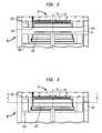
- Suitable arrangementssuch as an access port 101 ( FIGS. 2 and 3 ) in the side or circumferential wall of the reactor are provided for loading and unloading wafers.
- the wafer carrier 14is removable.
- a generally hoop-like shutter 103is mounted for movement in the upstream and downstream axial directions. When the shutter 103 is in the retracted or open position depicted in FIG. 2 , a wafer carrier 14 with treated wafers can be removed from the chamber and replaced by a new wafer carrier 14 bearing wafers to be treated. When the shutter 103 is in the advanced or closed position depicted in FIG. 3 , it encircles the wafer carrier 14 and covers the access port 101 .
- shutter 103forms part of the wall of the reaction chamber.
- the internal surfaces 105 of shutter 103desirably are surfaces of revolution about the axis of rotation 16 of the wafer carrier.
- Shutter 103desirably is provided with coolant passages (not shown) connected to a liquid coolant circulator for maintaining the temperature of the shutter at a temperature below that of the wafer carrier.
- the reactoralso includes a loop-like collar 102 referred to as a “confined inlet” element.
- Collar 102defines an interior surface 104 which extends downstream from head 22 and forms a part of the reactor wall.
- Surface 104is also in the form of a surface of revolution about axis 16 and flares slightly radially outwardly, away from the axis 16 , in the downstream direction.
- shutter 103is in the advanced or closed position ( FIG. 3 ) the surface 104 of collar 102 is substantially continuous with the inner surface 105 of the shutter 103 .
- Collar 102also may be provided with coolant passages.
- reactorsmay have other access systems, such as, for example, top-loading or bottom loading of wafers through a removable top or bottom portion of the reactor.
- the other features of the reactor not specifically discussed hereinmay be, for example, of the types used in reactors sold under the trademark TURBODISC by Veeco Instruments Inc.
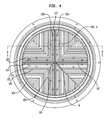
- the gas distribution and injector head 22includes a manifold assembly 107 , which may be formed from one plate or, more typically, a plurality of plates superposed on one another.
- the manifold assembly 107has recesses in its downstream surface defining gas conduits open to the downstream surface of the manifold assembly. A few of these gas conduits 109 , 111 , 113 are shown in FIG. 4 .
- An element 115 referred to herein as a “cold plate” or “diffuser”overlies the downstream surface of manifold assembly 107 .
- Cold plate 115is provided with coolant passages 116 connected to a source of a circulating coolant.
- Cold plate 115defines the downstream surface 24 of the distribution and injector head 22 , i.e., the surface facing toward the bottom of the drawing in FIGS. 1-4 . This surface is also referred to herein as the “inner” surface 24 of head 22 .
- a screen 123is provided between the cold plate 115 and manifold assembly 107 . The screen has limited permeability or porosity.
- Cold plate 115defines a plurality of first gas inlets 117 .
- each first gas inlet 117is in the form of an elongated slot. Such slot forms a passageway which extends through cold plate 115 and communicates with the downstream or inner surface and thus defines an elongated port communicating with the interior of reaction chamber 10 .
- the first gas inlets 117are arranged along two rows denoted by broken lines in FIG. 5 .
- the first gas inlets or slots 117are also shown schematically in FIG. 7 .
- the rowsextend perpendicular to the axis 16 and perpendicular to one another, and cross one another at the axis.
- each row of slots 117may include two or more slots.
- one rowincludes inboard slots 117 a and 117 b disposed near to, but not crossing, axis 16 , and also includes slots 117 c and 117 d disposed further from the axis.
- the other rowincludes radially inboard slots 117 e and 117 f , and radially outboard slots 117 g and 117 h.
- the first gas inlets 117communicate with some of the gas conduits in manifold assembly 107 . These gas conduits are referred to herein as first gas conduits. For example, as seen in FIG. 4 , first gas inlet 117 communicates with first gas conduit 113 through a portion of screen 123 . The first gas conduits are connected, through internal connections of the manifold assembly, schematically illustrated by broken line 121 in FIG. 5 , to a first gas source 26 Although the first gas source is shown in FIG.
- first gas source and conduitsmay include more complex components arranged to supply the first gas with the same or different compositions and/or flow rates to different ones of the first gas inlets along the extent of the rows of first gas inlets.
- first gas conduits communicating with the radially inner first gas inlets 117 a , 117 b , 117 e and 117 fmay be connected together to form an inner zone
- gas conduits communicating with radially outboard slots 117 c , 117 d , 117 g and 117 hmay be connected together to form a radially outboard zone.
- the first gas supply arrangementmay be arranged to supply the first gas with different composition and/or flow rates in the radially inner and radially outer zones.
- the flow rates and compositions of the gasescan be selected, for example, as discussed in PCT Publication WO 2005/019496, the disclosure of which is incorporated by reference herein, and in copending, commonly assigned U.S. patent application Ser. No. 11/544,075, published as U.S. Published Patent Application 2007-0134419 A1, the disclosure of which is also incorporated by reference herein.
- the first gasmay include a reactive constituent such as, for example, an alkyl, and may include non-reactive carrier gases such as nitrogen or hydrogen.
- the composition of the first gasmay be varied in different regions to include different proportions of carrier gases and thus match the density of the first gas to the density of the second gas discharged in the various regions.
- the flow ratemay be varied so that the discharge velocity of the first gas matches the discharge velocity of the second gas.
- the injector structurefurther defines a plurality of second gas field inlets 125 , which are also in the form of elongated slots which extend through the cold plate 115 . Each such slot terminates in an elongated port at the downstream end of the passageway open to the inner or downstream surface of cold plate 115 .
- the second gas field inletsalso communicate with the interior of chamber 10 .
- the second gas field inletsare disposed in an array over the regions of the inner surface 24 ( FIG. 1 ) which are not occupied by the rows of first gas inlets 117 .
- the second gas field inlets 125communicate through screen 123 with second gas conduits defined by the manifold assembly 107 . For example, the inlets 125 depicted in FIG.
- the second gas conduits, and thus the second gas field inlets 125are connected to one or more sources 30 of a second gas by internal connections 127 within the manifold assembly and through one or more control elements schematically depicted as valves 32 .
- the second gas field inlets 125 and associated conduitsmay be subdivided into multiple zones which can be regulated independently, to provide the second gas with different composition and/or flow rate in different regions.
- the second gas field inlets 125 at different radial distances from axis 16can constitute different zones.
- the second gas field inlets 125are disposed in quadrants of the injector head around the axis between the rows of first gas inlets. As best seen in FIG. 5 , the elongated slots constituting the second gas field inlets 125 within each quadrant extend parallel to one another. As shown in FIGS. 5 and 6 , the elongated second gas field inlets 125 within each quadrant extend parallel to the row of first gas field inlets extending through that quadrant. Thus, the elongated slot constituting each first gas inlet 117 extends between two adjacent second gas field inlets 125 a and 125 b.
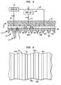
- the cold plate 115includes diffuser elements 129 .
- Each diffuser elementis in the form of an elongated blade having a generally triangular cross-section.
- Each such elongated bladelies between two elongated, slot-like gas inlets and extends parallel to those elongated inlets.
- diffuser element or blade 129 alies between first gas inlet 117 and second gas field inlet 125 a
- blade 129 blies between two second gas field inlets 125 a and 125 c .
- Each blade 129tapers in the downstream direction to a relatively sharp edge 131 at the downstream extremity of the blade.
- edge 131desirably is substantially less than 1 mm and desirably is so small that the radius plays no appreciable role in the dynamics of the discharged gases.
- the side surfaces 133 of the bladesdesirably extend all the way to the gas inlets.
- the cold plate 115desirably defines a center second gas inlet 135 in the form of a port mounted at axis 16 .
- the second gas source 30is also connected to the second gas center inlet 135 through further internal connections such as a second gas conduit (not shown) within manifold assembly 107 and through a control element 34 ( FIG. 1 ) such as a valve which is separate from the control elements associated with the field second gas inlets 125 .
- a control element 34FIG. 1
- the flow rate of the second gas through the center inlet 135can be controlled independently of the flow rate through the field inlets.
- the composition of the second gas sent to the center inlet 135also may be controllable independently of the composition of the second gas send to the field inlets 125 . Any other device which can control the flow rate of the second gas can be used instead of the valves.
- the rows of first gas inlets 117terminate inboard of the reactor wall, i.e., inboard of the internal surface 104 of collar 102 .
- the rows of first gas inletsextend to a first radial distance D R1 from axis 16 which is less than the radius of the reactor vessel, thus leaving a gap or radial distance G f between the outboard end of each row and the wall of the reactor vessel.
- the radius of the reactor vesselis defined by the internal surface 104 of the collar 102 .
- the array of second gas field injectors 125extends to a second radial distance D R2 from the axis, the second radial distance D R2 being greater than the first radial distance D R1 .
- the array of second gas field injectors 125extends nearly to the wall of the reactor, i.e., nearly to the internal surface 104 of collar 102 .
- the first radial distance D R1may be smaller than the radius of the wafer carrier 14 .
- the apparatus discussed abovecan be made in essentially any size; most typically, the wafer carrier 14 is approximately 3 inches (7.6 cm) to approximately 18 inches (45.7 cm) in diameter or greater.
- one or more wafers (substrates) 18are held in the wafer (substrate) carrier 14 and maintained at an elevated temperature by the heating elements within the reactor.
- the wafer carrier 14rotates about axis 16 at a rate ⁇ on the rotating spindle driven by motor.
- ⁇typically is about 500 RPM or higher, although the rate ⁇ may vary from approximately 300 RPM to 1500 RPM or higher.
- the temperaturemay vary from approximately 350° C. or lower to 1600° C. or higher. The optimum temperature depends on the particular material being grown.
- the appropriate first and second gasses to perform the desired treatment on the surfaces of the wafers 18are introduced through head 22 .
- the apparatus discussed aboveis most typically used for metalorganic chemical vapor deposition (“MOCVD”).
- MOCVDmetalorganic chemical vapor deposition
- the apparatusmay be used for MOCVD of a III-V semiconductor, in which the first gas includes as a reactive constituent one or more alkyls of one or more group III metals and the second gas includes as an active constituent a hydride of a group V element such as, for example, ammonia, arsine or the like.
- the flow ratesmay vary from approximately 5 liters/minute to 300 liters/minute. Pressure of the reactor typically ranges from approximately 25 Torr to 500 Torr or greater.
- first gas source 26is actuated to feed a first gas such as a gas containing a metal alkyl to the first gas inlets 117 , and thereby discharge streams of a first gas generally downstream within chamber 10 from the first gas inlets 117 .
- the second gas source 30is actuated to feed a second gas such as a gas containing a group V hydride to second gas field inlets 125 , and thereby discharge streams of the second gas generally downstream, toward the substrates or wafers 18 , from the second gas field inlets 125 .
- the streams of first and second gassesneed not be directed exactly downstream, exactly parallel with rotational axis 16 .
- the gasesapproach the rotating wafer carrier 14 , they are impelled into a circumferential flow around axis 16 , and also flow outwardly, away from axis 16 and toward the periphery of the wafer carrier. As the gases approach the wafer carrier 14 , the gases mix with one another so that the gases react at and near the substrates such as to form a reaction product such as a III-V semiconductor that deposits on the exposed surfaces of the substrates.
- the gasesalso tend to form unwanted deposits on components of the reactor itself.
- Several features of the present inventioninhibit such unwanted deposition. Because the rows of first gas injectors 117 terminate radially inward from the reactor walls, the concentration of first gas in the gas which flows along the reactor walls is dramatically reduced and hence parasitic deposition on the wall is also reduced. For example, parasitic deposition on the inner surface 104 of collar 102 and on the inner surface 105 of shutter 103 is materially reduced. If the gap or radial distance G f ( FIG.
- the tapered diffuser elements 129substantially suppress unwanted deposition on the injector head 22 .
- the present inventionis not limited by any theory of operation, it is believed that this result is achieved by suppressing recirculation of the gases near the downstream surface 24 of the injector head 22 . It is believed that the gases passing out of the first gas inlets 117 and second gas field inlets 125 pass out of the injector head 22 with flow as indicated by the smoothly spreading streamlines S shown in FIG. 5 . In flow of this type, the gases from adjacent gas inlets merge into the desired uniform downward flow without eddies.
- Placement of the first gas inlets 117 in two rows extending across the diameter of the reactorprovides good mixing of the first gas with the second gas in the vicinity of the rotating wafer carrier, and helps to assure that there is an adequate proportion of the first gas throughout the circumferential extent of the wafer carrier. This improves the efficiency of the reaction and helps to promote optimized growth. If only one row of first gas injectors is used, the system will work, but the reaction will be less efficient in some locations remote from the single row. In a variant of this approach, more than two diametral rows can be used. For example, three diametral rows can be used.
- the first gas injectorsmay be provided as radial rows such as, for example, rows extending outwardly from the central axis along three or five radii.
- the second gas center inlet 135provides a source of the second gas, such as the group V hydride, directed at the center of the wafer carrier. This assures that there will be an adequate supply of the second gas, such as the hydride, in those regions of the wafer carrier near the central axis 16 .
- the independent adjustability and control of the second gas flow through the central inlet 135allows adjustment of the process to compensate for variations in process conditions such as convection or diffusion of the reactants. This, in turn, allows for improved deposition uniformity.
- the gas inletsmay be provided as rows of holes 217 , 225 extending parallel to one another, rather than as elongated slots.
- the diffuser elements 229are disposed between holes of neighboring rows, but there are no diffuser elements between holes of the same row.
- the diffuser elementsmay be pyramidal rather than blade-like.
- a wafer carrier 14for holding substrates 18 for reactive gas processing, such as deposition processes
- a wafer carrier 14is not necessary and a substrate 18 may be placed directly on a rotating reactor surface such as a chuck, without a wafer carrier holding the substrate.
- the downstream direction as referred to herein and identified by arrow Dis the direction from the gas distribution injector head 22 toward the wafer carrier 14 ; it need not be in any particular orientation relative to gravity.
- the gas distribution injector head 22may also be placed on the side of the chamber 10 (such that the downstream direction D is the direction from the side of the chamber 10 horizontally towards the center of the chamber 10 ), or the gas distribution injector head 22 may also be placed on the bottom of the chamber 10 (such that the downstream direction is the direction from the bottom of the chamber 10 upwards towards the center of the chamber 10 ). Also, in the embodiment discussed above with reference to FIG. 1 , the exhaust ports (not shown) are described at being at the downstream end of the reaction chamber; the exhaust ports may be located on other portions of the reaction chamber.
- the two reactant gasesare provided simultaneously.
- the reactant gasesare supplied sequentially and/or with overlapping pulses.
- pulses of the reactant gasesare applied in alternating sequence, so that a pulse of one carrier gas terminates before a pulse of another gas begins.
- pulses of the different carrier gasesare supplied in alternating sequence but overlap one another in time.
- carrier gas flowmay be supplied simultaneously with one or more of the reactant gases.
- the first and second gasesmay be any reactant gases suitable for performing any treatment operation on the substrates, including but not limited to those for use in a chemical vapor deposition process as discussed above.
- Reactant gasesin various embodiments may include any gas, vapor, or material which participates in the treatment of a substrate within the reactor. More particularly, the reactant gas may be any gas that is suitable for treating the substrate surface.
- the reactant gassesmay be a mixture of plural chemical species, and may include inert, non-reactant gas components. Either or both of the reactant gases may include a combination of gases, such as a reactive component and a non-reactive gas.
- III-V semiconductorssuch as but not limited to GaAs, GaP, GaAs 1-x P x , Ga 1-y Al y As, Ga 1-y In y As, AlAs, AlN, InAs, InP, InGaP, InSb, GaN, InGaN, and the like.
- these reactorscan also be applied to other systems, including formation of Group II-VI compounds, such as but not limited to ZnSe, CdTe, HgCdTe, CdZnTe, CdSeTe, and the like; Group IV materials such as SiC, diamond, and SiGe; as well as oxides, such as YBCO, BaTiO, MgO 2 , ZrO, SiO 2 , ZnO and ZnSiO.
- the reactors and processes discussed abovecan be applied to deposition of other materials such as metals, such as Al, Cu and W.
- the resultant materialswill have a wide range of electronic and opto-electronic applications, including but not limited to light emitting diodes (LED's), lasers, solar cells, photocathodes, HEMT's and MESFET's.
- the gases supplied in the reactormay perform treatments other than deposition such as, for example, a reactive etching process.
- FIG. 1is shown as a vertical rotating disk reactor 10 , this reactor is only provided as an example, and it is understood that various features of the present invention can be used with other types of reactors such as non-rotating disk reactors, lateral flow reactors, rotating injector reactors, and the like. Additionally, additional reactant gases may be supplied to the chamber via one or more supplementary gas sources, gas chambers and gas inlets. The patterns and structures described herein can thus be readily extended to three, four or more precursors along with one or more carrier gases.
- the present inventionhas industrial application in manufacture of semiconductors and related articles.
Landscapes
- Chemical & Material Sciences (AREA)
- General Chemical & Material Sciences (AREA)
- Chemical Kinetics & Catalysis (AREA)
- Engineering & Computer Science (AREA)
- Materials Engineering (AREA)
- Mechanical Engineering (AREA)
- Metallurgy (AREA)
- Organic Chemistry (AREA)
- Chemical Vapour Deposition (AREA)
Abstract
Description
Claims (19)
Priority Applications (1)
| Application Number | Priority Date | Filing Date | Title |
|---|---|---|---|
| US12/951,361US9273395B2 (en) | 2007-01-12 | 2010-11-22 | Gas treatment systems |
Applications Claiming Priority (3)
| Application Number | Priority Date | Filing Date | Title |
|---|---|---|---|
| US88024307P | 2007-01-12 | 2007-01-12 | |
| US12/008,705US8152923B2 (en) | 2007-01-12 | 2008-01-11 | Gas treatment systems |
| US12/951,361US9273395B2 (en) | 2007-01-12 | 2010-11-22 | Gas treatment systems |
Related Parent Applications (1)
| Application Number | Title | Priority Date | Filing Date |
|---|---|---|---|
| US12/008,705DivisionUS8152923B2 (en) | 2007-01-12 | 2008-01-11 | Gas treatment systems |
Publications (2)
| Publication Number | Publication Date |
|---|---|
| US20110091648A1 US20110091648A1 (en) | 2011-04-21 |
| US9273395B2true US9273395B2 (en) | 2016-03-01 |
Family
ID=39636286
Family Applications (3)
| Application Number | Title | Priority Date | Filing Date |
|---|---|---|---|
| US12/008,705Expired - Fee RelatedUS8152923B2 (en) | 2007-01-12 | 2008-01-11 | Gas treatment systems |
| US12/951,361Expired - Fee RelatedUS9273395B2 (en) | 2007-01-12 | 2010-11-22 | Gas treatment systems |
| US12/951,341Expired - Fee RelatedUS8287646B2 (en) | 2007-01-12 | 2010-11-22 | Gas treatment systems |
Family Applications Before (1)
| Application Number | Title | Priority Date | Filing Date |
|---|---|---|---|
| US12/008,705Expired - Fee RelatedUS8152923B2 (en) | 2007-01-12 | 2008-01-11 | Gas treatment systems |
Family Applications After (1)
| Application Number | Title | Priority Date | Filing Date |
|---|---|---|---|
| US12/951,341Expired - Fee RelatedUS8287646B2 (en) | 2007-01-12 | 2010-11-22 | Gas treatment systems |
Country Status (6)
| Country | Link |
|---|---|
| US (3) | US8152923B2 (en) |
| KR (3) | KR101464228B1 (en) |
| CN (3) | CN102174693B (en) |
| DE (1) | DE112008000169T5 (en) |
| TW (1) | TWI390608B (en) |
| WO (1) | WO2008088743A1 (en) |
Cited By (1)
| Publication number | Priority date | Publication date | Assignee | Title |
|---|---|---|---|---|
| US20140116330A1 (en)* | 2008-12-04 | 2014-05-01 | Veeco Instruments Inc. | Chemical vapor deposition flow inlet elements and methods |
Families Citing this family (114)
| Publication number | Priority date | Publication date | Assignee | Title |
|---|---|---|---|---|
| KR101464228B1 (en)* | 2007-01-12 | 2014-11-21 | 비코 인스트루먼츠 인코포레이티드 | Gas treatment systems |
| US8334015B2 (en)* | 2007-09-05 | 2012-12-18 | Intermolecular, Inc. | Vapor based combinatorial processing |
| EP2215282B1 (en) | 2007-10-11 | 2016-11-30 | Valence Process Equipment, Inc. | Chemical vapor deposition reactor |
| US7976631B2 (en)* | 2007-10-16 | 2011-07-12 | Applied Materials, Inc. | Multi-gas straight channel showerhead |
| US8847249B2 (en) | 2008-06-16 | 2014-09-30 | Soraa, Inc. | Solid-state optical device having enhanced indium content in active regions |
| US20100006873A1 (en)* | 2008-06-25 | 2010-01-14 | Soraa, Inc. | HIGHLY POLARIZED WHITE LIGHT SOURCE BY COMBINING BLUE LED ON SEMIPOLAR OR NONPOLAR GaN WITH YELLOW LED ON SEMIPOLAR OR NONPOLAR GaN |
| US8805134B1 (en) | 2012-02-17 | 2014-08-12 | Soraa Laser Diode, Inc. | Methods and apparatus for photonic integration in non-polar and semi-polar oriented wave-guided optical devices |
| US8259769B1 (en) | 2008-07-14 | 2012-09-04 | Soraa, Inc. | Integrated total internal reflectors for high-gain laser diodes with high quality cleaved facets on nonpolar/semipolar GaN substrates |
| US8143148B1 (en) | 2008-07-14 | 2012-03-27 | Soraa, Inc. | Self-aligned multi-dielectric-layer lift off process for laser diode stripes |
| CN105762249A (en) | 2008-08-04 | 2016-07-13 | Soraa有限公司 | White Light Devices Using Non-polar Or Semipolar Gallium Containing Materials And Phosphors |
| US8284810B1 (en) | 2008-08-04 | 2012-10-09 | Soraa, Inc. | Solid state laser device using a selected crystal orientation in non-polar or semi-polar GaN containing materials and methods |
| US8895107B2 (en)* | 2008-11-06 | 2014-11-25 | Veeco Instruments Inc. | Chemical vapor deposition with elevated temperature gas injection |
| CA2653581A1 (en) | 2009-02-11 | 2010-08-11 | Kenneth Scott Alexander Butcher | Migration and plasma enhanced chemical vapour deposition |
| US8252662B1 (en) | 2009-03-28 | 2012-08-28 | Soraa, Inc. | Method and structure for manufacture of light emitting diode devices using bulk GaN |
| US8294179B1 (en) | 2009-04-17 | 2012-10-23 | Soraa, Inc. | Optical device structure using GaN substrates and growth structures for laser applications |
| US8634442B1 (en) | 2009-04-13 | 2014-01-21 | Soraa Laser Diode, Inc. | Optical device structure using GaN substrates for laser applications |
| US8837545B2 (en) | 2009-04-13 | 2014-09-16 | Soraa Laser Diode, Inc. | Optical device structure using GaN substrates and growth structures for laser applications |
| US8254425B1 (en) | 2009-04-17 | 2012-08-28 | Soraa, Inc. | Optical device structure using GaN substrates and growth structures for laser applications |
| CN102396083B (en) | 2009-04-13 | 2015-12-16 | 天空激光二极管有限公司 | For the structure of optical means of the use GAN substrate of laser application |
| US8242522B1 (en) | 2009-05-12 | 2012-08-14 | Soraa, Inc. | Optical device structure using non-polar GaN substrates and growth structures for laser applications in 481 nm |
| US8416825B1 (en) | 2009-04-17 | 2013-04-09 | Soraa, Inc. | Optical device structure using GaN substrates and growth structure for laser applications |
| US8247887B1 (en) | 2009-05-29 | 2012-08-21 | Soraa, Inc. | Method and surface morphology of non-polar gallium nitride containing substrates |
| US8427590B2 (en) | 2009-05-29 | 2013-04-23 | Soraa, Inc. | Laser based display method and system |
| US9250044B1 (en) | 2009-05-29 | 2016-02-02 | Soraa Laser Diode, Inc. | Gallium and nitrogen containing laser diode dazzling devices and methods of use |
| US10108079B2 (en) | 2009-05-29 | 2018-10-23 | Soraa Laser Diode, Inc. | Laser light source for a vehicle |
| US8509275B1 (en) | 2009-05-29 | 2013-08-13 | Soraa, Inc. | Gallium nitride based laser dazzling device and method |
| US9829780B2 (en) | 2009-05-29 | 2017-11-28 | Soraa Laser Diode, Inc. | Laser light source for a vehicle |
| US9800017B1 (en) | 2009-05-29 | 2017-10-24 | Soraa Laser Diode, Inc. | Laser device and method for a vehicle |
| US8314429B1 (en) | 2009-09-14 | 2012-11-20 | Soraa, Inc. | Multi color active regions for white light emitting diode |
| US8750342B1 (en) | 2011-09-09 | 2014-06-10 | Soraa Laser Diode, Inc. | Laser diodes with scribe structures |
| US8355418B2 (en) | 2009-09-17 | 2013-01-15 | Soraa, Inc. | Growth structures and method for forming laser diodes on {20-21} or off cut gallium and nitrogen containing substrates |
| CN102630349B (en) | 2009-09-18 | 2017-06-13 | 天空公司 | Power light emitting diode and method of operating with current density |
| US9583678B2 (en) | 2009-09-18 | 2017-02-28 | Soraa, Inc. | High-performance LED fabrication |
| US9293644B2 (en) | 2009-09-18 | 2016-03-22 | Soraa, Inc. | Power light emitting diode and method with uniform current density operation |
| US8933644B2 (en) | 2009-09-18 | 2015-01-13 | Soraa, Inc. | LED lamps with improved quality of light |
| TWI430714B (en)* | 2009-10-15 | 2014-03-11 | Orbotech Lt Solar Llc | Showerhead assembly for plasma processing chamber and method for fabricating gas ionization plate thereof |
| KR20110054840A (en)* | 2009-11-18 | 2011-05-25 | 주식회사 아토 | Shower head assembly and thin film deposition apparatus having same |
| JP5835722B2 (en) | 2009-12-10 | 2015-12-24 | オルボテック エルティ ソラー,エルエルシー | Automatic ranking multi-directional serial processor |
| US8905588B2 (en) | 2010-02-03 | 2014-12-09 | Sorra, Inc. | System and method for providing color light sources in proximity to predetermined wavelength conversion structures |
| US10147850B1 (en) | 2010-02-03 | 2018-12-04 | Soraa, Inc. | System and method for providing color light sources in proximity to predetermined wavelength conversion structures |
| US9927611B2 (en) | 2010-03-29 | 2018-03-27 | Soraa Laser Diode, Inc. | Wearable laser based display method and system |
| US8451876B1 (en) | 2010-05-17 | 2013-05-28 | Soraa, Inc. | Method and system for providing bidirectional light sources with broad spectrum |
| US8816319B1 (en) | 2010-11-05 | 2014-08-26 | Soraa Laser Diode, Inc. | Method of strain engineering and related optical device using a gallium and nitrogen containing active region |
| US8975615B2 (en) | 2010-11-09 | 2015-03-10 | Soraa Laser Diode, Inc. | Method of fabricating optical devices using laser treatment of contact regions of gallium and nitrogen containing material |
| US9048170B2 (en) | 2010-11-09 | 2015-06-02 | Soraa Laser Diode, Inc. | Method of fabricating optical devices using laser treatment |
| US9318875B1 (en) | 2011-01-24 | 2016-04-19 | Soraa Laser Diode, Inc. | Color converting element for laser diode |
| US9595813B2 (en) | 2011-01-24 | 2017-03-14 | Soraa Laser Diode, Inc. | Laser package having multiple emitters configured on a substrate member |
| US9025635B2 (en) | 2011-01-24 | 2015-05-05 | Soraa Laser Diode, Inc. | Laser package having multiple emitters configured on a support member |
| US9093820B1 (en) | 2011-01-25 | 2015-07-28 | Soraa Laser Diode, Inc. | Method and structure for laser devices using optical blocking regions |
| US8143147B1 (en) | 2011-02-10 | 2012-03-27 | Intermolecular, Inc. | Methods and systems for forming thin films |
| US9236530B2 (en) | 2011-04-01 | 2016-01-12 | Soraa, Inc. | Miscut bulk substrates |
| US9287684B2 (en) | 2011-04-04 | 2016-03-15 | Soraa Laser Diode, Inc. | Laser package having multiple emitters with color wheel |
| WO2012139006A2 (en)* | 2011-04-07 | 2012-10-11 | Veeco Instruments Inc. | Metal-organic vapor phase epitaxy system and process |
| US8459276B2 (en) | 2011-05-24 | 2013-06-11 | Orbotech LT Solar, LLC. | Broken wafer recovery system |
| US9646827B1 (en) | 2011-08-23 | 2017-05-09 | Soraa, Inc. | Method for smoothing surface of a substrate containing gallium and nitrogen |
| US8971370B1 (en) | 2011-10-13 | 2015-03-03 | Soraa Laser Diode, Inc. | Laser devices using a semipolar plane |
| DE102011055061A1 (en)* | 2011-11-04 | 2013-05-08 | Aixtron Se | CVD reactor or substrate holder for a CVD reactor |
| JP6038618B2 (en)* | 2011-12-15 | 2016-12-07 | 株式会社ニューフレアテクノロジー | Film forming apparatus and film forming method |
| US9020003B1 (en) | 2012-03-14 | 2015-04-28 | Soraa Laser Diode, Inc. | Group III-nitride laser diode grown on a semi-polar orientation of gallium and nitrogen containing substrates |
| US10559939B1 (en) | 2012-04-05 | 2020-02-11 | Soraa Laser Diode, Inc. | Facet on a gallium and nitrogen containing laser diode |
| US9343871B1 (en) | 2012-04-05 | 2016-05-17 | Soraa Laser Diode, Inc. | Facet on a gallium and nitrogen containing laser diode |
| US9800016B1 (en) | 2012-04-05 | 2017-10-24 | Soraa Laser Diode, Inc. | Facet on a gallium and nitrogen containing laser diode |
| US9328419B2 (en)* | 2012-04-18 | 2016-05-03 | Hermes-Epitek Corporation | Gas treatment apparatus with surrounding spray curtains |
| JP2013229493A (en)* | 2012-04-26 | 2013-11-07 | Sharp Corp | Group-iii nitride semiconductor stacked substrate and group-iii nitride semiconductor field-effect transistor |
| CN103388132B (en)* | 2012-05-11 | 2015-11-25 | 中微半导体设备(上海)有限公司 | Gas shower head, its manufacturing method and thin film growth reactor |
| US8971368B1 (en) | 2012-08-16 | 2015-03-03 | Soraa Laser Diode, Inc. | Laser devices having a gallium and nitrogen containing semipolar surface orientation |
| US9087695B2 (en) | 2012-10-22 | 2015-07-21 | Sensor Electronic Technology, Inc. | Multi-wafer reactor |
| US9404182B2 (en) | 2012-10-22 | 2016-08-02 | Sensor Electronic Technology, Inc. | Multi-wafer reactor |
| US9166372B1 (en) | 2013-06-28 | 2015-10-20 | Soraa Laser Diode, Inc. | Gallium nitride containing laser device configured on a patterned substrate |
| US9368939B2 (en) | 2013-10-18 | 2016-06-14 | Soraa Laser Diode, Inc. | Manufacturable laser diode formed on C-plane gallium and nitrogen material |
| US9520695B2 (en) | 2013-10-18 | 2016-12-13 | Soraa Laser Diode, Inc. | Gallium and nitrogen containing laser device having confinement region |
| US9362715B2 (en) | 2014-02-10 | 2016-06-07 | Soraa Laser Diode, Inc | Method for manufacturing gallium and nitrogen bearing laser devices with improved usage of substrate material |
| US9379525B2 (en) | 2014-02-10 | 2016-06-28 | Soraa Laser Diode, Inc. | Manufacturable laser diode |
| US9209596B1 (en) | 2014-02-07 | 2015-12-08 | Soraa Laser Diode, Inc. | Manufacturing a laser diode device from a plurality of gallium and nitrogen containing substrates |
| US9520697B2 (en) | 2014-02-10 | 2016-12-13 | Soraa Laser Diode, Inc. | Manufacturable multi-emitter laser diode |
| US9871350B2 (en) | 2014-02-10 | 2018-01-16 | Soraa Laser Diode, Inc. | Manufacturable RGB laser diode source |
| KR101550614B1 (en) | 2014-02-11 | 2015-09-08 | 현대자동차 주식회사 | Catalyst carrier for purification of exhausted gas, method for preparing the same, and catalyst for purification of exhausted gas |
| US9564736B1 (en) | 2014-06-26 | 2017-02-07 | Soraa Laser Diode, Inc. | Epitaxial growth of p-type cladding regions using nitrogen gas for a gallium and nitrogen containing laser diode |
| US10249511B2 (en)* | 2014-06-27 | 2019-04-02 | Lam Research Corporation | Ceramic showerhead including central gas injector for tunable convective-diffusive gas flow in semiconductor substrate processing apparatus |
| US12126143B2 (en) | 2014-11-06 | 2024-10-22 | Kyocera Sld Laser, Inc. | Method of manufacture for an ultraviolet emitting optoelectronic device |
| US9246311B1 (en) | 2014-11-06 | 2016-01-26 | Soraa Laser Diode, Inc. | Method of manufacture for an ultraviolet laser diode |
| FR3029939A1 (en)* | 2014-12-16 | 2016-06-17 | Saint-Gobain Lumilog | CHEMICAL VAPOR DEPOSITION REACTOR |
| US9666677B1 (en) | 2014-12-23 | 2017-05-30 | Soraa Laser Diode, Inc. | Manufacturable thin film gallium and nitrogen containing devices |
| US9653642B1 (en) | 2014-12-23 | 2017-05-16 | Soraa Laser Diode, Inc. | Manufacturable RGB display based on thin film gallium and nitrogen containing light emitting diodes |
| US9748113B2 (en) | 2015-07-30 | 2017-08-29 | Veeco Intruments Inc. | Method and apparatus for controlled dopant incorporation and activation in a chemical vapor deposition system |
| US11437775B2 (en) | 2015-08-19 | 2022-09-06 | Kyocera Sld Laser, Inc. | Integrated light source using a laser diode |
| US11437774B2 (en) | 2015-08-19 | 2022-09-06 | Kyocera Sld Laser, Inc. | High-luminous flux laser-based white light source |
| US10879673B2 (en) | 2015-08-19 | 2020-12-29 | Soraa Laser Diode, Inc. | Integrated white light source using a laser diode and a phosphor in a surface mount device package |
| US10938182B2 (en) | 2015-08-19 | 2021-03-02 | Soraa Laser Diode, Inc. | Specialized integrated light source using a laser diode |
| US9787963B2 (en) | 2015-10-08 | 2017-10-10 | Soraa Laser Diode, Inc. | Laser lighting having selective resolution |
| TWI733712B (en)* | 2015-12-18 | 2021-07-21 | 美商應用材料股份有限公司 | A diffuser for a deposition chamber and an electrode for a deposition chamber |
| US10119191B2 (en)* | 2016-06-08 | 2018-11-06 | Applied Materials, Inc. | High flow gas diffuser assemblies, systems, and methods |
| CN107723790B (en)* | 2016-08-12 | 2020-07-07 | 上海新昇半导体科技有限公司 | Epitaxial equipment, equipment manufacturing method and epitaxial method |
| JP2018133471A (en)* | 2017-02-16 | 2018-08-23 | 漢民科技股▲分▼有限公司 | Vapor deposition apparatus |
| US10655226B2 (en)* | 2017-05-26 | 2020-05-19 | Applied Materials, Inc. | Apparatus and methods to improve ALD uniformity |
| CN107195526A (en)* | 2017-06-08 | 2017-09-22 | 上海华力微电子有限公司 | A kind of method rubbed between the part for reducing board |
| US10771155B2 (en) | 2017-09-28 | 2020-09-08 | Soraa Laser Diode, Inc. | Intelligent visible light with a gallium and nitrogen containing laser source |
| US10222474B1 (en) | 2017-12-13 | 2019-03-05 | Soraa Laser Diode, Inc. | Lidar systems including a gallium and nitrogen containing laser light source |
| US10551728B1 (en) | 2018-04-10 | 2020-02-04 | Soraa Laser Diode, Inc. | Structured phosphors for dynamic lighting |
| US11239637B2 (en) | 2018-12-21 | 2022-02-01 | Kyocera Sld Laser, Inc. | Fiber delivered laser induced white light system |
| US11421843B2 (en) | 2018-12-21 | 2022-08-23 | Kyocera Sld Laser, Inc. | Fiber-delivered laser-induced dynamic light system |
| US12000552B2 (en) | 2019-01-18 | 2024-06-04 | Kyocera Sld Laser, Inc. | Laser-based fiber-coupled white light system for a vehicle |
| US12152742B2 (en) | 2019-01-18 | 2024-11-26 | Kyocera Sld Laser, Inc. | Laser-based light guide-coupled wide-spectrum light system |
| US11884202B2 (en) | 2019-01-18 | 2024-01-30 | Kyocera Sld Laser, Inc. | Laser-based fiber-coupled white light system |
| US11225715B2 (en)* | 2019-04-11 | 2022-01-18 | Samsung Electronics Co., Ltd. | Showerhead, semiconductor manufacturing apparatus including the same, and semiconductor manufacturing method |
| US11228158B2 (en) | 2019-05-14 | 2022-01-18 | Kyocera Sld Laser, Inc. | Manufacturable laser diodes on a large area gallium and nitrogen containing substrate |
| US10903623B2 (en) | 2019-05-14 | 2021-01-26 | Soraa Laser Diode, Inc. | Method and structure for manufacturable large area gallium and nitrogen containing substrate |
| USD936187S1 (en)* | 2020-02-12 | 2021-11-16 | Applied Materials, Inc. | Gas distribution assembly lid |
| US12191626B1 (en) | 2020-07-31 | 2025-01-07 | Kyocera Sld Laser, Inc. | Vertically emitting laser devices and chip-scale-package laser devices and laser-based, white light emitting devices |
| CN114351117B (en)* | 2020-10-13 | 2022-12-20 | 东部超导科技(苏州)有限公司 | Spray plate, MOCVD reaction system with spray plate and use method of MOCVD reaction system |
| USD1071103S1 (en) | 2022-04-11 | 2025-04-15 | Applied Materials, Inc. | Gas distribution plate |
| USD1037778S1 (en) | 2022-07-19 | 2024-08-06 | Applied Materials, Inc. | Gas distribution plate |
| USD1085029S1 (en) | 2022-07-19 | 2025-07-22 | Applied Materials, Inc. | Gas distribution plate |
| KR20250117369A (en)* | 2022-11-28 | 2025-08-04 | 비코 인스트루먼츠 인코포레이티드 | Multi-disk chemical vapor deposition system using cross-flow gas injection |
Citations (34)
| Publication number | Priority date | Publication date | Assignee | Title |
|---|---|---|---|---|
| US4854263A (en) | 1987-08-14 | 1989-08-08 | Applied Materials, Inc. | Inlet manifold and methods for increasing gas dissociation and for PECVD of dielectric films |
| US4993358A (en) | 1989-07-28 | 1991-02-19 | Watkins-Johnson Company | Chemical vapor deposition reactor and method of operation |
| US5269847A (en) | 1990-08-23 | 1993-12-14 | Applied Materials, Inc. | Variable rate distribution gas flow reaction chamber |
| US6098568A (en) | 1997-12-01 | 2000-08-08 | Applied Materials, Inc. | Mixed frequency CVD apparatus |
| US6197121B1 (en) | 1996-11-27 | 2001-03-06 | Emcore Corporation | Chemical vapor deposition apparatus |
| US20030037880A1 (en) | 2000-11-01 | 2003-02-27 | Applied Materials, Inc. | Dielectric etch chamber with expanded process window |
| US20040060514A1 (en) | 2002-01-25 | 2004-04-01 | Applied Materials, Inc. A Delaware Corporation | Gas distribution showerhead |
| US20040082171A1 (en) | 2002-09-17 | 2004-04-29 | Shin Cheol Ho | ALD apparatus and ALD method for manufacturing semiconductor device |
| US20050011436A1 (en) | 2003-07-15 | 2005-01-20 | Heng Liu | Chemical vapor deposition reactor |
| WO2005019496A1 (en) | 2003-08-20 | 2005-03-03 | Veeco Instruments Inc. | Alkyl push flow for vertical flow rotating disk reactors |
| US6921437B1 (en) | 2003-05-30 | 2005-07-26 | Aviza Technology, Inc. | Gas distribution system |
| JP2005294421A (en) | 2004-03-31 | 2005-10-20 | Tokyo Electron Ltd | Film forming method and apparatus, and gate insulating film forming method |
| CN1693535A (en) | 2004-04-30 | 2005-11-09 | 周星工程股份有限公司 | Method of depositing thin film and thin film deposition system having separate injection port for spraying cleaning gas |
| US20060011298A1 (en) | 2004-07-15 | 2006-01-19 | Ji-Eun Lim | Showerhead with branched gas receiving channel and apparatus including the same for use in manufacturing semiconductor substrates |
| US20060021574A1 (en) | 2004-08-02 | 2006-02-02 | Veeco Instruments Inc. | Multi-gas distribution injector for chemical vapor deposition reactors |
| US20060121193A1 (en) | 2003-04-30 | 2006-06-08 | Strauch Gerhard K | Process and apparatus for depositing semiconductor layers using two process gases, one of which is preconditioned |
| CN1828825A (en) | 2005-03-02 | 2006-09-06 | 东京毅力科创株式会社 | Gas supply member and plasma processing apparatus |
| US20060199131A1 (en) | 2003-04-07 | 2006-09-07 | Hiroo Kawasaki | Loading table and heat treating apparatus having the loading table |
| US20060196604A1 (en) | 2005-03-02 | 2006-09-07 | Tokyo Electron Limited | Gas supply member and plasma processing apparatus |
| US20060263522A1 (en)* | 2005-05-19 | 2006-11-23 | Piezonics Co., Ltd. | Apparatus for chemical vapor deposition (CVD) with showerhead and method thereof |
| US20070095284A1 (en) | 2004-06-04 | 2007-05-03 | Iizuka Hachishiro | Gas treating device and film forming device |
| US20070218701A1 (en)* | 2006-03-15 | 2007-09-20 | Asm Japan K.K. | Semiconductor-processing apparatus with rotating susceptor |
| US20070218702A1 (en)* | 2006-03-15 | 2007-09-20 | Asm Japan K.K. | Semiconductor-processing apparatus with rotating susceptor |
| US20080099147A1 (en) | 2006-10-26 | 2008-05-01 | Nyi Oo Myo | Temperature controlled multi-gas distribution assembly |
| US20080152840A1 (en) | 2006-12-22 | 2008-06-26 | Applied Materials, Inc. | Apparatus for integrated gas and radiation delivery |
| US20080166884A1 (en) | 2007-01-08 | 2008-07-10 | Nelson Shelby F | Delivery device comprising gas diffuser for thin film deposition |
| US20080173735A1 (en) | 2007-01-12 | 2008-07-24 | Veeco Instruments Inc. | Gas treatment systems |
| US20090178614A1 (en) | 2001-02-09 | 2009-07-16 | Tokyo Electron Limited | Film-forming apparatus |
| US20100112216A1 (en)* | 2008-11-06 | 2010-05-06 | Veeco Instruments Inc. | Chemical vapor deposition with elevated temperature gas injection |
| US20100143588A1 (en) | 2008-12-04 | 2010-06-10 | Veeco Instruments Inc. | Chemical vapor deposition flow inlet elements and methods |
| US20110215071A1 (en) | 2010-03-03 | 2011-09-08 | Veeco Instruments Inc. | Wafer carrier with sloped edge |
| US20120027936A1 (en) | 2010-08-02 | 2012-02-02 | Veeco Instruments Inc. | Exhaust for cvd reactor |
| US8617349B2 (en)* | 2009-10-15 | 2013-12-31 | Orbotech LT Solar, LLC. | Showerhead assembly for plasma processing chamber |
| US20140360430A1 (en)* | 2013-06-05 | 2014-12-11 | Veeco Instruments, Inc. | Wafer carrier having thermal uniformity-enhancing features |
- 2008
- 2008-01-11KRKR1020147001152Apatent/KR101464228B1/ennot_activeExpired - Fee Related
- 2008-01-11TWTW097101198Apatent/TWI390608B/ennot_activeIP Right Cessation
- 2008-01-11KRKR1020147001151Apatent/KR101464227B1/ennot_activeExpired - Fee Related
- 2008-01-11KRKR20097016411Apatent/KR101483522B1/ennot_activeExpired - Fee Related
- 2008-01-11CNCN201110021660.4Apatent/CN102174693B/ennot_activeExpired - Fee Related
- 2008-01-11DEDE112008000169Tpatent/DE112008000169T5/ennot_activeWithdrawn
- 2008-01-11CNCN200880005064.3Apatent/CN101611472B/ennot_activeExpired - Fee Related
- 2008-01-11USUS12/008,705patent/US8152923B2/ennot_activeExpired - Fee Related
- 2008-01-11CNCN201110021659.1Apatent/CN102127752B/ennot_activeExpired - Fee Related
- 2008-01-11WOPCT/US2008/000402patent/WO2008088743A1/enactiveApplication Filing
- 2010
- 2010-11-22USUS12/951,361patent/US9273395B2/ennot_activeExpired - Fee Related
- 2010-11-22USUS12/951,341patent/US8287646B2/ennot_activeExpired - Fee Related
Patent Citations (58)
| Publication number | Priority date | Publication date | Assignee | Title |
|---|---|---|---|---|
| US4854263A (en) | 1987-08-14 | 1989-08-08 | Applied Materials, Inc. | Inlet manifold and methods for increasing gas dissociation and for PECVD of dielectric films |
| US4854263B1 (en) | 1987-08-14 | 1997-06-17 | Applied Materials Inc | Inlet manifold and methods for increasing gas dissociation and for PECVD of dielectric films |
| US4993358A (en) | 1989-07-28 | 1991-02-19 | Watkins-Johnson Company | Chemical vapor deposition reactor and method of operation |
| US5269847A (en) | 1990-08-23 | 1993-12-14 | Applied Materials, Inc. | Variable rate distribution gas flow reaction chamber |
| US6197121B1 (en) | 1996-11-27 | 2001-03-06 | Emcore Corporation | Chemical vapor deposition apparatus |
| US6098568A (en) | 1997-12-01 | 2000-08-08 | Applied Materials, Inc. | Mixed frequency CVD apparatus |
| US20030037880A1 (en) | 2000-11-01 | 2003-02-27 | Applied Materials, Inc. | Dielectric etch chamber with expanded process window |
| US20090178614A1 (en) | 2001-02-09 | 2009-07-16 | Tokyo Electron Limited | Film-forming apparatus |
| US20040060514A1 (en) | 2002-01-25 | 2004-04-01 | Applied Materials, Inc. A Delaware Corporation | Gas distribution showerhead |
| US20040082171A1 (en) | 2002-09-17 | 2004-04-29 | Shin Cheol Ho | ALD apparatus and ALD method for manufacturing semiconductor device |
| US7435445B2 (en) | 2002-09-17 | 2008-10-14 | Moohan Co., Ltd. | Method for manufacturing semiconductor device |
| US20060199131A1 (en) | 2003-04-07 | 2006-09-07 | Hiroo Kawasaki | Loading table and heat treating apparatus having the loading table |
| US20060121193A1 (en) | 2003-04-30 | 2006-06-08 | Strauch Gerhard K | Process and apparatus for depositing semiconductor layers using two process gases, one of which is preconditioned |
| US6921437B1 (en) | 2003-05-30 | 2005-07-26 | Aviza Technology, Inc. | Gas distribution system |
| US20050011436A1 (en) | 2003-07-15 | 2005-01-20 | Heng Liu | Chemical vapor deposition reactor |
| WO2005019496A1 (en) | 2003-08-20 | 2005-03-03 | Veeco Instruments Inc. | Alkyl push flow for vertical flow rotating disk reactors |
| US20150225875A1 (en)* | 2003-08-20 | 2015-08-13 | Veeco Instruments Inc. | Density-matching alkyl push flow for vertical flow rotating disk reactors |
| CN1860252A (en) | 2003-09-29 | 2006-11-08 | 应用材料公司 | Gas distribution showerhead |
| JP2005294421A (en) | 2004-03-31 | 2005-10-20 | Tokyo Electron Ltd | Film forming method and apparatus, and gate insulating film forming method |
| US20070141257A1 (en) | 2004-03-31 | 2007-06-21 | Tokyo Electron Limited | Method and apparatus for forming metal silicate film, and method for manufacturing semiconductor device |
| CN1693535A (en) | 2004-04-30 | 2005-11-09 | 周星工程股份有限公司 | Method of depositing thin film and thin film deposition system having separate injection port for spraying cleaning gas |
| US20070095284A1 (en) | 2004-06-04 | 2007-05-03 | Iizuka Hachishiro | Gas treating device and film forming device |
| US20060011298A1 (en) | 2004-07-15 | 2006-01-19 | Ji-Eun Lim | Showerhead with branched gas receiving channel and apparatus including the same for use in manufacturing semiconductor substrates |
| US20100300359A1 (en)* | 2004-08-02 | 2010-12-02 | Veeco Instruments Inc. | Multi-gas distribution injector for chemical vapor deposition reactors |
| US20060021574A1 (en) | 2004-08-02 | 2006-02-02 | Veeco Instruments Inc. | Multi-gas distribution injector for chemical vapor deposition reactors |
| US7416635B2 (en) | 2005-03-02 | 2008-08-26 | Tokyo Electron Limited | Gas supply member and plasma processing apparatus |
| US20060196604A1 (en) | 2005-03-02 | 2006-09-07 | Tokyo Electron Limited | Gas supply member and plasma processing apparatus |
| CN1828825A (en) | 2005-03-02 | 2006-09-06 | 东京毅力科创株式会社 | Gas supply member and plasma processing apparatus |
| US20060263522A1 (en)* | 2005-05-19 | 2006-11-23 | Piezonics Co., Ltd. | Apparatus for chemical vapor deposition (CVD) with showerhead and method thereof |
| US7479303B2 (en) | 2005-05-19 | 2009-01-20 | Piezonica Co., Ltd. | Method for chemical vapor deposition (CVD) with showerhead and method thereof |
| US20090178616A1 (en) | 2005-05-19 | 2009-07-16 | Chul Soo Byun | Apparatus for chemical vapor deposition (cvd) with showerhead |
| US8298370B2 (en)* | 2005-05-19 | 2012-10-30 | Piezonics Co., Ltd. | Apparatus for chemical vapor deposition (CVD) with showerhead |
| US20070218702A1 (en)* | 2006-03-15 | 2007-09-20 | Asm Japan K.K. | Semiconductor-processing apparatus with rotating susceptor |
| US20070218701A1 (en)* | 2006-03-15 | 2007-09-20 | Asm Japan K.K. | Semiconductor-processing apparatus with rotating susceptor |
| US20080099147A1 (en) | 2006-10-26 | 2008-05-01 | Nyi Oo Myo | Temperature controlled multi-gas distribution assembly |
| US20080152840A1 (en) | 2006-12-22 | 2008-06-26 | Applied Materials, Inc. | Apparatus for integrated gas and radiation delivery |
| US7922863B2 (en) | 2006-12-22 | 2011-04-12 | Applied Materials, Inc. | Apparatus for integrated gas and radiation delivery |
| US20080166884A1 (en) | 2007-01-08 | 2008-07-10 | Nelson Shelby F | Delivery device comprising gas diffuser for thin film deposition |
| US8152923B2 (en)* | 2007-01-12 | 2012-04-10 | Veeco Instruments Inc. | Gas treatment systems |
| US20110088623A1 (en) | 2007-01-12 | 2011-04-21 | Veeco Instruments Inc. | Gas treatment systems |
| US20110091648A1 (en) | 2007-01-12 | 2011-04-21 | Veeco Instruments Inc. | Gas treatment systems |
| US20080173735A1 (en) | 2007-01-12 | 2008-07-24 | Veeco Instruments Inc. | Gas treatment systems |
| US8287646B2 (en)* | 2007-01-12 | 2012-10-16 | Veeco Instruments Inc. | Gas treatment systems |
| US20140352619A1 (en)* | 2008-11-06 | 2014-12-04 | Veeco Instruments Inc. | Chemical vapor deposition with elevated temperature gas injection |
| US20120040514A1 (en)* | 2008-11-06 | 2012-02-16 | Veeco Instruments Inc. | Chemical vapor deposition with elevated temperature gas injection |
| US20150056790A1 (en)* | 2008-11-06 | 2015-02-26 | Veeco Instruments Inc. | Chemical vapor deposition with elevated temperature gas injection |
| US20100112216A1 (en)* | 2008-11-06 | 2010-05-06 | Veeco Instruments Inc. | Chemical vapor deposition with elevated temperature gas injection |
| US8937000B2 (en)* | 2008-11-06 | 2015-01-20 | Veeco Instruments Inc. | Chemical vapor deposition with elevated temperature gas injection |
| US8895107B2 (en)* | 2008-11-06 | 2014-11-25 | Veeco Instruments Inc. | Chemical vapor deposition with elevated temperature gas injection |
| US8636847B2 (en)* | 2008-12-04 | 2014-01-28 | Veeco Instruments Inc. | Chemical vapor deposition flow inlet elements and methods |
| US20140116330A1 (en)* | 2008-12-04 | 2014-05-01 | Veeco Instruments Inc. | Chemical vapor deposition flow inlet elements and methods |
| US20120325151A1 (en)* | 2008-12-04 | 2012-12-27 | Veeco Instruments Inc. | Chemical vapor deposition flow inlet elements and methods |
| US20100143588A1 (en) | 2008-12-04 | 2010-06-10 | Veeco Instruments Inc. | Chemical vapor deposition flow inlet elements and methods |
| US8303713B2 (en)* | 2008-12-04 | 2012-11-06 | Veeco Instruments Inc. | Chemical vapor deposition flow inlet elements and methods |
| US8617349B2 (en)* | 2009-10-15 | 2013-12-31 | Orbotech LT Solar, LLC. | Showerhead assembly for plasma processing chamber |
| US20110215071A1 (en) | 2010-03-03 | 2011-09-08 | Veeco Instruments Inc. | Wafer carrier with sloped edge |
| US20120027936A1 (en) | 2010-08-02 | 2012-02-02 | Veeco Instruments Inc. | Exhaust for cvd reactor |
| US20140360430A1 (en)* | 2013-06-05 | 2014-12-11 | Veeco Instruments, Inc. | Wafer carrier having thermal uniformity-enhancing features |
Non-Patent Citations (3)
| Title |
|---|
| International Search Report, PCT/US2008/000402. |
| Office Action from corresponding Chinese Application No. 20088005064.3 dated Mar. 20, 2012. |
| Office Action from corresponding Chinese Application No. 201110021659.1dated Oct. 10, 2012. |
Cited By (2)
| Publication number | Priority date | Publication date | Assignee | Title |
|---|---|---|---|---|
| US20140116330A1 (en)* | 2008-12-04 | 2014-05-01 | Veeco Instruments Inc. | Chemical vapor deposition flow inlet elements and methods |
| US10017876B2 (en)* | 2008-12-04 | 2018-07-10 | Veeco Instruments Inc. | Chemical vapor deposition flow inlet elements and methods |
Also Published As
| Publication number | Publication date |
|---|---|
| TWI390608B (en) | 2013-03-21 |
| WO2008088743A1 (en) | 2008-07-24 |
| US8152923B2 (en) | 2012-04-10 |
| US20110091648A1 (en) | 2011-04-21 |
| CN101611472B (en) | 2015-03-25 |
| KR20140015625A (en) | 2014-02-06 |
| CN102174693B (en) | 2014-10-29 |
| KR101464227B1 (en) | 2014-11-21 |
| CN101611472A (en) | 2009-12-23 |
| KR101483522B1 (en) | 2015-01-16 |
| US20080173735A1 (en) | 2008-07-24 |
| KR20090117724A (en) | 2009-11-12 |
| KR20140011429A (en) | 2014-01-28 |
| TW200903592A (en) | 2009-01-16 |
| CN102127752A (en) | 2011-07-20 |
| CN102174693A (en) | 2011-09-07 |
| KR101464228B1 (en) | 2014-11-21 |
| CN102127752B (en) | 2014-06-25 |
| US20110088623A1 (en) | 2011-04-21 |
| DE112008000169T5 (en) | 2010-01-14 |
| US8287646B2 (en) | 2012-10-16 |
Similar Documents
| Publication | Publication Date | Title |
|---|---|---|
| US9273395B2 (en) | Gas treatment systems | |
| US9593434B2 (en) | Alkyl push flow for vertical flow rotating disk reactors | |
| US7641939B2 (en) | Chemical vapor deposition reactor having multiple inlets | |
| US20060021574A1 (en) | Multi-gas distribution injector for chemical vapor deposition reactors | |
| US8888919B2 (en) | Wafer carrier with sloped edge | |
| US20100263588A1 (en) | Methods and apparatus for epitaxial growth of semiconductor materials | |
| US20050011459A1 (en) | Chemical vapor deposition reactor | |
| JP7495882B2 (en) | Chemical vapor deposition apparatus with multi-zone injector block | |
| CN103361624B (en) | Metallo-organic compound chemical vapor deposition method and device | |
| KR20090101157A (en) | Density Matching Alkyl Extrusion Flow for Vertical Flow Rotary Disc Reactor | |
| JPH0967192A (en) | Vapor phase growth equipment | |
| JP2006100741A (en) | Vapor deposition system |
Legal Events
| Date | Code | Title | Description |
|---|---|---|---|
| AS | Assignment | Owner name:VEECO INSTRUMENTS INC., NEW YORK Free format text:ASSIGNMENT OF ASSIGNORS INTEREST;ASSIGNORS:MITROVIC, BOJAN;GURARY, ALEX;ARMOUR, ERIC A.;REEL/FRAME:025311/0493 Effective date:20080303 | |
| ZAAA | Notice of allowance and fees due | Free format text:ORIGINAL CODE: NOA | |
| ZAAB | Notice of allowance mailed | Free format text:ORIGINAL CODE: MN/=. | |
| STCF | Information on status: patent grant | Free format text:PATENTED CASE | |
| MAFP | Maintenance fee payment | Free format text:PAYMENT OF MAINTENANCE FEE, 4TH YEAR, LARGE ENTITY (ORIGINAL EVENT CODE: M1551); ENTITY STATUS OF PATENT OWNER: LARGE ENTITY Year of fee payment:4 | |
| AS | Assignment | Owner name:HSBC BANK USA, NATIONAL ASSOCIATION, AS COLLATERAL AGENT, NEW YORK Free format text:PATENT SECURITY AGREEMENT;ASSIGNOR:VEECO INSTRUMENTS INC.;REEL/FRAME:058533/0321 Effective date:20211216 | |
| FEPP | Fee payment procedure | Free format text:MAINTENANCE FEE REMINDER MAILED (ORIGINAL EVENT CODE: REM.); ENTITY STATUS OF PATENT OWNER: LARGE ENTITY | |
| LAPS | Lapse for failure to pay maintenance fees | Free format text:PATENT EXPIRED FOR FAILURE TO PAY MAINTENANCE FEES (ORIGINAL EVENT CODE: EXP.); ENTITY STATUS OF PATENT OWNER: LARGE ENTITY | |
| STCH | Information on status: patent discontinuation | Free format text:PATENT EXPIRED DUE TO NONPAYMENT OF MAINTENANCE FEES UNDER 37 CFR 1.362 | |
| FP | Lapsed due to failure to pay maintenance fee | Effective date:20240301 | |
| AS | Assignment | Owner name:HSBC BANK USA, NATIONAL ASSOCIATION, NEW YORK Free format text:SECURITY INTEREST;ASSIGNOR:VEECO INSTRUMENTS INC.;REEL/FRAME:071649/0225 Effective date:20250616 |