US9269446B1 - Methods to improve programming of slow cells - Google Patents
Methods to improve programming of slow cellsDownload PDFInfo
- Publication number
- US9269446B1 US9269446B1US14/681,653US201514681653AUS9269446B1US 9269446 B1US9269446 B1US 9269446B1US 201514681653 AUS201514681653 AUS 201514681653AUS 9269446 B1US9269446 B1US 9269446B1
- Authority
- US
- United States
- Prior art keywords
- word line
- memory cells
- memory
- selected word
- program
- Prior art date
- Legal status (The legal status is an assumption and is not a legal conclusion. Google has not performed a legal analysis and makes no representation as to the accuracy of the status listed.)
- Active
Links
Images


Classifications
- G—PHYSICS
- G11—INFORMATION STORAGE
- G11C—STATIC STORES
- G11C16/00—Erasable programmable read-only memories
- G11C16/02—Erasable programmable read-only memories electrically programmable
- G11C16/06—Auxiliary circuits, e.g. for writing into memory
- G11C16/10—Programming or data input circuits
- G—PHYSICS
- G11—INFORMATION STORAGE
- G11C—STATIC STORES
- G11C11/00—Digital stores characterised by the use of particular electric or magnetic storage elements; Storage elements therefor
- G11C11/56—Digital stores characterised by the use of particular electric or magnetic storage elements; Storage elements therefor using storage elements with more than two stable states represented by steps, e.g. of voltage, current, phase, frequency
- G11C11/5621—Digital stores characterised by the use of particular electric or magnetic storage elements; Storage elements therefor using storage elements with more than two stable states represented by steps, e.g. of voltage, current, phase, frequency using charge storage in a floating gate
- G11C11/5628—Programming or writing circuits; Data input circuits
- G—PHYSICS
- G11—INFORMATION STORAGE
- G11C—STATIC STORES
- G11C16/00—Erasable programmable read-only memories
- G11C16/02—Erasable programmable read-only memories electrically programmable
- G11C16/04—Erasable programmable read-only memories electrically programmable using variable threshold transistors, e.g. FAMOS
- G11C16/0483—Erasable programmable read-only memories electrically programmable using variable threshold transistors, e.g. FAMOS comprising cells having several storage transistors connected in series
- G—PHYSICS
- G11—INFORMATION STORAGE
- G11C—STATIC STORES
- G11C16/00—Erasable programmable read-only memories
- G11C16/02—Erasable programmable read-only memories electrically programmable
- G11C16/06—Auxiliary circuits, e.g. for writing into memory
- G11C16/34—Determination of programming status, e.g. threshold voltage, overprogramming or underprogramming, retention
- G11C16/3436—Arrangements for verifying correct programming or erasure
- G11C16/3454—Arrangements for verifying correct programming or for detecting overprogrammed cells
- G11C16/3459—Circuits or methods to verify correct programming of nonvolatile memory cells
- H—ELECTRICITY
- H10—SEMICONDUCTOR DEVICES; ELECTRIC SOLID-STATE DEVICES NOT OTHERWISE PROVIDED FOR
- H10B—ELECTRONIC MEMORY DEVICES
- H10B43/00—EEPROM devices comprising charge-trapping gate insulators
- H10B43/20—EEPROM devices comprising charge-trapping gate insulators characterised by three-dimensional arrangements, e.g. with cells on different height levels
- H10B43/23—EEPROM devices comprising charge-trapping gate insulators characterised by three-dimensional arrangements, e.g. with cells on different height levels with source and drain on different levels, e.g. with sloping channels
- H10B43/27—EEPROM devices comprising charge-trapping gate insulators characterised by three-dimensional arrangements, e.g. with cells on different height levels with source and drain on different levels, e.g. with sloping channels the channels comprising vertical portions, e.g. U-shaped channels
- G—PHYSICS
- G11—INFORMATION STORAGE
- G11C—STATIC STORES
- G11C2216/00—Indexing scheme relating to G11C16/00 and subgroups, for features not directly covered by these groups
- G11C2216/12—Reading and writing aspects of erasable programmable read-only memories
- G11C2216/14—Circuits or methods to write a page or sector of information simultaneously into a nonvolatile memory, typically a complete row or word line in flash memory
Definitions
- This applicationrelates to the operation of re-programmable non-volatile memory systems such as semiconductor flash memory that record data using charge stored in charge storage elements of memory cells.
- Solid-state memorycapable of nonvolatile storage of charge, particularly in the form of EEPROM and flash EEPROM packaged as a small form factor card, has recently become the storage of choice in a variety of mobile and handheld devices, notably information appliances and consumer electronics products.
- RAMrandom access memory
- flash memoryis non-volatile, and retains its stored data even after power is turned off.
- ROMread only memory
- flash memoryis rewritable similar to a disk storage device. In spite of the higher cost, flash memory is increasingly being used in mass storage applications.
- Flash EEPROMis similar to EEPROM (electrically erasable and programmable read-only memory) in that it is a non-volatile memory that can be erased and have new data written or “programmed” into their memory cells. Both utilize a floating (unconnected) conductive gate, in a field effect transistor structure, positioned over a channel region in a semiconductor substrate, between source and drain regions. A control gate is then provided over the floating gate. The threshold voltage characteristic of the transistor is controlled by the amount of charge that is retained on the floating gate. That is, for a given level of charge on the floating gate, there is a corresponding voltage (threshold) that must be applied to the control gate before the transistor is turned “on” to permit conduction between its source and drain regions. Flash memory such as Flash EEPROM allows entire blocks of memory cells to be erased at the same time.
- the floating gatecan hold a range of charges and therefore can be programmed to any threshold voltage level within a threshold voltage window.
- the size of the threshold voltage windowis delimited by the minimum and maximum threshold levels of the device, which in turn correspond to the range of the charges that can be programmed onto the floating gate.
- the threshold windowgenerally depends on the memory device's characteristics, operating conditions and history. Each distinct, resolvable threshold voltage level range within the window may, in principle, be used to designate a definite memory state of the cell.
- a “page” of memory elementsare read or programmed together.
- a rowtypically contains several interleaved pages or it may constitute one page. All memory elements of a page are read or programmed together.
- Nonvolatile memory devicesare also manufactured from memory cells with a dielectric layer for storing charge. Instead of the conductive floating gate elements described earlier, a dielectric layer is used. An ONO dielectric layer extends across the channel between source and drain diffusions. The charge for one data bit is localized in the dielectric layer adjacent to the drain, and the charge for the other data bit is localized in the dielectric layer adjacent to the source.
- a nonvolatile memory cellmay have a trapping dielectric sandwiched between two silicon dioxide layers. Multi-state data storage is implemented by separately reading the binary states of the spatially separated charge storage regions within the dielectric.
- Methodsare presented for the operating of a non-volatile memory circuit having an array of a plurality of programmable memory cells formed along bit lines and word line, the method including maintaining a record of memory cells of the array that are slow to program and performing a programming operation for memory cells on a selected word line.
- the programming operationincludes determining from the record cells on the selecting word line that are slow to program and applying a pulse on the selected word line.
- the bit lines corresponding to the memory cells along the selected word lineare biased, where the biasing including: for memory cells along the selected word line not to be programmed, setting a programming inhibit voltage on the corresponding bit lines; for memory cells along the selected word line that are to be programmed and that are not slow to program memory cells, setting a program enable voltage on the corresponding bit lines; and, for slow to program memory cells along the selected word line that are to be programmed, setting an enhanced program enable voltage on the corresponding bit lines.
- the program enable voltageis a voltage intermediate to the program inhibit voltage and the enhanced program enable voltage.
- Additional methodsare presented for operating a non-volatile memory circuit having an array of a plurality of programmable memory cells formed along bit lines and word line, that includes maintaining a record of memory cells of the array that are slow to program and performing a programming operation for memory cells on a selected word line.
- the programming operationincludes determining from the record cells on the selecting word line that are slow to program and biasing the bit lines corresponding to the memory cells along the selected word line, where the biasing includes: for memory cells along the selected word line not to be programmed, setting a programming inhibit voltage on the corresponding bit lines; and, for memory cells along the selected word line that are to be programmed, setting a program enable voltage on the corresponding bit lines.
- a first pulse on the selected word linewhere for slow to program memory cells along the selected word line that are to be programmed, the corresponding bit lines are maintained at the program enable voltage for the duration of the first pulse, and for memory cells along the selected word line that are to be programmed and that are not slow to program memory cells, the corresponding bit lines are switched from the program enable voltage to the program inhibit voltage during the first pulse.
- non-volatile memory circuithaving an array of a plurality of programmable memory cells formed along bit lines and word line that include maintaining a record of memory cells of the array that are slow to program and writing a page of data along a selected word line.
- the writing of the page of data along the selected word lineincludes: performing an alternating series pulse and verify operations for the memory cells along the selected word line until the page of data is determined to be successfully written, wherein memory cell along the selected word line that verify as written to a corresponding target state are inhibited from further programming; subsequently determining whether any memory cells along the selected word line that have failed to verify and that are listed in the record as slow to program; and subsequently applying an additional pulse to the selected word line with all of the memory cells inhibited from further programming except the memory cells determined both to be slow to program and to have failed to verify.
- a methodfor determining NAND strings of a block of the array having slow to program memory cells.
- the memory cells of the NAND stringsare formed along word lines and each of the NAND strings of the block connected along a corresponding bit line.
- a first write operationis performed for memory cells of the block along a first word line corresponding to a first set of a plurality bit lines, but not for memory cells of the block along the first word line corresponding to a second set of one or more bit lines, where the second set of bit lines is distinct from the first set of bit lines.
- a number of programming pulses used to successfully perform the first write operationis determined.
- a second write operationis performed for memory cells of the block along the first word line corresponding to the second set of bit lines, but not for memory cells of the block along the first word line corresponding to the first set of bit lines.
- a number of programming pulses used to successfully the second write operationis determined.
- a comparisonis performed of the number of programming pulses used to successfully perform the first write operation with the number of programming pulses used to successfully perform the second write operation; and based upon the comparison, a determination is performed of whether NAND strings corresponding to the second set of bit lines include memory cells that are slow to program.
- a methodis presented of determining NAND strings of a block of the array having slow to program memory cells, the memory cells of the NAND strings being formed along word lines and each of the NAND strings of the block connected along a corresponding bit line.
- a first write operationis performed for a first set of memory cells of the block along a first word line corresponding to a first set of a plurality bit lines, but not for a second set of one or more memory cells of the block along the first word line corresponding to a second set of one or more bit lines, where the second set of bit lines is distinct from the first set of bit lines.
- An amount of current through the first set of memory cells during the first write operationis determined.
- a second write operationis performed for the second set of memory cells, but not for the first set of memory cells an amount of current through the second set of memory cells during the second write operation is determined.
- a comparisonis performed of the amount of current through the first set of memory cells during the first write operation with the amount of current through the second set of memory cells during the second write operation; and based upon the comparison, a determination is made of whether NAND strings corresponding to the second set of bit lines include memory cells that are slow to program.
- a further methodfor determining NAND strings of a block of the array having slow to program memory cells, the memory cells of the NAND strings being formed along word lines and each of the NAND strings of the block connected along a corresponding bit line.
- the memory cells of a first blockare programmed and an erase operation is subsequently performed on the first block.
- a comparisonis performed of the level of erasure of memory cells of the first block corresponding to a first set of a plurality bit line relative to the level of erase of memory cells of the first block corresponding to a second set of one or more bit lines, where the second set of bit lines is distinct from the first set of bit lines. Based upon the comparison, a determination is performed of whether NAND strings corresponding to the second set of bit lines include memory cells that are slow to program.
- non-volatile flash memory circuithaving an array of memory cells formed according to a NAND type of architecture
- additional methodsare described for determining NAND strings of a block of the array having slow to program memory cells, where the memory cells of the NAND strings are formed along word lines and each of the NAND strings of the block is connected along a corresponding bit line.
- a first number of programming pulsesis applied to a first word line of the block with memory cells of the block corresponding to first and second sets of bit lines enabled for programming, the first set of bit lines being a plurality bit lines and the second set of bit lines including one or more bit lines, where the second set of bit lines is distinct from the first set of bit lines.
- a comparisonis subsequently performed of the relative amount of programming of memory cells corresponding to the second set of bit lines with respect to the amount of programming of memory cells corresponding to the first set of bit lines, and, based upon the comparison, a determination is performed of whether NAND strings corresponding to the second set of bit lines include memory cells that are slow to program.
- FIG. 1illustrates schematically the main hardware components of a memory system suitable for implementing various aspects described in the following.
- FIG. 2illustrates schematically a non-volatile memory cell.
- FIG. 3illustrates the relation between the source-drain current I D and the control gate voltage V CG for four different charges Q 1 -Q 4 that the floating gate may be selectively storing at any one time at fixed drain voltage.
- FIG. 4illustrates schematically a string of memory cells organized into a NAND string.
- FIG. 5illustrates an example of a NAND array 210 of memory cells, constituted from NAND strings 50 such as that shown in FIG. 4 .
- FIG. 6illustrates a page of memory cells, organized in the NAND configuration, being sensed or programmed in parallel.
- FIGS. 7A-7Cillustrate an example of programming a population of memory cells.
- FIG. 8shows an example of a physical structure of a 3-D NAND string.
- FIGS. 9-12look at a particular monolithic three dimensional (3D) memory array of the NAND type (more specifically of the “BiCS” type).
- FIG. 13is a top view of a BiCS structure detail, showing a column's worth of bit lines (running top to bottom) connected to corresponding memory cells along the word line (running right to left) of a finger between two interconnect regions.
- FIG. 14is a top view diagram showing the BiCS structure where bit lines are in vertical direction on the page and word lines are in the horizontal direction.
- FIGS. 15A and 15Bare two embodiments for storing data on slow NAND strings.
- FIG. 16is block diagram of some of the elements of the memory circuit for implementing one exemplary embodiment.
- FIG. 17shows a column of bits lines running across the top of the four fingers of a block, where the NAND strings are represented for the first four bit lines.
- FIG. 18looks at a selected string for BL 0 and BL 1 , where an enhanced enable level of a negative bias is applied to BL 1 .
- FIG. 19is a block diagram to illustrate some of the elements involved in the embodiment of FIG. 18 .
- FIG. 20schematically illustrates using a longer programming pulse for slow cells at top and a shorter pulse is applied to the normal cells.
- FIG. 21represents bit line levels to provide the effect programming pulses of FIG. 20 .
- FIGS. 22-25illustrate a technique for the memory to apply some number of dummy (without verify) program pulses with a higher VPGM or with wider pulse width to push Vt of slow cells higher.
- FIG. 1illustrates schematically the main hardware components of a memory system suitable for implementing the following.
- the memory system 90typically operates with a host 80 through a host interface.
- the memory systemmay be in the form of a removable memory such as a memory card, or may be in the form of an embedded memory system.
- the memory system 90includes a memory 102 whose operations are controlled by a controller 100 .
- the memory 102comprises one or more array of non-volatile memory cells distributed over one or more integrated circuit chip.
- the controller 100may include interface circuits 110 , a processor 120 , ROM (read-only-memory) 122 , RAM (random access memory) 130 , programmable nonvolatile memory 124 , and additional components.
- the controlleris typically formed as an ASIC (application specific integrated circuit) and the components included in such an ASIC generally depend on the particular application.
- ASICapplication specific integrated circuit
- semiconductor memory devicesinclude volatile memory devices, such as dynamic random access memory (“DRAM”) or static random access memory (“SRAM”) devices, non-volatile memory devices, such as resistive random access memory (“ReRAM”), electrically erasable programmable read only memory (“EEPROM”), flash memory (which can also be considered a subset of EEPROM), ferroelectric random access memory (“FRAM”), and magnetoresistive random access memory (“MRAM”), and other semiconductor elements capable of storing information.
- volatile memory devicessuch as dynamic random access memory (“DRAM”) or static random access memory (“SRAM”) devices
- non-volatile memory devicessuch as resistive random access memory (“ReRAM”), electrically erasable programmable read only memory (“EEPROM”), flash memory (which can also be considered a subset of EEPROM), ferroelectric random access memory (“FRAM”), and magnetoresistive random access memory (“MRAM”), and other semiconductor elements capable of storing information.
- ReRAMresistive random access memory
- EEPROMelectrically erasable programmable
- the memory devicescan be formed from passive and/or active elements, in any combinations.
- passive semiconductor memory elementsinclude ReRAM device elements, which in some embodiments include a resistivity switching storage element, such as an anti-fuse, phase change material, etc., and optionally a steering element, such as a diode, etc.
- active semiconductor memory elementsinclude EEPROM and flash memory device elements, which in some embodiments include elements containing a charge storage region, such as a floating gate, conductive nanoparticles, or a charge storage dielectric material.
- Multiple memory elementsmay be configured so that they are connected in series or so that each element is individually accessible.
- flash memory devices in a NAND configurationtypically contain memory elements connected in series.
- a NAND memory arraymay be configured so that the array is composed of multiple strings of memory in which a string is composed of multiple memory elements sharing a single bit line and accessed as a group.
- memory elementsmay be configured so that each element is individually accessible, e.g., a NOR memory array.
- NAND and NOR memory configurationsare exemplary, and memory elements may be otherwise configured.
- the semiconductor memory elements located within and/or over a substratemay be arranged in two or three dimensions, such as a two dimensional memory structure or a three dimensional memory structure.
- the semiconductor memory elementsare arranged in a single plane or a single memory device level.
- memory elementsare arranged in a plane (e.g., in an x-z direction plane) which extends substantially parallel to a major surface of a substrate that supports the memory elements.
- the substratemay be a wafer over or in which the layer of the memory elements are formed or it may be a carrier substrate which is attached to the memory elements after they are formed.
- the substratemay include a semiconductor such as silicon.
- the memory elementsmay be arranged in the single memory device level in an ordered array, such as in a plurality of rows and/or columns. However, the memory elements may be arrayed in non-regular or non-orthogonal configurations.
- the memory elementsmay each have two or more electrodes or contact lines, such as bit lines and word lines.
- a three dimensional memory arrayis arranged so that memory elements occupy multiple planes or multiple memory device levels, thereby forming a structure in three dimensions (i.e., in the x, y and z directions, where the y direction is substantially perpendicular and the x and z directions are substantially parallel to the major surface of the substrate).
- a three dimensional memory structuremay be vertically arranged as a stack of multiple two dimensional memory device levels.
- a three dimensional memory arraymay be arranged as multiple vertical columns (e.g., columns extending substantially perpendicular to the major surface of the substrate, i.e., in the y direction) with each column having multiple memory elements in each column.
- the columnsmay be arranged in a two dimensional configuration, e.g., in an x-z plane, resulting in a three dimensional arrangement of memory elements with elements on multiple vertically stacked memory planes.
- Other configurations of memory elements in three dimensionscan also constitute a three dimensional memory array.
- the memory elementsmay be coupled together to form a NAND string within a single horizontal (e.g., x-z) memory device levels.
- the memory elementsmay be coupled together to form a vertical NAND string that traverses across multiple horizontal memory device levels.
- Other three dimensional configurationscan be envisioned wherein some NAND strings contain memory elements in a single memory level while other strings contain memory elements which span through multiple memory levels.
- Three dimensional memory arraysmay also be designed in a NOR configuration and in a ReRAM configuration.
- a monolithic three dimensional memory arraytypically, one or more memory device levels are formed above a single substrate.
- the monolithic three dimensional memory arraymay also have one or more memory layers at least partially within the single substrate.
- the substratemay include a semiconductor such as silicon.
- the layers constituting each memory device level of the arrayare typically formed on the layers of the underlying memory device levels of the array.
- layers of adjacent memory device levels of a monolithic three dimensional memory arraymay be shared or have intervening layers between memory device levels.
- non-monolithic stacked memoriescan be constructed by forming memory levels on separate substrates and then stacking the memory levels atop each other. The substrates may be thinned or removed from the memory device levels before stacking, but as the memory device levels are initially formed over separate substrates, the resulting memory arrays are not monolithic three dimensional memory arrays. Further, multiple two dimensional memory arrays or three dimensional memory arrays (monolithic or non-monolithic) may be formed on separate chips and then packaged together to form a stacked-chip memory device.
- Associated circuitryis typically required for operation of the memory elements and for communication with the memory elements.
- memory devicesmay have circuitry used for controlling and driving memory elements to accomplish functions such as programming and reading.
- This associated circuitrymay be on the same substrate as the memory elements and/or on a separate substrate.
- a controller for memory read-write operationsmay be located on a separate controller chip and/or on the same substrate as the memory elements.
- FIG. 2illustrates schematically a non-volatile memory cell.
- the memory cell 10can be implemented by a field-effect transistor having a charge storage unit 20 , such as a floating gate or a charge trapping (dielectric) layer.
- the memory cell 10also includes a source 14 , a drain 16 , and a control gate 30 .
- non-volatile solid-state memory devicesThere are many commercially successful non-volatile solid-state memory devices being used today. These memory devices may employ different types of memory cells, each type having one or more charge storage element.
- Typical non-volatile memory cellsinclude EEPROM and flash EEPROM: Also, examples of memory devices utilizing dielectric storage elements.
- the memory state of a cellis usually read by sensing the conduction current across the source and drain electrodes of the cell when a reference voltage is applied to the control gate.
- a corresponding conduction current with respect to a fixed reference control gate voltagemay be detected.
- the range, of charge programmable onto the floating gatedefines a corresponding threshold voltage window or a corresponding conduction current window.
- the threshold voltage for a given memory state under testat the control gate and detect if the conduction current is lower or higher than a threshold current (cell-read reference current).
- the detection of the conduction current relative to a threshold currentis accomplished by examining the rate the conduction current is discharging through the capacitance of the bit line.
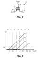
- FIG. 3illustrates the relation between the source-drain current I D and the control gate voltage V CG for four different charges Q 1 -Q 4 that the floating gate may be selectively storing at any one time.
- the four solid I D versus V CG curvesrepresent four of seven possible charge levels that can be programmed on a floating gate of a memory cell, respectively corresponding to four possible memory states.
- the threshold voltage window of a population of cellsmay range from 0.5V to 3.5V. Seven possible programmed memory states “0”, “1”, “2”, “3”, “4”, “5”, “6”, and an erased state (not shown) may be demarcated by partitioning the threshold window into regions in intervals of 0.5V each.
- Q 4is in a memory state “5”.
- a memory devicemay have memory cells having a threshold window that ranges from ⁇ 1.5V to 5V. This provides a maximum width of 6.5V. If the memory cell is to store 16 states, each state may occupy from 200 mV to 300 mV in the threshold window. This will require higher precision in programming and reading operations in order to be able to achieve the required resolution.
- FIG. 4illustrates schematically a string of memory cells organized into a NAND string.
- a pair of select transistors S 1 , S 2controls the memory transistor chain's connection to the external world via the NAND string's source terminal 54 and drain terminal 56 respectively.
- the source select transistor S 1when the source select transistor S 1 is turned on, the source terminal is coupled to a source line (see FIG. 5 ).
- the drain select transistor S 2is turned on, the drain terminal of the NAND string is coupled to a bit line of the memory array.
- Each memory transistor 10 in the chainacts as a memory cell. It has a charge storage element 20 to store a given amount of charge so as to represent an intended memory state.
- a control gate 30 of each memory transistorallows control over read and write operations. As will be seen in FIG. 5 , the control gates 30 of corresponding memory transistors of a row of NAND string are all connected to the same word line. Similarly, a control gate 32 of each of the select transistors S 1 , S 2 provides control access to the NAND string via its source terminal 54 and drain terminal 56 respectively. Likewise, the control gates 32 of corresponding select transistors of a row of NAND string are all connected to the same select line.
- FIG. 4Billustrates an example of a NAND array 210 of memory cells, constituted from NAND strings 50 such as that shown in FIG. 4 .
- a bit linesuch as bit line 36 is coupled to the drain terminal 56 of each NAND string.
- a source linesuch as source line 34 is coupled to the source terminals 54 of each NAND string.
- the control gates along a row of memory cells in a bank of NAND stringsare connected to a word line such as word line 42 .
- the control gates along a row of select transistors in a bank of NAND stringsare connected to a select line such as select line 44 .
- An entire row of memory cells in a bank of NAND stringscan be addressed by appropriate voltages on the word lines and select lines of the bank of NAND strings.
- FIG. 6illustrates a page of memory cells, organized in the NAND configuration, being sensed or programmed in parallel.
- FIG. 6essentially shows a bank of NAND strings 50 in the memory array 210 of FIG. 5 , where the detail of each NAND string is shown explicitly as in FIG. 4 .
- a physical pagesuch as the page 60 , is a group of memory cells enabled to be sensed or programmed in parallel. This is accomplished by a corresponding page of sense amplifiers 212 . The sensed results are latched in a corresponding set of latches 214 .
- Each sense amplifiercan be coupled to a NAND string via a bit line.
- the pageis enabled by the control gates of the cells of the page connected in common to a word line 42 and each cell accessible by a sense amplifier accessible via a bit line 36 .
- a sensing voltage or a programming voltageis respectively applied to the common word line WL 3 together with appropriate voltages on the bit lines.
- flash memorydiffers from other of types of memory. That is the floating gate must first be emptied of charge. Programming then adds a desired amount of charge back to the floating gate. It does not support removing a portion of the charge from the floating gate to go from a more programmed state to a lesser one. This means that updated data cannot overwrite existing data and must be written to a previous unwritten location.
- the array of memory cellsis divided into a large number of blocks of memory cells.
- the blockis the unit of erase. That is, each block contains the minimum number of memory cells that are erased together. While aggregating a large number of cells in a block to be erased in parallel will improve erase performance, a large size block also entails dealing with a larger number of update and obsolete data.
- Each blockis typically divided into a number of physical pages.
- a logical pageis a unit of programming or reading that contains a number of bits equal to the number of cells in a physical page.
- one physical pagestores one logical page of data.
- a physical pagestores two logical pages. The number of logical pages stored in a physical page thus reflects the number of bits stored per cell.
- the individual pagesmay be divided into segments and the segments may contain the fewest number of cells that are written at one time as a basic programming operation.
- One or more logical pages of dataare typically stored in one row of memory cells.
- a pagecan store one or more sectors.
- a sectorincludes user data and overhead data.
- FIG. 7A-7Cillustrate an example of programming a population of 4-state memory cells.
- FIG. 7Aillustrates the population of memory cells programmable into four distinct distributions of threshold voltages respectively representing memory states “0”, “1”, “2” and “3”.
- FIG. 7Billustrates the initial distribution of “erased” threshold voltages for an erased memory.
- FIG. 6Cillustrates an example of the memory after many of the memory cells have been programmed. Essentially, a cell initially has an “erased” threshold voltage and programming will move it to a higher value into one of the three zones demarcated by verify levels vV 1 , vV 2 and vV 3 .
- each memory cellcan be programmed to one of the three programmed states “1”, “2” and “3” or remain un-programmed in the “erased” state.
- the initial distribution of the “erased” state as shown in FIG. 7Bwill become narrower and the erased state is represented by the “0” state.
- a 2-bit code having a lower bit and an upper bitcan be used to represent each of the four memory states.
- the “0”, “1”, “2” and “3” statesare respectively represented by “11”, “01”, “00” and ‘10”.
- the 2-bit datamay be read from the memory by sensing in “full-sequence” mode where the two bits are sensed together by sensing relative to the read demarcation threshold values rV 1 , rV 2 and rV 3 in three sub-passes respectively.
- An alternative arrangement to a conventional two-dimensional (2-D) NAND arrayis a three-dimensional (3-D) array.
- 3-D arraysextend up from the wafer surface and generally include stacks, or columns, of memory cells extending upwards.
- Various 3-D arrangementsare possible.
- a NAND stringis formed vertically with one end (e.g. source) at the wafer surface and the other end (e.g. drain) on top.
- a NAND stringis formed in a U-shape so that both ends of the NAND string are accessible on top, thus facilitating connections between such strings.
- FIG. 8shows a first example of a NAND string 701 that extends in a vertical direction, i.e. extending in the z-direction, perpendicular to the x-y plane of the substrate.
- Memory cellsare formed where a vertical bit line (local bit line) 703 passes through a word line (e.g. WL 0 , WL 1 , etc.).
- a charge trapping layer between the local bit line and the word linestores charge, which affects the threshold voltage of the transistor formed by the word line (gate) coupled to the vertical bit line (channel) that it encircles.
- Such memory cellsmay be formed by forming stacks of word lines and then etching memory holes where memory cells are to be formed. Memory holes are then lined with a charge trapping layer and filled with a suitable local bit line/channel material (with suitable dielectric layers for isolation).
- select gates 705 , 707are located at either end of the string to allow the NAND string to be selectively connected to, or isolated from, external elements 709 , 711 .
- external elementsare generally conductive lines such as common source lines or bit lines that serve large numbers of NAND strings.
- Vertical NAND stringsmay be operated in a similar manner to planar NAND strings and both SLC and MLC operation is possible. While FIG. 8 shows an example of a NAND string that has 32 cells (0-31) connected in series, the number of cells in a NAND string may be any suitable number. Not all cells are shown for clarity. It will be understood that additional cells are formed where word lines 3-29 (not shown) intersect the local vertical bit line.
- a 3D NAND arraycan, loosely speaking, be formed tilting up the respective structures 50 and 210 of FIGS. 5 and 6 to be perpendicular to the x-y plane.
- each y-z planecorresponds to the page structure of FIG. 6 , with m such plane at differing x locations.
- the (global) bit lines, BL 1 - meach run across the top to an associated sense amp SA 1 - m .
- the word lines, WL 1 - n , and source and select lines SSL 1 - n and DSL 1 - nthen run in x direction, with the NAND string connected at bottom to a common source line CSL.
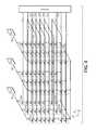
- FIGS. 9-12look at a particular monolithic three dimensional (3D) memory array of the NAND type (more specifically of the “BiCS” type), where one or more memory device levels are formed above a single substrate, in more detail.
- FIG. 9is an oblique projection of part of such a structure, showing a portion corresponding to two of the page structures in FIG. 5 , where, depending on the embodiment, each of these could correspond to a separate block or be different “fingers” of the same block.
- the NAND strings lying in a common y-z planethey are squashed together in the y direction, so that the NAND strings are somewhat staggered in the x direction.
- the NAND stringsare connected along global bit lines (BL) spanning multiple such sub-divisions of the array that run in the x direction.
- global common source linesalso run across multiple such structures in the x direction and are connect to the sources at the bottoms of the NAND string, which are connected by a local interconnect (LI) that serves as the local common source line of the individual finger.
- LIlocal interconnect
- the global source linescan span the whole, or just a portion, of the array structure.
- variationscan include the NAND string being formed in a U type structure, where part of the string itself runs back up.
- FIG. 9To the right of FIG. 9 is a representation of the elements of one of the vertical NAND strings from the structure to the left.
- Multiple memory cellsare connected through a drain select gate SGD to the associated bit line BL at the top and connected through the associated source select gate SDS to the associated local source line LI to a global source line SL.
- a select gateIt is often useful to have a select gate with a greater length than that of memory cells, where this can alternately be achieved by having several select gates in series (as described in U.S. patent application Ser. No. 13/925,662, filed on Jun. 24, 2013), making for more uniform processing of layers.
- the select gatesare programmable to have their threshold levels adjusted.
- This exemplary embodimentalso includes several dummy cells at the ends that are not used to store user data, as their proximity to the select gates makes them more prone to disturbs.
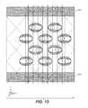
- FIG. 10shows a top view of the structure for two blocks in the exemplary embodiment.
- Two blocks(BLK 0 above, BLK 1 below) are shown, each having four fingers that run left to right.
- the word lines and select gate lines of each levelalso run left to right, with the word lines of the different fingers of the same block being commonly connected at a “terrace” and then on to receive their various voltage level through the word line select gates at WLTr.
- the word lines of a given layer in a blockcan also be commonly connected on the far side from the terrace.
- the selected gate linescan be individual for each level, rather common, allowing the fingers to be individually selected.
- the bit linesare shown running up and down the page and connect on to the sense amp circuits, where, depending on the embodiment, each sense amp can correspond to a single bit line or be multiplexed to several bit lines.
- FIG. 11shows a side view of one block, again with four fingers.
- the select gates SGD and SGS at either end of the NAND stringsare formed of four layers, with the word lines WL in-between, all formed over a CPWELL.
- a given fingeris selected by setting its select gates to a level VSG and the word lines are biased according to the operation, such as a read voltage (VCGRV) for the selected word lines and the read-pass voltage (VREAD) for the non-selected word lines.
- the non-selected fingerscan then be cut off by setting their select gates accordingly.
- FIG. 12illustrates some detail of an individual cell.
- a dielectric coreruns in the vertical direction and is surrounded by a channel silicon layer, that is in turn surrounded a tunnel dielectric (TNL) and then the charge trapping dielectric layer (CTL).
- TNLtunnel dielectric
- CTLcharge trapping dielectric layer
- the gate of the cellis here formed of tungsten with which is surrounded by a metal barrier and is separated from the charge trapping layer by blocking (BLK) oxide and a high K layer.
- BLKblocking
- some of the memory holes (MH) in which the NAND strings are formedare in close proximity to the local interconnects (LI), such as for the common source line CELSRC.
- LIlocal interconnects
- a conducting layersuch as of tungsten, is formed around these memory holes, as illustrated in FIG. 12 . Due to the narrow space involved between the memory hole and local interconnect, in some cases the conductive word line layer is not completed filled in the memory holes adjacent to an LI. As the conductive word line will then not fully surround these memory cells, they may have a slower response to program and erase operations. This section looks at techniques to identify the slow to program cells that have these defects and store this information.
- FIG. 13is a top view of a BiCS structure detail, showing a column's worth of bit lines (running top to bottom) connected to corresponding memory cells along the word line (running right to left) of a finger between two interconnect regions.
- the memory holesinclude a channel region and charge trapping region (see FIG. 12 ) and are connected to one of the 8 bit lines of the column.
- the detailshows 10 memory holes, where the lower one of the right-most memory holes and the upper one of the left-most memory holes belong to the column on either side.
- the interconnect regionsare at top ( 1301 ) and bottom ( 1303 ), where a pair of memory holes of each column are in proximity to one or the other of the LI regions.
- FIG. 14is a top view diagram showing the BiCS structure where bit lines are in vertical direction on the page and word lines are in the horizontal direction.
- the memory hole locationis represented as x, which is the contact from the bit line to the memory hole.
- the memory holesare arranged in stagger position, so only some cells can have contact with an interconnect LI.
- stagger structureto memory holes that is periodic and based on particular word line numbers, but can readily be extended to other structure where such defects would arise.
- the memory holes associated with bit lines 1, 2, 5 and 6 of a byte sized columnare located at the outer side of string, close to one of the LI regions, while the cells associated with bit line numbers 0, 3, 4 and 7 are interior to the finger. Consequently, in the exemplary arrangement, for a particular byte/column only the memory cells on outer part of a finger are subject to having an LI short defect.
- bit lines 0-7 in FIG. 14the cells on bit lines 0, 3, 4, and 7 are not adjacent to an LI and can give an indication of an expected number of programming loops.
- the “top” cells (as oriented on the figure) on bit lines 1 and 5would reflect a problem with the LI above and the “bottom” cells on bit lines 2 and 6 would reflect a problem with the LI below.
- Programming only the inner cells using a 01100110 sequencegives a measure number of programming loop NP 1 , where the 0 and 1 respectively correspond to program enable and program for the cells on bit lines 0-7.
- Programming only outer top cells using a 10111011 sequencecan be used to measure a number of programming loops NP OT
- programming only outer bottom cells using a 11011101 sequencecan be used to measure a number of programming loops NP OB .
- These three programming operationscan be done in any convenient order.
- the determination for a blockcan be based on a single word line's programming or for a set of word lines, where, consistency the same word line or set of would lines can be used for all of the blocks.
- a NAND string in which defects are present for the top cellswill have NP OT >NP 1 and for the bottom cells (Def OB ) if NP OB >NP 1 , where a margin of some number of counts (such as NP 1 +2) can be used.
- the margincan be a settable parameter.
- the comparison reference NP 1can be local, with each column of a finger having its own NP 1 or a coarser granularity can be sued for the references: for example, to save test time, the same NP 1 can be used for a whole block or set of blocks or for plane.
- NP 1can be higher if inner cells are slow to program due to some other defect, which may make it more difficult to distinguish inner from defective outer cells. Because of this, in some embodiments NP 1 can be calibrated to a certain number or range in order to distinguish or detect outer bad strings accurately. A value can be calibrated and one reference number be kept in a register to check that NP 1 has not drifted too much from block to block.
- the memory systemIn order to capture weak strings that may not be detected at time 0, but which can degrade device operation in the field, the memory system to apply stress and then detection method to accelerate weak strings.
- the stresscan be applied with all word lines selected and the LI at 0V, or, alternately, a high voltage on the LI and the word lines on all blocks at 0V, where the well can be floated to avoid overstressing the cells.
- slow to program stringscan be marked down as slow (bad) strings and stored for reference in, for example, a specified area of the non-volatile memory or a fuse memory or other location where they can be maintained and accessed.
- the result of Def OT or Def OB to mark which strings are defectivecan then be read out for use during program operations.
- This defect informationcan be stored in several formats.
- the memorycan store block number and string information for only blocks that have at least one of the strings defective for either Outer_Bottom or Outter_Top.
- FIG. 15Ais a schematic representation of this arrangement that will use, for example, two bytes of data for block address information and one byte information for 4 strings (2 bits for outer_bottom+outter_Top).
- thiscan be accommodated in one page of non-volatile memory, although two pages may be used if redundancy or XOR check data is included due to reliability concerns.
- the string informationcan be recorded for all blocks without making decision of if that block has any defected string or not, as illustrated schematically in FIG. 15B .
- each blockhas one byte of information for 4 strings and 2 bits for Outer Bottom and Outer Top. For best case or worst case this would involve 4 K Bytes, for example, of information without redundancy or 8K byte with one byte redundancy.
- the informationcan be stored on different pages.
- Another algorithm for determining NAND strings with slow to program cellsbe based on the cells' current (ICELL), rather than the program loop count, during the verify phase or subsequent sensing operation.
- inner cellsare again programmed using a 0110110 sequence, but instead of a loop count, the process now measures Icell current for the inner cell programming operation (ICELL 1 ). Only the outer top cells are programmed using a 1011011 sequence and the Icell current for outer top cell programming operation (ICELL OT ) is measured; and only the outer bottom cells using a 11011101 sequence is programmed and the Icell current for the outer bottom cell programming operation (ICELL OB ) is measured.
- the off-setcan be a settable parameter.
- the reference valuehere ICELL 1
- ICELL 1can be maintained for each finger for column or with a coarser granularity, such as an average of several blocks. The result of the determination can then be recorded as discussed above as well.
- a third algorithm to determine slow to program NAND stringsuses a test sequence to stress and detect weak strings, where after applying a stress slow to erase strings are identified and the information is stored as described above.
- a program stresscan be applied with all word lines selected and the LI at 0V, or, alternately, a high voltage on the LI and the word lines on all blocks at 0V, where the well can be floated to avoid overstressing the cells.
- the defectwill cause strings to be resistive and slow to erase.
- the detection phasebegins with the blocks the blocks being tested. For example, if a flash write mode is available, the blocks can all be written with “00” data, for example.
- a shallow erase block-by-block testis then performed, after which a read with “FF” (erased) data is performed to determine which strings were slow to erase. Alternately, the decision can be made based on string current measurements. The block numbers and slow strings information can then be recorded as above.
- FFerased
- An alternate detectionis for the cells on the different NAND strings being tested to be programmed by a fixed number of pulses to, for example, the highest data state (such as “3” in FIG. 7A ).
- the cell current ICELLcan then be measured to find the slow strings relative to the normal strings. Use of a higher state will more clearly differentiate the NAND strings from the normal. For example, as part of the device characterization process, the number of pulses needed to program a fast to program cell to a give state, such as the highest or a relatively high state, can be determined.
- This number of pulsescan then be applied along a word line (or done for a set of word lines) and then the different NAND strings can be checked for their relative level of programming, such as by applying a read voltage along the word line and looking at the relative current amounts, or by determining the different voltage levels that need to be applied for the strings to conduct.
- FIG. 16is block diagram of some of the elements of the memory circuit for implementing the various embodiments described above.
- the array and peripheral elementsare at 1601 .
- the 10 padsare at 1603 , the address and command registers at 1609 and 1611 , and the clock generator and oscillator at 1605 and 1607 .
- a finite state machine and sequencer 1613serves as the on-chip control circuitry for the reference voltage and current generating circuitry 1617 , charge pump circuits 1615 , and drivers 1619 .
- Some of the elements involved in determining slow to program NAND stringsare shown at lower right. Latches for the inner strings loop count and outer strings loop count are respectively shown at 1623 and 1621 . These are then compared at 1625 , with decision and recordation then represented at 1627 .
- the elements 1621 , 1623 , 1625 , 1627can variously be incorporated into the other control circuitry and logic of the memory chip.
- This sectionlooks at methods to improve the programming of slow cells. Although this will discussed primarily in the context of BiCS types which have defects in tungsten deposition leading to memory hole to LI shorts, such as discussed in the last section, the techniques are generally applicable. In particular, the various techniques described below can be applied to the various 2D and 3D non-volatile memories described in earlier sections as well as for other memories that use similar programming techniques.
- the memorywill determine if a selected string in a selected blocks is slow to program. This can be done be reading the listing of these defects, such as described in the last section, and checking the corresponding byte and mark the selected string bits for Def OT or Def OB . In the exemplary embodiments, depending on the defective bit information, either bit lines 1, 5, bit lines 2, 6, or all of bit lines 1, 2, 5 and 6 are applied with countermeasure. If any Def-bits are zero then those cells will be treated as a normal block.
- the memoryselectively supplies a different bit line bias to selected slow to program cells, such as a negative bias that can be provided from an extra pump, if such voltages are not already available on the device.
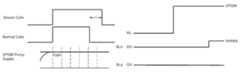
- a different bit line biasto selected slow to program cells, such as a negative bias that can be provided from an extra pump, if such voltages are not already available on the device. This manipulation of bit line voltages allows the memory to change effective VPGM voltage for the slow cell. This is illustrated schematically in FIG. 17 .
- FIG. 17shows a column of bits lines (BL 0 - 7 ) running across the top of the four fingers of a block, where the NAND strings are represented for the first four bit lines.
- the outer bits lines (BL 1 , BL 2 , BL 5 , BL 6 )are slow to program and selected, this can have an “enhanced” program enable voltage of a negative bias (for e.g., ⁇ 1V voltage) applied, rather than a typical program enable voltage of ⁇ 0V for selected, but normal (that is, not marked as slow) cells.
- Non-selected (or verified) cells of either typewould have a program inhibit voltage, such as a few volts, sufficient to turn off the drain side select gate.
- FIG. 18looks at a selected string for just BL 0 and BL 1 , where the string for BL 0 is slow.
- An enhanced enable level of a negative biasis applied to BL 1
- a normal program enable biassuch as 0V is applied on BL 0 .
- a programming pulse of VPGMis then applied on the selected word line (WL 46 in the example).
- the effective increase A of the programming voltagehelps the slow to program cells to program more quickly.
- FIG. 19is a block diagram to illustrate some of the elements involved.
- FIG. 19repeats many of the same elements as in FIG. 16 , where these are similarly numbered.
- the circuitrynow also include an analog circuit to generate the negative bias levels for use on the slow bit lines, where this is show separate from the other charge pump elements for purposes of this discussion.
- Another option for improving the programming rate of slow cellis through use of an elongated programming time for the pulse applied to the slow cells, relative to the pulse length for normal cells.
- FIG. 20This is illustrated schematically in FIG. 20 , where an actual programming pulse is shown at bottom, a longer pulse is applied to the slow cells at top, and a shorter pulse is applied to the normal cells at center. Any outer slow cells will get extra timing for programming, while the faster cells (inner cells) will receive less. As all of the cells on the same word line will receive the same pulse, however, the pulse length itself is not shortened; rather, the memory selectively inhibits faster cells earlier and slower cells will be applied VPGM for little more time.
- FIG. 21where the pulse along the word line is at top.
- the bit lines (BLs at bottom)stay at the program enable voltage (0V).
- the bit line (BLn, center)is initially at the program enable level, but then raised to the inhibit voltage Vinhibit.
- a further optionis the use of a dummy programming pulse to push slower cells higher.
- a memorytypically will allow for some number of failed bits in a program operation, a normal case Bit Scan Pass Fail criterion BSPF.
- the memorycan inhibit all cells which passed the corresponding program verify level and then can apply some number of dummy (without verify) program pulses with a higher VPGM or with wider pulse width to push Vt of slow cells higher. This is illustrated with respect to FIGS. 22-25 .
- FIG. 22looks at a set of normal cells' threshold voltages (Vt) distribution and number of programming pulses.
- the two distributionscorrespond to an erased state E and a programmed state P.
- the selected cellsprogram to the P state after two pulse, except for a few below the BSPR point. If there is no defect present in any of the cells, the cells will behave more or less identically, as shown in FIG. 22 where the Vt of normal cells are shifted correctly for all the cells and there are very few slow cells which are below the BSPF level.
- the BSPF criterionis increased as explained earlier, so the even though many of the programming cells have not passed the actual (non-modified) BSPF criterion, the memory considers the programming algorithm as passed. After this passing the (relaxed) BSPF criterion, the memory can apply one or more dummy programming pulse with higher VPGM value or for a longer duration. An example of this is illustrated by the write waveform of FIG. 25 .
- the P state distributionmeets the relaxed BSPF criterion.
- the slow cellare then given an additional, larger dummy pulse, without a subsequent verify or lockout operation.
Landscapes
- Engineering & Computer Science (AREA)
- Microelectronics & Electronic Packaging (AREA)
- Computer Hardware Design (AREA)
- Read Only Memory (AREA)
Abstract
Description
Claims (21)
Priority Applications (1)
| Application Number | Priority Date | Filing Date | Title |
|---|---|---|---|
| US14/681,653US9269446B1 (en) | 2015-04-08 | 2015-04-08 | Methods to improve programming of slow cells |
Applications Claiming Priority (1)
| Application Number | Priority Date | Filing Date | Title |
|---|---|---|---|
| US14/681,653US9269446B1 (en) | 2015-04-08 | 2015-04-08 | Methods to improve programming of slow cells |
Publications (1)
| Publication Number | Publication Date |
|---|---|
| US9269446B1true US9269446B1 (en) | 2016-02-23 |
Family
ID=55314731
Family Applications (1)
| Application Number | Title | Priority Date | Filing Date |
|---|---|---|---|
| US14/681,653ActiveUS9269446B1 (en) | 2015-04-08 | 2015-04-08 | Methods to improve programming of slow cells |
Country Status (1)
| Country | Link |
|---|---|
| US (1) | US9269446B1 (en) |
Cited By (11)
| Publication number | Priority date | Publication date | Assignee | Title |
|---|---|---|---|---|
| US9564226B1 (en)* | 2015-10-30 | 2017-02-07 | Sandisk Technologies Llc | Smart verify for programming non-volatile memory |
| KR20170024429A (en)* | 2015-08-25 | 2017-03-07 | 삼성전자주식회사 | Non-volatile memory device, operating method thereof and solid state drive including the same |
| US10102903B1 (en)* | 2017-03-31 | 2018-10-16 | Intel Corporation | Write process for a non volatile memory device |
| US10127985B2 (en) | 2017-03-03 | 2018-11-13 | Toshiba Memory Corporation | Semiconductor memory device |
| CN113345498A (en)* | 2020-02-18 | 2021-09-03 | 闪迪技术有限公司 | System and method for program verification of a memory system |
| US11342035B1 (en) | 2020-11-24 | 2022-05-24 | Sandisk Technologies Llc | Memory apparatus and method of operation using one pulse smart verify |
| US11514991B1 (en) | 2021-05-04 | 2022-11-29 | Sandisk Technologies Llc | Program tail plane comparator for non-volatile memory structures |
| US11568943B2 (en) | 2020-11-24 | 2023-01-31 | Sandisk Technologies Llc | Memory apparatus and method of operation using zero pulse smart verify |
| US20230085583A1 (en)* | 2021-09-16 | 2023-03-16 | Macronix International Co., Ltd. | Three dimension memory device |
| US11775374B2 (en) | 2021-04-15 | 2023-10-03 | Western Digital Technologies, Inc. | State-by-state program loop delta detection mode for detecting a defective memory array |
| US20240127891A1 (en)* | 2022-10-17 | 2024-04-18 | Sandisk Technologies Llc | Program pulse duration increase for nand program failure |
Citations (172)
| Publication number | Priority date | Publication date | Assignee | Title |
|---|---|---|---|---|
| US3710348A (en) | 1970-04-02 | 1973-01-09 | Ibm | Connect modules |
| US3895360A (en) | 1974-01-29 | 1975-07-15 | Westinghouse Electric Corp | Block oriented random access memory |
| US4357685A (en) | 1979-09-28 | 1982-11-02 | Sgs-Ates Componenti Elettronici S.P.A. | Method of programming an electrically alterable nonvolatile memory |
| US4426688A (en) | 1981-08-03 | 1984-01-17 | Ncr Corporation | Memory system having an alternate memory |
| JPS61292747A (en) | 1985-06-20 | 1986-12-23 | Nec Corp | Buffer register |
| US4720815A (en) | 1985-05-20 | 1988-01-19 | Fujitsu Limited | Semiconductor memory device in form of shift register with two-phase clock signal supply |
| US4757477A (en) | 1986-06-06 | 1988-07-12 | Fujitsu Limited | Dual-port semiconductor memory device |
| JPH01128297A (en) | 1987-11-12 | 1989-05-19 | Sharp Corp | Semiconductor integrated circuit device |
| US5070032A (en) | 1989-03-15 | 1991-12-03 | Sundisk Corporation | Method of making dense flash eeprom semiconductor memory structures |
| US5095344A (en) | 1988-06-08 | 1992-03-10 | Eliyahou Harari | Highly compact eprom and flash eeprom devices |
| US5172338A (en) | 1989-04-13 | 1992-12-15 | Sundisk Corporation | Multi-state EEprom read and write circuits and techniques |
| US5200959A (en) | 1989-10-17 | 1993-04-06 | Sundisk Corporation | Device and method for defect handling in semi-conductor memory |
| US5270979A (en) | 1991-03-15 | 1993-12-14 | Sundisk Corporation | Method for optimum erasing of EEPROM |
| US5313421A (en) | 1992-01-14 | 1994-05-17 | Sundisk Corporation | EEPROM with split gate source side injection |
| US5315541A (en) | 1992-07-24 | 1994-05-24 | Sundisk Corporation | Segmented column memory array |
| JPH06150666A (en) | 1992-11-12 | 1994-05-31 | Sanyo Electric Co Ltd | Input circuit |
| US5343063A (en) | 1990-12-18 | 1994-08-30 | Sundisk Corporation | Dense vertical programmable read only memory cell structure and processes for making them |
| US5386390A (en) | 1992-04-28 | 1995-01-31 | Mitsubishi Denki Kabushiki Kaisha | Semiconductor memory with looped shift registers as row and column drivers |
| US5418752A (en) | 1989-04-13 | 1995-05-23 | Sundisk Corporation | Flash EEPROM system with erase sector select |
| US5428621A (en) | 1992-09-21 | 1995-06-27 | Sundisk Corporation | Latent defect handling in EEPROM devices |
| US5430859A (en) | 1991-07-26 | 1995-07-04 | Sundisk Corporation | Solid state memory system including plural memory chips and a serialized bus |
| US5430679A (en) | 1990-12-20 | 1995-07-04 | International Business Machines Corporation | Flexible redundancy architecture and fuse download scheme |
| US5442748A (en) | 1993-10-29 | 1995-08-15 | Sun Microsystems, Inc. | Architecture of output switching circuitry for frame buffer |
| US5479370A (en) | 1992-02-20 | 1995-12-26 | Kabushiki Kaisha Toshiba | Semiconductor memory with bypass circuit |
| US5485425A (en) | 1992-06-30 | 1996-01-16 | Hitachi, Ltd. | Semiconductor memory device having redundant column and operation method thereof |
| US5570315A (en) | 1993-09-21 | 1996-10-29 | Kabushiki Kaisha Toshiba | Multi-state EEPROM having write-verify control circuit |
| US5595924A (en) | 1994-05-25 | 1997-01-21 | Sandisk Corporation | Technique of forming over an irregular surface a polysilicon layer with a smooth surface |
| US5642312A (en) | 1988-06-08 | 1997-06-24 | Harari; Eliyahou | Flash EEPROM system cell array with more than two storage states per memory cell |
| US5657332A (en) | 1992-05-20 | 1997-08-12 | Sandisk Corporation | Soft errors handling in EEPROM devices |
| US5663901A (en) | 1991-04-11 | 1997-09-02 | Sandisk Corporation | Computer memory cards using flash EEPROM integrated circuit chips and memory-controller systems |
| US5699300A (en) | 1989-05-26 | 1997-12-16 | Akamatsu; Hironori | Divided wordline memory arrangement having overlapping activation of wordlines during continuous access cycle |
| US5712180A (en) | 1992-01-14 | 1998-01-27 | Sundisk Corporation | EEPROM with split gate source side injection |
| US5768192A (en) | 1996-07-23 | 1998-06-16 | Saifun Semiconductors, Ltd. | Non-volatile semiconductor memory cell utilizing asymmetrical charge trapping |
| US5774397A (en) | 1993-06-29 | 1998-06-30 | Kabushiki Kaisha Toshiba | Non-volatile semiconductor memory device and method of programming a non-volatile memory cell to a predetermined state |
| US5783958A (en) | 1996-01-19 | 1998-07-21 | Sgs-Thomson Microelectronics, Inc. | Switching master slave circuit |
| WO1998044420A1 (en) | 1997-03-31 | 1998-10-08 | Lexar Media, Inc. | Moving sectors within a block in a flash memory |
| US5822245A (en) | 1997-03-26 | 1998-10-13 | Atmel Corporation | Dual buffer flash memory architecture with multiple operating modes |
| US5848009A (en) | 1996-10-08 | 1998-12-08 | Samsung Electronics Co., Ltd. | Integrated circuit memory devices that map nondefective memory cell blocks into continuous addresses |
| US5890192A (en) | 1996-11-05 | 1999-03-30 | Sandisk Corporation | Concurrent write of multiple chunks of data into multiple subarrays of flash EEPROM |
| US5903495A (en) | 1996-03-18 | 1999-05-11 | Kabushiki Kaisha Toshiba | Semiconductor device and memory system |
| US5930167A (en) | 1997-07-30 | 1999-07-27 | Sandisk Corporation | Multi-state non-volatile flash memory capable of being its own two state write cache |
| US6011725A (en) | 1997-08-01 | 2000-01-04 | Saifun Semiconductors, Ltd. | Two bit non-volatile electrically erasable and programmable semiconductor memory cell utilizing asymmetrical charge trapping |
| US6021463A (en) | 1997-09-02 | 2000-02-01 | International Business Machines Corporation | Method and means for efficiently managing update writes and fault tolerance in redundancy groups of addressable ECC-coded sectors in a DASD storage subsystem |
| US6038184A (en) | 1997-04-25 | 2000-03-14 | Nec Corporation | Semiconductor memory device having internal timing generator shared between data read/write and burst access |
| US6038167A (en) | 1995-01-31 | 2000-03-14 | Hitachi, Ltd. | Nonvolatile memory device and refreshing method |
| US6091666A (en) | 1996-10-04 | 2000-07-18 | Sony Corporation | Nonvolatile flash memory with fast data programming operation |
| WO2000049488A1 (en) | 1999-02-17 | 2000-08-24 | Memory Corporation Plc | Memory system |
| US6134148A (en) | 1997-09-30 | 2000-10-17 | Hitachi, Ltd. | Semiconductor integrated circuit and data processing system |
| US6151248A (en) | 1999-06-30 | 2000-11-21 | Sandisk Corporation | Dual floating gate EEPROM cell array with steering gates shared by adjacent cells |
| US6222762B1 (en) | 1992-01-14 | 2001-04-24 | Sandisk Corporation | Multi-state memory |
| US6230233B1 (en) | 1991-09-13 | 2001-05-08 | Sandisk Corporation | Wear leveling techniques for flash EEPROM systems |
| US6252800B1 (en) | 1998-11-24 | 2001-06-26 | Fujitsu Limited | Semiconductor memory device |
| US6266273B1 (en) | 2000-08-21 | 2001-07-24 | Sandisk Corporation | Method and structure for reliable data copy operation for non-volatile memories |
| US6282624B1 (en) | 1997-11-13 | 2001-08-28 | Seiko Epson Corporation | Non-volatile memory apparatus including first and second address conversion tables stored in volatile and nonvolatile memories for improved access at power up |
| US6353553B1 (en) | 2000-01-24 | 2002-03-05 | Mitsubishi Denki Kabushiki Kaisha | Nonvolatile semiconductor memory device having structure storing multivalued data and data storage system comprising the nonvolatile semiconductor memory device |
| US6426893B1 (en) | 2000-02-17 | 2002-07-30 | Sandisk Corporation | Flash eeprom system with simultaneous multiple data sector programming and storage of physical block characteristics in other designated blocks |
| US20020118574A1 (en) | 2001-02-26 | 2002-08-29 | Geoffrey Gongwer | Non-volatile memory with improved programming and method therefor |
| US6456528B1 (en) | 2001-09-17 | 2002-09-24 | Sandisk Corporation | Selective operation of a multi-state non-volatile memory system in a binary mode |
| US6480423B2 (en) | 1998-07-17 | 2002-11-12 | Kabushiki Kaisha Toshiba | High-speed cycle clock-synchronous memory device |
| US6510488B2 (en) | 2001-02-05 | 2003-01-21 | M-Systems Flash Disk Pioneers Ltd. | Method for fast wake-up of a flash memory system |
| US6512263B1 (en) | 2000-09-22 | 2003-01-28 | Sandisk Corporation | Non-volatile memory cell array having discontinuous source and drain diffusions contacted by continuous bit line conductors and methods of forming |
| US6522580B2 (en) | 2001-06-27 | 2003-02-18 | Sandisk Corporation | Operating techniques for reducing effects of coupling between storage elements of a non-volatile memory operated in multiple data states |
| WO2003025939A2 (en) | 2001-09-17 | 2003-03-27 | Sandisk Corporation | Dynamic column block selection |
| US6581142B1 (en) | 2000-09-01 | 2003-06-17 | International Business Machines Corporation | Computer program product and method for partial paging and eviction of microprocessor instructions in an embedded computer |
| US6594177B2 (en) | 2001-08-02 | 2003-07-15 | Stmicroelectronics, Inc. | Redundancy circuit and method for replacing defective memory cells in a flash memory device |
| US20030182317A1 (en) | 2002-03-22 | 2003-09-25 | Kahn Andy C. | File folding technique |
| US6657891B1 (en) | 2002-11-29 | 2003-12-02 | Kabushiki Kaisha Toshiba | Semiconductor memory device for storing multivalued data |
| US20040060031A1 (en) | 2002-09-24 | 2004-03-25 | Sandisk Corporation | Highly compact non-volatile memory and method thereof |
| US20040109357A1 (en) | 2002-09-24 | 2004-06-10 | Raul-Adrian Cernea | Non-volatile memory and method with improved sensing |
| US6771536B2 (en) | 2002-02-27 | 2004-08-03 | Sandisk Corporation | Operating techniques for reducing program and read disturbs of a non-volatile memory |
| US6813184B2 (en) | 2002-01-12 | 2004-11-02 | Samsung Electronics Co., Ltd. | NAND flash memory and method of erasing, programming, and copy-back programming thereof |
| CN1549133A (en) | 2003-05-22 | 2004-11-24 | 群联电子股份有限公司 | Parallel double-track using method of flash memory |
| US6853596B2 (en) | 2002-09-13 | 2005-02-08 | Fujitsu Limited | Semiconductor memory enabling correct substitution of redundant cell array |
| US6870768B2 (en) | 2002-09-06 | 2005-03-22 | Sandisk Corporation | Techniques for reducing effects of coupling between storage elements of adjacent rows of memory cells |
| US20050073884A1 (en) | 2003-10-03 | 2005-04-07 | Gonzalez Carlos J. | Flash memory data correction and scrub techniques |
| US20050083735A1 (en)* | 2003-10-20 | 2005-04-21 | Jian Chen | Behavior based programming of non-volatile memory |
| US20050144360A1 (en) | 2003-12-30 | 2005-06-30 | Bennett Alan D. | Non-volatile memory and method with block management system |
| US20050141387A1 (en) | 2003-12-31 | 2005-06-30 | Raul-Adrian Cernea | Flexible and area efficient column redundancy for non-volatile memories |
| US20050213393A1 (en) | 2004-03-14 | 2005-09-29 | M-Systems Flash Disk Pioneers, Ltd. | States encoding in multi-bit flash cells for optimizing error rate |
| US6967873B2 (en) | 2003-10-02 | 2005-11-22 | Advanced Micro Devices, Inc. | Memory device and method using positive gate stress to recover overerased cell |
| US6990018B2 (en) | 2003-04-18 | 2006-01-24 | Kabushiki Kaisha Toshiba | Non-volatile semiconductor memory device, electronic card using the same and electronic apparatus |
| US6996017B2 (en) | 2003-03-28 | 2006-02-07 | Matrix Semiconductor, Inc. | Redundant memory structure using bad bit pointers |
| US7027330B2 (en) | 2004-05-11 | 2006-04-11 | Hynix Semiconductor Inc | Multi-input/output repair method of NAND flash memory device and NAND flash memory device thereof |
| US7039781B2 (en) | 2001-07-27 | 2006-05-02 | Matsushtia Electric Industrial Co., Ltd. | Flash memory apparatus and method for merging stored data items |
| US20060114726A1 (en) | 2002-09-25 | 2006-06-01 | Renesas Technology Corp. | Nonvolatile memory |
| US7057939B2 (en) | 2004-04-23 | 2006-06-06 | Sandisk Corporation | Non-volatile memory and control with improved partial page program capability |
| US7058818B2 (en) | 2002-08-08 | 2006-06-06 | M-Systems Flash Disk Pioneers Ltd. | Integrated circuit for digital rights management |
| US20060126390A1 (en) | 2004-12-14 | 2006-06-15 | Gorobets Sergey A | Pipelined programming of non-volatile memories using early data |
| US20060136656A1 (en) | 2004-12-21 | 2006-06-22 | Conley Kevin M | System and method for use of on-chip non-volatile memory write cache |
| WO2006064318A1 (en) | 2004-12-13 | 2006-06-22 | Axalto Sa | Method to secure writing in memory against attacks by radiation or other means |
| US7076611B2 (en) | 2003-08-01 | 2006-07-11 | Microsoft Corporation | System and method for managing objects stored in a cache |
| US20060161728A1 (en) | 2005-01-20 | 2006-07-20 | Bennett Alan D | Scheduling of housekeeping operations in flash memory systems |
| US7110294B2 (en) | 2004-07-20 | 2006-09-19 | Kabushiki Kaisha Toshiba | Semiconductor memory device |
| US7158421B2 (en) | 2005-04-01 | 2007-01-02 | Sandisk Corporation | Use of data latches in multi-phase programming of non-volatile memories |
| US20070061502A1 (en) | 2005-09-09 | 2007-03-15 | M-Systems Flash Disk Pioneers Ltd. | Flash memory storage system and method |
| US20070065119A1 (en) | 2005-09-06 | 2007-03-22 | Msystems Ltd. | Portable selective memory data exchange device |
| US7206230B2 (en) | 2005-04-01 | 2007-04-17 | Sandisk Corporation | Use of data latches in cache operations of non-volatile memories |
| US20070091677A1 (en) | 2005-10-25 | 2007-04-26 | M-Systems Flash Disk Pioneers Ltd. | Method for recovering from errors in flash memory |
| US20070103977A1 (en) | 2005-11-08 | 2007-05-10 | Conley Kevin M | Retargetable memory cell redundancy methods |
| US7224605B1 (en) | 2006-03-24 | 2007-05-29 | Sandisk Corporation | Non-volatile memory with redundancy data buffered in data latches for defective locations |
| US20070159652A1 (en) | 2005-11-30 | 2007-07-12 | Canon Kabushiki Kaisha | Data processing apparatus and data processing method |
| US20070180346A1 (en) | 2006-01-18 | 2007-08-02 | Sandisk Il Ltd. | Method Of Arranging Data In A Multi-Level Cell Memory Device |
| US20070186032A1 (en) | 2005-08-03 | 2007-08-09 | Sinclair Alan W | Flash Memory Systems With Direct Data File Storage Utilizing Data Consolidation and Garbage Collection |
| US7257689B1 (en) | 2004-10-15 | 2007-08-14 | Veritas Operating Corporation | System and method for loosely coupled temporal storage management |
| US20070211530A1 (en) | 2006-03-09 | 2007-09-13 | Takeshi Nakano | Data recording method of semiconductor integrated circuit device |
| US20070220197A1 (en) | 2005-01-31 | 2007-09-20 | M-Systems Flash Disk Pioneers, Ltd. | Method of managing copy operations in flash memories |
| US20070237006A1 (en) | 2006-04-11 | 2007-10-11 | Msystems Ltd. | Method for generating soft bits in flash memories |
| US20070260808A1 (en) | 2006-05-08 | 2007-11-08 | Sandisk Il Ltd. | Remotely controllable media distribution device |
| US7299314B2 (en) | 2003-12-31 | 2007-11-20 | Sandisk Corporation | Flash storage system with write/erase abort detection mechanism |
| US20070268745A1 (en) | 2006-05-21 | 2007-11-22 | Sandisk Il Ltd. | Method of storing data in a multi-bit-cell flash memory |
| US20070283081A1 (en) | 2006-06-06 | 2007-12-06 | Msystem Ltd. | Cache control in a non-volatile memory device |
| US20070285980A1 (en) | 2006-05-10 | 2007-12-13 | Takahiro Shimizu | Semiconductor memory device |
| US7310347B2 (en) | 2004-03-14 | 2007-12-18 | Sandisk, Il Ltd. | States encoding in multi-bit flash cells |
| US20080002467A1 (en) | 2006-06-30 | 2008-01-03 | Hidetaka Tsuji | Card controller controlling semiconductor memory including memory cell having charge accumulation layer and control gate |
| US20080082736A1 (en) | 2004-03-11 | 2008-04-03 | Chow David Q | Managing bad blocks in various flash memory cells for electronic data flash card |
| US20080104309A1 (en) | 2006-10-30 | 2008-05-01 | Cheon Won-Moon | Flash memory device with multi-level cells and method of writing data therein |
| US20080112238A1 (en) | 2006-10-25 | 2008-05-15 | Seon-Taek Kim | Hybrid flash memory device and method for assigning reserved blocks thereof |
| US20080147996A1 (en) | 2004-09-01 | 2008-06-19 | International Business Machines Corporation | Atomic read/write support in a multi-module memory configuration |
| US20080159012A1 (en) | 2006-12-28 | 2008-07-03 | Hynix Semiconductor Inc. | Semiconductor memory device, and multi-chip package and method of operating the same |
| US20080181000A1 (en) | 2007-01-31 | 2008-07-31 | Sandisk Il Ltd. | Method Of Improving Programming Precision In Flash Memory |
| US7411846B2 (en) | 2000-02-02 | 2008-08-12 | Broadcom Corporation | Memory redundance circuit techniques |
| US20080209112A1 (en) | 1999-08-04 | 2008-08-28 | Super Talent Electronics, Inc. | High Endurance Non-Volatile Memory Devices |
| US7420847B2 (en) | 2004-12-14 | 2008-09-02 | Sandisk Corporation | Multi-state memory having data recovery after program fail |
| US7426623B2 (en) | 2005-01-14 | 2008-09-16 | Sandisk Il Ltd | System and method for configuring flash memory partitions as super-units |
| US20080244367A1 (en) | 2007-03-31 | 2008-10-02 | Henry Chin | Non-volatile memory with guided simulated annealing error correction control |
| US20080244338A1 (en) | 2007-03-31 | 2008-10-02 | Nima Mokhlesi | Soft bit data transmission for error correction control in non-volatile memory |
| US20080250300A1 (en) | 2007-03-29 | 2008-10-09 | Nima Mokhlesi | Method for decoding data in non-volatile storage using reliability metrics based on multiple reads |
| US20080250220A1 (en) | 2007-04-06 | 2008-10-09 | Takafumi Ito | Memory system |
| US20080253181A1 (en)* | 2007-04-03 | 2008-10-16 | Kabushiki Kaisha Toshiba | Method for programming a semiconductor memory device |
| US7447070B2 (en) | 2002-09-24 | 2008-11-04 | Sandisk Corporation | Highly compact non-volatile memory and method therefor with internal serial buses |
| US20080279005A1 (en) | 2007-05-11 | 2008-11-13 | Spansion Llc | Managing flash memory program and erase cycles in the time domain |
| US20080294814A1 (en) | 2007-05-24 | 2008-11-27 | Sergey Anatolievich Gorobets | Flash Memory System with Management of Housekeeping Operations |
| US20080301532A1 (en) | 2006-09-25 | 2008-12-04 | Kabushiki Kaisha Toshiba | Non-volatile semiconductor memory device |
| US20080307192A1 (en) | 2007-06-08 | 2008-12-11 | Sinclair Alan W | Method And System For Storage Address Re-Mapping For A Memory Device |
| US20080310224A1 (en) | 2007-06-15 | 2008-12-18 | Micron Technology, Inc. | Coarse and fine programming in a solid state memory |
| US7490283B2 (en) | 2004-05-13 | 2009-02-10 | Sandisk Corporation | Pipelined data relocation and improved chip architectures |
| US7493457B2 (en) | 2004-11-08 | 2009-02-17 | Sandisk Il. Ltd | States encoding in multi-bit flash cells for optimizing error rate |
| US7502259B2 (en) | 2004-12-30 | 2009-03-10 | Sandisk Corporation | On-chip data grouping and alignment |
| US20090067244A1 (en) | 2007-09-07 | 2009-03-12 | Yan Li | Nonvolatile memory and method for on-chip pseudo-randomization of data within a page and between pages |
| US20090089482A1 (en) | 2007-09-28 | 2009-04-02 | Shai Traister | Dynamic metablocks |
| US20090089520A1 (en) | 2007-09-28 | 2009-04-02 | Bratin Saha | Hardware acceleration of strongly atomic software transactional memory |
| US20090089481A1 (en) | 2007-09-27 | 2009-04-02 | Arjun Kapoor | Leveraging Portable System Power to Enhance Memory Management and Enable Application Level Features |
| US20090094482A1 (en) | 2005-10-17 | 2009-04-09 | Eugene Zilberman | Data restoration in case of page-programming failure |
| CN101421797A (en) | 2006-03-24 | 2009-04-29 | 桑迪士克股份有限公司 | Nonvolatile memory and method with redundant data buffered in remote buffer circuit |
| US20090172247A1 (en) | 2007-12-27 | 2009-07-02 | Sandisk Il Ltd. | Controller for one type of nand flash memory for emulating another type of nand flash memory |
| US20090172498A1 (en) | 2007-12-27 | 2009-07-02 | Mark Shlick | Error correction in copy back memory operations |
| US20090310408A1 (en) | 2008-06-13 | 2009-12-17 | Samsung Electronics Co., Ltd. | Memory system and method of accessing a semiconductor memory device |
| US20100037012A1 (en) | 2007-12-28 | 2010-02-11 | Hirokuni Yano | Semiconductor Storage Device, Method of Controlling the Same, Controller and Information Processing Apparatus |
| US20100107004A1 (en) | 2008-10-26 | 2010-04-29 | Aldo Bottelli | Method for selectively retrieving column redundancy data in memory device |
| US20100157641A1 (en) | 2006-05-12 | 2010-06-24 | Anobit Technologies Ltd. | Memory device with adaptive capacity |
| US20100172179A1 (en) | 2009-01-05 | 2010-07-08 | Sergey Anatolievich Gorobets | Spare Block Management of Non-Volatile Memories |
| US20100174845A1 (en) | 2009-01-05 | 2010-07-08 | Sergey Anatolievich Gorobets | Wear Leveling for Non-Volatile Memories: Maintenance of Experience Count and Passive Techniques |
| US20100174846A1 (en) | 2009-01-05 | 2010-07-08 | Alexander Paley | Nonvolatile Memory With Write Cache Having Flush/Eviction Methods |
| US20100172180A1 (en) | 2009-01-05 | 2010-07-08 | Alexander Paley | Non-Volatile Memory and Method With Write Cache Partitioning |
| US20100174847A1 (en) | 2009-01-05 | 2010-07-08 | Alexander Paley | Non-Volatile Memory and Method With Write Cache Partition Management Methods |
| US20100287217A1 (en) | 2009-04-08 | 2010-11-11 | Google Inc. | Host control of background garbage collection in a data storage device |
| US20100325351A1 (en) | 2009-06-12 | 2010-12-23 | Bennett Jon C R | Memory system having persistent garbage collection |
| US20100329007A1 (en) | 2009-06-24 | 2010-12-30 | Hardwell Chibvongodze | Pointer Based Column Selection Techniques in Non-Volatile Memories |
| US20110063909A1 (en) | 2009-09-16 | 2011-03-17 | Kabushiki Kaisha Toshiba | Nonvolatile semiconductor memory and method of testing the same |
| US20110096601A1 (en) | 2009-10-28 | 2011-04-28 | Gavens Lee M | Non-Volatile Memory And Method With Accelerated Post-Write Read To Manage Errors |
| US20110099460A1 (en) | 2009-10-28 | 2011-04-28 | Gautam Ashok Dusija | Non-Volatile Memory And Method With Post-Write Read And Adaptive Re-Write To Manage Errors |
| US7961512B2 (en) | 2008-03-19 | 2011-06-14 | Sandisk Corporation | Adaptive algorithm in cache operation with dynamic data latch requirements |
| US20110153913A1 (en) | 2009-12-18 | 2011-06-23 | Jianmin Huang | Non-Volatile Memory with Multi-Gear Control Using On-Chip Folding of Data |
| US7986554B2 (en) | 2008-03-19 | 2011-07-26 | Sandisk Technologies Inc. | Different combinations of wordline order and look-ahead read to improve non-volatile memory performance |
| US8027195B2 (en) | 2009-06-05 | 2011-09-27 | SanDisk Technologies, Inc. | Folding data stored in binary format into multi-state format within non-volatile memory devices |
| US8054684B2 (en) | 2009-12-18 | 2011-11-08 | Sandisk Technologies Inc. | Non-volatile memory and method with atomic program sequence and write abort detection |
| US20110292724A1 (en)* | 2010-05-31 | 2011-12-01 | Samsung Electronics Co., Ltd. | Nonvolatile memory device, system and programming method with dynamic verification mode selection |
| US8144512B2 (en) | 2009-12-18 | 2012-03-27 | Sandisk Technologies Inc. | Data transfer flows for on-chip folding |
| US8379454B2 (en) | 2011-05-05 | 2013-02-19 | Sandisk Technologies Inc. | Detection of broken word-lines in memory arrays |
| US8565019B2 (en) | 2007-11-20 | 2013-10-22 | Kabushiki Kaisha Toshiba | Method for controlling threshold value in nonvolatile semiconductor memory device |
| US8913446B2 (en) | 2011-09-30 | 2014-12-16 | Kabushiki Kaisha Toshiba | Nonvolatile semiconductor memory device |
| US8933516B1 (en) | 2013-06-24 | 2015-01-13 | Sandisk 3D Llc | High capacity select switches for three-dimensional structures |
- 2015
- 2015-04-08USUS14/681,653patent/US9269446B1/enactiveActive
Patent Citations (194)
| Publication number | Priority date | Publication date | Assignee | Title |
|---|---|---|---|---|
| US3710348A (en) | 1970-04-02 | 1973-01-09 | Ibm | Connect modules |
| US3895360A (en) | 1974-01-29 | 1975-07-15 | Westinghouse Electric Corp | Block oriented random access memory |
| US4357685A (en) | 1979-09-28 | 1982-11-02 | Sgs-Ates Componenti Elettronici S.P.A. | Method of programming an electrically alterable nonvolatile memory |
| US4426688A (en) | 1981-08-03 | 1984-01-17 | Ncr Corporation | Memory system having an alternate memory |
| US4720815A (en) | 1985-05-20 | 1988-01-19 | Fujitsu Limited | Semiconductor memory device in form of shift register with two-phase clock signal supply |
| JPS61292747A (en) | 1985-06-20 | 1986-12-23 | Nec Corp | Buffer register |
| US4757477A (en) | 1986-06-06 | 1988-07-12 | Fujitsu Limited | Dual-port semiconductor memory device |
| JPH01128297A (en) | 1987-11-12 | 1989-05-19 | Sharp Corp | Semiconductor integrated circuit device |
| US5642312A (en) | 1988-06-08 | 1997-06-24 | Harari; Eliyahou | Flash EEPROM system cell array with more than two storage states per memory cell |
| US5095344A (en) | 1988-06-08 | 1992-03-10 | Eliyahou Harari | Highly compact eprom and flash eeprom devices |
| US5070032A (en) | 1989-03-15 | 1991-12-03 | Sundisk Corporation | Method of making dense flash eeprom semiconductor memory structures |
| US5172338A (en) | 1989-04-13 | 1992-12-15 | Sundisk Corporation | Multi-state EEprom read and write circuits and techniques |
| US5172338B1 (en) | 1989-04-13 | 1997-07-08 | Sandisk Corp | Multi-state eeprom read and write circuits and techniques |
| US5936971A (en) | 1989-04-13 | 1999-08-10 | Sandisk Corporation | Multi-state flash EEprom system with cache memory |
| US5862080A (en) | 1989-04-13 | 1999-01-19 | Sandisk Corporation | Multi-state flash EEprom system with defect handling |
| US5602987A (en) | 1989-04-13 | 1997-02-11 | Sandisk Corporation | Flash EEprom system |
| US6523132B1 (en) | 1989-04-13 | 2003-02-18 | Sandisk Corporation | Flash EEprom system |
| US5418752A (en) | 1989-04-13 | 1995-05-23 | Sundisk Corporation | Flash EEPROM system with erase sector select |
| US5699300A (en) | 1989-05-26 | 1997-12-16 | Akamatsu; Hironori | Divided wordline memory arrangement having overlapping activation of wordlines during continuous access cycle |
| US5200959A (en) | 1989-10-17 | 1993-04-06 | Sundisk Corporation | Device and method for defect handling in semi-conductor memory |
| US5343063A (en) | 1990-12-18 | 1994-08-30 | Sundisk Corporation | Dense vertical programmable read only memory cell structure and processes for making them |
| US5380672A (en) | 1990-12-18 | 1995-01-10 | Sundisk Corporation | Dense vertical programmable read only memory cell structures and processes for making them |
| US5430679A (en) | 1990-12-20 | 1995-07-04 | International Business Machines Corporation | Flexible redundancy architecture and fuse download scheme |
| US5270979A (en) | 1991-03-15 | 1993-12-14 | Sundisk Corporation | Method for optimum erasing of EEPROM |
| US5663901A (en) | 1991-04-11 | 1997-09-02 | Sandisk Corporation | Computer memory cards using flash EEPROM integrated circuit chips and memory-controller systems |
| US5430859A (en) | 1991-07-26 | 1995-07-04 | Sundisk Corporation | Solid state memory system including plural memory chips and a serialized bus |
| US6230233B1 (en) | 1991-09-13 | 2001-05-08 | Sandisk Corporation | Wear leveling techniques for flash EEPROM systems |
| US5712180A (en) | 1992-01-14 | 1998-01-27 | Sundisk Corporation | EEPROM with split gate source side injection |
| US6222762B1 (en) | 1992-01-14 | 2001-04-24 | Sandisk Corporation | Multi-state memory |
| US5313421A (en) | 1992-01-14 | 1994-05-17 | Sundisk Corporation | EEPROM with split gate source side injection |
| US5479370A (en) | 1992-02-20 | 1995-12-26 | Kabushiki Kaisha Toshiba | Semiconductor memory with bypass circuit |
| US5386390A (en) | 1992-04-28 | 1995-01-31 | Mitsubishi Denki Kabushiki Kaisha | Semiconductor memory with looped shift registers as row and column drivers |
| US5657332A (en) | 1992-05-20 | 1997-08-12 | Sandisk Corporation | Soft errors handling in EEPROM devices |
| US5485425A (en) | 1992-06-30 | 1996-01-16 | Hitachi, Ltd. | Semiconductor memory device having redundant column and operation method thereof |
| US5315541A (en) | 1992-07-24 | 1994-05-24 | Sundisk Corporation | Segmented column memory array |
| US5428621A (en) | 1992-09-21 | 1995-06-27 | Sundisk Corporation | Latent defect handling in EEPROM devices |
| JPH06150666A (en) | 1992-11-12 | 1994-05-31 | Sanyo Electric Co Ltd | Input circuit |
| US5774397A (en) | 1993-06-29 | 1998-06-30 | Kabushiki Kaisha Toshiba | Non-volatile semiconductor memory device and method of programming a non-volatile memory cell to a predetermined state |
| US5570315A (en) | 1993-09-21 | 1996-10-29 | Kabushiki Kaisha Toshiba | Multi-state EEPROM having write-verify control circuit |
| US5442748A (en) | 1993-10-29 | 1995-08-15 | Sun Microsystems, Inc. | Architecture of output switching circuitry for frame buffer |
| US5661053A (en) | 1994-05-25 | 1997-08-26 | Sandisk Corporation | Method of making dense flash EEPROM cell array and peripheral supporting circuits formed in deposited field oxide with the use of spacers |
| US5595924A (en) | 1994-05-25 | 1997-01-21 | Sandisk Corporation | Technique of forming over an irregular surface a polysilicon layer with a smooth surface |
| US6038167A (en) | 1995-01-31 | 2000-03-14 | Hitachi, Ltd. | Nonvolatile memory device and refreshing method |
| US5783958A (en) | 1996-01-19 | 1998-07-21 | Sgs-Thomson Microelectronics, Inc. | Switching master slave circuit |
| US5903495A (en) | 1996-03-18 | 1999-05-11 | Kabushiki Kaisha Toshiba | Semiconductor device and memory system |
| US6046935A (en) | 1996-03-18 | 2000-04-04 | Kabushiki Kaisha Toshiba | Semiconductor device and memory system |
| US5768192A (en) | 1996-07-23 | 1998-06-16 | Saifun Semiconductors, Ltd. | Non-volatile semiconductor memory cell utilizing asymmetrical charge trapping |
| US20010000023A1 (en) | 1996-09-30 | 2001-03-15 | Takayuki Kawahara | Semiconductor integrated circuit and data processing system |
| US6091666A (en) | 1996-10-04 | 2000-07-18 | Sony Corporation | Nonvolatile flash memory with fast data programming operation |
| US5848009A (en) | 1996-10-08 | 1998-12-08 | Samsung Electronics Co., Ltd. | Integrated circuit memory devices that map nondefective memory cell blocks into continuous addresses |
| US5890192A (en) | 1996-11-05 | 1999-03-30 | Sandisk Corporation | Concurrent write of multiple chunks of data into multiple subarrays of flash EEPROM |
| US5822245A (en) | 1997-03-26 | 1998-10-13 | Atmel Corporation | Dual buffer flash memory architecture with multiple operating modes |
| WO1998044420A1 (en) | 1997-03-31 | 1998-10-08 | Lexar Media, Inc. | Moving sectors within a block in a flash memory |
| US6038184A (en) | 1997-04-25 | 2000-03-14 | Nec Corporation | Semiconductor memory device having internal timing generator shared between data read/write and burst access |
| US5930167A (en) | 1997-07-30 | 1999-07-27 | Sandisk Corporation | Multi-state non-volatile flash memory capable of being its own two state write cache |
| US6011725A (en) | 1997-08-01 | 2000-01-04 | Saifun Semiconductors, Ltd. | Two bit non-volatile electrically erasable and programmable semiconductor memory cell utilizing asymmetrical charge trapping |
| US6021463A (en) | 1997-09-02 | 2000-02-01 | International Business Machines Corporation | Method and means for efficiently managing update writes and fault tolerance in redundancy groups of addressable ECC-coded sectors in a DASD storage subsystem |
| US6134148A (en) | 1997-09-30 | 2000-10-17 | Hitachi, Ltd. | Semiconductor integrated circuit and data processing system |
| US6282624B1 (en) | 1997-11-13 | 2001-08-28 | Seiko Epson Corporation | Non-volatile memory apparatus including first and second address conversion tables stored in volatile and nonvolatile memories for improved access at power up |
| US6480423B2 (en) | 1998-07-17 | 2002-11-12 | Kabushiki Kaisha Toshiba | High-speed cycle clock-synchronous memory device |
| US6252800B1 (en) | 1998-11-24 | 2001-06-26 | Fujitsu Limited | Semiconductor memory device |
| WO2000049488A1 (en) | 1999-02-17 | 2000-08-24 | Memory Corporation Plc | Memory system |
| US6151248A (en) | 1999-06-30 | 2000-11-21 | Sandisk Corporation | Dual floating gate EEPROM cell array with steering gates shared by adjacent cells |
| US20080209112A1 (en) | 1999-08-04 | 2008-08-28 | Super Talent Electronics, Inc. | High Endurance Non-Volatile Memory Devices |
| US6353553B1 (en) | 2000-01-24 | 2002-03-05 | Mitsubishi Denki Kabushiki Kaisha | Nonvolatile semiconductor memory device having structure storing multivalued data and data storage system comprising the nonvolatile semiconductor memory device |
| US7411846B2 (en) | 2000-02-02 | 2008-08-12 | Broadcom Corporation | Memory redundance circuit techniques |
| US6426893B1 (en) | 2000-02-17 | 2002-07-30 | Sandisk Corporation | Flash eeprom system with simultaneous multiple data sector programming and storage of physical block characteristics in other designated blocks |
| US6266273B1 (en) | 2000-08-21 | 2001-07-24 | Sandisk Corporation | Method and structure for reliable data copy operation for non-volatile memories |
| US6581142B1 (en) | 2000-09-01 | 2003-06-17 | International Business Machines Corporation | Computer program product and method for partial paging and eviction of microprocessor instructions in an embedded computer |
| US6512263B1 (en) | 2000-09-22 | 2003-01-28 | Sandisk Corporation | Non-volatile memory cell array having discontinuous source and drain diffusions contacted by continuous bit line conductors and methods of forming |
| US6510488B2 (en) | 2001-02-05 | 2003-01-21 | M-Systems Flash Disk Pioneers Ltd. | Method for fast wake-up of a flash memory system |
| US20020118574A1 (en) | 2001-02-26 | 2002-08-29 | Geoffrey Gongwer | Non-volatile memory with improved programming and method therefor |
| US6522580B2 (en) | 2001-06-27 | 2003-02-18 | Sandisk Corporation | Operating techniques for reducing effects of coupling between storage elements of a non-volatile memory operated in multiple data states |
| US7039781B2 (en) | 2001-07-27 | 2006-05-02 | Matsushtia Electric Industrial Co., Ltd. | Flash memory apparatus and method for merging stored data items |
| US6594177B2 (en) | 2001-08-02 | 2003-07-15 | Stmicroelectronics, Inc. | Redundancy circuit and method for replacing defective memory cells in a flash memory device |
| US6456528B1 (en) | 2001-09-17 | 2002-09-24 | Sandisk Corporation | Selective operation of a multi-state non-volatile memory system in a binary mode |
| US6560146B2 (en) | 2001-09-17 | 2003-05-06 | Sandisk Corporation | Dynamic column block selection |
| US20030223274A1 (en) | 2001-09-17 | 2003-12-04 | Sandisk Corporation | Dynamic column block selection |
| WO2003025939A2 (en) | 2001-09-17 | 2003-03-27 | Sandisk Corporation | Dynamic column block selection |
| US6813184B2 (en) | 2002-01-12 | 2004-11-02 | Samsung Electronics Co., Ltd. | NAND flash memory and method of erasing, programming, and copy-back programming thereof |
| US6771536B2 (en) | 2002-02-27 | 2004-08-03 | Sandisk Corporation | Operating techniques for reducing program and read disturbs of a non-volatile memory |
| US20030182317A1 (en) | 2002-03-22 | 2003-09-25 | Kahn Andy C. | File folding technique |
| US7058818B2 (en) | 2002-08-08 | 2006-06-06 | M-Systems Flash Disk Pioneers Ltd. | Integrated circuit for digital rights management |
| US6870768B2 (en) | 2002-09-06 | 2005-03-22 | Sandisk Corporation | Techniques for reducing effects of coupling between storage elements of adjacent rows of memory cells |
| US6853596B2 (en) | 2002-09-13 | 2005-02-08 | Fujitsu Limited | Semiconductor memory enabling correct substitution of redundant cell array |
| US7447070B2 (en) | 2002-09-24 | 2008-11-04 | Sandisk Corporation | Highly compact non-volatile memory and method therefor with internal serial buses |
| US20040109357A1 (en) | 2002-09-24 | 2004-06-10 | Raul-Adrian Cernea | Non-volatile memory and method with improved sensing |
| US20040060031A1 (en) | 2002-09-24 | 2004-03-25 | Sandisk Corporation | Highly compact non-volatile memory and method thereof |
| US20060114726A1 (en) | 2002-09-25 | 2006-06-01 | Renesas Technology Corp. | Nonvolatile memory |
| US6657891B1 (en) | 2002-11-29 | 2003-12-02 | Kabushiki Kaisha Toshiba | Semiconductor memory device for storing multivalued data |
| US6996017B2 (en) | 2003-03-28 | 2006-02-07 | Matrix Semiconductor, Inc. | Redundant memory structure using bad bit pointers |
| US6990018B2 (en) | 2003-04-18 | 2006-01-24 | Kabushiki Kaisha Toshiba | Non-volatile semiconductor memory device, electronic card using the same and electronic apparatus |
| CN1549133A (en) | 2003-05-22 | 2004-11-24 | 群联电子股份有限公司 | Parallel double-track using method of flash memory |
| US7076611B2 (en) | 2003-08-01 | 2006-07-11 | Microsoft Corporation | System and method for managing objects stored in a cache |
| US6967873B2 (en) | 2003-10-02 | 2005-11-22 | Advanced Micro Devices, Inc. | Memory device and method using positive gate stress to recover overerased cell |
| US20050073884A1 (en) | 2003-10-03 | 2005-04-07 | Gonzalez Carlos J. | Flash memory data correction and scrub techniques |
| US20050083735A1 (en)* | 2003-10-20 | 2005-04-21 | Jian Chen | Behavior based programming of non-volatile memory |
| US20050144365A1 (en) | 2003-12-30 | 2005-06-30 | Sergey Anatolievich Gorobets | Non-volatile memory and method with control data management |
| US20050144360A1 (en) | 2003-12-30 | 2005-06-30 | Bennett Alan D. | Non-volatile memory and method with block management system |
| US7299314B2 (en) | 2003-12-31 | 2007-11-20 | Sandisk Corporation | Flash storage system with write/erase abort detection mechanism |
| US7405985B2 (en) | 2003-12-31 | 2008-07-29 | Sandisk Corporation | Flexible and area efficient column redundancy for non-volatile memories |
| US20050141387A1 (en) | 2003-12-31 | 2005-06-30 | Raul-Adrian Cernea | Flexible and area efficient column redundancy for non-volatile memories |
| US7170802B2 (en) | 2003-12-31 | 2007-01-30 | Sandisk Corporation | Flexible and area efficient column redundancy for non-volatile memories |
| US20080082736A1 (en) | 2004-03-11 | 2008-04-03 | Chow David Q | Managing bad blocks in various flash memory cells for electronic data flash card |
| US20080104312A1 (en) | 2004-03-14 | 2008-05-01 | Sandisk Il Ltd. | States encoding in multi-bit flash cells for optimizing error rate |
| US7310347B2 (en) | 2004-03-14 | 2007-12-18 | Sandisk, Il Ltd. | States encoding in multi-bit flash cells |
| US20050213393A1 (en) | 2004-03-14 | 2005-09-29 | M-Systems Flash Disk Pioneers, Ltd. | States encoding in multi-bit flash cells for optimizing error rate |
| US7057939B2 (en) | 2004-04-23 | 2006-06-06 | Sandisk Corporation | Non-volatile memory and control with improved partial page program capability |
| US7027330B2 (en) | 2004-05-11 | 2006-04-11 | Hynix Semiconductor Inc | Multi-input/output repair method of NAND flash memory device and NAND flash memory device thereof |
| US7490283B2 (en) | 2004-05-13 | 2009-02-10 | Sandisk Corporation | Pipelined data relocation and improved chip architectures |
| US7110294B2 (en) | 2004-07-20 | 2006-09-19 | Kabushiki Kaisha Toshiba | Semiconductor memory device |
| US20080147996A1 (en) | 2004-09-01 | 2008-06-19 | International Business Machines Corporation | Atomic read/write support in a multi-module memory configuration |
| US7257689B1 (en) | 2004-10-15 | 2007-08-14 | Veritas Operating Corporation | System and method for loosely coupled temporal storage management |
| US7493457B2 (en) | 2004-11-08 | 2009-02-17 | Sandisk Il. Ltd | States encoding in multi-bit flash cells for optimizing error rate |
| WO2006064318A1 (en) | 2004-12-13 | 2006-06-22 | Axalto Sa | Method to secure writing in memory against attacks by radiation or other means |
| US7420847B2 (en) | 2004-12-14 | 2008-09-02 | Sandisk Corporation | Multi-state memory having data recovery after program fail |
| US20060126390A1 (en) | 2004-12-14 | 2006-06-15 | Gorobets Sergey A | Pipelined programming of non-volatile memories using early data |
| US7345928B2 (en) | 2004-12-14 | 2008-03-18 | Sandisk Corporation | Data recovery methods in multi-state memory after program fail |
| US20060136656A1 (en) | 2004-12-21 | 2006-06-22 | Conley Kevin M | System and method for use of on-chip non-volatile memory write cache |
| US7502259B2 (en) | 2004-12-30 | 2009-03-10 | Sandisk Corporation | On-chip data grouping and alignment |
| US7426623B2 (en) | 2005-01-14 | 2008-09-16 | Sandisk Il Ltd | System and method for configuring flash memory partitions as super-units |
| US20060161728A1 (en) | 2005-01-20 | 2006-07-20 | Bennett Alan D | Scheduling of housekeeping operations in flash memory systems |
| US20070220197A1 (en) | 2005-01-31 | 2007-09-20 | M-Systems Flash Disk Pioneers, Ltd. | Method of managing copy operations in flash memories |
| US7158421B2 (en) | 2005-04-01 | 2007-01-02 | Sandisk Corporation | Use of data latches in multi-phase programming of non-volatile memories |
| US7206230B2 (en) | 2005-04-01 | 2007-04-17 | Sandisk Corporation | Use of data latches in cache operations of non-volatile memories |
| US20070186032A1 (en) | 2005-08-03 | 2007-08-09 | Sinclair Alan W | Flash Memory Systems With Direct Data File Storage Utilizing Data Consolidation and Garbage Collection |
| US20070065119A1 (en) | 2005-09-06 | 2007-03-22 | Msystems Ltd. | Portable selective memory data exchange device |
| US20070061502A1 (en) | 2005-09-09 | 2007-03-15 | M-Systems Flash Disk Pioneers Ltd. | Flash memory storage system and method |
| US20090094482A1 (en) | 2005-10-17 | 2009-04-09 | Eugene Zilberman | Data restoration in case of page-programming failure |
| US20070091677A1 (en) | 2005-10-25 | 2007-04-26 | M-Systems Flash Disk Pioneers Ltd. | Method for recovering from errors in flash memory |
| US20070103977A1 (en) | 2005-11-08 | 2007-05-10 | Conley Kevin M | Retargetable memory cell redundancy methods |
| US20070159652A1 (en) | 2005-11-30 | 2007-07-12 | Canon Kabushiki Kaisha | Data processing apparatus and data processing method |
| US20070180346A1 (en) | 2006-01-18 | 2007-08-02 | Sandisk Il Ltd. | Method Of Arranging Data In A Multi-Level Cell Memory Device |
| US20070211530A1 (en) | 2006-03-09 | 2007-09-13 | Takeshi Nakano | Data recording method of semiconductor integrated circuit device |
| CN101421797A (en) | 2006-03-24 | 2009-04-29 | 桑迪士克股份有限公司 | Nonvolatile memory and method with redundant data buffered in remote buffer circuit |
| US7224605B1 (en) | 2006-03-24 | 2007-05-29 | Sandisk Corporation | Non-volatile memory with redundancy data buffered in data latches for defective locations |
| US20070237006A1 (en) | 2006-04-11 | 2007-10-11 | Msystems Ltd. | Method for generating soft bits in flash memories |
| US7502254B2 (en) | 2006-04-11 | 2009-03-10 | Sandisk Il Ltd | Method for generating soft bits in flash memories |
| US20070260808A1 (en) | 2006-05-08 | 2007-11-08 | Sandisk Il Ltd. | Remotely controllable media distribution device |
| US20070285980A1 (en) | 2006-05-10 | 2007-12-13 | Takahiro Shimizu | Semiconductor memory device |
| US20100157641A1 (en) | 2006-05-12 | 2010-06-24 | Anobit Technologies Ltd. | Memory device with adaptive capacity |
| US20070268745A1 (en) | 2006-05-21 | 2007-11-22 | Sandisk Il Ltd. | Method of storing data in a multi-bit-cell flash memory |
| WO2007141783A1 (en) | 2006-06-06 | 2007-12-13 | Sandisk Il Ltd | Cache control in a non-volatile memory device |
| US20070283081A1 (en) | 2006-06-06 | 2007-12-06 | Msystem Ltd. | Cache control in a non-volatile memory device |
| US20080002467A1 (en) | 2006-06-30 | 2008-01-03 | Hidetaka Tsuji | Card controller controlling semiconductor memory including memory cell having charge accumulation layer and control gate |
| US20080301532A1 (en) | 2006-09-25 | 2008-12-04 | Kabushiki Kaisha Toshiba | Non-volatile semiconductor memory device |
| US20080112238A1 (en) | 2006-10-25 | 2008-05-15 | Seon-Taek Kim | Hybrid flash memory device and method for assigning reserved blocks thereof |
| US20080104309A1 (en) | 2006-10-30 | 2008-05-01 | Cheon Won-Moon | Flash memory device with multi-level cells and method of writing data therein |
| US20080159012A1 (en) | 2006-12-28 | 2008-07-03 | Hynix Semiconductor Inc. | Semiconductor memory device, and multi-chip package and method of operating the same |
| US20080181000A1 (en) | 2007-01-31 | 2008-07-31 | Sandisk Il Ltd. | Method Of Improving Programming Precision In Flash Memory |
| US20080250300A1 (en) | 2007-03-29 | 2008-10-09 | Nima Mokhlesi | Method for decoding data in non-volatile storage using reliability metrics based on multiple reads |
| US20080244367A1 (en) | 2007-03-31 | 2008-10-02 | Henry Chin | Non-volatile memory with guided simulated annealing error correction control |
| US20080244338A1 (en) | 2007-03-31 | 2008-10-02 | Nima Mokhlesi | Soft bit data transmission for error correction control in non-volatile memory |
| US20080253181A1 (en)* | 2007-04-03 | 2008-10-16 | Kabushiki Kaisha Toshiba | Method for programming a semiconductor memory device |
| US20080250220A1 (en) | 2007-04-06 | 2008-10-09 | Takafumi Ito | Memory system |
| US20080279005A1 (en) | 2007-05-11 | 2008-11-13 | Spansion Llc | Managing flash memory program and erase cycles in the time domain |
| US20080294814A1 (en) | 2007-05-24 | 2008-11-27 | Sergey Anatolievich Gorobets | Flash Memory System with Management of Housekeeping Operations |
| US20080307192A1 (en) | 2007-06-08 | 2008-12-11 | Sinclair Alan W | Method And System For Storage Address Re-Mapping For A Memory Device |
| US20080310224A1 (en) | 2007-06-15 | 2008-12-18 | Micron Technology, Inc. | Coarse and fine programming in a solid state memory |
| US20090067244A1 (en) | 2007-09-07 | 2009-03-12 | Yan Li | Nonvolatile memory and method for on-chip pseudo-randomization of data within a page and between pages |
| US20090089481A1 (en) | 2007-09-27 | 2009-04-02 | Arjun Kapoor | Leveraging Portable System Power to Enhance Memory Management and Enable Application Level Features |
| US20090089520A1 (en) | 2007-09-28 | 2009-04-02 | Bratin Saha | Hardware acceleration of strongly atomic software transactional memory |
| US20090089482A1 (en) | 2007-09-28 | 2009-04-02 | Shai Traister | Dynamic metablocks |
| US8565019B2 (en) | 2007-11-20 | 2013-10-22 | Kabushiki Kaisha Toshiba | Method for controlling threshold value in nonvolatile semiconductor memory device |
| US20090172247A1 (en) | 2007-12-27 | 2009-07-02 | Sandisk Il Ltd. | Controller for one type of nand flash memory for emulating another type of nand flash memory |
| US20090172498A1 (en) | 2007-12-27 | 2009-07-02 | Mark Shlick | Error correction in copy back memory operations |
| US20100037012A1 (en) | 2007-12-28 | 2010-02-11 | Hirokuni Yano | Semiconductor Storage Device, Method of Controlling the Same, Controller and Information Processing Apparatus |
| US7986554B2 (en) | 2008-03-19 | 2011-07-26 | Sandisk Technologies Inc. | Different combinations of wordline order and look-ahead read to improve non-volatile memory performance |
| US7961512B2 (en) | 2008-03-19 | 2011-06-14 | Sandisk Corporation | Adaptive algorithm in cache operation with dynamic data latch requirements |
| US20090310408A1 (en) | 2008-06-13 | 2009-12-17 | Samsung Electronics Co., Ltd. | Memory system and method of accessing a semiconductor memory device |
| US20100107004A1 (en) | 2008-10-26 | 2010-04-29 | Aldo Bottelli | Method for selectively retrieving column redundancy data in memory device |
| US20100174847A1 (en) | 2009-01-05 | 2010-07-08 | Alexander Paley | Non-Volatile Memory and Method With Write Cache Partition Management Methods |
| US20100174845A1 (en) | 2009-01-05 | 2010-07-08 | Sergey Anatolievich Gorobets | Wear Leveling for Non-Volatile Memories: Maintenance of Experience Count and Passive Techniques |
| US8244960B2 (en) | 2009-01-05 | 2012-08-14 | Sandisk Technologies Inc. | Non-volatile memory and method with write cache partition management methods |
| US8040744B2 (en) | 2009-01-05 | 2011-10-18 | Sandisk Technologies Inc. | Spare block management of non-volatile memories |
| US8094500B2 (en) | 2009-01-05 | 2012-01-10 | Sandisk Technologies Inc. | Non-volatile memory and method with write cache partitioning |
| US20100172179A1 (en) | 2009-01-05 | 2010-07-08 | Sergey Anatolievich Gorobets | Spare Block Management of Non-Volatile Memories |
| US20100172180A1 (en) | 2009-01-05 | 2010-07-08 | Alexander Paley | Non-Volatile Memory and Method With Write Cache Partitioning |
| US8700840B2 (en) | 2009-01-05 | 2014-04-15 | SanDisk Technologies, Inc. | Nonvolatile memory with write cache having flush/eviction methods |
| US20100174846A1 (en) | 2009-01-05 | 2010-07-08 | Alexander Paley | Nonvolatile Memory With Write Cache Having Flush/Eviction Methods |
| US20100287217A1 (en) | 2009-04-08 | 2010-11-11 | Google Inc. | Host control of background garbage collection in a data storage device |
| US8027195B2 (en) | 2009-06-05 | 2011-09-27 | SanDisk Technologies, Inc. | Folding data stored in binary format into multi-state format within non-volatile memory devices |
| US20100325351A1 (en) | 2009-06-12 | 2010-12-23 | Bennett Jon C R | Memory system having persistent garbage collection |
| US20100329007A1 (en) | 2009-06-24 | 2010-12-30 | Hardwell Chibvongodze | Pointer Based Column Selection Techniques in Non-Volatile Memories |
| US20110063909A1 (en) | 2009-09-16 | 2011-03-17 | Kabushiki Kaisha Toshiba | Nonvolatile semiconductor memory and method of testing the same |
| US20110096601A1 (en) | 2009-10-28 | 2011-04-28 | Gavens Lee M | Non-Volatile Memory And Method With Accelerated Post-Write Read To Manage Errors |
| US20110099460A1 (en) | 2009-10-28 | 2011-04-28 | Gautam Ashok Dusija | Non-Volatile Memory And Method With Post-Write Read And Adaptive Re-Write To Manage Errors |
| US8144512B2 (en) | 2009-12-18 | 2012-03-27 | Sandisk Technologies Inc. | Data transfer flows for on-chip folding |
| US8054684B2 (en) | 2009-12-18 | 2011-11-08 | Sandisk Technologies Inc. | Non-volatile memory and method with atomic program sequence and write abort detection |
| US20110153913A1 (en) | 2009-12-18 | 2011-06-23 | Jianmin Huang | Non-Volatile Memory with Multi-Gear Control Using On-Chip Folding of Data |
| US20110292724A1 (en)* | 2010-05-31 | 2011-12-01 | Samsung Electronics Co., Ltd. | Nonvolatile memory device, system and programming method with dynamic verification mode selection |
| US8379454B2 (en) | 2011-05-05 | 2013-02-19 | Sandisk Technologies Inc. | Detection of broken word-lines in memory arrays |
| US8913446B2 (en) | 2011-09-30 | 2014-12-16 | Kabushiki Kaisha Toshiba | Nonvolatile semiconductor memory device |
| US8933516B1 (en) | 2013-06-24 | 2015-01-13 | Sandisk 3D Llc | High capacity select switches for three-dimensional structures |
Non-Patent Citations (9)
Cited By (12)
| Publication number | Priority date | Publication date | Assignee | Title |
|---|---|---|---|---|
| KR20170024429A (en)* | 2015-08-25 | 2017-03-07 | 삼성전자주식회사 | Non-volatile memory device, operating method thereof and solid state drive including the same |
| US9564226B1 (en)* | 2015-10-30 | 2017-02-07 | Sandisk Technologies Llc | Smart verify for programming non-volatile memory |
| US10127985B2 (en) | 2017-03-03 | 2018-11-13 | Toshiba Memory Corporation | Semiconductor memory device |
| TWI642065B (en)* | 2017-03-03 | 2018-11-21 | 東芝記憶體股份有限公司 | Semiconductor memory device |
| US10102903B1 (en)* | 2017-03-31 | 2018-10-16 | Intel Corporation | Write process for a non volatile memory device |
| CN113345498A (en)* | 2020-02-18 | 2021-09-03 | 闪迪技术有限公司 | System and method for program verification of a memory system |
| US11342035B1 (en) | 2020-11-24 | 2022-05-24 | Sandisk Technologies Llc | Memory apparatus and method of operation using one pulse smart verify |
| US11568943B2 (en) | 2020-11-24 | 2023-01-31 | Sandisk Technologies Llc | Memory apparatus and method of operation using zero pulse smart verify |
| US11775374B2 (en) | 2021-04-15 | 2023-10-03 | Western Digital Technologies, Inc. | State-by-state program loop delta detection mode for detecting a defective memory array |
| US11514991B1 (en) | 2021-05-04 | 2022-11-29 | Sandisk Technologies Llc | Program tail plane comparator for non-volatile memory structures |
| US20230085583A1 (en)* | 2021-09-16 | 2023-03-16 | Macronix International Co., Ltd. | Three dimension memory device |
| US20240127891A1 (en)* | 2022-10-17 | 2024-04-18 | Sandisk Technologies Llc | Program pulse duration increase for nand program failure |
Similar Documents
| Publication | Publication Date | Title |
|---|---|---|
| US9947407B2 (en) | Techniques for programming of select gates in NAND memory | |
| US9269446B1 (en) | Methods to improve programming of slow cells | |
| US9934872B2 (en) | Erase stress and delta erase loop count methods for various fail modes in non-volatile memory | |
| US9899077B2 (en) | Write abort detection for multi-state memories | |
| US9449694B2 (en) | Non-volatile memory with multi-word line select for defect detection operations | |
| US10032524B2 (en) | Techniques for determining local interconnect defects | |
| US9449700B2 (en) | Boundary word line search and open block read methods with reduced read disturb | |
| US9218874B1 (en) | Multi-pulse programming cycle of non-volatile memory for enhanced de-trapping | |
| US9653175B2 (en) | Determination of word line to word line shorts between adjacent blocks | |
| US9978456B2 (en) | Techniques for reducing read disturb in partially written blocks of non-volatile memory | |
| US9659666B2 (en) | Dynamic memory recovery at the sub-block level | |
| US9202593B1 (en) | Techniques for detecting broken word lines in non-volatile memories | |
| US9224502B1 (en) | Techniques for detection and treating memory hole to local interconnect marginality defects | |
| US9349458B2 (en) | Biasing of unselected blocks of non-volatile memory to reduce loading | |
| US9934858B2 (en) | Use of dummy word lines for metadata storage | |
| US9595338B2 (en) | Utilizing NAND strings in dummy blocks for faster bit line precharge | |
| US9564219B2 (en) | Current based detection and recording of memory hole-interconnect spacing defects | |
| US20170084342A1 (en) | Adaptive Operation of 3D NAND Memory | |
| US9443612B2 (en) | Determination of bit line to low voltage signal shorts | |
| US20160098197A1 (en) | Nonvolatile memory and method with state encoding and page-by-page programming yielding invariant read points | |
| US9460809B2 (en) | AC stress mode to screen out word line to word line shorts | |
| US20160124664A1 (en) | Block Level Local Column Redundancy Methods for Higher Yield | |
| US9240249B1 (en) | AC stress methods to screen out bit line defects | |
| US9484086B2 (en) | Determination of word line to local source line shorts |
Legal Events
| Date | Code | Title | Description |
|---|---|---|---|
| AS | Assignment | Owner name:SANDISK TECHNOLOGIES INC., TEXAS Free format text:ASSIGNMENT OF ASSIGNORS INTEREST;ASSIGNORS:MAGIA, SAGAR;SABDE, JAGDISH;PACHAMUTHU, JAYAVEL;AND OTHERS;REEL/FRAME:035392/0939 Effective date:20150406 | |
| STCF | Information on status: patent grant | Free format text:PATENTED CASE | |
| AS | Assignment | Owner name:SANDISK TECHNOLOGIES LLC, TEXAS Free format text:CHANGE OF NAME;ASSIGNOR:SANDISK TECHNOLOGIES INC;REEL/FRAME:038807/0948 Effective date:20160516 | |
| MAFP | Maintenance fee payment | Free format text:PAYMENT OF MAINTENANCE FEE, 4TH YEAR, LARGE ENTITY (ORIGINAL EVENT CODE: M1551); ENTITY STATUS OF PATENT OWNER: LARGE ENTITY Year of fee payment:4 | |
| MAFP | Maintenance fee payment | Free format text:PAYMENT OF MAINTENANCE FEE, 8TH YEAR, LARGE ENTITY (ORIGINAL EVENT CODE: M1552); ENTITY STATUS OF PATENT OWNER: LARGE ENTITY Year of fee payment:8 | |
| AS | Assignment | Owner name:SANDISK TECHNOLOGIES, INC., CALIFORNIA Free format text:ASSIGNMENT OF ASSIGNORS INTEREST;ASSIGNOR:SANDISK TECHNOLOGIES LLC;REEL/FRAME:069796/0423 Effective date:20241227 | |
| AS | Assignment | Owner name:SANDISK TECHNOLOGIES, INC., CALIFORNIA Free format text:PARTIAL RELEASE OF SECURITY INTERESTS;ASSIGNOR:JPMORGAN CHASE BANK, N.A., AS AGENT;REEL/FRAME:071382/0001 Effective date:20250424 Owner name:JPMORGAN CHASE BANK, N.A., AS COLLATERAL AGENT, ILLINOIS Free format text:SECURITY AGREEMENT;ASSIGNOR:SANDISK TECHNOLOGIES, INC.;REEL/FRAME:071050/0001 Effective date:20250424 |