US9268413B2 - Multi-touch touchscreen incorporating pen tracking - Google Patents
Multi-touch touchscreen incorporating pen trackingDownload PDFInfo
- Publication number
- US9268413B2 US9268413B2US12/168,678US16867808AUS9268413B2US 9268413 B2US9268413 B2US 9268413B2US 16867808 AUS16867808 AUS 16867808AUS 9268413 B2US9268413 B2US 9268413B2
- Authority
- US
- United States
- Prior art keywords
- display panel
- touch
- display system
- front surface
- panel
- Prior art date
- Legal status (The legal status is an assumption and is not a legal conclusion. Google has not performed a legal analysis and makes no representation as to the accuracy of the status listed.)
- Expired - Fee Related, expires
Links
Images


Classifications
- G—PHYSICS
- G06—COMPUTING OR CALCULATING; COUNTING
- G06F—ELECTRIC DIGITAL DATA PROCESSING
- G06F3/00—Input arrangements for transferring data to be processed into a form capable of being handled by the computer; Output arrangements for transferring data from processing unit to output unit, e.g. interface arrangements
- G06F3/01—Input arrangements or combined input and output arrangements for interaction between user and computer
- G06F3/03—Arrangements for converting the position or the displacement of a member into a coded form
- G06F3/041—Digitisers, e.g. for touch screens or touch pads, characterised by the transducing means
- G06F3/042—Digitisers, e.g. for touch screens or touch pads, characterised by the transducing means by opto-electronic means
- G—PHYSICS
- G06—COMPUTING OR CALCULATING; COUNTING
- G06F—ELECTRIC DIGITAL DATA PROCESSING
- G06F3/00—Input arrangements for transferring data to be processed into a form capable of being handled by the computer; Output arrangements for transferring data from processing unit to output unit, e.g. interface arrangements
- G06F3/01—Input arrangements or combined input and output arrangements for interaction between user and computer
- G06F3/03—Arrangements for converting the position or the displacement of a member into a coded form
- G06F3/0304—Detection arrangements using opto-electronic means
- G06F3/0317—Detection arrangements using opto-electronic means in co-operation with a patterned surface, e.g. absolute position or relative movement detection for an optical mouse or pen positioned with respect to a coded surface
- G06F3/0321—Detection arrangements using opto-electronic means in co-operation with a patterned surface, e.g. absolute position or relative movement detection for an optical mouse or pen positioned with respect to a coded surface by optically sensing the absolute position with respect to a regularly patterned surface forming a passive digitiser, e.g. pen optically detecting position indicative tags printed on a paper sheet
- G—PHYSICS
- G06—COMPUTING OR CALCULATING; COUNTING
- G06F—ELECTRIC DIGITAL DATA PROCESSING
- G06F3/00—Input arrangements for transferring data to be processed into a form capable of being handled by the computer; Output arrangements for transferring data from processing unit to output unit, e.g. interface arrangements
- G06F3/01—Input arrangements or combined input and output arrangements for interaction between user and computer
- G06F3/03—Arrangements for converting the position or the displacement of a member into a coded form
- G06F3/033—Pointing devices displaced or positioned by the user, e.g. mice, trackballs, pens or joysticks; Accessories therefor
- G06F3/0354—Pointing devices displaced or positioned by the user, e.g. mice, trackballs, pens or joysticks; Accessories therefor with detection of 2D relative movements between the device, or an operating part thereof, and a plane or surface, e.g. 2D mice, trackballs, pens or pucks
- G06F3/03545—Pens or stylus
- G—PHYSICS
- G06—COMPUTING OR CALCULATING; COUNTING
- G06F—ELECTRIC DIGITAL DATA PROCESSING
- G06F3/00—Input arrangements for transferring data to be processed into a form capable of being handled by the computer; Output arrangements for transferring data from processing unit to output unit, e.g. interface arrangements
- G06F3/01—Input arrangements or combined input and output arrangements for interaction between user and computer
- G06F3/03—Arrangements for converting the position or the displacement of a member into a coded form
- G06F3/041—Digitisers, e.g. for touch screens or touch pads, characterised by the transducing means
- G06F3/042—Digitisers, e.g. for touch screens or touch pads, characterised by the transducing means by opto-electronic means
- G06F3/0421—Digitisers, e.g. for touch screens or touch pads, characterised by the transducing means by opto-electronic means by interrupting or reflecting a light beam, e.g. optical touch-screen
- G—PHYSICS
- G06—COMPUTING OR CALCULATING; COUNTING
- G06F—ELECTRIC DIGITAL DATA PROCESSING
- G06F3/00—Input arrangements for transferring data to be processed into a form capable of being handled by the computer; Output arrangements for transferring data from processing unit to output unit, e.g. interface arrangements
- G06F3/01—Input arrangements or combined input and output arrangements for interaction between user and computer
- G06F3/048—Interaction techniques based on graphical user interfaces [GUI]
- G06F3/0487—Interaction techniques based on graphical user interfaces [GUI] using specific features provided by the input device, e.g. functions controlled by the rotation of a mouse with dual sensing arrangements, or of the nature of the input device, e.g. tap gestures based on pressure sensed by a digitiser
- G06F3/0488—Interaction techniques based on graphical user interfaces [GUI] using specific features provided by the input device, e.g. functions controlled by the rotation of a mouse with dual sensing arrangements, or of the nature of the input device, e.g. tap gestures based on pressure sensed by a digitiser using a touch-screen or digitiser, e.g. input of commands through traced gestures
- G06F3/04883—Interaction techniques based on graphical user interfaces [GUI] using specific features provided by the input device, e.g. functions controlled by the rotation of a mouse with dual sensing arrangements, or of the nature of the input device, e.g. tap gestures based on pressure sensed by a digitiser using a touch-screen or digitiser, e.g. input of commands through traced gestures for inputting data by handwriting, e.g. gesture or text
- G—PHYSICS
- G06—COMPUTING OR CALCULATING; COUNTING
- G06F—ELECTRIC DIGITAL DATA PROCESSING
- G06F2203/00—Indexing scheme relating to G06F3/00 - G06F3/048
- G06F2203/041—Indexing scheme relating to G06F3/041 - G06F3/045
- G06F2203/04109—FTIR in optical digitiser, i.e. touch detection by frustrating the total internal reflection within an optical waveguide due to changes of optical properties or deformation at the touch location
- G—PHYSICS
- G06—COMPUTING OR CALCULATING; COUNTING
- G06F—ELECTRIC DIGITAL DATA PROCESSING
- G06F2203/00—Indexing scheme relating to G06F3/00 - G06F3/048
- G06F2203/048—Indexing scheme relating to G06F3/048
- G06F2203/04808—Several contacts: gestures triggering a specific function, e.g. scrolling, zooming, right-click, when the user establishes several contacts with the surface simultaneously; e.g. using several fingers or a combination of fingers and pen
Definitions
- the present inventionrelates to multi-touch touchscreens, and in particular to incorporating pen tracking with a multi-touch touchscreen system.
- a touchscreenis a specially configured display device that is generally capable of detecting when a display panel is touched and the location of touches within the display panel.
- the touchesmay be provided by a stylus, human finger, or the like.
- a touchscreenprovides an additional or alternative input device to a keypad, keyboard, or mouse for a wide range of electronic devices, such as point of sale devices, hand-held electronics, interactive displays, work stations, personal computers, automated teller machines, and the like.
- these touchscreen systemshave employed different types of technologies to sense the location of touches, but have been limited to being able to detect the location of only a single touch at any given time.
- multi-touch touchscreenshave been developed that are capable of sensing multiple touches at the same time.
- the ability for a touchscreen to detect and track multiple touchesrepresents a revolutionary step forward in interface technology.
- multi-touch touchscreensone or more users can use multiple fingers to select, manipulate, and drag displayed objects at the same time.
- the potential for such applicationsis vast, especially as the size of the multi-touch touchscreens increases.
- the most commercially notable multi-touch touchscreen to dateis the primary interface and display on the Apple® iPhone.
- the iPhoneallows a user to use two fingers at the same time to perform various functions through the touchscreen, including enlarging or shrinking an object being displayed by respectively sliding the fingers apart or sliding the fingers toward each other along the surface of the touchscreen.
- the iPhone touchscreenrelies on a capacitive grid to detect the coordinates and movement of the different touches; however, the use of the capacitive grid means that the touchscreen cannot detect the touch of a stylus or human touches through non-conductive gloves. Further, the use of the capacitive grid substantially limits the scalability of the touchscreen and the number touches that can be tracked at any given time. For the iPhone, only two touches are generally used at any given time. As such, only relatively small displays are able to incorporate the iPhone's touchscreen technology. Many other current touchscreen technologies suffer from the same operational and size limitations.
- IRinfrared
- An associated processorreceives the corresponding touch information from the IR sensors and processes the touch information as user input.
- the processoris configured to control the display content based on the user input derived from the display panel being touched.
- the technologyis essentially limited to human touch and is generally not capable of tracking contact and movement of smaller, non-human objects, such as a stylus from a pen-type instrument or the like.
- the effective touch sensitivity of the display panel and the IR sensorsis relatively low, thereby limiting the resolution at which a user may operate to the size of their fingers.
- multi-touch applicationsare limited to relatively high level selection, movement, and outlining functions. Small scale handwriting, drawing, selection, and the like that would require operating at higher resolutions is not currently feasible. Further, when multiple users are interacting with the display panel, these technologies are not capable of differentiating between different users who are touching the display panel.
- Ambient lightis often incandescent or natural light, which has a relatively high IR light content.
- the ambient IR lightinterferes with the IR light that is emanated or reflected from the rear of the display panel in response to a touch, and effectively reduces the ability of the IR sensors to detect when and how the display panel is being touched.
- the ability to determine the relative intensity or force associated with the touchis generally inversely proportional to the amount of ambient IR light, and is difficult when ambient light is changing.
- the present inventionrelates to a multi-touch display system that supports both multi-touch human input as well as input from a digital pen.
- the display systemhas a display panel that is configured to allow human touches along a front surface to be detected and tracked. These human touches are used as input to the overall display system.
- the display panelalso includes a location pattern that preferably covers the viewable areas of the display panel. The location pattern is configured to allow any location within the location pattern to be detected by analyzing a portion of the display pattern that is associated with the particular location.
- the digital penis used to “write” on the display panel, wherein such a writing function involves detecting the location where writing occurs and controlling display content that is displayed on the display panel to reflect what is being written.
- portions of the location pattern where the digital pen is writing at any given timeare analyzed to determine where the writing is occurring on the display panel.
- the display contentmay be manipulated to include the writing as it was written and at the location where it was written. As such, the display content reflects what is being written on the display panel by the digital pen.
- the location patternis an Anoto pattern, which was developed by Anoto, Inc.
- Location patterns like the Anoto patternuse dots, marking, or other graphics to create a continuously variable pattern, wherein each unique portion of the location pattern provides information sufficient to identify the location of that portion of the location pattern.
- the location patternmay also be encoded to identify the particular display panel on which the location pattern is provided. As such, different display panels may be identified from the location pattern.
- the digital penrepresents any type of digital writing device and can take various forms.
- the digital penis capable of detecting the location pattern and providing corresponding information to a central processing system for the display system through wired, or preferably wireless, communications.
- the display panelmay be an integrated display panel wherein the display technology is integrated into the panel, such as that used for LCD or plasma-based displays.
- the display systememploys rear projection technology, wherein a projector is used to project an image of the display content on the rear of the display panel and the image is viewable from the front of the display panel.
- the multi-touch technology for sensing human touchesmay include any known technology that is compatible with the display technology being used. However, the preferred embodiment of the present invention employs rear projection display technology and multi-touch technology, which relies on the sensing of infrared reflections that correspond to human touches.
- FIG. 1is a block representation of a multi-touch display system according to the prior art.
- FIG. 2illustrates total internal reflections in a display panel of the prior art.
- FIG. 3illustrates frustrated total internal reflections in a display panel according to the prior art.
- FIG. 4is a block representation of a multi-touch display system according to one embodiment of the present invention.
- FIG. 5illustrates a digital pen according to one embodiment of the present invention.
- FIGS. 6A and 6Billustrate an Anoto pattern that is used in certain embodiments of the present invention.
- FIG. 7illustrates total internal reflections in a display panel according to one embodiment of the present invention.
- FIG. 8illustrates frustrated total internal reflections in a display panel according to one embodiment of the present invention.
- FIGS. 9A and 9Billustrate the difference in evanescent field strength between the prior art and one embodiment of the present invention.
- FIG. 10illustrates the use of a frame for baffling according to one embodiment of the present invention.
- FIG. 11illustrates a display panel composition according to a first embodiment of the present invention.
- FIG. 12illustrates a display panel composition according to a second embodiment of the present invention.
- FIG. 13illustrates a display panel composition according to a third embodiment of the present invention.
- the present inventionrelates to a multi-touch display system that supports both multi-touch human input as well as input from a digital pen.
- the display systemhas a display panel that is configured to allow human touches along a front surface to be detected and tracked. These human touches are used as input to the overall display system.
- the display panelalso includes a location pattern that preferably covers the viewable areas of the display panel. The location pattern is configured to allow any location within the location pattern to be detected by analyzing a portion of the display pattern that is associated with the particular location.
- the digital penis used to “write” on the display panel, wherein such a writing function involves detecting the location where writing occurs and controlling display content that is displayed on the display panel to reflect what is being written.
- portions of the location pattern where the digital pen is writing at any given timeare analyzed to determine where the writing is occurring on the display panel.
- the display contentmay be manipulated to include the writing as it was written and at the location where it was written. As such, the display content reflects what is being written on the display panel by the digital pen.
- the location patternis an Anoto pattern, which was developed by Anoto, Inc.
- Location patterns like the Anoto patternuse dots, marking, or other graphics to create a continuously variable pattern, wherein each unique portion of the location pattern provides information sufficient to identify the location of that portion of the location pattern.
- the location patternmay also be encoded to identify the particular display panel on which the location pattern is provided. As such, different display panels may be identified from the location pattern.
- the digital penrepresents any type of digital writing device and can take various forms.
- the digital penis capable of detecting the location pattern and providing corresponding information to a central processing system for the display system through wired, or preferably wireless, communications.
- the display panelmay be an integrated display panel wherein the display technology is integrated into the panel, such as that used for LCD or plasma-based displays.
- the display systememploys rear projection technology, wherein a projector is used to project an image of the display content on the rear of the display panel and the image is viewable from the front of the display panel.
- the multi-touch technology for sensing human touchesmay include any known technology that is compatible with the display technology being used. However, the preferred embodiment of the present invention employs rear projection display technology and multi-touch technology, which relies on the sensing of infrared reflections that correspond to human touches.
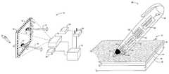
- a multi-touch display system 10such as that developed by Jeff Han, is centered about a specially configured display panel 12 , which acts as both a rear projection screen and a multi-touch touchscreen panel. An image projected from the rear of the display panel 12 is viewable from the front of the display panel 12 , and the front of the display panel 12 provides the tactile, or touching, surface for a user to touch when providing an input to the multi-touch display system 10 .
- the multi-touch display system 10relies on the optical phenomena of total internal reflection (TIR) and frustrated total internal reflection (FTIR) to detect when, where, and how the display panel 12 is being touched. These phenomena are described in greater detail after the overview of the various components of the multi-touch display system 10 .
- TIRtotal internal reflection
- FTIRfrustrated total internal reflection
- a state of TIRoccurs when light rays traveling inside the display panel 12 are maintained within the display panel 12 and effectively no portion of the light rays escape and travel outside of the display panel 12 .
- at least a portion of the display panel 12acts as waveguide for infrared (IR) light that is injected into the display panel 12 by an array of IR light-emitting diodes (LEDs) 14 .
- IRinfrared
- the IR LEDs 14are spaced along the perimeter edges of the display panel 12 and positioned to radiate IR light into the display panel 12 such that the IR light is normally maintained in the display panel 12 to facilitate a state of TIR when the display panel 12 is not being touched.
- a state of FTIRoccurs, when the state of TIR is disturbed, or frustrated. Such disturbance may be caused by the display panel 12 being touched.
- the points where the display panel 12 is touchedare referred to as touch points 16 .
- touch points 16When the front surface of the display panel 12 is touched at the touch points 16 , the state of TIR is disturbed. As a result, certain IR light that would otherwise be maintained within the display panel 12 is scattered and exits the rear of the display panel 12 as FTIRs 18 .
- Multiple FTIR sensors 20are positioned behind the display panel 12 and are configured to detect and monitor the relative location and intensity of the FTIRs 18 coming from the rear of the display panel 12 . Since the light escaping the display panel 12 is IR light, the FTIR sensors 20 are IR light detectors. Although IR light is discussed herein, other types of visible or non-visible light may be employed.
- the FTIR sensors 20determine metrics associated with the FTIRs 18 and provide corresponding FTIR information to a processor 22 , which may take the form of a personal computer, server, control system, or the like. The processor is able to process the FTIR information and determine how the display panel 12 is being touched. With this system, multiple touches can be detected and tracked at any given time.
- the touchesmay range from simple taps to complex touch and drag motions where a precise path of touch is monitored.
- the intensity of the touchesmay also be monitored because the intensity of the FTIRs 18 is generally proportional to the pressure associated with each touch. Accordingly, various aspects of multiple touches of the display panel 12 can be tracked by the processor 22 at any given time.
- the touches and nature of the touchesare processed as touch inputs to the multi-touch display system 10 .
- the touch inputsare used to control operation of the multi-touch display system 10 .
- the multi-touch display system 10also includes a projector 24 that is capable of projecting still or video content on the rear of the display panel 12 .
- the display panel 12is configured such that images projected on the rear of the display panel are viewable from the front of the display panel 12 in traditional rear-projection fashion.
- the projected contentis the display content for the multi-touch display system 10 .
- the display contentmay be generated in whole or in part by the processor 22 and provided to the projector 24 , which will project the display content on the rear of the display panel 12 .
- the processor 22may include or be associated with any number of media devices or players from which all or a portion of the display content may be accessed or derived.
- the processor 22will control the display content presented to, and thus projected by, the projector 24 in response to the touch inputs to provide an interactive system.
- the entire multi-touch display system 10may be provided in a single enclosure, wherein at least the display panel 12 is coupled to an articulating member that allows the display panel 12 to be rotated between horizontal and vertical orientations.
- the display panel 12is illustrated wherein a power supply 26 drives the IR LEDS 14 that reside around the perimeter edge of the display panel 12 .
- the display panel 12is shown to include a waveguide panel 28 and a surface layer structure 30 , which resides on the top surface of the waveguide panel 28 and may include one more layers.
- the waveguide panel 28is generally a clear acrylic or like polymer.
- the surface layer structure 30represents the front of the display panel 12 and provides the surface to be touched.
- the surface layer structure 30is preferably compliant and provides a translucent surface on which the display content is projected, since the waveguide 28 is formed from a clear material.
- the bottom surface of the waveguide panel 28represents the rear of the display panel 12 that faces the projector 24 .
- a boundaryis formed between the top surface of the waveguide panel 28 and the bottom surface the surface layer structure 30 .
- the acrylic of the waveguide panel 28has a different index of refraction than the bottom layer of the surface layer structure 30 .
- the IR light raysare partially refracted and partially reflected.
- the refracted IR light rayschange direction at the boundary and travel into and through the surface layer structure 30 .
- the reflected IR light raysare reflected back into the first material and continue traveling through the waveguide panel 28 .
- the scenariois the same for the boundary formed between the bottom surface of the waveguide panel 28 and air.
- a state of TIRis achieved when essentially all of the IR light rays traveling in the waveguide panel 28 are totally reflected back into the waveguide panel 28 after reaching a boundary, and thus, effectively none of the IR light rays are refracted into the surface layer structure 30 or air on either side of the waveguide panel 28 . As such, the IR light rays stay within the waveguide panel 28 . Those IR light rays that stay within the waveguide panel 28 are referred to as internal reflections 32 . Certain conditions are generally required for TIR. First, the refractive index of the waveguide panel 28 must be greater than that of the bottom layer of the surface layer structure 30 as well as the air on the other side of the waveguide panel 28 .
- the angle of incidence for the IR light raysmust be greater than the critical angle associated of the waveguide panel 28 .
- the angle of incidenceis a measure of the angle at which the light ray is traveling with respect to a line normal, or perpendicular, to the top or bottom surface of the waveguide panel 28 .
- the critical angleis generally dependent on the composition of the waveguide panel 28 and corresponds to the angle of incidence above which TIR occurs in the waveguide panel 28 .
- an exemplary FTIR stateoccurs when the state of TIR is disturbed, and IR light rays that are normally reflected back into the first material are scattered and travel outside of the waveguide panel 28 as FTIRs 18 .
- FTIRs 18may be caused by a person touching the surface layer structure 30 at a touch point 16 . Such touching causes the compliant surface layer structure 30 to compress, which results in a disturbance along the boundary, wherein IR light rays are reflected back into the waveguide panel 28 in such a manner as to have angles of incidence that are less than the critical angle associated with a state of TIR.
- these IR light raysexit the bottom surface of the waveguide panel 28 as FTIRs 18 and become detectable by the FTIR sensors 20 .
- the FTIRs 18exit the bottom surface of waveguide panel 28 at a point substantially opposite of the touch point 16 .
- the force of the touch at the touch point 16generally controls the intensity of the FTIRs 18 .
- the FTIR sensors 20may be able to determine the duration, location, and relative intensity of the touch as well as track any subsequent movement of the touch point 16 . Any number of touches can be tracked and used as inputs to the processor 22 . In certain embodiments, ten or more touches may be tracked at any given time.
- these multi-touch touchscreen technologiesprovide remarkable multi-touch interactivity.
- the technologyis essentially limited to human touch and is generally not capable of tracking contact and movement of smaller, non-human objects, such as a stylus from a pen-type instrument or the like.
- the effective touch sensitivity of the prior art display panels 12 and the IR sensors 20is relatively low, thereby limiting the resolution at which a user may operate to the size of their fingers.
- multi-touch applicationsare limited to relatively high level selection, movement, and outlining functions. Small scale handwriting, drawing, selection and the like that would require operating at higher resolutions are not feasible. Further, these technologies are not capable of differentiating between different users who are touching the display panel 12 .
- a stylusdefines the part of a non-human instrument, such as a pen device, that is used to interact with the display panel 12 .
- the multi-touch display system 10 described aboveis modified as illustrated in FIG. 4 .
- a wireless access point 36is provided in association with the processor 22 and is configured to support wireless communication with a digital pen 38 .
- the digital pen 38is capable of gathering writing information sufficient to determine when the digital pen 38 is being used to “write” on the display panel 12 , what is being written on the display panel 12 , and where it is being written on the display panel 12 . Further, the writing information identifies the location of the digital pen 38 during each pen stroke against the display panel 12 .
- the terms “write,” “writing,” and “written”are defined to relate to text (including numbers, letters, and symbols), drawing objects, symbols, doodling, and the like.
- the digital pen 38may process the writing information to generate pen data, and transmit the pen data wirelessly to the wireless access point 36 .
- the writing informationmay be sent from the digital pen 38 with little or no processing as pen data to the wireless access point 36 .
- the digital pen 38may or may not have an ink cartridge. Regardless of the presence of an ink cartridge, the digital pen 38 is configured to allow writing on the display panel 12 without applying ink to the display panel 12 . Any writing appearing on the display panel 12 is rendered as display content by the processor 22 .
- the pen datais passed to the processor 22 and processed as user input, which may be used along with other touch information provided from the FTIR sensors 20 to control the display content projected on the display panel 12 .
- the actual or processed writing informationis provided in real time to the processor 22 via the wireless access point 36 .
- the processor 22will immediately processes the pen data to determine what content is written and where the content is written on the display panel 12 .
- the processor 22may also process the display content to include the written content, as it was written, in the display content.
- the display contentis continuously updated in real time with a substantial replica of the written content as the content is being written on the display panel 12 . As such, handwriting appears as the actual handwriting and sketches appear as the actual sketches in real time.
- the pen strokes or the like interactionscan be used as any other touch input to select, drag, and the like. These control interactions may also be transferred in a processed or unprocessed form as pen data to the processor 22 .
- Each digital pen 38will preferably have a unique identity, which is transmitted with the pen data.
- the processor 22can identify the particular digital pen 38 from which any given written content was created and process it accordingly. Multiple digital pens 38 may be used to write on the display panel 12 at the same time.
- the processor 22may process the writing information from different ones of the digital pens 38 at the same time and in the same or different manners, depending on the supporting application. Accordingly, a large scale multi-touch display system 10 is provided that is capable of processing multiple human touches as well as multiple digital pen interactions at the same time. Further, the interactions from the different digital pens 38 may be distinguished from each other, such that inputs from different users can be differentiated.
- an exemplary digital pen 38is illustrated as being engaged with a surface of the display panel 12 .
- the display panel 12includes the waveguide panel 28 and surface layers 40 that reside on the waveguide panel 28 .
- the surface layers 40include a compliant layer 42 that has a refractive index that is lower than that of the waveguide panel 28 .
- the compliant layer 42is relatively clear and will allow a projected image that is passed through the waveguide panel 28 to be presented on a projection layer 44 , which resides over the compliant layer 42 .
- the projection layer 44effectively provides a screen on which the projected display content is displayed. Again, the projected display content is viewable from the front or top of the display panel 12 .
- a location pattern 46is printed on or in the surface layers 40 , and preferably on the projection layer 44 .
- the location pattern 46preferably provides a unique pattern across the entire viewable area of the display panel 12 .
- the digital pen 38is able to gather writing information based on the location pattern 46 , and either process the location pattern 46 to determine the precise location of the digital pen 38 , or deliver the location information as pen data to the processor 22 , which may process the location pattern 46 to determine the location of the digital pen 38 .
- the location informationis continuously updated and used to track the movement, and thus pen strokes, associated with using the digital pen 38 to write information on the display panel 12 .
- the location pattern 46is configured such that the patterns at any location throughout the entire surface area of the display panel 12 are unique and enable a precise location to be detected by analyzing a small portion of the location patterns 46 .
- the locations at which writing occurs for any number of digital pens 38may be tracked and processed at any given time.
- the location pattern 46is the same or analogous to an Anoto pattern.
- the Anoto patternwas developed in association with a digital pen that is capable of reading an Anoto pattern on paper that has the Anoto pattern printed on it by Anoto, Inc. Further information on Anoto patterns may be obtained at Anoto.com.
- the Anoto patterncomprises a large number of very small dots that have a nominal spacing of 0.3 mm.
- the dotshave a nominal spacing of 0.3 mm, the dots create a pattern that uniquely identifies any location on the surface of the display panel 12 .
- An exemplary section of an enlarged Anoto patternis provided in FIG. 6A , wherein the continuously variable offsets of the dots from the 0.3 mm grid is illustrated in FIG. 6B .
- the Anoto patternmay also be configured to uniquely identify the display panel 12 , such that different display panels 12 will have a unique signature.
- a digital pen 38may be able to interact with any number of multi-touch display systems 10 that are within wireless communication range of each other, wherein the digital pen 38 or processor 22 will be able to identify the particular display panel 12 that is being written upon.
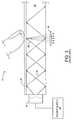
- the digital pen 38will generally include a body 48 to which a stylus 50 is attached.
- the stylus 50represents the writing tip, and thus the point of contact, for the digital pen 38 to the display panel 12 .
- a control system 52which is associated with a pressure sensor 54 , an IR light source (LS) 56 , such as an IR light-emitting diode (LED), an image sensor (IS) 58 , transceiver circuitry 60 , and memory 62 .
- LSIR light source
- LEDIR light-emitting diode
- ISimage sensor
- the transceiver circuitry 60is associated with the control system 52 as well as one or more antennas 66 to facilitate bi-directional wireless communications with the wireless access point 36 .
- These communicationsmay be based on any wireless communication standard, such as the IEEE's 802.11 wireless local area network standards, as well as personal area network standards, such as Bluetooth or wireless universal serial bus (USB).
- any wireless communication standardsuch as the IEEE's 802.11 wireless local area network standards, as well as personal area network standards, such as Bluetooth or wireless universal serial bus (USB).
- USBwireless universal serial bus
- the pressure sensor 54is coupled to the stylus 50 , and is configured to detect when the stylus 50 is pressed against the display panel 12 , and preferably to monitor the relative force associated with the contact. As such, the pressure sensor 54 can pass associated force information to the control system 52 for storage, processing, or a combination thereof.
- This force informationis considered writing information, and may be used to determine when the digital pen 38 is being used to write on the digital panel 12 , and perhaps the intensity associated with such writing. As such, the written content may ultimately be displayed in the display content in a manner indicative of the effective weight associated with writing the content on the display panel 12 .
- the pressure sensor 54allows the control system 52 to determine when writing is taking place.
- the location pattern 46 and the projection layer 44are configured such that the dots or other pattern indicia of the location pattern 46 absorb IR light emitted from the IR light source 56 , and reflect light that is not absorbed by the location pattern 46 back to the image sensor 58 .
- the image sensor 58 and the control system 52cooperate with one another to effectively provide an IR camera.
- the IR cameramay take many pictures per second of the location pattern 46 when the stylus 50 is in contact with the display panel 12 . Each picture captures the reflected IR light that is not absorbed by the location pattern 46 and is proximate to or about the point on the display panel 12 that is in contact with the stylus 50 .
- This picture informationmay be considered writing information, and is processed either by the control system 52 or passed to the processor 22 for processing. Regardless of the location of processing, each image is processed to identify the time that it was captured and the location of the stylus 50 when the image was captured. The location may be identified as coordinates or the like. As the sequence of images is processed, the location, direction, and distance of any movement associated with a given stroke of the digital pen 38 can be calculated. As the strokes are detected, the written content can be determined. Accordingly, the digital pen 38 may facilitate detection of the exact location and nature of every stroke of the digital pen 38 against the display panel 12 .
- FIG. 7a cross-section of a display panel 12 is illustrated, wherein a digital pen 38 is in contact with the projection layer 44 .
- the TIR effectis preferably not affected by the stylus 50 of the digital pen 38 being in contact with the surface layers 40 .
- the relatively small size of the point of the stylus 50 when compared to a human fingeris such that any surface disturbances by the stylus 50 are not sufficient to trigger an FTIR effect.
- the processor 22may subtract out the input of any FTIRs 18 that are caused by the digital pen 38 , since the location of the digital pen 38 is known.
- the perimeter edge (left side) of the waveguide panel 28is beveled, instead of being perpendicular to the face of the display panel 12 , as was illustrated in the prior art embodiments of FIGS. 2 and 3 .
- Applicantshave discovered that forming a perimeter edge with a bevel and coupling the IR LEDs 14 such that they are perpendicular to the beveled surface of the perimeter edge greatly enhances multi-touch performance. If the bevel is between about 30 and 60 degrees, and preferably about 45 degrees from the top or bottom surfaces of the waveguide panel 28 , the TIR and FTIR effects are enhanced and provide greater sensitivity to human touches.
- the TIR effectis still maintained when the digital pen 38 is in contact with the display panel 12 , yet significantly stronger FTIRs 18 are provided in response to human touches, and in comparison with the prior art embodiments illustrated in FIGS. 2 and 3 , as shown in FIG. 8 . Further, the use of beveled perimeter edges significantly increases the sensitivity to human touch as well as the ability to differentiate between different intensities of human touch.
- the increased performanceis primarily due to a significant increase of the evanescent field formed outside the surfaces of the waveguide panel 28 .
- the evanescent fieldis the light field that extends past the surfaces of the waveguide panel 28 during a state of TIR. When the evanescent field is disturbed, an FTIR effect may be triggered. The greater the evanescent field, the greater the sensitivity to evanescent field disturbances, and the greater intensity of resulting FTIRs 18 .
- FIGS. 9A and 9BA comparison of the relative evanescent field strengths associated with a perpendicular perimeter edge and a beveled perimeter edge is illustrated in FIGS. 9A and 9B .
- the evanescent field strengthis significantly higher at the surface of the waveguide panel 28 , and remains significantly higher at all distances outside of the waveguide panel 28 .
- the use of baffling 67that may be a part of a frame for the display panel 12 may be used to retain IR light that is trapped in the waveguide panel 28 until a usable part of the display panel 12 is reached.
- a further benefit of the higher evanescent field strengthis the increased immunity to the impacts of ambient lighting, and in particular, ambient lighting that has a high IR content. As will be described further below, other embodiments of the present invention provide even further ambient lighting immunity.
- the display panel 12includes a waveguide panel 28 , a compliant layer 42 above the waveguide panel 28 , a projection layer 44 above the compliant layer 42 , and a protection layer 68 above the projection layer 44 . Additional layers may be formed between or within these identified layers. Notably, the compliant layer 42 , projection layer 44 , and protection layer 68 are considered to be part of the surface layers 40 .
- the display panel 12it is beneficial to configure the display panel 12 such that the location pattern 46 can be printed on the display panel 12 in a manner facilitating operation of the digital pens 38 .
- the display panel 12should be suitable for rear projection, and the location pattern 46 should be printed on the display panel 12 in a manner that does not significantly interfere with viewing the projected image.
- the display panel 12should have an acceptable FTIR effect, and should preferably be able to work well in ambient lighting and provide a highly sensitive FTIR effect.
- the location pattern 46is printed on the projection layer 44 .
- the projection layer 44provides a translucent screen that the projected image is visible against, as well as a reflective background for the digital pen 38 .
- the IR light emitted from the IR light source 56should be reflected back toward the image sensor 58 of the digital pen 38 for areas that do not include dots or other pattern indicia associated with the location pattern 46 .
- the projection layer 44should be configured such that it does not stick to the compliant layer 42 .
- a white Rosco screen, or similar rear projection screen,meets the desired requirements for the projection layer 44 .
- Other materials for the projection layer 44may include HP Backlit UV or a backlit rigid PVC layer.
- the compliant layer 42is preferably formed of silicone or other appropriate compliant material. Preferred silicones include SORTA-ClearTM 40 and Elastocil® RT 601. Other materials for the compliant layer 42 may include Supatex or other suitable thin layers of latex.
- the waveguide panel 28is preferably acrylic or like polycarbonate plate, such as Lexan® 9030. Other materials for the waveguide panel 28 include Plexiglas.
- the protection layer 68may be formed from a clear, and preferably very thin, plastic foil, and is merely provided to reduce damage, abrasion, and wear to the projection layer 44 .
- the protection layer 68may be formed of transparent anti-scratch foils such as those used for windows, bus stops, or display cabinets. Notably, any number of layers can be provided above the projection layer 44 ; however, the addition of layers will ultimately bend the projected image as well as potentially hinder the ability of the digital pen 38 to read the location pattern 46 .
- the overall composition of the display panel 12is similar to that illustrated in FIG. 11 .
- the projection layer 44is formed from two separate layers, which include a screen layer 70 and a pattern layer 72 .
- the pattern layer 72is a clear plastic layer that has the location pattern 46 printed on it.
- the pattern layer 72will not reflect IR light as required for operation of the digital pen 38 .
- the screen layer 70will provide a reflective background for the IR light and allow the digital pen 38 to work as described above.
- the screen layer 70in addition to providing a matte IR light reflective background for the pattern layer 72 , will also provide a medium on which the projected image will be visible. Again, a white Rosco screen or the like meets all the requirements for the screen layer 70 .
- the protection layer 68 , compliant layer 42 , and waveguide panel 28may be configured as described above.
- FIG. 13the third embodiment of the display panel 12 is illustrated.
- This embodimentprovides the most immunity to ambient light that has a high IR content.
- the embodimentis shown as being the same as the embodiment of FIG. 12 , with the exception that a filter layer 74 is provided between the projection layer 44 and the compliant layer 42 . Further, the filter layer 74 is broken into two layers, which include an IR filtering layer 76 and an anti-stick layer 78 .
- the IR filtering layer 76is preferably a thin foil, which is capable of filtering ambient light, and in particular is capable of filtering the IR content of ambient light. Materials for the IR filtering layer 76 may include transparent sun protection foils and heat reflecting foils.
- the IR filtering layer 76will at least reduce the amount of IR content from ambient light that will reach the compliant layer 42 and the waveguide panel 28 .
- the anti-stick layer 78is provided to prevent the IR filtering layer 76 from sticking to the compliant layer 42 after a touch event.
- the foil of the IR filtering layer 76may stick to the silicone of the compliant layer 42 .
- Such stickingmay trigger a continuous and lingering FTIR effect after the touch event is removed.
- the anti-stick layer 78is transparent. Tracing paper has proven to be a suitable material for this layer.
- Other materials for the anti-stick layer 78may include a thin layer of Teflon spray or clear coat.
Landscapes
- Engineering & Computer Science (AREA)
- General Engineering & Computer Science (AREA)
- Theoretical Computer Science (AREA)
- Human Computer Interaction (AREA)
- Physics & Mathematics (AREA)
- General Physics & Mathematics (AREA)
- Position Input By Displaying (AREA)
Abstract
Description
Claims (28)
Priority Applications (7)
| Application Number | Priority Date | Filing Date | Title |
|---|---|---|---|
| US12/168,678US9268413B2 (en) | 2008-07-07 | 2008-07-07 | Multi-touch touchscreen incorporating pen tracking |
| KR1020117002789AKR20110038121A (en) | 2008-07-07 | 2009-06-11 | Multi-touch touchscreen with pen tracking |
| JP2011517256AJP5346081B2 (en) | 2008-07-07 | 2009-06-11 | Multi-touch touch screen with pen tracking |
| PCT/IB2009/005912WO2010004384A1 (en) | 2008-07-07 | 2009-06-11 | Multi-touch touchscreen incorporating pen tracking |
| BRPI0915656ABRPI0915656A2 (en) | 2008-07-07 | 2009-06-11 | Multitouch touch screen that incorporates pen tracking |
| EP09794047AEP2310933A4 (en) | 2008-07-07 | 2009-06-11 | Multi-touch touchscreen incorporating pen tracking |
| CN200980135801.6ACN102144208B (en) | 2008-07-07 | 2009-06-11 | Multi-touch touchscreen incorporating pen tracking |
Applications Claiming Priority (1)
| Application Number | Priority Date | Filing Date | Title |
|---|---|---|---|
| US12/168,678US9268413B2 (en) | 2008-07-07 | 2008-07-07 | Multi-touch touchscreen incorporating pen tracking |
Publications (2)
| Publication Number | Publication Date |
|---|---|
| US20100001962A1 US20100001962A1 (en) | 2010-01-07 |
| US9268413B2true US9268413B2 (en) | 2016-02-23 |
Family
ID=41463986
Family Applications (1)
| Application Number | Title | Priority Date | Filing Date |
|---|---|---|---|
| US12/168,678Expired - Fee RelatedUS9268413B2 (en) | 2008-07-07 | 2008-07-07 | Multi-touch touchscreen incorporating pen tracking |
Country Status (7)
| Country | Link |
|---|---|
| US (1) | US9268413B2 (en) |
| EP (1) | EP2310933A4 (en) |
| JP (1) | JP5346081B2 (en) |
| KR (1) | KR20110038121A (en) |
| CN (1) | CN102144208B (en) |
| BR (1) | BRPI0915656A2 (en) |
| WO (1) | WO2010004384A1 (en) |
Cited By (3)
| Publication number | Priority date | Publication date | Assignee | Title |
|---|---|---|---|---|
| US10459676B2 (en) | 2016-10-16 | 2019-10-29 | Dell Products, L.P. | Dynamic user interface for multiple shared displays in an electronic collaboration setting |
| US10514769B2 (en) | 2016-10-16 | 2019-12-24 | Dell Products, L.P. | Volumetric tracking for orthogonal displays in an electronic collaboration setting |
| US10664215B2 (en) | 2016-10-16 | 2020-05-26 | Dell Products, L.P. | Controlling multiple shared displays in an electronic collaboration setting |
Families Citing this family (53)
| Publication number | Priority date | Publication date | Assignee | Title |
|---|---|---|---|---|
| US8441467B2 (en)* | 2006-08-03 | 2013-05-14 | Perceptive Pixel Inc. | Multi-touch sensing display through frustrated total internal reflection |
| KR101407300B1 (en)* | 2007-11-19 | 2014-06-13 | 엘지디스플레이 주식회사 | Multi touch flat display module |
| US20090219253A1 (en)* | 2008-02-29 | 2009-09-03 | Microsoft Corporation | Interactive Surface Computer with Switchable Diffuser |
| FR2933511A1 (en)* | 2008-07-04 | 2010-01-08 | Optinnova | INTERACTIVE VISUALIZATION DEVICE AND METHOD USING DETECTION CAMERA AND OPTICAL POINTER |
| KR20110049379A (en)* | 2009-11-05 | 2011-05-12 | 삼성전자주식회사 | Multi-touch and close object sensing device using wedge waveguide |
| EP2343629A3 (en) | 2010-01-08 | 2015-01-21 | Integrated Digital Technologies, Inc. | Stylus and touch input system |
| US9128537B2 (en)* | 2010-03-04 | 2015-09-08 | Autodesk, Inc. | Bimanual interactions on digital paper using a pen and a spatially-aware mobile projector |
| US20110291995A1 (en)* | 2010-05-25 | 2011-12-01 | Industrial Technology Research Institute | Sterilizing device and manufacturing method for sterilizing device |
| CN102270069B (en)* | 2010-06-03 | 2015-01-28 | 乐金显示有限公司 | Touch panel integrated display device |
| KR101901241B1 (en) | 2010-06-03 | 2018-09-27 | 엘지디스플레이 주식회사 | Touch Panel Integrated Display Device |
| US10620754B2 (en)* | 2010-11-22 | 2020-04-14 | 3M Innovative Properties Company | Touch-sensitive device with electrodes having location pattern included therein |
| US20120125882A1 (en)* | 2010-11-22 | 2012-05-24 | 3M Innovtive Properties Company | Method of making touch-sensitive device with electrodes having location pattern included therein |
| JP4816808B1 (en)* | 2010-12-14 | 2011-11-16 | 大日本印刷株式会社 | Computer apparatus, input system, and program |
| JP5655572B2 (en)* | 2011-01-07 | 2015-01-21 | 大日本印刷株式会社 | Electronic pen, computer device, input system, and program |
| JP5655573B2 (en)* | 2011-01-07 | 2015-01-21 | 大日本印刷株式会社 | Computer apparatus, input system, and program |
| JP5678697B2 (en)* | 2011-02-01 | 2015-03-04 | 大日本印刷株式会社 | Computer apparatus, input system, and program |
| JP5664300B2 (en)* | 2011-02-07 | 2015-02-04 | 大日本印刷株式会社 | Computer apparatus, input system, and program |
| JP5664301B2 (en)* | 2011-02-08 | 2015-02-04 | 大日本印刷株式会社 | Computer device, electronic pen input system, and program |
| JP5664303B2 (en)* | 2011-02-09 | 2015-02-04 | 大日本印刷株式会社 | Computer apparatus, input system, and program |
| KR101158234B1 (en) | 2011-03-04 | 2012-06-19 | 호서대학교 산학협력단 | Touch screen apparatus and touch screen control method thereof |
| US8947429B2 (en) | 2011-04-12 | 2015-02-03 | Autodesk, Inc. | Gestures and tools for creating and editing solid models |
| US9182882B2 (en) | 2011-04-12 | 2015-11-10 | Autodesk, Inc. | Dynamic creation and modeling of solid models |
| US8902222B2 (en) | 2012-01-16 | 2014-12-02 | Autodesk, Inc. | Three dimensional contriver tool for modeling with multi-touch devices |
| DE102011101782A1 (en)* | 2011-05-17 | 2012-11-22 | Trw Automotive Electronics & Components Gmbh | Optical display and control element and method for optical position determination |
| US8860675B2 (en) | 2011-07-12 | 2014-10-14 | Autodesk, Inc. | Drawing aid system for multi-touch devices |
| US20140225827A1 (en)* | 2011-09-22 | 2014-08-14 | Hewlett-Packard Development Company, L.P. | Soft button input systems and methods |
| CN204044759U (en) | 2011-12-16 | 2014-12-24 | 3M创新有限公司 | There is the optical digitizers system of the unique photoluminescence mark in position |
| CN103383610A (en)* | 2012-05-02 | 2013-11-06 | 北京通世舟数字科技有限责任公司 | Liquid crystal display multi-touch method |
| CN103576992B (en)* | 2012-08-06 | 2017-09-15 | 原相科技股份有限公司 | Film and light guide plate and position detection system with positional information |
| ITTO20120804A1 (en)* | 2012-09-17 | 2014-03-18 | Csp Innovazione Nelle Ict Societa Consortile A | APPARATUS FOR THE ASSESSMENT OF THE MOTOR SKILLS OF A SUBJECT AND ITS PROCEDURE |
| US9891759B2 (en)* | 2012-09-28 | 2018-02-13 | Apple Inc. | Frustrated total internal reflection and capacitive sensing |
| US20140112499A1 (en)* | 2012-10-23 | 2014-04-24 | Yellow Matter Entertainment, LLC | Audio production console and related process |
| US8692212B1 (en)* | 2012-10-29 | 2014-04-08 | 3M Innovative Properties Company | Optical digitizer system with position-unique photoluminescent indicia |
| US10753746B2 (en) | 2012-11-29 | 2020-08-25 | 3M Innovative Properties, Inc. | Multi-mode stylus and digitizer system |
| US9250792B2 (en) | 2012-11-29 | 2016-02-02 | International Business Machines Corporation | Method, apparatus and computer program to designate content retrieval on an interactive display |
| US9958954B2 (en) | 2012-12-13 | 2018-05-01 | 3M Innovative Properties Company | System and methods for calibrating a digitizer system |
| GB2522249A (en)* | 2014-01-20 | 2015-07-22 | Promethean Ltd | Active pointing device detection |
| LU92378B1 (en)* | 2014-02-17 | 2015-08-18 | Iee Internat Electronics & Enigineering Sa | Occupant sensor and seat with such an occupant sensor |
| US9921688B2 (en) | 2014-03-04 | 2018-03-20 | Qualcomm Incorporated | Large area interactive display screen |
| US10088917B2 (en)* | 2014-07-30 | 2018-10-02 | Hewlett-Packard Development Company, L.P. | Detector for a display |
| KR102277902B1 (en)* | 2014-09-05 | 2021-07-15 | 삼성전자주식회사 | Object contact pressure meter and methods of manufacturing and measuring the same |
| KR102487643B1 (en)* | 2014-10-17 | 2023-01-11 | 주식회사 네오랩컨버전스 | Electronic pen, electronic device associated with electronic pen, method for controlling electronic device and computer-readable medium on which program for performing the method for controlling electronic device is recorded |
| KR102337258B1 (en)* | 2014-10-17 | 2021-12-08 | 주식회사 네오랩컨버전스 | Electronic pen, electronic device associated with electronic pen and method for controlling electronic device |
| US10996795B2 (en) | 2014-12-15 | 2021-05-04 | Beechrock Limited | Anti-glare and anti-reflective tactile effect surface for optical touch detection |
| US9921685B2 (en) | 2014-12-15 | 2018-03-20 | Rapt Ip Limited | Tactile effect waveguide surface for optical touch detection |
| US10754442B2 (en)* | 2015-07-09 | 2020-08-25 | YewSavin, Inc. | Films or surfaces including positional tracking marks |
| US10254857B2 (en) | 2016-03-06 | 2019-04-09 | Microsoft Technology Licensing, Llc | Soft touch detection of a stylus |
| US10514803B2 (en) | 2016-03-06 | 2019-12-24 | Microsoft Technology Licensing, Llc | Pen in field force sensing calibration |
| CN106018994A (en)* | 2016-05-10 | 2016-10-12 | 苏州赛腾精密电子股份有限公司 | Touch control detection mechanism |
| JP6824992B2 (en)* | 2016-09-01 | 2021-02-03 | 株式会社ワコム | Stylus, sensor controller, and electronic ruler |
| US10146337B2 (en) | 2016-09-15 | 2018-12-04 | Samsung Electronics Co., Ltd. | Digital handwriting device and method of using the same |
| WO2019147227A1 (en) | 2018-01-24 | 2019-08-01 | Hewlett-Packard Development Company, L.P. | Surfaces with embedded information |
| KR102439724B1 (en)* | 2018-08-21 | 2022-09-05 | 비크락 리미티드 | Barrier Layer and Tactile Surface Features for Optical Touch Detection Device |
Citations (21)
| Publication number | Priority date | Publication date | Assignee | Title |
|---|---|---|---|---|
| US4091382A (en) | 1976-09-27 | 1978-05-23 | Willis J. Ball | Display system |
| US4346376A (en) | 1980-04-16 | 1982-08-24 | Bell Telephone Laboratories, Incorporated | Touch position sensitive surface |
| US4484179A (en)* | 1980-04-16 | 1984-11-20 | At&T Bell Laboratories | Touch position sensitive surface |
| JP2003508831A (en) | 1999-08-30 | 2003-03-04 | アノト・アクティエボラーク | System and apparatus for electronic recording of handwritten information |
| JP2005056357A (en) | 2003-08-07 | 2005-03-03 | Dainippon Printing Co Ltd | Electronic pen form |
| US6882385B2 (en) | 2001-03-05 | 2005-04-19 | Nitto Denko Corporation | Polarizing plate having protective films with plasticizer, liquid crystal display using the same, and methods of making the same |
| CN1647100A (en) | 2002-03-13 | 2005-07-27 | O-笔公司 | A touch pad, a stylus for use with the touch pad, and a method of operating the touch pad |
| JP2005235174A (en) | 2004-02-19 | 2005-09-02 | Au Optronics Corp | Touch panel unit and method for detecting position on display panel |
| US20060227120A1 (en)* | 2005-03-28 | 2006-10-12 | Adam Eikman | Photonic touch screen apparatus and method of use |
| CN1925513A (en) | 2005-08-30 | 2007-03-07 | Lg电子株式会社 | Touch key assembly for a mobile terminal |
| WO2007127258A2 (en) | 2006-04-27 | 2007-11-08 | Wms Gaming Inc. | Wagering game with multi-point gesture sensing device |
| US20070290047A1 (en)* | 2006-05-30 | 2007-12-20 | Keiko Tazaki | Pattern printed sheet |
| WO2008017077A2 (en) | 2006-08-03 | 2008-02-07 | Perceptive Pixel, Inc. | Multi-touch sensing display through frustrated total internal reflection |
| US20080029691A1 (en) | 2006-08-03 | 2008-02-07 | Han Jefferson Y | Multi-touch sensing display through frustrated total internal reflection |
| WO2008066004A1 (en) | 2006-11-30 | 2008-06-05 | Sega Corporation | Position inputting apparatus |
| JP2008152640A (en) | 2006-12-19 | 2008-07-03 | Sony Corp | Coordinate input device and coordinate input system |
| US20080233360A1 (en)* | 2006-12-27 | 2008-09-25 | Keiko Sekine | Transparent sheet having a pattern for infrared reflection |
| US20080284925A1 (en) | 2006-08-03 | 2008-11-20 | Han Jefferson Y | Multi-touch sensing through frustrated total internal reflection |
| US20090033637A1 (en) | 2007-07-30 | 2009-02-05 | Han Jefferson Y | Liquid multi-touch sensor and display device |
| JP2009043228A (en) | 2008-03-24 | 2009-02-26 | Kenji Yoshida | Calibration method and information input auxiliary sheet |
| US20090219253A1 (en) | 2008-02-29 | 2009-09-03 | Microsoft Corporation | Interactive Surface Computer with Switchable Diffuser |
- 2008
- 2008-07-07USUS12/168,678patent/US9268413B2/ennot_activeExpired - Fee Related
- 2009
- 2009-06-11BRBRPI0915656Apatent/BRPI0915656A2/ennot_activeIP Right Cessation
- 2009-06-11KRKR1020117002789Apatent/KR20110038121A/ennot_activeWithdrawn
- 2009-06-11EPEP09794047Apatent/EP2310933A4/ennot_activeWithdrawn
- 2009-06-11CNCN200980135801.6Apatent/CN102144208B/ennot_activeExpired - Fee Related
- 2009-06-11WOPCT/IB2009/005912patent/WO2010004384A1/enactiveApplication Filing
- 2009-06-11JPJP2011517256Apatent/JP5346081B2/ennot_activeExpired - Fee Related
Patent Citations (25)
| Publication number | Priority date | Publication date | Assignee | Title |
|---|---|---|---|---|
| US4091382A (en) | 1976-09-27 | 1978-05-23 | Willis J. Ball | Display system |
| US4346376A (en) | 1980-04-16 | 1982-08-24 | Bell Telephone Laboratories, Incorporated | Touch position sensitive surface |
| US4484179A (en)* | 1980-04-16 | 1984-11-20 | At&T Bell Laboratories | Touch position sensitive surface |
| US4346376B1 (en) | 1980-04-16 | 1988-12-13 | ||
| US4484179B1 (en)* | 1980-04-16 | 1989-03-28 | ||
| JP2003508831A (en) | 1999-08-30 | 2003-03-04 | アノト・アクティエボラーク | System and apparatus for electronic recording of handwritten information |
| US6882385B2 (en) | 2001-03-05 | 2005-04-19 | Nitto Denko Corporation | Polarizing plate having protective films with plasticizer, liquid crystal display using the same, and methods of making the same |
| CN1647100A (en) | 2002-03-13 | 2005-07-27 | O-笔公司 | A touch pad, a stylus for use with the touch pad, and a method of operating the touch pad |
| JP2005056357A (en) | 2003-08-07 | 2005-03-03 | Dainippon Printing Co Ltd | Electronic pen form |
| JP2005235174A (en) | 2004-02-19 | 2005-09-02 | Au Optronics Corp | Touch panel unit and method for detecting position on display panel |
| US20060227120A1 (en)* | 2005-03-28 | 2006-10-12 | Adam Eikman | Photonic touch screen apparatus and method of use |
| CN1925513A (en) | 2005-08-30 | 2007-03-07 | Lg电子株式会社 | Touch key assembly for a mobile terminal |
| WO2007127258A2 (en) | 2006-04-27 | 2007-11-08 | Wms Gaming Inc. | Wagering game with multi-point gesture sensing device |
| US20070290047A1 (en)* | 2006-05-30 | 2007-12-20 | Keiko Tazaki | Pattern printed sheet |
| WO2008017077A2 (en) | 2006-08-03 | 2008-02-07 | Perceptive Pixel, Inc. | Multi-touch sensing display through frustrated total internal reflection |
| US20080029691A1 (en) | 2006-08-03 | 2008-02-07 | Han Jefferson Y | Multi-touch sensing display through frustrated total internal reflection |
| US20080179507A2 (en) | 2006-08-03 | 2008-07-31 | Han Jefferson | Multi-touch sensing through frustrated total internal reflection |
| US20080284925A1 (en) | 2006-08-03 | 2008-11-20 | Han Jefferson Y | Multi-touch sensing through frustrated total internal reflection |
| JP2009545828A (en) | 2006-08-03 | 2009-12-24 | パーセプティブ ピクセル,インク. | Multi-contact detection display device with total reflection interference |
| WO2008066004A1 (en) | 2006-11-30 | 2008-06-05 | Sega Corporation | Position inputting apparatus |
| JP2008152640A (en) | 2006-12-19 | 2008-07-03 | Sony Corp | Coordinate input device and coordinate input system |
| US20080233360A1 (en)* | 2006-12-27 | 2008-09-25 | Keiko Sekine | Transparent sheet having a pattern for infrared reflection |
| US20090033637A1 (en) | 2007-07-30 | 2009-02-05 | Han Jefferson Y | Liquid multi-touch sensor and display device |
| US20090219253A1 (en) | 2008-02-29 | 2009-09-03 | Microsoft Corporation | Interactive Surface Computer with Switchable Diffuser |
| JP2009043228A (en) | 2008-03-24 | 2009-02-26 | Kenji Yoshida | Calibration method and information input auxiliary sheet |
Non-Patent Citations (37)
| Title |
|---|
| Brandl, Peter et al., "An Adaptable Rear-Projection Screen Using Digital Pens and Hand Gestures," 17th International Conference on Artificial Reality and Telexistence 2007, 2007, pp. 49-54, IEEE Computer Society. |
| Brandl, Peter et al., "An Adaptive Rear Projection Screen Using Digital Pens and Hand Gestures," IEEE ICAT 2007, Nov. 2007, pp. 49-54, IEEE. |
| Brandl, Peter et al., "Combining and Measuring the Benefits of Bimanual Pen and Direct-Touch Interaction on Horizontal Interfaces," Proceedings of the working conference on Advanced visual interfaces, 2008, pp. 1-8. |
| Decision on Rejection for Chinese Patent Application No. 200980135803.5, issued Apr. 30, 2014, 13 pages. |
| Decision to Grant a Patent for Japanese Patent Application No. 2011-517255, mailed Oct. 8, 2013, 5 pages. |
| Decision to Grant a Patent for Japanese Patent Application No. 2011-517256, mailed Jul. 23, 2013, 5 pages. |
| Dietz, Paul et al., "DiamondTouch: A Multi-User Touch Technology," ACM Symposium on User Interface Software and Technology, Nov. 2001, pp. 219-226. |
| Elrod et al., "Liveboard: A Large Interactive Display Supporting Group Meetings, Presentations and Remote Collaboration," CHI '92, 1992, pp. 599-607, New York, NY, ACM Press. |
| English translation of First Office Action for Chinese patent application 200980135801.6 issued Jan. 30, 2013, 21 pages. |
| English translation of First Office Action for Chinese patent application 200980135803.5 issued Feb. 5, 2013, 20 pages. |
| English translation of Non-final Office Action for Japanese patent application 2011-517255 mailed Mar. 5, 2013, 4 pages. |
| European Search Report for European Patent Application No. 09794046.2 mailed Dec. 21, 2012, 9 pages. |
| European Search Report for European Patent Application No. 09794046.4 mailed Jan. 4, 2013, 8 pages. |
| Final Office Action for U.S. Appl. No. 12/168,688, mailed Nov. 27, 2013, 15 pages. |
| Final Rejection mailed Oct. 11, 2011, for U.S. Appl. No. 12/168,688, 13 pages. |
| Haller, Michael et al., "Large Interactive Surfaces Based on Digital Pens," Nov. 20, 2007, Media Interaction Lab, Upper Austria University of Applied Sciences, Softwarepark 11, Austria. |
| Haller, Michael et al., "The Shared Design Space," ACM SIGGRAPH 2006 Emerging Technologies, 2006, p. 29, New York, NY, ACM Press. |
| Haller, Michael, "Interactive Displays and Next-Generation Interfaces," Emerging Technologies for Learning, Mar. 2008, vol. 3, Becta. |
| Haller, Michael, "Natural User Interfaces," Apr. 2008, Media Interaction Lab, Upper Austria University of Applied Sciences, Hagenberg-Austria. |
| Han, Jefferson Y., "Low-Cost Multi-Touch Sensing through Frustrated Total Internal Reflection," UIST '05, 2005, pp. 115-118, New York, NY, ACM. |
| Hodges, Steve et al., "ThinSight: Versatile Multi-touch Sensing for Thin Form-factor Displays," Proceedings of the 20th Annual ACM Symposium on User Interface Software and Technology, Oct. 7-10, 2007, pp. 259-268, New York, NY, ACM. |
| International Search Report for PCT/IB2009/005741 mailed Sep. 29, 2009. |
| International Search Report for PCT/IB2009/005912, mailed Oct. 13, 2009. |
| Izadi, Shahram et al., "ThinSight: Integrated Optical Multi-touch Sensing through Thin Form-factor Displays," Proceedings of the 2007 Workshop on Emerging Displays Technologies: Images and Beyond: the Future of Displays and Interaction, Aug. 4, 2007, vol. 252, New York, NY, ACM. |
| Matsushita, Nobuyuki et al., "HoloWall: Designing a Finger, Hand, Body and Object Sensitive Wall," Proceedings of the 10th Annual ACM Symposium on User Interface Software and Technology, Oct. 14-17, 1997, pp. 209-210, New York, NY, ACM. |
| Microsoft Surface, from http://www.surface.com, 2008, Microsoft Corporation. |
| Morrison, Gerald D., "A Camera-Based Touch Interface infrastructures, for Pervasive Displays," Workshop on pervasive display infrastructures, interfaces and applications, May 7, 2006. |
| Non-final Office Action for U.S. Appl. No. 12/168,688 mailed Jul. 23, 2012, 17 pages. |
| Non-final Office Action for U.S. Appl. No. 12/168,688 mailed Mar. 28, 2013, 13 pages. |
| Notice of Allowance for U.S. Appl. No. 12/168,688, mailed Apr. 16, 2014, 8 pages. |
| Office Action mailed Mar. 30, 2011 in U.S. Appl. No. 12/168,688. |
| Ryall, Kathy et al., "Experiences with and Observations of Direct-Touch Tabletops," Proceedings of the First IEEE Workshop on Horizontal Interactive Human-Computer Systems, 2006, pp. 89-96, Adelaide, South Australia, IEEE. |
| Second Office Action for Chinese Patent Application No. 200980135801.6, mailed Nov. 29, 2013, 18 pages. |
| Second Office Action for Chinese Patent Application No. 200980135803.5, mailed Oct. 14, 2013, 14 pages. |
| Third Office Action for Chinese Patent Application No. 200980135801.6, issued Jun. 4, 2014, 11 pages. |
| Wilson, Andrew D., "PlayAnywhere: A Compact Interactive Tabletop Projection-Vision System," Symposium on User Interface Software and Technology (UIST), 2005. |
| Wilson, Andrew D., "TouchLight: An Imaging Touch Screen and Display for Gesture-Based Interaction," Proceedings of the 6th International Conference on Multimodal Interfaces, Oct. 13-15, 2004, pp. 69-76, New York, NY, ACM. |
Cited By (3)
| Publication number | Priority date | Publication date | Assignee | Title |
|---|---|---|---|---|
| US10459676B2 (en) | 2016-10-16 | 2019-10-29 | Dell Products, L.P. | Dynamic user interface for multiple shared displays in an electronic collaboration setting |
| US10514769B2 (en) | 2016-10-16 | 2019-12-24 | Dell Products, L.P. | Volumetric tracking for orthogonal displays in an electronic collaboration setting |
| US10664215B2 (en) | 2016-10-16 | 2020-05-26 | Dell Products, L.P. | Controlling multiple shared displays in an electronic collaboration setting |
Also Published As
| Publication number | Publication date |
|---|---|
| KR20110038121A (en) | 2011-04-13 |
| BRPI0915656A2 (en) | 2019-09-24 |
| JP2012529680A (en) | 2012-11-22 |
| US20100001962A1 (en) | 2010-01-07 |
| EP2310933A4 (en) | 2013-01-23 |
| EP2310933A1 (en) | 2011-04-20 |
| WO2010004384A1 (en) | 2010-01-14 |
| WO2010004384A8 (en) | 2010-04-08 |
| JP5346081B2 (en) | 2013-11-20 |
| CN102144208A (en) | 2011-08-03 |
| CN102144208B (en) | 2015-03-25 |
Similar Documents
| Publication | Publication Date | Title |
|---|---|---|
| US9268413B2 (en) | Multi-touch touchscreen incorporating pen tracking | |
| US8842076B2 (en) | Multi-touch touchscreen incorporating pen tracking | |
| US9262016B2 (en) | Gesture recognition method and interactive input system employing same | |
| KR102335132B1 (en) | Multi-modal gesture based interactive system and method using one single sensing system | |
| US9092129B2 (en) | System and method for capturing hand annotations | |
| US9996197B2 (en) | Camera-based multi-touch interaction and illumination system and method | |
| US20110298708A1 (en) | Virtual Touch Interface | |
| US20110063224A1 (en) | System and method for remote, virtual on screen input | |
| US20230057020A1 (en) | Meeting interaction system | |
| Izadi et al. | ThinSight: integrated optical multi-touch sensing through thin form-factor displays | |
| CN103365485A (en) | Optical Touch Sensing Device | |
| CA2885950A1 (en) | Interactive input system and method for grouping graphical objects | |
| Maierhöfer et al. | TipTrack: precise, low-latency, robust optical pen tracking on arbitrary surfaces using an IR-emitting pen tip | |
| Maierhöfer et al. | Demonstration of an Infrared Pen as an Input Device for Projected Augmented Reality Tabletops | |
| Kudale et al. | Human computer interaction model based virtual whiteboard: A review | |
| CN114138162A (en) | Intelligent transparent office table interaction method | |
| KR100908879B1 (en) | LED-based object control system for table top display |
Legal Events
| Date | Code | Title | Description |
|---|---|---|---|
| AS | Assignment | Owner name:NORTEL NETWORKS LIMITED, CANADA Free format text:ASSIGNMENT OF ASSIGNORS INTEREST;ASSIGNORS:DORAY, BERNARD;TO, PAUL;HALLER, MICHAEL;AND OTHERS;SIGNING DATES FROM 20080919 TO 20081114;REEL/FRAME:021862/0542 Owner name:NORTEL NETWORKS LIMITED, CANADA Free format text:ASSIGNMENT OF ASSIGNORS INTEREST;ASSIGNORS:DORAY, BERNARD;TO, PAUL;HALLER, MICHAEL;AND OTHERS;REEL/FRAME:021862/0542;SIGNING DATES FROM 20080919 TO 20081114 | |
| AS | Assignment | Owner name:ROCKSTAR BIDCO, LP, NEW YORK Free format text:ASSIGNMENT OF ASSIGNORS INTEREST;ASSIGNOR:NORTEL NETWORKS LIMITED;REEL/FRAME:027143/0717 Effective date:20110729 | |
| AS | Assignment | Owner name:ROCKSTAR CONSORTIUM US LP, TEXAS Free format text:ASSIGNMENT OF ASSIGNORS INTEREST;ASSIGNOR:ROCKSTAR BIDCO, LP;REEL/FRAME:032436/0804 Effective date:20120509 | |
| AS | Assignment | Owner name:RPX CLEARINGHOUSE LLC, CALIFORNIA Free format text:ASSIGNMENT OF ASSIGNORS INTEREST;ASSIGNORS:ROCKSTAR CONSORTIUM US LP;ROCKSTAR CONSORTIUM LLC;BOCKSTAR TECHNOLOGIES LLC;AND OTHERS;REEL/FRAME:034924/0779 Effective date:20150128 | |
| STCF | Information on status: patent grant | Free format text:PATENTED CASE | |
| AS | Assignment | Owner name:JPMORGAN CHASE BANK, N.A., AS COLLATERAL AGENT, IL Free format text:SECURITY AGREEMENT;ASSIGNORS:RPX CORPORATION;RPX CLEARINGHOUSE LLC;REEL/FRAME:038041/0001 Effective date:20160226 | |
| AS | Assignment | Owner name:RPX CLEARINGHOUSE LLC, CALIFORNIA Free format text:RELEASE (REEL 038041 / FRAME 0001);ASSIGNOR:JPMORGAN CHASE BANK, N.A.;REEL/FRAME:044970/0030 Effective date:20171222 Owner name:RPX CORPORATION, CALIFORNIA Free format text:RELEASE (REEL 038041 / FRAME 0001);ASSIGNOR:JPMORGAN CHASE BANK, N.A.;REEL/FRAME:044970/0030 Effective date:20171222 | |
| AS | Assignment | Owner name:JEFFERIES FINANCE LLC, NEW YORK Free format text:SECURITY INTEREST;ASSIGNOR:RPX CLEARINGHOUSE LLC;REEL/FRAME:046485/0644 Effective date:20180619 | |
| FEPP | Fee payment procedure | Free format text:MAINTENANCE FEE REMINDER MAILED (ORIGINAL EVENT CODE: REM.); ENTITY STATUS OF PATENT OWNER: LARGE ENTITY | |
| LAPS | Lapse for failure to pay maintenance fees | Free format text:PATENT EXPIRED FOR FAILURE TO PAY MAINTENANCE FEES (ORIGINAL EVENT CODE: EXP.); ENTITY STATUS OF PATENT OWNER: LARGE ENTITY | |
| STCH | Information on status: patent discontinuation | Free format text:PATENT EXPIRED DUE TO NONPAYMENT OF MAINTENANCE FEES UNDER 37 CFR 1.362 | |
| FP | Lapsed due to failure to pay maintenance fee | Effective date:20200223 | |
| AS | Assignment | Owner name:RPX CLEARINGHOUSE LLC, CALIFORNIA Free format text:RELEASE BY SECURED PARTY;ASSIGNOR:JEFFERIES FINANCE LLC;REEL/FRAME:054305/0505 Effective date:20201023 | |
| AS | Assignment | Owner name:CONTINENTAL DISC CORPORATION, LLC (F/K/A CONTINENTAL DISC CORPORATION), MISSOURI Free format text:RELEASE BY SECURED PARTY;ASSIGNOR:CITIZENS BANK, N.A.;REEL/FRAME:060668/0268 Effective date:20220729 Owner name:DEXTER MAGNETIC TECHNOLOGIES, INC., ILLINOIS Free format text:RELEASE BY SECURED PARTY;ASSIGNOR:CITIZENS BANK, N.A.;REEL/FRAME:060668/0268 Effective date:20220729 Owner name:GROTH CORPORATION, LLC (F/K/A GROTH CORPORATION), MISSOURI Free format text:RELEASE BY SECURED PARTY;ASSIGNOR:CITIZENS BANK, N.A.;REEL/FRAME:060668/0268 Effective date:20220729 |