US9263156B2 - System and method for adjusting trip points within a storage device - Google Patents
System and method for adjusting trip points within a storage deviceDownload PDFInfo
- Publication number
- US9263156B2 US9263156B2US14/135,433US201314135433AUS9263156B2US 9263156 B2US9263156 B2US 9263156B2US 201314135433 AUS201314135433 AUS 201314135433AUS 9263156 B2US9263156 B2US 9263156B2
- Authority
- US
- United States
- Prior art keywords
- voltage
- trip
- storage device
- spd
- power fail
- Prior art date
- Legal status (The legal status is an assumption and is not a legal conclusion. Google has not performed a legal analysis and makes no representation as to the accuracy of the status listed.)
- Active, expires
Links
Images


Classifications
- G—PHYSICS
- G11—INFORMATION STORAGE
- G11C—STATIC STORES
- G11C29/00—Checking stores for correct operation ; Subsequent repair; Testing stores during standby or offline operation
- G11C29/04—Detection or location of defective memory elements, e.g. cell constructio details, timing of test signals
- G11C29/50—Marginal testing, e.g. race, voltage or current testing
- G11C29/50004—Marginal testing, e.g. race, voltage or current testing of threshold voltage
- G—PHYSICS
- G06—COMPUTING OR CALCULATING; COUNTING
- G06F—ELECTRIC DIGITAL DATA PROCESSING
- G06F1/00—Details not covered by groups G06F3/00 - G06F13/00 and G06F21/00
- G06F1/26—Power supply means, e.g. regulation thereof
- G06F1/28—Supervision thereof, e.g. detecting power-supply failure by out of limits supervision
- G—PHYSICS
- G11—INFORMATION STORAGE
- G11C—STATIC STORES
- G11C5/00—Details of stores covered by group G11C11/00
- G11C5/14—Power supply arrangements, e.g. power down, chip selection or deselection, layout of wirings or power grids, or multiple supply levels
- G11C5/143—Detection of memory cassette insertion or removal; Continuity checks of supply or ground lines; Detection of supply variations, interruptions or levels ; Switching between alternative supplies
- G—PHYSICS
- G11—INFORMATION STORAGE
- G11C—STATIC STORES
- G11C29/00—Checking stores for correct operation ; Subsequent repair; Testing stores during standby or offline operation
- G11C29/04—Detection or location of defective memory elements, e.g. cell constructio details, timing of test signals
- G11C29/50—Marginal testing, e.g. race, voltage or current testing
- G11C2029/5004—Voltage
Definitions
- the disclosed embodimentsrelate generally to memory systems, and in particular, to adjusting trip points in a storage device.
- Flash memorytypically utilize memory cells to store data as an electrical value, such as an electrical charge or voltage.
- a flash memory cellfor example, includes a single transistor with a floating gate that is used to store a charge representative of a data value.
- Flash memoryis a non-volatile data storage device that can be electrically erased and reprogrammed. More generally, non-volatile memory (e.g., flash memory, as well as other types of non-volatile memory implemented using any of a variety of technologies) retains stored information even when not powered, as opposed to volatile memory, which requires power to maintain the stored information.
- FIG. 1is a block diagram illustrating an implementation of a data storage system in accordance with some embodiments.
- FIG. 2Ais a block diagram illustrating an implementation of a supervisory controller in accordance with some embodiments.
- FIG. 2Bis a block diagram illustrating an implementation of a storage controller in accordance with some embodiments.
- FIG. 2Cis a block diagram illustrating an implementation of a non-volatile memory (NVM) controller in accordance with some embodiments.
- NVMnon-volatile memory
- FIG. 3is a block diagram illustrating a portion of a data storage device in accordance with some embodiments.
- FIG. 4Ais a block diagram illustrating an implementation of a portion of voltage monitoring circuitry in accordance with some embodiments.
- FIG. 4Bis a block diagram illustrating an implementation of a portion of voltage monitoring circuitry in accordance with some embodiments.
- FIG. 5is a block diagram illustrating an implementation of a data hardening module in accordance with some embodiments.
- FIGS. 6A-6Cillustrate a flowchart representation of a method of adjusting trip points in a data storage device in accordance with some embodiments.
- the various implementations described hereininclude systems, methods and/or devices for adjusting trip points that trigger a power fail process based on one or more configuration parameters of a storage device.
- a storage deviceconfigured to be compatible with an interface standard (e.g., DDR3) that allows a host system to provide one of a plurality of supply voltages to the storage device
- the storage deviceis configured to adjust trip points that trigger a power fail process in accordance with the supply voltage(s) provided by the host system.
- some embodimentsinclude a method of adjusting trip points in a storage device.
- the methodis performed within a storage device operatively coupled with a host system.
- the methodincludes: obtaining one or more configuration parameters; and based on the one or more configuration parameters, determining a trip voltage.
- the methodalso includes comparing the trip voltage with an input voltage.
- the methodfurther includes triggering a power fail condition in accordance with a determination that the input voltage is less than the trip voltage (or, in some circumstances, greater than the trip voltage).
- Some embodimentsinclude a storage device comprising: a host interface configured to couple the storage device with a host system; a supervisory controller with one or more processors and memory; a power fail module for detecting a power fail condition; and a plurality of controller for managing one or more non-volatile memory devices.
- the storage deviceis configured to perform the operations of any of the methods described herein.
- Some embodimentsinclude a storage device comprising: a host interface configured to couple the storage device with a host system; and means for performing the operations of any of the methods described herein.
- Some embodimentsinclude a non-transitory computer readable storage medium, storing one or more programs for execution by one or more processors of a storage device, the one or more programs including instructions for performing the operations any of the methods described herein.
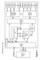
- FIG. 1is a block diagram illustrating an implementation of data storage system 100 in accordance with some embodiments. While some example features are illustrated, various other features have not been illustrated for the sake of brevity and so as not to obscure more pertinent aspects of the example implementations disclosed herein.
- data storage system 100includes storage device 120 , which includes host interface 122 , supervisory controller 124 , power fail module 126 , power control 127 , storage controller 128 (sometimes called a memory controller), one or more non-volatile memory (NVM) controllers 130 (e.g., NVM controller 130 - 1 through NVM controller 130 - m ), and non-volatile memory (NVM) (e.g., one or more NVM device(s) 140 , 142 such as one or more flash memory devices), and is used in conjunction with computer system 110 .
- storage controller 128sometimes called a memory controller
- NVM controller 130e.g., NVM controller 130 - 1 through NVM controller 130 - m
- NVMnon-volatile memory
- NVMnon-volatile memory
- Computer system 110is coupled with storage device 120 through data connections 101 .
- computer system 110includes storage device 120 as a component and/or sub-system.
- Computer system 110may be any suitable computing device, such as a personal computer, a workstation, a computer server, or any other computing device.
- Computer system 110is sometimes called a host or host system.
- computer system 110includes one or more processors, one or more types of memory, optionally includes a display and/or other user interface components such as a keyboard, a touch screen display, a mouse, a track-pad, a digital camera and/or any number of supplemental devices to add functionality.
- computer system 110sends one or more host commands (e.g., read commands and/or write commands) on control line 111 to storage device 120 .
- host commandse.g., read commands and/or write commands
- computer system 110is a server system, such as a server system in a data center, and does not have a display and other user interface components.
- storage device 120includes a single NVM device while in other implementations storage device 120 includes a plurality of NVM devices.
- NVM devices 140 , 142include NAND-type flash memory or NOR-type flash memory.
- NVM controller 130is a solid-state drive (SSD) controller.
- SSDsolid-state drive
- storage device 120is or includes a dual in-line memory module (DIMM) device.
- DIMMdual in-line memory module
- storage device 120is compatible with a DIMM memory slot.
- storage device 120is compatible with a 240-pin DIMM memory slot and is compatible with signaling in accordance with a DDR3 interface specification.
- storage device 120includes NVM devices 140 , 142 (e.g., NVM devices 140 - 1 through 140 - n and NVM devices 142 - 1 through 142 - k ) and NVM controllers 130 (e.g., NVM controllers 130 - 1 through 130 - m ).
- NVM controllers 130include one or more processing units (sometimes called CPUs or processors) configured to execute instructions in one or more programs (e.g., in NVM controllers 130 ).
- the one or more processorsare shared by one or more components within, and in some cases, beyond the function of NVM controllers 130 .
- NVM devices 140 , 142are coupled with NVM controllers 130 through connections that typically convey commands in addition to data, and, optionally, convey metadata, error correction information and/or other information in addition to data values to be stored in NVM devices 140 , 142 and data values read from NVM devices 140 , 142 .
- NVM devices 140 , 142can be configured for enterprise storage suitable for applications such as cloud computing, or for caching data stored (or to be stored) in secondary storage, such as hard disk drives.
- flash memorye.g., NVM devices 140 , 142
- flash memorycan also be configured for relatively smaller-scale applications such as personal flash drives or hard-disk replacements for personal, laptop and tablet computers.
- storage device 120includes other non-volatile memory device(s) and corresponding non-volatile storage controller(s).
- storage device 120also includes host interface 122 , supervisory controller 124 , power fail module 126 , power control 127 , and storage controller 128 .
- Storage device 120may include various additional features that have not been illustrated for the sake of brevity and so as not to obscure more pertinent features of the example implementations disclosed herein, and a different arrangement of features may be possible.
- Host interface 122provides an interface to computer system 110 through data connections 101 .
- Supervisory controller 124is coupled with host interface 122 , power fail module 126 , power control 127 , storage controller 128 , and NVM controllers 130 (connection not shown) in order to coordinate the operation of these components, including supervising and controlling functions such as power up, power down, data hardening, charging energy storage device(s), data logging, and other aspects of managing functions on storage device 120 .
- Supervisory controller 124is coupled with host interface 122 via serial presence detect (SPD) bus 154 and receives supply voltage line V SPD 156 from the host interface 122 .
- V SPD 156is a standardized voltage (e.g., typically 3.3 V).
- Serial presence detectrefers to a standardized way to automatically access information about a computer memory module (e.g., storage device 120 ).
- the failurecan be communicated with a host system (e.g., computer system 110 ) via SPD bus 154 .
- Power fail module 126is coupled with host interface 122 , supervisory controller 124 , and power control 127 .
- Power fail module 126is configured to monitor one or more input voltages (e.g., V dd 152 and, optionally, V SPD 156 ) provided to storage device 120 by a host system (e.g., computer system 110 ).
- a power fail conditione.g., an under or over voltage event
- power fail module 126is configured to provide a PFAIL signal to supervisory controller 124 and, in some circumstances, discharge an energy storage device to provide power to storage controller 128 and NVM controllers 130 .
- FIGS. 3-5For a more detailed description of power fail module 126 , see the description of FIGS. 3-5 .
- supervisory controller 124In response to receiving the PFAIL signal indicating a power fail condition from power fail module 126 , supervisory controller 124 performs one or more operations of a power fail process including, but not limited to, signaling the power fail condition to a plurality of controllers on storage device 120 (e.g., storage controller 128 and NVM controllers 130 ) via control lines 162 .
- Power control 127is coupled with supervisory controller 124 , power fail module 126 , storage controller 128 , and NVM controllers 130 (connection not shown) in order to provide power to these components.
- power control 127includes one or more voltage regulators controlled by supervisory controller 124 via control line 162 .
- power control 127is configured to remove power from a specified NVM controller 130 in response to a command from supervisory controller 124 via control line 162 .
- Storage controller 128is coupled with host interface 122 , supervisory controller 124 , power control 127 , and NVM controllers 130 . In some embodiments, during a write operation, storage controller 128 receives data via data bus 158 from computer system 110 through host interface 122 and during a read operation, storage controller 128 sends data to computer system 110 through host interface 122 via data bus 158 . Further, host interface 122 provides additional data, signals, voltages, and/or other information needed for communication between storage controller 128 and computer system 110 . In some embodiments, storage controller 128 and host interface 122 use a defined interface standard for communication, such as double data rate type three synchronous dynamic random access memory (DDR3).
- DDR3synchronous dynamic random access memory
- storage controller 128 and NVM controllers 130use a defined interface standard for communication, such as serial advance technology attachment (SATA).
- SATAserial advance technology attachment
- the device interface used by storage controller 128 to communicate with NVM controllers 130is SAS (serial attached SCSI), or other storage interface.
- storage controller 128maps DDR interface commands from the host system (e.g., computer system 1120 ) to SATA or SAS interface commands for the plurality of controllers (e.g., storage controller 128 and NVM controllers 130 ).
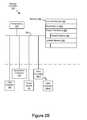
- FIG. 2Ais a block diagram illustrating an implementation of supervisory controller 124 in accordance with some embodiments.
- Supervisory controller 124includes one or more processors 202 (sometimes called CPUs or processing units) for executing modules, programs and/or instructions stored in memory 206 and thereby performing processing operations, serial presence detect (SPD) module 205 (e.g., non-volatile memory) storing information related to storage device 120 (e.g., a serial number, memory type, supported communication protocol, etc.), memory 206 , optionally a digital-to-analog converter (DAC) 204 for converting digital values to an analog signal (e.g., a portion of an integrated or partially integrated DAC/ADC), and one or more communication buses 208 for interconnecting these components.
- SPDserial presence detect
- DACdigital-to-analog converter
- Communication buses 208optionally, include circuitry (sometimes called a chipset) that interconnects and controls communications between system components.
- Supervisory controller 124is coupled with host interface 122 , power fail module 126 , power control 127 , storage controller 128 , and NVM controllers 130 (e.g., NVM controllers 130 - 1 through 130 - m ) by communication buses 208 .
- Memory 206includes high-speed random access memory, such as DRAM, SRAM, DDR RAM or other random access solid state memory devices, and may include non-volatile memory, such as one or more magnetic disk storage devices, optical disk storage devices, flash memory devices, or other non-volatile solid state storage devices.
- Memory 206optionally, includes one or more storage devices remotely located from processor(s) 202 .
- Memory 206or alternately the non-volatile memory device(s) within memory 206 , comprises a non-transitory computer readable storage medium.
- memory 206or the computer readable storage medium of memory 206 , stores the following programs, modules, and data structures, or a subset or superset thereof:
- Each of the above identified elementsmay be stored in one or more of the previously mentioned memory devices, and corresponds to a set of instructions for performing a function described above.
- the above identified modules or programsi.e., sets of instructions
- memory 206may store a subset of the modules and data structures identified above.
- memory 206may store additional modules and data structures not described above.
- the programs, modules, and data structures stored in memory 206 , or the computer readable storage medium of memory 206provide instructions for implementing any of the methods described below with reference to FIGS. 6A-6C .
- FIG. 2Ashows supervisory controller 124
- FIG. 2Ais intended more as a functional description of the various features which may be present in supervisory controller 124 than as a structural schematic of the embodiments described herein.
- items shown separatelycould be combined and some items could be separated.
- FIG. 2Bis a block diagram illustrating an implementation of a storage controller 128 in accordance with some embodiments.
- Storage controller 128typically, includes one or more processors 252 (sometimes called CPUs or processing units) for executing modules, programs and/or instructions stored in memory 256 and thereby performing processing operations, memory 256 , and one or more communication buses 258 for interconnecting these components.
- Communication buses 258optionally, include circuitry (sometimes called a chipset) that interconnects and controls communications between system components.
- Storage controller 128is coupled with host interface 122 , supervisory controller 124 , power control 127 , and NVM controllers 130 (e.g., NVM controllers 130 - 1 through 130 - m ) by communication buses 258 .
- NVM controllers 130e.g., NVM controllers 130 - 1 through 130 - m
- Memory 256includes high-speed random access memory, such as DRAM, SRAM, DDR RAM or other random access solid state memory devices, and may include non-volatile memory, such as one or more magnetic disk storage devices, optical disk storage devices, flash memory devices, or other non-volatile solid state storage devices. Memory 256 , optionally, includes one or more storage devices remotely located from processor(s) 252 . Memory 256 , or alternately the non-volatile memory device(s) within memory 256 , comprises a non-transitory computer readable storage medium. In some embodiments, memory 256 , or the computer readable storage medium of memory 256 , stores the following programs, modules, and data structures, or a subset or superset thereof:
- the power fail module 264optionally, includes a transfer module 266 for transferring data held in volatile memory 268 to non-volatile memory.
- Each of the above identified elementsmay be stored in one or more of the previously mentioned memory devices, and corresponds to a set of instructions for performing a function described above.
- the above identified modules or programsi.e., sets of instructions
- memory 256may store a subset of the modules and data structures identified above.
- memory 256may store additional modules and data structures not described above.
- FIG. 2Bshows storage controller 128
- FIG. 2Bis intended more as a functional description of the various features which may be present in storage controller 128 than as a structural schematic of the embodiments described herein.
- items shown separatelycould be combined and some items could be separated.
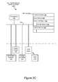
- FIG. 2Cis a block diagram illustrating an implementation of representative NVM controller 130 - 1 in accordance with some embodiments.
- NVM controller 130 - 1typically includes one or more processors 272 (sometimes called CPUs or processing units) for executing modules, programs and/or instructions stored in memory 276 and thereby performing processing operations, memory 276 , and one or more communication buses 278 for interconnecting these components.
- Communication buses 278optionally include circuitry (sometimes called a chipset) that interconnects and controls communications between system components.
- NVM controller 130 - 1is coupled with supervisory controller 124 , power control 127 , storage controller 128 , and NVM devices 140 (e.g., NVM devices 140 - 1 through 140 - n ) by communication buses 278 .
- Memory 276includes high-speed random access memory, such as DRAM, SRAM, DDR RAM or other random access solid state memory devices, and may include non-volatile memory, such as one or more magnetic disk storage devices, optical disk storage devices, flash memory devices, or other non-volatile solid state storage devices. Memory 276 , optionally, includes one or more storage devices remotely located from processor(s) 272 . Memory 276 , or alternately the non-volatile memory device(s) within memory 276 , comprises a non-transitory computer readable storage medium. In some embodiments, memory 276 , or the computer readable storage medium of memory 276 , stores the following programs, modules, and data structures, or a subset or superset thereof:
- power fail module 284optionally, includes a transfer module 286 for transferring data held in volatile memory 288 to non-volatile memory.
- Each of the above identified elementsmay be stored in one or more of the previously mentioned memory devices, and corresponds to a set of instructions for performing a function described above.
- the above identified modules or programsi.e., sets of instructions
- memory 276may store a subset of the modules and data structures identified above.
- memory 276may store additional modules and data structures not described above.
- FIG. 2Cshows NVM controller 130 - 1
- FIG. 2Cis intended more as a functional description of the various features which may be present in NVM controller 130 - 1 than as a structural schematic of the embodiments described herein. In practice, and as recognized by those of ordinary skill in the art, items shown separately could be combined and some items could be separated. Further, although FIG. 2C shows representative NVM controller 130 - 1 , the description of FIG. 2C similarly applies to other NVM controllers (e.g., NVM controllers 130 - 2 through 130 - m ) in storage device 120 , as shown in FIG. 1 .
- NVM controllers 130 - 2 through 130 - min storage device 120 , as shown in FIG. 1 .
- FIG. 3is a block diagram illustrating an implementation of a portion of storage device 120 in accordance with some embodiments. While some example features are illustrated, various other features have not been illustrated for the sake of brevity and so as not to obscure more pertinent aspects of the example implementations disclosed herein. To that end, as a non-limiting example, supervisory controller 124 includes one or more processors 202 and DAC 204 , and power fail module 126 includes voltage monitoring circuitry 302 and data hardening module 308 . In some embodiments, DAC 204 is a component of one or more processors 202 . In some embodiments, V dd 152 is a voltage supplied by the host system (e.g., computer system 110 , FIG.
- the host systeme.g., computer system 110 , FIG.
- V SPD 156is a voltage supplied by the host system for a serial presence detect (SPD) functionality and has a target value of 3.3 V.
- SPDserial presence detect
- voltage monitoring circuitry 302is configured to detect a power fail condition (e.g., an under or over voltage event) as to an input voltage (e.g., V dd 152 or V SPD 156 ) supplied by a host system (e.g., computer system 110 , FIG. 1 ) and signal the power fail condition to supervisory controller 124 .
- voltage monitoring circuitry 302includes V dd monitoring circuitry 304 configured to detect an under or over voltage event as to V dd 152 and V SPD monitoring circuitry 306 configured to detect an under or over voltage event as to V SPD 156 .
- V dd monitoring circuitry 304see the description of FIG. 4A .
- V SPD monitoring circuitry 306see the description of FIG. 4B .
- data hardening module 308is configured to interconnect an energy storage device to provide power to storage controller 128 and NVM controllers 130 .
- data hardening module 308see the description of FIG. 5 .
- data hardening module 308see U.S. Provisional Patent Application No. 61/887,910 entitled “Power Sequencing and Data Hardening Circuitry Architecture,” which is herein incorporated by reference.
- FIG. 4Ais a block diagram illustrating an implementation of a portion of voltage monitoring circuitry 302 (V dd monitoring circuitry 304 ) in accordance with some embodiments. While some example features are illustrated, various other features have not been illustrated for the sake of brevity and so as not to obscure more pertinent aspects of the example implementations disclosed herein. To that end, as a non-limiting example, V dd monitoring circuitry 304 includes reference signal conditioning module 402 , input signal conditioning module 404 , comparator 406 , and transistor 408 .
- the reference signalis DAC output 312 from supervisory controller 124 .
- supervisory controller 124 or a component thereofe.g., obtaining module 210 , FIG. 2A
- supervisory controller 124 or a component thereofe.g., determination module 216 , FIG.
- DAC 204converts the digital value for the trip voltage to an analog value, and supervisory controller 124 provides DAC output 312 to V dd monitoring circuitry 304 .
- reference signal conditioning module 402is configured to condition DAC output 312 (sometimes called a “reference signal,” “trip voltage,” or “trip point”) prior to a comparison operation with this reference signal.
- the conditioningincludes one or more of buffering, filtering, scaling, and level shifting DAC output 312 to produce a reference comparison signal 418 .
- conditioning module 402is implemented using well-known circuitry components (e.g., unity gain amplifier, low-pass RC filter, voltage divider, etc.), the exact configuration of which depends on the particular conditioning applied to DAC output 312 . For example, the conditioning adjusts the trip voltage so that the full range of DAC values map to the practical range of trip voltages.
- V ref 414is a voltage-supply independent reference voltage supplied by comparator 406 and used by reference signal conditioning module 402 to level shift DAC output 312 .
- DAC output 312starts as a low value (e.g., 1 V) and is raised to the proper trip voltage (e.g., 1.125 V, 1.215 V, or 1.35 V) by reference signal conditioning module 402 .
- input signal conditioning module 404is configured to condition V dd 152 (sometimes called an “input signal,” “input voltage,” or “supply voltage”) supplied by the host system prior to a comparison operation with this input signal.
- the conditioningincludes one or more of buffering, filtering, and scaling V dd 152 to produce a comparison input signal 416 corresponding to V dd 152 .
- input signal conditioning module 404is implemented using well-known circuitry components (e.g., unity gain amplifier, low-pass RC filter, voltage divider, etc.), the exact configuration of which depends on the particular conditioning applied to the V dd 152 .
- comparator 406is configured to perform a comparison operation between the conditioned reference signal (e.g., the output of reference signal conditioning module 402 ) and the conditioned input signal (e.g., the output of input signal conditioning module 404 ). If the conditioned input signal is less than (or, alternatively, greater than) the conditioned reference signal, comparator 406 is configured to output PFAIL signal 314 to supervisory controller 124 (e.g., logic high). For example, in FIG. 4A , PFAIL signal 314 indicates the occurrence of a power fail condition (e.g., an under or over voltage event) as to V dd 152 .
- PFAIL signal 314indicates the occurrence of a power fail condition (e.g., an under or over voltage event) as to V dd 152 .
- comparator 406is configured to provide hysteresis 410 of the result of the comparison operation for subsequent comparisons (e.g., 3 to 10 mV of feedback). In some embodiments, comparator 406 is also configured to provide V ref 414 to one or more other components of storage device 120 (e.g., supervisory controller 124 and V SPD monitoring circuitry 306 ).
- latching mechanism 412is configured to latch, unlatch, or force (e.g., simulate) the power fail condition.
- comparator 406indicates the occurrence of a power fail condition as to V dd 152
- PFAIL signal 314e.g., logic high
- transistor 408closed state
- the input signale.g., a level adjusted and scaled comparison input signal 416 corresponding to V dd 152
- supervisory controller 124 or a component thereofis configured to unlatch the power fail condition by providing a PFAIL control signal 316 (e.g., logic low) that disables transistor 408 (open state), which unlatches the power fail condition—by allowing the comparison input signal 416 to reach the comparator 406 without being shorted to ground.
- supervisory controller 124 or a component thereofe.g., latching module 228 , FIG.
- PFAIL control signal 316e.g., logic high
- PFAIL control signal 316is tristated (e.g., put into a high impedance state) by supervisory controller 124 when supervisory controller 124 is neither unlatching the power fail condition nor forcing a power fail condition, which disables transistor 408 unless PFAIL 314 is asserted (e.g., logic high).
- FIG. 4Bis a block diagram illustrating an implementation of a portion of voltage monitoring circuitry 302 (V SPD monitoring circuitry 306 ) in accordance with some embodiments. While some example features are illustrated, various other features have not been illustrated for the sake of brevity and so as not to obscure more pertinent aspects of the example implementations disclosed herein. To that end, as a non-limiting example, V SPD monitoring circuitry 306 includes reference signal conditioning module 422 , input signal conditioning module 424 , and comparator 426 . In some embodiments, the reference signal is V ref 414 from comparator 406 of V dd monitoring circuitry 304 , as shown in FIG. 4A .
- V ref 414is a voltage-supply independent reference voltage (e.g., a predetermined voltage such as 1.23 V).
- the input signalis V SPD 156 supplied by the host system (e.g., with a target voltage of 3.3V).
- reference signal conditioning module 422is configured to condition V ref 414 (sometimes called a “reference signal,” “trip voltage,” or “trip point”) prior to a comparison operation with this reference signal.
- the conditioningincludes one or more of buffering and filtering V ref 414 with a plurality of well-known circuitry components (e.g., unity gain amplifier, low-pass RC filter, etc.) to produce a conditioned V ref comparison signal 430 .
- input signal conditioning module 424is configured to condition V SPD 156 (sometimes called an “input signal,” “input voltage,” or “supply voltage”) supplied by the host system prior to a comparison operation with this input signal.
- the conditioningincludes one or more of buffering, filtering, and scaling V SPD 156 with a plurality of well-known circuitry components (e.g., unity gain amplifier, low-pass RC filter, voltage divider, etc.) to produce a conditioned V SPD comparison signal 432 .
- a conditioned V SPD comparison signal 432For example, if V ref 414 is 1.23 V and the target voltage for V SPD 156 is 3.3 V, input signal conditioning module 424 includes a low-pass RC filter to filter out any ripples or glitches in V SPD 156 and, also, a voltage divider to scale down V SPD 156 (e.g., by approximately 73% or a factor of 2.7).
- comparator 426is configured to perform a comparison operation between the conditioned reference signal 430 (e.g., the output of reference signal conditioning module 422 ) and the conditioned input signal 432 (e.g., the output of input signal conditioning module 424 ). If the conditioned input signal 432 is less than (or, alternatively, greater than) the conditioned reference signal 430 , comparator 426 is configured to output PFAIL signal 314 to supervisory controller 124 (e.g., logic high). For example, in FIG. 4B , PFAIL signal 314 indicates the occurrence of a power fail condition (e.g., an under or over voltage event) as to V SPD 156 . Additionally, comparator 426 is configured to provide hysteresis 428 of the result of the comparison operation for subsequent comparisons.
- PFAIL signal 314indicates the occurrence of a power fail condition (e.g., an under or over voltage event) as to V SPD 156 .
- FIG. 5is a block diagram illustrating an implementation of data hardening module 308 in accordance with some embodiments. While some example features are illustrated, various other features have not been illustrated for the sake of brevity and so as not to obscure more pertinent aspects of the example implementations disclosed herein. To that end, as a non-limiting example, data hardening module 308 includes transistors 502 and 504 , boost circuitry 506 , energy storage device 510 , keeper circuitry 512 , and logic block 514 .
- V holdup 508is a boosted voltage, higher than V dd 152 , and has a target value of 5.7 V. In some embodiments, V holdup 508 is used to charge an energy storage device 510 (e.g., one or more hold-up capacitors). Further, in some embodiments, only one of transistors 502 , 504 is enabled at any one time. In some embodiments, data hardening circuit 308 's energy storage device 510 stores, immediately prior to a power fail condition being detected, at least approximately 30 to 70 mJ of energy per NVM controller 130 in storage device 120 .
- supervisory controller 124 or a component thereofmonitors and manages the functionality of data hardening module 308 .
- supervisory controller 124 or a component thereofe.g., processor 202
- supervisory controller 124 or a component thereofis configured to perform one or more operations of a power fail process including controlling transistors 502 and 504 so that V switched 160 is the voltage from energy storage device 510 , and energy storage device 510 is used (sometimes said to be “discharged”) to provide power to storage device 120 .
- V dd 152is used to supply power to storage device 120 .
- energy storage device 510is used to provide power to storage device 120 .
- supervisory controller 124 or a component thereofe.g., processor 202 ) controls transistors 502 and 504 via control lines 318 to control V switched 160 to be voltage from V dd 152 (e.g., during regular operation) or voltage from energy storage device 510 (e.g., during the power fail process).
- transistor 502is turned on (e.g., to complete the connection between V dd 152 and V switched 160 ) and transistor 504 is turned off (e.g., to disable the connection between energy storage device 510 and V switched 160 ) so that V dd 152 is used to supply power to storage device 120 .
- transistor 502is turned off (e.g., to disable the connection between V dd 152 and V switched 160 ) and transistor 504 is turned on (e.g., to enable the connection between energy storage device 510 and V switched 160 ) so that energy storage device 510 is used to provide power to storage device 120 .
- any energy storage deviceincluding one or more capacitors, one or more inductors, or one or more other passive elements that store energy, may be used to store energy to be used during the power fail process.
- energy storage device 510is charged using V holdup 508 , a voltage higher than V dd 152 .
- V dd 152is boosted up to V holdup 508 using boost circuitry 506 (e.g., 1.35 V or 1.5 V is boosted up to 5.7 V).
- boost circuitry 506is controlled and enabled by supervisory controller 124 (e.g., via processor 202 ).
- V switched 160is used as an input to keeper circuitry 512 , which along with V SPD 156 provides power to processor 202 .
- V switched 160is provided via keeper circuitry 512 to processor 202 so as to provide power to processor 202 .
- V SPD 156provides power to keeper circuitry 512 .
- logic block 514e.g., OR or XOR determines which of keeper circuitry 512 or V SPD 156 provides power to supervisory controller 124 (e.g., processor 202 ).
- V SPD 156is provided to storage device 120 before V dd 152 is provided to storage device 120 .
- supervisory controller 124 or a component thereofe.g., processor 202
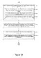
- FIGS. 6A-6Cillustrate a flowchart representation of a method 600 of adjusting trip points (e.g., a trip voltage that triggers a power fail process) in a data storage device in accordance with some embodiments.
- method 600is performed by a storage device (e.g., storage device 120 , FIG. 1 ) or one or more components of the storage device (e.g., supervisory controller 124 , power fail module 126 , storage controller 128 , and/or NVM controllers 130 , FIG. 1 ), where the storage device is operatively coupled with a host system (e.g., computer system 110 , FIG. 1 ).
- a host systeme.g., computer system 110 , FIG. 1
- method 600is governed by instructions that are stored in a non-transitory computer readable storage medium and that are executed by one or more processors of a device, such as the one or more processors 202 of supervisory controller 124 , the one or more processors 252 of storage controller 128 , and/or the one or more processors 272 of NVM controllers 130 , as shown in FIGS. 2A-2C .
- a storage deviceobtains ( 602 ) one or more configuration parameters.
- supervisory controller 124 or a component thereofe.g., obtaining module 210 , FIG. 2A ) is configured to obtain one or more configuration parameters associated with storage device 120 .
- the one or more configuration parametersinclude ( 604 ) an indication of a default input voltage and configuration information of the storage device.
- the one or more configuration parametersinclude an indication of the default input voltage (e.g., V dd ) supplied by the host system (e.g., computer system 110 , FIG. 1 ) to storage device 120 or voltage class of storage device 120 (e.g., 1.25 V, 1.35 V, or 1.5 V) and information associated with the current configuration of storage device 120 .
- supervisory controller 124 or a component thereofis configured to receive an indication of the default input (or supply) voltage (e.g., V dd ) from the host system (e.g., computer system 110 , FIG. 1 ).
- receiving module 212receives an indication of the default input voltage via SPD Bus 154 from the host system.
- the storage devicesamples ( 608 ) the input voltage to determine the default input voltage.
- supervisory controller 124 or a component thereofe.g., sampling module 214 , FIG. 2A
- sampling module 214samples V dd upon power-on and/or restart of storage device 120 to determine the default input voltage.
- sampling module 214determines the default input voltage by averaging a plurality of sample measurements of V dd .
- the storage devicemodifies ( 610 ) one or more timing parameters associated with a communication bus that operatively couples the storage device and the host system based on the one or more configuration parameters.
- supervisory controller 124 or a component thereofe.g., modification module 222 , FIG. 2A
- modification module 222modifies skew and timing parameters associated with the communication bus (e.g., DDR3) that operatively couples storage device 120 and the host system (e.g., computer system 110 , FIG. 1 ) based on the default input voltage (e.g., V dd ) provided to storage device 120 or voltage class of storage device 120 (e.g., 1.25 V, 1.35 V, or 1.5 V).
- the storage devicedetermines ( 612 ) a trip voltage based on the one or more configuration parameters.
- supervisory controller 124 or a component thereofe.g., determination module 216 , FIG. 2A
- determination module 216determines the trip voltage based on the default input voltage (e.g., V dd ) provided to storage device 120 or voltage class of storage device 120 (e.g., 1.25 V, 1.35 V, or 1.5 V).
- the trip voltagevaries depending on the target value of the voltage. For example, if the target value of the input voltage is 1.5 V, the trip voltage may be 1.5 V minus 5 percent (i.e., 1.425 V) or minus 10 percent (i.e., 1.35 V).
- determining the trip voltageincludes selecting ( 614 ) one of a plurality of stored predefined trip voltages based on the one or more configuration parameters.
- supervisory controller or a component thereofe.g., selection module 218 , FIG. 2A
- trip voltage table 220includes a predefined trip voltage for each of a plurality potential default input voltages supplied by a host system or voltage classes of storage device 120 (e.g., 1.25 V, 1.35 V, or 1.5 V). For example, if the one or more configuration parameters indicate that the default input voltage (e.g., V dd ) is 1.5 V, selection module 218 selects a trip voltage from trip voltage table 220 that corresponds to a default input voltage of 1.5 V.
- the storage deviceconditions ( 616 ) the trip voltage by buffering the trip voltage and, after the buffering, level shifting and scaling the trip voltage.
- an analog reference signale.g., DAC output 312 , FIGS. 3 and 4A
- DAC output 312corresponding to the determined trip voltage is generated by supervisory controller 124 or a component thereof (e.g., DAC 204 , FIGS. 2A and 3 ) and input to power fail module 126 or a component thereof (e.g., V dd monitoring circuitry 304 , FIG. 4A ).
- the reference signale.g., DAC output 312 , FIGS.
- reference signal conditioning module 402is configured to condition the reference signal.
- the conditioningincludes one or more of buffering, filtering, scaling, and level shifting to adjust the trip voltage so that the full range of DAC values map to the practical range of voltage trip points. For example (circuit details not shown in Figures), first, a unity gain operation amplifier buffers the reference signal (e.g., DAC output 312 ) to stabilize the impedance; second, a filter filters noise out of the reference signal; third, the reference signal is scaled; and fourth, the reference signal is level shifted by utilizing a voltage-supply independent voltage source (e.g., V ref 414 ).
- V ref 414a voltage-supply independent voltage source
- the storage deviceconditions ( 618 ) the input voltage (e.g., V dd 152 or V SPD 156 ) by scaling the input voltage and filtering the input voltage.
- the input voltagee.g., V dd 152 or V SPD 156
- the reference signale.g., DAC output 312 or V ref 414
- the input signale.g., V dd 152 or V SPD 156
- power fail module 126 or a component thereofconditions the input signal by scaling and filtering the input signal.
- V dd 152e.g., the input signal
- input signal conditioning module 404is conditioned by input signal conditioning module 404 .
- V dd 152is scaled by voltage divider circuitry and noise is filtered out of V dd 152 with a low-pass (e.g., RC) filter (circuit details not shown in Figures).
- V SPD 156e.g., the input signal
- input signal conditioning module 424e.g., V SPD 156 is scaled down to the value of V ref 414 and noise is filtered out of V SPD 156 with a low-pass (e.g., RC) filter.
- the storage devicecompares ( 620 ) the trip voltage to an input voltage.
- comparator 306performs a comparison operation between the conditioned reference signal (e.g., the output of reference signal conditioning module 402 ) and the conditioned input signal (e.g., the output of input signal conditioning module 404 ).
- the storage devicetriggers ( 622 ) the power fail condition in accordance with a determination that the input voltage is less than the trip voltage. For example, in FIG. 4A , if the conditioned input signal is less than the conditioned reference signal, comparator 406 is configured to output PFAIL signal 314 to supervisory controller 124 (e.g., logic high). In this example, in FIG. 4A , PFAIL signal 314 indicates the occurrence of a power fail condition (e.g., an under voltage event) as to V dd 152 .
- a power fail conditione.g., an under voltage event
- supervisory controller 124 or a component thereofis configured to perform one or more operations of a power fail process including signaling the power fail condition to a plurality of controllers on storage device 120 (e.g., storage controller 128 and NVM controllers 130 , FIG. 1 ) via control lines 162 , controlling transistors 502 , 504 so that V switched 160 is the voltage from energy storage device 510 .
- V dd Monitoring Circuitry 304in response to detecting a power fail condition (e.g., an under or over voltage event) as to V dd 152 , V dd Monitoring Circuitry 304 or a component thereof (e.g., comparator 406 ) asserts output PFAIL signal 314 to the plurality of controllers in storage device 120 (e.g., storage controller 128 and NVM controllers 130 , FIG. 1 ).
- V dd Monitoring Circuitry 304also controls transistors 502 , 504 so that V switched 160 is the voltage from energy storage device 510 .
- V dd Monitoring Circuitry 304directly asserts the PFAIL signal so as to reduce the latency of the PFAIL transition which provides power to the controllers via energy storage device 510 .
- the trip voltageis a first trip voltage and the input voltage is a supply voltage provided by the host system
- the storage devicecompares ( 624 ) a second trip voltage to a serial presence detect (SPD) voltage provided by the host system, and, in accordance with a determination that the SPD voltage is less than the second trip voltage, the storage device triggers the power fail condition.
- the second trip voltageis not determined because V SPD is a standardized value (e.g., 3.3 V).
- comparator 426performs a comparison operation between the conditioned reference signal (e.g., the output of reference signal conditioning module 422 ) and the conditioned input signal (e.g., the output of input signal conditioning module 424 ).
- comparator 426is configured to output PFAIL signal 314 to supervisory controller 124 (e.g., logic high).
- PFAIL signal 314indicates the occurrence of a power fail condition as to V SPD 156 .
- supervisory controller 124 or a component thereofis configured to perform one or more operations of a power fail process including signaling the power fail condition to a plurality of controllers on storage device 120 (e.g., storage controller 128 and NVM controllers 130 , FIG. 1 ) via control lines 162 and causing back up power to be provided to supervisory controller 124 (e.g., V switched 160 via keeper circuitry 512 , as shown in FIG. 5 ).
- V SPD Monitoring Circuitry 306in response to detecting a power fail condition (e.g., an under or over voltage event) as to V SPD 156 , V SPD Monitoring Circuitry 306 or a component thereof (e.g., comparator 426 ) asserts output PFAIL signal 314 to the plurality of controllers in storage device 120 (e.g., storage controller 128 and NVM controllers 130 , FIG. 1 ).
- V SPD Monitoring Circuitry 306also controls transistors 502 , 504 so that V switched 160 is the voltage from energy storage device 510 .
- V SPD Monitoring Circuitry 306directly asserts the PFAIL signal so as to reduce the latency of the PFAIL transition which provides power to the controllers via energy storage device 510 .
- comparing the second trip voltage to the SPD voltage provided by the host systemincludes comparing ( 626 ) a voltage-supply independent voltage with a voltage derived from the SPD voltage.
- V ref 414is a voltage-supply independent voltage provided by comparator 406 , as shown in FIG. 4A .
- comparator 426compares V ref 414 with a scaled version of V SPD 156 . In this example, if V ref 414 is 1.23 V and the target voltage for V SPD 156 is 3.3 V, input signal conditioning module 424 is configured to scale down V SPD 156 (e.g., by approximately 73% or a factor of 2.7).
- the storage deviceprovides ( 628 ) hysteresis with respect to subsequent comparisons using feedback of the comparison of the trip voltage with the input voltage.
- comparator 406is configured to provide hysteresis 410 of the result of the comparison operation of DAC output 312 and V dd 152 for subsequent comparisons (e.g., 3 to 10 mV of feedback).
- comparator 426is configured to provide hysteresis 428 of the result of the comparison operation of V ref 414 and V SPD 156 for subsequent comparisons.
- the storage devicelatches ( 630 ) the power fail condition.
- PFAIL signal 314e.g., logic high
- the storage devicelatches ( 630 ) the power fail condition.
- the storage deviceclears ( 632 ) the latched power fail condition.
- supervisory controller 124 or a component thereofe.g., latching module 228 , FIG. 2A
- PFAIL control signal 316e.g., logic low
- the power fail processis complete once the plurality of controllers (e.g., storage controller 128 and NVM controller 130 , FIG. 1 ) has transferred data held in volatile memory to non-volatile memory.
- the storage devicetriggers ( 634 ) the power fail condition in accordance with a condition determined by execution of one or more procedures by a controller within the storage device.
- supervisory controller 124 or a component thereofe.g., latching module 228 , FIG. 2A
- PFAIL control signal 316e.g., logic high
- transistor 408closed state
- the input signale.g., V dd 152
- the forced or simulated power fail conditionis utilized to test one or more operations of the power fail process.
- the storage devicemodifies ( 636 ) one of a plurality of stored predefined trip voltages in response to a command from the host system.
- supervisory controller 124 or a component thereofe.g., modification module 222 , FIG. 2A
- supervisory controller 124is configured to modify one or more trip voltages stored in trip voltage table 220 in response to a request or command from the host system (e.g., computer system 110 ).
- supervisory controller 124is configured to receive commands (or requests) from the host system (e.g., computer system 110 ) via SPD bus 154 .
- storage device 120includes a data controller coupled between host interface 122 and storage controller 128 that is configured to control the input and output of data to the one or more NVM devices.
- the data controlleris configured to receive commands (or requests) from the host system (e.g., computer system 110 ) and communicate the command to supervisory controller 124 (e.g., via a semaphore register or I 2 C).
- first, second, etc.may be used herein to describe various elements, these elements should not be limited by these terms. These terms are only used to distinguish one element from another.
- a first NVM controllercould be termed a second NVM controller, and, similarly, a second NVM controller could be termed a first NVM controller, without changing the meaning of the description, so long as all occurrences of the “first NVM controller” are renamed consistently and all occurrences of the “second NVM controller” are renamed consistently.
- the first NVM controller and the second NVM controllerare both NVM controllers, but they are not the same NVM controller.
- the term “if”may be construed to mean “when” or “upon” or “in response to determining” or “in accordance with a determination” or “in response to detecting,” that a stated condition precedent is true, depending on the context.
- the phrase “if it is determined [that a stated condition precedent is true]” or “if [a stated condition precedent is true]” or “when [a stated condition precedent is true]”may be construed to mean “upon determining” or “in response to determining” or “in accordance with a determination” or “upon detecting” or “in response to detecting” that the stated condition precedent is true, depending on the context.
Landscapes
- Engineering & Computer Science (AREA)
- Theoretical Computer Science (AREA)
- Power Engineering (AREA)
- Physics & Mathematics (AREA)
- General Engineering & Computer Science (AREA)
- General Physics & Mathematics (AREA)
- Power Sources (AREA)
Abstract
Description
- obtaining
module 210 for obtaining one or more configuration parameters, including:- optionally, a receiving
module 212 for receiving one or more configuration parameters fromcomputer system 110; and sampling module 214 for sampling Vdd152 (connection not shown) to determine one or more configuration parameters (e.g., a default input voltage (Vdd) supplied by computer system110);
- optionally, a receiving
determination module 216 for determining a trip voltage (sometimes called a “trip point”) based on the one or more configuration parameters, optionally including:selection module 218 for selecting a trip voltage from trip voltage table220 based on the one or more configuration parameters, where trip voltage table220 includes a plurality of predefined trip voltages;
- optionally, a
modification module 222 for modifying one ormore timing parameters 224 based on the one or more configuration parameters and for modifying one or more trip voltages in trip voltage table220 in response to a request fromcomputer system 110; - power fail
module 226 for performing one or more operations of a power fail process in response to detecting (or the triggering of) a power fail condition, including:- latching
module 228 for latching, unlatching, or forcing the power fail condition (e.g., by controllinglatching mechanism 412,FIG. 4A ); power switch module 230 for controlling Vswitched160 (FIGS. 1 and 5 );discharge module 232 for discharging an energy storage device510 (e.g., one or more hold-up capacitors) (seeFIG. 5 );signal module 234 for signaling a power fail condition to a plurality of controllers on storage device120 (e.g.,storage controller 128 andNVM controllers 130,FIG. 1 );power removal module 236 for removing power from the plurality of controllers on storage device120 (e.g., by controllingpower control 127,FIG. 1 ); andreset module 238 for resetting one or more of the plurality of controllers on storage device120 (e.g.,storage controller 128 andNVM controllers 130,FIG. 1 );
- latching
control module 240 for coordinating the operations ofstorage device 120, including supervisory, control, and power fail functions; andnon-volatile memory 242 for storing information related to the operations ofstorage device 120, optionally including:- event log244 for storing the time and occurrence of events (e.g., the occurrence of a power fail condition).
- obtaining
interface module 260 for communicating with other components, such ashost interface 122,supervisory controller 124,power control 127, andNVM controllers 130;reset module 262 for resettingstorage controller 128; and- power fail
module 264 for performing a power fail operation in response to a signal of a power fail condition fromsupervisory controller 124.
interface module 280 for communicating with other components, such assupervisory controller 124,power control 127,storage controller 128, andNVM devices 140;reset module 282 for resetting NVM controller130-1; and- power fail
module 284 for performing a power fail operation in response to a signal of a power fail condition fromsupervisory controller 124.
Claims (23)
Priority Applications (5)
| Application Number | Priority Date | Filing Date | Title |
|---|---|---|---|
| US14/135,433US9263156B2 (en) | 2013-11-07 | 2013-12-19 | System and method for adjusting trip points within a storage device |
| CN201480071969.6ACN106133837B (en) | 2013-11-07 | 2014-11-04 | System and method for adjusting trip point in storage device |
| DE112014005090.3TDE112014005090B4 (en) | 2013-11-07 | 2014-11-04 | System and method for setting trip points for a power failure check within a storage device |
| PCT/US2014/063949WO2015069667A1 (en) | 2013-11-07 | 2014-11-04 | System and method for adjusting power failure check trip point within a storage device |
| TW103138832ATWI632556B (en) | 2013-11-07 | 2014-11-07 | System and method for adjusting trip points within a storage device |
Applications Claiming Priority (2)
| Application Number | Priority Date | Filing Date | Title |
|---|---|---|---|
| US201361901266P | 2013-11-07 | 2013-11-07 | |
| US14/135,433US9263156B2 (en) | 2013-11-07 | 2013-12-19 | System and method for adjusting trip points within a storage device |
Publications (2)
| Publication Number | Publication Date |
|---|---|
| US20150127999A1 US20150127999A1 (en) | 2015-05-07 |
| US9263156B2true US9263156B2 (en) | 2016-02-16 |
Family
ID=53007987
Family Applications (1)
| Application Number | Title | Priority Date | Filing Date |
|---|---|---|---|
| US14/135,433Active2034-05-26US9263156B2 (en) | 2013-11-07 | 2013-12-19 | System and method for adjusting trip points within a storage device |
Country Status (5)
| Country | Link |
|---|---|
| US (1) | US9263156B2 (en) |
| CN (1) | CN106133837B (en) |
| DE (1) | DE112014005090B4 (en) |
| TW (1) | TWI632556B (en) |
| WO (1) | WO2015069667A1 (en) |
Cited By (3)
| Publication number | Priority date | Publication date | Assignee | Title |
|---|---|---|---|---|
| TWI626661B (en)* | 2016-12-28 | 2018-06-11 | 上海寶存信息科技有限公司 | Data storage device and method for monitoring storage capability of secontary power of data storage device |
| CN111623521A (en)* | 2019-02-28 | 2020-09-04 | 格德斯控股两合公司 | Electric continuous heater and method for operating an electric continuous heater of this type |
| US20220276302A1 (en)* | 2019-07-09 | 2022-09-01 | Stmicroelectronics International N.V. | System and method for parallel testing of electronic device |
Families Citing this family (1)
| Publication number | Priority date | Publication date | Assignee | Title |
|---|---|---|---|---|
| US11763913B2 (en)* | 2021-07-12 | 2023-09-19 | EMC IP Holding Company LLC | Automated testing of functionality of multiple NVRAM cards |
Citations (370)
| Publication number | Priority date | Publication date | Assignee | Title |
|---|---|---|---|---|
| US4173737A (en) | 1978-05-04 | 1979-11-06 | Zenith Radio Corporation | Limited position, non-volatile memory tuning system |
| US4888750A (en) | 1986-03-07 | 1989-12-19 | Kryder Mark H | Method and system for erase before write magneto-optic recording |
| US4916652A (en) | 1987-09-30 | 1990-04-10 | International Business Machines Corporation | Dynamic multiple instruction stream multiple data multiple pipeline apparatus for floating-point single instruction stream single data architectures |
| US5129089A (en) | 1987-12-18 | 1992-07-07 | Digital Equipment Corporation | Distributed interlock apparatus and distributed interlock management method |
| US5270979A (en) | 1991-03-15 | 1993-12-14 | Sundisk Corporation | Method for optimum erasing of EEPROM |
| US5329491A (en) | 1993-06-30 | 1994-07-12 | Intel Corporation | Nonvolatile memory card with automatic power supply configuration |
| US5381528A (en) | 1992-10-15 | 1995-01-10 | Maxtor Corporation | Demand allocation of read/write buffer partitions favoring sequential read cache |
| US5519847A (en) | 1993-06-30 | 1996-05-21 | Intel Corporation | Method of pipelining sequential writes in a flash memory |
| US5530705A (en) | 1995-02-08 | 1996-06-25 | International Business Machines Corporation | Soft error recovery system and method |
| US5537555A (en) | 1993-03-22 | 1996-07-16 | Compaq Computer Corporation | Fully pipelined and highly concurrent memory controller |
| US5551003A (en) | 1992-12-11 | 1996-08-27 | International Business Machines Corporation | System for managing log structured array (LSA) of DASDS by managing segment space availability and reclaiming regions of segments using garbage collection procedure |
| US5636342A (en) | 1995-02-17 | 1997-06-03 | Dell Usa, L.P. | Systems and method for assigning unique addresses to agents on a system management bus |
| US5657332A (en) | 1992-05-20 | 1997-08-12 | Sandisk Corporation | Soft errors handling in EEPROM devices |
| US5666114A (en) | 1994-11-22 | 1997-09-09 | International Business Machines Corporation | Method and means for managing linear mapped address spaces storing compressed data at the storage subsystem control unit or device level |
| US5708849A (en) | 1994-01-26 | 1998-01-13 | Intel Corporation | Implementing scatter/gather operations in a direct memory access device on a personal computer |
| US5765185A (en) | 1995-03-17 | 1998-06-09 | Atmel Corporation | EEPROM array with flash-like core having ECC or a write cache or interruptible load cycles |
| US5890193A (en) | 1995-07-28 | 1999-03-30 | Micron Technology, Inc. | Architecture for state machine for controlling internal operations of flash memory |
| US5936884A (en) | 1995-09-29 | 1999-08-10 | Intel Corporation | Multiple writes per a single erase for a nonvolatile memory |
| US5943692A (en) | 1997-04-30 | 1999-08-24 | International Business Machines Corporation | Mobile client computer system with flash memory management utilizing a virtual address map and variable length data |
| US5982664A (en) | 1997-10-22 | 1999-11-09 | Oki Electric Industry Co., Ltd. | Semiconductor memory capable of writing and reading data |
| US6000006A (en) | 1997-08-25 | 1999-12-07 | Bit Microsystems, Inc. | Unified re-map and cache-index table with dual write-counters for wear-leveling of non-volatile flash RAM mass storage |
| US6006345A (en) | 1997-05-09 | 1999-12-21 | International Business Machines Corporation | Pattern generator for memory burn-in and test |
| US6016560A (en) | 1995-06-14 | 2000-01-18 | Hitachi, Ltd. | Semiconductor memory, memory device, and memory card |
| US6018304A (en) | 1997-12-18 | 2000-01-25 | Texas Instruments Incorporated | Method and apparatus for high-rate n/n+1 low-complexity modulation codes with adjustable codeword length and error control capability |
| US6044472A (en) | 1996-06-21 | 2000-03-28 | Archos | Device and method for supplying power to an external data medium reader unit connected to a computer, and external reader unit including this device |
| US6070074A (en) | 1998-04-24 | 2000-05-30 | Trw Inc. | Method for enhancing the performance of a regenerative satellite communications system |
| US6119250A (en) | 1996-05-07 | 2000-09-12 | Matsushita Electric Industrial Co., Ltd. | Semiconductor integrated circuit |
| US6138261A (en) | 1998-04-29 | 2000-10-24 | Trw Inc. | Concatenated coding system for satellite communications |
| US6182264B1 (en) | 1998-05-22 | 2001-01-30 | Vlsi Technology, Inc. | Smart dynamic selection of error correction methods for DECT based data services |
| US6192092B1 (en) | 1998-06-15 | 2001-02-20 | Intel Corp. | Method and apparatus for clock skew compensation |
| US6295592B1 (en) | 1998-07-31 | 2001-09-25 | Micron Technology, Inc. | Method of processing memory requests in a pipelined memory controller |
| US6311263B1 (en) | 1994-09-23 | 2001-10-30 | Cambridge Silicon Radio Limited | Data processing circuits and interfaces |
| US20010050824A1 (en) | 1999-01-04 | 2001-12-13 | Maxtor Corporation | Servo area numbering strategy for computer disk drives |
| US20020024846A1 (en) | 1996-09-30 | 2002-02-28 | Takayuki Kawahara | Semiconductor integrated circuit and data processing system |
| US20020036515A1 (en) | 2000-01-18 | 2002-03-28 | Formfactor, Inc. | Apparatus for reducing power supply noise in an integrated circuit |
| US6408394B1 (en) | 1998-11-18 | 2002-06-18 | Compaq Computer Corp. | System and method for applying initialization power to SCSI devices |
| US6412042B1 (en) | 1999-11-17 | 2002-06-25 | Maxtor Corporation | System and method for improved disk drive performance and reliability |
| US20020083299A1 (en) | 2000-12-22 | 2002-06-27 | International Business Machines Corporation | High speed remote storage controller |
| US6442076B1 (en) | 2000-06-30 | 2002-08-27 | Micron Technology, Inc. | Flash memory with multiple status reading capability |
| US20020122334A1 (en) | 2001-01-03 | 2002-09-05 | Samsung Electronics Co., Ltd. | Flash memory device with cell current measuring scheme using write driver |
| US6449625B1 (en) | 1999-04-20 | 2002-09-10 | Lucent Technologies Inc. | Use of a two-way stack approach to optimize flash memory management for embedded database systems |
| US20020152305A1 (en) | 2000-03-03 | 2002-10-17 | Jackson Gregory J. | Systems and methods for resource utilization analysis in information management environments |
| US20020162075A1 (en) | 2001-04-30 | 2002-10-31 | Talagala Nisha D. | Storage array employing scrubbing operations at the disk-controller level |
| US20020165896A1 (en) | 2001-05-02 | 2002-11-07 | Kim Jason Seung-Min | Multiprocessor communication system and method |
| US6484224B1 (en) | 1999-11-29 | 2002-11-19 | Cisco Technology Inc. | Multi-interface symmetric multiprocessor |
| US6516437B1 (en) | 2000-03-07 | 2003-02-04 | General Electric Company | Turbo decoder control for use with a programmable interleaver, variable block length, and multiple code rates |
| US20030041299A1 (en) | 2001-08-23 | 2003-02-27 | Fujitsu Limited | Memory controller for multilevel cell memory |
| US20030043829A1 (en) | 2001-07-06 | 2003-03-06 | Abbas Rashid | Cross-bar switch employing a multiple entry point FIFO |
| US20030088805A1 (en) | 2001-09-28 | 2003-05-08 | Tim Majni | Error indication in a raid memory system |
| US6564285B1 (en) | 1994-06-03 | 2003-05-13 | Intel Corporation | Synchronous interface for a nonvolatile memory |
| US20030093628A1 (en) | 2001-11-14 | 2003-05-15 | Matter Eugene P. | Memory adaptedt to provide dedicated and or shared memory to multiple processors and method therefor |
| US20030163594A1 (en) | 2002-02-27 | 2003-08-28 | Aasheim Jered Donald | Open-architecture file system |
| US20030163629A1 (en) | 2002-02-22 | 2003-08-28 | Conley Kevin M. | Pipelined parallel programming operation in a non-volatile memory system |
| US20030188045A1 (en) | 2000-04-13 | 2003-10-02 | Jacobson Michael B. | System and method for distributing storage controller tasks |
| US20030189856A1 (en) | 2002-04-04 | 2003-10-09 | Samsung Electronics Co., Ltd. | Multi-level flash memory with temperature compensation |
| US20030198100A1 (en) | 2001-12-04 | 2003-10-23 | Hitachi, Ltd. | Method of controlling the operation of non-volatile semiconductor memory chips |
| US20030204341A1 (en)* | 2000-03-30 | 2003-10-30 | Guliani Sandeep K. | Method and apparatus for flash voltage detection and lockout |
| US20030212719A1 (en) | 2002-05-08 | 2003-11-13 | Hitachi, Ltd. | Method for heap memory management and computer system using the same method |
| US6678788B1 (en) | 2000-05-26 | 2004-01-13 | Emc Corporation | Data type and topological data categorization and ordering for a mass storage system |
| US20040024963A1 (en) | 2002-08-05 | 2004-02-05 | Nisha Talagala | Method and system for striping data to accommodate integrity metadata |
| US20040024957A1 (en) | 2001-08-07 | 2004-02-05 | Chun-Hung Lin | Window-based flash memory storage system and management and access methods thereof |
| US20040057575A1 (en) | 2002-09-25 | 2004-03-25 | Tong Zhang | LDPC code and encoder/decoder regarding same |
| US20040062157A1 (en) | 2001-03-30 | 2004-04-01 | Fujitsu Limited | Storage apparatus and its focus control method |
| US20040073829A1 (en) | 1998-07-16 | 2004-04-15 | Olarig Sompong P. | Fail-over of multiple memory blocks in multiple memory modules in computer system |
| US20040114265A1 (en) | 2002-12-16 | 2004-06-17 | Xerox Corporation | User-selectable automatic secure data file erasure of job after job completion |
| US6757768B1 (en) | 2001-05-17 | 2004-06-29 | Cisco Technology, Inc. | Apparatus and technique for maintaining order among requests issued over an external bus of an intermediate network node |
| US20040143710A1 (en) | 2002-12-02 | 2004-07-22 | Walmsley Simon Robert | Cache updating method and apparatus |
| US20040148561A1 (en) | 2003-01-23 | 2004-07-29 | Ba-Zhong Shen | Stopping and/or reducing oscillations in low density parity check (LDPC) decoding |
| US20040153902A1 (en) | 2003-01-21 | 2004-08-05 | Nexflash Technologies, Inc. | Serial flash integrated circuit having error detection and correction |
| US6775792B2 (en) | 2001-01-29 | 2004-08-10 | Snap Appliance, Inc. | Discrete mapping of parity blocks |
| US20040167898A1 (en) | 2003-02-26 | 2004-08-26 | Margolus Norman H. | History preservation in a computer storage system |
| US20040181734A1 (en) | 2003-03-14 | 2004-09-16 | Saliba George A. | Extended error correction codes |
| EP1465203A1 (en) | 2003-04-03 | 2004-10-06 | Samsung Electronics Co., Ltd. | Nonvolatile memory with page copy capability and method thereof |
| US20040199714A1 (en) | 1995-07-31 | 2004-10-07 | Petro Estakhri | Increasing the memory performance of flash memory devices by writing sectors simultaneously to multiple flash memory devices |
| US6810440B2 (en) | 1999-06-09 | 2004-10-26 | Qlogic Corporation | Method and apparatus for automatically transferring I/O blocks between a host system and a host adapter |
| US20040237018A1 (en) | 2003-05-23 | 2004-11-25 | Riley Dwight D. | Dual decode scheme |
| US6836815B1 (en) | 2001-07-11 | 2004-12-28 | Pasternak Solutions Llc | Layered crossbar for interconnection of multiple processors and shared memories |
| US6836808B2 (en) | 2002-02-25 | 2004-12-28 | International Business Machines Corporation | Pipelined packet processing |
| US6842436B2 (en) | 1999-12-17 | 2005-01-11 | Siemens Aktiengesellschaft | Multiport-RAM memory device |
| US6865650B1 (en) | 2000-09-29 | 2005-03-08 | Emc Corporation | System and method for hierarchical data storage |
| US20050060456A1 (en) | 2003-09-16 | 2005-03-17 | Denali Software, Inc. | Method and apparatus for multi-port memory controller |
| US20050060501A1 (en) | 2003-09-16 | 2005-03-17 | Denali Software, Inc. | Port independent data transaction interface for multi-port devices |
| US20050073884A1 (en) | 2003-10-03 | 2005-04-07 | Gonzalez Carlos J. | Flash memory data correction and scrub techniques |
| US6895464B2 (en) | 2002-06-03 | 2005-05-17 | Honeywell International Inc. | Flash memory management system and method utilizing multiple block list windows |
| US20050108588A1 (en) | 2003-11-14 | 2005-05-19 | Ming-Huan Yuan | System and method for starting up plural electronic devices in an orderly manner |
| US20050114587A1 (en) | 2003-11-22 | 2005-05-26 | Super Talent Electronics Inc. | ExpressCard with On-Card Flash Memory with Shared Flash-Control Bus but Separate Ready Lines |
| US20050172207A1 (en) | 2004-01-30 | 2005-08-04 | Radke William H. | Error detection and correction scheme for a memory device |
| US20050172065A1 (en) | 2004-01-30 | 2005-08-04 | Micron Technology, Inc. | Data move method and apparatus |
| US20050193161A1 (en) | 2004-02-26 | 2005-09-01 | Lee Charles C. | System and method for controlling flash memory |
| US20050201148A1 (en) | 2004-03-12 | 2005-09-15 | Super Talent Electronics, Inc. | Flash memory device and architecture with multi level cells |
| US20050231765A1 (en) | 2003-12-16 | 2005-10-20 | Matsushita Electric Industrial Co., Ltd. | Information recording medium, data processing apparatus and data processing method |
| US20050251617A1 (en) | 2004-05-07 | 2005-11-10 | Sinclair Alan W | Hybrid non-volatile memory system |
| US20050249013A1 (en) | 2004-04-01 | 2005-11-10 | Janzen Jeffery W | Techniques for storing accurate operating current values |
| US6966006B2 (en) | 2002-05-09 | 2005-11-15 | International Business Machines Corporation | Adaptive startup policy for accelerating multi-disk array spin-up |
| US20050257120A1 (en) | 2004-05-13 | 2005-11-17 | Gorobets Sergey A | Pipelined data relocation and improved chip architectures |
| US20050273560A1 (en) | 2004-06-03 | 2005-12-08 | Hulbert Jared E | Method and apparatus to avoid incoherency between a cache memory and flash memory |
| US6978343B1 (en) | 2002-08-05 | 2005-12-20 | Netlogic Microsystems, Inc. | Error-correcting content addressable memory |
| US6980985B1 (en) | 2000-08-30 | 2005-12-27 | At&T Corp. | Distributed evalulation of directory queries using a topology cache |
| US6981205B2 (en) | 2001-10-23 | 2005-12-27 | Lenovo (Singapore) Pte Ltd | Data storage apparatus, read data processor, and read data processing method |
| US20050289314A1 (en) | 2004-06-23 | 2005-12-29 | Adusumilli Vijaya P | Simultaneous external read operation during internal programming in a flash memory device |
| US20060010174A1 (en) | 2004-07-09 | 2006-01-12 | Lu Nguyen | Method and system for backing up and restoring data |
| US6988171B2 (en) | 1999-03-03 | 2006-01-17 | International Business Machines Corporation | Method and system for recovery of meta data in a storage controller |
| US20060039227A1 (en) | 2004-08-17 | 2006-02-23 | Lawrence Lai | Memory device having staggered memory operations |
| US20060039196A1 (en) | 2003-10-03 | 2006-02-23 | Gorobets Sergey A | Corrected data storage and handling methods |
| US20060053246A1 (en) | 2004-08-30 | 2006-03-09 | Lee Schweiray J | Systems and methods for providing nonvolatile memory management in wireless phones |
| US7020017B2 (en) | 2004-04-06 | 2006-03-28 | Sandisk Corporation | Variable programming of non-volatile memory |
| US7028165B2 (en) | 2000-12-06 | 2006-04-11 | Intel Corporation | Processor stalling |
| US7032123B2 (en) | 2001-10-19 | 2006-04-18 | Sun Microsystems, Inc. | Error recovery |
| US20060087893A1 (en) | 2004-10-27 | 2006-04-27 | Sony Corporation | Storage device and information processing system |
| US7043505B1 (en) | 2003-01-28 | 2006-05-09 | Unisys Corporation | Method variation for collecting stability data from proprietary systems |
| US20060107181A1 (en) | 2004-10-13 | 2006-05-18 | Sameep Dave | Decoder architecture system and method |
| US20060136570A1 (en) | 2003-06-10 | 2006-06-22 | Pandya Ashish A | Runtime adaptable search processor |
| US20060136681A1 (en) | 2004-12-21 | 2006-06-22 | Sanjeev Jain | Method and apparatus to support multiple memory banks with a memory block |
| US7076598B2 (en) | 2003-09-09 | 2006-07-11 | Solid State System Co., Ltd. | Pipeline accessing method to a large block memory |
| US20060156177A1 (en) | 2004-12-29 | 2006-07-13 | Sailesh Kottapalli | Method and apparatus for recovering from soft errors in register files |
| US20060195650A1 (en) | 2005-02-25 | 2006-08-31 | Su Zhiqiang J | Method to detect NAND-flash parameters by hardware automatically |
| US7102860B2 (en) | 2002-06-11 | 2006-09-05 | Stmicroelectronics, Inc. | Power limiting time delay circuit |
| US7111293B1 (en) | 1998-06-03 | 2006-09-19 | Ants Software, Inc. | Method for increased concurrency in a computer system |
| US7126873B2 (en) | 2004-06-29 | 2006-10-24 | Super Talent Electronics, Inc. | Method and system for expanding flash storage device capacity |
| US20060244049A1 (en) | 2002-10-04 | 2006-11-02 | Sharp Kabushiki Kaisha | Semiconductor memory device, method for controlling the same, and mobile electronic device |
| US7133282B2 (en) | 2004-05-19 | 2006-11-07 | Hitachi, Ltd. | Disk array device |
| US20060259528A1 (en) | 2005-05-13 | 2006-11-16 | Microsoft Corporation | Implementation for collecting unmanaged memory |
| US20060291301A1 (en) | 2005-06-24 | 2006-12-28 | Marco Ziegelmayer | Memory device and method for operating the memory device |
| US20070011413A1 (en) | 2004-01-29 | 2007-01-11 | Yusuke Nonaka | Storage system having a plurality of interfaces |
| US20070061597A1 (en) | 2005-09-14 | 2007-03-15 | Micky Holtzman | Secure yet flexible system architecture for secure devices with flash mass storage memory |
| US20070058446A1 (en) | 2005-09-15 | 2007-03-15 | Hynix Semiconductor Inc. | Erase and Program Method of Flash Memory Device for Increasing Program Speed of Flash Memory Device |
| US20070076479A1 (en) | 2005-09-30 | 2007-04-05 | Mosaid Technologies Incorporated | Multiple independent serial link memory |
| WO2007036834A2 (en) | 2005-09-27 | 2007-04-05 | Nxp B.V. | Error detection / correction circuit and corresponding method |
| US20070081408A1 (en) | 2005-10-06 | 2007-04-12 | Oh Suk Kwon | Multi-chip semiconductor memory device having internal power supply voltage generation circuit for decreasing current consumption |
| US20070083697A1 (en) | 2005-10-07 | 2007-04-12 | Microsoft Corporation | Flash memory management |
| US20070088716A1 (en) | 2005-10-13 | 2007-04-19 | Microsoft Corporation | Extensible meta-data |
| US20070091677A1 (en) | 2005-10-25 | 2007-04-26 | M-Systems Flash Disk Pioneers Ltd. | Method for recovering from errors in flash memory |
| US20070113019A1 (en) | 2005-11-17 | 2007-05-17 | International Business Machines Corporation | Fast path memory read request processing in a multi-level memory architecture |
| US20070133312A1 (en) | 2000-05-10 | 2007-06-14 | Micron Technology, Inc. | Flash with consistent latency for read operations |
| US20070147113A1 (en) | 2005-12-28 | 2007-06-28 | Nima Mokhlesi | Alternate sensing techniques for non-volatile memories |
| US20070150790A1 (en) | 2005-12-27 | 2007-06-28 | Gross Stephen J | Method of storing downloadable firmware on bulk media |
| US20070157064A1 (en) | 2005-12-27 | 2007-07-05 | D.S.P. Group Ltd. | Systems and methods for error corrections |
| US20070156842A1 (en) | 2005-12-29 | 2007-07-05 | Vermeulen Allan H | Distributed storage system with web services client interface |
| WO2007080586A2 (en) | 2006-01-10 | 2007-07-19 | Saifun Semiconductors Ltd. | Rd algorithm improvement for nrom technology |
| US20070174579A1 (en) | 2006-01-20 | 2007-07-26 | Samsung Electronics Co., Ltd. | Apparatus for collecting garbage block of nonvolatile memory according to power state and method of collecting the same |
| US20070180346A1 (en) | 2006-01-18 | 2007-08-02 | Sandisk Il Ltd. | Method Of Arranging Data In A Multi-Level Cell Memory Device |
| US20070180188A1 (en) | 2006-02-02 | 2007-08-02 | Akira Fujibayashi | Virtual path storage system and control method for the same |
| US20070201274A1 (en) | 2000-01-06 | 2007-08-30 | Super Talent Electronics Inc. | Cell-Downgrading and Reference-Voltage Adjustment for a Multi-Bit-Cell Flash Memory |
| US7275170B2 (en) | 2003-02-04 | 2007-09-25 | Fujitsu Limited | Performance controller of electronic device, performance controlling method and computer program product |
| US20070234143A1 (en) | 2006-01-25 | 2007-10-04 | Samsung Electronics Co., Ltd. | Semiconductor memory devices and methods of testing for failed bits of semiconductor memory devices |
| US20070245061A1 (en) | 2006-04-13 | 2007-10-18 | Intel Corporation | Multiplexing a parallel bus interface and a flash memory interface |
| US20070245099A1 (en) | 2005-12-07 | 2007-10-18 | Microsoft Corporation | Cache metadata for implementing bounded transactional memory |
| US20070263442A1 (en) | 2006-05-15 | 2007-11-15 | Apple Inc. | Off-Die Charge Pump that Supplies Multiple Flash Devices |
| US20070277036A1 (en) | 2003-05-23 | 2007-11-29 | Washington University, A Corporation Of The State Of Missouri | Intelligent data storage and processing using fpga devices |
| US20070279988A1 (en) | 2006-05-17 | 2007-12-06 | Micron Technology, Inc. | Apparatus and method for reduced peak power consumption during common operation of multi-NAND flash memory devices |
| US20070294496A1 (en) | 2006-06-19 | 2007-12-20 | Texas Instruments Incorporated | Methods, apparatus, and systems for secure demand paging and other paging operations for processor devices |
| US20070291556A1 (en) | 2006-06-19 | 2007-12-20 | Teruhiko Kamei | Programming Differently Sized Margins and Sensing with Compensations at Select States for Improved Read Operations in Non-Volatile Memory |
| US20070300130A1 (en) | 2006-05-17 | 2007-12-27 | Sandisk Corporation | Method of Error Correction Coding for Multiple-Sector Pages in Flash Memory Devices |
| US20080013390A1 (en) | 2006-07-12 | 2008-01-17 | Volker Zipprich-Rasch | Memory array architecture and method for high-speed distribution measurements |
| US20080022163A1 (en) | 2006-06-28 | 2008-01-24 | Hitachi, Ltd. | Storage system and data protection method therefor |
| US20080019182A1 (en) | 2006-07-20 | 2008-01-24 | Kosuke Yanagidaira | Semiconductor memory device and control method of the same |
| US20080028275A1 (en) | 2006-06-29 | 2008-01-31 | Digital Fountain, Inc. | Efficient Encoding and Decoding Methods for Representing Schedules and Processing Forward Error Correction Codes |
| US7328377B1 (en) | 2004-01-27 | 2008-02-05 | Altera Corporation | Error correction for programmable logic integrated circuits |
| US20080043871A1 (en) | 2004-09-15 | 2008-02-21 | Eads Secure Networks | Insertion of a Secondary Binary Information Stream into a Main Symbol Stream of a Digital Modulation |
| EP1299800B1 (en) | 2000-06-02 | 2008-02-27 | Sun Microsystems, Inc. | System and method for migrating processes on a network |
| US20080052446A1 (en) | 2006-08-28 | 2008-02-28 | Sandisk Il Ltd. | Logical super block mapping for NAND flash memory |
| US20080056005A1 (en) | 2006-08-30 | 2008-03-06 | Micron Technology, Inc. | Non-volatile memory cell read failure reduction |
| US20080071971A1 (en) | 2006-09-20 | 2008-03-20 | Samsung Electronics Co., Ltd. | Apparatus and method for reorganization of mapping information in flash memory |
| US20080077937A1 (en) | 2006-07-28 | 2008-03-27 | Samsung Electronics Co., Ltd. | Multipath accessible semiconductor memory device with host interface between processors |
| US20080077841A1 (en) | 2006-09-27 | 2008-03-27 | Gonzalez Carlos J | Methods of Cell Population Distribution Assisted Read Margining |
| US20080086677A1 (en) | 2006-10-10 | 2008-04-10 | Xueshi Yang | Adaptive systems and methods for storing and retrieving data to and from memory cells |
| US20080112226A1 (en) | 2006-11-13 | 2008-05-15 | Nima Mokhlesi | Non-volatile memory with boost structures |
| US20080141043A1 (en) | 2006-12-06 | 2008-06-12 | David Flynn | Apparatus, system, and method for managing data using a data pipeline |
| US20080147714A1 (en) | 2006-12-19 | 2008-06-19 | Mauricio Breternitz | Efficient bloom filter |
| US20080147998A1 (en) | 2006-12-18 | 2008-06-19 | Samsung Electronics Co., Ltd. | Method and apparatus for detecting static data area, wear-leveling, and merging data units in nonvolatile data storage device |
| US20080144371A1 (en) | 2005-10-12 | 2008-06-19 | Macronix International Co., Ltd. | Systems and methods for programming a memory device |
| US20080147964A1 (en) | 2004-02-26 | 2008-06-19 | Chow David Q | Using various flash memory cells to build usb data flash cards with multiple partitions and autorun function |
| US20080148124A1 (en) | 2004-06-04 | 2008-06-19 | Yan Zhang | Method and system for detecting and correcting errors while accessing memory devices in microprocessor systems |
| WO2008075292A2 (en) | 2006-12-18 | 2008-06-26 | Nxp B.V. | Power-on temperature sensor/spd detect |
| US20080168319A1 (en) | 2007-01-08 | 2008-07-10 | Samsung Electronics Co., Ltd. | Flash memory Device Error Correction Code Controllers and Related Methods and Memory Systems |
| US20080168191A1 (en) | 2007-01-10 | 2008-07-10 | Giora Biran | Barrier and Interrupt Mechanism for High Latency and Out of Order DMA Device |
| US20080170460A1 (en) | 2007-01-17 | 2008-07-17 | Samsung Electronics Co., Ltd | Multi-path accessible semiconductor memory device having mailbox areas and mailbox access control method thereof |
| US20080229003A1 (en) | 2007-03-15 | 2008-09-18 | Nagamasa Mizushima | Storage system and method of preventing deterioration of write performance in storage system |
| US20080229000A1 (en) | 2007-03-12 | 2008-09-18 | Samsung Electronics Co., Ltd. | Flash memory device and memory system |
| US20080229176A1 (en) | 2003-12-22 | 2008-09-18 | International Business Machines Corporation | Method for fast ecc memory testing by software including ecc check byte |
| WO2008121577A1 (en) | 2007-03-31 | 2008-10-09 | Sandisk Corporation | Soft bit data transmission for error correction control in non-volatile memory |
| WO2008121553A1 (en) | 2007-03-29 | 2008-10-09 | Sandisk Corporation | Non-volatile storage with decoding of data using reliability metrics based on multiple reads |
| US20080270680A1 (en) | 2005-11-17 | 2008-10-30 | Chee Keng Chang | Controller for Non-Volatile Memories and Methods of Operating the Memory Controller |
| EP1990921A2 (en) | 2007-05-07 | 2008-11-12 | Broadcom Corporation | Operational parameter adaptable LDPC (low density parity check) decoder |
| US20080282128A1 (en) | 1999-08-04 | 2008-11-13 | Super Talent Electronics, Inc. | Method of Error Correction Code on Solid State Disk to Gain Data Security and Higher Performance |
| US20080285351A1 (en) | 2007-05-14 | 2008-11-20 | Mark Shlick | Measuring threshold voltage distribution in memory using an aggregate characteristic |
| US20080313132A1 (en) | 2007-06-15 | 2008-12-18 | Fang Hao | High accuracy bloom filter using partitioned hashing |
| US20090003058A1 (en) | 2007-06-28 | 2009-01-01 | Samsung Electronics Co., Ltd. | Flash memory device and method for adjusting read voltage of flash memory device |
| US20090019216A1 (en) | 2007-07-15 | 2009-01-15 | Shuhji Yamada | Disk drive device and method for saving a table for managing data in non-volatile semiconductor memory in disk drive device |
| US20090031083A1 (en) | 2007-07-25 | 2009-01-29 | Kenneth Lewis Willis | Storage control unit with memory cash protection via recorded log |
| US20090037652A1 (en) | 2003-12-02 | 2009-02-05 | Super Talent Electronics Inc. | Command Queuing Smart Storage Transfer Manager for Striping Data to Raw-NAND Flash Modules |
| WO2009028281A1 (en) | 2007-08-31 | 2009-03-05 | Kabushiki Kaisha Toshiba | Semiconductor memory device and method of controlling the same |
| WO2009032945A1 (en) | 2007-09-06 | 2009-03-12 | Siliconsystems, Inc. | Storage subsystem capable of adjusting ecc settings based on monitored conditions |
| US20090070608A1 (en) | 2007-09-12 | 2009-03-12 | Denso Corporation | Electronic control unit and signal monitoring circuit |
| US7516292B2 (en) | 2003-05-09 | 2009-04-07 | Fujitsu Limited | Method for predicting and avoiding danger in execution environment |
| US7523157B2 (en) | 2003-09-25 | 2009-04-21 | International Business Machines Corporation | Managing a plurality of processors as devices |
| US7529466B2 (en) | 2001-08-06 | 2009-05-05 | Sony Corporation | Signal processing method and signal processing apparatus |
| US7527466B2 (en) | 2003-04-03 | 2009-05-05 | Simmons Robert J | Building-erection structural member transporter |
| US20090116283A1 (en) | 2007-11-07 | 2009-05-07 | Micron Technology, Inc. | Controlling a memory device responsive to degradation |
| WO2009058140A1 (en) | 2007-10-31 | 2009-05-07 | Agere Systems Inc. | Systematic error correction for multi-level flash memory |
| US20090125671A1 (en) | 2006-12-06 | 2009-05-14 | David Flynn | Apparatus, system, and method for storage space recovery after reaching a read count limit |
| US20090144598A1 (en) | 2007-11-30 | 2009-06-04 | Tony Yoon | Error correcting code predication system and method |
| US7546478B2 (en) | 2006-02-10 | 2009-06-09 | International Business Machines Corporation | Apparatus and method to provide power to a plurality of data storage devices disposed in a data storage system |
| US20090172260A1 (en) | 2007-12-27 | 2009-07-02 | Pliant Technology, Inc. | Flash memory controller and system including data pipelines incorporating multiple buffers |
| US20090172335A1 (en) | 2007-12-31 | 2009-07-02 | Anand Krishnamurthi Kulkarni | Flash devices with raid |
| WO2009084724A1 (en) | 2007-12-28 | 2009-07-09 | Kabushiki Kaisha Toshiba | Semiconductor storage device |
| US7566987B2 (en) | 2006-09-14 | 2009-07-28 | Lutron Electronics Co., Inc. | Method of powering up a plurality of loads in sequence |
| US20090193058A1 (en) | 2008-01-29 | 2009-07-30 | Denali Software, Inc. | System and method for providing copyback data integrity in a non-volatile memory system |
| US7571277B2 (en) | 2006-11-06 | 2009-08-04 | Hitachi, Ltd. | Semiconductor memory system for flash memory |
| US20090213649A1 (en) | 2002-08-29 | 2009-08-27 | Renesas Technology Corp. | Semiconductor processing device and IC card |
| US20090222708A1 (en) | 2008-03-01 | 2009-09-03 | Kabushiki Kaisha Toshiba | Error correcting device and error correcting method |
| US20090228761A1 (en) | 2008-03-07 | 2009-09-10 | Anobit Technologies Ltd | Efficient readout from analog memory cells using data compression |
| US7596643B2 (en) | 2007-02-07 | 2009-09-29 | Siliconsystems, Inc. | Storage subsystem with configurable buffer |
| US20090249160A1 (en) | 2005-06-27 | 2009-10-01 | Wen Gao | Methods and apparatus for power reduction in iterative decoders |
| US20090268521A1 (en) | 2008-04-28 | 2009-10-29 | Koki Ueno | Non-volatile semiconductor memory device |
| WO2009134576A1 (en) | 2008-04-30 | 2009-11-05 | Apple Inc. | Copyback optimization for memory system |
| US20090292972A1 (en) | 2008-05-23 | 2009-11-26 | Samsung Electronics Co., Ltd. | Error correction apparatus, method thereof and memory device comprising the apparatus |
| US20090296486A1 (en) | 2008-05-28 | 2009-12-03 | Samsung Electronics Co., Ltd. | Memory device and memory programming method |
| US20090296466A1 (en) | 2008-05-28 | 2009-12-03 | Samsung Electronics Co., Ltd. | Memory device and memory programming method |
| US20090310422A1 (en) | 2008-06-11 | 2009-12-17 | Kabushiki Kaisha Toshiba | Non-volatile semiconductor storage device |
| US20090319864A1 (en) | 2008-06-20 | 2009-12-24 | Denali Software, Inc. | Method and apparatus for dynamically configurable multi level error correction |
| US20100002506A1 (en) | 2008-07-04 | 2010-01-07 | Samsung Electronics Co., Ltd. | Memory device and memory programming method |
| US20100008175A1 (en) | 2008-07-10 | 2010-01-14 | Sanmina-Sci Corporation | Battery-less cache memory module with integrated backup |
| US20100011261A1 (en) | 2008-07-08 | 2010-01-14 | International Business Machines Corporation | Verifying Data Integrity of a Non-Volatile Memory System during Data Caching Process |
| US20100020620A1 (en) | 2008-07-23 | 2010-01-28 | Samsung Electronics Co., Ltd | Memory device and method of programming thereof |
| US20100061151A1 (en) | 2008-09-11 | 2010-03-11 | Toru Miwa | Multi-pass programming for memory with reduced data storage requirement |
| US7681106B2 (en) | 2006-03-29 | 2010-03-16 | Freescale Semiconductor, Inc. | Error correction device and methods thereof |
| US7685494B1 (en) | 2006-05-08 | 2010-03-23 | Marvell International, Ltd. | Error correction coding for varying signal-to-noise ratio channels |
| US20100091535A1 (en) | 2007-03-12 | 2010-04-15 | Anobit Technologies Ltd | Adaptive estimation of memory cell read thresholds |
| US7707481B2 (en) | 2006-05-16 | 2010-04-27 | Pitney Bowes Inc. | System and method for efficient uncorrectable error detection in flash memory |
| US20100103737A1 (en) | 2008-10-28 | 2010-04-29 | Ki Tae Park | Read Compensation Circuits and Apparatus Using Same |
| US20100110798A1 (en) | 2008-10-31 | 2010-05-06 | Jung-Sheng Hoei | Program window adjust for memory cell signal line delay |
| US20100118608A1 (en) | 2008-11-10 | 2010-05-13 | Samsung Electronics Co., Ltd. | Non-volatile memory device, memory card and system, and method determining read voltage in same |
| US20100138592A1 (en) | 2008-12-02 | 2010-06-03 | Samsung Electronics Co. Ltd. | Memory device, memory system and mapping information recovering method |
| US20100153616A1 (en) | 2008-12-16 | 2010-06-17 | Intel Corporation | Methods and systems to allocate addresses in a high-endurance/low-endurance hybrid flash memory |
| US20100161936A1 (en) | 2008-12-22 | 2010-06-24 | Robert Royer | Method and system for queuing transfers of multiple non-contiguous address ranges with a single command |
| US20100174959A1 (en) | 2009-01-06 | 2010-07-08 | Samsung Electronics Co., Ltd. | Decoding method and memory system device using the same |
| US7765454B2 (en) | 2005-05-24 | 2010-07-27 | Sgi International, Inc. | Fault tolerant memory system |
| US20100199125A1 (en) | 2009-02-04 | 2010-08-05 | Micron Technology, Inc. | Systems and Methods for Storing and Recovering Controller Data in Non-Volatile Memory Devices |
| US20100199138A1 (en) | 2009-02-02 | 2010-08-05 | Jun Rye Rho | Nonvolatile memory device and method of operating the same |
| US20100202196A1 (en) | 2009-02-06 | 2010-08-12 | Sang Kyu Lee | Method of reading nonvolatile memory device and nonvolatile memory device for implementing the method |
| US20100208521A1 (en) | 2009-02-17 | 2010-08-19 | Samsung Electronics Co., Ltd. | Nonvolatile memory device, method of operating nonvolatile memory device and memory system including nonvolatile memory device |
| US20100262889A1 (en) | 2006-06-30 | 2010-10-14 | Bains Kuljit S | Reliability, availability, and serviceability in a memory device |
| US20100281207A1 (en) | 2009-04-30 | 2010-11-04 | Miller Steven C | Flash-based data archive storage system |
| US20100281342A1 (en) | 2009-04-30 | 2010-11-04 | Samsung Electronics Co., Ltd. | Memory controller and memory system |
| US20100332858A1 (en) | 2009-06-26 | 2010-12-30 | Jon David Trantham | Systems, methods and devices for regulation or isolation of backup power in memory devices |
| US7870326B2 (en) | 2006-07-28 | 2011-01-11 | Samsung Electronics Co., Ltd. | Multiprocessor system and method thereof |
| US20110010514A1 (en) | 2009-07-07 | 2011-01-13 | International Business Machines Corporation | Adjusting Location of Tiered Storage Residence Based on Usage Patterns |
| US7890818B2 (en) | 2007-03-28 | 2011-02-15 | Samsung Electronics Co., Ltd. | Read level control apparatuses and methods |
| US20110051513A1 (en) | 2009-08-25 | 2011-03-03 | Micron Technology, Inc. | Methods, devices, and systems for dealing with threshold voltage change in memory devices |
| WO2011024015A1 (en) | 2009-08-25 | 2011-03-03 | Sandisk Il Ltd. | Restoring data into a flash storage device |
| US20110066597A1 (en) | 2009-09-14 | 2011-03-17 | Vmware, Inc. | Method and System for Performing Live Migration of Persistent Data of a Virtual Machine |
| US7913022B1 (en) | 2007-02-14 | 2011-03-22 | Xilinx, Inc. | Port interface modules (PIMs) in a multi-port memory controller (MPMC) |
| US20110078407A1 (en) | 2009-09-25 | 2011-03-31 | Russell Lee Lewis | Determining an end of valid log in a log of write records |
| US20110083060A1 (en) | 2009-10-05 | 2011-04-07 | Kabushiki Kaisha Toshiba | Memory system and control method for the same |
| US7925960B2 (en) | 2006-11-07 | 2011-04-12 | Macronix International Co., Ltd. | Memory and method for checking reading errors thereof |
| US20110099460A1 (en) | 2009-10-28 | 2011-04-28 | Gautam Ashok Dusija | Non-Volatile Memory And Method With Post-Write Read And Adaptive Re-Write To Manage Errors |
| US20110113281A1 (en) | 2009-11-12 | 2011-05-12 | Via Technologies, Inc. | Data storage system and method |
| US7945825B2 (en) | 2007-11-25 | 2011-05-17 | Spansion Isreal, Ltd | Recovery while programming non-volatile memory (NVM) |
| US20110122691A1 (en) | 2009-11-20 | 2011-05-26 | Sandisk Corporation | Power management of memory systems |
| US7954041B2 (en) | 2005-10-31 | 2011-05-31 | Samsung Electronics Co., Ltd | Apparatus and method for transmitting/receiving a signal in a communication system using a low density parity check code |
| US20110131444A1 (en) | 2009-12-02 | 2011-06-02 | Seagate Technology Llc | Systems and methods for low wear operation of solid state memory |
| US7971112B2 (en) | 2008-02-05 | 2011-06-28 | Fujitsu Limited | Memory diagnosis method |
| US7974368B2 (en) | 2006-09-25 | 2011-07-05 | Sunplus Technology Co., Ltd. | Decoding method and system for real-time wireless channel estimation |
| US20110173378A1 (en) | 2009-08-24 | 2011-07-14 | Ocz Technology Group, Inc. | Computer system with backup function and method therefor |
| US20110179249A1 (en) | 2010-01-15 | 2011-07-21 | Silicon Motion, Inc. | Data Storage Device and Method for Handling Data Read Out from Memory |
| US7996642B1 (en) | 2007-04-25 | 2011-08-09 | Marvell International Ltd. | Digital locked loop on channel tagged memory requests for memory optimization |
| US20110199825A1 (en) | 2010-02-17 | 2011-08-18 | Samsung Electronics Co., Ltd. | Nonvolatile memory device, operating method thereof, and memory system including the same |
| US8006161B2 (en) | 2005-10-26 | 2011-08-23 | Samsung Electronics Co., Ltd | Apparatus and method for receiving signal in a communication system using a low density parity check code |
| US20110205823A1 (en) | 2010-02-19 | 2011-08-25 | Gerrit Jan Hemink | Non-Volatile Storage With Temperature Compensation Based On Neighbor State Information |
| US20110213920A1 (en) | 2009-08-11 | 2011-09-01 | Texas Memory Systems, Inc. | FLASH-based Memory System with Static or Variable Length Page Stripes Including Data Protection Information and Auxiliary Protection Stripes |
| US20110225346A1 (en) | 2010-03-10 | 2011-09-15 | Seagate Technology Llc | Garbage collection in a storage device |
| US20110222342A1 (en) | 2010-03-09 | 2011-09-15 | Samsung Electronics Co., Ltd. | Data storage system having multi-bit memory device and operating method thereof |
| US20110231600A1 (en) | 2006-03-29 | 2011-09-22 | Hitachi, Ltd. | Storage System Comprising Flash Memory Modules Subject to Two Wear - Leveling Process |
| US20110228601A1 (en) | 2010-03-17 | 2011-09-22 | Olbrich Aaron K | Mlc self-raid flash data protection scheme |
| US8032724B1 (en) | 2007-04-04 | 2011-10-04 | Marvell International Ltd. | Demand-driven opportunistic garbage collection in memory components |
| US8042011B2 (en) | 2009-04-28 | 2011-10-18 | Synopsys, Inc. | Runtime programmable BIST for testing a multi-port memory device |
| US20110264843A1 (en) | 2010-04-22 | 2011-10-27 | Seagate Technology Llc | Data segregation in a storage device |
| US20110271040A1 (en) | 2010-04-30 | 2011-11-03 | Kabushiki Kaisha Toshiba | Memory system having nonvolatile semiconductor storage devices |
| EP2386958A1 (en) | 2010-05-13 | 2011-11-16 | Assa Abloy AB | Method for incremental anti-tear garbage collection |
| US20110283119A1 (en) | 2010-05-13 | 2011-11-17 | GCCA Inc. | System and Method for Providing Energy Efficient Cloud Computing |
| US8069390B2 (en) | 2006-07-25 | 2011-11-29 | Commuications Coding Corporation | Universal error control coding scheme for digital communication and data storage systems |
| US20120023144A1 (en) | 2010-07-21 | 2012-01-26 | Seagate Technology Llc | Managing Wear in Flash Memory |
| US20120054414A1 (en) | 2010-09-01 | 2012-03-01 | Lite-On It Corp. | Solid state drive and data control method thereof |
| US20120063234A1 (en) | 2010-09-06 | 2012-03-15 | Hitoshi Shiga | Memory system having nonvolatile semiconductor memories |
| US20120072639A1 (en) | 2010-09-20 | 2012-03-22 | Seagate Technology Llc | Selection of Units for Garbage Collection in Flash Memory |
| US20120096217A1 (en) | 2010-10-15 | 2012-04-19 | Kyquang Son | File system-aware solid-state storage management system |
| US20120110250A1 (en) | 2010-11-03 | 2012-05-03 | Densbits Technologies Ltd. | Meethod, system and computer readable medium for copy back |
| US8190967B2 (en) | 2006-12-08 | 2012-05-29 | Samsung Electronics Co., Ltd. | Parity check matrix storing method, block LDPC coding method, and apparatus using parity check matrix storing method |
| US20120151124A1 (en) | 2010-12-08 | 2012-06-14 | Sung Hoon Baek | Non-Volatile Memory Device, Devices Having the Same, and Method of Operating the Same |
| US20120151253A1 (en) | 2010-12-14 | 2012-06-14 | Western Digital Technologies, Inc. | System and method for maintaining a data redundancy scheme in a solid state memory in the event of a power loss |
| US20120151294A1 (en) | 2010-12-09 | 2012-06-14 | Samsung Electronics Co., Ltd. | Method and apparatus for correcting errors in memory device |
| US20120173797A1 (en) | 2010-12-31 | 2012-07-05 | Yang-Chih Shen | Method for performing block management/flash memory management, and associated memory device and controller thereof |
| US20120185750A1 (en) | 2011-01-19 | 2012-07-19 | JVC Kenwood Corporation | Decoding device and decoding method for decoding data encoded by ldpc |
| US20120195126A1 (en) | 2008-01-22 | 2012-08-02 | Micron Technology, Inc. | Cell operation monitoring |
| US20120203951A1 (en) | 2010-01-27 | 2012-08-09 | Fusion-Io, Inc. | Apparatus, system, and method for determining a configuration parameter for solid-state storage media |
| US8250380B2 (en) | 2009-12-17 | 2012-08-21 | Hitachi Global Storage Technologies Netherlands B.V. | Implementing secure erase for solid state drives |
| US20120216079A1 (en) | 2011-02-22 | 2012-08-23 | Apple Inc. | Obtaining Debug Information from a Flash Memory Device |
| US8254181B2 (en) | 2008-11-24 | 2012-08-28 | Samsung Electronics Co., Ltd. | Nonvolatile memory device and programming method |
| US8259506B1 (en) | 2009-03-25 | 2012-09-04 | Apple Inc. | Database of memory read thresholds |
| US20120233391A1 (en) | 2009-08-12 | 2012-09-13 | Texas Memory Systems, Inc. | Efficient Reduction of Read Disturb Errors in NAND FLASH Memory |
| US20120239858A1 (en) | 2010-07-07 | 2012-09-20 | Stec, Inc. | Apparatus and method for determining an operating condition of a memory cell based on cycle information |
| US20120236658A1 (en) | 2010-03-24 | 2012-09-20 | Apple Inc. | Systems and methods for refreshing non-volatile memory |
| US20120239976A1 (en) | 2010-07-09 | 2012-09-20 | Stec, Inc. | Apparatus and method for determining a read level of a flash memory after an inactive period of time |
| US20120259863A1 (en) | 2011-04-11 | 2012-10-11 | Bodwin James M | Low Level Object Version Tracking Using Non-Volatile Memory Write Generations |
| US20120275466A1 (en) | 2010-10-21 | 2012-11-01 | Texas Instruments Incorporated | System and method for classifying packets |
| US20120278564A1 (en) | 2011-04-29 | 2012-11-01 | Seagate Technology Llc | Secure erasure of data from a non-volatile memory |
| US20120284587A1 (en) | 2008-06-18 | 2012-11-08 | Super Talent Electronics, Inc. | Super-Endurance Solid-State Drive with Endurance Translation Layer (ETL) and Diversion of Temp Files for Reduced Flash Wear |
| US20120284574A1 (en) | 2011-05-03 | 2012-11-08 | Chris Nga Yee Avila | Non-Volatile Memory and Method Having Efficient On-Chip Block-Copying with Controlled Error Rate |
| US8312349B2 (en) | 2009-10-27 | 2012-11-13 | Micron Technology, Inc. | Error detection/correction based memory management |
| US20130007343A1 (en) | 2011-06-28 | 2013-01-03 | Seagate Technology Llc | Parameter Tracking for Memory Devices |
| US20130007543A1 (en) | 2011-06-30 | 2013-01-03 | Seagate Technology Llc | Estimating temporal degradation of non-volatile solid-state memory |
| US20130007073A1 (en) | 2011-06-29 | 2013-01-03 | International Business Machines Corporation | Conservative garbage collection and access protection |
| US20130024735A1 (en) | 2011-07-19 | 2013-01-24 | Ocz Technology Group Inc. | Solid-state memory-based storage method and device with low error rate |
| US20130031438A1 (en) | 2011-07-29 | 2013-01-31 | Stec, Inc. | Multi-rate ldpc decoding |
| US20130036418A1 (en) | 2010-12-22 | 2013-02-07 | Vmware, Inc. | In-Place Snapshots of a Virtual Disk Configured with Sparse Extent |
| US20130047045A1 (en) | 2011-08-19 | 2013-02-21 | Stec, Inc. | Error indicator from ecc decoder |
| US20130073924A1 (en) | 2011-09-15 | 2013-03-21 | Sandisk Technologies Inc. | Data storage device and method to correct bit values using multiple read voltages |
| US20130079942A1 (en) | 2010-06-01 | 2013-03-28 | Koninklijke Philips Electronics N.V. | System and method for sequential application of power to electrical loads |
| US8412985B1 (en) | 2009-06-30 | 2013-04-02 | Micron Technology, Inc. | Hardwired remapped memory |
| US20130086131A1 (en) | 2011-10-03 | 2013-04-04 | Oracle International Corporation | Time-based object aging for generational garbage collectors |
| US20130086132A1 (en) | 2011-10-03 | 2013-04-04 | Oracle International Corporation | Time-based object aging for generational garbage collectors |
| US20130094288A1 (en) | 2011-10-18 | 2013-04-18 | Seagate Technology Llc | Categorizing bit errors of solid-state, non-volatile memory |
| US8429436B2 (en) | 2009-09-09 | 2013-04-23 | Fusion-Io, Inc. | Apparatus, system, and method for power reduction in a storage device |
| US20130111279A1 (en) | 2011-11-02 | 2013-05-02 | Sandisk Technologies Inc. | Systems and methods of generating a replacement default read threshold |
| US20130111298A1 (en) | 2011-10-31 | 2013-05-02 | Apple Inc. | Systems and methods for obtaining and using nonvolatile memory health information |
| US8438459B2 (en) | 2004-12-22 | 2013-05-07 | Lg Electronics Inc. | Apparatus and method for decoding using channel code |
| US20130124888A1 (en) | 2010-06-29 | 2013-05-16 | Panasonic Corporation | Nonvolatile storage system, power supply circuit for memory system, flash memory, flash memory controller, and nonvolatile semiconductor storage device |
| US20130121084A1 (en) | 2011-11-10 | 2013-05-16 | Sandisk Technologies Inc. | Method and apparatus to provide data including hard bit data and soft bit data to a rank modulation decoder |
| US20130132652A1 (en) | 2010-01-27 | 2013-05-23 | Fusion-Io, Inc. | Managing non-volatile media |
| US20130128666A1 (en) | 2011-11-21 | 2013-05-23 | Chris Avila | Scrub Techniques for Use with Dynamic Read |
| US8453022B2 (en) | 2007-12-05 | 2013-05-28 | Densbits Technologies Ltd. | Apparatus and methods for generating row-specific reading thresholds in flash memory |
| US20130179646A1 (en) | 2012-01-10 | 2013-07-11 | Sony Corporation | Storage control device, storage device, and control method for controlling storage control device |
| US20130176784A1 (en) | 2011-03-30 | 2013-07-11 | Stec, Inc. | Adjusting operating parameters for memory cells based on wordline address and cycle information |
| US20130191601A1 (en) | 2012-01-24 | 2013-07-25 | Fusion-Io, Inc. | Apparatus, system, and method for managing a cache |
| EP2620946A2 (en) | 2012-01-24 | 2013-07-31 | Apple Inc. | Adaptive programming and erasure methods for analog memory cells |
| US20130194874A1 (en) | 2012-01-30 | 2013-08-01 | Fuchen Mu | Dynamic Healing Of Non-Volatile Memory Cells |
| US20130232289A1 (en) | 2008-11-10 | 2013-09-05 | Fusion-Io, Inc. | Apparatus, system, and method for wear management |
| US20130258738A1 (en) | 2011-12-28 | 2013-10-03 | Apple Inc. | Optimized threshold search in analog memory cells using separator pages of the same type as read pages |
| US20130265838A1 (en) | 2012-03-19 | 2013-10-10 | Sandisk Technologies Inc. | Immunity Against Temporary and Short Power Drops in Non-Volatile Memory: Pausing Techninques |
| US20130282955A1 (en) | 2012-04-19 | 2013-10-24 | Liam M. Parker | System and method for limiting fragmentation |
| US20130290611A1 (en) | 2012-03-23 | 2013-10-31 | Violin Memory Inc. | Power management in a flash memory |
| US20130301373A1 (en) | 2012-05-14 | 2013-11-14 | Eugene Jinglun Tam | Memory Chip Power Management |
| US20130304980A1 (en) | 2011-09-30 | 2013-11-14 | Intel Corporation | Autonomous initialization of non-volatile random access memory in a computer system |
| US20130343131A1 (en) | 2012-06-26 | 2013-12-26 | Lsi Corporation | Fast tracking for flash channels |
| US8627117B2 (en) | 2009-06-26 | 2014-01-07 | Seagate Technology Llc | Device with power control feature involving backup power reservoir circuit |
| US20140013188A1 (en) | 2010-07-21 | 2014-01-09 | Sk Hynix Memory Solutions Inc. | Error recovery for flash memory |
| US8634248B1 (en) | 2012-11-09 | 2014-01-21 | Sandisk Technologies Inc. | On-device data analytics using NAND flash based intelligent memory |
| US20140063905A1 (en) | 2012-08-29 | 2014-03-06 | SK Hynix Inc. | Semiconductor memory device capable of measuring write current and method for measuring write current |
| US20140075133A1 (en) | 2012-09-10 | 2014-03-13 | Sandisk Technologies Inc. | Peak Current Management in Multi-Die Non-Volatile Memory Devices |
| US20140082456A1 (en) | 2012-09-14 | 2014-03-20 | Sandisk Technologies Inc. | Data storage device with intermediate ecc stage |
| US20140082261A1 (en) | 2011-10-05 | 2014-03-20 | Lsi Corporation | Self-journaling and hierarchical consistency for non-volatile storage |
| US20140095775A1 (en) | 2012-01-12 | 2014-04-03 | Fusion-io-Inc. | Systems and methods for cache endurance |
| US8694854B1 (en) | 2010-08-17 | 2014-04-08 | Apple Inc. | Read threshold setting based on soft readout statistics |
| US20140122818A1 (en) | 2012-10-31 | 2014-05-01 | Hitachi Computer Peripherals Co., Ltd. | Storage apparatus and method for controlling storage apparatus |
| US8724789B2 (en) | 2007-08-06 | 2014-05-13 | Yellow Pages | Systems and methods to connect people for real time communications via directory assistance |
| US20140136883A1 (en) | 2012-11-15 | 2014-05-15 | Lsi Corporation | Read disturb effect determination |
| US20140136927A1 (en) | 2010-10-27 | 2014-05-15 | Lsi Corporation | Adaptive ecc techniques for flash memory based data storage |
| US20140143505A1 (en) | 2012-11-19 | 2014-05-22 | Advanced Micro Devices, Inc. | Dynamically Configuring Regions of a Main Memory in a Write-Back Mode or a Write-Through Mode |
| US20140201596A1 (en) | 2013-01-17 | 2014-07-17 | Apple Inc. | Adaptation of Analog Memory Cell Read Thresholds Using Partial ECC Syndromes |
| US20140223084A1 (en) | 2013-02-06 | 2014-08-07 | Samsung Electronics Co., Ltd. | Memory system and related method of operation |
| US20140258755A1 (en) | 2013-03-10 | 2014-09-11 | Lsi Corporation | Storage device power failure infrastructure |
| US20140269090A1 (en) | 2013-03-15 | 2014-09-18 | Fusion-Io, Inc. | Periodic Erase Operation for a Non-Volatile Medium |
| US8885434B2 (en) | 2009-06-17 | 2014-11-11 | Stmicroelectronics International N.V. | Retention of data during stand-by mode |
| US8898373B1 (en) | 2011-06-29 | 2014-11-25 | Western Digital Technologies, Inc. | System and method for improving wear-leveling performance in solid-state memory |
| US20140359381A1 (en) | 2011-11-02 | 2014-12-04 | The University Of Tokyo | Memory controller and data storage device |
| US8910030B2 (en) | 2008-09-24 | 2014-12-09 | Netapp, Inc. | Redistributing parity in a storage system |
| US8923066B1 (en) | 2012-04-09 | 2014-12-30 | Sk Hynix Memory Solutions Inc. | Storage of read thresholds for NAND flash storage using linear approximation |
| US20150153799A1 (en) | 2013-12-04 | 2015-06-04 | Sandisk Enterprise Ip Llc | Startup Performance and Power Isolation |
| US9128690B2 (en) | 2012-09-24 | 2015-09-08 | Texas Instruments Incorporated | Bus pin reduction and power management |
Family Cites Families (8)
| Publication number | Priority date | Publication date | Assignee | Title |
|---|---|---|---|---|
| FR41014E (en)* | 1928-02-03 | 1932-10-20 | Naamlooze Vennootschap Vigoros | Slabs and pavements with special wear surface |
| US6871291B2 (en)* | 2002-01-22 | 2005-03-22 | Wistron Corporation | Method for recording power failure time of a computer system |
| US8074034B2 (en)* | 2007-07-25 | 2011-12-06 | Agiga Tech Inc. | Hybrid nonvolatile ram |
| US8386806B2 (en)* | 2007-12-17 | 2013-02-26 | Intel Corporation | Integrated power management logic |
| US8316244B1 (en)* | 2008-05-13 | 2012-11-20 | Netapp, Inc. | Power failure system and method for storing request information |
| US8090988B2 (en)* | 2009-11-24 | 2012-01-03 | Virtium Technology, Inc. | Saving information to flash memory during power failure |
| GB201003017D0 (en)* | 2010-02-23 | 2010-04-07 | Icera Inc | Method and system for controlling a supply voltage |
| US8645886B2 (en)* | 2012-04-16 | 2014-02-04 | Freescale Semiconductor, Inc. | Integrated circuit power management verification method |
- 2013
- 2013-12-19USUS14/135,433patent/US9263156B2/enactiveActive
- 2014
- 2014-11-04DEDE112014005090.3Tpatent/DE112014005090B4/enactiveActive
- 2014-11-04CNCN201480071969.6Apatent/CN106133837B/ennot_activeExpired - Fee Related
- 2014-11-04WOPCT/US2014/063949patent/WO2015069667A1/enactiveApplication Filing
- 2014-11-07TWTW103138832Apatent/TWI632556B/enactive
Patent Citations (395)
| Publication number | Priority date | Publication date | Assignee | Title |
|---|---|---|---|---|
| US4173737A (en) | 1978-05-04 | 1979-11-06 | Zenith Radio Corporation | Limited position, non-volatile memory tuning system |
| US4888750A (en) | 1986-03-07 | 1989-12-19 | Kryder Mark H | Method and system for erase before write magneto-optic recording |
| US4916652A (en) | 1987-09-30 | 1990-04-10 | International Business Machines Corporation | Dynamic multiple instruction stream multiple data multiple pipeline apparatus for floating-point single instruction stream single data architectures |
| US5129089A (en) | 1987-12-18 | 1992-07-07 | Digital Equipment Corporation | Distributed interlock apparatus and distributed interlock management method |
| US5270979A (en) | 1991-03-15 | 1993-12-14 | Sundisk Corporation | Method for optimum erasing of EEPROM |
| US5657332A (en) | 1992-05-20 | 1997-08-12 | Sandisk Corporation | Soft errors handling in EEPROM devices |
| US5381528A (en) | 1992-10-15 | 1995-01-10 | Maxtor Corporation | Demand allocation of read/write buffer partitions favoring sequential read cache |
| US5551003A (en) | 1992-12-11 | 1996-08-27 | International Business Machines Corporation | System for managing log structured array (LSA) of DASDS by managing segment space availability and reclaiming regions of segments using garbage collection procedure |
| US5537555A (en) | 1993-03-22 | 1996-07-16 | Compaq Computer Corporation | Fully pipelined and highly concurrent memory controller |
| US5329491A (en) | 1993-06-30 | 1994-07-12 | Intel Corporation | Nonvolatile memory card with automatic power supply configuration |
| US5519847A (en) | 1993-06-30 | 1996-05-21 | Intel Corporation | Method of pipelining sequential writes in a flash memory |
| US5708849A (en) | 1994-01-26 | 1998-01-13 | Intel Corporation | Implementing scatter/gather operations in a direct memory access device on a personal computer |
| US6564285B1 (en) | 1994-06-03 | 2003-05-13 | Intel Corporation | Synchronous interface for a nonvolatile memory |
| US6311263B1 (en) | 1994-09-23 | 2001-10-30 | Cambridge Silicon Radio Limited | Data processing circuits and interfaces |
| US5666114A (en) | 1994-11-22 | 1997-09-09 | International Business Machines Corporation | Method and means for managing linear mapped address spaces storing compressed data at the storage subsystem control unit or device level |
| US5530705A (en) | 1995-02-08 | 1996-06-25 | International Business Machines Corporation | Soft error recovery system and method |
| US5636342A (en) | 1995-02-17 | 1997-06-03 | Dell Usa, L.P. | Systems and method for assigning unique addresses to agents on a system management bus |
| US5765185A (en) | 1995-03-17 | 1998-06-09 | Atmel Corporation | EEPROM array with flash-like core having ECC or a write cache or interruptible load cycles |
| US6016560A (en) | 1995-06-14 | 2000-01-18 | Hitachi, Ltd. | Semiconductor memory, memory device, and memory card |
| US5890193A (en) | 1995-07-28 | 1999-03-30 | Micron Technology, Inc. | Architecture for state machine for controlling internal operations of flash memory |
| US20040199714A1 (en) | 1995-07-31 | 2004-10-07 | Petro Estakhri | Increasing the memory performance of flash memory devices by writing sectors simultaneously to multiple flash memory devices |
| US5936884A (en) | 1995-09-29 | 1999-08-10 | Intel Corporation | Multiple writes per a single erase for a nonvolatile memory |
| US6119250A (en) | 1996-05-07 | 2000-09-12 | Matsushita Electric Industrial Co., Ltd. | Semiconductor integrated circuit |
| US6044472A (en) | 1996-06-21 | 2000-03-28 | Archos | Device and method for supplying power to an external data medium reader unit connected to a computer, and external reader unit including this device |
| US20020024846A1 (en) | 1996-09-30 | 2002-02-28 | Takayuki Kawahara | Semiconductor integrated circuit and data processing system |
| US5943692A (en) | 1997-04-30 | 1999-08-24 | International Business Machines Corporation | Mobile client computer system with flash memory management utilizing a virtual address map and variable length data |
| US6006345A (en) | 1997-05-09 | 1999-12-21 | International Business Machines Corporation | Pattern generator for memory burn-in and test |
| US6000006A (en) | 1997-08-25 | 1999-12-07 | Bit Microsystems, Inc. | Unified re-map and cache-index table with dual write-counters for wear-leveling of non-volatile flash RAM mass storage |
| US5982664A (en) | 1997-10-22 | 1999-11-09 | Oki Electric Industry Co., Ltd. | Semiconductor memory capable of writing and reading data |
| US6018304A (en) | 1997-12-18 | 2000-01-25 | Texas Instruments Incorporated | Method and apparatus for high-rate n/n+1 low-complexity modulation codes with adjustable codeword length and error control capability |
| US6070074A (en) | 1998-04-24 | 2000-05-30 | Trw Inc. | Method for enhancing the performance of a regenerative satellite communications system |
| US6138261A (en) | 1998-04-29 | 2000-10-24 | Trw Inc. | Concatenated coding system for satellite communications |
| US6182264B1 (en) | 1998-05-22 | 2001-01-30 | Vlsi Technology, Inc. | Smart dynamic selection of error correction methods for DECT based data services |
| US7111293B1 (en) | 1998-06-03 | 2006-09-19 | Ants Software, Inc. | Method for increased concurrency in a computer system |
| US6192092B1 (en) | 1998-06-15 | 2001-02-20 | Intel Corp. | Method and apparatus for clock skew compensation |
| US20040073829A1 (en) | 1998-07-16 | 2004-04-15 | Olarig Sompong P. | Fail-over of multiple memory blocks in multiple memory modules in computer system |
| US6295592B1 (en) | 1998-07-31 | 2001-09-25 | Micron Technology, Inc. | Method of processing memory requests in a pipelined memory controller |
| US6408394B1 (en) | 1998-11-18 | 2002-06-18 | Compaq Computer Corp. | System and method for applying initialization power to SCSI devices |
| US20010050824A1 (en) | 1999-01-04 | 2001-12-13 | Maxtor Corporation | Servo area numbering strategy for computer disk drives |
| US6988171B2 (en) | 1999-03-03 | 2006-01-17 | International Business Machines Corporation | Method and system for recovery of meta data in a storage controller |
| US6449625B1 (en) | 1999-04-20 | 2002-09-10 | Lucent Technologies Inc. | Use of a two-way stack approach to optimize flash memory management for embedded database systems |
| US6810440B2 (en) | 1999-06-09 | 2004-10-26 | Qlogic Corporation | Method and apparatus for automatically transferring I/O blocks between a host system and a host adapter |
| US20080282128A1 (en) | 1999-08-04 | 2008-11-13 | Super Talent Electronics, Inc. | Method of Error Correction Code on Solid State Disk to Gain Data Security and Higher Performance |
| US6412042B1 (en) | 1999-11-17 | 2002-06-25 | Maxtor Corporation | System and method for improved disk drive performance and reliability |
| US6484224B1 (en) | 1999-11-29 | 2002-11-19 | Cisco Technology Inc. | Multi-interface symmetric multiprocessor |
| US6842436B2 (en) | 1999-12-17 | 2005-01-11 | Siemens Aktiengesellschaft | Multiport-RAM memory device |
| US20070201274A1 (en) | 2000-01-06 | 2007-08-30 | Super Talent Electronics Inc. | Cell-Downgrading and Reference-Voltage Adjustment for a Multi-Bit-Cell Flash Memory |
| US20020036515A1 (en) | 2000-01-18 | 2002-03-28 | Formfactor, Inc. | Apparatus for reducing power supply noise in an integrated circuit |
| US20020152305A1 (en) | 2000-03-03 | 2002-10-17 | Jackson Gregory J. | Systems and methods for resource utilization analysis in information management environments |
| US6516437B1 (en) | 2000-03-07 | 2003-02-04 | General Electric Company | Turbo decoder control for use with a programmable interleaver, variable block length, and multiple code rates |
| US20030204341A1 (en)* | 2000-03-30 | 2003-10-30 | Guliani Sandeep K. | Method and apparatus for flash voltage detection and lockout |
| US20030188045A1 (en) | 2000-04-13 | 2003-10-02 | Jacobson Michael B. | System and method for distributing storage controller tasks |
| US20070133312A1 (en) | 2000-05-10 | 2007-06-14 | Micron Technology, Inc. | Flash with consistent latency for read operations |
| US6678788B1 (en) | 2000-05-26 | 2004-01-13 | Emc Corporation | Data type and topological data categorization and ordering for a mass storage system |
| EP1299800B1 (en) | 2000-06-02 | 2008-02-27 | Sun Microsystems, Inc. | System and method for migrating processes on a network |
| US6442076B1 (en) | 2000-06-30 | 2002-08-27 | Micron Technology, Inc. | Flash memory with multiple status reading capability |
| US6980985B1 (en) | 2000-08-30 | 2005-12-27 | At&T Corp. | Distributed evalulation of directory queries using a topology cache |
| US6865650B1 (en) | 2000-09-29 | 2005-03-08 | Emc Corporation | System and method for hierarchical data storage |
| US7028165B2 (en) | 2000-12-06 | 2006-04-11 | Intel Corporation | Processor stalling |
| US20020083299A1 (en) | 2000-12-22 | 2002-06-27 | International Business Machines Corporation | High speed remote storage controller |
| US20020122334A1 (en) | 2001-01-03 | 2002-09-05 | Samsung Electronics Co., Ltd. | Flash memory device with cell current measuring scheme using write driver |
| US6775792B2 (en) | 2001-01-29 | 2004-08-10 | Snap Appliance, Inc. | Discrete mapping of parity blocks |
| US20040062157A1 (en) | 2001-03-30 | 2004-04-01 | Fujitsu Limited | Storage apparatus and its focus control method |
| US20020162075A1 (en) | 2001-04-30 | 2002-10-31 | Talagala Nisha D. | Storage array employing scrubbing operations at the disk-controller level |
| US20020165896A1 (en) | 2001-05-02 | 2002-11-07 | Kim Jason Seung-Min | Multiprocessor communication system and method |
| US6757768B1 (en) | 2001-05-17 | 2004-06-29 | Cisco Technology, Inc. | Apparatus and technique for maintaining order among requests issued over an external bus of an intermediate network node |
| US20030043829A1 (en) | 2001-07-06 | 2003-03-06 | Abbas Rashid | Cross-bar switch employing a multiple entry point FIFO |
| US7184446B2 (en) | 2001-07-06 | 2007-02-27 | Juniper Networks, Inc. | Cross-bar switch employing a multiple entry point FIFO |
| US20070208901A1 (en) | 2001-07-11 | 2007-09-06 | Purcell Stephen C | Layered crossbar for interconnection of multiple processors and shared memories |
| US6836815B1 (en) | 2001-07-11 | 2004-12-28 | Pasternak Solutions Llc | Layered crossbar for interconnection of multiple processors and shared memories |
| US7529466B2 (en) | 2001-08-06 | 2009-05-05 | Sony Corporation | Signal processing method and signal processing apparatus |
| US20040024957A1 (en) | 2001-08-07 | 2004-02-05 | Chun-Hung Lin | Window-based flash memory storage system and management and access methods thereof |
| US20030041299A1 (en) | 2001-08-23 | 2003-02-27 | Fujitsu Limited | Memory controller for multilevel cell memory |
| US20060085671A1 (en) | 2001-09-28 | 2006-04-20 | Tim Majni | Error indication in a raid memory system |
| US20030088805A1 (en) | 2001-09-28 | 2003-05-08 | Tim Majni | Error indication in a raid memory system |
| US7032123B2 (en) | 2001-10-19 | 2006-04-18 | Sun Microsystems, Inc. | Error recovery |
| US6981205B2 (en) | 2001-10-23 | 2005-12-27 | Lenovo (Singapore) Pte Ltd | Data storage apparatus, read data processor, and read data processing method |
| US20030093628A1 (en) | 2001-11-14 | 2003-05-15 | Matter Eugene P. | Memory adaptedt to provide dedicated and or shared memory to multiple processors and method therefor |
| US20030198100A1 (en) | 2001-12-04 | 2003-10-23 | Hitachi, Ltd. | Method of controlling the operation of non-volatile semiconductor memory chips |
| US6871257B2 (en) | 2002-02-22 | 2005-03-22 | Sandisk Corporation | Pipelined parallel programming operation in a non-volatile memory system |
| US20030163629A1 (en) | 2002-02-22 | 2003-08-28 | Conley Kevin M. | Pipelined parallel programming operation in a non-volatile memory system |
| US6836808B2 (en) | 2002-02-25 | 2004-12-28 | International Business Machines Corporation | Pipelined packet processing |
| US7533214B2 (en) | 2002-02-27 | 2009-05-12 | Microsoft Corporation | Open architecture flash driver |
| US20030163594A1 (en) | 2002-02-27 | 2003-08-28 | Aasheim Jered Donald | Open-architecture file system |
| US20030189856A1 (en) | 2002-04-04 | 2003-10-09 | Samsung Electronics Co., Ltd. | Multi-level flash memory with temperature compensation |
| US20030212719A1 (en) | 2002-05-08 | 2003-11-13 | Hitachi, Ltd. | Method for heap memory management and computer system using the same method |
| US6966006B2 (en) | 2002-05-09 | 2005-11-15 | International Business Machines Corporation | Adaptive startup policy for accelerating multi-disk array spin-up |
| US6895464B2 (en) | 2002-06-03 | 2005-05-17 | Honeywell International Inc. | Flash memory management system and method utilizing multiple block list windows |
| US7102860B2 (en) | 2002-06-11 | 2006-09-05 | Stmicroelectronics, Inc. | Power limiting time delay circuit |
| US20040024963A1 (en) | 2002-08-05 | 2004-02-05 | Nisha Talagala | Method and system for striping data to accommodate integrity metadata |
| US6978343B1 (en) | 2002-08-05 | 2005-12-20 | Netlogic Microsystems, Inc. | Error-correcting content addressable memory |
| US20090213649A1 (en) | 2002-08-29 | 2009-08-27 | Renesas Technology Corp. | Semiconductor processing device and IC card |
| US20040057575A1 (en) | 2002-09-25 | 2004-03-25 | Tong Zhang | LDPC code and encoder/decoder regarding same |
| US20060244049A1 (en) | 2002-10-04 | 2006-11-02 | Sharp Kabushiki Kaisha | Semiconductor memory device, method for controlling the same, and mobile electronic device |
| US20040143710A1 (en) | 2002-12-02 | 2004-07-22 | Walmsley Simon Robert | Cache updating method and apparatus |
| US20040114265A1 (en) | 2002-12-16 | 2004-06-17 | Xerox Corporation | User-selectable automatic secure data file erasure of job after job completion |
| US20040153902A1 (en) | 2003-01-21 | 2004-08-05 | Nexflash Technologies, Inc. | Serial flash integrated circuit having error detection and correction |
| US20040148561A1 (en) | 2003-01-23 | 2004-07-29 | Ba-Zhong Shen | Stopping and/or reducing oscillations in low density parity check (LDPC) decoding |
| US7043505B1 (en) | 2003-01-28 | 2006-05-09 | Unisys Corporation | Method variation for collecting stability data from proprietary systems |
| US7275170B2 (en) | 2003-02-04 | 2007-09-25 | Fujitsu Limited | Performance controller of electronic device, performance controlling method and computer program product |
| US20040167898A1 (en) | 2003-02-26 | 2004-08-26 | Margolus Norman H. | History preservation in a computer storage system |
| US7162678B2 (en) | 2003-03-14 | 2007-01-09 | Quantum Corporation | Extended error correction codes |
| US20040181734A1 (en) | 2003-03-14 | 2004-09-16 | Saliba George A. | Extended error correction codes |
| US20080163030A1 (en) | 2003-04-03 | 2008-07-03 | Samsung Electronics Co., Ltd. | Nonvolatile memory with error correction for page copy operation and method thereof |
| EP1465203A1 (en) | 2003-04-03 | 2004-10-06 | Samsung Electronics Co., Ltd. | Nonvolatile memory with page copy capability and method thereof |
| US7527466B2 (en) | 2003-04-03 | 2009-05-05 | Simmons Robert J | Building-erection structural member transporter |
| US7516292B2 (en) | 2003-05-09 | 2009-04-07 | Fujitsu Limited | Method for predicting and avoiding danger in execution environment |
| US20070277036A1 (en) | 2003-05-23 | 2007-11-29 | Washington University, A Corporation Of The State Of Missouri | Intelligent data storage and processing using fpga devices |
| US20040237018A1 (en) | 2003-05-23 | 2004-11-25 | Riley Dwight D. | Dual decode scheme |
| US20060136570A1 (en) | 2003-06-10 | 2006-06-22 | Pandya Ashish A | Runtime adaptable search processor |
| US7076598B2 (en) | 2003-09-09 | 2006-07-11 | Solid State System Co., Ltd. | Pipeline accessing method to a large block memory |
| US7100002B2 (en) | 2003-09-16 | 2006-08-29 | Denali Software, Inc. | Port independent data transaction interface for multi-port devices |
| US20050060501A1 (en) | 2003-09-16 | 2005-03-17 | Denali Software, Inc. | Port independent data transaction interface for multi-port devices |
| US20050060456A1 (en) | 2003-09-16 | 2005-03-17 | Denali Software, Inc. | Method and apparatus for multi-port memory controller |
| US7523157B2 (en) | 2003-09-25 | 2009-04-21 | International Business Machines Corporation | Managing a plurality of processors as devices |
| US20050073884A1 (en) | 2003-10-03 | 2005-04-07 | Gonzalez Carlos J. | Flash memory data correction and scrub techniques |
| US7173852B2 (en) | 2003-10-03 | 2007-02-06 | Sandisk Corporation | Corrected data storage and handling methods |
| US20060039196A1 (en) | 2003-10-03 | 2006-02-23 | Gorobets Sergey A | Corrected data storage and handling methods |
| US20050108588A1 (en) | 2003-11-14 | 2005-05-19 | Ming-Huan Yuan | System and method for starting up plural electronic devices in an orderly manner |
| US20050114587A1 (en) | 2003-11-22 | 2005-05-26 | Super Talent Electronics Inc. | ExpressCard with On-Card Flash Memory with Shared Flash-Control Bus but Separate Ready Lines |
| US20090037652A1 (en) | 2003-12-02 | 2009-02-05 | Super Talent Electronics Inc. | Command Queuing Smart Storage Transfer Manager for Striping Data to Raw-NAND Flash Modules |
| US20050231765A1 (en) | 2003-12-16 | 2005-10-20 | Matsushita Electric Industrial Co., Ltd. | Information recording medium, data processing apparatus and data processing method |
| US20080229176A1 (en) | 2003-12-22 | 2008-09-18 | International Business Machines Corporation | Method for fast ecc memory testing by software including ecc check byte |
| US7328377B1 (en) | 2004-01-27 | 2008-02-05 | Altera Corporation | Error correction for programmable logic integrated circuits |
| US20070011413A1 (en) | 2004-01-29 | 2007-01-11 | Yusuke Nonaka | Storage system having a plurality of interfaces |
| US20050172207A1 (en) | 2004-01-30 | 2005-08-04 | Radke William H. | Error detection and correction scheme for a memory device |
| US20050172065A1 (en) | 2004-01-30 | 2005-08-04 | Micron Technology, Inc. | Data move method and apparatus |
| US20050193161A1 (en) | 2004-02-26 | 2005-09-01 | Lee Charles C. | System and method for controlling flash memory |
| US20080147964A1 (en) | 2004-02-26 | 2008-06-19 | Chow David Q | Using various flash memory cells to build usb data flash cards with multiple partitions and autorun function |
| US20050201148A1 (en) | 2004-03-12 | 2005-09-15 | Super Talent Electronics, Inc. | Flash memory device and architecture with multi level cells |
| US20050249013A1 (en) | 2004-04-01 | 2005-11-10 | Janzen Jeffery W | Techniques for storing accurate operating current values |
| US7020017B2 (en) | 2004-04-06 | 2006-03-28 | Sandisk Corporation | Variable programming of non-volatile memory |
| US20050251617A1 (en) | 2004-05-07 | 2005-11-10 | Sinclair Alan W | Hybrid non-volatile memory system |
| US20050257120A1 (en) | 2004-05-13 | 2005-11-17 | Gorobets Sergey A | Pipelined data relocation and improved chip architectures |
| US7133282B2 (en) | 2004-05-19 | 2006-11-07 | Hitachi, Ltd. | Disk array device |
| US20050273560A1 (en) | 2004-06-03 | 2005-12-08 | Hulbert Jared E | Method and apparatus to avoid incoherency between a cache memory and flash memory |
| US20080148124A1 (en) | 2004-06-04 | 2008-06-19 | Yan Zhang | Method and system for detecting and correcting errors while accessing memory devices in microprocessor systems |
| US20050289314A1 (en) | 2004-06-23 | 2005-12-29 | Adusumilli Vijaya P | Simultaneous external read operation during internal programming in a flash memory device |
| US7126873B2 (en) | 2004-06-29 | 2006-10-24 | Super Talent Electronics, Inc. | Method and system for expanding flash storage device capacity |
| US20060010174A1 (en) | 2004-07-09 | 2006-01-12 | Lu Nguyen | Method and system for backing up and restoring data |
| US20060039227A1 (en) | 2004-08-17 | 2006-02-23 | Lawrence Lai | Memory device having staggered memory operations |
| US20060053246A1 (en) | 2004-08-30 | 2006-03-09 | Lee Schweiray J | Systems and methods for providing nonvolatile memory management in wireless phones |
| US20080043871A1 (en) | 2004-09-15 | 2008-02-21 | Eads Secure Networks | Insertion of a Secondary Binary Information Stream into a Main Symbol Stream of a Digital Modulation |
| US20060107181A1 (en) | 2004-10-13 | 2006-05-18 | Sameep Dave | Decoder architecture system and method |
| US20060087893A1 (en) | 2004-10-27 | 2006-04-27 | Sony Corporation | Storage device and information processing system |
| US20060136681A1 (en) | 2004-12-21 | 2006-06-22 | Sanjeev Jain | Method and apparatus to support multiple memory banks with a memory block |
| US8438459B2 (en) | 2004-12-22 | 2013-05-07 | Lg Electronics Inc. | Apparatus and method for decoding using channel code |
| US20060156177A1 (en) | 2004-12-29 | 2006-07-13 | Sailesh Kottapalli | Method and apparatus for recovering from soft errors in register files |
| US20060195650A1 (en) | 2005-02-25 | 2006-08-31 | Su Zhiqiang J | Method to detect NAND-flash parameters by hardware automatically |
| US20060259528A1 (en) | 2005-05-13 | 2006-11-16 | Microsoft Corporation | Implementation for collecting unmanaged memory |
| US7765454B2 (en) | 2005-05-24 | 2010-07-27 | Sgi International, Inc. | Fault tolerant memory system |
| US20060291301A1 (en) | 2005-06-24 | 2006-12-28 | Marco Ziegelmayer | Memory device and method for operating the memory device |
| US20090249160A1 (en) | 2005-06-27 | 2009-10-01 | Wen Gao | Methods and apparatus for power reduction in iterative decoders |
| US20070061597A1 (en) | 2005-09-14 | 2007-03-15 | Micky Holtzman | Secure yet flexible system architecture for secure devices with flash mass storage memory |
| US20070058446A1 (en) | 2005-09-15 | 2007-03-15 | Hynix Semiconductor Inc. | Erase and Program Method of Flash Memory Device for Increasing Program Speed of Flash Memory Device |
| US20090207660A1 (en) | 2005-09-15 | 2009-08-20 | Hynix Semiconductor Inc. | Program method of flash memory device |
| WO2007036834A2 (en) | 2005-09-27 | 2007-04-05 | Nxp B.V. | Error detection / correction circuit and corresponding method |
| US20070076479A1 (en) | 2005-09-30 | 2007-04-05 | Mosaid Technologies Incorporated | Multiple independent serial link memory |
| US20070081408A1 (en) | 2005-10-06 | 2007-04-12 | Oh Suk Kwon | Multi-chip semiconductor memory device having internal power supply voltage generation circuit for decreasing current consumption |
| US20070083697A1 (en) | 2005-10-07 | 2007-04-12 | Microsoft Corporation | Flash memory management |
| US20080144371A1 (en) | 2005-10-12 | 2008-06-19 | Macronix International Co., Ltd. | Systems and methods for programming a memory device |
| US20070088716A1 (en) | 2005-10-13 | 2007-04-19 | Microsoft Corporation | Extensible meta-data |
| US20070091677A1 (en) | 2005-10-25 | 2007-04-26 | M-Systems Flash Disk Pioneers Ltd. | Method for recovering from errors in flash memory |
| US8006161B2 (en) | 2005-10-26 | 2011-08-23 | Samsung Electronics Co., Ltd | Apparatus and method for receiving signal in a communication system using a low density parity check code |
| US7954041B2 (en) | 2005-10-31 | 2011-05-31 | Samsung Electronics Co., Ltd | Apparatus and method for transmitting/receiving a signal in a communication system using a low density parity check code |
| US20070113019A1 (en) | 2005-11-17 | 2007-05-17 | International Business Machines Corporation | Fast path memory read request processing in a multi-level memory architecture |
| US20080270680A1 (en) | 2005-11-17 | 2008-10-30 | Chee Keng Chang | Controller for Non-Volatile Memories and Methods of Operating the Memory Controller |
| US8041884B2 (en) | 2005-11-17 | 2011-10-18 | Chee Keng Chang | Controller for non-volatile memories and methods of operating the memory controller |
| US20070245099A1 (en) | 2005-12-07 | 2007-10-18 | Microsoft Corporation | Cache metadata for implementing bounded transactional memory |
| US20070157064A1 (en) | 2005-12-27 | 2007-07-05 | D.S.P. Group Ltd. | Systems and methods for error corrections |
| US20070150790A1 (en) | 2005-12-27 | 2007-06-28 | Gross Stephen J | Method of storing downloadable firmware on bulk media |
| US20070147113A1 (en) | 2005-12-28 | 2007-06-28 | Nima Mokhlesi | Alternate sensing techniques for non-volatile memories |
| US20070156842A1 (en) | 2005-12-29 | 2007-07-05 | Vermeulen Allan H | Distributed storage system with web services client interface |
| WO2007080586A2 (en) | 2006-01-10 | 2007-07-19 | Saifun Semiconductors Ltd. | Rd algorithm improvement for nrom technology |
| US20070180346A1 (en) | 2006-01-18 | 2007-08-02 | Sandisk Il Ltd. | Method Of Arranging Data In A Multi-Level Cell Memory Device |
| US20070174579A1 (en) | 2006-01-20 | 2007-07-26 | Samsung Electronics Co., Ltd. | Apparatus for collecting garbage block of nonvolatile memory according to power state and method of collecting the same |
| US7774390B2 (en) | 2006-01-20 | 2010-08-10 | Samsung Electronics Co., Ltd. | Apparatus for collecting garbage block of nonvolatile memory according to power state and method of collecting the same |
| US20070234143A1 (en) | 2006-01-25 | 2007-10-04 | Samsung Electronics Co., Ltd. | Semiconductor memory devices and methods of testing for failed bits of semiconductor memory devices |
| US20070180188A1 (en) | 2006-02-02 | 2007-08-02 | Akira Fujibayashi | Virtual path storage system and control method for the same |
| US7546478B2 (en) | 2006-02-10 | 2009-06-09 | International Business Machines Corporation | Apparatus and method to provide power to a plurality of data storage devices disposed in a data storage system |
| US7681106B2 (en) | 2006-03-29 | 2010-03-16 | Freescale Semiconductor, Inc. | Error correction device and methods thereof |
| US20110231600A1 (en) | 2006-03-29 | 2011-09-22 | Hitachi, Ltd. | Storage System Comprising Flash Memory Modules Subject to Two Wear - Leveling Process |
| US20070245061A1 (en) | 2006-04-13 | 2007-10-18 | Intel Corporation | Multiplexing a parallel bus interface and a flash memory interface |
| US7685494B1 (en) | 2006-05-08 | 2010-03-23 | Marvell International, Ltd. | Error correction coding for varying signal-to-noise ratio channels |
| US20070263442A1 (en) | 2006-05-15 | 2007-11-15 | Apple Inc. | Off-Die Charge Pump that Supplies Multiple Flash Devices |
| US7707481B2 (en) | 2006-05-16 | 2010-04-27 | Pitney Bowes Inc. | System and method for efficient uncorrectable error detection in flash memory |
| US20070279988A1 (en) | 2006-05-17 | 2007-12-06 | Micron Technology, Inc. | Apparatus and method for reduced peak power consumption during common operation of multi-NAND flash memory devices |
| US20070300130A1 (en) | 2006-05-17 | 2007-12-27 | Sandisk Corporation | Method of Error Correction Coding for Multiple-Sector Pages in Flash Memory Devices |
| US20070294496A1 (en) | 2006-06-19 | 2007-12-20 | Texas Instruments Incorporated | Methods, apparatus, and systems for secure demand paging and other paging operations for processor devices |
| US20070291556A1 (en) | 2006-06-19 | 2007-12-20 | Teruhiko Kamei | Programming Differently Sized Margins and Sensing with Compensations at Select States for Improved Read Operations in Non-Volatile Memory |
| US20080022163A1 (en) | 2006-06-28 | 2008-01-24 | Hitachi, Ltd. | Storage system and data protection method therefor |
| US7574554B2 (en) | 2006-06-28 | 2009-08-11 | Hitachi, Ltd. | Storage system and data protection method therefor |
| US20080028275A1 (en) | 2006-06-29 | 2008-01-31 | Digital Fountain, Inc. | Efficient Encoding and Decoding Methods for Representing Schedules and Processing Forward Error Correction Codes |
| US20100262889A1 (en) | 2006-06-30 | 2010-10-14 | Bains Kuljit S | Reliability, availability, and serviceability in a memory device |
| US20080013390A1 (en) | 2006-07-12 | 2008-01-17 | Volker Zipprich-Rasch | Memory array architecture and method for high-speed distribution measurements |
| US20080019182A1 (en) | 2006-07-20 | 2008-01-24 | Kosuke Yanagidaira | Semiconductor memory device and control method of the same |
| US8069390B2 (en) | 2006-07-25 | 2011-11-29 | Commuications Coding Corporation | Universal error control coding scheme for digital communication and data storage systems |
| US20080077937A1 (en) | 2006-07-28 | 2008-03-27 | Samsung Electronics Co., Ltd. | Multipath accessible semiconductor memory device with host interface between processors |
| US7870326B2 (en) | 2006-07-28 | 2011-01-11 | Samsung Electronics Co., Ltd. | Multiprocessor system and method thereof |
| US20080052446A1 (en) | 2006-08-28 | 2008-02-28 | Sandisk Il Ltd. | Logical super block mapping for NAND flash memory |
| US20080056005A1 (en) | 2006-08-30 | 2008-03-06 | Micron Technology, Inc. | Non-volatile memory cell read failure reduction |
| US7566987B2 (en) | 2006-09-14 | 2009-07-28 | Lutron Electronics Co., Inc. | Method of powering up a plurality of loads in sequence |
| US20080071971A1 (en) | 2006-09-20 | 2008-03-20 | Samsung Electronics Co., Ltd. | Apparatus and method for reorganization of mapping information in flash memory |
| US7974368B2 (en) | 2006-09-25 | 2011-07-05 | Sunplus Technology Co., Ltd. | Decoding method and system for real-time wireless channel estimation |
| US20080077841A1 (en) | 2006-09-27 | 2008-03-27 | Gonzalez Carlos J | Methods of Cell Population Distribution Assisted Read Margining |
| US20080086677A1 (en) | 2006-10-10 | 2008-04-10 | Xueshi Yang | Adaptive systems and methods for storing and retrieving data to and from memory cells |
| US7571277B2 (en) | 2006-11-06 | 2009-08-04 | Hitachi, Ltd. | Semiconductor memory system for flash memory |
| US7925960B2 (en) | 2006-11-07 | 2011-04-12 | Macronix International Co., Ltd. | Memory and method for checking reading errors thereof |
| US20080112226A1 (en) | 2006-11-13 | 2008-05-15 | Nima Mokhlesi | Non-volatile memory with boost structures |
| US20080141043A1 (en) | 2006-12-06 | 2008-06-12 | David Flynn | Apparatus, system, and method for managing data using a data pipeline |
| US20090125671A1 (en) | 2006-12-06 | 2009-05-14 | David Flynn | Apparatus, system, and method for storage space recovery after reaching a read count limit |
| US8190967B2 (en) | 2006-12-08 | 2012-05-29 | Samsung Electronics Co., Ltd. | Parity check matrix storing method, block LDPC coding method, and apparatus using parity check matrix storing method |
| US20080147998A1 (en) | 2006-12-18 | 2008-06-19 | Samsung Electronics Co., Ltd. | Method and apparatus for detecting static data area, wear-leveling, and merging data units in nonvolatile data storage device |
| WO2008075292A2 (en) | 2006-12-18 | 2008-06-26 | Nxp B.V. | Power-on temperature sensor/spd detect |
| US20080147714A1 (en) | 2006-12-19 | 2008-06-19 | Mauricio Breternitz | Efficient bloom filter |
| US20080168319A1 (en) | 2007-01-08 | 2008-07-10 | Samsung Electronics Co., Ltd. | Flash memory Device Error Correction Code Controllers and Related Methods and Memory Systems |
| US20080168191A1 (en) | 2007-01-10 | 2008-07-10 | Giora Biran | Barrier and Interrupt Mechanism for High Latency and Out of Order DMA Device |
| US7840762B2 (en) | 2007-01-17 | 2010-11-23 | Samsung Electronics Co., Ltd | Multi-path accessible semiconductor memory device having mailbox areas and mailbox access control method thereof |
| US20080170460A1 (en) | 2007-01-17 | 2008-07-17 | Samsung Electronics Co., Ltd | Multi-path accessible semiconductor memory device having mailbox areas and mailbox access control method thereof |
| US7596643B2 (en) | 2007-02-07 | 2009-09-29 | Siliconsystems, Inc. | Storage subsystem with configurable buffer |
| US7913022B1 (en) | 2007-02-14 | 2011-03-22 | Xilinx, Inc. | Port interface modules (PIMs) in a multi-port memory controller (MPMC) |
| US20100091535A1 (en) | 2007-03-12 | 2010-04-15 | Anobit Technologies Ltd | Adaptive estimation of memory cell read thresholds |
| US20080229000A1 (en) | 2007-03-12 | 2008-09-18 | Samsung Electronics Co., Ltd. | Flash memory device and memory system |
| US20080229003A1 (en) | 2007-03-15 | 2008-09-18 | Nagamasa Mizushima | Storage system and method of preventing deterioration of write performance in storage system |
| US7761655B2 (en) | 2007-03-15 | 2010-07-20 | Hitachi, Ltd. | Storage system and method of preventing deterioration of write performance in storage system |
| US7890818B2 (en) | 2007-03-28 | 2011-02-15 | Samsung Electronics Co., Ltd. | Read level control apparatuses and methods |
| WO2008121553A1 (en) | 2007-03-29 | 2008-10-09 | Sandisk Corporation | Non-volatile storage with decoding of data using reliability metrics based on multiple reads |
| WO2008121577A1 (en) | 2007-03-31 | 2008-10-09 | Sandisk Corporation | Soft bit data transmission for error correction control in non-volatile memory |
| US8032724B1 (en) | 2007-04-04 | 2011-10-04 | Marvell International Ltd. | Demand-driven opportunistic garbage collection in memory components |
| US7996642B1 (en) | 2007-04-25 | 2011-08-09 | Marvell International Ltd. | Digital locked loop on channel tagged memory requests for memory optimization |
| EP1990921A2 (en) | 2007-05-07 | 2008-11-12 | Broadcom Corporation | Operational parameter adaptable LDPC (low density parity check) decoder |
| US20080285351A1 (en) | 2007-05-14 | 2008-11-20 | Mark Shlick | Measuring threshold voltage distribution in memory using an aggregate characteristic |
| US20080313132A1 (en) | 2007-06-15 | 2008-12-18 | Fang Hao | High accuracy bloom filter using partitioned hashing |
| US20090003058A1 (en) | 2007-06-28 | 2009-01-01 | Samsung Electronics Co., Ltd. | Flash memory device and method for adjusting read voltage of flash memory device |
| US20090019216A1 (en) | 2007-07-15 | 2009-01-15 | Shuhji Yamada | Disk drive device and method for saving a table for managing data in non-volatile semiconductor memory in disk drive device |
| US20090031083A1 (en) | 2007-07-25 | 2009-01-29 | Kenneth Lewis Willis | Storage control unit with memory cash protection via recorded log |
| US8724789B2 (en) | 2007-08-06 | 2014-05-13 | Yellow Pages | Systems and methods to connect people for real time communications via directory assistance |
| WO2009028281A1 (en) | 2007-08-31 | 2009-03-05 | Kabushiki Kaisha Toshiba | Semiconductor memory device and method of controlling the same |
| WO2009032945A1 (en) | 2007-09-06 | 2009-03-12 | Siliconsystems, Inc. | Storage subsystem capable of adjusting ecc settings based on monitored conditions |
| US20090070608A1 (en) | 2007-09-12 | 2009-03-12 | Denso Corporation | Electronic control unit and signal monitoring circuit |
| WO2009058140A1 (en) | 2007-10-31 | 2009-05-07 | Agere Systems Inc. | Systematic error correction for multi-level flash memory |
| US20090116283A1 (en) | 2007-11-07 | 2009-05-07 | Micron Technology, Inc. | Controlling a memory device responsive to degradation |
| US7945825B2 (en) | 2007-11-25 | 2011-05-17 | Spansion Isreal, Ltd | Recovery while programming non-volatile memory (NVM) |
| US20090144598A1 (en) | 2007-11-30 | 2009-06-04 | Tony Yoon | Error correcting code predication system and method |
| US8453022B2 (en) | 2007-12-05 | 2013-05-28 | Densbits Technologies Ltd. | Apparatus and methods for generating row-specific reading thresholds in flash memory |
| US20090172260A1 (en) | 2007-12-27 | 2009-07-02 | Pliant Technology, Inc. | Flash memory controller and system including data pipelines incorporating multiple buffers |
| US7978516B2 (en) | 2007-12-27 | 2011-07-12 | Pliant Technology, Inc. | Flash memory controller having reduced pinout |
| US20090172258A1 (en) | 2007-12-27 | 2009-07-02 | Pliant Technology, Inc | Flash memory controller garbage collection operations performed independently in multiple flash memory groups |
| US20090172261A1 (en) | 2007-12-27 | 2009-07-02 | Pliant Technology, Inc. | Multiprocessor storage controller |
| US20090172259A1 (en) | 2007-12-27 | 2009-07-02 | Pliant Technology, Inc. | Mass storage controller volatile memory containing metadata related to flash memory storage |
| US7934052B2 (en) | 2007-12-27 | 2011-04-26 | Pliant Technology, Inc. | System and method for performing host initiated mass storage commands using a hierarchy of data structures |
| US20090172308A1 (en) | 2007-12-27 | 2009-07-02 | Pliant Technology, Inc. | Storage controller for flash memory including a crossbar switch connecting a plurality of processors with a plurality of internal memories |
| US20090172499A1 (en) | 2007-12-27 | 2009-07-02 | Pliant Technology, Inc. | Patrol function used in flash storage controller to detect data errors |
| US20090172262A1 (en) | 2007-12-27 | 2009-07-02 | Pliant Technology, Inc. | Metadata rebuild in a flash memory controller following a loss of power |
| US20090168525A1 (en) | 2007-12-27 | 2009-07-02 | Pliant Technology, Inc. | Flash memory controller having reduced pinout |
| US20100037012A1 (en) | 2007-12-28 | 2010-02-11 | Hirokuni Yano | Semiconductor Storage Device, Method of Controlling the Same, Controller and Information Processing Apparatus |
| WO2009084724A1 (en) | 2007-12-28 | 2009-07-09 | Kabushiki Kaisha Toshiba | Semiconductor storage device |
| US20090172335A1 (en) | 2007-12-31 | 2009-07-02 | Anand Krishnamurthi Kulkarni | Flash devices with raid |
| US20120195126A1 (en) | 2008-01-22 | 2012-08-02 | Micron Technology, Inc. | Cell operation monitoring |
| US20090193058A1 (en) | 2008-01-29 | 2009-07-30 | Denali Software, Inc. | System and method for providing copyback data integrity in a non-volatile memory system |
| US7971112B2 (en) | 2008-02-05 | 2011-06-28 | Fujitsu Limited | Memory diagnosis method |
| US20090222708A1 (en) | 2008-03-01 | 2009-09-03 | Kabushiki Kaisha Toshiba | Error correcting device and error correcting method |
| US20090228761A1 (en) | 2008-03-07 | 2009-09-10 | Anobit Technologies Ltd | Efficient readout from analog memory cells using data compression |
| US20090268521A1 (en) | 2008-04-28 | 2009-10-29 | Koki Ueno | Non-volatile semiconductor memory device |
| WO2009134576A1 (en) | 2008-04-30 | 2009-11-05 | Apple Inc. | Copyback optimization for memory system |
| US20090292972A1 (en) | 2008-05-23 | 2009-11-26 | Samsung Electronics Co., Ltd. | Error correction apparatus, method thereof and memory device comprising the apparatus |
| US20090296486A1 (en) | 2008-05-28 | 2009-12-03 | Samsung Electronics Co., Ltd. | Memory device and memory programming method |
| US20090296466A1 (en) | 2008-05-28 | 2009-12-03 | Samsung Electronics Co., Ltd. | Memory device and memory programming method |
| US20090310422A1 (en) | 2008-06-11 | 2009-12-17 | Kabushiki Kaisha Toshiba | Non-volatile semiconductor storage device |
| US20120284587A1 (en) | 2008-06-18 | 2012-11-08 | Super Talent Electronics, Inc. | Super-Endurance Solid-State Drive with Endurance Translation Layer (ETL) and Diversion of Temp Files for Reduced Flash Wear |
| US20090319864A1 (en) | 2008-06-20 | 2009-12-24 | Denali Software, Inc. | Method and apparatus for dynamically configurable multi level error correction |
| US20100002506A1 (en) | 2008-07-04 | 2010-01-07 | Samsung Electronics Co., Ltd. | Memory device and memory programming method |
| US20100011261A1 (en) | 2008-07-08 | 2010-01-14 | International Business Machines Corporation | Verifying Data Integrity of a Non-Volatile Memory System during Data Caching Process |
| US20100008175A1 (en) | 2008-07-10 | 2010-01-14 | Sanmina-Sci Corporation | Battery-less cache memory module with integrated backup |
| US20100020620A1 (en) | 2008-07-23 | 2010-01-28 | Samsung Electronics Co., Ltd | Memory device and method of programming thereof |
| US20100061151A1 (en) | 2008-09-11 | 2010-03-11 | Toru Miwa | Multi-pass programming for memory with reduced data storage requirement |
| US8910030B2 (en) | 2008-09-24 | 2014-12-09 | Netapp, Inc. | Redistributing parity in a storage system |
| US20100103737A1 (en) | 2008-10-28 | 2010-04-29 | Ki Tae Park | Read Compensation Circuits and Apparatus Using Same |
| US20100110798A1 (en) | 2008-10-31 | 2010-05-06 | Jung-Sheng Hoei | Program window adjust for memory cell signal line delay |
| US20130232289A1 (en) | 2008-11-10 | 2013-09-05 | Fusion-Io, Inc. | Apparatus, system, and method for wear management |
| US20100118608A1 (en) | 2008-11-10 | 2010-05-13 | Samsung Electronics Co., Ltd. | Non-volatile memory device, memory card and system, and method determining read voltage in same |
| US8254181B2 (en) | 2008-11-24 | 2012-08-28 | Samsung Electronics Co., Ltd. | Nonvolatile memory device and programming method |
| US20100138592A1 (en) | 2008-12-02 | 2010-06-03 | Samsung Electronics Co. Ltd. | Memory device, memory system and mapping information recovering method |
| US20100153616A1 (en) | 2008-12-16 | 2010-06-17 | Intel Corporation | Methods and systems to allocate addresses in a high-endurance/low-endurance hybrid flash memory |
| US20100161936A1 (en) | 2008-12-22 | 2010-06-24 | Robert Royer | Method and system for queuing transfers of multiple non-contiguous address ranges with a single command |
| US20100174959A1 (en) | 2009-01-06 | 2010-07-08 | Samsung Electronics Co., Ltd. | Decoding method and memory system device using the same |
| US20100199138A1 (en) | 2009-02-02 | 2010-08-05 | Jun Rye Rho | Nonvolatile memory device and method of operating the same |
| US20100199125A1 (en) | 2009-02-04 | 2010-08-05 | Micron Technology, Inc. | Systems and Methods for Storing and Recovering Controller Data in Non-Volatile Memory Devices |
| US20100202196A1 (en) | 2009-02-06 | 2010-08-12 | Sang Kyu Lee | Method of reading nonvolatile memory device and nonvolatile memory device for implementing the method |
| US20100208521A1 (en) | 2009-02-17 | 2010-08-19 | Samsung Electronics Co., Ltd. | Nonvolatile memory device, method of operating nonvolatile memory device and memory system including nonvolatile memory device |
| US8259506B1 (en) | 2009-03-25 | 2012-09-04 | Apple Inc. | Database of memory read thresholds |
| US8042011B2 (en) | 2009-04-28 | 2011-10-18 | Synopsys, Inc. | Runtime programmable BIST for testing a multi-port memory device |
| US20100281207A1 (en) | 2009-04-30 | 2010-11-04 | Miller Steven C | Flash-based data archive storage system |
| US20100281342A1 (en) | 2009-04-30 | 2010-11-04 | Samsung Electronics Co., Ltd. | Memory controller and memory system |
| US8885434B2 (en) | 2009-06-17 | 2014-11-11 | Stmicroelectronics International N.V. | Retention of data during stand-by mode |
| US8627117B2 (en) | 2009-06-26 | 2014-01-07 | Seagate Technology Llc | Device with power control feature involving backup power reservoir circuit |
| US20100332858A1 (en) | 2009-06-26 | 2010-12-30 | Jon David Trantham | Systems, methods and devices for regulation or isolation of backup power in memory devices |
| US8412985B1 (en) | 2009-06-30 | 2013-04-02 | Micron Technology, Inc. | Hardwired remapped memory |
| US20110010514A1 (en) | 2009-07-07 | 2011-01-13 | International Business Machines Corporation | Adjusting Location of Tiered Storage Residence Based on Usage Patterns |
| US20110213920A1 (en) | 2009-08-11 | 2011-09-01 | Texas Memory Systems, Inc. | FLASH-based Memory System with Static or Variable Length Page Stripes Including Data Protection Information and Auxiliary Protection Stripes |
| US20120233391A1 (en) | 2009-08-12 | 2012-09-13 | Texas Memory Systems, Inc. | Efficient Reduction of Read Disturb Errors in NAND FLASH Memory |
| US20110173378A1 (en) | 2009-08-24 | 2011-07-14 | Ocz Technology Group, Inc. | Computer system with backup function and method therefor |
| US20110051513A1 (en) | 2009-08-25 | 2011-03-03 | Micron Technology, Inc. | Methods, devices, and systems for dealing with threshold voltage change in memory devices |
| WO2011024015A1 (en) | 2009-08-25 | 2011-03-03 | Sandisk Il Ltd. | Restoring data into a flash storage device |
| US8429436B2 (en) | 2009-09-09 | 2013-04-23 | Fusion-Io, Inc. | Apparatus, system, and method for power reduction in a storage device |
| US20110066597A1 (en) | 2009-09-14 | 2011-03-17 | Vmware, Inc. | Method and System for Performing Live Migration of Persistent Data of a Virtual Machine |
| US20110078407A1 (en) | 2009-09-25 | 2011-03-31 | Russell Lee Lewis | Determining an end of valid log in a log of write records |
| US20110083060A1 (en) | 2009-10-05 | 2011-04-07 | Kabushiki Kaisha Toshiba | Memory system and control method for the same |
| US8312349B2 (en) | 2009-10-27 | 2012-11-13 | Micron Technology, Inc. | Error detection/correction based memory management |
| US20110099460A1 (en) | 2009-10-28 | 2011-04-28 | Gautam Ashok Dusija | Non-Volatile Memory And Method With Post-Write Read And Adaptive Re-Write To Manage Errors |
| US20110113281A1 (en) | 2009-11-12 | 2011-05-12 | Via Technologies, Inc. | Data storage system and method |
| US20110122691A1 (en) | 2009-11-20 | 2011-05-26 | Sandisk Corporation | Power management of memory systems |
| US20110131444A1 (en) | 2009-12-02 | 2011-06-02 | Seagate Technology Llc | Systems and methods for low wear operation of solid state memory |
| US8250380B2 (en) | 2009-12-17 | 2012-08-21 | Hitachi Global Storage Technologies Netherlands B.V. | Implementing secure erase for solid state drives |
| US20110179249A1 (en) | 2010-01-15 | 2011-07-21 | Silicon Motion, Inc. | Data Storage Device and Method for Handling Data Read Out from Memory |
| US20130132652A1 (en) | 2010-01-27 | 2013-05-23 | Fusion-Io, Inc. | Managing non-volatile media |
| US20120203951A1 (en) | 2010-01-27 | 2012-08-09 | Fusion-Io, Inc. | Apparatus, system, and method for determining a configuration parameter for solid-state storage media |
| US20110199825A1 (en) | 2010-02-17 | 2011-08-18 | Samsung Electronics Co., Ltd. | Nonvolatile memory device, operating method thereof, and memory system including the same |
| US20110205823A1 (en) | 2010-02-19 | 2011-08-25 | Gerrit Jan Hemink | Non-Volatile Storage With Temperature Compensation Based On Neighbor State Information |
| US20110222342A1 (en) | 2010-03-09 | 2011-09-15 | Samsung Electronics Co., Ltd. | Data storage system having multi-bit memory device and operating method thereof |
| US20110225346A1 (en) | 2010-03-10 | 2011-09-15 | Seagate Technology Llc | Garbage collection in a storage device |
| US20110228601A1 (en) | 2010-03-17 | 2011-09-22 | Olbrich Aaron K | Mlc self-raid flash data protection scheme |
| US20120236658A1 (en) | 2010-03-24 | 2012-09-20 | Apple Inc. | Systems and methods for refreshing non-volatile memory |
| US20110264843A1 (en) | 2010-04-22 | 2011-10-27 | Seagate Technology Llc | Data segregation in a storage device |
| US20110271040A1 (en) | 2010-04-30 | 2011-11-03 | Kabushiki Kaisha Toshiba | Memory system having nonvolatile semiconductor storage devices |
| US20110283119A1 (en) | 2010-05-13 | 2011-11-17 | GCCA Inc. | System and Method for Providing Energy Efficient Cloud Computing |
| EP2386958A1 (en) | 2010-05-13 | 2011-11-16 | Assa Abloy AB | Method for incremental anti-tear garbage collection |
| US20130079942A1 (en) | 2010-06-01 | 2013-03-28 | Koninklijke Philips Electronics N.V. | System and method for sequential application of power to electrical loads |
| US20130124888A1 (en) | 2010-06-29 | 2013-05-16 | Panasonic Corporation | Nonvolatile storage system, power supply circuit for memory system, flash memory, flash memory controller, and nonvolatile semiconductor storage device |
| US20120239858A1 (en) | 2010-07-07 | 2012-09-20 | Stec, Inc. | Apparatus and method for determining an operating condition of a memory cell based on cycle information |
| US20120239976A1 (en) | 2010-07-09 | 2012-09-20 | Stec, Inc. | Apparatus and method for determining a read level of a flash memory after an inactive period of time |
| US20140013188A1 (en) | 2010-07-21 | 2014-01-09 | Sk Hynix Memory Solutions Inc. | Error recovery for flash memory |
| US20120023144A1 (en) | 2010-07-21 | 2012-01-26 | Seagate Technology Llc | Managing Wear in Flash Memory |
| US8694854B1 (en) | 2010-08-17 | 2014-04-08 | Apple Inc. | Read threshold setting based on soft readout statistics |
| US20120054414A1 (en) | 2010-09-01 | 2012-03-01 | Lite-On It Corp. | Solid state drive and data control method thereof |
| US20120063234A1 (en) | 2010-09-06 | 2012-03-15 | Hitoshi Shiga | Memory system having nonvolatile semiconductor memories |
| US20120072639A1 (en) | 2010-09-20 | 2012-03-22 | Seagate Technology Llc | Selection of Units for Garbage Collection in Flash Memory |
| US20120096217A1 (en) | 2010-10-15 | 2012-04-19 | Kyquang Son | File system-aware solid-state storage management system |
| US20120275466A1 (en) | 2010-10-21 | 2012-11-01 | Texas Instruments Incorporated | System and method for classifying packets |
| US20140136927A1 (en) | 2010-10-27 | 2014-05-15 | Lsi Corporation | Adaptive ecc techniques for flash memory based data storage |
| US20120110250A1 (en) | 2010-11-03 | 2012-05-03 | Densbits Technologies Ltd. | Meethod, system and computer readable medium for copy back |
| US20120151124A1 (en) | 2010-12-08 | 2012-06-14 | Sung Hoon Baek | Non-Volatile Memory Device, Devices Having the Same, and Method of Operating the Same |
| US20120151294A1 (en) | 2010-12-09 | 2012-06-14 | Samsung Electronics Co., Ltd. | Method and apparatus for correcting errors in memory device |
| US20120151253A1 (en) | 2010-12-14 | 2012-06-14 | Western Digital Technologies, Inc. | System and method for maintaining a data redundancy scheme in a solid state memory in the event of a power loss |
| US20130036418A1 (en) | 2010-12-22 | 2013-02-07 | Vmware, Inc. | In-Place Snapshots of a Virtual Disk Configured with Sparse Extent |
| US20120173797A1 (en) | 2010-12-31 | 2012-07-05 | Yang-Chih Shen | Method for performing block management/flash memory management, and associated memory device and controller thereof |
| US20120185750A1 (en) | 2011-01-19 | 2012-07-19 | JVC Kenwood Corporation | Decoding device and decoding method for decoding data encoded by ldpc |
| US20120216079A1 (en) | 2011-02-22 | 2012-08-23 | Apple Inc. | Obtaining Debug Information from a Flash Memory Device |
| US20130176784A1 (en) | 2011-03-30 | 2013-07-11 | Stec, Inc. | Adjusting operating parameters for memory cells based on wordline address and cycle information |
| US20120259863A1 (en) | 2011-04-11 | 2012-10-11 | Bodwin James M | Low Level Object Version Tracking Using Non-Volatile Memory Write Generations |
| US20120278564A1 (en) | 2011-04-29 | 2012-11-01 | Seagate Technology Llc | Secure erasure of data from a non-volatile memory |
| US20120284574A1 (en) | 2011-05-03 | 2012-11-08 | Chris Nga Yee Avila | Non-Volatile Memory and Method Having Efficient On-Chip Block-Copying with Controlled Error Rate |
| US20130007343A1 (en) | 2011-06-28 | 2013-01-03 | Seagate Technology Llc | Parameter Tracking for Memory Devices |
| US20130007073A1 (en) | 2011-06-29 | 2013-01-03 | International Business Machines Corporation | Conservative garbage collection and access protection |
| US8898373B1 (en) | 2011-06-29 | 2014-11-25 | Western Digital Technologies, Inc. | System and method for improving wear-leveling performance in solid-state memory |
| US20130007543A1 (en) | 2011-06-30 | 2013-01-03 | Seagate Technology Llc | Estimating temporal degradation of non-volatile solid-state memory |
| US20130024735A1 (en) | 2011-07-19 | 2013-01-24 | Ocz Technology Group Inc. | Solid-state memory-based storage method and device with low error rate |
| US20130031438A1 (en) | 2011-07-29 | 2013-01-31 | Stec, Inc. | Multi-rate ldpc decoding |
| US20130047045A1 (en) | 2011-08-19 | 2013-02-21 | Stec, Inc. | Error indicator from ecc decoder |
| US20130073924A1 (en) | 2011-09-15 | 2013-03-21 | Sandisk Technologies Inc. | Data storage device and method to correct bit values using multiple read voltages |
| US20130304980A1 (en) | 2011-09-30 | 2013-11-14 | Intel Corporation | Autonomous initialization of non-volatile random access memory in a computer system |
| US20130086132A1 (en) | 2011-10-03 | 2013-04-04 | Oracle International Corporation | Time-based object aging for generational garbage collectors |
| US20130086131A1 (en) | 2011-10-03 | 2013-04-04 | Oracle International Corporation | Time-based object aging for generational garbage collectors |
| US20140082261A1 (en) | 2011-10-05 | 2014-03-20 | Lsi Corporation | Self-journaling and hierarchical consistency for non-volatile storage |
| US20130094288A1 (en) | 2011-10-18 | 2013-04-18 | Seagate Technology Llc | Categorizing bit errors of solid-state, non-volatile memory |
| US20130111298A1 (en) | 2011-10-31 | 2013-05-02 | Apple Inc. | Systems and methods for obtaining and using nonvolatile memory health information |
| US20140359381A1 (en) | 2011-11-02 | 2014-12-04 | The University Of Tokyo | Memory controller and data storage device |
| US20130111279A1 (en) | 2011-11-02 | 2013-05-02 | Sandisk Technologies Inc. | Systems and methods of generating a replacement default read threshold |
| US20130121084A1 (en) | 2011-11-10 | 2013-05-16 | Sandisk Technologies Inc. | Method and apparatus to provide data including hard bit data and soft bit data to a rank modulation decoder |
| US20130128666A1 (en) | 2011-11-21 | 2013-05-23 | Chris Avila | Scrub Techniques for Use with Dynamic Read |
| US20130258738A1 (en) | 2011-12-28 | 2013-10-03 | Apple Inc. | Optimized threshold search in analog memory cells using separator pages of the same type as read pages |
| US20130179646A1 (en) | 2012-01-10 | 2013-07-11 | Sony Corporation | Storage control device, storage device, and control method for controlling storage control device |
| US20140095775A1 (en) | 2012-01-12 | 2014-04-03 | Fusion-io-Inc. | Systems and methods for cache endurance |
| EP2620946A2 (en) | 2012-01-24 | 2013-07-31 | Apple Inc. | Adaptive programming and erasure methods for analog memory cells |
| US20130191601A1 (en) | 2012-01-24 | 2013-07-25 | Fusion-Io, Inc. | Apparatus, system, and method for managing a cache |
| US20130194874A1 (en) | 2012-01-30 | 2013-08-01 | Fuchen Mu | Dynamic Healing Of Non-Volatile Memory Cells |
| US20130265838A1 (en) | 2012-03-19 | 2013-10-10 | Sandisk Technologies Inc. | Immunity Against Temporary and Short Power Drops in Non-Volatile Memory: Pausing Techninques |
| US20130290611A1 (en) | 2012-03-23 | 2013-10-31 | Violin Memory Inc. | Power management in a flash memory |
| US8923066B1 (en) | 2012-04-09 | 2014-12-30 | Sk Hynix Memory Solutions Inc. | Storage of read thresholds for NAND flash storage using linear approximation |
| US20130282955A1 (en) | 2012-04-19 | 2013-10-24 | Liam M. Parker | System and method for limiting fragmentation |
| US20130301373A1 (en) | 2012-05-14 | 2013-11-14 | Eugene Jinglun Tam | Memory Chip Power Management |
| US20130343131A1 (en) | 2012-06-26 | 2013-12-26 | Lsi Corporation | Fast tracking for flash channels |
| US20140063905A1 (en) | 2012-08-29 | 2014-03-06 | SK Hynix Inc. | Semiconductor memory device capable of measuring write current and method for measuring write current |
| US20140075133A1 (en) | 2012-09-10 | 2014-03-13 | Sandisk Technologies Inc. | Peak Current Management in Multi-Die Non-Volatile Memory Devices |
| US20140082456A1 (en) | 2012-09-14 | 2014-03-20 | Sandisk Technologies Inc. | Data storage device with intermediate ecc stage |
| US9128690B2 (en) | 2012-09-24 | 2015-09-08 | Texas Instruments Incorporated | Bus pin reduction and power management |
| US20140122818A1 (en) | 2012-10-31 | 2014-05-01 | Hitachi Computer Peripherals Co., Ltd. | Storage apparatus and method for controlling storage apparatus |
| US8634248B1 (en) | 2012-11-09 | 2014-01-21 | Sandisk Technologies Inc. | On-device data analytics using NAND flash based intelligent memory |
| US20140136883A1 (en) | 2012-11-15 | 2014-05-15 | Lsi Corporation | Read disturb effect determination |
| US20140143505A1 (en) | 2012-11-19 | 2014-05-22 | Advanced Micro Devices, Inc. | Dynamically Configuring Regions of a Main Memory in a Write-Back Mode or a Write-Through Mode |
| US20140201596A1 (en) | 2013-01-17 | 2014-07-17 | Apple Inc. | Adaptation of Analog Memory Cell Read Thresholds Using Partial ECC Syndromes |
| US20140223084A1 (en) | 2013-02-06 | 2014-08-07 | Samsung Electronics Co., Ltd. | Memory system and related method of operation |
| US20140258755A1 (en) | 2013-03-10 | 2014-09-11 | Lsi Corporation | Storage device power failure infrastructure |
| US20140269090A1 (en) | 2013-03-15 | 2014-09-18 | Fusion-Io, Inc. | Periodic Erase Operation for a Non-Volatile Medium |
| US20150153799A1 (en) | 2013-12-04 | 2015-06-04 | Sandisk Enterprise Ip Llc | Startup Performance and Power Isolation |
Non-Patent Citations (59)
| Title |
|---|
| Ashkenazi et al., "Platform independent overall security architecture in multi-processor system-on-chip integrated circuits for use in mobile phones and handheld devices," ScienceDirect, Computers and Electrical Engineering 33 (2007), 18 pages. |
| Barr, Introduction to Watchdog Timers, Oct. 2001, 3 pgs. |
| Bayer, "Prefix B-Trees", IP.COM Journal, IP.COM Inc., West Henrietta, NY, Mar. 30, 2007, 29 pages. |
| Bhattacharjee et al., "Efficient Index Compression in DB2 LUW", IBM Research Report, Jun. 23, 2009, http://domino.research.ibm.com/library/cyberdig.nsf/papers/40B2C45876D0D747852575E100620CE7/$File/rc24815.pdf, 13 pages. |
| Canim, Buffered Bloom ilters on Solid State Storage, ADMS*10, Singapore, Sep. 13-17, 2010, 8 pgs. |
| International Search Report and Written Opinion dated Apr. 20, 2015, received in International Patent Application No. PCT/US2014/063949, which corresponds to U.S. Appl. No. 14/135,433, 21 pages (Delpapa). |
| International Search Report and Written Opinion dated Jan. 21, 2015, received in International Application No. PCT/US2014/059746, which corresponds to U.S. Appl. No. 14/137,511, 13 pages (Dancho). |
| International Search Report and Written Opinion dated Jul. 23, 2015, received in International Patent Application No. PCT/US2015/030850, which corresponds to U.S. Appl. No. 14/298,843, 12 pages (Ellis). |
| International Search Report and Written Opinion dated Jul. 25, 2014, received in International Patent Application No. PCT/US2014/029453, which corresponds to U.S. Appl. No. 13/963,444, 9 pages (Frayer). |
| International Search Report and Written Opinion dated Jun. 2, 2015, received in International Patent Application No. PCT/US2015/018255, which corresponds to U.S. Appl. No. 14/336,967, 14 pages (Chander). |
| International Search Report and Written Opinion dated Jun. 30, 2015, received in International Patent Application No. PCT/US2015/023927, which corresponds to U.S. Appl. No. 14/454,687, 11 pages (Kadayam). |
| International Search Report and Written Opinion dated Jun. 8, 2015, received in International Patent Application No. PCT/US2015/018252, which corresponds to U.S. Appl. No. 14/339,072, 9 pages (Busch). |
| International Search Report and Written Opinion dated Mar. 17, 2015, received in International Patent Application No. PCT/US2014/067467, which corresponds to U.S. Appl. No. 14/135,420, 13 pages (Lucas). |
| International Search Report and Written Opinion dated Mar. 24, 2014, received in International Patent Application No. PCT/US2013/074777, which corresponds to U.S. Appl. No. 13/831,308, 10 pages (George). |
| International Search Report and Written Opinion dated Mar. 7, 2014, received in International Patent Application No. PCT/US2013/074772, which corresponds to U.S. Appl. No. 13/831,218, 10 pages (George). |
| International Search Report and Written Opinion dated Mar. 7, 2014, received in International Patent Application No. PCT/US2013/074779, which corresponds to U.S. Appl. No. 13/831,374, 8 pages (George). |
| International Search Report and Written Opinion dated Mar. 9, 2015, received in International Patent Application No. PCT/US2014/059747, which corresponds to U.S. Appl. No. 14/137,440, 9 pages (Fitzpatrick). |
| International Search Report and Written Opinion dated May 4, 2015, received in International Patent Application No. PCT/US2014/065987, which corresponds to U.S. Appl. No. 14/135,400, 12 pages (George). |
| International Search Report and Written Opinion dated Sep. 14, 2015, received in International Patent Application No. PCT/US2015/036807, which corresponds to U.S. Appl. No. 14/311,152, 9 pages (Higgins). |
| Invitation to Pay Additional Fees dated Feb. 13, 2015, received in International Patent Application No. PCT/US2014/063949, which corresponds to U.S. Appl. No. 14/135,433, 6 pages (Delpapa). |
| Kang, A Multi-Channel Architecture for High-Performance NAND Flash-Based Storage System, J. Syst. Archit., 53, 9, Sep. 2007, 15 pgs. |
| Kim, A Space-Efficient Flash Translation Layer for CompactFlash Systems, May 2002, 10 pgs. |
| Lee et al., "A Semi-Preemptive Garbage Collector for Solid State Drives," Apr. 2011, IEEE, pp. 12-21. |
| lntemational Search Report and Written Opinion dated Feb. 18, 2015, received in International Appication No. PCT/US2014/066921, which corresponds to U.S. Appl. No. 14/135,260, 13 pages (Fitzpatrick). |
| Lu, A Forest-structured Bloom Filter with Flash Memory, MSST 2011, Denver, CO, May 23-27, 2011, article, 6 pgs. |
| Lu, A Forest-structured Bloom Filter with Flash Memory, MSST 2011, Denver, CO, May 23-27, 2011, presentation slides, 25 pgs. |
| McLean, Information Technology-AT Attachment with Packet Interface Extension, Aug. 19, 1998, 339 pgs. |
| Office Action dated Dec. 8, 2014, received in Chinese Patent Application No. 201180021660.2, which corresponds to U.S. Appl. No. 12/726,200, 7 pages (Olbrich). |
| Office Action dated Feb. 17, 2015, received in Chinese Patent Application No. 201210334987.1, which corresponds to U.S. Appl. No. 12/082,207, 9 pages (Prins). |
| Office Action dated Jul. 31, 2015, received in Chinese Patent Application No. 201180021660.2, which corresponds to U.S. Appl. No. 12/726,200, 9 pages (Olbrich). |
| Oracle, "Oracle9i: Database Concepts", Jul. 2001, http://docs.oracle.com/cd/A91202-01/901-doc/server.901/288856.pdf, 49 pages. |
| Park, A High Performance Controller for NAND Flash-Based Solid State Disk (NSSD), Feb. 12-16, 2006, 4 pgs. |
| Pliant Technology, International Search Report / Written Opinion, PCT/US08/88133, Mar. 19, 2009, 7 pgs. |
| Pliant Technology, International Search Report / Written Opinion, PCT/US08/88136, Mar. 19, 2009, 7 pgs. |
| Pliant Technology, International Search Report / Written Opinion, PCT/US08/88146, Feb. 26, 2009, 10 pgs. |
| Pliant Technology, International Search Report / Written Opinion, PCT/US08/88154, Feb. 27, 2009, 8 pgs. |
| Pliant Technology, International Search Report / Written Opinion, PCT/US08/88164, Feb. 13, 2009, 6 pgs. |
| Pliant Technology, International Search Report / Written Opinion, PCT/US08/88206, Feb. 18, 2009, 8 pgs. |
| Pliant Technology, International Search Report / Written Opinion, PCT/US08/88217, Feb. 19, 2009, 7 pgs. |
| Pliant Technology, International Search Report / Written Opinion, PCT/US08/88229, Feb. 13, 2009, 7 pgs. |
| Pliant Technology, International Search Report / Written Opinion, PCT/US08/88232, Feb. 19, 2009, 8 pgs. |
| Pliant Technology, International Search Report / Written Opinion, PCT/US08/88236, Feb. 19, 2009, 7 pgs. |
| Pliant Technology, International Search Report / Written Opinion, PCT/US2011/028637, Oct. 27, 2011, 11 pgs. |
| Pliant Technology, Supplementary ESR, 08866997.3, Feb. 23, 2012, 6 pgs. |
| SanDisk Enterprise IP LLC, International Search Report / Written Opinion, PCT/US2012/042764, Aug. 31, 2012, 12 pgs. |
| SanDisk Enterprise IP LLC, International Search Report / Written Opinion, PCT/US2012/042771, Mar. 4, 2013, 14 pgs. |
| SanDisk Enterprise IP LLC, International Search Report / Written Opinion, PCT/US2012/042775, Sep. 26, 2012, 8 pgs. |
| SanDisk Enterprise IP LLC, International Search Report / Written Opinion, PCT/US2012/059447, Jun. 6, 2013, 12 pgs. |
| SanDisk Enterprise IP LLC, International Search Report / Written Opinion, PCT/US2012/059453, Jun. 6, 2013, 12 pgs. |
| Sandisk Enterprise IP LLC, International Search Report / Written Opinion, PCT/US2012/059459, Feb. 14, 2013, 9 pgs. |
| SanDisk Enterprise IP LLC, International Search Report / Written Opinion, PCT/US2012/065914, May 23, 2013, 7 pgs. |
| SanDisk Enterprise IP LLC, International Search Report / Written Opinion, PCT/US2012/065916, Apr. 5, 2013, 7 pgs. |
| SanDisk Enterprise IP LLC, International Search Report / Written Opinion, PCT/US2012/065919, Jun. 17, 2013, 8 pgs. |
| SanDisk Enterprise IP LLC, Notification of the Decision to Grant a Patent Right for Patent for Invention, CN 200880127623.8, Jul. 4, 2013, 1 pg. |
| SanDisk Enterprise IP LLC, Office Action, CN 200880127623.8, Apr. 18, 2012, 12 pgs. |
| SanDisk Enterprise IP LLC, Office Action, CN 200880127623.8, Dec. 31, 2012, 9 pgs. |
| SanDisk Enterprise IP LLC, Office Action, JP 2010-540863, Jul. 24, 2012, 3 pgs. |
| Watchdog Timer and Power Savin Modes, Microchip Technology Inc., 2005, 14 pgs. |
| Zeidman, 1999 Verilog Designer's Library, 9 pgs. |
Cited By (4)
| Publication number | Priority date | Publication date | Assignee | Title |
|---|---|---|---|---|
| TWI626661B (en)* | 2016-12-28 | 2018-06-11 | 上海寶存信息科技有限公司 | Data storage device and method for monitoring storage capability of secontary power of data storage device |
| CN111623521A (en)* | 2019-02-28 | 2020-09-04 | 格德斯控股两合公司 | Electric continuous heater and method for operating an electric continuous heater of this type |
| US20220276302A1 (en)* | 2019-07-09 | 2022-09-01 | Stmicroelectronics International N.V. | System and method for parallel testing of electronic device |
| US12203982B2 (en)* | 2019-07-09 | 2025-01-21 | Stmicroelectronics International N.V. | System and method for parallel testing of electronic device |
Also Published As
| Publication number | Publication date |
|---|---|
| TWI632556B (en) | 2018-08-11 |
| WO2015069667A1 (en) | 2015-05-14 |
| CN106133837B (en) | 2020-01-14 |
| DE112014005090T5 (en) | 2016-08-11 |
| DE112014005090B4 (en) | 2020-12-17 |
| TW201532066A (en) | 2015-08-16 |
| CN106133837A (en) | 2016-11-16 |
| US20150127999A1 (en) | 2015-05-07 |
Similar Documents
| Publication | Publication Date | Title |
|---|---|---|
| US9582058B2 (en) | Power inrush management of storage devices | |
| US9250676B2 (en) | Power failure architecture and verification | |
| US9235245B2 (en) | Startup performance and power isolation | |
| US9280429B2 (en) | Power fail latching based on monitoring multiple power supply voltages in a storage device | |
| US9129665B2 (en) | Dynamic brownout adjustment in a storage device | |
| US10942657B2 (en) | Power management integrated circuit (PMIC) master/slave functionality | |
| US11079831B2 (en) | Control scheme to temporarily raise supply voltage in response to sudden change in current demand | |
| US9122636B2 (en) | Hard power fail architecture | |
| US9984762B1 (en) | Cascaded E-fuse switch circuits to control data backup in a storage device | |
| US11404906B1 (en) | Power failure protection system for solid state drives | |
| US11003237B2 (en) | Method for performing power management in a memory device, associated memory device and controller thereof, and associated electronic device | |
| US9263156B2 (en) | System and method for adjusting trip points within a storage device | |
| KR102628764B1 (en) | Power management components for memory subsystem power cycling | |
| US9244785B2 (en) | Simulated power failure and data hardening | |
| US9703636B2 (en) | Firmware reversion trigger and control | |
| US9520162B2 (en) | DIMM device controller supervisor | |
| US10817188B2 (en) | Data storing method and system initializing method after sudden power-off event | |
| US20150149699A1 (en) | Adaptive Erase of a Storage Device | |
| US9323637B2 (en) | Power sequencing and data hardening architecture | |
| KR102730283B1 (en) | Data storage device and operating method thereof | |
| WO2025015545A1 (en) | Power loss protection and reset signal generation in memory systems | |
| CN112783806A (en) | Control device and method under SSD data storage |
Legal Events
| Date | Code | Title | Description |
|---|---|---|---|
| AS | Assignment | Owner name:SANDISK ENTERPRISE IP LLC, CALIFORNIA Free format text:ASSIGNMENT OF ASSIGNORS INTEREST;ASSIGNORS:DELPAPA, KENNETH B.;LUCAS, GREGG S.;ELLIS, ROBERT W.;SIGNING DATES FROM 20131218 TO 20131219;REEL/FRAME:032040/0522 | |
| STCF | Information on status: patent grant | Free format text:PATENTED CASE | |
| AS | Assignment | Owner name:SANDISK TECHNOLOGIES INC., TEXAS Free format text:ASSIGNMENT OF ASSIGNORS INTEREST;ASSIGNOR:SANDISK ENTERPRISE IP LLC;REEL/FRAME:038295/0225 Effective date:20160324 | |
| AS | Assignment | Owner name:SANDISK TECHNOLOGIES LLC, TEXAS Free format text:CHANGE OF NAME;ASSIGNOR:SANDISK TECHNOLOGIES INC;REEL/FRAME:038807/0948 Effective date:20160516 | |
| MAFP | Maintenance fee payment | Free format text:PAYMENT OF MAINTENANCE FEE, 4TH YEAR, LARGE ENTITY (ORIGINAL EVENT CODE: M1551); ENTITY STATUS OF PATENT OWNER: LARGE ENTITY Year of fee payment:4 | |
| MAFP | Maintenance fee payment | Free format text:PAYMENT OF MAINTENANCE FEE, 8TH YEAR, LARGE ENTITY (ORIGINAL EVENT CODE: M1552); ENTITY STATUS OF PATENT OWNER: LARGE ENTITY Year of fee payment:8 | |
| AS | Assignment | Owner name:SANDISK TECHNOLOGIES, INC., CALIFORNIA Free format text:ASSIGNMENT OF ASSIGNORS INTEREST;ASSIGNOR:SANDISK TECHNOLOGIES LLC;REEL/FRAME:069796/0423 Effective date:20241227 | |
| AS | Assignment | Owner name:SANDISK TECHNOLOGIES, INC., CALIFORNIA Free format text:PARTIAL RELEASE OF SECURITY INTERESTS;ASSIGNOR:JPMORGAN CHASE BANK, N.A., AS AGENT;REEL/FRAME:071382/0001 Effective date:20250424 Owner name:JPMORGAN CHASE BANK, N.A., AS COLLATERAL AGENT, ILLINOIS Free format text:SECURITY AGREEMENT;ASSIGNOR:SANDISK TECHNOLOGIES, INC.;REEL/FRAME:071050/0001 Effective date:20250424 |