US9257431B2 - Memory cell with independently-sized electrode - Google Patents
Memory cell with independently-sized electrodeDownload PDFInfo
- Publication number
- US9257431B2 US9257431B2US14/036,788US201314036788AUS9257431B2US 9257431 B2US9257431 B2US 9257431B2US 201314036788 AUS201314036788 AUS 201314036788AUS 9257431 B2US9257431 B2US 9257431B2
- Authority
- US
- United States
- Prior art keywords
- electrode
- lateral dimension
- memory
- switch element
- memory cell
- Prior art date
- Legal status (The legal status is an assumption and is not a legal conclusion. Google has not performed a legal analysis and makes no representation as to the accuracy of the status listed.)
- Active
Links
- 238000000034methodMethods0.000claimsabstractdescription27
- 239000000463materialSubstances0.000claimsdescription78
- IJGRMHOSHXDMSA-UHFFFAOYSA-NAtomic nitrogenChemical compoundN#NIJGRMHOSHXDMSA-UHFFFAOYSA-N0.000claimsdescription23
- OKTJSMMVPCPJKN-UHFFFAOYSA-NCarbonChemical compound[C]OKTJSMMVPCPJKN-UHFFFAOYSA-N0.000claimsdescription20
- 229910052799carbonInorganic materials0.000claimsdescription20
- 238000005530etchingMethods0.000claimsdescription20
- 229910052757nitrogenInorganic materials0.000claimsdescription11
- 230000008569processEffects0.000claimsdescription11
- 230000000694effectsEffects0.000claimsdescription2
- 230000007547defectEffects0.000description16
- 239000003989dielectric materialSubstances0.000description14
- 229920000642polymerPolymers0.000description11
- 238000013459approachMethods0.000description10
- 229910052714telluriumInorganic materials0.000description9
- 238000000059patterningMethods0.000description7
- 150000004770chalcogenidesChemical class0.000description6
- 230000008859changeEffects0.000description6
- 239000012782phase change materialSubstances0.000description6
- 230000015572biosynthetic processEffects0.000description5
- 229910052787antimonyInorganic materials0.000description4
- -1e.g.Substances0.000description4
- 239000000203mixtureSubstances0.000description4
- 150000001875compoundsChemical class0.000description3
- 239000004020conductorSubstances0.000description3
- 238000003860storageMethods0.000description3
- 229910018110Se—TeInorganic materials0.000description2
- 229910045601alloyInorganic materials0.000description2
- 239000000956alloySubstances0.000description2
- 229910052782aluminiumInorganic materials0.000description2
- 238000003491arrayMethods0.000description2
- 229910052751metalInorganic materials0.000description2
- 239000002184metalSubstances0.000description2
- 229910052711seleniumInorganic materials0.000description2
- 239000004065semiconductorSubstances0.000description2
- 238000004513sizingMethods0.000description2
- 229910052719titaniumInorganic materials0.000description2
- 239000010936titaniumSubstances0.000description2
- 230000007704transitionEffects0.000description2
- 229910052721tungstenInorganic materials0.000description2
- RYGMFSIKBFXOCR-UHFFFAOYSA-NCopperChemical compound[Cu]RYGMFSIKBFXOCR-UHFFFAOYSA-N0.000description1
- 229910000618GeSbTeInorganic materials0.000description1
- 229910005939Ge—SnInorganic materials0.000description1
- 229910020938Sn-NiInorganic materials0.000description1
- 229910020923Sn-OInorganic materials0.000description1
- 229910002855Sn-PdInorganic materials0.000description1
- 229910018731Sn—AuInorganic materials0.000description1
- 229910008937Sn—NiInorganic materials0.000description1
- 229910008772Sn—SeInorganic materials0.000description1
- ATJFFYVFTNAWJD-UHFFFAOYSA-NTinChemical compound[Sn]ATJFFYVFTNAWJD-UHFFFAOYSA-N0.000description1
- RTAQQCXQSZGOHL-UHFFFAOYSA-NTitaniumChemical compound[Ti]RTAQQCXQSZGOHL-UHFFFAOYSA-N0.000description1
- 230000006978adaptationEffects0.000description1
- XAGFODPZIPBFFR-UHFFFAOYSA-NaluminiumChemical compound[Al]XAGFODPZIPBFFR-UHFFFAOYSA-N0.000description1
- 229910052785arsenicInorganic materials0.000description1
- 229910052796boronInorganic materials0.000description1
- 239000006227byproductSubstances0.000description1
- 230000001413cellular effectEffects0.000description1
- 229910052804chromiumInorganic materials0.000description1
- 239000010949copperSubstances0.000description1
- 229910052802copperInorganic materials0.000description1
- 238000010586diagramMethods0.000description1
- 230000005684electric fieldEffects0.000description1
- 239000007772electrode materialSubstances0.000description1
- 230000003628erosive effectEffects0.000description1
- 230000005669field effectEffects0.000description1
- 229910052733galliumInorganic materials0.000description1
- 229910052732germaniumInorganic materials0.000description1
- 229910052735hafniumInorganic materials0.000description1
- 229910052738indiumInorganic materials0.000description1
- APFVFJFRJDLVQX-UHFFFAOYSA-Nindium atomChemical compound[In]APFVFJFRJDLVQX-UHFFFAOYSA-N0.000description1
- 230000014759maintenance of locationEffects0.000description1
- 238000004519manufacturing processMethods0.000description1
- 238000005259measurementMethods0.000description1
- 229910044991metal oxideInorganic materials0.000description1
- 150000004706metal oxidesChemical class0.000description1
- 150000002739metalsChemical class0.000description1
- 230000004048modificationEffects0.000description1
- 238000012986modificationMethods0.000description1
- 229910052750molybdenumInorganic materials0.000description1
- 229910052758niobiumInorganic materials0.000description1
- 150000004767nitridesChemical class0.000description1
- 229910052763palladiumInorganic materials0.000description1
- 238000012545processingMethods0.000description1
- 239000007787solidSubstances0.000description1
- 239000000126substanceSubstances0.000description1
- 229910052717sulfurInorganic materials0.000description1
- 230000001360synchronised effectEffects0.000description1
- 229910052715tantalumInorganic materials0.000description1
- 229910052718tinInorganic materials0.000description1
- 230000001960triggered effectEffects0.000description1
- WFKWXMTUELFFGS-UHFFFAOYSA-NtungstenChemical compound[W]WFKWXMTUELFFGS-UHFFFAOYSA-N0.000description1
- 239000010937tungstenSubstances0.000description1
- 229910052726zirconiumInorganic materials0.000description1
Images


Classifications
- H—ELECTRICITY
- H10—SEMICONDUCTOR DEVICES; ELECTRIC SOLID-STATE DEVICES NOT OTHERWISE PROVIDED FOR
- H10N—ELECTRIC SOLID-STATE DEVICES NOT OTHERWISE PROVIDED FOR
- H10N70/00—Solid-state devices having no potential barriers, and specially adapted for rectifying, amplifying, oscillating or switching
- H10N70/801—Constructional details of multistable switching devices
- H10N70/821—Device geometry
- H10N70/826—Device geometry adapted for essentially vertical current flow, e.g. sandwich or pillar type devices
- H10N70/8265—Device geometry adapted for essentially vertical current flow, e.g. sandwich or pillar type devices on sidewalls of dielectric structures, e.g. mesa-shaped or cup-shaped devices
- H01L27/1052—
- H—ELECTRICITY
- H01—ELECTRIC ELEMENTS
- H01L—SEMICONDUCTOR DEVICES NOT COVERED BY CLASS H10
- H01L21/00—Processes or apparatus adapted for the manufacture or treatment of semiconductor or solid state devices or of parts thereof
- H01L21/02—Manufacture or treatment of semiconductor devices or of parts thereof
- H01L21/04—Manufacture or treatment of semiconductor devices or of parts thereof the devices having potential barriers, e.g. a PN junction, depletion layer or carrier concentration layer
- H01L21/18—Manufacture or treatment of semiconductor devices or of parts thereof the devices having potential barriers, e.g. a PN junction, depletion layer or carrier concentration layer the devices having semiconductor bodies comprising elements of Group IV of the Periodic Table or AIIIBV compounds with or without impurities, e.g. doping materials
- H01L21/28—Manufacture of electrodes on semiconductor bodies using processes or apparatus not provided for in groups H01L21/20 - H01L21/268
- H—ELECTRICITY
- H01—ELECTRIC ELEMENTS
- H01L—SEMICONDUCTOR DEVICES NOT COVERED BY CLASS H10
- H01L21/00—Processes or apparatus adapted for the manufacture or treatment of semiconductor or solid state devices or of parts thereof
- H01L21/02—Manufacture or treatment of semiconductor devices or of parts thereof
- H01L21/04—Manufacture or treatment of semiconductor devices or of parts thereof the devices having potential barriers, e.g. a PN junction, depletion layer or carrier concentration layer
- H01L21/18—Manufacture or treatment of semiconductor devices or of parts thereof the devices having potential barriers, e.g. a PN junction, depletion layer or carrier concentration layer the devices having semiconductor bodies comprising elements of Group IV of the Periodic Table or AIIIBV compounds with or without impurities, e.g. doping materials
- H01L21/30—Treatment of semiconductor bodies using processes or apparatus not provided for in groups H01L21/20 - H01L21/26
- H01L21/31—Treatment of semiconductor bodies using processes or apparatus not provided for in groups H01L21/20 - H01L21/26 to form insulating layers thereon, e.g. for masking or by using photolithographic techniques; After treatment of these layers; Selection of materials for these layers
- H01L21/3205—Deposition of non-insulating-, e.g. conductive- or resistive-, layers on insulating layers; After-treatment of these layers
- H01L21/321—After treatment
- H01L21/3213—Physical or chemical etching of the layers, e.g. to produce a patterned layer from a pre-deposited extensive layer
- H01L27/222—
- H01L27/2463—
- H01L45/04—
- H01L45/06—
- H01L45/1233—
- H01L45/1253—
- H01L45/14—
- H01L45/144—
- H01L45/146—
- H01L45/1675—
- H—ELECTRICITY
- H10—SEMICONDUCTOR DEVICES; ELECTRIC SOLID-STATE DEVICES NOT OTHERWISE PROVIDED FOR
- H10B—ELECTRONIC MEMORY DEVICES
- H10B61/00—Magnetic memory devices, e.g. magnetoresistive RAM [MRAM] devices
- H—ELECTRICITY
- H10—SEMICONDUCTOR DEVICES; ELECTRIC SOLID-STATE DEVICES NOT OTHERWISE PROVIDED FOR
- H10B—ELECTRONIC MEMORY DEVICES
- H10B63/00—Resistance change memory devices, e.g. resistive RAM [ReRAM] devices
- H10B63/20—Resistance change memory devices, e.g. resistive RAM [ReRAM] devices comprising selection components having two electrodes, e.g. diodes
- H10B63/24—Resistance change memory devices, e.g. resistive RAM [ReRAM] devices comprising selection components having two electrodes, e.g. diodes of the Ovonic threshold switching type
- H—ELECTRICITY
- H10—SEMICONDUCTOR DEVICES; ELECTRIC SOLID-STATE DEVICES NOT OTHERWISE PROVIDED FOR
- H10B—ELECTRONIC MEMORY DEVICES
- H10B63/00—Resistance change memory devices, e.g. resistive RAM [ReRAM] devices
- H10B63/80—Arrangements comprising multiple bistable or multi-stable switching components of the same type on a plane parallel to the substrate, e.g. cross-point arrays
- H—ELECTRICITY
- H10—SEMICONDUCTOR DEVICES; ELECTRIC SOLID-STATE DEVICES NOT OTHERWISE PROVIDED FOR
- H10N—ELECTRIC SOLID-STATE DEVICES NOT OTHERWISE PROVIDED FOR
- H10N70/00—Solid-state devices having no potential barriers, and specially adapted for rectifying, amplifying, oscillating or switching
- H10N70/011—Manufacture or treatment of multistable switching devices
- H10N70/061—Shaping switching materials
- H10N70/063—Shaping switching materials by etching of pre-deposited switching material layers, e.g. lithography
- H—ELECTRICITY
- H10—SEMICONDUCTOR DEVICES; ELECTRIC SOLID-STATE DEVICES NOT OTHERWISE PROVIDED FOR
- H10N—ELECTRIC SOLID-STATE DEVICES NOT OTHERWISE PROVIDED FOR
- H10N70/00—Solid-state devices having no potential barriers, and specially adapted for rectifying, amplifying, oscillating or switching
- H10N70/20—Multistable switching devices, e.g. memristors
- H10N70/231—Multistable switching devices, e.g. memristors based on solid-state phase change, e.g. between amorphous and crystalline phases, Ovshinsky effect
- H—ELECTRICITY
- H10—SEMICONDUCTOR DEVICES; ELECTRIC SOLID-STATE DEVICES NOT OTHERWISE PROVIDED FOR
- H10N—ELECTRIC SOLID-STATE DEVICES NOT OTHERWISE PROVIDED FOR
- H10N70/00—Solid-state devices having no potential barriers, and specially adapted for rectifying, amplifying, oscillating or switching
- H10N70/801—Constructional details of multistable switching devices
- H10N70/821—Device geometry
- H10N70/826—Device geometry adapted for essentially vertical current flow, e.g. sandwich or pillar type devices
- H—ELECTRICITY
- H10—SEMICONDUCTOR DEVICES; ELECTRIC SOLID-STATE DEVICES NOT OTHERWISE PROVIDED FOR
- H10N—ELECTRIC SOLID-STATE DEVICES NOT OTHERWISE PROVIDED FOR
- H10N70/00—Solid-state devices having no potential barriers, and specially adapted for rectifying, amplifying, oscillating or switching
- H10N70/801—Constructional details of multistable switching devices
- H10N70/841—Electrodes
- H—ELECTRICITY
- H10—SEMICONDUCTOR DEVICES; ELECTRIC SOLID-STATE DEVICES NOT OTHERWISE PROVIDED FOR
- H10N—ELECTRIC SOLID-STATE DEVICES NOT OTHERWISE PROVIDED FOR
- H10N70/00—Solid-state devices having no potential barriers, and specially adapted for rectifying, amplifying, oscillating or switching
- H10N70/801—Constructional details of multistable switching devices
- H10N70/881—Switching materials
- H10N70/882—Compounds of sulfur, selenium or tellurium, e.g. chalcogenides
- H10N70/8828—Tellurides, e.g. GeSbTe
- H—ELECTRICITY
- H10—SEMICONDUCTOR DEVICES; ELECTRIC SOLID-STATE DEVICES NOT OTHERWISE PROVIDED FOR
- H10N—ELECTRIC SOLID-STATE DEVICES NOT OTHERWISE PROVIDED FOR
- H10N70/00—Solid-state devices having no potential barriers, and specially adapted for rectifying, amplifying, oscillating or switching
- H10N70/801—Constructional details of multistable switching devices
- H10N70/881—Switching materials
- H10N70/883—Oxides or nitrides
- H10N70/8833—Binary metal oxides, e.g. TaOx
Definitions
- the present disclosurerelates generally to semiconductor devices, and more particularly to memory cell architectures and methods of forming the same.
- RAMrandom-access memory
- ROMread only memory
- DRAMdynamic random access memory
- SDRAMsynchronous dynamic random access memory
- resistance variable memoryflash memory
- PCMphase change material
- RRAMresistive random access memory
- Non-volatile memoryis utilized as memory devices for a wide range of electronic applications in need of high memory densities, high reliability, and data retention without power.
- Non-volatile memorymay be used in, for example, personal computers, portable memory sticks, solid state drives (SSDs), digital cameras, cellular telephones, portable music players such as MP3 players, movie players, and other electronic devices.
- Constant challenges related to memory device fabricationare to decrease the size of a memory device, increase the storage density of a memory device, reduce power consumption, and/or limit memory device cost.
- Some memory devicesinclude memory cells arranged in a two dimensional array, in which memory cells are all arranged in a same plane.
- various memory devicesinclude memory cells arranged into a three dimensional (3D) array having multiple levels of memory cells.
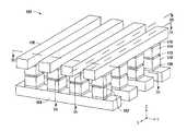
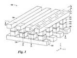
- FIG. 1is a perspective view of a portion of a memory array in accordance with a number of embodiments of the present disclosure.
- FIG. 2illustrates a three dimensional memory array in accordance with a number of embodiments of the present disclosure.
- FIGS. 3A and 3Billustrate cross-sectional views of memory cells in perpendicular directions in accordance with a number of embodiments of the present disclosure.
- FIG. 4Aillustrates a cross-sectional view of fin structures prior to independently-sizing middle electrodes in accordance with a number of embodiments of the present disclosure.
- FIG. 4Billustrates a cross-sectional view of fin structures having independently-sized middle electrodes in accordance with a number of embodiments of the present disclosure.
- FIGS. 5A and 5Billustrate previous approach cross-sectional views in parallel directions at different locations of memory cells having stringer defects.
- FIGS. 6A and 6Billustrate cross-sectional views of memory cells in parallel directions at different locations without stringer defects in accordance with a number of embodiments of the present disclosure.
- FIGS. 7A and 7Billustrate cross-sectional views of memory cells in parallel directions having tapered memory element in accordance with a number of embodiments of the present disclosure.
- FIGS. 8A and 8Billustrate cross-sectional views of memory cells in parallel directions at different locations having tapered memory elements without stringer defects in accordance with a number of embodiments of the present disclosure.
- An example memory cellcan include a switch element and a memory element.
- a middle electrodeis formed between the memory element and the switch element.
- An outside electrodeis formed adjacent the switch element or the memory element at a location other than between the memory element and the switch element.
- a lateral dimension of the middle electrodeis different than, e.g., less than, a lateral dimension of the outside electrode.
- Embodiments of the present disclosureimplement a memory cell in a cross point memory array in which the dimensions of the middle electrode, e.g., located between a memory element and a switch element are independent from the dimensions of outside electrodes, e.g., bottom electrode and/or top electrode.
- Reducing lateral dimension(s) of the middle electrodecan increase the current density at the middle electrode/memory element contact surface area for a given amount of input power, thereby improving the effectiveness to induce memory element phase transitions due to thermal budget on the memory element, e.g., increased heat generated by localized increased current flow.
- reducing lateral dimension(s) of the middle electrodecan reduce the risk of stringer formation during etch of a conductive line located above the memory cell, e.g., bit line etch.
- 106may reference element “06” in FIG. 1
- a similar elementmay be referenced as 306 in FIG. 3A .
- “a number of” a particular element and/or featurecan refer to one or more of such elements and/or features.
- the term “substantially”intends that the modified characteristic needs not be absolute, but is close enough so as to achieve the advantages of the characteristic.
- “substantially parallel”is not limited to absolute parallelism, and can include orientations that are at least closer to a parallel orientation than a perpendicular orientation.
- “substantially orthogonal”is not limited to absolute orthogonalism, and can include orientations that are at least closer to a perpendicular orientation than a parallel orientation.
- FIG. 1is a perspective view of a portion of a memory array 100 in accordance with a number of embodiments of the present disclosure.
- the cross point array 100 of memory cells shown in FIG. 1can be created through dry etch patterning in two perpendicular directions, e.g., corresponding to the direction of the conductive lines 104 underlying the memory cells, e.g., word lines, and the conductive lines 106 overlying the memory cells, e.g., bit lines.
- Materials corresponding to respective conductive lines and components of the memory cellcan be bulk deposited as a stack of materials and etched to form the various features, e.g., pillars of materials.
- the dry etch patterning in two perpendicular directionsforms the various conductive lines, fin structure, and ultimately pillars corresponding to individual memory cells.
- a first etchcan define underlying conductive lines and one direction of the pillar, e.g., a fin structure separated by first trenches, from the stack of materials.
- the sides of the pillarcan be self-aligned to the underlying conductive lines, e.g., word lines 304 , which in turn can be connected to other circuitry.
- a second etchcan define overlying conductive lines and the other direction of the pillar. Additional etches can be used to independently size various material components of the fin structures and/or pillars, as described further below.
- memory array 100is a cross point memory.
- embodiments of the present disclosureare not so limited.
- embodiments of the present disclosurecan comprise a three dimensional (3D) cross point memory with more decks of word line and bit lines with memory cells therebetween.
- Array 100can be a cross-point array having memory cells 102 located at the intersections of a number of conductive lines, e.g., access lines 104 , which may be referred to herein as word lines, and a number of conductive lines, e.g., data/sense lines 106 , which may be referred to herein as bit lines.
- word lines 104can be parallel or substantially parallel to each other and can be orthogonal to bit lines 106 , which can be parallel or substantially parallel to each other.
- Word lines 104 and/or bit lines 106can be a conductive material such as tungsten, copper, titanium, aluminum, and/or other metals, for example.
- array 100can be a portion, e.g., a level, of a three-dimensional array, e.g., a multi-level array, (described further with respect to FIG. 2 ) in which other arrays similar to array 100 are at different levels, for example above and/or below array 100 .
- Each memory cell 102can include a memory element 114 , e.g., storage element, coupled in series with a respective switch element 110 , e.g., selector device, and/or access device.
- the memory cellcan have a number of electrodes adjacent the memory element 114 and switch element 110 , including a first, e.g., bottom, electrode, second, e.g., middle, electrode, and/or third, e.g., top, electrode.
- the memory element 114can be, for example, a resistive memory element.
- the memory element 114can be formed between a pair of electrodes, e.g., third electrode 116 and second electrode 112 .
- the memory elementcan be comprised of a resistance variable material such as a phase change memory (PCM) material, for example.
- PCMphase change memory
- the PCM materialcan be a chalcogenide alloy such as a Germanium-Antimony-Tellurium (GST) material, e.g., Ge—Sb—Te materials such as Ge 2 Sb 2 Te 5 , Ge 1 Sb 2 Te 4 , Ge 1 Sb 4 Te 7 , Ge 8 Sb 5 Te 8 , Ge 4 Sb 4 Te 7 , etc., or an indium(In)-antimony(Sb)-tellurium(Te) (IST) material, e.g., In 2 Sb 2 Te 5 , In 1 Sb 2 Te 4 , In 1 Sb 4 Te 7 , etc., among other phase change memory materials.
- GSTGermanium-Antimony-Tellurium
- GSTGermanium-Antimony-Tellurium
- GSTGermanium-Antimony-Tellurium
- GSTGermanium-Antimony
- phase change memory materialscan include Ge—Te, In—Se, Sb—Te, Ga—Sb, In—Sb, As—Te, Al—Te, Ge—Sb—Te, Te—Ge—As, In—Sb—Te, Te—Sn—Se, Ge—Se—Ga, Bi—Se—Sb, Ga—Se—Te, Sn—Sb—Te, In—Sb—Ge, Te—Ge—Sb—S, Te—Ge—Sn—O, Te—Ge—Sn—Au, Pd—Te—Ge—Sn, In—Se—Ti—Co, Ge—Sb—Te—Pd, Ge—Sb—Te—Co, Sb—Te—Bi—Se, Ge—Sb—Se
- embodiments of the present disclosureare not limited to a particular type of PCM material. Further, embodiments are not limited to memory elements comprising PCM materials.
- the memory elementscan comprise a number of resistance variable materials such as binary metal oxides, colossal magnetoresistive materials, and/or various polymer-based resistive variable materials, among others.
- FIG. 1shows the memory element 114 , switch element 110 , and electrodes 108 and 116 all having similar dimensions in pillars, and middle electrode 112 having a smaller dimension in the “X” direction than the dimensions of the memory element 114 , switch element 110 , and electrodes 108 and 116 in the same (“X”) direction.
- a memory cell 102can be formed with a middle electrode 112 having different dimension(s), e.g., smaller critical dimension(s), smaller cross-sectional area, smallest lateral dimension, etc., than the memory element 114 , switch element 110 , and/or the outside electrodes, e.g., electrodes 108 and 116 .
- outside electroderefers to an electrode formed in a location other than between the memory element 114 and the switch element 110 .
- the middle electrode 112can be formed to have smaller dimensions than electrodes 108 and 116 in two corresponding directions, e.g., in the “Y” direction and the “X” direction.
- bottom electrode 108 and switch elementneed not be confined to a pillar, and can extend continuously along the top of the word line 104 , as shown and discussed with respect to FIG. 3B .
- a middle electrode 112can be recessed after an etch that defines a first conductive line, e.g., word line. That is, during a word line etch, a fin structure is formed self-aligned to the word line. Thereafter, the middle electrode 112 can be recessed to have a smaller dimension than the word line (and other component materials of the fin structure.
- the middle electrode 112can alternatively or additionally be recessed after an etch that defines a second conductive line, e.g., bit line such that the middle electrode 112 is recessed in one or two directions, e.g., in a direction perpendicular to the direction in which a word line extends and/or in a direction perpendicular to the direction in which a bit line extends.
- a second conductive linee.g., bit line
- the switch element 110can be a two terminal device such as a diode, an ovonic threshold switch (OTS), or an ovonic memory switch (OMS).
- OTSovonic threshold switch
- OMSovonic memory switch
- the switch element 110can be a field effect transistor (FET), a bipolar junction transistor (BJT), or a diode, among other types of selector devices.
- FETfield effect transistor
- BJTbipolar junction transistor
- the switch element 110can be formed between a pair of electrodes, e.g., the first electrode 108 and a second electrode 112 .
- FIG. 1illustrates a configuration having the memory element 114 formed over the switch element 110
- the switch element 110can be formed over the memory element 114 , for example.
- Electrodes 108 , 112 , and/or 116can comprise materials such as Ti, Ta, W, Al, Cr, Zr, Nb, Mo, Hf, B, C, conductive nitrides of the aforementioned materials, e.g., TiN, TaN, WN, CN, etc.), and/or combinations thereof.
- the switch elements 110 corresponding to memory cells 102can be OTS's having a chalcogenide selector device material.
- the chalcogenide material of the switch element 110may not actively change phase, e.g., between amorphous and crystalline, such as a chalcogenide resistance variable material of the memory element.
- the chalcogenide material of the switch elementcan change between an “on” and “off” state depending on the voltage potential applied across memory cell 102 .
- the “state” of the OTScan change when a current through the OTS exceeds a threshold current or a voltage across the OTS exceeds a threshold voltage. Once the threshold current or voltage is reached, an on state can be triggered and the OTS can be in a conductive state. In this example, if the current or voltage potential drops below a threshold value, the OTS can return to a non-conductive state.
- the memory element 114can comprise one or more of the same material(s) as the switch element 110 .
- memory element 114 and switch element 110can comprise different materials.
- Memory cells 102can be programmed to a target data state, e.g., corresponding to a particular resistance state, by applying sources of an electrical field or energy, such as positive or negative electrical pulses, to the cells, e.g., to the storage element of the cells, for a particular duration.
- the electrical pulsescan be, for example, positive or negative voltage or current pulses.
- FIG. 2illustrates a three dimensional (3D) memory array in accordance with a number of embodiments of the present disclosure.
- the 3D memory arraycomprises a plurality of memory cells 202 - 1 , 202 - 2 , e.g., memory element in series with a switch element with a middle electrode having different dimension(s), e.g., smaller, than the memory element, switch element, and/or other electrodes as described with respect to FIG. 1 .
- FIG. 2shows a first memory array comprising memory cells 202 - 1 formed between word lines 204 - 1 and bits lines 206 , and a second memory array comprising memory cells 202 - 2 formed between word lines 204 - 2 and bits lines 206 . That is, the first memory array formed below bit lines 206 and the second memory array formed above bit lines 206 share common bit lines 206 therebetween.
- FIG. 2is a simplified diagram that does not precisely reflect the three dimensional physical dimensions of the various features illustrated, including the exact proximity of features to one another.
- FIG. 2should not be considered as to be representative of the precise topological positioning of the various elements and electrodes of individual memory cells. Rather, FIG. 2 provides an overview of the electrical scheme for a 3D memory array, and the approximate relative arrangement of the various features.
- FIG. 2shows a 3D array comprising 2 memory arrays, embodiments of the present invention are not so limited, and can include additional memory array(s) arranged into a number of levels.
- FIGS. 3A and 3Billustrate cross-sectional views of memory cells in perpendicular directions in accordance with a number of embodiments of the present disclosure.
- the orientation of the view shown in FIG. 3A through the pillarsis shown by outline 3 A- 3 A in FIG. 1 .
- the orientation of the view shown in FIG. 3Balso through the pillars but in a direction perpendicular to that of cut line 3 A- 3 A, is shown by cutline 3 B- 3 B in FIG. 1 (except that in FIG. 1 the bottom electrode and switch element are shown being part of the pillar whereas in FIG. 3A they are not).
- FIGS. 3A and 3Bthe pillars of materials are shown being square when viewed from the side and end perspectives.
- FIG. 3Ashows a cross-section in a first direction, e.g., side view, of a portion of a memory array, such as that shown in FIG. 1 .
- FIG. 3Bshows a cross-section in a second direction, e.g., end view, of a portion of a memory array, such as that shown in FIG. 1 .
- FIGS. 3A and 3Bshow some additional detail than that shown and described with respect to FIG. 1 .
- the memory cells shown in FIGS. 3A and 3Bcan be similar to those described with respect to FIGS. 1 and 2 .
- a stack of materialscan be formed over a word line 304 .
- the stack of materialscan include a first electrode 308 , e.g., bottom electrode, formed over a first conductive line 304 , e.g., word line, a switch element 310 formed over the first electrode 308 , a second electrode 312 , e.g., middle electrode, formed over the switch element 310 , a memory element 314 formed over the second electrode 312 , and a third electrode 316 formed over the memory element 314 .
- the stack of materialscan be etched to form fin structures self-aligned with the first conductive line 304 , and the trenches between the fin structures can be filled-in with dielectric material 322 .
- a conductive materiale.g., metal film
- An additional etch processcan be used to form second trenches that define second conductive line 306 , e.g., bit lines, in a direction perpendicular to the trenches used to define the word lines 304 and fin structures. Pillars corresponding to respective memory cells that are separated from one another can be self-aligned to the bit lines 306 .
- an additional etchcan be used to independently size one or more components of the pillars, e.g., the second electrode, as described further with respect to FIGS.
- the second trenchescan also be filled-in with dielectric material to isolate the array of active pillars corresponding to memory cells from one another.
- self-aligned conductive linesextend in perpendicular directions to connect the array to associated circuitry.
- the second electrode 312can be independently-sized after the word line etch to have a smaller lateral dimension than other fin components in a particular corresponding direction. That is, the middle electrode can have a smallest lateral dimension in a particular direction with respect to other materials comprising a fin structure created by the word line etch in the corresponding, e.g., same, particular direction.
- the middle electrodecan be independently-sized after the word line etch by the process illustrated and described below.
- the pillarscan alternatively or additionally be etched after the bit line etch to independently-size pillar component(s), e.g., middle electrode.
- FIG. 4Aillustrates a cross-sectional view of fin structures prior to independently-sizing middle electrodes in accordance with a number of embodiments of the present disclosure.
- the orientation of the view shown in FIG. 4A through the pillarsis a similar orientation as that shown by cutline 3 A- 3 A in FIG. 1 .
- FIG. 4Ashows an end view of fin structures self-aligned to underlying conductive lines. The fin structures shown in FIG.
- FIG. 4Ainclude a first electrode 408 , e.g., bottom electrode, formed over a first conductive line 404 , e.g., word line, a switch element 410 formed over the first electrode 408 , a second electrode 412 A, e.g., middle electrode, formed over the switch element 410 , a memory element 414 formed over the second electrode 412 A, and a third electrode 416 formed over the memory element 414 .
- FIG. 4Aalso shows a hard mask 418 , used to pattern the first conductive line 404 and fin structures.
- first electrode 408 , second electrode 412 , and third electrode 416can be formed from materials that include carbon (C).
- Ccarbon
- embodiments of the present disclosureare not so limited, and electrodes can be formed of other materials that have low resistivity and are not active with the chalcogenide alloy used for the memory element and/or switch element.
- Carbonhas electric properties such as a viable resistivity for application as an electrode of a memory cell, and can be easily patterned with an extremely high selectivity towards inorganic hard masks, such as hard mask 418 shown in FIG. 4A .
- Ability to easily pattern electrodesis increasingly important as stack complexity increases.
- Electrodescan have a critical dimension (CD) defined by the CD of the hard mask 418 , and if the word line profile is substantially vertical, the electrodes can have dimensions substantially similar to the hard mask 418 used for patterning.
- Critical dimension (CD)is the finest line resolvable associated with etch patterning, e.g., etching using a pattern to delineate areas to be etched from areas not to be etched.
- FIG. 4Billustrates a cross-sectional view of fin structures having independently-sized middle electrodes in accordance with a number of embodiments of the present disclosure.
- the orientation of the view shown in FIG. 4Bis a similar orientation as that shown by cutline 3 B- 3 B in FIG. 1 .
- the second electrode 412 Be.g., middle electrode formed between the switch element 410 and memory element 414 , can be sized independently from other components of the fin structure, as shown in FIG. 4B .
- second electrode 412 B shown in FIG. 4Bhas a lateral dimension in the horizontal direction that is less than a lateral dimension in the horizontal direction of the other components of the fin structure, including the other electrodes, memory element 414 and switch element 410 .
- Changing the lateral dimension the second electrode from that shown for second electrode 412 A to that of second electrode 412 Bhas several advantages. Reducing one or both lateral dimensions of the second electrode with respect to the lateral dimension(s) of the memory element 414 can reduce the areas of the middle electrode 412 B/memory element 414 contact surfaces, thereby increasing the current density, which can improve the effectiveness to induce phase transitions in the memory element 414 . Additionally, reducing one or both lateral dimensions of the second electrode, such as is shown for second electrode 412 B, can reduce the risk of stringer defect formation during the etch to define overlying conductive lines, e.g., bit line etch, as is described further with respect to FIGS. 5A-8B below.
- the second electrodee.g., 412 A shown in FIGS. 4A and 412B shown in FIG. 4B can be formed of a material that has a higher etch rate than the material from which one or more other electrodes are formed.
- the second electrodecan be formed of a material that has a higher etch rate when etched with O 2 -based chemistries than the material from which one or more other electrodes are formed.
- the second electrodecan be etched with O 2 -based chemistries that can have minimal effect on the memory element 414 , switching element 410 , and inorganic hard mask 418 .
- an additional isotropic etch using an O 2 -based plasma with the bias voltage offcan be used to laterally recess the second electrode as shown for second electrode 412 B in FIG. 4B .
- the additional isotropic etchcan be an O 2 flash process.
- the second electrodee.g., 412 A shown in FIGS. 4A and 412B shown in FIG. 4B
- the second electrodecan be formed from combination of carbon and nitrogen (CNx), where “x” may be a positive integer, but can include other (non-integer) ratios.
- nitrogencan be in the range of 2%-50% of the stoichiometric compound.
- embodimentsare not limited to this range, and can include more or less nitrogen.
- Other electrodes, e.g., first electrode 408 and third electrode 416can be formed of carbon (C), e.g., without nitrogen.
- the additional isotropic etch using an O 2 -based plasma with the bias voltage offcan modify all carbon-based electrodes (with minimal impact on other materials such as the memory element 414 , switch element 410 , and hard mask 418 ).
- the CNx materialhas a higher etch rate than that of carbon, e.g., absent the nitrogen, the second electrode can recess faster than the other carbon-based electrodes.
- a tunable second electrodee.g., middle electrode, recession with negligible erosion of the other electrodes, e.g., top electrode and/or bottom electrode.
- a lateral dimension of the second electrodecan be changed to be less than a lateral dimension of other electrodes and/or memory element 414 and/or switch element 410 .
- a smallest lateral dimension of the second electrode in at least one of the X- and/or Y-directionsshown in FIG. 1
- recessing the second electrodecan create a negative step below the memory element 414 . That is, the memory element 414 can overhang the second electrode 412 B.
- This geometrycan have advantages in avoiding stringer defect formation as is discussed below.
- FIG. 4Bshows recession of the second electrode 412 B after the fin structures shown in FIG. 4A are completely formed, e.g., down to include conductive lines, e.g., word lines 404 , definition
- the second electrode 412 Bcan be recessed after the fin structures are partially formed so as to expose the second electrode 412 B, e.g., only the top electrode 416 , memory element 414 , and second electrode 412 B are exposed. At, or after, this stage of processing, the second electrode 412 B can then be recessed. Thereafter, the balance of the fin structure, including conductive lines can be formed.
- the second electrode 412 Bcan be recessed any time after it is exposed by either the word line etch and/or the bit line etch.
- FIG. 4Bdescribes recessing the second electrode 412 B
- embodiments of the present disclosureare not so limited, and other components of the fin structure (self-aligned with word line) and/or vertical structure (self-aligned with both word line and bit line) can be recessed independently or in combination with recession of the second electrode 412 B. That is, according to some embodiments of the present disclosure the first electrode 408 and/or the third electrode 416 can be formed of a different composition than other electrodes, e.g., CNx, and thus recessed in a similar manner as that described for recessing the second electrode 412 B.
- FIGS. 5A and 5Billustrate previous approach cross-sectional views in parallel directions at different locations of memory cells having stringer defects.
- FIG. 5Ashows a cross-sectional side view sliced through an overlying conductive line, e.g., bit line 560 , with pillars separated by dielectric material 562 (in a similar orientation as that shown by cutline 3 A- 3 A in FIG. 1 ), except that the second electrode 552 , e.g., middle electrode, is not recessed.
- the second electrode 552e.g., middle electrode
- first electrode 548e.g., bottom electrode
- first conductive line 544e.g., word line
- switch element 550formed over the first electrode 548
- second electrode 552e.g., middle electrode
- memory element 556formed over the second electrode 552
- third electrode 558formed over the memory element 556 .
- the bit line 560extends left-right across the top of the pillars and interposing dielectric 562 .
- FIG. 5Bshows a cross-sectional view in an orientation parallel to the view shown in FIG. 5A , but sliced at a location between the bit lines 560 shown in FIG. 5A . Portions of the previous fin structures after the bit line etch are shown in FIG. 5B , with the fin structures between the bit lines 560 being etched down to the switch element 550 . That is, the second electrode 552 has been etched by the bit line etch to the extent shown in FIG. 5B .
- the second electrode 552can be affected by polymers 554 redeposited during memory element patterning or by the word line profile, e.g., etching the stack of materials to form the underlying conductive lines, e.g., word lines.
- polymersrefers to byproducts created by etching process that have a low volatility and so are difficult to remove.
- polymers 554can be deposited on the trench walls in the vicinity of where the memory element 556 is removed during the bit line etch as shown in FIG. 5B .
- the conductive stringer defectcan remain in memory cells formed according to previous approaches, which can result in electrical defects in the memory cell operation, including column-to-column leakage current.
- FIGS. 6A and 6Billustrate cross-sectional views of memory cells in parallel directions without stringer defects in accordance with a number of embodiments of the present disclosure.
- FIG. 6Ashows a cross-sectional side view sliced through an overlying conductive line, e.g., bit line 606 , with pillars separated by dielectric material 622 .
- the orientation of the view shown in FIG. 6Ais similar to that indicated in FIG. 1 by cutline 3 A- 3 A.
- Each pillar shown in FIG. 6Aincludes a first electrode 608 , e.g., bottom electrode, formed over a first conductive line 604 , e.g., word line, a switch element 610 formed over the first electrode 608 , a second electrode 612 B, e.g., middle electrode, formed over the switch element 610 , a memory element 614 formed over the second electrode 612 B, and a third electrode 616 formed over the memory element 614 .
- the bit line 606extends left-right across the top of the pillars and interposing dielectric 622 .
- the view and memory cell configuration shown in FIG. 6Bare similar to that shown in FIG.
- the second electrode 612 Bcan be referred to as a middle electrode
- the first electrode 608 and/or the third electrode 616can be referred to as an outside electrode.
- FIG. 6Bshows a cross-sectional end view in an orientation parallel to the view shown in FIG. 6A , but sliced at a location between the bit lines 606 shown in FIG. 6A .
- the orientation of the view shown in FIG. 6Bis indicated in FIG. 1 by cutline 6 B- 6 B.
- Portions of the previous fin structures after the bit line etchare shown in FIG. 6B , with the fin structures between the bit lines 606 being etched down to the switch element 610 . That is, the second electrode 612 B between the bit lines 606 has been etched away by the bit line etch to the extent shown in FIG. 6B .
- FIG. 6Bshows polymers 654 deposited on the trench walls in the vicinity of where the memory element 614 is removed during the bit line etch as shown in FIG. 6B .
- the polymers 654are formed in a similar manner to that described above with respect to FIG. 5B .
- the material being shadowed by the polymers 654is dielectric material 622 rather than material from which the second electrode 612 B is formed. That is, the material being shadowed by the polymers 654 is insulative rather than conductive. What might have been conductive residuals were removed when the second electrode was recessed. Therefore, unlike previous approaches, column-to-column leakage is avoided since conductive stringer defects are eliminated.
- the middle electrodee.g., second electrode 412 A shown in FIGS. 4A and 412B shown in FIG. 4B
- An outside electrodecan be modified by similar techniques such that the outside electrode can have a lateral dimension that is smaller than a lateral dimension of the middle electrode.
- the middle electrodecan be formed of carbon (C), e.g., without nitrogen, and the outside electrode(s) can be formed of CNx, where “x” may be a positive integer, but can include other (non-integer) ratios.
- nitrogencan be in the range of 2%-50% of the stoichiometric compound. However, embodiments are not limited to this range, and can include more or less nitrogen.
- the outside electrode(s)are formed of CNx, and the middle electrode is formed of carbon
- an additional isotropic etch using an O 2 -based plasma with the bias voltage offcan modify all carbon-based electrodes (with minimal impact on other materials such as the memory element, switch element, and hard mask).
- the CNx materialhas a higher etch rate than that of carbon, e.g., absent the nitrogen
- the outside electrode(s)can recess faster than the other carbon-based electrodes, e.g., the middle electrode.
- one outside electrodecan be formed of CNx, and the middle electrode and other outside electrode can be formed of carbon, e.g., without nitrogen.
- FIGS. 7A and 7Billustrate cross-sectional views of memory cells in parallel directions having tapered memory element in accordance with a number of embodiments of the present disclosure.
- FIG. 7Ashows a cross-sectional side view sliced through an overlying conductive line, e.g., bit line 760 (in a similar orientation as that shown by outline 3 A- 3 A in FIG. 1 ), with pillars separated by dielectric material 762 .
- bit line 760in a similar orientation as that shown by outline 3 A- 3 A in FIG. 1
- first electrode 748e.g., bottom electrode, formed over a first conductive line 744 , e.g., word line, a switch element 750 formed over the first electrode 748 , a second electrode 752 , e.g., middle electrode, formed over the switch element 750 , a memory element 756 formed over the second electrode 752 , and a third electrode 758 formed over the memory element 756 .
- the bit line 760extends left-right across the top of the pillars and interposing dielectric 762 .
- FIG. 7Adiffers from the configuration shown in FIG. 5A .
- the memory element 556 shown in FIG. 5Ahas a vertical profile according to a previous approach.
- the memory element 756 shown in FIG. 7Ahas a tapered profile, e.g., width is smaller at a higher elevation and gradually larger at lower elevations. Tapering of the memory element 756 can occur during etching of the fin structures and underlying conductive lines, e.g., word lines, from the bulk deposited stack of materials. For example, the tapering may occur because of recession of the third electrode 758 , e.g., top electrode, or hard mask during an etch to form same.
- FIG. 7Bshows a cross-sectional view in an orientation parallel to the view shown in FIG. 7A , but sliced at a location between the bit lines 760 shown in FIG. 7A .
- FIG. 7Billustrates stringer defects that can occur (which is addressed below with respect to FIGS. 8A and 8B ).
- Portions of the previous fin structures after the bit line etchare shown in FIG. 7B , with the fin structures between the bit lines 760 being etched down to the switch element 750 . That is, the second electrode 752 has been etched by the bit line etch to the extent shown in FIG. 7B .
- Stringer defect formationcan also be attributable to the word line profile, e.g., etching the stack of materials to form the underlying conductive lines. Since bit line patterning, e.g., etching, is highly anisotropic, the dielectric material 762 located above the tapered portion 755 of the memory element 756 can shadow the tapered portion 755 of the memory element 756 , which in turn can shadow the portion of the second electrode 752 therebelow. With this shadowing during the bit line etch according to a previous approach, a portion of the conductive second electrode 752 remains along the trench walls, thereby leading to a conductive stringer defect that can cause column-to-column leakage as previously described.
- the conductive second electrode 752 material left underneath the tapered portion 755 of the memory element 756cannot be removed without damaging the third electrode 758 , e.g., top electrode, since, according to a previous approach, when the electrodes are all formed of a same material, or materials having very similar etch rates. That is, an etch that might be used to remove the conductive second electrode 752 material left underneath the tapered portion 755 of the memory element 756 would also consume material of the third electrode 758 , which is already narrowed as shown in FIG. 7A .
- FIGS. 8A and 8Billustrate cross-sectional views of memory cells in parallel directions having tapered memory elements without stringer defects in accordance with a number of embodiments of the present disclosure.
- FIG. 8Ashows a cross-sectional side view sliced through an overlying conductive line, e.g., bit line 806 , with pillars separated by dielectric material 822 (in a similar orientation as that shown by cutline 3 A- 3 A in FIG. 1 ).
- first electrode 808e.g., bottom electrode
- first conductive line 804e.g., word line
- switch element 810formed over the first electrode 808
- second electrode 812 Be.g., middle electrode
- the bit line 806extends left-right across the top of the pillars and interposing dielectric 822 .
- the view and memory cell configuration shown in FIG. 8Aare similar to that shown in FIG. 6A but with a tapered memory element 814 A and narrowed third electrode 816 A.
- FIG. 8Ashows the second electrode 812 B recessed beneath the tapered memory element 814 A.
- one of the first 808 , the second 812 B, and/or the third electrode 816 Acan be etched, via a selective/isotropic process, to have a lateral dimension in a particular direction that is different than, e.g., less than, a lateral dimension of the other electrodes in the same particular direction.
- one electrodecan be etched to be larger, or smaller, than other electrodes.
- each electrodecan be etched to have a different lateral dimension than all other electrodes and/or the switch element 810 and/or the memory element 814 A.
- FIG. 8Bshows a cross-sectional end view in an orientation parallel to the view shown in FIG. 8A , but sliced at a location between the bit lines 806 shown in FIG. 8A .
- Portions of the previous fin structures after the bit line etchare shown in FIG. 8B , with the fin structures between the bit lines 806 being etched down to the switch element 810 . That is, the second electrode 812 B between the bit lines 806 has been etched away by the bit line etch to the extent shown in FIG. 8B .
- bit line patterninge.g., etching
- bit line patterningis highly anisotropic
- the dielectric material 822 located above the tapered portion 855 of the memory element 814 Acan shadow the tapered portion 855 of the memory element 814 A, which in turn can shadow material therebelow.
- the material below the tapered portion 855 of the memory element 814 Ais dielectric material 822 rather than conductive second electrode material.
- the tapered portion 855 of the memory element 812 Bcan be eliminated after the bit line etch by a subsequent long isotropic over etch.
- the dielectric material 822 that remains after the tapered portion 855 of the memory element 812 Bis insulative rather than conductive. That is, the resulting trench from the bit line etch is free from residual materials. As such, conductive stringer defects are eliminated and column-to-column leakage current does not occur via a conductive stringer defect electrical path, thereby avoiding electrical failures in the memory cell array.
Landscapes
- Engineering & Computer Science (AREA)
- Manufacturing & Machinery (AREA)
- Physics & Mathematics (AREA)
- Condensed Matter Physics & Semiconductors (AREA)
- General Physics & Mathematics (AREA)
- Computer Hardware Design (AREA)
- Microelectronics & Electronic Packaging (AREA)
- Power Engineering (AREA)
- Semiconductor Memories (AREA)
Abstract
Description
Claims (26)
Priority Applications (3)
| Application Number | Priority Date | Filing Date | Title |
|---|---|---|---|
| US14/036,788US9257431B2 (en) | 2013-09-25 | 2013-09-25 | Memory cell with independently-sized electrode |
| US14/972,152US9831428B2 (en) | 2013-09-25 | 2015-12-17 | Memory cell with independently-sized electrode |
| US15/792,842US10777743B2 (en) | 2013-09-25 | 2017-10-25 | Memory cell with independently-sized electrode |
Applications Claiming Priority (1)
| Application Number | Priority Date | Filing Date | Title |
|---|---|---|---|
| US14/036,788US9257431B2 (en) | 2013-09-25 | 2013-09-25 | Memory cell with independently-sized electrode |
Related Child Applications (1)
| Application Number | Title | Priority Date | Filing Date |
|---|---|---|---|
| US14/972,152DivisionUS9831428B2 (en) | 2013-09-25 | 2015-12-17 | Memory cell with independently-sized electrode |
Publications (2)
| Publication Number | Publication Date |
|---|---|
| US20150084156A1 US20150084156A1 (en) | 2015-03-26 |
| US9257431B2true US9257431B2 (en) | 2016-02-09 |
Family
ID=52690219
Family Applications (3)
| Application Number | Title | Priority Date | Filing Date |
|---|---|---|---|
| US14/036,788ActiveUS9257431B2 (en) | 2013-09-25 | 2013-09-25 | Memory cell with independently-sized electrode |
| US14/972,152Active2033-10-11US9831428B2 (en) | 2013-09-25 | 2015-12-17 | Memory cell with independently-sized electrode |
| US15/792,842ActiveUS10777743B2 (en) | 2013-09-25 | 2017-10-25 | Memory cell with independently-sized electrode |
Family Applications After (2)
| Application Number | Title | Priority Date | Filing Date |
|---|---|---|---|
| US14/972,152Active2033-10-11US9831428B2 (en) | 2013-09-25 | 2015-12-17 | Memory cell with independently-sized electrode |
| US15/792,842ActiveUS10777743B2 (en) | 2013-09-25 | 2017-10-25 | Memory cell with independently-sized electrode |
Country Status (1)
| Country | Link |
|---|---|
| US (3) | US9257431B2 (en) |
Cited By (13)
| Publication number | Priority date | Publication date | Assignee | Title |
|---|---|---|---|---|
| US9831428B2 (en)* | 2013-09-25 | 2017-11-28 | Micron Technology, Inc. | Memory cell with independently-sized electrode |
| US9960350B2 (en)* | 2016-06-03 | 2018-05-01 | SK Hynix Inc. | Method of fabricating switching element and method of manufacturing resistive memory device |
| US10297642B2 (en) | 2017-03-28 | 2019-05-21 | Samsung Electronics Co., Ltd. | Semiconductor device having data storage pattern |
| US10424374B2 (en) | 2017-04-28 | 2019-09-24 | Micron Technology, Inc. | Programming enhancement in self-selecting memory |
| US10424730B2 (en)* | 2018-02-09 | 2019-09-24 | Micron Technology, Inc. | Tapered memory cell profiles |
| US10541364B2 (en) | 2018-02-09 | 2020-01-21 | Micron Technology, Inc. | Memory cells with asymmetrical electrode interfaces |
| US10693065B2 (en) | 2018-02-09 | 2020-06-23 | Micron Technology, Inc. | Tapered cell profile and fabrication |
| US10741754B2 (en) | 2017-12-18 | 2020-08-11 | International Business Machines Corporation | Resistive memory with amorphous silicon filaments |
| US10854813B2 (en) | 2018-02-09 | 2020-12-01 | Micron Technology, Inc. | Dopant-modulated etching for memory devices |
| US10903275B2 (en) | 2019-06-03 | 2021-01-26 | International Business Machines Corporation | Three-dimensional stackable multi-layer cross-point memory with single-crystalline bipolar junction transistor selectors |
| US11018188B2 (en) | 2019-06-03 | 2021-05-25 | International Business Machines Corporation | Three-dimensional stackable multi-layer cross-point memory with bipolar junction transistor selectors |
| US11374059B2 (en)* | 2017-06-26 | 2022-06-28 | Micron Technology, Inc. | Memory cells having resistors and formation of the same |
| US11711987B2 (en) | 2020-08-31 | 2023-07-25 | Micron Technology, Inc. | Memory electrodes and formation thereof |
Families Citing this family (17)
| Publication number | Priority date | Publication date | Assignee | Title |
|---|---|---|---|---|
| US9054295B2 (en)* | 2011-08-23 | 2015-06-09 | Micron Technology, Inc. | Phase change memory cells including nitrogenated carbon materials, methods of forming the same, and phase change memory devices including nitrogenated carbon materials |
| KR102375591B1 (en) | 2015-10-27 | 2022-03-16 | 삼성전자주식회사 | Semiconductor device and method for fabricating the same |
| KR102453349B1 (en) | 2016-02-25 | 2022-10-07 | 삼성전자주식회사 | Variable resistance memory devices and methods of manufacturing the same |
| KR102463036B1 (en)* | 2016-03-15 | 2022-11-03 | 삼성전자주식회사 | Semiconductor memory devices and methods of manufacturing the same |
| US10269566B2 (en) | 2016-04-29 | 2019-04-23 | Lam Research Corporation | Etching substrates using ale and selective deposition |
| US10566212B2 (en) | 2016-12-19 | 2020-02-18 | Lam Research Corporation | Designer atomic layer etching |
| US10832909B2 (en) | 2017-04-24 | 2020-11-10 | Lam Research Corporation | Atomic layer etch, reactive precursors and energetic sources for patterning applications |
| US10494715B2 (en)* | 2017-04-28 | 2019-12-03 | Lam Research Corporation | Atomic layer clean for removal of photoresist patterning scum |
| US10796912B2 (en) | 2017-05-16 | 2020-10-06 | Lam Research Corporation | Eliminating yield impact of stochastics in lithography |
| US10580976B2 (en)* | 2018-03-19 | 2020-03-03 | Sandisk Technologies Llc | Three-dimensional phase change memory device having a laterally constricted element and method of making the same |
| WO2019231460A1 (en)* | 2018-05-31 | 2019-12-05 | Intel Corporation | Phase change memory structures and devices |
| US10593875B2 (en) | 2018-06-15 | 2020-03-17 | Macronix International Co., Ltd. | Self-aligned 3D memory with confined cell |
| US10937832B2 (en) | 2018-06-21 | 2021-03-02 | Macronix International Co., Ltd. | 3D memory with confined cell |
| KR102712682B1 (en) | 2019-05-17 | 2024-10-04 | 에스케이하이닉스 주식회사 | Electronic device and method for fabricating electronic device |
| WO2021072576A1 (en)* | 2019-10-14 | 2021-04-22 | Yangtze Memory Technologies Co., Ltd. | Methods for forming three-dimensional phase-change memory devices |
| US11545214B2 (en) | 2020-07-08 | 2023-01-03 | Samsung Electronics Co., Ltd. | Resistive memory device |
| FR3126544B1 (en)* | 2021-08-31 | 2024-08-09 | Commissariat Energie Atomique | Resistive memory device and method of production |
Citations (29)
| Publication number | Priority date | Publication date | Assignee | Title |
|---|---|---|---|---|
| US6709874B2 (en) | 2001-01-24 | 2004-03-23 | Infineon Technologies Ag | Method of manufacturing a metal cap layer for preventing damascene conductive lines from oxidation |
| US20060151771A1 (en) | 2005-01-12 | 2006-07-13 | Elpida Memory, Inc. | Phase-change-type semiconductor memory device |
| US20070284635A1 (en)* | 2006-06-07 | 2007-12-13 | Fournier Jeffrey P | Nitrogenated carbon electrode for chalcogenide device and method of making same |
| US7435648B2 (en) | 2006-07-26 | 2008-10-14 | Macronix International Co., Ltd. | Methods of trench and contact formation in memory cells |
| US20080304308A1 (en) | 2005-12-12 | 2008-12-11 | Hitachi Global Storage Technologies Netherlands B.V. | Unipolar resistance random access memory (rram) device and vertically stacked architecture |
| US20090258255A1 (en)* | 2005-10-19 | 2009-10-15 | Central Japan Railway Company | Method for Producing Diamond Having Acicular Projection Array Structure on Surface thereof, Diamond Material, Electrode and Electronic Device |
| US20090267043A1 (en)* | 2008-04-28 | 2009-10-29 | Heon Yong Chang | Phase change memory device resistant to stack pattern collapse and a method for manufacturing the same |
| US20090267042A1 (en) | 2008-04-24 | 2009-10-29 | Happ Thomas D | Integrated Circuit and Method of Manufacturing an Integrated Circuit |
| US20100232200A1 (en) | 2009-03-10 | 2010-09-16 | Shepard Daniel R | Vertical switch three-dimensional memory array |
| US7888711B2 (en) | 2007-07-26 | 2011-02-15 | Unity Semiconductor Corporation | Continuous plane of thin-film materials for a two-terminal cross-point memory |
| US20110084248A1 (en)* | 2009-10-13 | 2011-04-14 | Nanya Technology Corporation | Cross point memory array devices |
| US20110089507A1 (en) | 2009-10-20 | 2011-04-21 | Magic Technologies, Inc. | Novel bit line preparation method in MRAM fabrication |
| US20110095257A1 (en)* | 2009-10-23 | 2011-04-28 | Huiwen Xu | Memory cell that includes a carbon-based reversible resistance switching element compatible with a steering element, and methods of forming the same |
| US7943515B2 (en) | 2008-09-09 | 2011-05-17 | Sandisk 3D Llc | Shared masks for x-lines and shared masks for y-lines for fabrication of 3D memory arrays |
| US20110147690A1 (en) | 2009-12-22 | 2011-06-23 | Hynix Semiconductor Inc. | Phase change memory device having 3 dimensional stack structure and fabrication method thereof |
| US7989789B2 (en) | 2002-04-04 | 2011-08-02 | Kabushiki Kaisha Toshiba | Phase-change memory device that stores information in a non-volatile manner by changing states of a memory material |
| US20110215436A1 (en) | 2010-03-02 | 2011-09-08 | Micron Technology, Inc. | Semiconductor devices including a diode structure over a conductive strap and methods of forming such semiconductor devices |
| US20110278527A1 (en) | 2010-05-17 | 2011-11-17 | Yutaka Ishibashi | Semiconductor device |
| US20110278528A1 (en) | 2010-05-12 | 2011-11-17 | Macronix International Co., Ltd. | Self aligned fin-type programmable memory cell |
| CN102270739A (en) | 2011-05-10 | 2011-12-07 | 天津理工大学 | A resistive variable memory cell containing a fast switching device and its preparation method |
| US8173987B2 (en) | 2009-04-27 | 2012-05-08 | Macronix International Co., Ltd. | Integrated circuit 3D phase change memory array and manufacturing method |
| US20120225534A1 (en)* | 2009-11-30 | 2012-09-06 | Micron Technology, Inc. | Self-aligned cross-point phase change memory-switch array |
| US8274067B2 (en) | 2007-06-14 | 2012-09-25 | Samsung Electronics Co., Ltd. | Memory devices and methods of manufacturing the same |
| US20120261638A1 (en) | 2011-04-13 | 2012-10-18 | Micron Technology, Inc. | Vertical memory cell for high-density memory |
| US20130009122A1 (en) | 2011-07-04 | 2013-01-10 | Samsung Electronics Co., Ltd. | Non-volatile memory device having variable resistance element and method of fabricating the same |
| US8404514B2 (en) | 2009-12-23 | 2013-03-26 | Intel Corporation | Fabricating current-confining structures in phase change memory switch cells |
| US8409915B2 (en) | 2010-09-20 | 2013-04-02 | Micron Technology, Inc. | Methods of forming memory cells |
| US8416609B2 (en) | 2010-02-15 | 2013-04-09 | Micron Technology, Inc. | Cross-point memory cells, non-volatile memory arrays, methods of reading a memory cell, methods of programming a memory cell, methods of writing to and reading from a memory cell, and computer systems |
| US20130187114A1 (en)* | 2012-01-23 | 2013-07-25 | Sandisk 3D Llc | Non-Volatile Memory Cell Containing a Nano-Rail Electrode |
Family Cites Families (16)
| Publication number | Priority date | Publication date | Assignee | Title |
|---|---|---|---|---|
| US4302822A (en)* | 1978-05-12 | 1981-11-24 | Nippon Electric Co., Ltd. | Thin-film magnetic bubble domain detection device and process for manufacturing the same |
| US5629235A (en)* | 1995-07-05 | 1997-05-13 | Winbond Electronics Corporation | Method for forming damage-free buried contact |
| US6034882A (en)* | 1998-11-16 | 2000-03-07 | Matrix Semiconductor, Inc. | Vertically stacked field programmable nonvolatile memory and method of fabrication |
| KR100560659B1 (en)* | 2003-03-21 | 2006-03-16 | 삼성전자주식회사 | Phase change memory device and manufacturing method thereof |
| JP4783070B2 (en)* | 2005-06-24 | 2011-09-28 | シャープ株式会社 | Semiconductor memory device and manufacturing method thereof |
| KR100810615B1 (en)* | 2006-09-20 | 2008-03-06 | 삼성전자주식회사 | Phase-transition memory device with high-temperature phase-transition pattern and method of manufacturing the same |
| US8796660B2 (en)* | 2006-10-16 | 2014-08-05 | Panasonic Corporation | Nonvolatile memory element comprising a resistance variable element and a diode |
| KR100780964B1 (en)* | 2006-11-13 | 2007-12-03 | 삼성전자주식회사 | Phase change memory device having a cell diode and a manufacturing method thereof |
| KR100810617B1 (en)* | 2007-02-09 | 2008-03-06 | 삼성전자주식회사 | Multi-bit phase change memory device and manufacturing method |
| US8338816B2 (en)* | 2007-10-15 | 2012-12-25 | Panasonic Corporation | Nonvolatile memory element, and nonvolatile semiconductor device using the nonvolatile memory element |
| JP4881400B2 (en)* | 2009-03-23 | 2012-02-22 | 株式会社東芝 | Nonvolatile semiconductor memory device and screening method thereof |
| US8153488B2 (en)* | 2009-03-24 | 2012-04-10 | Kabushiki Kaisha Toshiba | Method for manufacturing nonvolatile storage device |
| JP2011003719A (en)* | 2009-06-18 | 2011-01-06 | Toshiba Corp | Resistance variation memory |
| JP5439419B2 (en)* | 2011-03-18 | 2014-03-12 | 株式会社東芝 | Nonvolatile semiconductor memory device and method for manufacturing nonvolatile semiconductor memory device |
| US8729523B2 (en) | 2012-08-31 | 2014-05-20 | Micron Technology, Inc. | Three dimensional memory array architecture |
| US9257431B2 (en)* | 2013-09-25 | 2016-02-09 | Micron Technology, Inc. | Memory cell with independently-sized electrode |
- 2013
- 2013-09-25USUS14/036,788patent/US9257431B2/enactiveActive
- 2015
- 2015-12-17USUS14/972,152patent/US9831428B2/enactiveActive
- 2017
- 2017-10-25USUS15/792,842patent/US10777743B2/enactiveActive
Patent Citations (29)
| Publication number | Priority date | Publication date | Assignee | Title |
|---|---|---|---|---|
| US6709874B2 (en) | 2001-01-24 | 2004-03-23 | Infineon Technologies Ag | Method of manufacturing a metal cap layer for preventing damascene conductive lines from oxidation |
| US7989789B2 (en) | 2002-04-04 | 2011-08-02 | Kabushiki Kaisha Toshiba | Phase-change memory device that stores information in a non-volatile manner by changing states of a memory material |
| US20060151771A1 (en) | 2005-01-12 | 2006-07-13 | Elpida Memory, Inc. | Phase-change-type semiconductor memory device |
| US20090258255A1 (en)* | 2005-10-19 | 2009-10-15 | Central Japan Railway Company | Method for Producing Diamond Having Acicular Projection Array Structure on Surface thereof, Diamond Material, Electrode and Electronic Device |
| US20080304308A1 (en) | 2005-12-12 | 2008-12-11 | Hitachi Global Storage Technologies Netherlands B.V. | Unipolar resistance random access memory (rram) device and vertically stacked architecture |
| US20070284635A1 (en)* | 2006-06-07 | 2007-12-13 | Fournier Jeffrey P | Nitrogenated carbon electrode for chalcogenide device and method of making same |
| US7435648B2 (en) | 2006-07-26 | 2008-10-14 | Macronix International Co., Ltd. | Methods of trench and contact formation in memory cells |
| US8274067B2 (en) | 2007-06-14 | 2012-09-25 | Samsung Electronics Co., Ltd. | Memory devices and methods of manufacturing the same |
| US7888711B2 (en) | 2007-07-26 | 2011-02-15 | Unity Semiconductor Corporation | Continuous plane of thin-film materials for a two-terminal cross-point memory |
| US20090267042A1 (en) | 2008-04-24 | 2009-10-29 | Happ Thomas D | Integrated Circuit and Method of Manufacturing an Integrated Circuit |
| US20090267043A1 (en)* | 2008-04-28 | 2009-10-29 | Heon Yong Chang | Phase change memory device resistant to stack pattern collapse and a method for manufacturing the same |
| US7943515B2 (en) | 2008-09-09 | 2011-05-17 | Sandisk 3D Llc | Shared masks for x-lines and shared masks for y-lines for fabrication of 3D memory arrays |
| US20100232200A1 (en) | 2009-03-10 | 2010-09-16 | Shepard Daniel R | Vertical switch three-dimensional memory array |
| US8173987B2 (en) | 2009-04-27 | 2012-05-08 | Macronix International Co., Ltd. | Integrated circuit 3D phase change memory array and manufacturing method |
| US20110084248A1 (en)* | 2009-10-13 | 2011-04-14 | Nanya Technology Corporation | Cross point memory array devices |
| US20110089507A1 (en) | 2009-10-20 | 2011-04-21 | Magic Technologies, Inc. | Novel bit line preparation method in MRAM fabrication |
| US20110095257A1 (en)* | 2009-10-23 | 2011-04-28 | Huiwen Xu | Memory cell that includes a carbon-based reversible resistance switching element compatible with a steering element, and methods of forming the same |
| US20120225534A1 (en)* | 2009-11-30 | 2012-09-06 | Micron Technology, Inc. | Self-aligned cross-point phase change memory-switch array |
| US20110147690A1 (en) | 2009-12-22 | 2011-06-23 | Hynix Semiconductor Inc. | Phase change memory device having 3 dimensional stack structure and fabrication method thereof |
| US8404514B2 (en) | 2009-12-23 | 2013-03-26 | Intel Corporation | Fabricating current-confining structures in phase change memory switch cells |
| US8416609B2 (en) | 2010-02-15 | 2013-04-09 | Micron Technology, Inc. | Cross-point memory cells, non-volatile memory arrays, methods of reading a memory cell, methods of programming a memory cell, methods of writing to and reading from a memory cell, and computer systems |
| US20110215436A1 (en) | 2010-03-02 | 2011-09-08 | Micron Technology, Inc. | Semiconductor devices including a diode structure over a conductive strap and methods of forming such semiconductor devices |
| US20110278528A1 (en) | 2010-05-12 | 2011-11-17 | Macronix International Co., Ltd. | Self aligned fin-type programmable memory cell |
| US20110278527A1 (en) | 2010-05-17 | 2011-11-17 | Yutaka Ishibashi | Semiconductor device |
| US8409915B2 (en) | 2010-09-20 | 2013-04-02 | Micron Technology, Inc. | Methods of forming memory cells |
| US20120261638A1 (en) | 2011-04-13 | 2012-10-18 | Micron Technology, Inc. | Vertical memory cell for high-density memory |
| CN102270739A (en) | 2011-05-10 | 2011-12-07 | 天津理工大学 | A resistive variable memory cell containing a fast switching device and its preparation method |
| US20130009122A1 (en) | 2011-07-04 | 2013-01-10 | Samsung Electronics Co., Ltd. | Non-volatile memory device having variable resistance element and method of fabricating the same |
| US20130187114A1 (en)* | 2012-01-23 | 2013-07-25 | Sandisk 3D Llc | Non-Volatile Memory Cell Containing a Nano-Rail Electrode |
Non-Patent Citations (7)
| Title |
|---|
| Bez, "Phase Change Memory: State of the Art and Perspective," 11th Leti Annual Review, Jun. 22-24, 2009, 34 pp. |
| Kau et al., "A Stackable Cross-Point Phase Change Memory," IEEE Xplore, Dec. 2009, pp. 27.1.1-27.1.4. |
| Malventano, "Intel and Numonyx announce vertical Phase Change Memory," PC Perspective, Oct. 28, 2009, http://www.pcper.com/news/Storage/Intel-and-Numonyx-announce-vertical-Phase-Change-Memory, 2 pp. |
| Meyer et al., "Oxide Dual-Layer Memory Element for Scalable Non-Volatile Cross-Point Memory Technology," IEEE Technology, Nov. 2008, 5 pp. |
| Savage, "Numonyx Makes Stackable Phase-Change Memory," IEEE Spectrum, Nov. 17, 2009, http://spectrum.ieee.org/semiconductors/memory/numonyx-makes-stackable-phasechange-memory, 3 pp. |
| U.S. Appl. No. 13/600,699, by Frederico Pio, filed Aug. 31, 2012. |
| Wong, "Emerging Memories," Department of Electrical Engineering, Stanford University, Stanford, California, Apr. 3, 2008, 77 pp. |
Cited By (24)
| Publication number | Priority date | Publication date | Assignee | Title |
|---|---|---|---|---|
| US10777743B2 (en) | 2013-09-25 | 2020-09-15 | Micron Technology, Inc. | Memory cell with independently-sized electrode |
| US9831428B2 (en)* | 2013-09-25 | 2017-11-28 | Micron Technology, Inc. | Memory cell with independently-sized electrode |
| US9960350B2 (en)* | 2016-06-03 | 2018-05-01 | SK Hynix Inc. | Method of fabricating switching element and method of manufacturing resistive memory device |
| US10297642B2 (en) | 2017-03-28 | 2019-05-21 | Samsung Electronics Co., Ltd. | Semiconductor device having data storage pattern |
| US10424374B2 (en) | 2017-04-28 | 2019-09-24 | Micron Technology, Inc. | Programming enhancement in self-selecting memory |
| US11735261B2 (en) | 2017-04-28 | 2023-08-22 | Micron Technology, Inc. | Programming enhancement in self-selecting memory |
| US11200950B2 (en) | 2017-04-28 | 2021-12-14 | Micron Technology, Inc. | Programming enhancement in self-selecting memory |
| US11374059B2 (en)* | 2017-06-26 | 2022-06-28 | Micron Technology, Inc. | Memory cells having resistors and formation of the same |
| US10741754B2 (en) | 2017-12-18 | 2020-08-11 | International Business Machines Corporation | Resistive memory with amorphous silicon filaments |
| US10868248B2 (en) | 2018-02-09 | 2020-12-15 | Micron Technology, Inc. | Tapered memory cell profiles |
| US11545625B2 (en) | 2018-02-09 | 2023-01-03 | Micron Technology, Inc. | Tapered memory cell profiles |
| US10854813B2 (en) | 2018-02-09 | 2020-12-01 | Micron Technology, Inc. | Dopant-modulated etching for memory devices |
| US10693065B2 (en) | 2018-02-09 | 2020-06-23 | Micron Technology, Inc. | Tapered cell profile and fabrication |
| US12082513B2 (en) | 2018-02-09 | 2024-09-03 | Micron Technology, Inc. | Memory cells with asymmetrical electrode interfaces |
| US11800816B2 (en) | 2018-02-09 | 2023-10-24 | Micron Technology, Inc. | Dopant-modulated etching for memory devices |
| US11133463B2 (en) | 2018-02-09 | 2021-09-28 | Micron Technology, Inc. | Memory cells with asymmetrical electrode interfaces |
| US10672981B2 (en) | 2018-02-09 | 2020-06-02 | Micron Technology, Inc. | Memory cells with asymmetrical electrode interfaces |
| US10541364B2 (en) | 2018-02-09 | 2020-01-21 | Micron Technology, Inc. | Memory cells with asymmetrical electrode interfaces |
| US11404637B2 (en) | 2018-02-09 | 2022-08-02 | Micron Technology, Inc. | Tapered cell profile and fabrication |
| US10847719B2 (en) | 2018-02-09 | 2020-11-24 | Micron Technology, Inc. | Tapered cell profile and fabrication |
| US10424730B2 (en)* | 2018-02-09 | 2019-09-24 | Micron Technology, Inc. | Tapered memory cell profiles |
| US11018188B2 (en) | 2019-06-03 | 2021-05-25 | International Business Machines Corporation | Three-dimensional stackable multi-layer cross-point memory with bipolar junction transistor selectors |
| US10903275B2 (en) | 2019-06-03 | 2021-01-26 | International Business Machines Corporation | Three-dimensional stackable multi-layer cross-point memory with single-crystalline bipolar junction transistor selectors |
| US11711987B2 (en) | 2020-08-31 | 2023-07-25 | Micron Technology, Inc. | Memory electrodes and formation thereof |
Also Published As
| Publication number | Publication date |
|---|---|
| US20180047896A1 (en) | 2018-02-15 |
| US20160104837A1 (en) | 2016-04-14 |
| US9831428B2 (en) | 2017-11-28 |
| US20150084156A1 (en) | 2015-03-26 |
| US10777743B2 (en) | 2020-09-15 |
Similar Documents
| Publication | Publication Date | Title |
|---|---|---|
| US10777743B2 (en) | Memory cell with independently-sized electrode | |
| US10886332B2 (en) | Memory cell with independently-sized elements | |
| US9443763B2 (en) | Methods for forming interconnections between top electrodes in memory cells by a two-step chemical-mechanical polishing (CMP) process | |
| US8728940B2 (en) | Memory arrays and methods of forming same | |
| US9111858B2 (en) | Non-volatile semiconductor memory device and method for manufacturing the same | |
| US8716059B2 (en) | Combined conductive plug/conductive line memory arrays and methods of forming the same | |
| CN112670406B (en) | Semiconductor device and memory cell | |
| CN102754234A (en) | Self-aligned growth method for chalcogenide memory access devices | |
| US9006076B2 (en) | Resistive memory device and fabrication method thereof | |
| US12219883B2 (en) | Techniques for forming self-aligned memory structures | |
| KR20080048757A (en) | Resistive memory device and manufacturing method thereof | |
| US9466795B2 (en) | Memory cells with recessed electrode contacts |
Legal Events
| Date | Code | Title | Description |
|---|---|---|---|
| AS | Assignment | Owner name:MICRON TECHNOLOGY, INC, IDAHO Free format text:ASSIGNMENT OF ASSIGNORS INTEREST;ASSIGNORS:RAVASIO, MARCELLO;SCIARRILLO, SAMUELE;GOTTI, ANDREA;REEL/FRAME:031279/0589 Effective date:20130916 | |
| STCF | Information on status: patent grant | Free format text:PATENTED CASE | |
| AS | Assignment | Owner name:U.S. BANK NATIONAL ASSOCIATION, AS COLLATERAL AGENT, CALIFORNIA Free format text:SECURITY INTEREST;ASSIGNOR:MICRON TECHNOLOGY, INC.;REEL/FRAME:038669/0001 Effective date:20160426 Owner name:U.S. BANK NATIONAL ASSOCIATION, AS COLLATERAL AGEN Free format text:SECURITY INTEREST;ASSIGNOR:MICRON TECHNOLOGY, INC.;REEL/FRAME:038669/0001 Effective date:20160426 | |
| AS | Assignment | Owner name:MORGAN STANLEY SENIOR FUNDING, INC., AS COLLATERAL AGENT, MARYLAND Free format text:PATENT SECURITY AGREEMENT;ASSIGNOR:MICRON TECHNOLOGY, INC.;REEL/FRAME:038954/0001 Effective date:20160426 Owner name:MORGAN STANLEY SENIOR FUNDING, INC., AS COLLATERAL Free format text:PATENT SECURITY AGREEMENT;ASSIGNOR:MICRON TECHNOLOGY, INC.;REEL/FRAME:038954/0001 Effective date:20160426 | |
| AS | Assignment | Owner name:U.S. BANK NATIONAL ASSOCIATION, AS COLLATERAL AGENT, CALIFORNIA Free format text:CORRECTIVE ASSIGNMENT TO CORRECT THE REPLACE ERRONEOUSLY FILED PATENT #7358718 WITH THE CORRECT PATENT #7358178 PREVIOUSLY RECORDED ON REEL 038669 FRAME 0001. ASSIGNOR(S) HEREBY CONFIRMS THE SECURITY INTEREST;ASSIGNOR:MICRON TECHNOLOGY, INC.;REEL/FRAME:043079/0001 Effective date:20160426 Owner name:U.S. BANK NATIONAL ASSOCIATION, AS COLLATERAL AGEN Free format text:CORRECTIVE ASSIGNMENT TO CORRECT THE REPLACE ERRONEOUSLY FILED PATENT #7358718 WITH THE CORRECT PATENT #7358178 PREVIOUSLY RECORDED ON REEL 038669 FRAME 0001. ASSIGNOR(S) HEREBY CONFIRMS THE SECURITY INTEREST;ASSIGNOR:MICRON TECHNOLOGY, INC.;REEL/FRAME:043079/0001 Effective date:20160426 | |
| AS | Assignment | Owner name:JPMORGAN CHASE BANK, N.A., AS COLLATERAL AGENT, ILLINOIS Free format text:SECURITY INTEREST;ASSIGNORS:MICRON TECHNOLOGY, INC.;MICRON SEMICONDUCTOR PRODUCTS, INC.;REEL/FRAME:047540/0001 Effective date:20180703 Owner name:JPMORGAN CHASE BANK, N.A., AS COLLATERAL AGENT, IL Free format text:SECURITY INTEREST;ASSIGNORS:MICRON TECHNOLOGY, INC.;MICRON SEMICONDUCTOR PRODUCTS, INC.;REEL/FRAME:047540/0001 Effective date:20180703 | |
| AS | Assignment | Owner name:MICRON TECHNOLOGY, INC., IDAHO Free format text:RELEASE BY SECURED PARTY;ASSIGNOR:U.S. BANK NATIONAL ASSOCIATION, AS COLLATERAL AGENT;REEL/FRAME:047243/0001 Effective date:20180629 | |
| MAFP | Maintenance fee payment | Free format text:PAYMENT OF MAINTENANCE FEE, 4TH YEAR, LARGE ENTITY (ORIGINAL EVENT CODE: M1551); ENTITY STATUS OF PATENT OWNER: LARGE ENTITY Year of fee payment:4 | |
| AS | Assignment | Owner name:MICRON TECHNOLOGY, INC., IDAHO Free format text:RELEASE BY SECURED PARTY;ASSIGNOR:MORGAN STANLEY SENIOR FUNDING, INC., AS COLLATERAL AGENT;REEL/FRAME:050937/0001 Effective date:20190731 | |
| AS | Assignment | Owner name:MICRON TECHNOLOGY, INC., IDAHO Free format text:RELEASE BY SECURED PARTY;ASSIGNOR:JPMORGAN CHASE BANK, N.A., AS COLLATERAL AGENT;REEL/FRAME:051028/0001 Effective date:20190731 Owner name:MICRON SEMICONDUCTOR PRODUCTS, INC., IDAHO Free format text:RELEASE BY SECURED PARTY;ASSIGNOR:JPMORGAN CHASE BANK, N.A., AS COLLATERAL AGENT;REEL/FRAME:051028/0001 Effective date:20190731 | |
| MAFP | Maintenance fee payment | Free format text:PAYMENT OF MAINTENANCE FEE, 8TH YEAR, LARGE ENTITY (ORIGINAL EVENT CODE: M1552); ENTITY STATUS OF PATENT OWNER: LARGE ENTITY Year of fee payment:8 |