US9257274B2 - Gapfill of variable aspect ratio features with a composite PEALD and PECVD method - Google Patents
Gapfill of variable aspect ratio features with a composite PEALD and PECVD methodDownload PDFInfo
- Publication number
- US9257274B2 US9257274B2US14/137,860US201314137860AUS9257274B2US 9257274 B2US9257274 B2US 9257274B2US 201314137860 AUS201314137860 AUS 201314137860AUS 9257274 B2US9257274 B2US 9257274B2
- Authority
- US
- United States
- Prior art keywords
- gap
- reactant
- plasma
- film
- gaps
- Prior art date
- Legal status (The legal status is an assumption and is not a legal conclusion. Google has not performed a legal analysis and makes no representation as to the accuracy of the status listed.)
- Active
Links
- 238000000034methodMethods0.000titleclaimsabstractdescription240
- 238000000623plasma-assisted chemical vapour depositionMethods0.000titleclaimsabstractdescription70
- 239000002131composite materialSubstances0.000titledescription2
- 239000000758substrateSubstances0.000claimsabstractdescription96
- 238000000151depositionMethods0.000claimsabstractdescription56
- 238000011049fillingMethods0.000claimsabstractdescription39
- 230000007246mechanismEffects0.000claimsabstractdescription16
- 238000005530etchingMethods0.000claimsabstractdescription11
- 239000004065semiconductorSubstances0.000claimsabstractdescription10
- 239000000376reactantSubstances0.000claimsdescription144
- 238000006243chemical reactionMethods0.000claimsdescription72
- 238000010926purgeMethods0.000claimsdescription32
- 238000000231atomic layer depositionMethods0.000claimsdescription31
- GQPLMRYTRLFLPF-UHFFFAOYSA-NNitrous OxideChemical compound[O-][N+]#NGQPLMRYTRLFLPF-UHFFFAOYSA-N0.000claimsdescription24
- 239000000463materialSubstances0.000claimsdescription24
- XUIMIQQOPSSXEZ-UHFFFAOYSA-NSiliconChemical group[Si]XUIMIQQOPSSXEZ-UHFFFAOYSA-N0.000claimsdescription22
- 229910052710siliconInorganic materials0.000claimsdescription22
- 239000010703siliconSubstances0.000claimsdescription21
- 239000012808vapor phaseSubstances0.000claimsdescription21
- 230000015572biosynthetic processEffects0.000claimsdescription18
- 238000006557surface reactionMethods0.000claimsdescription11
- QVGXLLKOCUKJST-UHFFFAOYSA-Natomic oxygenChemical compound[O]QVGXLLKOCUKJST-UHFFFAOYSA-N0.000claimsdescription10
- 238000010574gas phase reactionMethods0.000claimsdescription10
- 239000001301oxygenSubstances0.000claimsdescription10
- 229910052760oxygenInorganic materials0.000claimsdescription10
- 238000010408sweepingMethods0.000claimsdescription10
- 239000001272nitrous oxideSubstances0.000claimsdescription8
- 230000001590oxidative effectEffects0.000claimsdescription8
- 239000011800void materialSubstances0.000claimsdescription8
- 238000009616inductively coupled plasmaMethods0.000claimsdescription7
- 239000003446ligandSubstances0.000claimsdescription7
- 239000006227byproductSubstances0.000claimsdescription6
- 238000013459approachMethods0.000claimsdescription5
- 239000003989dielectric materialSubstances0.000claimsdescription3
- PHUNDLUSWHZQPF-UHFFFAOYSA-Nbis(tert-butylamino)siliconChemical compoundCC(C)(C)N[Si]NC(C)(C)CPHUNDLUSWHZQPF-UHFFFAOYSA-N0.000claims1
- 230000008021depositionEffects0.000abstractdescription42
- 230000008569processEffects0.000description120
- 210000002381plasmaAnatomy0.000description86
- 239000007789gasSubstances0.000description27
- 235000012431wafersNutrition0.000description25
- 238000012545processingMethods0.000description18
- 239000012071phaseSubstances0.000description17
- IJGRMHOSHXDMSA-UHFFFAOYSA-NAtomic nitrogenChemical compoundN#NIJGRMHOSHXDMSA-UHFFFAOYSA-N0.000description12
- BOTDANWDWHJENH-UHFFFAOYSA-NTetraethyl orthosilicateChemical compoundCCO[Si](OCC)(OCC)OCCBOTDANWDWHJENH-UHFFFAOYSA-N0.000description12
- 229910052751metalInorganic materials0.000description12
- 239000002184metalSubstances0.000description12
- 239000002243precursorSubstances0.000description11
- VYIRVGYSUZPNLF-UHFFFAOYSA-Nn-(tert-butylamino)silyl-2-methylpropan-2-amineChemical compoundCC(C)(C)N[SiH2]NC(C)(C)CVYIRVGYSUZPNLF-UHFFFAOYSA-N0.000description10
- NJPPVKZQTLUDBO-UHFFFAOYSA-NnovaluronChemical compoundC1=C(Cl)C(OC(F)(F)C(OC(F)(F)F)F)=CC=C1NC(=O)NC(=O)C1=C(F)C=CC=C1FNJPPVKZQTLUDBO-UHFFFAOYSA-N0.000description10
- BLRPTPMANUNPDV-UHFFFAOYSA-NSilaneChemical compound[SiH4]BLRPTPMANUNPDV-UHFFFAOYSA-N0.000description9
- 229910052814silicon oxideInorganic materials0.000description9
- VYPSYNLAJGMNEJ-UHFFFAOYSA-NSilicium dioxideChemical compoundO=[Si]=OVYPSYNLAJGMNEJ-UHFFFAOYSA-N0.000description8
- 230000008901benefitEffects0.000description8
- 238000005137deposition processMethods0.000description8
- 230000001276controlling effectEffects0.000description7
- 239000000203mixtureSubstances0.000description7
- 229910052757nitrogenInorganic materials0.000description7
- 229910000077silaneInorganic materials0.000description7
- QGZKDVFQNNGYKY-UHFFFAOYSA-NAmmoniaChemical compoundNQGZKDVFQNNGYKY-UHFFFAOYSA-N0.000description6
- 239000011261inert gasSubstances0.000description6
- 239000005368silicate glassSubstances0.000description6
- -1thexylsilaneChemical compound0.000description6
- 238000004132cross linkingMethods0.000description5
- 230000007704transitionEffects0.000description5
- 238000011282treatmentMethods0.000description5
- XKRFYHLGVUSROY-UHFFFAOYSA-NArgonChemical compound[Ar]XKRFYHLGVUSROY-UHFFFAOYSA-N0.000description4
- OAKJQQAXSVQMHS-UHFFFAOYSA-NHydrazineChemical compoundNNOAKJQQAXSVQMHS-UHFFFAOYSA-N0.000description4
- 150000001412aminesChemical class0.000description4
- 239000001257hydrogenSubstances0.000description4
- 229910052739hydrogenInorganic materials0.000description4
- 238000011065in-situ storageMethods0.000description4
- 150000002500ionsChemical class0.000description4
- QJGQUHMNIGDVPM-UHFFFAOYSA-Nnitrogen groupChemical group[N]QJGQUHMNIGDVPM-UHFFFAOYSA-N0.000description4
- 229920002120photoresistant polymerPolymers0.000description4
- 238000009832plasma treatmentMethods0.000description4
- FZHAPNGMFPVSLP-UHFFFAOYSA-NsilanamineChemical compound[SiH3]NFZHAPNGMFPVSLP-UHFFFAOYSA-N0.000description4
- 238000012546transferMethods0.000description4
- OKTJSMMVPCPJKN-UHFFFAOYSA-NCarbonChemical group[C]OKTJSMMVPCPJKN-UHFFFAOYSA-N0.000description3
- ROSDSFDQCJNGOL-UHFFFAOYSA-NDimethylamineChemical compoundCNCROSDSFDQCJNGOL-UHFFFAOYSA-N0.000description3
- UFHFLCQGNIYNRP-UHFFFAOYSA-NHydrogenChemical compound[H][H]UFHFLCQGNIYNRP-UHFFFAOYSA-N0.000description3
- 229910021529ammoniaInorganic materials0.000description3
- KOPOQZFJUQMUML-UHFFFAOYSA-NchlorosilaneChemical classCl[SiH3]KOPOQZFJUQMUML-UHFFFAOYSA-N0.000description3
- 238000000280densificationMethods0.000description3
- UAOMVDZJSHZZME-UHFFFAOYSA-NdiisopropylamineChemical compoundCC(C)NC(C)CUAOMVDZJSHZZME-UHFFFAOYSA-N0.000description3
- 229910052734heliumInorganic materials0.000description3
- 239000001307heliumSubstances0.000description3
- SWQJXJOGLNCZEY-UHFFFAOYSA-Nhelium atomChemical compound[He]SWQJXJOGLNCZEY-UHFFFAOYSA-N0.000description3
- 239000007788liquidSubstances0.000description3
- 238000004518low pressure chemical vapour depositionMethods0.000description3
- 239000003550markerSubstances0.000description3
- 238000011112process operationMethods0.000description3
- 230000001737promoting effectEffects0.000description3
- 238000003860storageMethods0.000description3
- 239000000126substanceSubstances0.000description3
- 229910052715tantalumInorganic materials0.000description3
- GUVRBAGPIYLISA-UHFFFAOYSA-Ntantalum atomChemical compound[Ta]GUVRBAGPIYLISA-UHFFFAOYSA-N0.000description3
- YBRBMKDOPFTVDT-UHFFFAOYSA-Ntert-butylamineChemical compoundCC(C)(C)NYBRBMKDOPFTVDT-UHFFFAOYSA-N0.000description3
- 239000010936titaniumSubstances0.000description3
- 229910052719titaniumInorganic materials0.000description3
- ZOXJGFHDIHLPTG-UHFFFAOYSA-NBoronChemical compound[B]ZOXJGFHDIHLPTG-UHFFFAOYSA-N0.000description2
- UGFAIRIUMAVXCW-UHFFFAOYSA-NCarbon monoxideChemical compound[O+]#[C-]UGFAIRIUMAVXCW-UHFFFAOYSA-N0.000description2
- 239000005046ChlorosilaneSubstances0.000description2
- QUSNBJAOOMFDIB-UHFFFAOYSA-NEthylamineChemical compoundCCNQUSNBJAOOMFDIB-UHFFFAOYSA-N0.000description2
- BAVYZALUXZFZLV-UHFFFAOYSA-NMethylamineChemical compoundNCBAVYZALUXZFZLV-UHFFFAOYSA-N0.000description2
- CBENFWSGALASAD-UHFFFAOYSA-NOzoneChemical compound[O-][O+]=OCBENFWSGALASAD-UHFFFAOYSA-N0.000description2
- RTAQQCXQSZGOHL-UHFFFAOYSA-NTitaniumChemical compound[Ti]RTAQQCXQSZGOHL-UHFFFAOYSA-N0.000description2
- 150000003973alkyl aminesChemical class0.000description2
- 229910052782aluminiumInorganic materials0.000description2
- XAGFODPZIPBFFR-UHFFFAOYSA-NaluminiumChemical compound[Al]XAGFODPZIPBFFR-UHFFFAOYSA-N0.000description2
- 229910052786argonInorganic materials0.000description2
- 229910052796boronInorganic materials0.000description2
- 229910002091carbon monoxideInorganic materials0.000description2
- 239000012159carrier gasSubstances0.000description2
- 238000005229chemical vapour depositionMethods0.000description2
- 238000007796conventional methodMethods0.000description2
- 238000010586diagramMethods0.000description2
- 230000009969flowable effectEffects0.000description2
- 230000004907fluxEffects0.000description2
- 239000011521glassSubstances0.000description2
- 229910052736halogenInorganic materials0.000description2
- 150000002367halogensChemical class0.000description2
- 125000004435hydrogen atomChemical group[H]*0.000description2
- 125000002887hydroxy groupChemical group[H]O*0.000description2
- BMFVGAAISNGQNM-UHFFFAOYSA-NisopentylamineChemical compoundCC(C)CCNBMFVGAAISNGQNM-UHFFFAOYSA-N0.000description2
- 238000004519manufacturing processMethods0.000description2
- 230000010534mechanism of actionEffects0.000description2
- 150000004767nitridesChemical class0.000description2
- 150000004819silanolsChemical class0.000description2
- FDNAPBUWERUEDA-UHFFFAOYSA-Nsilicon tetrachlorideChemical compoundCl[Si](Cl)(Cl)ClFDNAPBUWERUEDA-UHFFFAOYSA-N0.000description2
- ZDHXKXAHOVTTAH-UHFFFAOYSA-NtrichlorosilaneChemical compoundCl[SiH](Cl)ClZDHXKXAHOVTTAH-UHFFFAOYSA-N0.000description2
- GETQZCLCWQTVFV-UHFFFAOYSA-NtrimethylamineChemical compoundCN(C)CGETQZCLCWQTVFV-UHFFFAOYSA-N0.000description2
- WFKWXMTUELFFGS-UHFFFAOYSA-NtungstenChemical compound[W]WFKWXMTUELFFGS-UHFFFAOYSA-N0.000description2
- 229910052721tungstenInorganic materials0.000description2
- 239000010937tungstenSubstances0.000description2
- XLYOFNOQVPJJNP-UHFFFAOYSA-NwaterSubstancesOXLYOFNOQVPJJNP-UHFFFAOYSA-N0.000description2
- 229910001868waterInorganic materials0.000description2
- JZKAJIFHBZJCAI-UHFFFAOYSA-N1,2-ditert-butylhydrazineChemical compoundCC(C)(C)NNC(C)(C)CJZKAJIFHBZJCAI-UHFFFAOYSA-N0.000description1
- BEEYLGLWYXWFAG-UHFFFAOYSA-N2-aminosilyl-2-methylpropaneChemical compoundCC(C)(C)[SiH2]NBEEYLGLWYXWFAG-UHFFFAOYSA-N0.000description1
- MAYUMUDTQDNZBD-UHFFFAOYSA-N2-chloroethylsilaneChemical compound[SiH3]CCClMAYUMUDTQDNZBD-UHFFFAOYSA-N0.000description1
- VUGMARFZKDASCX-UHFFFAOYSA-N2-methyl-N-silylpropan-2-amineChemical compoundCC(C)(C)N[SiH3]VUGMARFZKDASCX-UHFFFAOYSA-N0.000description1
- GELMWIVBBPAMIO-UHFFFAOYSA-N2-methylbutan-2-amineChemical compoundCCC(C)(C)NGELMWIVBBPAMIO-UHFFFAOYSA-N0.000description1
- MNTMWHBQGOKGDD-UHFFFAOYSA-N3-methylbutylsilaneChemical compoundCC(C)CC[SiH3]MNTMWHBQGOKGDD-UHFFFAOYSA-N0.000description1
- HTJDQJBWANPRPF-UHFFFAOYSA-NCyclopropylamineChemical compoundNC1CC1HTJDQJBWANPRPF-UHFFFAOYSA-N0.000description1
- 229910004721HSiCl3Inorganic materials0.000description1
- AVXURJPOCDRRFD-UHFFFAOYSA-NHydroxylamineChemical compoundONAVXURJPOCDRRFD-UHFFFAOYSA-N0.000description1
- FYYHWMGAXLPEAU-UHFFFAOYSA-NMagnesiumChemical compound[Mg]FYYHWMGAXLPEAU-UHFFFAOYSA-N0.000description1
- 229910014329N(SiH3)3Inorganic materials0.000description1
- OAICVXFJPJFONN-UHFFFAOYSA-NPhosphorusChemical compound[P]OAICVXFJPJFONN-UHFFFAOYSA-N0.000description1
- 229910052581Si3N4Inorganic materials0.000description1
- GDFCWFBWQUEQIJ-UHFFFAOYSA-N[B].[P]Chemical compound[B].[P]GDFCWFBWQUEQIJ-UHFFFAOYSA-N0.000description1
- QROCSKKOEBOLQO-UHFFFAOYSA-N[Mn](C1C=CC=C1)C1C=CC=C1Chemical compound[Mn](C1C=CC=C1)C1C=CC=C1QROCSKKOEBOLQO-UHFFFAOYSA-N0.000description1
- XMIJDTGORVPYLW-UHFFFAOYSA-N[SiH2]Chemical compound[SiH2]XMIJDTGORVPYLW-UHFFFAOYSA-N0.000description1
- 230000004913activationEffects0.000description1
- 238000001994activationMethods0.000description1
- 150000004703alkoxidesChemical class0.000description1
- 229910003481amorphous carbonInorganic materials0.000description1
- 150000001448anilinesChemical class0.000description1
- 230000003667anti-reflective effectEffects0.000description1
- 125000003118aryl groupChemical group0.000description1
- 230000009286beneficial effectEffects0.000description1
- 150000003939benzylaminesChemical class0.000description1
- VQPFDLRNOCQMSN-UHFFFAOYSA-NbromosilaneChemical classBr[SiH3]VQPFDLRNOCQMSN-UHFFFAOYSA-N0.000description1
- AUOLYXZHVVMFPD-UHFFFAOYSA-Nbutan-2-yl(chloro)silaneChemical compoundCCC(C)[SiH2]ClAUOLYXZHVVMFPD-UHFFFAOYSA-N0.000description1
- VBLDUBUUQYXSCG-UHFFFAOYSA-Nbutan-2-ylsilaneChemical compoundCCC(C)[SiH3]VBLDUBUUQYXSCG-UHFFFAOYSA-N0.000description1
- 239000003990capacitorSubstances0.000description1
- 229910052799carbonInorganic materials0.000description1
- 125000002915carbonyl groupChemical group[*:2]C([*:1])=O0.000description1
- 239000012707chemical precursorSubstances0.000description1
- 239000003638chemical reducing agentSubstances0.000description1
- CRIVIYPBVUGWSC-UHFFFAOYSA-Nchloro(propan-2-yl)silaneChemical compoundCC(C)[SiH2]ClCRIVIYPBVUGWSC-UHFFFAOYSA-N0.000description1
- KIGALSBMRYYLFJ-UHFFFAOYSA-Nchloro-(2,3-dimethylbutan-2-yl)-dimethylsilaneChemical compoundCC(C)C(C)(C)[Si](C)(C)ClKIGALSBMRYYLFJ-UHFFFAOYSA-N0.000description1
- YGHUUVGIRWMJGE-UHFFFAOYSA-NchlorodimethylsilaneChemical compoundC[SiH](C)ClYGHUUVGIRWMJGE-UHFFFAOYSA-N0.000description1
- AZFVLHQDIIJLJG-UHFFFAOYSA-NchloromethylsilaneChemical compound[SiH3]CClAZFVLHQDIIJLJG-UHFFFAOYSA-N0.000description1
- KZZKOVLJUKWSKX-UHFFFAOYSA-NcyclobutanamineChemical compoundNC1CCC1KZZKOVLJUKWSKX-UHFFFAOYSA-N0.000description1
- 230000003247decreasing effectEffects0.000description1
- 238000007872degassingMethods0.000description1
- 238000013461designMethods0.000description1
- UWGIJJRGSGDBFJ-UHFFFAOYSA-NdichloromethylsilaneChemical compound[SiH3]C(Cl)ClUWGIJJRGSGDBFJ-UHFFFAOYSA-N0.000description1
- MROCJMGDEKINLD-UHFFFAOYSA-NdichlorosilaneChemical compoundCl[SiH2]ClMROCJMGDEKINLD-UHFFFAOYSA-N0.000description1
- UCXUKTLCVSGCNR-UHFFFAOYSA-NdiethylsilaneChemical compoundCC[SiH2]CCUCXUKTLCVSGCNR-UHFFFAOYSA-N0.000description1
- 229940043279diisopropylamineDrugs0.000description1
- UBHZUDXTHNMNLD-UHFFFAOYSA-NdimethylsilaneChemical compoundC[SiH2]CUBHZUDXTHNMNLD-UHFFFAOYSA-N0.000description1
- 230000003467diminishing effectEffects0.000description1
- PZPGRFITIJYNEJ-UHFFFAOYSA-NdisilaneChemical compound[SiH3][SiH3]PZPGRFITIJYNEJ-UHFFFAOYSA-N0.000description1
- 238000009826distributionMethods0.000description1
- OGWXFZNXPZTBST-UHFFFAOYSA-Nditert-butyl(chloro)silaneChemical compoundCC(C)(C)[SiH](Cl)C(C)(C)COGWXFZNXPZTBST-UHFFFAOYSA-N0.000description1
- LFLMSLJSSVNEJH-UHFFFAOYSA-Nditert-butyl(silyl)silaneChemical compoundCC(C)(C)[SiH]([SiH3])C(C)(C)CLFLMSLJSSVNEJH-UHFFFAOYSA-N0.000description1
- JTGAUXSVQKWNHO-UHFFFAOYSA-Nditert-butylsiliconChemical compoundCC(C)(C)[Si]C(C)(C)CJTGAUXSVQKWNHO-UHFFFAOYSA-N0.000description1
- 230000000694effectsEffects0.000description1
- XGZNHFPFJRZBBT-UHFFFAOYSA-Nethanol;titaniumChemical compound[Ti].CCO.CCO.CCO.CCOXGZNHFPFJRZBBT-UHFFFAOYSA-N0.000description1
- NPEOKFBCHNGLJD-UHFFFAOYSA-Nethyl(methyl)azanide;hafnium(4+)Chemical compound[Hf+4].CC[N-]C.CC[N-]C.CC[N-]C.CC[N-]CNPEOKFBCHNGLJD-UHFFFAOYSA-N0.000description1
- KCWYOFZQRFCIIE-UHFFFAOYSA-NethylsilaneChemical compoundCC[SiH3]KCWYOFZQRFCIIE-UHFFFAOYSA-N0.000description1
- 230000006870functionEffects0.000description1
- 229910052732germaniumInorganic materials0.000description1
- GNPVGFCGXDBREM-UHFFFAOYSA-Ngermanium atomChemical compound[Ge]GNPVGFCGXDBREM-UHFFFAOYSA-N0.000description1
- 229910052735hafniumInorganic materials0.000description1
- VBJZVLUMGGDVMO-UHFFFAOYSA-Nhafnium atomChemical compound[Hf]VBJZVLUMGGDVMO-UHFFFAOYSA-N0.000description1
- 150000004820halidesChemical class0.000description1
- 125000005843halogen groupChemical group0.000description1
- 238000010438heat treatmentMethods0.000description1
- 125000005842heteroatomChemical group0.000description1
- 150000002431hydrogenChemical class0.000description1
- 230000010354integrationEffects0.000description1
- IDIOJRGTRFRIJL-UHFFFAOYSA-NiodosilaneChemical classI[SiH3]IDIOJRGTRFRIJL-UHFFFAOYSA-N0.000description1
- JJWLVOIRVHMVIS-UHFFFAOYSA-NisopropylamineChemical compoundCC(C)NJJWLVOIRVHMVIS-UHFFFAOYSA-N0.000description1
- 238000001459lithographyMethods0.000description1
- 229910052749magnesiumInorganic materials0.000description1
- 239000011777magnesiumSubstances0.000description1
- GTLNCANDXCIVJA-UHFFFAOYSA-Nmagnesium;propylcyclopentaneChemical compound[Mg].CCC[C]1[CH][CH][CH][CH]1.CCC[C]1[CH][CH][CH][CH]1GTLNCANDXCIVJA-UHFFFAOYSA-N0.000description1
- WPBNNNQJVZRUHP-UHFFFAOYSA-Lmanganese(2+);methyl n-[[2-(methoxycarbonylcarbamothioylamino)phenyl]carbamothioyl]carbamate;n-[2-(sulfidocarbothioylamino)ethyl]carbamodithioateChemical compound[Mn+2].[S-]C(=S)NCCNC([S-])=S.COC(=O)NC(=S)NC1=CC=CC=C1NC(=S)NC(=O)OCWPBNNNQJVZRUHP-UHFFFAOYSA-L0.000description1
- 239000011159matrix materialSubstances0.000description1
- 150000001247metal acetylidesChemical class0.000description1
- 229910001507metal halideInorganic materials0.000description1
- 150000005309metal halidesChemical class0.000description1
- 238000001465metallisationMethods0.000description1
- 229910052752metalloidInorganic materials0.000description1
- 150000002738metalloidsChemical class0.000description1
- IFVRUKGTKXWWQF-UHFFFAOYSA-NmethylaminosiliconChemical compoundCN[Si]IFVRUKGTKXWWQF-UHFFFAOYSA-N0.000description1
- UIUXUFNYAYAMOE-UHFFFAOYSA-NmethylsilaneChemical compound[SiH3]CUIUXUFNYAYAMOE-UHFFFAOYSA-N0.000description1
- 238000012544monitoring processMethods0.000description1
- ULWOJODHECIZAU-UHFFFAOYSA-Nn,n-diethylpropan-2-amineChemical compoundCCN(CC)C(C)CULWOJODHECIZAU-UHFFFAOYSA-N0.000description1
- CATWEXRJGNBIJD-UHFFFAOYSA-Nn-tert-butyl-2-methylpropan-2-amineChemical compoundCC(C)(C)NC(C)(C)CCATWEXRJGNBIJD-UHFFFAOYSA-N0.000description1
- XWESXZZECGOXDQ-UHFFFAOYSA-Nn-tert-butylhydroxylamineChemical compoundCC(C)(C)NOXWESXZZECGOXDQ-UHFFFAOYSA-N0.000description1
- 125000004433nitrogen atomChemical groupN*0.000description1
- 229910052755nonmetalInorganic materials0.000description1
- 125000002524organometallic groupChemical group0.000description1
- 150000001282organosilanesChemical class0.000description1
- 230000003071parasitic effectEffects0.000description1
- 239000002245particleSubstances0.000description1
- 229910052698phosphorusInorganic materials0.000description1
- 239000011574phosphorusSubstances0.000description1
- 238000000678plasma activationMethods0.000description1
- 238000001020plasma etchingMethods0.000description1
- 238000005498polishingMethods0.000description1
- 229920003209poly(hydridosilsesquioxane)Polymers0.000description1
- 229910021420polycrystalline siliconInorganic materials0.000description1
- 229920005591polysiliconPolymers0.000description1
- DNAJDTIOMGISDS-UHFFFAOYSA-Nprop-2-enylsilaneChemical compound[SiH3]CC=CDNAJDTIOMGISDS-UHFFFAOYSA-N0.000description1
- YYVGYULIMDRZMJ-UHFFFAOYSA-Npropan-2-ylsilaneChemical compoundCC(C)[SiH3]YYVGYULIMDRZMJ-UHFFFAOYSA-N0.000description1
- 150000003222pyridinesChemical class0.000description1
- 230000001105regulatory effectEffects0.000description1
- 238000011160researchMethods0.000description1
- BHRZNVHARXXAHW-UHFFFAOYSA-Nsec-butylamineChemical compoundCCC(C)NBHRZNVHARXXAHW-UHFFFAOYSA-N0.000description1
- 238000012163sequencing techniqueMethods0.000description1
- 125000001339silanediyl groupChemical group[H][Si]([H])(*)*0.000description1
- 150000004756silanesChemical class0.000description1
- VUEONHALRNZYJM-UHFFFAOYSA-NsilanetetramineChemical compoundN[Si](N)(N)NVUEONHALRNZYJM-UHFFFAOYSA-N0.000description1
- LIVNPJMFVYWSIS-UHFFFAOYSA-Nsilicon monoxideChemical class[Si-]#[O+]LIVNPJMFVYWSIS-UHFFFAOYSA-N0.000description1
- HQVNEWCFYHHQES-UHFFFAOYSA-Nsilicon nitrideChemical compoundN12[Si]34N5[Si]62N3[Si]51N64HQVNEWCFYHHQES-UHFFFAOYSA-N0.000description1
- 239000002210silicon-based materialSubstances0.000description1
- 239000007787solidSubstances0.000description1
- 239000007921spraySubstances0.000description1
- 238000004544sputter depositionMethods0.000description1
- 229910052712strontiumInorganic materials0.000description1
- CIOAGBVUUVVLOB-UHFFFAOYSA-Nstrontium atomChemical compound[Sr]CIOAGBVUUVVLOB-UHFFFAOYSA-N0.000description1
- UTYRQCFTOYUATF-UHFFFAOYSA-Ntert-butyl(chloro)silaneChemical compoundCC(C)(C)[SiH2]ClUTYRQCFTOYUATF-UHFFFAOYSA-N0.000description1
- IPGXXWZOPBFRIZ-UHFFFAOYSA-Ntert-butyl(silyl)silaneChemical compoundCC(C)(C)[SiH2][SiH3]IPGXXWZOPBFRIZ-UHFFFAOYSA-N0.000description1
- BCNZYOJHNLTNEZ-UHFFFAOYSA-Ntert-butyldimethylsilyl chlorideChemical compoundCC(C)(C)[Si](C)(C)ClBCNZYOJHNLTNEZ-UHFFFAOYSA-N0.000description1
- KNSVRQSOPKYFJN-UHFFFAOYSA-Ntert-butylsiliconChemical compoundCC(C)(C)[Si]KNSVRQSOPKYFJN-UHFFFAOYSA-N0.000description1
- QIMILRIEUVPAMG-UHFFFAOYSA-Ntert-butylsilyl carbamateChemical compoundC(N)(O[SiH2]C(C)(C)C)=OQIMILRIEUVPAMG-UHFFFAOYSA-N0.000description1
- 239000005052trichlorosilaneSubstances0.000description1
- JLTRXTDYQLMHGR-UHFFFAOYSA-NtrimethylaluminiumChemical compoundC[Al](C)CJLTRXTDYQLMHGR-UHFFFAOYSA-N0.000description1
- VEDJZFSRVVQBIL-UHFFFAOYSA-NtrisilaneChemical compound[SiH3][SiH2][SiH3]VEDJZFSRVVQBIL-UHFFFAOYSA-N0.000description1
- VOSJXMPCFODQAR-UHFFFAOYSA-Ntrisilylamine groupChemical group[SiH3]N([SiH3])[SiH3]VOSJXMPCFODQAR-UHFFFAOYSA-N0.000description1
- 238000009834vaporizationMethods0.000description1
- 230000008016vaporizationEffects0.000description1
Images


Classifications
- H—ELECTRICITY
- H01—ELECTRIC ELEMENTS
- H01L—SEMICONDUCTOR DEVICES NOT COVERED BY CLASS H10
- H01L21/00—Processes or apparatus adapted for the manufacture or treatment of semiconductor or solid state devices or of parts thereof
- H01L21/02—Manufacture or treatment of semiconductor devices or of parts thereof
- H01L21/02104—Forming layers
- H01L21/02107—Forming insulating materials on a substrate
- H01L21/02225—Forming insulating materials on a substrate characterised by the process for the formation of the insulating layer
- H01L21/0226—Forming insulating materials on a substrate characterised by the process for the formation of the insulating layer formation by a deposition process
- H01L21/02263—Forming insulating materials on a substrate characterised by the process for the formation of the insulating layer formation by a deposition process deposition from the gas or vapour phase
- H01L21/02271—Forming insulating materials on a substrate characterised by the process for the formation of the insulating layer formation by a deposition process deposition from the gas or vapour phase deposition by decomposition or reaction of gaseous or vapour phase compounds, i.e. chemical vapour deposition
- H01L21/02274—Forming insulating materials on a substrate characterised by the process for the formation of the insulating layer formation by a deposition process deposition from the gas or vapour phase deposition by decomposition or reaction of gaseous or vapour phase compounds, i.e. chemical vapour deposition in the presence of a plasma [PECVD]
- C—CHEMISTRY; METALLURGY
- C23—COATING METALLIC MATERIAL; COATING MATERIAL WITH METALLIC MATERIAL; CHEMICAL SURFACE TREATMENT; DIFFUSION TREATMENT OF METALLIC MATERIAL; COATING BY VACUUM EVAPORATION, BY SPUTTERING, BY ION IMPLANTATION OR BY CHEMICAL VAPOUR DEPOSITION, IN GENERAL; INHIBITING CORROSION OF METALLIC MATERIAL OR INCRUSTATION IN GENERAL
- C23C—COATING METALLIC MATERIAL; COATING MATERIAL WITH METALLIC MATERIAL; SURFACE TREATMENT OF METALLIC MATERIAL BY DIFFUSION INTO THE SURFACE, BY CHEMICAL CONVERSION OR SUBSTITUTION; COATING BY VACUUM EVAPORATION, BY SPUTTERING, BY ION IMPLANTATION OR BY CHEMICAL VAPOUR DEPOSITION, IN GENERAL
- C23C16/00—Chemical coating by decomposition of gaseous compounds, without leaving reaction products of surface material in the coating, i.e. chemical vapour deposition [CVD] processes
- C23C16/04—Coating on selected surface areas, e.g. using masks
- C23C16/045—Coating cavities or hollow spaces, e.g. interior of tubes; Infiltration of porous substrates
- C—CHEMISTRY; METALLURGY
- C23—COATING METALLIC MATERIAL; COATING MATERIAL WITH METALLIC MATERIAL; CHEMICAL SURFACE TREATMENT; DIFFUSION TREATMENT OF METALLIC MATERIAL; COATING BY VACUUM EVAPORATION, BY SPUTTERING, BY ION IMPLANTATION OR BY CHEMICAL VAPOUR DEPOSITION, IN GENERAL; INHIBITING CORROSION OF METALLIC MATERIAL OR INCRUSTATION IN GENERAL
- C23C—COATING METALLIC MATERIAL; COATING MATERIAL WITH METALLIC MATERIAL; SURFACE TREATMENT OF METALLIC MATERIAL BY DIFFUSION INTO THE SURFACE, BY CHEMICAL CONVERSION OR SUBSTITUTION; COATING BY VACUUM EVAPORATION, BY SPUTTERING, BY ION IMPLANTATION OR BY CHEMICAL VAPOUR DEPOSITION, IN GENERAL
- C23C16/00—Chemical coating by decomposition of gaseous compounds, without leaving reaction products of surface material in the coating, i.e. chemical vapour deposition [CVD] processes
- C23C16/22—Chemical coating by decomposition of gaseous compounds, without leaving reaction products of surface material in the coating, i.e. chemical vapour deposition [CVD] processes characterised by the deposition of inorganic material, other than metallic material
- C23C16/30—Deposition of compounds, mixtures or solid solutions, e.g. borides, carbides, nitrides
- C23C16/34—Nitrides
- C23C16/345—Silicon nitride
- C—CHEMISTRY; METALLURGY
- C23—COATING METALLIC MATERIAL; COATING MATERIAL WITH METALLIC MATERIAL; CHEMICAL SURFACE TREATMENT; DIFFUSION TREATMENT OF METALLIC MATERIAL; COATING BY VACUUM EVAPORATION, BY SPUTTERING, BY ION IMPLANTATION OR BY CHEMICAL VAPOUR DEPOSITION, IN GENERAL; INHIBITING CORROSION OF METALLIC MATERIAL OR INCRUSTATION IN GENERAL
- C23C—COATING METALLIC MATERIAL; COATING MATERIAL WITH METALLIC MATERIAL; SURFACE TREATMENT OF METALLIC MATERIAL BY DIFFUSION INTO THE SURFACE, BY CHEMICAL CONVERSION OR SUBSTITUTION; COATING BY VACUUM EVAPORATION, BY SPUTTERING, BY ION IMPLANTATION OR BY CHEMICAL VAPOUR DEPOSITION, IN GENERAL
- C23C16/00—Chemical coating by decomposition of gaseous compounds, without leaving reaction products of surface material in the coating, i.e. chemical vapour deposition [CVD] processes
- C23C16/22—Chemical coating by decomposition of gaseous compounds, without leaving reaction products of surface material in the coating, i.e. chemical vapour deposition [CVD] processes characterised by the deposition of inorganic material, other than metallic material
- C23C16/30—Deposition of compounds, mixtures or solid solutions, e.g. borides, carbides, nitrides
- C23C16/40—Oxides
- C23C16/401—Oxides containing silicon
- C23C16/402—Silicon dioxide
- C—CHEMISTRY; METALLURGY
- C23—COATING METALLIC MATERIAL; COATING MATERIAL WITH METALLIC MATERIAL; CHEMICAL SURFACE TREATMENT; DIFFUSION TREATMENT OF METALLIC MATERIAL; COATING BY VACUUM EVAPORATION, BY SPUTTERING, BY ION IMPLANTATION OR BY CHEMICAL VAPOUR DEPOSITION, IN GENERAL; INHIBITING CORROSION OF METALLIC MATERIAL OR INCRUSTATION IN GENERAL
- C23C—COATING METALLIC MATERIAL; COATING MATERIAL WITH METALLIC MATERIAL; SURFACE TREATMENT OF METALLIC MATERIAL BY DIFFUSION INTO THE SURFACE, BY CHEMICAL CONVERSION OR SUBSTITUTION; COATING BY VACUUM EVAPORATION, BY SPUTTERING, BY ION IMPLANTATION OR BY CHEMICAL VAPOUR DEPOSITION, IN GENERAL
- C23C16/00—Chemical coating by decomposition of gaseous compounds, without leaving reaction products of surface material in the coating, i.e. chemical vapour deposition [CVD] processes
- C23C16/44—Chemical coating by decomposition of gaseous compounds, without leaving reaction products of surface material in the coating, i.e. chemical vapour deposition [CVD] processes characterised by the method of coating
- C23C16/455—Chemical coating by decomposition of gaseous compounds, without leaving reaction products of surface material in the coating, i.e. chemical vapour deposition [CVD] processes characterised by the method of coating characterised by the method used for introducing gases into reaction chamber or for modifying gas flows in reaction chamber
- C23C16/45523—Pulsed gas flow or change of composition over time
- C23C16/45525—Atomic layer deposition [ALD]
- C23C16/45527—Atomic layer deposition [ALD] characterized by the ALD cycle, e.g. different flows or temperatures during half-reactions, unusual pulsing sequence, use of precursor mixtures or auxiliary reactants or activations
- C23C16/45536—Use of plasma, radiation or electromagnetic fields
- C23C16/4554—Plasma being used non-continuously in between ALD reactions
- C—CHEMISTRY; METALLURGY
- C23—COATING METALLIC MATERIAL; COATING MATERIAL WITH METALLIC MATERIAL; CHEMICAL SURFACE TREATMENT; DIFFUSION TREATMENT OF METALLIC MATERIAL; COATING BY VACUUM EVAPORATION, BY SPUTTERING, BY ION IMPLANTATION OR BY CHEMICAL VAPOUR DEPOSITION, IN GENERAL; INHIBITING CORROSION OF METALLIC MATERIAL OR INCRUSTATION IN GENERAL
- C23C—COATING METALLIC MATERIAL; COATING MATERIAL WITH METALLIC MATERIAL; SURFACE TREATMENT OF METALLIC MATERIAL BY DIFFUSION INTO THE SURFACE, BY CHEMICAL CONVERSION OR SUBSTITUTION; COATING BY VACUUM EVAPORATION, BY SPUTTERING, BY ION IMPLANTATION OR BY CHEMICAL VAPOUR DEPOSITION, IN GENERAL
- C23C16/00—Chemical coating by decomposition of gaseous compounds, without leaving reaction products of surface material in the coating, i.e. chemical vapour deposition [CVD] processes
- C23C16/56—After-treatment
- H—ELECTRICITY
- H01—ELECTRIC ELEMENTS
- H01L—SEMICONDUCTOR DEVICES NOT COVERED BY CLASS H10
- H01L21/00—Processes or apparatus adapted for the manufacture or treatment of semiconductor or solid state devices or of parts thereof
- H01L21/02—Manufacture or treatment of semiconductor devices or of parts thereof
- H01L21/02104—Forming layers
- H01L21/02107—Forming insulating materials on a substrate
- H01L21/02109—Forming insulating materials on a substrate characterised by the type of layer, e.g. type of material, porous/non-porous, pre-cursors, mixtures or laminates
- H01L21/02112—Forming insulating materials on a substrate characterised by the type of layer, e.g. type of material, porous/non-porous, pre-cursors, mixtures or laminates characterised by the material of the layer
- H01L21/02123—Forming insulating materials on a substrate characterised by the type of layer, e.g. type of material, porous/non-porous, pre-cursors, mixtures or laminates characterised by the material of the layer the material containing silicon
- H01L21/02164—Forming insulating materials on a substrate characterised by the type of layer, e.g. type of material, porous/non-porous, pre-cursors, mixtures or laminates characterised by the material of the layer the material containing silicon the material being a silicon oxide, e.g. SiO2
- H—ELECTRICITY
- H01—ELECTRIC ELEMENTS
- H01L—SEMICONDUCTOR DEVICES NOT COVERED BY CLASS H10
- H01L21/00—Processes or apparatus adapted for the manufacture or treatment of semiconductor or solid state devices or of parts thereof
- H01L21/02—Manufacture or treatment of semiconductor devices or of parts thereof
- H01L21/02104—Forming layers
- H01L21/02107—Forming insulating materials on a substrate
- H01L21/02109—Forming insulating materials on a substrate characterised by the type of layer, e.g. type of material, porous/non-porous, pre-cursors, mixtures or laminates
- H01L21/022—Forming insulating materials on a substrate characterised by the type of layer, e.g. type of material, porous/non-porous, pre-cursors, mixtures or laminates the layer being a laminate, i.e. composed of sublayers, e.g. stacks of alternating high-k metal oxides
- H—ELECTRICITY
- H01—ELECTRIC ELEMENTS
- H01L—SEMICONDUCTOR DEVICES NOT COVERED BY CLASS H10
- H01L21/00—Processes or apparatus adapted for the manufacture or treatment of semiconductor or solid state devices or of parts thereof
- H01L21/02—Manufacture or treatment of semiconductor devices or of parts thereof
- H01L21/02104—Forming layers
- H01L21/02107—Forming insulating materials on a substrate
- H01L21/02109—Forming insulating materials on a substrate characterised by the type of layer, e.g. type of material, porous/non-porous, pre-cursors, mixtures or laminates
- H01L21/02205—Forming insulating materials on a substrate characterised by the type of layer, e.g. type of material, porous/non-porous, pre-cursors, mixtures or laminates the layer being characterised by the precursor material for deposition
- H01L21/02208—Forming insulating materials on a substrate characterised by the type of layer, e.g. type of material, porous/non-porous, pre-cursors, mixtures or laminates the layer being characterised by the precursor material for deposition the precursor containing a compound comprising Si
- H01L21/02211—Forming insulating materials on a substrate characterised by the type of layer, e.g. type of material, porous/non-porous, pre-cursors, mixtures or laminates the layer being characterised by the precursor material for deposition the precursor containing a compound comprising Si the compound being a silane, e.g. disilane, methylsilane or chlorosilane
- H—ELECTRICITY
- H01—ELECTRIC ELEMENTS
- H01L—SEMICONDUCTOR DEVICES NOT COVERED BY CLASS H10
- H01L21/00—Processes or apparatus adapted for the manufacture or treatment of semiconductor or solid state devices or of parts thereof
- H01L21/02—Manufacture or treatment of semiconductor devices or of parts thereof
- H01L21/02104—Forming layers
- H01L21/02107—Forming insulating materials on a substrate
- H01L21/02109—Forming insulating materials on a substrate characterised by the type of layer, e.g. type of material, porous/non-porous, pre-cursors, mixtures or laminates
- H01L21/02205—Forming insulating materials on a substrate characterised by the type of layer, e.g. type of material, porous/non-porous, pre-cursors, mixtures or laminates the layer being characterised by the precursor material for deposition
- H01L21/02208—Forming insulating materials on a substrate characterised by the type of layer, e.g. type of material, porous/non-porous, pre-cursors, mixtures or laminates the layer being characterised by the precursor material for deposition the precursor containing a compound comprising Si
- H01L21/02219—Forming insulating materials on a substrate characterised by the type of layer, e.g. type of material, porous/non-porous, pre-cursors, mixtures or laminates the layer being characterised by the precursor material for deposition the precursor containing a compound comprising Si the compound comprising silicon and nitrogen
- H—ELECTRICITY
- H01—ELECTRIC ELEMENTS
- H01L—SEMICONDUCTOR DEVICES NOT COVERED BY CLASS H10
- H01L21/00—Processes or apparatus adapted for the manufacture or treatment of semiconductor or solid state devices or of parts thereof
- H01L21/02—Manufacture or treatment of semiconductor devices or of parts thereof
- H01L21/02104—Forming layers
- H01L21/02107—Forming insulating materials on a substrate
- H01L21/02225—Forming insulating materials on a substrate characterised by the process for the formation of the insulating layer
- H01L21/0226—Forming insulating materials on a substrate characterised by the process for the formation of the insulating layer formation by a deposition process
- H01L21/02263—Forming insulating materials on a substrate characterised by the process for the formation of the insulating layer formation by a deposition process deposition from the gas or vapour phase
- H01L21/02271—Forming insulating materials on a substrate characterised by the process for the formation of the insulating layer formation by a deposition process deposition from the gas or vapour phase deposition by decomposition or reaction of gaseous or vapour phase compounds, i.e. chemical vapour deposition
- H01L21/0228—Forming insulating materials on a substrate characterised by the process for the formation of the insulating layer formation by a deposition process deposition from the gas or vapour phase deposition by decomposition or reaction of gaseous or vapour phase compounds, i.e. chemical vapour deposition deposition by cyclic CVD, e.g. ALD, ALE, pulsed CVD
- H—ELECTRICITY
- H01—ELECTRIC ELEMENTS
- H01L—SEMICONDUCTOR DEVICES NOT COVERED BY CLASS H10
- H01L21/00—Processes or apparatus adapted for the manufacture or treatment of semiconductor or solid state devices or of parts thereof
- H01L21/67—Apparatus specially adapted for handling semiconductor or electric solid state devices during manufacture or treatment thereof; Apparatus specially adapted for handling wafers during manufacture or treatment of semiconductor or electric solid state devices or components ; Apparatus not specifically provided for elsewhere
- H01L21/67005—Apparatus not specifically provided for elsewhere
- H01L21/67011—Apparatus for manufacture or treatment
- H01L21/67155—Apparatus for manufacturing or treating in a plurality of work-stations
- H01L21/67201—Apparatus for manufacturing or treating in a plurality of work-stations characterized by the construction of the load-lock chamber
- H—ELECTRICITY
- H01—ELECTRIC ELEMENTS
- H01L—SEMICONDUCTOR DEVICES NOT COVERED BY CLASS H10
- H01L21/00—Processes or apparatus adapted for the manufacture or treatment of semiconductor or solid state devices or of parts thereof
- H01L21/70—Manufacture or treatment of devices consisting of a plurality of solid state components formed in or on a common substrate or of parts thereof; Manufacture of integrated circuit devices or of parts thereof
- H01L21/71—Manufacture of specific parts of devices defined in group H01L21/70
- H01L21/76—Making of isolation regions between components
- H01L21/762—Dielectric regions, e.g. EPIC dielectric isolation, LOCOS; Trench refilling techniques, SOI technology, use of channel stoppers
- H01L21/76224—Dielectric regions, e.g. EPIC dielectric isolation, LOCOS; Trench refilling techniques, SOI technology, use of channel stoppers using trench refilling with dielectric materials
- H01L21/76229—Concurrent filling of a plurality of trenches having a different trench shape or dimension, e.g. rectangular and V-shaped trenches, wide and narrow trenches, shallow and deep trenches
- H—ELECTRICITY
- H01—ELECTRIC ELEMENTS
- H01L—SEMICONDUCTOR DEVICES NOT COVERED BY CLASS H10
- H01L21/00—Processes or apparatus adapted for the manufacture or treatment of semiconductor or solid state devices or of parts thereof
- H01L21/70—Manufacture or treatment of devices consisting of a plurality of solid state components formed in or on a common substrate or of parts thereof; Manufacture of integrated circuit devices or of parts thereof
- H01L21/71—Manufacture of specific parts of devices defined in group H01L21/70
- H01L21/768—Applying interconnections to be used for carrying current between separate components within a device comprising conductors and dielectrics
- H01L21/76801—Applying interconnections to be used for carrying current between separate components within a device comprising conductors and dielectrics characterised by the formation and the after-treatment of the dielectrics, e.g. smoothing
- H01L21/76837—Filling up the space between adjacent conductive structures; Gap-filling properties of dielectrics
- H—ELECTRICITY
- H01—ELECTRIC ELEMENTS
- H01L—SEMICONDUCTOR DEVICES NOT COVERED BY CLASS H10
- H01L21/00—Processes or apparatus adapted for the manufacture or treatment of semiconductor or solid state devices or of parts thereof
- H01L21/02—Manufacture or treatment of semiconductor devices or of parts thereof
- H01L21/04—Manufacture or treatment of semiconductor devices or of parts thereof the devices having potential barriers, e.g. a PN junction, depletion layer or carrier concentration layer
- H01L21/18—Manufacture or treatment of semiconductor devices or of parts thereof the devices having potential barriers, e.g. a PN junction, depletion layer or carrier concentration layer the devices having semiconductor bodies comprising elements of Group IV of the Periodic Table or AIIIBV compounds with or without impurities, e.g. doping materials
- H01L21/28—Manufacture of electrodes on semiconductor bodies using processes or apparatus not provided for in groups H01L21/20 - H01L21/268
- H01L21/283—Deposition of conductive or insulating materials for electrodes conducting electric current
- H01L21/285—Deposition of conductive or insulating materials for electrodes conducting electric current from a gas or vapour, e.g. condensation
- H01L21/28506—Deposition of conductive or insulating materials for electrodes conducting electric current from a gas or vapour, e.g. condensation of conductive layers
- H01L21/28512—Deposition of conductive or insulating materials for electrodes conducting electric current from a gas or vapour, e.g. condensation of conductive layers on semiconductor bodies comprising elements of Group IV of the Periodic Table
- H01L21/28556—Deposition of conductive or insulating materials for electrodes conducting electric current from a gas or vapour, e.g. condensation of conductive layers on semiconductor bodies comprising elements of Group IV of the Periodic Table by chemical means, e.g. CVD, LPCVD, PECVD, laser CVD
- H01L21/28562—Selective deposition
- H—ELECTRICITY
- H01—ELECTRIC ELEMENTS
- H01L—SEMICONDUCTOR DEVICES NOT COVERED BY CLASS H10
- H01L21/00—Processes or apparatus adapted for the manufacture or treatment of semiconductor or solid state devices or of parts thereof
- H01L21/70—Manufacture or treatment of devices consisting of a plurality of solid state components formed in or on a common substrate or of parts thereof; Manufacture of integrated circuit devices or of parts thereof
- H01L21/71—Manufacture of specific parts of devices defined in group H01L21/70
- H01L21/768—Applying interconnections to be used for carrying current between separate components within a device comprising conductors and dielectrics
- H01L21/76801—Applying interconnections to be used for carrying current between separate components within a device comprising conductors and dielectrics characterised by the formation and the after-treatment of the dielectrics, e.g. smoothing
- H01L21/76822—Modification of the material of dielectric layers, e.g. grading, after-treatment to improve the stability of the layers, to increase their density etc.
- H01L21/76826—Modification of the material of dielectric layers, e.g. grading, after-treatment to improve the stability of the layers, to increase their density etc. by contacting the layer with gases, liquids or plasmas
Definitions
- the fabrication of integrated circuitsincludes many diverse processing steps.
- One of the operations frequently employedis the deposition of a dielectric film into a gap between features patterned over or into silicon substrates.
- One of the goals in depositing such materialis to form a void-free, seam-free fill in the gap.
- device dimensionsbecome smaller in the context of DRAM, flash memory and logic, for example, it has become increasingly difficult to achieve this type of ideal fill.
- HDPhigh density plasma
- SACVDsub-atmospheric chemical vapor deposition
- LPCVDlow pressure chemical vapor deposition
- ALDAtomic layer deposition
- a further challengeis simultaneously filling gaps of different sizes on a substrate.
- a deposition method optimized for a wide gap with a small aspect ratiomay not be suitable for filling a narrow gap with a large aspect ratio, and vice versa. Therefore, a method of achieving void-free, seam-free fill of dielectric material into a gap is needed, particularly one that may be used to simultaneously fill gaps of various sizes.
- Certain embodiments hereinrelate to methods and apparatus for filling a gap on a semiconductor substrate.
- the gapis filled through a plasma enhanced atomic layer deposition (PEALD) operation.
- PEALDplasma enhanced atomic layer deposition
- PECVDplasma enhanced chemical vapor deposition
- a method for filling a gapincluding (a) introducing a first reactant in vapor phase into a reaction chamber having the substrate therein, and allowing the first reactant to adsorb onto the substrate surface; (b) introducing a second reactant in vapor phase into the reaction chamber and allowing the second reactant to adsorb onto the substrate surface; (c) exposing the substrate surface to plasma to drive a surface reaction between the first and second reactants on the substrate surface to form a film layer that lines the bottom and sidewalls of the gap; (d) sweeping the reaction chamber without performing a pumpdown; and (e) repeating operations (a) through (d) to form additional film layers, where when opposing film layers on opposite sidewalls of the gap approach one another, surface groups present on the opposing film layers crosslink with one another to thereby fill the gap.
- the methodsmay be used to fill the gap without the formation of a void or seam.
- the first reactantis a silicon-containing reactant and the second reactant is an oxidizing reactant.
- the first reactantmay include bis(tertiary-butyl-amino)silane (BTBAS).
- BBASbis(tertiary-butyl-amino)silane
- the second reactantmay include oxygen and/or nitrous oxide.
- the gapis reentrant.
- the gapis filled through a mechanism that may be characterized at least in part as a bottom-up fill mechanism. This bottom-up fill mechanism may achieve a seam-free, void-free fill, even where a gap is reentrant.
- a method of filling a gap on a substrate surfaceincluding (a) introducing a first reactant in vapor phase into a reaction chamber having the substrate therein, and allowing the first reactant to adsorb onto the substrate surface; (b) introducing a second reactant in vapor phase into the reaction chamber and allowing the second reactant to adsorb onto the substrate surface; and (c) exposing the substrate surface to plasma to drive a surface reaction between the first and second reactants on the substrate surface to form a film layer that lines the bottom and sidewalls of the gap, where the film is denser and/or thinner near the field region and upper sidewalls of the gap compared to near the bottom and lower sidewalls of the gap.
- the methodmay include an operation of (d) sweeping the reaction chamber without performing a pumpdown after (c) is performed.
- the methodincludes repeating operations (a) through (c) (or (a) through (d)) to form additional film layers to thereby fill the gap.
- the gapmay be filled through a bottom-up fill mechanism, without the formation of a void or seam.
- a method of filling a gap on a substrate surfaceincluding (a) introducing a first reactant in vapor phase into a reaction chamber having the substrate therein, and allowing the first reactant to adsorb onto the substrate surface; (b) introducing a second reactant in vapor phase into the reaction chamber and allowing the second reactant to adsorb onto the substrate surface; (c) exposing the substrate surface to plasma to drive a surface reaction between the first and second reactants on the substrate surface to form a film layer that lines the bottom and sidewalls of the gap, (d) sweeping the reaction chamber without performing a pumpdown; and repeating operations (a) through (d) to form additional film layers where ligands of one or more reactants are preferentially buried in the film near the bottom and lower sidewalls of the gap compared to the field region and upper sidewalls of the gap.
- the methodmay include an operation of (d) sweeping the reaction chamber without performing a pumpdown after (c) is performed.
- a method of filling a gap on a substrate surfaceincluding (a) introducing a first reactant in vapor phase into a reaction chamber having the substrate therein, and allowing the first reactant to adsorb onto the substrate surface; (b) introducing a second reactant in vapor phase into the reaction chamber and allowing the second reactant to adsorb onto the substrate surface; (c) exposing the substrate surface to plasma to drive a surface reaction between the first and second reactants on the substrate surface to form a film lining the gap; (d) sweeping or purging the reaction chamber; (e) introducing a third reactant in vapor phase and fourth reactant in vapor phase into the reaction chamber concurrently; and (f) generating a plasma from the vapor phase reactants to drive a gas phase reaction between the third and fourth reactants, where the gas phase reaction produces a gap-filling material, and where the gap-filling material partially or completely fills the gap on the substrate surface.
- the first and second reactantsmay be the same as at least one of the third and fourth reactants.
- the first and second reactantsmay each be the same as the third and fourth reactants.
- the film formed in (c)is the same material as the gap-filling material formed in (f).
- the film formed in (c) and the gap-filling material formed in (f)may be silicon oxide.
- the first reactantmay be a silicon-containing reactant and the second reactant may be an oxidizing reactant.
- the first reactantmay include BTBAS.
- the second reactantmay include oxygen and/or nitrous oxide.
- examples of the third reactantmay be TEOS or silane, with examples of the fourth reactant being an oxidizing reactant.
- operations (a) through (c)are repeated before operations (e) through (f), and no pumpdown occurs after each iteration of operation (c).
- the methodmay be performed without any intervening etching operations.
- One advantage of the disclosed embodimentsis that the method may be performed in a single reaction chamber. In many cases, the substrate is not removed from the reaction chamber during or between any of operations (a) through (f).
- operations (a) through (c)include forming a conformal film that is thicker at the bottom of the gap than on the upper sidewalls of the gap. This may be achieved in a variety of ways.
- operation (c)may include preferentially densifying the film near the top of the gap compared to the film near the bottom of the gap.
- operation (c)may include preferentially burying ligands of one or more reactants in the film near the bottom of the gap compared to near the upper sidewalls of the gap.
- Operation (c)may also include promoting crosslinking between the film formed on a first sidewall of the gap and the film formed on an opposing sidewall of the gap.
- a method of filling gaps on a substrate surfaceincluding (a) introducing a first reactant in vapor phase into a reaction chamber having the substrate therein, and allowing the first reactant to adsorb onto the substrate surface, where the substrate has at least a narrow gap having a critical dimension less than about 50 nm and a wide gap having a critical dimension greater than or equal to about 50 nm; (b) introducing a second reactant in vapor phase into the reaction chamber and allowing the second reactant to adsorb onto the substrate surface; (c) exposing the substrate surface to plasma to drive a surface reaction between the first and second reactants on the substrate surface to form a film, where the film completely fills the narrow gap and lines the wide gap; (d) sweeping or purging the reaction chamber; (e) introducing a third reactant in vapor phase and fourth reactant in vapor phase into the reaction chamber concurrently; and (f) generating a plasma from the vapor phase reactants to drive a
- the narrow gaphas an aspect ratio of greater than about 4:1 and the wide gap has an aspect ratio of less than or equal to about 4:1.
- the narrow gapmay be reentrant in some embodiments. Even where the narrow gap is reentrant, it may be filled without forming seams or voids.
- operations (a) through (c)are repeated before operations (e) through (f), and no pumpdown occurs after each iteration of operation (c).
- the film formed in (c)may be the same material as the gap-filling material formed in (f).
- the methodis performed without any intervening etching operations. The disclosed embodiments allow the narrow gap and wide gap to be filled without forming seams or voids.
- an apparatus for filling gaps on a semiconductor substratemay include a reaction chamber, a substrate supporter, a plasma generation source, one or more process gas inlets, one or more outlets, and a controller.
- the controllermay be configured to perform any of the methods disclosed herein.
- Another aspect of the disclosed embodimentsis a method of filling one or more gaps on a semiconductor substrate with a dielectric material, including: (a) depositing a silicon-containing film in the one or more gaps on the substrate through a plasma enhanced atomic layer deposition surface reaction to partially fill the one or more gaps with the silicon-containing film; and (b) depositing additional silicon-containing film on the film deposited in (a) through a plasma enhanced chemical vapor deposition gas-phase reaction to complete fill of the one or more gaps with the silicon-containing film.
- FIG. 1shows a flowchart of a method of depositing a film through a plasma enhanced atomic layer deposition (PEALD) process.
- PEALDplasma enhanced atomic layer deposition
- FIG. 2shows a substrate having gaps of different aspect ratios that may be filled according to the disclosed embodiments.
- FIG. 3shows the substrate of FIG. 2 after a PEALD deposition process is performed.
- FIG. 4shows a close-up view of a narrow gap of FIGS. 2 and 3 as the PEALD process is performed to fill the gap.
- FIG. 5shows a flowchart of a method of depositing a film through a plasma enhanced chemical vapor deposition (PECVD) process.
- PECVDplasma enhanced chemical vapor deposition
- FIG. 6shows a block diagram of an apparatus that may be used to carry out the disclosed methods.
- FIG. 7depicts a multi-station apparatus that may be used to carry out the disclosed methods.
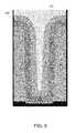
- FIG. 8shows a partially filled high aspect ratio gap that was filled according to the disclosed PEALD methods.
- FIGS. 9-11show additional pictures of high aspect ratio gaps filled according to the disclosed PEALD methods.
- FIG. 12shows a wide gap filled with silicon oxide deposited according to a disclosed PECVD method.
- semiconductor wafersemiconductor wafer
- wafersemiconductor wafer
- substratesubstrate
- wafer substratesemiconductor substrate
- partially fabricated integrated circuitcan refer to a silicon wafer during any of many stages of integrated circuit fabrication thereon.
- a wafer or substrate used in the semiconductor device industrymay have a diameter of 200 mm, or 300 mm, or 450 mm.
- the following detailed descriptionassumes the invention is implemented on a wafer. However, the invention is not so limited.
- the work piecemay be of various shapes, sizes, and materials.
- other work pieces that may take advantage of this inventioninclude various articles such as printed circuit boards, glass panels, and the like.
- HDP, SACVD and LPCVDhave only limited fill capability, and typically result in the formation of voids and seams. These voids and seams can open up after a chemical mechanical polishing (CMP) operation, or after an etch-back is performed. These opened seams and voids can then trap materials, such as polysilicon and tungsten, that are subsequently deposited. These materials are often incompletely removed in subsequent CMP or etch-back operations, and can remain in the device to cause shorts and/or loss of yield.
- CMPchemical mechanical polishing
- etch-backetch-back
- Certain embodiments hereinrelate to a hybrid method of filling differently sized gaps on a semiconductor substrate.
- the first portion of the methodrelates to an ALD operation, for example a plasma enhanced ALD (PEALD) operation.
- the ALD operationmay be performed in a novel way to promote a bottom-up type fill in narrow gaps.
- This bottom-up fill mechanismhelps achieve the void-free, seam-free fill, particularly in narrow gaps (e.g., gaps having a critical dimension (CD) of about 50 nm or less) and/or gaps having high aspect ratios (e.g., depth to width aspect ratio of about 4:1 or higher).
- the ALD operationalso acts to form a layer on, but not completely fill, wider gaps present on the substrate (e.g., gaps having a CD larger than about 50 nm) having lower aspect ratios (e.g., aspect ratios of about 4:1 or lower).
- the second portion of the methodrelates to a plasma enhanced chemical vapor deposition (PECVD) method that is used to fill the remainder of the wider gaps.
- PECVDplasma enhanced chemical vapor deposition
- this methodmay be performed using a direct (in situ) capacitively coupled plasma.
- a radio frequency (RF) plasma sourceis employed, though any type of plasma source capable of generating a direct plasma may be employed, including microwave and DC sources.
- RFradio frequency
- a remotely-generated plasmamay be employed.
- the remote plasmamay be capacitively-coupled or inductively-coupled according to various embodiments.
- the plasmas used in the PECVD methods described hereinmay have lower plasma density than high density plasmas generated by in-situ inductively coupled plasma generators such as those used in HDP processes.
- plasma densitiesmay be on the order of about 10 11 -10 13 ions/cm 3 , as opposed to about 10 8 -10 10 ions/cm 3 for PECVD processes in certain embodiments.
- HDP methodsgenerally do not produce the required fill results, as described above, and typically require the use of etch operations between subsequent deposition steps.
- charged dielectric precursor speciesare directed downwards to fill the gap.
- the PEALD and PECVD methodsmay be implemented in the same chamber. Both of these types of processes run in similar pressure and flow regimes, and can use the same RF power sources. Further, the PECVD methods may be performed in a single step, meaning that no intervening etching operations (or other processes such as deposition processes) are required. By contrast, it is not practical to run PEALD and HDP processes in the same chamber.
- the two processesoperate in substantially different pressure regimes.
- PEALD processesgenerally run in the range of a few Ton, and benefit from high gas flows for purging.
- HDP processesoperate in the mTorr range, which requires relatively low gas flows compared to what is used with PEALD.
- HDP processesare typically practiced in large volume chambers, while ALD processes benefit from substantially smaller volumes.
- HDP processesgenerally require a different power source than PEALD, which would further complicate reactor design.
- HDP processeshave shown good gap fill, HDP processes suffer from engineering problems related to “forbidden gap” sizes. Where a hybrid ALD/HDP deposition approach is used, a forbidden gap may exist where the CD of the gap is slightly larger than 2 ⁇ the thickness of the ALD layer deposited. In these cases, the HDP processes are unable to fill the remaining gap.
- the PECVD methods described hereincan fill gaps including those previously lined with PEALD. After any challenging structures are lined/filled with PEALD, the PECVD process may be used to fill remaining structures in a less conformal manner.
- the PECVD operationis advantageous in achieving a high deposition rate to fill larger gaps that would take a long time to fill through ALD alone.
- the methodsinclude only the first operation of performing PEALD.
- the PEALD and PECVD operationsare performed in the same chamber.
- This setupis beneficial, as there is no need to transfer the substrate from a PEALD reaction chamber to a PECVD reaction chamber. Thus, there is no need to worry about moisture getting on or into the film, and there is no corresponding need to perform a de-gassing operation or high temperature anneal to remove the moisture before performing the PECVD operation.
- Another benefit to the single chamber approachis that it reduces capital costs, cycle times and process flow complexity.
- a first portion of the methodincludes a PEALD operation performed under optimum conditions for filling a high aspect ratio gap
- a second portion of the methodincludes a more relaxed PEALD operation such as one having reduced dose and purge times. These relaxed PEALD operations may also promote PECVD or partial PECVD deposition.
- an etch stepis used to taper the gap profile. The etch step may be performed between a first portion of the method and a second portion of the method (e.g., between a PEALD operation and a PECVD operation), or within a single portion of the method (e.g., between two PEALD operations or between two PECVD operations).
- the methodsmay be combined as appropriate. The optimum solution will depend on the actual distribution of aspect ratios and gap dimensions present on the substrate.
- the completed filmis generated in part by ALD/CFD and in part by a CVD process such as PECVD.
- a CVD processsuch as PECVD.
- the ALD/CFD portion of the deposition processis performed first and the PECVD portion is performed second, although this need not be the case.
- Mixed ALD/CFD with CVD processescan improve the step coverage over that seen with CVD alone and additionally improve the deposition rate over that seen with ALD/CFD alone.
- plasma or other activationis applied while one ALD/CFD reactant is flowing in order to produce parasitic CVD operations and thereby achieve higher deposition rates, a different class of films, etc.
- two or more ALD/CFD phasesmay be employed and/or two or more CVD phases may be employed.
- an initial portion of the filmmay be deposited by ALD/CFD, followed by an intermediate portion of the film being deposited by CVD, and a final portion of the film deposited by ALD/CFD.
- a transition phasemay be employed between the ALD/CFD and CVD phases.
- the conditions employed during such transition phasedifferent from those employed in either the ALD/CFD or the CVD phases.
- the conditionspermit simultaneous ALD/CFD surface reactions and CVD type gas phase reactions.
- the transition phasetypically involves exposure to a plasma, which may be pulsed for example. Further, the transition phase may involve delivery of one or more reactants at a low flow rate, i.e., a rate that is significantly lower than that employed in the corresponding ALD/CFD phase of the process.
- the disclosed PEALD processesare useful in achieving void-free, seam-free fill of relatively narrow/high aspect ratio features.
- certain embodiments of the processesappear to result in a bottom-up fill mechanism where material is preferentially deposited near the bottom of the gap as opposed to the top of the gap as the gap is being filled.
- the filmdeposits thicker at/near the bottom of the gap and in many cases achieves a tapered profile as the gap is filled.
- the tapered profileis defined to mean that the film deposits thicker near the bottom and thinner near the top of the gap, as shown in the Experimental section, below.
- This tapered profileis especially useful in achieving a high quality fill without voids or seams in high aspect ratio features.
- This fill mechanismwas unexpected, as atomic layer deposition methods typically result in the formation of a seam as the sidewalls close in towards one another. By promoting bottom-up fill, this seam can be avoided and a more robust device results.
- the bottom-up fill mechanismmay be caused by preferential film densification near the top of the gap.
- species present in the plasmaespecially ions
- bombard the film surfacethereby compacting and densifying the film.
- this densificationmay happen preferentially near the top of the gap. Due to the shape of the gap, it is much easier for ions to bombard the film in the field region and near the top of the gap, as opposed to near the bottom of the gap, which is much more protected.
- the film near the topbecomes denser and thinner than the material near the bottom of the trench, which remains thicker and less dense.
- crosslinkingmay occur between groups present on opposing sidewalls of the gap. As deposition proceeds and the sidewalls close in towards one another, the terminal groups may crosslink with one another, thus avoiding any seam.
- surface hydroxyls/silanols on one sidewallmay crosslink with surface hydroxyls/silanols on the opposing wall, thereby liberating water and forming a silicon-oxide matrix.
- These terminal cross-linking groupsmay preferentially be found on the sidewalls of a gap.
- a further factor that may promote seam-free, void-free, bottom-up fillingis that ligand byproducts may be liberated from the film in a non-uniform manner, such that the byproducts become preferentially trapped at or near the bottom of the gap as opposed to near the top of the gap. This entrapment may lead to a higher deposition rate within the feature, especially near the bottom of the gap.
- BBASbis(tertiary-butyl-amino)silane
- TSAtert-butylamine
- FIG. 1presents a flowchart for a method of performing a plasma enhanced atomic layer deposition process 100 .
- the process 100begins at operation 101 , where a dose of a first reactant is provided to a reaction chamber containing a substrate.
- the substratewill typically have gaps therein that are to be filled, partially or completely, through the PEALD process.
- the PEALD process 100completely fills gaps of a first type, and partially fills (e.g., lines) gaps of a second type, as discussed further below.
- the first reactantmay be a silicon-containing reactant.
- the reaction chamberis purged, for example with an inert gas or a nitrogen carrier gas. This helps remove any remaining first reactant from the reaction chamber.
- the second reactantis provided to the reaction chamber.
- the second reactantis an oxidizing reactant.
- the second reactantmay also be a mix of reactants.
- the second reactantis a roughly equal volume flow of oxygen and nitrous oxide.
- the phrase “roughly equal volume flow”means that the flow of a first species and the flow of a second species do not differ by more than about 20%, as measured in SLM.
- the second reactantis provided in operation 105 , which may include pre-flowing the reactant before flowing the reactant coincident with plasma activation in operation 107 .
- the plasmaWhen the plasma is activated, it drives a reaction between the first and second reactants on the surface of the substrate. Next, the plasma is extinguished, and then the reaction chamber is purged, for example with inert gas or a nitrogen carrier gas. This operation 109 is referred to as the post-RF purge.
- the method 100is typically repeated a number of times to build up the desired film thickness.
- the method 100can result in a fill having a tapered profile and bottom-up fill characteristics. These factors promote void-free, seam-free fill.
- the film deposited through the disclosed methodsare fairly dense.
- operation 101includes providing BTBAS (or other primary reactant) at a flow rate of about 0.5-2.5 mL/min, or about 1.5-2.5 L/min, for example 2 mL/min, for a time period of between about 0.1-1 second, or about 0.2-0.5 seconds, for example about 0.3 seconds.
- Operation 103includes purging the reaction chamber with inert gas for between about 0.1-1 seconds, or between about 0.2-0.5 seconds, for example about 0.3 seconds.
- Operation 105includes co-flowing O 2 and N 2 O at a flow rate between about 2-20 SLM each, or between about 8-12 SLM each, for example about 10 SLM each.
- a plasmais generated at operation 107 using between about 300 W-10 kW, or between about 4-6 kW, for example about 5 kW RF power. These values represent the total RF power delivered, which is divided among four stations/pedestals.
- the plasma exposurelasts for a duration between about 10 milliseconds and 3 seconds, or between about 0.25-1 second, for example about 0.5 seconds.
- the RF frequency applied to generate the plasmamay be about 13.56 or 27 MHz.
- the reaction chamberis purged with inert gas at operation 109 for a time period between about 10 milliseconds and 5 seconds, or between about 50-150 milliseconds, for example about 90 milliseconds. It should be understood that the above conditions are examples, with other reactants, flow rates, pulse times, and power used as appropriate for the particular implementation.
- PEALD methods described hereinmay be conformal film deposition (CFD) methods.
- CFDconformal film deposition
- Plasma enhanced conformal film deposition techniques and apparatusare further discussed and described in U.S. patent application Ser. No. 13/084,399, filed Apr. 11, 2011, and titled “PLASMA ACTIVATED CONFORMAL FILM DEPOSITION,” which is incorporated by reference in its entirety above.
- the disclosed methods and apparatusare not limited to use with particular precursors. While the methods have already proven to be effective with certain precursors (as shown in the Experimental section) it is believed that the methods may also be used with a variety of other precursors to gain similar benefits.
- At least one of the reactantswill generally contain an element that is solid at room temperature, the element being incorporated into the film formed by the PEALD/PECVD method.
- This reactantmay be referred to as a principal reactant.
- the principal reactanttypically includes, for example, a metal (e.g., aluminum, titanium, etc.), a semiconductor (e.g., silicon, germanium, etc.), and/or a non-metal or metalloid (e.g., boron).
- the other reactantis sometimes referred to as an auxiliary reactant or a co-reactant.
- Non-limiting examples of co-reactantsinclude oxygen, ozone, hydrogen, hydrazine, water, carbon monoxide, nitrous oxide, ammonia, alkyl amines, and the like.
- the co-reactantmay also be a mix of reactants, as mentioned above.
- the PEALD/PECVD processmay be used to deposit a wide variety of film types and in particular implementations to fill gaps with these film types. While much of the discussion herein focuses on the formation of undoped silicon oxides, other film types such as nitrides, carbides, oxynitrides, carbon-doped oxides, nitrogen-doped oxides, borides, etc. may also be formed. Oxides include a wide range of materials including undoped silicate glass (USG), doped silicate glass. Examples of doped glasses included boron doped silicate glass (BSG), phosphorus doped silicate glass (PSG), and boron phosphorus doped silicate glass (BPSG). Still further, the PEALD/PECVD process may be used for metal deposition and feature fill.
- the deposited filmis a silicon-containing film.
- the silicon-containing reactantmay be for example, a silane, a halosilane or an aminosilane.
- a silanecontains hydrogen and/or carbon groups, but does not contain a halogen.
- silanesexamples include silane (SiH 4 ), disilane (Si 2 H 6 ), and organo silanes such as methylsilane, ethylsilane, isopropylsilane, t-butylsilane, dimethylsilane, diethylsilane, di-t-butylsilane, allylsilane, sec-butylsilane, thexylsilane, isoamylsilane, t-butyldisilane, di-t-butyldisilane, tetra-ethyl-ortho-silicate (also known as tetra-ethoxy-silane or TEOS) and the like.
- organo silanessuch as methylsilane, ethylsilane, isopropylsilane, t-butylsilane, dimethylsilane, diethylsilane, di-t-butyl
- halosilanecontains at least one halogen group and may or may not contain hydrogens and/or carbon groups.
- halosilanesare iodosilanes, bromosilanes, chlorosilanes and fluorosilanes.
- halosilanes, particularly fluorosilanesmay form reactive halide species that can etch silicon materials, in certain embodiments described herein, the silicon-containing reactant is not present when a plasma is struck.
- chlorosilanesare tetrachlorosilane (SiCl 4 ), trichlorosilane (HSiCl 3 ), dichlorosilane (H 2 SiCl 2 ), monochlorosilane (ClSiH 3 ), chloroallylsilane, chloromethylsilane, dichloromethylsilane, chlorodimethylsilane, chloroethylsilane, t-butylchlorosilane, di-t-butylchlorosilane, chloroisopropylsilane, chloro sec-butylsilane, t-butyldimethylchlorosilane, thexyldimethylchlorosilane, and the like.
- aminosilaneincludes at least one nitrogen atom bonded to a silicon atom, but may also contain hydrogens, oxygens, halogens and carbons.
- Examples of aminosilanesare mono-, di-, tri- and tetra-aminosilane (H 3 SiNH 2 ), H 2 Si(NH 2 ) 2 , HSi(NH 2 ) 3 and Si(NH 2 ) 4 , respectively), as well as substituted mono-, di-, tri- and tetra-aminosilanes, for example, t-butylaminosilane, methylaminosilane, tert-butylsilanamine, bis(tertiarybutylamino)silane (SiH 2 (NHC(CH 3 ) 3 ) 2 (BTBAS), tert-butyl silylcarbamate, SiH(CH 3 )—(N(CH 3 ) 2 ) 2 , SiHCl—(N(CH 3 ) 2 ) 2 , (
- the deposited filmcontains metal.
- metal-containing filmsthat may be formed include oxides and nitrides of aluminum, titanium, hafnium, tantalum, tungsten, manganese, magnesium, strontium, etc., as well as elemental metal films.
- Example precursorsmay include metal alkylamines, metal alkoxides, metal alkylamides, metal halides, metal ⁇ -diketonates, metal carbonyls, organometallics, etc. Appropriate metal-containing precursors will include the metal that is desired to be incorporated into the film.
- a tantalum-containing layermay be deposited by reacting pentakis(dimethylamido)tantalum with ammonia or another reducing agent.
- metal-containing precursorsexamples include trimethylaluminum, tetraethoxytitanium, tetrakis-dimethyl-amido titanium, hafnium tetrakis(ethylmethylamide), bis(cyclopentadienyl)mangane se, bis(n-propylcyclopentadienyl)magnesium, etc.
- an oxygen-containing oxidizing reactantis used.
- oxygen-containing oxidizing reactantsinclude oxygen, ozone, nitrous oxide, carbon monoxide, etc.
- the deposited filmcontains nitrogen, and a nitrogen-containing reactant is used.
- a nitrogen-containing reactantcontains at least one nitrogen, for example, ammonia, hydrazine, amines (e.g., amines bearing carbon) such as methylamine, dimethylamine, ethylamine, isopropylamine, t-butylamine, di-t-butylamine, cyclopropylamine, sec-butylamine, cyclobutylamine, isoamylamine, 2-methylbutan-2-amine, trimethylamine, diisopropylamine, diethylisopropylamine, di-t-butylhydrazine, as well as aromatic containing amines such as anilines, pyridines, and benzylamines.
- aminese.g., amines bearing carbon
- Aminesmay be primary, secondary, tertiary or quaternary (for example, tetraalkylammonium compounds).
- a nitrogen-containing reactantcan contain heteroatoms other than nitrogen, for example, hydroxylamine, t-butyloxycarbonyl amine and N-t-butyl hydroxylamine are nitrogen-containing reactants.
- the disclosed PEALD processis especially useful for filling relatively narrow gaps (CD ⁇ about 50 nm) having a relatively high aspect ratio (AR>about 4:1). However, the process may also be performed on larger gaps and gaps having smaller ARs, as well.
- the PEALD processis performed on a substrate having at least two different types of gaps.
- a first typemay include gaps having a CD less than about 50 nm, and/or an AR greater than about 4:1. This first type is referred to as a narrow gap.
- a second typemay include gaps having a CD greater than about 50 nm, and/or an AR less than about 4:1. This second type is referred to as a wide gap.
- a wide gapis at least about 2 times, or at least about 5 times, or at least about 10 times wider than a narrow gap.
- the AR of the narrow gapmay be at least about 2 times, or at least about 5 times, or at least about 10 times greater than the AR of the wide gap.
- FIG. 2presents a substrate 200 having two different types of gaps 202 and 204 .
- the aspect ratio of the gapsis calculated as the height of the gap divided by the width of the gap. These dimensions are labeled in FIG. 2 .
- Gaps 202are narrow gaps having an aspect ratio slightly larger than 4:1.
- Gaps 204are wide gaps having an aspect ratio of about 1:2.
- FIG. 3shows the same substrate 200 after a PEALD deposition process is performed to deposit an oxide layer 210 .
- the narrow gaps 202are completely filled, while the wide gap 204 is lined with oxide material 210 .
- the film 210 deposited on the bottom of the wide gap 204may be slightly thicker than the film 210 deposited on the sidewalls of gap 204 . However, this thickness difference is much more pronounced in the narrow gap 202 as it fills with material.
- FIG. 4shows a portion of substrate 200 at a time during the PEALD deposition process.
- narrow gap 202is shown mid-deposition.
- the deposited oxide layer 210has a tapered profile, such that the film is thinner near the top of the gap and thicker near the bottom of the gap. This results in a diminishing gap that is smaller at the bottom than at the top. This shape is ideal for promoting void-free, seam-free fill.
- the mechanisms described abovee.g., preferential film densification, preferential ligand trapping, and/or crosslinking
- a gap filled by a PEALD operationhas a reentrant profile.
- the gapis smaller at an upper portion and wider at a lower portion. It has been observed that bottom-up fill can be achieved with the disclosed PEALD process, even with gaps that have a somewhat reentrant profile.
- the PEALD processhas been shown to be fairly resilient to changes in temperature.
- the processhas been shown to be effective at 200° C. and 400° C. In some embodiments, therefore, the process is conducted at a temperature between about 200-400° C. In other cases, however, the temperature may fall outside this range.
- the pressure inside the reaction chamber during the PEALD processmay be between about 1-10 Torr, or between about 3-7 Torr, for example about 6 Torr.
- the substrateis exposed to plasma to drive the reaction between the first and second reactants.
- plasmamay be used to drive this reaction including capacitively coupled plasmas and inductively coupled plasmas.
- plasma generatorsmay be used including RF, DC, and microwave plasma generators.
- the plasmamay be direct or remote.
- the gas used to generate the plasmamay include an inert gas such as argon or helium.
- the gaswill also typically include one of the reactants, for example an oxidizing reactant where an oxide film is being formed.
- an RF signalis used to drive plasma formation.
- the RF appliedis high frequency RF only, for example at a frequency of about 13.56 or 27 MHz.
- the RFhas a low frequency component as well.
- the RF power delivered to drive plasma formationmay be between about 300 W and about 10 kW. In some cases, the RF power delivered is between about 4-6 kW, for example about 5 kW. These values represent the total power delivered, which is divided among four stations/pedestals.
- the duration of plasma exposuremay vary between different embodiments.
- RF poweris applied for between about 10 milliseconds and 3 seconds, or between about 0.25 seconds and about 1 second. In a particular example, RF power is applied for about 0.5 seconds.
- the RF power and RF timedetermine the RF flux delivered to the chamber. It has been found that by increasing the RF flux (either by increasing RF time or power), the wet etch rate (WER) of the film may be reduced. Because the PEALD process has shown a fair resilience to different RF conditions, these variables may be used to achieve a tunable WER.
- the first purgeoccurs after the dose of the first reactant is delivered to the processing chamber, and may be referred to as a reactant purge. This purge is conducted to sweep out any remaining, non-adsorbed first reactant.
- the second purgeoccurs after the substrate is exposed to plasma, and may be referred to as the post-RF purge. This purge is conducted to sweep out any remaining reactants, as well as any film formation byproducts.
- One methodinvolves supplying the chamber with a flow of non-reactant gas (e.g., argon, helium, nitrogen, etc.) to sweep out any undesired species. With a sweep, the pressure in the reaction chamber stays substantially constant.
- Another method of purging a reaction chamberis to perform a pump down. Where this is the case, a vacuum is applied and the reaction chamber is evacuated. During the evacuation, the pressure in the reaction chamber is significantly reduced, for example to less than about 1 Torr.
- gapfill resultsare better where the post-RF purge includes a sweep, as compared to a pump down.
- the post-RF conditionsincluding the presence or absence of a pump down, may affect the surface functionality present on the surface of the deposited film. This surface functionality may determine whether or not crosslinking occurs between opposing sidewalls as the gap is filled.
- One way to encourage the desired bottom-up deposition patternis to sweep the reaction chamber instead of performing a pump down.
- no pump downis performed after plasma exposure during the PEALD deposition.
- a pump downmay be performed between a PEALD operation and a PECVD operation.
- the reactant purgemay be performed for a duration between about 0.1-1 seconds, for example between about 0.2-0.5 seconds. In a particular example, the reactant purge has a duration of about 0.3 seconds.
- the post-RF purgemay be performed for a duration between about 0.01-5 seconds, for example between about 0.05-0.15 seconds. In one case the post-RF purge has a duration of about 0.09 seconds.
- the PECVD methods disclosed hereinmay be practiced after a PEALD process to finish filling gaps that were only partially filled/lined. This method is advantageous compared to a PEALD process alone because it offers a much higher deposition rate, resulting in decreased processing times and increased throughput.
- the PEALD processmay be used to fill small gaps and line large gaps, and then the PECVD process may be used to complete the filling of the large gaps. This offers a convenient way to fill features of varying sizes and aspect ratios. In many cases, the gaps can be filled without any intervening etching operations.
- FIG. 5shows a flow chart for a method 500 of filling a gap with PECVD.
- the method 500may be performed after the method 100 of FIG. 1 .
- the PECVD methodgenerally begins by flowing one or more reactants into the reaction chamber at operation 501 .
- the reactant deliverymay continue as plasma is generated in operation 503 .
- the substrate surfaceis exposed to plasma, which causes deposition to occur on the substrate surface in operation 505 . This process continues until a desired film thickness is reached.
- the plasmais extinguished and the reactant flow is terminated.
- the reaction chamberis purged at operation 509 .
- operation 501includes flowing TEOS at a rate of about 1-20 mL/min and O 2 at a rate of about 2,000-30,000 sccm.
- RF poweris applied with an HF component between about 200-3,000 W, and an LF component between about 200-2,500 W (divided among four stations).
- the HF frequencyis about 13.56 or 27 MHz, while the LF frequency is between about 300-400 kHz.
- the pressure in the reaction chamberis between about 1-10 Torr, and the temperature is between about 100-450° C.
- the reactants, chamber conditions, timing, etc.may vary depending on the desired film and application. The values provided in this section are not intended to be limiting.
- the PEALD processmay end by extinguishing the plasma, performing the post-RF purge (with or without a pump down), and then immediately flowing the PECVD reactant(s).
- hybrid PEALD/PECVD methodsas discussed and described in U.S. patent application Ser. No. 13/084,399, filed Apr. 11, 2011, and titled “PLASMA ACTIVATED CONFORMAL FILM DEPOSITION,” which is incorporated by reference above, may be used.
- the PECVD reactionmay be performed with either the same reactants as the ALD reaction, or with different reactants.
- the PEALD reactionis performed with BTBAS and a mixture of O 2 /N 2 O, and the PECVD reaction is performed with TEOS and/or silane.
- the TEOS and silane reactantshave been found to be especially useful in practicing the PECVD reaction.
- the reactants listed above in the PEALD Reactants sectionmay be used in the PECVD reaction.
- the flow rate of reactantsmay vary depending on the desired process.
- SiH 4is used as a reactant and has a flow rate between about 100-1,500 sccm, with a flow of N 2 O between about 2,000-20,000 sccm.
- the flow of TEOSis between about 1-20 mL/min, and the flow of O 2 is between about 2,000-30,000 sccm.
- the temperature in the reaction chamber during the PECVD reactionmay be between about 50-450° C., in certain embodiments. This range may be especially appropriate for reactions using silane. Where other reactants are used, the temperature range may be more limited or more broad, for example between about 100-450° C. where TEOS is used.
- the pressure in the reaction chamber during the PECVD reactionmay be between about 1-10 Torr, for example about 5 Torr.
- the chamber conditionsare very similar between the PEALD operation and the PECVD operation, it is feasible to implement both types of reactions in a single reaction chamber. As discussed above, this is advantageous because it reduces or eliminates the risk of moisture entering the film as the substrate is moved between processing chambers, and reduces the need to perform a degassing operation between the two processes.
- the PECVD reactionsare driven by exposure to plasma.
- the plasmamay be a capacitively coupled plasma or a remotely generated inductively coupled plasma. For the reasons discussed above, it may be preferable to avoid using an in situ inductively coupled plasma.
- the gas used to generate the plasmawill include at least one reactant.
- the plasma generation gasmay also include other species, as well.
- the plasma generation gasincludes an inert gas.
- the frequency used to drive plasma formationmay contain both LF and HF components.
- the HF frequencymay be about 13.56 MHz or about 27 MHz.
- the LF frequencymay be between about 300-400 kHz.
- the HF RF power used to drive plasma formationmay be between about 200-3,000 W.
- the LF RF power used to drive plasma formationmay be between about 200-2,500 W. These power levels represent the total power delivered, which is divided among four stations. The duration of plasma exposure depends on the desired thickness of the deposited film.
- pulsed PECVD methodsmay be used. These methods may involve pulsing precursor and/or RF power levels.
- a purgeis typically conducted after the PECVD deposition is complete. This purge operates to remove reactants and any byproducts from the reaction chamber. Because the film is already deposited at this point, the purge conditions are less important than with the PEALD reactions, which require many iterations of reactant purge and post-RF purge as the PEALD film is formed.
- a suitable apparatus for performing the disclosed methodstypically includes hardware for accomplishing the process operations and a system controller having instructions for controlling process operations in accordance with the present invention.
- the hardwaremay include one or more PEALD, PECVD or joint PEALD/PECVD process stations included in a process tool.
- FIG. 6provides a block diagram of an example apparatus that may be used to practice the disclosed embodiments.
- a reactor 600includes a process chamber 624 , which encloses other components of the reactor and serves to contain the plasma generated by, e.g., a capacitor type system including a showerhead 614 working in conjunction with a grounded heater block 620 .
- a low-frequency RF generator 602connected to a matching network 606 , and a high-frequency RF generator 604 are connected to showerhead 614 .
- the power and frequency supplied by matching network 606is sufficient to generate a plasma from the process gas, for example 400-700 W total energy.
- both the HFRF generator and the LFRF generatorare used.
- the high frequency RF componentis generally between about 2-60 MHz; in a preferred embodiment, the HF component is about 13.56 MHz or 27 MHz.
- the low frequency LF componentis generally between about 250-400 kHz; in a particular embodiment, the LF component is about 350 kHz.
- a wafer pedestal 618supports a substrate 616 .
- the pedestaltypically includes a chuck, a fork, or lift pins to hold and transfer the substrate during and between the deposition and/or plasma treatment reactions.
- the chuckmay be an electrostatic chuck, a mechanical chuck or various other types of chuck as are available for use in the industry and/or research.
- the process gasesare introduced via inlet 612 .
- Multiple source gas lines 610are connected to manifold 608 .
- the gasesmay be premixed or not.
- Appropriate valving and mass flow control mechanismsare employed to ensure that the correct gases are delivered during the deposition and plasma treatment phases of the process.
- liquid flow control mechanismsare employed. The liquid is then vaporized and mixed with other process gases during its transportation in a manifold heated above its vaporization point before reaching the deposition chamber.
- a vacuum pump 626e.g., a one or two stage mechanical dry pump and/or a turbomolecular pump typically draws process gases out and maintains a suitably low pressure within the reactor by a close loop controlled flow restriction device, such as a throttle valve or a pendulum valve.
- the inventionmay be implemented on a multi-station or single station tool.
- the 300 mm Novellus VectorTM tool having a 4-station deposition scheme or the 200 mm SequelTM tool having a 6-station deposition schemeare used. It is possible to index the wafers after every deposition and/or post-deposition plasma anneal treatment until all the required depositions and treatments are completed, or multiple depositions and treatments can be conducted at a single station before indexing the wafer. It has been shown that film stress is the same in either case. However, conducting multiple depositions/treatments on one station is substantially faster than indexing following each deposition and/or treatment.
- FIG. 7shows a schematic view of an embodiment of a multi-station processing tool 2400 with an inbound load lock 2402 and an outbound load lock 2404 , either or both of which may comprise a remote plasma source.
- a robot 2406at atmospheric pressure, is configured to move wafers from a cassette loaded through a pod 2408 into inbound load lock 2402 via an atmospheric port 2410 .
- a waferis placed by the robot 2406 on a pedestal 2412 in the inbound load lock 2402 , the atmospheric port 2410 is closed, and the load lock is pumped down.
- the inbound load lock 2402comprises a remote plasma source
- the wafermay be exposed to a remote plasma treatment in the load lock prior to being introduced into a processing chamber 2414 .
- the waferalso may be heated in the inbound load lock 2402 as well, for example, to remove moisture and adsorbed gases.
- a chamber transport port 2416 to processing chamber 2414is opened, and another robot (not shown) places the wafer into the reactor on a pedestal of a first station shown in the reactor for processing. While the embodiment depicted in FIG. 7 includes load locks, it will be appreciated that, in some embodiments, direct entry of a wafer into a process station may be provided.
- the depicted processing chamber 2414comprises four process stations, numbered from 1 to 4 in the embodiment shown in FIG. 7 .
- Each stationhas a heated pedestal (shown at 2418 for station 1 ), and gas line inlets.
- each process stationmay have different or multiple purposes.
- a process stationmay be switchable between a PEALD and PECVD process mode.
- processing chamber 2414may include one or more matched pairs of PEALD and PECVD process stations.
- a processing chambermay have any suitable number of stations.
- a processing chambermay have five or more stations, while in other embodiments a processing chamber may have three or fewer stations.
- FIG. 7also depicts an embodiment of a wafer handling system 2490 for transferring wafers within processing chamber 2414 .
- wafer handling system 2490may transfer wafers between various process stations and/or between a process station and a load lock. It will be appreciated that any suitable wafer handling system may be employed. Non-limiting examples include wafer carousels and wafer handling robots.
- FIG. 7also depicts an embodiment of a system controller 2450 employed to control process conditions and hardware states of process tool 2400 .
- System controller 2450may include one or more memory devices 2456 , one or more mass storage devices 2454 , and one or more processors 2452 .
- Processor 2452may include a CPU or computer, analog and/or digital input/output connections, stepper motor controller boards, etc.
- system controller 2450controls all of the activities of process tool 2400 .
- System controller 2450executes system control software 2458 stored in mass storage device 2454 , loaded into memory device 2456 , and executed on processor 2452 .
- System control software 2458may include instructions for controlling the timing, mixture of gases, chamber and/or station pressure, chamber and/or station temperature, purge conditions and timing, wafer temperature, RF power levels, RF frequencies, substrate, pedestal, chuck and/or susceptor position, and other parameters of a particular process performed by process tool 2400 .
- System control software 2458may be configured in any suitable way. For example, various process tool component subroutines or control objects may be written to control operation of the process tool components necessary to carry out various process tool processes in accordance with the disclosed methods.
- System control software 2458may be coded in any suitable computer readable programming language.
- system control software 2458may include input/output control (IOC) sequencing instructions for controlling the various parameters described above.
- IOCinput/output control
- each phase of a PEALD processmay include one or more instructions for execution by system controller 2450 .
- the instructions for setting process conditions for a PEALD process phasemay be included in a corresponding PEALD recipe phase.
- the PEALD recipe phasesmay be sequentially arranged, so that all instructions for a PEALD process phase are executed concurrently with that process phase. The same can be said for PECVD processes and hybrid PEALD/PECVD processes.
- mass storage device 2454 and/or memory device 2456 associated with system controller 2450may be employed in some embodiments.
- programs or sections of programs for this purposeinclude a substrate positioning program, a process gas control program, a pressure control program, a heater control program, and a plasma control program.
- a substrate positioning programmay include program code for process tool components that are used to load the substrate onto pedestal 2418 and to control the spacing between the substrate and other parts of process tool 2400 .
- a process gas control programmay include code for controlling gas composition and flow rates and optionally for flowing gas into one or more process stations prior to deposition in order to stabilize the pressure in the process station.
- a pressure control programmay include code for controlling the pressure in the process station by regulating, for example, a throttle valve in the exhaust system of the process station, a gas flow into the process station, etc.
- a heater control programmay include code for controlling the current to a heating unit that is used to heat the substrate.
- the heater control programmay control delivery of a heat transfer gas (such as helium) to the substrate.
- a plasma control programmay include code for setting RF power levels applied to the process electrodes in one or more process stations.
- the user interfacemay include a display screen, graphical software displays of the apparatus and/or process conditions, and user input devices such as pointing devices, keyboards, touch screens, microphones, etc.
- parameters adjusted by system controller 2450may relate to process conditions.
- process conditionsinclude process gas composition and flow rates, temperature, pressure, plasma conditions (such as RF bias power levels), pressure, temperature, etc. These parameters may be provided to the user in the form of a recipe, which may be entered utilizing the user interface.
- Signals for monitoring the processmay be provided by analog and/or digital input connections of system controller 2450 from various process tool sensors.
- the signals for controlling the processmay be output on the analog and digital output connections of process tool 2400 .
- process tool sensorsthat may be monitored include mass flow controllers, pressure sensors (such as manometers), thermocouples, etc. Appropriately programmed feedback and control algorithms may be used with data from these sensors to maintain process conditions.
- System controller 2450may provide program instructions for implementing the above-described deposition processes.
- the program instructionsmay control a variety of process parameters, such as DC power level, RF power level, RF bias power level, pressure, temperature, etc.
- the instructionsmay control the parameters to operate in-situ deposition of film stacks according to various embodiments described herein.
- Lithographic patterning of a filmtypically comprises some or all of the following steps, each step enabled with a number of possible tools: (1) application of photoresist on a workpiece, e.g., a substrate having a silicon nitride film formed thereon, using a spin-on or spray-on tool; (2) curing of photoresist using a hot plate or furnace or other suitable curing tool; (3) exposing the photoresist to visible or UV or x-ray light with a tool such as a wafer stepper; (4) developing the resist so as to selectively remove resist and thereby pattern it using a tool such as a wet bench or a spray developer; (5) transferring the resist pattern into an underlying film or workpiece by using a dry or plasma-assisted etching tool; and (6) removing the resist using a tool such as an RF or microwave plasma resist stripper.
- an ashable hard mask layersuch as an amorphous carbon layer
- another suitable hard masksuch as an antireflective
- FIG. 8presents a gap 802 partially filled with silicon oxide film 804 in a PEALD process according to the disclosed methods.
- Markers 806are provided in order to evaluate the conformality of the oxide film 804 .
- Each of the markers 806has an identical height.
- the deposited filmis thicker at the bottom than at the top.
- the lower sidewallsare thicker than the upper sidewalls, which are both thicker than the top region.
- the film thickness near the topis about the same as the film thickness in the top corner.
- the silicon oxide film 804was deposited at about 400° C., with a 2 mL/min flow of BTBAS for a duration of about 0.3 seconds, followed by a reactant purge with a sweep duration of about 0.3 seconds, followed by delivery of a mixture of O 2 /N 2 O at 10 SLM each, coincident with a 0.5 second exposure to RF plasma, followed by a post-RF purge having a duration of 0.09 seconds.
- the plasmawas a high frequency plasma, with a power of about 5 kW split among four pedestals.
- the film 804shows a tapered profile, which is ideal for filling gaps, especially those having large aspect ratios.
- FIG. 9shows a substrate with a number of gaps filled with silicon-oxide according to the disclosed PEALD methods.
- the gapsin this case have an aspect ratio of about 7:1, and a CD on the order of about 30 nm.
- the deposited filmwas dense, and did not show any seams or voids.
- FIG. 10shows a close-up view of a gap filled according to the disclosed PEALD methods. No seams or voids are detected in the fill.
- FIG. 11shows a substrate having high aspect ratio gaps (AR about 8:1) filled according to the disclosed PEALD methods.
- the gap on the rightshows some degree of reentrancy.
- the markers A and Bare the same length. It can be seen that the gap is wider at marker B than at marker A. While the width difference is fairly slight, even small degrees of reentrancy will result in the formation of voids under many conventional methods.
- FIG. 12shows a wide gap filled with silicon oxide according to a disclosed PECVD method with TEOS performed at about 200° C.
- the film depositedwas about 2,000 ⁇ thick, and showed good gap fill properties, with no voids or seams. No etching operations were performed.
Landscapes
- Engineering & Computer Science (AREA)
- Chemical & Material Sciences (AREA)
- Physics & Mathematics (AREA)
- Power Engineering (AREA)
- Condensed Matter Physics & Semiconductors (AREA)
- General Physics & Mathematics (AREA)
- Manufacturing & Machinery (AREA)
- Computer Hardware Design (AREA)
- Microelectronics & Electronic Packaging (AREA)
- Chemical Kinetics & Catalysis (AREA)
- General Chemical & Material Sciences (AREA)
- Materials Engineering (AREA)
- Mechanical Engineering (AREA)
- Metallurgy (AREA)
- Organic Chemistry (AREA)
- Plasma & Fusion (AREA)
- Inorganic Chemistry (AREA)
- Electromagnetism (AREA)
- Formation Of Insulating Films (AREA)
- Chemical Vapour Deposition (AREA)
Abstract
Description
This application claims benefit of prior U.S. Provisional Application No. 61/884,923, filed Sep. 30, 2013, and titled “GAPFILL OF VARIABLE ASPECT RATIO FEATURES WITH A COMPOSITE PEALD AND PECVD METHOD,” which is incorporated herein by reference in its entirety and for all purposes. This application is also a continuation-in-part of U.S. patent application Ser. No. 13/084,399, filed Apr. 11, 2011, and titled “PLASMA ACTIVATED CONFORMAL FILM DEPOSITION,” which claims benefit of the following prior U.S. Provisional Application Nos., each of which is incorporated herein by reference in its entirety and for all purposes: 61/324,710, filed Apr. 15, 2010, and titled “PLASMA ACTIVATED CONFORMAL FILM DEPOSITION”; 61/372,367, filed Aug. 10, 2010, and titled “PLASMA ACTIVATED CONFORMAL FILM DEPOSITION”; 61/379,081, filed Sep. 1, 2010, and titled “PLASMA ACTIVATED CONFORMAL FILM DEPOSITION”; and 61/417,807, filed Nov. 29, 2010, and titled “PLASMA ACTIVATED CONFORMAL FILM DEPOSITION.”
The fabrication of integrated circuits includes many diverse processing steps. One of the operations frequently employed is the deposition of a dielectric film into a gap between features patterned over or into silicon substrates. One of the goals in depositing such material is to form a void-free, seam-free fill in the gap. As device dimensions become smaller in the context of DRAM, flash memory and logic, for example, it has become increasingly difficult to achieve this type of ideal fill.
While deposition methods such as high density plasma (HDP), sub-atmospheric chemical vapor deposition (SACVD), and low pressure chemical vapor deposition (LPCVD) have been used for gap fill, these methods do not achieve the desired fill capability. Flowable chemical vapor deposition and spin-on dielectric (SOD) methods can achieve the desired fill, but tend to deposit highly porous films. Further, these methods are especially complex and costly to integrate, as they require many extra processing steps. Atomic layer deposition (ALD) processes have also been used for gap fill, but these processes suffer from long processing times and low throughput, especially for large gaps. In some cases, multi-step deposition processes are used, including deposition-etch-deposition processes which require distinct etching operations between subsequent deposition operations. The etching may be done to remedy or prevent void formation in the gap. While this method is useful, it would be preferable to use a process that involves only deposition, with no required etch operations.
A further challenge is simultaneously filling gaps of different sizes on a substrate. For example, a deposition method optimized for a wide gap with a small aspect ratio may not be suitable for filling a narrow gap with a large aspect ratio, and vice versa. Therefore, a method of achieving void-free, seam-free fill of dielectric material into a gap is needed, particularly one that may be used to simultaneously fill gaps of various sizes.
Certain embodiments herein relate to methods and apparatus for filling a gap on a semiconductor substrate. In certain cases, the gap is filled through a plasma enhanced atomic layer deposition (PEALD) operation. In other cases, the gap is filled through a hybrid method including both PEALD and plasma enhanced chemical vapor deposition (PECVD) operations. In one aspect of the embodiments herein, a method is provided for filling a gap including (a) introducing a first reactant in vapor phase into a reaction chamber having the substrate therein, and allowing the first reactant to adsorb onto the substrate surface; (b) introducing a second reactant in vapor phase into the reaction chamber and allowing the second reactant to adsorb onto the substrate surface; (c) exposing the substrate surface to plasma to drive a surface reaction between the first and second reactants on the substrate surface to form a film layer that lines the bottom and sidewalls of the gap; (d) sweeping the reaction chamber without performing a pumpdown; and (e) repeating operations (a) through (d) to form additional film layers, where when opposing film layers on opposite sidewalls of the gap approach one another, surface groups present on the opposing film layers crosslink with one another to thereby fill the gap. The methods may be used to fill the gap without the formation of a void or seam.
In some embodiments, the first reactant is a silicon-containing reactant and the second reactant is an oxidizing reactant. For example, the first reactant may include bis(tertiary-butyl-amino)silane (BTBAS). In a further example, the second reactant may include oxygen and/or nitrous oxide. In various cases, the gap is reentrant. Further, in many embodiments, the gap is filled through a mechanism that may be characterized at least in part as a bottom-up fill mechanism. This bottom-up fill mechanism may achieve a seam-free, void-free fill, even where a gap is reentrant.
In another aspect of the disclosed embodiments, a method of filling a gap on a substrate surface is provided, including (a) introducing a first reactant in vapor phase into a reaction chamber having the substrate therein, and allowing the first reactant to adsorb onto the substrate surface; (b) introducing a second reactant in vapor phase into the reaction chamber and allowing the second reactant to adsorb onto the substrate surface; and (c) exposing the substrate surface to plasma to drive a surface reaction between the first and second reactants on the substrate surface to form a film layer that lines the bottom and sidewalls of the gap, where the film is denser and/or thinner near the field region and upper sidewalls of the gap compared to near the bottom and lower sidewalls of the gap. The method may include an operation of (d) sweeping the reaction chamber without performing a pumpdown after (c) is performed. In some embodiments, the method includes repeating operations (a) through (c) (or (a) through (d)) to form additional film layers to thereby fill the gap. In certain embodiments the gap may be filled through a bottom-up fill mechanism, without the formation of a void or seam.
In another aspect of the disclosed embodiments, a method of filling a gap on a substrate surface is provided, including (a) introducing a first reactant in vapor phase into a reaction chamber having the substrate therein, and allowing the first reactant to adsorb onto the substrate surface; (b) introducing a second reactant in vapor phase into the reaction chamber and allowing the second reactant to adsorb onto the substrate surface; (c) exposing the substrate surface to plasma to drive a surface reaction between the first and second reactants on the substrate surface to form a film layer that lines the bottom and sidewalls of the gap, (d) sweeping the reaction chamber without performing a pumpdown; and repeating operations (a) through (d) to form additional film layers where ligands of one or more reactants are preferentially buried in the film near the bottom and lower sidewalls of the gap compared to the field region and upper sidewalls of the gap. The method may include an operation of (d) sweeping the reaction chamber without performing a pumpdown after (c) is performed. In certain embodiments, the gap may be filled through a bottom-up fill mechanism without the formation of a void or seam.
In a further aspect of the disclosed embodiments, a method of filling a gap on a substrate surface is provided, including (a) introducing a first reactant in vapor phase into a reaction chamber having the substrate therein, and allowing the first reactant to adsorb onto the substrate surface; (b) introducing a second reactant in vapor phase into the reaction chamber and allowing the second reactant to adsorb onto the substrate surface; (c) exposing the substrate surface to plasma to drive a surface reaction between the first and second reactants on the substrate surface to form a film lining the gap; (d) sweeping or purging the reaction chamber; (e) introducing a third reactant in vapor phase and fourth reactant in vapor phase into the reaction chamber concurrently; and (f) generating a plasma from the vapor phase reactants to drive a gas phase reaction between the third and fourth reactants, where the gas phase reaction produces a gap-filling material, and where the gap-filling material partially or completely fills the gap on the substrate surface.
The first and second reactants may be the same as at least one of the third and fourth reactants. For example, the first and second reactants may each be the same as the third and fourth reactants. In other cases, there may be no overlap between the first and second reactants and the third and fourth reactants. In many cases, the film formed in (c) is the same material as the gap-filling material formed in (f). For example, the film formed in (c) and the gap-filling material formed in (f) may be silicon oxide. In these cases, the first reactant may be a silicon-containing reactant and the second reactant may be an oxidizing reactant. For example, the first reactant may include BTBAS. In a further example, the second reactant may include oxygen and/or nitrous oxide. In these or other cases, examples of the third reactant may be TEOS or silane, with examples of the fourth reactant being an oxidizing reactant.
In some implementations, operations (a) through (c) are repeated before operations (e) through (f), and no pumpdown occurs after each iteration of operation (c). In these or other cases, the method may be performed without any intervening etching operations. One advantage of the disclosed embodiments is that the method may be performed in a single reaction chamber. In many cases, the substrate is not removed from the reaction chamber during or between any of operations (a) through (f). In some implementations, operations (a) through (c) include forming a conformal film that is thicker at the bottom of the gap than on the upper sidewalls of the gap. This may be achieved in a variety of ways. In some embodiments, operation (c) may include preferentially densifying the film near the top of the gap compared to the film near the bottom of the gap. In these or other embodiments, operation (c) may include preferentially burying ligands of one or more reactants in the film near the bottom of the gap compared to near the upper sidewalls of the gap. Operation (c) may also include promoting crosslinking between the film formed on a first sidewall of the gap and the film formed on an opposing sidewall of the gap.
In yet another aspect of the disclosed embodiments, a method of filling gaps on a substrate surface is provided, including (a) introducing a first reactant in vapor phase into a reaction chamber having the substrate therein, and allowing the first reactant to adsorb onto the substrate surface, where the substrate has at least a narrow gap having a critical dimension less than about 50 nm and a wide gap having a critical dimension greater than or equal to about 50 nm; (b) introducing a second reactant in vapor phase into the reaction chamber and allowing the second reactant to adsorb onto the substrate surface; (c) exposing the substrate surface to plasma to drive a surface reaction between the first and second reactants on the substrate surface to form a film, where the film completely fills the narrow gap and lines the wide gap; (d) sweeping or purging the reaction chamber; (e) introducing a third reactant in vapor phase and fourth reactant in vapor phase into the reaction chamber concurrently; and (f) generating a plasma from the vapor phase reactants to drive a gas phase reaction between the third and fourth reactants, where the gas phase reaction produces a gap-filling material, and wherein the gap-filling material partially or completely fills the wide gap on the substrate surface.
In some cases, the narrow gap has an aspect ratio of greater than about 4:1 and the wide gap has an aspect ratio of less than or equal to about 4:1. The narrow gap may be reentrant in some embodiments. Even where the narrow gap is reentrant, it may be filled without forming seams or voids. In some implementations, operations (a) through (c) are repeated before operations (e) through (f), and no pumpdown occurs after each iteration of operation (c). In these or other cases, the film formed in (c) may be the same material as the gap-filling material formed in (f). In many embodiments, the method is performed without any intervening etching operations. The disclosed embodiments allow the narrow gap and wide gap to be filled without forming seams or voids.
In a further aspect of the disclosed embodiments, an apparatus for filling gaps on a semiconductor substrate is disclosed. The apparatus may include a reaction chamber, a substrate supporter, a plasma generation source, one or more process gas inlets, one or more outlets, and a controller. The controller may be configured to perform any of the methods disclosed herein.
Another aspect of the disclosed embodiments is a method of filling one or more gaps on a semiconductor substrate with a dielectric material, including: (a) depositing a silicon-containing film in the one or more gaps on the substrate through a plasma enhanced atomic layer deposition surface reaction to partially fill the one or more gaps with the silicon-containing film; and (b) depositing additional silicon-containing film on the film deposited in (a) through a plasma enhanced chemical vapor deposition gas-phase reaction to complete fill of the one or more gaps with the silicon-containing film.
These and other features will be described below with reference to the associated drawings.
In this application, the terms “semiconductor wafer,” “wafer,” “substrate,” “wafer substrate,” and “partially fabricated integrated circuit” are used interchangeably. One of ordinary skill in the art would understand that the term “partially fabricated integrated circuit” can refer to a silicon wafer during any of many stages of integrated circuit fabrication thereon. A wafer or substrate used in the semiconductor device industry may have a diameter of 200 mm, or 300 mm, or 450 mm. The following detailed description assumes the invention is implemented on a wafer. However, the invention is not so limited. The work piece may be of various shapes, sizes, and materials. In addition to semiconductor wafers, other work pieces that may take advantage of this invention include various articles such as printed circuit boards, glass panels, and the like.
In the following description, numerous specific details are set forth in order to provide a thorough understanding of the presented embodiments. The disclosed embodiments may be practiced without some or all of these specific details. In other instances, well-known process operations have not been described in detail to not unnecessarily obscure the disclosed embodiments. While the disclosed embodiments will be described in conjunction with the specific embodiments, it will be understood that it is not intended to limit the disclosed embodiments.
Conventional gap fill techniques have been unsuccessful in achieving void-free, seam-free fill for high density films in high aspect ratio gaps. HDP, SACVD and LPCVD have only limited fill capability, and typically result in the formation of voids and seams. These voids and seams can open up after a chemical mechanical polishing (CMP) operation, or after an etch-back is performed. These opened seams and voids can then trap materials, such as polysilicon and tungsten, that are subsequently deposited. These materials are often incompletely removed in subsequent CMP or etch-back operations, and can remain in the device to cause shorts and/or loss of yield. Flowable CVD (e.g., flowable oxide) and SOD techniques have complex integration schemes that may result in high costs associated with the various additional steps involved.
Certain embodiments herein relate to a hybrid method of filling differently sized gaps on a semiconductor substrate. The first portion of the method relates to an ALD operation, for example a plasma enhanced ALD (PEALD) operation. The ALD operation may be performed in a novel way to promote a bottom-up type fill in narrow gaps. This bottom-up fill mechanism helps achieve the void-free, seam-free fill, particularly in narrow gaps (e.g., gaps having a critical dimension (CD) of about 50 nm or less) and/or gaps having high aspect ratios (e.g., depth to width aspect ratio of about 4:1 or higher). The ALD operation also acts to form a layer on, but not completely fill, wider gaps present on the substrate (e.g., gaps having a CD larger than about 50 nm) having lower aspect ratios (e.g., aspect ratios of about 4:1 or lower).
The second portion of the method relates to a plasma enhanced chemical vapor deposition (PECVD) method that is used to fill the remainder of the wider gaps. In certain embodiments, this method may be performed using a direct (in situ) capacitively coupled plasma. In many embodiments, a radio frequency (RF) plasma source is employed, though any type of plasma source capable of generating a direct plasma may be employed, including microwave and DC sources. Further, in some embodiments, a remotely-generated plasma may be employed. The remote plasma may be capacitively-coupled or inductively-coupled according to various embodiments.
The plasmas used in the PECVD methods described herein may have lower plasma density than high density plasmas generated by in-situ inductively coupled plasma generators such as those used in HDP processes. For example, in HDP processes plasma densities may be on the order of about 1011-1013ions/cm3, as opposed to about 108-1010ions/cm3for PECVD processes in certain embodiments. HDP methods generally do not produce the required fill results, as described above, and typically require the use of etch operations between subsequent deposition steps. In HDP methods, charged dielectric precursor species are directed downwards to fill the gap. This results in some sputtering of material, which can then redeposit on the sidewalls of the gap, especially near the top of the gap, as well as in the field region. Further, uncharged particles present in the chamber may deposit in the upper sidewall region, as well. This unwanted deposition can build up to form sidewall deposits and top-hats, which prevent the gap from being uniformly filled. Etch steps may be used to combat the undesired upper sidewall deposition that occurs with HDP, though this increases the complexity of the deposition method. If no etch steps are performed, the gap will generally not be able to fill without formation of a void. The HDP methods are also much more expensive to implement, with a lower throughput than PECVD methods.
According to various embodiments, the PEALD and PECVD methods may be implemented in the same chamber. Both of these types of processes run in similar pressure and flow regimes, and can use the same RF power sources. Further, the PECVD methods may be performed in a single step, meaning that no intervening etching operations (or other processes such as deposition processes) are required. By contrast, it is not practical to run PEALD and HDP processes in the same chamber. First, the two processes operate in substantially different pressure regimes. PEALD processes generally run in the range of a few Ton, and benefit from high gas flows for purging. HDP processes operate in the mTorr range, which requires relatively low gas flows compared to what is used with PEALD. Next, HDP processes are typically practiced in large volume chambers, while ALD processes benefit from substantially smaller volumes. Furthermore, HDP processes generally require a different power source than PEALD, which would further complicate reactor design.
Although HDP processes have shown good gap fill, HDP processes suffer from engineering problems related to “forbidden gap” sizes. Where a hybrid ALD/HDP deposition approach is used, a forbidden gap may exist where the CD of the gap is slightly larger than 2× the thickness of the ALD layer deposited. In these cases, the HDP processes are unable to fill the remaining gap. The PECVD methods described herein can fill gaps including those previously lined with PEALD. After any challenging structures are lined/filled with PEALD, the PECVD process may be used to fill remaining structures in a less conformal manner.
The PECVD operation is advantageous in achieving a high deposition rate to fill larger gaps that would take a long time to fill through ALD alone. In some embodiments, however, the methods include only the first operation of performing PEALD.
In various embodiments, the PEALD and PECVD operations are performed in the same chamber. This setup is beneficial, as there is no need to transfer the substrate from a PEALD reaction chamber to a PECVD reaction chamber. Thus, there is no need to worry about moisture getting on or into the film, and there is no corresponding need to perform a de-gassing operation or high temperature anneal to remove the moisture before performing the PECVD operation. Another benefit to the single chamber approach is that it reduces capital costs, cycle times and process flow complexity.
Variations may be made to the basic method described above to achieve different hybrid filling scenarios. In one example, a first portion of the method includes a PEALD operation performed under optimum conditions for filling a high aspect ratio gap, and a second portion of the method includes a more relaxed PEALD operation such as one having reduced dose and purge times. These relaxed PEALD operations may also promote PECVD or partial PECVD deposition. In another example, an etch step is used to taper the gap profile. The etch step may be performed between a first portion of the method and a second portion of the method (e.g., between a PEALD operation and a PECVD operation), or within a single portion of the method (e.g., between two PEALD operations or between two PECVD operations). Of course, the methods may be combined as appropriate. The optimum solution will depend on the actual distribution of aspect ratios and gap dimensions present on the substrate.
Combined PEALD and PECVD methods for filling gaps on substrates are discussed in U.S. patent application Ser. No. 13/084,399, which was incorporated by reference above. In certain cases, as discussed in Ser. No. 13/084,399, there may be a transition phase between an PEALD operation and a PECVD operation in which both PEALD surface reactions and PECVD gas phase reactions occur simultaneously.
In such embodiments, the completed film is generated in part by ALD/CFD and in part by a CVD process such as PECVD. Typically, the ALD/CFD portion of the deposition process is performed first and the PECVD portion is performed second, although this need not be the case. Mixed ALD/CFD with CVD processes can improve the step coverage over that seen with CVD alone and additionally improve the deposition rate over that seen with ALD/CFD alone. In some cases, plasma or other activation is applied while one ALD/CFD reactant is flowing in order to produce parasitic CVD operations and thereby achieve higher deposition rates, a different class of films, etc.
In certain embodiments, two or more ALD/CFD phases may be employed and/or two or more CVD phases may be employed. For example, an initial portion of the film may be deposited by ALD/CFD, followed by an intermediate portion of the film being deposited by CVD, and a final portion of the film deposited by ALD/CFD. In such embodiments, it may be desirable to modify the CVD portion of the film, as by plasma treatment or etching, prior to depositing the later portion of the film by ALD/CFD.
A transition phase may be employed between the ALD/CFD and CVD phases. The conditions employed during such transition phase different from those employed in either the ALD/CFD or the CVD phases. Typically, though not necessarily, the conditions permit simultaneous ALD/CFD surface reactions and CVD type gas phase reactions. The transition phase typically involves exposure to a plasma, which may be pulsed for example. Further, the transition phase may involve delivery of one or more reactants at a low flow rate, i.e., a rate that is significantly lower than that employed in the corresponding ALD/CFD phase of the process.
Methods
Plasma Enhanced Atomic Layer Deposition
The disclosed PEALD processes are useful in achieving void-free, seam-free fill of relatively narrow/high aspect ratio features. Unexpectedly, certain embodiments of the processes appear to result in a bottom-up fill mechanism where material is preferentially deposited near the bottom of the gap as opposed to the top of the gap as the gap is being filled. Although deposition happens on the sidewalls and field region as well, the film deposits thicker at/near the bottom of the gap and in many cases achieves a tapered profile as the gap is filled. The tapered profile is defined to mean that the film deposits thicker near the bottom and thinner near the top of the gap, as shown in the Experimental section, below. This tapered profile is especially useful in achieving a high quality fill without voids or seams in high aspect ratio features. This fill mechanism was unexpected, as atomic layer deposition methods typically result in the formation of a seam as the sidewalls close in towards one another. By promoting bottom-up fill, this seam can be avoided and a more robust device results.
Without wishing to be bound by any theory or mechanism of action, it is believed that the bottom-up fill mechanism may be caused by preferential film densification near the top of the gap. As the film is exposed to plasma, species present in the plasma (especially ions) bombard the film surface, thereby compacting and densifying the film. Under appropriate conditions, this densification may happen preferentially near the top of the gap. Due to the shape of the gap, it is much easier for ions to bombard the film in the field region and near the top of the gap, as opposed to near the bottom of the gap, which is much more protected. Thus, the film near the top becomes denser and thinner than the material near the bottom of the trench, which remains thicker and less dense.
Another factor that may promote seam-free, void-free, bottom-up filling is that crosslinking may occur between groups present on opposing sidewalls of the gap. As deposition proceeds and the sidewalls close in towards one another, the terminal groups may crosslink with one another, thus avoiding any seam. In the case of a gap-filling silicon oxide film, for example, surface hydroxyls/silanols on one sidewall may crosslink with surface hydroxyls/silanols on the opposing wall, thereby liberating water and forming a silicon-oxide matrix. These terminal cross-linking groups may preferentially be found on the sidewalls of a gap.
A further factor that may promote seam-free, void-free, bottom-up filling is that ligand byproducts may be liberated from the film in a non-uniform manner, such that the byproducts become preferentially trapped at or near the bottom of the gap as opposed to near the top of the gap. This entrapment may lead to a higher deposition rate within the feature, especially near the bottom of the gap. For example, where bis(tertiary-butyl-amino)silane (BTBAS) is used as a precursor, one type of ligand byproduct that may become entrapped is tert-butylamine (TBA). It is understood, however, that where ligands become trapped in a growing film, the properties of the film may be affected to some degree.
Atoperation 105, the second reactant is provided to the reaction chamber. In certain cases, the second reactant is an oxidizing reactant. The second reactant may also be a mix of reactants. In a particular embodiment, the second reactant is a roughly equal volume flow of oxygen and nitrous oxide. As used herein, the phrase “roughly equal volume flow” means that the flow of a first species and the flow of a second species do not differ by more than about 20%, as measured in SLM. The second reactant is provided inoperation 105, which may include pre-flowing the reactant before flowing the reactant coincident with plasma activation inoperation 107. When the plasma is activated, it drives a reaction between the first and second reactants on the surface of the substrate. Next, the plasma is extinguished, and then the reaction chamber is purged, for example with inert gas or a nitrogen carrier gas. Thisoperation 109 is referred to as the post-RF purge.
Themethod 100 is typically repeated a number of times to build up the desired film thickness. By using the conditions and methods disclosed herein, themethod 100 can result in a fill having a tapered profile and bottom-up fill characteristics. These factors promote void-free, seam-free fill. Advantageously, the film deposited through the disclosed methods are fairly dense.
In a particular example,operation 101 includes providing BTBAS (or other primary reactant) at a flow rate of about 0.5-2.5 mL/min, or about 1.5-2.5 L/min, for example 2 mL/min, for a time period of between about 0.1-1 second, or about 0.2-0.5 seconds, for example about 0.3 seconds.Operation 103 includes purging the reaction chamber with inert gas for between about 0.1-1 seconds, or between about 0.2-0.5 seconds, for example about 0.3 seconds.Operation 105 includes co-flowing O2and N2O at a flow rate between about 2-20 SLM each, or between about 8-12 SLM each, for example about 10 SLM each. Coincident with this reactant delivery, a plasma is generated atoperation 107 using between about 300 W-10 kW, or between about 4-6 kW, for example about 5 kW RF power. These values represent the total RF power delivered, which is divided among four stations/pedestals. The plasma exposure lasts for a duration between about 10 milliseconds and 3 seconds, or between about 0.25-1 second, for example about 0.5 seconds. The RF frequency applied to generate the plasma may be about 13.56 or 27 MHz. Next, the reaction chamber is purged with inert gas atoperation 109 for a time period between about 10 milliseconds and 5 seconds, or between about 50-150 milliseconds, for example about 90 milliseconds. It should be understood that the above conditions are examples, with other reactants, flow rates, pulse times, and power used as appropriate for the particular implementation.
The PEALD methods described herein may be conformal film deposition (CFD) methods. Plasma enhanced conformal film deposition techniques and apparatus are further discussed and described in U.S. patent application Ser. No. 13/084,399, filed Apr. 11, 2011, and titled “PLASMA ACTIVATED CONFORMAL FILM DEPOSITION,” which is incorporated by reference in its entirety above.
PEALD Reactants
The disclosed methods and apparatus are not limited to use with particular precursors. While the methods have already proven to be effective with certain precursors (as shown in the Experimental section) it is believed that the methods may also be used with a variety of other precursors to gain similar benefits.
At least one of the reactants will generally contain an element that is solid at room temperature, the element being incorporated into the film formed by the PEALD/PECVD method. This reactant may be referred to as a principal reactant. The principal reactant typically includes, for example, a metal (e.g., aluminum, titanium, etc.), a semiconductor (e.g., silicon, germanium, etc.), and/or a non-metal or metalloid (e.g., boron). The other reactant is sometimes referred to as an auxiliary reactant or a co-reactant. Non-limiting examples of co-reactants include oxygen, ozone, hydrogen, hydrazine, water, carbon monoxide, nitrous oxide, ammonia, alkyl amines, and the like. The co-reactant may also be a mix of reactants, as mentioned above.
The PEALD/PECVD process may be used to deposit a wide variety of film types and in particular implementations to fill gaps with these film types. While much of the discussion herein focuses on the formation of undoped silicon oxides, other film types such as nitrides, carbides, oxynitrides, carbon-doped oxides, nitrogen-doped oxides, borides, etc. may also be formed. Oxides include a wide range of materials including undoped silicate glass (USG), doped silicate glass. Examples of doped glasses included boron doped silicate glass (BSG), phosphorus doped silicate glass (PSG), and boron phosphorus doped silicate glass (BPSG). Still further, the PEALD/PECVD process may be used for metal deposition and feature fill.
While the disclosed embodiments are not limited to particular reactants, an exemplary list of reactants is provided below.
In certain embodiments, the deposited film is a silicon-containing film. In these cases, the silicon-containing reactant may be for example, a silane, a halosilane or an aminosilane. A silane contains hydrogen and/or carbon groups, but does not contain a halogen. Examples of silanes are silane (SiH4), disilane (Si2H6), and organo silanes such as methylsilane, ethylsilane, isopropylsilane, t-butylsilane, dimethylsilane, diethylsilane, di-t-butylsilane, allylsilane, sec-butylsilane, thexylsilane, isoamylsilane, t-butyldisilane, di-t-butyldisilane, tetra-ethyl-ortho-silicate (also known as tetra-ethoxy-silane or TEOS) and the like. A halosilane contains at least one halogen group and may or may not contain hydrogens and/or carbon groups. Examples of halosilanes are iodosilanes, bromosilanes, chlorosilanes and fluorosilanes. Although halosilanes, particularly fluorosilanes, may form reactive halide species that can etch silicon materials, in certain embodiments described herein, the silicon-containing reactant is not present when a plasma is struck. Specific chlorosilanes are tetrachlorosilane (SiCl4), trichlorosilane (HSiCl3), dichlorosilane (H2SiCl2), monochlorosilane (ClSiH3), chloroallylsilane, chloromethylsilane, dichloromethylsilane, chlorodimethylsilane, chloroethylsilane, t-butylchlorosilane, di-t-butylchlorosilane, chloroisopropylsilane, chloro sec-butylsilane, t-butyldimethylchlorosilane, thexyldimethylchlorosilane, and the like. An aminosilane includes at least one nitrogen atom bonded to a silicon atom, but may also contain hydrogens, oxygens, halogens and carbons. Examples of aminosilanes are mono-, di-, tri- and tetra-aminosilane (H3SiNH2), H2Si(NH2)2, HSi(NH2)3and Si(NH2)4, respectively), as well as substituted mono-, di-, tri- and tetra-aminosilanes, for example, t-butylaminosilane, methylaminosilane, tert-butylsilanamine, bis(tertiarybutylamino)silane (SiH2(NHC(CH3)3)2(BTBAS), tert-butyl silylcarbamate, SiH(CH3)—(N(CH3)2)2, SiHCl—(N(CH3)2)2, (Si(CH3)2NH)3and the like. A further example of an aminosilane is trisilylamine (N(SiH3)3).
In other cases, the deposited film contains metal. Examples of metal-containing films that may be formed include oxides and nitrides of aluminum, titanium, hafnium, tantalum, tungsten, manganese, magnesium, strontium, etc., as well as elemental metal films. Example precursors may include metal alkylamines, metal alkoxides, metal alkylamides, metal halides, metal β-diketonates, metal carbonyls, organometallics, etc. Appropriate metal-containing precursors will include the metal that is desired to be incorporated into the film. For example, a tantalum-containing layer may be deposited by reacting pentakis(dimethylamido)tantalum with ammonia or another reducing agent. Further examples of metal-containing precursors that may be employed include trimethylaluminum, tetraethoxytitanium, tetrakis-dimethyl-amido titanium, hafnium tetrakis(ethylmethylamide), bis(cyclopentadienyl)mangane se, bis(n-propylcyclopentadienyl)magnesium, etc.
In certain implementations, an oxygen-containing oxidizing reactant is used. Examples of oxygen-containing oxidizing reactants include oxygen, ozone, nitrous oxide, carbon monoxide, etc.
In some embodiments, the deposited film contains nitrogen, and a nitrogen-containing reactant is used. A nitrogen-containing reactant contains at least one nitrogen, for example, ammonia, hydrazine, amines (e.g., amines bearing carbon) such as methylamine, dimethylamine, ethylamine, isopropylamine, t-butylamine, di-t-butylamine, cyclopropylamine, sec-butylamine, cyclobutylamine, isoamylamine, 2-methylbutan-2-amine, trimethylamine, diisopropylamine, diethylisopropylamine, di-t-butylhydrazine, as well as aromatic containing amines such as anilines, pyridines, and benzylamines. Amines may be primary, secondary, tertiary or quaternary (for example, tetraalkylammonium compounds). A nitrogen-containing reactant can contain heteroatoms other than nitrogen, for example, hydroxylamine, t-butyloxycarbonyl amine and N-t-butyl hydroxylamine are nitrogen-containing reactants.
Other precursors, such as will be apparent to or readily discernible by those skilled in the art given the teachings provided herein, may also be used.
Gap Conditions
The disclosed PEALD process is especially useful for filling relatively narrow gaps (CD<about 50 nm) having a relatively high aspect ratio (AR>about 4:1). However, the process may also be performed on larger gaps and gaps having smaller ARs, as well.
In various embodiments, the PEALD process is performed on a substrate having at least two different types of gaps. A first type may include gaps having a CD less than about 50 nm, and/or an AR greater than about 4:1. This first type is referred to as a narrow gap. A second type may include gaps having a CD greater than about 50 nm, and/or an AR less than about 4:1. This second type is referred to as a wide gap. For the reasons discussed above, it can be difficult to simultaneously fill both narrow and wide gaps. Another way to characterize the different types of gaps is by comparing their sizes relative to one another. In some cases, a wide gap is at least about 2 times, or at least about 5 times, or at least about 10 times wider than a narrow gap.
In these or other cases, the AR of the narrow gap may be at least about 2 times, or at least about 5 times, or at least about 10 times greater than the AR of the wide gap.
In many implementations where the PEALD process is performed on a substrate having both narrow and wide gaps, the PEALD process will act to completely fill the narrow gap, and line the surface of the wide gap.FIG. 2 presents asubstrate 200 having two different types ofgaps FIG. 2 .Gaps 202 are narrow gaps having an aspect ratio slightly larger than 4:1.Gaps 204 are wide gaps having an aspect ratio of about 1:2.
This fill mechanism has not been previously observed with PEALD type processes. Instead, conventional PEALD processes form films that have no such tapered profile, where more vertical sidewalls grow towards one another and meet in the center. In these conventional methods, chemicals may get trapped in the extremely narrow void/seam formed in the center of the gap. This trapping is likely to occur, in part because the entire height of the gap closes in at substantially the same time. Conversely, with the disclosed methods, the sidewalls close in towards each other to a greater degree towards the bottom of the gap as opposed to the top of the gap. Thus, as the sidewalls grow towards one another, the bottom of the deposited film grows upwards, and chemicals present in the gap are pushed out. This results in a process where seam and void formation is avoided, producing an excellent quality filled gap.
In some embodiments, a gap filled by a PEALD operation has a reentrant profile. In other words, the gap is smaller at an upper portion and wider at a lower portion. It has been observed that bottom-up fill can be achieved with the disclosed PEALD process, even with gaps that have a somewhat reentrant profile. These results are shown below in the Experimental section.
Chamber Conditions
The PEALD process has been shown to be fairly resilient to changes in temperature. In particular, the process has been shown to be effective at 200° C. and 400° C. In some embodiments, therefore, the process is conducted at a temperature between about 200-400° C. In other cases, however, the temperature may fall outside this range.
The pressure inside the reaction chamber during the PEALD process may be between about 1-10 Torr, or between about 3-7 Torr, for example about 6 Torr.
Plasma Generation Conditions
In the PEALD operation, the substrate is exposed to plasma to drive the reaction between the first and second reactants. Various types of plasma may be used to drive this reaction including capacitively coupled plasmas and inductively coupled plasmas. Various types of plasma generators may be used including RF, DC, and microwave plasma generators. Moreover, according to various embodiments, the plasma may be direct or remote.
The gas used to generate the plasma may include an inert gas such as argon or helium. The gas will also typically include one of the reactants, for example an oxidizing reactant where an oxide film is being formed.
In many cases, an RF signal is used to drive plasma formation. In some embodiments, the RF applied is high frequency RF only, for example at a frequency of about 13.56 or 27 MHz. In other embodiments, the RF has a low frequency component as well. The RF power delivered to drive plasma formation may be between about 300 W and about 10 kW. In some cases, the RF power delivered is between about 4-6 kW, for example about 5 kW. These values represent the total power delivered, which is divided among four stations/pedestals.
Additional plasma generation conditions are discussed in U.S. patent application Ser. No. 13/084,399, filed Apr. 11, 2011, and titled “PLASMA ACTIVATED CONFORMAL FILM DEPOSITION,” which is incorporated by reference above.
The duration of plasma exposure may vary between different embodiments. In some cases, RF power is applied for between about 10 milliseconds and 3 seconds, or between about 0.25 seconds and about 1 second. In a particular example, RF power is applied for about 0.5 seconds. The RF power and RF time determine the RF flux delivered to the chamber. It has been found that by increasing the RF flux (either by increasing RF time or power), the wet etch rate (WER) of the film may be reduced. Because the PEALD process has shown a fair resilience to different RF conditions, these variables may be used to achieve a tunable WER.
Purge Conditions
Generally, two sweep/purge operations occur during a single cycle of a PEALD reaction. The first purge occurs after the dose of the first reactant is delivered to the processing chamber, and may be referred to as a reactant purge. This purge is conducted to sweep out any remaining, non-adsorbed first reactant. The second purge occurs after the substrate is exposed to plasma, and may be referred to as the post-RF purge. This purge is conducted to sweep out any remaining reactants, as well as any film formation byproducts.
There are various ways to purge a reaction chamber. One method involves supplying the chamber with a flow of non-reactant gas (e.g., argon, helium, nitrogen, etc.) to sweep out any undesired species. With a sweep, the pressure in the reaction chamber stays substantially constant. Another method of purging a reaction chamber is to perform a pump down. Where this is the case, a vacuum is applied and the reaction chamber is evacuated. During the evacuation, the pressure in the reaction chamber is significantly reduced, for example to less than about 1 Torr.
It has been found that gapfill results are better where the post-RF purge includes a sweep, as compared to a pump down. Without wishing to be bound by a particular theory or mechanism of action, it is believed that the post-RF conditions, including the presence or absence of a pump down, may affect the surface functionality present on the surface of the deposited film. This surface functionality may determine whether or not crosslinking occurs between opposing sidewalls as the gap is filled. One way to encourage the desired bottom-up deposition pattern is to sweep the reaction chamber instead of performing a pump down. Thus, in certain embodiments, no pump down is performed after plasma exposure during the PEALD deposition. In some cases, however, a pump down may be performed between a PEALD operation and a PECVD operation.
The reactant purge may be performed for a duration between about 0.1-1 seconds, for example between about 0.2-0.5 seconds. In a particular example, the reactant purge has a duration of about 0.3 seconds.
The post-RF purge may be performed for a duration between about 0.01-5 seconds, for example between about 0.05-0.15 seconds. In one case the post-RF purge has a duration of about 0.09 seconds.
Plasma Enhanced Chemical Vapor Deposition
The PECVD methods disclosed herein may be practiced after a PEALD process to finish filling gaps that were only partially filled/lined. This method is advantageous compared to a PEALD process alone because it offers a much higher deposition rate, resulting in decreased processing times and increased throughput. Thus, the PEALD process may be used to fill small gaps and line large gaps, and then the PECVD process may be used to complete the filling of the large gaps. This offers a convenient way to fill features of varying sizes and aspect ratios. In many cases, the gaps can be filled without any intervening etching operations.
In a PECVD reaction, a substrate is exposed to one or more volatile precursors, which react and/or decompose to produce the desired deposit on the substrate surface.FIG. 5 shows a flow chart for amethod 500 of filling a gap with PECVD. In various embodiments, themethod 500 may be performed after themethod 100 ofFIG. 1 . The PECVD method generally begins by flowing one or more reactants into the reaction chamber atoperation 501. The reactant delivery may continue as plasma is generated inoperation 503. The substrate surface is exposed to plasma, which causes deposition to occur on the substrate surface inoperation 505. This process continues until a desired film thickness is reached. Atoperation 507, the plasma is extinguished and the reactant flow is terminated. Next, the reaction chamber is purged atoperation 509.
In one example process,operation 501 includes flowing TEOS at a rate of about 1-20 mL/min and O2at a rate of about 2,000-30,000 sccm. RF power is applied with an HF component between about 200-3,000 W, and an LF component between about 200-2,500 W (divided among four stations). The HF frequency is about 13.56 or 27 MHz, while the LF frequency is between about 300-400 kHz. The pressure in the reaction chamber is between about 1-10 Torr, and the temperature is between about 100-450° C. Of course, it is understood that in other embodiments, the reactants, chamber conditions, timing, etc. may vary depending on the desired film and application. The values provided in this section are not intended to be limiting.
PECVD methods and apparatus are further discussed and described in the following patent documents, which are each herein incorporated by reference in their entireties: U.S. Pat. No. 7,381,644, titled “PULSED PECVD METHOD FOR MODULATING HYDROGEN CONTENT IN HARD MASK”; U.S. Pat. No. 8,110,493, titled “PULSED PECVD METHOD FOR MODULATING HYDROGEN CONTENT IN HARD MASK”; U.S. Pat. No. 7,923,376, titled “METHODS OF REDUCING DEFECTS IN PECVD TEOS FILMS”; and U.S. patent application Ser. No. 13/478,999, titled “PECVD DEPOSITION OF SMOOTH SILICON FILMS,” filed May 23, 2012.
In many cases, there will be no downtime between a PEALD process and a PECVD process. For example, the PEALD process may end by extinguishing the plasma, performing the post-RF purge (with or without a pump down), and then immediately flowing the PECVD reactant(s).
In some embodiments, hybrid PEALD/PECVD methods as discussed and described in U.S. patent application Ser. No. 13/084,399, filed Apr. 11, 2011, and titled “PLASMA ACTIVATED CONFORMAL FILM DEPOSITION,” which is incorporated by reference above, may be used.
PECVD Reactants
The PECVD reaction may be performed with either the same reactants as the ALD reaction, or with different reactants. In one embodiment, the PEALD reaction is performed with BTBAS and a mixture of O2/N2O, and the PECVD reaction is performed with TEOS and/or silane. The TEOS and silane reactants have been found to be especially useful in practicing the PECVD reaction. Generally, the reactants listed above in the PEALD Reactants section may be used in the PECVD reaction.
The flow rate of reactants may vary depending on the desired process. In one embodiment related to PECVD undoped silicate glass (USG), SiH4is used as a reactant and has a flow rate between about 100-1,500 sccm, with a flow of N2O between about 2,000-20,000 sccm. In another embodiment related to PECVD using TEOS, the flow of TEOS is between about 1-20 mL/min, and the flow of O2is between about 2,000-30,000 sccm.
Chamber Conditions
The temperature in the reaction chamber during the PECVD reaction may be between about 50-450° C., in certain embodiments. This range may be especially appropriate for reactions using silane. Where other reactants are used, the temperature range may be more limited or more broad, for example between about 100-450° C. where TEOS is used.
The pressure in the reaction chamber during the PECVD reaction may be between about 1-10 Torr, for example about 5 Torr.
Because the chamber conditions are very similar between the PEALD operation and the PECVD operation, it is feasible to implement both types of reactions in a single reaction chamber. As discussed above, this is advantageous because it reduces or eliminates the risk of moisture entering the film as the substrate is moved between processing chambers, and reduces the need to perform a degassing operation between the two processes.
Plasma Generation Conditions
The PECVD reactions are driven by exposure to plasma. The plasma may be a capacitively coupled plasma or a remotely generated inductively coupled plasma. For the reasons discussed above, it may be preferable to avoid using an in situ inductively coupled plasma.
The gas used to generate the plasma will include at least one reactant. The plasma generation gas may also include other species, as well. For example, in certain embodiments the plasma generation gas includes an inert gas.
The frequency used to drive plasma formation may contain both LF and HF components. In some embodiments the HF frequency may be about 13.56 MHz or about 27 MHz. The LF frequency may be between about 300-400 kHz. The HF RF power used to drive plasma formation may be between about 200-3,000 W. The LF RF power used to drive plasma formation may be between about 200-2,500 W. These power levels represent the total power delivered, which is divided among four stations. The duration of plasma exposure depends on the desired thickness of the deposited film.
In some embodiments, pulsed PECVD methods may be used. These methods may involve pulsing precursor and/or RF power levels.
Purge Conditions
A purge is typically conducted after the PECVD deposition is complete. This purge operates to remove reactants and any byproducts from the reaction chamber. Because the film is already deposited at this point, the purge conditions are less important than with the PEALD reactions, which require many iterations of reactant purge and post-RF purge as the PEALD film is formed.
Apparatus
A suitable apparatus for performing the disclosed methods typically includes hardware for accomplishing the process operations and a system controller having instructions for controlling process operations in accordance with the present invention. For example, in some embodiments, the hardware may include one or more PEALD, PECVD or joint PEALD/PECVD process stations included in a process tool.
Within the reactor, awafer pedestal 618 supports asubstrate 616. The pedestal typically includes a chuck, a fork, or lift pins to hold and transfer the substrate during and between the deposition and/or plasma treatment reactions. The chuck may be an electrostatic chuck, a mechanical chuck or various other types of chuck as are available for use in the industry and/or research.
The process gases are introduced viainlet 612. Multiplesource gas lines 610 are connected tomanifold 608. The gases may be premixed or not. Appropriate valving and mass flow control mechanisms are employed to ensure that the correct gases are delivered during the deposition and plasma treatment phases of the process. In the case that the chemical precursor(s) are delivered in liquid form, liquid flow control mechanisms are employed. The liquid is then vaporized and mixed with other process gases during its transportation in a manifold heated above its vaporization point before reaching the deposition chamber.
Processgases exit chamber 600 via anoutlet 622. A vacuum pump626 (e.g., a one or two stage mechanical dry pump and/or a turbomolecular pump) typically draws process gases out and maintains a suitably low pressure within the reactor by a close loop controlled flow restriction device, such as a throttle valve or a pendulum valve.
The invention may be implemented on a multi-station or single station tool. In specific embodiments, the 300 mm Novellus Vector™ tool having a 4-station deposition scheme or the 200 mm Sequel™ tool having a 6-station deposition scheme are used. It is possible to index the wafers after every deposition and/or post-deposition plasma anneal treatment until all the required depositions and treatments are completed, or multiple depositions and treatments can be conducted at a single station before indexing the wafer. It has been shown that film stress is the same in either case. However, conducting multiple depositions/treatments on one station is substantially faster than indexing following each deposition and/or treatment.
The depictedprocessing chamber 2414 comprises four process stations, numbered from 1 to 4 in the embodiment shown inFIG. 7 . Each station has a heated pedestal (shown at2418 for station1), and gas line inlets. It will be appreciated that in some embodiments, each process station may have different or multiple purposes. For example, in some embodiments, a process station may be switchable between a PEALD and PECVD process mode. Additionally or alternatively, in some embodiments,processing chamber 2414 may include one or more matched pairs of PEALD and PECVD process stations. While the depictedprocessing chamber 2414 comprises four stations, it will be understood that a processing chamber according to the present disclosure may have any suitable number of stations. For example, in some embodiments, a processing chamber may have five or more stations, while in other embodiments a processing chamber may have three or fewer stations.
In some embodiments,system controller 2450 controls all of the activities ofprocess tool 2400.System controller 2450 executessystem control software 2458 stored inmass storage device 2454, loaded intomemory device 2456, and executed onprocessor 2452.System control software 2458 may include instructions for controlling the timing, mixture of gases, chamber and/or station pressure, chamber and/or station temperature, purge conditions and timing, wafer temperature, RF power levels, RF frequencies, substrate, pedestal, chuck and/or susceptor position, and other parameters of a particular process performed byprocess tool 2400.System control software 2458 may be configured in any suitable way. For example, various process tool component subroutines or control objects may be written to control operation of the process tool components necessary to carry out various process tool processes in accordance with the disclosed methods.System control software 2458 may be coded in any suitable computer readable programming language.
In some embodiments,system control software 2458 may include input/output control (IOC) sequencing instructions for controlling the various parameters described above. For example, each phase of a PEALD process may include one or more instructions for execution bysystem controller 2450. The instructions for setting process conditions for a PEALD process phase may be included in a corresponding PEALD recipe phase. In some embodiments, the PEALD recipe phases may be sequentially arranged, so that all instructions for a PEALD process phase are executed concurrently with that process phase. The same can be said for PECVD processes and hybrid PEALD/PECVD processes.
Other computer software and/or programs stored onmass storage device 2454 and/ormemory device 2456 associated withsystem controller 2450 may be employed in some embodiments. Examples of programs or sections of programs for this purpose include a substrate positioning program, a process gas control program, a pressure control program, a heater control program, and a plasma control program.
A substrate positioning program may include program code for process tool components that are used to load the substrate ontopedestal 2418 and to control the spacing between the substrate and other parts ofprocess tool 2400.
A process gas control program may include code for controlling gas composition and flow rates and optionally for flowing gas into one or more process stations prior to deposition in order to stabilize the pressure in the process station. A pressure control program may include code for controlling the pressure in the process station by regulating, for example, a throttle valve in the exhaust system of the process station, a gas flow into the process station, etc.
A heater control program may include code for controlling the current to a heating unit that is used to heat the substrate. Alternatively, the heater control program may control delivery of a heat transfer gas (such as helium) to the substrate.
A plasma control program may include code for setting RF power levels applied to the process electrodes in one or more process stations.
In some embodiments, there may be a user interface associated withsystem controller 2450. The user interface may include a display screen, graphical software displays of the apparatus and/or process conditions, and user input devices such as pointing devices, keyboards, touch screens, microphones, etc.
In some embodiments, parameters adjusted bysystem controller 2450 may relate to process conditions. Non-limiting examples include process gas composition and flow rates, temperature, pressure, plasma conditions (such as RF bias power levels), pressure, temperature, etc. These parameters may be provided to the user in the form of a recipe, which may be entered utilizing the user interface.
Signals for monitoring the process may be provided by analog and/or digital input connections ofsystem controller 2450 from various process tool sensors. The signals for controlling the process may be output on the analog and digital output connections ofprocess tool 2400. Non-limiting examples of process tool sensors that may be monitored include mass flow controllers, pressure sensors (such as manometers), thermocouples, etc. Appropriately programmed feedback and control algorithms may be used with data from these sensors to maintain process conditions.
Lithographic patterning of a film typically comprises some or all of the following steps, each step enabled with a number of possible tools: (1) application of photoresist on a workpiece, e.g., a substrate having a silicon nitride film formed thereon, using a spin-on or spray-on tool; (2) curing of photoresist using a hot plate or furnace or other suitable curing tool; (3) exposing the photoresist to visible or UV or x-ray light with a tool such as a wafer stepper; (4) developing the resist so as to selectively remove resist and thereby pattern it using a tool such as a wet bench or a spray developer; (5) transferring the resist pattern into an underlying film or workpiece by using a dry or plasma-assisted etching tool; and (6) removing the resist using a tool such as an RF or microwave plasma resist stripper. In some embodiments, an ashable hard mask layer (such as an amorphous carbon layer) and another suitable hard mask (such as an antireflective layer) may be deposited prior to applying the photoresist.
It is to be understood that the configurations and/or approaches described herein are exemplary in nature, and that these specific embodiments or examples are not to be considered in a limiting sense, because numerous variations are possible. The specific routines or methods described herein may represent one or more of any number of processing strategies. As such, various acts illustrated may be performed in the sequence illustrated, in other sequences, in parallel, or in some cases omitted. Likewise, the order of the above described processes may be changed.
The subject matter of the present disclosure includes all novel and nonobvious combinations and sub-combinations of the various processes, systems and configurations, and other features, functions, acts, and/or properties disclosed herein, as well as any and all equivalents thereof.
Experimental
It should be noted that the gaps shown inFIGS. 8-11 were filled with no etching operations performed.
Claims (23)
1. A method of filling a gap on a substrate surface, the method comprising:
(a) introducing a first reactant in vapor phase into a reaction chamber having the substrate therein, and allowing the first reactant to adsorb onto the substrate surface;
(b) introducing a second reactant in vapor phase into the reaction chamber and allowing the second reactant to adsorb onto the substrate surface;
(c) exposing the substrate surface to plasma to drive a surface reaction between the first and second reactants on the substrate surface to form a film layer that lines the bottom and sidewalls of the gap;
(d) sweeping the reaction chamber without performing a pumpdown; and
(e) repeating operations (a) through (d) to form additional film layers, wherein the gap is filled through a bottom-up fill mechanism in which the film layers are deposited thinner near the top of the gap and thicker near the bottom of the gap, and wherein when opposing film layers on opposite sidewalls of the gap approach one another, surface groups present on the opposing film layers crosslink with one another to thereby fill the gap without the formation of a void or seam.
2. The method ofclaim 1 , wherein the first reactant is a silicon-containing reactant and the second reactant is an oxidizing reactant.
3. The method ofclaim 2 , wherein the first reactant comprises BTBAS (bis(tertiary-butyl-amino)silane).
4. The method ofclaim 2 , wherein the second reactant comprises oxygen and/or nitrous oxide.
5. The method ofclaim 4 , wherein the second reactant comprises oxygen and nitrous oxide, and wherein the volumetric flow rate of oxygen and the volumetric flow rate of nitrous oxide do not differ by more than about 20%.
6. The method ofclaim 1 , wherein the gap is reentrant.
7. A method of filling gaps on a substrate surface, the method comprising:
(a) introducing a first reactant in vapor phase into a reaction chamber having the substrate therein, and allowing the first reactant to adsorb onto the substrate surface, wherein the substrate has at least a narrow gap having a critical dimension less than about 50 nm and a wide gap having a critical dimension greater than or equal to about 50 nm;
(b) introducing a second reactant in vapor phase into the reaction chamber and allowing the second reactant to adsorb onto the substrate surface;
(c) exposing the substrate surface to plasma to drive a surface reaction between the first and second reactants on the substrate surface to form a film;
(d) sweeping or purging the reaction chamber;
(e) repeating operations (a) through (d), wherein the film formed completely fills the narrow gap and lines the wide gap;
(f) introducing at least a third reactant in vapor phase into the reaction chamber; and
(g) exposing the substrate surface to plasma while the third reactant is flowing to the reaction chamber to drive a gas phase reaction, wherein the gas phase reaction produces a gap-filling material, and wherein the gap-filling material partially or completely fills the wide gap on the substrate surface.
8. The method ofclaim 7 , wherein the plasma in operation (g) is a capacitively coupled plasma.
9. The method ofclaim 7 , wherein the narrow gap has an aspect ratio of greater than about 4:1 and the wide gap has an aspect ratio of less than or equal to about 4:1.
10. The method ofclaim 7 , wherein the narrow gap is reentrant and is filled without forming seams or voids.
11. The method ofclaim 7 , wherein no pumpdown occurs after each iteration of operation (c).
12. The method ofclaim 7 , wherein the film formed in (c) comprises the same material as the gap-filling material formed in (g).
13. The method ofclaim 7 , wherein the method is performed without any intervening etching operations.
14. The method ofclaim 7 , wherein the narrow gap and wide gap are filled without forming seams or voids.
15. A method of filling one or more gaps on a semiconductor substrate with a dielectric material, comprising:
(a) depositing a silicon-containing film in the one or more gaps on the substrate through a plasma enhanced atomic layer deposition surface reaction to partially fill the one or more gaps with the silicon-containing film; and
(b) depositing additional silicon-containing film on the film deposited in (a) through a plasma enhanced chemical vapor deposition gas-phase reaction to complete fill of the one or more gaps with the silicon-containing film.
16. The method ofclaim 7 , wherein the plasma in (g) is an inductively coupled plasma.
17. The method ofclaim 16 , wherein the plasma in (g) is a remotely generated plasma.
18. The method ofclaim 15 , wherein operation (b) is performed using an inductively coupled plasma.
19. The method ofclaim 18 , wherein the inductively coupled plasma is remotely generated.
20. The method ofclaim 1 , wherein sweeping the reaction chamber in operation (d) is performed after exposing the substrate surface to plasma in operation (c) and before a subsequent iteration of introducing the first reactant in operation (a), and wherein sweeping the reaction chamber occurs over a duration between about 0.05-0.15 seconds.
21. The method ofclaim 1 , wherein during operation (c), ligand byproducts become preferentially trapped at or near the bottom of the gap as opposed to near the top of the gap.
22. The method ofclaim 15 , wherein the gaps comprise at least a smaller gap and a larger gap.
23. The method ofclaim 22 , wherein operation (a) results in (i) completely filling the smaller gap, and (ii) lining the larger gap with the silicon-containing film, and wherein operation (b) results in completely filling the larger gap with the additional silicon-containing film.
Priority Applications (12)
| Application Number | Priority Date | Filing Date | Title |
|---|---|---|---|
| US14/137,860US9257274B2 (en) | 2010-04-15 | 2013-12-20 | Gapfill of variable aspect ratio features with a composite PEALD and PECVD method |
| TW103133765ATWI649803B (en) | 2013-09-30 | 2014-09-29 | Gapfill of variable aspect ratio features with a composite peald and pecvd method |
| CN201410521390.7ACN104517892B (en) | 2013-09-30 | 2014-09-30 | Gap filling of variable aspect ratio features using composite PEALD and PECVD methods |
| CN201710839679.7ACN107665811B (en) | 2013-09-30 | 2014-09-30 | Gap fill for variable aspect ratio features using compound PEALD and PECVD methods |
| KR1020140131380AKR102368432B1 (en) | 2013-09-30 | 2014-09-30 | Gapfill of variable aspect ratio features with a composite peald and pecvd method |
| US14/987,542US9793110B2 (en) | 2010-04-15 | 2016-01-04 | Gapfill of variable aspect ratio features with a composite PEALD and PECVD method |
| US15/654,186US10361076B2 (en) | 2010-04-15 | 2017-07-19 | Gapfill of variable aspect ratio features with a composite PEALD and PECVD method |
| US16/428,067US11133180B2 (en) | 2010-04-15 | 2019-05-31 | Gapfill of variable aspect ratio features with a composite PEALD and PECVD method |
| US17/465,555US12261038B2 (en) | 2010-04-15 | 2021-09-02 | Gapfill of variable aspect ratio features with a composite PEALD and PECVD method |
| KR1020220023506AKR102492259B1 (en) | 2013-09-30 | 2022-02-23 | Gapfill of variable aspect ratio features with a composite peald and pecvd method |
| KR1020230008206AKR102681619B1 (en) | 2013-09-30 | 2023-01-19 | Gapfill of variable aspect ratio features with a composite peald and pecvd method |
| KR1020240086074AKR20240110538A (en) | 2013-09-30 | 2024-07-01 | Gapfill of variable aspect ratio features with a composite peald and pecvd method |
Applications Claiming Priority (7)
| Application Number | Priority Date | Filing Date | Title |
|---|---|---|---|
| US32471010P | 2010-04-15 | 2010-04-15 | |
| US37236710P | 2010-08-10 | 2010-08-10 | |
| US37908110P | 2010-09-01 | 2010-09-01 | |
| US41780710P | 2010-11-29 | 2010-11-29 | |
| US13/084,399US8728956B2 (en) | 2010-04-15 | 2011-04-11 | Plasma activated conformal film deposition |
| US201361884923P | 2013-09-30 | 2013-09-30 | |
| US14/137,860US9257274B2 (en) | 2010-04-15 | 2013-12-20 | Gapfill of variable aspect ratio features with a composite PEALD and PECVD method |
Related Parent Applications (1)
| Application Number | Title | Priority Date | Filing Date |
|---|---|---|---|
| US13/084,399Continuation-In-PartUS8728956B2 (en) | 2010-04-15 | 2011-04-11 | Plasma activated conformal film deposition |
Related Child Applications (1)
| Application Number | Title | Priority Date | Filing Date |
|---|---|---|---|
| US14/987,542ContinuationUS9793110B2 (en) | 2010-04-15 | 2016-01-04 | Gapfill of variable aspect ratio features with a composite PEALD and PECVD method |
Publications (2)
| Publication Number | Publication Date |
|---|---|
| US20140106574A1 US20140106574A1 (en) | 2014-04-17 |
| US9257274B2true US9257274B2 (en) | 2016-02-09 |
Family
ID=50475703
Family Applications (5)
| Application Number | Title | Priority Date | Filing Date |
|---|---|---|---|
| US14/137,860ActiveUS9257274B2 (en) | 2010-04-15 | 2013-12-20 | Gapfill of variable aspect ratio features with a composite PEALD and PECVD method |
| US14/987,542ActiveUS9793110B2 (en) | 2010-04-15 | 2016-01-04 | Gapfill of variable aspect ratio features with a composite PEALD and PECVD method |
| US15/654,186ActiveUS10361076B2 (en) | 2010-04-15 | 2017-07-19 | Gapfill of variable aspect ratio features with a composite PEALD and PECVD method |
| US16/428,067ActiveUS11133180B2 (en) | 2010-04-15 | 2019-05-31 | Gapfill of variable aspect ratio features with a composite PEALD and PECVD method |
| US17/465,555Active2032-12-27US12261038B2 (en) | 2010-04-15 | 2021-09-02 | Gapfill of variable aspect ratio features with a composite PEALD and PECVD method |
Family Applications After (4)
| Application Number | Title | Priority Date | Filing Date |
|---|---|---|---|
| US14/987,542ActiveUS9793110B2 (en) | 2010-04-15 | 2016-01-04 | Gapfill of variable aspect ratio features with a composite PEALD and PECVD method |
| US15/654,186ActiveUS10361076B2 (en) | 2010-04-15 | 2017-07-19 | Gapfill of variable aspect ratio features with a composite PEALD and PECVD method |
| US16/428,067ActiveUS11133180B2 (en) | 2010-04-15 | 2019-05-31 | Gapfill of variable aspect ratio features with a composite PEALD and PECVD method |
| US17/465,555Active2032-12-27US12261038B2 (en) | 2010-04-15 | 2021-09-02 | Gapfill of variable aspect ratio features with a composite PEALD and PECVD method |
Country Status (1)
| Country | Link |
|---|---|
| US (5) | US9257274B2 (en) |
Cited By (387)
| Publication number | Priority date | Publication date | Assignee | Title |
|---|---|---|---|---|
| US9478438B2 (en) | 2014-08-20 | 2016-10-25 | Lam Research Corporation | Method and apparatus to deposit pure titanium thin film at low temperature using titanium tetraiodide precursor |
| US9478411B2 (en) | 2014-08-20 | 2016-10-25 | Lam Research Corporation | Method to tune TiOx stoichiometry using atomic layer deposited Ti film to minimize contact resistance for TiOx/Ti based MIS contact scheme for CMOS |
| US9502238B2 (en) | 2015-04-03 | 2016-11-22 | Lam Research Corporation | Deposition of conformal films by atomic layer deposition and atomic layer etch |
| US9558931B2 (en) | 2012-07-27 | 2017-01-31 | Asm Ip Holding B.V. | System and method for gas-phase sulfur passivation of a semiconductor surface |
| US9564312B2 (en) | 2014-11-24 | 2017-02-07 | Lam Research Corporation | Selective inhibition in atomic layer deposition of silicon-containing films |
| US9570274B2 (en) | 2010-04-15 | 2017-02-14 | Novellus Systems, Inc. | Plasma activated conformal dielectric film deposition |
| US9570290B2 (en) | 2010-04-15 | 2017-02-14 | Lam Research Corporation | Plasma assisted atomic layer deposition titanium oxide for conformal encapsulation and gapfill applications |
| US9589770B2 (en) | 2013-03-08 | 2017-03-07 | Asm Ip Holding B.V. | Method and systems for in-situ formation of intermediate reactive species |
| US9605343B2 (en) | 2013-11-13 | 2017-03-28 | Asm Ip Holding B.V. | Method for forming conformal carbon films, structures conformal carbon film, and system of forming same |
| US9605342B2 (en) | 2012-09-12 | 2017-03-28 | Asm Ip Holding B.V. | Process gas management for an inductively-coupled plasma deposition reactor |
| US9611544B2 (en) | 2010-04-15 | 2017-04-04 | Novellus Systems, Inc. | Plasma activated conformal dielectric film deposition |
| US9627221B1 (en) | 2015-12-28 | 2017-04-18 | Asm Ip Holding B.V. | Continuous process incorporating atomic layer etching |
| US9647114B2 (en) | 2015-08-14 | 2017-05-09 | Asm Ip Holding B.V. | Methods of forming highly p-type doped germanium tin films and structures and devices including the films |
| US9657845B2 (en) | 2014-10-07 | 2017-05-23 | Asm Ip Holding B.V. | Variable conductance gas distribution apparatus and method |
| US9659799B2 (en) | 2012-08-28 | 2017-05-23 | Asm Ip Holding B.V. | Systems and methods for dynamic semiconductor process scheduling |
| US9685320B2 (en) | 2010-09-23 | 2017-06-20 | Lam Research Corporation | Methods for depositing silicon oxide |
| US20170221796A1 (en)* | 2016-01-29 | 2017-08-03 | United Microelectronics Corp. | Through-silicon via structure |
| US9773643B1 (en) | 2016-06-30 | 2017-09-26 | Lam Research Corporation | Apparatus and method for deposition and etch in gap fill |
| US9786570B2 (en) | 2012-11-08 | 2017-10-10 | Novellus Systems, Inc. | Methods for depositing films on sensitive substrates |
| US9793110B2 (en) | 2010-04-15 | 2017-10-17 | Lam Research Corporation | Gapfill of variable aspect ratio features with a composite PEALD and PECVD method |
| US9790595B2 (en) | 2013-07-12 | 2017-10-17 | Asm Ip Holding B.V. | Method and system to reduce outgassing in a reaction chamber |
| US9837271B2 (en) | 2014-07-18 | 2017-12-05 | Asm Ip Holding B.V. | Process for forming silicon-filled openings with a reduced occurrence of voids |
| US9890456B2 (en) | 2014-08-21 | 2018-02-13 | Asm Ip Holding B.V. | Method and system for in situ formation of gas-phase compounds |
| US9892917B2 (en) | 2010-04-15 | 2018-02-13 | Lam Research Corporation | Plasma assisted atomic layer deposition of multi-layer films for patterning applications |
| US9905423B2 (en) | 2013-11-07 | 2018-02-27 | Novellus Systems, Inc. | Soft landing nanolaminates for advanced patterning |
| US9997357B2 (en) | 2010-04-15 | 2018-06-12 | Lam Research Corporation | Capped ALD films for doping fin-shaped channel regions of 3-D IC transistors |
| US10037884B2 (en) | 2016-08-31 | 2018-07-31 | Lam Research Corporation | Selective atomic layer deposition for gapfill using sacrificial underlayer |
| US10062563B2 (en) | 2016-07-01 | 2018-08-28 | Lam Research Corporation | Selective atomic layer deposition with post-dose treatment |
| US10074560B2 (en) | 2016-09-23 | 2018-09-11 | Samsung Electronics Co., Ltd. | Method of manufacturing semiconductor device |
| US10083836B2 (en) | 2015-07-24 | 2018-09-25 | Asm Ip Holding B.V. | Formation of boron-doped titanium metal films with high work function |
| US10087525B2 (en) | 2015-08-04 | 2018-10-02 | Asm Ip Holding B.V. | Variable gap hard stop design |
| US10167557B2 (en) | 2014-03-18 | 2019-01-01 | Asm Ip Holding B.V. | Gas distribution system, reactor including the system, and methods of using the same |
| US10229833B2 (en) | 2016-11-01 | 2019-03-12 | Asm Ip Holding B.V. | Methods for forming a transition metal nitride film on a substrate by atomic layer deposition and related semiconductor device structures |
| US10249524B2 (en) | 2017-08-09 | 2019-04-02 | Asm Ip Holding B.V. | Cassette holder assembly for a substrate cassette and holding member for use in such assembly |
| US10249577B2 (en) | 2016-05-17 | 2019-04-02 | Asm Ip Holding B.V. | Method of forming metal interconnection and method of fabricating semiconductor apparatus using the method |
| US10262859B2 (en) | 2016-03-24 | 2019-04-16 | Asm Ip Holding B.V. | Process for forming a film on a substrate using multi-port injection assemblies |
| US10269559B2 (en) | 2017-09-13 | 2019-04-23 | Lam Research Corporation | Dielectric gapfill of high aspect ratio features utilizing a sacrificial etch cap layer |
| US10269558B2 (en) | 2016-12-22 | 2019-04-23 | Asm Ip Holding B.V. | Method of forming a structure on a substrate |
| US10276355B2 (en) | 2015-03-12 | 2019-04-30 | Asm Ip Holding B.V. | Multi-zone reactor, system including the reactor, and method of using the same |
| US10283353B2 (en) | 2017-03-29 | 2019-05-07 | Asm Ip Holding B.V. | Method of reforming insulating film deposited on substrate with recess pattern |
| US10290508B1 (en) | 2017-12-05 | 2019-05-14 | Asm Ip Holding B.V. | Method for forming vertical spacers for spacer-defined patterning |
| US10312055B2 (en) | 2017-07-26 | 2019-06-04 | Asm Ip Holding B.V. | Method of depositing film by PEALD using negative bias |
| US10312129B2 (en) | 2015-09-29 | 2019-06-04 | Asm Ip Holding B.V. | Variable adjustment for precise matching of multiple chamber cavity housings |
| US10319588B2 (en) | 2017-10-10 | 2019-06-11 | Asm Ip Holding B.V. | Method for depositing a metal chalcogenide on a substrate by cyclical deposition |
| US10322384B2 (en) | 2015-11-09 | 2019-06-18 | Asm Ip Holding B.V. | Counter flow mixer for process chamber |
| US10340125B2 (en) | 2013-03-08 | 2019-07-02 | Asm Ip Holding B.V. | Pulsed remote plasma method and system |
| US10340135B2 (en) | 2016-11-28 | 2019-07-02 | Asm Ip Holding B.V. | Method of topologically restricted plasma-enhanced cyclic deposition of silicon or metal nitride |
| US10343920B2 (en) | 2016-03-18 | 2019-07-09 | Asm Ip Holding B.V. | Aligned carbon nanotubes |
| US10361201B2 (en) | 2013-09-27 | 2019-07-23 | Asm Ip Holding B.V. | Semiconductor structure and device formed using selective epitaxial process |
| US10364496B2 (en) | 2011-06-27 | 2019-07-30 | Asm Ip Holding B.V. | Dual section module having shared and unshared mass flow controllers |
| US10367080B2 (en) | 2016-05-02 | 2019-07-30 | Asm Ip Holding B.V. | Method of forming a germanium oxynitride film |
| US10364493B2 (en) | 2016-08-25 | 2019-07-30 | Asm Ip Holding B.V. | Exhaust apparatus and substrate processing apparatus having an exhaust line with a first ring having at least one hole on a lateral side thereof placed in the exhaust line |
| US10378106B2 (en) | 2008-11-14 | 2019-08-13 | Asm Ip Holding B.V. | Method of forming insulation film by modified PEALD |
| US10381226B2 (en) | 2016-07-27 | 2019-08-13 | Asm Ip Holding B.V. | Method of processing substrate |
| US10381219B1 (en) | 2018-10-25 | 2019-08-13 | Asm Ip Holding B.V. | Methods for forming a silicon nitride film |
| US10388509B2 (en) | 2016-06-28 | 2019-08-20 | Asm Ip Holding B.V. | Formation of epitaxial layers via dislocation filtering |
| US10388513B1 (en) | 2018-07-03 | 2019-08-20 | Asm Ip Holding B.V. | Method for depositing silicon-free carbon-containing film as gap-fill layer by pulse plasma-assisted deposition |
| US10395919B2 (en) | 2016-07-28 | 2019-08-27 | Asm Ip Holding B.V. | Method and apparatus for filling a gap |
| US10403504B2 (en) | 2017-10-05 | 2019-09-03 | Asm Ip Holding B.V. | Method for selectively depositing a metallic film on a substrate |
| US10410943B2 (en) | 2016-10-13 | 2019-09-10 | Asm Ip Holding B.V. | Method for passivating a surface of a semiconductor and related systems |
| US10435790B2 (en) | 2016-11-01 | 2019-10-08 | Asm Ip Holding B.V. | Method of subatmospheric plasma-enhanced ALD using capacitively coupled electrodes with narrow gap |
| US10438965B2 (en) | 2014-12-22 | 2019-10-08 | Asm Ip Holding B.V. | Semiconductor device and manufacturing method thereof |
| US10446393B2 (en) | 2017-05-08 | 2019-10-15 | Asm Ip Holding B.V. | Methods for forming silicon-containing epitaxial layers and related semiconductor device structures |
| US10460932B2 (en) | 2017-03-31 | 2019-10-29 | Asm Ip Holding B.V. | Semiconductor device with amorphous silicon filled gaps and methods for forming |
| US10458018B2 (en) | 2015-06-26 | 2019-10-29 | Asm Ip Holding B.V. | Structures including metal carbide material, devices including the structures, and methods of forming same |
| US10468251B2 (en) | 2016-02-19 | 2019-11-05 | Asm Ip Holding B.V. | Method for forming spacers using silicon nitride film for spacer-defined multiple patterning |
| US10468262B2 (en) | 2017-02-15 | 2019-11-05 | Asm Ip Holding B.V. | Methods for forming a metallic film on a substrate by a cyclical deposition and related semiconductor device structures |
| US10483099B1 (en) | 2018-07-26 | 2019-11-19 | Asm Ip Holding B.V. | Method for forming thermally stable organosilicon polymer film |
| US10480072B2 (en) | 2009-04-06 | 2019-11-19 | Asm Ip Holding B.V. | Semiconductor processing reactor and components thereof |
| US10504742B2 (en) | 2017-05-31 | 2019-12-10 | Asm Ip Holding B.V. | Method of atomic layer etching using hydrogen plasma |
| US10501866B2 (en) | 2016-03-09 | 2019-12-10 | Asm Ip Holding B.V. | Gas distribution apparatus for improved film uniformity in an epitaxial system |
| US10510536B2 (en) | 2018-03-29 | 2019-12-17 | Asm Ip Holding B.V. | Method of depositing a co-doped polysilicon film on a surface of a substrate within a reaction chamber |
| US10529554B2 (en) | 2016-02-19 | 2020-01-07 | Asm Ip Holding B.V. | Method for forming silicon nitride film selectively on sidewalls or flat surfaces of trenches |
| US10529563B2 (en) | 2017-03-29 | 2020-01-07 | Asm Ip Holdings B.V. | Method for forming doped metal oxide films on a substrate by cyclical deposition and related semiconductor device structures |
| US10529542B2 (en) | 2015-03-11 | 2020-01-07 | Asm Ip Holdings B.V. | Cross-flow reactor and method |
| US10535516B2 (en) | 2018-02-01 | 2020-01-14 | Asm Ip Holdings B.V. | Method for depositing a semiconductor structure on a surface of a substrate and related semiconductor structures |
| US10541333B2 (en) | 2017-07-19 | 2020-01-21 | Asm Ip Holding B.V. | Method for depositing a group IV semiconductor and related semiconductor device structures |
| US10541173B2 (en) | 2016-07-08 | 2020-01-21 | Asm Ip Holding B.V. | Selective deposition method to form air gaps |
| US10559458B1 (en) | 2018-11-26 | 2020-02-11 | Asm Ip Holding B.V. | Method of forming oxynitride film |
| US10590535B2 (en) | 2017-07-26 | 2020-03-17 | Asm Ip Holdings B.V. | Chemical treatment, deposition and/or infiltration apparatus and method for using the same |
| US10600673B2 (en) | 2015-07-07 | 2020-03-24 | Asm Ip Holding B.V. | Magnetic susceptor to baseplate seal |
| US10605530B2 (en) | 2017-07-26 | 2020-03-31 | Asm Ip Holding B.V. | Assembly of a liner and a flange for a vertical furnace as well as the liner and the vertical furnace |
| US10607895B2 (en) | 2017-09-18 | 2020-03-31 | Asm Ip Holdings B.V. | Method for forming a semiconductor device structure comprising a gate fill metal |
| USD880437S1 (en) | 2018-02-01 | 2020-04-07 | Asm Ip Holding B.V. | Gas supply plate for semiconductor manufacturing apparatus |
| US10612137B2 (en) | 2016-07-08 | 2020-04-07 | Asm Ip Holdings B.V. | Organic reactants for atomic layer deposition |
| US10612136B2 (en) | 2018-06-29 | 2020-04-07 | ASM IP Holding, B.V. | Temperature-controlled flange and reactor system including same |
| US10622375B2 (en) | 2016-11-07 | 2020-04-14 | Asm Ip Holding B.V. | Method of processing a substrate and a device manufactured by using the method |
| US10643826B2 (en) | 2016-10-26 | 2020-05-05 | Asm Ip Holdings B.V. | Methods for thermally calibrating reaction chambers |
| US10643904B2 (en) | 2016-11-01 | 2020-05-05 | Asm Ip Holdings B.V. | Methods for forming a semiconductor device and related semiconductor device structures |
| US10658181B2 (en) | 2018-02-20 | 2020-05-19 | Asm Ip Holding B.V. | Method of spacer-defined direct patterning in semiconductor fabrication |
| US10655221B2 (en) | 2017-02-09 | 2020-05-19 | Asm Ip Holding B.V. | Method for depositing oxide film by thermal ALD and PEALD |
| US10658205B2 (en) | 2017-09-28 | 2020-05-19 | Asm Ip Holdings B.V. | Chemical dispensing apparatus and methods for dispensing a chemical to a reaction chamber |
| US10665452B2 (en) | 2016-05-02 | 2020-05-26 | Asm Ip Holdings B.V. | Source/drain performance through conformal solid state doping |
| US10685834B2 (en) | 2017-07-05 | 2020-06-16 | Asm Ip Holdings B.V. | Methods for forming a silicon germanium tin layer and related semiconductor device structures |
| US10683571B2 (en) | 2014-02-25 | 2020-06-16 | Asm Ip Holding B.V. | Gas supply manifold and method of supplying gases to chamber using same |
| US10692741B2 (en) | 2017-08-08 | 2020-06-23 | Asm Ip Holdings B.V. | Radiation shield |
| US10707106B2 (en) | 2011-06-06 | 2020-07-07 | Asm Ip Holding B.V. | High-throughput semiconductor-processing apparatus equipped with multiple dual-chamber modules |
| US10714350B2 (en) | 2016-11-01 | 2020-07-14 | ASM IP Holdings, B.V. | Methods for forming a transition metal niobium nitride film on a substrate by atomic layer deposition and related semiconductor device structures |
| US10714385B2 (en) | 2016-07-19 | 2020-07-14 | Asm Ip Holding B.V. | Selective deposition of tungsten |
| US10714335B2 (en) | 2017-04-25 | 2020-07-14 | Asm Ip Holding B.V. | Method of depositing thin film and method of manufacturing semiconductor device |
| US10714315B2 (en) | 2012-10-12 | 2020-07-14 | Asm Ip Holdings B.V. | Semiconductor reaction chamber showerhead |
| US10731249B2 (en) | 2018-02-15 | 2020-08-04 | Asm Ip Holding B.V. | Method of forming a transition metal containing film on a substrate by a cyclical deposition process, a method for supplying a transition metal halide compound to a reaction chamber, and related vapor deposition apparatus |
| US10734497B2 (en) | 2017-07-18 | 2020-08-04 | Asm Ip Holding B.V. | Methods for forming a semiconductor device structure and related semiconductor device structures |
| US10734244B2 (en) | 2017-11-16 | 2020-08-04 | Asm Ip Holding B.V. | Method of processing a substrate and a device manufactured by the same |
| US10741385B2 (en) | 2016-07-28 | 2020-08-11 | Asm Ip Holding B.V. | Method and apparatus for filling a gap |
| US10755922B2 (en) | 2018-07-03 | 2020-08-25 | Asm Ip Holding B.V. | Method for depositing silicon-free carbon-containing film as gap-fill layer by pulse plasma-assisted deposition |
| US10770336B2 (en) | 2017-08-08 | 2020-09-08 | Asm Ip Holding B.V. | Substrate lift mechanism and reactor including same |
| US10770286B2 (en) | 2017-05-08 | 2020-09-08 | Asm Ip Holdings B.V. | Methods for selectively forming a silicon nitride film on a substrate and related semiconductor device structures |
| US10767789B2 (en) | 2018-07-16 | 2020-09-08 | Asm Ip Holding B.V. | Diaphragm valves, valve components, and methods for forming valve components |
| US10797133B2 (en) | 2018-06-21 | 2020-10-06 | Asm Ip Holding B.V. | Method for depositing a phosphorus doped silicon arsenide film and related semiconductor device structures |
| US10804098B2 (en) | 2009-08-14 | 2020-10-13 | Asm Ip Holding B.V. | Systems and methods for thin-film deposition of metal oxides using excited nitrogen-oxygen species |
| US10811256B2 (en) | 2018-10-16 | 2020-10-20 | Asm Ip Holding B.V. | Method for etching a carbon-containing feature |
| US10818758B2 (en) | 2018-11-16 | 2020-10-27 | Asm Ip Holding B.V. | Methods for forming a metal silicate film on a substrate in a reaction chamber and related semiconductor device structures |
| USD900036S1 (en) | 2017-08-24 | 2020-10-27 | Asm Ip Holding B.V. | Heater electrical connector and adapter |
| US10829852B2 (en) | 2018-08-16 | 2020-11-10 | Asm Ip Holding B.V. | Gas distribution device for a wafer processing apparatus |
| US10832903B2 (en) | 2011-10-28 | 2020-11-10 | Asm Ip Holding B.V. | Process feed management for semiconductor substrate processing |
| US10847366B2 (en) | 2018-11-16 | 2020-11-24 | Asm Ip Holding B.V. | Methods for depositing a transition metal chalcogenide film on a substrate by a cyclical deposition process |
| US10847365B2 (en) | 2018-10-11 | 2020-11-24 | Asm Ip Holding B.V. | Method of forming conformal silicon carbide film by cyclic CVD |
| US10844484B2 (en) | 2017-09-22 | 2020-11-24 | Asm Ip Holding B.V. | Apparatus for dispensing a vapor phase reactant to a reaction chamber and related methods |
| US10847371B2 (en) | 2018-03-27 | 2020-11-24 | Asm Ip Holding B.V. | Method of forming an electrode on a substrate and a semiconductor device structure including an electrode |
| USD903477S1 (en) | 2018-01-24 | 2020-12-01 | Asm Ip Holdings B.V. | Metal clamp |
| US10851456B2 (en) | 2016-04-21 | 2020-12-01 | Asm Ip Holding B.V. | Deposition of metal borides |
| US10854498B2 (en) | 2011-07-15 | 2020-12-01 | Asm Ip Holding B.V. | Wafer-supporting device and method for producing same |
| US10858737B2 (en) | 2014-07-28 | 2020-12-08 | Asm Ip Holding B.V. | Showerhead assembly and components thereof |
| US10867786B2 (en) | 2018-03-30 | 2020-12-15 | Asm Ip Holding B.V. | Substrate processing method |
| US10865475B2 (en) | 2016-04-21 | 2020-12-15 | Asm Ip Holding B.V. | Deposition of metal borides and silicides |
| US10867788B2 (en) | 2016-12-28 | 2020-12-15 | Asm Ip Holding B.V. | Method of forming a structure on a substrate |
| US10872771B2 (en) | 2018-01-16 | 2020-12-22 | Asm Ip Holding B. V. | Method for depositing a material film on a substrate within a reaction chamber by a cyclical deposition process and related device structures |
| US10886123B2 (en) | 2017-06-02 | 2021-01-05 | Asm Ip Holding B.V. | Methods for forming low temperature semiconductor layers and related semiconductor device structures |
| US10883175B2 (en) | 2018-08-09 | 2021-01-05 | Asm Ip Holding B.V. | Vertical furnace for processing substrates and a liner for use therein |
| US10892156B2 (en) | 2017-05-08 | 2021-01-12 | Asm Ip Holding B.V. | Methods for forming a silicon nitride film on a substrate and related semiconductor device structures |
| US10896820B2 (en) | 2018-02-14 | 2021-01-19 | Asm Ip Holding B.V. | Method for depositing a ruthenium-containing film on a substrate by a cyclical deposition process |
| US10910262B2 (en) | 2017-11-16 | 2021-02-02 | Asm Ip Holding B.V. | Method of selectively depositing a capping layer structure on a semiconductor device structure |
| US10914004B2 (en) | 2018-06-29 | 2021-02-09 | Asm Ip Holding B.V. | Thin-film deposition method and manufacturing method of semiconductor device |
| US10923344B2 (en) | 2017-10-30 | 2021-02-16 | Asm Ip Holding B.V. | Methods for forming a semiconductor structure and related semiconductor structures |
| US10928731B2 (en) | 2017-09-21 | 2021-02-23 | Asm Ip Holding B.V. | Method of sequential infiltration synthesis treatment of infiltrateable material and structures and devices formed using same |
| US10934619B2 (en) | 2016-11-15 | 2021-03-02 | Asm Ip Holding B.V. | Gas supply unit and substrate processing apparatus including the gas supply unit |
| US10941490B2 (en) | 2014-10-07 | 2021-03-09 | Asm Ip Holding B.V. | Multiple temperature range susceptor, assembly, reactor and system including the susceptor, and methods of using the same |
| US10975470B2 (en) | 2018-02-23 | 2021-04-13 | Asm Ip Holding B.V. | Apparatus for detecting or monitoring for a chemical precursor in a high temperature environment |
| US11001925B2 (en) | 2016-12-19 | 2021-05-11 | Asm Ip Holding B.V. | Substrate processing apparatus |
| US11018002B2 (en) | 2017-07-19 | 2021-05-25 | Asm Ip Holding B.V. | Method for selectively depositing a Group IV semiconductor and related semiconductor device structures |
| US11015245B2 (en) | 2014-03-19 | 2021-05-25 | Asm Ip Holding B.V. | Gas-phase reactor and system having exhaust plenum and components thereof |
| US11018047B2 (en) | 2018-01-25 | 2021-05-25 | Asm Ip Holding B.V. | Hybrid lift pin |
| US11022879B2 (en) | 2017-11-24 | 2021-06-01 | Asm Ip Holding B.V. | Method of forming an enhanced unexposed photoresist layer |
| US11024523B2 (en) | 2018-09-11 | 2021-06-01 | Asm Ip Holding B.V. | Substrate processing apparatus and method |
| US11031242B2 (en) | 2018-11-07 | 2021-06-08 | Asm Ip Holding B.V. | Methods for depositing a boron doped silicon germanium film |
| USD922229S1 (en) | 2019-06-05 | 2021-06-15 | Asm Ip Holding B.V. | Device for controlling a temperature of a gas supply unit |
| US11049751B2 (en) | 2018-09-14 | 2021-06-29 | Asm Ip Holding B.V. | Cassette supply system to store and handle cassettes and processing apparatus equipped therewith |
| US11056567B2 (en) | 2018-05-11 | 2021-07-06 | Asm Ip Holding B.V. | Method of forming a doped metal carbide film on a substrate and related semiconductor device structures |
| US11053591B2 (en) | 2018-08-06 | 2021-07-06 | Asm Ip Holding B.V. | Multi-port gas injection system and reactor system including same |
| US11056344B2 (en) | 2017-08-30 | 2021-07-06 | Asm Ip Holding B.V. | Layer forming method |
| US11069510B2 (en) | 2017-08-30 | 2021-07-20 | Asm Ip Holding B.V. | Substrate processing apparatus |
| US11081345B2 (en) | 2018-02-06 | 2021-08-03 | Asm Ip Holding B.V. | Method of post-deposition treatment for silicon oxide film |
| US11087997B2 (en) | 2018-10-31 | 2021-08-10 | Asm Ip Holding B.V. | Substrate processing apparatus for processing substrates |
| US11088002B2 (en) | 2018-03-29 | 2021-08-10 | Asm Ip Holding B.V. | Substrate rack and a substrate processing system and method |
| US11114283B2 (en) | 2018-03-16 | 2021-09-07 | Asm Ip Holding B.V. | Reactor, system including the reactor, and methods of manufacturing and using same |
| US11114294B2 (en) | 2019-03-08 | 2021-09-07 | Asm Ip Holding B.V. | Structure including SiOC layer and method of forming same |
| USD930782S1 (en) | 2019-08-22 | 2021-09-14 | Asm Ip Holding B.V. | Gas distributor |
| US11127589B2 (en) | 2019-02-01 | 2021-09-21 | Asm Ip Holding B.V. | Method of topology-selective film formation of silicon oxide |
| US11127617B2 (en) | 2017-11-27 | 2021-09-21 | Asm Ip Holding B.V. | Storage device for storing wafer cassettes for use with a batch furnace |
| USD931978S1 (en) | 2019-06-27 | 2021-09-28 | Asm Ip Holding B.V. | Showerhead vacuum transport |
| US11139308B2 (en) | 2015-12-29 | 2021-10-05 | Asm Ip Holding B.V. | Atomic layer deposition of III-V compounds to form V-NAND devices |
| US11139191B2 (en) | 2017-08-09 | 2021-10-05 | Asm Ip Holding B.V. | Storage apparatus for storing cassettes for substrates and processing apparatus equipped therewith |
| US11158513B2 (en) | 2018-12-13 | 2021-10-26 | Asm Ip Holding B.V. | Methods for forming a rhenium-containing film on a substrate by a cyclical deposition process and related semiconductor device structures |
| USD935572S1 (en) | 2019-05-24 | 2021-11-09 | Asm Ip Holding B.V. | Gas channel plate |
| US11171025B2 (en) | 2019-01-22 | 2021-11-09 | Asm Ip Holding B.V. | Substrate processing device |
| US11205585B2 (en) | 2016-07-28 | 2021-12-21 | Asm Ip Holding B.V. | Substrate processing apparatus and method of operating the same |
| US11217444B2 (en) | 2018-11-30 | 2022-01-04 | Asm Ip Holding B.V. | Method for forming an ultraviolet radiation responsive metal oxide-containing film |
| USD940837S1 (en) | 2019-08-22 | 2022-01-11 | Asm Ip Holding B.V. | Electrode |
| US11222772B2 (en) | 2016-12-14 | 2022-01-11 | Asm Ip Holding B.V. | Substrate processing apparatus |
| US11227782B2 (en) | 2019-07-31 | 2022-01-18 | Asm Ip Holding B.V. | Vertical batch furnace assembly |
| US11227789B2 (en) | 2019-02-20 | 2022-01-18 | Asm Ip Holding B.V. | Method and apparatus for filling a recess formed within a substrate surface |
| US11232963B2 (en) | 2018-10-03 | 2022-01-25 | Asm Ip Holding B.V. | Substrate processing apparatus and method |
| US11230766B2 (en) | 2018-03-29 | 2022-01-25 | Asm Ip Holding B.V. | Substrate processing apparatus and method |
| US11233133B2 (en) | 2015-10-21 | 2022-01-25 | Asm Ip Holding B.V. | NbMC layers |
| US11251068B2 (en) | 2018-10-19 | 2022-02-15 | Asm Ip Holding B.V. | Substrate processing apparatus and substrate processing method |
| US11251040B2 (en) | 2019-02-20 | 2022-02-15 | Asm Ip Holding B.V. | Cyclical deposition method including treatment step and apparatus for same |
| US11257708B2 (en)* | 2018-09-05 | 2022-02-22 | Samsung Electronics Co., Ltd. | Gap-fill layers, methods of forming the same, and semiconductor devices manufactured by the methods of forming the same |
| USD944946S1 (en) | 2019-06-14 | 2022-03-01 | Asm Ip Holding B.V. | Shower plate |
| US11270899B2 (en) | 2018-06-04 | 2022-03-08 | Asm Ip Holding B.V. | Wafer handling chamber with moisture reduction |
| US11274369B2 (en) | 2018-09-11 | 2022-03-15 | Asm Ip Holding B.V. | Thin film deposition method |
| US11282698B2 (en) | 2019-07-19 | 2022-03-22 | Asm Ip Holding B.V. | Method of forming topology-controlled amorphous carbon polymer film |
| US11286558B2 (en) | 2019-08-23 | 2022-03-29 | Asm Ip Holding B.V. | Methods for depositing a molybdenum nitride film on a surface of a substrate by a cyclical deposition process and related semiconductor device structures including a molybdenum nitride film |
| US11286562B2 (en) | 2018-06-08 | 2022-03-29 | Asm Ip Holding B.V. | Gas-phase chemical reactor and method of using same |
| US11289326B2 (en) | 2019-05-07 | 2022-03-29 | Asm Ip Holding B.V. | Method for reforming amorphous carbon polymer film |
| USD947913S1 (en) | 2019-05-17 | 2022-04-05 | Asm Ip Holding B.V. | Susceptor shaft |
| US11295980B2 (en) | 2017-08-30 | 2022-04-05 | Asm Ip Holding B.V. | Methods for depositing a molybdenum metal film over a dielectric surface of a substrate by a cyclical deposition process and related semiconductor device structures |
| USD948463S1 (en) | 2018-10-24 | 2022-04-12 | Asm Ip Holding B.V. | Susceptor for semiconductor substrate supporting apparatus |
| USD949319S1 (en) | 2019-08-22 | 2022-04-19 | Asm Ip Holding B.V. | Exhaust duct |
| US11306395B2 (en) | 2017-06-28 | 2022-04-19 | Asm Ip Holding B.V. | Methods for depositing a transition metal nitride film on a substrate by atomic layer deposition and related deposition apparatus |
| US11315794B2 (en) | 2019-10-21 | 2022-04-26 | Asm Ip Holding B.V. | Apparatus and methods for selectively etching films |
| US11339476B2 (en) | 2019-10-08 | 2022-05-24 | Asm Ip Holding B.V. | Substrate processing device having connection plates, substrate processing method |
| US11342216B2 (en) | 2019-02-20 | 2022-05-24 | Asm Ip Holding B.V. | Cyclical deposition method and apparatus for filling a recess formed within a substrate surface |
| US11345999B2 (en) | 2019-06-06 | 2022-05-31 | Asm Ip Holding B.V. | Method of using a gas-phase reactor system including analyzing exhausted gas |
| US11355338B2 (en) | 2019-05-10 | 2022-06-07 | Asm Ip Holding B.V. | Method of depositing material onto a surface and structure formed according to the method |
| US11361990B2 (en) | 2018-05-28 | 2022-06-14 | Asm Ip Holding B.V. | Substrate processing method and device manufactured by using the same |
| US11374112B2 (en) | 2017-07-19 | 2022-06-28 | Asm Ip Holding B.V. | Method for depositing a group IV semiconductor and related semiconductor device structures |
| US11378337B2 (en) | 2019-03-28 | 2022-07-05 | Asm Ip Holding B.V. | Door opener and substrate processing apparatus provided therewith |
| US11393690B2 (en) | 2018-01-19 | 2022-07-19 | Asm Ip Holding B.V. | Deposition method |
| US11390945B2 (en) | 2019-07-03 | 2022-07-19 | Asm Ip Holding B.V. | Temperature control assembly for substrate processing apparatus and method of using same |
| US11390946B2 (en) | 2019-01-17 | 2022-07-19 | Asm Ip Holding B.V. | Methods of forming a transition metal containing film on a substrate by a cyclical deposition process |
| US11401605B2 (en) | 2019-11-26 | 2022-08-02 | Asm Ip Holding B.V. | Substrate processing apparatus |
| US11414760B2 (en) | 2018-10-08 | 2022-08-16 | Asm Ip Holding B.V. | Substrate support unit, thin film deposition apparatus including the same, and substrate processing apparatus including the same |
| US11424119B2 (en) | 2019-03-08 | 2022-08-23 | Asm Ip Holding B.V. | Method for selective deposition of silicon nitride layer and structure including selectively-deposited silicon nitride layer |
| US11430674B2 (en) | 2018-08-22 | 2022-08-30 | Asm Ip Holding B.V. | Sensor array, apparatus for dispensing a vapor phase reactant to a reaction chamber and related methods |
| US11430640B2 (en) | 2019-07-30 | 2022-08-30 | Asm Ip Holding B.V. | Substrate processing apparatus |
| US11437241B2 (en) | 2020-04-08 | 2022-09-06 | Asm Ip Holding B.V. | Apparatus and methods for selectively etching silicon oxide films |
| US11443926B2 (en) | 2019-07-30 | 2022-09-13 | Asm Ip Holding B.V. | Substrate processing apparatus |
| US11447864B2 (en) | 2019-04-19 | 2022-09-20 | Asm Ip Holding B.V. | Layer forming method and apparatus |
| US11450554B2 (en) | 2019-12-20 | 2022-09-20 | Samsung Electronics Co., Ltd. | Method of forming material film, integrated circuit device, and method of manufacturing the integrated circuit device |
| US11447861B2 (en) | 2016-12-15 | 2022-09-20 | Asm Ip Holding B.V. | Sequential infiltration synthesis apparatus and a method of forming a patterned structure |
| US11453943B2 (en) | 2016-05-25 | 2022-09-27 | Asm Ip Holding B.V. | Method for forming carbon-containing silicon/metal oxide or nitride film by ALD using silicon precursor and hydrocarbon precursor |
| USD965044S1 (en) | 2019-08-19 | 2022-09-27 | Asm Ip Holding B.V. | Susceptor shaft |
| USD965524S1 (en) | 2019-08-19 | 2022-10-04 | Asm Ip Holding B.V. | Susceptor support |
| US20220319834A1 (en)* | 2021-04-02 | 2022-10-06 | ASM IP Holding, B.V. | Methods and systems for filling a gap |
| US11469098B2 (en) | 2018-05-08 | 2022-10-11 | Asm Ip Holding B.V. | Methods for depositing an oxide film on a substrate by a cyclical deposition process and related device structures |
| US11476109B2 (en) | 2019-06-11 | 2022-10-18 | Asm Ip Holding B.V. | Method of forming an electronic structure using reforming gas, system for performing the method, and structure formed using the method |
| US11473195B2 (en) | 2018-03-01 | 2022-10-18 | Asm Ip Holding B.V. | Semiconductor processing apparatus and a method for processing a substrate |
| US11482533B2 (en) | 2019-02-20 | 2022-10-25 | Asm Ip Holding B.V. | Apparatus and methods for plug fill deposition in 3-D NAND applications |
| US11482412B2 (en) | 2018-01-19 | 2022-10-25 | Asm Ip Holding B.V. | Method for depositing a gap-fill layer by plasma-assisted deposition |
| US11482418B2 (en) | 2018-02-20 | 2022-10-25 | Asm Ip Holding B.V. | Substrate processing method and apparatus |
| US11488854B2 (en) | 2020-03-11 | 2022-11-01 | Asm Ip Holding B.V. | Substrate handling device with adjustable joints |
| US11488819B2 (en) | 2018-12-04 | 2022-11-01 | Asm Ip Holding B.V. | Method of cleaning substrate processing apparatus |
| US11492703B2 (en) | 2018-06-27 | 2022-11-08 | Asm Ip Holding B.V. | Cyclic deposition methods for forming metal-containing material and films and structures including the metal-containing material |
| US11495459B2 (en) | 2019-09-04 | 2022-11-08 | Asm Ip Holding B.V. | Methods for selective deposition using a sacrificial capping layer |
| US11499222B2 (en) | 2018-06-27 | 2022-11-15 | Asm Ip Holding B.V. | Cyclic deposition methods for forming metal-containing material and films and structures including the metal-containing material |
| US11499226B2 (en) | 2018-11-02 | 2022-11-15 | Asm Ip Holding B.V. | Substrate supporting unit and a substrate processing device including the same |
| US11501968B2 (en) | 2019-11-15 | 2022-11-15 | Asm Ip Holding B.V. | Method for providing a semiconductor device with silicon filled gaps |
| US11515187B2 (en) | 2020-05-01 | 2022-11-29 | Asm Ip Holding B.V. | Fast FOUP swapping with a FOUP handler |
| US11515188B2 (en) | 2019-05-16 | 2022-11-29 | Asm Ip Holding B.V. | Wafer boat handling device, vertical batch furnace and method |
| US11521851B2 (en) | 2020-02-03 | 2022-12-06 | Asm Ip Holding B.V. | Method of forming structures including a vanadium or indium layer |
| US11527400B2 (en) | 2019-08-23 | 2022-12-13 | Asm Ip Holding B.V. | Method for depositing silicon oxide film having improved quality by peald using bis(diethylamino)silane |
| US11527403B2 (en) | 2019-12-19 | 2022-12-13 | Asm Ip Holding B.V. | Methods for filling a gap feature on a substrate surface and related semiconductor structures |
| US11530876B2 (en) | 2020-04-24 | 2022-12-20 | Asm Ip Holding B.V. | Vertical batch furnace assembly comprising a cooling gas supply |
| US11530483B2 (en) | 2018-06-21 | 2022-12-20 | Asm Ip Holding B.V. | Substrate processing system |
| US11532757B2 (en) | 2016-10-27 | 2022-12-20 | Asm Ip Holding B.V. | Deposition of charge trapping layers |
| US11551925B2 (en) | 2019-04-01 | 2023-01-10 | Asm Ip Holding B.V. | Method for manufacturing a semiconductor device |
| US11551912B2 (en) | 2020-01-20 | 2023-01-10 | Asm Ip Holding B.V. | Method of forming thin film and method of modifying surface of thin film |
| USD975665S1 (en) | 2019-05-17 | 2023-01-17 | Asm Ip Holding B.V. | Susceptor shaft |
| US11557474B2 (en) | 2019-07-29 | 2023-01-17 | Asm Ip Holding B.V. | Methods for selective deposition utilizing n-type dopants and/or alternative dopants to achieve high dopant incorporation |
| US11562901B2 (en) | 2019-09-25 | 2023-01-24 | Asm Ip Holding B.V. | Substrate processing method |
| US11572620B2 (en) | 2018-11-06 | 2023-02-07 | Asm Ip Holding B.V. | Methods for selectively depositing an amorphous silicon film on a substrate |
| US11581186B2 (en) | 2016-12-15 | 2023-02-14 | Asm Ip Holding B.V. | Sequential infiltration synthesis apparatus |
| US11587815B2 (en) | 2019-07-31 | 2023-02-21 | Asm Ip Holding B.V. | Vertical batch furnace assembly |
| US11587814B2 (en) | 2019-07-31 | 2023-02-21 | Asm Ip Holding B.V. | Vertical batch furnace assembly |
| US11594450B2 (en) | 2019-08-22 | 2023-02-28 | Asm Ip Holding B.V. | Method for forming a structure with a hole |
| USD979506S1 (en) | 2019-08-22 | 2023-02-28 | Asm Ip Holding B.V. | Insulator |
| US11594600B2 (en) | 2019-11-05 | 2023-02-28 | Asm Ip Holding B.V. | Structures with doped semiconductor layers and methods and systems for forming same |
| US11605528B2 (en) | 2019-07-09 | 2023-03-14 | Asm Ip Holding B.V. | Plasma device using coaxial waveguide, and substrate treatment method |
| USD980814S1 (en) | 2021-05-11 | 2023-03-14 | Asm Ip Holding B.V. | Gas distributor for substrate processing apparatus |
| USD980813S1 (en) | 2021-05-11 | 2023-03-14 | Asm Ip Holding B.V. | Gas flow control plate for substrate processing apparatus |
| US11610775B2 (en) | 2016-07-28 | 2023-03-21 | Asm Ip Holding B.V. | Method and apparatus for filling a gap |
| US11610774B2 (en) | 2019-10-02 | 2023-03-21 | Asm Ip Holding B.V. | Methods for forming a topographically selective silicon oxide film by a cyclical plasma-enhanced deposition process |
| US11615970B2 (en) | 2019-07-17 | 2023-03-28 | Asm Ip Holding B.V. | Radical assist ignition plasma system and method |
| USD981973S1 (en) | 2021-05-11 | 2023-03-28 | Asm Ip Holding B.V. | Reactor wall for substrate processing apparatus |
| US11626316B2 (en) | 2019-11-20 | 2023-04-11 | Asm Ip Holding B.V. | Method of depositing carbon-containing material on a surface of a substrate, structure formed using the method, and system for forming the structure |
| US11626308B2 (en) | 2020-05-13 | 2023-04-11 | Asm Ip Holding B.V. | Laser alignment fixture for a reactor system |
| US11629407B2 (en) | 2019-02-22 | 2023-04-18 | Asm Ip Holding B.V. | Substrate processing apparatus and method for processing substrates |
| US11629406B2 (en) | 2018-03-09 | 2023-04-18 | Asm Ip Holding B.V. | Semiconductor processing apparatus comprising one or more pyrometers for measuring a temperature of a substrate during transfer of the substrate |
| US11637011B2 (en) | 2019-10-16 | 2023-04-25 | Asm Ip Holding B.V. | Method of topology-selective film formation of silicon oxide |
| US11637014B2 (en) | 2019-10-17 | 2023-04-25 | Asm Ip Holding B.V. | Methods for selective deposition of doped semiconductor material |
| US11639811B2 (en) | 2017-11-27 | 2023-05-02 | Asm Ip Holding B.V. | Apparatus including a clean mini environment |
| US11639548B2 (en) | 2019-08-21 | 2023-05-02 | Asm Ip Holding B.V. | Film-forming material mixed-gas forming device and film forming device |
| US11646198B2 (en) | 2015-03-20 | 2023-05-09 | Lam Research Corporation | Ultrathin atomic layer deposition film accuracy thickness control |
| US11646184B2 (en) | 2019-11-29 | 2023-05-09 | Asm Ip Holding B.V. | Substrate processing apparatus |
| US11646205B2 (en) | 2019-10-29 | 2023-05-09 | Asm Ip Holding B.V. | Methods of selectively forming n-type doped material on a surface, systems for selectively forming n-type doped material, and structures formed using same |
| US11644758B2 (en) | 2020-07-17 | 2023-05-09 | Asm Ip Holding B.V. | Structures and methods for use in photolithography |
| US11643724B2 (en) | 2019-07-18 | 2023-05-09 | Asm Ip Holding B.V. | Method of forming structures using a neutral beam |
| US11646204B2 (en) | 2020-06-24 | 2023-05-09 | Asm Ip Holding B.V. | Method for forming a layer provided with silicon |
| US11658029B2 (en) | 2018-12-14 | 2023-05-23 | Asm Ip Holding B.V. | Method of forming a device structure using selective deposition of gallium nitride and system for same |
| US11658035B2 (en) | 2020-06-30 | 2023-05-23 | Asm Ip Holding B.V. | Substrate processing method |
| US11664267B2 (en) | 2019-07-10 | 2023-05-30 | Asm Ip Holding B.V. | Substrate support assembly and substrate processing device including the same |
| US11664199B2 (en) | 2018-10-19 | 2023-05-30 | Asm Ip Holding B.V. | Substrate processing apparatus and substrate processing method |
| US11664245B2 (en) | 2019-07-16 | 2023-05-30 | Asm Ip Holding B.V. | Substrate processing device |
| US11674220B2 (en) | 2020-07-20 | 2023-06-13 | Asm Ip Holding B.V. | Method for depositing molybdenum layers using an underlayer |
| US11680839B2 (en) | 2019-08-05 | 2023-06-20 | Asm Ip Holding B.V. | Liquid level sensor for a chemical source vessel |
| US11685991B2 (en) | 2018-02-14 | 2023-06-27 | Asm Ip Holding B.V. | Method for depositing a ruthenium-containing film on a substrate by a cyclical deposition process |
| USD990441S1 (en) | 2021-09-07 | 2023-06-27 | Asm Ip Holding B.V. | Gas flow control plate |
| US11688603B2 (en) | 2019-07-17 | 2023-06-27 | Asm Ip Holding B.V. | Methods of forming silicon germanium structures |
| USD990534S1 (en) | 2020-09-11 | 2023-06-27 | Asm Ip Holding B.V. | Weighted lift pin |
| US11705333B2 (en) | 2020-05-21 | 2023-07-18 | Asm Ip Holding B.V. | Structures including multiple carbon layers and methods of forming and using same |
| US11718913B2 (en) | 2018-06-04 | 2023-08-08 | Asm Ip Holding B.V. | Gas distribution system and reactor system including same |
| US11725277B2 (en) | 2011-07-20 | 2023-08-15 | Asm Ip Holding B.V. | Pressure transmitter for a semiconductor processing environment |
| US11725280B2 (en) | 2020-08-26 | 2023-08-15 | Asm Ip Holding B.V. | Method for forming metal silicon oxide and metal silicon oxynitride layers |
| US11735422B2 (en) | 2019-10-10 | 2023-08-22 | Asm Ip Holding B.V. | Method of forming a photoresist underlayer and structure including same |
| US11742198B2 (en) | 2019-03-08 | 2023-08-29 | Asm Ip Holding B.V. | Structure including SiOCN layer and method of forming same |
| US11769682B2 (en) | 2017-08-09 | 2023-09-26 | Asm Ip Holding B.V. | Storage apparatus for storing cassettes for substrates and processing apparatus equipped therewith |
| US11767589B2 (en) | 2020-05-29 | 2023-09-26 | Asm Ip Holding B.V. | Substrate processing device |
| US11776846B2 (en) | 2020-02-07 | 2023-10-03 | Asm Ip Holding B.V. | Methods for depositing gap filling fluids and related systems and devices |
| US11781221B2 (en) | 2019-05-07 | 2023-10-10 | Asm Ip Holding B.V. | Chemical source vessel with dip tube |
| US11781243B2 (en) | 2020-02-17 | 2023-10-10 | Asm Ip Holding B.V. | Method for depositing low temperature phosphorous-doped silicon |
| US11804364B2 (en) | 2020-05-19 | 2023-10-31 | Asm Ip Holding B.V. | Substrate processing apparatus |
| US11814747B2 (en) | 2019-04-24 | 2023-11-14 | Asm Ip Holding B.V. | Gas-phase reactor system-with a reaction chamber, a solid precursor source vessel, a gas distribution system, and a flange assembly |
| US11823866B2 (en) | 2020-04-02 | 2023-11-21 | Asm Ip Holding B.V. | Thin film forming method |
| US11823876B2 (en) | 2019-09-05 | 2023-11-21 | Asm Ip Holding B.V. | Substrate processing apparatus |
| US11821078B2 (en) | 2020-04-15 | 2023-11-21 | Asm Ip Holding B.V. | Method for forming precoat film and method for forming silicon-containing film |
| US11830730B2 (en) | 2017-08-29 | 2023-11-28 | Asm Ip Holding B.V. | Layer forming method and apparatus |
| US11828707B2 (en) | 2020-02-04 | 2023-11-28 | Asm Ip Holding B.V. | Method and apparatus for transmittance measurements of large articles |
| US11830738B2 (en) | 2020-04-03 | 2023-11-28 | Asm Ip Holding B.V. | Method for forming barrier layer and method for manufacturing semiconductor device |
| US11827981B2 (en) | 2020-10-14 | 2023-11-28 | Asm Ip Holding B.V. | Method of depositing material on stepped structure |
| US11840761B2 (en) | 2019-12-04 | 2023-12-12 | Asm Ip Holding B.V. | Substrate processing apparatus |
| US11873557B2 (en) | 2020-10-22 | 2024-01-16 | Asm Ip Holding B.V. | Method of depositing vanadium metal |
| US11876356B2 (en) | 2020-03-11 | 2024-01-16 | Asm Ip Holding B.V. | Lockout tagout assembly and system and method of using same |
| US11885023B2 (en) | 2018-10-01 | 2024-01-30 | Asm Ip Holding B.V. | Substrate retaining apparatus, system including the apparatus, and method of using same |
| USD1012873S1 (en) | 2020-09-24 | 2024-01-30 | Asm Ip Holding B.V. | Electrode for semiconductor processing apparatus |
| US11885020B2 (en) | 2020-12-22 | 2024-01-30 | Asm Ip Holding B.V. | Transition metal deposition method |
| US11887857B2 (en) | 2020-04-24 | 2024-01-30 | Asm Ip Holding B.V. | Methods and systems for depositing a layer comprising vanadium, nitrogen, and a further element |
| US11885013B2 (en) | 2019-12-17 | 2024-01-30 | Asm Ip Holding B.V. | Method of forming vanadium nitride layer and structure including the vanadium nitride layer |
| US11891696B2 (en) | 2020-11-30 | 2024-02-06 | Asm Ip Holding B.V. | Injector configured for arrangement within a reaction chamber of a substrate processing apparatus |
| US11901179B2 (en) | 2020-10-28 | 2024-02-13 | Asm Ip Holding B.V. | Method and device for depositing silicon onto substrates |
| US11898243B2 (en) | 2020-04-24 | 2024-02-13 | Asm Ip Holding B.V. | Method of forming vanadium nitride-containing layer |
| US11915929B2 (en) | 2019-11-26 | 2024-02-27 | Asm Ip Holding B.V. | Methods for selectively forming a target film on a substrate comprising a first dielectric surface and a second metallic surface |
| US11923181B2 (en) | 2019-11-29 | 2024-03-05 | Asm Ip Holding B.V. | Substrate processing apparatus for minimizing the effect of a filling gas during substrate processing |
| US11929251B2 (en) | 2019-12-02 | 2024-03-12 | Asm Ip Holding B.V. | Substrate processing apparatus having electrostatic chuck and substrate processing method |
| US11946137B2 (en) | 2020-12-16 | 2024-04-02 | Asm Ip Holding B.V. | Runout and wobble measurement fixtures |
| US11961741B2 (en) | 2020-03-12 | 2024-04-16 | Asm Ip Holding B.V. | Method for fabricating layer structure having target topological profile |
| US11959168B2 (en) | 2020-04-29 | 2024-04-16 | Asm Ip Holding B.V. | Solid source precursor vessel |
| USD1023959S1 (en) | 2021-05-11 | 2024-04-23 | Asm Ip Holding B.V. | Electrode for substrate processing apparatus |
| US11967488B2 (en) | 2013-02-01 | 2024-04-23 | Asm Ip Holding B.V. | Method for treatment of deposition reactor |
| US11976359B2 (en) | 2020-01-06 | 2024-05-07 | Asm Ip Holding B.V. | Gas supply assembly, components thereof, and reactor system including same |
| US11986868B2 (en) | 2020-02-28 | 2024-05-21 | Asm Ip Holding B.V. | System dedicated for parts cleaning |
| US11987881B2 (en) | 2020-05-22 | 2024-05-21 | Asm Ip Holding B.V. | Apparatus for depositing thin films using hydrogen peroxide |
| US11993847B2 (en) | 2020-01-08 | 2024-05-28 | Asm Ip Holding B.V. | Injector |
| US11993843B2 (en) | 2017-08-31 | 2024-05-28 | Asm Ip Holding B.V. | Substrate processing apparatus |
| US11996292B2 (en) | 2019-10-25 | 2024-05-28 | Asm Ip Holding B.V. | Methods for filling a gap feature on a substrate surface and related semiconductor structures |
| US11996289B2 (en) | 2020-04-16 | 2024-05-28 | Asm Ip Holding B.V. | Methods of forming structures including silicon germanium and silicon layers, devices formed using the methods, and systems for performing the methods |
| US11996309B2 (en) | 2019-05-16 | 2024-05-28 | Asm Ip Holding B.V. | Wafer boat handling device, vertical batch furnace and method |
| US12009224B2 (en) | 2020-09-29 | 2024-06-11 | Asm Ip Holding B.V. | Apparatus and method for etching metal nitrides |
| US12006572B2 (en) | 2019-10-08 | 2024-06-11 | Asm Ip Holding B.V. | Reactor system including a gas distribution assembly for use with activated species and method of using same |
| US12009241B2 (en) | 2019-10-14 | 2024-06-11 | Asm Ip Holding B.V. | Vertical batch furnace assembly with detector to detect cassette |
| US12020934B2 (en) | 2020-07-08 | 2024-06-25 | Asm Ip Holding B.V. | Substrate processing method |
| US12025484B2 (en) | 2018-05-08 | 2024-07-02 | Asm Ip Holding B.V. | Thin film forming method |
| US12027365B2 (en) | 2020-11-24 | 2024-07-02 | Asm Ip Holding B.V. | Methods for filling a gap and related systems and devices |
| US12033885B2 (en) | 2020-01-06 | 2024-07-09 | Asm Ip Holding B.V. | Channeled lift pin |
| US12040177B2 (en) | 2020-08-18 | 2024-07-16 | Asm Ip Holding B.V. | Methods for forming a laminate film by cyclical plasma-enhanced deposition processes |
| US12040181B2 (en) | 2019-05-01 | 2024-07-16 | Lam Research Corporation | Modulated atomic layer deposition |
| US12040200B2 (en) | 2017-06-20 | 2024-07-16 | Asm Ip Holding B.V. | Semiconductor processing apparatus and methods for calibrating a semiconductor processing apparatus |
| US12040199B2 (en) | 2018-11-28 | 2024-07-16 | Asm Ip Holding B.V. | Substrate processing apparatus for processing substrates |
| US12043899B2 (en) | 2017-01-10 | 2024-07-23 | Asm Ip Holding B.V. | Reactor system and method to reduce residue buildup during a film deposition process |
| US12051567B2 (en) | 2020-10-07 | 2024-07-30 | Asm Ip Holding B.V. | Gas supply unit and substrate processing apparatus including gas supply unit |
| US12051602B2 (en) | 2020-05-04 | 2024-07-30 | Asm Ip Holding B.V. | Substrate processing system for processing substrates with an electronics module located behind a door in a front wall of the substrate processing system |
| US12057314B2 (en) | 2020-05-15 | 2024-08-06 | Asm Ip Holding B.V. | Methods for silicon germanium uniformity control using multiple precursors |
| US12074022B2 (en) | 2020-08-27 | 2024-08-27 | Asm Ip Holding B.V. | Method and system for forming patterned structures using multiple patterning process |
| US12087586B2 (en) | 2020-04-15 | 2024-09-10 | Asm Ip Holding B.V. | Method of forming chromium nitride layer and structure including the chromium nitride layer |
| US12106944B2 (en) | 2020-06-02 | 2024-10-01 | Asm Ip Holding B.V. | Rotating substrate support |
| US12107005B2 (en) | 2020-10-06 | 2024-10-01 | Asm Ip Holding B.V. | Deposition method and an apparatus for depositing a silicon-containing material |
| US12112940B2 (en) | 2019-07-19 | 2024-10-08 | Asm Ip Holding B.V. | Method of forming topology-controlled amorphous carbon polymer film |
| US12125700B2 (en) | 2020-01-16 | 2024-10-22 | Asm Ip Holding B.V. | Method of forming high aspect ratio features |
| US12131885B2 (en) | 2020-12-22 | 2024-10-29 | Asm Ip Holding B.V. | Plasma treatment device having matching box |
| US12129545B2 (en) | 2020-12-22 | 2024-10-29 | Asm Ip Holding B.V. | Precursor capsule, a vessel and a method |
| US12148609B2 (en) | 2020-09-16 | 2024-11-19 | Asm Ip Holding B.V. | Silicon oxide deposition method |
| US12154824B2 (en) | 2020-08-14 | 2024-11-26 | Asm Ip Holding B.V. | Substrate processing method |
| US12159788B2 (en) | 2020-12-14 | 2024-12-03 | Asm Ip Holding B.V. | Method of forming structures for threshold voltage control |
| US12169361B2 (en) | 2019-07-30 | 2024-12-17 | Asm Ip Holding B.V. | Substrate processing apparatus and method |
| US12173404B2 (en) | 2020-03-17 | 2024-12-24 | Asm Ip Holding B.V. | Method of depositing epitaxial material, structure formed using the method, and system for performing the method |
| US12195852B2 (en) | 2020-11-23 | 2025-01-14 | Asm Ip Holding B.V. | Substrate processing apparatus with an injector |
| US12211742B2 (en) | 2020-09-10 | 2025-01-28 | Asm Ip Holding B.V. | Methods for depositing gap filling fluid |
| US12209308B2 (en) | 2020-11-12 | 2025-01-28 | Asm Ip Holding B.V. | Reactor and related methods |
| US12217954B2 (en) | 2020-08-25 | 2025-02-04 | Asm Ip Holding B.V. | Method of cleaning a surface |
| US12217946B2 (en) | 2020-10-15 | 2025-02-04 | Asm Ip Holding B.V. | Method of manufacturing semiconductor device, and substrate treatment apparatus using ether-CAT |
| US12218000B2 (en) | 2020-09-25 | 2025-02-04 | Asm Ip Holding B.V. | Semiconductor processing method |
| USD1060598S1 (en) | 2021-12-03 | 2025-02-04 | Asm Ip Holding B.V. | Split showerhead cover |
| US12218269B2 (en) | 2020-02-13 | 2025-02-04 | Asm Ip Holding B.V. | Substrate processing apparatus including light receiving device and calibration method of light receiving device |
| US12221357B2 (en) | 2020-04-24 | 2025-02-11 | Asm Ip Holding B.V. | Methods and apparatus for stabilizing vanadium compounds |
| US12230531B2 (en) | 2018-04-09 | 2025-02-18 | Asm Ip Holding B.V. | Substrate supporting apparatus, substrate processing apparatus including the same, and substrate processing method |
| US12243747B2 (en) | 2020-04-24 | 2025-03-04 | Asm Ip Holding B.V. | Methods of forming structures including vanadium boride and vanadium phosphide layers |
| US12241158B2 (en) | 2020-07-20 | 2025-03-04 | Asm Ip Holding B.V. | Method for forming structures including transition metal layers |
| US12243757B2 (en) | 2020-05-21 | 2025-03-04 | Asm Ip Holding B.V. | Flange and apparatus for processing substrates |
| US12243742B2 (en) | 2020-04-21 | 2025-03-04 | Asm Ip Holding B.V. | Method for processing a substrate |
| US12247286B2 (en) | 2019-08-09 | 2025-03-11 | Asm Ip Holding B.V. | Heater assembly including cooling apparatus and method of using same |
| US12252785B2 (en) | 2019-06-10 | 2025-03-18 | Asm Ip Holding B.V. | Method for cleaning quartz epitaxial chambers |
| US12255053B2 (en) | 2020-12-10 | 2025-03-18 | Asm Ip Holding B.V. | Methods and systems for depositing a layer |
| US12252782B2 (en) | 2019-12-02 | 2025-03-18 | Lam Research Corporation | In-situ PECVD cap layer |
| US12266524B2 (en) | 2020-06-16 | 2025-04-01 | Asm Ip Holding B.V. | Method for depositing boron containing silicon germanium layers |
| US12272527B2 (en) | 2018-05-09 | 2025-04-08 | Asm Ip Holding B.V. | Apparatus for use with hydrogen radicals and method of using same |
| US12276023B2 (en) | 2017-08-04 | 2025-04-15 | Asm Ip Holding B.V. | Showerhead assembly for distributing a gas within a reaction chamber |
| US12278129B2 (en) | 2020-03-04 | 2025-04-15 | Asm Ip Holding B.V. | Alignment fixture for a reactor system |
| US12288710B2 (en) | 2020-12-18 | 2025-04-29 | Asm Ip Holding B.V. | Wafer processing apparatus with a rotatable table |
| US12322591B2 (en) | 2020-07-27 | 2025-06-03 | Asm Ip Holding B.V. | Thin film deposition process |
| US12378665B2 (en) | 2018-10-26 | 2025-08-05 | Asm Ip Holding B.V. | High temperature coatings for a preclean and etch apparatus and related methods |
| US12406846B2 (en) | 2020-05-26 | 2025-09-02 | Asm Ip Holding B.V. | Method for depositing boron and gallium containing silicon germanium layers |
| US12410515B2 (en) | 2020-01-29 | 2025-09-09 | Asm Ip Holding B.V. | Contaminant trap system for a reactor system |
| US12431349B2 (en) | 2019-06-07 | 2025-09-30 | Lam Research Corporation | In-situ control of film properties during atomic layer deposition |
| US12431334B2 (en) | 2020-02-13 | 2025-09-30 | Asm Ip Holding B.V. | Gas distribution assembly |
| US12428726B2 (en) | 2019-10-08 | 2025-09-30 | Asm Ip Holding B.V. | Gas injection system and reactor system including same |
| US12431354B2 (en) | 2020-07-01 | 2025-09-30 | Asm Ip Holding B.V. | Silicon nitride and silicon oxide deposition methods using fluorine inhibitor |
| US12444599B2 (en) | 2021-12-08 | 2025-10-14 | Asm Ip Holding B.V. | Method for forming an ultraviolet radiation responsive metal oxide-containing film |
Families Citing this family (46)
| Publication number | Priority date | Publication date | Assignee | Title |
|---|---|---|---|---|
| US8956983B2 (en) | 2010-04-15 | 2015-02-17 | Novellus Systems, Inc. | Conformal doping via plasma activated atomic layer deposition and conformal film deposition |
| US20110256734A1 (en) | 2010-04-15 | 2011-10-20 | Hausmann Dennis M | Silicon nitride films and methods |
| US9076646B2 (en) | 2010-04-15 | 2015-07-07 | Lam Research Corporation | Plasma enhanced atomic layer deposition with pulsed plasma exposure |
| US8592328B2 (en) | 2012-01-20 | 2013-11-26 | Novellus Systems, Inc. | Method for depositing a chlorine-free conformal sin film |
| KR102207992B1 (en) | 2012-10-23 | 2021-01-26 | 램 리써치 코포레이션 | Sub-saturated atomic layer deposition and conformal film deposition |
| SG2013083241A (en) | 2012-11-08 | 2014-06-27 | Novellus Systems Inc | Conformal film deposition for gapfill |
| TWI639179B (en) | 2014-01-31 | 2018-10-21 | 美商蘭姆研究公司 | Vacuum integrated hard mask process and equipment |
| US9214334B2 (en) | 2014-02-18 | 2015-12-15 | Lam Research Corporation | High growth rate process for conformal aluminum nitride |
| KR102655396B1 (en)* | 2015-02-23 | 2024-04-04 | 어플라이드 머티어리얼스, 인코포레이티드 | Cyclic sequential processes to form high quality thin films |
| US9570289B2 (en) | 2015-03-06 | 2017-02-14 | Lam Research Corporation | Method and apparatus to minimize seam effect during TEOS oxide film deposition |
| US10526701B2 (en) | 2015-07-09 | 2020-01-07 | Lam Research Corporation | Multi-cycle ALD process for film uniformity and thickness profile modulation |
| US20170250211A1 (en)* | 2016-02-25 | 2017-08-31 | Taiwan Semiconductor Manufacturing Co., Ltd. | Semiconductor image sensor device and manufacturing method of the same |
| US10566212B2 (en) | 2016-12-19 | 2020-02-18 | Lam Research Corporation | Designer atomic layer etching |
| FR3064283B1 (en)* | 2017-03-22 | 2022-04-29 | Kobus Sas | PROCESS AND REACTOR DEVICE FOR PRODUCING THIN LAYERS IMPLEMENTING A SUCCESSION OF DEPOSIT STAGES, AND APPLICATIONS OF THIS PROCESS |
| US10832909B2 (en) | 2017-04-24 | 2020-11-10 | Lam Research Corporation | Atomic layer etch, reactive precursors and energetic sources for patterning applications |
| US10796912B2 (en)* | 2017-05-16 | 2020-10-06 | Lam Research Corporation | Eliminating yield impact of stochastics in lithography |
| US10199270B2 (en)* | 2017-05-25 | 2019-02-05 | Globalfoundries Inc. | Multi-directional self-aligned multiple patterning |
| CN110998790B (en) | 2017-08-04 | 2024-07-09 | 朗姆研究公司 | Selective deposition of SiN on horizontal surfaces |
| US10763108B2 (en)* | 2017-08-18 | 2020-09-01 | Lam Research Corporation | Geometrically selective deposition of a dielectric film |
| US10236177B1 (en) | 2017-08-22 | 2019-03-19 | ASM IP Holding B.V.. | Methods for depositing a doped germanium tin semiconductor and related semiconductor device structures |
| US10781519B2 (en) | 2018-06-18 | 2020-09-22 | Tokyo Electron Limited | Method and apparatus for processing substrate |
| US20200003937A1 (en)* | 2018-06-29 | 2020-01-02 | Applied Materials, Inc. | Using flowable cvd to gap fill micro/nano structures for optical components |
| US10727046B2 (en)* | 2018-07-06 | 2020-07-28 | Lam Research Corporation | Surface modified depth controlled deposition for plasma based deposition |
| US11069528B2 (en) | 2018-10-31 | 2021-07-20 | Taiwan Semiconductor Manufacturing Company, Ltd. | Semiconductor device and method |
| KR20240104192A (en) | 2018-11-14 | 2024-07-04 | 램 리써치 코포레이션 | Methods for Making hard masks useful in next-generation lithography |
| US12211691B2 (en) | 2018-12-20 | 2025-01-28 | Lam Research Corporation | Dry development of resists |
| US12125711B2 (en) | 2019-03-18 | 2024-10-22 | Lam Research Corporation | Reducing roughness of extreme ultraviolet lithography resists |
| US12087572B2 (en) | 2019-03-28 | 2024-09-10 | Lam Research Corporation | Etch stop layer |
| US11075266B2 (en) | 2019-04-29 | 2021-07-27 | International Business Machines Corporation | Vertically stacked fin semiconductor devices |
| WO2020223011A1 (en) | 2019-04-30 | 2020-11-05 | Lam Research Corporation | Atomic layer etch and selective deposition process for extreme ultraviolet lithography resist improvement |
| TW202514284A (en) | 2019-06-26 | 2025-04-01 | 美商蘭姆研究公司 | Photoresist development with halide chemistries |
| JP7278164B2 (en)* | 2019-07-11 | 2023-05-19 | 東京エレクトロン株式会社 | Method for forming ruthenium film and substrate processing system |
| US11444243B2 (en) | 2019-10-28 | 2022-09-13 | Micron Technology, Inc. | Electronic devices comprising metal oxide materials and related methods and systems |
| WO2021146138A1 (en) | 2020-01-15 | 2021-07-22 | Lam Research Corporation | Underlayer for photoresist adhesion and dose reduction |
| JP7702419B2 (en) | 2020-02-28 | 2025-07-03 | ラム リサーチ コーポレーション | Multilayer hardmasks for defect reduction in EUV patterning - Patents.com |
| US12436464B2 (en) | 2020-04-03 | 2025-10-07 | Lam Research Corporation | Pre-exposure photoresist curing to enhance EUV lithographic performance |
| JP7382512B2 (en) | 2020-07-07 | 2023-11-16 | ラム リサーチ コーポレーション | Integrated dry process for irradiated photoresist patterning |
| US20230107357A1 (en) | 2020-11-13 | 2023-04-06 | Lam Research Corporation | Process tool for dry removal of photoresist |
| KR20220121720A (en)* | 2021-02-25 | 2022-09-01 | 에이에스엠 아이피 홀딩 비.브이. | Methods of forming phosphosilicate glass layers, structures formed using the methods and systems for performing the methods |
| KR20230028615A (en) | 2021-08-19 | 2023-03-02 | 삼성전자주식회사 | Semiconductor device and method for manufacturing the same |
| US12416079B2 (en) | 2021-09-08 | 2025-09-16 | Samsung Electronics Co., Ltd. | Method and apparatus for filling gap using atomic layer deposition |
| DE102022108150B3 (en) | 2022-04-05 | 2023-04-27 | Technische Universität Ilmenau | Process and reactor configuration for the production of oxide or oxynitride layers |
| WO2023205570A1 (en)* | 2022-04-21 | 2023-10-26 | Lam Research Corporation | Nonconformal oxide film deposition using carbon-containing inhibitor |
| US20240112903A1 (en)* | 2022-09-29 | 2024-04-04 | Applied Materials, Inc. | Selective oxidation of a substrate |
| WO2024243002A1 (en)* | 2023-05-25 | 2024-11-28 | Lam Research Corporation | Low pressure chemical vapor deposition of silicon oxide |
| US20250046602A1 (en)* | 2023-08-03 | 2025-02-06 | Applied Materials, Inc. | Reactive-ion deposition processes for dielectric material formation |
Citations (213)
| Publication number | Priority date | Publication date | Assignee | Title |
|---|---|---|---|---|
| US4500563A (en) | 1982-12-15 | 1985-02-19 | Pacific Western Systems, Inc. | Independently variably controlled pulsed R.F. plasma chemical vapor processing |
| EP0277766A2 (en) | 1987-02-02 | 1988-08-10 | AT&T Corp. | Process for producing devices containing silicon nitride films |
| US5496608A (en) | 1993-09-22 | 1996-03-05 | Brother Kogyo Kabushiki Kaisha | Optical recording medium |
| US5670432A (en) | 1996-08-01 | 1997-09-23 | Taiwan Semiconductor Manufacturing Company, Ltd. | Thermal treatment to form a void free aluminum metal layer for a semiconductor device |
| US5856003A (en) | 1997-11-17 | 1999-01-05 | Taiwan Semiconductor Manufacturing Company, Ltd. | Method for forming pseudo buried layer for sub-micron bipolar or BiCMOS device |
| US5874368A (en) | 1997-10-02 | 1999-02-23 | Air Products And Chemicals, Inc. | Silicon nitride from bis(tertiarybutylamino)silane |
| US5932286A (en) | 1993-03-16 | 1999-08-03 | Applied Materials, Inc. | Deposition of silicon nitride thin films |
| US6270572B1 (en) | 1998-08-07 | 2001-08-07 | Samsung Electronics Co., Ltd. | Method for manufacturing thin film using atomic layer deposition |
| KR20010111448A (en) | 2000-06-08 | 2001-12-19 | 이경수 | Method for forming a thin film |
| US6391803B1 (en) | 2001-06-20 | 2002-05-21 | Samsung Electronics Co., Ltd. | Method of forming silicon containing thin films by atomic layer deposition utilizing trisdimethylaminosilane |
| US20020076507A1 (en) | 2000-12-15 | 2002-06-20 | Chiang Tony P. | Process sequence for atomic layer deposition |
| US6416822B1 (en) | 2000-12-06 | 2002-07-09 | Angstrom Systems, Inc. | Continuous method for depositing a film by modulated ion-induced atomic layer deposition (MII-ALD) |
| US6428859B1 (en) | 2000-12-06 | 2002-08-06 | Angstron Systems, Inc. | Sequential method for depositing a film by modulated ion-induced atomic layer deposition (MII-ALD) |
| US6468924B2 (en) | 2000-12-06 | 2002-10-22 | Samsung Electronics Co., Ltd. | Methods of forming thin films by atomic layer deposition |
| US20030008070A1 (en) | 2001-06-12 | 2003-01-09 | Applied Materials,Inc | Low-resistivity tungsten from high-pressure chemical vapor deposition using metal-organic precursor |
| US20030024477A1 (en) | 2001-08-02 | 2003-02-06 | Hitachi Kokusai Electric Inc. | Substrate processing apparatus |
| US6528430B2 (en) | 2001-05-01 | 2003-03-04 | Samsung Electronics Co., Ltd. | Method of forming silicon containing thin films by atomic layer deposition utilizing Si2C16 and NH3 |
| US6551893B1 (en) | 2001-11-27 | 2003-04-22 | Micron Technology, Inc. | Atomic layer deposition of capacitor dielectric |
| US6576053B1 (en) | 1999-10-06 | 2003-06-10 | Samsung Electronics Co., Ltd. | Method of forming thin film using atomic layer deposition method |
| US6632478B2 (en) | 2001-02-22 | 2003-10-14 | Applied Materials, Inc. | Process for forming a low dielectric constant carbon-containing film |
| US6645574B1 (en) | 1999-04-06 | 2003-11-11 | Genitech, Inc. | Method of forming a thin film |
| KR20040001036A (en) | 2002-06-26 | 2004-01-07 | 동부전자 주식회사 | Thin film deposition method |
| US6689220B1 (en) | 2000-11-22 | 2004-02-10 | Simplus Systems Corporation | Plasma enhanced pulsed layer deposition |
| US20040033698A1 (en) | 2002-08-17 | 2004-02-19 | Lee Yun-Jung | Method of forming oxide layer using atomic layer deposition method and method of forming capacitor of semiconductor device using the same |
| US20040053515A1 (en) | 2002-09-12 | 2004-03-18 | Comita Paul B. | Apparatus and method for surface finishing a silicon film |
| US6723595B2 (en) | 2001-02-02 | 2004-04-20 | Jusung Engineering Co., Ltd. | Thin film deposition method including using atomic layer deposition without purging between introducing the gaseous reactants |
| US6730614B1 (en) | 2002-11-29 | 2004-05-04 | Electronics And Telecommunications Research Institute | Method of forming a thin film in a semiconductor device |
| US6743738B2 (en) | 2001-02-12 | 2004-06-01 | Asm America, Inc. | Dopant precursors and processes |
| US6756318B2 (en) | 2001-09-10 | 2004-06-29 | Tegal Corporation | Nanolayer thick film processing system and method |
| US6809421B1 (en) | 1996-12-02 | 2004-10-26 | Kabushiki Kaisha Toshiba | Multichip semiconductor device, chip therefor and method of formation thereof |
| US20040231799A1 (en) | 2001-08-06 | 2004-11-25 | Lee Chun Soo | Plasma enhanced atomic layer deposition (peald) equipment and method of forming a conducting thin film using the same thereof |
| US6828218B2 (en) | 2001-05-31 | 2004-12-07 | Samsung Electronics Co., Ltd. | Method of forming a thin film using atomic layer deposition |
| US6835417B2 (en) | 2002-02-27 | 2004-12-28 | Infineon Technologies Ag | Method and device for depositing thin layers via ALD/CVD processes in combination with rapid thermal processes |
| US20050042865A1 (en) | 2003-08-19 | 2005-02-24 | International Business Machines Corporation | Atomic layer deposition of metallic contacts, gates and diffusion barriers |
| US6861356B2 (en) | 1997-11-05 | 2005-03-01 | Tokyo Electron Limited | Method of forming a barrier film and method of forming wiring structure and electrodes of semiconductor device having a barrier film |
| US6884466B2 (en) | 1999-02-12 | 2005-04-26 | Gelest, Inc. | Process for low-temperature metal-organic chemical vapor deposition of tungsten nitride and tungsten nitride films |
| US20050109276A1 (en) | 2003-11-25 | 2005-05-26 | Applied Materials, Inc. | Thermal chemical vapor deposition of silicon nitride using BTBAS bis(tertiary-butylamino silane) in a single wafer chamber |
| US20050118837A1 (en) | 2002-07-19 | 2005-06-02 | Todd Michael A. | Method to form ultra high quality silicon-containing compound layers |
| US20050159017A1 (en) | 2004-01-08 | 2005-07-21 | Jin-Gyun Kim | Nitrogenous compositions for forming silicon nitride layers and methods of forming silicon nitride layers using the same |
| US6930060B2 (en) | 2003-06-18 | 2005-08-16 | International Business Machines Corporation | Method for forming a uniform distribution of nitrogen in silicon oxynitride gate dielectric |
| US6930058B2 (en) | 2003-04-21 | 2005-08-16 | Micron Technology, Inc. | Method of depositing a silicon dioxide comprising layer doped with at least one of P, B and Ge |
| US20050181535A1 (en) | 2004-02-17 | 2005-08-18 | Yun Sun J. | Method of fabricating passivation layer for organic devices |
| US20050196977A1 (en) | 2004-03-02 | 2005-09-08 | Semiconductor Leading Edge Technologies, Inc. | Method of forming silicon nitride film and method of manufacturing semiconductor device |
| US6943092B2 (en) | 2002-12-28 | 2005-09-13 | Dongbuanam Semiconductor, Inc. | Methods of manufacturing semiconductor devices |
| US20050233553A1 (en) | 2002-10-03 | 2005-10-20 | Michael Kountz | Method of fabricating semiconductor by nitrogen doping of silicon film |
| US6962876B2 (en) | 2002-03-05 | 2005-11-08 | Samsung Electronics Co., Ltd. | Method for forming a low-k dielectric layer for a semiconductor device |
| US20050260347A1 (en) | 2004-05-21 | 2005-11-24 | Narwankar Pravin K | Formation of a silicon oxynitride layer on a high-k dielectric material |
| US20050287775A1 (en) | 2004-06-28 | 2005-12-29 | Kazuhide Hasebe | Film formation apparatus and method for semiconductor process |
| US6987240B2 (en) | 2002-04-18 | 2006-01-17 | Applied Materials, Inc. | Thermal flux processing by scanning |
| US20060030148A1 (en) | 2001-02-02 | 2006-02-09 | Applied Materials, Inc. | Formation of a tantalum-nitride layer |
| US7001844B2 (en) | 2004-04-30 | 2006-02-21 | International Business Machines Corporation | Material for contact etch layer to enhance device performance |
| US20060084283A1 (en) | 2004-10-20 | 2006-04-20 | Paranjpe Ajit P | Low temperature sin deposition methods |
| US20060088985A1 (en) | 2002-07-19 | 2006-04-27 | Ruben Haverkort | Low temperature silicon compound deposition |
| US7041335B2 (en) | 2002-06-04 | 2006-05-09 | Applied Materials, Inc. | Titanium tantalum nitride silicide layer |
| US7077904B2 (en) | 2002-04-25 | 2006-07-18 | Samsung Electronics Co., Ltd. | Method for atomic layer deposition (ALD) of silicon oxide film |
| US7081271B2 (en) | 2001-12-07 | 2006-07-25 | Applied Materials, Inc. | Cyclical deposition of refractory metal silicon nitride |
| US20060165890A1 (en) | 2005-01-26 | 2006-07-27 | Tokyo Electron Limited | Method and apparatus for monolayer deposition (MLD) |
| US20060199357A1 (en) | 2005-03-07 | 2006-09-07 | Wan Yuet M | High stress nitride film and method for formation thereof |
| US7109129B1 (en) | 2005-03-09 | 2006-09-19 | Novellus Systems, Inc. | Optimal operation of conformal silica deposition reactors |
| US7115528B2 (en) | 2003-04-29 | 2006-10-03 | Micron Technology, Inc. | Systems and method for forming silicon oxide layers |
| WO2006026350A3 (en) | 2004-08-27 | 2006-10-12 | Asm Int | Low temperature silicon compound deposition |
| US7122464B2 (en) | 2002-08-28 | 2006-10-17 | Micron Technology, Inc. | Systems and methods of forming refractory metal nitride layers using disilazanes |
| US7122222B2 (en) | 2003-01-23 | 2006-10-17 | Air Products And Chemicals, Inc. | Precursors for depositing silicon containing films and processes thereof |
| US7125815B2 (en) | 2003-07-07 | 2006-10-24 | Micron Technology, Inc. | Methods of forming a phosphorous doped silicon dioxide comprising layer |
| US7132353B1 (en) | 2005-08-02 | 2006-11-07 | Applied Materials, Inc. | Boron diffusion barrier by nitrogen incorporation in spacer dielectrics |
| US7148155B1 (en) | 2004-10-26 | 2006-12-12 | Novellus Systems, Inc. | Sequential deposition/anneal film densification method |
| US20060286774A1 (en) | 2005-06-21 | 2006-12-21 | Applied Materials. Inc. | Method for forming silicon-containing materials during a photoexcitation deposition process |
| US20060286776A1 (en) | 2005-06-21 | 2006-12-21 | Applied Materials, Inc. | Method for forming silicon-containing materials during a photoexcitation deposition process |
| US20060286818A1 (en) | 2005-06-17 | 2006-12-21 | Yaxin Wang | Method for silicon based dielectric chemical vapor deposition |
| US20070010071A1 (en) | 2005-07-06 | 2007-01-11 | Hiroyuki Matsuura | Method and apparatus for forming silicon oxynitride film |
| US7172792B2 (en) | 2002-12-20 | 2007-02-06 | Applied Materials, Inc. | Method for forming a high quality low temperature silicon nitride film |
| US7176084B2 (en) | 2005-06-09 | 2007-02-13 | Taiwan Semiconductor Manufacturing Co., Ltd. | Self-aligned conductive spacer process for sidewall control gate of high-speed random access memory |
| US20070065576A1 (en) | 2005-09-09 | 2007-03-22 | Vikram Singh | Technique for atomic layer deposition |
| US7205187B2 (en) | 2005-01-18 | 2007-04-17 | Tokyo Electron Limited | Micro-feature fill process and apparatus using hexachlorodisilane or other chlorine-containing silicon precursor |
| US7223649B2 (en) | 2003-08-21 | 2007-05-29 | Samsung Electronics Co., Ltd. | Method of fabricating transistor of DRAM semiconductor device |
| US20070137572A1 (en) | 2003-05-19 | 2007-06-21 | Tokyo Electron Limited | Plasma processing apparatus |
| US7241686B2 (en) | 2004-07-20 | 2007-07-10 | Applied Materials, Inc. | Atomic layer deposition of tantalum-containing materials using the tantalum precursor TAIMATA |
| US7244668B2 (en) | 2004-06-07 | 2007-07-17 | Dongbu Electronics Co., Ltd. | Methods of manufacturing semiconductor devices |
| US20070167028A1 (en) | 2006-01-16 | 2007-07-19 | Pao-Hwa Chou | Film formation method and apparatus for semiconductor process |
| US7250083B2 (en) | 2002-03-08 | 2007-07-31 | Sundew Technologies, Llc | ALD method and apparatus |
| US7259050B2 (en) | 2004-04-29 | 2007-08-21 | Taiwan Semiconductor Manufacturing Company, Ltd. | Semiconductor device and method of making the same |
| US7261919B2 (en) | 2003-11-18 | 2007-08-28 | Flx Micro, Inc. | Silicon carbide and other films and method of deposition |
| US20070215036A1 (en) | 2006-03-15 | 2007-09-20 | Hyung-Sang Park | Method and apparatus of time and space co-divided atomic layer deposition |
| US20070218701A1 (en) | 2006-03-15 | 2007-09-20 | Asm Japan K.K. | Semiconductor-processing apparatus with rotating susceptor |
| US20070232082A1 (en) | 2006-03-31 | 2007-10-04 | Mihaela Balseanu | Method to improve the step coverage and pattern loading for dielectric films |
| US20070251444A1 (en) | 2006-04-25 | 2007-11-01 | Stmicroelectronics S.A. | PEALD Deposition of a Silicon-Based Material |
| US20070259110A1 (en) | 2006-05-05 | 2007-11-08 | Applied Materials, Inc. | Plasma, uv and ion/neutral assisted ald or cvd in a batch tool |
| US7314835B2 (en) | 2005-03-21 | 2008-01-01 | Tokyo Electron Limited | Plasma enhanced atomic layer deposition system and method |
| WO2007118026A3 (en) | 2006-03-31 | 2008-01-10 | Applied Materials Inc | Step coverage and pattern loading for dielectric films |
| US7341959B2 (en) | 2005-03-21 | 2008-03-11 | Tokyo Electron Limited | Plasma enhanced atomic layer deposition system and method |
| US20080063791A1 (en) | 2006-09-01 | 2008-03-13 | Kazuhide Hasebe | Film formation method and apparatus for semiconductor process |
| US20080075881A1 (en) | 2006-07-26 | 2008-03-27 | Won Seok-Jun | Method of Forming A Metallic Oxide Film Using Atomic Layer Deposition |
| US7351668B2 (en) | 2005-03-09 | 2008-04-01 | Tokyo Electron Limited | Film formation method and apparatus for semiconductor process |
| US7361538B2 (en) | 2005-04-14 | 2008-04-22 | Infineon Technologies Ag | Transistors and methods of manufacture thereof |
| US7361611B2 (en) | 2004-06-29 | 2008-04-22 | International Business Machines Corporation | Doped nitride film, doped oxide film and other doped films |
| US20080131601A1 (en) | 2003-04-23 | 2008-06-05 | Gi Youl Kim | Transient enhanced atomic layer deposition |
| US20080139003A1 (en) | 2006-10-26 | 2008-06-12 | Shahid Pirzada | Barrier coating deposition for thin film devices using plasma enhanced chemical vapor deposition process |
| US7390743B2 (en) | 2004-11-22 | 2008-06-24 | Samsung Electronics Co., Ltd. | Methods for forming a structured tungsten layer and forming a semiconductor device using the same |
| US7393561B2 (en) | 1997-08-11 | 2008-07-01 | Applied Materials, Inc. | Method and apparatus for layer by layer deposition of thin films |
| US7399388B2 (en) | 2003-07-25 | 2008-07-15 | Applied Materials, Inc. | Sequential gas flow oxide deposition technique |
| US7419888B2 (en) | 2005-07-29 | 2008-09-02 | Samsung Electronics Co., Ltd. | Method of forming a silicon-rich nanocrystalline structure by an atomic layer deposition process and method of manufacturing a non-volatile semiconductor device using the same |
| US20080213479A1 (en) | 2007-02-16 | 2008-09-04 | Tokyo Electron Limited | SiCN film formation method and apparatus |
| US20080242116A1 (en) | 2007-03-30 | 2008-10-02 | Tokyo Electron Limited | Method for forming strained silicon nitride films and a device containing such films |
| US7435684B1 (en) | 2006-07-26 | 2008-10-14 | Novellus Systems, Inc. | Resolving of fluorine loading effect in the vacuum chamber |
| US7435454B2 (en) | 2005-03-21 | 2008-10-14 | Tokyo Electron Limited | Plasma enhanced atomic layer deposition system and method |
| US20080274302A1 (en) | 2005-03-11 | 2008-11-06 | Kazuhide Hasebe | Film formation method and apparatus for semiconductor process |
| US7462571B2 (en) | 2004-07-28 | 2008-12-09 | Tokyo Electron Limited | Film formation method and apparatus for semiconductor process for forming a silicon nitride film |
| US20080311760A1 (en) | 2007-06-11 | 2008-12-18 | Nobutake Nodera | Film formation method and apparatus for semiconductor process |
| US20080317972A1 (en) | 2007-06-21 | 2008-12-25 | Asm International N.V. | Method for depositing thin films by mixed pulsed cvd and ald |
| US20090018668A1 (en) | 2003-12-09 | 2009-01-15 | Separation Design Group, Llc | Sorption method, device, and system |
| US7482247B1 (en) | 2004-12-30 | 2009-01-27 | Novellus Systems, Inc. | Conformal nanolaminate dielectric deposition and etch bag gap fill process |
| US20090041952A1 (en) | 2007-08-10 | 2009-02-12 | Asm Genitech Korea Ltd. | Method of depositing silicon oxide films |
| US20090039349A1 (en) | 2007-05-17 | 2009-02-12 | Semiconductor Energy Laboratory Co., Ltd. | Manufacturing method of semiconductor device, manufacturing method of display device, semiconductor device, display device, and electronic device |
| US20090065896A1 (en) | 2007-09-07 | 2009-03-12 | Seoul National University Industry Foundation | CAPACITOR HAVING Ru ELECTRODE AND TiO2 DIELECTRIC LAYER FOR SEMICONDUCTOR DEVICE AND METHOD OF FABRICATING THE SAME |
| US20090075490A1 (en) | 2007-09-18 | 2009-03-19 | L'air Liquite Societe Anonyme Pour L'etude Et L'exploitation Des Procedes Georges Claude | Method of forming silicon-containing films |
| US7521331B2 (en) | 2005-03-10 | 2009-04-21 | Samsung Electronics Co., Ltd. | High dielectric film and related method of manufacture |
| KR20090057665A (en) | 2007-12-03 | 2009-06-08 | 주식회사 아이피에스 | Method of forming thin film containing metal |
| US7544615B2 (en) | 2002-08-28 | 2009-06-09 | Micron Technology, Inc. | Systems and methods of forming refractory metal nitride layers using organic amines |
| US20090148625A1 (en) | 2005-02-16 | 2009-06-11 | Hynix Semiconductor Inc. | Method for forming thin film |
| US20090155606A1 (en) | 2007-12-13 | 2009-06-18 | Asm Genitech Korea Ltd. | Methods of depositing a silicon nitride film |
| US20090163012A1 (en) | 2007-12-21 | 2009-06-25 | Tokyo Electron Limited | Method of forming high-dielectric constant films for semiconductor devices |
| KR20090080019A (en) | 2008-01-19 | 2009-07-23 | 도쿄엘렉트론가부시키가이샤 | Film forming method and apparatus for semiconductor processing |
| KR20090081396A (en) | 2006-10-16 | 2009-07-28 | 어플라이드 머티어리얼스, 인코포레이티드 | Fabrication of High Quality Dielectric Films of Silicon Dioxide for STI: Use of Different Siloxane-Based Precursors for Half II-Remote Plasma Enhanced Deposition Processes |
| US7572052B2 (en) | 2007-07-10 | 2009-08-11 | Applied Materials, Inc. | Method for monitoring and calibrating temperature in semiconductor processing chambers |
| US20090203197A1 (en) | 2008-02-08 | 2009-08-13 | Hiroji Hanawa | Novel method for conformal plasma immersed ion implantation assisted by atomic layer deposition |
| US20090208880A1 (en) | 2008-02-20 | 2009-08-20 | Applied Materials, Inc. | Process sequence for formation of patterned hard mask film (rfp) without need for photoresist or dry etch |
| US7592231B2 (en) | 2006-08-01 | 2009-09-22 | United Microelectronics Corp. | MOS transistor and fabrication thereof |
| US7601648B2 (en) | 2006-07-31 | 2009-10-13 | Applied Materials, Inc. | Method for fabricating an integrated gate dielectric layer for field effect transistors |
| US7615449B2 (en) | 2006-04-28 | 2009-11-10 | Hynix Semiconductor Inc. | Semiconductor device having a recess channel transistor |
| US7615438B2 (en) | 2005-12-08 | 2009-11-10 | Micron Technology, Inc. | Lanthanide yttrium aluminum oxide dielectric films |
| US20090278224A1 (en) | 2008-05-07 | 2009-11-12 | Asm Genitech Korea Ltd. | Methods of forming an amorphous silicon thin film |
| JP4364320B2 (en) | 1997-05-07 | 2009-11-18 | アプライド マテリアルズ インコーポレイテッド | In situ deposition method of dielectric oxide layer and antireflection film |
| US7622369B1 (en) | 2008-05-30 | 2009-11-24 | Asm Japan K.K. | Device isolation technology on semiconductor substrate |
| US7622383B2 (en) | 2005-08-22 | 2009-11-24 | Samsung Electronics Co., Ltd. | Methods of forming conductive polysilicon thin films via atomic layer deposition and methods of manufacturing semiconductor devices including such polysilicon thin films |
| US7633125B2 (en) | 2007-08-31 | 2009-12-15 | Intel Corporation | Integration of silicon boron nitride in high voltage and small pitch semiconductors |
| US7638170B2 (en) | 2007-06-21 | 2009-12-29 | Asm International N.V. | Low resistivity metal carbonitride thin film deposition by atomic layer deposition |
| US7645484B2 (en) | 2006-03-31 | 2010-01-12 | Tokyo Electron Limited | Method of forming a metal carbide or metal carbonitride film having improved adhesion |
| JP2010010497A (en) | 2008-06-29 | 2010-01-14 | Tokyo Electron Ltd | Film forming method, film forming device, and recording medium |
| US7651959B2 (en) | 2007-12-03 | 2010-01-26 | Asm Japan K.K. | Method for forming silazane-based dielectric film |
| US7651729B2 (en) | 2004-05-14 | 2010-01-26 | Samsung Electronics Co., Ltd. | Method of fabricating metal silicate layer using atomic layer deposition technique |
| US7651730B2 (en) | 2004-07-15 | 2010-01-26 | Tokyo Electron Limited | Method and apparatus for forming silicon oxide film |
| US20100022099A1 (en) | 2005-03-15 | 2010-01-28 | Asm America, Inc. | Method of forming non-conformal layers |
| US20100025824A1 (en) | 2008-07-29 | 2010-02-04 | Taiwan Semiconductor Manufacturing Company, Ltd. | Structure for Reducing Integrated Circuit Corner Peeling |
| US7682657B2 (en) | 1996-08-16 | 2010-03-23 | Asm International N.V. | Sequential chemical vapor deposition |
| US20100099236A1 (en) | 2008-10-16 | 2010-04-22 | Applied Materials, Inc. | Gapfill improvement with low etch rate dielectric liners |
| US20100096688A1 (en) | 2008-10-21 | 2010-04-22 | Applied Materials, Inc. | Non-volatile memory having charge trap layer with compositional gradient |
| US20100102417A1 (en) | 2008-10-27 | 2010-04-29 | Applied Materials, Inc. | Vapor deposition method for ternary compounds |
| US7713592B2 (en) | 2003-02-04 | 2010-05-11 | Tegal Corporation | Nanolayer deposition process |
| US20100124621A1 (en) | 2008-11-14 | 2010-05-20 | Asm Japan K.K. | Method of Forming Insulation Film by Modified PEALD |
| US20100136260A1 (en) | 2008-10-04 | 2010-06-03 | Tokyo Electron Limited | Film formation method in vertical batch cvd apparatus |
| US20100136313A1 (en) | 2008-12-01 | 2010-06-03 | Asm Japan K.K. | Process for forming high resistivity thin metallic film |
| US7758920B2 (en) | 2005-08-02 | 2010-07-20 | Tokyo Electron Limited | Method and apparatus for forming silicon-containing insulating film |
| US7776733B2 (en) | 2007-05-02 | 2010-08-17 | Tokyo Electron Limited | Method for depositing titanium nitride films for semiconductor manufacturing |
| US20100221925A1 (en) | 2009-01-21 | 2010-09-02 | Asm Japan K.K. | METHOD OF FORMING CONFORMAL DIELECTRIC FILM HAVING Si-N BONDS BY PECVD |
| US7825039B2 (en) | 2006-04-05 | 2010-11-02 | Tokyo Electron Limited | Vertical plasma processing method for forming silicon containing film |
| US20100310791A1 (en) | 2008-01-28 | 2010-12-09 | Mitsubishi Heavy Industries, Ltd. | Plasma processing method and plasma processing system |
| US20110003445A1 (en) | 2009-07-03 | 2011-01-06 | Renesas Electronics Corporation | Manufacturing method of semiconductor device |
| US20110014798A1 (en) | 2007-10-22 | 2011-01-20 | Applied Materials, Inc. | High quality silicon oxide films by remote plasma cvd from disilane precursors |
| US20110014795A1 (en) | 2009-07-15 | 2011-01-20 | Asm Japan K.K. | Method of Forming Stress-Tuned Dielectric Film Having Si-N Bonds by Modified PEALD |
| US20110014796A1 (en) | 2008-03-06 | 2011-01-20 | Masanobu Hayashi | Dipping solution for use in production of siliceous film and process for producing siliceous film using the dipping solution |
| EP2278046A1 (en) | 2005-05-16 | 2011-01-26 | Air Products and Chemicals, Inc. | Precursors for cvd silicon carbo-nitride films |
| US7906168B2 (en) | 2006-09-28 | 2011-03-15 | Tokyo Electron Limited | Film formation method and apparatus for forming silicon oxide film |
| US7919416B2 (en) | 2009-01-21 | 2011-04-05 | Asm Japan K.K. | Method of forming conformal dielectric film having Si-N bonds by PECVD |
| US7923378B2 (en) | 2008-02-01 | 2011-04-12 | Tokyo Electron Limited | Film formation method and apparatus for forming silicon-containing insulating film |
| US7923068B2 (en) | 2007-02-12 | 2011-04-12 | Lotus Applied Technology, Llc | Fabrication of composite materials using atomic layer deposition |
| US20110086516A1 (en) | 2009-10-14 | 2011-04-14 | Asm Japan K.K. | METHOD OF DEPOSITING DIELECTRIC FILM HAVING Si-N BONDS BY MODIFIED PEALD METHOD |
| US7959985B2 (en) | 2006-03-20 | 2011-06-14 | Tokyo Electron Limited | Method of integrating PEALD Ta-containing films into Cu metallization |
| US20110151142A1 (en) | 2009-12-22 | 2011-06-23 | Applied Materials, Inc. | Pecvd multi-step processing with continuous plasma |
| US20110151674A1 (en) | 2009-12-23 | 2011-06-23 | Applied Materials, Inc. | Smooth siconi etch for silicon-containing films |
| US20110151678A1 (en) | 2009-12-09 | 2011-06-23 | Kaihan Ashtiani | Novel gap fill integration |
| US20110159202A1 (en) | 2009-12-29 | 2011-06-30 | Asm Japan K.K. | Method for Sealing Pores at Surface of Dielectric Layer by UV Light-Assisted CVD |
| US7989365B2 (en) | 2009-08-18 | 2011-08-02 | Applied Materials, Inc. | Remote plasma source seasoning |
| US20110198756A1 (en) | 2005-11-28 | 2011-08-18 | Thenappan Ue | Organometallic Precursors and Related Intermediates for Deposition Processes, Their Production and Methods of Use |
| US20110201210A1 (en) | 2010-02-15 | 2011-08-18 | Tokyo Electron Limited | Film formation method, film formation apparatus, and method for using film formation apparatus |
| US20110215445A1 (en) | 2010-02-04 | 2011-09-08 | Air Products And Chemicals, Inc. | Methods to Prepare Silicon-Containing Films |
| US8034673B2 (en) | 2008-04-18 | 2011-10-11 | Tokyo Electron Limited | Film formation method and apparatus for forming silicon-containing insulating film doped with metal |
| US20110256726A1 (en) | 2010-04-15 | 2011-10-20 | Adrien Lavoie | Plasma activated conformal film deposition |
| US20110298099A1 (en) | 2010-06-04 | 2011-12-08 | Applied Materials, Inc. | Silicon dioxide layer deposited with bdeas |
| US20110309475A1 (en) | 2010-06-18 | 2011-12-22 | Samsung Electronics Co., Ltd. | Three-dimensional stacked structure semiconductor device having through-silicon via and signaling method for the semiconductor device |
| US20120009802A1 (en) | 2010-04-15 | 2012-01-12 | Adrien Lavoie | Plasma activated conformal dielectric film deposition |
| US20120009803A1 (en) | 2005-01-22 | 2012-01-12 | Applied Materials, Inc. | Mixing Energized and Non-Energized Gases for Silicon Nitride Deposition |
| US8101531B1 (en) | 2010-09-23 | 2012-01-24 | Novellus Systems, Inc. | Plasma-activated deposition of conformal films |
| US20120028454A1 (en) | 2010-04-15 | 2012-02-02 | Shankar Swaminathan | Plasma activated conformal dielectric film deposition |
| US20120028469A1 (en) | 2010-07-30 | 2012-02-02 | Asm Japan K.K. | METHOD OF TAILORING CONFORMALITY OF Si-CONTAINING FILM |
| US8119544B2 (en) | 2008-01-12 | 2012-02-21 | Tokyo Electron Limited | Film formation method and apparatus for semiconductor process |
| US20120058282A1 (en) | 2010-09-03 | 2012-03-08 | Asm Japan K.K. | Method of Forming Conformal Film Having Si-N Bonds on High-Aspect Ratio Pattern |
| US8133797B2 (en) | 2008-05-16 | 2012-03-13 | Novellus Systems, Inc. | Protective layer to enable damage free gap fill |
| US20120077349A1 (en) | 2010-09-23 | 2012-03-29 | Ming Li | Plasma-activated deposition of conformal films |
| WO2012048094A2 (en) | 2010-10-06 | 2012-04-12 | Applied Materials, Inc. | Atomic layer deposition of photoresist materials and hard mask precursors |
| US20120108079A1 (en) | 2010-10-29 | 2012-05-03 | Applied Materials, Inc. | Atomic Layer Deposition Film With Tunable Refractive Index And Absorption Coefficient And Methods Of Making |
| US20120164846A1 (en) | 2010-12-28 | 2012-06-28 | Asm Japan K.K. | Method of Forming Metal Oxide Hardmask |
| US8227032B2 (en) | 2005-03-17 | 2012-07-24 | L'air Liquide Societe Anonyme Pour L'etude Et L'exploitation Des Procedes Georges Claude | Method of forming silicon oxide containing films |
| US20120213940A1 (en) | 2010-10-04 | 2012-08-23 | Applied Materials, Inc. | Atomic layer deposition of silicon nitride using dual-source precursor and interleaved plasma |
| US8278224B1 (en) | 2009-09-24 | 2012-10-02 | Novellus Systems, Inc. | Flowable oxide deposition using rapid delivery of process gases |
| WO2012087737A3 (en) | 2010-12-22 | 2012-11-29 | Novellus Systems, Inc. | Variable-density plasma processing of semiconductor substrates |
| US20120315394A1 (en) | 2010-03-19 | 2012-12-13 | Tokyo Electron Limited | Film forming apparatus, film forming method, method for optimizing rotational speed, and storage medium |
| US8366953B2 (en) | 2006-09-19 | 2013-02-05 | Tokyo Electron Limited | Plasma cleaning method and plasma CVD method |
| US20130040447A1 (en) | 2010-04-15 | 2013-02-14 | Shankar Swaminathan | Conformal doping via plasma activated atomic layer deposition and conformal film deposition |
| US8383525B2 (en) | 2008-04-25 | 2013-02-26 | Asm America, Inc. | Plasma-enhanced deposition process for forming a metal oxide thin film and related structures |
| US20130071580A1 (en) | 2011-09-13 | 2013-03-21 | Applied Materials, Inc. | Activated Silicon Precursors For Low Temperature Deposition |
| WO2013043330A1 (en) | 2011-09-23 | 2013-03-28 | Novellus Systems, Inc. | Plasma activated conformal dielectric film deposition |
| US20130115783A1 (en) | 2010-08-02 | 2013-05-09 | Eugene Technology Co., Ltd. | Method for depositing cyclic thin film |
| US20130189854A1 (en) | 2012-01-20 | 2013-07-25 | Dennis Hausmann | Method for depositing a chlorine-free conformal sin film |
| US20130196516A1 (en) | 2011-04-11 | 2013-08-01 | Adrien Lavoie | Methods for uv-assisted conformal film deposition |
| US20130309415A1 (en) | 2012-05-21 | 2013-11-21 | Novellus Systems, Inc. | Systems and methods for modulating step coverage during conformal film deposition |
| US20140030444A1 (en) | 2012-07-30 | 2014-01-30 | Novellus Systems, Inc. | High pressure, high power plasma activated conformal film deposition |
| US20140106574A1 (en) | 2010-04-15 | 2014-04-17 | Lam Research Corporation | Gapfill of variable aspect ratio features with a composite peald and pecvd method |
| US20140113457A1 (en) | 2010-04-15 | 2014-04-24 | Lam Research Corporation | Plasma enhanced atomic layer deposition with pulsed plasma exposure |
| US20140120737A1 (en) | 2012-10-23 | 2014-05-01 | Lam Research Corporation | Sub-saturated atomic layer deposition and conformal film deposition |
| US20140134827A1 (en) | 2010-04-15 | 2014-05-15 | Novellus Systems, Inc. | Conformal film deposition for gapfill |
| US20140141542A1 (en) | 2012-11-08 | 2014-05-22 | Novellus Systems, Inc. | Methods for depositing films on sensitive substrates |
| US20140302686A1 (en) | 2013-04-08 | 2014-10-09 | Heng Pan | Apparatus and Method for Conformal Treatment of Dielectric Films Using Inductively Coupled Plasma |
| US20150126042A1 (en) | 2013-11-07 | 2015-05-07 | Novellus Systems, Inc. | Soft landing nanolaminates for advanced patterning |
Family Cites Families (341)
| Publication number | Priority date | Publication date | Assignee | Title |
|---|---|---|---|---|
| JPS4843472A (en) | 1971-10-04 | 1973-06-23 | ||
| US4018124A (en) | 1975-11-26 | 1977-04-19 | Rosado Ruperto L | Automatic guitar tuner for electric guitars |
| JPH0293071A (en) | 1988-09-29 | 1990-04-03 | Toshiba Corp | Method of forming thin film |
| JPH0311635A (en) | 1989-06-08 | 1991-01-18 | Sekiyu Sangyo Katsuseika Center | Method for manufacturing compound semiconductor device |
| US5094984A (en) | 1990-10-12 | 1992-03-10 | Hewlett-Packard Company | Suppression of water vapor absorption in glass encapsulation |
| JPH04364320A (en) | 1991-06-07 | 1992-12-16 | Mitsubishi Electric Corp | Step-out detection circuit |
| US5230929A (en) | 1992-07-20 | 1993-07-27 | Dow Corning Corporation | Plasma-activated chemical vapor deposition of fluoridated cyclic siloxanes |
| TW201848B (en) | 1991-11-08 | 1993-03-11 | Advanced Micro Devices Inc | |
| DE4136987A1 (en) | 1991-11-11 | 1993-05-13 | Leybold Ag | METHOD FOR SURFACE PASSIVATION OF SENSORS |
| JPH05226279A (en) | 1992-02-10 | 1993-09-03 | Toshiba Corp | Method for manufacturing semiconductor device |
| US5223443A (en) | 1992-02-19 | 1993-06-29 | Integrated Device Technology, Inc. | Method for determining wafer cleanliness |
| US5286297A (en) | 1992-06-24 | 1994-02-15 | Texas Instruments Incorporated | Multi-electrode plasma processing apparatus |
| JPH06177120A (en) | 1992-10-27 | 1994-06-24 | Sony Corp | Deposition of interlayer dielectric film |
| JPH0781271A (en) | 1993-09-20 | 1995-03-28 | Hitachi Ltd | Automatic page turning control method |
| JPH07176084A (en) | 1993-12-20 | 1995-07-14 | Kuraray Co Ltd | Polycarbonate resin for information recording medium and method for manufacturing information recording medium |
| US20010028922A1 (en) | 1995-06-07 | 2001-10-11 | Sandhu Gurtej S. | High throughput ILD fill process for high aspect ratio gap fill |
| JPH09102494A (en) | 1995-10-09 | 1997-04-15 | Toshiba Corp | Protective film for semiconductor device and method for forming the same |
| JPH09167755A (en) | 1995-12-15 | 1997-06-24 | Nec Corp | Plasma oxide film processor |
| US6191026B1 (en) | 1996-01-09 | 2001-02-20 | Applied Materials, Inc. | Method for submicron gap filling on a semiconductor substrate |
| US5593914A (en) | 1996-03-19 | 1997-01-14 | Radiant Technologies, Inc. | Method for constructing ferroelectric capacitor-like structures on silicon dioxide surfaces |
| US6399221B1 (en) | 1996-06-25 | 2002-06-04 | Northwestern University | Organic light-emitting diodes and methods for assembly and emission control |
| US5916365A (en) | 1996-08-16 | 1999-06-29 | Sherman; Arthur | Sequential chemical vapor deposition |
| JPH1098032A (en) | 1996-09-20 | 1998-04-14 | Hitachi Ltd | Thin film forming method and thin film forming apparatus |
| US5994209A (en) | 1996-11-13 | 1999-11-30 | Applied Materials, Inc. | Methods and apparatus for forming ultra-shallow doped regions using doped silicon oxide films |
| US6184158B1 (en) | 1996-12-23 | 2001-02-06 | Lam Research Corporation | Inductively coupled plasma CVD |
| US6069058A (en) | 1997-05-14 | 2000-05-30 | United Semiconductor Corp. | Shallow trench isolation for semiconductor devices |
| US6346741B1 (en) | 1997-11-20 | 2002-02-12 | Advanced Technology Materials, Inc. | Compositions and structures for chemical mechanical polishing of FeRAM capacitors and method of fabricating FeRAM capacitors using same |
| US6100202A (en) | 1997-12-08 | 2000-08-08 | Taiwan Semiconductor Manufacturing Company | Pre deposition stabilization method for forming a void free isotropically etched anisotropically patterned doped silicate glass layer |
| US6509601B1 (en) | 1998-07-31 | 2003-01-21 | Samsung Electronics Co., Ltd. | Semiconductor memory device having capacitor protection layer and method for manufacturing the same |
| US6218293B1 (en) | 1998-11-13 | 2001-04-17 | Micron Technology, Inc. | Batch processing for semiconductor wafers to form aluminum nitride and titanium aluminum nitride |
| US6200893B1 (en) | 1999-03-11 | 2001-03-13 | Genus, Inc | Radical-assisted sequential CVD |
| KR100420753B1 (en) | 1999-03-17 | 2004-03-02 | 세미컨덕터300 게엠베하 운트 코 카게 | Method for filling gaps on a semiconductor wafer |
| WO2001007967A1 (en) | 1999-07-22 | 2001-02-01 | Corning Incorporated | Extreme ultraviolet soft x-ray projection lithographic method and mask devices |
| US6313042B1 (en) | 1999-09-03 | 2001-11-06 | Applied Materials, Inc. | Cleaning contact with successive fluorine and hydrogen plasmas |
| KR100356473B1 (en) | 1999-12-29 | 2002-10-18 | 주식회사 하이닉스반도체 | Method of forming a aluminum oxide thin film in a semiconductor device |
| JP3437832B2 (en) | 2000-03-22 | 2003-08-18 | 東京エレクトロン株式会社 | Film forming method and film forming apparatus |
| JP2001274404A (en) | 2000-03-24 | 2001-10-05 | Toshiba Corp | Thin film transistor and method of manufacturing the same |
| US6759325B2 (en) | 2000-05-15 | 2004-07-06 | Asm Microchemistry Oy | Sealing porous structures |
| JP2002009072A (en) | 2000-06-23 | 2002-01-11 | Tokyo Electron Ltd | Method and apparatus for forming silicon nitride film |
| EP1292970B1 (en) | 2000-06-08 | 2011-09-28 | Genitech Inc. | Thin film forming method |
| US20050230047A1 (en) | 2000-08-11 | 2005-10-20 | Applied Materials, Inc. | Plasma immersion ion implantation apparatus |
| US6482726B1 (en) | 2000-10-17 | 2002-11-19 | Advanced Micro Devices, Inc. | Control trimming of hard mask for sub-100 nanometer transistor gate |
| JP2002134497A (en) | 2000-10-23 | 2002-05-10 | Sony Corp | Manufacturing method for semiconductor device |
| JP3437830B2 (en) | 2000-11-28 | 2003-08-18 | 東京エレクトロン株式会社 | Film formation method |
| US6878402B2 (en) | 2000-12-06 | 2005-04-12 | Novellus Systems, Inc. | Method and apparatus for improved temperature control in atomic layer deposition |
| KR20020048617A (en) | 2000-12-18 | 2002-06-24 | 박종섭 | Method for forming ta2o5 dielectric layer by plasma enhanced atomic layer deposition |
| JP4406178B2 (en) | 2001-03-28 | 2010-01-27 | 株式会社渡辺商行 | Deposition equipment |
| US7005392B2 (en) | 2001-03-30 | 2006-02-28 | Advanced Technology Materials, Inc. | Source reagent compositions for CVD formation of gate dielectric thin films using amide precursors and method of using same |
| US6448192B1 (en) | 2001-04-16 | 2002-09-10 | Motorola, Inc. | Method for forming a high dielectric constant material |
| US6610169B2 (en) | 2001-04-21 | 2003-08-26 | Simplus Systems Corporation | Semiconductor processing system and method |
| CN100355058C (en) | 2001-05-04 | 2007-12-12 | 东京毅力科创株式会社 | Ionized PVD with sequential deposition and etching |
| KR100474847B1 (en) | 2001-05-07 | 2005-03-08 | 삼성전자주식회사 | Thin film comprising multi components and method for forming the same |
| KR100403630B1 (en) | 2001-07-07 | 2003-10-30 | 삼성전자주식회사 | Method for forming inter-layer dielectric film of semiconductor device by HDP CVD |
| US7098131B2 (en) | 2001-07-19 | 2006-08-29 | Samsung Electronics Co., Ltd. | Methods for forming atomic layers and thin films including tantalum nitride and devices including the same |
| US20030092280A1 (en) | 2001-11-09 | 2003-05-15 | Applied Materials, Inc. | Method for etching tungsten using NF3 and Cl2 |
| US7108771B2 (en) | 2001-12-13 | 2006-09-19 | Advanced Technology Materials, Inc. | Method for removal of impurities in cyclic siloxanes useful as precursors for low dielectric constant thin films |
| JP2003197615A (en) | 2001-12-26 | 2003-07-11 | Tokyo Electron Ltd | Plasma treatment apparatus and method for cleaning the same |
| EP1490529A1 (en) | 2002-03-28 | 2004-12-29 | President And Fellows Of Harvard College | Vapor deposition of silicon dioxide nanolaminates |
| KR20030081144A (en) | 2002-04-11 | 2003-10-17 | 가부시키가이샤 히다치 고쿠사이 덴키 | Vertical semiconductor manufacturing apparatus |
| US7374617B2 (en) | 2002-04-25 | 2008-05-20 | Micron Technology, Inc. | Atomic layer deposition methods and chemical vapor deposition methods |
| US6682603B2 (en) | 2002-05-07 | 2004-01-27 | Applied Materials Inc. | Substrate support with extended radio frequency electrode upper surface |
| US6777308B2 (en)* | 2002-05-17 | 2004-08-17 | Micron Technology, Inc. | Method of improving HDP fill process |
| US20040129212A1 (en) | 2002-05-20 | 2004-07-08 | Gadgil Pradad N. | Apparatus and method for delivery of reactive chemical precursors to the surface to be treated |
| US20060014384A1 (en) | 2002-06-05 | 2006-01-19 | Jong-Cheol Lee | Method of forming a layer and forming a capacitor of a semiconductor device having the same layer |
| KR20050069986A (en) | 2002-08-18 | 2005-07-05 | 에비자 테크놀로지, 인크. | Low termperature deposition of silicon oxides and oxynitrieds |
| US6730164B2 (en) | 2002-08-28 | 2004-05-04 | Micron Technology, Inc. | Systems and methods for forming strontium- and/or barium-containing layers |
| US6784049B2 (en) | 2002-08-28 | 2004-08-31 | Micron Technology, Inc. | Method for forming refractory metal oxide layers with tetramethyldisiloxane |
| JP4358492B2 (en) | 2002-09-25 | 2009-11-04 | レール・リキード−ソシエテ・アノニム・プール・レテュード・エ・レクスプロワタシオン・デ・プロセデ・ジョルジュ・クロード | Method for producing silicon nitride film or silicon oxynitride film by thermal chemical vapor deposition |
| US7531679B2 (en) | 2002-11-14 | 2009-05-12 | Advanced Technology Materials, Inc. | Composition and method for low temperature deposition of silicon-containing films such as films including silicon nitride, silicon dioxide and/or silicon-oxynitride |
| US7097886B2 (en) | 2002-12-13 | 2006-08-29 | Applied Materials, Inc. | Deposition process for high aspect ratio trenches |
| CN100567564C (en) | 2002-12-20 | 2009-12-09 | 应用材料有限公司 | Method and apparatus for forming high quality low temperature silicon nitride layer |
| US6890656B2 (en) | 2002-12-20 | 2005-05-10 | General Electric Company | High rate deposition of titanium dioxide |
| US6930059B2 (en) | 2003-02-27 | 2005-08-16 | Sharp Laboratories Of America, Inc. | Method for depositing a nanolaminate film by atomic layer deposition |
| US7288292B2 (en) | 2003-03-18 | 2007-10-30 | International Business Machines Corporation | Ultra low k (ULK) SiCOH film and method |
| US6949442B2 (en) | 2003-05-05 | 2005-09-27 | Infineon Technologies Ag | Methods of forming MIM capacitors |
| US6765303B1 (en) | 2003-05-06 | 2004-07-20 | Advanced Micro Devices, Inc. | FinFET-based SRAM cell |
| KR100541195B1 (en) | 2003-05-09 | 2006-01-11 | 주식회사 아이피에스 | Method for cleaning metal oxide film deposition chamber and deposition apparatus for performing the same |
| US7205240B2 (en) | 2003-06-04 | 2007-04-17 | Applied Materials, Inc. | HDP-CVD multistep gapfill process |
| US7264849B2 (en) | 2003-07-11 | 2007-09-04 | Optisolar, Inc. | Roll-vortex plasma chemical vapor deposition method |
| US7056833B2 (en) | 2003-09-23 | 2006-06-06 | Micron Technology, Inc. | Methods of filling gaps and methods of depositing materials using high density plasma chemical vapor deposition |
| US7601860B2 (en) | 2003-10-10 | 2009-10-13 | Advanced Technology Materials, Inc. | Composition and method for low temperature chemical vapor deposition of silicon-containing films including silicon carbonitride and silicon oxycarbonitride films |
| KR100500472B1 (en) | 2003-10-13 | 2005-07-12 | 삼성전자주식회사 | Recess gate transistor structure and method therefore |
| JP3999189B2 (en) | 2003-10-31 | 2007-10-31 | 松下電器産業株式会社 | Semiconductor device and manufacturing method thereof |
| JP2005210076A (en) | 2003-12-25 | 2005-08-04 | Semiconductor Leading Edge Technologies Inc | Method for forming silicon nitride film and method for manufacturing semiconductor device using this method |
| KR100545697B1 (en) | 2003-12-29 | 2006-01-24 | 주식회사 하이닉스반도체 | Trench device isolation method for semiconductor devices |
| US7088003B2 (en) | 2004-02-19 | 2006-08-08 | International Business Machines Corporation | Structures and methods for integration of ultralow-k dielectrics with improved reliability |
| KR100538096B1 (en) | 2004-03-16 | 2005-12-21 | 삼성전자주식회사 | Method for forming a capacitor using atomic layer deposition method |
| JP2005310927A (en) | 2004-04-20 | 2005-11-04 | Toshiba Corp | Deposition method of high quality silicon nitride film by ultraviolet irradiation |
| US7449345B2 (en) | 2004-06-15 | 2008-11-11 | Headway Technologies, Inc. | Capping structure for enhancing dR/R of the MTJ device |
| US7488690B2 (en) | 2004-07-06 | 2009-02-10 | Applied Materials, Inc. | Silicon nitride film with stress control |
| JP4376715B2 (en) | 2004-07-16 | 2009-12-02 | 三洋電機株式会社 | Manufacturing method of semiconductor device |
| JP4470023B2 (en) | 2004-08-20 | 2010-06-02 | レール・リキード−ソシエテ・アノニム・プール・レテュード・エ・レクスプロワタシオン・デ・プロセデ・ジョルジュ・クロード | Method for manufacturing silicon nitride film |
| CN101053063B (en) | 2004-09-01 | 2012-10-03 | 艾克塞利斯技术公司 | Apparatus and plasma ashing method for increasing photoresist removal rate |
| US7790633B1 (en) | 2004-10-26 | 2010-09-07 | Novellus Systems, Inc. | Sequential deposition/anneal film densification method |
| JP2006135029A (en) | 2004-11-04 | 2006-05-25 | Sharp Corp | Dry etching equipment |
| US20060105106A1 (en) | 2004-11-16 | 2006-05-18 | Applied Materials, Inc. | Tensile and compressive stressed materials for semiconductors |
| JP4701691B2 (en) | 2004-11-29 | 2011-06-15 | 東京エレクトロン株式会社 | Etching method |
| US8193096B2 (en) | 2004-12-13 | 2012-06-05 | Novellus Systems, Inc. | High dose implantation strip (HDIS) in H2 base chemistry |
| US20060183055A1 (en) | 2005-02-15 | 2006-08-17 | O'neill Mark L | Method for defining a feature on a substrate |
| KR100841866B1 (en) | 2005-02-17 | 2008-06-27 | 가부시키가이샤 히다치 고쿠사이 덴키 | Method for manufacturing semiconductor device and substrate processing apparatus |
| CN100554506C (en) | 2005-03-09 | 2009-10-28 | 东京毅力科创株式会社 | Film that semiconductor processes is used and device |
| US7211525B1 (en) | 2005-03-16 | 2007-05-01 | Novellus Systems, Inc. | Hydrogen treatment enhanced gap fill |
| JP4228150B2 (en) | 2005-03-23 | 2009-02-25 | 東京エレクトロン株式会社 | Film forming apparatus, film forming method, and storage medium |
| US7422636B2 (en) | 2005-03-25 | 2008-09-09 | Tokyo Electron Limited | Plasma enhanced atomic layer deposition system having reduced contamination |
| JP4607637B2 (en) | 2005-03-28 | 2011-01-05 | 東京エレクトロン株式会社 | Silicon nitride film forming method, silicon nitride film forming apparatus and program |
| US7365027B2 (en) | 2005-03-29 | 2008-04-29 | Micron Technology, Inc. | ALD of amorphous lanthanide doped TiOx films |
| US7687409B2 (en) | 2005-03-29 | 2010-03-30 | Micron Technology, Inc. | Atomic layer deposited titanium silicon oxide films |
| JP4642528B2 (en) | 2005-03-31 | 2011-03-02 | 東京エレクトロン株式会社 | Plasma processing apparatus and plasma processing method |
| JP4752349B2 (en) | 2005-06-23 | 2011-08-17 | 大日本印刷株式会社 | Pattern forming body and manufacturing method thereof |
| US7329586B2 (en) | 2005-06-24 | 2008-02-12 | Applied Materials, Inc. | Gapfill using deposition-etch sequence |
| KR100734748B1 (en) | 2005-09-08 | 2007-07-03 | 주식회사 아이피에스 | In-situ nitride thin film deposition method |
| US20070087581A1 (en) | 2005-09-09 | 2007-04-19 | Varian Semiconductor Equipment Associates, Inc. | Technique for atomic layer deposition |
| US7785658B2 (en) | 2005-10-07 | 2010-08-31 | Asm Japan K.K. | Method for forming metal wiring structure |
| US7524743B2 (en) | 2005-10-13 | 2009-04-28 | Varian Semiconductor Equipment Associates, Inc. | Conformal doping apparatus and method |
| CN101288162B (en) | 2005-10-14 | 2010-06-09 | 日本电气株式会社 | Semiconductor device manufacturing method and manufacturing device thereof |
| TWI332532B (en) | 2005-11-04 | 2010-11-01 | Applied Materials Inc | Apparatus and process for plasma-enhanced atomic layer deposition |
| US7897217B2 (en) | 2005-11-18 | 2011-03-01 | Tokyo Electron Limited | Method and system for performing plasma enhanced atomic layer deposition |
| US7592251B2 (en) | 2005-12-08 | 2009-09-22 | Micron Technology, Inc. | Hafnium tantalum titanium oxide films |
| US7829159B2 (en) | 2005-12-16 | 2010-11-09 | Asm Japan K.K. | Method of forming organosilicon oxide film and multilayer resist structure |
| KR20070066945A (en) | 2005-12-21 | 2007-06-27 | 에이에스엠 저펜 가부시기가이샤 | Thin Film Formation Method by Atomic Layer Growth and Chemical Vapor Deposition |
| JP2007180362A (en) | 2005-12-28 | 2007-07-12 | Toshiba Corp | Semiconductor device |
| US20070238301A1 (en) | 2006-03-28 | 2007-10-11 | Cabral Stephen H | Batch processing system and method for performing chemical oxide removal |
| JP2007287889A (en) | 2006-04-14 | 2007-11-01 | Kochi Univ Of Technology | Insulating film forming method, semiconductor device manufacturing method |
| JP2007287890A (en) | 2006-04-14 | 2007-11-01 | Kochi Univ Of Technology | Insulating film forming method, semiconductor device manufacturing method, plasma CVD apparatus |
| US7524750B2 (en) | 2006-04-17 | 2009-04-28 | Applied Materials, Inc. | Integrated process modulation (IPM) a novel solution for gapfill with HDP-CVD |
| US7727413B2 (en) | 2006-04-24 | 2010-06-01 | Applied Materials, Inc. | Dual plasma source process using a variable frequency capacitively coupled source to control plasma ion density |
| US7431859B2 (en) | 2006-04-28 | 2008-10-07 | Applied Materials, Inc. | Plasma etch process using polymerizing etch gases with different etch and polymer-deposition rates in different radial gas injection zones with time modulation |
| US8530361B2 (en) | 2006-05-23 | 2013-09-10 | Air Products And Chemicals, Inc. | Process for producing silicon and oxide films from organoaminosilane precursors |
| US20070281106A1 (en) | 2006-05-30 | 2007-12-06 | Applied Materials, Inc. | Process chamber for dielectric gapfill |
| US20090324971A1 (en) | 2006-06-16 | 2009-12-31 | Fujifilm Manufacturing Europe B.V. | Method and apparatus for atomic layer deposition using an atmospheric pressure glow discharge plasma |
| US7625820B1 (en) | 2006-06-21 | 2009-12-01 | Novellus Systems, Inc. | Method of selective coverage of high aspect ratio structures with a conformal film |
| US8232176B2 (en) | 2006-06-22 | 2012-07-31 | Applied Materials, Inc. | Dielectric deposition and etch back processes for bottom up gapfill |
| US20080014759A1 (en) | 2006-07-12 | 2008-01-17 | Applied Materials, Inc. | Method for fabricating a gate dielectric layer utilized in a gate structure |
| US7749879B2 (en) | 2006-08-03 | 2010-07-06 | Micron Technology, Inc. | ALD of silicon films on germanium |
| JP5258229B2 (en) | 2006-09-28 | 2013-08-07 | 東京エレクトロン株式会社 | Film forming method and film forming apparatus |
| US7939455B2 (en) | 2006-09-29 | 2011-05-10 | Tokyo Electron Limited | Method for forming strained silicon nitride films and a device containing such films |
| WO2008042981A2 (en) | 2006-10-05 | 2008-04-10 | Asm America, Inc. | Ald of metal silicate films |
| US20080087890A1 (en) | 2006-10-16 | 2008-04-17 | Micron Technology, Inc. | Methods to form dielectric structures in semiconductor devices and resulting devices |
| KR100816759B1 (en) | 2006-11-09 | 2008-03-25 | 삼성전자주식회사 | Nonvolatile Memory with Variable Resistance Storage and Operation Method |
| US20080142483A1 (en) | 2006-12-07 | 2008-06-19 | Applied Materials, Inc. | Multi-step dep-etch-dep high density plasma chemical vapor deposition processes for dielectric gapfills |
| JP5336070B2 (en) | 2006-12-21 | 2013-11-06 | アイメック | Improved method of selective epitaxial growth process. |
| US7884025B2 (en) | 2007-01-30 | 2011-02-08 | Applied Materials, Inc. | Plasma process uniformity across a wafer by apportioning ground return path impedances among plural VHF sources |
| US20080207007A1 (en) | 2007-02-27 | 2008-08-28 | Air Products And Chemicals, Inc. | Plasma Enhanced Cyclic Chemical Vapor Deposition of Silicon-Containing Films |
| KR100805018B1 (en) | 2007-03-23 | 2008-02-20 | 주식회사 하이닉스반도체 | Manufacturing Method of Semiconductor Device |
| US7531452B2 (en)* | 2007-03-30 | 2009-05-12 | Tokyo Electron Limited | Strained metal silicon nitride films and method of forming |
| KR100818714B1 (en) | 2007-04-10 | 2008-04-02 | 주식회사 하이닉스반도체 | Device Separating Method of Semiconductor Device |
| JP2008294260A (en) | 2007-05-25 | 2008-12-04 | Sony Corp | Semiconductor device and manufacturing method therefor, and laminate insulating film and forming method therefor |
| WO2008153674A1 (en) | 2007-06-09 | 2008-12-18 | Boris Kobrin | Method and apparatus for anisotropic etching |
| US8262920B2 (en) | 2007-06-18 | 2012-09-11 | Lam Research Corporation | Minimization of mask undercut on deep silicon etch |
| KR100956210B1 (en) | 2007-06-19 | 2010-05-04 | 에어 프로덕츠 앤드 케미칼스, 인코오포레이티드 | Plasma Enhanced Cyclic Deposition of Metal Silicon Nitride Thin Films |
| EP2011898B1 (en) | 2007-07-03 | 2021-04-07 | Beneq Oy | Method in depositing metal oxide materials |
| US8197636B2 (en) | 2007-07-12 | 2012-06-12 | Applied Materials, Inc. | Systems for plasma enhanced chemical vapor deposition and bevel edge etching |
| JP5098882B2 (en) | 2007-08-31 | 2012-12-12 | 東京エレクトロン株式会社 | Plasma processing equipment |
| US8119424B2 (en) | 2007-09-28 | 2012-02-21 | Everspin Technologies, Inc. | Electronic device including a magneto-resistive memory device and a process for forming the electronic device |
| CN101442004B (en) | 2007-11-23 | 2011-01-12 | 中芯国际集成电路制造(上海)有限公司 | Method for forming doped region wall by deposition carbonaceous film |
| KR101221598B1 (en) | 2007-12-18 | 2013-01-14 | 삼성전자주식회사 | Method for forming a dielectric layer pattern and method for manufacturing non-volatile memory device using for the same |
| KR20090067576A (en) | 2007-12-21 | 2009-06-25 | 삼성전자주식회사 | Trench embedding method and formation method of device isolation structure using same |
| TWI420722B (en) | 2008-01-30 | 2013-12-21 | Osram Opto Semiconductors Gmbh | Device with package unit |
| TWI445083B (en) | 2008-02-08 | 2014-07-11 | Tokyo Electron Ltd | Insulation film formation method, the computer can read the memory media and processing system |
| US8247030B2 (en) | 2008-03-07 | 2012-08-21 | Tokyo Electron Limited | Void-free copper filling of recessed features using a smooth non-agglomerated copper seed layer |
| US7816278B2 (en) | 2008-03-28 | 2010-10-19 | Tokyo Electron Limited | In-situ hybrid deposition of high dielectric constant films using atomic layer deposition and chemical vapor deposition |
| US20090286402A1 (en) | 2008-05-13 | 2009-11-19 | Applied Materials, Inc | Method for critical dimension shrink using conformal pecvd films |
| US8298628B2 (en) | 2008-06-02 | 2012-10-30 | Air Products And Chemicals, Inc. | Low temperature deposition of silicon-containing films |
| ES2335638B1 (en) | 2008-08-01 | 2011-02-09 | Cosentino, S.A. | ARTICLE IN THE FORM OF A TABLE OR Slab MANUFACTURED OF PETREO AGLOMERATE COATED WITH TRANSPARENT THIN SHEETS OF TIO2 OR ZNO THROUGH DRY DEPOSITION TECHNIQUES WITH HIGH RESISTANCE AGAINST SOLAR DEGRADATION. |
| US8129555B2 (en) | 2008-08-12 | 2012-03-06 | Air Products And Chemicals, Inc. | Precursors for depositing silicon-containing films and methods for making and using same |
| US8357617B2 (en) | 2008-08-22 | 2013-01-22 | Taiwan Semiconductor Manufacturing Company, Ltd. | Method of patterning a metal gate of semiconductor device |
| US20100051578A1 (en) | 2008-09-04 | 2010-03-04 | Shuo-Che Chang | Method for fabricating an integrated circuit |
| JP2010103484A (en) | 2008-09-29 | 2010-05-06 | Adeka Corp | Semiconductor device, apparatus and method for manufacturing the same |
| US8303780B2 (en) | 2008-09-30 | 2012-11-06 | Tdk Corporation | Method of forming mask for dry etching and manufacturing method of magnetic head using the same method |
| US8591661B2 (en) | 2009-12-11 | 2013-11-26 | Novellus Systems, Inc. | Low damage photoresist strip method for low-K dielectrics |
| US7745346B2 (en) | 2008-10-17 | 2010-06-29 | Novellus Systems, Inc. | Method for improving process control and film conformality of PECVD film |
| US8580993B2 (en) | 2008-11-12 | 2013-11-12 | Air Products And Chemicals, Inc. | Amino vinylsilane precursors for stressed SiN films |
| US8647722B2 (en) | 2008-11-14 | 2014-02-11 | Asm Japan K.K. | Method of forming insulation film using plasma treatment cycles |
| US7994002B2 (en) | 2008-11-24 | 2011-08-09 | Applied Materials, Inc. | Method and apparatus for trench and via profile modification |
| CN101736326B (en) | 2008-11-26 | 2011-08-10 | 中微半导体设备(上海)有限公司 | Capacitively coupled plasma processing reactor |
| GB0823565D0 (en) | 2008-12-24 | 2009-01-28 | Oxford Instr Plasma Technology | Signal generating system |
| JP5293168B2 (en) | 2008-12-25 | 2013-09-18 | 富士通株式会社 | Resist composition and method for manufacturing semiconductor device using the same |
| JP2010183069A (en) | 2009-01-07 | 2010-08-19 | Hitachi Kokusai Electric Inc | Manufacturing method of semiconductor device and substrate processing apparatus |
| US8142862B2 (en) | 2009-01-21 | 2012-03-27 | Asm Japan K.K. | Method of forming conformal dielectric film having Si-N bonds by PECVD |
| JP2010177652A (en) | 2009-02-02 | 2010-08-12 | Toshiba Corp | Method for manufacturing semiconductor device |
| JP5298938B2 (en) | 2009-02-24 | 2013-09-25 | 住友電気工業株式会社 | Manufacturing method of semiconductor device |
| JP4792097B2 (en) | 2009-03-25 | 2011-10-12 | 株式会社東芝 | Nonvolatile memory device and manufacturing method thereof |
| US8197915B2 (en) | 2009-04-01 | 2012-06-12 | Asm Japan K.K. | Method of depositing silicon oxide film by plasma enhanced atomic layer deposition at low temperature |
| JP2010251654A (en) | 2009-04-20 | 2010-11-04 | Elpida Memory Inc | Deposition method and manufacturing method of semiconductor device |
| KR101114283B1 (en) | 2009-04-24 | 2012-03-05 | (주)제이하라 | Apparatus for generating plazma |
| JP2011023576A (en) | 2009-07-16 | 2011-02-03 | Hitachi Kokusai Electric Inc | Method of manufacturing semiconductor device, and device for treating substrate |
| JP2011023655A (en) | 2009-07-17 | 2011-02-03 | Shimadzu Corp | Silicon nitride thin film depositing method, and silicon nitride thin film depositing device |
| US9548228B2 (en) | 2009-08-04 | 2017-01-17 | Lam Research Corporation | Void free tungsten fill in different sized features |
| US8119527B1 (en) | 2009-08-04 | 2012-02-21 | Novellus Systems, Inc. | Depositing tungsten into high aspect ratio features |
| US8169024B2 (en) | 2009-08-18 | 2012-05-01 | International Business Machines Corporation | Method of forming extremely thin semiconductor on insulator (ETSOI) device without ion implantation |
| JP5569153B2 (en) | 2009-09-02 | 2014-08-13 | ソニー株式会社 | Solid-state imaging device and manufacturing method thereof |
| KR101680899B1 (en) | 2009-09-02 | 2016-11-29 | 소니 주식회사 | Solid-state image pickup device and fabrication process thereof |
| KR101732187B1 (en) | 2009-09-03 | 2017-05-02 | 에이에스엠 저펜 가부시기가이샤 | METHOD OF FORMING CONFORMAL DIELECTRIC FILM HAVING Si-N BONDS BY PECVD |
| US8072800B2 (en) | 2009-09-15 | 2011-12-06 | Grandis Inc. | Magnetic element having perpendicular anisotropy with enhanced efficiency |
| KR101133250B1 (en) | 2009-09-29 | 2012-04-05 | 부산대학교 산학협력단 | manufacturing mathod of transparency electrode using polymer substrate atmosphere plasma treated |
| US8076241B2 (en) | 2009-09-30 | 2011-12-13 | Tokyo Electron Limited | Methods for multi-step copper plating on a continuous ruthenium film in recessed features |
| WO2011058947A1 (en) | 2009-11-11 | 2011-05-19 | 日本電気株式会社 | Variable resistance element, semiconductor device, and method for forming variable resistance element |
| US8691675B2 (en) | 2009-11-25 | 2014-04-08 | International Business Machines Corporation | Vapor phase deposition processes for doping silicon |
| US20110143548A1 (en) | 2009-12-11 | 2011-06-16 | David Cheung | Ultra low silicon loss high dose implant strip |
| US8662053B2 (en) | 2009-12-22 | 2014-03-04 | Cummins Inc. | Pre-combustion device for an internal combustion engine |
| JP2011166106A (en) | 2010-01-13 | 2011-08-25 | Renesas Electronics Corp | Semiconductor device manufacturing method and semiconductor device |
| US20110207323A1 (en) | 2010-02-25 | 2011-08-25 | Robert Ditizio | Method of forming and patterning conformal insulation layer in vias and etched structures |
| US20130078376A1 (en) | 2010-04-01 | 2013-03-28 | L'air Liquide, Societe Anonyme Pour L'etude Et L'exploitation Des Procedes Georges Claude | Metal nitride containing film deposition using combination of amino-metal and halogenated metal precursors |
| US9997357B2 (en) | 2010-04-15 | 2018-06-12 | Lam Research Corporation | Capped ALD films for doping fin-shaped channel regions of 3-D IC transistors |
| US9373500B2 (en) | 2014-02-21 | 2016-06-21 | Lam Research Corporation | Plasma assisted atomic layer deposition titanium oxide for conformal encapsulation and gapfill applications |
| US8993460B2 (en) | 2013-01-10 | 2015-03-31 | Novellus Systems, Inc. | Apparatuses and methods for depositing SiC/SiCN films via cross-metathesis reactions with organometallic co-reactants |
| US9892917B2 (en) | 2010-04-15 | 2018-02-13 | Lam Research Corporation | Plasma assisted atomic layer deposition of multi-layer films for patterning applications |
| EP3664165B1 (en) | 2010-05-21 | 2022-06-29 | ASM International N.V. | Method of manufacturing a solar cell |
| KR20160068986A (en) | 2010-07-22 | 2016-06-15 | 비코 에이엘디 인코포레이티드 | Treating surface of substrate using inert gas plasma in atomic layer deposition |
| JP5490753B2 (en) | 2010-07-29 | 2014-05-14 | 東京エレクトロン株式会社 | Trench filling method and film forming system |
| US20120064682A1 (en) | 2010-09-14 | 2012-03-15 | Jang Kyung-Tae | Methods of Manufacturing Three-Dimensional Semiconductor Memory Devices |
| US9685320B2 (en) | 2010-09-23 | 2017-06-20 | Lam Research Corporation | Methods for depositing silicon oxide |
| US8405135B2 (en) | 2010-10-05 | 2013-03-26 | International Business Machines Corporation | 3D via capacitor with a floating conductive plate for improved reliability |
| KR101815527B1 (en) | 2010-10-07 | 2018-01-05 | 삼성전자주식회사 | Semiconductor device and method for manufacturing the same |
| US8440571B2 (en) | 2010-11-03 | 2013-05-14 | Applied Materials, Inc. | Methods for deposition of silicon carbide and silicon carbonitride films |
| KR102496406B1 (en) | 2010-11-10 | 2023-02-06 | 나노시스, 인크. | Quantum dot films, lighting devices, and lighting methods |
| US9719169B2 (en) | 2010-12-20 | 2017-08-01 | Novellus Systems, Inc. | System and apparatus for flowable deposition in semiconductor fabrication |
| JP2012160671A (en) | 2011-02-02 | 2012-08-23 | Toshiba Corp | Magnetic random access memory and method of manufacturing the same |
| JP5661523B2 (en) | 2011-03-18 | 2015-01-28 | 東京エレクトロン株式会社 | Film forming method and film forming apparatus |
| US20120258261A1 (en) | 2011-04-11 | 2012-10-11 | Novellus Systems, Inc. | Increasing etch selectivity of carbon films with lower absorption co-efficient and stress |
| US20140120270A1 (en) | 2011-04-25 | 2014-05-01 | James M. Tour | Direct growth of graphene films on non-catalyst surfaces |
| US8771807B2 (en) | 2011-05-24 | 2014-07-08 | Air Products And Chemicals, Inc. | Organoaminosilane precursors and methods for making and using same |
| US9006802B2 (en) | 2011-08-18 | 2015-04-14 | Taiwan Semiconductor Manufacturing Company, Ltd. | Semiconductor device manufacturing methods and methods of forming insulating material layers |
| JP2013058521A (en) | 2011-09-07 | 2013-03-28 | Toshiba Corp | Storage device and method for manufacturing the same |
| JP5551129B2 (en) | 2011-09-07 | 2014-07-16 | 株式会社東芝 | Storage device |
| WO2013039881A2 (en) | 2011-09-13 | 2013-03-21 | Applied Materials, Inc. | Carbosilane precursors for low temperature film deposition |
| US8809169B2 (en) | 2011-09-30 | 2014-08-19 | Tokyo Electron Limited | Multi-layer pattern for alternate ALD processes |
| US8569184B2 (en) | 2011-09-30 | 2013-10-29 | Asm Japan K.K. | Method for forming single-phase multi-element film by PEALD |
| JP6043546B2 (en) | 2011-10-21 | 2016-12-14 | 株式会社日立国際電気 | Semiconductor device manufacturing method, substrate processing method, substrate processing apparatus, and program |
| WO2013065806A1 (en) | 2011-11-02 | 2013-05-10 | 宇部興産株式会社 | Tris (dialkylamide) aluminum compound, and method for producing aluminum-containing thin film using same |
| US9318431B2 (en) | 2011-11-04 | 2016-04-19 | Taiwan Semiconductor Manufacturing Company, Ltd. | Integrated circuit having a MOM capacitor and method of making same |
| US9059263B2 (en) | 2011-11-09 | 2015-06-16 | QUALCOMM Incorpated | Low-K dielectric protection spacer for patterning through substrate vias through a low-K wiring layer |
| KR20130056608A (en) | 2011-11-22 | 2013-05-30 | 에스케이하이닉스 주식회사 | Phase-change random access memory device and method of manufacturing the same |
| KR20200043526A (en) | 2011-12-20 | 2020-04-27 | 인텔 코포레이션 | Conformal low temperature hermetic dielectric diffusion barriers |
| JP5679581B2 (en)* | 2011-12-27 | 2015-03-04 | 東京エレクトロン株式会社 | Deposition method |
| US9200167B2 (en) | 2012-01-27 | 2015-12-01 | Air Products And Chemicals, Inc. | Alkoxyaminosilane compounds and applications thereof |
| JP5843318B2 (en) | 2012-02-14 | 2016-01-13 | 株式会社Adeka | Raw material for forming aluminum nitride thin film for ALD method and method for producing the thin film |
| US8728955B2 (en) | 2012-02-14 | 2014-05-20 | Novellus Systems, Inc. | Method of plasma activated deposition of a conformal film on a substrate surface |
| US8846484B2 (en) | 2012-02-15 | 2014-09-30 | Intermolecular, Inc. | ReRAM stacks preparation by using single ALD or PVD chamber |
| US9390893B2 (en) | 2012-02-22 | 2016-07-12 | Lam Research Corporation | Sub-pulsing during a state |
| WO2013137115A1 (en) | 2012-03-15 | 2013-09-19 | 東京エレクトロン株式会社 | Film forming process and film forming apparatus |
| JP5547763B2 (en) | 2012-03-16 | 2014-07-16 | 三井造船株式会社 | Plasma generating method, thin film forming method using the method, and plasma generating apparatus |
| JP6125247B2 (en) | 2012-03-21 | 2017-05-10 | 株式会社日立国際電気 | Semiconductor device manufacturing method, substrate processing method, substrate processing apparatus, and program |
| US8952765B2 (en) | 2012-03-23 | 2015-02-10 | Mks Instruments, Inc. | System and methods of bimodal automatic power and frequency tuning of RF generators |
| TWI602283B (en) | 2012-03-27 | 2017-10-11 | 諾發系統有限公司 | Tungsten feature fill |
| SG195494A1 (en) | 2012-05-18 | 2013-12-30 | Novellus Systems Inc | Carbon deposition-etch-ash gap fill process |
| US8716149B2 (en) | 2012-05-29 | 2014-05-06 | GlobalFoundries, Inc. | Methods for fabricating integrated circuits having improved spacers |
| US20130320429A1 (en) | 2012-05-31 | 2013-12-05 | Asm Ip Holding B.V. | Processes and structures for dopant profile control in epitaxial trench fill |
| US10211310B2 (en) | 2012-06-12 | 2019-02-19 | Novellus Systems, Inc. | Remote plasma based deposition of SiOC class of films |
| US8962078B2 (en) | 2012-06-22 | 2015-02-24 | Tokyo Electron Limited | Method for depositing dielectric films |
| JP6040609B2 (en) | 2012-07-20 | 2016-12-07 | 東京エレクトロン株式会社 | Film forming apparatus and film forming method |
| US20140049162A1 (en) | 2012-08-15 | 2014-02-20 | George Thomas | Defect reduction in plasma processing |
| US8795774B2 (en) | 2012-09-23 | 2014-08-05 | Rohm And Haas Electronic Materials Llc | Hardmask |
| US10279959B2 (en) | 2012-12-11 | 2019-05-07 | Versum Materials Us, Llc | Alkoxysilylamine compounds and applications thereof |
| US9362133B2 (en) | 2012-12-14 | 2016-06-07 | Lam Research Corporation | Method for forming a mask by etching conformal film on patterned ashable hardmask |
| US9304396B2 (en) | 2013-02-25 | 2016-04-05 | Lam Research Corporation | PECVD films for EUV lithography |
| US9824881B2 (en) | 2013-03-14 | 2017-11-21 | Asm Ip Holding B.V. | Si precursors for deposition of SiN at low temperatures |
| US8846550B1 (en) | 2013-03-14 | 2014-09-30 | Asm Ip Holding B.V. | Silane or borane treatment of metal thin films |
| US20140271097A1 (en) | 2013-03-15 | 2014-09-18 | Applied Materials, Inc. | Processing systems and methods for halide scavenging |
| JP6230809B2 (en) | 2013-04-22 | 2017-11-15 | 株式会社日立国際電気 | Semiconductor device manufacturing method, substrate processing apparatus, and program |
| JP6494940B2 (en) | 2013-07-25 | 2019-04-03 | ラム リサーチ コーポレーションLam Research Corporation | Void-free tungsten filling to different size features |
| CN104347421A (en) | 2013-08-07 | 2015-02-11 | 中芯国际集成电路制造(北京)有限公司 | Method for forming finned field-effect transistor (FET) |
| KR102081195B1 (en) | 2013-08-28 | 2020-02-25 | 삼성전자주식회사 | Semiconductor Memory Device And Method Of Fabricating The Same |
| US9564361B2 (en) | 2013-09-13 | 2017-02-07 | Qualcomm Incorporated | Reverse self aligned double patterning process for back end of line fabrication of a semiconductor device |
| TWI649803B (en) | 2013-09-30 | 2019-02-01 | 蘭姆研究公司 | Gapfill of variable aspect ratio features with a composite peald and pecvd method |
| US9368348B2 (en) | 2013-10-01 | 2016-06-14 | Taiwan Semiconductor Manufacturing Company, Ltd. | Self-aligned patterning process |
| CA2927191C (en) | 2013-10-17 | 2022-02-15 | Nanosys, Inc. | Light emitting diode (led) devices |
| CN104576506A (en) | 2013-10-22 | 2015-04-29 | 中微半导体设备(上海)有限公司 | Method for etching silicon through hole |
| US10106887B2 (en) | 2013-11-13 | 2018-10-23 | L'Air Liquide, Société Anonyme pour l'Etude et l'Exploitation des Procédés Georges Claude | Group 5 transition metal-containing compounds for vapor deposition of group 5 transition metal-containing films |
| US10179947B2 (en) | 2013-11-26 | 2019-01-15 | Asm Ip Holding B.V. | Method for forming conformal nitrided, oxidized, or carbonized dielectric film by atomic layer deposition |
| TWI480415B (en) | 2013-11-27 | 2015-04-11 | Ind Tech Res Inst | Multimode thin film deposition apparatus and thin film deposition method |
| US20150159271A1 (en) | 2013-12-09 | 2015-06-11 | Veeco Ald Inc. | Deposition of non-isostructural layers for flexible substrate |
| US9401273B2 (en) | 2013-12-11 | 2016-07-26 | Asm Ip Holding B.V. | Atomic layer deposition of silicon carbon nitride based materials |
| WO2015094596A1 (en) | 2013-12-17 | 2015-06-25 | Applied Materials, Inc. | Semiconductor system assemblies and methods of operation |
| US9214334B2 (en) | 2014-02-18 | 2015-12-15 | Lam Research Corporation | High growth rate process for conformal aluminum nitride |
| JP6320248B2 (en) | 2014-03-04 | 2018-05-09 | 東京エレクトロン株式会社 | Plasma etching method |
| CN103928396A (en) | 2014-04-08 | 2014-07-16 | 上海华力微电子有限公司 | Method for expanding opening of groove |
| US9305837B2 (en) | 2014-04-10 | 2016-04-05 | Taiwan Semiconductor Manufacturing Company Limited | Semiconductor arrangement and formation thereof |
| US9543375B2 (en) | 2014-06-27 | 2017-01-10 | Taiwan Semiconductor Manufacturing Co., Ltd. | MIM/RRAM structure with improved capacitance and reduced leakage current |
| KR101576637B1 (en) | 2014-07-15 | 2015-12-10 | 주식회사 유진테크 | Method for depositing on deep trehcn having high aspect ratio |
| US10094018B2 (en) | 2014-10-16 | 2018-10-09 | Lam Research Corporation | Dynamic precursor dosing for atomic layer deposition |
| TWI735912B (en) | 2014-08-22 | 2021-08-11 | 美商蘭姆研究公司 | Plasma system, plasma tool, radio frequency generator, controller, and methods for sub-pulsing during a state |
| US9576792B2 (en) | 2014-09-17 | 2017-02-21 | Asm Ip Holding B.V. | Deposition of SiN |
| JP6512962B2 (en) | 2014-09-17 | 2019-05-15 | 東京エレクトロン株式会社 | Plasma processing system |
| US10115567B2 (en) | 2014-09-17 | 2018-10-30 | Tokyo Electron Limited | Plasma processing apparatus |
| US9214333B1 (en) | 2014-09-24 | 2015-12-15 | Lam Research Corporation | Methods and apparatuses for uniform reduction of the in-feature wet etch rate of a silicon nitride film formed by ALD |
| US9184060B1 (en) | 2014-11-14 | 2015-11-10 | Lam Research Corporation | Plated metal hard mask for vertical NAND hole etch |
| US9589790B2 (en) | 2014-11-24 | 2017-03-07 | Lam Research Corporation | Method of depositing ammonia free and chlorine free conformal silicon nitride film |
| US9564312B2 (en) | 2014-11-24 | 2017-02-07 | Lam Research Corporation | Selective inhibition in atomic layer deposition of silicon-containing films |
| US9997373B2 (en) | 2014-12-04 | 2018-06-12 | Lam Research Corporation | Technique to deposit sidewall passivation for high aspect ratio cylinder etch |
| CN105719954B (en) | 2014-12-04 | 2018-09-07 | 中芯国际集成电路制造(上海)有限公司 | The forming method of semiconductor structure |
| US9620377B2 (en) | 2014-12-04 | 2017-04-11 | Lab Research Corporation | Technique to deposit metal-containing sidewall passivation for high aspect ratio cylinder etch |
| US9496169B2 (en) | 2015-02-12 | 2016-11-15 | Taiwan Semiconductor Manufacturing Company, Ltd. | Method of forming an interconnect structure having an air gap and structure thereof |
| US9595424B2 (en) | 2015-03-02 | 2017-03-14 | Lam Research Corporation | Impedance matching circuit for operation with a kilohertz RF generator and a megahertz RF generator to control plasma processes |
| US10043690B2 (en) | 2015-03-31 | 2018-08-07 | Lam Research Corporation | Fault detection using showerhead voltage variation |
| US9502238B2 (en) | 2015-04-03 | 2016-11-22 | Lam Research Corporation | Deposition of conformal films by atomic layer deposition and atomic layer etch |
| US9406693B1 (en) | 2015-04-20 | 2016-08-02 | Sandisk Technologies Llc | Selective removal of charge-trapping layer for select gate transistors and dummy memory cells in 3D stacked memory |
| US9502428B1 (en) | 2015-04-29 | 2016-11-22 | Sandisk Technologies Llc | Sidewall assisted process for wide and narrow line formation |
| US9859088B2 (en) | 2015-04-30 | 2018-01-02 | Lam Research Corporation | Inter-electrode gap variation methods for compensating deposition non-uniformity |
| US9299830B1 (en) | 2015-05-07 | 2016-03-29 | Texas Instruments Incorporated | Multiple shielding trench gate fet |
| US20160329206A1 (en) | 2015-05-08 | 2016-11-10 | Lam Research Corporation | Methods of modulating residual stress in thin films |
| US10378107B2 (en) | 2015-05-22 | 2019-08-13 | Lam Research Corporation | Low volume showerhead with faceplate holes for improved flow uniformity |
| US9653571B2 (en) | 2015-06-15 | 2017-05-16 | International Business Machines Corporation | Freestanding spacer having sub-lithographic lateral dimension and method of forming same |
| US10526701B2 (en) | 2015-07-09 | 2020-01-07 | Lam Research Corporation | Multi-cycle ALD process for film uniformity and thickness profile modulation |
| CN106373880B (en) | 2015-07-22 | 2021-05-25 | 联华电子股份有限公司 | Semiconductor element and method of forming the same |
| US9972504B2 (en) | 2015-08-07 | 2018-05-15 | Lam Research Corporation | Atomic layer etching of tungsten for enhanced tungsten deposition fill |
| US10410857B2 (en) | 2015-08-24 | 2019-09-10 | Asm Ip Holding B.V. | Formation of SiN thin films |
| US9523148B1 (en) | 2015-08-25 | 2016-12-20 | Asm Ip Holdings B.V. | Process for deposition of titanium oxynitride for use in integrated circuit fabrication |
| KR102080114B1 (en) | 2015-09-21 | 2020-02-24 | 주식회사 원익아이피에스 | Method of fabricating nitride film |
| US9768272B2 (en) | 2015-09-30 | 2017-09-19 | International Business Machines Corporation | Replacement gate FinFET process using a sit process to define source/drain regions, gate spacers and a gate cavity |
| KR102250656B1 (en) | 2015-10-08 | 2021-05-11 | 삼성전자주식회사 | Method of forming patterns for semiconductor device |
| CN205164805U (en) | 2015-11-26 | 2016-04-20 | 醴陵市三塘瓷业有限公司 | Domestic ceramics stock mixes smashes all -in -one |
| US9997351B2 (en) | 2015-12-08 | 2018-06-12 | Varian Semiconductor Equipment Associates, Inc. | Apparatus and techniques for filling a cavity using angled ion beam |
| US9627221B1 (en) | 2015-12-28 | 2017-04-18 | Asm Ip Holding B.V. | Continuous process incorporating atomic layer etching |
| US10115601B2 (en) | 2016-02-03 | 2018-10-30 | Tokyo Electron Limited | Selective film formation for raised and recessed features using deposition and etching processes |
| US10529554B2 (en) | 2016-02-19 | 2020-01-07 | Asm Ip Holding B.V. | Method for forming silicon nitride film selectively on sidewalls or flat surfaces of trenches |
| US10468251B2 (en) | 2016-02-19 | 2019-11-05 | Asm Ip Holding B.V. | Method for forming spacers using silicon nitride film for spacer-defined multiple patterning |
| JP6777754B2 (en) | 2016-02-26 | 2020-10-28 | バーサム マテリアルズ ユーエス,リミティド ライアビリティ カンパニー | Compositions for depositing silicon-containing membranes and methods using them |
| KR101802384B1 (en) | 2016-03-03 | 2017-11-28 | 임경철 | Apparatus and method for deposition |
| TWI722132B (en) | 2016-03-13 | 2021-03-21 | 美商應用材料股份有限公司 | Selective deposition of silicon nitride films for spacer applications |
| US10157736B2 (en) | 2016-05-06 | 2018-12-18 | Lam Research Corporation | Methods of encapsulation |
| US9773643B1 (en) | 2016-06-30 | 2017-09-26 | Lam Research Corporation | Apparatus and method for deposition and etch in gap fill |
| US10062563B2 (en) | 2016-07-01 | 2018-08-28 | Lam Research Corporation | Selective atomic layer deposition with post-dose treatment |
| KR102014175B1 (en) | 2016-07-22 | 2019-08-27 | (주)디엔에프 | The manufacturing method of the silicon nitride film by using plasma enhanced atomic layer deposition |
| US10347547B2 (en) | 2016-08-09 | 2019-07-09 | Lam Research Corporation | Suppressing interfacial reactions by varying the wafer temperature throughout deposition |
| US10037884B2 (en) | 2016-08-31 | 2018-07-31 | Lam Research Corporation | Selective atomic layer deposition for gapfill using sacrificial underlayer |
| US9865455B1 (en) | 2016-09-07 | 2018-01-09 | Lam Research Corporation | Nitride film formed by plasma-enhanced and thermal atomic layer deposition process |
| JP6763274B2 (en) | 2016-10-14 | 2020-09-30 | 東京エレクトロン株式会社 | Film forming equipment, cleaning method of film forming equipment and storage medium |
| US10655221B2 (en) | 2017-02-09 | 2020-05-19 | Asm Ip Holding B.V. | Method for depositing oxide film by thermal ALD and PEALD |
| CN114875388A (en) | 2017-05-05 | 2022-08-09 | Asm Ip 控股有限公司 | Plasma enhanced deposition method for controlled formation of oxygen-containing films |
| US10361112B2 (en) | 2017-06-29 | 2019-07-23 | Taiwan Semiconductor Manufacturing Co., Ltd. | High aspect ratio gap fill |
| US10763108B2 (en) | 2017-08-18 | 2020-09-01 | Lam Research Corporation | Geometrically selective deposition of a dielectric film |
| US10269559B2 (en) | 2017-09-13 | 2019-04-23 | Lam Research Corporation | Dielectric gapfill of high aspect ratio features utilizing a sacrificial etch cap layer |
| US10633740B2 (en) | 2018-03-19 | 2020-04-28 | Applied Materials, Inc. | Methods for depositing coatings on aerospace components |
| WO2020093013A1 (en) | 2018-11-01 | 2020-05-07 | Lam Research Corporation | Method for generating high quality plasma for enhanced atomic layer deposition |
| JP7164789B2 (en) | 2018-12-21 | 2022-11-02 | レール・リキード-ソシエテ・アノニム・プール・レテュード・エ・レクスプロワタシオン・デ・プロセデ・ジョルジュ・クロード | Precursors and processes for depositing Si-containing films using ALD at temperatures above 550°C |
| KR102726216B1 (en) | 2019-05-01 | 2024-11-04 | 램 리써치 코포레이션 | Modulated atomic layer deposition |
| JP2022534793A (en) | 2019-06-07 | 2022-08-03 | ラム リサーチ コーポレーション | In situ control of film properties during atomic layer deposition |
| JP2023504257A (en) | 2019-12-02 | 2023-02-02 | ラム リサーチ コーポレーション | Cap layer by PECVD in-SITU |
| US12071688B2 (en) | 2020-03-31 | 2024-08-27 | Entegris, Inc. | Precursors and methods for preparing silicon-containing films |
| CN118355473A (en) | 2021-12-03 | 2024-07-16 | 朗姆研究公司 | Conformal carbon-doped silicon nitride films and methods thereof |
- 2013
- 2013-12-20USUS14/137,860patent/US9257274B2/enactiveActive
- 2016
- 2016-01-04USUS14/987,542patent/US9793110B2/enactiveActive
- 2017
- 2017-07-19USUS15/654,186patent/US10361076B2/enactiveActive
- 2019
- 2019-05-31USUS16/428,067patent/US11133180B2/enactiveActive
- 2021
- 2021-09-02USUS17/465,555patent/US12261038B2/enactiveActive
Patent Citations (257)
| Publication number | Priority date | Publication date | Assignee | Title |
|---|---|---|---|---|
| US4500563A (en) | 1982-12-15 | 1985-02-19 | Pacific Western Systems, Inc. | Independently variably controlled pulsed R.F. plasma chemical vapor processing |
| EP0277766A2 (en) | 1987-02-02 | 1988-08-10 | AT&T Corp. | Process for producing devices containing silicon nitride films |
| US5932286A (en) | 1993-03-16 | 1999-08-03 | Applied Materials, Inc. | Deposition of silicon nitride thin films |
| US5496608A (en) | 1993-09-22 | 1996-03-05 | Brother Kogyo Kabushiki Kaisha | Optical recording medium |
| US5670432A (en) | 1996-08-01 | 1997-09-23 | Taiwan Semiconductor Manufacturing Company, Ltd. | Thermal treatment to form a void free aluminum metal layer for a semiconductor device |
| US7682657B2 (en) | 1996-08-16 | 2010-03-23 | Asm International N.V. | Sequential chemical vapor deposition |
| US6809421B1 (en) | 1996-12-02 | 2004-10-26 | Kabushiki Kaisha Toshiba | Multichip semiconductor device, chip therefor and method of formation thereof |
| JP4364320B2 (en) | 1997-05-07 | 2009-11-18 | アプライド マテリアルズ インコーポレイテッド | In situ deposition method of dielectric oxide layer and antireflection film |
| US7393561B2 (en) | 1997-08-11 | 2008-07-01 | Applied Materials, Inc. | Method and apparatus for layer by layer deposition of thin films |
| US5874368A (en) | 1997-10-02 | 1999-02-23 | Air Products And Chemicals, Inc. | Silicon nitride from bis(tertiarybutylamino)silane |
| US6861356B2 (en) | 1997-11-05 | 2005-03-01 | Tokyo Electron Limited | Method of forming a barrier film and method of forming wiring structure and electrodes of semiconductor device having a barrier film |
| US5856003A (en) | 1997-11-17 | 1999-01-05 | Taiwan Semiconductor Manufacturing Company, Ltd. | Method for forming pseudo buried layer for sub-micron bipolar or BiCMOS device |
| US6270572B1 (en) | 1998-08-07 | 2001-08-07 | Samsung Electronics Co., Ltd. | Method for manufacturing thin film using atomic layer deposition |
| US6884466B2 (en) | 1999-02-12 | 2005-04-26 | Gelest, Inc. | Process for low-temperature metal-organic chemical vapor deposition of tungsten nitride and tungsten nitride films |
| US6645574B1 (en) | 1999-04-06 | 2003-11-11 | Genitech, Inc. | Method of forming a thin film |
| US6576053B1 (en) | 1999-10-06 | 2003-06-10 | Samsung Electronics Co., Ltd. | Method of forming thin film using atomic layer deposition method |
| KR20010111448A (en) | 2000-06-08 | 2001-12-19 | 이경수 | Method for forming a thin film |
| US6689220B1 (en) | 2000-11-22 | 2004-02-10 | Simplus Systems Corporation | Plasma enhanced pulsed layer deposition |
| US6428859B1 (en) | 2000-12-06 | 2002-08-06 | Angstron Systems, Inc. | Sequential method for depositing a film by modulated ion-induced atomic layer deposition (MII-ALD) |
| US6416822B1 (en) | 2000-12-06 | 2002-07-09 | Angstrom Systems, Inc. | Continuous method for depositing a film by modulated ion-induced atomic layer deposition (MII-ALD) |
| US6468924B2 (en) | 2000-12-06 | 2002-10-22 | Samsung Electronics Co., Ltd. | Methods of forming thin films by atomic layer deposition |
| US20020076507A1 (en) | 2000-12-15 | 2002-06-20 | Chiang Tony P. | Process sequence for atomic layer deposition |
| US20060030148A1 (en) | 2001-02-02 | 2006-02-09 | Applied Materials, Inc. | Formation of a tantalum-nitride layer |
| US6723595B2 (en) | 2001-02-02 | 2004-04-20 | Jusung Engineering Co., Ltd. | Thin film deposition method including using atomic layer deposition without purging between introducing the gaseous reactants |
| US6743738B2 (en) | 2001-02-12 | 2004-06-01 | Asm America, Inc. | Dopant precursors and processes |
| US6632478B2 (en) | 2001-02-22 | 2003-10-14 | Applied Materials, Inc. | Process for forming a low dielectric constant carbon-containing film |
| US6528430B2 (en) | 2001-05-01 | 2003-03-04 | Samsung Electronics Co., Ltd. | Method of forming silicon containing thin films by atomic layer deposition utilizing Si2C16 and NH3 |
| US6828218B2 (en) | 2001-05-31 | 2004-12-07 | Samsung Electronics Co., Ltd. | Method of forming a thin film using atomic layer deposition |
| US20030008070A1 (en) | 2001-06-12 | 2003-01-09 | Applied Materials,Inc | Low-resistivity tungsten from high-pressure chemical vapor deposition using metal-organic precursor |
| US6391803B1 (en) | 2001-06-20 | 2002-05-21 | Samsung Electronics Co., Ltd. | Method of forming silicon containing thin films by atomic layer deposition utilizing trisdimethylaminosilane |
| US20030024477A1 (en) | 2001-08-02 | 2003-02-06 | Hitachi Kokusai Electric Inc. | Substrate processing apparatus |
| US20040231799A1 (en) | 2001-08-06 | 2004-11-25 | Lee Chun Soo | Plasma enhanced atomic layer deposition (peald) equipment and method of forming a conducting thin film using the same thereof |
| US6756318B2 (en) | 2001-09-10 | 2004-06-29 | Tegal Corporation | Nanolayer thick film processing system and method |
| US6551893B1 (en) | 2001-11-27 | 2003-04-22 | Micron Technology, Inc. | Atomic layer deposition of capacitor dielectric |
| US7081271B2 (en) | 2001-12-07 | 2006-07-25 | Applied Materials, Inc. | Cyclical deposition of refractory metal silicon nitride |
| US6835417B2 (en) | 2002-02-27 | 2004-12-28 | Infineon Technologies Ag | Method and device for depositing thin layers via ALD/CVD processes in combination with rapid thermal processes |
| US6962876B2 (en) | 2002-03-05 | 2005-11-08 | Samsung Electronics Co., Ltd. | Method for forming a low-k dielectric layer for a semiconductor device |
| US7250083B2 (en) | 2002-03-08 | 2007-07-31 | Sundew Technologies, Llc | ALD method and apparatus |
| US6987240B2 (en) | 2002-04-18 | 2006-01-17 | Applied Materials, Inc. | Thermal flux processing by scanning |
| US7077904B2 (en) | 2002-04-25 | 2006-07-18 | Samsung Electronics Co., Ltd. | Method for atomic layer deposition (ALD) of silicon oxide film |
| US7041335B2 (en) | 2002-06-04 | 2006-05-09 | Applied Materials, Inc. | Titanium tantalum nitride silicide layer |
| KR20040001036A (en) | 2002-06-26 | 2004-01-07 | 동부전자 주식회사 | Thin film deposition method |
| US7294582B2 (en) | 2002-07-19 | 2007-11-13 | Asm International, N.V. | Low temperature silicon compound deposition |
| US7964513B2 (en) | 2002-07-19 | 2011-06-21 | Asm America, Inc. | Method to form ultra high quality silicon-containing compound layers |
| US7651953B2 (en) | 2002-07-19 | 2010-01-26 | Asm America, Inc. | Method to form ultra high quality silicon-containing compound layers |
| US20050118837A1 (en) | 2002-07-19 | 2005-06-02 | Todd Michael A. | Method to form ultra high quality silicon-containing compound layers |
| US7297641B2 (en) | 2002-07-19 | 2007-11-20 | Asm America, Inc. | Method to form ultra high quality silicon-containing compound layers |
| US20060088985A1 (en) | 2002-07-19 | 2006-04-27 | Ruben Haverkort | Low temperature silicon compound deposition |
| US20080038936A1 (en) | 2002-07-19 | 2008-02-14 | Asm America, Inc. | Method to form ultra high quality silicon-containing compound layers |
| US20040033698A1 (en) | 2002-08-17 | 2004-02-19 | Lee Yun-Jung | Method of forming oxide layer using atomic layer deposition method and method of forming capacitor of semiconductor device using the same |
| US7151039B2 (en) | 2002-08-17 | 2006-12-19 | Samsung Electronics Co., Ltd. | Method of forming oxide layer using atomic layer deposition method and method of forming capacitor of semiconductor device using the same |
| US7122464B2 (en) | 2002-08-28 | 2006-10-17 | Micron Technology, Inc. | Systems and methods of forming refractory metal nitride layers using disilazanes |
| US7544615B2 (en) | 2002-08-28 | 2009-06-09 | Micron Technology, Inc. | Systems and methods of forming refractory metal nitride layers using organic amines |
| US20040053515A1 (en) | 2002-09-12 | 2004-03-18 | Comita Paul B. | Apparatus and method for surface finishing a silicon film |
| US20050233553A1 (en) | 2002-10-03 | 2005-10-20 | Michael Kountz | Method of fabricating semiconductor by nitrogen doping of silicon film |
| US6730614B1 (en) | 2002-11-29 | 2004-05-04 | Electronics And Telecommunications Research Institute | Method of forming a thin film in a semiconductor device |
| US7172792B2 (en) | 2002-12-20 | 2007-02-06 | Applied Materials, Inc. | Method for forming a high quality low temperature silicon nitride film |
| US6943092B2 (en) | 2002-12-28 | 2005-09-13 | Dongbuanam Semiconductor, Inc. | Methods of manufacturing semiconductor devices |
| US7122222B2 (en) | 2003-01-23 | 2006-10-17 | Air Products And Chemicals, Inc. | Precursors for depositing silicon containing films and processes thereof |
| US7713592B2 (en) | 2003-02-04 | 2010-05-11 | Tegal Corporation | Nanolayer deposition process |
| US6930058B2 (en) | 2003-04-21 | 2005-08-16 | Micron Technology, Inc. | Method of depositing a silicon dioxide comprising layer doped with at least one of P, B and Ge |
| US7981473B2 (en) | 2003-04-23 | 2011-07-19 | Aixtron, Inc. | Transient enhanced atomic layer deposition |
| US20080131601A1 (en) | 2003-04-23 | 2008-06-05 | Gi Youl Kim | Transient enhanced atomic layer deposition |
| US7115528B2 (en) | 2003-04-29 | 2006-10-03 | Micron Technology, Inc. | Systems and method for forming silicon oxide layers |
| US20070137572A1 (en) | 2003-05-19 | 2007-06-21 | Tokyo Electron Limited | Plasma processing apparatus |
| US6930060B2 (en) | 2003-06-18 | 2005-08-16 | International Business Machines Corporation | Method for forming a uniform distribution of nitrogen in silicon oxynitride gate dielectric |
| US7125815B2 (en) | 2003-07-07 | 2006-10-24 | Micron Technology, Inc. | Methods of forming a phosphorous doped silicon dioxide comprising layer |
| US7399388B2 (en) | 2003-07-25 | 2008-07-15 | Applied Materials, Inc. | Sequential gas flow oxide deposition technique |
| US20050042865A1 (en) | 2003-08-19 | 2005-02-24 | International Business Machines Corporation | Atomic layer deposition of metallic contacts, gates and diffusion barriers |
| US7223649B2 (en) | 2003-08-21 | 2007-05-29 | Samsung Electronics Co., Ltd. | Method of fabricating transistor of DRAM semiconductor device |
| US7261919B2 (en) | 2003-11-18 | 2007-08-28 | Flx Micro, Inc. | Silicon carbide and other films and method of deposition |
| US20050109276A1 (en) | 2003-11-25 | 2005-05-26 | Applied Materials, Inc. | Thermal chemical vapor deposition of silicon nitride using BTBAS bis(tertiary-butylamino silane) in a single wafer chamber |
| US20090018668A1 (en) | 2003-12-09 | 2009-01-15 | Separation Design Group, Llc | Sorption method, device, and system |
| US7488694B2 (en) | 2004-01-08 | 2009-02-10 | Samsung Electronics Co., Ltd. | Methods of forming silicon nitride layers using nitrogenous compositions |
| US20050159017A1 (en) | 2004-01-08 | 2005-07-21 | Jin-Gyun Kim | Nitrogenous compositions for forming silicon nitride layers and methods of forming silicon nitride layers using the same |
| US20050181535A1 (en) | 2004-02-17 | 2005-08-18 | Yun Sun J. | Method of fabricating passivation layer for organic devices |
| US7510984B2 (en) | 2004-03-02 | 2009-03-31 | Ulvac, Inc. | Method of forming silicon nitride film and method of manufacturing semiconductor device |
| US20050196977A1 (en) | 2004-03-02 | 2005-09-08 | Semiconductor Leading Edge Technologies, Inc. | Method of forming silicon nitride film and method of manufacturing semiconductor device |
| US7259050B2 (en) | 2004-04-29 | 2007-08-21 | Taiwan Semiconductor Manufacturing Company, Ltd. | Semiconductor device and method of making the same |
| US7001844B2 (en) | 2004-04-30 | 2006-02-21 | International Business Machines Corporation | Material for contact etch layer to enhance device performance |
| US7651729B2 (en) | 2004-05-14 | 2010-01-26 | Samsung Electronics Co., Ltd. | Method of fabricating metal silicate layer using atomic layer deposition technique |
| US20050260347A1 (en) | 2004-05-21 | 2005-11-24 | Narwankar Pravin K | Formation of a silicon oxynitride layer on a high-k dielectric material |
| US7244668B2 (en) | 2004-06-07 | 2007-07-17 | Dongbu Electronics Co., Ltd. | Methods of manufacturing semiconductor devices |
| US20050287775A1 (en) | 2004-06-28 | 2005-12-29 | Kazuhide Hasebe | Film formation apparatus and method for semiconductor process |
| US7300885B2 (en) | 2004-06-28 | 2007-11-27 | Tokyo Electron Limited | Film formation apparatus and method for semiconductor process |
| US7361611B2 (en) | 2004-06-29 | 2008-04-22 | International Business Machines Corporation | Doped nitride film, doped oxide film and other doped films |
| US7595010B2 (en) | 2004-06-29 | 2009-09-29 | International Business Machines Corporation | Method for producing a doped nitride film, doped oxide film and other doped films |
| US7651730B2 (en) | 2004-07-15 | 2010-01-26 | Tokyo Electron Limited | Method and apparatus for forming silicon oxide film |
| US7241686B2 (en) | 2004-07-20 | 2007-07-10 | Applied Materials, Inc. | Atomic layer deposition of tantalum-containing materials using the tantalum precursor TAIMATA |
| US7524762B2 (en) | 2004-07-20 | 2009-04-28 | Applied Materials, Inc. | Atomic layer deposition of tantalum-containing materials using the tantalum precursor TAIMATA |
| US7462571B2 (en) | 2004-07-28 | 2008-12-09 | Tokyo Electron Limited | Film formation method and apparatus for semiconductor process for forming a silicon nitride film |
| WO2006026350A3 (en) | 2004-08-27 | 2006-10-12 | Asm Int | Low temperature silicon compound deposition |
| US20060084283A1 (en) | 2004-10-20 | 2006-04-20 | Paranjpe Ajit P | Low temperature sin deposition methods |
| US7148155B1 (en) | 2004-10-26 | 2006-12-12 | Novellus Systems, Inc. | Sequential deposition/anneal film densification method |
| US7390743B2 (en) | 2004-11-22 | 2008-06-24 | Samsung Electronics Co., Ltd. | Methods for forming a structured tungsten layer and forming a semiconductor device using the same |
| US7482247B1 (en) | 2004-12-30 | 2009-01-27 | Novellus Systems, Inc. | Conformal nanolaminate dielectric deposition and etch bag gap fill process |
| US7205187B2 (en) | 2005-01-18 | 2007-04-17 | Tokyo Electron Limited | Micro-feature fill process and apparatus using hexachlorodisilane or other chlorine-containing silicon precursor |
| US20120009803A1 (en) | 2005-01-22 | 2012-01-12 | Applied Materials, Inc. | Mixing Energized and Non-Energized Gases for Silicon Nitride Deposition |
| US20060165890A1 (en) | 2005-01-26 | 2006-07-27 | Tokyo Electron Limited | Method and apparatus for monolayer deposition (MLD) |
| US20090148625A1 (en) | 2005-02-16 | 2009-06-11 | Hynix Semiconductor Inc. | Method for forming thin film |
| US20060199357A1 (en) | 2005-03-07 | 2006-09-07 | Wan Yuet M | High stress nitride film and method for formation thereof |
| US7629267B2 (en) | 2005-03-07 | 2009-12-08 | Asm International N.V. | High stress nitride film and method for formation thereof |
| US7351668B2 (en) | 2005-03-09 | 2008-04-01 | Tokyo Electron Limited | Film formation method and apparatus for semiconductor process |
| US7109129B1 (en) | 2005-03-09 | 2006-09-19 | Novellus Systems, Inc. | Optimal operation of conformal silica deposition reactors |
| US7521331B2 (en) | 2005-03-10 | 2009-04-21 | Samsung Electronics Co., Ltd. | High dielectric film and related method of manufacture |
| US20080274302A1 (en) | 2005-03-11 | 2008-11-06 | Kazuhide Hasebe | Film formation method and apparatus for semiconductor process |
| US20100022099A1 (en) | 2005-03-15 | 2010-01-28 | Asm America, Inc. | Method of forming non-conformal layers |
| US8334218B2 (en) | 2005-03-15 | 2012-12-18 | Asm America, Inc. | Method of forming non-conformal layers |
| US8227032B2 (en) | 2005-03-17 | 2012-07-24 | L'air Liquide Societe Anonyme Pour L'etude Et L'exploitation Des Procedes Georges Claude | Method of forming silicon oxide containing films |
| US7314835B2 (en) | 2005-03-21 | 2008-01-01 | Tokyo Electron Limited | Plasma enhanced atomic layer deposition system and method |
| US7435454B2 (en) | 2005-03-21 | 2008-10-14 | Tokyo Electron Limited | Plasma enhanced atomic layer deposition system and method |
| US7341959B2 (en) | 2005-03-21 | 2008-03-11 | Tokyo Electron Limited | Plasma enhanced atomic layer deposition system and method |
| US7361538B2 (en) | 2005-04-14 | 2008-04-22 | Infineon Technologies Ag | Transistors and methods of manufacture thereof |
| EP2278046A1 (en) | 2005-05-16 | 2011-01-26 | Air Products and Chemicals, Inc. | Precursors for cvd silicon carbo-nitride films |
| US7176084B2 (en) | 2005-06-09 | 2007-02-13 | Taiwan Semiconductor Manufacturing Co., Ltd. | Self-aligned conductive spacer process for sidewall control gate of high-speed random access memory |
| US20060286818A1 (en) | 2005-06-17 | 2006-12-21 | Yaxin Wang | Method for silicon based dielectric chemical vapor deposition |
| US20060286774A1 (en) | 2005-06-21 | 2006-12-21 | Applied Materials. Inc. | Method for forming silicon-containing materials during a photoexcitation deposition process |
| US20060286776A1 (en) | 2005-06-21 | 2006-12-21 | Applied Materials, Inc. | Method for forming silicon-containing materials during a photoexcitation deposition process |
| US20070010071A1 (en) | 2005-07-06 | 2007-01-11 | Hiroyuki Matsuura | Method and apparatus for forming silicon oxynitride film |
| US7632757B2 (en) | 2005-07-06 | 2009-12-15 | Tokyo Electron Limited | Method for forming silicon oxynitride film |
| US7419888B2 (en) | 2005-07-29 | 2008-09-02 | Samsung Electronics Co., Ltd. | Method of forming a silicon-rich nanocrystalline structure by an atomic layer deposition process and method of manufacturing a non-volatile semiconductor device using the same |
| US7132353B1 (en) | 2005-08-02 | 2006-11-07 | Applied Materials, Inc. | Boron diffusion barrier by nitrogen incorporation in spacer dielectrics |
| US7758920B2 (en) | 2005-08-02 | 2010-07-20 | Tokyo Electron Limited | Method and apparatus for forming silicon-containing insulating film |
| US7622383B2 (en) | 2005-08-22 | 2009-11-24 | Samsung Electronics Co., Ltd. | Methods of forming conductive polysilicon thin films via atomic layer deposition and methods of manufacturing semiconductor devices including such polysilicon thin films |
| US20070065576A1 (en) | 2005-09-09 | 2007-03-22 | Vikram Singh | Technique for atomic layer deposition |
| US20110198756A1 (en) | 2005-11-28 | 2011-08-18 | Thenappan Ue | Organometallic Precursors and Related Intermediates for Deposition Processes, Their Production and Methods of Use |
| US7615438B2 (en) | 2005-12-08 | 2009-11-10 | Micron Technology, Inc. | Lanthanide yttrium aluminum oxide dielectric films |
| US20070167028A1 (en) | 2006-01-16 | 2007-07-19 | Pao-Hwa Chou | Film formation method and apparatus for semiconductor process |
| US7507676B2 (en) | 2006-01-16 | 2009-03-24 | Tokyo Electron Limited | Film formation method and apparatus for semiconductor process |
| US20070218701A1 (en) | 2006-03-15 | 2007-09-20 | Asm Japan K.K. | Semiconductor-processing apparatus with rotating susceptor |
| US20070215036A1 (en) | 2006-03-15 | 2007-09-20 | Hyung-Sang Park | Method and apparatus of time and space co-divided atomic layer deposition |
| US7959985B2 (en) | 2006-03-20 | 2011-06-14 | Tokyo Electron Limited | Method of integrating PEALD Ta-containing films into Cu metallization |
| WO2007118026A3 (en) | 2006-03-31 | 2008-01-10 | Applied Materials Inc | Step coverage and pattern loading for dielectric films |
| US20070232082A1 (en) | 2006-03-31 | 2007-10-04 | Mihaela Balseanu | Method to improve the step coverage and pattern loading for dielectric films |
| US7645484B2 (en) | 2006-03-31 | 2010-01-12 | Tokyo Electron Limited | Method of forming a metal carbide or metal carbonitride film having improved adhesion |
| US7825039B2 (en) | 2006-04-05 | 2010-11-02 | Tokyo Electron Limited | Vertical plasma processing method for forming silicon containing film |
| US20070251444A1 (en) | 2006-04-25 | 2007-11-01 | Stmicroelectronics S.A. | PEALD Deposition of a Silicon-Based Material |
| US7615449B2 (en) | 2006-04-28 | 2009-11-10 | Hynix Semiconductor Inc. | Semiconductor device having a recess channel transistor |
| US20070259110A1 (en) | 2006-05-05 | 2007-11-08 | Applied Materials, Inc. | Plasma, uv and ion/neutral assisted ald or cvd in a batch tool |
| US7435684B1 (en) | 2006-07-26 | 2008-10-14 | Novellus Systems, Inc. | Resolving of fluorine loading effect in the vacuum chamber |
| US20080075881A1 (en) | 2006-07-26 | 2008-03-27 | Won Seok-Jun | Method of Forming A Metallic Oxide Film Using Atomic Layer Deposition |
| US7601648B2 (en) | 2006-07-31 | 2009-10-13 | Applied Materials, Inc. | Method for fabricating an integrated gate dielectric layer for field effect transistors |
| US7592231B2 (en) | 2006-08-01 | 2009-09-22 | United Microelectronics Corp. | MOS transistor and fabrication thereof |
| US20080063791A1 (en) | 2006-09-01 | 2008-03-13 | Kazuhide Hasebe | Film formation method and apparatus for semiconductor process |
| US7964241B2 (en) | 2006-09-01 | 2011-06-21 | Tokyo Electron Limited | Film formation method and apparatus for semiconductor process |
| US8366953B2 (en) | 2006-09-19 | 2013-02-05 | Tokyo Electron Limited | Plasma cleaning method and plasma CVD method |
| US7906168B2 (en) | 2006-09-28 | 2011-03-15 | Tokyo Electron Limited | Film formation method and apparatus for forming silicon oxide film |
| KR20090081396A (en) | 2006-10-16 | 2009-07-28 | 어플라이드 머티어리얼스, 인코포레이티드 | Fabrication of High Quality Dielectric Films of Silicon Dioxide for STI: Use of Different Siloxane-Based Precursors for Half II-Remote Plasma Enhanced Deposition Processes |
| US20080139003A1 (en) | 2006-10-26 | 2008-06-12 | Shahid Pirzada | Barrier coating deposition for thin film devices using plasma enhanced chemical vapor deposition process |
| US7923068B2 (en) | 2007-02-12 | 2011-04-12 | Lotus Applied Technology, Llc | Fabrication of composite materials using atomic layer deposition |
| US20080213479A1 (en) | 2007-02-16 | 2008-09-04 | Tokyo Electron Limited | SiCN film formation method and apparatus |
| US20120282418A1 (en) | 2007-02-16 | 2012-11-08 | Tokyo Electron Limited | SiCN FILM FORMATION METHOD AND APPARATUS |
| US20080242116A1 (en) | 2007-03-30 | 2008-10-02 | Tokyo Electron Limited | Method for forming strained silicon nitride films and a device containing such films |
| US7776733B2 (en) | 2007-05-02 | 2010-08-17 | Tokyo Electron Limited | Method for depositing titanium nitride films for semiconductor manufacturing |
| US20090039349A1 (en) | 2007-05-17 | 2009-02-12 | Semiconductor Energy Laboratory Co., Ltd. | Manufacturing method of semiconductor device, manufacturing method of display device, semiconductor device, display device, and electronic device |
| US8178448B2 (en) | 2007-06-11 | 2012-05-15 | Tokyo Electron Limited | Film formation method and apparatus for semiconductor process |
| US20100304574A1 (en) | 2007-06-11 | 2010-12-02 | Tokyo Electron Limited | Film formation method and apparatus for semiconductor process |
| US20080311760A1 (en) | 2007-06-11 | 2008-12-18 | Nobutake Nodera | Film formation method and apparatus for semiconductor process |
| US20080317972A1 (en) | 2007-06-21 | 2008-12-25 | Asm International N.V. | Method for depositing thin films by mixed pulsed cvd and ald |
| US7638170B2 (en) | 2007-06-21 | 2009-12-29 | Asm International N.V. | Low resistivity metal carbonitride thin film deposition by atomic layer deposition |
| US7572052B2 (en) | 2007-07-10 | 2009-08-11 | Applied Materials, Inc. | Method for monitoring and calibrating temperature in semiconductor processing chambers |
| US20090041952A1 (en) | 2007-08-10 | 2009-02-12 | Asm Genitech Korea Ltd. | Method of depositing silicon oxide films |
| US7633125B2 (en) | 2007-08-31 | 2009-12-15 | Intel Corporation | Integration of silicon boron nitride in high voltage and small pitch semiconductors |
| US20090065896A1 (en) | 2007-09-07 | 2009-03-12 | Seoul National University Industry Foundation | CAPACITOR HAVING Ru ELECTRODE AND TiO2 DIELECTRIC LAYER FOR SEMICONDUCTOR DEVICE AND METHOD OF FABRICATING THE SAME |
| US20090075490A1 (en) | 2007-09-18 | 2009-03-19 | L'air Liquite Societe Anonyme Pour L'etude Et L'exploitation Des Procedes Georges Claude | Method of forming silicon-containing films |
| US20110014798A1 (en) | 2007-10-22 | 2011-01-20 | Applied Materials, Inc. | High quality silicon oxide films by remote plasma cvd from disilane precursors |
| US7651959B2 (en) | 2007-12-03 | 2010-01-26 | Asm Japan K.K. | Method for forming silazane-based dielectric film |
| KR20090057665A (en) | 2007-12-03 | 2009-06-08 | 주식회사 아이피에스 | Method of forming thin film containing metal |
| US20090155606A1 (en) | 2007-12-13 | 2009-06-18 | Asm Genitech Korea Ltd. | Methods of depositing a silicon nitride film |
| US20090163012A1 (en) | 2007-12-21 | 2009-06-25 | Tokyo Electron Limited | Method of forming high-dielectric constant films for semiconductor devices |
| US8119544B2 (en) | 2008-01-12 | 2012-02-21 | Tokyo Electron Limited | Film formation method and apparatus for semiconductor process |
| US8080290B2 (en) | 2008-01-19 | 2011-12-20 | Tokyo Electron Limited | Film formation method and apparatus for semiconductor process |
| US20090191722A1 (en) | 2008-01-19 | 2009-07-30 | Tokyo Electron Limited | Film formation method and apparatus for semiconductor process |
| KR20090080019A (en) | 2008-01-19 | 2009-07-23 | 도쿄엘렉트론가부시키가이샤 | Film forming method and apparatus for semiconductor processing |
| US20100310791A1 (en) | 2008-01-28 | 2010-12-09 | Mitsubishi Heavy Industries, Ltd. | Plasma processing method and plasma processing system |
| US7923378B2 (en) | 2008-02-01 | 2011-04-12 | Tokyo Electron Limited | Film formation method and apparatus for forming silicon-containing insulating film |
| US8357619B2 (en)* | 2008-02-01 | 2013-01-22 | Tokyo Electron Limited | Film formation method for forming silicon-containing insulating film |
| US20090203197A1 (en) | 2008-02-08 | 2009-08-13 | Hiroji Hanawa | Novel method for conformal plasma immersed ion implantation assisted by atomic layer deposition |
| US20090208880A1 (en) | 2008-02-20 | 2009-08-20 | Applied Materials, Inc. | Process sequence for formation of patterned hard mask film (rfp) without need for photoresist or dry etch |
| US20110014796A1 (en) | 2008-03-06 | 2011-01-20 | Masanobu Hayashi | Dipping solution for use in production of siliceous film and process for producing siliceous film using the dipping solution |
| US8034673B2 (en) | 2008-04-18 | 2011-10-11 | Tokyo Electron Limited | Film formation method and apparatus for forming silicon-containing insulating film doped with metal |
| US8383525B2 (en) | 2008-04-25 | 2013-02-26 | Asm America, Inc. | Plasma-enhanced deposition process for forming a metal oxide thin film and related structures |
| US20090278224A1 (en) | 2008-05-07 | 2009-11-12 | Asm Genitech Korea Ltd. | Methods of forming an amorphous silicon thin film |
| US8133797B2 (en) | 2008-05-16 | 2012-03-13 | Novellus Systems, Inc. | Protective layer to enable damage free gap fill |
| US7622369B1 (en) | 2008-05-30 | 2009-11-24 | Asm Japan K.K. | Device isolation technology on semiconductor substrate |
| JP2010010497A (en) | 2008-06-29 | 2010-01-14 | Tokyo Electron Ltd | Film forming method, film forming device, and recording medium |
| US20100025824A1 (en) | 2008-07-29 | 2010-02-04 | Taiwan Semiconductor Manufacturing Company, Ltd. | Structure for Reducing Integrated Circuit Corner Peeling |
| US20100136260A1 (en) | 2008-10-04 | 2010-06-03 | Tokyo Electron Limited | Film formation method in vertical batch cvd apparatus |
| US8257789B2 (en) | 2008-10-04 | 2012-09-04 | Tokyo Electron Limited | Film formation method in vertical batch CVD apparatus |
| US20100099236A1 (en) | 2008-10-16 | 2010-04-22 | Applied Materials, Inc. | Gapfill improvement with low etch rate dielectric liners |
| US20100096688A1 (en) | 2008-10-21 | 2010-04-22 | Applied Materials, Inc. | Non-volatile memory having charge trap layer with compositional gradient |
| US20100102417A1 (en) | 2008-10-27 | 2010-04-29 | Applied Materials, Inc. | Vapor deposition method for ternary compounds |
| US20100124621A1 (en) | 2008-11-14 | 2010-05-20 | Asm Japan K.K. | Method of Forming Insulation Film by Modified PEALD |
| US20100136313A1 (en) | 2008-12-01 | 2010-06-03 | Asm Japan K.K. | Process for forming high resistivity thin metallic film |
| US7919416B2 (en) | 2009-01-21 | 2011-04-05 | Asm Japan K.K. | Method of forming conformal dielectric film having Si-N bonds by PECVD |
| US20100221925A1 (en) | 2009-01-21 | 2010-09-02 | Asm Japan K.K. | METHOD OF FORMING CONFORMAL DIELECTRIC FILM HAVING Si-N BONDS BY PECVD |
| US20110003445A1 (en) | 2009-07-03 | 2011-01-06 | Renesas Electronics Corporation | Manufacturing method of semiconductor device |
| US20110014795A1 (en) | 2009-07-15 | 2011-01-20 | Asm Japan K.K. | Method of Forming Stress-Tuned Dielectric Film Having Si-N Bonds by Modified PEALD |
| US7989365B2 (en) | 2009-08-18 | 2011-08-02 | Applied Materials, Inc. | Remote plasma source seasoning |
| US8278224B1 (en) | 2009-09-24 | 2012-10-02 | Novellus Systems, Inc. | Flowable oxide deposition using rapid delivery of process gases |
| US20110086516A1 (en) | 2009-10-14 | 2011-04-14 | Asm Japan K.K. | METHOD OF DEPOSITING DIELECTRIC FILM HAVING Si-N BONDS BY MODIFIED PEALD METHOD |
| US20110151678A1 (en) | 2009-12-09 | 2011-06-23 | Kaihan Ashtiani | Novel gap fill integration |
| US20110151142A1 (en) | 2009-12-22 | 2011-06-23 | Applied Materials, Inc. | Pecvd multi-step processing with continuous plasma |
| US20110151674A1 (en) | 2009-12-23 | 2011-06-23 | Applied Materials, Inc. | Smooth siconi etch for silicon-containing films |
| US20110159202A1 (en) | 2009-12-29 | 2011-06-30 | Asm Japan K.K. | Method for Sealing Pores at Surface of Dielectric Layer by UV Light-Assisted CVD |
| US20110215445A1 (en) | 2010-02-04 | 2011-09-08 | Air Products And Chemicals, Inc. | Methods to Prepare Silicon-Containing Films |
| US20110201210A1 (en) | 2010-02-15 | 2011-08-18 | Tokyo Electron Limited | Film formation method, film formation apparatus, and method for using film formation apparatus |
| US20120315394A1 (en) | 2010-03-19 | 2012-12-13 | Tokyo Electron Limited | Film forming apparatus, film forming method, method for optimizing rotational speed, and storage medium |
| US20140216337A1 (en) | 2010-04-15 | 2014-08-07 | Novellus Systems, Inc. | Plasma activated conformal dielectric film deposition |
| US20120028454A1 (en) | 2010-04-15 | 2012-02-02 | Shankar Swaminathan | Plasma activated conformal dielectric film deposition |
| US8999859B2 (en) | 2010-04-15 | 2015-04-07 | Novellus Systems, Inc. | Plasma activated conformal dielectric film deposition |
| US20140209562A1 (en) | 2010-04-15 | 2014-07-31 | Novellus Systems, Inc. | Plasma activated conformal film deposition |
| US20140106574A1 (en) | 2010-04-15 | 2014-04-17 | Lam Research Corporation | Gapfill of variable aspect ratio features with a composite peald and pecvd method |
| WO2011130397A2 (en) | 2010-04-15 | 2011-10-20 | Novellus Systems, Inc. | Improved silicon nitride films and methods |
| US8728956B2 (en) | 2010-04-15 | 2014-05-20 | Novellus Systems, Inc. | Plasma activated conformal film deposition |
| US20110256734A1 (en) | 2010-04-15 | 2011-10-20 | Hausmann Dennis M | Silicon nitride films and methods |
| US20140134827A1 (en) | 2010-04-15 | 2014-05-15 | Novellus Systems, Inc. | Conformal film deposition for gapfill |
| WO2011130326A2 (en) | 2010-04-15 | 2011-10-20 | Novellus Systems, Inc. | Plasma activated conformal film deposition |
| US20110256726A1 (en) | 2010-04-15 | 2011-10-20 | Adrien Lavoie | Plasma activated conformal film deposition |
| US8637411B2 (en) | 2010-04-15 | 2014-01-28 | Novellus Systems, Inc. | Plasma activated conformal dielectric film deposition |
| US20140113457A1 (en) | 2010-04-15 | 2014-04-24 | Lam Research Corporation | Plasma enhanced atomic layer deposition with pulsed plasma exposure |
| US20130040447A1 (en) | 2010-04-15 | 2013-02-14 | Shankar Swaminathan | Conformal doping via plasma activated atomic layer deposition and conformal film deposition |
| US20120009802A1 (en) | 2010-04-15 | 2012-01-12 | Adrien Lavoie | Plasma activated conformal dielectric film deposition |
| US8956983B2 (en) | 2010-04-15 | 2015-02-17 | Novellus Systems, Inc. | Conformal doping via plasma activated atomic layer deposition and conformal film deposition |
| US20110298099A1 (en) | 2010-06-04 | 2011-12-08 | Applied Materials, Inc. | Silicon dioxide layer deposited with bdeas |
| US20110309475A1 (en) | 2010-06-18 | 2011-12-22 | Samsung Electronics Co., Ltd. | Three-dimensional stacked structure semiconductor device having through-silicon via and signaling method for the semiconductor device |
| US20120028469A1 (en) | 2010-07-30 | 2012-02-02 | Asm Japan K.K. | METHOD OF TAILORING CONFORMALITY OF Si-CONTAINING FILM |
| US8669185B2 (en) | 2010-07-30 | 2014-03-11 | Asm Japan K.K. | Method of tailoring conformality of Si-containing film |
| US20130115783A1 (en) | 2010-08-02 | 2013-05-09 | Eugene Technology Co., Ltd. | Method for depositing cyclic thin film |
| US20120058282A1 (en) | 2010-09-03 | 2012-03-08 | Asm Japan K.K. | Method of Forming Conformal Film Having Si-N Bonds on High-Aspect Ratio Pattern |
| US8394466B2 (en) | 2010-09-03 | 2013-03-12 | Asm Japan K.K. | Method of forming conformal film having si-N bonds on high-aspect ratio pattern |
| WO2012040317A3 (en) | 2010-09-23 | 2012-06-21 | Novellus Systems, Inc. | Plasma-activated deposition of conformal films |
| US20130319329A1 (en) | 2010-09-23 | 2013-12-05 | Novellus Systems, Inc. | Plasma-activated deposition of conformal films |
| US20120077349A1 (en) | 2010-09-23 | 2012-03-29 | Ming Li | Plasma-activated deposition of conformal films |
| US8101531B1 (en) | 2010-09-23 | 2012-01-24 | Novellus Systems, Inc. | Plasma-activated deposition of conformal films |
| US8524612B2 (en) | 2010-09-23 | 2013-09-03 | Novellus Systems, Inc. | Plasma-activated deposition of conformal films |
| US20120213940A1 (en) | 2010-10-04 | 2012-08-23 | Applied Materials, Inc. | Atomic layer deposition of silicon nitride using dual-source precursor and interleaved plasma |
| WO2012048094A2 (en) | 2010-10-06 | 2012-04-12 | Applied Materials, Inc. | Atomic layer deposition of photoresist materials and hard mask precursors |
| US20120108079A1 (en) | 2010-10-29 | 2012-05-03 | Applied Materials, Inc. | Atomic Layer Deposition Film With Tunable Refractive Index And Absorption Coefficient And Methods Of Making |
| WO2012087737A3 (en) | 2010-12-22 | 2012-11-29 | Novellus Systems, Inc. | Variable-density plasma processing of semiconductor substrates |
| US20120164846A1 (en) | 2010-12-28 | 2012-06-28 | Asm Japan K.K. | Method of Forming Metal Oxide Hardmask |
| US20130196516A1 (en) | 2011-04-11 | 2013-08-01 | Adrien Lavoie | Methods for uv-assisted conformal film deposition |
| US8647993B2 (en) | 2011-04-11 | 2014-02-11 | Novellus Systems, Inc. | Methods for UV-assisted conformal film deposition |
| US20140051262A9 (en) | 2011-04-11 | 2014-02-20 | Adrien Lavoie | Methods for uv-assisted conformal film deposition |
| WO2013032786A3 (en) | 2011-09-01 | 2013-05-10 | Novellus Systems, Inc. | Plasma activated conformal dielectric film deposition |
| US20130071580A1 (en) | 2011-09-13 | 2013-03-21 | Applied Materials, Inc. | Activated Silicon Precursors For Low Temperature Deposition |
| WO2013043330A1 (en) | 2011-09-23 | 2013-03-28 | Novellus Systems, Inc. | Plasma activated conformal dielectric film deposition |
| US20130189854A1 (en) | 2012-01-20 | 2013-07-25 | Dennis Hausmann | Method for depositing a chlorine-free conformal sin film |
| US20140141626A1 (en) | 2012-01-20 | 2014-05-22 | Novellus Systems, Inc. | Method for depositing a chlorine-free conformal sin film |
| US8592328B2 (en) | 2012-01-20 | 2013-11-26 | Novellus Systems, Inc. | Method for depositing a chlorine-free conformal sin film |
| WO2013112727A1 (en) | 2012-01-26 | 2013-08-01 | Novellus Systems, Inc. | Methods for uv-assisted conformal film deposition |
| US20130309415A1 (en) | 2012-05-21 | 2013-11-21 | Novellus Systems, Inc. | Systems and methods for modulating step coverage during conformal film deposition |
| US20140030444A1 (en) | 2012-07-30 | 2014-01-30 | Novellus Systems, Inc. | High pressure, high power plasma activated conformal film deposition |
| US20140120737A1 (en) | 2012-10-23 | 2014-05-01 | Lam Research Corporation | Sub-saturated atomic layer deposition and conformal film deposition |
| US20140141542A1 (en) | 2012-11-08 | 2014-05-22 | Novellus Systems, Inc. | Methods for depositing films on sensitive substrates |
| US20140302686A1 (en) | 2013-04-08 | 2014-10-09 | Heng Pan | Apparatus and Method for Conformal Treatment of Dielectric Films Using Inductively Coupled Plasma |
| US20150126042A1 (en) | 2013-11-07 | 2015-05-07 | Novellus Systems, Inc. | Soft landing nanolaminates for advanced patterning |
Non-Patent Citations (82)
| Title |
|---|
| Cecchi et al., (2007) "Ultra-thin conformal pore-sealing of low-k materials by plasma-assisted ALD," University of New Mexico, Albuquerque, NM, Sandia National Labs, Albuquerque, NM, 1 page. |
| Choi, Gyu-Jin et al., (2009) "Plasma-enhanced atomic layer deposition of TiO2 and Al-doped TiO2 films using N2O and O2 reactants," Journal of the Electrochemical Society, 156(9):G138-G143. |
| European Extended Search Report dated Apr. 14, 2014 issued in EP 13 15 2046. |
| Hausmann et al. (2002) "Atomic Layer Deposition of Hafnium and Zirconium Oxides Using Metal Amide Precursors," Chem. Mater. 14(10):4350-4358. |
| Kim, H., et al., (2002) "The Growth of Tantalum Thin Films by Plasma-Enhanced Atomic Layer Deposition and Diffusion Barrier Properties," Mat. Res. Soc. Symp. Proc. 716:B8.5.1-B8.5.6. |
| King, Sean W., (Jul./Aug. 2011) "Plasma enhanced atomic layer deposition of SiNx:H and SiO2," J. Vac. Sci. Technol. A29(4):9 pages. |
| Ko, Myoung-Gyun, et al., "Characterization of ruthenium thin film deposited by rf-direct plasma atomic layer deposition," 209th ECS Meeting, Abstract #50, p. 1 [Downloaded on Jun. 9, 2014]. |
| Ko, Myoung-Gyun, et al., (Oct. 2008) "Correlation of Carbon Content with the Thermal Stability of Ruthenium Deposited by Using RF-Direct Plasma-Enhanced Atomic-Layer Deposition," Journal of the Korean Physical Society, 53(4):2123-2128. |
| Korean Final Office Action dated Aug. 18, 2014 issued in KR 10-2012-0043797. |
| Korean Notice of Provisional Rejection dated Dec. 6, 2013 issued in KR 10-2012-0043797. |
| Korean Trial Decision (English description) dated May 25, 2015 issued in KR 10-2012-0043797. |
| Lee et al., (2005) "Chemically conformal deposition of SrTiO3 thin films by Atomic Layer Deposition using conventional metal organic precursors and remote-plasma activated H2O," School of Materials Science and Engineering, and Inter-university Semiconductor Research Center, Seoul National University, Microelectronic Engineering 80:158-161. |
| Lee, Jong Ju, (2005) "Low-impurity, highly conformal atomic layer deposition of titanium nitride using NH3-Ar-H2 plasma treatment for capacitor electrodes," Materials Letters, 59:615-617. |
| Li, Xingcun, et al., (2011) "Atomic Layer Deposition A1203 Thin Films in Magnetized Radio Frequency Plasma Source," Physics Procedia 18:100-106. |
| Man P.F. et al., (Feb. 11-15, 1996) "Elimination of Post-Release Adhesion in Microstructures Using Conformal Fluorocarbon Coatings," MEMS '96 Proceedings, IEEE, pp. 55-60. |
| Nguyen, S.V. et al., (Jan./Mar. 1999) "Plasma-assist chemical vapor deposition of dielectric thin films for ULSI semiconductor circuits," IBM J.Res.Develop. 43(1.2):5-38. |
| PCT International Preliminary Report on Patentability and Written Opinion dated Apr. 3, 2014, issued in Application No. PCT/US2012/052769. |
| PCT International Preliminary Report on Patentability and Written Opinion dated Apr. 4, 2013 issued in Application No. PCT/US2011/052537. |
| PCT International Preliminary Report on Patentability and Written Opinion dated Aug. 7, 2014, issued in Application No. PCT/US2013/022977. |
| PCT International Preliminary Report on Patentability and Written Opinion dated Mar. 13, 2014, issued in Application No. PCT/US2012/051740. |
| PCT International Preliminary Report on Patentability and Written Opinion, dated Oct. 26, 2012, issued in PCT/US2011/032303. |
| PCT International Preliminary Report on Patentability, dated Oct. 26, 2012, issued in PCT/US2011/032186. |
| PCT International Search Report and Written Opinion dated Dec. 18, 2012, issued in Application No. PCT/US2012/052769. |
| PCT International Search Report and Written Opinion dated Feb. 28, 2013, issued in Application No. PCT/US2012/051740. |
| PCT International Search Report and Written Opinion dated May 2, 2012 issued in Application No. PCT/US2011/052537. |
| PCT International Search Report and Written Opinion dated May 27, 2013, issued in Application No. PCT/US2013/022977. |
| PCT International Search Report and Written Opinion, dated Feb. 20, 2012, issued in PCT/US2011/032303. |
| PCT International Search Report and Written Opinion, dated Oct. 20, 2011, issued in PCT/US2011/032186. |
| PCT Invitation to Pay Additional Fees; Communication Re Partial International Search, dated Dec. 16, 2011, issued in PCT/US2011/032303. |
| Plasma Enhanced Atomic Layer Deposition (PEALD), Website: http://www.asm.com/index.php?option=com-content&task=view&id=19&Itemid=161 (2010), 1 page. |
| PlasmaPro(TM), NGP®80 Range, Next Generation Plasma Systems, Oxford Instruments (2010), 8 pages. |
| PlasmaPro™, NGP®80 Range, Next Generation Plasma Systems, Oxford Instruments (2010), 8 pages. |
| Puurunen, Riikka L. (2005) "Surface chemistry of atomic layer deposition: A case study for the trimethylaluminum/water process," Journal of Applied Physics, 97:121301-1-121301-52. |
| U.S. Appl. No. 14/065,334, filed Oct. 28, 2013, entitled "Method for Depositing a Cholrine-Free Conformal Sin Film". |
| U.S. Appl. No. 14/074,596, filed Nov. 7, 2013, entitled "Conformal Film Deposition for Gapfill." |
| U.S. Appl. No. 14/074,617, filed Nov. 7, 2013, entitled "Methods for Depositing Films on Sensitive Substrates". |
| U.S. Appl. No. 14/133,239, filed Dec. 18, 2013, entitled "Plasma Activated Conformal Dielectric Film Deposition." |
| U.S. Appl. No. 14/183,287, filed Feb. 18, 2014, entitled "High Growth Rate Process for Conformal Aluminum Nitride." |
| U.S. Appl. No. 14/187,145, filed Feb. 21, 2014, entitled "Plasma Assisted Atomic Layer Deposition Titanium Oxide for Conformal Encapsulation and Gap Fill Applications." |
| U.S. Appl. No. 14/194,324, filed Feb. 28, 2014, entitled "Soft Landing Nanolaminates for Advanced Patterning." |
| U.S. Appl. No. 14/194,549, filed Feb. 28, 2014, entitled "Capped ALD Films for Doping Fin-Shaped Channel Regions of 3-D IC Transistors." |
| U.S. Appl. No. 14/195,653, filed Mar. 3, 2014, entitled "RF Cycle Purging to Reduce Surface Roughness in Metal Oxide and Metal Nitride Films." |
| U.S. Appl. No. 14/231,554, filed Mar. 31, 2014, entitled "Plasma Activated Conformal Film Deposition." |
| U.S. Appl. No. 14/335,785, filed Jul. 18, 2014, entitled "Methods for Depositing Silicon Oxide." |
| U.S. Appl. No. 14/552,011, filed Nov. 24, 2014, entitled "Selective Inhibition in Atomic Layer Deposition of Silicon-Containing Films." |
| U.S. Appl. No. 14/678,736, filed Apr. 3, 2015, entitled "Deposition of Conformal Films by Atomic Layer Deposition and Atomic Layer Etch." |
| US Examiner's Answer to Appeal Brief (filed May 22, 2014) Before the Patent Trial and Appeal Board dated Aug. 14, 2014 issued U.S. Appl. No. 13/224,240. |
| US Final Office Action dated Apr. 25, 2013 issued in U.S. Appl. No. 13/084,305. |
| US Final Office Action dated Feb. 26, 2013 issued in U.S. Appl. No. 13/011,569. |
| US Final Office Action dated Jan. 15, 2015 issued in U.S. Appl. No. 14/144,107. |
| US Final Office Action dated Nov. 22, 2013 issued U.S. Appl. No. 13/224,240. |
| US Final Office Action dated Nov. 24, 2014 issued in U.S. Appl. No. 13/953,616. |
| US Final Office Action dated Sep. 13, 2013 issued in U.S. Appl. No. 13/084,399. |
| US Notice of Allowance dated Aug. 7, 2014 issued U.S. Appl. No. 14/133,239. |
| US Notice of Allowance dated Jan. 15, 2014 issued in U.S. Appl. No. 13/084,399. |
| US Notice of Allowance dated Jul. 26, 2013, issued U.S. Appl. No. 13/414,619. |
| US Notice of Allowance dated Jun. 19, 2013 issued U.S. Appl. No. 13/242,084. |
| US Notice of Allowance dated Mar. 19, 2015 issued in U.S. Appl. No. 14/144,107. |
| US Notice of Allowance dated May 6, 2013 issued in U.S. Appl. No. 13/011,569. |
| US Notice of Allowance dated Nov. 19, 2014 issued in U.S. Appl. No. 13/607,386 . |
| US Notice of Allowance dated Nov. 26, 2014 issued U.S. Appl. No. 14/133,239. |
| US Notice of Allowance dated Oct. 4, 2013 issued U.S. Appl. No. 13/472,282. |
| US Notice of Allowance dated Oct. 8, 2014 issued in U.S. Appl. No. 13/607,386. |
| US Notice of Allowance dated Sep. 19, 2013 issued U.S. Appl. No. 13/242,084. |
| US Notice of Allowance dated Sep. 30, 2011 issued in U.S. Appl. No. 12/889,132. |
| US Office Action dated Apr. 11, 2014 issued in U.S. Appl. No. 14/065,334. |
| US Office Action dated Apr. 13, 2011 issued in U.S. Appl. No. 12/889,132. |
| US Office Action dated Apr. 13, 2015 issued in U.S. Appl. No. 14/335,785. |
| US Office Action dated Apr. 29, 2013 issued U.S. Appl. No. 13/224,240. |
| US Office Action dated Apr. 4, 2013 issued U.S. Appl. No. 13/242,084. |
| US Office Action dated Aug. 1, 2012 issued in U.S. Appl. No. 13/011,569. |
| US Office Action dated Dec. 11, 2014 issued in U.S. Appl. No. 14/074,596. |
| US Office Action dated Jan. 2, 2015 issued in U.S. Appl. No. 14/231,554. |
| US Office Action dated Jul. 10, 2014 issued in U.S. Appl. No. 14/144,107. |
| US Office Action dated Jun. 13, 2014 issued in U.S. Appl. No. 13/953,616. |
| US Office Action dated Jun. 7, 2013 issued U.S. Appl. No. 13/414,619. |
| US Office Action dated Mar. 15, 2013 issued in U.S. Appl. No. 13/084,399. |
| US Office Action dated May 15, 2015 issued in U.S. Appl. No. 14/074,617. |
| US Office Action dated May 21, 2014 issued in U.S. Appl. No. 13/607,386. |
| US Office Action dated May 24, 2013 issued U.S. Appl. No. 13/472,282. |
| US Office Action dated Sep. 14, 2012 issued in U.S. Appl. No. 13/084,305. |
| van der Straten et al. (2004) "Atomic layer deposition of tantalum nitride for ultrathin liner applications in advanced copper metallization schemes," Journal of Materials Research, 19(2):447-453. |
Cited By (510)
| Publication number | Priority date | Publication date | Assignee | Title |
|---|---|---|---|---|
| US10378106B2 (en) | 2008-11-14 | 2019-08-13 | Asm Ip Holding B.V. | Method of forming insulation film by modified PEALD |
| US10844486B2 (en) | 2009-04-06 | 2020-11-24 | Asm Ip Holding B.V. | Semiconductor processing reactor and components thereof |
| US10480072B2 (en) | 2009-04-06 | 2019-11-19 | Asm Ip Holding B.V. | Semiconductor processing reactor and components thereof |
| US10804098B2 (en) | 2009-08-14 | 2020-10-13 | Asm Ip Holding B.V. | Systems and methods for thin-film deposition of metal oxides using excited nitrogen-oxygen species |
| US12261038B2 (en) | 2010-04-15 | 2025-03-25 | Lam Research Corporation | Gapfill of variable aspect ratio features with a composite PEALD and PECVD method |
| US10043655B2 (en) | 2010-04-15 | 2018-08-07 | Novellus Systems, Inc. | Plasma activated conformal dielectric film deposition |
| US9570290B2 (en) | 2010-04-15 | 2017-02-14 | Lam Research Corporation | Plasma assisted atomic layer deposition titanium oxide for conformal encapsulation and gapfill applications |
| US9793110B2 (en) | 2010-04-15 | 2017-10-17 | Lam Research Corporation | Gapfill of variable aspect ratio features with a composite PEALD and PECVD method |
| US10361076B2 (en) | 2010-04-15 | 2019-07-23 | Lam Research Corporation | Gapfill of variable aspect ratio features with a composite PEALD and PECVD method |
| US11133180B2 (en) | 2010-04-15 | 2021-09-28 | Lam Research Corporation | Gapfill of variable aspect ratio features with a composite PEALD and PECVD method |
| US9611544B2 (en) | 2010-04-15 | 2017-04-04 | Novellus Systems, Inc. | Plasma activated conformal dielectric film deposition |
| US9570274B2 (en) | 2010-04-15 | 2017-02-14 | Novellus Systems, Inc. | Plasma activated conformal dielectric film deposition |
| US10559468B2 (en) | 2010-04-15 | 2020-02-11 | Lam Research Corporation | Capped ALD films for doping fin-shaped channel regions of 3-D IC transistors |
| US10043657B2 (en) | 2010-04-15 | 2018-08-07 | Lam Research Corporation | Plasma assisted atomic layer deposition metal oxide for patterning applications |
| US9997357B2 (en) | 2010-04-15 | 2018-06-12 | Lam Research Corporation | Capped ALD films for doping fin-shaped channel regions of 3-D IC transistors |
| US9673041B2 (en) | 2010-04-15 | 2017-06-06 | Lam Research Corporation | Plasma assisted atomic layer deposition titanium oxide for patterning applications |
| US9892917B2 (en) | 2010-04-15 | 2018-02-13 | Lam Research Corporation | Plasma assisted atomic layer deposition of multi-layer films for patterning applications |
| US11011379B2 (en) | 2010-04-15 | 2021-05-18 | Lam Research Corporation | Capped ALD films for doping fin-shaped channel regions of 3-D IC transistors |
| US9685320B2 (en) | 2010-09-23 | 2017-06-20 | Lam Research Corporation | Methods for depositing silicon oxide |
| US10707106B2 (en) | 2011-06-06 | 2020-07-07 | Asm Ip Holding B.V. | High-throughput semiconductor-processing apparatus equipped with multiple dual-chamber modules |
| US10364496B2 (en) | 2011-06-27 | 2019-07-30 | Asm Ip Holding B.V. | Dual section module having shared and unshared mass flow controllers |
| US10854498B2 (en) | 2011-07-15 | 2020-12-01 | Asm Ip Holding B.V. | Wafer-supporting device and method for producing same |
| US11725277B2 (en) | 2011-07-20 | 2023-08-15 | Asm Ip Holding B.V. | Pressure transmitter for a semiconductor processing environment |
| US10832903B2 (en) | 2011-10-28 | 2020-11-10 | Asm Ip Holding B.V. | Process feed management for semiconductor substrate processing |
| US9558931B2 (en) | 2012-07-27 | 2017-01-31 | Asm Ip Holding B.V. | System and method for gas-phase sulfur passivation of a semiconductor surface |
| US9659799B2 (en) | 2012-08-28 | 2017-05-23 | Asm Ip Holding B.V. | Systems and methods for dynamic semiconductor process scheduling |
| US10566223B2 (en) | 2012-08-28 | 2020-02-18 | Asm Ip Holdings B.V. | Systems and methods for dynamic semiconductor process scheduling |
| US9605342B2 (en) | 2012-09-12 | 2017-03-28 | Asm Ip Holding B.V. | Process gas management for an inductively-coupled plasma deposition reactor |
| US10714315B2 (en) | 2012-10-12 | 2020-07-14 | Asm Ip Holdings B.V. | Semiconductor reaction chamber showerhead |
| US11501956B2 (en) | 2012-10-12 | 2022-11-15 | Asm Ip Holding B.V. | Semiconductor reaction chamber showerhead |
| US10741458B2 (en) | 2012-11-08 | 2020-08-11 | Novellus Systems, Inc. | Methods for depositing films on sensitive substrates |
| US9786570B2 (en) | 2012-11-08 | 2017-10-10 | Novellus Systems, Inc. | Methods for depositing films on sensitive substrates |
| US10008428B2 (en) | 2012-11-08 | 2018-06-26 | Novellus Systems, Inc. | Methods for depositing films on sensitive substrates |
| US11967488B2 (en) | 2013-02-01 | 2024-04-23 | Asm Ip Holding B.V. | Method for treatment of deposition reactor |
| US10366864B2 (en) | 2013-03-08 | 2019-07-30 | Asm Ip Holding B.V. | Method and system for in-situ formation of intermediate reactive species |
| US10340125B2 (en) | 2013-03-08 | 2019-07-02 | Asm Ip Holding B.V. | Pulsed remote plasma method and system |
| US9589770B2 (en) | 2013-03-08 | 2017-03-07 | Asm Ip Holding B.V. | Method and systems for in-situ formation of intermediate reactive species |
| US9790595B2 (en) | 2013-07-12 | 2017-10-17 | Asm Ip Holding B.V. | Method and system to reduce outgassing in a reaction chamber |
| US10361201B2 (en) | 2013-09-27 | 2019-07-23 | Asm Ip Holding B.V. | Semiconductor structure and device formed using selective epitaxial process |
| US10192742B2 (en) | 2013-11-07 | 2019-01-29 | Novellus Systems, Inc. | Soft landing nanolaminates for advanced patterning |
| US9905423B2 (en) | 2013-11-07 | 2018-02-27 | Novellus Systems, Inc. | Soft landing nanolaminates for advanced patterning |
| US9605343B2 (en) | 2013-11-13 | 2017-03-28 | Asm Ip Holding B.V. | Method for forming conformal carbon films, structures conformal carbon film, and system of forming same |
| US10683571B2 (en) | 2014-02-25 | 2020-06-16 | Asm Ip Holding B.V. | Gas supply manifold and method of supplying gases to chamber using same |
| US10604847B2 (en) | 2014-03-18 | 2020-03-31 | Asm Ip Holding B.V. | Gas distribution system, reactor including the system, and methods of using the same |
| US10167557B2 (en) | 2014-03-18 | 2019-01-01 | Asm Ip Holding B.V. | Gas distribution system, reactor including the system, and methods of using the same |
| US11015245B2 (en) | 2014-03-19 | 2021-05-25 | Asm Ip Holding B.V. | Gas-phase reactor and system having exhaust plenum and components thereof |
| US9837271B2 (en) | 2014-07-18 | 2017-12-05 | Asm Ip Holding B.V. | Process for forming silicon-filled openings with a reduced occurrence of voids |
| US10858737B2 (en) | 2014-07-28 | 2020-12-08 | Asm Ip Holding B.V. | Showerhead assembly and components thereof |
| US9478438B2 (en) | 2014-08-20 | 2016-10-25 | Lam Research Corporation | Method and apparatus to deposit pure titanium thin film at low temperature using titanium tetraiodide precursor |
| US9478411B2 (en) | 2014-08-20 | 2016-10-25 | Lam Research Corporation | Method to tune TiOx stoichiometry using atomic layer deposited Ti film to minimize contact resistance for TiOx/Ti based MIS contact scheme for CMOS |
| US9890456B2 (en) | 2014-08-21 | 2018-02-13 | Asm Ip Holding B.V. | Method and system for in situ formation of gas-phase compounds |
| US10787741B2 (en) | 2014-08-21 | 2020-09-29 | Asm Ip Holding B.V. | Method and system for in situ formation of gas-phase compounds |
| US10941490B2 (en) | 2014-10-07 | 2021-03-09 | Asm Ip Holding B.V. | Multiple temperature range susceptor, assembly, reactor and system including the susceptor, and methods of using the same |
| US10561975B2 (en) | 2014-10-07 | 2020-02-18 | Asm Ip Holdings B.V. | Variable conductance gas distribution apparatus and method |
| US11795545B2 (en) | 2014-10-07 | 2023-10-24 | Asm Ip Holding B.V. | Multiple temperature range susceptor, assembly, reactor and system including the susceptor, and methods of using the same |
| US9657845B2 (en) | 2014-10-07 | 2017-05-23 | Asm Ip Holding B.V. | Variable conductance gas distribution apparatus and method |
| US10804099B2 (en) | 2014-11-24 | 2020-10-13 | Lam Research Corporation | Selective inhibition in atomic layer deposition of silicon-containing films |
| US9564312B2 (en) | 2014-11-24 | 2017-02-07 | Lam Research Corporation | Selective inhibition in atomic layer deposition of silicon-containing films |
| US9875891B2 (en) | 2014-11-24 | 2018-01-23 | Lam Research Corporation | Selective inhibition in atomic layer deposition of silicon-containing films |
| US10438965B2 (en) | 2014-12-22 | 2019-10-08 | Asm Ip Holding B.V. | Semiconductor device and manufacturing method thereof |
| US10529542B2 (en) | 2015-03-11 | 2020-01-07 | Asm Ip Holdings B.V. | Cross-flow reactor and method |
| US10276355B2 (en) | 2015-03-12 | 2019-04-30 | Asm Ip Holding B.V. | Multi-zone reactor, system including the reactor, and method of using the same |
| US11742189B2 (en) | 2015-03-12 | 2023-08-29 | Asm Ip Holding B.V. | Multi-zone reactor, system including the reactor, and method of using the same |
| US11646198B2 (en) | 2015-03-20 | 2023-05-09 | Lam Research Corporation | Ultrathin atomic layer deposition film accuracy thickness control |
| US12354871B2 (en) | 2015-03-20 | 2025-07-08 | Lam Research Corporation | Ultrathin atomic layer deposition film accuracy thickness control |
| US9502238B2 (en) | 2015-04-03 | 2016-11-22 | Lam Research Corporation | Deposition of conformal films by atomic layer deposition and atomic layer etch |
| US11242598B2 (en) | 2015-06-26 | 2022-02-08 | Asm Ip Holding B.V. | Structures including metal carbide material, devices including the structures, and methods of forming same |
| US10458018B2 (en) | 2015-06-26 | 2019-10-29 | Asm Ip Holding B.V. | Structures including metal carbide material, devices including the structures, and methods of forming same |
| US10600673B2 (en) | 2015-07-07 | 2020-03-24 | Asm Ip Holding B.V. | Magnetic susceptor to baseplate seal |
| US10083836B2 (en) | 2015-07-24 | 2018-09-25 | Asm Ip Holding B.V. | Formation of boron-doped titanium metal films with high work function |
| US10087525B2 (en) | 2015-08-04 | 2018-10-02 | Asm Ip Holding B.V. | Variable gap hard stop design |
| US9647114B2 (en) | 2015-08-14 | 2017-05-09 | Asm Ip Holding B.V. | Methods of forming highly p-type doped germanium tin films and structures and devices including the films |
| US10312129B2 (en) | 2015-09-29 | 2019-06-04 | Asm Ip Holding B.V. | Variable adjustment for precise matching of multiple chamber cavity housings |
| US11233133B2 (en) | 2015-10-21 | 2022-01-25 | Asm Ip Holding B.V. | NbMC layers |
| US10322384B2 (en) | 2015-11-09 | 2019-06-18 | Asm Ip Holding B.V. | Counter flow mixer for process chamber |
| US9627221B1 (en) | 2015-12-28 | 2017-04-18 | Asm Ip Holding B.V. | Continuous process incorporating atomic layer etching |
| US11139308B2 (en) | 2015-12-29 | 2021-10-05 | Asm Ip Holding B.V. | Atomic layer deposition of III-V compounds to form V-NAND devices |
| US11956977B2 (en) | 2015-12-29 | 2024-04-09 | Asm Ip Holding B.V. | Atomic layer deposition of III-V compounds to form V-NAND devices |
| US10504821B2 (en)* | 2016-01-29 | 2019-12-10 | United Microelectronics Corp. | Through-silicon via structure |
| US20170221796A1 (en)* | 2016-01-29 | 2017-08-03 | United Microelectronics Corp. | Through-silicon via structure |
| US10529554B2 (en) | 2016-02-19 | 2020-01-07 | Asm Ip Holding B.V. | Method for forming silicon nitride film selectively on sidewalls or flat surfaces of trenches |
| US11676812B2 (en) | 2016-02-19 | 2023-06-13 | Asm Ip Holding B.V. | Method for forming silicon nitride film selectively on top/bottom portions |
| US10468251B2 (en) | 2016-02-19 | 2019-11-05 | Asm Ip Holding B.V. | Method for forming spacers using silicon nitride film for spacer-defined multiple patterning |
| US10720322B2 (en) | 2016-02-19 | 2020-07-21 | Asm Ip Holding B.V. | Method for forming silicon nitride film selectively on top surface |
| US10501866B2 (en) | 2016-03-09 | 2019-12-10 | Asm Ip Holding B.V. | Gas distribution apparatus for improved film uniformity in an epitaxial system |
| US10343920B2 (en) | 2016-03-18 | 2019-07-09 | Asm Ip Holding B.V. | Aligned carbon nanotubes |
| US12240760B2 (en) | 2016-03-18 | 2025-03-04 | Asm Ip Holding B.V. | Aligned carbon nanotubes |
| US10262859B2 (en) | 2016-03-24 | 2019-04-16 | Asm Ip Holding B.V. | Process for forming a film on a substrate using multi-port injection assemblies |
| US10865475B2 (en) | 2016-04-21 | 2020-12-15 | Asm Ip Holding B.V. | Deposition of metal borides and silicides |
| US10851456B2 (en) | 2016-04-21 | 2020-12-01 | Asm Ip Holding B.V. | Deposition of metal borides |
| US10367080B2 (en) | 2016-05-02 | 2019-07-30 | Asm Ip Holding B.V. | Method of forming a germanium oxynitride film |
| US10665452B2 (en) | 2016-05-02 | 2020-05-26 | Asm Ip Holdings B.V. | Source/drain performance through conformal solid state doping |
| US11101370B2 (en) | 2016-05-02 | 2021-08-24 | Asm Ip Holding B.V. | Method of forming a germanium oxynitride film |
| US10249577B2 (en) | 2016-05-17 | 2019-04-02 | Asm Ip Holding B.V. | Method of forming metal interconnection and method of fabricating semiconductor apparatus using the method |
| US11453943B2 (en) | 2016-05-25 | 2022-09-27 | Asm Ip Holding B.V. | Method for forming carbon-containing silicon/metal oxide or nitride film by ALD using silicon precursor and hydrocarbon precursor |
| US10388509B2 (en) | 2016-06-28 | 2019-08-20 | Asm Ip Holding B.V. | Formation of epitaxial layers via dislocation filtering |
| US10957514B2 (en) | 2016-06-30 | 2021-03-23 | Lam Research Corporation | Apparatus and method for deposition and etch in gap fill |
| US10373806B2 (en) | 2016-06-30 | 2019-08-06 | Lam Research Corporation | Apparatus and method for deposition and etch in gap fill |
| US9773643B1 (en) | 2016-06-30 | 2017-09-26 | Lam Research Corporation | Apparatus and method for deposition and etch in gap fill |
| US10679848B2 (en) | 2016-07-01 | 2020-06-09 | Lam Research Corporation | Selective atomic layer deposition with post-dose treatment |
| US10062563B2 (en) | 2016-07-01 | 2018-08-28 | Lam Research Corporation | Selective atomic layer deposition with post-dose treatment |
| US10612137B2 (en) | 2016-07-08 | 2020-04-07 | Asm Ip Holdings B.V. | Organic reactants for atomic layer deposition |
| US10541173B2 (en) | 2016-07-08 | 2020-01-21 | Asm Ip Holding B.V. | Selective deposition method to form air gaps |
| US11649546B2 (en) | 2016-07-08 | 2023-05-16 | Asm Ip Holding B.V. | Organic reactants for atomic layer deposition |
| US11749562B2 (en) | 2016-07-08 | 2023-09-05 | Asm Ip Holding B.V. | Selective deposition method to form air gaps |
| US11094582B2 (en) | 2016-07-08 | 2021-08-17 | Asm Ip Holding B.V. | Selective deposition method to form air gaps |
| US10714385B2 (en) | 2016-07-19 | 2020-07-14 | Asm Ip Holding B.V. | Selective deposition of tungsten |
| US10381226B2 (en) | 2016-07-27 | 2019-08-13 | Asm Ip Holding B.V. | Method of processing substrate |
| US10741385B2 (en) | 2016-07-28 | 2020-08-11 | Asm Ip Holding B.V. | Method and apparatus for filling a gap |
| US11107676B2 (en) | 2016-07-28 | 2021-08-31 | Asm Ip Holding B.V. | Method and apparatus for filling a gap |
| US11610775B2 (en) | 2016-07-28 | 2023-03-21 | Asm Ip Holding B.V. | Method and apparatus for filling a gap |
| US10395919B2 (en) | 2016-07-28 | 2019-08-27 | Asm Ip Holding B.V. | Method and apparatus for filling a gap |
| US11205585B2 (en) | 2016-07-28 | 2021-12-21 | Asm Ip Holding B.V. | Substrate processing apparatus and method of operating the same |
| US11694892B2 (en) | 2016-07-28 | 2023-07-04 | Asm Ip Holding B.V. | Method and apparatus for filling a gap |
| US10364493B2 (en) | 2016-08-25 | 2019-07-30 | Asm Ip Holding B.V. | Exhaust apparatus and substrate processing apparatus having an exhaust line with a first ring having at least one hole on a lateral side thereof placed in the exhaust line |
| US10037884B2 (en) | 2016-08-31 | 2018-07-31 | Lam Research Corporation | Selective atomic layer deposition for gapfill using sacrificial underlayer |
| US10074560B2 (en) | 2016-09-23 | 2018-09-11 | Samsung Electronics Co., Ltd. | Method of manufacturing semiconductor device |
| US10410943B2 (en) | 2016-10-13 | 2019-09-10 | Asm Ip Holding B.V. | Method for passivating a surface of a semiconductor and related systems |
| US10943771B2 (en) | 2016-10-26 | 2021-03-09 | Asm Ip Holding B.V. | Methods for thermally calibrating reaction chambers |
| US10643826B2 (en) | 2016-10-26 | 2020-05-05 | Asm Ip Holdings B.V. | Methods for thermally calibrating reaction chambers |
| US11532757B2 (en) | 2016-10-27 | 2022-12-20 | Asm Ip Holding B.V. | Deposition of charge trapping layers |
| US10643904B2 (en) | 2016-11-01 | 2020-05-05 | Asm Ip Holdings B.V. | Methods for forming a semiconductor device and related semiconductor device structures |
| US10720331B2 (en) | 2016-11-01 | 2020-07-21 | ASM IP Holdings, B.V. | Methods for forming a transition metal nitride film on a substrate by atomic layer deposition and related semiconductor device structures |
| US10714350B2 (en) | 2016-11-01 | 2020-07-14 | ASM IP Holdings, B.V. | Methods for forming a transition metal niobium nitride film on a substrate by atomic layer deposition and related semiconductor device structures |
| US10435790B2 (en) | 2016-11-01 | 2019-10-08 | Asm Ip Holding B.V. | Method of subatmospheric plasma-enhanced ALD using capacitively coupled electrodes with narrow gap |
| US11810788B2 (en) | 2016-11-01 | 2023-11-07 | Asm Ip Holding B.V. | Methods for forming a transition metal niobium nitride film on a substrate by atomic layer deposition and related semiconductor device structures |
| US10229833B2 (en) | 2016-11-01 | 2019-03-12 | Asm Ip Holding B.V. | Methods for forming a transition metal nitride film on a substrate by atomic layer deposition and related semiconductor device structures |
| US10644025B2 (en) | 2016-11-07 | 2020-05-05 | Asm Ip Holding B.V. | Method of processing a substrate and a device manufactured by using the method |
| US10622375B2 (en) | 2016-11-07 | 2020-04-14 | Asm Ip Holding B.V. | Method of processing a substrate and a device manufactured by using the method |
| US11396702B2 (en) | 2016-11-15 | 2022-07-26 | Asm Ip Holding B.V. | Gas supply unit and substrate processing apparatus including the gas supply unit |
| US10934619B2 (en) | 2016-11-15 | 2021-03-02 | Asm Ip Holding B.V. | Gas supply unit and substrate processing apparatus including the gas supply unit |
| US10340135B2 (en) | 2016-11-28 | 2019-07-02 | Asm Ip Holding B.V. | Method of topologically restricted plasma-enhanced cyclic deposition of silicon or metal nitride |
| US11222772B2 (en) | 2016-12-14 | 2022-01-11 | Asm Ip Holding B.V. | Substrate processing apparatus |
| US11970766B2 (en) | 2016-12-15 | 2024-04-30 | Asm Ip Holding B.V. | Sequential infiltration synthesis apparatus |
| US11447861B2 (en) | 2016-12-15 | 2022-09-20 | Asm Ip Holding B.V. | Sequential infiltration synthesis apparatus and a method of forming a patterned structure |
| US12000042B2 (en) | 2016-12-15 | 2024-06-04 | Asm Ip Holding B.V. | Sequential infiltration synthesis apparatus and a method of forming a patterned structure |
| US11581186B2 (en) | 2016-12-15 | 2023-02-14 | Asm Ip Holding B.V. | Sequential infiltration synthesis apparatus |
| US11851755B2 (en) | 2016-12-15 | 2023-12-26 | Asm Ip Holding B.V. | Sequential infiltration synthesis apparatus and a method of forming a patterned structure |
| US11001925B2 (en) | 2016-12-19 | 2021-05-11 | Asm Ip Holding B.V. | Substrate processing apparatus |
| US10784102B2 (en) | 2016-12-22 | 2020-09-22 | Asm Ip Holding B.V. | Method of forming a structure on a substrate |
| US11251035B2 (en) | 2016-12-22 | 2022-02-15 | Asm Ip Holding B.V. | Method of forming a structure on a substrate |
| US10269558B2 (en) | 2016-12-22 | 2019-04-23 | Asm Ip Holding B.V. | Method of forming a structure on a substrate |
| US10867788B2 (en) | 2016-12-28 | 2020-12-15 | Asm Ip Holding B.V. | Method of forming a structure on a substrate |
| US12043899B2 (en) | 2017-01-10 | 2024-07-23 | Asm Ip Holding B.V. | Reactor system and method to reduce residue buildup during a film deposition process |
| US10655221B2 (en) | 2017-02-09 | 2020-05-19 | Asm Ip Holding B.V. | Method for depositing oxide film by thermal ALD and PEALD |
| US12106965B2 (en) | 2017-02-15 | 2024-10-01 | Asm Ip Holding B.V. | Methods for forming a metallic film on a substrate by cyclical deposition and related semiconductor device structures |
| US10468262B2 (en) | 2017-02-15 | 2019-11-05 | Asm Ip Holding B.V. | Methods for forming a metallic film on a substrate by a cyclical deposition and related semiconductor device structures |
| US11410851B2 (en) | 2017-02-15 | 2022-08-09 | Asm Ip Holding B.V. | Methods for forming a metallic film on a substrate by cyclical deposition and related semiconductor device structures |
| US10468261B2 (en) | 2017-02-15 | 2019-11-05 | Asm Ip Holding B.V. | Methods for forming a metallic film on a substrate by cyclical deposition and related semiconductor device structures |
| US10283353B2 (en) | 2017-03-29 | 2019-05-07 | Asm Ip Holding B.V. | Method of reforming insulating film deposited on substrate with recess pattern |
| US11658030B2 (en) | 2017-03-29 | 2023-05-23 | Asm Ip Holding B.V. | Method for forming doped metal oxide films on a substrate by cyclical deposition and related semiconductor device structures |
| US10529563B2 (en) | 2017-03-29 | 2020-01-07 | Asm Ip Holdings B.V. | Method for forming doped metal oxide films on a substrate by cyclical deposition and related semiconductor device structures |
| US10460932B2 (en) | 2017-03-31 | 2019-10-29 | Asm Ip Holding B.V. | Semiconductor device with amorphous silicon filled gaps and methods for forming |
| US10714335B2 (en) | 2017-04-25 | 2020-07-14 | Asm Ip Holding B.V. | Method of depositing thin film and method of manufacturing semiconductor device |
| US10950432B2 (en) | 2017-04-25 | 2021-03-16 | Asm Ip Holding B.V. | Method of depositing thin film and method of manufacturing semiconductor device |
| US10770286B2 (en) | 2017-05-08 | 2020-09-08 | Asm Ip Holdings B.V. | Methods for selectively forming a silicon nitride film on a substrate and related semiconductor device structures |
| US10892156B2 (en) | 2017-05-08 | 2021-01-12 | Asm Ip Holding B.V. | Methods for forming a silicon nitride film on a substrate and related semiconductor device structures |
| US10446393B2 (en) | 2017-05-08 | 2019-10-15 | Asm Ip Holding B.V. | Methods for forming silicon-containing epitaxial layers and related semiconductor device structures |
| US11848200B2 (en) | 2017-05-08 | 2023-12-19 | Asm Ip Holding B.V. | Methods for selectively forming a silicon nitride film on a substrate and related semiconductor device structures |
| US10504742B2 (en) | 2017-05-31 | 2019-12-10 | Asm Ip Holding B.V. | Method of atomic layer etching using hydrogen plasma |
| US10886123B2 (en) | 2017-06-02 | 2021-01-05 | Asm Ip Holding B.V. | Methods for forming low temperature semiconductor layers and related semiconductor device structures |
| US12040200B2 (en) | 2017-06-20 | 2024-07-16 | Asm Ip Holding B.V. | Semiconductor processing apparatus and methods for calibrating a semiconductor processing apparatus |
| US11306395B2 (en) | 2017-06-28 | 2022-04-19 | Asm Ip Holding B.V. | Methods for depositing a transition metal nitride film on a substrate by atomic layer deposition and related deposition apparatus |
| US11976361B2 (en) | 2017-06-28 | 2024-05-07 | Asm Ip Holding B.V. | Methods for depositing a transition metal nitride film on a substrate by atomic layer deposition and related deposition apparatus |
| US10685834B2 (en) | 2017-07-05 | 2020-06-16 | Asm Ip Holdings B.V. | Methods for forming a silicon germanium tin layer and related semiconductor device structures |
| US11164955B2 (en) | 2017-07-18 | 2021-11-02 | Asm Ip Holding B.V. | Methods for forming a semiconductor device structure and related semiconductor device structures |
| US11695054B2 (en) | 2017-07-18 | 2023-07-04 | Asm Ip Holding B.V. | Methods for forming a semiconductor device structure and related semiconductor device structures |
| US10734497B2 (en) | 2017-07-18 | 2020-08-04 | Asm Ip Holding B.V. | Methods for forming a semiconductor device structure and related semiconductor device structures |
| US11018002B2 (en) | 2017-07-19 | 2021-05-25 | Asm Ip Holding B.V. | Method for selectively depositing a Group IV semiconductor and related semiconductor device structures |
| US11374112B2 (en) | 2017-07-19 | 2022-06-28 | Asm Ip Holding B.V. | Method for depositing a group IV semiconductor and related semiconductor device structures |
| US10541333B2 (en) | 2017-07-19 | 2020-01-21 | Asm Ip Holding B.V. | Method for depositing a group IV semiconductor and related semiconductor device structures |
| US12363960B2 (en) | 2017-07-19 | 2025-07-15 | Asm Ip Holding B.V. | Method for depositing a Group IV semiconductor and related semiconductor device structures |
| US11004977B2 (en) | 2017-07-19 | 2021-05-11 | Asm Ip Holding B.V. | Method for depositing a group IV semiconductor and related semiconductor device structures |
| US10312055B2 (en) | 2017-07-26 | 2019-06-04 | Asm Ip Holding B.V. | Method of depositing film by PEALD using negative bias |
| US11802338B2 (en) | 2017-07-26 | 2023-10-31 | Asm Ip Holding B.V. | Chemical treatment, deposition and/or infiltration apparatus and method for using the same |
| US10605530B2 (en) | 2017-07-26 | 2020-03-31 | Asm Ip Holding B.V. | Assembly of a liner and a flange for a vertical furnace as well as the liner and the vertical furnace |
| US10590535B2 (en) | 2017-07-26 | 2020-03-17 | Asm Ip Holdings B.V. | Chemical treatment, deposition and/or infiltration apparatus and method for using the same |
| US12276023B2 (en) | 2017-08-04 | 2025-04-15 | Asm Ip Holding B.V. | Showerhead assembly for distributing a gas within a reaction chamber |
| US10770336B2 (en) | 2017-08-08 | 2020-09-08 | Asm Ip Holding B.V. | Substrate lift mechanism and reactor including same |
| US11587821B2 (en) | 2017-08-08 | 2023-02-21 | Asm Ip Holding B.V. | Substrate lift mechanism and reactor including same |
| US11417545B2 (en) | 2017-08-08 | 2022-08-16 | Asm Ip Holding B.V. | Radiation shield |
| US10692741B2 (en) | 2017-08-08 | 2020-06-23 | Asm Ip Holdings B.V. | Radiation shield |
| US10249524B2 (en) | 2017-08-09 | 2019-04-02 | Asm Ip Holding B.V. | Cassette holder assembly for a substrate cassette and holding member for use in such assembly |
| US11769682B2 (en) | 2017-08-09 | 2023-09-26 | Asm Ip Holding B.V. | Storage apparatus for storing cassettes for substrates and processing apparatus equipped therewith |
| US11139191B2 (en) | 2017-08-09 | 2021-10-05 | Asm Ip Holding B.V. | Storage apparatus for storing cassettes for substrates and processing apparatus equipped therewith |
| US10672636B2 (en) | 2017-08-09 | 2020-06-02 | Asm Ip Holding B.V. | Cassette holder assembly for a substrate cassette and holding member for use in such assembly |
| USD900036S1 (en) | 2017-08-24 | 2020-10-27 | Asm Ip Holding B.V. | Heater electrical connector and adapter |
| US11830730B2 (en) | 2017-08-29 | 2023-11-28 | Asm Ip Holding B.V. | Layer forming method and apparatus |
| US11069510B2 (en) | 2017-08-30 | 2021-07-20 | Asm Ip Holding B.V. | Substrate processing apparatus |
| US11295980B2 (en) | 2017-08-30 | 2022-04-05 | Asm Ip Holding B.V. | Methods for depositing a molybdenum metal film over a dielectric surface of a substrate by a cyclical deposition process and related semiconductor device structures |
| US11056344B2 (en) | 2017-08-30 | 2021-07-06 | Asm Ip Holding B.V. | Layer forming method |
| US11581220B2 (en) | 2017-08-30 | 2023-02-14 | Asm Ip Holding B.V. | Methods for depositing a molybdenum metal film over a dielectric surface of a substrate by a cyclical deposition process and related semiconductor device structures |
| US11993843B2 (en) | 2017-08-31 | 2024-05-28 | Asm Ip Holding B.V. | Substrate processing apparatus |
| US10269559B2 (en) | 2017-09-13 | 2019-04-23 | Lam Research Corporation | Dielectric gapfill of high aspect ratio features utilizing a sacrificial etch cap layer |
| US10607895B2 (en) | 2017-09-18 | 2020-03-31 | Asm Ip Holdings B.V. | Method for forming a semiconductor device structure comprising a gate fill metal |
| US10928731B2 (en) | 2017-09-21 | 2021-02-23 | Asm Ip Holding B.V. | Method of sequential infiltration synthesis treatment of infiltrateable material and structures and devices formed using same |
| US10844484B2 (en) | 2017-09-22 | 2020-11-24 | Asm Ip Holding B.V. | Apparatus for dispensing a vapor phase reactant to a reaction chamber and related methods |
| US11387120B2 (en) | 2017-09-28 | 2022-07-12 | Asm Ip Holding B.V. | Chemical dispensing apparatus and methods for dispensing a chemical to a reaction chamber |
| US10658205B2 (en) | 2017-09-28 | 2020-05-19 | Asm Ip Holdings B.V. | Chemical dispensing apparatus and methods for dispensing a chemical to a reaction chamber |
| US11094546B2 (en) | 2017-10-05 | 2021-08-17 | Asm Ip Holding B.V. | Method for selectively depositing a metallic film on a substrate |
| US12033861B2 (en) | 2017-10-05 | 2024-07-09 | Asm Ip Holding B.V. | Method for selectively depositing a metallic film on a substrate |
| US10403504B2 (en) | 2017-10-05 | 2019-09-03 | Asm Ip Holding B.V. | Method for selectively depositing a metallic film on a substrate |
| US10319588B2 (en) | 2017-10-10 | 2019-06-11 | Asm Ip Holding B.V. | Method for depositing a metal chalcogenide on a substrate by cyclical deposition |
| US10734223B2 (en) | 2017-10-10 | 2020-08-04 | Asm Ip Holding B.V. | Method for depositing a metal chalcogenide on a substrate by cyclical deposition |
| US10923344B2 (en) | 2017-10-30 | 2021-02-16 | Asm Ip Holding B.V. | Methods for forming a semiconductor structure and related semiconductor structures |
| US12040184B2 (en) | 2017-10-30 | 2024-07-16 | Asm Ip Holding B.V. | Methods for forming a semiconductor structure and related semiconductor structures |
| US10910262B2 (en) | 2017-11-16 | 2021-02-02 | Asm Ip Holding B.V. | Method of selectively depositing a capping layer structure on a semiconductor device structure |
| US10734244B2 (en) | 2017-11-16 | 2020-08-04 | Asm Ip Holding B.V. | Method of processing a substrate and a device manufactured by the same |
| US11022879B2 (en) | 2017-11-24 | 2021-06-01 | Asm Ip Holding B.V. | Method of forming an enhanced unexposed photoresist layer |
| US11127617B2 (en) | 2017-11-27 | 2021-09-21 | Asm Ip Holding B.V. | Storage device for storing wafer cassettes for use with a batch furnace |
| US11639811B2 (en) | 2017-11-27 | 2023-05-02 | Asm Ip Holding B.V. | Apparatus including a clean mini environment |
| US11682572B2 (en) | 2017-11-27 | 2023-06-20 | Asm Ip Holdings B.V. | Storage device for storing wafer cassettes for use with a batch furnace |
| US10290508B1 (en) | 2017-12-05 | 2019-05-14 | Asm Ip Holding B.V. | Method for forming vertical spacers for spacer-defined patterning |
| US10872771B2 (en) | 2018-01-16 | 2020-12-22 | Asm Ip Holding B. V. | Method for depositing a material film on a substrate within a reaction chamber by a cyclical deposition process and related device structures |
| US11501973B2 (en) | 2018-01-16 | 2022-11-15 | Asm Ip Holding B.V. | Method for depositing a material film on a substrate within a reaction chamber by a cyclical deposition process and related device structures |
| US11482412B2 (en) | 2018-01-19 | 2022-10-25 | Asm Ip Holding B.V. | Method for depositing a gap-fill layer by plasma-assisted deposition |
| US11972944B2 (en) | 2018-01-19 | 2024-04-30 | Asm Ip Holding B.V. | Method for depositing a gap-fill layer by plasma-assisted deposition |
| US12119228B2 (en) | 2018-01-19 | 2024-10-15 | Asm Ip Holding B.V. | Deposition method |
| US11393690B2 (en) | 2018-01-19 | 2022-07-19 | Asm Ip Holding B.V. | Deposition method |
| USD903477S1 (en) | 2018-01-24 | 2020-12-01 | Asm Ip Holdings B.V. | Metal clamp |
| US11018047B2 (en) | 2018-01-25 | 2021-05-25 | Asm Ip Holding B.V. | Hybrid lift pin |
| US10535516B2 (en) | 2018-02-01 | 2020-01-14 | Asm Ip Holdings B.V. | Method for depositing a semiconductor structure on a surface of a substrate and related semiconductor structures |
| USD880437S1 (en) | 2018-02-01 | 2020-04-07 | Asm Ip Holding B.V. | Gas supply plate for semiconductor manufacturing apparatus |
| USD913980S1 (en) | 2018-02-01 | 2021-03-23 | Asm Ip Holding B.V. | Gas supply plate for semiconductor manufacturing apparatus |
| US11735414B2 (en) | 2018-02-06 | 2023-08-22 | Asm Ip Holding B.V. | Method of post-deposition treatment for silicon oxide film |
| US11081345B2 (en) | 2018-02-06 | 2021-08-03 | Asm Ip Holding B.V. | Method of post-deposition treatment for silicon oxide film |
| US10896820B2 (en) | 2018-02-14 | 2021-01-19 | Asm Ip Holding B.V. | Method for depositing a ruthenium-containing film on a substrate by a cyclical deposition process |
| US11387106B2 (en) | 2018-02-14 | 2022-07-12 | Asm Ip Holding B.V. | Method for depositing a ruthenium-containing film on a substrate by a cyclical deposition process |
| US11685991B2 (en) | 2018-02-14 | 2023-06-27 | Asm Ip Holding B.V. | Method for depositing a ruthenium-containing film on a substrate by a cyclical deposition process |
| US10731249B2 (en) | 2018-02-15 | 2020-08-04 | Asm Ip Holding B.V. | Method of forming a transition metal containing film on a substrate by a cyclical deposition process, a method for supplying a transition metal halide compound to a reaction chamber, and related vapor deposition apparatus |
| US12173402B2 (en) | 2018-02-15 | 2024-12-24 | Asm Ip Holding B.V. | Method of forming a transition metal containing film on a substrate by a cyclical deposition process, a method for supplying a transition metal halide compound to a reaction chamber, and related vapor deposition apparatus |
| US11482418B2 (en) | 2018-02-20 | 2022-10-25 | Asm Ip Holding B.V. | Substrate processing method and apparatus |
| US10658181B2 (en) | 2018-02-20 | 2020-05-19 | Asm Ip Holding B.V. | Method of spacer-defined direct patterning in semiconductor fabrication |
| US11939673B2 (en) | 2018-02-23 | 2024-03-26 | Asm Ip Holding B.V. | Apparatus for detecting or monitoring for a chemical precursor in a high temperature environment |
| US10975470B2 (en) | 2018-02-23 | 2021-04-13 | Asm Ip Holding B.V. | Apparatus for detecting or monitoring for a chemical precursor in a high temperature environment |
| US11473195B2 (en) | 2018-03-01 | 2022-10-18 | Asm Ip Holding B.V. | Semiconductor processing apparatus and a method for processing a substrate |
| US11629406B2 (en) | 2018-03-09 | 2023-04-18 | Asm Ip Holding B.V. | Semiconductor processing apparatus comprising one or more pyrometers for measuring a temperature of a substrate during transfer of the substrate |
| US11114283B2 (en) | 2018-03-16 | 2021-09-07 | Asm Ip Holding B.V. | Reactor, system including the reactor, and methods of manufacturing and using same |
| US12020938B2 (en) | 2018-03-27 | 2024-06-25 | Asm Ip Holding B.V. | Method of forming an electrode on a substrate and a semiconductor device structure including an electrode |
| US11398382B2 (en) | 2018-03-27 | 2022-07-26 | Asm Ip Holding B.V. | Method of forming an electrode on a substrate and a semiconductor device structure including an electrode |
| US10847371B2 (en) | 2018-03-27 | 2020-11-24 | Asm Ip Holding B.V. | Method of forming an electrode on a substrate and a semiconductor device structure including an electrode |
| US11230766B2 (en) | 2018-03-29 | 2022-01-25 | Asm Ip Holding B.V. | Substrate processing apparatus and method |
| US11088002B2 (en) | 2018-03-29 | 2021-08-10 | Asm Ip Holding B.V. | Substrate rack and a substrate processing system and method |
| US10510536B2 (en) | 2018-03-29 | 2019-12-17 | Asm Ip Holding B.V. | Method of depositing a co-doped polysilicon film on a surface of a substrate within a reaction chamber |
| US10867786B2 (en) | 2018-03-30 | 2020-12-15 | Asm Ip Holding B.V. | Substrate processing method |
| US12230531B2 (en) | 2018-04-09 | 2025-02-18 | Asm Ip Holding B.V. | Substrate supporting apparatus, substrate processing apparatus including the same, and substrate processing method |
| US12025484B2 (en) | 2018-05-08 | 2024-07-02 | Asm Ip Holding B.V. | Thin film forming method |
| US11469098B2 (en) | 2018-05-08 | 2022-10-11 | Asm Ip Holding B.V. | Methods for depositing an oxide film on a substrate by a cyclical deposition process and related device structures |
| US12272527B2 (en) | 2018-05-09 | 2025-04-08 | Asm Ip Holding B.V. | Apparatus for use with hydrogen radicals and method of using same |
| US11056567B2 (en) | 2018-05-11 | 2021-07-06 | Asm Ip Holding B.V. | Method of forming a doped metal carbide film on a substrate and related semiconductor device structures |
| US11908733B2 (en) | 2018-05-28 | 2024-02-20 | Asm Ip Holding B.V. | Substrate processing method and device manufactured by using the same |
| US11361990B2 (en) | 2018-05-28 | 2022-06-14 | Asm Ip Holding B.V. | Substrate processing method and device manufactured by using the same |
| US11718913B2 (en) | 2018-06-04 | 2023-08-08 | Asm Ip Holding B.V. | Gas distribution system and reactor system including same |
| US11270899B2 (en) | 2018-06-04 | 2022-03-08 | Asm Ip Holding B.V. | Wafer handling chamber with moisture reduction |
| US11837483B2 (en) | 2018-06-04 | 2023-12-05 | Asm Ip Holding B.V. | Wafer handling chamber with moisture reduction |
| US11286562B2 (en) | 2018-06-08 | 2022-03-29 | Asm Ip Holding B.V. | Gas-phase chemical reactor and method of using same |
| US11530483B2 (en) | 2018-06-21 | 2022-12-20 | Asm Ip Holding B.V. | Substrate processing system |
| US10797133B2 (en) | 2018-06-21 | 2020-10-06 | Asm Ip Holding B.V. | Method for depositing a phosphorus doped silicon arsenide film and related semiconductor device structures |
| US11296189B2 (en) | 2018-06-21 | 2022-04-05 | Asm Ip Holding B.V. | Method for depositing a phosphorus doped silicon arsenide film and related semiconductor device structures |
| US11492703B2 (en) | 2018-06-27 | 2022-11-08 | Asm Ip Holding B.V. | Cyclic deposition methods for forming metal-containing material and films and structures including the metal-containing material |
| US11499222B2 (en) | 2018-06-27 | 2022-11-15 | Asm Ip Holding B.V. | Cyclic deposition methods for forming metal-containing material and films and structures including the metal-containing material |
| US11814715B2 (en) | 2018-06-27 | 2023-11-14 | Asm Ip Holding B.V. | Cyclic deposition methods for forming metal-containing material and films and structures including the metal-containing material |
| US11952658B2 (en) | 2018-06-27 | 2024-04-09 | Asm Ip Holding B.V. | Cyclic deposition methods for forming metal-containing material and films and structures including the metal-containing material |
| US10914004B2 (en) | 2018-06-29 | 2021-02-09 | Asm Ip Holding B.V. | Thin-film deposition method and manufacturing method of semiconductor device |
| US11168395B2 (en) | 2018-06-29 | 2021-11-09 | Asm Ip Holding B.V. | Temperature-controlled flange and reactor system including same |
| US10612136B2 (en) | 2018-06-29 | 2020-04-07 | ASM IP Holding, B.V. | Temperature-controlled flange and reactor system including same |
| US10755922B2 (en) | 2018-07-03 | 2020-08-25 | Asm Ip Holding B.V. | Method for depositing silicon-free carbon-containing film as gap-fill layer by pulse plasma-assisted deposition |
| US10755923B2 (en) | 2018-07-03 | 2020-08-25 | Asm Ip Holding B.V. | Method for depositing silicon-free carbon-containing film as gap-fill layer by pulse plasma-assisted deposition |
| US11923190B2 (en) | 2018-07-03 | 2024-03-05 | Asm Ip Holding B.V. | Method for depositing silicon-free carbon-containing film as gap-fill layer by pulse plasma-assisted deposition |
| US11646197B2 (en) | 2018-07-03 | 2023-05-09 | Asm Ip Holding B.V. | Method for depositing silicon-free carbon-containing film as gap-fill layer by pulse plasma-assisted deposition |
| US10388513B1 (en) | 2018-07-03 | 2019-08-20 | Asm Ip Holding B.V. | Method for depositing silicon-free carbon-containing film as gap-fill layer by pulse plasma-assisted deposition |
| US10767789B2 (en) | 2018-07-16 | 2020-09-08 | Asm Ip Holding B.V. | Diaphragm valves, valve components, and methods for forming valve components |
| US10483099B1 (en) | 2018-07-26 | 2019-11-19 | Asm Ip Holding B.V. | Method for forming thermally stable organosilicon polymer film |
| US11053591B2 (en) | 2018-08-06 | 2021-07-06 | Asm Ip Holding B.V. | Multi-port gas injection system and reactor system including same |
| US10883175B2 (en) | 2018-08-09 | 2021-01-05 | Asm Ip Holding B.V. | Vertical furnace for processing substrates and a liner for use therein |
| US10829852B2 (en) | 2018-08-16 | 2020-11-10 | Asm Ip Holding B.V. | Gas distribution device for a wafer processing apparatus |
| US11430674B2 (en) | 2018-08-22 | 2022-08-30 | Asm Ip Holding B.V. | Sensor array, apparatus for dispensing a vapor phase reactant to a reaction chamber and related methods |
| US11640922B2 (en) | 2018-09-05 | 2023-05-02 | Samsung Electronics Co., Ltd. | Gap-fill layers, methods of forming the same, and semiconductor devices manufactured by the methods of forming the same |
| US11257708B2 (en)* | 2018-09-05 | 2022-02-22 | Samsung Electronics Co., Ltd. | Gap-fill layers, methods of forming the same, and semiconductor devices manufactured by the methods of forming the same |
| US11024523B2 (en) | 2018-09-11 | 2021-06-01 | Asm Ip Holding B.V. | Substrate processing apparatus and method |
| US11274369B2 (en) | 2018-09-11 | 2022-03-15 | Asm Ip Holding B.V. | Thin film deposition method |
| US11804388B2 (en) | 2018-09-11 | 2023-10-31 | Asm Ip Holding B.V. | Substrate processing apparatus and method |
| US11049751B2 (en) | 2018-09-14 | 2021-06-29 | Asm Ip Holding B.V. | Cassette supply system to store and handle cassettes and processing apparatus equipped therewith |
| US11885023B2 (en) | 2018-10-01 | 2024-01-30 | Asm Ip Holding B.V. | Substrate retaining apparatus, system including the apparatus, and method of using same |
| US11232963B2 (en) | 2018-10-03 | 2022-01-25 | Asm Ip Holding B.V. | Substrate processing apparatus and method |
| US11414760B2 (en) | 2018-10-08 | 2022-08-16 | Asm Ip Holding B.V. | Substrate support unit, thin film deposition apparatus including the same, and substrate processing apparatus including the same |
| US10847365B2 (en) | 2018-10-11 | 2020-11-24 | Asm Ip Holding B.V. | Method of forming conformal silicon carbide film by cyclic CVD |
| US10811256B2 (en) | 2018-10-16 | 2020-10-20 | Asm Ip Holding B.V. | Method for etching a carbon-containing feature |
| US11664199B2 (en) | 2018-10-19 | 2023-05-30 | Asm Ip Holding B.V. | Substrate processing apparatus and substrate processing method |
| US11251068B2 (en) | 2018-10-19 | 2022-02-15 | Asm Ip Holding B.V. | Substrate processing apparatus and substrate processing method |
| USD948463S1 (en) | 2018-10-24 | 2022-04-12 | Asm Ip Holding B.V. | Susceptor for semiconductor substrate supporting apparatus |
| US10381219B1 (en) | 2018-10-25 | 2019-08-13 | Asm Ip Holding B.V. | Methods for forming a silicon nitride film |
| US12378665B2 (en) | 2018-10-26 | 2025-08-05 | Asm Ip Holding B.V. | High temperature coatings for a preclean and etch apparatus and related methods |
| US11735445B2 (en) | 2018-10-31 | 2023-08-22 | Asm Ip Holding B.V. | Substrate processing apparatus for processing substrates |
| US11087997B2 (en) | 2018-10-31 | 2021-08-10 | Asm Ip Holding B.V. | Substrate processing apparatus for processing substrates |
| US11866823B2 (en) | 2018-11-02 | 2024-01-09 | Asm Ip Holding B.V. | Substrate supporting unit and a substrate processing device including the same |
| US11499226B2 (en) | 2018-11-02 | 2022-11-15 | Asm Ip Holding B.V. | Substrate supporting unit and a substrate processing device including the same |
| US11572620B2 (en) | 2018-11-06 | 2023-02-07 | Asm Ip Holding B.V. | Methods for selectively depositing an amorphous silicon film on a substrate |
| US11031242B2 (en) | 2018-11-07 | 2021-06-08 | Asm Ip Holding B.V. | Methods for depositing a boron doped silicon germanium film |
| US10818758B2 (en) | 2018-11-16 | 2020-10-27 | Asm Ip Holding B.V. | Methods for forming a metal silicate film on a substrate in a reaction chamber and related semiconductor device structures |
| US11798999B2 (en) | 2018-11-16 | 2023-10-24 | Asm Ip Holding B.V. | Methods for forming a metal silicate film on a substrate in a reaction chamber and related semiconductor device structures |
| US11244825B2 (en) | 2018-11-16 | 2022-02-08 | Asm Ip Holding B.V. | Methods for depositing a transition metal chalcogenide film on a substrate by a cyclical deposition process |
| US10847366B2 (en) | 2018-11-16 | 2020-11-24 | Asm Ip Holding B.V. | Methods for depositing a transition metal chalcogenide film on a substrate by a cyclical deposition process |
| US11411088B2 (en) | 2018-11-16 | 2022-08-09 | Asm Ip Holding B.V. | Methods for forming a metal silicate film on a substrate in a reaction chamber and related semiconductor device structures |
| US10559458B1 (en) | 2018-11-26 | 2020-02-11 | Asm Ip Holding B.V. | Method of forming oxynitride film |
| US12040199B2 (en) | 2018-11-28 | 2024-07-16 | Asm Ip Holding B.V. | Substrate processing apparatus for processing substrates |
| US11217444B2 (en) | 2018-11-30 | 2022-01-04 | Asm Ip Holding B.V. | Method for forming an ultraviolet radiation responsive metal oxide-containing film |
| US11488819B2 (en) | 2018-12-04 | 2022-11-01 | Asm Ip Holding B.V. | Method of cleaning substrate processing apparatus |
| US11158513B2 (en) | 2018-12-13 | 2021-10-26 | Asm Ip Holding B.V. | Methods for forming a rhenium-containing film on a substrate by a cyclical deposition process and related semiconductor device structures |
| US11769670B2 (en) | 2018-12-13 | 2023-09-26 | Asm Ip Holding B.V. | Methods for forming a rhenium-containing film on a substrate by a cyclical deposition process and related semiconductor device structures |
| US11658029B2 (en) | 2018-12-14 | 2023-05-23 | Asm Ip Holding B.V. | Method of forming a device structure using selective deposition of gallium nitride and system for same |
| US11959171B2 (en) | 2019-01-17 | 2024-04-16 | Asm Ip Holding B.V. | Methods of forming a transition metal containing film on a substrate by a cyclical deposition process |
| US11390946B2 (en) | 2019-01-17 | 2022-07-19 | Asm Ip Holding B.V. | Methods of forming a transition metal containing film on a substrate by a cyclical deposition process |
| US11171025B2 (en) | 2019-01-22 | 2021-11-09 | Asm Ip Holding B.V. | Substrate processing device |
| US11127589B2 (en) | 2019-02-01 | 2021-09-21 | Asm Ip Holding B.V. | Method of topology-selective film formation of silicon oxide |
| US11227789B2 (en) | 2019-02-20 | 2022-01-18 | Asm Ip Holding B.V. | Method and apparatus for filling a recess formed within a substrate surface |
| US11798834B2 (en) | 2019-02-20 | 2023-10-24 | Asm Ip Holding B.V. | Cyclical deposition method and apparatus for filling a recess formed within a substrate surface |
| US11482533B2 (en) | 2019-02-20 | 2022-10-25 | Asm Ip Holding B.V. | Apparatus and methods for plug fill deposition in 3-D NAND applications |
| US11251040B2 (en) | 2019-02-20 | 2022-02-15 | Asm Ip Holding B.V. | Cyclical deposition method including treatment step and apparatus for same |
| US11615980B2 (en) | 2019-02-20 | 2023-03-28 | Asm Ip Holding B.V. | Method and apparatus for filling a recess formed within a substrate surface |
| US11342216B2 (en) | 2019-02-20 | 2022-05-24 | Asm Ip Holding B.V. | Cyclical deposition method and apparatus for filling a recess formed within a substrate surface |
| US12176243B2 (en) | 2019-02-20 | 2024-12-24 | Asm Ip Holding B.V. | Method and apparatus for filling a recess formed within a substrate surface |
| US12410522B2 (en) | 2019-02-22 | 2025-09-09 | Asm Ip Holding B.V. | Substrate processing apparatus and method for processing substrates |
| US11629407B2 (en) | 2019-02-22 | 2023-04-18 | Asm Ip Holding B.V. | Substrate processing apparatus and method for processing substrates |
| US11742198B2 (en) | 2019-03-08 | 2023-08-29 | Asm Ip Holding B.V. | Structure including SiOCN layer and method of forming same |
| US11901175B2 (en) | 2019-03-08 | 2024-02-13 | Asm Ip Holding B.V. | Method for selective deposition of silicon nitride layer and structure including selectively-deposited silicon nitride layer |
| US11424119B2 (en) | 2019-03-08 | 2022-08-23 | Asm Ip Holding B.V. | Method for selective deposition of silicon nitride layer and structure including selectively-deposited silicon nitride layer |
| US11114294B2 (en) | 2019-03-08 | 2021-09-07 | Asm Ip Holding B.V. | Structure including SiOC layer and method of forming same |
| US11378337B2 (en) | 2019-03-28 | 2022-07-05 | Asm Ip Holding B.V. | Door opener and substrate processing apparatus provided therewith |
| US11551925B2 (en) | 2019-04-01 | 2023-01-10 | Asm Ip Holding B.V. | Method for manufacturing a semiconductor device |
| US11447864B2 (en) | 2019-04-19 | 2022-09-20 | Asm Ip Holding B.V. | Layer forming method and apparatus |
| US11814747B2 (en) | 2019-04-24 | 2023-11-14 | Asm Ip Holding B.V. | Gas-phase reactor system-with a reaction chamber, a solid precursor source vessel, a gas distribution system, and a flange assembly |
| US12040181B2 (en) | 2019-05-01 | 2024-07-16 | Lam Research Corporation | Modulated atomic layer deposition |
| US11781221B2 (en) | 2019-05-07 | 2023-10-10 | Asm Ip Holding B.V. | Chemical source vessel with dip tube |
| US11289326B2 (en) | 2019-05-07 | 2022-03-29 | Asm Ip Holding B.V. | Method for reforming amorphous carbon polymer film |
| US11355338B2 (en) | 2019-05-10 | 2022-06-07 | Asm Ip Holding B.V. | Method of depositing material onto a surface and structure formed according to the method |
| US11996309B2 (en) | 2019-05-16 | 2024-05-28 | Asm Ip Holding B.V. | Wafer boat handling device, vertical batch furnace and method |
| US11515188B2 (en) | 2019-05-16 | 2022-11-29 | Asm Ip Holding B.V. | Wafer boat handling device, vertical batch furnace and method |
| USD947913S1 (en) | 2019-05-17 | 2022-04-05 | Asm Ip Holding B.V. | Susceptor shaft |
| USD975665S1 (en) | 2019-05-17 | 2023-01-17 | Asm Ip Holding B.V. | Susceptor shaft |
| USD935572S1 (en) | 2019-05-24 | 2021-11-09 | Asm Ip Holding B.V. | Gas channel plate |
| USD922229S1 (en) | 2019-06-05 | 2021-06-15 | Asm Ip Holding B.V. | Device for controlling a temperature of a gas supply unit |
| US11453946B2 (en) | 2019-06-06 | 2022-09-27 | Asm Ip Holding B.V. | Gas-phase reactor system including a gas detector |
| US12195855B2 (en) | 2019-06-06 | 2025-01-14 | Asm Ip Holding B.V. | Gas-phase reactor system including a gas detector |
| US11345999B2 (en) | 2019-06-06 | 2022-05-31 | Asm Ip Holding B.V. | Method of using a gas-phase reactor system including analyzing exhausted gas |
| US12431349B2 (en) | 2019-06-07 | 2025-09-30 | Lam Research Corporation | In-situ control of film properties during atomic layer deposition |
| US12252785B2 (en) | 2019-06-10 | 2025-03-18 | Asm Ip Holding B.V. | Method for cleaning quartz epitaxial chambers |
| US11908684B2 (en) | 2019-06-11 | 2024-02-20 | Asm Ip Holding B.V. | Method of forming an electronic structure using reforming gas, system for performing the method, and structure formed using the method |
| US11476109B2 (en) | 2019-06-11 | 2022-10-18 | Asm Ip Holding B.V. | Method of forming an electronic structure using reforming gas, system for performing the method, and structure formed using the method |
| USD944946S1 (en) | 2019-06-14 | 2022-03-01 | Asm Ip Holding B.V. | Shower plate |
| USD931978S1 (en) | 2019-06-27 | 2021-09-28 | Asm Ip Holding B.V. | Showerhead vacuum transport |
| US11746414B2 (en) | 2019-07-03 | 2023-09-05 | Asm Ip Holding B.V. | Temperature control assembly for substrate processing apparatus and method of using same |
| US11390945B2 (en) | 2019-07-03 | 2022-07-19 | Asm Ip Holding B.V. | Temperature control assembly for substrate processing apparatus and method of using same |
| US11605528B2 (en) | 2019-07-09 | 2023-03-14 | Asm Ip Holding B.V. | Plasma device using coaxial waveguide, and substrate treatment method |
| US11664267B2 (en) | 2019-07-10 | 2023-05-30 | Asm Ip Holding B.V. | Substrate support assembly and substrate processing device including the same |
| US12107000B2 (en) | 2019-07-10 | 2024-10-01 | Asm Ip Holding B.V. | Substrate support assembly and substrate processing device including the same |
| US11664245B2 (en) | 2019-07-16 | 2023-05-30 | Asm Ip Holding B.V. | Substrate processing device |
| US11996304B2 (en) | 2019-07-16 | 2024-05-28 | Asm Ip Holding B.V. | Substrate processing device |
| US11688603B2 (en) | 2019-07-17 | 2023-06-27 | Asm Ip Holding B.V. | Methods of forming silicon germanium structures |
| US11615970B2 (en) | 2019-07-17 | 2023-03-28 | Asm Ip Holding B.V. | Radical assist ignition plasma system and method |
| US12129548B2 (en) | 2019-07-18 | 2024-10-29 | Asm Ip Holding B.V. | Method of forming structures using a neutral beam |
| US11643724B2 (en) | 2019-07-18 | 2023-05-09 | Asm Ip Holding B.V. | Method of forming structures using a neutral beam |
| US11282698B2 (en) | 2019-07-19 | 2022-03-22 | Asm Ip Holding B.V. | Method of forming topology-controlled amorphous carbon polymer film |
| US12112940B2 (en) | 2019-07-19 | 2024-10-08 | Asm Ip Holding B.V. | Method of forming topology-controlled amorphous carbon polymer film |
| US11557474B2 (en) | 2019-07-29 | 2023-01-17 | Asm Ip Holding B.V. | Methods for selective deposition utilizing n-type dopants and/or alternative dopants to achieve high dopant incorporation |
| US11443926B2 (en) | 2019-07-30 | 2022-09-13 | Asm Ip Holding B.V. | Substrate processing apparatus |
| US12169361B2 (en) | 2019-07-30 | 2024-12-17 | Asm Ip Holding B.V. | Substrate processing apparatus and method |
| US11430640B2 (en) | 2019-07-30 | 2022-08-30 | Asm Ip Holding B.V. | Substrate processing apparatus |
| US11227782B2 (en) | 2019-07-31 | 2022-01-18 | Asm Ip Holding B.V. | Vertical batch furnace assembly |
| US11587815B2 (en) | 2019-07-31 | 2023-02-21 | Asm Ip Holding B.V. | Vertical batch furnace assembly |
| US11587814B2 (en) | 2019-07-31 | 2023-02-21 | Asm Ip Holding B.V. | Vertical batch furnace assembly |
| US11876008B2 (en) | 2019-07-31 | 2024-01-16 | Asm Ip Holding B.V. | Vertical batch furnace assembly |
| US11680839B2 (en) | 2019-08-05 | 2023-06-20 | Asm Ip Holding B.V. | Liquid level sensor for a chemical source vessel |
| US12247286B2 (en) | 2019-08-09 | 2025-03-11 | Asm Ip Holding B.V. | Heater assembly including cooling apparatus and method of using same |
| USD965044S1 (en) | 2019-08-19 | 2022-09-27 | Asm Ip Holding B.V. | Susceptor shaft |
| USD965524S1 (en) | 2019-08-19 | 2022-10-04 | Asm Ip Holding B.V. | Susceptor support |
| US11639548B2 (en) | 2019-08-21 | 2023-05-02 | Asm Ip Holding B.V. | Film-forming material mixed-gas forming device and film forming device |
| USD940837S1 (en) | 2019-08-22 | 2022-01-11 | Asm Ip Holding B.V. | Electrode |
| USD930782S1 (en) | 2019-08-22 | 2021-09-14 | Asm Ip Holding B.V. | Gas distributor |
| USD949319S1 (en) | 2019-08-22 | 2022-04-19 | Asm Ip Holding B.V. | Exhaust duct |
| US11594450B2 (en) | 2019-08-22 | 2023-02-28 | Asm Ip Holding B.V. | Method for forming a structure with a hole |
| USD979506S1 (en) | 2019-08-22 | 2023-02-28 | Asm Ip Holding B.V. | Insulator |
| US12040229B2 (en) | 2019-08-22 | 2024-07-16 | Asm Ip Holding B.V. | Method for forming a structure with a hole |
| US11898242B2 (en) | 2019-08-23 | 2024-02-13 | Asm Ip Holding B.V. | Methods for forming a polycrystalline molybdenum film over a surface of a substrate and related structures including a polycrystalline molybdenum film |
| US11286558B2 (en) | 2019-08-23 | 2022-03-29 | Asm Ip Holding B.V. | Methods for depositing a molybdenum nitride film on a surface of a substrate by a cyclical deposition process and related semiconductor device structures including a molybdenum nitride film |
| US11527400B2 (en) | 2019-08-23 | 2022-12-13 | Asm Ip Holding B.V. | Method for depositing silicon oxide film having improved quality by peald using bis(diethylamino)silane |
| US11827978B2 (en) | 2019-08-23 | 2023-11-28 | Asm Ip Holding B.V. | Methods for depositing a molybdenum nitride film on a surface of a substrate by a cyclical deposition process and related semiconductor device structures including a molybdenum nitride film |
| US12033849B2 (en) | 2019-08-23 | 2024-07-09 | Asm Ip Holding B.V. | Method for depositing silicon oxide film having improved quality by PEALD using bis(diethylamino)silane |
| US11495459B2 (en) | 2019-09-04 | 2022-11-08 | Asm Ip Holding B.V. | Methods for selective deposition using a sacrificial capping layer |
| US11823876B2 (en) | 2019-09-05 | 2023-11-21 | Asm Ip Holding B.V. | Substrate processing apparatus |
| US11562901B2 (en) | 2019-09-25 | 2023-01-24 | Asm Ip Holding B.V. | Substrate processing method |
| US11610774B2 (en) | 2019-10-02 | 2023-03-21 | Asm Ip Holding B.V. | Methods for forming a topographically selective silicon oxide film by a cyclical plasma-enhanced deposition process |
| US12230497B2 (en) | 2019-10-02 | 2025-02-18 | Asm Ip Holding B.V. | Methods for forming a topographically selective silicon oxide film by a cyclical plasma-enhanced deposition process |
| US11339476B2 (en) | 2019-10-08 | 2022-05-24 | Asm Ip Holding B.V. | Substrate processing device having connection plates, substrate processing method |
| US12428726B2 (en) | 2019-10-08 | 2025-09-30 | Asm Ip Holding B.V. | Gas injection system and reactor system including same |
| US12006572B2 (en) | 2019-10-08 | 2024-06-11 | Asm Ip Holding B.V. | Reactor system including a gas distribution assembly for use with activated species and method of using same |
| US11735422B2 (en) | 2019-10-10 | 2023-08-22 | Asm Ip Holding B.V. | Method of forming a photoresist underlayer and structure including same |
| US12009241B2 (en) | 2019-10-14 | 2024-06-11 | Asm Ip Holding B.V. | Vertical batch furnace assembly with detector to detect cassette |
| US11637011B2 (en) | 2019-10-16 | 2023-04-25 | Asm Ip Holding B.V. | Method of topology-selective film formation of silicon oxide |
| US11637014B2 (en) | 2019-10-17 | 2023-04-25 | Asm Ip Holding B.V. | Methods for selective deposition of doped semiconductor material |
| US11315794B2 (en) | 2019-10-21 | 2022-04-26 | Asm Ip Holding B.V. | Apparatus and methods for selectively etching films |
| US11996292B2 (en) | 2019-10-25 | 2024-05-28 | Asm Ip Holding B.V. | Methods for filling a gap feature on a substrate surface and related semiconductor structures |
| US11646205B2 (en) | 2019-10-29 | 2023-05-09 | Asm Ip Holding B.V. | Methods of selectively forming n-type doped material on a surface, systems for selectively forming n-type doped material, and structures formed using same |
| US11594600B2 (en) | 2019-11-05 | 2023-02-28 | Asm Ip Holding B.V. | Structures with doped semiconductor layers and methods and systems for forming same |
| US12266695B2 (en) | 2019-11-05 | 2025-04-01 | Asm Ip Holding B.V. | Structures with doped semiconductor layers and methods and systems for forming same |
| US11501968B2 (en) | 2019-11-15 | 2022-11-15 | Asm Ip Holding B.V. | Method for providing a semiconductor device with silicon filled gaps |
| US11626316B2 (en) | 2019-11-20 | 2023-04-11 | Asm Ip Holding B.V. | Method of depositing carbon-containing material on a surface of a substrate, structure formed using the method, and system for forming the structure |
| US11915929B2 (en) | 2019-11-26 | 2024-02-27 | Asm Ip Holding B.V. | Methods for selectively forming a target film on a substrate comprising a first dielectric surface and a second metallic surface |
| US11401605B2 (en) | 2019-11-26 | 2022-08-02 | Asm Ip Holding B.V. | Substrate processing apparatus |
| US11923181B2 (en) | 2019-11-29 | 2024-03-05 | Asm Ip Holding B.V. | Substrate processing apparatus for minimizing the effect of a filling gas during substrate processing |
| US11646184B2 (en) | 2019-11-29 | 2023-05-09 | Asm Ip Holding B.V. | Substrate processing apparatus |
| US11929251B2 (en) | 2019-12-02 | 2024-03-12 | Asm Ip Holding B.V. | Substrate processing apparatus having electrostatic chuck and substrate processing method |
| US12252782B2 (en) | 2019-12-02 | 2025-03-18 | Lam Research Corporation | In-situ PECVD cap layer |
| US11840761B2 (en) | 2019-12-04 | 2023-12-12 | Asm Ip Holding B.V. | Substrate processing apparatus |
| US11885013B2 (en) | 2019-12-17 | 2024-01-30 | Asm Ip Holding B.V. | Method of forming vanadium nitride layer and structure including the vanadium nitride layer |
| US12119220B2 (en) | 2019-12-19 | 2024-10-15 | Asm Ip Holding B.V. | Methods for filling a gap feature on a substrate surface and related semiconductor structures |
| US11527403B2 (en) | 2019-12-19 | 2022-12-13 | Asm Ip Holding B.V. | Methods for filling a gap feature on a substrate surface and related semiconductor structures |
| US11450554B2 (en) | 2019-12-20 | 2022-09-20 | Samsung Electronics Co., Ltd. | Method of forming material film, integrated circuit device, and method of manufacturing the integrated circuit device |
| US11976359B2 (en) | 2020-01-06 | 2024-05-07 | Asm Ip Holding B.V. | Gas supply assembly, components thereof, and reactor system including same |
| US12033885B2 (en) | 2020-01-06 | 2024-07-09 | Asm Ip Holding B.V. | Channeled lift pin |
| US11993847B2 (en) | 2020-01-08 | 2024-05-28 | Asm Ip Holding B.V. | Injector |
| US12125700B2 (en) | 2020-01-16 | 2024-10-22 | Asm Ip Holding B.V. | Method of forming high aspect ratio features |
| US11551912B2 (en) | 2020-01-20 | 2023-01-10 | Asm Ip Holding B.V. | Method of forming thin film and method of modifying surface of thin film |
| US12410515B2 (en) | 2020-01-29 | 2025-09-09 | Asm Ip Holding B.V. | Contaminant trap system for a reactor system |
| US11521851B2 (en) | 2020-02-03 | 2022-12-06 | Asm Ip Holding B.V. | Method of forming structures including a vanadium or indium layer |
| US11828707B2 (en) | 2020-02-04 | 2023-11-28 | Asm Ip Holding B.V. | Method and apparatus for transmittance measurements of large articles |
| US11776846B2 (en) | 2020-02-07 | 2023-10-03 | Asm Ip Holding B.V. | Methods for depositing gap filling fluids and related systems and devices |
| US12218269B2 (en) | 2020-02-13 | 2025-02-04 | Asm Ip Holding B.V. | Substrate processing apparatus including light receiving device and calibration method of light receiving device |
| US12431334B2 (en) | 2020-02-13 | 2025-09-30 | Asm Ip Holding B.V. | Gas distribution assembly |
| US11781243B2 (en) | 2020-02-17 | 2023-10-10 | Asm Ip Holding B.V. | Method for depositing low temperature phosphorous-doped silicon |
| US11986868B2 (en) | 2020-02-28 | 2024-05-21 | Asm Ip Holding B.V. | System dedicated for parts cleaning |
| US12278129B2 (en) | 2020-03-04 | 2025-04-15 | Asm Ip Holding B.V. | Alignment fixture for a reactor system |
| US11876356B2 (en) | 2020-03-11 | 2024-01-16 | Asm Ip Holding B.V. | Lockout tagout assembly and system and method of using same |
| US11837494B2 (en) | 2020-03-11 | 2023-12-05 | Asm Ip Holding B.V. | Substrate handling device with adjustable joints |
| US11488854B2 (en) | 2020-03-11 | 2022-11-01 | Asm Ip Holding B.V. | Substrate handling device with adjustable joints |
| US11961741B2 (en) | 2020-03-12 | 2024-04-16 | Asm Ip Holding B.V. | Method for fabricating layer structure having target topological profile |
| US12173404B2 (en) | 2020-03-17 | 2024-12-24 | Asm Ip Holding B.V. | Method of depositing epitaxial material, structure formed using the method, and system for performing the method |
| US11823866B2 (en) | 2020-04-02 | 2023-11-21 | Asm Ip Holding B.V. | Thin film forming method |
| US11830738B2 (en) | 2020-04-03 | 2023-11-28 | Asm Ip Holding B.V. | Method for forming barrier layer and method for manufacturing semiconductor device |
| US11437241B2 (en) | 2020-04-08 | 2022-09-06 | Asm Ip Holding B.V. | Apparatus and methods for selectively etching silicon oxide films |
| US11821078B2 (en) | 2020-04-15 | 2023-11-21 | Asm Ip Holding B.V. | Method for forming precoat film and method for forming silicon-containing film |
| US12087586B2 (en) | 2020-04-15 | 2024-09-10 | Asm Ip Holding B.V. | Method of forming chromium nitride layer and structure including the chromium nitride layer |
| US11996289B2 (en) | 2020-04-16 | 2024-05-28 | Asm Ip Holding B.V. | Methods of forming structures including silicon germanium and silicon layers, devices formed using the methods, and systems for performing the methods |
| US12243742B2 (en) | 2020-04-21 | 2025-03-04 | Asm Ip Holding B.V. | Method for processing a substrate |
| US11887857B2 (en) | 2020-04-24 | 2024-01-30 | Asm Ip Holding B.V. | Methods and systems for depositing a layer comprising vanadium, nitrogen, and a further element |
| US11898243B2 (en) | 2020-04-24 | 2024-02-13 | Asm Ip Holding B.V. | Method of forming vanadium nitride-containing layer |
| US12243747B2 (en) | 2020-04-24 | 2025-03-04 | Asm Ip Holding B.V. | Methods of forming structures including vanadium boride and vanadium phosphide layers |
| US12221357B2 (en) | 2020-04-24 | 2025-02-11 | Asm Ip Holding B.V. | Methods and apparatus for stabilizing vanadium compounds |
| US12130084B2 (en) | 2020-04-24 | 2024-10-29 | Asm Ip Holding B.V. | Vertical batch furnace assembly comprising a cooling gas supply |
| US11530876B2 (en) | 2020-04-24 | 2022-12-20 | Asm Ip Holding B.V. | Vertical batch furnace assembly comprising a cooling gas supply |
| US11959168B2 (en) | 2020-04-29 | 2024-04-16 | Asm Ip Holding B.V. | Solid source precursor vessel |
| US11515187B2 (en) | 2020-05-01 | 2022-11-29 | Asm Ip Holding B.V. | Fast FOUP swapping with a FOUP handler |
| US11798830B2 (en) | 2020-05-01 | 2023-10-24 | Asm Ip Holding B.V. | Fast FOUP swapping with a FOUP handler |
| US12051602B2 (en) | 2020-05-04 | 2024-07-30 | Asm Ip Holding B.V. | Substrate processing system for processing substrates with an electronics module located behind a door in a front wall of the substrate processing system |
| US11626308B2 (en) | 2020-05-13 | 2023-04-11 | Asm Ip Holding B.V. | Laser alignment fixture for a reactor system |
| US12057314B2 (en) | 2020-05-15 | 2024-08-06 | Asm Ip Holding B.V. | Methods for silicon germanium uniformity control using multiple precursors |
| US11804364B2 (en) | 2020-05-19 | 2023-10-31 | Asm Ip Holding B.V. | Substrate processing apparatus |
| US11705333B2 (en) | 2020-05-21 | 2023-07-18 | Asm Ip Holding B.V. | Structures including multiple carbon layers and methods of forming and using same |
| US12243757B2 (en) | 2020-05-21 | 2025-03-04 | Asm Ip Holding B.V. | Flange and apparatus for processing substrates |
| US11987881B2 (en) | 2020-05-22 | 2024-05-21 | Asm Ip Holding B.V. | Apparatus for depositing thin films using hydrogen peroxide |
| US12406846B2 (en) | 2020-05-26 | 2025-09-02 | Asm Ip Holding B.V. | Method for depositing boron and gallium containing silicon germanium layers |
| US11767589B2 (en) | 2020-05-29 | 2023-09-26 | Asm Ip Holding B.V. | Substrate processing device |
| US12106944B2 (en) | 2020-06-02 | 2024-10-01 | Asm Ip Holding B.V. | Rotating substrate support |
| US12266524B2 (en) | 2020-06-16 | 2025-04-01 | Asm Ip Holding B.V. | Method for depositing boron containing silicon germanium layers |
| US11646204B2 (en) | 2020-06-24 | 2023-05-09 | Asm Ip Holding B.V. | Method for forming a layer provided with silicon |
| US11658035B2 (en) | 2020-06-30 | 2023-05-23 | Asm Ip Holding B.V. | Substrate processing method |
| US12431354B2 (en) | 2020-07-01 | 2025-09-30 | Asm Ip Holding B.V. | Silicon nitride and silicon oxide deposition methods using fluorine inhibitor |
| US12020934B2 (en) | 2020-07-08 | 2024-06-25 | Asm Ip Holding B.V. | Substrate processing method |
| US12055863B2 (en) | 2020-07-17 | 2024-08-06 | Asm Ip Holding B.V. | Structures and methods for use in photolithography |
| US11644758B2 (en) | 2020-07-17 | 2023-05-09 | Asm Ip Holding B.V. | Structures and methods for use in photolithography |
| US11674220B2 (en) | 2020-07-20 | 2023-06-13 | Asm Ip Holding B.V. | Method for depositing molybdenum layers using an underlayer |
| US12241158B2 (en) | 2020-07-20 | 2025-03-04 | Asm Ip Holding B.V. | Method for forming structures including transition metal layers |
| US12322591B2 (en) | 2020-07-27 | 2025-06-03 | Asm Ip Holding B.V. | Thin film deposition process |
| US12154824B2 (en) | 2020-08-14 | 2024-11-26 | Asm Ip Holding B.V. | Substrate processing method |
| US12040177B2 (en) | 2020-08-18 | 2024-07-16 | Asm Ip Holding B.V. | Methods for forming a laminate film by cyclical plasma-enhanced deposition processes |
| US12217954B2 (en) | 2020-08-25 | 2025-02-04 | Asm Ip Holding B.V. | Method of cleaning a surface |
| US11725280B2 (en) | 2020-08-26 | 2023-08-15 | Asm Ip Holding B.V. | Method for forming metal silicon oxide and metal silicon oxynitride layers |
| US12074022B2 (en) | 2020-08-27 | 2024-08-27 | Asm Ip Holding B.V. | Method and system for forming patterned structures using multiple patterning process |
| US12211742B2 (en) | 2020-09-10 | 2025-01-28 | Asm Ip Holding B.V. | Methods for depositing gap filling fluid |
| USD990534S1 (en) | 2020-09-11 | 2023-06-27 | Asm Ip Holding B.V. | Weighted lift pin |
| US12148609B2 (en) | 2020-09-16 | 2024-11-19 | Asm Ip Holding B.V. | Silicon oxide deposition method |
| USD1012873S1 (en) | 2020-09-24 | 2024-01-30 | Asm Ip Holding B.V. | Electrode for semiconductor processing apparatus |
| US12218000B2 (en) | 2020-09-25 | 2025-02-04 | Asm Ip Holding B.V. | Semiconductor processing method |
| US12009224B2 (en) | 2020-09-29 | 2024-06-11 | Asm Ip Holding B.V. | Apparatus and method for etching metal nitrides |
| US12107005B2 (en) | 2020-10-06 | 2024-10-01 | Asm Ip Holding B.V. | Deposition method and an apparatus for depositing a silicon-containing material |
| US12051567B2 (en) | 2020-10-07 | 2024-07-30 | Asm Ip Holding B.V. | Gas supply unit and substrate processing apparatus including gas supply unit |
| US11827981B2 (en) | 2020-10-14 | 2023-11-28 | Asm Ip Holding B.V. | Method of depositing material on stepped structure |
| US12217946B2 (en) | 2020-10-15 | 2025-02-04 | Asm Ip Holding B.V. | Method of manufacturing semiconductor device, and substrate treatment apparatus using ether-CAT |
| US11873557B2 (en) | 2020-10-22 | 2024-01-16 | Asm Ip Holding B.V. | Method of depositing vanadium metal |
| US11901179B2 (en) | 2020-10-28 | 2024-02-13 | Asm Ip Holding B.V. | Method and device for depositing silicon onto substrates |
| US12209308B2 (en) | 2020-11-12 | 2025-01-28 | Asm Ip Holding B.V. | Reactor and related methods |
| US12195852B2 (en) | 2020-11-23 | 2025-01-14 | Asm Ip Holding B.V. | Substrate processing apparatus with an injector |
| US12027365B2 (en) | 2020-11-24 | 2024-07-02 | Asm Ip Holding B.V. | Methods for filling a gap and related systems and devices |
| US11891696B2 (en) | 2020-11-30 | 2024-02-06 | Asm Ip Holding B.V. | Injector configured for arrangement within a reaction chamber of a substrate processing apparatus |
| US12255053B2 (en) | 2020-12-10 | 2025-03-18 | Asm Ip Holding B.V. | Methods and systems for depositing a layer |
| US12159788B2 (en) | 2020-12-14 | 2024-12-03 | Asm Ip Holding B.V. | Method of forming structures for threshold voltage control |
| US11946137B2 (en) | 2020-12-16 | 2024-04-02 | Asm Ip Holding B.V. | Runout and wobble measurement fixtures |
| US12288710B2 (en) | 2020-12-18 | 2025-04-29 | Asm Ip Holding B.V. | Wafer processing apparatus with a rotatable table |
| US12131885B2 (en) | 2020-12-22 | 2024-10-29 | Asm Ip Holding B.V. | Plasma treatment device having matching box |
| US12129545B2 (en) | 2020-12-22 | 2024-10-29 | Asm Ip Holding B.V. | Precursor capsule, a vessel and a method |
| US11885020B2 (en) | 2020-12-22 | 2024-01-30 | Asm Ip Holding B.V. | Transition metal deposition method |
| US20220319834A1 (en)* | 2021-04-02 | 2022-10-06 | ASM IP Holding, B.V. | Methods and systems for filling a gap |
| US12442082B2 (en) | 2021-05-04 | 2025-10-14 | Asm Ip Holding B.V. | Reactor system comprising a tuning circuit |
| USD1023959S1 (en) | 2021-05-11 | 2024-04-23 | Asm Ip Holding B.V. | Electrode for substrate processing apparatus |
| USD981973S1 (en) | 2021-05-11 | 2023-03-28 | Asm Ip Holding B.V. | Reactor wall for substrate processing apparatus |
| USD980813S1 (en) | 2021-05-11 | 2023-03-14 | Asm Ip Holding B.V. | Gas flow control plate for substrate processing apparatus |
| USD980814S1 (en) | 2021-05-11 | 2023-03-14 | Asm Ip Holding B.V. | Gas distributor for substrate processing apparatus |
| USD990441S1 (en) | 2021-09-07 | 2023-06-27 | Asm Ip Holding B.V. | Gas flow control plate |
| USD1060598S1 (en) | 2021-12-03 | 2025-02-04 | Asm Ip Holding B.V. | Split showerhead cover |
| US12444599B2 (en) | 2021-12-08 | 2025-10-14 | Asm Ip Holding B.V. | Method for forming an ultraviolet radiation responsive metal oxide-containing film |
Also Published As
| Publication number | Publication date |
|---|---|
| US20170323786A1 (en) | 2017-11-09 |
| US10361076B2 (en) | 2019-07-23 |
| US20190311897A1 (en) | 2019-10-10 |
| US20140106574A1 (en) | 2014-04-17 |
| US9793110B2 (en) | 2017-10-17 |
| US12261038B2 (en) | 2025-03-25 |
| US20160118246A1 (en) | 2016-04-28 |
| US20220059348A1 (en) | 2022-02-24 |
| US11133180B2 (en) | 2021-09-28 |
Similar Documents
| Publication | Publication Date | Title |
|---|---|---|
| US12261038B2 (en) | Gapfill of variable aspect ratio features with a composite PEALD and PECVD method | |
| KR102681619B1 (en) | Gapfill of variable aspect ratio features with a composite peald and pecvd method | |
| US9076646B2 (en) | Plasma enhanced atomic layer deposition with pulsed plasma exposure | |
| US10658172B2 (en) | Dielectric gapfill of high aspect ratio features utilizing a sacrificial etch cap layer | |
| US10192742B2 (en) | Soft landing nanolaminates for advanced patterning | |
| JP6562629B2 (en) | Plasma atomic layer deposition with pulsed plasma exposure | |
| US9865455B1 (en) | Nitride film formed by plasma-enhanced and thermal atomic layer deposition process | |
| US9786570B2 (en) | Methods for depositing films on sensitive substrates | |
| US9685320B2 (en) | Methods for depositing silicon oxide | |
| US9502238B2 (en) | Deposition of conformal films by atomic layer deposition and atomic layer etch | |
| US9966255B2 (en) | Method of densifying films in semiconductor device | |
| US20180082886A1 (en) | Temporally pulsed and kinetically modulated cvd dielectrics for gapfill applications |
Legal Events
| Date | Code | Title | Description |
|---|---|---|---|
| AS | Assignment | Owner name:LAM RESEARCH CORPORATION, CALIFORNIA Free format text:ASSIGNMENT OF ASSIGNORS INTEREST;ASSIGNORS:KANG, HU;SWAMINATHAN, SHANKAR;QIAN, JUN;AND OTHERS;SIGNING DATES FROM 20140227 TO 20140505;REEL/FRAME:032831/0963 | |
| STCF | Information on status: patent grant | Free format text:PATENTED CASE | |
| MAFP | Maintenance fee payment | Free format text:PAYMENT OF MAINTENANCE FEE, 4TH YEAR, LARGE ENTITY (ORIGINAL EVENT CODE: M1551); ENTITY STATUS OF PATENT OWNER: LARGE ENTITY Year of fee payment:4 | |
| MAFP | Maintenance fee payment | Free format text:PAYMENT OF MAINTENANCE FEE, 8TH YEAR, LARGE ENTITY (ORIGINAL EVENT CODE: M1552); ENTITY STATUS OF PATENT OWNER: LARGE ENTITY Year of fee payment:8 |