US9256311B2 - Flexible touch sensor - Google Patents
Flexible touch sensorDownload PDFInfo
- Publication number
- US9256311B2 US9256311B2US13/284,674US201113284674AUS9256311B2US 9256311 B2US9256311 B2US 9256311B2US 201113284674 AUS201113284674 AUS 201113284674AUS 9256311 B2US9256311 B2US 9256311B2
- Authority
- US
- United States
- Prior art keywords
- touch sensor
- drive
- flexible substrate
- substantially flexible
- sense electrodes
- Prior art date
- Legal status (The legal status is an assumption and is not a legal conclusion. Google has not performed a legal analysis and makes no representation as to the accuracy of the status listed.)
- Active, expires
Links
Images


Classifications
- G—PHYSICS
- G06—COMPUTING OR CALCULATING; COUNTING
- G06F—ELECTRIC DIGITAL DATA PROCESSING
- G06F3/00—Input arrangements for transferring data to be processed into a form capable of being handled by the computer; Output arrangements for transferring data from processing unit to output unit, e.g. interface arrangements
- G06F3/01—Input arrangements or combined input and output arrangements for interaction between user and computer
- G06F3/03—Arrangements for converting the position or the displacement of a member into a coded form
- G06F3/041—Digitisers, e.g. for touch screens or touch pads, characterised by the transducing means
- G06F3/044—Digitisers, e.g. for touch screens or touch pads, characterised by the transducing means by capacitive means
- G06F3/0443—Digitisers, e.g. for touch screens or touch pads, characterised by the transducing means by capacitive means using a single layer of sensing electrodes
- G—PHYSICS
- G06—COMPUTING OR CALCULATING; COUNTING
- G06F—ELECTRIC DIGITAL DATA PROCESSING
- G06F3/00—Input arrangements for transferring data to be processed into a form capable of being handled by the computer; Output arrangements for transferring data from processing unit to output unit, e.g. interface arrangements
- G06F3/01—Input arrangements or combined input and output arrangements for interaction between user and computer
- G06F3/03—Arrangements for converting the position or the displacement of a member into a coded form
- G06F3/041—Digitisers, e.g. for touch screens or touch pads, characterised by the transducing means
- G06F3/0414—Digitisers, e.g. for touch screens or touch pads, characterised by the transducing means using force sensing means to determine a position
- G—PHYSICS
- G06—COMPUTING OR CALCULATING; COUNTING
- G06F—ELECTRIC DIGITAL DATA PROCESSING
- G06F3/00—Input arrangements for transferring data to be processed into a form capable of being handled by the computer; Output arrangements for transferring data from processing unit to output unit, e.g. interface arrangements
- G06F3/01—Input arrangements or combined input and output arrangements for interaction between user and computer
- G06F3/03—Arrangements for converting the position or the displacement of a member into a coded form
- G06F3/033—Pointing devices displaced or positioned by the user, e.g. mice, trackballs, pens or joysticks; Accessories therefor
- G06F3/0354—Pointing devices displaced or positioned by the user, e.g. mice, trackballs, pens or joysticks; Accessories therefor with detection of 2D relative movements between the device, or an operating part thereof, and a plane or surface, e.g. 2D mice, trackballs, pens or pucks
- G06F3/03547—Touch pads, in which fingers can move on a surface
- G—PHYSICS
- G06—COMPUTING OR CALCULATING; COUNTING
- G06F—ELECTRIC DIGITAL DATA PROCESSING
- G06F3/00—Input arrangements for transferring data to be processed into a form capable of being handled by the computer; Output arrangements for transferring data from processing unit to output unit, e.g. interface arrangements
- G06F3/01—Input arrangements or combined input and output arrangements for interaction between user and computer
- G06F3/03—Arrangements for converting the position or the displacement of a member into a coded form
- G06F3/041—Digitisers, e.g. for touch screens or touch pads, characterised by the transducing means
- G06F3/044—Digitisers, e.g. for touch screens or touch pads, characterised by the transducing means by capacitive means
- G06F3/0445—Digitisers, e.g. for touch screens or touch pads, characterised by the transducing means by capacitive means using two or more layers of sensing electrodes, e.g. using two layers of electrodes separated by a dielectric layer
- G—PHYSICS
- G06—COMPUTING OR CALCULATING; COUNTING
- G06F—ELECTRIC DIGITAL DATA PROCESSING
- G06F3/00—Input arrangements for transferring data to be processed into a form capable of being handled by the computer; Output arrangements for transferring data from processing unit to output unit, e.g. interface arrangements
- G06F3/01—Input arrangements or combined input and output arrangements for interaction between user and computer
- G06F3/03—Arrangements for converting the position or the displacement of a member into a coded form
- G06F3/041—Digitisers, e.g. for touch screens or touch pads, characterised by the transducing means
- G06F3/044—Digitisers, e.g. for touch screens or touch pads, characterised by the transducing means by capacitive means
- G06F3/0446—Digitisers, e.g. for touch screens or touch pads, characterised by the transducing means by capacitive means using a grid-like structure of electrodes in at least two directions, e.g. using row and column electrodes
- G—PHYSICS
- G01—MEASURING; TESTING
- G01R—MEASURING ELECTRIC VARIABLES; MEASURING MAGNETIC VARIABLES
- G01R1/00—Details of instruments or arrangements of the types included in groups G01R5/00 - G01R13/00 and G01R31/00
- G01R1/02—General constructional details
- G01R1/06—Measuring leads; Measuring probes
- G01R1/067—Measuring probes
- G01R1/073—Multiple probes
- G01R1/07307—Multiple probes with individual probe elements, e.g. needles, cantilever beams or bump contacts, fixed in relation to each other, e.g. bed of nails fixture or probe card
- G01R1/0735—Multiple probes with individual probe elements, e.g. needles, cantilever beams or bump contacts, fixed in relation to each other, e.g. bed of nails fixture or probe card arranged on a flexible frame or film
- G—PHYSICS
- G01—MEASURING; TESTING
- G01R—MEASURING ELECTRIC VARIABLES; MEASURING MAGNETIC VARIABLES
- G01R31/00—Arrangements for testing electric properties; Arrangements for locating electric faults; Arrangements for electrical testing characterised by what is being tested not provided for elsewhere
- G01R31/28—Testing of electronic circuits, e.g. by signal tracer
- G01R31/2851—Testing of integrated circuits [IC]
- G01R31/2886—Features relating to contacting the IC under test, e.g. probe heads; chucks
- G01R31/2889—Interfaces, e.g. between probe and tester
- G—PHYSICS
- G06—COMPUTING OR CALCULATING; COUNTING
- G06F—ELECTRIC DIGITAL DATA PROCESSING
- G06F2203/00—Indexing scheme relating to G06F3/00 - G06F3/048
- G06F2203/033—Indexing scheme relating to G06F3/033
- G06F2203/0339—Touch strips, e.g. orthogonal touch strips to control cursor movement or scrolling; single touch strip to adjust parameter or to implement a row of soft keys
- G—PHYSICS
- G06—COMPUTING OR CALCULATING; COUNTING
- G06F—ELECTRIC DIGITAL DATA PROCESSING
- G06F2203/00—Indexing scheme relating to G06F3/00 - G06F3/048
- G06F2203/041—Indexing scheme relating to G06F3/041 - G06F3/045
- G06F2203/04112—Electrode mesh in capacitive digitiser: electrode for touch sensing is formed of a mesh of very fine, normally metallic, interconnected lines that are almost invisible to see. This provides a quite large but transparent electrode surface, without need for ITO or similar transparent conductive material
Definitions
- touch position sensorssuch as (for example) resistive touch screens, surface acoustic wave touch screens, and capacitive touch screens.
- reference to a touch sensormay encompass a touch screen, and vice versa, where appropriate.
- a controllermay process the change in capacitance to determine its position on the touch screen.
- Touch sensor 10may implement a capacitive form of touch sensing.
- touch sensor 10may include an array of drive and sense electrodes forming an array of capacitive nodes.
- a drive electrode and a sense electrodemay form a capacitive node.
- the drive and sense electrodes forming the capacitive nodemay come near each other, but not make electrical contact with each other. Instead, the drive and sense electrodes may be capacitively coupled to each other across a space between them.
- a pulsed or alternating voltage applied to the drive electrode(by controller 12 ) may induce a charge on the sense electrode, and the amount of charge induced may be susceptible to external influence (such as a touch or the proximity of an object).
- controller 12may measure the change in capacitance. By measuring changes in capacitance throughout the array, controller 12 may determine the position of the touch or proximity within the touch-sensitive area(s) of touch sensor 10 .
- a change in capacitance at a capacitive node of touch sensor 10may indicate a touch or proximity input at the position of the capacitive node.
- Controller 12may detect and process the change in capacitance to determine the presence and location of the touch or proximity input. Controller 12 may then communicate information about the touch or proximity input to one or more other components (such one or more central processing units (CPUs) or digital signal processors (DSPs)) of a device that includes touch sensor 10 and controller 12 , which may respond to the touch or proximity input by initiating a function of the device (or an application running on the device) associated with it.
- CPUscentral processing units
- DSPsdigital signal processors
- Controller 12may be one or more integrated circuits (ICs)—such as for example general-purpose microprocessors, microcontrollers, programmable logic devices or arrays, application-specific ICs (ASICs)—on a flexible printed circuit (FPC) bonded to the substrate of touch sensor 10 , as described below.
- Controller 12may include a processor unit, a drive unit, a sense unit, and a storage unit.
- the drive unitmay supply drive signals to the drive electrodes of touch sensor 10 .
- the sense unitmay sense charge at the capacitive nodes of touch sensor 10 and provide measurement signals to the processor unit representing capacitances at the capacitive nodes.
- the processor unitmay control the supply of drive signals to the drive electrodes by the drive unit and process measurement signals from the sense unit to detect and process the presence and location of a touch or proximity input within the touch-sensitive area(s) of touch sensor 10 .
- the processor unitmay also track changes in the position of a touch or proximity input within the touch-sensitive area(s) of touch sensor 10 .
- the storage unitmay store programming for execution by the processor unit, including programming for controlling the drive unit to supply drive signals to the drive electrodes, programming for processing measurement signals from the sense unit, and other suitable programming, where appropriate.
- Tracks 14 of conductive material disposed on the substrate of touch sensor 10may couple the drive or sense electrodes of touch sensor 10 to bond pads 16 , also disposed on the substrate of touch sensor 10 . As described below, bond pads 16 facilitate coupling of tracks 14 to controller 12 . Tracks 14 may extend into or around (e.g. at the edges of) the touch-sensitive area(s) of touch sensor 10 . Particular tracks 14 may provide drive connections for coupling controller 12 to drive electrodes of touch sensor 10 , through which the drive unit of controller 12 may supply drive signals to the drive electrodes. Other tracks 14 may provide sense connections for coupling controller 12 to sense electrodes of touch sensor 10 , through which the sense unit of controller 12 may sense charge at the capacitive nodes of touch sensor 10 .
- Tracks 14may be made of fine lines of metal or other conductive material.
- the conductive material of tracks 14may be copper or copper-based and have a width of approximately 100 ⁇ m or less.
- the conductive material of tracks 14may be silver or silver-based and have a width of approximately 100 ⁇ m or less.
- tracks 14may be made of ITO in whole or in part in addition or as an alternative to fine lines of metal or other conductive material.
- touch sensor 10may include one or more ground lines terminating at a ground connector (which may be a bond pad 16 ) at an edge of the substrate of touch sensor 10 (similar to tracks 14 ).
- Bond pads 16may be located along one or more edges of the substrate, outside the touch-sensitive area(s) of touch sensor 10 .
- controller 12may be on an FPC.
- Bond pads 16may be made of the same material as tracks 14 and may be bonded to the FPC using an anisotropic conductive film (ACF).
- Connection 18may include conductive lines on the FPC coupling controller 12 to bond pads 16 , in turn coupling controller 12 to tracks 14 and to the drive or sense electrodes of touch sensor 10 . This disclosure contemplates any suitable connection 18 between controller 12 and touch sensor 10 .
- FIGS. 2A-2Billustrate two example mesh patterns of a touch-sensitive mesh layer.
- an electrodemay be made of fine lines 22 A-B of metal or other conductive material (e.g., copper, silver, or a copper- or silver-based material) and the lines 22 A-B of conductive material may occupy the area of the electrode shape in a hatched, mesh, or other suitable pattern.
- an example mesh pattern 20 of a touch-sensitive mesh layermay be formed from substantially straight lines 22 A-B of conductive material.
- Mesh pattern 20may be formed using two sets 22 A-B of substantially parallel lines of conductive material.
- Mesh pattern 20may be made up of an array of diamond-shaped mesh cells 24 formed from substantially orthogonal intersections between lines 22 A with lines 22 B of conductive material.
- first set 22 A and second set 22 B of conducting linesmay be disposed such that a total line density is less than approximately 10% of a surface area.
- the contribution of the conductive lines to the reduction of transmission of light through mesh pattern 20may be less than approximately 10%.
- conductive lines 22 A-Bmay be opaque, the combined optical transmittance of electrodes formed using mesh pattern 20 may be approximately 90% or higher ignoring reduction in transmittance due to other factors such as the substantially flexible substrate material.
- mesh pattern 26may be formed from substantially non-linear conductive lines 28 A-B.
- Non-linear line patterns 28 A-Bmay be used to avoid long linear stretches of fine metal with a repeat frequency, reducing a probability of causing interference or moiré patterns.
- the non-linear pattern of the conductive lines 28 A-B of mesh pattern 26may disperse and hence reduce the visibility of reflections from conductive lines 28 A-B when illuminated by incident light.
- each of conductive lines 28 A-B of mesh pattern 26may have a substantially sinusoidal shape.
- Mesh pattern 26may be made up of an array of mesh cells 29 formed from non-orthogonal intersections between lines 26 A with lines 26 B of conductive material.
- FIGS. 3-6illustrate example cut patterns in example mesh pattern of FIG. 2A .
- macro-features (e.g., electrodes) of the touch sensormay be formed through cuts made in a mesh pattern of lines of conductive material.
- a cut pattern 30may be formed through horizontal cuts 32 and vertical cuts 34 with orthogonal intersections.
- cut pattern 30 with interdigitated substantially rectangular projectionsmay be defined through horizontal cuts 32 and vertical cuts 34 .
- cut pattern 30 with interdigitated projectionsmay approximately correspond to projections of a sense electrode interdigitated with projections of a corresponding drive electrode. Using interdigitated electrode projections may increase a number of capacitive coupling edges between sense electrodes and corresponding drive electrodes.
- cut pattern 30 with interdigitated projectionsmay approximately correspond to projections of a sense electrode interdigitated with projections of a corresponding drive electrode disposed on different layers. Using interdigitated electrode projections may increase a number of capacitive coupling edges between sense electrodes and corresponding drive electrodes.
- a cut pattern 40may be defined using vertical cuts 42 and angled cuts 44 .
- Cut pattern 40 with interdigitated saw-tooth projections having non-orthogonal intersectionsmay be defined through a substantially repeating pattern of vertical cuts 42 and angled cuts 44 .
- cut pattern 40may approximately correspond to electrodes using angled cuts 44 to increase a length of coupling edges between interdigitated projections of sense electrodes and corresponding drive electrodes.
- horizontal cuts 52 A-B and vertical cuts 54may define a cut pattern 50 with alternating substantially rectangular projections.
- horizontal cuts 52 A-B and vertical cuts 54may define cut pattern 50 with projections having a width defined by the dimension of horizontal cuts 52 A-B.
- a substantially rectangular projectionmay have a width defined by horizontal cuts 52 A and another substantially rectangular projection may have a width defined by horizontal cuts 52 B.
- cut pattern 50may approximately correspond to alternating electrodes with differing widths, which may reduce interference patterns.
- horizontal cuts 62 and angled cuts 64may form a cut pattern 60 using non-orthogonal intersections to define interdigitated projections substantially in the shape of parallelograms.
- cut pattern 60may approximately correspond to an electrode pattern with substantially parallelogram projections.
- micro-features (e.g. in-fill structures) of the touch sensormay be formed through cuts made in the mesh pattern of conductive material. Filling in gaps or voids using in-fill structures may reduce a number of areas with optical discontinuities visible when viewing an underlying display.
- gaps between adjacent electrodes or voids within electrodesmay be substantially filled using in-fill structures of electrically isolated conductive material. The isolated in-fill shapes may serve to visually obscure an electrode pattern, while having a minimal impact on the fringing fields between adjacent electrodes. Therefore, using in-fill structures may have electric field distributions substantially similar to electric field distributions without in-fill structures.
- in-fill structuresmay be a series of electrically isolated squares formed using horizontal and vertical cuts in a mesh pattern.
- this disclosuredescribes or illustrates particular in-fill shapes having particular patterns, this disclosure contemplates any suitable in-fill shapes having any suitable patterns.
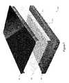
- FIG. 7illustrates an example mobile telephone that incorporates a flexible touch-sensitive apparatus.
- example mobile telephone 600incorporates a touch-sensitive apparatus 612 wrapped around an example display 613 .
- Substrate 602may include or have attached to it tracking areas, which may include tracks providing drive and sense connections to and from the drive and sense electrodes of touch-sensitive apparatus 612 .
- an electrode pattern of touch-sensitive apparatus 612made from metal-mesh technology with a copper, silver, or other suitable metal mesh, as described above.
- Substrate 602may have the electrode pattern disposed on a surface.
- Substrate 602 and the conductive material of the electrode patternmay be flexible, enabling the conductive material to wrap around the left and right edges of the surface to left-side and right-side surfaces.
- the flexible conductive material of the electrode patternmay be thicker or wider at the sharper edges than at the flat portions of surfaces.
- the electrode patternmay wrap around an edge 603 of example mobile phone 600 .
- touch-sensitive apparatus 612may be wrapped around a curved surface.
- the curved surfacemay be curved in one dimension or in two dimensions.
- touch-sensitive apparatus 612may be wrapped over surfaces that are substantially perpendicular to each other or, if there is no substantial distinction between surfaces (such as, for example, a pebble-shaped or curved device), an angle of deviation between the surfaces of 45° or greater.
- this disclosuredescribes and illustrates a particular use of touch-sensitive apparatus 612 in a particular device, this disclosure contemplates any suitable use of touch-sensitive apparatus 612 in any suitable device.
- Example display 613may be a liquid crystal display (LCD), a light-emitting diode (LED) display, an LED-backlight LCD, or other suitable display and may be visible though cover panel 601 and substrate 602 , as well as the electrode pattern disposed on substrate 602 .
- LCDliquid crystal display
- LEDlight-emitting diode
- LED-backlight LCDor other suitable display and may be visible though cover panel 601 and substrate 602 , as well as the electrode pattern disposed on substrate 602 .
- this disclosuredescribes and illustrates a particular display and particular display types, this disclosure contemplates any suitable device display and any suitable display types.
- a computer-readable storage mediumencompasses one or more non-transitory, tangible computer-readable storage media possessing structure.
- a computer-readable storage mediummay include a semiconductor-based or other ICs (such, as for example, a field-programmable gate array (FPGA) or ASICs), a hard disk, an HDD, a hybrid hard drive (HHD), an optical disc, an optical disc drive (ODD), a magneto-optical disc, a magneto-optical drive, a floppy disk, a floppy disk drive (FDD), magnetic tape, a holographic storage medium, a solid-state drive (SSD), a RAM-drive, a SECURE DIGITAL card, a SECURE DIGITAL drive, or another suitable computer-readable storage medium or a combination of two or more of these, where appropriate.
- FPGAfield-programmable gate array
- ASICsapplication-programmable gate array
- reference to a computer-readable storage mediumexcludes any medium that is not eligible for patent protection under 35 U.S.C. ⁇ 101.
- reference to a computer-readable storage mediumexcludes transitory forms of signal transmission (such as a propagating electrical or electromagnetic signal per se) to the extent that they are not eligible for patent protection under 35 U.S.C. ⁇ 101.
- a computer-readable non-transitory storage mediummay be volatile, non-volatile, or a combination of volatile and non-volatile, where appropriate.
- references in the appended claims to an apparatus or system or a component of an apparatus or system being adapted to, arranged to, capable of, configured to, enabled to, operable to, or operative to perform a particular functionencompasses that apparatus, system, component, whether or not it or that particular function is activated, turned on, or unlocked, as long as that apparatus, system, or component is so adapted, arranged, capable, configured, enabled, operable, or operative.
Landscapes
- Engineering & Computer Science (AREA)
- General Engineering & Computer Science (AREA)
- Theoretical Computer Science (AREA)
- Human Computer Interaction (AREA)
- Physics & Mathematics (AREA)
- General Physics & Mathematics (AREA)
- Position Input By Displaying (AREA)
- Switches That Are Operated By Magnetic Or Electric Fields (AREA)
Abstract
Description
Claims (20)
Priority Applications (5)
| Application Number | Priority Date | Filing Date | Title |
|---|---|---|---|
| US13/284,674US9256311B2 (en) | 2011-10-28 | 2011-10-28 | Flexible touch sensor |
| DE202012101382UDE202012101382U1 (en) | 2011-10-28 | 2012-04-16 | Flexible touch sensor |
| TW101137833ATWI567618B (en) | 2011-10-28 | 2012-10-12 | Flexible touch sensor |
| DE102012218783ADE102012218783A1 (en) | 2011-10-28 | 2012-10-16 | Flexible touch sensor device for LCD of e.g. mobile telephone, has control and selection electrodes that are made of flexible conductive material and are bent on flexible substrate |
| CN201210394366.2ACN103092441B (en) | 2011-10-28 | 2012-10-17 | Flexible touch sensor |
Applications Claiming Priority (1)
| Application Number | Priority Date | Filing Date | Title |
|---|---|---|---|
| US13/284,674US9256311B2 (en) | 2011-10-28 | 2011-10-28 | Flexible touch sensor |
Publications (2)
| Publication Number | Publication Date |
|---|---|
| US20130106441A1 US20130106441A1 (en) | 2013-05-02 |
| US9256311B2true US9256311B2 (en) | 2016-02-09 |
Family
ID=46509154
Family Applications (1)
| Application Number | Title | Priority Date | Filing Date |
|---|---|---|---|
| US13/284,674Active2032-07-23US9256311B2 (en) | 2011-10-28 | 2011-10-28 | Flexible touch sensor |
Country Status (4)
| Country | Link |
|---|---|
| US (1) | US9256311B2 (en) |
| CN (1) | CN103092441B (en) |
| DE (2) | DE202012101382U1 (en) |
| TW (1) | TWI567618B (en) |
Cited By (2)
| Publication number | Priority date | Publication date | Assignee | Title |
|---|---|---|---|---|
| US10285263B2 (en) | 2014-09-03 | 2019-05-07 | Samsung Display Co., Ltd. | Flexible circuit board and electronic device including the same |
| US10877332B2 (en)* | 2011-10-05 | 2020-12-29 | Apple Inc. | Displays with minimized border regions having an apertured TFT layer for signal conductors |
Families Citing this family (24)
| Publication number | Priority date | Publication date | Assignee | Title |
|---|---|---|---|---|
| US8946985B2 (en)* | 2012-05-07 | 2015-02-03 | Samsung Display Co., Ltd. | Flexible touch screen panel and flexible display device with the same |
| KR101980842B1 (en) | 2012-09-06 | 2019-05-22 | 삼성디스플레이 주식회사 | Sensing unit, flexible device, and display device |
| KR102077316B1 (en) | 2012-11-14 | 2020-04-08 | 삼성디스플레이 주식회사 | flexible touch screen panel and flexible display device with the same |
| CN104956296A (en)* | 2013-01-29 | 2015-09-30 | 夏普株式会社 | Input device, manufacturing method thereof, and electronic information device |
| US9086770B2 (en)* | 2013-04-15 | 2015-07-21 | Atmel Corporation | Touch sensor with high-density macro-feature design |
| KR101473312B1 (en)* | 2013-05-31 | 2014-12-16 | 삼성디스플레이 주식회사 | A touch screen panel and a flexible display apparatus including the same |
| US9310944B2 (en)* | 2013-07-25 | 2016-04-12 | Atmel Corporation | Oncell single-layer touch sensor |
| TWI521401B (en)* | 2013-09-27 | 2016-02-11 | 恆顥科技股份有限公司 | Flexible touch apparatus and systems thereof |
| KR102211968B1 (en)* | 2013-12-02 | 2021-02-05 | 삼성디스플레이 주식회사 | Touch panel, display apparatus and method for manufacturing touch panel |
| KR20150093280A (en)* | 2014-02-06 | 2015-08-18 | 삼성디스플레이 주식회사 | Display device |
| US20150305147A1 (en)* | 2014-04-16 | 2015-10-22 | Thomas Nathaniel Tombs | Wrap-around micro-wire circuit structure |
| JP6231432B2 (en)* | 2014-05-02 | 2017-11-15 | 富士フイルム株式会社 | Conductive film, display device including the same, and method for evaluating conductive film |
| US10394350B2 (en) | 2014-08-11 | 2019-08-27 | Atmel Corporation | Fabricated electrical circuit on touch sensor substrate |
| CN104238816A (en)* | 2014-09-04 | 2014-12-24 | 京东方科技集团股份有限公司 | Touch screen panel and manufacturing method thereof |
| GB2529898B (en)* | 2014-09-08 | 2016-08-31 | Touchnetix Ltd | Touch sensors |
| CN106716315A (en)* | 2015-06-24 | 2017-05-24 | 深圳市柔宇科技有限公司 | Flexible packaging cover plate, preparation method therefor, touch display device, and preparation method therefor |
| KR102489956B1 (en)* | 2015-12-30 | 2023-01-17 | 엘지디스플레이 주식회사 | Display device and method of driving the same |
| CN108509070A (en)* | 2017-02-26 | 2018-09-07 | 朱晓庆 | A kind of identifiable Electronic Paper and answering card |
| CN112272815B (en)* | 2018-06-08 | 2024-04-19 | 东友精细化工有限公司 | Touch sensor module, window stack structure including the same, and image display apparatus including the same |
| TWI679565B (en)* | 2018-09-04 | 2019-12-11 | 友達光電股份有限公司 | Touch panel |
| CN111610871A (en)* | 2019-02-25 | 2020-09-01 | 英属维尔京群岛商天材创新材料科技股份有限公司 | Electrode structure and touch panel thereof |
| CN110286795B (en)* | 2019-06-27 | 2022-11-22 | 业成科技(成都)有限公司 | Touch control device |
| US12135337B2 (en)* | 2020-04-24 | 2024-11-05 | The General Hospital Corporation | Proximity detection for assessing sensing probe attachment state |
| WO2022093248A1 (en)* | 2020-10-29 | 2022-05-05 | Hewlett-Packard Development Company, L.P. | Capacitive sensing |
Citations (38)
| Publication number | Priority date | Publication date | Assignee | Title |
|---|---|---|---|---|
| US5089672A (en)* | 1990-09-19 | 1992-02-18 | Miller Edge, Inc. | Flexible electrically conductive contact for a switch which is actuated upon force being applied thereto |
| US5729249A (en)* | 1991-11-26 | 1998-03-17 | Itu Research, Inc. | Touch sensitive input control device |
| US20020149572A1 (en)* | 2001-04-17 | 2002-10-17 | Schulz Stephen C. | Flexible capacitive touch sensor |
| US20070153548A1 (en)* | 2004-05-21 | 2007-07-05 | Sharp Kabushiki Kaisha | Backlight unit and liquid crystal display device having the same |
| US20080129317A1 (en)* | 2006-12-01 | 2008-06-05 | Katsuichi Oba | Input device and method of manufacturing the same |
| US20080158183A1 (en)* | 2007-01-03 | 2008-07-03 | Apple Computer, Inc. | Double-sided touch-sensitive panel with shield and drive combined layer |
| US20080165139A1 (en)* | 2007-01-05 | 2008-07-10 | Apple Inc. | Touch screen stack-up processing |
| US20080277259A1 (en)* | 2007-05-11 | 2008-11-13 | Sense Pad Tech Co., Ltd | Capacitive type touch panel |
| US20080303782A1 (en)* | 2007-06-05 | 2008-12-11 | Immersion Corporation | Method and apparatus for haptic enabled flexible touch sensitive surface |
| US20090002339A1 (en)* | 2005-06-01 | 2009-01-01 | Synaptics Incorporated | Touch pad with flexible substrate |
| US20090219257A1 (en)* | 2008-02-28 | 2009-09-03 | 3M Innovative Properties Company | Touch screen sensor |
| US20090315854A1 (en) | 2008-06-18 | 2009-12-24 | Epson Imaging Devices Corporation | Capacitance type input device and display device with input function |
| US7663607B2 (en)* | 2004-05-06 | 2010-02-16 | Apple Inc. | Multipoint touchscreen |
| US20100045614A1 (en)* | 2008-08-21 | 2010-02-25 | Wacom Co., Ltd. | Extended Touchscreen Pattern |
| US20100045620A1 (en)* | 2008-07-23 | 2010-02-25 | Ding Hua Long | Integration design for capacitive touch panels and liquid crystal displays |
| US20100156840A1 (en)* | 2008-02-28 | 2010-06-24 | Frey Matthew H | Touch screen sensor having varying sheet resistance |
| US20100308844A1 (en)* | 2009-06-03 | 2010-12-09 | Synaptics Incorporated | Input device and method with pressure-sensitive layer |
| US20110005845A1 (en)* | 2009-07-07 | 2011-01-13 | Apple Inc. | Touch sensing device having conductive nodes |
| US20110012793A1 (en)* | 2009-07-17 | 2011-01-20 | Amm David T | Electronic devices with capacitive proximity sensors for proximity-based radio-frequency power control |
| US7875814B2 (en) | 2005-07-21 | 2011-01-25 | Tpo Displays Corp. | Electromagnetic digitizer sensor array structure |
| US20110018556A1 (en)* | 2009-07-21 | 2011-01-27 | Borei Corporation | Pressure and touch sensors on flexible substrates for toys |
| US20110210935A1 (en)* | 2010-03-01 | 2011-09-01 | Cando Corporation | Sensory structure of capacitive touch panel and capacitive touch panel having the same |
| US8031174B2 (en) | 2007-01-03 | 2011-10-04 | Apple Inc. | Multi-touch surface stackup arrangement |
| US8031094B2 (en) | 2009-09-11 | 2011-10-04 | Apple Inc. | Touch controller with improved analog front end |
| US8040326B2 (en) | 2007-06-13 | 2011-10-18 | Apple Inc. | Integrated in-plane switching display and touch sensor |
| US8049732B2 (en) | 2007-01-03 | 2011-11-01 | Apple Inc. | Front-end signal compensation |
| US20120038613A1 (en)* | 2010-08-13 | 2012-02-16 | Samsung Electronics Co., Ltd. | Flexible display apparatus and control method thereof |
| US20120074961A1 (en)* | 2010-09-29 | 2012-03-29 | Kopin Corporation | Capacitive sensor with active shield electrode |
| US20120098785A1 (en)* | 2010-10-25 | 2012-04-26 | Josef Tatelbaum | Garment with Touch-Sensitive Features |
| WO2012129247A2 (en) | 2011-03-21 | 2012-09-27 | Apple Inc. | Electronic devices with flexible displays |
| US20120242592A1 (en)* | 2011-03-21 | 2012-09-27 | Rothkopf Fletcher R | Electronic devices with flexible displays |
| US20120243719A1 (en) | 2011-03-21 | 2012-09-27 | Franklin Jeremy C | Display-Based Speaker Structures for Electronic Devices |
| US20120243151A1 (en) | 2011-03-21 | 2012-09-27 | Stephen Brian Lynch | Electronic Devices With Convex Displays |
| US20120242588A1 (en) | 2011-03-21 | 2012-09-27 | Myers Scott A | Electronic devices with concave displays |
| US20120299865A1 (en)* | 2011-05-25 | 2012-11-29 | Hyunseok Yu | Sensor for Capacitive Touch Panel Including Mesh Pattern and Capacitive Touch Panel Including the Same |
| US20130032414A1 (en)* | 2011-08-04 | 2013-02-07 | Esat Yilmaz | Touch Sensor for Curved or Flexible Surfaces |
| US20130076612A1 (en) | 2011-09-26 | 2013-03-28 | Apple Inc. | Electronic device with wrap around display |
| US20130088671A1 (en)* | 2011-10-05 | 2013-04-11 | Paul S. Drzaic | Displays with Minimized Border Regions |
Family Cites Families (6)
| Publication number | Priority date | Publication date | Assignee | Title |
|---|---|---|---|---|
| GB0515175D0 (en)* | 2005-07-25 | 2005-08-31 | Plastic Logic Ltd | Flexible resistive touch screen |
| EP2082436B1 (en)* | 2006-10-12 | 2019-08-28 | Cambrios Film Solutions Corporation | Nanowire-based transparent conductors and method of making them |
| KR100921326B1 (en)* | 2008-04-30 | 2009-10-13 | 삼성코닝정밀유리 주식회사 | Liquid crystal display filter and liquid crystal display device having same |
| TWI423106B (en)* | 2008-07-11 | 2014-01-11 | Hon Hai Prec Ind Co Ltd | Method for making liquid crystal display with touch panel |
| CN101924816B (en)* | 2009-06-12 | 2013-03-20 | 清华大学 | Flexible mobile phone |
| US9836167B2 (en)* | 2009-08-03 | 2017-12-05 | Atmel Corporation | Electrode layout for touch screens |
- 2011
- 2011-10-28USUS13/284,674patent/US9256311B2/enactiveActive
- 2012
- 2012-04-16DEDE202012101382Upatent/DE202012101382U1/ennot_activeExpired - Lifetime
- 2012-10-12TWTW101137833Apatent/TWI567618B/ennot_activeIP Right Cessation
- 2012-10-16DEDE102012218783Apatent/DE102012218783A1/ennot_activeCeased
- 2012-10-17CNCN201210394366.2Apatent/CN103092441B/ennot_activeCeased
Patent Citations (41)
| Publication number | Priority date | Publication date | Assignee | Title |
|---|---|---|---|---|
| US5089672A (en)* | 1990-09-19 | 1992-02-18 | Miller Edge, Inc. | Flexible electrically conductive contact for a switch which is actuated upon force being applied thereto |
| US5729249A (en)* | 1991-11-26 | 1998-03-17 | Itu Research, Inc. | Touch sensitive input control device |
| US20020149572A1 (en)* | 2001-04-17 | 2002-10-17 | Schulz Stephen C. | Flexible capacitive touch sensor |
| US7663607B2 (en)* | 2004-05-06 | 2010-02-16 | Apple Inc. | Multipoint touchscreen |
| US20070153548A1 (en)* | 2004-05-21 | 2007-07-05 | Sharp Kabushiki Kaisha | Backlight unit and liquid crystal display device having the same |
| US20080129927A1 (en)* | 2004-05-21 | 2008-06-05 | Sharp Kabushiki Kaisha | Backlight unit and liquid crystal display device having the same |
| US20090002339A1 (en)* | 2005-06-01 | 2009-01-01 | Synaptics Incorporated | Touch pad with flexible substrate |
| US7875814B2 (en) | 2005-07-21 | 2011-01-25 | Tpo Displays Corp. | Electromagnetic digitizer sensor array structure |
| US20080129317A1 (en)* | 2006-12-01 | 2008-06-05 | Katsuichi Oba | Input device and method of manufacturing the same |
| US8049732B2 (en) | 2007-01-03 | 2011-11-01 | Apple Inc. | Front-end signal compensation |
| US20080158183A1 (en)* | 2007-01-03 | 2008-07-03 | Apple Computer, Inc. | Double-sided touch-sensitive panel with shield and drive combined layer |
| US8031174B2 (en) | 2007-01-03 | 2011-10-04 | Apple Inc. | Multi-touch surface stackup arrangement |
| US7920129B2 (en) | 2007-01-03 | 2011-04-05 | Apple Inc. | Double-sided touch-sensitive panel with shield and drive combined layer |
| US20080165139A1 (en)* | 2007-01-05 | 2008-07-10 | Apple Inc. | Touch screen stack-up processing |
| US20080277259A1 (en)* | 2007-05-11 | 2008-11-13 | Sense Pad Tech Co., Ltd | Capacitive type touch panel |
| US20080303782A1 (en)* | 2007-06-05 | 2008-12-11 | Immersion Corporation | Method and apparatus for haptic enabled flexible touch sensitive surface |
| US8040326B2 (en) | 2007-06-13 | 2011-10-18 | Apple Inc. | Integrated in-plane switching display and touch sensor |
| US20100156840A1 (en)* | 2008-02-28 | 2010-06-24 | Frey Matthew H | Touch screen sensor having varying sheet resistance |
| US8179381B2 (en) | 2008-02-28 | 2012-05-15 | 3M Innovative Properties Company | Touch screen sensor |
| US20090219257A1 (en)* | 2008-02-28 | 2009-09-03 | 3M Innovative Properties Company | Touch screen sensor |
| US20090315854A1 (en) | 2008-06-18 | 2009-12-24 | Epson Imaging Devices Corporation | Capacitance type input device and display device with input function |
| US20100045620A1 (en)* | 2008-07-23 | 2010-02-25 | Ding Hua Long | Integration design for capacitive touch panels and liquid crystal displays |
| US20100045614A1 (en)* | 2008-08-21 | 2010-02-25 | Wacom Co., Ltd. | Extended Touchscreen Pattern |
| US20100308844A1 (en)* | 2009-06-03 | 2010-12-09 | Synaptics Incorporated | Input device and method with pressure-sensitive layer |
| US20110005845A1 (en)* | 2009-07-07 | 2011-01-13 | Apple Inc. | Touch sensing device having conductive nodes |
| US20110012793A1 (en)* | 2009-07-17 | 2011-01-20 | Amm David T | Electronic devices with capacitive proximity sensors for proximity-based radio-frequency power control |
| US20110018556A1 (en)* | 2009-07-21 | 2011-01-27 | Borei Corporation | Pressure and touch sensors on flexible substrates for toys |
| US8031094B2 (en) | 2009-09-11 | 2011-10-04 | Apple Inc. | Touch controller with improved analog front end |
| US20110210935A1 (en)* | 2010-03-01 | 2011-09-01 | Cando Corporation | Sensory structure of capacitive touch panel and capacitive touch panel having the same |
| US20120038613A1 (en)* | 2010-08-13 | 2012-02-16 | Samsung Electronics Co., Ltd. | Flexible display apparatus and control method thereof |
| US20120074961A1 (en)* | 2010-09-29 | 2012-03-29 | Kopin Corporation | Capacitive sensor with active shield electrode |
| US20120098785A1 (en)* | 2010-10-25 | 2012-04-26 | Josef Tatelbaum | Garment with Touch-Sensitive Features |
| WO2012129247A2 (en) | 2011-03-21 | 2012-09-27 | Apple Inc. | Electronic devices with flexible displays |
| US20120242592A1 (en)* | 2011-03-21 | 2012-09-27 | Rothkopf Fletcher R | Electronic devices with flexible displays |
| US20120243719A1 (en) | 2011-03-21 | 2012-09-27 | Franklin Jeremy C | Display-Based Speaker Structures for Electronic Devices |
| US20120243151A1 (en) | 2011-03-21 | 2012-09-27 | Stephen Brian Lynch | Electronic Devices With Convex Displays |
| US20120242588A1 (en) | 2011-03-21 | 2012-09-27 | Myers Scott A | Electronic devices with concave displays |
| US20120299865A1 (en)* | 2011-05-25 | 2012-11-29 | Hyunseok Yu | Sensor for Capacitive Touch Panel Including Mesh Pattern and Capacitive Touch Panel Including the Same |
| US20130032414A1 (en)* | 2011-08-04 | 2013-02-07 | Esat Yilmaz | Touch Sensor for Curved or Flexible Surfaces |
| US20130076612A1 (en) | 2011-09-26 | 2013-03-28 | Apple Inc. | Electronic device with wrap around display |
| US20130088671A1 (en)* | 2011-10-05 | 2013-04-11 | Paul S. Drzaic | Displays with Minimized Border Regions |
Non-Patent Citations (3)
| Title |
|---|
| U.S. Appl. No. 61/454,894, filed Mar. 21, 2011, Rothkopf. |
| U.S. Appl. No. 61/454,936, filed Mar. 21, 2011, Myers. |
| U.S. Appl. No. 61/454,950, filed Mar. 21, 2011, Lynch. |
Cited By (3)
| Publication number | Priority date | Publication date | Assignee | Title |
|---|---|---|---|---|
| US10877332B2 (en)* | 2011-10-05 | 2020-12-29 | Apple Inc. | Displays with minimized border regions having an apertured TFT layer for signal conductors |
| US11137648B2 (en) | 2011-10-05 | 2021-10-05 | Apple Inc. | Displays with minimized border regions having an apertured TFT layer for signal conductors |
| US10285263B2 (en) | 2014-09-03 | 2019-05-07 | Samsung Display Co., Ltd. | Flexible circuit board and electronic device including the same |
Also Published As
| Publication number | Publication date |
|---|---|
| DE202012101382U1 (en) | 2012-05-09 |
| CN103092441B (en) | 2017-08-25 |
| TW201333793A (en) | 2013-08-16 |
| DE102012218783A1 (en) | 2013-05-02 |
| US20130106441A1 (en) | 2013-05-02 |
| TWI567618B (en) | 2017-01-21 |
| CN103092441A (en) | 2013-05-08 |
Similar Documents
| Publication | Publication Date | Title |
|---|---|---|
| US9256311B2 (en) | Flexible touch sensor | |
| US9262019B2 (en) | Touch sensor with conductive lines having different widths | |
| US10644080B2 (en) | Integrated touch screen | |
| US9154127B2 (en) | Touch sensor with conductive lines having portions with different widths | |
| US10659044B2 (en) | On-display-sensor stack | |
| US9501179B2 (en) | Touch sensor for curved or flexible surfaces | |
| US20130127775A1 (en) | Single-Layer Touch Sensor with Crossovers | |
| US9965106B2 (en) | Touch screen with electrodes positioned between pixels | |
| US20130180841A1 (en) | Sensor Stack with Opposing Electrodes | |
| US9116586B2 (en) | Uniform-density coplanar touch sensor | |
| US8941014B2 (en) | Complex adhesive boundaries for touch sensors | |
| US20130155001A1 (en) | Low-Resistance Electrodes | |
| US10044353B2 (en) | Substantially edgeless touch sensor | |
| US20130127769A1 (en) | Low-Resistance Electrodes | |
| US20130127771A1 (en) | Touch sensor with surface irregularities | |
| US20130181910A1 (en) | Dual-Substrate-Sensor Stack | |
| US8847898B2 (en) | Signal-to-noise ratio in touch sensors | |
| US10394402B2 (en) | Touch sensor with edge-balanced macro-feature design | |
| US9760207B2 (en) | Single-layer touch sensor | |
| US9791992B2 (en) | Oncell single-layer touch sensor | |
| US20130141340A1 (en) | Multi-Surface Touch Sensor | |
| US20180032182A1 (en) | Variable-Pitch Tracking For Touch Sensors | |
| US20130141381A1 (en) | Surface Coverage Touch |
Legal Events
| Date | Code | Title | Description |
|---|---|---|---|
| AS | Assignment | Owner name:ATMEL TECHNOLOGIES U.K. LIMITED, UNITED KINGDOM Free format text:ASSIGNMENT OF ASSIGNORS INTEREST;ASSIGNOR:YILMAZ, ESAT;REEL/FRAME:027143/0349 Effective date:20111026 Owner name:ATMEL CORPORATION, CALIFORNIA Free format text:ASSIGNMENT OF ASSIGNORS INTEREST;ASSIGNORS:LAUB, STEVEN ALAN;SHAIKH, JALIL;REEL/FRAME:027143/0316 Effective date:20111026 | |
| AS | Assignment | Owner name:ATMEL CORPORATION, CALIFORNIA Free format text:ASSIGNMENT OF ASSIGNORS INTEREST;ASSIGNOR:ATMEL TECHNOLOGIES U.K. LIMITED;REEL/FRAME:027558/0271 Effective date:20120117 | |
| AS | Assignment | Owner name:MORGAN STANLEY SENIOR FUNDING, INC. AS ADMINISTRATIVE AGENT, NEW YORK Free format text:PATENT SECURITY AGREEMENT;ASSIGNOR:ATMEL CORPORATION;REEL/FRAME:031912/0173 Effective date:20131206 Owner name:MORGAN STANLEY SENIOR FUNDING, INC. AS ADMINISTRAT Free format text:PATENT SECURITY AGREEMENT;ASSIGNOR:ATMEL CORPORATION;REEL/FRAME:031912/0173 Effective date:20131206 | |
| STCF | Information on status: patent grant | Free format text:PATENTED CASE | |
| AS | Assignment | Owner name:ATMEL CORPORATION, CALIFORNIA Free format text:TERMINATION AND RELEASE OF SECURITY INTEREST IN PATENT COLLATERAL;ASSIGNOR:MORGAN STANLEY SENIOR FUNDING, INC.;REEL/FRAME:038376/0001 Effective date:20160404 | |
| AS | Assignment | Owner name:JPMORGAN CHASE BANK, N.A., AS ADMINISTRATIVE AGENT, ILLINOIS Free format text:SECURITY INTEREST;ASSIGNOR:ATMEL CORPORATION;REEL/FRAME:041715/0747 Effective date:20170208 Owner name:JPMORGAN CHASE BANK, N.A., AS ADMINISTRATIVE AGENT Free format text:SECURITY INTEREST;ASSIGNOR:ATMEL CORPORATION;REEL/FRAME:041715/0747 Effective date:20170208 | |
| AS | Assignment | Owner name:JPMORGAN CHASE BANK, N.A., AS ADMINISTRATIVE AGENT, ILLINOIS Free format text:SECURITY INTEREST;ASSIGNORS:MICROCHIP TECHNOLOGY INCORPORATED;SILICON STORAGE TECHNOLOGY, INC.;ATMEL CORPORATION;AND OTHERS;REEL/FRAME:046426/0001 Effective date:20180529 Owner name:JPMORGAN CHASE BANK, N.A., AS ADMINISTRATIVE AGENT Free format text:SECURITY INTEREST;ASSIGNORS:MICROCHIP TECHNOLOGY INCORPORATED;SILICON STORAGE TECHNOLOGY, INC.;ATMEL CORPORATION;AND OTHERS;REEL/FRAME:046426/0001 Effective date:20180529 | |
| AS | Assignment | Owner name:WELLS FARGO BANK, NATIONAL ASSOCIATION, AS NOTES COLLATERAL AGENT, CALIFORNIA Free format text:SECURITY INTEREST;ASSIGNORS:MICROCHIP TECHNOLOGY INCORPORATED;SILICON STORAGE TECHNOLOGY, INC.;ATMEL CORPORATION;AND OTHERS;REEL/FRAME:047103/0206 Effective date:20180914 Owner name:WELLS FARGO BANK, NATIONAL ASSOCIATION, AS NOTES C Free format text:SECURITY INTEREST;ASSIGNORS:MICROCHIP TECHNOLOGY INCORPORATED;SILICON STORAGE TECHNOLOGY, INC.;ATMEL CORPORATION;AND OTHERS;REEL/FRAME:047103/0206 Effective date:20180914 | |
| AS | Assignment | Owner name:MICROCHIP TECHNOLOGY INCORPORATED, ARIZONA Free format text:RELEASE OF SECURITY INTEREST IN CERTAIN PATENT RIGHTS;ASSIGNOR:WELLS FARGO BANK, NATIONAL ASSOCIATION, AS NOTES COLLATERAL AGENT;REEL/FRAME:047976/0937 Effective date:20181221 Owner name:MICROCHIP TECHNOLOGY INCORPORATED, ARIZONA Free format text:RELEASE OF SECURITY INTEREST IN CERTAIN PATENT RIGHTS;ASSIGNOR:JPMORGAN CHASE BANK, N.A., AS ADMINISTRATIVE AGENT;REEL/FRAME:047976/0884 Effective date:20181221 Owner name:ATMEL CORPORATION, ARIZONA Free format text:RELEASE OF SECURITY INTEREST IN CERTAIN PATENT RIGHTS;ASSIGNOR:WELLS FARGO BANK, NATIONAL ASSOCIATION, AS NOTES COLLATERAL AGENT;REEL/FRAME:047976/0937 Effective date:20181221 Owner name:ATMEL CORPORATION, ARIZONA Free format text:RELEASE OF SECURITY INTEREST IN CERTAIN PATENT RIGHTS;ASSIGNOR:JPMORGAN CHASE BANK, N.A., AS ADMINISTRATIVE AGENT;REEL/FRAME:047976/0884 Effective date:20181221 | |
| AS | Assignment | Owner name:SOLAS OLED LIMITED, IRELAND Free format text:ASSIGNMENT OF ASSIGNORS INTEREST;ASSIGNORS:MICROCHIP TECHNOLOGY INCORPORATED;AMTEL CORPORATION;REEL/FRAME:048201/0225 Effective date:20181221 | |
| MAFP | Maintenance fee payment | Free format text:PAYMENT OF MAINTENANCE FEE, 4TH YEAR, LARGE ENTITY (ORIGINAL EVENT CODE: M1551); ENTITY STATUS OF PATENT OWNER: LARGE ENTITY Year of fee payment:4 | |
| IPR | Aia trial proceeding filed before the patent and appeal board: inter partes review | Free format text:TRIAL NO: IPR2019-01668 Opponent name:SAMSUNG DISPLAY CO., LTD., SAMSUNG ELECTRONICS CO. Effective date:20190930 | |
| AS | Assignment | Owner name:MICROSEMI STORAGE SOLUTIONS, INC., ARIZONA Free format text:RELEASE BY SECURED PARTY;ASSIGNOR:JPMORGAN CHASE BANK, N.A., AS ADMINISTRATIVE AGENT;REEL/FRAME:059333/0222 Effective date:20220218 Owner name:MICROSEMI CORPORATION, ARIZONA Free format text:RELEASE BY SECURED PARTY;ASSIGNOR:JPMORGAN CHASE BANK, N.A., AS ADMINISTRATIVE AGENT;REEL/FRAME:059333/0222 Effective date:20220218 Owner name:ATMEL CORPORATION, ARIZONA Free format text:RELEASE BY SECURED PARTY;ASSIGNOR:JPMORGAN CHASE BANK, N.A., AS ADMINISTRATIVE AGENT;REEL/FRAME:059333/0222 Effective date:20220218 Owner name:SILICON STORAGE TECHNOLOGY, INC., ARIZONA Free format text:RELEASE BY SECURED PARTY;ASSIGNOR:JPMORGAN CHASE BANK, N.A., AS ADMINISTRATIVE AGENT;REEL/FRAME:059333/0222 Effective date:20220218 Owner name:MICROCHIP TECHNOLOGY INCORPORATED, ARIZONA Free format text:RELEASE BY SECURED PARTY;ASSIGNOR:JPMORGAN CHASE BANK, N.A., AS ADMINISTRATIVE AGENT;REEL/FRAME:059333/0222 Effective date:20220218 | |
| AS | Assignment | Owner name:ATMEL CORPORATION, ARIZONA Free format text:RELEASE BY SECURED PARTY;ASSIGNOR:JPMORGAN CHASE BANK, N.A., AS ADMINISTRATIVE AGENT;REEL/FRAME:059262/0105 Effective date:20220218 | |
| AS | Assignment | Owner name:MICROSEMI STORAGE SOLUTIONS, INC., ARIZONA Free format text:RELEASE BY SECURED PARTY;ASSIGNOR:WELLS FARGO BANK, NATIONAL ASSOCIATION, AS NOTES COLLATERAL AGENT;REEL/FRAME:059358/0001 Effective date:20220228 Owner name:MICROSEMI CORPORATION, ARIZONA Free format text:RELEASE BY SECURED PARTY;ASSIGNOR:WELLS FARGO BANK, NATIONAL ASSOCIATION, AS NOTES COLLATERAL AGENT;REEL/FRAME:059358/0001 Effective date:20220228 Owner name:ATMEL CORPORATION, ARIZONA Free format text:RELEASE BY SECURED PARTY;ASSIGNOR:WELLS FARGO BANK, NATIONAL ASSOCIATION, AS NOTES COLLATERAL AGENT;REEL/FRAME:059358/0001 Effective date:20220228 Owner name:SILICON STORAGE TECHNOLOGY, INC., ARIZONA Free format text:RELEASE BY SECURED PARTY;ASSIGNOR:WELLS FARGO BANK, NATIONAL ASSOCIATION, AS NOTES COLLATERAL AGENT;REEL/FRAME:059358/0001 Effective date:20220228 Owner name:MICROCHIP TECHNOLOGY INCORPORATED, ARIZONA Free format text:RELEASE BY SECURED PARTY;ASSIGNOR:WELLS FARGO BANK, NATIONAL ASSOCIATION, AS NOTES COLLATERAL AGENT;REEL/FRAME:059358/0001 Effective date:20220228 | |
| IPRC | Trial and appeal board: inter partes review certificate | Kind code of ref document:K1 Free format text:INTER PARTES REVIEW CERTIFICATE; TRIAL NO. IPR2019-01668, SEP. 30, 2019 INTER PARTES REVIEW CERTIFICATE FOR PATENT 9,256,311, ISSUED FEB. 9, 2016, APPL. NO. 13/284,674, OCT. 28, 2011 INTER PARTES REVIEW CERTIFICATE ISSUED AUG. 8, 2022 Effective date:20220808 | |
| MAFP | Maintenance fee payment | Free format text:PAYMENT OF MAINTENANCE FEE, 8TH YEAR, LARGE ENTITY (ORIGINAL EVENT CODE: M1552); ENTITY STATUS OF PATENT OWNER: LARGE ENTITY Year of fee payment:8 |