US9253380B2 - Thin form factor computational array cameras and modular array cameras - Google Patents
Thin form factor computational array cameras and modular array camerasDownload PDFInfo
- Publication number
- US9253380B2 US9253380B2US14/188,524US201414188524AUS9253380B2US 9253380 B2US9253380 B2US 9253380B2US 201414188524 AUS201414188524 AUS 201414188524AUS 9253380 B2US9253380 B2US 9253380B2
- Authority
- US
- United States
- Prior art keywords
- array
- sub
- module
- image data
- modules
- Prior art date
- Legal status (The legal status is an assumption and is not a legal conclusion. Google has not performed a legal analysis and makes no representation as to the accuracy of the status listed.)
- Active
Links
- 238000000034methodMethods0.000claimsabstractdescription57
- 239000000758substrateSubstances0.000claimsdescription58
- 230000008569processEffects0.000claimsdescription35
- 239000011521glassSubstances0.000claimsdescription31
- 238000012545processingMethods0.000claimsdescription21
- 230000003287optical effectEffects0.000claimsdescription16
- 238000012937correctionMethods0.000claimsdescription12
- 238000001514detection methodMethods0.000claimsdescription10
- 239000000919ceramicSubstances0.000claimsdescription9
- 238000004891communicationMethods0.000claimsdescription7
- 230000003595spectral effectEffects0.000description43
- 238000004519manufacturing processMethods0.000description36
- 238000003491arrayMethods0.000description32
- 238000010276constructionMethods0.000description32
- 235000012431wafersNutrition0.000description24
- 230000005540biological transmissionEffects0.000description19
- 238000003384imaging methodMethods0.000description16
- 238000001429visible spectrumMethods0.000description12
- 210000000352storage cellAnatomy0.000description10
- 238000013500data storageMethods0.000description9
- 239000000470constituentSubstances0.000description8
- 238000001228spectrumMethods0.000description8
- 230000008901benefitEffects0.000description7
- 238000007726management methodMethods0.000description7
- 125000006850spacer groupChemical group0.000description6
- 230000000007visual effectEffects0.000description6
- 230000003044adaptive effectEffects0.000description4
- 238000000429assemblyMethods0.000description4
- 230000009286beneficial effectEffects0.000description4
- 230000008878couplingEffects0.000description4
- 238000010168coupling processMethods0.000description4
- 238000005859coupling reactionMethods0.000description4
- 238000009432framingMethods0.000description4
- 229920000642polymerPolymers0.000description4
- 238000005070samplingMethods0.000description4
- 239000011248coating agentSubstances0.000description3
- 238000000576coating methodMethods0.000description3
- 238000010348incorporationMethods0.000description3
- 230000010354integrationEffects0.000description3
- 238000000465mouldingMethods0.000description3
- 230000011664signalingEffects0.000description3
- 230000001360synchronised effectEffects0.000description3
- 238000004364calculation methodMethods0.000description2
- 238000006243chemical reactionMethods0.000description2
- 238000013461designMethods0.000description2
- 238000009826distributionMethods0.000description2
- 238000005516engineering processMethods0.000description2
- 238000001746injection mouldingMethods0.000description2
- 239000000463materialSubstances0.000description2
- 230000035945sensitivityEffects0.000description2
- 238000005476solderingMethods0.000description2
- 239000000243solutionSubstances0.000description2
- 230000006641stabilisationEffects0.000description2
- 238000011105stabilizationMethods0.000description2
- 230000002123temporal effectEffects0.000description2
- PXFBZOLANLWPMH-UHFFFAOYSA-N16-EpiaffinineNatural productsC1C(C2=CC=CC=C2N2)=C2C(=O)CC2C(=CC)CN(C)C1C2COPXFBZOLANLWPMH-UHFFFAOYSA-N0.000description1
- XUIMIQQOPSSXEZ-UHFFFAOYSA-NSiliconChemical compound[Si]XUIMIQQOPSSXEZ-UHFFFAOYSA-N0.000description1
- 238000013459approachMethods0.000description1
- 230000000903blocking effectEffects0.000description1
- 230000003139buffering effectEffects0.000description1
- 230000003247decreasing effectEffects0.000description1
- 229910003460diamondInorganic materials0.000description1
- 239000010432diamondSubstances0.000description1
- 230000000694effectsEffects0.000description1
- 238000001413far-infrared spectroscopyMethods0.000description1
- 230000006870functionEffects0.000description1
- 230000007246mechanismEffects0.000description1
- 238000012986modificationMethods0.000description1
- 230000004048modificationEffects0.000description1
- 238000004806packaging method and processMethods0.000description1
- 238000000059patterningMethods0.000description1
- 230000002093peripheral effectEffects0.000description1
- 230000000704physical effectEffects0.000description1
- 230000000135prohibitive effectEffects0.000description1
- 230000009467reductionEffects0.000description1
- 230000010076replicationEffects0.000description1
- 230000004044responseEffects0.000description1
- 238000005096rolling processMethods0.000description1
- 229910052710siliconInorganic materials0.000description1
- 239000010703siliconSubstances0.000description1
- 238000003860storageMethods0.000description1
- 238000012546transferMethods0.000description1
- 230000009466transformationEffects0.000description1
Images


Classifications
- H04N5/2252—
- H—ELECTRICITY
- H04—ELECTRIC COMMUNICATION TECHNIQUE
- H04N—PICTORIAL COMMUNICATION, e.g. TELEVISION
- H04N23/00—Cameras or camera modules comprising electronic image sensors; Control thereof
- H04N23/10—Cameras or camera modules comprising electronic image sensors; Control thereof for generating image signals from different wavelengths
- H04N23/11—Cameras or camera modules comprising electronic image sensors; Control thereof for generating image signals from different wavelengths for generating image signals from visible and infrared light wavelengths
- H—ELECTRICITY
- H04—ELECTRIC COMMUNICATION TECHNIQUE
- H04N—PICTORIAL COMMUNICATION, e.g. TELEVISION
- H04N23/00—Cameras or camera modules comprising electronic image sensors; Control thereof
- H04N23/10—Cameras or camera modules comprising electronic image sensors; Control thereof for generating image signals from different wavelengths
- H04N23/13—Cameras or camera modules comprising electronic image sensors; Control thereof for generating image signals from different wavelengths with multiple sensors
- H—ELECTRICITY
- H04—ELECTRIC COMMUNICATION TECHNIQUE
- H04N—PICTORIAL COMMUNICATION, e.g. TELEVISION
- H04N23/00—Cameras or camera modules comprising electronic image sensors; Control thereof
- H04N23/50—Constructional details
- H04N23/51—Housings
- H—ELECTRICITY
- H04—ELECTRIC COMMUNICATION TECHNIQUE
- H04N—PICTORIAL COMMUNICATION, e.g. TELEVISION
- H04N23/00—Cameras or camera modules comprising electronic image sensors; Control thereof
- H04N23/60—Control of cameras or camera modules
- H—ELECTRICITY
- H04—ELECTRIC COMMUNICATION TECHNIQUE
- H04N—PICTORIAL COMMUNICATION, e.g. TELEVISION
- H04N23/00—Cameras or camera modules comprising electronic image sensors; Control thereof
- H04N23/90—Arrangement of cameras or camera modules, e.g. multiple cameras in TV studios or sports stadiums
- H—ELECTRICITY
- H04—ELECTRIC COMMUNICATION TECHNIQUE
- H04N—PICTORIAL COMMUNICATION, e.g. TELEVISION
- H04N23/00—Cameras or camera modules comprising electronic image sensors; Control thereof
- H04N23/95—Computational photography systems, e.g. light-field imaging systems
- H04N23/951—Computational photography systems, e.g. light-field imaging systems by using two or more images to influence resolution, frame rate or aspect ratio
- H—ELECTRICITY
- H04—ELECTRIC COMMUNICATION TECHNIQUE
- H04N—PICTORIAL COMMUNICATION, e.g. TELEVISION
- H04N25/00—Circuitry of solid-state image sensors [SSIS]; Control thereof
- H04N25/10—Circuitry of solid-state image sensors [SSIS]; Control thereof for transforming different wavelengths into image signals
- H04N25/11—Arrangement of colour filter arrays [CFA]; Filter mosaics
- H04N25/13—Arrangement of colour filter arrays [CFA]; Filter mosaics characterised by the spectral characteristics of the filter elements
- H04N25/134—Arrangement of colour filter arrays [CFA]; Filter mosaics characterised by the spectral characteristics of the filter elements based on three different wavelength filter elements
- H—ELECTRICITY
- H04—ELECTRIC COMMUNICATION TECHNIQUE
- H04N—PICTORIAL COMMUNICATION, e.g. TELEVISION
- H04N25/00—Circuitry of solid-state image sensors [SSIS]; Control thereof
- H04N25/48—Increasing resolution by shifting the sensor relative to the scene
- H—ELECTRICITY
- H04—ELECTRIC COMMUNICATION TECHNIQUE
- H04N—PICTORIAL COMMUNICATION, e.g. TELEVISION
- H04N25/00—Circuitry of solid-state image sensors [SSIS]; Control thereof
- H04N25/70—SSIS architectures; Circuits associated therewith
- H—ELECTRICITY
- H04—ELECTRIC COMMUNICATION TECHNIQUE
- H04N—PICTORIAL COMMUNICATION, e.g. TELEVISION
- H04N25/00—Circuitry of solid-state image sensors [SSIS]; Control thereof
- H04N25/70—SSIS architectures; Circuits associated therewith
- H04N25/701—Line sensors
- H04N5/2254—
- H04N5/332—
- H04N5/349—
Definitions
- the present inventiongenerally relates to one-dimensional array cameras and also relates to the construction of modular array cameras using one-dimensional sub-array modules.
- array camerasare characterized in that they include an imager array that has multiple arrays of pixels, where each pixel array is intended to define a focal plane, and each focal plane has a separate lens stack.
- each focal planeincludes a plurality of rows of pixels that also forms a plurality of columns of pixels, and each focal plane is contained within a region of the imager that does not contain pixels from another focal plane.
- An imageis typically formed on each focal plane by its respective lens stack.
- the array camerais constructed using an imager array that incorporates multiple focal planes and an optic array of lens stacks.
- a 1 ⁇ N array camera moduleincludes: a 1 ⁇ N arrangement of focal planes, where N is greater than or equal to 2, each focal plane includes a plurality of rows of pixels that also form a plurality of columns of pixels, and each focal plane does not include pixels from another focal plane; and a 1 ⁇ N arrangement of lens stacks, the 1 ⁇ N arrangement of lens stacks being disposed relative to the 1 ⁇ N arrangement of focal planes so as to form a 1 ⁇ N arrangement of cameras, each of which being configured to independently capture an image of a scene, where each lens stack has a field of view that is shifted with respect to the field-of-views of each other lens stack so that each shift includes a sub-pixel shifted view of the scene.
- Nis greater than or equal to 3.
- Nis 5.
- the 1 ⁇ N arrangement of camerasincludes a green camera that is configured to image light corresponding with the green band of the visible spectrum.
- the green camerais centrally disposed relative to the 1 ⁇ N arrangement of cameras.
- the lens stack of the green camerais adapted to image light corresponding with the green band of the visible spectrum.
- a red camera that is configured to image light corresponding with the red band of the visible spectrum and a blue camera that is configured to image light corresponding with the blue band of the visible spectrumare each disposed on either side of the centrally disposed green camera.
- N7.
- the 1 ⁇ N arrangement of camerasincludes a green camera that is configured to image light corresponding with the green band of the visible spectrum, and that is centrally disposed relative to the 1 ⁇ N arrangement of cameras.
- a red camera that is configured to image light corresponding with the red band of the visible spectrum and a blue camera that is configured to image light corresponding with the blue band of the visible spectrumare each disposed on either side of the centrally disposed green camera.
- Nis 9.
- the 1 ⁇ N arrangement of camerasincludes a green camera that is configured to image light corresponding with the green band of the visible spectrum, and that is centrally disposed relative to the 1 ⁇ N arrangement of cameras.
- a red camera that is configured to image light corresponding with the red band of the visible spectrum and a blue camera that is configured to image light corresponding with the blue band of the visible spectrumare each disposed on either side of the centrally disposed green camera.
- the 1 ⁇ N arrangement of focal planesis embodied within a monolithic structure.
- the 1 ⁇ N arrangement of lens stacksis embodied within a monolithic structure.
- the 1 ⁇ N arrangement of focal planes and the 1 ⁇ N arrangement of lens stacksare each embodied within the same monolithic structure.
- At least one camerais embodied within a single sub-array module, the sub-array module including: a 1 ⁇ X arrangement of focal planes, where X is greater than or equal to 1, each focal plane comprises a plurality of rows of pixels that also form a plurality of columns of pixels, and each focal plane does not include pixels from another focal plane; and a 1 ⁇ X arrangement of lens stacks, the 1 ⁇ X arrangement of lens stacks being disposed relative to the 1 ⁇ X arrangement of focal planes so as to form a 1 ⁇ X arrangement of cameras, each of which being configured to independently capture an image of a scene, where each lens stack has a field of view that is shifted with respect to the field-of-views of each other lens stack so that each shift includes a sub-pixel shifted view of the scene.
- the sub-array modulefurther includes interface circuitry that can allow the sub-array module to interface with another sub-array module so that it can at least transmit image data to another sub-array module or receive image data from another sub-array module.
- the 1 ⁇ X arrangement of camerasis embodied within a single monolithic structure.
- N9 and X is 3.
- the 1 ⁇ 9 arrangement of camerasare embodied within three 1 ⁇ 3 sub-array modules, each 1 ⁇ 3 sub-array module including: a 1 ⁇ 3 arrangement of focal planes, where each focal plane comprises a plurality of rows of pixels that also form a plurality of columns of pixels, and each focal plane does not include pixels from another focal plane; and a 1 ⁇ 3 arrangement of lens stacks, the 1 ⁇ 3 arrangement of lens stacks being disposed relative to the 1 ⁇ 3 arrangement of focal planes so as to form a 1 ⁇ 3 arrangement of cameras, each of which being configured to independently capture an image of a scene, where each lens stack has a field of view that is shifted with respect to the field-of-views of each other lens stack so that each shift includes a sub-pixel shifted view of the scene.
- each sub-array modulefurther includes interface circuitry that can allow the sub-array module to interface with another sub-array module so that it can at least transmit image data to another sub-array module or receive image data from another sub-array module.
- an array camera modulefurther includes at least two sub-array modules, where each sub-array module includes: a 1 ⁇ X arrangement of focal planes, where X is greater than or equal to 1, each focal plane comprises a plurality of rows of pixels that also form a plurality of columns of pixels, and each focal plane does not include pixels from another focal plane; and a 1 ⁇ X arrangement of lens stacks, the 1 ⁇ X arrangement of lens stacks being disposed relative to the 1 ⁇ X arrangement of focal planes so as to form a 1 ⁇ X arrangement of cameras, each of which being configured to independently capture an image of a scene, where each lens stack has a field of view that is shifted with respect to the field-of-views of each other lens stack so that each shift includes a sub-pixel shifted view of the scene; where each of the at least two sub-array modules are adjoined to the interconnects of a single substrate, and can thereby interface with at least one other sub-array module.
- each of the at least two sub-array modulesfurther includes interface circuitry that can allow the respective sub-array module to interface with another sub-array module so that it can at least transmit image data to another sub-array module or receive image data from another sub-array module.
- the substrateis optically transparent.
- the substrateis glass.
- the substrateis ceramic
- a 1 ⁇ X sub-array moduleincludes: a 1 ⁇ X arrangement of focal planes, where X is greater than or equal to 1, each focal plane comprises a plurality of rows of pixels that also form a plurality of columns of pixels, and each focal plane does not include pixels from another focal plane; and a 1 ⁇ X arrangement of lens stacks, the 1 ⁇ X arrangement of lens stacks being disposed relative to the 1 ⁇ X arrangement of focal planes so as to form a 1 ⁇ X arrangement of cameras, each of which being configured to independently capture an image of a scene, where each lens stack has a field of view that is shifted with respect to the field-of-views of each other lens stack so that each shift includes a sub-pixel shifted view of the scene.
- the 1 ⁇ X sub-array modulefurther includes interface circuitry that can allow the sub-array module to interface with another sub-array module so that it can at least transmit image data to another sub-array module or receive image data from another sub-array module.
- the interface circuitryimplements a MIPI CSI 2 interface.
- a 1 ⁇ N array cameraincludes: a 1 ⁇ N arrangement of focal planes, where N is greater than or equal to 2, each focal plane comprises a plurality of rows of pixels that also form a plurality of columns of pixels, and each focal plane does not include pixels from another focal plane; and a 1 ⁇ N arrangement of lens stacks, the 1 ⁇ N arrangement of lens stacks being disposed relative to the 1 ⁇ N arrangement of focal planes so as to form a 1 ⁇ N arrangement of cameras, each of which being configured to independently capture an image of a scene, where each lens stack has a field of view that is shifted with respect to the field-of-views of each other lens stack so that each shift includes a sub-pixel shifted view of the scene; and a processor that is configured to construct an image of the scene using image data generated by the 1 ⁇ N array camera module.
- an X ⁇ Y sub-array moduleincludes: an X ⁇ Y arrangement of focal planes, where X and Y are each greater than or equal to 1, each focal plane includes a plurality of rows of pixels that also form a plurality of columns of pixels, and each focal plane does not include pixels from another focal plane; and an X ⁇ Y arrangement of lens stacks, the X ⁇ Y arrangement of lens stacks being disposed relative to the X ⁇ Y arrangement of focal planes so as to form an X ⁇ Y arrangement of cameras, each of which being configured to independently capture an image of a scene, where each lens stack has a field of view that is shifted with respect to the field-of-views of each other lens stack so that each shift includes a sub-pixel shifted view of the scene; and image data output circuitry that is configured to output image data from the X ⁇ Y sub-array module that can be aggregated with image data from other sub-array modules so that an image of the scene can be constructed.
- Xis 1.
- X and Yare each greater than 1.
- the arrangement of camerasare embodied within a single monolithic structure
- an M ⁇ N array cameraincludes: a plurality of X ⁇ Y sub-array modules, each including: an X ⁇ Y arrangement of focal planes, where X and Y are each greater than or equal to 1, each focal plane includes a plurality of rows of pixels that also form a plurality of columns of pixels, and each focal plane does not include pixels from another focal plane; and an X ⁇ Y arrangement of lens stacks, the X ⁇ Y arrangement of lens stacks being disposed relative to the X ⁇ Y arrangement of focal planes so as to form an X ⁇ Y arrangement of cameras, each of which being configured to independently capture an image of a scene, where each lens stack has a field of view that is shifted with respect to the field-of-views of each other lens stack so that each shift includes a sub-pixel shifted view of the scene; and image data output circuitry that is configured to output image data from the sub-array module that can be aggregated with image data from other sub-array modules so that an image of the scene can be constructed; where the plurality of X ⁇ Y
- an M ⁇ N array camerafurther includes circuitry that aggregates the image data generated by each of the sub-array modules into a single MIPI output, and provides the MIPI output to the processor so that the processor can construct an image of the scene.
- an M ⁇ N array camerafurther includes a parallax disparity resolution module, where the parallax disparity resolution module is configured to receive image data captured by each sub-array module, implement a parallax detection and correction process on the received image data, and output the result for further processing.
- an M ⁇ N array camerafurther includes circuitry that converts the output of the parallax disparity resolution module into a single MIPI output, and provides the MIPI output to the processor so that the processor can construct an image of the scene.
- the parallax disparity resolution moduleincludes a processor and memory, where the memory contains software to configure the processor to act as a parallax disparity resolution module.
- the parallax disparity resolution moduleis a hardware parallax disparity resolution module.
- At least two of the plurality of sub-array modulesare adjoined to the interconnects of a single substrate, and can thereby output image data through the interconnects.
- each of the plurality of sub-array modulesare adjoined to the interconnects of a single substrate, and can thereby output image data through the interconnects.
- the substrateis optically transparent.
- the substrateis glass.
- the substrateis ceramic.
- At least one sub-array moduleis embodied within a single monolithic structure.
- each sub-array moduleis embodied within a single respective monolithic structure.
- an array camerafurther includes: a plurality of I/O devices, where each of the plurality of I/O devices interfaces with at least one camera: and a separate I/O block that includes circuitry configured to receive image data, aggregate the received image data, and output the aggregated image data to the processor so that the processor can construct an image of the scene; and where each of the plurality of I/O devices interfaces with the I/O block.
- the number of I/O devicesequals the number of sub-array modules, and each I/O device interfaces with a corresponding sub-array module.
- FIG. 1conceptually illustrates an array camera architecture in accordance with an embodiment of the invention.
- FIG. 2conceptually illustrates an imager array architecture in accordance with an embodiment of the invention.
- FIG. 3conceptually illustrates the construction of an array camera module in accordance with an embodiment of the invention.
- FIGS. 4A and 4Billustrate 1 ⁇ 5 array camera modules in accordance with embodiments of the invention.
- FIGS. 5A-5Cillustrate 1 ⁇ 7 array camera modules in accordance with embodiments of the invention.
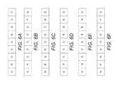
- FIGS. 6A-6Fillustrate 1 ⁇ 9 array camera modules in accordance with embodiments of the invention.
- FIG. 7Aillustrates a 1 ⁇ 3 sub-array module in accordance with an embodiment of the invention.
- FIG. 7Billustrates another 1 ⁇ 3 sub-array module in accordance with another embodiment of the invention
- FIGS. 8A-8Killustrate 1 ⁇ 3 sub-array modules in accordance with embodiments of the invention.
- FIG. 9illustrates how sub-array modules may be reconfigured in accordance with an embodiment of the invention.
- FIGS. 10A-10Cillustrate how 1 ⁇ 3 sub-array modules may be coupled to form array camera modules in accordance with embodiments of the invention.
- FIGS. 11A-11Billustrates how 1 ⁇ 3 sub-array modules may interface with a receiving device and thereby implement an array camera in accordance with embodiments of the invention
- FIG. 12illustrate how sub-array modules may be coupled via a glass substrate with interconnects to form an array camera module in accordance with embodiments of the invention.
- FIGS. 13A-13Billustrate how array camera modules formed from sub-array modules may utilize a parallax disparity resolution module in accordance with embodiments of the invention.
- FIGS. 14A-14Billustrate how sub-array modules may be coupled to form an M ⁇ N array camera in accordance with embodiments of the invention.
- FIG. 15illustrates how sub-array modules may be coupled via a glass substrate with interconnects to form a two-dimensional array camera in accordance with embodiments of the invention
- FIG. 16illustrates a Pi filter group that may be utilized in accordance with embodiments of the invention.
- FIGS. 17A-17Billustrates how sub-array modules may be coupled to form an array camera that employs Pi filter groups.
- FIGS. 18A-18Billustrate 1 ⁇ 4 sub-array modules in accordance with embodiments of the invention.
- FIGS. 19A-19Billustrate how 1 ⁇ 4 sub-array modules may be coupled to form an M ⁇ N array camera in accordance with embodiments of the invention
- FIGS. 20A-20Dillustrate 1 ⁇ 5 sub-array modules in accordance with embodiments of the invention.
- FIGS. 21A-21Billustrate how 1 ⁇ 5 sub-array modules may be coupled to form an M ⁇ N array camera in accordance with embodiments of the invention.
- FIG. 22illustrates a two-dimensional array camera fabricated from multiple two-dimensional sub-array modules.
- a lens stack and its corresponding focal planecan be understood to be a ‘camera’ (as opposed to an ‘array camera’).
- array camerascapture image data that can be used to form multiple images of a single scene using their constituent cameras, and process the image data to yield a single image of the scene with improved image properties.
- U.S. patent application Ser. No. 12/935,504discloses many two-dimensional array camera schemes. However, such two-dimensional embodiments may be inapplicable in a number of desirable applications. For example, a consumer electronics device, such as a tablet or smartphone, may benefit from the use of an array camera with a distinctly thin form factor such that it would be able to fit within the device's bezel.
- One-dimensional array camera modulesare advantageous insofar as they may accommodate distinct form factor requirements, and are further advantageous in that they may ease processing requirements as compared with two-dimensional array cameras (e.g. they simplify parallax disparity resolution calculations).
- 1 ⁇ 5 array camera modulesare utilized in the construction of an array camera.
- a 1 ⁇ 5 array camera moduleis utilized that includes a central narrow spectral band green camera (i.e.
- a cameraconfigured to image light that falls within the ‘green’ band of the visible spectrum, which can be achieved, for example, where the corresponding lens stack is configured to focus light that falls within the ‘green’ band of the visible spectrum onto the corresponding focal plane), and adjacent narrow spectral band blue and red cameras on either side of the central narrow spectral band green camera.
- 1 ⁇ 7 array camera modulesare utilized in the construction of array cameras.
- a 1 ⁇ 7 array camera moduleincludes a central narrow spectral band green camera, adjacent narrow spectral band blue and red cameras on either side of the central narrow spectral band green camera, and two periphery narrow spectral band green cameras.
- 1 ⁇ 9 array camera modulesare utilized in the construction of an array camera.
- a 1 ⁇ 9 array camera modulecan be preferable to either a 1 ⁇ 7 or a 1 ⁇ 5 array camera module since a 1 ⁇ 9 array camera module can capture more image data.
- 1 ⁇ 9 array camera modulesmay include narrow spectral band green, blue, and red cameras, full visual spectrum cameras, and/or near-infrared (near-IR) cameras, which are useful for imaging in low lighting conditions.
- a 1 ⁇ 9 array camera moduleincludes more narrow spectral band green cameras than either narrow spectral band blue, narrow spectral band red, or near-IR cameras.
- one-dimensional array camera modulesare constructed that do not use narrow spectral band cameras; in many embodiments one-dimensional array camera modules are constructed that employ Bayer filters to facilitate the imaging of a scene.
- one-dimensional array camerasmay be beneficial in numerous applications, their manufacture can be challenging.
- components for one-dimensional array camerase.g. the lenses and the corresponding sensor
- the elongated nature of the componentsmay not be conducive to optimizing wafer space.
- the periphery of the wafer used in the manufacturemay contain significant unused space that, because of the elongated shape of lens array, cannot accommodate further lens arrays.
- wafersmay be more efficient in the manufacture of components that are more ‘square’ in shape than ‘elongated.’
- array camerasare constructed using sub-array modules.
- Each of the sub-array modulesare configured to interface with other sub-array modules so that data can pass between the sub-array modules, enabling a processor to communicate with multiple sub-array modules via an interface with one of the sub-array modules.
- the dies used in the construction of sub-array modulesmay be less elongated as compared with the dies utilized in the construction of the aforementioned one-dimensional array camera modules, and can therefore better utilize wafer space.
- a 1 ⁇ 3 sub-array moduleis utilized that includes input and output interface circuitry, which allow the sub-array module to couple with other sub-array modules.
- a sub-array module including a single camerais utilized.
- the interface circuitrycan further allow coupled sub-array modules to transmit and receive data including image data and/or instructions from a processor with one another.
- the image data from one of the sub-array modulesmay be read out by a processor.
- the interface circuitrymay employ any interface protocol including Mobile Industry Processor Interface Alliance (MIPI) Camera Serial Interface 2(c) interface format (the “MIPI interface format”) or a Standard Mobile Imaging Architecture (“SMIA”) format.
- MIPIMobile Industry Processor Interface Alliance
- MIPI interface formatCamera Serial Interface 2(c) interface format
- SIAStandard Mobile Imaging Architecture
- the 1 ⁇ 3 modular array camerasmay include constituent narrow spectral band green, blue, or red cameras and may also include near-IR cameras.
- sub-array modulesto construct array cameras can provide numerous advantages.
- the manufacture of sub-array modulescan result in a greater yield as compared with the manufacturing yield of longer one-dimensional array camera modules since sub-array module components may more efficiently utilize wafer space. Additionally, their manufacture can also result in comparatively greater homogeneity between sub-array modules since sub-array modules are less intricate as compared with longer one-dimensional array camera modules or two-dimensional array camera modules.
- sub-array modulesare versatile insofar as they can be used to construct array cameras of any specified dimension.
- One-dimensional array camera modules and sub-array modules in accordance with embodiments of the inventionare discussed further below.
- Array cameras in accordance with many embodiments of the inventioncan include an array camera module and a processor.
- the array camera modulecan include an array of cameras.
- An array camera modulecan include an imager array, which is a sensor that includes an array of focal planes.
- Each focal planeincludes an array of pixels used to capture an image formed on the focal plane by a lens stack.
- the focal planecan be formed of, but is not limited to, traditional CIS (CMOS Image Sensor), CCD (charge-coupled device), quantum film image sensors, high dynamic range sensor elements, multispectral sensor elements and various alternatives thereof.
- the pixels of each focal planehave similar physical properties and receive light through the same lens stack.
- the pixels in each focal planemay be associated with the same color filter.
- At least one of the focal planesincludes a Bayer-pattern filter.
- the focal planesare independently controlled.
- the operation of the focal planes in the imager arrayis controlled via a single set of controls.
- Array camerasare discussed in U.S. patent application Ser. No. 13/106,797 entitled “Architectures for imager arrays and array cameras” and U.S. patent application Ser. No. 12/952,106 entitled “Capturing and processing of images using monolithic camera array with heterogenous imagers” the disclosure of both applications is hereby incorporated by reference in its entirety.
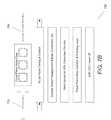
- the array camera 100includes an array camera module 102 that is configured to transmit 106 image data to a receiving device 108 via an interface format involving the transmission of additional data describing the transmitted image data.
- the array camera module 102includes an array of cameras 104 .
- the cameras 104 in the array camera module 102are formed from the combination of a lens stack and a focal plane.
- the array camera module 102can include an optic array of lens stacks and an imager array of focal planes. These multiple cameras 104 may be active or inactive at any given time.
- the image data captured by these multiple camerasmay be transmitted from the focal planes of each camera to a processor.
- the focal planesmay have different imaging characteristics, such as varying exposure times, start times, and end times. Therefore, the timing of the transmission of the image data captured by each focal plane can vary. Accordingly, the imager array can transmit additional data describing the image data to enable a device receiving the image data to appropriately reconstruct images from the received image data.
- the transmission of array camera image datais disclosed in U.S. patent application Ser. No. 13/470,252, entitled “Systems and Methods for Transmitting and Receiving Array Camera Image Data,” the disclosure of which is hereby incorporated by reference.
- the array camera 100captures images using a plurality of cameras 104 , which can have different imaging characteristics.
- the array camera 100can separately control each of the cameras to obtain enhanced image capture and/or to enhance processes such as (but not limited to) super-resolution processes that may be applied to the captured images. For example, each pixel of
- a focal planemay capture different wavelengths of light, or may capture the intensity of light, varying exposure times, start times, or end times.
- the focal planescan commence transmitting the image data captured using the pixels to a receiving device 108 .
- the image data captured by different camerascan be interleaved for transmission to a receiving device 108 that includes interface circuitry configured to receive image data.
- the interface circuitryis implemented in hardware and/or using a processor.
- the receiving device 108can then organize the captured image data from the received packet and appropriately combine the image data to process and/or reconstruct the image(s) captured by one or more of the focal planes in the imager array.
- image data from multiple images of a scenecan be captured by the array camera module 102 .
- the array camera module 102transmits 106 the image data to a receiving device 108 .
- the array camera module 102transmits the image data using a small number of local data storage cells on the array camera module 102 that store the captured image data following capture by the cameras.
- the array camera module 102manages the capture and transmission of image data so that the captured image data stored in the storage cells is transmitted by the imager array of the array camera module 102 in the time taken to capture and load the next set of image data into the storage cells. In this way, the array camera module can continuously buffer and transmit image data using a number of local data storage cells that is less than the total number of pixels in the array camera module.
- a line of image data transmitted by an imager arraycan be considered to equal the number of pixels in a row of a focal plane multiplied by the number of focal planes.
- the clock frequency of transmitter circuitry on the imager arrayis set to a desired output data rate and the internal focal plane pixel rate is set to 1/N the desired output data rate (where N is the total number of focal planes).
- Nis the total number of focal planes.
- an imager array including 4 focal planes(as in a 1 ⁇ 4 array) transmits image data from all focal planes, then there is very little data storage utilized prior to the start of focal plane readout, because the data is transmitted at approximately the rate that at which it is being read. If, however, the same imager array only has one active imager, then almost all of the pixels from a row of the focal plane are stored since the buffer is being read 4 times as fast as it is being written. Therefore, the data storage requirement would be one row of pixels (i.e. 1 ⁇ 4th of a line of image data). When three focal planes are active, 1/the data from the three focal planes is buffered before transmission commences to avoid underflow.
- the total number of data storage cells utilizedis equal to the number of pixels in three quarters of a row of one of the focal planes in this example.
- the above examplesillustrate how the data storage requirements of an imager array can vary based upon the number of active focal planes.
- the total number of storage cells within an imager arrayis less than a quarter of a line of image data.
- the total number of storage cells within an imager arrayis equal to a line of image data.
- the total number of data storage cellsis between a quarter of a line of image data and a full line of image data.
- the total number of storage cellsis equal to or greater than a line of image data.
- Imager arrays in accordance with many embodiments of the inventionare configured to output image data via an interface format that accommodates the transfer of image data captured via multiple focal planes.
- the imager arrayis configured to transmit captured image data in accordance with an interface format that is compatible with standard interface formats, such as (but not limited to) the MIPI CSI-2 interface format (MIPI interface format), the Camera Link interface format, and any of the Universal Serial Bus (USB) interface formats or FireWire interface formats.
- MIPI interface formatMIPI interface format
- USBUniversal Serial Bus
- FireWire interface formatsany of the Universal Serial Bus
- array camera system architecturesare discussed above for constructing array cameras including 1 ⁇ N arrays of cameras, any of a variety of system architectures for array cameras including 1 ⁇ N arrays of cameras can be utilized as appropriate to the requirements of a specific application in accordance with embodiments of the invention.
- Imager array architecturesare discussed below in greater detail.
- the imager array 200includes a focal plane array core 202 that includes a 1 ⁇ N array of focal planes 204 and all analog signal processing, pixel level control logic, signaling, and analog-to-digital conversion circuitry.
- the imager arrayalso includes focal plane timing and control circuitry 206 that is responsible for controlling the capture of image information using the pixels.
- the focal plane timing and control circuitry 206can synchronize the capture of image data by the focal planes such that active focal planes capture image data from a scene simultaneously.
- the focal plane timing and control circuitry 206causes the active focal planes to capture image data from a scene in a particular controlled sequence.
- the focal plane timing and control circuitry 206utilizes reset and read-out signals to control the integration time of the pixels. In several embodiments, any of a variety of techniques can be utilized to control integration time of pixels and/or to capture image information using pixels. In many embodiments, the focal plane timing and control circuitry 206 provides flexibility of image information capture control, which enables features including (but not limited to) high dynamic range imaging, high speed video, and electronic image stabilization.
- the imager array 200includes power management and bias generation circuitry 208 .
- the power management and bias generation circuitry 208provides current and voltage references to analog circuitry such as the reference voltages against which an ADC would measure the signal to be converted against.
- the power management and bias circuitryalso includes logic that turns off the current/voltage references to certain circuits when they are not in use for power saving reasons.
- the imager arrayincludes dark current and fixed pattern (FPN) correction circuitry 210 that increases the consistency of the black level of the image data captured by the imager array and can reduce the appearance of row temporal noise and column fixed pattern noise.
- FPNdark current and fixed pattern
- each focal planeincludes reference pixels for the purpose of calibrating the dark current and FPN of the focal plane and the control circuitry can keep the reference pixels active when the rest of the pixels of the focal plane are powered down in order to increase the speed with which the imager array can be powered up by reducing the need for calibration of dark current and FPN.
- the SOC imagerincludes focal plane framing circuitry 212 that packages the data captured from the focal planes into a container file and can prepare the captured image data for transmission.
- the focal plane framing circuitry 212includes information identifying the focal plane and/or group of pixels from which the captured image data originated.
- the imager array 200also includes an interface for transmission of captured image data to external devices.
- the interfaceis a MIPI CSI 2 output interface supporting four lanes that can support read-out of video at 30 fps from the imager array and incorporating data output interface circuitry 214 , interface control circuitry 216 and interface input circuitry 218 .
- the bandwidth of each laneis optimized for the total number of pixels in the imager array and the desired frame rate.
- various interfaces including the MIPI CSI 2 interface to transmit image data captured by an array of imagers within an imager array to an external device in accordance with embodiments of the inventionis described in U.S. patent application Ser. No. 13/470,252, cited to and incorporated by reference above.
- An imager array in accordance with embodiments of the inventioncan include a single controller that can separately sequence and control each focal plane.
- Having a common controller and I/O circuitrycan provide important system advantages including lowering the cost of the system due to the use of less silicon area, decreasing power consumption due to resource sharing and reduced system interconnects, simpler system integration due to the host system only communicating with a single controller rather than M ⁇ N controllers and read-out I/O paths, simpler array synchronization due to the use of a common controller, and improved system reliability due to the reduction in the number of interconnects.
- an imager array in accordance with embodiments of the inventionmay include a parallax disparity resolution module 220 that can determine disparity between pixels in different images captured by the camera array using parallax detection processes similar to those described in U.S. Provisional Patent Application Ser. No. 61/691,666 entitled “Systems and Methods for Parallax Detection and Correction in Images Captured Using Array Cameras” to Venkataraman et al., the disclosure of which is incorporated by reference herein in its entirety.
- the processing requirements for a parallax disparity resolution calculationmay be sufficiently low that the process may be computed by the imager array circuitry.
- any of a variety of imager arrayscan be constructed in accordance with embodiments of the invention that enable the capture of images of a scene at a plurality of focal planes in accordance with embodiments of the invention.
- Array camera modules that utilize imager arraysare discussed below.
- Array camera modules in accordance with many embodiments of the inventioninclude the combination of an optic array including a 1 ⁇ N array of lens stacks and an imager array that includes a 1 ⁇ N array of focal planes. Each lens stack in the optic array defines a separate optical channel.
- the optic arraymay be mounted to an imager array that includes a focal plane for each of the optical channels, where each focal plane includes an array of pixels or sensor elements configured to capture an image.
- the array camera modulecan be utilized to capture image data from multiple images of a scene that can be read out to a processor for further processing, e.g. to synthesize a high resolution image using super-resolution processing.
- each of the cameras in an array camera modulecan capture image data of a scene reflecting a sub-pixel shifted view of the scene—i.e. relative to the corresponding image formed by at least one other camera (e.g. the lens stack of each camera can have a field-of-view that is shifted with respect to the field-of-view of each other camera so that each shift includes a sub-pixel shifted view of the scene); hence, the aggregated image data can embody sufficient sampling diversity to enable the implementation of super-resolution processes that can be used construct an enhanced image of the scene using the aggregated image data.
- each lens stackcan form an image of a scene onto a corresponding focal plane, and thereby generate image data, from a slightly different viewpoint relative to an image formed by each of the other lens stacks, such that the images formed of the scene by each of the lens stacks contain non-redundant information of about the scene.
- the non-redundant informationcan be used in the construction of a super-resolved image.
- the optics in an array camera moduleare designed to be able to resolve images to a sufficient extent such that the super-resolution processes can be implemented.
- the MTF of the opticsis able to resolve variation in intensity at the spatial resolution of the image that is to result from implemented super-resolution processes (e.g. as opposed to the spatial resolution of the image that can be formed by a single respective camera within an array camera module).
- arrays of lens stacksand ‘arrays of focal planes’ are referenced, it is not meant to be suggested that such arrays are necessarily monolithic structures.
- a plurality of distinct lens stacksare disposed relative to one-another to form a 1 ⁇ N array of lens stacks; similarly, in many instances a plurality of distinct focal planes are disposed relative to one-another to form a 1 ⁇ N array of focal planes.
- a plurality of lens stacks, and a plurality of focal planescan be adjoined in any suitable way to construct a 1 ⁇ N array camera module in accordance with embodiments of the invention.
- the focal planes and/or lens stacksare embodied within monolithic structures.
- FIG. 3An exploded view of an array camera module formed by combining a lens stack array with a monolithic sensor including an array of focal planes in accordance with an embodiment of the invention is illustrated in FIG. 3 .
- the array camera module 300includes an optic array 310 including 1 ⁇ N distinct lens stacks forming N separate apertures and an imager array 330 that includes a 1 ⁇ N array of focal planes 340 .
- Each lens stack 320 in the optic array 310creates an optical channel that resolves an image on one of the focal planes 340 on the imager array 330 .
- Each of the lens stacks 320may be of a different type.
- the optical channelsare used to capture images of different portions of the wavelength of light spectrum (e.g. using color filters, located either within the lens stack or on the sensor) and the lens stack in each optical channel is specifically optimized for the portion of the spectrum imaged by the focal plane associated with the optical channel.
- the array camera module 300includes lens stacks 320 having one or multiple separate optical lens elements axially arranged with respect to each other.
- Optic arrays of lens stacks 310in accordance with several embodiments of the invention include one or more adaptive optical elements that can enable the independent adjustment of the focal length of each lens stack and/or later shifting of the centration of the refractive power distribution of the adaptive optical element.
- adaptive optical elementsis described in U.S. patent application Ser. No. 13/650,039, entitled “Lens Stack Arrays Including Adaptive Optical Elements”, filed Oct. 11, 2012, the disclosure of which is incorporated by reference herein in its entirety.
- the array camera moduleemploys wafer level optics (WLO) technology.
- WLOis a technology that encompasses a number of processes, including, for example, molding of lens arrays on glass wafers, stacking of those wafers (including wafers having lenses replicated on either side of the substrate) with appropriate spacers, followed by packaging of the optics directly with the imager into a monolithic integrated module.
- the WLO proceduremay involve, among other procedures, using a diamond-turned mold to create each plastic lens element on a glass substrate.
- the process chain in WLOgenerally includes producing a diamond turned lens master (both on an individual and array level), then producing a negative mold for replication of that master (also called a stamp or tool), and then finally forming a polymer replica on a glass substrate, which has been structured with appropriate supporting optical elements, such as, for example, apertures (transparent openings in light blocking material layers), and filters.
- a diamond turned lens masterboth on an individual and array level
- a negative mold for replication of that masteralso called a stamp or tool
- a polymer replica on a glass substratewhich has been structured with appropriate supporting optical elements, such as, for example, apertures (transparent openings in light blocking material layers), and filters.
- appropriate supporting optical elementssuch as, for example, apertures (transparent openings in light blocking material layers), and filters.
- array camera module configurationshave been discussed above, any of a variety of array camera modules that utilize lens stacks and focal planes may be implemented in accordance with embodiments of the invention.
- One-dimensional array camera modulesare discussed below.
- one-dimensional (or 1 ⁇ N) array camera modulesare utilized in the construction of array cameras.
- One-dimensional array camera modulescan provide a number of benefits.
- one-dimensional array camera modulescan enable the construction of array cameras having distinctly thin form factors.
- Such array camerasmay be useful in a host of applications.
- array cameras having a thin form factormay be incorporated within the bezel of a consumer electronics device such as a laptop, a tablet, or a smart phone, and may further be incorporated within a pair of eye glasses.
- array cameras that incorporate one-dimensional array camera modulesare advantageous insofar as they may require less processing and/or memory requirements as compared to two-dimensional (or M ⁇ N) array cameras.
- array camerastypically employ a parallax detection and correction process in order to facilitate the imaging of a scene.
- the processis meant to address the fact that the relative positioning of objects in a scene may appear to vary from the respective viewpoints of different cameras within an array camera module.
- this techniquecan be processor intensive and involve significant data storage requirements related to searches for corresponding pixels along epipolar lines (other than just horizontal or vertical) between cameras located in different rows and/or columns within the array camera module.
- Array camera modulestypically pass image data to a processor by starting with image data captured by pixels in a first row of a focal plane and then advancing to the next row of pixels and reading out image data from pixels within the next row of pixels.
- the read out of image data from pixels within a focal planecan also be interspersed with the readout of image data from pixels within other focal planes. Note that with this technique, because image data is being passed to the processor along the rows of the focal planes, searches for corresponding pixels along vertical or diagonal epipolar lines, for example during a parallax detection and correction process of a two-dimensional array camera, involve the processor storing substantial amounts of image data across multiple rows of image data captured by a focal plane.
- one-dimensional array camera modulesmay provide greater manufacturing yield as compared with two dimensional array camera modules, because one-dimensional array camera modules may have less cameras.
- the array camera moduleincludes a central narrow spectral band green camera (G), adjacent narrow spectral band blue cameras (B), and periphery narrow spectral band red cameras (R).
- Color filtersmay be employed to achieve the respective narrow spectral band cameras.
- the color filtersmay be located either within the lens stack or on the sensor.
- a narrow spectral band green cameramay be centrally placed to accommodate the fact that humans are most sensitive to green light.
- Narrow spectral band red and blue camerasmay be placed on either side of the central narrow spectral band green camera—this configuration may counteract any occlusion that may occur as a result of any obstructing foreground objects.
- FIG. 4Bis similar to FIG. 4A except that the narrow spectral band red cameras are adjacent to a central narrow spectral band green camera, and narrow spectral band blue cameras enclose the configuration.
- Nnear-IR cameras
- Pfull visual spectrum cameras
- Bayer filterswhich are typically implemented on the sensor, may be utilized to obtain color information.
- FIGS. 5A-5CA 1 ⁇ 7 array camera module in accordance with embodiments of the invention is illustrated in FIGS. 5A-5C .
- a 1 ⁇ 7 array camera modulemay employ more narrow spectral band green cameras than narrow spectral band blue or narrow spectral band red cameras. This may be to accommodate the fact that humans are most sensitive to green light.
- the array camera moduleincludes a central narrow spectral band green camera and periphery narrow spectral band green cameras, and narrow spectral band red and blue cameras. The cameras may be symmetrically distributed or they may be asymmetrically distributed. In the embodiments illustrated in FIGS.
- the narrow spectral band camerasare symmetrically distributed.
- the narrow spectral band camerasare asymmetrically distributed.
- the inclusion of multiple red and blue cameras uniformly distributed around the central green camerareduces the likelihood of color artifacts related to occlusions by foreground objects.
- the presence of multiple green cameras in an array having sub-pixel shifted views of the scene to provide sampling diversityenables the application of super-resolution processes to the captured image data to recover a higher resolution image of the scene.
- any number of configurationsmay be employed all in accordance with embodiments of the invention.
- near-IR camerasmay be employed, and in a number of embodiments, full visual spectrum cameras are employed.
- Bayer filtersmay be utilized to obtain color information.
- a 1 ⁇ 9 array camera module in accordance with embodiments of the inventionis illustrated in FIGS. 6A-6F .
- a 1 ⁇ 9 array camera modulemay be more preferable than either a 1 ⁇ 7 array camera module or a 1 ⁇ 5 array camera module since it provides more image data.
- a 1 ⁇ 9 array camera modulemay employ more narrow spectral band green cameras than narrow spectral band blue or narrow spectral band red cameras. The inclusion of multiple red and blue cameras distributed around the central green camera reduces the likelihood of color artifacts related to occlusions by foreground objects.
- the presence of multiple green cameras in an array having sub-pixel shifted views of the scene to provide sampling diversityenables the application of super-resolution processes to the captured image data to recover a higher resolution image of the scene.
- narrow spectral band green camerasare not disposed along the periphery of the array camera module.
- array camera modulewith any number of cameras may be implemented in accordance with embodiments of the invention. For instance, 1 ⁇ 4 array camera modules and 1 ⁇ 5 array camera modules may be implemented. Sub-array modules that may be used to construct one-dimensional array camera modules are discussed below.
- sub-array modulesare used in the construction of array cameras.
- Sub-array modulesmay be configured to interface with other sub-array modules so that data can pass between the sub-array modules, thereby enabling a processor to interact with multiple coupled sub-array modules via an interface with one of the sub-array modules.
- sub-array modulescan couple with other sub-array modules to enable the fabrication of array cameras of any number of specified dimensions and characteristics.
- sub-array modulesdo not couple with one-another, but instead interact directly or indirectly (e.g. via a bus) with a receiving device (e.g. a processor). Accordingly, sub-array modules of this variety can also enable the modular construction of an array camera of any number of specified dimensions and characteristics.
- sub-array modulesin the construction of array cameras can provide a number of benefits.
- the use of sub-array modules to construct array camerascan improve manufacturing yield relative to the direct fabrication of an array camera module.
- one-dimensional array camera modulesmay be beneficial in numerous applications, their manufacture can be challenging.
- components for one-dimensional array camerase.g. the lenses and the corresponding sensor
- the periphery of the wafer used in the manufacturemay contain significant unused space that, because of the elongated shape of a lens array, cannot accommodate further lens arrays.
- wafersare may be more efficient in the manufacture of components that are more ‘square’ in shape than ‘elongated.’
- sub-array modules that are used in the construction of an array camera modulemay be less elongated than the array camera module.
- sub-array modulescan better optimize wafer space during manufacture.
- sub-array modulesare also beneficial since they comprise a relatively fewer number of cameras compared to an array camera module: the more cameras an array camera module has, the more difficult it is to directly manufacture since it is more likely to have a critical number of faulty cameras.
- manufacturing processes disclosed in prior U.S. patent application Ser. No. 13/050,429 disclosure entitled “Fabrication process for mastering imaging lens arrays”can be more beneficially applied if the array to be generated is smaller like those discussed in this application.
- the 1 ⁇ N master structure, for the sub-arraycan be more optimally fine-tuned for homogeneity either by multiple attempts to directly diamond-turn the 1 ⁇ N arrays of the template or by multiple attempts to step-and-repeat the 1 ⁇ N array of the template from single lens pins before using the final small-variation 1 ⁇ N template to fully populate, for example, a 8′′ wafer scale master.
- the array-internal performance variation and in particular BFL-variationcan be reduced.
- Resulting variations from array to array on the full wafer scale mastercan be compensated by the approach presented under the method described above.
- array camera modules constructed from sub-array modulesmay be further advantageous in that each individual sub-array module may incorporate custom spacers to counteract back focal length variation.
- U.S. Patent Application Ser. No. 61/666,852 entitled “Systems and Methods for Manufacturing Camera Modules Using Active Alignment of Lens Stack Arrays and Sensors”discusses the issues related to back focal length (BFL) misalignment in the construction of array camera modules, and is hereby incorporated by reference.
- BFLback focal length
- the distribution of the average BFL for a 1 ⁇ N sub-array module fabricated in a wafer stackis determined over a sufficient number of stacks to establish the repeatable array-average BFL variation.
- a spacer wafermay then be machined with steps in thickness that correspond to the pattern of the average-BFL over the wafer stack, and the spacers may thereafter be incorporated into the sub array module.
- the standard deviation of the BFL of sub-array modules within a wafer stackis expected to be small given the relatively small number of cameras in a sub-array module; accordingly, the incorporation of the customized spacers into the sub-array modules is expected to result in sufficient focusing.
- the sub-array module 700includes a focal plane array core 702 that includes a 1 ⁇ 3 array of focal planes 704 and all analog signal processing, pixel level control logic, signaling, and analog-to-digital conversion circuitry. Although a 1 ⁇ 3 array of focal planes is illustrated, any number of focal planes can be used in accordance with embodiments of the invention.
- the sub-array moduleincludes lens stacks 706 , and the combination of a lens stack 706 and its corresponding focal plane 704 can be configured to implement any type of camera including but not limited to narrow spectral band red cameras, narrow spectral band blue cameras, narrow spectral band green cameras, near-IR cameras, and full visual spectrum cameras. Bayer-filters may be employed to facilitate imaging.
- the sub-array modulemay utilize focal plane timing and control circuitry 708 that is responsible for controlling the capture of image information using the focal plane's constituent pixels.
- the focal plane timing and control circuitry 708provides flexibility of image information capture control which enables features including, but not limited to, high dynamic range imaging, high speed video, and electronic imaging stabilization.
- the focal plane timing and control circuitrycan have inputs 720 and outputs 722 related to the timing of image capture, so that the sub-array module timing can be controlled by an external device (e.g. a processor, or alternatively another sub-array module).
- the sub-array module 700includes power management and bias generation circuitry 710 .
- the power management and bias generation circuitry 710provides current and voltage references to analog circuitry such as the reference voltages against which an ADC would measure the signal to be converted against.
- the power management and bias circuitry 710also includes logic that turns off the current/voltage references to certain circuits when they are not in use for power saving reasons.
- the imager arrayincludes dark current and fixed pattern (FPN) correction circuitry 712 that increases the consistency of the black level of the image data captured by the imager array and can reduce the appearance of row temporal noise and column fixed pattern noise.
- FPNdark current and fixed pattern
- each focal planeincludes reference pixels for the purpose of calibrating the dark current and FPN of the focal plane and the control circuitry can keep the reference pixels active when the rest of the pixels of the focal plane are powered down in order to increase the speed with which the imager array can be powered up by reducing the need for calibration of dark current and FPN.
- the sub-array moduleincludes focal plane framing circuitry 714 that packages the data captured from the focal planes into a container file and can prepare the captured image data for transmission.
- the focal plane framing circuitry 714includes information identifying the focal plane and/or group of pixels from which the captured image data originated.
- the sub-array module 700also includes an interface for transmission and reception of data to and from external device(s).
- the interfacecan allow for the transmission and reception of image data.
- the interfaceis a MIPI CSI 2 output interface supporting four lanes that can support read-out of video at 30 fps from the imager array and incorporating interface control circuitry 716 , and two sets of data input/output interface circuitry 718 .
- each set of interface circuitryis capable of both sending and receiving data.
- the interface circuitry, the interface control circuitry, and the focal plane timing and control inputs/outputscan allow the sub-array module to be controlled by a processor (either directly or indirectly), and/or can also allow the sub-array module to receive/transmit captured image data.
- the bandwidth of each input/output laneis optimized for the total number of pixels in the imager array and the desired frame rate.
- the input/output interface circuitryis configured to interface with any receiving device such as another sub-array module or a processor. Note that although the illustrated embodiment depicts a MIPI CSI 2 protocol, any interface protocol may be used including a Standard Mobile Imaging Architecture (“SMIA”) format.
- SIAStandard Mobile Imaging Architecture
- the use of various interfaces including the MIPI CSI 2 interface to transmit image data captured by an array of imagers within an imager array to an external device in accordance with embodiments of the inventionis described in U.S. patent application Ser. No. 13/470,252, cited to and incorporated by reference above.
- the sub-array modulemay also include pins that can be used to establish a unique slave address for the sub-array module in the case where the sub-array module interfaces with a master device (e.g. a processor, or a master sub-array module) via a bus as discussed below. In this way, each slave device can be independently controlled by the master device.
- a master devicee.g. a processor, or a master sub-array module
- FIG. 7BA sub-array module in accordance with several embodiments of the invention is illustrated in FIG. 7B .
- the sub-array module 750is similar to that seen in FIG. 7A , except that it does not include two sets of interface circuitry that allow both the transmission and reception of data; instead the illustrated embodiment depicts a sub-array module that includes receive interface circuitry 752 configured to receive image data from another sub-array module for forwarding, and transmit interface circuitry 754 configured to transmit forwarded image data and image data captured by the sub-array module.
- receive interface circuitry 752configured to receive image data from another sub-array module for forwarding
- transmit interface circuitry 754configured to transmit forwarded image data and image data captured by the sub-array module.
- sub-array modulesare implemented that are not required to couple with other sub-array modules; instead they each interface—either directly or indirectly—with a receiving device, such as a processor, and thereby provide image data.
- a receiving devicesuch as a processor
- any suitable way for transmitting the datacan be implemented.
- image datacan be transmitted in parallel, or it can be transmitted in a serial fashion.
- sub-array modulesare configured to output image data to a bus; subsequently, the image data carried by the bus (e.g. from each of many sub-array modules) can be processed into a single MIPI output that can be more easily handled by a receiving device.
- the image datacan be transmitted to the bus in a parallel fashion, or as serial data, e.g. via low voltage differential signaling.
- any suitable I/O devicemay be used to relay image data to a receiving device, not just a conventional bus.
- sub-array modulescan be implemented that do not have to have, for example, distinct MIPI processing circuitry; instead, the processing of image data from many sub-array modules into a single MIPI output can be accomplished separately and more efficiently. Accordingly, the manufacture of sub-array modules can become less intricate, and their manufacturing yield may increase as a result. Further, with this modular construction, I/O devices can be easily swapped if desired.
- any suitable architecturecan be implemented in accordance with embodiments of the invention.
- sub-array modulesany of a variety of sub-array modules that can allow for transmission and reception of data may be implemented in accordance with embodiments of the invention.
- 1 ⁇ 4, 1 ⁇ 2, and even 1 ⁇ 1 sub-array modulesmay be implemented.
- 2-dimensional sub-array modulesmay also be implemented in accordance with embodiments of the invention; for example 2 ⁇ 3, 2 ⁇ 2, and 3 ⁇ 3 sub-array modules may be implemented.
- Two-dimensional sub-array modulesmay be used to construct two-dimensional array camera modules. Sub-array module lens configurations and the construction of one-dimensional array camera modules using sub-array modules are discussed below.
- Sub-array modulesmay include cameras arranged in a variety of configurations in accordance with embodiments of the invention.
- the exact configurations employed in sub-array modulesdepend on the particular design of the array camera to be formed. For example, in the case where a GNRBGBRNG 1 ⁇ 9 array camera is desired (like the one illustrated in FIG. 6E ), three 1 ⁇ 3 sub-array modules may be used to form the corresponding array camera module having the following respective camera arrangement configurations: GNR, BGB, and RNG.
- FIGS. 8A-8Kdepict ten examples of sub-array module configurations that are similar to those shown in FIG. 7B in accordance with embodiments of the invention. Although ten examples are provided in FIGS.
- any number of configurations of sub-array modules using any of a variety of color filter patternsmay be implemented in accordance with embodiments of the invention.
- the sub-array modules 800are illustrated as having corresponding interface circuitry 802 , represented by arrows. The direction of the arrows is meant to indicate the direction in which image data is passed when the interface circuitry is operational.
- a BGR sub-array modulemay be reconfigured so that it acts as a RGB sub-array module.
- FIG. 9illustrates how a BGR sub-array module may be reconfigured to act as a RGB sub-array module.
- the BGR sub-array module 900may be rotated 180° 902 , and its corresponding interface circuitry may be reconfigured 904 such that the transmission/reception protocols in the interface circuitry are reversed.
- the data read from the sub-array modulecan include a flag and/or additional data indicating the orientation of the sub-array module to enable a processor to map the relative position of pixel addresses to corresponding locations in other cameras in an array camera.
- the BGR sub-array modulemay be rotated 180° and positioned on a PCB (or laminated chip carrier or other similar such interconnector), and the configuration of the PCB (or laminated chip carrier or other similar such interconnector) may invert the routing of the data transmitted to/from the sub-array module, such that the sub-array module acts as a RGB sub-array module.
- PCBprinted circuit board
- Sub-array modulesmay be coupled to form an array camera module in accordance with embodiments of the invention.
- sub-array modulesmay be coupled via their respective interface circuitry such that data may be passed from one sub-array module to the coupled sub-array module.
- FIGS. 10A-10Cillustrate the construction of three respective 1 ⁇ 9 array camera modules using three 1 ⁇ 3 sub-array modules.
- FIG. 10Aillustrates a GNRBGBRNG array camera module 1000 made from a GNR sub-array module 1002 , a BGB sub-array module 1004 , and a RNG sub-array module 1006 . Note that data received by one sub-array module can of course be transmitted to another sub-array module.
- a respective sub-array modulecan include within the transmission information regarding the type of data and its origination and/or the orientation of the sub-array module within the array (i.e. standard or inverted/rotated).
- the BGB sub-array module 1004transmits data to the RNG sub-array module 1006
- the BGBcan also transmit information regarding what type of data is being transmitted—e.g. image data—and where it originated from—e.g. which pixel of which focal plane of which sub-array module (e.g., the GNR sub-array module or the BGB sub-array module itself).
- any type of informationcan be transmitted between sub-array modules that facilitates their coupling.
- the RNG sub-array module 1006can read out the data to an external device.
- the GNR sub-array module 1002can transmit image data to the BGB sub-array module 1004 , which can then transmit image data (including the image data received from the GNR sub-array module) to the RNG sub-array module 1006 ; the RNG sub-array module 1006 may then read out image data (including the image data received from the BGB sub-array module, which itself includes image data received from the GNR sub-array module) to an external device.
- the manner in which the sub-array modules interface with each other and with a receiving devicemay be different.
- the manner in which the RNG sub-array module 1006 interfaces with a receiving devicemay be in accordance with the MIPI interface format, whereas the manner in which the GNR sub-array module 1002 , the BGB sub-array module 1004 , and the RNG sub-array module 1006 interface with one another in a different manner, e.g., via simple analog voltages or serial interfaces.
- the array camera module 1000can couple with a receiving device, e.g. a processor, such that the receiving device can synchronize the capture of images from each of the sub-array modules.
- a receiving devicee.g. a processor
- each of the sub-array moduleshas inputs and outputs that can be used to control the respective sub-array module's internal timing engine, and that can allow a processor to synchronize the capture of images.
- a processorcan thus provide a driving signal to each of the sub-array modules that synchronizes the capture of images of the focal planes in the sub-array modules.
- the processorcan provide the signal via a bus-type architecture, where the processor is set as a master, and each of the sub-arrays is set as a slave.
- the processorcan also provide the driving signal to a directly coupled sub-array module, and the sub-array module can then relay the driving signal to an adjacent sub-array module, and this relaying process can continue until each sub-array module is provided with a driving signal.
- the processordoes not provide a driving signal to each sub-array module; instead, the processor provides a driving signal to a master sub-array module.
- the master sub-array modulecan then controls the slave sub-array modules so that the capture of images from the cameras of the sub-array modules is synchronized.
- the driving signalcan constitute a ‘horizontal sync pulse’ and a ‘vertical sync pulse’ to help facilitate the precise capture of image data.
- the image datamay be captured by the pixels of the focal plane by advancing along the rows of pixels of the focal plane—i.e. image data is captured by a first row of pixels in a particular direction (e.g. left-to-right), then image data is captured by a next row of pixels, etc.
- a constituent horizontal sync pulse within a driving signalcan synchronize the sampling and readout of a particular row of pixels within a focal plane (whichever row the vertical timing controller is pointing to at that time).
- the vertical sync pulseindicates to a vertical timing controller associated with a focal plane that the vertical timing controller should start at the beginning of the frame (i.e. row zero).
- the vertical sync pulsecan synchronize the capture of individual frames from each sub-array module within the video.
- one of the sub-arraysis configured as a master that outputs the horizontal and vertical sync pulses to the other sub-arrays in the array cameras, which are designated as slaves synchronized to the control signals issued by the master sub-array.
- any driving signalcan be used to synchronize the capture of image data in accordance with embodiments of the invention.
- the sub-array modulescan also include outputs that provide information concerning the state of the internal timing engine of the sub-array camera module. In many embodiments, the timing information is also provided using a ‘horizontal sync pulse’ and a ‘vertical sync pulse’.
- FIGS. 10A-10Cany number of array camera modules can be constructed using sub-array modules in accordance with embodiments of the invention. For example, array camera modules of any length may be constructed using sub-array modules in accordance with embodiments of the invention.
- FIG. 11Aillustrates a 1 ⁇ 9 array camera fabricated from three 1 ⁇ 3 sub-array modules that do not couple with one another in accordance with embodiments of the invention.
- the array camera 1100corresponds with that seen in FIG. 10A , except that each sub-array module, 1102 , 1104 , and 1106 , outputs image data to a bus 1108 , and thereby transmits image data to a processor 1108 .
- intermediary circuitryis used to convert received image data to a single MIPI output, which is then transmitted to a processor 1110 .
- array camerascan be implemented whereby sub-array modules do not couple with one another.
- FIG. 11Billustrates a 1 ⁇ 9 array camera similar to that seen in FIG. 11A , except that each sub-array module is associated with a respective I/O device, that itself interfaces with an I/O block which processes the received image data and provides an output to a processor.
- a 1 ⁇ 9 array camera 1150includes three sub-array modules 1152 , 1154 , and 1156 , that are each affiliated with a respective I/O device, 1158 , 1160 , and 1162 . Accordingly, the respective I/O devices interface with a separate I/O block 1164 that can aggregate the image data and thereby provide a single MIPI output.
- the I/O block 1164can provide the output in a MIPI container to a processor 1166 for further processing.
- this architectureincludes multiple I/O devices, each affiliated with certain cameras, image data may be processed more effectively and efficiently. For example, using this architecture, the length of circuit traces can be reduced, and correspondingly, the signal to noise ratio can be enhanced. Consequently, the increased efficiency can help mitigate a host of issues that may otherwise be present including those relating to: image data synchronization; power consumption; and cross-talk. Additionally, as multiple I/O devices are used, they each may be adapted to have a smaller footprint, and can thereby facilitate the implementation of an advantageous physical layout of the sub-array modules.
- each of multiple I/O devicescan be affiliated with any number of cameras in accordance with embodiments of the invention.
- 2 I/O devicesare incorporated whereby one I/O device is affiliated with 6 cameras, and the other I/O device is affiliated with 3 cameras.
- the I/O devicesmay then interface with a separate I/O block that receives image data, aggregates it, and outputs it to a processor for further processing.
- two-dimensional sub-array modulesmay also be implemented in accordance with embodiments of the invention; accordingly, I/O devices may also be affiliated with any number of cameras in an arrangement of two-dimensional sub-array modules in accordance with embodiments of the invention.
- I/O blocksmay be affiliated with cameras within sub-array modules of any dimensions in accordance with embodiments of the invention.
- sub-array modules of different typesmay be coupled to form array camera modules.
- 1 ⁇ 3 sub-array modulesmay be combined with 1 ⁇ 2 sub-array modules, 1 ⁇ 4 sub-array modules, or even 1 ⁇ 1 sub-array modules.
- This flexibilityis advantageous insofar as it can alleviate unwieldy manufacturing processes.
- the manufacture of sub-array modules that include near-IR camerase.g. a GRN sub-array module as shown in FIG. 8D
- an IR cut-off filterthat can be a structured dielectric coating
- a 1 ⁇ 1 near-IR sub-array modulemay be coupled with another sub-array module of any type, thereby resulting in an array camera module that includes a near-IR camera. This technique may be advantageous in that cumbersome manufacturing processes may be avoided.
- 1 ⁇ 1 sub-array modules that include near-IR camerascan be produced separately on a single wafer that does not include any other color channels and later coupled with a sub-array module that includes color cameras constituting different color channels. Consequently, the step of selectively removing an IR cut-off filter and then applying an organic near-IR pass filter or other dielectric coating may be avoided.
- a 1 ⁇ 2 GR sub-array modulemay be coupled to a 1 ⁇ 1 near-IR camera to form a 1 ⁇ 3 GRN array camera module in accordance with embodiments of the invention.
- the particular lens fabrication technique employed in the fabrication of a sub-array modulemay be selected to accommodate the particular sub-array module's functionality and/or its manufacturing process.
- any number of sub-array moduleswhich can each be of different types, can be coupled to form an array camera module in accordance with embodiments of the invention.
- the constituent sub-array modulesmay be designed to accommodate any number of different manufacturing processes.
- sub-array modulesmay be combined using a single substrate that includes interconnects.
- sub-array modulesmay be coupled to a substrate that has interconnects, such that when the sub-array modules are coupled to the substrate, the sub-array modules can thereby interface with each other and/or with a receiving device (e.g. a processor) via the substrate's interconnects.
- a receiving devicee.g. a processor
- FIG. 12The interconnection of three sub-array modules coupled to a glass substrate in accordance with an embodiment of the invention is illustrated in FIG. 12 .
- three sub-array modulesare coupled to a glass substrate that includes interconnects, thereby allowing the sub-array modules to interface with one another and with a receiving device.
- the array camera module 1200is constructed from a glass substrate 1202 that includes interconnects 1204 , upon which sub-array modules 1206 can couple.
- the sub-array modulescan include electrical pads to couple with the glass substrate's interconnects.
- the electrical padscan include the same interface functionality discussed above with respect to FIGS. 7A and 7B (e.g. interface circuitry 718 , 752 , 754 , inputs/outputs, 720 , 722 ).
- the interconnects 1204can allow the sub-array modules to interface with one another and with a receiving device such as, but not limited to, an appropriately configured microprocessor and/or an application specific device that is configured to read in the serial data from the independent sub-array modules and synthesize a cohesive output data stream (e.g. a MIPI serial output data stream).
- a receiving devicesuch as, but not limited to, an appropriately configured microprocessor and/or an application specific device that is configured to read in the serial data from the independent sub-array modules and synthesize a cohesive output data stream (e.g. a MIPI serial output data stream).
- the interconnectscan be configured so as to allow each sub-array module to interface—either directly or indirectly—with a receiving device such that each sub-array module can provide image data to a receiving device without having to couple with another sub-array module.
- the array camera seen in FIG. 11can be constructed using a single substrate.
- the lenses of a sub-array modulemay also be bonded to the glass substrate.
- the sensors that include the sub-arrays of focal planesmay be coupled with the glass substrate on one side of it that includes interconnects, and the corresponding lenses that combine with the sensors to form an imager array may be bonded to the other side of the glass substrate such that the complete functionality of the sub-array module is achieved.
- the sub-array modulecan still function even though the glass substrate lies between the sensor dies and the corresponding lenses.
- the lens for each sensor in a sub-array modulecan be independently mounted to the glass substrate.
- arrays of lens stackscan be mounted to the glass substrate and the number of lens stacks in the array need not correspond with the number of focal planes on the sensors mounted to the glass substrate.
- a substrate to facilitate the coupling of sub-array modulescan be advantageous in that the specific configuration of the substrate can govern the spacing between the sub-array modules, and the spacing between sub-array modules can control the array camera module's imaging ability. Specifically, the manner in which the interconnects are situated can govern the sub-array module spacing. Hence, sub-array modules that are coupled need not be within immediate proximity of one another when a substrate is used to enable their coupling. Although much of the discussion above refers to the use of glass substrates, any of a variety of optically transparent substrate materials can be utilized as appropriate to the requirements of specific applications in accordance with embodiments of the invention.
- substrates in which openings are formed to permit transmission of light through the substratecan also be utilized including (but not limited to) ceramic substrates in which through holes are formed.
- a single sensor or multiple sensorscan be fixed to one side of the ceramic carrier to form the focal planes of the array camera module and lens barrels containing lens stacks can be affixed to the other side of the ceramic carrier so that the lens stacks direct light onto the focal planes of the one or more sensors through the openings in the ceramic carrier.
- the ceramic carrieris rigid and has a coefficient of thermal expansion that matches that of the sensor.
- One-dimensional array camera modules constructed from sub-array modulesmay also be coupled to a parallax disparity resolution module in accordance with embodiments of the invention.
- the parallax disparity resolution modulemay either a hardware parallax disparity resolution module or may be a software parallax disparity resolution module.
- FIG. 13Aillustrates a 1 ⁇ 9 array camera module constructed from three constituent 1 ⁇ 3 sub array modules, where the array camera module 1300 outputs the data to a hardware parallax disparity resolution module 1302 .
- FIG. 13Billustrates a 1 ⁇ 9 array camera module constructed from three constituent 1 ⁇ 3 sub-array modules, where the array camera module 1350 outputs the data to a software parallax disparity resolution module 1352 .
- Either parallax disparity resolution module 1302 , 1352can receive the data and implement processes to detect parallax within image data (using processes similar to, but not limited to, those described in U.S. Provisional Patent Application Ser. No. 61/691,666) and implement processes to account for the detected parallax in the further processing of the image data.
- Two-dimensional array camera modulesmay also be constructed from sub-array modules in accordance with embodiments of the invention, and this is discussed below.
- Sub-array modulesmay be coupled to form two-dimensional array cameras in accordance with embodiments of the invention.
- a 3 ⁇ 9 two-dimensional array camera constructed from sub-array modules in accordance with embodiments of the inventionis illustrated in FIG. 14A .
- nine 1 ⁇ 3 sub-array modulesare coupled so as to form three array camera module sub-assemblies 1402 .
- Each array camera module sub-assembly 1402is then coupled to a parallax disparity resolution module 1404 (either hardware or software).
- an interconnection moduleinterfaces with a processor 1406 and one of the sub-arrays in each of the rows of the camera array to enable communication between the processor and each of the sub-arrays.
- the processoris configured to directly interface with multiple sub-arrays, e.g. similar to the arrangement seen in FIG. 11 .
- each sub-array moduleis configured to interface with circuitry that receives image data from each sub-array module and converts the image data to a single MIPI output, which is thereby provided to a processor.
- the three 1 ⁇ 9 array camera module sub-assembliesare adjacent to each other such that a 3 ⁇ 9 array camera module can be achieved.
- the processor 1406is made aware of the relative location of the cameras, and uses this information in processing received data.
- a two-dimensional array camerais formed from sub-array modules where a single sub-array module reads out data to a processor.
- FIG. 14Billustrates a two-dimensional 3 ⁇ 9 array camera where a single constituent sub-array module reads out data to a processor.
- the array camera 1450is formed from nine 1 ⁇ 3 sub-array modules that are coupled, where data from the sub-array modules is read out by a single sub-array module 1452 to a processor 1454 , which can then process the image data.
- the sub array modulesare arranged such that a 3 ⁇ 9 array camera module is achieved.
- any arrangementmay be implemented in order to achieve a two-dimensional array camera module in accordance with embodiments of the invention.
- the processor 1454is made aware of the relative location of the cameras, and uses this information in processing received data.
- the manner in which the sub-array modules interface with one another and with a receiving devicemay all be different.
- FIG. 15illustrates a two-dimensional array camera formed from sub-array modules coupled to a substrate.
- the array camera 1500includes a glass substrate 1502 with interconnects 1504 , sub-array modules 1506 , and a processor 1508 .
- the sub-array modules 1506can connect to the glass substrate 1502 via electrical pads, and as before the imager arrays of a sub-array module 1506 may be coupled to one-side of the glass substrate that includes interconnects 1504 , and corresponding lenses may be bonded to the other side of the glass substrate 1502 .
- an array camera modulemay be patterned with “ ⁇ filter groups”, or alternatively “Pi filter groups.”
- Pi filter groupsrefers to a pattern of narrow spectral band cameras within the array camera module. Processes for patterning array cameras with Pi filter groups are described in U.S. Provisional Patent Application Ser. No. 61/641,164, entitled “Camera Modules Patterned with ⁇ Filter Groups”, Venkataraman et al. The disclosure of U.S. Provisional Patent Application Ser. No. 61/641,164 is incorporated by reference herein in its entirety.
- a single Pi filter groupis illustrated in FIG. 16 , wherein 5 cameras are configured to receive green light, 2 cameras are configured to receive red light, and 2 cameras are configured to receive blue light.
- the Pi filter patternsmay facilitate the efficient capturing of color image data.
- two-dimensional array camerasare constructed using sub-array modules wherein the sub-array modules are arranged such that Pi filter groups are implemented within the array camera.
- FIGS. 17A and 17Bare similar to FIGS. 14A and 14B except that the sub-array modules are configured to implement Pi filter groups.
- FIGS. 18A-18Billustrate 1 ⁇ 4 sub-array modules in accordance with some embodiments. It should be repeated that although only narrow spectral band blue, green and red cameras are illustrated in FIGS. 18A-18B , any type of camera may of course be implemented in sub-array modules in accordance with embodiments of the invention.
- FIGS. 19A and 19Billustrate the construction of a 4 ⁇ 4 array camera using 1 ⁇ 4 sub-array modules in accordance with many embodiments.
- FIGS. 19A and 19Bare similar to FIGS. 14A and 14B except that 1 ⁇ 4 sub-array modules are used to form the array camera.
- the illustrated embodimentincludes an array camera, sub-array module sub-assemblies 1902 , an interconnection module 1904 , and a processor 1906 , 1908 .
- Pi filter groupsare patterned on the array camera.
- FIGS. 20A-20Dillustrate 1 ⁇ 5 sub-array modules
- 21A-21Billustrate the construction of 5 ⁇ 5 array cameras using 1 ⁇ 5 sub-array modules.
- the illustrated embodimentincludes an array camera 2100 , sub-array modules sub-assemblies 2102 , an interconnection module 2104 , and a processor 2106 , 2108 .
- Pi filter groupsare implemented on the two dimensional array cameras.
- a particular benefit of utilizing 1 ⁇ 5 sub-array modules to build a 5 ⁇ 5 array camera moduleis that the 5 ⁇ 5 array camera can be constructed using two different types of 1 ⁇ 5 sub-array modules (i.e. GRGRG and BGBGB or GBGBG and RGRGR).
- any square array patterned with Pi filter groups including an odd number of rows and columnscan be constructed using only two different types of sub-arrays.
- two-dimensional sub-array modulesmay also be implemented to construct two-dimensional array cameras in accordance with embodiments of the invention.
- FIG. 22illustrates the construction of a 4 ⁇ 4 array camera using 2 ⁇ 2 sub-array modules.
- the 4 ⁇ 4 array camera 2200is similar to that seen in FIG. 19 , except that it includes four 2 ⁇ 2 sub-array modules 2202 .
- each sub-array module 2202interfaces with circuitry 2204 that receives image data from each of the sub-array modules and outputs the aggregated image data to a processor 2206 .
- the sub-array modulescan provide image data to a processor in any suitable fashion in accordance with embodiments of the invention.
- the two-dimensional sub-arraysinclude interface circuitry that allow them to interface with other sub-array modules, and thereby transmit image data to (and otherwise interact with) a processor.
- modular array camerasinclude both two-dimensional and one-dimensional sub-array modules.
- modular array cameras of any dimensioncan be constructed from one-dimensional and/or two-dimensional sub-array modules in accordance with embodiments of the invention.
- 1 ⁇ 1 sub-array modulesmay also be used to construct array cameras, and this is discussed below.
- 1 ⁇ 1 sub-array modulesmay be used to construct array cameras.
- 1 ⁇ 1 sub-array modulesmay be used to construct either one dimensional array cameras or two-dimensional array cameras.
- 1 ⁇ 1 sub-array modulesare similar to the sub-array modules discussed above except that they do not include multiple lens stacks and multiple focal planes. Instead, a 1 ⁇ 1 sub-array module includes a single lens stack and a sensor including single focal plane. Accordingly, the above-mentioned techniques regarding constructing array cameras from sub-array modules may also be used to construct array cameras from 1 ⁇ 1 sub-array modules. Using 1 ⁇ 1 sub-array modules to construct array cameras may confer a host of benefits.
- Array cameras of any dimensionmay be constructed using 1 ⁇ 1 sub-array modules, and many different types of 1 ⁇ 1 sub-array modules may be used in the construction.
- 1 ⁇ 1 sub-array modulesthat have different F numbers, focal lengths, image sensor formats and/or fields of view, may be used, particularly because slightly different heights of different types of 1 ⁇ 1 sub-array modules can be accommodated.
- the different substrates and spacer thicknesses within a lens stackmay be accommodated.
- these sub-array modulesare used to construct array cameras that can provide optical zoom with no moving parts.
- Array camerasmay also incorporate 1 ⁇ 1 sub-array modules that are configured for near-IR sensitivity and far-IR sensitivity.
- sub-array modulesthat implement a time-of-flight camera to provide additional depth information, may also be used in accordance with embodiments of the invention.
- 1 ⁇ 1 sub-array modulesare also beneficial insofar as 1 ⁇ 1 sub-array modules of the same type (e.g., near-IR cameras) may be constructed on the same wafer, thereby increasing manufacturing efficiencies.
- 1 ⁇ 1 sub-array modulesmay be assembled to form an array camera module using a variety of technique appropriate to the specific 1 ⁇ 1 sub-array module constructions, including any of the above discussed techniques, in accordance with embodiments of the invention.
- the sensor of a 1 ⁇ 1 sub-array moduleis adjoined to a printed circuit board using reflow soldering. Subsequently, the respective lenses of the sub-array module may be adjoined to the sensor. Note that the lenses may be affixed to the sensor using the active alignment processes U.S. Patent Application Ser. No. 61/666,852.
- the sensors of a 1 ⁇ 1 sub-array moduleare bonded to a glass substrate that includes interconnects that allow the sub-array modules and other components to interface.
- the corresponding lensesmay also be bonded to the glass substrate. This technique is similar to that already described above.
- each sub-array moduleis first independently formed such that it is inclusive of the sensor and the lens stack array, and is then reflow soldered to a printed circuit board.
- both the lens and the sensorare adapted to be capable of undergoing a reflow soldering process.
- This method of manufacturemay be advantageous insofar as the individual sub-array modules can be evaluated prior to construction of the array camera. It may be further advantageous, as the formed sub-array modules may be easily rearranged to provide different types of array cameras.
- one-dimensional array camera modules and two-dimensional array camera modulesmay be formed from 1 ⁇ 1 sub-array modules in accordance with embodiments of the invention.
- the particular arrangement of the 1 ⁇ 1 sub-array moduleswill govern whether a one-dimensional or a two-dimensional array camera module is achieved.
- the sub-array moduleswhen the individual sub-array modules are assembled to form an array camera, the sub-array modules may be oriented in slightly different directions with respect to one another, for example due to manufacturing tolerances and corrections for alignment. As a result, the epipolar lines of the resulting array camera may deviate with respect to the scanlines of the individual cameras. Consequently, in many embodiments, the array camera includes a processor that can perform an affine transformation in conjunction with parallax disparity resolution, in processing the images provided by the sub-array modules, to resolve the discrepancies in camera orientation.
- an array camera that is constructed from 1 ⁇ 1 sub-array modulesalso utilizes an external hardware block that can read in serial data from the independent 1 ⁇ 1 sub-array modules, and synthesize a cohesive output data stream (e.g. a MIPI serial output data stream) that can be transmitted to a receiving device, e.g. a processor.
- the external hardware blockcan interact with the sub-array modules through a custom 12 C interface to, for example, command and control the individual sub-array modules.
- the external hardware blockincludes sufficient buffer space so that it can read out all the data from the sub-array modules to the receiving device simultaneously.
- the external hardware blockincludes circuitry to encrypt the data being read out from the camera array to enable digital rights management control.
- the external hardware blockincludes circuitry to compress the data being read out from the camera array to reduce the data bandwidth requirements in the resulting output stream.
- array camera modulescan be constructed using any of a variety of techniques involving fixing sub-array modules of any dimension to a substrate appropriate to the requirements of a specific application in accordance with embodiments of the invention.
- sub-array modules of different typesmay be coupled to form an array camera module. It is therefore to be understood that the present invention may be practiced otherwise than specifically described. Thus, embodiments of the present invention should be considered in all respects as illustrative and not restrictive.
Landscapes
- Engineering & Computer Science (AREA)
- Multimedia (AREA)
- Signal Processing (AREA)
- Physics & Mathematics (AREA)
- Spectroscopy & Molecular Physics (AREA)
- Computing Systems (AREA)
- Theoretical Computer Science (AREA)
- Studio Devices (AREA)
Abstract
Description
Claims (26)
Priority Applications (2)
| Application Number | Priority Date | Filing Date | Title |
|---|---|---|---|
| US14/188,524US9253380B2 (en) | 2013-02-24 | 2014-02-24 | Thin form factor computational array cameras and modular array cameras |
| US15/012,044US9743051B2 (en) | 2013-02-24 | 2016-02-01 | Thin form factor computational array cameras and modular array cameras |
Applications Claiming Priority (2)
| Application Number | Priority Date | Filing Date | Title |
|---|---|---|---|
| US201361768523P | 2013-02-24 | 2013-02-24 | |
| US14/188,524US9253380B2 (en) | 2013-02-24 | 2014-02-24 | Thin form factor computational array cameras and modular array cameras |
Related Child Applications (1)
| Application Number | Title | Priority Date | Filing Date |
|---|---|---|---|
| US15/012,044ContinuationUS9743051B2 (en) | 2013-02-24 | 2016-02-01 | Thin form factor computational array cameras and modular array cameras |
Publications (2)
| Publication Number | Publication Date |
|---|---|
| US20140240529A1 US20140240529A1 (en) | 2014-08-28 |
| US9253380B2true US9253380B2 (en) | 2016-02-02 |
Family
ID=51387763
Family Applications (4)
| Application Number | Title | Priority Date | Filing Date |
|---|---|---|---|
| US14/188,521ActiveUS9374512B2 (en) | 2013-02-24 | 2014-02-24 | Thin form factor computational array cameras and modular array cameras |
| US14/188,524ActiveUS9253380B2 (en) | 2013-02-24 | 2014-02-24 | Thin form factor computational array cameras and modular array cameras |
| US15/012,044ActiveUS9743051B2 (en) | 2013-02-24 | 2016-02-01 | Thin form factor computational array cameras and modular array cameras |
| US15/136,166ActiveUS9774831B2 (en) | 2013-02-24 | 2016-04-22 | Thin form factor computational array cameras and modular array cameras |
Family Applications Before (1)
| Application Number | Title | Priority Date | Filing Date |
|---|---|---|---|
| US14/188,521ActiveUS9374512B2 (en) | 2013-02-24 | 2014-02-24 | Thin form factor computational array cameras and modular array cameras |
Family Applications After (2)
| Application Number | Title | Priority Date | Filing Date |
|---|---|---|---|
| US15/012,044ActiveUS9743051B2 (en) | 2013-02-24 | 2016-02-01 | Thin form factor computational array cameras and modular array cameras |
| US15/136,166ActiveUS9774831B2 (en) | 2013-02-24 | 2016-04-22 | Thin form factor computational array cameras and modular array cameras |
Country Status (2)
| Country | Link |
|---|---|
| US (4) | US9374512B2 (en) |
| WO (1) | WO2014133974A1 (en) |
Cited By (58)
| Publication number | Priority date | Publication date | Assignee | Title |
|---|---|---|---|---|
| US20160094834A1 (en)* | 2014-09-29 | 2016-03-31 | Samsung Electronics Co., Ltd. | Imaging device with 4-lens time-of-flight pixels & interleaved readout thereof |
| US9412206B2 (en) | 2012-02-21 | 2016-08-09 | Pelican Imaging Corporation | Systems and methods for the manipulation of captured light field image data |
| US9485496B2 (en) | 2008-05-20 | 2016-11-01 | Pelican Imaging Corporation | Systems and methods for measuring depth using images captured by a camera array including cameras surrounding a central camera |
| US9497429B2 (en) | 2013-03-15 | 2016-11-15 | Pelican Imaging Corporation | Extended color processing on pelican array cameras |
| US9536166B2 (en) | 2011-09-28 | 2017-01-03 | Kip Peli P1 Lp | Systems and methods for decoding image files containing depth maps stored as metadata |
| US9706132B2 (en) | 2012-05-01 | 2017-07-11 | Fotonation Cayman Limited | Camera modules patterned with pi filter groups |
| US9733486B2 (en) | 2013-03-13 | 2017-08-15 | Fotonation Cayman Limited | Systems and methods for controlling aliasing in images captured by an array camera for use in super-resolution processing |
| US9743051B2 (en) | 2013-02-24 | 2017-08-22 | Fotonation Cayman Limited | Thin form factor computational array cameras and modular array cameras |
| US9749547B2 (en) | 2008-05-20 | 2017-08-29 | Fotonation Cayman Limited | Capturing and processing of images using camera array incorperating Bayer cameras having different fields of view |
| US9749568B2 (en) | 2012-11-13 | 2017-08-29 | Fotonation Cayman Limited | Systems and methods for array camera focal plane control |
| US9766380B2 (en) | 2012-06-30 | 2017-09-19 | Fotonation Cayman Limited | Systems and methods for manufacturing camera modules using active alignment of lens stack arrays and sensors |
| US9774789B2 (en) | 2013-03-08 | 2017-09-26 | Fotonation Cayman Limited | Systems and methods for high dynamic range imaging using array cameras |
| US9794476B2 (en) | 2011-09-19 | 2017-10-17 | Fotonation Cayman Limited | Systems and methods for controlling aliasing in images captured by an array camera for use in super resolution processing using pixel apertures |
| US9800856B2 (en) | 2013-03-13 | 2017-10-24 | Fotonation Cayman Limited | Systems and methods for synthesizing images from image data captured by an array camera using restricted depth of field depth maps in which depth estimation precision varies |
| US9800859B2 (en) | 2013-03-15 | 2017-10-24 | Fotonation Cayman Limited | Systems and methods for estimating depth using stereo array cameras |
| US9807382B2 (en) | 2012-06-28 | 2017-10-31 | Fotonation Cayman Limited | Systems and methods for detecting defective camera arrays and optic arrays |
| US9813616B2 (en) | 2012-08-23 | 2017-11-07 | Fotonation Cayman Limited | Feature based high resolution motion estimation from low resolution images captured using an array source |
| US9813617B2 (en) | 2013-11-26 | 2017-11-07 | Fotonation Cayman Limited | Array camera configurations incorporating constituent array cameras and constituent cameras |
| US9832374B2 (en)* | 2012-10-26 | 2017-11-28 | Google Llc | Method, system, and computer program product for gamifying the process of obtaining panoramic images |
| US9858673B2 (en) | 2012-08-21 | 2018-01-02 | Fotonation Cayman Limited | Systems and methods for estimating depth and visibility from a reference viewpoint for pixels in a set of images captured from different viewpoints |
| US9888194B2 (en) | 2013-03-13 | 2018-02-06 | Fotonation Cayman Limited | Array camera architecture implementing quantum film image sensors |
| US9898856B2 (en) | 2013-09-27 | 2018-02-20 | Fotonation Cayman Limited | Systems and methods for depth-assisted perspective distortion correction |
| US9924092B2 (en) | 2013-11-07 | 2018-03-20 | Fotonation Cayman Limited | Array cameras incorporating independently aligned lens stacks |
| US9942474B2 (en) | 2015-04-17 | 2018-04-10 | Fotonation Cayman Limited | Systems and methods for performing high speed video capture and depth estimation using array cameras |
| US9955070B2 (en) | 2013-03-15 | 2018-04-24 | Fotonation Cayman Limited | Systems and methods for synthesizing high resolution images using image deconvolution based on motion and depth information |
| US9986224B2 (en) | 2013-03-10 | 2018-05-29 | Fotonation Cayman Limited | System and methods for calibration of an array camera |
| US10009538B2 (en) | 2013-02-21 | 2018-06-26 | Fotonation Cayman Limited | Systems and methods for generating compressed light field representation data using captured light fields, array geometry, and parallax information |
| US10089740B2 (en) | 2014-03-07 | 2018-10-02 | Fotonation Limited | System and methods for depth regularization and semiautomatic interactive matting using RGB-D images |
| US10091405B2 (en) | 2013-03-14 | 2018-10-02 | Fotonation Cayman Limited | Systems and methods for reducing motion blur in images or video in ultra low light with array cameras |
| US10119808B2 (en) | 2013-11-18 | 2018-11-06 | Fotonation Limited | Systems and methods for estimating depth from projected texture using camera arrays |
| US10127682B2 (en) | 2013-03-13 | 2018-11-13 | Fotonation Limited | System and methods for calibration of an array camera |
| US10218889B2 (en) | 2011-05-11 | 2019-02-26 | Fotonation Limited | Systems and methods for transmitting and receiving array camera image data |
| US10250871B2 (en) | 2014-09-29 | 2019-04-02 | Fotonation Limited | Systems and methods for dynamic calibration of array cameras |
| US10306120B2 (en) | 2009-11-20 | 2019-05-28 | Fotonation Limited | Capturing and processing of images captured by camera arrays incorporating cameras with telephoto and conventional lenses to generate depth maps |
| US10366472B2 (en) | 2010-12-14 | 2019-07-30 | Fotonation Limited | Systems and methods for synthesizing high resolution images using images captured by an array of independently controllable imagers |
| US10390005B2 (en) | 2012-09-28 | 2019-08-20 | Fotonation Limited | Generating images from light fields utilizing virtual viewpoints |
| US10412314B2 (en) | 2013-03-14 | 2019-09-10 | Fotonation Limited | Systems and methods for photometric normalization in array cameras |
| US10455168B2 (en) | 2010-05-12 | 2019-10-22 | Fotonation Limited | Imager array interfaces |
| US10482618B2 (en) | 2017-08-21 | 2019-11-19 | Fotonation Limited | Systems and methods for hybrid depth regularization |
| US10514279B2 (en)* | 2014-10-09 | 2019-12-24 | Invensense, Inc. | System and method for MEMS sensor system synchronization |
| US10674138B2 (en) | 2013-03-15 | 2020-06-02 | Fotonation Limited | Autofocus system for a conventional camera that uses depth information from an array camera |
| US11270110B2 (en) | 2019-09-17 | 2022-03-08 | Boston Polarimetrics, Inc. | Systems and methods for surface modeling using polarization cues |
| US11290658B1 (en) | 2021-04-15 | 2022-03-29 | Boston Polarimetrics, Inc. | Systems and methods for camera exposure control |
| US11302012B2 (en) | 2019-11-30 | 2022-04-12 | Boston Polarimetrics, Inc. | Systems and methods for transparent object segmentation using polarization cues |
| US11525906B2 (en) | 2019-10-07 | 2022-12-13 | Intrinsic Innovation Llc | Systems and methods for augmentation of sensor systems and imaging systems with polarization |
| US11580667B2 (en) | 2020-01-29 | 2023-02-14 | Intrinsic Innovation Llc | Systems and methods for characterizing object pose detection and measurement systems |
| US11689813B2 (en) | 2021-07-01 | 2023-06-27 | Intrinsic Innovation Llc | Systems and methods for high dynamic range imaging using crossed polarizers |
| US11792538B2 (en) | 2008-05-20 | 2023-10-17 | Adeia Imaging Llc | Capturing and processing of images including occlusions focused on an image sensor by a lens stack array |
| US11797863B2 (en) | 2020-01-30 | 2023-10-24 | Intrinsic Innovation Llc | Systems and methods for synthesizing data for training statistical models on different imaging modalities including polarized images |
| US11953700B2 (en) | 2020-05-27 | 2024-04-09 | Intrinsic Innovation Llc | Multi-aperture polarization optical systems using beam splitters |
| US11954886B2 (en) | 2021-04-15 | 2024-04-09 | Intrinsic Innovation Llc | Systems and methods for six-degree of freedom pose estimation of deformable objects |
| US12020455B2 (en) | 2021-03-10 | 2024-06-25 | Intrinsic Innovation Llc | Systems and methods for high dynamic range image reconstruction |
| US12069227B2 (en) | 2021-03-10 | 2024-08-20 | Intrinsic Innovation Llc | Multi-modal and multi-spectral stereo camera arrays |
| US12067746B2 (en) | 2021-05-07 | 2024-08-20 | Intrinsic Innovation Llc | Systems and methods for using computer vision to pick up small objects |
| US12172310B2 (en) | 2021-06-29 | 2024-12-24 | Intrinsic Innovation Llc | Systems and methods for picking objects using 3-D geometry and segmentation |
| US12175741B2 (en) | 2021-06-22 | 2024-12-24 | Intrinsic Innovation Llc | Systems and methods for a vision guided end effector |
| US12293535B2 (en) | 2021-08-03 | 2025-05-06 | Intrinsic Innovation Llc | Systems and methods for training pose estimators in computer vision |
| US12340538B2 (en) | 2021-06-25 | 2025-06-24 | Intrinsic Innovation Llc | Systems and methods for generating and using visual datasets for training computer vision models |
Families Citing this family (13)
| Publication number | Priority date | Publication date | Assignee | Title |
|---|---|---|---|---|
| US20130265459A1 (en) | 2011-06-28 | 2013-10-10 | Pelican Imaging Corporation | Optical arrangements for use with an array camera |
| US9214013B2 (en) | 2012-09-14 | 2015-12-15 | Pelican Imaging Corporation | Systems and methods for correcting user identified artifacts in light field images |
| WO2014150856A1 (en) | 2013-03-15 | 2014-09-25 | Pelican Imaging Corporation | Array camera implementing quantum dot color filters |
| US9633442B2 (en) | 2013-03-15 | 2017-04-25 | Fotonation Cayman Limited | Array cameras including an array camera module augmented with a separate camera |
| US9247117B2 (en) | 2014-04-07 | 2016-01-26 | Pelican Imaging Corporation | Systems and methods for correcting for warpage of a sensor array in an array camera module by introducing warpage into a focal plane of a lens stack array |
| US9521319B2 (en) | 2014-06-18 | 2016-12-13 | Pelican Imaging Corporation | Array cameras and array camera modules including spectral filters disposed outside of a constituent image sensor |
| KR102483838B1 (en) | 2015-04-19 | 2023-01-02 | 포토내이션 리미티드 | Multi-Baseline Camera Array System Architecture for Depth Augmentation in VR/AR Applications |
| WO2017025885A1 (en)* | 2015-08-07 | 2017-02-16 | King Abdullah University Of Science And Technology | Doppler time-of-flight imaging |
| EP3403062B1 (en) | 2016-01-11 | 2023-01-04 | Carrier Corporation | Infrared presence detector system |
| US10474148B2 (en)* | 2016-07-27 | 2019-11-12 | General Electric Company | Navigating an unmanned aerial vehicle |
| ES2866975T3 (en)* | 2016-10-18 | 2021-10-20 | Photonic Sensors & Algorithms S L | Device and method for obtaining distance information from views |
| US10475838B2 (en)* | 2017-09-25 | 2019-11-12 | Omnivision Technologies, Inc. | Multi-pixel detector and associated method for increasing angular sensitivity |
| CN119678019A (en)* | 2022-05-16 | 2025-03-21 | 塞克热量股份有限公司 | Thermal imaging camera modules configured for integration into a host system |
Citations (503)
| Publication number | Priority date | Publication date | Assignee | Title |
|---|---|---|---|---|
| US4124798A (en) | 1965-12-09 | 1978-11-07 | Thompson Kenneth B | Optical viewing apparatus |
| US4198646A (en) | 1978-10-13 | 1980-04-15 | Hughes Aircraft Company | Monolithic imager for near-IR |
| US4323925A (en) | 1980-07-07 | 1982-04-06 | Avco Everett Research Laboratory, Inc. | Method and apparatus for arraying image sensor modules |
| US4460449A (en) | 1983-01-03 | 1984-07-17 | Amerace Corporation | Apparatus for making a tool |
| JPS5925483Y2 (en) | 1979-05-22 | 1984-07-26 | 株式会社東芝 | Kitchen waste processing machine |
| US4467365A (en) | 1980-10-16 | 1984-08-21 | Fuji Xerox Co., Ltd. | Control system for reading device |
| JPS6437177A (en) | 1987-08-03 | 1989-02-07 | Canon Kk | Image pickup device |
| JPH02285772A (en) | 1989-04-26 | 1990-11-26 | Toshiba Corp | Image reading device |
| US5005083A (en) | 1988-05-19 | 1991-04-02 | Siemens Aktiengesellschaft | FLIR system with two optical channels for observing a wide and a narrow field of view |
| US5070414A (en) | 1988-09-20 | 1991-12-03 | Kabushiki Kaisha Toshiba | Method and apparatus for reading image information formed on material |
| US5144448A (en) | 1990-07-31 | 1992-09-01 | Vidar Systems Corporation | Scanning apparatus using multiple CCD arrays and related method |
| US5327125A (en) | 1992-07-13 | 1994-07-05 | Sharp Kabushiki Kaisha | Apparatus for and method of converting a sampling frequency according to a data driven type processing |
| US5629524A (en) | 1995-02-21 | 1997-05-13 | Advanced Scientific Concepts, Inc. | High speed crystallography detector |
| EP0840502A2 (en) | 1996-11-04 | 1998-05-06 | Eastman Kodak Company | Compact digital camera with segmented fields of view |
| US5808350A (en) | 1997-01-03 | 1998-09-15 | Raytheon Company | Integrated IR, visible and NIR sensor and methods of fabricating same |
| US5832312A (en) | 1996-02-22 | 1998-11-03 | Eastman Kodak Company | Watertight body for accommodating a photographic camera |
| US5880691A (en) | 1995-11-07 | 1999-03-09 | California Institute Of Technology | Capacitively coupled successive approximation ultra low power analog-to-digital converter |
| JPH11142609A (en) | 1997-11-14 | 1999-05-28 | Nikon Corp | Diffusion plate manufacturing method and diffusion plate, and microlens array manufacturing method and microlens array |
| US5933190A (en) | 1995-04-18 | 1999-08-03 | Imec Vzw | Pixel structure, image sensor using such pixel structure and corresponding peripheral circuitry |
| JPH11223708A (en) | 1998-02-09 | 1999-08-17 | Nikon Corp | Method of manufacturing indenter and micro optical element array |
| US5973844A (en) | 1996-01-26 | 1999-10-26 | Proxemics | Lenslet array systems and methods |
| US6002743A (en) | 1996-07-17 | 1999-12-14 | Telymonde; Timothy D. | Method and apparatus for image acquisition from a plurality of cameras |
| US6005607A (en) | 1995-06-29 | 1999-12-21 | Matsushita Electric Industrial Co., Ltd. | Stereoscopic computer graphics image generating apparatus and stereoscopic TV apparatus |
| US6034690A (en) | 1996-08-02 | 2000-03-07 | U.S. Philips Corporation | Post-processing generation of focus/defocus effects for computer graphics images |
| US6069365A (en) | 1997-11-25 | 2000-05-30 | Alan Y. Chow | Optical processor based imaging system |
| US6069351A (en) | 1998-07-16 | 2000-05-30 | Intel Corporation | Focal plane processor for scaling information from image sensors |
| JP2000209503A (en) | 1999-01-19 | 2000-07-28 | Nippon Hoso Kyokai <Nhk> | Solid-state imaging device and video signal output device therefor |
| US6097394A (en) | 1997-04-28 | 2000-08-01 | Board Of Trustees, Leland Stanford, Jr. University | Method and system for light field rendering |
| US6124974A (en) | 1996-01-26 | 2000-09-26 | Proxemics | Lenslet array systems and methods |
| US6137100A (en) | 1998-06-08 | 2000-10-24 | Photobit Corporation | CMOS image sensor with different pixel sizes for different colors |
| US6141048A (en) | 1996-08-19 | 2000-10-31 | Eastman Kodak Company | Compact image capture device |
| US6160909A (en) | 1998-04-01 | 2000-12-12 | Canon Kabushiki Kaisha | Depth control for stereoscopic images |
| US6163414A (en) | 1997-10-20 | 2000-12-19 | Fuji Xerox Co., Ltd. | Image reading apparatus |
| US6172352B1 (en) | 1998-03-20 | 2001-01-09 | Syscan, Inc. | Sensing module for accelerating signal readout from image sensors |
| US6205241B1 (en) | 1998-06-01 | 2001-03-20 | Canon Kabushiki Kaisha | Compression of stereoscopic images |
| US6239909B1 (en) | 1997-12-25 | 2001-05-29 | Olympus Optical Co. Ltd. | Image-forming method and image-forming apparatus |
| US20010005225A1 (en) | 1997-07-24 | 2001-06-28 | Vincent S. Clark | Focal plane exposure control system for cmos area image sensors |
| US20010019621A1 (en) | 1998-08-28 | 2001-09-06 | Hanna Keith James | Method and apparatus for processing images |
| US20010038387A1 (en) | 1999-11-30 | 2001-11-08 | Takatoshi Tomooka | Image display method, image display system, host device, image display device and display interface |
| US20020012056A1 (en) | 1999-02-26 | 2002-01-31 | Roy T. Trevino | Light sensor with increased dynamic range |
| US20020027608A1 (en) | 1998-09-23 | 2002-03-07 | Honeywell, Inc. | Method and apparatus for calibrating a tiled display |
| US6358862B1 (en) | 1999-09-02 | 2002-03-19 | Micron Technology, Inc | Passivation integrity improvements |
| US20020039438A1 (en) | 1996-02-21 | 2002-04-04 | Katsuhiko Mori | Matching point extracting method and apparatus therefor |
| EP1201407A2 (en) | 2000-10-31 | 2002-05-02 | Eastman Kodak Company | Method of manufacturing a microlens array mold and a microlens array |
| US20020057845A1 (en) | 2000-10-20 | 2002-05-16 | Fossum Eric R. | Dynamic range extension for CMOS image sensors |
| US20020063807A1 (en) | 1999-04-19 | 2002-05-30 | Neal Margulis | Method for Performing Image Transforms in a Digital Display System |
| US20020087403A1 (en) | 2001-01-03 | 2002-07-04 | Nokia Corporation | Statistical metering and filtering of content via pixel-based metadata |
| US20020089596A1 (en) | 2000-12-28 | 2002-07-11 | Yasuo Suda | Image sensing apparatus |
| US20020094027A1 (en) | 2001-01-15 | 2002-07-18 | Noriyuki Sato | Transmission header compressor not compressing transmission headers attached to intra-frame coded moving-picture data |
| US20020101528A1 (en) | 1998-01-22 | 2002-08-01 | Paul P. Lee | Integrated cmos active pixel digital camera |
| US20020113888A1 (en) | 2000-12-18 | 2002-08-22 | Kazuhiro Sonoda | Image pickup apparatus |
| US20020113867A1 (en) | 1997-02-20 | 2002-08-22 | Tomoshi Takigawa | Stereoscopic image display apparatus for detecting viewpoint position and forming stereoscopic image while following up viewpoint position |
| US6443579B1 (en) | 2001-05-02 | 2002-09-03 | Kenneth Myers | Field-of-view controlling arrangements |
| US6476805B1 (en) | 1999-12-23 | 2002-11-05 | Microsoft Corporation | Techniques for spatial displacement estimation and multi-resolution operations on light fields |
| US6477260B1 (en) | 1998-11-02 | 2002-11-05 | Nissan Motor Co., Ltd. | Position measuring apparatus using a pair of electronic cameras |
| US20020163054A1 (en) | 2001-03-21 | 2002-11-07 | Yasuo Suda | Semiconductor device and its manufacture method |
| US20020167537A1 (en) | 2001-05-11 | 2002-11-14 | Miroslav Trajkovic | Motion-based tracking with pan-tilt-zoom camera |
| US20020177054A1 (en) | 2001-04-24 | 2002-11-28 | Kenji Saitoh | Exposure method and apparatus |
| US6502097B1 (en) | 1999-12-23 | 2002-12-31 | Microsoft Corporation | Data structure for efficient access to variable-size data objects |
| US20030025227A1 (en) | 2001-08-02 | 2003-02-06 | Zograph, Llc | Reproduction of relief patterns |
| US6525302B2 (en) | 2001-06-06 | 2003-02-25 | The Regents Of The University Of Colorado | Wavefront coding phase contrast imaging systems |
| JP2003094445A (en) | 2001-09-20 | 2003-04-03 | Seiko Epson Corp | Method for manufacturing fine structure, method for manufacturing device provided with the fine structure, fine structure by the manufacturing method, device for manufacturing the fine structure, and device for manufacturing the device including the fine structure |
| US20030086079A1 (en) | 2001-10-31 | 2003-05-08 | Lfk-Lenkflugkoerpersysteme Gmbh | Process and apparatus for automatically determining the modulation transfer function of focal plane array cameras |
| US6563537B1 (en) | 1997-07-31 | 2003-05-13 | Fuji Photo Film Co., Ltd. | Image signal interpolation |
| US6571466B1 (en) | 2000-03-27 | 2003-06-03 | Amkor Technology, Inc. | Flip chip image sensor package fabrication method |
| JP2003163938A (en) | 2001-11-28 | 2003-06-06 | Japan Science & Technology Corp | Image input device |
| US20030124763A1 (en) | 2001-05-30 | 2003-07-03 | Taiwan Semiconductor Manufacturing Company | Colors only process to reduce package yield loss |
| US20030140347A1 (en) | 1999-12-22 | 2003-07-24 | Viktor Varsa | Method for transmitting video images, a data transmission system, a transmitting video terminal, and a receiving video terminal |
| US6603513B1 (en) | 1999-02-16 | 2003-08-05 | Micron Technology, Inc. | Using a single control line to provide select and reset signals to image sensors in two rows of a digital imaging device |
| US6611289B1 (en) | 1999-01-15 | 2003-08-26 | Yanbin Yu | Digital cameras using multiple sensors with multiple lenses |
| US20030179418A1 (en) | 2002-03-19 | 2003-09-25 | Eastman Kodak Company | Producing a defective pixel map from defective cluster pixels in an area array image sensor |
| US6628330B1 (en) | 1999-09-01 | 2003-09-30 | Neomagic Corp. | Color interpolator and horizontal/vertical edge enhancer using two line buffer and alternating even/odd filters for digital camera |
| US6627896B1 (en) | 1999-07-27 | 2003-09-30 | Canon Kabushiki Kaisha | Image sensing apparatus |
| US6639596B1 (en) | 1999-09-20 | 2003-10-28 | Microsoft Corporation | Stereo reconstruction from multiperspective panoramas |
| US20030211405A1 (en) | 2002-05-13 | 2003-11-13 | Kartik Venkataraman | Color filter imaging array and method of formation |
| US6657218B2 (en) | 2000-11-01 | 2003-12-02 | Seiko Epson Corporation | Method and apparatus for measuring gap, method and apparatus for measuring shape and method for manufacturing liquid crystal device |
| US6671399B1 (en) | 1999-10-27 | 2003-12-30 | Canon Kabushiki Kaisha | Fast epipolar line adjustment of stereo pairs |
| US20040008271A1 (en) | 2002-07-04 | 2004-01-15 | Minolta Co., Ltd. | Imaging device and digital camera using the imaging device |
| US20040012689A1 (en) | 2002-07-16 | 2004-01-22 | Fairchild Imaging | Charge coupled devices in tiled arrays |
| US20040027358A1 (en) | 2002-08-09 | 2004-02-12 | Hayato Nakao | Image data generating apparatus |
| US20040047274A1 (en) | 2002-06-27 | 2004-03-11 | Olumpus Optical Co., Ltd. | Image pickup lens unit and image pickup device |
| US20040050104A1 (en) | 2002-09-18 | 2004-03-18 | Eastman Kodak Company | Forming information transfer lens array |
| US20040056966A1 (en) | 2000-07-21 | 2004-03-25 | Schechner Yoav Y. | Method and apparatus for image mosaicing |
| US20040061787A1 (en) | 2002-09-30 | 2004-04-01 | Zicheng Liu | Foveated wide-angle imaging system and method for capturing and viewing wide-angle images in real time |
| US20040066454A1 (en) | 2002-07-03 | 2004-04-08 | Topcon Corporation | Device and method of measuring data for calibration, program for measuring data for calibration, program recording medium readable with computer, and image data processing device |
| US20040100570A1 (en) | 2002-11-19 | 2004-05-27 | Makoto Shizukuishi | Image sensor and digital camera |
| US6750904B1 (en) | 1998-10-31 | 2004-06-15 | International Business Machines Corporation | Camera system for three dimensional images and video |
| US20040114807A1 (en) | 2002-12-13 | 2004-06-17 | Dan Lelescu | Statistical representation and coding of light field data |
| US6765617B1 (en) | 1997-11-14 | 2004-07-20 | Tangen Reidar E | Optoelectronic camera and method for image formatting in the same |
| US6771833B1 (en) | 1999-08-20 | 2004-08-03 | Eastman Kodak Company | Method and system for enhancing digital images |
| US20040151401A1 (en) | 2000-12-01 | 2004-08-05 | Sawhney Harpreet S. | Techniques and systems for developing high-resolution imagery |
| JP2004221585A (en) | 2003-01-09 | 2004-08-05 | Dialog Semiconductor | APS pixel with reset noise suppression and programmable binning capability |
| US6774941B1 (en) | 1999-10-26 | 2004-08-10 | National Semiconductor Corporation | CCD output processing stage that amplifies signals from colored pixels based on the conversion efficiency of the colored pixels |
| US20040165090A1 (en) | 2003-02-13 | 2004-08-26 | Alex Ning | Auto-focus (AF) lens and process |
| US20040169617A1 (en) | 2003-03-01 | 2004-09-02 | The Boeing Company | Systems and methods for providing enhanced vision imaging with decreased latency |
| US20040170340A1 (en) | 2003-02-27 | 2004-09-02 | Microsoft Corporation | Bayesian image super resolution |
| US20040174439A1 (en) | 2003-03-07 | 2004-09-09 | Upton Wayne A. | High frame rate high definition imaging system and method |
| US20040179834A1 (en) | 2003-03-14 | 2004-09-16 | Eastman Kodak Company | Camera using beam splitter with micro-lens image amplification |
| US6795253B2 (en) | 2002-05-08 | 2004-09-21 | Fuji Photo Optical Co., Ltd. | Imaging lens |
| US20040207836A1 (en) | 2002-09-27 | 2004-10-21 | Rajeshwar Chhibber | High dynamic range optical inspection system and method |
| US20040213449A1 (en) | 2003-02-03 | 2004-10-28 | Photon Dynamics, Inc. | Method and apparatus for optical inspection of a display |
| US20040218809A1 (en) | 2003-05-02 | 2004-11-04 | Microsoft Corporation | Cyclopean virtual imaging via generalized probabilistic smoothing |
| US6819358B1 (en) | 1999-04-26 | 2004-11-16 | Microsoft Corporation | Error calibration for digital image sensors and apparatus using the same |
| US20040240052A1 (en) | 2003-06-02 | 2004-12-02 | Pentax Corporation | Multiple-focal imaging device, and a mobile device having the multiple-focal-length imaging device |
| US20040251509A1 (en) | 2003-06-11 | 2004-12-16 | Choi Kyoung-Sei | CMOS type image sensor module having transparent polymeric encapsulation material |
| US20040264806A1 (en) | 2003-06-24 | 2004-12-30 | Microsoft Corporation | System and method for de-noising multiple copies of a signal |
| US20050007461A1 (en) | 2003-07-11 | 2005-01-13 | Novatek Microelectronic Co. | Correction system and method of analog front end |
| US20050006477A1 (en) | 2003-07-07 | 2005-01-13 | Mehul Patel | Imaging arrangement and barcode imager for imaging an optical code or target at a plurality of focal planes |
| US20050009313A1 (en)* | 2003-06-06 | 2005-01-13 | Sanyo Electric Co., Ltd. | Manufacturing method for semiconductor device |
| US20050012035A1 (en) | 2003-01-21 | 2005-01-20 | Miller Steven D. | System and method for significant dust detection and enhancement of dust images over land and ocean |
| US20050036778A1 (en) | 2003-08-12 | 2005-02-17 | Demonte Frank J. | Fixed-focus camera module and associated method of assembly |
| US20050048690A1 (en) | 2003-06-24 | 2005-03-03 | Katsumi Yamamoto | Image sensor having micro-lens array separated with trench structures and method of making |
| US20050047678A1 (en) | 2003-09-03 | 2005-03-03 | Jones James L. | Image change detection systems, methods, and articles of manufacture |
| US20050068436A1 (en) | 2001-05-29 | 2005-03-31 | Miriam Fraenkel | CMOS imager for cellular applications and methods of using such |
| US6879735B1 (en) | 1998-09-14 | 2005-04-12 | University Of Utah Reasearch Foundation | Method of digital image enhancement and sharpening |
| JP2005116022A (en) | 2003-10-06 | 2005-04-28 | Toshiba Corp | Magnetic recording medium manufacturing method, manufacturing apparatus, imprint stamper and manufacturing method thereof |
| US6903770B1 (en) | 1998-07-27 | 2005-06-07 | Sanyo Electric Co., Ltd. | Digital camera which produces a single image based on two exposures |
| US20050128595A1 (en) | 2003-12-16 | 2005-06-16 | Nobuo Shimizu | Substrate with recess portion for microlens, microlens substrate, transmissive screen, rear type projector, and method of manufacturing substrate with recess portion for microlens |
| US20050132098A1 (en) | 2003-12-11 | 2005-06-16 | Canon Kabushiki Kaisha | Relay apparatus for relaying communication from CPU to peripheral device |
| US6909121B2 (en) | 1998-05-11 | 2005-06-21 | Seiko Epson Corporation | Microlens array substrate, method of manufacturing the same, and display device |
| US20050134712A1 (en) | 2003-12-18 | 2005-06-23 | Gruhlke Russell W. | Color image sensor having imaging element array forming images on respective regions of sensor elements |
| US20050147277A1 (en) | 2004-01-05 | 2005-07-07 | Honda Motor Co., Ltd | Apparatus, method and program for moving object detection |
| US20050151759A1 (en) | 2003-09-08 | 2005-07-14 | Gonzalez-Banos Hector H. | Systems and methods for directly generating a view using a layered approach |
| US6927922B2 (en) | 2001-12-18 | 2005-08-09 | The University Of Rochester | Imaging using a multifocal aspheric lens to obtain extended depth of field |
| US20050175257A1 (en) | 2002-05-21 | 2005-08-11 | Yoshihiko Kuroki | Information processing apparatus, information processing system, and dialogist displaying method |
| US20050185711A1 (en) | 2004-02-20 | 2005-08-25 | Hanspeter Pfister | 3D television system and method |
| US20050205785A1 (en) | 2001-05-11 | 2005-09-22 | Bert Hornback | Imaging device with multiple fields of view incorporating memory-based temperature compensation of an uncooled focal plane array |
| US20050219363A1 (en) | 2004-04-05 | 2005-10-06 | Kohler Timothy L | Imaging device analysis systems and imaging device analysis methods |
| US20050224843A1 (en) | 2004-04-07 | 2005-10-13 | Christian Boemler | High dynamic range pixel amplifier |
| US20050225654A1 (en) | 2004-04-08 | 2005-10-13 | Digital Optics Corporation | Thin color camera |
| JP2005295381A (en) | 2004-04-02 | 2005-10-20 | Sony Corp | Imaging device |
| US6958862B1 (en) | 2003-04-21 | 2005-10-25 | Foveon, Inc. | Use of a lenslet array with a vertically stacked pixel array |
| US20050275946A1 (en) | 2004-05-19 | 2005-12-15 | The Regents Of The University Of California | Optical system applicable to improving the dynamic range of Shack-Hartmann sensors |
| US20050286612A1 (en) | 2004-06-28 | 2005-12-29 | Nec Electronics Corporation | De-interleaver, mobile communication terminal, and de-interleaving method |
| US20060002635A1 (en) | 2004-06-30 | 2006-01-05 | Oscar Nestares | Computing a higher resolution image from multiple lower resolution images using model-based, robust bayesian estimation |
| US20060007331A1 (en) | 2004-06-28 | 2006-01-12 | Sony Corporation | Image sensor |
| JP2006033493A (en) | 2004-07-16 | 2006-02-02 | Matsushita Electric Ind Co Ltd | Imaging device |
| US20060023197A1 (en) | 2004-07-27 | 2006-02-02 | Joel Andrew H | Method and system for automated production of autostereoscopic and animated prints and transparencies from digital and non-digital media |
| US20060023314A1 (en) | 2004-07-27 | 2006-02-02 | Boettiger Ulrich C | Controlling lens shape in a microlens array |
| JP2006047944A (en) | 2004-03-24 | 2006-02-16 | Fuji Photo Film Co Ltd | Photographing lens |
| US20060034003A1 (en) | 2004-08-16 | 2006-02-16 | Xceed Imaging Ltd. | Optical method and system for extended depth of focus |
| US20060033005A1 (en) | 2004-08-11 | 2006-02-16 | Dmitri Jerdev | Correction of non-uniform sensitivity in an image array |
| US20060038891A1 (en) | 2003-01-31 | 2006-02-23 | Masatoshi Okutomi | Method for creating high resolution color image, system for creating high resolution color image and program creating high resolution color image |
| US20060049930A1 (en) | 2002-07-15 | 2006-03-09 | Levi Zruya | Method and apparatus for implementing multipurpose monitoring system |
| US20060054782A1 (en) | 2004-08-25 | 2006-03-16 | Olsen Richard I | Apparatus for multiple camera devices and method of operating same |
| US20060054780A1 (en) | 2004-09-15 | 2006-03-16 | Raytheon Company | Multispectral imaging chip using photonic crystals |
| US20060055811A1 (en) | 2004-09-14 | 2006-03-16 | Frtiz Bernard S | Imaging system having modules with adaptive optical elements |
| US7015954B1 (en) | 1999-08-09 | 2006-03-21 | Fuji Xerox Co., Ltd. | Automatic video system using multiple cameras |
| US20060069478A1 (en) | 2004-09-30 | 2006-03-30 | Clarion Co., Ltd. | Parking-assist system using image information from an imaging camera and distance information from an infrared laser camera |
| US20060072029A1 (en) | 2002-10-25 | 2006-04-06 | Konica Minolta Holdings, Inc. | Image input device |
| US20060087747A1 (en) | 2004-10-21 | 2006-04-27 | Konica Minolta Opto. Inc. | Optical system, image pickup device and digital apparatus |
| US20060098888A1 (en) | 2004-10-22 | 2006-05-11 | Nikon Corporation | Imaging device and image processing program for estimating fixed pattern noise from partial noise output of available pixel area |
| US20060125936A1 (en) | 2004-12-15 | 2006-06-15 | Gruhike Russell W | Multi-lens imaging systems and methods |
| US20060138322A1 (en) | 2003-01-31 | 2006-06-29 | Costello Kenneth A | Backside imaging through a doped layer |
| US20060152803A1 (en) | 2005-01-11 | 2006-07-13 | Provitola Anthony I | Enhancement of depth perception |
| US20060159369A1 (en) | 2005-01-19 | 2006-07-20 | U.S. Army Research Laboratory | Method of super-resolving images |
| US20060157640A1 (en) | 2005-01-18 | 2006-07-20 | Perlman Stephen G | Apparatus and method for capturing still images and video using coded aperture techniques |
| US7085409B2 (en) | 2000-10-18 | 2006-08-01 | Sarnoff Corporation | Method and apparatus for synthesizing new video and/or still imagery from a collection of real video and/or still imagery |
| US20060187338A1 (en) | 2005-02-18 | 2006-08-24 | May Michael J | Camera phone using multiple lenses and image sensors to provide an extended zoom range |
| US20060197937A1 (en) | 2005-02-08 | 2006-09-07 | Canesta, Inc. | Methods and system to quantify depth data accuracy in three-dimensional sensors using single frame capture |
| US20060203113A1 (en) | 2003-02-21 | 2006-09-14 | Takamasa Wada | Solid-state image pickup device and drive method thereof |
| US20060210186A1 (en) | 1999-12-10 | 2006-09-21 | Kathrin Berkner | Multiscale sharpening and smoothing with wavelets |
| US20060214085A1 (en) | 2005-03-24 | 2006-09-28 | Micron Technology, Inc. | Readout technique for increasing or maintaining dynamic range in image sensors |
| JP2006258930A (en) | 2005-03-15 | 2006-09-28 | Nikon Corp | Microlens manufacturing method and microlens mold manufacturing method |
| US20060239549A1 (en) | 2005-04-26 | 2006-10-26 | Kelly Sean C | Method and apparatus for correcting a channel dependent color aberration in a digital image |
| US20060243889A1 (en) | 2004-07-19 | 2006-11-02 | Farnworth Warren M | Microelectronic imagers with optical devices and methods of manufacturing such microelectronic imagers |
| US20060251410A1 (en) | 2005-05-05 | 2006-11-09 | Trutna William R Jr | Imaging device employing optical motion sensor as gyroscope |
| US20060274174A1 (en) | 2005-06-02 | 2006-12-07 | Tewinkle Scott L | System for controlling integration times of photosensors in an imaging device |
| US20060278948A1 (en) | 2005-06-08 | 2006-12-14 | Matsushita Electric Industrial Co., Ltd. | Solid-state image sensor and manufacturing method thereof |
| US20060279648A1 (en) | 2005-06-09 | 2006-12-14 | Fuji Photo Film Co., Ltd. | Imaging device and digital camera |
| EP1734766A2 (en) | 2005-06-14 | 2006-12-20 | Samsung Electronics Co., Ltd. | Transport stream structure including image data and apparatus and method for transmitting and receiving image data |
| US20070002159A1 (en) | 2005-07-01 | 2007-01-04 | Olsen Richard I | Method and apparatus for use in camera and systems employing same |
| US7161614B1 (en) | 1999-11-26 | 2007-01-09 | Sanyo Electric Co., Ltd. | Device and method for converting two-dimensional video to three-dimensional video |
| US20070024614A1 (en) | 2005-07-26 | 2007-02-01 | Tam Wa J | Generating a depth map from a two-dimensional source image for stereoscopic and multiview imaging |
| US20070036427A1 (en) | 2005-08-15 | 2007-02-15 | Makibi Nakamura | Depth information for auto focus using two pictures and two-dimensional gaussian scale space theory |
| US20070041391A1 (en) | 2005-08-18 | 2007-02-22 | Micron Technology, Inc. | Method and apparatus for controlling imager output data rate |
| US20070040828A1 (en) | 2003-05-13 | 2007-02-22 | Eceed Imaging Ltd. | Optical method and system for enhancing image resolution |
| US20070040922A1 (en) | 2005-08-22 | 2007-02-22 | Micron Technology, Inc. | HDR/AB on multi-way shared pixels |
| US20070052825A1 (en) | 2000-08-07 | 2007-03-08 | Kwang-Bo Cho | Pixel optimization for color |
| US20070083114A1 (en) | 2005-08-26 | 2007-04-12 | The University Of Connecticut | Systems and methods for image resolution enhancement |
| US20070085917A1 (en) | 2005-10-14 | 2007-04-19 | Fujifilm Corporation | Image pickup apparatus for preventing linearity defect |
| US20070126898A1 (en) | 2004-09-27 | 2007-06-07 | Digital Optics Corporation | Thin camera and associated methods |
| US20070127831A1 (en) | 2003-04-10 | 2007-06-07 | Kartik Venkataraman | Compression system for integrated sensor devices |
| US20070139333A1 (en) | 2004-08-26 | 2007-06-21 | Susumu Sato | Optical element |
| US20070146511A1 (en) | 2005-11-17 | 2007-06-28 | Sony Corporation | Signal processing apparatus for solid-state imaging device, signal processing method, and imaging system |
| US20070158427A1 (en) | 2003-11-13 | 2007-07-12 | Xiaoxun Zhu | Method of automatically reading code symbols on objects present within the field of view (FOV) of a hand-supportable digital-imaging based code symbol reader, by simultaneously projecting an image cropping zone (ICZ) framing pattern and a field of illumination within the FOV during object illuminationand imaging operations |
| US20070160310A1 (en) | 2003-12-01 | 2007-07-12 | Japan Science And Technology Agency | Apparatus and method for image configuring |
| US20070159541A1 (en) | 2006-01-09 | 2007-07-12 | Sparks Andrew W | Single camera multi-spectral imager |
| JP2007520107A (en) | 2003-12-18 | 2007-07-19 | アバゴ・テクノロジーズ・ジェネラル・アイピー(シンガポール)プライベート・リミテッド | Color image sensor having an image sensor for forming an image on each area of the sensor element |
| US20070165931A1 (en) | 2005-12-07 | 2007-07-19 | Honda Motor Co., Ltd. | Human being detection apparatus, method of detecting human being, and human being detecting program |
| US20070171290A1 (en) | 2003-05-08 | 2007-07-26 | Ronald Kroger | Pixel patterns |
| WO2007083579A1 (en) | 2006-01-20 | 2007-07-26 | Matsushita Electric Industrial Co., Ltd. | Compound eye camera module and method of producing the same |
| US7262799B2 (en) | 2000-10-25 | 2007-08-28 | Canon Kabushiki Kaisha | Image sensing apparatus and its control method, control program, and storage medium |
| US20070206241A1 (en) | 2006-03-06 | 2007-09-06 | Micron Technology, Inc. | Fused multi-array color image sensor |
| US20070211164A1 (en) | 2004-08-25 | 2007-09-13 | Olsen Richard I | Imager module optical focus and assembly method |
| US20070216765A1 (en) | 2006-03-16 | 2007-09-20 | Wong Earl Q | Simple method for calculating camera defocus from an image scene |
| US20070228256A1 (en) | 2006-03-31 | 2007-10-04 | Mentzer Ray A | Analog vertical sub-sampling in an active pixel sensor (APS) image sensor |
| US7292735B2 (en) | 2004-04-16 | 2007-11-06 | Microsoft Corporation | Virtual image artifact detection |
| US20070258006A1 (en) | 2005-08-25 | 2007-11-08 | Olsen Richard I | Solid state camera optics frame and assembly |
| US20070258706A1 (en) | 2006-05-08 | 2007-11-08 | Ramesh Raskar | Method for deblurring images using optimized temporal coding patterns |
| US20070257184A1 (en) | 2005-08-25 | 2007-11-08 | Olsen Richard I | Large dynamic range cameras |
| US7295697B1 (en) | 1999-12-06 | 2007-11-13 | Canon Kabushiki Kaisha | Depth information measurement apparatus and mixed reality presentation system |
| US20070263114A1 (en) | 2006-05-01 | 2007-11-15 | Microalign Technologies, Inc. | Ultra-thin digital imaging device of high resolution for mobile electronic devices and method of imaging |
| US20070268374A1 (en) | 2006-05-12 | 2007-11-22 | Robinson M D | End-to-end design of superresolution electro-optic imaging systems |
| US20070296847A1 (en) | 2006-06-21 | 2007-12-27 | Chao-Chi Chang | Method of making image capture unit |
| US20070296835A1 (en) | 2005-08-25 | 2007-12-27 | Olsen Richard I | Digital cameras with direct luminance and chrominance detection |
| US20070296832A1 (en) | 2006-06-12 | 2007-12-27 | Masataka Ota | Imaging apparatus |
| US20080019611A1 (en) | 2004-03-31 | 2008-01-24 | Canon Kabushiki Kaisha | Imaging System Performance Measurement |
| US20080025649A1 (en) | 2002-02-07 | 2008-01-31 | Microsoft Coporation | Transformation of exif images |
| US20080043096A1 (en) | 2006-04-04 | 2008-02-21 | Anthony Vetro | Method and System for Decoding and Displaying 3D Light Fields |
| US20080043095A1 (en) | 2006-04-04 | 2008-02-21 | Anthony Vetro | Method and System for Acquiring, Encoding, Decoding and Displaying 3D Light Fields |
| US20080054518A1 (en) | 2006-08-31 | 2008-03-06 | Samsung Electro-Mechanics Co., Ltd. | Method of manufacturing a stamper |
| US20080062164A1 (en) | 2006-08-11 | 2008-03-13 | Bassi Zorawar | System and method for automated calibration and correction of display geometry and color |
| JP2008507874A (en) | 2004-07-23 | 2008-03-13 | ザ サイエンス アンド テクノロジー ファシリティーズ カウンシル | Imaging device |
| US20080080028A1 (en) | 2006-10-02 | 2008-04-03 | Micron Technology, Inc. | Imaging method, apparatus and system having extended depth of field |
| US20080079805A1 (en) | 2006-09-29 | 2008-04-03 | Ayako Takagi | Stereoscopic image display apparatus and stereoscopic image producing method |
| US20080084486A1 (en) | 2006-10-04 | 2008-04-10 | Enge Amy D | Providing multiple video signals from single sensor |
| US20080088793A1 (en) | 2006-09-25 | 2008-04-17 | Sverdrup Lawrence H | Methods and lenses for correction of chromatic aberration |
| US20080095523A1 (en) | 2006-10-18 | 2008-04-24 | Lynn Schilling-Benz | Lens array assisted focus detection |
| US7369165B2 (en) | 2001-08-31 | 2008-05-06 | Stmicroelectronics S.R.L. | Noise filter for Bayer pattern image data |
| US20080112635A1 (en) | 2006-11-15 | 2008-05-15 | Sony Corporation | Imaging apparatus and method, and method for designing imaging apparatus |
| US20080118241A1 (en) | 2006-11-16 | 2008-05-22 | Tekolste Robert | Control of stray light in camera systems employing an optics stack and associated methods |
| US20080131019A1 (en) | 2006-12-01 | 2008-06-05 | Yi-Ren Ng | Interactive Refocusing of Electronic Images |
| US20080131107A1 (en) | 2006-12-01 | 2008-06-05 | Fujifilm Corporation | Photographing apparatus |
| US7391572B2 (en) | 2006-03-01 | 2008-06-24 | International Business Machines Corporation | Hybrid optical/electronic structures fabricated by a common molding process |
| US20080152215A1 (en) | 2006-12-26 | 2008-06-26 | Kenichi Horie | Coding method, electronic camera, recording medium storing coded program, and decoding method |
| US20080151097A1 (en) | 2006-12-22 | 2008-06-26 | Industrial Technology Research Institute | Autofocus searching method |
| US20080152296A1 (en) | 2006-12-21 | 2008-06-26 | Byung Tae Oh | Methods and Systems for Processing Film Grain Noise |
| US20080158375A1 (en) | 2006-12-29 | 2008-07-03 | Nokia Corporation | Method and system for image pre-processing |
| US20080158259A1 (en) | 2006-12-28 | 2008-07-03 | Texas Instruments Incorporated | Image warping and lateral color correction |
| US20080158698A1 (en) | 2006-12-29 | 2008-07-03 | Chao-Chi Chang | Lens barrel array and lens array and the method of making the same |
| US7408725B2 (en) | 2005-09-29 | 2008-08-05 | Fujinon Corporation | Single focus lens |
| US20080187305A1 (en) | 2007-02-06 | 2008-08-07 | Ramesh Raskar | 4D light field cameras |
| US20080193026A1 (en) | 2007-02-09 | 2008-08-14 | Kenichi Horie | Decoding method, decoding apparatus, storage medium in which decoding program is stored, and electronic camera |
| US20080219654A1 (en) | 2007-03-09 | 2008-09-11 | Border John N | Camera using multiple lenses and image sensors to provide improved focusing capability |
| US20080218610A1 (en) | 2005-09-30 | 2008-09-11 | Glenn Harrison Chapman | Methods and Apparatus for Detecting Defects in Imaging Arrays by Image Analysis |
| WO2008108926A1 (en) | 2007-03-07 | 2008-09-12 | Altasens, Inc. | Apparatus and method for reducing edge effect in an image sensor |
| WO2008108271A1 (en) | 2007-03-06 | 2008-09-12 | Sharp Kabushiki Kaisha | Imaging lens, imaging unit and portable information terminal provided with the imaging unit |
| US7425984B2 (en) | 2003-04-04 | 2008-09-16 | Stmicroelectronics, Inc. | Compound camera and methods for implementing auto-focus, depth-of-field and high-resolution functions |
| US20080239116A1 (en) | 2007-03-27 | 2008-10-02 | Micron Technology, Inc. | Method and apparatus for automatic linear shift parallax correction for multi-array image systems |
| US20080240598A1 (en) | 2007-03-30 | 2008-10-02 | Brother Kogyo Kabushiki Kaisha | Image processor |
| US20080247638A1 (en) | 2007-03-26 | 2008-10-09 | Funai Electric Co., Ltd. | Three-Dimensional Object Imaging Device |
| US20080247653A1 (en) | 2007-04-03 | 2008-10-09 | Micron Technology, Inc. | Method and apparatus for parallelization of image compression encoders |
| JP2008258885A (en) | 2007-04-04 | 2008-10-23 | Texas Instr Japan Ltd | Imaging apparatus and driving method of imaging apparatus |
| US20080273751A1 (en) | 2006-10-16 | 2008-11-06 | Chang Yuan | Detection and Tracking of Moving Objects from a Moving Platform in Presence of Strong Parallax |
| US20080272416A1 (en) | 2007-05-03 | 2008-11-06 | Young Je Yun | Image sensor and method of manufacturing the same |
| US20080278591A1 (en) | 2007-05-09 | 2008-11-13 | Barna Sandor L | Method and apparatus for improving low-light performance for small pixel image sensors |
| US20080298674A1 (en) | 2007-05-29 | 2008-12-04 | Image Masters Inc. | Stereoscopic Panoramic imaging system |
| WO2008150817A1 (en) | 2007-05-31 | 2008-12-11 | Artificial Muscle, Inc. | Optical systems employing compliant electroactive materials |
| US20090050946A1 (en) | 2004-07-25 | 2009-02-26 | Jacques Duparre | Camera module, array based thereon, and method for the production thereof |
| US20090052743A1 (en) | 2004-10-12 | 2009-02-26 | Axel Techmer | Motion estimation in a plurality of temporally successive digital images |
| US20090060281A1 (en) | 2007-03-26 | 2009-03-05 | Funai Electric Co., Ltd. | Object Distance Deriving Device |
| US20090086074A1 (en) | 2007-09-27 | 2009-04-02 | Omnivision Technologies, Inc. | Dual mode camera solution apparatus, system, and method |
| US20090091806A1 (en) | 2007-10-09 | 2009-04-09 | Masafumi Inuiya | Solid-state imaging device, imaging apparatus, and method for manufacturing solid-state imaging device |
| US20090096050A1 (en) | 2007-10-11 | 2009-04-16 | Park Seung Ryong | Image Sensor and Method for Manufacturing the Same |
| US20090102956A1 (en) | 2007-10-18 | 2009-04-23 | Georgiev Todor G | Fast Computational Camera Based On Two Arrays of Lenses |
| US20090109306A1 (en) | 2007-10-26 | 2009-04-30 | Jizhang Shan | High dynamic range sensor with reduced line memory for color interpolation |
| US20090128833A1 (en) | 2007-11-15 | 2009-05-21 | Giora Yahav | Dual mode depth imaging |
| US20090140131A1 (en)* | 2005-06-23 | 2009-06-04 | Nikon Corporation | Image input apparatus, photodetection apparatus, and image synthesis method |
| US20090152664A1 (en) | 2007-04-18 | 2009-06-18 | Ethan Jacob Dukenfield Klem | Materials, Systems and Methods for Optoelectronic Devices |
| JP2009132010A (en) | 2007-11-29 | 2009-06-18 | Panasonic Electric Works Co Ltd | Manufacturing method of mold for microlens array |
| US20090167922A1 (en) | 2005-01-18 | 2009-07-02 | Perlman Stephen G | Apparatus and method for capturing still images and video using coded lens imaging techniques |
| US20090180021A1 (en) | 2008-01-15 | 2009-07-16 | Fujifilm Corporation | Method for adjusting position of image sensor, method and apparatus for manufacturing a camera module, and camera module |
| US20090179142A1 (en) | 2006-01-23 | 2009-07-16 | Jacques Duparre | Image Detection System and Method For Production at Least One Image Detection System |
| US20090201371A1 (en) | 2005-03-23 | 2009-08-13 | Panasonic Corporation | On-vehicle imaging device |
| US20090200622A1 (en) | 2008-02-11 | 2009-08-13 | Omnivision Technologies, Inc. | Self-aligned filter for an image sensor |
| US20090207235A1 (en) | 2005-11-30 | 2009-08-20 | Gianluca Francini | Method for Determining Scattered Disparity Fields in Stereo Vision |
| US20090225203A1 (en) | 2008-02-28 | 2009-09-10 | Funai Electric Co., Ltd. | Compound-eye imaging device |
| EP2104334A1 (en) | 2006-12-04 | 2009-09-23 | Sony Corporation | Imaging device and imaging method |
| US20090237520A1 (en) | 2003-07-18 | 2009-09-24 | Katsumi Kaneko | Image pick-up appararus and synchronization-signal-generating apparatus |
| US20090245573A1 (en) | 2008-03-03 | 2009-10-01 | Videolq, Inc. | Object matching for tracking, indexing, and search |
| US7606484B1 (en) | 2006-03-23 | 2009-10-20 | Flir Systems, Inc. | Infrared and near-infrared camera hyperframing |
| US20090263017A1 (en) | 2002-10-10 | 2009-10-22 | Anthony Amir Tanbakuchi | Method for reconstruction of pixel color values |
| US20090268970A1 (en) | 2008-04-29 | 2009-10-29 | Sevket Derin Babacan | Method and Apparatus for Block-Based Compression of Light-field Images |
| US20090268192A1 (en) | 2008-04-25 | 2009-10-29 | Rockwell Collins, Inc. | High dynamic range sensor system and method |
| US20090268983A1 (en) | 2005-07-25 | 2009-10-29 | The Regents Of The University Of California | Digital imaging system and method using multiple digital image sensors to produce large high-resolution gapless mosaic images |
| US20090274387A1 (en) | 2008-05-05 | 2009-11-05 | Micron Technology, Inc. | Method of capturing high dynamic range images with objects in the scene |
| US20090284651A1 (en) | 2008-05-19 | 2009-11-19 | Microsoft Corporation | Quantization and differential coding of alpha image data |
| US20090297056A1 (en) | 2008-05-28 | 2009-12-03 | Micron Technology, Inc. | Method and apparatus for extended depth-of-field image restoration |
| US20090302205A9 (en) | 2004-08-25 | 2009-12-10 | Olsen Richard I | Lens frame and optical focus assembly for imager module |
| US7633511B2 (en) | 2004-04-01 | 2009-12-15 | Microsoft Corporation | Pop-up light field |
| WO2009151903A2 (en) | 2008-05-20 | 2009-12-17 | Pelican Imaging Corporation | Capturing and processing of images using monolithic camera array with hetergeneous imagers |
| US7639435B2 (en) | 2007-04-04 | 2009-12-29 | Hon Hai Precision Industry Co., Ltd. | Optical module with adhesively mounted filter |
| US20090323195A1 (en) | 2008-06-27 | 2009-12-31 | Micron Technology, Inc. | Lens master devices, lens structures, imaging devices, and methods and apparatuses of making the same |
| US20090323206A1 (en) | 2008-06-25 | 2009-12-31 | Micron Technology, Inc. | Imaging module with symmetrical lens system and method of manufacture |
| US20090324118A1 (en) | 2008-06-30 | 2009-12-31 | Oleg Maslov | Computing higher resolution images from multiple lower resolution images |
| US20100002126A1 (en) | 2004-11-16 | 2010-01-07 | Aptina Imaging Corporation | System and method for focusing a digital camera |
| US20100002314A1 (en) | 2008-07-01 | 2010-01-07 | Micron Technology, Inc. | Lens system with symmetrical optics |
| US20100002313A1 (en) | 2008-07-02 | 2010-01-07 | Jacques Duparre | Method and apparatus providing singlet wafer lens system with field flattener |
| US7646549B2 (en) | 2006-12-18 | 2010-01-12 | Xceed Imaging Ltd | Imaging system and method for providing extended depth of focus, range extraction and super resolved imaging |
| US20100013927A1 (en) | 2008-04-11 | 2010-01-21 | Nearmap Pty Ltd. | Systems and Methods of Capturing Large Area Images in Detail Including Cascaded Cameras and/or Calibration Features |
| US7657090B2 (en) | 2003-05-26 | 2010-02-02 | Noritsu Koki Co., Ltd. | Region detecting method and region detecting apparatus |
| US20100053600A1 (en) | 2008-09-01 | 2010-03-04 | Funai Electric Co., Ltd. | Optical Condition Design Method for a Compound-Eye Imaging Device |
| US20100053342A1 (en) | 2008-09-04 | 2010-03-04 | Samsung Electronics Co. Ltd. | Image edit method and apparatus for mobile terminal |
| US7675080B2 (en) | 2006-01-10 | 2010-03-09 | Aptina Imaging Corp. | Uniform color filter arrays in a moat |
| US7675681B2 (en) | 2007-02-02 | 2010-03-09 | Toshiba Matsushita Display Technology Co., Ltd. | Display device |
| US20100060746A9 (en) | 2004-08-25 | 2010-03-11 | Richard Ian Olsen | Simultaneous multiple field of view digital cameras |
| US20100073463A1 (en) | 2008-09-25 | 2010-03-25 | Kabushiki Kaisha Toshiba | Stereoscopic image capturing apparatus and stereoscopic image capturing system |
| US20100074532A1 (en) | 2006-11-21 | 2010-03-25 | Mantisvision Ltd. | 3d geometric modeling and 3d video content creation |
| US20100085425A1 (en) | 2008-10-07 | 2010-04-08 | Kar-Han Tan | One-Touch Projector Alignment for 3D Stereo Display |
| US20100086227A1 (en) | 2008-10-04 | 2010-04-08 | Microsoft Corporation | Image super-resolution using gradient profile prior |
| US20100091389A1 (en) | 2006-10-11 | 2010-04-15 | Polight As | Design of compact adjustable lens |
| US20100097491A1 (en) | 2008-10-21 | 2010-04-22 | Stmicroelectronics S.R.L. | Compound camera sensor and related method of processing digital images |
| US7706634B2 (en) | 2003-01-20 | 2010-04-27 | Fraunhofer-Gesellschaft Zur Foerderung Der Angewandten Forschung E.V. | Method and camera (apparatus) for optically capturing a screen |
| US20100103259A1 (en) | 2008-10-20 | 2010-04-29 | Funai Electric Co., Ltd. | Object Distance Deriving Device |
| US20100103308A1 (en) | 2008-10-29 | 2010-04-29 | Jabil Circuit, Inc. | Positioning wafer lenses on electronic imagers |
| US20100111444A1 (en) | 2007-04-24 | 2010-05-06 | Coffman Thayne R | Method and system for fast dense stereoscopic ranging |
| US20100118127A1 (en) | 2008-11-13 | 2010-05-13 | Samsung Electronics Co., Ltd. | Wide depth of field 3D display apparatus and method |
| US7723662B2 (en) | 2005-10-07 | 2010-05-25 | The Board Of Trustees Of The Leland Stanford Junior University | Microscopy arrangements and approaches |
| US20100133230A1 (en) | 2006-10-11 | 2010-06-03 | Polight As | Method for manufacturing adjustable lens |
| US20100133418A1 (en) | 2005-01-07 | 2010-06-03 | Edward Sargent | Quantum dot optical devices with enhanced gain and sensitivity and methods of making same |
| US20100141802A1 (en) | 2008-12-08 | 2010-06-10 | Timothy Knight | Light Field Data Acquisition Devices, and Methods of Using and Manufacturing Same |
| US20100142839A1 (en) | 2008-11-19 | 2010-06-10 | Canon Kabushiki Kaisha | Dvc as generic file format for plenoptic camera |
| US7738013B2 (en) | 2001-05-29 | 2010-06-15 | Samsung Electronics Co., Ltd. | Systems and methods for power conservation in a CMOS imager |
| US20100157073A1 (en) | 2008-12-22 | 2010-06-24 | Yuhi Kondo | Image processing apparatus, image processing method, and program |
| US20100166410A1 (en) | 2008-12-27 | 2010-07-01 | Hon Hai Precision Industry Co., Ltd. | Camera module array for obtaining compound images |
| US20100165152A1 (en) | 2008-12-30 | 2010-07-01 | Massachusetts Institute Of Technology | Processing Images Having Different Focus |
| US20100177411A1 (en) | 2009-01-09 | 2010-07-15 | Shashikant Hegde | Wafer level lens replication on micro-electrical-mechanical systems |
| US20100195716A1 (en) | 2007-06-26 | 2010-08-05 | Koninklijke Philips Electronics N.V. | Method and system for encoding a 3d video signal, enclosed 3d video signal, method and system for decoder for a 3d video signal |
| US20100194901A1 (en) | 2009-02-02 | 2010-08-05 | L-3 Communications Cincinnati Electronics Corporation | Multi-Channel Imaging Devices |
| US20100201834A1 (en) | 2009-02-10 | 2010-08-12 | Sony Corporation | Solid-state imaging device, method of manufacturing the same, and electronic apparatus |
| US7782364B2 (en) | 2007-08-21 | 2010-08-24 | Aptina Imaging Corporation | Multi-array sensor with integrated sub-array for parallax detection and photometer functionality |
| US20100231285A1 (en) | 2009-03-12 | 2010-09-16 | Boomer James B | Mipi analog switch for automatic selection of multiple image sensors |
| US20100244165A1 (en) | 2009-03-26 | 2010-09-30 | Micron Technology, Inc. | Method and apparatus providing combined spacer and optical lens element |
| US20100265385A1 (en) | 2009-04-18 | 2010-10-21 | Knight Timothy J | Light Field Camera Image, File and Configuration Data, and Methods of Using, Storing and Communicating Same |
| US20100265381A1 (en) | 2009-04-16 | 2010-10-21 | Sony Corporation | Imaging device |
| US7826153B2 (en) | 2006-11-24 | 2010-11-02 | Lg Innotek Co., Ltd. | Lens assembly and method for manufacturing the same |
| US20100281070A1 (en) | 2009-05-01 | 2010-11-04 | Creative Technology Ltd | Data file having more than one mode of operation |
| US7840067B2 (en) | 2003-10-24 | 2010-11-23 | Arcsoft, Inc. | Color matching and color correction for images forming a panoramic image |
| US20100302423A1 (en) | 2009-05-27 | 2010-12-02 | Adams Jr James E | Four-channel color filter array pattern |
| US20100309292A1 (en) | 2007-11-29 | 2010-12-09 | Gwangju Institute Of Science And Technology | Method and apparatus for generating multi-viewpoint depth map, method for generating disparity of multi-viewpoint image |
| US20100321595A1 (en) | 2009-06-18 | 2010-12-23 | Hon Hai Precision Industry Co., Ltd. | Camera module with liquid crystal module |
| US20110001037A1 (en) | 2009-07-02 | 2011-01-06 | Xerox Corporation | Image sensor with integration time compensation |
| WO2011008443A2 (en) | 2009-06-29 | 2011-01-20 | Lensvector Inc. | Wafer level camera module with active optical element |
| US20110018973A1 (en) | 2008-03-26 | 2011-01-27 | Konica Minolta Holdings, Inc. | Three-dimensional imaging device and method for calibrating three-dimensional imaging device |
| US20110019243A1 (en) | 2009-07-21 | 2011-01-27 | Constant Jr Henry J | Stereoscopic form reader |
| US20110032370A1 (en) | 2008-05-25 | 2011-02-10 | Avistar Communications Corporation | Synthetic image formation signal processing hardware for vignetted optoelectronic arrays, lensless cameras, and integrated camera-displays |
| US20110043661A1 (en) | 2008-02-08 | 2011-02-24 | University Of Kent | Camera Adapter Based Optical Imaging Apparatus |
| US20110043668A1 (en) | 2009-08-24 | 2011-02-24 | Mckinnon Patrick R | Detection of Defective Pixels in an Image Sensor |
| US20110043665A1 (en) | 2009-08-19 | 2011-02-24 | Kabushiki Kaisha Toshiba | Image processing device, solid-state imaging device, and camera module |
| US7912673B2 (en) | 2005-03-11 | 2011-03-22 | Creaform Inc. | Auto-referenced system and apparatus for three-dimensional scanning |
| US20110080487A1 (en)* | 2008-05-20 | 2011-04-07 | Pelican Imaging Corporation | Capturing and processing of images using monolithic camera array with heterogeneous imagers |
| WO2011055655A1 (en) | 2009-11-05 | 2011-05-12 | コニカミノルタオプト株式会社 | Image pickup device, optical unit, wafer lens laminated body, and method for manufacturing wafer lens laminated body |
| WO2011063347A2 (en) | 2009-11-20 | 2011-05-26 | Pelican Imaging Corporation | Capturing and processing of images using monolithic camera array with heterogeneous imagers |
| US20110121421A1 (en) | 2008-05-09 | 2011-05-26 | Ecole Polytechnique Federate de Lausanne EPFL | Image sensor having nonlinear response |
| US20110128393A1 (en)* | 2009-12-01 | 2011-06-02 | Nokia Corporation | Digital imaging |
| US20110128412A1 (en) | 2009-11-25 | 2011-06-02 | Milnes Thomas B | Actively Addressable Aperture Light Field Camera |
| JP2011109484A (en) | 2009-11-18 | 2011-06-02 | Sharp Corp | Multi-lens camera apparatus and electronic information device |
| EP2336816A2 (en) | 2009-12-04 | 2011-06-22 | Ricoh Company, Ltd. | Imaging device |
| US20110149409A1 (en) | 2006-09-21 | 2011-06-23 | Sinvent As | Polymer lens |
| US20110153248A1 (en) | 2009-12-23 | 2011-06-23 | Yeming Gu | Ophthalmic quality metric system |
| US20110157321A1 (en) | 2009-12-25 | 2011-06-30 | Casio Computer Co., Ltd. | Imaging device, 3d modeling data creation method, and computer-readable recording medium storing programs |
| US7973834B2 (en) | 2007-09-24 | 2011-07-05 | Jianwen Yang | Electro-optical foveated imaging and tracking system |
| US20110176020A1 (en) | 2010-01-20 | 2011-07-21 | Hon Hai Precision Industry Co., Ltd. | Camera module with lens array |
| US7986018B2 (en) | 2006-10-23 | 2011-07-26 | Sony Corporation | Solid-state imaging device |
| US7990447B2 (en) | 2006-06-14 | 2011-08-02 | Kabushiki Kaisha Toshiba | Solid-state image sensor |
| US8000498B2 (en) | 2007-12-21 | 2011-08-16 | Industrial Research Institute | Moving object detection apparatus and method |
| KR20110097647A (en) | 2010-02-23 | 2011-08-31 | 삼성전자주식회사 | Apparatus and method for generating stereoscopic image data in a portable terminal |
| US20110211824A1 (en) | 2008-01-23 | 2011-09-01 | Georgiev Todor G | Methods and Apparatus for Full-Resolution Light-Field Capture and Rendering |
| US8013904B2 (en) | 2008-12-09 | 2011-09-06 | Seiko Epson Corporation | View projection matrix based high performance low latency display pipeline |
| US20110221658A1 (en) | 2010-02-28 | 2011-09-15 | Osterhout Group, Inc. | Augmented reality eyepiece with waveguide having a mirrored surface |
| US20110221939A1 (en) | 2005-08-03 | 2011-09-15 | Dmitri Jerdev | Correction of cluster defects in imagers |
| US20110221599A1 (en) | 2010-03-09 | 2011-09-15 | Flir Systems, Inc. | Imager with multiple sensor arrays |
| US20110221950A1 (en) | 2010-03-12 | 2011-09-15 | Doeke Jolt Oostra | Camera device, wafer scale package |
| WO2011116203A1 (en) | 2010-03-17 | 2011-09-22 | Pelican Imaging Corporation | Fabrication process for mastering imaging lens arrays |
| US8027531B2 (en) | 2004-07-21 | 2011-09-27 | The Board Of Trustees Of The Leland Stanford Junior University | Apparatus and method for capturing a scene using staggered triggering of dense camera arrays |
| US20110234841A1 (en) | 2009-04-18 | 2011-09-29 | Lytro, Inc. | Storage and Transmission of Pictures Including Multiple Frames |
| US20110242342A1 (en) | 2010-04-05 | 2011-10-06 | Qualcomm Incorporated | Combining data from multiple image sensors |
| US20110255592A1 (en) | 2008-10-27 | 2011-10-20 | Lg Electronics Inc. | Virtual view image synthesis method and apparatus |
| US20110255745A1 (en) | 2008-11-14 | 2011-10-20 | The Scripps Research Institute | Image analysis platform for identifying artifacts in samples and laboratory consumables |
| US20110261993A1 (en) | 2010-04-26 | 2011-10-27 | City University Of Hong Kong | Well focused catadioptric image acquisition |
| US20110267348A1 (en) | 2010-04-29 | 2011-11-03 | Dennis Lin | Systems and methods for generating a virtual camera viewpoint for an image |
| US20110273531A1 (en) | 2009-12-14 | 2011-11-10 | Atsushi Ito | Image processing apparatus, image processing method and program |
| US20110274366A1 (en) | 2010-05-07 | 2011-11-10 | Microsoft Corporation | Depth map confidence filtering |
| WO2011143501A1 (en) | 2010-05-12 | 2011-11-17 | Pelican Imaging Corporation | Architectures for imager arrays and array cameras |
| US20110285866A1 (en) | 2010-05-18 | 2011-11-24 | Satish Kumar Bhrugumalla | Multi-Channel Imager |
| US20110298917A1 (en) | 2010-03-19 | 2011-12-08 | Satoshi Yanagita | Imaging apparatus, method, program, and recording medium used in the program |
| US20110300929A1 (en) | 2010-06-03 | 2011-12-08 | Microsoft Corporation | Synthesis of information from multiple audiovisual sources |
| US8077245B2 (en) | 2004-03-17 | 2011-12-13 | Adamo Thomas J | Apparatus for imaging using an array of lenses |
| US20110310980A1 (en) | 2010-06-22 | 2011-12-22 | Qualcomm Mems Technologies, Inc. | Apparatus and methods for processing frames of video data across a display interface using a block-based encoding scheme and a tag id |
| US20110317766A1 (en) | 2010-06-25 | 2011-12-29 | Gwangju Institute Of Science And Technology | Apparatus and method of depth coding using prediction mode |
| US8098304B2 (en) | 2003-07-07 | 2012-01-17 | Zoran Corporation | Dynamic identification and correction of defective pixels |
| US8098297B2 (en) | 2008-09-03 | 2012-01-17 | Sony Corporation | Pre- and post-shutter signal image capture and sort for digital camera |
| US8106949B2 (en) | 2009-03-26 | 2012-01-31 | Seiko Epson Corporation | Small memory footprint light transport matrix capture |
| US20120026342A1 (en) | 2010-07-27 | 2012-02-02 | Xiaoguang Yu | Electronic system communicating with image sensor |
| US20120026297A1 (en) | 2009-03-30 | 2012-02-02 | Shunichi Sato | Imaging apparatus and imaging method |
| US20120039525A1 (en) | 2010-08-12 | 2012-02-16 | At&T Intellectual Property I, L.P. | Apparatus and method for providing three dimensional media content |
| US20120044372A1 (en) | 2010-08-18 | 2012-02-23 | Apple Inc. | Dual image sensor image processing system and method |
| US20120044249A1 (en) | 2002-03-27 | 2012-02-23 | Sanyo Electric Co., Ltd. | Method and apparatus for processing three-dimensional images |
| US8126279B2 (en) | 2007-11-19 | 2012-02-28 | The University Of Arizona | Lifting-based view compensated compression and remote visualization of volume rendered images |
| US8130120B2 (en) | 2007-02-27 | 2012-03-06 | Toyota Jidosha Kabushiki Kaisha | Parking assistance device |
| US20120069235A1 (en) | 2010-09-20 | 2012-03-22 | Canon Kabushiki Kaisha | Image capture with focus adjustment |
| US8164629B1 (en) | 2003-02-12 | 2012-04-24 | The Research Foundation Of State University Of New York | Linear system based, qualitative independent motion detection from compressed mpeg surveillance video |
| US8169486B2 (en) | 2006-06-05 | 2012-05-01 | DigitalOptics Corporation Europe Limited | Image acquisition method and apparatus |
| WO2012057623A1 (en) | 2010-10-24 | 2012-05-03 | Ziv Attar | System and method for imaging and image processing |
| US20120105691A1 (en) | 2010-11-03 | 2012-05-03 | Sony Corporation | Lens and colour filter arrangement, super-resolution camera system and method |
| US20120113413A1 (en) | 2009-08-11 | 2012-05-10 | Ether Precision, Inc | Method and device for algining a lens with an optical system |
| US8180145B2 (en) | 2007-12-28 | 2012-05-15 | Industrial Technology Research Institute | Method for producing image with depth by using 2D images |
| US8189089B1 (en) | 2009-01-20 | 2012-05-29 | Adobe Systems Incorporated | Methods and apparatus for reducing plenoptic camera artifacts |
| US8189065B2 (en) | 2008-01-23 | 2012-05-29 | Adobe Systems Incorporated | Methods and apparatus for full-resolution light-field capture and rendering |
| WO2012074361A1 (en) | 2010-12-03 | 2012-06-07 | Mimos Berhad | Method of image segmentation using intensity and depth information |
| WO2012078126A1 (en) | 2010-12-08 | 2012-06-14 | Thomson Licensing | System and method for trinocular depth acquisition with triangular sensor |
| US20120147205A1 (en)* | 2010-12-14 | 2012-06-14 | Pelican Imaging Corporation | Systems and methods for synthesizing high resolution images using super-resolution processes |
| US20120147139A1 (en) | 2010-03-19 | 2012-06-14 | Bo Li | Stereoscopic image aligning apparatus, stereoscopic image aligning method, and program of the same |
| US20120154551A1 (en) | 2010-12-17 | 2012-06-21 | Canon Kabushiki Kaisha | Stereo image display system, stereo imaging apparatus and stereo display apparatus |
| US20120153153A1 (en) | 2007-07-25 | 2012-06-21 | Eminent Electronic Technology Corp. | Integrated Ambient Light Sensor and Distance Sensor |
| US8212914B2 (en) | 2009-07-24 | 2012-07-03 | Hon Hai Precision Industry Co., Ltd. | Computational imaging system |
| US8213711B2 (en) | 2007-04-03 | 2012-07-03 | Her Majesty The Queen In Right Of Canada As Represented By The Minister Of Industry, Through The Communications Research Centre Canada | Method and graphical user interface for modifying depth maps |
| US20120170134A1 (en) | 2009-09-15 | 2012-07-05 | Commissariat A L'energie Atomique Et Aux Ene Alt | Optical device with deformable piezoelectric actuation membrane |
| US20120176479A1 (en) | 2002-11-21 | 2012-07-12 | Vision Iii Imaging, Inc. | Critical Alignment of Parallax Images for Autostereoscopic Display |
| US20120188389A1 (en)* | 2011-01-25 | 2012-07-26 | Peng Lin | Method and apparatus for parallax correction in fused array imaging systems |
| US20120188420A1 (en) | 2011-01-25 | 2012-07-26 | Black Robert A | Imaging systems with array cameras for depth sensing |
| US20120188634A1 (en) | 2011-01-20 | 2012-07-26 | Kenneth Scott Kubala | Passively Athermalized Infrared Imaging System And Method Of Manufacturing Same |
| US20120200734A1 (en) | 2011-02-09 | 2012-08-09 | Research In Motion Limited | Increased low light sensitivity for image sensors by combining quantum dot sensitivity to visible and infrared light |
| US8244058B1 (en) | 2008-05-30 | 2012-08-14 | Adobe Systems Incorporated | Method and apparatus for managing artifacts in frequency domain processing of light-field images |
| US8242426B2 (en) | 2006-12-12 | 2012-08-14 | Dolby Laboratories Licensing Corporation | Electronic camera having multiple sensors for capturing high dynamic range images and related methods |
| US8244027B2 (en) | 2008-01-25 | 2012-08-14 | Fuji Jukogyo Kabushiki Kaisha | Vehicle environment recognition system |
| US20120229628A1 (en) | 2009-11-13 | 2012-09-13 | Eiji Ishiyama | Distance measuring apparatus, distance measuring method, distance measuring program, distance measuring system, and image pickup apparatus |
| US8280194B2 (en) | 2008-04-29 | 2012-10-02 | Sony Corporation | Reduced hardware implementation for a two-picture depth map algorithm |
| US8279325B2 (en) | 2008-11-25 | 2012-10-02 | Lytro, Inc. | System and method for acquiring, editing, generating and outputting video data |
| US20120249550A1 (en) | 2009-04-18 | 2012-10-04 | Lytro, Inc. | Selective Transmission of Image Data Based on Device Attributes |
| US20120249836A1 (en) | 2011-03-28 | 2012-10-04 | Sony Corporation | Method and apparatus for performing user inspired visual effects rendering on an image |
| US8290358B1 (en) | 2007-06-25 | 2012-10-16 | Adobe Systems Incorporated | Methods and apparatus for light-field imaging |
| US20120262607A1 (en) | 2009-12-24 | 2012-10-18 | Tomoya Shimura | Multocular image pickup apparatus and multocular image pickup method |
| US8294099B2 (en) | 2009-04-10 | 2012-10-23 | Bae Systems Information And Electronic Systems Integration Inc. | On-wafer butted microbolometer imaging array |
| US20120268574A1 (en) | 2011-04-22 | 2012-10-25 | Commissariat A L'energie Atomique Et Aux Ene Alt | Imager integrated circuit and stereoscopic image capture device |
| US8305456B1 (en) | 2011-05-11 | 2012-11-06 | Pelican Imaging Corporation | Systems and methods for transmitting and receiving array camera image data |
| US8315476B1 (en) | 2009-01-20 | 2012-11-20 | Adobe Systems Incorporated | Super-resolution with the focused plenoptic camera |
| US20120293695A1 (en) | 2011-02-28 | 2012-11-22 | Seiji Tanaka | Color imaging apparatus |
| US8345144B1 (en) | 2009-07-15 | 2013-01-01 | Adobe Systems Incorporated | Methods and apparatus for rich image capture with focused plenoptic cameras |
| US20130003184A1 (en) | 2011-06-28 | 2013-01-03 | Pelican Imaging Corporation | Optical arrangements for use with an array camera |
| US20130002828A1 (en) | 2011-07-01 | 2013-01-03 | Yuanyuan Ding | Context and Epsilon Stereo Constrained Correspondence Matching |
| US20130010073A1 (en) | 2011-07-08 | 2013-01-10 | Do Minh N | System and method for generating a depth map and fusing images from a camera array |
| US20130016885A1 (en) | 2011-07-14 | 2013-01-17 | Canon Kabushiki Kaisha | Image processing apparatus, imaging system, and image processing system |
| US20130022111A1 (en) | 2011-07-22 | 2013-01-24 | Qualcomm Incorporated | Coding motion depth maps with depth range variation |
| US8360574B2 (en) | 2006-03-20 | 2013-01-29 | High Performance Optics, Inc. | High performance selective light wavelength filtering providing improved contrast sensitivity |
| US20130033579A1 (en) | 2010-02-19 | 2013-02-07 | Dual Aperture Inc. | Processing multi-aperture image data |
| US20130050526A1 (en)* | 2011-08-24 | 2013-02-28 | Brian Keelan | Super-resolution imaging systems |
| US20130050504A1 (en) | 2011-08-29 | 2013-02-28 | Qualcomm Incorporated | Fast calibration of displays using spectral-based colorimetrically calibrated multicolor camera |
| US8400555B1 (en) | 2009-12-01 | 2013-03-19 | Adobe Systems Incorporated | Focused plenoptic camera employing microlenses with different focal lengths |
| US20130070060A1 (en)* | 2011-09-19 | 2013-03-21 | Pelican Imaging Corporation | Systems and methods for determining depth from multiple views of a scene that include aliasing using hypothesized fusion |
| US20130076967A1 (en) | 2011-09-28 | 2013-03-28 | Apple Inc. | Dynamic Autofocus Opertions |
| US20130077880A1 (en) | 2011-09-28 | 2013-03-28 | Pelican Imaging Corporation | Systems and methods for encoding light field image files |
| US20130088489A1 (en) | 2010-06-29 | 2013-04-11 | Koninklijke Philips Electronics N.V. | Method and system for producing a virtual output image from data obtained by an array of image capturing devices |
| US20130088637A1 (en) | 2011-10-11 | 2013-04-11 | Pelican Imaging Corporation | Lens Stack Arrays Including Adaptive Optical Elements |
| US20130113899A1 (en) | 2011-11-04 | 2013-05-09 | Kabushiki Kaisha Toshiba | Video processing device and video processing method |
| US20130120605A1 (en) | 2010-03-03 | 2013-05-16 | Todor G. Georgiev | Methods, Apparatus, and Computer-Readable Storage Media for Blended Rendering of Focused Plenoptic Camera Data |
| US8446492B2 (en) | 2009-12-10 | 2013-05-21 | Honda Motor Co., Ltd. | Image capturing device, method of searching for occlusion region, and program |
| US20130128068A1 (en) | 2010-08-27 | 2013-05-23 | Todor G. Georgiev | Methods and Apparatus for Rendering Focused Plenoptic Camera Data using Super-Resolved Demosaicing |
| US20130128121A1 (en) | 2010-09-14 | 2013-05-23 | Aseem O. Agarwala | Methods and Apparatus for Video Completion |
| US20130128087A1 (en) | 2010-08-27 | 2013-05-23 | Todor G. Georgiev | Methods and Apparatus for Super-Resolution in Integral Photography |
| US20130128069A1 (en) | 2010-08-27 | 2013-05-23 | Todor G. Georgiev | Methods and Apparatus for Rendering Output Images with Simulated Artistic Effects from Focused Plenoptic Camera Data |
| US20130147979A1 (en) | 2010-05-12 | 2013-06-13 | Pelican Imaging Corporation | Systems and methods for extending dynamic range of imager arrays by controlling pixel analog gain |
| WO2013119706A1 (en) | 2012-02-06 | 2013-08-15 | Pelican Imaging Corporation | Systems and methods for extending dynamic range of imager arrays by controlling pixel analog gain |
| US20130215108A1 (en) | 2012-02-21 | 2013-08-22 | Pelican Imaging Corporation | Systems and Methods for the Manipulation of Captured Light Field Image Data |
| US20130223759A1 (en)* | 2012-02-28 | 2013-08-29 | Canon Kabushiki Kaisha | Image processing method and device, and program |
| US20130222556A1 (en) | 2010-09-22 | 2013-08-29 | Fujitsu Limited | Stereo picture generating device, and stereo picture generating method |
| US20130259317A1 (en) | 2008-10-15 | 2013-10-03 | Spinella Ip Holdings, Inc. | Digital processing method and system for determination of optical flow |
| US8553093B2 (en) | 2008-09-30 | 2013-10-08 | Sony Corporation | Method and apparatus for super-resolution imaging using digital imaging devices |
| US20130265459A1 (en) | 2011-06-28 | 2013-10-10 | Pelican Imaging Corporation | Optical arrangements for use with an array camera |
| US8559756B2 (en) | 2007-08-06 | 2013-10-15 | Adobe Systems Incorporated | Radiance processing by demultiplexing in the frequency domain |
| US20130274923A1 (en) | 2012-04-13 | 2013-10-17 | Automation Engineering, Inc. | Active Alignment Using Continuous Motion Sweeps and Temporal Interpolation |
| US20130293760A1 (en) | 2012-05-01 | 2013-11-07 | Pelican Imaging Corporation | Camera modules patterned with pi filter groups |
| US8619082B1 (en) | 2012-08-21 | 2013-12-31 | Pelican Imaging Corporation | Systems and methods for parallax detection and correction in images captured using array cameras that contain occlusions using subsets of images to perform depth estimation |
| US20140002674A1 (en) | 2012-06-30 | 2014-01-02 | Pelican Imaging Corporation | Systems and Methods for Manufacturing Camera Modules Using Active Alignment of Lens Stack Arrays and Sensors |
| US20140009586A1 (en) | 2009-07-31 | 2014-01-09 | 3D Media Corporation | Methods, systems, and computer-readable storage media for selecting image capture positions to generate three-dimensional images |
| US8648918B2 (en) | 2010-02-18 | 2014-02-11 | Sony Corporation | Method and system for obtaining a point spread function using motion information |
| US8655052B2 (en) | 2007-01-26 | 2014-02-18 | Intellectual Discovery Co., Ltd. | Methodology for 3D scene reconstruction from 2D image sequences |
| US20140076336A1 (en) | 2009-09-17 | 2014-03-20 | Ascentia Health, Inc. | Ear insert for relief of tmj discomfort and headaches |
| US20140079336A1 (en) | 2012-09-14 | 2014-03-20 | Pelican Imaging Corporation | Systems and methods for correcting user identified artifacts in light field images |
| US8682107B2 (en) | 2010-12-22 | 2014-03-25 | Electronics And Telecommunications Research Institute | Apparatus and method for creating 3D content for oriental painting |
| US8687087B2 (en) | 2006-08-29 | 2014-04-01 | Csr Technology Inc. | Digital camera with selectively increased dynamic range by control of parameters during image acquisition |
| US20140092281A1 (en) | 2012-09-28 | 2014-04-03 | Pelican Imaging Corporation | Generating Images from Light Fields Utilizing Virtual Viewpoints |
| US20140104490A1 (en) | 2012-10-12 | 2014-04-17 | Wintek Corporation | Image capture device |
| US20140118493A1 (en) | 2009-04-16 | 2014-05-01 | Primesense Ltd. | Three-dimensional mapping and imaging |
| WO2014032020A3 (en) | 2012-08-23 | 2014-05-08 | Pelican Imaging Corporation | Feature based high resolution motion estimation from low resolution images captured using an array source |
| US20140132810A1 (en) | 2012-11-13 | 2014-05-15 | Pelican Imaging Corporation | Systems and methods for array camera focal plane control |
| US20140176592A1 (en) | 2011-02-15 | 2014-06-26 | Lytro, Inc. | Configuring two-dimensional image processing based on light-field parameters |
| US20140192253A1 (en) | 2013-01-05 | 2014-07-10 | Tinz Optics, Inc. | Methods and apparatus for capturing and/or processing images |
| US20140198188A1 (en) | 2011-09-21 | 2014-07-17 | Fujifilm Corporation | Image processing device, method and recording medium, stereoscopic image capture device, portable electronic apparatus, printer, and stereoscopic image player device |
| US20140232822A1 (en) | 2013-02-21 | 2014-08-21 | Pelican Imaging Corporation | Systems and methods for generating compressed light field representation data using captured light fields, array geometry, and parallax information |
| US20140240528A1 (en) | 2013-02-24 | 2014-08-28 | Pelican Imaging Corporation | Thin Form Factor Computational Array Cameras and Modular Array Cameras |
| US20140253738A1 (en) | 2013-03-10 | 2014-09-11 | Pelican Imaging Corporation | System and methods for calibration of an array camera using a single captured image |
| WO2014138697A1 (en) | 2013-03-08 | 2014-09-12 | Pelican Imaging Corporation | Systems and methods for high dynamic range imaging using array cameras |
| WO2014144157A1 (en) | 2013-03-15 | 2014-09-18 | Pelican Imaging Corporation | Optical arrangements for use with an array camera |
| US20140267286A1 (en) | 2013-03-15 | 2014-09-18 | Pelican Imaging Corporation | Systems and Methods for Providing an Array Projector |
| US20140267633A1 (en) | 2013-03-15 | 2014-09-18 | Pelican Imaging Corporation | Systems and Methods for Stereo Imaging with Camera Arrays |
| US20140267890A1 (en) | 2013-03-13 | 2014-09-18 | Pelican Imaging Corporation | Systems and methods for controlling aliasing in images captured by an array camera for use in super-resolution processing |
| US20140267762A1 (en) | 2013-03-15 | 2014-09-18 | Pelican Imaging Corporation | Extended color processing on pelican array cameras |
| US20140267243A1 (en) | 2013-03-13 | 2014-09-18 | Pelican Imaging Corporation | Systems and Methods for Synthesizing Images from Image Data Captured by an Array Camera Using Restricted Depth of Field Depth Maps in which Depth Estimation Precision Varies |
| US8842201B2 (en) | 2011-01-06 | 2014-09-23 | Sony Corporation | Image capturing device including lens array and processing |
| WO2014150856A1 (en) | 2013-03-15 | 2014-09-25 | Pelican Imaging Corporation | Array camera implementing quantum dot color filters |
| US20140285675A1 (en) | 2013-03-13 | 2014-09-25 | Pelican Imaging Corporation | System and Methods for Calibration of an Array Camera |
| WO2014160142A1 (en) | 2013-03-13 | 2014-10-02 | Pelican Imaging Corporation | Systems and methods for using alignment to increase sampling diversity of cameras in an array camera module |
| WO2014159779A1 (en) | 2013-03-14 | 2014-10-02 | Pelican Imaging Corporation | Systems and methods for reducing motion blur in images or video in ultra low light with array cameras |
| US8854462B2 (en) | 2006-08-24 | 2014-10-07 | Valeo Vision | Method of determining the passage of a vehicle through a gap |
| WO2014164909A1 (en) | 2013-03-13 | 2014-10-09 | Pelican Imaging Corporation | Array camera architecture implementing quantum film sensors |
| US20140313315A1 (en) | 2011-11-15 | 2014-10-23 | Technion Research & Development Foundation Limited | Method and system for transmitting light |
| US8896594B2 (en) | 2012-06-30 | 2014-11-25 | Microsoft Corporation | Depth sensing with depth-adaptive illumination |
| US20150091900A1 (en) | 2013-09-27 | 2015-04-02 | Pelican Imaging Corporation | Systems and Methods for Depth-Assisted Perspective Distortion Correction |
| US9019426B2 (en) | 2009-12-30 | 2015-04-28 | Samsung Electronics Co., Ltd. | Method of generating image data by an image device including a plurality of lenses and apparatus for generating image data |
| US20150124113A1 (en) | 2013-11-07 | 2015-05-07 | Pelican Imaging Corporation | Array Cameras Incorporating Independently Aligned Lens Stacks |
| US9030528B2 (en) | 2011-04-04 | 2015-05-12 | Apple Inc. | Multi-zone imaging sensor and lens array |
Family Cites Families (227)
| Publication number | Priority date | Publication date | Assignee | Title |
|---|---|---|---|---|
| JPS5925483A (en) | 1982-08-04 | 1984-02-09 | Hitachi Denshi Ltd | solid-state imaging device |
| US4652909A (en) | 1982-09-14 | 1987-03-24 | New York Institute Of Technology | Television camera and recording system for high definition television having imagers of different frame rate |
| EP0289885A1 (en) | 1987-05-08 | 1988-11-09 | Siemens Aktiengesellschaft | Aperture system for production of several partical probes with changeable cross-section |
| US5157499A (en) | 1990-06-29 | 1992-10-20 | Kabushiki Kaisha N A C | High-speed video camera using solid-state image sensor |
| FR2680976B1 (en) | 1991-09-10 | 1998-12-31 | Hospal Ind | ARTIFICIAL KIDNEY PROVIDED WITH BLOOD CHARACTERISTIC MEANS OF DETERMINATION AND CORRESPONDING DETERMINATION METHOD. |
| US5325449A (en) | 1992-05-15 | 1994-06-28 | David Sarnoff Research Center, Inc. | Method for fusing images and apparatus therefor |
| US5659424A (en) | 1993-05-25 | 1997-08-19 | Hitachi, Ltd. | Projecting lens and image display device |
| JPH0715457A (en) | 1993-06-18 | 1995-01-17 | Hitachi Ltd | Digital communication switching system |
| EP0677821A3 (en) | 1994-04-14 | 1996-03-06 | Hewlett Packard Co | Magnify a digital image using feedback. |
| US20020195548A1 (en) | 2001-06-06 | 2002-12-26 | Dowski Edward Raymond | Wavefront coding interference contrast imaging systems |
| JPH09181913A (en) | 1995-12-26 | 1997-07-11 | Olympus Optical Co Ltd | Camera system |
| MY118360A (en) | 1996-04-30 | 2004-10-30 | Nippon Telegraph & Telephone | Scheme for detecting shot boundaries in compressed video data using inter-frame/inter field prediction coding and intra-frame/intra-field coding |
| US6340994B1 (en) | 1998-08-12 | 2002-01-22 | Pixonics, Llc | System and method for using temporal gamma and reverse super-resolution to process images for use in digital display systems |
| JP2001008235A (en) | 1999-06-25 | 2001-01-12 | Minolta Co Ltd | Image input method for reconfiguring three-dimensional data and multiple-lens data input device |
| US6647142B1 (en) | 1999-08-19 | 2003-11-11 | Mitsubishi Electric Research Laboratories, Inc. | Badge identification system |
| JP2001195050A (en) | 1999-11-05 | 2001-07-19 | Mitsubishi Electric Corp | Graphic accelerator |
| JP2001194114A (en) | 2000-01-14 | 2001-07-19 | Sony Corp | Image processing apparatus and method and program providing medium |
| US6523046B2 (en) | 2000-02-25 | 2003-02-18 | Microsoft Corporation | Infrastructure and method for supporting generic multimedia metadata |
| JP2001264033A (en) | 2000-03-17 | 2001-09-26 | Sony Corp | Three-dimensional shape-measuring apparatus and its method, three-dimensional modeling device and its method, and program providing medium |
| JP2001277260A (en) | 2000-03-30 | 2001-10-09 | Seiko Epson Corp | Microlens array, method for manufacturing the same, master for manufacturing the same, and display device |
| KR20020084288A (en) | 2000-04-04 | 2002-11-04 | 주식회사 아도반테스토 | Multibeam exposure apparatus comprising multiaxis electron lens and method for manufacturing semiconductor device |
| WO2001082593A1 (en) | 2000-04-24 | 2001-11-01 | The Government Of The United States Of America, As Represented By The Secretary Of The Navy | Apparatus and method for color image fusion |
| JP2001337263A (en) | 2000-05-25 | 2001-12-07 | Olympus Optical Co Ltd | Range-finding device |
| DE60115789T2 (en) | 2000-08-25 | 2006-08-31 | Fuji Photo Film Co., Ltd., Minami-Ashigara | Apparatus for parallax image acquisition and parallax image processing |
| US6788338B1 (en) | 2000-11-20 | 2004-09-07 | Petko Dimitrov Dinev | High resolution video camera apparatus having two image sensors and signal processing |
| JP2002171537A (en) | 2000-11-30 | 2002-06-14 | Canon Inc | Compound eye imaging system, imaging device, and electronic device |
| EP1356431A2 (en) | 2000-12-05 | 2003-10-29 | YEDA RESEARCH AND DEVELOPMENT Co. LTD. | Apparatus and method for alignment of spatial or temporal non-overlapping image sequences |
| JP2002195910A (en) | 2000-12-26 | 2002-07-10 | Omron Corp | System for testing optical part |
| JP2003139910A (en) | 2001-10-30 | 2003-05-14 | Sony Corp | Optical element, method and device for manufacturing the same, and liquid crystal display device and image projection type display device using the same |
| JP2003298920A (en) | 2002-03-29 | 2003-10-17 | Fuji Photo Film Co Ltd | Digital camera |
| US20030188659A1 (en) | 2002-04-05 | 2003-10-09 | Canadian Bank Note Company Limited | Method and apparatus for reproducing a color image based on monochrome images derived therefrom |
| US6856314B2 (en) | 2002-04-18 | 2005-02-15 | Stmicroelectronics, Inc. | Method and system for 3D reconstruction of multiple views with altering search path and occlusion modeling |
| JP2003347192A (en) | 2002-05-24 | 2003-12-05 | Toshiba Corp | Energy beam exposure method and exposure device |
| US7129981B2 (en) | 2002-06-27 | 2006-10-31 | International Business Machines Corporation | Rendering system and method for images having differing foveal area and peripheral view area resolutions |
| US7447380B2 (en) | 2002-09-12 | 2008-11-04 | Inoe Technologies, Llc | Efficient method for creating a viewpoint from plurality of images |
| US20040105021A1 (en) | 2002-12-02 | 2004-06-03 | Bolymedia Holdings Co., Ltd. | Color filter patterns for image sensors |
| US7340099B2 (en) | 2003-01-17 | 2008-03-04 | University Of New Brunswick | System and method for image fusion |
| US7218320B2 (en) | 2003-03-13 | 2007-05-15 | Sony Corporation | System and method for capturing facial and body motion |
| US7206449B2 (en) | 2003-03-19 | 2007-04-17 | Mitsubishi Electric Research Laboratories, Inc. | Detecting silhouette edges in images |
| US7097311B2 (en) | 2003-04-19 | 2006-08-29 | University Of Kentucky Research Foundation | Super-resolution overlay in multi-projector displays |
| JP4071793B2 (en) | 2003-10-22 | 2008-04-02 | 松下電器産業株式会社 | IMAGING DEVICE, MANUFACTURING METHOD THEREOF, AND PORTABLE DEVICE |
| JP4118916B2 (en) | 2003-11-11 | 2008-07-16 | オリンパス株式会社 | Multispectral imaging device |
| US7453510B2 (en) | 2003-12-11 | 2008-11-18 | Nokia Corporation | Imaging device |
| US20050128509A1 (en) | 2003-12-11 | 2005-06-16 | Timo Tokkonen | Image creating method and imaging device |
| US7496293B2 (en) | 2004-01-14 | 2009-02-24 | Elbit Systems Ltd. | Versatile camera for various visibility conditions |
| US8134637B2 (en) | 2004-01-28 | 2012-03-13 | Microsoft Corporation | Method and system to increase X-Y resolution in a depth (Z) camera using red, blue, green (RGB) sensing |
| US7620265B1 (en) | 2004-04-12 | 2009-11-17 | Equinox Corporation | Color invariant image fusion of visible and thermal infrared video |
| JP2005303694A (en) | 2004-04-13 | 2005-10-27 | Konica Minolta Holdings Inc | Compound eye imaging device |
| US8218625B2 (en) | 2004-04-23 | 2012-07-10 | Dolby Laboratories Licensing Corporation | Encoding, decoding and representing high dynamic range images |
| US20060034531A1 (en) | 2004-05-10 | 2006-02-16 | Seiko Epson Corporation | Block noise level evaluation method for compressed images and control method of imaging device utilizing the evaluation method |
| US20050265633A1 (en) | 2004-05-25 | 2005-12-01 | Sarnoff Corporation | Low latency pyramid processor for image processing systems |
| JP2005354124A (en) | 2004-06-08 | 2005-12-22 | Seiko Epson Corp | Generation of high pixel density image from multiple low pixel density images |
| US7330593B2 (en) | 2004-06-25 | 2008-02-12 | Stmicroelectronics, Inc. | Segment based image matching method and system |
| JP2006033228A (en) | 2004-07-14 | 2006-02-02 | Victor Co Of Japan Ltd | Picture imaging apparatus |
| JP2006033570A (en) | 2004-07-20 | 2006-02-02 | Olympus Corp | Image generating device |
| US20060028476A1 (en) | 2004-08-03 | 2006-02-09 | Irwin Sobel | Method and system for providing extensive coverage of an object using virtual cameras |
| JP2006050263A (en) | 2004-08-04 | 2006-02-16 | Olympus Corp | Image generation method and device |
| US7430339B2 (en) | 2004-08-09 | 2008-09-30 | Microsoft Corporation | Border matting by dynamic programming |
| US7645635B2 (en) | 2004-08-16 | 2010-01-12 | Micron Technology, Inc. | Frame structure and semiconductor attach process for use therewith for fabrication of image sensor packages and the like, and resulting packages |
| US20070247517A1 (en) | 2004-08-23 | 2007-10-25 | Sarnoff Corporation | Method and apparatus for producing a fused image |
| CN100489599C (en) | 2004-08-26 | 2009-05-20 | 财团法人秋田企业活性化中心 | Liquid crystal lens |
| US20060046204A1 (en) | 2004-08-31 | 2006-03-02 | Sharp Laboratories Of America, Inc. | Directly patternable microlens |
| DE102004052994C5 (en) | 2004-11-03 | 2010-08-26 | Vistec Electron Beam Gmbh | Multi-beam modulator for a particle beam and use of the multi-beam modulator for maskless substrate structuring |
| WO2006060746A2 (en) | 2004-12-03 | 2006-06-08 | Infrared Solutions, Inc. | Visible light and ir combined image camera with a laser pointer |
| US8854486B2 (en) | 2004-12-17 | 2014-10-07 | Mitsubishi Electric Research Laboratories, Inc. | Method and system for processing multiview videos for view synthesis using skip and direct modes |
| JP2008537190A (en) | 2005-01-07 | 2008-09-11 | ジェスチャー テック,インコーポレイテッド | Generation of three-dimensional image of object by irradiating with infrared pattern |
| US7965314B1 (en) | 2005-02-09 | 2011-06-21 | Flir Systems, Inc. | Foveal camera systems and methods |
| WO2006102181A1 (en) | 2005-03-21 | 2006-09-28 | Massachusetts Institute Of Technology (Mit) | Real-time, continuous-wave terahertz imaging using a microbolometer focal-plane array |
| WO2006101064A1 (en) | 2005-03-24 | 2006-09-28 | Matsushita Electric Industrial Co., Ltd. | Imaging device and lens array used therein |
| EP1882449A4 (en) | 2005-05-18 | 2010-05-05 | Hitachi Medical Corp | Radiograph and image processing program |
| US7364306B2 (en) | 2005-06-20 | 2008-04-29 | Digital Display Innovations, Llc | Field sequential light source modulation for a digital display system |
| JP4577126B2 (en) | 2005-07-08 | 2010-11-10 | オムロン株式会社 | Projection pattern generation apparatus and generation method for stereo correspondence |
| EP1912434A1 (en) | 2005-07-26 | 2008-04-16 | Matsushita Electric Industrial Co., Ltd. | Compound eye imaging apparatus |
| US7806604B2 (en) | 2005-10-20 | 2010-10-05 | Honeywell International Inc. | Face detection and tracking in a wide field of view |
| KR100730406B1 (en) | 2005-11-16 | 2007-06-19 | 광운대학교 산학협력단 | Stereoscopic image display device using intermediate element image |
| JP4501855B2 (en) | 2005-12-22 | 2010-07-14 | ソニー株式会社 | Image signal processing apparatus, imaging apparatus, image signal processing method, and computer program |
| JP2007180730A (en) | 2005-12-27 | 2007-07-12 | Eastman Kodak Co | Digital camera and data management method |
| JP4834412B2 (en) | 2006-02-03 | 2011-12-14 | 富士フイルム株式会社 | Solid-state imaging device and electronic endoscope using the same |
| US8133194B2 (en) | 2006-02-22 | 2012-03-13 | Henry Ford Health System | System and method for delivery of regional citrate anticoagulation to extracorporeal blood circuits |
| US20070201859A1 (en) | 2006-02-24 | 2007-08-30 | Logitech Europe S.A. | Method and system for use of 3D sensors in an image capture device |
| JP4615468B2 (en) | 2006-03-23 | 2011-01-19 | 富士フイルム株式会社 | Imaging device |
| CN101064780B (en) | 2006-04-30 | 2012-07-04 | 台湾新力国际股份有限公司 | Method and apparatus for improving image stitching accuracy using lens distortion correction |
| US9736346B2 (en) | 2006-05-09 | 2017-08-15 | Stereo Display, Inc | Imaging system improving image resolution of the system with low resolution image sensor |
| US7916362B2 (en) | 2006-05-22 | 2011-03-29 | Eastman Kodak Company | Image sensor with improved light sensitivity |
| US8139142B2 (en) | 2006-06-01 | 2012-03-20 | Microsoft Corporation | Video manipulation of red, green, blue, distance (RGB-Z) data including segmentation, up-sampling, and background substitution techniques |
| US20070177004A1 (en) | 2006-06-08 | 2007-08-02 | Timo Kolehmainen | Image creating method and imaging device |
| FR2902530A1 (en) | 2006-06-19 | 2007-12-21 | St Microelectronics Rousset | Polymer lens fabricating method for e.g. complementary MOS imager, involves realizing opaque zones on convex lens by degrading molecular structure of polymer material, where zones form diaphragm and diffraction network that forms filter |
| US7925117B2 (en) | 2006-06-27 | 2011-04-12 | Honeywell International Inc. | Fusion of sensor data and synthetic data to form an integrated image |
| KR100793369B1 (en) | 2006-07-06 | 2008-01-11 | 삼성전자주식회사 | Image sensor with improved resolution and image detection method using the same |
| US20080024683A1 (en) | 2006-07-31 | 2008-01-31 | Niranjan Damera-Venkata | Overlapped multi-projector system with dithering |
| US20080030592A1 (en) | 2006-08-01 | 2008-02-07 | Eastman Kodak Company | Producing digital image with different resolution portions |
| JP2008039852A (en) | 2006-08-01 | 2008-02-21 | Agc Techno Glass Co Ltd | Glass optical element and its manufacturing method |
| US8306063B2 (en) | 2006-08-29 | 2012-11-06 | EXFO Services Assurance, Inc. | Real-time transport protocol stream detection system and method |
| US20100103175A1 (en) | 2006-10-25 | 2010-04-29 | Tokyo Institute Of Technology | Method for generating a high-resolution virtual-focal-plane image |
| US7888159B2 (en) | 2006-10-26 | 2011-02-15 | Omnivision Technologies, Inc. | Image sensor having curved micro-mirrors over the sensing photodiode and method for fabricating |
| JP4452951B2 (en) | 2006-11-02 | 2010-04-21 | 富士フイルム株式会社 | Distance image generation method and apparatus |
| KR20080043106A (en) | 2006-11-13 | 2008-05-16 | 삼성전자주식회사 | Optical lens and manufacturing method thereof |
| US20080165257A1 (en) | 2007-01-05 | 2008-07-10 | Micron Technology, Inc. | Configurable pixel array system and method |
| US7729602B2 (en) | 2007-03-09 | 2010-06-01 | Eastman Kodak Company | Camera using multiple lenses and image sensors operable in a default imaging mode |
| US7683962B2 (en) | 2007-03-09 | 2010-03-23 | Eastman Kodak Company | Camera using multiple lenses and image sensors in a rangefinder configuration to provide a range map |
| US7859588B2 (en) | 2007-03-09 | 2010-12-28 | Eastman Kodak Company | Method and apparatus for operating a dual lens camera to augment an image |
| US8493496B2 (en) | 2007-04-02 | 2013-07-23 | Primesense Ltd. | Depth mapping using projected patterns |
| US7812869B2 (en) | 2007-05-11 | 2010-10-12 | Aptina Imaging Corporation | Configurable pixel array system and method |
| JP4341695B2 (en) | 2007-05-17 | 2009-10-07 | ソニー株式会社 | Image input processing device, imaging signal processing circuit, and imaging signal noise reduction method |
| JP4337911B2 (en) | 2007-05-24 | 2009-09-30 | ソニー株式会社 | Imaging device, imaging circuit, and imaging method |
| JP5006727B2 (en) | 2007-07-26 | 2012-08-22 | 株式会社リコー | Image processing apparatus and digital camera |
| EP2034338A1 (en) | 2007-08-11 | 2009-03-11 | ETH Zurich | Liquid Lens System |
| EP2026563A1 (en) | 2007-08-14 | 2009-02-18 | Deutsche Thomson OHG | System and method for detecting defective pixels |
| AT505690B1 (en) | 2007-08-31 | 2012-09-15 | Zentrum Fuer Biomedizinische Technologie Der Donau Uni Krems | METHOD OF DETERMINING ION CONCENTRATION IN CITRATE ANTICOAGULATED EXTRACORPORAL BLOOD CLEANING |
| US7940311B2 (en) | 2007-10-03 | 2011-05-10 | Nokia Corporation | Multi-exposure pattern for enhancing dynamic range of images |
| US7920193B2 (en) | 2007-10-23 | 2011-04-05 | Aptina Imaging Corporation | Methods, systems and apparatuses using barrier self-calibration for high dynamic range imagers |
| US20100223237A1 (en) | 2007-11-05 | 2010-09-02 | University Of Florida Research Foundation, Inc. | Lossless data compression and real-time decompression |
| US20090128644A1 (en) | 2007-11-15 | 2009-05-21 | Camp Jr William O | System and method for generating a photograph |
| US8351685B2 (en) | 2007-11-16 | 2013-01-08 | Gwangju Institute Of Science And Technology | Device and method for estimating depth map, and method for generating intermediate image and method for encoding multi-view video using the same |
| GB2455316B (en) | 2007-12-04 | 2012-08-15 | Sony Corp | Image processing apparatus and method |
| WO2009073950A1 (en) | 2007-12-13 | 2009-06-18 | Keigo Izuka | Camera system and method for amalgamating images to create an omni-focused image |
| US7880807B2 (en) | 2007-12-26 | 2011-02-01 | Sony Ericsson Mobile Communications Ab | Camera system with mirror arrangement for generating self-portrait panoramic pictures |
| US20110031381A1 (en) | 2007-12-28 | 2011-02-10 | Hiok-Nam Tay | Light guide array for an image sensor |
| JP4413261B2 (en) | 2008-01-10 | 2010-02-10 | シャープ株式会社 | Imaging apparatus and optical axis control method |
| US8824833B2 (en) | 2008-02-01 | 2014-09-02 | Omnivision Technologies, Inc. | Image data fusion systems and methods |
| CN101520532A (en) | 2008-02-29 | 2009-09-02 | 鸿富锦精密工业(深圳)有限公司 | Composite lens |
| US8259208B2 (en) | 2008-04-15 | 2012-09-04 | Sony Corporation | Method and apparatus for performing touch-based adjustments within imaging devices |
| JP2009300268A (en) | 2008-06-13 | 2009-12-24 | Nippon Hoso Kyokai <Nhk> | Three-dimensional information detection device |
| KR20100002032A (en) | 2008-06-24 | 2010-01-06 | 삼성전자주식회사 | Image generating method, image processing method, and apparatus thereof |
| CN102016654A (en) | 2008-06-25 | 2011-04-13 | 柯尼卡美能达精密光学株式会社 | Imaging optical system, and imaging lens manufacturing method |
| KR101000531B1 (en) | 2008-06-26 | 2010-12-14 | 에스디씨마이크로 주식회사 | CC management system using wireless LAN that increases data transmission range |
| US8456517B2 (en) | 2008-07-09 | 2013-06-04 | Primesense Ltd. | Integrated processor for 3D mapping |
| KR101445185B1 (en) | 2008-07-10 | 2014-09-30 | 삼성전자주식회사 | Flexible image capturing apparatus having a plurality of image capturing units and method of manufacturing the same |
| CN101656259A (en) | 2008-08-20 | 2010-02-24 | 鸿富锦精密工业(深圳)有限公司 | Image sensor packaging structure, packaging method and camera module |
| WO2010022503A1 (en) | 2008-09-01 | 2010-03-04 | Lensvector Inc. | Wafer-level fabrication of liquid crystal optoelectronic devices |
| US8149323B2 (en) | 2008-12-18 | 2012-04-03 | Qualcomm Incorporated | System and method to autofocus assisted by autoexposure control |
| US9354490B2 (en) | 2009-01-09 | 2016-05-31 | New York University | Method, computer-accessible, medium and systems for facilitating dark flash photography |
| US8290301B2 (en) | 2009-02-06 | 2012-10-16 | Raytheon Company | Optimized imaging system for collection of high resolution imagery |
| WO2010095440A1 (en) | 2009-02-20 | 2010-08-26 | パナソニック株式会社 | Recording medium, reproduction device, and integrated circuit |
| US8520970B2 (en) | 2010-04-23 | 2013-08-27 | Flir Systems Ab | Infrared resolution and contrast enhancement with fusion |
| KR20100099896A (en) | 2009-03-04 | 2010-09-15 | 삼성전자주식회사 | Metadata generating method and apparatus, and image processing method and apparatus using the metadata |
| US8542287B2 (en) | 2009-03-19 | 2013-09-24 | Digitaloptics Corporation | Dual sensor camera |
| WO2010116368A1 (en) | 2009-04-07 | 2010-10-14 | Nextvision Stabilized Systems Ltd | Methods for compensating for light distortions related noise in a camera system having multiple image sensors |
| US20100259610A1 (en) | 2009-04-08 | 2010-10-14 | Celsia, Llc | Two-Dimensional Display Synced with Real World Object Movement |
| EP2244484B1 (en) | 2009-04-22 | 2012-03-28 | Raytrix GmbH | Digital imaging method for synthesizing an image using data recorded with a plenoptic camera |
| CN101527046B (en) | 2009-04-28 | 2012-09-05 | 青岛海信数字多媒体技术国家重点实验室有限公司 | Motion detection method, device and system |
| KR101671021B1 (en) | 2009-04-30 | 2016-11-10 | 삼성전자주식회사 | Apparatus and method for transmitting stereoscopic image effectively |
| KR20100130423A (en) | 2009-06-03 | 2010-12-13 | 삼성전자주식회사 | Wafer-level lens module and imaging module having same |
| US20100321640A1 (en) | 2009-06-22 | 2010-12-23 | Industrial Technology Research Institute | Projection display chip |
| JP2011030184A (en) | 2009-07-01 | 2011-02-10 | Sony Corp | Image processing apparatus, and image processing method |
| JP2011017764A (en) | 2009-07-07 | 2011-01-27 | Konica Minolta Opto Inc | Imaging lens, imaging apparatus and portable terminal |
| US8577183B2 (en) | 2009-08-05 | 2013-11-05 | Raytheon Company | Resolution on demand |
| US8320666B2 (en) | 2009-08-14 | 2012-11-27 | Genesis Group Inc. | Real-time image and video matting |
| KR101680300B1 (en) | 2009-08-31 | 2016-11-28 | 삼성전자주식회사 | Liquid lens and method for manufacturing the same |
| US9274699B2 (en) | 2009-09-03 | 2016-03-01 | Obscura Digital | User interface for a large scale multi-user, multi-touch system |
| US8411146B2 (en) | 2009-09-04 | 2013-04-02 | Lockheed Martin Corporation | Single camera color and infrared polarimetric imaging |
| WO2011039679A1 (en) | 2009-10-02 | 2011-04-07 | Koninklijke Philips Electronics N.V. | Selecting viewpoints for generating additional views in 3d video |
| US8199165B2 (en) | 2009-10-14 | 2012-06-12 | Hewlett-Packard Development Company, L.P. | Methods and systems for object segmentation in digital images |
| DE102009049387B4 (en) | 2009-10-14 | 2016-05-25 | Fraunhofer-Gesellschaft zur Förderung der angewandten Forschung e.V. | Apparatus, image processing apparatus and method for optical imaging |
| CN102714741B (en) | 2009-10-14 | 2016-01-20 | 汤姆森特许公司 | The method and apparatus of depth map process |
| US8502909B2 (en) | 2009-10-19 | 2013-08-06 | Pixar | Super light-field lens |
| US8546737B2 (en) | 2009-10-30 | 2013-10-01 | Invisage Technologies, Inc. | Systems and methods for color binning |
| KR20120084775A (en) | 2009-10-30 | 2012-07-30 | 휴렛-팩커드 디벨롭먼트 컴퍼니, 엘.피. | Stereo display systems |
| KR101608970B1 (en) | 2009-11-27 | 2016-04-05 | 삼성전자주식회사 | Apparatus and method for processing image using light field data |
| US9030530B2 (en) | 2009-12-15 | 2015-05-12 | Thomson Licensing | Stereo-image quality and disparity/depth indications |
| CN102118551A (en) | 2009-12-31 | 2011-07-06 | 鸿富锦精密工业(深圳)有限公司 | Imaging device |
| WO2011097508A2 (en) | 2010-02-04 | 2011-08-11 | University Of Southern California | Combined spectral and polarimetry imaging and diagnostics |
| KR20110097690A (en) | 2010-02-23 | 2011-08-31 | 삼성전자주식회사 | Method and apparatus for providing multiview still image service, Method and apparatus for receiving multiview still image service |
| WO2011116345A1 (en) | 2010-03-19 | 2011-09-22 | Invisage Technologies, Inc. | Dark current reduction in image sensors via dynamic electrical biasing |
| US8896668B2 (en) | 2010-04-05 | 2014-11-25 | Qualcomm Incorporated | Combining data from multiple image sensors |
| US20130250150A1 (en) | 2010-05-03 | 2013-09-26 | Michael R. Malone | Devices and methods for high-resolution image and video capture |
| US9256974B1 (en) | 2010-05-04 | 2016-02-09 | Stephen P Hines | 3-D motion-parallax portable display software application |
| KR101756910B1 (en) | 2010-05-11 | 2017-07-26 | 삼성전자주식회사 | Apparatus and method for processing light field data using mask with attenuation pattern |
| JP5545016B2 (en) | 2010-05-12 | 2014-07-09 | ソニー株式会社 | Imaging device |
| WO2011142774A1 (en) | 2010-05-14 | 2011-11-17 | Omnivision Technologies, Inc. | Alternative color image array and associated methods |
| US20120062697A1 (en) | 2010-06-09 | 2012-03-15 | Chemimage Corporation | Hyperspectral imaging sensor for tracking moving targets |
| CN101883291B (en) | 2010-06-29 | 2012-12-19 | 上海大学 | Method for drawing viewpoints by reinforcing interested region |
| US8493432B2 (en) | 2010-06-29 | 2013-07-23 | Mitsubishi Electric Research Laboratories, Inc. | Digital refocusing for wide-angle images using axial-cone cameras |
| GB2482022A (en) | 2010-07-16 | 2012-01-18 | St Microelectronics Res & Dev | Method for measuring resolution and aberration of lens and sensor |
| US8386964B2 (en) | 2010-07-21 | 2013-02-26 | Microsoft Corporation | Interactive image matting |
| US20120019700A1 (en) | 2010-07-26 | 2012-01-26 | American Technologies Network Corporation | Optical system with automatic mixing of daylight and thermal vision digital video signals |
| US20120026451A1 (en) | 2010-07-29 | 2012-02-02 | Lensvector Inc. | Tunable liquid crystal lens with single sided contacts |
| CN102375199B (en) | 2010-08-11 | 2015-06-03 | 鸿富锦精密工业(深圳)有限公司 | Camera module |
| US20120056982A1 (en) | 2010-09-08 | 2012-03-08 | Microsoft Corporation | Depth camera based on structured light and stereo vision |
| US9013550B2 (en) | 2010-09-09 | 2015-04-21 | Qualcomm Incorporated | Online reference generation and tracking for multi-user augmented reality |
| WO2012036902A1 (en) | 2010-09-14 | 2012-03-22 | Thomson Licensing | Compression methods and apparatus for occlusion data |
| US9065991B2 (en) | 2010-11-04 | 2015-06-23 | Lensvector Inc. | Methods of adjustment free manufacture of focus free camera modules |
| US9177381B2 (en) | 2010-12-22 | 2015-11-03 | Nani Holdings IP, LLC | Depth estimate determination, systems and methods |
| US8565709B2 (en) | 2010-12-30 | 2013-10-22 | Apple Inc. | Digital signal filter |
| JP5594477B2 (en) | 2011-01-26 | 2014-09-24 | Nltテクノロジー株式会社 | Image display device, image display method, and program |
| WO2012100829A1 (en) | 2011-01-27 | 2012-08-02 | Metaio Gmbh | Method for determining correspondences between a first and a second image, and method for determining the pose of a camera |
| US20120200726A1 (en) | 2011-02-09 | 2012-08-09 | Research In Motion Limited | Method of Controlling the Depth of Field for a Small Sensor Camera Using an Extension for EDOF |
| US8406548B2 (en) | 2011-02-28 | 2013-03-26 | Sony Corporation | Method and apparatus for performing a blur rendering process on an image |
| US8537245B2 (en) | 2011-03-04 | 2013-09-17 | Hand Held Products, Inc. | Imaging and decoding device with quantum dot imager |
| CA2769358C (en) | 2011-03-08 | 2016-06-07 | Research In Motion Limited | Quantum dot image sensor with dummy pixels used for intensity calculations |
| US9565449B2 (en) | 2011-03-10 | 2017-02-07 | Qualcomm Incorporated | Coding multiview video plus depth content |
| US20120249853A1 (en) | 2011-03-28 | 2012-10-04 | Marc Krolczyk | Digital camera for reviewing related images |
| US9561316B2 (en) | 2011-04-29 | 2017-02-07 | Medtronic, Inc. | Intersession monitoring for blood fluid removal therapy |
| JP5797016B2 (en) | 2011-05-30 | 2015-10-21 | キヤノン株式会社 | Image processing apparatus, image processing method, and program |
| JP5762142B2 (en) | 2011-05-31 | 2015-08-12 | キヤノン株式会社 | Imaging apparatus, image processing apparatus and method thereof |
| JP2013005259A (en) | 2011-06-17 | 2013-01-07 | Sony Corp | Image processing apparatus, image processing method, and program |
| US9264689B2 (en) | 2011-08-04 | 2016-02-16 | Semiconductor Components Industries, Llc | Systems and methods for color compensation in multi-view video |
| US8432435B2 (en) | 2011-08-10 | 2013-04-30 | Seiko Epson Corporation | Ray image modeling for fast catadioptric light field rendering |
| CN103119516B (en) | 2011-09-20 | 2016-09-07 | 松下知识产权经营株式会社 | Light field camera and image processing device |
| US8724893B2 (en) | 2011-09-27 | 2014-05-13 | Thomson Licensing | Method and system for color look up table generation |
| JP5831105B2 (en) | 2011-09-30 | 2015-12-09 | ソニー株式会社 | Imaging apparatus and imaging method |
| EP2592823A3 (en) | 2011-10-12 | 2013-06-19 | Canon Kabushiki Kaisha | Image-capturing device |
| US20130107061A1 (en) | 2011-10-31 | 2013-05-02 | Ankit Kumar | Multi-resolution ip camera |
| US9692991B2 (en) | 2011-11-04 | 2017-06-27 | Qualcomm Incorporated | Multispectral imaging system |
| EP2590138B1 (en) | 2011-11-07 | 2019-09-11 | Flir Systems AB | Gas visualization arrangements, devices, and methods |
| US20130121559A1 (en) | 2011-11-16 | 2013-05-16 | Sharp Laboratories Of America, Inc. | Mobile device with three dimensional augmented reality |
| US9172889B2 (en) | 2012-02-09 | 2015-10-27 | Semiconductor Components Industries, Llc | Imaging systems and methods for generating auto-exposed high-dynamic-range images |
| JP5860304B2 (en) | 2012-02-23 | 2016-02-16 | キヤノン株式会社 | Imaging apparatus, control method therefor, program, and storage medium |
| EP2637139A1 (en) | 2012-03-05 | 2013-09-11 | Thomson Licensing | Method and apparatus for bi-layer segmentation |
| CN104303493A (en) | 2012-05-09 | 2015-01-21 | 莱特洛公司 | Optimization of Optical Systems for Improved Light Field Capture and Manipulation |
| JP2015534734A (en) | 2012-06-28 | 2015-12-03 | ペリカン イメージング コーポレイション | System and method for detecting defective camera arrays, optical arrays, and sensors |
| US9147251B2 (en) | 2012-08-03 | 2015-09-29 | Flyby Media, Inc. | Systems and methods for efficient 3D tracking of weakly textured planar surfaces for augmented reality applications |
| US8988566B2 (en) | 2012-08-09 | 2015-03-24 | Omnivision Technologies, Inc. | Lens array for partitioned image sensor having color filters |
| CN104584545B (en) | 2012-08-31 | 2017-05-31 | 索尼公司 | Image processing apparatus, image processing method and information processor |
| US9143673B2 (en) | 2012-09-19 | 2015-09-22 | Google Inc. | Imaging device with a plurality of pixel arrays |
| EP2915325A4 (en) | 2012-10-31 | 2016-06-01 | Invisage Technologies Inc | IMAGE AND VIDEO CAPTURE WITH EXTENDED FIELD OF VISION |
| CN112911252B (en) | 2012-11-28 | 2023-07-04 | 核心光电有限公司 | Multi-aperture imaging system |
| US9001226B1 (en) | 2012-12-04 | 2015-04-07 | Lytro, Inc. | Capturing and relighting images using multiple devices |
| US9088369B2 (en) | 2012-12-28 | 2015-07-21 | Synergy Microwave Corporation | Self injection locked phase locked looped optoelectronic oscillator |
| KR20140094395A (en) | 2013-01-22 | 2014-07-30 | 삼성전자주식회사 | photographing device for taking a picture by a plurality of microlenses and method thereof |
| US20150002734A1 (en) | 2013-07-01 | 2015-01-01 | Motorola Mobility Llc | Electronic Device with Modulated Light Flash Operation for Rolling Shutter Image Sensor |
| US9521416B1 (en) | 2013-03-11 | 2016-12-13 | Kip Peli P1 Lp | Systems and methods for image data compression |
| US9445003B1 (en) | 2013-03-15 | 2016-09-13 | Pelican Imaging Corporation | Systems and methods for synthesizing high resolution images using image deconvolution based on motion and depth information |
| US20150104101A1 (en) | 2013-10-14 | 2015-04-16 | Apple Inc. | Method and ui for z depth image segmentation |
| WO2015081279A1 (en) | 2013-11-26 | 2015-06-04 | Pelican Imaging Corporation | Array camera configurations incorporating multiple constituent array cameras |
| JP6211435B2 (en) | 2014-02-26 | 2017-10-11 | 株式会社アドバンテスト | Manufacturing method of semiconductor device |
| US9521319B2 (en) | 2014-06-18 | 2016-12-13 | Pelican Imaging Corporation | Array cameras and array camera modules including spectral filters disposed outside of a constituent image sensor |
- 2014
- 2014-02-24USUS14/188,521patent/US9374512B2/enactiveActive
- 2014-02-24USUS14/188,524patent/US9253380B2/enactiveActive
- 2014-02-24WOPCT/US2014/018084patent/WO2014133974A1/enactiveApplication Filing
- 2016
- 2016-02-01USUS15/012,044patent/US9743051B2/enactiveActive
- 2016-04-22USUS15/136,166patent/US9774831B2/enactiveActive
Patent Citations (646)
| Publication number | Priority date | Publication date | Assignee | Title |
|---|---|---|---|---|
| US4124798A (en) | 1965-12-09 | 1978-11-07 | Thompson Kenneth B | Optical viewing apparatus |
| US4198646A (en) | 1978-10-13 | 1980-04-15 | Hughes Aircraft Company | Monolithic imager for near-IR |
| JPS5925483Y2 (en) | 1979-05-22 | 1984-07-26 | 株式会社東芝 | Kitchen waste processing machine |
| US4323925A (en) | 1980-07-07 | 1982-04-06 | Avco Everett Research Laboratory, Inc. | Method and apparatus for arraying image sensor modules |
| US4467365A (en) | 1980-10-16 | 1984-08-21 | Fuji Xerox Co., Ltd. | Control system for reading device |
| US4460449A (en) | 1983-01-03 | 1984-07-17 | Amerace Corporation | Apparatus for making a tool |
| JPS6437177A (en) | 1987-08-03 | 1989-02-07 | Canon Kk | Image pickup device |
| US5005083A (en) | 1988-05-19 | 1991-04-02 | Siemens Aktiengesellschaft | FLIR system with two optical channels for observing a wide and a narrow field of view |
| US5070414A (en) | 1988-09-20 | 1991-12-03 | Kabushiki Kaisha Toshiba | Method and apparatus for reading image information formed on material |
| JPH02285772A (en) | 1989-04-26 | 1990-11-26 | Toshiba Corp | Image reading device |
| US5144448A (en) | 1990-07-31 | 1992-09-01 | Vidar Systems Corporation | Scanning apparatus using multiple CCD arrays and related method |
| US5327125A (en) | 1992-07-13 | 1994-07-05 | Sharp Kabushiki Kaisha | Apparatus for and method of converting a sampling frequency according to a data driven type processing |
| US5629524A (en) | 1995-02-21 | 1997-05-13 | Advanced Scientific Concepts, Inc. | High speed crystallography detector |
| US5933190A (en) | 1995-04-18 | 1999-08-03 | Imec Vzw | Pixel structure, image sensor using such pixel structure and corresponding peripheral circuitry |
| US6175379B1 (en) | 1995-06-29 | 2001-01-16 | Matsushita Electric Industrial Co., Ltd. | Stereoscopic CG image generating apparatus and stereoscopic TV apparatus |
| US6005607A (en) | 1995-06-29 | 1999-12-21 | Matsushita Electric Industrial Co., Ltd. | Stereoscopic computer graphics image generating apparatus and stereoscopic TV apparatus |
| US5880691A (en) | 1995-11-07 | 1999-03-09 | California Institute Of Technology | Capacitively coupled successive approximation ultra low power analog-to-digital converter |
| US6124974A (en) | 1996-01-26 | 2000-09-26 | Proxemics | Lenslet array systems and methods |
| US5973844A (en) | 1996-01-26 | 1999-10-26 | Proxemics | Lenslet array systems and methods |
| US20020039438A1 (en) | 1996-02-21 | 2002-04-04 | Katsuhiko Mori | Matching point extracting method and apparatus therefor |
| US5832312A (en) | 1996-02-22 | 1998-11-03 | Eastman Kodak Company | Watertight body for accommodating a photographic camera |
| US6002743A (en) | 1996-07-17 | 1999-12-14 | Telymonde; Timothy D. | Method and apparatus for image acquisition from a plurality of cameras |
| US6034690A (en) | 1996-08-02 | 2000-03-07 | U.S. Philips Corporation | Post-processing generation of focus/defocus effects for computer graphics images |
| US6141048A (en) | 1996-08-19 | 2000-10-31 | Eastman Kodak Company | Compact image capture device |
| US6137535A (en) | 1996-11-04 | 2000-10-24 | Eastman Kodak Company | Compact digital camera with segmented fields of view |
| EP0840502A2 (en) | 1996-11-04 | 1998-05-06 | Eastman Kodak Company | Compact digital camera with segmented fields of view |
| US5808350A (en) | 1997-01-03 | 1998-09-15 | Raytheon Company | Integrated IR, visible and NIR sensor and methods of fabricating same |
| US20020113867A1 (en) | 1997-02-20 | 2002-08-22 | Tomoshi Takigawa | Stereoscopic image display apparatus for detecting viewpoint position and forming stereoscopic image while following up viewpoint position |
| US6097394A (en) | 1997-04-28 | 2000-08-01 | Board Of Trustees, Leland Stanford, Jr. University | Method and system for light field rendering |
| US20010005225A1 (en) | 1997-07-24 | 2001-06-28 | Vincent S. Clark | Focal plane exposure control system for cmos area image sensors |
| US6563537B1 (en) | 1997-07-31 | 2003-05-13 | Fuji Photo Film Co., Ltd. | Image signal interpolation |
| US6163414A (en) | 1997-10-20 | 2000-12-19 | Fuji Xerox Co., Ltd. | Image reading apparatus |
| US6765617B1 (en) | 1997-11-14 | 2004-07-20 | Tangen Reidar E | Optoelectronic camera and method for image formatting in the same |
| JPH11142609A (en) | 1997-11-14 | 1999-05-28 | Nikon Corp | Diffusion plate manufacturing method and diffusion plate, and microlens array manufacturing method and microlens array |
| US6069365A (en) | 1997-11-25 | 2000-05-30 | Alan Y. Chow | Optical processor based imaging system |
| US6239909B1 (en) | 1997-12-25 | 2001-05-29 | Olympus Optical Co. Ltd. | Image-forming method and image-forming apparatus |
| US20020101528A1 (en) | 1998-01-22 | 2002-08-01 | Paul P. Lee | Integrated cmos active pixel digital camera |
| JPH11223708A (en) | 1998-02-09 | 1999-08-17 | Nikon Corp | Method of manufacturing indenter and micro optical element array |
| US6172352B1 (en) | 1998-03-20 | 2001-01-09 | Syscan, Inc. | Sensing module for accelerating signal readout from image sensors |
| US6160909A (en) | 1998-04-01 | 2000-12-12 | Canon Kabushiki Kaisha | Depth control for stereoscopic images |
| US6909121B2 (en) | 1998-05-11 | 2005-06-21 | Seiko Epson Corporation | Microlens array substrate, method of manufacturing the same, and display device |
| US6205241B1 (en) | 1998-06-01 | 2001-03-20 | Canon Kabushiki Kaisha | Compression of stereoscopic images |
| US6137100A (en) | 1998-06-08 | 2000-10-24 | Photobit Corporation | CMOS image sensor with different pixel sizes for different colors |
| US6069351A (en) | 1998-07-16 | 2000-05-30 | Intel Corporation | Focal plane processor for scaling information from image sensors |
| US6903770B1 (en) | 1998-07-27 | 2005-06-07 | Sanyo Electric Co., Ltd. | Digital camera which produces a single image based on two exposures |
| US20010019621A1 (en) | 1998-08-28 | 2001-09-06 | Hanna Keith James | Method and apparatus for processing images |
| US20030190072A1 (en) | 1998-08-28 | 2003-10-09 | Sean Adkins | Method and apparatus for processing images |
| US6879735B1 (en) | 1998-09-14 | 2005-04-12 | University Of Utah Reasearch Foundation | Method of digital image enhancement and sharpening |
| US20020027608A1 (en) | 1998-09-23 | 2002-03-07 | Honeywell, Inc. | Method and apparatus for calibrating a tiled display |
| US6750904B1 (en) | 1998-10-31 | 2004-06-15 | International Business Machines Corporation | Camera system for three dimensional images and video |
| US6477260B1 (en) | 1998-11-02 | 2002-11-05 | Nissan Motor Co., Ltd. | Position measuring apparatus using a pair of electronic cameras |
| US6611289B1 (en) | 1999-01-15 | 2003-08-26 | Yanbin Yu | Digital cameras using multiple sensors with multiple lenses |
| JP2000209503A (en) | 1999-01-19 | 2000-07-28 | Nippon Hoso Kyokai <Nhk> | Solid-state imaging device and video signal output device therefor |
| US6603513B1 (en) | 1999-02-16 | 2003-08-05 | Micron Technology, Inc. | Using a single control line to provide select and reset signals to image sensors in two rows of a digital imaging device |
| US20020012056A1 (en) | 1999-02-26 | 2002-01-31 | Roy T. Trevino | Light sensor with increased dynamic range |
| US20020063807A1 (en) | 1999-04-19 | 2002-05-30 | Neal Margulis | Method for Performing Image Transforms in a Digital Display System |
| US6819358B1 (en) | 1999-04-26 | 2004-11-16 | Microsoft Corporation | Error calibration for digital image sensors and apparatus using the same |
| US6627896B1 (en) | 1999-07-27 | 2003-09-30 | Canon Kabushiki Kaisha | Image sensing apparatus |
| US7015954B1 (en) | 1999-08-09 | 2006-03-21 | Fuji Xerox Co., Ltd. | Automatic video system using multiple cameras |
| US6771833B1 (en) | 1999-08-20 | 2004-08-03 | Eastman Kodak Company | Method and system for enhancing digital images |
| US6628330B1 (en) | 1999-09-01 | 2003-09-30 | Neomagic Corp. | Color interpolator and horizontal/vertical edge enhancer using two line buffer and alternating even/odd filters for digital camera |
| US6358862B1 (en) | 1999-09-02 | 2002-03-19 | Micron Technology, Inc | Passivation integrity improvements |
| US6639596B1 (en) | 1999-09-20 | 2003-10-28 | Microsoft Corporation | Stereo reconstruction from multiperspective panoramas |
| US6774941B1 (en) | 1999-10-26 | 2004-08-10 | National Semiconductor Corporation | CCD output processing stage that amplifies signals from colored pixels based on the conversion efficiency of the colored pixels |
| US6671399B1 (en) | 1999-10-27 | 2003-12-30 | Canon Kabushiki Kaisha | Fast epipolar line adjustment of stereo pairs |
| US7161614B1 (en) | 1999-11-26 | 2007-01-09 | Sanyo Electric Co., Ltd. | Device and method for converting two-dimensional video to three-dimensional video |
| US20010038387A1 (en) | 1999-11-30 | 2001-11-08 | Takatoshi Tomooka | Image display method, image display system, host device, image display device and display interface |
| US7295697B1 (en) | 1999-12-06 | 2007-11-13 | Canon Kabushiki Kaisha | Depth information measurement apparatus and mixed reality presentation system |
| US20060210186A1 (en) | 1999-12-10 | 2006-09-21 | Kathrin Berkner | Multiscale sharpening and smoothing with wavelets |
| US20030140347A1 (en) | 1999-12-22 | 2003-07-24 | Viktor Varsa | Method for transmitting video images, a data transmission system, a transmitting video terminal, and a receiving video terminal |
| US6476805B1 (en) | 1999-12-23 | 2002-11-05 | Microsoft Corporation | Techniques for spatial displacement estimation and multi-resolution operations on light fields |
| US6502097B1 (en) | 1999-12-23 | 2002-12-31 | Microsoft Corporation | Data structure for efficient access to variable-size data objects |
| US6571466B1 (en) | 2000-03-27 | 2003-06-03 | Amkor Technology, Inc. | Flip chip image sensor package fabrication method |
| US20040056966A1 (en) | 2000-07-21 | 2004-03-25 | Schechner Yoav Y. | Method and apparatus for image mosaicing |
| US20070052825A1 (en) | 2000-08-07 | 2007-03-08 | Kwang-Bo Cho | Pixel optimization for color |
| US7085409B2 (en) | 2000-10-18 | 2006-08-01 | Sarnoff Corporation | Method and apparatus for synthesizing new video and/or still imagery from a collection of real video and/or still imagery |
| US20020057845A1 (en) | 2000-10-20 | 2002-05-16 | Fossum Eric R. | Dynamic range extension for CMOS image sensors |
| US7262799B2 (en) | 2000-10-25 | 2007-08-28 | Canon Kabushiki Kaisha | Image sensing apparatus and its control method, control program, and storage medium |
| JP2002205310A (en) | 2000-10-31 | 2002-07-23 | Eastman Kodak Co | Method of manufacturing mold for micro-lens array |
| EP1201407A2 (en) | 2000-10-31 | 2002-05-02 | Eastman Kodak Company | Method of manufacturing a microlens array mold and a microlens array |
| US6657218B2 (en) | 2000-11-01 | 2003-12-02 | Seiko Epson Corporation | Method and apparatus for measuring gap, method and apparatus for measuring shape and method for manufacturing liquid crystal device |
| US20040151401A1 (en) | 2000-12-01 | 2004-08-05 | Sawhney Harpreet S. | Techniques and systems for developing high-resolution imagery |
| JP2002252338A (en) | 2000-12-18 | 2002-09-06 | Canon Inc | Imaging device and imaging system |
| US20020113888A1 (en) | 2000-12-18 | 2002-08-22 | Kazuhiro Sonoda | Image pickup apparatus |
| US20020089596A1 (en) | 2000-12-28 | 2002-07-11 | Yasuo Suda | Image sensing apparatus |
| US20020087403A1 (en) | 2001-01-03 | 2002-07-04 | Nokia Corporation | Statistical metering and filtering of content via pixel-based metadata |
| US20020094027A1 (en) | 2001-01-15 | 2002-07-18 | Noriyuki Sato | Transmission header compressor not compressing transmission headers attached to intra-frame coded moving-picture data |
| US6635941B2 (en) | 2001-03-21 | 2003-10-21 | Canon Kabushiki Kaisha | Structure of semiconductor device with improved reliability |
| US20020163054A1 (en) | 2001-03-21 | 2002-11-07 | Yasuo Suda | Semiconductor device and its manufacture method |
| US20020177054A1 (en) | 2001-04-24 | 2002-11-28 | Kenji Saitoh | Exposure method and apparatus |
| US6443579B1 (en) | 2001-05-02 | 2002-09-03 | Kenneth Myers | Field-of-view controlling arrangements |
| US7235785B2 (en) | 2001-05-11 | 2007-06-26 | Irvine Sensors Corp. | Imaging device with multiple fields of view incorporating memory-based temperature compensation of an uncooled focal plane array |
| US20050205785A1 (en) | 2001-05-11 | 2005-09-22 | Bert Hornback | Imaging device with multiple fields of view incorporating memory-based temperature compensation of an uncooled focal plane array |
| US20020167537A1 (en) | 2001-05-11 | 2002-11-14 | Miroslav Trajkovic | Motion-based tracking with pan-tilt-zoom camera |
| US7738013B2 (en) | 2001-05-29 | 2010-06-15 | Samsung Electronics Co., Ltd. | Systems and methods for power conservation in a CMOS imager |
| US20050068436A1 (en) | 2001-05-29 | 2005-03-31 | Miriam Fraenkel | CMOS imager for cellular applications and methods of using such |
| US20030124763A1 (en) | 2001-05-30 | 2003-07-03 | Taiwan Semiconductor Manufacturing Company | Colors only process to reduce package yield loss |
| US6525302B2 (en) | 2001-06-06 | 2003-02-25 | The Regents Of The University Of Colorado | Wavefront coding phase contrast imaging systems |
| US20030025227A1 (en) | 2001-08-02 | 2003-02-06 | Zograph, Llc | Reproduction of relief patterns |
| US7369165B2 (en) | 2001-08-31 | 2008-05-06 | Stmicroelectronics S.R.L. | Noise filter for Bayer pattern image data |
| JP2003094445A (en) | 2001-09-20 | 2003-04-03 | Seiko Epson Corp | Method for manufacturing fine structure, method for manufacturing device provided with the fine structure, fine structure by the manufacturing method, device for manufacturing the fine structure, and device for manufacturing the device including the fine structure |
| US20030086079A1 (en) | 2001-10-31 | 2003-05-08 | Lfk-Lenkflugkoerpersysteme Gmbh | Process and apparatus for automatically determining the modulation transfer function of focal plane array cameras |
| JP2003163938A (en) | 2001-11-28 | 2003-06-06 | Japan Science & Technology Corp | Image input device |
| US6927922B2 (en) | 2001-12-18 | 2005-08-09 | The University Of Rochester | Imaging using a multifocal aspheric lens to obtain extended depth of field |
| US20080025649A1 (en) | 2002-02-07 | 2008-01-31 | Microsoft Coporation | Transformation of exif images |
| US20030179418A1 (en) | 2002-03-19 | 2003-09-25 | Eastman Kodak Company | Producing a defective pixel map from defective cluster pixels in an area array image sensor |
| US8254668B2 (en) | 2002-03-27 | 2012-08-28 | Sanyo Electric Co., Ltd. | Method and apparatus for processing three-dimensional images |
| US20120044249A1 (en) | 2002-03-27 | 2012-02-23 | Sanyo Electric Co., Ltd. | Method and apparatus for processing three-dimensional images |
| US6795253B2 (en) | 2002-05-08 | 2004-09-21 | Fuji Photo Optical Co., Ltd. | Imaging lens |
| US20040234873A1 (en) | 2002-05-13 | 2004-11-25 | Kartik Venkataraman | Color filter imaging array and method of formation |
| US20030211405A1 (en) | 2002-05-13 | 2003-11-13 | Kartik Venkataraman | Color filter imaging array and method of formation |
| US20050175257A1 (en) | 2002-05-21 | 2005-08-11 | Yoshihiko Kuroki | Information processing apparatus, information processing system, and dialogist displaying method |
| US20040047274A1 (en) | 2002-06-27 | 2004-03-11 | Olumpus Optical Co., Ltd. | Image pickup lens unit and image pickup device |
| US20040066454A1 (en) | 2002-07-03 | 2004-04-08 | Topcon Corporation | Device and method of measuring data for calibration, program for measuring data for calibration, program recording medium readable with computer, and image data processing device |
| US20040008271A1 (en) | 2002-07-04 | 2004-01-15 | Minolta Co., Ltd. | Imaging device and digital camera using the imaging device |
| US20060049930A1 (en) | 2002-07-15 | 2006-03-09 | Levi Zruya | Method and apparatus for implementing multipurpose monitoring system |
| US20040012689A1 (en) | 2002-07-16 | 2004-01-22 | Fairchild Imaging | Charge coupled devices in tiled arrays |
| US20040027358A1 (en) | 2002-08-09 | 2004-02-12 | Hayato Nakao | Image data generating apparatus |
| US20040050104A1 (en) | 2002-09-18 | 2004-03-18 | Eastman Kodak Company | Forming information transfer lens array |
| US20040207836A1 (en) | 2002-09-27 | 2004-10-21 | Rajeshwar Chhibber | High dynamic range optical inspection system and method |
| US20040061787A1 (en) | 2002-09-30 | 2004-04-01 | Zicheng Liu | Foveated wide-angle imaging system and method for capturing and viewing wide-angle images in real time |
| US20090263017A1 (en) | 2002-10-10 | 2009-10-22 | Anthony Amir Tanbakuchi | Method for reconstruction of pixel color values |
| US20060072029A1 (en) | 2002-10-25 | 2006-04-06 | Konica Minolta Holdings, Inc. | Image input device |
| US20040100570A1 (en) | 2002-11-19 | 2004-05-27 | Makoto Shizukuishi | Image sensor and digital camera |
| US20120176479A1 (en) | 2002-11-21 | 2012-07-12 | Vision Iii Imaging, Inc. | Critical Alignment of Parallax Images for Autostereoscopic Display |
| US20040114807A1 (en) | 2002-12-13 | 2004-06-17 | Dan Lelescu | Statistical representation and coding of light field data |
| JP2004221585A (en) | 2003-01-09 | 2004-08-05 | Dialog Semiconductor | APS pixel with reset noise suppression and programmable binning capability |
| US7706634B2 (en) | 2003-01-20 | 2010-04-27 | Fraunhofer-Gesellschaft Zur Foerderung Der Angewandten Forschung E.V. | Method and camera (apparatus) for optically capturing a screen |
| US20050012035A1 (en) | 2003-01-21 | 2005-01-20 | Miller Steven D. | System and method for significant dust detection and enhancement of dust images over land and ocean |
| US20060138322A1 (en) | 2003-01-31 | 2006-06-29 | Costello Kenneth A | Backside imaging through a doped layer |
| US20060038891A1 (en) | 2003-01-31 | 2006-02-23 | Masatoshi Okutomi | Method for creating high resolution color image, system for creating high resolution color image and program creating high resolution color image |
| US20040213449A1 (en) | 2003-02-03 | 2004-10-28 | Photon Dynamics, Inc. | Method and apparatus for optical inspection of a display |
| US8773536B1 (en) | 2003-02-12 | 2014-07-08 | The Research Foundation For The State University Of New York | Linear system based, qualitative independent motion detection from compressed MPEG surveillance video |
| US8164629B1 (en) | 2003-02-12 | 2012-04-24 | The Research Foundation Of State University Of New York | Linear system based, qualitative independent motion detection from compressed mpeg surveillance video |
| US20040165090A1 (en) | 2003-02-13 | 2004-08-26 | Alex Ning | Auto-focus (AF) lens and process |
| US20060203113A1 (en) | 2003-02-21 | 2006-09-14 | Takamasa Wada | Solid-state image pickup device and drive method thereof |
| US20040170340A1 (en) | 2003-02-27 | 2004-09-02 | Microsoft Corporation | Bayesian image super resolution |
| US20040169617A1 (en) | 2003-03-01 | 2004-09-02 | The Boeing Company | Systems and methods for providing enhanced vision imaging with decreased latency |
| US20040174439A1 (en) | 2003-03-07 | 2004-09-09 | Upton Wayne A. | High frame rate high definition imaging system and method |
| US20040179834A1 (en) | 2003-03-14 | 2004-09-16 | Eastman Kodak Company | Camera using beam splitter with micro-lens image amplification |
| US7425984B2 (en) | 2003-04-04 | 2008-09-16 | Stmicroelectronics, Inc. | Compound camera and methods for implementing auto-focus, depth-of-field and high-resolution functions |
| US20070127831A1 (en) | 2003-04-10 | 2007-06-07 | Kartik Venkataraman | Compression system for integrated sensor devices |
| US6958862B1 (en) | 2003-04-21 | 2005-10-25 | Foveon, Inc. | Use of a lenslet array with a vertically stacked pixel array |
| US20040218809A1 (en) | 2003-05-02 | 2004-11-04 | Microsoft Corporation | Cyclopean virtual imaging via generalized probabilistic smoothing |
| US20070171290A1 (en) | 2003-05-08 | 2007-07-26 | Ronald Kroger | Pixel patterns |
| US20070040828A1 (en) | 2003-05-13 | 2007-02-22 | Eceed Imaging Ltd. | Optical method and system for enhancing image resolution |
| US7657090B2 (en) | 2003-05-26 | 2010-02-02 | Noritsu Koki Co., Ltd. | Region detecting method and region detecting apparatus |
| US20040240052A1 (en) | 2003-06-02 | 2004-12-02 | Pentax Corporation | Multiple-focal imaging device, and a mobile device having the multiple-focal-length imaging device |
| US20050009313A1 (en)* | 2003-06-06 | 2005-01-13 | Sanyo Electric Co., Ltd. | Manufacturing method for semiconductor device |
| US20040251509A1 (en) | 2003-06-11 | 2004-12-16 | Choi Kyoung-Sei | CMOS type image sensor module having transparent polymeric encapsulation material |
| US20040264806A1 (en) | 2003-06-24 | 2004-12-30 | Microsoft Corporation | System and method for de-noising multiple copies of a signal |
| US20050048690A1 (en) | 2003-06-24 | 2005-03-03 | Katsumi Yamamoto | Image sensor having micro-lens array separated with trench structures and method of making |
| US20050006477A1 (en) | 2003-07-07 | 2005-01-13 | Mehul Patel | Imaging arrangement and barcode imager for imaging an optical code or target at a plurality of focal planes |
| US8098304B2 (en) | 2003-07-07 | 2012-01-17 | Zoran Corporation | Dynamic identification and correction of defective pixels |
| CN1839394A (en) | 2003-07-07 | 2006-09-27 | 讯宝科技公司 | Imaging devices and barcode imagers for imaging optical codes or targets onto multiple focal planes |
| US20050007461A1 (en) | 2003-07-11 | 2005-01-13 | Novatek Microelectronic Co. | Correction system and method of analog front end |
| US20090237520A1 (en) | 2003-07-18 | 2009-09-24 | Katsumi Kaneko | Image pick-up appararus and synchronization-signal-generating apparatus |
| US20050036778A1 (en) | 2003-08-12 | 2005-02-17 | Demonte Frank J. | Fixed-focus camera module and associated method of assembly |
| US20050047678A1 (en) | 2003-09-03 | 2005-03-03 | Jones James L. | Image change detection systems, methods, and articles of manufacture |
| US20050151759A1 (en) | 2003-09-08 | 2005-07-14 | Gonzalez-Banos Hector H. | Systems and methods for directly generating a view using a layered approach |
| JP2005116022A (en) | 2003-10-06 | 2005-04-28 | Toshiba Corp | Magnetic recording medium manufacturing method, manufacturing apparatus, imprint stamper and manufacturing method thereof |
| US7840067B2 (en) | 2003-10-24 | 2010-11-23 | Arcsoft, Inc. | Color matching and color correction for images forming a panoramic image |
| US20070158427A1 (en) | 2003-11-13 | 2007-07-12 | Xiaoxun Zhu | Method of automatically reading code symbols on objects present within the field of view (FOV) of a hand-supportable digital-imaging based code symbol reader, by simultaneously projecting an image cropping zone (ICZ) framing pattern and a field of illumination within the FOV during object illuminationand imaging operations |
| US20070160310A1 (en) | 2003-12-01 | 2007-07-12 | Japan Science And Technology Agency | Apparatus and method for image configuring |
| US20050132098A1 (en) | 2003-12-11 | 2005-06-16 | Canon Kabushiki Kaisha | Relay apparatus for relaying communication from CPU to peripheral device |
| US20050128595A1 (en) | 2003-12-16 | 2005-06-16 | Nobuo Shimizu | Substrate with recess portion for microlens, microlens substrate, transmissive screen, rear type projector, and method of manufacturing substrate with recess portion for microlens |
| JP2005181460A (en) | 2003-12-16 | 2005-07-07 | Seiko Epson Corp | Microlens concave substrate, microlens substrate, transmissive screen, rear projector, and manufacturing method of microlens concave substrate |
| US20050134712A1 (en) | 2003-12-18 | 2005-06-23 | Gruhlke Russell W. | Color image sensor having imaging element array forming images on respective regions of sensor elements |
| JP2007520107A (en) | 2003-12-18 | 2007-07-19 | アバゴ・テクノロジーズ・ジェネラル・アイピー(シンガポール)プライベート・リミテッド | Color image sensor having an image sensor for forming an image on each area of the sensor element |
| US20050147277A1 (en) | 2004-01-05 | 2005-07-07 | Honda Motor Co., Ltd | Apparatus, method and program for moving object detection |
| US20050185711A1 (en) | 2004-02-20 | 2005-08-25 | Hanspeter Pfister | 3D television system and method |
| US8077245B2 (en) | 2004-03-17 | 2011-12-13 | Adamo Thomas J | Apparatus for imaging using an array of lenses |
| JP2006047944A (en) | 2004-03-24 | 2006-02-16 | Fuji Photo Film Co Ltd | Photographing lens |
| US20080019611A1 (en) | 2004-03-31 | 2008-01-24 | Canon Kabushiki Kaisha | Imaging System Performance Measurement |
| US7633511B2 (en) | 2004-04-01 | 2009-12-15 | Microsoft Corporation | Pop-up light field |
| JP2005295381A (en) | 2004-04-02 | 2005-10-20 | Sony Corp | Imaging device |
| US20050219363A1 (en) | 2004-04-05 | 2005-10-06 | Kohler Timothy L | Imaging device analysis systems and imaging device analysis methods |
| US20050224843A1 (en) | 2004-04-07 | 2005-10-13 | Christian Boemler | High dynamic range pixel amplifier |
| US20050225654A1 (en) | 2004-04-08 | 2005-10-13 | Digital Optics Corporation | Thin color camera |
| US7292735B2 (en) | 2004-04-16 | 2007-11-06 | Microsoft Corporation | Virtual image artifact detection |
| US20050275946A1 (en) | 2004-05-19 | 2005-12-15 | The Regents Of The University Of California | Optical system applicable to improving the dynamic range of Shack-Hartmann sensors |
| US20060007331A1 (en) | 2004-06-28 | 2006-01-12 | Sony Corporation | Image sensor |
| US20050286612A1 (en) | 2004-06-28 | 2005-12-29 | Nec Electronics Corporation | De-interleaver, mobile communication terminal, and de-interleaving method |
| US20060002635A1 (en) | 2004-06-30 | 2006-01-05 | Oscar Nestares | Computing a higher resolution image from multiple lower resolution images using model-based, robust bayesian estimation |
| JP2006033493A (en) | 2004-07-16 | 2006-02-02 | Matsushita Electric Ind Co Ltd | Imaging device |
| US20060243889A1 (en) | 2004-07-19 | 2006-11-02 | Farnworth Warren M | Microelectronic imagers with optical devices and methods of manufacturing such microelectronic imagers |
| US8027531B2 (en) | 2004-07-21 | 2011-09-27 | The Board Of Trustees Of The Leland Stanford Junior University | Apparatus and method for capturing a scene using staggered triggering of dense camera arrays |
| JP2008507874A (en) | 2004-07-23 | 2008-03-13 | ザ サイエンス アンド テクノロジー ファシリティーズ カウンシル | Imaging device |
| US20090050946A1 (en) | 2004-07-25 | 2009-02-26 | Jacques Duparre | Camera module, array based thereon, and method for the production thereof |
| US20060176566A1 (en) | 2004-07-27 | 2006-08-10 | Boettiger Ulrich C | Controlling lens shape in a microlens array |
| US20060023197A1 (en) | 2004-07-27 | 2006-02-02 | Joel Andrew H | Method and system for automated production of autostereoscopic and animated prints and transparencies from digital and non-digital media |
| US20060023314A1 (en) | 2004-07-27 | 2006-02-02 | Boettiger Ulrich C | Controlling lens shape in a microlens array |
| US20060033005A1 (en) | 2004-08-11 | 2006-02-16 | Dmitri Jerdev | Correction of non-uniform sensitivity in an image array |
| US20060034003A1 (en) | 2004-08-16 | 2006-02-16 | Xceed Imaging Ltd. | Optical method and system for extended depth of focus |
| US20100060746A9 (en) | 2004-08-25 | 2010-03-11 | Richard Ian Olsen | Simultaneous multiple field of view digital cameras |
| US7199348B2 (en) | 2004-08-25 | 2007-04-03 | Newport Imaging Corporation | Apparatus for multiple camera devices and method of operating same |
| US20090302205A9 (en) | 2004-08-25 | 2009-12-10 | Olsen Richard I | Lens frame and optical focus assembly for imager module |
| US20070211164A1 (en) | 2004-08-25 | 2007-09-13 | Olsen Richard I | Imager module optical focus and assembly method |
| US20060054782A1 (en) | 2004-08-25 | 2006-03-16 | Olsen Richard I | Apparatus for multiple camera devices and method of operating same |
| US20110108708A1 (en) | 2004-08-25 | 2011-05-12 | Richard Ian Olsen | Digital camera with multiple pipeline signal processors |
| US20100208100A9 (en) | 2004-08-25 | 2010-08-19 | Newport Imaging Corporation | Digital camera with multiple pipeline signal processors |
| US20080030597A1 (en) | 2004-08-25 | 2008-02-07 | Newport Imaging Corporation | Digital camera with multiple pipeline signal processors |
| US20070139333A1 (en) | 2004-08-26 | 2007-06-21 | Susumu Sato | Optical element |
| US20060055811A1 (en) | 2004-09-14 | 2006-03-16 | Frtiz Bernard S | Imaging system having modules with adaptive optical elements |
| US20060054780A1 (en) | 2004-09-15 | 2006-03-16 | Raytheon Company | Multispectral imaging chip using photonic crystals |
| US20070126898A1 (en) | 2004-09-27 | 2007-06-07 | Digital Optics Corporation | Thin camera and associated methods |
| US20060069478A1 (en) | 2004-09-30 | 2006-03-30 | Clarion Co., Ltd. | Parking-assist system using image information from an imaging camera and distance information from an infrared laser camera |
| US20090052743A1 (en) | 2004-10-12 | 2009-02-26 | Axel Techmer | Motion estimation in a plurality of temporally successive digital images |
| US20060087747A1 (en) | 2004-10-21 | 2006-04-27 | Konica Minolta Opto. Inc. | Optical system, image pickup device and digital apparatus |
| US20060098888A1 (en) | 2004-10-22 | 2006-05-11 | Nikon Corporation | Imaging device and image processing program for estimating fixed pattern noise from partial noise output of available pixel area |
| US20100002126A1 (en) | 2004-11-16 | 2010-01-07 | Aptina Imaging Corporation | System and method for focusing a digital camera |
| US20060125936A1 (en) | 2004-12-15 | 2006-06-15 | Gruhike Russell W | Multi-lens imaging systems and methods |
| US20100133418A1 (en) | 2005-01-07 | 2010-06-03 | Edward Sargent | Quantum dot optical devices with enhanced gain and sensitivity and methods of making same |
| US20060152803A1 (en) | 2005-01-11 | 2006-07-13 | Provitola Anthony I | Enhancement of depth perception |
| US20100220212A1 (en) | 2005-01-18 | 2010-09-02 | Perlman Stephen G | Apparatus and method for capturing still images and video using coded lens imaging techniques |
| US20090167922A1 (en) | 2005-01-18 | 2009-07-02 | Perlman Stephen G | Apparatus and method for capturing still images and video using coded lens imaging techniques |
| US20060157640A1 (en) | 2005-01-18 | 2006-07-20 | Perlman Stephen G | Apparatus and method for capturing still images and video using coded aperture techniques |
| US20060159369A1 (en) | 2005-01-19 | 2006-07-20 | U.S. Army Research Laboratory | Method of super-resolving images |
| US20060197937A1 (en) | 2005-02-08 | 2006-09-07 | Canesta, Inc. | Methods and system to quantify depth data accuracy in three-dimensional sensors using single frame capture |
| US20060187338A1 (en) | 2005-02-18 | 2006-08-24 | May Michael J | Camera phone using multiple lenses and image sensors to provide an extended zoom range |
| US7912673B2 (en) | 2005-03-11 | 2011-03-22 | Creaform Inc. | Auto-referenced system and apparatus for three-dimensional scanning |
| JP2006258930A (en) | 2005-03-15 | 2006-09-28 | Nikon Corp | Microlens manufacturing method and microlens mold manufacturing method |
| US20090201371A1 (en) | 2005-03-23 | 2009-08-13 | Panasonic Corporation | On-vehicle imaging device |
| US20060214085A1 (en) | 2005-03-24 | 2006-09-28 | Micron Technology, Inc. | Readout technique for increasing or maintaining dynamic range in image sensors |
| US20060239549A1 (en) | 2005-04-26 | 2006-10-26 | Kelly Sean C | Method and apparatus for correcting a channel dependent color aberration in a digital image |
| US20060251410A1 (en) | 2005-05-05 | 2006-11-09 | Trutna William R Jr | Imaging device employing optical motion sensor as gyroscope |
| US20060274174A1 (en) | 2005-06-02 | 2006-12-07 | Tewinkle Scott L | System for controlling integration times of photosensors in an imaging device |
| US20060278948A1 (en) | 2005-06-08 | 2006-12-14 | Matsushita Electric Industrial Co., Ltd. | Solid-state image sensor and manufacturing method thereof |
| US20060279648A1 (en) | 2005-06-09 | 2006-12-14 | Fuji Photo Film Co., Ltd. | Imaging device and digital camera |
| EP1734766A2 (en) | 2005-06-14 | 2006-12-20 | Samsung Electronics Co., Ltd. | Transport stream structure including image data and apparatus and method for transmitting and receiving image data |
| US20090140131A1 (en)* | 2005-06-23 | 2009-06-04 | Nikon Corporation | Image input apparatus, photodetection apparatus, and image synthesis method |
| US20070002159A1 (en) | 2005-07-01 | 2007-01-04 | Olsen Richard I | Method and apparatus for use in camera and systems employing same |
| US20070102622A1 (en) | 2005-07-01 | 2007-05-10 | Olsen Richard I | Apparatus for multiple camera devices and method of operating same |
| US20090268983A1 (en) | 2005-07-25 | 2009-10-29 | The Regents Of The University Of California | Digital imaging system and method using multiple digital image sensors to produce large high-resolution gapless mosaic images |
| US20070024614A1 (en) | 2005-07-26 | 2007-02-01 | Tam Wa J | Generating a depth map from a two-dimensional source image for stereoscopic and multiview imaging |
| US20110221939A1 (en) | 2005-08-03 | 2011-09-15 | Dmitri Jerdev | Correction of cluster defects in imagers |
| US20070036427A1 (en) | 2005-08-15 | 2007-02-15 | Makibi Nakamura | Depth information for auto focus using two pictures and two-dimensional gaussian scale space theory |
| US20070041391A1 (en) | 2005-08-18 | 2007-02-22 | Micron Technology, Inc. | Method and apparatus for controlling imager output data rate |
| US20070040922A1 (en) | 2005-08-22 | 2007-02-22 | Micron Technology, Inc. | HDR/AB on multi-way shared pixels |
| US20070296835A1 (en) | 2005-08-25 | 2007-12-27 | Olsen Richard I | Digital cameras with direct luminance and chrominance detection |
| US20070257184A1 (en) | 2005-08-25 | 2007-11-08 | Olsen Richard I | Large dynamic range cameras |
| US20070258006A1 (en) | 2005-08-25 | 2007-11-08 | Olsen Richard I | Solid state camera optics frame and assembly |
| US20130027580A1 (en) | 2005-08-25 | 2013-01-31 | Protarius Filo Ag, L.L.C. | Digital cameras with direct luminance and chrominance detection |
| US20070083114A1 (en) | 2005-08-26 | 2007-04-12 | The University Of Connecticut | Systems and methods for image resolution enhancement |
| US7408725B2 (en) | 2005-09-29 | 2008-08-05 | Fujinon Corporation | Single focus lens |
| US20080218610A1 (en) | 2005-09-30 | 2008-09-11 | Glenn Harrison Chapman | Methods and Apparatus for Detecting Defects in Imaging Arrays by Image Analysis |
| US7723662B2 (en) | 2005-10-07 | 2010-05-25 | The Board Of Trustees Of The Leland Stanford Junior University | Microscopy arrangements and approaches |
| US20070085917A1 (en) | 2005-10-14 | 2007-04-19 | Fujifilm Corporation | Image pickup apparatus for preventing linearity defect |
| US20070146511A1 (en) | 2005-11-17 | 2007-06-28 | Sony Corporation | Signal processing apparatus for solid-state imaging device, signal processing method, and imaging system |
| US20090207235A1 (en) | 2005-11-30 | 2009-08-20 | Gianluca Francini | Method for Determining Scattered Disparity Fields in Stereo Vision |
| US20070165931A1 (en) | 2005-12-07 | 2007-07-19 | Honda Motor Co., Ltd. | Human being detection apparatus, method of detecting human being, and human being detecting program |
| US20070159541A1 (en) | 2006-01-09 | 2007-07-12 | Sparks Andrew W | Single camera multi-spectral imager |
| US7675080B2 (en) | 2006-01-10 | 2010-03-09 | Aptina Imaging Corp. | Uniform color filter arrays in a moat |
| WO2007083579A1 (en) | 2006-01-20 | 2007-07-26 | Matsushita Electric Industrial Co., Ltd. | Compound eye camera module and method of producing the same |
| US20090179142A1 (en) | 2006-01-23 | 2009-07-16 | Jacques Duparre | Image Detection System and Method For Production at Least One Image Detection System |
| US7391572B2 (en) | 2006-03-01 | 2008-06-24 | International Business Machines Corporation | Hybrid optical/electronic structures fabricated by a common molding process |
| US20070206241A1 (en) | 2006-03-06 | 2007-09-06 | Micron Technology, Inc. | Fused multi-array color image sensor |
| US20070216765A1 (en) | 2006-03-16 | 2007-09-20 | Wong Earl Q | Simple method for calculating camera defocus from an image scene |
| US8360574B2 (en) | 2006-03-20 | 2013-01-29 | High Performance Optics, Inc. | High performance selective light wavelength filtering providing improved contrast sensitivity |
| US7606484B1 (en) | 2006-03-23 | 2009-10-20 | Flir Systems, Inc. | Infrared and near-infrared camera hyperframing |
| US20070228256A1 (en) | 2006-03-31 | 2007-10-04 | Mentzer Ray A | Analog vertical sub-sampling in an active pixel sensor (APS) image sensor |
| US20080043096A1 (en) | 2006-04-04 | 2008-02-21 | Anthony Vetro | Method and System for Decoding and Displaying 3D Light Fields |
| US20080043095A1 (en) | 2006-04-04 | 2008-02-21 | Anthony Vetro | Method and System for Acquiring, Encoding, Decoding and Displaying 3D Light Fields |
| US8044994B2 (en) | 2006-04-04 | 2011-10-25 | Mitsubishi Electric Research Laboratories, Inc. | Method and system for decoding and displaying 3D light fields |
| US20070263114A1 (en) | 2006-05-01 | 2007-11-15 | Microalign Technologies, Inc. | Ultra-thin digital imaging device of high resolution for mobile electronic devices and method of imaging |
| US20070258706A1 (en) | 2006-05-08 | 2007-11-08 | Ramesh Raskar | Method for deblurring images using optimized temporal coding patterns |
| US20070268374A1 (en) | 2006-05-12 | 2007-11-22 | Robinson M D | End-to-end design of superresolution electro-optic imaging systems |
| US8169486B2 (en) | 2006-06-05 | 2012-05-01 | DigitalOptics Corporation Europe Limited | Image acquisition method and apparatus |
| US20070296832A1 (en) | 2006-06-12 | 2007-12-27 | Masataka Ota | Imaging apparatus |
| US7990447B2 (en) | 2006-06-14 | 2011-08-02 | Kabushiki Kaisha Toshiba | Solid-state image sensor |
| US20070296847A1 (en) | 2006-06-21 | 2007-12-27 | Chao-Chi Chang | Method of making image capture unit |
| US20080062164A1 (en) | 2006-08-11 | 2008-03-13 | Bassi Zorawar | System and method for automated calibration and correction of display geometry and color |
| US8406562B2 (en) | 2006-08-11 | 2013-03-26 | Geo Semiconductor Inc. | System and method for automated calibration and correction of display geometry and color |
| US8854462B2 (en) | 2006-08-24 | 2014-10-07 | Valeo Vision | Method of determining the passage of a vehicle through a gap |
| US8687087B2 (en) | 2006-08-29 | 2014-04-01 | Csr Technology Inc. | Digital camera with selectively increased dynamic range by control of parameters during image acquisition |
| US20080054518A1 (en) | 2006-08-31 | 2008-03-06 | Samsung Electro-Mechanics Co., Ltd. | Method of manufacturing a stamper |
| JP2008055908A (en) | 2006-08-31 | 2008-03-13 | Samsung Electro Mech Co Ltd | Manufacturing method of stamper |
| US20110149408A1 (en) | 2006-09-21 | 2011-06-23 | Sinvent As | Compact polymer lens |
| US20110149409A1 (en) | 2006-09-21 | 2011-06-23 | Sinvent As | Polymer lens |
| US20080088793A1 (en) | 2006-09-25 | 2008-04-17 | Sverdrup Lawrence H | Methods and lenses for correction of chromatic aberration |
| US20080079805A1 (en) | 2006-09-29 | 2008-04-03 | Ayako Takagi | Stereoscopic image display apparatus and stereoscopic image producing method |
| US20080080028A1 (en) | 2006-10-02 | 2008-04-03 | Micron Technology, Inc. | Imaging method, apparatus and system having extended depth of field |
| US20080084486A1 (en) | 2006-10-04 | 2008-04-10 | Enge Amy D | Providing multiple video signals from single sensor |
| US20100133230A1 (en) | 2006-10-11 | 2010-06-03 | Polight As | Method for manufacturing adjustable lens |
| US20100091389A1 (en) | 2006-10-11 | 2010-04-15 | Polight As | Design of compact adjustable lens |
| US20080273751A1 (en) | 2006-10-16 | 2008-11-06 | Chang Yuan | Detection and Tracking of Moving Objects from a Moving Platform in Presence of Strong Parallax |
| US20080095523A1 (en) | 2006-10-18 | 2008-04-24 | Lynn Schilling-Benz | Lens array assisted focus detection |
| US7986018B2 (en) | 2006-10-23 | 2011-07-26 | Sony Corporation | Solid-state imaging device |
| US20080112635A1 (en) | 2006-11-15 | 2008-05-15 | Sony Corporation | Imaging apparatus and method, and method for designing imaging apparatus |
| US20080118241A1 (en) | 2006-11-16 | 2008-05-22 | Tekolste Robert | Control of stray light in camera systems employing an optics stack and associated methods |
| US20100074532A1 (en) | 2006-11-21 | 2010-03-25 | Mantisvision Ltd. | 3d geometric modeling and 3d video content creation |
| US7826153B2 (en) | 2006-11-24 | 2010-11-02 | Lg Innotek Co., Ltd. | Lens assembly and method for manufacturing the same |
| US20080131107A1 (en) | 2006-12-01 | 2008-06-05 | Fujifilm Corporation | Photographing apparatus |
| US20080131019A1 (en) | 2006-12-01 | 2008-06-05 | Yi-Ren Ng | Interactive Refocusing of Electronic Images |
| EP2104334A1 (en) | 2006-12-04 | 2009-09-23 | Sony Corporation | Imaging device and imaging method |
| US8242426B2 (en) | 2006-12-12 | 2012-08-14 | Dolby Laboratories Licensing Corporation | Electronic camera having multiple sensors for capturing high dynamic range images and related methods |
| US7646549B2 (en) | 2006-12-18 | 2010-01-12 | Xceed Imaging Ltd | Imaging system and method for providing extended depth of focus, range extraction and super resolved imaging |
| US20080152296A1 (en) | 2006-12-21 | 2008-06-26 | Byung Tae Oh | Methods and Systems for Processing Film Grain Noise |
| US20080151097A1 (en) | 2006-12-22 | 2008-06-26 | Industrial Technology Research Institute | Autofocus searching method |
| US20080152215A1 (en) | 2006-12-26 | 2008-06-26 | Kenichi Horie | Coding method, electronic camera, recording medium storing coded program, and decoding method |
| US20080158259A1 (en) | 2006-12-28 | 2008-07-03 | Texas Instruments Incorporated | Image warping and lateral color correction |
| US20080158698A1 (en) | 2006-12-29 | 2008-07-03 | Chao-Chi Chang | Lens barrel array and lens array and the method of making the same |
| US20080158375A1 (en) | 2006-12-29 | 2008-07-03 | Nokia Corporation | Method and system for image pre-processing |
| US8655052B2 (en) | 2007-01-26 | 2014-02-18 | Intellectual Discovery Co., Ltd. | Methodology for 3D scene reconstruction from 2D image sequences |
| US7675681B2 (en) | 2007-02-02 | 2010-03-09 | Toshiba Matsushita Display Technology Co., Ltd. | Display device |
| US20080187305A1 (en) | 2007-02-06 | 2008-08-07 | Ramesh Raskar | 4D light field cameras |
| US20080193026A1 (en) | 2007-02-09 | 2008-08-14 | Kenichi Horie | Decoding method, decoding apparatus, storage medium in which decoding program is stored, and electronic camera |
| US8130120B2 (en) | 2007-02-27 | 2012-03-06 | Toyota Jidosha Kabushiki Kaisha | Parking assistance device |
| WO2008108271A1 (en) | 2007-03-06 | 2008-09-12 | Sharp Kabushiki Kaisha | Imaging lens, imaging unit and portable information terminal provided with the imaging unit |
| WO2008108926A1 (en) | 2007-03-07 | 2008-09-12 | Altasens, Inc. | Apparatus and method for reducing edge effect in an image sensor |
| US20080219654A1 (en) | 2007-03-09 | 2008-09-11 | Border John N | Camera using multiple lenses and image sensors to provide improved focusing capability |
| US20080247638A1 (en) | 2007-03-26 | 2008-10-09 | Funai Electric Co., Ltd. | Three-Dimensional Object Imaging Device |
| US20090060281A1 (en) | 2007-03-26 | 2009-03-05 | Funai Electric Co., Ltd. | Object Distance Deriving Device |
| US20080239116A1 (en) | 2007-03-27 | 2008-10-02 | Micron Technology, Inc. | Method and apparatus for automatic linear shift parallax correction for multi-array image systems |
| US20080240598A1 (en) | 2007-03-30 | 2008-10-02 | Brother Kogyo Kabushiki Kaisha | Image processor |
| US8213711B2 (en) | 2007-04-03 | 2012-07-03 | Her Majesty The Queen In Right Of Canada As Represented By The Minister Of Industry, Through The Communications Research Centre Canada | Method and graphical user interface for modifying depth maps |
| US20080247653A1 (en) | 2007-04-03 | 2008-10-09 | Micron Technology, Inc. | Method and apparatus for parallelization of image compression encoders |
| JP2008258885A (en) | 2007-04-04 | 2008-10-23 | Texas Instr Japan Ltd | Imaging apparatus and driving method of imaging apparatus |
| US7639435B2 (en) | 2007-04-04 | 2009-12-29 | Hon Hai Precision Industry Co., Ltd. | Optical module with adhesively mounted filter |
| US20090152664A1 (en) | 2007-04-18 | 2009-06-18 | Ethan Jacob Dukenfield Klem | Materials, Systems and Methods for Optoelectronic Devices |
| US20100111444A1 (en) | 2007-04-24 | 2010-05-06 | Coffman Thayne R | Method and system for fast dense stereoscopic ranging |
| US20080272416A1 (en) | 2007-05-03 | 2008-11-06 | Young Je Yun | Image sensor and method of manufacturing the same |
| US20080278591A1 (en) | 2007-05-09 | 2008-11-13 | Barna Sandor L | Method and apparatus for improving low-light performance for small pixel image sensors |
| US20080298674A1 (en) | 2007-05-29 | 2008-12-04 | Image Masters Inc. | Stereoscopic Panoramic imaging system |
| WO2008150817A1 (en) | 2007-05-31 | 2008-12-11 | Artificial Muscle, Inc. | Optical systems employing compliant electroactive materials |
| US8290358B1 (en) | 2007-06-25 | 2012-10-16 | Adobe Systems Incorporated | Methods and apparatus for light-field imaging |
| US20100195716A1 (en) | 2007-06-26 | 2010-08-05 | Koninklijke Philips Electronics N.V. | Method and system for encoding a 3d video signal, enclosed 3d video signal, method and system for decoder for a 3d video signal |
| US20120153153A1 (en) | 2007-07-25 | 2012-06-21 | Eminent Electronic Technology Corp. | Integrated Ambient Light Sensor and Distance Sensor |
| US8559756B2 (en) | 2007-08-06 | 2013-10-15 | Adobe Systems Incorporated | Radiance processing by demultiplexing in the frequency domain |
| US7782364B2 (en) | 2007-08-21 | 2010-08-24 | Aptina Imaging Corporation | Multi-array sensor with integrated sub-array for parallax detection and photometer functionality |
| US7973834B2 (en) | 2007-09-24 | 2011-07-05 | Jianwen Yang | Electro-optical foveated imaging and tracking system |
| US20090086074A1 (en) | 2007-09-27 | 2009-04-02 | Omnivision Technologies, Inc. | Dual mode camera solution apparatus, system, and method |
| US8541730B2 (en) | 2007-10-09 | 2013-09-24 | Fujifilm Corporation | Solid-state imaging device, imaging apparatus, and method for manufacturing solid-state imaging device |
| US20090091806A1 (en) | 2007-10-09 | 2009-04-09 | Masafumi Inuiya | Solid-state imaging device, imaging apparatus, and method for manufacturing solid-state imaging device |
| US20090096050A1 (en) | 2007-10-11 | 2009-04-16 | Park Seung Ryong | Image Sensor and Method for Manufacturing the Same |
| US20090102956A1 (en) | 2007-10-18 | 2009-04-23 | Georgiev Todor G | Fast Computational Camera Based On Two Arrays of Lenses |
| US20090109306A1 (en) | 2007-10-26 | 2009-04-30 | Jizhang Shan | High dynamic range sensor with reduced line memory for color interpolation |
| US20090128833A1 (en) | 2007-11-15 | 2009-05-21 | Giora Yahav | Dual mode depth imaging |
| US8126279B2 (en) | 2007-11-19 | 2012-02-28 | The University Of Arizona | Lifting-based view compensated compression and remote visualization of volume rendered images |
| JP2009132010A (en) | 2007-11-29 | 2009-06-18 | Panasonic Electric Works Co Ltd | Manufacturing method of mold for microlens array |
| US20100309292A1 (en) | 2007-11-29 | 2010-12-09 | Gwangju Institute Of Science And Technology | Method and apparatus for generating multi-viewpoint depth map, method for generating disparity of multi-viewpoint image |
| US8000498B2 (en) | 2007-12-21 | 2011-08-16 | Industrial Research Institute | Moving object detection apparatus and method |
| US8180145B2 (en) | 2007-12-28 | 2012-05-15 | Industrial Technology Research Institute | Method for producing image with depth by using 2D images |
| US20090180021A1 (en) | 2008-01-15 | 2009-07-16 | Fujifilm Corporation | Method for adjusting position of image sensor, method and apparatus for manufacturing a camera module, and camera module |
| US8189065B2 (en) | 2008-01-23 | 2012-05-29 | Adobe Systems Incorporated | Methods and apparatus for full-resolution light-field capture and rendering |
| US20110211824A1 (en) | 2008-01-23 | 2011-09-01 | Georgiev Todor G | Methods and Apparatus for Full-Resolution Light-Field Capture and Rendering |
| US8244027B2 (en) | 2008-01-25 | 2012-08-14 | Fuji Jukogyo Kabushiki Kaisha | Vehicle environment recognition system |
| US20110043661A1 (en) | 2008-02-08 | 2011-02-24 | University Of Kent | Camera Adapter Based Optical Imaging Apparatus |
| US20090200622A1 (en) | 2008-02-11 | 2009-08-13 | Omnivision Technologies, Inc. | Self-aligned filter for an image sensor |
| US20090225203A1 (en) | 2008-02-28 | 2009-09-10 | Funai Electric Co., Ltd. | Compound-eye imaging device |
| US20090245573A1 (en) | 2008-03-03 | 2009-10-01 | Videolq, Inc. | Object matching for tracking, indexing, and search |
| US20110018973A1 (en) | 2008-03-26 | 2011-01-27 | Konica Minolta Holdings, Inc. | Three-dimensional imaging device and method for calibrating three-dimensional imaging device |
| US20100013927A1 (en) | 2008-04-11 | 2010-01-21 | Nearmap Pty Ltd. | Systems and Methods of Capturing Large Area Images in Detail Including Cascaded Cameras and/or Calibration Features |
| US20090268192A1 (en) | 2008-04-25 | 2009-10-29 | Rockwell Collins, Inc. | High dynamic range sensor system and method |
| US20090268970A1 (en) | 2008-04-29 | 2009-10-29 | Sevket Derin Babacan | Method and Apparatus for Block-Based Compression of Light-field Images |
| US8280194B2 (en) | 2008-04-29 | 2012-10-02 | Sony Corporation | Reduced hardware implementation for a two-picture depth map algorithm |
| US20090274387A1 (en) | 2008-05-05 | 2009-11-05 | Micron Technology, Inc. | Method of capturing high dynamic range images with objects in the scene |
| US20110121421A1 (en) | 2008-05-09 | 2011-05-26 | Ecole Polytechnique Federate de Lausanne EPFL | Image sensor having nonlinear response |
| US20090284651A1 (en) | 2008-05-19 | 2009-11-19 | Microsoft Corporation | Quantization and differential coding of alpha image data |
| US20140368683A1 (en) | 2008-05-20 | 2014-12-18 | Pelican Imaging Corporation | Capturing and Processing of Images Using Non-Monolithic Camera Arrays |
| US20140333731A1 (en) | 2008-05-20 | 2014-11-13 | Pelican Imaging Corporation | Systems and Methods for Performing Post Capture Refocus Using Images Captured by Camera Arrays |
| US9060124B2 (en) | 2008-05-20 | 2015-06-16 | Pelican Imaging Corporation | Capturing and processing of images using non-monolithic camera arrays |
| US9055233B2 (en) | 2008-05-20 | 2015-06-09 | Pelican Imaging Corporation | Systems and methods for synthesizing higher resolution images using a set of images containing a baseline image |
| US9041829B2 (en) | 2008-05-20 | 2015-05-26 | Pelican Imaging Corporation | Capturing and processing of high dynamic range images using camera arrays |
| US20110080487A1 (en)* | 2008-05-20 | 2011-04-07 | Pelican Imaging Corporation | Capturing and processing of images using monolithic camera array with heterogeneous imagers |
| US9041823B2 (en) | 2008-05-20 | 2015-05-26 | Pelican Imaging Corporation | Systems and methods for performing post capture refocus using images captured by camera arrays |
| US20150009362A1 (en) | 2008-05-20 | 2015-01-08 | Pelican Imaging Corporation | Capturing and Processing of Images Captured by Camera Arrays Including Cameras Dedicated to Sampling Luma and Cameras Dedicated to Sampling Chroma |
| US20150009353A1 (en) | 2008-05-20 | 2015-01-08 | Pelican Imaging Corporation | Systems and Methods for Measuring Depth Using Images Captured by Monolithic Camera Arrays Including at Least One Bayer Camera |
| US20150009354A1 (en) | 2008-05-20 | 2015-01-08 | Pelican Imaging Corporation | Capturing and Processing of Images Captured by Non-Grid Camera Arrays |
| US20140368662A1 (en) | 2008-05-20 | 2014-12-18 | Pelican Imaging Corporation | Capturing and Processing of Near-IR Images Including Occlusions Using Camera Arrays Incorporating Near-IR Light Sources |
| US20140368685A1 (en) | 2008-05-20 | 2014-12-18 | Pelican Imaging Corporation | Capturing and Processing of High Dynamic Range Images Using Camera Arrays |
| US20140368684A1 (en) | 2008-05-20 | 2014-12-18 | Pelican Imaging Corporation | Capturing and Processing of Images Captured by Camera Arrays Including Heterogeneous Optics |
| US20140354854A1 (en) | 2008-05-20 | 2014-12-04 | Pelican Imaging Corporation | Capturing and Processing of Images Including Occlusions Captured by Camera Arrays |
| US20110069189A1 (en)* | 2008-05-20 | 2011-03-24 | Pelican Imaging Corporation | Capturing and processing of images using monolithic camera array with heterogeneous imagers |
| US20140354773A1 (en) | 2008-05-20 | 2014-12-04 | Pelican Imaging Corporation | Systems and Methods for Normalizing Image Data Captured by Camera Arrays |
| US20140354843A1 (en) | 2008-05-20 | 2014-12-04 | Pelican Imaging Corporation | Camera Arrays Incorporating 3 x 3 Imager Configurations |
| WO2009151903A2 (en) | 2008-05-20 | 2009-12-17 | Pelican Imaging Corporation | Capturing and processing of images using monolithic camera array with hetergeneous imagers |
| US20140354844A1 (en) | 2008-05-20 | 2014-12-04 | Pelican Imaging Corporation | Systems and Methods for Measuring Depth Using Images Captured by Camera Arrays |
| US20140355870A1 (en) | 2008-05-20 | 2014-12-04 | Pelican Imaging Corporation | Systems and Methods for Generating Depth Maps Using A Set of Images Containing A Baseline Image |
| US20140354855A1 (en) | 2008-05-20 | 2014-12-04 | Pelican Imaging Corporation | Systems and Methods for Synthesizing Higher Resolution Images Using Images Captured by Camera Arrays |
| US20140354853A1 (en) | 2008-05-20 | 2014-12-04 | Pelican Imaging Corporation | Systems and methods for synthesizing higher resolution images using a set of images containing a baseline image |
| US8902321B2 (en)* | 2008-05-20 | 2014-12-02 | Pelican Imaging Corporation | Capturing and processing of images using monolithic camera array with heterogeneous imagers |
| US20140347509A1 (en) | 2008-05-20 | 2014-11-27 | Pelican Imaging Corporation | Capturing and Processing of Images Including Occlusions Captured by Arrays of Luma and Chroma Cameras |
| US8896719B1 (en) | 2008-05-20 | 2014-11-25 | Pelican Imaging Corporation | Systems and methods for parallax measurement using camera arrays incorporating 3 x 3 camera configurations |
| US20140340539A1 (en) | 2008-05-20 | 2014-11-20 | Pelican Imaging Corporation | Capturing and Processing of Images Captured by Arrays Including Polychromatic Cameras |
| US8866920B2 (en)* | 2008-05-20 | 2014-10-21 | Pelican Imaging Corporation | Capturing and processing of images using monolithic camera array with heterogeneous imagers |
| US20140333787A1 (en) | 2008-05-20 | 2014-11-13 | Pelican Imaging Corporation | Systems and Methods for Parallax Measurement Using Camera Arrays Incorporating 3 x 3 Camera Configurations |
| US20140333764A1 (en) | 2008-05-20 | 2014-11-13 | Pelican Imaging Corporation | Systems and Methods for Generating Depth Maps Using Images Captured by Camera Arrays |
| US8885059B1 (en) | 2008-05-20 | 2014-11-11 | Pelican Imaging Corporation | Systems and methods for measuring depth using images captured by camera arrays |
| US8830375B2 (en) | 2008-05-25 | 2014-09-09 | Lester F. Ludwig | Vignetted optoelectronic array for use in synthetic image formation via signal processing, lensless cameras, and integrated camera-displays |
| US20110032370A1 (en) | 2008-05-25 | 2011-02-10 | Avistar Communications Corporation | Synthetic image formation signal processing hardware for vignetted optoelectronic arrays, lensless cameras, and integrated camera-displays |
| US8131097B2 (en) | 2008-05-28 | 2012-03-06 | Aptina Imaging Corporation | Method and apparatus for extended depth-of-field image restoration |
| US20090297056A1 (en) | 2008-05-28 | 2009-12-03 | Micron Technology, Inc. | Method and apparatus for extended depth-of-field image restoration |
| US8244058B1 (en) | 2008-05-30 | 2012-08-14 | Adobe Systems Incorporated | Method and apparatus for managing artifacts in frequency domain processing of light-field images |
| US20090323206A1 (en) | 2008-06-25 | 2009-12-31 | Micron Technology, Inc. | Imaging module with symmetrical lens system and method of manufacture |
| US20090323195A1 (en) | 2008-06-27 | 2009-12-31 | Micron Technology, Inc. | Lens master devices, lens structures, imaging devices, and methods and apparatuses of making the same |
| US20090324118A1 (en) | 2008-06-30 | 2009-12-31 | Oleg Maslov | Computing higher resolution images from multiple lower resolution images |
| US20100002314A1 (en) | 2008-07-01 | 2010-01-07 | Micron Technology, Inc. | Lens system with symmetrical optics |
| US20100002313A1 (en) | 2008-07-02 | 2010-01-07 | Jacques Duparre | Method and apparatus providing singlet wafer lens system with field flattener |
| US20100053600A1 (en) | 2008-09-01 | 2010-03-04 | Funai Electric Co., Ltd. | Optical Condition Design Method for a Compound-Eye Imaging Device |
| US8098297B2 (en) | 2008-09-03 | 2012-01-17 | Sony Corporation | Pre- and post-shutter signal image capture and sort for digital camera |
| US20100053342A1 (en) | 2008-09-04 | 2010-03-04 | Samsung Electronics Co. Ltd. | Image edit method and apparatus for mobile terminal |
| US20100073463A1 (en) | 2008-09-25 | 2010-03-25 | Kabushiki Kaisha Toshiba | Stereoscopic image capturing apparatus and stereoscopic image capturing system |
| US8553093B2 (en) | 2008-09-30 | 2013-10-08 | Sony Corporation | Method and apparatus for super-resolution imaging using digital imaging devices |
| US20100086227A1 (en) | 2008-10-04 | 2010-04-08 | Microsoft Corporation | Image super-resolution using gradient profile prior |
| US20100085425A1 (en) | 2008-10-07 | 2010-04-08 | Kar-Han Tan | One-Touch Projector Alignment for 3D Stereo Display |
| US20130259317A1 (en) | 2008-10-15 | 2013-10-03 | Spinella Ip Holdings, Inc. | Digital processing method and system for determination of optical flow |
| US20100103259A1 (en) | 2008-10-20 | 2010-04-29 | Funai Electric Co., Ltd. | Object Distance Deriving Device |
| US20130229540A1 (en) | 2008-10-21 | 2013-09-05 | Stmicroelectronics S.R.L | Compound camera sensor and related method of processing digital images |
| US20100097491A1 (en) | 2008-10-21 | 2010-04-22 | Stmicroelectronics S.R.L. | Compound camera sensor and related method of processing digital images |
| US20110255592A1 (en) | 2008-10-27 | 2011-10-20 | Lg Electronics Inc. | Virtual view image synthesis method and apparatus |
| US20100103308A1 (en) | 2008-10-29 | 2010-04-29 | Jabil Circuit, Inc. | Positioning wafer lenses on electronic imagers |
| US20100118127A1 (en) | 2008-11-13 | 2010-05-13 | Samsung Electronics Co., Ltd. | Wide depth of field 3D display apparatus and method |
| US20110255745A1 (en) | 2008-11-14 | 2011-10-20 | The Scripps Research Institute | Image analysis platform for identifying artifacts in samples and laboratory consumables |
| US20100142839A1 (en) | 2008-11-19 | 2010-06-10 | Canon Kabushiki Kaisha | Dvc as generic file format for plenoptic camera |
| US8279325B2 (en) | 2008-11-25 | 2012-10-02 | Lytro, Inc. | System and method for acquiring, editing, generating and outputting video data |
| US20100141802A1 (en) | 2008-12-08 | 2010-06-10 | Timothy Knight | Light Field Data Acquisition Devices, and Methods of Using and Manufacturing Same |
| US20120327222A1 (en) | 2008-12-08 | 2012-12-27 | Lytro, Inc. | Light Field Data Acquisition |
| US8289440B2 (en) | 2008-12-08 | 2012-10-16 | Lytro, Inc. | Light field data acquisition devices, and methods of using and manufacturing same |
| US8013904B2 (en) | 2008-12-09 | 2011-09-06 | Seiko Epson Corporation | View projection matrix based high performance low latency display pipeline |
| US20100157073A1 (en) | 2008-12-22 | 2010-06-24 | Yuhi Kondo | Image processing apparatus, image processing method, and program |
| US20100166410A1 (en) | 2008-12-27 | 2010-07-01 | Hon Hai Precision Industry Co., Ltd. | Camera module array for obtaining compound images |
| US20100165152A1 (en) | 2008-12-30 | 2010-07-01 | Massachusetts Institute Of Technology | Processing Images Having Different Focus |
| US20100177411A1 (en) | 2009-01-09 | 2010-07-15 | Shashikant Hegde | Wafer level lens replication on micro-electrical-mechanical systems |
| US8189089B1 (en) | 2009-01-20 | 2012-05-29 | Adobe Systems Incorporated | Methods and apparatus for reducing plenoptic camera artifacts |
| US8315476B1 (en) | 2009-01-20 | 2012-11-20 | Adobe Systems Incorporated | Super-resolution with the focused plenoptic camera |
| US20100194901A1 (en) | 2009-02-02 | 2010-08-05 | L-3 Communications Cincinnati Electronics Corporation | Multi-Channel Imaging Devices |
| US20100201834A1 (en) | 2009-02-10 | 2010-08-12 | Sony Corporation | Solid-state imaging device, method of manufacturing the same, and electronic apparatus |
| US20100231285A1 (en) | 2009-03-12 | 2010-09-16 | Boomer James B | Mipi analog switch for automatic selection of multiple image sensors |
| US8106949B2 (en) | 2009-03-26 | 2012-01-31 | Seiko Epson Corporation | Small memory footprint light transport matrix capture |
| US20100244165A1 (en) | 2009-03-26 | 2010-09-30 | Micron Technology, Inc. | Method and apparatus providing combined spacer and optical lens element |
| US20120026297A1 (en) | 2009-03-30 | 2012-02-02 | Shunichi Sato | Imaging apparatus and imaging method |
| US8294099B2 (en) | 2009-04-10 | 2012-10-23 | Bae Systems Information And Electronic Systems Integration Inc. | On-wafer butted microbolometer imaging array |
| US20140118493A1 (en) | 2009-04-16 | 2014-05-01 | Primesense Ltd. | Three-dimensional mapping and imaging |
| US20100265381A1 (en) | 2009-04-16 | 2010-10-21 | Sony Corporation | Imaging device |
| US20110234841A1 (en) | 2009-04-18 | 2011-09-29 | Lytro, Inc. | Storage and Transmission of Pictures Including Multiple Frames |
| US20120249550A1 (en) | 2009-04-18 | 2012-10-04 | Lytro, Inc. | Selective Transmission of Image Data Based on Device Attributes |
| US20100265385A1 (en) | 2009-04-18 | 2010-10-21 | Knight Timothy J | Light Field Camera Image, File and Configuration Data, and Methods of Using, Storing and Communicating Same |
| US20100281070A1 (en) | 2009-05-01 | 2010-11-04 | Creative Technology Ltd | Data file having more than one mode of operation |
| US20100302423A1 (en) | 2009-05-27 | 2010-12-02 | Adams Jr James E | Four-channel color filter array pattern |
| US20100321595A1 (en) | 2009-06-18 | 2010-12-23 | Hon Hai Precision Industry Co., Ltd. | Camera module with liquid crystal module |
| WO2011008443A2 (en) | 2009-06-29 | 2011-01-20 | Lensvector Inc. | Wafer level camera module with active optical element |
| US20110001037A1 (en) | 2009-07-02 | 2011-01-06 | Xerox Corporation | Image sensor with integration time compensation |
| US8345144B1 (en) | 2009-07-15 | 2013-01-01 | Adobe Systems Incorporated | Methods and apparatus for rich image capture with focused plenoptic cameras |
| US20110019243A1 (en) | 2009-07-21 | 2011-01-27 | Constant Jr Henry J | Stereoscopic form reader |
| US8212914B2 (en) | 2009-07-24 | 2012-07-03 | Hon Hai Precision Industry Co., Ltd. | Computational imaging system |
| US20140009586A1 (en) | 2009-07-31 | 2014-01-09 | 3D Media Corporation | Methods, systems, and computer-readable storage media for selecting image capture positions to generate three-dimensional images |
| US20120113413A1 (en) | 2009-08-11 | 2012-05-10 | Ether Precision, Inc | Method and device for algining a lens with an optical system |
| US20110043665A1 (en) | 2009-08-19 | 2011-02-24 | Kabushiki Kaisha Toshiba | Image processing device, solid-state imaging device, and camera module |
| US20110043668A1 (en) | 2009-08-24 | 2011-02-24 | Mckinnon Patrick R | Detection of Defective Pixels in an Image Sensor |
| US20120170134A1 (en) | 2009-09-15 | 2012-07-05 | Commissariat A L'energie Atomique Et Aux Ene Alt | Optical device with deformable piezoelectric actuation membrane |
| US20140076336A1 (en) | 2009-09-17 | 2014-03-20 | Ascentia Health, Inc. | Ear insert for relief of tmj discomfort and headaches |
| WO2011055655A1 (en) | 2009-11-05 | 2011-05-12 | コニカミノルタオプト株式会社 | Image pickup device, optical unit, wafer lens laminated body, and method for manufacturing wafer lens laminated body |
| US20120229628A1 (en) | 2009-11-13 | 2012-09-13 | Eiji Ishiyama | Distance measuring apparatus, distance measuring method, distance measuring program, distance measuring system, and image pickup apparatus |
| JP2011109484A (en) | 2009-11-18 | 2011-06-02 | Sharp Corp | Multi-lens camera apparatus and electronic information device |
| WO2011063347A2 (en) | 2009-11-20 | 2011-05-26 | Pelican Imaging Corporation | Capturing and processing of images using monolithic camera array with heterogeneous imagers |
| US8861089B2 (en) | 2009-11-20 | 2014-10-14 | Pelican Imaging Corporation | Capturing and processing of images using monolithic camera array with heterogeneous imagers |
| US20140368686A1 (en) | 2009-11-20 | 2014-12-18 | Pelican Imaging Corporation | Capturing and Processing of Images Including Occlusions Captured by Heterogeneous Camera Arrays |
| US8514491B2 (en) | 2009-11-20 | 2013-08-20 | Pelican Imaging Corporation | Capturing and processing of images using monolithic camera array with heterogeneous imagers |
| WO2011063347A3 (en) | 2009-11-20 | 2011-10-06 | Pelican Imaging Corporation | Capturing and processing of images using monolithic camera array with heterogeneous imagers |
| US20110122308A1 (en)* | 2009-11-20 | 2011-05-26 | Pelican Imaging Corporation | Capturing and processing of images using monolithic camera array with heterogeneous imagers |
| US20110128412A1 (en) | 2009-11-25 | 2011-06-02 | Milnes Thomas B | Actively Addressable Aperture Light Field Camera |
| US20110128393A1 (en)* | 2009-12-01 | 2011-06-02 | Nokia Corporation | Digital imaging |
| US8400555B1 (en) | 2009-12-01 | 2013-03-19 | Adobe Systems Incorporated | Focused plenoptic camera employing microlenses with different focal lengths |
| EP2336816A2 (en) | 2009-12-04 | 2011-06-22 | Ricoh Company, Ltd. | Imaging device |
| US8446492B2 (en) | 2009-12-10 | 2013-05-21 | Honda Motor Co., Ltd. | Image capturing device, method of searching for occlusion region, and program |
| US20110273531A1 (en) | 2009-12-14 | 2011-11-10 | Atsushi Ito | Image processing apparatus, image processing method and program |
| US20110153248A1 (en) | 2009-12-23 | 2011-06-23 | Yeming Gu | Ophthalmic quality metric system |
| US20120262607A1 (en) | 2009-12-24 | 2012-10-18 | Tomoya Shimura | Multocular image pickup apparatus and multocular image pickup method |
| US20110157321A1 (en) | 2009-12-25 | 2011-06-30 | Casio Computer Co., Ltd. | Imaging device, 3d modeling data creation method, and computer-readable recording medium storing programs |
| US9019426B2 (en) | 2009-12-30 | 2015-04-28 | Samsung Electronics Co., Ltd. | Method of generating image data by an image device including a plurality of lenses and apparatus for generating image data |
| US8289409B2 (en) | 2010-01-20 | 2012-10-16 | Hon Hai Precision Industry Co., Ltd. | Compact camera module with lens array |
| US20110176020A1 (en) | 2010-01-20 | 2011-07-21 | Hon Hai Precision Industry Co., Ltd. | Camera module with lens array |
| US8648918B2 (en) | 2010-02-18 | 2014-02-11 | Sony Corporation | Method and system for obtaining a point spread function using motion information |
| US20130033579A1 (en) | 2010-02-19 | 2013-02-07 | Dual Aperture Inc. | Processing multi-aperture image data |
| US20120314033A1 (en) | 2010-02-23 | 2012-12-13 | Lee Gun-Ill | Apparatus and method for generating 3d image data in a portable terminal |
| KR20110097647A (en) | 2010-02-23 | 2011-08-31 | 삼성전자주식회사 | Apparatus and method for generating stereoscopic image data in a portable terminal |
| US20110221658A1 (en) | 2010-02-28 | 2011-09-15 | Osterhout Group, Inc. | Augmented reality eyepiece with waveguide having a mirrored surface |
| US20130120605A1 (en) | 2010-03-03 | 2013-05-16 | Todor G. Georgiev | Methods, Apparatus, and Computer-Readable Storage Media for Blended Rendering of Focused Plenoptic Camera Data |
| US20110221599A1 (en) | 2010-03-09 | 2011-09-15 | Flir Systems, Inc. | Imager with multiple sensor arrays |
| US20110221950A1 (en) | 2010-03-12 | 2011-09-15 | Doeke Jolt Oostra | Camera device, wafer scale package |
| US20110241234A1 (en) | 2010-03-17 | 2011-10-06 | Pelican Imaging Corporation | Fabrication process for mastering imaging lens arrays |
| WO2011116203A1 (en) | 2010-03-17 | 2011-09-22 | Pelican Imaging Corporation | Fabrication process for mastering imaging lens arrays |
| US8231814B2 (en) | 2010-03-17 | 2012-07-31 | Pelican Imaging Corporation | Fabrication process for mastering imaging lens arrays |
| US20120198677A1 (en) | 2010-03-17 | 2012-08-09 | Pelican Imaging Corporation | Fabrication process for mastering imaging lens arrays |
| US20110298917A1 (en) | 2010-03-19 | 2011-12-08 | Satoshi Yanagita | Imaging apparatus, method, program, and recording medium used in the program |
| US20120147139A1 (en) | 2010-03-19 | 2012-06-14 | Bo Li | Stereoscopic image aligning apparatus, stereoscopic image aligning method, and program of the same |
| US20110242342A1 (en) | 2010-04-05 | 2011-10-06 | Qualcomm Incorporated | Combining data from multiple image sensors |
| US20110242355A1 (en) | 2010-04-05 | 2011-10-06 | Qualcomm Incorporated | Combining data from multiple image sensors |
| US20110242356A1 (en) | 2010-04-05 | 2011-10-06 | Qualcomm Incorporated | Combining data from multiple image sensors |
| US20110261993A1 (en) | 2010-04-26 | 2011-10-27 | City University Of Hong Kong | Well focused catadioptric image acquisition |
| US20110267348A1 (en) | 2010-04-29 | 2011-11-03 | Dennis Lin | Systems and methods for generating a virtual camera viewpoint for an image |
| US20110274366A1 (en) | 2010-05-07 | 2011-11-10 | Microsoft Corporation | Depth map confidence filtering |
| US20120012748A1 (en) | 2010-05-12 | 2012-01-19 | Pelican Imaging Corporation | Architectures for imager arrays and array cameras |
| US20130147979A1 (en) | 2010-05-12 | 2013-06-13 | Pelican Imaging Corporation | Systems and methods for extending dynamic range of imager arrays by controlling pixel analog gain |
| WO2011143501A1 (en) | 2010-05-12 | 2011-11-17 | Pelican Imaging Corporation | Architectures for imager arrays and array cameras |
| US20110279721A1 (en)* | 2010-05-12 | 2011-11-17 | Pelican Imaging Corporation | Imager array interfaces |
| US8928793B2 (en) | 2010-05-12 | 2015-01-06 | Pelican Imaging Corporation | Imager array interfaces |
| JP2013526801A (en) | 2010-05-12 | 2013-06-24 | ペリカン イメージング コーポレイション | Architecture for imager arrays and array cameras |
| US20110285866A1 (en) | 2010-05-18 | 2011-11-24 | Satish Kumar Bhrugumalla | Multi-Channel Imager |
| US20110300929A1 (en) | 2010-06-03 | 2011-12-08 | Microsoft Corporation | Synthesis of information from multiple audiovisual sources |
| US20110310980A1 (en) | 2010-06-22 | 2011-12-22 | Qualcomm Mems Technologies, Inc. | Apparatus and methods for processing frames of video data across a display interface using a block-based encoding scheme and a tag id |
| US20110317766A1 (en) | 2010-06-25 | 2011-12-29 | Gwangju Institute Of Science And Technology | Apparatus and method of depth coding using prediction mode |
| US20130088489A1 (en) | 2010-06-29 | 2013-04-11 | Koninklijke Philips Electronics N.V. | Method and system for producing a virtual output image from data obtained by an array of image capturing devices |
| US20120026342A1 (en) | 2010-07-27 | 2012-02-02 | Xiaoguang Yu | Electronic system communicating with image sensor |
| US20120039525A1 (en) | 2010-08-12 | 2012-02-16 | At&T Intellectual Property I, L.P. | Apparatus and method for providing three dimensional media content |
| US20120044372A1 (en) | 2010-08-18 | 2012-02-23 | Apple Inc. | Dual image sensor image processing system and method |
| US20130128068A1 (en) | 2010-08-27 | 2013-05-23 | Todor G. Georgiev | Methods and Apparatus for Rendering Focused Plenoptic Camera Data using Super-Resolved Demosaicing |
| US20130128069A1 (en) | 2010-08-27 | 2013-05-23 | Todor G. Georgiev | Methods and Apparatus for Rendering Output Images with Simulated Artistic Effects from Focused Plenoptic Camera Data |
| US20130128087A1 (en) | 2010-08-27 | 2013-05-23 | Todor G. Georgiev | Methods and Apparatus for Super-Resolution in Integral Photography |
| US20130128121A1 (en) | 2010-09-14 | 2013-05-23 | Aseem O. Agarwala | Methods and Apparatus for Video Completion |
| US20120069235A1 (en) | 2010-09-20 | 2012-03-22 | Canon Kabushiki Kaisha | Image capture with focus adjustment |
| US20130222556A1 (en) | 2010-09-22 | 2013-08-29 | Fujitsu Limited | Stereo picture generating device, and stereo picture generating method |
| WO2012057621A1 (en) | 2010-10-24 | 2012-05-03 | Ziv Attar | System and method for imaging using multi aperture camera |
| WO2012057623A1 (en) | 2010-10-24 | 2012-05-03 | Ziv Attar | System and method for imaging and image processing |
| WO2012057620A3 (en) | 2010-10-24 | 2012-06-14 | Ziv Attar | System and method for imaging using multi aperture camera |
| WO2012057619A1 (en) | 2010-10-24 | 2012-05-03 | Ziv Attar | System and method for imaging using multi aperture camera |
| WO2012057622A1 (en) | 2010-10-24 | 2012-05-03 | Ziv Attar | System and method for imaging using multi aperture camera |
| WO2012057620A2 (en) | 2010-10-24 | 2012-05-03 | Ziv Attar | System and method for imaging using multi aperture camera |
| US20120105691A1 (en) | 2010-11-03 | 2012-05-03 | Sony Corporation | Lens and colour filter arrangement, super-resolution camera system and method |
| WO2012074361A1 (en) | 2010-12-03 | 2012-06-07 | Mimos Berhad | Method of image segmentation using intensity and depth information |
| WO2012078126A1 (en) | 2010-12-08 | 2012-06-14 | Thomson Licensing | System and method for trinocular depth acquisition with triangular sensor |
| US20150036014A1 (en) | 2010-12-14 | 2015-02-05 | Pelican Imaging Corporation | Systems and Methods for Synthesizing High Resolution Images Using Images Captured by an Array of Independently Controllable Imagers |
| US9041824B2 (en) | 2010-12-14 | 2015-05-26 | Pelican Imaging Corporation | Systems and methods for dynamic refocusing of high resolution images generated using images captured by a plurality of imagers |
| US8878950B2 (en) | 2010-12-14 | 2014-11-04 | Pelican Imaging Corporation | Systems and methods for synthesizing high resolution images using super-resolution processes |
| US20120147205A1 (en)* | 2010-12-14 | 2012-06-14 | Pelican Imaging Corporation | Systems and methods for synthesizing high resolution images using super-resolution processes |
| WO2012082904A1 (en) | 2010-12-14 | 2012-06-21 | Pelican Imaging Corporation | Systems and methods for synthesizing high resolution images using super-resolution processes |
| US20150042833A1 (en) | 2010-12-14 | 2015-02-12 | Pelican Imaging Corporation | Systems and Methods for Synthesizing High Resolution Images Using a Set of Geometrically Registered Images |
| US20150036015A1 (en) | 2010-12-14 | 2015-02-05 | Pelican Imaging Corporation | Systems and Methods for Dynamic Refocusing of High Resolution Images Generated Using Images Captured by a Plurality of Imagers |
| US20120154551A1 (en) | 2010-12-17 | 2012-06-21 | Canon Kabushiki Kaisha | Stereo image display system, stereo imaging apparatus and stereo display apparatus |
| US8682107B2 (en) | 2010-12-22 | 2014-03-25 | Electronics And Telecommunications Research Institute | Apparatus and method for creating 3D content for oriental painting |
| US8842201B2 (en) | 2011-01-06 | 2014-09-23 | Sony Corporation | Image capturing device including lens array and processing |
| US20120188634A1 (en) | 2011-01-20 | 2012-07-26 | Kenneth Scott Kubala | Passively Athermalized Infrared Imaging System And Method Of Manufacturing Same |
| US20120188420A1 (en) | 2011-01-25 | 2012-07-26 | Black Robert A | Imaging systems with array cameras for depth sensing |
| US20120188389A1 (en)* | 2011-01-25 | 2012-07-26 | Peng Lin | Method and apparatus for parallax correction in fused array imaging systems |
| US8581995B2 (en)* | 2011-01-25 | 2013-11-12 | Aptina Imaging Corporation | Method and apparatus for parallax correction in fused array imaging systems |
| US20120200734A1 (en) | 2011-02-09 | 2012-08-09 | Research In Motion Limited | Increased low light sensitivity for image sensors by combining quantum dot sensitivity to visible and infrared light |
| US20140176592A1 (en) | 2011-02-15 | 2014-06-26 | Lytro, Inc. | Configuring two-dimensional image processing based on light-field parameters |
| US20120293695A1 (en) | 2011-02-28 | 2012-11-22 | Seiji Tanaka | Color imaging apparatus |
| US20120249836A1 (en) | 2011-03-28 | 2012-10-04 | Sony Corporation | Method and apparatus for performing user inspired visual effects rendering on an image |
| US9030528B2 (en) | 2011-04-04 | 2015-05-12 | Apple Inc. | Multi-zone imaging sensor and lens array |
| US20120268574A1 (en) | 2011-04-22 | 2012-10-25 | Commissariat A L'energie Atomique Et Aux Ene Alt | Imager integrated circuit and stereoscopic image capture device |
| US20120287291A1 (en) | 2011-05-11 | 2012-11-15 | Pelican Imaging Corporation | Systems and methods for transmitting and receiving array camera image data |
| US8305456B1 (en) | 2011-05-11 | 2012-11-06 | Pelican Imaging Corporation | Systems and methods for transmitting and receiving array camera image data |
| US8692893B2 (en) | 2011-05-11 | 2014-04-08 | Pelican Imaging Corporation | Systems and methods for transmitting and receiving array camera image data |
| US20140218546A1 (en) | 2011-05-11 | 2014-08-07 | Pelican Imaging Corporation | Systems and Methods for Transmitting and Receiving Array Camera Image Data |
| US20130057710A1 (en) | 2011-05-11 | 2013-03-07 | Pelican Imaging Corporation | Systems and methods for transmitting and receiving array camera image data |
| WO2012155119A1 (en) | 2011-05-11 | 2012-11-15 | Pelican Imaging Corporation | Systems and methods for transmitting and receiving array camera image data |
| US8804255B2 (en) | 2011-06-28 | 2014-08-12 | Pelican Imaging Corporation | Optical arrangements for use with an array camera |
| JP2014521117A (en) | 2011-06-28 | 2014-08-25 | ペリカン イメージング コーポレイション | Optical array for use with array cameras |
| US20140347748A1 (en) | 2011-06-28 | 2014-11-27 | Pelican Imaging Corporation | Optical Arrangements for Use with an Array Camera |
| US20130003184A1 (en) | 2011-06-28 | 2013-01-03 | Pelican Imaging Corporation | Optical arrangements for use with an array camera |
| WO2013003276A1 (en) | 2011-06-28 | 2013-01-03 | Pelican Imaging Corporation | Optical arrangements for use with an array camera |
| US20130265459A1 (en) | 2011-06-28 | 2013-10-10 | Pelican Imaging Corporation | Optical arrangements for use with an array camera |
| US20130002828A1 (en) | 2011-07-01 | 2013-01-03 | Yuanyuan Ding | Context and Epsilon Stereo Constrained Correspondence Matching |
| US20130010073A1 (en) | 2011-07-08 | 2013-01-10 | Do Minh N | System and method for generating a depth map and fusing images from a camera array |
| US20130016885A1 (en) | 2011-07-14 | 2013-01-17 | Canon Kabushiki Kaisha | Image processing apparatus, imaging system, and image processing system |
| US20130022111A1 (en) | 2011-07-22 | 2013-01-24 | Qualcomm Incorporated | Coding motion depth maps with depth range variation |
| US20130050526A1 (en)* | 2011-08-24 | 2013-02-28 | Brian Keelan | Super-resolution imaging systems |
| US8866951B2 (en)* | 2011-08-24 | 2014-10-21 | Aptina Imaging Corporation | Super-resolution imaging systems |
| US20130050504A1 (en) | 2011-08-29 | 2013-02-28 | Qualcomm Incorporated | Fast calibration of displays using spectral-based colorimetrically calibrated multicolor camera |
| WO2013043761A1 (en) | 2011-09-19 | 2013-03-28 | Pelican Imaging Corporation | Determining depth from multiple views of a scene that include aliasing using hypothesized fusion |
| US20130070060A1 (en)* | 2011-09-19 | 2013-03-21 | Pelican Imaging Corporation | Systems and methods for determining depth from multiple views of a scene that include aliasing using hypothesized fusion |
| WO2013043751A1 (en) | 2011-09-19 | 2013-03-28 | Pelican Imaging Corporation | Systems and methods for controlling aliasing in images captured by an array camera for use in super resolution processing using pixel apertures |
| US20140198188A1 (en) | 2011-09-21 | 2014-07-17 | Fujifilm Corporation | Image processing device, method and recording medium, stereoscopic image capture device, portable electronic apparatus, printer, and stereoscopic image player device |
| US20150003753A1 (en) | 2011-09-28 | 2015-01-01 | Pelican Imaging Corporation | Systems and methods for encoding refocusable light field image files |
| US8831367B2 (en) | 2011-09-28 | 2014-09-09 | Pelican Imaging Corporation | Systems and methods for decoding light field image files |
| US9036931B2 (en) | 2011-09-28 | 2015-05-19 | Pelican Imaging Corporation | Systems and methods for decoding structured light field image files |
| US9031343B2 (en) | 2011-09-28 | 2015-05-12 | Pelican Imaging Corporation | Systems and methods for encoding light field image files having a depth map |
| US9031342B2 (en) | 2011-09-28 | 2015-05-12 | Pelican Imaging Corporation | Systems and methods for encoding refocusable light field image files |
| US9042667B2 (en) | 2011-09-28 | 2015-05-26 | Pelican Imaging Corporation | Systems and methods for decoding light field image files using a depth map |
| US9031335B2 (en) | 2011-09-28 | 2015-05-12 | Pelican Imaging Corporation | Systems and methods for encoding light field image files having depth and confidence maps |
| US9025895B2 (en) | 2011-09-28 | 2015-05-05 | Pelican Imaging Corporation | Systems and methods for decoding refocusable light field image files |
| US9025894B2 (en) | 2011-09-28 | 2015-05-05 | Pelican Imaging Corporation | Systems and methods for decoding light field image files having depth and confidence maps |
| US20130077882A1 (en) | 2011-09-28 | 2013-03-28 | Pelican Imaging Corporation | Systems and methods for decoding light field image files |
| US20150055884A1 (en) | 2011-09-28 | 2015-02-26 | Pelican Imaging Corporation | Systems and methods for encoding light field image files having a depth map |
| WO2013049699A1 (en) | 2011-09-28 | 2013-04-04 | Pelican Imaging Corporation | Systems and methods for encoding and decoding light field image files |
| US20130077880A1 (en) | 2011-09-28 | 2013-03-28 | Pelican Imaging Corporation | Systems and methods for encoding light field image files |
| US20140369615A1 (en) | 2011-09-28 | 2014-12-18 | Pelican Imaging Corporation | Systems and methods for decoding structured light field image files |
| US8542933B2 (en) | 2011-09-28 | 2013-09-24 | Pelican Imaging Corporation | Systems and methods for decoding light field image files |
| US20140376825A1 (en) | 2011-09-28 | 2014-12-25 | Pelican Imaging Corporation | Systems and methods for encoding light field image files having depth and confidence maps |
| US20150015669A1 (en) | 2011-09-28 | 2015-01-15 | Pelican Imaging Corporation | Systems and methods for decoding light field image files using a depth map |
| US9036928B2 (en) | 2011-09-28 | 2015-05-19 | Pelican Imaging Corporation | Systems and methods for encoding structured light field image files |
| US20140376826A1 (en) | 2011-09-28 | 2014-12-25 | Pelican Imaging Corporation | Systems and methods for decoding light field image files having depth and confidence maps |
| US20150003752A1 (en) | 2011-09-28 | 2015-01-01 | Pelican Imaging Corporation | Systems and methods for decoding refocusable light field image files |
| US20140369612A1 (en) | 2011-09-28 | 2014-12-18 | Pelican Imaging Corporation | Systems and Methods for Encoding Structured Light Field Image Files |
| US20130076967A1 (en) | 2011-09-28 | 2013-03-28 | Apple Inc. | Dynamic Autofocus Opertions |
| WO2013055960A1 (en) | 2011-10-11 | 2013-04-18 | Pelican Imaging Corporation | Lens stack arrays including adaptive optical elements |
| US20130088637A1 (en) | 2011-10-11 | 2013-04-11 | Pelican Imaging Corporation | Lens Stack Arrays Including Adaptive Optical Elements |
| US20130113899A1 (en) | 2011-11-04 | 2013-05-09 | Kabushiki Kaisha Toshiba | Video processing device and video processing method |
| US20140313315A1 (en) | 2011-11-15 | 2014-10-23 | Technion Research & Development Foundation Limited | Method and system for transmitting light |
| WO2013119706A1 (en) | 2012-02-06 | 2013-08-15 | Pelican Imaging Corporation | Systems and methods for extending dynamic range of imager arrays by controlling pixel analog gain |
| US20130215108A1 (en) | 2012-02-21 | 2013-08-22 | Pelican Imaging Corporation | Systems and Methods for the Manipulation of Captured Light Field Image Data |
| WO2013126578A1 (en) | 2012-02-21 | 2013-08-29 | Pelican Imaging Corporation | Systems and methods for the manipulation of captured light field image data |
| US20130223759A1 (en)* | 2012-02-28 | 2013-08-29 | Canon Kabushiki Kaisha | Image processing method and device, and program |
| US20130274923A1 (en) | 2012-04-13 | 2013-10-17 | Automation Engineering, Inc. | Active Alignment Using Continuous Motion Sweeps and Temporal Interpolation |
| US20130293760A1 (en) | 2012-05-01 | 2013-11-07 | Pelican Imaging Corporation | Camera modules patterned with pi filter groups |
| US8896594B2 (en) | 2012-06-30 | 2014-11-25 | Microsoft Corporation | Depth sensing with depth-adaptive illumination |
| US20140002674A1 (en) | 2012-06-30 | 2014-01-02 | Pelican Imaging Corporation | Systems and Methods for Manufacturing Camera Modules Using Active Alignment of Lens Stack Arrays and Sensors |
| US20140321712A1 (en) | 2012-08-21 | 2014-10-30 | Pelican Imaging Corporation | Systems and Methods for Performing Depth Estimation using Image Data from Multiple Spectral Channels |
| US8780113B1 (en) | 2012-08-21 | 2014-07-15 | Pelican Imaging Corporation | Systems and methods for performing depth estimation using image data from multiple spectral channels |
| US20150042767A1 (en) | 2012-08-21 | 2015-02-12 | Pelican Imaging Corporation | Systems and Methods for Measuring Depth Based Upon Occlusion Patterns in Images |
| US20150042766A1 (en) | 2012-08-21 | 2015-02-12 | Pelican Imaging Corporation | System and Methods for Measuring Depth Using an Array Camera Employing a Bayer Filter |
| US20150049915A1 (en) | 2012-08-21 | 2015-02-19 | Pelican Imaging Corporation | Systems and Methods for Generating Depth Maps and Corresponding Confidence Maps Indicating Depth Estimation Reliability |
| US20150049917A1 (en) | 2012-08-21 | 2015-02-19 | Pelican Imaging Corporation | Systems and Methods for Measuring Depth In the Presence of Occlusions Using a Subset of Images |
| US8619082B1 (en) | 2012-08-21 | 2013-12-31 | Pelican Imaging Corporation | Systems and methods for parallax detection and correction in images captured using array cameras that contain occlusions using subsets of images to perform depth estimation |
| US20150049916A1 (en) | 2012-08-21 | 2015-02-19 | Pelican Imaging Corporation | Systems and Methods for Estimating Depth and Visibility from a Reference Viewpoint for Pixels in a Set of Images Captured from Different Viewpoints |
| WO2014032020A3 (en) | 2012-08-23 | 2014-05-08 | Pelican Imaging Corporation | Feature based high resolution motion estimation from low resolution images captured using an array source |
| US20140079336A1 (en) | 2012-09-14 | 2014-03-20 | Pelican Imaging Corporation | Systems and methods for correcting user identified artifacts in light field images |
| WO2014052974A2 (en) | 2012-09-28 | 2014-04-03 | Pelican Imaging Corporation | Generating images from light fields utilizing virtual viewpoints |
| US20140092281A1 (en) | 2012-09-28 | 2014-04-03 | Pelican Imaging Corporation | Generating Images from Light Fields Utilizing Virtual Viewpoints |
| US20140104490A1 (en) | 2012-10-12 | 2014-04-17 | Wintek Corporation | Image capture device |
| WO2014078443A1 (en) | 2012-11-13 | 2014-05-22 | Pelican Imaging Corporation | Systems and methods for array camera focal plane control |
| US20140132810A1 (en) | 2012-11-13 | 2014-05-15 | Pelican Imaging Corporation | Systems and methods for array camera focal plane control |
| US20140192253A1 (en) | 2013-01-05 | 2014-07-10 | Tinz Optics, Inc. | Methods and apparatus for capturing and/or processing images |
| WO2014130849A1 (en) | 2013-02-21 | 2014-08-28 | Pelican Imaging Corporation | Generating compressed light field representation data |
| US20140232822A1 (en) | 2013-02-21 | 2014-08-21 | Pelican Imaging Corporation | Systems and methods for generating compressed light field representation data using captured light fields, array geometry, and parallax information |
| WO2014133974A9 (en) | 2013-02-24 | 2015-04-09 | Pelican Imaging Corporation | Thin form computational and modular array cameras |
| WO2014133974A1 (en) | 2013-02-24 | 2014-09-04 | Pelican Imaging Corporation | Thin form computational and modular array cameras |
| US20140240528A1 (en) | 2013-02-24 | 2014-08-28 | Pelican Imaging Corporation | Thin Form Factor Computational Array Cameras and Modular Array Cameras |
| WO2014138697A1 (en) | 2013-03-08 | 2014-09-12 | Pelican Imaging Corporation | Systems and methods for high dynamic range imaging using array cameras |
| WO2014138695A1 (en) | 2013-03-08 | 2014-09-12 | Pelican Imaging Corporation | Systems and methods for measuring scene information while capturing images using array cameras |
| US8866912B2 (en) | 2013-03-10 | 2014-10-21 | Pelican Imaging Corporation | System and methods for calibration of an array camera using a single captured image |
| US20150035992A1 (en) | 2013-03-10 | 2015-02-05 | Pelican Imaging Corporation | System and Methods for Calibration of an Array Camera |
| US20140253738A1 (en) | 2013-03-10 | 2014-09-11 | Pelican Imaging Corporation | System and methods for calibration of an array camera using a single captured image |
| WO2014165244A1 (en) | 2013-03-13 | 2014-10-09 | Pelican Imaging Corporation | Systems and methods for synthesizing images from image data captured by an array camera using restricted depth of field depth maps in which depth estimation precision varies |
| US20140267890A1 (en) | 2013-03-13 | 2014-09-18 | Pelican Imaging Corporation | Systems and methods for controlling aliasing in images captured by an array camera for use in super-resolution processing |
| WO2014164550A2 (en) | 2013-03-13 | 2014-10-09 | Pelican Imaging Corporation | System and methods for calibration of an array camera |
| WO2014164909A1 (en) | 2013-03-13 | 2014-10-09 | Pelican Imaging Corporation | Array camera architecture implementing quantum film sensors |
| US20140267243A1 (en) | 2013-03-13 | 2014-09-18 | Pelican Imaging Corporation | Systems and Methods for Synthesizing Images from Image Data Captured by an Array Camera Using Restricted Depth of Field Depth Maps in which Depth Estimation Precision Varies |
| US20140285675A1 (en) | 2013-03-13 | 2014-09-25 | Pelican Imaging Corporation | System and Methods for Calibration of an Array Camera |
| WO2014160142A1 (en) | 2013-03-13 | 2014-10-02 | Pelican Imaging Corporation | Systems and methods for using alignment to increase sampling diversity of cameras in an array camera module |
| WO2014159721A1 (en) | 2013-03-13 | 2014-10-02 | Pelican Imaging Corporation | Systems and methods for controlling aliasing in images captured by an array camera for use in super-resolution processing |
| WO2014159779A1 (en) | 2013-03-14 | 2014-10-02 | Pelican Imaging Corporation | Systems and methods for reducing motion blur in images or video in ultra low light with array cameras |
| US20140267286A1 (en) | 2013-03-15 | 2014-09-18 | Pelican Imaging Corporation | Systems and Methods for Providing an Array Projector |
| WO2014144157A1 (en) | 2013-03-15 | 2014-09-18 | Pelican Imaging Corporation | Optical arrangements for use with an array camera |
| WO2014149403A1 (en) | 2013-03-15 | 2014-09-25 | Pelican Imaging Corporation | Extended color processing on pelican array cameras |
| WO2014150856A1 (en) | 2013-03-15 | 2014-09-25 | Pelican Imaging Corporation | Array camera implementing quantum dot color filters |
| US20140267633A1 (en) | 2013-03-15 | 2014-09-18 | Pelican Imaging Corporation | Systems and Methods for Stereo Imaging with Camera Arrays |
| US20140267762A1 (en) | 2013-03-15 | 2014-09-18 | Pelican Imaging Corporation | Extended color processing on pelican array cameras |
| WO2014145856A1 (en) | 2013-03-15 | 2014-09-18 | Pelican Imaging Corporation | Systems and methods for stereo imaging with camera arrays |
| WO2015048694A2 (en) | 2013-09-27 | 2015-04-02 | Pelican Imaging Corporation | Systems and methods for depth-assisted perspective distortion correction |
| US20150091900A1 (en) | 2013-09-27 | 2015-04-02 | Pelican Imaging Corporation | Systems and Methods for Depth-Assisted Perspective Distortion Correction |
| US20150124151A1 (en) | 2013-11-07 | 2015-05-07 | Pelican Imaging Corporation | Array Camera Modules Incorporating Independently Aligned Lens Stacks |
| US20150122411A1 (en) | 2013-11-07 | 2015-05-07 | Pelican Imaging Corporation | Methods of Manufacturing Array Camera Modules Incorporating Independently Aligned Lens Stacks |
| US20150124113A1 (en) | 2013-11-07 | 2015-05-07 | Pelican Imaging Corporation | Array Cameras Incorporating Independently Aligned Lens Stacks |
Non-Patent Citations (185)
| Title |
|---|
| "International Search Report and Written Opinion for International Application PCT/US2014/064693, Report Completed Mar. 7, 2015, Mailed Apr. 2, 2015, 15 pgs.". |
| Baker et al., "Limits on Super-Resolution and How to Break Them", IEEE Transactions on Pattern Analysis and Machine Intelligence, Sep. 2002, vol. 24, No. 9, pp. 1167-1183. |
| Bertero et al., "Super-resolution in computational imaging", Micron, 2003, vol. 34, Issues 6-7, 17 pgs. |
| Bishop et al., "Full-Resolution Depth Map Estimation from an Aliased Plenoptic Light Field", ACCV 2010, Part II, LNCS 6493, pp. 186-200, 2011. |
| Bishop et al., "Light Field Superresolution", Retrieved from http://home.eps.hw.ac.uk/˜sz73/ICCP09/LightFieldSuperresolution.pdf, 9 pgs, 2009. |
| Bishop et al., "The Light Field Camera: Extended Depth of Field, Aliasing, and Superresolution", IEEE Transactions on Pattern Analysis and Machine Intelligence, May 2012, vol. 34, No. 5, pp. 972-986. |
| Borman et al, "Image Sequence Processing", Source unknown, Oct. 14, 2002, 81 pgs. |
| Borman et al., "Block-Matching Sub-Pixel Motion Estimation from Noisy, Under-Sampled Frames-An Empirical Performance Evaluation", Proc SPIE, Dec. 1998, 3653, 10 pgs. |
| Borman et al., "Image Resampling and Constraint Formulation for Multi-Frame Super-Resolution Restoration", Proc. SPIE, Jun. 2003, 5016, 12 pgs. |
| Borman et al., "Linear models for multi-frame super-resolution restoration under non-affine registration and spatially varying PSF", Proc. SPIE, May 2004, vol. 5299, 12 pgs. |
| Borman et al., "Nonlinear Prediction Methods for Estimation of Clique Weighting Parameters in NonGaussian Image Models", Proc. SPIE, 1998. 3459, 9 pgs. |
| Borman et al., "Simultaneous Multi-Frame Map Super-Resolution Video Enhancement Using Spatio-Temporal Priors", Image Processing, 1999, ICIP 99 Proceedings, vol. 3, pp. 469-473. |
| Borman et al., "Super-Resolution from Image Sequences-A Review", Circuits & Systems, 1998, pp. 374-378. |
| Borman, "Topics in Multiframe Superresolution Restoration", Thesis of Sean Borman, Apr. 2004, 282 pgs. |
| Bose et al., "Superresolution and Noise Filtering Using Moving Least Squares", IEEE Transactions on Image Processing, 2006, 21 pgs. |
| Boye et al., "Comparison of Subpixel Image Registration Algorithms", Proc. of SPIE-IS&T Electronic Imaging, vol. 7246, pp. 72460X-1-72460X-9, 2009. |
| Bruckner et al., "Artificial compound eye applying hyperacuity", Optics Express, Dec. 11, 2006, vol. 14, No. 25, pp. 12076-12084. |
| Bruckner et al., "Driving microoptical imaging systems towards miniature camera applications", Proc. SPIE, Micro-Optics, 2010, 11 pgs. |
| Bruckner et al., "Thin wafer-level camera lenses inspired by insect compound eyes", Optics Express, Nov. 22, 2010, vol. 18, No. 24, pp. 24379-24394. |
| Capel, "Image Mosaicing and Super-resolution", [online], Retrieved on Nov. 10, 2012. Retrieved from the Internet at URL:, Title pg., abstract, table of contents, pp. 1-263 (269 total pages). |
| Capel, "Image Mosaicing and Super-resolution", [online], Retrieved on Nov. 10, 2012. Retrieved from the Internet at URL:<http://citeseerx.ist.psu.edu/viewdoc/download?doi=10.1.1.226.2643&rep=rep1 &type=pdf>, Title pg., abstract, table of contents, pp. 1-263 (269 total pages). |
| Chan et al., "Extending the Depth of Field in a Compound-Eye Imaging System with Super-Resolution Reconstruction", Proceedings-International Conference on Pattern Recognition, 2006, vol. 3, pp. 623-626. |
| Chan et al., "Investigation of Computational Compound-Eye Imaging System with Super-Resolution Reconstruction", IEEE, ISASSP 2006, pp. 1177-1180. |
| Chan et al., "Super-resolution reconstruction in a computational compound-eye imaging system", Multidim. Syst. Sign Process, 2007, vol. 18, pp. 83-101. |
| Chen et al., "Interactive deformation of light fields", In Proceedings of SIGGRAPH I3D 2005, pp. 139-146. |
| Chen et al., "KNN Matting", IEEE Transactions on Pattern Analysis and Machine Intelligence, Sep. 2013, vol. 35, No. 9, pp. 2175-2188. |
| Drouin et al., "Fast Multiple-Baseline Stereo with Occlusion", Proceedings of the Fifth International Conference on 3-D Digital Imaging and Modeling, 2005, 8 pgs. |
| Drouin et al., "Geo-Consistency for Wide Multi-Camera Stereo", Proceedings of the 2005 IEEE Computer Society Conference on Computer Vision and Pattern Recognition, 2005, 8 pgs. |
| Drouin et al., "Improving Border Localization of Multi-Baseline Stereo Using Border-Cut", International Journal of Computer Vision, Jul. 2009, vol. 83, Issue 3, 8 pgs. |
| Duparre et al., "Artificial apposition compound eye fabricated by micro-optics technology", Applied Optics, Aug. 1, 2004, vol. 43, No. 22, pp. 4303-4310. |
| Duparre et al., "Artificial compound eye zoom camera", Bioinspiration & Biomimetics, 2008, vol. 3, pp. 1-6. |
| Duparre et al., "Artificial compound eyes-different concepts and their application to ultra flat image acquisition sensors", MOEMS and Miniaturized Systems IV, Proc. SPIE 5346, Jan. 2004, pp. 89-100. |
| Duparre et al., "Chirped arrays of refractive ellipsoidal microlenses for aberration correction under oblique incidence", Optics Express, Dec. 26, 2005, vol. 13, No. 26, pp. 10539-10551. |
| Duparre et al., "Micro-optical artificial compound eyes", Bioinspiration & Biomimetics, 2006, vol. 1, pp. R1-R16. |
| Duparre et al., "Microoptical artificial compound eyes-from design to experimental verification of two different concepts", Proc. of SPIE, Optical Design and Engineering II, vol. 5962, pp. 59622A-1-59622A-12, 2005. |
| Duparre et al., "Microoptical Artificial Compound Eyes-Two Different Concepts for Compact Imaging Systems", 11th Microoptics Conference, Oct. 30-Nov. 2, 2005, 2 pgs. |
| Duparre et al., "Microoptical telescope compound eye", Optics Express, Feb. 7, 2005, vol. 13, No. 3, pp. 889-903. |
| Duparre et al., "Micro-optically fabricated artificial apposition compound eye", Electronic Imaging-Science and Technology, Prod. SPIE 5301, Jan. 2004, pp. 25-33. |
| Duparre et al., "Novel Optics/Micro-Optics for Miniature Imaging Systems", Proc. of SPIE, 2006, vol. 6196, pp. 619607-1-619607-15. |
| Duparre et al., "Theoretical analysis of an artificial superposition compound eye for application in ultra flat digital image acquisition devices", Optical Systems Design, Proc. SPIE 5249, Sep. 2003, pp. 408-418. |
| Duparre et al., "Thin compound-eye camera", Applied Optics, May 20, 2005, vol. 44, No. 15, pp. 2949-2956. |
| Duparre et al., "Ultra-Thin Camera Based on Artificial Apposistion Compound Eyes", 10th Microoptics Conference, Sep. 1-3, 2004, 2 pgs. |
| Extended European Search Report for European Application EP12782935.6, report completed Aug. 28, 2014 Mailed Sep. 4, 2014, 7 Pgs. |
| Extended European Search Report for European Application EP12804266.0, Report Completed Jan. 27, 2015, Mailed Feb. 3, 2015, 6 Pgs. |
| Extended European Search Report for European Application EP12835041.0, Report Completed Jan. 28, 2015, Mailed Feb. 4, 2015, 6 Pgs. |
| Fanaswala, "Regularized Super-Resolution of Multi-View Images", Retrieved on Nov. 10, 2012. Retrieved from the Internet at URL:, 163 pgs. |
| Fanaswala, "Regularized Super-Resolution of Multi-View Images", Retrieved on Nov. 10, 2012. Retrieved from the Internet at URL:<http://www.site.uottawa.ca/-edubois/theses/Fanaswala-thesis.pdf>, 163 pgs. |
| Farrell et al., "Resolution and Light Sensitivity Tradeoff with Pixel Size", Proceedings of the SPIE Electronic Imaging 2006 Conference, 2006, vol. 6069, 8 pgs. |
| Farsiu et al., "Advances and Challenges in Super-Resolution", International Journal of Imaging Systems and Technology, 2004, vol. 14, pp. 47-57. |
| Farsiu et al., "Fast and Robust Multiframe Super Resolution", IEEE Transactions on Image Processing, Oct. 2004, vol. 13, No. 10, pp. 1327-1344. |
| Farsiu et al., "Multiframe Demosaicing and Super-Resolution of Color Images", IEEE Transactions on Image Processing, Jan. 2006, vol. 15, No. 1, pp. 141-159. |
| Feris et al., "Multi-Flash Stereopsis: Depth Edge Preserving Stereo with Small Baseline Illumination", IEEE Trans on PAMI, 2006, 31 pgs. |
| Fife et al., "A 3D Multi-Aperture Image Sensor Architecture", Custom Integrated Circuits Conference, 2006, CICC '06, IEEE, pp. 281-284. |
| Fife et al., "A 3MPixel Multi-Aperture Image Sensor with 0.7Mu Pixels in 0.11Mu CMOS", ISSCC 2008, Session 2, Image Sensors & Technology, 2008, pp. 48-50. |
| Fischer et al., Optical System Design, 2nd Edition, SPIE Press, pp. 191-198, 2008. |
| Fischer et al.,Optical System Design, 2nd Edition, SPIE Press, pp. 49-58, 2008. |
| Goldman et al., "Video Object Annotation, Navigation, and Composition", In Proceedings of UIST 2008, pp. 3-12. |
| Gortler et al., "The Lumigraph", In Proceedings of SIGGRAPH 1996, pp. 43-54. |
| Hacohen et al., "Non-Rigid Dense Correspondence with Applications for Image Enhancement", ACM Transactions on Graphics, 30, 4, 2011, pp. 70:1-70:10. |
| Hamilton, "JPEG File Interchange Format, Version 1.02", Sep. 1, 1992, 9 pgs. |
| Hardie, "A Fast Image Super-Algorithm Using an Adaptive Wiener Filter", IEEE Transactions on Image Processing, Dec. 2007, vol. 16, No. 12, pp. 2953-2964. |
| Hasinoff et al., "Search-and-Replace Editing for Personal Photo Collections", Computational Photography (ICCP) 2010, pp. 1-8. |
| Horisaki et al., "Irregular Lens Arrangement Design to Improve Imaging Performance of Compound-Eye Imaging Systems", Applied Physics Express, 2010, vol. 3, pp. 022501-1-022501-3. |
| Horisaki et al., "Superposition Imaging for Three-Dimensionally Space-Invariant Point Spread Functions", Applied Physics Express, 2011, vol. 4, pp. 112501-1-112501-3. |
| Horn et al., "LightShop: Interactive Light Field Manipulation and Rendering", In Proceedings of I3D 2007, pp. 121-128. |
| International Preliminary Report on Patentability for International Application No. PCT/US2012/059813, International Filing Date Oct. 11, 2012, Search Completed Apr. 15, 2014, 7 pgs. |
| International Preliminary Report on Patentability for International Application No. PCT/US2013/059991, Report Issued Mar. 17, 2015, Mailed Mar. 26, 2015, 8 pgs. |
| International Preliminary Report on Patentability for International Application No. PCT/US2014/018084, Report issued Aug. 25, 2015, Mailed Sep. 3, 2015, 11 Pgs. |
| International Preliminary Report on Patentability for International Application PCT/US13/56065, Report Issued Feb. 24, 2015, Mailed Mar. 5, 2015, 4 Pgs. |
| International Preliminary Report on Patentability for International Application PCT/US13/62720, Report Issued Mar. 31, 2015, Mailed Apr. 9, 2015, 8 Pgs. |
| International Preliminary Report on Patentability for International Application PCT/US2013/024987, Mailed Aug. 21, 2014, 13 Pgs. |
| International Preliminary Report on Patentability for International Application PCT/US2013/027146, International Filing Date Feb. 21, 2013, Report Completed Apr. 2, 2013, Report Issued Aug. 26, 2014, 10 pages. |
| International Preliminary Report on Patentability for International Application PCT/US2013/039155, report completed Nov. 4, 2014, Mailed Nov. 13, 2014, 10 Pgs. |
| International Preliminary Report on Patentability for International Application PCT/US2013/046002, Report issued Dec. 31, 2014, Mailed Jan. 8, 2015, 6 Pgs. |
| International Preliminary Report on Patentability for International Application PCT/US2013/048772, Report issued Dec. 31, 2014, Mailed Jan. 8, 2015, 8 Pgs. |
| International Preliminary Report on Patentability for International Application PCT/US2013/056502, Report Issued Feb. 24, 2015, Mailed Mar. 5, 2015, 7 Pgs. |
| International Preliminary Report on Patentability for International Application PCT/US2014/023762, Report issued Mar. 2, 2015, Mailed Mar. 9, 2015, 10 Pgs. |
| International Search Report and Written Opinion for International Application No. PCT/US13/48772, Search Completed Oct. 21, 2013, Mailed Nov. 8, 2013, 6 pgs. |
| International Search Report and Written Opinion for International Application No. PCT/US13/56065, Search Completed Nov. 25, 2013, Mailed Nov. 26, 2013, 8 pgs. |
| International Search Report and Written Opinion for International Application No. PCT/US13/59991, Search Completed Feb. 6, 2014, Mailed Feb. 26, 2014, 8 pgs. |
| International Search Report and Written Opinion for International Application No. PCT/US2009/044687, date completed Jan. 5, 2010, date mailed Jan. 13, 2010, 9 pgs. |
| International Search Report and Written Opinion for International Application No. PCT/US2011/64921, Report Completed Feb. 25, 2011, mailed Mar. 6, 2012, 17 pgs. |
| International Search Report and Written Opinion for International Application No. PCT/US2013/027146, completed Apr. 2, 2013, 12 pgs. |
| International Search Report and Written Opinion for International Application No. PCT/US2013/039155, Search completed Jul. 1, 2013, Mailed Jul. 11, 2013, 11 Pgs. |
| International Search Report and Written Opinion for International Application No. PCT/US2013/056502, Search Completed Feb. 18, 2014, Mailed Mar. 19, 2014, 7 pgs. |
| International Search Report and Written Opinion for International Application No. PCT/US2013/069932, Search Completed Mar. 14, 2014, Mailed Apr. 14, 2014, 12 pgs. |
| International Search Report and Written Opinion for International Application No.PCT/US13/46002, Search Completed Nov. 13, 2013, Mailed Nov. 29, 2013, 7 pgs. |
| International Search Report and Written Opinion for International Application No.PCT/US2013/024987, Search Completed Mar. 27, 2013, Mailed Apr. 15, 2013, 14 pgs. |
| International Search Report and Written Opinion for International Application PCT/US11/36349, mailed Aug. 22, 2011, 12 pgs. |
| International Search Report and Written Opinion for International Application PCT/US12/37670, Mailed Jul. 18, 2012, Search Completed Jul. 5, 2012, 9 pgs. |
| International Search Report and Written Opinion for International Application PCT/US13/62720, report completed Mar. 25, 2014, Mailed Apr. 21, 2014, 9 Pgs. |
| International Search Report and Written Opinion for International Application PCT/US14/024903 report completed Jun. 12, 2014, Mailed, Jun. 27, 2014, 13 pgs. |
| International Search Report and Written Opinion for International Application PCT/US14/17766, report completed May 28, 2014, 9 Pgs. |
| International Search Report and Written Opinion for International Application PCT/US14/17766, Report completed May 28, 2014, Mailed Jun. 18, 2014, 9 pgs. |
| International Search Report and Written Opinion for International Application PCT/US14/18084, completed May 23, 2014, 12 pgs. |
| International Search Report and Written Opinion for International Application PCT/US14/18084, Report completed May 23, 2014, Mailed Jun. 10, 2014, 12 pgs. |
| International Search Report and Written Opinion for International Application PCT/US14/18116, report completed May 13, 2014, Mailed Jun. 2, 2014, 12 Pgs. |
| International Search Report and Written Opinion for International Application PCT/US14/18116, report completed May 13, 2014, Mailed Jun. 2, 2014, 6 Pgs. |
| International Search Report and Written Opinion for International Application PCT/US14/22118, report completed Jun. 9, 2014, Mailed Jun. 25, 2014, 5 pgs. |
| International Search Report and Written Opinion for International Application PCT/US14/22774 report completed Jun. 9, 2014, Mailed Jul. 14, 2014, 6 Pgs. |
| International Search Report and Written Opinion for International Application PCT/US14/24407, report completed Jun. 11, 2014, Mailed Jul. 8, 2014, 9 Pgs. |
| International Search Report and Written Opinion for International Application PCT/US14/25100, report completed Jul. 7, 2014, Mailed Aug. 7, 2014 5 Pgs. |
| International Search Report and Written Opinion for International Application PCT/US14/25904 report completed Jun. 10, 2014, Mailed Jul. 10, 2014, 6 Pgs. |
| International Search Report and Written Opinion for International Application PCT/US2009/044687, completed Jan. 5, 2010, 13 pgs. |
| International Search Report and Written Opinion for International Application PCT/US2010/057661, completed Mar. 9, 2011, 14 pgs. |
| International Search Report and Written Opinion for International Application PCT/US2012/044014, completed Oct. 12, 2012, 15 pgs. |
| International Search Report and Written Opinion for International Application PCT/US2012/056151, completed Nov. 14, 2012, 10 pgs. |
| International Search Report and Written Opinion for International Application PCT/US2012/059813, completed Dec. 17, 2012, 8 pgs. |
| International Search Report and Written Opinion for International Application PCT/US2012/58093, completed Nov. 15, 2012, 12 pgs. |
| International Search Report and Written Opinion for International Application PCT/US2014/022123, report completed Jun. 9, 2014, Mailed Jun. 25, 2014, 5 pgs. |
| International Search Report and Written Opinion for International Application PCT/US2014/024947, Report Completed Jul. 8, 2014, Mailed Aug. 5, 2014, 8 Pgs. |
| International Search Report and Written Opinion for International Application PCT/US2014/028447, report completed Jun. 30, 2014, Mailed Jul. 21, 2014, 8 Pgs. |
| International Search Report and Written Opinion for International Application PCT/US2014/030692, report completed Jul. 28, 2014, Mailed Aug 27, 2014, 7 Pages. |
| International Search Report and Written Opinion for International Application PCT/US2014/066229, Search Completed Mar. 6, 2015, Mailed Mar. 19, 2015, 9 Pgs. |
| International Search Report and Written Opinion for International Application PCT/US2014/067740, Report Completed Jan. 29, 2015, Mailed Mar. 3 2015, 10 pgs. |
| International Search Report and Written Opinion for International Application PCT/US2014/23762, Report Completed May 30, 2014, Mailed Jul. 3, 2014, 6 Pgs. |
| Isaksen et al., "Dynamically Reparameterized Light Fields", In Proceedings of SIGGRAPH 2000, pp. 297-306. |
| Jarabo et al., "Efficient Propagation of Light Field Edits", In Proceedings of SIACG 2011, pp. 75-80. |
| Joshi, et al., "Synthetic Aperture Tracking: Tracking Through Occlusions", I CCV IEEE 11th International Conference on Computer Vision; Publication [online]. Oct. 2007 [retrieved Jul. 28, 2014]. Retrieved from the Internet: <URL: http:I/ieeexplore.ieee.org/stamp/stamp.jsp?tp=&arnumber=4409032&isnumber=4408819>; pp. 1-8. |
| Kang et al., "Handling Occlusions inn Dense Multi-View Stereo", Computer Vision and Pattern Recognition, 2001, vol. 1, pp. 1-103-1-110. |
| Kitamura et al., "Reconstruction of a high-resolution image on a compound-eye image-capturing system", Applied Optics, Mar. 10, 2004, vol. 43, No. 8, pp. 1719-1727. |
| Krishnamurthy et al., "Compression and Transmission of Depth Maps for Image-Based Rendering", Image Processing, 2001, pp. 828-831. |
| Kutulakos et al., Occluding Contour Detection Using Affine Invariants and Purposive Viewpoint Control, Proc., CVPR 94, 8 pgs., 1994. |
| Lee et al., "Electroactive Polymer Actuator for Lens-Drive Unit in Auto-Focus Compact Camera Module", ETRI Journal, vol. 31, No. 6, Dec. 2009, pp. 695-702. |
| LensVector, How LensVector Autofocus Works, printed Nov. 2, 2012 from http://www.lensvector.com/overview.html, 1 pg, 2012. |
| Levin et al., "A Closed Form Solution to Natural Image Matting", Pattern Analysis and Machine Intelligence, Feb. 2008, vol. 30, 8 pgs. |
| Levoy et al., Light Field Rendering, Proc. ADM SIGGRAPH '96, pp. 1-12, 1996. |
| Levoy, "Light Fields and Computational Imaging", IEEE Computer Society, Aug. 2006, pp. 46-55. |
| Li et al., "A Hybrid Camera for Motion Deblurring and Depth Map Super-Resolution," Jun. 23-28, 2008, IEEE Conference on Computer Vision and Pattern Recognition, 8 pgs. Retrieved from www.eecis.udel.edu/~jye/lab-research/08/deblur-feng.pdf on Feb. 5, 2014. |
| Li et al., "A Hybrid Camera for Motion Deblurring and Depth Map Super-Resolution," Jun. 23-28, 2008, IEEE Conference on Computer Vision and Pattern Recognition, 8 pgs. Retrieved from www.eecis.udel.edu/˜jye/lab-research/08/deblur-feng.pdf on Feb. 5, 2014. |
| Liu et al., "Virtual View Reconstruction Using Temporal Information", 2012 IEEE International Conference on Multimedia and Expo, 2012, pp. 115-120. |
| Lo et al., "Stereoscopic 3D Copy & Paste", ACM Transactions on Graphics, vol. 29, No. 6, Article 147, Dec. 2010, pp. 147:1-147:10. |
| Mitra et al., "Light Field Denoising, Light Field Superresolution and Stereo Camera Based Refocussing using a GMM Light Field Patch Prior", Computer Vision and Pattern Recognition Workshops (CVPRW), 2012 IEEE Computer Society Conference on Jun. 16-21, 2012, pp. 22-28. |
| Moreno-Noguer, Francese et al. , "Active Refocusing of Images and Videos", ACM SIGGRAPH, 2007, vol. 26, pp. 1-10, [retrieved on Jul. 8, 2015], Retrieved from the Internet <U RL:http://doi.acm.org/10.1145/1276377.1276461 >. |
| Muehlebach, "Camera Auto Exposure Control for VSLAM Applications, Studies on Mechatronics", Swiss Federal Institute of Technology Zurich, Autumn Term 2010 course, 67 pgs. |
| Nayar, "Computational Cameras: Redefining the Image", IEEE Computer Society, Aug. 2006, pp. 30-38. |
| Ng et al., "Super-Resolution Image Restoration from Blurred Low-Resolution Images", Journal of Mathematical Imaging and Vision, 2005, vol. 23, pp. 367-378. |
| Ng, "Digital Light Field Photography", Thesis, Jul. 2006, 203 pgs. |
| Nitta et al., "Image reconstruction for thin observation module by bound optics by using the iterative backprojection method", Applied Optics, May 1, 2006, vol. 45, No. 13, pp. 2893-2900. |
| Nomura et al., "Scene Collages and Flexible Camera Arrays", Proceedings of Eurographics Symposium on Rendering, 2007, 12 pgs. |
| Office Action for U.S. Appl. No. 12/952,106, dated Aug. 16, 2012, 12 pgs. |
| Park et al., "Super-Resolution Image Reconstruction", IEEE Signal Processing Magazine, May 2003, pp. 21-36. |
| Pham et al., "Robust Super-Resolution without Regularization", Journal of Physics: Conference Series 124, 2008, pp. 1-19. |
| PoLight, Designing Imaging Products Using Reflowable Autofocus Lenses, http://www.polight.no/tunable-polymer-autofocus-lens-html--11.html, 2012. |
| Pouydebasquea et al., "Varifocal liquid lenses with integrated actuator, high focusing power and low operating voltage fabricated on 200 mm wafers", Sensors and Actuators A: Physical, vol. 172, Issue 1, Dec. 2011, pp. 280-286. |
| Protter et al., "Generalizing the Nonlocal-Means to Super-Resolution Reconstruction", IEEE Transactions on Image Processing, Jan. 2009, vol. 18, No. 1, pp. 36-51. |
| Radtke et al., "Laser lithographic fabrication and characterization of a spherical artificial compound eye", Optics Express, Mar. 19, 2007, vol. 15, No. 6, pp. 3067-3077. |
| Rander et al., "Virtualized Reality: Constructing Time-Varying Virtual Worlds From Real World Events", Proc. of IEEE Visualization '97, Phoenix, Arizona, Oct. 19-24, 1997, pp. 277-283, 552. |
| Rhemann et al, "Fast Cost-Volume Filtering for Visual Correspondence and Beyond", IEEE Trans. Pattern Anal. Mach. Intell., 2013, vol. 35, No. 2, pp. 504-511. |
| Robertson et al., "Dynamic Range Improvement Through Multiple Exposures", In Proc. of the Int. Conf. on Image Processing, 1999, 5 pgs. |
| Robertson et al., "Estimation-theoretic approach to dynamic range enhancement using multiple exposures", Journal of Electronic Imaging, Apr. 2003, vol. 12, No. 2, pp. 219-228. |
| Roy et al., "Non-Uniform Hierarchical Pyramid Stereo for Large Images", Computer and Robot Vision, 2007, pp. 208-215. |
| Sauer et al., "Parallel Computation of Sequential Pixel Updates in Statistical Tomographic Reconstruction", ICIP 1995, pp. 93-96. |
| Seitz et al., Plenoptic Image Editing, International Journal of Computer Vision 48, 2 pgs., pp. 115-129, 2002. |
| Shum et al., "Pop-Up Light Field: An Interactive Image-Based Modeling and Rendering System," Apr. 2004, ACM Transactions on Graphics, vol. 23, No. 2, pp. 143-162. Retrieved from http://131.107.65.14/en-us/um/people/jiansun/papers/PopupLightField-TOG.pdf on Feb. 5. |
| Stollberg et al., "The Gabor superlens as an alternative wafer-level camera approach inspired by superposition compound eyes of nocturnal insects", Optics Express, Aug. 31, 2009, vol. 17, No. 18, pp. 15747-15759. |
| Takeda et al., "Super-resolution Without Explicit Subpixel Motion Estimation", IEEE Transaction on Image Processing, Sep. 2009, vol. 18, No. 9, pp. 1958-1975. |
| Tallon et al., "Upsampling and Denoising of Depth Maps Via Joint-Segmentation", 20th European Signal Processing Conference, Aug. 27-31, 2012, 5 pgs. |
| Tanida et al., "Color imaging with an integrated compound imaging system", Optics Express, Sep. 8, 2003, vol. 11, No. 18, pp. 2109-2117. |
| Tanida et al., "Thin observation module by bound optics (TOMBO): concept and experimental verification", Applied Optics, Apr. 10, 2001, vol. 40, No. 11, pp. 1806-1813. |
| Taylor, Virtual camera movement: The way of the future?, American Cinematographer 77, 9 (Sept.), 93-100, 1996. |
| US 8,957,977, 02/2015, Venkataraman et al. (withdrawn) |
| US 8,964,053, 02/2015, Venkataraman et al. (withdrawn) |
| US 8,965,058, 02/2015, Venkataraman et al. (withdrawn) |
| US 9,014,491, 04/2015, Venkataraman et al. (withdrawn) |
| Vaish et al., "Reconstructing Occluded Surfaces Using Synthetic Apertures: Stereo, Focus and Robust Measures", Proceeding, CVPR '06 Proceedings of the 2006 IEEE Computer Society Conference on Computer Vision and Pattern Recognition-vol. 2, pp. 2331-2338. |
| Vaish et al., "Synthetic Aperture Focusing Using a Shear-Warp Factorization of the Viewing Transform", IEEE Workshop on A3DISS, CVPR, 2005, 8 pgs. |
| Vaish et al., "Using Plane + Parallax for Calibrating Dense Camera Arrays", IEEE Conference on Computer Vision and Pattern Recognition (CVPR), 2004, 8 pgs. |
| Veilleux, "CCD Gain Lab: The Theory", University of Maryland, College Park-Observational Astronomy (ASTR 310), Oct. 19, 2006, pp. 1-5 (online], [retrieved on May 13, 2014]. Retrieved from the Internet <URL: http://www.astro.umd.edu/~veilleux/ASTR310/fall06/ccd-theory.pdf, 5 pgs. |
| Veilleux, "CCD Gain Lab: The Theory", University of Maryland, College Park-Observational Astronomy (ASTR 310), Oct. 19, 2006, pp. 1-5 (online], [retrieved on May 13, 2014]. Retrieved from the Internet <URL: http://www.astro.umd.edu/˜veilleux/ASTR310/fall06/ccd-theory.pdf, 5 pgs. |
| Vuong et al., "A New Auto Exposure and Auto White-Balance Algorithm to Detect High Dynamic Range Conditions Using CMOS Technology", Proceedings of the World Congress on Engineering and Computer Science 2008, WCECS 2008, Oct. 22-24, 2008. |
| Wang, Calculation of Image Position, Size and Orientation Using First Order Properties, 10 pgs., 2010. |
| Wetzstein et al., "Computational Plenoptic Imaging", Computer Graphics Forum, 2011, vol. 30, No. 8, pp. 2397-2426. |
| Wheeler et al., "Super-Resolution Image Synthesis Using Projections Onto Convex Sets in the Frequency Domain", Proc. SPIE, 2005, 5674, 12 pgs. |
| Wikipedia, Polarizing Filter (Photography), http://en.wikipedia.org/wiki/Polarizing-filter-(photography), 1 pg, Printed Dec. 12, 2012. |
| Wilburn et al., "High Performance Imaging Using Large Camera Arrays", ACM Transactions on Graphics, Jul. 2005, vol. 24, No. 3, pp. 765-776. |
| Wilburn et al., "High-Speed Videography Using a Dense Camera Array", Proceeding, CVPR'04 Proceedings of the 2004 IEEE Computer Society Conference on Computer Vision and Pattern Recognition, pp. 294-301. |
| Wilburn et al., "The Light Field Video Camera", Proceedings of Media Processors 2002, SPIE Electronic Imaging, 2002, 8 pgs. |
| Wilburn, "High Performance Imaging Using Arrays of Inexpensive Cameras", Thesis of Bennett Wilburn, Dec. 2004, 128 pgs. |
| Wippermann et al., "Design and fabrication of a chirped array of refractive ellipsoidal micro-lenses for an apposition eye camera objective", Proceedings of SPIE, Optical Design and Engineering II, Oct. 15, 2005, 59622C-1-59622C-11. |
| Yang et al., "A Real-Time Distributed Light Field Camera", Eurographics Workshop on Rendering (2002), pp. 1-10. |
| Yang et al., Superresolution Using Preconditioned Conjugate Gradient Method, Source and date unknown, 8 pgs., 2002. |
| Zhang et al., "A Self-Reconfigurable Camera Array", Eurographics Symposium on Rendering, 2004, 12 pgs. |
| Zhang, Qiang et al. , "Depth estimation, spatially variant image registration, and super-resolution using a multi-lenslet camera", Proceedings of SPIE, vol. 7705, Apr. 23, 2010, pp. 770505-770505-8, XP055113797 ISSN: 0277-786X, DOI: 10.1117/12.852171. |
| Zomet et al., "Robust Super-Resolution", IEEE, 2001, pp. 1-6. |
Cited By (116)
| Publication number | Priority date | Publication date | Assignee | Title |
|---|---|---|---|---|
| US10142560B2 (en) | 2008-05-20 | 2018-11-27 | Fotonation Limited | Capturing and processing of images including occlusions focused on an image sensor by a lens stack array |
| US10027901B2 (en) | 2008-05-20 | 2018-07-17 | Fotonation Cayman Limited | Systems and methods for generating depth maps using a camera arrays incorporating monochrome and color cameras |
| US9485496B2 (en) | 2008-05-20 | 2016-11-01 | Pelican Imaging Corporation | Systems and methods for measuring depth using images captured by a camera array including cameras surrounding a central camera |
| US11412158B2 (en) | 2008-05-20 | 2022-08-09 | Fotonation Limited | Capturing and processing of images including occlusions focused on an image sensor by a lens stack array |
| US12041360B2 (en) | 2008-05-20 | 2024-07-16 | Adeia Imaging Llc | Capturing and processing of images including occlusions focused on an image sensor by a lens stack array |
| US9576369B2 (en) | 2008-05-20 | 2017-02-21 | Fotonation Cayman Limited | Systems and methods for generating depth maps using images captured by camera arrays incorporating cameras having different fields of view |
| US9749547B2 (en) | 2008-05-20 | 2017-08-29 | Fotonation Cayman Limited | Capturing and processing of images using camera array incorperating Bayer cameras having different fields of view |
| US9712759B2 (en) | 2008-05-20 | 2017-07-18 | Fotonation Cayman Limited | Systems and methods for generating depth maps using a camera arrays incorporating monochrome and color cameras |
| US11792538B2 (en) | 2008-05-20 | 2023-10-17 | Adeia Imaging Llc | Capturing and processing of images including occlusions focused on an image sensor by a lens stack array |
| US12022207B2 (en) | 2008-05-20 | 2024-06-25 | Adeia Imaging Llc | Capturing and processing of images including occlusions focused on an image sensor by a lens stack array |
| US10306120B2 (en) | 2009-11-20 | 2019-05-28 | Fotonation Limited | Capturing and processing of images captured by camera arrays incorporating cameras with telephoto and conventional lenses to generate depth maps |
| US10455168B2 (en) | 2010-05-12 | 2019-10-22 | Fotonation Limited | Imager array interfaces |
| US11875475B2 (en) | 2010-12-14 | 2024-01-16 | Adeia Imaging Llc | Systems and methods for synthesizing high resolution images using images captured by an array of independently controllable imagers |
| US12243190B2 (en) | 2010-12-14 | 2025-03-04 | Adeia Imaging Llc | Systems and methods for synthesizing high resolution images using images captured by an array of independently controllable imagers |
| US10366472B2 (en) | 2010-12-14 | 2019-07-30 | Fotonation Limited | Systems and methods for synthesizing high resolution images using images captured by an array of independently controllable imagers |
| US11423513B2 (en) | 2010-12-14 | 2022-08-23 | Fotonation Limited | Systems and methods for synthesizing high resolution images using images captured by an array of independently controllable imagers |
| US10218889B2 (en) | 2011-05-11 | 2019-02-26 | Fotonation Limited | Systems and methods for transmitting and receiving array camera image data |
| US10742861B2 (en) | 2011-05-11 | 2020-08-11 | Fotonation Limited | Systems and methods for transmitting and receiving array camera image data |
| US9794476B2 (en) | 2011-09-19 | 2017-10-17 | Fotonation Cayman Limited | Systems and methods for controlling aliasing in images captured by an array camera for use in super resolution processing using pixel apertures |
| US10375302B2 (en) | 2011-09-19 | 2019-08-06 | Fotonation Limited | Systems and methods for controlling aliasing in images captured by an array camera for use in super resolution processing using pixel apertures |
| US12052409B2 (en) | 2011-09-28 | 2024-07-30 | Adela Imaging LLC | Systems and methods for encoding image files containing depth maps stored as metadata |
| US11729365B2 (en) | 2011-09-28 | 2023-08-15 | Adela Imaging LLC | Systems and methods for encoding image files containing depth maps stored as metadata |
| US9811753B2 (en) | 2011-09-28 | 2017-11-07 | Fotonation Cayman Limited | Systems and methods for encoding light field image files |
| US10984276B2 (en) | 2011-09-28 | 2021-04-20 | Fotonation Limited | Systems and methods for encoding image files containing depth maps stored as metadata |
| US10430682B2 (en) | 2011-09-28 | 2019-10-01 | Fotonation Limited | Systems and methods for decoding image files containing depth maps stored as metadata |
| US20180197035A1 (en) | 2011-09-28 | 2018-07-12 | Fotonation Cayman Limited | Systems and Methods for Encoding Image Files Containing Depth Maps Stored as Metadata |
| US10019816B2 (en) | 2011-09-28 | 2018-07-10 | Fotonation Cayman Limited | Systems and methods for decoding image files containing depth maps stored as metadata |
| US9536166B2 (en) | 2011-09-28 | 2017-01-03 | Kip Peli P1 Lp | Systems and methods for decoding image files containing depth maps stored as metadata |
| US10275676B2 (en) | 2011-09-28 | 2019-04-30 | Fotonation Limited | Systems and methods for encoding image files containing depth maps stored as metadata |
| US10311649B2 (en) | 2012-02-21 | 2019-06-04 | Fotonation Limited | Systems and method for performing depth based image editing |
| US9412206B2 (en) | 2012-02-21 | 2016-08-09 | Pelican Imaging Corporation | Systems and methods for the manipulation of captured light field image data |
| US9754422B2 (en) | 2012-02-21 | 2017-09-05 | Fotonation Cayman Limited | Systems and method for performing depth based image editing |
| US9706132B2 (en) | 2012-05-01 | 2017-07-11 | Fotonation Cayman Limited | Camera modules patterned with pi filter groups |
| US10334241B2 (en) | 2012-06-28 | 2019-06-25 | Fotonation Limited | Systems and methods for detecting defective camera arrays and optic arrays |
| US9807382B2 (en) | 2012-06-28 | 2017-10-31 | Fotonation Cayman Limited | Systems and methods for detecting defective camera arrays and optic arrays |
| US9766380B2 (en) | 2012-06-30 | 2017-09-19 | Fotonation Cayman Limited | Systems and methods for manufacturing camera modules using active alignment of lens stack arrays and sensors |
| US10261219B2 (en) | 2012-06-30 | 2019-04-16 | Fotonation Limited | Systems and methods for manufacturing camera modules using active alignment of lens stack arrays and sensors |
| US11022725B2 (en) | 2012-06-30 | 2021-06-01 | Fotonation Limited | Systems and methods for manufacturing camera modules using active alignment of lens stack arrays and sensors |
| US12002233B2 (en) | 2012-08-21 | 2024-06-04 | Adeia Imaging Llc | Systems and methods for estimating depth and visibility from a reference viewpoint for pixels in a set of images captured from different viewpoints |
| US10380752B2 (en) | 2012-08-21 | 2019-08-13 | Fotonation Limited | Systems and methods for estimating depth and visibility from a reference viewpoint for pixels in a set of images captured from different viewpoints |
| US9858673B2 (en) | 2012-08-21 | 2018-01-02 | Fotonation Cayman Limited | Systems and methods for estimating depth and visibility from a reference viewpoint for pixels in a set of images captured from different viewpoints |
| US12437432B2 (en) | 2012-08-21 | 2025-10-07 | Adeia Imaging Llc | Systems and methods for estimating depth and visibility from a reference viewpoint for pixels in a set of images captured from different viewpoints |
| US10462362B2 (en) | 2012-08-23 | 2019-10-29 | Fotonation Limited | Feature based high resolution motion estimation from low resolution images captured using an array source |
| US9813616B2 (en) | 2012-08-23 | 2017-11-07 | Fotonation Cayman Limited | Feature based high resolution motion estimation from low resolution images captured using an array source |
| US10390005B2 (en) | 2012-09-28 | 2019-08-20 | Fotonation Limited | Generating images from light fields utilizing virtual viewpoints |
| US10165179B2 (en)* | 2012-10-26 | 2018-12-25 | Google Llc | Method, system, and computer program product for gamifying the process of obtaining panoramic images |
| US9832374B2 (en)* | 2012-10-26 | 2017-11-28 | Google Llc | Method, system, and computer program product for gamifying the process of obtaining panoramic images |
| US9749568B2 (en) | 2012-11-13 | 2017-08-29 | Fotonation Cayman Limited | Systems and methods for array camera focal plane control |
| US10009538B2 (en) | 2013-02-21 | 2018-06-26 | Fotonation Cayman Limited | Systems and methods for generating compressed light field representation data using captured light fields, array geometry, and parallax information |
| US9774831B2 (en) | 2013-02-24 | 2017-09-26 | Fotonation Cayman Limited | Thin form factor computational array cameras and modular array cameras |
| US9743051B2 (en) | 2013-02-24 | 2017-08-22 | Fotonation Cayman Limited | Thin form factor computational array cameras and modular array cameras |
| US9774789B2 (en) | 2013-03-08 | 2017-09-26 | Fotonation Cayman Limited | Systems and methods for high dynamic range imaging using array cameras |
| US9917998B2 (en) | 2013-03-08 | 2018-03-13 | Fotonation Cayman Limited | Systems and methods for measuring scene information while capturing images using array cameras |
| US11272161B2 (en) | 2013-03-10 | 2022-03-08 | Fotonation Limited | System and methods for calibration of an array camera |
| US10958892B2 (en) | 2013-03-10 | 2021-03-23 | Fotonation Limited | System and methods for calibration of an array camera |
| US9986224B2 (en) | 2013-03-10 | 2018-05-29 | Fotonation Cayman Limited | System and methods for calibration of an array camera |
| US11985293B2 (en) | 2013-03-10 | 2024-05-14 | Adeia Imaging Llc | System and methods for calibration of an array camera |
| US11570423B2 (en) | 2013-03-10 | 2023-01-31 | Adeia Imaging Llc | System and methods for calibration of an array camera |
| US10225543B2 (en) | 2013-03-10 | 2019-03-05 | Fotonation Limited | System and methods for calibration of an array camera |
| US9800856B2 (en) | 2013-03-13 | 2017-10-24 | Fotonation Cayman Limited | Systems and methods for synthesizing images from image data captured by an array camera using restricted depth of field depth maps in which depth estimation precision varies |
| US10127682B2 (en) | 2013-03-13 | 2018-11-13 | Fotonation Limited | System and methods for calibration of an array camera |
| US9733486B2 (en) | 2013-03-13 | 2017-08-15 | Fotonation Cayman Limited | Systems and methods for controlling aliasing in images captured by an array camera for use in super-resolution processing |
| US9888194B2 (en) | 2013-03-13 | 2018-02-06 | Fotonation Cayman Limited | Array camera architecture implementing quantum film image sensors |
| US10412314B2 (en) | 2013-03-14 | 2019-09-10 | Fotonation Limited | Systems and methods for photometric normalization in array cameras |
| US10091405B2 (en) | 2013-03-14 | 2018-10-02 | Fotonation Cayman Limited | Systems and methods for reducing motion blur in images or video in ultra low light with array cameras |
| US10547772B2 (en) | 2013-03-14 | 2020-01-28 | Fotonation Limited | Systems and methods for reducing motion blur in images or video in ultra low light with array cameras |
| US10674138B2 (en) | 2013-03-15 | 2020-06-02 | Fotonation Limited | Autofocus system for a conventional camera that uses depth information from an array camera |
| US10638099B2 (en) | 2013-03-15 | 2020-04-28 | Fotonation Limited | Extended color processing on pelican array cameras |
| US10455218B2 (en) | 2013-03-15 | 2019-10-22 | Fotonation Limited | Systems and methods for estimating depth using stereo array cameras |
| US9955070B2 (en) | 2013-03-15 | 2018-04-24 | Fotonation Cayman Limited | Systems and methods for synthesizing high resolution images using image deconvolution based on motion and depth information |
| US10542208B2 (en) | 2013-03-15 | 2020-01-21 | Fotonation Limited | Systems and methods for synthesizing high resolution images using image deconvolution based on motion and depth information |
| US9800859B2 (en) | 2013-03-15 | 2017-10-24 | Fotonation Cayman Limited | Systems and methods for estimating depth using stereo array cameras |
| US10182216B2 (en) | 2013-03-15 | 2019-01-15 | Fotonation Limited | Extended color processing on pelican array cameras |
| US9497429B2 (en) | 2013-03-15 | 2016-11-15 | Pelican Imaging Corporation | Extended color processing on pelican array cameras |
| US10540806B2 (en) | 2013-09-27 | 2020-01-21 | Fotonation Limited | Systems and methods for depth-assisted perspective distortion correction |
| US9898856B2 (en) | 2013-09-27 | 2018-02-20 | Fotonation Cayman Limited | Systems and methods for depth-assisted perspective distortion correction |
| US9924092B2 (en) | 2013-11-07 | 2018-03-20 | Fotonation Cayman Limited | Array cameras incorporating independently aligned lens stacks |
| US10767981B2 (en) | 2013-11-18 | 2020-09-08 | Fotonation Limited | Systems and methods for estimating depth from projected texture using camera arrays |
| US11486698B2 (en) | 2013-11-18 | 2022-11-01 | Fotonation Limited | Systems and methods for estimating depth from projected texture using camera arrays |
| US10119808B2 (en) | 2013-11-18 | 2018-11-06 | Fotonation Limited | Systems and methods for estimating depth from projected texture using camera arrays |
| US9813617B2 (en) | 2013-11-26 | 2017-11-07 | Fotonation Cayman Limited | Array camera configurations incorporating constituent array cameras and constituent cameras |
| US10708492B2 (en) | 2013-11-26 | 2020-07-07 | Fotonation Limited | Array camera configurations incorporating constituent array cameras and constituent cameras |
| US10574905B2 (en) | 2014-03-07 | 2020-02-25 | Fotonation Limited | System and methods for depth regularization and semiautomatic interactive matting using RGB-D images |
| US10089740B2 (en) | 2014-03-07 | 2018-10-02 | Fotonation Limited | System and methods for depth regularization and semiautomatic interactive matting using RGB-D images |
| US9716819B2 (en)* | 2014-09-29 | 2017-07-25 | Samsung Electronics Co., Ltd. | Imaging device with 4-lens time-of-flight pixels and interleaved readout thereof |
| US20160094834A1 (en)* | 2014-09-29 | 2016-03-31 | Samsung Electronics Co., Ltd. | Imaging device with 4-lens time-of-flight pixels & interleaved readout thereof |
| US11546576B2 (en) | 2014-09-29 | 2023-01-03 | Adeia Imaging Llc | Systems and methods for dynamic calibration of array cameras |
| US10250871B2 (en) | 2014-09-29 | 2019-04-02 | Fotonation Limited | Systems and methods for dynamic calibration of array cameras |
| US10514279B2 (en)* | 2014-10-09 | 2019-12-24 | Invensense, Inc. | System and method for MEMS sensor system synchronization |
| US9942474B2 (en) | 2015-04-17 | 2018-04-10 | Fotonation Cayman Limited | Systems and methods for performing high speed video capture and depth estimation using array cameras |
| US10818026B2 (en) | 2017-08-21 | 2020-10-27 | Fotonation Limited | Systems and methods for hybrid depth regularization |
| US11562498B2 (en) | 2017-08-21 | 2023-01-24 | Adela Imaging LLC | Systems and methods for hybrid depth regularization |
| US11983893B2 (en) | 2017-08-21 | 2024-05-14 | Adeia Imaging Llc | Systems and methods for hybrid depth regularization |
| US10482618B2 (en) | 2017-08-21 | 2019-11-19 | Fotonation Limited | Systems and methods for hybrid depth regularization |
| US11699273B2 (en) | 2019-09-17 | 2023-07-11 | Intrinsic Innovation Llc | Systems and methods for surface modeling using polarization cues |
| US11270110B2 (en) | 2019-09-17 | 2022-03-08 | Boston Polarimetrics, Inc. | Systems and methods for surface modeling using polarization cues |
| US11982775B2 (en) | 2019-10-07 | 2024-05-14 | Intrinsic Innovation Llc | Systems and methods for augmentation of sensor systems and imaging systems with polarization |
| US12099148B2 (en) | 2019-10-07 | 2024-09-24 | Intrinsic Innovation Llc | Systems and methods for surface normals sensing with polarization |
| US11525906B2 (en) | 2019-10-07 | 2022-12-13 | Intrinsic Innovation Llc | Systems and methods for augmentation of sensor systems and imaging systems with polarization |
| US11842495B2 (en) | 2019-11-30 | 2023-12-12 | Intrinsic Innovation Llc | Systems and methods for transparent object segmentation using polarization cues |
| US11302012B2 (en) | 2019-11-30 | 2022-04-12 | Boston Polarimetrics, Inc. | Systems and methods for transparent object segmentation using polarization cues |
| US12380568B2 (en) | 2019-11-30 | 2025-08-05 | Intrinsic Innovation Llc | Systems and methods for transparent object segmentation using polarization cues |
| US11580667B2 (en) | 2020-01-29 | 2023-02-14 | Intrinsic Innovation Llc | Systems and methods for characterizing object pose detection and measurement systems |
| US11797863B2 (en) | 2020-01-30 | 2023-10-24 | Intrinsic Innovation Llc | Systems and methods for synthesizing data for training statistical models on different imaging modalities including polarized images |
| US11953700B2 (en) | 2020-05-27 | 2024-04-09 | Intrinsic Innovation Llc | Multi-aperture polarization optical systems using beam splitters |
| US12020455B2 (en) | 2021-03-10 | 2024-06-25 | Intrinsic Innovation Llc | Systems and methods for high dynamic range image reconstruction |
| US12069227B2 (en) | 2021-03-10 | 2024-08-20 | Intrinsic Innovation Llc | Multi-modal and multi-spectral stereo camera arrays |
| US11954886B2 (en) | 2021-04-15 | 2024-04-09 | Intrinsic Innovation Llc | Systems and methods for six-degree of freedom pose estimation of deformable objects |
| US11683594B2 (en) | 2021-04-15 | 2023-06-20 | Intrinsic Innovation Llc | Systems and methods for camera exposure control |
| US11290658B1 (en) | 2021-04-15 | 2022-03-29 | Boston Polarimetrics, Inc. | Systems and methods for camera exposure control |
| US12067746B2 (en) | 2021-05-07 | 2024-08-20 | Intrinsic Innovation Llc | Systems and methods for using computer vision to pick up small objects |
| US12175741B2 (en) | 2021-06-22 | 2024-12-24 | Intrinsic Innovation Llc | Systems and methods for a vision guided end effector |
| US12340538B2 (en) | 2021-06-25 | 2025-06-24 | Intrinsic Innovation Llc | Systems and methods for generating and using visual datasets for training computer vision models |
| US12172310B2 (en) | 2021-06-29 | 2024-12-24 | Intrinsic Innovation Llc | Systems and methods for picking objects using 3-D geometry and segmentation |
| US11689813B2 (en) | 2021-07-01 | 2023-06-27 | Intrinsic Innovation Llc | Systems and methods for high dynamic range imaging using crossed polarizers |
| US12293535B2 (en) | 2021-08-03 | 2025-05-06 | Intrinsic Innovation Llc | Systems and methods for training pose estimators in computer vision |
Also Published As
| Publication number | Publication date |
|---|---|
| WO2014133974A1 (en) | 2014-09-04 |
| US20140240529A1 (en) | 2014-08-28 |
| US9374512B2 (en) | 2016-06-21 |
| US9774831B2 (en) | 2017-09-26 |
| US9743051B2 (en) | 2017-08-22 |
| WO2014133974A9 (en) | 2015-04-09 |
| US20140240528A1 (en) | 2014-08-28 |
| US20170085845A1 (en) | 2017-03-23 |
| US20160269651A1 (en) | 2016-09-15 |
Similar Documents
| Publication | Publication Date | Title |
|---|---|---|
| US9774831B2 (en) | Thin form factor computational array cameras and modular array cameras | |
| US10708492B2 (en) | Array camera configurations incorporating constituent array cameras and constituent cameras | |
| US12200380B2 (en) | Solid-state imaging device and electronic camera | |
| US11425323B2 (en) | Image sensor and operating method thereof | |
| WO2013015854A1 (en) | Method and apparatus for array camera pixel readout | |
| CN111479066B (en) | Image pickup element and image pickup apparatus | |
| CN113852769B (en) | Image sensor and merging method thereof | |
| JP6248468B2 (en) | Imaging apparatus and electronic apparatus | |
| CN115379142A (en) | Image sensor including autofocus pixels | |
| US9036066B2 (en) | Solid-state image pickup device, method of controlling solid-state image pickup device, and image pickup device | |
| KR102505432B1 (en) | Image sensor module and dual camera module | |
| US20220174232A1 (en) | Image sensor and pixel array of image sensor | |
| JP4512504B2 (en) | Microlens mounted single-plate color solid-state imaging device and image input device | |
| CN116095525A (en) | Image Sensors, Application Processors and Image Sensing Devices | |
| JP6610648B2 (en) | Imaging device | |
| CN113132692A (en) | Image sensor, imaging device, electronic apparatus, image processing system, and signal processing method | |
| JP2018029404A (en) | Imaging device and imaging apparatus | |
| JP2016076886A (en) | Imaging device and method for forming the same |
Legal Events
| Date | Code | Title | Description |
|---|---|---|---|
| AS | Assignment | Owner name:PELICAN IMAGING CORPORATION, CALIFORNIA Free format text:ASSIGNMENT OF ASSIGNORS INTEREST;ASSIGNORS:VENKATARAMAN, KARTIK;GALLAGHER, PAUL;LELESCU, DAN;AND OTHERS;SIGNING DATES FROM 20150520 TO 20150725;REEL/FRAME:036249/0285 | |
| STCF | Information on status: patent grant | Free format text:PATENTED CASE | |
| AS | Assignment | Owner name:KIP PELI P1 LP, NEW YORK Free format text:ASSIGNMENT OF ASSIGNORS INTEREST;ASSIGNOR:PELICAN IMAGING CORPORATION;REEL/FRAME:037565/0385 Effective date:20151221 Owner name:DBD CREDIT FUNDING LLC, NEW YORK Free format text:SECURITY INTEREST;ASSIGNOR:PELICAN IMAGING CORPORATION;REEL/FRAME:037565/0417 Effective date:20151221 Owner name:KIP PELI P1 LP, NEW YORK Free format text:SECURITY INTEREST;ASSIGNOR:PELICAN IMAGING CORPORATION;REEL/FRAME:037565/0439 Effective date:20151221 | |
| AS | Assignment | Owner name:DBD CREDIT FUNDING LLC, NEW YORK Free format text:CORRECTIVE ASSIGNMENT TO CORRECT THE ASSIGNOR AND ASSIGNEE PREVIOUSLY RECORDED AT REEL: 037565 FRAME: 0439. ASSIGNOR(S) HEREBY CONFIRMS THE SECURITY INTEREST;ASSIGNOR:KIP PELI P1 LP;REEL/FRAME:037591/0377 Effective date:20151221 | |
| AS | Assignment | Owner name:DRAWBRIDGE OPPORTUNITIES FUND LP, NEW YORK Free format text:SECURITY INTEREST;ASSIGNOR:DBD CREDIT FUNDING LLC;REEL/FRAME:038982/0151 Effective date:20160608 Owner name:DRAWBRIDGE OPPORTUNITIES FUND LP, NEW YORK Free format text:SECURITY INTEREST;ASSIGNOR:DBD CREDIT FUNDING LLC;REEL/FRAME:039117/0345 Effective date:20160608 | |
| AS | Assignment | Owner name:DRAWBRIDGE SPECIAL OPPORTUNITIES FUND LP, NEW YORK Free format text:CHANGE OF NAME;ASSIGNOR:DBD CREDIT FUNDING LLC;REEL/FRAME:040494/0930 Effective date:20161019 Owner name:DRAWBRIDGE SPECIAL OPPORTUNITIES FUND LP, NEW YORK Free format text:CHANGE OF NAME;ASSIGNOR:DBD CREDIT FUNDING LLC;REEL/FRAME:040423/0725 Effective date:20161019 | |
| AS | Assignment | Owner name:PELICAN IMAGING CORPORATION, CALIFORNIA Free format text:ASSIGNMENT OF ASSIGNORS INTEREST;ASSIGNOR:KIP PELI P1 LP;REEL/FRAME:040674/0677 Effective date:20161031 Owner name:FOTONATION CAYMAN LIMITED, UNITED STATES Free format text:ASSIGNMENT OF ASSIGNORS INTEREST;ASSIGNOR:PELICAN IMAGING CORPORATION;REEL/FRAME:040675/0025 Effective date:20161031 | |
| CC | Certificate of correction | ||
| AS | Assignment | Owner name:FOTONATION LIMITED, IRELAND Free format text:ASSIGNMENT OF ASSIGNORS INTEREST;ASSIGNOR:FOTONATION CAYMAN LIMITED;REEL/FRAME:046539/0815 Effective date:20180516 | |
| MAFP | Maintenance fee payment | Free format text:PAYMENT OF MAINTENANCE FEE, 4TH YEAR, LARGE ENTITY (ORIGINAL EVENT CODE: M1551); ENTITY STATUS OF PATENT OWNER: LARGE ENTITY Year of fee payment:4 | |
| AS | Assignment | Owner name:BANK OF AMERICA, N.A., AS COLLATERAL AGENT, NORTH CAROLINA Free format text:SECURITY INTEREST;ASSIGNORS:ADEIA GUIDES INC.;ADEIA IMAGING LLC;ADEIA MEDIA HOLDINGS LLC;AND OTHERS;REEL/FRAME:063529/0272 Effective date:20230501 | |
| MAFP | Maintenance fee payment | Free format text:PAYMENT OF MAINTENANCE FEE, 8TH YEAR, LARGE ENTITY (ORIGINAL EVENT CODE: M1552); ENTITY STATUS OF PATENT OWNER: LARGE ENTITY Year of fee payment:8 |