US9252338B2 - Methods and apparatus for implementing color consistency in remote wavelength conversion - Google Patents
Methods and apparatus for implementing color consistency in remote wavelength conversionDownload PDFInfo
- Publication number
- US9252338B2 US9252338B2US13/871,383US201313871383AUS9252338B2US 9252338 B2US9252338 B2US 9252338B2US 201313871383 AUS201313871383 AUS 201313871383AUS 9252338 B2US9252338 B2US 9252338B2
- Authority
- US
- United States
- Prior art keywords
- wavelength conversion
- conversion component
- light
- led
- component
- Prior art date
- Legal status (The legal status is an assumption and is not a legal conclusion. Google has not performed a legal analysis and makes no representation as to the accuracy of the status listed.)
- Expired - Fee Related, expires
Links
Images


Classifications
- H01L33/502—
- F—MECHANICAL ENGINEERING; LIGHTING; HEATING; WEAPONS; BLASTING
- F21—LIGHTING
- F21V—FUNCTIONAL FEATURES OR DETAILS OF LIGHTING DEVICES OR SYSTEMS THEREOF; STRUCTURAL COMBINATIONS OF LIGHTING DEVICES WITH OTHER ARTICLES, NOT OTHERWISE PROVIDED FOR
- F21V9/00—Elements for modifying spectral properties, polarisation or intensity of the light emitted, e.g. filters
- F21V9/30—Elements containing photoluminescent material distinct from or spaced from the light source
- F—MECHANICAL ENGINEERING; LIGHTING; HEATING; WEAPONS; BLASTING
- F21—LIGHTING
- F21V—FUNCTIONAL FEATURES OR DETAILS OF LIGHTING DEVICES OR SYSTEMS THEREOF; STRUCTURAL COMBINATIONS OF LIGHTING DEVICES WITH OTHER ARTICLES, NOT OTHERWISE PROVIDED FOR
- F21V3/00—Globes; Bowls; Cover glasses
- F21V3/02—Globes; Bowls; Cover glasses characterised by the shape
- F21V3/0463—
- F21V3/0481—
- F—MECHANICAL ENGINEERING; LIGHTING; HEATING; WEAPONS; BLASTING
- F21—LIGHTING
- F21V—FUNCTIONAL FEATURES OR DETAILS OF LIGHTING DEVICES OR SYSTEMS THEREOF; STRUCTURAL COMBINATIONS OF LIGHTING DEVICES WITH OTHER ARTICLES, NOT OTHERWISE PROVIDED FOR
- F21V3/00—Globes; Bowls; Cover glasses
- F21V3/04—Globes; Bowls; Cover glasses characterised by materials, surface treatments or coatings
- F21V3/06—Globes; Bowls; Cover glasses characterised by materials, surface treatments or coatings characterised by the material
- F21V3/08—Globes; Bowls; Cover glasses characterised by materials, surface treatments or coatings characterised by the material the material comprising photoluminescent substances
- F—MECHANICAL ENGINEERING; LIGHTING; HEATING; WEAPONS; BLASTING
- F21—LIGHTING
- F21V—FUNCTIONAL FEATURES OR DETAILS OF LIGHTING DEVICES OR SYSTEMS THEREOF; STRUCTURAL COMBINATIONS OF LIGHTING DEVICES WITH OTHER ARTICLES, NOT OTHERWISE PROVIDED FOR
- F21V3/00—Globes; Bowls; Cover glasses
- F21V3/04—Globes; Bowls; Cover glasses characterised by materials, surface treatments or coatings
- F21V3/10—Globes; Bowls; Cover glasses characterised by materials, surface treatments or coatings characterised by coatings
- F21V3/12—Globes; Bowls; Cover glasses characterised by materials, surface treatments or coatings characterised by coatings the coatings comprising photoluminescent substances
- F21V9/16—
- F—MECHANICAL ENGINEERING; LIGHTING; HEATING; WEAPONS; BLASTING
- F21—LIGHTING
- F21V—FUNCTIONAL FEATURES OR DETAILS OF LIGHTING DEVICES OR SYSTEMS THEREOF; STRUCTURAL COMBINATIONS OF LIGHTING DEVICES WITH OTHER ARTICLES, NOT OTHERWISE PROVIDED FOR
- F21V9/00—Elements for modifying spectral properties, polarisation or intensity of the light emitted, e.g. filters
- F21V9/30—Elements containing photoluminescent material distinct from or spaced from the light source
- F21V9/32—Elements containing photoluminescent material distinct from or spaced from the light source characterised by the arrangement of the photoluminescent material
- H—ELECTRICITY
- H10—SEMICONDUCTOR DEVICES; ELECTRIC SOLID-STATE DEVICES NOT OTHERWISE PROVIDED FOR
- H10H—INORGANIC LIGHT-EMITTING SEMICONDUCTOR DEVICES HAVING POTENTIAL BARRIERS
- H10H20/00—Individual inorganic light-emitting semiconductor devices having potential barriers, e.g. light-emitting diodes [LED]
- H10H20/80—Constructional details
- H10H20/85—Packages
- H10H20/851—Wavelength conversion means
- H10H20/8511—Wavelength conversion means characterised by their material, e.g. binder
- H10H20/8512—Wavelength conversion materials
- F21K9/56—
- F—MECHANICAL ENGINEERING; LIGHTING; HEATING; WEAPONS; BLASTING
- F21—LIGHTING
- F21K—NON-ELECTRIC LIGHT SOURCES USING LUMINESCENCE; LIGHT SOURCES USING ELECTROCHEMILUMINESCENCE; LIGHT SOURCES USING CHARGES OF COMBUSTIBLE MATERIAL; LIGHT SOURCES USING SEMICONDUCTOR DEVICES AS LIGHT-GENERATING ELEMENTS; LIGHT SOURCES NOT OTHERWISE PROVIDED FOR
- F21K9/00—Light sources using semiconductor devices as light-generating elements, e.g. using light-emitting diodes [LED] or lasers
- F21K9/60—Optical arrangements integrated in the light source, e.g. for improving the colour rendering index or the light extraction
- F21K9/64—Optical arrangements integrated in the light source, e.g. for improving the colour rendering index or the light extraction using wavelength conversion means distinct or spaced from the light-generating element, e.g. a remote phosphor layer
- F—MECHANICAL ENGINEERING; LIGHTING; HEATING; WEAPONS; BLASTING
- F21—LIGHTING
- F21Y—INDEXING SCHEME ASSOCIATED WITH SUBCLASSES F21K, F21L, F21S and F21V, RELATING TO THE FORM OR THE KIND OF THE LIGHT SOURCES OR OF THE COLOUR OF THE LIGHT EMITTED
- F21Y2101/00—Point-like light sources
- F21Y2101/02—
- F—MECHANICAL ENGINEERING; LIGHTING; HEATING; WEAPONS; BLASTING
- F21—LIGHTING
- F21Y—INDEXING SCHEME ASSOCIATED WITH SUBCLASSES F21K, F21L, F21S and F21V, RELATING TO THE FORM OR THE KIND OF THE LIGHT SOURCES OR OF THE COLOUR OF THE LIGHT EMITTED
- F21Y2115/00—Light-generating elements of semiconductor light sources
- F21Y2115/10—Light-emitting diodes [LED]
Definitions
- This disclosurerelates to solid-state light emitting devices and lamps that utilize remote wavelength conversion using photoluminescence materials.
- Color temperatureis a characteristic of visible light that has important applications in lighting.
- the color temperature of a light sourceis the temperature of an ideal black-body radiator that radiates light of comparable hue to that of the light source.
- Color temperatureis conventionally stated in the unit of absolute temperature, the kelvin, having the unit symbol K.
- the color temperature of a white light sourceis determined predominantly by the mechanism used to generate the light.
- incandescent light sourcestypically have a relatively low color temperature around 3000K, called “warm white”.
- fluorescent lightshave a higher color temperature around 7000K, called “cool white”.
- the choice of warm or cool whiteis determined when purchasing the light source or when a building design or construction is completed. In many situations, such as street lighting, warm white and cool white light are used together.
- White LEDsgenerally include one or more photoluminescent materials (e.g., one or more phosphor materials), which absorb a portion of the radiation emitted by the LED and re-emit light of a different color (wavelength).
- the phosphor materialmay be provided as a layer on, or incorporated within a wavelength conversion component that is located remotely from the LED.
- the LEDgenerates blue light and the phosphor(s) absorbs a percentage of the blue light and re-emits yellow light or a combination of green and red light, green and yellow light, green and orange or yellow and red light.
- the portion of the blue light generated by the LED that is not absorbed by the phosphor material combined with the light emitted by the phosphorprovides light which appears to the eye as being nearly white in color.
- Such white light LEDsare characterized by their long operating life expectancy (>50,000 hours) and high luminous efficacy (70 lumens per watt and higher).
- CCTcorrelated color temperature
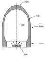
- FIG. 1which includes a blue LED light source 104 and a remote phosphor component 102 .
- the remote phosphor component 102has a tall and narrow aspect ratio, such that there are unequal distances from the LED 104 to different portions of the remote phosphor component 102 .
- blue excitation lightinteracts with the phosphor material in component 102 to generate photoluminescence light.
- differing portions of the component 102may receive differing levels of blue light and may also interact to different extents. This is due to many possible reasons.
- differing levels of emitted phosphor light from the component 102contribute to shifts in color. Due to the isotropic nature of the photoluminescence process, photoluminescence light is emitted equally in all directions, resulting in converted light re-entering the interior of the component. In this way, light which is converted at one location on the component 102 may be “recycled” before being emitted from the lighting device at a different location on the component.
- FIG. 2illustrates how a light pipe 202 having side emission chambers 206 may generate shifts in color over the length of the component due to long light paths. Color shifts occur in the light pipe 202 due to excitation light not being evenly distributed from the LED source 204 due to the length of the light pipe.
- the unequal conversion pathsmay also be caused by indirect light paths from the LED 204 caused by reflective light off reflective surfaces 214 within the light pipe 202 .
- the interior of the light pipe 202may be filed with either air or an optical medium.
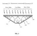
- FIG. 3illustrates a planar remote phosphor component 302 mounted over a wide mixing chamber 306 , where the configuration includes a central excitation source 304 .
- Color shiftsoccur due to excitation light not being evenly distributed from the center-only source 304 across the width of the planar phosphor component 302 , both due to unequal length light paths directly from the LED 304 to the component 302 , as well as unequal length reflective light paths caused by reflection off reflective surfaces 314 within the mixing chamber 306 .
- FIGS. 1-3illustrate LED light devices having unequal length conversion paths for LED light
- FIG. 4illustrates an embodiment of the invention in which variable thickness is utilized to perform color tuning
- FIG. 5shows a configuration for a wavelength conversion component having thicker walls at both the lower portion and upper portion, with thinner walls in the middle portion of the component;
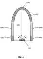
- FIG. 6illustrates an alternate embodiment, in which color tuning is effected by changing the loading of the phosphor materials within different portions of the component
- FIG. 7illustrates an approach in which the phosphor in a wavelength conversion component is deposited as a layer of material onto a transparent substrate, and color tuning is effected by changing the thickness of the phosphor layer on the substrate;
- FIG. 8illustrates an embodiment where the thickness t of a planar wavelength conversion component is adjusted to control the conversion ratio of the blue excitation light from an LED
- FIGS. 9A-9Billustrate embodiments where the print layer thicknesses is controlled by either using a patterning approach or by using multiple print layers combined with patterning to create different phosphor layer thicknesses;
- FIGS. 10A and 10Billustrate views of an example of light emitting devices that utilize remote wavelength conversion according to embodiments of the invention.
- FIG. 11illustrates a flowchart of a method for tuning a light-emitting device in accordance with some embodiments.
- Embodiments of the inventionconcern lighting arrangements and light emitting devices with remote wavelength conversion.
- the present inventionprovides an approach to implement lighting arrangements (architectures) which provides consistent color despite inconsistent light path lengths for phosphor light conversions.
- Various approachescan be taken to perform color tuning according to embodiments of the invention.
- the thickness of the wavelength conversion componentis varied to perform color tuning.
- phosphor loading and/or concentrationscan be varied within the component to perform color tuning.
- an LED lighting arrangementcomprises at least one LED operable to emit light of a first wavelength range and a wavelength conversion component that is operable to emit light of a second wavelength range when excited by light of the first wavelength range from the at least one LED.
- the emitted light from the LED lighting arrangementcomprises combined light from both the at least one LED and the wavelength conversion component, where the wavelength conversion component is remote from the at least one LED.
- the wavelength conversion componenthas differing amounts of photoluminescent materials at different portions of the wavelength conversion component, wherein a visibly uniform color of light is producible from the LED lighting arrangement based at least in part on the differing amounts of photoluminescent materials at different portions of the wavelength conversion component.
- the differing amounts of the photoluminescent materialsis implemented to generally equalize a ratio of emitted photoluminescence light compared to emitted LED light from the wavelength conversion component.
- the differing amounts of photoluminescent materials at the different portions of the wavelength conversion componentcan be implemented by different ways.
- varying wall thicknessesis implemented for the wavelength conversion component.
- the wavelength conversion componentis planar in shape, and a central portion is thicker than an edge portion of the wavelength conversion component.
- the wavelength conversion componentmay also be generally dome-shaped, and a lower wall portion comprises thicker walls compared to a central wall portion of the wavelength conversion component.
- the lighting arrangementmay also be implemented where the differing amounts of photoluminescent materials at the different portions of the wavelength conversion component is implemented by varying concentration of the photoluminescent materials within the wavelength conversion component.
- the differing amounts of photoluminescent materials at the different portions of the wavelength conversion componentcan also be implemented by varying thickness of a photoluminescent material layer on a substrate in the wavelength conversion component.
- the photoluminescent material layercan be implemented with a pattern that is not contiguous over the wavelength conversion component. In some embodiments, the pattern comprises at least one of dots or pixels of the photoluminescent materials at variable size or frequency over the photoluminescent material layer.
- more of the photoluminescent materialis provided at portions of the wavelength conversion component receiving having higher levels of LED light and less of the photoluminescent material is provided at portions of the wavelength conversion component receiving having lower levels of LED light.
- Some embodimentsare directed to a wavelength conversion component that is operable to emit light of a second wavelength range when excited by light of the first wavelength range from at least one LED, where emitted light comprises combined light from both the at least one LED and the wavelength conversion component. Differing amounts of photoluminescent materials are present at different portions of the wavelength conversion component, where a visibly uniform color of light is producible based at least in part on the differing amounts of photoluminescent materials at different portions of the wavelength conversion component.
- the differing amounts of photoluminescent materials at the different portions of the wavelength conversion componentcan be implemented in various ways, and is to generally equalize a ratio of emitted photoluminescent light compared to emitted LED light from the wavelength conversion component.
- the differing amounts of photoluminescent materials at the different portions of the wavelength conversion componentcan be implemented by different ways.
- varying wall thicknessesis implemented for the wavelength conversion component.
- the wavelength conversion componentis planar in shape, and a central portion is thicker than an edge portion of the wavelength conversion component.
- the wavelength conversion componentmay also be generally dome-shaped, and a lower wall portion comprises thicker walls compared to a central wall portion of the wavelength conversion component.
- the lighting arrangementmay also be implemented where the differing amounts of photoluminescent materials at the different portions of the wavelength conversion component is implemented by varying concentration of the photoluminescent materials within the wavelength conversion component.
- the differing amounts of photoluminescent materials at the different portions of the wavelength conversion componentcan also be implemented by varying thickness of a photoluminescent material layer on a substrate in the wavelength conversion component.
- the photoluminescent material layercan be implemented with a pattern that is not contiguous over the wavelength conversion component. In some embodiments, the pattern comprises at least one of dots or pixels of the photoluminescent materials at variable size or frequency over the photoluminescent material layer.
- the wavelength conversion component according to the inventionmay comprise any shape.
- the wavelength conversion componentcomprises a three-dimensional shape (such as a generally dome shaped shell) having an aspect ratio that is not one to one, e.g., greater than or less than 1:1 ratio.
- the wavelength conversion componentmay also comprise a planar shape, and a combination of the planar shape with a mixing chamber corresponds to an aspect ratio that is not one to one.
- a mixing chamberexists for the wavelength conversion component having a three-dimensional shape, where the interior of the wavelength conversion component in combination with a substrate forms a mixing chamber.
- the wavelength conversion componentmay be planar in shape, and a central portion is thicker than an edge portion of the wavelength conversion component.
- the wavelength conversion componentmay be generally dome-shaped, with a lower wall portion having thicker walls compared to a central wall portion of the wavelength conversion component.
- Some embodimentsare directed to a method for color tuning an LED lighting arrangement, comprising identifying at least one LED operable to emit light of a first wavelength range and configuring a wavelength conversion component that is operable to emit light of a second wavelength range when excited by light of the first wavelength range from the at least one LED.
- the emitted light from the LED lighting arrangementcomprises combined light from both the at least one LED and the wavelength conversion component, and the wavelength conversion component being remote from the at least one LED.
- the wavelength conversion componentis color tuned by implementing differing amounts of photoluminescent materials at different portions of the wavelength conversion component, wherein a visibly uniform color of light is producible from the LED lighting arrangement based at least in part on the differing amounts of photoluminescent materials at different portions of the wavelength conversion component.
- the differing amounts of photoluminescent materials at the different portions of the wavelength conversion componentis implemented by at least one of (a) varying wall thicknesses for the wavelength conversion component, (b) varying concentration of the photoluminescent materials within the wavelength conversion component, or (c) varying thickness of a photoluminescent material layer on a substrate in the wavelength conversion component.
- Profiles of the at least one LED and the wavelength conversion componentare analyzed to configure the differing amounts of the photoluminescent materials to generally equalize a ratio of emitted photoluminescent light compared to emitted LED light from the wavelength conversion component.
- the profile of the at least one LED that is analyzedcomprises an emission profile
- the profile of the wavelength conversion componentcomprises an aspect ratio for the wavelength conversion component or for a mixing chamber that incorporates the wavelength conversion component. Simulation can be performed to analyze the at least one LED and the wavelength conversion component.
- a physical sample of the wavelength conversion componentis analyzed and adjusted to perform color tuning.
- the present inventionprovides an approach to implement lighting architectures which provides consistent color despite inconsistent light path lengths for phosphor light conversions.
- photoluminescent materialsembodied specifically as phosphor materials.
- the inventionis applicable to any type of photoluminescent material, such as either phosphor materials or quantum dots.
- a quantum dotis a portion of matter (e.g. semiconductor) whose excitons are confined in all three spatial dimensions that may be excited by radiation energy to emit light of a particular wavelength or range of wavelengths.
- the inventionis not limited to phosphor based wavelength conversion components unless claimed as such.
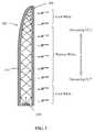
- FIG. 1shows an example lighting arrangement that may include color shift problems due to unequal path lengths.
- One possible cause of the shifts in coloris the nature of blue light conversion that occurs.
- a proportion of the blue lightis absorbed and converted by a process of photoluminescence into light of a different color (e.g., green, yellow, or red).
- the further the excitation light travels through the remote phosphor componentthe more collisions that take place, leaving a higher percentage of phosphor light versus the original blue light from the excitation source (LED 104 ).
- light generated at the baseis “cooler” because it has a higher proportion of blue light to photoluminescence light since the excitation primarily comes from the blue light source (LED). Blue light is converted into warm light by the phosphor. Further away from the blue light source, the illumination primarily comes from “recycled” light thus causing an external color shift from cool at the base to warmer at the top.
- LEDblue light source
- the inventionsolves this problem by color tuning the wavelength conversion component to ensure a consistent emission of color from the lighting arrangement.
- Various approachescan be taken to perform color tuning according to embodiments of the invention.
- the thickness of the wavelength conversion componentis varied to perform color tuning.
- phosphor loading and/or concentrationscan be varied within the component to perform color tuning.
- FIG. 4illustrates an embodiment of the invention in which variable thickness is utilized to perform color tuning.
- the thickness of the walls 408 of the remote phosphor component 402determines the amount of blue light from the excitation light source (LED) 404 that is converted into photoluminescence light versus that amount of blue light that passes through the component without being converted. Varying the thickness of the walls 408 on component 402 permits adjustments/tuning of this ratio of conversion.
- the lightis primarily coming from the blue LED 404 .
- a thicker wallis used to convert more of the blue light into photoluminescence light.
- the wall thicknessis reduced, proportionately to reduce the conversion ratio of blue light to photoluminescence light and to thereby allow blue light to pass more easily through the component 402 .
- This approachtherefore provides a solution to the color shift problem that is both efficient and simple to manufacture. This approach also increases conversion efficiencies since light is not required to pass through more phosphor than is required to generate light of a desired color.
- the different wall thicknessesare tuned to match emissions characteristics of the LED light source, the aspect ratio of the remote phosphor component, and the expected interactions that occur between the emitted excitation light and the phosphor component.
- the wall thicknessescan be provided in any appropriate configuration suitable to effect consistent color over the length of the component. For example, it is possible that the lighting architecture results in relatively higher amounts of blue light being emitted from both the top and bottom portions of the component, causing cooler light colors at those portions of the component and a shift towards warmer colors emitted from the central portion of the component.
- FIG. 5shows a configuration for the wavelength conversion component 502 having thicker walls at both the lower portion 508 a and upper portion 508 c of the component (where a relatively higher ratio of blue light would otherwise be emitted), with thinner walls in the middle portion 508 b (where a relatively lower ratio of blue light would otherwise be emitted). The result is a more uniform emission of color from this lighting arrangement.
- FIG. 6illustrates an alternate embodiment, in which color tuning is effected by changing the loading of the phosphor materials within different portions of the component 602 .
- the amount and/or concentration of phosphor within the material that make up the phosphoris adjusted to control the conversion ratio of blue light and the amount of blue light that passes through the component 602 .
- the concentration of phosphor materials in the lower portions 608 a of the component wallis greater than the concentration of phosphor materials in the central portions 608 b of the component 602 .
- the concentration at portion 608 cmay also be separately increased/decreased depending upon whether the emitted color from that portion needs to be tuned.
- the concentration of phosphor materialsmay be reversed, where the concentration in the lower portions of the component wall is less than the concentration of phosphor materials in the upper portions of the component.
- FIG. 7illustrates yet another approach that can be taken tune colors for the lighting arrangement.
- the phosphor in wavelength conversion component 702is deposited as a layer of material 702 a onto a transparent substrate 702 b , and color tuning is effected by changing the thickness of the phosphor layer 702 a on the substrate 702 b .
- the thickness of the phosphor layer 702 ais adjusted to control the ratio of blue light that is converted by the phosphor materials into photoluminescence light.
- Any suitable deposition approachcan be taken to vary the thickness of the phosphor layer.
- any one of printing, spraying, or coating techniquesmay be used to implement the phosphor layer 702 a and to control the thickness of that layer.
- FIG. 3illustrates a planar remote phosphor component over a wide mixing chamber having a central excitation source, where color shifts occur due to excitation light not being evenly distributed from the center-only source over the length of the phosphor component.
- FIG. 8illustrates an embodiment of a solution to this problem, where the thickness t of the planar wavelength conversion component 802 is adjusted to control the conversion ratio of the blue excitation light from LED 804 .
- the highest ratio of blue light to photoluminescence lightwould otherwise be emitted from the central portion 808 a of the component.
- color tuningis performed by increasing the thickness of the component at that central portion 808 a .
- color tuningis performed by decreasing the thickness of the component at the edge portions 808 b . Assuming a gradient shift in color this configuration, then tuning is performed by having a gradient change in thickness from the central portion 808 a to the edge portion 808 b of the component 802 . This approach can similarly be applied to perform color tuning of the light pipe configuration illustrated in FIG. 2 .
- the print layer thicknesses for the wavelength conversion component 902can be controlled, for example, by either using a patterning approach 910 a or 910 b or by using multiple print layers combined with patterning to create different phosphor layer thicknesses.
- the layersdo not need to be contiguous over the entire panel. Instead, pixels and/or dots may be printed at variable dot size and for frequency distributed over the panel.
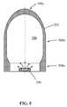
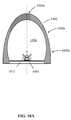
- FIGS. 10A and 10Billustrate views of an example of light emitting devices 1000 that utilize remote wavelength conversion according to embodiments of the invention.
- the device 1000comprises a dome-shaped wavelength conversion component 1002 that is mounted onto a substrate 1012 .
- the substrate 1012comprises a MCPCB (metal core printed circuit board).
- a MCPCBcomprises a layered structure composed of a metal core base, typically aluminum, a thermally conducting/electrically insulating dielectric layer and a copper circuit layer for electrically connecting electrical components in a desired circuit configuration.
- the LEDs 1004may be configured in various arrangements.
- the device 1000 according to the embodiment of FIG. 10Acomprises a single LED 1004 while the device 1000 of according to the embodiment of FIG. 10B comprises a plurality/array of blue light emitting LEDs (blue LEDs) 1004 that are mounted to the substrate 1012 of the device 1000 .
- the LEDs 1004can be implemented using any suitable solid-state light emitter device, such as a blue light emitting diode (LED).
- Each solid-state light emittercan comprise a gallium nitride-based blue light emitting LED, such as a 1 W InGaN/GaN (indium gallium nitride/gallium nitride) based LED chip which is operable to generate blue light of wavelength 400 to 465 nm.
- the LEDs 1004are configured such that their principle emission axis is parallel with the axis of the lighting device 1000 .
- the wavelength conversion component 1002may comprise phosphor material.
- the color of the emission product produced by the wavelength conversion componentwill depend on the phosphor material composition and the quantity of phosphor material per unit area in the wavelength conversion component.
- the wavelength conversion component 1002is configured to tune the light emissions characteristics of the device 1000 to produce consistent color emissions over all (or part) of its exterior.
- color tuningis performed by varying the thickness of the walls for the wavelength conversion component 1002 .
- the concentration of phosphor materials in the lower portions 1008 a of the component wallmay be configured to be greater than the concentration of phosphor materials in the central portions 1008 b of the component 1002 .
- the concentration at top portion 1008 cmay also be separately increased/decreased depending upon whether the emitted color from that portion needs to be tuned.
- the concentration of phosphors within the wavelength conversion component 1002is adjusted to color tune the device 1000 .
- the wavelength conversion component 1002may include a wavelength conversion layer comprising photoluminescent material situated on a light transmissive substrate, where the thickness and/or loading of the wavelength conversion layer is adjusted to perform color tuning.
- the wavelength conversion component 1002comprises any suitable photoluminescent materials, and may comprise an inorganic or organic phosphor such as for example silicate-based phosphor of a general composition A 3 Si(O,D) 5 or A 2 Si(O,D) 4 in which Si is silicon, O is oxygen, A comprises strontium (Sr), barium (Ba), magnesium (Mg) or calcium (Ca) and D comprises chlorine (Cl), fluorine (F), nitrogen (N) or sulfur (S).
- silicate-based phosphorsare disclosed in U.S. Pat. No. 7,575,697 B2 “Silicate-based green phosphors”, U.S. Pat. No.
- the phosphorcan also comprise an aluminate-based material such as is taught in co-pending patent application US2006/0158090 A1 “Novel aluminate-based green phosphors” and U.S. Pat. No.
- the phosphor materialis not limited to the examples described and can comprise any phosphor material including nitride and/or sulfate phosphor materials, oxy-nitrides and oxy-sulfate phosphors or garnet materials (YAG).
- the wavelength conversion component 1002is operable to absorb a proportion of the blue light ⁇ 1 generated by the LEDs 1004 and convert it to light of a different wavelength by a process of photoluminescence (i.e. converting light to ⁇ 2 ). Not all of the blue light ⁇ 1 generated by the LEDs 1004 is absorbed by the wavelength conversion component 1002 and some of it is emitted.
- the emission product of the device 1000thus comprises the combined light of wavelength ⁇ 1 generated by the LEDs 1004 and the wavelength ⁇ 2 generated by the wavelength conversion component 1002 .
- Light generated by the wavelength conversion component 1002refers to the emitted light resulting from conversion of the LED light into light of a different wavelength through photoluminescence.
- the CCT of the emission productis thus a combination of the CCT of the light generated by the LED ( ⁇ 1 ) and the CCT of the light ( ⁇ 2 ) generated by the wavelength conversion component 1002 .
- Color tuningis performed by adjusting the characteristics of different portions of the wavelength conversion component to change the overall CCT of those portions of the component, so that a more uniform CCT is provided over all or substantially all of the component.
- the color tuningis performed to specifically address emissions characteristics of the LED light source, the aspect ratio of the remote phosphor component, and the expected interactions that occur between the emitted excitation light and the phosphor component.
- the relative characteristics of these componentsmay differ from one lighting arrangement to another lighting arrangement, thereby necessitating different tuning arrangements as needed.
- the wavelength conversion component of FIG. 10A having a single LED blue light sourceis different from the configuration of FIG. 10B having multiple LED blue light sources, though the external shape of the component is the same for each configuration. Therefore, it is likely that, even if all other aspects of the configuration are the same or similar (such as the aspect ratio of the wavelength conversion component), the color tuning will result in different levels of wall thicknesses needed to provide consistent color.
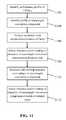
- FIG. 11illustrates a flowchart of a method for tuning a light-emitting device in accordance with some embodiments.
- the performance profile of the LED(s) for the lighting arrangementis identified. This step identifies the expected light emission pattern to be generated by the one or more LEDs used in the lighting arrangement, e.g., by using a polar diagram to identify expected light distribution patterns from the LED(s).
- identificationis made of the physical profile for the wavelength conversion component. In some embodiments for three-dimensional components, this step is performed by identifying the aspect ratio and/or dimensions of the component. For two-dimensional components, this step is performed by identifying the shape and/or dimensions of the component.
- the expected configuration of the LED(s) relative to the wavelength configuration componentcan be identified at this point. This step identifies the expected placement of the one or more LEDs relative to the wavelength conversion component.
- analysisis performed to predict the expected color emissions from the different portions of the component.
- a modelis constructed of the lighting arrangement, and computer-based simulation, using for example a ray tracing program, is performed to predict the expected color emissions from the lighting arrangement.
- the wavelength conversion componentis configured to provide uniform color emissions. Any suitable manner of configurations may be performed for this step. For example, the wall thickness of the component may be adjusted to balance color emissions by the lighting arrangement. Additional analysis/simulations may be performed to determine whether the expected performance of the configuration provides uniform color emissions.
- a sample lighting arrangementis then manufactured having the configuration from step 1108 .
- the lighting arrangementis physically tested at 1110 to determine whether the arrangement will produce uniform color emissions in real world conditions.
- adjustmentscan be made to fine-tune the design configurations. For example, wall thicknesses can be expanded and/or contracted at various portions of the wavelength conversion component. Thereafter, the design is finalized and ready for manufacture.
- injection moldingmay be performed to manufacture color tuned wavelength conversion components.
- color tuningis performed by adjusting wall thicknesses
- the injection molding processmerely needs to produce desired thicknesses at specific locations for the component.
- the componentcan be co-injection moding such that different parts of the component have different loadings and/or concentrations of photoluminescent materials.
- the molding processcan occur in stages, where different source materials and/or combinations of source materials having differing phosphor levels are provided when molding the parts of the component intended to have differing concentrations of the phosphor materials.
Landscapes
- Engineering & Computer Science (AREA)
- General Engineering & Computer Science (AREA)
- Physics & Mathematics (AREA)
- Spectroscopy & Molecular Physics (AREA)
- Microelectronics & Electronic Packaging (AREA)
- Optics & Photonics (AREA)
- Led Device Packages (AREA)
- Non-Portable Lighting Devices Or Systems Thereof (AREA)
Abstract
Description
Claims (36)
Priority Applications (1)
| Application Number | Priority Date | Filing Date | Title |
|---|---|---|---|
| US13/871,383US9252338B2 (en) | 2012-04-26 | 2013-04-26 | Methods and apparatus for implementing color consistency in remote wavelength conversion |
Applications Claiming Priority (2)
| Application Number | Priority Date | Filing Date | Title |
|---|---|---|---|
| US201261639048P | 2012-04-26 | 2012-04-26 | |
| US13/871,383US9252338B2 (en) | 2012-04-26 | 2013-04-26 | Methods and apparatus for implementing color consistency in remote wavelength conversion |
Publications (2)
| Publication Number | Publication Date |
|---|---|
| US20130286632A1 US20130286632A1 (en) | 2013-10-31 |
| US9252338B2true US9252338B2 (en) | 2016-02-02 |
Family
ID=49477107
Family Applications (1)
| Application Number | Title | Priority Date | Filing Date |
|---|---|---|---|
| US13/871,383Expired - Fee RelatedUS9252338B2 (en) | 2012-04-26 | 2013-04-26 | Methods and apparatus for implementing color consistency in remote wavelength conversion |
Country Status (5)
| Country | Link |
|---|---|
| US (1) | US9252338B2 (en) |
| EP (2) | EP3240052A1 (en) |
| JP (1) | JP2015515734A (en) |
| CN (1) | CN104247058B (en) |
| WO (1) | WO2013163573A1 (en) |
Cited By (1)
| Publication number | Priority date | Publication date | Assignee | Title |
|---|---|---|---|---|
| US20160013379A1 (en)* | 2014-07-11 | 2016-01-14 | Lumenmax Optoelectronics Co., Ltd. | Emitting device of wide-angle led |
Families Citing this family (7)
| Publication number | Priority date | Publication date | Assignee | Title |
|---|---|---|---|---|
| US9255666B2 (en)* | 2011-11-10 | 2016-02-09 | Epistar Corporation | Illumination apparatus |
| US20150098239A1 (en)* | 2013-10-07 | 2015-04-09 | 3M Innovative Properties Company | Lighting device with remote down-converting material |
| DE102015001723A1 (en) | 2015-02-05 | 2016-08-11 | Sergey Dyukin | The method of improving the characteristics of lighting devices with a front lighting of the light guide, which include the luminophore, which is illuminated with semiconductor structures. |
| JP6288061B2 (en) | 2015-12-10 | 2018-03-07 | 日亜化学工業株式会社 | Method for manufacturing light emitting device |
| EP3385603A1 (en)* | 2017-04-06 | 2018-10-10 | Intematix Corporation | Led-based linear lamps and lighting arrangements |
| US20190093853A1 (en)* | 2017-09-26 | 2019-03-28 | GM Global Technology Operations LLC | Light guide assembly having phosphorescent material |
| CN109348660B (en)* | 2018-11-16 | 2022-08-19 | 昇印光电(昆山)股份有限公司 | Decorative sheet and consumer electronics cover plate |
Citations (150)
| Publication number | Priority date | Publication date | Assignee | Title |
|---|---|---|---|---|
| US3290255A (en) | 1963-09-30 | 1966-12-06 | Gen Electric | White electroluminescent phosphor |
| US3593055A (en) | 1969-04-16 | 1971-07-13 | Bell Telephone Labor Inc | Electro-luminescent device |
| US3670193A (en) | 1970-05-14 | 1972-06-13 | Duro Test Corp | Electric lamps producing energy in the visible and ultra-violet ranges |
| US3676668A (en) | 1969-12-29 | 1972-07-11 | Gen Electric | Solid state lamp assembly |
| US3691482A (en) | 1970-01-19 | 1972-09-12 | Bell Telephone Labor Inc | Display system |
| US3709685A (en) | 1970-02-19 | 1973-01-09 | Ilford Ltd | Photoconductive zinc oxide sensitized by substituted thiazolidene dyes |
| US3743833A (en) | 1971-07-16 | 1973-07-03 | Eastman Kodak Co | Radiographic elements and binders |
| US3763405A (en) | 1970-12-21 | 1973-10-02 | Nippon Electric Co | Solid state luminescent display device |
| US3793046A (en) | 1970-12-04 | 1974-02-19 | Philips Corp | Method of manufacturing a pigment |
| US3819974A (en) | 1973-03-12 | 1974-06-25 | D Stevenson | Gallium nitride metal-semiconductor junction light emitting diode |
| US3819973A (en) | 1972-11-02 | 1974-06-25 | A Hosford | Electroluminescent filament |
| US3849707A (en) | 1973-03-07 | 1974-11-19 | Ibm | PLANAR GaN ELECTROLUMINESCENT DEVICE |
| US3875456A (en) | 1972-04-04 | 1975-04-01 | Hitachi Ltd | Multi-color semiconductor lamp |
| JPS5079379U (en) | 1973-11-24 | 1975-07-09 | ||
| US3932881A (en) | 1972-09-05 | 1976-01-13 | Nippon Electric Co., Inc. | Electroluminescent device including dichroic and infrared reflecting components |
| US3937998A (en) | 1973-10-05 | 1976-02-10 | U.S. Philips Corporation | Luminescent coating for low-pressure mercury vapour discharge lamp |
| US3972717A (en) | 1973-03-21 | 1976-08-03 | Hoechst Aktiengesellschaft | Electrophotographic recording material |
| US4047075A (en) | 1975-03-01 | 1977-09-06 | Licentia-Patent-Verwaltungs-G.M.B.H. | Encapsulated light-emitting diode structure and array thereof |
| US4081764A (en) | 1972-10-12 | 1978-03-28 | Minnesota Mining And Manufacturing Company | Zinc oxide light emitting diode |
| US4104076A (en) | 1970-03-17 | 1978-08-01 | Saint-Gobain Industries | Manufacture of novel grey and bronze glasses |
| US4143394A (en) | 1976-07-30 | 1979-03-06 | Licentia Patent-Verwaltungs-G.M.B.H. | Semiconductor luminescence device with housing |
| GB2017409A (en) | 1978-03-22 | 1979-10-03 | Bayraktaroglu B | Light-emitting diode |
| US4176294A (en) | 1975-10-03 | 1979-11-27 | Westinghouse Electric Corp. | Method and device for efficiently generating white light with good rendition of illuminated objects |
| US4176299A (en) | 1975-10-03 | 1979-11-27 | Westinghouse Electric Corp. | Method for efficiently generating white light with good color rendition of illuminated objects |
| US4211955A (en) | 1978-03-02 | 1980-07-08 | Ray Stephen W | Solid state lamp |
| US4305019A (en) | 1979-12-31 | 1981-12-08 | Westinghouse Electric Corp. | Warm-white fluorescent lamp having good efficacy and color rendering and using special phosphor blend as separate undercoat |
| US4315192A (en) | 1979-12-31 | 1982-02-09 | Westinghouse Electric Corp. | Fluorescent lamp using high performance phosphor blend which is protected from color shifts by a very thin overcoat of stable phosphor of similar chromaticity |
| US4443532A (en) | 1981-07-29 | 1984-04-17 | Bell Telephone Laboratories, Incorporated | Induced crystallographic modification of aromatic compounds |
| JPS60170194U (en) | 1984-04-20 | 1985-11-11 | 鈴木 悦三 | Roll paper holder that can be opened and closed |
| US4559470A (en) | 1981-04-22 | 1985-12-17 | Mitsubishi Denki Kabushiki Kaisha | Fluorescent discharge lamp |
| US4573766A (en) | 1983-12-19 | 1986-03-04 | Cordis Corporation | LED Staggered back lighting panel for LCD module |
| US4618555A (en) | 1984-01-11 | 1986-10-21 | Mitsubishi Chemical Ind., Ltd. | Electrophotographic photoreceptor comprising azo compounds |
| US4638214A (en) | 1985-03-25 | 1987-01-20 | General Electric Company | Fluorescent lamp containing aluminate phosphor |
| US4667036A (en) | 1983-08-27 | 1987-05-19 | Basf Aktiengesellschaft | Concentration of light over a particular area, and novel perylene-3,4,9,10-tetracarboxylic acid diimides |
| US4678285A (en) | 1984-01-13 | 1987-07-07 | Ricoh Company, Ltd. | Liquid crystal color display device |
| US4727003A (en) | 1985-09-30 | 1988-02-23 | Ricoh Company, Ltd. | Electroluminescence device |
| US4772885A (en) | 1984-11-22 | 1988-09-20 | Ricoh Company, Ltd. | Liquid crystal color display device |
| US4845223A (en) | 1985-12-19 | 1989-07-04 | Basf Aktiengesellschaft | Fluorescent aryloxy-substituted perylene-3,4,9,10-tetracarboxylic acid diimides |
| JPH01179471A (en) | 1988-01-07 | 1989-07-17 | Natl Inst For Res In Inorg Mater | Cubic boron nitride P-n junction light emitting device |
| US4859539A (en) | 1987-03-23 | 1989-08-22 | Eastman Kodak Company | Optically brightened polyolefin coated paper support |
| JPH01260707A (en) | 1988-04-11 | 1989-10-18 | Idec Izumi Corp | Device for emitting white light |
| JPH0291980A (en) | 1988-09-29 | 1990-03-30 | Toshiba Lighting & Technol Corp | solid state light emitting device |
| US4915478A (en) | 1988-10-05 | 1990-04-10 | The United States Of America As Represented By The Secretary Of The Navy | Low power liquid crystal display backlight |
| US4918497A (en) | 1988-12-14 | 1990-04-17 | Cree Research, Inc. | Blue light emitting diode formed in silicon carbide |
| US4946621A (en) | 1986-04-29 | 1990-08-07 | Centre National De La Recherche Scientifique (Cnrs) | Luminescent mixed borates based on rare earths |
| US4992704A (en) | 1989-04-17 | 1991-02-12 | Basic Electronics, Inc. | Variable color light emitting diode |
| JPH0324692Y2 (en) | 1987-08-06 | 1991-05-29 | ||
| WO1991008508A1 (en) | 1989-11-24 | 1991-06-13 | Innovare Limited | A display device |
| US5077161A (en) | 1990-05-31 | 1991-12-31 | Xerox Corporation | Imaging members with bichromophoric bisazo perylene photoconductive materials |
| US5110931A (en) | 1987-11-27 | 1992-05-05 | Hoechst Aktiengesellschaft | Process for the preparation of n,n'-dimethylperylene-3,4,9,10-tetracarboxylic diimide in high-hiding pigment form |
| US5126214A (en) | 1989-03-15 | 1992-06-30 | Idemitsu Kosan Co., Ltd. | Electroluminescent element |
| US5131916A (en) | 1990-03-01 | 1992-07-21 | Bayer Aktiengesellschaft | Colored fluorescent polymer emulsions for marker pens: graft copolymers and fluorescent dyes in aqueous phase |
| US5143433A (en) | 1991-11-01 | 1992-09-01 | Litton Systems Canada Limited | Night vision backlighting system for liquid crystal displays |
| US5143438A (en) | 1990-10-15 | 1992-09-01 | Thorn Emi Plc | Light sources |
| JPH04289691A (en) | 1990-12-07 | 1992-10-14 | Mitsubishi Cable Ind Ltd | El illuminant |
| JPH04321280A (en) | 1991-04-19 | 1992-11-11 | Nichia Chem Ind Ltd | Blue color light-emitting diode |
| US5166761A (en) | 1991-04-01 | 1992-11-24 | Midwest Research Institute | Tunnel junction multiple wavelength light-emitting diodes |
| US5208462A (en) | 1991-12-19 | 1993-05-04 | Allied-Signal Inc. | Wide bandwidth solid state optical source |
| US5210051A (en) | 1990-03-27 | 1993-05-11 | Cree Research, Inc. | High efficiency light emitting diodes from bipolar gallium nitride |
| US5211467A (en) | 1992-01-07 | 1993-05-18 | Rockwell International Corporation | Fluorescent lighting system |
| JPH05152609A (en) | 1991-11-25 | 1993-06-18 | Nichia Chem Ind Ltd | Light emitting diode |
| US5237182A (en) | 1990-11-29 | 1993-08-17 | Sharp Kabushiki Kaisha | Electroluminescent device of compound semiconductor with buffer layer |
| US5264034A (en) | 1989-08-11 | 1993-11-23 | Hoechst Aktiengesellschaft | Pigment preparations based on perylene compounds |
| US5283425A (en) | 1992-02-06 | 1994-02-01 | Rohm Co., Ltd. | Light emitting element array substrate with reflecting means |
| JPH06267301A (en) | 1993-03-15 | 1994-09-22 | Olympus Optical Co Ltd | Organic photoluminescence element |
| US5369289A (en) | 1991-10-30 | 1994-11-29 | Toyoda Gosei Co. Ltd. | Gallium nitride-based compound semiconductor light-emitting device and method for making the same |
| US5405709A (en) | 1993-09-13 | 1995-04-11 | Eastman Kodak Company | White light emitting internal junction organic electroluminescent device |
| JPH07176794A (en) | 1993-12-17 | 1995-07-14 | Nichia Chem Ind Ltd | Surface light source |
| US5439971A (en) | 1991-11-12 | 1995-08-08 | Eastman Chemical Company | Fluorescent pigment concentrates |
| JPH07235207A (en) | 1994-02-21 | 1995-09-05 | Copal Co Ltd | Back light |
| JPH0799345B2 (en) | 1988-10-31 | 1995-10-25 | 防衛庁技術研究本部長 | Method and apparatus for generating water temperature profile data |
| JPH07282609A (en) | 1994-04-06 | 1995-10-27 | Tsuzuki Shogo | Light source device for illumination using semiconductor laser device |
| JPH087614Y2 (en) | 1990-05-08 | 1996-03-04 | 中部電力株式会社 | Wire cap |
| US5518808A (en) | 1992-12-18 | 1996-05-21 | E. I. Du Pont De Nemours And Company | Luminescent materials prepared by coating luminescent compositions onto substrate particles |
| US5557168A (en) | 1993-04-02 | 1996-09-17 | Okaya Electric Industries Co., Ltd. | Gas-discharging type display device and a method of manufacturing |
| JPH08250281A (en) | 1995-03-08 | 1996-09-27 | Olympus Optical Co Ltd | Luminescent element and displaying apparatus |
| US5563621A (en) | 1991-11-18 | 1996-10-08 | Black Box Vision Limited | Display apparatus |
| US5578839A (en) | 1992-11-20 | 1996-11-26 | Nichia Chemical Industries, Ltd. | Light-emitting gallium nitride-based compound semiconductor device |
| US5583349A (en) | 1995-11-02 | 1996-12-10 | Motorola | Full color light emitting diode display |
| US5585640A (en) | 1995-01-11 | 1996-12-17 | Huston; Alan L. | Glass matrix doped with activated luminescent nanocrystalline particles |
| US5619356A (en) | 1993-09-16 | 1997-04-08 | Sharp Kabushiki Kaisha | Reflective liquid crystal display device having a compensator with a retardation value between 0.15 μm and 0.38 μm and a single polarizer |
| US5660461A (en) | 1994-12-08 | 1997-08-26 | Quantum Devices, Inc. | Arrays of optoelectronic devices and method of making same |
| US5677417A (en) | 1993-05-04 | 1997-10-14 | Max-Planck-Gesellschaft Zur Foerderung | Tetraaroxyperylene-3,4,9,10-tetracarboxylic polyimides |
| US5679152A (en) | 1994-01-27 | 1997-10-21 | Advanced Technology Materials, Inc. | Method of making a single crystals Ga*N article |
| US5763901A (en) | 1992-12-17 | 1998-06-09 | Kabushiki Kaisha Toshiba | Semiconductor light-emitting device and method for manufacturing the device |
| US5771039A (en) | 1994-06-06 | 1998-06-23 | Ditzik; Richard J. | Direct view display device integration techniques |
| US5770887A (en) | 1993-10-08 | 1998-06-23 | Mitsubishi Cable Industries, Ltd. | GaN single crystal |
| US5777350A (en) | 1994-12-02 | 1998-07-07 | Nichia Chemical Industries, Ltd. | Nitride semiconductor light-emitting device |
| US5869199A (en) | 1993-03-26 | 1999-02-09 | Sumitomo Electric Industries, Ltd. | Organic electroluminescent elements comprising triazoles |
| JP2900928B2 (en) | 1997-10-20 | 1999-06-02 | 日亜化学工業株式会社 | Light emitting diode |
| US5959316A (en) | 1998-09-01 | 1999-09-28 | Hewlett-Packard Company | Multiple encapsulation of phosphor-LED devices |
| US5962971A (en)* | 1997-08-29 | 1999-10-05 | Chen; Hsing | LED structure with ultraviolet-light emission chip and multilayered resins to generate various colored lights |
| US5998925A (en) | 1996-07-29 | 1999-12-07 | Nichia Kagaku Kogyo Kabushiki Kaisha | Light emitting device having a nitride compound semiconductor and a phosphor containing a garnet fluorescent material |
| JP2000022216A (en) | 1998-06-26 | 2000-01-21 | Sanken Electric Co Ltd | Resin-sealed semiconductor light emitting device having fluorescent cover |
| US6137217A (en) | 1992-08-28 | 2000-10-24 | Gte Products Corporation | Fluorescent lamp with improved phosphor blend |
| US6340824B1 (en) | 1997-09-01 | 2002-01-22 | Kabushiki Kaisha Toshiba | Semiconductor light emitting device including a fluorescent material |
| US6504301B1 (en) | 1999-09-03 | 2003-01-07 | Lumileds Lighting, U.S., Llc | Non-incandescent lightbulb package using light emitting diodes |
| US20030038596A1 (en)* | 2001-08-21 | 2003-02-27 | Wen-Chih Ho | Light-mixing layer and method |
| US6576488B2 (en) | 2001-06-11 | 2003-06-10 | Lumileds Lighting U.S., Llc | Using electrophoresis to produce a conformally coated phosphor-converted light emitting semiconductor |
| US6600175B1 (en) | 1996-03-26 | 2003-07-29 | Advanced Technology Materials, Inc. | Solid state white light emitter and display using same |
| US6642652B2 (en) | 2001-06-11 | 2003-11-04 | Lumileds Lighting U.S., Llc | Phosphor-converted light emitting device |
| US6642618B2 (en) | 2000-12-21 | 2003-11-04 | Lumileds Lighting U.S., Llc | Light-emitting device and production thereof |
| US20040012027A1 (en)* | 2002-06-13 | 2004-01-22 | Cree Lighting Company | Saturated phosphor solid state emitter |
| US20040217364A1 (en)* | 2003-05-01 | 2004-11-04 | Cree Lighting Company, Inc. | Multiple component solid state white light |
| US6869812B1 (en) | 2003-05-13 | 2005-03-22 | Heng Liu | High power AllnGaN based multi-chip light emitting diode |
| US20050221519A1 (en)* | 2004-03-31 | 2005-10-06 | Michael Leung | Semiconductor light emitting devices including a luminescent conversion element and methods for packaging the same |
| US20060158090A1 (en) | 2005-01-14 | 2006-07-20 | Intematix Corporation | Novel aluminate-based green phosphors |
| US7153015B2 (en) | 2001-12-31 | 2006-12-26 | Innovations In Optics, Inc. | Led white light optical system |
| JP2007035802A (en) | 2005-07-25 | 2007-02-08 | Matsushita Electric Works Ltd | Light-emitting device |
| JP2007287814A (en) | 2006-04-14 | 2007-11-01 | Nichia Chem Ind Ltd | Light emitting device for illumination |
| JP4010665B2 (en) | 1998-09-08 | 2007-11-21 | 三洋電機株式会社 | Installation method of solar cell module |
| US7311858B2 (en) | 2004-08-04 | 2007-12-25 | Intematix Corporation | Silicate-based yellow-green phosphors |
| US20080111472A1 (en) | 2006-11-10 | 2008-05-15 | Intematix Corporation | Aluminum-silicate based orange-red phosphors with mixed divalent and trivalent cations |
| US7390437B2 (en) | 2004-08-04 | 2008-06-24 | Intematix Corporation | Aluminate-based blue phosphors |
| US20080231181A1 (en)* | 2007-03-22 | 2008-09-25 | Siew It Pang | Phosphor Converted LED with Improved Uniformity and Having Lower Phosphor Requirements |
| US7479662B2 (en) | 2002-08-30 | 2009-01-20 | Lumination Llc | Coated LED with improved efficiency |
| US20090057698A1 (en)* | 2005-03-01 | 2009-03-05 | Kabushiki Kaisha Toshiba | Light emission device |
| US20090184333A1 (en) | 2008-01-17 | 2009-07-23 | Foxsemicon Integrated Technology, Inc. | Light emitting diode device |
| US7575697B2 (en) | 2004-08-04 | 2009-08-18 | Intematix Corporation | Silicate-based green phosphors |
| US7601276B2 (en) | 2004-08-04 | 2009-10-13 | Intematix Corporation | Two-phase silicate-based yellow phosphor |
| US20090262516A1 (en) | 2008-01-17 | 2009-10-22 | Intematix Corporation | Light emitting device with phosphor wavelength conversion |
| US20090283721A1 (en) | 2008-05-19 | 2009-11-19 | Intematix Corporation | Nitride-based red phosphors |
| US20090315051A1 (en) | 2008-06-19 | 2009-12-24 | Chia-Hao Wu | Photoelectric semiconductor device capable of generating uniform compound lights |
| US7655156B2 (en) | 2005-08-03 | 2010-02-02 | Intematix Corporation | Silicate-based orange phosphors |
| US20100067240A1 (en) | 2008-09-16 | 2010-03-18 | John Selverian | Optical Cup For Lighting Module |
| WO2010074963A1 (en) | 2008-12-15 | 2010-07-01 | Intematix Corporation | Nitride-based red-emitting phosphors in rgb (red-green-blue) lighting systems |
| US20100238659A1 (en) | 2009-03-18 | 2010-09-23 | Jame-Kwei Fann | Apparatus For Eliminating Ghost Image Of Point Light Sources |
| US20110096560A1 (en) | 2009-10-23 | 2011-04-28 | Samsung Led Co., Ltd. | Phosphor, method for preparing and using the same, light emitting device package, surface light source apparatus and lighting apparatus using red phosphor |
| US20110149578A1 (en) | 2008-08-12 | 2011-06-23 | Heiji Niiyama | Light-emitting device |
| US7999283B2 (en)* | 2007-06-14 | 2011-08-16 | Cree, Inc. | Encapsulant with scatterer to tailor spatial emission pattern and color uniformity in light emitting diodes |
| US20110216522A1 (en) | 2010-03-04 | 2011-09-08 | Xicato, Inc. | Efficient LED-Based Illumination Module With High Color Rendering Index |
| US20110227102A1 (en) | 2010-03-03 | 2011-09-22 | Cree, Inc. | High efficacy led lamp with remote phosphor and diffuser configuration |
| US20110256647A1 (en)* | 2011-06-28 | 2011-10-20 | Bridgelux Inc | Methods of manufacturing elongated lenses for use in light emitting apparatuses |
| US20120020092A1 (en) | 2011-04-25 | 2012-01-26 | Bailey Edward E | Multiple-tier Omnidirectional Solid-State Emission Source |
| US20120033404A1 (en) | 2010-08-03 | 2012-02-09 | Lite-On Technology Corporation | Illumination device |
| JP2012043837A (en) | 2010-08-12 | 2012-03-01 | Okaya Electric Ind Co Ltd | Lamp structure |
| US20120126260A1 (en)* | 2008-11-18 | 2012-05-24 | Hussell Christopher P | High efficacy semiconductor light emitting devices employing remote phosphor configurations |
| US20120138874A1 (en)* | 2010-12-02 | 2012-06-07 | Intematix Corporation | Solid-state light emitting devices and signage with photoluminescence wavelength conversion and photoluminescent compositions therefor |
| US8334644B2 (en) | 2010-05-10 | 2012-12-18 | Abl Ip Holding Llc | Lighting using solid state device and phosphors to produce light approximating a black body radiation spectrum |
| US8384105B2 (en)* | 2010-03-19 | 2013-02-26 | Micron Technology, Inc. | Light emitting diodes with enhanced thermal sinking and associated methods of operation |
| US20130057140A1 (en)* | 2010-05-20 | 2013-03-07 | Light Prescriptions Innovators, Llc | Led light bulb with translucent spherical diffuser and remote phosphor thereupon |
| US20130092969A1 (en)* | 2010-07-01 | 2013-04-18 | Koninklijke Philips Electronics N.V. | TL retrofit LED module inside sealed glass tube |
| US20130235586A1 (en) | 2008-11-18 | 2013-09-12 | Koninklijke Philips Electronics N.V. | Led-based electric lamp |
| US20130267051A1 (en)* | 2010-12-13 | 2013-10-10 | Osram Opto Semiconductors Gmbh | Method for Producing a Luminescence Conversion Substance Layer, a Composition Therefor and a Component Comprising such a Luminescence Conversion Substance Layer |
| US20130293098A1 (en)* | 2006-08-03 | 2013-11-07 | Intematix Corporation | Solid-state linear lighting arrangements including light emitting phosphor |
| US20130307010A1 (en)* | 2011-02-09 | 2013-11-21 | Koninklijke Philips N.V. | Polymeric Matrix With Organic Phosphor and Manufactory Thereof |
| US20130306998A1 (en)* | 2011-01-13 | 2013-11-21 | Vladimir Nikolaevich Ulasyuk | LED White Light Source with Remote Photoluminescent Reflecting Converter |
| US8735926B2 (en)* | 2011-11-21 | 2014-05-27 | Stanley Electric Co., Ltd. | Semiconductor light emitting device and manufacturing method of the same |
| US8803412B2 (en)* | 2011-03-18 | 2014-08-12 | Abl Ip Holding Llc | Semiconductor lamp |
| US8870431B2 (en)* | 2010-12-31 | 2014-10-28 | Industrial Technology Research Institute | Light mixing module |
Family Cites Families (2)
| Publication number | Priority date | Publication date | Assignee | Title |
|---|---|---|---|---|
| JP2009123803A (en)* | 2007-11-13 | 2009-06-04 | Sanyo Electric Co Ltd | Light emitting diode device |
| JP2010225791A (en)* | 2009-03-23 | 2010-10-07 | Stanley Electric Co Ltd | Semiconductor light emitting device |
- 2013
- 2013-04-26USUS13/871,383patent/US9252338B2/ennot_activeExpired - Fee Related
- 2013-04-26CNCN201380022407.8Apatent/CN104247058B/ennot_activeExpired - Fee Related
- 2013-04-26EPEP17166944.3Apatent/EP3240052A1/ennot_activeWithdrawn
- 2013-04-26EPEP13781431.5Apatent/EP2842176B1/ennot_activeNot-in-force
- 2013-04-26WOPCT/US2013/038454patent/WO2013163573A1/enactiveApplication Filing
- 2013-04-26JPJP2015509191Apatent/JP2015515734A/enactivePending
Patent Citations (159)
| Publication number | Priority date | Publication date | Assignee | Title |
|---|---|---|---|---|
| US3290255A (en) | 1963-09-30 | 1966-12-06 | Gen Electric | White electroluminescent phosphor |
| US3593055A (en) | 1969-04-16 | 1971-07-13 | Bell Telephone Labor Inc | Electro-luminescent device |
| US3676668A (en) | 1969-12-29 | 1972-07-11 | Gen Electric | Solid state lamp assembly |
| US3691482A (en) | 1970-01-19 | 1972-09-12 | Bell Telephone Labor Inc | Display system |
| US3709685A (en) | 1970-02-19 | 1973-01-09 | Ilford Ltd | Photoconductive zinc oxide sensitized by substituted thiazolidene dyes |
| US4104076A (en) | 1970-03-17 | 1978-08-01 | Saint-Gobain Industries | Manufacture of novel grey and bronze glasses |
| US3670193A (en) | 1970-05-14 | 1972-06-13 | Duro Test Corp | Electric lamps producing energy in the visible and ultra-violet ranges |
| US3793046A (en) | 1970-12-04 | 1974-02-19 | Philips Corp | Method of manufacturing a pigment |
| US3763405A (en) | 1970-12-21 | 1973-10-02 | Nippon Electric Co | Solid state luminescent display device |
| US3743833A (en) | 1971-07-16 | 1973-07-03 | Eastman Kodak Co | Radiographic elements and binders |
| US3875456A (en) | 1972-04-04 | 1975-04-01 | Hitachi Ltd | Multi-color semiconductor lamp |
| US3932881A (en) | 1972-09-05 | 1976-01-13 | Nippon Electric Co., Inc. | Electroluminescent device including dichroic and infrared reflecting components |
| US4081764A (en) | 1972-10-12 | 1978-03-28 | Minnesota Mining And Manufacturing Company | Zinc oxide light emitting diode |
| US3819973A (en) | 1972-11-02 | 1974-06-25 | A Hosford | Electroluminescent filament |
| US3849707A (en) | 1973-03-07 | 1974-11-19 | Ibm | PLANAR GaN ELECTROLUMINESCENT DEVICE |
| US3819974A (en) | 1973-03-12 | 1974-06-25 | D Stevenson | Gallium nitride metal-semiconductor junction light emitting diode |
| US3972717A (en) | 1973-03-21 | 1976-08-03 | Hoechst Aktiengesellschaft | Electrophotographic recording material |
| US3937998A (en) | 1973-10-05 | 1976-02-10 | U.S. Philips Corporation | Luminescent coating for low-pressure mercury vapour discharge lamp |
| JPS5079379U (en) | 1973-11-24 | 1975-07-09 | ||
| US4047075A (en) | 1975-03-01 | 1977-09-06 | Licentia-Patent-Verwaltungs-G.M.B.H. | Encapsulated light-emitting diode structure and array thereof |
| US4176294A (en) | 1975-10-03 | 1979-11-27 | Westinghouse Electric Corp. | Method and device for efficiently generating white light with good rendition of illuminated objects |
| US4176299A (en) | 1975-10-03 | 1979-11-27 | Westinghouse Electric Corp. | Method for efficiently generating white light with good color rendition of illuminated objects |
| US4143394A (en) | 1976-07-30 | 1979-03-06 | Licentia Patent-Verwaltungs-G.M.B.H. | Semiconductor luminescence device with housing |
| US4211955A (en) | 1978-03-02 | 1980-07-08 | Ray Stephen W | Solid state lamp |
| GB2017409A (en) | 1978-03-22 | 1979-10-03 | Bayraktaroglu B | Light-emitting diode |
| US4305019A (en) | 1979-12-31 | 1981-12-08 | Westinghouse Electric Corp. | Warm-white fluorescent lamp having good efficacy and color rendering and using special phosphor blend as separate undercoat |
| US4315192A (en) | 1979-12-31 | 1982-02-09 | Westinghouse Electric Corp. | Fluorescent lamp using high performance phosphor blend which is protected from color shifts by a very thin overcoat of stable phosphor of similar chromaticity |
| US4559470A (en) | 1981-04-22 | 1985-12-17 | Mitsubishi Denki Kabushiki Kaisha | Fluorescent discharge lamp |
| US4443532A (en) | 1981-07-29 | 1984-04-17 | Bell Telephone Laboratories, Incorporated | Induced crystallographic modification of aromatic compounds |
| US4667036A (en) | 1983-08-27 | 1987-05-19 | Basf Aktiengesellschaft | Concentration of light over a particular area, and novel perylene-3,4,9,10-tetracarboxylic acid diimides |
| US4573766A (en) | 1983-12-19 | 1986-03-04 | Cordis Corporation | LED Staggered back lighting panel for LCD module |
| US4618555A (en) | 1984-01-11 | 1986-10-21 | Mitsubishi Chemical Ind., Ltd. | Electrophotographic photoreceptor comprising azo compounds |
| US4678285A (en) | 1984-01-13 | 1987-07-07 | Ricoh Company, Ltd. | Liquid crystal color display device |
| JPS60170194U (en) | 1984-04-20 | 1985-11-11 | 鈴木 悦三 | Roll paper holder that can be opened and closed |
| US4772885A (en) | 1984-11-22 | 1988-09-20 | Ricoh Company, Ltd. | Liquid crystal color display device |
| US4638214A (en) | 1985-03-25 | 1987-01-20 | General Electric Company | Fluorescent lamp containing aluminate phosphor |
| US4727003A (en) | 1985-09-30 | 1988-02-23 | Ricoh Company, Ltd. | Electroluminescence device |
| US4845223A (en) | 1985-12-19 | 1989-07-04 | Basf Aktiengesellschaft | Fluorescent aryloxy-substituted perylene-3,4,9,10-tetracarboxylic acid diimides |
| US4946621A (en) | 1986-04-29 | 1990-08-07 | Centre National De La Recherche Scientifique (Cnrs) | Luminescent mixed borates based on rare earths |
| US4859539A (en) | 1987-03-23 | 1989-08-22 | Eastman Kodak Company | Optically brightened polyolefin coated paper support |
| JPH0324692Y2 (en) | 1987-08-06 | 1991-05-29 | ||
| US5110931A (en) | 1987-11-27 | 1992-05-05 | Hoechst Aktiengesellschaft | Process for the preparation of n,n'-dimethylperylene-3,4,9,10-tetracarboxylic diimide in high-hiding pigment form |
| JPH01179471A (en) | 1988-01-07 | 1989-07-17 | Natl Inst For Res In Inorg Mater | Cubic boron nitride P-n junction light emitting device |
| JPH01260707A (en) | 1988-04-11 | 1989-10-18 | Idec Izumi Corp | Device for emitting white light |
| JPH0291980A (en) | 1988-09-29 | 1990-03-30 | Toshiba Lighting & Technol Corp | solid state light emitting device |
| US4915478A (en) | 1988-10-05 | 1990-04-10 | The United States Of America As Represented By The Secretary Of The Navy | Low power liquid crystal display backlight |
| JPH0799345B2 (en) | 1988-10-31 | 1995-10-25 | 防衛庁技術研究本部長 | Method and apparatus for generating water temperature profile data |
| US4918497A (en) | 1988-12-14 | 1990-04-17 | Cree Research, Inc. | Blue light emitting diode formed in silicon carbide |
| US5126214A (en) | 1989-03-15 | 1992-06-30 | Idemitsu Kosan Co., Ltd. | Electroluminescent element |
| US4992704A (en) | 1989-04-17 | 1991-02-12 | Basic Electronics, Inc. | Variable color light emitting diode |
| US5264034A (en) | 1989-08-11 | 1993-11-23 | Hoechst Aktiengesellschaft | Pigment preparations based on perylene compounds |
| WO1991008508A1 (en) | 1989-11-24 | 1991-06-13 | Innovare Limited | A display device |
| US5131916A (en) | 1990-03-01 | 1992-07-21 | Bayer Aktiengesellschaft | Colored fluorescent polymer emulsions for marker pens: graft copolymers and fluorescent dyes in aqueous phase |
| US5210051A (en) | 1990-03-27 | 1993-05-11 | Cree Research, Inc. | High efficiency light emitting diodes from bipolar gallium nitride |
| JPH087614Y2 (en) | 1990-05-08 | 1996-03-04 | 中部電力株式会社 | Wire cap |
| US5077161A (en) | 1990-05-31 | 1991-12-31 | Xerox Corporation | Imaging members with bichromophoric bisazo perylene photoconductive materials |
| US5143438A (en) | 1990-10-15 | 1992-09-01 | Thorn Emi Plc | Light sources |
| US5237182A (en) | 1990-11-29 | 1993-08-17 | Sharp Kabushiki Kaisha | Electroluminescent device of compound semiconductor with buffer layer |
| JPH04289691A (en) | 1990-12-07 | 1992-10-14 | Mitsubishi Cable Ind Ltd | El illuminant |
| US5166761A (en) | 1991-04-01 | 1992-11-24 | Midwest Research Institute | Tunnel junction multiple wavelength light-emitting diodes |
| JPH04321280A (en) | 1991-04-19 | 1992-11-11 | Nichia Chem Ind Ltd | Blue color light-emitting diode |
| US5369289A (en) | 1991-10-30 | 1994-11-29 | Toyoda Gosei Co. Ltd. | Gallium nitride-based compound semiconductor light-emitting device and method for making the same |
| US5143433A (en) | 1991-11-01 | 1992-09-01 | Litton Systems Canada Limited | Night vision backlighting system for liquid crystal displays |
| US5439971A (en) | 1991-11-12 | 1995-08-08 | Eastman Chemical Company | Fluorescent pigment concentrates |
| US5563621A (en) | 1991-11-18 | 1996-10-08 | Black Box Vision Limited | Display apparatus |
| JPH05152609A (en) | 1991-11-25 | 1993-06-18 | Nichia Chem Ind Ltd | Light emitting diode |
| US5208462A (en) | 1991-12-19 | 1993-05-04 | Allied-Signal Inc. | Wide bandwidth solid state optical source |
| US5211467A (en) | 1992-01-07 | 1993-05-18 | Rockwell International Corporation | Fluorescent lighting system |
| US5283425A (en) | 1992-02-06 | 1994-02-01 | Rohm Co., Ltd. | Light emitting element array substrate with reflecting means |
| US6137217A (en) | 1992-08-28 | 2000-10-24 | Gte Products Corporation | Fluorescent lamp with improved phosphor blend |
| US5578839A (en) | 1992-11-20 | 1996-11-26 | Nichia Chemical Industries, Ltd. | Light-emitting gallium nitride-based compound semiconductor device |
| US5763901A (en) | 1992-12-17 | 1998-06-09 | Kabushiki Kaisha Toshiba | Semiconductor light-emitting device and method for manufacturing the device |
| US5518808A (en) | 1992-12-18 | 1996-05-21 | E. I. Du Pont De Nemours And Company | Luminescent materials prepared by coating luminescent compositions onto substrate particles |
| JPH06267301A (en) | 1993-03-15 | 1994-09-22 | Olympus Optical Co Ltd | Organic photoluminescence element |
| EP0647694B1 (en) | 1993-03-26 | 1999-09-15 | Sumitomo Electric Industries, Ltd. | Organic electroluminescent elements |
| US5869199A (en) | 1993-03-26 | 1999-02-09 | Sumitomo Electric Industries, Ltd. | Organic electroluminescent elements comprising triazoles |
| US5557168A (en) | 1993-04-02 | 1996-09-17 | Okaya Electric Industries Co., Ltd. | Gas-discharging type display device and a method of manufacturing |
| US5677417A (en) | 1993-05-04 | 1997-10-14 | Max-Planck-Gesellschaft Zur Foerderung | Tetraaroxyperylene-3,4,9,10-tetracarboxylic polyimides |
| US5405709A (en) | 1993-09-13 | 1995-04-11 | Eastman Kodak Company | White light emitting internal junction organic electroluminescent device |
| US5619356A (en) | 1993-09-16 | 1997-04-08 | Sharp Kabushiki Kaisha | Reflective liquid crystal display device having a compensator with a retardation value between 0.15 μm and 0.38 μm and a single polarizer |
| US5770887A (en) | 1993-10-08 | 1998-06-23 | Mitsubishi Cable Industries, Ltd. | GaN single crystal |
| JPH07176794A (en) | 1993-12-17 | 1995-07-14 | Nichia Chem Ind Ltd | Surface light source |
| US5679152A (en) | 1994-01-27 | 1997-10-21 | Advanced Technology Materials, Inc. | Method of making a single crystals Ga*N article |
| JPH07235207A (en) | 1994-02-21 | 1995-09-05 | Copal Co Ltd | Back light |
| US5535230A (en) | 1994-04-06 | 1996-07-09 | Shogo Tzuzuki | Illuminating light source device using semiconductor laser element |
| JPH07282609A (en) | 1994-04-06 | 1995-10-27 | Tsuzuki Shogo | Light source device for illumination using semiconductor laser device |
| US5771039A (en) | 1994-06-06 | 1998-06-23 | Ditzik; Richard J. | Direct view display device integration techniques |
| US5777350A (en) | 1994-12-02 | 1998-07-07 | Nichia Chemical Industries, Ltd. | Nitride semiconductor light-emitting device |
| US5660461A (en) | 1994-12-08 | 1997-08-26 | Quantum Devices, Inc. | Arrays of optoelectronic devices and method of making same |
| US5585640A (en) | 1995-01-11 | 1996-12-17 | Huston; Alan L. | Glass matrix doped with activated luminescent nanocrystalline particles |
| JPH08250281A (en) | 1995-03-08 | 1996-09-27 | Olympus Optical Co Ltd | Luminescent element and displaying apparatus |
| US5583349A (en) | 1995-11-02 | 1996-12-10 | Motorola | Full color light emitting diode display |
| US20080224597A1 (en) | 1996-03-26 | 2008-09-18 | Cree, Inc. | Solid state white light emitter and display using same |
| US20080224598A1 (en) | 1996-03-26 | 2008-09-18 | Cree, Inc. | Solid state white light emitter and display using same |
| US7615795B2 (en) | 1996-03-26 | 2009-11-10 | Cree, Inc. | Solid state white light emitter and display using same |
| US6600175B1 (en) | 1996-03-26 | 2003-07-29 | Advanced Technology Materials, Inc. | Solid state white light emitter and display using same |
| US7943945B2 (en) | 1996-03-26 | 2011-05-17 | Cree, Inc. | Solid state white light emitter and display using same |
| US20060049416A1 (en) | 1996-03-26 | 2006-03-09 | Bruce Baretz | Solid state white light emitter and display using same |
| US20040016938A1 (en) | 1996-03-26 | 2004-01-29 | Bruce Baretz | Solid state white light emitter and display using same |
| US5998925A (en) | 1996-07-29 | 1999-12-07 | Nichia Kagaku Kogyo Kabushiki Kaisha | Light emitting device having a nitride compound semiconductor and a phosphor containing a garnet fluorescent material |
| US5962971A (en)* | 1997-08-29 | 1999-10-05 | Chen; Hsing | LED structure with ultraviolet-light emission chip and multilayered resins to generate various colored lights |
| US6340824B1 (en) | 1997-09-01 | 2002-01-22 | Kabushiki Kaisha Toshiba | Semiconductor light emitting device including a fluorescent material |
| JP2900928B2 (en) | 1997-10-20 | 1999-06-02 | 日亜化学工業株式会社 | Light emitting diode |
| JP2000022216A (en) | 1998-06-26 | 2000-01-21 | Sanken Electric Co Ltd | Resin-sealed semiconductor light emitting device having fluorescent cover |
| US5959316A (en) | 1998-09-01 | 1999-09-28 | Hewlett-Packard Company | Multiple encapsulation of phosphor-LED devices |
| JP4010665B2 (en) | 1998-09-08 | 2007-11-21 | 三洋電機株式会社 | Installation method of solar cell module |
| US6504301B1 (en) | 1999-09-03 | 2003-01-07 | Lumileds Lighting, U.S., Llc | Non-incandescent lightbulb package using light emitting diodes |
| US6642618B2 (en) | 2000-12-21 | 2003-11-04 | Lumileds Lighting U.S., Llc | Light-emitting device and production thereof |
| US6642652B2 (en) | 2001-06-11 | 2003-11-04 | Lumileds Lighting U.S., Llc | Phosphor-converted light emitting device |
| US6576488B2 (en) | 2001-06-11 | 2003-06-10 | Lumileds Lighting U.S., Llc | Using electrophoresis to produce a conformally coated phosphor-converted light emitting semiconductor |
| US20030038596A1 (en)* | 2001-08-21 | 2003-02-27 | Wen-Chih Ho | Light-mixing layer and method |
| US7153015B2 (en) | 2001-12-31 | 2006-12-26 | Innovations In Optics, Inc. | Led white light optical system |
| US20040012027A1 (en)* | 2002-06-13 | 2004-01-22 | Cree Lighting Company | Saturated phosphor solid state emitter |
| US7479662B2 (en) | 2002-08-30 | 2009-01-20 | Lumination Llc | Coated LED with improved efficiency |
| US20040217364A1 (en)* | 2003-05-01 | 2004-11-04 | Cree Lighting Company, Inc. | Multiple component solid state white light |
| US6869812B1 (en) | 2003-05-13 | 2005-03-22 | Heng Liu | High power AllnGaN based multi-chip light emitting diode |
| US20050221519A1 (en)* | 2004-03-31 | 2005-10-06 | Michael Leung | Semiconductor light emitting devices including a luminescent conversion element and methods for packaging the same |
| US7311858B2 (en) | 2004-08-04 | 2007-12-25 | Intematix Corporation | Silicate-based yellow-green phosphors |
| US7575697B2 (en) | 2004-08-04 | 2009-08-18 | Intematix Corporation | Silicate-based green phosphors |
| US7390437B2 (en) | 2004-08-04 | 2008-06-24 | Intematix Corporation | Aluminate-based blue phosphors |
| US7601276B2 (en) | 2004-08-04 | 2009-10-13 | Intematix Corporation | Two-phase silicate-based yellow phosphor |
| US20060158090A1 (en) | 2005-01-14 | 2006-07-20 | Intematix Corporation | Novel aluminate-based green phosphors |
| US20090057698A1 (en)* | 2005-03-01 | 2009-03-05 | Kabushiki Kaisha Toshiba | Light emission device |
| JP2007035802A (en) | 2005-07-25 | 2007-02-08 | Matsushita Electric Works Ltd | Light-emitting device |
| US7655156B2 (en) | 2005-08-03 | 2010-02-02 | Intematix Corporation | Silicate-based orange phosphors |
| JP2007287814A (en) | 2006-04-14 | 2007-11-01 | Nichia Chem Ind Ltd | Light emitting device for illumination |
| US20130293098A1 (en)* | 2006-08-03 | 2013-11-07 | Intematix Corporation | Solid-state linear lighting arrangements including light emitting phosphor |
| US20080111472A1 (en) | 2006-11-10 | 2008-05-15 | Intematix Corporation | Aluminum-silicate based orange-red phosphors with mixed divalent and trivalent cations |
| US20080231181A1 (en)* | 2007-03-22 | 2008-09-25 | Siew It Pang | Phosphor Converted LED with Improved Uniformity and Having Lower Phosphor Requirements |
| US7999283B2 (en)* | 2007-06-14 | 2011-08-16 | Cree, Inc. | Encapsulant with scatterer to tailor spatial emission pattern and color uniformity in light emitting diodes |
| US20090262516A1 (en) | 2008-01-17 | 2009-10-22 | Intematix Corporation | Light emitting device with phosphor wavelength conversion |
| US20090184333A1 (en) | 2008-01-17 | 2009-07-23 | Foxsemicon Integrated Technology, Inc. | Light emitting diode device |
| US20090283721A1 (en) | 2008-05-19 | 2009-11-19 | Intematix Corporation | Nitride-based red phosphors |
| US20090315051A1 (en) | 2008-06-19 | 2009-12-24 | Chia-Hao Wu | Photoelectric semiconductor device capable of generating uniform compound lights |
| US20110149578A1 (en) | 2008-08-12 | 2011-06-23 | Heiji Niiyama | Light-emitting device |
| US20100067240A1 (en) | 2008-09-16 | 2010-03-18 | John Selverian | Optical Cup For Lighting Module |
| US20120126260A1 (en)* | 2008-11-18 | 2012-05-24 | Hussell Christopher P | High efficacy semiconductor light emitting devices employing remote phosphor configurations |
| US20130235586A1 (en) | 2008-11-18 | 2013-09-12 | Koninklijke Philips Electronics N.V. | Led-based electric lamp |
| WO2010074963A1 (en) | 2008-12-15 | 2010-07-01 | Intematix Corporation | Nitride-based red-emitting phosphors in rgb (red-green-blue) lighting systems |
| US20150084499A1 (en) | 2009-03-11 | 2015-03-26 | Lite-On Electronics (Guangzhou) Limited | Illumination device |
| US20100238659A1 (en) | 2009-03-18 | 2010-09-23 | Jame-Kwei Fann | Apparatus For Eliminating Ghost Image Of Point Light Sources |
| US20110096560A1 (en) | 2009-10-23 | 2011-04-28 | Samsung Led Co., Ltd. | Phosphor, method for preparing and using the same, light emitting device package, surface light source apparatus and lighting apparatus using red phosphor |
| US20110227102A1 (en) | 2010-03-03 | 2011-09-22 | Cree, Inc. | High efficacy led lamp with remote phosphor and diffuser configuration |
| US20110216522A1 (en) | 2010-03-04 | 2011-09-08 | Xicato, Inc. | Efficient LED-Based Illumination Module With High Color Rendering Index |
| US8384105B2 (en)* | 2010-03-19 | 2013-02-26 | Micron Technology, Inc. | Light emitting diodes with enhanced thermal sinking and associated methods of operation |
| US8334644B2 (en) | 2010-05-10 | 2012-12-18 | Abl Ip Holding Llc | Lighting using solid state device and phosphors to produce light approximating a black body radiation spectrum |
| US20130057140A1 (en)* | 2010-05-20 | 2013-03-07 | Light Prescriptions Innovators, Llc | Led light bulb with translucent spherical diffuser and remote phosphor thereupon |
| US20130092969A1 (en)* | 2010-07-01 | 2013-04-18 | Koninklijke Philips Electronics N.V. | TL retrofit LED module inside sealed glass tube |
| US20120033404A1 (en) | 2010-08-03 | 2012-02-09 | Lite-On Technology Corporation | Illumination device |
| JP2012043837A (en) | 2010-08-12 | 2012-03-01 | Okaya Electric Ind Co Ltd | Lamp structure |
| US20120138874A1 (en)* | 2010-12-02 | 2012-06-07 | Intematix Corporation | Solid-state light emitting devices and signage with photoluminescence wavelength conversion and photoluminescent compositions therefor |
| US20130267051A1 (en)* | 2010-12-13 | 2013-10-10 | Osram Opto Semiconductors Gmbh | Method for Producing a Luminescence Conversion Substance Layer, a Composition Therefor and a Component Comprising such a Luminescence Conversion Substance Layer |
| US8870431B2 (en)* | 2010-12-31 | 2014-10-28 | Industrial Technology Research Institute | Light mixing module |
| US20130306998A1 (en)* | 2011-01-13 | 2013-11-21 | Vladimir Nikolaevich Ulasyuk | LED White Light Source with Remote Photoluminescent Reflecting Converter |
| US20130307010A1 (en)* | 2011-02-09 | 2013-11-21 | Koninklijke Philips N.V. | Polymeric Matrix With Organic Phosphor and Manufactory Thereof |
| US8803412B2 (en)* | 2011-03-18 | 2014-08-12 | Abl Ip Holding Llc | Semiconductor lamp |
| US20120020092A1 (en) | 2011-04-25 | 2012-01-26 | Bailey Edward E | Multiple-tier Omnidirectional Solid-State Emission Source |
| US20110256647A1 (en)* | 2011-06-28 | 2011-10-20 | Bridgelux Inc | Methods of manufacturing elongated lenses for use in light emitting apparatuses |
| US8735926B2 (en)* | 2011-11-21 | 2014-05-27 | Stanley Electric Co., Ltd. | Semiconductor light emitting device and manufacturing method of the same |
Non-Patent Citations (103)
| Title |
|---|
| "Fraunhofer-Gesellschafl: Research News Special1997", http://www.fhg.de/press/md-e/md1997/sondert2.hlm,(accessed on Jul. 23, 1998), Jan. 1997, Publisher: Fraunhofer Institute. |
| Adachi, C. et al., "Blue light-emitting organic electroluminescent devices", "Appl. Phys. Lett.", Feb. 26, 1990, pp. 799-801, vol. 56, No. 9. |
| Akasaki, Isamu, et al., "Photoluminescence of Mg-doped p-type GaN and electroluminescence of GaN p-n junction LED", "Journal of Luminescence", Jan.-Feb. 1991, pp. 666-670, vol. 48-49 pt. 2. |
| Amano, H., et al., "UV and blue electroluminescence from Al/GaN:Mg/GaN LED treated with low-energy electron beam irradiation (LEEBI)", "Institute of Physics: Conference Series", 1990, pp. 725-730, vol. 106, No. 10. |
| Apr. 14, 2010 Office Action in U.S. Appl. No. 11/264,124. |
| Apr. 15, 2009 Office Action in U.S. Appl. No. 11/264,124, issued by Abu I Kalam. |
| Armaroli, N. et al., "Supramolecular Photochemistry and Photophysics.", "J. Am. Chern. Soc.", 1994, pp. 5211-5217, vol. 116. |
| Aug. 21, 2006 Office Action in U.S. Appl. No. 10/623,198, issued by Thao X. Le. |
| Aug. 24, 2007 Office Action in U.S. Appl. No. 11/264,124, issued by Thao X. Le. |
| Aug. 26, 2010 Office Action in U.S. Appl. No. 12/131,118. |
| Berggren, M. et al., "Light-emitting diodes with variable colours from polymer blends", "Nature", Dec. 1, 1994, pp. 444-446, vol. 372. |
| Berggren, M., et al., "White light from an electroluminescent diode made from poly[3(4-octylphenyl)-2,2′-bithiophene] and an oxadiazole . . . ", "Journal of Applied Physics", Dec. 1994, pp. 7530-7534, vol. 76, No. 11. |
| Berggren, M., et al., "White light from an electroluminescent diode made from poly[3(4-octylphenyl)-2,2'-bithiophene] and an oxadiazole . . . ", "Journal of Applied Physics", Dec. 1994, pp. 7530-7534, vol. 76, No. 11. |
| Boonkosum, W. et al., "Novel Flat Panel display made of amorphous SiN:H/SiC:H thin film LED", "Physical Concepts and Materials for Novel Optoelectronic Device Applications II", 1993, pp. 40-51, vol. 1985. |
| Bradfield, P.L., et al., "Electroluminescence from sulfur impurities in a p-n junction formed in epitaxial silicon", "Appl. Phys. Lett", 07110/1989, pp. 10D-102, vol. 55, No. 2. |
| Chao, Zhang Jin, et al., "White light emitting glasses", "Journal of Solid State Chemistry", 1991, pp. 17-29, vol. 93. |
| Comrie, M. , "Full Color LED Added to Lumex's Lineup", "EBN", Jun. 19, 1995, p. 28. |
| CRC Handbook, 63rd Ed., (1983) p. E-201. |
| Das, N.C., et al., "Luminescence spectra of ann-channel metal-oxide-semiconductor field-effect transistor at breakdown", 1990, pp. 1152-1153, vol. 56, No. 12. |
| Dec. 16. 2004 Office Action in U.S. Appl. No. 10/623,198, issued by Thao X. Le. |
| Dictionary Definition of Phosphor, Oxford English Dictionary Online, Mar. 9, 2012 (Only partial available due to corrupt file as provided, on Mar. 22, 2012 in U.S. Appl. No. 12/131,119; Request for Full Reference filed). |
| El Jouhari, N., et al., "White light generation using fluorescent glasses activated by Ce3+, Tb3+ and Mn2+ ions", "Journal De Physique IV, Colloque C2", Oct. 1992, pp. 257-260, vol. 2. |
| European Search Report dated Oct. 12, 2015 for EP Appln. No. 13781431.5. |
| Feb. 21, 2012 Office Action in U.S. Appl. No. 12/131,118, issued by Abul Kalam. |
| Feb. 26, 2008 Office Action in U.S. Appl. No. 11/264,124, issued by Abu I Kalam. |
| Feb. 4, 2005 Office Action in U.S. Appl. No. 10/623,198, issued by Thao X. Le. |
| Feb. 7, 2007 Office Action in U.S. Appl. No. 11/264,124, issued by Thao X. Le. |
| Final Office Action dated Sep. 8, 2014 for U.S. Appl. No. 13/769,210. |
| Forrest, S. et al. , "Organic emitters promise a new generation of displays", "Laser Focus World", Feb. 1995, pp. 99-107. |
| Hamada, Y. et al. , "Blue-Light-Emitting Organic Electroluminescent Devices with Oxadiazole Dimer Dyes as an Emitter", "Jpn. J. Appl. Physics", Jun. 1992, pp. 1812-1816, vol. 31. |
| Hamakawa, Yoshihiro, et al., "Toward a visible light display by amorphous SiC:H alloy system", "Optoelectronics-Devices and Technologies", Dec. 1989, pp. 281-294, vol. 4, No. 2. |
| Hirano, Masao, et al., "Various performances of fiber-optical temperature sensor utilizing infrared-to-visible conversion phosphor", "Electrochemisty (JP)", Feb. 1987, pp. 158-164, vol. 55, No. 2, Publisher: Electrochemical Society of Japan. |
| International Preliminary Report on Patentability dated Aug. 28, 2014 for PCT Appln. No. PCT/2013/026050. |
| International Search Report & Written Opinion dated May 30, 2013 for PCT Appln. No. PCT/US2013/026050. |
| International Search Report and Written Opinion for PCT Appln. No. PCT/US2013/038454. |
| Jan. 29, 2007 Office Action in U.S. Appl. No. 10/623,198, issued by Thao X. Le. |
| Jan. 30, 2006 Office Action in U.S. Appl. No. 11/264,124, issued by Thao X. Le. |
| Jan. 7, 2011 Office Action in U.S. Appl. No. 12/131,119, issued by Steven Y. Horikoshi. |
| Jang, S., "Effect of Avalanche-Induced Light Emission on the Multiplication Factor in Bipolar Junction Transistors", "Solid-State Electronics", 1991, pp. 1191-1196, vol. 34, No. 11. |
| Jul. 10, 2008 Office Action in U.S. Appl. No. 11/264,124, issued by Abu I Kalam. |
| Jul. 14, 2005 Notice of Allowance, Notice of Allowability, and Examiner's Statement of Reasons for Allowance in U.S. Appl. No. 10/623,198, issued by Thao X. Le. |
| Jul. 14, 2011 Office Action in U.S. Appl. No. 12/131,119, issued by Steve Horikoshi. |
| Jul. 7, 2011 Office Action in U.S. Appl. No. 12/131,118, issued by Abu I Kalam. |
| Jun. 14, 2006 Office Action in U.S. Appl. No. 11/264,124, issued by Thao X. Le. |
| Jun. 26, 2007 Office Action in U.S. Appl. No. 10/623,198, issued by Thao X. Le. |
| Kido, J. et al. , "1,2,4-Triazole Derivative as an Electron Transport Layer in Organic Luminescent Devices", "Jpn. J. Appl. Phys.", Jul. 1, 1993, pp. L917-L920, vol. 32. |
| Kido, J. et al. , "Bright blue electroluminescence from poly(N-vinylcarbazole)", "Appl. Phys. Letters", Nov. 8, 1993, pp. 2627-2629, vol. 63, No. 19. |
| Kido, J., et al., "White light-emitting organic electroluminescent devices using the poly(N-vinylcarbazole) emitter layer doped with . . . ", "Appl. Phys. Lett.", Feb. 14, 1994, pp. 815-817, vol. 64, No. 7. |
| Krames, M., et al., "Status and Future of High-Power Light-Emitting Diodes for Solid-Slate Lighting", "Journal of Display Technology", Jun. 2007, pp. 160-175, vol. 3, No. 2. |
| Kudryashov, V., et al., "Spectra of Superbright Blue and Green InGaN/AlGaN/GaN Light-Emitting diodes", "Journal of the European Ceramic Society", May 1996, pp. 2033-2037, vol. 17. |
| Larach, S., et al., "Blue emitting luminescent phosphors: Review and status", "Int'l Workshop on Electroluminescence", 1990, pp. 137-143. |
| LEDs and Laser Diodes, Electus Distribution, copyright 2001, available at URL:http://www.jaycarcom.au/images-uploaded/ledlaser.Pdf. |
| Lester, S., et al., "High dislocation densities in high efficiency GaN-based light-emitting diodes", "Appl. Phys. Lett.", Mar. 6, 1995, pp. 1249-1251, vol. 66, No. 10. |
| Lumogen® F Violet 570 Data Sheet; available at the BASF Chemical Company website Lumogen® F Violet 570 Data Sheet; available at the BASF Chemical Company website URL,http://worldaccount.basf.com/wa/EUen-GB/Catalog/Pigments/doc4/BASF/PRD/30048274/.pdt?title=Technicai%20Datasheet&asset-type=pds/pdf&language=EN&urn=urn: documentum:eCommerce-soi-EU :09007bb280021e27.pdf:09007bb280021e27.pdf. |
| Machine Translation of JP 2007-035802 A.* |
| Mar. 2, 2009 Office Action in U.S. Appl. No. 10/623,198, issued by Abu I Kalam. |
| Mar. 22, 2012 Office Action in U.S. Appl. No. 12/131,119, issued by Steven Y. Horikoshi. |
| Mar. 28, 2006 Office Action in U.S. Appl. No. 10/623,198, issued by Thao X. Le. |
| Mar. 4, 2011 Notice of Allowance, Notice of Allowability, Examiners Interview Summary, Examiners Amendment/ Comment and Examiners Statement of Reason for Allowance in U.S. Appl. No. 11/264,124, issued by Abu I Kalam. |
| Mar. 7, 2008 Office Action in U.S. Appl. No. 10/623,198, issued by Abu I Kalam. |
| Maruska, H.P., "Gallium nitride light-emitting diodes (dissertation)", "Dissertation Submitted to Stanford University", Nov. 1973. |
| Maruska, H.P., et al., "Violet luminescence of Mg-doped GaN", "Appl. Phys. Lett.", Mar. 15, 1973, pp. 303-305, vol. 22, No. 6. |
| May 4, 2010 Office Action in U.S. Appl. No. 12/131,119. |
| McGraw-Hill, "McGraw-Hill Dictionary of Scientific and Technical Terms, Third Edition", "McGraw-Hill Dictionary of Scientific and Technical Terms", 1984, p. 912 and 1446, Publisher: McGraw-Hill. |
| McGraw-Hill, "McGraw-Hill Encyclopedia of Science and Technology, Sixth Edition", "McGraw-Hill Encyclopedia of Science and Technology", 1987, p. 582 and 60-63, vol. 9-10, Publisher: McGraw-Hill. |
| Mimura, Hidenori, et al., "Visible electroluminescence from uc-SiC/porous Si/c-Si p-n junctions", "Int. J. Optoelectron.", 1994, pp. 211-215, vol. 9, No. 2. |
| Miura, Noboru, et al., "Several Blue-Emitting Thin-Film Electroluminescent Devices", "Jpn. J. Appl. Phys.", Jan. 15, 1992, pp. L46-L48, vol. 31, No. Part 2, No. 1A IB. |
| Morkoc et al., "Large-band-gap SIC, 111-V nitride, and II-VI ZnSe-based semiconductor device technologies", J. Appl. Phys. 76(3), 1; Mar. 17, 1994; Illinois University. |
| Muench, W.V., et al., "Silicon carbide light-emitting diodes with epitaxial junctions", "Solid-State Electronics", Oct. 1976, pp. 871-874, vol. 19, No. 10. |
| Mukai, T., et al., "Recent progress of nitride-based light emitting devices", "Phys. Stat. Sol.", Sep. 2003, pp. 52-57, vol. 200, No. 1. |
| Nakamura, S., et al., "High-power InGaN single-quantum-well-structure blue and violet light-emitting diodes", "Appl. Phys. Lett.", Sep. 25, 1995, pp. 1868-1870, vol. 67, No. 13. |
| Nakamura, S., et al., "The Blue Laser Diode: GaN Based Light Emitters and Lasers", Mar. 21, 1997, p. 239, Publisher: Springer-Verlag. |
| Nakamura, S., et al., "The Blue Laser Diode: The Complete Story, 2nd Revised and Enlarged Edition", Oct. 2000, pp. 237-240, Publisher: Springer-Verlag. |
| Non-final Office Action dated Jan. 31, 2014, for U.S. Appl. No. 13/769,210. |
| Nov. 30, 2010 Office Action in U.S. Appl. No. 12/131,118. |
| Oct. 20, 2008 Office Action in U.S. Appl. No. 10/623,198 |
| Pankove, J.I., et al., "Scanning electron microscopy studies of GaN", "Journal of Applied Physics", Apr. 1975, pp. 1647-1652, vol. 46, No. 4. |
| Pavan, P., et al., "Explanation of Current Crowding Phenomena Induced by Impact Ionization in Advanced Si Bipolar Transistors by Means of . . . ", "Microelectronic Engineering", 1992, pp. 699-702, vol. 19. |
| Pei, Q, et al., "Polymer Light-Emitting Electrochemical Cells", "Science", Aug. 25, 1995, pp. 1086-1088, vol. 269, No. 5227. |
| Reexam Advisory Action dated Sep. 28, 2012 for U.S. Appl. No. 90/010,940. |
| Reexam Final Office Action dated May 24, 2012 for U.S. Appl. No. 90/010,940. |
| Reexam Final Office Action dated Nov. 7, 2011 for U.S. Appl. No. 90/010,940. |
| Reexam Non-Final Office Action dated Jan. 26, 2012 for U.S. Appl. No. 90/010,940. |
| Reexam Non-Final Office Action dated Mar. 3, 2011 for U.S. Appl. No. 90/010,940. |
| Reexam Non-Final Office Action dated Sep. 20, 2010 for U.S. Appl. No. 90/010,940. |
| Roman. D., "LEDs Turn a Brighter Blue", "Electronic Buyers' News", Jun. 19, 1995, pp. 28 and 35, vol. 960, Publisher: CMP Media LLC. |
| Saleh and Teich, Fundamentals of Photonics, New York: John Wiley & Sons, 1991, pp. 592-594. |
| Sato, Yuichi, et al., "Full-color fluorescent display devices using a near-UV light-emitting diode", "Japanese Journal of Applied Physics", Jul. 1996, pp. L838-L839, vol. 35, No. ?A. |
| Sep. 17, 2009 Notice of Allowance, Notice of Allowability, Examiners Amendmeni/Comment, and Examiners Statement of Reasons for Allowance in U.S. Appl. No. 10/623,198, issued by Abul Kalam. |
| Sep. 29, 2009 Office Action in U.S. Appl. No. 11/264,124, issued by Abu I Kalam. |
| Tanaka, Shosaku, et al., "Bright white-light electroluminescence based on nonradiative energy transfer in Ce-and Eu-doped SrS thin films", "Applied Physics Letters", Nov. 23, 1987, pp. 1661-1663, vol. 51, No. 21. |
| Tanaka, Shosaku, et al., "White Light Emitting Thin-Film Electroluminescent Devices with SrS:Ce,Cl/ZnS:Mn Double Phosphor Layers", "Jpn. J. Appl. Phys.", Mar. 20, 1986, pp. L225-L227, vol. 25, No. 3. |
| The Penguin Dictionary of Electronics, 3rd edition, pp. 315, 437-438, 509-510, copyright 1979, 1988, and 1998. |
| Ura, M. , "Recent trends of development of silicon monocarbide blue-light emission diodes", "Kinzoku", 1989, pp. 11-15, vol. 59, No. 9. |
| Werner, K. , "Higher Visibility for LEDs", "IEEE Spectrum", Jul. 1994, pp. 30-39. |
| Wojciechowski, J. et al. , "Infrared-To-Blue Up-Converting Phosphor", "Electron Technology", 1978, pp. 31-47, vol. 11, No. 3. |
| Yamaguchi, Y. et al., "High-Brightness SiC Blue LEDS and Their Application to Full Color LED Lamps", "Optoelectronics-Devices and Technologies", Jun. 1992, pp. 57-67, vol. 7, No. 1. |
| Yang, Y., et al., "Voltage controlled two color light-emitting electrochemical cells", "Appl. Phys. Lett.", 1996, vol. 68, No. 19. |
| Yoshimi, Masashi, et al., "Amorphous carbon basis blue light electroluminescent device", "Optoelectronics- Devices and Technologies", Jun. 1992, pp. 69-81, vol. 7, No. 1. |
| Zanoni, E., et al., "Impact ionization, recombination, and visible light emission in ALGaAs/GaAs high electron mobility transistors", "J. Appl. Phys.", 1991, pp. 529-531, vol. 70, No. 1. |
| Zanoni, E., et al., "Measurements of Avalanche Effects and Light Emission in Advanced Si and SiGe Bipolar Transistors", "Microelectronic Engineering", 1991, pp. 23-26, vol. 15. |
| Zdanowski, Marek, "Pulse operating up-converting phosphor LED", "Electron Technol.", 1978, pp. 49-61, vol. 11, No. 3. |
| Zhiming, Chen, et al., "Amorphous thin film white-LED and its light-emitting mechanism", "Conference Record of the 1991 International Display Research Conference", Oct. 1991, pp. 122-125. |
Cited By (1)
| Publication number | Priority date | Publication date | Assignee | Title |
|---|---|---|---|---|
| US20160013379A1 (en)* | 2014-07-11 | 2016-01-14 | Lumenmax Optoelectronics Co., Ltd. | Emitting device of wide-angle led |
Also Published As
| Publication number | Publication date |
|---|---|
| EP2842176A1 (en) | 2015-03-04 |
| EP2842176B1 (en) | 2018-11-07 |
| US20130286632A1 (en) | 2013-10-31 |
| EP2842176A4 (en) | 2015-11-11 |
| EP3240052A1 (en) | 2017-11-01 |
| JP2015515734A (en) | 2015-05-28 |
| WO2013163573A1 (en) | 2013-10-31 |
| CN104247058A (en) | 2014-12-24 |
| CN104247058B (en) | 2017-10-03 |
Similar Documents
| Publication | Publication Date | Title |
|---|---|---|
| US9252338B2 (en) | Methods and apparatus for implementing color consistency in remote wavelength conversion | |
| CN106068675B (en) | Lamps for enhanced optical illumination and color preference | |
| Sun et al. | Packaging efficiency in phosphor-converted white LEDs and its impact to the limit of luminous efficacy | |
| CN105556197B (en) | Light emitting device with adapted output spectrum | |
| EP3156722B1 (en) | Lighting device and lighting control method | |
| TWI463636B (en) | High color rendering index illumination device with blue tones of increasing wavelength | |
| US20180124882A1 (en) | Methods and apparatus for implementing tunable light emitting device with remote wavelength conversion | |
| TWI398024B (en) | Luminous medium | |
| US9528665B2 (en) | Phosphors for warm white emitters | |
| US10312419B2 (en) | White light emitting devices | |
| US20120140436A1 (en) | Solid-state lamps with light guide and photoluminescence material | |
| US8579451B2 (en) | LED lamp | |
| KR20140097328A (en) | Solid state lighting device including multiple wavelength conversion materials | |
| CN109642718A (en) | Utilize the illumination of multi-region fusion cup | |
| CN103959490A (en) | Photoluminescence wavelength conversion components for solid-state light emitting devices and lamps | |
| CN105075397B (en) | Dimmable lighting device | |
| US9644825B2 (en) | Lighting device | |
| US20130235557A1 (en) | Led light source and associated structural unit | |
| CN101075608A (en) | Light emitting device and method of operation thereof | |
| WO2015140760A1 (en) | Led packages and apparatuses with enhanced color uniformity, and manufacturing method therefor. | |
| US9905735B1 (en) | High brightness, low-cri semiconductor light emitting devices including narrow-spectrum luminescent materials | |
| JP2025533131A (en) | Light-emitting filamentary devices | |
| CN120035731A (en) | Light-emitting filament device | |
| CN103782092B (en) | Illuminator and illumination control method | |
| TWM455117U (en) | Light-emitting device |
Legal Events
| Date | Code | Title | Description |
|---|---|---|---|
| AS | Assignment | Owner name:INTEMATIX CORPORATION, CALIFORNIA Free format text:ASSIGNMENT OF ASSIGNORS INTEREST;ASSIGNOR:EDWARDS, CHARLES;REEL/FRAME:031849/0388 Effective date:20131220 | |
| ZAAA | Notice of allowance and fees due | Free format text:ORIGINAL CODE: NOA | |
| ZAAB | Notice of allowance mailed | Free format text:ORIGINAL CODE: MN/=. | |
| AS | Assignment | Owner name:EAST WEST BANK, CALIFORNIA Free format text:SECURITY INTEREST;ASSIGNORS:INTEMATIX HONG KONG CO. LIMITED;INTEMATIX CORPORATION;REEL/FRAME:036967/0623 Effective date:20151022 | |
| ZAAA | Notice of allowance and fees due | Free format text:ORIGINAL CODE: NOA | |
| STCF | Information on status: patent grant | Free format text:PATENTED CASE | |
| FEPP | Fee payment procedure | Free format text:ENTITY STATUS SET TO UNDISCOUNTED (ORIGINAL EVENT CODE: BIG.); ENTITY STATUS OF PATENT OWNER: LARGE ENTITY | |
| MAFP | Maintenance fee payment | Free format text:PAYMENT OF MAINTENANCE FEE, 4TH YEAR, LARGE ENTITY (ORIGINAL EVENT CODE: M1551); ENTITY STATUS OF PATENT OWNER: LARGE ENTITY Year of fee payment:4 | |
| AS | Assignment | Owner name:INTEMATIX CORPORATION, CALIFORNIA Free format text:RELEASE BY SECURED PARTY;ASSIGNOR:EAST WEST BANK;REEL/FRAME:059910/0304 Effective date:20220414 Owner name:INTEMATIX HONG KONG CO. LIMITED, CALIFORNIA Free format text:RELEASE BY SECURED PARTY;ASSIGNOR:EAST WEST BANK;REEL/FRAME:059910/0304 Effective date:20220414 | |
| FEPP | Fee payment procedure | Free format text:MAINTENANCE FEE REMINDER MAILED (ORIGINAL EVENT CODE: REM.); ENTITY STATUS OF PATENT OWNER: LARGE ENTITY | |
| LAPS | Lapse for failure to pay maintenance fees | Free format text:PATENT EXPIRED FOR FAILURE TO PAY MAINTENANCE FEES (ORIGINAL EVENT CODE: EXP.); ENTITY STATUS OF PATENT OWNER: LARGE ENTITY | |
| STCH | Information on status: patent discontinuation | Free format text:PATENT EXPIRED DUE TO NONPAYMENT OF MAINTENANCE FEES UNDER 37 CFR 1.362 | |
| FP | Lapsed due to failure to pay maintenance fee | Effective date:20240202 |