US9252272B2 - FinFET semiconductor device having local buried oxide - Google Patents
FinFET semiconductor device having local buried oxideDownload PDFInfo
- Publication number
- US9252272B2 US9252272B2US14/083,164US201314083164AUS9252272B2US 9252272 B2US9252272 B2US 9252272B2US 201314083164 AUS201314083164 AUS 201314083164AUS 9252272 B2US9252272 B2US 9252272B2
- Authority
- US
- United States
- Prior art keywords
- gate
- fin
- buried oxide
- semiconductor device
- oxide region
- Prior art date
- Legal status (The legal status is an assumption and is not a legal conclusion. Google has not performed a legal analysis and makes no representation as to the accuracy of the status listed.)
- Active
Links
Images


Classifications
- H01L29/785—
- H—ELECTRICITY
- H01—ELECTRIC ELEMENTS
- H01L—SEMICONDUCTOR DEVICES NOT COVERED BY CLASS H10
- H01L21/00—Processes or apparatus adapted for the manufacture or treatment of semiconductor or solid state devices or of parts thereof
- H01L21/70—Manufacture or treatment of devices consisting of a plurality of solid state components formed in or on a common substrate or of parts thereof; Manufacture of integrated circuit devices or of parts thereof
- H01L21/71—Manufacture of specific parts of devices defined in group H01L21/70
- H01L21/76—Making of isolation regions between components
- H01L21/762—Dielectric regions, e.g. EPIC dielectric isolation, LOCOS; Trench refilling techniques, SOI technology, use of channel stoppers
- H01L21/7624—Dielectric regions, e.g. EPIC dielectric isolation, LOCOS; Trench refilling techniques, SOI technology, use of channel stoppers using semiconductor on insulator [SOI] technology
- H01L21/76243—Dielectric regions, e.g. EPIC dielectric isolation, LOCOS; Trench refilling techniques, SOI technology, use of channel stoppers using semiconductor on insulator [SOI] technology using silicon implanted buried insulating layers, e.g. oxide layers, i.e. SIMOX techniques
- H—ELECTRICITY
- H10—SEMICONDUCTOR DEVICES; ELECTRIC SOLID-STATE DEVICES NOT OTHERWISE PROVIDED FOR
- H10D—INORGANIC ELECTRIC SEMICONDUCTOR DEVICES
- H10D30/00—Field-effect transistors [FET]
- H10D30/60—Insulated-gate field-effect transistors [IGFET]
- H10D30/62—Fin field-effect transistors [FinFET]
- H—ELECTRICITY
- H01—ELECTRIC ELEMENTS
- H01L—SEMICONDUCTOR DEVICES NOT COVERED BY CLASS H10
- H01L21/00—Processes or apparatus adapted for the manufacture or treatment of semiconductor or solid state devices or of parts thereof
- H01L21/02—Manufacture or treatment of semiconductor devices or of parts thereof
- H01L21/04—Manufacture or treatment of semiconductor devices or of parts thereof the devices having potential barriers, e.g. a PN junction, depletion layer or carrier concentration layer
- H01L21/18—Manufacture or treatment of semiconductor devices or of parts thereof the devices having potential barriers, e.g. a PN junction, depletion layer or carrier concentration layer the devices having semiconductor bodies comprising elements of Group IV of the Periodic Table or AIIIBV compounds with or without impurities, e.g. doping materials
- H01L21/22—Diffusion of impurity materials, e.g. doping materials, electrode materials, into or out of a semiconductor body, or between semiconductor regions; Interactions between two or more impurities; Redistribution of impurities
- H01L21/225—Diffusion of impurity materials, e.g. doping materials, electrode materials, into or out of a semiconductor body, or between semiconductor regions; Interactions between two or more impurities; Redistribution of impurities using diffusion into or out of a solid from or into a solid phase, e.g. a doped oxide layer
- H01L21/2251—Diffusion into or out of group IV semiconductors
- H01L21/2252—Diffusion into or out of group IV semiconductors using predeposition of impurities into the semiconductor surface, e.g. from a gaseous phase
- H01L21/2253—Diffusion into or out of group IV semiconductors using predeposition of impurities into the semiconductor surface, e.g. from a gaseous phase by ion implantation
- H—ELECTRICITY
- H01—ELECTRIC ELEMENTS
- H01L—SEMICONDUCTOR DEVICES NOT COVERED BY CLASS H10
- H01L21/00—Processes or apparatus adapted for the manufacture or treatment of semiconductor or solid state devices or of parts thereof
- H01L21/02—Manufacture or treatment of semiconductor devices or of parts thereof
- H01L21/04—Manufacture or treatment of semiconductor devices or of parts thereof the devices having potential barriers, e.g. a PN junction, depletion layer or carrier concentration layer
- H01L21/18—Manufacture or treatment of semiconductor devices or of parts thereof the devices having potential barriers, e.g. a PN junction, depletion layer or carrier concentration layer the devices having semiconductor bodies comprising elements of Group IV of the Periodic Table or AIIIBV compounds with or without impurities, e.g. doping materials
- H01L21/28—Manufacture of electrodes on semiconductor bodies using processes or apparatus not provided for in groups H01L21/20 - H01L21/268
- H01L21/283—Deposition of conductive or insulating materials for electrodes conducting electric current
- H01L29/66795—
- H01L29/7849—
- H—ELECTRICITY
- H10—SEMICONDUCTOR DEVICES; ELECTRIC SOLID-STATE DEVICES NOT OTHERWISE PROVIDED FOR
- H10D—INORGANIC ELECTRIC SEMICONDUCTOR DEVICES
- H10D30/00—Field-effect transistors [FET]
- H10D30/01—Manufacture or treatment
- H10D30/021—Manufacture or treatment of FETs having insulated gates [IGFET]
- H10D30/024—Manufacture or treatment of FETs having insulated gates [IGFET] of fin field-effect transistors [FinFET]
- H—ELECTRICITY
- H10—SEMICONDUCTOR DEVICES; ELECTRIC SOLID-STATE DEVICES NOT OTHERWISE PROVIDED FOR
- H10D—INORGANIC ELECTRIC SEMICONDUCTOR DEVICES
- H10D30/00—Field-effect transistors [FET]
- H10D30/60—Insulated-gate field-effect transistors [IGFET]
- H10D30/791—Arrangements for exerting mechanical stress on the crystal lattice of the channel regions
- H10D30/798—Arrangements for exerting mechanical stress on the crystal lattice of the channel regions being provided in or under the channel regions
Definitions
- ESOIExtremely thin Silicon-On-Insulator
- MOSFETsplanar Metal Oxide Silicon Field Effect Transistors
- Such structuresprovide fully depleted devices having planar architectures with superior short channel control, low junction leakage current, and an un-doped body with low variability from random dopant fluctuations.
- Thin body semiconductor deviceshave limitations, however, in that they are not well adapted for stress inducement in the channel (or body) for carrier mobility enhancement. Also, source/drain resistance tends to be too high due to thin Silicon (Si) layer (i.e., small amount of Si materials) for many applications.
- the structure of raised sources and drainscan be formed using Si epitaxial growth.
- the added stress in a channel of a MOSFET on ETSOI by using such methodscan still be minimal and the source and drain resistance is still too high for many applications which typically employ MOSFETs formed on a bulk Si substrate.
- non-planar FETsincorporate various vertical transistor structures.
- One such semiconductor structureis the “FinFET”, which takes its name from the multiple semiconductor “fins” that are used to form the respective gate channel with small footprint.
- the fin structurehelps to control current leakage through the transistor in the off state, and a double gate or tri-gate structure may be employed to control short channel effects.
- a FinFET semiconductor devicehaving a fin extending from a bulk silicon substrate, wherein there is formed wrapped around a portion of the fin a gate, and wherein proximate a channel area of the fin aligned to the gate there is formed a local buried oxide region aligned to the gate.
- the local buried oxide regionis formed below a channel area of the fin.
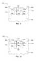
- FIG. 1is a top view of a FinFET semiconductor device having a local buried oxide region.
- FIG. 2is a perspective view of a FinFET semiconductor device having a local buried oxide region.
- FIG. 3is a perspective view of a FinFET semiconductor device having a local buried oxide region in another embodiment.
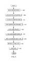
- FIG. 4is a flow diagram illustrating a method including forming a local buried oxide region in a FinFET semiconductor device.
- FIGS. 5-12are fin widthwise cross sectional side view schematic diagrams illustrating fabrication of a FinFET semiconductor device having a local buried oxide region.
- FIGS. 13 and 14are fin lengthwise cross sectional side view schematic diagrams illustrating a semiconductor device.
- FIG. 15is a fin lengthwise schematic diagram illustrating a semiconductor device having a plurality of FinFETs.
- a fin field effect transistor (FinFET) semiconductor device 100having a fin 202 extending from a bulk silicon substrate 102 , wherein there is formed wrapped around a portion of the fin 202 a gate 101 , and wherein proximate a channel area 103 of the fin aligned to the gate 101 there is formed a local buried oxide region 104 . Between substrate 102 and gate 101 there can be disposed oxide 204 (oxide layer 204 ). Oxide 204 can be disposed in surrounding relation to a lower elevation portion of fin 202 . Shown as having a single fin in the embodiment of FIGS. 1 and 2 , semiconductor device 100 can have more than one fin. In one embodiment, semiconductor device 100 can be provided by bulk wafer defining a plurality of field effect transistors. In one embodiment, semiconductor device 100 can be provided by an integrated circuit (IC) defining a plurality of field effect transistors.
- ICintegrated circuit
- FIGS. 1 and 2show a top plan view and isometric view, respectively, of a FinFET semiconductor device 100 fabricated on Si substrate 102 . Though only one fin is illustrated in FIG. 1 for simplicity, there can be multiple fins 202 fabricated in parallel with fin 202 . Fin 202 can extend upwardly from substrate 102 . Each fin 202 of a semiconductor device 100 can be elongated and can include a rectangular cross section as depicted in the views of FIGS. 2-12 herein. In the embodiment illustrated, FinFET semiconductor device 100 includes a gate 101 which can be wrapped around the top and sides of a fin 202 . A source 105 is defined at one end of fin 202 , and a drain 107 is defined at the other end of fin 202 .
- Source 105 and drain 107can be defined on fin 202 and doped by performing appropriate implantation processes. Appropriate implantation processes can include e.g., implantation of dopants (n-type or p-type) for n-type and p-type source and drain of FinFETs.
- a channel 103can be defined by fin 202 intermediate source 105 and drain 107 at a region of fin 202 covered by gate 101 and aligned to gate 101 .
- Channel 103can be defined in the fin 202 above local buried oxide region 104 , the channel 103 having a first end and a second end, a source 105 defined at the first end of the channel 103 and a drain 105 defined at the second end of the channel 103 .
- channel 103can be delimited by a local buried oxide region 104 below the top surface of fin 202 by a distance in one embodiment of between about 20 nm and 40 nm (this distance being the height of the fin portion that extends above local buried oxide region 104 being referred to as the active fin height). Therefore, in one embodiment, current can only flow through the portion of the channel of fin 202 above local buried oxide region 104 .
- Gate 101 in one embodimentcan have a gate stack having multiple layers.
- the multiple layerscan include one or more metal layers and one or more dielectric layers.
- the one or more metal layerscan have, e.g., one or more layers of titanium nitride (TiN), TiAlC, TaN, aluminum (Al), or tungsten (W).
- the one or more dielectric layerscan have, e.g., one or more of Si-oxide, Si-nitride, or high-k material (e.g., Hf-oxide). Because gate 101 can have have multiple layers, gate 101 can be referred to a gate stack.
- a semiconductor device 100can include a local buried oxide region 104 aligned with a gate 101 .
- a channel 103can be defined that is aligned with gate 101 and which can be above local buried oxide region 104 .
- Local buried oxide region 104can be referred to as “BOX”.
- Local buried oxide region 104can be formed in one or more of bulk Si substrate 102 and fin 202 by implantation of oxygen into fin 202 followed by annealing. In the embodiments depicted in FIGS. 1-15 herein, local buried oxide region 104 is formed in fin 202 to define a channel 103 above local buried oxide region 104 and an area of fin 202 below local buried oxide region 104 .
- BOX 104can be aligned to gate 101 and can have a length less than a length of gate 101 as depicted in FIGS. 1 and 2 . BOX 104 can be adapted so that BOX 104 blocks a leakage current path between source 105 and drain 107 .
- FIG. 3there is shown a perspective view of an alternative embodiment of device 100 .
- the “active” channel 103is above the local buried oxide region 104 .
- the area of fin 202 below the local buried oxide region 104can provide mechanical stability to the substrate.
- the location of local buried oxide region 104can be adjusted toward the surface of Si substrate 102 , or even half way (e.g., as depicted in the embodiment illustrated in FIG. 15 ) or mostly submerged into the Si-substrate, so that the active fin channel height is larger to define a stronger FinFET device 100 .
- FIGS. 5-12illustrate cross-sectional views of a fin 202 perpendicular to the fin direction (widthwise) and parallel and through the gate 101 .
- FIGS. 13-14are cross-sectional views co-extensive with the fin direction (lengthwise) through gate 101 . In the views of FIGS. 5-12 , two fins are illustrated.
- SiN layer depositionthere can be performed SiN layer deposition.
- a bulk substrate 102having fins 202 and oxide 204 (oxide layer 204 ).
- the providingcan include providing a substrate 102 , forming fins 202 and filling oxide 204 between fin 202 and depositing thereon an insulation layer 206 .
- Performance of insulation layer deposition at block 402can be accompanied by chemical-mechanical planarization (CMP) to provide a flat surface to improve efficiently and accuracy of ensuing gate pattern lithography processes.
- CMPchemical-mechanical planarization
- the insulation layer 206can be e.g., a silicon nitride (SiN) layer as depicted in FIG. 6 .
- Insulation layer 206which can be provided by SiN, can serve as a hard mask.
- the providing at block 402can alternatively include providing a Si substrate having fins 202 and filled oxide 204 and depositing thereon insulation layer 206 in other form, e.g., a Si-oxide layer or a combination of Si-nitride and Si-oxide layers.
- the thickness of the insulation layer 206can be in the range of about 10 nm to about 100 nm.
- the providing at block 402can also include shallow trench isolation (STI) and formation. As indicated in FIG.
- STIshallow trench isolation
- shallow trench isolation (STI) oxide 115can be formed at block 402 .
- STI oxidecan be deposited into shallow trenches of Si substrate 102 to isolate sets of devices of semiconductor device 100 .
- the shallow trenches that are filled with STI oxide in the views of FIGS. 4-12are shown as having a depth greater than a depth of oxide 204 deposited adjacent to fins 202 .
- shallow trenches filled with STI oxide 115can have a depth less than a depth of oxide 204 deposited adjacent to fins 202 .
- shallow trenches filled with STI oxidecan have a depth equal to a depth of oxide 204 deposited adjacent to fins 202 .
- the depth of oxide 204can be regarded as the depth of oxide 204 after recessing of oxide 204 at block 422 to be described herein.
- the providing of STI and formation at block 404can also include providing shallow trench isolation (forming a trench with STI oxide 115 ) between fins 202 depicted in FIGS. 5-12 .
- a depth of such intermediate trenchescan be less than, greater than, or equal to a depth of trenches (filled with STI oxide 115 ) depicted in FIGS. 5-12 .
- gate patterninglithography followed by gate reactive ion etching (RIE) to open the gate area 101 a .
- RIEgate reactive ion etching
- gate patterningfor providing an opening in insulation layer 206 (to allow for oxygen ion implantation in subsequent step).
- Gate area 101 a as depicted in FIG. 7can be uncovered by photoresist.
- the gate patterningcan include providing a mask, the mask having a two dimensional area pattern that defines a gate area of device 100 .
- Removal of the mask provided by insulation layer 206can include, e.g., RIE or wet etching.
- hot H3PO4 acidcan be used to remove nitride 206 without damaging the Si fins 202 and filled oxide 204 .
- FIG. 9there can be performed oxygen ion implantation into the exposed gate area 101 a .
- a local buried oxide region 104FIG. 9
- Forming of a local buried oxide region 104can be performed by using ion implantation of oxygen (O + ) through an exposed surface 202 s of fin 202 into an area within fin 202 and followed by thermal annealing.
- O +ion implantation of oxygen
- a local buried oxide region 104can be regarded as being “self aligned” to gate 101 .
- Local buried oxide region 104can be aligned to a gate 101 .
- Local buried oxide region 104can have a length in common with a length of gate 101 .
- local buried oxide region 104can have a width in common with width of gate 101 .
- local buried oxide region 104can have one or more a length and width less than a length and width, respectively, of gate 101 .
- the implantation of oxygen ionscan be accompanied by implantation of one or more of nitrogen (N), carbon (C) and fluorine (F).
- the energy and dose of implantation of one or more of oxygen ions, N, C, and Fis designed to form a local buried oxide region 104 (BOX) deep enough underneath the a surface of fin 202 , so that dopant diffusion is reduced and stress at local buried oxide region 104 and surrounding areas of fin 202 is reduced.
- the implant energy of Ois in the range of from about 10 KeV to about 100 KeV. In one embodiment, the implant energy of O is in the range from about 200 KeV to about 1 MeV.
- the local buried oxide region 104(shown as formed in FIG.
- the ion implantationcan include implantation of oxygen (with dose in the range of 10 15 to 10 17 cm 2 ) and followed by implantation sequentially of nitrogen (N), carbon (C), or fluorine (F) with smaller dose (in the range of from about 1.0% to about 3.0% of the main O dose).
- mask 206defines both an area of implantation of oxygen ions, and in a manner set forth herein, a gate area 101 a , an area of gate electrode material. With use of mask 206 a formed local buried oxide region 104 can be self aligned to a gate area 101 a and accordingly can be self aligned to a formed gate 101 when gate 101 is formed. When local buried oxide region 104 is formed a channel area 103 a can be formed on fin 202 above local buried oxide region 104 .
- SIMOXSeparation by Implantation of Oxygen
- oxygen implantis performed in a localized area through a patterned mask 206 and with a lower dosage and no elevated temperature during implantation and also lower annealing temperature after implantation than in the case of a SIMOX for SOI substrate fabrication.
- the oxygen implantation for the formation of local buried oxide region 104is at a dosage of about 10 16 to 10 17 ions/cm 2 , which is about 1% to about 10% of the known blank implant of oxygen at elevated temperature in the SIMOX technology method for forming SOI substrate.
- the implant energy of Ocan be ⁇ 120 KeV (to achieve the formation of BOX 20-40 nm below the active fin).
- the post implant annealing temperature in this disclosureis in a range of from about 800° C. to about 1100° C. which is significantly lower than that for the referred to SIMOX process.
- High temperature annealing at block 416can be performed subsequent to implantation of oxygen at block 412 .
- the high temperature annealingcan be performed e.g., at from about 800 deg. C. to about 1100 deg. C. in inert ambient to form a local buried oxide region 104 (BOX) and heal the damage in the silicon channel from the implantation at block 412 .
- post implantation annealing temperatures seen in SIMOX for SOI substrate fabrication processesare in the range of >1200 C.
- the implant of additives (N, C, F) with oxygen ionshelps to suppress the generation of defects during post implant thermal annealing and also lower than the annealing temperature significantly.
- the implantation of the noted additives (N, C, F)also provides smooth stress transition between the local buried oxide region 104 and surrounding Si channel area 103 a ( FIG. 11 ) of fin 202 .
- a post implant annealing temperature lower than that in SIMOX for SOI substrate fabricationcan result in a robust “defect free” and minimum stress around the Si channel area 103 a ( FIG. 1 ).
- inclusion of one or more of the noted additives N, C, and Fcan suppress dopants of B, P, diffusion into the local buried oxide region 104 from an adjacent channel area 103 a , so that there is provided reduced fluctuations of device parameters.
- oxide 204can be recessed deep enough to the level of BOX 104 (e.g., to the middle of BOX level, or at least 10 nm below the top of BOX). In one embodiment, oxide 204 can be recessed to a certain level, the certain level within a range from the top of BOX 104 to a bottom of BOX 104 .
- a thin oxide (e.g., SiO 2 ) layer 1103i.e., an interfacial layer
- the oxide layer 1103can be used as the gate dielectric in a gate first process or oxide layer 1103 can be used as a dummy gate dielectric in a gate last process.
- a gate dielectric of gate 101can be a multiple layer of thin Si-oxide, Si-oxynitride, and high-k (HfO2) materials to achieve high quality and thin effective thickness and low leakage.
- polysilicon depositioncan be performed on an entire wafer.
- a thickness of the polysilicon layer 2101can be thick enough so that a gate area 101 a is fully filled with polysilicon.
- CMPchemical-mechanical planarization
- the polysilicon gate heightcan be controlled by a thickness of insulation layer 206 , and the gate height can be above the top of fin 202 by between about 20 nm and about 40 nm. Planarization can improve efficiency and accuracy of ensuing processing.
- FIG. 13is a fin lengthwise cross sectional side view of the semiconductor device 100 depicted in the fin widthwise cross sectional views of FIGS. 5-12 .
- the removalcan be performed using hot phosphorus acid which is selective to silicon and oxide.
- only insulation layer 206is removed.
- the non-channel portion of fins 202are exposed for further process steps to form components, e.g., spacers, source/drain, contacts to complete the FinFET (as a poly-gate process) in accordance with a gate first process.
- polysilicon layer 2101can define a gate electrode 101 e ( FIG. 14 ).
- a gate last processthere can be performed completion of a FinFET device 100 by a gate last process (with the poly gate stack to be removed later in process steps).
- a gate last processa poly-Si layer 2101 can be used as a temporary gate stack to form an offset spacer, followed by optional Halo implantation and extension implantations.
- Rapid Thermal Analysis (RTA)can be performed and is optional depending on a specific integration scheme used.
- Source and drain formationcan be the same as that in bulk flow with eSiGe (for PFET stress booster), SMT or SiC (for NFET stress booster).
- ILDInterlayer Dielectric
- MOLMiddle of Line
- FIGS. 1-3 and FIGS. 14-15Further aspects of a FinFET semiconductor device having a local buried oxide region 104 are now described with reference to FIGS. 1-3 and FIGS. 14-15 . It is seen with reference to FIGS. 1-3 and FIGS. 14-15 that local buried oxide region 104 can be formed only under the gate 101 and a well controlled channel 103 but not under a source and drain 105 and 107 . Such local buried oxide region 104 underneath a defined channel 103 can effectively eliminate or block the leakage current between the source 105 and drain 107 (i.e., similar to the advantage exhibited as in the case of a MOSFET fabricated on SOI substrate, e.g., ETSOI device).
- the active channel 103is above the BOX 104 and the active fin height is determined by the energy/dose level of the oxygen implantation.
- the depth of channel 103can be controlled by one or more of varying a dosage of oxygen ion implantation and the inclusion of zero or more additives with the implantation.
- Channel 103can be aligned to gate 101 and local buried oxide region 104 can be aligned to gate 101 . Accordingly, local buried oxide region 104 can be aligned to channel 103 and channel 103 can be aligned to local buried oxide region 104 .
- a gate 101provided by a gate stack having gate electrode 101 e and gate dielectric 101 d .
- a gate electrode 101 ecan be provided by polysilicon layer 2101 and gate dielectric 101 d can be provided by oxide layer 1103 .
- gate electrode 101 e and gate dielectric 101 dare set forth herein in one embodiment as having a single layer each, gate electrode 101 e and gate dielectric 101 d can include one or more layers.
- gate electrode 101 ecan include multiple conducting layers, e.g., TiN, TaN, TiAl, TiC, Al, and W, (e.g., to set the correct “work function” in advanced CMOS technology nodes).
- the gate dielectric 101 dmay also be multiple layers of dielectric, e.g., high-k and SiO 2 , for better capacitive coupling to channel 103 and smaller leakage between the gate electrode 101 e and channel 103 .
- the combination of one or more layers of a gate electrode and one or more layers of a gate dielectriccan be regarded as a “gate stack”. As illustrated in FIG. 14 , local buried oxide region 104 can be aligned with gate 101 .
- Gate 101can be bounded by imaginary vertically extending planes 101 p that extend perpendicularly through substrate 102 .
- local buried oxide region 104can be formed so that it does not extend lengthwise in either direction beyond the imaginary vertically extending planes 101 p .
- local buried oxide region 104can be aligned to gate 101 by having at least a portion thereof within a location delimited by planes 101 p .
- local buried oxide region 104can be aligned to gate 101 by being defined within a location delimited by planes 101 p and by being absent of a portion that extends external to a location delimited by planes 101 p .
- local buried oxide region 104can be aligned to gate 101 by being defined within a location delimited by planes 101 p , by being absent of a portion that extends external to a location delimited by planes 101 p , and by having a length in common with a length of gate 101 .
- local buried oxide 104with use of mask 206 to be self aligned to gate area 101 a and gate 101 when formed, local buried oxide region is aligned to gate area 101 a and gate 101 when formed.
- channel 103can be aligned to gate 101 by having at least a portion thereof within a location delimited by planes 101 p . In one embodiment, channel 103 can be aligned to gate 101 by being defined within a location delimited by planes 101 p and by being absent of a portion that extends external to a location delimited by planes 101 p . As depicted in the views of FIGS. 1-15 , a gate 101 can be disposed over a fin 202 having defined therein a BOX 104 aligned to gate 101 and a channel 103 aligned to gate 101 .
- a gate 101 disposed over fin 202can include a portion within an area delimited by imaginary vertically extending planes 101 f (depicted in FIG. 12 ) that bound sidewalls of fin 202 and extend perpendicularly to substrate 102 (which can be planar) and a portion external to an area delimited by imaginary vertically extending planes 101 f bounded by sidewalls of fin 202 .
- a gate 101 disposed over fin 202can be entirely defined within an area delimited by imaginary vertically extending planes 101 f (depicted in FIG.
- dotted line 2502indicates an elevation of a base of fins 202 , i.e., the depth to which bulk substrate 102 , e.g., Si, can be recessed to define fins 202 .
- a field effect channel with such a structureis a thin silicon body partially delimited by the local buried oxide region 104 and thus can achieve the leakage current inhibiting performance on the order of that seen with an extremely thin silicon insulator (ETSOI) device.
- ETSOIextremely thin silicon insulator
- source and drain 105 and 107formed on fins 202 that are formed contiguous with bulk silicon substrate 102 as depicted in the views of FIGS. 1-3 and FIGS. 14-15 , the heat generated in logic circuits operating at high frequency can be readily dissipated to bulk silicon substrate 102 to exhibit the same advantages as are exhibited by logic circuits fabricated on a bulk silicon substrate.
- source and drain 105 and 107can be formed to be “embedded” source and drain 105 and 107 .
- FIG. 14is a fin lengthwise cross sectional side view illustrating additional aspects of a method set forth with reference to FIGS. 5-13 , wherein the embodiment illustrated in the view of FIG. 14 is depicted as including optional halo implants and extension implants.
- Source 105 and drain 107can be fabricated as embedded sources and drains including stressors.
- embedded source and drain 105 and 107can be fabricated by recessing of S/D Si, then epi regrowth of SiGe for p-type S/D and SiC for n-type S/D selectively in order to induce stress in the channel 103 .
- source 105includes epitaxial growth formation 105 ep for inducing stress in channel 103
- drain 107includes an epitaxial growth formation 107 ep for inducing stress in channel 103 .
- device 100is depicted as having halo implants 106 , and source and drain extension implants 109 as optional features.
- these optional Halo implants 106 and extension implants 109 for FinFETsare useful in case of short channel length (e.g. ⁇ 20 nm) for reducing short channel effect.
- Halo implants through the source/draincan also facilitate adjustment of the threshold voltage (Vt) of the device 100 for implementation of a multi-Vt scheme in logic circuits.
- Vtthreshold voltage
- FIG. 15there is depicted a semiconductor device 100 having a plurality of FinFETs.
- Semiconductor device 100 as depicted in FIG. 15includes a first FinFET at location “A” and a second FinFET at location “B”.
- Each of the first FinFET and second FinFETcan be as fabricated according to method in accordance with that described with reference to FIGS. 5-14 except each of the first FinFET at location “A” and the second FinFET at location “B” can be absent of halo implants 106 and source/drain extension implants 109 .
- FIG. 15depicts a bulk silicon wafer.
- FIG. 15depicts an integrated circuit (IC).
- ICintegrated circuit
- a method or device that “comprises”, “has”, “includes” or “contains” one or more steps or elementspossesses those one or more steps or elements, but is not limited to possessing only those one or more steps or elements.
- a step of a method or an element of a device that “comprises”, “has”, “includes” or “contains” one or more featurespossesses those one or more features, but is not limited to possessing only those one or more features.
- a device or structure that is configured in a certain wayis configured in at least that way, but may also be configured in ways that are not listed.
Landscapes
- Engineering & Computer Science (AREA)
- Physics & Mathematics (AREA)
- Condensed Matter Physics & Semiconductors (AREA)
- General Physics & Mathematics (AREA)
- Manufacturing & Machinery (AREA)
- Computer Hardware Design (AREA)
- Microelectronics & Electronic Packaging (AREA)
- Power Engineering (AREA)
- Thin Film Transistor (AREA)
- Insulated Gate Type Field-Effect Transistor (AREA)
- Metal-Oxide And Bipolar Metal-Oxide Semiconductor Integrated Circuits (AREA)
Abstract
Description
Claims (20)
Priority Applications (2)
| Application Number | Priority Date | Filing Date | Title |
|---|---|---|---|
| US14/083,164US9252272B2 (en) | 2013-11-18 | 2013-11-18 | FinFET semiconductor device having local buried oxide |
| US14/974,772US20160111322A1 (en) | 2013-11-18 | 2015-12-18 | Finfet semiconductor device having local buried oxide |
Applications Claiming Priority (1)
| Application Number | Priority Date | Filing Date | Title |
|---|---|---|---|
| US14/083,164US9252272B2 (en) | 2013-11-18 | 2013-11-18 | FinFET semiconductor device having local buried oxide |
Related Child Applications (1)
| Application Number | Title | Priority Date | Filing Date |
|---|---|---|---|
| US14/974,772DivisionUS20160111322A1 (en) | 2013-11-18 | 2015-12-18 | Finfet semiconductor device having local buried oxide |
Publications (2)
| Publication Number | Publication Date |
|---|---|
| US20150137235A1 US20150137235A1 (en) | 2015-05-21 |
| US9252272B2true US9252272B2 (en) | 2016-02-02 |
Family
ID=53172423
Family Applications (2)
| Application Number | Title | Priority Date | Filing Date |
|---|---|---|---|
| US14/083,164ActiveUS9252272B2 (en) | 2013-11-18 | 2013-11-18 | FinFET semiconductor device having local buried oxide |
| US14/974,772AbandonedUS20160111322A1 (en) | 2013-11-18 | 2015-12-18 | Finfet semiconductor device having local buried oxide |
Family Applications After (1)
| Application Number | Title | Priority Date | Filing Date |
|---|---|---|---|
| US14/974,772AbandonedUS20160111322A1 (en) | 2013-11-18 | 2015-12-18 | Finfet semiconductor device having local buried oxide |
Country Status (1)
| Country | Link |
|---|---|
| US (2) | US9252272B2 (en) |
Cited By (1)
| Publication number | Priority date | Publication date | Assignee | Title |
|---|---|---|---|---|
| US9647123B1 (en) | 2016-10-14 | 2017-05-09 | International Business Machines Corporation | Self-aligned sigma extension regions for vertical transistors |
Families Citing this family (5)
| Publication number | Priority date | Publication date | Assignee | Title |
|---|---|---|---|---|
| US20150187915A1 (en)* | 2013-12-26 | 2015-07-02 | Samsung Electronics Co., Ltd. | Method for fabricating fin type transistor |
| US20170110541A1 (en)* | 2015-10-15 | 2017-04-20 | Qualcomm Incorporated | Nanowire channel structures of continuously stacked heterogeneous nanowires for complementary metal oxide semiconductor (cmos) devices |
| US10032678B2 (en) | 2015-10-15 | 2018-07-24 | Qualcomm Incorporated | Nanowire channel structures of continuously stacked nanowires for complementary metal oxide semiconductor (CMOS) devices |
| US9536789B1 (en) | 2016-01-27 | 2017-01-03 | International Business Mashines Corporation | Fin-double-gated junction field effect transistor |
| CN109309056B (en)* | 2017-07-27 | 2020-12-22 | 中芯国际集成电路制造(上海)有限公司 | Semiconductor structure and method of forming the same |
Citations (49)
| Publication number | Priority date | Publication date | Assignee | Title |
|---|---|---|---|---|
| US5061642A (en) | 1989-08-19 | 1991-10-29 | Fujitsu Limited | Method of manufacturing semiconductor on insulator |
| US5888297A (en) | 1995-01-09 | 1999-03-30 | Nec Corporation | Method of fabricating SOI substrate |
| US6420218B1 (en)* | 2000-04-24 | 2002-07-16 | Advanced Micro Devices, Inc. | Ultra-thin-body SOI MOS transistors having recessed source and drain regions |
| US20050280090A1 (en)* | 2003-11-05 | 2005-12-22 | Anderson Brent A | Method of fabricating a FinFET |
| US20060027870A1 (en)* | 2004-08-05 | 2006-02-09 | Satoshi Inaba | Semiconductor device and method of manufacturing the same |
| US20060084215A1 (en)* | 2003-12-05 | 2006-04-20 | Kabushiki Kaisha Toshiba | Semiconductor device and method for manufacturing the same |
| US20070122984A1 (en)* | 2005-02-15 | 2007-05-31 | International Business Machines Corporation | Structure and method for manufacturing strained finfet |
| US20080135935A1 (en)* | 2006-12-07 | 2008-06-12 | Young Kyun Cho | Dual structure finfet and method of manufacturing the same |
| US20080237655A1 (en)* | 2007-03-29 | 2008-10-02 | Kabushiki Kaisha Toshiba | Semiconductor apparatus and method for manufacturing same |
| US20090014795A1 (en)* | 2004-07-29 | 2009-01-15 | Risho Koh | Substrate for field effect transistor, field effect transistor and method for production thereof |
| US20090224321A1 (en)* | 2008-03-06 | 2009-09-10 | Renesas Technology Corp | Semiconductor device and method of manufacturing semiconductor device |
| US20110084315A1 (en)* | 2009-10-08 | 2011-04-14 | International Business Machines Corporation | Semiconductor device having silicon on stressed liner (sol) |
| US20120061759A1 (en)* | 2010-09-15 | 2012-03-15 | International Business Machines Corporation | Extremely Thin Semiconductor-on-Insulator (ETSOI) FET Having a Stair-Shape Raised Source/Drain and a Method of Forming the Same |
| US20120104498A1 (en)* | 2010-10-27 | 2012-05-03 | International Business Machines Corporation | Semiconductor device having localized extremely thin silicon on insulator channel region |
| US8273626B2 (en)* | 2003-06-27 | 2012-09-25 | Intel Corporationn | Nonplanar semiconductor device with partially or fully wrapped around gate electrode and methods of fabrication |
| US20130119466A1 (en) | 2008-08-29 | 2013-05-16 | Taiwan Semiconductor Manufacturing Company, Ltd. | High Voltage Device with Reduced Leakage |
| US20130122665A1 (en) | 2010-03-16 | 2013-05-16 | International Business Machines Corporation | Method of Manufacturing a Thin Box Metal Backgate Extremely Thin SOI Device |
| US8445963B2 (en) | 2007-12-19 | 2013-05-21 | Imec | Multi-gate semiconductor devices with improved carrier mobility |
| US8445337B2 (en) | 2010-05-12 | 2013-05-21 | International Business Machines Corporation | Generation of multiple diameter nanowire field effect transistors |
| US20130127049A1 (en) | 2008-06-27 | 2013-05-23 | Taiwan Semiconductor Manufacturing Company, Ltd. | Method for Stacking Devices and Structure Thereof |
| US20130140639A1 (en) | 2011-12-01 | 2013-06-06 | Taiwan Semiconductor Manufacturing Company, Ltd. | High gate density devices and methods |
| US8461647B2 (en) | 2010-03-10 | 2013-06-11 | Taiwan Semiconductor Manufacturing Company, Ltd. | Semiconductor device having multi-thickness gate dielectric |
| US20130146953A1 (en) | 2011-12-12 | 2013-06-13 | International Business Machines Corporation | Method and Structure For Forming ETSOI Capacitors, Diodes, Resistors and Back Gate Contacts |
| US20130146959A1 (en) | 2011-12-12 | 2013-06-13 | International Business Machines Corporation | Method and Structure For Forming On-Chip High Quality Capacitors With ETSOI Transistors |
| US20130155382A1 (en) | 2007-02-26 | 2013-06-20 | Eriko Inoue | Work stage of exposing apparatus, exposing method and method of manufacturing a structure |
| US8469886B2 (en) | 2003-12-09 | 2013-06-25 | Dexcom, Inc. | Signal processing for continuous analyte sensor |
| US8482069B2 (en) | 1997-11-18 | 2013-07-09 | Semiconductor Energy Laboratory Co., Ltd. | Nonvolatile memory and electronic apparatus |
| US8486736B2 (en) | 2008-10-20 | 2013-07-16 | Semiconductor Energy Laboratory Co., Ltd. | Method for manufacturing light-emitting device |
| US20130193916A1 (en) | 2006-05-31 | 2013-08-01 | Semiconductor Energy Laboratory Co., Ltd. | Semiconductor device and ic label, ic tag, and ic card having the same |
| US20130200438A1 (en) | 2011-10-31 | 2013-08-08 | Taiwan Semiconductor Manufacturing Company, Ltd. | Systems and methods for signal amplification with a dual-gate bio field effect transistor |
| US8507989B2 (en) | 2011-05-16 | 2013-08-13 | International Business Machine Corporation | Extremely thin semiconductor-on-insulator (ETSOI) FET with a back gate and reduced parasitic capacitance |
| US20130207187A1 (en) | 2012-02-13 | 2013-08-15 | Taiwan Semiconductor Manufacturing Company, Ltd. | Insulated gate bipolar transistor structure having low substrate leakage |
| US8517275B2 (en) | 2006-12-27 | 2013-08-27 | Semiconductor Energy Laboratory Co., Ltd. | Semiconductor device |
| US8519479B2 (en) | 2010-05-12 | 2013-08-27 | International Business Machines Corporation | Generation of multiple diameter nanowire field effect transistors |
| US8531000B2 (en) | 2009-04-22 | 2013-09-10 | Panasonic Corporation | SOI wafer, method for producing same, and method for manufacturing semiconductor device |
| US8536650B2 (en) | 2008-03-28 | 2013-09-17 | International Business Machines Corporation | Strained ultra-thin SOI transistor formed by replacement gate |
| US8546246B2 (en) | 2011-01-13 | 2013-10-01 | International Business Machines Corporation | Radiation hardened transistors based on graphene and carbon nanotubes |
| US20130260505A1 (en) | 2012-03-30 | 2013-10-03 | International Business Machines Corporation | Solar-powered energy-autonomous silicon-on-insulator device |
| US8551313B2 (en) | 2007-11-15 | 2013-10-08 | International Business Machines Corporation | Method and apparatus for electroplating on soi and bulk semiconductor wafers |
| US8558370B2 (en) | 2007-03-13 | 2013-10-15 | Semiconductor Energy Laboratory Co., Ltd. | Semiconductor device with antenna |
| US20130270640A1 (en) | 2007-03-12 | 2013-10-17 | Kabushiki Kaisha Toshiba | Semiconductor device |
| US8564025B2 (en) | 2009-12-04 | 2013-10-22 | International Business Machines Corporation | Nanowire FET having induced radial strain |
| US20130320294A1 (en)* | 2011-12-23 | 2013-12-05 | Annalisa Cappellani | Common-substrate semiconductor devices having nanowires or semiconductor bodies with differing material orientation or composition |
| US8610201B1 (en)* | 2012-08-16 | 2013-12-17 | Kabushiki Kaisha Toshiba | FinFET comprising a punch-through stopper |
| US20140167163A1 (en)* | 2012-12-17 | 2014-06-19 | International Business Machines Corporation | Multi-Fin FinFETs with Epitaxially-Grown Merged Source/Drains |
| US20140264596A1 (en)* | 2013-03-14 | 2014-09-18 | International Business Machines Corporation | Partially isolated fin-shaped field effect transistors |
| US20140361338A1 (en)* | 2013-06-06 | 2014-12-11 | International Business Machines Corporation | REDUCED RESISTANCE SiGe FinFET DEVICES AND METHOD OF FORMING SAME |
| US20150102428A1 (en)* | 2012-07-30 | 2015-04-16 | International Business Machines Corporation | Merged fin finfet with (100) sidewall surfaces and method of making same |
| US9153309B2 (en)* | 2010-02-07 | 2015-10-06 | Zeno Semiconductor Inc. | Semiconductor memory device having electrically floating body transistor, semiconductor memory device having both volatile and non-volatile functionality and method or operating |
Family Cites Families (7)
| Publication number | Priority date | Publication date | Assignee | Title |
|---|---|---|---|---|
| US5468657A (en)* | 1994-06-17 | 1995-11-21 | Sharp Microelectronics Technology, Inc. | Nitridation of SIMOX buried oxide |
| US8735990B2 (en)* | 2007-02-28 | 2014-05-27 | International Business Machines Corporation | Radiation hardened FinFET |
| US7452758B2 (en)* | 2007-03-14 | 2008-11-18 | International Business Machines Corporation | Process for making FinFET device with body contact and buried oxide junction isolation |
| US8969974B2 (en)* | 2012-06-14 | 2015-03-03 | Taiwan Semiconductor Manufacturing Company, Ltd. | Structure and method for FinFET device |
| US8847281B2 (en)* | 2012-07-27 | 2014-09-30 | Intel Corporation | High mobility strained channels for fin-based transistors |
| US8846477B2 (en)* | 2012-09-27 | 2014-09-30 | Globalfoundries Inc. | Methods of forming 3-D semiconductor devices using a replacement gate technique and a novel 3-D device |
| US9006786B2 (en)* | 2013-07-03 | 2015-04-14 | Taiwan Semiconductor Manufacturing Company, Ltd. | Fin structure of semiconductor device |
- 2013
- 2013-11-18USUS14/083,164patent/US9252272B2/enactiveActive
- 2015
- 2015-12-18USUS14/974,772patent/US20160111322A1/ennot_activeAbandoned
Patent Citations (53)
| Publication number | Priority date | Publication date | Assignee | Title |
|---|---|---|---|---|
| US5061642A (en) | 1989-08-19 | 1991-10-29 | Fujitsu Limited | Method of manufacturing semiconductor on insulator |
| US5888297A (en) | 1995-01-09 | 1999-03-30 | Nec Corporation | Method of fabricating SOI substrate |
| US8482069B2 (en) | 1997-11-18 | 2013-07-09 | Semiconductor Energy Laboratory Co., Ltd. | Nonvolatile memory and electronic apparatus |
| US6420218B1 (en)* | 2000-04-24 | 2002-07-16 | Advanced Micro Devices, Inc. | Ultra-thin-body SOI MOS transistors having recessed source and drain regions |
| US8273626B2 (en)* | 2003-06-27 | 2012-09-25 | Intel Corporationn | Nonplanar semiconductor device with partially or fully wrapped around gate electrode and methods of fabrication |
| US20050280090A1 (en)* | 2003-11-05 | 2005-12-22 | Anderson Brent A | Method of fabricating a FinFET |
| US20060084215A1 (en)* | 2003-12-05 | 2006-04-20 | Kabushiki Kaisha Toshiba | Semiconductor device and method for manufacturing the same |
| US8469886B2 (en) | 2003-12-09 | 2013-06-25 | Dexcom, Inc. | Signal processing for continuous analyte sensor |
| US20090014795A1 (en)* | 2004-07-29 | 2009-01-15 | Risho Koh | Substrate for field effect transistor, field effect transistor and method for production thereof |
| US20060027870A1 (en)* | 2004-08-05 | 2006-02-09 | Satoshi Inaba | Semiconductor device and method of manufacturing the same |
| US20070122984A1 (en)* | 2005-02-15 | 2007-05-31 | International Business Machines Corporation | Structure and method for manufacturing strained finfet |
| US20130193916A1 (en) | 2006-05-31 | 2013-08-01 | Semiconductor Energy Laboratory Co., Ltd. | Semiconductor device and ic label, ic tag, and ic card having the same |
| US20080135935A1 (en)* | 2006-12-07 | 2008-06-12 | Young Kyun Cho | Dual structure finfet and method of manufacturing the same |
| US8517275B2 (en) | 2006-12-27 | 2013-08-27 | Semiconductor Energy Laboratory Co., Ltd. | Semiconductor device |
| US20130155382A1 (en) | 2007-02-26 | 2013-06-20 | Eriko Inoue | Work stage of exposing apparatus, exposing method and method of manufacturing a structure |
| US20130270640A1 (en) | 2007-03-12 | 2013-10-17 | Kabushiki Kaisha Toshiba | Semiconductor device |
| US8558370B2 (en) | 2007-03-13 | 2013-10-15 | Semiconductor Energy Laboratory Co., Ltd. | Semiconductor device with antenna |
| US20080237655A1 (en)* | 2007-03-29 | 2008-10-02 | Kabushiki Kaisha Toshiba | Semiconductor apparatus and method for manufacturing same |
| US8551313B2 (en) | 2007-11-15 | 2013-10-08 | International Business Machines Corporation | Method and apparatus for electroplating on soi and bulk semiconductor wafers |
| US8445963B2 (en) | 2007-12-19 | 2013-05-21 | Imec | Multi-gate semiconductor devices with improved carrier mobility |
| US20090224321A1 (en)* | 2008-03-06 | 2009-09-10 | Renesas Technology Corp | Semiconductor device and method of manufacturing semiconductor device |
| US8536650B2 (en) | 2008-03-28 | 2013-09-17 | International Business Machines Corporation | Strained ultra-thin SOI transistor formed by replacement gate |
| US20130127049A1 (en) | 2008-06-27 | 2013-05-23 | Taiwan Semiconductor Manufacturing Company, Ltd. | Method for Stacking Devices and Structure Thereof |
| US20130119466A1 (en) | 2008-08-29 | 2013-05-16 | Taiwan Semiconductor Manufacturing Company, Ltd. | High Voltage Device with Reduced Leakage |
| US8486736B2 (en) | 2008-10-20 | 2013-07-16 | Semiconductor Energy Laboratory Co., Ltd. | Method for manufacturing light-emitting device |
| US8531000B2 (en) | 2009-04-22 | 2013-09-10 | Panasonic Corporation | SOI wafer, method for producing same, and method for manufacturing semiconductor device |
| US20130149823A1 (en) | 2009-10-08 | 2013-06-13 | International Business Machines Corporation | Semiconductor device having silicon on stressed liner (sol) |
| US20110084315A1 (en)* | 2009-10-08 | 2011-04-14 | International Business Machines Corporation | Semiconductor device having silicon on stressed liner (sol) |
| US8564025B2 (en) | 2009-12-04 | 2013-10-22 | International Business Machines Corporation | Nanowire FET having induced radial strain |
| US9153309B2 (en)* | 2010-02-07 | 2015-10-06 | Zeno Semiconductor Inc. | Semiconductor memory device having electrically floating body transistor, semiconductor memory device having both volatile and non-volatile functionality and method or operating |
| US8461647B2 (en) | 2010-03-10 | 2013-06-11 | Taiwan Semiconductor Manufacturing Company, Ltd. | Semiconductor device having multi-thickness gate dielectric |
| US20130122665A1 (en) | 2010-03-16 | 2013-05-16 | International Business Machines Corporation | Method of Manufacturing a Thin Box Metal Backgate Extremely Thin SOI Device |
| US8575699B2 (en) | 2010-03-16 | 2013-11-05 | International Business Machines Corporation | Thin box metal backgate extremely thin SOI device |
| US8519479B2 (en) | 2010-05-12 | 2013-08-27 | International Business Machines Corporation | Generation of multiple diameter nanowire field effect transistors |
| US8445337B2 (en) | 2010-05-12 | 2013-05-21 | International Business Machines Corporation | Generation of multiple diameter nanowire field effect transistors |
| US20120061759A1 (en)* | 2010-09-15 | 2012-03-15 | International Business Machines Corporation | Extremely Thin Semiconductor-on-Insulator (ETSOI) FET Having a Stair-Shape Raised Source/Drain and a Method of Forming the Same |
| US8574970B2 (en) | 2010-09-15 | 2013-11-05 | International Business Machines Corporation | Method of forming an extremely thin semiconductor insulator (ETSOI) FET having a stair-shaped raised source/drain |
| US20120104498A1 (en)* | 2010-10-27 | 2012-05-03 | International Business Machines Corporation | Semiconductor device having localized extremely thin silicon on insulator channel region |
| US8546246B2 (en) | 2011-01-13 | 2013-10-01 | International Business Machines Corporation | Radiation hardened transistors based on graphene and carbon nanotubes |
| US8507989B2 (en) | 2011-05-16 | 2013-08-13 | International Business Machine Corporation | Extremely thin semiconductor-on-insulator (ETSOI) FET with a back gate and reduced parasitic capacitance |
| US20130200438A1 (en) | 2011-10-31 | 2013-08-08 | Taiwan Semiconductor Manufacturing Company, Ltd. | Systems and methods for signal amplification with a dual-gate bio field effect transistor |
| US20130140639A1 (en) | 2011-12-01 | 2013-06-06 | Taiwan Semiconductor Manufacturing Company, Ltd. | High gate density devices and methods |
| US20130146953A1 (en) | 2011-12-12 | 2013-06-13 | International Business Machines Corporation | Method and Structure For Forming ETSOI Capacitors, Diodes, Resistors and Back Gate Contacts |
| US20130146959A1 (en) | 2011-12-12 | 2013-06-13 | International Business Machines Corporation | Method and Structure For Forming On-Chip High Quality Capacitors With ETSOI Transistors |
| US20130320294A1 (en)* | 2011-12-23 | 2013-12-05 | Annalisa Cappellani | Common-substrate semiconductor devices having nanowires or semiconductor bodies with differing material orientation or composition |
| US20130207187A1 (en) | 2012-02-13 | 2013-08-15 | Taiwan Semiconductor Manufacturing Company, Ltd. | Insulated gate bipolar transistor structure having low substrate leakage |
| US8575694B2 (en) | 2012-02-13 | 2013-11-05 | Taiwan Semiconductor Manufacturing Company, Ltd. | Insulated gate bipolar transistor structure having low substrate leakage |
| US20130260505A1 (en) | 2012-03-30 | 2013-10-03 | International Business Machines Corporation | Solar-powered energy-autonomous silicon-on-insulator device |
| US20150102428A1 (en)* | 2012-07-30 | 2015-04-16 | International Business Machines Corporation | Merged fin finfet with (100) sidewall surfaces and method of making same |
| US8610201B1 (en)* | 2012-08-16 | 2013-12-17 | Kabushiki Kaisha Toshiba | FinFET comprising a punch-through stopper |
| US20140167163A1 (en)* | 2012-12-17 | 2014-06-19 | International Business Machines Corporation | Multi-Fin FinFETs with Epitaxially-Grown Merged Source/Drains |
| US20140264596A1 (en)* | 2013-03-14 | 2014-09-18 | International Business Machines Corporation | Partially isolated fin-shaped field effect transistors |
| US20140361338A1 (en)* | 2013-06-06 | 2014-12-11 | International Business Machines Corporation | REDUCED RESISTANCE SiGe FinFET DEVICES AND METHOD OF FORMING SAME |
Non-Patent Citations (6)
| Title |
|---|
| Apr. 7, 2015 Advisory Action in U.S. Appl. No. 13/943,849. |
| Co-Owned U.S. Appl. No. 13/943,849 filed Jul. 17, 2013, USPTO File History Record (Communications from applicant and to applicant, from Jul. 17, 2013 through Jul. 7, 2015). |
| Jan. 14, 2015 Final Office Action in U.S. Appl. No. 13/943,849. |
| Jul. 7, 2015 Advisory Action in U.S. Appl. No. 13/943,849. |
| Liu et al., "Semiconductor Device Having Local Buried Oxide", U.S. Appl. No. 13/943,849, filed Jul. 17, 2013, 22 pages. |
| USPTO Office Action dated Aug. 14, 2014; For Co-Owned U.S. Appl. No. 13/943.849. |
Cited By (1)
| Publication number | Priority date | Publication date | Assignee | Title |
|---|---|---|---|---|
| US9647123B1 (en) | 2016-10-14 | 2017-05-09 | International Business Machines Corporation | Self-aligned sigma extension regions for vertical transistors |
Also Published As
| Publication number | Publication date |
|---|---|
| US20160111322A1 (en) | 2016-04-21 |
| US20150137235A1 (en) | 2015-05-21 |
Similar Documents
| Publication | Publication Date | Title |
|---|---|---|
| US8685847B2 (en) | Semiconductor device having localized extremely thin silicon on insulator channel region | |
| US9450078B1 (en) | Forming punch-through stopper regions in finFET devices | |
| US7700446B2 (en) | Virtual body-contacted trigate | |
| US8106456B2 (en) | SOI transistors having an embedded extension region to improve extension resistance and channel strain characteristics | |
| US6372559B1 (en) | Method for self-aligned vertical double-gate MOSFET | |
| US20150093868A1 (en) | Integrated circuit devices including finfets and methods of forming the same | |
| US20070138556A1 (en) | Self-aligned planar double-gate process by self-aligned oxidation | |
| US20160111322A1 (en) | Finfet semiconductor device having local buried oxide | |
| US8143671B2 (en) | Lateral trench FETs (field effect transistors) | |
| US10014406B2 (en) | Semiconductor device and method of forming the same | |
| JP5184831B2 (en) | Method for forming fin-type transistor | |
| US9520397B2 (en) | Abrupt source/drain junction formation using a diffusion facilitation layer | |
| KR100618827B1 (en) | Semiconductor device comprising FIFNFETT and method for manufacturing same | |
| US9590101B2 (en) | FinFET with multiple dislocation planes and method for forming the same | |
| TW201916175A (en) | Sidewall engineering for enhanced device performance in advanced devices | |
| US9337269B2 (en) | Buried-channel FinFET device and method | |
| US6657261B2 (en) | Ground-plane device with back oxide topography | |
| US8610233B2 (en) | Hybrid MOSFET structure having drain side schottky junction | |
| TWI886417B (en) | Transistor structure | |
| KR101129835B1 (en) | Semiconductor Device And Method for Manufacturing the same | |
| US10170315B2 (en) | Semiconductor device having local buried oxide | |
| CN102044433A (en) | Mixed source-drain electrode field effect transistor and manufacturing method thereof | |
| KR100506455B1 (en) | A method for forming a semiconductor device | |
| CN105590961B (en) | FINFET structure and manufacturing method thereof | |
| TW202535189A (en) | Transistor structure |
Legal Events
| Date | Code | Title | Description |
|---|---|---|---|
| AS | Assignment | Owner name:GLOBALFOUNDRIES INC., CAYMAN ISLANDS Free format text:ASSIGNMENT OF ASSIGNORS INTEREST;ASSIGNORS:LIU, YANXIANG;CHI, MIN-HWA;REEL/FRAME:031624/0073 Effective date:20131118 | |
| STCF | Information on status: patent grant | Free format text:PATENTED CASE | |
| AS | Assignment | Owner name:ALSEPHINA INNOVATIONS INC., CANADA Free format text:ASSIGNMENT OF ASSIGNORS INTEREST;ASSIGNOR:GLOBALFOUNDRIES INC.;REEL/FRAME:049669/0749 Effective date:20181126 | |
| MAFP | Maintenance fee payment | Free format text:PAYMENT OF MAINTENANCE FEE, 4TH YEAR, LARGE ENTITY (ORIGINAL EVENT CODE: M1551); ENTITY STATUS OF PATENT OWNER: LARGE ENTITY Year of fee payment:4 | |
| AS | Assignment | Owner name:GLOBALFOUNDRIES INC., CAYMAN ISLANDS Free format text:RELEASE BY SECURED PARTY;ASSIGNOR:WILMINGTON TRUST, NATIONAL ASSOCIATION;REEL/FRAME:054636/0001 Effective date:20201117 | |
| AS | Assignment | Owner name:WOLLOCHET SOLUTIONS LLC, DELAWARE Free format text:ASSIGNMENT OF ASSIGNORS INTEREST;ASSIGNOR:ALSEPHINA INNOVATIONS INC.;REEL/FRAME:060210/0144 Effective date:20220414 | |
| MAFP | Maintenance fee payment | Free format text:PAYMENT OF MAINTENANCE FEE, 8TH YEAR, LARGE ENTITY (ORIGINAL EVENT CODE: M1552); ENTITY STATUS OF PATENT OWNER: LARGE ENTITY Year of fee payment:8 |