US9252204B2 - Metal insulator metal (MIM) capacitor structure - Google Patents
Metal insulator metal (MIM) capacitor structureDownload PDFInfo
- Publication number
- US9252204B2 US9252204B2US13/233,752US201113233752AUS9252204B2US 9252204 B2US9252204 B2US 9252204B2US 201113233752 AUS201113233752 AUS 201113233752AUS 9252204 B2US9252204 B2US 9252204B2
- Authority
- US
- United States
- Prior art keywords
- metal layer
- layer
- dielectric cap
- top surface
- insulative substrate
- Prior art date
- Legal status (The legal status is an assumption and is not a legal conclusion. Google has not performed a legal analysis and makes no representation as to the accuracy of the status listed.)
- Expired - Fee Related, expires
Links
Images


Classifications
- H01L28/90—
- H—ELECTRICITY
- H10—SEMICONDUCTOR DEVICES; ELECTRIC SOLID-STATE DEVICES NOT OTHERWISE PROVIDED FOR
- H10D—INORGANIC ELECTRIC SEMICONDUCTOR DEVICES
- H10D1/00—Resistors, capacitors or inductors
- H10D1/60—Capacitors
- H10D1/68—Capacitors having no potential barriers
- H10D1/692—Electrodes
- H10D1/711—Electrodes having non-planar surfaces, e.g. formed by texturisation
- H10D1/716—Electrodes having non-planar surfaces, e.g. formed by texturisation having vertical extensions
Definitions
- the present inventionrelates to microfabrication of semiconductor devices, and, more specifically, to structures and fabrication methods of metal-insulator-metal (MIM) capacitors.
- MIMmetal-insulator-metal
- MIM capacitorsare limited in size because they typically include two metal plates with an insulator between the plates. In such a configuration, the plates must have a significant surface area to achieve desired capacitances.
- One solution for thishas been to develop a MIM capacitor oriented transversely to a surface of surrounding substrate, such as an insulated through-silicon-via (TSV) type MIM.
- TSVthrough-silicon-via
- the via configurationimposes limits on efficiency and capacitance for a given configuration.
- a MIM capacitorincludes an insulative substrate.
- a first cavity formed in the insulative substratemay have a first metal layer conformally deposited therein, and an insulator layer may be conformally deposited on the first metal layer.
- a second metal layermay further be deposited on the insulator layer, and a dielectric cap may be included.
- Another embodiment of the invention disclosed hereinincludes a method of fabricating a MIM capacitor in an insulative substrate.
- An insulative substratemay be provided, and a first cavity may be formed in the insulative substrate.
- a first metal layermay be formed in the first cavity, and an insulator layer may be formed on an exposed surface of the first metal layer.
- a second metal layermay further be formed on the insulator layer, and a dielectric cap may be formed.
- FIG. 1is a schematic illustration of a MIM capacitor according to an embodiment of the invention disclosed herein.
- FIG. 2is a schematic illustration of a MIM capacitor according to an embodiment of the invention disclosed herein.
- FIG. 3is a schematic illustration of a MIM capacitor according to an embodiment of the invention disclosed herein.
- FIG. 4is a schematic illustration of a MIM capacitor according to an embodiment of the invention disclosed herein.
- FIG. 5is a schematic flow diagram of a method of fabricating a MIM capacitor according to an embodiment of the invention disclosed herein.
- FIGS. 6-10are schematic illustrations of stages of manufacture of a MIM capacitor according to an embodiment of the invention disclosed herein and as shown in FIG. 1 .
- FIGS. 11-14are schematic illustrations of stages of manufacture of a MIM capacitor according to an embodiment of the invention disclosed herein and as shown in FIG. 2 .
- FIG. 15is a schematic flow diagram of a method of depositing an insulator layer of a MIM capacitor according to an embodiment of the invention disclosed herein and as seen in FIG. 3 .
- FIGS. 16-19are schematic illustrations of stages of manufacture of a MIM capacitor according to an embodiment of the invention disclosed herein and as shown in FIG. 3 .
- FIG. 20is a schematic flow diagram of a method of depositing an insulator layer of a MIM capacitor according to an embodiment of the invention disclosed herein and as seen in FIG. 4 .
- FIGS. 21-24are schematic illustrations of stages of manufacture of a MIM capacitor according to an embodiment of the invention disclosed herein and as shown in FIG. 4 .
- FIG. 25is a schematic block diagram of a general purpose computer system which may be used to practice the invention.
- FIG. 26is a schematic flow diagram of a design process used in semiconductor design, manufacturing, and/or test.
- Embodiments of the invention disclosed hereinprovide a more efficient MIM capacitor that may be formed in an insulative substrate as part of back end of line (BEOL) processes.
- BEOLback end of line
- some processes employed in microfabricationmay not be appropriate for fabrication of embodiments of the invention disclosed herein.
- processes requiring temperatures that might damage components and/or devices already extant on a substrate in which embodiments of the invention disclosed herein might be formedwould be inappropriate and/or undesirable.
- lower temperature and less damaging processesare more appropriate for use in the fabrication of embodiments of the inventive MIM capacitor.
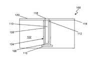
- a metal insulator metal (MIM) capacitor 100includes an insulative substrate 102 , in which a first cavity 104 may be formed.
- insulative substrate 102may be a BEOL interlevel dielectric layer and/or a BEOL intermetal dielectric layer in embodiments.
- a first metal layer 106may lie within cavity 104 , such as by being conformally deposited.
- An insulator layer 108may lie on first metal layer 106 , such as by being conformally deposited on first metal layer 106 , and a second metal layer 110 may lie on insulator layer 108 .
- second metal layer 110may be conformally deposited on insulator layer 108 and additional metal may fill any remaining cavity, though in embodiments second metal layer 110 simply fills any remaining cavity as shown in FIG. 1 .
- a dielectric cap 112shown as two insulative plugs in FIG. 1 , may be formed at ends of insulator layer 108 so that an additional layer of material may overlie an end of insulator layer 108 and be flush with a top surface 114 of insulative substrate 102 .
- a first contact 116 and a second contact 118may be formed so that they are each electrically connected to a respective one of first and second metal layers 106 , 110 . In embodiments, first contact 116 is deposited before first metal layer 106 is formed.
- a cover layer 120such as of an insulative material, may be formed on top surface 114 , and second contact 118 may be formed using a via through cover layer 120 .
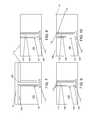
- a metal insulator metal (MIM) capacitor 200includes an insulative substrate 202 in which a first cavity 204 may be formed.
- insulative substrate 202may be a BEOL interlevel dielectric layer and/or a BEOL intermetal dielectric layer in embodiments.
- a first metal layer 206may lie within cavity 204 , such as by being conformally deposited.
- An insulator layer 208may lie on first metal layer 206 , such as by being conformally deposited on first metal layer 206 , and a second metal layer 210 may lie on insulator layer 208 .
- second metal layer 210may be conformally deposited on insulator layer 208 and additional metal may fill any remaining cavity, though in embodiments second metal layer 210 may simply fill any remaining cavity as shown in FIG. 2 .
- a dielectric cap 212shown as two insulative plugs in FIG. 2 , may be formed at ends of insulator layer 208 so that an additional layer of material may overlie an end of insulator layer 208 and be flush with a top surface 214 of insulative substrate 202 .
- a first contact 216 and a second contact 218may be formed so that they are each electrically connected to a respective one of first and second metal layers 206 , 210 .
- a cover layer 220such as of an insulative material, may be formed on top surface 214 , and both first contacts 216 and second contact 218 may be formed using vias through cover layer 220 .
- a metal insulator metal (MIM) capacitor 300includes an insulative substrate 302 in which a first cavity 304 may be formed.
- insulative substrate 302may be a BEOL interlevel dielectric layer and/or a BEOL intermetal dielectric layer in embodiments.
- a first metal layer 306may lie within cavity 304 , such as by being conformally deposited.
- An insulator layer 308may lie on first metal layer 306 , such as by being conformally deposited on first metal layer 306 , and a second metal layer 310 may lie on insulator layer 308 .
- second metal layer 310may be conformally deposited on insulator layer 308 and additional metal may fill any remaining cavity, though in embodiments second metal layer 310 simply fills any remaining cavity as shown in FIG. 3 .
- a dielectric cap 312shown as extensions of insulator layer 308 in FIG. 3 , may be formed at ends of insulator layer 308 so that an additional layer of material may overlie an end of first metal layer 306 and be flush with a top surface 314 of insulative substrate 302 .
- a first contact 316 and a second contact 318may be formed so that they are each electrically connected to a respective one of first and second metal layers 306 , 310 . In embodiments, first contact 316 is deposited before first metal layer 306 is formed.
- a cover layer 320such as of an insulative material, may be formed on top surface 314 , and second contact 318 may be formed using a via through cover layer 320 .
- a metal insulator metal (MIM) capacitor 400includes an insulative substrate 402 in which a first cavity 404 may be formed.
- insulative substrate 402may be a BEOL interlevel dielectric layer and/or a BEOL intermetal dielectric layer in embodiments.
- a first metal layer 406may lie within cavity 404 , such as by being conformally deposited.
- An insulator layer 408may lie on first metal layer 406 , such as by being conformally deposited on first metal layer 406 , and a second metal layer 410 may lie on insulator layer 408 .
- second metal layer 410may be conformally deposited on insulator layer 408 and additional metal may fill any remaining cavity, though in embodiments second metal layer 410 simply fills any remaining cavity as shown in FIG. 4 .
- a dielectric cap 412shown as extensions of insulator layer 408 in FIG. 4 , may be formed at ends of insulator layer 408 so that an additional layer of material may overlie an end of first metal layer 406 and be flush with a top surface 414 of insulative substrate 402 .
- a first contact 416 and a second contact 418may be formed so that they are each electrically connected to a respective one of first and second metal layers 406 , 410 . In embodiments, first contact 416 is deposited before first metal layer 406 is formed.
- a cover layer 420such as of an insulative material, may be formed on top surface 414 , and second contact 418 may be formed using a via through cover layer 420 .
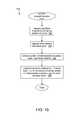
- FIG. 5An example of a method 500 of making a MIM capacitor such as the examples shown schematically in FIGS. 1-4 is seen in FIG. 5 .
- An insulative substratemay be provided (block 502 ), such as a BEOL interlevel dielectric layer and/or a BEOL intermetal dielectric layer in embodiments, and a first cavity may be formed (block 504 ).
- a diffusion barriermay be deposited on the surface(s) of the first cavity (block 506 ), such as to prevent bleed of ions from the MIM capacitor into the substrate and vice versa.
- a first contactmay be formed (block 508 ), such as by depositing conductive material in the closed end of first cavity 104 , 304 , 404 .
- a first metal layermay be deposited (block 510 ), and an insulator layer may be deposited (block 512 ).
- the deposition of the first metal layer and/or the insulator layermay be achieved using conformal deposition, such as chemical vapor deposition (CVD), physical vapor deposition (PVD), and/or any other suitable technique now known and/or later developed.
- a second metal layermay then be formed (block 514 ), and a dielectric cap may be formed (block 516 ).
- the second metal layerfills whatever cavity remains after depositing the insulator layer, but other embodiments produce a conformal second metal layer that leaves a portion of the first cavity that may be filled with additional conductive material.
- a second contactmay be formed (block 518 ), though in embodiments where the first contact is not in the closed end of the first cavity, both first and second contacts may be formed.
- the method 600may include forming cavities (block 602 ) and depositing dielectric material in the cavities (block 604 ). For example, a collar pattern and RIE technique may be employed, followed by deposition of insulative material in the resulting cavities. Cover layer 320 may then be deposited (block 606 ), and second contact 118 , 218 may be formed.
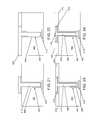
- FIGS. 7-10show stages of forming a MIM capacitor 100 as seen in FIG. 1 resulting from the application of methods 500 , 600 .
- a structuresuch as that shown in FIG. 7 may be produced.
- excess material on a surface 114 of substrate 102may be removed.
- CMPchemical-mechanical polishing
- any other suitable techniquemay be employed to remove excess portions of first metal layer 106 , insulator layer 108 , and second metal layer 110 , exposing surface 114 of substrate 102 , as seen, for example, in FIG. 8 .
- first metal layer 106 , insulator layer 108 , and second metal layer 110may be removed to form cavities in which dielectric cap 112 may be formed as seen in FIG. 9 .
- a collar pattern and RIE techniquemay be employed, followed by deposition of insulative material in the resulting cavities. If excess material results, it may be removed using any suitable technique, such as CMP, to yield ends of first metal layer 106 , insulator layer 108 , second metal layer 110 , and/or dielectric cap 112 that are flush with surface 114 of substrate 102 , again as seen in FIG. 9 .
- Cover layer 120may then be deposited, and a via may be formed so that second metal contact 118 may be deposited or otherwise formed in electrical contact with second metal layer 110 , as seen in FIGS. 1 and 10 .
- a diffusion barrieris included, a diffusion barrier is deposited after formation of first cavity 104 , preferably before formation of first contact 116 .
- first contact 116in the closed end of first cavity 104 .
- First contact 116may be formed later in the process, as will be seen below, though the structure and process may still closely resemble the example shown in FIGS. 7-10 .
- First metal layer 206 , insulator layer 208 , and second metal layer 210are deposited in first cavity 204 , yielding a structure such as that shown in FIG. 11 .
- Excess material on a surface 214 of substrate 202may be removed, such as by CMP or any other suitable technique, to expose surface 214 of substrate 202 , as seen, for example, in FIG. 12 .
- first metal layer 206 , insulator layer 208 , and second metal layer 210may be removed according to embodiments employing method 400 to form cavities in which dielectric cap 212 may be formed as seen in FIG. 13 .
- a collar pattern and RIE techniquemay be employed, followed by deposition of insulative material in the resulting cavities. If excess material results, it may be removed using any suitable technique, such as CMP, to yield ends of first metal layer 206 , insulator layer 208 , second metal layer 210 , and/or dielectric cap 212 that are flush with surface 214 of substrate 202 , again as seen in FIG. 13 .
- CMPany suitable technique
- cover layer 220may then be deposited, and vias may be formed to allow formation of first and/or second metal contacts 216 , 218 in electrical contact with respective first and second metal layers 206 , 210 .
- first and second contacts 216 , 218may be formed on a same end of first cavity 204 , which may allow easier access and/or enhance performance of MIM capacitor 200 .
- a diffusion barriermay be deposited after formation of first cavity 204 , such as before formation of first contact 216 .
- dielectric cap 112 , 212may be formed after deposition of first and second metal layers 106 , 110 and insulator layer 108 .
- dielectric cap 312may be formed with or by deposition of insulator layer 308 .
- An alternative method 700 of depositing an insulator layeris seen in FIG. 15 , with stages of manufacture shown in FIGS. 16-19 .
- Alternative method 500may include, after deposition of first metal layer 306 , depositing sacrificial material 322 in a remaining portion of first cavity 304 (block 702 ), as seen in FIG. 16 .
- CMP or another techniquemay be employed to make deposited materials flush with surface 314 of substrate 302 , and an intermediate insulative layer 305 may then be deposited (block 704 ) on surface 314 , again as seen in FIG. 16 .
- a portion of intermediate insulative layer 305 and sacrificial material 322may then be removed (block 706 ) so that ends of first metal layer 306 and a portion of surface 314 are exposed, as well as surfaces of first metal layer 306 in first cavity 304 and exposed edge surfaces of intermediate insulative layer 305 , as seen in FIG. 17 .
- Insulator layer 308may then be deposited (block 708 ), such as to cover the exposed portion of surface 314 , ends of first metal layer 306 , and edge surfaces of intermediate insulative layer 305 , as seen in FIGS. 18 and 19 . Deposition of insulator layer 308 in this configuration forms dielectric cap 312 across ends of first metal layer 306 , the exposed portion of surface 314 , and edge surfaces of intermediate insulative layer 305 . Second metal layer 310 may then be deposited, followed by deposition of cover layer 320 and formation of second contact 318 , as seen in FIG. 19 .
- FIG. 20schematically illustrates another method 800 of depositing an insulator layer that may yield a MIM capacitor 400 according to embodiments such as the example of FIG. 4 , with stages of manufacture shown schematically in FIGS. 21-24 .
- first metal layer 406may have been deposited so that portions of first metal layer 406 extend along surface 414 of substrate 402 .
- Sacrificial siliconmay be deposited in a remaining portion of first cavity 404 and to overlie the portions of first metal layer 406 extending along surface 414 (block 802 ), as seen in FIG. 21 .
- An intermediate insulative layer 405may then be deposited (block 804 ), and the sacrificial silicon may be removed (block 806 ) to expose first metal layer 406 .
- Insulative materialmay be deposited on first metal layer 406 (block 808 ) to form insulator layer 408 and dielectric cap 412 , as seen in FIGS. 23 and 24 .
- Second metal layer 410may then be formed, as well as cover layer 420 and second contact 418 , as seen in FIGS. 4 and 24 .
- dielectric cap 412includes portions of insulator layer 408 overlying surface 414 of substrate 404 .
- second metal layer 310 , 410 and/or fill metalforms a T shape in which a portion of second metal layer 310 , 410 is parallel to and/or overlies a portion of surface 314 , 414 of insulative substrate 302 , 402 , which surface 314 , 414 is at an open end of first cavity 304 , 404 . So arranging second metal layer 310 , 410 over first metal layer 306 , 406 , insulator layer 308 , 408 , and dielectric cap 312 , 412 enhances performance of a MIM capacitor according to embodiments.
- Constructing a MIM capacitor according to embodiments of the invention disclosed hereinmay yield a capacitor that requires less surface area on a substrate for a given capacitance than may be required by other MIM capacitors.
- a MIM capacitor according to embodimentsmay, for example, achieve a higher capacitance density than planar MIM capacitors, and inclusion of a dielectric cap according to embodiments may reduce damage done to insulative material of the MIM capacitor that might otherwise occur during CMP and/or other manufacturing stages and/or techniques.
- FIG. 25illustrates a block diagram of a general-purpose computer system which can be used to implement the circuit and circuit design structure described herein.
- the design structuremay be coded as a set of instructions on removable or hard media for use by general-purpose computer.
- FIG. 25is a schematic block diagram of a general-purpose computer for practicing the present invention.
- FIG. 25shows a computer system 900 , which has at least one microprocessor or central processing unit (CPU) 905 .
- CPUcentral processing unit
- CPU 905is interconnected via a system bus 920 to machine readable media 975 , which includes, for example, a random access memory (RAM) 910 , a read-only memory (ROM) 915 , a removable and/or program storage device 955 and a mass data and/or program storage device 950 .
- An input/output (I/O) adapter 930connects mass storage device 950 and removable storage device 955 to system bus 920 .
- a user interface 935connects a keyboard 965 and a mouse 960 to system bus 920
- a port adapter 925connects a data port 945 to system bus 920 and a display adapter 940 connect a display device 970 .
- ROM 915contains the basic operating system for computer system 900 .
- removable data and/or program storage device 955examples include magnetic media such as floppy drives, tape drives, portable flash drives, zip drives, and optical media such as CD ROM or DVD drives.
- mass data and/or program storage device 950examples include hard disk drives and non-volatile memory such as flash memory.
- other user input devicessuch as trackballs, writing tablets, pressure pads, microphones, light pens and position-sensing screen displays may be connected to user interface 935 .
- display device 970include cathode-ray tubes (CRT) and liquid crystal displays (LCD).
- a machine readable computer programmay be created by one of skill in the art and stored in computer system 900 or a data and/or any one or more of machine readable medium 975 to simplify the practicing of this invention.
- information for the computer program created to run the present inventionis loaded on the appropriate removable data and/or program storage device 955 , fed through data port 945 or entered using keyboard 965 .
- a usercontrols the program by manipulating functions performed by the computer program and providing other data inputs via any of the above mentioned data input means.
- Display device 970provides a means for the user to accurately control the computer program and perform the desired tasks described herein.
- FIG. 26shows a block diagram of an example design flow 1000 .
- Design flow 1000may vary depending on the type of IC being designed.
- a design flow 1000 for building an application specific IC (ASIC)may differ from a design flow 1000 for designing a standard component.
- Design structure 1020is preferably an input to a design process 1010 and may come from an IP provider, a core developer, or other design company or may be generated by the operator of the design flow, or from other sources.
- Design structure 1020comprises circuit or capacitor 100 , 200 , 300 , 400 in the form of schematics or HDL, a hardware-description language (e.g., Verilog, VHDL, C, etc.).
- Design structure 1020may be contained on one or more machine readable medium.
- design structure 1020may be a text file or a graphical representation of circuit or capacitor 100 , 200 , 300 , 400 .
- Design process 1010preferably synthesizes (or translates) circuit or capacitor 100 , 200 , 300 , 400 into a netlist 1080 , where netlist 1080 is, for example, a list of wires, transistors, logic gates, control circuits, I/O, models, etc., that describes the connections to other elements and circuits in an integrated circuit design and recorded on at least one of machine readable medium. This may be an iterative process in which netlist 1080 is re-synthesized one or more times depending on design specifications and parameters for the circuit.
- Design process 1010may include using a variety of inputs; for example, inputs from library elements 1030 which may house a set of commonly used elements, circuits, and devices, including models, layouts, and symbolic representations, for a given manufacturing technology (e.g., different technology nodes, 32 nm, 45 nm, 100 nm, etc.), design specifications 1040 , characterization data 1050 , verification data 1060 , design rules 1070 , and test data files 1085 (which may include test patterns and other testing information). Design process 1010 may further include, for example, standard circuit design processes such as timing analysis, verification, design rule checking, place and route operations, etc.
- standard circuit design processessuch as timing analysis, verification, design rule checking, place and route operations, etc.
- design process 1010preferably translates circuit or capacitor 100 , 200 , 300 , 400 , 300 , along with the rest of the integrated circuit design (if applicable), into a final design structure 1090 (e.g., information stored in a GDS storage medium).
- Final design structure 1090may comprise information such as, for example, test data files, design content files, manufacturing data, layout parameters, wires, levels of metal, vias, shapes, test data, data for routing through the manufacturing line, and any other data required by a semiconductor manufacturer to produce circuit or capacitor 100 , 200 , 300 , 400 , 300 .
- Final design structure 1080may then proceed to a stage 1085 where, for example, final design structure 1080 proceeds to tape-out, is released to manufacturing, is sent to another design house or is sent back to the customer.
Landscapes
- Semiconductor Integrated Circuits (AREA)
Abstract
Description
Claims (19)
Priority Applications (1)
| Application Number | Priority Date | Filing Date | Title |
|---|---|---|---|
| US13/233,752US9252204B2 (en) | 2011-09-15 | 2011-09-15 | Metal insulator metal (MIM) capacitor structure |
Applications Claiming Priority (1)
| Application Number | Priority Date | Filing Date | Title |
|---|---|---|---|
| US13/233,752US9252204B2 (en) | 2011-09-15 | 2011-09-15 | Metal insulator metal (MIM) capacitor structure |
Publications (2)
| Publication Number | Publication Date |
|---|---|
| US20130069199A1 US20130069199A1 (en) | 2013-03-21 |
| US9252204B2true US9252204B2 (en) | 2016-02-02 |
Family
ID=47879884
Family Applications (1)
| Application Number | Title | Priority Date | Filing Date |
|---|---|---|---|
| US13/233,752Expired - Fee RelatedUS9252204B2 (en) | 2011-09-15 | 2011-09-15 | Metal insulator metal (MIM) capacitor structure |
Country Status (1)
| Country | Link |
|---|---|
| US (1) | US9252204B2 (en) |
Cited By (2)
| Publication number | Priority date | Publication date | Assignee | Title |
|---|---|---|---|---|
| US12356638B2 (en) | 2021-12-06 | 2025-07-08 | International Business Machines Corporation | Metal-insulator-metal capacitor structure with enlarged capacitor area |
| US12388006B2 (en) | 2022-06-09 | 2025-08-12 | Globalfoundries Singapore Pte. Ltd. | Capacitor and airgap structure |
Families Citing this family (7)
| Publication number | Priority date | Publication date | Assignee | Title |
|---|---|---|---|---|
| CN103367329B (en)* | 2013-07-23 | 2016-03-30 | 上海华力微电子有限公司 | For testing the semiconductor structure of MIM capacitor |
| US10163792B2 (en)* | 2014-07-28 | 2018-12-25 | Qualcomm Incorporated | Semiconductor device having an airgap defined at least partially by a protective structure |
| US9960168B2 (en)* | 2014-12-24 | 2018-05-01 | Globalfoundries Inc. | Capacitor strap connection structure and fabrication method |
| US9425105B1 (en)* | 2015-09-15 | 2016-08-23 | International Business Machines Corporation | Semiconductor device including self-aligned gate structure and improved gate spacer topography |
| CN111668186B (en)* | 2020-06-08 | 2025-02-18 | 矽力杰半导体技术(杭州)有限公司 | Semiconductor device and method for manufacturing the same |
| US12094763B2 (en) | 2021-09-07 | 2024-09-17 | Globalfoundries Singapore Pte. Ltd. | Metal-insulator-metal capacitor (MIMCAP) and methods of forming the same |
| CN118231374A (en)* | 2022-12-21 | 2024-06-21 | 联华电子股份有限公司 | Metal-insulating layer-metal capacitor structure and manufacturing method thereof |
Citations (25)
| Publication number | Priority date | Publication date | Assignee | Title |
|---|---|---|---|---|
| US6341056B1 (en)* | 2000-05-17 | 2002-01-22 | Lsi Logic Corporation | Capacitor with multiple-component dielectric and method of fabricating same |
| US6362012B1 (en) | 2001-03-05 | 2002-03-26 | Taiwan Semiconductor Manufacturing Company | Structure of merged vertical capacitor inside spiral conductor for RF and mixed-signal applications |
| US6417535B1 (en) | 1998-12-23 | 2002-07-09 | Lsi Logic Corporation | Vertical interdigitated metal-insulator-metal capacitor for an integrated circuit |
| US6451667B1 (en) | 2000-12-21 | 2002-09-17 | Infineon Technologies Ag | Self-aligned double-sided vertical MIMcap |
| US6472721B2 (en) | 2000-07-24 | 2002-10-29 | Taiwan Semiconductor Manufacturing Company | Dual damascene interconnect structures that include radio frequency capacitors and inductors |
| US6528366B1 (en)* | 2001-03-01 | 2003-03-04 | Taiwan Semiconductor Manufacturing Company | Fabrication methods of vertical metal-insulator-metal (MIM) capacitor for advanced embedded DRAM applications |
| US6593185B1 (en) | 2002-05-17 | 2003-07-15 | United Microelectronics Corp. | Method of forming embedded capacitor structure applied to logic integrated circuit |
| US6624040B1 (en) | 2002-09-20 | 2003-09-23 | Chartered Semiconductor Manufacturing Ltd. | Self-integrated vertical MIM capacitor in the dual damascene process |
| US6706588B1 (en) | 2003-04-09 | 2004-03-16 | Infineon Technologies Ag | Method of fabricating an integrated circuit having embedded vertical capacitor |
| US6709918B1 (en) | 2002-12-02 | 2004-03-23 | Chartered Semiconductor Manufacturing Ltd. | Method for making a metal-insulator-metal (MIM) capacitor and metal resistor for a copper back-end-of-line (BEOL) technology |
| US6876027B2 (en) | 2003-04-10 | 2005-04-05 | Taiwan Semiconductor Manufacturing Company | Method of forming a metal-insulator-metal capacitor structure in a copper damascene process sequence |
| US6891219B2 (en) | 2000-11-27 | 2005-05-10 | Lsi Logic Corporation | Metal-insulator-metal capacitor formed by damascene processes between metal interconnect layers and method of forming same |
| US20050275005A1 (en)* | 2004-06-11 | 2005-12-15 | Seung-Man Choi | Metal-insulator-metal (MIM) capacitor and method of fabricating the same |
| US7078759B2 (en)* | 2003-05-22 | 2006-07-18 | Renesas Technology Corp. | Semiconductor device manufacturing method and semiconductor device |
| US7091562B2 (en) | 2004-08-13 | 2006-08-15 | Himax Technologies, Inc. | CMOS power sensor |
| US7091542B1 (en) | 2005-01-28 | 2006-08-15 | International Business Machines Corporation | Method of forming a MIM capacitor for Cu BEOL application |
| US7095073B2 (en) | 2002-11-02 | 2006-08-22 | Chartered Semiconductor Manufacturing Ltd. | High K artificial lattices for capacitor applications to use in Cu or Al BEOL |
| US7378719B2 (en) | 2000-12-20 | 2008-05-27 | Micron Technology, Inc. | Low leakage MIM capacitor |
| US7383475B1 (en)* | 2007-10-29 | 2008-06-03 | International Business Machines Corporation | Design structure for memory array repair where repair logic cannot operate at same operating condition as array |
| US7416953B2 (en) | 2005-10-31 | 2008-08-26 | Taiwan Semiconductor Manufacturing Co., Ltd. | Vertical MIM capacitors and method of fabricating the same |
| US20090090998A1 (en)* | 2007-10-08 | 2009-04-09 | Je-Sik Woo | Semiconductor device and manufacturing method thereof |
| US7638830B2 (en) | 2003-10-28 | 2009-12-29 | Taiwan Semiconductor Manufacturing Co., Ltd. | Vertical metal-insulator-metal (MIM) capacitors |
| US7682896B2 (en) | 2005-09-09 | 2010-03-23 | International Business Machines Corporation | Trench metal-insulator-metal (MIM) capacitors integrated with middle-of-line metal contacts, and method of fabricating same |
| US20100127316A1 (en)* | 2008-11-25 | 2010-05-27 | Kuo-Chi Tu | Structure for protecting metal-insulator-metal capacitor in memory device from charge damage |
| US7741188B2 (en) | 2008-03-24 | 2010-06-22 | International Business Machines Corporation | Deep trench (DT) metal-insulator-metal (MIM) capacitor |
- 2011
- 2011-09-15USUS13/233,752patent/US9252204B2/ennot_activeExpired - Fee Related
Patent Citations (25)
| Publication number | Priority date | Publication date | Assignee | Title |
|---|---|---|---|---|
| US6417535B1 (en) | 1998-12-23 | 2002-07-09 | Lsi Logic Corporation | Vertical interdigitated metal-insulator-metal capacitor for an integrated circuit |
| US6341056B1 (en)* | 2000-05-17 | 2002-01-22 | Lsi Logic Corporation | Capacitor with multiple-component dielectric and method of fabricating same |
| US6472721B2 (en) | 2000-07-24 | 2002-10-29 | Taiwan Semiconductor Manufacturing Company | Dual damascene interconnect structures that include radio frequency capacitors and inductors |
| US6891219B2 (en) | 2000-11-27 | 2005-05-10 | Lsi Logic Corporation | Metal-insulator-metal capacitor formed by damascene processes between metal interconnect layers and method of forming same |
| US7378719B2 (en) | 2000-12-20 | 2008-05-27 | Micron Technology, Inc. | Low leakage MIM capacitor |
| US6451667B1 (en) | 2000-12-21 | 2002-09-17 | Infineon Technologies Ag | Self-aligned double-sided vertical MIMcap |
| US6528366B1 (en)* | 2001-03-01 | 2003-03-04 | Taiwan Semiconductor Manufacturing Company | Fabrication methods of vertical metal-insulator-metal (MIM) capacitor for advanced embedded DRAM applications |
| US6362012B1 (en) | 2001-03-05 | 2002-03-26 | Taiwan Semiconductor Manufacturing Company | Structure of merged vertical capacitor inside spiral conductor for RF and mixed-signal applications |
| US6593185B1 (en) | 2002-05-17 | 2003-07-15 | United Microelectronics Corp. | Method of forming embedded capacitor structure applied to logic integrated circuit |
| US6624040B1 (en) | 2002-09-20 | 2003-09-23 | Chartered Semiconductor Manufacturing Ltd. | Self-integrated vertical MIM capacitor in the dual damascene process |
| US7095073B2 (en) | 2002-11-02 | 2006-08-22 | Chartered Semiconductor Manufacturing Ltd. | High K artificial lattices for capacitor applications to use in Cu or Al BEOL |
| US6709918B1 (en) | 2002-12-02 | 2004-03-23 | Chartered Semiconductor Manufacturing Ltd. | Method for making a metal-insulator-metal (MIM) capacitor and metal resistor for a copper back-end-of-line (BEOL) technology |
| US6706588B1 (en) | 2003-04-09 | 2004-03-16 | Infineon Technologies Ag | Method of fabricating an integrated circuit having embedded vertical capacitor |
| US6876027B2 (en) | 2003-04-10 | 2005-04-05 | Taiwan Semiconductor Manufacturing Company | Method of forming a metal-insulator-metal capacitor structure in a copper damascene process sequence |
| US7078759B2 (en)* | 2003-05-22 | 2006-07-18 | Renesas Technology Corp. | Semiconductor device manufacturing method and semiconductor device |
| US7638830B2 (en) | 2003-10-28 | 2009-12-29 | Taiwan Semiconductor Manufacturing Co., Ltd. | Vertical metal-insulator-metal (MIM) capacitors |
| US20050275005A1 (en)* | 2004-06-11 | 2005-12-15 | Seung-Man Choi | Metal-insulator-metal (MIM) capacitor and method of fabricating the same |
| US7091562B2 (en) | 2004-08-13 | 2006-08-15 | Himax Technologies, Inc. | CMOS power sensor |
| US7091542B1 (en) | 2005-01-28 | 2006-08-15 | International Business Machines Corporation | Method of forming a MIM capacitor for Cu BEOL application |
| US7682896B2 (en) | 2005-09-09 | 2010-03-23 | International Business Machines Corporation | Trench metal-insulator-metal (MIM) capacitors integrated with middle-of-line metal contacts, and method of fabricating same |
| US7416953B2 (en) | 2005-10-31 | 2008-08-26 | Taiwan Semiconductor Manufacturing Co., Ltd. | Vertical MIM capacitors and method of fabricating the same |
| US20090090998A1 (en)* | 2007-10-08 | 2009-04-09 | Je-Sik Woo | Semiconductor device and manufacturing method thereof |
| US7383475B1 (en)* | 2007-10-29 | 2008-06-03 | International Business Machines Corporation | Design structure for memory array repair where repair logic cannot operate at same operating condition as array |
| US7741188B2 (en) | 2008-03-24 | 2010-06-22 | International Business Machines Corporation | Deep trench (DT) metal-insulator-metal (MIM) capacitor |
| US20100127316A1 (en)* | 2008-11-25 | 2010-05-27 | Kuo-Chi Tu | Structure for protecting metal-insulator-metal capacitor in memory device from charge damage |
Cited By (2)
| Publication number | Priority date | Publication date | Assignee | Title |
|---|---|---|---|---|
| US12356638B2 (en) | 2021-12-06 | 2025-07-08 | International Business Machines Corporation | Metal-insulator-metal capacitor structure with enlarged capacitor area |
| US12388006B2 (en) | 2022-06-09 | 2025-08-12 | Globalfoundries Singapore Pte. Ltd. | Capacitor and airgap structure |
Also Published As
| Publication number | Publication date |
|---|---|
| US20130069199A1 (en) | 2013-03-21 |
Similar Documents
| Publication | Publication Date | Title |
|---|---|---|
| US9252204B2 (en) | Metal insulator metal (MIM) capacitor structure | |
| EP2243162B1 (en) | On-chip integrated voltage-controlled variable inductor | |
| TWI497329B (en) | Modeling system, computer modeling method, and non-transitory machine readable storage medium | |
| US8842412B2 (en) | Tapered via and MIM capacitor | |
| US9424992B2 (en) | Complimentary metal-insulator-metal (MIM) capacitors and method of manufacture | |
| CN109698166A (en) | The method for forming the gate contacting structure of transistor unit, cross-coupling contact structures | |
| US8901710B2 (en) | Interdigitated capacitors with a zero quadratic voltage coefficient of capacitance or zero linear temperature coefficient of capacitance | |
| JP2015502074A (en) | Manufacturing method, structure, and design structure of integrated semiconductor device with amorphous silicon beam | |
| JP2018525825A (en) | Metallization process for memory devices | |
| US9018754B2 (en) | Heat dissipative electrical isolation/insulation structure for semiconductor devices and method of making | |
| US9436792B2 (en) | Method of designing layout of integrated circuit and method of manufacturing integrated circuit | |
| US8980720B2 (en) | eFUSE and method of fabrication | |
| US8836050B2 (en) | Structure and method to fabricate a body contact | |
| TWI513093B (en) | Vertical coplanar waveguide with tunable characteristic impedance, design structure and method of fabricating the same | |
| DE102012221818B4 (en) | STRUCTURES AND DESIGN STRUCTURES OF MICROELECTROMECHANICAL SYSTEMS (MEMS) | |
| CN105895617B (en) | Semiconductor devices, layout designs and the method being used for producing the semiconductor devices | |
| US8835250B2 (en) | FinFET trench circuit | |
| US20170286588A1 (en) | Full-Chip Assessment Of Time-Dependent Dielectric Breakdown | |
| US9231046B2 (en) | Capacitor using barrier layer metallurgy | |
| US20130087841A1 (en) | Plated structures | |
| US8959009B1 (en) | Modeling dielectric coating of conductor | |
| US9064786B2 (en) | Dual three-dimensional (3D) resistor and methods of forming | |
| TWI523204B (en) | Ferroelectric capacitor module, manufacturing method and design structure |
Legal Events
| Date | Code | Title | Description |
|---|---|---|---|
| AS | Assignment | Owner name:INTERNATIONAL BUSINESS MACHINES CORPORATION, NEW Y Free format text:ASSIGNMENT OF ASSIGNORS INTEREST;ASSIGNORS:ADKISSON, JAMES W.;CANDRA, PANGLIJEN;OGG, KEVIN N.;AND OTHERS;REEL/FRAME:026933/0781 Effective date:20110909 | |
| AS | Assignment | Owner name:GLOBALFOUNDRIES U.S. 2 LLC, NEW YORK Free format text:ASSIGNMENT OF ASSIGNORS INTEREST;ASSIGNOR:INTERNATIONAL BUSINESS MACHINES CORPORATION;REEL/FRAME:036550/0001 Effective date:20150629 | |
| AS | Assignment | Owner name:GLOBALFOUNDRIES INC., CAYMAN ISLANDS Free format text:ASSIGNMENT OF ASSIGNORS INTEREST;ASSIGNORS:GLOBALFOUNDRIES U.S. 2 LLC;GLOBALFOUNDRIES U.S. INC.;REEL/FRAME:036779/0001 Effective date:20150910 | |
| FEPP | Fee payment procedure | Free format text:PAYER NUMBER DE-ASSIGNED (ORIGINAL EVENT CODE: RMPN); ENTITY STATUS OF PATENT OWNER: LARGE ENTITY Free format text:PAYOR NUMBER ASSIGNED (ORIGINAL EVENT CODE: ASPN); ENTITY STATUS OF PATENT OWNER: LARGE ENTITY | |
| FEPP | Fee payment procedure | Free format text:PAYER NUMBER DE-ASSIGNED (ORIGINAL EVENT CODE: RMPN); ENTITY STATUS OF PATENT OWNER: LARGE ENTITY Free format text:PAYOR NUMBER ASSIGNED (ORIGINAL EVENT CODE: ASPN); ENTITY STATUS OF PATENT OWNER: LARGE ENTITY | |
| STCF | Information on status: patent grant | Free format text:PATENTED CASE | |
| AS | Assignment | Owner name:WILMINGTON TRUST, NATIONAL ASSOCIATION, DELAWARE Free format text:SECURITY AGREEMENT;ASSIGNOR:GLOBALFOUNDRIES INC.;REEL/FRAME:049490/0001 Effective date:20181127 | |
| FEPP | Fee payment procedure | Free format text:MAINTENANCE FEE REMINDER MAILED (ORIGINAL EVENT CODE: REM.); ENTITY STATUS OF PATENT OWNER: LARGE ENTITY | |
| LAPS | Lapse for failure to pay maintenance fees | Free format text:PATENT EXPIRED FOR FAILURE TO PAY MAINTENANCE FEES (ORIGINAL EVENT CODE: EXP.); ENTITY STATUS OF PATENT OWNER: LARGE ENTITY | |
| STCH | Information on status: patent discontinuation | Free format text:PATENT EXPIRED DUE TO NONPAYMENT OF MAINTENANCE FEES UNDER 37 CFR 1.362 | |
| FP | Lapsed due to failure to pay maintenance fee | Effective date:20200202 | |
| AS | Assignment | Owner name:GLOBALFOUNDRIES INC., CAYMAN ISLANDS Free format text:RELEASE BY SECURED PARTY;ASSIGNOR:WILMINGTON TRUST, NATIONAL ASSOCIATION;REEL/FRAME:054636/0001 Effective date:20201117 | |
| AS | Assignment | Owner name:GLOBALFOUNDRIES U.S. INC., NEW YORK Free format text:RELEASE BY SECURED PARTY;ASSIGNOR:WILMINGTON TRUST, NATIONAL ASSOCIATION;REEL/FRAME:056987/0001 Effective date:20201117 |