US9246231B2 - High-gain wideband antenna apparatus - Google Patents
High-gain wideband antenna apparatusDownload PDFInfo
- Publication number
- US9246231B2 US9246231B2US13/746,384US201313746384AUS9246231B2US 9246231 B2US9246231 B2US 9246231B2US 201313746384 AUS201313746384 AUS 201313746384AUS 9246231 B2US9246231 B2US 9246231B2
- Authority
- US
- United States
- Prior art keywords
- conductor patterns
- antenna apparatus
- wideband antenna
- gain wideband
- gain
- Prior art date
- Legal status (The legal status is an assumption and is not a legal conclusion. Google has not performed a legal analysis and makes no representation as to the accuracy of the status listed.)
- Expired - Fee Related, expires
Links
Images


Classifications
- H—ELECTRICITY
- H01—ELECTRIC ELEMENTS
- H01Q—ANTENNAS, i.e. RADIO AERIALS
- H01Q1/00—Details of, or arrangements associated with, antennas
- H01Q1/36—Structural form of radiating elements, e.g. cone, spiral, umbrella; Particular materials used therewith
- H01Q1/38—Structural form of radiating elements, e.g. cone, spiral, umbrella; Particular materials used therewith formed by a conductive layer on an insulating support
- H—ELECTRICITY
- H01—ELECTRIC ELEMENTS
- H01Q—ANTENNAS, i.e. RADIO AERIALS
- H01Q15/00—Devices for reflection, refraction, diffraction or polarisation of waves radiated from an antenna, e.g. quasi-optical devices
- H01Q15/02—Refracting or diffracting devices, e.g. lens, prism
- H—ELECTRICITY
- H01—ELECTRIC ELEMENTS
- H01Q—ANTENNAS, i.e. RADIO AERIALS
- H01Q1/00—Details of, or arrangements associated with, antennas
- H01Q1/42—Housings not intimately mechanically associated with radiating elements, e.g. radome
- H01Q1/425—Housings not intimately mechanically associated with radiating elements, e.g. radome comprising a metallic grid
- H—ELECTRICITY
- H01—ELECTRIC ELEMENTS
- H01Q—ANTENNAS, i.e. RADIO AERIALS
- H01Q1/00—Details of, or arrangements associated with, antennas
- H01Q1/44—Details of, or arrangements associated with, antennas using equipment having another main function to serve additionally as an antenna, e.g. means for giving an antenna an aesthetic aspect
- H01Q1/46—Electric supply lines or communication lines
- H—ELECTRICITY
- H01—ELECTRIC ELEMENTS
- H01Q—ANTENNAS, i.e. RADIO AERIALS
- H01Q15/00—Devices for reflection, refraction, diffraction or polarisation of waves radiated from an antenna, e.g. quasi-optical devices
- H01Q15/0006—Devices acting selectively as reflecting surface, as diffracting or as refracting device, e.g. frequency filtering or angular spatial filtering devices
- H01Q15/0013—Devices acting selectively as reflecting surface, as diffracting or as refracting device, e.g. frequency filtering or angular spatial filtering devices said selective devices working as frequency-selective reflecting surfaces, e.g. FSS, dichroic plates, surfaces being partly transmissive and reflective
- H—ELECTRICITY
- H01—ELECTRIC ELEMENTS
- H01Q—ANTENNAS, i.e. RADIO AERIALS
- H01Q15/00—Devices for reflection, refraction, diffraction or polarisation of waves radiated from an antenna, e.g. quasi-optical devices
- H01Q15/0006—Devices acting selectively as reflecting surface, as diffracting or as refracting device, e.g. frequency filtering or angular spatial filtering devices
- H01Q15/0053—Selective devices used as spatial filter or angular sidelobe filter
- H—ELECTRICITY
- H01—ELECTRIC ELEMENTS
- H01Q—ANTENNAS, i.e. RADIO AERIALS
- H01Q5/00—Arrangements for simultaneous operation of antennas on two or more different wavebands, e.g. dual-band or multi-band arrangements
Definitions
- Exemplary embodiments of the present inventionrelates to a high-gain wideband antenna apparatus, and more particularly, to a high-gain wideband antenna apparatus capable of controlling a phase and a magnitude of a reflection coefficient by including a cover in which conductor patterns having a specific shape are arranged on both surfaces of a dielectric material.
- an antennawhich is an essential apparatus for transmitting and receiving a signal in a wireless communication system, is resonated with an electromagnetic wave of a specific frequency to transmit and receive an electromagnetic signal of a corresponding frequency.
- the Fabry-Perot resonator type antennacan improve the gain of the antenna, but has a too narrow bandwidth and thus, cannot be easily applied for transmission and reception of a wideband signal.
- An embodiment of the present inventionis directed to a high-gain wideband antenna apparatus capable of increasing a gain and a bandwidth of an antenna by controlling a phase and a magnitude of a reflection coefficient by arranging conductor patterns having a specific shape on both surfaces of a dielectric material.
- an embodiment of the present inventionis directed to a high-gain wideband antenna apparatus having a high front back ratio by mounting metal wall surfaces around an antenna.
- An embodiment of the present inventionrelates to a high-gain wideband antenna apparatus, including: a feeding antenna configured to radiate a signal; a cover configured to be disposed on a front surface of the feeding antenna based on a radiation direction of the signal and including a conductor pattern formed in a specific shape; and a ground surface configured to be disposed on a rear surface of the feeding antenna based on the radiation direction of the signal.
- the conductor patternsmay be formed in different shapes on top and bottom surfaces of a dielectric substrate configuring the cover.
- the conductor patternsmay be formed by repeatedly arranging preset unit cells.
- the conductor patternsmay be formed by non-uniformly arranging the sizes of the unit cells.
- the high-gain wideband antenna apparatusmay further include: metal wall surfaces disposed at sides of the feeding antenna based on a radiation direction of the signal.
- Another embodiment of the present inventionrelates to a high-gain wideband antenna apparatus, including: a feeding antenna configured to radiate a signal; and covers each disposed on front and back surfaces of the feeding antenna based on a radiation direction of the signal and each including conductor patterns formed in a specific shape.
- An embodiment of the present inventionrelates to a high-gain wideband antenna apparatus, including: a cylindrical cover configured to include conductor patterns formed in a specific shape; and a feeding antenna configured to be disposed in the cylindrical cover and radiate a signal toward the conductor patterns.
- the conductor patternsmay be each formed in different shapes on inner and outer surfaces of a cylindrical dielectric substrate configuring the cover.
- An embodiment of the present inventionrelates to a high-gain wideband antenna apparatus, including: a cylindrical cover configured to include conductor patterns formed in a specific shape; a plurality of feeding antennas configured to be each disposed in a plurality of areas partitioned in the cover to radiate a signal toward the conductor patterns; and a ground surface configured to be positioned at a central area common to the plurality of areas.
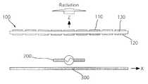
- FIG. 1is a diagram illustrating a structure of a high-gain wideband antenna apparatus in accordance with a first embodiment of the present invention
- FIG. 2is a side view illustrating a cover of the high-gain wideband antenna apparatus in accordance with the first embodiment of the present invention
- FIGS. 3A and 3Bare exemplified diagrams of unit cells configuring conductor patterns on both surfaces of the cover of the high-gain wideband antenna apparatus in accordance with the first embodiment of the present invention
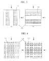
- FIG. 4is an exemplified diagram in which the conductor patterns are uniformly arranged on both surfaces of the cover of the high-gain wideband antenna apparatus in accordance with the first embodiment of the present invention
- FIG. 5is an exemplified diagram in which the conductor patterns are non-uniformly arranged on both surfaces of the cover of the high-gain wideband antenna apparatus in accordance with the first embodiment of the present invention
- FIGS. 6A and 6Bare various exemplified diagrams of the unit cells configuring the conductor patterns on both surfaces of the cover of the high-gain wideband antenna apparatus in accordance with the first embodiment of the present invention
- FIG. 7is a graph illustrating reflection characteristics when a plane wave is incident to the cover of the high-gain wideband antenna apparatus in accordance with the first embodiment of the present invention.
- FIG. 8is a diagram illustrating a structure of a high-gain wideband antenna apparatus in accordance with a second embodiment of the present invention.
- FIG. 9is a diagram illustrating a structure of a high-gain wideband antenna apparatus in accordance with a third embodiment of the present invention.
- FIG. 10is a graph illustrating a change in an antenna gain when metal wall surfaces are mounted as illustrated in FIG. 9 ;
- FIG. 11is a graph illustrating a change in an antenna front back ratio when the metal wall surfaces are mounted as illustrated in FIG. 9 ;
- FIG. 12is a diagram illustrating a structure of a high-gain wideband antenna apparatus in accordance with a third embodiment of the present invention.
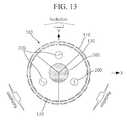
- FIG. 13is a diagram illustrating a structure of a high-gain wideband antenna apparatus in accordance with a fifth embodiment of the present invention.
- FIG. 1is a diagram illustrating a structure of a high-gain wideband antenna apparatus in accordance with a first embodiment of the present invention.
- a high-gain wideband antenna apparatusin accordance with a first embodiment of the present invention includes a cover 100 , a feeding antenna 200 , and a ground surface 300 .
- the high-gain wideband antenna apparatus in accordance with the embodiment of the present inventionmay further include metal wall surfaces 400 that are disposed at sides of the feeding antenna 200 based on a radiation direction of a signal so as to improve a front back ration (FBF) of an antenna.
- FFBfront back ration
- FIG. 2is a side view illustrating a cover of the high-gain wideband antenna apparatus in accordance with the first embodiment of the present invention
- FIG. 3A and 3Bare exemplified diagrams of unit cells configuring conductor patterns on both surfaces of the cover of the high-gain wideband antenna apparatus in accordance with the first embodiment of the present invention.
- FIG. 4is an exemplified diagram in which the conductor patterns are uniformly arranged on both surfaces of the cover of the high-gain wideband antenna apparatus in accordance with the first embodiment of the present invention
- FIG. 5is an exemplified diagram in which the conductor patterns are non-uniformly arranged on both surfaces of the cover of the high-gain wideband antenna apparatus in accordance with the first embodiment of the present invention.
- FIGS. 6A and 6Bare various exemplified diagrams of the unit cells configuring the conductor patterns on both surfaces of the cover of the high-gain wideband antenna apparatus in accordance with the first embodiment of the present invention.
- the cover 100includes a dielectric substrate 130 formed of a general dielectric material and conductor patterns 110 and 120 that are formed on top and bottom surface of the dielectric substrate 130 .
- the conductive patterns 110 and 120include a top conductor pattern 110 that is formed on a top surface of the dielectric substrate 130 and a bottom conductor pattern 120 that is formed on a bottom surface of the dielectric substrate 130 .
- the conductive patterns 110 and 120may be formed by repeatedly arranging unit cells having a preset specific shape in x and y-axis directions, wherein the top conductor pattern 110 and the bottom conductor pattern 120 may be formed in different shapes.
- the top conductor pattern 110may be formed by repeatedly arranging the unit cells having a shape illustrated in FIG. 3A in the x and y-axis directions and the bottom conductor pattern 120 may be formed by repeatedly arranging the unit cells having a shape illustrated in FIG. 3B in the x and y-axis directions.
- the top conductor pattern 110 and the bottom conductor pattern 120may be uniformly formed by making the size of the unit cells configuring each pattern equal to each other.
- the top conductor pattern 110 and the bottom conductor pattern 120may also be uniformly formed by using the unit cells of different sizes.
- the case in which the conductor patterns 110 and 120 of the cover 100 are non-uniformly formedexhibits more excellent performance than the case in which the conductor patterns 110 and 120 of the cover 100 are uniformly formed, which can be confirmed in FIG. 10 to be described below.
- FIGS. 2 to 5illustrates, for example, when the shape of the unit cells configuring the conductor patterns 110 and 120 is a rectangular patch shape in an x-axis direction or a y-axis direction, but the shape or the size of the unit cell may be variously selected according to designer's intention, system specification, values such as the magnitude or the phase of the reflection coefficient to be generated, and the like.
- the unit cells configuring the conductor patterns 110 and 120 of the cover 100are implemented in various shapes as illustrated in FIGS. 6A and 6B and thus, the magnitude, phase, or bandwidth characteristics of the reflection coefficient can be appropriately controlled.
- FIG. 7is a graph illustrating reflection characteristics when a plane wave is incident to the cover of the high-gain wideband antenna apparatus in accordance with the first embodiment of the present invention.
- a slope of the reflection coefficienthas a negative value over the overall frequency band and has a positive value in the vicinity of the operating frequency.
- the gainmay be slightly smaller than the case in which the reflective coefficient is 1 but the wideband characteristics may be provided together with a relatively high gain.
- a distance between two conductor patterns 110 and 111 that are formed on the top and bottom surfaces of the dielectric substrate 130 of the cover 100is set to be a thickness of about 1/100 of a wavelength.
- the thickness of the dielectric substrate 130may be implemented thicker or thinner according to the width of the targeted frequency band for implementing the wideband or the targeted magnitude and phase of the reflection coefficient.
- the magnitude and phase, bandwidth characteristics, frequency indicating the characteristics, and the like, of the reflection coefficientcan be controlled by appropriately selecting the shape or the size of the conductor patterns 110 and 120 formed on the top and bottom surfaces of the dielectric substrate 130 and the thickness of the dielectric substrate 130 .
- the magnitude and phase, bandwidth characteristics, frequency indicating the characteristics, and the like, of the reflection coefficientmay also be controlled by appropriately selecting a permittivity of the dielectric substrate 130 .
- the feeding antenna 200which is an antennal radiating a signal, may include various antennas such as a patch antenna, a dipole antenna, a slot antenna, a waveguide antenna, and the like, that can feed a signal.
- the above-mentioned cover 100is disposed a front surface of the feeding antenna based on a radiation direction of a signal radiated from the feeding antenna 200 and the signal radiated from the feeding antenna 200 is radiated toward the conductor patterns 110 and 120 of the cover 100 .
- the ground surface 300is disposed on a back surface of the feeding antenna 200 based on the radiation direction of the signal radiated from the feeding antenna 200 to ground the feeding antenna 200 .
- FIG. 8is a diagram illustrating a structure of a high-gain wideband antenna apparatus in accordance with a second embodiment of the present invention.
- the first embodiment of the present invention as described abovedescribes, for example, when the high-gain wideband antenna apparatus includes the ground surface 300 disposed on the back surface of the feeding antenna 200 based on the radiation direction of the signal.
- the high-gain wideband antenna apparatus in accordance with the embodiment of the present inventionmay be implemented to include the extra cover 100 instead of the ground surface 300 .
- the high-gain wideband antenna apparatusin accordance with the embodiment of the present invention may include a plurality of covers 100 that includes the conductor patterns 110 and 120 formed on the top and bottom surfaces of the dielectric substrate 130 and the feeding antenna 200 that is disposed between the plurality of covers 100 to radiate the signal toward the plurality of conductor patterns 110 and 120 provided on the plurality of covers 100 .
- FIG. 9is a diagram illustrating a structure of a high-gain wideband antenna apparatus in accordance with a third embodiment of the present invention
- FIG. 10is a graph illustrating a change in an antenna gain when metal wall surfaces are mounted as illustrated in FIG. 9
- FIG. 11is a graph illustrating a change in an antenna front back ratio when the metal wall surfaces are mounted as illustrated in FIG. 9 .
- the high-gain wideband antennal apparatus in accordance with the present inventionmay further include metal surfaces 400 that are disposed at the sides of the feeding antenna 200 based on the radiation direction of the signal as illustrated in FIG. 9 .
- the case in which the conductor patterns 110 and 120 of the cover 100 are uniformly arrangedexhibits more excellent wideband characteristics than the case in which the conductor patterns 110 and 120 of the cover 100 are non-uniformly arranged and the gain of the antenna is improved when the metal surfaces 400 are mounted.
- the front back ratiois improved when the metal surfaces 400 are disposed.
- the metal wall surfaces 400are mounted at the left and right sides of the feeding antenna 200 , thereby improving the gain and front back ratio of the antenna.
- FIG. 12is a diagram illustrating a structure of a high-gain wideband antenna apparatus in accordance with a third embodiment of the present invention
- FIG. 13is a diagram illustrating a structure of a high-gain wideband antenna apparatus in accordance with a fifth embodiment of the present invention.
- the first, second, and third embodiments of the present invention as described abovedescribe, for example, the case in which the cover 100 may be implemented as a plane shape, but the cover 100 may also be implemented in a cylindrical shape.
- the high-gain wideband antenna apparatus in accordance with the present inventionmay include the cover 100 including the conductive patterns 110 and 120 that are formed on the inner and outer surfaces of the cylindrical dielectric substrate 130 and one feeding antenna 200 that is disposed in the cover 100 to radiate the signal toward the conductive patterns 110 and 120 provided on the cover 100 .
- the high-gain wideband apparatus in accordance with the present inventionmay be implemented as an antenna having a sector shape by including the cover 100 including the conductor patterns 110 and 120 that are formed in the inner and outer surfaces of the cylindrical dielectric substrate 130 , the plurality of feeding antennas 200 each disposed in the plurality of areas partitioned in the cover 100 , and the ground surface 300 that is disposed in a central area common to the plurality of areas to ground the feeding antennas 200 .
- the cover 100is formed in a spherical shape (ball shape) and may be applied to the antenna apparatus.
- the conductor patternsare appropriately configured on both surfaces of the dielectric material to increase the gain and bandwidth of the antenna by controlling the phase of the reflection coefficient in the specific frequency band.
- the conductor patternscan be appropriately configured on both surfaces of the dielectric material in the antenna using the Fabry-Perot resonator to control the phase of the reflection coefficient in the specific frequency band, thereby increasing the gain and bandwidth of the antenna.
- the resonance conditions of the Fabry-Perot resonatorcan be satisfied even in the wide frequency band, thereby obtaining the high gain in the relatively wide frequency band.
- the bandwidth of the antennacan be more extended by uniformly configuring the size of the conductive patterns and the front back ration of the antenna can be improved by additionally mounting the metal wall surfaces at the sides of the feeding antenna.
Landscapes
- Waveguide Aerials (AREA)
- Aerials With Secondary Devices (AREA)
- Details Of Aerials (AREA)
Abstract
Description
The present application claims priority under 35 U.S.C 119(a) to Korean Application No. 10-2012-0019956, filed on Feb. 27, 2012, in the Korean Intellectual Property Office, which is incorporated herein by reference in its entirety set forth in full.
Exemplary embodiments of the present invention relates to a high-gain wideband antenna apparatus, and more particularly, to a high-gain wideband antenna apparatus capable of controlling a phase and a magnitude of a reflection coefficient by including a cover in which conductor patterns having a specific shape are arranged on both surfaces of a dielectric material.
Generally, an antenna, which is an essential apparatus for transmitting and receiving a signal in a wireless communication system, is resonated with an electromagnetic wave of a specific frequency to transmit and receive an electromagnetic signal of a corresponding frequency.
Recently, with the rapid development of the wireless communication system, a use of the antenna has been diversified. Further, various methods for improving a gain and characteristics of the antenna have been proposed.
As a method for improving the gain of the antenna, a method for improving the gain of the antenna while an electromagnetic wave from the antenna being resonated in a resonator by disposing a feeding apparatus of the antenna in a Fabry-Perot resonator has been proposed.
The Fabry-Perot resonator type antenna can improve the gain of the antenna, but has a too narrow bandwidth and thus, cannot be easily applied for transmission and reception of a wideband signal.
As the related art, there is US Patent Laid-Open No. 2007/0200788 (Publication in Aug. 30, 2007: Antenna Unit Having A Single Antenna Element And A Periodic Structure Upper Plate).
The above-mentioned technical configuration is a background art for helping understanding of the present invention and does not mean related arts well known in a technical field to which the present invention pertains.
An embodiment of the present invention is directed to a high-gain wideband antenna apparatus capable of increasing a gain and a bandwidth of an antenna by controlling a phase and a magnitude of a reflection coefficient by arranging conductor patterns having a specific shape on both surfaces of a dielectric material.
In addition, an embodiment of the present invention is directed to a high-gain wideband antenna apparatus having a high front back ratio by mounting metal wall surfaces around an antenna.
An embodiment of the present invention relates to a high-gain wideband antenna apparatus, including: a feeding antenna configured to radiate a signal; a cover configured to be disposed on a front surface of the feeding antenna based on a radiation direction of the signal and including a conductor pattern formed in a specific shape; and a ground surface configured to be disposed on a rear surface of the feeding antenna based on the radiation direction of the signal.
The conductor patterns may be formed in different shapes on top and bottom surfaces of a dielectric substrate configuring the cover.
The conductor patterns may be formed by repeatedly arranging preset unit cells.
The conductor patterns may be formed by non-uniformly arranging the sizes of the unit cells.
The high-gain wideband antenna apparatus may further include: metal wall surfaces disposed at sides of the feeding antenna based on a radiation direction of the signal.
Another embodiment of the present invention relates to a high-gain wideband antenna apparatus, including: a feeding antenna configured to radiate a signal; and covers each disposed on front and back surfaces of the feeding antenna based on a radiation direction of the signal and each including conductor patterns formed in a specific shape.
An embodiment of the present invention relates to a high-gain wideband antenna apparatus, including: a cylindrical cover configured to include conductor patterns formed in a specific shape; and a feeding antenna configured to be disposed in the cylindrical cover and radiate a signal toward the conductor patterns.
The conductor patterns may be each formed in different shapes on inner and outer surfaces of a cylindrical dielectric substrate configuring the cover.
An embodiment of the present invention relates to a high-gain wideband antenna apparatus, including: a cylindrical cover configured to include conductor patterns formed in a specific shape; a plurality of feeding antennas configured to be each disposed in a plurality of areas partitioned in the cover to radiate a signal toward the conductor patterns; and a ground surface configured to be positioned at a central area common to the plurality of areas.
The above and other aspects, features and other advantages will be more clearly understood from the following detailed description taken in conjunction with the accompanying drawings, in which:
Hereinafter, a high-gain wideband antenna apparatus in accordance with embodiments of the present invention will be described with reference to the accompanying drawings. During the process, a thickness of lines, a size of components, or the like, illustrated in the drawings may be exaggeratedly illustrated for clearness and convenience of explanation. Further, the following terminologies are defined in consideration of the functions in the present invention and may be construed in different ways by intention or practice of users and operators. Therefore, the definitions of terms used in the present description should be construed based on the contents throughout the specification.
As illustrated inFIG. 1 , a high-gain wideband antenna apparatus in accordance with a first embodiment of the present invention includes acover 100, afeeding antenna 200, and aground surface 300.
In this case, the high-gain wideband antenna apparatus in accordance with the embodiment of the present invention may further includemetal wall surfaces 400 that are disposed at sides of thefeeding antenna 200 based on a radiation direction of a signal so as to improve a front back ration (FBF) of an antenna.
In addition,FIG. 4 is an exemplified diagram in which the conductor patterns are uniformly arranged on both surfaces of the cover of the high-gain wideband antenna apparatus in accordance with the first embodiment of the present invention andFIG. 5 is an exemplified diagram in which the conductor patterns are non-uniformly arranged on both surfaces of the cover of the high-gain wideband antenna apparatus in accordance with the first embodiment of the present invention.
In addition,FIGS. 6A and 6B are various exemplified diagrams of the unit cells configuring the conductor patterns on both surfaces of the cover of the high-gain wideband antenna apparatus in accordance with the first embodiment of the present invention.
As illustrated inFIG. 2 , thecover 100 includes adielectric substrate 130 formed of a general dielectric material andconductor patterns dielectric substrate 130.
In this configuration, theconductive patterns top conductor pattern 110 that is formed on a top surface of thedielectric substrate 130 and abottom conductor pattern 120 that is formed on a bottom surface of thedielectric substrate 130.
Theconductive patterns top conductor pattern 110 and thebottom conductor pattern 120 may be formed in different shapes.
In detail, thetop conductor pattern 110 may be formed by repeatedly arranging the unit cells having a shape illustrated inFIG. 3A in the x and y-axis directions and thebottom conductor pattern 120 may be formed by repeatedly arranging the unit cells having a shape illustrated inFIG. 3B in the x and y-axis directions.
As illustrated inFIG. 4 , thetop conductor pattern 110 and thebottom conductor pattern 120 may be uniformly formed by making the size of the unit cells configuring each pattern equal to each other.
On the other hand, as illustrated inFIG. 5 , thetop conductor pattern 110 and thebottom conductor pattern 120 may also be uniformly formed by using the unit cells of different sizes.
As described above, the case in which theconductor patterns cover 100 are non-uniformly formed exhibits more excellent performance than the case in which theconductor patterns cover 100 are uniformly formed, which can be confirmed inFIG. 10 to be described below.
Meanwhile,FIGS. 2 to 5 illustrates, for example, when the shape of the unit cells configuring theconductor patterns
For example, the unit cells configuring theconductor patterns cover 100 are implemented in various shapes as illustrated inFIGS. 6A and 6B and thus, the magnitude, phase, or bandwidth characteristics of the reflection coefficient can be appropriately controlled.
Referring toFIG. 7 , it can be appreciated that a slope of the reflection coefficient has a negative value over the overall frequency band and has a positive value in the vicinity of the operating frequency.
This coincides with the case in which characteristics of an ideal phase satisfying wideband resonance conditions have a positive slope, but the value of the reflective coefficient is has a value of 1 or less. Therefore, when being applied to the Fabry-Perot resonator antenna, it can be appreciated that the gain may be slightly smaller than the case in which the reflective coefficient is 1 but the wideband characteristics may be provided together with a relatively high gain.
Meanwhile, in accordance with the embodiment of the present invention, a distance between twoconductor patterns 110 and111 that are formed on the top and bottom surfaces of thedielectric substrate 130 of thecover 100 is set to be a thickness of about 1/100 of a wavelength. However, the thickness of thedielectric substrate 130 may be implemented thicker or thinner according to the width of the targeted frequency band for implementing the wideband or the targeted magnitude and phase of the reflection coefficient.
That is, the magnitude and phase, bandwidth characteristics, frequency indicating the characteristics, and the like, of the reflection coefficient can be controlled by appropriately selecting the shape or the size of theconductor patterns dielectric substrate 130 and the thickness of thedielectric substrate 130.
In addition, the magnitude and phase, bandwidth characteristics, frequency indicating the characteristics, and the like, of the reflection coefficient may also be controlled by appropriately selecting a permittivity of thedielectric substrate 130.
The feedingantenna 200, which is an antennal radiating a signal, may include various antennas such as a patch antenna, a dipole antenna, a slot antenna, a waveguide antenna, and the like, that can feed a signal.
In this case, the above-mentionedcover 100 is disposed a front surface of the feeding antenna based on a radiation direction of a signal radiated from the feedingantenna 200 and the signal radiated from the feedingantenna 200 is radiated toward theconductor patterns cover 100.
Theground surface 300 is disposed on a back surface of the feedingantenna 200 based on the radiation direction of the signal radiated from the feedingantenna 200 to ground thefeeding antenna 200.
The first embodiment of the present invention as described above describes, for example, when the high-gain wideband antenna apparatus includes theground surface 300 disposed on the back surface of the feedingantenna 200 based on the radiation direction of the signal.
However, the high-gain wideband antenna apparatus in accordance with the embodiment of the present invention may be implemented to include theextra cover 100 instead of theground surface 300.
That is, the high-gain wideband antenna apparatus in accordance with the embodiment of the present invention may include a plurality ofcovers 100 that includes theconductor patterns dielectric substrate 130 and the feedingantenna 200 that is disposed between the plurality ofcovers 100 to radiate the signal toward the plurality ofconductor patterns covers 100.
In the above configuration, it is possible to more increase the gain and bandwidth of the antenna.
Unlike the first and second embodiments as described above, the high-gain wideband antennal apparatus in accordance with the present invention may further includemetal surfaces 400 that are disposed at the sides of the feedingantenna 200 based on the radiation direction of the signal as illustrated inFIG. 9 .
Referring toFIG. 10 , it can be appreciated that the case in which theconductor patterns cover 100 are uniformly arranged exhibits more excellent wideband characteristics than the case in which theconductor patterns cover 100 are non-uniformly arranged and the gain of the antenna is improved when the metal surfaces400 are mounted.
In addition, referring toFIG. 11 , it can be appreciated that the front back ratio is improved when the metal surfaces400 are disposed.
That is, the metal wall surfaces400 are mounted at the left and right sides of the feedingantenna 200, thereby improving the gain and front back ratio of the antenna.
The first, second, and third embodiments of the present invention as described above describe, for example, the case in which thecover 100 may be implemented as a plane shape, but thecover 100 may also be implemented in a cylindrical shape.
That is, as illustrated inFIG. 12 , the high-gain wideband antenna apparatus in accordance with the present invention may include thecover 100 including theconductive patterns dielectric substrate 130 and onefeeding antenna 200 that is disposed in thecover 100 to radiate the signal toward theconductive patterns cover 100.
Alternatively, as illustrated inFIG. 13 , the high-gain wideband apparatus in accordance with the present invention may be implemented as an antenna having a sector shape by including thecover 100 including theconductor patterns dielectric substrate 130, the plurality of feedingantennas 200 each disposed in the plurality of areas partitioned in thecover 100, and theground surface 300 that is disposed in a central area common to the plurality of areas to ground the feedingantennas 200.
Unlike this, thecover 100 is formed in a spherical shape (ball shape) and may be applied to the antenna apparatus.
As described above, according to the high-gain wideband apparatus in accordance with the present invention, in the antenna using the Fabry-Perot resonator, the conductor patterns are appropriately configured on both surfaces of the dielectric material to increase the gain and bandwidth of the antenna by controlling the phase of the reflection coefficient in the specific frequency band.
Further, it is possible to more extend the bandwidth of the antenna by uniformly configuring the size of theconductor patterns antenna 200.
In accordance with the embodiments of the present invention, the conductor patterns can be appropriately configured on both surfaces of the dielectric material in the antenna using the Fabry-Perot resonator to control the phase of the reflection coefficient in the specific frequency band, thereby increasing the gain and bandwidth of the antenna.
That is, in accordance with the embodiments of the present invention, the resonance conditions of the Fabry-Perot resonator can be satisfied even in the wide frequency band, thereby obtaining the high gain in the relatively wide frequency band.
In addition, in accordance with the embodiments of the present invention, the bandwidth of the antenna can be more extended by uniformly configuring the size of the conductive patterns and the front back ration of the antenna can be improved by additionally mounting the metal wall surfaces at the sides of the feeding antenna.
Although the embodiments of the present invention have been described in detail, they are only examples. It will be appreciated by those skilled in the art that various modifications and equivalent other embodiments are possible from the present invention. Accordingly, the actual technical protection scope of the present invention must be determined by the spirit of the appended claims.
Claims (19)
1. A high-gain wideband antenna apparatus, comprising:
a feeding antenna configured to radiate a signal;
a cover configured to be disposed on a front surface of the feeding antenna based on a radiation direction of the signal and including conductor patterns formed on top and bottom surfaces of a dielectric substrate constituting the cover; and
a ground surface configured to be disposed on a rear surface of the feeding antenna based on the radiation direction of the signal,
wherein a thickness of the dielectric substrate is determined according to at least one of a bandwidth of a target frequency band, a magnitude of a reflection coefficient and a phase of the reflection coefficient.
2. The high-gain wideband antenna apparatus ofclaim 1 , wherein the conductor patterns are each formed in different shapes.
3. The high-gain wideband antenna apparatus ofclaim 1 , wherein the conductor patterns are formed by repeatedly arranging preset unit cells.
4. The high-gain wideband antenna apparatus ofclaim 3 , wherein the conductor patterns are formed by non-uniformly arranging the sizes of the unit cells.
5. The high-gain wideband antenna apparatus ofclaim 1 , further comprising: metal wall surfaces disposed at sides of the feeding antenna based on a radiation direction of the signal.
6. A high-gain wideband antenna apparatus, comprising:
a feeding antenna configured to radiate a signal; and
covers each disposed on front and back surfaces of the feeding antenna based on a radiation direction of the signal and each including conductor patterns formed on top and bottom surfaces of a dielectric substrate constituting the cover,
wherein a thickness of the dielectric substrate is determined according to at least one of a bandwidth of a target frequency band, a magnitude of a reflection coefficient and a phase of the reflection coefficient.
7. The high-gain wideband antenna apparatus ofclaim 6 , wherein the conductor patterns are each formed in different shapes.
8. The high-gain wideband antenna apparatus ofclaim 6 , wherein the conductor patterns are formed by repeatedly arranging preset unit cells.
9. The high-gain wideband antenna apparatus ofclaim 8 , wherein the conductor patterns are formed by non-uniformly arranging the sizes of the unit cells.
10. The high-gain wideband antenna apparatus ofclaim 6 , further comprising: metal wall surfaces disposed at sides of the feeding antenna based on a radiation direction of the signal.
11. A high-gain wideband antenna apparatus, comprising:
a cylindrical cover configured to include conductor patterns formed on inner and outer surfaces of a cylindrical dielectric substrate constituting the cylindrical cover; and
a feeding antenna configured to be disposed in the cylindrical cover and radiate a signal toward the conductor patterns,
wherein a thickness of the cylindrical dielectric substrate is determined according to at least one of a bandwidth of a target frequency band, a magnitude of a reflection coefficient and a phase of the reflection coefficient.
12. The high-gain wideband antenna apparatus ofclaim 11 , wherein the conductor patterns are each formed in different shapes.
13. The high-gain wideband antenna apparatus ofclaim 11 , wherein the conductor patterns are formed by repeatedly arranging preset unit cells.
14. The high-gain wideband antenna apparatus ofclaim 13 , wherein the conductor patterns are formed by non-uniformly arranging the sizes of the unit cells.
15. A high-gain wideband antenna apparatus, comprising:
a cylindrical cover configured to include conductor patterns;
a plurality of feeding antennas configured to be each disposed in a plurality of areas partitioned in the cover to radiate a signal toward the conductor patterns; and
a ground surface configured to be positioned at a central area common to the plurality of areas.
16. The high-gain wideband antenna apparatus ofclaim 15 , wherein the conductor patterns are each formed in different shapes on inner and outer surfaces of a cylindrical dielectric substrate configuring the cover.
17. The high-gain wideband antenna apparatus ofclaim 15 , wherein the conductor patterns are formed by repeatedly arranging preset unit cells.
18. The high-gain wideband antenna apparatus ofclaim 17 , wherein the conductor patterns are formed by non-uniformly arranging the sizes of the unit cells.
19. The high-gain wideband antenna apparatus ofclaim 15 , wherein each of the plurality of feeding antennas is disposed between the cylindrical cover and the ground surface.
Applications Claiming Priority (2)
| Application Number | Priority Date | Filing Date | Title |
|---|---|---|---|
| KR10-2012-0019956 | 2012-02-27 | ||
| KR1020120019956AKR20130098098A (en) | 2012-02-27 | 2012-02-27 | High-gain wideband antenna apparatus |
Publications (2)
| Publication Number | Publication Date |
|---|---|
| US20130222200A1 US20130222200A1 (en) | 2013-08-29 |
| US9246231B2true US9246231B2 (en) | 2016-01-26 |
Family
ID=49002254
Family Applications (1)
| Application Number | Title | Priority Date | Filing Date |
|---|---|---|---|
| US13/746,384Expired - Fee RelatedUS9246231B2 (en) | 2012-02-27 | 2013-01-22 | High-gain wideband antenna apparatus |
Country Status (2)
| Country | Link |
|---|---|
| US (1) | US9246231B2 (en) |
| KR (1) | KR20130098098A (en) |
Cited By (141)
| Publication number | Priority date | Publication date | Assignee | Title |
|---|---|---|---|---|
| US9608740B2 (en) | 2015-07-15 | 2017-03-28 | At&T Intellectual Property I, L.P. | Method and apparatus for launching a wave mode that mitigates interference |
| US9640850B2 (en) | 2015-06-25 | 2017-05-02 | At&T Intellectual Property I, L.P. | Methods and apparatus for inducing a non-fundamental wave mode on a transmission medium |
| US9667317B2 (en) | 2015-06-15 | 2017-05-30 | At&T Intellectual Property I, L.P. | Method and apparatus for providing security using network traffic adjustments |
| US9674711B2 (en) | 2013-11-06 | 2017-06-06 | At&T Intellectual Property I, L.P. | Surface-wave communications and methods thereof |
| US9685992B2 (en) | 2014-10-03 | 2017-06-20 | At&T Intellectual Property I, L.P. | Circuit panel network and methods thereof |
| US9705561B2 (en) | 2015-04-24 | 2017-07-11 | At&T Intellectual Property I, L.P. | Directional coupling device and methods for use therewith |
| US9705610B2 (en) | 2014-10-21 | 2017-07-11 | At&T Intellectual Property I, L.P. | Transmission device with impairment compensation and methods for use therewith |
| US9722318B2 (en) | 2015-07-14 | 2017-08-01 | At&T Intellectual Property I, L.P. | Method and apparatus for coupling an antenna to a device |
| US9729197B2 (en) | 2015-10-01 | 2017-08-08 | At&T Intellectual Property I, L.P. | Method and apparatus for communicating network management traffic over a network |
| US9735833B2 (en) | 2015-07-31 | 2017-08-15 | At&T Intellectual Property I, L.P. | Method and apparatus for communications management in a neighborhood network |
| US9742462B2 (en) | 2014-12-04 | 2017-08-22 | At&T Intellectual Property I, L.P. | Transmission medium and communication interfaces and methods for use therewith |
| US9742521B2 (en) | 2014-11-20 | 2017-08-22 | At&T Intellectual Property I, L.P. | Transmission device with mode division multiplexing and methods for use therewith |
| US9749013B2 (en) | 2015-03-17 | 2017-08-29 | At&T Intellectual Property I, L.P. | Method and apparatus for reducing attenuation of electromagnetic waves guided by a transmission medium |
| US9748626B2 (en) | 2015-05-14 | 2017-08-29 | At&T Intellectual Property I, L.P. | Plurality of cables having different cross-sectional shapes which are bundled together to form a transmission medium |
| US9749053B2 (en) | 2015-07-23 | 2017-08-29 | At&T Intellectual Property I, L.P. | Node device, repeater and methods for use therewith |
| US9762289B2 (en) | 2014-10-14 | 2017-09-12 | At&T Intellectual Property I, L.P. | Method and apparatus for transmitting or receiving signals in a transportation system |
| US9769020B2 (en) | 2014-10-21 | 2017-09-19 | At&T Intellectual Property I, L.P. | Method and apparatus for responding to events affecting communications in a communication network |
| US9769128B2 (en) | 2015-09-28 | 2017-09-19 | At&T Intellectual Property I, L.P. | Method and apparatus for encryption of communications over a network |
| US9768833B2 (en) | 2014-09-15 | 2017-09-19 | At&T Intellectual Property I, L.P. | Method and apparatus for sensing a condition in a transmission medium of electromagnetic waves |
| US9780834B2 (en) | 2014-10-21 | 2017-10-03 | At&T Intellectual Property I, L.P. | Method and apparatus for transmitting electromagnetic waves |
| US9788326B2 (en) | 2012-12-05 | 2017-10-10 | At&T Intellectual Property I, L.P. | Backhaul link for distributed antenna system |
| US9787412B2 (en) | 2015-06-25 | 2017-10-10 | At&T Intellectual Property I, L.P. | Methods and apparatus for inducing a fundamental wave mode on a transmission medium |
| US9793955B2 (en) | 2015-04-24 | 2017-10-17 | At&T Intellectual Property I, Lp | Passive electrical coupling device and methods for use therewith |
| US9793951B2 (en) | 2015-07-15 | 2017-10-17 | At&T Intellectual Property I, L.P. | Method and apparatus for launching a wave mode that mitigates interference |
| US9793954B2 (en) | 2015-04-28 | 2017-10-17 | At&T Intellectual Property I, L.P. | Magnetic coupling device and methods for use therewith |
| US9800327B2 (en) | 2014-11-20 | 2017-10-24 | At&T Intellectual Property I, L.P. | Apparatus for controlling operations of a communication device and methods thereof |
| US9820146B2 (en) | 2015-06-12 | 2017-11-14 | At&T Intellectual Property I, L.P. | Method and apparatus for authentication and identity management of communicating devices |
| US9838078B2 (en) | 2015-07-31 | 2017-12-05 | At&T Intellectual Property I, L.P. | Method and apparatus for exchanging communication signals |
| US9838896B1 (en) | 2016-12-09 | 2017-12-05 | At&T Intellectual Property I, L.P. | Method and apparatus for assessing network coverage |
| US9847850B2 (en) | 2014-10-14 | 2017-12-19 | At&T Intellectual Property I, L.P. | Method and apparatus for adjusting a mode of communication in a communication network |
| US9847566B2 (en) | 2015-07-14 | 2017-12-19 | At&T Intellectual Property I, L.P. | Method and apparatus for adjusting a field of a signal to mitigate interference |
| US9853342B2 (en) | 2015-07-14 | 2017-12-26 | At&T Intellectual Property I, L.P. | Dielectric transmission medium connector and methods for use therewith |
| US9860075B1 (en) | 2016-08-26 | 2018-01-02 | At&T Intellectual Property I, L.P. | Method and communication node for broadband distribution |
| US9865911B2 (en) | 2015-06-25 | 2018-01-09 | At&T Intellectual Property I, L.P. | Waveguide system for slot radiating first electromagnetic waves that are combined into a non-fundamental wave mode second electromagnetic wave on a transmission medium |
| US9866276B2 (en) | 2014-10-10 | 2018-01-09 | At&T Intellectual Property I, L.P. | Method and apparatus for arranging communication sessions in a communication system |
| US9866309B2 (en) | 2015-06-03 | 2018-01-09 | At&T Intellectual Property I, Lp | Host node device and methods for use therewith |
| US9871558B2 (en) | 2014-10-21 | 2018-01-16 | At&T Intellectual Property I, L.P. | Guided-wave transmission device and methods for use therewith |
| US9871283B2 (en) | 2015-07-23 | 2018-01-16 | At&T Intellectual Property I, Lp | Transmission medium having a dielectric core comprised of plural members connected by a ball and socket configuration |
| US9871282B2 (en) | 2015-05-14 | 2018-01-16 | At&T Intellectual Property I, L.P. | At least one transmission medium having a dielectric surface that is covered at least in part by a second dielectric |
| US9876264B2 (en) | 2015-10-02 | 2018-01-23 | At&T Intellectual Property I, Lp | Communication system, guided wave switch and methods for use therewith |
| US9876605B1 (en) | 2016-10-21 | 2018-01-23 | At&T Intellectual Property I, L.P. | Launcher and coupling system to support desired guided wave mode |
| US9876570B2 (en) | 2015-02-20 | 2018-01-23 | At&T Intellectual Property I, Lp | Guided-wave transmission device with non-fundamental mode propagation and methods for use therewith |
| US9882257B2 (en) | 2015-07-14 | 2018-01-30 | At&T Intellectual Property I, L.P. | Method and apparatus for launching a wave mode that mitigates interference |
| US9887447B2 (en) | 2015-05-14 | 2018-02-06 | At&T Intellectual Property I, L.P. | Transmission medium having multiple cores and methods for use therewith |
| US9893795B1 (en) | 2016-12-07 | 2018-02-13 | At&T Intellectual Property I, Lp | Method and repeater for broadband distribution |
| US9906269B2 (en) | 2014-09-17 | 2018-02-27 | At&T Intellectual Property I, L.P. | Monitoring and mitigating conditions in a communication network |
| US9904535B2 (en) | 2015-09-14 | 2018-02-27 | At&T Intellectual Property I, L.P. | Method and apparatus for distributing software |
| US9913139B2 (en) | 2015-06-09 | 2018-03-06 | At&T Intellectual Property I, L.P. | Signal fingerprinting for authentication of communicating devices |
| US9912027B2 (en) | 2015-07-23 | 2018-03-06 | At&T Intellectual Property I, L.P. | Method and apparatus for exchanging communication signals |
| US9911020B1 (en) | 2016-12-08 | 2018-03-06 | At&T Intellectual Property I, L.P. | Method and apparatus for tracking via a radio frequency identification device |
| US9912033B2 (en) | 2014-10-21 | 2018-03-06 | At&T Intellectual Property I, Lp | Guided wave coupler, coupling module and methods for use therewith |
| US9912382B2 (en) | 2015-06-03 | 2018-03-06 | At&T Intellectual Property I, Lp | Network termination and methods for use therewith |
| US9912419B1 (en) | 2016-08-24 | 2018-03-06 | At&T Intellectual Property I, L.P. | Method and apparatus for managing a fault in a distributed antenna system |
| US9917341B2 (en) | 2015-05-27 | 2018-03-13 | At&T Intellectual Property I, L.P. | Apparatus and method for launching electromagnetic waves and for modifying radial dimensions of the propagating electromagnetic waves |
| US9930668B2 (en) | 2013-05-31 | 2018-03-27 | At&T Intellectual Property I, L.P. | Remote distributed antenna system |
| US9929755B2 (en) | 2015-07-14 | 2018-03-27 | At&T Intellectual Property I, L.P. | Method and apparatus for coupling an antenna to a device |
| US9927517B1 (en) | 2016-12-06 | 2018-03-27 | At&T Intellectual Property I, L.P. | Apparatus and methods for sensing rainfall |
| US9948355B2 (en) | 2014-10-21 | 2018-04-17 | At&T Intellectual Property I, L.P. | Apparatus for providing communication services and methods thereof |
| US9948354B2 (en) | 2015-04-28 | 2018-04-17 | At&T Intellectual Property I, L.P. | Magnetic coupling device with reflective plate and methods for use therewith |
| US9948333B2 (en) | 2015-07-23 | 2018-04-17 | At&T Intellectual Property I, L.P. | Method and apparatus for wireless communications to mitigate interference |
| US9954286B2 (en) | 2014-10-21 | 2018-04-24 | At&T Intellectual Property I, L.P. | Guided-wave transmission device with non-fundamental mode propagation and methods for use therewith |
| US9954287B2 (en) | 2014-11-20 | 2018-04-24 | At&T Intellectual Property I, L.P. | Apparatus for converting wireless signals and electromagnetic waves and methods thereof |
| US9967173B2 (en) | 2015-07-31 | 2018-05-08 | At&T Intellectual Property I, L.P. | Method and apparatus for authentication and identity management of communicating devices |
| US9973416B2 (en) | 2014-10-02 | 2018-05-15 | At&T Intellectual Property I, L.P. | Method and apparatus that provides fault tolerance in a communication network |
| US9973940B1 (en) | 2017-02-27 | 2018-05-15 | At&T Intellectual Property I, L.P. | Apparatus and methods for dynamic impedance matching of a guided wave launcher |
| US9991580B2 (en) | 2016-10-21 | 2018-06-05 | At&T Intellectual Property I, L.P. | Launcher and coupling system for guided wave mode cancellation |
| US9999038B2 (en) | 2013-05-31 | 2018-06-12 | At&T Intellectual Property I, L.P. | Remote distributed antenna system |
| US9998870B1 (en) | 2016-12-08 | 2018-06-12 | At&T Intellectual Property I, L.P. | Method and apparatus for proximity sensing |
| US9997819B2 (en) | 2015-06-09 | 2018-06-12 | At&T Intellectual Property I, L.P. | Transmission medium and method for facilitating propagation of electromagnetic waves via a core |
| US10009067B2 (en) | 2014-12-04 | 2018-06-26 | At&T Intellectual Property I, L.P. | Method and apparatus for configuring a communication interface |
| US10009063B2 (en) | 2015-09-16 | 2018-06-26 | At&T Intellectual Property I, L.P. | Method and apparatus for use with a radio distributed antenna system having an out-of-band reference signal |
| US10020844B2 (en) | 2016-12-06 | 2018-07-10 | T&T Intellectual Property I, L.P. | Method and apparatus for broadcast communication via guided waves |
| US10027397B2 (en) | 2016-12-07 | 2018-07-17 | At&T Intellectual Property I, L.P. | Distributed antenna system and methods for use therewith |
| US10027398B2 (en) | 2015-06-11 | 2018-07-17 | At&T Intellectual Property I, Lp | Repeater and methods for use therewith |
| US10033108B2 (en) | 2015-07-14 | 2018-07-24 | At&T Intellectual Property I, L.P. | Apparatus and methods for generating an electromagnetic wave having a wave mode that mitigates interference |
| US10044409B2 (en) | 2015-07-14 | 2018-08-07 | At&T Intellectual Property I, L.P. | Transmission medium and methods for use therewith |
| US10069535B2 (en) | 2016-12-08 | 2018-09-04 | At&T Intellectual Property I, L.P. | Apparatus and methods for launching electromagnetic waves having a certain electric field structure |
| US10079661B2 (en) | 2015-09-16 | 2018-09-18 | At&T Intellectual Property I, L.P. | Method and apparatus for use with a radio distributed antenna system having a clock reference |
| US10090594B2 (en) | 2016-11-23 | 2018-10-02 | At&T Intellectual Property I, L.P. | Antenna system having structural configurations for assembly |
| US10090606B2 (en) | 2015-07-15 | 2018-10-02 | At&T Intellectual Property I, L.P. | Antenna system with dielectric array and methods for use therewith |
| US10103801B2 (en) | 2015-06-03 | 2018-10-16 | At&T Intellectual Property I, L.P. | Host node device and methods for use therewith |
| US10103422B2 (en) | 2016-12-08 | 2018-10-16 | At&T Intellectual Property I, L.P. | Method and apparatus for mounting network devices |
| US10136434B2 (en) | 2015-09-16 | 2018-11-20 | At&T Intellectual Property I, L.P. | Method and apparatus for use with a radio distributed antenna system having an ultra-wideband control channel |
| US10135147B2 (en) | 2016-10-18 | 2018-11-20 | At&T Intellectual Property I, L.P. | Apparatus and methods for launching guided waves via an antenna |
| US10135145B2 (en) | 2016-12-06 | 2018-11-20 | At&T Intellectual Property I, L.P. | Apparatus and methods for generating an electromagnetic wave along a transmission medium |
| US10135146B2 (en) | 2016-10-18 | 2018-11-20 | At&T Intellectual Property I, L.P. | Apparatus and methods for launching guided waves via circuits |
| US10139820B2 (en) | 2016-12-07 | 2018-11-27 | At&T Intellectual Property I, L.P. | Method and apparatus for deploying equipment of a communication system |
| US10148016B2 (en) | 2015-07-14 | 2018-12-04 | At&T Intellectual Property I, L.P. | Apparatus and methods for communicating utilizing an antenna array |
| US10144036B2 (en) | 2015-01-30 | 2018-12-04 | At&T Intellectual Property I, L.P. | Method and apparatus for mitigating interference affecting a propagation of electromagnetic waves guided by a transmission medium |
| US10168695B2 (en) | 2016-12-07 | 2019-01-01 | At&T Intellectual Property I, L.P. | Method and apparatus for controlling an unmanned aircraft |
| US10170840B2 (en) | 2015-07-14 | 2019-01-01 | At&T Intellectual Property I, L.P. | Apparatus and methods for sending or receiving electromagnetic signals |
| US10178445B2 (en) | 2016-11-23 | 2019-01-08 | At&T Intellectual Property I, L.P. | Methods, devices, and systems for load balancing between a plurality of waveguides |
| US10205655B2 (en) | 2015-07-14 | 2019-02-12 | At&T Intellectual Property I, L.P. | Apparatus and methods for communicating utilizing an antenna array and multiple communication paths |
| US10225025B2 (en) | 2016-11-03 | 2019-03-05 | At&T Intellectual Property I, L.P. | Method and apparatus for detecting a fault in a communication system |
| US10224634B2 (en) | 2016-11-03 | 2019-03-05 | At&T Intellectual Property I, L.P. | Methods and apparatus for adjusting an operational characteristic of an antenna |
| US10243270B2 (en) | 2016-12-07 | 2019-03-26 | At&T Intellectual Property I, L.P. | Beam adaptive multi-feed dielectric antenna system and methods for use therewith |
| US10243784B2 (en) | 2014-11-20 | 2019-03-26 | At&T Intellectual Property I, L.P. | System for generating topology information and methods thereof |
| US10264586B2 (en) | 2016-12-09 | 2019-04-16 | At&T Mobility Ii Llc | Cloud-based packet controller and methods for use therewith |
| US10291311B2 (en) | 2016-09-09 | 2019-05-14 | At&T Intellectual Property I, L.P. | Method and apparatus for mitigating a fault in a distributed antenna system |
| US10291334B2 (en) | 2016-11-03 | 2019-05-14 | At&T Intellectual Property I, L.P. | System for detecting a fault in a communication system |
| US10298293B2 (en) | 2017-03-13 | 2019-05-21 | At&T Intellectual Property I, L.P. | Apparatus of communication utilizing wireless network devices |
| US10305190B2 (en) | 2016-12-01 | 2019-05-28 | At&T Intellectual Property I, L.P. | Reflecting dielectric antenna system and methods for use therewith |
| US10312567B2 (en) | 2016-10-26 | 2019-06-04 | At&T Intellectual Property I, L.P. | Launcher with planar strip antenna and methods for use therewith |
| US10320586B2 (en) | 2015-07-14 | 2019-06-11 | At&T Intellectual Property I, L.P. | Apparatus and methods for generating non-interfering electromagnetic waves on an insulated transmission medium |
| US10326689B2 (en) | 2016-12-08 | 2019-06-18 | At&T Intellectual Property I, L.P. | Method and system for providing alternative communication paths |
| US10326494B2 (en) | 2016-12-06 | 2019-06-18 | At&T Intellectual Property I, L.P. | Apparatus for measurement de-embedding and methods for use therewith |
| US10341142B2 (en) | 2015-07-14 | 2019-07-02 | At&T Intellectual Property I, L.P. | Apparatus and methods for generating non-interfering electromagnetic waves on an uninsulated conductor |
| US10340983B2 (en) | 2016-12-09 | 2019-07-02 | At&T Intellectual Property I, L.P. | Method and apparatus for surveying remote sites via guided wave communications |
| US10340573B2 (en) | 2016-10-26 | 2019-07-02 | At&T Intellectual Property I, L.P. | Launcher with cylindrical coupling device and methods for use therewith |
| US10340601B2 (en) | 2016-11-23 | 2019-07-02 | At&T Intellectual Property I, L.P. | Multi-antenna system and methods for use therewith |
| US10340603B2 (en) | 2016-11-23 | 2019-07-02 | At&T Intellectual Property I, L.P. | Antenna system having shielded structural configurations for assembly |
| US10340600B2 (en) | 2016-10-18 | 2019-07-02 | At&T Intellectual Property I, L.P. | Apparatus and methods for launching guided waves via plural waveguide systems |
| US10355367B2 (en) | 2015-10-16 | 2019-07-16 | At&T Intellectual Property I, L.P. | Antenna structure for exchanging wireless signals |
| US10359749B2 (en) | 2016-12-07 | 2019-07-23 | At&T Intellectual Property I, L.P. | Method and apparatus for utilities management via guided wave communication |
| US10361489B2 (en) | 2016-12-01 | 2019-07-23 | At&T Intellectual Property I, L.P. | Dielectric dish antenna system and methods for use therewith |
| US10374316B2 (en) | 2016-10-21 | 2019-08-06 | At&T Intellectual Property I, L.P. | System and dielectric antenna with non-uniform dielectric |
| US10382976B2 (en) | 2016-12-06 | 2019-08-13 | At&T Intellectual Property I, L.P. | Method and apparatus for managing wireless communications based on communication paths and network device positions |
| US10389029B2 (en) | 2016-12-07 | 2019-08-20 | At&T Intellectual Property I, L.P. | Multi-feed dielectric antenna system with core selection and methods for use therewith |
| US10389037B2 (en) | 2016-12-08 | 2019-08-20 | At&T Intellectual Property I, L.P. | Apparatus and methods for selecting sections of an antenna array and use therewith |
| US10411356B2 (en) | 2016-12-08 | 2019-09-10 | At&T Intellectual Property I, L.P. | Apparatus and methods for selectively targeting communication devices with an antenna array |
| US10439675B2 (en) | 2016-12-06 | 2019-10-08 | At&T Intellectual Property I, L.P. | Method and apparatus for repeating guided wave communication signals |
| US10446936B2 (en) | 2016-12-07 | 2019-10-15 | At&T Intellectual Property I, L.P. | Multi-feed dielectric antenna system and methods for use therewith |
| US10498044B2 (en) | 2016-11-03 | 2019-12-03 | At&T Intellectual Property I, L.P. | Apparatus for configuring a surface of an antenna |
| US10530505B2 (en) | 2016-12-08 | 2020-01-07 | At&T Intellectual Property I, L.P. | Apparatus and methods for launching electromagnetic waves along a transmission medium |
| US10535928B2 (en) | 2016-11-23 | 2020-01-14 | At&T Intellectual Property I, L.P. | Antenna system and methods for use therewith |
| US10547348B2 (en) | 2016-12-07 | 2020-01-28 | At&T Intellectual Property I, L.P. | Method and apparatus for switching transmission mediums in a communication system |
| US10601494B2 (en) | 2016-12-08 | 2020-03-24 | At&T Intellectual Property I, L.P. | Dual-band communication device and method for use therewith |
| US10637149B2 (en) | 2016-12-06 | 2020-04-28 | At&T Intellectual Property I, L.P. | Injection molded dielectric antenna and methods for use therewith |
| US10650940B2 (en) | 2015-05-15 | 2020-05-12 | At&T Intellectual Property I, L.P. | Transmission medium having a conductive material and methods for use therewith |
| US10694379B2 (en) | 2016-12-06 | 2020-06-23 | At&T Intellectual Property I, L.P. | Waveguide system with device-based authentication and methods for use therewith |
| US10727599B2 (en) | 2016-12-06 | 2020-07-28 | At&T Intellectual Property I, L.P. | Launcher with slot antenna and methods for use therewith |
| US10755542B2 (en) | 2016-12-06 | 2020-08-25 | At&T Intellectual Property I, L.P. | Method and apparatus for surveillance via guided wave communication |
| US10777873B2 (en) | 2016-12-08 | 2020-09-15 | At&T Intellectual Property I, L.P. | Method and apparatus for mounting network devices |
| US10797781B2 (en) | 2015-06-03 | 2020-10-06 | At&T Intellectual Property I, L.P. | Client node device and methods for use therewith |
| US10811767B2 (en) | 2016-10-21 | 2020-10-20 | At&T Intellectual Property I, L.P. | System and dielectric antenna with convex dielectric radome |
| US10819035B2 (en) | 2016-12-06 | 2020-10-27 | At&T Intellectual Property I, L.P. | Launcher with helical antenna and methods for use therewith |
| US10916969B2 (en) | 2016-12-08 | 2021-02-09 | At&T Intellectual Property I, L.P. | Method and apparatus for providing power using an inductive coupling |
| US10938108B2 (en) | 2016-12-08 | 2021-03-02 | At&T Intellectual Property I, L.P. | Frequency selective multi-feed dielectric antenna system and methods for use therewith |
| US11032819B2 (en) | 2016-09-15 | 2021-06-08 | At&T Intellectual Property I, L.P. | Method and apparatus for use with a radio distributed antenna system having a control channel reference signal |
| CN113013607A (en)* | 2021-02-25 | 2021-06-22 | 西南交通大学 | Low profile low RCS Fabry-Perot resonator antenna |
| EP4496127A4 (en)* | 2022-03-18 | 2025-07-16 | Univ Tohoku | ANTENNA DEVICE |
Families Citing this family (31)
| Publication number | Priority date | Publication date | Assignee | Title |
|---|---|---|---|---|
| KR102175681B1 (en)* | 2014-11-20 | 2020-11-06 | 삼성전자주식회사 | Reradiate repeater |
| CN104466385A (en)* | 2014-11-27 | 2015-03-25 | 张永超 | Novel antenna housing with high wave transmittance |
| CN104466386A (en)* | 2014-11-27 | 2015-03-25 | 张永超 | Low-loss metamaterial antenna housing |
| CN105006642A (en)* | 2015-06-26 | 2015-10-28 | 桂林电子科技大学 | Single-negative material separating plate and broadband high-isolation monopole array antenna |
| KR101751123B1 (en)* | 2015-09-11 | 2017-07-11 | 세종대학교산학협력단 | Reflect Type Cell Array Antenna with Small Size |
| KR101756307B1 (en)* | 2015-10-15 | 2017-07-10 | 현대자동차주식회사 | Antenna apparatus, vehicle having the same and control method for the antenna apparatus |
| KR101709074B1 (en) | 2015-11-13 | 2017-02-23 | 현대자동차주식회사 | Antenna and vehicle having the same |
| US10270160B2 (en)* | 2016-04-27 | 2019-04-23 | Topcon Positioning Systems, Inc. | Antenna radomes forming a cut-off pattern |
| KR101803196B1 (en)* | 2016-06-28 | 2017-11-29 | 홍익대학교 산학협력단 | System for high gain antenna beam steering using parealectric |
| US10218079B2 (en)* | 2016-08-29 | 2019-02-26 | Venti Group, LLC | Periodic array assembly comprising arrays of periodic elements having inwardly extending protrusions |
| KR102332120B1 (en)* | 2017-04-25 | 2021-11-30 | 삼성전자주식회사 | Meta-structure antenna and meta-structure array antenna |
| CN107482313A (en)* | 2017-06-19 | 2017-12-15 | 西北工业大学 | A Broadband Resonant Cavity Antenna with Gradient Structure |
| CN107919536B (en)* | 2017-11-13 | 2020-02-18 | 合肥若森智能科技有限公司 | Dual Linear Polarized Antenna Feed Array and Satellite Communication Antenna for Satellite Communication |
| CN108565549A (en)* | 2018-03-23 | 2018-09-21 | 南京航空航天大学 | A kind of medium incorporating high gain low section Fabry-Perot resonant antennas |
| US10651566B2 (en)* | 2018-04-23 | 2020-05-12 | The Boeing Company | Unit cell antenna for phased arrays |
| KR102482247B1 (en)* | 2018-08-13 | 2022-12-28 | 삼성전자주식회사 | Antenna device including planar lens |
| CN109390689A (en)* | 2018-12-13 | 2019-02-26 | 舟山麦克斯韦物联网科技有限公司 | A kind of miniaturization broadband high-gain cavity antenna |
| CN112310633B (en) | 2019-07-30 | 2022-02-01 | Oppo广东移动通信有限公司 | Antenna device and electronic apparatus |
| CN110534921B (en)* | 2019-09-11 | 2021-06-25 | 西安电子科技大学 | Electronically tuneable downtilt base station antenna based on reflective metasurface and partially reflective surface |
| KR20210044729A (en) | 2019-10-15 | 2021-04-23 | 서울대학교산학협력단 | Liquid crystal based frequency reconfigurable prs antenna system |
| CN112701480B (en)* | 2019-10-22 | 2023-05-05 | Oppo广东移动通信有限公司 | Antenna device and electronic equipment |
| KR102299534B1 (en)* | 2020-03-25 | 2021-09-08 | 인천대학교 산학협력단 | A Small RFID Antenna System with Plenar Reflectarray for High Antenna Gain |
| CN111276809B (en)* | 2020-03-25 | 2025-02-11 | 西安星网天线技术有限公司 | A shortwave high-gain variable-element Yagi antenna and its adjustment method |
| JP7285801B2 (en)* | 2020-04-16 | 2023-06-02 | 三菱電機株式会社 | Communication device and electronic toll collection system |
| CN112201944B (en)* | 2020-09-08 | 2022-12-20 | 中国人民解放军空军工程大学 | FP resonant cavity antenna based on super-structure surface |
| CN116868442A (en)* | 2020-11-19 | 2023-10-10 | 华为技术有限公司 | Low profile device including coupled resonant structural layers |
| CN112838376B (en)* | 2021-01-07 | 2022-04-19 | 西安电子科技大学 | Broadband High-Gain Fabry-Perot Resonant Cavity Antenna Based on Regular Hexagonal Elements |
| CN112886272B (en)* | 2021-01-14 | 2022-03-04 | 西安电子科技大学 | Dual-frequency dual-polarization Fabry-Perot resonant cavity antenna |
| CN113285237B (en)* | 2021-05-18 | 2022-06-14 | 重庆邮电大学 | Broadband high-gain Fabry-Perot resonant cavity antenna |
| CN113363725B (en)* | 2021-06-17 | 2023-06-27 | 深圳市博达盛科技有限公司 | Shared aperture plane antenna compatible with Sub-6GHz and millimeter wave frequency bands |
| CN113937463B (en)* | 2021-09-24 | 2023-03-10 | 荣耀终端有限公司 | Electronic equipment with millimeter wave antenna module |
Citations (9)
| Publication number | Priority date | Publication date | Assignee | Title |
|---|---|---|---|---|
| US5892485A (en)* | 1997-02-25 | 1999-04-06 | Pacific Antenna Technologies | Dual frequency reflector antenna feed element |
| US6342866B1 (en)* | 2000-03-17 | 2002-01-29 | The United States Of America As Represented By The Secretary Of The Navy | Wideband antenna system |
| US20030184497A1 (en)* | 2002-03-27 | 2003-10-02 | Chunfei Ye | Cylindrical Fresnel zone antenna with reflective ground plate |
| JP2007143132A (en) | 2005-10-21 | 2007-06-07 | Nitta Ind Corp | Sheet material for improvement communication, antenna device comprising the same sheet material, and electronic information transmitter |
| US20070200788A1 (en) | 2006-02-28 | 2007-08-30 | Mitsumi Electric Co., Ltd. | Antenna unit having a single antenna element and a periodic structure upper plate |
| US7319429B2 (en) | 2005-10-25 | 2008-01-15 | Tatung Company | Partially reflective surface antenna |
| US20100277374A1 (en) | 2009-04-29 | 2010-11-04 | Electronics And Telecommunications Research Institute | Antenna having metamaterial superstrate and providing gain improvement and beamforming together |
| US7884778B2 (en)* | 2006-06-30 | 2011-02-08 | Industrial Technology Research Institute | Antenna structure with antenna radome and method for rising gain thereof |
| US20140009346A1 (en)* | 2012-07-09 | 2014-01-09 | Raytheon Company | Scanned Antenna Having Small Volume and High Gain |
- 2012
- 2012-02-27KRKR1020120019956Apatent/KR20130098098A/ennot_activeWithdrawn
- 2013
- 2013-01-22USUS13/746,384patent/US9246231B2/ennot_activeExpired - Fee Related
Patent Citations (11)
| Publication number | Priority date | Publication date | Assignee | Title |
|---|---|---|---|---|
| US5892485A (en)* | 1997-02-25 | 1999-04-06 | Pacific Antenna Technologies | Dual frequency reflector antenna feed element |
| US6342866B1 (en)* | 2000-03-17 | 2002-01-29 | The United States Of America As Represented By The Secretary Of The Navy | Wideband antenna system |
| US20030184497A1 (en)* | 2002-03-27 | 2003-10-02 | Chunfei Ye | Cylindrical Fresnel zone antenna with reflective ground plate |
| JP2007143132A (en) | 2005-10-21 | 2007-06-07 | Nitta Ind Corp | Sheet material for improvement communication, antenna device comprising the same sheet material, and electronic information transmitter |
| US7319429B2 (en) | 2005-10-25 | 2008-01-15 | Tatung Company | Partially reflective surface antenna |
| US20070200788A1 (en) | 2006-02-28 | 2007-08-30 | Mitsumi Electric Co., Ltd. | Antenna unit having a single antenna element and a periodic structure upper plate |
| US7463213B2 (en) | 2006-02-28 | 2008-12-09 | Mitsumi Electric Co., Ltd. | Antenna unit having a single antenna element and a periodic structure upper plate |
| US7884778B2 (en)* | 2006-06-30 | 2011-02-08 | Industrial Technology Research Institute | Antenna structure with antenna radome and method for rising gain thereof |
| US20100277374A1 (en) | 2009-04-29 | 2010-11-04 | Electronics And Telecommunications Research Institute | Antenna having metamaterial superstrate and providing gain improvement and beamforming together |
| KR20100118889A (en) | 2009-04-29 | 2010-11-08 | 한국전자통신연구원 | Antenna with metamaterial superstrate simultaneosly providing high-gain and beam-width control |
| US20140009346A1 (en)* | 2012-07-09 | 2014-01-09 | Raytheon Company | Scanned Antenna Having Small Volume and High Gain |
Non-Patent Citations (2)
| Title |
|---|
| A.P. Feresidis, et al; "A Broadband High-Gain Resonant Cavity Antenna with Single Feed", Proc. EuCAP2006, Nice, France; Nov. 6-10, 2006, 5 pages. |
| L. Moustafa, et al; "EBG Structure With Wide Defect Band for Broadband Cavity Antenna Applications", IEEE Antennas and Wireless Propagation Letters, vol. 7, First published Nov. 7, 2008; Current version published Jan. 16, 2009. pp. 693-696. |
Cited By (160)
| Publication number | Priority date | Publication date | Assignee | Title |
|---|---|---|---|---|
| US9788326B2 (en) | 2012-12-05 | 2017-10-10 | At&T Intellectual Property I, L.P. | Backhaul link for distributed antenna system |
| US9999038B2 (en) | 2013-05-31 | 2018-06-12 | At&T Intellectual Property I, L.P. | Remote distributed antenna system |
| US10091787B2 (en) | 2013-05-31 | 2018-10-02 | At&T Intellectual Property I, L.P. | Remote distributed antenna system |
| US9930668B2 (en) | 2013-05-31 | 2018-03-27 | At&T Intellectual Property I, L.P. | Remote distributed antenna system |
| US10051630B2 (en) | 2013-05-31 | 2018-08-14 | At&T Intellectual Property I, L.P. | Remote distributed antenna system |
| US9674711B2 (en) | 2013-11-06 | 2017-06-06 | At&T Intellectual Property I, L.P. | Surface-wave communications and methods thereof |
| US9768833B2 (en) | 2014-09-15 | 2017-09-19 | At&T Intellectual Property I, L.P. | Method and apparatus for sensing a condition in a transmission medium of electromagnetic waves |
| US10063280B2 (en) | 2014-09-17 | 2018-08-28 | At&T Intellectual Property I, L.P. | Monitoring and mitigating conditions in a communication network |
| US9906269B2 (en) | 2014-09-17 | 2018-02-27 | At&T Intellectual Property I, L.P. | Monitoring and mitigating conditions in a communication network |
| US9973416B2 (en) | 2014-10-02 | 2018-05-15 | At&T Intellectual Property I, L.P. | Method and apparatus that provides fault tolerance in a communication network |
| US9685992B2 (en) | 2014-10-03 | 2017-06-20 | At&T Intellectual Property I, L.P. | Circuit panel network and methods thereof |
| US9866276B2 (en) | 2014-10-10 | 2018-01-09 | At&T Intellectual Property I, L.P. | Method and apparatus for arranging communication sessions in a communication system |
| US9847850B2 (en) | 2014-10-14 | 2017-12-19 | At&T Intellectual Property I, L.P. | Method and apparatus for adjusting a mode of communication in a communication network |
| US9762289B2 (en) | 2014-10-14 | 2017-09-12 | At&T Intellectual Property I, L.P. | Method and apparatus for transmitting or receiving signals in a transportation system |
| US9780834B2 (en) | 2014-10-21 | 2017-10-03 | At&T Intellectual Property I, L.P. | Method and apparatus for transmitting electromagnetic waves |
| US9960808B2 (en) | 2014-10-21 | 2018-05-01 | At&T Intellectual Property I, L.P. | Guided-wave transmission device and methods for use therewith |
| US9769020B2 (en) | 2014-10-21 | 2017-09-19 | At&T Intellectual Property I, L.P. | Method and apparatus for responding to events affecting communications in a communication network |
| US9954286B2 (en) | 2014-10-21 | 2018-04-24 | At&T Intellectual Property I, L.P. | Guided-wave transmission device with non-fundamental mode propagation and methods for use therewith |
| US9948355B2 (en) | 2014-10-21 | 2018-04-17 | At&T Intellectual Property I, L.P. | Apparatus for providing communication services and methods thereof |
| US9705610B2 (en) | 2014-10-21 | 2017-07-11 | At&T Intellectual Property I, L.P. | Transmission device with impairment compensation and methods for use therewith |
| US9871558B2 (en) | 2014-10-21 | 2018-01-16 | At&T Intellectual Property I, L.P. | Guided-wave transmission device and methods for use therewith |
| US9876587B2 (en) | 2014-10-21 | 2018-01-23 | At&T Intellectual Property I, L.P. | Transmission device with impairment compensation and methods for use therewith |
| US9912033B2 (en) | 2014-10-21 | 2018-03-06 | At&T Intellectual Property I, Lp | Guided wave coupler, coupling module and methods for use therewith |
| US9742521B2 (en) | 2014-11-20 | 2017-08-22 | At&T Intellectual Property I, L.P. | Transmission device with mode division multiplexing and methods for use therewith |
| US10243784B2 (en) | 2014-11-20 | 2019-03-26 | At&T Intellectual Property I, L.P. | System for generating topology information and methods thereof |
| US9800327B2 (en) | 2014-11-20 | 2017-10-24 | At&T Intellectual Property I, L.P. | Apparatus for controlling operations of a communication device and methods thereof |
| US9954287B2 (en) | 2014-11-20 | 2018-04-24 | At&T Intellectual Property I, L.P. | Apparatus for converting wireless signals and electromagnetic waves and methods thereof |
| US9749083B2 (en) | 2014-11-20 | 2017-08-29 | At&T Intellectual Property I, L.P. | Transmission device with mode division multiplexing and methods for use therewith |
| US9742462B2 (en) | 2014-12-04 | 2017-08-22 | At&T Intellectual Property I, L.P. | Transmission medium and communication interfaces and methods for use therewith |
| US10009067B2 (en) | 2014-12-04 | 2018-06-26 | At&T Intellectual Property I, L.P. | Method and apparatus for configuring a communication interface |
| US10144036B2 (en) | 2015-01-30 | 2018-12-04 | At&T Intellectual Property I, L.P. | Method and apparatus for mitigating interference affecting a propagation of electromagnetic waves guided by a transmission medium |
| US9876571B2 (en) | 2015-02-20 | 2018-01-23 | At&T Intellectual Property I, Lp | Guided-wave transmission device with non-fundamental mode propagation and methods for use therewith |
| US9876570B2 (en) | 2015-02-20 | 2018-01-23 | At&T Intellectual Property I, Lp | Guided-wave transmission device with non-fundamental mode propagation and methods for use therewith |
| US9749013B2 (en) | 2015-03-17 | 2017-08-29 | At&T Intellectual Property I, L.P. | Method and apparatus for reducing attenuation of electromagnetic waves guided by a transmission medium |
| US9831912B2 (en) | 2015-04-24 | 2017-11-28 | At&T Intellectual Property I, Lp | Directional coupling device and methods for use therewith |
| US10224981B2 (en) | 2015-04-24 | 2019-03-05 | At&T Intellectual Property I, Lp | Passive electrical coupling device and methods for use therewith |
| US9793955B2 (en) | 2015-04-24 | 2017-10-17 | At&T Intellectual Property I, Lp | Passive electrical coupling device and methods for use therewith |
| US9705561B2 (en) | 2015-04-24 | 2017-07-11 | At&T Intellectual Property I, L.P. | Directional coupling device and methods for use therewith |
| US9948354B2 (en) | 2015-04-28 | 2018-04-17 | At&T Intellectual Property I, L.P. | Magnetic coupling device with reflective plate and methods for use therewith |
| US9793954B2 (en) | 2015-04-28 | 2017-10-17 | At&T Intellectual Property I, L.P. | Magnetic coupling device and methods for use therewith |
| US9748626B2 (en) | 2015-05-14 | 2017-08-29 | At&T Intellectual Property I, L.P. | Plurality of cables having different cross-sectional shapes which are bundled together to form a transmission medium |
| US9871282B2 (en) | 2015-05-14 | 2018-01-16 | At&T Intellectual Property I, L.P. | At least one transmission medium having a dielectric surface that is covered at least in part by a second dielectric |
| US9887447B2 (en) | 2015-05-14 | 2018-02-06 | At&T Intellectual Property I, L.P. | Transmission medium having multiple cores and methods for use therewith |
| US10650940B2 (en) | 2015-05-15 | 2020-05-12 | At&T Intellectual Property I, L.P. | Transmission medium having a conductive material and methods for use therewith |
| US9917341B2 (en) | 2015-05-27 | 2018-03-13 | At&T Intellectual Property I, L.P. | Apparatus and method for launching electromagnetic waves and for modifying radial dimensions of the propagating electromagnetic waves |
| US9967002B2 (en) | 2015-06-03 | 2018-05-08 | At&T Intellectual I, Lp | Network termination and methods for use therewith |
| US10812174B2 (en) | 2015-06-03 | 2020-10-20 | At&T Intellectual Property I, L.P. | Client node device and methods for use therewith |
| US9935703B2 (en) | 2015-06-03 | 2018-04-03 | At&T Intellectual Property I, L.P. | Host node device and methods for use therewith |
| US10050697B2 (en) | 2015-06-03 | 2018-08-14 | At&T Intellectual Property I, L.P. | Host node device and methods for use therewith |
| US9912381B2 (en) | 2015-06-03 | 2018-03-06 | At&T Intellectual Property I, Lp | Network termination and methods for use therewith |
| US9866309B2 (en) | 2015-06-03 | 2018-01-09 | At&T Intellectual Property I, Lp | Host node device and methods for use therewith |
| US10103801B2 (en) | 2015-06-03 | 2018-10-16 | At&T Intellectual Property I, L.P. | Host node device and methods for use therewith |
| US9912382B2 (en) | 2015-06-03 | 2018-03-06 | At&T Intellectual Property I, Lp | Network termination and methods for use therewith |
| US10797781B2 (en) | 2015-06-03 | 2020-10-06 | At&T Intellectual Property I, L.P. | Client node device and methods for use therewith |
| US9997819B2 (en) | 2015-06-09 | 2018-06-12 | At&T Intellectual Property I, L.P. | Transmission medium and method for facilitating propagation of electromagnetic waves via a core |
| US9913139B2 (en) | 2015-06-09 | 2018-03-06 | At&T Intellectual Property I, L.P. | Signal fingerprinting for authentication of communicating devices |
| US10142010B2 (en) | 2015-06-11 | 2018-11-27 | At&T Intellectual Property I, L.P. | Repeater and methods for use therewith |
| US10027398B2 (en) | 2015-06-11 | 2018-07-17 | At&T Intellectual Property I, Lp | Repeater and methods for use therewith |
| US9820146B2 (en) | 2015-06-12 | 2017-11-14 | At&T Intellectual Property I, L.P. | Method and apparatus for authentication and identity management of communicating devices |
| US9667317B2 (en) | 2015-06-15 | 2017-05-30 | At&T Intellectual Property I, L.P. | Method and apparatus for providing security using network traffic adjustments |
| US9640850B2 (en) | 2015-06-25 | 2017-05-02 | At&T Intellectual Property I, L.P. | Methods and apparatus for inducing a non-fundamental wave mode on a transmission medium |
| US9865911B2 (en) | 2015-06-25 | 2018-01-09 | At&T Intellectual Property I, L.P. | Waveguide system for slot radiating first electromagnetic waves that are combined into a non-fundamental wave mode second electromagnetic wave on a transmission medium |
| US9787412B2 (en) | 2015-06-25 | 2017-10-10 | At&T Intellectual Property I, L.P. | Methods and apparatus for inducing a fundamental wave mode on a transmission medium |
| US10069185B2 (en) | 2015-06-25 | 2018-09-04 | At&T Intellectual Property I, L.P. | Methods and apparatus for inducing a non-fundamental wave mode on a transmission medium |
| US9847566B2 (en) | 2015-07-14 | 2017-12-19 | At&T Intellectual Property I, L.P. | Method and apparatus for adjusting a field of a signal to mitigate interference |
| US10148016B2 (en) | 2015-07-14 | 2018-12-04 | At&T Intellectual Property I, L.P. | Apparatus and methods for communicating utilizing an antenna array |
| US10033108B2 (en) | 2015-07-14 | 2018-07-24 | At&T Intellectual Property I, L.P. | Apparatus and methods for generating an electromagnetic wave having a wave mode that mitigates interference |
| US9882257B2 (en) | 2015-07-14 | 2018-01-30 | At&T Intellectual Property I, L.P. | Method and apparatus for launching a wave mode that mitigates interference |
| US10170840B2 (en) | 2015-07-14 | 2019-01-01 | At&T Intellectual Property I, L.P. | Apparatus and methods for sending or receiving electromagnetic signals |
| US9853342B2 (en) | 2015-07-14 | 2017-12-26 | At&T Intellectual Property I, L.P. | Dielectric transmission medium connector and methods for use therewith |
| US10205655B2 (en) | 2015-07-14 | 2019-02-12 | At&T Intellectual Property I, L.P. | Apparatus and methods for communicating utilizing an antenna array and multiple communication paths |
| US10044409B2 (en) | 2015-07-14 | 2018-08-07 | At&T Intellectual Property I, L.P. | Transmission medium and methods for use therewith |
| US10320586B2 (en) | 2015-07-14 | 2019-06-11 | At&T Intellectual Property I, L.P. | Apparatus and methods for generating non-interfering electromagnetic waves on an insulated transmission medium |
| US9929755B2 (en) | 2015-07-14 | 2018-03-27 | At&T Intellectual Property I, L.P. | Method and apparatus for coupling an antenna to a device |
| US10341142B2 (en) | 2015-07-14 | 2019-07-02 | At&T Intellectual Property I, L.P. | Apparatus and methods for generating non-interfering electromagnetic waves on an uninsulated conductor |
| US9722318B2 (en) | 2015-07-14 | 2017-08-01 | At&T Intellectual Property I, L.P. | Method and apparatus for coupling an antenna to a device |
| US9793951B2 (en) | 2015-07-15 | 2017-10-17 | At&T Intellectual Property I, L.P. | Method and apparatus for launching a wave mode that mitigates interference |
| US9608740B2 (en) | 2015-07-15 | 2017-03-28 | At&T Intellectual Property I, L.P. | Method and apparatus for launching a wave mode that mitigates interference |
| US10090606B2 (en) | 2015-07-15 | 2018-10-02 | At&T Intellectual Property I, L.P. | Antenna system with dielectric array and methods for use therewith |
| US9871283B2 (en) | 2015-07-23 | 2018-01-16 | At&T Intellectual Property I, Lp | Transmission medium having a dielectric core comprised of plural members connected by a ball and socket configuration |
| US9912027B2 (en) | 2015-07-23 | 2018-03-06 | At&T Intellectual Property I, L.P. | Method and apparatus for exchanging communication signals |
| US9806818B2 (en) | 2015-07-23 | 2017-10-31 | At&T Intellectual Property I, Lp | Node device, repeater and methods for use therewith |
| US9749053B2 (en) | 2015-07-23 | 2017-08-29 | At&T Intellectual Property I, L.P. | Node device, repeater and methods for use therewith |
| US9948333B2 (en) | 2015-07-23 | 2018-04-17 | At&T Intellectual Property I, L.P. | Method and apparatus for wireless communications to mitigate interference |
| US9838078B2 (en) | 2015-07-31 | 2017-12-05 | At&T Intellectual Property I, L.P. | Method and apparatus for exchanging communication signals |
| US9735833B2 (en) | 2015-07-31 | 2017-08-15 | At&T Intellectual Property I, L.P. | Method and apparatus for communications management in a neighborhood network |
| US9967173B2 (en) | 2015-07-31 | 2018-05-08 | At&T Intellectual Property I, L.P. | Method and apparatus for authentication and identity management of communicating devices |
| US9904535B2 (en) | 2015-09-14 | 2018-02-27 | At&T Intellectual Property I, L.P. | Method and apparatus for distributing software |
| US10136434B2 (en) | 2015-09-16 | 2018-11-20 | At&T Intellectual Property I, L.P. | Method and apparatus for use with a radio distributed antenna system having an ultra-wideband control channel |
| US10009063B2 (en) | 2015-09-16 | 2018-06-26 | At&T Intellectual Property I, L.P. | Method and apparatus for use with a radio distributed antenna system having an out-of-band reference signal |
| US10079661B2 (en) | 2015-09-16 | 2018-09-18 | At&T Intellectual Property I, L.P. | Method and apparatus for use with a radio distributed antenna system having a clock reference |
| US9769128B2 (en) | 2015-09-28 | 2017-09-19 | At&T Intellectual Property I, L.P. | Method and apparatus for encryption of communications over a network |
| US9729197B2 (en) | 2015-10-01 | 2017-08-08 | At&T Intellectual Property I, L.P. | Method and apparatus for communicating network management traffic over a network |
| US9876264B2 (en) | 2015-10-02 | 2018-01-23 | At&T Intellectual Property I, Lp | Communication system, guided wave switch and methods for use therewith |
| US10355367B2 (en) | 2015-10-16 | 2019-07-16 | At&T Intellectual Property I, L.P. | Antenna structure for exchanging wireless signals |
| US9912419B1 (en) | 2016-08-24 | 2018-03-06 | At&T Intellectual Property I, L.P. | Method and apparatus for managing a fault in a distributed antenna system |
| US9860075B1 (en) | 2016-08-26 | 2018-01-02 | At&T Intellectual Property I, L.P. | Method and communication node for broadband distribution |
| US10291311B2 (en) | 2016-09-09 | 2019-05-14 | At&T Intellectual Property I, L.P. | Method and apparatus for mitigating a fault in a distributed antenna system |
| US11032819B2 (en) | 2016-09-15 | 2021-06-08 | At&T Intellectual Property I, L.P. | Method and apparatus for use with a radio distributed antenna system having a control channel reference signal |
| US10340600B2 (en) | 2016-10-18 | 2019-07-02 | At&T Intellectual Property I, L.P. | Apparatus and methods for launching guided waves via plural waveguide systems |
| US10135147B2 (en) | 2016-10-18 | 2018-11-20 | At&T Intellectual Property I, L.P. | Apparatus and methods for launching guided waves via an antenna |
| US10135146B2 (en) | 2016-10-18 | 2018-11-20 | At&T Intellectual Property I, L.P. | Apparatus and methods for launching guided waves via circuits |
| US9876605B1 (en) | 2016-10-21 | 2018-01-23 | At&T Intellectual Property I, L.P. | Launcher and coupling system to support desired guided wave mode |
| US9991580B2 (en) | 2016-10-21 | 2018-06-05 | At&T Intellectual Property I, L.P. | Launcher and coupling system for guided wave mode cancellation |
| US10374316B2 (en) | 2016-10-21 | 2019-08-06 | At&T Intellectual Property I, L.P. | System and dielectric antenna with non-uniform dielectric |
| US10811767B2 (en) | 2016-10-21 | 2020-10-20 | At&T Intellectual Property I, L.P. | System and dielectric antenna with convex dielectric radome |
| US10312567B2 (en) | 2016-10-26 | 2019-06-04 | At&T Intellectual Property I, L.P. | Launcher with planar strip antenna and methods for use therewith |
| US10340573B2 (en) | 2016-10-26 | 2019-07-02 | At&T Intellectual Property I, L.P. | Launcher with cylindrical coupling device and methods for use therewith |
| US10291334B2 (en) | 2016-11-03 | 2019-05-14 | At&T Intellectual Property I, L.P. | System for detecting a fault in a communication system |
| US10225025B2 (en) | 2016-11-03 | 2019-03-05 | At&T Intellectual Property I, L.P. | Method and apparatus for detecting a fault in a communication system |
| US10224634B2 (en) | 2016-11-03 | 2019-03-05 | At&T Intellectual Property I, L.P. | Methods and apparatus for adjusting an operational characteristic of an antenna |
| US10431894B2 (en) | 2016-11-03 | 2019-10-01 | At&T Intellectual Property I, L.P. | Methods and apparatus for adjusting an operational characteristic of an antenna |
| US10498044B2 (en) | 2016-11-03 | 2019-12-03 | At&T Intellectual Property I, L.P. | Apparatus for configuring a surface of an antenna |
| US10340603B2 (en) | 2016-11-23 | 2019-07-02 | At&T Intellectual Property I, L.P. | Antenna system having shielded structural configurations for assembly |
| US10340601B2 (en) | 2016-11-23 | 2019-07-02 | At&T Intellectual Property I, L.P. | Multi-antenna system and methods for use therewith |
| US10090594B2 (en) | 2016-11-23 | 2018-10-02 | At&T Intellectual Property I, L.P. | Antenna system having structural configurations for assembly |
| US10178445B2 (en) | 2016-11-23 | 2019-01-08 | At&T Intellectual Property I, L.P. | Methods, devices, and systems for load balancing between a plurality of waveguides |
| US10535928B2 (en) | 2016-11-23 | 2020-01-14 | At&T Intellectual Property I, L.P. | Antenna system and methods for use therewith |
| US10361489B2 (en) | 2016-12-01 | 2019-07-23 | At&T Intellectual Property I, L.P. | Dielectric dish antenna system and methods for use therewith |
| US10305190B2 (en) | 2016-12-01 | 2019-05-28 | At&T Intellectual Property I, L.P. | Reflecting dielectric antenna system and methods for use therewith |
| US10020844B2 (en) | 2016-12-06 | 2018-07-10 | T&T Intellectual Property I, L.P. | Method and apparatus for broadcast communication via guided waves |
| US10755542B2 (en) | 2016-12-06 | 2020-08-25 | At&T Intellectual Property I, L.P. | Method and apparatus for surveillance via guided wave communication |
| US10819035B2 (en) | 2016-12-06 | 2020-10-27 | At&T Intellectual Property I, L.P. | Launcher with helical antenna and methods for use therewith |
| US9927517B1 (en) | 2016-12-06 | 2018-03-27 | At&T Intellectual Property I, L.P. | Apparatus and methods for sensing rainfall |
| US10326494B2 (en) | 2016-12-06 | 2019-06-18 | At&T Intellectual Property I, L.P. | Apparatus for measurement de-embedding and methods for use therewith |
| US10727599B2 (en) | 2016-12-06 | 2020-07-28 | At&T Intellectual Property I, L.P. | Launcher with slot antenna and methods for use therewith |
| US10694379B2 (en) | 2016-12-06 | 2020-06-23 | At&T Intellectual Property I, L.P. | Waveguide system with device-based authentication and methods for use therewith |
| US10637149B2 (en) | 2016-12-06 | 2020-04-28 | At&T Intellectual Property I, L.P. | Injection molded dielectric antenna and methods for use therewith |
| US10439675B2 (en) | 2016-12-06 | 2019-10-08 | At&T Intellectual Property I, L.P. | Method and apparatus for repeating guided wave communication signals |
| US10382976B2 (en) | 2016-12-06 | 2019-08-13 | At&T Intellectual Property I, L.P. | Method and apparatus for managing wireless communications based on communication paths and network device positions |
| US10135145B2 (en) | 2016-12-06 | 2018-11-20 | At&T Intellectual Property I, L.P. | Apparatus and methods for generating an electromagnetic wave along a transmission medium |
| US9893795B1 (en) | 2016-12-07 | 2018-02-13 | At&T Intellectual Property I, Lp | Method and repeater for broadband distribution |
| US10547348B2 (en) | 2016-12-07 | 2020-01-28 | At&T Intellectual Property I, L.P. | Method and apparatus for switching transmission mediums in a communication system |
| US10389029B2 (en) | 2016-12-07 | 2019-08-20 | At&T Intellectual Property I, L.P. | Multi-feed dielectric antenna system with core selection and methods for use therewith |
| US10243270B2 (en) | 2016-12-07 | 2019-03-26 | At&T Intellectual Property I, L.P. | Beam adaptive multi-feed dielectric antenna system and methods for use therewith |
| US10359749B2 (en) | 2016-12-07 | 2019-07-23 | At&T Intellectual Property I, L.P. | Method and apparatus for utilities management via guided wave communication |
| US10168695B2 (en) | 2016-12-07 | 2019-01-01 | At&T Intellectual Property I, L.P. | Method and apparatus for controlling an unmanned aircraft |
| US10139820B2 (en) | 2016-12-07 | 2018-11-27 | At&T Intellectual Property I, L.P. | Method and apparatus for deploying equipment of a communication system |
| US10446936B2 (en) | 2016-12-07 | 2019-10-15 | At&T Intellectual Property I, L.P. | Multi-feed dielectric antenna system and methods for use therewith |
| US10027397B2 (en) | 2016-12-07 | 2018-07-17 | At&T Intellectual Property I, L.P. | Distributed antenna system and methods for use therewith |
| US10326689B2 (en) | 2016-12-08 | 2019-06-18 | At&T Intellectual Property I, L.P. | Method and system for providing alternative communication paths |
| US10777873B2 (en) | 2016-12-08 | 2020-09-15 | At&T Intellectual Property I, L.P. | Method and apparatus for mounting network devices |
| US10530505B2 (en) | 2016-12-08 | 2020-01-07 | At&T Intellectual Property I, L.P. | Apparatus and methods for launching electromagnetic waves along a transmission medium |
| US10601494B2 (en) | 2016-12-08 | 2020-03-24 | At&T Intellectual Property I, L.P. | Dual-band communication device and method for use therewith |
| US10069535B2 (en) | 2016-12-08 | 2018-09-04 | At&T Intellectual Property I, L.P. | Apparatus and methods for launching electromagnetic waves having a certain electric field structure |
| US10411356B2 (en) | 2016-12-08 | 2019-09-10 | At&T Intellectual Property I, L.P. | Apparatus and methods for selectively targeting communication devices with an antenna array |
| US10938108B2 (en) | 2016-12-08 | 2021-03-02 | At&T Intellectual Property I, L.P. | Frequency selective multi-feed dielectric antenna system and methods for use therewith |
| US10916969B2 (en) | 2016-12-08 | 2021-02-09 | At&T Intellectual Property I, L.P. | Method and apparatus for providing power using an inductive coupling |
| US10103422B2 (en) | 2016-12-08 | 2018-10-16 | At&T Intellectual Property I, L.P. | Method and apparatus for mounting network devices |
| US9998870B1 (en) | 2016-12-08 | 2018-06-12 | At&T Intellectual Property I, L.P. | Method and apparatus for proximity sensing |
| US10389037B2 (en) | 2016-12-08 | 2019-08-20 | At&T Intellectual Property I, L.P. | Apparatus and methods for selecting sections of an antenna array and use therewith |
| US9911020B1 (en) | 2016-12-08 | 2018-03-06 | At&T Intellectual Property I, L.P. | Method and apparatus for tracking via a radio frequency identification device |
| US10264586B2 (en) | 2016-12-09 | 2019-04-16 | At&T Mobility Ii Llc | Cloud-based packet controller and methods for use therewith |
| US10340983B2 (en) | 2016-12-09 | 2019-07-02 | At&T Intellectual Property I, L.P. | Method and apparatus for surveying remote sites via guided wave communications |
| US9838896B1 (en) | 2016-12-09 | 2017-12-05 | At&T Intellectual Property I, L.P. | Method and apparatus for assessing network coverage |
| US9973940B1 (en) | 2017-02-27 | 2018-05-15 | At&T Intellectual Property I, L.P. | Apparatus and methods for dynamic impedance matching of a guided wave launcher |
| US10298293B2 (en) | 2017-03-13 | 2019-05-21 | At&T Intellectual Property I, L.P. | Apparatus of communication utilizing wireless network devices |
| CN113013607A (en)* | 2021-02-25 | 2021-06-22 | 西南交通大学 | Low profile low RCS Fabry-Perot resonator antenna |
| CN113013607B (en)* | 2021-02-25 | 2022-02-01 | 西南交通大学 | Low profile low RCS Fabry-Perot resonator antenna |
| EP4496127A4 (en)* | 2022-03-18 | 2025-07-16 | Univ Tohoku | ANTENNA DEVICE |
Also Published As
| Publication number | Publication date |
|---|---|
| KR20130098098A (en) | 2013-09-04 |
| US20130222200A1 (en) | 2013-08-29 |
Similar Documents
| Publication | Publication Date | Title |
|---|---|---|
| US9246231B2 (en) | High-gain wideband antenna apparatus | |
| JP6980768B2 (en) | Impedance matching for open surface antennas | |
| Bouslama et al. | Beam-switching antenna with a new reconfigurable frequency selective surface | |
| KR102482836B1 (en) | Electronic device with antenna device | |
| EP2826097B1 (en) | Phased array antenna | |
| JP6514408B2 (en) | Broadband antenna including substrate integrated waveguide | |
| US20240178555A1 (en) | Smart antenna for in-vehicle applications that can be integrated with tcu and other electronics | |
| US7298333B2 (en) | Patch antenna element and application thereof in a phased array antenna | |
| CN102956964B (en) | Antenna device | |
| US10020594B2 (en) | Array antenna | |
| CN107210522A (en) | There is the antenna for base station of dummy elements between subarray | |
| KR101517475B1 (en) | multi band multi polarization patch antenna | |
| Chung et al. | Wearable Reconfigurable Antennas with Multi-Mode Switching for Sub-6GHz, V-Band and D-Band Applications | |
| US11527837B2 (en) | Dual polarised omnidirectional antenna apparatus | |
| US7579991B2 (en) | Portable wireless apparatus | |
| JP2001160710A (en) | Wide band array antenna | |
| US8912969B2 (en) | Directional antenna and radiating pattern adjustment method | |
| EP3549165A1 (en) | Super directive array of volumetric antenna elements for wireless device applications | |
| KR101751123B1 (en) | Reflect Type Cell Array Antenna with Small Size | |
| KR101593416B1 (en) | Antenna using a coupling element | |
| JP7514736B2 (en) | Antenna Device | |
| Bertuch et al. | Size-limited Q-band circular switched parasitic array antenna with small elevation beamwidth | |
| KR102018778B1 (en) | High Gain Antenna Using Lens | |
| CN120691096A (en) | electronic devices | |
| KR20210072410A (en) | Antenna Structure with Director Added to Case |
Legal Events
| Date | Code | Title | Description |
|---|---|---|---|
| AS | Assignment | Owner name:ELECTRONICS AND TELECOMMUNICATIONS RESEARCH INSTIT Free format text:ASSIGNMENT OF ASSIGNORS INTEREST;ASSIGNOR:JU, JEONGHO;REEL/FRAME:029667/0028 Effective date:20130115 | |
| STCF | Information on status: patent grant | Free format text:PATENTED CASE | |
| FEPP | Fee payment procedure | Free format text:MAINTENANCE FEE REMINDER MAILED (ORIGINAL EVENT CODE: REM.); ENTITY STATUS OF PATENT OWNER: SMALL ENTITY | |
| LAPS | Lapse for failure to pay maintenance fees | Free format text:PATENT EXPIRED FOR FAILURE TO PAY MAINTENANCE FEES (ORIGINAL EVENT CODE: EXP.); ENTITY STATUS OF PATENT OWNER: SMALL ENTITY | |
| STCH | Information on status: patent discontinuation | Free format text:PATENT EXPIRED DUE TO NONPAYMENT OF MAINTENANCE FEES UNDER 37 CFR 1.362 | |
| FP | Lapsed due to failure to pay maintenance fee | Effective date:20200126 |