US9245791B2 - Method for fabricating a contact - Google Patents
Method for fabricating a contactDownload PDFInfo
- Publication number
- US9245791B2 US9245791B2US14/754,190US201514754190AUS9245791B2US 9245791 B2US9245791 B2US 9245791B2US 201514754190 AUS201514754190 AUS 201514754190AUS 9245791 B2US9245791 B2US 9245791B2
- Authority
- US
- United States
- Prior art keywords
- substituted
- oxycarbosilane
- carbosilane
- interlevel dielectric
- contact
- Prior art date
- Legal status (The legal status is an assumption and is not a legal conclusion. Google has not performed a legal analysis and makes no representation as to the accuracy of the status listed.)
- Active
Links
- 238000000034methodMethods0.000titleclaimsdescription76
- 239000000758substrateSubstances0.000claimsabstractdescription30
- 239000006117anti-reflective coatingSubstances0.000claimsabstractdescription19
- 239000011248coating agentSubstances0.000claimsabstractdescription18
- 238000000576coating methodMethods0.000claimsabstractdescription18
- 239000000463materialSubstances0.000claimsdescription68
- 239000000203mixtureSubstances0.000claimsdescription56
- 230000008569processEffects0.000claimsdescription35
- 229920000642polymerPolymers0.000claimsdescription31
- 229920001577copolymerPolymers0.000claimsdescription29
- 125000004417unsaturated alkyl groupChemical group0.000claimsdescription25
- KPUWHANPEXNPJT-UHFFFAOYSA-NdisiloxaneChemical class[SiH3]O[SiH3]KPUWHANPEXNPJT-UHFFFAOYSA-N0.000claimsdescription22
- 239000000178monomerSubstances0.000claimsdescription22
- 229910000077silaneInorganic materials0.000claimsdescription22
- 238000000059patterningMethods0.000claimsdescription21
- 150000004756silanesChemical class0.000claimsdescription15
- BLRPTPMANUNPDV-UHFFFAOYSA-NSilaneChemical compound[SiH4]BLRPTPMANUNPDV-UHFFFAOYSA-N0.000claimsdescription7
- 229910045601alloyInorganic materials0.000claimsdescription5
- 239000000956alloySubstances0.000claimsdescription5
- 238000005229chemical vapour depositionMethods0.000claimsdescription5
- 239000003575carbonaceous materialSubstances0.000claimsdescription4
- 229910052719titaniumInorganic materials0.000claimsdescription4
- 229910052802copperInorganic materials0.000claimsdescription3
- 229910052715tantalumInorganic materials0.000claimsdescription3
- 229910052721tungstenInorganic materials0.000claimsdescription3
- 229910052707rutheniumInorganic materials0.000claimsdescription2
- 239000010410layerSubstances0.000description79
- 238000000151depositionMethods0.000description20
- 150000004767nitridesChemical class0.000description20
- 239000003989dielectric materialSubstances0.000description19
- 239000004065semiconductorSubstances0.000description19
- 229920002120photoresistant polymerPolymers0.000description17
- 239000004020conductorSubstances0.000description14
- 230000010354integrationEffects0.000description14
- 230000008021depositionEffects0.000description13
- 238000001020plasma etchingMethods0.000description13
- 238000005530etchingMethods0.000description12
- 239000000047productSubstances0.000description10
- 229910021332silicideInorganic materials0.000description10
- OKTJSMMVPCPJKN-UHFFFAOYSA-NCarbonChemical compound[C]OKTJSMMVPCPJKN-UHFFFAOYSA-N0.000description9
- 239000012212insulatorSubstances0.000description9
- 229910052751metalInorganic materials0.000description7
- 239000002184metalSubstances0.000description7
- FVBUAEGBCNSCDD-UHFFFAOYSA-Nsilicide(4-)Chemical compound[Si-4]FVBUAEGBCNSCDD-UHFFFAOYSA-N0.000description7
- 229910052710siliconInorganic materials0.000description7
- XUIMIQQOPSSXEZ-UHFFFAOYSA-NSiliconChemical compound[Si]XUIMIQQOPSSXEZ-UHFFFAOYSA-N0.000description6
- 238000013461designMethods0.000description6
- 239000011229interlayerSubstances0.000description6
- 238000001459lithographyMethods0.000description6
- 238000012545processingMethods0.000description6
- 239000010703siliconSubstances0.000description6
- 239000002904solventSubstances0.000description6
- 239000002253acidSubstances0.000description5
- 238000004519manufacturing processMethods0.000description5
- 230000015572biosynthetic processEffects0.000description4
- 238000013036cure processMethods0.000description4
- 230000000694effectsEffects0.000description4
- 238000010894electron beam technologyMethods0.000description4
- 239000011810insulating materialSubstances0.000description4
- 238000010884ion-beam techniqueMethods0.000description4
- 229910021420polycrystalline siliconInorganic materials0.000description4
- 229920005591polysiliconPolymers0.000description4
- HBMJWWWQQXIZIP-UHFFFAOYSA-Nsilicon carbideChemical compound[Si+]#[C-]HBMJWWWQQXIZIP-UHFFFAOYSA-N0.000description4
- 238000003860storageMethods0.000description4
- 239000000654additiveSubstances0.000description3
- 229910052799carbonInorganic materials0.000description3
- 239000002041carbon nanotubeSubstances0.000description3
- 229910021393carbon nanotubeInorganic materials0.000description3
- 239000010949copperSubstances0.000description3
- 230000006870functionEffects0.000description3
- 229910021389grapheneInorganic materials0.000description3
- 239000011295pitchSubstances0.000description3
- 229910010271silicon carbideInorganic materials0.000description3
- 125000006850spacer groupChemical group0.000description3
- 239000000126substanceSubstances0.000description3
- 239000010936titaniumSubstances0.000description3
- 238000012546transferMethods0.000description3
- RYGMFSIKBFXOCR-UHFFFAOYSA-NCopperChemical compound[Cu]RYGMFSIKBFXOCR-UHFFFAOYSA-N0.000description2
- 239000004971Cross linkerSubstances0.000description2
- -1GaASChemical compound0.000description2
- 229910000577Silicon-germaniumInorganic materials0.000description2
- RTAQQCXQSZGOHL-UHFFFAOYSA-NTitaniumChemical compound[Ti]RTAQQCXQSZGOHL-UHFFFAOYSA-N0.000description2
- 230000000996additive effectEffects0.000description2
- 229910052782aluminiumInorganic materials0.000description2
- XAGFODPZIPBFFR-UHFFFAOYSA-NaluminiumChemical compound[Al]XAGFODPZIPBFFR-UHFFFAOYSA-N0.000description2
- 238000000231atomic layer depositionMethods0.000description2
- 230000004888barrier functionEffects0.000description2
- 239000007795chemical reaction productSubstances0.000description2
- 230000000295complement effectEffects0.000description2
- 239000002131composite materialSubstances0.000description2
- 150000001875compoundsChemical class0.000description2
- 238000005137deposition processMethods0.000description2
- 238000003618dip coatingMethods0.000description2
- 238000007598dipping methodMethods0.000description2
- 238000004049embossingMethods0.000description2
- 239000007791liquid phaseSubstances0.000description2
- 229910044991metal oxideInorganic materials0.000description2
- 150000004706metal oxidesChemical class0.000description2
- 239000011148porous materialSubstances0.000description2
- GUVRBAGPIYLISA-UHFFFAOYSA-Ntantalum atomChemical compound[Ta]GUVRBAGPIYLISA-UHFFFAOYSA-N0.000description2
- 238000011282treatmentMethods0.000description2
- WFKWXMTUELFFGS-UHFFFAOYSA-NtungstenChemical compound[W]WFKWXMTUELFFGS-UHFFFAOYSA-N0.000description2
- 239000010937tungstenSubstances0.000description2
- 238000009281ultraviolet germicidal irradiationMethods0.000description2
- 229910001218Gallium arsenideInorganic materials0.000description1
- 229910000927Ge alloyInorganic materials0.000description1
- UFHFLCQGNIYNRP-UHFFFAOYSA-NHydrogenChemical compound[H][H]UFHFLCQGNIYNRP-UHFFFAOYSA-N0.000description1
- 229910000673Indium arsenideInorganic materials0.000description1
- 239000004642PolyimideSubstances0.000description1
- KJTLSVCANCCWHF-UHFFFAOYSA-NRutheniumChemical compound[Ru]KJTLSVCANCCWHF-UHFFFAOYSA-N0.000description1
- 229910003811SiGeCInorganic materials0.000description1
- 229910003481amorphous carbonInorganic materials0.000description1
- 230000003667anti-reflective effectEffects0.000description1
- QVGXLLKOCUKJST-UHFFFAOYSA-Natomic oxygenChemical compound[O]QVGXLLKOCUKJST-UHFFFAOYSA-N0.000description1
- 230000005540biological transmissionEffects0.000description1
- 229910052796boronInorganic materials0.000description1
- WUKWITHWXAAZEY-UHFFFAOYSA-Lcalcium difluorideChemical compound[F-].[F-].[Ca+2]WUKWITHWXAAZEY-UHFFFAOYSA-L0.000description1
- 229910001634calcium fluorideInorganic materials0.000description1
- 230000015556catabolic processEffects0.000description1
- 239000003054catalystSubstances0.000description1
- 239000000919ceramicSubstances0.000description1
- 238000002508contact lithographyMethods0.000description1
- 238000004132cross linkingMethods0.000description1
- 238000006731degradation reactionMethods0.000description1
- 230000001419dependent effectEffects0.000description1
- 238000011161developmentMethods0.000description1
- 238000007606doctor blade methodMethods0.000description1
- 238000000609electron-beam lithographyMethods0.000description1
- 230000005669field effectEffects0.000description1
- 125000000524functional groupChemical group0.000description1
- 229910052732germaniumInorganic materials0.000description1
- 229910052735hafniumInorganic materials0.000description1
- 229920001519homopolymerPolymers0.000description1
- 229910052739hydrogenInorganic materials0.000description1
- 239000001257hydrogenSubstances0.000description1
- 238000007654immersionMethods0.000description1
- 230000006872improvementEffects0.000description1
- RPQDHPTXJYYUPQ-UHFFFAOYSA-Nindium arsenideChemical compound[In]#[As]RPQDHPTXJYYUPQ-UHFFFAOYSA-N0.000description1
- 239000013067intermediate productSubstances0.000description1
- 238000002164ion-beam lithographyMethods0.000description1
- 150000002500ionsChemical class0.000description1
- 238000002955isolationMethods0.000description1
- 229910052746lanthanumInorganic materials0.000description1
- 230000000873masking effectEffects0.000description1
- 238000001465metallisationMethods0.000description1
- 238000000813microcontact printingMethods0.000description1
- 238000000845micromoulding in capillaryMethods0.000description1
- 238000001682microtransfer mouldingMethods0.000description1
- 238000012986modificationMethods0.000description1
- 230000004048modificationEffects0.000description1
- 229910021421monocrystalline siliconInorganic materials0.000description1
- 238000001127nanoimprint lithographyMethods0.000description1
- 229910052759nickelInorganic materials0.000description1
- 230000003287optical effectEffects0.000description1
- 229910052760oxygenInorganic materials0.000description1
- 239000001301oxygenSubstances0.000description1
- 230000003071parasitic effectEffects0.000description1
- 238000006552photochemical reactionMethods0.000description1
- 238000002294plasma sputter depositionMethods0.000description1
- 238000000623plasma-assisted chemical vapour depositionMethods0.000description1
- 239000004033plasticSubstances0.000description1
- 229920003023plasticPolymers0.000description1
- 238000007747platingMethods0.000description1
- 231100000572poisoningToxicity0.000description1
- 230000000607poisoning effectEffects0.000description1
- 229920002492poly(sulfone)Polymers0.000description1
- 229920000058polyacrylatePolymers0.000description1
- 229920000728polyesterPolymers0.000description1
- 229920001721polyimidePolymers0.000description1
- 229920000193polymethacrylatePolymers0.000description1
- 239000003361porogenSubstances0.000description1
- 238000007639printingMethods0.000description1
- 230000005855radiationEffects0.000description1
- 230000009467reductionEffects0.000description1
- 238000000820replica mouldingMethods0.000description1
- 238000000263scanning probe lithographyMethods0.000description1
- 239000002356single layerSubstances0.000description1
- 238000002384solvent-assisted micromouldingMethods0.000description1
- 239000007921spraySubstances0.000description1
- 238000004544sputter depositionMethods0.000description1
- 229910052718tinInorganic materials0.000description1
- 125000000391vinyl groupChemical group[H]C([*])=C([H])[H]0.000description1
- 229920002554vinyl polymerPolymers0.000description1
Images


Classifications
- H—ELECTRICITY
- H01—ELECTRIC ELEMENTS
- H01L—SEMICONDUCTOR DEVICES NOT COVERED BY CLASS H10
- H01L21/00—Processes or apparatus adapted for the manufacture or treatment of semiconductor or solid state devices or of parts thereof
- H01L21/70—Manufacture or treatment of devices consisting of a plurality of solid state components formed in or on a common substrate or of parts thereof; Manufacture of integrated circuit devices or of parts thereof
- H01L21/71—Manufacture of specific parts of devices defined in group H01L21/70
- H01L21/768—Applying interconnections to be used for carrying current between separate components within a device comprising conductors and dielectrics
- H01L21/76801—Applying interconnections to be used for carrying current between separate components within a device comprising conductors and dielectrics characterised by the formation and the after-treatment of the dielectrics, e.g. smoothing
- H01L21/76802—Applying interconnections to be used for carrying current between separate components within a device comprising conductors and dielectrics characterised by the formation and the after-treatment of the dielectrics, e.g. smoothing by forming openings in dielectrics
- H01L21/76814—Applying interconnections to be used for carrying current between separate components within a device comprising conductors and dielectrics characterised by the formation and the after-treatment of the dielectrics, e.g. smoothing by forming openings in dielectrics post-treatment or after-treatment, e.g. cleaning or removal of oxides on underlying conductors
- H—ELECTRICITY
- H01—ELECTRIC ELEMENTS
- H01L—SEMICONDUCTOR DEVICES NOT COVERED BY CLASS H10
- H01L21/00—Processes or apparatus adapted for the manufacture or treatment of semiconductor or solid state devices or of parts thereof
- H01L21/70—Manufacture or treatment of devices consisting of a plurality of solid state components formed in or on a common substrate or of parts thereof; Manufacture of integrated circuit devices or of parts thereof
- H01L21/71—Manufacture of specific parts of devices defined in group H01L21/70
- H01L21/768—Applying interconnections to be used for carrying current between separate components within a device comprising conductors and dielectrics
- H01L21/76801—Applying interconnections to be used for carrying current between separate components within a device comprising conductors and dielectrics characterised by the formation and the after-treatment of the dielectrics, e.g. smoothing
- H01L21/76802—Applying interconnections to be used for carrying current between separate components within a device comprising conductors and dielectrics characterised by the formation and the after-treatment of the dielectrics, e.g. smoothing by forming openings in dielectrics
- H01L21/76807—Applying interconnections to be used for carrying current between separate components within a device comprising conductors and dielectrics characterised by the formation and the after-treatment of the dielectrics, e.g. smoothing by forming openings in dielectrics for dual damascene structures
- H01L21/76808—Applying interconnections to be used for carrying current between separate components within a device comprising conductors and dielectrics characterised by the formation and the after-treatment of the dielectrics, e.g. smoothing by forming openings in dielectrics for dual damascene structures involving intermediate temporary filling with material
- H—ELECTRICITY
- H01—ELECTRIC ELEMENTS
- H01L—SEMICONDUCTOR DEVICES NOT COVERED BY CLASS H10
- H01L21/00—Processes or apparatus adapted for the manufacture or treatment of semiconductor or solid state devices or of parts thereof
- H01L21/02—Manufacture or treatment of semiconductor devices or of parts thereof
- H01L21/027—Making masks on semiconductor bodies for further photolithographic processing not provided for in group H01L21/18 or H01L21/34
- H01L21/0271—Making masks on semiconductor bodies for further photolithographic processing not provided for in group H01L21/18 or H01L21/34 comprising organic layers
- H01L21/0273—Making masks on semiconductor bodies for further photolithographic processing not provided for in group H01L21/18 or H01L21/34 comprising organic layers characterised by the treatment of photoresist layers
- H01L21/0274—Photolithographic processes
- H01L21/0276—Photolithographic processes using an anti-reflective coating
- H—ELECTRICITY
- H01—ELECTRIC ELEMENTS
- H01L—SEMICONDUCTOR DEVICES NOT COVERED BY CLASS H10
- H01L21/00—Processes or apparatus adapted for the manufacture or treatment of semiconductor or solid state devices or of parts thereof
- H01L21/02—Manufacture or treatment of semiconductor devices or of parts thereof
- H01L21/04—Manufacture or treatment of semiconductor devices or of parts thereof the devices having potential barriers, e.g. a PN junction, depletion layer or carrier concentration layer
- H01L21/18—Manufacture or treatment of semiconductor devices or of parts thereof the devices having potential barriers, e.g. a PN junction, depletion layer or carrier concentration layer the devices having semiconductor bodies comprising elements of Group IV of the Periodic Table or AIIIBV compounds with or without impurities, e.g. doping materials
- H01L21/28—Manufacture of electrodes on semiconductor bodies using processes or apparatus not provided for in groups H01L21/20 - H01L21/268
- H01L21/283—Deposition of conductive or insulating materials for electrodes conducting electric current
- H—ELECTRICITY
- H01—ELECTRIC ELEMENTS
- H01L—SEMICONDUCTOR DEVICES NOT COVERED BY CLASS H10
- H01L21/00—Processes or apparatus adapted for the manufacture or treatment of semiconductor or solid state devices or of parts thereof
- H01L21/02—Manufacture or treatment of semiconductor devices or of parts thereof
- H01L21/04—Manufacture or treatment of semiconductor devices or of parts thereof the devices having potential barriers, e.g. a PN junction, depletion layer or carrier concentration layer
- H01L21/18—Manufacture or treatment of semiconductor devices or of parts thereof the devices having potential barriers, e.g. a PN junction, depletion layer or carrier concentration layer the devices having semiconductor bodies comprising elements of Group IV of the Periodic Table or AIIIBV compounds with or without impurities, e.g. doping materials
- H01L21/30—Treatment of semiconductor bodies using processes or apparatus not provided for in groups H01L21/20 - H01L21/26
- H01L21/31—Treatment of semiconductor bodies using processes or apparatus not provided for in groups H01L21/20 - H01L21/26 to form insulating layers thereon, e.g. for masking or by using photolithographic techniques; After treatment of these layers; Selection of materials for these layers
- H01L21/3105—After-treatment
- H01L21/31058—After-treatment of organic layers
- H—ELECTRICITY
- H01—ELECTRIC ELEMENTS
- H01L—SEMICONDUCTOR DEVICES NOT COVERED BY CLASS H10
- H01L21/00—Processes or apparatus adapted for the manufacture or treatment of semiconductor or solid state devices or of parts thereof
- H01L21/02—Manufacture or treatment of semiconductor devices or of parts thereof
- H01L21/04—Manufacture or treatment of semiconductor devices or of parts thereof the devices having potential barriers, e.g. a PN junction, depletion layer or carrier concentration layer
- H01L21/18—Manufacture or treatment of semiconductor devices or of parts thereof the devices having potential barriers, e.g. a PN junction, depletion layer or carrier concentration layer the devices having semiconductor bodies comprising elements of Group IV of the Periodic Table or AIIIBV compounds with or without impurities, e.g. doping materials
- H01L21/30—Treatment of semiconductor bodies using processes or apparatus not provided for in groups H01L21/20 - H01L21/26
- H01L21/31—Treatment of semiconductor bodies using processes or apparatus not provided for in groups H01L21/20 - H01L21/26 to form insulating layers thereon, e.g. for masking or by using photolithographic techniques; After treatment of these layers; Selection of materials for these layers
- H01L21/3105—After-treatment
- H01L21/311—Etching the insulating layers by chemical or physical means
- H—ELECTRICITY
- H01—ELECTRIC ELEMENTS
- H01L—SEMICONDUCTOR DEVICES NOT COVERED BY CLASS H10
- H01L21/00—Processes or apparatus adapted for the manufacture or treatment of semiconductor or solid state devices or of parts thereof
- H01L21/70—Manufacture or treatment of devices consisting of a plurality of solid state components formed in or on a common substrate or of parts thereof; Manufacture of integrated circuit devices or of parts thereof
- H01L21/71—Manufacture of specific parts of devices defined in group H01L21/70
- H01L21/768—Applying interconnections to be used for carrying current between separate components within a device comprising conductors and dielectrics
- H01L21/76801—Applying interconnections to be used for carrying current between separate components within a device comprising conductors and dielectrics characterised by the formation and the after-treatment of the dielectrics, e.g. smoothing
- H01L21/76802—Applying interconnections to be used for carrying current between separate components within a device comprising conductors and dielectrics characterised by the formation and the after-treatment of the dielectrics, e.g. smoothing by forming openings in dielectrics
- H01L21/76805—Applying interconnections to be used for carrying current between separate components within a device comprising conductors and dielectrics characterised by the formation and the after-treatment of the dielectrics, e.g. smoothing by forming openings in dielectrics the opening being a via or contact hole penetrating the underlying conductor
- H—ELECTRICITY
- H01—ELECTRIC ELEMENTS
- H01L—SEMICONDUCTOR DEVICES NOT COVERED BY CLASS H10
- H01L21/00—Processes or apparatus adapted for the manufacture or treatment of semiconductor or solid state devices or of parts thereof
- H01L21/70—Manufacture or treatment of devices consisting of a plurality of solid state components formed in or on a common substrate or of parts thereof; Manufacture of integrated circuit devices or of parts thereof
- H01L21/71—Manufacture of specific parts of devices defined in group H01L21/70
- H01L21/768—Applying interconnections to be used for carrying current between separate components within a device comprising conductors and dielectrics
- H01L21/76801—Applying interconnections to be used for carrying current between separate components within a device comprising conductors and dielectrics characterised by the formation and the after-treatment of the dielectrics, e.g. smoothing
- H01L21/76802—Applying interconnections to be used for carrying current between separate components within a device comprising conductors and dielectrics characterised by the formation and the after-treatment of the dielectrics, e.g. smoothing by forming openings in dielectrics
- H01L21/76816—Aspects relating to the layout of the pattern or to the size of vias or trenches
- H—ELECTRICITY
- H01—ELECTRIC ELEMENTS
- H01L—SEMICONDUCTOR DEVICES NOT COVERED BY CLASS H10
- H01L21/00—Processes or apparatus adapted for the manufacture or treatment of semiconductor or solid state devices or of parts thereof
- H01L21/70—Manufacture or treatment of devices consisting of a plurality of solid state components formed in or on a common substrate or of parts thereof; Manufacture of integrated circuit devices or of parts thereof
- H01L21/71—Manufacture of specific parts of devices defined in group H01L21/70
- H01L21/768—Applying interconnections to be used for carrying current between separate components within a device comprising conductors and dielectrics
- H01L21/76801—Applying interconnections to be used for carrying current between separate components within a device comprising conductors and dielectrics characterised by the formation and the after-treatment of the dielectrics, e.g. smoothing
- H01L21/76822—Modification of the material of dielectric layers, e.g. grading, after-treatment to improve the stability of the layers, to increase their density etc.
- H01L21/76825—Modification of the material of dielectric layers, e.g. grading, after-treatment to improve the stability of the layers, to increase their density etc. by exposing the layer to particle radiation, e.g. ion implantation, irradiation with UV light or electrons etc.
- H—ELECTRICITY
- H01—ELECTRIC ELEMENTS
- H01L—SEMICONDUCTOR DEVICES NOT COVERED BY CLASS H10
- H01L21/00—Processes or apparatus adapted for the manufacture or treatment of semiconductor or solid state devices or of parts thereof
- H01L21/70—Manufacture or treatment of devices consisting of a plurality of solid state components formed in or on a common substrate or of parts thereof; Manufacture of integrated circuit devices or of parts thereof
- H01L21/71—Manufacture of specific parts of devices defined in group H01L21/70
- H01L21/768—Applying interconnections to be used for carrying current between separate components within a device comprising conductors and dielectrics
- H01L21/76801—Applying interconnections to be used for carrying current between separate components within a device comprising conductors and dielectrics characterised by the formation and the after-treatment of the dielectrics, e.g. smoothing
- H01L21/76822—Modification of the material of dielectric layers, e.g. grading, after-treatment to improve the stability of the layers, to increase their density etc.
- H01L21/76826—Modification of the material of dielectric layers, e.g. grading, after-treatment to improve the stability of the layers, to increase their density etc. by contacting the layer with gases, liquids or plasmas
- H—ELECTRICITY
- H01—ELECTRIC ELEMENTS
- H01L—SEMICONDUCTOR DEVICES NOT COVERED BY CLASS H10
- H01L21/00—Processes or apparatus adapted for the manufacture or treatment of semiconductor or solid state devices or of parts thereof
- H01L21/70—Manufacture or treatment of devices consisting of a plurality of solid state components formed in or on a common substrate or of parts thereof; Manufacture of integrated circuit devices or of parts thereof
- H01L21/71—Manufacture of specific parts of devices defined in group H01L21/70
- H01L21/768—Applying interconnections to be used for carrying current between separate components within a device comprising conductors and dielectrics
- H01L21/76801—Applying interconnections to be used for carrying current between separate components within a device comprising conductors and dielectrics characterised by the formation and the after-treatment of the dielectrics, e.g. smoothing
- H01L21/76822—Modification of the material of dielectric layers, e.g. grading, after-treatment to improve the stability of the layers, to increase their density etc.
- H01L21/76828—Modification of the material of dielectric layers, e.g. grading, after-treatment to improve the stability of the layers, to increase their density etc. thermal treatment
- H—ELECTRICITY
- H01—ELECTRIC ELEMENTS
- H01L—SEMICONDUCTOR DEVICES NOT COVERED BY CLASS H10
- H01L21/00—Processes or apparatus adapted for the manufacture or treatment of semiconductor or solid state devices or of parts thereof
- H01L21/70—Manufacture or treatment of devices consisting of a plurality of solid state components formed in or on a common substrate or of parts thereof; Manufacture of integrated circuit devices or of parts thereof
- H01L21/71—Manufacture of specific parts of devices defined in group H01L21/70
- H01L21/768—Applying interconnections to be used for carrying current between separate components within a device comprising conductors and dielectrics
- H01L21/76801—Applying interconnections to be used for carrying current between separate components within a device comprising conductors and dielectrics characterised by the formation and the after-treatment of the dielectrics, e.g. smoothing
- H01L21/76829—Applying interconnections to be used for carrying current between separate components within a device comprising conductors and dielectrics characterised by the formation and the after-treatment of the dielectrics, e.g. smoothing characterised by the formation of thin functional dielectric layers, e.g. dielectric etch-stop, barrier, capping or liner layers
- H01L21/76832—Multiple layers
- H—ELECTRICITY
- H01—ELECTRIC ELEMENTS
- H01L—SEMICONDUCTOR DEVICES NOT COVERED BY CLASS H10
- H01L21/00—Processes or apparatus adapted for the manufacture or treatment of semiconductor or solid state devices or of parts thereof
- H01L21/70—Manufacture or treatment of devices consisting of a plurality of solid state components formed in or on a common substrate or of parts thereof; Manufacture of integrated circuit devices or of parts thereof
- H01L21/71—Manufacture of specific parts of devices defined in group H01L21/70
- H01L21/768—Applying interconnections to be used for carrying current between separate components within a device comprising conductors and dielectrics
- H01L21/76838—Applying interconnections to be used for carrying current between separate components within a device comprising conductors and dielectrics characterised by the formation and the after-treatment of the conductors
- H01L21/76877—Filling of holes, grooves or trenches, e.g. vias, with conductive material
- H01L21/76879—Filling of holes, grooves or trenches, e.g. vias, with conductive material by selective deposition of conductive material in the vias, e.g. selective C.V.D. on semiconductor material, plating
- H—ELECTRICITY
- H01—ELECTRIC ELEMENTS
- H01L—SEMICONDUCTOR DEVICES NOT COVERED BY CLASS H10
- H01L21/00—Processes or apparatus adapted for the manufacture or treatment of semiconductor or solid state devices or of parts thereof
- H01L21/70—Manufacture or treatment of devices consisting of a plurality of solid state components formed in or on a common substrate or of parts thereof; Manufacture of integrated circuit devices or of parts thereof
- H01L21/71—Manufacture of specific parts of devices defined in group H01L21/70
- H01L21/768—Applying interconnections to be used for carrying current between separate components within a device comprising conductors and dielectrics
- H01L21/76838—Applying interconnections to be used for carrying current between separate components within a device comprising conductors and dielectrics characterised by the formation and the after-treatment of the conductors
- H01L21/76895—Local interconnects; Local pads, as exemplified by patent document EP0896365
- H—ELECTRICITY
- H01—ELECTRIC ELEMENTS
- H01L—SEMICONDUCTOR DEVICES NOT COVERED BY CLASS H10
- H01L21/00—Processes or apparatus adapted for the manufacture or treatment of semiconductor or solid state devices or of parts thereof
- H01L21/70—Manufacture or treatment of devices consisting of a plurality of solid state components formed in or on a common substrate or of parts thereof; Manufacture of integrated circuit devices or of parts thereof
- H01L21/71—Manufacture of specific parts of devices defined in group H01L21/70
- H01L21/768—Applying interconnections to be used for carrying current between separate components within a device comprising conductors and dielectrics
- H01L21/76897—Formation of self-aligned vias or contact plugs, i.e. involving a lithographically uncritical step
- H—ELECTRICITY
- H01—ELECTRIC ELEMENTS
- H01L—SEMICONDUCTOR DEVICES NOT COVERED BY CLASS H10
- H01L21/00—Processes or apparatus adapted for the manufacture or treatment of semiconductor or solid state devices or of parts thereof
- H01L21/02—Manufacture or treatment of semiconductor devices or of parts thereof
- H01L21/027—Making masks on semiconductor bodies for further photolithographic processing not provided for in group H01L21/18 or H01L21/34
- H01L21/0271—Making masks on semiconductor bodies for further photolithographic processing not provided for in group H01L21/18 or H01L21/34 comprising organic layers
- H01L21/0272—Making masks on semiconductor bodies for further photolithographic processing not provided for in group H01L21/18 or H01L21/34 comprising organic layers for lift-off processes
- H—ELECTRICITY
- H01—ELECTRIC ELEMENTS
- H01L—SEMICONDUCTOR DEVICES NOT COVERED BY CLASS H10
- H01L2924/00—Indexing scheme for arrangements or methods for connecting or disconnecting semiconductor or solid-state bodies as covered by H01L24/00
- H01L2924/0001—Technical content checked by a classifier
- H01L2924/0002—Not covered by any one of groups H01L24/00, H01L24/00 and H01L2224/00
Definitions
- the present inventionrelates to semiconductor contact structures and fabrication methods, and in particular to contact structures made by direct patterning of dielectric material or by image reversal patterning.
- Typical conventional integration schemes for forming electrical contacts for transistors in a semiconductor chipinclude depositing a nitride stop layer on top of finished front end of line (FEOL) devices (e.g., transistors). An oxide layer is deposited and planarized. Contact patterns are formed by lithography on either a regular resist or resist on antireflection coating (ARC) mask stacks or multiple layer mask stacks, such as a tri-layer mask stack, which need to be removed in later steps. Plasma etch processes are used to transfer the contact patterns into the oxide layer by opening the ARC layer, etching through the oxide layer, which typically has a different thickness on the top of gate and source/drain areas of the transistors, and then stopping on the nitride stopping layer. The nitride stopping layer is etched through—stopping on silicide layers on tops of gate and source/drain areas.
- FEOLfront end of line
- etchingis performed in five steps. These include open ARC, etch oxide (stop on the nitride stop layer), etch the nitride stop layer, strip the resist and ARC and perform a post plasma etching treatment, e.g., Ar plasma sputtering step.
- etchingcan totally stop in very small holes, such as those having diameters less than 10 nm in diameter.
- a pre-barrier layer deposition clean processusually a step of plasma etching with Ar sputtering, can sputter oxide from the oxide wall of the holes down to the bottoms of holes to cause an increase in contact resistance.
- An electrically conductive contact structureincludes a permanent antireflection coating formed on a substrate having contact pads.
- a patterned dielectric layeris formed on the antireflective coating.
- the patterned dielectric layer and the permanent antireflective coatingform openings. The openings correspond with locations of the contact pads.
- Electrically conductive contact structuresare formed in the openings to make electrical contact with the contacts pads such that the patterned dielectric layer and the permanent antireflective coating each have a conductively filled region forming the contact structures.
- a method for fabricating an electrically conductive contactincludes forming a permanent antireflective coating on a substrate; forming an interlevel dielectric composition on the antireflective coating wherein the interlevel dielectric composition includes a material patternable with irradiation and curable to become a permanent interlevel dielectric layer; patterning the interlevel dielectric composition to form contact holes by exposing the interlevel dielectric composition to radiation and developing the interlevel dielectric composition with a chemical solution; curing the interlevel dielectric composition thereby converting the interlevel dielectric composition into a patterned permanent interlevel dielectric layer; opening up the antireflection coating to expose contact pads within the contact holes; and filling the contacts holes with an electrically conductive fill material to form electrically conductive contacts.
- Another method for fabricating a contactincludes forming a permanent antireflective coating on a substrate; forming a pattern of resist islands in a first resist directly on the permanent antireflective coating, the resist islands occupying volumes where contacts will be formed; filling spaces between the resist islands with an interlevel dielectric composition; removing the resist islands to form contact holes in the interlevel dielectric composition; opening up the antireflection coating to expose contact pads within the contacts holes; and filling the contacts holes with an electrically conductive fill material to form contacts.
- FIG. 1shows a cross-sectional view of a device having a permanent antireflection coating and a patternable dielectric composition that can be patterned like a resist and can be cured to form a permanent dielectric layer in accordance with one illustrative embodiment
- FIG. 2shows a cross-sectional view of the device having the patternable dielectric composition of FIG. 1 patterned to form contacts holes after a touch-up plasma etch to open the antireflection coating in accordance with one illustrative embodiment
- FIG. 3shows a cross-sectional view of the device showing the patternable dielectric composition of FIG. 2 cured to form a permanent patterned dielectric layer in accordance with one illustrative embodiment
- FIG. 4shows a cross-sectional view of the device showing the contact holes filled to form contacts in accordance with one illustrative embodiment
- FIG. 5shows a cross-sectional view of a device having a permanent antireflection coating and a resist layer in accordance with another illustrative embodiment
- FIG. 6shows a cross-sectional view of the device of FIG. 5 having the resist layer patterned to form resist islands that create a reverse image for contact holes in accordance with one illustrative embodiment
- FIG. 7shows a cross-sectional view of the device of FIG. 6 having the resist islands buried in a patternable dielectric composition that can be patterned like a resist and can be cured to form a permanent dielectric layer in accordance with one illustrative embodiment
- FIG. 8shows a cross-sectional view of the device of FIG. 7 showing a top surface planarized to expose the resist islands in accordance with one illustrative embodiment
- FIG. 9shows a cross-sectional view of the device having the patternable dielectric composition of FIG. 8 having contact holes after removing the resist islands in accordance with one illustrative embodiment
- FIG. 10shows a cross-sectional view of the device of FIG. 9 having the patternable dielectric composition being cured to form a permanent patterned dielectric layer and the antireflection coating opened up to expose contact pads in the contacts holes in accordance with one illustrative embodiment
- FIG. 11shows a cross-sectional view of the device of FIG. 10 showing the contact holes filled to form contacts in accordance with one illustrative embodiment.
- the present principlesprovide electrically conductive contact structures and methods for fabrication by direct patterning of the dielectric material or by an image reversal patterning technique.
- new integration schemesare provided to form contacts.
- Nitride, oxide and resist mask stacksare replaced with a permanent antireflection coating and a patternable dielectric composition, which can be converted to a patterned and cured permanent dielectric layer.
- the patternable dielectric composition layeris developed to transfer a pattern, i.e., via and/or bars.
- the dielectric composition layeris cured into a permanent dielectric structural layer to replace the oxide/nitride dielectric stack. It should be understood that the patternable dielectric composition may be formed as the permanent dielectric layer upon deposition.
- drawbacks of conventional integration processesare avoided by, e.g., combining the functions of a photoresist and a dielectric material into one material.
- This one materialwhich may be referred to as a patternable low-k (low dielectric constant) material herein, acts as a photoresist during the lithographic patterning process and, as such, a separate photoresist is not required or used herein.
- the patternable low-k materialis subsequently converted into a low-k material with a post patterning cure.
- the methods disclosed hereinreduce plasma induced dielectric damage and the need for plasma etching, complex sacrificial film stacks and processes needed for patterning these stacks.
- the methods disclosed hereinalso afford superior pattern profile control.
- the patternable low-k materialpermits the formation of customizable contact hole shapes.
- the shapesare employed (as reverse images) to be filled by conductive material to form contacts or other structures. This flexibility permits the control of the conductor shape.
- An antireflective coatingmay be employed over front end of line structures, such as transistors.
- An illustrative method for fabricating, e.g., a contact structurein accordance with one illustrative embodiment may include, depositing an anti-reflective layer on a substrate, depositing a first positive- or negative-tone photoresist (preferably a patternable low-k material) and performing a pattern-wise exposure to irradiation with an inversed-tone mask, e.g., ultraviolet (UV) light, extreme UV (EUV), E-beam, etc. Patterns (e.g., for contact holes) are formed by selective removal of the unexposed (or exposed) areas (e.g., development). Then, the patternable low-k material is cured. The contact holes are filled with a conductive fill material.
- a first positive- or negative-tone photoresistpreferably a patternable low-k material
- an inversed-tone maske.g., ultraviolet (UV) light,
- an antireflective coatingis formed on the semiconductor substrate.
- the ARC and patternable low-k materialsare part of a permanent dielectric material stack of the interconnect structure.
- new integration schemesare provided to form electrically conductive contacts.
- Nitride, oxide and resist mask stacksare replaced with a permanent antireflection coating, a photoresist and a curable dielectric composition, which can be converted to a patterned and cured permanent dielectric layer.
- the curable dielectric compositionfills the openings of the photo resist patterns which form contact holes and bars.
- the dielectric composition layeris cured into a permanent dielectric structural layer to replace the oxide/nitride dielectric stack.
- a number of photoresist steps and all other sacrificial materials and their related deposition, pattern transfer (etch) and removal process used in prior art integrationare reduced.
- the need for plasma etching, which is typically employed in patterning processesis minimized.
- the reduced use of plasma etchingreduces plasma-induced contact damage, thus minimizing the increase in contact resistance of traditional integration schemes.
- the methods as described hereinreduce a number of layers needed to fabricate a contact structure and, as such, reduce the time and cost of fabricating structures as compared to prior art processes.
- the interlayer dielectric materials employed hereinare preferably materials that act as a low-k (low dielectric constant) dielectric insulator after a cure process.
- the cured product of an interlayer dielectric materialtherefore, can serve as an on-chip dielectric insulator.
- the terms “cure” or “curing”are used interchangeable to refer to one of the processes selected from a thermal cure, an electron beam cure, an ultra-violet (UV) cure, an ion beam cure, a plasma cure, a microwave cure or a combination thereof.
- a “cured” product of an interlayer dielectric materialis the product of the interlayer dielectric material after it has undergone a cure process.
- the “cured” product of an interlayer dielectric materialmay be different from the original interlayer dielectric material in chemical nature and physical, mechanical and electrical properties.
- Circuits or structures as described hereinmay be part of a design for an integrated circuit chip.
- the chip designmay be created in a graphical computer programming language, and stored in a computer storage medium (such as a disk, tape, physical hard drive, or virtual hard drive such as in a storage access network). If the designer does not fabricate chips or the photolithographic masks used to fabricate chips, the designer may transmit the resulting design by physical means (e.g., by providing a copy of the storage medium storing the design) or electronically (e.g., through the Internet) to such entities, directly or indirectly.
- the stored designis then converted into the appropriate format (e.g., GDSII) for the fabrication of photolithographic masks, which typically include multiple copies of the chip design in question that are to be formed on a wafer.
- the photolithographic masksare utilized to define areas of the wafer (and/or the layers thereon) to be etched or otherwise processed.
- the methods as described hereinmay be used in the fabrication of integrated circuit chips.
- the resulting integrated circuit chipscan be distributed by the fabricator in raw wafer form (that is, as a single wafer that has multiple unpackaged chips), as a bare die, or in a packaged form.
- the chipis mounted in a single chip package (such as a plastic carrier, with leads that are affixed to a motherboard or other higher level carrier) or in a multichip package (such as a ceramic carrier that has either or both surface interconnections or buried interconnections).
- the chipis then integrated with other chips, discrete circuit elements, and/or other signal processing devices as part of either (a) an intermediate product, such as a motherboard, or (b) an end product.
- the end productcan be any product that includes integrated circuit chips, ranging from toys and other low-end applications to advanced computer products having a display, a keyboard or other input device, and a central processor.
- the described embodimentsdemonstrate image reversal processes.
- An image reversalis where positively formed (e.g., mask lines, resist lines or features etc.) features will result in negative features being formed (e.g., vias and trenches) and vise versa.
- the negative features in the present embodimentswill then be employed for forming interconnect structures or the like.
- the interconnect structuresare formed without etching interlevel dielectric layers to form trenches or vias. Instead, photoresists are employed to shape these trenches or vias and function as an interlevel dielectric layer.
- the interlevel dielectric materialcan be formed to provide a plurality of different vertical profiles.
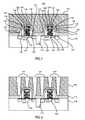
- FIG. 1an illustrative cross-sectional view of front end of line (FEOL) structures is depicted.
- the structuresinclude a metal oxide semiconductor field effect transistor (MOSFET) 100 , which includes a complementary MOS (CMOS) device having an n-FET 102 and a p-FET 104 .
- CMOScomplementary MOS
- the n-FET 102 and p-FET 104are formed in a semiconductor substrate 108 .
- the substrate 108 and the n-FET 102 and p-FET 104have an antireflection coating (ARC) 110 formed thereon.
- ARCantireflection coating
- the substrate 108may include a semiconductor substrate, e.g., silicon, GaAS, silicon on insulator, etc. Although the substrate 108 shown is for a FEOL structure, the present principles are applicable to forming contacts on other layers of a semiconductor device structure. As such, the substrate 108 may include an electrically semiconducting material, an insulating material, a conductive material, devices or structures made of these materials or any combination thereof (e.g., a lower level of an interconnect structure). When the substrate 108 is comprised of a semiconducting material, any semiconductor such as Si, SiGe, SiGeC, SiC, Ge alloys, GaAs, InAs, InP and other III/V or II/VI compound semiconductors, or organic semiconductors may be employed.
- any semiconductorsuch as Si, SiGe, SiGeC, SiC, Ge alloys, GaAs, InAs, InP and other III/V or II/VI compound semiconductors, or organic semiconductors may be employed.
- the substrate 108may also be a flexible substrate including devices that are suitable for high-speed roll-to-roll processing.
- substrate 108may also be a layered semiconductor such as, for example, Si/SiGe, Si/SiC, silicon-on-insulators (SOIs) or silicon germanium-on-insulators (SGOIs).
- SOIssilicon-on-insulators
- SGOIssilicon germanium-on-insulators
- These semiconductor materialsmay form a device, or devices (n-FET 102 and p-FET 104 ) or structures, which may be discrete or interconnected.
- These devices and device structuresmay be for computation, transmission, storage or display of information, such as logic devices, memory devices, switches or display devices.
- the insulating materialcan be an organic insulator, an inorganic insulator or a combination thereof including multilayers.
- the substrate 108may also include a patternable low-k dielectric material as well. These electrical insulating materials may be part of a device, or devices or structures, which may be discrete or interconnected. These devices and structures may be for logic applications or memory applications.
- the substrate 108is an electrically conducting material, the substrate may include, for example, polysilicon, an elemental metal, an alloy including at least one elemental metal, a metal silicide, a metal nitride or combinations thereof including multilayers.
- CMOScomplementary metal oxide semiconductor
- strained silicon devicesstrained silicon devices
- carbon-based (carbon nanotubes and/or graphene) devicesphase-change memory devices
- magnetic memory devicesmagnetic spin switching devices
- quantum devicesmolecule-based switches and other switching or memory devices that can be part of an integrated circuit
- Substrate 108may include shallow trench isolation structures 112 to prevent charge leakage between devices.
- the n-FET device 102includes source and drain regions 114 and 116 , which have silicided regions 118 formed thereon.
- the p-FET device 104also includes source and drain regions 120 and 122 , which have silicided regions 124 formed thereon.
- the n-FET device 102 and p-FET 104include gate structures 126 . These include a gate dielectric 128 with a gate conductor 130 (e.g., doped polysilicon, or a metal gate for high dielectric constant gate dielectrics).
- the gate structures 126include doped monocrystalline silicon regions 132 with silicided regions 134 .
- the silicided regions 118 , 124 and 134provide landing sites for later formed contacts.
- the gate structures 128also include low temperature oxide (LTO) offset spacers 136 and spacers 138 (e.g., nitride).
- the ARC 110is formed on a surface of the devices 102 , 104 and substrate 108 and, in particular over silicided regions 118 , 124 and 134 .
- the silicided regions 118 , 124 and 134form contact pads.
- the ARC 110may be a single layer, multilayer or a graded layer with a composition that varies along the vertical direction.
- the ARC 110acts as an antireflective coating (ARC) during a lithographic patterning process; (ii) withstands high-temperature processing (e.g., up to about 1000° C.); (iii) prevents patterning film (e.g., resist or a patternable low-k material) poisoning by the substrate 108 ; (iv) provides sufficient etch selectivity between the patternable low-k material and the ARC layer 110 ; (v) serves as a permanent dielectric layer in a chip (low dielectric constant, e.g., k ⁇ 15, more commonly k ⁇ 7.0); and (vi) is compatible with conventional integration and produces reliable hardware.
- ARCantireflective coating
- Antireflective coatings (ARC) 110are known to those skilled in the art and include, for example, organic homopolymers or copolymers of polyesters, polyimides, polyacrylates, polymethacrylates, polysulfones, and amorphous carbon that satisfy all of the characteristics of ARC 110 mentioned above.
- the ARC 110may be applied by spin-on techniques, spray on techniques, dipping, etc.
- Inorganic antireflective coatingssuch as silicon oxynitride (SiON), silicon carbide (SiC), silicon oxycarbide (SiOC), SiCOH, siloxane, silane, carbosilane, oxycarbosilane, and silsesquioxane, either as a polymer or a copolymer may also be employed and may be deposited, for example, by plasma-enhanced chemical vapor deposition, atomic layer deposition, spin-on techniques, dipping, etc.
- the ARC 110may include atoms of M, carbon (C) and hydrogen (H), wherein M is at least one of Si, Ge, B, Sn, Fe, Ta, Ti, Ni, Hf and La.
- the thickness of the ARC 110may vary depending on the technique used to form the same as well as the material make-up of the layer.
- the ARC 110may have a thickness from about 1 to about 200 nm, with a thickness from about 10 to about 100 nm being more common.
- ARC 110is a multilayer ARC
- the deposition of each layermay be the same or a combination of deposition methods can be used.
- a post deposition baking stepis usually needed to remove unwanted components, such as solvent, and to effect crosslinking.
- the post deposition baking step of ARC 110may be performed at a temperature from 80° C. to 300° C., with a baking temperature from 120° C. to 200° C. being even more likely. Other post-deposition treatments may be performed.
- a resist material, patterning film or patternable low-k material 140is deposited on the ARC 110 .
- the material 140may include chemically amplified photoresists, non-chemically amplified photoresists, positive-tone or negative tone.
- Processing of material 140may include a deposition process including, for example, spin-on-coating, dip coating, brush coating, and ink-jet dispensing.
- a post deposition baking stepmay be performed to remove unwanted components, such as solvent. When performed, the baking step is conducted at a temperature from 40° C. to 200° C., with a baking temperature from 60° C. to 140° C. being even more preferred. The duration of the baking step varies from 10 seconds to 600 seconds and is not critical.
- the thickness of the material 140may vary depending on the requirements of a chip being fabricated, the method being employed to form the same, and the make-up of the material 140 .
- the patternable low-k material 140may have a thickness from 1 nm to 50,000 nm, with a thickness from 10 nm to 500 nm being preferred.
- the pattern-wise exposing processcan be accomplished in a variety of ways, including, for example, exposure through a mask with a lithography stepper or a scanner with an exposure light source of G-line, Mine (365 nm), DUV (248 nm, 193 nm, 157 nm, 126 nm), Extreme UV (13.4 nm, 6.5 nm), an electron beam, an ion beam, etc.
- the exposing processmay be performed in a dry mode or an immersion mode.
- the exposing processmay be performed with a single exposure or multiple exposures.
- the pattern-wise exposing processmay include direct writing without the use of a mask with, for example, light, electron beam, ion beam, and scanning probe lithography.
- Other patterning techniquesthat can be used include contact printing techniques such as nanoimprint lithography, embossing, micro contact printing, replica molding, microtransfer molding, micromolding in capillaries and solvent-assisted micromolding, thermal assisted embossing, inject printing, and the like.
- An optional post-exposure bakingmay be employed to effect the photochemical reactions.
- the baking stepis conducted at a temperature from 60° to 200° C., with a baking temperature from 80° to 140° C. being even more typical.
- the duration of the baking stepvaries and is not critical to the practice of the present invention.
- the dielectric layeris permanent it preferably has a dielectric constant of no more than 10, more preferably no more than 4.3.
- the permanent antireflective coating layerhas a dielectric constant of no more than 15, and preferably no more than 7.0.
- a positive- or negative-tone patternable low-k material 140is employed to form contact holes 144 .
- the maskis aligned with the silicide regions 118 , 124 and 134 .
- the layer 140is exposed to irradiation and then developed.
- the holes 144provide channels to form electrical contacts later. Since the holes 144 are patterned using lithographic methods, the pattern features 144 may be formed with a plurality of different shapes and sizes, as illustratively depicted.
- latent images or patternsare developed into relief images or patterns to form the holes 144 with an appropriate developer, usually an aqueous base solution, such as a 0.26N tetramethylammoniahydroxide (TMAH) solution.
- TMAHtetramethylammoniahydroxide
- a touch-up plasma etch or equivalent processis performed to open up the ARC 110 and expose the silicided regions 118 , 124 , 134 in the bottom of holes 144 .
- the patterning film 140preferably includes a photo-patternable low k (PPLK) material.
- PPLKphoto-patternable low k
- the photo-patternable low k (PPLK) materials employed hereinmay include any dielectric materials possessing two functions. They act as a photoresist during a patterning process and are subsequently converted into a low-k dielectric insulator during a post patterning cure process. The cured product of a PPLK material, therefore, can serve as a permanent on-chip dielectric insulator.
- the photo-patternable low k material employed hereincan be deposited from a liquid phase.
- cureor “curing” are used interchangeable to refer one of the processes selected from a thermal cure, an electron beam cure, an ultra-violet (UV) cure, an ion beam cure, a plasma cure, a microwave cure or a combination thereof.
- UVultra-violet
- a “cured” product of a photo-patternable low k materialis the product of the photo-patternable low k material after it has undergone one of the aforementioned cure processes.
- the “cured” product of a photo-patternable low k materialis different from the photo-patternable low k material in chemical nature and physical, mechanical and electrical properties.
- photo-patternable low k materialincludes a functionalized polymer, copolymer or blend including at least two of any combination of polymers and/or copolymers having one or more acid-sensitive imageable groups.
- the PPLK materialacts as a photoresist and after curing it is converted into a dielectric material having a dielectric constant of about 7.0 or less. It is noted that when the PPLK material is comprised of a polymer, the polymer includes at least one monomer (to be described in greater detail below). When the PPLK material is comprised of a copolymer, the copolymer includes at least two monomers (to be described in greater detail below).
- the blends of polymers and/or copolymersinclude at least two of any combination of polymers and/or copolymers described herein.
- the PPLK materialis a photo-patternable composition including a polymer, a copolymer, or a blend including at least two of any combination of polymers and/or copolymers, wherein the polymers include one monomer and the copolymers include at least two monomers and wherein the monomers of the polymers and the monomers of the copolymers are selected from a siloxane, silane, carbosilane, oxycarbosilane, silsesquioxane, alkyltrialkoxysilane, tetra-alkoxysilane, unsaturated alkyl substituted silsesquioxane, unsaturated alkyl substituted siloxane, unsaturated alkyl substituted silane, an unsaturated alkyl substituted carbosilane, unsaturated alkyl substituted oxycarbosilane, carbosilane substituted silsesquioxane, carbosilane substituted siloxane, carbos
- the PPLK material that can be employedis a photo-patternable composition comprising a photo/acid-sensitive polymer of one monomer or a copolymer of at least two monomers selected from siloxane, silane, carbosilane, oxycarbosilane, organosilicates, silsesquioxanes and the like.
- the PPLK materialmay also be photo-patternable composition comprising a polymer of one monomer or a copolymer of at least two monomers selected from alkyltrialkoxysilane, tetra-alkoxysilane, unsaturated alkyl (such as vinyl) substituted silsesquioxane, unsaturated alkyl substituted siloxane, unsaturated alkyl substituted silane, an unsaturated alkyl substituted carbosilane, unsaturated alkyl substituted oxycarbosilane, carbosilane substituted silsesquioxane, carbosilane substituted siloxane, carbosilane substituted silane, carbosilane substituted carbosilane, carbosilane substituted oxycarbosilane, oxycarbosilane substituted silsesquioxane, oxycarbosilane substituted siloxane, oxycarbosilane substituted silane,
- the PPLK materialmay comprise a blend including at least two of any combination of polymers and/or copolymers, wherein the polymers include one monomer and the copolymers include at least two monomers and wherein the monomers of the polymers and the monomers of the copolymers are selected from a siloxane, silane, carbosilane, oxycarbosilane, silsesquioxane, alkyltrialkoxysilane, tetra-alkoxysilane, unsaturated alkyl substituted silsesquioxane, unsaturated alkyl substituted siloxane, unsaturated alkyl substituted silane, an unsaturated alkyl substituted carbosilane, unsaturated alkyl substituted oxycarbosilane, carbosilane substituted silsesquioxane, carbosilane substituted siloxane, carbosilane substituted silane, carbosilane substituted carbosilane, carb
- the PPLK materialmay be a photo-patternable composition further comprising at least one microscopic pore generator (porogen).
- the pore generatormay be or may not be photo/acid sensitive.
- Illustrative polymers for the PPLK materialinclude, but are not limited to, siloxane, silane, carbosilane, oxycarbosilane, silsesquioxane-type polymers including caged, linear, branched or combinations thereof.
- the PPLK materialis a photo-patternable composition comprising a blend of these photo/acid-sensitive polymers.
- the PPLK materialis formed from a photo-patternable composition (negative-tone or positive-tone) that includes at least one of the above mentioned polymers, copolymers or blends, a photoacid generator, a base additive and a solvent used in a photoresist composition.
- a photo-patternable compositionnegative-tone or positive-tone
- the PPLK materialmay be formed from a patternable composition optionally including an additional cross-linker.
- negative-toneit is meant that the part of the PPLK material that is exposed to an actinic irradiation will not be removed by a conventional developer, while the unexposed part of the PPLK material is removed.
- the additional cross-linkercan be a small compound (as compared with a polymer or copolymer) or a polymer, a copolymer, or a blend including at least two of any combination of polymers and/or copolymers, wherein the polymers include one monomer and the copolymers include at least two monomers and wherein the monomers of the polymers and the monomers of the copolymers are selected from a siloxane, silane, carbosilane, oxycarbosilane, silsesquioxane, alkyltrialkoxysilane, tetra-alkoxysilane, unsaturated alkyl substituted silsesquioxane, unsaturated alkyl substituted siloxane, unsaturated alkyl substituted silane, an unsaturated alkyl substituted carbosilane, unsaturated alkyl substituted oxycarbosilane, carbosilane substituted silsesquioxane, carb
- the PPLK materialis a positive-tone photo-patternable material
- itis formed from a patternable composition that includes at least one of the above mentioned polymers, copolymers or blends wherein the polymers, copolymers or blends containing at least photo/acid imageable functional group to form positive-tone patterns, a photoacid generator, a base additive and a solvent used in a photoresist.
- positive-toneit is meant that the part of the PPLK material that is exposed to an actinic irradiation will be removed by a conventional developer, while the unexposed part of the PPLK material is not removed.
- the photoacid generators, base additives and solventsare well known to those skilled in the art.
- the patterning film 140is cured.
- the curingmay be performed with heat, UV, or E-beam.
- the cured patterning film 140(with e.g., PPLK material) provides a permanent dielectric material 150 which is employed to insulate conductive structures.
- Curingis performed by a thermal cure, an electron beam cure, an ultra-violet (UV) cure, an ion beam cure, a plasma cure, a microwave cure or a combination thereof.
- UVultra-violet
- ion beam cureion beam cure
- plasma curea microwave cure or a combination thereof.
- the conditions for each of the curing processesare known to those skilled in the art and any condition can be chosen as long as it coverts the photo-patternable low k material into a low k film and maintains pattern fidelity.
- an irradiation cure stepis performed by a combination of a thermal cure and an ultra-violet (UV) cure wherein the wavelength of the ultra-violet (UV) light is from 50 nm to 300 nm and the light source for the ultra-violet (UV) cure is a UV lamp, an excimer (exciplex) laser or a combination thereof.
- UVultra-violet
- the excimer lasermay be generated from at least one of the excimers selected from the group consisting of Ar 2 *, Kr 2 *, F 2 , Xe 2 *, ArF, KrF, XeBr, XeCl, XeCl, XeF, CaF 2 , KrCl, and Cl 2 wherein the wavelength of the excimer laser is in the range from 50 nm to 300 nm. Additionally, the light of the ultra-violet (UV) cure may be enhanced and/or diffused with a lens or other optical diffusing device known to those skilled in the art.
- UVultra-violet
- this post patterning cureis a combined UV/thermal cure.
- This combined UV/thermal cureis carried on a UV/thermal cure module under vacuum or inert atmosphere, such as, in N 2 , He or Ar.
- the UV/thermal cure temperaturemay be from 100° C. to 500° C., with a cure temperature from 300° C. to 450° C. being more common.
- the duration of the UV/thermal cureis from 0.5 min to 30 min with duration from 1 min to 10 min being more common.
- the UV cure moduleis designed to have a very low oxygen content to avoid degradation of the resultant dielectric materials.
- This post-patterning cure, if performed,may be in different or the same tool cluster as that of the patterning step.
- the thickness of the patterned and cured PPLK material 150may vary depending on the requirements of the chip and the technique used to form the same, as well as the material make-up of the layer.
- the first PPLK material 150may have a thickness, e.g., from 1 nm to 50000 nm, with a thickness from 10 nm to 500 nm being preferable.
- a metallization processincludes depositing a conductor 152 into holes 144 in layer 150 and over a top surface of layer 150 .
- the conductor 152may include copper, aluminum, tungsten, titanium, tantalum, electrically conductive carbon materials such as carbon nanotubes and graphene, doped polysilicon or any other useful conductive materials, or alloys/combinations thereof.
- the conductive contact structureas may include a barrier layer when the conductive contact metal is Cu or a conductive catalyst when the conductive carbon materials are employed.
- the conductor 152may be deposited using chemical vapor deposition (CVD), atomic layer deposition, plating, or other deposition techniques or directly grown from the source, drain regions and the gate contact regions.
- the holes 144are filled with electrically conductive material 152 which takes the shape of the holes 144 .
- a chemical-mechanical polishis performed to remove excess conductor 152 from the surface of dielectric layer 150 to form contacts 154 in contact with contact pads (e.g., silicides regions 118 , 124 and 134 ) in accordance with the present principles.
- CMPchemical-mechanical polish
- Other planarization processesmay also be employed.
- the layer 150is shaped using irradiation and includes a high degree of accuracy without etching open the contact holes 144 . Contacts 154 formed within contact holes 144 therefore are more accurately shaped which results in improved reliability.
- all contact sizes and shapes with layer 150are processed simultaneously, which eliminates a plurality of deposition, masking and etching steps—making the process more efficient and less expensive.
- process steps in the conventional integration schemessuch as, nitride deposition, oxide deposition, oxide CMP, multiple plasma etching steps, including, ARC open, oxide etching, nitride etching, resist stripping, etc. are eliminated.
- a nitride stopping layeris eliminated, which has a higher dielectric constant, e.g., k ⁇ 7.4, compared with a k value of, e.g., about 4.5 of in a PPLK ARC layer ( 110 ).
- This k value reductioncan reduce parasitic capacitance between gates and contact metal studs and/or bars, which can result in the improvement of device performance.
- Plasma etching stepsare eliminated in accordance with the present principles.
- Plasma etching stepsare the most challenging process steps in the contact formation especially in attempting to make conventional self-aligned contact (SAC) integration achievable when gate pitch shrinks down to, e.g., less than 50 nm or so.
- SACself-aligned contact
- the contacts 152have less width at a lower portion and a greater width at a top portion.
- the contacts 152may include other graduated shapes or stepped shapes as well. It should be understood that the silicided regions 118 , 124 and 134 represent one type of contact pad. Other types of contact pads may also be employed. Processing can continue using the inventive processes or conventional processes.
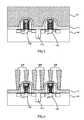
- resist image reversalis employed to form contact holes in accordance with the present principles.
- ARC layer 110 and a resist layer 202are formed as described with reference to FIG. 1 .
- Resist layer 202may employ a reversed-tone mask and a positive- or negative-tone photoresist to form inverse patterns for contact hole formation.
- resist layer 202is exposed (or prevented from being exposed) to (from) irradiation to form cross-linked pillars or resist island structures 204 .
- the remaining portions of resist layer 202are removed by a developer to provide the structure shown.
- the pattern-wise exposure to irradiationmay include, e.g., UV light, e-beam, EUV with an inversed-tone mask.
- a dielectric composition 206is deposited.
- the deposition processincludes, for example, spin-on-coating, dip coating, brush coating, doctor blade coating, and ink-jet dispensing.
- the dielectric composition 206is formulated such that it is compatible with the underlying photoresist pattern 204 , i.e., the application of the dielectric composition 206 does not substantially alter the dimension and profile of the resist patterns 204 .
- a post deposition baking stepmay be employed to remove unwanted components, such as solvent. When performed, the baking step is conducted at a temperature from 40° C. to 200° C., with a baking temperature from 60° C. to 140° C. being even more preferred. The duration of the baking step varies from 10 seconds to 600 seconds and is not critical.
- the dielectric composition 206may include a PPLK material, which can be converted into a patterned and cured permanent dielectric layer in later steps.
- Layer 206may be applied using a spin-on process or a chemical vapor deposition (CVD) process.
- the composite layeris formed by filling resist openings wherein the filling should not distort the resist patterns/islands 204 .
- the dielectric composition 206may include other dielectric materials as well.
- the dielectric layer 206is planarized using, e.g., a dry or wet etch to expose a top surface 205 of the resist island structures 204 .
- the resist of the island structures 204is removed from the resist layer 206 to leave contact holes 212 with ARC 110 remaining at the bottom of the holes 212 .
- This exposes resist island structures 204which may be removed by a wet method, a dry method, heat, UV light or a combination thereof.
- a wet methodis employed with an appropriate developer after exposing the dielectric and resist composite structure to a blanket UV irradiation.
- a dry methodis employed with an appropriate selective reactive ion etching that removes only the exposed resist.
- a dry methodis employed by using heat or UV irradiation to remove exposed resist islands.
- the layer 206may be cured as described above to convert the resist layer 206 into a patterned and cured permanent dielectric layer 210 .
- This stepis not needed in the layer 206 is formed as a permanent dielectric material ( 210 ).
- the pattern in layer 210corresponds to contact holes 212 that will be employed to form contacts in later steps.
- An ARC open processis performed to open the ARC 110 for source, drain and gates contacts. The ARC open process is as described above and exposes the silicided regions 118 , 124 and 134 in contact holes 212 .
- a conductive material 214is deposited to fill the contact holes 212 and is formed over a surface of the dielectric layer 210 .
- a CMP processmay be performed to planarize the top surface.
- the conductive materialmay include, copper, aluminum, tungsten, titanium, tantalum, ruthenium their alloys electrically conductive carbon materials such as carbon nanotubes and graphene, doped polysilicon or any other useful conductive material, or alloys/combinations thereof.
- This integration schemeforms contacts 220 using a photoresist image reversal method to replace the nitride, oxide, and the resist mask stack of conventional process with a permanent resist base dielectric layer and permanent ARC.
- the present methodreduces many process steps of conventional integration schemes, such as, e.g., nitride deposition, oxide deposition, oxide CMP, multiple plasma etching steps, including, oxide etching, nitride etching, resist stripping, etc. Plasma etching steps are also eliminated.
Landscapes
- Engineering & Computer Science (AREA)
- Physics & Mathematics (AREA)
- Condensed Matter Physics & Semiconductors (AREA)
- General Physics & Mathematics (AREA)
- Manufacturing & Machinery (AREA)
- Computer Hardware Design (AREA)
- Microelectronics & Electronic Packaging (AREA)
- Power Engineering (AREA)
- Plasma & Fusion (AREA)
- Internal Circuitry In Semiconductor Integrated Circuit Devices (AREA)
Abstract
Description
Claims (8)
Priority Applications (1)
| Application Number | Priority Date | Filing Date | Title |
|---|---|---|---|
| US14/754,190US9245791B2 (en) | 2011-04-15 | 2015-06-29 | Method for fabricating a contact |
Applications Claiming Priority (3)
| Application Number | Priority Date | Filing Date | Title |
|---|---|---|---|
| US13/088,110US8890318B2 (en) | 2011-04-15 | 2011-04-15 | Middle of line structures |
| US13/970,124US9343354B2 (en) | 2011-04-15 | 2013-08-19 | Middle of line structures and methods for fabrication |
| US14/754,190US9245791B2 (en) | 2011-04-15 | 2015-06-29 | Method for fabricating a contact |
Related Parent Applications (1)
| Application Number | Title | Priority Date | Filing Date |
|---|---|---|---|
| US13/970,124DivisionUS9343354B2 (en) | 2011-04-15 | 2013-08-19 | Middle of line structures and methods for fabrication |
Publications (2)
| Publication Number | Publication Date |
|---|---|
| US20150318208A1 US20150318208A1 (en) | 2015-11-05 |
| US9245791B2true US9245791B2 (en) | 2016-01-26 |
Family
ID=47005838
Family Applications (3)
| Application Number | Title | Priority Date | Filing Date |
|---|---|---|---|
| US13/088,110Expired - Fee RelatedUS8890318B2 (en) | 2011-04-15 | 2011-04-15 | Middle of line structures |
| US13/970,124Active2031-07-23US9343354B2 (en) | 2011-04-15 | 2013-08-19 | Middle of line structures and methods for fabrication |
| US14/754,190ActiveUS9245791B2 (en) | 2011-04-15 | 2015-06-29 | Method for fabricating a contact |
Family Applications Before (2)
| Application Number | Title | Priority Date | Filing Date |
|---|---|---|---|
| US13/088,110Expired - Fee RelatedUS8890318B2 (en) | 2011-04-15 | 2011-04-15 | Middle of line structures |
| US13/970,124Active2031-07-23US9343354B2 (en) | 2011-04-15 | 2013-08-19 | Middle of line structures and methods for fabrication |
Country Status (1)
| Country | Link |
|---|---|
| US (3) | US8890318B2 (en) |
Cited By (2)
| Publication number | Priority date | Publication date | Assignee | Title |
|---|---|---|---|---|
| US10923388B2 (en) | 2019-01-18 | 2021-02-16 | Globalfoundries U.S. Inc. | Gap fill void and connection structures |
| US11114533B2 (en) | 2019-03-19 | 2021-09-07 | Samsung Electronics Co., Ltd. | Semiconductor device including contacts having different heights and different widths |
Families Citing this family (26)
| Publication number | Priority date | Publication date | Assignee | Title |
|---|---|---|---|---|
| US8754530B2 (en)* | 2008-08-18 | 2014-06-17 | International Business Machines Corporation | Self-aligned borderless contacts for high density electronic and memory device integration |
| US8890318B2 (en) | 2011-04-15 | 2014-11-18 | International Business Machines Corporation | Middle of line structures |
| US8900988B2 (en) | 2011-04-15 | 2014-12-02 | International Business Machines Corporation | Method for forming self-aligned airgap interconnect structures |
| US9054160B2 (en) | 2011-04-15 | 2015-06-09 | International Business Machines Corporation | Interconnect structure and method for fabricating on-chip interconnect structures by image reversal |
| US20130062732A1 (en) | 2011-09-08 | 2013-03-14 | International Business Machines Corporation | Interconnect structures with functional components and methods for fabrication |
| US9087753B2 (en)* | 2012-05-10 | 2015-07-21 | International Business Machines Corporation | Printed transistor and fabrication method |
| US9059095B2 (en)* | 2013-04-22 | 2015-06-16 | International Business Machines Corporation | Self-aligned borderless contacts using a photo-patternable dielectric material as a replacement contact |
| US9515163B2 (en)* | 2013-09-09 | 2016-12-06 | Globalfoundries Inc. | Methods of forming FinFET semiconductor devices with self-aligned contact elements using a replacement gate process and the resulting devices |
| CN104752329B (en)* | 2013-12-30 | 2017-12-01 | 中芯国际集成电路制造(上海)有限公司 | The forming method of interconnection structure |
| US20150200042A1 (en)* | 2014-01-10 | 2015-07-16 | Applied Materials, Inc. | Recessing ultra-low k dielectric using remote plasma source |
| US9281192B2 (en) | 2014-03-13 | 2016-03-08 | Taiwan Semiconductor Manufacturing Co., Ltd. | CMP-friendly coatings for planar recessing or removing of variable-height layers |
| US9324830B2 (en) | 2014-03-27 | 2016-04-26 | International Business Machines Corporation | Self-aligned contact process enabled by low temperature |
| KR101719901B1 (en)* | 2014-05-13 | 2017-03-24 | 타이완 세미콘덕터 매뉴팩쳐링 컴퍼니 리미티드 | Cmp-friendly coatings for planar recessing or removing of variable-height layers |
| KR102216543B1 (en)* | 2014-06-16 | 2021-02-17 | 삼성전자주식회사 | Graphene-Metal bonding structure and method of manufacturing the same, and semiconductor device having graphene-Metal bonding structure |
| KR102295239B1 (en) | 2015-01-08 | 2021-09-01 | 삼성전자주식회사 | Method of forming the semiconductor device |
| US9490253B1 (en)* | 2015-09-23 | 2016-11-08 | International Business Machines Corporation | Gate planarity for finFET using dummy polish stop |
| US9673101B2 (en) | 2015-09-30 | 2017-06-06 | International Business Machines Corporation | Minimize middle-of-line contact line shorts |
| US10727070B2 (en)* | 2016-03-21 | 2020-07-28 | International Business Machines Corporation | Liner-less contact metallization |
| US10886268B2 (en)* | 2016-11-29 | 2021-01-05 | Taiwan Semiconductor Manufacturing Co., Ltd. | Method of manufacturing a semiconductor device with separated merged source/drain structure |
| CN108962817B (en)* | 2017-05-22 | 2020-11-27 | 中芯国际集成电路制造(上海)有限公司 | Semiconductor structure and forming method thereof |
| US10685884B2 (en) | 2017-07-31 | 2020-06-16 | Taiwan Semiconductor Manufacturing Co., Ltd. | Semiconductor device including a Fin-FET and method of manufacturing the same |
| US11069813B2 (en)* | 2019-09-30 | 2021-07-20 | Taiwan Semiconductor Manufacturing Co., Ltd. | Localized heating in laser annealing process |
| CN110634801B (en)* | 2019-10-18 | 2022-04-22 | 中国科学院微电子研究所 | A kind of contact hole preparation method |
| US11587828B2 (en)* | 2020-08-11 | 2023-02-21 | Nanya Technology Corporation | Semiconductor device with graphene conductive structure and method for forming the same |
| CN116130409A (en)* | 2021-11-15 | 2023-05-16 | 长鑫存储技术有限公司 | Method for forming contact structure, semiconductor structure and memory |
| US20230268223A1 (en)* | 2022-02-24 | 2023-08-24 | Taiwan Semiconductor Manufacturing Co., Ltd. | Semiconductor devices and methods of manufacture |
Citations (108)
| Publication number | Priority date | Publication date | Assignee | Title |
|---|---|---|---|---|
| US4783646A (en) | 1986-03-07 | 1988-11-08 | Kabushiki Kaisha Toshiba | Stolen article detection tag sheet, and method for manufacturing the same |
| US4808545A (en) | 1987-04-20 | 1989-02-28 | International Business Machines Corporation | High speed GaAs MESFET having refractory contacts and a self-aligned cold gate fabrication process |
| US5426319A (en) | 1992-07-07 | 1995-06-20 | Mitsubishi Denki Kabushiki Kaisha | High-frequency semiconductor device including microstrip transmission line |
| US5430441A (en) | 1993-10-12 | 1995-07-04 | Motorola, Inc. | Transponding tag and method |
| US5461003A (en) | 1994-05-27 | 1995-10-24 | Texas Instruments Incorporated | Multilevel interconnect structure with air gaps formed between metal leads |
| US5651857A (en) | 1995-09-08 | 1997-07-29 | International Business Machines Corporation | Sidewall spacer using an overhang |
| US5795830A (en) | 1995-06-06 | 1998-08-18 | International Business Machines Corporation | Reducing pitch with continuously adjustable line and space dimensions |
| US5913113A (en) | 1997-02-24 | 1999-06-15 | Lg Electronics Inc. | Method for fabricating a thin film transistor of a liquid crystal display device |
| US5976768A (en) | 1997-07-17 | 1999-11-02 | International Business Machines Corporation | Method for forming sidewall spacers using frequency doubling hybrid resist and device formed thereby |
| US6007968A (en) | 1997-10-29 | 1999-12-28 | International Business Machines Corporation | Method for forming features using frequency doubling hybrid resist and device formed thereby |
| US6014422A (en) | 1998-05-21 | 2000-01-11 | Internaitonal Business Machines Corporation | Method for varying x-ray hybrid resist space dimensions |
| US6025260A (en) | 1998-02-05 | 2000-02-15 | Integrated Device Technology, Inc. | Method for fabricating air gap with borderless contact |
| US6037195A (en) | 1997-09-25 | 2000-03-14 | Kabushiki Kaisha Toshiba | Process of producing thin film transistor |
| US6093508A (en) | 1997-03-28 | 2000-07-25 | International Business Machines Corporation | Dual damascene structure formed in a single photoresist film |
| US6114082A (en) | 1996-09-16 | 2000-09-05 | International Business Machines Corporation | Frequency doubling hybrid photoresist having negative and positive tone components and method of preparing the same |
| US6150256A (en) | 1998-10-30 | 2000-11-21 | International Business Machines Corporation | Method for forming self-aligned features |
| US6165893A (en) | 1999-01-29 | 2000-12-26 | Hyundai Electronics Industries Co., Ltd. | Insulating layers and a forming method thereof |
| US6184041B1 (en) | 1998-05-13 | 2001-02-06 | International Business Machines Corporation | Fused hybrid resist shapes as a means of modulating hybrid resist space width |
| US6194268B1 (en) | 1998-10-30 | 2001-02-27 | International Business Machines Corporation | Printing sublithographic images using a shadow mandrel and off-axis exposure |
| US6200726B1 (en) | 1996-09-16 | 2001-03-13 | International Business Machines Corporation | Optimization of space width for hybrid photoresist |
| US6214719B1 (en) | 1999-09-30 | 2001-04-10 | Novellus Systems, Inc. | Method of implementing air-gap technology for low capacitance ILD in the damascene scheme |
| US6221562B1 (en) | 1998-11-13 | 2001-04-24 | International Business Machines Corporation | Resist image reversal by means of spun-on-glass |
| US6252290B1 (en) | 1999-10-25 | 2001-06-26 | Chartered Semiconductor Manufacturing Ltd. | Method to form, and structure of, a dual damascene interconnect device |
| US6284439B1 (en) | 1996-09-16 | 2001-09-04 | International Business Machines Corporation | Method of producing an integrated circuit chip using low “k” factor hybrid photoresist and apparatus formed thereby |
| US6320543B1 (en) | 1999-03-24 | 2001-11-20 | Nec Corporation | Microwave and millimeter wave circuit apparatus |
| US20010054766A1 (en) | 1999-05-12 | 2001-12-27 | Bachir Dirahoui | Process for making a planar integrated circuit interconnect |
| US6337278B1 (en) | 2000-08-23 | 2002-01-08 | Mosel Vitelic, Inc. | Technique for forming a borderless overlapping gate and diffusion contact structure in integrated circuit device processing |
| US6338934B1 (en) | 1999-08-26 | 2002-01-15 | International Business Machines Corporation | Hybrid resist based on photo acid/photo base blending |
| US20020076895A1 (en)* | 2000-12-18 | 2002-06-20 | Sun-Chieh Chien | Fabrication method for an embedded dynamic random access memory (DRAM) |
| US20020142531A1 (en) | 2001-03-29 | 2002-10-03 | Hsu Sheng Teng | Dual damascene copper gate and interconnect therefore |
| US20020158337A1 (en) | 2000-02-08 | 2002-10-31 | Babich Katherina E. | Multilayer interconnect structure containing air gaps and method for making |
| US6492732B2 (en) | 1997-07-28 | 2002-12-10 | United Microelectronics Corp. | Interconnect structure with air gap compatible with unlanded vias |
| US20030012539A1 (en) | 2001-04-30 | 2003-01-16 | Tony Mule' | Backplane, printed wiring board, and/or multi-chip module-level optical interconnect layer having embedded air-gap technologies and methods of fabrication |
| US6514857B1 (en) | 1998-02-02 | 2003-02-04 | Applied Materials, Inc. | Damascene structure fabricated using a layer of silicon-based photoresist material |
| US20030127426A1 (en) | 2002-01-07 | 2003-07-10 | Macronix International Co., Ltd. | Method for pitch reduction |
| US20030209802A1 (en) | 2002-05-13 | 2003-11-13 | Fujitsu Limited | Semiconductor device and method for fabricating the same |
| US6649531B2 (en) | 2001-11-26 | 2003-11-18 | International Business Machines Corporation | Process for forming a damascene structure |
| US20030217426A1 (en) | 2002-05-07 | 2003-11-27 | Quickie Manufacturing Corporation | Cleaning implement with removable cleaning element |
| US20040058277A1 (en) | 2002-09-24 | 2004-03-25 | Jun He | Mechanically robust interconnect for low-k dielectric material using post treatment |
| US6737708B2 (en) | 1999-10-29 | 2004-05-18 | Fujitsu Display Technologies Corporation | Thin-film transistor, liquid-crystal display device, and method of producing the same |
| US20040094821A1 (en) | 2002-11-15 | 2004-05-20 | Water Lur | Air gap for dual damascene applications |
| US20040137241A1 (en) | 2003-01-08 | 2004-07-15 | International Business Machines Corporation | Patternable low dielectric constsnt materials and their use in ULSI interconnection |
| US6780753B2 (en) | 2002-05-31 | 2004-08-24 | Applied Materials Inc. | Airgap for semiconductor devices |
| US20040196688A1 (en) | 2001-12-18 | 2004-10-07 | Matsushita Electric Industrial Co., Ltd. | Non-volatile memory |
| US6805109B2 (en) | 2002-09-18 | 2004-10-19 | Thomas L. Cowan | Igniter circuit with an air gap |
| US20040207001A1 (en) | 2001-03-28 | 2004-10-21 | Matrix Semiconductor, Inc. | Two mask floating gate EEPROM and method of making |
| US20050009305A1 (en) | 2003-06-26 | 2005-01-13 | International Business Machines Corporation | Method of forming freestanding semiconductor layer |
| US20060038212A1 (en) | 2004-08-19 | 2006-02-23 | John Moore | Structure for amorphous carbon based non-volatile memory |
| US7030031B2 (en) | 2003-06-24 | 2006-04-18 | International Business Machines Corporation | Method for forming damascene structure utilizing planarizing material coupled with diffusion barrier material |
| US7056840B2 (en) | 2003-09-30 | 2006-06-06 | International Business Machines Corp. | Direct photo-patterning of nanoporous organosilicates, and method of use |
| US7071532B2 (en) | 2003-09-30 | 2006-07-04 | International Business Machines Corporation | Adjustable self-aligned air gap dielectric for low capacitance wiring |
| US7091611B2 (en) | 2000-05-31 | 2006-08-15 | Micron Technology, Inc. | Multilevel copper interconnects with low-k dielectrics and air gaps |
| US7125793B2 (en) | 2003-12-23 | 2006-10-24 | Intel Corporation | Method for forming an opening for an interconnect structure in a dielectric layer having a photosensitive material |
| US7138329B2 (en) | 2002-11-15 | 2006-11-21 | United Microelectronics Corporation | Air gap for tungsten/aluminum plug applications |
| US20070099416A1 (en) | 2005-10-31 | 2007-05-03 | International Business Machines Corporation | Shrinking Contact Apertures Through LPD Oxide |
| US7235473B2 (en) | 2005-08-26 | 2007-06-26 | Freescale Semiconductor, Inc. | Dual silicide semiconductor fabrication process |
| US20070166981A1 (en) | 2006-01-19 | 2007-07-19 | Toshiharu Furukawa | Methods for forming uniform lithographic features |
| US7253095B2 (en) | 2002-11-15 | 2007-08-07 | United Microelectronics Corporation | Air gap formation method for reducing undesired capacitive coupling between interconnects in an integrated circuit device |
| US7265013B2 (en) | 2005-09-19 | 2007-09-04 | International Business Machines Corporation | Sidewall image transfer (SIT) technologies |
| US20070249170A1 (en) | 2006-04-25 | 2007-10-25 | David Kewley | Process for improving critical dimension uniformity of integrated circuit arrays |
| US7294934B2 (en) | 2002-11-21 | 2007-11-13 | Intel Corporation | Low-K dielectric structure and method |
| US7294568B2 (en) | 2004-08-20 | 2007-11-13 | Intel Corporation | Formation of air gaps in an interconnect structure using a thin permeable hard mask and resulting structures |
| US20080008969A1 (en) | 2006-07-10 | 2008-01-10 | Micron Technology, Inc. | Pitch reduction technology using alternating spacer depositions during the formation of a semiconductor device and systems including same |
| US7338896B2 (en) | 2004-12-17 | 2008-03-04 | Interuniversitair Microelektronica Centrum (Imec) | Formation of deep via airgaps for three dimensional wafer to wafer interconnect |
| KR100809901B1 (en) | 2007-02-02 | 2008-03-06 | 삼성전자주식회사 | Silica zero gel composite manufacturing method and composite |
| US7344827B2 (en) | 2003-05-07 | 2008-03-18 | Shin-Etsu Chemical Co., Inc. | Fine contact hole forming method employing thermal flow process |
| US7361454B2 (en) | 2003-10-15 | 2008-04-22 | Kabushiki Kaisha Toshiba | Method of forming contact hole and method of manufacturing semiconductor device |
| US7361991B2 (en) | 2003-09-19 | 2008-04-22 | International Business Machines Corporation | Closed air gap interconnect structure |
| US20080122106A1 (en) | 2006-09-11 | 2008-05-29 | International Business Machines | Method to generate airgaps with a template first scheme and a self aligned blockout mask |
| US20080142995A1 (en) | 2006-03-17 | 2008-06-19 | Toshiharu Furukawa | Layout and process to contact sub-lithographic structures |
| US20080150091A1 (en) | 2004-04-08 | 2008-06-26 | International Business Machines Corporation | MULTIPLE PATTERNING USING PATTERNABLE LOW-k DIELECTRIC MATERIALS |
| US20080176396A1 (en) | 2006-10-17 | 2008-07-24 | Takuya Futase | Manufacturing method of semiconductor device |
| US20080187731A1 (en) | 2003-09-12 | 2008-08-07 | International Business Machines Corporation | Techniques for Patterning Features in Semiconductor Devices |
| US7432041B2 (en) | 2002-12-04 | 2008-10-07 | Taiwan Semiconductor Manufacturing Co., Ltd. | Method and systems to print contact hole patterns |
| US20080265377A1 (en) | 2007-04-30 | 2008-10-30 | International Business Machines Corporation | Air gap with selective pinchoff using an anti-nucleation layer |
| US20090081418A1 (en) | 2007-09-20 | 2009-03-26 | International Business Machines Corporation | Spin-on antireflective coating for integration of patternable dielectric materials and interconnect structures |
| US20090079076A1 (en) | 2007-09-20 | 2009-03-26 | International Business Machines Corporation | Patternable dielectric film structure with improved lithography and method of fabricating same |
| US20090079075A1 (en) | 2007-09-20 | 2009-03-26 | International Business Machines Corporation | Interconnect structures with patternable low-k dielectrics and method of fabricating same |
| US7535016B2 (en) | 2005-01-31 | 2009-05-19 | International Business Machines Corporation | Vertical carbon nanotube transistor integration |
| US20090149026A1 (en) | 2007-12-06 | 2009-06-11 | Micron Technology, Inc. | Method for forming high density patterns |
| US20090166612A1 (en) | 2006-03-29 | 2009-07-02 | Cain Paul A | Techniques for Device Fabrication with Self-Aligned Electrodes |
| US20090174067A1 (en) | 2008-01-09 | 2009-07-09 | International Business Machines Corporation | Airgap-containing interconnect structure with patternable low-k material and method of fabricating |
| US7566598B2 (en) | 2004-08-10 | 2009-07-28 | Industrial Technology Research Institute | Method of mask reduction for producing a LTPS-TFT array by use of photo-sensitive low-K dielectrics |
| US7585614B2 (en) | 2004-09-20 | 2009-09-08 | International Business Machines Corporation | Sub-lithographic imaging techniques and processes |
| US20090233226A1 (en) | 2008-03-13 | 2009-09-17 | International Business Machines Corporation | Photopatternable dielectric materials for beol applications and methods for use |
| US20100009131A1 (en) | 2008-07-09 | 2010-01-14 | International Business Machines Corporation | Multi-exposure lithography employing a single anti-reflective coating layer |
| US20100028801A1 (en) | 2008-08-01 | 2010-02-04 | International Businesss Machines Corporation | Lithography for pitch reduction |
| US20100112463A1 (en) | 2008-11-03 | 2010-05-06 | Hynix Semiconductor Inc. | Method for forming fine contact hole pattern of semiconductor device |
| US20100197096A1 (en) | 2009-02-04 | 2010-08-05 | Advanced Micro Devices, Inc. | Methods for fabricating finfet structures having different channel lengths |
| US7790576B2 (en) | 2007-11-29 | 2010-09-07 | Stats Chippac, Ltd. | Semiconductor device and method of forming through hole vias in die extension region around periphery of die |
| US7811923B2 (en) | 2007-07-17 | 2010-10-12 | International Business Machines Corporation | Integrated wafer processing system for integration of patternable dielectric materials |
| US20100314769A1 (en) | 2007-09-20 | 2010-12-16 | Freescale Semiconductor, Inc. | For reducing electromigration effect in an integrated circuit |
| US20100314768A1 (en) | 2009-06-12 | 2010-12-16 | International Business Machines Corporation | Interconnect structure fabricated without dry plasma etch processing |
| US20100314767A1 (en) | 2009-06-16 | 2010-12-16 | International Business Machines Corporation | Self-aligned dual damascene beol structures with patternable low- k material and methods of forming same |
| US20100319971A1 (en) | 2009-06-17 | 2010-12-23 | International Business Machines Corporation | Airgap-containing interconnect structure with improved patternable low-k material and method of fabricating |
| US20110074044A1 (en) | 2009-09-29 | 2011-03-31 | International Business Machines Corporation | Patternable low-k dielectric interconnect structure with a graded cap layer and method of fabrication |
| US7919225B2 (en) | 2008-05-23 | 2011-04-05 | International Business Machines Corporation | Photopatternable dielectric materials for BEOL applications and methods for use |
| US20110130006A1 (en) | 2004-09-01 | 2011-06-02 | Micron Technology, Inc. | Mask material conversion |
| US7968382B2 (en) | 2007-02-02 | 2011-06-28 | Semiconductor Energy Laboratory Co., Ltd. | Method of manufacturing semiconductor device |
| US20110193167A1 (en) | 2010-02-11 | 2011-08-11 | Taiwan Semiconductor Manufacturing Company, Ltd. | Self-Aligned Two-Step STI Formation Through Dummy Poly Removal |
| US20110210380A1 (en)* | 2010-02-26 | 2011-09-01 | Thilo Scheiper | Contact bars with reduced fringing capacitance in a semiconductor device |
| US20110291284A1 (en)* | 2010-05-27 | 2011-12-01 | International Business Machines Corporation | INTERCONNECT STRUCTURE WITH AN OXYGEN-DOPED SiC ANTIREFLECTIVE COATING AND METHOD OF FABRICATION |
| US20110304053A1 (en) | 2010-06-11 | 2011-12-15 | International Business Machines Corp. | Interconnect structure and method of fabricating |
| US20120018891A1 (en) | 2010-07-20 | 2012-01-26 | International Business Machines Corporation | Methods to form self-aligned permanent on-chip interconnect structures |
| US8236599B2 (en) | 2009-04-09 | 2012-08-07 | State of Oregon acting by and through the State Board of Higher Education | Solution-based process for making inorganic materials |
| US20120261829A1 (en) | 2011-04-15 | 2012-10-18 | International Business Machines Corporation | Middle of line structures and methods for fabrication |
| US20130299883A1 (en) | 2012-05-10 | 2013-11-14 | International Business Machines Corporation | Printed transistor and fabrication method |
| US8586404B2 (en) | 2009-05-04 | 2013-11-19 | Taiwan Semiconductor Manufacturing Company, Ltd. | Method for reducing contact resistance of CMOS image sensor |
Family Cites Families (1)
| Publication number | Priority date | Publication date | Assignee | Title |
|---|---|---|---|---|
| US8637395B2 (en)* | 2009-11-16 | 2014-01-28 | International Business Machines Corporation | Methods for photo-patternable low-k (PPLK) integration with curing after pattern transfer |
- 2011
- 2011-04-15USUS13/088,110patent/US8890318B2/ennot_activeExpired - Fee Related
- 2013
- 2013-08-19USUS13/970,124patent/US9343354B2/enactiveActive
- 2015
- 2015-06-29USUS14/754,190patent/US9245791B2/enactiveActive
Patent Citations (121)
| Publication number | Priority date | Publication date | Assignee | Title |
|---|---|---|---|---|
| US4783646A (en) | 1986-03-07 | 1988-11-08 | Kabushiki Kaisha Toshiba | Stolen article detection tag sheet, and method for manufacturing the same |
| US4808545A (en) | 1987-04-20 | 1989-02-28 | International Business Machines Corporation | High speed GaAs MESFET having refractory contacts and a self-aligned cold gate fabrication process |
| US5426319A (en) | 1992-07-07 | 1995-06-20 | Mitsubishi Denki Kabushiki Kaisha | High-frequency semiconductor device including microstrip transmission line |
| US5430441A (en) | 1993-10-12 | 1995-07-04 | Motorola, Inc. | Transponding tag and method |
| US5461003A (en) | 1994-05-27 | 1995-10-24 | Texas Instruments Incorporated | Multilevel interconnect structure with air gaps formed between metal leads |
| US5795830A (en) | 1995-06-06 | 1998-08-18 | International Business Machines Corporation | Reducing pitch with continuously adjustable line and space dimensions |
| US5651857A (en) | 1995-09-08 | 1997-07-29 | International Business Machines Corporation | Sidewall spacer using an overhang |
| US6200726B1 (en) | 1996-09-16 | 2001-03-13 | International Business Machines Corporation | Optimization of space width for hybrid photoresist |
| US6284439B1 (en) | 1996-09-16 | 2001-09-04 | International Business Machines Corporation | Method of producing an integrated circuit chip using low “k” factor hybrid photoresist and apparatus formed thereby |
| US6313492B1 (en) | 1996-09-16 | 2001-11-06 | International Business Machines Corporation | Integrated circuit chip produced by using frequency doubling hybrid photoresist |
| US6114082A (en) | 1996-09-16 | 2000-09-05 | International Business Machines Corporation | Frequency doubling hybrid photoresist having negative and positive tone components and method of preparing the same |
| US6440635B1 (en) | 1996-09-16 | 2002-08-27 | International Business Machines Corporation | Low “K” factor hybrid photoresist |
| US5913113A (en) | 1997-02-24 | 1999-06-15 | Lg Electronics Inc. | Method for fabricating a thin film transistor of a liquid crystal display device |
| US6093508A (en) | 1997-03-28 | 2000-07-25 | International Business Machines Corporation | Dual damascene structure formed in a single photoresist film |
| US5976768A (en) | 1997-07-17 | 1999-11-02 | International Business Machines Corporation | Method for forming sidewall spacers using frequency doubling hybrid resist and device formed thereby |
| US20010021577A1 (en) | 1997-07-17 | 2001-09-13 | Jeffrey S. Brown | Method for forming sidewall spacers using frequency doubling hybrid resist and device formed thereby |
| US5981148A (en) | 1997-07-17 | 1999-11-09 | International Business Machines Corporation | Method for forming sidewall spacers using frequency doubling hybrid resist and device formed thereby |
| US6492732B2 (en) | 1997-07-28 | 2002-12-10 | United Microelectronics Corp. | Interconnect structure with air gap compatible with unlanded vias |
| US6492256B2 (en) | 1997-07-28 | 2002-12-10 | United Microelectronics Corp. | Method for forming an interconnect structure with air gap compatible with unlanded vias |
| US6037195A (en) | 1997-09-25 | 2000-03-14 | Kabushiki Kaisha Toshiba | Process of producing thin film transistor |
| US6007968A (en) | 1997-10-29 | 1999-12-28 | International Business Machines Corporation | Method for forming features using frequency doubling hybrid resist and device formed thereby |
| US6245488B1 (en) | 1997-10-29 | 2001-06-12 | International Business Machines Corporation | Method for forming features using frequency doubling hybrid resist and device formed thereby |
| US6825562B2 (en) | 1998-02-02 | 2004-11-30 | Applied Materials Inc. | Damascene structure fabricated using a layer of silicon-based photoresist material |
| US6514857B1 (en) | 1998-02-02 | 2003-02-04 | Applied Materials, Inc. | Damascene structure fabricated using a layer of silicon-based photoresist material |
| US6025260A (en) | 1998-02-05 | 2000-02-15 | Integrated Device Technology, Inc. | Method for fabricating air gap with borderless contact |
| US6184041B1 (en) | 1998-05-13 | 2001-02-06 | International Business Machines Corporation | Fused hybrid resist shapes as a means of modulating hybrid resist space width |
| US6014422A (en) | 1998-05-21 | 2000-01-11 | Internaitonal Business Machines Corporation | Method for varying x-ray hybrid resist space dimensions |
| US6150256A (en) | 1998-10-30 | 2000-11-21 | International Business Machines Corporation | Method for forming self-aligned features |
| US6194268B1 (en) | 1998-10-30 | 2001-02-27 | International Business Machines Corporation | Printing sublithographic images using a shadow mandrel and off-axis exposure |
| US6221562B1 (en) | 1998-11-13 | 2001-04-24 | International Business Machines Corporation | Resist image reversal by means of spun-on-glass |
| US6165893A (en) | 1999-01-29 | 2000-12-26 | Hyundai Electronics Industries Co., Ltd. | Insulating layers and a forming method thereof |
| US6320543B1 (en) | 1999-03-24 | 2001-11-20 | Nec Corporation | Microwave and millimeter wave circuit apparatus |
| US20010054766A1 (en) | 1999-05-12 | 2001-12-27 | Bachir Dirahoui | Process for making a planar integrated circuit interconnect |
| US6338934B1 (en) | 1999-08-26 | 2002-01-15 | International Business Machines Corporation | Hybrid resist based on photo acid/photo base blending |
| US6214719B1 (en) | 1999-09-30 | 2001-04-10 | Novellus Systems, Inc. | Method of implementing air-gap technology for low capacitance ILD in the damascene scheme |
| US6252290B1 (en) | 1999-10-25 | 2001-06-26 | Chartered Semiconductor Manufacturing Ltd. | Method to form, and structure of, a dual damascene interconnect device |
| US6737708B2 (en) | 1999-10-29 | 2004-05-18 | Fujitsu Display Technologies Corporation | Thin-film transistor, liquid-crystal display device, and method of producing the same |
| US20020158337A1 (en) | 2000-02-08 | 2002-10-31 | Babich Katherina E. | Multilayer interconnect structure containing air gaps and method for making |
| US7091611B2 (en) | 2000-05-31 | 2006-08-15 | Micron Technology, Inc. | Multilevel copper interconnects with low-k dielectrics and air gaps |
| US6337278B1 (en) | 2000-08-23 | 2002-01-08 | Mosel Vitelic, Inc. | Technique for forming a borderless overlapping gate and diffusion contact structure in integrated circuit device processing |
| US20020076895A1 (en)* | 2000-12-18 | 2002-06-20 | Sun-Chieh Chien | Fabrication method for an embedded dynamic random access memory (DRAM) |
| US20040207001A1 (en) | 2001-03-28 | 2004-10-21 | Matrix Semiconductor, Inc. | Two mask floating gate EEPROM and method of making |
| US20020142531A1 (en) | 2001-03-29 | 2002-10-03 | Hsu Sheng Teng | Dual damascene copper gate and interconnect therefore |
| US20030012539A1 (en) | 2001-04-30 | 2003-01-16 | Tony Mule' | Backplane, printed wiring board, and/or multi-chip module-level optical interconnect layer having embedded air-gap technologies and methods of fabrication |
| US6649531B2 (en) | 2001-11-26 | 2003-11-18 | International Business Machines Corporation | Process for forming a damascene structure |
| US20040196688A1 (en) | 2001-12-18 | 2004-10-07 | Matsushita Electric Industrial Co., Ltd. | Non-volatile memory |
| US20030127426A1 (en) | 2002-01-07 | 2003-07-10 | Macronix International Co., Ltd. | Method for pitch reduction |
| US20030217426A1 (en) | 2002-05-07 | 2003-11-27 | Quickie Manufacturing Corporation | Cleaning implement with removable cleaning element |
| US20030209802A1 (en) | 2002-05-13 | 2003-11-13 | Fujitsu Limited | Semiconductor device and method for fabricating the same |
| US6780753B2 (en) | 2002-05-31 | 2004-08-24 | Applied Materials Inc. | Airgap for semiconductor devices |
| US6805109B2 (en) | 2002-09-18 | 2004-10-19 | Thomas L. Cowan | Igniter circuit with an air gap |
| US20040058277A1 (en) | 2002-09-24 | 2004-03-25 | Jun He | Mechanically robust interconnect for low-k dielectric material using post treatment |
| US7138329B2 (en) | 2002-11-15 | 2006-11-21 | United Microelectronics Corporation | Air gap for tungsten/aluminum plug applications |
| US7253095B2 (en) | 2002-11-15 | 2007-08-07 | United Microelectronics Corporation | Air gap formation method for reducing undesired capacitive coupling between interconnects in an integrated circuit device |
| US20040094821A1 (en) | 2002-11-15 | 2004-05-20 | Water Lur | Air gap for dual damascene applications |
| US7294934B2 (en) | 2002-11-21 | 2007-11-13 | Intel Corporation | Low-K dielectric structure and method |
| US7432041B2 (en) | 2002-12-04 | 2008-10-07 | Taiwan Semiconductor Manufacturing Co., Ltd. | Method and systems to print contact hole patterns |
| US20040137241A1 (en) | 2003-01-08 | 2004-07-15 | International Business Machines Corporation | Patternable low dielectric constsnt materials and their use in ULSI interconnection |
| US7041748B2 (en) | 2003-01-08 | 2006-05-09 | International Business Machines Corporation | Patternable low dielectric constant materials and their use in ULSI interconnection |
| US7306853B2 (en) | 2003-01-08 | 2007-12-11 | International Business Machines Corporation | Patternable low dielectric constant materials and their use in ULSI interconnection |
| US7344827B2 (en) | 2003-05-07 | 2008-03-18 | Shin-Etsu Chemical Co., Inc. | Fine contact hole forming method employing thermal flow process |
| US7030031B2 (en) | 2003-06-24 | 2006-04-18 | International Business Machines Corporation | Method for forming damascene structure utilizing planarizing material coupled with diffusion barrier material |
| US20050009305A1 (en) | 2003-06-26 | 2005-01-13 | International Business Machines Corporation | Method of forming freestanding semiconductor layer |
| US20080187731A1 (en) | 2003-09-12 | 2008-08-07 | International Business Machines Corporation | Techniques for Patterning Features in Semiconductor Devices |
| US7361991B2 (en) | 2003-09-19 | 2008-04-22 | International Business Machines Corporation | Closed air gap interconnect structure |
| US7071532B2 (en) | 2003-09-30 | 2006-07-04 | International Business Machines Corporation | Adjustable self-aligned air gap dielectric for low capacitance wiring |
| US7056840B2 (en) | 2003-09-30 | 2006-06-06 | International Business Machines Corp. | Direct photo-patterning of nanoporous organosilicates, and method of use |
| US7361454B2 (en) | 2003-10-15 | 2008-04-22 | Kabushiki Kaisha Toshiba | Method of forming contact hole and method of manufacturing semiconductor device |
| US7125793B2 (en) | 2003-12-23 | 2006-10-24 | Intel Corporation | Method for forming an opening for an interconnect structure in a dielectric layer having a photosensitive material |
| US20080150091A1 (en) | 2004-04-08 | 2008-06-26 | International Business Machines Corporation | MULTIPLE PATTERNING USING PATTERNABLE LOW-k DIELECTRIC MATERIALS |
| US7566598B2 (en) | 2004-08-10 | 2009-07-28 | Industrial Technology Research Institute | Method of mask reduction for producing a LTPS-TFT array by use of photo-sensitive low-K dielectrics |
| US20060038212A1 (en) | 2004-08-19 | 2006-02-23 | John Moore | Structure for amorphous carbon based non-volatile memory |
| US7294568B2 (en) | 2004-08-20 | 2007-11-13 | Intel Corporation | Formation of air gaps in an interconnect structure using a thin permeable hard mask and resulting structures |
| US20110130006A1 (en) | 2004-09-01 | 2011-06-02 | Micron Technology, Inc. | Mask material conversion |
| US7585614B2 (en) | 2004-09-20 | 2009-09-08 | International Business Machines Corporation | Sub-lithographic imaging techniques and processes |
| US7338896B2 (en) | 2004-12-17 | 2008-03-04 | Interuniversitair Microelektronica Centrum (Imec) | Formation of deep via airgaps for three dimensional wafer to wafer interconnect |
| US7535016B2 (en) | 2005-01-31 | 2009-05-19 | International Business Machines Corporation | Vertical carbon nanotube transistor integration |
| US7235473B2 (en) | 2005-08-26 | 2007-06-26 | Freescale Semiconductor, Inc. | Dual silicide semiconductor fabrication process |
| US7265013B2 (en) | 2005-09-19 | 2007-09-04 | International Business Machines Corporation | Sidewall image transfer (SIT) technologies |
| US20070099416A1 (en) | 2005-10-31 | 2007-05-03 | International Business Machines Corporation | Shrinking Contact Apertures Through LPD Oxide |
| US20070166981A1 (en) | 2006-01-19 | 2007-07-19 | Toshiharu Furukawa | Methods for forming uniform lithographic features |
| US20080142995A1 (en) | 2006-03-17 | 2008-06-19 | Toshiharu Furukawa | Layout and process to contact sub-lithographic structures |
| US20090166612A1 (en) | 2006-03-29 | 2009-07-02 | Cain Paul A | Techniques for Device Fabrication with Self-Aligned Electrodes |
| US20070249170A1 (en) | 2006-04-25 | 2007-10-25 | David Kewley | Process for improving critical dimension uniformity of integrated circuit arrays |
| US20080008969A1 (en) | 2006-07-10 | 2008-01-10 | Micron Technology, Inc. | Pitch reduction technology using alternating spacer depositions during the formation of a semiconductor device and systems including same |
| US20080122106A1 (en) | 2006-09-11 | 2008-05-29 | International Business Machines | Method to generate airgaps with a template first scheme and a self aligned blockout mask |
| US20080176396A1 (en) | 2006-10-17 | 2008-07-24 | Takuya Futase | Manufacturing method of semiconductor device |
| US7968382B2 (en) | 2007-02-02 | 2011-06-28 | Semiconductor Energy Laboratory Co., Ltd. | Method of manufacturing semiconductor device |
| KR100809901B1 (en) | 2007-02-02 | 2008-03-06 | 삼성전자주식회사 | Silica zero gel composite manufacturing method and composite |
| US20080265377A1 (en) | 2007-04-30 | 2008-10-30 | International Business Machines Corporation | Air gap with selective pinchoff using an anti-nucleation layer |
| US7811923B2 (en) | 2007-07-17 | 2010-10-12 | International Business Machines Corporation | Integrated wafer processing system for integration of patternable dielectric materials |
| US20090079075A1 (en) | 2007-09-20 | 2009-03-26 | International Business Machines Corporation | Interconnect structures with patternable low-k dielectrics and method of fabricating same |
| US20090081418A1 (en) | 2007-09-20 | 2009-03-26 | International Business Machines Corporation | Spin-on antireflective coating for integration of patternable dielectric materials and interconnect structures |
| US7709370B2 (en) | 2007-09-20 | 2010-05-04 | International Business Machines Corporation | Spin-on antireflective coating for integration of patternable dielectric materials and interconnect structures |
| US20090079076A1 (en) | 2007-09-20 | 2009-03-26 | International Business Machines Corporation | Patternable dielectric film structure with improved lithography and method of fabricating same |
| US8084862B2 (en) | 2007-09-20 | 2011-12-27 | International Business Machines Corporation | Interconnect structures with patternable low-k dielectrics and method of fabricating same |
| US20100207276A1 (en) | 2007-09-20 | 2010-08-19 | International Business Machines Corporation | Spin-on antireflective coating for integration of patternable dielectric materials and interconnect structures |
| US20100314769A1 (en) | 2007-09-20 | 2010-12-16 | Freescale Semiconductor, Inc. | For reducing electromigration effect in an integrated circuit |
| US7790576B2 (en) | 2007-11-29 | 2010-09-07 | Stats Chippac, Ltd. | Semiconductor device and method of forming through hole vias in die extension region around periphery of die |
| US20090149026A1 (en) | 2007-12-06 | 2009-06-11 | Micron Technology, Inc. | Method for forming high density patterns |
| US20090174067A1 (en) | 2008-01-09 | 2009-07-09 | International Business Machines Corporation | Airgap-containing interconnect structure with patternable low-k material and method of fabricating |
| US20090233226A1 (en) | 2008-03-13 | 2009-09-17 | International Business Machines Corporation | Photopatternable dielectric materials for beol applications and methods for use |
| US8029971B2 (en) | 2008-03-13 | 2011-10-04 | International Business Machines Corporation | Photopatternable dielectric materials for BEOL applications and methods for use |
| US7919225B2 (en) | 2008-05-23 | 2011-04-05 | International Business Machines Corporation | Photopatternable dielectric materials for BEOL applications and methods for use |
| US20100009131A1 (en) | 2008-07-09 | 2010-01-14 | International Business Machines Corporation | Multi-exposure lithography employing a single anti-reflective coating layer |
| US20100028801A1 (en) | 2008-08-01 | 2010-02-04 | International Businesss Machines Corporation | Lithography for pitch reduction |
| US20100112463A1 (en) | 2008-11-03 | 2010-05-06 | Hynix Semiconductor Inc. | Method for forming fine contact hole pattern of semiconductor device |
| US20100197096A1 (en) | 2009-02-04 | 2010-08-05 | Advanced Micro Devices, Inc. | Methods for fabricating finfet structures having different channel lengths |
| US8236599B2 (en) | 2009-04-09 | 2012-08-07 | State of Oregon acting by and through the State Board of Higher Education | Solution-based process for making inorganic materials |
| US8586404B2 (en) | 2009-05-04 | 2013-11-19 | Taiwan Semiconductor Manufacturing Company, Ltd. | Method for reducing contact resistance of CMOS image sensor |
| US20100314768A1 (en) | 2009-06-12 | 2010-12-16 | International Business Machines Corporation | Interconnect structure fabricated without dry plasma etch processing |
| US20100314767A1 (en) | 2009-06-16 | 2010-12-16 | International Business Machines Corporation | Self-aligned dual damascene beol structures with patternable low- k material and methods of forming same |
| US20100319971A1 (en) | 2009-06-17 | 2010-12-23 | International Business Machines Corporation | Airgap-containing interconnect structure with improved patternable low-k material and method of fabricating |
| US20110074044A1 (en) | 2009-09-29 | 2011-03-31 | International Business Machines Corporation | Patternable low-k dielectric interconnect structure with a graded cap layer and method of fabrication |
| US20110193167A1 (en) | 2010-02-11 | 2011-08-11 | Taiwan Semiconductor Manufacturing Company, Ltd. | Self-Aligned Two-Step STI Formation Through Dummy Poly Removal |
| US20110210380A1 (en)* | 2010-02-26 | 2011-09-01 | Thilo Scheiper | Contact bars with reduced fringing capacitance in a semiconductor device |
| US20110291284A1 (en)* | 2010-05-27 | 2011-12-01 | International Business Machines Corporation | INTERCONNECT STRUCTURE WITH AN OXYGEN-DOPED SiC ANTIREFLECTIVE COATING AND METHOD OF FABRICATION |
| US20110304053A1 (en) | 2010-06-11 | 2011-12-15 | International Business Machines Corp. | Interconnect structure and method of fabricating |
| US20120018891A1 (en) | 2010-07-20 | 2012-01-26 | International Business Machines Corporation | Methods to form self-aligned permanent on-chip interconnect structures |
| US20120261829A1 (en) | 2011-04-15 | 2012-10-18 | International Business Machines Corporation | Middle of line structures and methods for fabrication |
| US20130299883A1 (en) | 2012-05-10 | 2013-11-14 | International Business Machines Corporation | Printed transistor and fabrication method |
Non-Patent Citations (16)
| Title |
|---|
| Final Office Action for U.S. Appl. No. 13/088,083 mailed on Mar. 19, 2014. |
| Final Office Action for U.S. Appl. No. 13/088,110 mailed on Mar. 20, 2014. |
| Final Office Action for U.S. Appl. No. 13/228,023 mailed on Jan. 14, 2015. |
| Final Office Action for U.S. Appl. No. 13/606,788 mailed on May 27, 2014. |
| Jung, W., et al. "Patterning With Amorphous Carbon Spacer for Expanding the Resolution Limit of Current Lithography Tool" Proc. of SPIE, vol. 6520, 65201C. Feb. 2007. pp. 1-9. |
| Jung, W., et al. "Patterning With Spacer for Expanding the Resolution Limit of Current Lithography Tool" Proc. of SPIE, vol. 6156, 61561J. Feb. 2006. pp. 1-9. |
| Lindert, L., et al. "A Novel EDRAM MIM Capacitor Integrated in a High Performance 32 nm Logic Technology" 2011 Symposium on VLSI Technology. Jun. 2011. (2 Pages). |
| Maenhoudt, M., et al. "Alternative Process Schemes for Double Patterning That Elminate the Intermediate Etch Step" Proc. of SPIE, vol. 6924, 69240P. Feb. 2008. pp. 1-12. |
| Non-Final Office Action for U.S. Appl. No. 13/088,083 mailed on Oct. 24, 2013. |
| Non-Final Office Action for U.S. Appl. No. 13/088,110 mailed on Nov. 5, 2013. |
| Non-Final Office Action for U.S. Appl. No. 13/197,325 mailed on Feb. 26, 2013. |
| Non-Final Office Action for U.S. Appl. No. 13/197,325 mailed on Jun. 18, 2013. |
| Non-Final Office Action for U.S. Appl. No. 13/228,023 mailed on May 1, 2015. |
| Non-Final Office Action for U.S. Appl. No. 13/228,023 mailed on Oct. 28, 2014. |
| Non-Final Office Action for U.S. Appl. No. 13/468,576 mailed on Nov. 12, 2014. |
| Non-Final Office Action for U.S. Appl. No. 13/970,124 mailed on Feb. 23, 2015. |
Cited By (4)
| Publication number | Priority date | Publication date | Assignee | Title |
|---|---|---|---|---|
| US10923388B2 (en) | 2019-01-18 | 2021-02-16 | Globalfoundries U.S. Inc. | Gap fill void and connection structures |
| US11651992B2 (en) | 2019-01-18 | 2023-05-16 | Globalfoundries U.S. Inc. | Gap fill void and connection structures |
| US11114533B2 (en) | 2019-03-19 | 2021-09-07 | Samsung Electronics Co., Ltd. | Semiconductor device including contacts having different heights and different widths |
| US12349437B2 (en) | 2019-03-19 | 2025-07-01 | Samsung Electronics Co., Ltd. | Method of fabricating a semiconductor device including source/drain contacts having different heights and different widths |
Also Published As
| Publication number | Publication date |
|---|---|
| US20150318208A1 (en) | 2015-11-05 |
| US20120261829A1 (en) | 2012-10-18 |
| US8890318B2 (en) | 2014-11-18 |
| US9343354B2 (en) | 2016-05-17 |
| US20130330923A1 (en) | 2013-12-12 |
Similar Documents
| Publication | Publication Date | Title |
|---|---|---|
| US9245791B2 (en) | Method for fabricating a contact | |
| US9054160B2 (en) | Interconnect structure and method for fabricating on-chip interconnect structures by image reversal | |
| US9490202B2 (en) | Self-aligned airgap interconnect structures | |
| US8822137B2 (en) | Self-aligned fine pitch permanent on-chip interconnect structures and method of fabrication | |
| CN110556335B (en) | Fully aligned vias employing selective metal deposition | |
| KR101515278B1 (en) | A method of reducing contact resistance of a metal | |
| CN109964311B (en) | Conductive cap-based method for conductive via fabrication and resulting structure | |
| US10741410B2 (en) | Material composition and methods thereof | |
| US9299847B2 (en) | Printed transistor and fabrication method | |
| US10665636B2 (en) | Magnetic random access memory with permanent photo-patternable low-K dielectric | |
| US10026647B2 (en) | Multi-metal fill with self-align patterning | |
| TW200527164A (en) | Structure comprising tunable anti-reflective coating and method of forming thereof | |
| KR101981867B1 (en) | Semiconductor device and manufacturing method thereof | |
| US9236298B2 (en) | Methods for fabrication interconnect structures with functional components and electrical conductive contact structures on a same level | |
| TWI865610B (en) | Semiconductor device and method for forming the same | |
| US20090209097A1 (en) | Method of forming interconnects | |
| US7883835B2 (en) | Method for double patterning a thin film | |
| US20230377956A1 (en) | Method of forming an interconect structure of a semiconductor device | |
| KR101665784B1 (en) | Device and method for reducing contact resistance of a metal | |
| US20250140605A1 (en) | Interconnect structure with high thermal conductivity and low parasitic capacitance | |
| US11682558B2 (en) | Fabrication of back-end-of-line interconnects |
Legal Events
| Date | Code | Title | Description |
|---|---|---|---|
| AS | Assignment | Owner name:INTERNATIONAL BUSINESS MACHINES CORPORATION, NEW Y Free format text:ASSIGNMENT OF ASSIGNORS INTEREST;ASSIGNORS:LIN, QINGHUANG;ZHANG, YING;SIGNING DATES FROM 20130724 TO 20130725;REEL/FRAME:035930/0229 | |
| AS | Assignment | Owner name:GLOBALFOUNDRIES U.S. 2 LLC, NEW YORK Free format text:ASSIGNMENT OF ASSIGNORS INTEREST;ASSIGNOR:INTERNATIONAL BUSINESS MACHINES CORPORATION;REEL/FRAME:037409/0869 Effective date:20151028 | |
| STCF | Information on status: patent grant | Free format text:PATENTED CASE | |
| AS | Assignment | Owner name:GLOBALFOUNDRIES INC., CAYMAN ISLANDS Free format text:ASSIGNMENT OF ASSIGNORS INTEREST;ASSIGNORS:GLOBALFOUNDRIES U.S. 2 LLC;GLOBALFOUNDRIES U.S. INC.;SIGNING DATES FROM 20151208 TO 20151214;REEL/FRAME:037542/0087 | |
| AS | Assignment | Owner name:WILMINGTON TRUST, NATIONAL ASSOCIATION, DELAWARE Free format text:SECURITY AGREEMENT;ASSIGNOR:GLOBALFOUNDRIES INC.;REEL/FRAME:049490/0001 Effective date:20181127 | |
| MAFP | Maintenance fee payment | Free format text:PAYMENT OF MAINTENANCE FEE, 4TH YEAR, LARGE ENTITY (ORIGINAL EVENT CODE: M1551); ENTITY STATUS OF PATENT OWNER: LARGE ENTITY Year of fee payment:4 | |
| AS | Assignment | Owner name:GLOBALFOUNDRIES INC., CAYMAN ISLANDS Free format text:RELEASE BY SECURED PARTY;ASSIGNOR:WILMINGTON TRUST, NATIONAL ASSOCIATION;REEL/FRAME:054479/0842 Effective date:20200410 Owner name:TAIWAN SEMICONDUCTOR MANUFACTURING CO., LTD., TAIWAN Free format text:ASSIGNMENT OF ASSIGNORS INTEREST;ASSIGNOR:GLOBALFOUNDRIES INC.;REEL/FRAME:054482/0862 Effective date:20200515 | |
| AS | Assignment | Owner name:GLOBALFOUNDRIES INC., CAYMAN ISLANDS Free format text:RELEASE BY SECURED PARTY;ASSIGNOR:WILMINGTON TRUST, NATIONAL ASSOCIATION;REEL/FRAME:054636/0001 Effective date:20201117 | |
| MAFP | Maintenance fee payment | Free format text:PAYMENT OF MAINTENANCE FEE, 8TH YEAR, LARGE ENTITY (ORIGINAL EVENT CODE: M1552); ENTITY STATUS OF PATENT OWNER: LARGE ENTITY Year of fee payment:8 |