US9244559B2 - Integrated pixel display and touch sensor - Google Patents
Integrated pixel display and touch sensorDownload PDFInfo
- Publication number
- US9244559B2 US9244559B2US13/715,677US201213715677AUS9244559B2US 9244559 B2US9244559 B2US 9244559B2US 201213715677 AUS201213715677 AUS 201213715677AUS 9244559 B2US9244559 B2US 9244559B2
- Authority
- US
- United States
- Prior art keywords
- touch
- drive
- display
- electrodes
- reference voltage
- Prior art date
- Legal status (The legal status is an assumption and is not a legal conclusion. Google has not performed a legal analysis and makes no representation as to the accuracy of the status listed.)
- Active, expires
Links
Images


Classifications
- G—PHYSICS
- G06—COMPUTING OR CALCULATING; COUNTING
- G06F—ELECTRIC DIGITAL DATA PROCESSING
- G06F3/00—Input arrangements for transferring data to be processed into a form capable of being handled by the computer; Output arrangements for transferring data from processing unit to output unit, e.g. interface arrangements
- G06F3/01—Input arrangements or combined input and output arrangements for interaction between user and computer
- G06F3/03—Arrangements for converting the position or the displacement of a member into a coded form
- G06F3/041—Digitisers, e.g. for touch screens or touch pads, characterised by the transducing means
- G06F3/0412—Digitisers structurally integrated in a display
- G—PHYSICS
- G02—OPTICS
- G02F—OPTICAL DEVICES OR ARRANGEMENTS FOR THE CONTROL OF LIGHT BY MODIFICATION OF THE OPTICAL PROPERTIES OF THE MEDIA OF THE ELEMENTS INVOLVED THEREIN; NON-LINEAR OPTICS; FREQUENCY-CHANGING OF LIGHT; OPTICAL LOGIC ELEMENTS; OPTICAL ANALOGUE/DIGITAL CONVERTERS
- G02F1/00—Devices or arrangements for the control of the intensity, colour, phase, polarisation or direction of light arriving from an independent light source, e.g. switching, gating or modulating; Non-linear optics
- G02F1/01—Devices or arrangements for the control of the intensity, colour, phase, polarisation or direction of light arriving from an independent light source, e.g. switching, gating or modulating; Non-linear optics for the control of the intensity, phase, polarisation or colour
- G02F1/13—Devices or arrangements for the control of the intensity, colour, phase, polarisation or direction of light arriving from an independent light source, e.g. switching, gating or modulating; Non-linear optics for the control of the intensity, phase, polarisation or colour based on liquid crystals, e.g. single liquid crystal display cells
- G02F1/133—Constructional arrangements; Operation of liquid crystal cells; Circuit arrangements
- G02F1/1333—Constructional arrangements; Manufacturing methods
- G02F1/13338—Input devices, e.g. touch panels
- G—PHYSICS
- G02—OPTICS
- G02F—OPTICAL DEVICES OR ARRANGEMENTS FOR THE CONTROL OF LIGHT BY MODIFICATION OF THE OPTICAL PROPERTIES OF THE MEDIA OF THE ELEMENTS INVOLVED THEREIN; NON-LINEAR OPTICS; FREQUENCY-CHANGING OF LIGHT; OPTICAL LOGIC ELEMENTS; OPTICAL ANALOGUE/DIGITAL CONVERTERS
- G02F1/00—Devices or arrangements for the control of the intensity, colour, phase, polarisation or direction of light arriving from an independent light source, e.g. switching, gating or modulating; Non-linear optics
- G02F1/01—Devices or arrangements for the control of the intensity, colour, phase, polarisation or direction of light arriving from an independent light source, e.g. switching, gating or modulating; Non-linear optics for the control of the intensity, phase, polarisation or colour
- G02F1/13—Devices or arrangements for the control of the intensity, colour, phase, polarisation or direction of light arriving from an independent light source, e.g. switching, gating or modulating; Non-linear optics for the control of the intensity, phase, polarisation or colour based on liquid crystals, e.g. single liquid crystal display cells
- G02F1/133—Constructional arrangements; Operation of liquid crystal cells; Circuit arrangements
- G02F1/1333—Constructional arrangements; Manufacturing methods
- G02F1/1343—Electrodes
- G02F1/134309—Electrodes characterised by their geometrical arrangement
- G—PHYSICS
- G06—COMPUTING OR CALCULATING; COUNTING
- G06F—ELECTRIC DIGITAL DATA PROCESSING
- G06F3/00—Input arrangements for transferring data to be processed into a form capable of being handled by the computer; Output arrangements for transferring data from processing unit to output unit, e.g. interface arrangements
- G06F3/01—Input arrangements or combined input and output arrangements for interaction between user and computer
- G06F3/03—Arrangements for converting the position or the displacement of a member into a coded form
- G06F3/041—Digitisers, e.g. for touch screens or touch pads, characterised by the transducing means
- G06F3/0416—Control or interface arrangements specially adapted for digitisers
- G—PHYSICS
- G06—COMPUTING OR CALCULATING; COUNTING
- G06F—ELECTRIC DIGITAL DATA PROCESSING
- G06F3/00—Input arrangements for transferring data to be processed into a form capable of being handled by the computer; Output arrangements for transferring data from processing unit to output unit, e.g. interface arrangements
- G06F3/01—Input arrangements or combined input and output arrangements for interaction between user and computer
- G06F3/03—Arrangements for converting the position or the displacement of a member into a coded form
- G06F3/041—Digitisers, e.g. for touch screens or touch pads, characterised by the transducing means
- G06F3/044—Digitisers, e.g. for touch screens or touch pads, characterised by the transducing means by capacitive means
- G06F3/0445—Digitisers, e.g. for touch screens or touch pads, characterised by the transducing means by capacitive means using two or more layers of sensing electrodes, e.g. using two layers of electrodes separated by a dielectric layer
- G—PHYSICS
- G06—COMPUTING OR CALCULATING; COUNTING
- G06F—ELECTRIC DIGITAL DATA PROCESSING
- G06F3/00—Input arrangements for transferring data to be processed into a form capable of being handled by the computer; Output arrangements for transferring data from processing unit to output unit, e.g. interface arrangements
- G06F3/01—Input arrangements or combined input and output arrangements for interaction between user and computer
- G06F3/03—Arrangements for converting the position or the displacement of a member into a coded form
- G06F3/041—Digitisers, e.g. for touch screens or touch pads, characterised by the transducing means
- G06F3/044—Digitisers, e.g. for touch screens or touch pads, characterised by the transducing means by capacitive means
- G06F3/0446—Digitisers, e.g. for touch screens or touch pads, characterised by the transducing means by capacitive means using a grid-like structure of electrodes in at least two directions, e.g. using row and column electrodes
- G—PHYSICS
- G06—COMPUTING OR CALCULATING; COUNTING
- G06F—ELECTRIC DIGITAL DATA PROCESSING
- G06F2203/00—Indexing scheme relating to G06F3/00 - G06F3/048
- G06F2203/041—Indexing scheme relating to G06F3/041 - G06F3/045
- G06F2203/04108—Touchless 2D- digitiser, i.e. digitiser detecting the X/Y position of the input means, finger or stylus, also when it does not touch, but is proximate to the digitiser's interaction surface without distance measurement in the Z direction
Definitions
- This disclosuregenerally relates to integrated pixel displays and touch sensors.
- a touch sensormay detect the presence and location of a touch or the proximity of an object (such as a user's finger or a stylus) within a touch-sensitive area of the touch sensor overlaid on a display screen, for example.
- the touch sensormay enable a user to interact directly with what is displayed on the screen, rather than indirectly with a mouse or touch pad.
- a touch sensormay be attached to or provided as part of a desktop computer, laptop computer, tablet computer, personal digital assistant (PDA), smartphone, satellite navigation device, portable media player, portable game console, kiosk computer, point-of-sale device, or other suitable device.
- a control panel on a household or other appliancemay include a touch sensor.
- touch sensorssuch as resistive touch screens, surface acoustic wave touch screens, and capacitive touch screens.
- reference to a touch sensormay encompass a touch screen, and vice versa, where appropriate.
- a touch-sensor controllermay process the change in capacitance to determine its position on the touch screen.
- FIG. 1illustrates an example touch sensor with an example controller.
- FIG. 2illustrates a profile view of a portion of an example touch screen in which a pixel layer provides a pixel-drive signal to a display layer of a LCD, and a reference voltage layer provides the display layer of the LCD with a reference voltage and provides an integrated touch sensor with a drive signal.
- FIG. 3illustrates a profile view of a portion of an example touch screen in which a pixel-drive layer provides a pixel-drive signal to a display layer of a LCD and a drive signal to an integrated touch sensor, and a reference voltage layer provides a reference voltage for the display layer of the LCD and provides a sense signal to a touch screen controller.
- FIG. 4illustrates an overhead view of an example touch screen in which pixel-drive electrodes provide a display portion of a touch screen with a pixel-drive signal and provide an integrated touch sensor of the touch screen with a drive signal.
- FIG. 5illustrates an overhead view of an example touch screen in which a reference voltage layer provides a display portion of a touch screen with a reference voltage and provides an integrated touch sensor of the touch screen with a drive signal.
- FIG. 1illustrates an example touch sensor 10 with an example touch-sensor controller 12 .
- Touch sensor 10 and touch-sensor controller 12may detect the presence and location of a touch or the proximity of an object within a touch-sensitive area of touch sensor 10 .
- reference to a touch sensormay encompass both the touch sensor and its touch-sensor controller, where appropriate.
- reference to a touch-sensor controllermay encompass both the touch-sensor controller and its touch sensor, where appropriate.
- Touch sensor 10may include one or more touch-sensitive areas, where appropriate.
- Touch sensor 10may include an array of drive and sense electrodes (or an array of electrodes of a single type) disposed on one or more substrates, which may be made of a dielectric material and/or may be included in a display stack.
- reference to a touch sensormay encompass both the electrodes of the touch sensor and the substrate(s) that they are disposed on, where appropriate.
- reference to a touch sensormay encompass the electrodes of the touch sensor, but not the substrate(s) that they are disposed on.
- An electrodemay be an area of conductive material forming a shape, such as for example a disc, square, rectangle, thin line, other suitable shape, or suitable combination of these.
- One or more cuts in one or more layers of conductive materialmay (at least in part) create the shape of an electrode, and the area of the shape may (at least in part) be bounded by those cuts.
- the conductive material of an electrodemay occupy approximately 100% of the area of its shape.
- an electrodemay be made of indium tin oxide (ITO) and the ITO of the electrode may occupy approximately 100% of the area of its shape (sometimes referred to as 100% fill), where appropriate.
- ITOindium tin oxide
- the conductive material of an electrodemay occupy substantially less than 100% of the area of its shape.
- an electrodemay be made of fine lines of metal or other conductive material (FLM) such as for example copper, silver, or a copper- or silver-based material and the fine lines of conductive material may occupy approximately 5% of the area of its shape in a hatched, mesh, or other suitable pattern.
- FLMconductive material
- reference to FLMencompasses such material, where appropriate.
- the shapes of the electrodes (or other elements) of a touch sensormay constitute in whole or in part one or more macro-features of the touch sensor.
- One or more characteristics of the implementation of those shapesmay constitute in whole or in part one or more micro-features of the touch sensor.
- One or more macro-features of a touch sensormay determine one or more characteristics of its functionality, and one or more micro-features of the touch sensor may determine one or more optical features of the touch sensor, such as transmittance, refraction, or reflection.
- a mechanical stackmay contain the substrate (or multiple substrates) and the conductive material forming the drive or sense electrodes of touch sensor 10 .
- the conductive material used for the drive or sense electrodesmay also be used for a portion of the display screen (e.g., the same conductive material may be used for the sense electrodes of a touch sensor and for the reference voltage layer of a display screen).
- the mechanical stackmay be within or comprise a portion of a display stack configured to generate images.
- the mechanical stackmay include a first layer of optically clear adhesive (OCA) beneath a cover panel of a display stack.
- OCAoptically clear adhesive
- the cover panelmay be clear and made of a resilient material suitable for repeated touching, such as for example glass, polycarbonate, or poly(methyl methacrylate) (PMMA).
- PMMApoly(methyl methacrylate)
- the first layer of OCAmay be disposed between a layer or substrate of the display stack and the substrate with the conductive material forming the drive or sense electrodes.
- the substrate with the conductive materialmay provide a benefit or feature in producing an image (e.g., it may be a layer or substrate found in a typical, non-touch, display stack) or it may be a layer added specifically to provide a substrate on which the electrodes are formed.
- the mechanical stackmay also include a second layer of OCA.
- the mechanical stackmay also include a dielectric layer (which may be made of polyethylene terephthalate (PET) or another suitable material, similar to the substrate with the conductive material forming the drive or sense electrodes).
- a dielectric layerwhich may be made of polyethylene terephthalate (PET) or another suitable material, similar to the substrate with the conductive material forming the drive or sense electrodes.
- PETpolyethylene terephthalate
- a thin coating of a dielectric materialmay be applied instead of the second layer of OCA and/or the dielectric layer.
- the second layer of OCAmay be disposed between the substrate with the conductive material making up the drive or sense electrodes and the dielectric layer, and the dielectric layer may be disposed between the second layer of OCA and another layer of the display stack.
- the cover panelmay have a thickness of approximately 1 mm; the first layer of OCA may have a thickness of approximately 0.05 mm; the substrate with the conductive material forming the drive or sense electrodes may have a thickness of approximately 0.05 mm; the second layer of OCA may have a thickness of approximately 0.05 mm; and the dielectric layer may have a thickness of approximately 0.05 mm.
- this disclosuredescribes a particular mechanical stack with a particular number of particular layers made of particular materials and having particular thicknesses, this disclosure contemplates any suitable mechanical stack with any suitable number of any suitable layers made of any suitable materials and having any suitable thicknesses.
- the drive or sense electrodes in touch sensor 10may be made of ITO in whole or in part.
- the drive or sense electrodes in touch sensor 10may be made of fine lines of metal or other conductive material.
- one or more portions of the conductive materialmay be copper or copper-based and have a thickness of approximately 5 ⁇ m or less and a width of approximately 10 ⁇ m or less.
- one or more portions of the conductive materialmay be silver or silver-based and similarly have a thickness of approximately 5 ⁇ m or less and a width of approximately 10 ⁇ m or less. This disclosure contemplates any suitable electrodes made of any suitable material.
- Touch sensor 10may implement a capacitive form of touch sensing.
- touch sensor 10may include an array of drive and sense electrodes forming an array of capacitive nodes.
- a drive electrode and a sense electrodemay form a capacitive node.
- the drive and sense electrodes forming the capacitive nodemay come near each other, but not make electrical contact with each other. Instead, the drive and sense electrodes may be capacitively coupled to each other across a space between them.
- a pulsed or alternating voltage applied to the drive electrode(by touch-sensor controller 12 ) may induce a charge on the sense electrode, and the amount of charge induced may be susceptible to external influence (such as a touch or the proximity of an object).
- touch-sensor controller 12may measure the change in capacitance. By measuring changes in capacitance throughout the array, touch-sensor controller 12 may determine the position of the touch or proximity within the touch-sensitive area(s) of touch sensor 10 .
- touch sensor 10may include an array of electrodes of a single type that may each form a capacitive node.
- touch-sensor controller 12may measure the change in capacitance, for example, as a change in the amount of charge needed to raise the voltage at the capacitive node by a pre-determined amount.
- touch-sensor controller 12may determine the position of the touch or proximity within the touch-sensitive area(s) of touch sensor 10 .
- This disclosurecontemplates any suitable form of capacitive touch sensing, where appropriate.
- one or more drive electrodesmay together form a drive line running horizontally or vertically or in any suitable orientation.
- one or more sense electrodesmay together form a sense line running horizontally or vertically or in any suitable orientation.
- drive linesmay run substantially perpendicular to sense lines.
- reference to a drive linemay encompass one or more drive electrodes making up the drive line, and vice versa, where appropriate.
- reference to a sense linemay encompass one or more sense electrodes making up the sense line, and vice versa, where appropriate.
- Touch sensor 10may have drive and sense electrodes disposed in a pattern on one side of a single substrate. In such a configuration, a pair of drive and sense electrodes capacitively coupled to each other across a space between them may form a capacitive node. For a self-capacitance implementation, electrodes of only a single type may be disposed in a pattern on a single substrate. In addition or as an alternative to having drive and sense electrodes disposed in a pattern on one side of a single substrate, touch sensor 10 may have drive electrodes disposed in a pattern on one side of a substrate and sense electrodes disposed in a pattern on another side of the substrate.
- touch sensor 10may have drive electrodes disposed in a pattern on one side of one substrate and sense electrodes disposed in a pattern on one side of another substrate.
- an intersection of a drive electrode and a sense electrodemay form a capacitive node.
- Such an intersectionmay be a location where the drive electrode and the sense electrode “cross” or come nearest each other in their respective planes.
- the drive and sense electrodesdo not make electrical contact with each other—instead they are capacitively coupled to each other across a dielectric at the intersection.
- this disclosuredescribes particular configurations of particular electrodes forming particular nodes, this disclosure contemplates any suitable configuration of any suitable electrodes forming any suitable nodes. Moreover, this disclosure contemplates any suitable electrodes disposed on any suitable number of any suitable substrates in any suitable patterns.
- a change in capacitance at a capacitive node of touch sensor 10may indicate a touch or proximity input at the position of the capacitive node.
- Touch-sensor controller 12may detect and process the change in capacitance to determine the presence and location of the touch or proximity input. Touch-sensor controller 12 may then communicate information about the touch or proximity input to one or more other components (such one or more central processing units (CPUs)) of a device that includes touch sensor 10 and touch-sensor controller 12 , which may respond to the touch or proximity input by initiating a function of the device (or an application running on the device) associated with it.
- CPUscentral processing units
- Touch-sensor controller 12may be one or more integrated circuits (ICs), such as for example general-purpose microprocessors, microcontrollers, programmable logic devices or arrays, or application-specific ICs (ASICs).
- touch-sensor controller 12comprises analog circuitry, digital logic, and digital non-volatile memory.
- touch-sensor controller 12is disposed on a flexible printed circuit (FPC) bonded to the substrate of touch sensor 10 .
- the FPCmay be active or passive, where appropriate.
- multiple touch-sensor controllers 12are disposed on the FPC.
- Touch-sensor controller 12may include a processor unit, a drive unit, a sense unit, a display unit, and a storage unit.
- the drive unitmay supply drive signals to the drive electrodes of touch sensor 10 .
- the sense unitmay sense charge at the capacitive nodes of touch sensor 10 and provide measurement signals to the processor unit representing capacitances at the capacitive nodes.
- the processor unitmay control the supply of drive signals to the drive electrodes by the drive unit and process measurement signals from the sense unit to detect and process the presence and location of a touch or proximity input within the touch-sensitive area(s) of touch sensor 10 .
- the processor unitmay also track changes in the position of a touch or proximity input within the touch-sensitive area(s) of touch sensor 10 .
- the storage unitmay store programming for execution by the processor unit, including programming for controlling the drive unit to supply drive signals to the drive electrodes, programming for processing measurement signals from the sense unit, and other suitable programming, where appropriate.
- Tracks 14 of conductive material disposed on the substrate of touch sensor 10may couple the drive or sense electrodes of touch sensor 10 to connection pads 16 , also disposed on the substrate of touch sensor 10 . As described below, connection pads 16 facilitate coupling of tracks 14 to touch-sensor controller 12 . Tracks 14 may extend into or around (e.g. at the edges of) the touch-sensitive area(s) of touch sensor 10 . Particular tracks 14 may provide drive connections for coupling touch-sensor controller 12 to drive electrodes of touch sensor 10 , through which the drive unit of touch-sensor controller 12 may supply drive signals to the drive electrodes.
- Tracks 14may provide sense connections for coupling touch-sensor controller 12 to sense electrodes of touch sensor 10 , through which the sense unit of touch-sensor controller 12 may sense charge at the capacitive nodes of touch sensor 10 .
- Tracks 14may be made of fine lines of metal or other conductive material.
- the conductive material of tracks 14may be copper or copper-based and have a width of approximately 100 ⁇ m or less.
- the conductive material of tracks 14may be silver or silver-based and have a width of approximately 100 ⁇ m or less.
- tracks 14may be made of ITO in whole or in part in addition or as an alternative to fine lines of metal or other conductive material.
- touch sensor 10may include one or more ground lines terminating at a ground connector (which may be a connection pad 16 ) at an edge of the substrate of touch sensor 10 (similar to tracks 14 ).
- Connection pads 16may be located along one or more edges of the substrate, outside the touch-sensitive area(s) of touch sensor 10 .
- touch-sensor controller 12may be on an FPC.
- Connection pads 16may be made of the same material as tracks 14 and may be bonded to the FPC using an anisotropic conductive film (ACF).
- Connection 18may include conductive lines on the FPC coupling touch-sensor controller 12 to connection pads 16 , in turn coupling touch-sensor controller 12 to tracks 14 and to the drive or sense electrodes of touch sensor 10 .
- This disclosurecontemplates any suitable connection 18 between touch-sensor controller 12 and touch sensor 10 .
- FIG. 2illustrates a profile view of a portion of an example touch screen in which a pixel layer provides a pixel-drive signal to a display layer of a LCD, and a reference voltage layer provides the display layer of the LCD with a reference voltage and provides an integrated touch sensor with a drive signal.
- Touch screen 200includes a stack of layers that provide both an image, via a display portion, and touch sensing, via an integrated touch sensor.
- the display portion of touch screen 200is configured to provide images through a two-dimensional array of pixels.
- the touch sensoris configured to determine a relative location of a touch input within touch screen 200 .
- touch screen 200are display layer(s) 210 , reference voltage layer 220 , sensor substrate 230 , sense electrodes 240 , and pixel layer 250 . Additional layers of touch screen 200 are not depicted.
- touch screen 200may include one or more layers, materials, and/or components above sense electrodes 240 , below pixel layer 250 , and/or in-between any of the other depicted layers of touch screen 200 .
- Display layer(s) 210may include pixels which provide images for touch screen 200 .
- Display layer(s) 210may include any suitable number of layers of touch screen 200 .
- display layer(s) 210may include a single display layer or more than one display layer.
- display layer(s) 210may be a liquid crystal layer that adjusts a polarization of light passing through the layer.
- display layer(s) 210may be the liquid crystal layer and any combination of one or more glass substrate layers with electrodes and/or one or more polarizing filter layers.
- display layer(s) 210may include VCOM layer(s) and/or pixel layer(s).
- the color of the pixels of display layer(s) 210may be determined, in part, based on an electrical potential between a pixel layer 250 and reference voltage layer 220 .
- the reference voltagemay be referred to as a common voltage or VCOM.
- reference voltage layer 220may also provide the drive signal for a touch sensor.
- the touch sensor portion of touch screen 200may include sense electrodes 240 , sensor substrate 230 , and reference voltage layer 220 .
- reference voltage layer 220may act as the drive electrodes of a touch sensor. This may allow the same layer, reference voltage layer 220 , to provide both a reference voltage for display layer(s) 210 and a drive signal for a touch sensor.
- Reference voltage layer 220may be electrically conductive so as to provide both the reference voltage and the drive signal.
- the reference voltage layer 220may comprise ITO.
- reference voltage layer 220may include fine lines of metal.
- the fine lines of metalmay be used to provide both the reference voltage for display layer(s) 210 as well as the drive signals for the touch sensor.
- the fine lines of metalmay be arranged in a mesh configuration.
- the fine lines of metalmay be electrically isolated drive lines that are all pulsed simultaneously to provide the reference voltage for display layer(s) 210 .
- the fine lines of metalmay be electrically isolated drive lines that are each pulsed one at a time to provide drive signals to sense electrodes 240 .
- two or more of the electrically isolated drive linesmay be pulsed simultaneously to provide drive signals to sense electrodes 240 .
- sensor substrate 230is located between sense electrodes 240 and reference voltage layer 220 .
- sensor substrate 230may comprise an additional layer that would not be found in a traditional non-touch sensitive LCD display stack.
- sensor substrate 230may comprise non-birefringent material. The use of a non-birefringent material may avoid undesirable twisting of the light passing through the material.
- sensor substrate 230may comprise an existing layer that would be found in a traditional non-touch sensitive LCD display stack.
- sensor substrate 230may be a color filter layer of an LCD display stack.
- sensor substrate 230may comprise multiple layers.
- Pixel layer 250may be configured to change the characteristics of the crystals within display layer(s) 210 (e.g., to change the image to be displayed by touch screen 200 ).
- pixel layer 250may comprise a two-dimensional array of pixel electrodes. The size of the two-dimensional array of pixel electrodes may correspond to the number of display pixels of touch screen 200 (e.g., each pixel to be displayed may have its own respective pixel electrode(s)). In some embodiments, each pixel electrode may be individually controlled to generate an image.
- an LCD display stackother embodiments may comprise other types of display stacks (e.g., any display stack that includes a reference voltage layer).
- an organic light emitting diode (OLED) display stackmay be used for touch screen 200 .
- FIG. 3illustrates a profile view of a portion of an example touch screen in which a pixel-drive layer provides a pixel-drive signal to a display layer of a LCD and a drive signal to an integrated touch sensor, and a reference voltage layer provides a reference voltage for the display layer of the LCD and provides a sense signal to a touch screen controller.
- touch screen 300provides both an image and touch sensitivity.
- touch screen 300may include several layers. The depicted layers of touch screen 300 include voltage layer 340 , display layer(s) 310 , and pixel-drive layer 330 . Additional layers of touch screen 300 are not depicted.
- touch screen 300may include one or more layers, materials, and/or components above voltage layer 340 , below pixel-drive layer 330 , and/or in-between any of the other depicted layers of touch screen 300 .
- the drive and sense electrodes of a touch sensorare implemented through pixel-drive layer 330 and reference voltage layer 340 , respectively. These layers also provide their traditional functionality for display layer(s) 310 .
- pixel-drive layer 330may be configured to change the characteristics of the crystals within display layer(s) 310 (e.g., to change the image to be displayed by touch screen 300 ) and may be configured to provide a drive signal for a touch sensor; and reference voltage layer 340 may be configured to provide a reference voltage for display layer(s) 310 and may be configured to provide sense signals to a touch screen controller (i.e., where the sense signals are provided by the reference voltage layer 340 as a result of the drive signals provided to the reference voltage layer 340 by pixel-drive layer 330 ).
- display layer(s) 310may also act as the sensor substrate for the touch sensor.
- pixel-drive layer 330may comprise a two-dimensional array of pixel-drive electrodes.
- the size of the two-dimensional array of pixel-drive electrodesmay correspond to the number of display pixels of touch screen 300 (e.g., each pixel to be displayed may have its own respective pixel-drive electrode).
- the pixel-drive electrodesmay be individually controlled to generate an image, in some embodiments they may be grouped together to provide drive signals for the touch sensor. For example, one or more rows of pixel-drive electrodes may be used collectively as a single drive electrode (e.g., the same drive signal may be sent to all the pixel-drive electrodes within one or more rows pixel-drive electrodes).
- one or both of pixel-drive layer 330 and reference voltage layer 340may comprise fine lines of metal.
- the fine lines of metal for pixel-drive layer 330 and/or reference voltage layer 340may be arranged in a mesh fashion.
- fine lines of metalmay be connected between the pixel-drive electrodes and a touch screen controller.
- the depicted embodimentincludes an LCD display stack, other embodiments may comprise other types of display stacks (e.g., any display stack that includes a reference voltage layer).
- an organic light emitting diode (OLED) display stackmay be used for touch screen 300 .
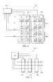
- the two-by-two touch sensorcomprises sense electrodes 440 and the two subsets of pixel-drive electrodes 430 that form drive electrodes 480 .
- pixel-drive electrodes 430are arranged into two subsets (drive electrode 480 a and drive electrode 480 b ), each subset comprises a two-by-four array of pixel-drive electrodes 430 .
- Controller 450is separately connected to each pixel-drive electrode 430 and thus may treat pixel-drive electrodes 430 as separate entities when generating an image and collectively (as subsets) when generating a drive signal to determine a location of a touch input.
- the sensor substrate(not shown), is located between sense electrodes 440 and drive electrodes 480 .
- touch screen controller 450is connected to sense electrodes 440 as well as the individual pixel-drive electrodes 430 that form drive electrodes 480 . This may allow touch screen controller 450 to both adjust the pixel-drive signal to control the image generated by touch screen 400 and to manage the drive signal for the touch sensor used to determine the relative location of a touch input. Because pixel-drive electrodes 430 are used for both the touch sensor functionality and for creating the displayed image, touch screen controller 450 may need to synchronize how and when it sends pixel-drive signals and drive signals.
- pixel-drive electrodeshave been grouped together in rows in the depicted embodiment, some embodiments may group the pixel-drive electrodes into clusters (e.g., two-by-two clusters) or may not group them together at all.
- sense electrodes 440may separately detect a touch input based on a change in the charge, capacitance, or electrical potential from each of the individual pixel-drive electrodes.
- FIG. 5illustrates an overhead view of an example touch screen in which a reference voltage layer provides a display portion of a touch screen with a reference voltage and provides an integrated touch sensor of the touch screen with a drive signal.
- touch screen 500includes touch screen controller 550 coupled to drive electrodes 530 and sense electrodes 540 .
- Drive electrodes 530may be spaced so as to provide a reference voltage for a display layer(s) (not depicted).
- Drive electrodes 530may also be configured to provide drive signals to a touch sensor.
- drive electrodes 530may be oriented perpendicularly to the orientation of sense electrodes 540 .
- drive electrodes 530may be made of fine lines of metal.
- Touch screen controller 550may use drive electrodes 530 to provide drive signals for a touch sensor and to provide a reference voltage for a display layer(s) (e.g., display layer(s) 210 of an LCD display stack). As discussed above with respect to FIG. 4 , touch screen controller 550 may synchronize the reference voltage and the drive signals being sent over drive electrodes 530 . Touch screen controller 550 may then use the sense signal provided by sense electrodes 540 to determine a relative location of a touch input.
- a display layer(s)e.g., display layer(s) 210 of an LCD display stack
- FIGS. 1-5have been described above as including particular components, the systems of FIGS. 1-5 may include any combination of any of the described components and any of the options or features described herein, as would be understood by one of ordinary skill in the art based upon the teachings of the disclosure.
- any of the options or features described hereinmay be utilized in combination with the illustrated embodiments of FIGS. 1-5 and/or any number of the other options or features also described herein as would be understood by one of ordinary skill in the art based upon the teachings of the disclosure.
- a computer-readable non-transitory storage mediummay include a semiconductor-based or other integrated circuit (IC), such as for example a field-programmable gate array (FPGA) or an application-specific IC (ASIC), a hard disk, an HDD, a hybrid hard drive (HHD), an optical disc, an optical disc drive (ODD), a magneto-optical disc, a magneto-optical drive, a floppy disk, a floppy disk drive (FDD), magnetic tape, a holographic storage medium, a solid-state drive (SSD), a RAM-drive, a SECURE DIGITAL card, a SECURE DIGITAL drive, another suitable medium, or a suitable combination of these, where appropriate.
- ICsemiconductor-based or other integrated circuit
- ICsuch as for example a field-programmable gate array (FPGA) or an application-specific IC (ASIC)
- HDDhigh-d hard drive
- HDDhigh-d hard drive
- ODDoptical disc drive
Landscapes
- Engineering & Computer Science (AREA)
- Physics & Mathematics (AREA)
- Theoretical Computer Science (AREA)
- General Engineering & Computer Science (AREA)
- General Physics & Mathematics (AREA)
- Human Computer Interaction (AREA)
- Nonlinear Science (AREA)
- Crystallography & Structural Chemistry (AREA)
- Optics & Photonics (AREA)
- Chemical & Material Sciences (AREA)
- Mathematical Physics (AREA)
- Geometry (AREA)
- Liquid Crystal (AREA)
- Electroluminescent Light Sources (AREA)
- Position Input By Displaying (AREA)
Abstract
Description
Claims (12)
Priority Applications (3)
| Application Number | Priority Date | Filing Date | Title |
|---|---|---|---|
| US13/715,677US9244559B2 (en) | 2012-12-14 | 2012-12-14 | Integrated pixel display and touch sensor |
| US14/983,064US9874963B2 (en) | 2012-12-14 | 2015-12-29 | Integrated pixel display and touch sensor |
| US15/874,149US10331255B2 (en) | 2012-12-14 | 2018-01-18 | Integrated pixel display and touch sensor |
Applications Claiming Priority (1)
| Application Number | Priority Date | Filing Date | Title |
|---|---|---|---|
| US13/715,677US9244559B2 (en) | 2012-12-14 | 2012-12-14 | Integrated pixel display and touch sensor |
Related Child Applications (1)
| Application Number | Title | Priority Date | Filing Date |
|---|---|---|---|
| US14/983,064DivisionUS9874963B2 (en) | 2012-12-14 | 2015-12-29 | Integrated pixel display and touch sensor |
Publications (2)
| Publication Number | Publication Date |
|---|---|
| US20140168133A1 US20140168133A1 (en) | 2014-06-19 |
| US9244559B2true US9244559B2 (en) | 2016-01-26 |
Family
ID=50930307
Family Applications (3)
| Application Number | Title | Priority Date | Filing Date |
|---|---|---|---|
| US13/715,677Active2033-01-12US9244559B2 (en) | 2012-12-14 | 2012-12-14 | Integrated pixel display and touch sensor |
| US14/983,064ActiveUS9874963B2 (en) | 2012-12-14 | 2015-12-29 | Integrated pixel display and touch sensor |
| US15/874,149ActiveUS10331255B2 (en) | 2012-12-14 | 2018-01-18 | Integrated pixel display and touch sensor |
Family Applications After (2)
| Application Number | Title | Priority Date | Filing Date |
|---|---|---|---|
| US14/983,064ActiveUS9874963B2 (en) | 2012-12-14 | 2015-12-29 | Integrated pixel display and touch sensor |
| US15/874,149ActiveUS10331255B2 (en) | 2012-12-14 | 2018-01-18 | Integrated pixel display and touch sensor |
Country Status (1)
| Country | Link |
|---|---|
| US (3) | US9244559B2 (en) |
Cited By (1)
| Publication number | Priority date | Publication date | Assignee | Title |
|---|---|---|---|---|
| US10831317B2 (en) | 2010-08-20 | 2020-11-10 | Neodrón Limited | Electronic ink touch sensitive display |
Families Citing this family (3)
| Publication number | Priority date | Publication date | Assignee | Title |
|---|---|---|---|---|
| CN103197463B (en)* | 2013-03-26 | 2015-06-17 | 京东方科技集团股份有限公司 | Color film substrate and production method, touch screen and display device thereof |
| KR102175563B1 (en)* | 2013-11-13 | 2020-11-06 | 엘지이노텍 주식회사 | Touch panel |
| US9465472B1 (en)* | 2014-08-29 | 2016-10-11 | Amazon Technologies, Inc. | Metal mesh touch sensor with low birefringence substrate and ultraviolet cut |
Citations (35)
| Publication number | Priority date | Publication date | Assignee | Title |
|---|---|---|---|---|
| US4814760A (en) | 1984-12-28 | 1989-03-21 | Wang Laboratories, Inc. | Information display and entry device |
| US6995550B2 (en) | 1998-07-08 | 2006-02-07 | E Ink Corporation | Method and apparatus for determining properties of an electrophoretic display |
| US20080048989A1 (en) | 2006-08-25 | 2008-02-28 | Soo-Wan Yoon | Touch screen display device and method of manufacturing the same |
| US20080062147A1 (en)* | 2006-06-09 | 2008-03-13 | Hotelling Steve P | Touch screen liquid crystal display |
| US20080143689A1 (en) | 2006-12-18 | 2008-06-19 | Foo Ken K | Optical shuttered touchscreen and method therefor |
| US20080309635A1 (en) | 2007-06-14 | 2008-12-18 | Epson Imaging Devices Corporation | Capacitive input device |
| US20090109522A1 (en) | 2002-06-10 | 2009-04-30 | E Ink Corporation | Electro-optic displays, and processes for the production thereof |
| WO2009131292A1 (en) | 2008-04-22 | 2009-10-29 | Atlab Inc. | Touch and proximity sensitive display panel, display device and touch and proximity sensing method using the same |
| WO2009133503A1 (en) | 2008-04-30 | 2009-11-05 | Koninklijke Philips Electronics N. V. | Electrophoretic display window |
| US20090315854A1 (en) | 2008-06-18 | 2009-12-24 | Epson Imaging Devices Corporation | Capacitance type input device and display device with input function |
| US7663607B2 (en) | 2004-05-06 | 2010-02-16 | Apple Inc. | Multipoint touchscreen |
| US20100045632A1 (en) | 2008-04-10 | 2010-02-25 | Atmel Corporation | Capacitive Position Sensor |
| US20100194707A1 (en) | 2009-02-02 | 2010-08-05 | Steven Porter Hotelling | Integrated Touch Screen |
| US7864503B2 (en) | 2007-05-11 | 2011-01-04 | Sense Pad Tech Co., Ltd | Capacitive type touch panel |
| US7875814B2 (en) | 2005-07-21 | 2011-01-25 | Tpo Displays Corp. | Electromagnetic digitizer sensor array structure |
| US20110025639A1 (en) | 2009-08-03 | 2011-02-03 | Matthew Trend | Electrode layout for touch screens |
| US7920129B2 (en) | 2007-01-03 | 2011-04-05 | Apple Inc. | Double-sided touch-sensitive panel with shield and drive combined layer |
| US20110109566A1 (en) | 2009-11-12 | 2011-05-12 | Innocom Technology (Shenzhen) Co., Ltd. | Touch panel with pdlc film and touch-sensitive display device using same |
| US20110109622A1 (en)* | 2009-11-12 | 2011-05-12 | Jung-Eun Son | Stereoscopic liquid crystal display device having touch panel and method for manufacturing the same |
| US8031174B2 (en) | 2007-01-03 | 2011-10-04 | Apple Inc. | Multi-touch surface stackup arrangement |
| US8031094B2 (en) | 2009-09-11 | 2011-10-04 | Apple Inc. | Touch controller with improved analog front end |
| US8040326B2 (en) | 2007-06-13 | 2011-10-18 | Apple Inc. | Integrated in-plane switching display and touch sensor |
| US8049732B2 (en) | 2007-01-03 | 2011-11-01 | Apple Inc. | Front-end signal compensation |
| US20110310459A1 (en) | 2009-10-28 | 2011-12-22 | E Ink Corporation | Electro-optic displays with touch sensors and/or tactile feedback |
| US20120044190A1 (en) | 2010-08-20 | 2012-02-23 | Qrg Limited | Electronic ink touch sensitive display |
| US8179381B2 (en) | 2008-02-28 | 2012-05-15 | 3M Innovative Properties Company | Touch screen sensor |
| US8217902B2 (en) | 2007-04-27 | 2012-07-10 | Tpk Touch Solutions Inc. | Conductor pattern structure of capacitive touch panel |
| US20120242592A1 (en) | 2011-03-21 | 2012-09-27 | Rothkopf Fletcher R | Electronic devices with flexible displays |
| WO2012129247A2 (en) | 2011-03-21 | 2012-09-27 | Apple Inc. | Electronic devices with flexible displays |
| US20120243719A1 (en) | 2011-03-21 | 2012-09-27 | Franklin Jeremy C | Display-Based Speaker Structures for Electronic Devices |
| US20120243151A1 (en) | 2011-03-21 | 2012-09-27 | Stephen Brian Lynch | Electronic Devices With Convex Displays |
| US20120242588A1 (en) | 2011-03-21 | 2012-09-27 | Myers Scott A | Electronic devices with concave displays |
| US20130076612A1 (en) | 2011-09-26 | 2013-03-28 | Apple Inc. | Electronic device with wrap around display |
| US8624845B2 (en) | 2008-09-26 | 2014-01-07 | Cypress Semiconductor Corporation | Capacitance touch screen |
| US8723824B2 (en) | 2011-09-27 | 2014-05-13 | Apple Inc. | Electronic devices with sidewall displays |
Family Cites Families (11)
| Publication number | Priority date | Publication date | Assignee | Title |
|---|---|---|---|---|
| US7625618B1 (en) | 2003-05-15 | 2009-12-01 | Rohr, Inc. | Advanced composite aerostructure article having a braided co-cured fly away hollow mandrel and method for fabrication |
| WO2008007372A2 (en)* | 2006-07-12 | 2008-01-17 | N-Trig Ltd. | Hover and touch detection for a digitizer |
| US8228264B2 (en) | 2007-03-28 | 2012-07-24 | Solomon Systech Limited | Segment driving method and system for a bistable display |
| US8319747B2 (en) | 2008-12-11 | 2012-11-27 | Apple Inc. | Single layer touch panel with segmented drive and sense electrodes |
| TWI381043B (en) | 2008-12-12 | 2013-01-01 | Ghitron Technology Co Ltd | Ion dielectric type touch sensor and device thereof |
| US7995041B2 (en)* | 2009-02-02 | 2011-08-09 | Apple Inc. | Integrated touch screen |
| US20110007011A1 (en) | 2009-07-13 | 2011-01-13 | Ocular Lcd Inc. | Capacitive touch screen with a mesh electrode |
| TWI443554B (en) | 2009-08-05 | 2014-07-01 | Silicon Integrated Sys Corp | Touch detecting device and method thereof |
| EP2520547A4 (en) | 2009-12-28 | 2014-11-19 | Sumitomo Chemical Co | PROCESS FOR THE MANUFACTURE OF A LITHIUM COMPLEX METAL OXIDE |
| US9489072B2 (en) | 2010-04-15 | 2016-11-08 | Atmel Corporation | Noise reduction in capacitive touch sensors |
| KR20120107312A (en) | 2011-03-21 | 2012-10-02 | 한국과학기술연구원 | 3-dimensional displaying apparatus and driving method thereof |
- 2012
- 2012-12-14USUS13/715,677patent/US9244559B2/enactiveActive
- 2015
- 2015-12-29USUS14/983,064patent/US9874963B2/enactiveActive
- 2018
- 2018-01-18USUS15/874,149patent/US10331255B2/enactiveActive
Patent Citations (39)
| Publication number | Priority date | Publication date | Assignee | Title |
|---|---|---|---|---|
| US4814760A (en) | 1984-12-28 | 1989-03-21 | Wang Laboratories, Inc. | Information display and entry device |
| US6995550B2 (en) | 1998-07-08 | 2006-02-07 | E Ink Corporation | Method and apparatus for determining properties of an electrophoretic display |
| US20090109522A1 (en) | 2002-06-10 | 2009-04-30 | E Ink Corporation | Electro-optic displays, and processes for the production thereof |
| US7663607B2 (en) | 2004-05-06 | 2010-02-16 | Apple Inc. | Multipoint touchscreen |
| US7875814B2 (en) | 2005-07-21 | 2011-01-25 | Tpo Displays Corp. | Electromagnetic digitizer sensor array structure |
| US20080062147A1 (en)* | 2006-06-09 | 2008-03-13 | Hotelling Steve P | Touch screen liquid crystal display |
| US20080048989A1 (en) | 2006-08-25 | 2008-02-28 | Soo-Wan Yoon | Touch screen display device and method of manufacturing the same |
| US20080143689A1 (en) | 2006-12-18 | 2008-06-19 | Foo Ken K | Optical shuttered touchscreen and method therefor |
| US8031174B2 (en) | 2007-01-03 | 2011-10-04 | Apple Inc. | Multi-touch surface stackup arrangement |
| US8049732B2 (en) | 2007-01-03 | 2011-11-01 | Apple Inc. | Front-end signal compensation |
| US7920129B2 (en) | 2007-01-03 | 2011-04-05 | Apple Inc. | Double-sided touch-sensitive panel with shield and drive combined layer |
| US8217902B2 (en) | 2007-04-27 | 2012-07-10 | Tpk Touch Solutions Inc. | Conductor pattern structure of capacitive touch panel |
| US7864503B2 (en) | 2007-05-11 | 2011-01-04 | Sense Pad Tech Co., Ltd | Capacitive type touch panel |
| US8040326B2 (en) | 2007-06-13 | 2011-10-18 | Apple Inc. | Integrated in-plane switching display and touch sensor |
| US20080309635A1 (en) | 2007-06-14 | 2008-12-18 | Epson Imaging Devices Corporation | Capacitive input device |
| US8179381B2 (en) | 2008-02-28 | 2012-05-15 | 3M Innovative Properties Company | Touch screen sensor |
| US20100044122A1 (en) | 2008-04-10 | 2010-02-25 | Atmel Corporation | Capacitive Touch Screen with Noise Suppression |
| US20100045632A1 (en) | 2008-04-10 | 2010-02-25 | Atmel Corporation | Capacitive Position Sensor |
| US20110025635A1 (en) | 2008-04-22 | 2011-02-03 | Atlab Inc. | Touch and proximity sensitive display panel, display device and touch and proximity sensing method using the same |
| WO2009131292A1 (en) | 2008-04-22 | 2009-10-29 | Atlab Inc. | Touch and proximity sensitive display panel, display device and touch and proximity sensing method using the same |
| US20110038030A1 (en) | 2008-04-30 | 2011-02-17 | Koninklijke Philips Electronics N.V. | Electrophoretic display window |
| WO2009133503A1 (en) | 2008-04-30 | 2009-11-05 | Koninklijke Philips Electronics N. V. | Electrophoretic display window |
| US20090315854A1 (en) | 2008-06-18 | 2009-12-24 | Epson Imaging Devices Corporation | Capacitance type input device and display device with input function |
| US8624845B2 (en) | 2008-09-26 | 2014-01-07 | Cypress Semiconductor Corporation | Capacitance touch screen |
| US20100194707A1 (en) | 2009-02-02 | 2010-08-05 | Steven Porter Hotelling | Integrated Touch Screen |
| US20110025639A1 (en) | 2009-08-03 | 2011-02-03 | Matthew Trend | Electrode layout for touch screens |
| US8031094B2 (en) | 2009-09-11 | 2011-10-04 | Apple Inc. | Touch controller with improved analog front end |
| US20110310459A1 (en) | 2009-10-28 | 2011-12-22 | E Ink Corporation | Electro-optic displays with touch sensors and/or tactile feedback |
| US8581860B2 (en) | 2009-11-12 | 2013-11-12 | Innocom Technology (Shenzhen) Co., Ltd. | Touch panel with PDLC film and touch-sensitive display device using same |
| US20110109622A1 (en)* | 2009-11-12 | 2011-05-12 | Jung-Eun Son | Stereoscopic liquid crystal display device having touch panel and method for manufacturing the same |
| US20110109566A1 (en) | 2009-11-12 | 2011-05-12 | Innocom Technology (Shenzhen) Co., Ltd. | Touch panel with pdlc film and touch-sensitive display device using same |
| US20120044190A1 (en) | 2010-08-20 | 2012-02-23 | Qrg Limited | Electronic ink touch sensitive display |
| WO2012129247A2 (en) | 2011-03-21 | 2012-09-27 | Apple Inc. | Electronic devices with flexible displays |
| US20120243151A1 (en) | 2011-03-21 | 2012-09-27 | Stephen Brian Lynch | Electronic Devices With Convex Displays |
| US20120242588A1 (en) | 2011-03-21 | 2012-09-27 | Myers Scott A | Electronic devices with concave displays |
| US20120243719A1 (en) | 2011-03-21 | 2012-09-27 | Franklin Jeremy C | Display-Based Speaker Structures for Electronic Devices |
| US20120242592A1 (en) | 2011-03-21 | 2012-09-27 | Rothkopf Fletcher R | Electronic devices with flexible displays |
| US20130076612A1 (en) | 2011-09-26 | 2013-03-28 | Apple Inc. | Electronic device with wrap around display |
| US8723824B2 (en) | 2011-09-27 | 2014-05-13 | Apple Inc. | Electronic devices with sidewall displays |
Non-Patent Citations (11)
| Title |
|---|
| E. Yilmaz, U.S. Appl. No. 12/859,874 Non-final Office Action dated Apr. 20, 2015. |
| E. Yilmaz, U.S. Appl. No. 12/859,874 Non-final Office Action dated Sep. 15, 2014. |
| E. Yilmaz, U.S. Appl. No. 12/859,874, Amendment after Non-Final dated Mar. 15, 2015. |
| E. Yilmaz, U.S. Appl. No. 12/859,874, Amendment to NFOA dated Feb. 11, 2013. |
| E. Yilmaz, U.S. Appl. No. 12/859,874, Amendment to NFOA dated Jul. 20, 2015. |
| E. Yilmaz, U.S. Appl. No. 12/859,874, Final Office Action dated Jun. 5, 2013. |
| E. Yilmaz, U.S. Appl. No. 12/859,874, Non-Final Office Action dated Oct. 11, 2012. |
| E. Yilmaz, U.S. Appl. No. 12/859,874, RCE and Amendment dated Sep. 5, 2013. |
| U.S. Appl. No. 61/454,894, filed Mar. 21, 2011, Rothkopf. |
| U.S. Appl. No. 61/454,936, filed Mar. 21, 2011, Myers. |
| U.S. Appl. No. 61/454,950, filed Mar. 21, 2011, Lynch. |
Cited By (1)
| Publication number | Priority date | Publication date | Assignee | Title |
|---|---|---|---|---|
| US10831317B2 (en) | 2010-08-20 | 2020-11-10 | Neodrón Limited | Electronic ink touch sensitive display |
Also Published As
| Publication number | Publication date |
|---|---|
| US20140168133A1 (en) | 2014-06-19 |
| US20180143722A1 (en) | 2018-05-24 |
| US10331255B2 (en) | 2019-06-25 |
| US9874963B2 (en) | 2018-01-23 |
| US20160132167A1 (en) | 2016-05-12 |
Similar Documents
| Publication | Publication Date | Title |
|---|---|---|
| US10644080B2 (en) | Integrated touch screen | |
| US10659044B2 (en) | On-display-sensor stack | |
| US9395836B2 (en) | System and method for reducing borders of a touch sensor | |
| US9965106B2 (en) | Touch screen with electrodes positioned between pixels | |
| US9262019B2 (en) | Touch sensor with conductive lines having different widths | |
| US20130180841A1 (en) | Sensor Stack with Opposing Electrodes | |
| US10044353B2 (en) | Substantially edgeless touch sensor | |
| US20130181910A1 (en) | Dual-Substrate-Sensor Stack | |
| US9804722B2 (en) | Fast scanning for mutual capacitance screens | |
| US8847898B2 (en) | Signal-to-noise ratio in touch sensors | |
| US9760207B2 (en) | Single-layer touch sensor | |
| US10353502B2 (en) | Touch device | |
| US9791992B2 (en) | Oncell single-layer touch sensor | |
| US10331255B2 (en) | Integrated pixel display and touch sensor | |
| US20130141340A1 (en) | Multi-Surface Touch Sensor | |
| US20130141381A1 (en) | Surface Coverage Touch |
Legal Events
| Date | Code | Title | Description |
|---|---|---|---|
| AS | Assignment | Owner name:ATMEL CORPORATION, CALIFORNIA Free format text:ASSIGNMENT OF ASSIGNORS INTEREST;ASSIGNOR:YILMAZ, ESAT;REEL/FRAME:029474/0695 Effective date:20121212 | |
| AS | Assignment | Owner name:MORGAN STANLEY SENIOR FUNDING, INC. AS ADMINISTRATIVE AGENT, NEW YORK Free format text:PATENT SECURITY AGREEMENT;ASSIGNOR:ATMEL CORPORATION;REEL/FRAME:031912/0173 Effective date:20131206 Owner name:MORGAN STANLEY SENIOR FUNDING, INC. AS ADMINISTRAT Free format text:PATENT SECURITY AGREEMENT;ASSIGNOR:ATMEL CORPORATION;REEL/FRAME:031912/0173 Effective date:20131206 | |
| STCF | Information on status: patent grant | Free format text:PATENTED CASE | |
| AS | Assignment | Owner name:ATMEL CORPORATION, CALIFORNIA Free format text:TERMINATION AND RELEASE OF SECURITY INTEREST IN PATENT COLLATERAL;ASSIGNOR:MORGAN STANLEY SENIOR FUNDING, INC.;REEL/FRAME:038376/0001 Effective date:20160404 | |
| AS | Assignment | Owner name:JPMORGAN CHASE BANK, N.A., AS ADMINISTRATIVE AGENT, ILLINOIS Free format text:SECURITY INTEREST;ASSIGNOR:ATMEL CORPORATION;REEL/FRAME:041715/0747 Effective date:20170208 Owner name:JPMORGAN CHASE BANK, N.A., AS ADMINISTRATIVE AGENT Free format text:SECURITY INTEREST;ASSIGNOR:ATMEL CORPORATION;REEL/FRAME:041715/0747 Effective date:20170208 | |
| AS | Assignment | Owner name:JPMORGAN CHASE BANK, N.A., AS ADMINISTRATIVE AGENT, ILLINOIS Free format text:SECURITY INTEREST;ASSIGNORS:MICROCHIP TECHNOLOGY INCORPORATED;SILICON STORAGE TECHNOLOGY, INC.;ATMEL CORPORATION;AND OTHERS;REEL/FRAME:046426/0001 Effective date:20180529 Owner name:JPMORGAN CHASE BANK, N.A., AS ADMINISTRATIVE AGENT Free format text:SECURITY INTEREST;ASSIGNORS:MICROCHIP TECHNOLOGY INCORPORATED;SILICON STORAGE TECHNOLOGY, INC.;ATMEL CORPORATION;AND OTHERS;REEL/FRAME:046426/0001 Effective date:20180529 | |
| AS | Assignment | Owner name:WELLS FARGO BANK, NATIONAL ASSOCIATION, AS NOTES COLLATERAL AGENT, CALIFORNIA Free format text:SECURITY INTEREST;ASSIGNORS:MICROCHIP TECHNOLOGY INCORPORATED;SILICON STORAGE TECHNOLOGY, INC.;ATMEL CORPORATION;AND OTHERS;REEL/FRAME:047103/0206 Effective date:20180914 Owner name:WELLS FARGO BANK, NATIONAL ASSOCIATION, AS NOTES C Free format text:SECURITY INTEREST;ASSIGNORS:MICROCHIP TECHNOLOGY INCORPORATED;SILICON STORAGE TECHNOLOGY, INC.;ATMEL CORPORATION;AND OTHERS;REEL/FRAME:047103/0206 Effective date:20180914 | |
| MAFP | Maintenance fee payment | Free format text:PAYMENT OF MAINTENANCE FEE, 4TH YEAR, LARGE ENTITY (ORIGINAL EVENT CODE: M1551); ENTITY STATUS OF PATENT OWNER: LARGE ENTITY Year of fee payment:4 | |
| AS | Assignment | Owner name:BOE TECHNOLOGY GROUP CO., LTD., CHINA Free format text:ASSIGNMENT OF ASSIGNORS INTEREST;ASSIGNOR:ATMEL CORPORATION;REEL/FRAME:050950/0594 Effective date:20191014 | |
| AS | Assignment | Owner name:MICROCHIP TECHNOLOGY INCORPORATED, ARIZONA Free format text:RELEASE BY SECURED PARTY;ASSIGNOR:WELLS FARGO BANK, NATIONAL ASSOCIATION, AS NOTES COLLATERAL AGENT;REEL/FRAME:050986/0798 Effective date:20191107 Owner name:ATMEL CORPORATION, ARIZONA Free format text:RELEASE BY SECURED PARTY;ASSIGNOR:JPMORGAN CHASE BANK, N.A., AS ADMINISTRATIVE AGENT;REEL/FRAME:050987/0430 Effective date:20191107 Owner name:MICROCHIP TECHNOLOGY INCORPORATED, ARIZONA Free format text:RELEASE BY SECURED PARTY;ASSIGNOR:JPMORGAN CHASE BANK, N.A., AS ADMINISTRATIVE AGENT;REEL/FRAME:050987/0430 Effective date:20191107 Owner name:ATMEL CORPORATION, ARIZONA Free format text:RELEASE BY SECURED PARTY;ASSIGNOR:WELLS FARGO BANK, NATIONAL ASSOCIATION, AS NOTES COLLATERAL AGENT;REEL/FRAME:050986/0798 Effective date:20191107 | |
| AS | Assignment | Owner name:MICROSEMI STORAGE SOLUTIONS, INC., ARIZONA Free format text:RELEASE BY SECURED PARTY;ASSIGNOR:JPMORGAN CHASE BANK, N.A., AS ADMINISTRATIVE AGENT;REEL/FRAME:059333/0222 Effective date:20220218 Owner name:MICROSEMI CORPORATION, ARIZONA Free format text:RELEASE BY SECURED PARTY;ASSIGNOR:JPMORGAN CHASE BANK, N.A., AS ADMINISTRATIVE AGENT;REEL/FRAME:059333/0222 Effective date:20220218 Owner name:ATMEL CORPORATION, ARIZONA Free format text:RELEASE BY SECURED PARTY;ASSIGNOR:JPMORGAN CHASE BANK, N.A., AS ADMINISTRATIVE AGENT;REEL/FRAME:059333/0222 Effective date:20220218 Owner name:SILICON STORAGE TECHNOLOGY, INC., ARIZONA Free format text:RELEASE BY SECURED PARTY;ASSIGNOR:JPMORGAN CHASE BANK, N.A., AS ADMINISTRATIVE AGENT;REEL/FRAME:059333/0222 Effective date:20220218 Owner name:MICROCHIP TECHNOLOGY INCORPORATED, ARIZONA Free format text:RELEASE BY SECURED PARTY;ASSIGNOR:JPMORGAN CHASE BANK, N.A., AS ADMINISTRATIVE AGENT;REEL/FRAME:059333/0222 Effective date:20220218 | |
| AS | Assignment | Owner name:ATMEL CORPORATION, ARIZONA Free format text:RELEASE BY SECURED PARTY;ASSIGNOR:JPMORGAN CHASE BANK, N.A., AS ADMINISTRATIVE AGENT;REEL/FRAME:059262/0105 Effective date:20220218 | |
| AS | Assignment | Owner name:MICROSEMI STORAGE SOLUTIONS, INC., ARIZONA Free format text:RELEASE BY SECURED PARTY;ASSIGNOR:WELLS FARGO BANK, NATIONAL ASSOCIATION, AS NOTES COLLATERAL AGENT;REEL/FRAME:059358/0001 Effective date:20220228 Owner name:MICROSEMI CORPORATION, ARIZONA Free format text:RELEASE BY SECURED PARTY;ASSIGNOR:WELLS FARGO BANK, NATIONAL ASSOCIATION, AS NOTES COLLATERAL AGENT;REEL/FRAME:059358/0001 Effective date:20220228 Owner name:ATMEL CORPORATION, ARIZONA Free format text:RELEASE BY SECURED PARTY;ASSIGNOR:WELLS FARGO BANK, NATIONAL ASSOCIATION, AS NOTES COLLATERAL AGENT;REEL/FRAME:059358/0001 Effective date:20220228 Owner name:SILICON STORAGE TECHNOLOGY, INC., ARIZONA Free format text:RELEASE BY SECURED PARTY;ASSIGNOR:WELLS FARGO BANK, NATIONAL ASSOCIATION, AS NOTES COLLATERAL AGENT;REEL/FRAME:059358/0001 Effective date:20220228 Owner name:MICROCHIP TECHNOLOGY INCORPORATED, ARIZONA Free format text:RELEASE BY SECURED PARTY;ASSIGNOR:WELLS FARGO BANK, NATIONAL ASSOCIATION, AS NOTES COLLATERAL AGENT;REEL/FRAME:059358/0001 Effective date:20220228 | |
| MAFP | Maintenance fee payment | Free format text:PAYMENT OF MAINTENANCE FEE, 8TH YEAR, LARGE ENTITY (ORIGINAL EVENT CODE: M1552); ENTITY STATUS OF PATENT OWNER: LARGE ENTITY Year of fee payment:8 |