US9239781B2 - Storage control system with erase block mechanism and method of operation thereof - Google Patents
Storage control system with erase block mechanism and method of operation thereofDownload PDFInfo
- Publication number
- US9239781B2 US9239781B2US13/648,869US201213648869AUS9239781B2US 9239781 B2US9239781 B2US 9239781B2US 201213648869 AUS201213648869 AUS 201213648869AUS 9239781 B2US9239781 B2US 9239781B2
- Authority
- US
- United States
- Prior art keywords
- super
- blocks
- block
- memory
- devices
- Prior art date
- Legal status (The legal status is an assumption and is not a legal conclusion. Google has not performed a legal analysis and makes no representation as to the accuracy of the status listed.)
- Active, expires
Links
Images


Classifications
- G—PHYSICS
- G06—COMPUTING OR CALCULATING; COUNTING
- G06F—ELECTRIC DIGITAL DATA PROCESSING
- G06F12/00—Accessing, addressing or allocating within memory systems or architectures
- G06F12/02—Addressing or allocation; Relocation
- G06F12/0223—User address space allocation, e.g. contiguous or non contiguous base addressing
- G06F12/023—Free address space management
- G06F12/0238—Memory management in non-volatile memory, e.g. resistive RAM or ferroelectric memory
- G06F12/0246—Memory management in non-volatile memory, e.g. resistive RAM or ferroelectric memory in block erasable memory, e.g. flash memory
- G—PHYSICS
- G06—COMPUTING OR CALCULATING; COUNTING
- G06F—ELECTRIC DIGITAL DATA PROCESSING
- G06F12/00—Accessing, addressing or allocating within memory systems or architectures
- G06F12/02—Addressing or allocation; Relocation
- G06F12/06—Addressing a physical block of locations, e.g. base addressing, module addressing, memory dedication
- G—PHYSICS
- G06—COMPUTING OR CALCULATING; COUNTING
- G06F—ELECTRIC DIGITAL DATA PROCESSING
- G06F13/00—Interconnection of, or transfer of information or other signals between, memories, input/output devices or central processing units
- G06F13/14—Handling requests for interconnection or transfer
- G06F13/16—Handling requests for interconnection or transfer for access to memory bus
- G06F13/1668—Details of memory controller
- G06F13/1684—Details of memory controller using multiple buses
Definitions
- the present inventionrelates generally to a storage control system and more particularly to a system for data management and control.
- Data storageoften called storage or memory, refers to computer components and recording media that retain digital data.
- Data storageis a core function and fundamental component of consumer and industrial electronics, especially devices such as computers, televisions, cellular phones, mobile devices, and digital video cameras.
- NOT-AND flashis one form of non-volatile memory used in solid-state storage devices.
- the memory cellsare arranged in typical row and column fashion with circuitry for accessing individual cells and placing the memory transistors of those cells store an analog value that can be interpreted to hold two logical states in the case of Single Level Cell (SLC) or more than two logical states in the case of Multi Level Cell (MLC).
- SLCSingle Level Cell
- MLCMulti Level Cell
- a flash memory cellis light in weight, occupies very little space, and consumes less power than electromechanical disk drives. Construction of a storage system with this type of memory allows for much higher bandwidths and input/output operations per second (IOPS) than typical electromechanical disk drives. More importantly, it is especially rugged and can operate at a much high temperature range. It will withstand without adverse effects repeated drops, each of which would destroy a typical electromechanical hard disk drive. A problem exhibited by flash memory is that it tends to have a limited life in use.
- IOPSinput/output operations per second
- the present inventionprovides a method of operation of a storage control system, including: partitioning memory channels with memory devices; selecting a super device with one of the memory devices from one of the memory channels, the super device having a super chip select connected to chip selects of the memory devices; and selecting a super block associated with the super device.
- the present inventionprovides a storage control system, including: a channel control module for partitioning memory channels with memory devices; a device control module for selecting a super device with one of the memory devices from one of the memory channels, the super device having a super chip select connected to chip selects of the memory devices; and a block control module for selecting a super block associated with the super device.
- FIG. 1is a storage control system with data management mechanism in an embodiment of the present invention.
- FIG. 2is an exemplary hardware block diagram of the memory controller.
- FIG. 3is a control flow of the memory controller.
- FIG. 4is an example diagram of memory groups of the memory devices.
- FIG. 5is an example diagram of the super blocks.
- FIG. 6is a flow diagram of a write operation.
- FIG. 7is an example diagram of logical-to-physical page mapping.
- FIG. 8is a functional block diagram of a recycle operation.
- FIG. 9is an example of a detailed control flow of the memory access module.
- FIG. 10is a flow chart of a method of operation of the storage control system of FIG. 1 in a further embodiment of the present invention.
- modulecan include software, hardware, or a combination thereof in the present invention in accordance with the context in which the term is used.
- the softwarecan be machine code, firmware, embedded code, and application software.
- the hardwarecan be circuitry, processor, computer, integrated circuit, integrated circuit cores, a microelectromechanical system (MEMS), passive devices, environmental sensors including temperature sensors, or a combination thereof.
- MEMSmicroelectromechanical system
- the storage control system 100includes a memory sub-system 102 having a memory controller 104 and a memory array 106 .
- the storage control system 100includes a host system 108 communicating with the memory sub-system 102 .
- the memory controller 104provides data control and management of the memory array 106 .
- the memory controller 104interfaces with the host system 108 and controls the memory array 106 to transfer data between the host system 108 and the memory array 106 .
- the memory array 106includes an array of memory devices 110 including flash memory devices or non-volatile memory devices.
- the memory array 106can include pages of data or information.
- the host system 108can request the memory controller 104 for reading, writing, and deleting data from or to a logical address space of a storage device or the memory sub-system 102 that includes the memory array 106 .
- the memory devices 110can include chip selects 112 , which are defined as control inputs, for enabling the memory devices 110 .
- Each of the chip selects 112can be used to control the operation of one of the memory devices 110 .
- Each of the chip selects 112can be used to control sub addresses or logical units (LUNs) within each of the memory devices 110 .
- LUNslogical units
- the memory controller 104can include a control unit 202 , a storage unit 204 , a memory interface unit 206 , and a host interface unit 208 .
- the control unit 202can include a control interface 210 .
- the control unit 202can execute software 212 stored in the storage unit 204 to provide the intelligence of the memory controller 104 .
- the control unit 202can be implemented in a number of different manners.
- the control unit 202can be a processor, an embedded processor, a microprocessor, a hardware control logic, a hardware finite state machine (FSM), a digital signal processor (DSP), or a combination thereof.
- FSMhardware finite state machine
- DSPdigital signal processor
- the control interface 210can be used for communication between the control unit 202 and other functional units in the memory controller 104 .
- the control interface 210can also be used for communication that is external to the memory controller 104 .
- the control interface 210can receive information from the other functional units or from external sources, or can transmit information to the other functional units or to external destinations.
- the external sources and the external destinationsrefer to sources and destinations external to the memory controller 104 .
- the control interface 210can be implemented in different ways and can include different implementations depending on which functional units or external units are being interfaced with the control interface 210 .
- the control interface 210can be implemented with a dedicated hardware including an application-specific integrated circuit (ASIC), a configurable hardware including a field-programmable gate array (FPGA), a discrete electronic hardware, or a combination thereof.
- ASICapplication-specific integrated circuit
- FPGAfield-programmable gate array
- the storage unit 204can include both hardware and the software 212 .
- the software 212can include control firmware.
- the storage unit 204can include a volatile memory, a nonvolatile memory, an internal memory, an external memory, or a combination thereof.
- the storage unit 204can be a nonvolatile storage such as non-volatile random access memory (NVRAM), Flash memory, disk storage, or a volatile storage such as static random access memory (SRAM).
- NVRAMnon-volatile random access memory
- SRAMstatic random access memory
- the storage unit 204can include a storage interface 214 .
- the storage interface 214can also be used for communication that is external to the memory controller 104 .
- the storage interface 214can receive information from the other functional units or from external sources, or can transmit information to the other functional units or to external destinations.
- the external sources and the external destinationsrefer to sources and destinations external to the memory controller 104 .
- the storage interface 214can include different implementations depending on which functional units or external units are being interfaced with the storage unit 204 .
- the storage interface 214can be implemented with technologies and techniques similar to the implementation of the control interface 210 .
- the memory interface unit 206can enable external communication to and from the memory controller 104 .
- the memory interface unit 206can permit the memory controller 104 to communicate with the memory array 106 of FIG. 1 .
- the memory interface unit 206can include a memory interface 216 .
- the memory interface 216can be used for communication between the memory interface unit 206 and other functional units in the memory controller 104 .
- the memory interface 216can receive information from the other functional units or can transmit information to the other functional units.
- the memory interface 216can include different implementations depending on which functional units are being interfaced with the memory interface unit 206 .
- the memory interface 216can be implemented with technologies and techniques similar to the implementation of the control interface 210 .
- the host interface unit 208allows the host system 108 of FIG. 1 to interface and interact with the memory controller 104 .
- the host interface unit 208can include a host interface 218 to provide communication mechanism between the host interface unit 208 and the host system 108 .
- the control unit 202can operate the host interface unit 208 to send control or status information generated by the memory controller 104 to the host system 108 .
- the control unit 202can also execute the software 212 for the other functions of the memory controller 104 .
- the control unit 202can further execute the software 212 for interaction with the memory array 106 via the memory interface unit 206 .
- the functional units in the memory controller 104can work individually and independently of the other functional units.
- the memory controller 104is described by operation of the memory controller 104 with the host system 108 and the memory array 106 . It is understood that the memory controller 104 , the host system 108 , and the memory array 106 can operate any of the modules and functions of the memory controller 104 .
- the memory controller 104can include a channel control module 302 , a device control module 304 , a block control module 306 , and a memory access module 308 .
- the channel control module 302is for performing operations associated with memory channels 404 of FIG. 4 .
- the device control module 304is for performing operations associated with super devices 406 of FIG. 4 .
- the block control module 306is for performing operations associated with super blocks 502 of FIG. 5 .
- the memory access module 308is for performing operations to access data in the memory devices 110 of FIG. 1 based on the super blocks 502 . Operations of the channel control module 302 , the device control module 304 , the block control module 306 , and the memory access module 308 will be described in more details in subsequent sections.
- the memory groups 402are defined as logical association or grouping of physical instances of the memory devices 110 .
- the term “logical”refers to non-physical and thus does not represent the physical configuration of the memory devices 110 .
- the memory groups 402can be identified by the channel control module 302 of FIG. 3 . Each of the memory groups 402 can be identified as being associated with a number of the memory devices 110 . Although each of the memory groups 402 is shown associated with eight of the memory devices 110 for illustration purposes, it is understood that each of the memory groups 402 can be associated with any number of the memory devices 110 .
- Each of the squares in FIG. 4is one of the memory devices 110 , which can represent independently controllable memory devices.
- the memory devices 110can represent dies or logical unit numbers (LUNs).
- LUNslogical unit numbers
- An important pointis that the memory devices 110 can execute commands independently from each other allowing parallel operations. This independent operation is used to gain greater bandwidths and high I/O operations (IOPS).
- the channel control module 302can partition each of the memory channels 404 that are associated with a number of the memory devices 110 .
- Each of the memory channels 404is defined as a physical bank or a physical group of the memory devices 110 that share a common data bus and a common set of associated control signals.
- the memory channels 404can represent an independent bus or communication path. Each of the memory channels 404 can represent an independent execution unit. Each of the memory channels 404 can include an ability to perform independent and parallel operations with respect to other instances of the memory channels 404 .
- Actions, commands, and status information transmitted within one of the memory channels 404can be limited to the memory devices 110 that are connected to the one of the memory channels 404 and can be independent from other instances of the memory channels 404 within a storage device. Data bus and control signals of one of the memory channels 404 cannot be shared with the other instances of the memory channels 404 .
- Each of the memory channels 404can include a number of bits of data based on a type of the memory devices 110 .
- each of the memory channels 404can include 8 bits, 16 bits, or any number of bits of data bus depending on the type of the memory devices 110 used and the construction of the memory controller 104 .
- the memory channels 404can represent physical channels.
- one of the memory channels 404can control or have ownership of a set of the memory devices 110 that share a common data bus and control signals.
- the memory devices 110can represent flash devices or flash components that independently operate from each other.
- the device control module 304 of FIG. 3can identify or select the super devices 406 , which are defined as groups of the memory devices 110 .
- the super devices 406can include portions of the memory channels 404 .
- the super devices 406can be selected with one of the memory devices 110 from one of the memory channels 404 .
- the term “super” in the super devices 406refers to a group of multiple hardware instances of the memory devices 110 .
- the device control module 304can group the memory devices 110 from the memory channels 404 to form the super devices 406 . For example, if there are 16 of the memory channels 404 and 8 of the memory devices 110 per each of the memory channels 404 , there can be 8 of the memory devices 110 , one from each of the memory channels 404 , grouped together for each of the super devices 406 and 16 of the super devices 406 as shown in FIG. 4 .
- the super devices 406can include a number of the memory devices 110 that are controlled in parallel across a number of the memory channels 404 .
- the super devices 406can be constructed with or associated with any number of the memory channels 404 that are executed in parallel.
- Each of the super devices 406can be associated with one of the memory devices 110 from each of the memory channels 404 . Although each of the super devices 406 is shown having 8 of the memory devices 110 for illustration purposes, it is understood that each of the super devices 406 can include any number of the memory devices 110 . For example, each of the super devices 406 can include up to a number of the memory channels 404 . Also for example, all of the super devices 406 can have the same structure and size. Each of the super devices 406 can include any number of the memory devices 110 per each of the memory channels 404 . In this case, there can be multiple passes made or accessed through the memory channels 404 . For example, each of the super devices 406 can include a number of the memory channels 404 with 2 of the memory devices 110 per each of the memory channels 404 .
- Each of the super devices 406can include one of the memory devices 110 from each of the memory channels 404 .
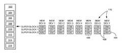
- Each of the super devices 406can include a number of the super blocks 502 of FIG. 5 , each of which can include a number of erase blocks 408 (EB).
- the super blocks 502are defined as logical groupings of the erase blocks 408 in the memory devices 110 .
- the number of the super devices 406can be based on a number of independently accessible instances of the memory devices 110 on the memory channels 404 selected by Chip Enables (CEs), logically addressable units (LUNs), or a combination thereof.
- CEsChip Enables
- LUNslogically addressable units
- the erase blocks 408are units of a non-volatile memory device or other types of block oriented non-volatile memory devices.
- the erase blocks 408can be one of atomic units of a NAND flash memory device or other types of block oriented non-volatile memory devices, which no finer control over erasing memory elements is capable.
- the erase blocks 408can form a part of a logically addressable memory space within a NAND flash or other type of block oriented non-volatile memory devices.
- the erase blocks 408can represent the smallest unit of memory that can be erased.
- the memory devices 110can represent NAND packages that can include multiple dies or logically addressable units (LUNs). Each of the dies or LUNs can include multiple planes, each of which can include a number of the erase blocks 408 . Each of the erase blocks 408 can include a number of pages, which can include a number of bytes.
- each of the planescan include approximately 2048 of the erase blocks 408 .
- each of the erase blocks 408can include 256 pages, each of which can include 8K bytes, where each 1K bytes includes 1024 bytes.
- a diecan include approximately 4096 of the erase blocks 408 divided into two of the planes with 2048 of the erase blocks 408 per plane.
- each of the super devices 406can access one of the super blocks 502 at any given instance.
- Each of the super blocks 502can include a number of the erase blocks 408 that are accessible by one of the super devices 406 at any given time.
- the erase blocks 408can be assigned across the memory channels 404 so that they can be accessed in a parallel approach.
- One of the erase blocks 408can be assigned per each of the memory channels 404 to form one of the super blocks 502 in the super devices 406 .
- the erase blocks 408can be 8 active instances of the erase blocks 408 associated with the one of the super devices 406 .
- the 8 active instances of the erase blocks 408can belong to a specific instance of the super blocks 502 .
- the present inventioncan include architecture and use of the memory devices 110 including NAND flash or other block oriented non-volatile memory organized in efficient groups to reduce the overhead of and runtime management in a solid state storage device.
- the present inventioncan include the super blocks 502 as an organization of memory blocks for parallel use by multiple memory controllers and the logical and physical linkage between the memory blocks.
- the present inventioncan provide additional organization for data protection via RAID operations with reduced overhead for both runtime recycling and drive initialization speed.
- the present inventioncan provide an additional structure for managing bad block memory elements without detriment or loss of system performance or efficiency.
- the super blocks 502provide the following effects.
- One of the effectsis amount of metadata that is stored in each of the erase blocks 408 is minimized or reduced. Such metadata can now be stored at a super-block level or in one of the super blocks 502 .
- Another of the effectsis fewer blocks are managed as well as reduction in time to initialize these data structures.
- Another of the effectsis host data is written to the super blocks 502 in a deterministic order.
- Another of the effectsis recycling can traverse or access the super blocks 502 in the same order by which the host system 108 writes data. As a result, recycling operations can preserve the same order used in write operations providing data striping for optimal read-back performance.
- the super devices 406provide improved performance by grouping of the memory devices 110 that are controlled in parallel across a number of the memory channels 404 .
- the super blocks 502are defined as groups of the erase blocks 408 .
- the groups of the erase blocks 408can be operated as one virtual erase block, which can be included within one of the super devices 406 .
- the super blocks 502allow the management of a group of individual physical instances of the erase blocks 408 as though it was one larger erase block. Actions including host writes, recycling operations, or erasing of blocks can be performed on a set of the erase blocks 408 included within one of the super blocks 502 as a single unit.
- Each of the super blocks 502can be identified and selected by the block control module 306 of FIG. 3 .
- Each of the super blocks 502is defined as a group of the erase blocks 408 that span across multiple of the memory channels 404 within one of the super devices 406 .
- each of the memory devices 110 in the super blocks 502can contribute a pair of the erase blocks 408 that can be accessed together.
- Each of the super blocks 502can be selected to be associated with the super devices 406 .
- Each of the super blocks 502can be accessed via and associated with only one of the super devices 406 . Since the super devices 406 span across multiple of the memory channels 404 , the super blocks 502 can also span across multiple of the memory channels 404 .
- the term “spanning across” used above for the super blocks 502refers to portions of different instances of the memory channels 404 are included in each of the super blocks 502 .
- the super devices 406can be included in a solid-state drive or a storage system dictated by a number of addressable elements within the memory channels 404 that can be controlled in a parallel method of operation.
- All the chip selects 112 of FIG. 1 of the memory devices 110can be partitioned into groups that can be controlled by super chip selects 504 .
- the super chip selects 504can be selected by the block control module 306 .
- the super chip selects 504can be selected by partitioning the chip selects 112 .
- the super chip selects 504are defined as groups of the chip selects 112 that are associated with the erase blocks 408 that form the corresponding instances of the super blocks 502 .
- One of the super chip selects 504is selected to be associated with one of the super blocks 502 and a group of the chip selects 112 of the memory devices 110 that are associated with the one of the super blocks 502 .
- the one of the super chip selects 504can be used to control the group of the chip selects 112 .
- the super chip selects 504are associated with the super blocks 502 .
- the super chip selects 504are provided by the block control module 306 to control operation of the memory devices 110 .
- the super chip selects 504can be used to assert or de-assert the chip selects 112 .
- the chip selects 112can be asserted or de-asserted to enable or disable, respectively, the memory devices 110 .
- the chip selects 112can be asserted or de-asserted by the block control module 306 assigning the super chip selects 504 to an active or inactive state such that the chip selects 112 are driven to logic ‘1’ or ‘0’, respectively, to enable or disable the memory devices 110 .
- Each of the super blocks 502can span or include only one of the super chip selects 504 .
- one of the super chip selects 504can be available for writing host data from the host system 108 of FIG. 1 to the memory array 106 of FIG. 1 and another of the super chip selects 504 can be provided for reading and writing recycling data to the memory array 106 .
- the partition of the chip selects 112 and the provision of the super chip selects 504eliminate conflict between host write and block erase operations because these operations are performed with difference instances of the super chip selects 504 . Furthermore, conflict between host read and host write (or recycle) operations can also be eliminated by mutual exclusion between operations on the super chip selects 504 .
- the last instance of the erase blocks 408 at the end of one of the super blocks 502can be written by the block control module 306 .
- the last instance of the erase blocks 408can be written with parity information 506 for RAID-5 architectures.
- the size of each of the super blocks 502can determine the overhead in the RAID-5 architectures.
- the last instance of the erase blocks 408is the last block to be accessed in the order by which the erase blocks 408 in the super blocks 502 are written by the host system 108 .
- RAID-5refers to an implementation for redundant array of independent disks (RAID) systems that uses block-level striping with parity data distributed across all member disks.
- An allocation of the erase blocks 408 within one of the super blocks 502can provide additional area for storage of the parity information 506 including RAID parity data.
- the parity information 506can only be complete after a full stripe across all the erase blocks 408 within the super blocks 502 are written.
- the parity information 506can be stored within one of the super blocks 502 .
- the parity information 506is defined as redundancy data that is used to rebuild or reconstruct a memory array to recover lost or corrupt data.
- the parity information 506can be calculated by the block control module 306 using exclusive-OR (XOR) binary operation performed on the data to be stored.
- XORexclusive-OR
- the parity pagescan be read only if there is an error correction code (ECC) error in one of the data pages in the super blocks 502 .
- ECCerror correction code
- the parity pagescan only be used in a case of an uncorrectable error and thus can have an extremely low read count, making them less susceptible to read disturb issues.
- Data retention in parity blockscan be better than that of data blocks in the super blocks 502 that are read a large number of times.
- a read disturb in the memory devices 110is a change of values of memory cells by an act of reading a memory cell or other memory cells within the memory devices 110 .
- read disturbscan be limited to cells within one of the erase blocks 408 .
- An example of thisis reading from one page of memory within one of the erase blocks 408 in the memory devices 110 can corrupt and change memory cells in other pages within the one of the erase blocks 408 .
- the read disturb affectrefers to the process of reading memory will create errors in the memory. Read disturbs are not always permanent and can be corrected when the memory is rewritten.
- Read-write and read-erase conflictscan be minimized by the block control module 306 .
- the conflictscan be minimized by partitioning the super blocks 502 using the super chip selects 504 .
- the super blocks 502There are positive factors of having the super blocks 502 .
- the positive factorsinclude fewer blocks to manage, fewer metadata pages 508 , infrastructure support for a RAID-5 implementation, and minimization of writes to a logical-to-physical (L2P) log during recycling.
- the metadata pages 508can be written by the block control module 306 to include logical page indexes.
- the metadata pages 508can be grouped and written once per each of the super blocks 502 as opposed to keeping metadata in each of the erase blocks 408 . This grouping of the metadata can also make traversing it during drive initialization more efficient.
- Metadatarefers to non-host related information that is in addition to and stored along with host data and that aids or supports retrieval, organization, health of, and current condition or state of the memory devices 110 .
- metadatacan include non-host related information including logical-to-physical mapping information of the host data within the memory devices 110 .
- metadatacan include non-host related information including logical block address (LBA) information, super block identification (ID) values, program/erase (PE) cycles, aging data, and other NAND statistics that is collected as a consequence of normal operations.
- LBAlogical block address
- IDsuper block identification
- PEprogram/erase
- transient metadata held or stored in the storage unit 204with a Random access memory (RAM), a Static random-access memory (SRAM), and a double data rate-synchronous dynamic random access memory (DDRAM).
- RAMRandom access memory
- SRAMStatic random-access memory
- DDRAMdouble data rate-synchronous dynamic random access memory
- persistent metadata held or stored in the memory devices 110there can be persistent metadata held or stored in the memory devices 110 .
- the memory devices 110 that form the super devices 406can be fixed through the life of a storage drive. It is understood that this assignment of the memory devices 110 to the super devices 406 can be determined in a number of ways because there can be unpopulated instances of the memory devices 110 in the storage drive.
- the super blocks 502can be formed in each of the super devices 406 . For example, since the super blocks 502 spans multiple of the memory channels 404 , 8 pages within one of the super blocks 502 can be concurrently written.
- a number of concurrent writescan be per logical unit (LUN) or dies.
- LUNlogical unit
- Each of the pagescan be specifically on separate instances of the memory channels 404 , or LUNs, and not just within one of the erase blocks 408 .
- Multiple of the erase blocks 408 grouped into each of the super blocks 502 by the block control module 306provide several advantages.
- One of the advantagesis that there fewer of the super blocks 502 than a number of the erase blocks 408 to manage and initialize by the block control module 306 .
- lists of the super blocks 502can be managed by the block control module 306 .
- data management resources including management data structures for managing the super blocks 502are smaller or less.
- the super blocks 502By creating the super blocks 502 that span multiple of the chip selects 112 of the memory devices 110 , additional advantages are achieved.
- One advantageis that the super blocks 502 provide an infrastructure that supports an internal redundant array of independent disks (RAID) architecture including RAID-5.
- the super blocks 502can be created in a way that facilitates efficient host performance, recycling, RAID, and load balancing performed by the memory access module 308 .
- RAID parity informationcan be part of and limited to contents of the one of the super blocks 502 . As such, operations to the one of the super blocks 502 self-contained with respect to providing RAID error protection to host data and any stored metadata information.
- a number of the erase blocks 408 in each of the super blocks 502can be determined by the super devices 406 of FIG. 4 .
- each of the super blocks 502can include at least 16 of the erase blocks 408 .
- Another advantage of the super blocks 502is that the super blocks 502 can include a number of the erase blocks 408 that are bad or remapped. If one of the super blocks 502 includes a number of the erase blocks 408 that are bad blocks, the entirety of the one of the super blocks 502 would not be rendered as useless.
- the erase blocks 408 that are bad or unusablecan be remapped by the block control module 306 .
- each of the erase blocks 408does not have to be associated with the same erase block number (or address) in each of the elements.
- a portion of the 23rd instance of the super blocks 502can include a number of the erase blocks 408 as follows.
- “Channel”is a corresponding channel number of the memory channels 404
- “CE 0 ”is chip enable 0
- “LUN 0 ”is logical unit 0
- “erase block”is an nth instance of the erase blocks 408 .
- RAID-5presents significant problems for recycling because parity pages need to be recycled along with data pages.
- data and parity pagesare recycling together by the memory access module 308 .
- the super blocks 502also provide a way for a recycling operation performed by the memory access module 308 to traverse data in the order by which that data is written. This operation minimizes the number of writes to the logical-to-physical log. This operation minimizes the number of writes to the logical-to-physical log, especially when the host system 108 writes larger data blocks.
- the program-erase count 510is defined as a numerical value indicating a number of times or cycles the memory devices 110 associated with the corresponding instances of the super blocks 502 are programmed or erased by the memory access module 308 .
- the valid-page count 512is defined as a numerical value indicating a number of pages that are valid in each of the super blocks 502 .
- host datacan be written in the order it arrives from the host and because all data pages within the memory devices 110 can be written sequentially and contiguously, one or more new version of the same host logical sector can exist within the super blocks 502 .
- only one of the host sectorscan be valid, making other copies in the super blocks 502 invalid.
- the valid state of the pages within one of the super blocks 502can be held in both the metadata pages 508 stored within the super blocks 502 and in the logical-to-physical (L2P) tabling system within the runtime volatile memory in the storage device.
- L2Plogical-to-physical
- Each of the super blocks 502can include one of the metadata pages 508 , denoted as Page- 63 .
- Each of the metadata pages 508can span multiple physical pages and is not limited to a single physical page depending on a number of elements in each of the super blocks 502 and the amount of metadata required for each element.
- Each of the super blocks 502can include only one of the metadata pages 508 .
- the metadata pages 508can include logical page indexes of the super blocks 502 . If the size of the super blocks 502 is properly determined, each of the metadata pages 508 can have a size that matches a size of a physical page in the memory devices 110 .
- the metadata pages 508can include any additional information stored along with host data that can aid in retrieval, organization, health of, and current condition or state of the memory devices 110 .
- the metadata pages 508can include but is not limited to a logical to physical mapping information of the host data within the memory devices 110 .
- the metadata pages 508 that are held within one of the super blocks 502can represent metadata specific to the one of the super blocks 502 .
- the metadata pages 508can be used to restore a host logical to physical mapping of data and a valid state of data stored within the one of the super blocks 502 .
- the metadata pages 508can also be used for storing the health and use status of the super blocks 502 .
- the metadata pages 508can be used to record the current recycling or runtime state of the super blocks 502 .
- the metadata pages 508are labeled by “page- 63 ” to indicate that the metadata pages 508 are stored in page 63 of one of the erase blocks 408 having 64 pages, although it is understood that the metadata pages 508 can be stored in the last page or any of the pages in the erase blocks 408 .
- Recycling operations performed by the memory access module 308can traverse or access data by following the same order by which host-write operations follow. As such, the original striping can be preserved. A number of operations for writing to the L2P log can be minimized.
- the super-block organizationis conducive to implementing RAID 5 within the storage drive.
- the last instance of the erase blocks 408 in each of the super blocks 502can include parity pages.
- paritycan be generated using exclusive-OR operations (XOR).
- the memory controller 104can include support for initializing, building, and writing the parity pages.
- Factory and run-time defectscan be handled by the memory access module 308 . If one of the erase blocks 408 within one of the super blocks 502 is bad, the entirety of the one of the super blocks 502 can optionally be thrown away. In addition, bad instances of the erase blocks 408 in the one of the super blocks 502 can be skipped or ignored by the memory access module 308 .
- the memory access module 308can be implemented with the software 212 of FIG. 2 to process the super blocks 502 with missing or bad instances of the erase blocks 408 .
- Statistics for the erase blocks 408can be used by the block control module 306 to estimate remaining lifetime of the storage drive or to extend the life of the storage drive if the super blocks 502 are provided with erase-block granularity.
- the chip selects 112 of the memory devices 110 that are not usedcan be processed by the block control module 306 .
- Each of the super blocks 502can include the program-erase count 510 .
- the program-erase count 510 and the valid-page count 512can be managed at a super-block level by the block control module 306 .
- the program-erase count 510can be calculated by the block control module 306 each time the memory devices 110 are accessed for a program operation or an erase operation by the memory access module 308 .
- the program-erase count 510can be used by the block control module 306 to determine if wear begins to deteriorate the integrity of the memory devices 110 .
- the super blocks 502can include any number of unusable blocks 514 , which are defined as blocks that are no longer available for access. If one of the erase blocks 408 is one of the unusable blocks 514 , writing and recycling operations performed by the memory access module 308 on the corresponding instance of the super blocks 502 can skip over the one of the erase blocks 408 .
- the super blocks 502can include remapped blocks for the unusable blocks 514 .
- the erase blocks 408can represent spare blocks 516 , which are blocks that are available for use. If the memory devices 110 include the spare blocks 516 , one of the erase blocks 408 that is one of the unusable blocks 514 can be remapped to one of the spare blocks 516 by the memory access module 308 . Remapping is preferably not spanned over different instances of the memory devices 110 .
- the performance improvements from the use of the super blocks 502can be from but not limited to the centralized storage of the metadata pages 508 in a single location instead of in each of the erase blocks 408 in the super blocks 502 .
- Each access to one of the erase blocks 408can incur a latency overhead of reading and writing.
- the remapping functioncan allow each of the super blocks 502 to have a full compliment of the erase blocks 408 . All of the erase blocks 408 within one of the super devices 406 can be accessed in a parallel approach with the one of the super devices 406 active.
- the super blocks 502 spanning multiple of the memory channels 404provide improved performance since multiple pages within each of the super blocks 502 are capable of being written concurrently by the memory access module 308 .
- the super blocks 502 spanning multiple of the chip selects 112 of the memory devices 110provide improved reliability with an infrastructure that supports an internal redundant array of independent disks (RAID) architecture including RAID-5.
- RAIDredundant array of independent disks
- the super blocks 502 including a number of the erase blocks 408 that are bad or remappedprovides improved memory resource utilization since the super blocks 502 with the unusable blocks 514 do not have to be thrown away but instead the unusable blocks 514 are able to be remapped with the spare blocks 516 by the memory access module 308 thereby eliminating the shortcoming of traditional super blocks where a bad block renders the entire super block useless.
- the super blocks 502provide improved performance since there are fewer statistics, including the program-erase count 510 and the valid-page count 512 , included in the metadata pages 508 that need to be managed by the block control module 306 .
- FIG. 6therein is shown a flow diagram of a write operation.
- the flow diagramdepicts function of the write operation performed by the memory access module 308 of FIG. 3 to control data flow through the memory groups 402 of FIG. 4 of the memory devices 110 .
- the flow diagramalso depicts how the erase blocks 408 for the write operation can be traversed or accessed.
- the write operationis described as follows for host write data from the host system 108 of FIG. 1 to the memory array 106 of FIG. 1 with the write operation performed by the memory access module 308 .
- the super blocks 502 of FIG. 5can represent a virtual erase block. Similar to physical erase blocks (not shown) of the memory devices 110 , the super blocks 502 as a virtual erase block can be written in sequential order by the memory access module 308 . Because data pages are in different instances of the memory channels 404 and physically different instances of the erase blocks 408 , this virtual erase block can be ordered such that multiple of the data pages can be written at the same time by the memory access module 308 .
- the super blocks 502can represent a 1024-page erase block.
- “8K” mentioned aboverefers to a number of user bytes in a NAND flash page.
- pagescan include a power of 2 bytes of user data and additional bytes for use by ECC and the metadata pages 508 .
- “8K”refers to 8192 bytes.
- a pagecan include 8192+640 bytes of storage, in which case 8K bytes (8192) can be used for host data and 640 extra bytes can be used for but not limited to storing logical block address (LBA) information, ECC parity bytes, and NAND health information.
- LBAlogical block address
- ECC parity bytesECC parity bytes
- NAND health informationlogical block address
- the super blocks 502can be used to implement RAID-5 architectures within the storage drive.
- the parity pagescan be stored by the memory access module 308 in the last instance of the erase blocks 408 within each of the super blocks 502 . All the parity pages would be included in the same instance of the erase blocks 408 .
- datacan be stored by the memory access module 308 in the first six instances of the memory channels 404 in one of the super blocks 502 .
- either data or optionally one of the metadata pages 508can be stored by the memory access module 308 in the seventh instance of the memory channels 404 and a parity page can be stored by the memory access module 308 in the eighth or last instance of the memory channels 404 .
- the instance of the erase blocks 408can be used or read only if there are uncorrectable error correction code (ECC) errors, the instance of the erase blocks 408 would not experience read disturbs.
- ECCerror correction code
- a RAID stripe operationcan be performed such that a parity page is not stored in the same instance of the memory devices 110 that are used to store data pages.
- the parity pagecan be written by the memory access module 308 .
- a RAID buffercan be used to maintain the current parity page by the memory access module 308 for each instance of the super blocks 502 that is open.
- the super blocks 502 that are openare blocks that are still under construction. In other words, the super blocks 502 are still being added to or being filled with user data or the metadata pages 508 have not been written. Any time there are unwritten pages in any of the erase blocks 408 that make up one of the super blocks 502 , the one of the super blocks 502 is considered open. In other words, open also refers to not completely logically written.
- the super blocks 502can be closed without writing all of the physical pages, but when the state of the super blocks 502 is set to “closed”, no more writing is allowed to take place, even if there are gaps or un-written pages within the super blocks 502 .
- the memory access module 308can include 12 RAID buffers for building or generating parity pages. As a result, 12 different RAID stripes can be operated at any given time. When RAID is not implemented on a super block basis, larger sizes of the super blocks 502 and less space for the parity pages can be used by the memory access module 308 .
- FIG. 7therein is shown an example diagram of logical-to-physical page mapping.
- the example diagramdepicts a mapping operation of logical pages 702 mapped to physical pages 704 in the memory devices 110 of FIG. 1 .
- the mapping operationcan be performed by the block control module 306 of FIG. 3 .
- the logical pages 702are defined as association or grouping of the physical pages 704 in the memory devices 110 .
- the physical pages 704are defined as pages in the memory devices 110 .
- the logical pages 702are different from the physical pages 704 .
- the logical pages 702do not represent the physical arrangement of pages in the memory devices 110 .
- the physical pages 704represent the physical arrangement of pages in the memory devices 110 .
- the physical pages 704can represent flash pages.
- the example diagramdepicts a first physical instance, denoted as “Device 0 ”, of the memory devices 110 .
- the first physical instancecan include 128 of the physical pages 704 , each of which spans across 8 of the memory channels 404 of FIG. 4 , denoted as “Ch 0 ”, “Ch 1 ” . . . “Ch 7 ”.
- 8K of the physical pages 704 in Device 0can be mapped by the block control module 306 to two 4K of the logical pages 702 , where 1K is equal to 1024.
- one of the metadata pages 508can be mapped by the block control module 306 to one of the physical pages 704 , denoted as “Ch 7 , Device 0 , Page 127 ”.
- FIG. 8therein is shown a functional block diagram of a recycle operation.
- the functional block diagramdepicts an operation of recycling data performed by the memory access module 308 of FIG. 3 .
- the memory access module 308can include a flash translation layer (FTL), not shown, to recycle the super blocks 502 of FIG. 5 for different reasons. Some of these reasons can include freeing space and wear leveling. Regardless of the reason, the FTL can perform the same steps to recycle the super blocks 502 .
- FTLflash translation layer
- the functional block diagramdepicts some of the logical pages 702 , denoted with strikethroughs, which are not kept and therefore not written to the external memory by the memory access module 308 .
- the external memorycan be implemented in the memory access module 308 .
- the external memorycan be implemented using the storage unit 204 .
- the storage unit 204can include Double Data Rate Random Access Memory (DDR RAM or DDRAM) or Scratch Pad Memory (SPM) to implement the external memory.
- DDR RAMDouble Data Rate Random Access Memory
- SPMScratch Pad Memory
- valid pages in the memory devices 110 controlled by the chip selects 112can be rebalanced during the recycling operation performed by the memory access module 308 .
- the valid pagesare the last temporal copy of a given host logical page. Every time the host system 108 of FIG. 1 writes a logical sector or page, any previous copy of the logical sector or page that is held within persistent or non-persistent memory can be then considered not valid or an older copy.
- the non-persistent memorycan represent the memory devices 110 .
- the functional block diagramdepicts an example of first 16 of the logical pages 702 of one of the super blocks 502 .
- the functional block diagramdepicts how the recycle operation compact data by the memory access module 308 .
- the metadata pages 508 of FIG. 5are excluded in the functional block diagram for convenience of analyzing load balancing performed by the memory access module 308 .
- the functional block diagramdepicts recycle pages 802 and write pages 804 .
- the recycle pages 802are a number of the logical pages 702 that are not saved to the external memory by the memory access module 308 .
- the memory channels 404 that include the recycle pages 802denoted with strikethroughs, are to be made available for writing data, for example, either during the recycle operation or in subsequent write operations performed by the memory access module 308 .
- the write pages 804are a number of the logical pages 702 that are kept and thus to be saved to the external memory by the memory access module 308 . Subsequently, the write pages 804 can be written or saved by the memory access module 308 to first 8 of the memory channels 404 , some of which are made available by not keeping the recycle pages 802 .
- the recycle operation performed by the memory access module 308can rebalance the data between the memory channels 404 .
- one of the super blocks 502spans across eight instances of the memory channels 404 , denoted as Channel 0 to Channel 7 .
- Channel 0 , Channel 1 , Channel 2 , Channel 3 , Channel 4 , Channel 5 , Channel 6 , and Channel 7include a number of the logical pages 702 that are determined valid by the memory access module 308 as 0 , 1 , 2 , 2 , 0 , 0 , 2 , and 1 , respectively.
- the recycle operationcan rebalance the data between the memory channels 404 with Channel 0 , Channel 1 , Channel 2 , Channel 3 , Channel 4 , Channel 5 , Channel 6 , and Channel 7 having a number of the logical pages 702 that are valid as 1 , 1 , 1 , 1 , 1 , 1 , 1 , and 1 , respectively.
- the data that are writtencan be kept together, for example, in large single blocks during the write operation and after the recycle operation are completed by the memory access module 308 .
- data pagescan be moved by the memory access module 308 in the same order that the host system 108 writes the data pages. As such, the number of writes to the L2P log can be minimized when recycling large-block writes is performed by the memory access module 308 .
- all the erase blocks 408 in each of the super blocks 502can be erased at the same time by the memory access module 308 .
- the entirety of the super devices 406 of FIG. 4 associated with the super blocks 502 being erasedis unavailable for reads.
- the super blocks 502can optionally be erased in smaller groups or even singularly to accommodate read operations requested by the host system 108 or conserve operation power. It is understood that the super devices 406 that are used in the erasure operation can be different from the super devices 406 that are used in the write operation requested by the host system 108 . Therefore, the erasure or recycle operation does not affect host writes.
- the memory devices 110can represent 32-nanometer (nm) multi-level cell (MLC) flash memory devices.
- the memory devices 110can include a multi-plane architecture.
- the memory devices 110can be used to construct a 512-gigabyte (GB) drive.
- the memory devices 110can include 4096 of the erase blocks 408 and additional blocks for the spare blocks 516 of FIG. 5 .
- the memory devices 110can include 128 of 8K pages per each of the erase blocks 408 , where 1K is equal to 1024.
- there can be 512K of the erase blocks 408each having a size of 1-megabyte (MB), where 1 MB is equal to 2 ⁇ 20 bytes.
- MB1-megabyte
- the symbol “ ⁇ ”refers to “to the power of”.
- sizes of the super blocks 502can be determined as follows.
- a number of the erase blocks 408 per each of the super blocks 502 , a number of the super devices 406 , a number of the super blocks 502 , and a size of one of the metadata pages 508can be 4, 32, 128K, and 4 KB, respectively.
- a number of the erase blocks 408 per each of the super blocks 502 , a number of the super devices 406 , a number of the super blocks 502 , and a size of one of the metadata pages 508can be 8, 16, 64K, and 8 KB, respectively.
- a number of the erase blocks 408 per each of the super blocks 502 , a number of the super devices 406 , a number of the super blocks 502 , and a size of one of the metadata pages 508can be 16, 8, 32K, and 16 KB, respectively.
- each of the super blocks 502 having eight of the erase blocks 408can be selected by the block control module 306 of FIG. 3 .
- the software 212 of FIG. 2can be implemented in the block control module 306 to support the super blocks 502 of any sizes.
- FIG. 9therein is shown an example of a detailed control flow of the memory access module 308 .
- the detailed control flowrepresents a state diagram of operational states of a number of the super devices 406 of FIG. 4 .
- the memory access module 308can include an idle module 902 , a host-write module 904 , a recycle-read module 906 , and a recycle-write module 908 .
- the idle module 902 , the host-write module 904 , the recycle-read module 906 , or the recycle-write module 908can be performed based on the operational states of the super devices 406 . Regardless of the dimension of the super blocks 502 of FIG. 5 , the memory access module 308 can control the super devices 406 using the idle module 902 , the host-write module 904 , the recycle-read module 906 , or the recycle-write module 908 .
- the state diagramdepicts an operation of the memory access module 308 either with or without recycling operations.
- the super devices 406can be operated and controlled by the idle module 902 or the host-write module 904 .
- the super devices 406can be operated and controlled by the idle module 902 , the host-write module 904 , the recycle-read module 906 , or the recycle-write module 908 .
- the super devices 406When the super devices 406 are controlled by the idle module 902 , the super devices 406 are in a healthy state. If recycling is enabled, the super devices 406 are the healthiest from the recycle operation. The super devices 406 can be subsequently used for host writes. The healthy state of the super devices 406 will be subsequently described in more details.
- the super devices 406are controlled by the host-write module 904 , the super devices 406 are servicing host writes requested from the host system 108 of FIG. 1 to the memory controller 104 of FIG. 1 .
- a number of the super devices 406can be in this state.
- control of these two instances of the super devices 406can be swapped by the memory access module 308 .
- a swap operationcan take place when the super devices 406 finish writing one of the metadata pages 508 of FIG. 5 for the super blocks 502 .
- the one of the super devices 406When one of the super devices 406 is controlled by the recycle-read module 906 , the one of the super devices 406 includes the super blocks 502 that are being recycled. Valid pages can be read out or the super blocks 502 can be erased by the recycle-read module 906 . Each time a recycle operation performed for the super blocks 502 is completed, the memory access module 308 can determine if the super devices 406 are to be transitioned to a different state by transferring control to the appropriate module in the memory access module 308 .
- the one of the super devices 406is writing relocated valid pages from another of the super devices 406 that is controlled by the recycle-read module 906 . Instances of the super devices 406 that are being written can be different from instances of the super devices 406 that are being read so that the next set of recycle pages can be read while the current set of pages are being written. As such, the super devices 406 can be rebalanced by the memory access module 308 .
- a recycle operationis a process of reclaiming the super blocks 502 that are older or written a longer time in the past.
- the super blocks 502 that are reclaimedcan have only a portion of pages valid or the age of the super blocks 502 can require the data to be moved for retention reasons.
- one or more of the super blocks 502can be identified to read valid pages from and rewrite them to a new open super block.
- valid pagescan be read from a donor super block and written to a new open super block, and stale or invalid pages (pages where there is a new temporal copy) are not read from (or moved out of) the donor super block.
- Partitioning the super devices 406 into the states described above by the memory access module 308can avoid several conflicts. For example, a host-write operation performed by the host-write module 904 conflict with an erase operation performed either by the recycle-read module 906 or the recycle-write module 908 can be avoided because each of these operations is performed for different instances of the super devices 406 .
- the memory access module 308can optionally include a scheduler implementation in a case of conflict with host reads because the host reads can be associated with any of the erase blocks 408 of FIG. 4 at any time.
- the idle module 902 , the recycle-read module 906 , and the recycle-write module 908form a loop.
- the healthy state of each of the super devices 406can be determined based on a number of the super blocks 502 that are ready-for-use. In other words, the higher the number of the super blocks 502 that are ready-for-use, the “healthier” the super devices 406 are.
- the super devices 406 in this loopwork together to create healthier super devices.
- the super devices 406 controlled by the idle module 902can represent the healthiest (or close to the healthiest) super devices in this recycle loop.
- the memory access module 308can swap the super devices 406 controlled by the host-write module 904 with the super devices 406 controlled by the idle module 902 .
- hysteresiscan be used so that the super devices 406 can stay in each state a little longer.
- the state transitionscan negatively affect the performance because an increase of a number of state transitions cause an increase in execution time of an operation and thus decreasing an overall system throughput.
- hysteresiscan be provided by increasing a threshold numerical value for comparing an output of a function of state input parameters resulting in a number of the state transitions would decrease thereby improving the performance.
- a number of the erase blocks 408 that are available in a die or LUNcan be allocated so that they can be used in place of factory or run-time defects. For example, 56 of the erase blocks 408 can be saved and be used to replace defective blocks.
- the super blocks 502 that are incompletecan be processed by the memory access module 308 .
- the remapping operationcan be performed to cover factory defects and any infant mortality.
- Incompleterefers to the super blocks 502 that are currently not assigned a full complement of the erase blocks 408 .
- the super blocks 502can represent partially utilized super blocks.
- Remapping bad blockscan optionally be performed by the memory access module 308 to provide an advantage of increased performance since an incomplete super block decreases write performance.
- the memory access module 308can interface with the block control module 306 of FIG. 3 .
- the block control module 306can be used to determine which of the erase blocks 408 can be used to replace the bad blocks.
- the erase blocks 408 used for replacing the bad blockscan include those that make up or are included in the super blocks 502 .
- Such instances of the erase blocks 408can include the erase blocks 408 that are previously remapped.
- the block control module 306can also determine instances of the super blocks 502 to which the erase blocks 408 belong. This operation is performed when super-block statistics, including the valid-page count 512 of FIG. 5 , is updated by the block control module 306 . For example, if a page in one of the erase blocks 408 that is remapped is obsolete, the L2P log can return the previous address in terms of the physical erase block. The valid-page count 512 in the corresponding instance of the super blocks 502 can be updated by the block control module 306 .
- a mapping operation of the bad blockscan be captured in a persistent manner, for example, using a serial data link protocol including a Serial Peripheral Interface (SPI) or any other synchronous serial data link protocol by the memory access module 308 .
- Persistent mannerrefers to storage of information across power cycles.
- Configuration information and operational firmwarecan be stored in an SPI device, which can represent a NOT-OR (NOR) type non-volatile memory or a non-volatile low power flash memory device.
- the SPI devicecan be separate from the memory devices 110 that are used for storing host data.
- the SPI devicecan be seldom written and can have extremely long persistence, which is good for but not limited to storing the configuration information and the operational firmware.
- mapping data structurescan be rebuilt during initialization by the memory access module 308 .
- the cost of using the mapping data structuresis less than the theoretical increased performance.
- Functions or operations of the memory controller 104 as described abovecan be implemented with the control unit 202 of FIG. 2 , the storage unit 204 of FIG. 2 , the memory interface unit 206 of FIG. 2 , the host interface unit 208 of FIG. 2 , or a combination thereof.
- the channel control module 302 of FIG. 3can be implemented with the control unit 202 to partition the memory channels 404 of FIG. 4 with the memory devices 110 .
- the device control module 304 of FIG. 3can be implemented with the control unit 202 to select the super devices 406 with one of the memory devices 110 from one of the memory channels 404 .
- the block control module 306can be implemented with the control unit 202 to select the super blocks 502 associated with only one instance of the super devices 406 or the super chip selects 504 of FIG. 5 .
- the block control module 306can be implemented with the control unit 202 to write the super blocks 502 with the parity information 506 of FIG. 5 in the erase blocks 408 at the end of the super blocks 502 .
- the block control module 306can be implemented with the control unit 202 to select the super blocks 502 having the program-erase count 510 of FIG. 5 , the valid-page count 512 , the spare blocks 516 of FIG. 5 , and the metadata pages 508 .
- the block control module 306can be implemented with the control unit 202 to select the super blocks 502 having the unusable blocks 514 of FIG. 5 and remap the unusable blocks 514 with the spare blocks 516 .
- the idle module 902can be implemented with the control unit 202 to operate and control the super devices 406 .
- the host-write module 904can be implemented with the control unit 202 to operate and control the super devices 406 .
- the recycle-read module 906can be implemented with the control unit 202 to control the super devices 406 , erase the super blocks 502 .
- the recycle-write module 908can be implemented with the control unit 202 to control the super devices 406 and write the relocated valid pages from the another of the super devices 406 that is controlled by the recycle-read module 906 .
- the method 1000includes: partitioning memory channels with memory devices in a block 1002 ; selecting a super device with one of the memory devices from one of the memory channels, the super device having a super chip select connected to chip selects of the memory devices in a block 1004 ; and selecting a super block associated with the super device in a block 1006 .
- the storage control system 100 of the present inventionfurnishes important and heretofore unknown and unavailable solutions, capabilities, and functional aspects for a storage control system with data management mechanism.
- the resulting method, process, apparatus, device, product, and/or systemis straightforward, cost-effective, uncomplicated, highly versatile, accurate, sensitive, and effective, and can be implemented by adapting known components for ready, efficient, and economical manufacturing, application, and utilization.
- Another important aspect of the present inventionis that it valuably supports and services the historical trend of reducing costs, simplifying systems, and increasing performance.
Landscapes
- Engineering & Computer Science (AREA)
- Theoretical Computer Science (AREA)
- Physics & Mathematics (AREA)
- General Engineering & Computer Science (AREA)
- General Physics & Mathematics (AREA)
- Techniques For Improving Reliability Of Storages (AREA)
Abstract
Description
Claims (20)
Priority Applications (1)
| Application Number | Priority Date | Filing Date | Title |
|---|---|---|---|
| US13/648,869US9239781B2 (en) | 2012-02-07 | 2012-10-10 | Storage control system with erase block mechanism and method of operation thereof |
Applications Claiming Priority (2)
| Application Number | Priority Date | Filing Date | Title |
|---|---|---|---|
| US201261596185P | 2012-02-07 | 2012-02-07 | |
| US13/648,869US9239781B2 (en) | 2012-02-07 | 2012-10-10 | Storage control system with erase block mechanism and method of operation thereof |
Publications (2)
| Publication Number | Publication Date |
|---|---|
| US20130205102A1 US20130205102A1 (en) | 2013-08-08 |
| US9239781B2true US9239781B2 (en) | 2016-01-19 |
Family
ID=48903956
Family Applications (1)
| Application Number | Title | Priority Date | Filing Date |
|---|---|---|---|
| US13/648,869Active2033-07-20US9239781B2 (en) | 2012-02-07 | 2012-10-10 | Storage control system with erase block mechanism and method of operation thereof |
Country Status (1)
| Country | Link |
|---|---|
| US (1) | US9239781B2 (en) |
Cited By (15)
| Publication number | Priority date | Publication date | Assignee | Title |
|---|---|---|---|---|
| US9543025B2 (en) | 2013-04-11 | 2017-01-10 | Sandisk Technologies Llc | Storage control system with power-off time estimation mechanism and method of operation thereof |
| US9665295B2 (en)* | 2013-08-07 | 2017-05-30 | Sandisk Technologies Llc | Data storage system with dynamic erase block grouping mechanism and method of operation thereof |
| US9747157B2 (en) | 2013-11-08 | 2017-08-29 | Sandisk Technologies Llc | Method and system for improving error correction in data storage |
| US10049037B2 (en) | 2013-04-05 | 2018-08-14 | Sandisk Enterprise Ip Llc | Data management in a storage system |
| US20190065332A1 (en)* | 2017-08-28 | 2019-02-28 | Silicon Motion, Inc. | Data storage device and data storage method for optimizing the data storage device |
| TWI664528B (en)* | 2018-06-06 | 2019-07-01 | 群聯電子股份有限公司 | Memory management method, memory control circuit unit and memory storage apparatus |
| US20190324670A1 (en)* | 2018-04-23 | 2019-10-24 | SK Hynix Inc. | Storage device and operating method thereof |
| WO2019222494A1 (en)* | 2018-05-18 | 2019-11-21 | Micron Technology, Inc. | Time indicator of super block operations |
| KR20200092414A (en)* | 2017-12-29 | 2020-08-03 | 마이크론 테크놀로지, 인크. | Partial superblock management on NAND devices |
| WO2021216128A1 (en)* | 2020-04-24 | 2021-10-28 | Western Digital Technologies, Inc. | Data parking for ssds with zones |
| US20210333996A1 (en)* | 2020-04-24 | 2021-10-28 | Western Digital Technologies, Inc. | Data Parking for SSDs with Streams |
| US20210373802A1 (en)* | 2020-05-26 | 2021-12-02 | Western Digital Technologies, Inc. | Data Integrity Protection Of ZNS Needs |
| US20220075526A1 (en)* | 2019-03-04 | 2022-03-10 | Silicon Motion, Inc. | Unbalanced plane management method, associated data storage device and controller thereof |
| US11561717B2 (en) | 2020-05-26 | 2023-01-24 | Western Digital Technologies, Inc. | Data integrity protection of SSDs utilizing streams |
| US11640259B2 (en) | 2020-05-21 | 2023-05-02 | Western Digital Technologies, Inc. | Use of surplus erase block pairs in super block formation |
Families Citing this family (29)
| Publication number | Priority date | Publication date | Assignee | Title |
|---|---|---|---|---|
| US8930647B1 (en) | 2011-04-06 | 2015-01-06 | P4tents1, LLC | Multiple class memory systems |
| US9164679B2 (en) | 2011-04-06 | 2015-10-20 | Patents1, Llc | System, method and computer program product for multi-thread operation involving first memory of a first memory class and second memory of a second memory class |
| US9170744B1 (en) | 2011-04-06 | 2015-10-27 | P4tents1, LLC | Computer program product for controlling a flash/DRAM/embedded DRAM-equipped system |
| US9158546B1 (en) | 2011-04-06 | 2015-10-13 | P4tents1, LLC | Computer program product for fetching from a first physical memory between an execution of a plurality of threads associated with a second physical memory |
| US9176671B1 (en) | 2011-04-06 | 2015-11-03 | P4tents1, LLC | Fetching data between thread execution in a flash/DRAM/embedded DRAM-equipped system |
| US9417754B2 (en) | 2011-08-05 | 2016-08-16 | P4tents1, LLC | User interface system, method, and computer program product |
| US9239781B2 (en) | 2012-02-07 | 2016-01-19 | SMART Storage Systems, Inc. | Storage control system with erase block mechanism and method of operation thereof |
| US8914670B2 (en)* | 2012-11-07 | 2014-12-16 | Apple Inc. | Redundancy schemes for non-volatile memory using parity zones having new and old parity blocks |
| US9671962B2 (en) | 2012-11-30 | 2017-06-06 | Sandisk Technologies Llc | Storage control system with data management mechanism of parity and method of operation thereof |
| US9329928B2 (en) | 2013-02-20 | 2016-05-03 | Sandisk Enterprise IP LLC. | Bandwidth optimization in a non-volatile memory system |
| US10546648B2 (en) | 2013-04-12 | 2020-01-28 | Sandisk Technologies Llc | Storage control system with data management mechanism and method of operation thereof |
| KR20140142035A (en)* | 2013-06-03 | 2014-12-11 | 삼성전자주식회사 | Memory controller and method of operation of the memory controller |
| US9367353B1 (en) | 2013-06-25 | 2016-06-14 | Sandisk Technologies Inc. | Storage control system with power throttling mechanism and method of operation thereof |
| US9244519B1 (en) | 2013-06-25 | 2016-01-26 | Smart Storage Systems. Inc. | Storage system with data transfer rate adjustment for power throttling |
| US9361222B2 (en) | 2013-08-07 | 2016-06-07 | SMART Storage Systems, Inc. | Electronic system with storage drive life estimation mechanism and method of operation thereof |
| US9448946B2 (en) | 2013-08-07 | 2016-09-20 | Sandisk Technologies Llc | Data storage system with stale data mechanism and method of operation thereof |
| US10067829B2 (en) | 2013-12-13 | 2018-09-04 | Intel Corporation | Managing redundancy information in a non-volatile memory |
| US9582201B2 (en) | 2014-09-26 | 2017-02-28 | Western Digital Technologies, Inc. | Multi-tier scheme for logical storage management |
| EP3297673A4 (en) | 2015-05-22 | 2019-05-08 | Memorial Sloan-Kettering Cancer Center | ANTIBODIES SIMILAR TO SPECIFIC T CELL RECEPTORS FOR PRAME PEPTIDE |
| US10223022B2 (en)* | 2017-01-27 | 2019-03-05 | Western Digital Technologies, Inc. | System and method for implementing super word line zones in a memory device |
| US10452537B2 (en)* | 2017-06-12 | 2019-10-22 | Western Digital Technologies, Inc. | System and method of direct write and mapping of data in a non-volatile memory having multiple sub-drives |
| US10649661B2 (en)* | 2017-06-26 | 2020-05-12 | Western Digital Technologies, Inc. | Dynamically resizing logical storage blocks |
| KR102469174B1 (en)* | 2018-01-11 | 2022-11-23 | 에스케이하이닉스 주식회사 | Data storage device and operating method thereof |
| CN110609795B (en)* | 2018-06-14 | 2022-11-22 | 群联电子股份有限公司 | Memory management method, memory control circuit unit and memory storage device |
| KR102583726B1 (en)* | 2018-06-27 | 2023-10-05 | 에스케이하이닉스 주식회사 | Memory system and operation method thereof |
| US12007886B2 (en)* | 2018-09-12 | 2024-06-11 | International Business Machines Corporation | Addressing page-correlated read issues using intra-block parity |
| US10929069B2 (en) | 2018-09-12 | 2021-02-23 | International Business Machines Corporation | Addressing page-correlated read issues using intra-block parity |
| CN112596679B (en)* | 2020-12-25 | 2023-10-10 | 深圳忆联信息系统有限公司 | RAID implementation method and device of solid state disk, computer equipment and storage medium |
| CN112817879B (en)* | 2021-01-11 | 2023-04-11 | 成都佰维存储科技有限公司 | Garbage recycling method and device, readable storage medium and electronic equipment |
Citations (285)
| Publication number | Priority date | Publication date | Assignee | Title |
|---|---|---|---|---|
| US4048481A (en) | 1974-12-17 | 1977-09-13 | Honeywell Information Systems Inc. | Diagnostic testing apparatus and method |
| US4839587A (en) | 1988-03-29 | 1989-06-13 | Digital Equipment Corporation | Test fixture for tab circuits and devices |
| US5034744A (en) | 1988-11-09 | 1991-07-23 | Nakamichi Corporation | Deglitching circuit |
| US5210854A (en) | 1989-06-14 | 1993-05-11 | Digital Equipment Corporation | System for updating program stored in eeprom by storing new version into new location and updating second transfer vector to contain starting address of new version |
| US5311395A (en) | 1992-10-29 | 1994-05-10 | Ncr Corporation | Surface mount heat sink |
| US5450354A (en) | 1992-08-31 | 1995-09-12 | Nippon Steel Corporation | Non-volatile semiconductor memory device detachable deterioration of memory cells |
| US5479638A (en) | 1993-03-26 | 1995-12-26 | Cirrus Logic, Inc. | Flash memory mass storage architecture incorporation wear leveling technique |
| US5784174A (en) | 1994-06-03 | 1998-07-21 | Canon Kabushiki Kaisha | Method for managing memory data at power-up |
| US5790828A (en) | 1993-04-29 | 1998-08-04 | Southwestern Bell Technology Resources, Inc. | Disk meshing and flexible storage mapping with enhanced flexible caching |
| US5930504A (en) | 1996-07-22 | 1999-07-27 | Intel Corporation | Dynamic nonvolatile memory update in a computer system |
| US5949785A (en) | 1995-11-01 | 1999-09-07 | Whittaker Corporation | Network access communications system and methodology |
| US5963983A (en) | 1996-04-15 | 1999-10-05 | International Business Machines Corporation | Method and apparatus for dynamically creating conversion tables to access a semiconductor memory device |
| US6034897A (en)* | 1999-04-01 | 2000-03-07 | Lexar Media, Inc. | Space management for managing high capacity nonvolatile memory |
| US6069827A (en) | 1995-09-27 | 2000-05-30 | Memory Corporation Plc | Memory system |
| US6091652A (en) | 1998-12-11 | 2000-07-18 | Lsi Logic Corporation | Testing semiconductor devices for data retention |
| US6275436B1 (en) | 1993-04-08 | 2001-08-14 | Hitachi, Ltd | Flash memory control method and apparatus processing system therewith |
| US6345367B1 (en) | 1996-07-11 | 2002-02-05 | Memory Corporation Plc | Defective memory block handling system by addressing a group of memory blocks for erasure and changing the content therewith |
| US6356447B2 (en) | 2000-06-20 | 2002-03-12 | Adc Telecommunications, Inc. | Surface mounted conduction heat sink |
| US6381670B1 (en) | 1997-01-07 | 2002-04-30 | Aplus Flash Technology, Inc. | Flash memory array having maximum and minimum threshold voltage detection for eliminating over-erasure problem and enhancing write operation |
| US6381176B1 (en) | 2000-10-11 | 2002-04-30 | Samsung Electronics Co., Ltd. | Method of driving remapping in flash memory and flash memory architecture suitable therefor |
| US20020056025A1 (en) | 2000-11-07 | 2002-05-09 | Qiu Chaoxin C. | Systems and methods for management of memory |
| US6412080B1 (en) | 1999-02-23 | 2002-06-25 | Microsoft Corporation | Lightweight persistent storage system for flash memory devices |
| US20020156891A1 (en) | 2001-01-29 | 2002-10-24 | Ulrich Thomas R. | Enhancing file system performance |
| US20020159285A1 (en) | 2000-03-01 | 2002-10-31 | Stephen Morley | Data balancing scheme in solid state storage devices |
| US20030033308A1 (en) | 2001-08-03 | 2003-02-13 | Patel Sujal M. | System and methods for providing a distributed file system utilizing metadata to track information about data stored throughout the system |
| US6529997B1 (en)* | 2000-08-11 | 2003-03-04 | Storage Technology Corporation | Apparatus and method for writing and reading data to and from a virtual volume of redundant storage devices |
| US20030046603A1 (en) | 1989-04-13 | 2003-03-06 | Eliyahou Harari | Flash EEprom system |
| US20030074592A1 (en) | 2001-10-15 | 2003-04-17 | Fujitsu Limited | Information processing apparatus, power supply control method for plural information processing apparatuses, and storage medium therefore |
| US6552581B1 (en) | 2000-08-25 | 2003-04-22 | Agere Systems Inc. | Current recycling circuit and a method of current recycling |
| US6587915B1 (en) | 1999-09-29 | 2003-07-01 | Samsung Electronics Co., Ltd. | Flash memory having data blocks, spare blocks, a map block and a header block and a method for controlling the same |
| US20030163633A1 (en) | 2002-02-27 | 2003-08-28 | Aasheim Jered Donald | System and method for achieving uniform wear levels in a flash memory device |
| US6618249B2 (en) | 2002-02-05 | 2003-09-09 | Quantum Corporation | Thermal cooling system for densely packed storage devices |
| US6661503B1 (en) | 1997-11-21 | 2003-12-09 | Hitachi, Ltd. | Method for manufacturing optic transmission modules and system for inspecting bit error rate characters |
| US6728913B1 (en) | 2000-02-25 | 2004-04-27 | Advanced Micro Devices, Inc. | Data recycling in memory |
| US20040080985A1 (en) | 2002-10-28 | 2004-04-29 | Sandisk Corporation, A Delaware Corporation | Maintaining erase counts in non-volatile storage systems |
| US20040088511A1 (en) | 2002-10-30 | 2004-05-06 | Bacon Kinney C. | Non-volatile memory access control |
| US6763424B2 (en) | 2001-01-19 | 2004-07-13 | Sandisk Corporation | Partial block data programming and reading operations in a non-volatile memory |
| US6775792B2 (en) | 2001-01-29 | 2004-08-10 | Snap Appliance, Inc. | Discrete mapping of parity blocks |
| US20040252670A1 (en) | 2003-06-12 | 2004-12-16 | Nokia Corporation | Adaptive power margin adjustment for a 1xEV-DV system |
| US20050021904A1 (en) | 2003-06-05 | 2005-01-27 | Stmicroelectronics S.R.L. | Mass memory device based on a flash memory with multiple buffers |
| US6850443B2 (en) | 1991-09-13 | 2005-02-01 | Sandisk Corporation | Wear leveling techniques for flash EEPROM systems |
| US6854070B2 (en) | 2000-01-25 | 2005-02-08 | Hewlett-Packard Development Company, L.P. | Hot-upgrade/hot-add memory |
| US20050038792A1 (en) | 2003-08-14 | 2005-02-17 | Johnson Ted C. | Apparatus and method for operating circular files |
| US6871304B2 (en) | 2002-08-12 | 2005-03-22 | Nortel Networks Limited | Method and apparatus for adjusting receiver voltage threshold and phase sampling point using FEC counts |
| US20050073884A1 (en) | 2003-10-03 | 2005-04-07 | Gonzalez Carlos J. | Flash memory data correction and scrub techniques |
| US20050076102A1 (en) | 2003-09-18 | 2005-04-07 | Alan Chen | Intelligent modular server management system for selectively operating and locating a plurality of computers |
| US6903972B2 (en) | 2003-07-30 | 2005-06-07 | M-Systems Flash Disk Pioneers Ltd. | Different methods applied for archiving data according to their desired lifetime |
| US6906961B2 (en) | 2003-06-24 | 2005-06-14 | Micron Technology, Inc. | Erase block data splitting |
| US20050144516A1 (en)* | 2003-12-30 | 2005-06-30 | Gonzalez Carlos J. | Adaptive deterministic grouping of blocks into multi-block units |
| US6975028B1 (en) | 2003-03-19 | 2005-12-13 | Delta Design, Inc. | Thermal apparatus for engaging electronic device |
| US20060015683A1 (en) | 2004-06-21 | 2006-01-19 | Dot Hill Systems Corporation | Raid controller using capacitor energy source to flush volatile cache data to non-volatile memory during main power outage |
| US20060020745A1 (en) | 2004-07-21 | 2006-01-26 | Conley Kevin M | Fat analysis for optimized sequential cluster management |
| US20060022054A1 (en) | 2004-07-28 | 2006-02-02 | Reuven Elhamias | Optimized non-volatile storage systems |
| US20060080505A1 (en) | 2004-10-08 | 2006-04-13 | Masahiro Arai | Disk array device and control method for same |
| US20060136682A1 (en) | 2004-12-21 | 2006-06-22 | Sriram Haridas | Method and apparatus for arbitrarily initializing a portion of memory |
| US20060143475A1 (en) | 2004-12-29 | 2006-06-29 | Herbert Howard C | Updating firmware securely over a network |
| US20060143365A1 (en) | 2002-06-19 | 2006-06-29 | Tokyo Electron Device Limited | Memory device, memory managing method and program |
| US7082495B2 (en) | 2002-06-27 | 2006-07-25 | Microsoft Corporation | Method and apparatus to reduce power consumption and improve read/write performance of hard disk drives using non-volatile memory |
| US7107389B2 (en) | 2002-08-29 | 2006-09-12 | Matsushita Electric Industrial Co., Ltd. | Semiconductor memory device and method for writing data into flash memory |
| US20060253641A1 (en) | 2003-08-07 | 2006-11-09 | Micron Technology, Inc. | Multiple erase block tagging in a flash memory device |
| US7139864B2 (en) | 2003-12-30 | 2006-11-21 | Sandisk Corporation | Non-volatile memory and method with block management system |
| US20060282644A1 (en) | 2005-06-08 | 2006-12-14 | Micron Technology, Inc. | Robust index storage for non-volatile memory |
| US20060294574A1 (en) | 2005-06-22 | 2006-12-28 | Cha Sang H | Apparatuses and methods for receiving software/firmware |
| US20070050536A1 (en) | 2005-09-01 | 2007-03-01 | Cypress Semiconductor Corporation | Flash drive fast wear leveling |
| US20070061511A1 (en) | 2005-09-15 | 2007-03-15 | Faber Robert W | Distributed and packed metadata structure for disk cache |
| US20070067598A1 (en) | 2004-07-12 | 2007-03-22 | Akihisa Fujimoto | Storage device and host apparatus |
| US20070079152A1 (en) | 2005-10-03 | 2007-04-05 | Winick Bradley D | System and method for throttling memory power consumption |
| US20070083779A1 (en) | 2005-10-07 | 2007-04-12 | Renesas Technology Corp. | Semiconductor integrated circuit device and power consumption control device |
| US7233497B2 (en) | 2004-10-06 | 2007-06-19 | Hewlett-Packard Development Company, L.P. | Surface mount heat sink |
| US7243186B2 (en) | 2003-12-22 | 2007-07-10 | Phison Electronics Corp. | Method of optimizing performance of flash memory |
| US20070226592A1 (en) | 2006-03-20 | 2007-09-27 | Micron Technology, Inc. | Variable sector-count ECC |
| US20070234004A1 (en) | 2006-03-31 | 2007-10-04 | Takashi Oshima | Memory system and controller |
| US20070260811A1 (en) | 2006-05-08 | 2007-11-08 | Merry David E Jr | Systems and methods for measuring the useful life of solid-state storage devices |
| US20070263444A1 (en) | 2006-05-15 | 2007-11-15 | Gorobets Sergey A | Non-Volatile Memory System with End of Life Calculation |
| US7298888B2 (en) | 2002-10-23 | 2007-11-20 | Hamar Laser Instruments, Inc. | Electronic level sensor |
| US20070276973A1 (en) | 2004-09-30 | 2007-11-29 | Intel Corporation | Managing queues |
| US20080028246A1 (en) | 2006-07-31 | 2008-01-31 | Witham Timothy D | Self-monitoring and self-adjusting power consumption computer control system |
| US7330927B1 (en) | 2003-05-07 | 2008-02-12 | Avago Technologies General Ip (Singapore) Pte. Ltd. | Apparatus and methodology for a pointer manager |
| US7333364B2 (en) | 2000-01-06 | 2008-02-19 | Super Talent Electronics, Inc. | Cell-downgrading and reference-voltage adjustment for a multi-bit-cell flash memory |
| US20080046630A1 (en) | 2006-08-21 | 2008-02-21 | Sandisk Il Ltd. | NAND flash memory controller exporting a logical sector-based interface |
| US20080052446A1 (en)* | 2006-08-28 | 2008-02-28 | Sandisk Il Ltd. | Logical super block mapping for NAND flash memory |
| US7350101B1 (en) | 2002-12-23 | 2008-03-25 | Storage Technology Corporation | Simultaneous writing and reconstruction of a redundant array of independent limited performance storage devices |
| US20080082736A1 (en) | 2004-03-11 | 2008-04-03 | Chow David Q | Managing bad blocks in various flash memory cells for electronic data flash card |
| US7355896B2 (en) | 2005-12-22 | 2008-04-08 | Chartered Semiconductor Manufacturing Ltd. | System for improving endurance and data retention in memory devices |
| US20080126720A1 (en) | 2006-11-24 | 2008-05-29 | Radoslav Danilak | Multi-memory device system and method for managing a lifetime thereof |
| US20080183918A1 (en) | 2007-01-31 | 2008-07-31 | Microsoft Corporation | Extending flash drive lifespan |
| US20080189588A1 (en) | 2007-02-07 | 2008-08-07 | Megachips Corporation | Bit error prevention method and information processing apparatus |
| EP1956489A2 (en) | 2007-02-07 | 2008-08-13 | Hitachi, Ltd. | Storage control unit and data management method |
| US7434122B2 (en) | 2004-08-04 | 2008-10-07 | Samsung Electronics Co., Ltd. | Flash memory device for performing bad block management and method of performing bad block management of flash memory device |
| US7441067B2 (en) | 2004-11-15 | 2008-10-21 | Sandisk Corporation | Cyclic flash memory wear leveling |
| US20080263289A1 (en) | 2007-04-20 | 2008-10-23 | Hitachi, Ltd. | Storage controller and storage control method |
| EP1990921A2 (en) | 2007-05-07 | 2008-11-12 | Broadcom Corporation | Operational parameter adaptable LDPC (low density parity check) decoder |
| US20080313505A1 (en)* | 2007-06-14 | 2008-12-18 | Samsung Electronics Co., Ltd. | Flash memory wear-leveling |
| US20090006900A1 (en) | 2007-06-28 | 2009-01-01 | International Business Machines Corporation | System and method for providing a high fault tolerant memory system |
| US20090019321A1 (en) | 2007-07-09 | 2009-01-15 | Micron Technolgy. Inc. | Error correction for memory |
| US20090070651A1 (en) | 2007-09-06 | 2009-03-12 | Siliconsystems, Inc. | Storage subsystem capable of adjusting ecc settings based on monitored conditions |
| US20090083587A1 (en) | 2007-09-26 | 2009-03-26 | Jien-Hau Ng | Apparatus and method for selectively enabling and disabling a squelch circuit across AHCI and SATA power states |
| US20090089485A1 (en) | 2007-09-27 | 2009-04-02 | Phison Electronics Corp. | Wear leveling method and controller using the same |
| WO2009042298A1 (en) | 2007-09-26 | 2009-04-02 | Rambus Inc. | Flash memory refresh |
| US7516267B2 (en) | 2005-11-03 | 2009-04-07 | Intel Corporation | Recovering from a non-volatile memory failure |
| US20090091990A1 (en) | 2007-10-09 | 2009-04-09 | Samsung Electronics Co., Ltd. | Apparatus and method of multi-bit programming |
| US20090109786A1 (en) | 2007-10-25 | 2009-04-30 | Ye Kyung-Wook | Data management method for non-volatile memory device |
| US20090125670A1 (en) | 2001-08-24 | 2009-05-14 | Micron Technology, Inc. | Erase block management |
| US20090138654A1 (en) | 2006-12-11 | 2009-05-28 | Pantas Sutardja | Fatigue management system and method for hybrid nonvolatile solid state memory system |
| US20090146721A1 (en) | 2007-12-07 | 2009-06-11 | Renesas Technology Corp. | Oob (out of band) detection circuit and serial ata system |
| US20090157948A1 (en) | 2007-12-14 | 2009-06-18 | Spansion Llc | Intelligent memory data management |
| US20090164710A1 (en) | 2007-12-20 | 2009-06-25 | Samsung Electronics Co., Ltd. | Semiconductor memory system and access method thereof |
| US20090164702A1 (en) | 2007-12-21 | 2009-06-25 | Spansion Llc | Frequency distributed flash memory allocation based on free page tables |
| US20090172262A1 (en) | 2007-12-27 | 2009-07-02 | Pliant Technology, Inc. | Metadata rebuild in a flash memory controller following a loss of power |
| US20090172248A1 (en) | 2007-12-27 | 2009-07-02 | Guangqing You | Management of a flash memory device |
| US20090179707A1 (en) | 2008-01-16 | 2009-07-16 | Sony Corporation | Signal processing circuit, signal processing method, and playback apparatus |
| US20090228634A1 (en) | 2006-03-13 | 2009-09-10 | Seiji Nakamura | Memory Controller For Flash Memory |
| US20090228761A1 (en) | 2008-03-07 | 2009-09-10 | Anobit Technologies Ltd | Efficient readout from analog memory cells using data compression |
| US20090259819A1 (en) | 2008-04-09 | 2009-10-15 | Skymedi Corporation | Method of wear leveling for non-volatile memory |
| US20090259896A1 (en) | 2008-04-10 | 2009-10-15 | Phison Electronics Corp. | Bad block identifying method for flash memory, storage system, and controller thereof |
| US20090271562A1 (en)* | 2008-04-25 | 2009-10-29 | Sinclair Alan W | Method and system for storage address re-mapping for a multi-bank memory device |
| US7613871B2 (en) | 2005-06-21 | 2009-11-03 | Hitachi, Ltd. | Storage system using a flash memory partitioned with write-once and rewritable blocks |
| US7620710B2 (en) | 2005-12-19 | 2009-11-17 | Commvault Systems, Inc. | System and method for performing multi-path storage operations |
| US7620769B2 (en) | 2000-01-06 | 2009-11-17 | Super Talent Electronics, Inc. | Recycling partially-stale flash blocks using a sliding window for multi-level-cell (MLC) flash memory |
| US20090287975A1 (en) | 2008-05-15 | 2009-11-19 | Samsung Electronics Co., Ltd. | Memory device and method of managing memory data error |
| US20090300238A1 (en) | 2008-05-27 | 2009-12-03 | Microsoft Corporation | Dynamic microcode for non-volatile memory |
| US7639532B2 (en) | 2007-10-10 | 2009-12-29 | Micron Technology, Inc. | Non-equal threshold voltage ranges in MLC NAND |
| US20090323419A1 (en) | 2008-06-26 | 2009-12-31 | Sdc Micro Inc. | Read-time wear-leveling method in storage system using flash memory device |
| US20090327591A1 (en) | 2008-06-25 | 2009-12-31 | Stec, Inc. | Slc-mlc combination flash storage device |
| US20090327581A1 (en) | 2008-06-30 | 2009-12-31 | Coulson Richard L | Nand memory |
| US20100017650A1 (en) | 2008-07-19 | 2010-01-21 | Nanostar Corporation, U.S.A | Non-volatile memory data storage system with reliability management |
| US20100023674A1 (en) | 2008-07-28 | 2010-01-28 | Aviles Joaquin J | Flash DIMM in a Standalone Cache Appliance System and Methodology |
| US7661054B2 (en) | 2005-09-30 | 2010-02-09 | Intel Corporation | Methods and arrangements to remap degraded storage blocks |
| US20100050053A1 (en) | 2008-08-22 | 2010-02-25 | Wilson Bruce A | Error control in a flash memory device |
| US7679948B2 (en) | 2008-06-05 | 2010-03-16 | Sun Microsystems, Inc. | Write and read assist circuit for SRAM with power recycling |
| US20100082890A1 (en) | 2008-09-30 | 2010-04-01 | Jin Gyu Heo | Method of managing a solid state drive, associated systems and implementations |
| US7693422B2 (en) | 2004-09-28 | 2010-04-06 | Alcatel-Lucent Usa Inc. | Constraint-based design of optical transmission systems |
| US20100122019A1 (en) | 2008-11-10 | 2010-05-13 | David Flynn | Apparatus, system, and method for managing physical regions in a solid-state storage device |
| US20100128537A1 (en) | 2008-11-25 | 2010-05-27 | Mohammed Suhail | Method of programming a non-volatile memory |
| US20100138592A1 (en) | 2008-12-02 | 2010-06-03 | Samsung Electronics Co. Ltd. | Memory device, memory system and mapping information recovering method |
| US7738502B2 (en) | 2006-09-01 | 2010-06-15 | Intel Corporation | Signal noise filtering in a serial interface |
| US7743216B2 (en) | 2006-06-30 | 2010-06-22 | Seagate Technology Llc | Predicting accesses to non-requested data |
| US20100169541A1 (en) | 2008-12-30 | 2010-07-01 | Guy Freikorn | Method and apparatus for retroactive adaptation of data location |
| US20100165689A1 (en) | 2008-12-31 | 2010-07-01 | Anobit Technologies Ltd | Rejuvenation of analog memory cells |
| US20100172179A1 (en)* | 2009-01-05 | 2010-07-08 | Sergey Anatolievich Gorobets | Spare Block Management of Non-Volatile Memories |
| US20100174845A1 (en) | 2009-01-05 | 2010-07-08 | Sergey Anatolievich Gorobets | Wear Leveling for Non-Volatile Memories: Maintenance of Experience Count and Passive Techniques |
| US20100217898A1 (en) | 2009-02-24 | 2010-08-26 | Seagate Technology Llc | Receiver training during a sata out of band sequence |
| US20100217915A1 (en) | 2009-02-23 | 2010-08-26 | International Business Machines Corporation | High availability memory system |
| US20100223531A1 (en) | 2009-02-27 | 2010-09-02 | Kabushiki Kaisha Toshiba | Semiconductor storage |
| US20100228928A1 (en) | 2009-03-04 | 2010-09-09 | Micron Technology, Inc. | Memory block selection |
| US20100262875A1 (en) | 2009-04-08 | 2010-10-14 | Steven Robert Hetzler | System, method, and computer program product for determining a retention behavior for at least one block of a memory device having finite endurance and/or retention |
| US20100262795A1 (en) | 2009-04-08 | 2010-10-14 | Steven Robert Hetzler | System, method, and computer program product for analyzing monitor data information from a plurality of memory devices having finite endurance and/or retention |
| US20100262792A1 (en) | 2009-04-08 | 2010-10-14 | Steven Robert Hetzler | System, method, and computer program product for estimating when a reliable life of a memory device having finite endurance and/or retention, or portion thereof, will be expended |
| US7818525B1 (en) | 2009-08-12 | 2010-10-19 | Texas Memory Systems, Inc. | Efficient reduction of read disturb errors in NAND FLASH memory |
| US7827348B2 (en) | 2000-01-06 | 2010-11-02 | Super Talent Electronics, Inc. | High performance flash memory devices (FMD) |
| US7830164B2 (en) | 2008-04-22 | 2010-11-09 | Honeywell International Inc. | Ducted test socket |
| US20100287328A1 (en) | 2009-05-07 | 2010-11-11 | Seagate Technology Llc | Wear leveling technique for storage devices |
| US20100293367A1 (en) | 2009-05-13 | 2010-11-18 | Dell Products L.P. | System and Method for Optimizing Performance of an Information Handling System Component |
| US20100312954A1 (en) | 2007-04-27 | 2010-12-09 | Byung-Gil Jeon | Multi-Chip Semiconductor Devices Having Non-Volatile Memory Devices Therein |
| US20100318719A1 (en) | 2009-06-12 | 2010-12-16 | Micron Technology, Inc. | Methods, memory controllers and devices for wear leveling a memory |
| US20100332726A1 (en) | 2009-06-26 | 2010-12-30 | Solid State System Co., Ltd. | Structure and method for managing writing operation on mlc flash memory |
| US20110002224A1 (en) | 2009-07-03 | 2011-01-06 | Fujitsu Limited | Apparatus and method for controlling congestion occurrence in a communication network |
| US20110016239A1 (en) | 2009-07-20 | 2011-01-20 | Ross John Stenfort | System, method, and computer program product for reducing a rate of data transfer to at least a portion of memory |
| US20110055455A1 (en) | 2009-09-03 | 2011-03-03 | Apple Inc. | Incremental garbage collection for non-volatile memories |
| US20110066788A1 (en) | 2009-09-15 | 2011-03-17 | International Business Machines Corporation | Container marker scheme for reducing write amplification in solid state devices |
| US20110072423A1 (en) | 2009-09-18 | 2011-03-24 | Yamaha Corporation | Firmware update apparatus and program |
| US20110078393A1 (en) | 2009-09-29 | 2011-03-31 | Silicon Motion, Inc. | Memory device and data access method |
| US20110099342A1 (en) | 2009-10-22 | 2011-04-28 | Kadir Ozdemir | Efficient Logging for Asynchronously Replicating Volume Groups |
| US20110107144A1 (en) | 2008-09-19 | 2011-05-05 | Mao Ohara | Storage controller and data erasing method for storage device |
| US20110131447A1 (en) | 2009-11-30 | 2011-06-02 | Gyan Prakash | Automated modular and secure boot firmware update |
| US20110131365A1 (en) | 2009-11-30 | 2011-06-02 | Via Technologies, Inc. | Data Storage System and Method |
| US20110132000A1 (en) | 2009-12-09 | 2011-06-09 | Deane Philip A | Thermoelectric Heating/Cooling Structures Including a Plurality of Spaced Apart Thermoelectric Components |
| US20110138100A1 (en) | 2009-12-07 | 2011-06-09 | Alan Sinclair | Method and system for concurrent background and foreground operations in a non-volatile memory array |
| US20110145473A1 (en) | 2009-12-11 | 2011-06-16 | Nimble Storage, Inc. | Flash Memory Cache for Data Storage Device |
| US20110161775A1 (en) | 2009-12-24 | 2011-06-30 | Hanan Weingarten | System and method for setting a flash memory cell read threshold |
| US7979614B1 (en) | 2005-05-05 | 2011-07-12 | Marvell International Ltd. | Flash memory/disk drive interface and method for same |
| US20110190963A1 (en) | 2010-01-29 | 2011-08-04 | Eurocopter Deutschland Gmbh | Method and system for an optimized utilization of energy resources of an electrical system |
| US20110191522A1 (en) | 2010-02-02 | 2011-08-04 | Condict Michael N | Managing Metadata and Page Replacement in a Persistent Cache in Flash Memory |
| US20110191649A1 (en) | 2010-02-01 | 2011-08-04 | Samsung Electronics Co., Ltd. | Solid state drive and method of controlling an error thereof |
| US8000161B2 (en) | 2007-06-28 | 2011-08-16 | University Of Virginia Patent Foundation | Method and system for encoding to eliminate parasitics in crossbar array memories |
| US8001135B2 (en) | 2007-03-02 | 2011-08-16 | Kabushiki Kaisha Toshiba | Search support apparatus, computer program product, and search support system |
| US20110209032A1 (en) | 2010-02-24 | 2011-08-25 | Choi Jinhyeok | Nonvolatile Memory Devices with Age-Based Variability of Read Operations and Methods of Operating Same |
| US8010738B1 (en) | 2008-06-27 | 2011-08-30 | Emc Corporation | Techniques for obtaining a specified lifetime for a data storage device |
| US8028123B2 (en) | 2008-04-15 | 2011-09-27 | SMART Modular Technologies (AZ) , Inc. | Circular wear leveling |
| US20110238892A1 (en) | 2010-03-24 | 2011-09-29 | Lite-On It Corp. | Wear leveling method of non-volatile memory |
| US20110239088A1 (en)* | 2010-03-23 | 2011-09-29 | Apple Inc. | Non-regular parity distribution detection via metadata tag |
| US20110258496A1 (en) | 2010-04-14 | 2011-10-20 | Phison Electronics Corp. | Data reading method, memory storage apparatus and memory controller thereof |
| US8072805B2 (en) | 2009-08-18 | 2011-12-06 | Skymedi Corporation | Method and system of finding a read voltage for a flash memory |
| WO2011156466A2 (en) | 2010-06-08 | 2011-12-15 | Hewlett-Packard Development Company, L.P. | Storage caching |
| US20110314219A1 (en) | 2001-01-29 | 2011-12-22 | Overland Storage, Inc. | Systems andmethod for storing parity groups |
| US20110320687A1 (en) | 2010-06-29 | 2011-12-29 | International Business Machines Corporation | Reducing write amplification in a cache with flash memory used as a write cache |
| US8095724B2 (en) | 2008-02-05 | 2012-01-10 | Skymedi Corporation | Method of wear leveling for non-volatile memory and apparatus using via shifting windows |
| US8095765B2 (en) | 2009-03-04 | 2012-01-10 | Micron Technology, Inc. | Memory block management |
| US20120011336A1 (en) | 2010-04-22 | 2012-01-12 | Hitachi, Ltd. | Method of controlling information processing system and information apparatus |
| US20120008401A1 (en) | 2010-07-06 | 2012-01-12 | Michael Katz | Systems and methods for storing, retrieving, and adjusting read thresholds in flash memory storage system |
| US20120023144A1 (en)* | 2010-07-21 | 2012-01-26 | Seagate Technology Llc | Managing Wear in Flash Memory |
| US8117396B1 (en) | 2006-10-10 | 2012-02-14 | Network Appliance, Inc. | Multi-level buffer cache management through soft-division of a uniform buffer cache |
| US20120047409A1 (en) | 2010-08-23 | 2012-02-23 | Apple Inc. | Systems and methods for generating dynamic super blocks |
| US20120047320A1 (en) | 2010-08-20 | 2012-02-23 | Samsung Electronics Co., Ltd | Method and apparatus to interface semiconductor storage device and host to provide performance throttling of semiconductor storage device |
| US20120047318A1 (en) | 2010-08-20 | 2012-02-23 | Samsung Electronics Co., Ltd | Semiconductor storage device and method of throttling performance of the same |
| US8127202B2 (en) | 2006-05-15 | 2012-02-28 | Apple Inc. | Use of alternative value in cell detection |
| US20120066450A1 (en) | 2009-02-11 | 2012-03-15 | Infinidat Ltd. | Virtualized storage system and method of operating thereof |
| US8145984B2 (en) | 2006-10-30 | 2012-03-27 | Anobit Technologies Ltd. | Reading memory cells using multiple thresholds |
| US20120079355A1 (en) | 2010-09-27 | 2012-03-29 | Seagate Technology Llc | Opportunistic decoding in memory systems |
| US20120079348A1 (en) | 2010-09-24 | 2012-03-29 | Helia Naeimi | Data with appended crc and residue value and encoder/decoder for same |
| US8154921B2 (en) | 2008-05-09 | 2012-04-10 | Sandisk Technologies Inc. | Dynamic and adaptive optimization of read compare levels based on memory cell threshold voltage distribution |
| US20120096217A1 (en) | 2010-10-15 | 2012-04-19 | Kyquang Son | File system-aware solid-state storage management system |
| US8169825B1 (en) | 2008-09-02 | 2012-05-01 | Anobit Technologies Ltd. | Reliable data storage in analog memory cells subjected to long retention periods |
| US20120124046A1 (en) | 2010-11-16 | 2012-05-17 | Actifio, Inc. | System and method for managing deduplicated copies of data using temporal relationships among copies |
| US20120124273A1 (en) | 2010-11-12 | 2012-05-17 | Seagate Technology Llc | Estimating Wear of Non-Volatile, Solid State Memory |
| US20120151260A1 (en) | 2010-12-08 | 2012-06-14 | Arnaldo Zimmermann | System and Method for Autonomous NAND Refresh |
| US8205028B1 (en) | 2007-07-31 | 2012-06-19 | Marvell International Ltd. | Adaptive bus profiler |
| US8209677B2 (en) | 2007-05-21 | 2012-06-26 | Sony Corporation | Broadcast download system via broadband power line communication |
| US20120170365A1 (en) | 2011-01-04 | 2012-07-05 | Samsung Electronics Co., Ltd. | Non-volatile memory devices and systems including the same, and methods of programming non-volatile memory devices |
| JP2012129859A (en) | 2010-12-16 | 2012-07-05 | Nec Corp | Radio access network system, remote monitoring device, antenna angle control method, and antenna angle control program |
| US8219776B2 (en) | 2009-09-23 | 2012-07-10 | Lsi Corporation | Logical-to-physical address translation for solid state disks |
| US8219724B1 (en) | 2010-09-29 | 2012-07-10 | Emc Corporation | Flexibly managing I/O operations based on application awareness |
| US20120185706A1 (en) | 2011-12-13 | 2012-07-19 | Sistla Krishnakanth V | Method, apparatus, and system for energy efficiency and energy conservation including dynamic control of energy consumption in power domains |
| US8228701B2 (en) | 2009-03-01 | 2012-07-24 | Apple Inc. | Selective activation of programming schemes in analog memory cell arrays |
| US8250621B2 (en) | 2005-09-14 | 2012-08-21 | Lg Electronics Inc. | Broadcasting receiver and method for upgrading firmware |
| US20120216085A1 (en) | 2011-02-23 | 2012-08-23 | Densbits Technologies Ltd. | Devices and method for wear estimation based memory management |
| US20120213004A1 (en) | 2011-02-17 | 2012-08-23 | Samsung Electronics Co., Ltd. | Non-volatile memory device and related read method |
| US8254172B1 (en) | 2009-09-30 | 2012-08-28 | Western Digital Technologies, Inc. | Wear leveling non-volatile semiconductor memory based on erase times and program times |
| US8259506B1 (en) | 2009-03-25 | 2012-09-04 | Apple Inc. | Database of memory read thresholds |
| EP2498259A2 (en) | 2011-03-08 | 2012-09-12 | Linear Technology Corporation | Methods and system for erasing data stored in nonvolatile memory in low power applications |
| US20120239858A1 (en) | 2010-07-07 | 2012-09-20 | Stec, Inc. | Apparatus and method for determining an operating condition of a memory cell based on cycle information |
| US20120236656A1 (en) | 2010-07-09 | 2012-09-20 | Stec, Inc. | Apparatus and method for determining a read level of a memory cell based on cycle information |
| US20120254686A1 (en) | 2010-10-01 | 2012-10-04 | SIGLEAD Inc. | Non-volatile semiconductor memory devices and error correction methods |
| US8289801B2 (en) | 2009-09-09 | 2012-10-16 | Fusion-Io, Inc. | Apparatus, system, and method for power reduction management in a storage device |
| US20120266011A1 (en) | 2011-04-13 | 2012-10-18 | Netapp, Inc. | Reliability based data allocation and recovery in a storage system |
| US20120266048A1 (en) | 2011-04-15 | 2012-10-18 | Chun Sing Jackson Chung | Dynamic Optimization of Back-End Memory System Interface |
| US8296534B1 (en) | 2007-06-29 | 2012-10-23 | Emc Corporation | Techniques for using flash-based memory in recovery processing |
| US20120278530A1 (en) | 2011-04-28 | 2012-11-01 | Seagate Technology Llc | Enforcing system intentions during memory scheduling |
| US20120278531A1 (en) | 2011-04-29 | 2012-11-01 | Western Digital Technologies, Inc. | System and method for improved parity determination within a data redundancy scheme in a solid state memory |
| US20120284587A1 (en) | 2008-06-18 | 2012-11-08 | Super Talent Electronics, Inc. | Super-Endurance Solid-State Drive with Endurance Translation Layer (ETL) and Diversion of Temp Files for Reduced Flash Wear |
| US20120297113A1 (en) | 2011-05-20 | 2012-11-22 | International Business Machines Corporation | Optimized flash based cache memory |
| US20120311402A1 (en) | 2011-06-02 | 2012-12-06 | Phison Electronics Corp. | Data reading method, memory controller, and memory storage device |
| US8332578B2 (en) | 2009-07-31 | 2012-12-11 | Intel Corporation | Method and system to improve the performance of a multi-level cell (MLC) NAND flash memory |
| US20120317334A1 (en) | 2011-06-07 | 2012-12-13 | Hitachi, Ltd. | Semiconductor storage apparatus and method of controlling semiconductor storage apparatus |
| US20120324191A1 (en) | 2011-06-14 | 2012-12-20 | Western Digital Technologies, Inc. | System and method for performing data retention that incorporates environmental conditions |
| US20120331207A1 (en) | 2011-06-24 | 2012-12-27 | Lassa Paul A | Controller, Storage Device, and Method for Power Throttling Memory Operations |
| US20130007543A1 (en) | 2011-06-30 | 2013-01-03 | Seagate Technology Llc | Estimating temporal degradation of non-volatile solid-state memory |
| US20130007380A1 (en) | 2011-06-30 | 2013-01-03 | Seagate Technology Llc | Limiting activity rates that impact life of a data storage media |
| US8363413B2 (en) | 2010-09-13 | 2013-01-29 | Raytheon Company | Assembly to provide thermal cooling |
| US8369141B2 (en) | 2007-03-12 | 2013-02-05 | Apple Inc. | Adaptive estimation of memory cell read thresholds |
| US8386860B2 (en) | 2010-04-14 | 2013-02-26 | Phison Electronics Corp. | Methods of calculating compensation voltage and adjusting threshold voltage and memory apparatus and controller |
| US20130054881A1 (en) | 2011-08-31 | 2013-02-28 | SMART Storage Systems, Inc. | Electronic system with storage management mechanism and method of operation thereof |
| US20130060994A1 (en) | 2011-09-02 | 2013-03-07 | SMART Storage Systems, Inc. | Non-volatile memory management system with time measure mechanism and method of operation thereof |
| US20130061019A1 (en) | 2011-09-02 | 2013-03-07 | SMART Storage Systems, Inc. | Storage control system with write amplification control mechanism and method of operation thereof |
| US8397101B2 (en) | 2010-06-03 | 2013-03-12 | Seagate Technology Llc | Ensuring a most recent version of data is recovered from a memory |
| US20130073788A1 (en) | 2011-09-16 | 2013-03-21 | Apple Inc. | Weave sequence counter for non-volatile memory systems |
| US8407409B2 (en) | 2009-04-02 | 2013-03-26 | Hitachi, Ltd. | Metrics and management for flash memory storage life |
| US20130080691A1 (en) | 2007-12-05 | 2013-03-28 | Hanan Weingarten | Flash memory device with physical cell value deterioration accommodation and methods useful in conjunction therewith |
| US20130094289A1 (en) | 2011-10-18 | 2013-04-18 | Seagate Technology Llc | Determination of memory read reference and programming voltages |
| US20130104005A1 (en) | 2007-12-05 | 2013-04-25 | Hanan Weingarten | Flash memory apparatus and methods using a plurality of decoding stages including optional use of concatenated bch codes and/or designation of "first below" cells |
| US20130100600A1 (en) | 2011-10-19 | 2013-04-25 | Hon Hai Precision Industry Co., Ltd. | Computer system with airflow guiding duct |
| US20130124792A1 (en) | 2011-02-03 | 2013-05-16 | Stec, Inc. | Erase-suspend system and method |
| US8464106B2 (en) | 2009-08-24 | 2013-06-11 | Ocz Technology Group, Inc. | Computer system with backup function and method therefor |
| US20130151753A1 (en) | 2011-12-09 | 2013-06-13 | Sandisk Technologies Inc. | Systems and methods of updating read voltages in a memory |
| US20130198436A1 (en) | 2012-01-30 | 2013-08-01 | Hitachi Global Storage Technologies Netherlands B.V. | Implementing enhanced data partial-erase for multi-level cell (mlc) memory using threshold voltage-drift or resistance drift tolerant moving baseline memory data encoding |
| US8503238B1 (en) | 2010-07-21 | 2013-08-06 | Sk Hynix Memory Solutions Inc. | Error recovery for flash memory |
| US20130205102A1 (en) | 2012-02-07 | 2013-08-08 | SMART Storage Systems, Inc. | Storage control system with erase block mechanism and method of operation thereof |
| US8521981B2 (en) | 2010-12-16 | 2013-08-27 | Microsoft Corporation | Memory power tokens |
| US20130232290A1 (en) | 2012-03-01 | 2013-09-05 | Mark Ish | Reducing write amplification in a flash memory |
| US20130238833A1 (en) | 2012-03-08 | 2013-09-12 | Apple Inc. | Heuristics for programming data in a non-volatile memory |
| US20130265825A1 (en) | 2012-04-10 | 2013-10-10 | Paul A. Lassa | System and method for micro-tiering in non-volatile memory |
| US8560770B2 (en) | 2009-11-13 | 2013-10-15 | Seagate Technology Llc | Non-volatile write cache for a data storage system |
| US8601203B2 (en) | 2010-03-12 | 2013-12-03 | Standard Microsystems Corporation | Firmware flashing of a portable device using a serial bus hub |
| US20130332791A1 (en) | 2012-06-11 | 2013-12-12 | Phison Electronics Corp. | Data protection method, and memory controller and memory storage device using the same |
| US8612669B1 (en) | 2010-06-28 | 2013-12-17 | Western Digital Technologies, Inc. | System and method for performing data retention in solid-state memory using copy commands and validity and usage data |
| US8612804B1 (en)* | 2010-09-30 | 2013-12-17 | Western Digital Technologies, Inc. | System and method for improving wear-leveling performance in solid-state memory |
| US20140036589A1 (en) | 2012-08-03 | 2014-02-06 | Micron Technology, Inc. | Memory cell state in a valley between adjacent data states |
| US8661184B2 (en) | 2010-01-27 | 2014-02-25 | Fusion-Io, Inc. | Managing non-volatile media |
| US20140059359A1 (en) | 2012-08-21 | 2014-02-27 | Micron Technology, Inc. | Power management |
| US8694811B2 (en) | 2010-10-29 | 2014-04-08 | Texas Instruments Incorporated | Power management for digital devices |
| US20140129874A1 (en) | 2012-11-07 | 2014-05-08 | Apple Inc. | Redundancy schemes for non-volatile memory using parity zones having new and old parity blocks |
| US8750052B2 (en) | 2011-02-14 | 2014-06-10 | Kabushiki Kaisha Toshiba | Semiconductor storage device |
| US20140158525A1 (en) | 2012-12-11 | 2014-06-12 | Anthony Elmer Greene | Apparatus for Controlling an Electrolytic Cell in a Water Purification System |
| US20140181370A1 (en) | 2012-12-21 | 2014-06-26 | Lsi Corporation | Method to apply fine grain wear leveling and garbage collection |
| US20140208174A1 (en) | 2013-01-22 | 2014-07-24 | SMART Storage Systems, Inc. | Storage control system with data management mechanism and method of operation thereof |
| US8793556B1 (en) | 2012-05-22 | 2014-07-29 | Pmc-Sierra, Inc. | Systems and methods for reclaiming flash blocks of a flash drive |
| US8799747B2 (en) | 2010-06-03 | 2014-08-05 | Seagate Technology Llc | Data hardening to compensate for loss of data retention characteristics in a non-volatile memory |
| US8832506B2 (en) | 2012-01-20 | 2014-09-09 | International Business Machines Corporation | Bit error rate based wear leveling for solid state drive memory |
| US8862818B1 (en)* | 2012-09-27 | 2014-10-14 | Emc Corporation | Handling partial stripe writes in log-structured storage |
| US8880838B2 (en) | 2013-01-08 | 2014-11-04 | Lyve Minds, Inc. | Storage network data allocation |
| US20140372777A1 (en) | 2013-06-17 | 2014-12-18 | Apple Inc. | Adaptive latency tolerance for power management of memory bus interfaces |
| US8984216B2 (en) | 2010-09-09 | 2015-03-17 | Fusion-Io, Llc | Apparatus, system, and method for managing lifetime of a storage device |
| US9043668B2 (en) | 2013-02-08 | 2015-05-26 | Seagate Technology Llc | Using ECC data for write deduplication processing |
| US9069468B2 (en) | 2011-09-11 | 2015-06-30 | Microsoft Technology Licensing, Llc | Pooled partition layout and representation |
| US9116401B2 (en) | 2006-02-06 | 2015-08-25 | Samsung Display Co., Ltd. | Horizontal stripe liquid crystal display device |
- 2012
- 2012-10-10USUS13/648,869patent/US9239781B2/enactiveActive
Patent Citations (295)
| Publication number | Priority date | Publication date | Assignee | Title |
|---|---|---|---|---|
| US4048481A (en) | 1974-12-17 | 1977-09-13 | Honeywell Information Systems Inc. | Diagnostic testing apparatus and method |
| US4839587A (en) | 1988-03-29 | 1989-06-13 | Digital Equipment Corporation | Test fixture for tab circuits and devices |
| US5034744A (en) | 1988-11-09 | 1991-07-23 | Nakamichi Corporation | Deglitching circuit |
| US20030046603A1 (en) | 1989-04-13 | 2003-03-06 | Eliyahou Harari | Flash EEprom system |
| US5210854A (en) | 1989-06-14 | 1993-05-11 | Digital Equipment Corporation | System for updating program stored in eeprom by storing new version into new location and updating second transfer vector to contain starting address of new version |
| US6850443B2 (en) | 1991-09-13 | 2005-02-01 | Sandisk Corporation | Wear leveling techniques for flash EEPROM systems |
| US5450354A (en) | 1992-08-31 | 1995-09-12 | Nippon Steel Corporation | Non-volatile semiconductor memory device detachable deterioration of memory cells |
| US5311395A (en) | 1992-10-29 | 1994-05-10 | Ncr Corporation | Surface mount heat sink |
| US5479638A (en) | 1993-03-26 | 1995-12-26 | Cirrus Logic, Inc. | Flash memory mass storage architecture incorporation wear leveling technique |
| US6275436B1 (en) | 1993-04-08 | 2001-08-14 | Hitachi, Ltd | Flash memory control method and apparatus processing system therewith |
| US5790828A (en) | 1993-04-29 | 1998-08-04 | Southwestern Bell Technology Resources, Inc. | Disk meshing and flexible storage mapping with enhanced flexible caching |
| US5784174A (en) | 1994-06-03 | 1998-07-21 | Canon Kabushiki Kaisha | Method for managing memory data at power-up |
| US6069827A (en) | 1995-09-27 | 2000-05-30 | Memory Corporation Plc | Memory system |
| US5949785A (en) | 1995-11-01 | 1999-09-07 | Whittaker Corporation | Network access communications system and methodology |
| US5963983A (en) | 1996-04-15 | 1999-10-05 | International Business Machines Corporation | Method and apparatus for dynamically creating conversion tables to access a semiconductor memory device |
| US6345367B1 (en) | 1996-07-11 | 2002-02-05 | Memory Corporation Plc | Defective memory block handling system by addressing a group of memory blocks for erasure and changing the content therewith |
| US5930504A (en) | 1996-07-22 | 1999-07-27 | Intel Corporation | Dynamic nonvolatile memory update in a computer system |
| US6381670B1 (en) | 1997-01-07 | 2002-04-30 | Aplus Flash Technology, Inc. | Flash memory array having maximum and minimum threshold voltage detection for eliminating over-erasure problem and enhancing write operation |
| US6661503B1 (en) | 1997-11-21 | 2003-12-09 | Hitachi, Ltd. | Method for manufacturing optic transmission modules and system for inspecting bit error rate characters |
| US6091652A (en) | 1998-12-11 | 2000-07-18 | Lsi Logic Corporation | Testing semiconductor devices for data retention |
| US6412080B1 (en) | 1999-02-23 | 2002-06-25 | Microsoft Corporation | Lightweight persistent storage system for flash memory devices |
| US6034897A (en)* | 1999-04-01 | 2000-03-07 | Lexar Media, Inc. | Space management for managing high capacity nonvolatile memory |
| US6587915B1 (en) | 1999-09-29 | 2003-07-01 | Samsung Electronics Co., Ltd. | Flash memory having data blocks, spare blocks, a map block and a header block and a method for controlling the same |
| US7333364B2 (en) | 2000-01-06 | 2008-02-19 | Super Talent Electronics, Inc. | Cell-downgrading and reference-voltage adjustment for a multi-bit-cell flash memory |
| US7620769B2 (en) | 2000-01-06 | 2009-11-17 | Super Talent Electronics, Inc. | Recycling partially-stale flash blocks using a sliding window for multi-level-cell (MLC) flash memory |
| US7827348B2 (en) | 2000-01-06 | 2010-11-02 | Super Talent Electronics, Inc. | High performance flash memory devices (FMD) |
| US6854070B2 (en) | 2000-01-25 | 2005-02-08 | Hewlett-Packard Development Company, L.P. | Hot-upgrade/hot-add memory |
| US6728913B1 (en) | 2000-02-25 | 2004-04-27 | Advanced Micro Devices, Inc. | Data recycling in memory |
| US20020159285A1 (en) | 2000-03-01 | 2002-10-31 | Stephen Morley | Data balancing scheme in solid state storage devices |
| US6356447B2 (en) | 2000-06-20 | 2002-03-12 | Adc Telecommunications, Inc. | Surface mounted conduction heat sink |
| US6529997B1 (en)* | 2000-08-11 | 2003-03-04 | Storage Technology Corporation | Apparatus and method for writing and reading data to and from a virtual volume of redundant storage devices |
| US6552581B1 (en) | 2000-08-25 | 2003-04-22 | Agere Systems Inc. | Current recycling circuit and a method of current recycling |
| US6381176B1 (en) | 2000-10-11 | 2002-04-30 | Samsung Electronics Co., Ltd. | Method of driving remapping in flash memory and flash memory architecture suitable therefor |
| US20020056025A1 (en) | 2000-11-07 | 2002-05-09 | Qiu Chaoxin C. | Systems and methods for management of memory |
| US6763424B2 (en) | 2001-01-19 | 2004-07-13 | Sandisk Corporation | Partial block data programming and reading operations in a non-volatile memory |
| US20110314219A1 (en) | 2001-01-29 | 2011-12-22 | Overland Storage, Inc. | Systems andmethod for storing parity groups |
| US6775792B2 (en) | 2001-01-29 | 2004-08-10 | Snap Appliance, Inc. | Discrete mapping of parity blocks |
| US20020156891A1 (en) | 2001-01-29 | 2002-10-24 | Ulrich Thomas R. | Enhancing file system performance |
| US20030033308A1 (en) | 2001-08-03 | 2003-02-13 | Patel Sujal M. | System and methods for providing a distributed file system utilizing metadata to track information about data stored throughout the system |
| US20090125670A1 (en) | 2001-08-24 | 2009-05-14 | Micron Technology, Inc. | Erase block management |
| US20030074592A1 (en) | 2001-10-15 | 2003-04-17 | Fujitsu Limited | Information processing apparatus, power supply control method for plural information processing apparatuses, and storage medium therefore |
| US6778387B2 (en) | 2002-02-05 | 2004-08-17 | Quantum Corporation | Thermal cooling system for densely packed storage devices |
| US6618249B2 (en) | 2002-02-05 | 2003-09-09 | Quantum Corporation | Thermal cooling system for densely packed storage devices |
| US20030163633A1 (en) | 2002-02-27 | 2003-08-28 | Aasheim Jered Donald | System and method for achieving uniform wear levels in a flash memory device |
| US20060143365A1 (en) | 2002-06-19 | 2006-06-29 | Tokyo Electron Device Limited | Memory device, memory managing method and program |
| US7082495B2 (en) | 2002-06-27 | 2006-07-25 | Microsoft Corporation | Method and apparatus to reduce power consumption and improve read/write performance of hard disk drives using non-volatile memory |
| US6871304B2 (en) | 2002-08-12 | 2005-03-22 | Nortel Networks Limited | Method and apparatus for adjusting receiver voltage threshold and phase sampling point using FEC counts |
| US7107389B2 (en) | 2002-08-29 | 2006-09-12 | Matsushita Electric Industrial Co., Ltd. | Semiconductor memory device and method for writing data into flash memory |
| US7298888B2 (en) | 2002-10-23 | 2007-11-20 | Hamar Laser Instruments, Inc. | Electronic level sensor |
| US20040080985A1 (en) | 2002-10-28 | 2004-04-29 | Sandisk Corporation, A Delaware Corporation | Maintaining erase counts in non-volatile storage systems |
| US20040088511A1 (en) | 2002-10-30 | 2004-05-06 | Bacon Kinney C. | Non-volatile memory access control |
| US7350101B1 (en) | 2002-12-23 | 2008-03-25 | Storage Technology Corporation | Simultaneous writing and reconstruction of a redundant array of independent limited performance storage devices |
| US6975028B1 (en) | 2003-03-19 | 2005-12-13 | Delta Design, Inc. | Thermal apparatus for engaging electronic device |
| US7330927B1 (en) | 2003-05-07 | 2008-02-12 | Avago Technologies General Ip (Singapore) Pte. Ltd. | Apparatus and methodology for a pointer manager |
| US20050021904A1 (en) | 2003-06-05 | 2005-01-27 | Stmicroelectronics S.R.L. | Mass memory device based on a flash memory with multiple buffers |
| US20040252670A1 (en) | 2003-06-12 | 2004-12-16 | Nokia Corporation | Adaptive power margin adjustment for a 1xEV-DV system |
| US6906961B2 (en) | 2003-06-24 | 2005-06-14 | Micron Technology, Inc. | Erase block data splitting |
| US20060256624A1 (en) | 2003-06-24 | 2006-11-16 | Micron Technology, Inc. | Erase block data splitting |
| US6903972B2 (en) | 2003-07-30 | 2005-06-07 | M-Systems Flash Disk Pioneers Ltd. | Different methods applied for archiving data according to their desired lifetime |
| US20060253641A1 (en) | 2003-08-07 | 2006-11-09 | Micron Technology, Inc. | Multiple erase block tagging in a flash memory device |
| US20050038792A1 (en) | 2003-08-14 | 2005-02-17 | Johnson Ted C. | Apparatus and method for operating circular files |
| US20050076102A1 (en) | 2003-09-18 | 2005-04-07 | Alan Chen | Intelligent modular server management system for selectively operating and locating a plurality of computers |
| US20110055468A1 (en) | 2003-10-03 | 2011-03-03 | Gonzalez Carlos J | Flash Memory Data Correction and Scrub Techniques |
| US20050073884A1 (en) | 2003-10-03 | 2005-04-07 | Gonzalez Carlos J. | Flash memory data correction and scrub techniques |
| US7243186B2 (en) | 2003-12-22 | 2007-07-10 | Phison Electronics Corp. | Method of optimizing performance of flash memory |
| US20050144516A1 (en)* | 2003-12-30 | 2005-06-30 | Gonzalez Carlos J. | Adaptive deterministic grouping of blocks into multi-block units |
| US7139864B2 (en) | 2003-12-30 | 2006-11-21 | Sandisk Corporation | Non-volatile memory and method with block management system |
| US20080082736A1 (en) | 2004-03-11 | 2008-04-03 | Chow David Q | Managing bad blocks in various flash memory cells for electronic data flash card |
| US20060015683A1 (en) | 2004-06-21 | 2006-01-19 | Dot Hill Systems Corporation | Raid controller using capacitor energy source to flush volatile cache data to non-volatile memory during main power outage |
| US20070067598A1 (en) | 2004-07-12 | 2007-03-22 | Akihisa Fujimoto | Storage device and host apparatus |
| US20060020745A1 (en) | 2004-07-21 | 2006-01-26 | Conley Kevin M | Fat analysis for optimized sequential cluster management |
| US20060022054A1 (en) | 2004-07-28 | 2006-02-02 | Reuven Elhamias | Optimized non-volatile storage systems |
| US7434122B2 (en) | 2004-08-04 | 2008-10-07 | Samsung Electronics Co., Ltd. | Flash memory device for performing bad block management and method of performing bad block management of flash memory device |
| US7693422B2 (en) | 2004-09-28 | 2010-04-06 | Alcatel-Lucent Usa Inc. | Constraint-based design of optical transmission systems |
| US20070276973A1 (en) | 2004-09-30 | 2007-11-29 | Intel Corporation | Managing queues |
| US7233497B2 (en) | 2004-10-06 | 2007-06-19 | Hewlett-Packard Development Company, L.P. | Surface mount heat sink |
| US20060080505A1 (en) | 2004-10-08 | 2006-04-13 | Masahiro Arai | Disk array device and control method for same |
| US7441067B2 (en) | 2004-11-15 | 2008-10-21 | Sandisk Corporation | Cyclic flash memory wear leveling |
| US20060136682A1 (en) | 2004-12-21 | 2006-06-22 | Sriram Haridas | Method and apparatus for arbitrarily initializing a portion of memory |
| US20060143475A1 (en) | 2004-12-29 | 2006-06-29 | Herbert Howard C | Updating firmware securely over a network |
| US7979614B1 (en) | 2005-05-05 | 2011-07-12 | Marvell International Ltd. | Flash memory/disk drive interface and method for same |
| US20060282644A1 (en) | 2005-06-08 | 2006-12-14 | Micron Technology, Inc. | Robust index storage for non-volatile memory |
| US7613871B2 (en) | 2005-06-21 | 2009-11-03 | Hitachi, Ltd. | Storage system using a flash memory partitioned with write-once and rewritable blocks |
| US20060294574A1 (en) | 2005-06-22 | 2006-12-28 | Cha Sang H | Apparatuses and methods for receiving software/firmware |
| US20070050536A1 (en) | 2005-09-01 | 2007-03-01 | Cypress Semiconductor Corporation | Flash drive fast wear leveling |
| US7853749B2 (en) | 2005-09-01 | 2010-12-14 | Cypress Semiconductor Corporation | Flash drive fast wear leveling |
| US8250621B2 (en) | 2005-09-14 | 2012-08-21 | Lg Electronics Inc. | Broadcasting receiver and method for upgrading firmware |
| US20070061511A1 (en) | 2005-09-15 | 2007-03-15 | Faber Robert W | Distributed and packed metadata structure for disk cache |
| US7661054B2 (en) | 2005-09-30 | 2010-02-09 | Intel Corporation | Methods and arrangements to remap degraded storage blocks |
| US20070079152A1 (en) | 2005-10-03 | 2007-04-05 | Winick Bradley D | System and method for throttling memory power consumption |
| US20070083779A1 (en) | 2005-10-07 | 2007-04-12 | Renesas Technology Corp. | Semiconductor integrated circuit device and power consumption control device |
| US7516267B2 (en) | 2005-11-03 | 2009-04-07 | Intel Corporation | Recovering from a non-volatile memory failure |
| US7620710B2 (en) | 2005-12-19 | 2009-11-17 | Commvault Systems, Inc. | System and method for performing multi-path storage operations |
| US7355896B2 (en) | 2005-12-22 | 2008-04-08 | Chartered Semiconductor Manufacturing Ltd. | System for improving endurance and data retention in memory devices |
| US9116401B2 (en) | 2006-02-06 | 2015-08-25 | Samsung Display Co., Ltd. | Horizontal stripe liquid crystal display device |
| US20090228634A1 (en) | 2006-03-13 | 2009-09-10 | Seiji Nakamura | Memory Controller For Flash Memory |
| US20070226592A1 (en) | 2006-03-20 | 2007-09-27 | Micron Technology, Inc. | Variable sector-count ECC |
| US20070234004A1 (en) | 2006-03-31 | 2007-10-04 | Takashi Oshima | Memory system and controller |
| US20070260811A1 (en) | 2006-05-08 | 2007-11-08 | Merry David E Jr | Systems and methods for measuring the useful life of solid-state storage devices |
| US8127202B2 (en) | 2006-05-15 | 2012-02-28 | Apple Inc. | Use of alternative value in cell detection |
| US20070263444A1 (en) | 2006-05-15 | 2007-11-15 | Gorobets Sergey A | Non-Volatile Memory System with End of Life Calculation |
| US7743216B2 (en) | 2006-06-30 | 2010-06-22 | Seagate Technology Llc | Predicting accesses to non-requested data |
| US20080028246A1 (en) | 2006-07-31 | 2008-01-31 | Witham Timothy D | Self-monitoring and self-adjusting power consumption computer control system |
| US20080046630A1 (en) | 2006-08-21 | 2008-02-21 | Sandisk Il Ltd. | NAND flash memory controller exporting a logical sector-based interface |
| US20080052446A1 (en)* | 2006-08-28 | 2008-02-28 | Sandisk Il Ltd. | Logical super block mapping for NAND flash memory |
| US7738502B2 (en) | 2006-09-01 | 2010-06-15 | Intel Corporation | Signal noise filtering in a serial interface |
| US8117396B1 (en) | 2006-10-10 | 2012-02-14 | Network Appliance, Inc. | Multi-level buffer cache management through soft-division of a uniform buffer cache |
| US8145984B2 (en) | 2006-10-30 | 2012-03-27 | Anobit Technologies Ltd. | Reading memory cells using multiple thresholds |
| US20080126720A1 (en) | 2006-11-24 | 2008-05-29 | Radoslav Danilak | Multi-memory device system and method for managing a lifetime thereof |
| US20090138654A1 (en) | 2006-12-11 | 2009-05-28 | Pantas Sutardja | Fatigue management system and method for hybrid nonvolatile solid state memory system |
| US20080183918A1 (en) | 2007-01-31 | 2008-07-31 | Microsoft Corporation | Extending flash drive lifespan |
| US20080189588A1 (en) | 2007-02-07 | 2008-08-07 | Megachips Corporation | Bit error prevention method and information processing apparatus |
| EP1956489A2 (en) | 2007-02-07 | 2008-08-13 | Hitachi, Ltd. | Storage control unit and data management method |
| US8001135B2 (en) | 2007-03-02 | 2011-08-16 | Kabushiki Kaisha Toshiba | Search support apparatus, computer program product, and search support system |
| US8369141B2 (en) | 2007-03-12 | 2013-02-05 | Apple Inc. | Adaptive estimation of memory cell read thresholds |
| US20080263289A1 (en) | 2007-04-20 | 2008-10-23 | Hitachi, Ltd. | Storage controller and storage control method |
| US20100312954A1 (en) | 2007-04-27 | 2010-12-09 | Byung-Gil Jeon | Multi-Chip Semiconductor Devices Having Non-Volatile Memory Devices Therein |
| EP1990921A2 (en) | 2007-05-07 | 2008-11-12 | Broadcom Corporation | Operational parameter adaptable LDPC (low density parity check) decoder |
| US8209677B2 (en) | 2007-05-21 | 2012-06-26 | Sony Corporation | Broadcast download system via broadband power line communication |
| US20080313505A1 (en)* | 2007-06-14 | 2008-12-18 | Samsung Electronics Co., Ltd. | Flash memory wear-leveling |
| US20090006900A1 (en) | 2007-06-28 | 2009-01-01 | International Business Machines Corporation | System and method for providing a high fault tolerant memory system |
| US8000161B2 (en) | 2007-06-28 | 2011-08-16 | University Of Virginia Patent Foundation | Method and system for encoding to eliminate parasitics in crossbar array memories |
| US8296534B1 (en) | 2007-06-29 | 2012-10-23 | Emc Corporation | Techniques for using flash-based memory in recovery processing |
| US20090019321A1 (en) | 2007-07-09 | 2009-01-15 | Micron Technolgy. Inc. | Error correction for memory |
| US8205028B1 (en) | 2007-07-31 | 2012-06-19 | Marvell International Ltd. | Adaptive bus profiler |
| US20090070651A1 (en) | 2007-09-06 | 2009-03-12 | Siliconsystems, Inc. | Storage subsystem capable of adjusting ecc settings based on monitored conditions |
| WO2009042298A1 (en) | 2007-09-26 | 2009-04-02 | Rambus Inc. | Flash memory refresh |
| US20090083587A1 (en) | 2007-09-26 | 2009-03-26 | Jien-Hau Ng | Apparatus and method for selectively enabling and disabling a squelch circuit across AHCI and SATA power states |
| US20090089485A1 (en) | 2007-09-27 | 2009-04-02 | Phison Electronics Corp. | Wear leveling method and controller using the same |
| US20090091990A1 (en) | 2007-10-09 | 2009-04-09 | Samsung Electronics Co., Ltd. | Apparatus and method of multi-bit programming |
| US7639532B2 (en) | 2007-10-10 | 2009-12-29 | Micron Technology, Inc. | Non-equal threshold voltage ranges in MLC NAND |
| US20090109786A1 (en) | 2007-10-25 | 2009-04-30 | Ye Kyung-Wook | Data management method for non-volatile memory device |
| US20130080691A1 (en) | 2007-12-05 | 2013-03-28 | Hanan Weingarten | Flash memory device with physical cell value deterioration accommodation and methods useful in conjunction therewith |
| US20130104005A1 (en) | 2007-12-05 | 2013-04-25 | Hanan Weingarten | Flash memory apparatus and methods using a plurality of decoding stages including optional use of concatenated bch codes and/or designation of "first below" cells |
| US20090146721A1 (en) | 2007-12-07 | 2009-06-11 | Renesas Technology Corp. | Oob (out of band) detection circuit and serial ata system |
| US20090157948A1 (en) | 2007-12-14 | 2009-06-18 | Spansion Llc | Intelligent memory data management |
| US20090164710A1 (en) | 2007-12-20 | 2009-06-25 | Samsung Electronics Co., Ltd. | Semiconductor memory system and access method thereof |
| US20090164702A1 (en) | 2007-12-21 | 2009-06-25 | Spansion Llc | Frequency distributed flash memory allocation based on free page tables |
| US20090172248A1 (en) | 2007-12-27 | 2009-07-02 | Guangqing You | Management of a flash memory device |
| US8245101B2 (en) | 2007-12-27 | 2012-08-14 | Sandisk Enterprise Ip Llc | Patrol function used in flash storage controller to detect data errors |
| US20090172262A1 (en) | 2007-12-27 | 2009-07-02 | Pliant Technology, Inc. | Metadata rebuild in a flash memory controller following a loss of power |
| US8386700B2 (en) | 2007-12-27 | 2013-02-26 | Sandisk Enterprise Ip Llc | Flash memory controller garbage collection operations performed independently in multiple flash memory groups |
| US20090179707A1 (en) | 2008-01-16 | 2009-07-16 | Sony Corporation | Signal processing circuit, signal processing method, and playback apparatus |
| US8095724B2 (en) | 2008-02-05 | 2012-01-10 | Skymedi Corporation | Method of wear leveling for non-volatile memory and apparatus using via shifting windows |
| US20090228761A1 (en) | 2008-03-07 | 2009-09-10 | Anobit Technologies Ltd | Efficient readout from analog memory cells using data compression |
| US20090259819A1 (en) | 2008-04-09 | 2009-10-15 | Skymedi Corporation | Method of wear leveling for non-volatile memory |
| US20090259896A1 (en) | 2008-04-10 | 2009-10-15 | Phison Electronics Corp. | Bad block identifying method for flash memory, storage system, and controller thereof |
| US8046645B2 (en) | 2008-04-10 | 2011-10-25 | Phison Electronics Corp. | Bad block identifying method for flash memory, storage system, and controller thereof |
| US8028123B2 (en) | 2008-04-15 | 2011-09-27 | SMART Modular Technologies (AZ) , Inc. | Circular wear leveling |
| US7830164B2 (en) | 2008-04-22 | 2010-11-09 | Honeywell International Inc. | Ducted test socket |
| US20090271562A1 (en)* | 2008-04-25 | 2009-10-29 | Sinclair Alan W | Method and system for storage address re-mapping for a multi-bank memory device |
| US8154921B2 (en) | 2008-05-09 | 2012-04-10 | Sandisk Technologies Inc. | Dynamic and adaptive optimization of read compare levels based on memory cell threshold voltage distribution |
| US20090287975A1 (en) | 2008-05-15 | 2009-11-19 | Samsung Electronics Co., Ltd. | Memory device and method of managing memory data error |
| US20090300238A1 (en) | 2008-05-27 | 2009-12-03 | Microsoft Corporation | Dynamic microcode for non-volatile memory |
| US7679948B2 (en) | 2008-06-05 | 2010-03-16 | Sun Microsystems, Inc. | Write and read assist circuit for SRAM with power recycling |
| US20120284587A1 (en) | 2008-06-18 | 2012-11-08 | Super Talent Electronics, Inc. | Super-Endurance Solid-State Drive with Endurance Translation Layer (ETL) and Diversion of Temp Files for Reduced Flash Wear |
| US20090327591A1 (en) | 2008-06-25 | 2009-12-31 | Stec, Inc. | Slc-mlc combination flash storage device |
| US20090323419A1 (en) | 2008-06-26 | 2009-12-31 | Sdc Micro Inc. | Read-time wear-leveling method in storage system using flash memory device |
| US8010738B1 (en) | 2008-06-27 | 2011-08-30 | Emc Corporation | Techniques for obtaining a specified lifetime for a data storage device |
| US20090327581A1 (en) | 2008-06-30 | 2009-12-31 | Coulson Richard L | Nand memory |
| US20100017650A1 (en) | 2008-07-19 | 2010-01-21 | Nanostar Corporation, U.S.A | Non-volatile memory data storage system with reliability management |
| US20100023674A1 (en) | 2008-07-28 | 2010-01-28 | Aviles Joaquin J | Flash DIMM in a Standalone Cache Appliance System and Methodology |
| US20100050053A1 (en) | 2008-08-22 | 2010-02-25 | Wilson Bruce A | Error control in a flash memory device |
| US8169825B1 (en) | 2008-09-02 | 2012-05-01 | Anobit Technologies Ltd. | Reliable data storage in analog memory cells subjected to long retention periods |
| US20110107144A1 (en) | 2008-09-19 | 2011-05-05 | Mao Ohara | Storage controller and data erasing method for storage device |
| US20100082890A1 (en) | 2008-09-30 | 2010-04-01 | Jin Gyu Heo | Method of managing a solid state drive, associated systems and implementations |
| US20100122019A1 (en) | 2008-11-10 | 2010-05-13 | David Flynn | Apparatus, system, and method for managing physical regions in a solid-state storage device |
| US20100128537A1 (en) | 2008-11-25 | 2010-05-27 | Mohammed Suhail | Method of programming a non-volatile memory |
| US20100138592A1 (en) | 2008-12-02 | 2010-06-03 | Samsung Electronics Co. Ltd. | Memory device, memory system and mapping information recovering method |
| US20100169541A1 (en) | 2008-12-30 | 2010-07-01 | Guy Freikorn | Method and apparatus for retroactive adaptation of data location |
| US20100165689A1 (en) | 2008-12-31 | 2010-07-01 | Anobit Technologies Ltd | Rejuvenation of analog memory cells |
| US20100172179A1 (en)* | 2009-01-05 | 2010-07-08 | Sergey Anatolievich Gorobets | Spare Block Management of Non-Volatile Memories |
| US20100174845A1 (en) | 2009-01-05 | 2010-07-08 | Sergey Anatolievich Gorobets | Wear Leveling for Non-Volatile Memories: Maintenance of Experience Count and Passive Techniques |
| US20120066450A1 (en) | 2009-02-11 | 2012-03-15 | Infinidat Ltd. | Virtualized storage system and method of operating thereof |
| US20100217915A1 (en) | 2009-02-23 | 2010-08-26 | International Business Machines Corporation | High availability memory system |
| US20100217898A1 (en) | 2009-02-24 | 2010-08-26 | Seagate Technology Llc | Receiver training during a sata out of band sequence |
| US20100223531A1 (en) | 2009-02-27 | 2010-09-02 | Kabushiki Kaisha Toshiba | Semiconductor storage |
| US8228701B2 (en) | 2009-03-01 | 2012-07-24 | Apple Inc. | Selective activation of programming schemes in analog memory cell arrays |
| US20100228928A1 (en) | 2009-03-04 | 2010-09-09 | Micron Technology, Inc. | Memory block selection |
| US8095765B2 (en) | 2009-03-04 | 2012-01-10 | Micron Technology, Inc. | Memory block management |
| US8259506B1 (en) | 2009-03-25 | 2012-09-04 | Apple Inc. | Database of memory read thresholds |
| US8407409B2 (en) | 2009-04-02 | 2013-03-26 | Hitachi, Ltd. | Metrics and management for flash memory storage life |
| US20100262875A1 (en) | 2009-04-08 | 2010-10-14 | Steven Robert Hetzler | System, method, and computer program product for determining a retention behavior for at least one block of a memory device having finite endurance and/or retention |
| US20100262795A1 (en) | 2009-04-08 | 2010-10-14 | Steven Robert Hetzler | System, method, and computer program product for analyzing monitor data information from a plurality of memory devices having finite endurance and/or retention |
| US20100262792A1 (en) | 2009-04-08 | 2010-10-14 | Steven Robert Hetzler | System, method, and computer program product for estimating when a reliable life of a memory device having finite endurance and/or retention, or portion thereof, will be expended |
| US20100287328A1 (en) | 2009-05-07 | 2010-11-11 | Seagate Technology Llc | Wear leveling technique for storage devices |
| US8051241B2 (en) | 2009-05-07 | 2011-11-01 | Seagate Technology Llc | Wear leveling technique for storage devices |
| US20100293367A1 (en) | 2009-05-13 | 2010-11-18 | Dell Products L.P. | System and Method for Optimizing Performance of an Information Handling System Component |
| US20100318719A1 (en) | 2009-06-12 | 2010-12-16 | Micron Technology, Inc. | Methods, memory controllers and devices for wear leveling a memory |
| US20100332726A1 (en) | 2009-06-26 | 2010-12-30 | Solid State System Co., Ltd. | Structure and method for managing writing operation on mlc flash memory |
| US20110002224A1 (en) | 2009-07-03 | 2011-01-06 | Fujitsu Limited | Apparatus and method for controlling congestion occurrence in a communication network |
| US20110016239A1 (en) | 2009-07-20 | 2011-01-20 | Ross John Stenfort | System, method, and computer program product for reducing a rate of data transfer to at least a portion of memory |
| US8332578B2 (en) | 2009-07-31 | 2012-12-11 | Intel Corporation | Method and system to improve the performance of a multi-level cell (MLC) NAND flash memory |
| US7818525B1 (en) | 2009-08-12 | 2010-10-19 | Texas Memory Systems, Inc. | Efficient reduction of read disturb errors in NAND FLASH memory |
| US8072805B2 (en) | 2009-08-18 | 2011-12-06 | Skymedi Corporation | Method and system of finding a read voltage for a flash memory |
| US8464106B2 (en) | 2009-08-24 | 2013-06-11 | Ocz Technology Group, Inc. | Computer system with backup function and method therefor |
| US20110055455A1 (en) | 2009-09-03 | 2011-03-03 | Apple Inc. | Incremental garbage collection for non-volatile memories |
| US8289801B2 (en) | 2009-09-09 | 2012-10-16 | Fusion-Io, Inc. | Apparatus, system, and method for power reduction management in a storage device |
| US20110066788A1 (en) | 2009-09-15 | 2011-03-17 | International Business Machines Corporation | Container marker scheme for reducing write amplification in solid state devices |
| US20110072423A1 (en) | 2009-09-18 | 2011-03-24 | Yamaha Corporation | Firmware update apparatus and program |
| US8219776B2 (en) | 2009-09-23 | 2012-07-10 | Lsi Corporation | Logical-to-physical address translation for solid state disks |
| US20110078393A1 (en) | 2009-09-29 | 2011-03-31 | Silicon Motion, Inc. | Memory device and data access method |
| US8254172B1 (en) | 2009-09-30 | 2012-08-28 | Western Digital Technologies, Inc. | Wear leveling non-volatile semiconductor memory based on erase times and program times |
| US20110099342A1 (en) | 2009-10-22 | 2011-04-28 | Kadir Ozdemir | Efficient Logging for Asynchronously Replicating Volume Groups |
| US8560770B2 (en) | 2009-11-13 | 2013-10-15 | Seagate Technology Llc | Non-volatile write cache for a data storage system |
| US20110131447A1 (en) | 2009-11-30 | 2011-06-02 | Gyan Prakash | Automated modular and secure boot firmware update |
| US20110131365A1 (en) | 2009-11-30 | 2011-06-02 | Via Technologies, Inc. | Data Storage System and Method |
| US20110138100A1 (en) | 2009-12-07 | 2011-06-09 | Alan Sinclair | Method and system for concurrent background and foreground operations in a non-volatile memory array |
| US20110132000A1 (en) | 2009-12-09 | 2011-06-09 | Deane Philip A | Thermoelectric Heating/Cooling Structures Including a Plurality of Spaced Apart Thermoelectric Components |
| US20110145473A1 (en) | 2009-12-11 | 2011-06-16 | Nimble Storage, Inc. | Flash Memory Cache for Data Storage Device |
| US20110161775A1 (en) | 2009-12-24 | 2011-06-30 | Hanan Weingarten | System and method for setting a flash memory cell read threshold |
| US8661184B2 (en) | 2010-01-27 | 2014-02-25 | Fusion-Io, Inc. | Managing non-volatile media |
| US20140108891A1 (en) | 2010-01-27 | 2014-04-17 | Fusion-Io, Inc. | Managing non-volatile media |
| US20110190963A1 (en) | 2010-01-29 | 2011-08-04 | Eurocopter Deutschland Gmbh | Method and system for an optimized utilization of energy resources of an electrical system |
| US20110191649A1 (en) | 2010-02-01 | 2011-08-04 | Samsung Electronics Co., Ltd. | Solid state drive and method of controlling an error thereof |
| US20110191522A1 (en) | 2010-02-02 | 2011-08-04 | Condict Michael N | Managing Metadata and Page Replacement in a Persistent Cache in Flash Memory |
| US20110209032A1 (en) | 2010-02-24 | 2011-08-25 | Choi Jinhyeok | Nonvolatile Memory Devices with Age-Based Variability of Read Operations and Methods of Operating Same |
| US8601203B2 (en) | 2010-03-12 | 2013-12-03 | Standard Microsystems Corporation | Firmware flashing of a portable device using a serial bus hub |
| US20110239088A1 (en)* | 2010-03-23 | 2011-09-29 | Apple Inc. | Non-regular parity distribution detection via metadata tag |
| US20110238892A1 (en) | 2010-03-24 | 2011-09-29 | Lite-On It Corp. | Wear leveling method of non-volatile memory |
| US20110258496A1 (en) | 2010-04-14 | 2011-10-20 | Phison Electronics Corp. | Data reading method, memory storage apparatus and memory controller thereof |
| US8386860B2 (en) | 2010-04-14 | 2013-02-26 | Phison Electronics Corp. | Methods of calculating compensation voltage and adjusting threshold voltage and memory apparatus and controller |
| US20120011336A1 (en) | 2010-04-22 | 2012-01-12 | Hitachi, Ltd. | Method of controlling information processing system and information apparatus |
| US8799747B2 (en) | 2010-06-03 | 2014-08-05 | Seagate Technology Llc | Data hardening to compensate for loss of data retention characteristics in a non-volatile memory |
| US8397101B2 (en) | 2010-06-03 | 2013-03-12 | Seagate Technology Llc | Ensuring a most recent version of data is recovered from a memory |
| WO2011156466A2 (en) | 2010-06-08 | 2011-12-15 | Hewlett-Packard Development Company, L.P. | Storage caching |
| US8612669B1 (en) | 2010-06-28 | 2013-12-17 | Western Digital Technologies, Inc. | System and method for performing data retention in solid-state memory using copy commands and validity and usage data |
| US20110320687A1 (en) | 2010-06-29 | 2011-12-29 | International Business Machines Corporation | Reducing write amplification in a cache with flash memory used as a write cache |
| US20120008401A1 (en) | 2010-07-06 | 2012-01-12 | Michael Katz | Systems and methods for storing, retrieving, and adjusting read thresholds in flash memory storage system |
| US20120239858A1 (en) | 2010-07-07 | 2012-09-20 | Stec, Inc. | Apparatus and method for determining an operating condition of a memory cell based on cycle information |
| US20120236656A1 (en) | 2010-07-09 | 2012-09-20 | Stec, Inc. | Apparatus and method for determining a read level of a memory cell based on cycle information |
| US8503238B1 (en) | 2010-07-21 | 2013-08-06 | Sk Hynix Memory Solutions Inc. | Error recovery for flash memory |
| US20120023144A1 (en)* | 2010-07-21 | 2012-01-26 | Seagate Technology Llc | Managing Wear in Flash Memory |
| US20120047320A1 (en) | 2010-08-20 | 2012-02-23 | Samsung Electronics Co., Ltd | Method and apparatus to interface semiconductor storage device and host to provide performance throttling of semiconductor storage device |
| US20120047318A1 (en) | 2010-08-20 | 2012-02-23 | Samsung Electronics Co., Ltd | Semiconductor storage device and method of throttling performance of the same |
| US20120047409A1 (en) | 2010-08-23 | 2012-02-23 | Apple Inc. | Systems and methods for generating dynamic super blocks |
| US8984216B2 (en) | 2010-09-09 | 2015-03-17 | Fusion-Io, Llc | Apparatus, system, and method for managing lifetime of a storage device |
| US8363413B2 (en) | 2010-09-13 | 2013-01-29 | Raytheon Company | Assembly to provide thermal cooling |
| US20120079348A1 (en) | 2010-09-24 | 2012-03-29 | Helia Naeimi | Data with appended crc and residue value and encoder/decoder for same |
| US20120079355A1 (en) | 2010-09-27 | 2012-03-29 | Seagate Technology Llc | Opportunistic decoding in memory systems |
| US8219724B1 (en) | 2010-09-29 | 2012-07-10 | Emc Corporation | Flexibly managing I/O operations based on application awareness |
| US8612804B1 (en)* | 2010-09-30 | 2013-12-17 | Western Digital Technologies, Inc. | System and method for improving wear-leveling performance in solid-state memory |
| US20120254686A1 (en) | 2010-10-01 | 2012-10-04 | SIGLEAD Inc. | Non-volatile semiconductor memory devices and error correction methods |
| US20120096217A1 (en) | 2010-10-15 | 2012-04-19 | Kyquang Son | File system-aware solid-state storage management system |
| US8694811B2 (en) | 2010-10-29 | 2014-04-08 | Texas Instruments Incorporated | Power management for digital devices |
| US20120124273A1 (en) | 2010-11-12 | 2012-05-17 | Seagate Technology Llc | Estimating Wear of Non-Volatile, Solid State Memory |
| US20120124046A1 (en) | 2010-11-16 | 2012-05-17 | Actifio, Inc. | System and method for managing deduplicated copies of data using temporal relationships among copies |
| US20120151260A1 (en) | 2010-12-08 | 2012-06-14 | Arnaldo Zimmermann | System and Method for Autonomous NAND Refresh |
| US8521981B2 (en) | 2010-12-16 | 2013-08-27 | Microsoft Corporation | Memory power tokens |
| JP2012129859A (en) | 2010-12-16 | 2012-07-05 | Nec Corp | Radio access network system, remote monitoring device, antenna angle control method, and antenna angle control program |
| US20120170365A1 (en) | 2011-01-04 | 2012-07-05 | Samsung Electronics Co., Ltd. | Non-volatile memory devices and systems including the same, and methods of programming non-volatile memory devices |
| US20130124792A1 (en) | 2011-02-03 | 2013-05-16 | Stec, Inc. | Erase-suspend system and method |
| US8750052B2 (en) | 2011-02-14 | 2014-06-10 | Kabushiki Kaisha Toshiba | Semiconductor storage device |
| US20120213004A1 (en) | 2011-02-17 | 2012-08-23 | Samsung Electronics Co., Ltd. | Non-volatile memory device and related read method |
| US20120216085A1 (en) | 2011-02-23 | 2012-08-23 | Densbits Technologies Ltd. | Devices and method for wear estimation based memory management |
| EP2498259A2 (en) | 2011-03-08 | 2012-09-12 | Linear Technology Corporation | Methods and system for erasing data stored in nonvolatile memory in low power applications |
| US20120266011A1 (en) | 2011-04-13 | 2012-10-18 | Netapp, Inc. | Reliability based data allocation and recovery in a storage system |
| US20120266048A1 (en) | 2011-04-15 | 2012-10-18 | Chun Sing Jackson Chung | Dynamic Optimization of Back-End Memory System Interface |
| US20120278530A1 (en) | 2011-04-28 | 2012-11-01 | Seagate Technology Llc | Enforcing system intentions during memory scheduling |
| US20120278531A1 (en) | 2011-04-29 | 2012-11-01 | Western Digital Technologies, Inc. | System and method for improved parity determination within a data redundancy scheme in a solid state memory |
| US20120297113A1 (en) | 2011-05-20 | 2012-11-22 | International Business Machines Corporation | Optimized flash based cache memory |
| US20120311402A1 (en) | 2011-06-02 | 2012-12-06 | Phison Electronics Corp. | Data reading method, memory controller, and memory storage device |
| US20120317334A1 (en) | 2011-06-07 | 2012-12-13 | Hitachi, Ltd. | Semiconductor storage apparatus and method of controlling semiconductor storage apparatus |
| US20120324191A1 (en) | 2011-06-14 | 2012-12-20 | Western Digital Technologies, Inc. | System and method for performing data retention that incorporates environmental conditions |
| US20120331207A1 (en) | 2011-06-24 | 2012-12-27 | Lassa Paul A | Controller, Storage Device, and Method for Power Throttling Memory Operations |
| US20130007543A1 (en) | 2011-06-30 | 2013-01-03 | Seagate Technology Llc | Estimating temporal degradation of non-volatile solid-state memory |
| US20130007380A1 (en) | 2011-06-30 | 2013-01-03 | Seagate Technology Llc | Limiting activity rates that impact life of a data storage media |
| US20130054881A1 (en) | 2011-08-31 | 2013-02-28 | SMART Storage Systems, Inc. | Electronic system with storage management mechanism and method of operation thereof |
| US20130060994A1 (en) | 2011-09-02 | 2013-03-07 | SMART Storage Systems, Inc. | Non-volatile memory management system with time measure mechanism and method of operation thereof |
| US20130061019A1 (en) | 2011-09-02 | 2013-03-07 | SMART Storage Systems, Inc. | Storage control system with write amplification control mechanism and method of operation thereof |
| US9063844B2 (en) | 2011-09-02 | 2015-06-23 | SMART Storage Systems, Inc. | Non-volatile memory management system with time measure mechanism and method of operation thereof |
| US9069468B2 (en) | 2011-09-11 | 2015-06-30 | Microsoft Technology Licensing, Llc | Pooled partition layout and representation |
| US20130073788A1 (en) | 2011-09-16 | 2013-03-21 | Apple Inc. | Weave sequence counter for non-volatile memory systems |
| US20130094289A1 (en) | 2011-10-18 | 2013-04-18 | Seagate Technology Llc | Determination of memory read reference and programming voltages |
| US20130100600A1 (en) | 2011-10-19 | 2013-04-25 | Hon Hai Precision Industry Co., Ltd. | Computer system with airflow guiding duct |
| US20130151753A1 (en) | 2011-12-09 | 2013-06-13 | Sandisk Technologies Inc. | Systems and methods of updating read voltages in a memory |
| US20120185706A1 (en) | 2011-12-13 | 2012-07-19 | Sistla Krishnakanth V | Method, apparatus, and system for energy efficiency and energy conservation including dynamic control of energy consumption in power domains |
| US8832506B2 (en) | 2012-01-20 | 2014-09-09 | International Business Machines Corporation | Bit error rate based wear leveling for solid state drive memory |
| US20130198436A1 (en) | 2012-01-30 | 2013-08-01 | Hitachi Global Storage Technologies Netherlands B.V. | Implementing enhanced data partial-erase for multi-level cell (mlc) memory using threshold voltage-drift or resistance drift tolerant moving baseline memory data encoding |
| US20130205102A1 (en) | 2012-02-07 | 2013-08-08 | SMART Storage Systems, Inc. | Storage control system with erase block mechanism and method of operation thereof |
| US20130232290A1 (en) | 2012-03-01 | 2013-09-05 | Mark Ish | Reducing write amplification in a flash memory |
| US20130238833A1 (en) | 2012-03-08 | 2013-09-12 | Apple Inc. | Heuristics for programming data in a non-volatile memory |
| US20130265825A1 (en) | 2012-04-10 | 2013-10-10 | Paul A. Lassa | System and method for micro-tiering in non-volatile memory |
| US8793556B1 (en) | 2012-05-22 | 2014-07-29 | Pmc-Sierra, Inc. | Systems and methods for reclaiming flash blocks of a flash drive |
| US20130332791A1 (en) | 2012-06-11 | 2013-12-12 | Phison Electronics Corp. | Data protection method, and memory controller and memory storage device using the same |
| US20140036589A1 (en) | 2012-08-03 | 2014-02-06 | Micron Technology, Inc. | Memory cell state in a valley between adjacent data states |
| US20140059359A1 (en) | 2012-08-21 | 2014-02-27 | Micron Technology, Inc. | Power management |
| US8862818B1 (en)* | 2012-09-27 | 2014-10-14 | Emc Corporation | Handling partial stripe writes in log-structured storage |
| US20140129874A1 (en) | 2012-11-07 | 2014-05-08 | Apple Inc. | Redundancy schemes for non-volatile memory using parity zones having new and old parity blocks |
| US20140158525A1 (en) | 2012-12-11 | 2014-06-12 | Anthony Elmer Greene | Apparatus for Controlling an Electrolytic Cell in a Water Purification System |
| US20140181370A1 (en) | 2012-12-21 | 2014-06-26 | Lsi Corporation | Method to apply fine grain wear leveling and garbage collection |
| US8880838B2 (en) | 2013-01-08 | 2014-11-04 | Lyve Minds, Inc. | Storage network data allocation |
| US20140208174A1 (en) | 2013-01-22 | 2014-07-24 | SMART Storage Systems, Inc. | Storage control system with data management mechanism and method of operation thereof |
| US9043668B2 (en) | 2013-02-08 | 2015-05-26 | Seagate Technology Llc | Using ECC data for write deduplication processing |
| US20140372777A1 (en) | 2013-06-17 | 2014-12-18 | Apple Inc. | Adaptive latency tolerance for power management of memory bus interfaces |
Non-Patent Citations (28)
| Title |
|---|
| Cooke, "Introduction to Flash Memory (T1A)," Flash Memory Summit, Aug. 22, 2008, Micron Technology, Inc., 102 pages. |
| Gal et al., "Algorithms and Data Structures for Flash Memories," ACM Computing Surveys, Jun. 2005, vol. 37, No. 2, 30 pages. |
| IBM Corporation, "Systems Management, Work Management," Version 5, Release 4, 9th Edition, Feb. 2006, pp. 1-21. |
| International Search Report and Written Opinion dated Aug. 22, 2014, received in International Patent Application No. PCT/US2014/032978, which corresponds to U.S. Appl. No. 14/081,992, 10 pages (Ellis). |
| International Search Report and written Opinion dated Dec. 20, 2013, received in PCT/US2013/045282, which corresponds to U.S. Appl. No. 13/493,949, 7 pages (Ellis). |
| International Search Report and Written Opinion dated Feb. 18, 2015, received in International Patent Application No. PCT/US2014/065401, which corresponds to U.S. Appl. No. 14/082,031, 9 pages (Higgins). |
| International Search Report and Written Opinion dated Jan. 9, 2015, received in International Patent Application No. PCT/US2014/049731, which corresponds to U.S. Appl. No. 14/334,324, 9 pages (Fitzpatrick). |
| International Search Report and Written Opinion dated Jul. 31, 2014, received in International Patent Application No. PCT/US2014/031465, which corresponds to U.S. Appl. No. 13/851,928, 13 pages (Ellis). |
| International Search Report and Written Opinion dated Jul. 31, 2014, received in International Patent Application No. PCT/US2014/033876, which corresponds to U.S. Appl. No. 13/861,326, 9 pages (Fitzpatrick). |
| International Search Report and Written Opinion dated Jun. 12, 2014, received in PCT/US2014/018972, which corresponds to U.S. Appl. No. 13/779,352, 12 pages (Schmier). |
| International Search Report and Written Opinion dated May 14, 2014, received in International Patent Application No. PCT/US2014/017168, which corresponds to U.S. Appl. No. 14/076,115, 6 pages (Fitzpatrick). |
| International Search Report and Written Opinion dated May 14, 2014, received in International Patent Application No. PCT/US2014/017169, which corresponds to U.S. Appl. No. 14/076,148, 6 pages (Fitzpatrick). |
| International Search Report and Written Opinion dated Nov. 5, 2014, received in International Patent Application No. PCT/US2014/049282, which corresponds to U.S. Appl. No. 13/957,407, 12 pages (Fitzpatrick). |
| International Search Report and Written Opinion dated Nov. 7, 2014, received in International Patent Application No. PCT/US2014/049732, which corresponds to U.S. Appl. No. 14/334,350, 13 pages (Fitzpatrick). |
| International Search Report and Written Opinion dated Oct. 17, 2014, received in International Patent Appilcation No. PCT/US2014/049734, which corresponds to U.S. Appl. No. 14/332,259, 8 pages (Higgins). |
| International Search Report and Written Opinion dated Oct. 23, 2014, received in International Patent Application No. PCT/US2014/049736, which corresponds to U.S. Appl. No. 14/446,249 8 pages (Fitzpatrick). |
| International Search Report dated Apr. 15, 2014, received in International Patent Application No. PCT/US2013/078340, which corresponds to U.S. Appl. No. 13/746,542, 11 pages (Ellis). |
| International Search Report dated Mar. 25, 2014, received in International Patent Application No. PCT/US2013/072400, which corresponds to U.S. Appl. No. 13/690,337, 3 pages (Ellis). |
| Invitation to Pay Additional Fees dated Jul. 25, 2014, received in International Patent Application No. PCT/US2014/021290, which corresponds to U.S. Appl. No. 13/791,797, 8 pages (Dean). |
| Narayanan et al., "Migrating Server Storage to SSDs: Analysis of Tradeoffs," Computer Systems, Apr. 2009, 12 pages. |
| O'Brien, "SMART Storage Systems Optimus SAS Enterprise SSD Review," SMART Storage Systems, Oct. 9, 2012, 44 pages. |
| Shiraz et al., "Block Aging Prevention Technique (BAP) for Flash Based Solid State Disks," 7th International Conference on Emerging Technologies (ICET), Sep. 5, 2011, 6 pages. |
| Spanjer, "Flash Management-Why and How?" Smart Modular Technologies, Nov. 2009, http://www.scantec.de/fileadmin/pdf/Smart-Modular/Flash-Management.pdf, 14 pages. |
| Tai et al, "Prolongation of Lifetime and the Evaluation Method of Dependable SSD," 25 International Symposium on Defect and Fault Tolerance in VLSI Systems, 2010, NJ, USA, 8 pages. |
| Texas Instruments, "Power Management IC for Digital Set Top Boxes," SLVSA10A, Sep. 2009, pp. 1-22. |
| Tseng et al., "Understanding the Impact of Power Loss on Flash Memory," DAC'11, Jun. 5-10, 2011, San Diego, California, 6 pages. |
| Ulinktech, "ATA Command Table (in Alphabetic Order)," Feb. 6, 2011, https://web.archive.org/web/20110206060820/http://www.ulinktech.com/downloads/AT, 6 pages. |
| Yimo et al., "WeLe-RAID: A SSD-Based RAID for System Endurance and Performance," Jan. 2011, Network and Parallel Computing, Springer, 14 pages. |
Cited By (25)
| Publication number | Priority date | Publication date | Assignee | Title |
|---|---|---|---|---|
| US10049037B2 (en) | 2013-04-05 | 2018-08-14 | Sandisk Enterprise Ip Llc | Data management in a storage system |
| US9543025B2 (en) | 2013-04-11 | 2017-01-10 | Sandisk Technologies Llc | Storage control system with power-off time estimation mechanism and method of operation thereof |
| US9665295B2 (en)* | 2013-08-07 | 2017-05-30 | Sandisk Technologies Llc | Data storage system with dynamic erase block grouping mechanism and method of operation thereof |
| US9747157B2 (en) | 2013-11-08 | 2017-08-29 | Sandisk Technologies Llc | Method and system for improving error correction in data storage |
| US10776228B2 (en)* | 2017-08-28 | 2020-09-15 | Silicon Motion, Inc. | Data storage device and data storage method for optimizing the data storage device |
| US20190065332A1 (en)* | 2017-08-28 | 2019-02-28 | Silicon Motion, Inc. | Data storage device and data storage method for optimizing the data storage device |
| KR20200092414A (en)* | 2017-12-29 | 2020-08-03 | 마이크론 테크놀로지, 인크. | Partial superblock management on NAND devices |
| US20190324670A1 (en)* | 2018-04-23 | 2019-10-24 | SK Hynix Inc. | Storage device and operating method thereof |
| US10846002B2 (en)* | 2018-04-23 | 2020-11-24 | SK Hynix Inc. | Memory controller to adjust the size of write data, operating method therof and storage device including the same |
| US11416164B2 (en) | 2018-05-18 | 2022-08-16 | Micron Technology, Inc. | Time indicator of super block operations |
| WO2019222494A1 (en)* | 2018-05-18 | 2019-11-21 | Micron Technology, Inc. | Time indicator of super block operations |
| US10740026B2 (en) | 2018-05-18 | 2020-08-11 | Micron Technology, Inc. | Time indicator of super block operations |
| TWI664528B (en)* | 2018-06-06 | 2019-07-01 | 群聯電子股份有限公司 | Memory management method, memory control circuit unit and memory storage apparatus |
| US20220075526A1 (en)* | 2019-03-04 | 2022-03-10 | Silicon Motion, Inc. | Unbalanced plane management method, associated data storage device and controller thereof |
| US11809723B2 (en)* | 2019-03-04 | 2023-11-07 | Silicon Motion, Inc. | Unbalanced plane management method, associated data storage device and controller thereof |
| CN114730291A (en)* | 2020-04-24 | 2022-07-08 | 西部数据技术公司 | Data parking of SSD with partitions |
| US11409459B2 (en) | 2020-04-24 | 2022-08-09 | Western Digital Technologies, Inc. | Data parking for SSDs with zones |
| US20210333996A1 (en)* | 2020-04-24 | 2021-10-28 | Western Digital Technologies, Inc. | Data Parking for SSDs with Streams |
| WO2021216128A1 (en)* | 2020-04-24 | 2021-10-28 | Western Digital Technologies, Inc. | Data parking for ssds with zones |
| US11847337B2 (en) | 2020-04-24 | 2023-12-19 | Western Digital Technologies, Inc. | Data parking for ZNS devices |
| US11640259B2 (en) | 2020-05-21 | 2023-05-02 | Western Digital Technologies, Inc. | Use of surplus erase block pairs in super block formation |
| US20210373802A1 (en)* | 2020-05-26 | 2021-12-02 | Western Digital Technologies, Inc. | Data Integrity Protection Of ZNS Needs |
| US11520523B2 (en)* | 2020-05-26 | 2022-12-06 | Western Digital Technologies, Inc. | Data integrity protection of ZNS needs |
| US11561717B2 (en) | 2020-05-26 | 2023-01-24 | Western Digital Technologies, Inc. | Data integrity protection of SSDs utilizing streams |
| US12079504B2 (en) | 2020-05-26 | 2024-09-03 | SanDisk Technologies, Inc. | Data integrity protection of SSDs utilizing streams |
Also Published As
| Publication number | Publication date |
|---|---|
| US20130205102A1 (en) | 2013-08-08 |
Similar Documents
| Publication | Publication Date | Title |
|---|---|---|
| US9239781B2 (en) | Storage control system with erase block mechanism and method of operation thereof | |
| US9671962B2 (en) | Storage control system with data management mechanism of parity and method of operation thereof | |
| US11967369B2 (en) | Lifetime mixed level non-volatile memory system | |
| US10802733B2 (en) | Methods and apparatus for configuring storage tiers within SSDs | |
| US8001317B2 (en) | Data writing method for non-volatile memory and controller using the same | |
| US9208079B2 (en) | Solid state memory (SSM), computer system including an SSM, and method of operating an SSM | |
| US9098399B2 (en) | Electronic system with storage management mechanism and method of operation thereof | |
| US8468292B2 (en) | Solid state drive data storage system and method | |
| US8606987B2 (en) | Data writing method for flash memory and controller using the same | |
| US9448946B2 (en) | Data storage system with stale data mechanism and method of operation thereof | |
| US20140310574A1 (en) | Green eMMC Device (GeD) Controller with DRAM Data Persistence, Data-Type Splitting, Meta-Page Grouping, and Diversion of Temp Files for Enhanced Flash Endurance | |
| EP2374063B1 (en) | Non-volatile memory and method with write cache partitioning | |
| US8037236B2 (en) | Flash memory writing method and storage system and controller using the same | |
| US8423707B2 (en) | Data access method for flash memory and storage system and controller using the same | |
| KR20230142795A (en) | Different write prioritization in ZNS devices | |
| US20210365384A1 (en) | Combined page footer for parallel metadata storage | |
| US11288184B2 (en) | Systems and methods for managing an artificially limited logical space of non-volatile memory | |
| KR20100105127A (en) | Solid state drive controller and method for operating of the solid state drive controller | |
| US12254183B2 (en) | Storage device including non-volatile memory device and operating method of storage device | |
| TWI823649B (en) | Control method of flash memory controller, flash memory controller, and electronic device | |
| US20240272811A1 (en) | Scheme for data entry insertion in a sparsely populated data structure | |
| US20250265185A1 (en) | Data Storage Device and Method for Using an Adaptive, Configurable Storage Indirection Unit |
Legal Events
| Date | Code | Title | Description |
|---|---|---|---|
| AS | Assignment | Owner name:SMART STORAGE SYSTEMS, INC., ARIZONA Free format text:ASSIGNMENT OF ASSIGNORS INTEREST;ASSIGNORS:JONES, RYAN;ELLIS, ROBERT W.;REEL/FRAME:029107/0134 Effective date:20121010 | |
| STCF | Information on status: patent grant | Free format text:PATENTED CASE | |
| AS | Assignment | Owner name:SANDISK TECHNOLOGIES INC., TEXAS Free format text:ASSIGNMENT OF ASSIGNORS INTEREST;ASSIGNOR:SMART STORAGE SYSTEMS, INC;REEL/FRAME:038290/0033 Effective date:20160324 | |
| AS | Assignment | Owner name:SANDISK TECHNOLOGIES LLC, TEXAS Free format text:CHANGE OF NAME;ASSIGNOR:SANDISK TECHNOLOGIES INC;REEL/FRAME:038807/0898 Effective date:20160516 | |
| MAFP | Maintenance fee payment | Free format text:PAYMENT OF MAINTENANCE FEE, 4TH YEAR, LARGE ENTITY (ORIGINAL EVENT CODE: M1551); ENTITY STATUS OF PATENT OWNER: LARGE ENTITY Year of fee payment:4 | |
| MAFP | Maintenance fee payment | Free format text:PAYMENT OF MAINTENANCE FEE, 8TH YEAR, LARGE ENTITY (ORIGINAL EVENT CODE: M1552); ENTITY STATUS OF PATENT OWNER: LARGE ENTITY Year of fee payment:8 | |
| AS | Assignment | Owner name:SANDISK TECHNOLOGIES, INC., CALIFORNIA Free format text:ASSIGNMENT OF ASSIGNORS INTEREST;ASSIGNOR:SANDISK TECHNOLOGIES LLC;REEL/FRAME:069796/0423 Effective date:20241227 | |
| AS | Assignment | Owner name:SANDISK TECHNOLOGIES, INC., CALIFORNIA Free format text:PARTIAL RELEASE OF SECURITY INTERESTS;ASSIGNOR:JPMORGAN CHASE BANK, N.A., AS AGENT;REEL/FRAME:071382/0001 Effective date:20250424 Owner name:JPMORGAN CHASE BANK, N.A., AS COLLATERAL AGENT, ILLINOIS Free format text:SECURITY AGREEMENT;ASSIGNOR:SANDISK TECHNOLOGIES, INC.;REEL/FRAME:071050/0001 Effective date:20250424 |