US9239751B1 - Compressing data from multiple reads for error control management in memory systems - Google Patents
Compressing data from multiple reads for error control management in memory systemsDownload PDFInfo
- Publication number
- US9239751B1 US9239751B1US13/831,686US201313831686AUS9239751B1US 9239751 B1US9239751 B1US 9239751B1US 201313831686 AUS201313831686 AUS 201313831686AUS 9239751 B1US9239751 B1US 9239751B1
- Authority
- US
- United States
- Prior art keywords
- bit
- sequence
- read
- buffer locations
- value
- Prior art date
- Legal status (The legal status is an assumption and is not a legal conclusion. Google has not performed a legal analysis and makes no representation as to the accuracy of the status listed.)
- Expired - Fee Related, expires
Links
Images


Classifications
- G—PHYSICS
- G06—COMPUTING OR CALCULATING; COUNTING
- G06F—ELECTRIC DIGITAL DATA PROCESSING
- G06F11/00—Error detection; Error correction; Monitoring
- G06F11/07—Responding to the occurrence of a fault, e.g. fault tolerance
- G06F11/08—Error detection or correction by redundancy in data representation, e.g. by using checking codes
- G06F11/085—Error detection or correction by redundancy in data representation, e.g. by using checking codes using codes with inherent redundancy, e.g. n-out-of-m codes
Definitions
- This disclosurerelates to error control in memory systems, and in particular, to managing data that is used for soft information error control decoding.
- flash memory devicestypically utilize memory cells to store data as an electrical value, such as an electrical charge or a voltage.
- a flash memory cellfor example, includes a single transistor with a floating gate that is used to store a charge representative of one or more data values.
- Increases in storage densityhave been facilitated in various ways, including increasing the density of memory cells, enabled by reductions in the minimum feature sizes of the semiconductor manufacturing processes used to manufacture flash memory devices, and transitioning from single-level flash memory cells to multi-level flash memory cells, so that two or more bits can be stored by each flash memory cell.
- ECCError control coding
- soft information decodingmay improve the error detection and correction capability of a particular error control code, and thus the capacity of the system.
- the utilization of soft information decodinghas a number of previously irresolvable drawbacks. For example, soft information decoding implementations tend to introduce undesirable delays (i.e., latencies), have relatively large semiconductor footprints, and are generally power and memory intensive.
- a sequence of data values produced by performing multiple soft reads on a memory cellis represented using a plurality of buffer locations, wherein there are fewer buffer locations than the total number of data values in the sequence.
- FIG. 1is a diagram of a data storage system, in accordance with some embodiments.
- FIG. 2Ais a diagram of voltage distributions that may be found in a single-level flash memory cell (SLC) over time and a sequence of reading threshold voltages, in accordance with some embodiments.
- SLCsingle-level flash memory cell
- FIG. 2Bis a diagram of voltage distributions that may be found in a multi-level flash memory cell over time and a sequence of reading threshold voltages for a lower page read in accordance with some embodiments.
- FIG. 2Cis a diagram of voltage distributions that may be found in a multi-level flash memory cell over time and a sequence of reading threshold voltages for an upper page read, in accordance with some embodiments.
- FIG. 3is a diagram of a data storage system, including a soft information generation module and a read data compression module, in accordance with some embodiments.
- FIG. 4is a more detailed diagram of the soft information generation module and the read data compression module shown in FIG. 3 , in accordance with some embodiments.
- FIG. 5Ais a flowchart representation of a method of compressing data read from a storage medium, in accordance with some embodiments.
- FIG. 5Bis a flowchart representation of another method of compressing data read from a storage medium, in accordance with some embodiments.
- FIG. 6is a flowchart representation of a method of compressing a 3-bit sequence of raw read data into a 2-bit representation, in accordance with some embodiments.
- FIG. 7is a state diagram including the possible states of two single-bit buffer locations based on the method represented in FIG. 6 , in accordance with some embodiments.
- FIG. 8is a flowchart representation of a method of compressing a 7-bit sequence of raw read data into a 3-bit representation, in accordance with some embodiments.
- FIG. 9is a state diagram including the possible states of three single-bit buffer locations based on the method represented in FIG. 8 , in accordance with some embodiments.
- FIG. 10is a diagram of a data storage system, in accordance with some embodiments.
- FIG. 11is a diagram of another data storage system, in accordance with some embodiments.
- the various implementations described hereininclude systems, methods and/or devices that may enhance the performance of error control methods used to improve the reliability of a storage medium, such as a flash memory device. Some implementations generate and utilize soft information for decoding error control encoded data read from a storage medium.
- some implementationsinclude a method of compressing a sequence of read data values into a bit-tuple of a predefined length to enable soft information decoding systems that use less power, less memory and/or less processing time.
- a bit-tuple of a predefined lengthis produced using M single-bit buffer locations, where M corresponds to the predefined length of the bit-tuple (i.e., the size of the compressed information unit).
- Some implementationsutilize a collection of characterization vectors that include soft information values associated with the possible permutations of the bit-tuples and the number of read operations performed to generate an individual bit-tuple.
- a sequence of bit-tuples(representative of the compressed read data) is converted to a sequence of soft information values by retrieving a characterization vector, and selecting a respective soft information value from the characterization vector for each bit-tuple in the sequence.
- the sequence of bit-tuplescorresponds to a codeword produced by an error control encoder during a write operation.
- a soft information valueis selected for a particular bit-tuple based at least in part on the number of read operations performed to generate the particular bit-tuple.
- a characterization vectoris selected from a characterization module based on one or more storage medium characterization parameter values associated with the current state of the storage medium.
- Each characterization vectorcorresponds to a different set of storage medium characterization parameter values, which provide an indication of at least one of a physical characteristic associated with at least a portion the storage medium, a mode of operation associated with at least a portion of the storage medium, a history of use associated with at least a portion of the storage medium, a condition characteristic associated with at least a portion of the storage medium, a read type associated with at least a portion of the storage medium, and a location associated with at least a portion of the storage medium.
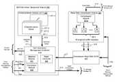
- FIG. 1is a diagram of an implementation of a data storage system 100 . While some example features are illustrated, those skilled in the art will appreciate from the present disclosure that various other features have not been illustrated for the sake of brevity and so as not to obscure more pertinent aspects of the example implementations disclosed herein. To that end, as a non-limiting example, the data storage system 100 includes a memory controller 120 , and a storage medium 130 , and is used in conjunction with a computer system 110 .
- storage medium 130is a single flash memory device while in other implementations storage medium 130 includes a plurality of flash memory devices.
- storage medium 130comprises at least one of NAND-type flash memory and NOR-type flash memory.
- memory controller 120is a solid-state drive (SSD) controller.
- SSDsolid-state drive
- Computer system 110is coupled to memory controller 120 through data connections 101 .
- Computer system 110includes memory controller 120 as a component and/or a sub-system.
- Computer system 110may be any suitable computer device, such as a computer, a laptop computer, a tablet device, a netbook, an internet kiosk, a personal digital assistant, a mobile phone, a smart phone, a gaming device, a computer server, or any other computing device.
- computer system 110includes one or more processors, one or more types of memory, a display and/or other user interface components such as a keyboard, a touch screen display, a mouse, a track-pad, a digital camera and/or any number of supplemental devices to add functionality.
- Storage medium 130is coupled to memory controller 120 through connections 103 .
- Connections 103are sometimes called data connections, but typically convey commands in addition to data, and optionally convey metadata, error correction information and/or other information in addition to data values to be stored in storage medium 130 and data values read from storage medium 130 .
- memory controller 120 and storage medium 130are included in the same device as components thereof.
- Storage medium 130may include any number (i.e., one or more) of memory devices including, without limitation, non-volatile semiconductor memory devices, such as flash memory.
- flash memory devicescan be configured for enterprise storage suitable for applications such as cloud computing, or for caching data stored (or be stored) in secondary storage, such as hard disk drivers. Additionally and/or alternatively, flash memory can also be configured for relatively smaller-scale applications such as personal flash drives or hard-disk replacements for personal, laptop and tablet computers.
- Storage medium 130is divided into a number of addressable and individually selectable blocks, such as selectable portion 131 .
- the individually selectable blocksare the minimum size erasable units in a flash memory device.
- each blockcontains the minimum number of memory cells that can be erased simultaneously.
- Each blockis usually further divided into a plurality of pages and/or wordlines, where each page or wordline is typically an instance of the smallest individually accessible portion in a block.
- the minimum unit of a data setis a sector, which is subunit of a page. That is, block includes multiple pages, each page contains a plurality of sectors, and each sector is the minimum unit of data for data writing or reading to the flash memory device.
- one blockmay comprise any number of pages, for example, 64 pages, 128 pages, 256 pages, or another suitable number of pages.
- Blocksare typically grouped into a plurality of zones. Each block zone can be independently managed to some extent, which increases the degree of parallelism for parallel operations and simplifies management of storage medium 130 .
- error control codingcan be utilized to limit the number of uncorrectable errors that are introduced by pseudo-random fluctuations, defects in the storage medium, operating conditions, device history, write-read circuitry, etc., or a combination of these and various other factors.
- memory controller 120includes a management module 121 , an input buffer 123 , an output buffer 124 , an error control module 125 and a storage medium interface (I/O) 128 .
- memory controller 120may include various additional features that have not been illustrated for the sake of brevity and so as not to obscure more pertinent features of the example implementations disclosed herein, and that a different arrangement of features may be possible.
- Input and output buffers 123 , 124provide an interface to computer system 110 through data connections 101 .
- storage medium I/O 128provides an interface to storage medium 130 though connections 103 .
- storage medium I/O 128includes read and write circuitry, including circuitry capable of providing reading signals to storage medium 130 (e.g., reading threshold voltages for NAND-type flash memory).
- management module 121includes a processor 122 configured to execute instructions in one or more programs, e.g., in management module 121 .
- processor 122may be shared by one or more components within, and in some cases, beyond the function of memory controller 120 .
- Management module 121is coupled to input and output buffers 123 , 124 , error control module 125 and storage medium I/O 128 in order to coordinate the operation of these components.
- Error control module 125is coupled between storage medium I/O 128 and the input and output buffers 123 , 124 . Error control module 125 is provided to limit the number of uncorrectable errors inadvertently introduced into data. To that end, error control module 125 includes an encoder 126 and a decoder 127 . Encoder 126 encodes data by applying an error control code to produce a codeword, which is subsequently stored in storage medium 130 . When the encoded data (a codeword) is read from the storage medium, decoder 127 applies a decoding process to the codeword to recover the data, and to correct errors in the recovered data within the error correcting capability of the error control code.
- input buffer 123receives data to be stored in storage medium 130 from computer system 110 .
- the data held in input buffer 123is made available to encoder 126 , which encodes the data to produce a codeword.
- the codewordis made available to the storage medium I/O 128 , which transfers the codeword to storage medium 130 in a manner dependent on the type of storage medium being utilized.
- storage medium I/O 128accesses the portion of storage medium 130 in which the corresponding codeword is stored to read the codeword and provide the codeword to decoder 127 .
- the codewordhas more than 1000 bits, 2000 bits, 4000 bits, or 8000 bits.
- the decoded datais provided to output buffer 124 , where the decoded data is made available to computer system 110 .
- memory controller 120may resort to a number of remedial actions or provide an indication of an irresolvable error condition.
- Hard information decodinggenerally means that absolute decisions are made as to whether a data value (e.g., data-bit or code-bit) is one symbol or another in a particular symbol alphabet.
- a particular data valuecan be either “0” or “1”, even if the raw electrical analog value read from a storage location does not indicate that the electrical value representing the data value is sufficient to decide with certainty that the data value is “0” or “1.”
- a hard-decision for a particular data valueis based on the most likely symbol corresponding to the analog electrical value read from the storage medium, and the probabilities that alternative decisions may be true are ignored by the hard-decision process. Often the hard-decision is based on the Euclidean distances from the analog read value to electrical level(s) defining the symbols.
- soft informationdoes not ignore the probabilities that different outcomes may be true in view of what is read from the storage medium.
- Error control methods using soft informationare particularly promising because soft information decoding often improves the error detection and correction capability of a particular error control code, and thus the capacity of the system.
- the utilization of soft information decodinghas been limited because of a number of previously irresolvable drawbacks, including increased power consumption, memory usage and added delays for generating and conveying the soft information.
- One particularly difficult challengehas been managing the delay, memory usage and power consumption previously required to create, store and transfer soft information between functional components.
- soft information generationrequired reading a memory cell (sometimes called a memory location) multiple times and combining the read results to generate a statistically accurate soft information value for each bit or symbol stored in the memory cell.
- the accuracy of the soft informationgenerally improves with the number of read operations performed, until a point of diminishing returns. But each read adds a delay, and the aggregate delay to generate accurate soft information for an entire sequence of data values is undesirable.
- Each read operationalso increases the amount of memory used to store the read data values prior to conversion into soft information values.
- Each read operationalso increases power consumption in at least three ways. First, power is consumed for each additional read operation performed. Second, power is consumed by the storage of the additional raw read data values produced by each additional read. Third, power is consumed when the raw read data values are transmitted from one functional block to another.
- some implementationsinclude systems, methods and/or devices enabled to utilize soft information error correction decoding to support the use of flash memory or other storage mediums.
- delay, power consumption, and/or memory usageare reduced during the generation of soft information from multiple read operations.
- raw read data from each memory locationis compressed into a corresponding bit-tuple representing the result of a number of sequential read operations.
- the bit-tupleis then used to retrieve a soft information value (e.g., a log-likelihood ratio, LLR) from a stored characterization vector associated with the current state of the storage medium, as identified by a set of storage medium characterization parameter values.
- a soft information valuee.g., a log-likelihood ratio, LLR
- memory usageis reduced because the amount of memory required to store a bit-tuple is smaller than the amount of memory required to store the corresponding sequence of raw read data values obtained (read) from a single memory location.
- the total amount of memory required to store a group of bit-tuples for one or more codewordsis significantly smaller (e.g., in some implementations, more than 50% smaller) than the total amount of memory required to store the corresponding raw read data for the one or more codewords, obtained by multiple read operations.
- power consumptionis reduced because less power is consumed to store a group of bit-tuples as compared to storing the raw read data for one or more codewords obtained by multiple read operations.
- delayis reduced by looking up a soft information value in a characterization vector based on a bit-tuple rather than computing the soft information value from the raw read data. In some implementations, delay is reduced because less time is needed to transfer a set of bit-tuples between system components (e.g., from storage medium 130 to memory controller 120 ), as compared to the time needed to transfer the corresponding raw read data values between system components.
- Flash memory devicesutilize memory cells to store data as electrical values, such as electrical charges or voltages.
- Each flash memory celltypically includes a single transistor with a floating gate that is used to store a charge, which modifies the threshold voltage of the transistor (i.e., the voltage needed to turn the transistor on).
- the magnitude of the charge, and the corresponding threshold voltage the charge creates,is used to represent one or more data values.
- a reading threshold voltageis applied to the control gate of the transistor and the resulting sensed current or voltage is mapped to a data value.
- cell voltageand “memory cell voltage,” in the context of flash memory cells, means the threshold voltage of the memory cell, which is the minimum voltage that needs to be applied to the gate of the memory cell's transistor in order for the transistor to conduct current.
- the reading threshold voltagesalso called reading signals and reading voltages
- the reading threshold voltages applied to a flash memory cellsare gate voltages applied to the gates of the flash memory cells to determine whether the memory cells conduct current at that gate voltage.
- the raw data value for that read operationis a “1” and otherwise it is a “0”.
- the memory cell voltage of a memory cellis read indirectly, by reading the memory cell using one or more reading threshold voltages. More specifically, each read operation produces a result that indicates whether the cell voltage of the memory cell is greater than or less than the reading threshold voltage used during that read operation. By reading the memory cell using multiple reading threshold voltages, the cell voltage can be determine more precisely than if the memory cell were read using only a single reading threshold voltage. Stated another way, the more read operations that are performed on a memory cell, each using a different reading threshold voltage, the more precisely the cell voltage of the memory cell is known.
- a single-level flash memory cellstores one bit of information (“0” or “1”). So the storage density of a SLC memory device is one bit per memory cell.
- a multi-level flash memory cellcan store two or more bits by using different ranges within the total voltage range of the memory cell to represent a multi-bit bit-tuple. In turn, the storage density of a MLC memory device is multiple-bits per cell (e.g., two bits per memory cell).
- a MLC memory deviceis used to store multiple bits by using voltage ranges within the total voltage range of a memory cell to represent different bit-tuples.
- a MLC memory deviceis typically more error prone than a SLC memory device created using the same manufacturing process because the effective voltage difference between the voltages used to store different data values is smaller for a MLC memory device.
- a typical errorincludes the cell voltage of a particular MLC shifting to a voltage range that is adjacent to the voltage range that would otherwise be representative of the correct bit-tuple.
- Such error-inducing factorsinclude, without limitation, pseudo-random electrical fluctuations, defects in the storage medium, operating conditions, device history (e.g., a count of the number of program-erase (P/E) cycles performed by the storage device), suboptimal performance or design and/or degradation of write-read circuitry, or a combination of these and other factors.
- P/Eprogram-erase
- suboptimal performance or design and/or degradation of write-read circuitryor a combination of these and other factors.
- the impact of such errorscan be reduced by grey-coding the data, such that there are only single-bit changes between bit-tuples in adjacent voltage ranges.
- FIG. 2Ais a simplified, prophetic diagram of voltage distributions 200 that may be found in a single-level (SLC) flash memory cell over time, and a sequence of reading threshold voltages V T ( 1 ), V T ( 2 ), V T ( 3 ), V T ( 4 ), V T ( 5 ) that are applied to the SLC during a sequential set of read operations according to some implementations.
- SLCsingle-level
- the voltage distributions 200have been simplified for illustrative purposes.
- the SLC memory cell voltage rangeapproximately extends from a voltage, V SS , at the source terminal of a NMOS transistor to a voltage, V DD , at the drain terminal of the same NMOS transistor.
- voltage distributions 200extend between V SS and V DD .
- Sequential voltage ranges 201 , 202 between the source and drain voltages, V SS and V DDare used to represent corresponding bit values “1” and “0,” respectively.
- Each voltage range 201 and 202has a respective center voltage V 1 201 b and V 0 202 b .
- Each voltage range 201 and 202also has a respective distribution of voltages 201 a and 202 a that may occur as a result of any number of a combination of error-inducing factors, examples of which are identified above.
- the charge on the floating gate of the SLC flash memory cellis set such that the resultant cell voltage (i.e., the cell's resultant threshold voltage) is at the center of one of the ranges 201 , 202 .
- the resultant cell voltageis, ideally, set to one of V 1 201 b and V 0 202 b in order to write a respective one of the bit values “1” and “0.”
- the actual cell voltagemay differ from the center voltage for the data written to the SLC flash memory cell.
- reading threshold voltages V T ( 1 ), V T ( 2 ), V T ( 3 ), V T ( 4 ), V T ( 5 )are applied between adjacent center voltages, e.g., applied proximate to the halfway region between adjacent center voltages V 1 201 b , and V 0 202 b .
- some or all of the reading threshold voltagesare located between voltage ranges 201 , 202 .
- reading threshold voltages V T ( 1 ), V T ( 2 ), V T ( 3 ), V T ( 4 ), V T ( 5 )are applied in the region proximate to where the voltage distributions 201 a , 202 a overlap, which is not necessarily proximate to the halfway region between adjacent center voltages V 1 201 b , and V 0 202 b .
- reading threshold voltages V T ( 1 ), V T ( 2 ), V T ( 3 ), V T ( 4 ), V T ( 5 )are sequentially applied, such that the application of each reading threshold voltage yields a raw read data value associated with each memory cell that is read.
- the sequence of raw read data values obtained from a memory cellis a N-bit binary sequence, generated by a sequence of N read operations.
- the reading threshold voltages used in the sequence of N read operationsis a monotonically increasing or decreasing sequence of reading threshold voltages.
- the monotonically increasing or decreasing sequence of reading threshold voltagesare applied non-sequentially and the resulting raw data values are re-ordered so that the resulting raw data values are thus arranged as though the reading threshold voltages had been applied sequentially.
- the memory cell current sensed in response to the applied reading threshold voltages V T ( 1 ), V T ( 2 ), V T ( 3 ), V T ( 4 ), V T ( 5 )is indicative of a memory cell voltage different from the respective center voltage V 1 201 b or V 0 202 b corresponding to the respective bit value written into the memory cell.
- Errors in cell voltage, and/or the cell voltage sensed when reading the memory cellcan occur during write operations, read operations, or due to “drift” of the cell voltage between the time data is written to the memory cell and the time a read operation is performed to read the data stored in the memory cell. For ease of discussion, these effects are collectively described as “cell voltage drift.”
- FIG. 2Bis a simplified, prophetic diagram of memory cell voltage distributions 210 a found in the memory cells of a MLC memory device over time and a sequence of reading threshold voltages V Ta ( 1 ), V Ta ( 2 ), V Ta ( 3 ), V Ta ( 4 ), V Ta ( 5 ) that are applied to memory cells of the MLC memory device during a sequential set of read operations for a lower page read according to some implementations.
- the cell voltage range of a MLCapproximately extends from the voltage, V SS , at the source terminal of a NMOS transistor to the voltage, V DD , at the drain terminal of the NMOS transistor.
- voltage distributions 210 aextend between V SS and V DD .
- Sequential voltage ranges 211 , 212 , 213 , 214 between the source and drain voltages, V SS and V DDare used to represent corresponding bit-tuples “11”, “01”, “00”, “10”, respectively.
- Each voltage range 211 , 212 , 213 , 214has a respective center voltage 211 b , 212 b , 213 b , 214 b .
- Each voltage range 211 , 212 , 213 , 214also has a respective distribution of voltages 211 a , 212 a , 213 a , 214 a that may occur as a result of any number or combination of the error-inducing factors described above.
- Grey-coding the bit-tuplesincludes constraining the assignment of bit-tuples to memory cell voltage ranges such that the respective bit-tuple of a particular voltage range is different from the respective bit-tuple of an adjacent voltage range by only one bit. For example, as shown in FIGS.
- the corresponding bit-tuples for the adjacent ranges 211 and 212are respectively “11” and “01”
- the corresponding bit-tuples for the adjacent ranges 212 and 213are respectively “01” and “00”
- the corresponding bit-tuples for the adjacent ranges 213 and 214are respectively “00” and “10”.
- the charge on the floating gate of the MLCwould be set such that the resultant cell voltage is at the center of one of the ranges 211 , 212 , 213 , 214 in order to write the corresponding bit-tuple to the MLC.
- the resultant cell voltagewould be set to one of V 11 211 b , V 10 212 b , V 00 213 b and V 10 214 b in order to write a corresponding one of the bit-tuples “11”, “01”, “00” and “10.” More typically, though, the resultant cell voltage is set to a value within a predefined range (e.g., 50, 100 or 200 millivolts) of a respective center voltage V 11 211 b , V 10 212 b , V 00 213 b and V 10 214 b corresponding to the bit-tuple written to the MLC.
- a predefined rangee.g., 50, 100 or 200 millivolts
- the least significant bit (i.e., the right-most bit) of each bit-tuplecorresponds to the “lower page” bit value of a MLC
- the most significant bit (i.e., the left-most bit) of each bit-tuplecorresponds to the “upper page” bit value of the MLC.
- the relative positions of the upper and lower page bitscan be exchanged.
- the actual cell voltagemay differ from the center voltage for the data written to the MLC.
- reading threshold voltages V Ta ( 1 ), V Ta ( 2 ), V Ta ( 3 ), V Ta ( 4 ), V Ta ( 5 )are applied between adjacent center voltages, e.g., applied proximate to the halfway region between adjacent center voltages V 01 212 b and V 00 213 b , and thus define threshold voltages between the voltage ranges 212 , 213 .
- reading threshold voltages V Ta ( 1 ), V Ta ( 2 ), V Ta ( 3 ), V Ta ( 4 ), V Ta ( 5 )are applied in the region proximate to where the voltage distributions 212 a , 213 a overlap, which may not necessarily be proximate to the halfway region between adjacent center voltages V 01 212 b and V 00 213 b .
- reading threshold voltages V Ta ( 1 ), V Ta ( 2 ), V Ta ( 3 ), V Ta ( 4 ), V Ta ( 5 )are sequentially applied, such that the application of each reading threshold voltage yields a raw read data value.
- V Ta ( 1 ), V Ta ( 2 ), V Ta ( 3 ), V Ta ( 4 ), V Ta ( 5 )five separate raw lower page read data values are obtained for each memory location (i.e., MLC).
- MLCmemory location
- the sequence of raw read data valuesis a N-bit binary sequence, generated by a sequence of N lower page read operations from a single memory location.
- the reading threshold voltages used for a sequence of read operationsincludes a monotonically increasing or decreasing sequence of reading threshold voltages.
- the monotonically increasing or decreasing sequence of reading threshold voltagescan be applied non-sequentially and the resulting raw lower page data values re-ordered so that the resulting raw lower page data values are thus arranged as though the reading threshold voltages had been applied sequentially.
- FIG. 2Cis a simplified, prophetic diagram of voltage distributions 210 b that may be found in a multi-level flash memory cell over time and a sequence of reading threshold voltages V Tb ( 1 ), V Tb ( 2 ), V Tb ( 3 ), V Tb ( 4 ), V Tb ( 5 ) that are applied to the MLC during a sequential set of read operations for an upper page read according to some implementations.
- the voltage distributions 210 b illustrated in FIG. 2Care similar to and adapted from the voltage distributions 210 a illustrated in FIG. 2B . Elements common to each include common reference numbers, and only the differences between FIGS. 2B and 2C are described herein for the sake of brevity.
- the upper page bit of a memory locationcan be read by applying the reading threshold voltages V Tb ( 1 ), V Tb ( 2 ), V Tb ( 3 ), V Tb ( 4 ), V Tb ( 5 ) across the respective transition between voltage distributions 211 a and 212 a or the respective transition between voltage distributions 213 a and 214 a .
- the reading threshold voltages V Tb ( 1 ), V Tb ( 2 ), V Tb ( 3 ), V Tb ( 4 ), V Tb ( 5 )are applied across the transition between voltage distributions 211 a and 212 a .
- the reading threshold voltages V Tb ( 1 ), V Tb ( 2 ), V Tb ( 3 ), V Tb ( 4 ), V Tb ( 5 )can either be applied proximate to the halfway region between adjacent center voltages V 11 and V 01 , or in the region proximate to where the voltage distributions 211 a , 212 a overlap, which is not necessarily proximate to the halfway region between adjacent center voltages V 11 211 b and V 01 212 b .
- any number of two or more reading threshold voltagescan be used in various implementations, and that the five reading threshold voltages described with reference FIG. 2C are merely provided as an illustrative example.
- a sequence of raw read data values for a single memory locationis a N-bit binary sequence.
- the raw read data valuesare generated by a sequence of N upper page read operations from a single memory location.
- the reading threshold voltages used for a sequence of read operationsincludes a monotonically increasing or decreasing sequence of reading threshold voltages.
- the monotonically increasing or decreasing sequence of reading threshold voltagescan be applied non-sequentially and the resulting raw upper page data values re-ordered so that the resulting raw upper page data values are thus arranged as though the reading threshold voltages had been applied sequentially.
- FIG. 3is a diagram of a data storage system 300 , including a soft information generation module 325 and a read data compression module 321 , in accordance with some embodiments.
- Data storage system 300 illustrated in FIG. 3is similar to and adapted from data storage system 100 illustrated in FIG. 1 .
- Elements common to eachinclude common reference numbers, and only the differences between FIGS. 1 and 3 are described herein for the sake of brevity.
- certain specific featuresare illustrated, those skilled in the art will appreciate from the present disclosure that various other features have not been illustrated for the sake of brevity and so as not to obscure more pertinent aspects of the example implementations disclosed herein.
- data storage system 300and in particular, memory controller 120 has been further configured to compress read data values from multiple read operations and utilize soft information for error control decoding. More specifically, memory controller 120 further includes read data compression module 321 , a compressed read data buffer 323 , and soft information generation module 325 . As discussed below with reference to FIG. 10 , in some other embodiments the read data compression module is implemented in the storage medium 130 .
- Soft information generation module 325is coupled to management module 121 , error control module 125 and storage medium I/O 128 .
- Management module 121is connected to provide soft information generation module 325 a control signal on a control line 225 .
- Soft information generation module 325is connected to provide decoder 127 with at least one sequence of soft information corresponding to the raw read data 328 retrieved by the storage medium 130 (obtained via storage medium I/O 128 in embodiments represented by FIG. 3 ). Additionally, in some implementations, soft information generation module 325 is also connected to provide one or more sets of reading threshold voltages to storage medium 130 via data line 327 and storage medium I/O 128 .
- Read data compression module 321is coupled to receive raw read data values 328 from storage medium 130 via storage medium I/O 128 .
- Read data compression module 321is configured to compress an N-bit sequence of raw read data values associated with a particular memory location into a bit-tuple of a predefined length, M.
- read data compression module 321is included in a device operable to compress a N-bit binary sequence, the N-bit binary sequence having an initial sub-sequence of M bits and a remaining sub-sequence of N ⁇ M bits.
- read data compression module 321produces a sequence of bit-tuples corresponding to an entire codeword by compressing the raw read data values for a set of memory locations associated with the entire codeword.
- One or more sequences of bit-tuples produced by read data compression module 321is stored in compressed read data buffer 323 .
- Compressed read data buffer 323is accessible by soft information generation module 325 to generate corresponding sequences of soft information values.
- Soft information generation module 325generates soft information values by utilizing a pre-generated collection of characterization vectors for various combinations of storage medium characterization parameter values. As described in further detail below with reference to FIG. 4 , each characterization vector includes soft information values associated with one or more permutations of bit-tuples.
- the sequences of soft informationare generated and passed to decoder 127 for soft information decoding.
- decoder 127is configured to decode sequences of soft information one codeword at a time.
- decoder 127is configured to decode sequences of soft information corresponding to two or more codewords in parallel.
- input buffer 123receives data to be stored in storage medium 130 from computer system 110 .
- the data in input buffer 123is made available to encoder 126 , which encodes the data to produce a codeword.
- the codewordis conveyed to storage medium via storage medium I/O 128 , which transfers the codeword to storage medium 130 in a manner dependent on the type of storage medium being utilized. For example, for MLC flash memory, each bit-tuple of the codeword is written into a respective memory cell by changing the charge on the floating gate of the respective memory cell.
- a read operationis initiated when computer system 110 sends a read command on control line 111 to memory controller 120 to request read data from storage medium 130 .
- Memory controller 120sends read operation commands to storage medium 130 , via storage medium I/O 128 , to obtain raw read data values 328 for each memory location that is read in response to the read command.
- Raw read data values 328are sent to and processed by read data compression module 321 , the operation of which is described in more detail below with reference to FIG. 4 .
- read data compression module 321For each memory location that has been read, read data compression module 321 produces a bit-tuple of a predefined length, M, and stores the bit-tuples in compressed read data buffer 323 .
- Soft information generation module 325generates a soft information value for each bit-tuple in compressed read data buffer 323 by selecting a respective soft information value from a characterization vector.
- Decoder 127is configured to decode sequences of soft information corresponding to codewords to as to produce decoded, error-free read data corresponding to the received read command.
- management module 121also passes the read request to soft information generation module 325 so that soft information generation module 325 can select reading threshold voltages for use by storage medium 130 . In some other implementations, management module 121 selects the reading threshold voltages for use by storage medium 130 . In yet other implementations, storage medium I/O 128 selects the reading threshold voltages.
- the read processcan be modified to utilize information about the current state of storage medium 130 .
- information about the current state of storage medium 130can be utilized to select reading threshold voltages in accordance with the current state of storage medium 130 .
- information about the current state of storage medium 130is provided in the form of one or more storage medium characterization parameter values.
- the one or more storage medium characterization parameter valuesprovide an indication of at least one of a physical characteristic associated with at least a portion the storage medium, a mode of operation associated with at least a portion of the storage medium, a history of use associated with at least a portion of the storage medium, a condition characteristic associated with at least a portion of the storage medium, a read type associated with at least a portion of the storage medium, and a location associated with at least a portion of the storage medium.
- the one or more storage medium characterization parameter valuesincludes an indicator of the storage medium locations being accessed, an indicator of the number of previous program/erase cycles of the storage medium (or, alternatively, an indicator of the number of previous program/erase cycles of the storage medium locations being accessed), and an indicator of the current temperature of the storage medium 130 .
- FIG. 4is a more detailed diagram of an implementation of soft information generation module 325 and read data compression module 321 , both of which are shown in less detail in FIG. 3 .
- soft information generation module 325includes a soft information management controller 410 and a characterization module 420 .
- characterization module 420includes a soft information management controller 410 and a characterization module 420 .
- memory controller 120receives one or more storage medium characterization parameter values, which characterize the current state of storage medium 130 , from computer system 110 along with the read request.
- storage medium characterization parameter valuesare stored internally by memory controller 120 and memory controller 120 retrieves the one or more storage medium characterization parameter values in response to receiving the read request from computer system 110 .
- the one or more storage medium characterization parameter valuesare passed to soft information generation module 325 .
- the one or more storage medium characterization parameter valuesare used by soft information generation module 325 to select a characterization vector associated with the current state of storage medium 130 .
- soft information management controller 410is connected to receive the read request and one or more storage medium characterization parameters on control and data lines 401 and 402 , respectively. Soft information management controller 410 is also connected to provide characterization module 420 a selection control signal on control line 411 , and to receive a selected characterization vector on data line 412 . In some implementations, soft information management controller 410 is further connected to provide reading threshold voltages to storage medium 130 via data line 414 and storage medium I/O 128 , and receive bit-tuples from compressed read data buffer 323 through data line 417 . Soft information management controller 410 is also connected to provide sequences of soft information values to decoder 127 ( FIG. 3 ) on data line 403 .
- Characterization module 420includes a collection of characterization vectors 421 - 1 , 421 - 2 , 421 - 3 , . . . 421 - n , that each store characterization data, such as soft information values for bit-tuples and reading threshold voltages, associated with storage medium 130 for one or more storage medium characterization parameter values.
- characterization datasuch as soft information values for bit-tuples and reading threshold voltages
- the characterization data stored in the characterization vectors 421is statistically derived. More detailed example implementations of characterization vectors 421 are described in co-pending U.S. patent application Ser. No. 13/602,031, entitled “Statistical Read Comparison Signal Generation for Memory Systems,” which is hereby incorporated by reference in its entirety.
- Soft information management controller 410includes a selection module 431 , a read controller 432 , and a conversion module 433 .
- the selection module 431is configured to use the one or more storage medium characterization parameters values to select a characterization vector from the stored collection of characterization vectors 421 - 1 , 421 - 2 , 421 - 3 , . . . 421 - n in accordance with the current state of storage medium 130 .
- the selection control signalincludes one or more of storage medium characterization parameters values and/or an index key associated with a combination of one or more of storage medium characterization parameters values.
- Read controller 432is configured to read a portion of storage medium 130 via storage medium I/O 128 . In some implementations, read controller 432 is configured to provide storage medium 130 with reading threshold voltages that are used to read the same portion of storage medium 130 multiple times.
- Conversion module 433is configured to generate a sequence of soft information values corresponding to the bit-tuples stored in compressed read data buffer 323 .
- the sequence of soft information valuesis generated, at least in part, by selecting a respective soft information value (e.g., a LLR, a transition probability, etc.) from the selected characterization vector for each bit-tuple.
- soft informationis generated by a device characterization process for memory devices produced by a particular manufacturing process, and stored in a characterization module or look-up table included in soft information generation module 325 .
- Read data compression module 321includes a compression module 321 a and M single-bit buffer locations 321 b . As described below with reference to FIGS. 5A-5B and 6 - 9 , read data compression module 321 is configured to compress a sequence of raw read data values, generated by a corresponding sequence of read operations from a single memory location, into an bit-tuple that is smaller than the sequence of raw read data values. To that end, read data compression module 321 is configured to receive raw read data values from the storage medium 130 via data line 415 , and write the generated bit-tuples to compressed read data buffer 323 over data lines 416 .
- read data compression module 321includes a device operable to compress a N-bit binary sequence, the N-bit binary sequence having an initial sub-sequence of M bits and a remaining sub-sequence of N ⁇ M bits.
- the deviceincludes M single-bit buffer locations (where N is greater than M), and a compression module.
- the compression moduleis configured to: populate the M single-bit buffer locations by setting each respective single-bit buffer location to a corresponding value (e.g., “000”, FIG.
- each N-bit binary sequenceis generated by a sequence of N read operations from a single memory location.
- the number of single-bit buffer locations, Mis equal to ⁇ log 2 (N+1) ⁇ , where ⁇ x ⁇ represents the value of “x” rounded up to the closest integer.
- read data compression module 321includes a device operable to compress a sequence of data values.
- the deviceincludes a plurality of buffer locations and a compression module.
- the compression moduleis configured to: populate each of the plurality of buffer locations by setting each buffer location to a corresponding value from an initial sub-sequence of sequence of data values; and update the collective state of the plurality buffer locations for each data value of a remaining sub-sequence of the sequence of data values in sequential order by determining whether the plurality of buffer locations is in a first state and overwriting the first state of the plurality of buffer locations when a respective remaining data value has a first value.
- the compression module 321 ais further configured to sequentially evaluate each bit of the remaining sub-sequence of N ⁇ M bits by: determining whether the M single-bit buffer locations are in the predefined state; determining whether the bit under evaluation has a read value equal to the first predefined value; and maintaining the predefined state of the M single-bit buffer locations in response to a positive determination that the M single-bit buffer locations are in the predefined state and the bit under evaluation has a read value equal to the first predefined value.
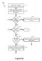
- FIG. 5Ais a flowchart representation of a method 500 a of compressing data read from a storage medium (e.g., storage medium 130 ) according to some implementations.
- method 500 ais performed by a memory controller or a module associated with a memory controller (e.g., read data compression module 321 shown in FIGS. 3 and 4 ).
- the method 500 ais performed for each bit of a codeword, and thus is typically performed thousands of times when a codeword having thousands of bits is read from the storage medium. More generally, in some embodiments, any of the data compression methods described herein is performed for each bit of a codeword, and thus is typically performed thousands of times when a codeword having thousands of bits is read from the storage medium.
- method 500 aincludes receiving a N-bit sequence, that was generated by a sequence of N read operations from a single memory location.
- read data compression module 321receives raw read data values from the storage medium I/O 128 via data line 415 .
- each read operation in the sequence of N read operationsproduces a read value equal to a binary 1 or 0.
- each of the sequence of N read operationsincludes applying a different respective reading signal.
- each respective reading signalis a reading threshold voltage suitable for application to the gates of memory cells in a flash memory.
- the reading threshold voltages used for the sequence of N read operationsinclude a monotonically increasing or decreasing sequence of reading threshold voltages.
- the methodincludes populating the M single-bit buffer locations with the first M-bits of the N-bit sequence.
- the M single-bit buffer locationsare populated by setting each respective single-bit buffer location of the M single-bit buffer locations to a value corresponding to a read value obtained by a respective read operation of the M initial read operations.
- the M single-bit buffer locationsare populated, in a predefined order, from a constituent least-significant-bit location to a constituent most-significant-bit location of the M single-bit buffer locations.
- method 500 aincludes determining whether the M single-bit buffer locations are in a first state (i.e., a corresponding predefined state).
- the first statecorresponds to an all-zero state, such that the data value stored in each of the M single-bit buffer locations is a “0.” If the M single-bit buffer locations are not in the first state (“No” path from block 5 - 3 a ), as represented by block 5 - 4 a , method 500 a includes maintaining the state of the M single-bit buffer locations irrespective of the remaining N ⁇ M bits in the N-bit sequence.
- method 500 aincludes determining if there is at least another unchecked bit in the remaining N ⁇ M bits of the N-bit sequence, the first of which represents the current bit under evaluation. If there are no more unchecked bits (“No” path from block 5 - 5 a ), the N-bit sequence has been fully compressed and the method ends for the N-bit sequence.
- method 500 aincludes determining whether the sequential unchecked bit (i.e., the current bit under evaluation) is different from a first predefined value.
- the first predefined valueis a “0.” In some other implementations, the first predefined value is a “1.” If the current bit under evaluation is equal to the first predefined value (“No” path from block 5 - 6 a ), as represented by block 5 - 7 a , method 500 a includes maintaining the first state of the M single-bit buffer locations.
- the methodincludes maintaining the first state of the M single-bit buffer locations.
- Method 500 athen circles back to the portion of the method represented by block 5 - 5 a , with the latest current bit under evaluation becoming a checked (or considered) bit.
- method 500 aincludes overwriting the state of the M single-bit buffer locations based on the sequence position of the current sequential unchecked bit.
- method 500 aincludes updating the state of the M single-bit buffer locations to a state that indicates which read operation in the sequence of N read operations is the first read operation in said sequence to produce a read value that is different from the first predefined read value.
- Method 500 athen circles back to the portion of the method represented by block 5 - 3 a , with the latest current bit under evaluation becoming a checked (or considered) bit.
- method 500 aincludes updating the state of the M single-bit buffer locations to a state that indicates which read operation in the sequence of N read operations is the first read operation in said sequence to produce a read value (e.g., “1”) that is different from the first predefined read value (e.g., “0”).
- a read valuee.g., “1”
- method 500 aincludes updating the collective state of the plurality buffer locations for each data value in a remaining sub-sequence of the sequence of data values in sequential order by: determining whether the plurality of buffer locations is in a first state; and overwriting the first state of the plurality of buffer locations when a respective remaining data value has a first value.
- the methodfurther includes maintaining ( 5 - 7 a ) the predefined state of the M single-bit buffer locations for each read operation in the N ⁇ M subsequent read operations that produces a read value equal to the first predefined read value.
- the sequence of operations shown in FIG. 5Ais replaced by a single table lookup operation, which directly converts the N-bit binary sequence received at 5 - 1 a into an M-bit compressed value, representing the state of the M single-bit buffer locations.
- a single table lookup operationwhich directly converts the N-bit binary sequence received at 5 - 1 a into an M-bit compressed value, representing the state of the M single-bit buffer locations.
- M-bit compressed valuerepresenting the state of the M single-bit buffer locations.
- the sequence of operations shown in FIG. 5Ais performed by digital combinatorial logic that generates an M-bit compressed value directly from the received N-bit binary sequence received at 5 - 1 a without performing any decision loops.
- FIG. 5Bis a flowchart representation of a method 500 b of compressing data read from a storage medium according to some implementations.
- method 500 bis performed by a memory controller or a module associated with a memory controller (e.g., read data compression module 321 shown in FIGS. 3 and 4 ).
- method 500 bis performed by logic (e.g., compression module 1012 , FIG. 10 ) in storage medium 130 (identified as memory system 1010 in FIG. 10 ) as raw data is generated by a sequence of read operations from a single memory location.
- method 500 bincludes compressing a N-bit binary sequence as it is generated by a sequence of N read operations from a single memory location, using M single-bit buffer locations, wherein M is less than N.
- M⁇ log 2 (N+1) ⁇ .
- the method 500 bis performed for each bit of a codeword, and thus is typically performed thousands of times when a codeword having thousands of bits is read from the storage medium.
- method 500 bincludes performing a read operation to read a bit value from a memory location.
- performing a read operation on a memory devicetypically includes reading data values from a number of memory locations together (e.g., all or a portion of the memory locations included in a block, a wordline a page, or a sector of a page).
- method 500 bis described with respect to reading data values from a single memory location.
- method 500 bis modified to operate on two or more N-bit binary sequences in parallel and/or serially, where the two or more N-bit binary sequences are generated by a sequence of N read operations from two or more memory locations.
- method 500 bincludes determining whether the number of read operations performed so far is less than or equal to M, the number of single-bit buffer locations. If the number of read operations performed is less than or equal to M (“Yes” path from block 5 - 2 b ), as represented by block 5 - 3 b , method 500 b includes populating a respective one of the M single-bit buffer locations with the bit value read from the memory location. Method 500 b then circles back to the portion of the method represented by block 5 - 1 b .
- method 500 bincludes populating the M single-bit buffer locations in order from a constituent least-significant-bit location to a constituent most-significant-bit location of the M single-bit buffer locations. In some implementations, populating the M single-bit buffer locations occurs on a per read basis, as shown in FIG. 5B . On the other hand, if the number of read operations performed is greater than M (“No” path from block 5 - 2 b ), as represented by block 5 - 4 b , method 500 b includes determining whether the M single-bit buffer locations are in a first state.
- method 500 bincludes maintaining the state of the M single-bit buffer locations irrespective of any remaining bit values subsequently read from the memory location.
- method 500 bincludes determining whether the read bit value differs from a first value.
- the first predefined valueis a “0.” In some other implementations, the first predefined value is a “1.”
- method 500 bincludes maintaining the first state of the M single-bit buffer locations. In other words, for each read operation greater than M that produces a read value equal to the first predefined read value, the method includes maintaining the first state of the M single-bit buffer locations. Following the portion of the method represented by block 5 - 7 b , method 500 b proceeds to the portion of the method represented by block 5 - 8 b , which is discussed in greater detail below.
- method 500 bincludes overwriting the state of the M single-bit buffer locations based on how many read operations have been performed thus far.
- method 500 bincludes updating the state of the M single-bit buffer locations to a state that indicates which read operation in the sequence of N read operations is the first read operation in said sequence to produce a read value that is different from the first predefined read value.
- method 500 bincludes determining whether N read operations have been performed. If N read operations have been performed (“Yes” path from block 5 - 8 b ), an N-bit sequence has been read from the memory location and compressed. Accordingly, method 500 b ends for the memory location. On the other hand, if fewer than N read operations have been performed (“No” path from block 5 - 8 b ), method 500 b circles back to the portion of the method represented by block 5 - 1 b.
- method 500 bincludes updating the state of the M single-bit buffer locations to a state that indicates which read operation in the sequence of N read operations is the first read operation in said sequence to produce a read value that is different from the first predefined read value.
- method 500 bincludes updating the collective state of the plurality buffer locations for each data value in a remaining sub-sequence of the sequence of data values in sequential order by: determining whether the plurality of buffer locations is in a first state; and overwriting the first state of the plurality of buffer locations when a respective remaining data value has a first value.
- the methodfurther includes maintaining the predefined state of the M single-bit buffer locations for each read operation in the N ⁇ M subsequent read operations that produces a read value equal to the first predefined read value.
- a modified version of method 500 bincludes, upon determining at block 5 - 4 b that the M single-bit buffer locations are not in the first state (“No” path from block 5 - 4 b ), aborting the sequence of read operations, because method 500 b includes maintaining the state of the M single-bit buffer locations irrespective of any remaining bit values subsequently read from the memory location.
- the “No” branch from block 5 - 4 bwould go directly to method “End” instead of block 5 - 7 b .
- fewer read operationsare performed to obtain the same compressed representation of the raw data read from the memory location, which reduces latency and reduces power consumption. This improvement is potentially most practical in implementation in which method 500 b is performed by logic in storage medium 130 .
- FIG. 6is a flowchart representation of a method 600 of compressing a 3-bit sequence of raw read data into a 2-bit representation.
- method 600is performed by a memory controller or a module associated with a memory controller (e.g., read data compression module 321 shown in FIGS. 3 and 4 ).
- method 600is performed by circuitry (e.g., logic circuitry) in a persistent storage device.
- method 600includes compressing a 3-bit binary sequence of raw read data, which is generated by a corresponding sequence of three read operations from a single memory location, using two single-bit buffer locations.
- method 600includes performing a first read operation to obtain a bit value from a memory location.
- method 600includes writing the first read bit value to the least significant bit (LSB) of the two single-bit buffer locations. Often the LSB is the right-most bit location in a buffer or a register. However, those skilled in the art will appreciate from the present disclosure that the opposite (i.e., designating the left-most bit location in a buffer or a register as the LSB) and various other arrangements are possible without departing from the scope of the claims.
- method 600includes performing a second read operation to obtain a bit value from the same memory location as the first read operation.
- method 600includes writing the second read bit value to the most significant bit (MSB) of the two single-bit buffer locations.
- MSBmost significant bit
- method 600includes performing a third read operation to obtain a bit value from the same memory location as the first and second read operations.
- method 600includes determining whether the two single-bit buffer locations are in an all-zero state (i.e., whether the bit value in each of the two single-bit buffer locations is a “0”).
- method 600ends for the 3-bit sequence by maintaining the non-zero state of the two single-bit buffer locations that was produced after the first two read operations.
- method 600includes determining whether the bit value produced by the third read operation is equal to a first predefined value.
- the first predefined valueis a “0.” In some other implementations, the first predefined value is a “1.” If the third read bit value is equal to the first predefined value (“Yes” path from block 6 - 7 ), method 600 ends for the 3-bit sequence by maintaining the non-zero state of the two single-bit buffer locations that was produced after the first two read operations. On the other hand, if the third read bit value differs from the first predefined value (“No” path from block 6 - 7 ), as represented by block 6 - 8 , method 600 includes overwriting the state of the two single-bit buffer locations.
- overwriting the state of the two single-bit buffer locationsincludes writing a “1” to the LSB of the two single-bit buffer locations. In some implementations, overwriting the state of the two single-bit buffer locations includes writing a “1” to the MSB of the two single-bit buffer locations (not shown in FIG. 6 ).
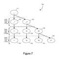
- FIG. 7is a state diagram 700 illustrating the possible states of two single-bit buffer locations based on method 600 represented by illustration in FIG. 6 .
- the first state 711corresponds to the state of the two single-bit buffer locations before a reading threshold voltage is applied for a first read operation, and thus the two single-bit buffer locations do not yet include valid data.
- the two single-bit buffer locationswill enter one of two states 721 , 722 depending on the first read bit value that is written to the LSB. If the first read operation yields a “1,” the two single-bit buffer locations will enter state 721 (e.g., “ — 1”) from state 711 . On the hand, if the first read operation yields a “0,” the two single-bit buffer locations will enter state 722 (e.g., “ — 0) from state 711 .
- the two single-bit buffer locationswill enter one of three states 731 , 732 , 733 depending on the second read bit value and the current state of the two single-bit buffer locations. If the second read operation yields a “1” and the two single-bit buffer locations are in state 722 , the two single-bit buffer locations will enter state 732 (e.g., “01”) from state 722 . If the second read operation yields a “0” and the two single-bit buffer locations are in state 722 , the two single-bit buffer locations will enter state 733 (e.g., “00”) from state 722 .
- the two single-bit buffer locationswill enter state 731 (e.g., “11”) regardless of the second read bit value.
- state 731e.g., “11”
- the two single-bit buffer locationsboth include valid data because the two single-bit buffer locations are populated with values that are a combination of the read data bit values that were read during the first and second read operations.
- the two single-bit buffer locationswill enter one of four states 741 , 742 , 743 , 744 depending on the third read bit value and the current state of the two single-bit buffer locations. If the two single-bit buffer locations are in state 731 , the two single-bit buffer locations will enter state 741 regardless of the third read bit value. Similarly, if the two single-bit buffer locations are in state 732 , the two single-bit buffer locations will enter state 742 regardless of the third read bit value.
- two single-bit buffer locationsare in state 733 and the third read bit value is a “1,” two single-bit buffer locations will enter state 744 (e.g., “01”) from state 733 . If the two single-bit buffer locations are in state 733 and the third read bit value is a “0,” two single-bit buffer locations will enter state 743 (e.g., “00”) from state 733 .
- method 600prevents newly generated non-zero states from conflicting with previously generated non-zero states while reducing the number of buffer locations need to store a 3-bit sequence of raw read data.
- FIG. 8is a flowchart representation of a method 800 of compressing a 7-bit sequence of raw read data into 3-bit representation.
- method 800is performed by a memory controller or a module associated with a memory controller (e.g., read data compression module 321 shown in FIGS. 3 and 4 ).
- method 800includes compressing a 7-bit binary sequence of raw read data, which is generated by a corresponding sequence of seven read operations from a single memory location, using three single-bit buffer locations.
- method 800includes performing a read operation to read a bit value from a memory location.
- performing a read operation on a memory devicetypically includes reading data values from a number of memory locations together (e.g., all or a portion of the memory locations included in a block, a zone, a word-line and/or a page).
- method 800is described with respect to reading data values from a single memory location.
- method 800is modified to operate on two or more 7-bit binary sequences in parallel and/or serially, where the two or more 7-bit binary sequences are generated by a sequence of seven read operations from a corresponding two or more memory locations.
- method 800includes determining whether the number of read operations performed so far is less than or equal to three. If the number of read operations performed thus far is greater than three (“No” path from block 8 - 2 ), method 800 proceeds to the portion of the method represented by block 8 - 8 , which is described in greater detail further below. On the other hand, the number of read operations performed so far is less than or equal to three (“Yes” path from block 8 - 2 ), as represented by block 8 - 3 , method 800 includes determining whether or not the latest read operation performed is the first read operation on the memory location.
- method 800includes writing the raw read data value (i.e., the read bit) to the LSB of the three single-bit buffer locations.
- method 800includes, determining whether or not the latest read operation performed is the second read operation on the memory location.
- method 800includes writing the raw read data value (i.e., the read bit) to the center significant bit (CSB) of the three single-bit buffer locations.
- method 800includes writing the raw read data value (i.e., the read bit) to the most significant bit (MSB) of the three single-bit buffer locations.
- the operation represented by block 8 - 6is determined in accordance with the value of the LSB; in particular, if the LSB has been set to a predefined value (e.g., “1”), then the CSB is set to the same predefined value regardless of the value of the second read bit; otherwise, the CSB is set to the value of the second read bit.
- a predefined valuee.g., “1”
- the operation represented by block 8 - 7is determined in accordance with the value of the LSB; in particular, if the CSB has been set to a predefined value (e.g., “1”), then the MSB is set to the same predefined value regardless of the value of the second read bit; otherwise, the MSB is set to the value of the third read bit.
- a predefined valuee.g., “1”
- method 800includes looping back to the portion of the method represented by block 8 - 1 .
- method 800includes determining whether or not the three single-bit buffer locations are in a first state (e.g., “000”).
- the first stateis an all-zero state in which each of the three single-bit buffer locations stores a “0.”
- the first statemay also include any combination of values stored in the three single-bit buffer locations. If the three single-bit buffer locations are not in the first state (“No” path from block 8 - 8 ), as represented by block 8 - 9 , method 800 includes maintaining the state of the three single-bit buffer locations, without regard to the value of the bit read during the latest read operation.
- method 800includes determining whether or not the latest read operation performed is the seventh read operation on the memory location. If the latest read operation is the seventh read operation on the memory location (“Yes” path from block 8 - 18 ), method 800 ends for the 7-bit sequence by maintaining the state of the three single-bit buffer locations. On the other hand, if the latest read operation is not the seventh read operation on the memory location (“No” path from block 8 - 18 ), method 800 loops back to the portion of the method represented by block 8 - 1 .
- method 800includes determining whether or not the latest read bit value is different from a first predefined read value.
- the first predefined valueis a “0.” In some other implementations, the first predefined value is a “1.” If the latest read bit value is not different from the first predefined read value (“No” path from block 8 - 10 ), method 800 proceeds to the portion of the method represented by 8 - 9 described above.
- method 800includes determining whether or not the latest read operation performed is the fourth read operation on the memory location. If the latest read operation is the fourth read operation on the memory location (“Yes” path from block 8 - 11 ), as represented by block 8 - 12 , method 800 includes writing the raw read data value (i.e., the read bit) to the LSB of the three single-bit buffer locations.
- method 800includes, determining whether or not the latest read operation performed is the fifth read operation on the memory location. If the latest read operation is the fifth read operation on the memory location (“Yes” path from block 8 - 13 ), as represented by block 8 - 14 , method 800 includes writing the raw read data value (i.e., the read bit) to the CSB of the three single-bit buffer locations.
- method 800includes, determining whether or not the latest read operation performed is the sixth read operation on the memory location. If the latest read operation is the sixth read operation on the memory location (“Yes” path from block 8 - 15 ), as represented by block 8 - 16 , method 800 includes writing the raw read data value (i.e., the read bit) to the LSB and to the CSB of the three single-bit buffer locations.
- the raw read data valuei.e., the read bit
- method 800includes writing the raw read data value (i.e., the read bit) to the LSB and to the MSB of the three single-bit buffer locations.
- FIG. 9is a state diagram illustrating the possible states of three single-bit buffer locations based on method 800 represented by illustration in FIG. 8 .
- the first state 911corresponds to the state of the three single-bit buffer locations before a reading threshold voltage is applied for a first read operation, and thus the three single-bit buffer locations do not yet include valid data.
- the three single-bit buffer locationsIn response to a first read operation, described above with reference to FIG. 8 , the three single-bit buffer locations will enter one of two states 921 , 922 depending on the first read bit value, in which the LSB is populated with the first read bit value. In response to a second read operation, described above with reference to FIG. 8 , the three single-bit buffer locations will enter one of three states 931 , 932 , 933 depending on the second read bit value, in which the CSB is populated based on a function of the second read bit value and the first read bit value. In response to a third read operation, described above with reference to FIG.
- the three single-bit buffer locationswill enter one of four states 941 , 942 , 943 , 944 depending on the third read bit value, in which the MSB is populated based on a function of the third read bit value, the second read bit value and the first read bit value.
- method 800operates to overwrite the all-zero state when a subsequent read value is different from first predefined value. As such, if after the third read the three single-bit buffer locations are in state 941 (e.g., “111”), the three single-bit buffer locations sequentially progress to states 951 , 961 , 971 and 981 in response to the subsequent read operations, without regard to the bit values obtained by those subsequent read operations.
- state 941e.g., “111”
- the three single-bit buffer locationssequentially progress to states 952 , 962 , 972 and 982 in response to the subsequent read operations, without regard to the bit values obtained by those subsequent read operations.
- state 943e.g., “100”
- the three single-bit buffer locationssequentially progress to states 953 , 963 , 973 and 983 in response to the subsequent read operations, without regard to the bit values obtained by those subsequent read operations.
- the three single-bit buffer locationsare in state 944 (an all-zero state) after three read operations, in response to the fourth read the three single-bit buffer locations enter state 955 if a “1” is read, and enter state 954 if a “0” is read. If the three single-bit buffer locations enter state 955 , the three single-bit buffer locations sequentially enter states 966 , 977 and 988 in response to subsequent read operations, without regard to the bit values obtained by those subsequent read operations.
- the three single-bit buffer locationsare in state 954 (an all-zero state)
- the three single-bit buffer locationsin response to the fifth read the three single-bit buffer locations enter state 965 if a “1” is read, and enter state 964 if a “0” is read. If the three single-bit buffer locations enter state 965 , the three single-bit buffer locations sequentially enter states 976 and 987 in response to subsequent read operations, without regard to the bit values obtained by those subsequent read operations.
- the three single-bit buffer locationsif after the fifth read the three single-bit buffer locations are in state 964 (an all-zero state), in response to the sixth read the three single-bit buffer locations enter state 975 if a “1” is read, and enter state 974 if a “0” is read. If the three single-bit buffer locations enter state 975 , the three single-bit buffer locations enter state 986 after the seventh read, without regard to the bit value obtained by the seventh read. Similarly, if after the sixth read the three single-bit buffer locations are in state 974 (an all-zero state), in response to the seventh read the three single-bit buffer locations enter state 985 if a “1” is read, and enter state 984 if a “0” is read.
- FIG. 10is a diagram of a data storage system 1000 according to some implementations.
- Data storage system 1000 illustrated in FIG. 10is similar to and adapted from the data storage system 300 illustrated in FIG. 3 . While certain specific features are illustrated, those skilled in the art will appreciate from the present disclosure that various other features have not been illustrated for the sake of brevity and so as not to obscure more pertinent aspects of the example implementations disclosed herein.
- data storage system 1000includes a memory system 1010 (e.g., storage medium 130 or a system that includes storage medium 130 ), an error control code (ECC) application specific integrated circuit (ASIC) 1030 , and a transmission lines coupling the memory system 1010 and the ECC ASIC 1030 .
- the memory system 1010includes a memory array 1011 (e.g., one or more flash memory die), a compression module 1012 and a page buffer 1013 coupled in series.
- the ECC ASIC 1030includes a decoding ASIC buffer 1031 and a LLR based decoding module 1032 coupled in series and operable to provide decoded data to a data processing system (not shown).
- compression module 1012compresses sequences of raw data read from memory array 1011 (e.g., as described above with reference to FIGS. 3-9 ), and writes compressed data to page buffer 1013 .
- Compressed data from page buffer 1013is transmitted across transmission line 1020 , where it is received by decoding ASIC buffer 1031 .
- LLR based decoding module 1032decodes the compressed data stored in decoding ASIC buffer 1031 (e.g., as described above with reference to FIGS. 1 , 3 and 4 ).
- FIG. 11is a diagram of a data storage system 1100 according to some implementations.
- Data storage system 1100 illustrated in FIG. 11is similar to and adapted from data storage system 1000 illustrated in FIG. 10 .
- FIG. 11While certain specific features are illustrated, those skilled in the art will appreciate from the present disclosure that various other features have not been illustrated for the sake of brevity and so as not to obscure more pertinent aspects of the example implementations disclosed herein.
- compression module 1131is implemented on ECC ASIC 1130 .
- raw data that is read from memory array 1111is stored in page buffer 1113 without first being compressed.
- the raw data from page buffer 1113is transmitted across transmission line 1120 , where it is received by compression module 1131 .
- Compression module 1131compresses sequences of raw data and stores compressed data in decoding ASIC buffer 1132 .
- LLR based decoding module 1133decodes the compressed data stored in decoding ASIC buffer 1132 .
- firstfirst
- secondsecond
- first contactfirst contact
- first contactsecond contact
- first contactsecond contact
- the term “if”may be construed to mean “when” or “upon” or “in response to determining” or “in accordance with a determination” or “in response to detecting,” that a stated condition precedent is true, depending on the context.
- the phrase “if it is determined [that a stated condition precedent is true]” or “if [a stated condition precedent is true]” or “when [a stated condition precedent is true]”may be construed to mean “upon determining” or “in response to determining” or “in accordance with a determination” or “upon detecting” or “in response to detecting” that the stated condition precedent is true, depending on the context.
Landscapes
- Engineering & Computer Science (AREA)
- Theoretical Computer Science (AREA)
- Quality & Reliability (AREA)
- Physics & Mathematics (AREA)
- General Engineering & Computer Science (AREA)
- General Physics & Mathematics (AREA)
- Read Only Memory (AREA)
Abstract
Description
| TABLE 1 | |||||
| First | Second | Third | 2-Bit Compressed | ||
| Read | Read | Read | value | ||
| 1 | x | x | 11 | ||
| 0 | 1 | x | 10 | ||
| 0 | 0 | 1 | 01 | ||
| 0 | 0 | 0 | 00 | ||
Claims (28)
Priority Applications (1)
| Application Number | Priority Date | Filing Date | Title |
|---|---|---|---|
| US13/831,686US9239751B1 (en) | 2012-12-27 | 2013-03-15 | Compressing data from multiple reads for error control management in memory systems |
Applications Claiming Priority (2)
| Application Number | Priority Date | Filing Date | Title |
|---|---|---|---|
| US201261746551P | 2012-12-27 | 2012-12-27 | |
| US13/831,686US9239751B1 (en) | 2012-12-27 | 2013-03-15 | Compressing data from multiple reads for error control management in memory systems |
Publications (1)
| Publication Number | Publication Date |
|---|---|
| US9239751B1true US9239751B1 (en) | 2016-01-19 |
Family
ID=55071416
Family Applications (1)
| Application Number | Title | Priority Date | Filing Date |
|---|---|---|---|
| US13/831,686Expired - Fee RelatedUS9239751B1 (en) | 2012-12-27 | 2013-03-15 | Compressing data from multiple reads for error control management in memory systems |
Country Status (1)
| Country | Link |
|---|---|
| US (1) | US9239751B1 (en) |
Cited By (2)
| Publication number | Priority date | Publication date | Assignee | Title |
|---|---|---|---|---|
| US10325664B2 (en)* | 2017-03-27 | 2019-06-18 | Toshiba Memory Corporation | Multi-bit memory system with adaptive read voltage controller |
| US11206046B2 (en) | 2019-08-13 | 2021-12-21 | Samsung Electronics Co., Ltd. | Operating method of memory controller, storage device and the operating method thereof |
Citations (337)
| Publication number | Priority date | Publication date | Assignee | Title |
|---|---|---|---|---|
| US4173737A (en) | 1978-05-04 | 1979-11-06 | Zenith Radio Corporation | Limited position, non-volatile memory tuning system |
| US4888750A (en) | 1986-03-07 | 1989-12-19 | Kryder Mark H | Method and system for erase before write magneto-optic recording |
| US4916652A (en) | 1987-09-30 | 1990-04-10 | International Business Machines Corporation | Dynamic multiple instruction stream multiple data multiple pipeline apparatus for floating-point single instruction stream single data architectures |
| US5129089A (en) | 1987-12-18 | 1992-07-07 | Digital Equipment Corporation | Distributed interlock apparatus and distributed interlock management method |
| US5270979A (en) | 1991-03-15 | 1993-12-14 | Sundisk Corporation | Method for optimum erasing of EEPROM |
| US5329491A (en) | 1993-06-30 | 1994-07-12 | Intel Corporation | Nonvolatile memory card with automatic power supply configuration |
| US5519847A (en) | 1993-06-30 | 1996-05-21 | Intel Corporation | Method of pipelining sequential writes in a flash memory |
| US5530705A (en) | 1995-02-08 | 1996-06-25 | International Business Machines Corporation | Soft error recovery system and method |
| US5537555A (en) | 1993-03-22 | 1996-07-16 | Compaq Computer Corporation | Fully pipelined and highly concurrent memory controller |
| US5551003A (en) | 1992-12-11 | 1996-08-27 | International Business Machines Corporation | System for managing log structured array (LSA) of DASDS by managing segment space availability and reclaiming regions of segments using garbage collection procedure |
| US5657332A (en) | 1992-05-20 | 1997-08-12 | Sandisk Corporation | Soft errors handling in EEPROM devices |
| US5666114A (en) | 1994-11-22 | 1997-09-09 | International Business Machines Corporation | Method and means for managing linear mapped address spaces storing compressed data at the storage subsystem control unit or device level |
| US5708849A (en) | 1994-01-26 | 1998-01-13 | Intel Corporation | Implementing scatter/gather operations in a direct memory access device on a personal computer |
| US5765185A (en) | 1995-03-17 | 1998-06-09 | Atmel Corporation | EEPROM array with flash-like core having ECC or a write cache or interruptible load cycles |
| US5890193A (en) | 1995-07-28 | 1999-03-30 | Micron Technology, Inc. | Architecture for state machine for controlling internal operations of flash memory |
| US5936884A (en) | 1995-09-29 | 1999-08-10 | Intel Corporation | Multiple writes per a single erase for a nonvolatile memory |
| US5943692A (en) | 1997-04-30 | 1999-08-24 | International Business Machines Corporation | Mobile client computer system with flash memory management utilizing a virtual address map and variable length data |
| US5982664A (en) | 1997-10-22 | 1999-11-09 | Oki Electric Industry Co., Ltd. | Semiconductor memory capable of writing and reading data |
| US6000006A (en) | 1997-08-25 | 1999-12-07 | Bit Microsystems, Inc. | Unified re-map and cache-index table with dual write-counters for wear-leveling of non-volatile flash RAM mass storage |
| US6006345A (en)* | 1997-05-09 | 1999-12-21 | International Business Machines Corporation | Pattern generator for memory burn-in and test |
| US6016560A (en) | 1995-06-14 | 2000-01-18 | Hitachi, Ltd. | Semiconductor memory, memory device, and memory card |
| US6018304A (en) | 1997-12-18 | 2000-01-25 | Texas Instruments Incorporated | Method and apparatus for high-rate n/n+1 low-complexity modulation codes with adjustable codeword length and error control capability |
| US6070074A (en) | 1998-04-24 | 2000-05-30 | Trw Inc. | Method for enhancing the performance of a regenerative satellite communications system |
| US6138261A (en) | 1998-04-29 | 2000-10-24 | Trw Inc. | Concatenated coding system for satellite communications |
| US6182264B1 (en) | 1998-05-22 | 2001-01-30 | Vlsi Technology, Inc. | Smart dynamic selection of error correction methods for DECT based data services |
| US6192092B1 (en) | 1998-06-15 | 2001-02-20 | Intel Corp. | Method and apparatus for clock skew compensation |
| US6295592B1 (en) | 1998-07-31 | 2001-09-25 | Micron Technology, Inc. | Method of processing memory requests in a pipelined memory controller |
| US6311263B1 (en) | 1994-09-23 | 2001-10-30 | Cambridge Silicon Radio Limited | Data processing circuits and interfaces |
| US20010050824A1 (en)* | 1999-01-04 | 2001-12-13 | Maxtor Corporation | Servo area numbering strategy for computer disk drives |
| US20020024846A1 (en) | 1996-09-30 | 2002-02-28 | Takayuki Kawahara | Semiconductor integrated circuit and data processing system |
| US6412042B1 (en) | 1999-11-17 | 2002-06-25 | Maxtor Corporation | System and method for improved disk drive performance and reliability |
| US20020083299A1 (en) | 2000-12-22 | 2002-06-27 | International Business Machines Corporation | High speed remote storage controller |
| US6442076B1 (en) | 2000-06-30 | 2002-08-27 | Micron Technology, Inc. | Flash memory with multiple status reading capability |
| US20020122334A1 (en) | 2001-01-03 | 2002-09-05 | Samsung Electronics Co., Ltd. | Flash memory device with cell current measuring scheme using write driver |
| US6449625B1 (en) | 1999-04-20 | 2002-09-10 | Lucent Technologies Inc. | Use of a two-way stack approach to optimize flash memory management for embedded database systems |
| US20020152305A1 (en) | 2000-03-03 | 2002-10-17 | Jackson Gregory J. | Systems and methods for resource utilization analysis in information management environments |
| US20020162075A1 (en) | 2001-04-30 | 2002-10-31 | Talagala Nisha D. | Storage array employing scrubbing operations at the disk-controller level |
| US20020165896A1 (en) | 2001-05-02 | 2002-11-07 | Kim Jason Seung-Min | Multiprocessor communication system and method |
| US6484224B1 (en) | 1999-11-29 | 2002-11-19 | Cisco Technology Inc. | Multi-interface symmetric multiprocessor |
| US6516437B1 (en) | 2000-03-07 | 2003-02-04 | General Electric Company | Turbo decoder control for use with a programmable interleaver, variable block length, and multiple code rates |
| US20030041299A1 (en) | 2001-08-23 | 2003-02-27 | Fujitsu Limited | Memory controller for multilevel cell memory |
| US20030043829A1 (en) | 2001-07-06 | 2003-03-06 | Abbas Rashid | Cross-bar switch employing a multiple entry point FIFO |
| US20030088805A1 (en) | 2001-09-28 | 2003-05-08 | Tim Majni | Error indication in a raid memory system |
| US6564285B1 (en) | 1994-06-03 | 2003-05-13 | Intel Corporation | Synchronous interface for a nonvolatile memory |
| US20030093628A1 (en) | 2001-11-14 | 2003-05-15 | Matter Eugene P. | Memory adaptedt to provide dedicated and or shared memory to multiple processors and method therefor |
| US20030163594A1 (en) | 2002-02-27 | 2003-08-28 | Aasheim Jered Donald | Open-architecture file system |
| US20030163629A1 (en) | 2002-02-22 | 2003-08-28 | Conley Kevin M. | Pipelined parallel programming operation in a non-volatile memory system |
| US20030188045A1 (en) | 2000-04-13 | 2003-10-02 | Jacobson Michael B. | System and method for distributing storage controller tasks |
| US20030189856A1 (en) | 2002-04-04 | 2003-10-09 | Samsung Electronics Co., Ltd. | Multi-level flash memory with temperature compensation |
| US20030198100A1 (en) | 2001-12-04 | 2003-10-23 | Hitachi, Ltd. | Method of controlling the operation of non-volatile semiconductor memory chips |
| US20030212719A1 (en) | 2002-05-08 | 2003-11-13 | Hitachi, Ltd. | Method for heap memory management and computer system using the same method |
| US6678788B1 (en) | 2000-05-26 | 2004-01-13 | Emc Corporation | Data type and topological data categorization and ordering for a mass storage system |
| US20040024957A1 (en) | 2001-08-07 | 2004-02-05 | Chun-Hung Lin | Window-based flash memory storage system and management and access methods thereof |
| US20040024963A1 (en) | 2002-08-05 | 2004-02-05 | Nisha Talagala | Method and system for striping data to accommodate integrity metadata |
| US20040057575A1 (en) | 2002-09-25 | 2004-03-25 | Tong Zhang | LDPC code and encoder/decoder regarding same |
| US20040062157A1 (en) | 2001-03-30 | 2004-04-01 | Fujitsu Limited | Storage apparatus and its focus control method |
| US20040073829A1 (en) | 1998-07-16 | 2004-04-15 | Olarig Sompong P. | Fail-over of multiple memory blocks in multiple memory modules in computer system |
| US20040114265A1 (en) | 2002-12-16 | 2004-06-17 | Xerox Corporation | User-selectable automatic secure data file erasure of job after job completion |
| US6757768B1 (en) | 2001-05-17 | 2004-06-29 | Cisco Technology, Inc. | Apparatus and technique for maintaining order among requests issued over an external bus of an intermediate network node |
| US20040143710A1 (en) | 2002-12-02 | 2004-07-22 | Walmsley Simon Robert | Cache updating method and apparatus |
| US20040148561A1 (en) | 2003-01-23 | 2004-07-29 | Ba-Zhong Shen | Stopping and/or reducing oscillations in low density parity check (LDPC) decoding |
| US20040153902A1 (en) | 2003-01-21 | 2004-08-05 | Nexflash Technologies, Inc. | Serial flash integrated circuit having error detection and correction |
| US6775792B2 (en) | 2001-01-29 | 2004-08-10 | Snap Appliance, Inc. | Discrete mapping of parity blocks |
| US20040167898A1 (en) | 2003-02-26 | 2004-08-26 | Margolus Norman H. | History preservation in a computer storage system |
| US20040181734A1 (en) | 2003-03-14 | 2004-09-16 | Saliba George A. | Extended error correction codes |
| EP1465203A1 (en) | 2003-04-03 | 2004-10-06 | Samsung Electronics Co., Ltd. | Nonvolatile memory with page copy capability and method thereof |
| US20040199714A1 (en) | 1995-07-31 | 2004-10-07 | Petro Estakhri | Increasing the memory performance of flash memory devices by writing sectors simultaneously to multiple flash memory devices |
| US6810440B2 (en) | 1999-06-09 | 2004-10-26 | Qlogic Corporation | Method and apparatus for automatically transferring I/O blocks between a host system and a host adapter |
| US20040237018A1 (en) | 2003-05-23 | 2004-11-25 | Riley Dwight D. | Dual decode scheme |
| US6836808B2 (en) | 2002-02-25 | 2004-12-28 | International Business Machines Corporation | Pipelined packet processing |
| US6836815B1 (en) | 2001-07-11 | 2004-12-28 | Pasternak Solutions Llc | Layered crossbar for interconnection of multiple processors and shared memories |
| US6842436B2 (en) | 1999-12-17 | 2005-01-11 | Siemens Aktiengesellschaft | Multiport-RAM memory device |
| US20050060456A1 (en) | 2003-09-16 | 2005-03-17 | Denali Software, Inc. | Method and apparatus for multi-port memory controller |
| US20050060501A1 (en) | 2003-09-16 | 2005-03-17 | Denali Software, Inc. | Port independent data transaction interface for multi-port devices |
| US20050073884A1 (en) | 2003-10-03 | 2005-04-07 | Gonzalez Carlos J. | Flash memory data correction and scrub techniques |
| US6895464B2 (en) | 2002-06-03 | 2005-05-17 | Honeywell International Inc. | Flash memory management system and method utilizing multiple block list windows |
| US20050114587A1 (en) | 2003-11-22 | 2005-05-26 | Super Talent Electronics Inc. | ExpressCard with On-Card Flash Memory with Shared Flash-Control Bus but Separate Ready Lines |
| US20050172065A1 (en) | 2004-01-30 | 2005-08-04 | Micron Technology, Inc. | Data move method and apparatus |
| US20050172207A1 (en) | 2004-01-30 | 2005-08-04 | Radke William H. | Error detection and correction scheme for a memory device |
| US20050193161A1 (en) | 2004-02-26 | 2005-09-01 | Lee Charles C. | System and method for controlling flash memory |
| US20050201148A1 (en) | 2004-03-12 | 2005-09-15 | Super Talent Electronics, Inc. | Flash memory device and architecture with multi level cells |
| US20050231765A1 (en) | 2003-12-16 | 2005-10-20 | Matsushita Electric Industrial Co., Ltd. | Information recording medium, data processing apparatus and data processing method |
| US20050251617A1 (en) | 2004-05-07 | 2005-11-10 | Sinclair Alan W | Hybrid non-volatile memory system |
| US20050249013A1 (en) | 2004-04-01 | 2005-11-10 | Janzen Jeffery W | Techniques for storing accurate operating current values |
| US20050257120A1 (en) | 2004-05-13 | 2005-11-17 | Gorobets Sergey A | Pipelined data relocation and improved chip architectures |
| US20050273560A1 (en) | 2004-06-03 | 2005-12-08 | Hulbert Jared E | Method and apparatus to avoid incoherency between a cache memory and flash memory |
| US6978343B1 (en) | 2002-08-05 | 2005-12-20 | Netlogic Microsystems, Inc. | Error-correcting content addressable memory |
| US6980985B1 (en) | 2000-08-30 | 2005-12-27 | At&T Corp. | Distributed evalulation of directory queries using a topology cache |
| US6981205B2 (en) | 2001-10-23 | 2005-12-27 | Lenovo (Singapore) Pte Ltd | Data storage apparatus, read data processor, and read data processing method |
| US20050289314A1 (en) | 2004-06-23 | 2005-12-29 | Adusumilli Vijaya P | Simultaneous external read operation during internal programming in a flash memory device |
| US20060010174A1 (en) | 2004-07-09 | 2006-01-12 | Lu Nguyen | Method and system for backing up and restoring data |
| US6988171B2 (en) | 1999-03-03 | 2006-01-17 | International Business Machines Corporation | Method and system for recovery of meta data in a storage controller |
| US20060039227A1 (en) | 2004-08-17 | 2006-02-23 | Lawrence Lai | Memory device having staggered memory operations |
| US20060039196A1 (en) | 2003-10-03 | 2006-02-23 | Gorobets Sergey A | Corrected data storage and handling methods |
| US20060053246A1 (en) | 2004-08-30 | 2006-03-09 | Lee Schweiray J | Systems and methods for providing nonvolatile memory management in wireless phones |
| US7020017B2 (en) | 2004-04-06 | 2006-03-28 | Sandisk Corporation | Variable programming of non-volatile memory |
| US7028165B2 (en) | 2000-12-06 | 2006-04-11 | Intel Corporation | Processor stalling |
| US7032123B2 (en) | 2001-10-19 | 2006-04-18 | Sun Microsystems, Inc. | Error recovery |
| US20060087893A1 (en) | 2004-10-27 | 2006-04-27 | Sony Corporation | Storage device and information processing system |
| US7043505B1 (en) | 2003-01-28 | 2006-05-09 | Unisys Corporation | Method variation for collecting stability data from proprietary systems |
| US20060107181A1 (en) | 2004-10-13 | 2006-05-18 | Sameep Dave | Decoder architecture system and method |
| US20060136570A1 (en) | 2003-06-10 | 2006-06-22 | Pandya Ashish A | Runtime adaptable search processor |
| US20060136681A1 (en) | 2004-12-21 | 2006-06-22 | Sanjeev Jain | Method and apparatus to support multiple memory banks with a memory block |
| US7076598B2 (en) | 2003-09-09 | 2006-07-11 | Solid State System Co., Ltd. | Pipeline accessing method to a large block memory |
| US20060156177A1 (en) | 2004-12-29 | 2006-07-13 | Sailesh Kottapalli | Method and apparatus for recovering from soft errors in register files |
| US20060195650A1 (en) | 2005-02-25 | 2006-08-31 | Su Zhiqiang J | Method to detect NAND-flash parameters by hardware automatically |
| US7111293B1 (en) | 1998-06-03 | 2006-09-19 | Ants Software, Inc. | Method for increased concurrency in a computer system |
| US7126873B2 (en) | 2004-06-29 | 2006-10-24 | Super Talent Electronics, Inc. | Method and system for expanding flash storage device capacity |
| US20060244049A1 (en) | 2002-10-04 | 2006-11-02 | Sharp Kabushiki Kaisha | Semiconductor memory device, method for controlling the same, and mobile electronic device |
| US20060259528A1 (en) | 2005-05-13 | 2006-11-16 | Microsoft Corporation | Implementation for collecting unmanaged memory |
| US20060291301A1 (en) | 2005-06-24 | 2006-12-28 | Marco Ziegelmayer | Memory device and method for operating the memory device |
| US20070011413A1 (en) | 2004-01-29 | 2007-01-11 | Yusuke Nonaka | Storage system having a plurality of interfaces |
| US20070058446A1 (en) | 2005-09-15 | 2007-03-15 | Hynix Semiconductor Inc. | Erase and Program Method of Flash Memory Device for Increasing Program Speed of Flash Memory Device |
| US20070061597A1 (en) | 2005-09-14 | 2007-03-15 | Micky Holtzman | Secure yet flexible system architecture for secure devices with flash mass storage memory |
| WO2007036834A2 (en) | 2005-09-27 | 2007-04-05 | Nxp B.V. | Error detection / correction circuit and corresponding method |
| US20070076479A1 (en) | 2005-09-30 | 2007-04-05 | Mosaid Technologies Incorporated | Multiple independent serial link memory |
| US20070083697A1 (en) | 2005-10-07 | 2007-04-12 | Microsoft Corporation | Flash memory management |
| US20070081408A1 (en) | 2005-10-06 | 2007-04-12 | Oh Suk Kwon | Multi-chip semiconductor memory device having internal power supply voltage generation circuit for decreasing current consumption |
| US20070088716A1 (en) | 2005-10-13 | 2007-04-19 | Microsoft Corporation | Extensible meta-data |
| US20070091677A1 (en) | 2005-10-25 | 2007-04-26 | M-Systems Flash Disk Pioneers Ltd. | Method for recovering from errors in flash memory |
| US20070113019A1 (en) | 2005-11-17 | 2007-05-17 | International Business Machines Corporation | Fast path memory read request processing in a multi-level memory architecture |
| US20070133312A1 (en) | 2000-05-10 | 2007-06-14 | Micron Technology, Inc. | Flash with consistent latency for read operations |
| US20070150790A1 (en) | 2005-12-27 | 2007-06-28 | Gross Stephen J | Method of storing downloadable firmware on bulk media |
| US20070147113A1 (en) | 2005-12-28 | 2007-06-28 | Nima Mokhlesi | Alternate sensing techniques for non-volatile memories |
| US20070157064A1 (en) | 2005-12-27 | 2007-07-05 | D.S.P. Group Ltd. | Systems and methods for error corrections |
| US20070156842A1 (en) | 2005-12-29 | 2007-07-05 | Vermeulen Allan H | Distributed storage system with web services client interface |
| WO2007080586A2 (en) | 2006-01-10 | 2007-07-19 | Saifun Semiconductors Ltd. | Rd algorithm improvement for nrom technology |
| US20070174579A1 (en) | 2006-01-20 | 2007-07-26 | Samsung Electronics Co., Ltd. | Apparatus for collecting garbage block of nonvolatile memory according to power state and method of collecting the same |
| US20070180188A1 (en) | 2006-02-02 | 2007-08-02 | Akira Fujibayashi | Virtual path storage system and control method for the same |
| US20070180346A1 (en) | 2006-01-18 | 2007-08-02 | Sandisk Il Ltd. | Method Of Arranging Data In A Multi-Level Cell Memory Device |
| US20070201274A1 (en) | 2000-01-06 | 2007-08-30 | Super Talent Electronics Inc. | Cell-Downgrading and Reference-Voltage Adjustment for a Multi-Bit-Cell Flash Memory |
| US20070234143A1 (en) | 2006-01-25 | 2007-10-04 | Samsung Electronics Co., Ltd. | Semiconductor memory devices and methods of testing for failed bits of semiconductor memory devices |
| US20070245061A1 (en) | 2006-04-13 | 2007-10-18 | Intel Corporation | Multiplexing a parallel bus interface and a flash memory interface |
| US20070245099A1 (en) | 2005-12-07 | 2007-10-18 | Microsoft Corporation | Cache metadata for implementing bounded transactional memory |
| US20070263442A1 (en) | 2006-05-15 | 2007-11-15 | Apple Inc. | Off-Die Charge Pump that Supplies Multiple Flash Devices |
| US20070277036A1 (en) | 2003-05-23 | 2007-11-29 | Washington University, A Corporation Of The State Of Missouri | Intelligent data storage and processing using fpga devices |
| US20070279988A1 (en) | 2006-05-17 | 2007-12-06 | Micron Technology, Inc. | Apparatus and method for reduced peak power consumption during common operation of multi-NAND flash memory devices |
| US20070294496A1 (en) | 2006-06-19 | 2007-12-20 | Texas Instruments Incorporated | Methods, apparatus, and systems for secure demand paging and other paging operations for processor devices |
| US20070291556A1 (en) | 2006-06-19 | 2007-12-20 | Teruhiko Kamei | Programming Differently Sized Margins and Sensing with Compensations at Select States for Improved Read Operations in Non-Volatile Memory |
| US20070300130A1 (en) | 2006-05-17 | 2007-12-27 | Sandisk Corporation | Method of Error Correction Coding for Multiple-Sector Pages in Flash Memory Devices |
| US20080022163A1 (en) | 2006-06-28 | 2008-01-24 | Hitachi, Ltd. | Storage system and data protection method therefor |
| US20080019182A1 (en) | 2006-07-20 | 2008-01-24 | Kosuke Yanagidaira | Semiconductor memory device and control method of the same |
| US20080028275A1 (en)* | 2006-06-29 | 2008-01-31 | Digital Fountain, Inc. | Efficient Encoding and Decoding Methods for Representing Schedules and Processing Forward Error Correction Codes |
| US7328377B1 (en) | 2004-01-27 | 2008-02-05 | Altera Corporation | Error correction for programmable logic integrated circuits |
| US20080043871A1 (en)* | 2004-09-15 | 2008-02-21 | Eads Secure Networks | Insertion of a Secondary Binary Information Stream into a Main Symbol Stream of a Digital Modulation |
| EP1299800B1 (en) | 2000-06-02 | 2008-02-27 | Sun Microsystems, Inc. | System and method for migrating processes on a network |
| US20080052446A1 (en) | 2006-08-28 | 2008-02-28 | Sandisk Il Ltd. | Logical super block mapping for NAND flash memory |
| US20080056005A1 (en) | 2006-08-30 | 2008-03-06 | Micron Technology, Inc. | Non-volatile memory cell read failure reduction |
| US20080071971A1 (en) | 2006-09-20 | 2008-03-20 | Samsung Electronics Co., Ltd. | Apparatus and method for reorganization of mapping information in flash memory |
| US20080077841A1 (en) | 2006-09-27 | 2008-03-27 | Gonzalez Carlos J | Methods of Cell Population Distribution Assisted Read Margining |
| US20080077937A1 (en) | 2006-07-28 | 2008-03-27 | Samsung Electronics Co., Ltd. | Multipath accessible semiconductor memory device with host interface between processors |
| US20080086677A1 (en) | 2006-10-10 | 2008-04-10 | Xueshi Yang | Adaptive systems and methods for storing and retrieving data to and from memory cells |
| US20080112226A1 (en) | 2006-11-13 | 2008-05-15 | Nima Mokhlesi | Non-volatile memory with boost structures |
| US20080141043A1 (en) | 2006-12-06 | 2008-06-12 | David Flynn | Apparatus, system, and method for managing data using a data pipeline |
| US20080147998A1 (en) | 2006-12-18 | 2008-06-19 | Samsung Electronics Co., Ltd. | Method and apparatus for detecting static data area, wear-leveling, and merging data units in nonvolatile data storage device |
| US20080144371A1 (en) | 2005-10-12 | 2008-06-19 | Macronix International Co., Ltd. | Systems and methods for programming a memory device |
| US20080147964A1 (en) | 2004-02-26 | 2008-06-19 | Chow David Q | Using various flash memory cells to build usb data flash cards with multiple partitions and autorun function |
| US20080147714A1 (en) | 2006-12-19 | 2008-06-19 | Mauricio Breternitz | Efficient bloom filter |
| US20080148124A1 (en) | 2004-06-04 | 2008-06-19 | Yan Zhang | Method and system for detecting and correcting errors while accessing memory devices in microprocessor systems |
| WO2008075292A2 (en) | 2006-12-18 | 2008-06-26 | Nxp B.V. | Power-on temperature sensor/spd detect |
| US20080168191A1 (en) | 2007-01-10 | 2008-07-10 | Giora Biran | Barrier and Interrupt Mechanism for High Latency and Out of Order DMA Device |
| US20080168319A1 (en) | 2007-01-08 | 2008-07-10 | Samsung Electronics Co., Ltd. | Flash memory Device Error Correction Code Controllers and Related Methods and Memory Systems |
| US20080170460A1 (en) | 2007-01-17 | 2008-07-17 | Samsung Electronics Co., Ltd | Multi-path accessible semiconductor memory device having mailbox areas and mailbox access control method thereof |
| US20080229176A1 (en) | 2003-12-22 | 2008-09-18 | International Business Machines Corporation | Method for fast ecc memory testing by software including ecc check byte |
| US20080229000A1 (en) | 2007-03-12 | 2008-09-18 | Samsung Electronics Co., Ltd. | Flash memory device and memory system |
| US20080229003A1 (en) | 2007-03-15 | 2008-09-18 | Nagamasa Mizushima | Storage system and method of preventing deterioration of write performance in storage system |
| WO2008121553A1 (en) | 2007-03-29 | 2008-10-09 | Sandisk Corporation | Non-volatile storage with decoding of data using reliability metrics based on multiple reads |
| WO2008121577A1 (en) | 2007-03-31 | 2008-10-09 | Sandisk Corporation | Soft bit data transmission for error correction control in non-volatile memory |
| US20080270680A1 (en) | 2005-11-17 | 2008-10-30 | Chee Keng Chang | Controller for Non-Volatile Memories and Methods of Operating the Memory Controller |
| EP1990921A2 (en) | 2007-05-07 | 2008-11-12 | Broadcom Corporation | Operational parameter adaptable LDPC (low density parity check) decoder |
| US20080282128A1 (en) | 1999-08-04 | 2008-11-13 | Super Talent Electronics, Inc. | Method of Error Correction Code on Solid State Disk to Gain Data Security and Higher Performance |
| US20080285351A1 (en) | 2007-05-14 | 2008-11-20 | Mark Shlick | Measuring threshold voltage distribution in memory using an aggregate characteristic |
| US20080313132A1 (en) | 2007-06-15 | 2008-12-18 | Fang Hao | High accuracy bloom filter using partitioned hashing |
| US20090003058A1 (en) | 2007-06-28 | 2009-01-01 | Samsung Electronics Co., Ltd. | Flash memory device and method for adjusting read voltage of flash memory device |
| US20090019216A1 (en) | 2007-07-15 | 2009-01-15 | Shuhji Yamada | Disk drive device and method for saving a table for managing data in non-volatile semiconductor memory in disk drive device |
| US20090037652A1 (en) | 2003-12-02 | 2009-02-05 | Super Talent Electronics Inc. | Command Queuing Smart Storage Transfer Manager for Striping Data to Raw-NAND Flash Modules |
| WO2009028281A1 (en) | 2007-08-31 | 2009-03-05 | Kabushiki Kaisha Toshiba | Semiconductor memory device and method of controlling the same |
| WO2009032945A1 (en) | 2007-09-06 | 2009-03-12 | Siliconsystems, Inc. | Storage subsystem capable of adjusting ecc settings based on monitored conditions |
| US7516292B2 (en) | 2003-05-09 | 2009-04-07 | Fujitsu Limited | Method for predicting and avoiding danger in execution environment |
| US7523157B2 (en) | 2003-09-25 | 2009-04-21 | International Business Machines Corporation | Managing a plurality of processors as devices |
| US7529466B2 (en) | 2001-08-06 | 2009-05-05 | Sony Corporation | Signal processing method and signal processing apparatus |
| US7527466B2 (en) | 2003-04-03 | 2009-05-05 | Simmons Robert J | Building-erection structural member transporter |
| WO2009058140A1 (en) | 2007-10-31 | 2009-05-07 | Agere Systems Inc. | Systematic error correction for multi-level flash memory |
| US20090116283A1 (en) | 2007-11-07 | 2009-05-07 | Micron Technology, Inc. | Controlling a memory device responsive to degradation |
| US20090125671A1 (en) | 2006-12-06 | 2009-05-14 | David Flynn | Apparatus, system, and method for storage space recovery after reaching a read count limit |
| US20090144598A1 (en) | 2007-11-30 | 2009-06-04 | Tony Yoon | Error correcting code predication system and method |
| US20090172262A1 (en) | 2007-12-27 | 2009-07-02 | Pliant Technology, Inc. | Metadata rebuild in a flash memory controller following a loss of power |
| US20090172335A1 (en) | 2007-12-31 | 2009-07-02 | Anand Krishnamurthi Kulkarni | Flash devices with raid |
| WO2009084724A1 (en) | 2007-12-28 | 2009-07-09 | Kabushiki Kaisha Toshiba | Semiconductor storage device |
| US20090193058A1 (en) | 2008-01-29 | 2009-07-30 | Denali Software, Inc. | System and method for providing copyback data integrity in a non-volatile memory system |
| US7571277B2 (en) | 2006-11-06 | 2009-08-04 | Hitachi, Ltd. | Semiconductor memory system for flash memory |
| US20090222708A1 (en) | 2008-03-01 | 2009-09-03 | Kabushiki Kaisha Toshiba | Error correcting device and error correcting method |
| US20090228761A1 (en) | 2008-03-07 | 2009-09-10 | Anobit Technologies Ltd | Efficient readout from analog memory cells using data compression |
| US7596643B2 (en) | 2007-02-07 | 2009-09-29 | Siliconsystems, Inc. | Storage subsystem with configurable buffer |
| US20090249160A1 (en) | 2005-06-27 | 2009-10-01 | Wen Gao | Methods and apparatus for power reduction in iterative decoders |
| US20090268521A1 (en) | 2008-04-28 | 2009-10-29 | Koki Ueno | Non-volatile semiconductor memory device |
| WO2009134576A1 (en) | 2008-04-30 | 2009-11-05 | Apple Inc. | Copyback optimization for memory system |
| US20090292972A1 (en) | 2008-05-23 | 2009-11-26 | Samsung Electronics Co., Ltd. | Error correction apparatus, method thereof and memory device comprising the apparatus |
| US20090296486A1 (en) | 2008-05-28 | 2009-12-03 | Samsung Electronics Co., Ltd. | Memory device and memory programming method |
| US20090296466A1 (en) | 2008-05-28 | 2009-12-03 | Samsung Electronics Co., Ltd. | Memory device and memory programming method |
| US20090310422A1 (en) | 2008-06-11 | 2009-12-17 | Kabushiki Kaisha Toshiba | Non-volatile semiconductor storage device |
| US20090319864A1 (en) | 2008-06-20 | 2009-12-24 | Denali Software, Inc. | Method and apparatus for dynamically configurable multi level error correction |
| US20100002506A1 (en) | 2008-07-04 | 2010-01-07 | Samsung Electronics Co., Ltd. | Memory device and memory programming method |
| US20100008175A1 (en) | 2008-07-10 | 2010-01-14 | Sanmina-Sci Corporation | Battery-less cache memory module with integrated backup |
| US20100011261A1 (en) | 2008-07-08 | 2010-01-14 | International Business Machines Corporation | Verifying Data Integrity of a Non-Volatile Memory System during Data Caching Process |
| US20100020620A1 (en) | 2008-07-23 | 2010-01-28 | Samsung Electronics Co., Ltd | Memory device and method of programming thereof |
| US20100061151A1 (en) | 2008-09-11 | 2010-03-11 | Toru Miwa | Multi-pass programming for memory with reduced data storage requirement |
| US7681106B2 (en) | 2006-03-29 | 2010-03-16 | Freescale Semiconductor, Inc. | Error correction device and methods thereof |
| US7685494B1 (en) | 2006-05-08 | 2010-03-23 | Marvell International, Ltd. | Error correction coding for varying signal-to-noise ratio channels |
| US20100091535A1 (en) | 2007-03-12 | 2010-04-15 | Anobit Technologies Ltd | Adaptive estimation of memory cell read thresholds |
| US7707481B2 (en) | 2006-05-16 | 2010-04-27 | Pitney Bowes Inc. | System and method for efficient uncorrectable error detection in flash memory |
| US20100103737A1 (en) | 2008-10-28 | 2010-04-29 | Ki Tae Park | Read Compensation Circuits and Apparatus Using Same |
| US20100110798A1 (en) | 2008-10-31 | 2010-05-06 | Jung-Sheng Hoei | Program window adjust for memory cell signal line delay |
| US20100118608A1 (en) | 2008-11-10 | 2010-05-13 | Samsung Electronics Co., Ltd. | Non-volatile memory device, memory card and system, and method determining read voltage in same |
| US20100138592A1 (en) | 2008-12-02 | 2010-06-03 | Samsung Electronics Co. Ltd. | Memory device, memory system and mapping information recovering method |
| US20100153616A1 (en) | 2008-12-16 | 2010-06-17 | Intel Corporation | Methods and systems to allocate addresses in a high-endurance/low-endurance hybrid flash memory |
| US20100161936A1 (en) | 2008-12-22 | 2010-06-24 | Robert Royer | Method and system for queuing transfers of multiple non-contiguous address ranges with a single command |
| US20100174959A1 (en) | 2009-01-06 | 2010-07-08 | Samsung Electronics Co., Ltd. | Decoding method and memory system device using the same |
| US7765454B2 (en)* | 2005-05-24 | 2010-07-27 | Sgi International, Inc. | Fault tolerant memory system |
| US20100199138A1 (en) | 2009-02-02 | 2010-08-05 | Jun Rye Rho | Nonvolatile memory device and method of operating the same |
| US20100199125A1 (en) | 2009-02-04 | 2010-08-05 | Micron Technology, Inc. | Systems and Methods for Storing and Recovering Controller Data in Non-Volatile Memory Devices |
| US20100202196A1 (en) | 2009-02-06 | 2010-08-12 | Sang Kyu Lee | Method of reading nonvolatile memory device and nonvolatile memory device for implementing the method |
| US20100208521A1 (en) | 2009-02-17 | 2010-08-19 | Samsung Electronics Co., Ltd. | Nonvolatile memory device, method of operating nonvolatile memory device and memory system including nonvolatile memory device |
| US20100262889A1 (en) | 2006-06-30 | 2010-10-14 | Bains Kuljit S | Reliability, availability, and serviceability in a memory device |
| US20100281207A1 (en) | 2009-04-30 | 2010-11-04 | Miller Steven C | Flash-based data archive storage system |
| US20100281342A1 (en) | 2009-04-30 | 2010-11-04 | Samsung Electronics Co., Ltd. | Memory controller and memory system |
| US7870326B2 (en) | 2006-07-28 | 2011-01-11 | Samsung Electronics Co., Ltd. | Multiprocessor system and method thereof |
| US7890818B2 (en) | 2007-03-28 | 2011-02-15 | Samsung Electronics Co., Ltd. | Read level control apparatuses and methods |
| US20110051513A1 (en) | 2009-08-25 | 2011-03-03 | Micron Technology, Inc. | Methods, devices, and systems for dealing with threshold voltage change in memory devices |
| WO2011024015A1 (en) | 2009-08-25 | 2011-03-03 | Sandisk Il Ltd. | Restoring data into a flash storage device |
| US20110066597A1 (en) | 2009-09-14 | 2011-03-17 | Vmware, Inc. | Method and System for Performing Live Migration of Persistent Data of a Virtual Machine |
| US7913022B1 (en) | 2007-02-14 | 2011-03-22 | Xilinx, Inc. | Port interface modules (PIMs) in a multi-port memory controller (MPMC) |
| US20110078407A1 (en) | 2009-09-25 | 2011-03-31 | Russell Lee Lewis | Determining an end of valid log in a log of write records |
| US20110083060A1 (en) | 2009-10-05 | 2011-04-07 | Kabushiki Kaisha Toshiba | Memory system and control method for the same |
| US7925960B2 (en) | 2006-11-07 | 2011-04-12 | Macronix International Co., Ltd. | Memory and method for checking reading errors thereof |
| US20110099460A1 (en) | 2009-10-28 | 2011-04-28 | Gautam Ashok Dusija | Non-Volatile Memory And Method With Post-Write Read And Adaptive Re-Write To Manage Errors |
| US20110113281A1 (en) | 2009-11-12 | 2011-05-12 | Via Technologies, Inc. | Data storage system and method |
| US7945825B2 (en) | 2007-11-25 | 2011-05-17 | Spansion Isreal, Ltd | Recovery while programming non-volatile memory (NVM) |
| US20110122691A1 (en) | 2009-11-20 | 2011-05-26 | Sandisk Corporation | Power management of memory systems |
| US7954041B2 (en) | 2005-10-31 | 2011-05-31 | Samsung Electronics Co., Ltd | Apparatus and method for transmitting/receiving a signal in a communication system using a low density parity check code |
| US20110131444A1 (en) | 2009-12-02 | 2011-06-02 | Seagate Technology Llc | Systems and methods for low wear operation of solid state memory |
| US7971112B2 (en) | 2008-02-05 | 2011-06-28 | Fujitsu Limited | Memory diagnosis method |
| US7974368B2 (en) | 2006-09-25 | 2011-07-05 | Sunplus Technology Co., Ltd. | Decoding method and system for real-time wireless channel estimation |
| US20110173378A1 (en) | 2009-08-24 | 2011-07-14 | Ocz Technology Group, Inc. | Computer system with backup function and method therefor |
| US20110179249A1 (en) | 2010-01-15 | 2011-07-21 | Silicon Motion, Inc. | Data Storage Device and Method for Handling Data Read Out from Memory |
| US7996642B1 (en) | 2007-04-25 | 2011-08-09 | Marvell International Ltd. | Digital locked loop on channel tagged memory requests for memory optimization |
| US20110199825A1 (en) | 2010-02-17 | 2011-08-18 | Samsung Electronics Co., Ltd. | Nonvolatile memory device, operating method thereof, and memory system including the same |
| US8006161B2 (en) | 2005-10-26 | 2011-08-23 | Samsung Electronics Co., Ltd | Apparatus and method for receiving signal in a communication system using a low density parity check code |
| US20110205823A1 (en) | 2010-02-19 | 2011-08-25 | Gerrit Jan Hemink | Non-Volatile Storage With Temperature Compensation Based On Neighbor State Information |
| US20110213920A1 (en) | 2009-08-11 | 2011-09-01 | Texas Memory Systems, Inc. | FLASH-based Memory System with Static or Variable Length Page Stripes Including Data Protection Information and Auxiliary Protection Stripes |
| US20110222342A1 (en) | 2010-03-09 | 2011-09-15 | Samsung Electronics Co., Ltd. | Data storage system having multi-bit memory device and operating method thereof |
| US20110231600A1 (en) | 2006-03-29 | 2011-09-22 | Hitachi, Ltd. | Storage System Comprising Flash Memory Modules Subject to Two Wear - Leveling Process |
| US20110228601A1 (en) | 2010-03-17 | 2011-09-22 | Olbrich Aaron K | Mlc self-raid flash data protection scheme |
| US8032724B1 (en) | 2007-04-04 | 2011-10-04 | Marvell International Ltd. | Demand-driven opportunistic garbage collection in memory components |
| US8042011B2 (en) | 2009-04-28 | 2011-10-18 | Synopsys, Inc. | Runtime programmable BIST for testing a multi-port memory device |
| US20110271040A1 (en) | 2010-04-30 | 2011-11-03 | Kabushiki Kaisha Toshiba | Memory system having nonvolatile semiconductor storage devices |
| EP2386958A1 (en) | 2010-05-13 | 2011-11-16 | Assa Abloy AB | Method for incremental anti-tear garbage collection |
| US8069390B2 (en) | 2006-07-25 | 2011-11-29 | Commuications Coding Corporation | Universal error control coding scheme for digital communication and data storage systems |
| US20120023144A1 (en) | 2010-07-21 | 2012-01-26 | Seagate Technology Llc | Managing Wear in Flash Memory |
| US20120054414A1 (en) | 2010-09-01 | 2012-03-01 | Lite-On It Corp. | Solid state drive and data control method thereof |
| US20120063234A1 (en) | 2010-09-06 | 2012-03-15 | Hitoshi Shiga | Memory system having nonvolatile semiconductor memories |
| US20120072639A1 (en) | 2010-09-20 | 2012-03-22 | Seagate Technology Llc | Selection of Units for Garbage Collection in Flash Memory |
| US20120096217A1 (en) | 2010-10-15 | 2012-04-19 | Kyquang Son | File system-aware solid-state storage management system |
| US20120110250A1 (en) | 2010-11-03 | 2012-05-03 | Densbits Technologies Ltd. | Meethod, system and computer readable medium for copy back |
| US8190967B2 (en) | 2006-12-08 | 2012-05-29 | Samsung Electronics Co., Ltd. | Parity check matrix storing method, block LDPC coding method, and apparatus using parity check matrix storing method |
| US20120151124A1 (en) | 2010-12-08 | 2012-06-14 | Sung Hoon Baek | Non-Volatile Memory Device, Devices Having the Same, and Method of Operating the Same |
| US20120151253A1 (en) | 2010-12-14 | 2012-06-14 | Western Digital Technologies, Inc. | System and method for maintaining a data redundancy scheme in a solid state memory in the event of a power loss |
| US20120151294A1 (en) | 2010-12-09 | 2012-06-14 | Samsung Electronics Co., Ltd. | Method and apparatus for correcting errors in memory device |
| US20120185750A1 (en) | 2011-01-19 | 2012-07-19 | JVC Kenwood Corporation | Decoding device and decoding method for decoding data encoded by ldpc |
| US20120195126A1 (en) | 2008-01-22 | 2012-08-02 | Micron Technology, Inc. | Cell operation monitoring |
| US20120203951A1 (en) | 2010-01-27 | 2012-08-09 | Fusion-Io, Inc. | Apparatus, system, and method for determining a configuration parameter for solid-state storage media |
| US8250380B2 (en) | 2009-12-17 | 2012-08-21 | Hitachi Global Storage Technologies Netherlands B.V. | Implementing secure erase for solid state drives |
| US20120216079A1 (en) | 2011-02-22 | 2012-08-23 | Apple Inc. | Obtaining Debug Information from a Flash Memory Device |
| US8254181B2 (en) | 2008-11-24 | 2012-08-28 | Samsung Electronics Co., Ltd. | Nonvolatile memory device and programming method |
| US8259506B1 (en) | 2009-03-25 | 2012-09-04 | Apple Inc. | Database of memory read thresholds |
| US20120233391A1 (en)* | 2009-08-12 | 2012-09-13 | Texas Memory Systems, Inc. | Efficient Reduction of Read Disturb Errors in NAND FLASH Memory |
| US20120239858A1 (en) | 2010-07-07 | 2012-09-20 | Stec, Inc. | Apparatus and method for determining an operating condition of a memory cell based on cycle information |
| US20120236658A1 (en) | 2010-03-24 | 2012-09-20 | Apple Inc. | Systems and methods for refreshing non-volatile memory |
| US20120239976A1 (en) | 2010-07-09 | 2012-09-20 | Stec, Inc. | Apparatus and method for determining a read level of a flash memory after an inactive period of time |
| US20120259863A1 (en) | 2011-04-11 | 2012-10-11 | Bodwin James M | Low Level Object Version Tracking Using Non-Volatile Memory Write Generations |
| US20120275466A1 (en) | 2010-10-21 | 2012-11-01 | Texas Instruments Incorporated | System and method for classifying packets |
| US20120278564A1 (en) | 2011-04-29 | 2012-11-01 | Seagate Technology Llc | Secure erasure of data from a non-volatile memory |
| US20120284587A1 (en) | 2008-06-18 | 2012-11-08 | Super Talent Electronics, Inc. | Super-Endurance Solid-State Drive with Endurance Translation Layer (ETL) and Diversion of Temp Files for Reduced Flash Wear |
| US8312349B2 (en) | 2009-10-27 | 2012-11-13 | Micron Technology, Inc. | Error detection/correction based memory management |
| US20130007543A1 (en) | 2011-06-30 | 2013-01-03 | Seagate Technology Llc | Estimating temporal degradation of non-volatile solid-state memory |
| US20130007073A1 (en) | 2011-06-29 | 2013-01-03 | International Business Machines Corporation | Conservative garbage collection and access protection |
| US20130024735A1 (en) | 2011-07-19 | 2013-01-24 | Ocz Technology Group Inc. | Solid-state memory-based storage method and device with low error rate |
| US20130031438A1 (en)* | 2011-07-29 | 2013-01-31 | Stec, Inc. | Multi-rate ldpc decoding |
| US20130036418A1 (en) | 2010-12-22 | 2013-02-07 | Vmware, Inc. | In-Place Snapshots of a Virtual Disk Configured with Sparse Extent |
| US20130047045A1 (en) | 2011-08-19 | 2013-02-21 | Stec, Inc. | Error indicator from ecc decoder |
| US20130073924A1 (en) | 2011-09-15 | 2013-03-21 | Sandisk Technologies Inc. | Data storage device and method to correct bit values using multiple read voltages |
| US8412985B1 (en) | 2009-06-30 | 2013-04-02 | Micron Technology, Inc. | Hardwired remapped memory |
| US20130086131A1 (en) | 2011-10-03 | 2013-04-04 | Oracle International Corporation | Time-based object aging for generational garbage collectors |
| US20130086132A1 (en) | 2011-10-03 | 2013-04-04 | Oracle International Corporation | Time-based object aging for generational garbage collectors |
| US20130094288A1 (en) | 2011-10-18 | 2013-04-18 | Seagate Technology Llc | Categorizing bit errors of solid-state, non-volatile memory |
| US8429436B2 (en) | 2009-09-09 | 2013-04-23 | Fusion-Io, Inc. | Apparatus, system, and method for power reduction in a storage device |
| US20130111298A1 (en) | 2011-10-31 | 2013-05-02 | Apple Inc. | Systems and methods for obtaining and using nonvolatile memory health information |
| US20130111279A1 (en) | 2011-11-02 | 2013-05-02 | Sandisk Technologies Inc. | Systems and methods of generating a replacement default read threshold |
| US8438459B2 (en) | 2004-12-22 | 2013-05-07 | Lg Electronics Inc. | Apparatus and method for decoding using channel code |
| US20130124888A1 (en) | 2010-06-29 | 2013-05-16 | Panasonic Corporation | Nonvolatile storage system, power supply circuit for memory system, flash memory, flash memory controller, and nonvolatile semiconductor storage device |
| US20130121084A1 (en) | 2011-11-10 | 2013-05-16 | Sandisk Technologies Inc. | Method and apparatus to provide data including hard bit data and soft bit data to a rank modulation decoder |
| US20130132652A1 (en) | 2010-01-27 | 2013-05-23 | Fusion-Io, Inc. | Managing non-volatile media |
| US20130128666A1 (en) | 2011-11-21 | 2013-05-23 | Chris Avila | Scrub Techniques for Use with Dynamic Read |
| US8453022B2 (en) | 2007-12-05 | 2013-05-28 | Densbits Technologies Ltd. | Apparatus and methods for generating row-specific reading thresholds in flash memory |
| US20130179646A1 (en) | 2012-01-10 | 2013-07-11 | Sony Corporation | Storage control device, storage device, and control method for controlling storage control device |
| US20130176784A1 (en) | 2011-03-30 | 2013-07-11 | Stec, Inc. | Adjusting operating parameters for memory cells based on wordline address and cycle information |
| US20130191601A1 (en) | 2012-01-24 | 2013-07-25 | Fusion-Io, Inc. | Apparatus, system, and method for managing a cache |
| EP2620946A2 (en) | 2012-01-24 | 2013-07-31 | Apple Inc. | Adaptive programming and erasure methods for analog memory cells |
| US20130194874A1 (en) | 2012-01-30 | 2013-08-01 | Fuchen Mu | Dynamic Healing Of Non-Volatile Memory Cells |
| US20130232289A1 (en) | 2008-11-10 | 2013-09-05 | Fusion-Io, Inc. | Apparatus, system, and method for wear management |
| US20130258738A1 (en) | 2011-12-28 | 2013-10-03 | Apple Inc. | Optimized threshold search in analog memory cells using separator pages of the same type as read pages |
| US20130265838A1 (en) | 2012-03-19 | 2013-10-10 | Sandisk Technologies Inc. | Immunity Against Temporary and Short Power Drops in Non-Volatile Memory: Pausing Techninques |
| US20130290611A1 (en) | 2012-03-23 | 2013-10-31 | Violin Memory Inc. | Power management in a flash memory |
| US20130301373A1 (en) | 2012-05-14 | 2013-11-14 | Eugene Jinglun Tam | Memory Chip Power Management |
| US20130304980A1 (en) | 2011-09-30 | 2013-11-14 | Intel Corporation | Autonomous initialization of non-volatile random access memory in a computer system |
| US20130343131A1 (en) | 2012-06-26 | 2013-12-26 | Lsi Corporation | Fast tracking for flash channels |
| US20140013188A1 (en) | 2010-07-21 | 2014-01-09 | Sk Hynix Memory Solutions Inc. | Error recovery for flash memory |
| US8634248B1 (en) | 2012-11-09 | 2014-01-21 | Sandisk Technologies Inc. | On-device data analytics using NAND flash based intelligent memory |
| US20140063905A1 (en) | 2012-08-29 | 2014-03-06 | SK Hynix Inc. | Semiconductor memory device capable of measuring write current and method for measuring write current |
| US20140075133A1 (en) | 2012-09-10 | 2014-03-13 | Sandisk Technologies Inc. | Peak Current Management in Multi-Die Non-Volatile Memory Devices |
| US20140082261A1 (en) | 2011-10-05 | 2014-03-20 | Lsi Corporation | Self-journaling and hierarchical consistency for non-volatile storage |
| US20140082456A1 (en) | 2012-09-14 | 2014-03-20 | Sandisk Technologies Inc. | Data storage device with intermediate ecc stage |
| US20140095775A1 (en) | 2012-01-12 | 2014-04-03 | Fusion-io-Inc. | Systems and methods for cache endurance |
| US8694854B1 (en) | 2010-08-17 | 2014-04-08 | Apple Inc. | Read threshold setting based on soft readout statistics |
| US20140122818A1 (en) | 2012-10-31 | 2014-05-01 | Hitachi Computer Peripherals Co., Ltd. | Storage apparatus and method for controlling storage apparatus |
| US8724789B2 (en) | 2007-08-06 | 2014-05-13 | Yellow Pages | Systems and methods to connect people for real time communications via directory assistance |
| US20140136927A1 (en) | 2010-10-27 | 2014-05-15 | Lsi Corporation | Adaptive ecc techniques for flash memory based data storage |
| US20140143505A1 (en) | 2012-11-19 | 2014-05-22 | Advanced Micro Devices, Inc. | Dynamically Configuring Regions of a Main Memory in a Write-Back Mode or a Write-Through Mode |
| US20140201596A1 (en) | 2013-01-17 | 2014-07-17 | Apple Inc. | Adaptation of Analog Memory Cell Read Thresholds Using Partial ECC Syndromes |
| US20140223084A1 (en) | 2013-02-06 | 2014-08-07 | Samsung Electronics Co., Ltd. | Memory system and related method of operation |
| US20140258755A1 (en) | 2013-03-10 | 2014-09-11 | Lsi Corporation | Storage device power failure infrastructure |
| US20140269090A1 (en) | 2013-03-15 | 2014-09-18 | Fusion-Io, Inc. | Periodic Erase Operation for a Non-Volatile Medium |
| US8885434B2 (en) | 2009-06-17 | 2014-11-11 | Stmicroelectronics International N.V. | Retention of data during stand-by mode |
| US8898373B1 (en) | 2011-06-29 | 2014-11-25 | Western Digital Technologies, Inc. | System and method for improving wear-leveling performance in solid-state memory |
| US20140359381A1 (en) | 2011-11-02 | 2014-12-04 | The University Of Tokyo | Memory controller and data storage device |
| US8910030B2 (en)* | 2008-09-24 | 2014-12-09 | Netapp, Inc. | Redistributing parity in a storage system |
| US8923066B1 (en) | 2012-04-09 | 2014-12-30 | Sk Hynix Memory Solutions Inc. | Storage of read thresholds for NAND flash storage using linear approximation |
- 2013
- 2013-03-15USUS13/831,686patent/US9239751B1/ennot_activeExpired - Fee Related
Patent Citations (362)
| Publication number | Priority date | Publication date | Assignee | Title |
|---|---|---|---|---|
| US4173737A (en) | 1978-05-04 | 1979-11-06 | Zenith Radio Corporation | Limited position, non-volatile memory tuning system |
| US4888750A (en) | 1986-03-07 | 1989-12-19 | Kryder Mark H | Method and system for erase before write magneto-optic recording |
| US4916652A (en) | 1987-09-30 | 1990-04-10 | International Business Machines Corporation | Dynamic multiple instruction stream multiple data multiple pipeline apparatus for floating-point single instruction stream single data architectures |
| US5129089A (en) | 1987-12-18 | 1992-07-07 | Digital Equipment Corporation | Distributed interlock apparatus and distributed interlock management method |
| US5270979A (en) | 1991-03-15 | 1993-12-14 | Sundisk Corporation | Method for optimum erasing of EEPROM |
| US5657332A (en) | 1992-05-20 | 1997-08-12 | Sandisk Corporation | Soft errors handling in EEPROM devices |
| US5551003A (en) | 1992-12-11 | 1996-08-27 | International Business Machines Corporation | System for managing log structured array (LSA) of DASDS by managing segment space availability and reclaiming regions of segments using garbage collection procedure |
| US5537555A (en) | 1993-03-22 | 1996-07-16 | Compaq Computer Corporation | Fully pipelined and highly concurrent memory controller |
| US5519847A (en) | 1993-06-30 | 1996-05-21 | Intel Corporation | Method of pipelining sequential writes in a flash memory |
| US5329491A (en) | 1993-06-30 | 1994-07-12 | Intel Corporation | Nonvolatile memory card with automatic power supply configuration |
| US5708849A (en) | 1994-01-26 | 1998-01-13 | Intel Corporation | Implementing scatter/gather operations in a direct memory access device on a personal computer |
| US6564285B1 (en) | 1994-06-03 | 2003-05-13 | Intel Corporation | Synchronous interface for a nonvolatile memory |
| US6311263B1 (en) | 1994-09-23 | 2001-10-30 | Cambridge Silicon Radio Limited | Data processing circuits and interfaces |
| US5666114A (en) | 1994-11-22 | 1997-09-09 | International Business Machines Corporation | Method and means for managing linear mapped address spaces storing compressed data at the storage subsystem control unit or device level |
| US5530705A (en) | 1995-02-08 | 1996-06-25 | International Business Machines Corporation | Soft error recovery system and method |
| US5765185A (en) | 1995-03-17 | 1998-06-09 | Atmel Corporation | EEPROM array with flash-like core having ECC or a write cache or interruptible load cycles |
| US6016560A (en) | 1995-06-14 | 2000-01-18 | Hitachi, Ltd. | Semiconductor memory, memory device, and memory card |
| US5890193A (en) | 1995-07-28 | 1999-03-30 | Micron Technology, Inc. | Architecture for state machine for controlling internal operations of flash memory |
| US20040199714A1 (en) | 1995-07-31 | 2004-10-07 | Petro Estakhri | Increasing the memory performance of flash memory devices by writing sectors simultaneously to multiple flash memory devices |
| US5936884A (en) | 1995-09-29 | 1999-08-10 | Intel Corporation | Multiple writes per a single erase for a nonvolatile memory |
| US20020024846A1 (en) | 1996-09-30 | 2002-02-28 | Takayuki Kawahara | Semiconductor integrated circuit and data processing system |
| US5943692A (en) | 1997-04-30 | 1999-08-24 | International Business Machines Corporation | Mobile client computer system with flash memory management utilizing a virtual address map and variable length data |
| US6006345A (en)* | 1997-05-09 | 1999-12-21 | International Business Machines Corporation | Pattern generator for memory burn-in and test |
| US6000006A (en) | 1997-08-25 | 1999-12-07 | Bit Microsystems, Inc. | Unified re-map and cache-index table with dual write-counters for wear-leveling of non-volatile flash RAM mass storage |
| US5982664A (en) | 1997-10-22 | 1999-11-09 | Oki Electric Industry Co., Ltd. | Semiconductor memory capable of writing and reading data |
| US6018304A (en) | 1997-12-18 | 2000-01-25 | Texas Instruments Incorporated | Method and apparatus for high-rate n/n+1 low-complexity modulation codes with adjustable codeword length and error control capability |
| US6070074A (en) | 1998-04-24 | 2000-05-30 | Trw Inc. | Method for enhancing the performance of a regenerative satellite communications system |
| US6138261A (en) | 1998-04-29 | 2000-10-24 | Trw Inc. | Concatenated coding system for satellite communications |
| US6182264B1 (en) | 1998-05-22 | 2001-01-30 | Vlsi Technology, Inc. | Smart dynamic selection of error correction methods for DECT based data services |
| US7111293B1 (en) | 1998-06-03 | 2006-09-19 | Ants Software, Inc. | Method for increased concurrency in a computer system |
| US6192092B1 (en) | 1998-06-15 | 2001-02-20 | Intel Corp. | Method and apparatus for clock skew compensation |
| US20040073829A1 (en) | 1998-07-16 | 2004-04-15 | Olarig Sompong P. | Fail-over of multiple memory blocks in multiple memory modules in computer system |
| US6295592B1 (en) | 1998-07-31 | 2001-09-25 | Micron Technology, Inc. | Method of processing memory requests in a pipelined memory controller |
| US20010050824A1 (en)* | 1999-01-04 | 2001-12-13 | Maxtor Corporation | Servo area numbering strategy for computer disk drives |
| US6988171B2 (en) | 1999-03-03 | 2006-01-17 | International Business Machines Corporation | Method and system for recovery of meta data in a storage controller |
| US6449625B1 (en) | 1999-04-20 | 2002-09-10 | Lucent Technologies Inc. | Use of a two-way stack approach to optimize flash memory management for embedded database systems |
| US6810440B2 (en) | 1999-06-09 | 2004-10-26 | Qlogic Corporation | Method and apparatus for automatically transferring I/O blocks between a host system and a host adapter |
| US20080282128A1 (en) | 1999-08-04 | 2008-11-13 | Super Talent Electronics, Inc. | Method of Error Correction Code on Solid State Disk to Gain Data Security and Higher Performance |
| US6412042B1 (en) | 1999-11-17 | 2002-06-25 | Maxtor Corporation | System and method for improved disk drive performance and reliability |
| US6484224B1 (en) | 1999-11-29 | 2002-11-19 | Cisco Technology Inc. | Multi-interface symmetric multiprocessor |
| US6842436B2 (en) | 1999-12-17 | 2005-01-11 | Siemens Aktiengesellschaft | Multiport-RAM memory device |
| US20070201274A1 (en) | 2000-01-06 | 2007-08-30 | Super Talent Electronics Inc. | Cell-Downgrading and Reference-Voltage Adjustment for a Multi-Bit-Cell Flash Memory |
| US20020152305A1 (en) | 2000-03-03 | 2002-10-17 | Jackson Gregory J. | Systems and methods for resource utilization analysis in information management environments |
| US6516437B1 (en) | 2000-03-07 | 2003-02-04 | General Electric Company | Turbo decoder control for use with a programmable interleaver, variable block length, and multiple code rates |
| US20030188045A1 (en) | 2000-04-13 | 2003-10-02 | Jacobson Michael B. | System and method for distributing storage controller tasks |
| US20070133312A1 (en) | 2000-05-10 | 2007-06-14 | Micron Technology, Inc. | Flash with consistent latency for read operations |
| US6678788B1 (en) | 2000-05-26 | 2004-01-13 | Emc Corporation | Data type and topological data categorization and ordering for a mass storage system |
| EP1299800B1 (en) | 2000-06-02 | 2008-02-27 | Sun Microsystems, Inc. | System and method for migrating processes on a network |
| US6442076B1 (en) | 2000-06-30 | 2002-08-27 | Micron Technology, Inc. | Flash memory with multiple status reading capability |
| US6980985B1 (en) | 2000-08-30 | 2005-12-27 | At&T Corp. | Distributed evalulation of directory queries using a topology cache |
| US7028165B2 (en) | 2000-12-06 | 2006-04-11 | Intel Corporation | Processor stalling |
| US20020083299A1 (en) | 2000-12-22 | 2002-06-27 | International Business Machines Corporation | High speed remote storage controller |
| US20020122334A1 (en) | 2001-01-03 | 2002-09-05 | Samsung Electronics Co., Ltd. | Flash memory device with cell current measuring scheme using write driver |
| US6775792B2 (en) | 2001-01-29 | 2004-08-10 | Snap Appliance, Inc. | Discrete mapping of parity blocks |
| US20040062157A1 (en) | 2001-03-30 | 2004-04-01 | Fujitsu Limited | Storage apparatus and its focus control method |
| US20020162075A1 (en) | 2001-04-30 | 2002-10-31 | Talagala Nisha D. | Storage array employing scrubbing operations at the disk-controller level |
| US20020165896A1 (en) | 2001-05-02 | 2002-11-07 | Kim Jason Seung-Min | Multiprocessor communication system and method |
| US6757768B1 (en) | 2001-05-17 | 2004-06-29 | Cisco Technology, Inc. | Apparatus and technique for maintaining order among requests issued over an external bus of an intermediate network node |
| US20030043829A1 (en) | 2001-07-06 | 2003-03-06 | Abbas Rashid | Cross-bar switch employing a multiple entry point FIFO |
| US7184446B2 (en) | 2001-07-06 | 2007-02-27 | Juniper Networks, Inc. | Cross-bar switch employing a multiple entry point FIFO |
| US20070208901A1 (en) | 2001-07-11 | 2007-09-06 | Purcell Stephen C | Layered crossbar for interconnection of multiple processors and shared memories |
| US6836815B1 (en) | 2001-07-11 | 2004-12-28 | Pasternak Solutions Llc | Layered crossbar for interconnection of multiple processors and shared memories |
| US7529466B2 (en) | 2001-08-06 | 2009-05-05 | Sony Corporation | Signal processing method and signal processing apparatus |
| US20040024957A1 (en) | 2001-08-07 | 2004-02-05 | Chun-Hung Lin | Window-based flash memory storage system and management and access methods thereof |
| US20030041299A1 (en) | 2001-08-23 | 2003-02-27 | Fujitsu Limited | Memory controller for multilevel cell memory |
| US20060085671A1 (en) | 2001-09-28 | 2006-04-20 | Tim Majni | Error indication in a raid memory system |
| US20030088805A1 (en) | 2001-09-28 | 2003-05-08 | Tim Majni | Error indication in a raid memory system |
| US7032123B2 (en) | 2001-10-19 | 2006-04-18 | Sun Microsystems, Inc. | Error recovery |
| US6981205B2 (en) | 2001-10-23 | 2005-12-27 | Lenovo (Singapore) Pte Ltd | Data storage apparatus, read data processor, and read data processing method |
| US20030093628A1 (en) | 2001-11-14 | 2003-05-15 | Matter Eugene P. | Memory adaptedt to provide dedicated and or shared memory to multiple processors and method therefor |
| US20030198100A1 (en) | 2001-12-04 | 2003-10-23 | Hitachi, Ltd. | Method of controlling the operation of non-volatile semiconductor memory chips |
| US20030163629A1 (en) | 2002-02-22 | 2003-08-28 | Conley Kevin M. | Pipelined parallel programming operation in a non-volatile memory system |
| US6871257B2 (en) | 2002-02-22 | 2005-03-22 | Sandisk Corporation | Pipelined parallel programming operation in a non-volatile memory system |
| US6836808B2 (en) | 2002-02-25 | 2004-12-28 | International Business Machines Corporation | Pipelined packet processing |
| US20030163594A1 (en) | 2002-02-27 | 2003-08-28 | Aasheim Jered Donald | Open-architecture file system |
| US7533214B2 (en) | 2002-02-27 | 2009-05-12 | Microsoft Corporation | Open architecture flash driver |
| US20030189856A1 (en) | 2002-04-04 | 2003-10-09 | Samsung Electronics Co., Ltd. | Multi-level flash memory with temperature compensation |
| US20030212719A1 (en) | 2002-05-08 | 2003-11-13 | Hitachi, Ltd. | Method for heap memory management and computer system using the same method |
| US6895464B2 (en) | 2002-06-03 | 2005-05-17 | Honeywell International Inc. | Flash memory management system and method utilizing multiple block list windows |
| US6978343B1 (en) | 2002-08-05 | 2005-12-20 | Netlogic Microsystems, Inc. | Error-correcting content addressable memory |
| US20040024963A1 (en) | 2002-08-05 | 2004-02-05 | Nisha Talagala | Method and system for striping data to accommodate integrity metadata |
| US20040057575A1 (en) | 2002-09-25 | 2004-03-25 | Tong Zhang | LDPC code and encoder/decoder regarding same |
| US20060244049A1 (en) | 2002-10-04 | 2006-11-02 | Sharp Kabushiki Kaisha | Semiconductor memory device, method for controlling the same, and mobile electronic device |
| US20040143710A1 (en) | 2002-12-02 | 2004-07-22 | Walmsley Simon Robert | Cache updating method and apparatus |
| US20040114265A1 (en) | 2002-12-16 | 2004-06-17 | Xerox Corporation | User-selectable automatic secure data file erasure of job after job completion |
| US20040153902A1 (en) | 2003-01-21 | 2004-08-05 | Nexflash Technologies, Inc. | Serial flash integrated circuit having error detection and correction |
| US20040148561A1 (en) | 2003-01-23 | 2004-07-29 | Ba-Zhong Shen | Stopping and/or reducing oscillations in low density parity check (LDPC) decoding |
| US7043505B1 (en) | 2003-01-28 | 2006-05-09 | Unisys Corporation | Method variation for collecting stability data from proprietary systems |
| US20040167898A1 (en) | 2003-02-26 | 2004-08-26 | Margolus Norman H. | History preservation in a computer storage system |
| US20040181734A1 (en) | 2003-03-14 | 2004-09-16 | Saliba George A. | Extended error correction codes |
| US7162678B2 (en) | 2003-03-14 | 2007-01-09 | Quantum Corporation | Extended error correction codes |
| EP1465203A1 (en) | 2003-04-03 | 2004-10-06 | Samsung Electronics Co., Ltd. | Nonvolatile memory with page copy capability and method thereof |
| US20080163030A1 (en) | 2003-04-03 | 2008-07-03 | Samsung Electronics Co., Ltd. | Nonvolatile memory with error correction for page copy operation and method thereof |
| US7527466B2 (en) | 2003-04-03 | 2009-05-05 | Simmons Robert J | Building-erection structural member transporter |
| US7516292B2 (en) | 2003-05-09 | 2009-04-07 | Fujitsu Limited | Method for predicting and avoiding danger in execution environment |
| US20040237018A1 (en) | 2003-05-23 | 2004-11-25 | Riley Dwight D. | Dual decode scheme |
| US20070277036A1 (en) | 2003-05-23 | 2007-11-29 | Washington University, A Corporation Of The State Of Missouri | Intelligent data storage and processing using fpga devices |
| US20060136570A1 (en) | 2003-06-10 | 2006-06-22 | Pandya Ashish A | Runtime adaptable search processor |
| US7076598B2 (en) | 2003-09-09 | 2006-07-11 | Solid State System Co., Ltd. | Pipeline accessing method to a large block memory |
| US7100002B2 (en) | 2003-09-16 | 2006-08-29 | Denali Software, Inc. | Port independent data transaction interface for multi-port devices |
| US20050060501A1 (en) | 2003-09-16 | 2005-03-17 | Denali Software, Inc. | Port independent data transaction interface for multi-port devices |
| US20050060456A1 (en) | 2003-09-16 | 2005-03-17 | Denali Software, Inc. | Method and apparatus for multi-port memory controller |
| US7523157B2 (en) | 2003-09-25 | 2009-04-21 | International Business Machines Corporation | Managing a plurality of processors as devices |
| US7173852B2 (en) | 2003-10-03 | 2007-02-06 | Sandisk Corporation | Corrected data storage and handling methods |
| US20050073884A1 (en) | 2003-10-03 | 2005-04-07 | Gonzalez Carlos J. | Flash memory data correction and scrub techniques |
| US20060039196A1 (en) | 2003-10-03 | 2006-02-23 | Gorobets Sergey A | Corrected data storage and handling methods |
| US20050114587A1 (en) | 2003-11-22 | 2005-05-26 | Super Talent Electronics Inc. | ExpressCard with On-Card Flash Memory with Shared Flash-Control Bus but Separate Ready Lines |
| US20090037652A1 (en) | 2003-12-02 | 2009-02-05 | Super Talent Electronics Inc. | Command Queuing Smart Storage Transfer Manager for Striping Data to Raw-NAND Flash Modules |
| US20050231765A1 (en) | 2003-12-16 | 2005-10-20 | Matsushita Electric Industrial Co., Ltd. | Information recording medium, data processing apparatus and data processing method |
| US20080229176A1 (en) | 2003-12-22 | 2008-09-18 | International Business Machines Corporation | Method for fast ecc memory testing by software including ecc check byte |
| US7328377B1 (en) | 2004-01-27 | 2008-02-05 | Altera Corporation | Error correction for programmable logic integrated circuits |
| US20070011413A1 (en) | 2004-01-29 | 2007-01-11 | Yusuke Nonaka | Storage system having a plurality of interfaces |
| US20050172065A1 (en) | 2004-01-30 | 2005-08-04 | Micron Technology, Inc. | Data move method and apparatus |
| US20050172207A1 (en) | 2004-01-30 | 2005-08-04 | Radke William H. | Error detection and correction scheme for a memory device |
| US20050193161A1 (en) | 2004-02-26 | 2005-09-01 | Lee Charles C. | System and method for controlling flash memory |
| US20080147964A1 (en) | 2004-02-26 | 2008-06-19 | Chow David Q | Using various flash memory cells to build usb data flash cards with multiple partitions and autorun function |
| US20050201148A1 (en) | 2004-03-12 | 2005-09-15 | Super Talent Electronics, Inc. | Flash memory device and architecture with multi level cells |
| US20050249013A1 (en) | 2004-04-01 | 2005-11-10 | Janzen Jeffery W | Techniques for storing accurate operating current values |
| US7020017B2 (en) | 2004-04-06 | 2006-03-28 | Sandisk Corporation | Variable programming of non-volatile memory |
| US20050251617A1 (en) | 2004-05-07 | 2005-11-10 | Sinclair Alan W | Hybrid non-volatile memory system |
| US20050257120A1 (en) | 2004-05-13 | 2005-11-17 | Gorobets Sergey A | Pipelined data relocation and improved chip architectures |
| US20050273560A1 (en) | 2004-06-03 | 2005-12-08 | Hulbert Jared E | Method and apparatus to avoid incoherency between a cache memory and flash memory |
| US20080148124A1 (en) | 2004-06-04 | 2008-06-19 | Yan Zhang | Method and system for detecting and correcting errors while accessing memory devices in microprocessor systems |
| US20050289314A1 (en) | 2004-06-23 | 2005-12-29 | Adusumilli Vijaya P | Simultaneous external read operation during internal programming in a flash memory device |
| US7126873B2 (en) | 2004-06-29 | 2006-10-24 | Super Talent Electronics, Inc. | Method and system for expanding flash storage device capacity |
| US20060010174A1 (en) | 2004-07-09 | 2006-01-12 | Lu Nguyen | Method and system for backing up and restoring data |
| US20060039227A1 (en) | 2004-08-17 | 2006-02-23 | Lawrence Lai | Memory device having staggered memory operations |
| US20060053246A1 (en) | 2004-08-30 | 2006-03-09 | Lee Schweiray J | Systems and methods for providing nonvolatile memory management in wireless phones |
| US20080043871A1 (en)* | 2004-09-15 | 2008-02-21 | Eads Secure Networks | Insertion of a Secondary Binary Information Stream into a Main Symbol Stream of a Digital Modulation |
| US20060107181A1 (en) | 2004-10-13 | 2006-05-18 | Sameep Dave | Decoder architecture system and method |
| US20060087893A1 (en) | 2004-10-27 | 2006-04-27 | Sony Corporation | Storage device and information processing system |
| US20060136681A1 (en) | 2004-12-21 | 2006-06-22 | Sanjeev Jain | Method and apparatus to support multiple memory banks with a memory block |
| US8438459B2 (en) | 2004-12-22 | 2013-05-07 | Lg Electronics Inc. | Apparatus and method for decoding using channel code |
| US20060156177A1 (en) | 2004-12-29 | 2006-07-13 | Sailesh Kottapalli | Method and apparatus for recovering from soft errors in register files |
| US20060195650A1 (en) | 2005-02-25 | 2006-08-31 | Su Zhiqiang J | Method to detect NAND-flash parameters by hardware automatically |
| US20060259528A1 (en) | 2005-05-13 | 2006-11-16 | Microsoft Corporation | Implementation for collecting unmanaged memory |
| US7765454B2 (en)* | 2005-05-24 | 2010-07-27 | Sgi International, Inc. | Fault tolerant memory system |
| US20060291301A1 (en) | 2005-06-24 | 2006-12-28 | Marco Ziegelmayer | Memory device and method for operating the memory device |
| US20090249160A1 (en) | 2005-06-27 | 2009-10-01 | Wen Gao | Methods and apparatus for power reduction in iterative decoders |
| US20070061597A1 (en) | 2005-09-14 | 2007-03-15 | Micky Holtzman | Secure yet flexible system architecture for secure devices with flash mass storage memory |
| US20070058446A1 (en) | 2005-09-15 | 2007-03-15 | Hynix Semiconductor Inc. | Erase and Program Method of Flash Memory Device for Increasing Program Speed of Flash Memory Device |
| US20090207660A1 (en) | 2005-09-15 | 2009-08-20 | Hynix Semiconductor Inc. | Program method of flash memory device |
| WO2007036834A2 (en) | 2005-09-27 | 2007-04-05 | Nxp B.V. | Error detection / correction circuit and corresponding method |
| US20070076479A1 (en) | 2005-09-30 | 2007-04-05 | Mosaid Technologies Incorporated | Multiple independent serial link memory |
| US20070081408A1 (en) | 2005-10-06 | 2007-04-12 | Oh Suk Kwon | Multi-chip semiconductor memory device having internal power supply voltage generation circuit for decreasing current consumption |
| US20070083697A1 (en) | 2005-10-07 | 2007-04-12 | Microsoft Corporation | Flash memory management |
| US20080144371A1 (en) | 2005-10-12 | 2008-06-19 | Macronix International Co., Ltd. | Systems and methods for programming a memory device |
| US20070088716A1 (en) | 2005-10-13 | 2007-04-19 | Microsoft Corporation | Extensible meta-data |
| US20070091677A1 (en) | 2005-10-25 | 2007-04-26 | M-Systems Flash Disk Pioneers Ltd. | Method for recovering from errors in flash memory |
| US8006161B2 (en) | 2005-10-26 | 2011-08-23 | Samsung Electronics Co., Ltd | Apparatus and method for receiving signal in a communication system using a low density parity check code |
| US7954041B2 (en) | 2005-10-31 | 2011-05-31 | Samsung Electronics Co., Ltd | Apparatus and method for transmitting/receiving a signal in a communication system using a low density parity check code |
| US8041884B2 (en) | 2005-11-17 | 2011-10-18 | Chee Keng Chang | Controller for non-volatile memories and methods of operating the memory controller |
| US20080270680A1 (en) | 2005-11-17 | 2008-10-30 | Chee Keng Chang | Controller for Non-Volatile Memories and Methods of Operating the Memory Controller |
| US20070113019A1 (en) | 2005-11-17 | 2007-05-17 | International Business Machines Corporation | Fast path memory read request processing in a multi-level memory architecture |
| US20070245099A1 (en) | 2005-12-07 | 2007-10-18 | Microsoft Corporation | Cache metadata for implementing bounded transactional memory |
| US20070150790A1 (en) | 2005-12-27 | 2007-06-28 | Gross Stephen J | Method of storing downloadable firmware on bulk media |
| US20070157064A1 (en) | 2005-12-27 | 2007-07-05 | D.S.P. Group Ltd. | Systems and methods for error corrections |
| US20070147113A1 (en) | 2005-12-28 | 2007-06-28 | Nima Mokhlesi | Alternate sensing techniques for non-volatile memories |
| US20070156842A1 (en) | 2005-12-29 | 2007-07-05 | Vermeulen Allan H | Distributed storage system with web services client interface |
| WO2007080586A2 (en) | 2006-01-10 | 2007-07-19 | Saifun Semiconductors Ltd. | Rd algorithm improvement for nrom technology |
| US20070180346A1 (en) | 2006-01-18 | 2007-08-02 | Sandisk Il Ltd. | Method Of Arranging Data In A Multi-Level Cell Memory Device |
| US7774390B2 (en) | 2006-01-20 | 2010-08-10 | Samsung Electronics Co., Ltd. | Apparatus for collecting garbage block of nonvolatile memory according to power state and method of collecting the same |
| US20070174579A1 (en) | 2006-01-20 | 2007-07-26 | Samsung Electronics Co., Ltd. | Apparatus for collecting garbage block of nonvolatile memory according to power state and method of collecting the same |
| US20070234143A1 (en) | 2006-01-25 | 2007-10-04 | Samsung Electronics Co., Ltd. | Semiconductor memory devices and methods of testing for failed bits of semiconductor memory devices |
| US20070180188A1 (en) | 2006-02-02 | 2007-08-02 | Akira Fujibayashi | Virtual path storage system and control method for the same |
| US7681106B2 (en) | 2006-03-29 | 2010-03-16 | Freescale Semiconductor, Inc. | Error correction device and methods thereof |
| US20110231600A1 (en) | 2006-03-29 | 2011-09-22 | Hitachi, Ltd. | Storage System Comprising Flash Memory Modules Subject to Two Wear - Leveling Process |
| US20070245061A1 (en) | 2006-04-13 | 2007-10-18 | Intel Corporation | Multiplexing a parallel bus interface and a flash memory interface |
| US7685494B1 (en) | 2006-05-08 | 2010-03-23 | Marvell International, Ltd. | Error correction coding for varying signal-to-noise ratio channels |
| US20070263442A1 (en) | 2006-05-15 | 2007-11-15 | Apple Inc. | Off-Die Charge Pump that Supplies Multiple Flash Devices |
| US7707481B2 (en) | 2006-05-16 | 2010-04-27 | Pitney Bowes Inc. | System and method for efficient uncorrectable error detection in flash memory |
| US20070279988A1 (en) | 2006-05-17 | 2007-12-06 | Micron Technology, Inc. | Apparatus and method for reduced peak power consumption during common operation of multi-NAND flash memory devices |
| US20070300130A1 (en) | 2006-05-17 | 2007-12-27 | Sandisk Corporation | Method of Error Correction Coding for Multiple-Sector Pages in Flash Memory Devices |
| US20070294496A1 (en) | 2006-06-19 | 2007-12-20 | Texas Instruments Incorporated | Methods, apparatus, and systems for secure demand paging and other paging operations for processor devices |
| US20070291556A1 (en) | 2006-06-19 | 2007-12-20 | Teruhiko Kamei | Programming Differently Sized Margins and Sensing with Compensations at Select States for Improved Read Operations in Non-Volatile Memory |
| US20080022163A1 (en) | 2006-06-28 | 2008-01-24 | Hitachi, Ltd. | Storage system and data protection method therefor |
| US7574554B2 (en) | 2006-06-28 | 2009-08-11 | Hitachi, Ltd. | Storage system and data protection method therefor |
| US20080028275A1 (en)* | 2006-06-29 | 2008-01-31 | Digital Fountain, Inc. | Efficient Encoding and Decoding Methods for Representing Schedules and Processing Forward Error Correction Codes |
| US20100262889A1 (en) | 2006-06-30 | 2010-10-14 | Bains Kuljit S | Reliability, availability, and serviceability in a memory device |
| US20080019182A1 (en) | 2006-07-20 | 2008-01-24 | Kosuke Yanagidaira | Semiconductor memory device and control method of the same |
| US8069390B2 (en) | 2006-07-25 | 2011-11-29 | Commuications Coding Corporation | Universal error control coding scheme for digital communication and data storage systems |
| US20080077937A1 (en) | 2006-07-28 | 2008-03-27 | Samsung Electronics Co., Ltd. | Multipath accessible semiconductor memory device with host interface between processors |
| US7870326B2 (en) | 2006-07-28 | 2011-01-11 | Samsung Electronics Co., Ltd. | Multiprocessor system and method thereof |
| US20080052446A1 (en) | 2006-08-28 | 2008-02-28 | Sandisk Il Ltd. | Logical super block mapping for NAND flash memory |
| US20080056005A1 (en) | 2006-08-30 | 2008-03-06 | Micron Technology, Inc. | Non-volatile memory cell read failure reduction |
| US20080071971A1 (en) | 2006-09-20 | 2008-03-20 | Samsung Electronics Co., Ltd. | Apparatus and method for reorganization of mapping information in flash memory |
| US7974368B2 (en) | 2006-09-25 | 2011-07-05 | Sunplus Technology Co., Ltd. | Decoding method and system for real-time wireless channel estimation |
| US20080077841A1 (en) | 2006-09-27 | 2008-03-27 | Gonzalez Carlos J | Methods of Cell Population Distribution Assisted Read Margining |
| US20080086677A1 (en) | 2006-10-10 | 2008-04-10 | Xueshi Yang | Adaptive systems and methods for storing and retrieving data to and from memory cells |
| US7571277B2 (en) | 2006-11-06 | 2009-08-04 | Hitachi, Ltd. | Semiconductor memory system for flash memory |
| US7925960B2 (en) | 2006-11-07 | 2011-04-12 | Macronix International Co., Ltd. | Memory and method for checking reading errors thereof |
| US20080112226A1 (en) | 2006-11-13 | 2008-05-15 | Nima Mokhlesi | Non-volatile memory with boost structures |
| US20080141043A1 (en) | 2006-12-06 | 2008-06-12 | David Flynn | Apparatus, system, and method for managing data using a data pipeline |
| US20090125671A1 (en) | 2006-12-06 | 2009-05-14 | David Flynn | Apparatus, system, and method for storage space recovery after reaching a read count limit |
| US8190967B2 (en) | 2006-12-08 | 2012-05-29 | Samsung Electronics Co., Ltd. | Parity check matrix storing method, block LDPC coding method, and apparatus using parity check matrix storing method |
| WO2008075292A2 (en) | 2006-12-18 | 2008-06-26 | Nxp B.V. | Power-on temperature sensor/spd detect |
| US20080147998A1 (en) | 2006-12-18 | 2008-06-19 | Samsung Electronics Co., Ltd. | Method and apparatus for detecting static data area, wear-leveling, and merging data units in nonvolatile data storage device |
| US20080147714A1 (en) | 2006-12-19 | 2008-06-19 | Mauricio Breternitz | Efficient bloom filter |
| US20080168319A1 (en) | 2007-01-08 | 2008-07-10 | Samsung Electronics Co., Ltd. | Flash memory Device Error Correction Code Controllers and Related Methods and Memory Systems |
| US20080168191A1 (en) | 2007-01-10 | 2008-07-10 | Giora Biran | Barrier and Interrupt Mechanism for High Latency and Out of Order DMA Device |
| US7840762B2 (en) | 2007-01-17 | 2010-11-23 | Samsung Electronics Co., Ltd | Multi-path accessible semiconductor memory device having mailbox areas and mailbox access control method thereof |
| US20080170460A1 (en) | 2007-01-17 | 2008-07-17 | Samsung Electronics Co., Ltd | Multi-path accessible semiconductor memory device having mailbox areas and mailbox access control method thereof |
| US7596643B2 (en) | 2007-02-07 | 2009-09-29 | Siliconsystems, Inc. | Storage subsystem with configurable buffer |
| US7913022B1 (en) | 2007-02-14 | 2011-03-22 | Xilinx, Inc. | Port interface modules (PIMs) in a multi-port memory controller (MPMC) |
| US20080229000A1 (en) | 2007-03-12 | 2008-09-18 | Samsung Electronics Co., Ltd. | Flash memory device and memory system |
| US20100091535A1 (en) | 2007-03-12 | 2010-04-15 | Anobit Technologies Ltd | Adaptive estimation of memory cell read thresholds |
| US20080229003A1 (en) | 2007-03-15 | 2008-09-18 | Nagamasa Mizushima | Storage system and method of preventing deterioration of write performance in storage system |
| US7761655B2 (en) | 2007-03-15 | 2010-07-20 | Hitachi, Ltd. | Storage system and method of preventing deterioration of write performance in storage system |
| US7890818B2 (en) | 2007-03-28 | 2011-02-15 | Samsung Electronics Co., Ltd. | Read level control apparatuses and methods |
| WO2008121553A1 (en) | 2007-03-29 | 2008-10-09 | Sandisk Corporation | Non-volatile storage with decoding of data using reliability metrics based on multiple reads |
| WO2008121577A1 (en) | 2007-03-31 | 2008-10-09 | Sandisk Corporation | Soft bit data transmission for error correction control in non-volatile memory |
| US8032724B1 (en) | 2007-04-04 | 2011-10-04 | Marvell International Ltd. | Demand-driven opportunistic garbage collection in memory components |
| US7996642B1 (en) | 2007-04-25 | 2011-08-09 | Marvell International Ltd. | Digital locked loop on channel tagged memory requests for memory optimization |
| EP1990921A2 (en) | 2007-05-07 | 2008-11-12 | Broadcom Corporation | Operational parameter adaptable LDPC (low density parity check) decoder |
| US20080285351A1 (en) | 2007-05-14 | 2008-11-20 | Mark Shlick | Measuring threshold voltage distribution in memory using an aggregate characteristic |
| US20080313132A1 (en) | 2007-06-15 | 2008-12-18 | Fang Hao | High accuracy bloom filter using partitioned hashing |
| US20090003058A1 (en) | 2007-06-28 | 2009-01-01 | Samsung Electronics Co., Ltd. | Flash memory device and method for adjusting read voltage of flash memory device |
| US20090019216A1 (en) | 2007-07-15 | 2009-01-15 | Shuhji Yamada | Disk drive device and method for saving a table for managing data in non-volatile semiconductor memory in disk drive device |
| US8724789B2 (en) | 2007-08-06 | 2014-05-13 | Yellow Pages | Systems and methods to connect people for real time communications via directory assistance |
| WO2009028281A1 (en) | 2007-08-31 | 2009-03-05 | Kabushiki Kaisha Toshiba | Semiconductor memory device and method of controlling the same |
| WO2009032945A1 (en) | 2007-09-06 | 2009-03-12 | Siliconsystems, Inc. | Storage subsystem capable of adjusting ecc settings based on monitored conditions |
| WO2009058140A1 (en) | 2007-10-31 | 2009-05-07 | Agere Systems Inc. | Systematic error correction for multi-level flash memory |
| US20090116283A1 (en) | 2007-11-07 | 2009-05-07 | Micron Technology, Inc. | Controlling a memory device responsive to degradation |
| US7945825B2 (en) | 2007-11-25 | 2011-05-17 | Spansion Isreal, Ltd | Recovery while programming non-volatile memory (NVM) |
| US20090144598A1 (en) | 2007-11-30 | 2009-06-04 | Tony Yoon | Error correcting code predication system and method |
| US8453022B2 (en) | 2007-12-05 | 2013-05-28 | Densbits Technologies Ltd. | Apparatus and methods for generating row-specific reading thresholds in flash memory |
| US7934052B2 (en) | 2007-12-27 | 2011-04-26 | Pliant Technology, Inc. | System and method for performing host initiated mass storage commands using a hierarchy of data structures |
| US20090172262A1 (en) | 2007-12-27 | 2009-07-02 | Pliant Technology, Inc. | Metadata rebuild in a flash memory controller following a loss of power |
| US20090172499A1 (en) | 2007-12-27 | 2009-07-02 | Pliant Technology, Inc. | Patrol function used in flash storage controller to detect data errors |
| US20090172259A1 (en) | 2007-12-27 | 2009-07-02 | Pliant Technology, Inc. | Mass storage controller volatile memory containing metadata related to flash memory storage |
| US20090172260A1 (en) | 2007-12-27 | 2009-07-02 | Pliant Technology, Inc. | Flash memory controller and system including data pipelines incorporating multiple buffers |
| US20090172261A1 (en) | 2007-12-27 | 2009-07-02 | Pliant Technology, Inc. | Multiprocessor storage controller |
| US20090172308A1 (en) | 2007-12-27 | 2009-07-02 | Pliant Technology, Inc. | Storage controller for flash memory including a crossbar switch connecting a plurality of processors with a plurality of internal memories |
| US20090168525A1 (en) | 2007-12-27 | 2009-07-02 | Pliant Technology, Inc. | Flash memory controller having reduced pinout |
| US7978516B2 (en) | 2007-12-27 | 2011-07-12 | Pliant Technology, Inc. | Flash memory controller having reduced pinout |
| US20090172258A1 (en) | 2007-12-27 | 2009-07-02 | Pliant Technology, Inc | Flash memory controller garbage collection operations performed independently in multiple flash memory groups |
| WO2009084724A1 (en) | 2007-12-28 | 2009-07-09 | Kabushiki Kaisha Toshiba | Semiconductor storage device |
| US20100037012A1 (en) | 2007-12-28 | 2010-02-11 | Hirokuni Yano | Semiconductor Storage Device, Method of Controlling the Same, Controller and Information Processing Apparatus |
| US20090172335A1 (en) | 2007-12-31 | 2009-07-02 | Anand Krishnamurthi Kulkarni | Flash devices with raid |
| US20120195126A1 (en) | 2008-01-22 | 2012-08-02 | Micron Technology, Inc. | Cell operation monitoring |
| US20090193058A1 (en) | 2008-01-29 | 2009-07-30 | Denali Software, Inc. | System and method for providing copyback data integrity in a non-volatile memory system |
| US7971112B2 (en) | 2008-02-05 | 2011-06-28 | Fujitsu Limited | Memory diagnosis method |
| US20090222708A1 (en) | 2008-03-01 | 2009-09-03 | Kabushiki Kaisha Toshiba | Error correcting device and error correcting method |
| US20090228761A1 (en) | 2008-03-07 | 2009-09-10 | Anobit Technologies Ltd | Efficient readout from analog memory cells using data compression |
| US20090268521A1 (en) | 2008-04-28 | 2009-10-29 | Koki Ueno | Non-volatile semiconductor memory device |
| WO2009134576A1 (en) | 2008-04-30 | 2009-11-05 | Apple Inc. | Copyback optimization for memory system |
| US20090292972A1 (en) | 2008-05-23 | 2009-11-26 | Samsung Electronics Co., Ltd. | Error correction apparatus, method thereof and memory device comprising the apparatus |
| US20090296466A1 (en) | 2008-05-28 | 2009-12-03 | Samsung Electronics Co., Ltd. | Memory device and memory programming method |
| US20090296486A1 (en) | 2008-05-28 | 2009-12-03 | Samsung Electronics Co., Ltd. | Memory device and memory programming method |
| US20090310422A1 (en) | 2008-06-11 | 2009-12-17 | Kabushiki Kaisha Toshiba | Non-volatile semiconductor storage device |
| US20120284587A1 (en) | 2008-06-18 | 2012-11-08 | Super Talent Electronics, Inc. | Super-Endurance Solid-State Drive with Endurance Translation Layer (ETL) and Diversion of Temp Files for Reduced Flash Wear |
| US20090319864A1 (en) | 2008-06-20 | 2009-12-24 | Denali Software, Inc. | Method and apparatus for dynamically configurable multi level error correction |
| US20100002506A1 (en) | 2008-07-04 | 2010-01-07 | Samsung Electronics Co., Ltd. | Memory device and memory programming method |
| US20100011261A1 (en) | 2008-07-08 | 2010-01-14 | International Business Machines Corporation | Verifying Data Integrity of a Non-Volatile Memory System during Data Caching Process |
| US20100008175A1 (en) | 2008-07-10 | 2010-01-14 | Sanmina-Sci Corporation | Battery-less cache memory module with integrated backup |
| US20100020620A1 (en) | 2008-07-23 | 2010-01-28 | Samsung Electronics Co., Ltd | Memory device and method of programming thereof |
| US20100061151A1 (en) | 2008-09-11 | 2010-03-11 | Toru Miwa | Multi-pass programming for memory with reduced data storage requirement |
| US8910030B2 (en)* | 2008-09-24 | 2014-12-09 | Netapp, Inc. | Redistributing parity in a storage system |
| US20100103737A1 (en) | 2008-10-28 | 2010-04-29 | Ki Tae Park | Read Compensation Circuits and Apparatus Using Same |
| US20100110798A1 (en) | 2008-10-31 | 2010-05-06 | Jung-Sheng Hoei | Program window adjust for memory cell signal line delay |
| US20130232289A1 (en) | 2008-11-10 | 2013-09-05 | Fusion-Io, Inc. | Apparatus, system, and method for wear management |
| US20100118608A1 (en) | 2008-11-10 | 2010-05-13 | Samsung Electronics Co., Ltd. | Non-volatile memory device, memory card and system, and method determining read voltage in same |
| US8254181B2 (en) | 2008-11-24 | 2012-08-28 | Samsung Electronics Co., Ltd. | Nonvolatile memory device and programming method |
| US20100138592A1 (en) | 2008-12-02 | 2010-06-03 | Samsung Electronics Co. Ltd. | Memory device, memory system and mapping information recovering method |
| US20100153616A1 (en) | 2008-12-16 | 2010-06-17 | Intel Corporation | Methods and systems to allocate addresses in a high-endurance/low-endurance hybrid flash memory |
| US20100161936A1 (en) | 2008-12-22 | 2010-06-24 | Robert Royer | Method and system for queuing transfers of multiple non-contiguous address ranges with a single command |
| US20100174959A1 (en) | 2009-01-06 | 2010-07-08 | Samsung Electronics Co., Ltd. | Decoding method and memory system device using the same |
| US20100199138A1 (en) | 2009-02-02 | 2010-08-05 | Jun Rye Rho | Nonvolatile memory device and method of operating the same |
| US20100199125A1 (en) | 2009-02-04 | 2010-08-05 | Micron Technology, Inc. | Systems and Methods for Storing and Recovering Controller Data in Non-Volatile Memory Devices |
| US20100202196A1 (en) | 2009-02-06 | 2010-08-12 | Sang Kyu Lee | Method of reading nonvolatile memory device and nonvolatile memory device for implementing the method |
| US20100208521A1 (en) | 2009-02-17 | 2010-08-19 | Samsung Electronics Co., Ltd. | Nonvolatile memory device, method of operating nonvolatile memory device and memory system including nonvolatile memory device |
| US8259506B1 (en) | 2009-03-25 | 2012-09-04 | Apple Inc. | Database of memory read thresholds |
| US8042011B2 (en) | 2009-04-28 | 2011-10-18 | Synopsys, Inc. | Runtime programmable BIST for testing a multi-port memory device |
| US20100281207A1 (en) | 2009-04-30 | 2010-11-04 | Miller Steven C | Flash-based data archive storage system |
| US20100281342A1 (en) | 2009-04-30 | 2010-11-04 | Samsung Electronics Co., Ltd. | Memory controller and memory system |
| US8885434B2 (en) | 2009-06-17 | 2014-11-11 | Stmicroelectronics International N.V. | Retention of data during stand-by mode |
| US8412985B1 (en) | 2009-06-30 | 2013-04-02 | Micron Technology, Inc. | Hardwired remapped memory |
| US20110213920A1 (en) | 2009-08-11 | 2011-09-01 | Texas Memory Systems, Inc. | FLASH-based Memory System with Static or Variable Length Page Stripes Including Data Protection Information and Auxiliary Protection Stripes |
| US20120233391A1 (en)* | 2009-08-12 | 2012-09-13 | Texas Memory Systems, Inc. | Efficient Reduction of Read Disturb Errors in NAND FLASH Memory |
| US20110173378A1 (en) | 2009-08-24 | 2011-07-14 | Ocz Technology Group, Inc. | Computer system with backup function and method therefor |
| US20110051513A1 (en) | 2009-08-25 | 2011-03-03 | Micron Technology, Inc. | Methods, devices, and systems for dealing with threshold voltage change in memory devices |
| WO2011024015A1 (en) | 2009-08-25 | 2011-03-03 | Sandisk Il Ltd. | Restoring data into a flash storage device |
| US8429436B2 (en) | 2009-09-09 | 2013-04-23 | Fusion-Io, Inc. | Apparatus, system, and method for power reduction in a storage device |
| US20110066597A1 (en) | 2009-09-14 | 2011-03-17 | Vmware, Inc. | Method and System for Performing Live Migration of Persistent Data of a Virtual Machine |
| US20110078407A1 (en) | 2009-09-25 | 2011-03-31 | Russell Lee Lewis | Determining an end of valid log in a log of write records |
| US20110083060A1 (en) | 2009-10-05 | 2011-04-07 | Kabushiki Kaisha Toshiba | Memory system and control method for the same |
| US8312349B2 (en) | 2009-10-27 | 2012-11-13 | Micron Technology, Inc. | Error detection/correction based memory management |
| US20110099460A1 (en) | 2009-10-28 | 2011-04-28 | Gautam Ashok Dusija | Non-Volatile Memory And Method With Post-Write Read And Adaptive Re-Write To Manage Errors |
| US20110113281A1 (en) | 2009-11-12 | 2011-05-12 | Via Technologies, Inc. | Data storage system and method |
| US20110122691A1 (en) | 2009-11-20 | 2011-05-26 | Sandisk Corporation | Power management of memory systems |
| US20110131444A1 (en) | 2009-12-02 | 2011-06-02 | Seagate Technology Llc | Systems and methods for low wear operation of solid state memory |
| US8250380B2 (en) | 2009-12-17 | 2012-08-21 | Hitachi Global Storage Technologies Netherlands B.V. | Implementing secure erase for solid state drives |
| US20110179249A1 (en) | 2010-01-15 | 2011-07-21 | Silicon Motion, Inc. | Data Storage Device and Method for Handling Data Read Out from Memory |
| US20120203951A1 (en) | 2010-01-27 | 2012-08-09 | Fusion-Io, Inc. | Apparatus, system, and method for determining a configuration parameter for solid-state storage media |
| US20130132652A1 (en) | 2010-01-27 | 2013-05-23 | Fusion-Io, Inc. | Managing non-volatile media |
| US20110199825A1 (en) | 2010-02-17 | 2011-08-18 | Samsung Electronics Co., Ltd. | Nonvolatile memory device, operating method thereof, and memory system including the same |
| US20110205823A1 (en) | 2010-02-19 | 2011-08-25 | Gerrit Jan Hemink | Non-Volatile Storage With Temperature Compensation Based On Neighbor State Information |
| US20110222342A1 (en) | 2010-03-09 | 2011-09-15 | Samsung Electronics Co., Ltd. | Data storage system having multi-bit memory device and operating method thereof |
| US20110228601A1 (en) | 2010-03-17 | 2011-09-22 | Olbrich Aaron K | Mlc self-raid flash data protection scheme |
| US20120236658A1 (en) | 2010-03-24 | 2012-09-20 | Apple Inc. | Systems and methods for refreshing non-volatile memory |
| US20110271040A1 (en) | 2010-04-30 | 2011-11-03 | Kabushiki Kaisha Toshiba | Memory system having nonvolatile semiconductor storage devices |
| EP2386958A1 (en) | 2010-05-13 | 2011-11-16 | Assa Abloy AB | Method for incremental anti-tear garbage collection |
| US20130124888A1 (en) | 2010-06-29 | 2013-05-16 | Panasonic Corporation | Nonvolatile storage system, power supply circuit for memory system, flash memory, flash memory controller, and nonvolatile semiconductor storage device |
| US20120239858A1 (en) | 2010-07-07 | 2012-09-20 | Stec, Inc. | Apparatus and method for determining an operating condition of a memory cell based on cycle information |
| US20120239976A1 (en) | 2010-07-09 | 2012-09-20 | Stec, Inc. | Apparatus and method for determining a read level of a flash memory after an inactive period of time |
| US20120023144A1 (en) | 2010-07-21 | 2012-01-26 | Seagate Technology Llc | Managing Wear in Flash Memory |
| US20140013188A1 (en) | 2010-07-21 | 2014-01-09 | Sk Hynix Memory Solutions Inc. | Error recovery for flash memory |
| US8694854B1 (en) | 2010-08-17 | 2014-04-08 | Apple Inc. | Read threshold setting based on soft readout statistics |
| US20120054414A1 (en) | 2010-09-01 | 2012-03-01 | Lite-On It Corp. | Solid state drive and data control method thereof |
| US20120063234A1 (en) | 2010-09-06 | 2012-03-15 | Hitoshi Shiga | Memory system having nonvolatile semiconductor memories |
| US20120072639A1 (en) | 2010-09-20 | 2012-03-22 | Seagate Technology Llc | Selection of Units for Garbage Collection in Flash Memory |
| US20120096217A1 (en) | 2010-10-15 | 2012-04-19 | Kyquang Son | File system-aware solid-state storage management system |
| US20120275466A1 (en) | 2010-10-21 | 2012-11-01 | Texas Instruments Incorporated | System and method for classifying packets |
| US20140136927A1 (en) | 2010-10-27 | 2014-05-15 | Lsi Corporation | Adaptive ecc techniques for flash memory based data storage |
| US20120110250A1 (en) | 2010-11-03 | 2012-05-03 | Densbits Technologies Ltd. | Meethod, system and computer readable medium for copy back |
| US20120151124A1 (en) | 2010-12-08 | 2012-06-14 | Sung Hoon Baek | Non-Volatile Memory Device, Devices Having the Same, and Method of Operating the Same |
| US20120151294A1 (en) | 2010-12-09 | 2012-06-14 | Samsung Electronics Co., Ltd. | Method and apparatus for correcting errors in memory device |
| US20120151253A1 (en) | 2010-12-14 | 2012-06-14 | Western Digital Technologies, Inc. | System and method for maintaining a data redundancy scheme in a solid state memory in the event of a power loss |
| US20130036418A1 (en) | 2010-12-22 | 2013-02-07 | Vmware, Inc. | In-Place Snapshots of a Virtual Disk Configured with Sparse Extent |
| US20120185750A1 (en) | 2011-01-19 | 2012-07-19 | JVC Kenwood Corporation | Decoding device and decoding method for decoding data encoded by ldpc |
| US20120216079A1 (en) | 2011-02-22 | 2012-08-23 | Apple Inc. | Obtaining Debug Information from a Flash Memory Device |
| US20130176784A1 (en) | 2011-03-30 | 2013-07-11 | Stec, Inc. | Adjusting operating parameters for memory cells based on wordline address and cycle information |
| US20120259863A1 (en) | 2011-04-11 | 2012-10-11 | Bodwin James M | Low Level Object Version Tracking Using Non-Volatile Memory Write Generations |
| US20120278564A1 (en) | 2011-04-29 | 2012-11-01 | Seagate Technology Llc | Secure erasure of data from a non-volatile memory |
| US20130007073A1 (en) | 2011-06-29 | 2013-01-03 | International Business Machines Corporation | Conservative garbage collection and access protection |
| US8898373B1 (en) | 2011-06-29 | 2014-11-25 | Western Digital Technologies, Inc. | System and method for improving wear-leveling performance in solid-state memory |
| US20130007543A1 (en) | 2011-06-30 | 2013-01-03 | Seagate Technology Llc | Estimating temporal degradation of non-volatile solid-state memory |
| US20130024735A1 (en) | 2011-07-19 | 2013-01-24 | Ocz Technology Group Inc. | Solid-state memory-based storage method and device with low error rate |
| US20130031438A1 (en)* | 2011-07-29 | 2013-01-31 | Stec, Inc. | Multi-rate ldpc decoding |
| US20130047045A1 (en) | 2011-08-19 | 2013-02-21 | Stec, Inc. | Error indicator from ecc decoder |
| US20130073924A1 (en) | 2011-09-15 | 2013-03-21 | Sandisk Technologies Inc. | Data storage device and method to correct bit values using multiple read voltages |
| US20130304980A1 (en) | 2011-09-30 | 2013-11-14 | Intel Corporation | Autonomous initialization of non-volatile random access memory in a computer system |
| US20130086131A1 (en) | 2011-10-03 | 2013-04-04 | Oracle International Corporation | Time-based object aging for generational garbage collectors |
| US20130086132A1 (en) | 2011-10-03 | 2013-04-04 | Oracle International Corporation | Time-based object aging for generational garbage collectors |
| US20140082261A1 (en) | 2011-10-05 | 2014-03-20 | Lsi Corporation | Self-journaling and hierarchical consistency for non-volatile storage |
| US20130094288A1 (en) | 2011-10-18 | 2013-04-18 | Seagate Technology Llc | Categorizing bit errors of solid-state, non-volatile memory |
| US20130111298A1 (en) | 2011-10-31 | 2013-05-02 | Apple Inc. | Systems and methods for obtaining and using nonvolatile memory health information |
| US20140359381A1 (en) | 2011-11-02 | 2014-12-04 | The University Of Tokyo | Memory controller and data storage device |
| US20130111279A1 (en) | 2011-11-02 | 2013-05-02 | Sandisk Technologies Inc. | Systems and methods of generating a replacement default read threshold |
| US20130121084A1 (en) | 2011-11-10 | 2013-05-16 | Sandisk Technologies Inc. | Method and apparatus to provide data including hard bit data and soft bit data to a rank modulation decoder |
| US20130128666A1 (en) | 2011-11-21 | 2013-05-23 | Chris Avila | Scrub Techniques for Use with Dynamic Read |
| US20130258738A1 (en) | 2011-12-28 | 2013-10-03 | Apple Inc. | Optimized threshold search in analog memory cells using separator pages of the same type as read pages |
| US20130179646A1 (en) | 2012-01-10 | 2013-07-11 | Sony Corporation | Storage control device, storage device, and control method for controlling storage control device |
| US20140095775A1 (en) | 2012-01-12 | 2014-04-03 | Fusion-io-Inc. | Systems and methods for cache endurance |
| US20130191601A1 (en) | 2012-01-24 | 2013-07-25 | Fusion-Io, Inc. | Apparatus, system, and method for managing a cache |
| EP2620946A2 (en) | 2012-01-24 | 2013-07-31 | Apple Inc. | Adaptive programming and erasure methods for analog memory cells |
| US20130194874A1 (en) | 2012-01-30 | 2013-08-01 | Fuchen Mu | Dynamic Healing Of Non-Volatile Memory Cells |
| US20130265838A1 (en) | 2012-03-19 | 2013-10-10 | Sandisk Technologies Inc. | Immunity Against Temporary and Short Power Drops in Non-Volatile Memory: Pausing Techninques |
| US20130290611A1 (en) | 2012-03-23 | 2013-10-31 | Violin Memory Inc. | Power management in a flash memory |
| US8923066B1 (en) | 2012-04-09 | 2014-12-30 | Sk Hynix Memory Solutions Inc. | Storage of read thresholds for NAND flash storage using linear approximation |
| US20130301373A1 (en) | 2012-05-14 | 2013-11-14 | Eugene Jinglun Tam | Memory Chip Power Management |
| US20130343131A1 (en) | 2012-06-26 | 2013-12-26 | Lsi Corporation | Fast tracking for flash channels |
| US20140063905A1 (en) | 2012-08-29 | 2014-03-06 | SK Hynix Inc. | Semiconductor memory device capable of measuring write current and method for measuring write current |
| US20140075133A1 (en) | 2012-09-10 | 2014-03-13 | Sandisk Technologies Inc. | Peak Current Management in Multi-Die Non-Volatile Memory Devices |
| US20140082456A1 (en) | 2012-09-14 | 2014-03-20 | Sandisk Technologies Inc. | Data storage device with intermediate ecc stage |
| US20140122818A1 (en) | 2012-10-31 | 2014-05-01 | Hitachi Computer Peripherals Co., Ltd. | Storage apparatus and method for controlling storage apparatus |
| US8634248B1 (en) | 2012-11-09 | 2014-01-21 | Sandisk Technologies Inc. | On-device data analytics using NAND flash based intelligent memory |
| US20140143505A1 (en) | 2012-11-19 | 2014-05-22 | Advanced Micro Devices, Inc. | Dynamically Configuring Regions of a Main Memory in a Write-Back Mode or a Write-Through Mode |
| US20140201596A1 (en) | 2013-01-17 | 2014-07-17 | Apple Inc. | Adaptation of Analog Memory Cell Read Thresholds Using Partial ECC Syndromes |
| US20140223084A1 (en) | 2013-02-06 | 2014-08-07 | Samsung Electronics Co., Ltd. | Memory system and related method of operation |
| US20140258755A1 (en) | 2013-03-10 | 2014-09-11 | Lsi Corporation | Storage device power failure infrastructure |
| US20140269090A1 (en) | 2013-03-15 | 2014-09-18 | Fusion-Io, Inc. | Periodic Erase Operation for a Non-Volatile Medium |
Non-Patent Citations (56)
| Title |
|---|
| Ashkenazi et al., "Platform independent overall security architecture in multi-processor system-on-chip integrated circuits for use in mobile phones and handheld devices," ScienceDirect, Computers and Electrical Engineering 33 (2007), 18 pages. |
| Barr, Introduction to Watchdog Timers, Oct. 2001, 3 pgs. |
| Bayer, "Prefix B-Trees", IP.COM Journal, IP.COM Inc., West Henrietta, NY, Mar. 30, 2007, 29 pages. |
| Bhattacharjee et al., "Efficient Index Compression in DB2 LUW", IBM Research Report, Jun. 23, 2009, http://domino.research.ibm.com/library/cyberdig.nsf/papers/40B2C45876D0D747852575E100620CE7/$File/rc24815.pdf, 13 pages. |
| Canim, Buffered Bloom ilters on Solid State Storage, ADMS*10, Singapore, Sep. 13-17, 2010, 8 pgs. |
| Intemational Search Report and Written Opinion dated Jul. 23, 2015, received in International Patent Application No. PCT/US2015/030850, which corresponds to U.S. Appl. No. 14/298,843, 12 pages (Ellis). |
| International Search Report and Written Opinion dated Apr. 20, 2015, received in International Patent Application No. PCT/US2014/053949, which corresponds to U.S. Appl. No. 14/135,433, 21 pages (Deipapa). |
| International Search Report and Written Opinion dated Feb. 18, 2015, received in International Patent Application No. PCT/US2014/066921, which corresponds to U.S. Appl. No. 14/135,260, 13 pages (Fitzpatrick). |
| International Search Report and Written Opinion dated Jan. 21, 2015, received in International Patent Application No. PCT/US2014/059748, which corresponds to U.S. Appl. No. 14/137,511, 13 pages (Dancho). |
| International Search Report and Written Opinion dated Jul. 25, 2014, received in International Patent Application No. PCT/US2014/029453, which corresponds to U.S. Appl. No. 13/963,444, 9 pages (Frayer). |
| International Search Report and Written Opinion dated Jun. 2, 2015, received in International Patent Application No. PCT/US2015/018255, which corresponds to U.S. Appl. No. 14/336,967, 14 pages (Chander). |
| International Search Report and Written Opinion dated Jun. 30, 2015, received in International Patent Application No. PCT/US2015/023927, which corresponds to U.S. Appl. No. 14/454,687, 11 pages (Kadayam). |
| International Search Report and Written Opinion dated Jun. 8, 2015, received in International Patent Application No. PCT/US2015/018252, which corresponds to U.S. Appl. No. 14/339,072, 9 pages (Busch). |
| International Search Report and Written Opinion dated Mar. 17, 2015, received in International Patent Application No. PCT/US2014/067467, which corresponds to U.S. Appl. No. 14/,135,420, 13 pages (Lucas). |
| International Search Report and Written Opinion dated Mar. 24, 2014, received in International Patent Application No. PCT/US2013/074777, which corresponds to U.S. Appl. No. 13/831,308, 10 pages (George). |
| International Search Report and Written Opinion dated Mar. 7, 2014, received in International Patent Application No. PCT/US2013/074772, which corresponds to U.S. Appl. No. 13/831,218, 10 pages (George). |
| International Search Report and Written Opinion dated Mar. 7, 2014, received in International Patent Application No. PCT/US2013/074779, which corresponds to U.S. Appl. No. 13/831,374, 8 pages (George). |
| International Search Report and Written Opinion dated Mar. 9, 2015, received in International Patent Application No. PCT/US2014/059747, which corresponds to U.S. Appl. No. 14/137,440, 9 pages (Fitzpatrick). |
| International Search Report and Written Opinion dated May 4, 2015, received in International Patent Application No. PCT/US2014/065987, which corresponds to U.S. Appl. No. 14/135,400, 12 pages (George). |
| Invitation to Pay Additional Fees dated Feb. 13, 2015 received in International Patent Application No. PCT/US2014/063949, which corresponds to U.S. Appl. No. 14/135,433, 6 pages (Delpapa). |
| Kang, A Multi-Channel Architecture for High-Perfromance NAND Flash-Based Storage System, J. Syst. Archit., 53, 9, Sep. 2007, 15 pgs. |
| Kim, A Space-Efficient Flash Translation Layer for CompactFlash Systems, May 2002, 10 pgs. |
| Lee et al., "A Semi-Preemptive Garbage Collector for Solid State Drives." Apr. 2011, IEEE, pp. 12-21. |
| Lu, A Forest-structured Bloom Filter with Flash Memory, MSST 2011, Denver, CO, May 23-27, 2011, article, 6 pgs. |
| Lu, A Forest-structured Bloom Filter with Flash Memory, MSST 2011, Denver, CO, May 23-27, 2011, presentation slides, 25 pgs. |
| McLean, Information Technology-AT Attachment with Packet Interface Extension, Aug. 19, 1998, 339 pgs. |
| Office Action dated Feb. 17, 2015, received in Chinese Patent Application No. 201210334987.1, which corresponds to U.S. Appl. No. 12/082,207, 9 pages (Prins). |
| Oracle, "Oracle91: Database Concepts", Jul. 2001, http://docs.oracle.com/cd/A91202-01/901-doc/server.901/a88856.pdf, 49 pages. |
| Park, A High Performance Controller for NAND Flash-Based Solid State Disk (NSSD), Feb. 12-16, 2006, 4 pgs. |
| Pliant Technology, International Search Report / Written Opinion, PCT/US08/88133, Mar. 19, 2009, 7 pgs. |
| Pliant Technology, International Search Report / Written Opinion, PCT/US08/8813354, Feb. 27, 2009, 9 pgs. |
| Pliant Technology, International Search Report / Written Opinion, PCT/US08/88136, Mar. 19, 2009, 7 pgs. |
| Pliant Technology, International Search Report / Written Opinion, PCT/US08/88146, Feb. 26, 2009, 10 pgs. |
| Pliant Technology, International Search Report / Written Opinion, PCT/US08/88206, Feb. 18, 2009, 8 pgs. |
| Pliant Technology, International Search Report / Written Opinion, PCT/US08/88217, Feb. 19, 2009, 7 pgs. |
| Pliant Technology, International Search Report / Written Opinion, PCT/US08/88229, Feb. 13, 2009, 8 pgs. |
| Pliant Technology, International Search Report / Written Opinion, PCT/US08/88232, Feb. 19, 2009, 8 pgs. |
| Pliant Technology, International Search Report / Written Opinion, PCT/US08/88236, Feb. 19, 2009, 7 pgs. |
| Pliant Technology, International Search Report / Written Opinion, PCT/US2011/028637, Oct. 27, 2011, 11 pgs. |
| Pliant Technology, Supplementary ESR, 08866997.3, Feb. 23, 2012, 6 pgs. |
| Pliant Technology, Written Opinion, PCT/US08/88164, Feb. 13, 2009, 6 pgs. |
| SanDisk Enterprise IP LLC, International Search Report / Written Opinion, PCT/US2012/042764, Aug. 31, 2012, 12 pgs. |
| SanDisk Enterprise IP LLC, International Search Report / Written Opinion, PCT/US2012/042771, Mar. 4, 2013, 14 pgs. |
| SanDisk Enterprise IP LLC, International Search Report / Written Opinion, PCT/US2012/042775, Sep. 26, 2012, 9 pgs. |
| SanDisk Enterprise IP LLC, International Search Report / Written Opinion, PCT/US2012/059447, Jun. 6, 2013, 12 pgs. |
| SanDisk Enterprise IP LLC, International Search Report / Written Opinion, PCT/US2012/059453, Jun. 6, 2013, 12 pgs. |
| SanDisk Enterprise IP LLC, International Search Report / Written Opinion, PCT/US2012/059459, Feb. 14, 2013, 9 pgs. |
| SanDisk Enterprise IP LLC, International Search Report / Written Opinion, PCT/US2012/065914, May 23, 2013, 7 pgs. |
| SanDisk Enterprise IP LLC, International Search Report / Written Opinion, PCT/US2012/065916, Apr. 5, 2013, 7 pgs. |
| SanDisk Enterprise IP LLC, International Search Report / Written Opinion, PCT/US2012/065919, Jun. 17, 2013, 8 pgs. |
| SanDisk Enterprise IP LLC, Notification of the Decision to Grant a Patent Right for Patent for Invention, CN 200880127623.8, Jul. 4, 2013, 1 pg. |
| SanDisk Enterprise IP LLC, Office Action, CN 200880127623.8, Apr. 18, 2012, 12 pgs. |
| SanDisk Enterprise IP LLC, Office Action, CN 200880127623.8, Dec. 31, 2012, 9 pgs. |
| SanDisk Enterprise IP LLC, Office Action, JP 2010-540863, Jul. 24, 2012, 3 pgs. |
| Watchdog Timer and Power Savin Modes, Microchip Technology Inc., 2005. |
| Zeidman, 1999 Verilog Designer's Library (04US), 9 pgs. |
Cited By (4)
| Publication number | Priority date | Publication date | Assignee | Title |
|---|---|---|---|---|
| US10325664B2 (en)* | 2017-03-27 | 2019-06-18 | Toshiba Memory Corporation | Multi-bit memory system with adaptive read voltage controller |
| US11017863B2 (en) | 2017-03-27 | 2021-05-25 | Toshiba Memory Corporation | Multi-bit memory system with adaptive read voltage controller |
| US11367489B2 (en) | 2017-03-27 | 2022-06-21 | Kioxia Corporation | Multi-bit memory system with adaptive read voltage controller |
| US11206046B2 (en) | 2019-08-13 | 2021-12-21 | Samsung Electronics Co., Ltd. | Operating method of memory controller, storage device and the operating method thereof |
Similar Documents
| Publication | Publication Date | Title |
|---|---|---|
| EP2776929B1 (en) | Soft information generation for memory systems | |
| US9728263B2 (en) | Method and device for iteratively updating read voltages | |
| US9092350B1 (en) | Detection and handling of unbalanced errors in interleaved codewords | |
| US9244763B1 (en) | System and method for updating a reading threshold voltage based on symbol transition information | |
| US9442662B2 (en) | Device and method for managing die groups | |
| US9454420B1 (en) | Method and system of reading threshold voltage equalization | |
| US9672942B2 (en) | Data decoding method of non-volatile memory device and apparatus for performing the method | |
| KR102081415B1 (en) | Method of optimizing llr used in nonvolatile memory device and method of correcting error in nonvolatile memory device | |
| JP5658128B2 (en) | System, method, and computer program for probabilistic multilayer error correction in NAND flash memory | |
| US9159437B2 (en) | Device and method for resolving an LM flag issue | |
| US9768808B2 (en) | Method for modifying device-specific variable error correction settings | |
| US9870830B1 (en) | Optimal multilevel sensing for reading data from a storage medium | |
| US20160299812A1 (en) | Device-Specific Variable Error Correction | |
| US20140173172A1 (en) | System and method to update read voltages in a non-volatile memory in response to tracking data | |
| US11050438B2 (en) | Memory controller | |
| CN106158040B (en) | Read voltage level estimation method, memory storage device and control circuit unit | |
| US8463985B2 (en) | Constrained coding to reduce floating gate coupling in non-volatile memories | |
| US20160299844A1 (en) | Mapping Logical Groups of Data to Physical Locations In Memory | |
| CN113066517A (en) | Memory system and method of operation | |
| US9009576B1 (en) | Adaptive LLR based on syndrome weight | |
| US10372377B2 (en) | Memory controller, memory system, and control method | |
| US9239751B1 (en) | Compressing data from multiple reads for error control management in memory systems | |
| US9367246B2 (en) | Performance optimization of data transfer for soft information generation |
Legal Events
| Date | Code | Title | Description |
|---|---|---|---|
| AS | Assignment | Owner name:SANDISK ENTERPRISE IP LLC, CALIFORNIA Free format text:ASSIGNMENT OF ASSIGNORS INTEREST;ASSIGNORS:CHEN, XIAOHENG;TAI, YING YU;ZHU, JIANGLI;AND OTHERS;REEL/FRAME:030396/0148 Effective date:20130313 | |
| STCF | Information on status: patent grant | Free format text:PATENTED CASE | |
| AS | Assignment | Owner name:SANDISK TECHNOLOGIES INC., TEXAS Free format text:ASSIGNMENT OF ASSIGNORS INTEREST;ASSIGNOR:SANDISK ENTERPRISE IP LLC;REEL/FRAME:038295/0225 Effective date:20160324 | |
| AS | Assignment | Owner name:SANDISK TECHNOLOGIES LLC, TEXAS Free format text:CHANGE OF NAME;ASSIGNOR:SANDISK TECHNOLOGIES INC;REEL/FRAME:038807/0898 Effective date:20160516 | |
| CC | Certificate of correction | ||
| FEPP | Fee payment procedure | Free format text:MAINTENANCE FEE REMINDER MAILED (ORIGINAL EVENT CODE: REM.); ENTITY STATUS OF PATENT OWNER: LARGE ENTITY | |
| LAPS | Lapse for failure to pay maintenance fees | Free format text:PATENT EXPIRED FOR FAILURE TO PAY MAINTENANCE FEES (ORIGINAL EVENT CODE: EXP.); ENTITY STATUS OF PATENT OWNER: LARGE ENTITY | |
| STCH | Information on status: patent discontinuation | Free format text:PATENT EXPIRED DUE TO NONPAYMENT OF MAINTENANCE FEES UNDER 37 CFR 1.362 | |
| FP | Expired due to failure to pay maintenance fee | Effective date:20200119 |